Embed Size (px)
DESCRIPTION
topological quantum phase transitions 11-13 and spin-polarized electrical currents 14,15 . remained largely unexplored experimentally, and no photocurrents have been measured. dynamic properties of topological insulators 11-15 and lead to novel opto-spintronic devices 16 . topological surface states can also exhibit novel electronic responses to light, such as static electronic properties of these surface states have been comprehensively imaged by 1! 1 2 !
Citation preview

! 1!
Control over topological insulator photocurrents with
light polarization
J. W. McIver1,2*, D. Hsieh1*, H. Steinberg1, P. Jarillo-Herrero1 & N. Gedik1
1Department of Physics, Massachusetts Institute of Technology, Cambridge MA 02139.
2Department of Physics, Harvard University, Cambridge MA 02138.
* These authors contributed equally to this work
Three-dimensional topological insulators1-3 represent a new quantum phase of
matter with spin-polarized surface states4,5 that are protected from backscattering. The
static electronic properties of these surface states have been comprehensively imaged by
both photoemission4-8 and tunneling9,10 spectroscopies. Theorists have proposed that
topological surface states can also exhibit novel electronic responses to light, such as
topological quantum phase transitions11-13 and spin-polarized electrical currents14,15.
However, the effects of optically driving a topological insulator out of equilibrium have
remained largely unexplored experimentally, and no photocurrents have been measured.
Here we show that illuminating the topological insulator Bi2Se3 with circularly polarized
light generates a photocurrent that originates from topological helical Dirac fermions, and
that reversing the helicity of the light reverses the direction of the photocurrent. We also
observe a photocurrent that is controlled by the linear polarization of light, and argue that
it may also have a topological surface state origin. This approach may allow the probing of
dynamic properties of topological insulators11-15 and lead to novel opto-spintronic devices16.
! 2!
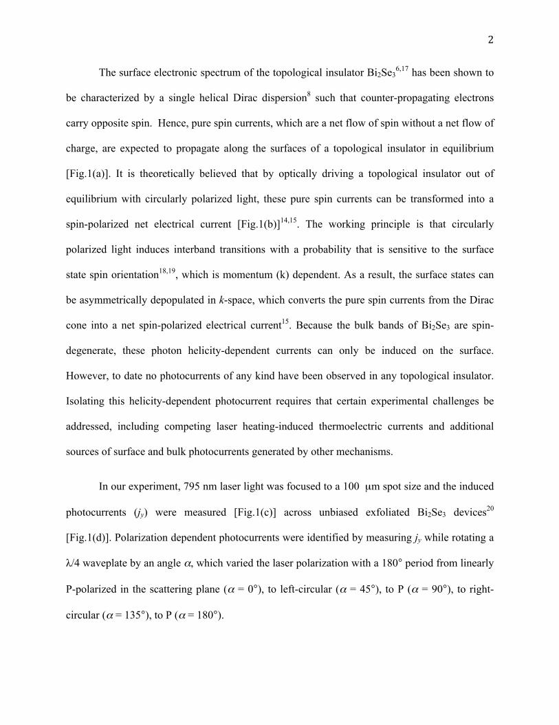
The surface electronic spectrum of the topological insulator Bi2Se36,17 has been shown to
be characterized by a single helical Dirac dispersion8 such that counter-propagating electrons
carry opposite spin. Hence, pure spin currents, which are a net flow of spin without a net flow of
charge, are expected to propagate along the surfaces of a topological insulator in equilibrium
[Fig.1(a)]. It is theoretically believed that by optically driving a topological insulator out of
equilibrium with circularly polarized light, these pure spin currents can be transformed into a
spin-polarized net electrical current [Fig.1(b)]14,15. The working principle is that circularly
polarized light induces interband transitions with a probability that is sensitive to the surface
state spin orientation18,19, which is momentum (k) dependent. As a result, the surface states can
be asymmetrically depopulated in k-space, which converts the pure spin currents from the Dirac
cone into a net spin-polarized electrical current15. Because the bulk bands of Bi2Se3 are spin-
degenerate, these photon helicity-dependent currents can only be induced on the surface.
However, to date no photocurrents of any kind have been observed in any topological insulator.
Isolating this helicity-dependent photocurrent requires that certain experimental challenges be
addressed, including competing laser heating-induced thermoelectric currents and additional
sources of surface and bulk photocurrents generated by other mechanisms.
In our experiment, 795 nm laser light was focused to a 100 µm spot size and the induced
photocurrents (jy) were measured [Fig.1(c)] across unbiased exfoliated Bi2Se3 devices20
[Fig.1(d)]. Polarization dependent photocurrents were identified by measuring jy while rotating a
λ/4 waveplate by an angle α, which varied the laser polarization with a 180° period from linearly
P-polarized in the scattering plane (α = 0°), to left-circular (α = 45°), to P (α = 90°), to right-
circular (α = 135°), to P (α = 180°).

! 3!
Owing to the high thermoelectric power of Bi2Se321, laser induced heat gradients in the
sample are expected to cause a bulk thermoelectric current background in addition to any
photocurrents generated. To isolate the photocurrent response, we varied the heat gradient
between the contacts by sweeping the laser spot position (y) across the Bi2Se3 device [Fig.1(e)] at
a fixed polarization (α = 0°). We find that a current develops that switches polarity across the
sample and is finite exactly at the center of the sample (y = 0). The contribution to jy that
switches polarity can be attributed to a thermoelectric current with electron-like carriers, which is
consistent with our n-type native Bi2Se3 [see Supplementary Information (SI)]. On the other
hand, the finite contribution to jy at y = 0, where the sample is evenly heated and the
thermoelectric current should be minimal, can be attributed to a photocurrent that may encode
aspects of the surface states’ electronic response to light. Figure 1(f) shows that this current
scales linearly with laser intensity, which is a characteristic feature of a photocurrent (SI). All
subsequent measurements were performed at y = 0 and in this low laser intensity regime (I < 60
W/cm2) (SI) where sample heating is minimized.
To investigate the role of spin in generating the photocurrent, we measured the light
polarization dependence of jy at y = 0. Figure 2(a) shows that when light is obliquely incident in
the xz-plane, jy exhibits a strong polarization dependence that is comprised of four components
jy(α) = Csin2α + L1sin4α + L2cos4α + D (1)
The coefficient C parameterizes a helicity-dependent photocurrent because rotating the λ/4
waveplate varies the light polarization between left- and right-circular with the functional form
sin2α. The helicity-dependence indicates that C is generated through a spin-dependent process.

! 4!
This is because left- and right-circularly polarized light preferentially interact with opposite spin
polarizations that are either aligned or anti-aligned to the light’s wavevector18, depending on the
helicity. The other coefficients in eq. (1) parameterize helicity-independent photocurrents that
depend on the linear polarization of light (L1 and L2) and that are polarization-independent (D),
which will be discussed later in the text.
We now move to understand if the spin-mediated photocurrent C is generated by states in
the helical Dirac cone. If this is the case, it should be possible to deduce the surface state spin
distribution by comparing the magnitude of C at different light angles of incidence. Because C is
generated transverse to the light scattering plane (xz-plane) in Fig.2(a), the opposing spin
polarizations that are excited by the different helicities must have a spin component in the xz-
plane and be asymmetrically distributed along the y-direction in k-space. Figure 2(b) shows that
C becomes very small when light is obliquely incident in the yz-plane, such that the device
contacts lie in the light scattering plane. This indicates that the electrons involved in generating C
have a spin polarization that is locked perpendicular to their linear momentum. When light is
normally incident, C completely vanishes [Fig.2(c)], which is characteristic of an in-plane spin
distribution but is more fundamentally required to vanish by the in-plane rotational symmetry of
Bi2Se315. Together these results reveal that the helicity-dependent photocurrent C arises from the
asymmetric optical excitation of the helical Dirac cone.
Having identified that C arises from the Dirac cone, we seek to understand if the
contributions L1, L2, and D in Fig.2(a) also share this origin. In general, the interband transition
probabilities that set photocurrent magnitudes can be highly temperature (T) dependent owing to
the thermal broadening of the Fermi distribution and small changes in the electronic structure
due to changes in the electron-phonon coupling strength22. Therefore, to understand if L1, L2, and
D are governed by the same interband transitions that give rise to C, we compare their detailed T

! 5!
dependence. The inset of Figure 3(a) shows that the fraction of incident photons absorbed by the
sample, the absorptivity (see Methods Summary), exhibits a sharp decrease as T is raised from
15 K. This is generally consistent with the T dependences exhibited by C, L1, L2, and D
[Fig.3(a)]. However, there are two clearly distinct sets of behavior: C and L1 decrease
monotonically to a constant and finite value between 60-293 K, whereas D and L2 decrease
identically to zero after undergoing a polarity reversal between 60-200 K. The similar behavior
shared by L1 and C strongly indicates that their generation mechanisms are deeply related and
that L1 may also have a Dirac cone origin. On the other hand, the D and L2 photocurrents likely
share a different origin.
The origin of D and L2 is revealed through the photon polarization dependence of the
absorptivity, which exhibits only a cos4α modulation [Fig.3(b)]. This is expected because the
maxima of cos4α describe when the incident light is P-polarized, which is the polarization that is
generally absorbed most strongly by solids23. The modulation amplitude is approximately 5% of
the α-independent background, which matches the percentage that the photocurrent component
L2cos4α modulates the α-independent photocurrent D [Fig.3(b)]. This observation, together with
their identical temperature dependence [Fig.3(a)], shows that L2 is a trivial modulation of the
photocurrent D. Because the polarization dependence of the absorptivity is representative of the
bulk index of refraction23, this is an indication that the photocurrent represented by D and L2
likely has a bulk origin.
The observation of polarization-dependent photocurrents that stem from helical Dirac
fermions (C and L1) coexisting with a bulk photocurrent (D and L2) in a topological insulator is
novel and we elaborate on their possible microscopic mechanisms below. The photocurrents C
and L1 arise through the asymmetric excitation of states in k-space and thus fall under the
! 6!
category of circular and linear photogalvanic effects respectively24. Circular and linear
photogalvanic effects have similarly been observed together in spin-orbit coupled quantum well
structures24,25 where the Rashba spin-split valance and conduction bands provide the required
asymmetric spin distribution. It has been theoretically shown for these systems that the two
photogalvanic effects are linked and that their combined magnitude is a measure of the spin
texture’s trivial Berry’s phase26,27. Photogalvanic currents have similarly been predicted to be a
measure of the non-trivial Berry’s phase in topological insulators15. However, determining the
Berry’s phase requires a quantitative measure of the Dirac cone contribution alone. This is
challenging because the depopulation of the Dirac cone using high energy light necessarily
implies a population of bulk-like excited states, which may also carry a net photogalvanic current
[Fig4(a)]. Eliminating these contributions will be possible when more insulating samples become
available and by extending these measurements into the lower energy (sub-bulk gap) THz
radiation regime so that only inter-band transitions within the Dirac cone occur15. While Rashba
spin-split quantum well states have been observed in the inversion layer of some Bi2Se3 samples,
their relative contribution to the circular photogalvanic effect can be expected to be small [SI].
This is because the circular photogalvanic effect from Rashba spin-split bands will have an
inherent cancellation effect arising from the presence of two oppositely spin-polarized Fermi
surfaces, which is absent for topological surface states because of their single Fermi surface [SI].
While we have provided a physical understanding of the circular photogalvanic effect (C) in
topological insulators, the linear photogalvanic effect (L1) requires and awaits a more
comprehensive theoretical treatment.
The bulk nature of the photocurrent described by D and L2 [Fig.3(b)] precludes a
photogalvanic origin because the photogalvanic effect is only permitted at the surface of Bi2Se3
where spin-splitting is present in the electronic structure. This is therefore likely due to a

! 7!
different mechanism that is allowed in the bulk called the photon drag effect28-31. Photon drag
describes photocurrents that result from the transfer of linear momentum from incident photons
to excited carriers [Fig.4(b)], thus permitting a photocurrent even if states are symmetrically
distributed in k-space. Helicity-independent photon drag photocurrents generated transverse to
the direction of momentum transfer, consistent with what we observe, have been attributed in
conventional semiconductors to an aspheric bulk band structure30, which is also present in Bi2Se3
and may be the origin of D and L2. Recently, a new helicity-dependent form of photon drag was
observed alongside photogalvanic currents in a quantum well system25. It was proposed that the
photon momentum transfer opened a spin-dependent relaxation channel in the spin-split valance
band that created a spin-polarized current. A similar process may be able to take place on the
surface of a topological insulator where the required spin-splitting is provided by the Dirac cone.
However, the bulk spin-degeneracy of Bi2Se3 enables us to rule out this and related32 bulk
photocurrent contributions to C and L1. While a photo-induced inverse spin Hall effect has been
observed in GaAs and related materials, the exceptionally short spin lifetime of bulk optically
spin oriented carriers will make contributions from this effect very small [SI].
Our measurements show that the polarization of light can be used to generate and control
photocurrents originating from topological surface states. The photocurrents observed are only
one of many possible non-equilibrium properties of a topologically ordered phase11-15 and there
are features in our data that call for a detailed theoretical treatment. In addition to the possibility
of measuring fundamental physical quantities, like the Berry’s phase15,26,27, optically induced
currents provide a promising route to generate and control spin-polarized currents purely at an
isolated surface or buried interface, which could be harnessed for spintronic applications16.
! 8!
Methods Summary.
Bi2Se3 was synthesized and devices were fabricated using the techniques reported in Ref. 20. 80
fs pulses of 795 nm (1.56 eV) laser light were derived from a Ti:sapphire oscillator at a repetition
rate of 80MHz. Data were corrected for small variations in laser intensity as a function of α due
to λ/4 waveplate imperfections. A 50x microscope objective and a high resolution CCD camera
were used to align the beam and device position with one µm accuracy. The absorptivity was
determined by performing reflectivity measurements on a bulk single crystal from the same ingot
used to fabricate devices.
References
1. Moore, J.E. The birth of topological insulators. Nature 464, 194-198 (2010). 2. Hasan, M.Z. & Kane, C.L. Colloquium: topological insulators. Rev. Mod. Phys. 82, 3045-3067 (2010). 3. Qi, X.-L. & Zhang, S.-C. Topological insulators and superconductors. Rev. Mod. Phys. 83, 1057-1110 (2011).
4. Hsieh, D. et al. A topological Dirac insulator in a quantum spin Hall phase. Nature 452, 970-974 (2008).
5. Hsieh, D. et al. Observation of unconventional quantum spin textures in topological insulators. Science 323, 919-922 (2009). 6. Xia, Y. et al. Observation of a large-gap topological-insulator class with a single Dirac cone on the surface. Nature Phys. 5, 398-402 (2009). 7. Chen, Y.L et al. Experimental realization of a three-dimensional topological insulator, Bi2Te3. Science 325, 178-181 (2009).
8. Hsieh, D. et al. A tunable topological insulator in the spin helical Dirac transport regime. Nature 460, 1101-1105 (2009). 9. Roushan, P. et al. Topological surface states protected from backscattering by chiral spin texture. Nature 460, 1106-1109 (2009). 10. Alpichshev, Z. et al. STM imaging of electronic waves on the surface of Bi2Te3: topologically protected surface states and hexagonal warping effects. Phys. Rev. Lett. 104,

! 9!
016401 (2010). 11. Inoue, J. I. & Tanaka, A. Photo-induced transition between conventional and topological insulators in two-dimensional electronic systems. Phys. Rev. Lett. 105, 017401 (2010). 12. Lindner, N. H., Refael, G. & Galitski, V. Floquet topological insulator in semiconductor quantum wells. Nature Phys. 7, 490-495 (2011). 13. Kitagawa, T., Oka, T., Bataas, A., Fu, L., Demler, E. Transport properties of non-equilibrium systems under the application of light: Photo-induced quantum Hall insulators without Landau levels. Preprint at http://arxiv.org/pdf/1104.4636v3 (2011). 14. Raghu, S., Chung, S.B, Qi, X.-L. & Zhang, S.-C. Collective modes of a helical liquid. Phys. Rev. Lett. 104, 116401 (2010).
15. Hosur, P. Circular photogalvanic effect on topological insulator surfaces: Berry-curvature-dependent response. Phys. Rev. B 83, 035309 (2011). 16. Wunderlich, J. et al., Spin hall effect transistor. Science 330, 1801-1804 (2010). 17. Zhang, H. et al. Topological insulators in Bi2Se3, Bi2Te3 and Sb2Te3 with a single Dirac cone on the surface. Nature Phys. 5, 438-442 (2009).
18. Meier, F. & Zakharchenya, B. Optical Orientation (Elsevier Science Publishing, Amsterdam, 1984). 19. Wang, Y.H. et al. Observation of a warped helical spin texture in Bi2Se3 from circular dichroism angle-resolved photoemission spectroscopy. Phys. Rev. Lett. 107, 207602 (2011). 20. Steinberg, H., Gardner, D. R., Lee, Y. S. & Jarillo-Herrero, P. Surface state transport and ambipolar electric field effect in Bi2Se3 nanodevices. Nano Lett. 10, 5032-5036 (2010). 21. Nolas, G.S., Sharp, J. & Goldsmid, H. J. Thermoelectrics: Basic Principles and New Materials Developments (Springer-Verlag, Berlin, 2001). p. 123 22. Lautenschlager, P., Garriga, M., Vina, L. & Cardona, M. Temperature dependence of the dielectric function and interband critical points in silicon. Phys. Rev. B 36, 4821-4830 (1987). 23. Hecht, E. Optics (4th ed., Addison Wesley, San Fransisco, 2002). p. 113. 24. Ganichev, S.D. & Prettl, W. Spin photocurrents in quantum wells. J. Phys.: Condens. Matter 15, R935-R983 (2003).
25. Diehl, H. et al. Spin photocurrents in (110)-grown quantum well structures. New J. Phys. 9, 349 (2007). 26. Deyo, E., Golub, L.E., Ivchenko, E.L., & Spivak, B. arXiv:0904.1917 (2009).

! 10!
27. Moore, J. E. & Orenstein, J. Confinement-induced Berry phase and helicity-dependent photocurrents. Phys. Rev. Lett. 105, 026805 (2010). 28. Danishevskii, A.M., Kastal’skii, A.A., Ryvkin, S.M. & Yaroshetskii, I.D. Dragging of free carriers by photons in direct interband transitions in semiconductors. Sov. Phys. JETP 31, 292-295 (1970). 29. Gibson, A.F. & Walker, A.C. Sign reversal of the photon drag effect in p-type germanium. J. Phys. C: Solid State Phys. 4, 2209 (1971). 30. Hattori, H., Umeno, M., Jimbo, T., Fujitani, O. & Miki, S. Anisotropic properties of photon drag effect in p-type germanium. J. Phys. Soc. Jpn. 35, 826-831 (1973). 31. Hatano, T., Ishihara, T., Tikhodeev, S. & Gippius, N. Transverse photovoltage induced by circularly polarized light. Phys. Rev. Lett. 103, 103906 (2009). 32. Ganichev, S.D. et al. Spin-galvanic effect due to optical spin orientation in n-type GaAs quantum well structures. Phys. Rev. B 68, 081302(R) (2003).
Acknowledgements.
This work was supported by DOE award number DE-FG02-08ER46521, performed in part at the
NSF funded Harvard Center for Nanoscale Systems and made use of the MRSEC Shared
Experimental Facilities supported by the National Science Foundation under award number
DMR - 0819762. J.W.M. acknowledges financial support from an NSF graduate research
fellowship. D.H. acknowledges support from a Pappalardo postdoctoral fellowship. H.S.
acknowledges support from the Israeli Ministry of Science. P.J-H. acknowledges support from
DOE Early Career Award number DE.SC0006418 and Packard Fellowship.

! 11!
Fig. 1: Isolation of a photocurrent response from a thermoelectric current background. (a) Pure spin currents from the Dirac cone in equilibrium due to cancelling electrical current contributions j. (b) Spin-polarized electrical current induced by optically driving the Dirac cone with circularly polarized light. (c) Schematic of the experimental geometry. The laser beam is incident on the device at the out-of-plane angle θ defined from the xy-plane and the in-plane angle φ. Photon polarization varied by rotating the λ/4 waveplate (QWP) and photo-induced currents jy were measured. (d) AFM image of a typical two-terminal 120 nm thick Bi2Se3 device. (e) jy/I with light obliquely incident at θ = 56º in the xz-plane as a function of beam focus position y at room temperature where y = 0 is the center of the sample. The red arrows in the inset represent beam position as it is scanned across the sample. (f) jy as a function of laser intensity I at y = 0 at 15 K. Fig. 2: A surface photocurrent originating from helical Dirac fermions. (a) jy(α)/I with light obliquely incident at θ = 56º in the xz-plane at 15 K. The solid red line is a fit to eq. (1) and the fit results are shown. (b) jy(α)/I with light obliquely incident at θ = 56º in the yz-plane at 15 K. (c) jy(α)/I with light normally incident (θ = 90º) and φ = 180º so that the laser electric field is perpendicular to the contacts at α = 0 at 15 K. Fig. 3: Distinct photocurrent contributions separated by temperature dependence. (a) Fit results for jy(α)/I as a function of temperature for the geometry in Fig.2(a). Inset: Optical absorptivity as a function of temperature with P-polarized light (α = 0) at θ = 56º. (b) Percent change of the absorptivity and L2cos4α /D as a function of photon polarization at room temperature. Fig. 4: Microscopic mechanisms of photocurrent generation. (a) k-space depiction of photon helicity-induced currents from the Dirac cone via the circular photogalvanic effect including contributions from excited states. (b) k-space depiction of photon drag. The optical transition arrows are tilted to account for the transfer of linear photon momentum.
2 +m
(c)
(e)
Beam y-position (+m)
j y/I (
pA W
-1cm
2 )
0 50-50 100-100
1
2
3
0
-1
photocurrent
thermoelectriccurrent
A
Laser Intensity (W/cm2)
j y (nA
)
0 20 40 60 80 100
1
2
3
0
(f)
y=0
A
Fig.1 Gedik
(d)(a)
(b)
E
k
yx

3-3 Fit amplitude
CL1
DL2
( .07)
(c)(b)
3-3 Fit amplitude
CL1
DL2
( .07)3Fit amplitude
CL1
DL2
( .07)-3
(a)
jy = Csin2 + L1sin4 + L2cos4 + D_ _ _
Photon polarization
0
4
8
20
24
28
Photon polarization
j y/I (
pA W
-1 cm
2 )
36
40
44
Photon polarization
e�= 56q�= 180
e�= 56q�= 270
e�= 90q�= 180
Fig.2 Gedik
A AA

Fit a
mp.
(pA
W-1
cm
2 )
Temperature (K)0 100 200 300
C L1 L2 D
3
2
1
0
-1
-2
(a)
( .06)
Photon polarization
0 300.58
T
.61
A
0
+5_��
(b)
Absorptivity L2cos4 /D_
Perc
ent c
hang
e
-5
e�= 56
Fig.3 Gedik

Fig.4 Gedik
(b)(a) Photogalvanic Effect Photon Drag Effect