Embed Size (px)
Citation preview
1
Vol.:(0123456789)
Scientific Reports | (2020) 10:18781 | https://doi.org/10.1038/s41598-020-75764-5
www.nature.com/scientificreports
Controllable deposition of organic metal halide perovskite films with wafer‑scale uniformity by single source flash evaporationWoocheol Lee1,5, Jonghoon Lee1,5, Hyeon‑Dong Lee2, Junwoo Kim1, Heebeom Ahn1, Youngrok Kim1, Daekyoung Yoo1, Jeongjae Lee3, Tae‑Woo Lee2,4, Keehoon Kang1* & Takhee Lee1*
Conventional solution‑processing techniques such as the spin‑coating method have been used successfully to reveal excellent properties of organic–inorganic halide perovskites (OHPs) for optoelectronic devices such as solar cell and light‑emitting diode, but it is essential to explore other deposition techniques compatible with large‑scale production. Single‑source flash evaporation technique, in which a single source of materials of interest is rapidly heated to be deposited in a few seconds, is one of the candidate techniques for large‑scale thin film deposition of OHPs. In this work, we investigated the reliability and controllability of the single‑source flash evaporation technique for methylammonium lead iodide (MAPbI3) perovskite. In‑depth statistical analysis was employed to demonstrate that the MAPbI3 films prepared via the flash evaporation have an ultrasmooth surface and uniform thickness throughout the 4‑inch wafer scale. We also show that the thickness and grain size of the MAPbI3 film can be controlled by adjusting the amount of the source and number of deposition steps. Finally, the excellent large‑area uniformity of the physical properties of the deposited thin films can be transferred to the uniformity in the device performance of MAPbI3 photodetectors prepared by flash evaporation which exhibited the responsivity of 0.2 A/W and detectivity of 3.82 × 10¹¹ Jones.
Organo-metal halide perovskites (OHPs) have come into the spotlight as the power conversion efficiency of solar cell using OHPs has increased dramatically in the past few years1–7. Since then, OHPs have demonstrated com-pliant performance in other optoeletronic devices such as light emitting diodes (LEDs)8–12, photodetectors13,14, lasers15 and phototransistors16. Out of various methods studied in the field, solution-processing2,17,18, thermal evaporation19,20 and chemical vapor deposition21,22 have gained the most attention as methods for depositing OHP thin films. Especially, spin-coating is the most commonly used lab-scale deposition method because it is a low-cost and easily accessible process. Although some works have reported remarkable device performances in large-area perovskite optoelectronic devices made with spin-coated perovskite films9,23, the solution-process fundamentally imposes limitations in reliably producing uniform films over a large area. In addition, the spin-coating methods have evolved to achieve high-quality OHP films for state-of-the-art devices by adopting addi-tional techniques17 such as hot-casting2,5, solvent engineering24,25 and two-step sequential deposition3,26,27, which inevitably adds complexities, and therefore reduces the overall controllability of the process.
The evaporation method, on the other hand, has a potential for uniform large-area film deposition28,29, con-formal film deposition on uneven surfaces30, as well as a simple patterning with shadow masks31. Additionally, since it is a solvent-free process, there is no need to consider surface tension or solubility of the underlying layer. Organo-halide precursor (e.g. methylammonium iodide, MAI) and lead-source precursor (e.g. lead iodide, PbI2) can be thermally evaporated by co-evaporation method19,32, sequential deposition33–35 or vapour-assisted
OPEN
1Department of Physics and Astronomy, and Institute of Applied Physics, Seoul National University, Seoul 08826, Korea. 2Department of Materials Science and Engineering, Seoul National University, Seoul 08826, Korea. 3School of Earth and Environmental Sciences, Seoul National University, Seoul 08826, Korea. 4School of Chemical and Biological Engineering, Institute of Engineering Research, Research Institute of Advanced Materials, Nano Systems Institute (NSI), Seoul National University, Seoul 08826, Korea. 5These authors contributed equally: Woocheol Lee and Jonghoon Lee. *email: [email protected]; [email protected]
2
Vol:.(1234567890)
Scientific Reports | (2020) 10:18781 | https://doi.org/10.1038/s41598-020-75764-5
www.nature.com/scientificreports/
deposition36,37 to form OHP (e.g. methylammonium lead iodide, MAPbI3) films. Although these deposition methods are well-established, it is still challenging to produce OHP films with the desired stoichiometric ratio between the three different ionic components by evaporation because the precursors have very different vapori-zation temperatures28.
Flash evaporation method has gained attention as a candidate for evaporating two or more precursors from a single thermal source by rapidly raising the temperature in a very short time20,30,31,38–41. In principle, the rapid vaporization of the precursors induces complete and uniform evaporation of the precursors, while maintain-ing the same ratio between the different components in OHP. Solar cells with flash evaporated OHP films have exhibited over 10% of power conversion efficiency39,41, which is comparable to the early stage spin-coated OHP films17,42. Furthermore, the flash evaporation method has been expanded to deposit OHP films with mixed cation and halide species30, which is challenging for the aforementioned other evaporation methods28. Although this aspect of flash evaporation presents a prospect of exploring a diverse compositional range of OHPs, there has been relatively a few reports which have systematically studied the controllability of the flash evaporation method and the uniformity of OHP films produced by this method. Especially, flash evaporated OHP films have only been reported to be uniform in small areas, but wafer-scale uniformity has rarely been investigated to assess its applicability for mass-producing devices with uniform performance. In this paper, we demonstrate that OHP films with wafer-scale uniformity can be formed by flash evaporation. In addition, it is difficult to monitor the deposition rate and control the resulting film thickness with flash evaporation due to the rapid nature of the evaporation process, unlike other methods. For optoelectronic devices, the thickness of the active layer is critical in determining the device performance43,44. Therefore, a reliable deposition of OHP films with controllability over a wide range of target thicknesses is desired for meeting different requirements in terms of film characteristics for various device applications. Our study directly shows that the thickness of flash evaporated OHP films can be controlled by simply adjusting the mass of the source material. Similarly, we discovered that the grain size of the flash evaporated OHP films varied with the mass of the source materials loaded, and that the grain size could even be controlled by introducing multi-step depositions.
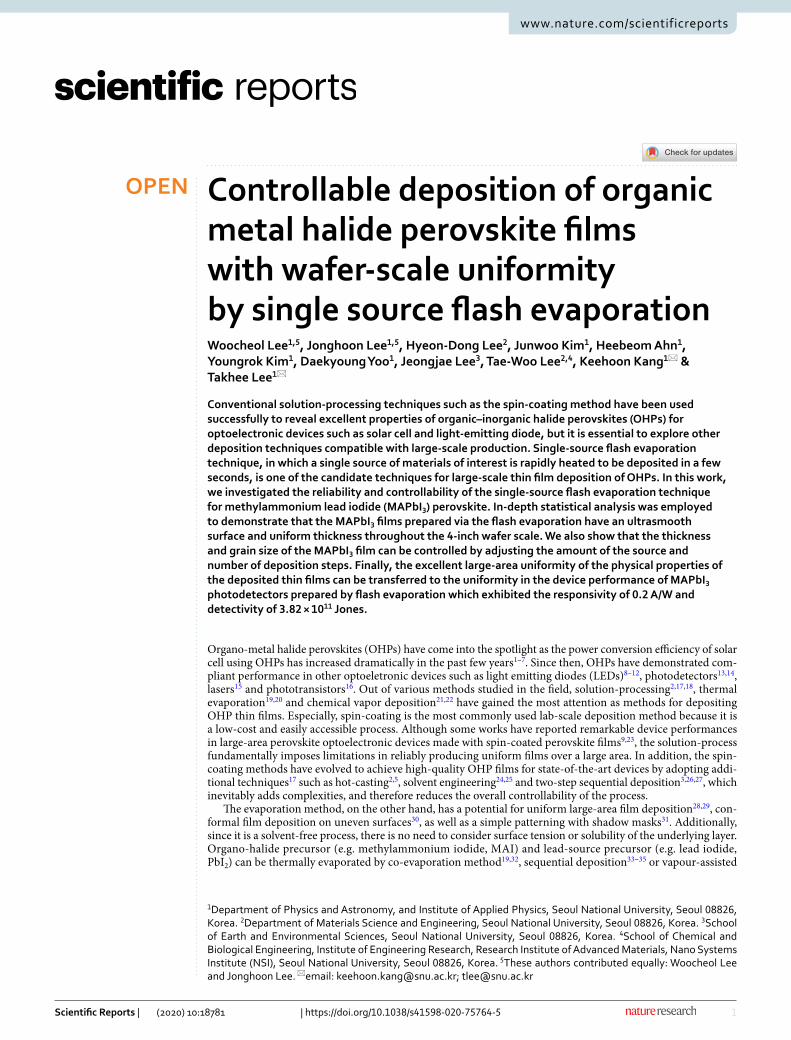
Results and discussionIn this study, we focused on the deposition of MAPbI3 films (see Fig. 1a for the crystal structure) by flash evaporation. Figure 1b shows a schematic image of the flash evaporation process adopted in this work. The pre-synthesized MAPbI3 single crystal powder was used as the source instead of PbI2 and MAI precursors (see the inset of Fig. 1b) in order to obtain better quality films owing to an exact stoichiometric ratio between the
Figure 1. (a) Schematic illustration of MAPbI3 crystal structure. (b) Schematic illustration of deposition of organo-halide perovskite film via flash evaporation. The inset shows photographs of MAPbI3 single crystal powder. (c) A photograph of the substrate holder for film uniformity test with the labels that indicate the location of the substrates (from A to F).

3
Vol.:(0123456789)
Scientific Reports | (2020) 10:18781 | https://doi.org/10.1038/s41598-020-75764-5
www.nature.com/scientificreports/
different ionic components of MAPbI3 within the single crystal30,45. The exact amount of single crystal powder was loaded on the tungsten boat which is located inside of vacuum chamber. The source-to-substrate distance was designed to be 30 cm which is the longest distance among source-to-substrate distances of flash evaporation reported so far20,31,38,40,41. This is so that we could achieve a uniform deposition of MAPbI3 over a large area at the substrate end. The MAPbI3 single crystal powder was heated by rapidly ramping up the heater current to 100 A in 3 s at a constant voltage of 0.31 V. The powder was then evaporated within 60 s and deposited on substrates which were located on specific locations of the holder. Throughout this paper, we will refer to different sample locations in the 4-inch wafer size substrate holder as labeled in Fig. 1c (substrate location A to F) to assess the uniformity of the deposited MAPbI3 film.
We checked the film quality of flash evaporated MAPbI3 films by probing their structural and optical prop-erties as shown in Figs. 2 and 3. An optical micrograph of the flash evaporated MAPbI3 film patterned by a shadow mask showed a smooth and clean film with a clearly distinguishable boundary at the edge (see Fig. 2a). The top-surface images of the films measured by field emission scanning electron microscope (FE-SEM) and atomic force microscope (AFM) are presented in Fig. 2b,c, respectively. A typical grain size determined from the FE-SEM image is 40 nm which we will discuss further later in the paper. A smooth and pinhole-free surface was observed with the roughness of approximately 5 nm (2.86 nm locally, Fig. 2c).
Figure 3a shows the X-ray diffraction (XRD) results. The green line shows the XRD result of the single crystal powders of MAPbI3 used as the source, which closely resembles the calculated XRD results. It signifies that a high purity MAPbI3 single crystal powders were successfully synthesized. The blue and red lines show the XRD results of the flash evaporated and spin-coated MAPbI3 films, respectively. The positions of the (110) and (220) peaks were the same for all the XRD results (14.1° and 28.5°, respectively), confirming the identical crystal structure of the flash evaporated MAPbI3 film with those prepared by other methods. As no peaks other than (110) and (220) peaks appeared, the deposited MAPbI3 films exhibit a strong preferred orientation along the (110) surface30,32,46,47. In addition, the high purity of the flash evaporated film is indicated by the absence of diffraction peaks that correspond to PbI2 (asterisk marks (12.6°)). Note that this is an interesting observation because many previous studies31,38,40,41 have demonstrated that the addition of excess MAI was necessary to deposit pure MAPbI3 films without PbI2 impurities (detailed discussion could be found in the Supplementary Information Sect. 1).
UV–visible absorbance and photoluminescence (PL) spectra were taken to investigate the optical properties of the flash evaporated MAPbI3 film (see Fig. 3b). The estimated optical bandgap from the absorbance spectrum by using the Tauc plot48 is 1.61 eV (see the inset of Fig. 3b) and PL peak is shown at 756 nm with a full-width-half-maximum (FWHM) of 45 nm, both of which agree well with the reported values for MAPbI3 in literature15,49.
Figure 2. (a) An optical microscope image of the flash evaporated MAPbI3 film. (b) SEM image and (c) AFM images of flash evaporated MAPbI3 film surface.

4
Vol:.(1234567890)
Scientific Reports | (2020) 10:18781 | https://doi.org/10.1038/s41598-020-75764-5
www.nature.com/scientificreports/
When compared with the spin-coated MAPbI3 film produced as a reference sample, it showed similar absorbance and PL spectra (see Fig. S1 in the Supplementary Information). From the structural and optical characterizations, we could safely confirm that our flash evaporated MAPbI3 films had a high film quality without a significant amount of impurities formed.
We checked that the evaporated perovskite films had a uniform thickness and the same optical properties over the whole wafer. Before testing wafer-scale film uniformity, we compared the film uniformity between the flash evaporated perovskite film to spin-coated perovskite film (reference) on the 1.5 × 1.5 cm2 substrate. The thickness values of both films were measured by randomly selecting 20 points on cross-sectional FE-SEM images (see Fig. S2 in the Supplementary Information). The average thickness values of the flash evaporated and spin-coated films were similar (207.1 nm and 225.0 nm, respectively), while the standard deviation for the spin-coated film was about 10 times larger (30.2 nm compared to 3.0 nm for the flash evaporated film). Given that the standard deviation value of 3.0 nm for the flash evaporated film is similar to the surface roughness value measured by AFM, the variation in the sampled thickness values can be assumed to be due to the morphology, not the variation in the actual thickness within the film. It can be seen that the film made by flash evaporation has a much uniform thickness and a smooth surface.
In order to investigate whether there was a change in the thickness depending on the location over the 4-inch wafer, cross-sectional FE-SEM images were taken for the evaporated films at each substrate location labeled according to Fig. 1c (Fig. 4a). The thickness values were measured at 20 points of the film for each substrate in order to carry out statistical analysis. Figure 4b is a graph summarizing the thickness values extracted from each substrate location drawn as a box and whisker diagram. The dots within the boxes represent the average values and boxes show the first and third quartile range of each distribution. The lines inside the box represent median values and the whiskers show the minimum and maximum values. The box and whisker diagrams show the similarity in the distribution of the thickness values at different locations. Figure 4c shows the distribution for all the measured 120 thickness values from the different locations shown in Fig. 4b plotted together in one histogram. The thickness values did not significantly deviate from the average value of 115.6 nm (the standard deviation was 3.1 nm) at all substrate locations. More importantly, there were no multiple peaks in the normal distribution fit, which suggests that all the thickness values belong to a single distribution. Tukey–Kramer honest significant difference test (Tukey test)50 was performed to quantitatively determine whether the distributions of the thickness values at the six different substrate locations (shown in Fig. 4b) can be judged as the same distribu-tion. Tukey test is a statistical test that compares multiple distributions simultaneously and shows how different they are from each other, which can be used to categorize similar distributions into separate groups. The detailed descriptions and raw data are presented in Sect. 4 in the Supplementary Information. Figure 4d is a graphical visualization of the Tukey test results. The comparison circles are shown in Fig. 4d have their centers each aligned with the average thickness values and the radii proportional to the standard deviation values of each distribution. The more the comparison circles overlap, the more similar the distributions are. Here, the comparison circles are all overlapped and therefore all the distributions can be judged as the same distribution sampled from the same population. Analysis of variance (ANOVA) test51 was also run to support whether the average values of two or more distributions are statistically identical (see Sect. 4 in Supplementary Information). Thus, all the average thickness values at each substrate location can be considered statistically identical. To visualize the uniformity in the film thickness over the whole 4-inch wafer, we used a color map to plot the average values of the film thickness at each substrate location from A to F (Fig. 4e). The average thickness values at each substrate location differed by less than 2 nm which is smaller than the standard deviation value of 3.1 nm (Fig. 4c). Figure 4f shows simulation results obtained by the Gaussian process regression with the whole 120 thickness data. The varia-tion of the predicted thickness across the wafer was as small as approximately 2 Å. In addition to the thickness
Figure 3. (a) XRD data of the flash evaporated film, spin-coated film and single crystal powder. Calculated results from the unit cell of MAPbI3 are also shown. (b) UV–visible absorbance and PL spectra of MAPbI3 film deposited via flash evaporation. The inset shows Tauc plot to estimate the optical bandgap of the perovskite film.

5
Vol.:(0123456789)
Scientific Reports | (2020) 10:18781 | https://doi.org/10.1038/s41598-020-75764-5
www.nature.com/scientificreports/
measurement, UV–visible absorbance and PL spectra were measured for the films deposited at each substrate location to confirm that they all have the same absorbance and PL responses regardless of location (see Fig. 4g and Fig. S3 in the Supplementary Information). All these results consistently support the wafer-scale uniformity of the flash evaporated perovskite film over the 4-inch wafer.
The controllability of the flash evaporation method was demonstrated by depositing various thicknesses of perovskite films by varying the weight of the source materials. The thicknesses of the films were measured by using a cross-sectional FE-SEM as in the uniformity measurement. The thickness increased linearly with increas-ing the weight of the source from 50 to 750 mg (see the red triangle points in Fig. 5a). However, as the weight of the source exceeded 750 mg, the increase in the thickness became sub-linear. In order to mitigate the non-linear relationship above the threshold weight of the source of 750 mg, we introduced a multi-step deposition (i.e. the perovskite films were successively deposited multiple times). For example, to deposit a target thickness of 250 nm, 500 mg of the source perovskite powders were deposited twice (a total of 1000 mg), which could then be described by a linear relationship again (see the blue diamond points in Fig. 5a). Figure 5b shows the representative cross-sectional SEM images of MAPbI3 films deposited with different weights of the source. Flash evaporation with 1500 mg of the source powders does not yield twice the thickness of the MAPbI3 film with 750 mg of the source powders. However, successively evaporating 750 mg of the source twice gives a MAPbI3 film twice the thickness (See Fig. 5b).
We discovered that the grain size could also be controlled by varying the weight of the source powders. The grain size tended to increase as the source mass increased (Fig. 5c,d). We also discovered that the grain size did not vary significantly depending on the number of deposition steps while the thickness increased linearly for a double-step (390 nm) and triple-step (620 nm) evaporated films for the source mass of 750 mg (see Fig. S4 in the Supplementary Information for more details), which potentially provides a way for controlling the grain size independently with the thickness (see the inset of Fig. 4d for the predicted range of grain size for each thickness). The grain size of crystals in perovskite films, along with its thickness, is an important parameter that determines the device performance of optoelectronic devices. In the case of solar cells, the carriers should be able to move freely from the active layer (the point of generation within) to the electrodes (where they are extracted), so the larger the grain, the better the collection efficiency40. In the case of LEDs, a higher rate of recombination is desired, and therefore a smaller grain size would be required to fabricate LEDs with higher emission efficiencies52. Therefore, our findings can be highly relevant for investigating the relationship between the grain size and device performance of optoelectronic devices based on flash evaporated perovskite films.
In order to demonstrate how the wafer-scale film uniformity discussed so far can be transferred to the uni-formity in the optoelectronic device performance, we fabricated photodetectors which are one of the most suit-able devices due to their simple structures that require only the deposition of two top contact electrodes on evaporated perovskite films (see the inset of Fig. 6a for the device structure). For performance comparison, a photodetector using spin-coated MAPbI3 film was also fabricated. The data for the photodetector with
Figure 4. Uniformity test of flash evaporated MAPbI3 films. (a) Cross-sectional SEM images for the thickness comparison of the MAPbI3 film by the substrate location given in Fig. 1c. (b) The measured thickness values presented in box and whisker diagram at each location. (c) A histogram of all the thickness data. (d) Comparison circles from the Tukey test. (e) Color map image of the average thickness values at each substrate location on the 4-inch wafer. (f) The estimated thickness of the perovskite film by Gaussian process. (g) UV–visible absorbance spectra of the MAPbI3 films at the different substrate locations.

6
Vol:.(1234567890)
Scientific Reports | (2020) 10:18781 | https://doi.org/10.1038/s41598-020-75764-5
www.nature.com/scientificreports/
spin-coated MAPbI3 film are shown in Figs. S5 and S6 in the Supplementary Information. The detailed fabrica-tion process is explained in the Methods section. Figure 6a shows typical current–voltage curves of the photo-detector with the evaporated film under light illumination with 532 nm wavelength and various laser intensities. The photocurrent gradually increased with increasing the laser intensity due to increased photogenerated carrier concentrations (see Fig. S6(a) in the Supplementary Information). The responsivity (R) which is the ratio of the
Figure 5. (a) A graph of thickness of the flash evaporated perovskite film as a function of the amount of the MAPbI3 single crystal power source. (b) Cross-sectional SEM images for a single- and multi-step deposited perovskite films by flash evaporation for comparison. (c) Top-view SEM images for showing grain size variation for deposition with different source mass. (d) Grain size correlation graph of the deposited perovskite films according to the source mass. The inset shows a predicted controllable range of the grain size and thickness of the MAPbI3 films by the empirical fit shown as the dashed line.
Figure 6. Device characteristics of photodetectors prepared by flash evaporation. (a) I–V characteristics under 520 nm laser with different intensities. The inset shows the optical microscope image of the fabricated MAPbI3 photodetector. (b) Time-dependent photoresponse of the photodetector under few cycles of turn-on and off. (c) The I–V characteristics under light and dark conditions for the photodetectors prepared by the flash evaporated films at the different substrate locations.

7
Vol.:(0123456789)
Scientific Reports | (2020) 10:18781 | https://doi.org/10.1038/s41598-020-75764-5
www.nature.com/scientificreports/
excess current generated by light illumination to the incident light power was studied. The responsivity decreased as the light power increased (see Fig. S6(b) in the Supplementary Information). This can be attributed to the increase of carrier–carrier scattering or filling the deep trap states with a longer lifetime, which tends to provide a higher photocurrent at a lower light power53–55. The estimated responsivity is 0.20 A/W for the photodetector with the flash evaporated film and 0.55 A/W for the photodetector with the spin-coated film at a bias of 20 V and light power of 0.21 uW. Detectivity (D*) which is another parameter to characterize the sensitivity of pho-
todetection was calculated according to D∗= R
(
2eIdarkA
)
−1
2 , where Idark is the dark current, A is the area of the photosensitive region and e is the electric charge (see Fig. S6(c) in the Supplementary Information). The highest value of detectivity was found to be 3.82 × 10¹¹ Jones within the measured range for the photodetector with the flash evaporated film. This is a comparable value to the detectivity of 6.14 × 10¹¹ Jones for the device with the spin-coated film. These device performance parameters are comparable to the previously reported MAPbI3-based photodetectors31,56–58 and commercial Si photodetectors (< 0.2 A/W)47,59. Figure 6b displays repeated on/off operation of the photodetector with the flash evaporated MAPbI3 film. The device showed relatively fast photo-responses (< 1 s), stable and reproducible operation during the measurement cycles. Finally, in order to demon-strate how the wafer-scale film uniformity discussed above can be transferred to the uniformity in the photode-tector device performance, we fabricated photodetectors with flash evaporated films at different locations (see Fig. 6c). The measured device characteristics were nearly identical regardless of the sample substrate locations (B, C, and F), which shows that we can achieve the wafer-scale uniformity in the device performance by our flash evaporation method.
Conclusions. We designed a single-source flash evaporation setup with a long source-to-substrate distance to deposit MAPbI3 films directly over 4-inch wafer. The thicknesses of the films were measured at various loca-tions of the 4-inch wafer and statistically analyzed to demonstrate that the thicknesses of the films were con-stant throughout the whole 4-inch wafer. The optical properties of the flash evaporated films were also identical throughout the wafer. The correlation between the amount of the single crystal perovskite powders loaded to the source and the thickness of the deposited film was studied to demonstrate the controllability of the evapora-tion. We observed that the deposited MAPbI3 film thickness was proportional to the source mass until a critical point, above which the film thickness started to saturate. The proportionality was recovered by introducing the multiple numbers of deposition steps which additionally provided a way for controlling the grain size by varying the source mass and number of deposition steps. The wafer-scale uniformity was preserved for photodetec-tor devices fabricated with flash evaporated MAPbI3 films. The fabricated devices showed the responsivity of 0.2 A/W and detectivity of 3.82 × 10¹¹ Jones which are comparable to the previously reported MAPbI3-based photodetectors. Our results demonstrate that single-source flash evaporation can be a promising route towards controllably and reliably depositing large-area perovskite films, and therefore producing perovskite-based opto-electronic devices in large-scale.
MethodsSynthesis of MAPbI3. 2.66 g of PbO and 1.90 g of CH3NH3I (MAI) were dispersed in a mixed acid solution of HI (18 ml, 57 wt% in water) and H3PO2 (2 ml, 50 wt% in water). The solution was heated at 130 °C until all the precursors were dissolved. The solution was then cooled to room temperature to precipitate MAPbI3 single crystals. The crystals were isolated by filtration and dried in vacuum conditions.
Film preparation. Substrate cleaning. The thermally grown 270 nm thick SiO2 on Si substrate and glass were sequentially cleaned with acetone, 2-propanol, and deionized water in a sonicator for 10 min at each step. SiO2 and glass substrates were exposed to 50 W, 30 sccm condition of O2 plasma for 120 s.
Deposition of MAPbI3 film by flash evaporation. Prepared MAPbI3 powder was placed into a tungsten boat. After the pressure in a chamber pumped down to below 1 × 10⁻⁶ Torr, the substrate holder was rotated in 24 rpm for film uniformity, and the current of tungsten boat was rapidly increased to 100 A in 3 s. Then, the temperature of the tungsten boat was raised rapidly and MAPbI3 powder sublimated. The nominal deposition rate read by the sensor was approximately 50–80 Å/s. When the deposition rate decreased to 0.1 Å/s, the process was terminated and the total deposition time was within 60 s.
Deposition of MAPbI3 film by spin‑coating. Spin-coating was conducted according to the known hot-casting method2. 0.5 M of perovskite precursor solution was prepared by dissolving the prepared MAPbI3 powder in DMF. The cleaned substrate was heated at 120 °C on the hot plate. Then, the heated substrate was quickly moved to the spin-coater and the precursor solution was spin-coated on the substrate for 40 s at 5000 rpm.
Fabrication of photodetector. The Au top electrode lines with 50 μm width and 50 nm thickness were deposited using a patterned shadow mask on prepared perovskite film. The electron-beam evaporator pressure was 1 × 10⁻⁶ Torr and the value of the Au deposition rate on the sensor was approximately 1 Å/s.
Film characterization. SEM measurements. The thickness and surface morphology of the perovskite film were analyzed by FE-SEM (JSM-7800F Prime) using an electron beam accelerated at 5 kV for surface morphol-ogy study and 10 kV for thickness study.

8
Vol:.(1234567890)
Scientific Reports | (2020) 10:18781 | https://doi.org/10.1038/s41598-020-75764-5
www.nature.com/scientificreports/
XRD measurements. Crystallographic structures of perovskite films were analyzed by high resolution X-ray diffraction (HRXRD) technique (Rigaku Smartlab).
Steady‑state PL measurements. Steady-state PL spectra of the thin film samples (glass/MAPbI3 film) were measured using a spectrofluorometer (JASCO FP-8500). The excitation wavelength was 520 nm and used Xenon arc lamp (150 W).
Absorbance measurements. The absorbance of the thin film samples (glass/MAPbI3 film) was measured using a UV/Vis spectrophotometer (PerkinElmer LAMBDA 45).
AFM measurements. Characterization of the perovskite layer surface was performed by an atomic force micro-scope system (NX 10 AFM, Park Systems).
Device measurement. The photodetector characteristics of the devices were measured using a semicon-ductor parameter analyzer (Keithley 4200 SCS) and a probe station system (JANIS Model ST-500). All the meas-urements were performed in a vacuum environment.
Data analysis. All data analyzed by the statistical analysis program (JMP software).
Received: 11 May 2020; Accepted: 19 October 2020
References 1. Zhou, H. et al. Interface engineering of highly efficient perovskite solar cells. Science 345, 542–546. https ://doi.org/10.1126/scien
ce.12540 50 (2014). 2. Nie, W. et al. High-efficiency solution-processed perovskite solar cells with millimeter-scale grains. Science 347, 522–525. https ://
doi.org/10.1126/scien ce.aaa04 72 (2015). 3. Yang, W. S. et al. High-performance photovoltaic perovskite layers fabricated through intramolecular exchange. Science 348,
1234–1237. https ://doi.org/10.1126/scien ce.aaa92 72 (2015). 4. Choi, H. et al. Conjugated polyelectrolyte hole transport layer for inverted-type perovskite solar cells. Nat. Commun. 6, 7348. https
://doi.org/10.1038/ncomm s8348 (2015). 5. Tsai, H. et al. High-efficiency two-dimensional Ruddlesden–Popper perovskite solar cells. Nature 536, 312–316. https ://doi.
org/10.1038/natur e1830 6 (2016). 6. Park, N.-G. Halide perovskite photovoltaics: history, progress, and perspectives. MRS Bull. 43, 527–533. https ://doi.org/10.1557/
mrs.2018.152 (2018). 7. NREL. Efficiency chart. https ://www.nrel.gov/pv/insig hts/asset s/pdfs/cell-pv-eff-emerg ingpv .pdf (2020). 8. Tan, Z.-K. et al. Bright light-emitting diodes based on organometal halide perovskite. Nat. Nanotechnol. 9, 687–692. https ://doi.
org/10.1038/nnano .2014.149 (2014). 9. Zhao, X. & Tan, Z.-K. Large-area near-infrared perovskite light-emitting diodes. Nat. Photon. 14, 215–218. https ://doi.org/10.1038/
s4156 6-019-0559-3 (2020). 10. Lee, H.-D. et al. Efficient Ruddlesden–Popper perovskite light-emitting diodes with randomly oriented nanocrystals. Adv. Funct.
Mater. 29, 1901225. https ://doi.org/10.1002/adfm.20190 1225 (2019). 11. Cho, H. et al. Overcoming the electroluminescence efficiency limitations of perovskite light-emitting diodes. Science 350, 1222–
1225. https ://doi.org/10.1126/scien ce.aad18 18 (2015). 12. Cao, Y. et al. Perovskite light-emitting diodes based on spontaneously formed submicrometre-scale structures. Nature 562, 249–253.
https ://doi.org/10.1038/s4158 6-018-0576-2 (2018). 13. Fang, Y., Dong, Q., Shao, Y., Yuan, Y. & Huang, J. Highly narrowband perovskite single-crystal photodetectors enabled by surface-
charge recombination. Nat. Photon. 9, 679. https ://doi.org/10.1038/nphot on.2015.156 (2015). 14. Blancon, J. C. et al. Extremely efficient internal exciton dissociation through edge states in layered 2D perovskites. Science 355,
1288–1292. https ://doi.org/10.1126/scien ce.aal42 11 (2017). 15. Xing, G. et al. Low-temperature solution-processed wavelength-tunable perovskites for lasing. Nat. Mater. 13, 476–480. https ://
doi.org/10.1038/nmat3 911 (2014). 16. Qian, L. et al. A solution-processed high-performance phototransistor based on a perovskite composite with chemically modified
graphenes. Adv. Mater. 29, 1606175. https ://doi.org/10.1002/adma.20160 6175 (2017). 17. Park, N.-G. Perovskite solar cells: an emerging photovoltaic technology. Mater. Today 18, 65–72. https ://doi.org/10.1016/j.matto
d.2014.07.007 (2015). 18. Yu, W. et al. Single crystal hybrid perovskite field-effect transistors. Nat. Commun. 9, 5354. https ://doi.org/10.1038/s4146 7-018-
07706 -9 (2018). 19. Momblona, C. et al. Efficient vacuum deposited p–i–n and n–i–p perovskite solar cells employing doped charge transport layers.
Energy Environ. Sci. 9, 3456–3463. https ://doi.org/10.1039/C6EE0 2100J (2016). 20. Mitzi, D. B., Prikas, M. T. & Chondroudis, K. Thin film deposition of organic−inorganic hybrid materials using a single source
thermal ablation technique. Chem. Mater. 11, 542–544 (1999). 21. Niu, L. et al. Controlled synthesis of organic/inorganic van der Waals solid for tunable light–matter interactions. Adv. Mater. 27,
7800–7808. https ://doi.org/10.1002/adma.20150 3367 (2015). 22. Lan, C. et al. Large-scale synthesis of freestanding layer-structured PbI2 and MAPbI3 nanosheets for high-performance photo-
detection. Adv. Mater. 29, 1702759. https ://doi.org/10.1002/adma.20170 2759 (2017). 23. Chen, Y., Zhang, L., Zhang, Y., Gao, H. & Yan, H. Large-area perovskite solar cells—a review of recent progress and issues. RSC
Adv. 8, 10489–10508. https ://doi.org/10.1039/C8RA0 0384J (2018). 24. Jeon, N. J. et al. Solvent engineering for high-performance inorganic–organic hybrid perovskite solar cells. Nat. Mater. 13, 897–903.
https ://doi.org/10.1038/nmat4 014 (2014). 25. Wu, T. et al. Solvent engineering for high-quality perovskite solar cell with an efficiency approaching 20%. J. Power Sources 365,
1–6. https ://doi.org/10.1016/j.jpows our.2017.08.074 (2017).

9
Vol.:(0123456789)
Scientific Reports | (2020) 10:18781 | https://doi.org/10.1038/s41598-020-75764-5
www.nature.com/scientificreports/
26. Burschka, J. et al. Sequential deposition as a route to high-performance perovskite-sensitized solar cells. Nature 499, 316–319. https ://doi.org/10.1038/natur e1234 0 (2013).
27. Im, J.-H., Jang, I.-H., Pellet, N., Grätzel, M. & Park, N.-G. Growth of CH3NH3PbI3 cuboids with controlled size for high-efficiency perovskite solar cells. Nat. Nanotechnol. 9, 927–932. https ://doi.org/10.1038/nnano .2014.181 (2014).
28. Ávila, J., Momblona, C., Boix, P. P., Sessolo, M. & Bolink, H. J. Vapor-deposited perovskites: The route to high-performance solar cell production?. Joule 1, 431–442. https ://doi.org/10.1016/j.joule .2017.07.014 (2017).
29. Li, G., Ho, J. Y. L., Wong, M. & Kwok, H.-S. Low cost, high throughput and centimeter-scale fabrication of efficient hybrid perovskite solar cells by closed space vapor transport. Phys. Status Solidi RRL Rapid Res. Lett. 10, 153–157. https ://doi.org/10.1002/pssr.20151 0386 (2016).
30. Crane, M. J. et al. Single-source vapor deposition of quantum-cutting Yb3+:CsPb(Cl1–xBrx)3 and other complex metal–halide perovskites. ACS Appl. Energy Mater. 2, 4560–4565. https ://doi.org/10.1021/acsae m.9b009 10 (2019).
31. Wei, H. et al. Perovskite photodetectors prepared by flash evaporation printing. RSC Adv. 7, 34795–34800. https ://doi.org/10.1039/C7RA0 4061J (2017).
32. Liu, M., Johnston, M. B. & Snaith, H. J. Efficient planar heterojunction perovskite solar cells by vapour deposition. Nature 501, 395–398. https ://doi.org/10.1038/natur e1250 9 (2013).
33. Yang, D. et al. Alternating precursor layer deposition for highly stable perovskite films towards efficient solar cells using vacuum deposition. J. Mater. Chem. A 3, 9401–9405. https ://doi.org/10.1039/C5TA0 1824B (2015).
34. Chen, C.-W. et al. Efficient and uniform planar-type perovskite solar cells by simple sequential vacuum deposition. Adv. Mater. 26, 6647–6652. https ://doi.org/10.1002/adma.20140 2461 (2014).
35. Bohee, H. & Jang-Sik, L. A strategy to design high-density nanoscale devices utilizing vapor deposition of metal halide perovskite materials. Adv. Mater. 29, 1701048. https ://doi.org/10.1002/adma.20170 1048 (2017).
36. Ono, L. K., Wang, S., Kato, Y., Raga, S. R. & Qi, Y. Fabrication of semi-transparent perovskite films with centimeter-scale superior uniformity by the hybrid deposition method. Energy Environ. Sci. 7, 3989–3993. https ://doi.org/10.1039/C4EE0 2539C (2014).
37. Hwang, B. & Lee, J.-S. 2D perovskite-based self-aligned lateral heterostructure photodetectors utilizing vapor deposition. Adv. Opt. Mater. 7, 1801356. https ://doi.org/10.1002/adom.20180 1356 (2018).
38. Tai, M. et al. Laser-induced flash-evaporation printing CH3NH3PbI3 thin films for high-performance planar solar cells. ACS Appl. Mater. Interfaces 10, 26206–26212. https ://doi.org/10.1021/acsam i.8b059 18 (2018).
39. Wei, H. et al. Flash-evaporation printing methodology for perovskite thin films. NPG Asia Mater. 9, e395–e395. https ://doi.org/10.1038/am.2017.91 (2017).
40. Xu, H. et al. Grain growth study of perovskite thin films prepared by flash evaporation and its effect on solar cell performance. RSC Adv. 6, 48851–48857. https ://doi.org/10.1039/C6RA0 7549E (2016).
41. Longo, G., Gil-Escrig, L., Degen, M. J., Sessolo, M. & Bolink, H. J. Perovskite solar cells prepared by flash evaporation. Chem. Commun. 51, 7376–7378 (2015).
42. Kim, H.-S. et al. Lead Iodide perovskite sensitized all-solid-state submicron thin film mesoscopic solar cell with efficiency exceed-ing 9%. Sci. Rep. 2, 591. https ://doi.org/10.1038/srep0 0591 (2012).
43. Momblona, C. et al. Efficient methylammonium lead iodide perovskite solar cells with active layers from 300 to 900 nm. APL Mater. 2, 081504. https ://doi.org/10.1063/1.48900 56 (2014).
44. Zhao, L., Lee, K. M., Roh, K., Khan, S. U. Z. & Rand, B. P. Improved outcoupling efficiency and stability of perovskite light-emitting diodes using thin emitting layers. Adv. Mater. 31, 1805836. https ://doi.org/10.1002/adma.20180 5836 (2019).
45. Huang, C.-Y., Wu, C.-C., Wu, C.-L. & Lin, C.-W. CsPbBr 3 perovskite powder, a robust and mass-producible single-source pre-cursor: synthesis, characterization, and optoelectronic applications. ACS Omega 4, 8081–8086. https ://doi.org/10.1021/acsom ega.9b003 85 (2019).
46. Climent-Pascual, E. et al. Influence of the substrate on the bulk properties of hybrid lead halide perovskite films. J. Mater. Chem. A 4, 18153–18163. https ://doi.org/10.1039/C6TA0 8695K (2016).
47. Wang, K., Wu, C., Yang, D., Jiang, Y. & Priya, S. Quasi-two-dimensional halide perovskite single crystal photodetector. ACS Nano 12, 4919–4929. https ://doi.org/10.1021/acsna no.8b019 99 (2018).
48. Saidaminov, M. I. et al. High-quality bulk hybrid perovskite single crystals within minutes by inverse temperature crystallization. Nat. Commun. 6, 7586. https ://doi.org/10.1038/ncomm s8586 (2015).
49. Kong, W. et al. Characterization of an abnormal photoluminescence behavior upon crystal-phase transition of perovskite CH3NH3PbI3. Phys. Chem. Chem. Phys. 17, 16405–16411. https ://doi.org/10.1039/C5CP0 2605A (2015).
50. Tukey, J. W. Exploratory Data Analysis Vol. 2 (Reading, Mass., 1977). 51. Scheffe, H. The Analysis of Variance Vol. 72 (Wiley, Hoboken, 1999). 52. Yuan, M. et al. Perovskite energy funnels for efficient light-emitting diodes. Nat. Nanotechnol. 11, 872–877. https ://doi.org/10.1038/
nnano .2016.110 (2016). 53. Zhang, W. et al. High-gain phototransistors based on a CVD MoS2 monolayer. Adv. Mater. 25, 3456–3461. https ://doi.org/10.1002/
adma.20130 1244 (2013). 54. Konstantatos, G. et al. Ultrasensitive solution-cast quantum dot photodetectors. Nature 442, 180–183. https ://doi.org/10.1038/
natur e0485 5 (2006). 55. Konstantatos, G., Clifford, J., Levina, L. & Sargent, E. H. Sensitive solution-processed visible-wavelength photodetectors. Nat.
Photon. 1, 531–534. https ://doi.org/10.1038/nphot on.2007.147 (2007). 56. Bao, C. et al. Highly flexible self-powered organolead trihalide perovskite photodetectors with gold nanowire networks as transpar-
ent electrodes. ACS Appl. Mater. Interfaces 8, 23868–23875. https ://doi.org/10.1021/acsam i.6b083 18 (2016). 57. Gegevičius, R., Treideris, M., Pakštas, V., Franckevičius, M. & Gulbinas, V. Oxide layer enhances photocurrent gain of the planar
MAPbI3 photodetector. Adv. Electron. Mater. 4, 1800114. https ://doi.org/10.1002/aelm.20180 0114 (2018). 58. Bai, F. et al. A high-performance self-powered photodetector based on monolayer MoS2/perovskite heterostructures. Adv. Mater.
Interfaces 5, 1701275. https ://doi.org/10.1002/admi.20170 1275 (2018). 59. Guo, F. et al. A nanocomposite ultraviolet photodetector based on interfacial trap-controlled charge injection. Nat. Nanotechnol.
7, 798–802. https ://doi.org/10.1038/nnano .2012.187 (2012).
AcknowledgementsThe authors appreciate the financial support of the National Creative Research Laboratory Programs (Grant Nos. 2012026372, NRF-2016R1A3B1908431) through the National Research Foundation of Korea (NRF) funded by the Korean Ministry of Science and ICT. K. K appreciates the financial support by Postdoctoral Science Fellow-ship from POSCO TJ Park Foundation.
Author contributionsT.L. and K.K. planned and supervised the research. W.L. designed the evaporation setup. W.L. and J.L. conducted the film deposition, device fabrication, and the experiments. H.L. contributed to the optical characterizations of the films. J.K. synthesized the MAPbI3 single crystal powders. H.A. contributed to the experimental design

10
Vol:.(1234567890)
Scientific Reports | (2020) 10:18781 | https://doi.org/10.1038/s41598-020-75764-5
www.nature.com/scientificreports/
and photodetector device tests. Y.K. and D.Y. contributed to the XRD and SEM measurements. J.L. analyzed the results of XRD measurements. W.L., J.L., T.-W.L., K.K., and T.L. analyzed the results and wrote the manuscript. All the authors commented and contributed to the manuscript.
Competing interests The authors declare no competing interests.
Additional informationSupplementary information is available for this paper at https ://doi.org/10.1038/s4159 8-020-75764 -5.
Correspondence and requests for materials should be addressed to K.K. or T.L.
Reprints and permissions information is available at www.nature.com/reprints.
Publisher’s note Springer Nature remains neutral with regard to jurisdictional claims in published maps and institutional affiliations.
Open Access This article is licensed under a Creative Commons Attribution 4.0 International License, which permits use, sharing, adaptation, distribution and reproduction in any medium or
format, as long as you give appropriate credit to the original author(s) and the source, provide a link to the Creative Commons licence, and indicate if changes were made. The images or other third party material in this article are included in the article’s Creative Commons licence, unless indicated otherwise in a credit line to the material. If material is not included in the article’s Creative Commons licence and your intended use is not permitted by statutory regulation or exceeds the permitted use, you will need to obtain permission directly from the copyright holder. To view a copy of this licence, visit http://creat iveco mmons .org/licen ses/by/4.0/.
© The Author(s) 2020
![Improving the Performance of Perovskite Solar Cells using ...€¦ · mixed-cation mixed-halide perovskite solar cells (PSCs), is explored. PSCs with a poly[bis(allylamino)phosphazene]](https://img.pdfslide.net/doc/110x75/5f120350d262194e3030b191/improving-the-performance-of-perovskite-solar-cells-using-mixed-cation-mixed-halide.jpg)