Embed Size (px)
Citation preview
UNIVERSITÉ DE MONTRÉAL
CONTROLLABLE FRONT-END CIRCUIT FOR GEIGER MODE
AVALANCHE PHOTODIODE
MARZIEH AMERI
DÉPARTEMENT DE GÉNIE ÉLECTRIQUE
ÉCOLE POLYTECHNIQUE DE MONTRÉAL
MÉMOIRE PRÉSENTÉ EN VUE DE L’OBTENTION
DU DIPLÔME DE MAÎTRISE ÈS SCIENCES APPLIQUÉES
(GÉNIE ÉLECTRIQUE)
FÉVRIER 2014
© Marzieh Ameri, 2014.
UNIVERSITÉ DE MONTRÉAL
ÉCOLE POLYTECHNIQUE DE MONTRÉAL
Ce mémoire intitulé:
CONTROLLABLE FRONT-END CIRCUIT FOR GEIGER MODE AVALANCHE
PHOTODIODE
présenté par : AMERI Marzieh
en vue de l’obtention du diplôme de : Maîtrise ès sciences appliquées
a été dûment accepté par le jury d’examen constitué de :
M. KASHYAP Raman, Ph.D., président
M. SAWAN Mohamad, Ph.D., membre et directeur de recherche
M. POULIOT Philippe, Ph.D., membre

iii
DEDICATION
A happy family is but an earlier heaven
John Browning
To My Lovely Mom, Zohreh
To My Patient Dad, Mahmood
For making my earlier heaven more wonderful each day by being who they are
For their endless love, support and encouragement

iv
ACKNOWLEDGEMENTS
One of the joys of completion is to look over the journey past and remember all the people who
have helped and supported me along this long but fulfilling road.
I would like to express my sincere gratitude to Professor Mohamad Sawan for all his support,
patience, generosity and advice during my master’s studies in Polytechnique Montréal. His
confidence in me gave me the power to overcome the difficulties and disturbances I had during
this journey. It was both an honor and a privilege to work with him. He patiently provided the
special vision and experiences in circuit design for biomedical applications.
I would not have completed this road if not for my parents, Zohreh and Mahmood, who instilled
within me a love of creative pursuits, science and language, all of which finds a place in this
thesis. Thank you both for giving me strength to reach for the stars and chase my dreams.
My great appreciation goes to my closest friend, Negin Javaheri, who was always a most reliable
person and a great support in all the struggles and frustrations I faced. A special feeling of
gratitude to my loving uncles, Masoud and Mohsen Ameri, whose words of encouragement and
push for tenacity ring in my ears. And their support was always with me in this journey.
Also, I would like to thank all faculty members, staff, graduate students, and colleagues of
Polystim lab who helped me during my education and research. Special thanks are due to the
following people for their help and collaboration: Dr. Saeid Hashemi, Masood Karimian, Shahab
Moazzeni, and Ahmed Hachani with whom I enjoyed the hours of friendly and stimulating
technical discussions.
I would like to thank CMC Microsystems for providing access to design tools, technologies, and
chip fabrication facilities.
v
RÉSUMÉ
L'objectif de recherche principal de ce mémoire est de concevoir et d’implémenter un circuit
intégré visant à contrôler une photodiode à avalanche (Avalanche photodiode - APD)
fonctionnant dans les deux modes : linéaire et Geiger. L'amélioration des performances liées à
l'exécution de cette structure, comprenant la maximisation du taux de comptage des photons, la
réduction de la consommation de puissance, ainsi que celle du bruit des circuits impliqués est
parmi les principaux objectifs. Également, la surveillance en temps réel des caractéristiques d'une
APD, en termes de tension de polarisation, de température, de rapport signal/bruit, de gain et du
contrôle des effets thermiques, est considérée.
En raison de l’obtention d’un gain de courant trop faible dans le mode linéaire des APD,
empêchant donc la détection de photons simples, le mode d’opération Geiger des APD a été
choisi pour le système de comptage de photons conçu. De plus, puisque l'opération en mode
Geiger exige un arrêt externe, le circuit Quench-Reset est utilisé pour détecter l'arrivée de
photons, en détectant l'impulsion produite à l'arrivée d’un photon, et en réinitialisant l'APD afin
de le préparer pour détecter le prochaine photon.
Un circuit rapide Quench-Reset a été conçu en technologie CMOS 0.18 µm, simulé puis fabriqué
par la fonderie TSMC via les services de CMC Microsystems. Un assemblage (wire-bounding)
spécial a été réalisé au laboratoire d’assemblage de Polytechnique (LASEM), affilié au
laboratoire Polystim. L’interface du contrôle numérique du circuit intégré a été implémentée sur
une plateforme FPGA hors puce. Un circuit imprimé (PCB) de test recevant le FPGA a été
complété afin de tester et caractériser le circuit intégré fabriqué. Le circuit numérique est
responsable du contrôle de l'effet de la température sur l'exécution de circuit APD en surveillant
le gain dans les modes de fonctionnement linéaire et Geiger. L'effet thermique est contrôlé en
changeant la tension de polarisation de circuit APD. Le code est développé dans Modelsim et mis
en application dans un FPGA Igloo de la compagnie Actel.
Le moment d'extinction du circuit APD se situe entre 1 et 4 ns, tandis que le temps de
réinitialisation est dans la gamme de 1 - 3 ns. La valeur la plus appropriée du temps hold off est
unique pour chaque système et dépend de la nature, de la densité et de la durée de vie des
maintient de photons associés à chaque APD; ainsi, le système est conçu de sorte à obtenir un
temps hold off contrôlable dans la gamme de 4ns à 2μs. L’interface de contrôle du gain pour
vi
rester indépendant des variations de la température est en mesure de faire le travail dans les
modes linéaire et Geiger de circuit APD avec une variation de 10%.
Ce travail fait partie de la mise en oeuvre d’un système d’imagerie clinique non invasif et portatif
entrepris par l'équipe de recherche multidisciplinaire Imaginc. Ce système communicant sans fil
avec un ordinateur est basé sur l’acquisition de signaux NIRS/EEG (Spectroscopie proche-
infrarouge/ électroencéphalographie), en temps réel, afin de produire une image du cortex entier
tout en améliorant le confort du patient et prolongeant la période de balayage.
Ce projet est supporté par les instituts de recherche en santé du Canada (IRSC) et de la fondation
des maladies du cœur.
vii
ABSTRACT
The objective of this master’s thesis is to design and implement a CMOS high-speed photon
counting interface to be integrated within an Avalanche Photodiode (APD) operating in both
linear and Geiger modes. Improving the main performance metrics of the structure including
maximizing photon counting rate and minimizing both power consumption and system noise are
among the objectives. Also, real-time monitoring of APD characteristics in terms of bias voltage,
temperature, signal-to-noise ratio, gain, and extending control of thermal effects on APD
performance are considered.
Since linear mode APD has low achievable current gain and therefore is not sensitive enough in
detecting single photons, Geiger mode APD was selected for photon counting systems.
Furthermore, since Geiger-mode operation requires an external stop, a Quench-Reset circuit was
employed to detect photon arrival, count the pulse generated at photon arrival, and reset the APD
in order to make it ready for the subsequent photon detection.
A high-speed quench-reset circuit was designed, implemented with 0.18 µm CMOS process, laid
out and simulated and then fabricated by TSMC through CMC Microsystems. Wire bonding was
done by LASEM facilities affiliated to Polystim laboratory. The control scheme of the whole
system was implemented in an off-chip FPGA platform. For the sake of test and measurement, a
PCB was made and test bench for digital part was implemented in FPGA. The scheme was
responsible for controlling the effect of temperature on APD performance by monitoring the gain
in both linear and Geiger modes of operation. The thermal effect was controlled through
changing the bias voltage of APD. The code was tested in Modelsim and implemented to Igloo
FPGA (Actel Co.). The chip was then tested using equipment available to Polystim and was
characterized in terms of the performance metrics in question.
The quench time for the designed circuit was in the range (1 – 4)ns while the reset time was in
the range (1 – 3)ns. The most appropriate value for hold-off time was unique for each system and
it depended on the nature, density and lifetime of the traps of each specific APD; therefore the
system was designed to have a controllable hold-off time in the range of 4ns - 2μs. The
temperature-independent gain control system was capable of controlling the gain for both linear-
mode and Geiger-mode APD in 10% variation.

viii
This work is part of the multidisciplinary Imaginc research team to develop a clinical imaging
system based on a real-time, noninvasive and portable NIRS/EEG (Near-infrared spectroscopy /
Electroencephalography) signal acquisition system, which communicates wirelessly with a
computer and images the whole brain cortex while improving comfort in long duration scanning.
The presented work is part of a collaboration between Polystim research group , CIHR (Canadian
Institutes of Health Research) and Heart and Stroke Foundation.

ix
TABLE OF CONTENTS
DEDICATION ........................................................................................................................... iii
ACKNOWLEDGEMENTS ........................................................................................................... iv
RÉSUMÉ ......................................................................................................................................... v
ABSTRACT .................................................................................................................................. vii
TABLE OF CONTENTS ............................................................................................................... ix
LIST OF TABLES ........................................................................................................................ xii
LIST OF FIGURES ...................................................................................................................... xiii
LIST OF SYMBOLS AND NOTATIONS ................................................................................... xv
CHAPTER 1 INTRODUCTION ............................................................................................. 1
1.1 Project Overview ............................................................................................................... 1
1.2 Basic Principles of Avalanche Photodiode ........................................................................ 4
1.2.1 Multiplication Process ................................................................................................ 4
1.2.2 Operation Mode .......................................................................................................... 7
1.2.3 APD Metrics and Features ......................................................................................... 9
1.2.3.1 Capacitance ......................................................................................................... 9
1.2.3.2 Bandwidth ......................................................................................................... 10
1.2.3.3 Quantum efficiency ........................................................................................... 12
1.2.3.4 Dark Count ........................................................................................................ 12
1.2.3.5 After-pulsing ..................................................................................................... 13
1.2.3.6 Leakage Current ................................................................................................ 14
1.2.3.7 Thermal Effect .................................................................................................. 14
1.3 Basic Principles of Quench-Reset Circuit ....................................................................... 15

x
1.4 Research Objective and Challenges ................................................................................ 17
CHAPTER 2 LITERATURE REVIEW ................................................................................ 19
2.1 Quenching ........................................................................................................................ 21
2.1.1 Passive Quenching ................................................................................................... 22
2.1.2 Active Quenching ..................................................................................................... 25
2.1.3 Further improvement ................................................................................................ 28
2.1.4 Thermal Effect Control ............................................................................................ 28
CHAPTER 3 QUENCH-RESET CIRCUIT: SIMULATION AND POST LAYOUT
RESULT ........................................................................................................................................ 31
3.1 Design Procedure ............................................................................................................. 31
3.2 Simulation Result ............................................................................................................ 37
3.2.1 Schematics ................................................................................................................ 38
3.2.2 Post-Layout .............................................................................................................. 41
3.3 Controller design for APD performance improvement ................................................... 43
3.4 Chapter Conclusion ......................................................................................................... 46
CHAPTER 4 EXPERIMENTAL RESULT: QUENCH-RESET CIRCUIT
AND THERMAL EFFECT CONTROL ....................................................................................... 47
4.1 Quench-Reset IC.............................................................................................................. 47
4.2 Control system ................................................................................................................. 53
4.2.1 Controller ................................................................................................................. 53
4.2.2 Temperature sensor .................................................................................................. 55
4.2.3 Test Bench ................................................................................................................ 55
4.2.4 Control System Result .............................................................................................. 57
4.2.4.1 Linear Mode ...................................................................................................... 57
4.2.4.2 Geiger Mode ..................................................................................................... 58

xi
4.2.5 Conclusion ................................................................................................................ 59
CONCLUSION ............................................................................................................................. 61
REFERENCES .............................................................................................................................. 64

xii
LIST OF TABLES
Table 4.1: Design characteristics .................................................................................................. 52
Table 4.2: I/O list of thermal effect control module for linear mode APD ................................... 57
Table 4.3: 1st Study case for thermal effect control module of linear mode APD – 2°C
increase in ambient temperature ............................................................................................ 57
Table 4.4: 2nd
Study case for thermal effect control module of linear mode APD – 2°C
decrease in ambient temperature ........................................................................................... 58
Table 4.5: I/O list of thermal effect control module for Geiger mode APD ................................. 59
Table 4.6: Case study for thermal effect control module of Geiger mode APD ........................... 59
xiii
LIST OF FIGURES
Figure 1.1: Block diagram of a typical NIRS system developed for brain imaging ....................... 2
Figure 1.2: The APD gain in function of its reverse bias voltage ................................................... 9
Figure 2.1: APD equivalent model ................................................................................................ 21
Figure 2.2: Passive Quenching: (a) Circuit, (b) Avalanche voltage and current behaviour ......... 23
Figure 2.3: Active Quenching Circuit Concept ............................................................................. 26
Figure 2.4: Active Quenching Circuit ........................................................................................... 27
Figure 3.1: Quench-Reset Overall: (a) system level block diagram, (b) expected signal ............. 32
Figure 3.2: Circuit level design: (a) Quench Circuit, (b) Reset Circuit, (c) Digitizer, (d)
Counter .................................................................................................................................. 33
Figure 3.3: (a) The quench circuit which consists of a level shifter and a quencher, (b)
APD cathode voltage in absence of the quench circuit, (c) Level shifter Output, (d)
Quencher Output ................................................................................................................... 35
Figure 3.4: The functionality of digitizer block: (a) Input Signal, (b) Digitizer block, (c)
Output Signal ......................................................................................................................... 36
Figure 3.5: The functionality of reset block : (a) Circuit design, (b) Detected signal by
D-flip flop, (c) generated enable signal for Quench circuit .................................................. 36
Figure 3.6: The feedback path of reset block ................................................................................ 37
Figure 3.7: APD simulation model ............................................................................................... 37
Figure 3.8: Schematic simulation quench-reset circuit with no hold-off in term of APD
voltage and output voltage: (a) 3 cycles of light impinging, (b) Zoom-in plot to
indicate quenching time ........................................................................................................ 39
Figure 3.9: Schematic simulation quench-reset circuit with 13 ns hold-off in term of
APD voltage, output voltage and reset pulse: (a) 4 quenching cycle, (b) Zoom-in
plot ......................................................................................................................................... 40
xiv
Figure 3.10: Layout simulation quench-reset circuit in term of APD voltage, output
voltage and reset pulse: (a) 3 cycles of light impinging, (b) Zoom-in plot ........................... 42
Figure 3.11: AC analysis of the Quench-Reset circuitry to estimate the bandwidth (BW) .......... 43
Figure 3.12: Control algorithm to compensate the thermal effect : (a) Linear-mode
Algorithm, (b) Geiger-mode Algorithm ............................................................................... 45
Figure 4.1: The Layout scheme of the achieved Quench-Reset Circuit ........................................ 47
Figure 4.2: The microphotograph of the whole fabricated chip .................................................... 48
Figure 4.3: APD Model ................................................................................................................. 49
Figure 4.4: Test setup of fabricated chip ....................................................................................... 50
Figure 4.5: Chip test result in response to: (a) one-shot light, (b) continues-wave light .............. 51
Figure 4.6: Chip test result for reset circuit with: (a) hold-off time of 4ns, (b) hold-off
time of 2µs ............................................................................................................................. 52
Figure 4.7: Igloo FPGA and FlashPro programmer ...................................................................... 53
Figure 4.8: Different modules of the control unit built by a dedicated VHDL code .................... 54
Figure 4.9: Control system test bench ........................................................................................... 56

xv
LIST OF SYMBOLS AND NOTATIONS
ADC Analog-to-digital converter SYMBOLS AND NOTATIONS
APD Avalanche Photodiode
DAC Digital-to-analog converter
FPGA Field-programmable gate array
LED light-emitting diode
MUX Multiplexer
NIRS Near-infrared spectroscopy
QC Quench Circuit
RC Reset Circuit
SNR Signal to Noise Ratio
SiAPD Silicon Avalanche Photodiode
TIA Transimpedance Amplifier
1
CHAPTER 1 INTRODUCTION
1.1 Project Overview
The objective of this project is to design peripheral circuits for the avalanche photodiodes (APD)
used as the detector of portable NIRS optical imaging technique. The signal detected by APD is
the amount of attenuation of the re-emerging light from the near infrared light emitted through
the scalp, skull dura and brain; therefore, an APD should be able to detect ultra-low amplitude
light and thus it is important for an APD to have high gain. The designed circuits are responsible
for quenching the bias voltage of APD operating in Geiger mode and controlling the gain for both
linear-mode and Geiger-mode APD in 10% variation.
The key merits of portable NIRS optical imaging technique lie in the possibility of designing a
non-invasive instrument that is unobtrusive, small size, low cost, low-power, and robust against
motion artifacts.
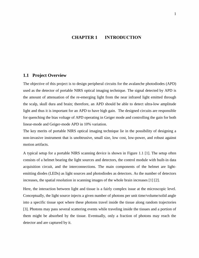
A typical setup for a portable NIRS scanning device is shown in Figure 1.1 [1]. The setup often
consists of a helmet bearing the light sources and detectors, the control module with built-in data
acquisition circuit, and the interconnections. The main components of the helmet are light-
emitting diodes (LEDs) as light sources and photodiodes as detectors. As the number of detectors
increases, the spatial resolution in scanning images of the whole brain increases [1] [2].
Here, the interaction between light and tissue is a fairly complex issue at the microscopic level.
Conceptually, the light source injects a given number of photons per unit time/volume/solid angle
into a specific tissue spot where these photons travel inside the tissue along random trajectories
[3]. Photons may pass several scattering events while traveling inside the tissues and a portion of
them might be absorbed by the tissue. Eventually, only a fraction of photons may reach the
detector and are captured by it.
2
On the other hand, to enhance the performance and accuracy of the NIRS system, highly sensitive
photodetectors are required to convert the ultra-low amplitude light signal into detectable electric
signal. There are only two options when it comes to choosing a photodiode that also amplifies the
received light signal: a) photomultiplier (PMT) and, b) avalanche photodiode (APD). Unlike the
PMT, APD works quite well for near-infrared light level with comparatively lower bias voltage
and lower power consumption and it is relatively insensitive to magnetic fields. The latter results
in having less noisy signals in magnetic areas, which makes it much easier to combine with other
brain imaging devices such as MRIs. Therefore APD can be a proper candidate for the
applications with high-magnetic-field. Moreover, APDs are also recognized for their simple and
monolithic structure, compact, lightweight, mechanical robustness and long life [4]. Thus APDs
are generally useful in applications where space is at a premium or where the detector may be
subjected to shock or vibration.
Having high quantum efficiency (80%) in near infrared is another advantage of APDs in
comparison to PMTs. Quantum efficiency is the efficiency with which light is detected. In a
typical PMT, only 10%-30% of incident photons are converted into photoelectrons at the
photocathode, and even this efficiency is achieved only over a narrow spectral range. In contrast,
Figure 1.1 Block diagram of a typical NIRS system developed for brain imaging
3
in addition to superior quantum efficiency (as high as 80% at 900 nm), APDs offer a wider
spectral range of 250 nm to 900 nm. Therefore, the photodetectors implemented for portable
NIRS are APDs.
NIRS portable systems could be evaluated by different parameters; among them, size, portability
and cost are of significant value. It is of great interest to integrate APD along with a peripheral
circuit with advanced sub-micron CMOS process. This way, choosing appropriate
substance/structure and adequate process for the design of an APD and the peripheral circuits
becomes of great concern. For APD structure to operate in near infrared range, materials such as
silicon (Si), InGaAs and Germanium (Ge) are suggested, among which silicon is preferred due to
its excellent crystal quality, low excess noise, low cost, low temperature dependence [22], high
gain and large bandwidth. Silicon APDs are also known for great performance in Geiger mode of
operation with dark counts in the range of a few counts per second [5]. Another characteristic that
makes silicon the most promising candidate for APDs is its low ionization coefficient ratio
(k < 0.1) [5] [6].
Silicon APDs incorporate an absorption layer for incoming photons to produce electron-hole
pairs in this region, as with any other photodiode. However, APDs operate with a large reverse
bia voltages. The high internal field accelerates the photon-generated electrons. These electrons
collide with the atomic lattice, in a recursive manner leading to an avalanche-like process.
Avalanche multiplication relies upon extremely high internal electric fields on the order of
105
V/cm to drive the ionizing collisions of carriers with the lattice. The small bandgap of
materials sensitive to long-wavelength light means that such high fields can cause tunneling
between bands: an unwanted source of dark current. The multiplication layer is designed to
provide the desired gain while suppressing noise. The performance of silicon APDs in infrared
range could be improved by replacing this layer with a low-bandgap and highly-absorbing
material such as InGaAs or Ge to absorb long-wavelength light in a single dedicated absorption
layer, while the multiplication layer remains silicon. Doping is used in an adjacent charge layer to
keep the potential low across the absorption material, so that only the multiplication layer
experiences extreme fields. For this purpose, Ge is preferred as it is possible to develop APDs
with CMOS-compatible process [6]. Adding Ge or InGaAs however complicates the process and
increases the cost significantly. In this project, silicon APD is chosen due to requiring low
operating voltage, exhibiting high quantum efficiency, and bearing low cost for near infrared

4
range applications. Taking the advantages of implementing an APD, fabricated with CMOS-
compatible processes along with CMOS-integrated circuit technologies may result in realizing
on-chip high-performance NIRS systems. Such implementation also serves our objective of
fabricating portable, ultra-high sensitive and low-power NIRS systems and peripherals while
saving used silicon area.
1.2 Basic Principles of Avalanche Photodiode
1.2.1 Multiplication Process
In an APD, when exposed to a light source, the light is absorbed in the depletion layer of the
reverse biased p-n junction, and electron-hole pairs are generated. This is due to the light energy
being greater than the bandgap energy in typical applications. Recall that the bandgap energy
depends on material properties and is greater than 1.1eV for silicon. The internal electric field
across the depletion region, when biased in reverse direction, drives the electrons towards the n+
side while it drifts the holes towards the p+ side. As the reverse bias voltage increases, so does
the electric field, which leads the carriers (mostly electrons) to accelerate. The carriers then gain
sufficient energy from the electric field and collide with the crystal lattice. This collision leads to
generation of another electron-hole pair while losing some of carriers’ kinetic energy. The
process is called impact ionization [7] and is defined as the ability to create a secondary electron-
hole pair for a carrier by gaining enough energy, and depends only on the local electric field [8].
The multiplication mechanism can be analyzed with reference to ionization rate and it is defined
as the number of electron-hole pairs generated during the time that a carrier moves a unit
distance. The ionization rates are denoted as α and β for electrons and holes, respectively. For
silicon, the ionization rate of electrons is larger than that of holes ( ), so the electrons
contribute more to the multiplication. The rate of ionization is reversely proportional to
temperature; that is, as the temperature decreases, energy loss for photon scattering decreases and
the ionization rate increases [9]. As a result of impact ionization for both electrons and holes,
additional carriers are generated. By traveling through the high electric field, the newly generated
carries obtain enough energy to trigger additional impact ionizations. This leads to a phenomenon
called avalanche. After a few transit times, a competition develops between the rate at which
5
electron-hole pairs are being generated by impact ionization and the rate at which they exit the
high-field region and are collected. If the magnitude of the reverse-bias voltage is below the
breakdown voltage, collection wins the competition, causing the population of electrons and
holes to decline. Each absorbed photon creates on average a number of electron-hole pairs (M),
where M typically lies in the range from tens to hundreds [10]. The internal gain, M, also called
multiplication gain, differentiates APDs from other photodiodes, and represents the amplification
of the generated carriers. Multiplication gain for an APD with uniform electric field and
ionization rate across the multiplication region with W width can be calculated through equation
(1-1) [11]
( [ ]) (1-1)
where
is called ionization rate ratio.
The above equation is used when electrons are injected into the avalanche region. The same
expression can also be used for holes by replacing k with ⁄ .
For most of silicon APDs, the electrons are injected into the avalanche region, which means
β < α , therefore [5].
As the bias voltage increases, the multiplication drastically increases until the device reaches a
point at which it experiences a large short circuit current and hence cannot be used as a detector.
The voltage at which the multiplication gain would be infinite is called breakdown voltage,
which is when the denominator of the equation (1-1) becomes zero. It is evident that the
breakdown voltage for a device with thicker multiplication region is larger than its thinner
counterpart. The ionization profile for each carrier is not uniform as they experience different
conditions. Therefore during the multiplication process, the device is subject to an incremental
noise. Such excess noise could be described as follow:
( ) (1-2)
where q is the charge of an electron and I is the sum of the photo-current generated at M=1 and
the dark current multiplied component. M is the multiplication gain and F refers to excess noise
factor, which can be expressed as follows: [12]
6
(
) ( ) (1-3)
where k is the ratio of the hole/electron impact ionization rates. Here, similar to gain equation, it
is assumed that the electrons are solely injected into the avalanche region. Equation (1-2) could
be extended to evaluate the gain for the injected holes, once k is substituted by ⁄ .
For the ideal minimized noise, k is considered to be zero and infinity for electron and hole
injections, respectively.
Statistical noise, defined as equation (1-4), should further be considered which incorporates the
transformation mechanism from photons to electrons. It indicates that the ionization rate is not
deterministic and has statistical fluctuations.
( ) (1-4)
where q is the charge of an electron and Ids is the dark current for non-multiplied component.
Considering equations (1-2) and (1-4), the shot noise of an APD (In), consisting of excess and
statistical components (In), could be formulated as follows:
( )
(1-5)
where B is the noise bandwidth, F is excess noise factor, M is multiplication gain, is
photocurrent at M = 1, is dark current multiplied component, and is the dark current
non-multiplied component.
The APD is also subject to thermal (dark current) noise due to load resistor which is given by
eq. (1-6)
(1-6)
where k is Boltzmann’s constant, T is absolute temperature, and RL is load resistance.
The APD total noise current is the sum of thermal and shot noises. Note that the total RMS noise
of a system is equal to the square root of the sum of all the noise components. It is shown in [29]
that for a detector where the only source of noise is dark current, the signal to noise ratio (SNR)
7
for a fluorescence signal of 107 photons/sec would be
⁄ . Here, the author assumes that
the dark current rate (DCR) of the detector is 106 counts/second and it follows Poissonian
distribution.
To maximize SNR, for a given input signal power, the noise should be minimized. In case of an
ideal APD, where the dark (thermal) noise is zero, the only source of noise is statistical noise.
This class of noise, as already stated, is related to transformation from photons to electrons. The
ideal SNR is given by:
(1-7)
The common source of light may not be capable of providing sufficient luminance.
Consequently, it is often needed to amplify the signal while holding the noise profile at low level.
There are two solutions which can be presented for such a problem: a) adding preamplifier and
amplifier stages and b) making use of detectors with intrinsic gain. The former solution, however,
may lead to an increase in the required area and complexity. It is worth noting that although an
APD introduces excess noise due to multiplication process, the amount of noise is still lower in
comparison to the noise generated from connecting an external amplifier to a conventional
photodiode operating at high frequencies.
1.2.2 Operation Mode
An APD can generally work in either linear or Geiger mode. The mode of operation depends on
the magnitude of the reverse bias voltage across the p-n junction with respect to the breakdown
voltage.
In order to operate in linear mode, the reverse bias voltage is kept below the breakdown voltage
of the junction and the photo-generated charges are amplified with a finite multiplication gain. In
this mode, the average photocurrent is shown to be proportional to the incident optical flux, and
the multiplication gain hence can be calculated as follows [13]:

8
[ ]
(1-8)
where m is a constant value for a particular APD; which depends on the substrate material and its
value ranges between 2 and 6. and represent the reverse bias voltage and the breakdown
voltage, respectively, while M stands for multiplication gain.
In this mode of operation for an APD, the avalanche multiplication process induces a measurable
current by amplifying the negligible current generated by photons. Despite amplification, such
multiplication gain is still low due to existing statistical fluctuations in the multiplication process
[3]. Therefore, an APD operating in linear-mode does not have enough sensitivity to detect single
photons.
On the other hand, enforcing an APD to operate in Geiger-mode requires the reverse bias voltage
to be higher than the breakdown voltage. This ensures that the primary signal gain is sufficient to
count single photon. In this mode of operation, APD works as a triggering rather than an
amplifying device. In fact, an APD operating in Geiger mode gives rise to a detectable
macroscopic current due to high electric field and the run-away avalanche phenomenon induced
by the creation of a single carrier. However, a macroscopic current would swiftly build [14] and
self-sustaining avalanche process would continue, thus rendering the device useless for
subsequent detections until it stops externally. The process may also stress the device and lead to
a damage which affects its performance and crosses the liability boundaries. Therefore, operating
in this mode requires applying an external stop which is essential to lead APD in a new detection
sequence [15]. Moreover, in the Geiger mode, the internal amplification of APD, which is the
result of the avalanche multiplication process, provides virtually infinite gain to the photo-
generated current. Such infinite gain further results in all the current pulses to have the same
amplitude. As a result, for an APD operating in Geiger mode, the amplitude of signal does not
bear significant information [4]. In this case, counting the number of pulses occurring as a result
of photon detection is of great interest. The photon counting rate is estimated either by counting
the number of events in a time interval with a certain duration or by measuring the time gap
between two consequently detected pulses.
The gain resulted from receiving a single photon in Geiger mode APD can be calculated as
follows [16] :
9
(1-9)
where C is junction capacitor, q is electron charge and Vex is excess voltage given by
.
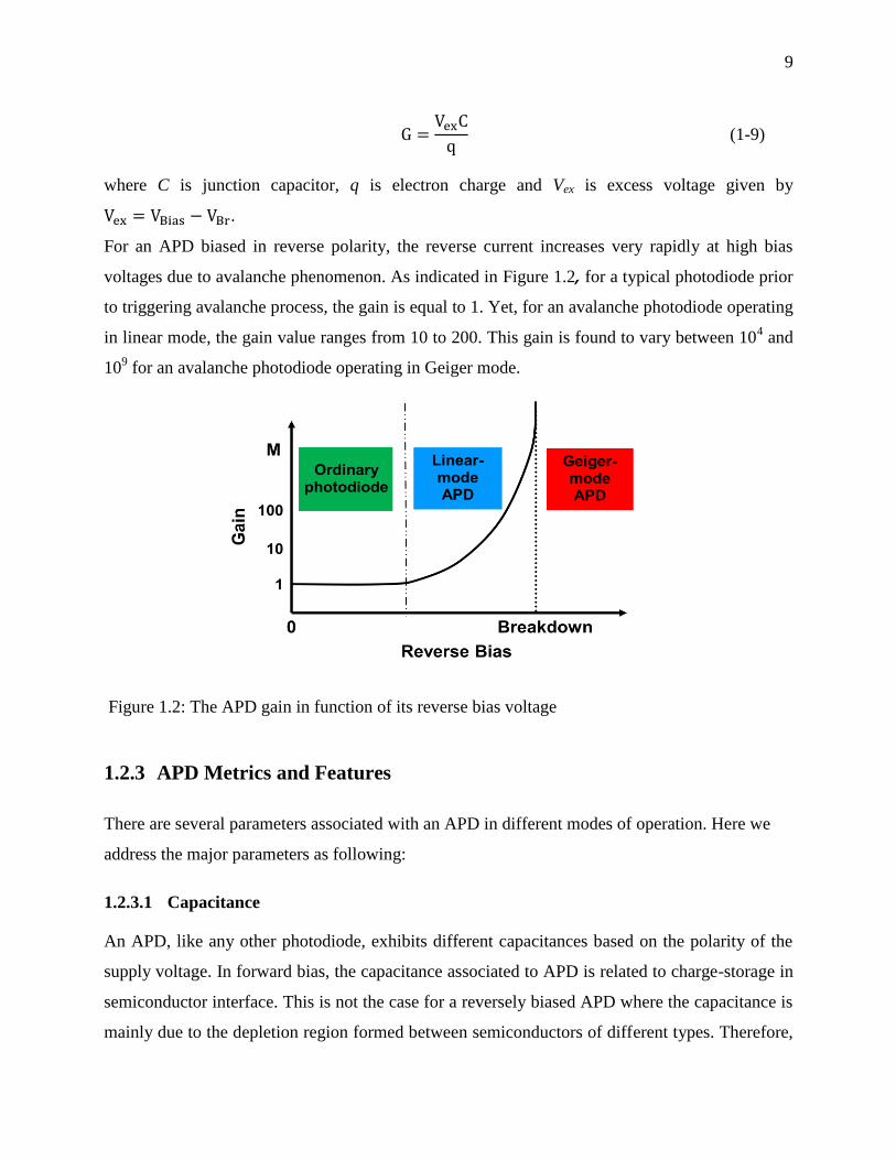
For an APD biased in reverse polarity, the reverse current increases very rapidly at high bias
voltages due to avalanche phenomenon. As indicated in Figure 1.2, for a typical photodiode prior
to triggering avalanche process, the gain is equal to 1. Yet, for an avalanche photodiode operating
in linear mode, the gain value ranges from 10 to 200. This gain is found to vary between 104 and
109 for an avalanche photodiode operating in Geiger mode.
1.2.3 APD Metrics and Features
There are several parameters associated with an APD in different modes of operation. Here we
address the major parameters as following:
1.2.3.1 Capacitance
An APD, like any other photodiode, exhibits different capacitances based on the polarity of the
supply voltage. In forward bias, the capacitance associated to APD is related to charge-storage in
semiconductor interface. This is not the case for a reversely biased APD where the capacitance is
mainly due to the depletion region formed between semiconductors of different types. Therefore,
Figure 1.2: The APD gain in function of its reverse bias voltage
10
the former is not applicable for Geiger-mode APD [17]. Since the junction capacitance depends
on the depletion layer thickness, it could be employed as a measure to find out the depth of the
depletion layer. If carriers are generated outside the depletion layer, they cause problems such as
slow signal decay time. Therefore, to ensure high-speed response, it is necessary to apply a
reverse voltage which makes the depletion layer thicker than the penetration depth of the light
into the light absorption layer [18]. For the APD with an active area of A and a depletion area
width of W, the junction capacitor is expressed as follows:
( ) (1-10)
where is the permittivity of dielectric.
From Eq. (1-10), increases with increasing APD active area and/or decreasing depletion
thickness. On the other hand, the transit time of charge carriers in an APD increases with an
increase in the thickness of APD depletion layer. Therefore, choosing the APD thickness would
imply a performance trade-off between noise and speed [19] [20]. Eq. (1-10) corroborates that the
capacitance has an inverse relation to bias voltage; therefore, by increasing bias voltage, APD
capacitance would decrease.
1.2.3.2 Bandwidth
The bandwidth of an APD photodiode is primarily determined by; a) electron and hole transit
times, b) R-C time constant, c) minority carrier diffusion length, d) the number of carrier
trappings, and e) signal delay due to photodiode packaging [21].
The transit times depend on the thickness of the active area and the electron/hole saturation
velocities. Thus, the thinner the absorbing layers are, the shorter the transit times will be.
The RC time constant is determined by the APD equivalent circuit parameters. Junction
capacitance, which is defined as the edge of the depletion region (or space charge region), and
parasitic capacitance, which depends on the metallization geometry, can be considered as the
APD capacitance. The APD resistance consists of series resistance, which is caused by the Ohmic
contacts, and bulk resistances, and load resistance. By considering RS and RL as the series and
load resistors, and CJ and CP as junction and parasitic capacitors, the electrical 3-dB bandwidth
can be approximated as follow [22]:
11
( )( ) (1-11)
Diffusion current is important for APDs since significant absorption occurs in depletion region,
which is outside of the high-field region. Those carriers within about one diffusion length of the
depletion region will have a chance to diffuse into the active region. The diffusion current will
contribute a slow tail to the detector impulse response and may be reduced to some extent by
recombination in these highly doped contact layers [22] and would deplete the entire absorbing
layer [21].
In some APD designs such as hetero-structures, the bandwidth may be limited by the occurrence
of carrier trapping of electrons at conduction band discontinuities and trapping of holes at valence
band discontinuities [22]. Hole trapping is a significant problem in long-wavelength
photodetectors due to the large valence band discontinuity at the InP / InGaAs heterojunction
[22]. Researchers have reported solutions such as applying a moderately high electric field across
the hetero-interface. Another technique suggests grading the band discontinuity with a
compositional alloy [21].
Packaging and any external connections to the photodetector often limit the detector
performance. Having a high impedance load and a reflection coefficient close to unity are other
problems of photodiodes. A solution to this problem is to integrate a matching resistor with the
device and using a lower contact layer without adding any additional mask or process steps [22].
The disadvantage of a load resistor is the reduction in effective quantum efficiency since some of
the photocurrent goes through the matching resistor [22].
Another influential parameter on APD bandwidth is terminal capacitance. In fact, APD
capacitance along with its input series resistance, form a circuit the time constant of which is
affected by capacitance. This time constant should be respected throughout the normal operation
of APD, which involves consequent charging/discharging of the detector. APDs with larger
capacitances, when compared to their counterparts, are subject to narrower bandwidth.
Decreasing the photodiode active area lowers junction capacitance and as a result reduces the RC
time constant. However, a small device area can result in high contact resistance, which will
increase RC constant. Packaging-induced parasitic effect may also cause bandwidth degradation.
The issue may be overcome by making use of advanced bonding techniques [21]. The external
12
bias circuit is a difficulty in very high speed devices is the difficulty in building external bias
circuits. The necessary bias capacitor and load resistor can be integrated with APD without
adding any additional mask or process steps by using a large area region as the capacitor and the
lower contact layer as the series resistor [22].
1.2.3.3 Quantum efficiency
There is a possibility for an absorbed photon in the active region of an APD to generate a primary
carrier, and to eventually trigger an avalanche process. Such possibility is called quantum
efficiency (QE). The ideal value for QE is unity, i.e., all the photons are absorbed in the active
region. As the wavelength becomes larger, the chance of the photon being absorbed through the
active portion of the depletion layer decreases. For short wavelengths (<400nm), the photon
generated in the surface may be immediately absorbed. Quantum efficiency mainly depends on
APD structure and antireflection (AR) coating on the diode window. Typical values of QE for
APD range from 40% to 80% [23].
1.2.3.4 Dark Count
Dark count rate (DCR) is defined as the number of avalanches triggered while there is no light
impinging on the active area of the APD. Dark counts are highly dependent on the doping of the
junction and the characteristics of the fabrication technology. Modifying the doping profile of
implants may mitigate the effect. APD active area also affects DCR in a non-linear fashion [24].
DCR can generally be used to characterize dark current, which is considered as a major source of
intrinsic noise in APDs. There are two major sources for dark current; a) random thermally-
generated electron-hole pair, and b) tunneling [25].
The minority carriers inside an APD may gain enough thermal energy from the substrate to
diffuse into depletion region. On the other hand, for Geiger-mode APD, the device experiences
large electric fields across depletion region due to reverse biasing; which may cause some of the
minority carriers to drift into the depletion region and accelerate across it [13]. The thermally-
generated electrons also have multiplication effect. At lower temperatures, the carriers have less
energy and thus their random motion decreases.
On the other hand, tunneling is mostly a design-based issue and is affected by the properties of
the materials of choice. Recall that for a design where APD is subject to small negative bias
13
voltage, the width of the depletion layer is very thin. Moreover, for an APD implemented using
semiconductor with small bandgap property, the carrier quasi-Fermi level (i.e. the displacement
of the population of holes and electrons from equilibrium) can overlap. For both conditions, the
carrier tunneling across the depletion region may by triggered and thus the tunneling current
occurs under reverse bias [26].Tunneling can be controlled by compromising vital properties like
bias voltage [27].
It is of great interest to hold the dark count noise as low as possible. The objective could be
served by enforcing APD to operate at temperatures and excess voltages as low as possible. For a
typical APD, DCR ranges from 1 to 106
counts/sec. If the DCR exceeds this range, for example
higher than 107, APD operates in saturation region and the signal will be inundated with dark
noise [28].
1.2.3.5 After-pulsing
During an avalanche, some of the carriers, crossing the depletion region, are captured at deep
levels inside the junction and are stored in traps in the APD. These carriers can release after a
random period of time. As the stored charges release during the active period of APD, an
avalanche current occurs. The resulting current is due to a previous avalanche event, but not
related to a new photon arrival. The new avalanche event, in turn can lead to further carrier
trapping, and this cycle continues. This unwanted source of noise is called after-pulsing.
After-pulsing intensity depends on: a) the number of carriers crossing the junction, b) trap density
and c) temperature. The number of carriers crossing the junction is directly related to the total
charge of the avalanche event, while the total charge and current intensity depends on the over-
voltage. In addition to trap density, how deep inside the junctions the released carriers were
trapped indicate the release period of each of the carriers, and therefore the onset of after-pulsing
[29]. The density of deep-level traps can be reduced by improving material quality which can be
a method for decreasing after-pulsing. However, material improvement is usually a relatively
difficult task [28]. Another effective parameter on after-pulsing is temperature: as temperature
increases, the trapped carriers escape more rapidly and thus the after-pulsing effect is less.
Although an increase in temperature decreases the after-pulsing effect, at the same time it leads to
increased thermal generation, causing higher dark count rate. The choice of the optimum

14
temperature is important in order to keep after-pulsing effect and dark count rate at the least
possible value.
After-pulsing is the major limitation on operation of APD as photon counter at high repetition
rate [29] and it limits the high frequency operation of APD. By keeping the voltage across the
APD below the breakdown voltage after each photon detection for sufficiently long time,
trapping centers can be empty and the after-pulses may not be generated anymore. The sufficient
time should be longer than the trap emission lifetime. However, when speed is important and the
repetition rate gets closer to the trap emission life time, after-pulsing effect increases.
1.2.3.6 Leakage Current
The leakage current is generated as a result of the voltage across the photodiode in the reverse
bias, and it is directly related to the size of the photodiode. With smaller photodiodes, the leakage
current will be lower. The total leakage current is the sum of the surface leakage current and the
volume leakage current:
(1-12)
The surface leakage current is the amount of leakage current between the p-doped and the n-
doped regions in contact with the SiO2 passivation layer. These leaks are related to the
circumference of the photodiode. The volume leakage current is the amount of leakage current
between the p-doped and the n-doped regions, in the volume of the junction (plane, cylindrical
and spherical). These leaks are related to the area of the photodiode (diffusion depth, length and
width of the junction).
1.2.3.7 Thermal Effect
As a result of impact ionization in the high electric field region of APD, electron-hole pairs are
generated which result in avalanche multiplication. Although carriers gain energy from the
applied electric field, some of this energy will be transferred to lattice vibration. This energy loss
is caused by various scattering mechanisms, of which phonon scattering will ultimately dominate
due to strong interaction between carriers and the lattice vibration [21]. The free mean path
length of carriers has an inverse relation with temperature [21], and it would decrease by an

15
increase in temperature. This means that carriers are scattered more frequently at elevated
temperatures.
On the other hand, as mentioned in sections 1.2.3.4 and 1.2.3.5, both DCR and after-pulsing
processes are temperature dependent. If the temperature is not low enough, the dark counts would
be high. The high dark counts occur when thermal generation triggers avalanche events, and
cooling the APD is a solution to this impact. In contrast, if the temperature is not high enough,
the after-pulsing effect would increase. As noted in 1.2.3.5, there is always the possibility that the
carriers become trapped inside the crystal and get released later. By reducing the temperature, the
lifetime of trapping events increases, which results in an increase in after-pulsing. Therefore there
is a trade-off between minimizing dark counts and after-pulsing by controlling the temperature.
Another APD parameter strongly affected by junction temperature is breakdown voltage (Vbr).
The thermal coefficient of breakdown voltage depends on the APD device structure and is
usually fairly high, typically around 0.3%/K [28]. At constant bias voltage supply, an increase in
breakdown voltage Vbr causes a decrease in over-voltage Vex, and therefore it results in reduced
photon detection efficiency and causes non-linear distortion in photon counting.
1.3 Basic Principles of Quench-Reset Circuit
Due to disadvantages of APDs which are long transit times and excess noise, associated with the
stochastic APD multiplication process, several high-speed CMOS front-end circuits have been
proposed in the past few years to overcome these limitations [19] [30]. As mentioned in
section 1.2.2, in the linear mode, there is a limitation on the maximum achievable gain. Therefore
in this mode, APD has to be followed by a transimpedance amplifier (TIA) front-end. TIA
converts the output current to voltage with maximum SNR for following stages of the receiver
for further processing [31]. However, operating in linear mode for APD means having the low
achievable current gain, and therefore not being sensitive enough to detect single photons. To
detect single photons, APDs must be operated in Geiger mode. Furthermore, since Geiger-mode
operation requires an external stop, the Quench-Reset circuit is employed to detect photon arrival,
count the pulse generated at photon arrival, and reset the APD in order to make it ready for the
next photon detection. The idea is to keep APD in an extremely sensitive condition (i.e., few

16
volts above the breakdown voltage) in a way that by absorbing a photon and triggering an
avalanche, a huge increase in output current occurs. At this point Quench-Reset circuit should be
active to quench (shut-off) the avalanche and return APD to the sensitive state. When the
avalanche is quenched the current becomes zero, and the voltage slowly returns to its previous
value.
In each quench-reset circuit, quench time is defined as the time elapsed from the onset of the
avalanche until it is quenched; which means the time it takes to interrupt the avalanche
multiplication process and shut off the avalanche current by increasing the APD's bias voltage
above breakdown. In the same circuit, reset time is defined as the time required for bringing back
the APD to its original quiescent state.
If the reset action happens immediately after quench process, the chance of having after-pulsing
increases. One solution to reduce the amount of after-pulsing, besides fast quenching [19] (which
means reducing the avalanche charge and current intensity rapidly), is to wait for all the trapped
charges to dissipate without triggering additional avalanches before resetting process. This can be
achieved by keeping the APD in the OFF state for a period of time in between the quench and
reset process. The mentioned period is called Hold-off time. The period of hold-off time depends
on the nature, density and lifetime of the traps of each specific APD. It should be long enough to
allow trapped carriers to be emitted and not to allow the after-pulsing affect the photon counting
statistics. Studies show that if the hold-off time is less than the mean trap lifetime then after-
pulsing will significantly affect the photon counting statistics [32]. Meanwhile, Hold-off time
should not be too long to avoid limiting the repetition rate and affecting the validity of the
counting statistics. Therefore most appropriate hold-off differs from one APD to another, and
having controllable hold-off time circuit is highlighted. The sum of quench time, hold-off time
and reset time is called dead-time, which can be defined as the minimum delay that must elapse
between two consecutive avalanches in order for both to be detected.
Another important portion of dead-time is reset time. Reset time should be as short as possible:
with long reset time, the chance of the avalanche triggering during reset time increases. On the
other hand, the effective bias voltage varies with time. This variation can cause some pulses to be
missed from photon counting; since, the output pulse from the early avalanche triggering may be
17
too small to be detected and the counting rate would be affected. Long reset time can also affect
APD’s performance, such as detection efficiency and timing response.
Having the peripheral circuits (TIA and Quench-Reset circuit) integrated with APD on the same
chip, adds some advantage to the system such as reducing after-pulsing, increasing sensitivity,
and lowering power consumption. CMOS 0.18 µm technology is the chosen process for
fabrication.
The ability of APD avalanche multiplication in amplifying the photon-generated signal makes it
well-suited for detecting extremely weak light intensities, such as the one associated with low-
amplitude reflected NIR signal. However, it is not always simple to gain the desired magnitude
for the amplified signal. It is due to the need for a high reverse voltage and a large multiplication
gain which is, among other facts, temperature dependant [5]. Therefore, employing a control unit
is essential to eliminate the effect of temperature and to improve the performance of APD,
accordingly.
1.4 Research Objective and Challenges
This Master’s thesis investigates the design and implementation of an integrated building block
intended to tune an APD with improving its performance in term of maximizing the photon
counting rate and minimizing power consumption and system noise. This system should be
capable of real-time monitoring of the APD’s gain and keeping its variation in a pre-defined
range.
The quench-reset circuit should be a circuit with high photon counting rate, low power
consumption and small size. Having controllable hold-off time is another objective of this circuit.
The circuit should be designed to be integrated on the same chip as the APD to reduce after-
pulsing, increase sensitivity and lower power consumption. To allow connection to other
designed components of the project, the quench-reset circuit should be fabricated in CMOS 0.18
µm technology.
To improve the performance of the APD, some of its parameters need to be monitored in real-
time, and corresponding values would be calculated based on the monitored parameters. This
goal is achieved by an off-chip control system. Bias voltage, temperature, and gain are the
18
mentioned parameters and features. As a result, a temperature-independent gain control loop is
designed by controlling and changing the bias voltage for linear and Geiger mode APD. The aim
is to choose the best controller device in terms of small size, user-friendly monitoring, and
compatibility to different sensors to be able to analyze as many parameters as possible.
Thesis Organization
Chapter 1 presented an introduction to the IMAGINC portable NIRS brain imaging device. The
avalanche photodiode and its limitations to work in linear and Geiger modes were reviewed.
Several of its physical parameters were outlined, and the effect of temperature on some of the
parameters was studied. The quench-reset circuit was introduced, and the related concepts were
reviewed.
Chapter 2 presents a literature review on different CMOS quench-reset (QR) circuits, including
advantages and disadvantages of each passive, active, and mixed circuits. Different systems used
to control the thermal effect on the performance of APDs are also reviewed.
In Chapter 3, designing quench-reset circuits are discussed, providing explanation on their
functionality and simulation results. A control system is designed to monitor APD parameters
and performance, and a temperature-independent gain control loop is designed based on changing
the bias voltage.
Chapter 4 covers experimental results of the fabricated quench-reset circuit integrated in a
CMOS chip. The overall platform is also discussed in this chapter. The unit consists of the
control system to improve the APD performance in both linear and Geiger modes, the quench-
reset circuit dedicated for the Geiger mode APD and a TIA circuit when APD performs in linear
mode.
Chapter 5 is presented as a summary of the project along with comments concerning
recommendations for future work to design fully integrated CMOS device including the APD, its
quench-reset circuit, as well as control circuit of various parameters on the same chip.
19
CHAPTER 2 LITERATURE REVIEW
Finding a technique for photon counting is necessary when the amount of light is extremely low;
in this case, conventional analog measurement of light intensity becomes extremely difficult. In
the 2000s, the concept of a new generation of photon counters introduced which was called SiPM
(Silicon-Photomultiplier). In January 2008 it was commercialized under the name of Multi-Pixel
Photon Counter (MPPC) by Hamamastsu and as SPM (Silicon Photomultiplier) by SensL. SiPM
is the matrix of photodiodes (e.g. 32x32 = 1024 photodiodes) polarized in Geiger mode, forming
a single undividable detector surface area of a few millimeters [16] [33]. Each photon generates a
current pulse, and at the detector output, counting the number of pulses represents the number of
photons received. In order to have an accurate measure of counted pulses, it is important to have
the width of the pulses as short as possible to avoid missing any photon; meanwhile the invalid
pulses should be filtered.
For many applications where very low-levels of light are to be detected, it is desirable to use a
detector with high sensitivity; namely, a device with high optical gain. The Avalanche
Photodiode has been developed for this purpose, which is essentially, as anticipated, a PIN diode
with high gain.
The idea of avalanche photodiodes was introduced in the 1950s, and became a popular research
area in the 1960s and early 1970s, with both linear-mode and Geiger-mode functions being topics
of interest. Limited electric fields and high fabrication cost of photo-multiplier tubes (PMTs)
were two main motivations to introduce APDs as both a signal amplifier for low-flux imaging
applications and as a means to detect single photons [34]. As research fueled development, other
advantages of APDs were revealed; offering digital-mode operation for single-photon counting
[34], high gain and high sensitivity. In the 1960s, Haitz’s group introduced the avalanche
phenomenon in p-n junctions biased above the breakdown voltage; a model of this device was
presented [35]. An APD is basically an advanced PIN photodiode but with faster timing. By way
of comparison to other PIN photodiode, APDs are associated with internal gain, which means

20
more than one signal carrier is generated per photon. Without gain, the electrical signal due to
photon flux is usually lost in readout noise.
In the 1970s, during the early development of silicon APDs, the statistical properties of the
avalanche phenomenon were provided by McIntyre and Webb [36] [37]; the single-photon
generated pulses were observed in their APDs biased above breakdown voltage [38]. Advances in
electronics have reduced the inherent noise and the breakdown voltage of APDs, which makes
them a suitable option for portable devices.
Sensitivity and signal-to-noise ratio can be enhanced by reducing the noise. The major source of
noise is dark noise which depends on both junction temperature and the reverse bias voltage.
Rather than cooling the device, operating APD under low biasing condition is important [39].
Another method to increase sensitivity is to enhance the gain. Although APD has the advantage
of high gain in comparison to PIN photodiodes, the gain in linear mode is not as high as PMTs.
Internal gain for APD operating in linear mode is 200-1000 while PMT typically has an internal
gain of 1x10⁵ to 1x10
7 [40]. To boost the APD gain, external amplification is required, and a
transimpedance amplifier is the solution to produce similar intensity signals between an APD and
PMT [40]. However, increasing the gain in this mode increases noise because the noise would be
also multiplied by the gain. Therefore, APD operated in Geiger mode is studied where bias
voltage is greater than breakdown voltage [41].
The optical gain is defined as the number of carriers generated as a result of the absorption of a
single photon. The optical gain for Geiger-mode APD is virtually infinite. The Geiger mode is
also called single-photon detection mode; since instead of a linear gain relation between the
generated photocurrent and the number of incident photons, it gives a digital pulse per avalanche
event [41]. The light intensity can be obtained from photon flux, which can be attained from
counting the photon events over a period of time. The sensitivity of Geiger-mode APD is limited
by dark count noise, which counts the events as the result of thermal generation of electron-hole
pair instead of incident photons [41]. As explained in previous chapter, as the result of avalanche
multiplication in Geiger-mode APD, a macroscopic current is triggered, and a sharp pulse is
produced which can be counted. The leading edge of the generated pulse marks the photon arrival
time very precisely. The self-sustaining current continues flowing until the electronic field is
reduced below breakdown onset. The final steady state current will be governed by the series
resistor (RS) of the circuit [42]. Meanwhile, the device will have no response to any other
21
incident photon. To externally stop the self-sustaining current and perform high-speed photon
counting, an APD is used in conjunction with a quench circuit, which can be passive, active or
gated. This is achieved by lowering the bias voltage below the breakdown voltage, which is done
by quenching procedure.
2.1 Quenching
Different solutions and circuits have been proposed for the quenching process; however, all
different types of quenching circuits have two main common purposes: to quench the avalanche
current by lowering the voltage below breakdown after triggering an avalanche current, and to
reset the device for subsequent detection by raising the voltage above breakdown.
There are three basic types of quenching circuits: passive quenching, active quenching and gated
quenching. There are also some combinations such as passive quenching with active reset, active
quenching with passive reset, gated active quenching and passive gated quenching [43].
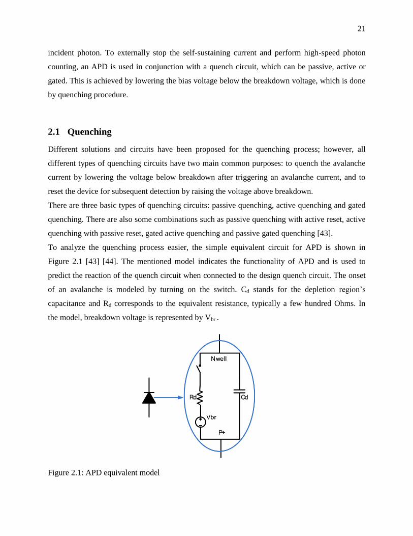
To analyze the quenching process easier, the simple equivalent circuit for APD is shown in
Figure 2.1 [43] [44]. The mentioned model indicates the functionality of APD and is used to
predict the reaction of the quench circuit when connected to the design quench circuit. The onset
of an avalanche is modeled by turning on the switch. Cd stands for the depletion region’s
capacitance and Rd corresponds to the equivalent resistance, typically a few hundred Ohms. In
the model, breakdown voltage is represented by Vbr .
Figure 2.1: APD equivalent model
22
2.1.1 Passive Quenching
By observing the generation of single-photon pulses in the avalanche photodiodes biased above
breakdown, APD is used in different applications such as astronomy and medical imaging.
However, these applications were limited by the features of the device and quenching circuit. The
first quenching circuit introduced was passive quenching.
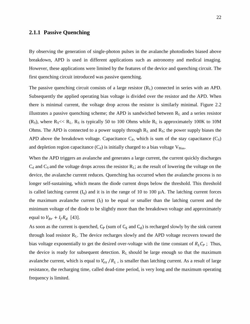
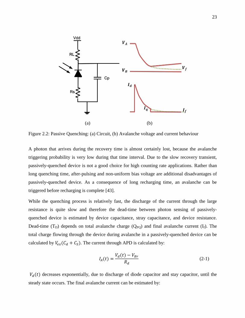
The passive quenching circuit consists of a large resistor (RL) connected in series with an APD.
Subsequently the applied operating bias voltage is divided over the resistor and the APD. When
there is minimal current, the voltage drop across the resistor is similarly minimal. Figure 2.2
illustrates a passive quenching scheme; the APD is sandwiched between RL and a series resistor
(RS), where RS<< RL. RS is typically 50 to 100 Ohms while RL is approximately 100K to 10M
Ohms. The APD is connected to a power supply through RL and RS; the power supply biases the
APD above the breakdown voltage. Capacitance CP, which is sum of the stay capacitance (CS)
and depletion region capacitance (Cd) is initially charged to a bias voltage VBias.
When the APD triggers an avalanche and generates a large current, the current quickly discharges
Cd and CS and the voltage drops across the resistor RL; as the result of lowering the voltage on the
device, the avalanche current reduces. Quenching has occurred when the avalanche process is no
longer self-sustaining, which means the diode current drops below the threshold. This threshold
is called latching current (Iq) and it is in the range of 10 to 100 µA. The latching current forces
the maximum avalanche current (If) to be equal or smaller than the latching current and the
minimum voltage of the diode to be slightly more than the breakdown voltage and approximately
equal to [43].
As soon as the current is quenched, (sum of and ) is recharged slowly by the sink current
through load resistor RL. The device recharges slowly and the APD voltage recovers toward the
bias voltage exponentially to get the desired over-voltage with the time constant of ; Thus,
the device is ready for subsequent detection. RL should be large enough so that the maximum
avalanche current, which is equal to ⁄ , is smaller than latching current. As a result of large
resistance, the recharging time, called dead-time period, is very long and the maximum operating
frequency is limited.
23
A photon that arrives during the recovery time is almost certainly lost, because the avalanche
triggering probability is very low during that time interval. Due to the slow recovery transient,
passively-quenched device is not a good choice for high counting rate applications. Rather than
long quenching time, after-pulsing and non-uniform bias voltage are additional disadvantages of
passively-quenched device. As a consequence of long recharging time, an avalanche can be
triggered before recharging is complete [43].
While the quenching process is relatively fast, the discharge of the current through the large
resistance is quite slow and therefore the dead-time between photon sensing of passively-
quenched device is estimated by device capacitance, stray capacitance, and device resistance.
Dead-time (TD) depends on total avalanche charge (QPQ) and final avalanche current (If). The
total charge flowing through the device during avalanche in a passively-quenched device can be
calculated by ( ). The current through APD is calculated by:
( ) ( )
(2-1)
( ) decreases exponentially, due to discharge of diode capacitor and stay capacitor, until the
steady state occurs. The final avalanche current can be estimated by:
(a) (b)
Figure 2.2: Passive Quenching: (a) Circuit, (b) Avalanche voltage and current behaviour

24
(2-2)
Since , the peak avalanche current is approximately equal to
(2-3)
To estimate the value of RL resistance, equation (2-3) is used. To assure that the avalanche is
quenched, the rule-of-thumb for a latching current, which ensures avalanche termination can be
used. This rule is considered the maximum avalanche current, or final current, to be 100 μA or
less [43] [45]. By knowing the required Vex and assuming If to be 100 μA, the required RL is
calculated. Equation (2-4) is used to assess the quenching time for passive quenching.
( ) (2-4)
The quenching time for passive quenching is limited by the capacitance value of ( ) and is
usually in the range of tens of nanoseconds (or 10-8
s). With an estimated 0.1 pF for a 20 µm
radius APD and a 1 MΩ quenching resistor, the time constant is on the order of 100 nanoseconds.
Additionally, it is typically difficult to reliably create uniform resistors, due to process variation
and mismatching.
The avalanche current discharge follows through , and induces a voltage in the output. The
avalanche signal depends on . A stronger signal results in a larger ratio of to . An
external capacitor in parallel to APD would also increase the avalanche signal; this method can
be used when the diode capacitor is larger than stray capacitor.
If the interval between photon arrivals is shorter than TD, the avalanche initiation probability,
and consequently the detection efficiency will vary with time. This is highly undesirable. In
addition, the output pulse amplitudes will also vary, and therefore some pulses may be missed by
the sensing circuitry; because most sampling circuits have a constant amplitude threshold [46]
[47]. Since RL is determined by the latching current and Cd is an artifact of the junction
itself, the only way to reduce TQ in a passively-quenched device is by reducing the stay
capacitance. The most effective way of doing this is by integrating the quenching resistor on the
same die as the APD itself [48] [49].
25
The performance of a passively-quenched device may be affected by the choice of the resistor
element. An off-chip resistor can have highly-precise resistance but will add parasitic
capacitance. On-chip resistors typically have very high temperature coefficients and take
up large areas. Transistors are a good choice but require a high-quality CMOS process and clean
voltage supplies. Moreover, they are limited by the supply voltage VDD of the specific
technology. This sets a limit on the allowed excess voltage with which APD can operate and
influence the physical design of the unit.
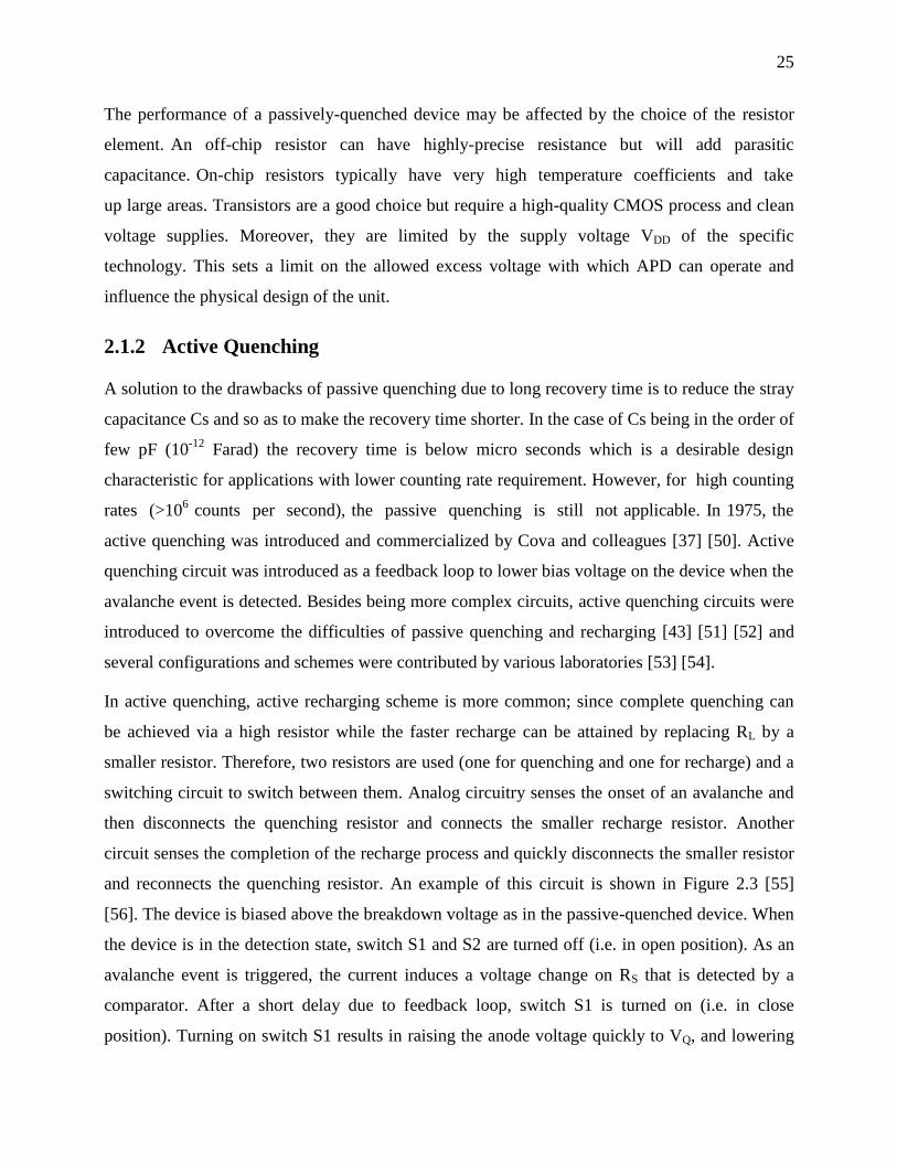
2.1.2 Active Quenching
A solution to the drawbacks of passive quenching due to long recovery time is to reduce the stray
capacitance Cs and so as to make the recovery time shorter. In the case of Cs being in the order of
few pF (10-12
Farad) the recovery time is below micro seconds which is a desirable design
characteristic for applications with lower counting rate requirement. However, for high counting
rates (>106 counts per second), the passive quenching is still not applicable. In 1975, the
active quenching was introduced and commercialized by Cova and colleagues [37] [50]. Active
quenching circuit was introduced as a feedback loop to lower bias voltage on the device when the
avalanche event is detected. Besides being more complex circuits, active quenching circuits were
introduced to overcome the difficulties of passive quenching and recharging [43] [51] [52] and
several configurations and schemes were contributed by various laboratories [53] [54].
In active quenching, active recharging scheme is more common; since complete quenching can
be achieved via a high resistor while the faster recharge can be attained by replacing RL by a
smaller resistor. Therefore, two resistors are used (one for quenching and one for recharge) and a
switching circuit to switch between them. Analog circuitry senses the onset of an avalanche and
then disconnects the quenching resistor and connects the smaller recharge resistor. Another
circuit senses the completion of the recharge process and quickly disconnects the smaller resistor
and reconnects the quenching resistor. An example of this circuit is shown in Figure 2.3 [55]
[56]. The device is biased above the breakdown voltage as in the passive-quenched device. When
the device is in the detection state, switch S1 and S2 are turned off (i.e. in open position). As an
avalanche event is triggered, the current induces a voltage change on RS that is detected by a
comparator. After a short delay due to feedback loop, switch S1 is turned on (i.e. in close
position). Turning on switch S1 results in raising the anode voltage quickly to VQ, and lowering
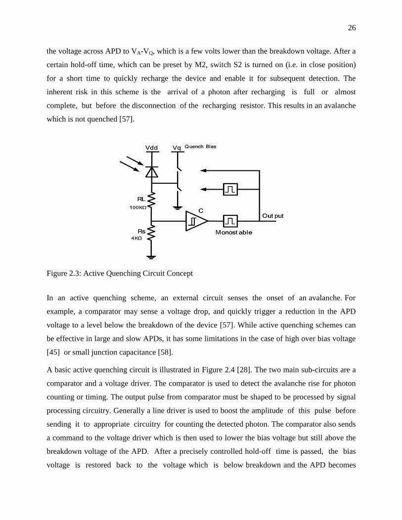
26
the voltage across APD to VA-VQ, which is a few volts lower than the breakdown voltage. After a
certain hold-off time, which can be preset by M2, switch S2 is turned on (i.e. in close position)
for a short time to quickly recharge the device and enable it for subsequent detection. The
inherent risk in this scheme is the arrival of a photon after recharging is full or almost
complete, but before the disconnection of the recharging resistor. This results in an avalanche
which is not quenched [57].
In an active quenching scheme, an external circuit senses the onset of an avalanche. For
example, a comparator may sense a voltage drop, and quickly trigger a reduction in the APD
voltage to a level below the breakdown of the device [57]. While active quenching schemes can
be effective in large and slow APDs, it has some limitations in the case of high over bias voltage
[45] or small junction capacitance [58].
A basic active quenching circuit is illustrated in Figure 2.4 [28]. The two main sub-circuits are a
comparator and a voltage driver. The comparator is used to detect the avalanche rise for photon
counting or timing. The output pulse from comparator must be shaped to be processed by signal
processing circuitry. Generally a line driver is used to boost the amplitude of this pulse before
sending it to appropriate circuitry for counting the detected photon. The comparator also sends
a command to the voltage driver which is then used to lower the bias voltage but still above the
breakdown voltage of the APD. After a precisely controlled hold-off time is passed, the bias
voltage is restored back to the voltage which is below breakdown and the APD becomes
Figure 2.3: Active Quenching Circuit Concept
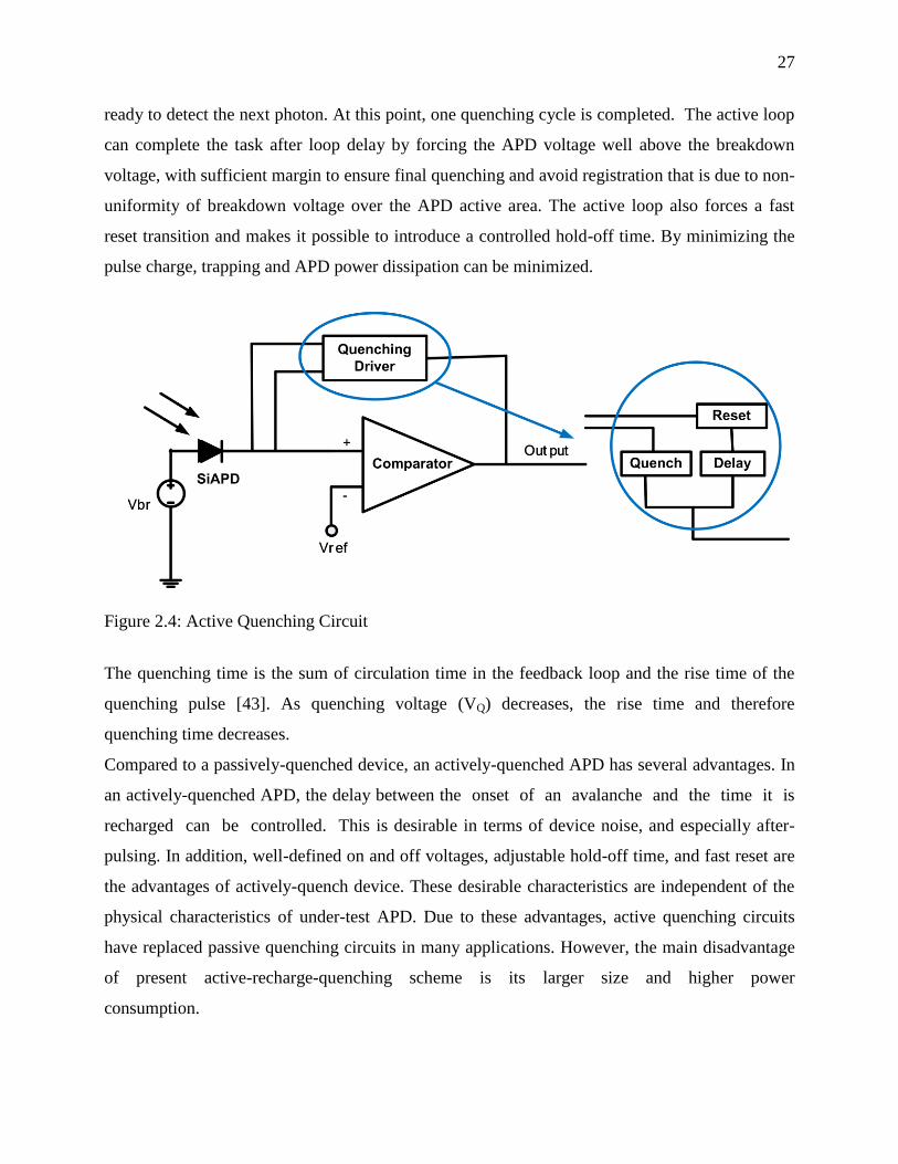
27
ready to detect the next photon. At this point, one quenching cycle is completed. The active loop
can complete the task after loop delay by forcing the APD voltage well above the breakdown
voltage, with sufficient margin to ensure final quenching and avoid registration that is due to non-
uniformity of breakdown voltage over the APD active area. The active loop also forces a fast
reset transition and makes it possible to introduce a controlled hold-off time. By minimizing the
pulse charge, trapping and APD power dissipation can be minimized.
The quenching time is the sum of circulation time in the feedback loop and the rise time of the
quenching pulse [43]. As quenching voltage (VQ) decreases, the rise time and therefore
quenching time decreases.
Compared to a passively-quenched device, an actively-quenched APD has several advantages. In
an actively-quenched APD, the delay between the onset of an avalanche and the time it is
recharged can be controlled. This is desirable in terms of device noise, and especially after-
pulsing. In addition, well-defined on and off voltages, adjustable hold-off time, and fast reset are
the advantages of actively-quench device. These desirable characteristics are independent of the
physical characteristics of under-test APD. Due to these advantages, active quenching circuits
have replaced passive quenching circuits in many applications. However, the main disadvantage
of present active-recharge-quenching scheme is its larger size and higher power
consumption.
Figure 2.4: Active Quenching Circuit
28
2.1.3 Further improvement
Next generation of quenching circuits are mixed quenching circuits, which are a combination of
passive and active quenching. The mixed quenching circuits provide flexibility in the choice of
the passive load. Since a quasi-quenching action is sufficient, load resistance RL can be smaller
than the minimum value required for passive quenching. An inductive load can also be employed
to enhance the reduction of the avalanche current for a short time, covering the delay of the active
feedback loop. However, to obtain satisfactory results and avoid overshoots and instability that is
due to the unavoidable combination of inductance and capacitances, such a circuit must be
accurately analyzed and carefully implemented.
On the other hand, the overall performance of a single photon detection system not only depends
on the APD characteristics but also on peripheral circuits, including quenching circuit and the
temperature control system. For example, the dead-time of a quenching circuit determines the
total charge flowing through the device during avalanche which affects after-pulsing
characteristics [59]. In addition, as the thermal effect was studied in section 1.2.3.7, having an on-
chip control system which can control the thermal effect is necessary.
2.1.4 Thermal Effect Control
As a result of increase in temperature, the breakdown voltage becomes higher, the diode noise
increases rapidly, and the gain decreases. Therefore it is important to cool the system. The
implications of the system without cooler are twofold: (a) by increase in temperature, the
avalanche voltage increases and differs from the initial voltage; therefore, the operation mode of
APD may change and there is no guarantee that APD can continue working in the single photon
detection mode. (b) As mentioned in section 1.2.3.7, an increase in temperature results in APD
breakdown voltage (VBr) increase. This means that, by keeping the bias voltage constant, the
excess voltage (Vex) may not be the optimum value anymore, and the single photon detection
efficiency may drop. (c) As discussed in section 1.2.3.4, an increase in temperature causes rapid
increase in thermal noise. By increase in the noise level, the amplitude of the detected pulse in the
output may increase as a result of thermal carriers. This may cause interference in the accuracy of
photon counting. (d) APD gain in both linear and Gieger modes of operation is another parameter
that would decrease by an increase in temperature.
29
Consequently, different methods are suggested for cooling APDs. A common suggested solution
is using fluid nitrogen or thermo-electricity cooling [60] [61] [62]. The simplicity of structure
makes thermo-electronic cooling system become a conventional solution for APDs. However,
since they have high power-consumption and are not integrated, APDs with thermo-electronic
coolers have to be used in laboratory settings [63], or in large instruments, where the power
consumption is not a limitation. Another solution is to design a control algorithm to compensate
for the thermal effect on APD parameters such as noise, gain, efficiency and SNR. This method is
a suitable solution for integrated devices. In most of suggested solutions, designing a
temperature-independent technique for automatic regulation of bias voltage is essential. This
technique results in maintaining the optimum excess voltage unchanged. The following
algorithms present some examples of compensation methods discussed in the literature:
The first method concerns the monitoring of noise changes [64]. This method is based on the
rapid increase of noise as a result of temperature increase. A signal is detected as the output of
noise change, and then is amplified and measured. When the detected noise voltage exceeds a
certain range, the bias voltage is decreased; and vice-versa, when noise signal decreases, the bias
voltage is increased. In this method the noise character nearby avalanche is studied, and the bias
voltage is stabilized based on noise characteristics [64].
Another method considers constant excess voltage, where the bias voltage is controlled as a
function of the variation of breakdown voltage due to the change of temperature. In this method
there is a temperature-breakdown voltage lookup table stored in a memory and the appropriate
bias voltage is selected from the values in the lookup table [65]. Since breakdown voltage has a
linear relation with temperature (over the operating range) the temperature coefficient is defined
as an APD specification and it can be replaced by the lookup table [66]. In this method, a
reference voltage is set to be a voltage implementing an optimal amplification ratio on an output
terminal; the desired voltage is generated by considering the slope variation of the plot of
temperature and breakdown voltage. To verify the suitable bias voltage used to compensate the
effect of temperature, there are two possibilities for the input of control loop: first input can be
from a temperature sensor, while the second possible input can be the amplitude of the APD
terminal output [66].
30
The third method is to use two APDs to eliminate the effect of noise on gain calculation and
define a multiplication factor as:
(2-5)
where IM is the un-multiplied current of the APD biased at high gain and IP is the primary un-
multiplied current of the APD at low gain.
By changing the bias voltage of a high-gain device, while maintaining a constant bias on low-
gain APD, the current ratio, and hence the high-gain of the device can be set at pre-selected
values [67]. From the ideal diode equation, the effect of temperature change on the low-gain
device is negligible when compared to the large-gain effect on the device. Therefore, over
moderate changes in room temperature IP remains constant while IM varies. In this method the
circuit is monitored to maintain its preset gain by adjusting the bias voltage of the high-gain
device [67].
31
CHAPTER 3 QUENCH-RESET CIRCUIT: SIMULATION AND POST
SSSSSSSSSSSSSLAYOUT RESULT
3.1 Design Procedure
As mentioned in section 1.3, the drawback of APD operating in Geiger-mode is that the
avalanche self-sustaining process continues until it is stopped externally. Due to the need for an
external stop and consequent quick reduction of the bias voltage, a quench-reset circuit must be
employed. The idea is to keep the APD in a sensitive condition, which is 1 volt above the
breakdown voltage for our case. As a result, by absorbing a photon and triggering an avalanche,
an increase of 400μA in output current occurs and therefore the APD cathode voltage would
increase by 1.5V. At this point the quench-reset circuit should be active to quench the avalanche
and return the APD to a sensitive state. When the avalanche is quenched the current is reset to
zero, and the voltage slowly returns to its value before detecting a photon (i.e., sensitive value).
The block diagram of the proposed solution is depicted in Figure 3.1. The Geiger-mode front-end
circuit is activated by sensing the leading edge of APD cathode voltage as a result of the
avalanche current. The quench block suppresses the avalanche current by lowering the bias
voltage below the critical value which may be very close to the junction breakdown voltage of
the semiconductor.
The output of the quenching block is digitized to be sent to the counter to complete the photon
detection system by measuring the time interval between successive pulses. After the pulse is
generated, the APD should be rearmed for subsequent detection; this is where the reset block can
be employed to bring back the APD voltage to the original sensitive level.
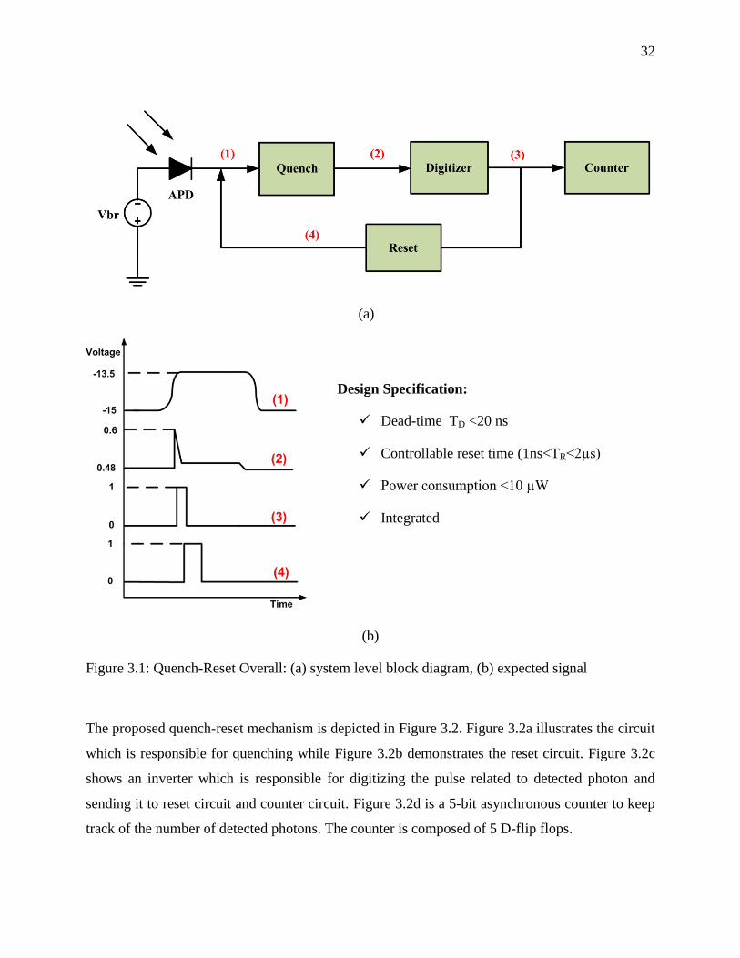
32
The proposed quench-reset mechanism is depicted in Figure 3.2. Figure 3.2a illustrates the circuit
which is responsible for quenching while Figure 3.2b demonstrates the reset circuit. Figure 3.2c
shows an inverter which is responsible for digitizing the pulse related to detected photon and
sending it to reset circuit and counter circuit. Figure 3.2d is a 5-bit asynchronous counter to keep
track of the number of detected photons. The counter is composed of 5 D-flip flops.
(a)
(b)
Figure 3.1: Quench-Reset Overall: (a) system level block diagram, (b) expected signal
Design Specification:
Dead-time TD <20 ns
Controllable reset time (1ns<TR<2µs)
Power consumption <10 µW
Integrated
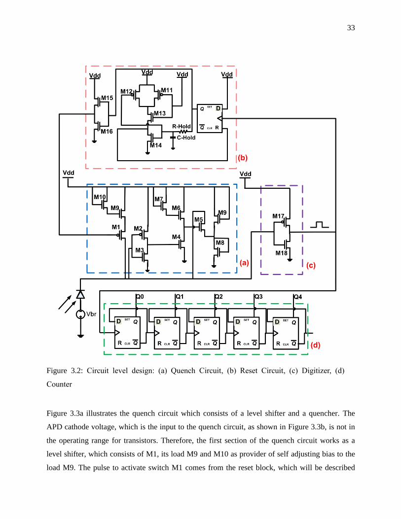
33
Figure 3.3a illustrates the quench circuit which consists of a level shifter and a quencher. The
APD cathode voltage, which is the input to the quench circuit, as shown in Figure 3.3b, is not in
the operating range for transistors. Therefore, the first section of the quench circuit works as a
level shifter, which consists of M1, its load M9 and M10 as provider of self adjusting bias to the
load M9. The pulse to activate switch M1 comes from the reset block, which will be described
Figure 3.2: Circuit level design: (a) Quench Circuit, (b) Reset Circuit, (c) Digitizer, (d)
Counter
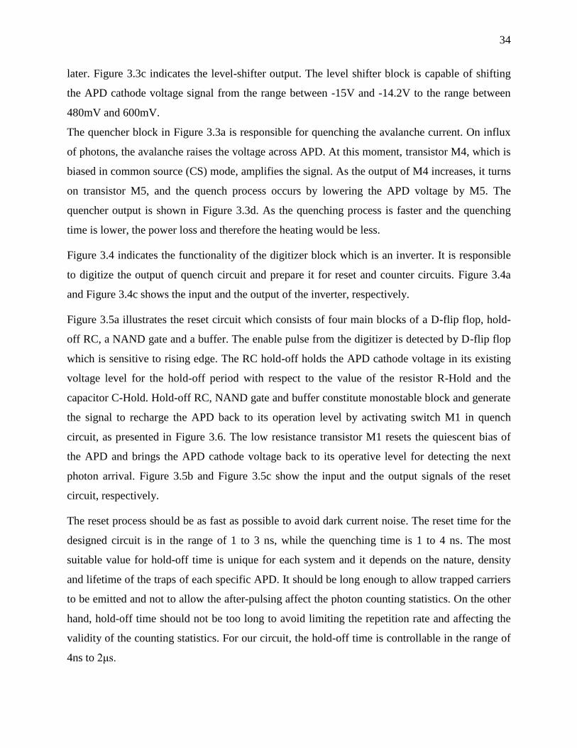
34
later. Figure 3.3c indicates the level-shifter output. The level shifter block is capable of shifting
the APD cathode voltage signal from the range between -15V and -14.2V to the range between
480mV and 600mV.
The quencher block in Figure 3.3a is responsible for quenching the avalanche current. On influx
of photons, the avalanche raises the voltage across APD. At this moment, transistor M4, which is
biased in common source (CS) mode, amplifies the signal. As the output of M4 increases, it turns
on transistor M5, and the quench process occurs by lowering the APD voltage by M5. The
quencher output is shown in Figure 3.3d. As the quenching process is faster and the quenching
time is lower, the power loss and therefore the heating would be less.
Figure 3.4 indicates the functionality of the digitizer block which is an inverter. It is responsible
to digitize the output of quench circuit and prepare it for reset and counter circuits. Figure 3.4a
and Figure 3.4c shows the input and the output of the inverter, respectively.
Figure 3.5a illustrates the reset circuit which consists of four main blocks of a D-flip flop, hold-
off RC, a NAND gate and a buffer. The enable pulse from the digitizer is detected by D-flip flop
which is sensitive to rising edge. The RC hold-off holds the APD cathode voltage in its existing
voltage level for the hold-off period with respect to the value of the resistor R-Hold and the
capacitor C-Hold. Hold-off RC, NAND gate and buffer constitute monostable block and generate
the signal to recharge the APD back to its operation level by activating switch M1 in quench
circuit, as presented in Figure 3.6. The low resistance transistor M1 resets the quiescent bias of
the APD and brings the APD cathode voltage back to its operative level for detecting the next
photon arrival. Figure 3.5b and Figure 3.5c show the input and the output signals of the reset
circuit, respectively.
The reset process should be as fast as possible to avoid dark current noise. The reset time for the
designed circuit is in the range of 1 to 3 ns, while the quenching time is 1 to 4 ns. The most
suitable value for hold-off time is unique for each system and it depends on the nature, density
and lifetime of the traps of each specific APD. It should be long enough to allow trapped carriers
to be emitted and not to allow the after-pulsing affect the photon counting statistics. On the other
hand, hold-off time should not be too long to avoid limiting the repetition rate and affecting the
validity of the counting statistics. For our circuit, the hold-off time is controllable in the range of
4ns to 2μs.
35
Figure 3.3: (a) The quench circuit which consists of a level shifter and a quencher, (b) APD cathode
voltage in absence of the quench circuit, (c) Level shifter Output, (d) Quencher Output
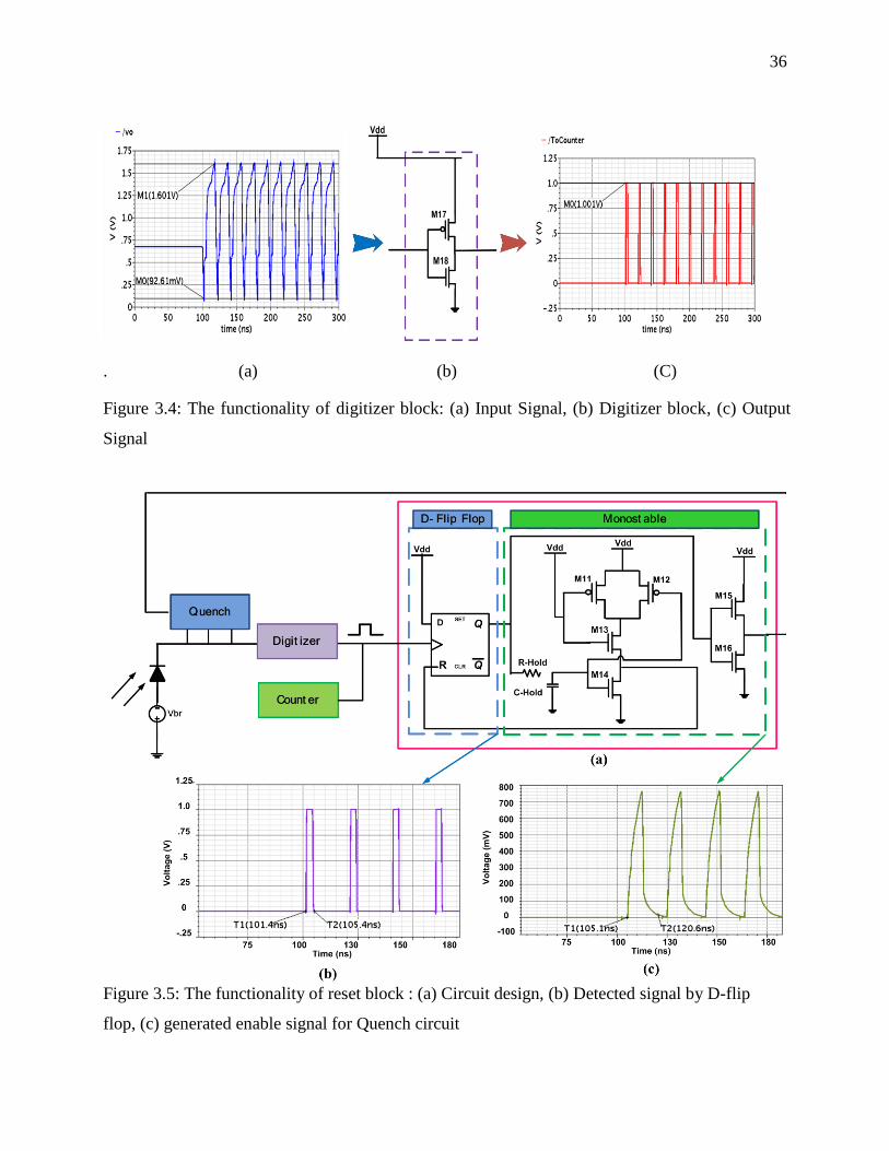
36
. (a) (b) (C)
Figure 3.4: The functionality of digitizer block: (a) Input Signal, (b) Digitizer block, (c) Output
Signal
Figure 3.5: The functionality of reset block : (a) Circuit design, (b) Detected signal by D-flip
flop, (c) generated enable signal for Quench circuit
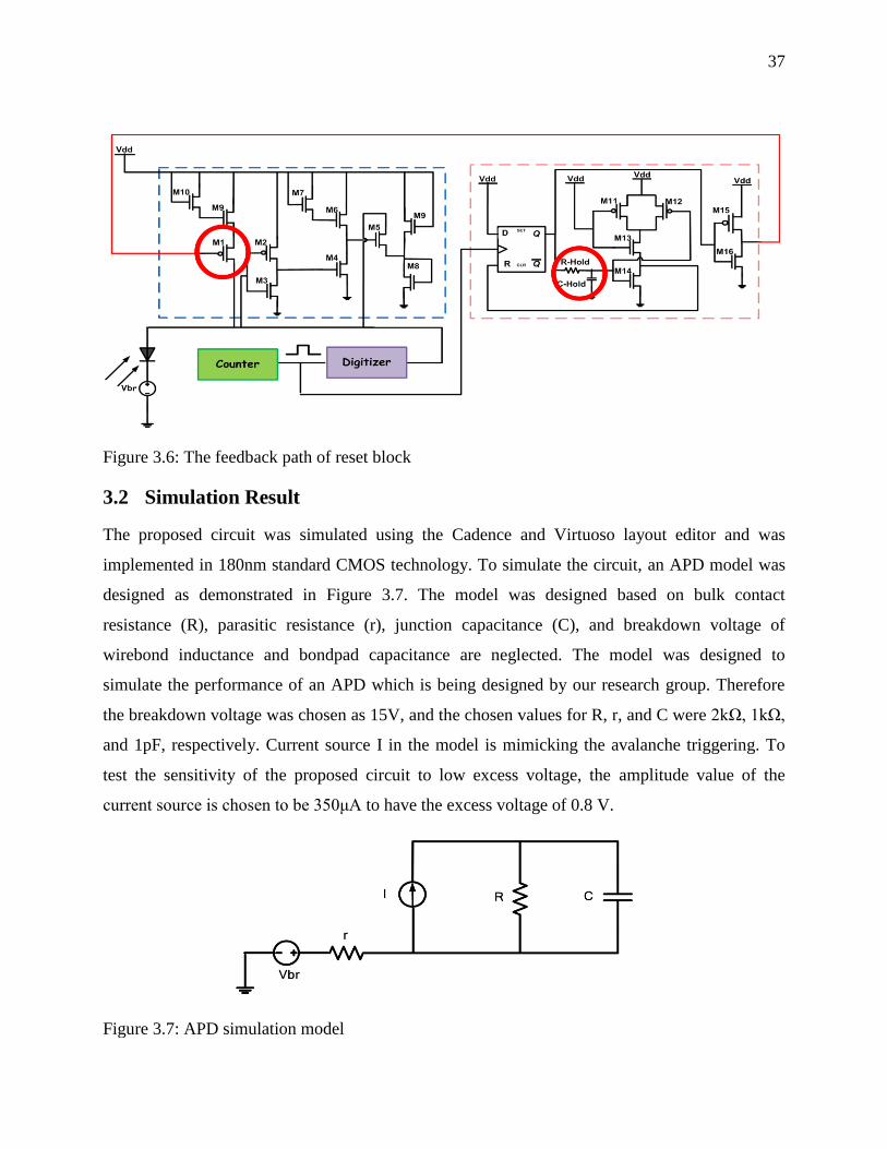
37
3.2 Simulation Result
The proposed circuit was simulated using the Cadence and Virtuoso layout editor and was
implemented in 180nm standard CMOS technology. To simulate the circuit, an APD model was
designed as demonstrated in Figure 3.7. The model was designed based on bulk contact
resistance (R), parasitic resistance (r), junction capacitance (C), and breakdown voltage of
wirebond inductance and bondpad capacitance are neglected. The model was designed to
simulate the performance of an APD which is being designed by our research group. Therefore
the breakdown voltage was chosen as 15V, and the chosen values for R, r, and C were 2kΩ, 1kΩ,
and 1pF, respectively. Current source I in the model is mimicking the avalanche triggering. To
test the sensitivity of the proposed circuit to low excess voltage, the amplitude value of the
current source is chosen to be 350μA to have the excess voltage of 0.8 V.
Figure 3.6: The feedback path of reset block
Figure 3.7: APD simulation model
38
3.2.1 Schematics
To lower the cost and reduce the design size, the design would greatly benefit from computer-
aided-design (CAD) tools that would allow optimization and verification of a particular system
before its actual fabrication. A transistor-levels design was first created as a schematic in
Cadence's 'Schematic Editor' to verify the performance of the circuit.
To estimate the photon counting rate, dead-time needs to be calculated. Dead-time is the sum of
quench time, hold-off time and reset time. Figure 3.8 indicates the performance of the APD
cathode voltage, and the output voltage to the counter, when the hold-off time is zero. Figure 3.8a
shows 3 cycles of light impinging, where signal demonstrates the light from LED; APD cathode
voltage quenches during light impinging and for each quenching event, a pulse is generated in
output voltage. Figure 3.8b, a diagrammatic representation of the results, conveys that there is a
time constant of 0.5 ns for light impinging. The quenching occurs in 0.91 ns. The output voltage
pulse is detected within 0.58 ns of the onset of the quenching. The width of the output voltage
pulse is approximately 1ns and it ends in 1.58 ns after the light impinge.
Besides having fast quenching, it is important to ensure that the output pulses are not interfered
by dark current. Therefore having controllable hold-off time is significant. Figure 3.9 illustrated
the same signals when the hold-off time is defined as 13 ns. In Figure 3.9a, the blue signal shows
the current occurred as a result of light impinging; the red signal and the green signal indicate
APD cathode voltage and quench-reset output voltage respectively. The orange signal indicates
the resetting pulse with the width equal to hold-off time value. Figure 3.9b is the zoomed-in
version of Figure 3.9a, and indicates that the quenching occurs at 2.3 ns after detecting the light.
However the reset pulse is generated 3ns later. This means that the design resetting feedback
block creates 2.7 ns delay. The resetting pulse has the width of 13 ns, which indicates the hold-
off time. When the resetting pulse disables, it takes 2.7ns for APD voltage to return to original
voltage level and for the device to be rearmed for subsequent detection. This time is called reset
time. The overall dead-time in this case is 20ns with 13ns pre-defined hold-off time.

39
(a)
(b)
Figure 3.8: Schematic simulation of the quench-reset circuit with no hold-off in terms of APD
voltage and output voltage: (a) 3 cycles of light emitting, (b) Zoom-in plot indicating quenching
time
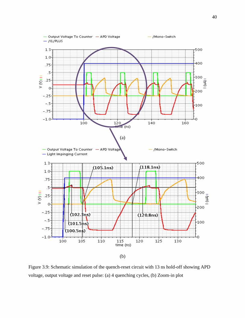
40
(a)
(b)
Figure 3.9: Schematic simulation of the quench-reset circuit with 13 ns hold-off showing APD
voltage, output voltage and reset pulse: (a) 4 quenching cycles, (b) Zoom-in plot

41
3.2.2 Post-Layout
Once the performance parameters of the quench-reset circuitry were validated through
simulations, the 'Virtuoso Layout Editor' tool from Cadence was used to create a compact layout
design for this circuitry. After the layout was completed, Design Rule Checker (DRC) was used
to make sure that all the shapes in the layout conformed to the design rules given in the design
rule specification sheet for this CMOS technology. Once the layout cleared all the DRCs, a netlist
check was performed using Layout-Versus-Schematic (LVS). LVS ensures that all the
connections in the layout are correct and the netlist extracted from the layout matches the one
extracted from the schematic. After the checks were cleared, the extraction tool was used to
extract a netlist from the designed layout with all the parasitic resistors and capacitors annotated
within. This new parasitic annotated netlist was then used to simulate and verify all significant
parameters of the circuitry again.
In case a particular important value is different from the design value then the circuit layout has
to be investigated and likely re-modified to fix this mismatch. Like all designs, such “re-work”
can be anticipated. After some modification, the simulations of the extracted netlist were very
close to the original schematic simulations and therefore no further modifications became
necessary.
Figure 3.10 demonstrates the layout result of the APD voltage and output voltage of quench-reset
circuitry with zero hold-off time. Figure 3.10b indicates that quenching occurred at 0.72 ns and
the output voltage ended at 0.83 ns.
Several additional measurements were taken in order to ensure the fabrication success of the
Quench-Reset design presented in this thesis. Figure 3.11 illustrates AC analysis of Quench-
Reset circuitry in the frequency range of 100 Hz to 5 GHz. It shows that the bandwidth of the
circuitry is 1.153 GHz.
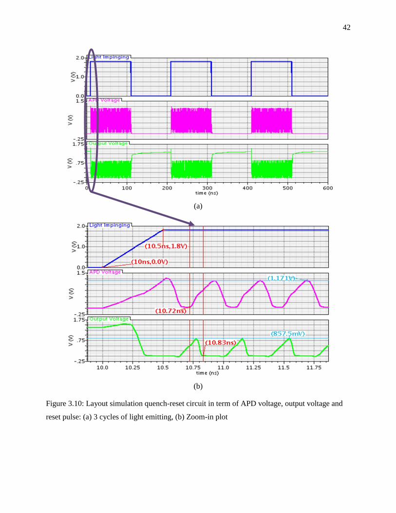
42
(a)
(b)
Figure 3.10: Layout simulation quench-reset circuit in term of APD voltage, output voltage and
reset pulse: (a) 3 cycles of light emitting, (b) Zoom-in plot
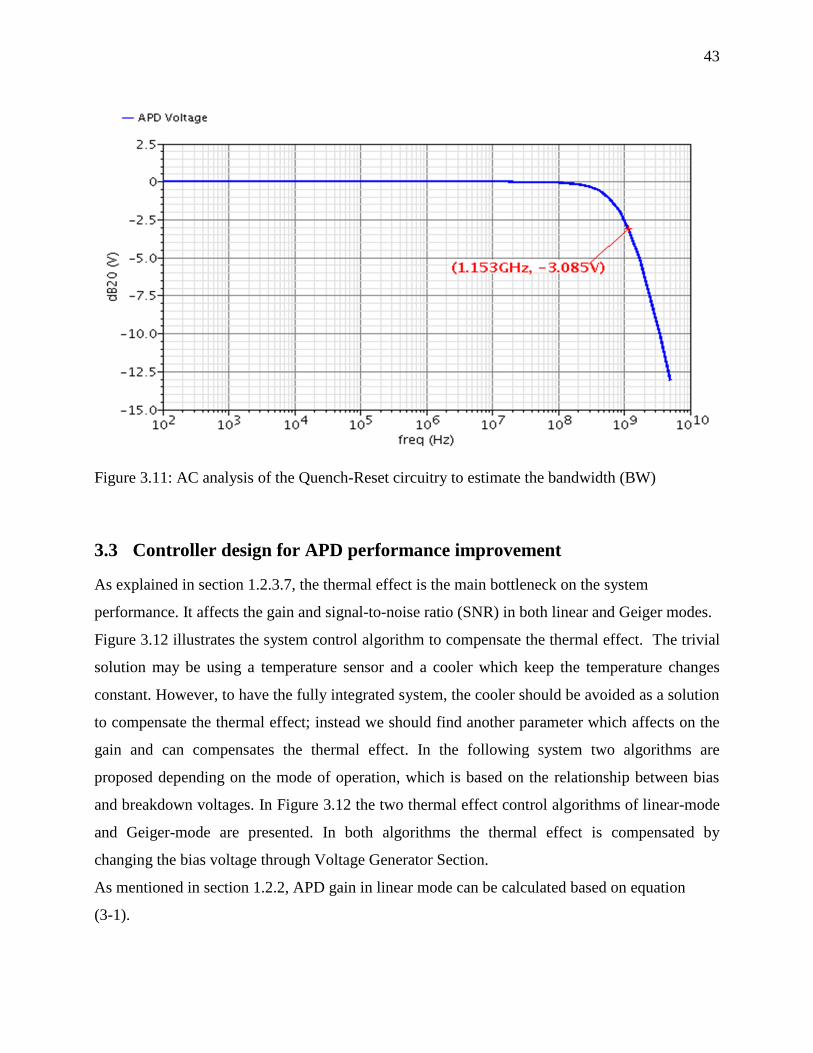
43
3.3 Controller design for APD performance improvement
As explained in section 1.2.3.7, the thermal effect is the main bottleneck on the system
performance. It affects the gain and signal-to-noise ratio (SNR) in both linear and Geiger modes.
Figure 3.12 illustrates the system control algorithm to compensate the thermal effect. The trivial
solution may be using a temperature sensor and a cooler which keep the temperature changes
constant. However, to have the fully integrated system, the cooler should be avoided as a solution
to compensate the thermal effect; instead we should find another parameter which affects on the
gain and can compensates the thermal effect. In the following system two algorithms are
proposed depending on the mode of operation, which is based on the relationship between bias
and breakdown voltages. In Figure 3.12 the two thermal effect control algorithms of linear-mode
and Geiger-mode are presented. In both algorithms the thermal effect is compensated by
changing the bias voltage through Voltage Generator Section.
As mentioned in section 1.2.2, APD gain in linear mode can be calculated based on equation
(3-1).
Figure 3.11: AC analysis of the Quench-Reset circuitry to estimate the bandwidth (BW)
44
[ ( )
]
(3-1)
where, I and R represent the total current and total equivalent resistance of APD. T0 is room
temperature at 25 C, T is the instant temperature and is a temperature coefficient. n is
determined by the character of the semiconductor material which is used to make the APD, and
its value ranges between 2 and 7 [68].
Vbr is changing linearly with temperature and indicate the changes of voltage per each Celsius
degree of change in temperature. Vir, which is the equivalent voltage of in equation (3-1),
is very small when compared with Vbias. Therefore a good estimation for the new required Vbias is
to apply the changes on breakdown voltage through temperature coefficient to primary bias
voltage. Figure 3.12a shows the methodology to compensate the thermal effect in linear mode.
The physical parameters of APD: and n along with initial temperature (T0) are preset. By
storing the initial values, the gain at initial temperature is calculated. By monitoring room
temperature the expected change in breakdown voltage can be calculated through preset
temperature coefficient. Thus, the calculated new value for bias voltage would be sent to voltage
generator section. By calculating new gain based on new bias voltage and new breakdown
voltage, the difference between the new gain and default gain is estimated and the accuracy of
this algorithm can be judged.
Similar methodology is used for Geiger mode. The gain in calculated through equation (3-2).
(3-2)
where C is the APD capacitor and q is electron charge and equal to 1.6021765 × 10⁻¹⁹
c. In this
method we try to keep Vex constant. Therefore the bias voltage is estimated based on the change
of breakdown voltage with change of temperature. In this mode by enabling a switch the output
of quench circuit is monitored in two modes of LED-off and LED-on. Dark current rate is
estimated in the case of LED-off and the sum of dark current rate and the output signal of quench
circuit is measured when LED-on. With the mentioned estimations, signal-to-noise ratio is
calculated.

45
Figure 3.12: Control algorithm to compensate the thermal effect: (a) Linear-mode Algorithm, (b)
Geiger-mode Algorithm

46
3.4 Chapter Conclusion
To verify the performance of the circuit, the transistor-level design was first captured as a
schematic in Cadence's 'Schematic Editor' and all design specifications were tested. 'Virtuoso
Layout Editor' from cadence was the tool used to create a compact layout design for this circuit.
After the layout was completed and the Design Rule Checker (DRC) test was checked, a netlist
check was performed using Layout-Versus-Schematic (LVS) to make sure that all the
connections in the layout are correct and the netlist extracted from the layout matches the one
extracted from the schematic. After optimization and verification of our design with aided-design
(CAD) tools, the design was ready to be sent for fabrication.
The design provided a minimum dead-time of 3ns with controllable hold-off time of 1ns-2μs, and
bandwidth of 1.153 GHz for the quench-reset design.
On the other side, an off-chip temperature-independent gain control system was designed and its
algorithm was tested through Modelsim. In this design the effect of temperature on the gain in
both linear-mode and Geiger-mode operations is controlled through changing the bias voltage of
APD. After performance verification, the control system was ready to be implemented on FPGA
and connected to the test APD through external connections.

47
CHAPTER 4 EXPERIMENTAL RESULT: QUENCH-RESET CIRCUIT
SSSSSSSSSSSSSAND THERMAL EFFECT CONTROL
4.1 Quench-Reset IC
The proposed quench-reset circuit was fabricated in a standard 0.18μm CMOS technology.
Figure 4.1 shows the post-layout, which is designed under Cadence layout editor and simulator
environment. The active area of the proposed circuit is only 50x120μm2 with 18 pins. The supply
voltage of 1.8V for analog section and 1V for digital section is chosen respectively.
The chip was fabricated by TSMC fabrication facilities through CMC Microsystems. The chip
consists of different APDs and quench-reset circuits. One of the quench-reset circuits was placed
separately from the designed APDs to have the option of testing quench-reset circuit independent
of the APD. The overall chip is 1mm2. Figure 4.2 presents the microphotograph of the fabricated
chip, which is a zoomed-in version of the quench-reset circuit.
Figure 4.1: The Layout scheme of the achieved Quench-Reset Circuit

48
As explained in section 1.1 the circuit is designed to be part of the light detection section of the
EEG-fNIRS brain imaging project. This whole chip includes an avalanche photodiode which is
still under design improvement and test by another student within Polystim, and it is not fully
functional yet. Therefore to test the functionality of the proposed quench building block, a
commercially-available APD device (model S2384, Hamamatsu Company) was connected to the
chip externally. As expected from the literature review, having both APD and front-end circuit
integrated on the same chip will improve the quench-reset process a few hundred times faster.
Therefore we are expecting to achieve quench and reset time in the range of few hundreds
nanoseconds with the commercial-APD test setup.
To have the output of APD in a range similar to the output of APD proposed by Polystim, the
APD model is designed based on a commercial device. Figure 4.3 depicts the APD model.
Figure 4.2: The microphotograph of the whole fabricated chip shared with a colleague from our
laboratory
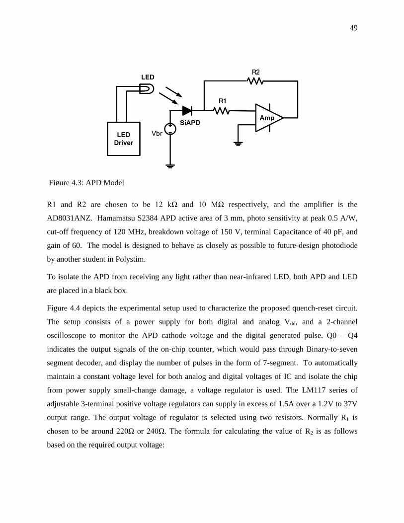
49
R1 and R2 are chosen to be 12 kΩ and 10 MΩ respectively, and the amplifier is the
AD8031ANZ. Hamamatsu S2384 APD active area of 3 mm, photo sensitivity at peak 0.5 A/W,
cut-off frequency of 120 MHz, breakdown voltage of 150 V, terminal Capacitance of 40 pF, and
gain of 60. The model is designed to behave as closely as possible to future-design photodiode
by another student in Polystim.
To isolate the APD from receiving any light rather than near-infrared LED, both APD and LED
are placed in a black box.
Figure 4.4 depicts the experimental setup used to characterize the proposed quench-reset circuit.
The setup consists of a power supply for both digital and analog Vdd, and a 2-channel
oscilloscope to monitor the APD cathode voltage and the digital generated pulse. Q0 – Q4
indicates the output signals of the on-chip counter, which would pass through Binary-to-seven
segment decoder, and display the number of pulses in the form of 7-segment. To automatically
maintain a constant voltage level for both analog and digital voltages of IC and isolate the chip
from power supply small-change damage, a voltage regulator is used. The LM117 series of
adjustable 3-terminal positive voltage regulators can supply in excess of 1.5A over a 1.2V to 37V
output range. The output voltage of regulator is selected using two resistors. Normally R1 is
chosen to be around 220Ω or 240Ω. The formula for calculating the value of R2 is as follows
based on the required output voltage:
Figure 4.3: APD Model
50
( ) (4-1)
Therefore the value of R2 would be
((
) ) (4-2)
Setting R2 to zero causes the output voltage to drop to 1.25V to apply to the pin connected to IC
digital VDD. Likewise to apply 1.8V to analog VDD pin, R2 is calculated to be 105 Ohm.
To verify the quench circuit, the chip is tested for both continuous and one-shot input signals.
The input is the signal to switch on the LED. Two cases are studied in Figure 4.5. The first case
is when the light is on only for short period. This input is called one shot pulse (Figure 4.5a). The
Figure 4.4: Test setup of fabricated chip
51
second case is when the light is on for long period and it is called continues-wave light. In post
layout result one shot input can be as short as 7ns, however in measurement with non-integrated
APD the minimum input is 250ns. Besides testing with non-integrated APD, the difference
between measurement and post-layout results is due to the bandwidth limitation of testing
devices. In Figure 4.5b the LED light is on for 2s and 8 pulses are detected. Thus the dead-time
of each pulse is 250ns. The third signal in both Figure 4.5a and Figure 4.5b indicates the digital
pulse generated with respect to each detection. Counting the number of pulses of mentioned
signal in specific period indicates the speed of photon counting in Mcounts/s. On the other hand,
the photon counting rate is estimated from the overall dead time, which is equal to the width of
each of mentioned pulses.
To test the ability of reset block in generating different hold-off times, the monostable section of
the reset block is tested with different RC. As shown in Figure 4.6, the monostable section in
reset block is capable of generating reset pulse with hold-off time in the range of 4ns to 2µs. In
(a) (b)
Figure 4.5: Chip test result in response to: (a) one-shot light, (b) continues-wave light. In both
plots: (1) LED driver voltage, (2) APD cathode voltage, (3) Output pulse to be sent to counter

52
this figure Signal (1) in both plots indicates the output from quench circuit used for the reset
block, and signal (2) indicates the output of this reset block. From the figure, we can conclude
that with similar input to the reset block that depends on the hold-off time, different-width
outputs can be generated. In Figure 4.6a, the generated hold-off pulse is 4ns while, Figure 4.6b
shows the reset signal with hold-off time equal to 2.60μs.
Table 4.1 summarizes the design characteristics of both circuit simulations and fabricated chip
results. The power consumption, input and output impedances of IC measurement are compared
with the simulation results.
Table 4.1: Design characteristics
Parameter Simulation Measurement
Power Consumption 2.14 mW 1.70 mW
Input Impedance 2 Ω 2.8 Ω
Output Impedance 1.58 kΩ 1.24 kΩ
(a) (b)
Figure 4.6: Chip test result for reset circuit with: (a) hold-off time of 4ns, (b) hold-off time of 2µs. In
both plots: (1) input pulse to reset block and signal, (2) output pulse of reset block
53
4.2 Control system
The thermal effect control is designed to keep the gain of the APD in accepted range. Depending
on the APD mode of operation, different algorithms may apply.
4.2.1 Controller
An inexpensive, fast, and reconfigurable control method is an FPGA programmed in a VHDL
language. Igloo FPGA from Actel was chosen due to its low power consumption. The device
with 100 pins adaptor and the programmer Flash Pro is shown in Figure 4.7.
The code consists of the main control unit and peripheral modules. These modules are depicted in
Figure 4.8. In addition, Libero is a comprehensive FPGA design and development software
dedicated to Actel products. It combines Microsemi SoC Products Group (formerly Actel) tools
with software such as Modelsim for simulation and Synplify for code synthesis and
implementation.
Figure 4.7: Igloo FPGA and FlashPro programmer
54
Inputs: These signals are:
Breakdown voltage: which is a physical characteristic of the APD; it is a constant input in
a test setup for a specific APD
Bias voltage: which is a variable input in each loop of operation
Leakage voltage: which is a variable input in each loop of operation; it is used in the gain
calculation in linear mode. Leakage voltage is measured from the output of the TIA,
which works as a current-to-voltage convertor for the leakage current of the APD
Temperature-sensor voltage: which is linearly proportional to the temperature in
centigrade degrees.
Temperature Sensor Interface: The integrated-circuit temperature sensor, LM35, generates an
output voltage signal with linear scale factor of +10 mV/°C. This value is converted to
temperature value by passing through the Voltage-Temperature convertor unit. In this unit the
temperature is calculated by multiplying the sensor voltage by a voltage-temperature factor.
The temperature value is used in the control algorithm in both linear and Geiger modes.
Figure 4.8: Different modules of the control unit built by a dedicated VHDL code
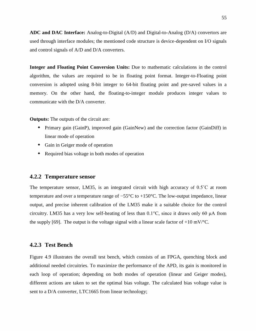
55
ADC and DAC Interface: Analog-to-Digital (A/D) and Digital-to-Analog (D/A) convertors are
used through interface modules; the mentioned code structure is device-dependent on I/O signals
and control signals of A/D and D/A converters.
Integer and Floating Point Conversion Units: Due to mathematic calculations in the control
algorithm, the values are required to be in floating point format. Integer-to-Floating point
conversion is adopted using 8-bit integer to 64-bit floating point and pre-saved values in a
memory. On the other hand, the floating-to-integer module produces integer values to
communicate with the D/A converter.
Outputs: The outputs of the circuit are:
Primary gain (GainP), improved gain (GainNew) and the correction factor (GainDiff) in
linear mode of operation
Gain in Geiger mode of operation
Required bias voltage in both modes of operation
4.2.2 Temperature sensor
The temperature sensor, LM35, is an integrated circuit with high accuracy of 0.5˚C at room
temperature and over a temperature range of −55°C to +150°C. The low-output impedance, linear
output, and precise inherent calibration of the LM35 make it a suitable choice for the control
circuitry. LM35 has a very low self-heating of less than 0.1°C, since it draws only 60 μA from
the supply [69]. The output is the voltage signal with a linear scale factor of +10 mV/°C.
4.2.3 Test Bench
Figure 4.9 illustrates the overall test bench, which consists of an FPGA, quenching block and
additional needed circuitries. To maximize the performance of the APD, its gain is monitored in
each loop of operation; depending on both modes of operation (linear and Geiger modes),
different actions are taken to set the optimal bias voltage. The calculated bias voltage value is
sent to a D/A converter, LTC1665 from linear technology;
56
To set the APD bias voltage, the converted analog signal is sent to the power-set unit. As shown
in Figure 4.9 the power set unit is a buffer (AD8005) which consists of two amplifiers. Besides
controlling the thermal effect, depending on the mode of operation, the control signal is generated
and the device switches between quench-reset circuit for Geiger mode operation and TIA for
linear mode through a MAX4525 multiplexer.
Figure 4.9: Control system test bench

57
4.2.4 Control System Result
4.2.4.1 Linear Mode
To test and validate the functionality of the linear-mode control loop, a test bench was created.
Table 4.2 indicates the I/O list. In the table, breakdown voltage and temperature coefficient are
two constant values for any specific APD. The leakage voltage is measured based on leakage
current while primary bias voltage is calculated by the equation: . At this point,
with the help of the algorithms the primary gain is calculated and the required bias voltage is
estimated to keep the gain within 10% variation. It is worth noting that the primary gain is
calculated based on inputs before the temperature-independent gain loop control is applied.
Table 4.2: I/O list of thermal effect control module for linear mode APD
I/O List Abrivation Parameter Value
(Decimal)
Required
Clock Cycles
Input (Constant) Vbr Breakdown Voltage 15V -
CoefTVbr Temperature Coefficient 0.65 -
Input (Measured)
Vr Bias Voltage 14.7V -
Vir Leakage Voltage 0.1V -
T0 Primary Temperature 25°C -
Output
(Calculated) Gd Primary Gain 37.75 400
To verify the temperature-independent gain control, two cases are studied. In the first case, the
ambient temperature is increased by 2°C, and in the second case it is decreased by 2°C. In both
cases, the required bias voltage is calculated and set through power supply unit and the new gain
is calculated. The goal is to have the new gain within 10% variation from the primary gain value.
Table 4.3 and 4.4 present the results.
Table 4.3: 1st Study case for thermal effect control module of linear mode APD – 2°C increase in
ambient temperature
I/O List Abr. Parameter Value
(Decimal)
Required
Clock Cycle
Input T Secondary Temperature 27°C -
Output NewBias Proposed Bias Voltage 16.1 85
G New Gain 41.00 427
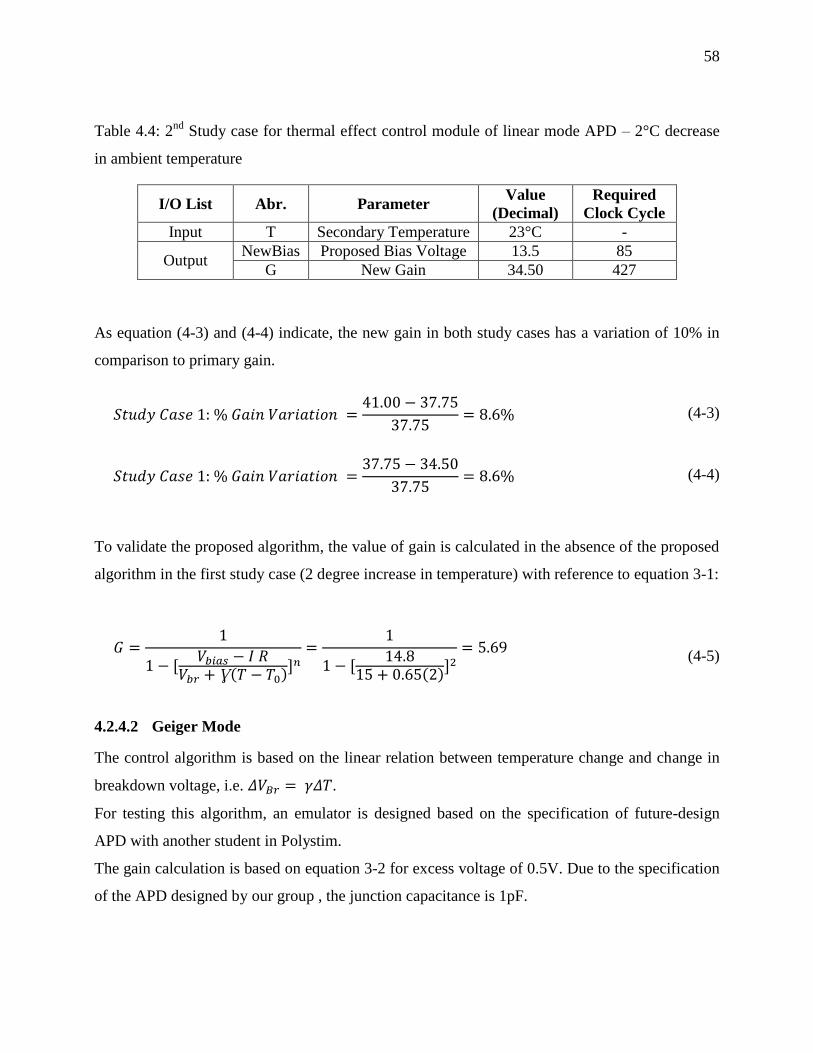
58
Table 4.4: 2nd
Study case for thermal effect control module of linear mode APD – 2°C decrease
in ambient temperature
I/O List Abr. Parameter Value
(Decimal)
Required
Clock Cycle
Input T Secondary Temperature 23°C -
Output NewBias Proposed Bias Voltage 13.5 85
G New Gain 34.50 427
As equation (4-3) and (4-4) indicate, the new gain in both study cases has a variation of 10% in
comparison to primary gain.
(4-3)
(4-4)
To validate the proposed algorithm, the value of gain is calculated in the absence of the proposed
algorithm in the first study case (2 degree increase in temperature) with reference to equation 3-1:
[
( )]
[
( )]
(4-5)
4.2.4.2 Geiger Mode
The control algorithm is based on the linear relation between temperature change and change in
breakdown voltage, i.e. .
For testing this algorithm, an emulator is designed based on the specification of future-design
APD with another student in Polystim.
The gain calculation is based on equation 3-2 for excess voltage of 0.5V. Due to the specification
of the APD designed by our group , the junction capacitance is 1pF.
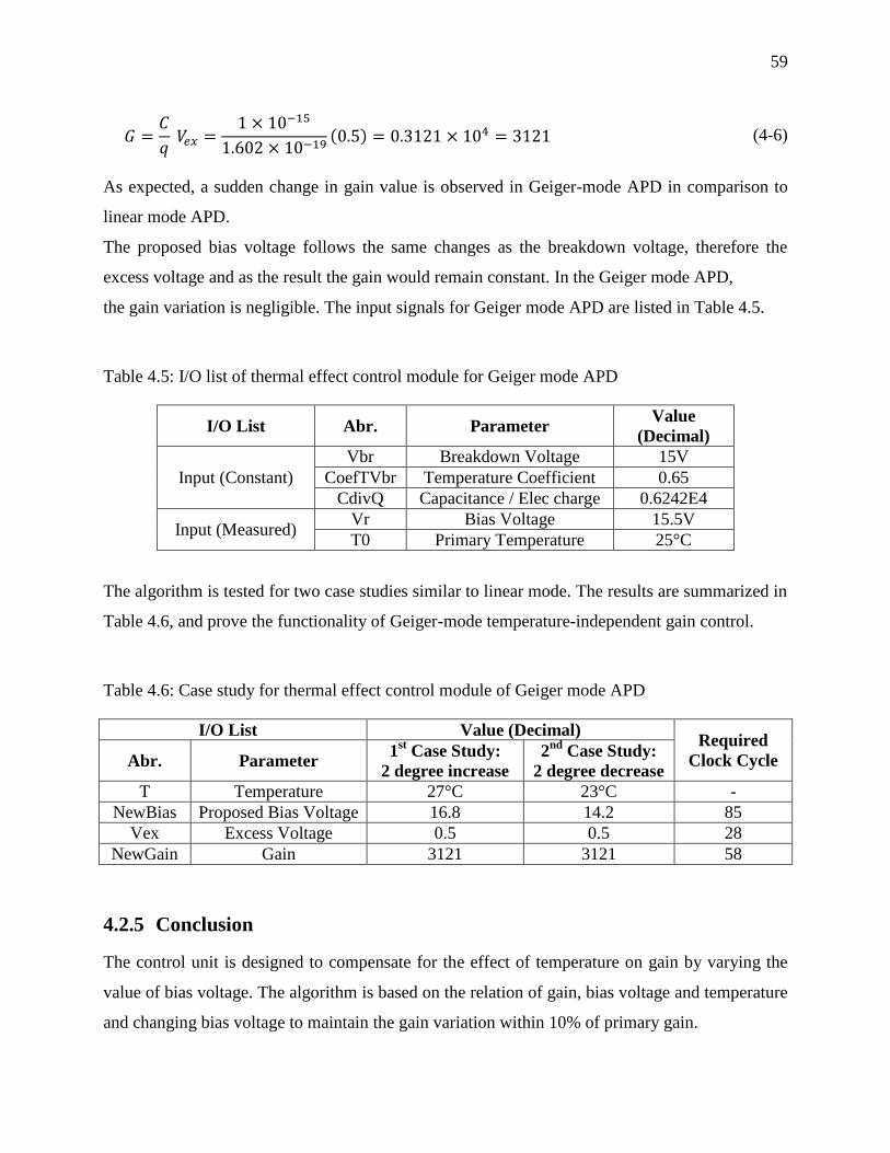
59
( ) (4-6)
As expected, a sudden change in gain value is observed in Geiger-mode APD in comparison to
linear mode APD.
The proposed bias voltage follows the same changes as the breakdown voltage, therefore the
excess voltage and as the result the gain would remain constant. In the Geiger mode APD,
the gain variation is negligible. The input signals for Geiger mode APD are listed in Table 4.5.
Table 4.5: I/O list of thermal effect control module for Geiger mode APD
I/O List Abr. Parameter Value
(Decimal)
Input (Constant)
Vbr Breakdown Voltage 15V
CoefTVbr Temperature Coefficient 0.65
CdivQ Capacitance / Elec charge 0.6242E4
Input (Measured) Vr Bias Voltage 15.5V
T0 Primary Temperature 25°C
The algorithm is tested for two case studies similar to linear mode. The results are summarized in
Table 4.6, and prove the functionality of Geiger-mode temperature-independent gain control.
Table 4.6: Case study for thermal effect control module of Geiger mode APD
I/O List Value (Decimal) Required
Clock Cycle Abr. Parameter 1
st Case Study:
2 degree increase
2nd
Case Study:
2 degree decrease
T Temperature 27°C 23°C -
NewBias Proposed Bias Voltage 16.8 14.2 85
Vex Excess Voltage 0.5 0.5 28
NewGain Gain 3121 3121 58
4.2.5 Conclusion
The control unit is designed to compensate for the effect of temperature on gain by varying the
value of bias voltage. The algorithm is based on the relation of gain, bias voltage and temperature
and changing bias voltage to maintain the gain variation within 10% of primary gain.

60
Two separate algorithms are coded based on the operation modes of APD. The proposed bias
voltage in the unit of voltage and required time in the unit of clock number are listed in separate
tables. The gain variation is calculated in each of the cases.

61
CONCLUSION
This work is proposed to complete the design of the sensor developed by multidisciplinary
research of IMAGINC group as part of the development of a real-time, noninvasive and portable
NIRS/EEG signal acquisition system to communicate wirelessly with a computer and image the
whole cortex while improving comfort in long duration scanning.
In this work, we designed and implemented an off-chip thermal effect control circuitry intended
for an integrated APD photon counting system operating in Geiger mode. The theoretical analysis
of the interface is confirmed by both simulation and experimental results.
Various publications addressing approaches to the design of quench and reset circuitry were
reviewed. The importance of quench-reset circuit is highlighted for Geiger mode APD in
different applications. The self-sustaining macroscopic current occurring as the result of
avalanche multiplication for each photon in Geiger-mode APD is triggered. Therefore, an
external force is required to reduce the electric field below breakdown onset and prepare the APD
to detect any other arriving photon while protecting the APD from being damaged. Quench-reset
circuitry is employed for this purpose. There are a variety of passive, active and mixed quench-
reset circuits were reviewed and a high-speed active quench-reset circuit has been preferred and
designed.
An electrical model is proposed to present the APD performance at photon detecting in the
operation of a switch. In this model, equivalent junction capacitors and resistors of our group’s
desired APD are placed. The model is designed in the Cadence tool to simulate the behavior of
the desired APD. The quench-reset circuitry is designed and simulated with TSMC 180nm
standard CMOS process. The design is then laid out and the post-layout simulations were
conducted to consider the non-idealities due to process imperfections and the significance of the
parasitic effects on circuit performance. The schematics and post layout simulation results
confirm a quench time of 1-3ns for the circuit which meet the requirements of high speed photon
detection quench circuits in functional near infrared optical brain imaging spectroscopy. A
controllable hold-off time of 4ns-2µs and a reset time of 1-4ns enhance the characteristics of the
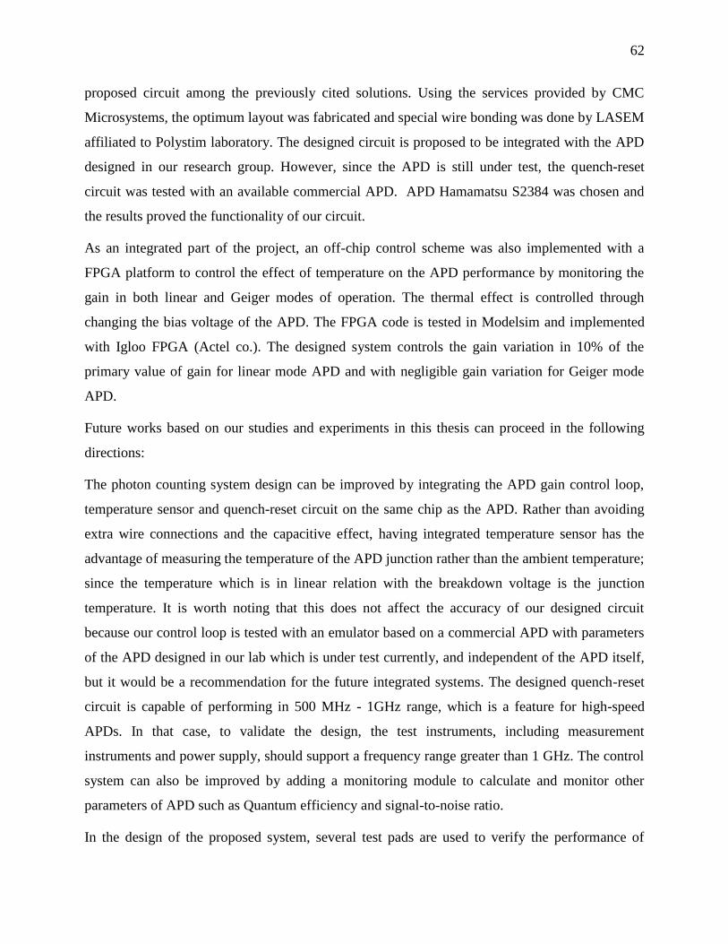
62
proposed circuit among the previously cited solutions. Using the services provided by CMC
Microsystems, the optimum layout was fabricated and special wire bonding was done by LASEM
affiliated to Polystim laboratory. The designed circuit is proposed to be integrated with the APD
designed in our research group. However, since the APD is still under test, the quench-reset
circuit was tested with an available commercial APD. APD Hamamatsu S2384 was chosen and
the results proved the functionality of our circuit.
As an integrated part of the project, an off-chip control scheme was also implemented with a
FPGA platform to control the effect of temperature on the APD performance by monitoring the
gain in both linear and Geiger modes of operation. The thermal effect is controlled through
changing the bias voltage of the APD. The FPGA code is tested in Modelsim and implemented
with Igloo FPGA (Actel co.). The designed system controls the gain variation in 10% of the
primary value of gain for linear mode APD and with negligible gain variation for Geiger mode
APD.
Future works based on our studies and experiments in this thesis can proceed in the following
directions:
The photon counting system design can be improved by integrating the APD gain control loop,
temperature sensor and quench-reset circuit on the same chip as the APD. Rather than avoiding
extra wire connections and the capacitive effect, having integrated temperature sensor has the
advantage of measuring the temperature of the APD junction rather than the ambient temperature;
since the temperature which is in linear relation with the breakdown voltage is the junction
temperature. It is worth noting that this does not affect the accuracy of our designed circuit
because our control loop is tested with an emulator based on a commercial APD with parameters
of the APD designed in our lab which is under test currently, and independent of the APD itself,
but it would be a recommendation for the future integrated systems. The designed quench-reset
circuit is capable of performing in 500 MHz - 1GHz range, which is a feature for high-speed
APDs. In that case, to validate the design, the test instruments, including measurement
instruments and power supply, should support a frequency range greater than 1 GHz. The control
system can also be improved by adding a monitoring module to calculate and monitor other
parameters of APD such as Quantum efficiency and signal-to-noise ratio.
In the design of the proposed system, several test pads are used to verify the performance of

63
different blocks. This resulted in using a larger silicon area to design the integrated chip. Since
the performance of the photon counting system is approved, it is possible to reduce the number of
the test points and minimize the size of the device. In the layout of the design, the pads are used
as terminals but these pads do not provide electrostatic discharge protection. This was a
limitation in our experimental test, and it is recommended that this protection be used for future
testing.

64
REFERENCES
[1] P W McCormick, M G Goetting, M Dujovny, and J L Ausman, "Noninvasive cerebral
optical spectroscopy for monitoring cerebral oxygen delivery and hemodynamics," Critical
Care Medicine, pp. 89-97, 1991.
[2] D k Sokol, O N Markand, E C Daly, T G Luerssen, and M D Malkoff, "Near infrared
spectroscopy (NIRS) distinguishes seizure types," Seizure, vol. 9, pp. 323-327, 2000.
[3] B J Steinhoof, G Herrendorf, and C Kurth, "Ictal near infrared spectroscopy in temporal lobe
epilepsy: a pilot study," Seizure, vol. 5, pp. 97-101, 1996.
[4] M Sawan, M T Salam, S Gelinas, J Le Lan, F Lesage, and D K Nguyen, "Combined NIRS-
EEG Remote Recordings for Epilepsy and Stroke Real-Time Monitoring," Circuits and
Systems (ISCAS), pp. 13-16, 2012.
[5] M Butti, M Caffini, A C Merzagora, A M Bianchi, G Baselli, B Onaral, P Secchi, and S
Cerutti, "Non-invasive neuroimaging: Generalized Linear Models for interpreting functional
Near infrared Spectroscopy signals," in Proceeding of the 3rd international IEEE EMBS
Conferance on Neural Engineering, Kohala Coast, hawaii, 2007.
[6] S Fantini and M A Franceschini, "Chapter 7: Frequency-Domain Techniques for Tissue
Spectroscopy and Imaging," in Handbook of Optical Biomedical Diagnostics. Bellingham,
WA: SPIE Press, 2002, pp. 405-453.
[7] A Sultana, E Kamrani, and M Sawan, "CMOS silicon avalanche photodiode for NIR light
detection: a survey," Analog Integrated Circuits and Signal Processing, vol. 70, pp. 1-13,
2012.
[8] Hamamatsu, "Chapter 02: Si photodiodes," in Photonic Handbook.: Hamamatsu Photonics
K. K., pp. 22-66.
65
[9] D Dai, H Chen, J E Bowers, Y Kang, M Morse, and M J Paniccia, "Equivalent circuit model
of a Ge/Si avalanche photodiode," Group IV Photonics, San Francisco, 2009.
[10] S M Sze and K N Kwok, Physics of Semiconductor Devices, 3rd Edition.: John Wiley &
Sons Inc, 1969.
[11] C Canali, P Pavan, A Di Carlo, P Lugli, R Malik, M Manfredi, A Neviani, L Vendrame, E
Zanoni, and G Zandler, "Experimental and Monte Carlo Analysis of Impact-Ionization in
AlGaAs/GaAs HBT’s," IEEE Transactions on Electron Devices, vol. 43, pp. 1769-1777,
1996.
[12] L E Tarof, J Yu, T Baird, R Bruce, and D G Knight, "Temperature Measurements of
Separate Absorption, Grading, Charge, and Multiplication (SAGCM) InP/InGaAs
Avalanche Photodiodes (APD’s)," IEEE Photonic Technology Letters, vol. 5, pp. 1044-
1046, 1993.
[13] R J McIntyre, "The distribution of gains in uniformly multiplying avalanche photodiodes:
Theory," IEEE Transactions on. Electron Devices, vol. 19, pp. 703-713, 1973.
[14] J Cheng, "Self-Quenching Single photon Avalanceh Photodiodes for Near-Infrared
Detection," University of california, 2012.
[15] F Loforce, "Low noise optical receiver using Si APD," Proc. SPIE, vol. 7212, Optical
Components and Materials VI, no. 721210, 2009
[16] R F Pierret, Semiconductor Device Fundamentals: Addison-Wesley Publishing Company,
1996.
[17] F Zappa, S Tisa, A Gulinatti, A Gallivanoni, and S Cova, "Complete single-photon counting
and timing module in a microscope," Optics Letters, vol. 30, pp.1327-1329, 2005.
[18] K Zhao, III-V Single Photon Avalanche Detector with Built-In Negative Feedback for NIR
Photon Detection: Proquest, Umi Dissertation Publishing, 2012.
66
[19] D Pellion, "Modélisation, fabrication et évaluation des photodiodes à avalanche polarisées
en mode Geiger pour la détection du photon unique dans les applications
Astrophysiques," Ph.D. dissertation, Dept. Elect. Eng., Université Paul Sabatier-Toulouse
III, 2008.
[20] B G Streetman, Solid State Electronic Devices. 4 edition: Prentice-Hall International, 1995.
[21] Hamamatsu, Characteristic and use of Si APD (Avalanche Photodiode), Technical Report,
2004.
[22] A Gallivanoni, I Rech, and M Ghioni, "Progress in Quenching Circuit for Single Photon
Avalanceh Diodes," IEEE Tranactions on nuclear science, vol. 57, 3815–3826, 2010.
[23] W T Tsang, "Part D: Photodetectors," in Semiconductors and Semimetals. Volume 22:
Lightwave Communications Technology: Academic Press, 1985.
[24] X Zheng, “Long-Wavelength, High-Speed Avalanche photodiodes and APD array”, Ph.D.
dissertation, Dept. Elect. Eng., University of Texas at Austin, 2004.
[25] J E Bowers and Y G Wey, "High-Speed Photodetectors," in Handbook of Optics. New York:
McGraw-Hill, 1995, ch. 17, pp. 17.11–17.14.
[26] V H Dhulla, “Single photon counting for ultra-weak fluorescence detection: system design,
characterization and application to DNA-sequencing,” Ph.D. dissertation, Dept. Elect. Eng.,
Stony Brook University, 2007.
[27] Maxim, DS-1100, 5-Tap Economy Timing Element (Delay Line), [Online]. HYPERLINK "
http://www.maxim-ic.com " http://www.maxim-ic.com
[28] K E kolb, “Characterization of silicon photodiodes with novel device architecture,” Master’s
Thesis, Collage of Science. Chester F. Carlson Center for Imaging Science, Rochester
Institude of Technology, 2011.
67
[29] J B Hurst, “Molecular-beam Epitaxial Growth of Low-dark-current Avalanche
Photodiodes,” Ph.D. dissertation, Dept. Elect. Eng., University of Texas at Austin, 2007.
[30] T Nesheim, “Single photon detection using avalanche photodiode,” Master’s Thesis, Dept.
Elect. & Telecom. Eng., Norges teknisk-naturvitenskapelige universitet, 1999.
[31] L Cheng, “Novel single photon sensors for highly sensitive fluorescence detection systems,”
Ph.D. dissertation, Dept. Elect. Eng., State University of New York at Stony Brook, 2009.
[32] M A Itzler, R Ben-Michael, C F Hsu, K Slomkowski, A tosi, S Cova, F Zappa, R Ispasoiu,
"Single photon avalanche diodes (SPADs) for 1.5µm photon counting applications," Journal
Modern Optics, vol. 54, pp. 283-304, 2007.
[33] k Phang, "CMOS Optical Preamplifier Design Using Graphical Circuit Analysis," Master’s
Thesis, Dept. Elect. Eng., University of Toronto, 2001.
[34] T H Lee, The Design of CMOS Radio-Frequency Integrated Circuits. Cambridge, U.K.:
Cambridge Univ. Press, 1998.
[35] Sh Deng and A P Morrison, "Design of a Hold-off Time Control Circuit for Geiger-mode
Avalanche Photodiodes," International Journal of Microelectronics and Commputer Science
, vol. 3, pp. 53-59, 2012
[36] R J Mcintyre, "Theory of Microplasma Instability in Silicon," Journal of Applied Physics,
vol. 32, pp. 983-995, 1961.
[37] S Cova, M Ghioni, A Lotito, I Rech, and F Zappa, "Evolution and prospects for singe-
photon avalanche diodes and quenching circuits," Journal of modern optics, pp. 1267-1288,
2004
[38] SensL Company. [Online]. HYPERLINK "http://www.SensL.com" http://www.SensL.com
[39] D Rennker, "Geiger-mode avalanche photodiodes, history, properties, and problems,"
68
Nuclear Instruments & Methods in Physics Research Section A, vol. 567, pp. 48-56, 2006.
[40] R h Haitz, "Model for the electrical behavior of a microplasma," Appled Physics, vol. 35, pp.
1370–1376, 1964.
[41] P P Webb, R J Mclntyre, and J Conradi, "Properties of Avalanche Photodiodes," RCA
Review, vol. 35, p. 234-278, 1974.
[42] J Ohta, Smart CMOS Imge Sensors and Applications. Boca. Raton, FL: Taylor & Francis
Group, 2008.
[43] W G Lawrence, G Varadi, G Entine, E Podniesinski, and P K Wallace, "Enhanced red and
near infrared detection in flow cytometry using avalanche photodiodes," Cytometry, vol.
73A, pp. 767-776, 2008.
[44] M M El-Desoki, "CMOS imagers for low-level light and high-speed biomedical
applications," Ph.D. dissertation, Dept. Elect. Eng., McMaster University, 2010.
[45] C A Primmerman, "Detection of Biological Agents," Lincoln Laboratory Journal , vol. 12,
pp. 3-31, 2000.
[46] S Cova, M Ghioni, A Lacaita, C Samori, and F Zappa, "Avalanche photodiodes and
quenching circuits for single-photon detection," Applied Optics, vol. 35, pp. 1956-1963
1996.
[47] W G Oldham, R Samuelso, and P Antognet, "Triggering phenomena in avalanche diodes,"
IEEE Transactions on Electron Devices, vol. 19, pp. 1056-1060, 1972.
[48] H Dautet, P Deschamps, B Dion, A D MacGregor, D MacSween, R J McIntyre, C Trottier,
and P P Webb, "Photon-counting techniques with silicon avalanche photodiodes," Applied
Optics , vol. 32, pp. 3894-3900, 1993.
[49] W Becher, TCSPC Handbook, 2nd ed. Berlin: Becher & Hickl GmbH, 2006.
69
[50] S Felekyan, R Kuhnemuth, V Kudryavtsev, C Sandhagen, W Becker, and C A M Seidel,
"Full correlation from picoseconds to seconds by time-resolved and time-correlated single
photon detection," Review of Scientific Instruments, vol. 76, pp. 83104-83114, 2005.
[51] H Finkelstein, M J Hsu, and S Esener, "An ultrafast Geiger-mode single photon avalanche
diode in 0.18-μm CMOS technology," in Proc. SPIE 6372, Advanced Photon Counting
Techniques, 63720W, Boston, 2006.
[52] A Rochas, G Ribordy, B Furrer, P A Besse, and R S Popovic, "First passively-quenched
single photon counting avalanche photodiode element integrated in a conventional CMOS
process with 32ns dead time," SPIE - The International Society for Optical Engineering, vol.
4833, pp. 107-115, 2002.
[53] P Antognetti, S Cova, and A Longoni, "A study of the operation and performances of an
avalanche diode as a single photon detector," in Proceedings of 2nd IEEE Ispra Nuclear
Electronic Symposium, 1975.
[54] S Tisa, A Tosi, and F Zappa, "Fully-integrated CMOS single photon counter," Optics
Express, vol. 15, pp. 2873-2887, 2007.
[55] A Rochas, P A Besse, and R S Popovic, "Actively recharged single photon counting
avalanche photodiode integrated in an industrial CMOS process," Sensors and Actuators A :
Physical, vol. 110, pp. 124-129, 2004.
[56] S Cove, "Active quenching circuit for avalanche photodiodes," U.S. Patent 4963727,
October 20, 1990.
[57] M Ghioni, S Cova, F Zappa, and C Samori, "Compact active quenching circuit for fast
photon counting with avalanche photodiodes," Review of Scientific Instruments, vol. 67, pp.
3440–3448, 1996
[58] Micro Photon Devices, "SPAD" [Online]. HYPERLINK "http://www.micro-photon-
70
devices.com" http://www.micro-photon-devices.com
[59] M Liu, Infrared Single Photon Avalanche Diodes: University of Virginia: Disseration of
Doctor of Philosophy, 2008.
[60] H Finkelstein, “Shallow-Trench-Isolation Bounded Single-Photon Avalanche Diodes in
Commercial Deep Submicron CMOS Technologies,” Ph.D. dissertation, Dept. Elect. Eng.,
University of California, San Diego, 2007.
[61] C Niclass, M Sergio, and E Charbon, "A single photon avalanche diode array fabricated in
deep-submicron CMOS technology," in Design, Automation and Test in Europe, DATE 06
Proceedings, 2006.
[62] S J Dimler, J S NG, R C Tozer, G J Rees, and J P R David, "Capacitive quenching
measurement circuit for Geiger-mode avalanche photodiodes," IEEE Select Topic in
Quantum Electronic, vol. 13, 2007.
[63] J G Rarity, T E Wall, and K D Ridley, "Single-photon counting for the 1300-1600-nm range
by use of peltier-cooled and passively quenched InGaAs avalanche photodiodes," Applied
Optics Journal, vol. 39, pp. 6746-6753, 2000.
[64] G Ribordy and D J Gautier, "Performance of InGaAs/InP avalanche photodiodes as gate-
mode photon counters," Applied Optics Journal, vol. 37, pp. 2272-2277, 1998.
[65] T Maruyama, M Kudo, and F Narusawa, "Photodetector having a control block for
maintaining a detection signal within a predetermined tolerance range," U.S Patent 657149,
May 27, 2003.
[66] H L Fu, X M Zheng, and M S He, "Exact Adjustment of Single Photon Avalanche Diode
Detector for the Yunnan Observatory Laser Ranging System," Astronomical Research &
Technology , vol. 1, pp. 37-311, 2004.
[67] B Zhou, F Y Huang, D S WU, and J Liu, "A single-photon detector without cooler," in
71
Proceedings of SPIE 8561, Advanced Sensor Systems and Applications, Vol. 85611E, 2012.
[68] J Stewart, A Ho, R J Hofmeister, D J Douma, L G Hosking, A Weber, and J B Price,
"Avalanche photodiode controller circuit for fiber optics transceiver," U.S Patent 7155133,
December 26, 2006.
[69] M Maeda and M Sudo, "Bias voltage control circuitry for avalanche photodiode taking
account of temperature slope of breakdown voltage of the diode, and method of adjusting the
same," 6157022 , December 5, 2000.
[70] D O'Connell, A P Morrison, K G McCarthy, P Angove, and B O'Flynn, "Miniature gain and
bias control circuit for avalanche photodiode," Electronics Letters, vol. 43, pp. 67-68, 2007.
[71] Y Li, J Wan, B Jiang, B Wang, and L Dong, "Thermo-drift Analysis and Bias Compensation
of the Gain of APD," SPIE7055, Infrared Systems and Photoelectronic Technology III,
70550W, 2008.
[72] Texis Instruments, "LM35 Datasheet", Texas Instruments Incorporated, 1999. [Online].
HYPERLINK "http://datasheetreference.com/datasheets/national_LM35_datasheet.pdf"
http://datasheetreference.com/datasheets/national_LM35_datasheet.pdf
[73] S Cova, A Longoni, and G Ripamonti, "Active-quenching and gating circuits for single-
photon avalanche-diodes (SPADs)," IEEE Transactions on Nuclear Science, vol. 29, pp.
599-601, 1982.
[74] A Gallivanoni, I Rech, D Resnati, M Ghioni, and S Cova, "Monolithic active quenching and
picosecond timing circuit suitable for large-area single-photon avalanche diodes," Optics
Express, vol. 14, pp. 5021-5030, 2006.
[75] I Rech, G Luo, M Ghioni, H Yang, X Sunney Xie, and S Cova, "Photon-timming detector
module for single-molecule spectroscopy with 60-ps resolution," IEEE Journal of Selected
Topics in Quantum Electronics, vol. 10, pp. 788-795, 2004.

72
[76] H Dautet and J DesChamps, "Active quench circuit and reset circuit for avalanche photo
diode," U.S Patent 5532474, August 2, 1999.
[77] A R Comeau, P D Deschamps, B Y Dion, and C J Trottier, "Active quench circuit for an
avalanche current device," U.S Patent 5933042, July 2, 1996.