Embed Size (px)
Citation preview

Copyright
by
Alexander Jin Pak
2016
The Dissertation Committee for Alexander Jin Pak Certifies that this is the
approved version of the following dissertation:
First-Principles Investigation of Carbon-Based Nanomaterials for
Supercapacitors
Committee:
Gyeong S. Hwang, Supervisor
John G. Ekerdt
Arumugam Manthiram
Deji Akinwande
Pengyu Ren
First-Principles Investigation of Carbon-Based Nanomaterials for
Supercapacitors
by
Alexander Jin Pak, B.S.C.E.
Dissertation
Presented to the Faculty of the Graduate School of
The University of Texas at Austin
in Partial Fulfillment
of the Requirements
for the Degree of
Doctor of Philosophy
The University of Texas at Austin
August 2016

Dedication
To my mother, father, and sister for their support over the years and to Harley, my quirky
but lovable cat.
v
Acknowledgements
First and foremost, I gratefully acknowledge Professor Gyeong S. Hwang, my
dissertation supervisor, for his mentorship, advice, encouragement and patience throughout
my graduate studies. I am immensely thankful for the countless hours he dedicated toward
our lively scientific debates, discussions of my professional career, and meticulous review
of our manuscripts and presentations. I would also like to express gratitude toward my
other committee members – Professors John G. Ekerdt, Arumugam Manthiram, Deji
Akinwande, and Pengyu Ren – for their invaluable insights and suggestions.
My fellow group members, both past and current, were an integral part of my
journey as a student, mentor, and scientist. In particular, I would like to thank Eunsu Paek,
Yongjin Lee, Kyoung E. Kweon, Yuhao Tsai, Haley Stowe, Matt Boyer, and Greg
Hartmann for our many spontaneous and fruitful discussions. I am also grateful for the
opportunity to interact with some brilliant experimental collaborators including Professors
Rodney S. Ruoff, Christopher W. Bielawski, Li Shi, and Keji Lai and their students.
Finally, I would like to acknowledge Professors Roger T. Bonnecaze and S.V. Sreenivasan
who allowed me to participate in the NASCENT Center and their shared vision for
nanomanufacturing.
My time in Austin was incredibly amazing thanks to the many friends I have made
here. They encouraged me to try new things, supported me throughout graduate school,
and hosted some legendary potlucks. I will miss them but I also know they will go on to
vi
do great things. I also want to thank my family and their unwavering faith in me which has
allowed me to get to this point in my career.
Alexander J. Pak
University of Texas at Austin
August 2016
vii
First-Principles Investigation of Carbon-Based Nanomaterials for
Supercapacitors
Alexander Jin Pak, Ph.D.
The University of Texas at Austin, 2016
Supervisor: Gyeong S. Hwang
Supercapacitors are electrochemical energy storage devices known for their large
power densities and long lifetimes yet limited energy densities. A conventional
understanding of supercapacitors relates the high power to fast ion accumulation at the
polarized electrode interface, forming the so-called electric double layer (EDL), and the
low energy to limited electrode surface area (SA). To improve the energy density, the
capacitance may be enhanced by using high SA electrode materials such as carbon-based
nanomaterials. While promising results have been experimentally reported, capacitances
have also been noted to exhibit a highly non-linear relationship with SA. These interesting
observations suggest that a gap exists in our fundamental understanding of charge storage
mechanisms in the EDL of carbon nanomaterials. Given that EDLs are typically on the
order of 1-3 nm thick, theoretical simulations can elucidate these unknown physical
insights in order to identify new design principles for future electrode materials.
In this dissertation, we explore two broad types of carbon-based nanomaterials,
which are separated into two Parts, using a combined density functional theory and
classical molecular dynamics computational approach. In Part I, we study the capacitance
viii
using various chemically and/or structurally modified graphene (or graphene-derived)
materials which is motivated by previous accounts of the limited capacitance using pristine
graphene. Our analysis demonstrates the viability of dramatically improving the
capacitance using graphene-derived materials owing to enhancements in the quantum
capacitance with marginal effects on the double layer capacitance. In Part II, we investigate
the capacitance using nanoporous carbon materials which is motivated by experimental
observations that relate capacitance to pore width rather than SA. Our findings confirm that
promoting ion confinement through pore width control can enhance capacitance, but also
identify pore shape dispersity as another important structural feature that facilitates fast ion
dynamics during charging/discharging.
The work in this dissertation presents an overview of new insights into charge
storage mechanisms using low-dimensional carbon-based nanomaterials and future
directions for materials development. Moreover, we anticipate that the established
methodologies and analyses can be broadly applicable to the study of other applications
utilizing electrified interfaces, including capacitive deionization and liquid-gated field
effect transistors.

ix
Table of Contents
List of Tables ....................................................................................................... xiii
List of Figures ...................................................................................................... xiv
Chapter 1: Introduction ............................................................................................1
1.1 Background and Motivation ..................................................................1
A. Necessity of Energy Storage .........................................................1
B. Supercapacitor Fundamentals .......................................................2
1.2 Research Objectives ...............................................................................7
1.3 Dissertation Overview ...........................................................................9
Chapter 2: Theoretical Background .......................................................................10
2.1 Simulation Techniques.........................................................................10
A. Quantum Mechanical Calculations .............................................10
B. Classical Molecular Dynamics ...................................................13
2.2 Capacitance Calculations .....................................................................18
A. Quantum Capacitance .................................................................18
B. Double Layer Capacitance ..........................................................19
C. Interfacial Capacitance ................................................................21
PART I: GRAPHENE-DERIVED MATERIALS .........................................................22
Chapter 3: Topological Point-like Defects ............................................................23
3.1 Introduction to Point-Like Defects ......................................................23
3.2 Computational Methods .......................................................................24
3.3 Defect Structures and Formation Energies ..........................................25
3.4 Relationship Between Defects and Electronic Structure .....................26
3.5 Impact of Topological Defects on Quantum Capacitance ...................31
3.6 Influence on the Double Layer and Total Interfacial Capacitance ......33
3.7 Tuning Through Combinations of Topological Defects ......................36
3.8 Conclusions ..........................................................................................39
x
Chapter 4: Transition Metal Dopant-Vacancy Complexes ....................................40
4.1 Introduction to Transition Metal Dopants............................................40
4.2 Computational Methods .......................................................................41
4.3 Geometry of Metal Dopant-Vacancy Complexes ................................43
4.4 Hybridization Between Dopant and Graphene Vacancy States ...........45
4.5 Metal-Induced Enhancement of the Quantum Capacitance.................50
4.6 Dopant Effect on the Double Layer Structure and Capacitance ..........51
A. Near Uncharged Electrodes ........................................................53
B. Near Charged Electrodes ............................................................57
4.7 Metal Doping Effect on the Total Interfacial Capacitance ..................61
4.8 Conclusions ..........................................................................................63
Chapter 5: Extended Edge Defects ........................................................................65
5.1 Introduction to Edge Defects in Graphene...........................................65
5.2 Computational Methods .......................................................................66
5.3 Nanoribbon Electronic Structure and Quantum Capacitance ..............69
5.4 Double Layer Microstructure and Capacitance Near Edges ................74
A. Near Uncharged Electrodes ........................................................74
B. Near Charged Electrodes ............................................................78
5.5 Total Interfacial Capacitance ...............................................................82
5.6 Conclusions ..........................................................................................83
Chapter 6: Basal-Plane Oxidation ..........................................................................85
6.1 Introduction to Graphene Oxide ..........................................................85
6.2 Computational Methods .......................................................................87
6.3 Hydroxyl Agglomeration on Basal Plane ............................................90
6.4 Coverage Effect on Electronic Structure and Quantum Capacitance ..93
6.5 Electrochemical Stability of Hydroxyl Functionalized Graphene .......98
6.6 Coverage Effect on Double Layer Microstructure and Capacitance ...99
6.7 Total Interfacial Capacitance .............................................................105
6.8 Conclusions ........................................................................................107
xi
PART II: NANOPOROUS CARBON MATERIALS .....................................109
Chapter 7: Influence of Carbon Nanotube Curvature on Capacitance ................110
7.1 Introduction to Carbon Nanotubes .....................................................110
7.2 Computational Methods .....................................................................112
7.3 Curvature Influence on Double Layer Structure and Capacitance ....114
7.4 Electronic Structure of Carbon Nanotubes ........................................127
7.5 Interfacial Capacitance of [BMIM][PF6]/CNT Systems ....................128
7.6 Conclusions ........................................................................................129
Chapter 8: Ion Confinement Effects in Charged Cylindrical Pores .....................132
8.1 Introduction to Pore Size Effect .........................................................132
8.2 Computational Methods .....................................................................134
8.3 Ionic Liquid Microstructure Confined Within CNTs ........................137
A. Neutral CNT electrodes ............................................................137
B. Charged CNT electrodes ...........................................................139
8.4 Influence of Applied Potential on Capacitance .................................142
8.5 Transient Migration of Ions During Charging ...................................145
8.6 Conclusions ........................................................................................149
Chapter 9: Pore Dispersity and Ion Kinetics in Nanoporous Carbons.................151
9.1 Introduction to Nanoporous Carbon ..................................................151
9.2 Computational Methods .....................................................................152
A. Electrode Structure Generation .................................................152
B. Force Field ................................................................................152
C. Molecular Dynamics .................................................................154
9.3 Nanoporous Carbon Structural Characterization ...............................155
9.4 Discharge Capacitance Using Nanoporous Carbon ...........................158
9.5 Influence of Confinement on Capacitance .........................................159
9.6 Ion Kinetics During Discharge ..........................................................162
9.7 Relationship Between Capacitance and Pore Shape Dispersity ........164
9.8 Conclusions ........................................................................................166
xii
Chapter 10: Summary and Future Directions ......................................................169
10.1 Materials Design Principles to Enhance Capacitance ........................171
A. Notable Trends on the Quantum Capacitance ..........................171
B. Notable Trends on the Double Layer Capacitance ...................174
10.2 Insights into Ion Electrokinetics under Confinement ........................177
10.3 Perspective on New Research Directions ..........................................179
10.4 Potential Future Directions ................................................................181
A. Tailoring Performance with Ionic Liquid Optimization ...........181
B. Developing Carbon-Based Materials for Pseudo-Capacitors ...182
C. Understanding Charging Dynamics and Impedance .................184
D. Extending to Other Applications ..............................................185
References ............................................................................................................187
Vita .................................................................................................................... 206
xiii
List of Tables
Table 4.1 Summary of the metal atom elevation and partial charge at varying
(µC/cm2) calculated from density functional theory and used in the
classical molecular dynamics simulations. .......................................52
Table 5.1 Summary of predicted capacitances for charged OH-18ZGNR electrodes
in [BMIM][PF6]. For comparison, the capacitance values for the pristine
graphene case are also shown in parentheses. ..................................82
Table 6.1 Summary of the average nearest neighbor distance between O atoms
(DOH) and pair-wise interaction energy per OH moiety (Ep,OH) for the
listed supercell systems. ....................................................................92
Table 7.1 Summary of simulation details used in this work. ..........................113
Table 7.2 The estimated interfacial capacitance (applied potential) for each
electrode at the listed surface charge densities σ (in µC/cm2). .......129
Table 8.1 Coarse-grain parameters primarily from Ref. 191 and 56, with q re-scaled
following the fashion of Ref. 192 and re-optimized to reproduce
experimental density and diffusivity. ..............................................136
Table 9.1 Coarse-grain parameters primarily from Ref. 191 and 56, with q re-scaled
following the fashion of Ref. 192 and re-optimized to reproduce
experimental density and diffusivity. ..............................................153
Table 9.2. Summary of the structural characteristics of the three nanoporous carbon
electrodes studied in this work. All pore geometry analysis was performed
using a Monte Carlo sampling approach described in Ref. 204. ....156

xiv
List of Figures
Figure 1.1 Ragone plot comparing the specific power (i.e., how quickly charge is
delivered) and energy (i.e., how much charge it contains) of capacitors
(grey and blue) and batteries (green and red). Reprinted by permission
from Macmillan Publishers Ltd: Nature Materials, Simon and Gogotsi,
Nature Materials, 7, 845, 2008, copyright 2008. ................................2
Figure 1.2 Schematic of the carbon nanomaterial electrode/ionic liquid interface with
(a) an illustration of the equivalent circuit with series capacitance from
the quantum (CQ) and double layer (CD) capacitances and (b) an idealized
potential profile where the total applied potential (a) is the sum of the
electrode (Q) and double layer (D) potential drop. ...........................7
Figure 2.1 Schematic of the geometric properties used in the force fields to describe
bonds, angles, dihedrals, and impropers. ..........................................14
Figure 3.1 Schematic of the investigated topological defect structures: (a) SW, (b)
V2(555-777), (c) V2(5555-6-7777), (d) V2(5-8-5), (e) I2(ISW), (f) I2(555-
6-777), (g) I2(5555-66-7777). Symmetry lines are shown as red, dashed
lines. Five-membered carbon rings are outlined in blue. The SW and V2
structures (upper panels) remain planar while the I2 structures (lower
panels) contain hillocks that are shown in the side-view snapshots. 25
Figure 3.2 Schematic of the Brillouin zones for the listed degree of symmetry. The
high symmetry points, symmetry lines, and reciprocal lattice vectors are
also shown. ........................................................................................27
Figure 3.3 Band structure (left) and density of states (DOS in eV-1 Å-2) (middle) of
the Stone-Wales defect (black, solid) and pristine graphene (red, dashed)
cases with the Fermi level indicated by the green, dashed line. Band
decomposed charge density isosurfaces of the shaded regions are
displayed to the right (±0.002 e/bohr3). ............................................27
xv
Figure 3.4 Band structure (left) and density of states (DOS in eV-1 Å-2) (middle) of
the (a) V2(555-777), (b) V2(5555-6-7777), and (c) V2(5-8-5) cases with
the Fermi level indicated by the green, dashed line. Band decomposed
charge density isosurfaces of the shaded regions are displayed to the right
(±0.002 e/bohr3). ...............................................................................28
Figure 3.5 DFT-calculated shift in the Fermi level relative to graphene for each of
the listed topological defect cases. The dotted line is a visual guide.29
Figure 3.6 Band structure (left) and density of states (DOS in eV-1 Å-2) (middle) of
the (a) I2(ISW), (b) I2(555-6-777), and (c) I2(5555-66-7777) cases with
the Fermi level indicated by the green, dashed line. Band decomposed
charge density isosurfaces of the shaded regions are displayed to the right
(±0.002 e/bohr3). ...............................................................................30
Figure 3.7 Calculated differential quantum capacitance (CQ) of the (a) pristine
graphene and the (b) SW, (c) V2(555-777), (d) V2(5555-6-7777), (e) V2(5-
8-5), (f) I2(ISW), (g) I2(555-6-777), and (h) I2(5555-66-7777) defect
cases. All profiles are shown as a function of the local electrode potential
(G). ...................................................................................................31
Figure 3.8 Comparison of the total amount of excess charge stored under (a) positive
and (b) negative bias for pristine graphene and each defective graphene
sheet as a function of the local electrode potential (G)....................32
Figure 3.9 Electrode charge distributions calculated from Bader charge analysis for
each defect case after one electron or hole (per supercell) has been added.
...........................................................................................................33
Figure 3.10 Mass density (ρm) profiles for the anode (a) and cathode (b) and potential
(ϕ) profiles for the anode (c) and cathode (d) for [BMIM][PF6] IL using
V2(555-777) and pristine graphene electrodes at = ±4.75 µC/cm2. Here,
the potential of the bulk electrolyte is set to ϕ = 0 V. .......................34
xvi
Figure 3.11 The (differential) total interfacial capacitance (CT) of [BMIM][PF6] IL
using the listed types of graphene electrodes. The double layer
capacitance for each case was represented by that of pristine graphene.
...........................................................................................................35
Figure 3.12 The density of states (DOS) and quantum capacitance (CQ) of the (a)
SW/V2(555-777)/I2(555-6-777)/I2(5555-66-7777) and (b) V2(555-
777)/I2(5555-66-7777) at 3:1 ratio mixed defect cases (the upper panel
shows top- and side-view schematics of the corresponding structures with
the defect region highlighted in red); the DOS (CQ) is depicted by the
shaded region (red line). The markings indicate the positions of resonant
defect states associated with the () SW, () V2(555-777), () I2(555-6-
777), and () I2(5555-66-7777) defects. The inset shows the excess
electrode charge (|| in C/g) as a function of electrode potential (ϕG in V).
...........................................................................................................37
Figure 3.13 Comparison of the density of states (DOS) of (a) SW, (b) V2(555-777),
(c) I2(555-6-777), (d) I2(5555-66-7777), and (e) SW/V2(555-777)/I2(555-
6-777)/I2(5555-66-7777) graphene sheets shifted relative to the EF of the
mixed defect case. The symbols show the positions of resonant defect
states. .................................................................................................38
Figure 3.14 Comparison of the density of states (DOS) of (a) V2(555-777), (b)
I2(5555-66-7777), and (c) V2(555-777)/I2(5555-66-7777) [3:1 ratio]
graphene sheets shifted relative to the EF of the mixed defect case. The
symbols show the positions of resonant defect states. ......................38
Figure 4.1 Top- and side-view schematics of a metal atom bound to the (a) mono-
vacancy and (b) di-vacancy site, as well as schematics for (c) BMIM, PF6,
and the simulation box. White, blue and gray balls indicate H, N, and C
atoms in BMIM while pink and cyan balls indicate P and F atoms in PF6.
Red and gray balls represent the metal and C atoms of the electrode.41
xvii
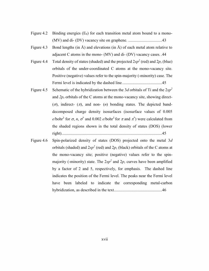
Figure 4.2 Binding energies (Eb) for each transition metal atom bound to a mono-
(MV) and di- (DV) vacancy site on graphene. .................................43
Figure 4.3 Bond lengths (in Å) and elevations (in Å) of each metal atom relative to
adjacent C atoms in the mono- (MV) and di- (DV) vacancy cases. .44
Figure 4.4 Total density of states (shaded) and the projected 2sp2 (red) and 2pz (blue)
orbitals of the under-coordinated C atoms at the mono-vacancy site.
Positive (negative) values refer to the spin-majority (-minority) case. The
Fermi level is indicated by the dashed line. ......................................45
Figure 4.5 Schematic of the hybridization between the 3d orbitals of Ti and the 2sp2
and 2pz orbitals of the C atoms at the mono-vacancy site, showing direct-
(), indirect- (), and non- (n) bonding states. The depicted band-
decomposed charge density isosurfaces (isosurface values of 0.005
e/bohr3 for , n, * and 0.002 e/bohr3 for and *) were calculated from
the shaded regions shown in the total density of states (DOS) (lower
right). .................................................................................................45
Figure 4.6 Spin-polarized density of states (DOS) projected onto the metal 3d
orbitals (shaded) and 2sp2 (red) and 2pz (black) orbitals of the C atoms at
the mono-vacancy site; positive (negative) values refer to the spin-
majority (-minority) state. The 2sp2 and 2pz curves have been amplified
by a factor of 2 and 5, respectively, for emphasis. The dashed line
indicates the position of the Fermi level. The peaks near the Fermi level
have been labeled to indicate the corresponding metal-carbon
hybridization, as described in the text. ..............................................46
xviii
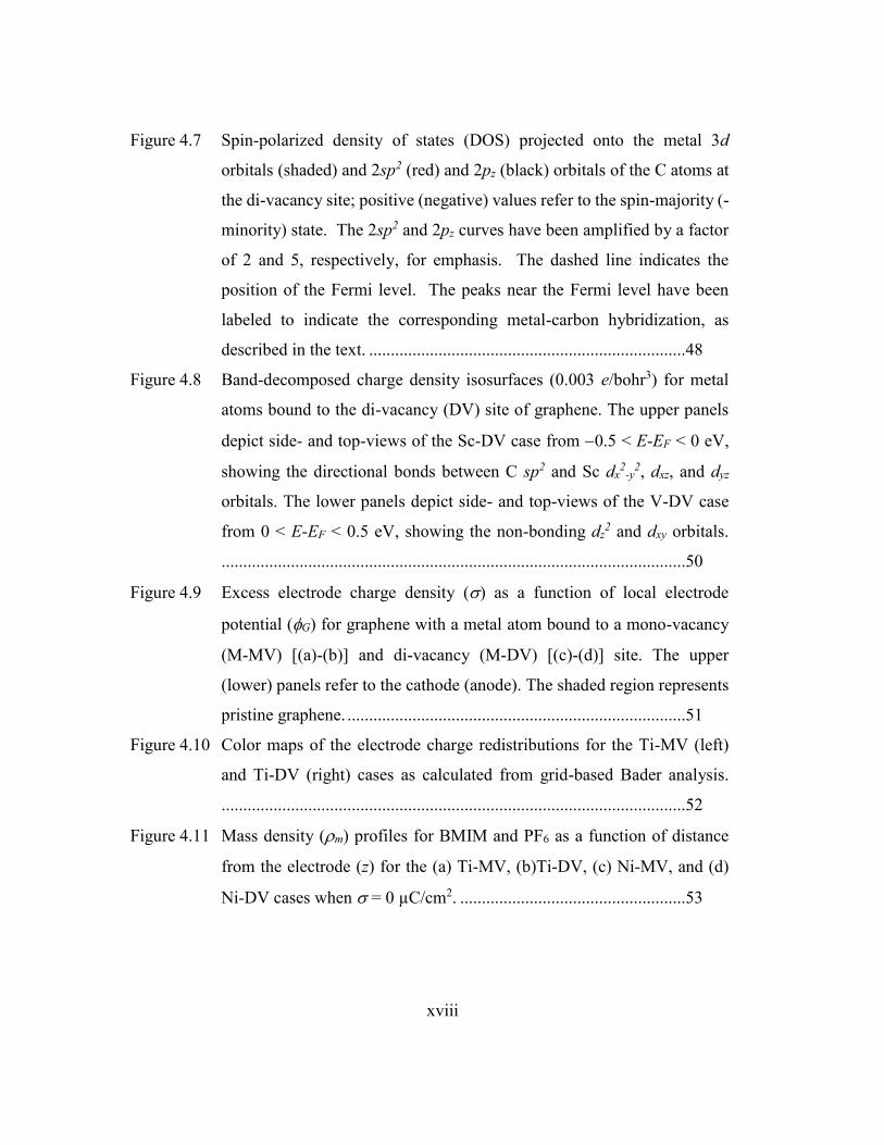
Figure 4.7 Spin-polarized density of states (DOS) projected onto the metal 3d
orbitals (shaded) and 2sp2 (red) and 2pz (black) orbitals of the C atoms at
the di-vacancy site; positive (negative) values refer to the spin-majority (-
minority) state. The 2sp2 and 2pz curves have been amplified by a factor
of 2 and 5, respectively, for emphasis. The dashed line indicates the
position of the Fermi level. The peaks near the Fermi level have been
labeled to indicate the corresponding metal-carbon hybridization, as
described in the text. .........................................................................48
Figure 4.8 Band-decomposed charge density isosurfaces (0.003 e/bohr3) for metal
atoms bound to the di-vacancy (DV) site of graphene. The upper panels
depict side- and top-views of the Sc-DV case from 0.5 < E-EF < 0 eV,
showing the directional bonds between C sp2 and Sc dx2
-y2, dxz, and dyz
orbitals. The lower panels depict side- and top-views of the V-DV case
from 0 < E-EF < 0.5 eV, showing the non-bonding dz2 and dxy orbitals.
...........................................................................................................50
Figure 4.9 Excess electrode charge density () as a function of local electrode
potential (G) for graphene with a metal atom bound to a mono-vacancy
(M-MV) [(a)-(b)] and di-vacancy (M-DV) [(c)-(d)] site. The upper
(lower) panels refer to the cathode (anode). The shaded region represents
pristine graphene. ..............................................................................51
Figure 4.10 Color maps of the electrode charge redistributions for the Ti-MV (left)
and Ti-DV (right) cases as calculated from grid-based Bader analysis.
...........................................................................................................52
Figure 4.11 Mass density (m) profiles for BMIM and PF6 as a function of distance
from the electrode (z) for the (a) Ti-MV, (b)Ti-DV, (c) Ni-MV, and (d)
Ni-DV cases when = 0 µC/cm2. ....................................................53
xix
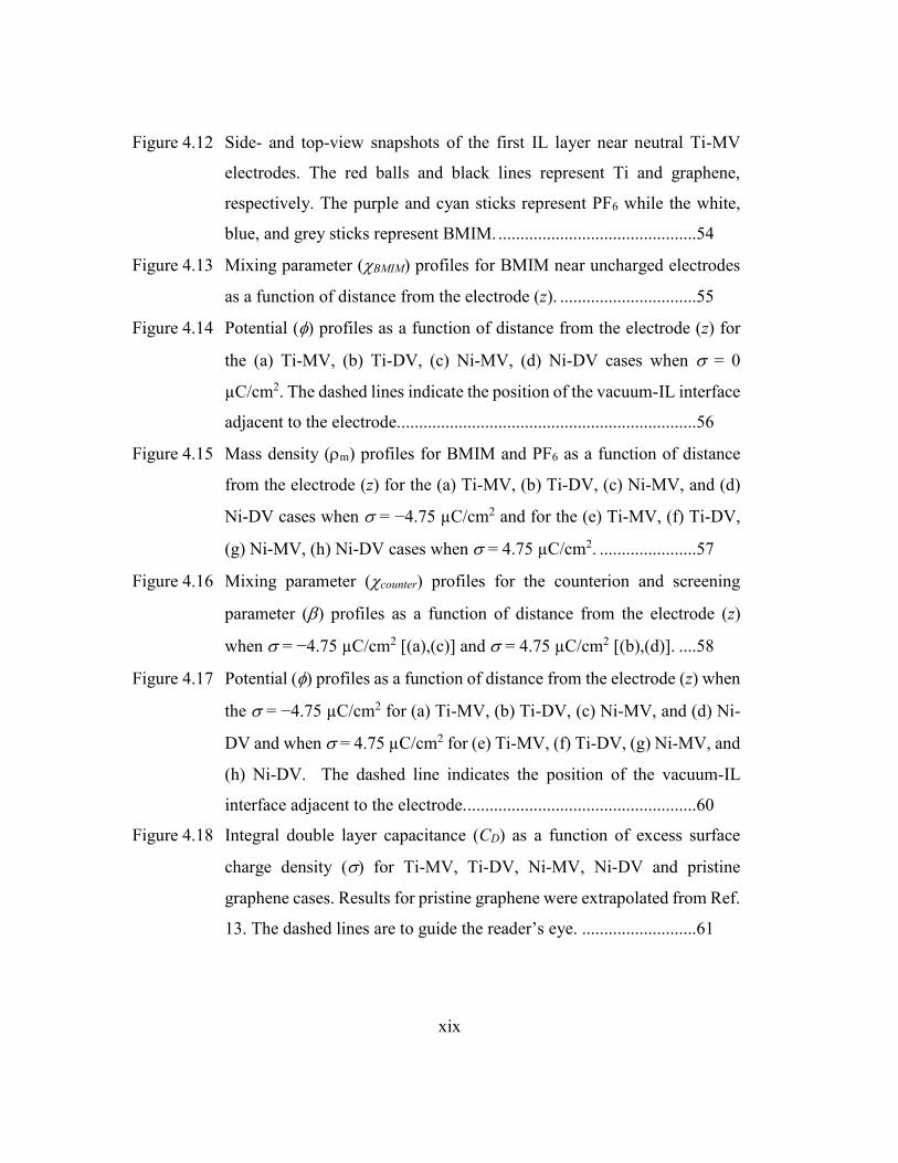
Figure 4.12 Side- and top-view snapshots of the first IL layer near neutral Ti-MV
electrodes. The red balls and black lines represent Ti and graphene,
respectively. The purple and cyan sticks represent PF6 while the white,
blue, and grey sticks represent BMIM. .............................................54
Figure 4.13 Mixing parameter (BMIM) profiles for BMIM near uncharged electrodes
as a function of distance from the electrode (z). ...............................55
Figure 4.14 Potential () profiles as a function of distance from the electrode (z) for
the (a) Ti-MV, (b) Ti-DV, (c) Ni-MV, (d) Ni-DV cases when = 0
µC/cm2. The dashed lines indicate the position of the vacuum-IL interface
adjacent to the electrode....................................................................56
Figure 4.15 Mass density (m) profiles for BMIM and PF6 as a function of distance
from the electrode (z) for the (a) Ti-MV, (b) Ti-DV, (c) Ni-MV, and (d)
Ni-DV cases when = −4.75 µC/cm2 and for the (e) Ti-MV, (f) Ti-DV,
(g) Ni-MV, (h) Ni-DV cases when = 4.75 µC/cm2. ......................57
Figure 4.16 Mixing parameter (counter) profiles for the counterion and screening
parameter () profiles as a function of distance from the electrode (z)
when = −4.75 µC/cm2 [(a),(c)] and = 4.75 µC/cm2 [(b),(d)]. ....58
Figure 4.17 Potential () profiles as a function of distance from the electrode (z) when
the = −4.75 µC/cm2 for (a) Ti-MV, (b) Ti-DV, (c) Ni-MV, and (d) Ni-
DV and when = 4.75 µC/cm2 for (e) Ti-MV, (f) Ti-DV, (g) Ni-MV, and
(h) Ni-DV. The dashed line indicates the position of the vacuum-IL
interface adjacent to the electrode. ....................................................60
Figure 4.18 Integral double layer capacitance (CD) as a function of excess surface
charge density () for Ti-MV, Ti-DV, Ni-MV, Ni-DV and pristine
graphene cases. Results for pristine graphene were extrapolated from Ref.
13. The dashed lines are to guide the reader’s eye. ..........................61

xx
Figure 4.19 Predicted total interfacial capacitance (CT) values for each metal-doped
graphene case as a function of applied potential (a). For reference, the CT
of pristine graphene in [BMIM][PF6] IL is also included. The dashed line
is to guide the reader’s eye. ...............................................................62
Figure 5.1 (Top) Schematic of the zigzag graphene nanoribbon supercell (bound by
the dashed lines) used in electronic structure calculations. The edges were
passivated by either H or H/OH atoms where H and O are indicated by
the white and red balls, respectively. (Bottom) Schematic of the
simulation box used in classical molecular dynamics simulations. The
white, red, and grey balls indicate H, O, and C electrode atoms,
respectively. The white, grey, and blue lines indicate the H, C, and N
atoms in BMIM while the pink and cyan lines indicate the P and F atoms
in PF6. Periodic boundary conditions were applied in all three directions.
...........................................................................................................68
Figure 5.2 Spin-polarized total density of states (DOS) of (a) H-passivated and (b)
alternating H-/OH-passivated zigzag graphene nanoribbons (ZGNR) at
different widths in the anti-ferromagnetic state. The insets depict the
corresponding DOS of the ferromagnetic state. Positive (negative) values
of the DOS indicate the spin-majority (-minority) states. The Fermi level
(EF) is marked by the dashed line. The band-decomposed charge density
isosurfaces (0.001 e bohr-3) were obtained from the highlighted energy
ranges. ...............................................................................................70
Figure 5.3 Integral quantum capacitances (CQ) as a function of local electrode
potential (E) for the (a) H-passivated and (b) alternating H-/OH-
passivated zigzag graphene nanoribbons (ZGNR) at different widths as
compared to that of pristine graphene. The depicted CQ of the ZGNR
electrodes was computed from the average CQ of the anti-ferromagnetic
and ferromagnetic states. The middle line indicates the neutrality point.
...........................................................................................................71
xxi
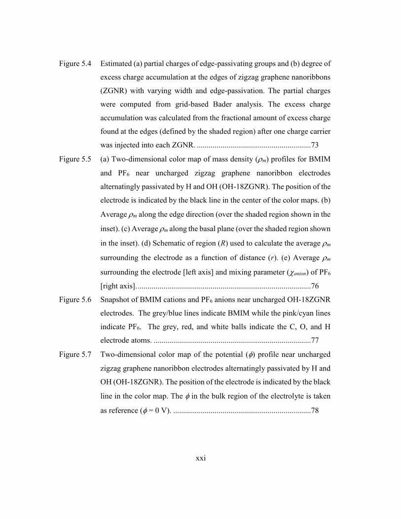
Figure 5.4 Estimated (a) partial charges of edge-passivating groups and (b) degree of
excess charge accumulation at the edges of zigzag graphene nanoribbons
(ZGNR) with varying width and edge-passivation. The partial charges
were computed from grid-based Bader analysis. The excess charge
accumulation was calculated from the fractional amount of excess charge
found at the edges (defined by the shaded region) after one charge carrier
was injected into each ZGNR. ..........................................................73
Figure 5.5 (a) Two-dimensional color map of mass density (m) profiles for BMIM
and PF6 near uncharged zigzag graphene nanoribbon electrodes
alternatingly passivated by H and OH (OH-18ZGNR). The position of the
electrode is indicated by the black line in the center of the color maps. (b)
Average m along the edge direction (over the shaded region shown in the
inset). (c) Average m along the basal plane (over the shaded region shown
in the inset). (d) Schematic of region (R) used to calculate the average m
surrounding the electrode as a function of distance (r). (e) Average m
surrounding the electrode [left axis] and mixing parameter (anion) of PF6
[right axis]. ........................................................................................76
Figure 5.6 Snapshot of BMIM cations and PF6 anions near uncharged OH-18ZGNR
electrodes. The grey/blue lines indicate BMIM while the pink/cyan lines
indicate PF6. The grey, red, and white balls indicate the C, O, and H
electrode atoms. ................................................................................77
Figure 5.7 Two-dimensional color map of the potential () profile near uncharged
zigzag graphene nanoribbon electrodes alternatingly passivated by H and
OH (OH-18ZGNR). The position of the electrode is indicated by the black
line in the color map. The in the bulk region of the electrolyte is taken
as reference ( = 0 V). ......................................................................78
xxii
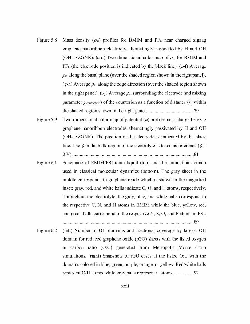
Figure 5.8 Mass density (m) profiles for BMIM and PF6 near charged zigzag
graphene nanoribbon electrodes alternatingly passivated by H and OH
(OH-18ZGNR): (a-d) Two-dimensional color map of m for BMIM and
PF6 (the electrode position is indicated by the black line), (e-f) Average
m along the basal plane (over the shaded region shown in the right panel),
(g-h) Average m along the edge direction (over the shaded region shown
in the right panel), (i-j) Average m surrounding the electrode and mixing
parameter counterion) of the counterion as a function of distance (r) within
the shaded region shown in the right panel. ......................................79
Figure 5.9 Two-dimensional color map of potential () profiles near charged zigzag
graphene nanoribbon electrodes alternatingly passivated by H and OH
(OH-18ZGNR). The position of the electrode is indicated by the black
line. The in the bulk region of the electrolyte is taken as reference ( =
0 V). ..................................................................................................81
Figure 6.1. Schematic of EMIM/FSI ionic liquid (top) and the simulation domain
used in classical molecular dynamics (bottom). The gray sheet in the
middle corresponds to graphene oxide which is shown in the magnified
inset; gray, red, and white balls indicate C, O, and H atoms, respectively.
Throughout the electrolyte, the gray, blue, and white balls correspond to
the respective C, N, and H atoms in EMIM while the blue, yellow, red,
and green balls correspond to the respective N, S, O, and F atoms in FSI.
...........................................................................................................89
Figure 6.2 (left) Number of OH domains and fractional coverage by largest OH
domain for reduced graphene oxide (rGO) sheets with the listed oxygen
to carbon ratio (O:C) generated from Metropolis Monte Carlo
simulations. (right) Snapshots of rGO cases at the listed O:C with the
domains colored in blue, green, purple, orange, or yellow. Red/white balls
represent O/H atoms while gray balls represent C atoms. ................92
xxiii
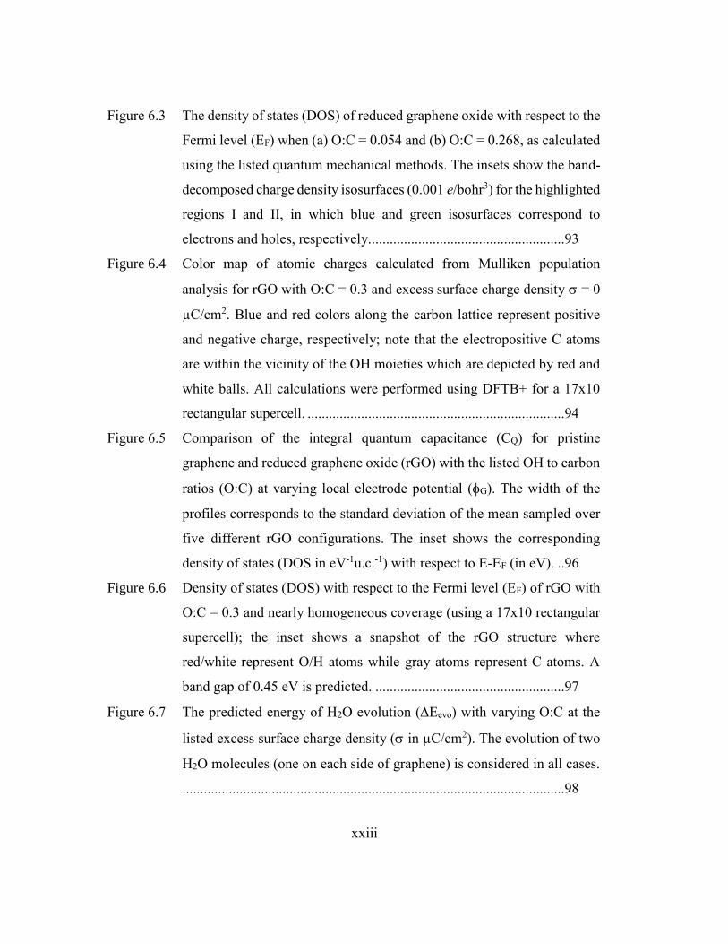
Figure 6.3 The density of states (DOS) of reduced graphene oxide with respect to the
Fermi level (EF) when (a) O:C = 0.054 and (b) O:C = 0.268, as calculated
using the listed quantum mechanical methods. The insets show the band-
decomposed charge density isosurfaces (0.001 e/bohr3) for the highlighted
regions I and II, in which blue and green isosurfaces correspond to
electrons and holes, respectively.......................................................93
Figure 6.4 Color map of atomic charges calculated from Mulliken population
analysis for rGO with O:C = 0.3 and excess surface charge density = 0
µC/cm2. Blue and red colors along the carbon lattice represent positive
and negative charge, respectively; note that the electropositive C atoms
are within the vicinity of the OH moieties which are depicted by red and
white balls. All calculations were performed using DFTB+ for a 17x10
rectangular supercell. ........................................................................94
Figure 6.5 Comparison of the integral quantum capacitance (CQ) for pristine
graphene and reduced graphene oxide (rGO) with the listed OH to carbon
ratios (O:C) at varying local electrode potential (G). The width of the
profiles corresponds to the standard deviation of the mean sampled over
five different rGO configurations. The inset shows the corresponding
density of states (DOS in eV-1u.c.-1) with respect to E-EF (in eV). ..96
Figure 6.6 Density of states (DOS) with respect to the Fermi level (EF) of rGO with
O:C = 0.3 and nearly homogeneous coverage (using a 17x10 rectangular
supercell); the inset shows a snapshot of the rGO structure where
red/white represent O/H atoms while gray atoms represent C atoms. A
band gap of 0.45 eV is predicted. .....................................................97
Figure 6.7 The predicted energy of H2O evolution (Eevo) with varying O:C at the
listed excess surface charge density ( in µC/cm2). The evolution of two
H2O molecules (one on each side of graphene) is considered in all cases.
...........................................................................................................98
xxiv
Figure 6.8 Average two-dimensional mass density (m) profiles of EMIM and FSI in
the first ionic liquid layer for the (a) pristine, (c) O:C = 0.1, and (e) O:C
= 0.3 graphene cases, which are shown as color maps. The respective line
profiles of the segments along the highlighted region are shown in (b), (d),
and (f), respectively. .......................................................................100
Figure 6.9 One-dimensional mass density (m) profiles of EMIM and FSI in the
direction perpendicular to the neutral electrode for the (a) pristine, (b) O:C
= 0.1, and (c) O:C = 0.3 graphene cases. ........................................101
Figure 6.10 The average relative screening factor (βrel) in the direction perpendicular
to the listed electrodes when the excess surface charge density (a) = 2.24
µC/cm2 and (b) = −2.24 µC/cm2. The insets depict the absolute
screening factor (βabs) as described in the manuscript. ...................103
Figure 6.11 Comparison of the integral electric double layer capacitances (CD) for
pristine graphene and three graphene oxide sheets with varying O:C at the
listed excess surface charge densities (). ......................................105
Figure 6.12 Comparison of the integral interfacial capacitances (CT) for pristine
graphene and three graphene oxide sheets with varying O:C at the listed
excess surface charge densities (). ................................................106
Figure 7.1 Schematic of BMIM, PF6, and the simulation domain. Two CNTs of the
same radius are placed in the simulation domain such that the IL maintains
its bulk density in the middle and edges of the domain. White, blue, and
grey lines indicate H, N, and C atoms in BMIM while red and pink lines
indicate F and P atoms in PF6, respectively. Periodic boundary conditions
are applied in the x, y, and z directions. ..........................................112
Figure 7.2 Calculated mass density (ρm) profiles for BMIM and PF6 near graphene,
(16,16) CNTs, and (6,6) CNTs at the listed σ (in µC/cm2) as a function of
distance from the electrode surface. ................................................115
xxv
Figure 7.3 (a) Schematic of IL accumulation near a CNT [left] and graphene [right]
with the electrodes shown in red. The electrode surface charge is balanced
by the counterions represented in black. Excess IL ions in the EDL are
represented in white. (b) Schematic of the electric field strength as a
function of distance from the electrode for varying electrode curvatures.
.........................................................................................................116
Figure 7.4 Space charge density profiles (ρq) for BMIM, PF6, and their sum near
graphene, (16,16) CNTs, and (6,6) CNTs at the listed σ (in µC/cm2) as a
function of distance from the electrode surface. .............................118
Figure 7.5. Calculated mixing parameter (χ) with varying electrodes at the listed σ (in
µC/cm2) as a function of distance from the electrode surface. .......120
Figure 7.6 Calculated screening parameter (β) with varying electrodes at the listed σ
(in µC/cm2) as a function of distance from the electrode surface. The inset
in (a) shows the first peak in (a) in greater detail. ..........................121
Figure 7.7 Potential (ϕ) profiles with varying electrodes at the listed σ (in µC/cm2)
as a function of distance from the electrode surface. The potential is taken
in reference to the electrode surface potential. ...............................124
Figure 7.8 Estimated integral EDL capacitance (CD) near the labeled (a) positive and
(b) negative electrodes with the listed σ (in µ/cm2). .......................126
Figure 7.9 (a) The electronic density of states (DOS) and (b) the calculated quantum
capacitance (CQ) of various electrodes as a function of E. E = 0 indicates
the position of the Fermi level. The inset of panel (a) shows the DOS of
graphene. .........................................................................................127
xxvi
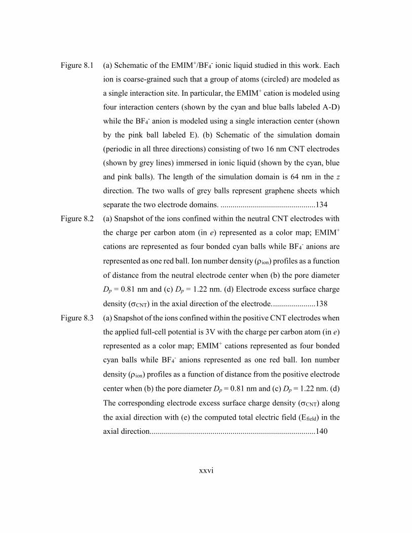
Figure 8.1 (a) Schematic of the EMIM+/BF4- ionic liquid studied in this work. Each
ion is coarse-grained such that a group of atoms (circled) are modeled as
a single interaction site. In particular, the EMIM+ cation is modeled using
four interaction centers (shown by the cyan and blue balls labeled A-D)
while the BF4- anion is modeled using a single interaction center (shown
by the pink ball labeled E). (b) Schematic of the simulation domain
(periodic in all three directions) consisting of two 16 nm CNT electrodes
(shown by grey lines) immersed in ionic liquid (shown by the cyan, blue
and pink balls). The length of the simulation domain is 64 nm in the z
direction. The two walls of grey balls represent graphene sheets which
separate the two electrode domains. ...............................................134
Figure 8.2 (a) Snapshot of the ions confined within the neutral CNT electrodes with
the charge per carbon atom (in e) represented as a color map; EMIM+
cations are represented as four bonded cyan balls while BF4- anions are
represented as one red ball. Ion number density (ion) profiles as a function
of distance from the neutral electrode center when (b) the pore diameter
Dp = 0.81 nm and (c) Dp = 1.22 nm. (d) Electrode excess surface charge
density (CNT) in the axial direction of the electrode. .....................138
Figure 8.3 (a) Snapshot of the ions confined within the positive CNT electrodes when
the applied full-cell potential is 3V with the charge per carbon atom (in e)
represented as a color map; EMIM+ cations represented as four bonded
cyan balls while BF4- anions represented as one red ball. Ion number
density (ion) profiles as a function of distance from the positive electrode
center when (b) the pore diameter Dp = 0.81 nm and (c) Dp = 1.22 nm. (d)
The corresponding electrode excess surface charge density (CNT) along
the axial direction with (e) the computed total electric field (Efield) in the
axial direction..................................................................................140

xxvii
Figure 8.4 (a) Areal integral capacitance of the full-cell (CDL,cell that is normalized to
the surface area of one electrode) with respect to the applied full-cell
potential () which is instantaneously applied. Length of the depletion
region (LD) as a function of at the (b) positive and (c) negative
electrode. The shaded region in all three panels depicts the transition
between migration and stagnation, as discussed in the main text. ..143
Figure 8.5 Color maps depicting the variation in time of the (a) number of cations,
(b) number of anions, and (c) electrode charge (in e) along the length of
the positive electrode when the applied full-cell potential is 0.5 V. For
comparison, the variation in time of the (d) number of cations, (e) number
of anions, and (f) electrode charge (in e) along the length of the positive
electrode when the applied full-cell potential is 3 V. The plots have a
spatial resolution of 0.5 nm and temporal resolution of 20 fs. The electrode
diameter is 0.81 nm. ........................................................................145
Figure 8.6 (a) Total number of confined ions (nion), (b) total excess surface charge
(qelec), and (c) the difference in the rate of electrode charge insertion and
ion insertion (∆rins) within the positive electrode as a function of time (t)
when the listed full-cell potential is applied starting 0 V. The electrode
diameter is 0.81 nm. ........................................................................147
Figure 8.7 The influence of charging time (chg) on (left) the full-cell capacitance
(CDL,cell in black squares) and (right) length of the depleted region (LD in
red triangles) at the positive electrode with diameter 0.81 nm when the
applied full-cell potential is 3 V. The shaded region depicts the transition
between migration and stagnation, as discussed in the manuscript.149
xxviii
Figure 9.1 (a) Schematic of the EMIM/BF4 ionic liquid studied in this work. Each
ion is coarse-grained such that a group of atoms (circled) are modeled as
a single interaction site. In particular, the EMIM+ cation is modeled using
four interaction centers (shown by the cyan and blue balls labeled A-D)
while the BF4- anion is modeled using a single interaction center (shown
by the pink ball labeled E). (b) Schematic of the simulation domain
(periodic in all three directions) consisting of two 16 nm porous carbon
electrodes (shown by grey lines) immersed in ionic liquid (shown by the
cyan, blue and pink balls). The length of the simulation domain is 60 nm
in the z direction. .............................................................................154
Figure 9.2 Distribution of (a) cation and (b) anion degrees of confinement (DoC)
within the NPG-9A electrode when the full-cell applied potential () is
0 and 3 V. Dashed lines depict the boundaries that distinguish edge, plane,
hollow, and pocket sites. .................................................................157
Figure 9.3 Comparison of the (a) areal (Car) and (b) specific (Csp) discharge
capacitances as a function of the applied full-cell potential () using
each nanoporous carbon electrode in a two-electrode configuration
immersed in EMIM/BF4 ionic liquid. The capacitances were calculated
using the specific surface area (based on a N2 gas probe) or mass of a
single electrode. Note that the differences between the computed Car can
vary significantly depending on the choice of gas molecule for structural
characterization. Here, we do not consider the electrode capacitance
contribution as it is assumed to be much larger than the double-layer
contribution. ....................................................................................159
Figure 9.4 (a) Comparison of the discharge capacity per site (∆qsite) for the three
electrode cases when the applied full-cell potential is 3 V. (b) Fraction of
the capacitance attributed to the total discharge capacity per site (fq,dc) for
the three electrode cases when the applied full-cell potential is 3 V.160
xxix
Figure 9.5 Discharge profiles of positive electrode when the applied full-cell
potential varies from 3 to 0 V over 1 ns in a non-equilibrium MD
simulation. The fraction of the electrode utilized (futil) as each type of
listed site in the (a) NPC-12A, (b) NPC-10A, and (c) NPC-9A case is
shown. In addition, the (left axis) total charge stored (qelec) and the (right
axis) ratio of anion-cation coordination number (Cco) to the anion-anion
coordination number (Ccounter) in the pocket (black) and hollow (red) sites
of the (d) NPC-12A, (b) NPC-10A, and (c) NPC-9A case is shown.163
Figure 9.6 (a) Estimated pore shape factor (Fps) based on the structural properties of
the electrodes evaluated using different gas probe radii (Rgp). Comparison
of experimental areal capacitance (C) based on BET surface areas with
respect to (b) Fps and (c) pore width (Wp). The dashed line in (b) serves as
a visual guide. Experimental values were extracted from Ref. 37, 200,
206, 207, and 208. ...........................................................................165
Figure 10.1 Schematic summary of the carbon-nanomaterial design space explored in
this work..........................................................................................170
Figure 10.2 Comparison of the average excess electrode charge ( evaluated at an
electrode potential of ±0.5 V) of graphene-based materials modified with
different atomic concentrations (at.%). The dashed line indicates the of
pristine graphene, which serves as a reference point. The dotted line is a
visual aid demonstrating the trend. .................................................173
1
Chapter 1: Introduction
1.1 BACKGROUND AND MOTIVATION
A. Necessity of Energy Storage
The rise in global demand for energy has spurred an increasingly distributed variety
of technologies and methods for energy conversion. However, providing the population
access to energy requires efficient means of storage. For example, the disconnect between
the energy supplied by intermittent alternative energy sources (e.g., solar and wind) or
power plants and the energy demanded by consumers using the electric grid can be bridged
by large-scale energy storage technologies.1,2 Small-scale energy storage is also a necessity
as the world becomes increasingly reliant on mobile devices, electric vehicles, and other
portable electronics.3,4
Within the energy storage landscape, two classes of technologies can be considered
ubiquitous – electrochemical double layer capacitors (EDLCs) and batteries.5,6 The major
differences between the two are the rate at which charge can be stored/extracted (i.e., the
power density) and the total amount of charge that can be stored/extracted (i.e., the energy
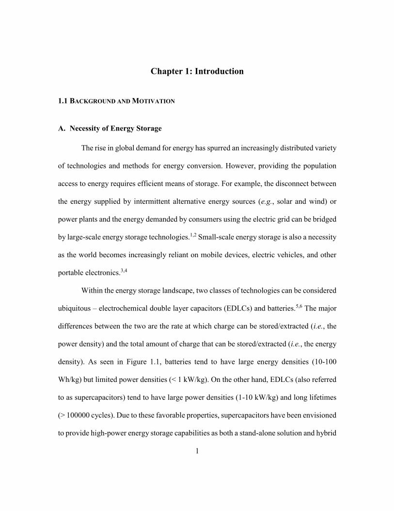
density). As seen in Figure 1.1, batteries tend to have large energy densities (10-100
Wh/kg) but limited power densities (< 1 kW/kg). On the other hand, EDLCs (also referred
to as supercapacitors) tend to have large power densities (1-10 kW/kg) and long lifetimes
(> 100000 cycles). Due to these favorable properties, supercapacitors have been envisioned
to provide high-power energy storage capabilities as both a stand-alone solution and hybrid
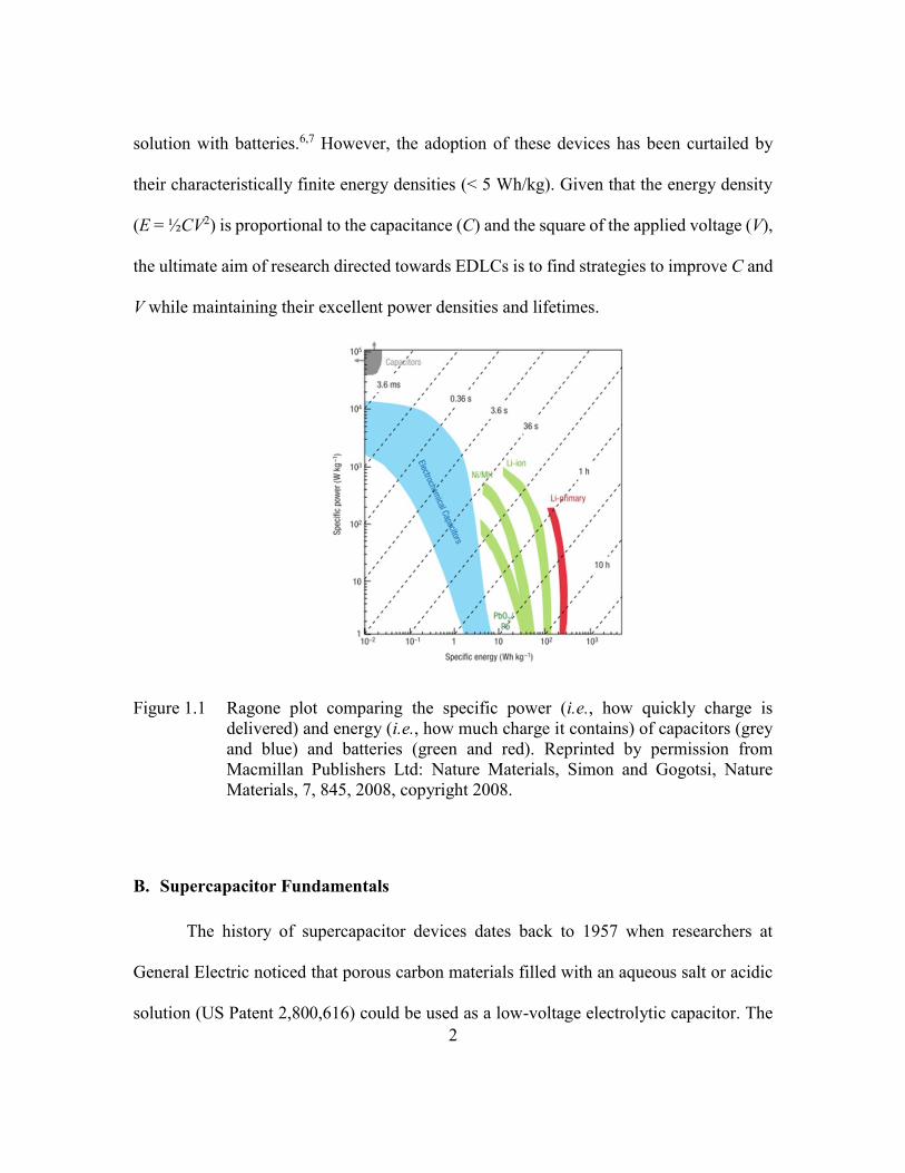
2
solution with batteries.6,7 However, the adoption of these devices has been curtailed by
their characteristically finite energy densities (< 5 Wh/kg). Given that the energy density
(E = ½CV2) is proportional to the capacitance (C) and the square of the applied voltage (V),
the ultimate aim of research directed towards EDLCs is to find strategies to improve C and
V while maintaining their excellent power densities and lifetimes.
Figure 1.1 Ragone plot comparing the specific power (i.e., how quickly charge is
delivered) and energy (i.e., how much charge it contains) of capacitors (grey
and blue) and batteries (green and red). Reprinted by permission from
Macmillan Publishers Ltd: Nature Materials, Simon and Gogotsi, Nature
Materials, 7, 845, 2008, copyright 2008.
B. Supercapacitor Fundamentals
The history of supercapacitor devices dates back to 1957 when researchers at
General Electric noticed that porous carbon materials filled with an aqueous salt or acidic
solution (US Patent 2,800,616) could be used as a low-voltage electrolytic capacitor. The
3
first practical device, however, was introduced in 1962 by the Standard Oil Company of
Ohio (US Patent 3,288,641) in which activated carbon black electrodes were used. In
particular, the patent recognized the formation of the electric double layer (EDL) as the
primary charge storage mechanism.
The conception of EDLs can be traced to the work of Helmholtz in 1853 when he
made the observation that charges in a polarized metallic electrode accumulate at the
surface and attract ions of opposite charge (so-called counter-ions).8 The two distinct and
segregated layers of charge formed by the electrode surface charge and the compact layer
of counter-ions were collectively called the EDL. Due to the notable similarities to parallel-
plate capacitors, the EDL was thought to have a constant C (=r0/d) proportional to the
dielectric constant of the electrolyte (r) and the separation distance between the surface
ions and the electrode (d). However, subsequent work demonstrated that C was, in fact, not
constant and depended on V. The work of Gouy and Chapman, and later amended by Stern,
resolved this observation by showing that C essentially depended on two capacitors in
series (now called GCS theory).9 The first referred to the compact monolayer of ions
accumulating at the electrode surface (the so-called inner Stern layer or inner Helmholtz
layer) with constant capacitance CH. The second was created by the diffuse outer layer of
electrolyte ions with potential-dependent capacitance CGC. The overall C, then, can be
determined from the relative contributions of CH and CGC such that 1/C = 1/CH + 1/CGC.
More importantly, these theories underscored that the operation of supercapacitors strongly
depends upon the molecular packing of ions at the electrode-electrolyte interface.
4
The patent by the Standard Oil Company of Ohio was also an important roadmap
that has driven the direction of supercapacitor research since then. Two key points were
highlighted. The first was the necessity of a conductive electrode material with large
surface area (in this case, larger than 300 m2/cm3). The second was the recognition that the
operating voltage was limited by the electrochemical stability of the electrolyte. Today,
most supercapacitors in the market utilize activated carbon electrodes with aqueous or
organic electrolytes. However, significant progress cannot be made unless new materials
can be designed and fabricated.
To extend the operational voltage, and therefore the energy density, ionic liquids
(ILs) have been widely explored as a potential electrolyte material. These solvent-free ions
remain in the liquid phase at room temperature and have excellent thermal stability, tunable
solvent properties, low volatility, and moderate ionic conductivity.10,11 Most importantly,
ILs are purported to have electrochemical window up to 4 V, which is much larger than
that of aqueous (up to 1 V) or organic (up to 2.5 V) electrolytes.5,12 Due to their small
Debye lengths, which is comparable to the size of an ion, and the strong electrode-ion and
ion-ion electrostatic interactions, IL ions display unique layering behavior that can extend
up to a few nanometers.13-15 In addition, the differential capacitance profiles using metal
electrodes commonly show a convex parabolic shape with one maximum (i.e., bell-shaped)
or two local maxima (i.e., camel-shaped) in contrast to the U-shaped profiles observed
using aqueous electrolytes and predicted by GCS theory.16-18 To explain these trends,
theoretical studies have been shown to be well-suited for understanding the mechanistic
relationships between the ion packing behavior at the interface, hereafter referred to as the
5
EDL microstructure, and the EDL capacitance (CD). Kornyshev derived an elegant
analytical expression based on the Poisson-Boltzmann lattice-gas model which identified
the importance of the void fraction, or compressibility, of the EDL to explain the observed
differential capacitance profiles.19 Inspired by this work, molecular-level computer
simulations have been used to further examine the relationship between the CD and the
EDL microstructure and identified many other factors – such as the size, configuration and
polarizability of ions, the effective dielectric constant of the electrolyte solution, and the
surface topology and shape of the electrode – as potentially important descriptors of the
EDL capacitive behavior.20-23 However, the relative importance of these factors, especially
at the interface of different electrode materials, is not yet clearly understood; this leaves
room for further investigation.
Carbon-based nanomaterials are another class of materials that offer rich
possibilities for use as future EDLC electrodes.24,25 Materials such as graphene, carbon
nanotubes, templated carbon, nanoporous carbon, and carbide-derived carbon are all
candidates owing to their large surface area, electrical conductivity, thermal conductivity,
and excellent mechanical strength and flexibility. However, early experimental work using
graphitic electrodes and ILs, such as highly ordered pyrolytic graphite (HOPG), were
observed to display anomalous capacitive behavior compared to standard metallic
electrodes; the differential C profiles exhibits the aforementioned U-shape in contrast to
the bell-shape or camel-shape profiles observed in metal/IL systems.26-28 To explain this
inconsistency, the capacitance of the electrode itself must be considered. At the interface
of a polarized semiconductor (or semimetallic) electrode and electrolyte, charge segregates
6
within the electrode surface forming the so-called space charge layer and essentially serves
as another capacitor in series. Randin and Yeager first applied the semiconductor “space
charge” capacitance picture for graphite with NaF.29 Gerischer and coworkers30,31 later
amended this theory to incorporate the electronic density of states (DOS) of graphite within
the framework of semiconductor theory; their analysis suggested that the finite DOS of
graphite near the Fermi level resulted in the dominance of the space charge contribution to
the measured capacitance. While the classical definition of the space charge layer cannot
apply to low-dimensional carbon nanomaterials, the quantized nature of their electronic
states lends itself to the adoption of the quantum capacitance (CQ) formalism, which is
proportional to the DOS.13,32 Simply put, while CD quantifies the ease in which ions can
accumulate in the EDL to screen the applied electric field, CQ quantifies the ease in which
charge carriers can be injected into the electrode itself.
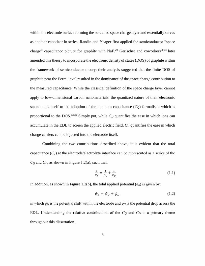
Combining the two contributions described above, it is evident that the total
capacitance (CT) at the electrode/electrolyte interface can be represented as a series of the
CQ and CD, as shown in Figure 1.2(a), such that:
1
𝐶𝑇=
1
𝐶𝑄+
1
𝐶𝐷 (1.1)
In addition, as shown in Figure 1.2(b), the total applied potential (ϕa) is given by:
𝜙𝑎 = 𝜙𝑄 + 𝜙𝐷 (1.2)
in which ϕQ is the potential shift within the electrode and ϕD is the potential drop across the
EDL. Understanding the relative contributions of the CQ and CD is a primary theme
throughout this dissertation.
7
Figure 1.2 Schematic of the carbon nanomaterial electrode/ionic liquid interface with (a)
an illustration of the equivalent circuit with series capacitance from the
quantum (CQ) and double layer (CD) capacitances and (b) an idealized
potential profile where the total applied potential (a) is the sum of the
electrode (Q) and double layer (D) potential drop.
1.2 RESEARCH OBJECTIVES
The broad aim of the research in this dissertation is to develop material design
principles to help guide future directions in supercapacitor research by understanding the
relationship between the chemistry and structure of carbon nanomaterials and the CT once
immersed in an IL. A computational approach is used in this work in order to probe the
fundamental molecular mechanisms at the carbon nanomaterial/IL interface under external
potential. The general computational framework is as follows. First, the structure of the
8
electrode is determined through a variety of simulation techniques ranging from Metropolis
Monte Carlo methods to quantum mechanical calculations; an appropriate technique is
determined on a case-by-case basis depending on the complexity of the disorder
investigated. Next, the electronic structure and CQ of the electrode is determined through
quantum mechanical calculations. These calculations are also essential to understand the
nature of excess charge accumulation. These insights, in turn, are utilized in classical
molecular dynamics simulations to determine the EDL microstructure and CD.
Two primary types of carbon nanomaterials are explored in this work. The first is
graphene and its direct derivatives. Previous theoretical studies in our group13,33 and
independent experiments34,35 have shown that despite the exceptionally high surface area
of graphene (2630 m2/g), its nature as a zero-gap semi-metal limits its CT by virtue of its
low CQ. However, the electronic structure and CQ may be tunable through the introduction
of dopants, defects, and functional groups. Four different types of modifications to
graphene, as described in the next section, are presented in this work. These studies also
serve to develop a foundation to investigate more complex electrode materials, such as
nanoporous carbon (NPC). Similar to graphene, NPCs consist of monolayer sp2 carbon
crumbled in three-dimensional networks. The current interest in NPCs largely stems from
the observation that ions confined in pores comparable to their sizes exhibit dramatically
enhanced areal CT.36,37 Understanding this mechanism is therefore the second focus of this
work.
9
1.3 DISSERTATION OVERVIEW
The organization of the dissertation is as follows:
In Chapter 1, the background, motivation, research framework, and objectives are
described. In Chapter 2, the theoretical background of the simulation techniques used in
this work are explained.
In Part I of this dissertation, graphene-based materials immersed in ionic liquid
electrolyte are explored. Specifically, the influence of four broad types of chemical and/or
structural modifications to graphene on the electronic structure (and CQ) and EDL
microstructure (and CD) is investigated. Chapters 3-6 accounts for point-like structural
defects as represented by topological defects (Chapter 3), chemical dopants as represented
by transition metal dopants (Chapter 4), extended structural defects as represented by edge
defects (Chapter 5), and chemical functionalization as represented by hydroxyl
functionalization of the basal plane (Chapter 6).
In Part II of this dissertation, nanoporous carbon materials immersed in ionic liquid
electrolyte are explored. Specifically, the influence of pore size and curvature on CT is
investigated. The electronic structure and EDL microstructure outside of carbon nanotubes
(Chapter 7) and within carbon nanotubes (Chapter 8) are presented. This work culminates
in the study of capacitive mechanisms using nanoporous carbon materials with varying
pore dispersity (Chapter 9).
Chapter 10 summarizes the overall conclusions of this dissertation and provides
perspectives on potential future directions for research.
10
Chapter 2: Theoretical Background
2.1 SIMULATION TECHNIQUES
A. Quantum Mechanical Calculations
The basis of all quantum mechanical calculations is to find solutions to the
wavefunction based on the Schrödinger equation38:
𝐻Ψ = 𝐸𝜓 (2.1)
in which the Hamiltonian (H) is a linear operator that describes the total energy (the
combined kinetic and potential energy) of the system which consists of:
𝐻 = ∑−ℏ2
2𝑚𝛼∇2
𝛼 + ∑−ℏ2
2𝑚𝑖∇2
𝑖 + ∑𝑒2
|𝑟𝛼−𝑟𝛽|𝛼,𝛼<𝛽 + ∑𝑒2
|𝑟𝑖−𝑟𝑗|𝑖,𝑖<𝑗 + ∑𝑒2
|𝑟𝑖−𝑟𝛼 |𝑖,𝛼 (2.2)
where the first two terms are the kinetic energies of the nuclei (denoted by the and
subscripts) and electrons (denoted by the i and j subscripts) and the last three terms are the
potential energies of the nuclei-nuclei, electron-electron, and electron-nuclei interactions.
Beyond the case of small atoms and molecules (e.g., hydrogen gas), analytical solutions to
Equation (2.1) and (2.2) do not exist. However, numerical solutions are also
computationally unwieldly due to the large number of degrees of freedom that are
necessary in contemporary research. Two approximations are commonly used to overcome
this deficiency.
The first approximation is known as the Born-Oppenheimer approximation.39 Due
to the large difference in nuclear and electronic mass (and therefore, large difference in
kinetic energy), the nuclear and electronic are assumed to be decoupled such that the
11
electronic portion within Equation (2.2) can be solved assuming fixed nuclear positions.
The electronic H therefore simplifies to:
𝐻 = ∑−ℏ2
2𝑚𝑖∇2
𝑖 + ∑𝑒2
|𝑟𝑖−𝑟𝑗|𝑖,𝑖<𝑗 + ∑ 𝑉𝑒𝑥𝑡(𝑟𝑖)𝑖 (2.3)
where Vext is the external potential (e.g., the nuclear contribution) felt by the electron.
Unfortunately, the many-body electron-electron interactions still pose a significant
computational burden. This problem is addressed by the second approximation which is
broadly called density functional theory (DFT).
In 1964, Hohenberg and Kohn introduced two important theorems that lay the
foundation for DFT methods.40 The first theorem showed that in any system of interacting
electrons under Vext, the total energy and Vext are a unique functional of the electron density
(r). The second theorem stated that the ground-state energy can be obtained through the
variational principle, such that the (r) that minimizes the total energy is the ground-state
electron density. Under Hohenberg-Kohn theory, the total energy (EHK) can be
reformulated with respect to (r) by the following expression:
𝐸𝐻𝐾 = 𝑇[𝜌(𝑟)] + 𝑉𝑒𝑒[𝜌(𝑟)] + ∫ 𝑉𝑒𝑥𝑡(𝑟)𝜌(𝑟)𝑑𝑟 (2.4)
where T[(r)] and Vee[(r)] are functionals for the kinetic energy and electron-electron
potential energy, respectively. Yet, Equation (2.4) remained impractical as the exact
functionals were unknown.
In 1965, the Kohn-Sham formulation was introduced and presented a practical
means of solving Equation (2.4).41 Here, the many-body problem (with order N2) is

12
remapped to N non-interacting single electron problems interacting within an effective
Kohn-Shan potential (VKS). The total electronic energy EKS can be expressed as:
𝐸𝐾𝑆 = 𝑇𝑆[𝜌(𝑟)] + 𝐸𝐻𝑎𝑟𝑡𝑟𝑒𝑒[𝜌(𝑟)] + 𝐸𝑋𝐶[𝜌(𝑟)] + ∫ 𝑉𝑒𝑥𝑡(𝑟)𝜌(𝑟)𝑑𝑟 (2.5)
in which TS[(r)] is the analytically known kinetic energy functional of a non-interacting
electron gas, EHartree[(r)] is the analytically known classical electrostatic energy of a non-
interacting gas, and EXC[(r)] is the exchange-correlation functional which essentially
describes the small error in kinetic and potential energies between the exact and non-
interacting electron gas systems. As the potential is simply the derivative of the energy (for
example, VKS = EKS/(r)), the single-electron Schrödinger equation can now be
simplified to:
[−ℏ2
2𝑚𝑖∇𝑖
2 + 𝑉𝐻𝑎𝑟𝑡𝑟𝑒𝑒(𝑟) + 𝑉𝑥𝑐(𝑟) + 𝑉𝑒𝑥𝑡(𝑟)] Ψ𝑖 = 𝜖𝑖Ψ𝑖 (2.6)
which can be solved self-consistently. In other words, numerical solvers can iteratively
solve Equation (2.6) by guessing an initial (r), constructing VKS (= VHartree + Vxc + Vext),
solving Equation (2.6) to calculate a new (r), and repeating until convergence is achieved.
By reducing the problem into N tractable equations, a considerable speed-up is
accomplished compared to all-electron methods. For periodic systems, another significant
speed-up is realized by using plane-wave basis sets to solve the Kohn-Sham equations in
reciprocal space.42 However, the accuracy of the obtained results depends on the
approximations used to describe Vxc and Vext. While the development of these
approximations has a long history, the common practices used in this dissertation will be
described. First, the EXC is represented by the generalized gradient approximation (GGA)
13
which considers both (r) and (r) (a so-called semi-local functional). The most popular
form of the functional was introduced by Perdew, Burke, and Ernzerhof (PBE) in 1996 and
has successfully been used to predict the chemical, electronic, and optical properties of
many materials.43-45 In the second approximation, the all-electron problem is reduced to
only the valence electrons as these tend to be the most chemically important; the core
electrons are considered frozen (or tightly bound).46 Therefore, a potential must be used to
describe the interaction between valence and core electrons. Due to large number of basis
sets required to describe the rapidly oscillating near the ion core, a technique called the
projector augmented wave (PAW) method47 is typically used to transform the all-electron
into a smooth pseudo ; note that outside a certain cutoff radius, the pseudo and all-
electron are equal.
B. Classical Molecular Dynamics
The basis of all classical molecular dynamics (cMD) simulations is to calculate the
positions (ri) and velocities (vi) of atoms over time (t) based on Newton’s equation of
motion48:
𝐹𝑖 = −∇𝐸𝑖 = 𝑚𝑖𝑑2𝑟𝑖
𝑑𝑡2 = 𝑚𝑖𝑎𝑖 (2.7)
where Fi is the per-atom force, Ei is the per-atom energy, mi is the atomic mass, and ai is
the atomic acceleration. Through numerical time-integration of Equation (2.7), a time-
dependent trajectory of atoms can be simulated. In addition, cMD simulations maintain a
thermodynamic ensemble (e.g., canonical NVT) in order to sample all possible atomic

14
microstates over time; according to the ergodic hypothesis, the time-averaged states are
equivalent to the ensemble-averaged states which is necessary to estimate thermodynamic
properties from statistical mechanics. Here, a key assumption is that the total energy can
be described classically by a so-called force field. Given current computing power from
the use of supercomputers, cMD simulations have successfully reported length- and time-
scales up to millions of atoms and hundreds of nanoseconds, respectively49; unlike ab-initio
MD simulations, cMD simulations assume that the quantum (or electronic) effects occur
on length- and time-scales too small to be relevant.
Figure 2.1 Schematic of the geometric properties used in the force fields to describe
bonds, angles, dihedrals, and impropers.
The reliability of cMD is contingent on the appropriate choice of force field. Here,
the force field refers to the model (both the functional form and the parameters) used to
describe the energetics of the system. The force-field typically takes the following form:
𝐸𝑡𝑜𝑡𝑎𝑙 = 𝐸𝑏𝑜𝑛𝑑 + 𝐸𝑎𝑛𝑔𝑙𝑒 + 𝐸𝑑𝑖ℎ𝑒𝑑𝑟𝑎𝑙 + 𝐸𝑖𝑚𝑝𝑟𝑜𝑝𝑒𝑟 + 𝐸𝑣𝑑𝑊 + 𝐸𝑒𝑙𝑒𝑐 (2.8)

15
in which the first four term describe the intra-atomic or bonding interactions (e.g., within
a molecule) and the last two terms describe the inter-atomic interactions (e.g., electrostatic
and van der Waals).
Many functional forms exist to describe the bonding and non-bonding interactions.
The one most commonly used in this dissertation is the all-atom OPLS (Optimized
Potentials for Liquid Simulations) force field50, derived from the AMBER force field51,
which has the following form:
𝐸𝑏𝑜𝑛𝑑 = ∑1
2𝐾𝑏𝑏𝑜𝑛𝑑𝑠 (𝑟 − 𝑟𝑜)2 (2.9)
𝐸𝑎𝑛𝑔𝑙𝑒 = ∑1
2𝐾𝑎(𝜃 − 𝜃𝑜)2
𝑎𝑛𝑔𝑙𝑒𝑠 (2.10)
𝐸𝑑𝑖ℎ𝑒𝑑𝑟𝑎𝑙 = ∑ ∑𝑉𝑛
2[1 − (−1)𝑛cos (𝑛𝜙 − 𝜙𝑛)]4
𝑛=1𝑑𝑖ℎ𝑒𝑑𝑟𝑎𝑙 (2.11)
𝐸𝑣𝑑𝑊 = ∑ 𝑓𝑖𝑗 [4𝜖𝑖𝑗 ((𝜎𝑖𝑗
𝑟𝑖𝑗)
12
− (𝜎𝑖𝑗
𝑟𝑖𝑗)
6
)]𝑖>𝑗 (2.12)
𝐸𝑒𝑙𝑒𝑐 = ∑ 𝑓𝑖𝑗𝑞𝑖𝑞𝑗𝑒2
4𝜋𝜖0𝑟𝑖𝑗𝑖>𝑗 (2.13)
where Kb/Ka/Vn are the bond/angle/dihedral force constants and ro/o/o are the equilibrium
bond lengths/angles/dihedral angles with the geometric properties depicted in Figure 2.1.
The bond and angle energies take the harmonic form while the dihedral energy takes the
form unique to OPLS; note that the inclusion of impropers is usually unnecessary except
in some cases when the harmonic form is taken. The van der Waals (vdW) energy follows
the pair-wise 12-6 Lennard Jones form described by the potential well (ij), zero-energy
distance (ij), and radial distance between atoms i and j (rij).52 The electrostatic energy is
described using the classical Coulomb relation based on the atomic charges qi/qj and the
16
vacuum permittivity (0).53 A fudge factor (fij) is introduced to scale the vdW and
electrostatic interaction energies for bonded atoms (up to the 3rd nearest connected
neighbor). Finally, a practical cut-off radius (rc) is introduced to limit the computational
burden of calculating all of the non-bonding interaction energies. This rc is commonly
around 12 Å, which is large enough to sufficiently capture the relevant vdW interactions
due to its rapid decay. However, this can introduce large errors in the electrostatic energy
due to its long-range nature. To overcome this limitation, the long-range contribution to
the electrostatic energy is computed using Ewald summations, which offers a fast way to
approximate this energy in Fourier space if periodicity is assumed.54,55 Another way to
speed-up computations is to use a coarse-grained approach in which several atoms are
grouped together into a single interaction center to significantly reduce the number of
pairwise (and bonding) interactions that require computation.56,57
Once the energies are calculated, the computed forces are used to update atomic
velocities and positions through numerical time-integration of Equation (2.7). The naïve
approach is to use the Taylor expansion of ri such that ri(t+∆t) = ri(t) + vi(t)∆t + ai(t)∆t2/2
+ O(∆t3) where ∆t is the simulation time step. However, this method is known to introduce
large errors and significant drift in energy due to errors in the predicted velocities.58 Many
time-integration methods have therefore been developed to be both efficient and reduce
errors. One popular scheme is known as the Velocity Verlet algorithm59 which is simplified
to the following 4 steps:
1. Calculate vi(t+½∆t) = vi(t) + ½ai(t)∆t
2. Calculate ri(t+∆t) = ri(t) + vi(t+½∆t)∆t
17
3. Calculate ai(t+∆t) from the forces based on ri(t+∆t)
4. Calculate vi(t+∆t) = vi(t+½∆t) + ½ai(t+∆t)∆t
Integration using this method conserves the total energy, yielding the microcanonical
ensemble (NVE) where the total number of atoms N, the system volume V, and the total
energy E are fixed.
In most cases, it is helpful to sample the system under different thermodynamic
ensembles in order to emulate more realistic experimental conditions. For example, the
canonical ensemble (NVT) can be used to assess the microstates of a system in thermal
equilibrium with a heat bath while the isobaric-isothermal ensemble (NPT) can be used to
do the same for systems under constant pressure conditions. Doing so requires an external
bias to the system, which therefore removes energy conservation and requires
modifications to the equations of motion.60 This external bias is known as a thermostat
when the temperature is controlled and as a barostat when the pressure is controlled. Again,
many thermostats and barostats have been developed but for the purposes of this
dissertation, the commonly used Nosé-Hoover thermostat60 will be reviewed.
The Nosé-Hoover thermostat is an extended Lagrangian approach that connects the
physically simulated system to a fictitious heat bath between which heat can be exchanged.
The benefit of this approach compared to other approaches, such as velocity re-scaling,
Berendsen, and Anderson thermostats, is that the kinetic energy samples a canonical
distribution centered around the target T0 in conjunction with smoothly changing dynamics.
The fictitious heat bath is included as an extra degree of freedom s with velocity vs
18
(typically substituted with = vs/s) and effective mass Q (i.e., the degree of coupling) such
that the Hamiltonian is now:
𝐻 = ∑1
2𝑚𝑖𝑣𝑖
2𝑖 + 𝐸𝑡𝑜𝑡𝑎𝑙(𝑟) +
1
2𝑄𝛾2 + 𝑁𝑑𝑓𝑘𝐵𝑇0𝑙𝑛(𝑠) (2.14)
where the first two (final two) terms are the kinetic and potential energies of the real
(virtual) system and Ndf refers to the degrees of freedom. The equations of motion are
accordingly amended:
𝑑𝑟𝑖2
𝑑𝑡=
𝐹𝑖
𝑚𝑖− 𝛾𝑟𝑖 (2.15)
𝑑𝛾
𝑑𝑡=
−𝑘𝐵𝑁𝑑𝑓
𝑄𝑇(𝑡) (
𝑇0
𝑇(𝑡)− 1) (2.16)
Note that this approach introduces a natural fluctuation in T that depends on the choice of
Q. The frequency of these oscillations can be estimated from the effective relaxation time
NH:
𝜏𝑁𝐻 = √𝑄
𝑁𝑑𝑓𝑘𝐵𝑇0 (2.17)
2.2 CAPACITANCE CALCULATIONS
A. Quantum Capacitance
The quantum capacitance (CQ) is a term that refers to the capacitance of an electrode
with quantized electronic states.32 Essentially, the CQ indicates the ease in which excess
charge carriers (i.e., electrons and holes) fill these quantized states. This is appropriate for
the electrode materials explored in this dissertation as they are low-dimensional carbon
19
nanomaterials. The differential CQ,diff is defined as dσ/dG, where dσ and dG refer to the
variations of excess charge density and local potential in graphene, respectively. Under an
external bias, the electrochemical potential is assumed to rigidly shift by μ (= −eG). Hence,
the excess charge density σ from the electron density (n) can be analytically expressed by:
𝜎 = 𝑒(𝑛𝑜 − 𝑛𝜇) = 𝑒 ∫ 𝐷(𝐸)[𝑓(𝐸) − 𝑓(𝐸 + 𝜇)]𝑑𝐸∞
−∞ (2.18)
where D(E) is the density of states, f(E) is the Fermi-Dirac distribution function, E is the
relative energy with respect to EF, e is the elementary charge, and the subscripts o and µ
refer to the neutral and non-neutral cases, respectively. Subsequently, the CQ,diff of graphene
is given by:
𝐶𝑄,𝑑𝑖𝑓𝑓 = 𝑑𝜎/𝑑𝜙𝐺 = 𝑒2 ∫ 𝐷(𝐸)𝐹𝑇(𝐸 + 𝜇)𝑑𝐸∞
−∞ (2.19)
where the thermal broadening function (FT(E)) is also expressed as:
𝐹𝑇(𝐸) = −𝑑𝑓
𝑑𝐸= (4𝑘𝐵𝑇)−1 sech2 𝐸
2𝑘𝐵𝑇 (2.20)
Note that the integral CQ,int can be obtained from the integration of CQ,diff such that:
𝐶𝑄,𝑖𝑛𝑡 =∫ 𝐶𝑄,𝑑𝑖𝑓𝑓𝑑𝜙
𝜙𝐺0
𝜙𝐺 (2.21)
B. Double Layer Capacitance
The double layer capacitance (CD) is a term that refers to the capacitance of the
EDL that develops at the electrode-electrolyte interface under an applied potential. The
two definitions commonly used are the differential CD,diff and the integral CD,int with the
following forms:
20
𝐶𝐷,𝑑𝑖𝑓𝑓 =𝑑𝜎
𝑑𝜙𝐷 (2.22)
𝐶𝐷,𝑖𝑛𝑡 =𝜎
𝜙𝐷 (2.23)
where is the electrode surface charge density and D is the potential drop over the EDL.
The surface charge at the electrode-electrolyte interface is commonly modeled
using two techniques. The first is called the constant-charge condition in which fixed
charges are used for each electrode atom. In the simplest case, the charges are distributed
uniformly. However, in the presence of defects and dopants, charge tends to redistribute
along the electrode surface and can be estimated from quantum mechanical
approximations, such as the Bader charge method61 or RESP method62. Given that the is
fixed, the D must be computed from the microstructure of the electrolyte. This is done by
solving Poisson’s equation in one-, two-, or three-dimensions depending on the system
under investigation:
∇2𝜙 = −𝜌𝑞
𝜖0 (2.24)
where q is the time-averaged spatial charge density extracted from the simulation
trajectories. From the profiles, D is calculated as the difference between the electrode
surface potential and the bulk electrolyte potential. Note that the choice of boundary
conditions will also depend on the system under investigation.
The second scenario is called the constant-potential condition in which the
electrode point charges are allowed to fluctuate at a fixed potential. There are numerous
methods63 of doing this but only one method is used in this dissertation and described in
Chapters 8 and 9. In this case, two electrodes are required in the simulation and D is
21
typically redefined in terms of the overall potential difference between the surfaces of the
positively and negatively polarized electrodes. As such, the time-averaged is used to
calculate the integral capacitance of the two-electrode cell CD,cell = /D.
C. Interfacial Capacitance
As described in Chapter 1, the total interfacial capacitance (CT) is given by the
series capacitances of CQ and CD following Equation (1.1). However, the CQ and CD can
only be combined when the associated with both values is equivalent. Hence, the easiest
way to compute CT is to evaluate a from Equation (1.2) at a given since the integral CT
= /a.
22
PART I: GRAPHENE-DERIVED MATERIALS
In Part I, the fundamental charge storage mechanisms in graphene-based materials
are explored using a combined density functional theory (DFT) and classical molecular
dynamics (MD) methodology. Although the excellent electrical conductivity and high
specific surface area of graphene motivates its use as a supercapacitor electrode material,
recent results have demonstrated that the intrinsically low quantum capacitance of
graphene can inhibit the total capacitance. This work aims to develop graphene
modification strategies, encompassing both chemical and structural changes, as a viable
means of engineering graphene-derived materials for use in supercapacitors.
Several types of modifications are independently investigated. First, localized
defects and/or chemical dopants on the basal plane of graphene are considered, such as
topological point-like defects and transition metal dopants. Then, extended edge defects
with different passivation chemistries are investigated. Finally, oxidation of the basal
plane, such as seen in graphene oxide, is studied. In all of these cases, the intent is to probe
the influence of disorder throughout the graphene system on the accumulation of both
the electrode charge carriers and the electrolyte ions at the interface.
23
Chapter 3: Topological Point-like Defects
Work in this chapter was published and reprinted from Carbon, Vol. 68, A. J. Pak, E. Paek,
and G. S. Hwang, Tailoring the Performance of Graphene-based Supercapacitors using
Topological Defects: A Theoretical Assessment, pg. 734−41, Copyright (2014), with
permission from Elsevier.
3.1 INTRODUCTION TO POINT-LIKE DEFECTS
Topological point-like defects describe structural deformations to the pristine
graphene lattice, including non-hexagonal rings, localized vacancies, and hillock
deformations. Depending on the growth conditions or processing by either irradiation or
chemical treatment, these defects have been readily observed on the basal plane of
graphene.64-67
In this chapter, the impact of topological defects primarily on the electronic
structure and quantum capacitance (CQ) of graphene are examined. Three types of
topological defects – Stone Wales, di-vacancies, and di-interstitials – are simulated using
density functional theory (DFT) at a defect density nd = 3 1013 cm-2 (≈ 0.8-1.6 at.%). The
influence these defects have on the double layer capacitance (CD), and therefore the overall
capacitance (CT), are briefly discussed. Finally, strategies to tune the electronic structure
using topological defects are presented.
24
3.2 COMPUTATIONAL METHODS
The atomic and electronic structures of pristine and defective graphene sheets were
calculated using DFT within the Perdew-Wang 91 generalized gradient approximation
(GGA-PW91)68, as implemented in the Vienna Ab initio Simulation Package (VASP)42.
The projector augmented wave (PAW) method69 was used to describe the interaction
between ion core and valence electrons based on a planewave basis set with a kinetic
energy cutoff of 400 eV. The simulation domain consisted of a hexagonal 8 8 supercell
with a GGA-optimized lattice constant of 2.466 Å and a vacuum space of 15 Å in the z
direction to avoid interactions with the periodic image. Each supercell had one defect,
corresponding to a defect density of 3.0 1013 cm-2 (≈ 0.8-1.6 at.%). For the Brillouin zone
integration, a (6×6×1) Monkhorst-Pack (M-P) k-point mesh70 for geometry optimization
and energy calculations and a (12×12×1) M-P k-point mesh for electronic structure
calculations were employed. Bader charge61 distributions were calculated using a
rectangular 4 8 supercell with the same lattice constant, vacuum spacing, and k-point
mesh under charge neutral conditions and with the injection of one electron or hole. The
larger, mixed-defect system was created using a rectangular 8 16 supercell (34.18 × 39.46
Å2) with 15 Å of vacuum space; here, (3×3×1) and (6×6×1) M-P k-point meshes were used
for geometry optimization and electronic structure calculations, respectively.
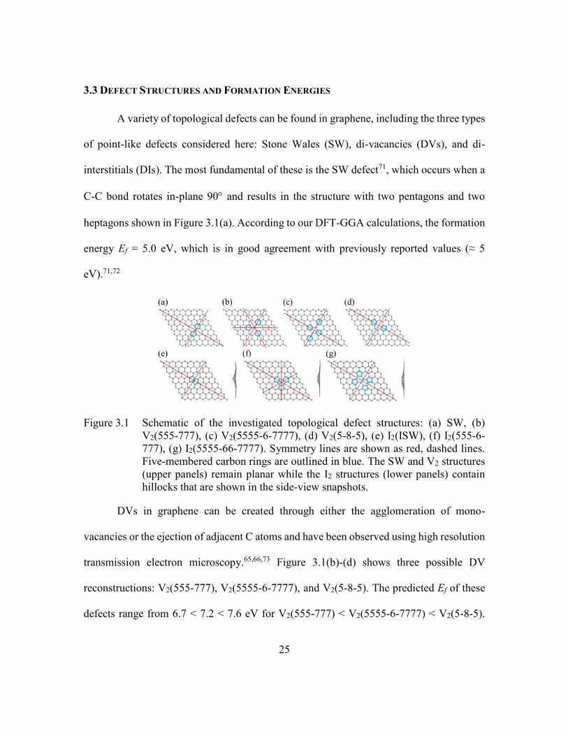
25
3.3 DEFECT STRUCTURES AND FORMATION ENERGIES
A variety of topological defects can be found in graphene, including the three types
of point-like defects considered here: Stone Wales (SW), di-vacancies (DVs), and di-
interstitials (DIs). The most fundamental of these is the SW defect71, which occurs when a
C-C bond rotates in-plane 90 and results in the structure with two pentagons and two
heptagons shown in Figure 3.1(a). According to our DFT-GGA calculations, the formation
energy Ef = 5.0 eV, which is in good agreement with previously reported values (≈ 5
eV).71,72
Figure 3.1 Schematic of the investigated topological defect structures: (a) SW, (b)
V2(555-777), (c) V2(5555-6-7777), (d) V2(5-8-5), (e) I2(ISW), (f) I2(555-6-
777), (g) I2(5555-66-7777). Symmetry lines are shown as red, dashed lines.
Five-membered carbon rings are outlined in blue. The SW and V2 structures
(upper panels) remain planar while the I2 structures (lower panels) contain
hillocks that are shown in the side-view snapshots.
DVs in graphene can be created through either the agglomeration of mono-
vacancies or the ejection of adjacent C atoms and have been observed using high resolution
transmission electron microscopy.65,66,73 Figure 3.1(b)-(d) shows three possible DV
reconstructions: V2(555-777), V2(5555-6-7777), and V2(5-8-5). The predicted Ef of these
defects range from 6.7 < 7.2 < 7.6 eV for V2(555-777) < V2(5555-6-7777) < V2(5-8-5).
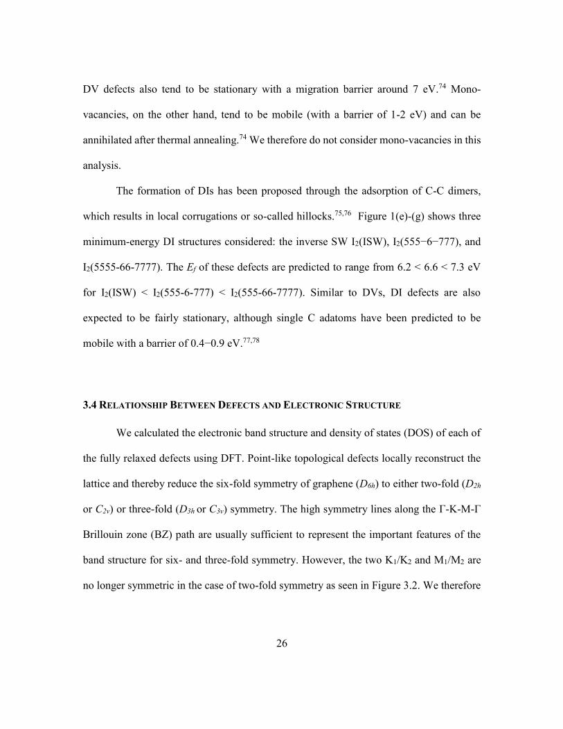
26
DV defects also tend to be stationary with a migration barrier around 7 eV.74 Mono-
vacancies, on the other hand, tend to be mobile (with a barrier of 1-2 eV) and can be
annihilated after thermal annealing.74 We therefore do not consider mono-vacancies in this
analysis.
The formation of DIs has been proposed through the adsorption of C-C dimers,
which results in local corrugations or so-called hillocks.75,76 Figure 1(e)-(g) shows three
minimum-energy DI structures considered: the inverse SW I2(ISW), I2(555−6−777), and
I2(5555-66-7777). The Ef of these defects are predicted to range from 6.2 < 6.6 < 7.3 eV
for I2(ISW) < I2(555-6-777) < I2(555-66-7777). Similar to DVs, DI defects are also
expected to be fairly stationary, although single C adatoms have been predicted to be
mobile with a barrier of 0.4−0.9 eV.77,78
3.4 RELATIONSHIP BETWEEN DEFECTS AND ELECTRONIC STRUCTURE
We calculated the electronic band structure and density of states (DOS) of each of
the fully relaxed defects using DFT. Point-like topological defects locally reconstruct the
lattice and thereby reduce the six-fold symmetry of graphene (D6h) to either two-fold (D2h
or C2v) or three-fold (D3h or C3v) symmetry. The high symmetry lines along the Γ-K-M-Γ
Brillouin zone (BZ) path are usually sufficient to represent the important features of the
band structure for six- and three-fold symmetry. However, the two K1/K2 and M1/M2 are
no longer symmetric in the case of two-fold symmetry as seen in Figure 3.2. We therefore
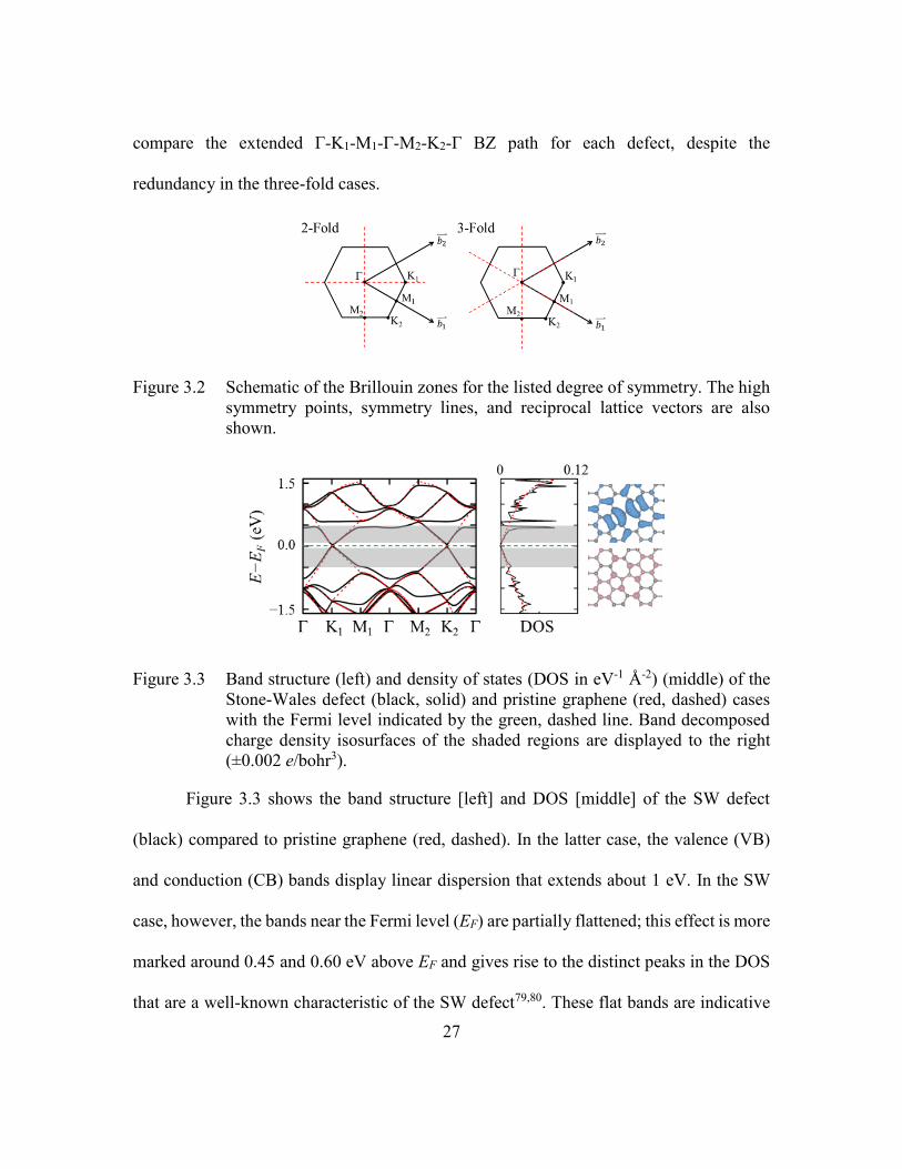
27
compare the extended Γ-K1-M1-Γ-M2-K2-Γ BZ path for each defect, despite the
redundancy in the three-fold cases.
Figure 3.2 Schematic of the Brillouin zones for the listed degree of symmetry. The high
symmetry points, symmetry lines, and reciprocal lattice vectors are also
shown.
Figure 3.3 Band structure (left) and density of states (DOS in eV-1 Å-2) (middle) of the
Stone-Wales defect (black, solid) and pristine graphene (red, dashed) cases
with the Fermi level indicated by the green, dashed line. Band decomposed
charge density isosurfaces of the shaded regions are displayed to the right
(±0.002 e/bohr3).
Figure 3.3 shows the band structure [left] and DOS [middle] of the SW defect
(black) compared to pristine graphene (red, dashed). In the latter case, the valence (VB)
and conduction (CB) bands display linear dispersion that extends about 1 eV. In the SW
case, however, the bands near the Fermi level (EF) are partially flattened; this effect is more
marked around 0.45 and 0.60 eV above EF and gives rise to the distinct peaks in the DOS
that are a well-known characteristic of the SW defect79,80. These flat bands are indicative

28
of the quasi-localization of the pz states in the vicinity of the SW defect, due to the
disruption of the graphene system. Hence, injected charge carriers, especially electrons,
will accumulate near the pentagon-heptagon C rings, as seen from the band decomposed
charge density isosurfaces [right]. However, the flat bands are also smoothly connected to
the low-energy dispersion of graphene (more so in the filled states), which suggests that a
large fraction of the excess charge can also widely spread over the graphene lattice.
Figure 3.4 Band structure (left) and density of states (DOS in eV-1 Å-2) (middle) of the
(a) V2(555-777), (b) V2(5555-6-7777), and (c) V2(5-8-5) cases with the Fermi
level indicated by the green, dashed line. Band decomposed charge density
isosurfaces of the shaded regions are displayed to the right (±0.002 e/bohr3).
Figure 3.4 shows the band structures [left] and DOS [middle] for each of the DV
structures. In all three cases, the EF is shifted down below the VB of graphene primarily
due to electron deficiency; note that V2 removes two electrons from the system of
graphene. The DOS plots show several pronounced peaks near the EF which correspond to
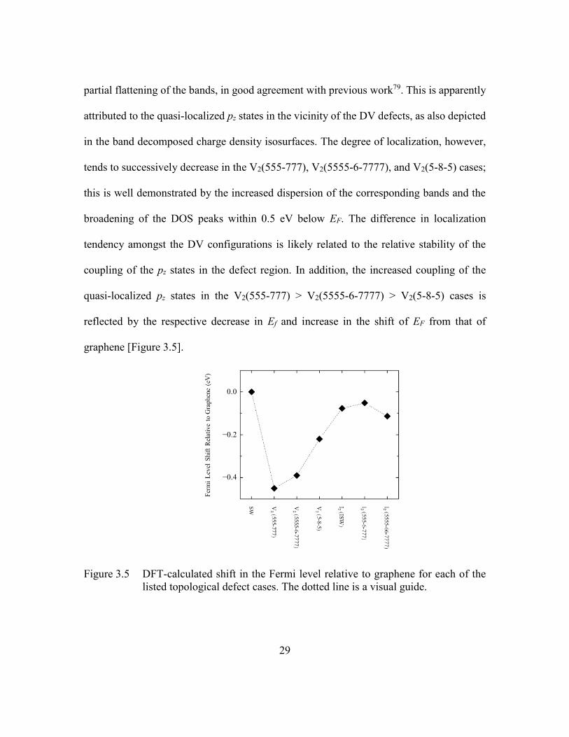
29
partial flattening of the bands, in good agreement with previous work79. This is apparently
attributed to the quasi-localized pz states in the vicinity of the DV defects, as also depicted
in the band decomposed charge density isosurfaces. The degree of localization, however,
tends to successively decrease in the V2(555-777), V2(5555-6-7777), and V2(5-8-5) cases;
this is well demonstrated by the increased dispersion of the corresponding bands and the
broadening of the DOS peaks within 0.5 eV below EF. The difference in localization
tendency amongst the DV configurations is likely related to the relative stability of the
coupling of the pz states in the defect region. In addition, the increased coupling of the
quasi-localized pz states in the V2(555-777) > V2(5555-6-7777) > V2(5-8-5) cases is
reflected by the respective decrease in Ef and increase in the shift of EF from that of
graphene [Figure 3.5].
Figure 3.5 DFT-calculated shift in the Fermi level relative to graphene for each of the
listed topological defect cases. The dotted line is a visual guide.
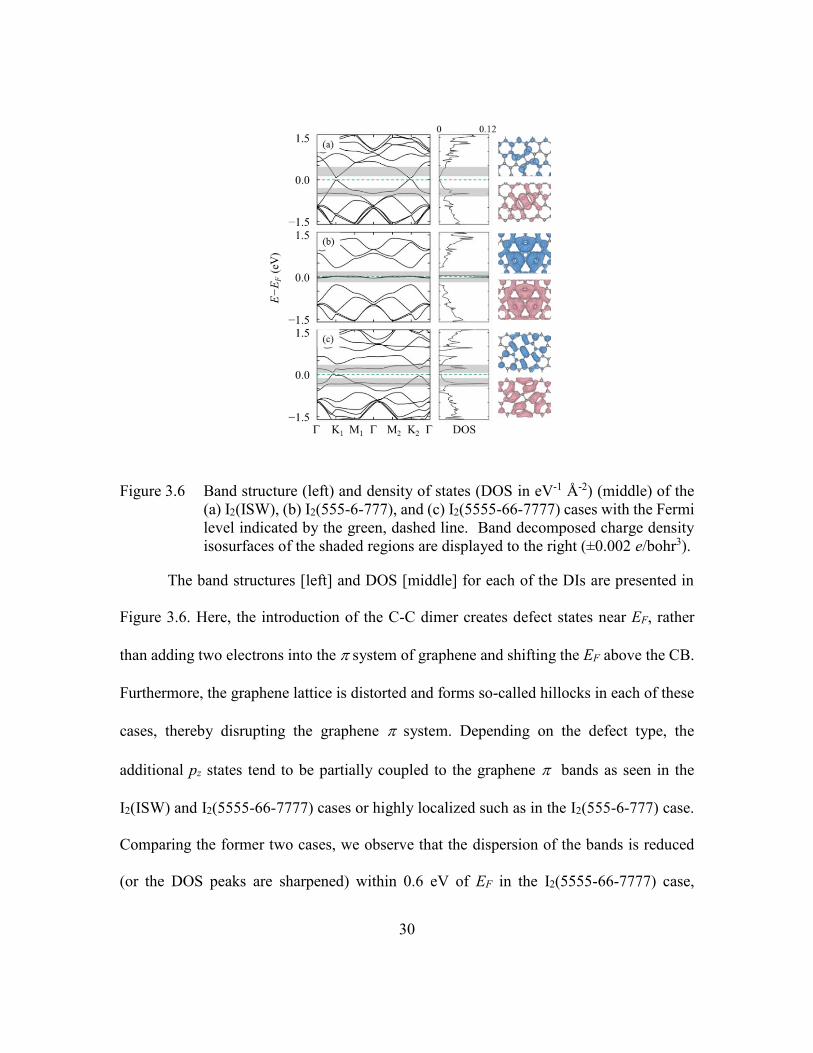
30
Figure 3.6 Band structure (left) and density of states (DOS in eV-1 Å-2) (middle) of the
(a) I2(ISW), (b) I2(555-6-777), and (c) I2(5555-66-7777) cases with the Fermi
level indicated by the green, dashed line. Band decomposed charge density
isosurfaces of the shaded regions are displayed to the right (±0.002 e/bohr3).
The band structures [left] and DOS [middle] for each of the DIs are presented in
Figure 3.6. Here, the introduction of the C-C dimer creates defect states near EF, rather
than adding two electrons into the system of graphene and shifting the EF above the CB.
Furthermore, the graphene lattice is distorted and forms so-called hillocks in each of these
cases, thereby disrupting the graphene system. Depending on the defect type, the
additional pz states tend to be partially coupled to the graphene bands as seen in the
I2(ISW) and I2(5555-66-7777) cases or highly localized such as in the I2(555-6-777) case.
Comparing the former two cases, we observe that the dispersion of the bands is reduced
(or the DOS peaks are sharpened) within 0.6 eV of EF in the I2(5555-66-7777) case,
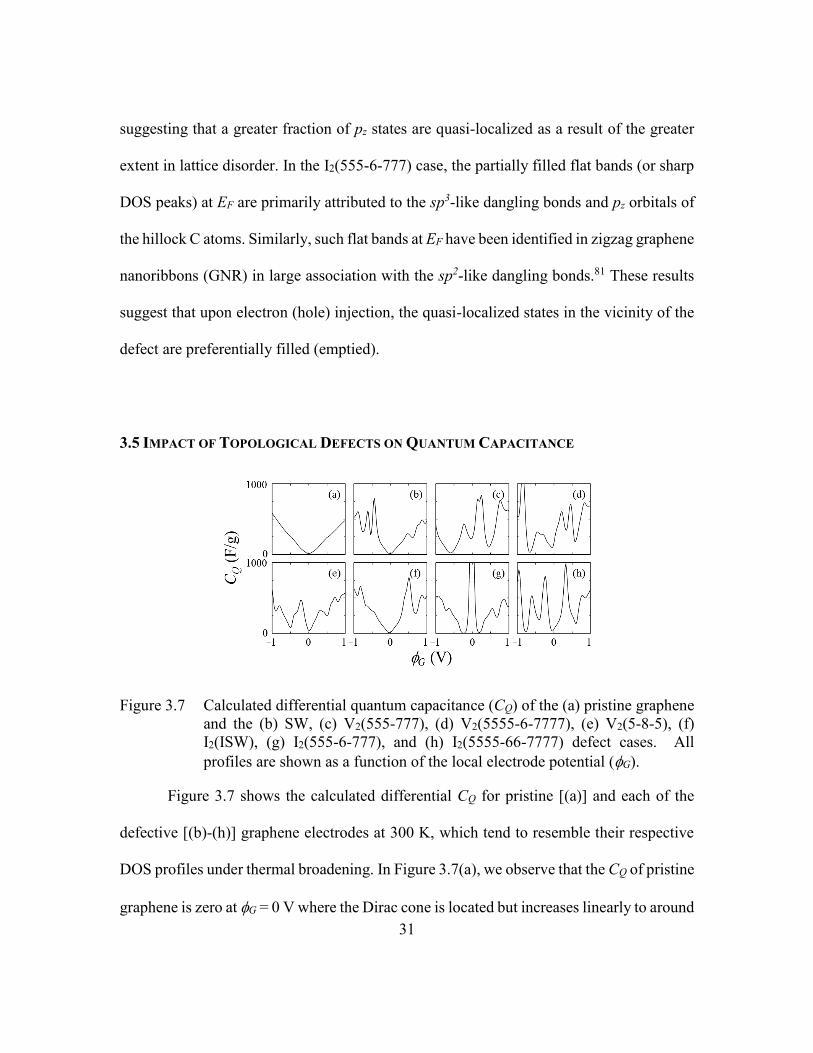
31
suggesting that a greater fraction of pz states are quasi-localized as a result of the greater
extent in lattice disorder. In the I2(555-6-777) case, the partially filled flat bands (or sharp
DOS peaks) at EF are primarily attributed to the sp3-like dangling bonds and pz orbitals of
the hillock C atoms. Similarly, such flat bands at EF have been identified in zigzag graphene
nanoribbons (GNR) in large association with the sp2-like dangling bonds.81 These results
suggest that upon electron (hole) injection, the quasi-localized states in the vicinity of the
defect are preferentially filled (emptied).
3.5 IMPACT OF TOPOLOGICAL DEFECTS ON QUANTUM CAPACITANCE
Figure 3.7 Calculated differential quantum capacitance (CQ) of the (a) pristine graphene
and the (b) SW, (c) V2(555-777), (d) V2(5555-6-7777), (e) V2(5-8-5), (f)
I2(ISW), (g) I2(555-6-777), and (h) I2(5555-66-7777) defect cases. All
profiles are shown as a function of the local electrode potential (G).
Figure 3.7 shows the calculated differential CQ for pristine [(a)] and each of the
defective [(b)-(h)] graphene electrodes at 300 K, which tend to resemble their respective
DOS profiles under thermal broadening. In Figure 3.7(a), we observe that the CQ of pristine
graphene is zero at G = 0 V where the Dirac cone is located but increases linearly to around
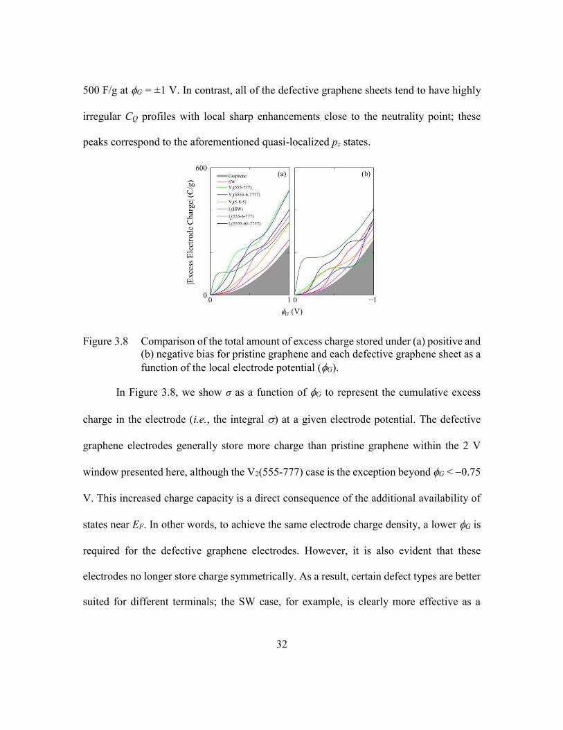
32
500 F/g at G = ±1 V. In contrast, all of the defective graphene sheets tend to have highly
irregular CQ profiles with local sharp enhancements close to the neutrality point; these
peaks correspond to the aforementioned quasi-localized pz states.
Figure 3.8 Comparison of the total amount of excess charge stored under (a) positive and
(b) negative bias for pristine graphene and each defective graphene sheet as a
function of the local electrode potential (G).
In Figure 3.8, we show σ as a function of G to represent the cumulative excess
charge in the electrode (i.e., the integral ) at a given electrode potential. The defective
graphene electrodes generally store more charge than pristine graphene within the 2 V
window presented here, although the V2(555-777) case is the exception beyond G < 0.75
V. This increased charge capacity is a direct consequence of the additional availability of
states near EF. In other words, to achieve the same electrode charge density, a lower G is
required for the defective graphene electrodes. However, it is also evident that these
electrodes no longer store charge symmetrically. As a result, certain defect types are better
suited for different terminals; the SW case, for example, is clearly more effective as a
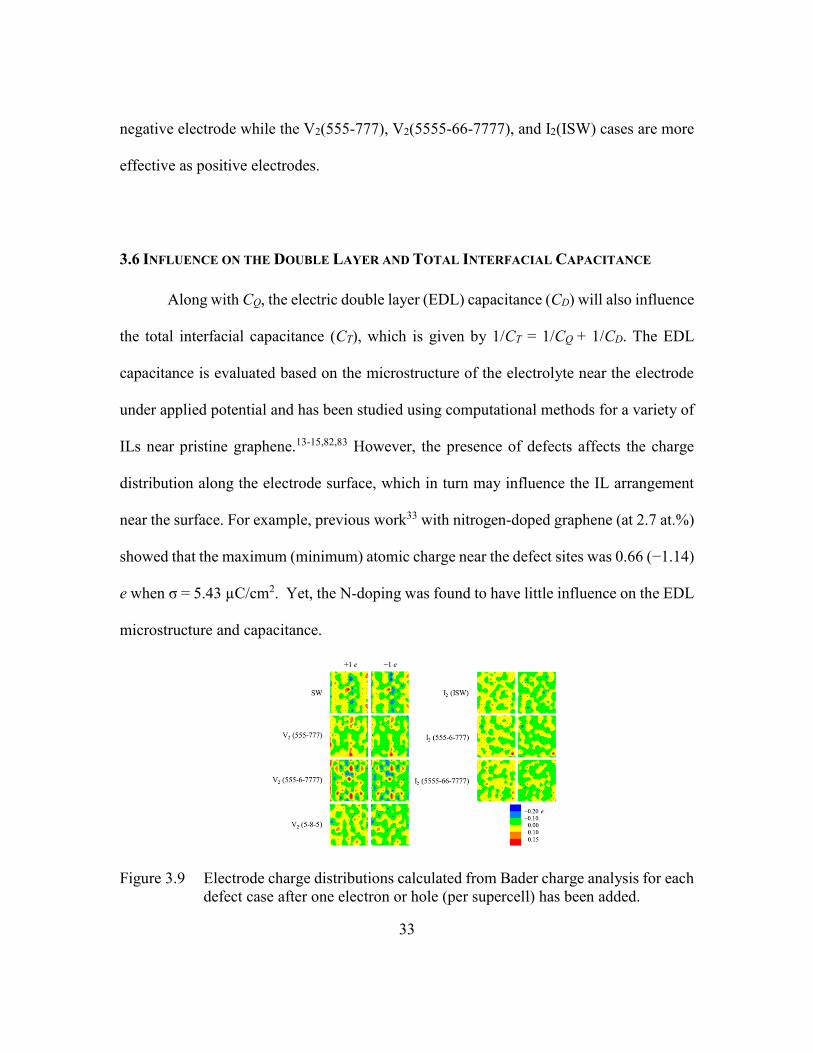
33
negative electrode while the V2(555-777), V2(5555-66-7777), and I2(ISW) cases are more
effective as positive electrodes.
3.6 INFLUENCE ON THE DOUBLE LAYER AND TOTAL INTERFACIAL CAPACITANCE
Along with CQ, the electric double layer (EDL) capacitance (CD) will also influence
the total interfacial capacitance (CT), which is given by 1/CT = 1/CQ + 1/CD. The EDL
capacitance is evaluated based on the microstructure of the electrolyte near the electrode
under applied potential and has been studied using computational methods for a variety of
ILs near pristine graphene.13-15,82,83 However, the presence of defects affects the charge
distribution along the electrode surface, which in turn may influence the IL arrangement
near the surface. For example, previous work33 with nitrogen-doped graphene (at 2.7 at.%)
showed that the maximum (minimum) atomic charge near the defect sites was 0.66 (−1.14)
e when σ = 5.43 µC/cm2. Yet, the N-doping was found to have little influence on the EDL
microstructure and capacitance.
Figure 3.9 Electrode charge distributions calculated from Bader charge analysis for each
defect case after one electron or hole (per supercell) has been added.
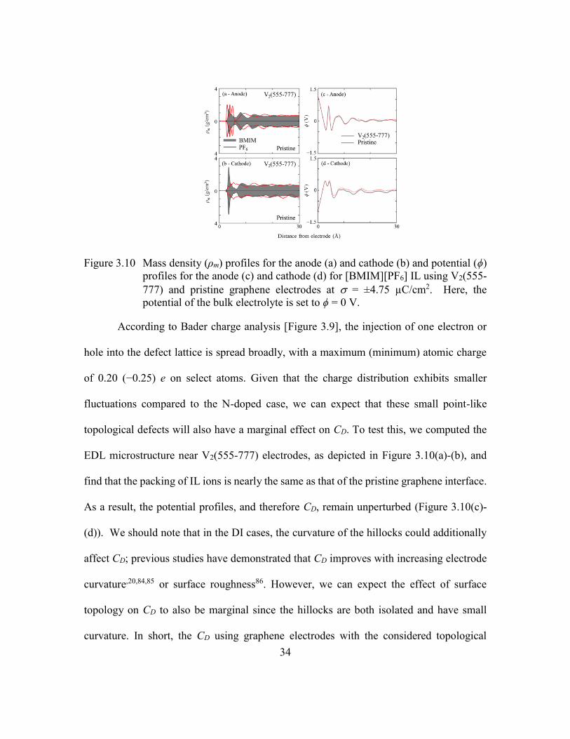
34
Figure 3.10 Mass density (ρm) profiles for the anode (a) and cathode (b) and potential (ϕ)
profiles for the anode (c) and cathode (d) for [BMIM][PF6] IL using V2(555-
777) and pristine graphene electrodes at = ±4.75 µC/cm2. Here, the
potential of the bulk electrolyte is set to ϕ = 0 V.
According to Bader charge analysis [Figure 3.9], the injection of one electron or
hole into the defect lattice is spread broadly, with a maximum (minimum) atomic charge
of 0.20 (−0.25) e on select atoms. Given that the charge distribution exhibits smaller
fluctuations compared to the N-doped case, we can expect that these small point-like
topological defects will also have a marginal effect on CD. To test this, we computed the
EDL microstructure near V2(555-777) electrodes, as depicted in Figure 3.10(a)-(b), and
find that the packing of IL ions is nearly the same as that of the pristine graphene interface.
As a result, the potential profiles, and therefore CD, remain unperturbed (Figure 3.10(c)-
(d)). We should note that in the DI cases, the curvature of the hillocks could additionally
affect CD; previous studies have demonstrated that CD improves with increasing electrode
curvature,20,84,85 or surface roughness86. However, we can expect the effect of surface
topology on CD to also be marginal since the hillocks are both isolated and have small
curvature. In short, the CD using graphene electrodes with the considered topological
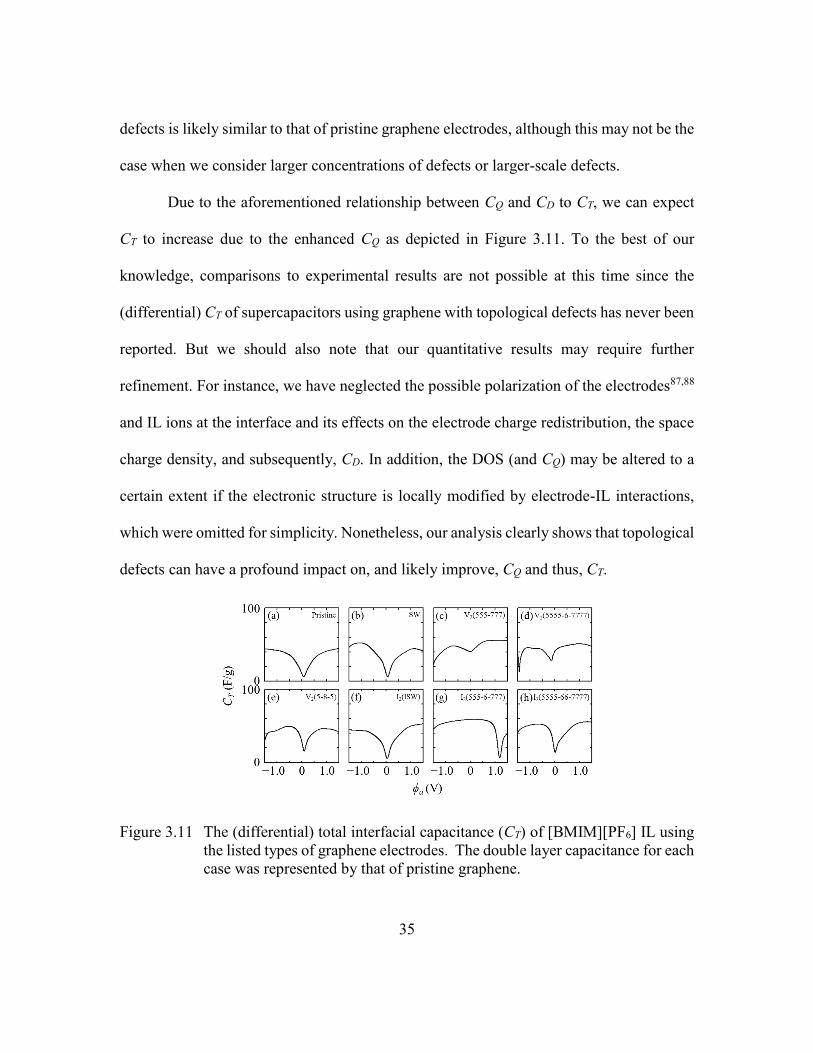
35
defects is likely similar to that of pristine graphene electrodes, although this may not be the
case when we consider larger concentrations of defects or larger-scale defects.
Due to the aforementioned relationship between CQ and CD to CT, we can expect
CT to increase due to the enhanced CQ as depicted in Figure 3.11. To the best of our
knowledge, comparisons to experimental results are not possible at this time since the
(differential) CT of supercapacitors using graphene with topological defects has never been
reported. But we should also note that our quantitative results may require further
refinement. For instance, we have neglected the possible polarization of the electrodes87,88
and IL ions at the interface and its effects on the electrode charge redistribution, the space
charge density, and subsequently, CD. In addition, the DOS (and CQ) may be altered to a
certain extent if the electronic structure is locally modified by electrode-IL interactions,
which were omitted for simplicity. Nonetheless, our analysis clearly shows that topological
defects can have a profound impact on, and likely improve, CQ and thus, CT.
Figure 3.11 The (differential) total interfacial capacitance (CT) of [BMIM][PF6] IL using
the listed types of graphene electrodes. The double layer capacitance for each
case was represented by that of pristine graphene.

36
3.7 TUNING THROUGH COMBINATIONS OF TOPOLOGICAL DEFECTS
In the previous section, we presented the electronic structure and CQ of individual
topological defects. Experimentally, however, it may be quite challenging to recreate such
homogeneity along the graphene lattice. Therefore, in this section, we increase the
complexity by exploring the impact of having different combinations of topological defects
on the electronic structure and CQ. To this end, we have simulated two scenarios: graphene
sheets with an overall nd = 3 1013 cm-2 using (1) SW, V2(555-777), I2(555-6-777), and
I2(5555-66-7777) defects [Figure 3.12(a)] and (2) V2(555-777) and I2(5555-66-7777)
defects at a 3:1 ratio [Figure 3.12(b)].
Figures 3.12(a)-(b) show the DOS of each of the two configurations of defective
graphene sheets, which exhibit several sharp peaks near EF. According to our analysis of
the projected DOS [Figure 3.13 and 3.14], each of these peaks is attributed to a particular
defect-induced quasi-localized state (see markings), which has been similarly observed in
previous theoretical work.79,89 Note that the positions of these quasi-localized states relative
to each other remain largely unchanged; the position of EF is approximated by the (density-
weighed) average positions of each EF in the associated individual defect cases (which can
be possible when long-range coupling between adjacent defect types is absent). This
analysis implies that the following two-step process can be used to tailor the electronic
structure of defective graphene: (1) determine the relative positions of quasi-localized
states from the chosen array of topological defects and (2) shift the position of EF based on
the densities of each topological defect. However, this procedure is likely possible only
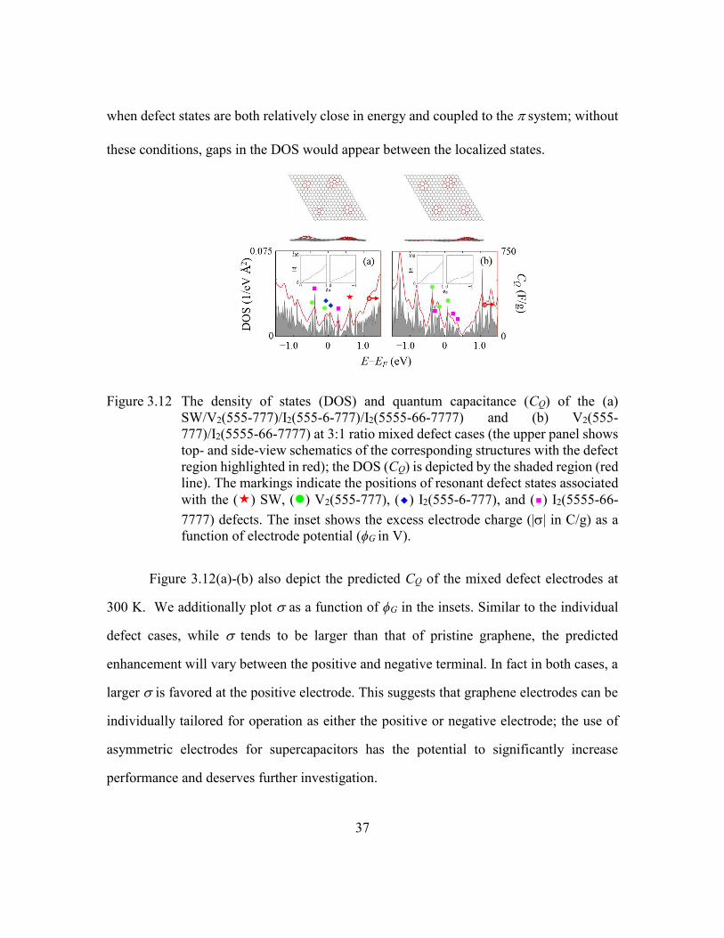
37
when defect states are both relatively close in energy and coupled to the system; without
these conditions, gaps in the DOS would appear between the localized states.
Figure 3.12 The density of states (DOS) and quantum capacitance (CQ) of the (a)
SW/V2(555-777)/I2(555-6-777)/I2(5555-66-7777) and (b) V2(555-
777)/I2(5555-66-7777) at 3:1 ratio mixed defect cases (the upper panel shows
top- and side-view schematics of the corresponding structures with the defect
region highlighted in red); the DOS (CQ) is depicted by the shaded region (red
line). The markings indicate the positions of resonant defect states associated
with the () SW, () V2(555-777), () I2(555-6-777), and () I2(5555-66-
7777) defects. The inset shows the excess electrode charge (|| in C/g) as a
function of electrode potential (ϕG in V).
Figure 3.12(a)-(b) also depict the predicted CQ of the mixed defect electrodes at
300 K. We additionally plot as a function of ϕG in the insets. Similar to the individual
defect cases, while tends to be larger than that of pristine graphene, the predicted
enhancement will vary between the positive and negative terminal. In fact in both cases, a
larger is favored at the positive electrode. This suggests that graphene electrodes can be
individually tailored for operation as either the positive or negative electrode; the use of
asymmetric electrodes for supercapacitors has the potential to significantly increase
performance and deserves further investigation.
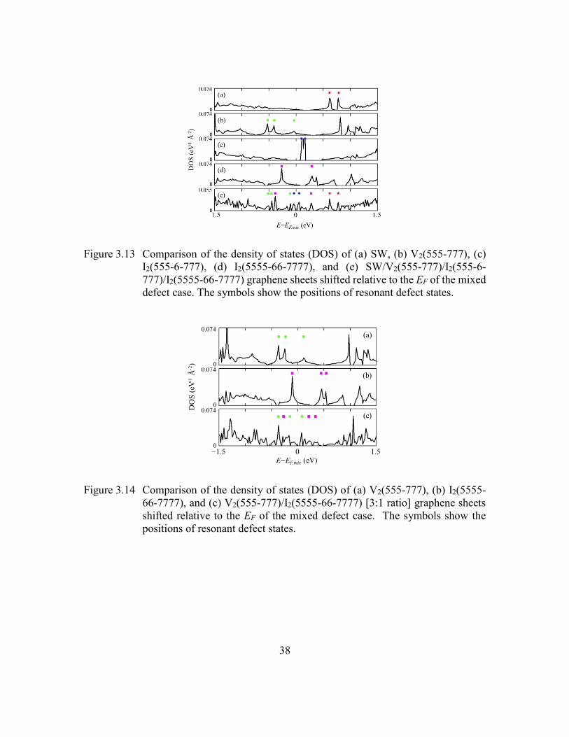
38
Figure 3.13 Comparison of the density of states (DOS) of (a) SW, (b) V2(555-777), (c)
I2(555-6-777), (d) I2(5555-66-7777), and (e) SW/V2(555-777)/I2(555-6-
777)/I2(5555-66-7777) graphene sheets shifted relative to the EF of the mixed
defect case. The symbols show the positions of resonant defect states.
Figure 3.14 Comparison of the density of states (DOS) of (a) V2(555-777), (b) I2(5555-
66-7777), and (c) V2(555-777)/I2(5555-66-7777) [3:1 ratio] graphene sheets
shifted relative to the EF of the mixed defect case. The symbols show the
positions of resonant defect states.
39
3.8 CONCLUSIONS
We have investigated the impact of topological defects on the electronic structure
and quantum capacitance of graphene using density functional theory. In this study, we
considered small point-like defects such as Stone-Wales, di-vacancies, and di-interstitials.
The presence of these defects disrupts the system of graphene, which gives rise to quasi-
localized states of varying degrees near the Fermi level. As a result, each of these defective
graphene electrodes tends to have enhanced quantum capacitance compared to pristine
graphene. Interestingly, their charging behavior is found to be asymmetric around the
neutrality point such that some defective graphene sheets are more effective as either the
positive or negative electrode. Our analysis also suggests that the double layer capacitance
remains virtually unaffected by the presence of these defects. These findings indicate that
graphene electrodes with topological defects may be used to enhance the overall
capacitance of supercapacitors by virtue of the increased quantum capacitance.
Furthermore, our study suggests that graphene-based electrodes can be specifically tailored
as separate positive and negative electrodes, which could significantly enhance the
performance of supercapacitors and warrants further study.
40
Chapter 4: Transition Metal Dopant-Vacancy Complexes
Work in this chapter was published and reprinted with permission from ACS Appl. Mater.
Interfaces, Vol. 6, E. Paek*, A. J. Pak*, and G. S. Hwang, Large Capacitance Enhancement
Induced by Metal-Doping in Graphene-based Supercapacitors: A First-Principles-Based
Assessment, pg. 12168−76. Copyright (2014) American Chemical Society. * Both authors contributed equally.
4.1 INTRODUCTION TO TRANSITION METAL DOPANTS
Chemical doping is a widely used technique to modify and tailor the electronic
structure of graphene.90,91 Nitrogen-doping of graphene, for example, has been explored
for a variety of applications, including high-sensitivity sensors92, catalysis93, and
supercapacitors94,95. One of the practical challenges of doping is the ability to control the
concentration and selectivity of desired dopant types. Recent theoretical96-98 and
experimental93,99,100 work has shown that transition metal (M) atoms can be selectively
bound to vacancy (V) defects along the graphene lattice. Using this approach, it may be
possible to tailor the dispersion of M-V complexes to atomic precision. In addition, unlike
traditional nitrogen dopants, M dopants include d orbitals which can hybridize with C 2p
orbitals. To date, however, the relative influence of M-V complexes on both CQ and CD,
and therefore CT, remains largely unexplored.
In this chapter, the influence of metal incorporation into graphene vacancies on CT
is investigated based on a model system of M-V graphene complexes in [BMIM][PF6] IL
using a combined classical molecular dynamics (MD) and density functional theory (DFT)
approach. The impact of M-V complexes on CQ and CD is of particular interest. Using DFT,
the electronic structure and CQ of 3d M atoms bound to mono- and di-vacancy sites in
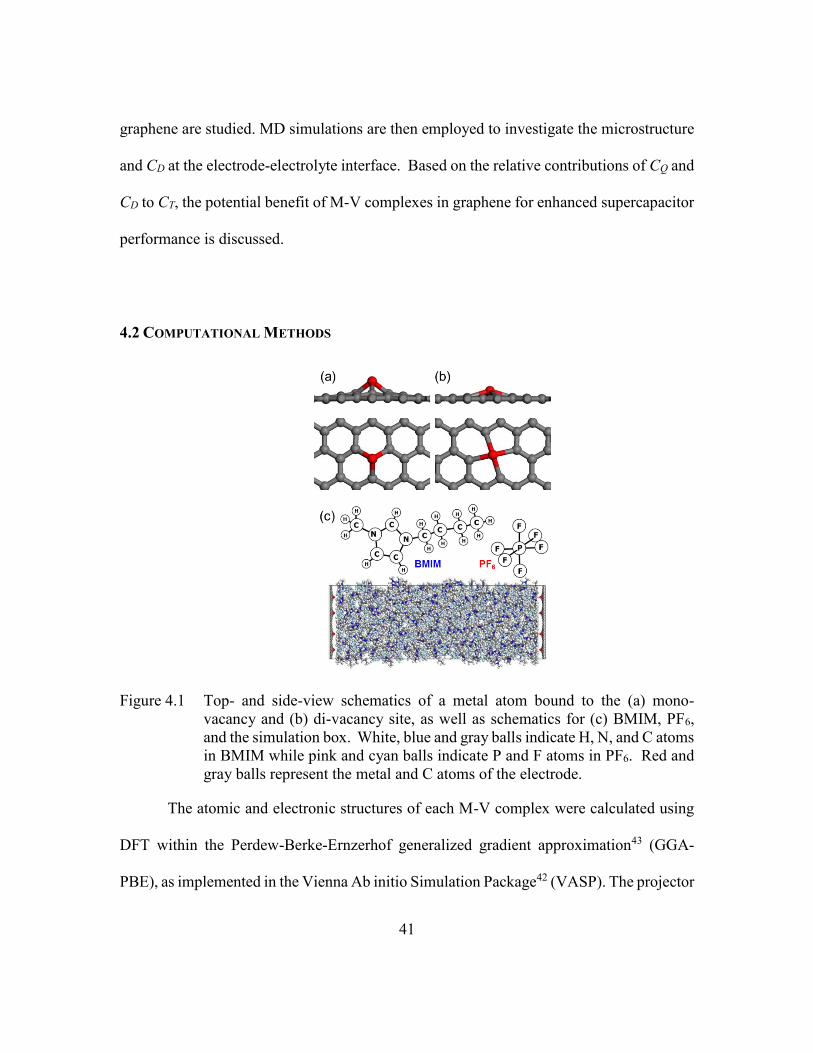
41
graphene are studied. MD simulations are then employed to investigate the microstructure
and CD at the electrode-electrolyte interface. Based on the relative contributions of CQ and
CD to CT, the potential benefit of M-V complexes in graphene for enhanced supercapacitor
performance is discussed.
4.2 COMPUTATIONAL METHODS
Figure 4.1 Top- and side-view schematics of a metal atom bound to the (a) mono-
vacancy and (b) di-vacancy site, as well as schematics for (c) BMIM, PF6,
and the simulation box. White, blue and gray balls indicate H, N, and C atoms
in BMIM while pink and cyan balls indicate P and F atoms in PF6. Red and
gray balls represent the metal and C atoms of the electrode.
The atomic and electronic structures of each M-V complex were calculated using
DFT within the Perdew-Berke-Ernzerhof generalized gradient approximation43 (GGA-
PBE), as implemented in the Vienna Ab initio Simulation Package42 (VASP). The projector
42
augmented wave (PAW) method69 is used to describe the interaction between core and
valence electrons based on a planewave basis set with a kinetic energy cutoff of 400 eV.
The pristine and M-doped graphene sheets were modeled using a 5 5 hexagonal supercell
with the GGA-optimized lattice constant of 2.466 Å (which is slightly larger than the
experimental value of 2.461 Å); each supercell had one metal atom and 49 (48) C atoms in
the M-MV (M-DV) cases, corresponding to a defect density of 7.6 1013 cm-2. Periodic
boundary conditions were employed in all three directions with a vacuum gap of 10 Å in
the vertical direction to separate the graphene system from its periodic images. For the
Brillouin zone integration, a (12×12×1) Monkhorst-Pack (MP) k-point mesh70 was used
for geometry optimization and energy calculations while a (15×15×1) MP k-point mesh
was used to ensure convergence for electronic structure calculations. Metal-doping induced
charge redistributions were determined using grid-based Bader analysis.61
The microstructure of [BMIM][PF6] near selected electrodes and the electric
potential profile were determined using MD simulations based on the OPLS-AA force
field50,101 when = 0, 2.38, 4.75, and 9.50 µC/cm2. The Lennard-Jones parameters for
Ti and Ni were adopted from previous work by Heinz and co-workers102 and Minonishi
and co-workers103; details on other force field parameters can be found in Ref. 13. As
illustrated in Figure 4.1, the simulation domain consists of 356 [BMIM][PF6] IL pairs
sandwiched between two electrodes (34.18 × 39.46 Å2) separated by 100 Å in the z-
direction with periodic boundary conditions in the x- and y-directions. Here, the structure
and charge distribution of the electrodes were determined from DFT calculations
(additional details are described later). Note that the domain is set to be large enough such
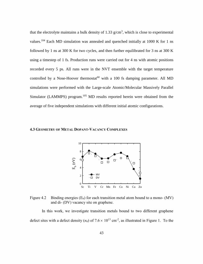
43
that the electrolyte maintains a bulk density of 1.33 g/cm3, which is close to experimental
values.104 Each MD simulation was annealed and quenched initially at 1000 K for 1 ns
followed by 1 ns at 300 K for two cycles, and then further equilibrated for 3 ns at 300 K
using a timestep of 1 fs. Production runs were carried out for 4 ns with atomic positions
recorded every 5 ps. All runs were in the NVT ensemble with the target temperature
controlled by a Nose-Hoover thermostat60 with a 100 fs damping parameter. All MD
simulations were performed with the Large-scale Atomic/Molecular Massively Parallel
Simulator (LAMMPS) program.105 MD results reported herein were obtained from the
average of five independent simulations with different initial atomic configurations.
4.3 GEOMETRY OF METAL DOPANT-VACANCY COMPLEXES
Figure 4.2 Binding energies (Eb) for each transition metal atom bound to a mono- (MV)
and di- (DV) vacancy site on graphene.
In this work, we investigate transition metals bound to two different graphene
defect sites with a defect density (nd) of 7.6 1013 cm-2, as illustrated in Figure 1. To the
Sc Ti V Cr Mn Fe Co Ni Cu Zn
Eb (
eV)
0
2
4
6
8
10
MV
DV
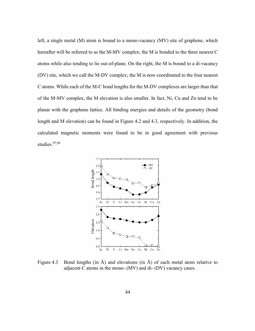
44
left, a single metal (M) atom is bound to a mono-vacancy (MV) site of graphene, which
hereafter will be referred to as the M-MV complex; the M is bonded to the three nearest C
atoms while also tending to lie out-of-plane. On the right, the M is bound to a di-vacancy
(DV) site, which we call the M-DV complex; the M is now coordinated to the four nearest
C atoms. While each of the M-C bond lengths for the M-DV complexes are larger than that
of the M-MV complex, the M elevation is also smaller. In fact, Ni, Cu and Zn tend to be
planar with the graphene lattice. All binding energies and details of the geometry (bond
length and M elevation) can be found in Figure 4.2 and 4.3, respectively. In addition, the
calculated magnetic moments were found to be in good agreement with previous
studies.97,98
Figure 4.3 Bond lengths (in Å) and elevations (in Å) of each metal atom relative to
adjacent C atoms in the mono- (MV) and di- (DV) vacancy cases.
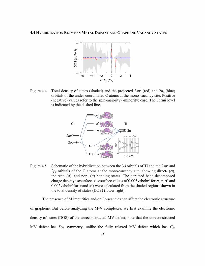
45
4.4 HYBRIDIZATION BETWEEN METAL DOPANT AND GRAPHENE VACANCY STATES
Figure 4.4 Total density of states (shaded) and the projected 2sp2 (red) and 2pz (blue)
orbitals of the under-coordinated C atoms at the mono-vacancy site. Positive
(negative) values refer to the spin-majority (-minority) case. The Fermi level
is indicated by the dashed line.
Figure 4.5 Schematic of the hybridization between the 3d orbitals of Ti and the 2sp2 and
2pz orbitals of the C atoms at the mono-vacancy site, showing direct- (),
indirect- (), and non- (n) bonding states. The depicted band-decomposed
charge density isosurfaces (isosurface values of 0.005 e/bohr3 for , n, * and
0.002 e/bohr3 for and *) were calculated from the shaded regions shown in
the total density of states (DOS) (lower right).
The presence of M impurities and/or C vacancies can affect the electronic structure
of graphene. But before analyzing the M-V complexes, we first examine the electronic
density of states (DOS) of the unreconstructed MV defect; note that the unreconstructed
MV defect has D3h symmetry, unlike the fully relaxed MV defect which has C2v
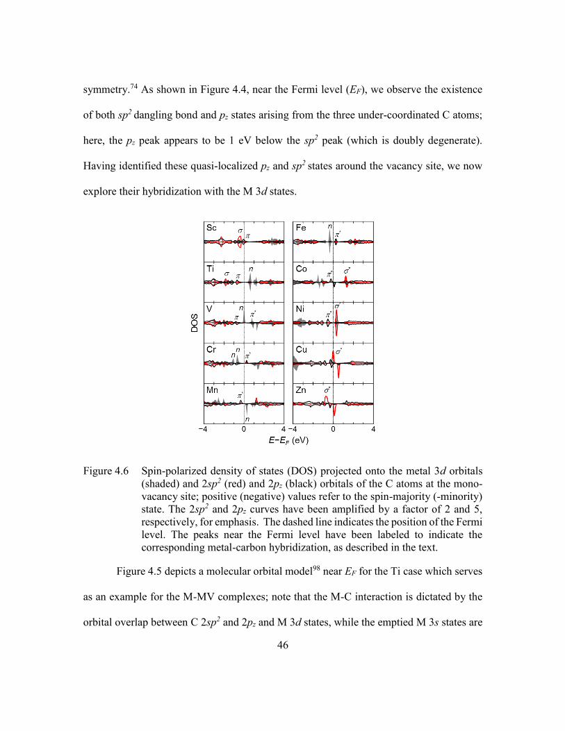
46
symmetry.74 As shown in Figure 4.4, near the Fermi level (EF), we observe the existence
of both sp2 dangling bond and pz states arising from the three under-coordinated C atoms;
here, the pz peak appears to be 1 eV below the sp2 peak (which is doubly degenerate).
Having identified these quasi-localized pz and sp2 states around the vacancy site, we now
explore their hybridization with the M 3d states.
Figure 4.6 Spin-polarized density of states (DOS) projected onto the metal 3d orbitals
(shaded) and 2sp2 (red) and 2pz (black) orbitals of the C atoms at the mono-
vacancy site; positive (negative) values refer to the spin-majority (-minority)
state. The 2sp2 and 2pz curves have been amplified by a factor of 2 and 5,
respectively, for emphasis. The dashed line indicates the position of the Fermi
level. The peaks near the Fermi level have been labeled to indicate the
corresponding metal-carbon hybridization, as described in the text.
Figure 4.5 depicts a molecular orbital model98 near EF for the Ti case which serves
as an example for the M-MV complexes; note that the M-C interaction is dictated by the
orbital overlap between C 2sp2 and 2pz and M 3d states, while the emptied M 3s states are
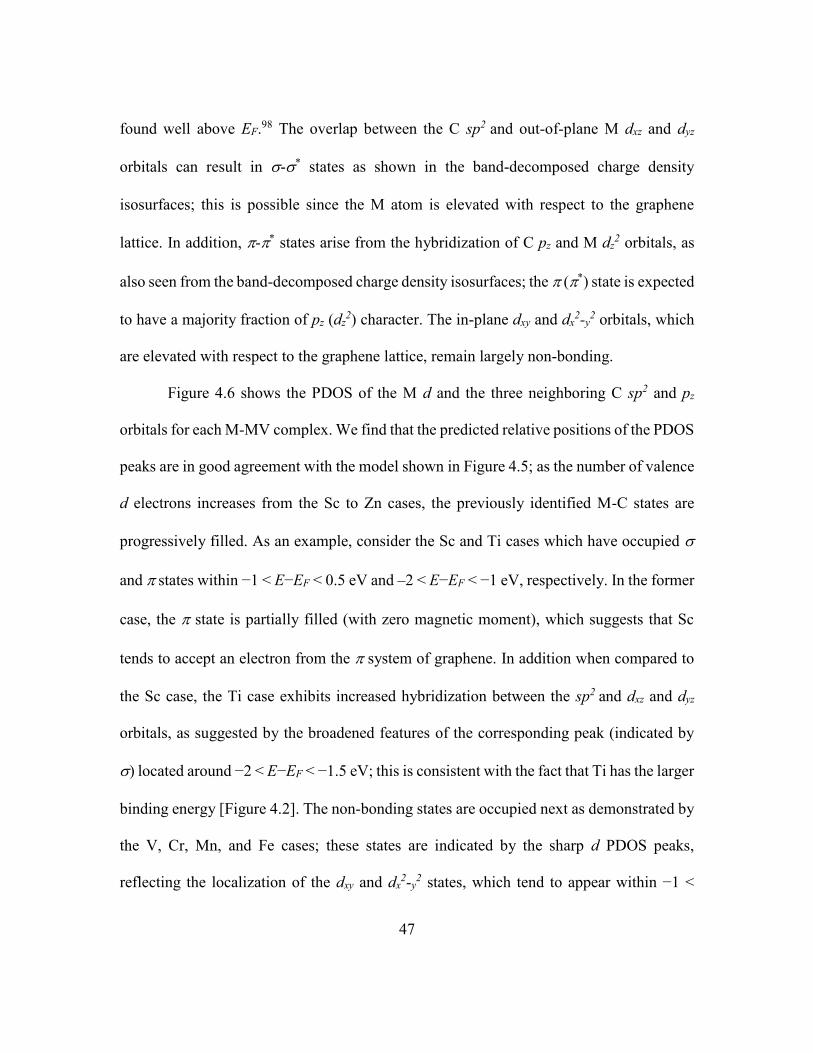
47
found well above EF.98 The overlap between the C sp2 and out-of-plane M dxz and dyz
orbitals can result in -* states as shown in the band-decomposed charge density
isosurfaces; this is possible since the M atom is elevated with respect to the graphene
lattice. In addition, -* states arise from the hybridization of C pz and M dz2 orbitals, as
also seen from the band-decomposed charge density isosurfaces; the (*) state is expected
to have a majority fraction of pz (dz2) character. The in-plane dxy and dx
2-y2 orbitals, which
are elevated with respect to the graphene lattice, remain largely non-bonding.
Figure 4.6 shows the PDOS of the M d and the three neighboring C sp2 and pz
orbitals for each M-MV complex. We find that the predicted relative positions of the PDOS
peaks are in good agreement with the model shown in Figure 4.5; as the number of valence
d electrons increases from the Sc to Zn cases, the previously identified M-C states are
progressively filled. As an example, consider the Sc and Ti cases which have occupied
and states within −1 < E−EF < 0.5 eV and –2 < E−EF < −1 eV, respectively. In the former
case, the state is partially filled (with zero magnetic moment), which suggests that Sc
tends to accept an electron from the system of graphene. In addition when compared to
the Sc case, the Ti case exhibits increased hybridization between the sp2 and dxz and dyz
orbitals, as suggested by the broadened features of the corresponding peak (indicated by
) located around −2 < E−EF < −1.5 eV; this is consistent with the fact that Ti has the larger
binding energy [Figure 4.2]. The non-bonding states are occupied next as demonstrated by
the V, Cr, Mn, and Fe cases; these states are indicated by the sharp d PDOS peaks,
reflecting the localization of the dxy and dx2-y
2 states, which tend to appear within −1 <
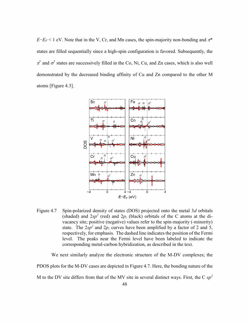
48
E−EF < 1 eV. Note that in the V, Cr, and Mn cases, the spin-majority non-bonding and *
states are filled sequentially since a high-spin configuration is favored. Subsequently, the
* and * states are successively filled in the Co, Ni, Cu, and Zn cases, which is also well
demonstrated by the decreased binding affinity of Cu and Zn compared to the other M
atoms [Figure 4.3].
Figure 4.7 Spin-polarized density of states (DOS) projected onto the metal 3d orbitals
(shaded) and 2sp2 (red) and 2pz (black) orbitals of the C atoms at the di-
vacancy site; positive (negative) values refer to the spin-majority (-minority)
state. The 2sp2 and 2pz curves have been amplified by a factor of 2 and 5,
respectively, for emphasis. The dashed line indicates the position of the Fermi
level. The peaks near the Fermi level have been labeled to indicate the
corresponding metal-carbon hybridization, as described in the text.
We next similarly analyze the electronic structure of the M-DV complexes; the
PDOS plots for the M-DV cases are depicted in Figure 4.7. Here, the bonding nature of the
M to the DV site differs from that of the MV site in several distinct ways. First, the C sp2
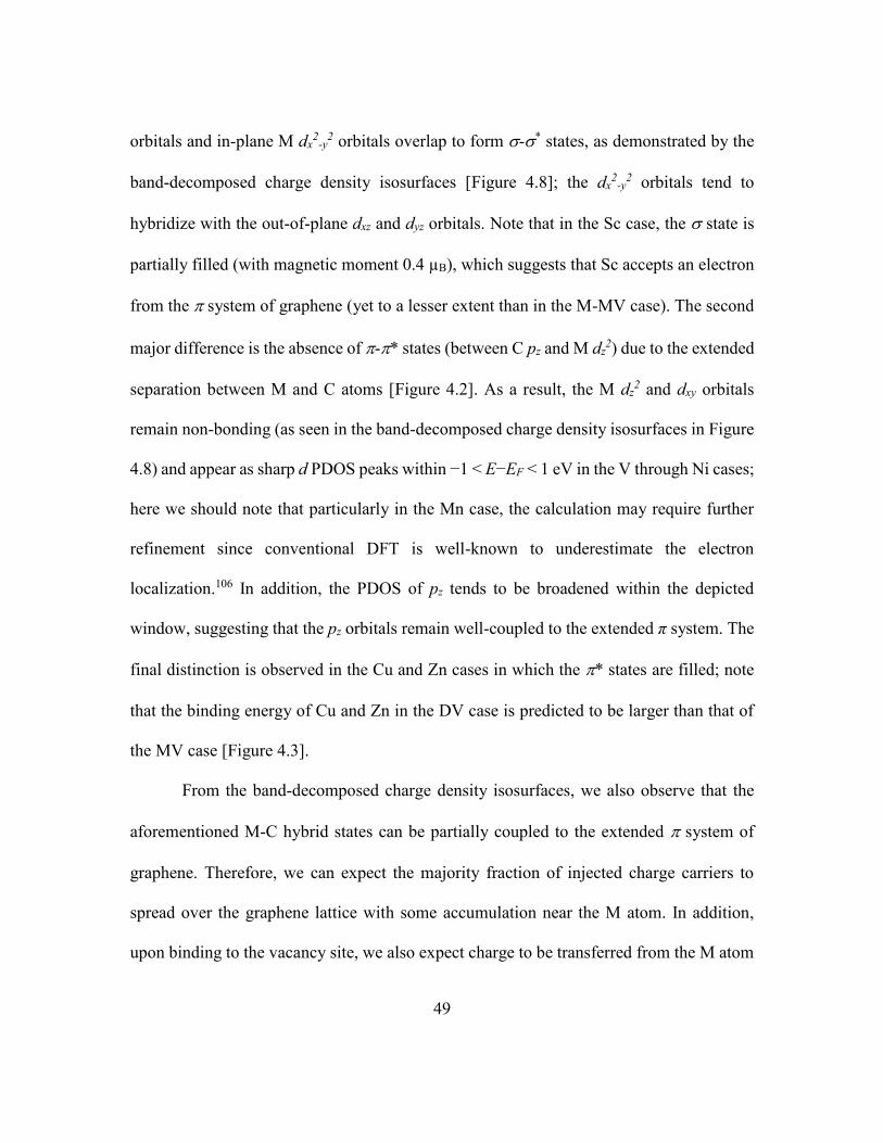
49
orbitals and in-plane M dx2
-y2 orbitals overlap to form -* states, as demonstrated by the
band-decomposed charge density isosurfaces [Figure 4.8]; the dx2
-y2 orbitals tend to
hybridize with the out-of-plane dxz and dyz orbitals. Note that in the Sc case, the state is
partially filled (with magnetic moment 0.4 µB), which suggests that Sc accepts an electron
from the system of graphene (yet to a lesser extent than in the M-MV case). The second
major difference is the absence of -* states (between C pz and M dz2) due to the extended
separation between M and C atoms [Figure 4.2]. As a result, the M dz2 and dxy orbitals
remain non-bonding (as seen in the band-decomposed charge density isosurfaces in Figure
4.8) and appear as sharp d PDOS peaks within −1 < E−EF < 1 eV in the V through Ni cases;
here we should note that particularly in the Mn case, the calculation may require further
refinement since conventional DFT is well-known to underestimate the electron
localization.106 In addition, the PDOS of pz tends to be broadened within the depicted
window, suggesting that the pz orbitals remain well-coupled to the extended π system. The
final distinction is observed in the Cu and Zn cases in which the * states are filled; note
that the binding energy of Cu and Zn in the DV case is predicted to be larger than that of
the MV case [Figure 4.3].
From the band-decomposed charge density isosurfaces, we also observe that the
aforementioned M-C hybrid states can be partially coupled to the extended system of
graphene. Therefore, we can expect the majority fraction of injected charge carriers to
spread over the graphene lattice with some accumulation near the M atom. In addition,
upon binding to the vacancy site, we also expect charge to be transferred from the M atom

50
to graphene, which we can quantify using Bader analysis61 (shown later); in the next
section, we explore the impact of this charge redistribution on how these M-V complexes
interact with [BMIM][PF6] IL at the electrode-electrolyte interface.
Figure 4.8 Band-decomposed charge density isosurfaces (0.003 e/bohr3) for metal atoms
bound to the di-vacancy (DV) site of graphene. The upper panels depict side-
and top-views of the Sc-DV case from 0.5 < E-EF < 0 eV, showing the
directional bonds between C sp2 and Sc dx2
-y2, dxz, and dyz orbitals. The lower
panels depict side- and top-views of the V-DV case from 0 < E-EF < 0.5 eV,
showing the non-bonding dz2 and dxy orbitals.
4.5 METAL-INDUCED ENHANCEMENT OF THE QUANTUM CAPACITANCE
In order to analyze the charging behavior of the electrode, we next compute the
excess surface charge density () as a function of ϕG in Figure 4.9 and compare it to that
of pristine graphene; note that = ∫ 𝐶𝑄𝑑𝜙𝜙𝐺
0. From Figure 4.9, it is abundantly clear that
each of the M-MV and M-DV complexes store significantly more charge than pristine
graphene [shaded] within a 2 V window. Note that in several M-MV cases (most notably
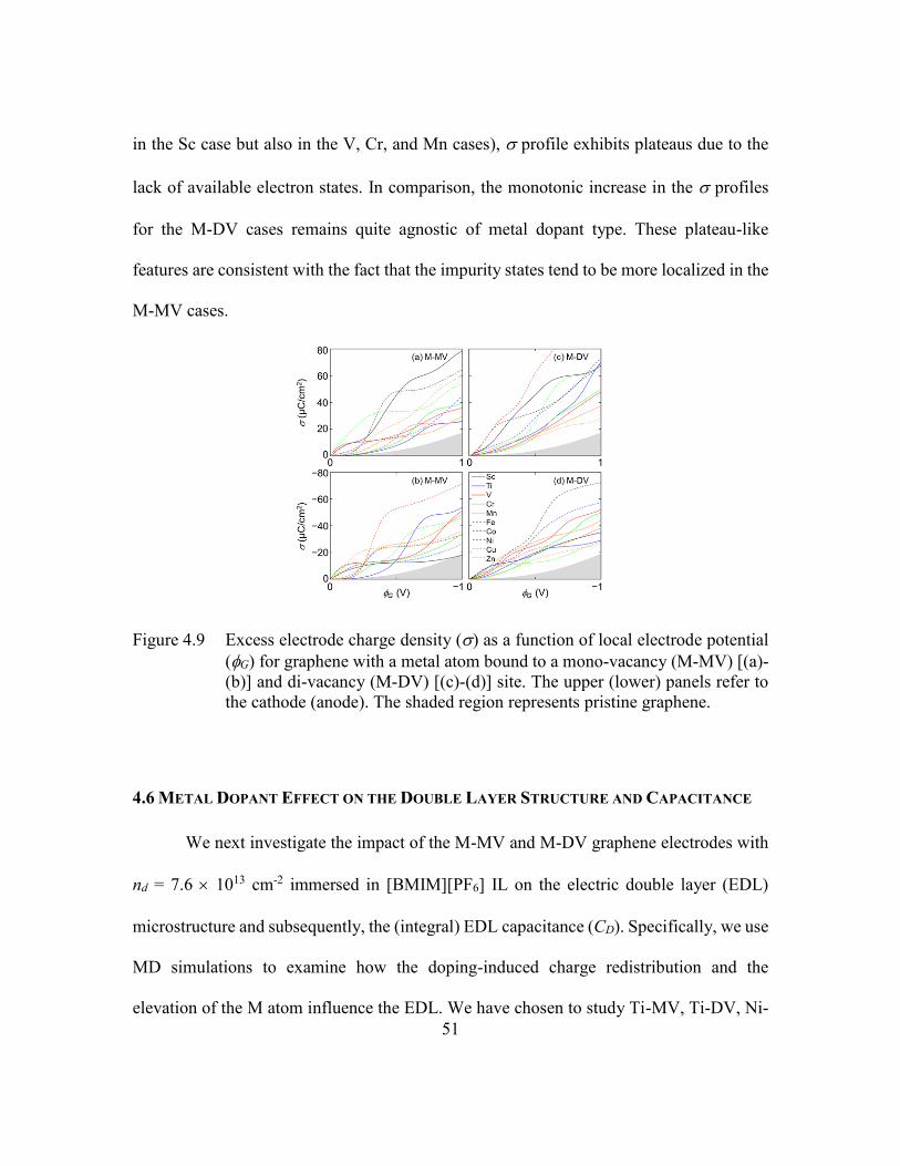
51
in the Sc case but also in the V, Cr, and Mn cases), profile exhibits plateaus due to the
lack of available electron states. In comparison, the monotonic increase in the profiles
for the M-DV cases remains quite agnostic of metal dopant type. These plateau-like
features are consistent with the fact that the impurity states tend to be more localized in the
M-MV cases.
Figure 4.9 Excess electrode charge density () as a function of local electrode potential
(G) for graphene with a metal atom bound to a mono-vacancy (M-MV) [(a)-
(b)] and di-vacancy (M-DV) [(c)-(d)] site. The upper (lower) panels refer to
the cathode (anode). The shaded region represents pristine graphene.
4.6 METAL DOPANT EFFECT ON THE DOUBLE LAYER STRUCTURE AND CAPACITANCE
We next investigate the impact of the M-MV and M-DV graphene electrodes with
nd = 7.6 1013 cm-2 immersed in [BMIM][PF6] IL on the electric double layer (EDL)
microstructure and subsequently, the (integral) EDL capacitance (CD). Specifically, we use
MD simulations to examine how the doping-induced charge redistribution and the
elevation of the M atom influence the EDL. We have chosen to study Ti-MV, Ti-DV, Ni-
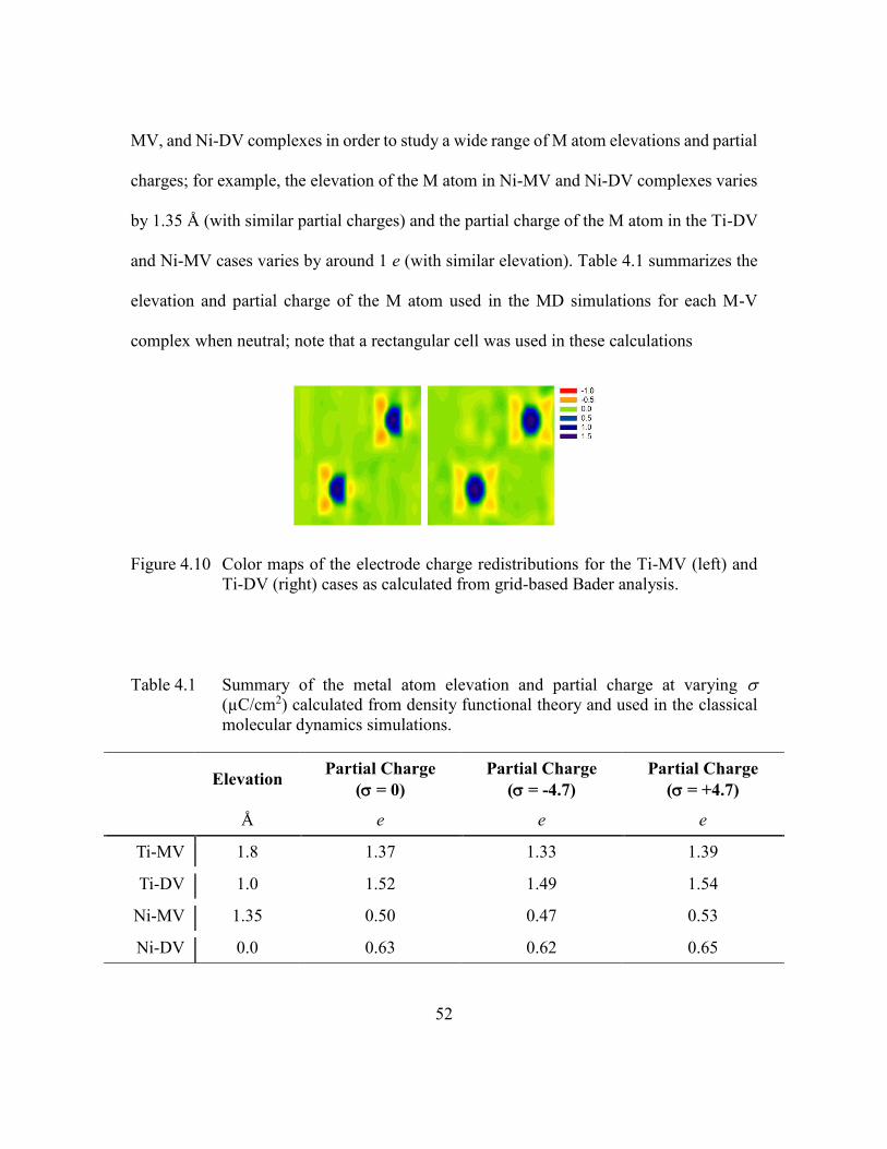
52
MV, and Ni-DV complexes in order to study a wide range of M atom elevations and partial
charges; for example, the elevation of the M atom in Ni-MV and Ni-DV complexes varies
by 1.35 Å (with similar partial charges) and the partial charge of the M atom in the Ti-DV
and Ni-MV cases varies by around 1 e (with similar elevation). Table 4.1 summarizes the
elevation and partial charge of the M atom used in the MD simulations for each M-V
complex when neutral; note that a rectangular cell was used in these calculations
Figure 4.10 Color maps of the electrode charge redistributions for the Ti-MV (left) and
Ti-DV (right) cases as calculated from grid-based Bader analysis.
Table 4.1 Summary of the metal atom elevation and partial charge at varying
(µC/cm2) calculated from density functional theory and used in the classical
molecular dynamics simulations.
Elevation Partial Charge
( = 0)
Partial Charge
( = -4.7)
Partial Charge
( = +4.7)
Å e e e
Ti-MV 1.8 1.37 1.33 1.39
Ti-DV 1.0 1.52 1.49 1.54
Ni-MV 1.35 0.50 0.47 0.53
Ni-DV 0.0 0.63 0.62 0.65
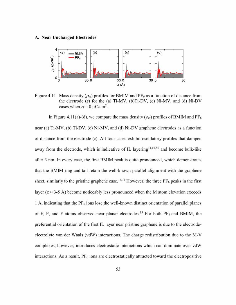
53
A. Near Uncharged Electrodes
Figure 4.11 Mass density (m) profiles for BMIM and PF6 as a function of distance from
the electrode (z) for the (a) Ti-MV, (b)Ti-DV, (c) Ni-MV, and (d) Ni-DV
cases when = 0 µC/cm2.
In Figure 4.11(a)-(d), we compare the mass density (m) profiles of BMIM and PF6
near (a) Ti-MV, (b) Ti-DV, (c) Ni-MV, and (d) Ni-DV graphene electrodes as a function
of distance from the electrode (z). All four cases exhibit oscillatory profiles that dampen
away from the electrode, which is indicative of IL layering14,15,85 and become bulk-like
after 3 nm. In every case, the first BMIM peak is quite pronounced, which demonstrates
that the BMIM ring and tail retain the well-known parallel alignment with the graphene
sheet, similarly to the pristine graphene case.13,14 However, the three PF6 peaks in the first
layer (z 3-5 Å) become noticeably less pronounced when the M atom elevation exceeds
1 Å, indicating that the PF6 ions lose the well-known distinct orientation of parallel planes
of F, P, and F atoms observed near planar electrodes.13 For both PF6 and BMIM, the
preferential orientation of the first IL layer near pristine graphene is due to the electrode-
electrolyte van der Waals (vdW) interactions. The charge redistribution due to the M-V
complexes, however, introduces electrostatic interactions which can dominate over vdW
interactions. As a result, PF6 ions are electrostatically attracted toward the electropositive
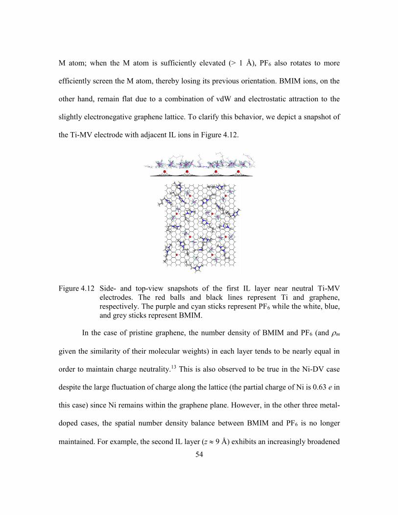
54
M atom; when the M atom is sufficiently elevated (> 1 Å), PF6 also rotates to more
efficiently screen the M atom, thereby losing its previous orientation. BMIM ions, on the
other hand, remain flat due to a combination of vdW and electrostatic attraction to the
slightly electronegative graphene lattice. To clarify this behavior, we depict a snapshot of
the Ti-MV electrode with adjacent IL ions in Figure 4.12.
Figure 4.12 Side- and top-view snapshots of the first IL layer near neutral Ti-MV
electrodes. The red balls and black lines represent Ti and graphene,
respectively. The purple and cyan sticks represent PF6 while the white, blue,
and grey sticks represent BMIM.
In the case of pristine graphene, the number density of BMIM and PF6 (and m
given the similarity of their molecular weights) in each layer tends to be nearly equal in
order to maintain charge neutrality.13 This is also observed to be true in the Ni-DV case
despite the large fluctuation of charge along the lattice (the partial charge of Ni is 0.63 e in
this case) since Ni remains within the graphene plane. However, in the other three metal-
doped cases, the spatial number density balance between BMIM and PF6 is no longer
maintained. For example, the second IL layer (z 9 Å) exhibits an increasingly broadened
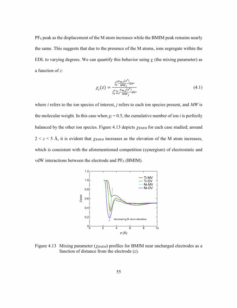
55
PF6 peak as the displacement of the M atom increases while the BMIM peak remains nearly
the same. This suggests that due to the presence of the M atoms, ions segregate within the
EDL to varying degrees. We can quantify this behavior using (the mixing parameter) as
a function of z:
𝑖(𝑧) =
∫𝜌𝑚,𝑖(𝑧′)
𝑀𝑊𝑖𝑑𝑧′
𝑧0
∫ ∑𝜌𝑚,𝑗(𝑧′)
𝑀𝑊𝑗𝑑𝑧′𝑗
𝑧0
(4.1)
where i refers to the ion species of interest, j refers to each ion species present, and MW is
the molecular weight. In this case when i = 0.5, the cumulative number of ion i is perfectly
balanced by the other ion species. Figure 4.13 depicts BMIM for each case studied; around
2 < z < 5 Å, it is evident that BMIM increases as the elevation of the M atom increases,
which is consistent with the aforementioned competition (synergism) of electrostatic and
vdW interactions between the electrode and PF6 (BMIM).
Figure 4.13 Mixing parameter (BMIM) profiles for BMIM near uncharged electrodes as a
function of distance from the electrode (z).

56
Figure 4.14 Potential () profiles as a function of distance from the electrode (z) for the
(a) Ti-MV, (b) Ti-DV, (c) Ni-MV, (d) Ni-DV cases when = 0 µC/cm2. The
dashed lines indicate the position of the vacuum-IL interface adjacent to the
electrode.
From the distribution of electrode and IL atoms with fixed atomic charges, we can
also compute the space charge variation and therefore, the spatial potential variation () by
solving Poisson’s equation (see Chapter 2). In Figure 4.14, we show as a function of z
for (a) Ti-MV, (b) Ti-DV, (c) Ni-MV, and (d) Ni-DV; the of the bulk electrolyte is taken
as reference ( = 0 V). To interpret the profiles, it is helpful to separately examine their
variation in the IL region and the near-electrode region between the electrode and first IL
layer. First, we study how the microstructure of the IL ions affects close to the electrode
(2 < z < 5 Å) as this is where discrepancies in the IL region between the different cases
noticeably appear. In accordance with an increasing degree of BMIM segregation (Ni-DV
< Ti-DV Ni-MV < Ti-MV cases), at the IL region interface (z 5 Å) also increases;
the accumulation of net positive charge close to the interface leads to a proportional
increase in . Between the electrode and the IL region interface, however, rapidly drops
if the M atom is elevated due to the local electric field generated from the charge
redistribution within the electrode; the extent of the drop in therefore increases as either
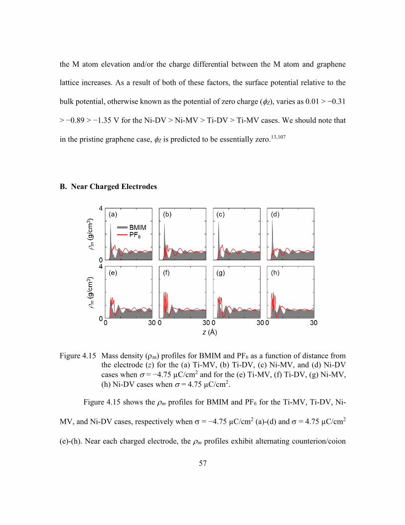
57
the M atom elevation and/or the charge differential between the M atom and graphene
lattice increases. As a result of both of these factors, the surface potential relative to the
bulk potential, otherwise known as the potential of zero charge (Z), varies as 0.01 > −0.31
> −0.89 > −1.35 V for the Ni-DV > Ni-MV > Ti-DV > Ti-MV cases. We should note that
in the pristine graphene case, Z is predicted to be essentially zero.13,107
B. Near Charged Electrodes
Figure 4.15 Mass density (m) profiles for BMIM and PF6 as a function of distance from
the electrode (z) for the (a) Ti-MV, (b) Ti-DV, (c) Ni-MV, and (d) Ni-DV
cases when = −4.75 µC/cm2 and for the (e) Ti-MV, (f) Ti-DV, (g) Ni-MV,
(h) Ni-DV cases when = 4.75 µC/cm2.
Figure 4.15 shows the m profiles for BMIM and PF6 for the Ti-MV, Ti-DV, Ni-
MV, and Ni-DV cases, respectively when = −4.75 µC/cm2 (a)-(d) and = 4.75 µC/cm2
(e)-(h). Near each charged electrode, the m profiles exhibit alternating counterion/coion
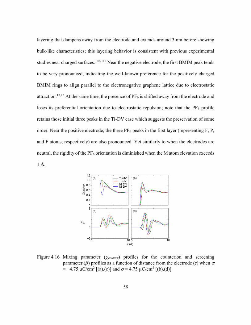
58
layering that dampens away from the electrode and extends around 3 nm before showing
bulk-like characteristics; this layering behavior is consistent with previous experimental
studies near charged surfaces.108-110 Near the negative electrode, the first BMIM peak tends
to be very pronounced, indicating the well-known preference for the positively charged
BMIM rings to align parallel to the electronegative graphene lattice due to electrostatic
attraction.13,15 At the same time, the presence of PF6 is shifted away from the electrode and
loses its preferential orientation due to electrostatic repulsion; note that the PF6 profile
retains those initial three peaks in the Ti-DV case which suggests the preservation of some
order. Near the positive electrode, the three PF6 peaks in the first layer (representing F, P,
and F atoms, respectively) are also pronounced. Yet similarly to when the electrodes are
neutral, the rigidity of the PF6 orientation is diminished when the M atom elevation exceeds
1 Å.
Figure 4.16 Mixing parameter (counter) profiles for the counterion and screening
parameter () profiles as a function of distance from the electrode (z) when
= −4.75 µC/cm2 [(a),(c)] and = 4.75 µC/cm2 [(b),(d)].
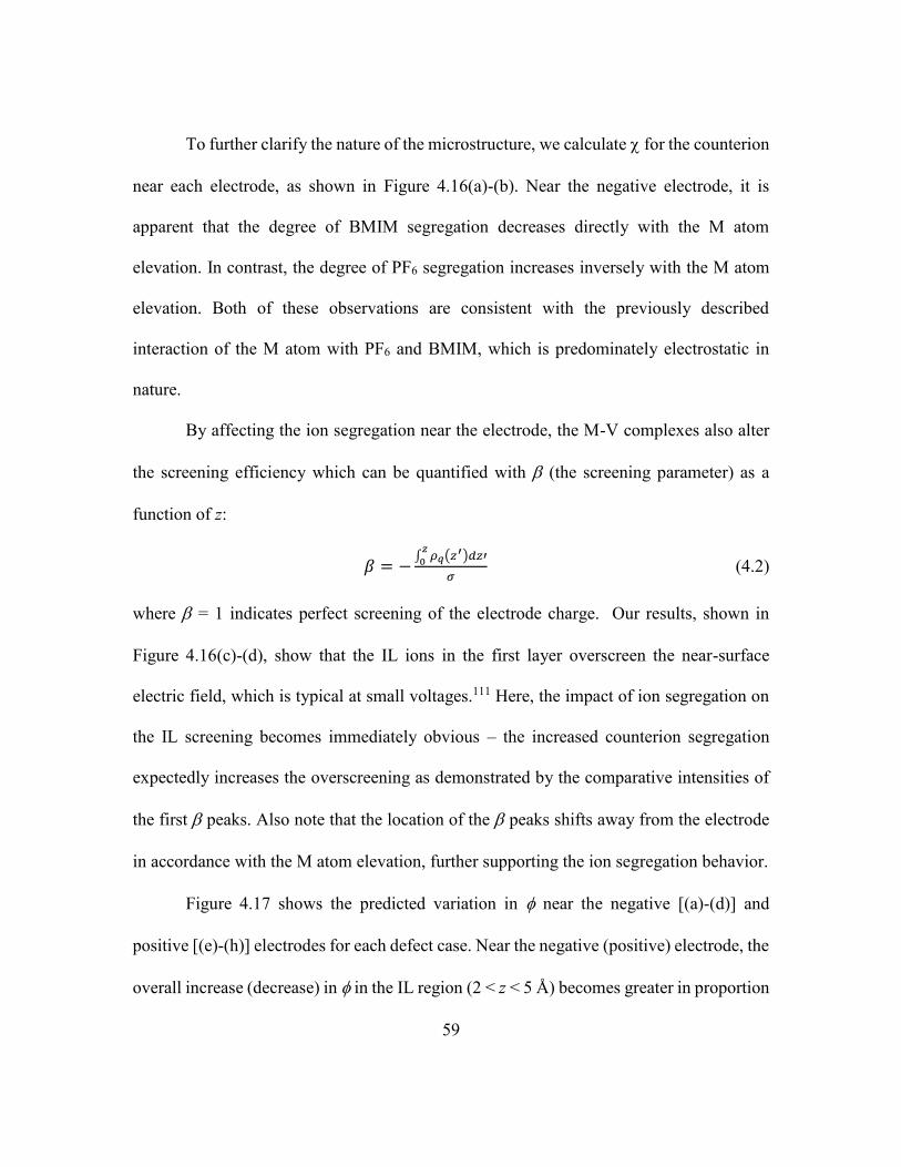
59
To further clarify the nature of the microstructure, we calculate for the counterion
near each electrode, as shown in Figure 4.16(a)-(b). Near the negative electrode, it is
apparent that the degree of BMIM segregation decreases directly with the M atom
elevation. In contrast, the degree of PF6 segregation increases inversely with the M atom
elevation. Both of these observations are consistent with the previously described
interaction of the M atom with PF6 and BMIM, which is predominately electrostatic in
nature.
By affecting the ion segregation near the electrode, the M-V complexes also alter
the screening efficiency which can be quantified with (the screening parameter) as a
function of z:
𝛽 = −∫ 𝜌𝑞(𝑧′)𝑑𝑧′
𝑧0
𝜎 (4.2)
where = 1 indicates perfect screening of the electrode charge. Our results, shown in
Figure 4.16(c)-(d), show that the IL ions in the first layer overscreen the near-surface
electric field, which is typical at small voltages.111 Here, the impact of ion segregation on
the IL screening becomes immediately obvious – the increased counterion segregation
expectedly increases the overscreening as demonstrated by the comparative intensities of
the first peaks. Also note that the location of the peaks shifts away from the electrode
in accordance with the M atom elevation, further supporting the ion segregation behavior.
Figure 4.17 shows the predicted variation in near the negative [(a)-(d)] and
positive [(e)-(h)] electrodes for each defect case. Near the negative (positive) electrode, the
overall increase (decrease) in in the IL region (2 < z < 5 Å) becomes greater in proportion
60
to the degree of counterion segregation (or by analogy, the extent of overscreening). From
the IL region interface to the electrode surface, expectedly drops (rises) near the negative
(positive) electrode due to the applied electric field. Here, is further influenced if the M
atom is elevated due to the local electric field generated from the charge redistribution of
the electrode. As the M atom elevation and/or partial charge increases, the drop (rise) in
is enhanced (mitigated) near the negative (positive) electrode.
Figure 4.17 Potential () profiles as a function of distance from the electrode (z) when the
= −4.75 µC/cm2 for (a) Ti-MV, (b) Ti-DV, (c) Ni-MV, and (d) Ni-DV and
when = 4.75 µC/cm2 for (e) Ti-MV, (f) Ti-DV, (g) Ni-MV, and (h) Ni-DV.
The dashed line indicates the position of the vacuum-IL interface adjacent to
the electrode.
From the predicted electrode surface potentials relative to the bulk potential (D),
we calculate the overall change in potential as the difference between D and Z. We can
therefore evaluate the (integral) double layer capacitances CD = /(D-Z), which we extend
to include = 2.38 and 9.5 µC/cm2, and compare them in Figure 4.18. Although Z
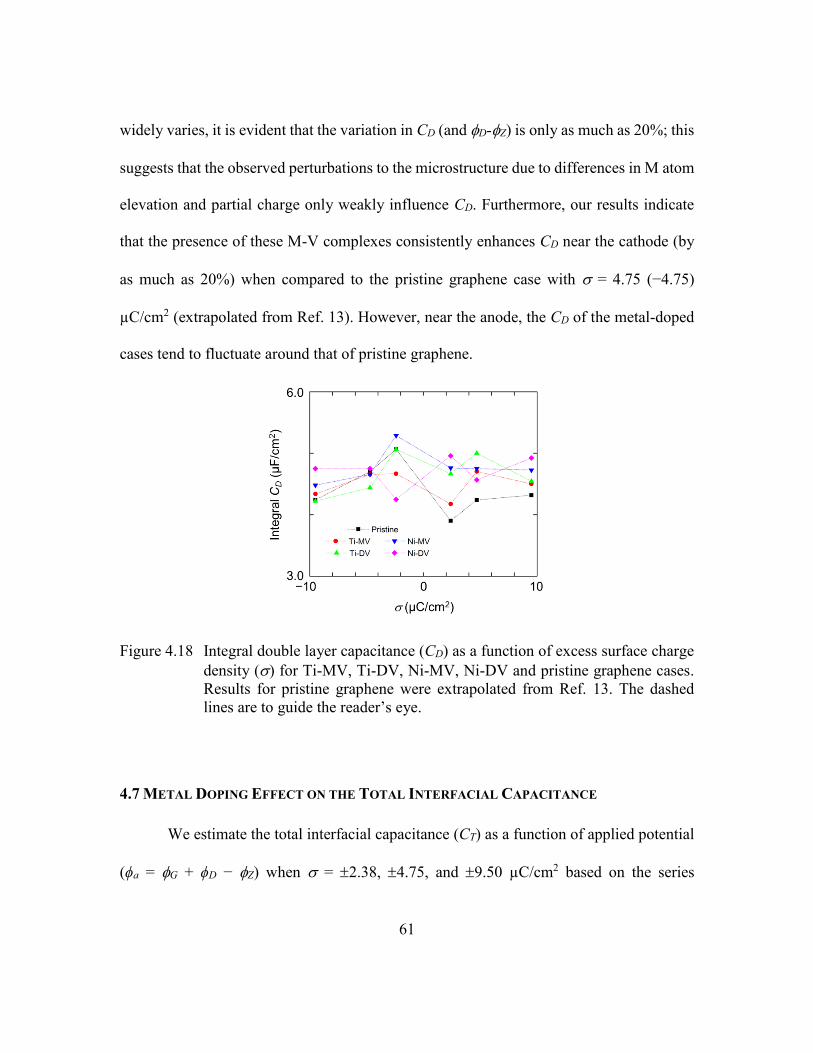
61
widely varies, it is evident that the variation in CD (and D-Z) is only as much as 20%; this
suggests that the observed perturbations to the microstructure due to differences in M atom
elevation and partial charge only weakly influence CD. Furthermore, our results indicate
that the presence of these M-V complexes consistently enhances CD near the cathode (by
as much as 20%) when compared to the pristine graphene case with = 4.75 (−4.75)
µC/cm2 (extrapolated from Ref. 13). However, near the anode, the CD of the metal-doped
cases tend to fluctuate around that of pristine graphene.
Figure 4.18 Integral double layer capacitance (CD) as a function of excess surface charge
density () for Ti-MV, Ti-DV, Ni-MV, Ni-DV and pristine graphene cases.
Results for pristine graphene were extrapolated from Ref. 13. The dashed
lines are to guide the reader’s eye.
4.7 METAL DOPING EFFECT ON THE TOTAL INTERFACIAL CAPACITANCE
We estimate the total interfacial capacitance (CT) as a function of applied potential
(ϕa = G + ϕD − Z) when = 2.38, 4.75, and 9.50 µC/cm2 based on the series
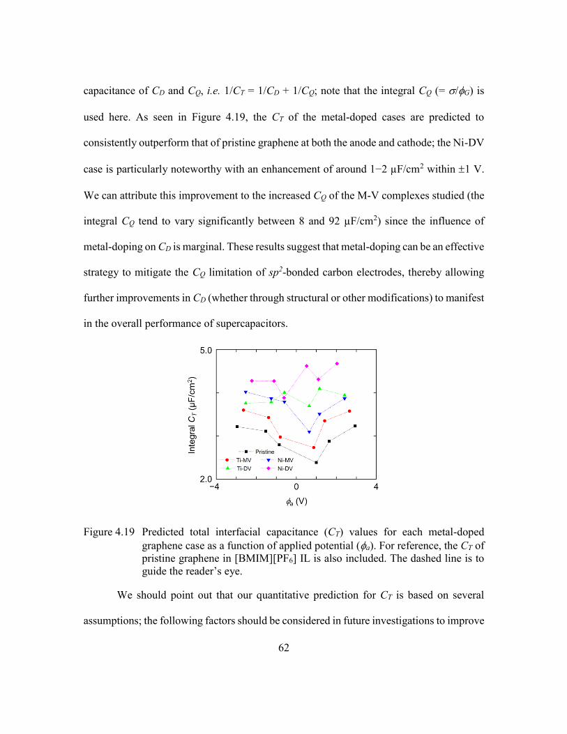
62
capacitance of CD and CQ, i.e. 1/CT = 1/CD + 1/CQ; note that the integral CQ (= /G) is
used here. As seen in Figure 4.19, the CT of the metal-doped cases are predicted to
consistently outperform that of pristine graphene at both the anode and cathode; the Ni-DV
case is particularly noteworthy with an enhancement of around 1−2 µF/cm2 within 1 V.
We can attribute this improvement to the increased CQ of the M-V complexes studied (the
integral CQ tend to vary significantly between 8 and 92 µF/cm2) since the influence of
metal-doping on CD is marginal. These results suggest that metal-doping can be an effective
strategy to mitigate the CQ limitation of sp2-bonded carbon electrodes, thereby allowing
further improvements in CD (whether through structural or other modifications) to manifest
in the overall performance of supercapacitors.
Figure 4.19 Predicted total interfacial capacitance (CT) values for each metal-doped
graphene case as a function of applied potential (a). For reference, the CT of
pristine graphene in [BMIM][PF6] IL is also included. The dashed line is to
guide the reader’s eye.
We should point out that our quantitative prediction for CT is based on several
assumptions; the following factors should be considered in future investigations to improve
63
accuracy. For instance, we have ignored the possible polarization at the electrode-
electrolyte interface, which can affect the electrode charge redistribution, the EDL
microstructure, and ultimately, CD (which is likely underestimated).87,88 In addition, we
recognize that conventional DFT can introduce self-interaction errors; the resultant
erroneous description of charge localization can be mitigated using hybrid functional
methods.112 We also omit the possible influence of IL interactions with the electrode on its
electronic structure, which may alter CQ to a certain extent. Nonetheless, our study clearly
shows that the inclusion of M impurities in sp2-bonded carbon nanomaterials can
significantly enhance EDLC performance primarily by dramatically improving CQ.
4.8 CONCLUSIONS
We examined the influence of metal-doped graphene in [BMIM][PF6] ionic liquid
on the electrode and electric double layer (EDL) capacitances using a combination of DFT
and classical MD simulations. We considered 3d transition metals (M) bound to mono-
(MV) and di- (DV) vacancy sites in graphene. Our electronic structure analysis
demonstrated that the introduction of these M-V complexes induces quasi-localized states.
From the predicted electronic density of states, we evaluated the quantum capacitance (CQ)
of each M-doped electrode and compared them to pristine graphene. Due to the augmented
availability of states, the charge storage capacities of each M-doped electrode were
generally found to exceed that of pristine graphene, and in some cases, by as much as 500%
(at a local potential of 1 V). We also studied the influence of these M-V complexes on the
64
EDL microstructure using a few selected cases as model systems. We found that the
microstructure can be perturbed; in particular, PF6 (BMIM) ions can accumulate near
(spread away from) the M atom. When the electrodes are charged, counterion segregation
becomes more (less) apparent near the cathode (anode) as the M atom elevation increases.
Despite these perturbations to the EDL, the estimated double layer capacitance (CD) was
found to be mostly within 20% of the pristine graphene case (while the potential of zero
charge was predicted to vary on the order of 1 V depending on the type of M-V complex).
Based on CQ and CD, we evaluated the total interfacial capacitances (CT = [1/CD + 1/CQ]-1)
and found that the M-doped cases were consistently enhanced by as much as 125% (within
1 V) when compared to pristine graphene. Our study clearly demonstrates that M-doping
of graphene-like electrodes can effectively mitigate the CQ limitation, thereby significantly
enhancing EDLC performance.
65
Chapter 5: Extended Edge Defects
Work in this chapter was published and reprinted with permission from J. Phys. Chem. C,
Vol. 118, A. J. Pak, E. Paek, and G. S. Hwang, Impact of Graphene Edges on Enhancing
the Performance of Electrochemical Double Layer Capacitors, pg. 21770−7. Copyright
(2014) American Chemical Society.
5.1 INTRODUCTION TO EDGE DEFECTS IN GRAPHENE
Up to this point, the scope of this dissertation has been limited to phenomena near
the basal plane of graphene where ion accumulation mostly occurs. But given the revealed
sensitivity of CT to CQ and CD, it would be valuable to explore similar phenomena near the
edges of graphene for several reasons. First, it is well-known that the presence of edges can
alter the electronic structure of graphene, which has been successfully utilized in many
electrochemical applications.113-115 Such modifications to the electronic structure may
subsequently affect CQ. It is also possible that the electric double layer (EDL)
microstructure, and therefore CD, can be noticeably perturbed near the edge sites, similarly
to the case of prismatic graphite electrodes with different degrees of corrugation.86
Furthermore, research into potential applications for graphene edges seems timely given
recent advances in the fabrication of high-quality graphene edges.116 One example of this
is a recent demonstration by Zhang and coworkers in which the splitting of vertically
aligned carbon nanotubes into graphene nanoribbons exhibited a four-fold increase in
specific capacitance.117 However to the best of our knowledge, a fundamental study on the
impact of edge defects on both CQ and CD has never been reported.
66
In this chapter, the effect of edge defects on CT is investigated using edge-
passivated graphene nanoribbons (GNRs) as model systems; only zigzag GNRs (ZGNRs)
are considered since they can be metallic while armchair GNRs are neglected as they are
always semiconducting. The relative impacts of these edge defects on CQ and CD are
studied using a first principles-based computational approach. First, density functional
theory (DFT) is employed to study the electronic structure and CQ of two types of edge-
passivated ZGNRs at varying widths. Using classical molecular dynamics (MD), the
microstructure and CD of a ZGNR immersed in [BMIM][PF6] ionic liquid is investigated.
Finally, the potential benefit of edge defects with regard to the overall CT is discussed.
5.2 COMPUTATIONAL METHODS
The atomic and electronic structures of each investigated ZGNR were calculated
using DFT within the spin-polarized Perdew-Wang 91 generalized gradient
approximation68 (GGA-PW91), as implemented in the Vienna Ab initio Simulation
Package42 (VASP); the Vosko-Wilk-Nusair interpolation was used for the correlation part
of the exchange correlation functional.118 The projector augmented wave (PAW) method69
was used to describe the interaction between ion core and valence electrons with a
planewave basis set using a kinetic energy cutoff of 400 eV.
Two different types of edge-passivated ZGNRs at two different widths are initially
investigated: (i) single hydrogen (H) termination (herein called H-18ZGNR and H-
60ZGNR) and (ii) alternating termination by a hydroxyl (OH) and single H (herein called

67
OH-18ZGNR and OH-60ZGNR). The OH group is considered one of the most stable
oxidation groups and is known to prefer a parallel orientation with respect to the plane of
the GNR.119,120 The ZGNRs were modeled using rectangular 2 9 (as shown in Figure 5.1)
and 2 30 supercells (corresponding to 72 and 240 C atoms, respectively) with a GGA-
optimized lattice constant of 2.466 Å. Periodic boundary conditions were employed in all
three directions but vacuum spaces of 10 and 20 Å were included in the z and y directions,
respectively, to remove interactions with adjacent images. For the Brillouin zone
integration, a (6×1×1) Monkhorst-Pack mesh70 of k-points was used to determine the
optimal geometries and total energies while an increased mesh size of (14×1×1) was used
for electronic structure calculations. To make comparisons to the pristine graphene case,
similar electronic structure calculations were performed using a 4-atom rectangular cell
with dimensions of 4.272 2.466 Å2; here, a (21×21×1) k-point mesh was used for
Brillouin zone sampling.
To study the atomic charge distribution of ZGNRs at different widths, additional
rectangular 2 5 and 2 13 supercells for both H-ZGNR and OH-ZGNR cases using the
same lattice constant, vacuum spacing, and k-point mesh were modeled. The atomic
charges were evaluated using grid-based Bader analysis61 under neutral and charged (1 e
per supercell) conditions; the latter case was used to study the excess charge redistribution.
The calculated Bader charges for OH-18ZGNR were subsequently used in the MD
calculations.
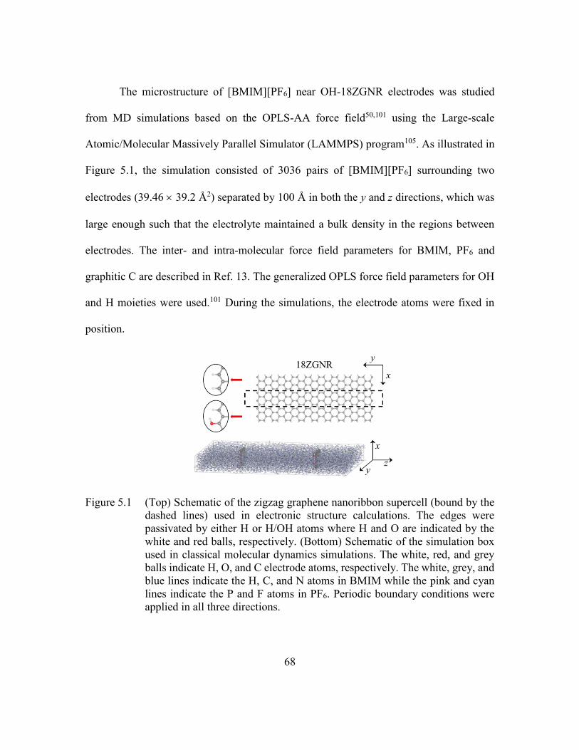
68
The microstructure of [BMIM][PF6] near OH-18ZGNR electrodes was studied
from MD simulations based on the OPLS-AA force field50,101 using the Large-scale
Atomic/Molecular Massively Parallel Simulator (LAMMPS) program105. As illustrated in
Figure 5.1, the simulation consisted of 3036 pairs of [BMIM][PF6] surrounding two
electrodes (39.46 39.2 Å2) separated by 100 Å in both the y and z directions, which was
large enough such that the electrolyte maintained a bulk density in the regions between
electrodes. The inter- and intra-molecular force field parameters for BMIM, PF6 and
graphitic C are described in Ref. 13. The generalized OPLS force field parameters for OH
and H moieties were used.101 During the simulations, the electrode atoms were fixed in
position.
Figure 5.1 (Top) Schematic of the zigzag graphene nanoribbon supercell (bound by the
dashed lines) used in electronic structure calculations. The edges were
passivated by either H or H/OH atoms where H and O are indicated by the
white and red balls, respectively. (Bottom) Schematic of the simulation box
used in classical molecular dynamics simulations. The white, red, and grey
balls indicate H, O, and C electrode atoms, respectively. The white, grey, and
blue lines indicate the H, C, and N atoms in BMIM while the pink and cyan
lines indicate the P and F atoms in PF6. Periodic boundary conditions were
applied in all three directions.
69
Electrodes with excess surface charge density = 0, 80.4 and −80.4 C g-1 were
studied using the predicted atomic charges from Bader analysis. Each MD simulation were
run initially at 1000 K for 1 ns followed by 1 ns at 300 K for three cycles to equilibrate the
system using a timestep of 1 fs. Production runs were carried out for 2 ns with atomic
positions recorded every 5 ps. All runs were in the NVT ensemble with the temperature
controlled by a Nose-Hoover thermostat60 with a 100 fs damping parameter. MD results
reported herein were obtained from the average of five independent simulations with
different initial atomic configurations. Further details about the MD simulations are
described in Ref. 13.
5.3 GRAPHENE NANORIBBON ELECTRONIC STRUCTURE AND QUANTUM CAPACITANCE
In this section, we present the band structures and density of states (DOS) of the
investigated ZGNRs, considering both the anti-ferromagnetic (AF) and ferromagnetic
(FM) spin states. Based on the electronic structure, we then predict and analyze the
quantum capacitance (CQ) of the ZGNRs.
Figure 5.2(a) shows the DOS for H-18ZGNR [left] and H-60ZGNR [right] in the
AF state (the insets show the FM state). According to our GGA-PW91 calculations for H-
18ZGNR, the AF state is marginally more stable ( 0.6 meV Å-1) than the FM state; other
functionals including LDA ( 0.2 meV Å-1) and GGA-PBE ( 1.0 meV Å-1) predict similar
results. In the AF case, a band gap of 0.3 eV is estimated to arise due to the differences in
AF exchange interaction between sublattices.120-122 In the FM case, the spin-majority and
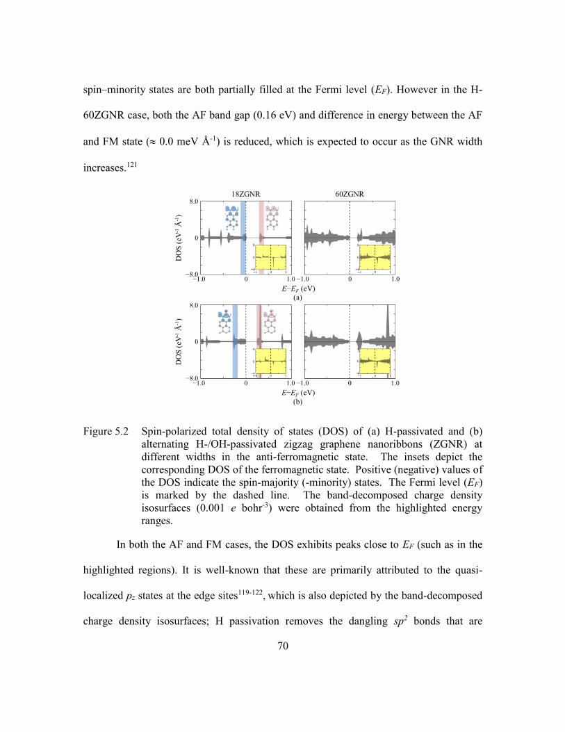
70
spin–minority states are both partially filled at the Fermi level (EF). However in the H-
60ZGNR case, both the AF band gap (0.16 eV) and difference in energy between the AF
and FM state ( 0.0 meV Å-1) is reduced, which is expected to occur as the GNR width
increases.121
Figure 5.2 Spin-polarized total density of states (DOS) of (a) H-passivated and (b)
alternating H-/OH-passivated zigzag graphene nanoribbons (ZGNR) at
different widths in the anti-ferromagnetic state. The insets depict the
corresponding DOS of the ferromagnetic state. Positive (negative) values of
the DOS indicate the spin-majority (-minority) states. The Fermi level (EF)
is marked by the dashed line. The band-decomposed charge density
isosurfaces (0.001 e bohr-3) were obtained from the highlighted energy
ranges.
In both the AF and FM cases, the DOS exhibits peaks close to EF (such as in the
highlighted regions). It is well-known that these are primarily attributed to the quasi-
localized pz states at the edge sites119-122, which is also depicted by the band-decomposed
charge density isosurfaces; H passivation removes the dangling sp2 bonds that are
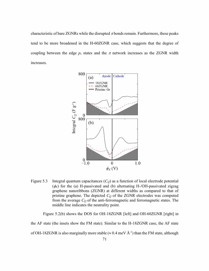
71
characteristic of bare ZGNRs while the disrupted bonds remain. Furthermore, these peaks
tend to be more broadened in the H-60ZGNR case, which suggests that the degree of
coupling between the edge pz states and the network increases as the ZGNR width
increases.
Figure 5.3 Integral quantum capacitances (CQ) as a function of local electrode potential
(E) for the (a) H-passivated and (b) alternating H-/OH-passivated zigzag
graphene nanoribbons (ZGNR) at different widths as compared to that of
pristine graphene. The depicted CQ of the ZGNR electrodes was computed
from the average CQ of the anti-ferromagnetic and ferromagnetic states. The
middle line indicates the neutrality point.
Figure 5.2(b) shows the DOS for OH-18ZGNR [left] and OH-60ZGNR [right] in
the AF state (the insets show the FM state). Similar to the H-18ZGNR case, the AF state
of OH-18ZGNR is also marginally more stable ( 0.4 meV Å-1) than the FM state, although
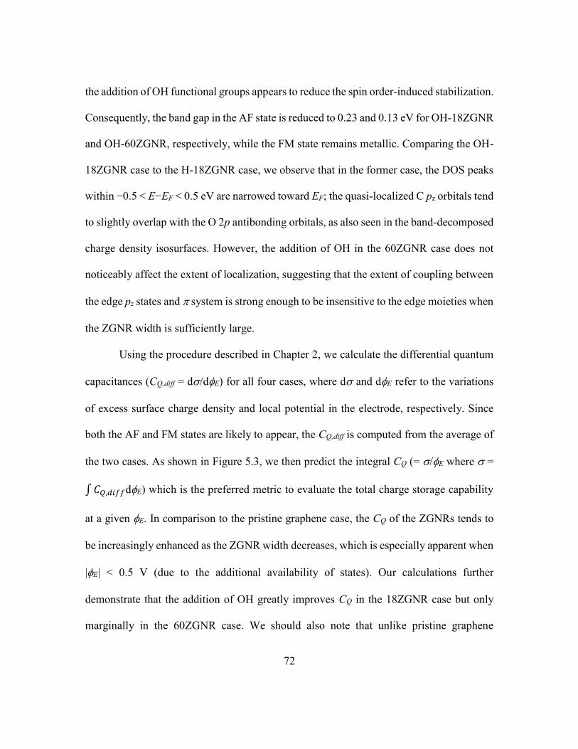
72
the addition of OH functional groups appears to reduce the spin order-induced stabilization.
Consequently, the band gap in the AF state is reduced to 0.23 and 0.13 eV for OH-18ZGNR
and OH-60ZGNR, respectively, while the FM state remains metallic. Comparing the OH-
18ZGNR case to the H-18ZGNR case, we observe that in the former case, the DOS peaks
within −0.5 < E−EF < 0.5 eV are narrowed toward EF; the quasi-localized C pz orbitals tend
to slightly overlap with the O 2p antibonding orbitals, as also seen in the band-decomposed
charge density isosurfaces. However, the addition of OH in the 60ZGNR case does not
noticeably affect the extent of localization, suggesting that the extent of coupling between
the edge pz states and system is strong enough to be insensitive to the edge moieties when
the ZGNR width is sufficiently large.
Using the procedure described in Chapter 2, we calculate the differential quantum
capacitances (CQ,diff = d/dE) for all four cases, where d and dE refer to the variations
of excess surface charge density and local potential in the electrode, respectively. Since
both the AF and FM states are likely to appear, the CQ,diff is computed from the average of
the two cases. As shown in Figure 5.3, we then predict the integral CQ (= /E where =
∫ 𝐶𝑄,𝑑𝑖𝑓𝑓dE) which is the preferred metric to evaluate the total charge storage capability
at a given E. In comparison to the pristine graphene case, the CQ of the ZGNRs tends to
be increasingly enhanced as the ZGNR width decreases, which is especially apparent when
|E| < 0.5 V (due to the additional availability of states). Our calculations further
demonstrate that the addition of OH greatly improves CQ in the 18ZGNR case but only
marginally in the 60ZGNR case. We should also note that unlike pristine graphene
73
electrodes, the ZGNR electrodes have intrinsically different CQ profiles at the anode and
cathode.
Figure 5.4 Estimated (a) partial charges of edge-passivating groups and (b) degree of
excess charge accumulation at the edges of zigzag graphene nanoribbons
(ZGNR) with varying width and edge-passivation. The partial charges were
computed from grid-based Bader analysis. The excess charge accumulation
was calculated from the fractional amount of excess charge found at the edges
(defined by the shaded region) after one charge carrier was injected into each
ZGNR.
Beyond the CQ, we also explore the local charge redistribution at the edges of
ZGNRs at varying widths; the charge redistribution is particularly important as it can affect
the electrostatic interactions at the electrode-electrolyte interface. To quantify this
behavior, we use grid-based Bader analysis to compute the atomic charges.61 In Figure
5.4(a), we first present the atomic charges of the edge-passivating moieties of both H- and
OH-ZGNRs. Here, the H and OH groups are expectedly positively and negatively charged,
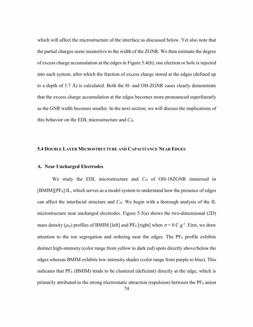
74
which will affect the microstructure of the interface as discussed below. Yet also note that
the partial charges seem insensitive to the width of the ZGNR. We then estimate the degree
of excess charge accumulation at the edges in Figure 5.4(b); one electron or hole is injected
into each system, after which the fraction of excess charge stored at the edges (defined up
to a depth of 3.7 Å) is calculated. Both the H- and OH-ZGNR cases clearly demonstrate
that the excess charge accumulation at the edges becomes more pronounced superlinearly
as the GNR width becomes smaller. In the next section, we will discuss the implications of
this behavior on the EDL microstructure and CD.
5.4 DOUBLE LAYER MICROSTRUCTURE AND CAPACITANCE NEAR EDGES
A. Near Uncharged Electrodes
We study the EDL microstructure and CD of OH-18ZGNR immersed in
[BMIM][PF6] IL, which serves as a model system to understand how the presence of edges
can affect the interfacial structure and CD. We begin with a thorough analysis of the IL
microstructure near uncharged electrodes. Figure 5.5(a) shows the two-dimensional (2D)
mass density (m) profiles of BMIM [left] and PF6 [right] when = 0 C g-1. First, we draw
attention to the ion segregation and ordering near the edges. The PF6 profile exhibits
distinct high-intensity (color range from yellow to dark red) spots directly above/below the
edges whereas BMIM exhibits low-intensity shades (color range from purple to blue). This
indicates that PF6 (BMIM) tends to be clustered (deficient) directly at the edge, which is
primarily attributed to the strong electrostatic attraction (repulsion) between the PF6 anion
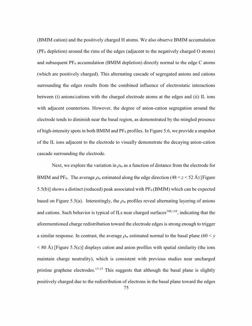
75
(BMIM cation) and the positively charged H atoms. We also observe BMIM accumulation
(PF6 depletion) around the rims of the edges (adjacent to the negatively charged O atoms)
and subsequent PF6 accumulation (BMIM depletion) directly normal to the edge C atoms
(which are positively charged). This alternating cascade of segregated anions and cations
surrounding the edges results from the combined influence of electrostatic interactions
between (i) anions/cations with the charged electrode atoms at the edges and (ii) IL ions
with adjacent counterions. However, the degree of anion-cation segregation around the
electrode tends to diminish near the basal region, as demonstrated by the mingled presence
of high-intensity spots in both BMIM and PF6 profiles. In Figure 5.6, we provide a snapshot
of the IL ions adjacent to the electrode to visually demonstrate the decaying anion-cation
cascade surrounding the electrode.
Next, we explore the variation in m as a function of distance from the electrode for
BMIM and PF6. The average m estimated along the edge direction (48 < z < 52 Å) [Figure
5.5(b)] shows a distinct (reduced) peak associated with PF6 (BMIM) which can be expected
based on Figure 5.5(a). Interestingly, the m profiles reveal alternating layering of anions
and cations. Such behavior is typical of ILs near charged surfaces108,110, indicating that the
aforementioned charge redistribution toward the electrode edges is strong enough to trigger
a similar response. In contrast, the average m estimated normal to the basal plane (60 < y
< 80 Å) [Figure 5.5(c)] displays cation and anion profiles with spatial similarity (the ions
maintain charge neutrality), which is consistent with previous studies near uncharged
pristine graphene electrodes.13-15 This suggests that although the basal plane is slightly
positively charged due to the redistribution of electrons in the basal plane toward the edges
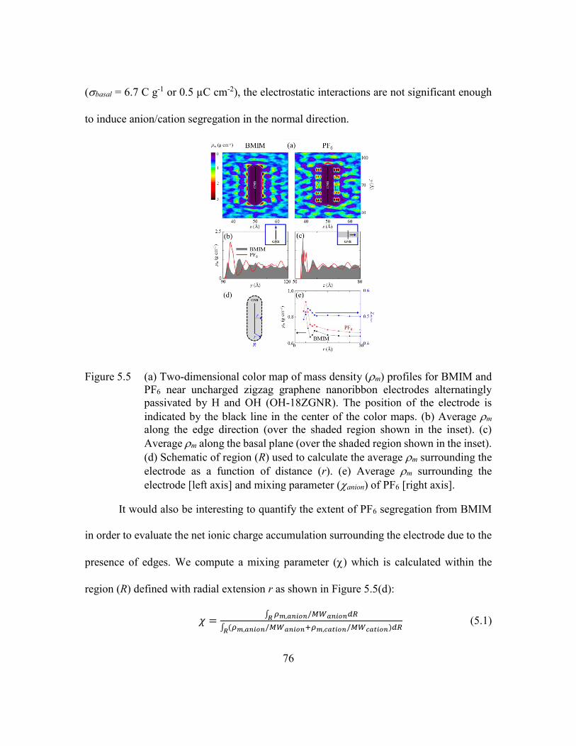
76
(basal = 6.7 C g-1 or 0.5 µC cm-2), the electrostatic interactions are not significant enough
to induce anion/cation segregation in the normal direction.
Figure 5.5 (a) Two-dimensional color map of mass density (m) profiles for BMIM and
PF6 near uncharged zigzag graphene nanoribbon electrodes alternatingly
passivated by H and OH (OH-18ZGNR). The position of the electrode is
indicated by the black line in the center of the color maps. (b) Average m
along the edge direction (over the shaded region shown in the inset). (c)
Average m along the basal plane (over the shaded region shown in the inset).
(d) Schematic of region (R) used to calculate the average m surrounding the
electrode as a function of distance (r). (e) Average m surrounding the
electrode [left axis] and mixing parameter (anion) of PF6 [right axis].
It would also be interesting to quantify the extent of PF6 segregation from BMIM
in order to evaluate the net ionic charge accumulation surrounding the electrode due to the
presence of edges. We compute a mixing parameter () which is calculated within the
region (R) defined with radial extension r as shown in Figure 5.5(d):
𝜒 =∫ 𝜌𝑚,𝑎𝑛𝑖𝑜𝑛/𝑀𝑊𝑎𝑛𝑖𝑜𝑛𝑑𝑅𝑅
∫ (𝜌𝑚,𝑎𝑛𝑖𝑜𝑛/𝑀𝑊𝑎𝑛𝑖𝑜𝑛+𝜌𝑚,𝑐𝑎𝑡𝑖𝑜𝑛/𝑀𝑊𝑐𝑎𝑡𝑖𝑜𝑛)𝑑𝑅𝑅
(5.1)
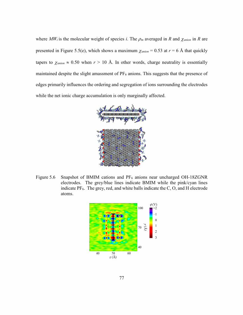
77
where MWi is the molecular weight of species i. The m averaged in R and anion in R are
presented in Figure 5.5(e), which shows a maximum anion = 0.53 at r = 6 Å that quickly
tapers to anion 0.50 when r > 10 Å. In other words, charge neutrality is essentially
maintained despite the slight amassment of PF6 anions. This suggests that the presence of
edges primarily influences the ordering and segregation of ions surrounding the electrodes
while the net ionic charge accumulation is only marginally affected.
Figure 5.6 Snapshot of BMIM cations and PF6 anions near uncharged OH-18ZGNR
electrodes. The grey/blue lines indicate BMIM while the pink/cyan lines
indicate PF6. The grey, red, and white balls indicate the C, O, and H electrode
atoms.
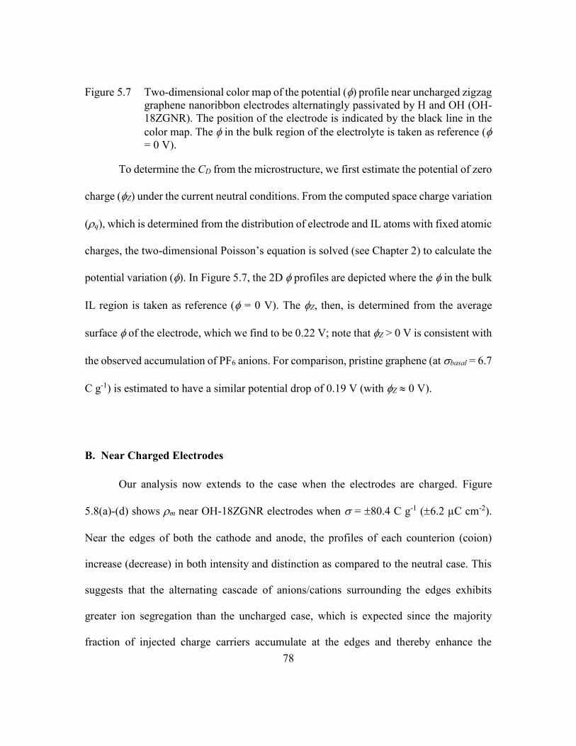
78
Figure 5.7 Two-dimensional color map of the potential () profile near uncharged zigzag
graphene nanoribbon electrodes alternatingly passivated by H and OH (OH-
18ZGNR). The position of the electrode is indicated by the black line in the
color map. The in the bulk region of the electrolyte is taken as reference (
= 0 V).
To determine the CD from the microstructure, we first estimate the potential of zero
charge (Z) under the current neutral conditions. From the computed space charge variation
(q), which is determined from the distribution of electrode and IL atoms with fixed atomic
charges, the two-dimensional Poisson’s equation is solved (see Chapter 2) to calculate the
potential variation (). In Figure 5.7, the 2D profiles are depicted where the in the bulk
IL region is taken as reference ( = 0 V). The Z, then, is determined from the average
surface of the electrode, which we find to be 0.22 V; note that Z > 0 V is consistent with
the observed accumulation of PF6 anions. For comparison, pristine graphene (at basal = 6.7
C g-1) is estimated to have a similar potential drop of 0.19 V (with Z 0 V).
B. Near Charged Electrodes
Our analysis now extends to the case when the electrodes are charged. Figure
5.8(a)-(d) shows m near OH-18ZGNR electrodes when = 80.4 C g-1 (6.2 µC cm-2).
Near the edges of both the cathode and anode, the profiles of each counterion (coion)
increase (decrease) in both intensity and distinction as compared to the neutral case. This
suggests that the alternating cascade of anions/cations surrounding the edges exhibits
greater ion segregation than the uncharged case, which is expected since the majority
fraction of injected charge carriers accumulate at the edges and thereby enhance the
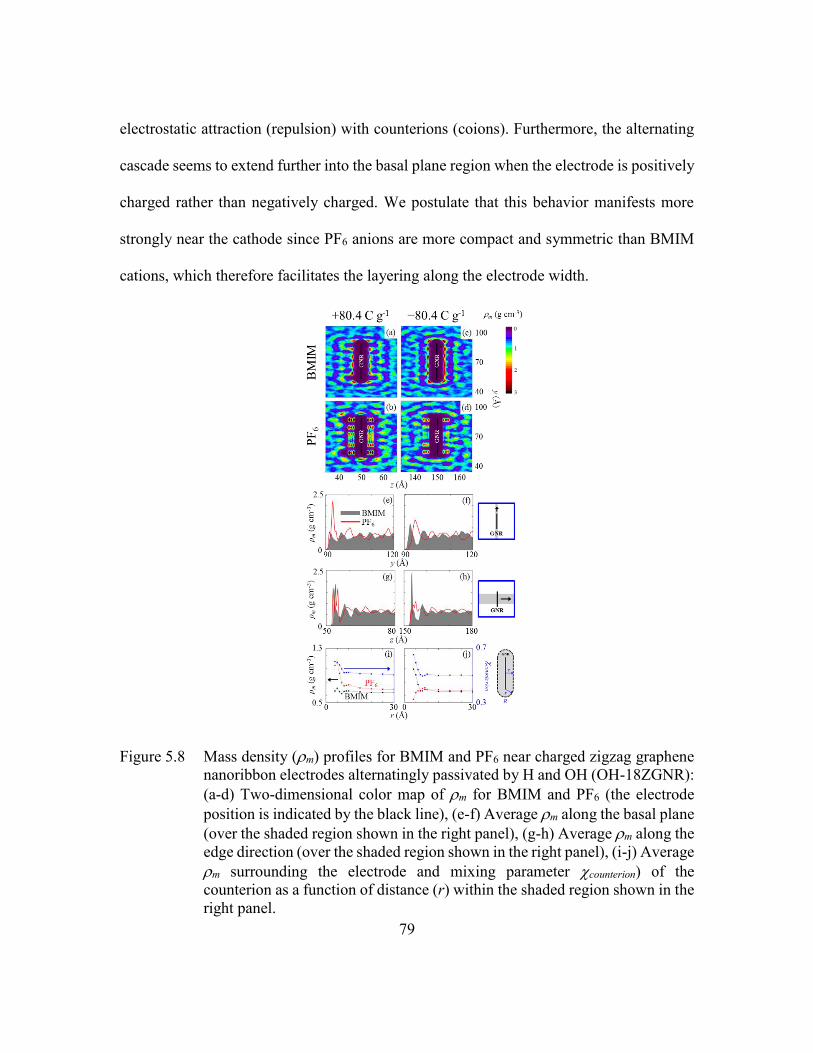
79
electrostatic attraction (repulsion) with counterions (coions). Furthermore, the alternating
cascade seems to extend further into the basal plane region when the electrode is positively
charged rather than negatively charged. We postulate that this behavior manifests more
strongly near the cathode since PF6 anions are more compact and symmetric than BMIM
cations, which therefore facilitates the layering along the electrode width.
Figure 5.8 Mass density (m) profiles for BMIM and PF6 near charged zigzag graphene
nanoribbon electrodes alternatingly passivated by H and OH (OH-18ZGNR):
(a-d) Two-dimensional color map of m for BMIM and PF6 (the electrode
position is indicated by the black line), (e-f) Average m along the basal plane
(over the shaded region shown in the right panel), (g-h) Average m along the
edge direction (over the shaded region shown in the right panel), (i-j) Average
m surrounding the electrode and mixing parameter counterion) of the
counterion as a function of distance (r) within the shaded region shown in the
right panel.
80
We next examine the variation in m along the edge direction and normal to the
basal plane. Figures 5.8(e)-(f) depict the average m in the edge direction near the cathode
and anode, respectively. Here, the first peak in the PF6 profile is noticeably enhanced
(diminished) at the cathode (anode) edge. The first peak in the BMIM profile, on the other
hand, is only marginally suppressed (augmented) at the cathode (anode) edge. In addition,
the alternating layering behavior, as also seen in the uncharged case [Figure 5.5(b)], is
maintained (suppressed) at the cathode (anode) edge. These observations suggest that the
electrostatic interaction with the positively charged H atom still tends to dominate ion
accumulation and segregation behavior directly at the edges since the injected charge
carriers merely strengthen (reduce) the partial charge of H at the cathode (anode). In direct
contrast, the average m profiles near the basal plane [Figure 5.8(g)-(h)] do not display
distinct alternation between PF6 and BMIM peaks, indicating that the ions are less
noticeably segregated in the direction normal to the basal plane. In other words, the
electrostatic interactions from the basal plane (basal 54.1 C g-1) are not strong enough
to induce such layering behavior.
To quantify the overall counterion accumulation surrounding the electrode, we
calculate counterion and the corresponding R-averaged m profiles near the cathode and
anode in Figure 5.8(i)-(j). Although it is readily apparent that the average m of counterions
near the cathode tends to exceed that of the anode when r < 6 Å, the net ratio of counterions
to coions remains similar for both cathode and anode. Therefore, the overall charge stored
at the electrode-electrolyte interface is expected to be comparable near the cathode and
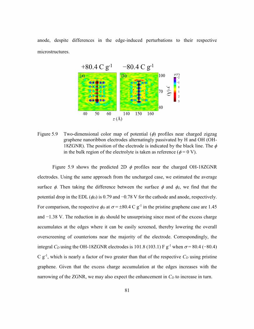
81
anode, despite differences in the edge-induced perturbations to their respective
microstructures.
Figure 5.9 Two-dimensional color map of potential () profiles near charged zigzag
graphene nanoribbon electrodes alternatingly passivated by H and OH (OH-
18ZGNR). The position of the electrode is indicated by the black line. The
in the bulk region of the electrolyte is taken as reference ( = 0 V).
Figure 5.9 shows the predicted 2D profiles near the charged OH-18ZGNR
electrodes. Using the same approach from the uncharged case, we estimated the average
surface . Then taking the difference between the surface and Z, we find that the
potential drop in the EDL (D) is 0.79 and −0.78 V for the cathode and anode, respectively.
For comparison, the respective D at = 80.4 C g-1 in the pristine graphene case are 1.45
and −1.38 V. The reduction in D should be unsurprising since most of the excess charge
accumulates at the edges where it can be easily screened, thereby lowering the overall
overscreening of counterions near the majority of the electrode. Correspondingly, the
integral CD using the OH-18ZGNR electrodes is 101.8 (103.1) F g-1 when = 80.4 (−80.4)
C g-1, which is nearly a factor of two greater than that of the respective CD using pristine
graphene. Given that the excess charge accumulation at the edges increases with the
narrowing of the ZGNR, we may also expect the enhancement in CD to increase in turn.
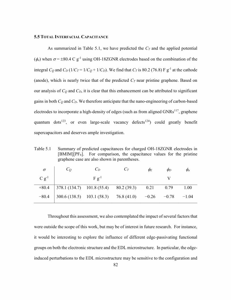
82
5.5 TOTAL INTERFACIAL CAPACITANCE
As summarized in Table 5.1, we have predicted the CT and the applied potential
(a) when = 80.4 C g-1 using OH-18ZGNR electrodes based on the combination of the
integral CQ and CD (1/CT = 1/CQ + 1/CD). We find that CT is 80.2 (76.8) F g-1 at the cathode
(anode), which is nearly twice that of the predicted CT near pristine graphene. Based on
our analysis of CQ and CD, it is clear that this enhancement can be attributed to significant
gains in both CQ and CD. We therefore anticipate that the nano-engineering of carbon-based
electrodes to incorporate a high-density of edges (such as from aligned GNRs117, graphene
quantum dots123, or even large-scale vacancy defects124) could greatly benefit
supercapacitors and deserves ample investigation.
Table 5.1 Summary of predicted capacitances for charged OH-18ZGNR electrodes in
[BMIM][PF6]. For comparison, the capacitance values for the pristine
graphene case are also shown in parentheses.
CQ CD CT E D a
C g-1 F g-1 V
+80.4 378.1 (134.7) 101.8 (55.4) 80.2 (39.3) 0.21 0.79 1.00
−80.4 300.6 (138.5) 103.1 (58.3) 76.8 (41.0) −0.26 −0.78 −1.04
Throughout this assessment, we also contemplated the impact of several factors that
were outside the scope of this work, but may be of interest in future research. For instance,
it would be interesting to explore the influence of different edge-passivating functional
groups on both the electronic structure and the EDL microstructure. In particular, the edge-
induced perturbations to the EDL microstructure may be sensitive to the configuration and
83
size of the functional group as well as the relative strength of electrostatic interactions with
the constituent atoms. Here, we should also note that stricter quantitative predictions using
our method may require additional considerations. For example, we did not model charge
polarization at the electrode-electrolyte interface for simplicity, which may affect the EDL
microstructure as well as the electronic structure of the electrode. In addition, conventional
DFT can introduce self-interaction errors which may underestimate charge localization,
but can be mitigated using hybrid functional methods.112 We also neglected charge transfer
between [BMIM][PF6] and the electrode since it appears to be unlikely.125 Nevertheless,
our computational approach is sufficient to demonstrate that the presence of edges can
enhance the performance of supercapacitors by virtue of increasing both CQ and CD.
5.6 CONCLUSIONS
We investigated the impact of ZGNRs in [BMIM][PF6] ionic liquid on the quantum
and EDL capacitances (and therefore, the interfacial capacitance) using a combined DFT
and classical MD approach. In our electronic structure analysis, we considered two
different widths of H-passivated (H-18ZGNR and H-60ZGNR) and alternatingly H-/OH-
passivated ZGNR (OH-18ZGNR/OH-60ZGNR) electrodes. Our results demonstrate that
the electronic states are quasi-localized in the vicinity of the edges, although the degree of
localization tends to decrease with increasing width. We then calculated the quantum
capacitances (CQ) from the electronic density of states. Comparisons with that of pristine
graphene reveal that the ZGNR electrodes have significantly larger CQ which are further
84
enhanced as the ZGNR width decreases. Furthermore, our results show that the degree of
excess charge accumulation at the edges increases super-linearly as the ZGNR width
decreases. We also studied the influence of edge defects on the EDL microstructure using
the OH-18ZGNR as a model system when the excess surface charge density = 0 and
80.4 C g-1. We find that the presence of edges induces an alternating cascade of PF6 and
BMIM ions in which the segregation is greatest near the edges. Upon charging, the
microstructure of the EDL exhibits a greater response near the edges due to the preferential
accumulation of excess charge carriers toward the edges. As a result, the EDL capacitance
(CD) of the OH-18ZGNR case is also predicted to be greatly enhanced when compared to
the pristine graphene case. Finally, the total interfacial capacitance (CT = [1/CD + 1/CQ]-1)
of the OH-18ZGNR case is found to experience a two-fold increase in comparison to the
pristine graphene case when = 80.4 (−80.4) C g-1. Our findings clearly highlight that the
inclusion of a large density of edge defects in graphene-like electrodes can dramatically
improve both CQ and CD, and therefore the overall performance of supercapacitors.
85
Chapter 6: Basal-Plane Oxidation
Work in this chapter was published and reprinted from ChemElectroChem, Vol. 3, A. J.
Pak and G. S. Hwang, On the Importance of Regulating Hydroxyl Coverage on the Basal
Plane of Graphene Oxide for Supercapacitors, pg. 741−8, Copyright (2016) with
permission from John Wiley and Sons.
6.1 INTRODUCTION TO GRAPHENE OXIDE
In recent years, reduced graphene oxide (rGO) has gained popularity as an
alternative graphene-based material. Part of the attraction is the cost-effective means of
producing rGO from the wet exfoliation of graphene oxide and subsequent chemical,
thermal, or electrochemical reduction.126-128 While rGO has traditionally been used as a
precursor for graphene sheets128, rGO is also an interesting and important material in its
own right. For instance, the oxygen moieties serve as electrochemically active sites which
have been utilized for enhanced catalytic activity of oxygen reduction129 and pseudo-
capacitive benefits130-132 in aqueous EDLCs. Naturally, rGO has also been explored for its
use as an electrode material in supercapacitors using organic or ionic-liquid electrolytes
which are electrochemically stable. To date, however, experimental results probing the
advantages of rGO for EDLC applications have been widely scattered. While rGO
electrodes have been shown to outperform graphene electrodes133,134, reported capacitances
have exhibited contradictory sensitivities to the ratio of oxygen to carbon atoms (O:C) and
the reduction process135,136. This underscores the need to understand the influence of the
extent of reduction on the capacitance.
86
To evaluate the impact of rGO reduction on EDLC performance, it is important to
recognize that the total interfacial capacitance (CT) strongly depends upon the contributions
from the electrode quantum capacitance (CQ) and electric double layer (EDL) capacitance
(CD). 13,34,35 While the latter property primarily depends upon the accumulation of ions at
the interface, the former quantifies the ease in which excess charge carriers populate the
electronic states of the electrode. To decouple these contributions, theoretical simulations
can provide valuable insights. For example, molecular dynamics simulations have shown
that regularly dispersed coverage of the basal plane of graphene with hydroxyl (OH) or
epoxide functional groups tends to monotonically decrease CD with increasing moiety
content.137-139 Quantum mechanical calculations have also shown that CQ can be
dramatically enhanced through OH functionalization of edge sites140 as well as chemical
modification33,141 of basal sites, although the basal-plane coverage by OH has yet to be
studied in this context. However, one challenge in undertaking such a fundamental
investigation is a proper account of the rGO structure. Experimental characterizations using
NMR spectroscopy and X-ray photo-electron spectrometry have identified the presence of
several oxygen moieties such as OH, epoxide, carboxyl, and carbonyl groups, although the
first two (OH and epoxide) are generally identified as the most common species along the
basal surface.142,143 Furthermore, recent experimental144,145 and theoretical146,147 work have
shown that oxygen moieties tend to aggregate along the basal surface, forming distinct
graphitic and oxidized regions. Therefore, careful attention should be applied in theoretical
studies to account for such structures. To this end, one possible method is a lattice-based
Monte Carlo scheme such as the one used by Zhou and Bongiorno.146

87
In this chapter, the effect of varying the O:C of rGO electrodes on CT is investigated
and compared to that of pristine graphene. Here, the OH functionalization of the basal
surface of graphene is considered for simplicity while possible OH agglomeration is
accounted using lattice-based Monte Carlo simulations. First, density functional theory
(DFT) and density functional tight binding (DFTB) theory are employed in order to study
the electronic structure, CQ, and electrochemical stability of the rGO sheets. Then, classical
molecular dynamics (MD) simulations are used in order to study the microstructure and
CD of the electrodes immersed in 1-ethyl-3-methylimidazolium bis(fluorosulfonyl)imide
([EMIM][FSI]) ionic liquid. Finally, the competition between CQ and CD is discussed in
relation to the potential enhancement in rGO-based supercapacitor performance compared
to that of pristine graphene electrodes.
6.2 COMPUTATIONAL METHODS
The electronic structure of each rGO sheet was calculated using DFT within the
Perdew-Berke-Ernzerhof generalized gradient approximation43 (GGA-PBE), as
implemented in the Vienna Ab initio Simulation Package42 (VASP). The projector
augmented wave (PAW) method69 was employed to describe the interaction between core
and valence electrons with a planewave basis set using a kinetic energy cutoff of 400 eV.
The rGO sheet was modeled using a 74 rectangular supercell (17.264817.0877 Å2) with
the PBE-optimized lattice constant of 2.466 Å for graphene. For all O:C cases, trans pairs
of OH groups were added to the graphene lattice according to the Metropolis Monte Carlo
88
(MMC) scheme described later. As an example of the agglomeration, 68 OH groups (34
trans pairs) and 680 C atoms (O:C = 0.1) formed five domains on average with the largest
domain covering 20% of the lattice. Periodic boundary conditions were employed in all
three directions with a vacuum spacing of 20 Å in the vertical direction to separate the rGO
sheet from its periodic images. For the Brillouin zone integration, a (6×6×1) Monkhorst-
Pack (MP) k-point mesh70 was used for geometry optimization and energy calculations,
while a (8×8×1) MP k-point mesh was used to ensure convergence for electronic structure
calculations; all energy (force) calculations were converged to within 1×10⁻⁶ eV (0.02
eV/Å). For comparison, third-order self-consistent charge DFTB calculations were
performed using Slater-Koster parameters from Ref. 148 as implemented in the DFTB+
program.149,150 For these calculations, a (13×13×1) MP k-point mesh was used for geometry
optimization and electronic structure calculations with the same convergence tolerance.
The calculated CQ values were based on larger rGO sheets (1710 rectangular
supercells corresponding to 41.928842.7193 Å2) which were prepared using the same
MMC scheme with 9, 34, and 102 trans pairs of OH groups added to the lattice, yielding
an O:C = 0.026, 0.1, and 0.3, respectively. Here, a (5×5×1) MP k-point mesh was used for
geometry optimization and electronic structure calculations. Partial atomic charges were
computed using Mulliken population analysis151 for excess charge density = 0, 2.24,
4.47 µC/cm2 (0, 5, and 10 e per sheet); these charges were used in the MD simulations
which are described below. All reported results were obtained from averages over five
independent samples at each O:C.
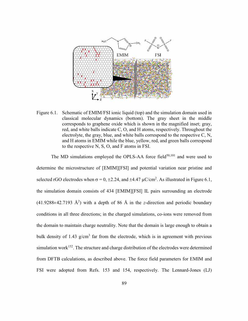
89
Figure 6.1. Schematic of EMIM/FSI ionic liquid (top) and the simulation domain used in
classical molecular dynamics (bottom). The gray sheet in the middle
corresponds to graphene oxide which is shown in the magnified inset; gray,
red, and white balls indicate C, O, and H atoms, respectively. Throughout the
electrolyte, the gray, blue, and white balls correspond to the respective C, N,
and H atoms in EMIM while the blue, yellow, red, and green balls correspond
to the respective N, S, O, and F atoms in FSI.
The MD simulations employed the OPLS-AA force field50,101 and were used to
determine the microstructure of [EMIM][FSI] and potential variation near pristine and
selected rGO electrodes when = 0, 2.24, and 4.47 µC/cm2. As illustrated in Figure 6.1,
the simulation domain consists of 434 [EMIM][FSI] IL pairs surrounding an electrode
(41.928842.7193 Å2) with a depth of 86 Å in the z-direction and periodic boundary
conditions in all three directions; in the charged simulations, co-ions were removed from
the domain to maintain charge neutrality. Note that the domain is large enough to obtain a
bulk density of 1.43 g/cm3 far from the electrode, which is in agreement with previous
simulation work152. The structure and charge distribution of the electrodes were determined
from DFTB calculations, as described above. The force field parameters for EMIM and
FSI were adopted from Refs. 153 and 154, respectively. The Lennard-Jones (LJ)
90
parameters for graphene and for the OH moieties were adopted from Refs. 155 and 101,
respectively. Spherical cutoffs of 10 Å and 12 Å were used for the LJ and Coulomb
interactions, respectively. Electrostatic interactions beyond the cutoff were calculated
using the Particle-Particle Particle-Mesh solver.54
While keeping the electrodes fixed, each MD simulation was annealed and
quenched initially at 700 K for 3 ns followed by 2 ns at 350 K for two cycles (i.e., 10 ns
total), and then further equilibrated for 3 ns at 300 K using a 1 fs time step. Production runs
were carried out for 4 ns with atomic positions recorded every 5 ps. All simulations were
in the NVT ensemble with the temperature controlled by a Nose-Hoover thermostat60 with
a 200 fs damping parameter. All MD simulations were performed with the Large-scale
Atomic/Molecular Massively Parallel Simulator (LAMMPS) program.105 MD results
reported herein were obtained from the average of five independent simulations with
different initial atomic configurations.
6.3 HYDROXYL AGGLOMERATION ON BASAL PLANE
To determine the rGO structure, we use lattice-based Metropolis Monte Carlo
simulations using a pair-wise potential model developed based on GGA-PBE energetics
from DFT calculations. First, we approximate the pair-wise interaction energy per OH
moiety (Ep,OH) when homogeneously dispersed on the basal surface of graphene at different
concentrations:
𝐸𝑝,𝑂𝐻 =𝐸𝑠𝑦𝑠𝑡𝑒𝑚−𝐸𝐺𝑟−𝑛𝐸𝑂𝐻
𝑛 (6.1)
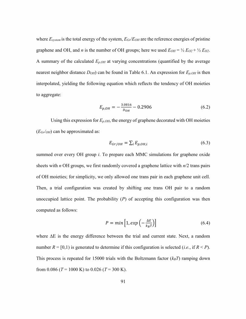
91
where Esystem is the total energy of the system, EGr/EOH are the reference energies of pristine
graphene and OH, and n is the number of OH groups; here we used EOH = ½ EO2 + ½ EH2.
A summary of the calculated Ep,OH at varying concentrations (quantified by the average
nearest neighbor distance DOH) can be found in Table 6.1. An expression for Ep,OH is then
interpolated, yielding the following equation which reflects the tendency of OH moieties
to aggregate:
𝐸𝑝,𝑂𝐻 = −3.0816
𝐷𝑂𝐻− 0.2906 (6.2)
Using this expression for Ep,OH, the energy of graphene decorated with OH moieties
(EGr/OH) can be approximated as:
𝐸𝐺𝑟/𝑂𝐻 = ∑ 𝐸𝑝,𝑂𝐻,𝑖𝑖 (6.3)
summed over every OH group i. To prepare each MMC simulations for graphene oxide
sheets with n OH groups, we first randomly covered a graphene lattice with n/2 trans pairs
of OH moieties; for simplicity, we only allowed one trans pair in each graphene unit cell.
Then, a trial configuration was created by shifting one trans OH pair to a random
unoccupied lattice point. The probability (P) of accepting this configuration was then
computed as follows:
𝑃 = 𝑚𝑖𝑛 [1, 𝑒𝑥𝑝 (−Δ𝐸
𝑘𝐵𝑇)] (6.4)
where ∆E is the energy difference between the trial and current state. Next, a random
number R = [0,1) is generated to determine if this configuration is selected (i.e., if R < P).
This process is repeated for 15000 trials with the Boltzmann factor (kBT) ramping down
from 0.086 (T = 1000 K) to 0.026 (T = 300 K).
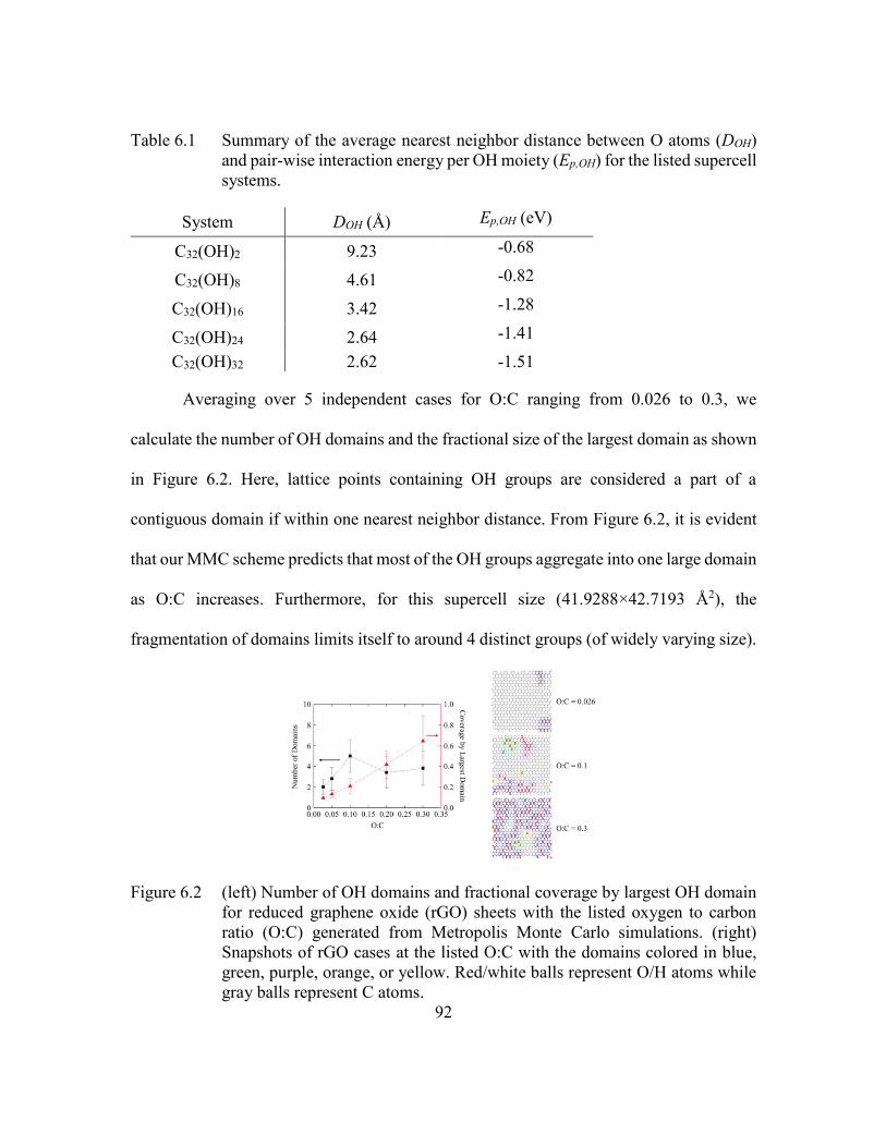
92
Table 6.1 Summary of the average nearest neighbor distance between O atoms (DOH)
and pair-wise interaction energy per OH moiety (Ep,OH) for the listed supercell
systems.
System DOH (Å) Ep,OH (eV)
C32(OH)2 9.23 -0.68
C32(OH)8 4.61 -0.82
C32(OH)16 3.42 -1.28
C32(OH)24 2.64 -1.41
C32(OH)32 2.62 -1.51
Averaging over 5 independent cases for O:C ranging from 0.026 to 0.3, we
calculate the number of OH domains and the fractional size of the largest domain as shown
in Figure 6.2. Here, lattice points containing OH groups are considered a part of a
contiguous domain if within one nearest neighbor distance. From Figure 6.2, it is evident
that our MMC scheme predicts that most of the OH groups aggregate into one large domain
as O:C increases. Furthermore, for this supercell size (41.9288×42.7193 Å2), the
fragmentation of domains limits itself to around 4 distinct groups (of widely varying size).
Figure 6.2 (left) Number of OH domains and fractional coverage by largest OH domain
for reduced graphene oxide (rGO) sheets with the listed oxygen to carbon
ratio (O:C) generated from Metropolis Monte Carlo simulations. (right)
Snapshots of rGO cases at the listed O:C with the domains colored in blue,
green, purple, orange, or yellow. Red/white balls represent O/H atoms while
gray balls represent C atoms.

93
6.4 COVERAGE EFFECT ON ELECTRONIC STRUCTURE AND QUANTUM CAPACITANCE
In this section, the electronic structure of rGO is reported at different OH contents
(i.e., O:C). First, the electronic density of states (DOS) of rGO at O:C = 0.054 and O:C =
0.268 are analyzed using DFT-GGA. Next, the viability of using the DFTB approach in
place of DFT-GGA is demonstrated. Using DFTB, we then proceed to calculate the
influence of O:C on the integral CQ of rGO.
Figure 6.3 The density of states (DOS) of reduced graphene oxide with respect to the
Fermi level (EF) when (a) O:C = 0.054 and (b) O:C = 0.268, as calculated
using the listed quantum mechanical methods. The insets show the band-
decomposed charge density isosurfaces (0.001 e/bohr3) for the highlighted
regions I and II, in which blue and green isosurfaces correspond to electrons
and holes, respectively.
Figure 6.3(a) depicts the total DOS of a rGO sheet with O:C = 0.054. The sharp
peaks seen above the Fermi level (EF) [0 < E−EF < 0.4 eV] are indicative of quasi-
94
localization of states arising from the presence of OH groups, similarly present in the cases
of graphene with chemical dopants33,141 and topological defects156,157. As seen from the
band-decomposed charge density isosurfaces of regions I and II, the quasi-localized states
near EF are primarily associated with the pz states of C atoms nearby OH moieties where
the system is most distorted; note that we find the O 2p states to be 1.8 eV below EF. In
the O:C = 0.268 case [Figure 6.3(b)], the density of quasi-localized states near EF is found
to increase since the distortion to the system intensifies with the addition of more OH
groups; here, a gap of 0.28 eV is also predicted to appear.
Figure 6.4 Color map of atomic charges calculated from Mulliken population analysis
for rGO with O:C = 0.3 and excess surface charge density = 0 µC/cm2. Blue
and red colors along the carbon lattice represent positive and negative charge,
respectively; note that the electropositive C atoms are within the vicinity of
the OH moieties which are depicted by red and white balls. All calculations
were performed using DFTB+ for a 17x10 rectangular supercell.
The presence of OH moieties consequently influences the charge distribution along
the rGO sheet. The OH moieties expectedly withdraw electrons from the system and
thereby act as a p-type dopant; hence, the adjacent C atoms are electropositive (as depicted
95
in the charge distribution map in Figure 6.4). We can also expect excess charge carriers to
primarily fill the system with slight accumulation near the OH sites where the degree of
quasi-localization is largest. Later, we will discuss the implications of the resultant charge
redistribution on the electrode-electrolyte interactions at the interface.
As our goal is to investigate the electronic structure of large and disordered sheets
of rGO with as many as thousands of atoms in a unit cell, we now consider the efficacy of
an alternative and less-expensive computational method. In Figure 6.3(a)-(b), we compare
the DOS predicted by DFT-GGA to that of DFTB and find that the latter sufficiently
approximates the former. However, it is clear that the DFTB method systematically
underestimates the electronic localization relative to DFT-GGA. For example, in the case
of O:C = 0.054, the empty states in the DFTB DOS are broadened such that the peak
appears around 0.3 eV above its relative position predicted using DFT-GGA. Furthermore,
the band gap in the O:C = 0.268 case is predicted to be 0.06 eV smaller from the DFTB
calculation. Nonetheless, DFTB captures the general availability of states near EF, which
ultimately determines CQ. Herein, we will use the DFTB method to estimate the DOS of
rGO with varying O:C.
Figure 6.5 shows the integral CQ as a function of local electrode potential (G)
calculated for larger rGO sheets (41.928842.7193 Å2) with O:C = 0.026, 0.1, and 0.3 and
for pristine graphene. Based on DFTB calculations, CQ was computed using procedure
described in Chapter 2 from the DOS averaged over all samples [inset of Figure 6.5]. In
comparison to pristine graphene, the overall CQ of the rGO sheets tends to increase as O:C
increases, especially close to the charge neutrality point, which reflects the additional
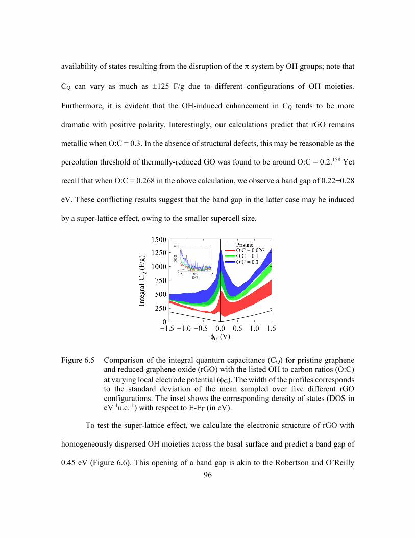
96
availability of states resulting from the disruption of the system by OH groups; note that
CQ can vary as much as 125 F/g due to different configurations of OH moieties.
Furthermore, it is evident that the OH-induced enhancement in CQ tends to be more
dramatic with positive polarity. Interestingly, our calculations predict that rGO remains
metallic when O:C = 0.3. In the absence of structural defects, this may be reasonable as the
percolation threshold of thermally-reduced GO was found to be around O:C = 0.2.158 Yet
recall that when O:C = 0.268 in the above calculation, we observe a band gap of 0.22−0.28
eV. These conflicting results suggest that the band gap in the latter case may be induced
by a super-lattice effect, owing to the smaller supercell size.
Figure 6.5 Comparison of the integral quantum capacitance (CQ) for pristine graphene
and reduced graphene oxide (rGO) with the listed OH to carbon ratios (O:C)
at varying local electrode potential (G). The width of the profiles corresponds
to the standard deviation of the mean sampled over five different rGO
configurations. The inset shows the corresponding density of states (DOS in
eV-1u.c.-1) with respect to E-EF (in eV).
To test the super-lattice effect, we calculate the electronic structure of rGO with
homogeneously dispersed OH moieties across the basal surface and predict a band gap of
0.45 eV (Figure 6.6). This opening of a band gap is akin to the Robertson and O’Reilly
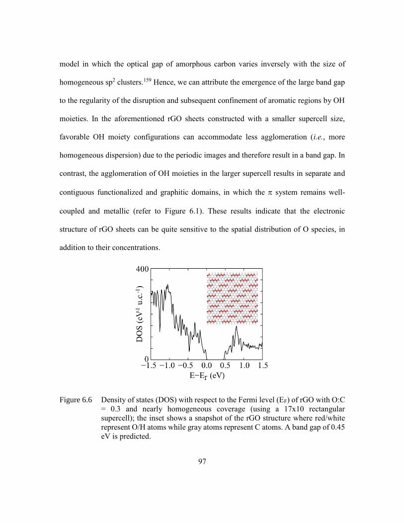
97
model in which the optical gap of amorphous carbon varies inversely with the size of
homogeneous sp2 clusters.159 Hence, we can attribute the emergence of the large band gap
to the regularity of the disruption and subsequent confinement of aromatic regions by OH
moieties. In the aforementioned rGO sheets constructed with a smaller supercell size,
favorable OH moiety configurations can accommodate less agglomeration (i.e., more
homogeneous dispersion) due to the periodic images and therefore result in a band gap. In
contrast, the agglomeration of OH moieties in the larger supercell results in separate and
contiguous functionalized and graphitic domains, in which the system remains well-
coupled and metallic (refer to Figure 6.1). These results indicate that the electronic
structure of rGO sheets can be quite sensitive to the spatial distribution of O species, in
addition to their concentrations.
Figure 6.6 Density of states (DOS) with respect to the Fermi level (EF) of rGO with O:C
= 0.3 and nearly homogeneous coverage (using a 17x10 rectangular
supercell); the inset shows a snapshot of the rGO structure where red/white
represent O/H atoms while gray atoms represent C atoms. A band gap of 0.45
eV is predicted.
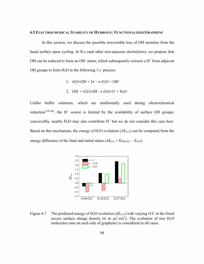
98
6.5 ELECTROCHEMICAL STABILITY OF HYDROXYL FUNCTIONALIZED GRAPHENE
In this section, we discuss the possible irreversible loss of OH moieties from the
basal surface upon cycling. In ILs (and other non-aqueous electrolytes), we propose that
OH can be reduced to form an OH- anion, which subsequently extracts a H+ from adjacent
OH groups to form H2O in the following 1 e- process:
1. rGO-OH + 1e- rGO + OH-
2. OH- + rGO-OH rGO-O- + H2O
Unlike buffer solutions, which are traditionally used during electrochemical
reduction128,160, the H+ source is limited by the availability of surface OH groups;
conceivably, nearby H2O may also contribute H+ but we do not consider this case here.
Based on this mechanism, the energy of H2O evolution (Eevo) can be computed from the
energy difference of the final and initial states (Eevo = EH2O/O- – EGO).
Figure 6.7 The predicted energy of H2O evolution (Eevo) with varying O:C at the listed
excess surface charge density ( in µC/cm2). The evolution of two H2O
molecules (one on each side of graphene) is considered in all cases.
99
Our interest is in evaluating Eevo at varying O:C using DFT. We consider the
previously used 74 rectangular supercells and allow one H2O to evolve on each side of
the rGO sheet; for completeness, the Eevo for the neutral, anodic, and cathodic cases are
calculated and shown in Figure 6.7. First, it is evident that at low O:C ratios (= 0.04), H2O
evolution is favorable and expectedly more so under cathodic potential ( = −5.43
µC/cm2). However, we find that the evolution becomes increasingly unfavorable as O:C
increases. Therefore, within a fixed operating potential, our results suggest that a critical
O:C exists, beyond which the loss of OH moieties can be mitigated.
To understand the origins of this behavior, we refer to our previous electronic
structure analysis. Recall that an increase in O:C is commensurate with greater quasi-
localization of states near EF. Hence, the preferential filling of excess charge carriers in
these states should increase with O:C and consequently it is less likely for electrons to
localize on an OH site to form OH-. Note that this behavior should be sensitive to the types
of oxygen moieties (such as basal-plane epoxides and edge-plane carboxyls, carbonyls, and
lactols) as well as their relative concentrations, which could be a subject of further study.
Nonetheless, this analysis demonstrates that the increased disruption of the system at
increased O:C ratios may enhance both the CQ and cycling stability of rGO electrodes.
6.6 COVERAGE EFFECT ON DOUBLE LAYER MICROSTRUCTURE AND CAPACITANCE
To evaluate the integral CD, the microstructure of [EMIM][FSI] near rGO
electrodes (O:C = 0.1 and 0.3) is investigated and compared to that of pristine graphene
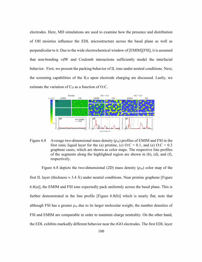
100
electrodes. Here, MD simulations are used to examine how the presence and distribution
of OH moieties influence the EDL microstructure across the basal plane as well as
perpendicular to it. Due to the wide electrochemical window of [EMIM][FSI], it is assumed
that non-bonding vdW and Coulomb interactions sufficiently model the interfacial
behavior. First, we present the packing behavior of IL ions under neutral conditions. Next,
the screening capabilities of the ILs upon electrode charging are discussed. Lastly, we
estimate the variation of CD as a function of O:C.
Figure 6.8 Average two-dimensional mass density (m) profiles of EMIM and FSI in the
first ionic liquid layer for the (a) pristine, (c) O:C = 0.1, and (e) O:C = 0.3
graphene cases, which are shown as color maps. The respective line profiles
of the segments along the highlighted region are shown in (b), (d), and (f),
respectively.
Figure 6.8 depicts the two-dimensional (2D) mass density (m) color map of the
first IL layer (thickness 3.4 Å) under neutral conditions. Near pristine graphene [Figure
6.8(a)], the EMIM and FSI ions expectedly pack uniformly across the basal plane. This is
further demonstrated in the line profile [Figure 6.8(b)] which is nearly flat; note that
although FSI has a greater m due to its larger molecular weight, the number densities of
FSI and EMIM are comparable in order to maintain charge neutrality. On the other hand,
the EDL exhibits markedly different behavior near the rGO electrodes. The first EDL layer
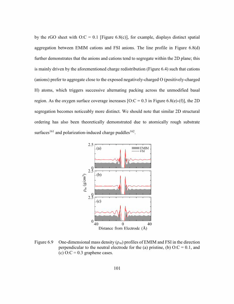
101
by the rGO sheet with O:C = 0.1 [Figure 6.8(c)], for example, displays distinct spatial
aggregation between EMIM cations and FSI anions. The line profile in Figure 6.8(d)
further demonstrates that the anions and cations tend to segregate within the 2D plane; this
is mainly driven by the aforementioned charge redistribution (Figure 6.4) such that cations
(anions) prefer to aggregate close to the exposed negatively-charged O (positively-charged
H) atoms, which triggers successive alternating packing across the unmodified basal
region. As the oxygen surface coverage increases [O:C = 0.3 in Figure 6.8(e)-(f)], the 2D
segregation becomes noticeably more distinct. We should note that similar 2D structural
ordering has also been theoretically demonstrated due to atomically rough substrate
surfaces161 and polarization-induced charge puddles162.
Figure 6.9 One-dimensional mass density (m) profiles of EMIM and FSI in the direction
perpendicular to the neutral electrode for the (a) pristine, (b) O:C = 0.1, and
(c) O:C = 0.3 graphene cases.
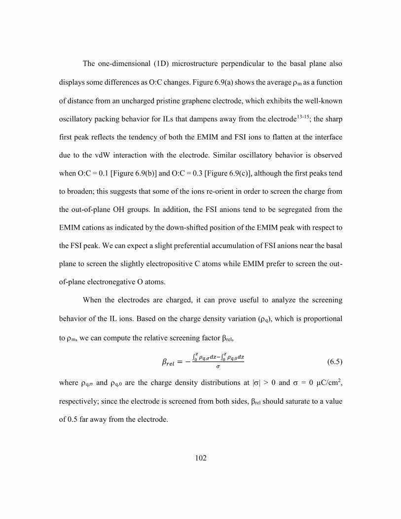
102
The one-dimensional (1D) microstructure perpendicular to the basal plane also
displays some differences as O:C changes. Figure 6.9(a) shows the average m as a function
of distance from an uncharged pristine graphene electrode, which exhibits the well-known
oscillatory packing behavior for ILs that dampens away from the electrode13-15; the sharp
first peak reflects the tendency of both the EMIM and FSI ions to flatten at the interface
due to the vdW interaction with the electrode. Similar oscillatory behavior is observed
when O:C = 0.1 [Figure 6.9(b)] and O:C = 0.3 [Figure 6.9(c)], although the first peaks tend
to broaden; this suggests that some of the ions re-orient in order to screen the charge from
the out-of-plane OH groups. In addition, the FSI anions tend to be segregated from the
EMIM cations as indicated by the down-shifted position of the EMIM peak with respect to
the FSI peak. We can expect a slight preferential accumulation of FSI anions near the basal
plane to screen the slightly electropositive C atoms while EMIM prefer to screen the out-
of-plane electronegative O atoms.
When the electrodes are charged, it can prove useful to analyze the screening
behavior of the IL ions. Based on the charge density variation (q), which is proportional
to m, we can compute the relative screening factor βrel,
𝛽𝑟𝑒𝑙 = −∫ 𝜌𝑞,𝜎𝑑𝑧
𝑧0 −∫ 𝜌𝑞,0𝑑𝑧
𝑧0
𝜎 (6.5)
where q, and q,0 are the charge density distributions at || > 0 and = 0 µC/cm2,
respectively; since the electrode is screened from both sides, βrel should saturate to a value
of 0.5 far away from the electrode.
103
Figure 6.10 The average relative screening factor (βrel) in the direction perpendicular to
the listed electrodes when the excess surface charge density (a) = 2.24
µC/cm2 and (b) = −2.24 µC/cm2. The insets depict the absolute screening
factor (βabs) as described in the manuscript.
As seen in Figure 6.10(a), the compact first IL layer near pristine graphene has a
peak βrel = 1.2 around 4.5 Å when = 2.24 µC/cm2. In contrast, the first βrel peak for the
O:C = 0.1 and 0.3 cases are respectively broadened and shifted away from the electrode,
indicating that the relative screening capability of the IL ions are increasingly impeded as
O:C increases. When = −2.24 µC/cm2 [Figure 6.10(b)], similar behavior is observed in
which the peak βrel broadens and diminishes as O:C increases; note, however, that the peak
βrel is around 1.0 (0.6) in the pristine (O:C = 0.3) graphene case, which is comparably
smaller than the peak β by the positive terminal. These results suggest that the accumulation
of counterions at the electrode-electrolyte interface is increasingly unfavorable as O:C
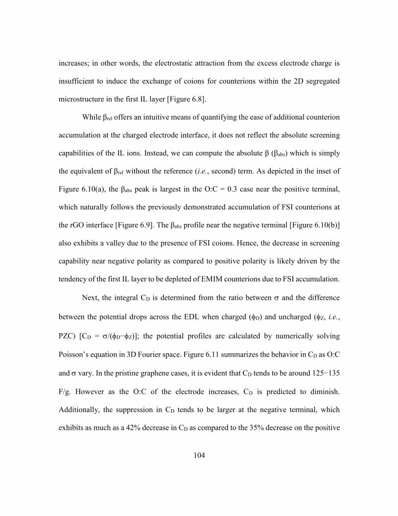
104
increases; in other words, the electrostatic attraction from the excess electrode charge is
insufficient to induce the exchange of coions for counterions within the 2D segregated
microstructure in the first IL layer [Figure 6.8].
While βrel offers an intuitive means of quantifying the ease of additional counterion
accumulation at the charged electrode interface, it does not reflect the absolute screening
capabilities of the IL ions. Instead, we can compute the absolute β (βabs) which is simply
the equivalent of βrel without the reference (i.e., second) term. As depicted in the inset of
Figure 6.10(a), the βabs peak is largest in the O:C = 0.3 case near the positive terminal,
which naturally follows the previously demonstrated accumulation of FSI counterions at
the rGO interface [Figure 6.9]. The βabs profile near the negative terminal [Figure 6.10(b)]
also exhibits a valley due to the presence of FSI coions. Hence, the decrease in screening
capability near negative polarity as compared to positive polarity is likely driven by the
tendency of the first IL layer to be depleted of EMIM counterions due to FSI accumulation.
Next, the integral CD is determined from the ratio between and the difference
between the potential drops across the EDL when charged (D) and uncharged (Z, i.e.,
PZC) [CD = /(D−Z)]; the potential profiles are calculated by numerically solving
Poisson’s equation in 3D Fourier space. Figure 6.11 summarizes the behavior in CD as O:C
and vary. In the pristine graphene cases, it is evident that CD tends to be around 125−135
F/g. However as the O:C of the electrode increases, CD is predicted to diminish.
Additionally, the suppression in CD tends to be larger at the negative terminal, which
exhibits as much as a 42% decrease in CD as compared to the 35% decrease on the positive
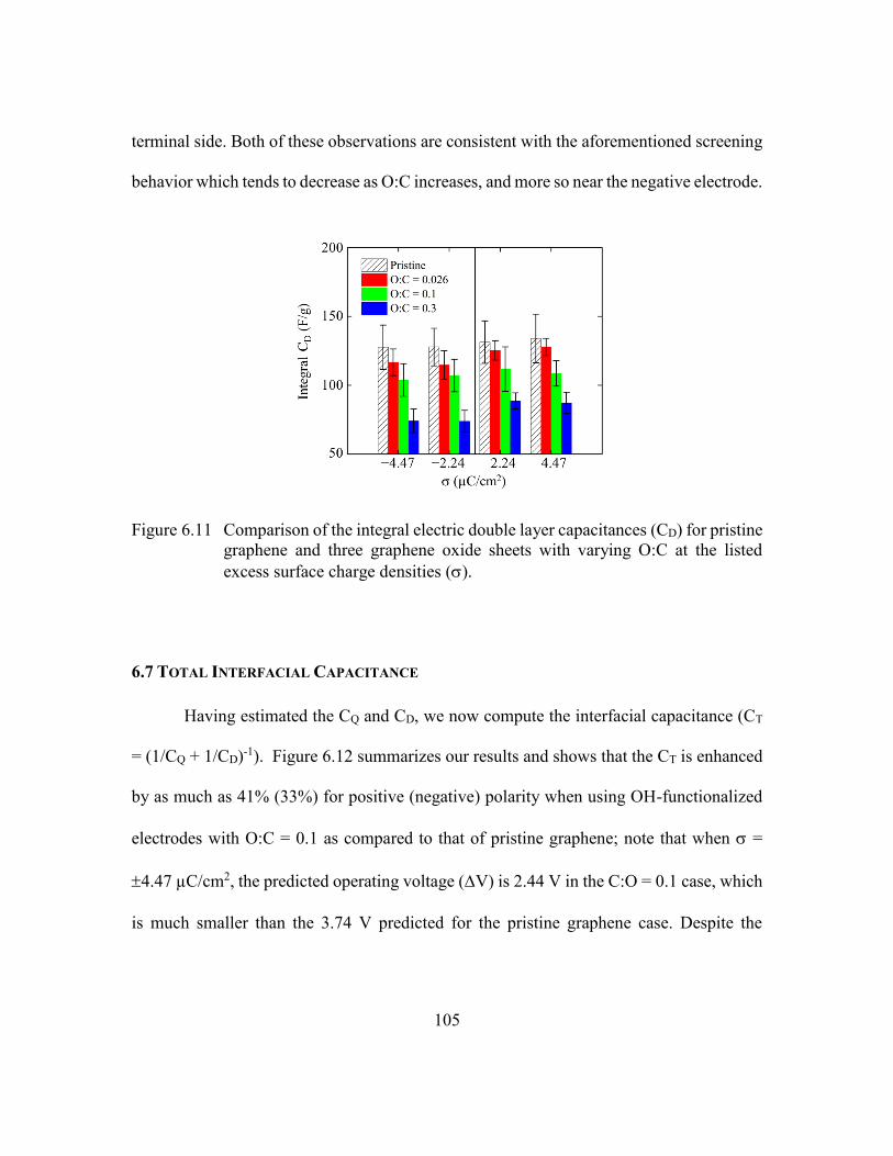
105
terminal side. Both of these observations are consistent with the aforementioned screening
behavior which tends to decrease as O:C increases, and more so near the negative electrode.
Figure 6.11 Comparison of the integral electric double layer capacitances (CD) for pristine
graphene and three graphene oxide sheets with varying O:C at the listed
excess surface charge densities ().
6.7 TOTAL INTERFACIAL CAPACITANCE
Having estimated the CQ and CD, we now compute the interfacial capacitance (CT
= (1/CQ + 1/CD)-1). Figure 6.12 summarizes our results and shows that the CT is enhanced
by as much as 41% (33%) for positive (negative) polarity when using OH-functionalized
electrodes with O:C = 0.1 as compared to that of pristine graphene; note that when =
4.47 µC/cm2, the predicted operating voltage (V) is 2.44 V in the C:O = 0.1 case, which
is much smaller than the 3.74 V predicted for the pristine graphene case. Despite the

106
diminished CD upon OH functionalization, we find that the CT can be dramatically
improved by virtue of the enhanced CQ.
Figure 6.12 Comparison of the integral interfacial capacitances (CT) for pristine graphene
and three graphene oxide sheets with varying O:C at the listed excess surface
charge densities ().
In addition, our results do suggest that there may be an optimal O:C in which the
benefit from the CQ most effectively mitigates the loss in CD. However, there are several
limitations in our simulations that prevent us from quantifying such a point. First, we did
not take into account the charge smearing at the electrode-electrolyte interface which may
have underestimated our prediction of the CD.88 More importantly, the CQ can be altered in
the presence of other types of oxygen moieties, as well as their concentrations and
distributions across the basal plane. In particular, we should be wary of rGO sheets with
band gaps that have been predicted to be as large as 3.0 eV which can occur when O:C >
0.5 for certain combinations and configurations of oxygen-containing functional
groups.147,163 Furthermore, the presence of additional topological defects that may be
created through the rGO reduction process164 can also strongly influence the electronic
107
structure as well as their electrochemical stability. It is possible that the highly scattered
performance of GO-based supercapacitors reported in the literature may be partially due to
the structurally-sensitive CQ. Moreover, the possible suppression of electrical conductivity
in rGO sheets with increased oxygen functionalization is another factor to consider.131
Therefore, it will be important to improve both the experimental characterization and
control of oxygen functionalization on rGO in order to fully utilize these materials for
supercapacitor electrodes. Nonetheless, our study reveals that rGO materials, which are
particularly attractive due to their ease in processing and scalability, can serve as a superior
alternative to graphene electrodes for EDLC applications.
6.8 CONCLUSIONS
We investigated the influence of reduced graphene oxide (rGO) electrodes immersed
in [EMIM][FSI] ionic liquid on both the quantum (CQ) and electric double layer (CD)
capacitances using a combined DFT and classical MD approach. As a model system, we
only considered OH moieties along the basal plane, while accounting for their preferential
spatial agglomeration, and vary the ratio of OH to C (O:C). Our three primary conclusions
are:
Increasing O:C (computed up to the O:C = 0.3 case) induces increasing quasi-
localization of C pz states, which subsequently enhances the CQ and electrochemical
stability of OH on the basal surface.
108
The CD can be repressed as O:C increases, which we attribute to the unfavorable
exchange of counterions with coions adjacent to the electrode surface due to the
preferred two-dimensionally ordering of cations and anions.
The total interfacial capacitance (CT = [1/CQ + 1/CD]-1) using OH-functionalized
electrodes is predicted to outperform pristine graphene electrodes owing to the
mitigation of the suppressed CD by improved CQ; for example when = 4.47
(−4.47) µC/cm2, CT is predicted to improve by 41% (33%).
Interestingly, our analysis suggests that the intended benefit from rGO electrodes strongly
depends upon both the concentration and arrangement of oxygen species. This may help
explain some inconsistencies reported in experimental results while advocating the need
for careful control, characterization, and optimization of oxygen functionalization.
Nonetheless, our findings clearly demonstrate that the use of rGO materials can
significantly improve CT as compared to pristine graphene and therefore offer a promising
alternative for supercapacitor devices.
109
PART II: NANOPOROUS CARBON MATERIALS
Extending on the concepts identified in Part I, Part II aims to develop materials
design principles for the use of nanoporous carbon in supercapacitors. Nanoporous carbon
materials consist of graphene-like sheets that are contorted into three-dimensional single-
atom-thick networks consisting of both negative- and positive-curvature surfaces (due to
the presence of topological defects). In addition to the inherently large surface area of these
materials, recent studies have purported that ion confinement within nanopores may
enhance capacitance. However, the exact nature of this enhancement and the factors that
contribute to it remain unclear.
The fundamental charge storage mechanisms using nanoporous carbon electrodes
are systematically explored by means of theoretical simulations. First, the influence of
positive curvature on the ionic liquid microstructure with an external potential is explored.
Then, the confinement of ions within charged subnanometer pores are investigated. Finally,
realistic nanoporous carbon electrodes filled with ionic liquid are studied. In all of these
cases, the intent is to probe the relationship between the electrode structure and both the
static and dynamic accumulation of electrode charge and ions.
110
Chapter 7: Influence of Carbon Nanotube Curvature on Capacitance
Work in this chapter was published and reprinted with permission from J. Phys. Chem. C,
Vol. 117, E. Paek*, A. J. Pak*, and G. S. Hwang, Curvature Effects on the Interfacial
Capacitance of Carbon Nanotubes in an Ionic Liquid, pg. 23539−46, Copyright (2013)
American Chemical Society. * Both authors contributed equally.
7.1 INTRODUCTION TO CARBON NANOTUBES
Carbon nanotubes (CNTs) have generated significant interest for use in a variety of
applications, including field-effect transistors, chemical sensors, energy conversion
devices, and energy storage devices.165,166 In particular, the incorporation of carbon
nanotube-based electrodes in EDLCs have demonstrated superior performance compared
to conventional activated carbon electrodes.167-171 Recent experimental work by Honda and
coworkers has demonstrated that the electrode topology, specifically different CNT
curvatures, can significantly impact the EDLC capacitance.168,172 While these studies can
begin to elucidate the behavior of EDLCs with various electrode topologies, our
understanding of the phenomena at the electrode-electrolyte interface is still limited due
largely to difficulties in experimental characterization at the molecular scale.
The majority of theoretical studies173,174 have focused on how inner pore sizes
influence the double layer capacitance (CD), yet few have investigated the role of the
positive (or outer) pore curvature. Huang and coworkers developed a model based on a
classical geometric capacitor and suggested that CD increases with decreasing CNT
radius.175 From classical molecular dynamics (MD) simulations, Feng and coworkers also
showed that a (5,5) CNT electrode results in at least a 30% enhancement in capacitance
111
compared to planar graphene electrodes with 1-butyl-3-methyl-imidazolium
hexafluorophosphate ([BMIM][PF6]) and [BMIM][Cl] ILs.85 A recent study from the same
group also predicted that the CD increases nonlinearly with CNT curvature in
[EMIM][TFSI] IL, with symmetric behavior at the anode and cathode due to the similarity
in cation/anion size.176 A detailed analysis of the impact of both different CNT curvatures
and cation/anion asymmetry on the EDL microstructure and CD, however, is still lacking.
Based on the work presented in Part I, it is evident that the total interfacial
capacitance (CT) of low-dimensional carbon electrodes – of which CNTs should be
included – strongly depends on the relative contributions of CD and the electrode quantum
capacitance (CQ). Therefore, in addition to CD, the CNT curvature can also influence CQ.
Yet, the relative roles of both CQ and CD in CNT-based EDLCs have yet to be reported.
In this chapter, the effect of electrode curvature on the interfacial capacitance is
investigated. Specifically, three different metallic CNTs [(6,6), (10,10), and (16,16)]
electrodes in [BMIM][PF6] IL are studied using combined density functional theory (DFT)
and classical MD simulations. The presented analysis aims to understand the relative
contributions of CD and CQ as compared to pristine graphene electrodes. First, the
microstructure of [BMIM][PF6] near the CNT electrodes is investigated by varying the
electrode surface charge density using MD simulations, from which the calculated IL
distribution is used to evaluate the potential variation and EDL integral capacitance. Then,
DFT calculations are employed to estimate the CQ of the CNTs. Based on the calculation
results, the impact of electrode curvature on the capacitive performance, especially the
curvature effect on CD and CQ in terms of applied voltage, is discussed.
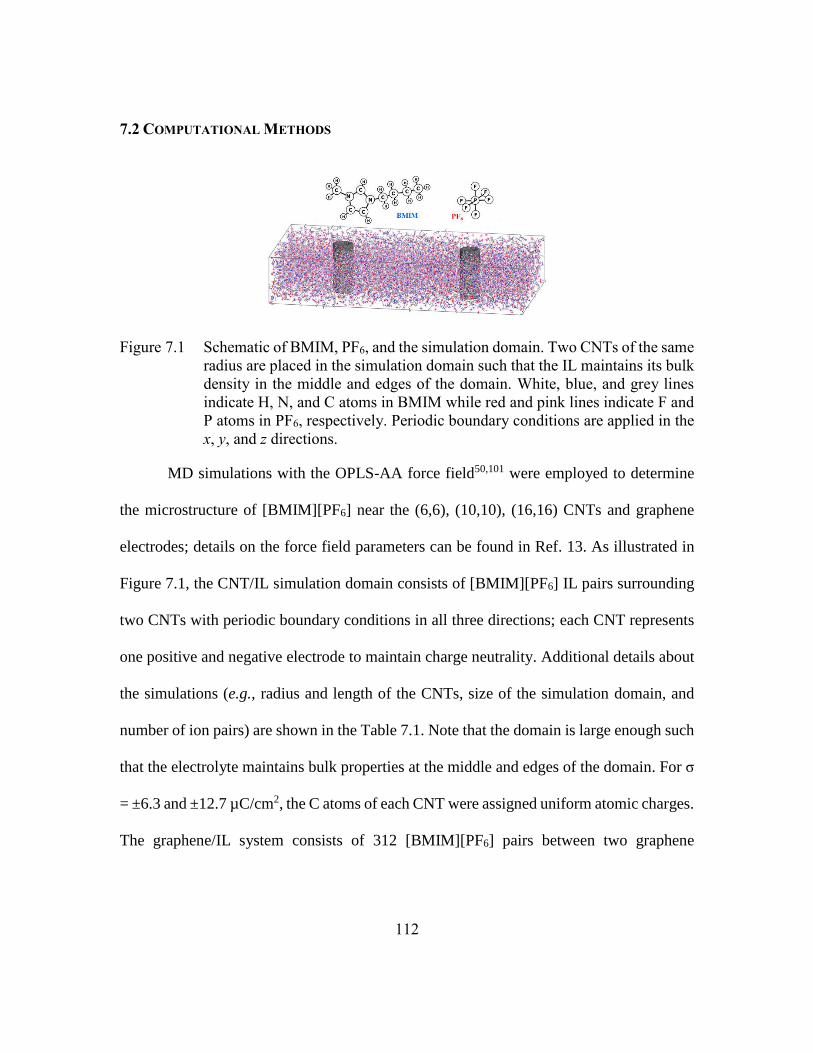
112
7.2 COMPUTATIONAL METHODS
Figure 7.1 Schematic of BMIM, PF6, and the simulation domain. Two CNTs of the same
radius are placed in the simulation domain such that the IL maintains its bulk
density in the middle and edges of the domain. White, blue, and grey lines
indicate H, N, and C atoms in BMIM while red and pink lines indicate F and
P atoms in PF6, respectively. Periodic boundary conditions are applied in the
x, y, and z directions.
MD simulations with the OPLS-AA force field50,101 were employed to determine
the microstructure of [BMIM][PF6] near the (6,6), (10,10), (16,16) CNTs and graphene
electrodes; details on the force field parameters can be found in Ref. 13. As illustrated in
Figure 7.1, the CNT/IL simulation domain consists of [BMIM][PF6] IL pairs surrounding
two CNTs with periodic boundary conditions in all three directions; each CNT represents
one positive and negative electrode to maintain charge neutrality. Additional details about
the simulations (e.g., radius and length of the CNTs, size of the simulation domain, and
number of ion pairs) are shown in the Table 7.1. Note that the domain is large enough such
that the electrolyte maintains bulk properties at the middle and edges of the domain. For σ
= ±6.3 and ±12.7 µC/cm2, the C atoms of each CNT were assigned uniform atomic charges.
The graphene/IL system consists of 312 [BMIM][PF6] pairs between two graphene
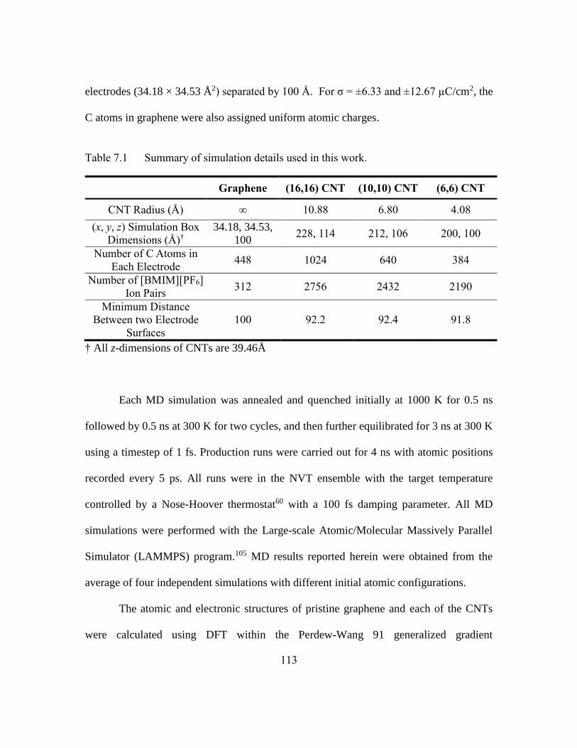
113
electrodes (34.18 × 34.53 Å2) separated by 100 Å. For σ = ±6.33 and ±12.67 µC/cm2, the
C atoms in graphene were also assigned uniform atomic charges.
Table 7.1 Summary of simulation details used in this work.
Graphene (16,16) CNT (10,10) CNT (6,6) CNT
CNT Radius (Å) ∞ 10.88 6.80 4.08
(x, y, z) Simulation Box
Dimensions (Å)† 34.18, 34.53,
100 228, 114 212, 106 200, 100
Number of C Atoms in
Each Electrode 448 1024 640 384
Number of [BMIM][PF6]
Ion Pairs 312 2756 2432 2190
Minimum Distance
Between two Electrode
Surfaces 100 92.2 92.4 91.8
† All z-dimensions of CNTs are 39.46Å
Each MD simulation was annealed and quenched initially at 1000 K for 0.5 ns
followed by 0.5 ns at 300 K for two cycles, and then further equilibrated for 3 ns at 300 K
using a timestep of 1 fs. Production runs were carried out for 4 ns with atomic positions
recorded every 5 ps. All runs were in the NVT ensemble with the target temperature
controlled by a Nose-Hoover thermostat60 with a 100 fs damping parameter. All MD
simulations were performed with the Large-scale Atomic/Molecular Massively Parallel
Simulator (LAMMPS) program.105 MD results reported herein were obtained from the
average of four independent simulations with different initial atomic configurations.
The atomic and electronic structures of pristine graphene and each of the CNTs
were calculated using DFT within the Perdew-Wang 91 generalized gradient
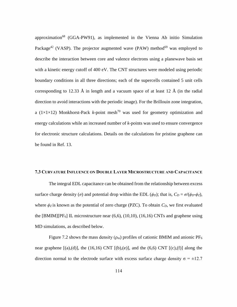
114
approximation68 (GGA-PW91), as implemented in the Vienna Ab initio Simulation
Package42 (VASP). The projector augmented wave (PAW) method69 was employed to
describe the interaction between core and valence electrons using a planewave basis set
with a kinetic energy cutoff of 400 eV. The CNT structures were modeled using periodic
boundary conditions in all three directions; each of the supercells contained 5 unit cells
corresponding to 12.33 Å in length and a vacuum space of at least 12 Å (in the radial
direction to avoid interactions with the periodic image). For the Brillouin zone integration,
a (1×1×12) Monkhorst-Pack k-point mesh70 was used for geometry optimization and
energy calculations while an increased number of k-points was used to ensure convergence
for electronic structure calculations. Details on the calculations for pristine graphene can
be found in Ref. 13.
7.3 CURVATURE INFLUENCE ON DOUBLE LAYER MICROSTRUCTURE AND CAPACITANCE
The integral EDL capacitance can be obtained from the relationship between excess
surface charge density (σ) and potential drop within the EDL (ϕD); that is, CD = σ/(ϕD-ϕZ),
where ϕZ is known as the potential of zero charge (PZC). To obtain CD, we first evaluated
the [BMIM][PF6] IL microstructure near (6,6), (10,10), (16,16) CNTs and graphene using
MD simulations, as described below.
Figure 7.2 shows the mass density (ρm) profiles of cationic BMIM and anionic PF6
near graphene [(a),(d)], the (16,16) CNT [(b),(e)], and the (6,6) CNT [(c),(f)] along the
direction normal to the electrode surface with excess surface charge density σ = ±12.7
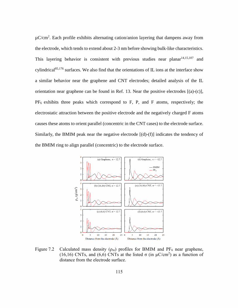
115
µC/cm2. Each profile exhibits alternating cation/anion layering that dampens away from
the electrode, which tends to extend about 2-3 nm before showing bulk-like characteristics.
This layering behavior is consistent with previous studies near planar14,15,107 and
cylindrical85,176 surfaces. We also find that the orientations of IL ions at the interface show
a similar behavior near the graphene and CNT electrodes; detailed analysis of the IL
orientation near graphene can be found in Ref. 13. Near the positive electrodes [(a)-(c)],
PF6 exhibits three peaks which correspond to F, P, and F atoms, respectively; the
electrostatic attraction between the positive electrode and the negatively charged F atoms
causes these atoms to orient parallel (concentric in the CNT cases) to the electrode surface.
Similarly, the BMIM peak near the negative electrode [(d)-(f)] indicates the tendency of
the BMIM ring to align parallel (concentric) to the electrode surface.
Figure 7.2 Calculated mass density (ρm) profiles for BMIM and PF6 near graphene,
(16,16) CNTs, and (6,6) CNTs at the listed σ (in µC/cm2) as a function of
distance from the electrode surface.
116
Figure 7.3 (a) Schematic of IL accumulation near a CNT [left] and graphene [right] with
the electrodes shown in red. The electrode surface charge is balanced by the
counterions represented in black. Excess IL ions in the EDL are represented
in white. (b) Schematic of the electric field strength as a function of distance
from the electrode for varying electrode curvatures.
As the curvature of the electrode increases [graphene < (16,16) CNT < (6,6) CNT],
the oscillations in the mass density profiles appear to dampen. In particular, the counterion
mass density peaks become increasingly smaller and more broadened. The peak (average)
density of PF6 in the first layer is 1.52 (3.23) > 1.43 (3.01) > 1.31 (2.46) g/cm3 near the
positively charged graphene > (16,16) CNT > (6,6) CNT. Similarly, near the negatively
charged electrodes, the peak (average) density of BMIM in the first layer is 1.15 (3.69) >
1.05 (3.30) > 0.98 (2.62) g/cm3 for graphene > (16,16) CNT > (6,6) CNT. These
observations indicate that the packing density of counterions varies inversely with respect
to electrode curvature. In addition, the density of coions is also noticeably influenced by
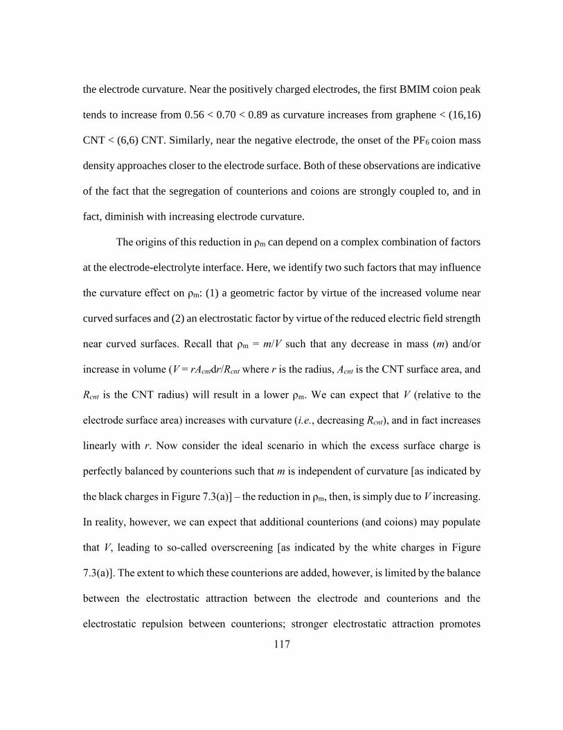
117
the electrode curvature. Near the positively charged electrodes, the first BMIM coion peak
tends to increase from 0.56 < 0.70 < 0.89 as curvature increases from graphene < (16,16)
CNT < (6,6) CNT. Similarly, near the negative electrode, the onset of the PF6 coion mass
density approaches closer to the electrode surface. Both of these observations are indicative
of the fact that the segregation of counterions and coions are strongly coupled to, and in
fact, diminish with increasing electrode curvature.
The origins of this reduction in ρm can depend on a complex combination of factors
at the electrode-electrolyte interface. Here, we identify two such factors that may influence
the curvature effect on ρm: (1) a geometric factor by virtue of the increased volume near
curved surfaces and (2) an electrostatic factor by virtue of the reduced electric field strength
near curved surfaces. Recall that ρm = m/V such that any decrease in mass (m) and/or
increase in volume (V = rAcntdr/Rcnt where r is the radius, Acnt is the CNT surface area, and
Rcnt is the CNT radius) will result in a lower ρm. We can expect that V (relative to the
electrode surface area) increases with curvature (i.e., decreasing Rcnt), and in fact increases
linearly with r. Now consider the ideal scenario in which the excess surface charge is
perfectly balanced by counterions such that m is independent of curvature [as indicated by
the black charges in Figure 7.3(a)] – the reduction in ρm, then, is simply due to V increasing.
In reality, however, we can expect that additional counterions (and coions) may populate
that V, leading to so-called overscreening [as indicated by the white charges in Figure
7.3(a)]. The extent to which these counterions are added, however, is limited by the balance
between the electrostatic attraction between the electrode and counterions and the
electrostatic repulsion between counterions; stronger electrostatic attraction promotes
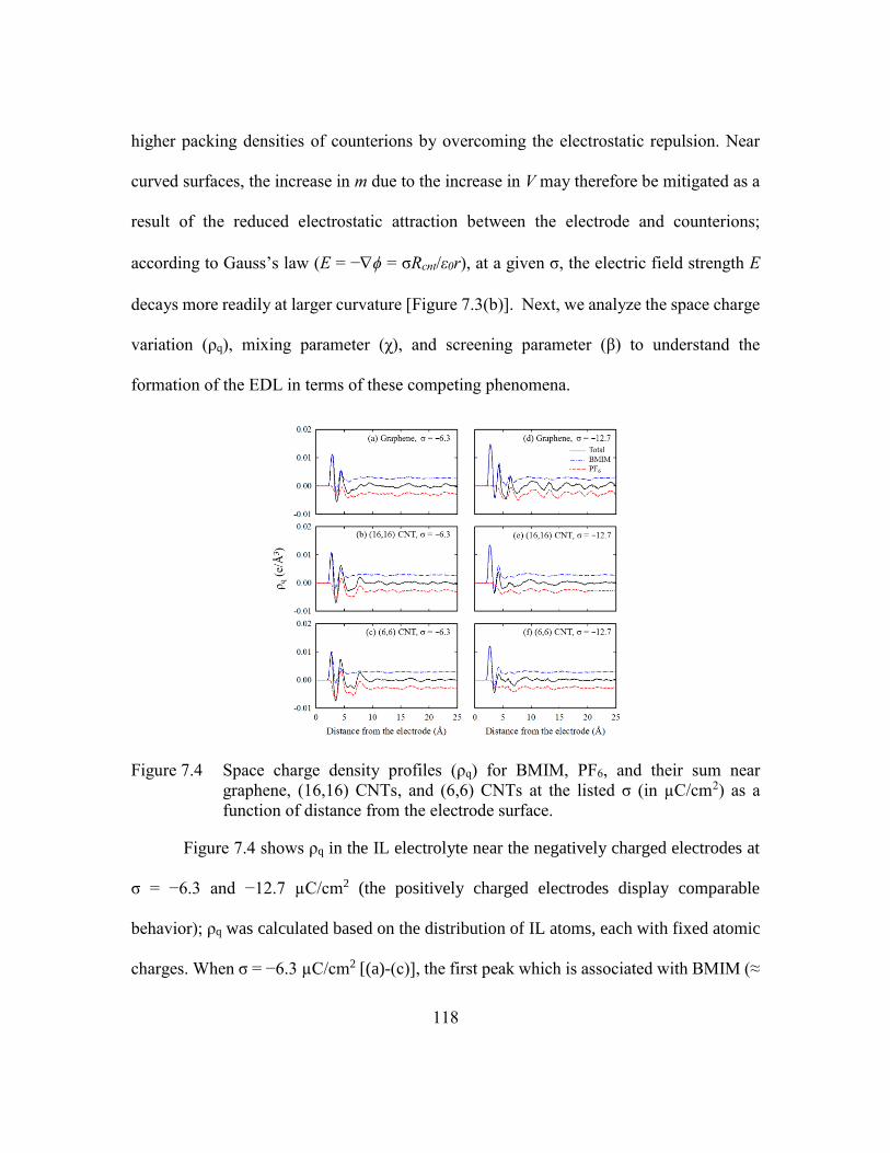
118
higher packing densities of counterions by overcoming the electrostatic repulsion. Near
curved surfaces, the increase in m due to the increase in V may therefore be mitigated as a
result of the reduced electrostatic attraction between the electrode and counterions;
according to Gauss’s law (E = −ϕ = σRcnt/ε0r), at a given σ, the electric field strength E
decays more readily at larger curvature [Figure 7.3(b)]. Next, we analyze the space charge
variation (ρq), mixing parameter (χ), and screening parameter (β) to understand the
formation of the EDL in terms of these competing phenomena.
Figure 7.4 Space charge density profiles (ρq) for BMIM, PF6, and their sum near
graphene, (16,16) CNTs, and (6,6) CNTs at the listed σ (in µC/cm2) as a
function of distance from the electrode surface.
Figure 7.4 shows ρq in the IL electrolyte near the negatively charged electrodes at
σ = −6.3 and −12.7 µC/cm2 (the positively charged electrodes display comparable
behavior); ρq was calculated based on the distribution of IL atoms, each with fixed atomic
charges. When σ = −6.3 µC/cm2 [(a)-(c)], the first peak which is associated with BMIM (≈
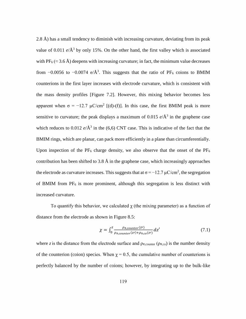
119
2.8 Å) has a small tendency to diminish with increasing curvature, deviating from its peak
value of 0.011 e/Å3 by only 15%. On the other hand, the first valley which is associated
with PF6 (≈ 3.6 Å) deepens with increasing curvature; in fact, the minimum value decreases
from −0.0056 to −0.0074 e/Å3. This suggests that the ratio of PF6 coions to BMIM
counterions in the first layer increases with electrode curvature, which is consistent with
the mass density profiles [Figure 7.2]. However, this mixing behavior becomes less
apparent when σ = −12.7 µC/cm2 [(d)-(f)]. In this case, the first BMIM peak is more
sensitive to curvature; the peak displays a maximum of 0.015 e/Å3 in the graphene case
which reduces to 0.012 e/Å3 in the (6,6) CNT case. This is indicative of the fact that the
BMIM rings, which are planar, can pack more efficiently in a plane than circumferentially.
Upon inspection of the PF6 charge density, we also observe that the onset of the PF6
contribution has been shifted to 3.8 Å in the graphene case, which increasingly approaches
the electrode as curvature increases. This suggests that at σ = −12.7 µC/cm2, the segregation
of BMIM from PF6 is more prominent, although this segregation is less distinct with
increased curvature.
To quantify this behavior, we calculated χ (the mixing parameter) as a function of
distance from the electrode as shown in Figure 8.5:
𝜒 = ∫𝜌#,𝑐𝑜𝑢𝑛𝑡𝑒𝑟(𝑧′)
𝜌#,𝑐𝑜𝑢𝑛𝑡𝑒𝑟(𝑧′)+𝜌#,𝑐𝑜(𝑧′)𝑑𝑧′
𝑧
0 (7.1)
where z is the distance from the electrode surface and ρ#,counter (ρ#,co) is the number density
of the counterion (coion) species. When χ = 0.5, the cumulative number of counterions is
perfectly balanced by the number of coions; however, by integrating up to the bulk-like
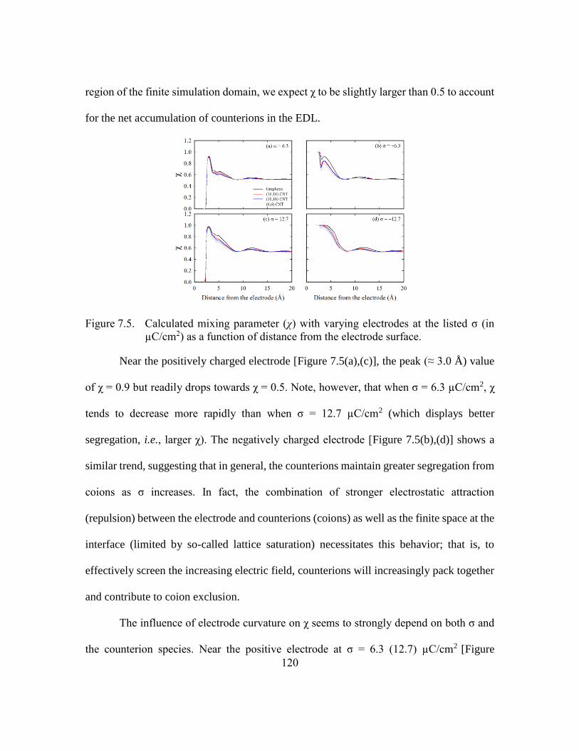
120
region of the finite simulation domain, we expect χ to be slightly larger than 0.5 to account
for the net accumulation of counterions in the EDL.
Figure 7.5. Calculated mixing parameter (χ) with varying electrodes at the listed σ (in
µC/cm2) as a function of distance from the electrode surface.
Near the positively charged electrode [Figure 7.5(a),(c)], the peak (≈ 3.0 Å) value
of χ = 0.9 but readily drops towards χ = 0.5. Note, however, that when σ = 6.3 µC/cm2, χ
tends to decrease more rapidly than when σ = 12.7 µC/cm2 (which displays better
segregation, i.e., larger χ). The negatively charged electrode [Figure 7.5(b),(d)] shows a
similar trend, suggesting that in general, the counterions maintain greater segregation from
coions as σ increases. In fact, the combination of stronger electrostatic attraction
(repulsion) between the electrode and counterions (coions) as well as the finite space at the
interface (limited by so-called lattice saturation) necessitates this behavior; that is, to
effectively screen the increasing electric field, counterions will increasingly pack together
and contribute to coion exclusion.
The influence of electrode curvature on χ seems to strongly depend on both σ and
the counterion species. Near the positive electrode at σ = 6.3 (12.7) µC/cm2 [Figure
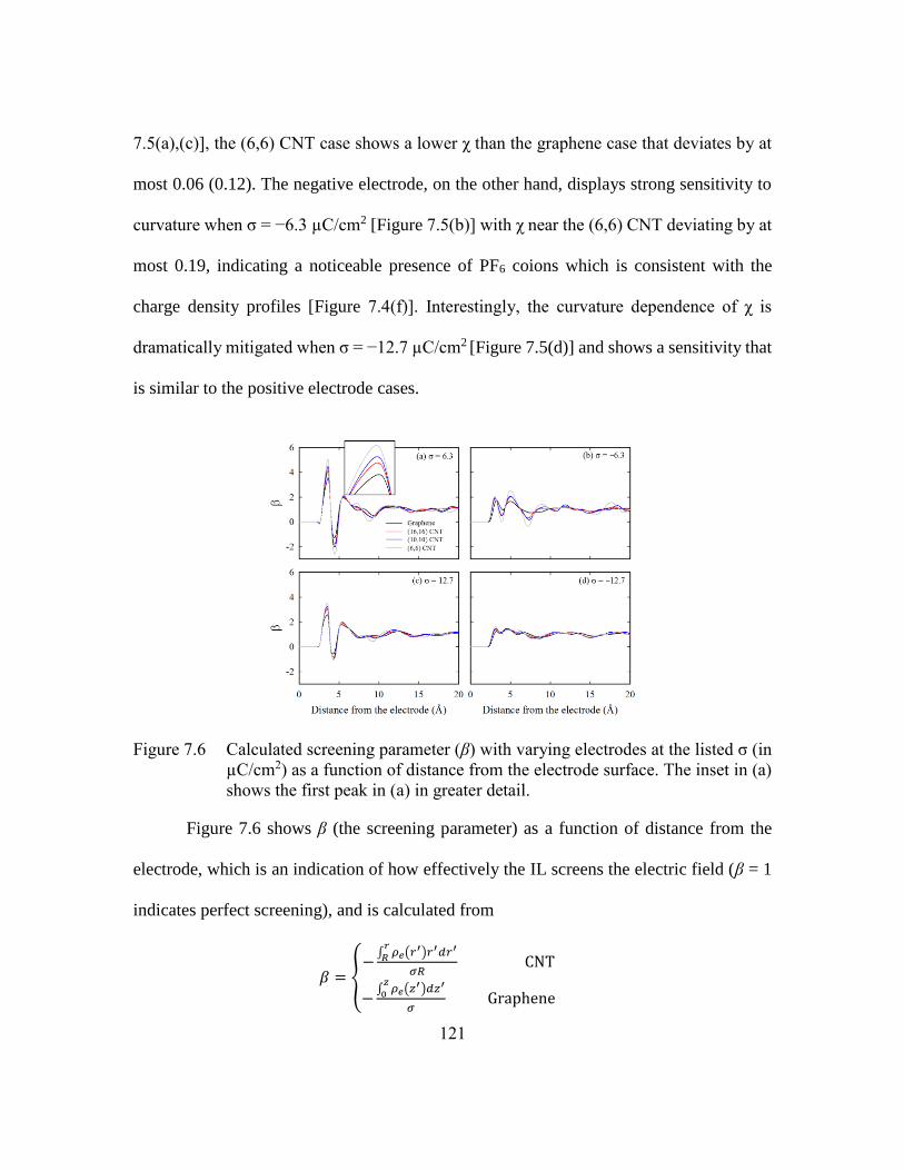
121
7.5(a),(c)], the (6,6) CNT case shows a lower χ than the graphene case that deviates by at
most 0.06 (0.12). The negative electrode, on the other hand, displays strong sensitivity to
curvature when σ = −6.3 µC/cm2 [Figure 7.5(b)] with χ near the (6,6) CNT deviating by at
most 0.19, indicating a noticeable presence of PF6 coions which is consistent with the
charge density profiles [Figure 7.4(f)]. Interestingly, the curvature dependence of χ is
dramatically mitigated when σ = −12.7 µC/cm2 [Figure 7.5(d)] and shows a sensitivity that
is similar to the positive electrode cases.
Figure 7.6 Calculated screening parameter (β) with varying electrodes at the listed σ (in
µC/cm2) as a function of distance from the electrode surface. The inset in (a)
shows the first peak in (a) in greater detail.
Figure 7.6 shows β (the screening parameter) as a function of distance from the
electrode, which is an indication of how effectively the IL screens the electric field (β = 1
indicates perfect screening), and is calculated from
𝛽 = {−
∫ 𝜌𝑒(𝑟′)𝑟′𝑑𝑟′𝑟𝑅
𝜎𝑅 CNT
−∫ 𝜌𝑒(𝑧′)𝑑𝑧′𝑧
0
𝜎 Graphene

122
where R is the CNT radius.
Our results show that ILs in the EDL typically overscreen the electric field, in good
agreement with previous theoretical studies13,111. In fact, the ions near the positive electrode
[Figure 7.6(a),(c)] generally tend to exhibit stronger overscreening than those near the
negative electrodes. This is primarily due to differences in the size and charge distribution
of BMIM and PF6. Near the positive electrode, PF6 can tightly pack together due to its
“spherical” symmetric shape; the first sharp peak [in Figure 7.6(a),(c)] is attributed to the
F atoms which are modeled here with a partial charge of −0.39 e. In contrast, the positive
charge in BMIM is spread somewhat broadly over its ring, which can partially account for
the smaller peaks near the negative electrode [Figure 7.6(b),(d)]. The peak is also
diminished since BMIM does not accumulate as readily as its PF6 counterpart due to its
bulky structure. As a result, PF6 seems to be more effective at screening the electric field
compared to BMIM. Furthermore, the peaks in β tend to diminish as σ increases since the
packing density of ions approach an asymptote that is defined by steric limitations. As σ
increases further beyond the so-called lattice saturation limit, the first IL layer is expected
to have β < 1.
From Figure 7.6, we also observe that increasing the electrode curvature results in
additional screening by the first IL layer. Note that the larger β near the CNTs is an
indication of a greater net number of counterions (i.e., those that are not paired with coions)
relative to the electrode surface area. This suggests that the counterions prefer to
overpopulate the first IL layer due to the increasing availability of space near curved
electrodes. Yet despite their larger numbers, these counterions near curved electrodes pack
123
less efficiently in that space as observed from the mass density profiles [Figure 7.2]. This
is due to the aforementioned reduced near-surface electric field strength which effectively
weakens the ability of the electrode-counterion attraction to overcome the counterion-
counterion repulsion. Because of the availability of space, the enhanced screening of the
electrode charge by the counterions near the curved electrodes also facilitates the
electrostatic attraction between counterions and coions, which promotes coion mixing at
the interface that is consistent with our previous discussion on IL mixing. However, this
behavior is also sensitive to the specific ability of the IL counterions to sterically exclude
the coions as discussed previously.
From ρq (the charge density), the electric potential (ϕ) profiles along the electrode
surface normal direction were calculated by solving Poisson’s equation, such that ϕ is given
by
𝜙(𝑧) = {−
𝜎𝑅
𝜖0ln
𝑟
𝑅−
1
𝜖0∫ 𝜌𝑞(𝑟′)𝑟′ ln
𝑟
𝑟′ 𝑑𝑟′𝑟
𝑅 CNT
−𝜎𝑧
𝜖0−
1
𝜖0∫ (𝑧 − 𝑧′)𝜌𝑞(𝑧′)𝑑𝑧′𝑧
0 Graphene
where ε0 is the vacuum permittivity.
The calculated potential (ϕ) profiles for graphene and the three CNT cases are
shown in Figure 7.7. In each panel, it is evident that the |ϕ| increases more rapidly near
interfaces with decreasing electrode curvature; for instance, the |ϕ| in the graphene case at
2.5 Å from the surface is around 0.5 V (1.0 V) more than that of the (6,6) CNT case when
σ = ±6.3 (±12.7) µC/cm2. This is primarily attributed to the fact that the electric field
strength decays radially in the CNT cases while remaining constant in the graphene case
[Figure 7.3].
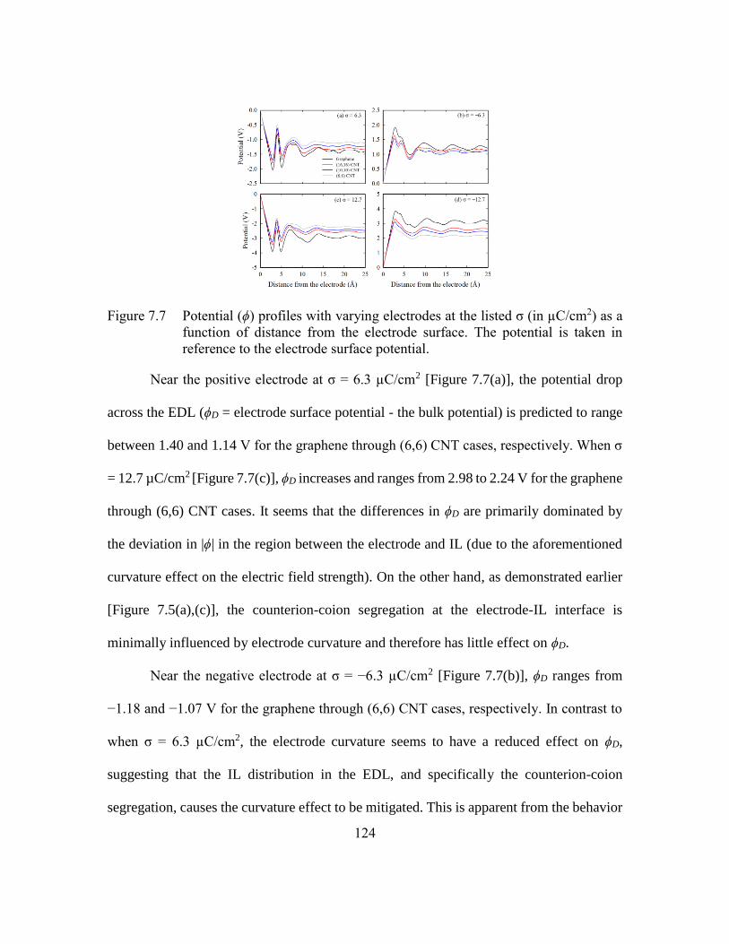
124
Figure 7.7 Potential (ϕ) profiles with varying electrodes at the listed σ (in µC/cm2) as a
function of distance from the electrode surface. The potential is taken in
reference to the electrode surface potential.
Near the positive electrode at σ = 6.3 µC/cm2 [Figure 7.7(a)], the potential drop
across the EDL (ϕD = electrode surface potential - the bulk potential) is predicted to range
between 1.40 and 1.14 V for the graphene through (6,6) CNT cases, respectively. When σ
= 12.7 µC/cm2 [Figure 7.7(c)], ϕD increases and ranges from 2.98 to 2.24 V for the graphene
through (6,6) CNT cases. It seems that the differences in ϕD are primarily dominated by
the deviation in |ϕ| in the region between the electrode and IL (due to the aforementioned
curvature effect on the electric field strength). On the other hand, as demonstrated earlier
[Figure 7.5(a),(c)], the counterion-coion segregation at the electrode-IL interface is
minimally influenced by electrode curvature and therefore has little effect on ϕD.
Near the negative electrode at σ = −6.3 µC/cm2 [Figure 7.7(b)], ϕD ranges from
−1.18 and −1.07 V for the graphene through (6,6) CNT cases, respectively. In contrast to
when σ = 6.3 µC/cm2, the electrode curvature seems to have a reduced effect on ϕD,
suggesting that the IL distribution in the EDL, and specifically the counterion-coion
segregation, causes the curvature effect to be mitigated. This is apparent from the behavior
125
of the potential profiles around 3-4 Å away from the electrode [Figure 7.7(b)] which is the
location of the first IL layer. As demonstrated by the graphene case, ϕ drops monotonically
in highly rich regions of counterions. For each of the CNT cases, ϕ drops then rises as a
small hump before dropping again. Recall that when σ = −6.3 µC/cm2, the segregation
between BMIM and PF6 is reduced near curved surfaces [Figure 7.5(b)], which ultimately
lowers the screening of the electric field and increases |ϕD| for each CNT case such that
they are closer to the graphene case. However, the discrepancy in ϕD, which ranges from
3.08 to 2.16 for the graphene through (6,6) CNT cases, increases when σ = −12.7 µC/cm2
[Figure 7.7(d)]. Note that the ϕ profiles no longer display a small hump around 3-4 Å away
from the electrode, which is consistent with the fact that the curvature effect on χ is greatly
mitigated when σ = −12.7 µC/cm2 [Figure 7.5(d)] due to the increased packing density of
BMIM while PF6 is also increasingly excluded.
Figure 7.8 shows the predicted CD near the positive [(a)] and negative [(b)]
electrodes with varying curvature, which tends to have a direct linear relationship. Recall
that CD = σ/(ϕD-ϕZ) where ϕZ is the potential at zero charge, which is nearly zero in all cases
studied. Hence, CD increases with curvature as a result of the decreasing ϕD. Near the
positive electrode, the CD at each electrode does not change significantly for both σ = 6.3
and 12.7 µC/cm2. This is due to the ability of PF6 to pack efficiently, thereby preventing
lattice saturation. However, we can expect CD to drop as σ continues to increase. The CD
is also suppressed when σ goes from −6.3 to −12.7 µC/cm2, which results from the lattice
saturation by BMIM. Interestingly, the drop in CD seems to be increasingly mitigated with
electrode curvature; the onset of lattice saturation, as discussed previously, is suppressed
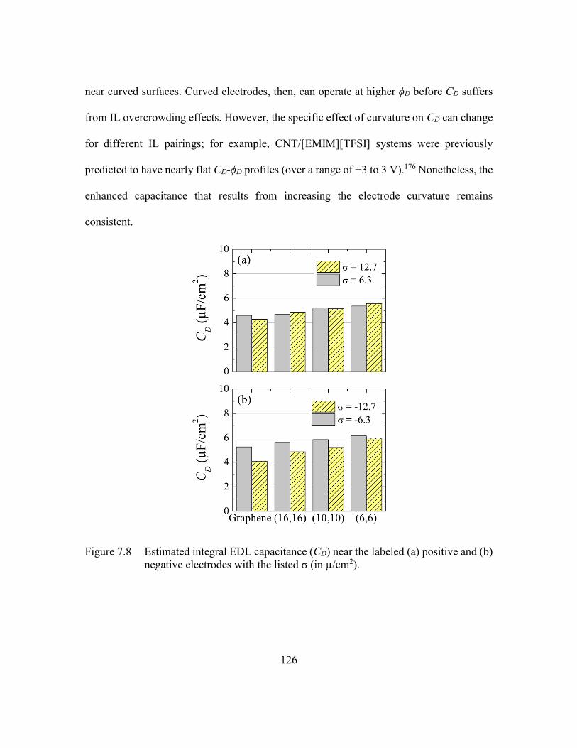
126
near curved surfaces. Curved electrodes, then, can operate at higher ϕD before CD suffers
from IL overcrowding effects. However, the specific effect of curvature on CD can change
for different IL pairings; for example, CNT/[EMIM][TFSI] systems were previously
predicted to have nearly flat CD-ϕD profiles (over a range of −3 to 3 V).176 Nonetheless, the
enhanced capacitance that results from increasing the electrode curvature remains
consistent.
Figure 7.8 Estimated integral EDL capacitance (CD) near the labeled (a) positive and (b)
negative electrodes with the listed σ (in µ/cm2).
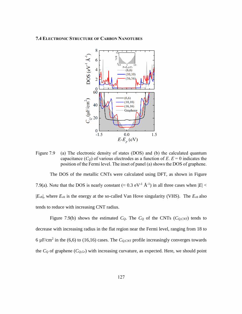
127
7.4 ELECTRONIC STRUCTURE OF CARBON NANOTUBES
Figure 7.9 (a) The electronic density of states (DOS) and (b) the calculated quantum
capacitance (CQ) of various electrodes as a function of E. E = 0 indicates the
position of the Fermi level. The inset of panel (a) shows the DOS of graphene.
The DOS of the metallic CNTs were calculated using DFT, as shown in Figure
7.9(a). Note that the DOS is nearly constant (≈ 0.3 eV-1 Å-1) in all three cases when |E| <
|Evh|, where Evh is the energy at the so-called Van Hove singularity (VHS). The Evh also
tends to reduce with increasing CNT radius.
Figure 7.9(b) shows the estimated CQ. The CQ of the CNTs (CQ,CNT) tends to
decrease with increasing radius in the flat region near the Fermi level, ranging from 18 to
6 µF/cm2 in the (6,6) to (16,16) cases. The CQ,CNT profile increasingly converges towards
the CQ of graphene (CQ,Gr) with increasing curvature, as expected. Here, we should point
128
out that the magnitude of CQ,CNT near the VHS peaks may be underestimated due to
numerical errors and can exhibit larger variation.
7.5 INTERFACIAL CAPACITANCE OF [BMIM][PF6]/CNT SYSTEMS
The total capacitance (CT) at the electrode-IL interface can be represented as a
series of CQ and CD, i.e., 1/CT = 1/CQ + 1/CD. With the CQ and CD values calculated above,
we estimated CT as a function of applied potential a (with respect to the potential of the
bulk electrolyte, i.e., a = E + D) as shown in Table 7.2. The relationship between CQ and
CD with a was obtained through σ; recall that CQ/CD σ E/D (see Chapter 2).
Table 7.2 shows a summary of the calculated CT (a) for each electrode case when
σ = ±6.3 and ±12.7 µC/cm2. When σ = ±6.3 µC/cm2, C T tends to be sensitive to electrode
curvature, yet does not increase directly with curvature. In fact, CT for both the (16,16) and
(6,6) CNT cases is predicted to be less than that of the graphene and (10,10), in
contradiction with the trend observed for CD. This is primarily due to the relatively larger
CQ for the graphene and (10,10) cases when σ = ±6.3 µC/cm2. The values of CQ for the
graphene, (16,16), (10,10), and (6,6) CNTs are around 10.5, 10.6, 10.2, and 16.8 µF/cm2,
respectively; note that the CQ for the (10,10) CNT is large because of the VHS. When σ =
±12.7 µC/cm2, however, CT follows the same trend observed for CD; each of the CQ values
exceeds 19 µF/cm2 (>> CD = 4−6 µF/cm2), making the CD the dominating factor.
Our study clearly suggests that the influence of electrode curvature on the overall
performance is strongly dependent on the relative contributions of CQ and CD which both
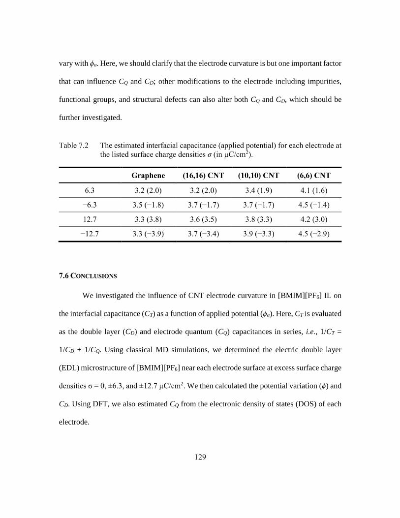
129
vary with ϕa. Here, we should clarify that the electrode curvature is but one important factor
that can influence CQ and CD; other modifications to the electrode including impurities,
functional groups, and structural defects can also alter both CQ and CD, which should be
further investigated.
Table 7.2 The estimated interfacial capacitance (applied potential) for each electrode at
the listed surface charge densities σ (in µC/cm2).
Graphene (16,16) CNT (10,10) CNT (6,6) CNT
6.3 3.2 (2.0) 3.2 (2.0) 3.4 (1.9) 4.1 (1.6)
−6.3 3.5 (−1.8) 3.7 (−1.7) 3.7 (−1.7) 4.5 (−1.4)
12.7 3.3 (3.8) 3.6 (3.5) 3.8 (3.3) 4.2 (3.0)
−12.7 3.3 (−3.9) 3.7 (−3.4) 3.9 (−3.3) 4.5 (−2.9)
7.6 CONCLUSIONS
We investigated the influence of CNT electrode curvature in [BMIM][PF6] IL on
the interfacial capacitance (CT) as a function of applied potential (ϕa). Here, CT is evaluated
as the double layer (CD) and electrode quantum (CQ) capacitances in series, i.e., 1/CT =
1/CD + 1/CQ. Using classical MD simulations, we determined the electric double layer
(EDL) microstructure of [BMIM][PF6] near each electrode surface at excess surface charge
densities σ = 0, ±6.3, and ±12.7 µC/cm2. We then calculated the potential variation (ϕ) and
CD. Using DFT, we also estimated CQ from the electronic density of states (DOS) of each
electrode.

130
Our analysis of the EDL microstructure reveals that general features near graphene
electrodes, such as the multi-layering of anions/cations and the IL orientations, are
consistent near CNT electrodes. However, increasing the electrode curvature tends to
reduce the density of IL counterions closest to the electrode, which we find is a
consequence of weakened electrostatic attraction between the electrode and counterions.
Despite the reduced density, we also find that increasing the electrode curvature enhances
the screening of the electrode charge and promotes counterion-coion mixing (i.e., less
segregation), although increasing σ abates both of these phenomena.
From the calculation results of ϕ, we observe that the potential drop in the EDL
(ϕD) diminishes as electrode curvature increases. This reduction is primarily attributed to
the fact that the electric field strength decays radially near the CNTs while remaining
constant near graphene. When σ = −6.3 µC/cm2, however, the curvature effect is mitigated
and is ascribed to the increased mixing of counterions and coions near the CNTs; the
reduced segregation effectively lowers the screening of the electric field such that ϕD is less
sensitive to curvature.
The lower ϕD amounts to a larger CD which tends to increase as electrode curvature
increases. When σ = ±6.3 µC/cm2, for example, an enhancement of around 18% using (6,6)
CNT electrodes is predicted when compared to graphene. As σ increases, we expect CD to
drop due to overcrowding in the EDL, as is observed when σ = −12.7 µC/cm2. Increasing
the electrode curvature, however, also increases the available space for IL ions to pack. As
a result, the potential window in which CD does not suffer from lattice saturation effects
will be larger near increasingly curved electrodes.
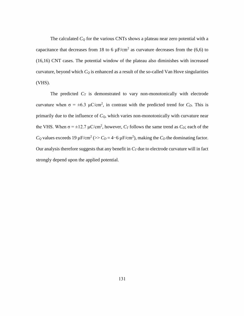
131
The calculated CQ for the various CNTs shows a plateau near zero potential with a
capacitance that decreases from 18 to 6 µF/cm2 as curvature decreases from the (6,6) to
(16,16) CNT cases. The potential window of the plateau also diminishes with increased
curvature, beyond which CQ is enhanced as a result of the so-called Van Hove singularities
(VHS).
The predicted CT is demonstrated to vary non-monotonically with electrode
curvature when σ = ±6.3 µC/cm2, in contrast with the predicted trend for CD. This is
primarily due to the influence of CQ, which varies non-monotonically with curvature near
the VHS. When σ = ±12.7 µC/cm2, however, CT follows the same trend as CD; each of the
CQ values exceeds 19 µF/cm2 (>> CD = 4−6 µF/cm2), making the CD the dominating factor.
Our analysis therefore suggests that any benefit in CT due to electrode curvature will in fact
strongly depend upon the applied potential.
132
Chapter 8: Ion Confinement Effects in Charged Cylindrical Pores
8.1 INTRODUCTION TO PORE SIZE EFFECT
Conventionally, the search for electrode materials has been directed toward finding
materials with good electrical conductivity and specific surface areas larger than
commercially-used activated carbons.25,24,177 For these reasons, carbon nanomaterials,
including graphene, carbon nanotubes (CNTs), and carbide-derived carbons (CDCs), have
all been recent subjects of interest. However, the work of Chmiola and coworkers36, and
later, Largeot and coworkers37, used CDC electrodes to show that the areal C can exhibit
dramatic improvement with nominal pore widths comparable to the size of the counter-ion.
These studies suggest that beyond maximizing the surface area, controlling the pore width
offers a new way of increasing C. Exploring this materials development route, however,
requires that an atomistic understanding of charge storage when ions are confined in
nanopores.
The mechanisms responsible for the enhancement in C has been the study of several
theoretical studies; in these works, the electrode is commonly modeled as ideal slit
nanopores. A simple phenomenological model theorized that polarizable electrode walls
screen long-range electrostatics to allow tight packing of similar ions in the so-called
superionic state.178 Classical molecular simulations of charged nanopores demonstrated
consistent behavior in which confined counter-ions were found to maintain elevated
density while co-ions were expelled.179 Several additional factors have been identified as
possible ways of tuning C. For example, an oscillatory dependence of C based on the pore

133
size was revealed by both classical molecular dynamics (MD) simulations173 and classical
DFT simulations180, which was attributed to interference from overlapping EDLs. In
addition to the pore size dependence, classical MD simulations showed that C can be
dependent on V and may be maximized when the co-ions were fully expelled before the
need for additional counter-ion insertion.181
As the primary incentive for supercapacitor adoption is their excellent power
capabilities, it is also important to understand the dynamics of ions confined in charged
nanopores. This is particularly relevant for ionic liquid (IL) electrolytes, which are solvent-
free ions with large electrochemical windows (up to 4 V). In the bulk liquid phase, ILs are
known to have high viscosities, due to strong ion-ion interactions182, which further increase
under confinement183. Interestingly, molecular simulations suggest that ions can achieve
diffusivities that exceed that of their bulk properties when confined in charged pores with
both sufficiently narrow widths and large potentials.184,185 In addition, ion charging
behavior has been suggested to be governed by counter-ion electrokinetics, as
demonstrated by both non-equilibrium MD simulations186 and experiments using the
electrochemical quartz crystal microbalance method187.
Beyond slit-pore geometries, limited studies have investigated other pore types
despite theoretical evidence of greater charge storage in increasingly confined regions188.
Ions confined within cylindrical nanopores, such as CNTs, constitute one such extreme
case. In the absence of external potential, several experimental studies have investigated
the structure of ILs in CNTs with diameters less than 3 nm, which report an interesting
adoption of a solid-like phase.189,190 It may be worthwhile to explore the influence of such
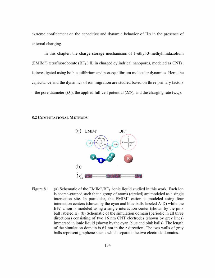
134
extreme confinement on the capacitive and dynamic behavior of ILs in the presence of
external charging.
In this chapter, the charge storage mechanisms of 1-ethyl-3-methylimidazolium
(EMIM+) tetrafluoroborate (BF4-) IL in charged cylindrical nanopores, modeled as CNTs,
is investigated using both equilibrium and non-equilibrium molecular dynamics. Here, the
capacitance and the dynamics of ion migration are studied based on three primary factors
– the pore diameter (Dp), the applied full-cell potential (∆), and the charging rate (chg).
8.2 COMPUTATIONAL METHODS
Figure 8.1 (a) Schematic of the EMIM+/BF4- ionic liquid studied in this work. Each ion
is coarse-grained such that a group of atoms (circled) are modeled as a single
interaction site. In particular, the EMIM+ cation is modeled using four
interaction centers (shown by the cyan and blue balls labeled A-D) while the
BF4- anion is modeled using a single interaction center (shown by the pink
ball labeled E). (b) Schematic of the simulation domain (periodic in all three
directions) consisting of two 16 nm CNT electrodes (shown by grey lines)
immersed in ionic liquid (shown by the cyan, blue and pink balls). The length
of the simulation domain is 64 nm in the z direction. The two walls of grey
balls represent graphene sheets which separate the two electrode domains.
135
Classical MD simulations were employed using LAMMPS105 to investigate the
microstructure and capacitance of IL molecules confined within fixed CNT electrodes
(depicted in Figure 8.1). The IL molecules were described using coarse-grain parameters
(Table 8.1) with partitioning shown in Figure 8.1; EMIM+ cations contained four
interaction centers while BF4- anions contained one interaction center. The LJ parameters
were adapted from Ref. 191; the charges (q) were re-scaled following the fashion of Ref.
192 while the zero-energy pair-wise distance () were re-optimized to reproduce
experimental density (1.28 g/cm3) and diffusivity (3.0-3.710-7 cm2/s). The bond, angle,
and dihedral parameters were adopted from Ref. 56 with the latter case adapted for the
OPLS form. The LJ parameters for the electrode carbon atoms were taken from Ref. 193.
All LJ and Coulomb energies were calculated using a spherical cutoff radius of 16 Å with
the long-range Coulomb energies included by the particle-particle particle-mesh method54.
While the positions of the electrode atoms were fixed, the charge of each atom was
allowed to fluctuate to emulate constant potential surfaces (with ∆). The charge
equilibration (Qeq) scheme194, which is commonly used in ReaxFF simulations195, was
adapted for this purpose. This method is based on equalization of the electronegativity.
Here, the electronegativity of the positive (negative) electrode is rigidly shifted by −∆/2
(+∆/2); while the IL charges are fixed, the electrode charges are solved iteratively at
every timestep with the sum of the total electrode charge constrained to zero. The short-
range Coulomb interactions included shielding corrections195 while the long-range
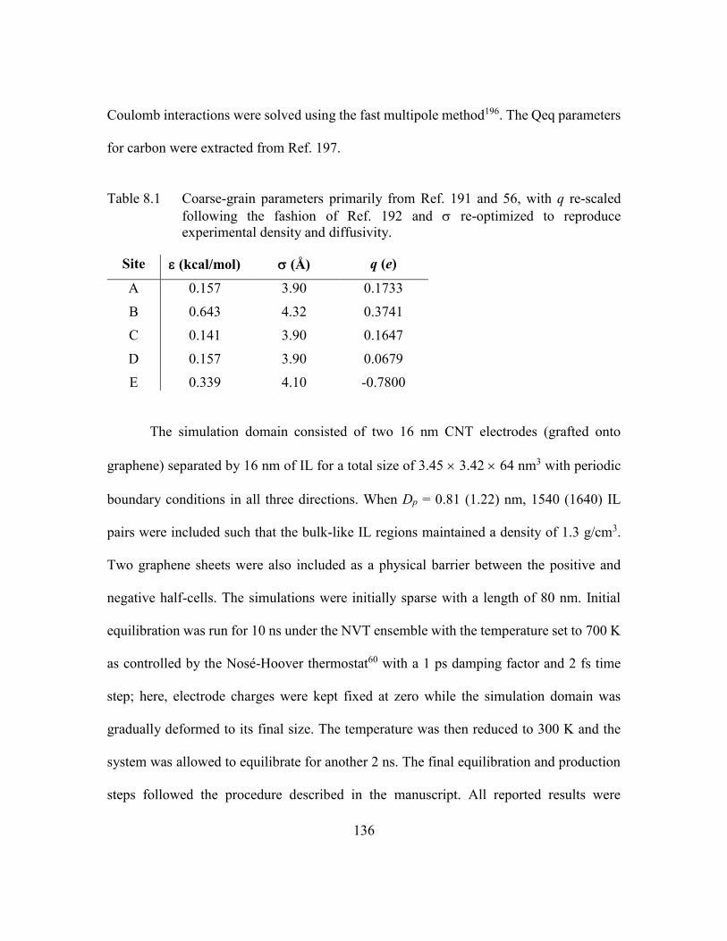
136
Coulomb interactions were solved using the fast multipole method196. The Qeq parameters
for carbon were extracted from Ref. 197.
Table 8.1 Coarse-grain parameters primarily from Ref. 191 and 56, with q re-scaled
following the fashion of Ref. 192 and re-optimized to reproduce
experimental density and diffusivity.
Site (kcal/mol) (Å) q (e)
A 0.157 3.90 0.1733
B 0.643 4.32 0.3741
C 0.141 3.90 0.1647
D 0.157 3.90 0.0679
E 0.339 4.10 -0.7800
The simulation domain consisted of two 16 nm CNT electrodes (grafted onto
graphene) separated by 16 nm of IL for a total size of 3.45 3.42 64 nm3 with periodic
boundary conditions in all three directions. When Dp = 0.81 (1.22) nm, 1540 (1640) IL
pairs were included such that the bulk-like IL regions maintained a density of 1.3 g/cm3.
Two graphene sheets were also included as a physical barrier between the positive and
negative half-cells. The simulations were initially sparse with a length of 80 nm. Initial
equilibration was run for 10 ns under the NVT ensemble with the temperature set to 700 K
as controlled by the Nosé-Hoover thermostat60 with a 1 ps damping factor and 2 fs time
step; here, electrode charges were kept fixed at zero while the simulation domain was
gradually deformed to its final size. The temperature was then reduced to 300 K and the
system was allowed to equilibrate for another 2 ns. The final equilibration and production
steps followed the procedure described in the manuscript. All reported results were
137
obtained from the average of four independent simulations with different initial atomic
configurations.
8.3 IONIC LIQUID MICROSTRUCTURE CONFINED WITHIN CNTS
A. Neutral CNT electrodes
We first investigate the electrode excess surface charge density (CNT) distribution
and ionic liquid (IL) microstructure under zero applied bias ( = 0 V). Two CNT
electrodes with Dp = 0.81 and 1.22 nm are considered with a length (Lp) of 16 nm to
maintain large aspect ratios (Lp >> Dp).
Figure 8.2(a) depicts a snapshot of the ions confined within the positive electrode.
When Dp = 0.81 nm, the ions are observed to form a molecular wire structure with highly
partitioned cations and anions. As such, distinct peaks are seen to alternate between cations
and anions in the number density (ion) plots shown in Figure 8.2(b). Each ion is caged by
its corresponding counter-ion to maintain charge neutrality. In addition, each ion also tends
to distinctly polarize the surrounding electrode atoms, as seen by the large oscillations in
the CNT plot shown in Figure 8.2(d), which serves to screen the ion charge. In contrast
when Dp = 1.22 nm, the larger internal volume allows the ions to mix axially (a spiral-like
configuration); the removal of axial segregation is evident by the suppressed oscillations
in the ion profile shown in Figure 8.2(c). The cations also tend to conform close to the
electrode walls (Figure 8.2(a)) in order to maximize van der Waals and electrostatic ion-
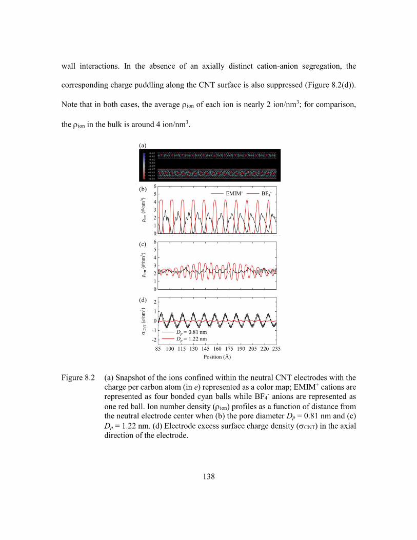
138
wall interactions. In the absence of an axially distinct cation-anion segregation, the
corresponding charge puddling along the CNT surface is also suppressed (Figure 8.2(d)).
Note that in both cases, the average ion of each ion is nearly 2 ion/nm3; for comparison,
the ion in the bulk is around 4 ion/nm3.
Figure 8.2 (a) Snapshot of the ions confined within the neutral CNT electrodes with the
charge per carbon atom (in e) represented as a color map; EMIM+ cations are
represented as four bonded cyan balls while BF4- anions are represented as
one red ball. Ion number density (ion) profiles as a function of distance from
the neutral electrode center when (b) the pore diameter Dp = 0.81 nm and (c)
Dp = 1.22 nm. (d) Electrode excess surface charge density (CNT) in the axial
direction of the electrode.
139
B. Charged CNT electrodes
Next, = 3 V is impulsively applied to the electrodes. Here, the electrodes tend
to attain full charge after 40 ps but are allowed to equilibrate for 4 ns before statistics are
extracted over additional 2 ns trajectories. Interestingly, as depicted in Figure 8.3(a),
distinct differences in the IL microstructures appear when comparing the two electrode
diameters. Most notably, the IL distribution along the axial direction of the positive
electrode is heterogeneous when Dp = 0.81 nm and homogeneous when Dp = 1.22 nm. For
simplicity, the negative electrode is not depicted but has qualitatively similar features as
discussed below.
In the more confined case (Dp = 0.81 nm), a region containing both EMIM+ co-ions
and BF4- counter-ions develops within the center of the positive electrode. As seen in
Figure 8.3(b), the average ion of both counter-ions and co-ions tends to be around 4
ion/nm3 which is comparable to bulk values. Beyond this central region, the electrode is
completely populated by BF4- counter-ions with an initially large ion around 16 ion/nm3
that tapers down to around 6 ion/nm3 near the entrances to the pore (Figure 8.3(b)). In
comparison, the nominal packing of EMIM/BF4 in its monoclinic crystal phase at 173 K is
8.6 ion/nm3.198 We therefore find that the anions can be driven into a higher density packed
state in order to screen the surface charge despite the anion-anion repulsion. Note that the
observed density should be related to the anion size and its compactness. The influence of
the ion size can be highlighted by the behavior in the negative electrode; although similar
IL packing behavior is observed, the maximum ion achieved by the EMIM+ counter-ion is

140
smaller ( 6 ion/nm3), likely due to the fact that the bulkiness of the cation facilitates the
screening of the electrode charge compared to the compact and nearly spherical anion,
while also restricting the ability to densely pack the ions together.
Figure 8.3 (a) Snapshot of the ions confined within the positive CNT electrodes when
the applied full-cell potential is 3V with the charge per carbon atom (in e)
represented as a color map; EMIM+ cations represented as four bonded cyan
balls while BF4- anions represented as one red ball. Ion number density (ion)
profiles as a function of distance from the positive electrode center when (b)
the pore diameter Dp = 0.81 nm and (c) Dp = 1.22 nm. (d) The corresponding
electrode excess surface charge density (CNT) along the axial direction with
(e) the computed total electric field (Efield) in the axial direction.
In the less confined case (Dp = 1.22 nm), the microstructure appears to be
comparatively more homogeneous in the axial direction. Figure 8.3(a) shows that the BF4-

141
counter-ions form a sheath-like structure that both screens the electrode charge and shields
the EMIM+ co-ion molecular chain that forms along the axis of the pore. The counter-ion
essentially forms a one to two molecule thick electric double layer which is possible due
to its small Debye length of less than 2 Å. However, we should note that the center of the
pore exhibits slight counter-ion accumulation (co-ion depletion), such that the ion of BF4-
(EMIM+) tapers (rises) from 6 ion/nm3 (1 ion/nm3) in the center of the pore to 5 ion/nm3
(1.5 ion/nm3) toward the entrances of the pore. In addition, the influence of ion size once
again manifests in the negative electrode. Namely, the compact BF4- co-ions tend to remain
trapped within the center of the pore. However, the EMIM+ counter-ion still tends to sheath
the co-ions, thereby shielding both the anions and the negatively charged surface.
Figure 8.3(d) compares the CNT of the two different electrode cases when = 3
V. It is evident that the two profiles are consistent with their respective IL packing behavior
in the axial direction. The Dp = 1.22 nm case, for example, exhibits an expectedly
homogeneous profile in the axial direction with slight accumulation in the center of the
pore. Similarly, the Dp = 0.81 nm case exhibits a heterogeneous profile with increasing
CNT from the pore entrance toward the center that is consistent with the aforementioned
counter-ion concentration gradient. However, CNT abruptly diminishes to neutral charge
along the central IL region that contains zero net ionic charge. This suggests that injected
charge carriers must be stored outside of this region, which henceforth will be called the
depletion region; here, the length of the depletion region (Ld) is 4.1 nm when Dp = 0.81 nm
as seen in Figure 8.3(d). Note that while the trans-axial electric field outside of the
depletion region (Figure 8.3(e)) serves as an inward driving force for counter-ions, it
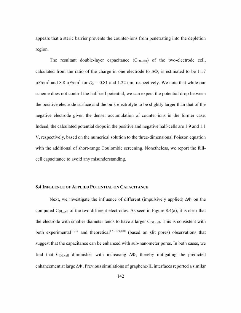
142
appears that a steric barrier prevents the counter-ions from penetrating into the depletion
region.
The resultant double-layer capacitance (CDL,cell) of the two-electrode cell,
calculated from the ratio of the charge in one electrode to , is estimated to be 11.7
µF/cm2 and 8.8 µF/cm2 for Dp = 0.81 and 1.22 nm, respectively. We note that while our
scheme does not control the half-cell potential, we can expect the potential drop between
the positive electrode surface and the bulk electrolyte to be slightly larger than that of the
negative electrode given the denser accumulation of counter-ions in the former case.
Indeed, the calculated potential drops in the positive and negative half-cells are 1.9 and 1.1
V, respectively, based on the numerical solution to the three-dimensional Poisson equation
with the additional of short-range Coulombic screening. Nonetheless, we report the full-
cell capacitance to avoid any misunderstanding.
8.4 INFLUENCE OF APPLIED POTENTIAL ON CAPACITANCE
Next, we investigate the influence of different (impulsively applied) on the
computed CDL,cell of the two different electrodes. As seen in Figure 8.4(a), it is clear that
the electrode with smaller diameter tends to have a larger CDL,cell. This is consistent with
both experimental36,37 and theoretical173,179,180 (based on slit pores) observations that
suggest that the capacitance can be enhanced with sub-nanometer pores. In both cases, we
find that CDL,cell diminishes with increasing , thereby mitigating the predicted
enhancement at large . Previous simulations of graphene/IL interfaces reported a similar
143
dependence of on C, which is attributed to the increasing saturation of ions in the
EDL.13 In these cases, the diminishment is gradual and continuous. However, an
anomalously distinct reduction (nearly 40%) of CDL,cell is observed between = 1 and 2
V in the Dp = 0.81 nm case, in contrast to the expected behavior in the Dp = 1.22 nm case.
Figure 8.4 (a) Areal integral capacitance of the full-cell (CDL,cell that is normalized to the
surface area of one electrode) with respect to the applied full-cell potential
() which is instantaneously applied. Length of the depletion region (LD) as
a function of at the (b) positive and (c) negative electrode. The shaded
region in all three panels depicts the transition between migration and
stagnation, as discussed in the main text.
To explain these observations, we assess the possible development of a depleted
region. Figure 8.4 shows the computed LD for both electrode cases on the positive (Figure
8.4(b)) and negative (Figure 8.4(c)) sides, respectively. Two distinct regimes become
144
immediately obvious. The first is the low potential regime ( < 1 V) in which both Dp =
0.81 and 1.22 nm cases exhibit a reduction in LD as increases. As discussed in depth
later, the repulsive electrostatic interactions between the electrode walls and co-ions drives
their expulsion from the pore while the electrode charge and counter-ions migrate from the
pore entrance to center. However, a transition occurs between = 1 and 1.5 V such that
when > 1.5 V, LD abruptly increases in the Dp = 0.81 nm case before gradually
decreasing with increasing . Here, the large density of counter-ions entering the pore
prevents co-ion expulsion, such that a depletion region forms within the center of the pore.
While similar behavior is seen in the Dp = 1.22 nm case, the pore remains large enough for
the counter-ions to screen the interaction between the trapped co-ions and electrode wall.
Nonetheless, both electrode cases exhibit a transition between co-ions migrating out of the
pore and co-ions remaining stagnated inside the pore.
Comparing the positive to negative electrodes, the trend in LD appears to be
qualitatively similar. The major difference is that in the latter case, LD tends to be larger
than the former case when < 1 V and smaller when > 1.5 V. This is likely related
to the difference in the counter-ion size. In the low potential regime ( < 1 V), the bulky
EMIM+ counter-ion in the negative electrode can screen the electrode charge more
efficiently than the compact BF4- counter-ion in the positive electrode, which can help
explain the observation of a larger LD. By the same argument, the bulkiness of the EMIM+
counter-ion may also facilitate the compression of the depletion region in the high potential
regime ( > 1.5 V), thereby resulting in a smaller LD.
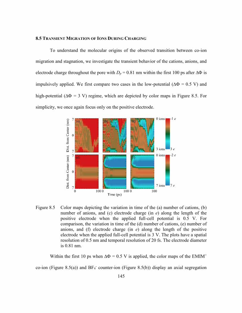
145
8.5 TRANSIENT MIGRATION OF IONS DURING CHARGING
To understand the molecular origins of the observed transition between co-ion
migration and stagnation, we investigate the transient behavior of the cations, anions, and
electrode charge throughout the pore with Dp = 0.81 nm within the first 100 ps after is
impulsively applied. We first compare two cases in the low-potential ( = 0.5 V) and
high-potential ( = 3 V) regime, which are depicted by color maps in Figure 8.5. For
simplicity, we once again focus only on the positive electrode.
Figure 8.5 Color maps depicting the variation in time of the (a) number of cations, (b)
number of anions, and (c) electrode charge (in e) along the length of the
positive electrode when the applied full-cell potential is 0.5 V. For
comparison, the variation in time of the (d) number of cations, (e) number of
anions, and (f) electrode charge (in e) along the length of the positive
electrode when the applied full-cell potential is 3 V. The plots have a spatial
resolution of 0.5 nm and temporal resolution of 20 fs. The electrode diameter
is 0.81 nm.
Within the first 10 ps when = 0.5 V is applied, the color maps of the EMIM+
co-ion (Figure 8.5(a)) and BF4- counter-ion (Figure 8.5(b)) display an axial segregation
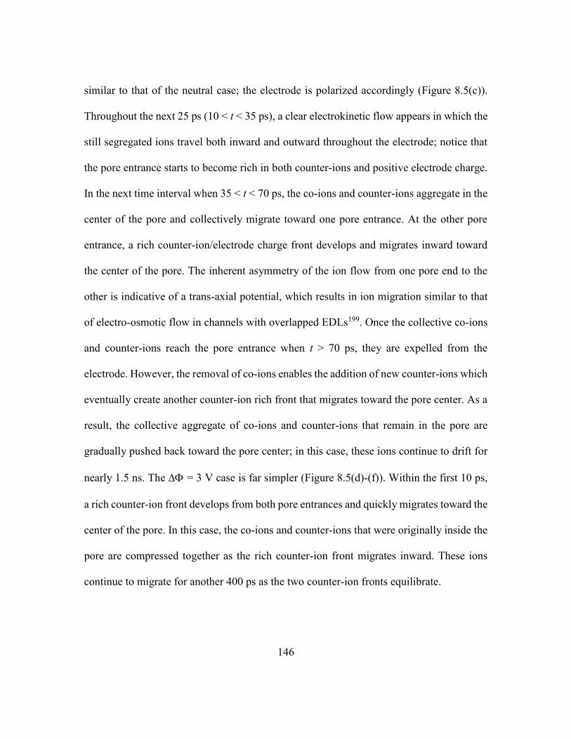
146
similar to that of the neutral case; the electrode is polarized accordingly (Figure 8.5(c)).
Throughout the next 25 ps (10 < t < 35 ps), a clear electrokinetic flow appears in which the
still segregated ions travel both inward and outward throughout the electrode; notice that
the pore entrance starts to become rich in both counter-ions and positive electrode charge.
In the next time interval when 35 < t < 70 ps, the co-ions and counter-ions aggregate in the
center of the pore and collectively migrate toward one pore entrance. At the other pore
entrance, a rich counter-ion/electrode charge front develops and migrates inward toward
the center of the pore. The inherent asymmetry of the ion flow from one pore end to the
other is indicative of a trans-axial potential, which results in ion migration similar to that
of electro-osmotic flow in channels with overlapped EDLs199. Once the collective co-ions
and counter-ions reach the pore entrance when t > 70 ps, they are expelled from the
electrode. However, the removal of co-ions enables the addition of new counter-ions which
eventually create another counter-ion rich front that migrates toward the pore center. As a
result, the collective aggregate of co-ions and counter-ions that remain in the pore are
gradually pushed back toward the pore center; in this case, these ions continue to drift for
nearly 1.5 ns. The = 3 V case is far simpler (Figure 8.5(d)-(f)). Within the first 10 ps,
a rich counter-ion front develops from both pore entrances and quickly migrates toward the
center of the pore. In this case, the co-ions and counter-ions that were originally inside the
pore are compressed together as the rich counter-ion front migrates inward. These ions
continue to migrate for another 400 ps as the two counter-ion fronts equilibrate.
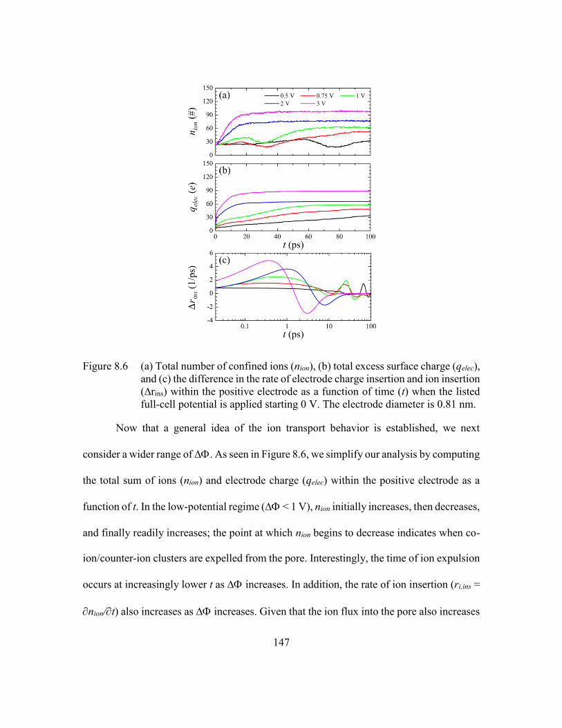
147
Figure 8.6 (a) Total number of confined ions (nion), (b) total excess surface charge (qelec),
and (c) the difference in the rate of electrode charge insertion and ion insertion
(∆rins) within the positive electrode as a function of time (t) when the listed
full-cell potential is applied starting 0 V. The electrode diameter is 0.81 nm.
Now that a general idea of the ion transport behavior is established, we next
consider a wider range of . As seen in Figure 8.6, we simplify our analysis by computing
the total sum of ions (nion) and electrode charge (qelec) within the positive electrode as a
function of t. In the low-potential regime ( < 1 V), nion initially increases, then decreases,
and finally readily increases; the point at which nion begins to decrease indicates when co-
ion/counter-ion clusters are expelled from the pore. Interestingly, the time of ion expulsion
occurs at increasingly lower t as increases. In addition, the rate of ion insertion (ri,ins =
nion/t) also increases as increases. Given that the ion flux into the pore also increases
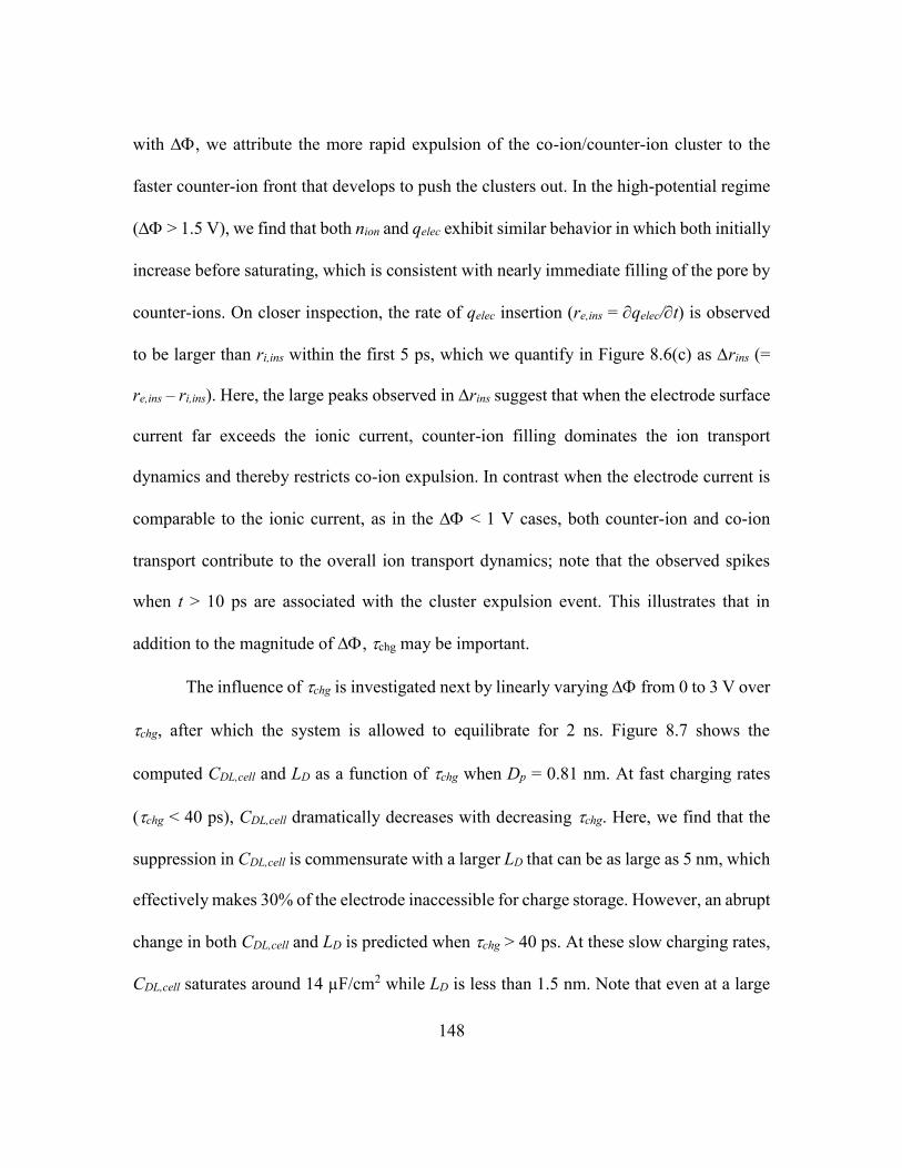
148
with , we attribute the more rapid expulsion of the co-ion/counter-ion cluster to the
faster counter-ion front that develops to push the clusters out. In the high-potential regime
( > 1.5 V), we find that both nion and qelec exhibit similar behavior in which both initially
increase before saturating, which is consistent with nearly immediate filling of the pore by
counter-ions. On closer inspection, the rate of qelec insertion (re,ins = qelec/t) is observed
to be larger than ri,ins within the first 5 ps, which we quantify in Figure 8.6(c) as ∆rins (=
re,ins – ri,ins). Here, the large peaks observed in ∆rins suggest that when the electrode surface
current far exceeds the ionic current, counter-ion filling dominates the ion transport
dynamics and thereby restricts co-ion expulsion. In contrast when the electrode current is
comparable to the ionic current, as in the < 1 V cases, both counter-ion and co-ion
transport contribute to the overall ion transport dynamics; note that the observed spikes
when t > 10 ps are associated with the cluster expulsion event. This illustrates that in
addition to the magnitude of , chg may be important.
The influence of chg is investigated next by linearly varying from 0 to 3 V over
chg, after which the system is allowed to equilibrate for 2 ns. Figure 8.7 shows the
computed CDL,cell and LD as a function of chg when Dp = 0.81 nm. At fast charging rates
(chg < 40 ps), CDL,cell dramatically decreases with decreasing chg. Here, we find that the
suppression in CDL,cell is commensurate with a larger LD that can be as large as 5 nm, which
effectively makes 30% of the electrode inaccessible for charge storage. However, an abrupt
change in both CDL,cell and LD is predicted when chg > 40 ps. At these slow charging rates,
CDL,cell saturates around 14 µF/cm2 while LD is less than 1.5 nm. Note that even at a large
149
chg of 10 ns, some co-ions remain trapped within the pore. Nonetheless, these results
suggest that the rate capability of these subnanometer electrodes is dictated by the rate at
which co-ions (and their paired counter-ions) are removed from the pore.
Figure 8.7 The influence of charging time (chg) on (left) the full-cell capacitance (CDL,cell
in black squares) and (right) length of the depleted region (LD in red triangles)
at the positive electrode with diameter 0.81 nm when the applied full-cell
potential is 3 V. The shaded region depicts the transition between migration
and stagnation, as discussed in the manuscript.
8.6 CONCLUSIONS
To summarize, we investigated the capacitance of ionic liquid confined within
charged cylindrical nanopores with diameters 0.81 and 1.22 nm using non-equilibrium
molecular dynamics. While we find that the capacitance is expectedly larger using the
narrower pore, an interesting inhomogeneity is observed as well. The smaller pore is found
to develop a so-called depletion region in the center of the pore, in which an equal number
of co-ions and counter-ions remain trapped. As this depletion region cannot accommodate
excess charge, a significant fraction of the electrode does not participate in charge storage.
150
Molecular analysis during the transient charging regime attributes the development of the
depletion region to the rapid over-filling of counter-ions into the pore. In addition, the
length of the depletion region is found to be strongly dependent on the competition between
forced electro-kinetic flow and natural ion convection, which in turn can be controlled by
the magnitude of the applied potential or the charging rate (or essentially, the scan rate). It
is evident that such phenomena may be related to the experimentally observed capacitance
fading at high rates. Due to the limited scope of this work, however, many other factors
remain largely unexplored; these factors can include the possible non-uniformity of the
pore structure, the geometry of different ions (including size, flexibility, and charge
distribution), the presence of solvent molecules, different surface chemistries with a
resultant surface charge redistribution, and possible electrolyte decomposition due to
charge localization (especially at the depletion region interface). Nonetheless, these
findings highlight the importance of investigating the transition between the migration or
stagnation of confined ions for the design of future nanoporous materials for supercapacitor
applications.
151
Chapter 9: Pore Dispersity and Ion Kinetics in Nanoporous Carbons
9.1 INTRODUCTION TO NANOPOROUS CARBON
Expanding on the work presented in Chapters 7 and 8, realistic nanoporous carbon
(NPCs) electrodes immersed in ionic liquid are now considered. The development of NPCs
is motivated by experimental work36,37 on carbide-derived carbons (CDCs) that suggested
that the areal capacitance (Car) exhibits dramatic enhancement when the nominal pore
width (Wp) is comparable to the size of the electrolyte ions. The subject, however, remains
somewhat controversial as others have reported a clear independence of Car with respect
to Wp.200 The main basis for this claim is that the commonly used Brunauer–Emmett–Teller
(BET) method of characterizing the surface area may result in misleading Car values.
Interestingly, while the specific capacitance (Csp) should be a more reliable metric, no such
trends have been reported based on Csp. Nonetheless, several theoretical studies explain the
discrepancy in Car by showing that the maximum Car is only achieved at certain potentials
for a given Wp.181,201 These authors postulate that the absence of a clear Wp dependence in
Ref. 200 is related to broad pore dispersity which may be common in most NPC materials.
However, the exact impact of pore dispersity on the capacitance remains unclear.
In this chapter, a resolution to the Car debate, as well as insights into Csp, is
attempted by investigating the role of pore dispersity, in both size and shape, on Car and
Csp. Here, the dynamic charge storage behavior of 1-ethyl-3-methylimidazolium (EMIM)
tetrafluoroborate (BF4) ionic liquid (IL) confined within realistic nanoporous carbon (NPC)
electrodes is studied using non-equilibrium molecular dynamics simulations.
152
9.2 COMPUTATIONAL METHODS
A. Electrode Structure Generation
Initial NPC structures were generated using the Mimetic model presented in Ref.
202. Simulation domains were 4.55 4.55 20 nm3 (using periodic boundary conditions)
with initial number densities of 0.05, 0.054, and 0.06 #/Å3 in a fcc lattice configuration.
Temperatures were quenched from 20000 K to 700 K under the NVT ensemble using the
Nosé-Hoover thermostat60 with a quench time of 1.6 ns and timestep of 0.07 fs. After
generation, 2 nm of carbon atoms were removed from each end to make the structures non-
periodic in the z direction. Then, unphysical and dangling carbons were removed from the
system after which hydrogen atoms were attached to the remaining sp carbon. The volumes
were then relaxed in the xy direction under the NPT ensemble using a Nosé-Hoover
barostat/thermostat60 and AIREBO potential203 for 500 ps with a timestep of 1 fs. The final
xy dimensions of the NPC-12, NPC-10, and NPC-9 electrodes were 4.54 4.54, 4.57
4.57, and 4.58 4.58 nm2, respectively.
B. Force Field
The ionic liquid was described using a coarse-grained approach such that EMIM+
and BF4- were reduced to four and one interaction centers, respectively, as depicted in
Figure 9.1. The non-bonding parameters were adapted from Ref. 191 as summarized in
Table 9.1; the charges (q) were re-scaled following the fashion of Ref. 192 while the zero-
energy pair-wise distance () were re-optimized to reproduce experimental density and
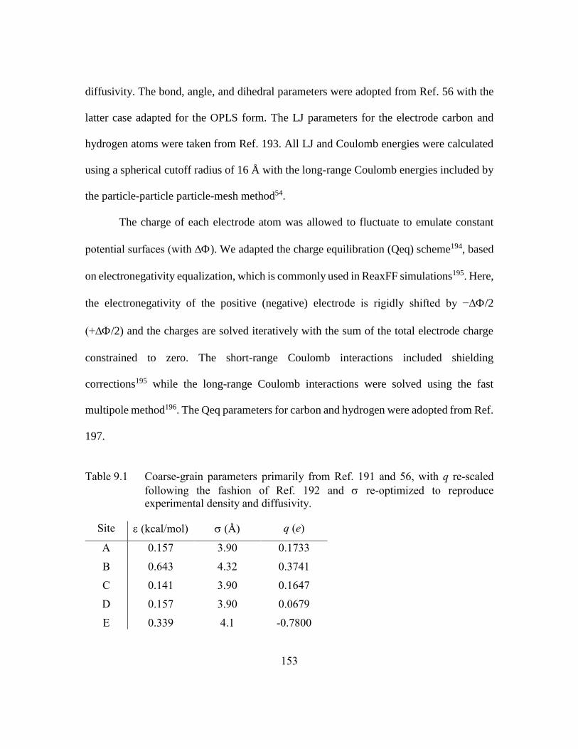
153
diffusivity. The bond, angle, and dihedral parameters were adopted from Ref. 56 with the
latter case adapted for the OPLS form. The LJ parameters for the electrode carbon and
hydrogen atoms were taken from Ref. 193. All LJ and Coulomb energies were calculated
using a spherical cutoff radius of 16 Å with the long-range Coulomb energies included by
the particle-particle particle-mesh method54.
The charge of each electrode atom was allowed to fluctuate to emulate constant
potential surfaces (with ∆). We adapted the charge equilibration (Qeq) scheme194, based
on electronegativity equalization, which is commonly used in ReaxFF simulations195. Here,
the electronegativity of the positive (negative) electrode is rigidly shifted by −∆/2
(+∆/2) and the charges are solved iteratively with the sum of the total electrode charge
constrained to zero. The short-range Coulomb interactions included shielding
corrections195 while the long-range Coulomb interactions were solved using the fast
multipole method196. The Qeq parameters for carbon and hydrogen were adopted from Ref.
197.
Table 9.1 Coarse-grain parameters primarily from Ref. 191 and 56, with q re-scaled
following the fashion of Ref. 192 and re-optimized to reproduce
experimental density and diffusivity.
Site (kcal/mol) (Å) q (e)
A 0.157 3.90 0.1733
B 0.643 4.32 0.3741
C 0.141 3.90 0.1647
D 0.157 3.90 0.0679
E 0.339 4.1 -0.7800
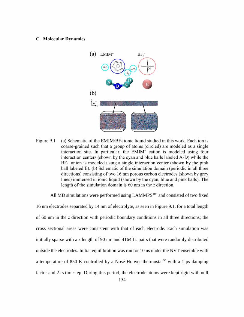
154
C. Molecular Dynamics
Figure 9.1 (a) Schematic of the EMIM/BF4 ionic liquid studied in this work. Each ion is
coarse-grained such that a group of atoms (circled) are modeled as a single
interaction site. In particular, the EMIM+ cation is modeled using four
interaction centers (shown by the cyan and blue balls labeled A-D) while the
BF4- anion is modeled using a single interaction center (shown by the pink
ball labeled E). (b) Schematic of the simulation domain (periodic in all three
directions) consisting of two 16 nm porous carbon electrodes (shown by grey
lines) immersed in ionic liquid (shown by the cyan, blue and pink balls). The
length of the simulation domain is 60 nm in the z direction.
All MD simulations were performed using LAMMPS105 and consisted of two fixed
16 nm electrodes separated by 14 nm of electrolyte, as seen in Figure 9.1, for a total length
of 60 nm in the z direction with periodic boundary conditions in all three directions; the
cross sectional areas were consistent with that of each electrode. Each simulation was
initially sparse with a z length of 90 nm and 4164 IL pairs that were randomly distributed
outside the electrodes. Initial equilibration was run for 10 ns under the NVT ensemble with
a temperature of 850 K controlled by a Nosé-Hoover thermostat60 with a 1 ps damping
factor and 2 fs timestep. During this period, the electrode atoms were kept rigid with null
155
charge and moved linearly to their final positions; the simulation domain was also linearly
deformed to its final length. A second equilibration step was performed at = 0 V for 10
ns with the electrode charges updated every 100 fs and the temperature gradually decreased
from 850 K to 300 K. Fixing the temperature at 300 K, charges were updated every 2 fs
while the systems were further equilibrated over 1 ns. Similarly, a = 3 V was
impulsively applied and equilibrated for 2 ns. Finally, molecular trajectories were extracted
every 5 ps over a production run of 4 ns to compute the DoC profiles.
To prepare the capacitance calculations, each simulation underwent pre-cycling by
linearly varying between 0 and the target for at least 3 charge and 2 discharge
ramps with 1 ns in each direction (total pre-cycling time was at least 5 ns); the pre-cycling
was considered complete when the largest and smallest peak-to-peak values of the
electrode charge deviated by less than 1% from the previous cycle. Discharge production
runs were carried out by first holding for 250 ps before allowing to linearly
decrease to 0 V over 1 ns; molecular trajectories were extracted every 2 ps.
All reported results were extracted from the average trajectories from 4 independent
simulations with different initial atomic configurations.
9.3 NANOPOROUS CARBON STRUCTURAL CHARACTERIZATION
As depicted in Figure 9.1, we consider a simulation domain that emulates a two-
electrode supercapacitor cell filled with 1-ethyl-3-methylimidazolium (EMIM+)
tetrafluoroborate (BF4-) ionic liquid (IL), modeled using a coarse-grain force field (see
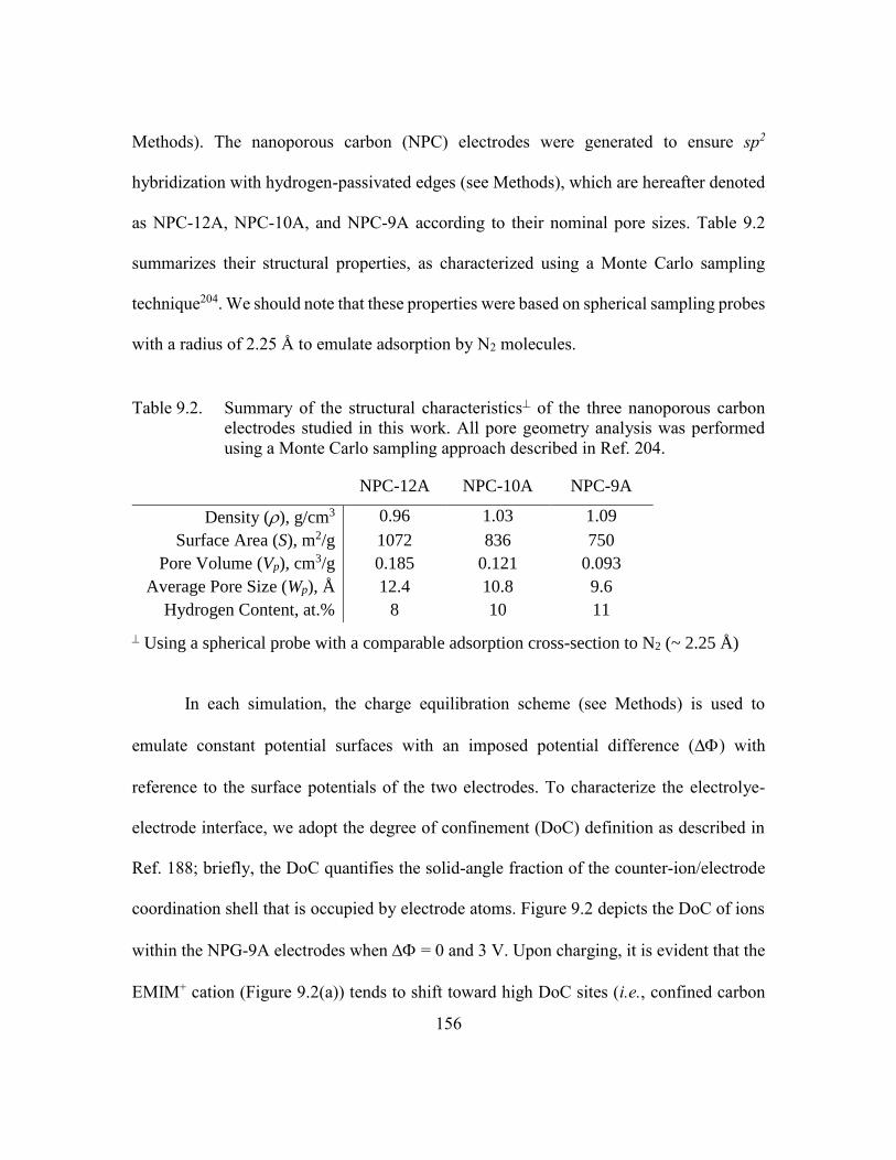
156
Methods). The nanoporous carbon (NPC) electrodes were generated to ensure sp2
hybridization with hydrogen-passivated edges (see Methods), which are hereafter denoted
as NPC-12A, NPC-10A, and NPC-9A according to their nominal pore sizes. Table 9.2
summarizes their structural properties, as characterized using a Monte Carlo sampling
technique204. We should note that these properties were based on spherical sampling probes
with a radius of 2.25 Å to emulate adsorption by N2 molecules.
Table 9.2. Summary of the structural characteristics of the three nanoporous carbon
electrodes studied in this work. All pore geometry analysis was performed
using a Monte Carlo sampling approach described in Ref. 204.
NPC-12A NPC-10A NPC-9A
Density (), g/cm3 0.96 1.03 1.09
Surface Area (S), m2/g 1072 836 750
Pore Volume (Vp), cm3/g 0.185 0.121 0.093
Average Pore Size (Wp), Å 12.4 10.8 9.6
Hydrogen Content, at.% 8 10 11
Using a spherical probe with a comparable adsorption cross-section to N2 (~ 2.25 Å)
In each simulation, the charge equilibration scheme (see Methods) is used to
emulate constant potential surfaces with an imposed potential difference () with
reference to the surface potentials of the two electrodes. To characterize the electrolye-
electrode interface, we adopt the degree of confinement (DoC) definition as described in
Ref. 188; briefly, the DoC quantifies the solid-angle fraction of the counter-ion/electrode
coordination shell that is occupied by electrode atoms. Figure 9.2 depicts the DoC of ions
within the NPG-9A electrodes when = 0 and 3 V. Upon charging, it is evident that the
EMIM+ cation (Figure 9.2(a)) tends to shift toward high DoC sites (i.e., confined carbon
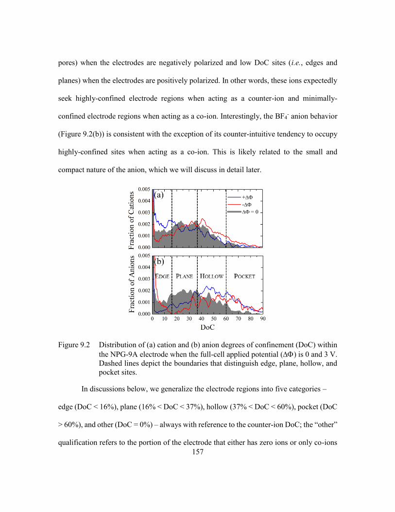
157
pores) when the electrodes are negatively polarized and low DoC sites (i.e., edges and
planes) when the electrodes are positively polarized. In other words, these ions expectedly
seek highly-confined electrode regions when acting as a counter-ion and minimally-
confined electrode regions when acting as a co-ion. Interestingly, the BF4- anion behavior
(Figure 9.2(b)) is consistent with the exception of its counter-intuitive tendency to occupy
highly-confined sites when acting as a co-ion. This is likely related to the small and
compact nature of the anion, which we will discuss in detail later.
Figure 9.2 Distribution of (a) cation and (b) anion degrees of confinement (DoC) within
the NPG-9A electrode when the full-cell applied potential () is 0 and 3 V.
Dashed lines depict the boundaries that distinguish edge, plane, hollow, and
pocket sites.
In discussions below, we generalize the electrode regions into five categories –
edge (DoC < 16%), plane (16% < DoC < 37%), hollow (37% < DoC < 60%), pocket (DoC
> 60%), and other (DoC = 0%) – always with reference to the counter-ion DoC; the “other”
qualification refers to the portion of the electrode that either has zero ions or only co-ions
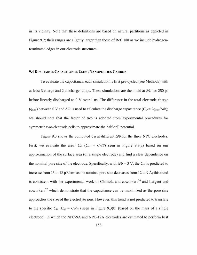
158
in its vicinity. Note that these definitions are based on natural partitions as depicted in
Figure 9.2; their ranges are slightly larger than those of Ref. 188 as we include hydrogen-
terminated edges in our electrode structures.
9.4 DISCHARGE CAPACITANCE USING NANOPOROUS CARBON
To evaluate the capacitance, each simulation is first pre-cycled (see Methods) with
at least 3 charge and 2 discharge ramps. These simulations are then held at for 250 ps
before linearly discharged to 0 V over 1 ns. The difference in the total electrode charge
(qelec) between 0 V and is used to calculate the discharge capacitance (CD = 2qelec/);
we should note that the factor of two is adopted from experimental procedures for
symmetric two-electrode cells to approximate the half-cell potential.
Figure 9.3 shows the computed CD at different for the three NPC electrodes.
First, we evaluate the areal CD (Car = CD/S) seen in Figure 9.3(a) based on our
approximation of the surface area (of a single electrode) and find a clear dependence on
the nominal pore size of the electrode. Specifically, with = 3 V, the Car is predicted to
increase from 13 to 18 µF/cm2 as the nominal pore size decreases from 12 to 9 Å; this trend
is consistent with the experimental work of Chmiola and coworkers36 and Largeot and
coworkers37 which demonstrate that the capacitance can be maximized as the pore size
approaches the size of the electrolyte ions. However, this trend is not predicted to translate
to the specific CD (Csp = CD/m) seen in Figure 9.3(b) (based on the mass of a single
electrode), in which the NPC-9A and NPC-12A electrodes are estimated to perform best
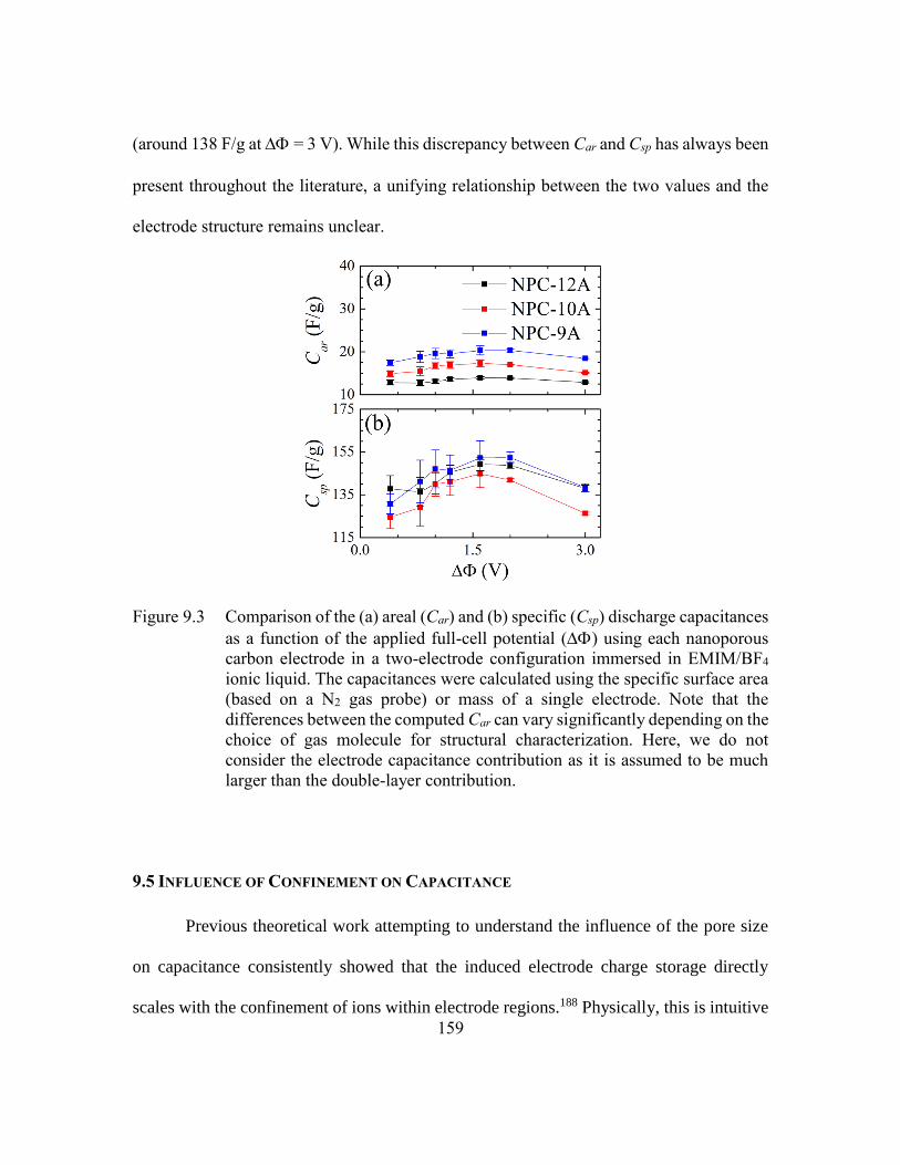
159
(around 138 F/g at = 3 V). While this discrepancy between Car and Csp has always been
present throughout the literature, a unifying relationship between the two values and the
electrode structure remains unclear.
Figure 9.3 Comparison of the (a) areal (Car) and (b) specific (Csp) discharge capacitances
as a function of the applied full-cell potential () using each nanoporous
carbon electrode in a two-electrode configuration immersed in EMIM/BF4
ionic liquid. The capacitances were calculated using the specific surface area
(based on a N2 gas probe) or mass of a single electrode. Note that the
differences between the computed Car can vary significantly depending on the
choice of gas molecule for structural characterization. Here, we do not
consider the electrode capacitance contribution as it is assumed to be much
larger than the double-layer contribution.
9.5 INFLUENCE OF CONFINEMENT ON CAPACITANCE
Previous theoretical work attempting to understand the influence of the pore size
on capacitance consistently showed that the induced electrode charge storage directly
scales with the confinement of ions within electrode regions.188 Physically, this is intuitive
160
as each carbon atom is polarized and should participate in the screening of the ion charge.
Indeed, our calculations exhibit similar behavior. For example, we find that in the NPC-
9A case when = 3 V, the electrode atoms in pocket sites store an average of 0.036
e/atom, which is greater than the average charge per electrode atom in hollow sites (0.028
e/atom) and plane sites (0.023 e/atom).
Figure 9.4 (a) Comparison of the discharge capacity per site (∆qsite) for the three
electrode cases when the applied full-cell potential is 3 V. (b) Fraction of the
capacitance attributed to the total discharge capacity per site (fq,dc) for the
three electrode cases when the applied full-cell potential is 3 V.
Upon discharging the system, however, two important observations are made. The
first is that when ∆ = 0 V, qelec is not zero which shows that charge remains trapped within
the electrode. The second is that the charge trapped within pocket sites greater exceeds that
161
of qelec, which is compensated by depleted charge regions throughout the rest of the
electrode. This significant charge puddling is analogous to that of graphene near charged
impurities at the charge neutrality point.205 As such, a more accurate metric for the
capacitance is the discharge capacity per site (qsite) which indicates the change in qelec (per
atom, per site) upon discharge.
Figure 9.4(a) shows the computed qsite at each aforementioned electrode site (i.e.,
other, edge, plane, hollow, pocket) for the three NPC electrodes considered. Surprisingly,
the pocket sites display the smallest qsite compared to other sites due to the large amount
of charge that remains trapped. In contrast, the edge sites tend to have the largest qsite,
particularly in the negative electrode, which is chemically intuitive given that the presence
of H-terminated edge defects promotes a greater accumulation of electrons compared to
the basal plane140. This suggests that the confined nature of the pocket sites does not
inherently enable large charge storage if the charge cannot be efficiently extracted.
Next, we investigate the contribution of the total discharge capacity of each site to
the capacitance (fq,dc) as shown in Figure 9.4(b); note that this fraction is calculated on an
atomic basis rather than surface area basis. At both the positive and negative electrodes,
the contribution from the pocket sites tends to increase as the pore size decreases. In
addition, the contribution from the pocket sites tends to be much larger at the positive
terminal, which is related to the size of the counter-ion. As discussed earlier, the compact
BF4- counter-ion readily fills the pocket sites under positive polarization while the bulky
EMIM+ counter-ion prefers to fill the hollow and plane sites under negative polarization.
Given that the Car is predicted to increase with smaller pore size, it appears that the
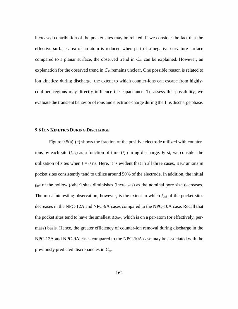
162
increased contribution of the pocket sites may be related. If we consider the fact that the
effective surface area of an atom is reduced when part of a negative curvature surface
compared to a planar surface, the observed trend in Car can be explained. However, an
explanation for the observed trend in Csp remains unclear. One possible reason is related to
ion kinetics; during discharge, the extent to which counter-ions can escape from highly-
confined regions may directly influence the capacitance. To assess this possibility, we
evaluate the transient behavior of ions and electrode charge during the 1 ns discharge phase.
9.6 ION KINETICS DURING DISCHARGE
Figure 9.5(a)-(c) shows the fraction of the positive electrode utilized with counter-
ions by each site (futil) as a function of time (t) during discharge. First, we consider the
utilization of sites when t = 0 ns. Here, it is evident that in all three cases, BF4- anions in
pocket sites consistently tend to utilize around 50% of the electrode. In addition, the initial
futil of the hollow (other) sites diminishes (increases) as the nominal pore size decreases.
The most interesting observation, however, is the extent to which futil of the pocket sites
decreases in the NPC-12A and NPC-9A cases compared to the NPC-10A case. Recall that
the pocket sites tend to have the smallest ∆qsite, which is on a per-atom (or effectively, per-
mass) basis. Hence, the greater efficiency of counter-ion removal during discharge in the
NPC-12A and NPC-9A cases compared to the NPC-10A case may be associated with the
previously predicted discrepancies in Csp.
163
Figure 9.5 Discharge profiles of positive electrode when the applied full-cell potential
varies from 3 to 0 V over 1 ns in a non-equilibrium MD simulation. The
fraction of the electrode utilized (futil) as each type of listed site in the (a) NPC-
12A, (b) NPC-10A, and (c) NPC-9A case is shown. In addition, the (left axis)
total charge stored (qelec) and the (right axis) ratio of anion-cation coordination
number (Cco) to the anion-anion coordination number (Ccounter) in the pocket
(black) and hollow (red) sites of the (d) NPC-12A, (b) NPC-10A, and (c)
NPC-9A case is shown.
A potential mechanism for ion extraction can be conceived based on the futil
behavior of the other sites. In all three cases, the futil of the hollow sites tends to increase
while t < 0.5 ns, before diminishing. But the increase in the NPC-12A and NPC-9A cases
is far more notable. This suggests that the hollow sites facilitate ion extraction from the
pocket sites by accommodating extra counter-ions. Interestingly, the qelec of the hollow
sites (Figure 9.5(d)-(f)) continues to decrease despite the increase in counter-ion
164
accommodation, suggesting that the electrode-ion electrostatic interaction is not the
primary driving force. However, we do find that the ratio of EMIM+ co-ions to BF4-
counter-ions that populate the coordination shell around hollow-adsorbed anions
(Cco/Ccounter) increases while t < 0.5 ns. A reorganization of the ions at the interface occurs
such that the coordinated EMIM+ cations stabilize anion accumulation due to the favorable
ion-ion interactions. Eventually when t > 0.5 ns, the depletion of the hollow-site qelec
appears to be sufficient enough to allow anions (and coordinated cations) to lift-off from
the surface into bulk-like reservoirs contained within the electrode volume, such that both
futil and Cco/Ccounter diminish.
9.7 RELATIONSHIP BETWEEN CAPACITANCE AND PORE SHAPE AND ITS DISPERSITY
In order for this reorganization of ions to occur, a dispersity of both pore shape and
pore size should be present throughout the electrode. We propose that one way to
approximate the pore shape, if we assume that the majority of the electrode consists of
negative-curvature surfaces, is through knowledge of the specific surface area (S), pore
volume (Vp), and the nominal pore size (Wp). Then, we define a pore shape factor (Fps)
𝐹𝑝𝑠 =𝑊𝑝
(2𝑉𝑝
𝑆)
such that the pores are nominally slit-like when Fps = 2, cylindrical-like when Fps = 4, and
spherical-like when Fps = 6. The dispersity of Fps ( Fps/Rgp) can then be qualitatively
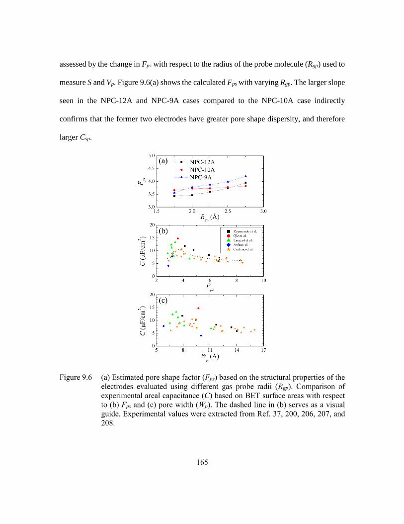
165
assessed by the change in Fps with respect to the radius of the probe molecule (Rgp) used to
measure S and Vp. Figure 9.6(a) shows the calculated Fps with varying Rgp. The larger slope
seen in the NPC-12A and NPC-9A cases compared to the NPC-10A case indirectly
confirms that the former two electrodes have greater pore shape dispersity, and therefore
larger Csp.
Figure 9.6 (a) Estimated pore shape factor (Fps) based on the structural properties of the
electrodes evaluated using different gas probe radii (Rgp). Comparison of
experimental areal capacitance (C) based on BET surface areas with respect
to (b) Fps and (c) pore width (Wp). The dashed line in (b) serves as a visual
guide. Experimental values were extracted from Ref. 37, 200, 206, 207, and
208.
166
The Fps can also be helpful to understand trends in the Car. The coordination of ions
by the electrode should be large when the pores are cylindrical-like. In addition, the
effective surface area per atom is reduced compared to surfaces with less curvature. Hence,
if we consider the Fps when Rgp = 2.25 Å (e.g., N2), we find that our predicted Car increases
as Fps approaches 4 (i.e., cylindrical-like). We can also extend this analysis to previously
reported experimental capacitances (C) of nanoporous carbon. In Figure 9.6(b), we
compare C as a function of Fps from five different sources; here, the BET surface area is
used and the Wp is estimated from provided pore size distributions when not directly
reported. Remarkably, a distinct correlation is observed although the maximum appears to
be centered around Fps 3.7. In comparison, C as a function of Wp is presented in Figure
9.6(c). The correlation with Wp is much weaker, which is consistent with the work of
Centeno and coworkers200 that showed a nearly independent relationship between C and
Wp. This suggests that the capacitance may be more strongly described by the pore
dispersity, characterized as Fps in this work, than by Wp. However, in materials with very
narrow pore size distributions (e.g., CDCs), the choice of Wp may exhibit more influence.
9.8 CONCLUSIONS
We investigated the relationship between the structural properties of nanoporous
carbons (immersed in EMIM/BF4 ionic liquid) and the discharge capacitance using non-
equilibrium molecular dynamics. The three electrodes studied in this work had nominal
pore widths of 12.4, 10.8, and 9.6 Å with large capacitances of 138 F/g (13 µF/cm2), 126
167
F/g (15 µF/cm2), and 138 F/g (18 µF/cm2), respectively, at 3 V. In an attempt to unify the
discrepancies between the areal and specific capacitances, we analyzed the molecular
origin of these capacitance values by studying both the electrode charge and ion
redistribution during discharge. Our results show that significant charge can remain trapped
within sites in which counter-ions are highly-confined by the electrode surface. Counter-
ion extraction was found to be facilitated by the presence of pores that are connected to
gradually less-confined electrode regions, which in turn allowed a gradual reorganization
of ions to stabilize counter-ion accumulation and eventual desorption. Therefore, larger
specific capacitances were attributed to more efficient ion extraction while larger areal
capacitances were attributed to the greater utilization of confined regions. Based on this
mechanism, a new structural property was proposed, termed the pore shape factor, which
was demonstrated to show a strong correlation to experimental data and can serve as an
alternative physical descriptor to the commonly used pore width.
These findings suggest that the design of future materials for supercapacitors
requires an understanding of the relationship between pore dispersity and the molecular
migration of ions (and surface charge) under quasi-equilibrium conditions. We anticipate
that such insights may also help explain scattered impedance measurements and improve
commonly used phenomenological transmission line models.209-211 In addition, the
approach presented in this work can be extended to study other factors such as different
electrode surface chemistries and solvation effects. Finally, these results highlight the
importance of reporting in-depth experimental characterization of the electrode structure,

168
including pore size distributions, specific surface areas, and pore volumes, using different
gas adsorbates.
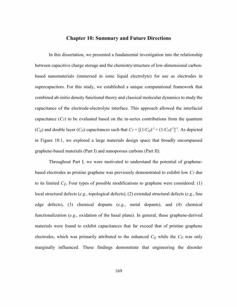
169
Chapter 10: Summary and Future Directions
In this dissertation, we presented a fundamental investigation into the relationship
between capacitive charge storage and the chemistry/structure of low-dimensional carbon-
based nanomaterials (immersed in ionic liquid electrolyte) for use as electrodes in
supercapacitors. For this study, we established a unique computational framework that
combined ab-initio density functional theory and classical molecular dynamics to study the
capacitance of the electrode-electrolyte interface. This approach allowed the interfacial
capacitance (CT) to be evaluated based on the in-series contributions from the quantum
(CQ) and double layer (CD) capacitances such that CT = [(1/CQ)-1 + (1/CD)-1]-1. As depicted
in Figure 10.1, we explored a large materials design space that broadly encompassed
graphene-based materials (Part I) and nanoporous carbons (Part II).
Throughout Part I, we were motivated to understand the potential of graphene-
based electrodes as pristine graphene was previously demonstrated to exhibit low CT due
to its limited CQ. Four types of possible modifications to graphene were considered: (1)
local structural defects (e.g., topological defects), (2) extended structural defects (e.g., line
edge defects), (3) chemical dopants (e.g., metal dopants), and (4) chemical
functionalization (e.g., oxidation of the basal plane). In general, these graphene-derived
materials were found to exhibit capacitances that far exceed that of pristine graphene
electrodes, which was primarily attributed to the enhanced CQ while the CD was only
marginally influenced. These findings demonstrate that engineering the disorder
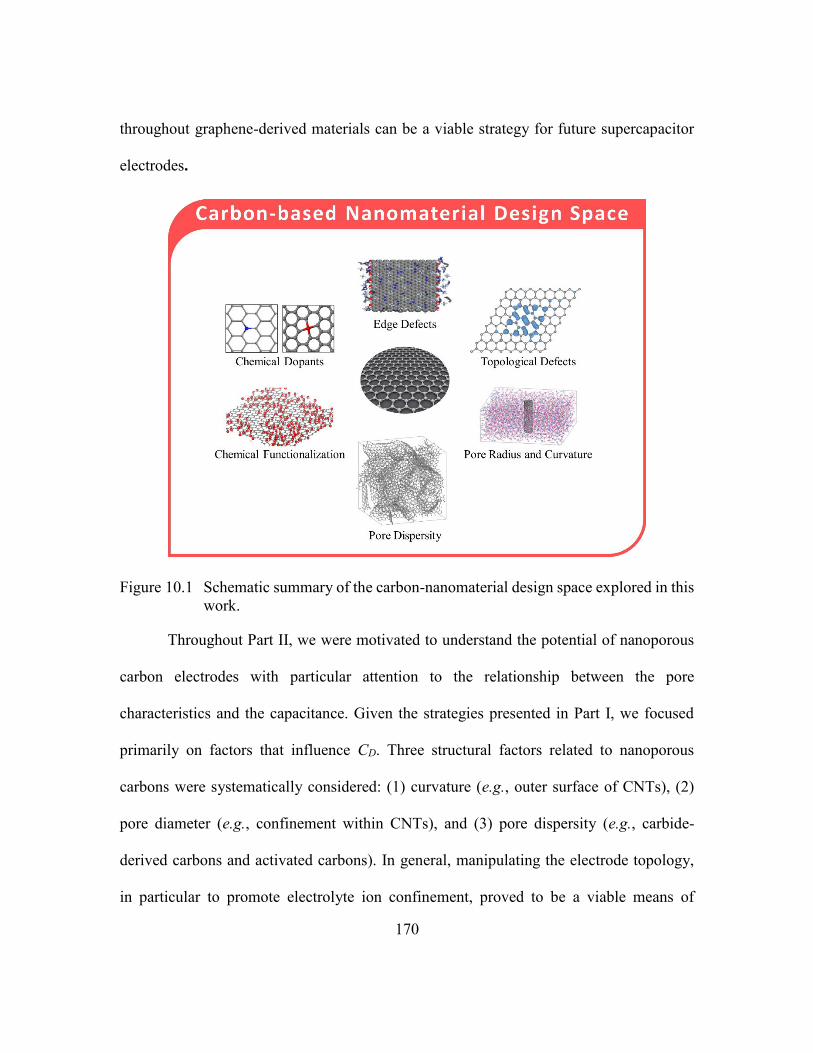
170
throughout graphene-derived materials can be a viable strategy for future supercapacitor
electrodes.
Figure 10.1 Schematic summary of the carbon-nanomaterial design space explored in this
work.
Throughout Part II, we were motivated to understand the potential of nanoporous
carbon electrodes with particular attention to the relationship between the pore
characteristics and the capacitance. Given the strategies presented in Part I, we focused
primarily on factors that influence CD. Three structural factors related to nanoporous
carbons were systematically considered: (1) curvature (e.g., outer surface of CNTs), (2)
pore diameter (e.g., confinement within CNTs), and (3) pore dispersity (e.g., carbide-
derived carbons and activated carbons). In general, manipulating the electrode topology,
in particular to promote electrolyte ion confinement, proved to be a viable means of
171
improving CD, and therefore CT, even with diminishing electrode surface area. However,
the full utilization of these materials was found to be dependent on the dynamics of ion
transport under an external field (i.e., electro-kinetics).
A more detailed summary of the key findings of this dissertation, as well as
thoughts of future directions, are described below.
10.1 MATERIALS DESIGN PRINCIPLES TO ENHANCE CAPACITANCE
A. Notable Trends on the Electronic Structure and Quantum Capacitance
The limited CQ of pristine graphene electrode is a direct consequence of the zero
density of states (DOS) at the charge neutrality point (e.g., the Fermi level) that linearly
increases away from the Fermi level. The origin of this unique DOS can be traced to the
extended conjugation of the system owing to the 2D honeycomb geometry of graphene.
Therefore, one method to increase the availability of states near the charge neutrality point
is to disrupt the system of graphene by the introduction of both chemical and structural
disorder. Here, we summarize the impact of different electrode designs on the electronic
structure and the CQ.
Trend 1: Capacitance enhancement is correlated to modification density
Interestingly, the impact of all the modifications explored throughout this
dissertation on the electronic structure share a common trait: the predicted enhancement in
CQ is primarily attributed to the resultant quasi-localization of carbon pz states in the
172
vicinity of the modification site. In the case of topological defects (Chapter 3), this is
intuitive as the only important change to the electronic structure is based on a localized
distortion to the lattice structure. Yet even when chemical functional groups were
considered (Chapter 6), the most relevant changes to the electronic structure were attributed
to the pz states of carbon atoms adjacent to functionalized sites, which could remain
partially coupled to the disrupted system. A notable exception is the case of transition
metal dopants (Chapter 4); the hybridization between the metal 3d states and carbon 2p
states can also introduce non-bonding d states close to the Fermi level which considerably
increases the number of available states. Nonetheless, this suggests that the CQ
enhancement can be estimated from the concentration of modified sites along the graphene
lattice.
Figure 7.1 depicts the average (with respect to positive and negative polarization)
CQ (at ±0.5 V) of graphene-derived materials as a function of concentration of directly
modified atoms; in other words, the concentration does not include the degree of lattice
reconstruction that may result from each type of modification. Remarkably, the increase in
CQ is confirmed to be generally correlated to the modification concentration while
independent of the type of modification; here, transition metal dopants are excluded due to
its inclusion of 3d states. In addition, it is clear that even at very low concentrations (< 1
at.%), the CQ of graphene exhibits dramatic improvements. Another important feature is
the ability of graphene to remain metallic even at large modification concentrations
approaching 30 at.%, as contiguous regions of conjugated states can still exist. However,
graphene may become semi-conducting at these concentrations if the modifications to the
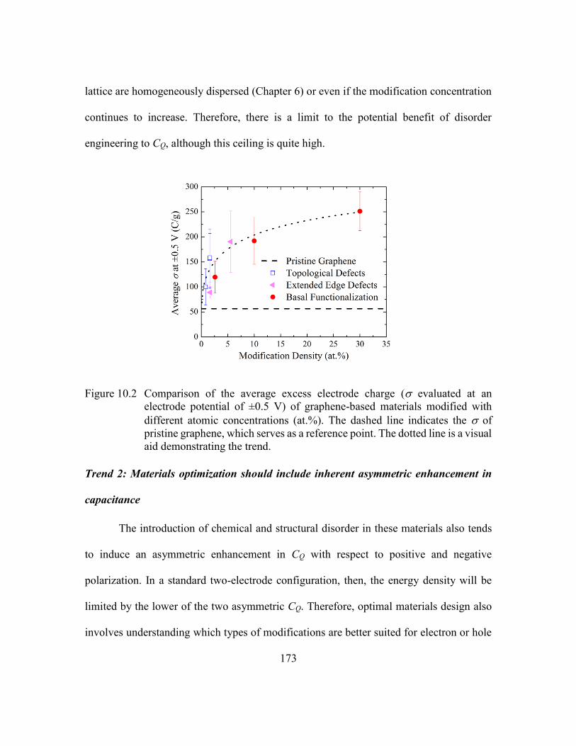
173
lattice are homogeneously dispersed (Chapter 6) or even if the modification concentration
continues to increase. Therefore, there is a limit to the potential benefit of disorder
engineering to CQ, although this ceiling is quite high.
Figure 10.2 Comparison of the average excess electrode charge ( evaluated at an
electrode potential of ±0.5 V) of graphene-based materials modified with
different atomic concentrations (at.%). The dashed line indicates the of
pristine graphene, which serves as a reference point. The dotted line is a visual
aid demonstrating the trend.
Trend 2: Materials optimization should include inherent asymmetric enhancement in
capacitance
The introduction of chemical and structural disorder in these materials also tends
to induce an asymmetric enhancement in CQ with respect to positive and negative
polarization. In a standard two-electrode configuration, then, the energy density will be
limited by the lower of the two asymmetric CQ. Therefore, optimal materials design also
involves understanding which types of modifications are better suited for electron or hole
174
injection. According to the analysis presented throughout Part I, it appears that the
suitability of each modification primarily depends on the charge withdrawing/donating
nature of the modified site. However, in many cases this behavior depends more on the
nature of hybridization rather than the relative electronegativity of bonded species (e.g.,
oxygen is usually more electronegative than carbon). For example, the states near most
topological defects (Chapter 2) tend to be electron withdrawing (similar to p-type dopants)
and consequently favor positive polarization. In graphene oxide, the oxidation sites along
the basal plane (Chapter 6) similarly serve as p-type sites and favor positive polarization.
On the other hand, oxidized edge defects serve as an n-type site (Chapter 5) as the lone pair
oxygen states slightly hybridize with adjacent carbon pz states (i.e., electron donating) and
consequently favor negative polarization. Therefore, modifications that tend to deplete
(inject) electrons from (to) the extended system are generally better suited as positive
(negative) electrodes materials.
B. Notable Trends on the Double Layer Microstructure and Capacitance
The CD of the electric double layer (EDL) at the electrode-electrolyte interface is
directly related to the molecular behavior of accumulated ions. For example, at the interface
of pristine graphene electrodes, the IL microstructure is known to exhibit distinct
cation/anion segregation perpendicular to the electrode surface that tends to extend up to
2-3 nm. The origins of this layering can be traced to the over-screening of the electrode
surface charge by the compact layer of adjacent counter-ions; the strong counterion-coion
175
electrostatic attraction triggers the formation of subsequent ion layers. Nonetheless, the
potential drop across the EDL, and thereby CD, is found to be primarily determined by the
packing density of the immediately adjacent layer of counter-ions. Here, we summarize the
impact of different electrode designs on the CD.
Trend 3: Most graphene modifications weakly perturb the double layer and capacitance
At low concentrations (less than 5 at.%) of chemical or structural modification to
graphene, such as those presented in Chapters 3 and 4, the microstructure of the electric
double layer was observed to be nearly the same as that of pristine graphene in both neutral
and charged states. Under neutral conditions, this was attributed to the fact that any charge
redistribution along the graphene sheet was localized to the modified sites. Given the small
Debye length of ionic liquids, only the ions closest to the modified sites were required to
reorganize to screen the perturbed field. Relatedly, excess charge carriers were predicted
to spread broadly across the graphene lattice as most of the system remained intact.
Therefore, the resultant ion accumulation at the EDL also remained the same while the CD
was virtually unaffected.
Trend 4: When double layers are noticeably perturbed, the spatial accumulation of
excess charge determines the capacitance
At larger modification concentrations, such as the cases presented in Chapters 5
and 6, the charge redistribution along the graphene lattice was observed to induce a notable
restructuring of the EDL. For example, in the presence of both edge defects or hydroxyl
176
functional groups, the electrolyte ions that reorganized to screen the localized surface
charge tended to trigger alternating cation/anion ordering (i.e., segregation) parallel to the
electrode surface under neutral conditions. Interestingly, the CD, in comparison to that of
pristine graphene electrodes, is observed to increase near edge defects (Chapter 5) and
decrease near basal-functionalized hydroxyl groups (Chapter 6). This difference was
attributed to the tendency of injected charge carriers to localize at sites that allow counter-
ions to accumulate with ease (difficulty) in the edge defect (hydroxyl functionalization)
case. Therefore, at these large modification concentrations, the CD also strongly depends
upon the electronic structure of the electrode material.
Trend 5: Promoting ion segregation via the electrode topology can improve capacitance
As described in Part I, the CD of the electric double layer (EDL) is dependent on
the molecular packing of ions at the electrode-electrolyte interface. One important aspect
that was previously identified is the degree of cation-anion segregation; the CD was found
to be inversely related to greater counter-ion/co-ion mixing within the EDL.
Throughout Part II, the influence of electrode topology on CD was found to exhibit
a similar dependence. For example, electrode surfaces with increasing positive curvature
(Chapter 7) tended to encourage increasingly enhanced CD. While this was primarily
attributed to the natural decay of an electric field in cylindrical geometries, the promotion
of ion mixing due to weaker electrode-electrolyte electrostatic interactions mitigated this
benefit, especially at large applied potentials. On the other hand, increasingly narrow
cylindrical nanopores (Chapter 8) were predicted to have dramatically enhanced CD (with
177
respect to planar electrodes), especially when the pore diameter is small enough to only
accommodate single-molecule chains of ions. Upon charging, ideal segregation can occur
such that only counter-ions remain in the pore while co-ions are expelled, thereby allowing
more charge to be stored at the electrode walls with greater CD. Even in the case of
materials with broad pore size distributions, such as nanoporous carbons (Chapter 9), the
amount of local excess charge stabilized by counter-ions directly scaled with the degree of
ion confinement by the electrode surface as these highly-confined environments also
promoted electrolyte segregation. Therefore, the CD was found to increase as the electrode
surface topology, as characterized by the introduced pore shape factor, became more
cylindrical-like.
Nonetheless, the full CD can only be utilized if both the charged state (with ideally
segregated ions) and neutral state (with ideally mixed ions to maintain charge neutrality)
are efficiently accessed during the rapid charge/discharge cycles of supercapacitor
operation. The kinetics that dictate this transition are described in the next section.
10.2 INSIGHTS INTO ION ELECTROKINETICS UNDER CONFINEMENT
In an ideal supercapacitor, the microstructure of the EDL during the charged and
uncharged states should reversibly transition between ideal counter-ion/co-ion segregation
and mixing, respectively, in order to maximize the CD. This is especially true when the
primary strategy to improve CD is through ion confinement. However, as observed in
Chapters 8 and 9, the failure of counter-ions to migrate out of pores during discharge (or
178
similarly, co-ions during charging) effectively prevents local capacitive storage in those
regions. During the charge phase, these stagnated ions can avert local accumulation of
excess electrode charge (Chapter 8). Similarly, during discharge, these trapped ions can
inhibit the utilization of excess electrode charge (Chapter 9). Two primary factors
(described below) were identified to influence the ion transport under an external field, or
so-called electrokinetics, in these confined regions.
First, the so-called scan rate (as used in cyclic voltammetry measurements), which
depends on the applied potential and the rate of charge/discharge, was found to have an
interesting non-linear relationship with CD. For example, during the charging of
subnanometer cylindrical pores (Chapter 9), an abrupt capacitive loss was observed beyond
a critical scan rate. This was attributed to the development of a so-called depletion region
in which co-ions remained trapped within the pores; beyond the critical scan rate, the
depletion region was predicted to always develop. According to our analysis, the critical
scan rate is dependent on the competition between forced electro-kinetic flow and natural
ion convection.
The second factor is the geometry of the electrode, with particular attention to
materials with broad pore size distributions. In Chapter 9, we found that the ion stagnation
(as previously described) could be mitigated, to a certain extent, if the electrode structure
contained pores with broadly varying pore shapes (as characterized by the aforementioned
pore shape factor). In particular, an electrode topology with a connected network of pores
with gradually diminishing confinement was identified to facilitate ion extraction and
179
eventual desorption from the electrode surface. Our analysis showed that such structural
features were necessary to aid counter-ion/co-ion reorganization during discharge.
Here, we have identified factors that may be essential to understand the dynamics
related to capacitance. More importantly, it is evident that our fundamental knowledge of
the dynamics at electrode-electrolyte interfaces remains limited, thereby warranting further
investigation. For instance, the influence of the scan rate and electrode structure should be
inherently related, although their relative contributions remain unclear. This work therefore
provides both motivation and a framework to explore the transitions between charged and
uncharged states that may accessed during supercapacitor operations.
10.3 PERSPECTIVE ON NEW RESEARCH DIRECTIONS
As stated in Chapter 1, the development of electrode materials for supercapacitors
has historically been driven by the paradigm that the capacitance is limited by the efficiency
of ion packing and accumulation in the electric double layer. Naturally, the exploration of
carbon materials, such as activated carbons, was guided by a specific research question:
how can we increase the specific and volumetric surface areas of conductive materials?
Recently, the benefits from this approach have yielded diminishing returns as cost-
effective methods to create high surface area materials have matured. As a result, most
commercial supercapacitors can be considered a commodity product, in which price is the
main distinguishing feature while performance tends to be comparable across the market.
The emergence of carbon nanomaterials, however, has provided a new pathway to develop

180
next-generation supercapacitors with the potential to out-class current devices. Yet
interestingly, the use of these materials as electrodes has demonstrated enhanced capacitive
performance that does not necessarily scale with surface area. However, early experimental
reports noticed a possible correlation between the capacitance and the average pore width,
which was attributed to selective ion segregation based on pore size.36,37 These
observations prompted a shift to a new research question: how does the structure of the
electrode influence ion packing and the capacitance?
Motivated by this question, recent experimental200,212-214 and theoretical21,85,86,
179,188,215,216 works have attempted to elucidate the relationship between the capacitance and
pore size, pore distribution, pore volume, and other facets of the electrode topology.
Throughout this work, however, we have demonstrated that other nuances can significantly
affect the capacitance. Some of these factors include the ease of charge injection into the
electrode (i.e., the quantum capacitance), the preferred spatial accumulation of excess
charge carriers throughout the electrode, as well as the kinetics of ion reorganization in
response to an external field. These findings suggest that the open question that guides
research should be amended to: how does the electrode chemistry and structure affect
excess charge accumulation and how efficiently do ions respond to screen the field?
Based on this amended research question, suggestions to improve two common
practices in theoretical simulations are proposed. The first common practice is the
evaluation of the electric double layer microstructure and capacitance at thermodynamic
equilibrium. Instead, it may be more appropriate to probe the capacitance using non-
equilibrium simulations (e.g., emulated cyclic voltammetry) in order to capture other
181
accessible pseudo-equilibrium states. To achieve this, improvements should be made to the
constant potential method commonly used to approximate the electrode excess charge
distribution. While previously used methods were limited to surface atoms with equal
polarizability, the method presented in Chapters 8 and 9 has the ability to distinguish
chemically-diverse species. Nonetheless, this model can be improved to incorporate more
complex phenomena, such as nonlinear electrostatic screening observed in few-layer
graphene217, which may be necessary for low-dimensional carbon nanomaterials.
10.4 POTENTIAL FUTURE DIRECTIONS
A. Tailoring Performance with Ionic Liquid Optimization
One attractive aspect of ionic liquids is their large design space, spanning the many
types of cations (e.g., imidazolium, phosphonium, pyridinium, etc.) and anions (e.g.,
borates, phosphates, sulfonimides) that can be synthesized and paired together. For
supercapacitors, choosing the proper cation-anion pair with a given electrode material can
further improve the capacitance. To help sieve through this large parameter space to
optimize performance, the size of the ion is commonly chosen as a defining characteristic.
For example, the compact Cl- anion has been predicted to yield larger capacitances than
PF6-, a bulkier anion, at graphene and carbon nanotube interfaces due to the effective ion
packing in the former case.85 In nanoporous materials, the capacitance is also expected to
be optimal when the ion size is slightly smaller than the average pore width to allow only
single-ion accomodation.37 Indeed, the work presented here exhibits similar trends. In
182
Chapter 8, the axial charge distribution as well as the size of the depletion region differed
at the negative and positive electrodes due to the differences in the cation and anion size.
Similarly, the electrode surface utilization in Chapter 9 depended on the size of the counter-
ion.
While the ion size has been a successful physical descriptor, it may be important to
investigate further the influence of different ion shapes and charge distributions on the
double layer formation and capacitance. For example, imidazolium cations with long tails
paired with compact anions can form heterogeneous domains due to (1) the strong
electrostatic attraction between the charged head groups of the cations and the anions and
(2) the van der Waals interactions between the weakly charged tail groups.218 As observed
in Chapter 6, such heterogeneity can impede ion reorganization upon electrode charging.
In addition, the shape and charge distribution of the ions can also influence their
electrokinetic behavior, as observed with ionic liquid lubricants under an external field219,
which is especially important when in highly-confined regions. Therefore, these additional
considerations concerning the ion size, shape/flexibility, and charge distribution may be
probed to tailor the design of future ionic liquids.
B. Developing Carbon-Based Materials for Pseudo-Capacitors
The characteristic differences between supercapacitors (high power density) and
batteries (high energy density) can be attributed to the differences in their charge storage
mechanisms. For example, batteries involve redox reactions at the interface which
183
inherently deliver more charge than simply storing them electrostatically in the double
layer of supercapacitors. On the other hand, ion reorganization and diffusion in the double
layer is typically much faster than charge transfer kinetics in batteries. Devices that utilize
both charge transfer and double layer formation for energy storage are called pseudo-
capacitors, which have moderate power densities and energy densities. Typically, the
active electrode material consists of a metal oxide, such as MnO2 or V2O5, supported on a
conductive carbon matrix.220,221 Reduced graphene oxide has also demonstrated pseudo-
capacitive characteristics, which has the added benefit of larger electrical conductivity
compared to metal oxides.222,223 However, in all of these cases, an aqueous electrolyte is
required as the reaction, which should be reversible, involves either protons, hydronium
ions, or intercalation of alkali ions.221
Currently, it remains to be seen if modified carbon nanomaterials immersed in ionic
liquid can be used in a pseudo-capacitive manner. Based on conventional mechanisms, it
seems unlikely given the large electrochemical windows of ionic liquids. However, in this
work, effects analogous to pseudo-capacitance have been demonstrated through
chemical/mechanical modification of graphene. For example, the dramatically enhanced
capacitance predicted for transition metal-doped graphene (Chapter 4) may be attributed to
the filling of the metal 3d non-bonding states, effectively changing the metal valency.
Pseudo-capacitive effects in graphene oxide can also be hypothesized based on the stability
analysis presented in Chapter 6. In this case, it is conceivable that with different structures,
oxygen concentrations, and operating potentials, electrochemical reduction based on
interacting functional groups may occur. The challenge, however, is to ensure that the
184
reaction can be reversible. This will likely depend on both the electronic structure of the
electrode material and the relative stability of the product species adsorbed on the surface
compared to their solubility in the ionic liquid.
C. Understanding Charging Dynamics and Impedance
As porous carbon supercapacitor electrodes utilize increasingly narrow pores, it is
important to understand the factors that facilitate or inhibit ion transport, and to a certain
extent, charge carrier transport, thus enabling the design of materials that maintain large
power densities. The charging dynamics are typically characterized by the impedance,
which can be measured with electrochemical impedance spectroscopy. The observed
impedance is then related to an equivalent circuit model with parameters that depend upon
the pore structure. In the commonly used de Levie transmission line model, uniform
cylindrical rods are assumed with key parameters including the pore radius, length, and
number of pores.224 In the past, this model has been useful for porous electrodes with large
pores and wide pore distributions.225 However, contemporary porous electrodes, especially
those fabricated with subnanometer pores, tend to exhibit anomalous impedance such as a
previously unobserved dependence on the applied potential.226 Given the observations in
Chapter 9, namely the differences in the charging profiles between electrode sites with
different shapes, it is timely to explore the molecular charging behavior of ions confined
within these nanostructures to aid in the development of macroscopic models and
understanding of charge and ion transport in these materials. Beyond studying the role of
185
electrode topology, the ion reorganization mechanism described in Chapter 9 also suggests
that the role of ion-solvent interactions should also be considered.
D. Extending to Other Applications
On a final note, it is worth mentioning that the concepts developed in this
dissertation may be extended to other applications involving electrified solid-liquid
interfaces. One notable example is water desalination through a capacitive deionization
(CDI) mechanism.227 Here, polarized carbon nanomaterials are often used to
electrostatically attract and extract salts from a brine feed. Many of the operating principles
are similar to supercapacitors, including the need for wide electrochemical windows, long
electrode lifetimes, and large capacitances. However, a key metric that distinguishes water
desalination from supercapacitors is the energy efficiency of ion extraction. Namely,
materials should be optimized to maximize the amount of ions adsorbed on the surface
with minimal energy (the product of excess charge and voltage). Conceivably, this might
be achieved by promoting co-ion/counter-ion mixing to stabilize more counter-ions at the
interface, similar to the discharge mechanism identified in Chapter 9. Therefore, a
theoretical approach, such as the methodology and analysis presented in Chapters 8 and 9,
may help elucidate design principles to maximize CDI efficiency.
Another example is the recent use of ionic liquids as gate dielectrics in field effect
transistors (FET).228 Here, the intention is to utilize the semiconductor-ionic liquid electric
double layer to induce large charge carrier densities in the FET channel; in other words, a

186
large capacitance is favorable in order to maximize the charge carrier density with minimal
energy consumption. In this case, the two key metrics are the carrier mobility and the
threshold voltage. The carrier mobility has been observed to decrease with increasing
capacitance229, which is likely related to the ionic-liquid-induced polarization of the
channel surface acting as shallow traps230. On the other hand, the threshold voltage can be
tuned based on the alignment of the semiconductor and gate flat band potentials, which is
also associated with the potential variation through the EDL.231 This motivates an in-depth
study into the performance of these devices based on the coupling between channel
material and ionic liquid, which is well-suited for the theoretical approach presented in Part
I.
The methodologies, analyses, and conclusions of this work may therefore be
broadly applicable to future studies involving the interfacial accumulation of excess charge
and ions under external potential.
187
References
(1) Barton, J. P.; Infield, D. G. Energy Storage and Its Use with Intermittent Renewable
Energy. IEEE Trans. Energy Convers. 2004, 19 (2), 441–448.
(2) Yang, Z.; Zhang, J.; Kintner-Meyer, M. C. W.; Lu, X.; Choi, D.; Lemmon, J. P.;
Liu, J. Electrochemical Energy Storage for Green Grid. Chem. Rev. 2011, 111,
3577–3613.
(3) Chen, H.; Cong, T. N.; Yang, W.; Tan, C.; Li, Y.; Ding, Y. Progress in Electrical
Energy Storage System: A Critical Review. Prog. Nat. Sci. 2009, 19 (3), 291–312.
(4) Karden, E.; Ploumen, S.; Fricke, B.; Miller, T.; Snyder, K. Energy Storage Devices
for Future Hybrid Electric Vehicles. J. Power Sources 2007, 168 (1 SPEC. ISS.), 2–
11.
(5) Simon, P.; Gogotsi, Y. Materials for Electrochemical Capacitors. Nat. Mater. 2008,
7 (11), 845–854.
(6) Winter, M.; Brodd, R. J. What Are Batteries, Fuel Cells, and Supercapacitors?
Chem. Rev. 2004, 104 (10), 4245–4269.
(7) Bakker, M. G.; Frazier, R. M.; Xu, C.; Pan, S.; Spear, S.; Chopra, N.; Bara, J. E.;
Burkett, S. Perspectives on Supercapacitors, Pseudocapacitors and Batteries.
Nanomater. Energy 2012, 1 (3), 136–158.
(8) Helmholtz, H. Ueber Einige Gesetze Der Vertheilung Elektrischer Ströme in
Körperlichen Leitern Mit Anwendung Auf Die Thierisch-Elektrischen Versuche.
Ann. Phys. 1853, 165 (6), 211–233.
(9) Stern, O. ZUR THEORIE DER ELEKTROLYTISCHEN DOPPELSCHICHT.
Zeitschrift für Elektrochemie und Angew. Phys. Chemie 1924, 30 (21-22), 508–516.
(10) Rogers, R.; Seddon, K. Ionic Liquids--Solvents of the Future? Science 2003, 302,
792–793.
(11) Xu, W.; Angell, C. Solvent-Free Electrolytes with Aqueous Solution-like
Conductivities. Science 2003, 302, 422–425.
(12) Lewandowski, A.; Galiński, M. Carbon–ionic Liquid Double-Layer Capacitors. J.
Phys. Chem. Solids 2004, 65 (2-3), 281–286.
(13) Paek, E.; Pak, A. J.; Hwang, G. S. A Computational Study of the Interfacial
Structure and Capacitance of Graphene in [BMIM][PF6] Ionic Liquid. J.
188
Electrochem. Soc. 2013, 160 (1), A1–A10.
(14) Maolin, S.; Fuchun, Z.; Guozhong, W.; Haiping, F.; Chunlei, W.; Shimou, C.; Yi,
Z.; Jun, H. Ordering Layers of [Bmim][PF6] Ionic Liquid on Graphite Surfaces:
Molecular Dynamics Simulation. J. Chem. Phys. 2008, 128 (13), 134504.
(15) Kislenko, S. A.; Samoylov, I. S.; Amirov, R. H. Molecular Dynamics Simulation of
the Electrochemical Interface Between a Graphite Surface and the Ionic Liquid
[BMIM][PF6]. Phys. Chem. Chem. Phys. 2009, 11 (27), 5584–5590.
(16) Lockett, V.; Sedev, R.; Ralston, J.; Horne, M.; Rodopoulos, T. Differential
Capacitance of the Electrical Double Layer in Imidazolium-Based Ionic Liquids:
Influence of Potential, Cation Size, and Temperature. J. Phys. Chem. C 2008, 112,
7486–7495.
(17) Alam, M. T.; Masud, J.; Islam, M. M.; Okajima, T.; Ohsaka, T. Differential
Capacitance at Au(111) in 1-Alkyl-3-Methylimidazolium Tetrafluoroborate Based
Room-Temperature Ionic Liquids. J. Phys. Chem. C 2011, 115 (40), 19797–19804.
(18) Alam, M. T.; Islam, M.; Okajima, T.; Ohsaka, T. Capacitance Measurements in a
Series of Room-Temperature Ionic Liquids at Glassy Carbon and Gold Electrode
Interfaces. J. Phys. Chem. C 2008, 112, 16600–16608.
(19) Kornyshev, A. Double-Layer in Ionic Liquids: Paradigm Change? J. Phys. Chem. B
2007, 111 (20), 5545–5557.
(20) Feng, G.; Jiang, D.; Cummings, P. T. Curvature Effect on the Capacitance of
Electric Double Layers at Ionic Liquid / Onion-Like Carbon Interfaces. J. Chem.
Theory Comput. 2012, 8 (3), 1058–1063.
(21) Vatamanu, J.; Cao, L.; Borodin, O. On the Influence of Surface Topography on the
Electric Double Layer Structure and Differential Capacitance of Graphite/ionic
Liquid Interfaces. J. Phys. Chem. Lett. 2011, 2, 2267–2272.
(22) Ma, K.; Woodward, C. E.; Forsman, J. Classical Density Functional Study on
Interfacial Structure and Differential Capacitance of Ionic Liquids near Charged
Surfaces Classical Density Functional Study on Interfacial Structure and
Differential Capacitance of Ionic Liquids near Charged Surfaces. J. Phys. Chem. C
2014, 118, 15825–15834.
(23) Lauw, Y.; Horne, M.; Rodopoulos, T.; Leermakers, F. Room-Temperature Ionic
Liquids: Excluded Volume and Ion Polarizability Effects in the Electrical Double-
Layer Structure and Capacitance. Phys. Rev. Lett. 2009, 103 (11), 1–4.
(24) Simon, P.; Gogotsi, Y. Capacitive Energy Storage in Nanostructured Carbon-
189
Electrolyte Systems. Acc. Chem. Res. 2012, 46 (5), 1094–1103.
(25) Wang, G.; Zhang, L.; Zhang, J. A Review of Electrode Materials for
Electrochemical Supercapacitors. Chem. Soc. Rev. 2012, 41 (2), 797–828.
(26) Islam, M. M.; Alam, M. T.; Okajima, T.; Ohsaka, T. Electrical Double Layer
Structure in Ionic Liquids: An Understanding of the Unusual Capacitance−Potential
Curve at a Nonmetallic Electrode. J. Phys. Chem. C 2009, 113 (9), 3386–3389.
(27) Islam, M.; Alam, M. T.; Ohsaka, T. Electrical Double-Layer Structure in Ionic
Liquids : A Corroboration of the Theoretical Model by Experimental Results. J.
Phys. Chem. C 2008, 112, 16568–16574.
(28) Lockett, V.; Horne, M.; Sedev, R.; Rodopoulos, T.; Ralston, J. Differential
Capacitance of the Double Layer at the Electrode/ionic Liquids Interface. Phys.
Chem. Chem. Phys. 2010, 12 (39), 12499–12512.
(29) Randin, J.-P.; Yeager, E. Differential Capacitance Study of Stress-Annealed
Pyrolytic Graphite Electrodes. J. Electrochem. Soc. 1971, 118 (5), 711–714.
(30) Gerischer, H. An Interpretation of the Double Layer Capacity. J. Phys. Chem. 1985,
89, 4249–4251.
(31) Gerischer, H.; McIntyre, R.; Scherson, D.; Storck, W. Density of the Electronic
States of Graphite: Derivation from Differential Capacitance Measurements. J.
Phys. Chem. 1987, 91 (1), 1930–1935.
(32) Luryi, S. Quantum Capacitance Devices. Appl. Phys. Lett. 1988, 52 (6), 501–503.
(33) Paek, E.; Pak, A. J.; Kweon, K. E.; Hwang, G. S. On the Origin of the Enhanced
Supercapacitor Performance of Nitrogen-Doped Graphene. J. Phys. Chem. C 2013,
117 (11), 5610–5616.
(34) Xia, J.; Chen, F.; Li, J.; Tao, N. Measurement of the Quantum Capacitance of
Graphene. Nat. Nanotechnol. 2009, 4 (8), 505–509.
(35) Stoller, M. D.; Magnuson, C. W.; Zhu, Y.; Murali, S.; Suk, J. W.; Piner, R.; Ruoff,
R. S. Interfacial Capacitance of Single Layer Graphene. Energy Environ. Sci. 2011,
4 (11), 4685–4689.
(36) Chmiola, J.; Yushin, G.; Gogotsi, Y.; Portet, C.; Simon, P.; Taberna, P. L.
Anomalous Increase in Carbon Capacitance at Pore Sizes Less than 1 Nanometer.
Science 2006, 313 (5794), 1760–1763.
(37) Largeot, C.; Portet, C.; Chmiola, J.; Taberna, P.; Gogotsi, Y.; Simon, P. Relation
190
between the Ion Size and Pore Size for an Electric Double-Layer Capacitor. J. Am.
Chem. Soc. 2008, 130, 2730–2731.
(38) Schrödinger, E. An Undulatory Theory of the Mechanics of Atoms and Molecules.
Phys. Rev. 1926, 28 (6), 1049–1070.
(39) Born, M.; Oppenheimer, R. Zur Quantentheorie Der Molekeln. Ann. Phys. 1927, 20
(84), 457–484.
(40) Hohenberg, P.; Kohn, W. Inhomogeneous Electron Gas. Phys. Rev. 1964, 136 (3B),
B864–B871.
(41) Kohn, W.; Sham, L. J. Self-Consistent Equations Including Exchange and
Correlation Effects. Phys. Rev. 1965, 140 (4A), A1133–A1138.
(42) Kresse, G.; Furthmüller, J. Efficient Iterative Schemes for Ab Initio Total-Energy
Calculations Using a Plane-Wave Basis Set. Phys. Rev. B. Condens. Matter 1996,
54 (16), 11169–11186.
(43) Perdew, J. P.; Burke, K.; Ernzerhof, M. Generalized Gradient Approximation Made
Simple. Phys. Rev. Lett. 1996, 77 (18), 3865–3868.
(44) Burke, K. Perspective on Density Functional Theory. J. Chem. Phys. 2012, 136 (15),
150901.
(45) Becke, A. D. Perspective: Fifty Years of Density-Functional Theory in Chemical
Physics. J. Chem. Phys. 2014, 140 (18), 18A301.
(46) Snow, E. C.; Wood, J. H. The Frozen Core Approximation in Solid State and
Molecular Calculations. Chem. Phys. Lett. 1974, 25 (1), 111–113.
(47) Blöchl, P. Projector Augmented-Wave Method. Phys. Rev. B 1994, 50 (24), 17953–
17979.
(48) Alder, B. J.; Wainwright, T. E. Studies in Molecular Dynamics. I. General Method.
J. Chem. Phys. 1959, 31 (2), 459.
(49) Shaw, D. E.; Bowers, K. J.; Chow, E.; Eastwood, M. P.; Ierardi, D. J.; Klepeis, J.
L.; Kuskin, J. S.; Larson, R. H.; Lindorff-Larsen, K.; Maragakis, P.; et al.
Millisecond-Scale Molecular Dynamics Simulations on Anton. In Proceedings of
the Conference on High Performance Computing Networking, Storage and Analysis
- SC ’09; ACM Press: New York, New York, USA, 2009; p 1.
(50) Jorgensen, W. L. Optimized Intermolecular Potential Functions for Liquid Alcohols.
J. Phys. Chem. 1986, 90 (7), 1276–1284.
191
(51) Wang, J.; Wolf, R. M.; Caldwell, J. W.; Kollman, P. A.; Case, D. A. Development
and Testing of a General Amber Force Field. J. Comput. Chem. 2004, 25, 1157−74.
(52) Jones, J. E. On the Determination of Molecular Fields. II. From the Equation of State
of a Gas. Proc. R. Soc. A Math. Phys. Eng. Sci. 1924, 106 (738), 463–477.
(53) Plimpton, S. J.; Lawton, W. E. A Very Accurate Test of Coulomb’s Law of Force
Between Charges. Phys. Rev. 1936, 50 (11), 1066–1071.
(54) Toukmaji, A. Y.; Board, J. A. Ewald Summation Techniques in Perspective: A
Survey. Comput. Phys. Commun. 1996, 95 (2-3), 73–92.
(55) Deserno, M.; Holm, C. How to Mesh up Ewald Sums. I. A Theoretical and
Numerical Comparison of Various Particle Mesh Routines. J. Chem. Phys. 1998,
109, 7678−93.
(56) Wang, Y.; Izvekov, S.; Yan, T.; Voth, G. A. Multiscale Coarse-Graining of Ionic
Liquids. J. Phys. Chem. B 2006, 110, 3564–3575.
(57) Liu, Z.; Wu, X.; Wang, W. A Novel United-Atom Force Field for Imidazolium-
Based Ionic Liquids. Phys. Chem. Chem. Phys. 2006, 8 (9), 1096–1104.
(58) Lippert, R. A.; Bowers, K. J.; Dror, R. O.; Eastwood, M. P.; Gregersen, B. A.;
Klepeis, J. L.; Kolossvary, I.; Shaw, D. E. A Common, Avoidable Source of Error
in Molecular Dynamics Integrators. J. Chem. Phys. 2007, 126 (4), 046101.
(59) Verlet, L. Computer “Experiments” on Classical Fluids. I. Thermodynamical
Properties of Lennard-Jones Molecules. Phys. Rev. 1967, 159 (1), 98–103.
(60) Hoover, W. Canonical Dynamics: Equilibrium Phase-Space Distributions. Phys.
Rev. A 1985, 31 (3), 1695–1697.
(61) Henkelman, G.; Arnaldsson, A.; Jónsson, H. A Fast and Robust Algorithm for Bader
Decomposition of Charge Density. Comput. Mater. Sci. 2006, 36 (3), 354–360.
(62) Bayly, C. I.; Cieplak, P.; Cornell, W.; Kollman, P. A. A Well-Behaved Electrostatic
Potential Based Method Using Charge Restraints for Deriving Atomic Charges: The
RESP Model. J. Phys. Chem. 1993, 97 (40), 10269–10280.
(63) Reed, S. K.; Lanning, O. J.; Madden, P. a. Electrochemical Interface between an
Ionic Liquid and a Model Metallic Electrode. J. Chem. Phys. 2007, 126 (8), 084704.
(64) Banhart, F.; Kotakoski, J.; Krasheninnikov, A. V. Structural Defects in Graphene.
ACS Nano 2011, 5 (1), 26–41.
192
(65) Kotakoski, J.; Meyer, J. C.; Kurasch, S.; Santos-Cottin, D.; Kaiser, U.;
Krasheninnikov, A. V. Stone-Wales-Type Transformations in Carbon
Nanostructures Driven by Electron Irradiation. Phys. Rev. B 2011, 83 (24), 245420.
(66) Kotakoski, J.; Krasheninnikov, A.; Kaiser, U.; Meyer, J. From Point Defects in
Graphene to Two-Dimensional Amorphous Carbon. Phys. Rev. Lett. 2011, 106 (10),
105505.
(67) Ugeda, M. M.; Brihuega, I.; Hiebel, F.; Mallet, P.; Veuillen, J.-Y.; Gómez-
Rodríguez, J. M.; Ynduráin, F. Electronic and Structural Characterization of
Divacancies in Irradiated Graphene. Phys. Rev. B 2012, 85 (12), 121402.
(68) Perdew, J. P.; Wang, Y. Accurate and Simple Analytic Representation of the
Electron-Gas Correlation Energy. Phys. Rev. B 1992, 45 (23), 13244–13249.
(69) Kresse, G.; Joubert, D. From Ultrasoft Pseudopotentials to the Projector
Augmented-Wave Method. Phys. Rev. B 1999, 59 (3), 11–19.
(70) Monkhorst, H. J.; Pack, J. D. Special Points for Brillouin-Zone Integrations. Phys.
Rev. B 1976, 13 (12), 5188–5192.
(71) Ma, J.; Alfè, D.; Michaelides, A.; Wang, E. Stone-Wales Defects in Graphene and
Other Planar sp2-Bonded Materials. Phys. Rev. B 2009, 80 (3), 033407.
(72) Li, L.; Reich, S.; Robertson, J. Defect Energies of Graphite: Density-Functional
Calculations. Phys. Rev. B 2005, 72 (18), 184109.
(73) Ugeda, M. M.; Fernández-Torre, D.; Brihuega, I.; Pou, P.; Martínez-Galera, a. J.;
Pérez, R.; Gómez-Rodríguez, J. M. Point Defects on Graphene on Metals. Phys.
Rev. Lett. 2011, 107 (11), 116803.
(74) El-Barbary, A. A.; Telling, R. H.; Ewels, C. P.; Heggie, M. I.; Briddon, P. R.
Structure and Energetics of the Vacancy in Graphite. Phys. Rev. B 2003, 68 (14),
144107.
(75) Zhang, H.; Zhao, M.; Yang, X.; Xia, H.; Liu, X.; Xia, Y. Diffusion and Coalescence
of Vacancies and Interstitials in Graphite: A First-Principles Study. Diam. Relat.
Mater. 2010, 19 (10), 1240–1244.
(76) Lusk, M. T.; Wu, D. T.; Carr, L. D. Graphene Nanoengineering and the Inverse
Stone-Thrower-Wales Defect. Phys. Rev. B 2010, 81 (15), 155444.
(77) Ma, Y. Simulation of Interstitial Diffusion in Graphite. Phys. Rev. B 2007, 76 (7),
075419.
193
(78) Lehtinen, P.; Foster, A. S.; Ayuela, A.; Krasheninnikov, A.; Nordlund, K.;
Nieminen, R. Magnetic Properties and Diffusion of Adatoms on a Graphene Sheet.
Phys. Rev. Lett. 2003, 91 (1), 017202.
(79) Lherbier, A.; Dubois, S. M.-M.; Declerck, X.; Niquet, Y.-M.; Roche, S.; Charlier,
J.-C. Transport Properties of Graphene Containing Structural Defects. Phys. Rev. B
2012, 86 (7), 075402.
(80) Shirodkar, S. N.; Waghmare, U. V. Electronic and Vibrational Signatures of Stone-
Wales Defects in Graphene: First-Principles Analysis. Phys. Rev. B 2012, 86 (16),
165401.
(81) Castro Neto, A. H.; Guinea, F.; Peres, N. M. R.; Novoselov, K. S.; Geim, A. K. The
Electronic Properties of Graphene. Rev. Mod. Phys. 2009, 81 (1), 109–162.
(82) Vatamanu, J.; Borodin, O.; Smith, G. D. Molecular Insights into the Potential and
Temperature Dependences of the Differential Capacitance of a Room-Temperature
Ionic Liquid at Graphite Electrodes. J. Am. Chem. Soc. 2010, 132 (42), 14825–
14833.
(83) Fedorov, M. V; Lynden-Bell, R. M. Probing the Neutral Graphene-Ionic Liquid
Interface: Insights from Molecular Dynamics Simulations. Phys. Chem. Chem.
Phys. 2012, 14 (8), 2552–2556.
(84) Paek, E.; Pak, A. J.; Hwang, G. S. Curvature Effects on the Interfacial Capacitance
of Carbon Nanotubes in an Ionic Liquid. J. Phys. Chem. C 2013, 117 (45), 23539–
23546.
(85) Feng, G.; Qiao, R.; Huang, J.; Dai, S.; Sumpter, B. G.; Meunier, V. The Importance
of Ion Size and Electrode Curvature on Electrical Double Layers in Ionic Liquids.
Phys. Chem. Chem. Phys. 2011, 13 (3), 1152–1161.
(86) Xing, L.; Vatamanu, J.; Smith, G. D.; Bedrov, D. Nanopatterning of Electrode
Surfaces as a Potential Route to Improve the Energy Density of Electric Double-
Layer Capacitors: Insight from Molecular Simulations. J. Phys. Chem. Lett. 2012, 3
(9), 1124–1129.
(87) Merlet, C.; Péan, C.; Rotenberg, B.; Madden, P. A.; Simon, P.; Salanne, M.
Simulating Supercapacitors: Can We Model Electrodes As Constant Charge
Surfaces? J. Phys. Chem. Lett. 2013, 4 (2), 264–268.
(88) Paek, E.; Pak, A. J.; Hwang, G. S. On the Influence of Polarization Effects in
Predicting the Interfacial Structure and Capacitance of Graphene-like Electrodes in
Ionic Liquids. J. Chem. Phys. 2015, 142 (2015), 024701.
194
(89) Cockayne, E.; Rutter, G. M.; Guisinger, N. P.; Crain, J. N.; First, P. N.; Stroscio, J.
A. Grain Boundary Loops in Graphene. Phys. Rev. B 2011, 83 (19), 195425.
(90) Terrones, H.; Lv, R.; Terrones, M.; Dresselhaus, M. S. The Role of Defects and
Doping in 2D Graphene Sheets and 1D Nanoribbons. Reports Prog. Phys. 2012, 75
(6), 062501.
(91) Zhan, D.; Yan, J.; Lai, L.; Ni, Z.; Liu, L.; Shen, Z. Engineering the Electronic
Structure of Graphene. Adv. Mater. 2012, 24, 4055–4069.
(92) Lv, R.; Li, Q.; Botello-Méndez, A. R.; Hayashi, T.; Wang, B.; Berkdemir, A.; Hao,
Q.; Elías, A. L.; Cruz-Silva, R.; Gutiérrez, H. R.; et al. Nitrogen-Doped Graphene:
Beyond Single Substitution and Enhanced Molecular Sensing. Sci. Rep. 2012, 2,
586.
(93) Kramm, U. I.; Herrmann-Geppert, I.; Behrends, J.; Lips, K.; Fiechter, S.; Bogdanoff,
P. On an Easy Way To Prepare Metal–Nitrogen Doped Carbon with Exclusive
Presence of MeN4-Type Sites Active for the ORR. J. Am. Chem. Soc. 2016,
jacs.5b11015.
(94) Jeong, H. M.; Lee, J. W.; Shin, W. H.; Choi, Y. J.; Shin, H. J.; Kang, J. K.; Choi, J.
W. Nitrogen-Doped Graphene for High-Performance Ultracapacitors and the
Importance of Nitrogen-Doped Sites at Basal Planes. Nano Lett. 2011, 11 (6), 2472–
2477.
(95) Qiu, Y.; Zhang, X.; Yang, S. High Performance Supercapacitors Based on Highly
Conductive Nitrogen-Doped Graphene Sheets. Phys. Chem. Chem. Phys. 2011, 13
(27), 12554–12558.
(96) Kim, G.; Jhi, S.-H.; Lim, S.; Park, N. Effect of Vacancy Defects in Graphene on
Metal Anchoring and Hydrogen Adsorption. Appl. Phys. Lett. 2009, 94 (17),
173102.
(97) Krasheninnikov, A. V.; Lehtinen, P. O.; Foster, A. S.; Pyykkö, P.; Nieminen, R. M.
Embedding Transition-Metal Atoms in Graphene: Structure, Bonding, and
Magnetism. Phys. Rev. Lett. 2009, 102 (12), 126807–1.
(98) Santos, E. J. G.; Ayuela, A.; Sánchez-Portal, D. First-Principles Study of
Substitutional Metal Impurities in Graphene: Structural, Electronic and Magnetic
Properties. New J. Phys. 2010, 12 (5), 053012.
(99) Rodríguez-Manzo, J. A.; Cretu, O.; Banhart, F. Trapping of Metal Atoms in
Vacancies of Carbon Nanotubes and Graphene. ACS Nano 2010, 4 (6), 3422–3428.
(100) Choi, W. I.; Jhi, S.-H.; Kim, K.; Kim, Y.-H. Divacancy-Nitrogen-Assisted
195
Transition Metal Dispersion and Hydrogen Adsorption in Defective Graphene: A
First-Principles Study. Phys. Rev. B 2010, 81 (8), 085441.
(101) Jorgensen, W. L.; Maxwell, D. S.; Tirado-Rives, J. Development and Testing of the
OPLS All-Atom Force Field on Conformational Energetics and Properties of
Organic Liquids. J. Am. Chem. Soc. 1996, 118 (45), 11225–11236.
(102) Heinz, H.; Vaia, R. A.; Farmer, B. L.; Naik, R. R. Accurate Simulation of Surfaces
and Interfaces of Face-Centered Cubic Metals Using 12−6 and 9−6 Lennard-Jones
Potentials. J. Phys. Chem. C 2008, 112 (44), 17281–17290.
(103) Minonishi, Y.; Ishioka, S.; Koiwa, M.; Morozumi, S.; Yamaguchi, M. The Core
Structure of 1/3⟨1123⟩ {1122} Edge Dislocations in H.C.P. Metals. Philos. Mag. A
2006, 43 (4), 1017–1026.
(104) Kumełan, J.; Kamps, Á. P.-S.; Tuma, D.; Maurer, G. Solubility of CO in the Ionic
Liquid [bmim][PF6]. Fluid Phase Equilib. 2005, 228-229, 207–211.
(105) Plimpton, S. Fast Parallel Algorithms for Short-Range Molecular Dynamics. J.
Comput. Phys. 1995, 117 (1), 1–19.
(106) Wu, M.; Cao, C.; Jiang, J. Z. Electronic Structure of Substitutionally Mn-Doped
Graphene. New J. Phys. 2010, 12 (6), 063020.
(107) Wang, S.; Li, S.; Cao, Z.; Yan, T. Molecular Dynamic Simulations of Ionic Liquids
at Graphite Surface. J. Phys. Chem. C 2010, 114 (2), 990–995.
(108) Mezger, M.; Schröder, H.; Reichert, H.; Schramm, S.; Okasinski, J. S.; Schöder, S.;
Honkimäki, V.; Deutsch, M.; Ocko, B. M.; Ralston, J.; et al. Molecular Layering of
Fluorinated Ionic Liquids at a Charged Sapphire (0001) Surface. Science 2008, 322
(5900), 424–428.
(109) Liu, Y.; Zhang, Y.; Wu, G.; Hu, J. Coexistence of Liquid and Solid Phases of Bmim-
PF6 Ionic Liquid on Mica Surfaces at Room Temperature. J. Am. Chem. Soc. 2006,
128 (23), 7456–7457.
(110) Bovio, S.; Podesta, A.; Lenardi, C.; Milani, P.; Na, C. I. M. I.; Fisica, D. Evidence
of Extended Solidlike Layering in [Bmim][NTf2] Ionic Liquid Thin Films at Room-
Temperature. J. Phys. Chem. B 2009, 113 (110), 6600–6603.
(111) Bazant, M. Z.; Storey, B. D.; Kornyshev, A. A. Double Layer in Ionic Liquids:
Overscreening vs. Crowding. Phys. Rev. Lett. 2011, 106, 046102.
(112) Cohen, A. J.; Mori-Sánchez, P.; Yang, W. Insights into Current Limitations of
Density Functional Theory. Science 2008, 321 (5890), 792–794.
196
(113) Brownson, D. A. C.; Munro, L. J.; Kampouris, D. K.; Banks, C. E. Electrochemistry
of Graphene: Not Such a Beneficial Electrode Material? RSC Adv. 2011, 1 (6), 978–
988.
(114) Song, W.; Ji, X.; Deng, W.; Chen, Q.; Shen, C.; Banks, C. E. Graphene
Ultracapacitors: Structural Impacts. Phys. Chem. Chem. Phys. 2013, 15 (13), 4799–
4803.
(115) Banerjee, S.; Shim, J.; Rivera, J.; Jin, X.; Estrada, D.; Solovyeva, V.; You, X.; Pak,
J.; Pop, E.; Aluru, N.; et al. Electrochemistry at the Edge of a Single Graphene Layer
in a Nanopore. ACS Nano 2013, 7 (1), 834–843.
(116) Jia, X.; Campos-Delgado, J.; Terrones, M.; Meunier, V.; Dresselhaus, M. S.
Graphene Edges: A Review of Their Fabrication and Characterization. Nanoscale
2011, 3 (1), 86–95.
(117) Zhang, C.; Peng, Z.; Lin, J.; Zhu, Y.; Ruan, G.; Hwang, C.-C.; Lu, W.; Hauge, R.
H.; Tour, J. M. Splitting of a Vertical Multiwalled Carbon Nanotube Carpet to a
Graphene Nanoribbon Carpet and Its Use in Supercapacitors. ACS Nano 2013, 7 (6),
5151–5159.
(118) Vosko, S. H.; Wilk, L.; Nusair, M. Accurate Spin-Dependent Electron Liquid
Correlation Energies for Local Spin Density Calculations: A Critical Analysis. Can.
J. Phys. 1980, 58, 1200–1211.
(119) Hod, O.; Barone, V.; Peralta, J. E.; Scuseria, G. E. Enhanced Half-Metallicity in
Edge-Oxidized Zigzag Graphene Nanoribbons. Nano Lett. 2007, 7 (8), 2295–2299.
(120) Lee, G.; Cho, K. Electronic Structures of Zigzag Graphene Nanoribbons with Edge
Hydrogenation and Oxidation. Phys. Rev. B 2009, 79 (16), 165440.
(121) Son, Y.-W.; Cohen, M. L.; Louie, S. G. Energy Gaps in Graphene Nanoribbons.
Phys. Rev. Lett. 2006, 97 (21), 216803.
(122) Pisani, L.; Chan, J.; Montanari, B.; Harrison, N. Electronic Structure and Magnetic
Properties of Graphitic Ribbons. Phys. Rev. B 2007, 75 (6), 064418.
(123) Liu, W.; Yan, X.; Chen, J.; Feng, Y.; Xue, Q. Novel and High-Performance
Asymmetric Micro-Supercapacitors Based on Graphene Quantum Dots and
Polyaniline Nanofibers. Nanoscale 2013, 5 (13), 6053–6062.
(124) Xu, Y.; Lin, Z.; Zhong, X.; Huang, X.; Weiss, N. O.; Huang, Y.; Duan, X. Holey
Graphene Frameworks for Highly Efficient Capacitive Energy Storage. Nat.
Commun. 2014, 5.
197
(125) Ghatee, M. H.; Moosavi, F. Physisorption of Hydrophobic and Hydrophilic 1-Alkyl-
3-Methylimidazolium Ionic Liquids on the Graphenes. J. Phys. Chem. C 2011, 115
(13), 5626–5636.
(126) Chen, D.; Feng, H.; Li, J. Graphene Oxide: Preparation, Functionalization, and
Electrochemical Applications. Chem. Rev. 2012, 112 (11), 6027–6053.
(127) Zhu, Y.; James, D. K.; Tour, J. M. New Routes to Graphene, Graphene Oxide and
Their Related Applications. Adv. Mater. 2012, 24 (36), 4924–4955.
(128) Pei, S.; Cheng, H. M. The Reduction of Graphene Oxide. Carbon N. Y. 2012, 50 (9),
3210–3228.
(129) Bikkarolla, S. K.; Cumpson, P.; Joseph, P.; Papakonstantinou, P. Oxygen Reduction
Reaction by Electrochemically Reduced Graphene Oxide. Faraday Discuss. 2014,
173, 415–428.
(130) Xu, B.; Yue, S.; Sui, Z.; Zhang, X.; Hou, S.; Cao, G.; Yang, Y. What Is the Choice
for Supercapacitors: Graphene or Graphene Oxide? Energy Environ. Sci. 2011, 4,
2826.
(131) Zhao, B.; Liu, P.; Jiang, Y.; Pan, D.; Tao, H.; Song, J.; Fang, T.; Xu, W.
Supercapacitor Performances of Thermally Reduced Graphene Oxide. J. Power
Sources 2012, 198 (2012), 423–427.
(132) Karthika, P. Functionalized Exfoliated Graphene Oxide as Supercapacitor
Electrodes. Soft Nanosci. Lett. 2012, 02 (October), 59–66.
(133) Chen, Y.; Zhang, X.; Zhang, D.; Yu, P.; Ma, Y. High Performance Supercapacitors
Based on Reduced Graphene Oxide in Aqueous and Ionic Liquid Electrolytes.
Carbon N. Y. 2011, 49 (2), 573–580.
(134) Kim, T.; Chang Kang, H.; Thanh Tung, T.; Don Lee, J.; Kim, H.; Seok Yang, W.;
Gyu Yoon, H.; Suh, K. S. Ionic Liquid-Assisted Microwave Reduction of Graphite
Oxide for Supercapacitors. RSC Adv. 2012, 2, 8808–8812.
(135) Buglione, L.; Chng, E. L. K.; Ambrosi, A.; Sofer, Z.; Pumera, M. Graphene
Materials Preparation Methods Have Dramatic Influence upon Their Capacitance.
Electrochem. commun. 2012, 14 (2012), 5–8.
(136) Pope, M. A.; Korkut, S.; Punckt, C.; Aksay, I. A. Supercapacitor Electrodes
Produced through Evaporative Consolidation of Graphene Oxide-Water-Ionic
Liquid Gels. J. Electrochem. Soc. 2013, 160 (10), A1653–A1660.
(137) Deyoung, A. D.; Park, S.; Dhumal, N. R.; Shim, Y.; Jung, Y.; Kim, H. J. Graphene
198
Oxide Supercapacitors: A Computer Simulation Study. J. Phys. Chem. C 2014, 118
(32), 18472–18480.
(138) Kerisit, S.; Schwenzer, B.; Vijayakumar, M. Effects of Oxygen-Containing
Functional Groups on Supercapacitor Performance. J. Phys. Chem. Lett. 2014, 5
(13), 2330–2334.
(139) Xu, K.; Ji, X.; Chen, C.; Wan, H.; Miao, L.; Jiang, J. Electrochemical Double Layer
near Polar Reduced Graphene Oxide Electrode: Insights from Molecular Dynamic
Study. Electrochim. Acta 2015, 166 (2015), 142–149.
(140) Pak, A. J.; Paek, E.; Hwang, G. S. Impact of Graphene Edges on Enhancing the
Performance of Electrochemical Double Layer Capacitors. J. Phys. Chem. C 2014,
118, 21770–21777.
(141) Paek, E.; Pak, A. J.; Hwang, G. S. Large Capacitance Enhancement Induced by
Metal-Doping in Graphene-Based Supercapacitors: A First-Principles-Based
Assessment. ACS Appl. Mater. Interfaces 2014, 6 (15), 12168–12176.
(142) Lerf, A.; He, H.; Forster, M.; Klinowski, J. Structure of Graphite Oxide Revisited.
J. Phys. Chem. B 1998, 5647 (97), 4477–4482.
(143) Gao, W.; Alemany, L. B.; Ci, L.; Ajayan, P. M. New Insights into the Structure and
Reduction of Graphite Oxide. Nat. Chem. 2009, 1 (5), 403–408.
(144) Cai, W.; Piner, R. D.; Stadermann, F. J.; Park, S.; Shaibat, M. A.; Ishii, Y.; Yang,
D.; Velamakanni, A.; An, S. J.; Stoller, M.; et al. Synthesis and Solid-State NMR
Structural Characterization of 13C-Labeled Graphite Oxide. Science (80-. ). 2008,
321, 1815–1817.
(145) Erickson, K.; Erni, R.; Lee, Z.; Alem, N.; Gannett, W.; Zettl, A. Determination of
the Local Chemical Structure of Graphene Oxide and Reduced Graphene Oxide.
Adv. Mater. 2010, 22 (40), 4467–4472.
(146) Zhou, S.; Bongiorno, A. Origin of the Chemical and Kinetic Stability of Graphene
Oxide. Sci. Rep. 2013, 3, 2484.
(147) Yan, J.-A.; Chou, M. Y. Oxidation Functional Groups on Graphene: Structural and
Electronic Properties. Phys. Rev. B 2010, 82 (12), 125403.
(148) Gaus, M.; Goez, A.; Elstner, M. Parametrization and Benchmark of DFTB3 for
Organic Molecules. J. Chem. Theory Comput. 2013, 9, 338–354.
(149) Elstner, M.; Porezag, D.; Jungnickel, G.; Elsner, J.; Haugk, M.; Frauenheim, T.;
Suhai, S.; Seifert, G. Self-Consistent-Charge Density-Functional Tight-Binding
199
Method for Simulations of Complex Materials Properties. Phys. Rev. B 1998, 58
(11), 7260–7268.
(150) Gaus, M.; Cui, Q.; Elstner, M. DFTB3: Extension of the Self-Consistent-Charge
Density-Functional Tight-Binding Method (SCC-DFTB). J. Chem. Theory 2011, 7,
931–948.
(151) Mulliken, R. S. Electronic Population Analysis on LCAO-MO Molecular Wave
Functions. I. J. Chem. Phys. 1955, 23 (10), 1833.
(152) Borodin, O.; Gorecki, W.; Smith, G. D.; Armand, M. Molecular Dynamics
Simulation and Pulsed-Field Gradient NMR Studies of Bis(fluorosulfonyl)imide
(FSI) and Bis[(trifluoromethyl)sulfonyl]imide (TFSI)-Based Ionic Liquids. J. Phys.
Chem. B 2010, 114, 6786–6798.
(153) Lopes, N. C.; Deschamps, J.; Pa, A. H. Modeling Ionic Liquids Using a Systematic
All-Atom Force Field. J. Phys. Chem. B 2004, 108, 2038–2047.
(154) Canongia Lopes, J. N.; Shimizu, K.; Pádua, A. A. H.; Umebayashi, Y.; Fukuda, S.;
Fujii, K.; Ishiguro, S. Potential Energy Landscape of Bis(fluorosulfonyl)amide. J.
Phys. Chem. B 2008, 112 (31), 9449–9455.
(155) Battezzati, L.; Pisani, C.; Ricca, F. Equilibrium Conformation and Surface Motion
of Hydrocarbon Molecules Physisorbed on Graphit. J. Chem. Soc. Faraday Trans.
2 1975, 71, 1629–1639.
(156) Pak, A. J.; Paek, E.; Hwang, G. S. Tailoring the Performance of Graphene-Based
Supercapacitors Using Topological Defects: A Theoretical Assessment. Carbon
2014, 68 (512), 734–741.
(157) Wood, B. C.; Ogitsu, T.; Otani, M.; Biener, J. First-Principles-Inspired Design
Strategies for Graphene-Based Supercapacitor Electrodes. J. Phys. Chem. C 2014,
118 (1), 4–15.
(158) Mattevi, C.; Eda, G.; Agnoli, S.; Miller, S.; Mkhoyan, K. A.; Celik, O.;
Mastrogiovanni, D.; Granozzi, G.; Garfunkel, E.; Chhowalla, M. Evolution of
Electrical, Chemical, and Structural Properties of Transparent and Conducting
Chemically Derived Graphene Thin Films. Adv. Funct. Mater. 2009, 19 (16), 2577–
2583.
(159) Robertson, J.; O’Reilly, E. P. Electronic and Atomic Structure of Amorphous
Carbon. Phys. Rev. B 1987, 35 (6), 2946–2957.
(160) Dreyer, D. R.; Park, S.; Bielawski, C. W.; Ruoff, R. S. The Chemistry of Graphene
Oxide. Chem. Soc. Rev. 2010, 39 (1), 228–240.

200
(161) Shimizu, K.; Pensado, A.; Malfreyt, P.; Pádua, A. a. H.; Canongia Lopes, J. N. 2D
or Not 2D: Structural and Charge Ordering at the Solid-Liquid Interface of the 1-(2-
Hydroxyethyl)-3-Methylimidazolium Tetrafluoroborate Ionic Liquid. Faraday
Discuss. 2012, 154, 155–169.
(162) Merlet, C.; Limmer, D. T.; Salanne, M.; van Roij, R.; Madden, P. A.; Chandler, D.;
Rotenberg, B. The Electric Double Layer Has a Life of Its Own. J. Phys. Chem. C
2014, 118, 18291–18298.
(163) Huang, H.; Li, Z.; She, J.; Wang, W. Oxygen Density Dependent Band Gap of
Reduced Graphene Oxide. J. Appl. Phys. 2012, 111 (5), 054317.
(164) Bagri, A.; Mattevi, C.; Acik, M.; Chabal, Y. J.; Chhowalla, M.; Shenoy, V. B.
Structural Evolution During the Reduction of Chemically Derived Graphene Oxide.
Nat. Chem. 2010, 2 (7), 581–587.
(165) Schnorr, J. M.; Swager, T. M. Emerging Applications of Carbon Nanotubes. Chem.
Mater. 2011, 23 (3), 646–657.
(166) Bandaru, P. R. Electrical Properties and Applications of Carbon Nanotube
Structures. J. Nanosci. Nanotechnol. 2007, 7 (3), 1–29.
(167) An, K. H.; Won, S. K.; Park, Y. S.; Choi, Y. C.; Lee, S. M.; Chung, D. C.; Bae, D.
J.; Lim, S. C.; Lee, Y. H. Supercapacitors Using Single-Walled Carbon Nanotube
Electrodes. Adv. Mater. 2001, 13 (7), 497–500.
(168) Honda, Y.; Haramoto, T.; Takeshige, M.; Shiozaki, H.; Kitamura, T.; Yoshikawa,
K.; Ishikawa, M. Performance of Electric Double-Layer Capacitor with Vertically
Aligned MWCNT Sheet Electrodes Prepared by Transfer Methodology. J.
Electrochem. Soc. 2008, 155 (12), A930–A935.
(169) Kaempgen, M.; Chan, C. K.; Ma, J.; Cui, Y.; Gruner, G. Printable Thin Film
Supercapacitors Using Single-Walled Carbon Nanotubes. Nano Lett. 2009, 9 (5),
1872–1876.
(170) Lu, W.; Qu, L.; Henry, K.; Dai, L. High Performance Electrochemical Capacitors
from Aligned Carbon Nanotube Electrodes and Ionic Liquid Electrolytes. J. Power
Sources 2009, 189 (2), 1270–1277.
(171) Kim, B.-W.; Chung, H.-G.; Min, B.-K.; Kim, H.-G.; Kim, W. Electrochemical
Capacitors Based on Aligned Carbon Nanotubes Directly Synthesized on Tantalum
Substrates. Bull. Korean Chem. Soc. 2010, 31 (12), 3697–3702.
(172) Honda, Y.; Takeshige, M.; Shiozaki, H.; Kitamura, T.; Yoshikawa, K.; Chakrabarti,
S.; Suekane, O.; Pan, L.; Nakayama, Y.; Yamagata, M.; et al. Vertically Aligned

201
Double-Walled Carbon Nanotube Electrode Prepared by Transfer Methodology for
Electric Double Layer Capacitor. J. Power Sources 2008, 185 (2), 1580–1584.
(173) Feng, G.; Cummings, P. T. Supercapacitor Capacitance Exhibits Oscillatory
Behavior as a Function of Nanopore Size. J. Phys. Chem. Lett. 2011, 2 (22), 2859–
2864.
(174) Shim, Y.; Kim, H. J. Nanoporous Carbon Supercapacitors in an Ionic Liquid: A
Computer Simulation Study. ACS Nano 2010, 4 (4), 2345–2355.
(175) Huang, J.; Sumpter, B. G.; Meunier, V.; Yushin, G.; Portet, C.; Gogotsi, Y.
Curvature Effects in Carbon Nanomaterials: Exohedral versus Endohedral
Supercapacitors. J. Mater. Res. 2010, 25 (08), 1525–1531.
(176) Feng, G.; Li, S.; Atchison, J. S.; Presser, V.; Cummings, P. T. Molecular Insights
into Carbon Nanotube Supercapacitors : Capacitance Independent of Voltage and
Temperature. J. Phys. Chem. C 2013, 117 (18), 9178–9186.
(177) Béguin, F.; Presser, V.; Balducci, A.; Frackowiak, E. Carbons and Electrolytes for
Advanced Supercapacitors. Adv. Mater. 2014, 26 (14), 2219–2251.
(178) Kondrat, S.; Kornyshev, A. Superionic State in Double-Layer Capacitors with
Nanoporous Electrodes. J. Phys. Condens. Matter 2011, 23 (2), 022201.
(179) Xing, L.; Vatamanu, J.; Borodin, O.; Bedrov, D. On the Atomistic Nature of
Capacitance Enhancement Generated by Ionic Liquid Electrolyte Confined in
Subnanometer Pores. J. Phys. Chem. Lett. 2013, 4, 132–140.
(180) Jiang, D. E.; Jin, Z.; Wu, J. Oscillation of Capacitance inside Nanopores. Nano Lett.
2011, 11 (12), 5373–5377.
(181) Wu, P.; Huang, J.; Meunier, V.; Sumpter, B. G.; Qiao, R. Voltage Dependent Charge
Storage Modes and Capacity in Subnanometer Pores. J. Phys. Chem. Lett. 2012, 3
(13), 1732–1737.
(182) Spohr, H. V; Patey, G. N. Structural and Dynamical Properties of Ionic Liquids:
Competing Influences of Molecular Properties. J. Chem. Phys. 2010, 132 (15),
154504.
(183) Perkin, S. Ionic Liquids in Confined Geometries. Phys. Chem. Chem. Phys. 2012,
14 (15), 5052–5062.
(184) Kondrat, S.; Wu, P.; Qiao, R.; Kornyshev, A. A. Accelerating Charging Dynamics
in Subnanometre Pores. Nat. Mater. 2014, 13 (4), 387–393.

202
(185) He, Y.; Qiao, R.; Vatamanu, J.; Borodin, O.; Bedrov, D.; Huang, J.; Sumpter, B. G.
The Importance of Ion Packing on the Dynamics of Ionic Liquids during Micropore
Charging. J. Phys. Chem. Lett. 2016, 7, 36–42.
(186) He, Y.; Huang, J.; Sumpter, B. G.; Kornyshev, A. A.; Qiao, R. Dynamic Charge
Storage in Ionic Liquids-Filled Nanopores: Insight from a Computational Cyclic
Voltammetry Study. J. Phys. Chem. Lett. 2014, 6, 22–30.
(187) Tsai, W.-Y.; Taberna, P.-L.; Simon, P. Electrochemical Quartz Crystal
Microbalance (EQCM) Study of Ion Dynamics in Nanoporous Carbons. J. Am.
Chem. Soc. 2014, 136, 8722–8728.
(188) Merlet, C.; Péan, C.; Rotenberg, B.; Madden, P. a; Daffos, B.; Taberna, P.-L.;
Simon, P.; Salanne, M. Highly Confined Ions Store Charge More Efficiently in
Supercapacitors. Nat. Commun. 2013, 4, 2701.
(189) Ohba, T.; Hata, K.; Chaban, V. V. Nanocrystallization of Imidazolium Ionic Liquid
in Carbon Nanotubes. J. Phys. Chem. C 2015, acs.jpcc.5b09423.
(190) Chen, S.; Wu, G.; Sha, M.; Huang, S. Transition of Ionicl Liquid [bmim][PF6] from
Liquid to High-Melting-Point Crystal When Confined in Carbon Nanotubes. J. Am.
Chem. Soc. 2007, 129, 2416–2417.
(191) Daily, J. W.; Micci, M. M. Ionic Velocities in an Ionic Liquid under High Electric
Fields Using All-Atom and Coarse-Grained Force Field Molecular Dynamics. J.
Chem. Phys. 2009, 131 (9), 094501.
(192) Roy, D.; Maroncelli, M. An Improved Four-Site Ionic Liquid Model. J. Phys. Chem.
B 2010, 114 (39), 12629–12631.
(193) Jorgensen, W. L.; Maxwell, D. S.; Tirado-rives, J. Development and Testing of the
OPLS All-Atom Force Field on Conformational Energetics and Properties of
Organic Liquids. J. Am. Chem. Soc. 1996, 118 (15), 11225–11236.
(194) Rappe, A.; III, W. G. Charge Equilibration for Molecular Dynamics Simulations. J.
Phys. Chem. 1991, 95, 3358–3363.
(195) van Duin, A. C. T.; Dasgupta, S.; Lorant, F.; Goddard, W. A. ReaxFF: A Reactive
Force Field for Hydrocarbons. J. Phys. Chem. A 2001, 105 (41), 9396–9409.
(196) Nakano, A. Parallel Multilevel Preconditioned Conjugate-Gradient Approach to
Variable-Charge Molecular Dynamics. Comput. Phys. Commun. 1997, 104 (1-3),
59–69.
(197) Chenoweth, K.; van Duin, A. C. T.; Goddard, W. a. ReaxFF Reactive Force Field

203
for Molecular Dynamics Simulations of Hydrocarbon Oxidation. J. Phys. Chem. A
2008, 112 (5), 1040–1053.
(198) Choudhury, A. R.; Winterton, N.; Steiner, A.; Cooper, A. I.; Johnson, K. A. In Situ
Crystallization of Low-Melting Ionic Liquids. J. Am. Chem. Soc. 2005, 127 (48),
16792–16793.
(199) Baldessari, F. Electrokinetics in Nanochannels. Part I. Electric Double Layer
Overlap and Channel-to-Well Equilibrium. J. Colloid Interface Sci. 2008, 325 (2),
526–538.
(200) Centeno, T. A.; Sereda, O.; Stoeckli, F. Capacitance in Carbon Pores of 0.7 to 15
Nm: A Regular Pattern. Phys. Chem. Chem. Phys. 2011, 13 (27), 12403–12406.
(201) Kondrat, S.; Pérez, C. R.; Presser, V.; Gogotsi, Y.; Kornyshev, A. A. Effect of Pore
Size and Its Dispersity on the Energy Storage in Nanoporous Supercapacitors.
Energy Environ. Sci. 2012, 5 (4), 6474.
(202) Shi, Y. A Mimetic Porous Carbon Model by Quench Molecular Dynamics
Simulation. J. Chem. Phys. 2008, 128 (23), 234707.
(203) Stuart, S. J.; Tutein, A. B.; Harrison, J. a. A Reactive Potential for Hydrocarbons
with Intermolecular Interactions. J. Chem. Phys. 2000, 112 (14), 6472.
(204) Willems, T. F.; Rycroft, C. H.; Kazi, M.; Meza, J. C.; Haranczyk, M. Algorithms
and Tools for High-Throughput Geometry-Based Analysis of Crystalline Porous
Materials. Microporous Mesoporous Mater. 2012, 149 (1), 134–141.
(205) Zhang, Y.; Brar, V. W.; Girit, C.; Zettl, A.; Crommie, M. F. Origin of Spatial Charge
Inhomogeneity in Graphene. Nat. Phys. 2009, 5 (10), 722–726.
(206) Raymundo-Piñero, E.; Kierzek, K.; Machnikowski, J.; Béguin, F. Relationship
between the Nanoporous Texture of Activated Carbons and Their Capacitance
Properties in Different Electrolytes. Carbon N. Y. 2006, 44 (12), 2498–2507.
(207) Qie, L.; Chen, W.; Xu, H.; Xiong, X.; Jiang, Y.; Zou, F.; Hu, X.; Xin, Y.; Zhang,
Z.; Huang, Y. Synthesis of Functionalized 3D Hierarchical Porous Carbon for High-
Performance Supercapacitors. Energy Environ. Sci. 2013, 6 (8), 2497.
(208) Ania, C. O.; Khomenko, V.; Raymundo-Piñero, E.; Parra, J. B.; Béguin, F. The
Large Electrochemical Capacitance of Microporous Doped Carbon Obtained by
Using a Zeolite Template. Adv. Funct. Mater. 2007, 17 (11), 1828–1836.
(209) Fletcher, S.; Black, V. J.; Kirkpatrick, I. A Universal Equivalent Circuit for Carbon-
Based Supercapacitors. J. Solid State Electrochem. 2014, 18 (5), 1377–1387.
204
(210) Hasbach, A.; Retter, U.; Siegler, K.; Kautek, W. On the Impedance of Porous
Electrodes – Double-Layer Charging and Charge Transfer on an Inhomogeneous
inside Electrode Surface. J. Electroanal. Chem. 2004, 561, 29–35.
(211) Ike, I. S.; Sigalas, I.; Iyuke, S.; Ozoemena, K. I. An Overview of Mathematical
Modeling of Electrochemical Supercapacitors/ultracapacitors. J. Power Sources
2015, 273, 264–277.
(212) Zhang, L.; Yang, X.; Zhang, F.; Long, G.; Zhang, T.; Leng, K.; Zhang, Y.; Huang,
Y.; Ma, Y.; Zhang, M.; et al. Controlling the Effective Surface Area and Pore Size
Distribution of sp2 Carbon Materials and Their Impact on the Capacitance
Performance of These Materials. J. Am. Chem. Soc. 2013, 135, 5921–5929.
(213) Chen, W.; Rakhi, R. B.; Hedhili, M. N.; Alshareef, H. N. Shape-Controlled Porous
Nanocarbons for High Performance Supercapacitors. J. Mater. Chem. A 2014, 2
(15), 5236.
(214) McDonough, J. K.; Frolov, A. I.; Presser, V.; Niu, J.; Miller, C. H.; Ubieto, T.;
Fedorov, M. V.; Gogotsi, Y. Influence of the Structure of Carbon Onions on Their
Electrochemical Performance in Supercapacitor Electrodes. Carbon N. Y. 2012, 50
(9), 3298–3309.
(215) Feng, G.; Qiao, R.; Huang, J.; Sumpter, B. G.; Meunier, V. Ion Distribution in
Electrified Micropores and Its Role in the Anomalous Enhancement of Capacitance.
ACS Nano 2010, 4 (4), 2382–2390.
(216) Merlet, C.; Rotenberg, B.; Madden, P. A.; Taberna, P.-L.; Simon, P.; Gogotsi, Y.;
Salanne, M. On the Molecular Origin of Supercapacitance in Nanoporous Carbon
Electrodes. Nat. Mater. 2012, 11 (4), 306–310.
(217) Kuroda, M.; Tersoff, J.; Martyna, G. Nonlinear Screening in Multilayer Graphene
Systems. Phys. Rev. Lett. 2011, 106 (11), 1–4.
(218) Wang, Y.; Voth, G. A. Tail Aggregation and Domain Diffusion in Ionic Liquids. J.
Phys. Chem. B 2006, 110 (37), 18601–18608.
(219) Fajardo, O. Y.; Bresme, F.; Kornyshev, a. a.; Urbakh, M. Electrotunable Lubricity
with Ionic Liquid Nanoscale Films. Sci. Rep. 2015, 5, 7698.
(220) Wang, W.; Guo, S.; Lee, I.; Ahmed, K.; Zhong, J.; Favors, Z.; Zaera, F.; Ozkan, M.;
Ozkan, C. S. Hydrous Ruthenium Oxide Nanoparticles Anchored to Graphene and
Carbon Nanotube Hybrid Foam for Supercapacitors. Sci. Rep. 2014, 4 (ii), 4452.
(221) Kuo, S.; Wu, N. Investigation of Pseudocapacitive Charge-Storage Reaction of
MnO2 nH2O Supercapacitors in Aqueous Electrolytes. J. Electrochem. Soc. 2006,
205
153 (7), A1317.
(222) Lee, Y.-H.; Chang, K.-H.; Hu, C.-C. Differentiate the Pseudocapacitance and
Double-Layer Capacitance Contributions for Nitrogen-Doped Reduced Graphene
Oxide in Acidic and Alkaline Electrolytes. J. Power Sources 2013, 227, 300–308.
(223) He, Y. Y.; Zhang, J. J.; Zhao, J. W. Influence of Graphene with Different Oxidation
Degrees on Nickel Hydroxide Pseudocapacitor Characterization. Acta Phys. - Chim.
Sin. 2014, 30 (2), 297–304.
(224) Barcia, O. E.; D’Elia, E.; Frateur, I.; Mattos, O. R.; Pébère, N.; Tribollet, B.
Application of the Impedance Model of de Levie for the Characterization of Porous
Electrodes. Electrochim. Acta 2002, 47 (13-14), 2109–2116.
(225) Candy, J. P.; Fouilloux, P.; Keddam, M.; Takenouti, H. The Pore Texture of Raney-
Nickel Determined by Impedance Measurements. Electrochim. Acta 1982, 27 (11),
1585–1593.
(226) Suss, M. E.; Baumann, T. F.; Worsley, M. A.; Rose, K. A.; Jaramillo, T. F.;
Stadermann, M.; Santiago, J. G. Impedance-Based Study of Capacitive Porous
Carbon Electrodes with Hierarchical and Bimodal Porosity. J. Power Sources 2013,
241, 266–273.
(227) Suss, M. E.; Porada, S.; Sun, X.; Biesheuvel, P. M.; Yoon, J.; Presser, V. Water
Desalination via Capacitive Deionization: What Is It and What Can We Expect from
It? Energy Environ. Sci. 2015, 8 (8), 2296–2319.
(228) Fujimoto, T.; Awaga, K. Electric-Double-Layer Field-Effect Transistors with Ionic
Liquids. Phys. Chem. Chem. Phys. 2013, 15 (23), 8983–9006.
(229) Ono, S.; Miwa, K.; Seki, S.; Takeya, J. A Comparative Study of Organic Single-
Crystal Transistors Gated with Various Ionic-Liquid Electrolytes. Appl. Phys. Lett.
2009, 94 (6), 1–4.
(230) Hulea, I. N.; Fratini, S.; Xie, H.; Mulder, C. L.; Iossad, N. N.; Rastelli, G.; Ciuchi,
S.; Morpurgo, A. F. Tunable Fröhlich Polarons in Organic Single-Crystal
Transistors. Nat. Mater. 2006, 5 (12), 982–986.
(231) Kergoat, L.; Herlogsson, L.; Piro, B.; Pham, M. C.; Horowitz, G.; Crispin, X.;
Berggren, M. Tuning the Threshold Voltage in Electrolyte-Gated Organic Field-
Effect Transistors. Proc. Natl. Acad. Sci. U. S. A. 2012, 109 (22), 8394–8399.
206
Vita
Alexander J. Pak was born in New York City, NY and lived there through high
school. His first real foray into the science was in a new biochemistry course taught in high
school at the Horace Mann School. This class inspired him to pursue a bachelor’s degree
in Chemical Engineering at M.I.T in Cambridge, MA as part of the Class of 2010. After
undergraduate school, Alex spent a year as a Junior Scientist at Nano Terra, Inc., a
Cambridge-based start-up company, where he first experienced nanotechnology-related
research. In August 2011, he began graduate studies in the McKetta Department of
Chemical Engineering at the University of Texas at Austin. Under the guidance of
Professor Gyeong S. Hwang, he pursued a Ph.D. in Chemical Engineering with his research
topic on fundamental charge storage mechanisms using carbon-based nanomaterials for
supercapacitor applications.
Permanent address (or email): [email protected]
This dissertation was typed by Alexander J. Pak.