Embed Size (px)
Citation preview
Copyright
by
Emil Casey Israel
2005
The Dissertation Committee for Emil Casey Israelcertifies that this is the approved version of the following dissertation:
Magnetic Structure in Manganites as Probed by
Magnetic Force Microscopy
Committee:
Alex de Lozanne, Supervisor
John Markert
Zhen Yao
James Erskine
Li Shi
Magnetic Structure in Manganites as Probed by
Magnetic Force Microscopy
by
Emil Casey Israel, B.A.
Dissertation
Presented to the Faculty of the Graduate School of
The University of Texas at Austin
in Partial Fulfillment
of the Requirements
for the Degree of
Doctor of Philosophy
THE UNIVERSITY OF TEXAS AT AUSTIN
December 2005

Dedicated to my family and friends in Austin.
Thanks for keeping me sane.
Acknowledgments
First off, I thank Alex for giving me a chance in his lab. He’s the best
solver of random problems that I’ve ever known and I hope a little of this
rubbed off on me. I also need to thank him for not kicking me out of the lab
early on when he saw the first MFM naked, out in the air, and caked in frost
after I decided that I needed to warm up from 77 K.
In the beginning there was Qingyou. He taught me as much as he
could in the two months we shared in the lab and even gave me some help
after he had left the lab. Without this shared time, I think I would’ve never
gotten off the ground. Jinho showed me how the lab worked and explained
in very kind terms that if you finish off the liquid nitrogen you should take
the dewar downstairs to get it refilled instead of waiting for the LN2 fairy to
fill it up. Liuwan was a very dedicated, patient working partner early on in
my time here and a really nice guy. I hope he has success in China. Ayan
came in the middle of my graduate career. He is truly an amazing person. He
would always have time to answer questions and to share a laugh. Weida has
been a tremendous help in recent years: teaching me how to think logically,
how to transfer helium and use a superconducting magnet, and helping with
modifications to the MFM. He was my round–the–clock scanning buddy, a
part of something I’m glad I did, but that I hope I never have to do again.
v
Casey was there in the beginning, but moved on to work with Troy
and Utkir. All of these guys were fun to hang out with and really had their
priorities straight, except for Utkir. He has something seriously wrong inside
his head, but that’s really what makes him unique and a great guy.
My current labmates are are a great group of people. Every day that I
go to the lab I end up learning something about other parts of the world, other
cultures, food, customs... sometimes even physics. Ming and Changbae both
work in my area of the lab on MFM–type projects, so I know them the best. I
can’t imagine the lab without either of these guys there, laughing and joking
around. I wish both of them success. Changbae is a great worker and I hope
our MFM works well for him in the future. Ming is a really sensitive guy and
a great cook. I’m lucky to have them both as friends. Jeehoon and Junwei
both came to UT the same year as Ming and are both STM guys. I remember
having discussions in the mornings with Jeehoon about his project and he was
always willing to share his insight with me. Junwei has a really strong sense
of humor I need to thank him for solving all my grounding problems with a
30 minute tutorial. Suenne and Seongsoo are both from the Materials Science
department and are very intelligent coworkers. Alfred and Fred are the newest
additions to the lab and I wish them the best.
The staff here at in the Physics department is great. Absolutely nothing
would ever get done without Allan and the rest of the machine shop guys,
Lenny and Ed in the cryogenics shop, John, Robert, and Gary in the electronics
shop, and David in the storeroom. Norma and Carol were always there for
vi
help with administrative issues. Most importantly, the single most influential
person on the vast majority of experimental projects, including mine, is Jack.
Without his help, most of us would be running around with unfinished projects
and fewer than 10 fingers.
Finally, I need to thank my family and friends outside of UT. I feel
very lucky to have a great research institution, almost all of my family, and a
bunch of close friends all in the same city. I can’t thank my Mom and Dad
enough for being there for me for 27 years so far, from showing me how much
fun learning can be in the beginning, to supporting me with dinners these
past few years. My sisters Sarah and Bea are a good deal smarter than me
and a constant source of inspiration. Both of my grandmothers were great
influences on me as I grew up. Grandma played cards and dominoes with
me and let me win every once in a while. Maw Maw and I had fun dragging
a magnet around on a tabletop by means of another one beneath the table,
a precursor to the experimental technique used throughout this dissertation.
I’ve been lucky to have such great friends/roommates to come home to after
particularly depressing days in the lab. They were always there to have fun
and keep me grounded in the real world. Chris, Anokh, and Min especially
have played a big role in my life these past years. I’d also like to thank all my
poker and lunch buddies. Truer words were never spoken: “It takes a village
to raise a village idiot”, or something like that...
vii
Magnetic Structure in Manganites as Probed by
Magnetic Force Microscopy
Publication No.
Emil Casey Israel, Ph.D.
The University of Texas at Austin, 2005
Supervisor: Alex de Lozanne
This dissertation describes the use of magnetic force microscopy to di-
rectly measure the magnetic structure of a sample on a microscopic level. Our
magnetic force microscope has been operated at temperatures ranging from
293 to 4.3 K and fields ranging from 0 to 3 T, providing a method for imag-
ing temperature and field–dependent magnetic phase transitions and domain
structures on a local scale. On the instrumentation side, I present details of
the design, construction, and operation of a magnetic force microscope with
coarse three dimensional tip/sample positioning. On the sample side, I focus
primarily on the results of our studies concerning magnetic phase transitions
in the manganite La1−x−yPryCaxMnO3, which for some dopings is a colossal
magnetoresistive material. I will briefly discuss two ongoing projects: the use
of our magnetic force microscope to image field–dependent domain structure
in patterned magnetic manganite films and its use as an electrostatic force
microscope.
viii
Table of Contents
Acknowledgments v
Abstract viii
List of Figures xi
Chapter 1. Introduction 1
Chapter 2. Force Microscopy 3
2.1 Magnetic Force Microscopy . . . . . . . . . . . . . . . . . . . . 4
2.2 Magnetic Force (Gradient) Microscopy . . . . . . . . . . . . . 6
Chapter 3. MFM Design and Operation Details 8
3.1 Cantilever . . . . . . . . . . . . . . . . . . . . . . . . . . . . . 8
3.2 Scanner . . . . . . . . . . . . . . . . . . . . . . . . . . . . . . . 11
3.3 Positioner . . . . . . . . . . . . . . . . . . . . . . . . . . . . . 12
3.4 Support . . . . . . . . . . . . . . . . . . . . . . . . . . . . . . 14
3.5 Chamber . . . . . . . . . . . . . . . . . . . . . . . . . . . . . . 15
3.6 Electronics . . . . . . . . . . . . . . . . . . . . . . . . . . . . . 17
3.7 Optical Alignment of Tip and Sample . . . . . . . . . . . . . . 19
3.8 Experimental Results . . . . . . . . . . . . . . . . . . . . . . . 21
Chapter 4. Introduction to Manganite Physics 24
4.1 CMR effect . . . . . . . . . . . . . . . . . . . . . . . . . . . . . 24
Chapter 5. An MFM Study of the Magnetic Structure in aCMR Film around the Insulator–Metal Transition 28
5.1 Experimental Setup . . . . . . . . . . . . . . . . . . . . . . . . 29
5.2 Temperature Dependent MFM data . . . . . . . . . . . . . . . 32
5.3 Discussion . . . . . . . . . . . . . . . . . . . . . . . . . . . . . 34
ix
Chapter 6. An MFM Study of the Magnetic Structure in aCMR Single Crystal around a Glass–Like Transi-tion 37
6.1 Chemical Pressure and Glassy Behavior . . . . . . . . . . . . . 38
6.2 Experimental Setup . . . . . . . . . . . . . . . . . . . . . . . . 40
6.3 Temperature Dependent MFM data . . . . . . . . . . . . . . . 43
6.4 Field Dependent MFM data . . . . . . . . . . . . . . . . . . . 46
6.5 Discussion . . . . . . . . . . . . . . . . . . . . . . . . . . . . . 47
Chapter 7. Thin–Film Manganite Devices 50
7.1 Magnetic Domain Walls in Manganites . . . . . . . . . . . . . 50
7.2 MFM and Transport data . . . . . . . . . . . . . . . . . . . . 52
7.3 Questions . . . . . . . . . . . . . . . . . . . . . . . . . . . . . 56
7.4 Micromagnetic Simulation . . . . . . . . . . . . . . . . . . . . 57
7.5 Future Direction . . . . . . . . . . . . . . . . . . . . . . . . . . 60
Chapter 8. Electrostatic Force Microscopy 62
8.1 Introduction to La5/8Sr3/8MnO3:LuMnO3 . . . . . . . . . . . . 63
8.2 MFM/EFM Scans of (La5/8Sr3/8MnO3)0.2(LuMnO3)0.8 . . . . . 64
8.3 Future Direction . . . . . . . . . . . . . . . . . . . . . . . . . . 66
Bibliography 68
Vita 74
x
List of Figures
1.1 General SPM diagram . . . . . . . . . . . . . . . . . . . . . . 2
3.1 MFM diagram . . . . . . . . . . . . . . . . . . . . . . . . . . . 9
3.2 Details of the MFM probe . . . . . . . . . . . . . . . . . . . . 10
3.3 “x–y” offset mechanism . . . . . . . . . . . . . . . . . . . . . . 13
3.4 Peg and slot rotational coupling from an x–y–z pipe to an x–y–zshaft . . . . . . . . . . . . . . . . . . . . . . . . . . . . . . . . 14
3.5 MFM pipe with integrated window . . . . . . . . . . . . . . . 16
3.6 Lateral alignment of tip and patterned sample . . . . . . . . . 19
3.7 Lateral alignment of tip and single crystal sample . . . . . . . 20
3.8 MFM/AFM images of patterned permalloy element . . . . . . 21
3.9 MFM/AFM images of La1/4Pr3/8Ca3/8MnO3 single crystal . . 23
4.1 The perovskite stucture . . . . . . . . . . . . . . . . . . . . . 25
4.2 Crystal field splitting of Mn d–orbitals . . . . . . . . . . . . . 26
4.3 Double exchange mechanism . . . . . . . . . . . . . . . . . . . 26
5.1 The temperature-dependent resistivity of the LPCMO thin film 31
5.2 Topography and MFM at 120 K during warming . . . . . . . . 32
5.3 The temperature-dependent MFM image sequence for cooling,for warming, and the resistivity of the LPCMO thin film over athermal cycle . . . . . . . . . . . . . . . . . . . . . . . . . . . 33
6.1 Zero field topography and MFM images of the LPCMO singlecrystal at 6 K . . . . . . . . . . . . . . . . . . . . . . . . . . . 41
6.2 MFM images of one area of the sample (10×10 µm2) and M vs.T during ZFC–FW . . . . . . . . . . . . . . . . . . . . . . . . 43
6.3 MFM images of one area of the sample (10×10 µm2) and M vs.H at various magnetic fields at 6.8 K after ZFC . . . . . . . . 45
6.4 Two–probe resistance of the sample taken in situ during MFMscans from Fig. 6.3 . . . . . . . . . . . . . . . . . . . . . . . . 47
xi
6.5 MFM image from Fig. 6.3(g) superimposed on a polarized op-tical microscope image . . . . . . . . . . . . . . . . . . . . . . 48
7.1 Order parameters across a magnetic domain wall . . . . . . . 50
7.2 Optical image of La0.7Ca0.3MnO3 domain wall device mountedinside the MFM . . . . . . . . . . . . . . . . . . . . . . . . . . 52
7.3 Optical image of La0.7Ca0.3MnO3 domain wall device . . . . . 53
7.4 Ex situ transport data of La0.7Ca0.3MnO3 domain wall deviceat 77 K . . . . . . . . . . . . . . . . . . . . . . . . . . . . . . 54
7.5 MFM images and in situ transport data of La0.7Ca0.3MnO3 do-main wall device at 77 K . . . . . . . . . . . . . . . . . . . . . 55
7.6 Micromagnetic simulation of La0.7Ca0.3MnO3 device . . . . . . 58
7.7 Zoom–in of micromagnetic simulation result and MFM imageshowing vertical domain wall . . . . . . . . . . . . . . . . . . . 59
7.8 Zoom–in of micromagnetic simulation result and MFM imageshowing diagonal domain wall . . . . . . . . . . . . . . . . . . 60
7.9 Vertical domain wall at a constriction with the inclusion of COphase . . . . . . . . . . . . . . . . . . . . . . . . . . . . . . . . 61
8.1 Electrostatic Force Microscopy . . . . . . . . . . . . . . . . . . 62
8.2 Polarized optical microscope image of (LSMO)0.2(LMO)0.8 sample 64
8.3 Room temperature MFM/EFM scans of (LSMO)0.2(LMO)0.8
sample . . . . . . . . . . . . . . . . . . . . . . . . . . . . . . . 65
8.4 EFM scan of (LSMO)0.2(LMO)0.8 sample at 77 K . . . . . . . 66
8.5 Relative (to 4 K) dielectric loss tangent vs. temperature forHoMnO3 and EFM contrast vs. temperature . . . . . . . . . . 67
xii
Chapter 1
Introduction
The invention of the scanning tunneling microscope (STM) in 1982 [1]
brought about a completely new way of thinking about how to answer ques-
tions in the field of surface science. In STM, a sharp metallic tip is scanned
across a biased metallic sample and the tunneling current between the two
serves as an extremely sensitive distance sensor. The direct, real-space visu-
alization of atomic scale features and phenomena provided (and still provides
today) the inspiration and approach for literally thousands of experiments.
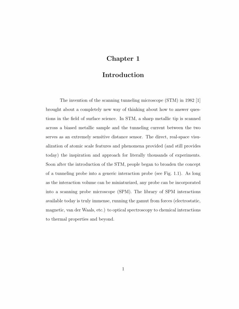
Soon after the introduction of the STM, people began to broaden the concept
of a tunneling probe into a generic interaction probe (see Fig. 1.1). As long
as the interaction volume can be miniaturized, any probe can be incorporated
into a scanning probe microscope (SPM). The library of SPM interactions
available today is truly immense, running the gamut from forces (electrostatic,
magnetic, van der Waals, etc.) to optical spectroscopy to chemical interactions
to thermal properties and beyond.
1
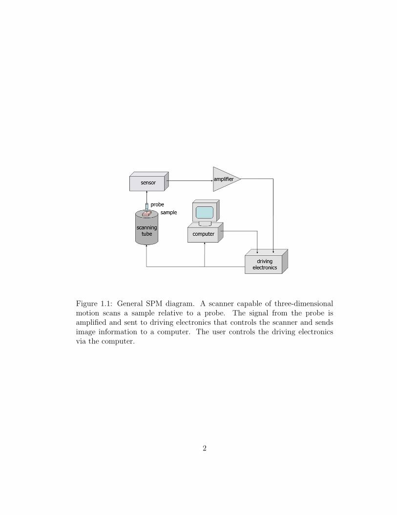
Figure 1.1: General SPM diagram. A scanner capable of three-dimensionalmotion scans a sample relative to a probe. The signal from the probe isamplified and sent to driving electronics that controls the scanner and sendsimage information to a computer. The user controls the driving electronicsvia the computer.
2
Chapter 2
Force Microscopy
The technique used in this dissertation, magnetic force microscopy
(MFM)1, is based on another SPM technique, atomic force microscopy (AFM).
[2] In AFM, a tip serves as the probe for atomic–range forces in order to ac-
quire the topography of a sample. The tip is attached to a cantilever with
spring constant k which reacts to a deflection z with a force
F = − k z (2.1)
in the direction perpendicular to the plane of the lever. All that is needed to
sense the interaction of the tip and sample is a way to read out the deflection
of the lever. A tunneling sensor fixed above the lever [2], a laser and split
photodiode [3], a fiberoptic interferometer [4], and a piezoresistive [5] or piezo-
electric [6] element embedded in the lever itself have all been used as deflection
sensors.
Initially, two modes for acquiring topography naturally presented them-
selves. In the first mode, constant–plane scanning, the tip is brought into
1For the sake of brevity, throughout this dissertation I will use the ”M” at the end ofany three letter acronym to refer to both the technique (microscopy) and the instrumentitself (microscope).
3
contact and scanned in a plane roughly parallel to the sample surface. The
cantilever deflects more over higher features on the sample and topography is
identified with the cantilever deflection. One problem with this scanning mode
is that the tip/sample force varies with topography changes. If the force is
too high, the tip and/or sample may be damaged. In the second mode, these
problems are somewhat mitigated by enabling a feedback loop during scan-
ning that changes the overall tip/sample distance to keep the lever deflection
constant. In this mode, since the deflection is constant, the force is constant,
and the topography is identified with the overall tip/sample distance changes.
2.1 Magnetic Force Microscopy
MFM can be performed in a mode similar to constant–plane scanning
AFM. The tip of the AFM lever is made magnetic and the tip is scanned in
a constant plane above the surface of the magnetic sample, where the topo-
graphic forces are negligible compared to the magnetic forces. The potential
of the tip/sample system is
U = −∫
tip
Mtip(r) ·B(r) dr, (2.2)
where the volume integral is over the tip, Mtip is the tip magnetization, and
B is the stray field from the sample. A truly massive effort has been put forth
by many groups to quantitatively calculate the MFM contrast mechanism for
varying Mtip models. [7] [8] [9] (See [9] for an extensive reference list.) Almost
all of the work I present in this dissertation is derived from mostly qualitative
4
MFM measurements, to some degree because it is rather difficult to extract
quantitative information without a careful calibration of Mtip(r), but primarily
because it is simply not necessary in many cases; the contrast variations within
an MFM image or series of MFM images will generally tell a complete story as
long as certain precautions (detailed in a case-by-case basis in later chapters)
are in place. With this in mind we take the first of many approximations, the
dipole approximation. [10] Assuming that the main contribution to Mtip(r) is
the dipole moment, m, Eqn. 2.2 simplifies to
U = −m ·B. (2.3)
The force is then
F = −∇U =∑
i=x,y,z
∂
∂i(mxBx + myBy + mzBz) i, (2.4)
where x and y are the cartesian unit vectors in the sample plane and z is
normal to the sample. Now we make two more assumptions:
1. That the lever is only sensitive to forces in the z direction (not true since
the lever is generally tilted around 12◦ from the x-y plane) so that the
only part of F which affects the lever is Fz.
2. That m is parallel to z so that mx = my = 0 (clearly not true for
a general Mtip(r), especially including the 12◦ lever tilt and the fact
that the surface of the tip is generally not normal to the surface of the
cantilever).
5
With these in place, Eqn. 2.4 goes to
F = Fz z = mz∂Bz
∂zz. (2.5)
In this MFM imaging mode, forces cause a pseudo-static deflection of the
cantilever that is proportional to the field gradient ∂Bz
∂zat the tip position
(taking the dipole approximation). For a nice demonstration of this technique,
see [11].
2.2 Magnetic Force (Gradient) Microscopy
For many reasons, today most MFM is performed using a different
scanning mode than that described in section 2.1. The cantilever is driven
near resonance and can be modeled as a damped, driven simple harmonic
oscillator with free resonant frequency f0. Durig provides two methods for
calculating the response of the lever to a general sample interaction. [12] The
first, simpler method is to consider the case in which the oscillation amplitude
of the lever is small compared to variations in the interaction force gradient
above the sample surface. The lever feels an effective softening or stiffening
due to the force gradient and the resonant frequency under the influence of
the sample is given by
f = f0
(1− F ′
z
k
) 12
, (2.6)
6
with F ′z = ∂Fz
∂z. Now we assume that F ′
z � k,2 Taylor expand Eqn. 2.6, and
set negligible terms to zero. We end up with an expression for the frequency
shift ∆f = f − f0:
∆f
f0
= − 1
2kF ′
z , (2.7)
and plugging in Fz from Eqn. 2.5 we get
∆f
f0
= −mz
2k
∂2Bz
∂z2. (2.8)
Durig also gives a method for calculating ∆f for the case that the oscillation
amplitude of the lever is large compared to variations in the interaction force
gradient above the sample surface [12], but this is beyond the scope of this
dissertation. We use lever oscillation amplitudes A around 50 nm, and con-
sidering that magnetic forces are relatively long-ranged, we feel safe in using
the small amplitude approximation, especially since we do not try to extract
quantitative information from the MFM images.
2This condition is always true for the data presented in this dissertation. F ′z is generally
measured to be in the range of 10−6 to 10−3 N/m and k for the levers we use runs from 0.1to 5 N/m.
7
Chapter 3
MFM Design and Operation Details1
Since the first demonstration by Martin and Wickramasinghe, [13]
MFM has improved continuously in terms of resolution, reliability, and ease of
use, all while adapting to more extreme environments. The MFM described
in this chapter was designed by Alex de Lozanne and is based on a variable–
temperature (VT)–MFM also built in his lab that has been productive [14]
[15] [16] [17] [18] [19] and is still in use. The heart of the new instrument is a
microfabricated piezoresistive cantilever sensor, and there are four substantial
improvements: in situ lateral positioning of the cantilever tip over the sample,
external optical access to aid in positioning, a longer probe in order to reach
a superconducting magnet inside a standard dewar, and a better heatsink to
allow the MFM to reach lower temperatures. I describe these and other main
features of this instrument.
3.1 Cantilever
Piezoresistive cantilevers (piezolevers) incorporate a doped Si layer that
undergoes resistance changes proportional to lever deflection changes. [20]
1Part of this chapter was submitted for publication in Rev. Sci. Inst. on 09/29/05.
8
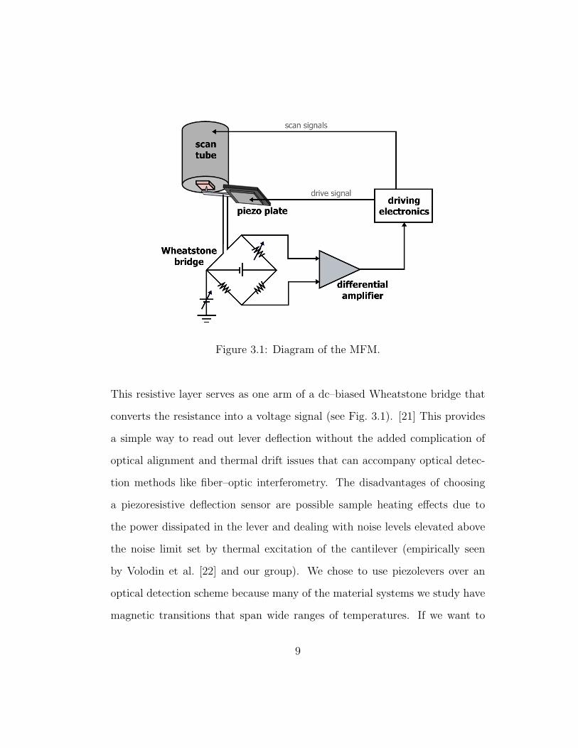
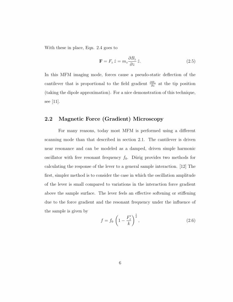
Figure 3.1: Diagram of the MFM.
This resistive layer serves as one arm of a dc–biased Wheatstone bridge that
converts the resistance into a voltage signal (see Fig. 3.1). [21] This provides
a simple way to read out lever deflection without the added complication of
optical alignment and thermal drift issues that can accompany optical detec-
tion methods like fiber–optic interferometry. The disadvantages of choosing
a piezoresistive deflection sensor are possible sample heating effects due to
the power dissipated in the lever and dealing with noise levels elevated above
the noise limit set by thermal excitation of the cantilever (empirically seen
by Volodin et al. [22] and our group). We chose to use piezolevers over an
optical detection scheme because many of the material systems we study have
magnetic transitions that span wide ranges of temperatures. If we want to
9
track an area of the sample while varying the sample temperature from 250 K
to 5 K and back, we can eliminate any possible optical misalignment induced
by thermal drift by using piezolevers. Because the material systems of inter-
est have relatively high magnetization values, the noise increase is rendered
inconsequential. Sample heating may be an issue at the lowest temperatures,
where heat capacities are lowest. We limit sample heating by placing an up-
per bound of 2 K on allowable cantilever heating through considerations of
heat exchange gas pressures, heat conduction pathways, and piezolever power
dissipation using the reasoning outlined by Giessibl et al. [21]
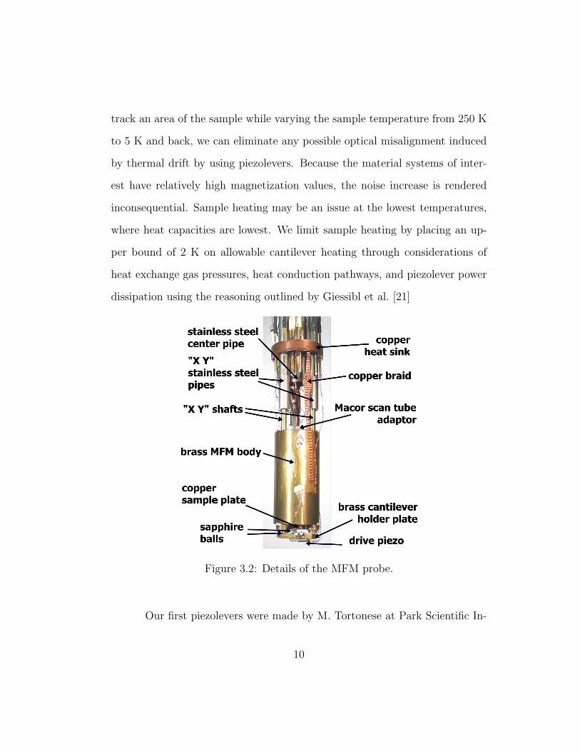
Figure 3.2: Details of the MFM probe.
Our first piezolevers were made by M. Tortonese at Park Scientific In-
10
struments. Recently we found a manufacturer of piezolevers in Japan (Seiko
Instruments) with a distributor in the USA (KLA–Tencor). We have used
both PRC400 and PRC120 cantilevers with spring constants of 2–4 N/m and
30–40 N/m, respectively. Since piezolevers are not currently available with a
magnetic coating, we deposit Fe, Co, Co85Cr15, or Co71Cr17Pt12 on the lever
and integrated tip by evaporation or by sputtering, taking care to avoid short-
ing the piezoresistor embedded in the lever. The cantilever chip is fixed, tip
pointing upward, to a brass cantilever holder plate with silver paint or epoxy.
This plate is held against the bottom of the instrument, as shown in Fig. 3.2,
has a hole cut in the center for optical access to the tip/sample region, and
is thermally linked to the brass MFM body with a copper wire (0.32 mm di-
ameter). A driving piezo plate is attached to the cantilever holder plate and
serves to excite the resonance of the cantilever.
3.2 Scanner
We use the same tube scanner as in the previous design, a PZT–5H
tube with four external electrodes and one internal electrode, 51 mm long,
with outer diameter (OD) of 6.35 mm and wall thickness of 0.51 mm (Stave-
ley Sensors). The maximum range of this scanner (±200 V applied to outer
electrodes) is approximately 160 µm at 293 K, 50 µm at 77 K, and 30 µm at
4.2 K. The scan tube fits inside a hole in the cylindrical brass MFM body and
is fixed at the top with a Macor adapter (Fig. 3.2). The sample is mounted
with the surface facing down on a copper sample stage attached to the bottom
11
of the scan tube just past the end of the MFM body. A Cernox temperature
sensor (LakeShore) and a heater resistor are mounted on opposite sides of the
sample stage. The copper sample stage is thermally linked to the MFM body
with a copper wire (0.16 mm diameter). The MFM has four leads that can
be used to connect to the sample to measure bulk resistivity or resistance of
a patterned device in situ as a function of temperature and applied magnetic
field.
3.3 Positioner
The x–y–z positioner is based on the traditional kinematic three–point
mount: one ball fits into a cone on the cantilever holder plate, the second ball
fits into a V–shaped groove, and the third ball presses against a flat surface.
We chose sapphire for the balls and the flat surface due to its high rigidity and
low friction with the aim of reliable, nonhysteretic motion. The third ball is
driven by a 10–80 screw, which provides a very smooth approach mechanism in
the z direction. The 10–80 screw is driven by a dedicated rotary manipulator
at the top of the probe, coupled by a thin stainless steel pipe.
The novel aspect of this design is that it provides quasi–x–y positioning
in a very compact design by mounting the first two balls mentioned above in an
off–center position on rotating shafts, as shown in Fig. 3.3. When the first shaft
is rotated, the first ball, which fits into a cone on the cantilever holder plate,
makes this cone rotate in a circle about this shaft while the second ball slides
along the V–shaped groove, as depicted by Fig. 3.3(c,d). For small rotations,
12
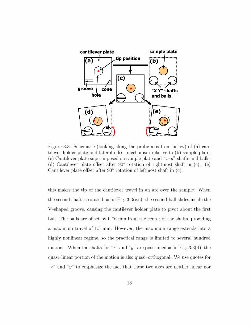
Figure 3.3: Schematic (looking along the probe axis from below) of (a) can-tilever holder plate and lateral offset mechanism relative to (b) sample plate.(c) Cantilever plate superimposed on sample plate and “x–y” shafts and balls.(d) Cantilever plate offset after 90◦ rotation of rightmost shaft in (c). (e)Cantilever plate offset after 90◦ rotation of leftmost shaft in (c).
this makes the tip of the cantilever travel in an arc over the sample. When
the second shaft is rotated, as in Fig. 3.3(c,e), the second ball slides inside the
V–shaped groove, causing the cantilever holder plate to pivot about the first
ball. The balls are offset by 0.76 mm from the center of the shafts, providing
a maximum travel of 1.5 mm. However, the maximum range extends into a
highly nonlinear regime, so the practical range is limited to several hundred
microns. When the shafts for “x” and “y” are positioned as in Fig. 3.3(d), the
quasi–linear portion of the motion is also quasi–orthogonal. We use quotes for
“x” and “y” to emphasize the fact that these two axes are neither linear nor
13
orthogonal over long distances.
The shafts for “x” and “y” are rotated by thin stainless steel pipes that
extend up to the top of the probe, where the head of a socket head screw is
mounted on each pipe. The details of how these pipes couple to the rotating
shafts on the MFM body are discussed in the next section. A single rotary
manipulator attached to the top of the probe with a bellows drives a ball–head
Allen key to engage and rotate either the “x” or “y” motion. Having separate,
dedicated rotary manipulators for “x” and “y” would be more convenient
although it would add to the cost and weight of the probe.
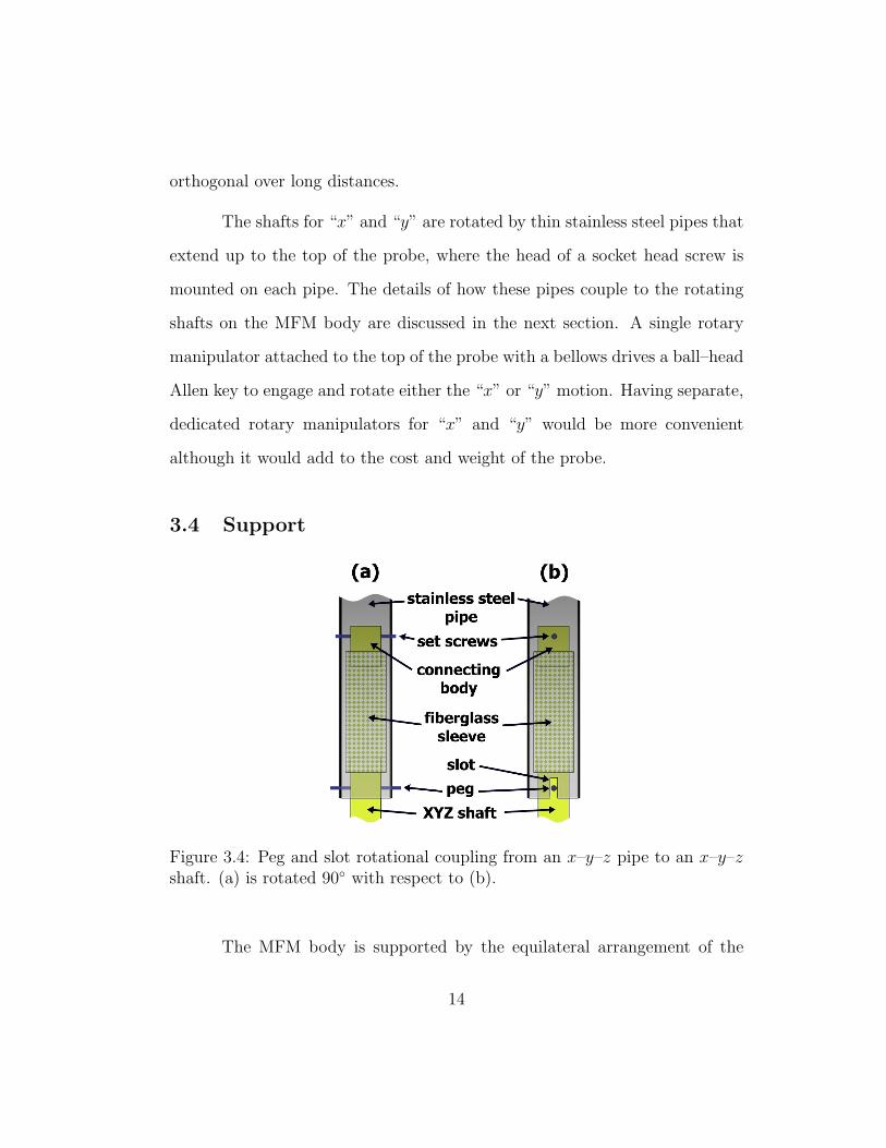
3.4 Support
Figure 3.4: Peg and slot rotational coupling from an x–y–z pipe to an x–y–zshaft. (a) is rotated 90◦ with respect to (b).
The MFM body is supported by the equilateral arrangement of the
14
three thin pipes (6.35 mm OD, 0.15 mm wall, stainless steel) that provide
rotary motion for x, y, and z positioning. To reduce vibrational coupling, the
weight of the MFM body is supported by a short piece of fiberglass sleeve
material on each shaft, while the torque is transmitted using a “peg and slot”
arrangement, as shown in Figure 3.4. The three thin pipes are held in place,
but allowed to rotate, by a copper heat sink above the MFM body and a
similar aluminum circular plate at the top of the probe. The copper heatsink
and aluminum plate are connected by a thin central pipe (11.1 mm OD, 0.15
mm wall, stainless steel) that provides rigidity for the probe as a whole. The
aluminum plate at the top of the probe is free to slide up and down to accom-
modate differential thermal contraction, and the weight of the whole probe
(or optional springs) provide the necessary force to press the copper heatsink
against a copper sheath at the bottom of the pipe housing (described in the
following section).
3.5 Chamber
The top of the probe has a small chamber made from a standard four–
way cross with 70 mm flanges. The top flange connects to the two rotary
manipulators mentioned above, while one side flange has a 20 pin feedthrough
for electrical leads and the other side flange connects to a valve and pumping
system. The bottom flange connects to the pipe housing for the instrument.
The pipe housing is a standard stainless steel tube (31.8 mm OD, 0.71 mm
wall). The pipe housing is removed every time a tip or sample is replaced.
15
While this is not as convenient as having a small canister attached at the
bottom, it has the reliability and long life of a seal that remains at room
temperature at the top of the probe.
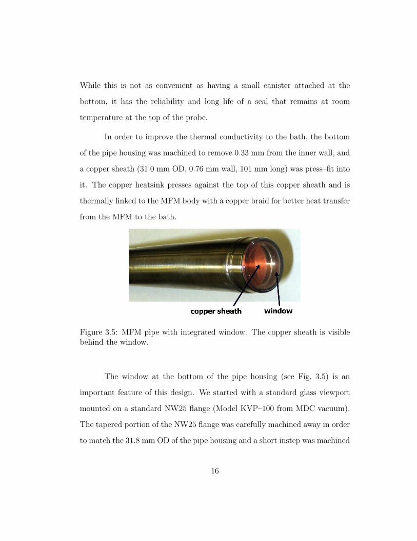
In order to improve the thermal conductivity to the bath, the bottom
of the pipe housing was machined to remove 0.33 mm from the inner wall, and
a copper sheath (31.0 mm OD, 0.76 mm wall, 101 mm long) was press–fit into
it. The copper heatsink presses against the top of this copper sheath and is
thermally linked to the MFM body with a copper braid for better heat transfer
from the MFM to the bath.
Figure 3.5: MFM pipe with integrated window. The copper sheath is visiblebehind the window.
The window at the bottom of the pipe housing (see Fig. 3.5) is an
important feature of this design. We started with a standard glass viewport
mounted on a standard NW25 flange (Model KVP–100 from MDC vacuum).
The tapered portion of the NW25 flange was carefully machined away in order
to match the 31.8 mm OD of the pipe housing and a short instep was machined
16
for alignment purposes. It was then welded at the bottom of the pipe housing.
The differential thermal contraction between the glass window and the stain-
less steel body is taken up by a thin Kovar sleeve. Nevertheless, approximately
half a year of thermal cyclings produced a small crack that started on one side
of the glass window and propagated to the opposite side over approximately
one more year. Surprisingly, the crack did not produce a measurable leak until
it crossed the complete window, but fortunately it was possible to seal it with
varnish (Kurt J. Lesker KL–5 leak sealant). We believe that this crack was
initially due to a manufacturing defect, or some shock during machining or
handling. An identical pipe and window has been thermally cycled from 77 K
to room temperature roughly 100 times with no cracks thus far.
3.6 Electronics
We drive the scanner and acquire imaging data with a Nanoscope IIIa
controller (Veeco–Digital Instruments). The lever deflection signal from the
Wheatstone bridge is differentially amplified by a Stanford Research Systems
SRS 560 Preamplifier (see Fig. 3.1). For MFM operation we use the frequency
modulation technique [23], both with the commercial “Extender” available for
the Nanoscope controller or with a digital phase lock loop (EasyPLL from
Nanosurf). The latter required homemade electronics to interface with the
Nanoscope controller. The homemade electronics consist mainly of a phase
shifter to choose the phase setpoint for the phase lock loop and an rms–to–
dc converter and comparator to generate the feedback signal for amplitude
17
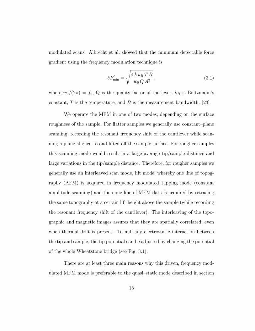
modulated scans. Albrecht et al. showed that the minimum detectable force
gradient using the frequency modulation technique is
δF ′min =
√4 k kB T B
w0 QA2, (3.1)
where w0/(2π) = f0, Q is the quality factor of the lever, kB is Boltzmann’s
constant, T is the temperature, and B is the measurement bandwidth. [23]
We operate the MFM in one of two modes, depending on the surface
roughness of the sample. For flatter samples we generally use constant–plane
scanning, recording the resonant frequency shift of the cantilever while scan-
ning a plane aligned to and lifted off the sample surface. For rougher samples
this scanning mode would result in a large average tip/sample distance and
large variations in the tip/sample distance. Therefore, for rougher samples we
generally use an interleaved scan mode, lift mode, whereby one line of topog-
raphy (AFM) is acquired in frequency–modulated tapping mode (constant
amplitude scanning) and then one line of MFM data is acquired by retracing
the same topography at a certain lift height above the sample (while recording
the resonant frequency shift of the cantilever). The interleaving of the topo-
graphic and magnetic images assures that they are spatially correlated, even
when thermal drift is present. To null any electrostatic interaction between
the tip and sample, the tip potential can be adjusted by changing the potential
of the whole Wheatstone bridge (see Fig. 3.1).
There are at least three main reasons why this driven, frequency mod-
ulated MFM mode is preferable to the quasi–static mode described in section
18
2.1:
1. Deflection sensor spectral noise is generally higher at lower frequencies.
A signal in the kHz regime (resonant frequencies are in this range) is
significantly less noisy than a signal in the dc to few hundred Hz range.
2. We can take advantage of the high Q in vacuum to decrease δF ′min.
3. Switching between topography and MFM acquisition during lift mode is
very simple to implement, allowing rougher samples to be scanned with
a small, constant tip/sample separation.
3.7 Optical Alignment of Tip and Sample
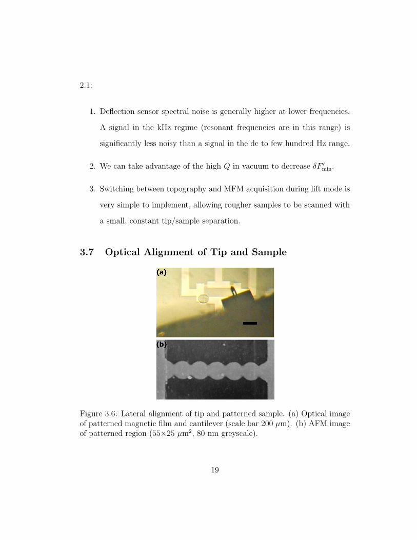
Figure 3.6: Lateral alignment of tip and patterned sample. (a) Optical imageof patterned magnetic film and cantilever (scale bar 200 µm). (b) AFM imageof patterned region (55×25 µm2, 80 nm greyscale).
19
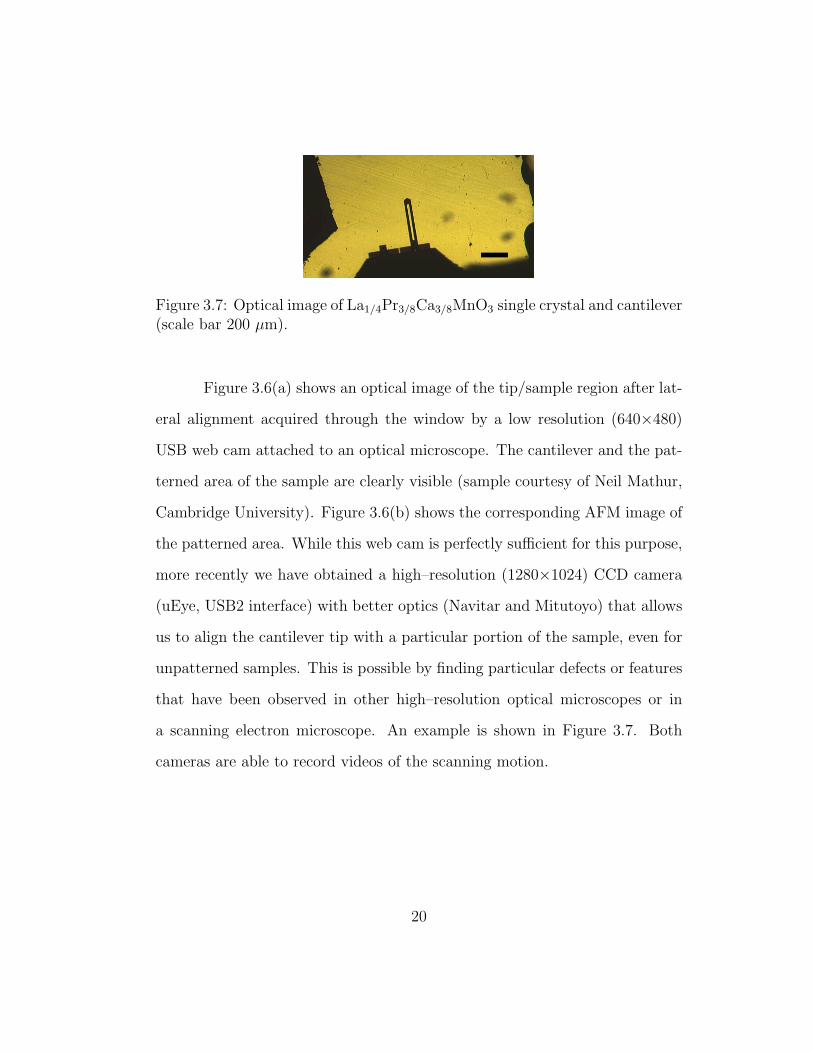
Figure 3.7: Optical image of La1/4Pr3/8Ca3/8MnO3 single crystal and cantilever(scale bar 200 µm).
Figure 3.6(a) shows an optical image of the tip/sample region after lat-
eral alignment acquired through the window by a low resolution (640×480)
USB web cam attached to an optical microscope. The cantilever and the pat-
terned area of the sample are clearly visible (sample courtesy of Neil Mathur,
Cambridge University). Figure 3.6(b) shows the corresponding AFM image of
the patterned area. While this web cam is perfectly sufficient for this purpose,
more recently we have obtained a high–resolution (1280×1024) CCD camera
(uEye, USB2 interface) with better optics (Navitar and Mitutoyo) that allows
us to align the cantilever tip with a particular portion of the sample, even for
unpatterned samples. This is possible by finding particular defects or features
that have been observed in other high–resolution optical microscopes or in
a scanning electron microscope. An example is shown in Figure 3.7. Both
cameras are able to record videos of the scanning motion.
20
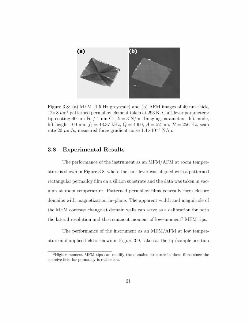
Figure 3.8: (a) MFM (1.5 Hz greyscale) and (b) AFM images of 40 nm thick,12×8 µm2 patterned permalloy element taken at 293 K. Cantilever parameters:tip coating 40 nm Fe / 1 nm Cr, k = 3 N/m. Imaging parameters: lift mode,lift height 100 nm, f0 = 43.37 kHz, Q = 4000, A = 52 nm, B = 256 Hz, scanrate 20 µm/s, measured force gradient noise 1.4×10⁻⁵ N/m.
3.8 Experimental Results
The performance of the instrument as an MFM/AFM at room temper-
ature is shown in Figure 3.8, where the cantilever was aligned with a patterned
rectangular permalloy film on a silicon substrate and the data was taken in vac-
uum at room temperature. Patterned permalloy films generally form closure
domains with magnetization in–plane. The apparent width and magnitude of
the MFM contrast change at domain walls can serve as a calibration for both
the lateral resolution and the remanent moment of low–moment2 MFM tips.
The performance of the instrument as an MFM/AFM at low temper-
ature and applied field is shown in Figure 3.9, taken at the tip/sample position
2Higher moment MFM tips can modify the domains structure in these films since thecoercive field for permalloy is rather low.
21
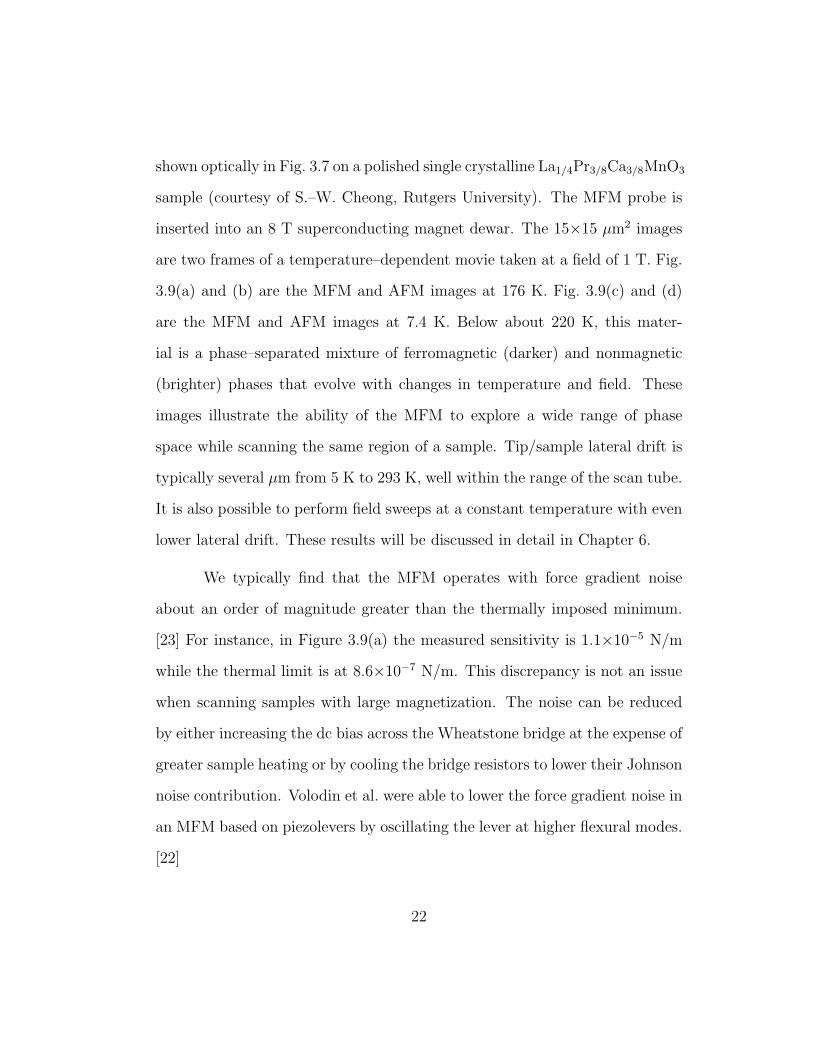
shown optically in Fig. 3.7 on a polished single crystalline La1/4Pr3/8Ca3/8MnO3
sample (courtesy of S.–W. Cheong, Rutgers University). The MFM probe is
inserted into an 8 T superconducting magnet dewar. The 15×15 µm2 images
are two frames of a temperature–dependent movie taken at a field of 1 T. Fig.
3.9(a) and (b) are the MFM and AFM images at 176 K. Fig. 3.9(c) and (d)
are the MFM and AFM images at 7.4 K. Below about 220 K, this mater-
ial is a phase–separated mixture of ferromagnetic (darker) and nonmagnetic
(brighter) phases that evolve with changes in temperature and field. These
images illustrate the ability of the MFM to explore a wide range of phase
space while scanning the same region of a sample. Tip/sample lateral drift is
typically several µm from 5 K to 293 K, well within the range of the scan tube.
It is also possible to perform field sweeps at a constant temperature with even
lower lateral drift. These results will be discussed in detail in Chapter 6.
We typically find that the MFM operates with force gradient noise
about an order of magnitude greater than the thermally imposed minimum.
[23] For instance, in Figure 3.9(a) the measured sensitivity is 1.1×10⁻⁵ N/m
while the thermal limit is at 8.6×10⁻⁷ N/m. This discrepancy is not an issue
when scanning samples with large magnetization. The noise can be reduced
by either increasing the dc bias across the Wheatstone bridge at the expense of
greater sample heating or by cooling the bridge resistors to lower their Johnson
noise contribution. Volodin et al. were able to lower the force gradient noise in
an MFM based on piezolevers by oscillating the lever at higher flexural modes.
[22]
22
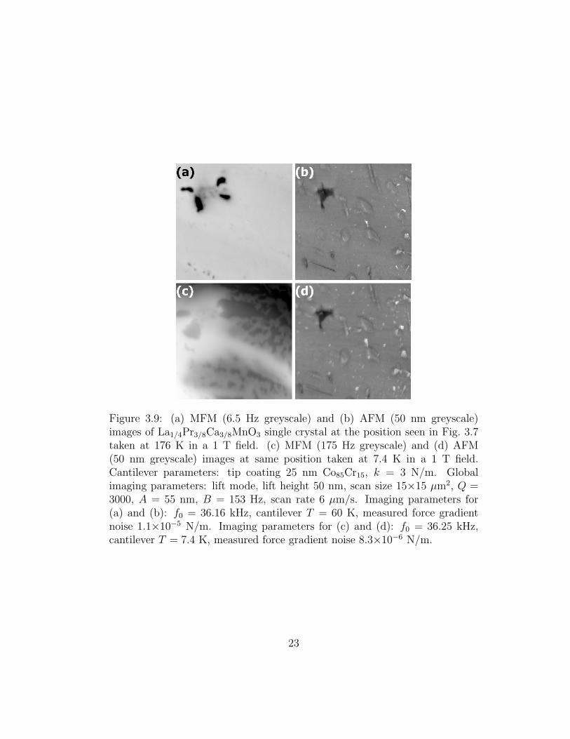
Figure 3.9: (a) MFM (6.5 Hz greyscale) and (b) AFM (50 nm greyscale)images of La1/4Pr3/8Ca3/8MnO3 single crystal at the position seen in Fig. 3.7taken at 176 K in a 1 T field. (c) MFM (175 Hz greyscale) and (d) AFM(50 nm greyscale) images at same position taken at 7.4 K in a 1 T field.Cantilever parameters: tip coating 25 nm Co85Cr15, k = 3 N/m. Globalimaging parameters: lift mode, lift height 50 nm, scan size 15×15 µm2, Q =3000, A = 55 nm, B = 153 Hz, scan rate 6 µm/s. Imaging parameters for(a) and (b): f0 = 36.16 kHz, cantilever T = 60 K, measured force gradientnoise 1.1×10⁻⁵ N/m. Imaging parameters for (c) and (d): f0 = 36.25 kHz,cantilever T = 7.4 K, measured force gradient noise 8.3×10⁻⁶ N/m.
23
Chapter 4
Introduction to Manganite Physics
For some materials (and fabricated devices), the resistance R(B) changes
with the application of a magnetic field, B. The ratio R(B)−R(0)R(B)
is aptly termed
the magnetoresistance (MR). In the vast majority of systems, the MR is small,
say 5% or less, even for fields of order 1 T. By exploiting the interaction of
currents with ferromagnetic layers spaced by nonmagnetic layers or coupled
antiferromagnetically, devices can be produced with MR ≈ −200%. This ef-
fect, discovered in 1988, was dubbed the giant magnetoresistive (GMR) effect
[24] [25], and today GMR heads are used in computers to sense stray fields
from the magnetic platters in hard disks and read out data.
4.1 CMR effect
In 1994, Jin et al. presented data from La2/3Ca1/3MnO3 thin films show-
ing a MR of −127 000% at 77 K in a 6 T field. [26] This unprecendented be-
havior was immediately christened the colossal magnetoresistive (CMR) effect.
Many manganites of the form R1−xAxMnO3 (R is a trivalent rare–earth ion
and A is a divalent dopant) exhibit the CMR effect for a wide doping range
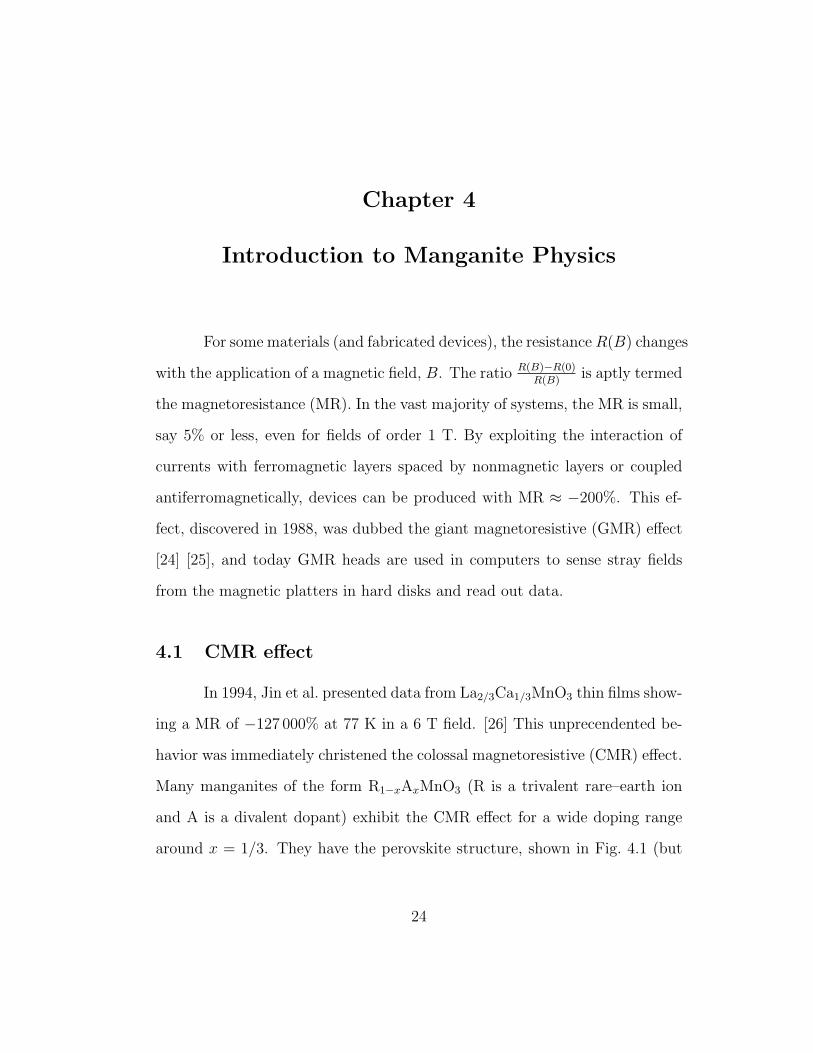
around x = 1/3. They have the perovskite structure, shown in Fig. 4.1 (but
24
Figure 4.1: The perovskite stucture.
generally are the slightly distorted Pnma structure). Generally speaking, these
materials show an insulator–metal transition from a high–temperature insu-
lating phase to a low–temperature metallic phase marked by a peak at TP in
the resistivity versus temperature curve. This phase transition is accompanied
by a magnetic transition from a high–temperature nonferromagnetic phase to
a low–temperature ferromagnetic (FM) phase at the Curie temperature, TC.
The doping of A2+ ions in R3+ sites results in a mixed Mn3+/Mn4+ va-
lence, with 4−x Mn d–shell electrons per Mn. The cubic crystal environment
splits the 5 3d orbitals into a t2g triplet and an eg doublet, as shown schemat-
ically in Fig. 4.2. Hund’s rule coupling aligns all these valence electrons. So,
3 electrons go to the t2g triplet, creating a core spin, and the remaining 1− x
electron can be in the eg doublet at a Mn site if its spin is aligned with the
core spin.
25
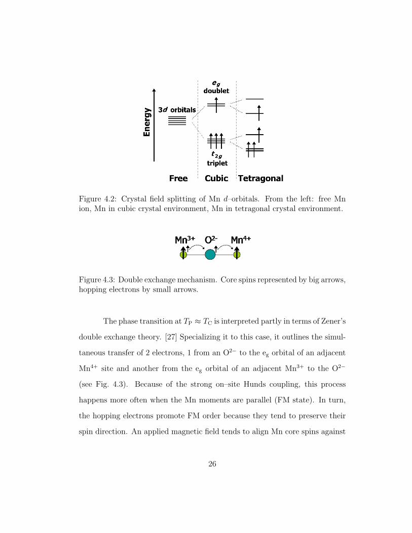
Figure 4.2: Crystal field splitting of Mn d–orbitals. From the left: free Mnion, Mn in cubic crystal environment, Mn in tetragonal crystal environment.
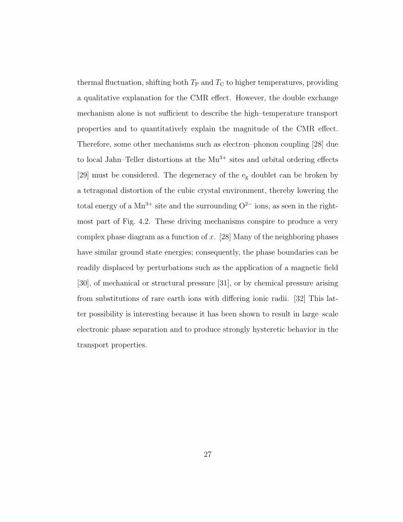
Figure 4.3: Double exchange mechanism. Core spins represented by big arrows,hopping electrons by small arrows.
The phase transition at TP ≈ TC is interpreted partly in terms of Zener’s
double exchange theory. [27] Specializing it to this case, it outlines the simul-
taneous transfer of 2 electrons, 1 from an O2− to the eg orbital of an adjacent
Mn4+ site and another from the eg orbital of an adjacent Mn3+ to the O2−
(see Fig. 4.3). Because of the strong on–site Hunds coupling, this process
happens more often when the Mn moments are parallel (FM state). In turn,
the hopping electrons promote FM order because they tend to preserve their
spin direction. An applied magnetic field tends to align Mn core spins against
26
thermal fluctuation, shifting both TP and TC to higher temperatures, providing
a qualitative explanation for the CMR effect. However, the double exchange
mechanism alone is not sufficient to describe the high–temperature transport
properties and to quantitatively explain the magnitude of the CMR effect.
Therefore, some other mechanisms such as electron–phonon coupling [28] due
to local Jahn–Teller distortions at the Mn3+ sites and orbital ordering effects
[29] must be considered. The degeneracy of the eg doublet can be broken by
a tetragonal distortion of the cubic crystal environment, thereby lowering the
total energy of a Mn3+ site and the surrounding O2− ions, as seen in the right-
most part of Fig. 4.2. These driving mechanisms conspire to produce a very
complex phase diagram as a function of x. [28] Many of the neighboring phases
have similar ground state energies; consequently, the phase boundaries can be
readily displaced by perturbations such as the application of a magnetic field
[30], of mechanical or structural pressure [31], or by chemical pressure arising
from substitutions of rare earth ions with differing ionic radii. [32] This lat-
ter possibility is interesting because it has been shown to result in large–scale
electronic phase separation and to produce strongly hysteretic behavior in the
transport properties.
27
Chapter 5
An MFM Study of the Magnetic Structure in
a CMR Film around the Insulator–Metal
Transition1
There is growing experimental and theoretical evidence that the doped
manganites are electronically inhomogeneous and that phase separation is
common in these materials. [33] [34] Uehara et al. used electron microscopy
to study the La5/8−yPryCa3/8MnO3 system. [32] Changes in the Pr doping
(y) lead to changes in the internal chemical pressure of the system due to
the slight ionic size difference between La3+ and Pr3+. They found that at
low temperatures, below TP, the system is electronically phase separated into
a micrometer–scale mixture of Jahn–Teller–distorted, insulating regions and
nondistorted, metallic FM domains, although they could not characterize the
local magnetic properties of these domains. They explained the CMR effect
by percolative transport through the FM domains; a magnetic field aligns the
magnetizations of FM domains that are dispersed in a configuration that is
near the percolation threshold. By the double exchange mechanism, electrons
can now move easily along these FM pathways and the resistance is lowered.
1Part of this chapter was published in ref. [19]
28
In this chapter I present the direct observation of the formation of
these percolative networks as the sample is cooled, and their disappearance
upon warming. Upon cooling, the isolated FM domains in thin films of
La1/3Pr1/3Ca1/3MnO3 start to grow and merge at the metal–insulator tran-
sition temperature TP1, leading to a steep drop in resistivity, and continue to
grow far below TP1. In contrast, upon warming, the FM domain size remains
unchanged until near the transition temperature. The jump in the resistiv-
ity results from the decrease in the average magnetization. The FM domains
almost disappear at a temperature TP2 (higher than TP1), showing a local mag-
netic hysteresis in agreement with the resistivity hysteresis. Even well above
TP2, some FM domains with higher transition temperatures are observed, indi-
cating magnetic inhomogeneity. These results give a few clues as to the origin
of the CMR in these materials and include a few surprising findings: the FM
domains continue to grow and change at temperatures well below TP1 during
cooling and upon warming they still exist at temperatures above TP2.
5.1 Experimental Setup
All of the data presented in this Chapter was taken using the lift mode
technique described in Section 3.6 with a lift height of 100 nm. We used
noncontact Piezolevers2 with resonant frequencies around 110 kHz. The lever
is made sensitive to magnetic forces by depositing a 50 nm Fe film on one side
of the tip and magnetizing it along its axis.
2Park Scientific Instruments (now Digital Instruments), Santa Barbara, CA.
29
The domain patterns of CMR films with different easy axes have dif-
ferent shapes. [35] MFM images of our sample indicate an in–plane easy axis.
Because the MFM is sensitive to force gradients perpendicular to the sample,
in order to see clearly the domains instead of the domain walls, a perpendicular
magnetic field is used to partially align the magnetization of the FM domains
out–of–plane. In the case of the cooling sequence, the MFM tip itself provides
this cooling field. For warming images we first cooled the sample across TP1 to
a low temperature in a 2.5 mT magnetic field perpendicularly applied to the
whole sample, then turned off the field before scanning during warming. The
thermal drift of the tip position relative to the sample was compensated for
during image acquisition with lateral offsets of the scan piezo and adjustments
of the coarse approach mechanism to follow the same area of the sample. This
data was not taken with the MFM described in Chapter 3, but with a previ-
ously built MFM. [14] In this MFM, a change in the direction of the coarse
approach mechanism causes an unpredictable change in the lateral position of
the sample, preventing us from scanning the same area of the sample when
changing from cooling to warming. The temperature change rate was roughly
0.1 K/minute during scanning.
The films were grown on NdGaO3 (NGO) (110) substrates by pulsed
laser deposition to a thickness of 60 nm. They were grown in an oxygen
atmosphere of 400 mTorr at a rate of about 1 A/second at a substrate tem-
perature of 820 ◦C. The temperature dependence of the resistivity of the film
(Fig. 5.1) shows that on cooling from room temperature, the resistivity grad-
30
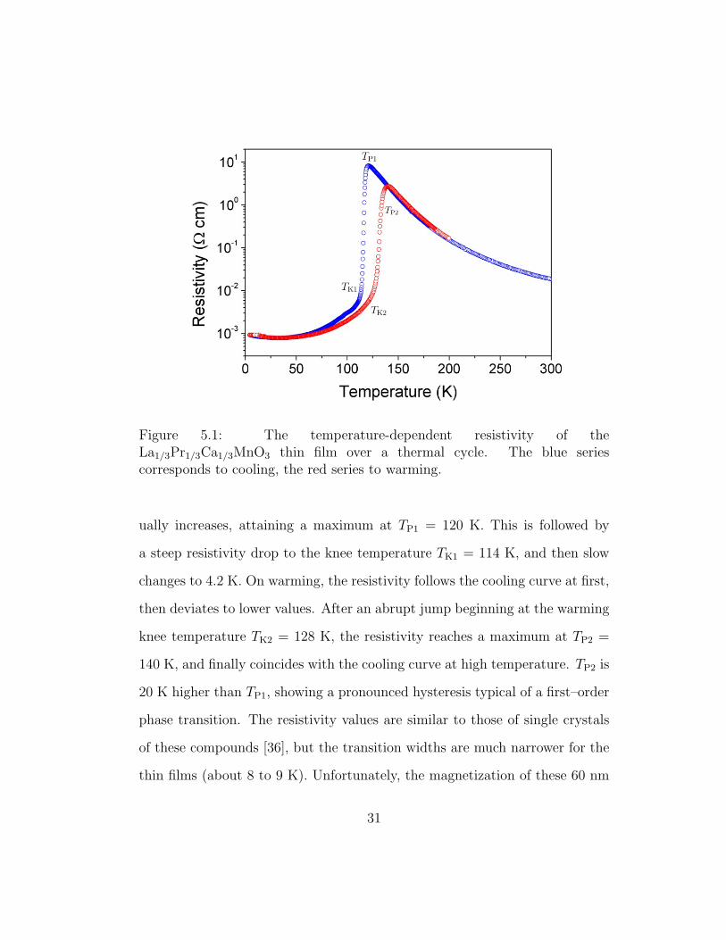
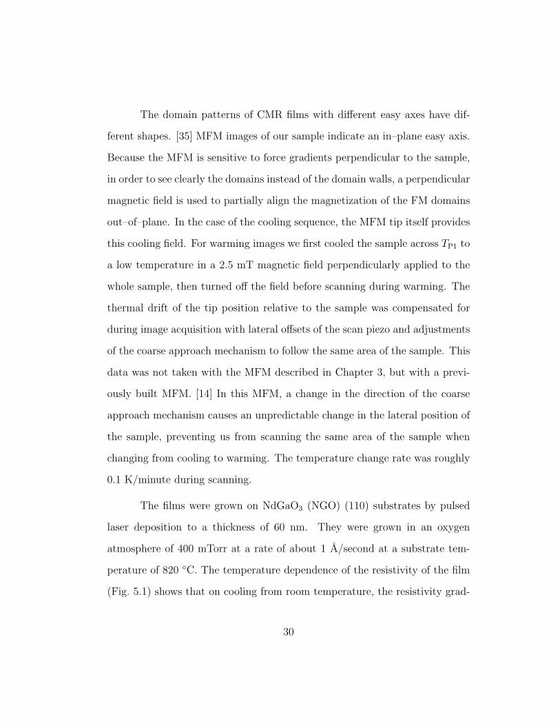
Figure 5.1: The temperature-dependent resistivity of theLa1/3Pr1/3Ca1/3MnO3 thin film over a thermal cycle. The blue seriescorresponds to cooling, the red series to warming.
ually increases, attaining a maximum at TP1 = 120 K. This is followed by
a steep resistivity drop to the knee temperature TK1 = 114 K, and then slow
changes to 4.2 K. On warming, the resistivity follows the cooling curve at first,
then deviates to lower values. After an abrupt jump beginning at the warming
knee temperature TK2 = 128 K, the resistivity reaches a maximum at TP2 =
140 K, and finally coincides with the cooling curve at high temperature. TP2 is
20 K higher than TP1, showing a pronounced hysteresis typical of a first–order
phase transition. The resistivity values are similar to those of single crystals
of these compounds [36], but the transition widths are much narrower for the
thin films (about 8 to 9 K). Unfortunately, the magnetization of these 60 nm
31
films on NGO is difficult to measure due to the paramagnetic substrate [37].
5.2 Temperature Dependent MFM data
Figure 5.2: (a) Topography image and (b) the corresponding MFM imagerecorded on the same area (7.5×7.5 µm2) of the sample at 120 K duringwarming.
Figure 5.2 shows a simultaneously acquired topographic image and
MFM image well below TP2. Comparison of the two images indicates that
the main features in the MFM image have no counterparts in the topography
image. The features in the MFM image are due to the nonuniform magnetic
field distribution above the sample surface; they are produced by FM domains
of differing magnetization in the sample.
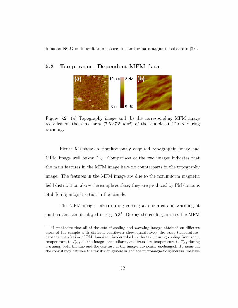
The MFM images taken during cooling at one area and warming at
another area are displayed in Fig. 5.33. During the cooling process the MFM
3I emphasize that all of the sets of cooling and warming images obtained on differentareas of the sample with different cantilevers show qualitatively the same temperature–dependent evolution of FM domains. As described in the text, during cooling from roomtemperature to TP1, all the images are uniform, and from low temperature to TK2 duringwarming, both the size and the contrast of the images are nearly unchanged. To maintainthe consistency between the resistivity hysteresis and the micromagnetic hysteresis, we have
32
Figure 5.3: The temperature-dependent MFM image sequence (a) for coolingand (c) for warming, and the resistivity (b) of the La1/3Pr1/3Ca1/3MnO3 thinfilm over a thermal cycle. The blue series corresponds to cooling, the redseries to warming. The center of each image is aligned horizontally with thetemperature scale from (b) at the time of image capture. Scanned areas are6×6 µm2 for all cooling images and 7.5×7.5 µm2 for all warming images. Allcooling images were taken at one area of the sample, all warming images weretaken at another area.
images are nearly uniform above TP1. Just below TP1, the contrast starts to
appear. The contrast of the sequence is gradually enhanced with decreasing
temperature, indicating that the magnetization of the FM domains becomes
increasingly stronger. The features gradually merge into continuous pathways
in the MFM field of view. Just past TK1 the percolation of the contrast features,
simply reproduced the three highest temperature images in Fig. 5.3(a) and the three lowesttemperature images in Fig. 5.3(c).
33
and therefore the FM domains, is clearly seen. When the temperature is
decreased further, although the change in the resistivity is smaller, the contrast
of the image continues to increase and the FM domains merge and enlarge,
which is an unexpected result.
However, during warming below TK2, both the contrast and the size of
the FM regions are nearly unchanged. Above TK2, although the size of the FM
regions is constant, the contrast rapidly decreases. At TP2 the contrast almost
completely disappears. The hysteresis in the local magnetic microstructure is
consistent with the resistivity hysteresis and qualitatively consistent with the
magnetization measurement on polycrystalline samples with similar composi-
tion. [38]
5.3 Discussion
The FM domains in the warming images have a much smaller size than
the cooling images at the same temperatures below TK1. This difference is
likely due to the way in which the sample is cooled. The tip of the MFM
vibrates above the sample surface at the resonant frequency of the lever, 110
KHz, contacting the sample at the lowest point of each oscillation. At this
contact point, the magnetic field applied by the tip is large (10 to 100 mT).
[39] Roughly, as the tip is scanned, a strong periodic magnetic pulse with
a frequency of 110 KHz is scanned over the sample. We believe that upon
cooling, although this scanning, localized magnetic pulse may not change the
relative FM volume fraction in the film [40], it may assist in driving the motion
34
of the domain walls, leading to the formation of FM domains with a large
characteristic length scale. On the other hand, the warming images were
obtained after the sample was cooled to the lowest temperature in a magnetic
field of 2.5 mT. This was done to coarsely simulate the effect of the scanning
tip during cooling and to begin the warming scans with a sample state similar
to the end of the cooling scans. During this cooling process, the tip is far away
from the sample. This cooling field may not be strong enough to move the
domain walls. When scanning during warming, the domain walls are strongly
pinned. As a result, the MFM image sequence does not show many changes.
As TP2 is approached, the average magnetization decreases, which results in a
rise in the resistivity (Fig. 5.3(b)). [41] Our observations indicate that during
cooling, the percolation of the FM domains causes the steep resistivity drop,
whereas during warming, the FM conductive paths remain until near TP2, but
the decrease in the average magnetization leads to the jump in resistivity.
This may explain why the knee in the resistivity is sharper during cooling
than during warming.
Even well above TP2, there is still a slight but discernable contrast in
some areas. We propose that this is due to the magnetic inhomogeneity above
TP that is frequently observed in similar CMR materials. [42] [43] [44] Due to
the constraining effect of the substrate, some effects observed in bulk samples
may be suppressed or different for these thin films. [36] This might account for
the sharper transitions in the thin films and the narrower hysteresis regions.
This implies that the temperature–dependent magnetic microstructure in thin
35
films is modified due to the effect of the substrate.
These results confirm that the local magnetic structure is correlated
with the hysteresis in resistivity and magnetization versus temperature and
that growth and merging of FM domains is a key part of the insulator–metal
transition in prototypical CMR manganites.
36
Chapter 6
An MFM Study of the Magnetic Structure in
a CMR Single Crystal around a Glass–Like
Transition1
We chose to investigate the issue of electronic phase separation in CMR
manganites more thoroughly in a similar sample to the one discussed in Chap-
ter 5. As previously stated, the La1−x−yPryCaxMnO3 (x = 3/8) system ex-
hibits large scale phase separation for a wide region of parameter (y, tem-
perature, field, etc.) space. [32] Recent experimental and theoretical efforts
increasingly emphasize the importance of µm–scale phase separation around
field and temperature induced transitions, where percolation is key in under-
standing the CMR effect, especially in manganites with low Curie tempera-
tures (TC). [32] [44] [19] It is suspected that this large scale phase separation
is caused by the accommodation strain arising from the lattice mismatch be-
tween the FM metallic phase (pseudo–cubic) and the charge–ordered (CO)
insulating phase (orthorhombic). [45] This point of view is supported by both
experiments and simulations. [36] [46] Therefore, it is important to understand
the thermodynamics of this strain–stabilized phase separation, yet little has
1Part of this chapter was submitted for publication in Science on 10/11/05.
37
been done.
6.1 Chemical Pressure and Glassy Behavior
La5/8−yPryCa3/8MnO3 (LPCMO) is a model system for investigating
the role of chemical pressure and accommodation strain on a phase–separated
state. With the Ca doping held constant at 3/8, the carrier concentration is
fixed, and changes in the Pr doping (y) lead to changes in the internal chemical
pressure of the system due to the slight ionic size difference between La3+ and
Pr3+. Both the phase separation balance and length scale depend strongly
on y. [32] Recently, Sharma et al. presented evidence supporting the classi-
fication of LPCMO (y = 0.41) as a “strain glass” at low temperature [47],
where hysteretic behavior is found in isothermal field sweeps. [48] The glass
transition is buried inside this large hysteresis so that it is hard to detect. Sim-
ilar isothermal hysteretic behavior has been observed in various manganites,
Pr1−xCaxMnO3, Nd1−xSrxMnO3, etc. as well. [49] This similarity suggests
that they might share the same glass–like state at low temperature.
The glassy behavior seen in phase–separated manganites is reminiscent
of the well–studied spin glass transition in Mn–doped Cu [50], which is signi-
fied by the bifurcation of the zero–field–cooled (ZFC) and field–cooled (FC)
susceptibility χ(T ) below TG. A wide class of heavily disordered ferromagnets
have been termed “cluster glasses” because they tend to show similar behavior
in χ(T ). [51] It has been speculated that the magnetization of FM clusters
freezes in a random fashion below the cluster glass transition and the mag-
38
netization of each cluster acts like an individual spin in a spin glass. Since
many phase–separated manganites also exhibit typical cluster glass behavior,
[47] [48] it may be natural to assume that the cluster glass picture is a suitable
description of the phase–separated manganites. The local magnetic configura-
tion of the glassy state in both disordered ferromagnets and phase–separated
manganites has never been studied on the scale of individual clusters, despite
the fact that “cluster glass” is commonly used to describe these material sys-
tems. In particular, no real–space imaging technique has been used to study
the cluster glass transition. Here, we succeed in imaging a possible cluster
glass transition in LPCMO (y = 3/8). Upon warming through TG, the “clus-
ter glass” picture predicts only that each frozen FM cluster magnetization
would be free to rotate, implying no significant change in FM volume frac-
tion. In contrast, we found that the FM volume fraction increases drastically,
reflecting the collective nature of the transition. Our results further confirm
that the mesoscopic scale phase separation found in LPCMO using electron
microscopy is representative of the bulk. [32] It would be interesting to extend
our study to other compounds showing similar behavior.
In this Chapter, I describe the results of variable–temperature magnetic
force microscope (VT–MFM) studies on single crystal LPCMO (y = 3/8), a
composition in which µm–scale phase separation has been observed. [32] After
ZFC from room temperature to below TG, the MFM images demonstrate that
the frozen glass state prevents the formation of new FM regions, even with
the application of a 1 T field. As the temperature approaches TG during
39
fieldwarming (FW), more and more nonmagnetic regions are converted to FM
domains along orthorhombic twin boundaries. Near and just above TG, the
FM regions grow into an extensive stripe–like pattern, correlating with the
sharp rise in bulk magnetization and the sharp decrease of resistivity. As the
temperature is increased further, the phase pattern remains relatively constant
with some fraction of the sample remaining nonmagnetic (presumably the CO
phase, which is antiferromagnetic below 180 K [48]) over a wide range of
temperature, agreeing with magnetization and resistivity data. In contrast to
this ZFC–FW strain–glass–like transition, during the FC–FW process the local
phase configuration and therefore magnetization and resistivity are relatively
static. It is found that the FM domains, once formed, persist even after the
field is turned off, indicating that the FM and CO phases have similar free
energies over this temperature range, a conclusion which is in agreement with
previous work. [32]
6.2 Experimental Setup
Single crystal samples of LPCMO (y = 3/8) were synthesized in an
optical floating zone furnace. One sample was mechanically cut, polished
with 0.1 µm paper with water, and annealed in an O2 atmosphere at 1000
◦C for 10 hours. The original sample was cleaved into two pieces, one for
SQUID measurements and one for VT–MFM and transport measurements. All
the MFM images were taken after inserting the MFM into a superconducting
magnet before scanning. All of the data presented in this Chapter was taken
40
with the MFM described in Chapter 3 using the lift mode technique described
in Section 3.6 at a lift height of 50 nm. We used PRC400 Piezolevers2 with
resonant frequencies around 35 kHz. The lever is made sensitive to magnetic
forces by depositing a 25 nm thick layer of Co85Cr15 on the tip and magnetizing
it along its axis3. Two copper wires were attached to the sample by silver paint
for two–probe resistance measurements taken simultaneously with MFM data.
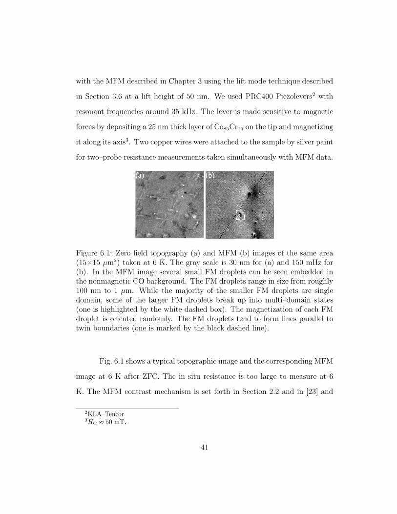
Figure 6.1: Zero field topography (a) and MFM (b) images of the same area(15×15 µm2) taken at 6 K. The gray scale is 30 nm for (a) and 150 mHz for(b). In the MFM image several small FM droplets can be seen embedded inthe nonmagnetic CO background. The FM droplets range in size from roughly100 nm to 1 µm. While the majority of the smaller FM droplets are singledomain, some of the larger FM droplets break up into multi–domain states(one is highlighted by the white dashed box). The magnetization of each FMdroplet is oriented randomly. The FM droplets tend to form lines parallel totwin boundaries (one is marked by the black dashed line).
Fig. 6.1 shows a typical topographic image and the corresponding MFM
image at 6 K after ZFC. The in situ resistance is too large to measure at 6
K. The MFM contrast mechanism is set forth in Section 2.2 and in [23] and
2KLA–Tencor3HC ≈ 50 mT.
41
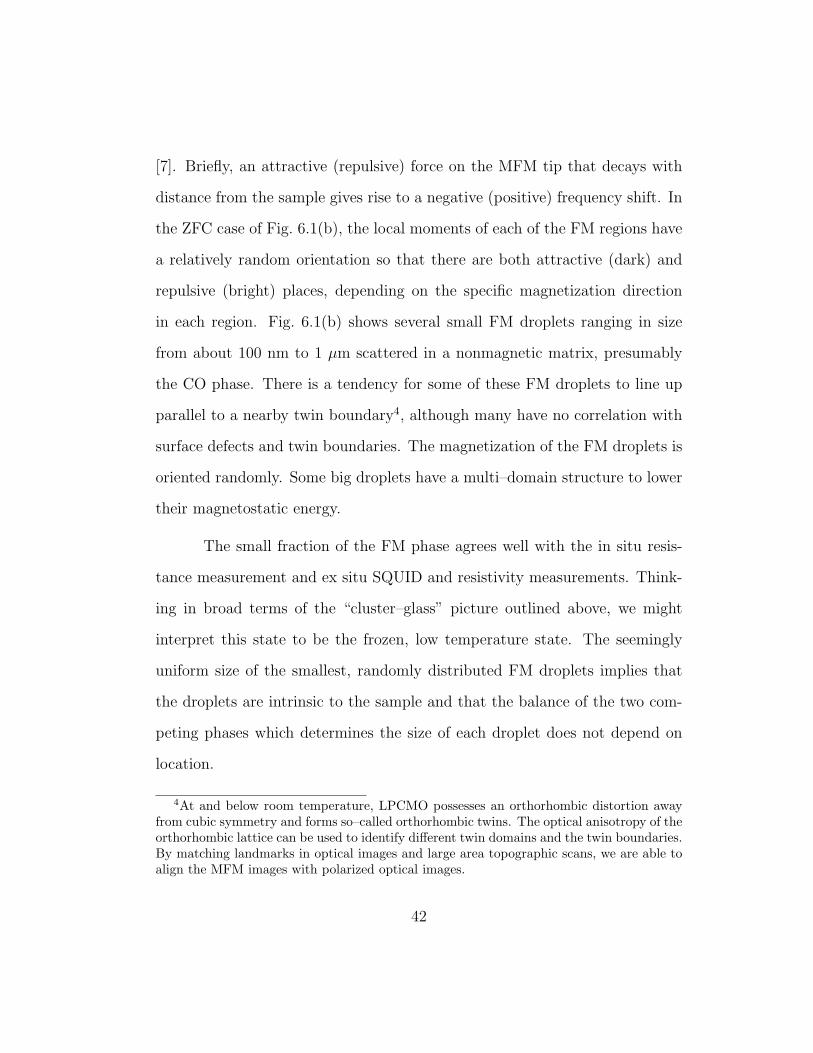
[7]. Briefly, an attractive (repulsive) force on the MFM tip that decays with
distance from the sample gives rise to a negative (positive) frequency shift. In
the ZFC case of Fig. 6.1(b), the local moments of each of the FM regions have
a relatively random orientation so that there are both attractive (dark) and
repulsive (bright) places, depending on the specific magnetization direction
in each region. Fig. 6.1(b) shows several small FM droplets ranging in size
from about 100 nm to 1 µm scattered in a nonmagnetic matrix, presumably
the CO phase. There is a tendency for some of these FM droplets to line up
parallel to a nearby twin boundary4, although many have no correlation with
surface defects and twin boundaries. The magnetization of the FM droplets is
oriented randomly. Some big droplets have a multi–domain structure to lower
their magnetostatic energy.
The small fraction of the FM phase agrees well with the in situ resis-
tance measurement and ex situ SQUID and resistivity measurements. Think-
ing in broad terms of the “cluster–glass” picture outlined above, we might
interpret this state to be the frozen, low temperature state. The seemingly
uniform size of the smallest, randomly distributed FM droplets implies that
the droplets are intrinsic to the sample and that the balance of the two com-
peting phases which determines the size of each droplet does not depend on
location.
4At and below room temperature, LPCMO possesses an orthorhombic distortion awayfrom cubic symmetry and forms so–called orthorhombic twins. The optical anisotropy of theorthorhombic lattice can be used to identify different twin domains and the twin boundaries.By matching landmarks in optical images and large area topographic scans, we are able toalign the MFM images with polarized optical images.
42
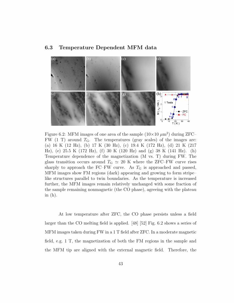
6.3 Temperature Dependent MFM data
Figure 6.2: MFM images of one area of the sample (10×10 µm2) during ZFC–FW (1 T) around TG. The temperatures (gray scales) of the images are:(a) 16 K (12 Hz), (b) 17 K (30 Hz), (c) 19.4 K (172 Hz), (d) 21 K (217Hz), (e) 25.5 K (172 Hz), (f) 30 K (120 Hz) and (g) 38 K (141 Hz). (h)Temperature dependence of the magnetization (M vs. T) during FW. Theglass transition occurs around TG ' 20 K where the ZFC–FW curve risessharply to approach the FC–FW curve. As TG is approached and passed,MFM images show FM regions (dark) appearing and growing to form stripe–like structures parallel to twin boundaries. As the temperature is increasedfurther, the MFM images remain relatively unchanged with some fraction ofthe sample remaining nonmagnetic (the CO phase), agreeing with the plateauin (h).
At low temperature after ZFC, the CO phase persists unless a field
larger than the CO melting field is applied. [48] [52] Fig. 6.2 shows a series of
MFM images taken during FW in a 1 T field after ZFC. In a moderate magnetic
field, e.g. 1 T, the magnetization of both the FM regions in the sample and
the MFM tip are aligned with the external magnetic field. Therefore, the
43
only force between them is attractive; the darkest places in the MFM images
correspond to regions with the highest effective moment, averaging over a
volume beneath the surface. Images taken from 5 K to 16 K show no significant
changes and are omitted from Fig. 6.2. Fig. 6.2(h) shows the temperature
dependence of the magnetization of the sample in a 1 T field during FW after
ZFC and FC. Comparing Fig. 6.2(a–g) with Fig. 6.2(h) we conclude that the
bulk magnetization is a good measure of the volume fraction of the FM phase
at 1 T. The ZFC data in Fig. 6.2(h) show a sharp rise in magnetization from
15 K to 25 K as MFM images confirm a significant increase in the FM fraction
and the in situ resistance drops to a finite value. Some of the long length
scale features in the MFM images are likely due to the formation of large FM
regions well beneath the sample surface. The FM regions tend to grow into
stripe–like structures during the transition. For this choice of field (1 T), some
CO regions persist above TG (bright color at the top–center of the frame in
Fig. 6.2(e–g)).
In contrast to the MFM images taken during ZFC–FW near and below
TG, the FC–FW images from the same temperature range show that the local
phase configuration is relatively static, agreeing with the magnetization data
in Fig. 6.2(h). This history dependence provides evidence for a glassy state.
[47] These FC–FW images will be presented elsewhere.
44
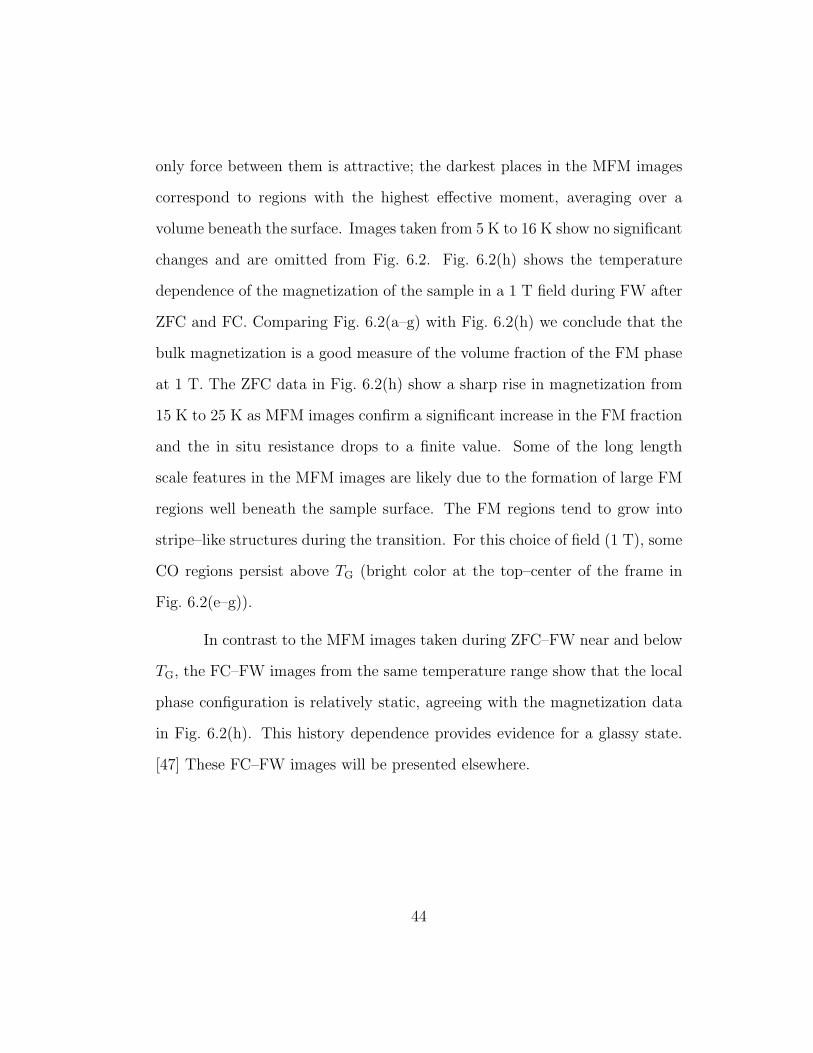
Figure 6.3: MFM images of one area of the sample (15×15 µm2) at variousmagnetic fields at 6.8 K after ZFC. The field values (gray scales) of the imagesare: (a) 0 T (2.3 Hz), (b) 0.5 T (8 Hz), (c) 1.0 T (8 Hz), (d) 1.4 T (8 Hz),(e) 1.6 T (8 Hz), (f) 1.75 T (8 Hz), (g) 2.1 T (150 Hz), (h) 2.3 T (150 Hz),(i) 2.5 T (150 Hz), (j) 3.0 T (150 Hz) and (k) 1.0 T (150 Hz). (l) Fielddependence of the magnetization (M vs. H) at 5 K. The CO melting field isaround 2 T. As the melting field is approached and passed, MFM images showFM regions (dark) appearing and growing at the expense of the CO phase(bright). FM regions form stripe–like structures parallel to twin boundaries.With the application of a 3 T field (j), all of the CO phase in the MFM imageframe is converted to the FM phase, with the exception of a few small COregions likely pinned by surface defects. As the field is lowered to 1 T (k), thesample stays magnetically saturated and (almost) fully FM, agreeing with thedata in (l).
45
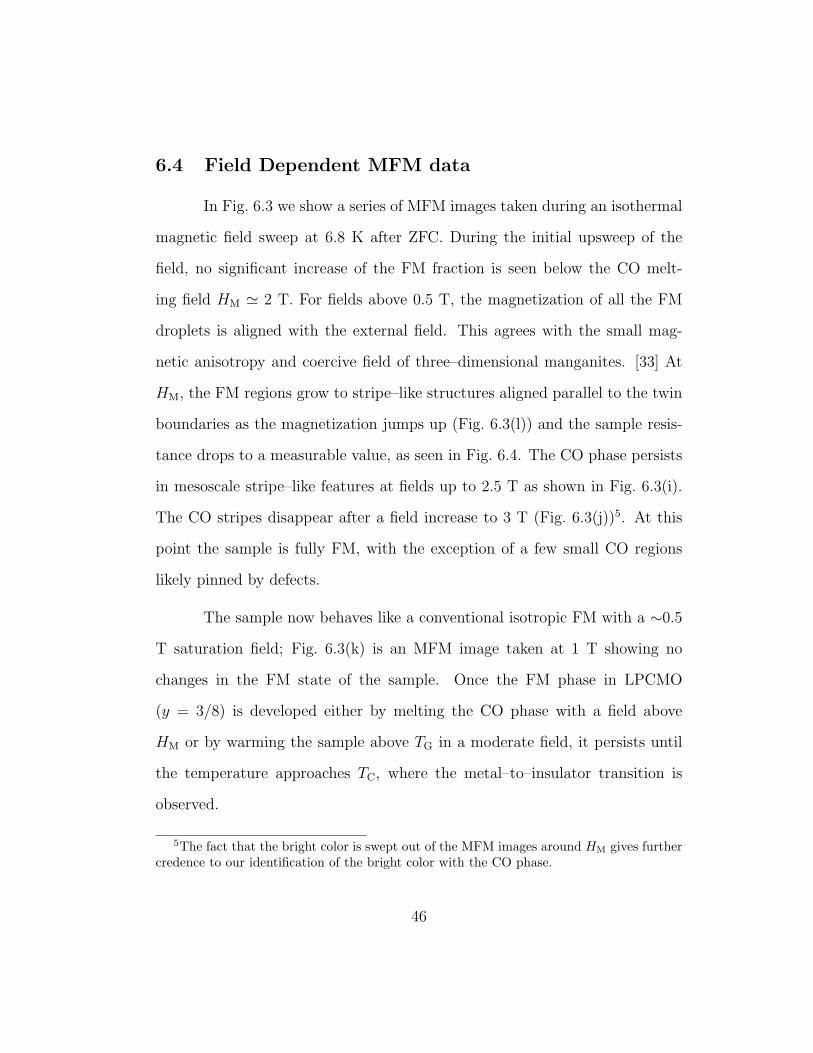
6.4 Field Dependent MFM data
In Fig. 6.3 we show a series of MFM images taken during an isothermal
magnetic field sweep at 6.8 K after ZFC. During the initial upsweep of the
field, no significant increase of the FM fraction is seen below the CO melt-
ing field HM ' 2 T. For fields above 0.5 T, the magnetization of all the FM
droplets is aligned with the external field. This agrees with the small mag-
netic anisotropy and coercive field of three–dimensional manganites. [33] At
HM, the FM regions grow to stripe–like structures aligned parallel to the twin
boundaries as the magnetization jumps up (Fig. 6.3(l)) and the sample resis-
tance drops to a measurable value, as seen in Fig. 6.4. The CO phase persists
in mesoscale stripe–like features at fields up to 2.5 T as shown in Fig. 6.3(i).
The CO stripes disappear after a field increase to 3 T (Fig. 6.3(j))5. At this
point the sample is fully FM, with the exception of a few small CO regions
likely pinned by defects.
The sample now behaves like a conventional isotropic FM with a ∼0.5
T saturation field; Fig. 6.3(k) is an MFM image taken at 1 T showing no
changes in the FM state of the sample. Once the FM phase in LPCMO
(y = 3/8) is developed either by melting the CO phase with a field above
HM or by warming the sample above TG in a moderate field, it persists until
the temperature approaches TC, where the metal–to–insulator transition is
observed.
5The fact that the bright color is swept out of the MFM images around HM gives furthercredence to our identification of the bright color with the CO phase.
46
Figure 6.4: Two–probe resistance of the sample taken in situ during MFMscans from Fig. 6.3. The seemingly sharp steps in R are artifacts of sitting ata single value of H for ≈ 45 minutes as each MFM image is acquired and thensweeping H relatively quickly to the next value.
6.5 Discussion
One common feature in both the glass transition (Fig. 6.2) and the
melting transition (Fig. 6.3) is that the FM domains form stripe–like features
along orthorhombic twin boundaries where a large strain variation is expected
(Fig. 6.5). Some FM droplets in the ZFC state also tend to line up along twin
boundaries. These correlations demonstrate that the martensitic accommoda-
tion strain plays a crucial role in the evolution of µm–scale phase separation
in manganites.
An emerging theme in the manganite community is that both compet-
ing phases and quenched disorder are needed to generate the CMR effect. [53]
[54] [55] [56] [57] The CMR regime is also where glassy behavior is usually
47
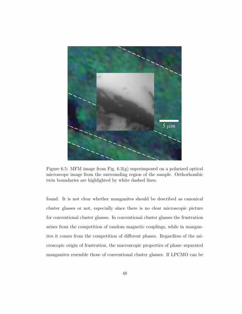
Figure 6.5: MFM image from Fig. 6.3(g) superimposed on a polarized opticalmicroscope image from the surrounding region of the sample. Orthorhombictwin boundaries are highlighted by white dashed lines.
found. It is not clear whether manganites should be described as canonical
cluster glasses or not, especially since there is no clear microscopic picture
for conventional cluster glasses. In conventional cluster glasses the frustration
arises from the competition of random magnetic couplings, while in mangan-
ites it comes from the competition of different phases. Regardless of the mi-
croscopic origin of frustration, the macroscopic properties of phase–separated
manganites resemble those of conventional cluster glasses. If LPCMO can be
48
categorized as a type of cluster glass, our results provide a clear picture of the
cluster glass transition on a local scale. In contrast to the commonly held view
that only reorientation of the FM cluster magnetization happens at the cluster
glass transition, we show a significant increase of the FM volume fraction, a
result consistent with recent magnetization relaxation studies. [47] [58] Fur-
ther microscopic investigations of both conventional cluster glass systems and
CMR manganites will bring out the similarities and differences between them,
helping to clarify the microscopic understanding of cluster glass systems. We
might be able to answer the question: Are the CMR manganites a new class
of cluster glasses? [59]
These results show that the phase–separated LPCMO system under-
goes a collective phase transition into a glassy ground state as a result of the
degeneracy of the FM and CO phases and inherent quenched disorder under
the freezing influence of accommodation strain energy barriers. Mesoscopic
scale phase separation is an intrinsic behavior of LPCMO and it may be uni-
versal across CMR manganites.
49
Chapter 7
Thin–Film Manganite Devices
Using the optical alignment procedure outlined in Chapter 3, we have
studied the formation of magnetic domain walls in patterned thin–film man-
ganite devices with the goal of measuring their transport properties.
7.1 Magnetic Domain Walls in Manganites
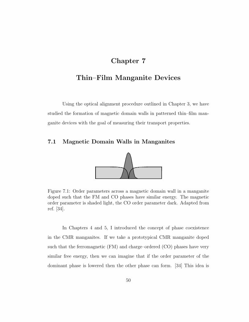
Figure 7.1: Order parameters across a magnetic domain wall in a manganitedoped such that the FM and CO phases have similar energy. The magneticorder parameter is shaded light, the CO order parameter dark. Adapted fromref. [34].
In Chapters 4 and 5, I introduced the concept of phase coexistence
in the CMR manganites. If we take a prototypical CMR manganite doped
such that the ferromagnetic (FM) and charge–ordered (CO) phases have very
similar free energy, then we can imagine that if the order parameter of the
dominant phase is lowered then the other phase can form. [34] This idea is
50
illustrated in Fig. 7.1. In a normal magnet, the magnitude of the FM order
parameter is nearly constant across a domain wall, but Fig. 7.1 illustrates the
possibility that if the FM order is lowered at a domain wall, the CO phase may
form a localized inclusion. Experimentally, we should be able to explore this
possibility by looking at the resistance of domain walls, specifically looking for
a high resistance state if the more insulating CO phase forms a break in the
primarily FM, metallic sample.
Mathur et al. fabricated planar devices from La0.7Ca0.3MnO3 with the
intention of measuring the domain wall resistance–area product from a well
defined number of domain walls. [60] The domain wall resistance–area product
was calculated from the device’s geometry and the resistance measurement.
This value was compared to the value calculated under the assumption of no
break in the FM order parameter, only from the decrease in electron bandwidth
as magnetization rotates across the domain wall. The measured value of the
resistance–area product turned out to be four orders of magnitude higher than
the calculated value, supporting the idea of the inclusion of the insulating CO
phase at magnetic domain walls.
We are using MFM to attempt to confirm the location and number of
domain walls in these devices and characterize the nature of the phase sepa-
ration at a domain wall. Figure 7.2 is an optical image showing the current
pathway through the device and the shadow of the MFM cantilever (The de-
vice is just past the end of the cantilever). Figure 7.3 is a higher magnification
image of the device, showing that it consists of La0.7Ca0.3MnO3 patterned on
51
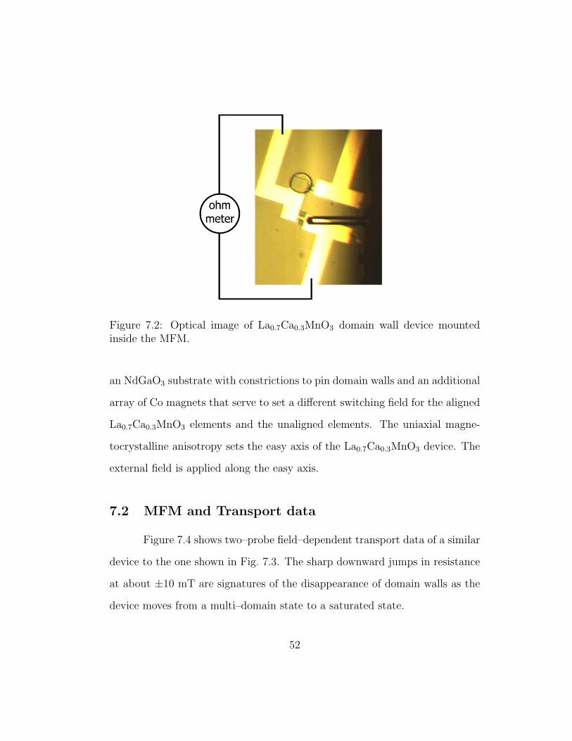
Figure 7.2: Optical image of La0.7Ca0.3MnO3 domain wall device mountedinside the MFM.
an NdGaO3 substrate with constrictions to pin domain walls and an additional
array of Co magnets that serve to set a different switching field for the aligned
La0.7Ca0.3MnO3 elements and the unaligned elements. The uniaxial magne-
tocrystalline anisotropy sets the easy axis of the La0.7Ca0.3MnO3 device. The
external field is applied along the easy axis.
7.2 MFM and Transport data
Figure 7.4 shows two–probe field–dependent transport data of a similar
device to the one shown in Fig. 7.3. The sharp downward jumps in resistance
at about ±10 mT are signatures of the disappearance of domain walls as the
device moves from a multi–domain state to a saturated state.
52
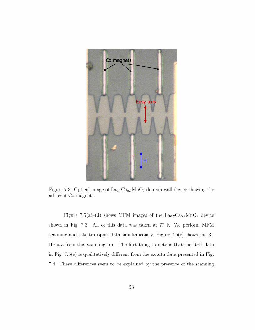
Figure 7.3: Optical image of La0.7Ca0.3MnO3 domain wall device showing theadjacent Co magnets.
Figure 7.5(a)–(d) shows MFM images of the La0.7Ca0.3MnO3 device
shown in Fig. 7.3. All of this data was taken at 77 K. We perform MFM
scanning and take transport data simultaneously. Figure 7.5(e) shows the R–
H data from this scanning run. The first thing to note is that the R–H data
in Fig. 7.5(e) is qualitatively different from the ex situ data presented in Fig.
7.4. These differences seem to be explained by the presence of the scanning
53
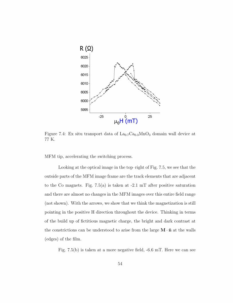
Figure 7.4: Ex situ transport data of La0.7Ca0.3MnO3 domain wall device at77 K.
MFM tip, accelerating the switching process.
Looking at the optical image in the top–right of Fig. 7.5, we see that the
outside parts of the MFM image frame are the track elements that are adjacent
to the Co magnets. Fig. 7.5(a) is taken at -2.1 mT after positive saturation
and there are almost no changes in the MFM images over this entire field range
(not shown). With the arrows, we show that we think the magnetization is still
pointing in the positive H direction throughout the device. Thinking in terms
of the build up of fictitious magnetic charge, the bright and dark contrast at
the constrictions can be understood to arise from the large M · n at the walls
(edges) of the film.
Fig. 7.5(b) is taken at a more negative field, -6.6 mT. Here we can see
54
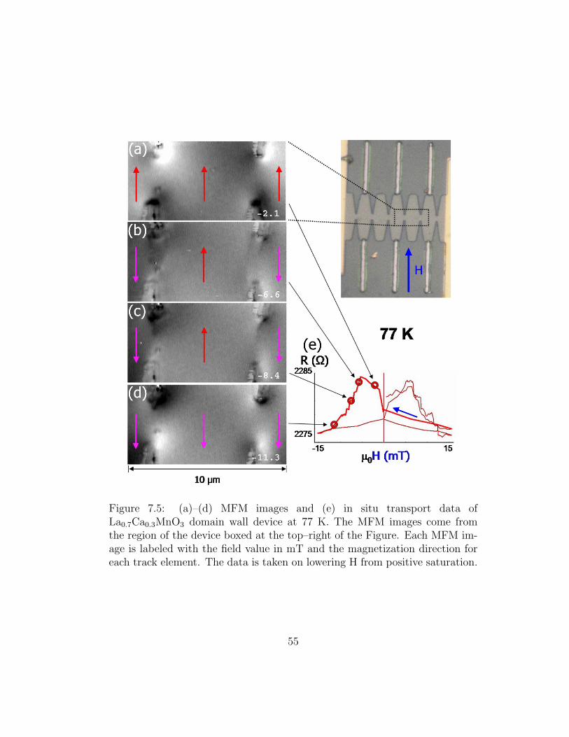
Figure 7.5: (a)–(d) MFM images and (e) in situ transport data ofLa0.7Ca0.3MnO3 domain wall device at 77 K. The MFM images come fromthe region of the device boxed at the top–right of the Figure. Each MFM im-age is labeled with the field value in mT and the magnetization direction foreach track element. The data is taken on lowering H from positive saturation.
55
some vertical line features cutting across the constrictions. Again, thinking
in terms of fictitious magnetic charge, these features can be understood as
arising from the divergence of the magnetization, ∇ ·M, at domain walls. As
the field is swept more negative, the domain walls move inward as negative
magnetization becomes increasingly energetically favored (Fig. 7.5(c)). When
the field is swept even more negative, to -11.3 mT (Fig. 7.5(d)) all the domain
walls disappear and the track is saturated in the negative direction. Note that
the MFM contrast is reversed relative to Fig. 7.5(a).
A close examination of the original, finely–spaced MFM images and
transport data shows that there is a drop in resistance whenever a domain
wall disappears. The resistance jumps are likely due to domain walls in the
transport pathway. If so, the domain wall resistance–area product increase
may be 4 or 5 orders of magnitude higher than expected. This suggests that
the inclusion of the CO phase at domain walls may actually be taking place.
7.3 Questions
There are some issues with this project as it now stands. The R–H data
certainly has some qualitative dependence on the presence or absence of the
scanning MFM tip. The tip which was used for this data was coated with 25
nm of Co85Cr15. It is possible to reduce the effect of the tip on the sample by
depositing a lower moment coating on the tip, either by reducing the thickness
of the coating or by moving to a lower moment material altogether.
The MFM images do not show repeatable devices states, that is, the
56
configuration of the domain walls is not just a function of field history. This
may be another artifact of the effect of the stray field of the MFM tip. It may
be possible to design a more robust device through micromagnetic simulation.
7.4 Micromagnetic Simulation
Cursory simulation using the OOMMF1 software package from NIST
[61] supports the formation of domain walls at the device constrictions. Figure
7.6 shows the result of a simulation set up with a random initial magnetization
that was allowed to relax to an energy minimum state, first at zero field (Fig.
7.6(a)), then at successively larger negative fields (Fig. 7.6(b)–(d)). Values
for the exchange stiffness and anisotropy constant come from ref. [60]. The
diagonal domain walls move outward as negative magnetization becomes more
favored and get trapped vertically at the constrictions, bowing out more as
the negative field is ramped up. This is shown in Figure 7.7.
The features cutting diagonally across the track in Fig. 7.6(a) are sim-
ilar to features seen in MFM scans of the track taken in the constant–plane
scanning mode described in Section 3.6. In this mode the tip does not come
into contact with the sample, so the effect of the tip on the sample may be re-
duced. Fig. 7.8 compares an MFM image for a constant–plane scanning series
with a zoom in of Fig. 7.6(a).
Missing from these simulations is the central postulate that we are
1http://math.nist.gov/oommf/
57
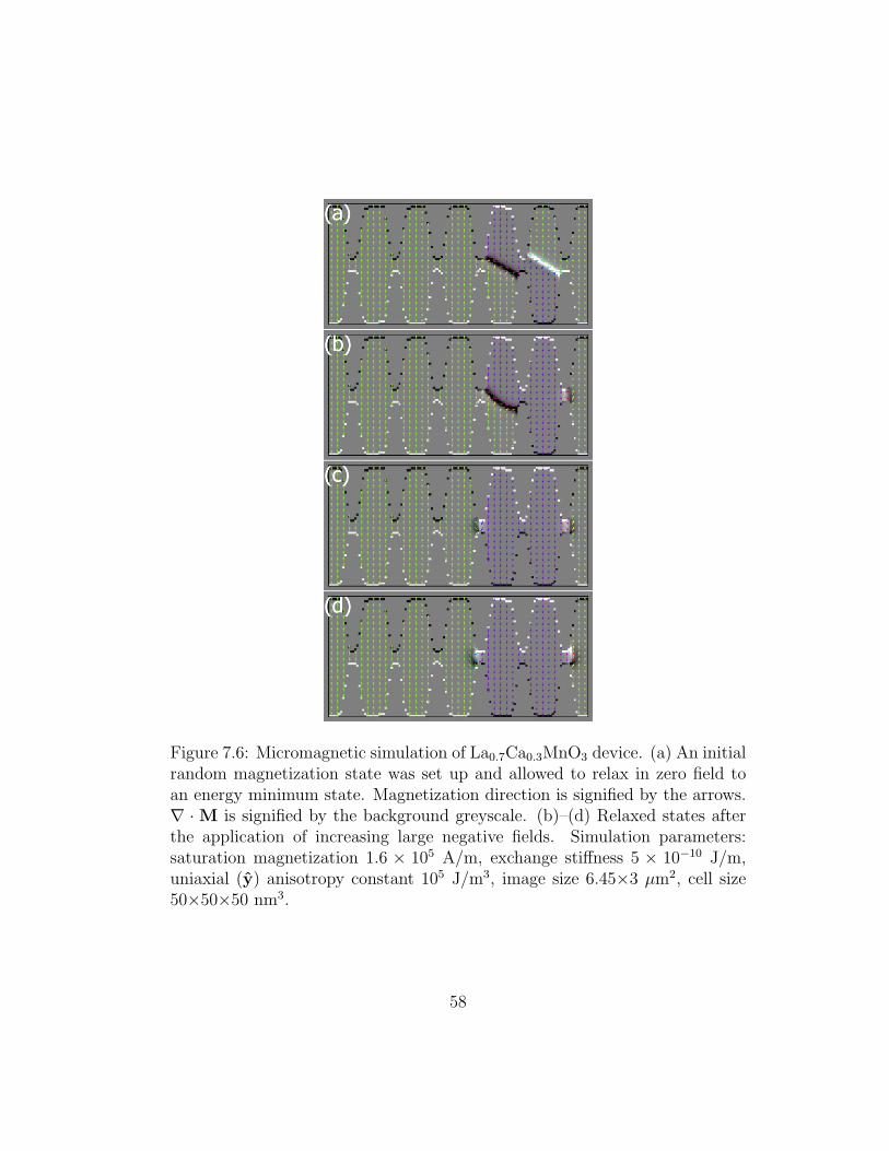
Figure 7.6: Micromagnetic simulation of La0.7Ca0.3MnO3 device. (a) An initialrandom magnetization state was set up and allowed to relax in zero field toan energy minimum state. Magnetization direction is signified by the arrows.∇ ·M is signified by the background greyscale. (b)–(d) Relaxed states afterthe application of increasing large negative fields. Simulation parameters:saturation magnetization 1.6 × 10⁵ A/m, exchange stiffness 5 × 10⁻¹⁰ J/m,uniaxial (y) anisotropy constant 105 J/m3, image size 6.45×3 µm2, cell size50×50×50 nm3.
58
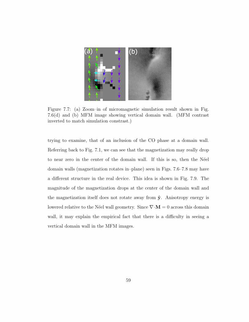
Figure 7.7: (a) Zoom–in of micromagnetic simulation result shown in Fig.7.6(d) and (b) MFM image showing vertical domain wall. (MFM contrastinverted to match simulation constrast.)
trying to examine, that of an inclusion of the CO phase at a domain wall.
Referring back to Fig. 7.1, we can see that the magnetization may really drop
to near zero in the center of the domain wall. If this is so, then the Neel
domain walls (magnetization rotates in–plane) seen in Figs. 7.6–7.8 may have
a different structure in the real device. This idea is shown in Fig. 7.9. The
magnitude of the magnetization drops at the center of the domain wall and
the magnetization itself does not rotate away from y. Anisotropy energy is
lowered relative to the Neel wall geometry. Since ∇·M = 0 across this domain
wall, it may explain the empirical fact that there is a difficulty in seeing a
vertical domain wall in the MFM images.
59
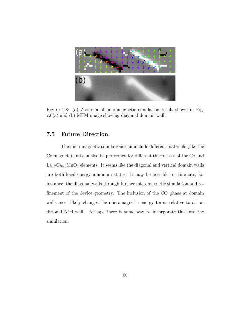
Figure 7.8: (a) Zoom–in of micromagnetic simulation result shown in Fig.7.6(a) and (b) MFM image showing diagonal domain wall.
7.5 Future Direction
The micromagnetic simulations can include different materials (like the
Co magnets) and can also be performed for different thicknesses of the Co and
La0.7Ca0.3MnO3 elements. It seems like the diagonal and vertical domain walls
are both local energy minimum states. It may be possible to eliminate, for
instance, the diagonal walls through further micromagnetic simulation and re-
finement of the device geometry. The inclusion of the CO phase at domain
walls most likely changes the micromagnetic energy terms relative to a tra-
ditional Neel wall. Perhaps there is some way to incorporate this into the
simulation.
60
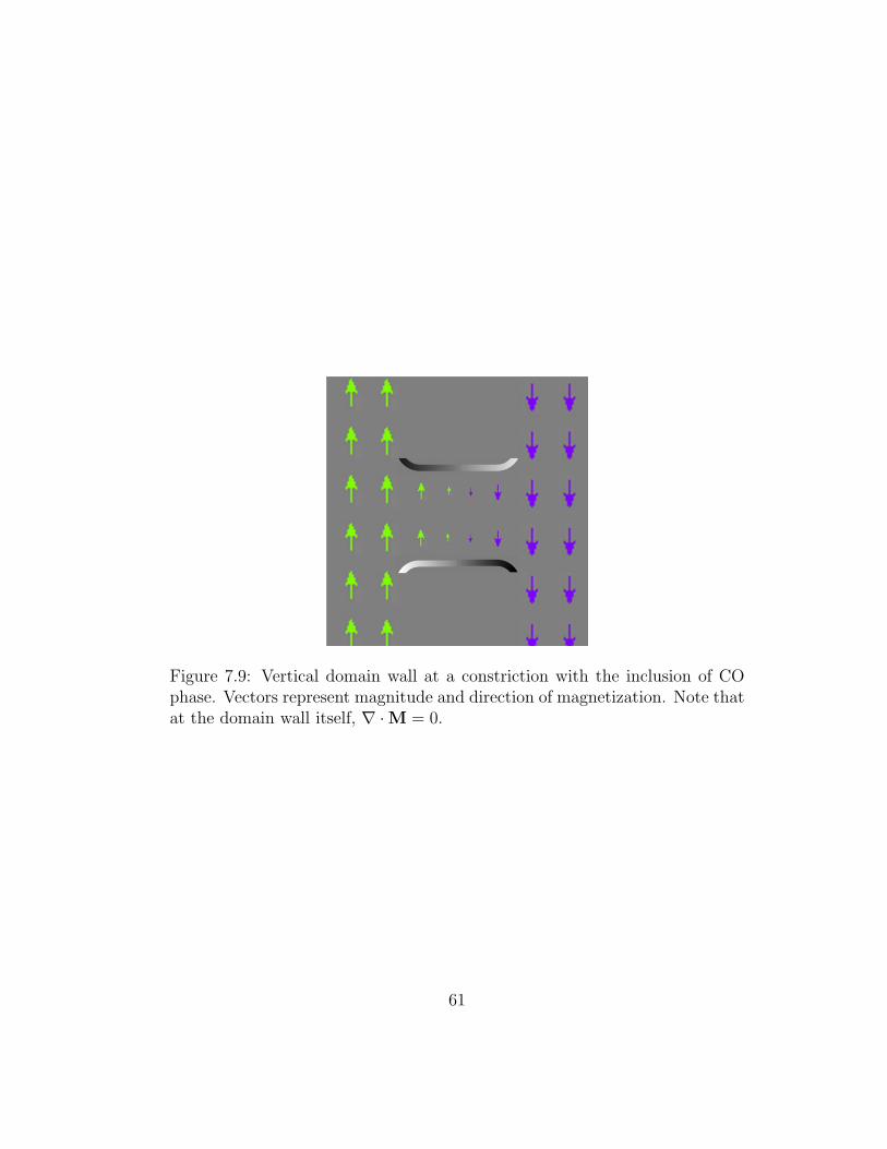
Figure 7.9: Vertical domain wall at a constriction with the inclusion of COphase. Vectors represent magnitude and direction of magnetization. Note thatat the domain wall itself, ∇ ·M = 0.
61
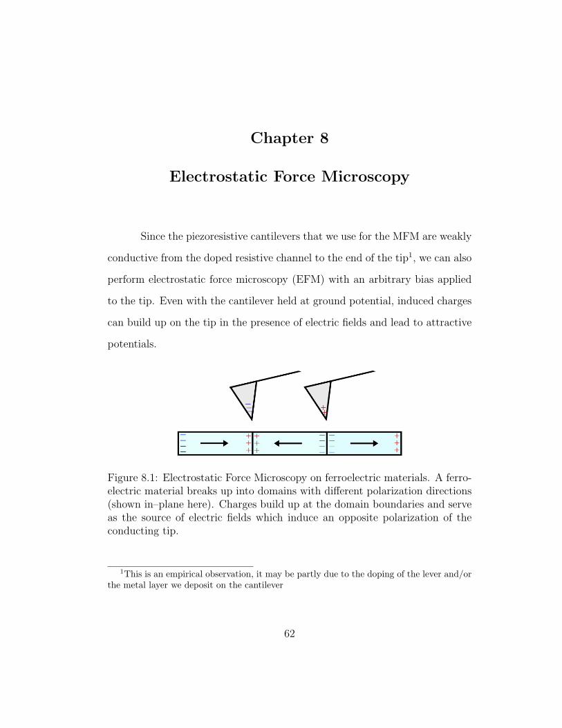
Chapter 8
Electrostatic Force Microscopy
Since the piezoresistive cantilevers that we use for the MFM are weakly
conductive from the doped resistive channel to the end of the tip1, we can also
perform electrostatic force microscopy (EFM) with an arbitrary bias applied
to the tip. Even with the cantilever held at ground potential, induced charges
can build up on the tip in the presence of electric fields and lead to attractive
potentials.
Figure 8.1: Electrostatic Force Microscopy on ferroelectric materials. A ferro-electric material breaks up into domains with different polarization directions(shown in–plane here). Charges build up at the domain boundaries and serveas the source of electric fields which induce an opposite polarization of theconducting tip.
1This is an empirical observation, it may be partly due to the doping of the lever and/orthe metal layer we deposit on the cantilever
62
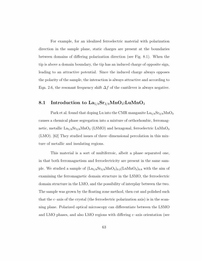
For example, for an idealized ferroelectric material with polarization
direction in the sample plane, static charges are present at the boundaries
between domains of differing polarization direction (see Fig. 8.1). When the
tip is above a domain boundary, the tip has an induced charge of opposite sign,
leading to an attractive potential. Since the induced charge always opposes
the polarity of the sample, the interaction is always attractive and according to
Eqn. 2.6, the resonant frequency shift ∆f of the cantilever is always negative.
8.1 Introduction to La5/8Sr3/8MnO3:LuMnO3
Park et al. found that doping Lu into the CMR manganite La5/8Sr3/8MnO3
causes a chemical phase segregation into a mixture of orthorhombic, ferromag-
netic, metallic La5/8Sr3/8MnO3 (LSMO) and hexagonal, ferroelectric LuMnO3
(LMO). [62] They studied issues of three–dimensional percolation in this mix-
ture of metallic and insulating regions.
This material is a sort of multiferroic, albeit a phase–separated one,
in that both ferromagnetism and ferroelectricity are present in the same sam-
ple. We studied a sample of (La5/8Sr3/8MnO3)0.2(LuMnO3)0.8 with the aim of
examining the ferromagnetic domain structure in the LSMO, the ferroelectric
domain structure in the LMO, and the possibility of interplay between the two.
The sample was grown by the floating zone method, then cut and polished such
that the c–axis of the crystal (the ferroelectric polarization axis) is in the scan-
ning plane. Polarized optical microscopy can differentiate between the LSMO
and LMO phases, and also LMO regions with differing c–axis orientation (see
63
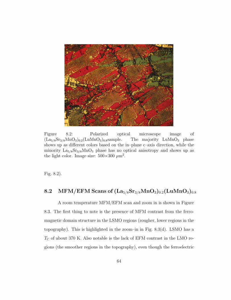
Figure 8.2: Polarized optical microscope image of(La5/8Sr3/8MnO3)0.2(LuMnO3)0.8sample. The majority LuMnO3 phaseshows up as different colors based on the in–plane c–axis direction, while theminority La5/8Sr3/8MnO3 phase has no optical anisotropy and shows up asthe light color. Image size: 500×300 µm2.
Fig. 8.2).
8.2 MFM/EFM Scans of (La5/8Sr3/8MnO3)0.2(LuMnO3)0.8
A room temperature MFM/EFM scan and zoom in is shown in Figure
8.3. The first thing to note is the presence of MFM contrast from the ferro-
magnetic domain structure in the LSMO regions (rougher, lower regions in the
topography). This is highlighted in the zoom–in in Fig. 8.3(d). LSMO has a
TC of about 370 K. Also notable is the lack of EFM contrast in the LMO re-
gions (the smoother regions in the topography), even though the ferroelectric
64
Figure 8.3: (a,c) Room temperature topography (1 µm greyscale) and (b,d)MFM/EFM scans (1.5 Hz greyscale) of (La5/8Sr3/8MnO3)0.2(LuMnO3)0.8 sam-ple. (a,b) image size: 40×40 µm2.
ordering temperature, TCFE, is 900 K.
An EFM scan of the sample taken at 77 K is shown in Fig. 8.4(b). For
this set of scans we used a tip with moment m very nearly zero. This is why
there is no MFM related contrast from the LSMO regions of the sample. Fig.
8.4(b) shows very strong contrast in the LMO regions arising from ferroelectric
domains. With the assumption that the c–axis is in–plane (see Fig. 8.1), the
dark areas in Fig. 8.4(b) correspond to ferroelectric domain walls in the LMO.
The obvious question here is why we see EFM contrast from the LMO
phase at 77 K and not at room temperature. In Fig. 8.5(a) we plot the relative
(to 4 K) dielectric loss tangent vs. temperature for a very similar ferroelec-
65
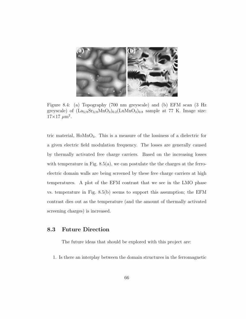
Figure 8.4: (a) Topography (700 nm greyscale) and (b) EFM scan (3 Hzgreyscale) of (La5/8Sr3/8MnO3)0.2(LuMnO3)0.8 sample at 77 K. Image size:17×17 µm2.
tric material, HoMnO3. This is a measure of the lossiness of a dielectric for
a given electric field modulation frequency. The losses are generally caused
by thermally activated free charge carriers. Based on the increasing losses
with temperature in Fig. 8.5(a), we can postulate the the charges at the ferro-
electric domain walls are being screened by these free charge carriers at high
temperatures. A plot of the EFM contrast that we see in the LMO phase
vs. temperature in Fig. 8.5(b) seems to support this assumption; the EFM
contrast dies out as the temperature (and the amount of thermally activated
screening charges) is increased.
8.3 Future Direction
The future ideas that should be explored with this project are:
1. Is there an interplay between the domain structures in the ferromagnetic
66
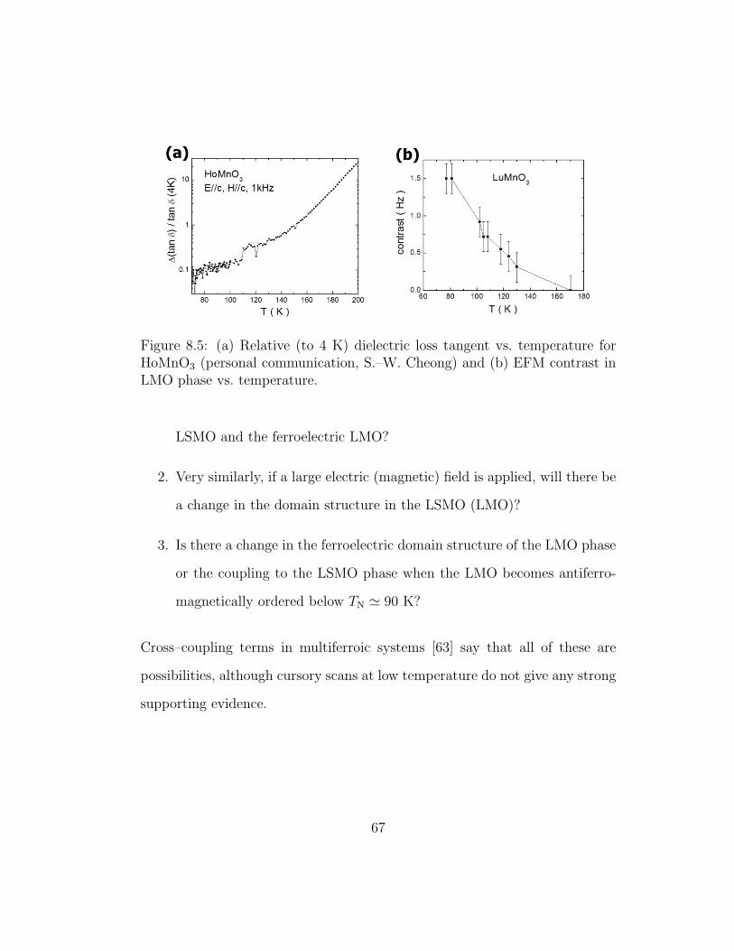
Figure 8.5: (a) Relative (to 4 K) dielectric loss tangent vs. temperature forHoMnO3 (personal communication, S.–W. Cheong) and (b) EFM contrast inLMO phase vs. temperature.
LSMO and the ferroelectric LMO?
2. Very similarly, if a large electric (magnetic) field is applied, will there be
a change in the domain structure in the LSMO (LMO)?
3. Is there a change in the ferroelectric domain structure of the LMO phase
or the coupling to the LSMO phase when the LMO becomes antiferro-
magnetically ordered below TN ' 90 K?
Cross–coupling terms in multiferroic systems [63] say that all of these are
possibilities, although cursory scans at low temperature do not give any strong
supporting evidence.
67
Bibliography
[1] G. Binnig, H. Rohrer, Ch. Gerber, and E. Weibel. Phys. Rev. Lett.,
49:57, 1982.
[2] G. Binnig, H. Rohrer, Ch. Gerber, and E. Weibel. Phys. Rev. Lett.,
56:930, 1986.
[3] G. Meyer and N. M. Amer. Appl. Phys. Lett., 53:1045, 1988.
[4] R. Erlandsson, G. M. McClelland, C. M. Mate, and S. Chiang. J. Vac.
Sci. Technol. A, 6:266, 1988.
[5] M. Tortonese, R. C. Barrett, and C. F. Quate. Appl. Phys. Lett., 62:834,
1993.
[6] T. Fujii, S. Watanabe, M. Suzuki, and T. Fujiu. J. Vac. Sci. Technol. B,
13:1119, 1995.
[7] D. Rugar, H. J. Mamin, P. Guethner, S. E. Lambert, J. E. Stern, I. Mc-
Fadyen, and T. Yogi. J. Appl. Phys., 68:1169, 1990.
[8] A. Wadas and H. J. Hug. J. Appl. Phys., 72:203, 1992.
[9] H. J. Hug, B. Stiefel, P. J. A. van Schendel, A. Moser, R. Hofer, S. Martin,
H.-J. Guntherodt, S. Porthun, L. Abelmann, J. C. Lodder, G. Bochi, and
R. C. O’Handley. J. Appl. Phys., 83:5609, 1998.
68
[10] U. Hartmann. Phys. Lett. A, 137:475, 1989.
[11] H. J. Hug, B. Stiefel, P. J. A. van Schendel, A. Moser, S. Martin, and
H.-J. Guntherodt. Rev. Sci. Instrum., 70:3625, 1999.
[12] U. Durig. Appl. Phys. Lett., 75:433, 1999.
[13] Y. Martin and H. K. Wickramasinghe. Appl. Phys. Lett., 50:1455, 1987.
[14] C. W. Yuan, Z. Zheng, A. L. de Lozanne, M. Tortonese, D. A. Rudman,
and J. N. Eckstein. J. Vac. Sci. Technol. B, 14:1210, 1996.
[15] Q. Lu, C. C. Chen, and A. de Lozanne. Science, 276:2006, 1997.
[16] C. C. Chen, Q. Lu, and A. de Lozanne. Appl. Phys. A, 66:S1181, 1998.
[17] A. Biswas, M. Rajeswari, R. C. Srivastava, T. Venkatesan, R. L. Greene,
Q. Lu, A. L. de Lozanne, and A. J. Millis. Phys. Rev. B, 63:184424, 2001.
[18] Q. Lu, K. Mochizuki, J. T. Markert, and A. de Lozanne. Physica C,
371:146, 2002.
[19] L. Zhang, C. Israel, A. Biswas, R. L. Greene, and A. de Lozanne. Science,
298:805, 2002.
[20] M. Tortonese. PhD thesis, Stanford University, 1993.
[21] F. J. Giessibl and B. M. Trafas. Rev. Sci. Instrum., 65:1923, 1994.
[22] A. Volodin, K. Temst, C. van Haesendonck, and Y. Bruynseraede. Rev.
Sci. Instrum., 71:4468, 2000.
69

[23] T. R. Albrecht, P. Grutter, D. Horne, and D. Rugar. J. Appl. Phys.,
69:668, 1991.
[24] M. N. Baibich, J. M. Broto, A. Fert, F. Nguyen Van Dau, F. Petroff,
P. Etienne, G. Creuzet, A. Friederich, and J. Chazelas. Phys. Rev. Lett.,
61:2472, 1988.
[25] G. Binasch, P. Grunberg, F. Saurenbach, and W. Zinn. Phys. Rev. B,
39:4828, 1989.
[26] S. Jin, T. H. Tiefel, M. McCormack, R. A. Fastnacht, R. Ramesh, and
L. H. Chen. Science, 264:413, 1994.
[27] C. Zener. Phys. Rev., 82:403, 1951.
[28] A. J. Millis. Nature, 392:147, 1998.
[29] R. Maezono, S. Ishihara, and N. Nagaosa. Phys. Rev. B, 58:11583, 1998.
[30] A. Asamitsu, Y. Moritomo, Y. Tomioka, T. Arima, and Y. Tokura. Na-
ture, 373:407, 1995.
[31] C. Martin, A. Maignan, M. Hervieu, B. Raveau, and J. Hejtmanek. Eur.
Phys. J. B, 16:469, 2000.
[32] M. Uehara, S. Mori, C. H. Chen, and S.-W. Cheong. Nature, 399:560,
1999.
[33] M. B. Salamon and M. Jaime. Rev. Mod. Phys., 73:583, 2001.
70
[34] N. D. Mathur and P. B. Littlewood. Solid State Commun., 119:271, 2001.
[35] R. Desfeux, S. Bailleul, A. Da Costa, W. Prellier, and A. M. Haghiri-
Gosnet. Appl. Phys. Lett., 78:3681, 2001.
[36] V. Podzorov, B. G. Kim, V. Kiryukhin, M. E. Gershenson, and S.-W.
Cheong. Phys. Rev. B, 64:140406, 2001.
[37] A. Biswas, M. Rajeswari, R. C. Srivastava, Y. H. Li, T. Venkatesan, R. L.
Greene, and A. J. Millis. Phys. Rev. B, 61:9665, 2000.
[38] P. Levy, F. Parisi, M. Quintero, L. Granja, J. Curiale, J. Sacanell, G. Leyva,
G. Polla, R. S. Freitas, and L. Ghivelder. Phys. Rev. B, 65:140401, 2002.
[39] L. Kong and S. Y. Chou. Appl. Phys. Lett., 70:2043, 1997.
[40] F. Parisi, P. Levy, L. Ghivelder, G. Polla, and D. Vega. Phys. Rev. B,
63:144419, 2001.
[41] A. Urushibara, Y. Moritomo, T. Arima, A. Asamitsu, G. Kido, and
Y. Tokura. Phys. Rev. B, 51:14103, 1995.
[42] Y.-A. Soh, G. Aeppli, N. D. Mathur, and M. G. Blamire. Phys. Rev. B,
63:20402, 2000.
[43] Y.-A. Soh, G. Aeppli, N. D. Mathur, and M. G. Blamire. J. Appl. Phys.,
87:6743, 2000.
[44] M. Fath, S. Freisem, A. A. Menovsky, Y. Tomioka, J. Aarts, and J. A.
Mydosh. Science, 285:1540, 1999.
71
[45] P. Littlewood. Nature, 399:529, 1999.
[46] K. H. Ahn, T. Lookman, and A. R. Bishop. Nature, 428:401, 2004.
[47] P. A. Sharma, S. B. Kim, T. Y. Koo, S. Guha, and S.-W. Cheong. Phys.
Rev. B, 71:224416, 2005.
[48] L. Ghivelder, R. S. Freitas, M. G. das Virgens, M. A. Continentino,
H. Martinho, L. Granja, M. Quintero, G. Leyva, P. Levy, and F. Parisi.
Phys. Rev. B, 69:214414, 2004.
[49] Y. Tokura and Y. Tomioka. J. Mag. Mag. Mat., 200:1, 1999.
[50] J. A. Mydosh. Spin Glasses. Taylor and Francis, London, 1993.
[51] B. Coles, B. V. B. Sarkissian, and R. H. Taylor. Phil. Mag. B, 37:489,
1978.
[52] I. Deac, S. V. Diaz, and B. G. Kim. Phys. Rev. B, 65:174426, 2002.
[53] D. Akahoshi, M. Uchida, Y. Tomioka, T. Arima, Y. Matsui, and Y. Tokura.
Phys. Rev. Lett., 90:177203, 2003.
[54] Y. Motome, N. Furukawa, and N. Nagaosa. Phys. Rev. Lett., 91:167204,
2003.
[55] H. Aliaga, D. Magnoux, A. Moreo, D. Poilblanc, S. Yunoki, and E. Dagotto.
Phys. Rev. B, 68:104405, 2003.
72
[56] J. Burgy, M. Mayr, V. Martin-Mayor, A. Moreo, and E. Dagotto. Phys.
Rev. Lett., 87:277202, 2001.
[57] J. Burgy, A. Moreo, and E. Dagotto. Phys. Rev. Lett., 92:097202, 2004.
[58] L. Ghivelder and F. Parisi. Phys. Rev. B, 71:184425, 2005.
[59] E. Dagotto. Nanoscale Phase Separation and Colossal Magnetoresistance.
Springer, Berlin, 2003.
[60] N. D. Mathur, P. B. Littlewood, N. K. Todd, S. P. Isaac, B.-S. Teo, D.-J.
Kang, E. J. Tarte, Z. H. Barber, J. E. Evetts, and M. G. Blamire. J.
Appl. Phys., 86:6287, 1999.
[61] M. J. Donahue and D. G. Porter. OOMMF User’s Guide, Version 1.0,
Interagency Report NISTIR 6376. National Institute of Standards and
Technology, Gaithersburg, MD, September 1999.
[62] S. Park, N. Hur, S. Guha, and S.-W. Cheong. Phys. Rev. Lett., 92:167206,
2004.
[63] N. A. Spaldin and M. Fiebig. Science, 309:391, 2005.
73
Vita
Emil Casey Israel was born in Bastrop, Texas on 11 January 1978, the
son of Gordon Israel and Jana Israel. He received the Bachelor of Arts degree
in Physics and Art & Art History from Rice University and was accepted and
started graduate studies at the University of Texas at Austin in 2000.
Permanent address: 1410 Ridgemont DriveAustin, Texas 78723
This dissertation was typeset with LATEX† by the author.
†LATEX is a document preparation system developed by Leslie Lamport as a specialversion of Donald Knuth’s TEX Program.
74