Embed Size (px)
Citation preview
Copyright
by
Huang-Chun Wen
2006
The Dissertation Committee for Huang-Chun Wen Certifies that this is
the approved version of the following dissertation:
SYSTEMATIC EVALUATION OF METAL GATE ELECTRODE
EFFECTIVE WORK FUNCTION AND ITS INFLUENCE ON
DEVICE PERFORMANCE IN CMOS DEVICES
Committee:
Dim-Lee Kwong, Supervisor
Sanjay Banerjee
Leonard F. Register
Paul S. Ho
Prashant Majhi
Gennadi Bersuker
SYSTEMATIC EVALUATION OF METAL GATE ELECTRODE
EFFECTIVE WORK FUNCTION AND ITS INFLUENCE ON
DEVICE PERFORMANCE IN CMOS DEVICES
by
Huang-Chun Wen, B.E.; M.S.EE
Dissertation
Presented to the Faculty of the Graduate School of
The University of Texas at Austin
in Partial Fulfillment
of the Requirements
for the Degree of
Doctor of Philosophy
The University of Texas at Austin
December, 2006
Dedication
To my loving family
v
Acknowledgements
I’d like to express my sincerest appreciation for the two key people who have
watched me grow into a researcher and guided me through the course of my PhD work,
my supervisor, Dr. Dim-Lee Kwong, and a real co-supervisor, Dr. Prashant Majhi from
SEMATECH. Thank you, Dr. Kwong, for taking me under his supervision, showing me
the opportunities in this field and preparing me for the challenge as the opportunities
come. Also to Prashant, words can’t express my gratitude to you, for giving me the
chance to work in a great team with the freedom in research and resources, and guiding
my research with the advanced issues and challenges.
I would also like to thank Dr. Sanjay Banerjee, Dr. Leonard F. Register, Dr. Paul
S. Ho, and Dr. Gennadi Bersuker for being on my dissertation committee.
I owe great debt to my family, the wonderful support from my father, Dr.
Ching-Rong Wen, for showing me the world of science, my mother Ya-Ling Yang and
my sister Pei-Chun Wen, for their love. I’ll always be filled with laughter and good food,
and I wouldn’t have done it without you.
There is an amazing number of people that have touch my live during these years,
I’ve been fortunate to meet and experienced a great time in my life with you. All my
group mates: JJ, Johnny, Sang Ho, Xuguang, Weiping, Liu Jun, Nan Lu and Scott, you
have taught me kindness and research blends nicely. All my teammates in the metal gate
electrode group at SEMATECH, Husam, Kisik, Hongfa, Rusty and Craig, for teaching
me the sensation of working as a team, we were a real team. And all the wonderful
people during the SEMATECH experience, I have learned so much from you. To Nan
and Wen-June, for your friendship.
Last but not least, the wonderful MER support staff, Bill and Jesse.
vi
SYSTEMATIC EVALUATION OF METAL GATE ELECTRODE
EFFECTIVE WORK FUNCTION AND ITS INFLUENCE ON
DEVICE PERFORMANCE IN CMOS DEVICES
Publication No._____________
Huang-Chun Wen, Ph. D.
The University of Texas at Austin, 2006
Supervisor: Dim-Lee Kwong
As the CMOS integrated circuits are reduced to the 100-nanometer regime, the
conventional SiO2-based gate dielectrics are facing serious scaling challenges. High-k
materials are expected to replace SiO2 as the gate insulator. However, metal gates are
coherently needed to replace poly-Si due to the increase in threshold voltage for high-k
stacks with poly-Si gates and the poly depletion effect. The challenge in metal gate
research is to obtain metals with effective work function (EWF) values of ~5.0-5.2eV for
p-MOS and 4.1-4.3eV for n-MOS. Although EWF should be determined predominately
by the vacuum WF of the materials, it is observed that the EWF is different on high-k
than on SiO2. One proposed mechanism to limit the EWF tuning on high-k dielectrics,
vii
and a possible inherent roadblock to the identification of band-edge metals, is the Fermi-
level pinning effect
Metal gate EWF has been systematically studied with the goal of identifying
band-edge metal gate electrode candidates. The terraced oxide technique has been
developed as the metric for accurate EWF extraction. A comparison of the literature
Fermi-level pinning models with our experimental data shows that an intrinsic limitation
(pinning at the high-k charge neutrality level) may not exist and the source of most EWF
deviation on high-k is due to extrinsic contributions, such as interfacial reactions. Both
the bulk metal characteristics and the interface properties between the metal and
dielectric have been found to control overall EWF. Charges can be induced in the gate
stack during device processing and shift the flatband voltage (Vfb). Engineering of the
EWF by an interface dipole has been identified as a plausible approach for EWF tuning.
Aluminum-containing electrode stacks and lanthanide electrode stacks are proposed as
potential p-type and n-type metal candidates.
The potential impact of candidate metal systems on device performance and
reliability was studied, as well as other materials that may reveal implications for the
influence of the electrode on the gate stack. Comparison of the deposition techniques,
shows that even physical vapor deposited (PVD) metal electrodes can exhibit high
performance. Metals with high O reactivity will reduce the high-k and consequently
degrade electron mobility. No long term reliability concerns were observed for the
candidate metals.
viii
Table of Contents
List of Figures ....................................................................................................... xii
CHAPTER 1 INTRODUCTION AND BACKGROUND 1 1.1 Challenges to transistor scaling .............................................................1
1.1.1 Challenges for Moore’s Law ........................................................1 1.1.2 Motivation for metal gate electrodes ............................................2
1.2 Requirements for the metal gate technology .........................................3 1.2.1 The effective work function (EWF) of metal gate electrodes.......3 1.2.2 Thermal stability of metal electrodes............................................5
1.3 Challenges to the metal gate technology ...............................................6 1.3.1 Identification of suitable band edge work function electrodes .....6 1.3.2 Study of metal electrode’s impact on device performance...........7
1.4 Dissertation Outline ...............................................................................8 1.5 Figures..................................................................................................10 1.6 References............................................................................................15
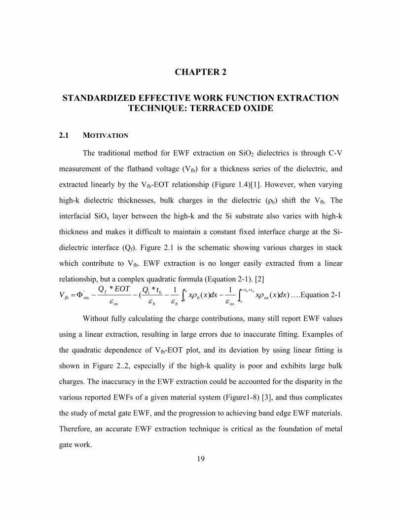
CHAPTER 2 STANDARDIZED EFFECTIVE WORK FUNCTION EXTRACTION TECHNIQUE: TERRACED OXIDE 19 2.1 Motivation............................................................................................19 2.2 Experimental procedures of the terraced oxide technique...................20
2.2.1 Charge model of the terraced oxide technique ...........................20 2.3 Demonstration of the terraced oxide extraction...................................21
2.3.1 Using the terraced oxide method for calculation of high-κ stack charges ........................................................................................22
2.4 Validation of terraced oxide EWF extraction: Comparison with current extracted barrier height ........................................................................23 2.4.1 The current extracted barrier height (J-V) method .....................23 2.4.2 Sample requirements and preparation for J-V barrier height
method……….............................................................................24 2.4.3 Comparison of terraced oxide (C-V) vs barrier height (J-V)
techniques ...................................................................................24 2.5 Conclusions..........................................................................................26 2.6 Figures..................................................................................................28
ix
2.7 References............................................................................................34
CHAPTER 3 DECOUPLING THE FERMI LEVEL PINNING EFFECT IN METAL GATE AND HIGH-κκκκ STACK 36 3.1 Motivation............................................................................................36 3.2 Model on intrinsic factors of EWF control ..........................................37
3.2.1 MIGS model for Ef-pinning ........................................................37 3.2.2 Experimental results in literature ................................................38
3.3 Separation of extrinsic contributions ...................................................38 3.3.1 Interface chemical reaction, materialistic change in the electrode
…………………………………………………………...38 3.3.2 Extrinsic defect states: Oxygen vacancy model and interface
dipole formation ........................................................................39 3.4 Combination of charge neutrality model and oxygen vacancy model
…………………………………………………………………40 3.5 Addressing intrinsic factors of Fermi-level pinning: Comparison of
terraced oxide EWF results with MIGS model....................................41 3.5.1 Approach for study and experimental details .............................41 3.5.2 Comparison of EWF with MIGS model .....................................41
3.6 Revision of MIGS theory.....................................................................42 3.7 Conclusions..........................................................................................43 3.8 Figures..................................................................................................44 3.9 References............................................................................................48
CHAPTER 4 UNDERSTANDING FACTORS CONTRIBUTING TO THE EWF OF METAL ELECTRODES 50 4.1 Introduction..........................................................................................50 4.2 Controlling metal bulk work function component...............................51
4.2.1 Pure metal and metal alloys ........................................................51 4.2.1.1 Complete solid solution ...............................................51 4.2.1.2 Inter-metallic compounds ............................................52
4.2.2 Metal nitrides and metal silicon nitrides.....................................55 4.3 Impact of gate stack charges on EWF..................................................59 4.4 Conclusions..........................................................................................60
x
4.5 Figures..................................................................................................61 4.6 References............................................................................................74
CHAPTER 5 MODULATION OF METAL/HIGH-K STACK INTERFACE FOR EWF TUNING 76 5.1 Introduction..........................................................................................76 5.2 Impact of interfacial engineering on EWF: Interface engineering toward
p-type band edge ..................................................................................76 5.2.1 Possibility of negative charge on Vfb shift..................................77 5.2.1 Possibility of dipole on Vfb shift .................................................78
5.3 Interface modulation via bulk metal electrodes ...................................80 Al-based metal electrodes for p-type band edge metal: Metal-
Aluminum-Nitride.......................................................................80 5.4 Interface engineering toward n-type EWF...........................................83 5.5 Summary..............................................................................................84 5.6 Figures..................................................................................................85 5.7 References............................................................................................99
CHAPTER 6 IMPACT OF METAL GATE ON DEVICE PERFORMANCE AND RELIABILITY 101 6.1 Introduction........................................................................................102 6.2 Impact of metal gate processes ..........................................................102
6.3 Metal gate on bulk high-κ: Charge trapping......................................106 6.4 Reliability for p-metal candidate system ...........................................110 6.5 Figures................................................................................................114 6.6 References..........................................................................................121
CHAPTER 7 CONCLUSIONS AND FUTURE WORK 124 7.1 Summary and conclusion...................................................................124 7.2 Future work: The Vfb rolloff issue for p-type EWF metals ...............125 7.3 Figures................................................................................................126 7.4 Reference ...........................................................................................128
xi
Appendix I ...........................................................................................................129
Appendix II ..........................................................................................................131
Bibliography ........................................................................................................134
VITA....................................................................................................................146
xii
List of Figures
Figure 1.1 Moore's Law Means More Performance. Processing power, measured in
millions of instructions per second (MIPS), has steadily risen because of
increased transistor counts [1]. .........................................................10
Figure 1.2 Feature size of transistors in Intel processors decreases exponentially over
time and the gate oxide thickness decreases accordingly [1]. ..........10
Figure 1.3 Flatband voltage versus number of HfO2 ALD cycles. (Inset: ∆Vfb versus
number of HfO2 ALD cycles) from reference [8]. Schematic of Fermi
pinning location with respect to Si conduction and valence bands. .11
Figure 1.4 EWF extraction from linear Vfb-EOT relationship measured on thickness
series of SiO2. ...................................................................................11
Figure 1.5 Band diagram of work function alignment in metal/dielectric/Si system at
flat band condition. ...........................................................................12
Figure 1.6 Vacuum work function of elements shown in the periodic table from H.
Michaelson [15]. ...............................................................................12
Figure 1.7 Effective work function on SiO2 versus bulk work function for various
metal electrodes reported in the literature.........................................13
Figure 1.8 Effective work function of various metal electrodes on HfO2 reported in the
literature showing disparity in reported values even for a single material
system. ..............................................................................................13
Figure 1.9 Diagram of MOSFET gate stack and their influence on EWF.........14
Figure 1.10 Predicted EWF values from MIGS model compared to experimental results,
and the schematic showing band diagram of interface changed states. [6]
..........................................................................................................14
xiii
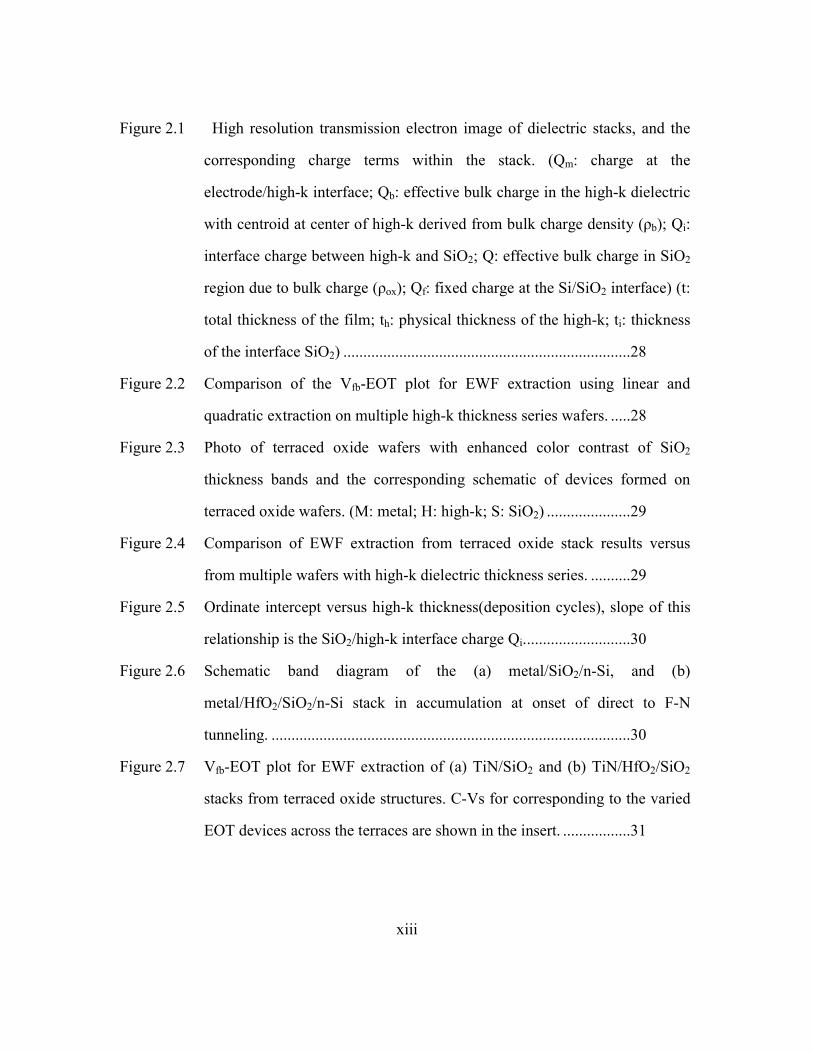
Figure 2.1 High resolution transmission electron image of dielectric stacks, and the
corresponding charge terms within the stack. (Qm: charge at the
electrode/high-k interface; Qb: effective bulk charge in the high-k dielectric
with centroid at center of high-k derived from bulk charge density (ρb); Qi:
interface charge between high-k and SiO2; Q: effective bulk charge in SiO2
region due to bulk charge (ρox); Qf: fixed charge at the Si/SiO2 interface) (t:
total thickness of the film; th: physical thickness of the high-k; ti: thickness
of the interface SiO2) ........................................................................28
Figure 2.2 Comparison of the Vfb-EOT plot for EWF extraction using linear and
quadratic extraction on multiple high-k thickness series wafers. .....28
Figure 2.3 Photo of terraced oxide wafers with enhanced color contrast of SiO2
thickness bands and the corresponding schematic of devices formed on
terraced oxide wafers. (M: metal; H: high-k; S: SiO2) .....................29
Figure 2.4 Comparison of EWF extraction from terraced oxide stack results versus
from multiple wafers with high-k dielectric thickness series. ..........29
Figure 2.5 Ordinate intercept versus high-k thickness(deposition cycles), slope of this
relationship is the SiO2/high-k interface charge Qi...........................30
Figure 2.6 Schematic band diagram of the (a) metal/SiO2/n-Si, and (b)
metal/HfO2/SiO2/n-Si stack in accumulation at onset of direct to F-N
tunneling. ..........................................................................................30
Figure 2.7 Vfb-EOT plot for EWF extraction of (a) TiN/SiO2 and (b) TiN/HfO2/SiO2
stacks from terraced oxide structures. C-Vs for corresponding to the varied
EOT devices across the terraces are shown in the insert. .................31
xiv
Figure 2.8 (a) δ(lnJ)/ δ V versus V plots from J-V curves of TiN/SiO2 and
TiN/HfO2/SiO2 stacks measured on the terraced oxide structures. (b)
∆JV and ∆JT for TiN/HfO2/SiO2 stacks measured at 300-100oK....32
Figure 2.9 Comparison of the EWF of various metal gate electrodes extracted from
terraced oxide/high-k stack structures with calculated WF from barrier
height extraction (with ∆Ec=1.7eV)..................................................33
Figure 3.10 MIGS model predicted EWF on HfO2 .[4] .......................................44
Figure 3.11 Plot of EWF for various metals on HfO2 and on SiO2 showing EWF shift
toward the empirically calculated ΦCNL of HfO2 ~4.4eV. [3] ..........44
Figure 3.12 (a) Vfb-EOT plot for EWF of Ru on SiO2 compared with high-k dielectrics,
and RuO2 on high-k dielectric (b) High resolution TEM image showing
interaction between Ru and SiO2 dielectric at elevated temperatures [12].
..........................................................................................................45
Figure 3.13 (a) Schematic of the interface dipole formation for forming gas (FG) only
and (b)after O2 anneal conditions [8]................................................45
Figure 3.14 Schematic illustrating (a) Atomistic illustration of balanced situation of
interface dipoles induced by interface metal-O and metal-Hf hybridization
at the energy of CNL. (b) Preferred interface bonding for various metals.
[13]....................................................................................................46
Figure 3.15 The extracted EWF of a series of electrodes on HfO2 and HfSiOx (20%
SiO2) versus the EWF on SiO2, for comparison with the MIGS trend line
with S=0.53, and the 1:1 ideal correlation with S=1.........................46
xv
Figure 3.16 Model results showing (a) energy difference between (110) and (100)
interface of HfO2 in contact with various metals, showing a preferred
stability phase. (b) Valance band offset modeling for barrier height
calculations of various metals on HfO2 (110) and (100) interfaces. Most
metals fall on solid trend line with S=1. Dashed line would be the trend
considering the stable interface (S=0.5) [17]....................................47
Figure 3.17 EWF of various metal electrode materials investigated with the terraced
oxide method.....................................................................................47
Figure 4.1 (a) Phase diagram of the Ta-W binary alloy system based on reference [1].
A complete solid solution is observed. (b) The effective work function for
Ta-W alloys on SiO2 and high-k dielectrics as a function of varied atomic
Ta%, showing linear relationship in the alloy region. ......................61
Figure 4.2 The Vfb versus EOT relationship results used for effective work function
extraction obtained on (a) terraced oxide and (b) terraced oxide + high-k
stacks showing excellent linear extraction. Changes in EOT for the thickest
EOT band within each wafer can be used to identify overall EOT changes.
..........................................................................................................62
Figure 4.3 High resolution transmission electron microscopy (HRTEM) images of the
(a) Ta/SiO2/Si and the (b) Ta/HfSiOx/SiO2/Si gate stack interfaces.
Formation of an interface layer is observed between the Ta/SiO2 interface.
..........................................................................................................63
Figure 4.4 Leakage current density of W, Ta-W alloys and Ta metal electrodes on
high-k. Higher leakage current is observed only with the Ta sample,
suggesting degradation of the dielectric, while Ta-W alloys and pure W are
similar. ..............................................................................................63
xvi
Figure 4.5 RBS composition of RuHf alloy.......................................................64
Figure 4.5 Phase diagram of RuHf alloy system.[1] ..........................................64
Figure 4.7 XRD diffraction pattern for RuHf alloys of various composition ....65
Figure 4.8 (a) Vfb vs. EOT plot for work function extraction of various Ru:Hf
compositions as-deposited on terraced oxide + HfO2. (b) EWF trend with
varied Ru composition, trend with composition is not linear and dependent
on dominant phase, is separated into Ru, and RuHf controlled regions.
..........................................................................................................65
Figure 4.9 (a) RBS composition of Ta, N in TaN with varying N2 flow rate. (b) Sheet
resistance of TaN with varying N2 flow rate. ...................................66
Figure 4.10 Vfb vs. EOT plot for work function extraction of TaN on (a) terraced oxide
and (b) terraced oxide+ 30Å HfSiOx. ...............................................66
Figure 4.11 Normalized C-V plot of TaN with varying N2 flow rate on SiO2.....67
Figure 4.12 Summary of EWF of metal nitride with varying nitrogen process flow rates.
..........................................................................................................67
Figure 4.13 Ternary phase diagram of TM-Si-N systems. Periodic table of elements
which form the quasi-binary TM-N, Si-N system [3]. .....................68
Figure 4.14 Ternary phase diagram for TiSiN, MoSiN and TaSiN and trend lines
indicating regions evaluated. ............................................................68
Figure 4.15 XRD spectrums for TM-Si-N films and their TM-N after a 1000oC thermal
anneal. ...............................................................................................69
Figure 4.16 (a) Vfb-EOT plot of TaSiN on terraced oxide for work function extraction
as a function of at% Si. (b) Effective work function of TaSiN on SiO2 and
HfSiOx as a function of at% Si.........................................................69
xvii
Figure 4.17 (a) Vfb-EOT plot of MoSiN on oxide for work function extraction as a
function of at% Si and (b) HfSiN on terraced oxide with 40Å HfO2 for
work function extraction as a function of at% Si..............................70
Figure 4.18 HRTEM image of the TaSiN metal gate on terraced oxide stacks for (a) Ta-
rich versus (b) Si-rich film. Phase separation is observed in (b). .....70
Figure 4.19 Vfb-EOT plot of the TaN/SiN thickness series on terraced oxide. Insert plot
is the ordinate intercept of Vfb-EOT versus SiN thickness, used for analysis
of charge in dielectric stacks.............................................................71
Figure 4.20 Effective work function of TiN and TiSiN on SiO2 and HfSiOx......71
Figure 4.21 Summary of the effective work function of amorphous metal electrodes
evaluated on SiO2 & high-k. .............................................................72
Figure 4.22 Vfb-EOT of a TaN/HfSiOx/terraced oxide stack, where the dielectric is
exposed to various plasma nitridation times.....................................72
Figure 4.23 ∆Jg/∆Vg relationship for metal/high-k barrier height extraction on
TaN/HfSiOx/ terraced oxide stacks, where the dielectric is exposed to
various plasma nitridation time.........................................................73
Figure 5. 1 Schematic of the Al-based TIL on high-k. Actual HRTEM image of the
metal/Al2O3/HfO2 stack included on the right. .................................86
Figure 5.2 (a) Vfb-EOT plot for CVD TiN electrode with and without a AlOx TIL. (b)
EWF for various metal electrode systems showing the TIL results in a
constant increase in EWF~300meV. ................................................86
Figure 5.3 Schematic of possible charge locations in the AlOx TIL/high-k stack87
xviii
Figure 5.4 (a)Vfb-EOT plot for Al2O3 thickness series (20, 40, 60, 80Å) on terraced
oxide (b) Plotting the y-ordinate intercept from plot (a) against Al2O3 film
thickness can extract the bulk and interface charge between Al2O3 and
SiO2...................................................................................................87
Figure 5.5 Temperature dependence of EWF for TiSiN metal electrode with AlOx TIL
capping on high-k. ............................................................................88
Figure 5.6 Secondary ion mass spectroscopy profiles of the TiSiN/AlOx/HfSiOx stack
after FG, 700oC and 900oC annealing, showing the Al redistribution and
diffusion into the high-k. ..................................................................88
Figure 5.7 Vfb-EOT plot for EWF extraction of thickness series of high-k (HfSiOx)
with AlOx TIL on terraced oxide. .....................................................89
Figure 5.8 Backside SIMS of the 65Å HfSiOx with AlO TIL on terraced oxide to show
the Al distribution after annealing. ...................................................89
Figure 5.9 Schematic showing possible dipole locations within the gatestack due to
use of AlO TIL..................................................................................90
Figure 5.10 Schematic of experiment set conducted to verify dipole location. Set (A)
AlO TIL on HfO2 as-deposited, and after 1000oC annealing; with varied
high-k PDA processes. Set (B) Reverse AlO TIL below HfO2 as deposited
and after 1000oC annealing...............................................................90
Figure 5.11 Backside SIMS profile showing the AlO TIL/HfO2 stacks after 1000oC
with (a) Al rich top interface and (b) uniform Al distribution in the
dielectric............................................................................................91
Figure 5.12 Vfb-EOT plot showing EWF for the AlO TIL/HfO2 stacks with varied Al
distribution........................................................................................91
xix
Figure 5.13 Schematic showing the effect of a dipole on the band diagram at for
example the AlO TIL/high-k interface .............................................92
Figure 5.14 XPS analysis of the AlO/SiO2 stack before and after anneal, showing the
reduction of SiO2 from Al after annealing. No significant change in the Hf
4f peak location is observed suggesting minimum modulation in the high-k
dielectric from Al incorporation [6]..................................................92
Figure 5.15 Phase diagram for MoAlN. Film compositions investigated in this study are
highlighted. .......................................................................................93
Figure 5.16 Vfb-EOT for EWF extraction for MN and MAlN.............................93
Figure 5.17 EWF extraction for MAlN as function of Al sputtering power. .......94
Figure 5.18 (a) Metal/high-k barrier height measurements from peak of current
derivative (b) XRD pattern for MoAlN before and after anneal. .....94
Figure 5.19 Temperature dependence of the EWF for various MAlN.................95
Figure 5.20 Transistor CV for MoAlN compared to TiSiN and TiSiN+AlO interface
layer ..................................................................................................95
Figure 5.21 (a) Hole mobility for transistors with MoAlN compared to TaN electrode
control, with slight degradation. (b) Interface state density measured by
charge pumping.................................................................................96
Figure 5.22 Transistor IdVg for MoAlN compared to TaN electrode. Insert shows the
Vfb-EOT rolloff behavior for MAlN.................................................96
Figure 5.23 Vfb-EOT plot for EWF extraction of various metals on high-k with an
La2O3 TIL..........................................................................................97
Figure 5.24 Backside SIMS profile of the gate stack showing distribution of La into the
high-k dielectric after anneal. ...........................................................97
xx
Figure 5.25 Transistor CV for samples with and without La2O3 TIL, and the thickness
dependence of Vfb with the TIL thickness. .......................................98
Figure 5.26 Transistor threshold voltage distribution samples with and without La2O3
TIL, and the thickness dependence of Vt with the TIL thickness.....98
Figure 5.27 Electron mobility plot versus effective field compared to the universal SiO2
for samples with and without La2O3 TIL, and the thickness dependence in
mobility with the TIL thickness. (b) Id-Vg plot measured from the single
pulse Id-Vg technique with 5s rise and fall time, and a 100s pulse
width showing no significant charge trapping with La2O3 TIL compared to
the control sample. ............................................................................99
Figure 6.1 Flat band voltage versus EOT for ALD (closed symbols) and PVD (open
symbols) TaN on HfO2. ..................................................................114
Figure 6.2 Threshold voltage variation for the long channel devices. Accumulation Jg
for the ALD and PVD TaN transistors. ..........................................114
Figure 6.3 (a) Id-Vg of the two metal gate transistors (b) Charge pumping (1MHz)
comparison of the two metal deposition methods. .........................115
Figure 6.4 Constant voltage comparison at 90oC for the two gate stack device,
indicating similar charge trapping characteristics. .........................115
Figure 6.5 Effective mobility plot for HfSix electrodes and TiN control modeled by the
DC, single pulse and ultra-short pulse Id-Vg measurements. ..........116
Figure 6.6 HRTEM image of the (a) TiN (b) HfSix electrode on 2nm HfO2. to compare
the high-k/ interfacial oxide thicknesses, and (c) CVD HfSix with higher Hf
content showing reduction in the interfacial oxide thickness from O
scavenging effects...........................................................................116
xxi
Figure 6.7 Comparison of the single pulse Id-Vg curve of the TiN and HfSix samples.
Insert shows schematic of the pulse Vg time dependence, tr, tf and PW
corresponding to the pulse rise, fall and width times, respectively. Change
in Id during the gate pulse voltage shown on the right for the HfSix sample.
Model of the Id current drop during gate pulse performed in blown-up plot.
........................................................................................................117
Figure 6.8 Fixed amplitude charge pumping data taken at different frequencies for TiN
and HfSix.........................................................................................117
Figure 6.9 (a) PBTI results for HfSix metal stacks compared to TiN control (b)Single
pulse Id-Vg curve for HfSix gated high-k stacks with (NH3 post high-k
deposition anneal) and without (N2 anneal) N incorporation. ........118
Figure 6.10 (a) C-V characteristics of the transistors highlight the Vfb and Vt shift. (b)
The threshold voltage shift is over 200 mV with the AlOx insertion.118
Figure 6.11 (a) Voltage dependence of CVS is parallel with time, showing a power law
dependence. (b) Power law factor n is comparable to previous data for
similar high-k thicknesses...............................................................119
Figure 6.12 Temperature dependence of NBTI (bias condition) . Activation energy of
NBTI indicates charge trapping is occurring, a problem that can be solved
with appropriate scaling..................................................................119
Figure 6.13 TDDB has vertical distribution in the Weibull plots for the TIL structure. A
respectable 10-year operating voltage of –1.6 V is extracted from TDDB.
........................................................................................................120
Figure 7.1 (a) Vfb-EOT plot for high and low EWF metals showing gradual Vfb
reduction for high EWF metals. (b) Vfb-rolloff as a function of processing
temperature .....................................................................................127
xxii
Figure 7.2 Vt-EOT relationship for high/low EWF metals. Rolloff effect is reflected in
pMOS Vt values in the low EOT range...........................................127
1
CHAPTER 1
INTRODUCTION AND BACKGROUND
1.1 CHALLENGES TO TRANSISTOR SCALING
1.1.1 Challenges for Moore’s Law
In the evolution of the electronics industry, downscaling of the metal oxide
semiconductor field effect transistor (MOSFET) dimensions has been one of the key
driving forces for gains in performance and productivity as predicted by Moore’s law [1].
For the past few decades, reduction in device size has enabled the increased number of
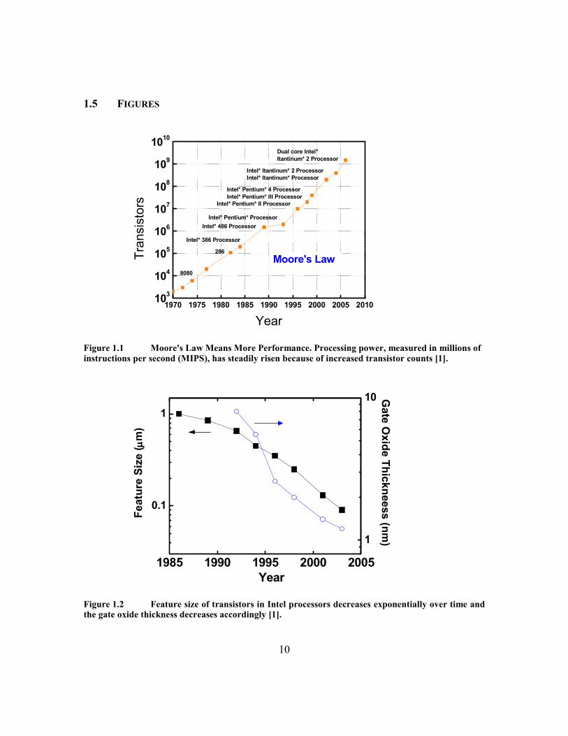
transistors per chip with enhanced circuit functionality and performance at lower cost
(Figure 1.1). Physical scaling of dielectric had been the approach to enhance drive
current. However, as devices approach the sub 100 nm scale, traditional silicon dioxide
dielectrics used in the transistor stack have been pushed to the physical limit (Figure 1.2)
and exhibit high leakage currents. Therefore, an alternative material solution is needed to
enable the further scaling. To achieve the target performance for the 65nm technology
node and beyond, the effective oxide thicknesses (EOT) of material stacks are required to
scale <1nm. Dielectric films with a higher dielectric constant (high-k) are identified as a
plausible solution to achieve the same capacitance (same EOT) while maintaining a
relatively thicker physical thickness [2]. Hafnium based high-k dielectrics are the
preferred material system for its thermal stability with the Si substrate, and appropriate κ
value 16~25 [3, 4]. Since the band-gap of dielectrics tend to be inversely proportional to
their dielectric constants, high-k films will have lower band-gap and result in smaller
barrier heights. A sufficient barrier height is needed to suppress leakage currents.
2
Therefore, Hf based dielectrics (HfO2, HfSiOx, HfSiOxNy)with band gap of ~5.7eV are
optimum dielectrics.
1.1.2 Motivation for metal gate electrodes
Performance and reliability issues remain concerns for the implementation of
high-k dielectrics, however key roadblocks are issues involving interaction between the
polysilicon (poly-Si/poly) electrode and high-k. An unfavorable increase in the threshold
voltage (Vt) have been observed for poly/high-k devices, especially for the p-type MOS
(pMOS) devices (nMOS Vtn increase ~0.4eV; pMOS Vtp increase ~0.7eV) [5]. The
Fermi-level pinning phenomena [6-8], suggests the Fermi-level of the poly-Si is easily
pinned to the energy level of metal oxide surface states due to charge exchange between
the electrode and the dielectric. Sources of such surface states may be, for Hf-based
dielectrics, the presence of Si-Hf bonds, or oxygen vacancies (oxygen deficient
interfaces). The pinning location is believed to be just below the Si conduction band
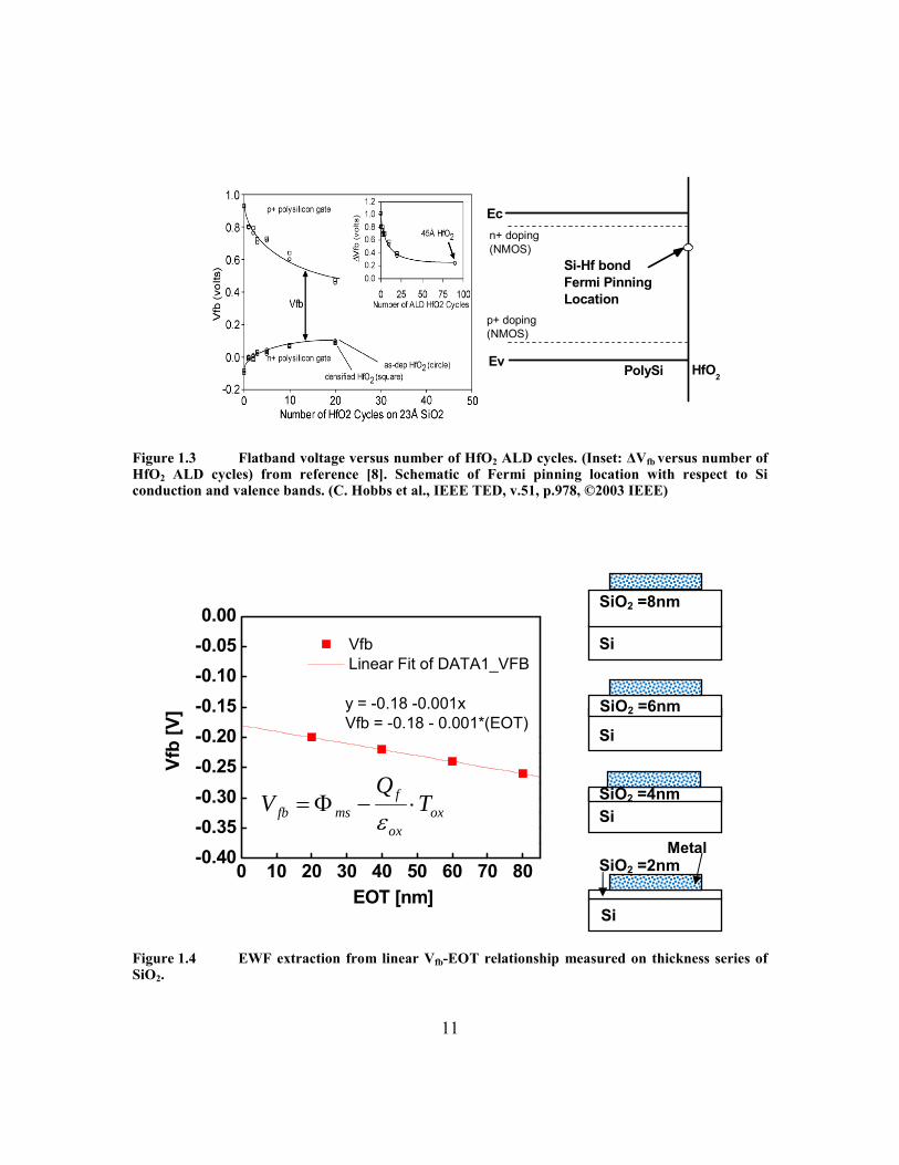
(~0.3eV below conduction band edge of Si), and thus explains the different Vt increase
for n/pMOS (Figure 1.3)[8, 9]. Another limitation to the use of poly-Si gates is the poly
depletion effect. It occurs when the MOSFET is turned on and the poly gate electrode is
depleted at the poly/dielectric interface. This thin depletion layer adds to the EOT (~3-4
Å) and consequently, reduces the gate capacitance and drain current [10]. As the EOT
target goes down, this additional layer cannot be neglected. These scaling challenges
have lead to the use of metal gate electrodes to replace poly-Si gates [11]. Metal gate
electrodes have the advantage of reducing poly/high-k interaction, eliminating poly
depletion, as well as reducing B penetration from the doped poly-Si into the gate
dielectric, and gate resistance. However, there has been limited consensus on the
appropriate electrode material, with production ready performances.
3
Alternatively, the industry has sought to the use of nitrided oxides with strain
engineered channels to improve carrier mobility, and has detoured off the scaling
approach for enhance device performance (90nm, 65nm nodes) [12]. However, the
limitations to poly/nitrided oxide stacks still remains, and metal electrodes in conjunction
with or without high-k dielectrics still remain a critical technology solution for sub-32nm
node applications.
1.2 REQUIREMENTS OF THE METAL GATE TECHNOLOGY
The quest for alternative metal electrodes faces several challenges in both device
characteristics and process integration. The optimal electrode material should exhibit 1)
proper work functions, 2) thermal/chemical stability with the underlying dielectric and 3)
ease of process integration.
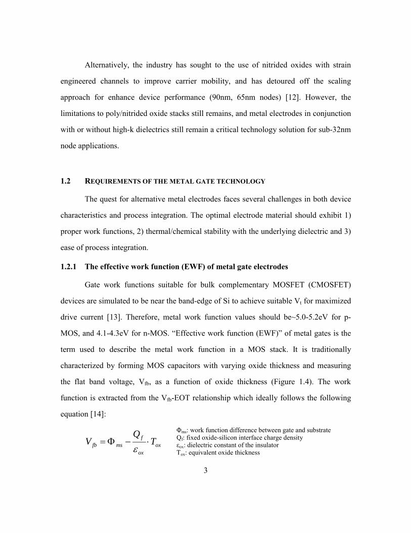
1.2.1 The effective work function (EWF) of metal gate electrodes
Gate work functions suitable for bulk complementary MOSFET (CMOSFET)
devices are simulated to be near the band-edge of Si to achieve suitable Vt for maximized
drive current [13]. Therefore, metal work function values should be~5.0-5.2eV for p-
MOS, and 4.1-4.3eV for n-MOS. “Effective work function (EWF)” of metal gates is the
term used to describe the metal work function in a MOS stack. It is traditionally
characterized by forming MOS capacitors with varying oxide thickness and measuring
the flat band voltage, Vfb, as a function of oxide thickness (Figure 1.4). The work
function is extracted from the Vfb-EOT relationship which ideally follows the following
equation [14]:
oxox
fmsfb T
QV ⋅−Φ=
ε
Φms: work function difference between gate and substrate Qf: fixed oxide-silicon interface charge density εox: dielectric constant of the insulator Tox: equivalent oxide thickness
4
The electrode work function is then determined using Φms and the known work
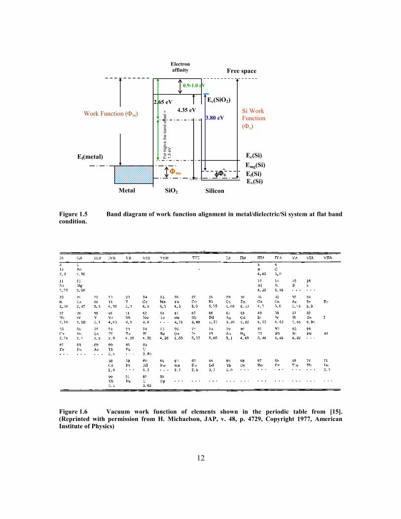
function of the silicon substrate (Φs), as shown in Figure 1.5.
EWF should be predominately determined by the bulk/vacuum work function of
the materials, which is mostly determined by the electronic and ionic structure of the
metal. The bulk (vacuum) work function for materials in the periodic table is reported by
Michaelson et al. (Figure 1.6)[15]. Materials in columns IIIB, IVB and VB are suitable
for n-type EWF, while materials in column VIII have p-type EWFs. Reports of the EWF
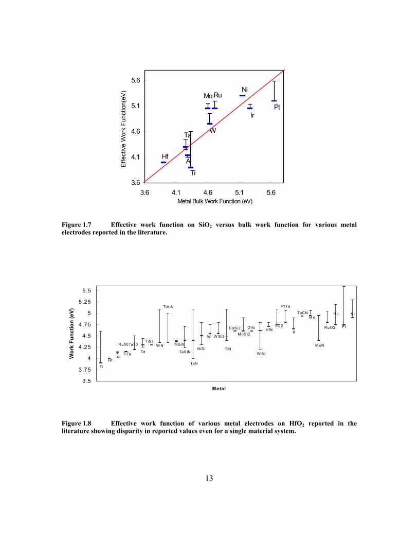
of various metal gate materials on SiO2 have followed the bulk work function reasonably
(Figure 1.7) [16-21]. However, the lack of direct correlation suggests other factors
besides the bulk work function also impact the EWF (such as interfacial reaction [22],
film structural changes [23, 24], etc.). The factors controlling EWF of metal electrodes on
high-k dielectrics (namely Hf-based dielectrics) exhibits a higher level of complexity.
From the thermal stability concerns of metals on high-k, the deposition process variation
(film thickness) [25, 26] and influence of bulk/interface charges from the dielectric itself
[27], the extracted EWF based on the linear Vfb-EOT relationships have shown a great
disparity even for a single metal system(Figure 1.8).
Summary of reported literature EWF values for various metal electrodes is shown
in Appendix I. They can be conveniently categorized into groups such as pure metals (Al,
Zr, Hf, Ti, Ta, Mo, Co, Pd, Ni, Re, Ir, Ru, Pt, W etc.), bi-metal alloys (RuTa, NiTi, PtTa
etc.), metal nitrides (binary metal nitride: WN, TiN, TaN, MoN; ternary metal nitride
systems: TaSiN, TiSiN, TiAlN etc.), conducting metal oxides (RuO2, IrO2 etc.) and metal
silicides (NiSi, CoSi, TiSi, HfSi, WSi etc.). Elemental metals have exhibited near band-
edge work functions, and binary metal alloys allows tuning of the work function by
controlling the composition of the alloy. Addition of a nitrogen or Si component to the
metal in most cases is reported to shift the work function toward mid-gap (4.6~4.8eV).
5
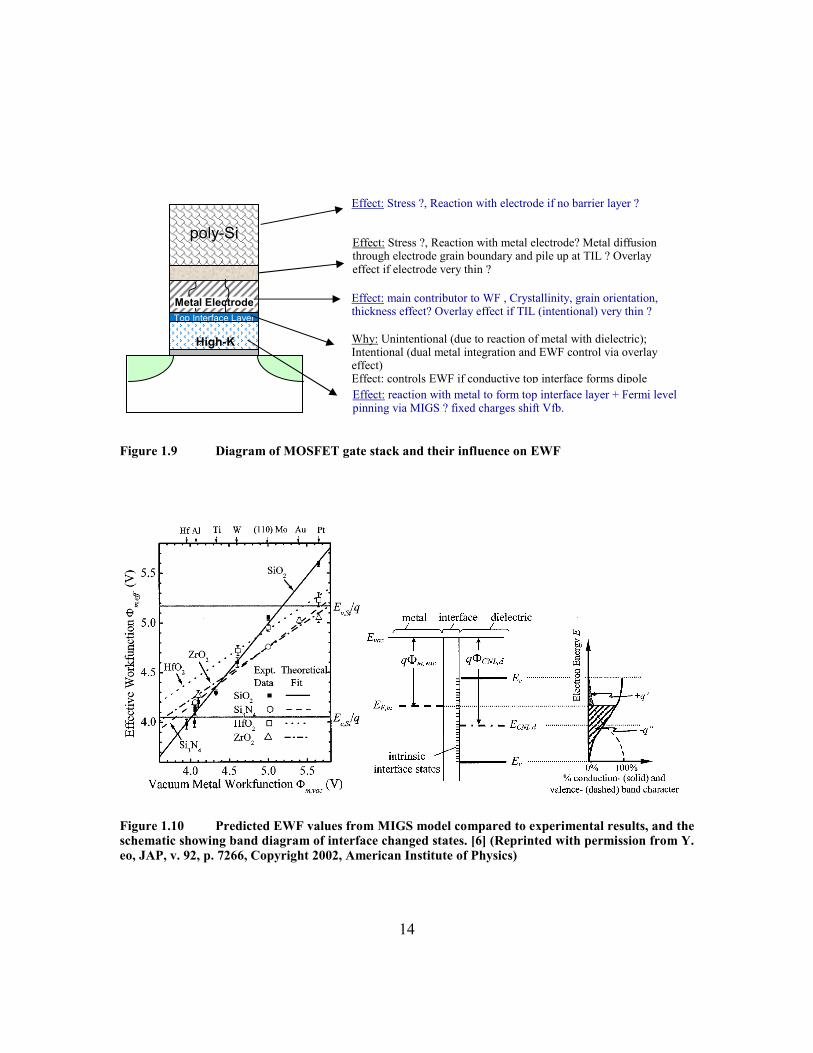
It has also been shown that not only the metal electrode itself, but also extrinsic
contributions from the overall gatestack used in the fabrication of the devices, as shown
in Figure 1.9, will impact the extracted EWF. Such complexity has obstructed the
identification of band-edge metal electrode systems, and the understanding of EWF
control on high-k dielectrics.
1.2.2 Thermal stability of metal electrodes
Considering the conventional gate-first process integration, the metal gate
material not only needs to have the correct work function, and low resistivity, but it
should be thermodynamically stable with its surrounding materials, especially the gate
dielectric [19]. Electrical properties will be affected with annealing conditions if a
reaction occurs, such as change in EOT, threshold voltage or gate leakage current.
Interdiffusion or chemical reactions are mostly attributed to the difference in the
electronegativity and atomic radii of the materials. A thorough thermal stability study of
various elemental metals and metal compounds on SiO2 and Al2O3 gate dielectrics had
been conducted by C. Cabral, Jr. et al. by in-situ XRD [28]. It is found that elemental
metals with n-MOS work functions undergo reactions with the dielectric, while others
become unstable due to its low melting point. Agglomeration is the issue in most of the
p-MOS compatible materials. Physical and electrical properties of metal gate electrodes
(TiN, TaSiN, WN, TaN, TaSi, Ir, IrO2) on HfO2 had been studied by J. Schaeffer et al. in
which material and interface studies elucidate which classes of metal gates are promising
dual metal electrodes candidates [29]. From their study, mostly ternary/binary metal
nitrides satisfy the thermal stability requirements of metal gates.
In the screening process for candidate electrode materials, detailed understanding
of the atomic characteristics of these metals are essential. Appendix II shows the
6
summarized material characteristics (bulk work function values, melting point, resistivity,
expansion coefficient, electronic specific heat) of several materials, as well as the
diffusion coefficient/activation energy, or diffusivity at 1000oC in Si, which will be
important parameters in the integration process. The electrical capture cross section, and
electron/hole trap energy levels of these materials in Si is also essential in determining
minority carrier lifetime if the gate metal diffuses within the channel. The gate etch
process for metals is an critical module in metal gate integration. Information of available
compound formation for these metals can provide directions for dry-etching solutions
[30].
1.3 CHALLENGES TO THE METAL GATE TECHNOLOGY
1.3.1 Identification of suitable band edge work function electrodes
Identification of suitable band edge work function electrode materials is the key
challenge to the metal gate technology. However, due to the complex nature of the
metal/high-k interface, minimization of error in the EWF study is needed to enable
systematic study of factors impacting work function. Unlike SiO2, using the traditional
Vfb-EOT extraction with various thickness of high-K is shown to exhibit error in the
EWF up to 0.3eV and may contribute to the disparity in the literature EWF results in
Figure 1.8 (More discussion can be found in Chapter 2). Therefore, an standardized EWF
extraction technique needs to be established first for accurate EWF extraction on high-k.
Although identification of suitable WF materials may be possible, a roadblock in
implementing proper work function electrodes on high-k has been proposed [6, 31-33].
The Fermi-level (Ef) pinning effect now between metal/high-k suggests EWF on high-k
would be different from its bulk value, vary with the underlying dielectric, and exhibit a
7
smaller range for EWF tuning than SiO2 (Figure 1.10)[6]. The metal induced gap states
(MIGS) model has been proposed to be the key intrinsic component inducing Ef-pinning.
The MIGS model suggests electrodes in contact with a dielectric will induce virtual states
in the dielectric, and interfacial charge transfer will shift the metal Ef towards the charge
neutrality level of the dielectric. It also predicts in order to achieve 5.2eV EWF on HfO2,
the electrode needs to have a bulk WF larger than 5.5eV, which only one element in the
periodic table (Pt) qualify, significantly limiting the chances of a p-type EWF solution.
And yet EWF results in the literature from pure Pt still has limited application to pMOS
[34, 35]. Multiple efforts to apply the MIGS theory to explain experimental results have
shown good correlation [6, 36], while other results cannot be completely addressed with
this model [33, 37]. Due to the limited consensus, a systematic study of the existence of
an intrinsic EWF limit is needed.
1.3.2 Study of metal electrode’s impact on device performance
The initial goal of obtaining band edge EWF metal gate was to enable EOT
scaling with maximized drive current, therefore it is crucial to study the impact of
electrodes on transistor device performance. Reports have shown the use of metal gate
electrodes is effective in screening phonon scattering in the high-k dielectric, which they
believe is the primary reason for mobility degradation in high-k films. Metal gate limit
phonons from coupling to the channel under inversion conditions, and thus result in
improved channel electron mobility [38]. Narayanan et al. [39] reported that electron
mobility optimization is critically dependent on specific electrode and interface layer
combinations as well as post deposition processing for the high-k films. Specific
chemistry for chemical deposition of the gate electrode, as well as the presence of N both
influence the reliability and performance of the device. The impact of metal gate process

8
on the high-k gate stack have been reported in [40, 41] which the different charge
trapping characteristics observe between ALD/PVD processes is from its influence on the
high-k bottom interface. The study of device performance and reliability for the candidate
metal stacks require careful investigation of mobility, Vt leakage current, and gate stack
changes due to the metal electrode. Combined with physical analysis, to investigate
sources of metal’s influence. The goal is to identify key process and material influences,
and hopefully will provide insight into the choice of candidate metal electrode material
systems and identify potential roadblocks.
1.4 DISSERTATION OUTLINE
A standardized method for work function measurement named the “terraced
oxide” method is proposed in Chapter 2. Comparison of the EWF extracted based on this
capacitance based measurement (C-V) and the barrier height between the metal/high-k
dielectric (based on a leakage current method) is performed to validate the accuracy of
the extraction. Various material systems will be evaluated utilizing this extraction
technique.
In Chapter 3, the critical question of whether there is intrinsic limitation to
achieving band edge EWF metals on high-k is addressed based on terraced oxide results
and correlation to the MIGS model.
A systematic breakdown of detailed understanding of factors contributing to the
EWF of metal electrodes and the possible control/engineering of these factors to our
benefit is discussed in Chapter 4.
Utilization of the understanding in Chapter 4, engineering the metal/high-k
interface in end allows band-edge EWF to be achieved with interface engineering.
9
Identified n-type and p-type electrode candidates and their EWF mechanisms are
discussed in Chapter 5.
Chapter 6 is the evaluation of the device performance of band edge metals,
combined with physical analysis to understand the influence of metal gates on device
properties, and furthermore, the influence of metal gates on device reliability.
Finally, chapter 7 discusses a new phenomena which is presented to be limiting
the integration of p-type EWF metals at low EOTs. Therefore, utilization at the 32nm
node still faces its challenges, and suggested approach for future studies are proposed.
10
1.5 FIGURES
1970 1975 1980 1985 1990 1995 2000 2005 2010103
104
105
106
107
108
109
1010
Moore's LawTran
sist
ors
Year
8080
Intel* Pentium* ProcessorIntel* 486 Processor
286
Intel* Pentium* II Processor
Intel* Pentium* 4 ProcessorIntel* Pentium* III Processor
Intel* Itantinum* 2 ProcessorIntel* Itantinum* Processor
Dual core Intel* Itantinum* 2 Processor
Intel* 386 Processor
Figure 1.1 Moore's Law Means More Performance. Processing power, measured in millions of instructions per second (MIPS), has steadily risen because of increased transistor counts [1].
1985 1990 1995 2000 2005
0.1
1
Year
Feat
ure
Size
( µµ µµm
)
Gate O
xide Thickneess (nm)1
10
Figure 1.2 Feature size of transistors in Intel processors decreases exponentially over time and the gate oxide thickness decreases accordingly [1].
11
HfO2PolySiEv
Si-Hf bondFermi PinningLocation
p+ doping(NMOS)
n+ doping(NMOS)
Ec
Figure 1.3 Flatband voltage versus number of HfO2 ALD cycles. (Inset: ∆Vfb versus number of HfO2 ALD cycles) from reference [8]. Schematic of Fermi pinning location with respect to Si conduction and valence bands. (C. Hobbs et al., IEEE TED, v.51, p.978, ©2003 IEEE)
0 10 20 30 40 50 60 70 80-0.40-0.35-0.30-0.25-0.20-0.15-0.10-0.050.00
oxox
fmsfb T
QV ⋅−Φ=
ε
Vfb Linear Fit of DATA1_VFB
Vfb
[V]
EOT [nm]
y = -0.18 -0.001xVfb = -0.18 - 0.001*(EOT)
Figure 1.4 EWF extraction from linear Vfb-EOT relationship measured on thickness series of SiO2.
Si
SiO2 =8nm
SiO2 =6nm
SiO2 =4nm
SiO2 =2nm
Si
Si
Si
Metal
12
Figure 1.5 Band diagram of work function alignment in metal/dielectric/Si system at flat band condition.
Figure 1.6 Vacuum work function of elements shown in the periodic table from [15]. (Reprinted with permission from H. Michaelson, JAP, v. 48, p. 4729, Copyright 1977, American Institute of Physics)
Ec(Si)
Ev(Si)
Emg(Si)Ef(Si)
Ec(SiO2)
Ef(metal)
Free space
ΦΦΦΦms ΦΦΦΦb
Electron affinity
4.35 eV3.80 eV
0.9-1.0 eV
Work Function (Φm)
SiliconSiO2 Metal
For h
igh-
k th
e ba
nd o
ffset
=
1.5
eV
2.65 eVSi Work Function (Φs)
0
13
Ni
PtIr
RuMo
W
Ti
Al
Ta
Hf
3.6
4.1
4.6
5.1
5.6
3.6 4.1 4.6 5.1 5.6Metal Bulk Work Function (eV)
Effe
ctiv
e W
ork
Func
tion(
eV)
Figure 1.7 Effective work function on SiO2 versus bulk work function for various metal electrodes reported in the literature.
W N
TiA lN
TiS iN
TaS iN
TaN
NiS i
W S i2W
Ni
P t
Ru
RuO2
M oN
M oTaCN
Ir
P tTa
IrO2HfN
W S i
ZrN
M oS i2CoS i2
TiN
TiS iRu50Ta50
TaTiTa
Ti
HfA l
3 .5
3 .75
4
4 .25
4.5
4 .75
5
5 .25
5.5
Metal
Wor
k Fu
nctio
n (e
V)
Figure 1.8 Effective work function of various metal electrodes on HfO2 reported in the literature showing disparity in reported values even for a single material system.
14
Figure 1.9 Diagram of MOSFET gate stack and their influence on EWF
Figure 1.10 Predicted EWF values from MIGS model compared to experimental results, and the schematic showing band diagram of interface changed states. [6] (Reprinted with permission from Y. eo, JAP, v. 92, p. 7266, Copyright 2002, American Institute of Physics)
High-K
Top Interface Layer
poly-Si
Metal Electrode
Effect: Stress ?, Reaction with electrode if no barrier layer ?
Effect: Stress ?, Reaction with metal electrode? Metal diffusion through electrode grain boundary and pile up at TIL ? Overlay effect if electrode very thin ?
Effect: main contributor to WF , Crystallinity, grain orientation, thickness effect? Overlay effect if TIL (intentional) very thin ?
Why: Unintentional (due to reaction of metal with dielectric); Intentional (dual metal integration and EWF control via overlay effect) Effect: controls EWF if conductive top interface forms dipole Effect: reaction with metal to form top interface layer + Fermi level pinning via MIGS ? fixed charges shift Vfb.
15
1.6 REFERENCES [1] G. E. Moore, "Progress in digital integrated electronics," presented at Electron
Devices Meeting, 1975 International, 1975. [2] G. D. Wilk, R. M. Wallace, and J. M. Anthony, "High-k gate dielectrics: Current
status and materials properties considerations," Journal of Applied Physics, vol. 89, pp. 5243-5275, 2001.
[3] B. H. Lee, L. Kang, W.-J. Qi, R. Nieh, Y. Jeon, K. Onishi, and J. C. Lee, "Ultrathin hafnium oxide with low leakage and excellent reliability for alternative gate dielectric application," presented at Electron Devices Meeting, 1999. IEDM Technical Digest. International, 1999.
[4] L. Kang, B. H. Lee, W.-J. Qi, Y. Jeon, R. Nieh, S. Gopalan, K. Onishi, and J. C. Lee, "Electrical characteristics of highly reliable ultrathin hafnium oxide gate dielectric," Electron Device Letters, IEEE, vol. 21, pp. 181-183, 2000.
[5] C. Hobbs, L. Fonseca, V. Dhandapani, S. Samavedam, B. Taylor, J. Grant, L. Dip, D. Triyoso, R. Hegde, D. Gilmer, R. Garcla, D. Roan, L. Lovejoy, R. Rai, L. Hebert, H. Tseng, B. White, and P. Tobin, "Fermi Level Pinning at the PolySietal Oxide Interface," VLSI Technology Digest, pp. 9-10, 2003.
[6] Y. C. Yeo, T. J. King, and C. M. Hu, "Metal-dielectric band alignment and its implications for metal gate complementary metal-oxide-semiconductor technology," Journal of Applied Physics, vol. 92, pp. 7266-7271, 2002.
[7] S. Samavedam, L. B. La, P. J. Tobin, B. White, C. Hobbs, L. R. C. Fonseca, A. Demkov, J. Schaeffer, E. Luckowski, A. Martinez, M. Raymond, D. Triyoso, D. Roan, V. Dhandapani, R. Garcia, S. G. H. Anderson, K. Moore, H. H. Tseng, C. Capasso, O. Adetutu, D. C. Gilmer, W. J. Taylor, R. Hegde, and J. Grant, "Fermi level pinning with sub-monolayer MeOx and metal gates," IEEE Electron Device Meeting, pp. 307-310, 2003.
[8] C. C. Hobbs, L. R. C. Fonseca, A. Knizhnik, V. Dhandapani, S. B. Samavedam, W. J. Taylor, J. M. Grant, L. G. Dip, D. H. Triyoso, R. I. Hegde, D. C. Gilmer, R. Garcia, D. Roan, M. L. Lovejoy, R. S. Rai, E. A. Hebert, H.-H. Tseng, S. G. H. Anderson, B. E. White, and P. J. Tobin, "Fermi-level pinning at the polysilicon/metal-oxide interface-Part II," Electron Devices, IEEE Transactions on, vol. 51, pp. 978-984, 2004.
[9] C. Hobbs, L. Fonseca, V. Dhandapani, S. Samavedam, B. Taylor, J. Grant, L. Dip, D. Triyoso, R. Hegde, D. Gilmer, R. Garcia, D. Roan, L. Lovejoy, R. Rai, L. Hebert, H. Tseng, B. White, and P. Tobin, "Fermi level pinning at the polySi/metal oxide interface," VLSI Technology, 2003. Digest of Technical Papers. 2003 Symposium on, pp. 9-10, 2003.
[10] C. Y. Wong, J. Y.-C. Sun, Y. Taur, C. S. Oh, R. Angelucci, and B. Davari, "Doping of n+ and p+ polysilicon in a dual-gate CMOS process," presented at Electron Devices Meeting, 2003. IEDM '03 Technical Digest. IEEE International, 1988.
[11] J. C. Hu, H. Yang, R. Kraft, A. L. P. Rotondaro, S. Hattangady, W. W. Lee, R. A. Chapman, C.-P. Chao, A. Chatterjee, M. Hanratty, M. Rodder, and I.-C. Chen,
16
"Feasibility of using W/TiN as metal gate for conventional 0.13 μm CMOS technology and beyond," Electron Devices Meeting, 1997. Technical Digest., International, pp. 825-828, 1997.
[12] ITRS, "ITRS Roadmap 2003," 2003. [13] I. De, D. Johri, A. Srivastava, and C. M. Osburn, "Impact of gate work function
on device performance at the 50 nm technology node," Solid-State-Electronics, vol. 44, pp. 1077-1080, 2000.
[14] E. H. Nicollian and J. R. Brews, MOS Physics and Technology. New york: Wiley, 1982.
[15] H. Michaelson, "The work function of the elements and its periodicity," Journal of Applied Physics, vol. 48, pp. 4729-4733, 1977.
[16] Y.-C. Yeo, T.-J. King, and C. Hu, "Metal-dielectric band alignment and its implications for metal gate complementary metal-oxide-semiconductor technology," Journal of Applied Physics, vol. 92, pp. 7266-7271, 2002.
[17] B.-Y. Tsui and C.-F. Huang, "Wide range work function modulation of binary alloys for MOSFET application," IEEE Electron Device Letter, vol. 24, pp. 153-155, 2003.
[18] M. A. Pawlak, T. Schram, K. Maex, and A. Vantomme, "Investigation of Iridium as a gate electrode for deep sub-micron CMOS technology," Microelectronic Engineering, vol. 70, pp. 373-376, 2003.
[19] B. Maiti and P. J. Tobin, "Metal Gates for Advanced CMOS Technology," SPIE Conference on Microelectronic Device Technology III, vol. 3881, pp. 46-57, 1999.
[20] H. Zhong, S. N. Hong, Y.-S. Suh, H. Lazar, G. Heuss, and V. Misra, "Properties of Ru-Ta alloys as gate electrodes for NMOS and PMOS silicon devices," IEEE Electron Device Meeting, 2001.
[21] I. Polishchuk, P. Ranade, T.-J. King, and C. Hu, "Dual work function metal gate CMOS transistors by Ni-Ti interdiffusion," IEEE Electron Device Letter, vol. 23, pp. 200-202, 2002.
[22] H. N. Alshareef, H. C. Wen, H. Luan, K. Choi, H. R. Harris, Y. Senzaki, P. Majhi, B. H. Lee, B. Foran, and G. Lian, "Temperature dependence of the work function of ruthenium-based gate electrodes," Thin Solid Films, vol. article in press Temperature dependence of the work function of ruthenium-based gate electrodes, 2006.
[23] R. Lin, Q. Lu, P. Ranade, T. J. King, and C. M. Hu, "An adjustable work function technology using Mo gate for CMOS devices," Ieee Electron Device Letters, vol. 23, pp. 49-51, 2002.
[24] S. H. Bae, W. P. Bai, H. C. Wen, S. Mathew, L. K. Bera, N. Balasubramanian, N. Yamada, M. F. Li, and D. L. Kwong, "Laminated metal gate electrode with tunable work function for advanced CMOS," presented at VLSI Technology, 2004. Digest of Technical Papers. 2004 Symposium on, 2004.
[25] G. Bersuker, P. Zeitzoff, J. H. Sim, B. H. Lee, R. Choi, G. Brown, and C. D. Young, "Mobility Evaluation in Transistors with Charge Trapping Gate Dielectrics," Applied Physics Letters, vol. 87, pp. 042905, 2005.
17
[26] H. N. Alshareef, H. C. Wen, H. R. Harris, K. Choi, H. F. Luan, P. Lysaght, P. Majhi, B. H. Lee, M. El-Bouanani, and V. Ukride, "Modulation of the work function of silicon gate electrode using thin TaN interlayers," Applied Physics Letters, vol. 87, 2005.
[27] S. Zafar, V. Narayanan, A. Callegari, F. R. McFeely, P. Jamison, E. Gusev, C. Cabral, and R. Jammy, "HfO/sub 2//metal stacks: determination of energy level diagram, work functions & their dependence on metal deposition," VLSI Technology, 2005. Digest of Technical Papers. 2005 Symposium on, pp. 44-45, 2005.
[28] C. C. Jr., C. Lavoie, A. S. Ozcan, R. S. Amos, V. Narayanan, E. P. Gusev, J. L. Jordam-Sweet, and J. M. E. Harper, "Evaluation of CMOS Gate Materials Using IN SITU Characterization Techniques," Electrochemical Society Proceedings, Advanced Short-Time Thermal Processing for Si-Based CMOS Devices, pp. 375-384, 2003.
[29] J. K. Schaeffer, S. B. Samavedam, D. C. Gilmer, V. Dhandapani, P. J. Tobin, J. Mogab, B. Y. Nguyen, B. E. White, S. Dakshina-Murthy, R. S. Rai, Z. X. Jiang, R. Martin, M. V. Raymond, M. Zavala, L. B. La, J. A. Smith, R. Garcia, D. Roan, M. Kottke, and R. B. Gregory, "Physical and electrical properties of metal gate electrodes on HfO2 gate dielectrics," Journal of Vacuum Science & Technology B, vol. 21, pp. 11-17, 2003.
[30] CRC Handbook of Chemistry and Physics, 70 ed. Boca Raton, Florida: CRC Press, Inc., 1989-1990.
[31] S. B. Samavedam, L. B. La, P. J. Tobin, B. White, C. Hobbs, L. R. C. Fonseca, A. A. Demkov, J. Schaeffer, E. Luckowski, A. Martinez, M. Raymond, D. Triyoso, D. Roan, V. Dhandapani, R. Garcia, S. G. H. Anderson, K. Moore, H. H. Tseng, C. Capasso, O. Adetutu, D. C. Gilmer, W. J. Taylor, R. Hegde, and J. Grant, "Fermi level pinning with sub-monolayer MeOx and metal gates [MOSFETs]," Electron Devices Meeting, 2003. IEDM '03 Technical Digest. IEEE International, pp. 13.1.1-13.1.4, 2003.
[32] J. Schaeffer, C. Capasso, L. R. C. Fonseca, S. Samavedam, L. B. La, J. Smith, S. Dakshina-Murthy, D. C. Gilmer, Luckowski, Y. Liang, S. Kalpat, B. Adetutu, H. H. Tseng, Y. Shiho, A. Demkov, R. Hegde, W. J. Taylor, R. Gregory, J. Jiang, E. Luckowski, M. Raymond, K. Moore, D. Triyoso, D. Roan, B. White, and P. J. Tobin, "Challenges for the integration of metal gate electrodes," IEEE Electron Device Meeting, 2004.
[33] K. Shiraishi, Y. Akasaka, S. Miyazaki, T. Nakayama, T. Nakaoka, G. Nakamura, K. Torii, H. Furutou, A. Ohta, P. Ahmet, K. Ohmori, H. Watanabe, T. Chikyo, M. L. Green, Y. Nara, and K. Yamada, "Universal theory of workfunctions at metal/Hf-based high-k dielectrics interfaces - guiding principles for gate metal selection," Electron Devices Meeting, 2005. IEDM Technical Digest. IEEE International, pp. 39-42, 2005.
[34] J. K. Schaeffer, L. R. C. Fonseca, S. B. Samavedam, Y. Liang, P. J. Tobin, and B. E. White, "Contributions to the effective work function of platinum on hafnium dioxide," Applied Physics Letters, vol. 85, pp. 1826-1828, 2004.
18
[35] E. Cartier, F. R. McFeely, V. Narayanan, P. Jamison, B. P. Linder, M. Copel, V. K. Paruchuri, V. S. Basker, R. Haight, D. Lim, R. Carruthers, T. Shaw, M. Steen, J. Sleight, J. Rubino, H. Deligianni, S. Guha, R. Jammy, and G. Shahidi, "Role of oxygen vacancies in V/sub FB//V/sub t/ stability of pFET metals on HfO/sub 2/," VLSI Technology, 2005. Digest of Technical Papers. 2005 Symposium on, pp. 230-231, 2005.
[36] D. Gu, S. K. Dey, and P. Majhi, "Effective work function of Pt, Pd, and Re on atomic layer deposited HfO[sub 2]," Applied Physics Letters, vol. 89, pp. 082907, 2006.
[37] H. Yang, Y. Son, S. Baek, H. Hwang, H. Lim, and H.-S. Jung, "Ti gate compatible with atomic-layer-deposited HfO[sub 2] for n-type metal-oxide-semiconductor devices," Applied Physics Letters, vol. 86, pp. 092107, 2005.
[38] R. Chau, S. Datta, M. Doczy, B. Doyle, J. Kavalieros, and M. Metz, "High-k/Metal–Gate Stack and Its MOSFET Characteristics," IEEE Electron Device Letter, vol. 25, pp. 408-410, 2004.
[39] A. C. V. Narayanan, F.R. McFeely, K. Nakamura, P. Jamison, S. Zafar, E. Cartier, A. Steegen, V. Ku, P. Nguyen, K. Milkove, C. Cabral Jr., M. Gribelyuk, C. Wajda, Y. Kawano, D. Lacey, Y. Li, E. Sikorski, E. Duch, H. Ng, C. Wann, R. Jammy, M. Ieong, G. Shahidi, "Dual Work Function Metal Gate CMOS using CVD metal electrodes," VLSI Technology Digest, pp. 192-193, 2004.
[40] C. Young, G. Bersuker, H. C. Wen, G. Brown, and P. Majhi, "Charge Trapping Characteristics of Hafnium Based High-ê Dielectrics with Various Metal Electrodes," SSDM 2004, 2004.
[41] P. Majhi, C. Young, G. Bersuker, H. C. Wen, G. A. Brown, B. Foran, R. Choi, P. M. Zeitzoff, and H. R. Huff, "Influence of Metal Gate Materials and Processing on Planar CMOS Device Characteristics with High-k Gate Dielectrics," ESSDERC, 2004.
[42] http://www.intel.com/technology/mooreslaw/index.htm, "Moore's Law Means More Performance."
19
CHAPTER 2
STANDARDIZED EFFECTIVE WORK FUNCTION EXTRACTION TECHNIQUE: TERRACED OXIDE
2.1 MOTIVATION
The traditional method for EWF extraction on SiO2 dielectrics is through C-V
measurement of the flatband voltage (Vfb) for a thickness series of the dielectric, and
extracted linearly by the Vfb-EOT relationship (Figure 1.4)[1]. However, when varying
high-k dielectric thicknesses, bulk charges in the dielectric (ρb) shift the Vfb. The
interfacial SiOx layer between the high-k and the Si substrate also varies with high-k
thickness and makes it difficult to maintain a constant fixed interface charge at the Si-
dielectric interface (Qf). Figure 2.1 is the schematic showing various charges in stack
which contribute to Vfb. EWF extraction is no longer easily extracted from a linear
relationship, but a complex quadratic formula (Equation 2-1). [2]
))(1)(1*(*
0
' dxxxdxxxtQEOTQV oh
h
h ttt
t oxox
t
bhh
hi
ox
fmsfb ∫∫
+=−−−−Φ= ρ
ερ
εεε….Equation 2-1
Without fully calculating the charge contributions, many still report EWF values
using a linear extraction, resulting in large errors due to inaccurate fitting. Examples of
the quadratic dependence of Vfb-EOT plot, and its deviation by using linear fitting is
shown in Figure 2..2, especially if the high-k quality is poor and exhibits large bulk
charges. The inaccuracy in the EWF extraction could be accounted for the disparity in the
various reported EWFs of a given material system (Figure1-8) [3], and thus complicates
the study of metal gate EWF, and the progression to achieving band edge EWF materials.
Therefore, an accurate EWF extraction technique is critical as the foundation of metal
gate work.
20
2.2 EXPERIMENTAL PROCEDURES OF THE TERRACED OXIDE TECHNIQUE
On a single device wafer with field isolation, the dielectric is thermally grown
SiO2 (10nm) and etched into ringed-terraces of various thicknesses with a benign wet
etching of diluted hydrofluoric acid. The SEZTM Model 203 spin etch processor was used
for the fabrication of our terraced oxides. Standard terraced oxide thicknesses of 2, 4, 6,
8nm (thick terraces) or 0, 2, 3, 4nm (ultra-thin terraces) are typically used. Details of this
process can be found in [4]. The quality of the terrace oxides is found to be comparable to
that of as grown thin oxides. Figure 2.3 is a photo of a blanket terraced oxide wafer with
thick oxides for enhanced color contrast and a schematic of terraced oxide devices . For
EWF extraction on high-k, the deposition of a thin high-k film (2~3nm) is added to the
terraced oxide wafers, then followed by metal electrode deposition. A tungsten (W) or
poly-Si capping layer is then deposited for ease of device testing, or to prevent metal
oxidation during subsequent thermal budgets. Capacitor devices were formed and EWF
was measured after a low temperature forming gas anneal, or after a 1000oC, 5 sec
activation anneal required to activate the dopants in CMOS device processes. C-V curves
were measured at 100 kHz using an Agilent 4284A measurement system, and the Vfb and
EOT values were computed from the NCSU CVC program [5].
2.2.1 Charge model of the terraced oxide technique
The terraced oxide method follows a three charge model to enable linear Vfb-EOT
extraction [6, 7] (Equation 2-3). The equation is a simplified form of the general model
given by R. Jha [2] (or Equation 2-2) and thus enable linear extraction of the Vfb-EOT
relationship by use of good quality terraced oxides, and limiting the SiO2 contribution
(ρox) to the equation:
21
ox
f
ox
oxhb
ox
imsfb
EOTQEOThEOThQVεε
εερε
*)
*2*)/(**
(2
' −−−Φ= ;
With the use of terraced oxide structures, a constant fixed interface charge
between the Si substrate and dielectric (Qf) is maintained across the varying oxide
thicknesses, minimizing wafer-to-wafer variation associated with multiple wafer
extraction methods. Qf can be calculated from the slope of the Vfb-EOT relationship. The
SiO2 bulk charge term in reference [2] (ρox) can be neglected for simplification of the
extraction since this bulk charge contribution is far smaller than that of Qf.[8] The
extracted y-axis ordinate intercept value contains the contribution of the metal WF as
well as the high-k/SiO2 interface charge (Qi) and high-k bulk charge density (ρb) terms.
(th: high-k physical thickness, EOTh: high-k EOT; EOT: EOT of high-k/SiO2 stack, εh:
high-k dielectric constant, εox: SiO2 dielectric constant).
The contributions of charges in the high-k on Vfb is controlled and can be
minimized (~+50 meV), by using a fixed and thinned high-k film (2~3nm). More on the
calculations for the bulk charge contribution will be discussed in the next section.
Therefore, for simplicity, the ordinate intercept value is the EWF values quoted when
extracting with the terraced oxide method.
2.3 DEMONSTRATION OF THE TERRACED OXIDE EXTRACTION
A comparison of Vfb-EOT plots for metal/HfSiOx gate stacks using a single
terraced oxide-fixed-thickness high-k wafer (linear extraction) and multiple oxide-
variable-thickness-high-k wafers (quadratic extraction) illustrates the advantage of the
terraced oxide stack approach (Figure 2.4) for reduce errors in extraction. More examples
of the application of the terraced oxide technique for EWF extraction is shown through
this work and has proven to be extremely sensitive to slight changes in metal EWF.
EOThtox
hh ε
ε= ..Equation 2-3
22
2.3.1 Using the terraced oxide method for calculation of high-κκκκ stack charges
To obtain the contribution of high-k bulk charge and high-k/oxide interface
charge terms, an experiment was designed with multiple terraced oxide wafers identical
except for varying constant high-k thickness (5cy, 15cy, 25cy, 30Å, 35Å, 45Å, 65Å ALD
HfO2 and HfSiOx). Their Vfb-EOT y-intercept values (Φi) are plotted versus the high-k
EOT values, and the Φi versus EOTh relationship should follow Equation 2-4. In Figure
2.5 Φi is plotted versus the physical thickness, in terms of ALD deposition cycles.
ox
hoxhb
ox
hims
EOTEOTQiε
εερε *2
*)/(** 2' −−Φ=Φ ….Equation 2-4
A linear plot implies a constant Qi and negligible ρb. The SiO2-high-k interface
charge density, Qi, may be computed from the slope of the plot. For ALD TiN gate
electrodes on both HfO2 and HfSiOx, a linear relationship is observed, and similar Qi/q is
calculated to be ~1.6x10¹²/cm2. A non-linear plot may imply the presence of bulk charge
ρb in the high-k film or the combination of Qi and ρb. With sufficient data it may be
possible to solve for both Qi and ρb. The ordinate y-axis intercept of this Φi–EOTh plot is
the gate electrode-substrate work function difference for the high-k stack system (At
EOTh=0, Φms=-0.47eV on HfSiOx, and -0.53 on HfO2; correlats to a work function of
~4.6eV, and 4.54eV, similar to the work function of ALD TiN on SiO2 in this
experiment: 4.54eV. This result suggest there is no reaction between the TiN and high-k
films, which will otherwise result in difference in effective work function.
The terraced oxide approach is therefore useful for evaluating work function of
metal electrodes on high-k films if the fixed high-k deposited is thin enough to limit the
effect of the interface charge term (which is proportional to EOTh). Using standard 20Å
or 30Å HfSiOx and HfO2, maximum deviation of the ordinate intercept value extracted
23
from the Vfb-EOT plot is found to be 50~100meV from the actual effective work function
of metal on high-k. Therefore, for simplicity, the ordinate intercept value is the EWF
values quoted when extracting with the terraced oxide method.
2.4 VALIDATION OF TERRACED OXIDE EWF EXTRACTION: COMPARISON WITH CURRENT EXTRACTED BARRIER HEIGHT
The Vfb is not only impacted by charge, but also is influenced by the presence of
other factors. Therefore, EWFs for metal gate electrodes on high-k dielectrics extracted
from the Vfb can be a combination of the true metal WF + dielectric stack charges +
interface dipole formation [9]. However, the actual work function (WF) with respect to
vacuum can be calculated by measuring the metal/dielectric barrier height (Φb) once the
electron affinity of a dielectric is known. Extracting Φb by monitoring the gate current
density- gate voltage- temperature (Jg-Vg-T) relationship (Vg>0) for MOS devices has
been reported by Zafar et al. [10-12]. Accuracy of the terraced oxide (C-V based) method
can be confirmed via comparison with the metal/high-k barrier height. We will cross
compare the C-V extracted EWF with that estimated from barrier height measurements.
2.4.1 The current extracted barrier height (J-V) method
If the main conduction mechanism is tunneling, the voltage applied when the
conduction mechanism transitions from direct tunneling to Fowler-Nordheim (F-N)
tunneling corresponds to the Φb at the metal/dielectric interface (Figure 2.6). This
technique provides a direct measurement of the metal/dielectric barrier height without the
impact of fixed oxide charges, nor knowledge of oxide fields. Restriction of this method
is the ability to measure the tunneling current without the dielectric undergoing early
breakdowns, which may be the case for ultra thin SiO2 layers.
24
2.4.2 Sample requirements and preparation for J-V barrier height method
The same terraced oxide structures for EWF extraction via C-V measurements
can be used for J-V if the samples are properly prepared. Highly doped n-type Si
substrates (Nd=1E18/cm3) are preferred as starting substrates to limit additional voltage
drop in the Si substrate at accumulation for the J-V barrier height extraction. A thin
terraced oxide is used with SiO2 thicknesses of 1.0, 1.5, 2.5, 3.5nm, followed by atomic
layer deposition of 3nm of HfO2 film and various metal gate electrodes, and a tungsten or
poly-Si capping layer. Film thicknesses are critical in order to see the transition point for
current conduction. Capacitor devices were formed and EWF was measured after a low
temperature forming gas anneal, or after a 1000oC, 5 sec activation anneal. J-V
measurements were made with a staircase voltage sweep with step size = 0.025V, and on
small area capacitors (area = 3e-6/cm2) to minimize defect-enhanced leakage currents.
2.4.3 Comparison of terraced oxide (C-V) vs barrier height (J-V) techniques
Vfb-EOT plots for EWF extraction on terraced oxide (SiO2) and terraced oxide +
high-k (HfO2) are shown in Figure 2.7(a)(b). The extracted EWF for TiN/SiO2 is 4.62eV,
with a fixed charge Qf=-6E11/cm2. The Vfb-EOT for TiN/HfO2 exhibits an excellent
linear relationship, suggesting minimum influence of ρb, with EWF=4.66eV and
Qf=2E11/cm2. Well behaved C-Vs for corresponding to the varied EOT devices across
the terraces are shown in the insert of both samples.
Leakage current measurements were performed on the same terraced oxide
capacitor structures. The band diagram for metal/SiO2 and metal/high-k/SiO2 MOS
devices in accumulation corresponding to the onset of current mechanism change (at Vg
peak= Φb) is shown in Figure 2.6. For SiO2 (Figure 2.6(a)), the barrier height is the
applied voltage at the maximum of the ∆ln(J)/ ∆V curve (the ∆JV method in [10]). With 3
25
nm HfO2 on 2~3nm SiO2 stacks, current across the SiO2 is completely in the direct
tunneling regime, and the peak of the δln(J)/ δV curve corresponds to the onset of
Fowler-Nordheim (F-N) tunneling in the high-k film, as shown in the band diagram
schematic in Figure 2.6(b). ∆JV results for both stacks are shown in Figure 2.8(a). The
various ∆ln(J)/ ∆V curves represent current measurements across the radius of the wafer,
reflecting variations in EOT on the terraced oxide wafer. TiN/SiO2 barrier height (Φbo), is
at Vgpeak=~3.7+/- 0.05V. This transforms to a TiN metal work function of 4.6+/- 0.05V
with the addition of the SiO2 electron affinity χ=0.9, consistent with that extracted from
the terraced oxide technique. Also worthy of note is that the peak intensity is most
evident for SiO2 thicknesses of the range 2.7~3.5nm, corresponding to the transition point
from direct to F-N tunneling at electric fields 8~9MV/cm [13]. The measured TiN/HfO2
barrier height (Φbh) is at Vgpeak~2.00+/- 0.05V. Since the metal work functions on high-
k and SiO2 are equal, as obtained from the terraced oxide results in this study, the
conduction band offset (∆Ec) between HfO2 and SiO2 can be calculated to be
Φbo-Φbh= 1.7eV. This value is slightly different from that (2eV) reported by Zafar in [12].
Modeling the band offset for oxides was previously reported by Robertson, and Demkov
[14, 15]. The calculated ∆Ec is a function of the charge neutrality levels (CNL) of HfO2
and its electron affinity, which may depend on the high-k processing conditions since
film structure (ex. monoclinic-HfO2 versus tetragonal structures) will influence the CNL.
Nevertheless, for mono-clinic HfO2, the ∆Ec measured (1.7eV) should reside within the
Schottky and Bardeen limits of the calculations, which is estimated to be between
1.6~2eV, respectively [15]. ∆JV for the HfO2/SiO2 sample has also been conducted at
temperatures ranging from 250-100oK to limit influence of thermal emission currents
(Figure 2.8 (b)). A shift in the ∆JV peak to a higher voltage ~80meV at 100oK is observed
which may be attributed to a similar amount of shift in the Fermi-level at 100oK [16],
26
thus validating the measured Φbh even at low temperatures. The ∆JT method as described
by Zafar in [10], ( ∆JT=[J(T1)-J(T2)]/J(T2) ) will also have a maximum when Vgpeak= Φb.
∆JT for 300 and 100oK is shown in (Figure 2.8(b)) ; it has been found to align well with
that for the ∆JV measurements.
A comparison of the EWF extracted by the terraced oxide technique on high-k
films, and WF calculated from the barrier height (measured with ∆Ec~1.7eV) is shown in
Figure 2.9 for multiple metal/high-k devices with maximum process thermal budget of
1000oC. A reasonable correlation is consistently obtained for various metal gate materials
with EWF deviations of +/-0.1V. The metal gates materials used in this study contained
pure metals, nitrides, and silicides, which exhibit good thermal stability with the
dielectric [17]. Consequently, interfacial reactions of metals with high-k or SiO2 that may
change the EWF is negligible.
2.5 CONCLUSIONS
The terraced oxide technique is proposed to be an accurate EWF extraction
technique allowing linear extraction of the Vfb-EOT relationship. The EWF for
metal/high-k stacks calculated using the ordinate intercept value may be impacted by 1)
dielectric bulk charges or 2) other factors such as formation of metal/high-k dipole.
Calculations of dielectric charges suggest use of thin high-k enables control of charge
contributions to EWF to ~50-100meV. Comparisons of the EWF extracted by the
terraced oxide technique with the barrier height calculated WF by the J-V measurements
have exhibited a reasonable correlation, suggesting real change in metal work function is
being measured, validating both techniques for EWF extraction [4].
Combining the terraced oxide method, which gives the EWF, and the J-V method,
which provides a true WF by metal/dielectric barrier height measurement, will allow
27
quantification and enhance learning on the other factors that have been reported to
influence the EWF for metal gate electrodes and are not well understood.
Acknowledgements
The authors would like to thank Sufi Zafar at IBM Research, T. J. Watson
Research Center, and Dr. Alex Demkov at the University of Texas Austin Department of
Physics, for their insightful discussions and comments.
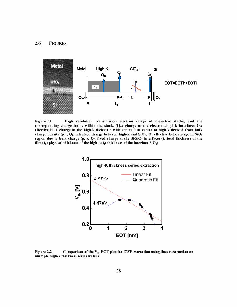
28
2.6 FIGURES
Figure 2.1 High resolution transmission electron image of dielectric stacks, and the corresponding charge terms within the stack. (Qm: charge at the electrode/high-k interface; Qb: effective bulk charge in the high-k dielectric with centroid at center of high-k derived from bulk charge density (ρb); Qi: interface charge between high-k and SiO2; Q: effective bulk charge in SiO2 region due to bulk charge (ρox); Qf: fixed charge at the Si/SiO2 interface) (t: total thickness of the film; th: physical thickness of the high-k; ti: thickness of the interface SiO2)
0 1 2 3 40.2
0.4
0.6
0.8
1.0
4.47eV
Linear Fit Quadratic Fit
V fb [V
]
EOT [nm]
high-K thickness series extraction
4.97eV
Figure 2.2 Comparison of the Vfb-EOT plot for EWF extraction using linear extraction on multiple high-k thickness series wafers.
0 th tti
ρρρρb
QbQi Qf
Qm Qs
High-K SiO2Metal Si
EOT=EOTh+EOTiQ
ρρρρi
0 th tti
ρρρρb
QbQi Qf
Qm Qs
High-K SiO2Metal Si
EOT=EOTh+EOTi
0 th tti
ρρρρb
QbQi Qf
Qm Qs
High-K SiO2Metal Si
EOT=EOTh+EOTiQ
ρρρρi
Metal
Si
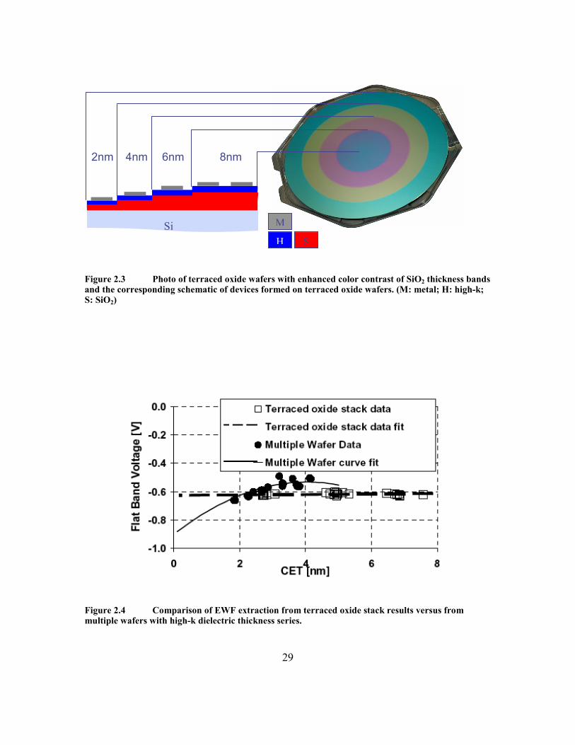
29
Figure 2.3 Photo of terraced oxide wafers with enhanced color contrast of SiO2 thickness bands and the corresponding schematic of devices formed on terraced oxide wafers. (M: metal; H: high-k; S: SiO2)
Figure 2.4 Comparison of EWF extraction from terraced oxide stack results versus from multiple wafers with high-k dielectric thickness series.
8nm 6nm 4nm 2nm
Si M
SH
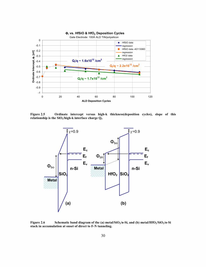
30
Figure 2.5 Ordinate intercept versus high-k thickness(deposition cycles), slope of this relationship is the SiO2/high-k interface charge Qi.
SiO2
n-Si
Metal
Φbo
Ec
Ev
Ef
χ=0.9
(a)
SiO2 HfO2
n-Si Metal
Φbh
Φbo
Ec
Ev
Ef
χ=0.9
(b)
Figure 2.6 Schematic band diagram of the (a) metal/SiO2/n-Si, and (b) metal/HfO2/SiO2/n-Si stack in accumulation at onset of direct to F-N tunneling.
ΦΦΦΦi vs. HfSiO & HfO2 Deposition Cycles
-1
-0.9
-0.8
-0.7
-0.6
-0.5
-0.4
-0.3
-0.2
-0.1
0
0 20 40 60 80 100 120ALD Deposition Cycles
Ord
inat
e In
terc
ept,
ΦΦ ΦΦi [
eV]
HfSiO dataregressionHfSiO data -4011306DregressionHfO2 dataregressionQi/q ~ 1.6x10¹² /cm2
Qi/q ~ 1.7x10¹² /cm2
Gate Electrode: 100Å ALD TiN/polysilicon
Qi/q ~ 2.2x10¹² /cm2
Lot 4081703
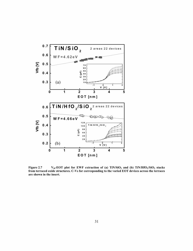
31
Figure 2.7 Vfb-EOT plot for EWF extraction of (a) TiN/SiO2 and (b) TiN/HfO2/SiO2 stacks from terraced oxide structures. C-Vs for corresponding to the varied EOT devices across the terraces are shown in the insert.
0 1 2 3 4 5
0 .3
0 .4
0 .5
0 .6
0 .7
-1 0 1 21 02 03 04 05 06 07 0
C (p
F)
V [ V ]
T iN /S iO 2
T iN /S iO 2
W F = 4 .6 2 e V
Vfb
[V]
E O T [n m ]
2 a re a s 2 2 d e v ic e s
0 1 2 3 4 5
0 .2
0 .3
0 .4
0 .5
0 .6
- 1 0 1 2
2 0
4 0
6 0
8 0
1 0 0
1 2 0
C (
pF)
V [ V ]
T i N / H f O 2 / S i O 2
2 a re a s 2 2 d e v ic e s
T iN /H fO 2/S iO 2
Vfb
[V]
E O T [n m ]
W F = 4 .6 6 e V
(a)
(b)
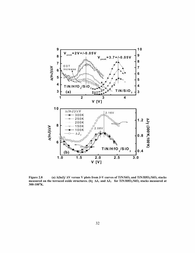
32
Figure 2.8 (a) ∆(lnJ)/ ∆V versus V plots from J-V curves of TiN/SiO2 and TiN/HfO2/SiO2 stacks measured on the terraced oxide structures. (b) ∆JV and ∆JT for TiN/HfO2/SiO2 stacks measured at 300-100oK.
3
4
5
6
7
8
9
1 2 3 43
4
56
7
89
1 0
T iN /S iO 2
V p e a k= 2 V + /-0 .0 5 VV p e a k= 3 .7 + /-0 .0 5 V
∆∆ ∆∆(( (( ln
J)/ ∆∆ ∆∆
V
V [V ]
T iN /H fO 2/S iO 2
E O T in c re a s e
1 .0 1 .5 2 .0 2 .5 3 .0
6
8
1 0
0 .4
0 .8
1 .2
∆∆ ∆∆ JT (300oK
,100oK
)
3 0 0 K 2 5 0 K 2 0 0 K 1 5 0 K 1 0 0 K
2 .1 6 V
∆∆ ∆∆(( ((ln
J)/ ∆∆ ∆∆
V
V [V ]
T iN /H fO2/S iO
2
2 .0 8 V
∆ ( ln J ) /∆ V
∆ J T
(a)
(b)
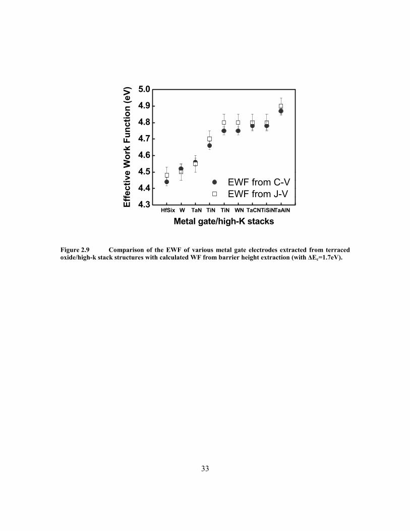
33
HfSix W TaN TiN TiN WN TaCNTiSiNTaAlN4.3
4.4
4.5
4.6
4.7
4.8
4.9
5.0
EWF from C-V EWF from J-V
Effe
ctiv
e W
ork
Func
tion
(eV)
Metal gate/high-K stacks
Figure 2.9 Comparison of the EWF of various metal gate electrodes extracted from terraced oxide/high-k stack structures with calculated WF from barrier height extraction (with ∆Ec=1.7eV).
34
2.7 REFERENCES [1] D. V. Lang, Thermally Stimulated Relaxation in Solids, vol. 37. Berlin: Springer,
1979. [2] R. Jha, J. Gurganos, Y. H. Kim, R. Choi, J. Lee, and V. Misra, "A capacitance-
based methodology for work function extraction for metals on high-k," IEEE Electron Device Letter, vol. 25, pp. 420-423, 2004.
[3] P. Majhi, H. C. Wen, H. Alshareef, K. Choi, R. Harris, P. Lysaght, H. Luan, Y. Senzaki, S. C. Song, B. H. Lee, and C. Ramiller, "Evaluation and integration of metal gate electrodes for future generation dual metal CMOS," Integrated Circuit Design and Technology, 2005. ICICDT 2005. 2005 International Conference on, pp. 69-72, 2005.
[4] H. C. Wen, R. N. Choi, G. A. Brown, T. Boscke, K. Matthews, H. R. Harris, K. Choi, H. N. Alshareef, H. F. Luan, G. Bersuker, P. Majhi, D. L. Kwong, and B. H. Lee, "Comparison of effective work function extraction methods using capacitance and current measurement techniques," Ieee Electron Device Letters, vol. 27, pp. 598-601, 2006.
[5] J. R. Hauser and K. Ahmed, "Characterization of Ultra-Thin Oxides Using Electrical C-V and I-V Measurements," Characterization and Metrology for ULSI Technology: 1998 International Conference, vol. 449, pp. 235-239, 1998.
[6] G. Brown, G. Smith, J. Saulters, K. Matthews, H. C. Wen, P. Majhi, and B. H. Lee, "An Improved Methodology for Gate Electrode Work Function Extraction in SiO2 and High-k Gate Stack Systems Using Terraced Oxide Structures," IEEE SISC conference, 2004.
[7] H. N. Alshareef, Z. Zhang, P. Majhi, G. Brown, P. Zeitzoff, H. Huff, and B. H. Lee, "Gate electrode development for dual metal-gate CMOS applications," in Future Fab, vol. 19, 2005, pp. 91-93.
[8] G. D. Wilk, M. L. Green, M.-Y. Ho, B. W. Busch, T. W. Sorsch, F. P. Klemens, B. Brijs, R. B. van Dover, A. Kornblit, T. Gustafsson, E. Garfunkel, S. Hillenius, D. Monroe, P. Kalavade, and J. M. Hergenrother, "Improved film growth and flatband voltage control of ALD HfO/sub 2/ and Hf-Al-O with n/sup +/ poly-Si gates using chemical oxides and optimized post-annealing," presented at VLSI Technology, 2002. Digest of Technical Papers. 2002 Symposium on, 2002.
[9] C. C. Hobbs, L. .Fonseca, A. Knizhnik, V. Dhandapani, S. B. Samavedam, W. J. Taylor, J. M. Grant, L. G. Dip, D. H. Triyoso, R. I. Hegde, D. C. Gilmer, R. Garcia, D. Roan, M. L. Lovejoy, R. S. Rai, E. A. Hebert, H.-H. Tseng, S. G. H. Anderson, B. E. White, and P. J. Tobin, "Fermi-Level Pinning at the Polysilicon/Metal–Oxide Interface—Part II," IEEE Transactions on Electron Devices, vol. 51, pp. 978-984, 2004.
[10] S. Zafar, C. Cabral, A. R., and A. Callegari, "A method for measuring barrier heights, metal work functions and fixed charge densities in metal/SiO2/Si capacitors," Applied Physics Letters, vol. 80, pp. 4858-4860, 2002.
35
[11] S. Zafar, E. Cartier, and E. P. Gusev, "Measurement of barrier heights in high permittivity gate dielectric films," Applied Physics Letters, vol. 80, pp. 2749-2751, 2002.
[12] S. Zafar, V. Narayanan, A. Callegari, F. R. McFeely, P. Jamison, E. Gusev, C. Cabral, and R. Jammy, "HfO/sub 2//metal stacks: determination of energy level diagram, work functions & their dependence on metal deposition," VLSI Technology, 2005. Digest of Technical Papers. 2005 Symposium on, pp. 44-45, 2005.
[13] T. Hori, Gate Dielectrics and MOS ULSI Principles, Technologies and Application: Springer-Verlag Berlin Heidelberg, 1997.
[14] J. Robertson, "Band offsets of wide-band-gap oxides and implications for future electronic devices," presented at Papers from the international conference on silicon dielectric interfaces, 2000.
[15] A. A. Demkov, L. R. C. Fonseca, E. Verret, J. Tomfohr, and O. F. Sankey, "Complex band structure and the band alignment problem at the Si--high-k dielectric interface," Physical Review B (Condensed Matter and Materials Physics), vol. 71, pp. 195306, 2005.
[16] A. S. Grove, Physics and Technology of Semiconductor Devices. New York: Wiley, 1967.
[17] P. Majhi, H.-C. Wen, K. Choi, H. Alshareef, C. Huffman, and B. H. Lee, "A systematic study of the influence of nitrogen in tuning the effective work function of nitrided metal gates," presented at VLSI Technology, 2005. (VLSI-TSA-Tech). 2005 IEEE VLSI-TSA International Symposium on, 2005.
36
CHAPTER 3
DECOUPLING THE FERMI LEVEL PINNING EFFECT IN METAL GATE AND HIGH-κκκκ STACK
3.1 MOTIVATION
The Fermi-level (Ef) pinning effect between metal/high-k, had widely been used
to explain why the effective work function (EWF) of metal electrodes on high-k would be
different from its bulk value, and on SiO2 [1-3] The metal induced gap states (MIGS)
model explains the Ef will pin toward the charge neutrality level in the high-k and
become an intrinsic limitation for obtaining band edge EWF metal electrodes on high-k
dielectrics [4, 5]. Many literature reports suggest the experimental EWF results agree
with the MIGS predictions [1, 6], however, recently detailed studies of many of these
electrode systems suggest contributions from extrinsic factors. Extrinsic contributions
include: defect states induced by the electrode (oxygen vacancy model)[7-9], chemical
reduction of the high-k interface [10], or material characteristic changes in the electrode
[11, 12]. Dr. Shiraishi has proposed a grand theory for metal EWF based on a
combination of the MIGS concept (intrinsic) as well as the O vacancy contributions
(extrinsic), where the charge neutrality level changes depending on the metal system [13].
The result of such extrinsic factors should be acknowledged as Ef deviation, and not
“pinning” since Ef is no longer pinned to an intrinsic value, however the term Ef-pinning
is loosely used for stacks with different EWF on high-k. The advances in this field now
questions whether experimental results correlate to the initial MIGS model after
separating out extrinsic contributions, and whether an intrinsic limitation does exist for
EWF tuning on high-k.
37
To enable study of the real intrinsic contribution in EWF on high-k, systematic
studies in understanding true factors contributing to EWF on high-k dielectrics, as well as
separation of extrinsic effects (such as interfacial reaction, interdiffusion, especially the
role of interfaces, etc.) is needed. Since any deviation of EWF on high-k from SiO2
maybe perceived as Ef-pinning effects, inaccurate determination of EWF may induce
complications in the observations. Thus through accurate EWF extraction by the terraced
oxide method, comparison with the MIGS intrinsic model is performed to address the
intrinsic contributions of Ef-pinning.
3.2 MODELS ON INTRINSIC FACTORS OF EWF CONTROL
3.2.1 MIGS model for Ef-pinning
The metal induced gap states (MIGS) model has been proposed to be the intrinsic
component inducing Ef-pinning [4, 5]. The MIGS model suggests due to the presence of
intrinsic interface states, as the electrode is in contact with a dielectric, interfacial charge
exchange will occur causing the metal Ef to shift toward a characteristic energy level in
dielectric, the charge neutrality level (ΦCNL) (Figure 3.1). The ΦCNL is the location of the
highest occupied surface state in the dielectric band gap. The degree of the metal Ef level
shift depends on the pinning strength of the dielectric, the Schottky pinning parameter S ,
and thus the EWF (Φm,eff) is related to its vacuum work function (Φm) with the
relationship:
)( ,, CNLvaccmCNLeffm S Φ−Φ+Φ=Φ
The S parameter is dependent on the electronic component of the dielectric constant ε∞
dielectric characteristic and follows the equation:
2)1(1.011
−+=
∞εS
38
This suggests dielectrics with higher dielectric constants will have greater degree of
pinning, and will especially limit the choices of obtaining band edge EWF on high-k
dielectrics.
3.2.2 Experimental results in literature
Experimental EWF results in the literature have shown reasonable correlation
(Figure 3.2) [3, 4] with the MIGS prediction, and empirically calculated the ΦCNL of
HfO2 to be ~4.4eV. However, other results still exhibit a reasonable degree of EWF span
for Ti and Pt electrodes [13, 14]. Further investigation has shown electrodes with high
WF such as Pt, Re and Ru, exhibit much lower EWF on high-k [7-9, 11]. Comparison of
the EWF reduction for Pt versus the MIGS model prediction give a pinning factor
S=0.15, or 0.25 much higher than the intrinsic limitation of S=0.53 for HfO2 [8], possibly
due to extrinsic effects. Whether an accurate EWF extraction was performed will also
complicate the learning. Therefore, results in the literature may not be completely
explained by MIGS, and require careful analysis.
3.3 SEPARATION OF EXTRINSIC CONTRIBUTIONS
3.3.1 Interface chemical reaction, materialistic change in the electrode
A material system often used as an example of Ef-pinning on high-k is the Ru
metal, where on SiO2 high EWF is observed (5eV), while low WF is obtained on high-k
(4.6eV) (Figure 3.3(a)). Through a systematic analysis of the reaction mechanism at the
Ru dielectric interface [15], we find that Ru easily reacts with SiO2 and is more thermally
stable on Hf-based high-k. The formation of a RuOx like interface at the Ru/SiO2
interface is the source of the high EWF, since RuO2 is a high vacuum WF material. The
reaction is easily observed at elevated temperatures through a high resolution TEM
39
image, shown in Figure 3.4(b)[12]. Cross comparison of EWF results with intentional
RuOx deposition on high-k also reproduces the high 5eV EWF. This observation is
consistent with that reported by Panstiano et al. [11]; when annealing Ru in an oxidizing
environment, a higher EWF is shown on both high-k and SiO2. This suggests the
modification induced at the metal/dielectric interface is due to materialistic changes, like
oxidation in the electrode, and not dominated by Ef-pinning like effects..
Another more subtle interface chemical reaction is reported for high WF Pt and
Re electrodes (5.6 and 5.3eV bulk WF, respectively). Reduction of the dielectric is
observed by X-ray photoemission spectroscopy where the formation of a Hf sub-oxide
peak is observed after annealing a fully oxidized HfO2/Re or Pt stack [10]. Although this
reaction is thermal dynamically unfavorable, but a catalytic decomposition of HfO2 due
to hydroxyls (OH impurities) will enhance the decomposition of HfO2 by stabilizing the
formation of charged O vacancies.
↑++→+ − OxHMeHfOMeHHfO xx 2222
This reaction is also coupled with a electrostatic shift in the Hf 4f and O 1s core level
bonds due to the charged defects formed, and has been suggested to induce Ef-pinning
with these states (O vacancies), driving the Ef toward the conduction band and reduce the
EWF observed by C-V measurements.
3.3.2 Extrinsic defect states: Oxygen vacancy model and interface dipole formation
High WF electrodes such as Pt and Re are reported to exhibit much lower EWF
on high-k due to formation of a interface dipole at the metal/high-k interface. Due to the
higher electronegativity of these metals (Pt: 2.28) versus Hf (1.3), a interface bonding
configuration of Pt-Hf or Pt-Vo(oxygen vacancy)-Hf could result in electron transfer to Pt
40
side and thus form a dipole, and reduce the EWF (Figure 3.4(a)). Through process
condition controls, passivation of this interface with more electronegative O atoms
through O2 annealing has shown to increase the EWF after reducing the concentration of
such defects (Figure 3.4(b)). These learning also supports that connection with oxygen
vacancies in the dielectric is the source of the interface charge exchange [7-9].
3.4 COMBINATION OF CHARGE NEUTRALITY MODEL AND OXYGEN VACANCY MODEL
An “general theory” of metal EWF based on a combination of the MIGS ΦCNL
concept (intrinsic) as well as the O vacancy contributions (extrinsic) is proposed to apply
for all electrodes [13]. It suggest a new ΦCNL which is the energy level where interfacial
electron transfer is cancelled with interfacial hybridization, and thus depends on the
amount of metal (M)-Hf versus metal-O interactions. As described in Figure 3.5, n-type
metals with high O reactivity, mainly consist of M-O-Hf bonds; while in p-type metals
M-Hf bonds dominate. The ΦCNL thus follows the below relationship and will depend on
the electrode interfacial bond number (number of metal-Hf bonds |tM-Hf| versus metal-O-
Hf bonds |tM-O|, and the density of occupied and unoccupied states in the metal (Docc,
Dunocc):
Therefore using the MIGS model to predict the EWF on high-k, results will be dependent
on the electrode material, and the EWF vs bulk WF plot should not follow the traditional
linear relationship (Section 3.2.1) due to the varied ΦCNL.
41
3.5 ADDRESSING INTRINSIC FACTORS OF FERMI-LEVEL PINNING: COMPARISON OF TERRACED OXIDE EWF RESULTS WITH MIGS MODEL
3.5.1 Approach for study and experimental details
An accurate and systematic study of the EWF is required to identify the existence
of an intrinsic contribution on EWF. Therefore, the terraced oxide method is used to
eliminate ambiguities in EWF extraction on all samples studied. To separate out extrinsic
contributions such as interfacial instability/reaction with the dielectrics, the study is
focused on electrodes with high thermal stability with the high-k dielectric, such as
metal-nitrides [16]. All samples have gone through a thermal budget to guarantee
interfacial chemical bonding (the M-Hf or M-O-Hf bond formation) between the
metal/high-k for the aforementioned extrinsic charge states to apply, and prevent the
formation of a physically-absorbed (physi-sorbed) interface.
3.5.2 Comparison of EWF with MIGS model
Using the assumption that the metal EWF on SiO2 equals, or has a 1:1 correlation
with the vacuum WF [4], we plot in Figure 3.6 the extracted EWF of a series of
electrodes on HfO2 and HfSiOx (20% SiO2) versus the EWF on SiO2. Also with
comparison with the MIGS trend line of S=0.53, and the 1:1 ideal correlation of S=1. The
EWF results for HfO2 and HfSiOx both show a near parallel relationship to the 1:1 ideal
slope, with a ~100meV shift increase, possibly due to the stack charges described in
Chapter 2.3.1. This parallel relationship suggests for thermally stable electrodes, intrinsic
Ef-pinning is not the dominant factor controlling EWF, and EWF is not limited by the
MIGS trend line. Interestingly, the near linear extraction of EWF results (EWF results for
metals fall on same trend line, and not impacted by varied ΦCNL) may also suggest the
42
varied ΦCNL model described in Section 3.4 does not apply for these thermally stable
electrodes.
3.6 REVISION OF MIGS THEORY
Due to discrepancy in experimental results in literature, Robertson et al. [17]
reported ideal modeling of the metal/high-k barrier height to estimate the EWF. They
propose the metal/high-k barrier height should be highly dependent on the metal/high-k
interface configurations. The HfO2 surface could be terminated with the polar-O (100)
interface and has only M-O bonds, or exhibit a non-polar (110) interface with both M-O
and M-M’ bonds. It is believed that the most stable interface is metal system dependent
[13], but in all will depend on the O chemical potential. Barrier height calculations can be
modeled through CASTEP pseudo-potential total energy calculations, where the valance
band offset (VBO) between is obtained from modeling of the valance band density of
states. VBO is found to be larger for (110) than (100) due to interface dipole (Figure 3.7).
Also, for given interface, slope S~1. Hence metal’s EWF in principle should span Si gap.
However, if a preferred orientation exists for a certain metal electrode to achieve stability
((100) for n-metals, (110) for p-metals), the VBO trend may follow the dashed line in
Figure 3.7, and appear to reduce the slope to S~0.5. This could be consistent with the
experimental EWF observations, and give the impression of an shallow slope. However,
this suggests the MIGS model should not be universal, and cannot be applied to explain
all metal EWF simply from intrinsic high-k interface states. Experimentally, the high-k
after high thermal budgets are normally monoclinic with a preferred phase of (111) [18],
and more modelling work needs to be performed to accurately predict the VBO for series
of metal gate electrodes.
43
3.7 CONCLUSIONS
Through systematic discussion of literature reported models, and avoiding the
pitfalls in the analysis. Our observations suggests after separating extrinsic factors, an
intrinsic Ef-pinning should not limit EWF tuning on high-k. Figure 3.8 shows the EWF
for vast material systems investigated with the terraced oxide method, and a similar range
in EWF change on high-k and SiO2 is consistently observed. Revision of the MIGS
theory by Robertson et al. also agrees that the metal WF should in theory span the total Si
band gap.
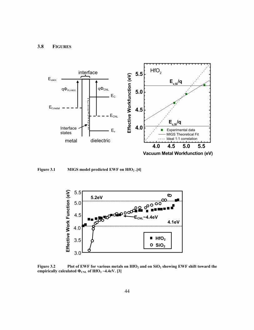
44
3.8 FIGURES
Figure 3.1 MIGS model predicted EWF on HfO2 .[4]
Figure 3.2 Plot of EWF for various metals on HfO2 and on SiO2 showing EWF shift toward the empirically calculated ΦCNL of HfO2 ~4.4eV. [3]
5.5
4.5
3.5
3.0
4.0
5.0
Effe
ctiv
e W
ork
Func
tion
(eV)
HfO2
SiO2
5.2eV
4.1eV ECNL~4.4eV
4.0 4.5 5.0 5.5
4.0
4.5
5.0
5.5
Ec,Si/q
Experimental data MIGS Theoretical Fit Ideal 1:1 correlation
Ev,Si/q
Effe
ctiv
e W
orkf
unct
ion
(eV)
Vacuum Metal Workfunction (eV)
HfO2
metal
interface
dielectric
Evacc
Ef,metal
qΦm,vacc
Interface states
ECNL
EC
Ev
qΦCNL
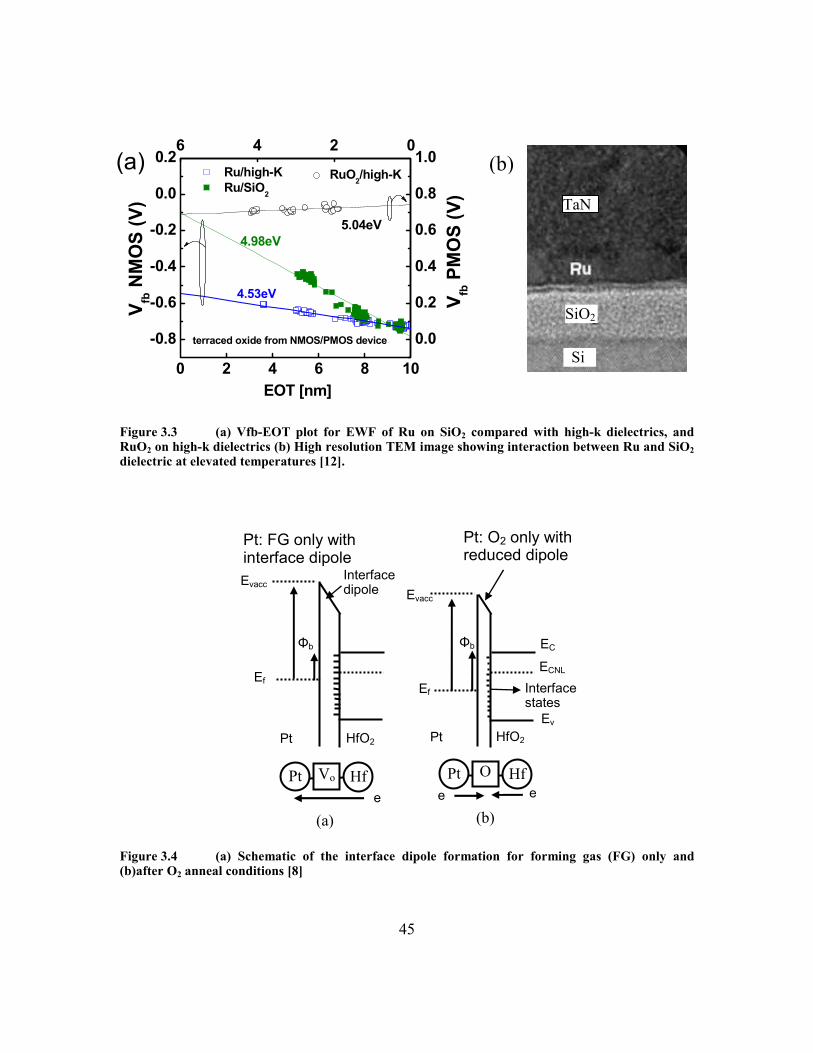
45
Figure 3.3 (a) Vfb-EOT plot for EWF of Ru on SiO2 compared with high-k dielectrics, and RuO2 on high-k dielectrics (b) High resolution TEM image showing interaction between Ru and SiO2 dielectric at elevated temperatures [12].
Figure 3.4 (a) Schematic of the interface dipole formation for forming gas (FG) only and (b)after O2 anneal conditions [8]
Pt: FG only with interface dipole
Pt HfO2
Evacc
Ef
Φb
Interface dipole
Pt HfVo e
Pt: O2 only with reduced dipole
Pt HfO2
Evacc
Ef
Φb
Interface states
ECNL
EC
Ev
Pt HfOe e
(a) (b)
0 2 4 6 8 10
-0.8
-0.6
-0.4
-0.2
0.0
0.26 4 2 0
0.0
0.2
0.4
0.6
0.8
1.0 V
fb N
MO
S (V
)
5.04eV
4.53eV
Ru/high-K Ru/SiO2
EOT [nm]
terraced oxide from NMOS/PMOS device
4.98eV
Vfb
PM
OS
(V)
RuO2/high-K(a) (b)
TaN
SiO2
Si
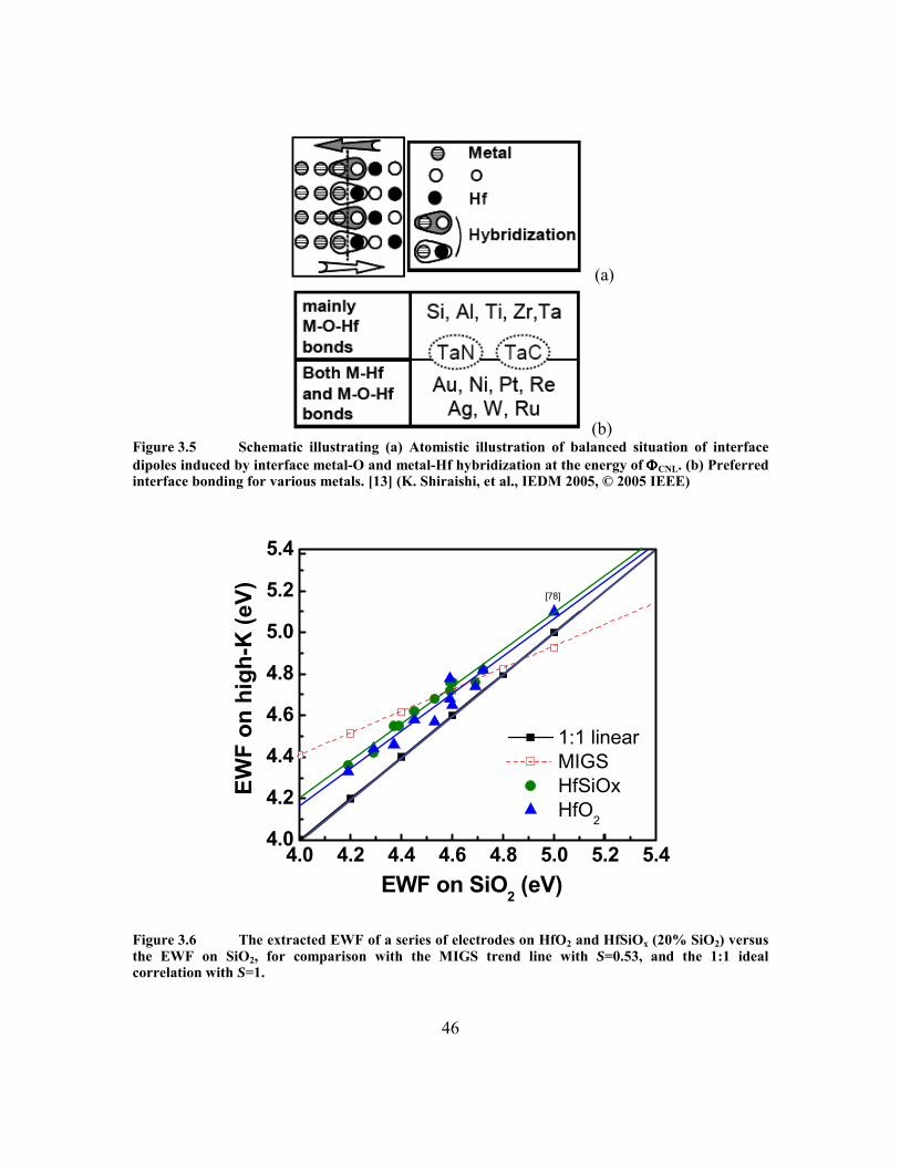
46
(a)
(b) Figure 3.5 Schematic illustrating (a) Atomistic illustration of balanced situation of interface dipoles induced by interface metal-O and metal-Hf hybridization at the energy of ΦΦΦΦCNL. (b) Preferred interface bonding for various metals. [13] (K. Shiraishi, et al., IEDM 2005, © 2005 IEEE)
Figure 3.6 The extracted EWF of a series of electrodes on HfO2 and HfSiOx (20% SiO2) versus the EWF on SiO2, for comparison with the MIGS trend line with S=0.53, and the 1:1 ideal correlation with S=1.
4.0 4.2 4.4 4.6 4.8 5.0 5.2 5.44.0
4.2
4.4
4.6
4.8
5.0
5.2
5.4
1:1 linear MIGS HfSiOx HfO
2
EWF
on h
igh-
K (e
V)
EWF on SiO2 (eV)
[78]
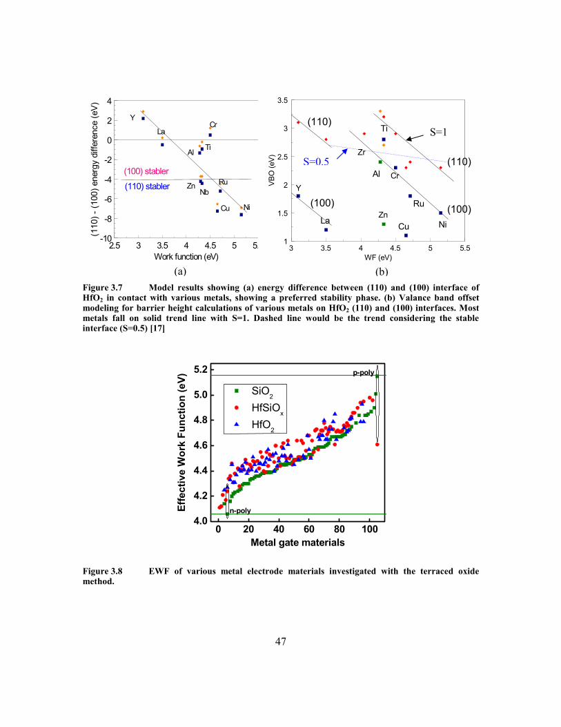
47
Figure 3.7 Model results showing (a) energy difference between (110) and (100) interface of HfO2 in contact with various metals, showing a preferred stability phase. (b) Valance band offset modeling for barrier height calculations of various metals on HfO2 (110) and (100) interfaces. Most metals fall on solid trend line with S=1. Dashed line would be the trend considering the stable interface (S=0.5) [17]
0 20 40 60 80 1004.0
4.2
4.4
4.6
4.8
5.0
5.2 p-poly
SiO2
HfSiOx
HfO2
Effe
ctiv
e W
ork
Func
tion
(eV)
Metal gate materials
n-poly
Figure 3.8 EWF of various metal electrode materials investigated with the terraced oxide method.
2.5 3 3.5 4 4.5 5 5.5-10
-8
-6
-4
-2
0
2
4
Work function (eV)
(110
) - (1
00) e
nerg
y di
ffere
nce
(eV)
Ni
Al
Y
La
Cu
Ti
Cr
RuZnNb
(110) stabler
(100) stabler
3 3.5 4 4.5 5 5.51
1.5
2
2.5
3
3.5
WF (eV)
VBO
(eV)
La Ni
Cr
Ru
Cu
Al
Ti
Y
Zn
Zr
(100)
(110)
(100)
(110)S=1
S=0.5
(a) (b)
48
3.9 REFERENCES [1] S. B. Samavedam, L. B. La, P. J. Tobin, B. White, C. Hobbs, L. R. C. Fonseca, A.
A. Demkov, J. Schaeffer, E. Luckowski, A. Martinez, M. Raymond, D. Triyoso, D. Roan, V. Dhandapani, R. Garcia, S. G. H. Anderson, K. Moore, H. H. Tseng, C. Capasso, O. Adetutu, D. C. Gilmer, W. J. Taylor, R. Hegde, and J. Grant, "Fermi level pinning with sub-monolayer MeOx and metal gates [MOSFETs]," Electron Devices Meeting, 2003. IEDM '03 Technical Digest. IEEE International, pp. 13.1.1-13.1.4, 2003.
[2] C. Ren, H. Y. Yu, J. F. Kang, Y. T. Hou, M. E. Li, W. D. Wang, D. S. H. Chan, and D. L. Kwong, "Fermi-level pinning induced thermal instability in the effective work function of TaN in TaN/SiO2 gate stack," Ieee Electron Device Letters, vol. 25, pp. 123-125, 2004.
[3] J. Schaeffer, C. Capasso, L. R. C. Fonseca, S. Samavedam, L. B. La, J. Smith, S. Dakshina-Murthy, D. C. Gilmer, Luckowski, Y. Liang, S. Kalpat, B. Adetutu, H. H. Tseng, Y. Shiho, A. Demkov, R. Hegde, W. J. Taylor, R. Gregory, J. Jiang, E. Luckowski, M. Raymond, K. Moore, D. Triyoso, D. Roan, B. White, and P. J. Tobin, "Challenges for the integration of metal gate electrodes," IEEE Electron Device Meeting, 2004.
[4] Y. C. Yeo, T. J. King, and C. M. Hu, "Metal-dielectric band alignment and its implications for metal gate complementary metal-oxide-semiconductor technology," Journal of Applied Physics, vol. 92, pp. 7266-7271, 2002.
[5] Y. C. Yeo, P. Ranade, T. J. King, and C. M. Hu, "Effects of high-kappa gate dielectric materials on metal and silicon gate work functions," Ieee Electron Device Letters, vol. 23, pp. 342-344, 2002.
[6] H. Y. Yu, C. Ren, Y. C. Yeo, J. F. Kang, X. P. Wang, H. H. H. Ma, M. F. Li, D. S. H. Chan, and A. L. Kwong, "Fermi pinning-induced thermal instability of metal-gate work functions," Ieee Electron Device Letters, vol. 25, pp. 337-339, 2004.
[7] E. Cartier, F. R. McFeely, V. Narayanan, P. Jamison, B. P. Linder, M. Copel, V. K. Paruchuri, V. S. Basker, R. Haight, D. Lim, R. Carruthers, T. Shaw, M. Steen, J. Sleight, J. Rubino, H. Deligianni, S. Guha, R. Jammy, and G. Shahidi, "Role of oxygen vacancies in V/sub FB//V/sub t/ stability of pFET metals on HfO/sub 2/," VLSI Technology, 2005. Digest of Technical Papers. 2005 Symposium on, pp. 230-231, 2005.
[8] J. K. Schaeffer, L. R. C. Fonseca, S. B. Samavedam, Y. Liang, P. J. Tobin, and B. E. White, "Contributions to the effective work function of platinum on hafnium dioxide," Applied Physics Letters, vol. 85, pp. 1826-1828, 2004.
[9] Y. Liang, J. Curless, C. J. Tracy, D. C. Gilmer, J. K. Schaeffer, D. H. Triyoso, and P. J. Tobin, "Interface dipole and effective work function of Re in Re/HfO[sub 2]/SiO[sub x]/n-Si gate stack," Applied Physics Letters, vol. 88, pp. 072907, 2006.
49
[10] M. Copel, R. P. Pezzi, D. Neumayer, and P. Jamison, "Reduction of hafnium oxide and hafnium silicate by rhenium and platinum," Applied Physics Letters, vol. 88, pp. 072914, 2006.
[11] L. Pantisano, T. Schram, Z. Li, J. G. Lisoni, G. Pourtois, S. D. Gendt, D. P. Brunco, A. Akheyar, V. V. Afanas'ev, S. Shamuilia, and A. Stesmans, "Ruthenium gate electrodes on SiO[sub 2] and HfO[sub 2]: Sensitivity to hydrogen and oxygen ambients," Applied Physics Letters, vol. 88, pp. 243514, 2006.
[12] H. N. Alshareef, H. C. Wen, H. Luan, K. Choi, H. R. Harris, Y. Senzaki, P. Majhi, B. H. Lee, B. Foran, and G. Lian, "Temperature dependence of the work function of ruthenium-based gate electrodes," Thin Solid Films, vol. article in press Temperature dependence of the work function of ruthenium-based gate electrodes, 2006.
[13] K. Shiraishi, Y. Akasaka, S. Miyazaki, T. Nakayama, T. Nakaoka, G. Nakamura, K. Torii, H. Furutou, A. Ohta, P. Ahmet, K. Ohmori, H. Watanabe, T. Chikyo, M. L. Green, Y. Nara, and K. Yamada, "Universal theory of workfunctions at metal/Hf-based high-k dielectrics interfaces - guiding principles for gate metal selection," Electron Devices Meeting, 2005. IEDM Technical Digest. IEEE International, pp. 39-42, 2005.
[14] H. Yang, Y. Son, S. Baek, H. Hwang, H. Lim, and H.-S. Jung, "Ti gate compatible with atomic-layer-deposited HfO[sub 2] for n-type metal-oxide-semiconductor devices," Applied Physics Letters, vol. 86, pp. 092107, 2005.
[15] H. C. Wen, P. Lysaght, H. N. Alshareef, C. Huffman, H. R. Harris, K. Choi, Y. Senzaki, H. Luan, P. Majhi, B. H. Lee, M. J. Campin, B. Foran, G. D. Lian, and D. L. Kwong, "Thermal response of Ru electrodes in contact with SiO2 and Hf-based high-k gate dielectrics," Journal of Applied Physics, vol. 98, 2005.
[16] H.-C. Wen, K. Choi, P. Majhi, H. Alshareef, C. Huffman, and B. H. Lee, "A systematic study of the influence of nitrogen in tuning the effective work function of nitrided metal gates," presented at VLSI Technology, 2005. (VLSI-TSA-Tech). 2005 IEEE VLSI-TSA International Symposium on, 2005.
[17] J. Robertson, "Invited talk at EMRS 2006," 2006. [18] G. Pant, A. Gnade, M. J. Kim, R. M. Wallace, B. E. Gnade, M. A. Quevedo-
Lopez, and P. D. Kirsch, "Effect of thickness on the crystallization of ultrathin HfSiON gate dielectrics," Applied Physics Letters, vol. 88, pp. 032901, 2006.
50
CHAPTER 4
UNDERSTANDING FACTORS CONTRIBUTING TO THE EWF OF METAL ELECTRODES
4.1 INTRODUCTION
The EWF of metal gate electrodes ideally should only be dependent on
bulk/vacuum work function of the materials. However, we’ve observed the relationship is
not so ideal in a MOS structure. The concern of WF deviation due to inaccurate EWF
extraction had been addressed in Chapter 2, where the terraced oxide method is proposed
for EWF extraction on high-k. In Chapter 3, an intrinsic Ef-pinning effect is found not to
limit EWF tunability on high-k, and any Ef-pinning effects has been clarified to be
mainly extrinsic. Extrinsic contributions from the overall gatestack have been found to
impact the overall measured EWF due to interdiffusion/reaction between layers,
processing conditions in the fabrication of the devices, or induce stack charges. Such
complexity has obstructed the identification of band-edge metal electrode systems, and
the understanding of EWF control on high-k dielectrics. From an engineering
perspective, it is critical to perform a systematic study of key factors effective in EWF
tuning, in effort to identify material systems and integration pathways that hold promise
in engineering metal-high-k stacks using the conventional gate first process.
Breakdown of the Vfb equation below has separated contributions to Vfb (and the
extracted EWF) into the following factors:
ox
f
ox
oxhb
ox
imsfb
EOTQQDEOThEOThQV
εεεερ
ε*
)*2
*)/(**(
2' −∆+∆+−−Φ=
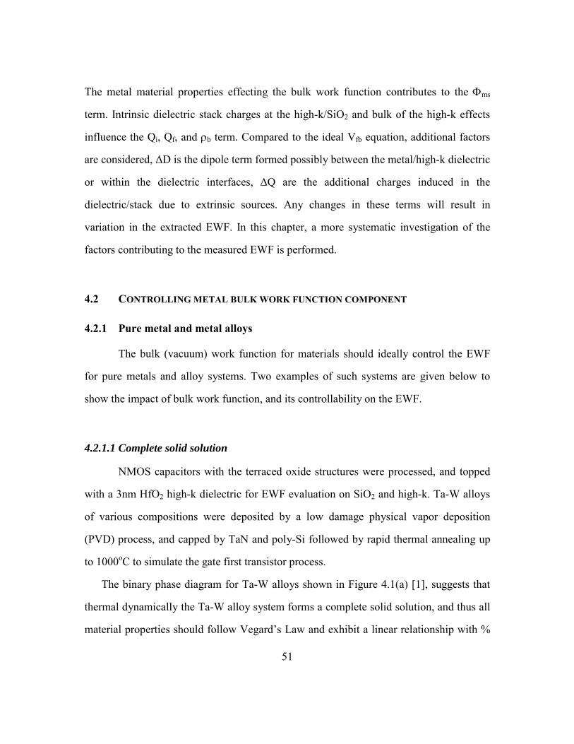
51
The metal material properties effecting the bulk work function contributes to the Φms
term. Intrinsic dielectric stack charges at the high-k/SiO2 and bulk of the high-k effects
influence the Qi, Qf, and ρb term. Compared to the ideal Vfb equation, additional factors
are considered, ∆D is the dipole term formed possibly between the metal/high-k dielectric
or within the dielectric interfaces, ∆Q are the additional charges induced in the
dielectric/stack due to extrinsic sources. Any changes in these terms will result in
variation in the extracted EWF. In this chapter, a more systematic investigation of the
factors contributing to the measured EWF is performed.
4.2 CONTROLLING METAL BULK WORK FUNCTION COMPONENT
4.2.1 Pure metal and metal alloys
The bulk (vacuum) work function for materials should ideally control the EWF
for pure metals and alloy systems. Two examples of such systems are given below to
show the impact of bulk work function, and its controllability on the EWF.
4.2.1.1 Complete solid solution
NMOS capacitors with the terraced oxide structures were processed, and topped
with a 3nm HfO2 high-k dielectric for EWF evaluation on SiO2 and high-k. Ta-W alloys
of various compositions were deposited by a low damage physical vapor deposition
(PVD) process, and capped by TaN and poly-Si followed by rapid thermal annealing up
to 1000oC to simulate the gate first transistor process.
The binary phase diagram for Ta-W alloys shown in Figure 4.1(a) [1], suggests that
thermal dynamically the Ta-W alloy system forms a complete solid solution, and thus all
material properties should follow Vegard’s Law and exhibit a linear relationship with %
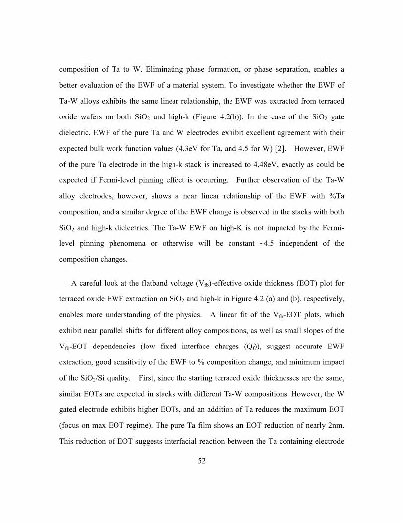
52
composition of Ta to W. Eliminating phase formation, or phase separation, enables a
better evaluation of the EWF of a material system. To investigate whether the EWF of
Ta-W alloys exhibits the same linear relationship, the EWF was extracted from terraced
oxide wafers on both SiO2 and high-k (Figure 4.2(b)). In the case of the SiO2 gate
dielectric, EWF of the pure Ta and W electrodes exhibit excellent agreement with their
expected bulk work function values (4.3eV for Ta, and 4.5 for W) [2]. However, EWF
of the pure Ta electrode in the high-k stack is increased to 4.48eV, exactly as could be
expected if Fermi-level pinning effect is occurring. Further observation of the Ta-W
alloy electrodes, however, shows a near linear relationship of the EWF with %Ta
composition, and a similar degree of the EWF change is observed in the stacks with both
SiO2 and high-k dielectrics. The Ta-W EWF on high-K is not impacted by the Fermi-
level pinning phenomena or otherwise will be constant ~4.5 independent of the
composition changes.
A careful look at the flatband voltage (Vfb)-effective oxide thickness (EOT) plot for
terraced oxide EWF extraction on SiO2 and high-k in Figure 4.2 (a) and (b), respectively,
enables more understanding of the physics. A linear fit of the Vfb-EOT plots, which
exhibit near parallel shifts for different alloy compositions, as well as small slopes of the
Vfb-EOT dependencies (low fixed interface charges (Qf)), suggest accurate EWF
extraction, good sensitivity of the EWF to % composition change, and minimum impact
of the SiO2/Si quality. First, since the starting terraced oxide thicknesses are the same,
similar EOTs are expected in stacks with different Ta-W compositions. However, the W
gated electrode exhibits higher EOTs, and an addition of Ta reduces the maximum EOT
(focus on max EOT regime). The pure Ta film shows an EOT reduction of nearly 2nm.
This reduction of EOT suggests interfacial reaction between the Ta containing electrode
53
and SiO2, where a high energy of oxide formation for Ta limits the thermal stability of Ta
on SiO2 dielectrics. Reduction of the SiO2 to form a TaOx-like interface, which has a
higher k value, could result in the EOT decrease. In this case, the EWF value of the
pure Ta electrode in the SiO2 dielectric stack is controlled by the interfacial reaction.
Physical observation of the interfacial reaction is shown in Figure 4.3(a), where an
interface is observed between the Ta and SiO2 region. W electrodes are known to be
thermally stable with SiO2 and do not exhibit the interfacial reaction. Based on the EOT
results, doping/alloying of Ta with W is shown to significantly suppress this interaction.
Interestingly, regardless of interfacial reaction, the EWF extracted is still consistent with
that expected from its bulk value, suggesting minimum impact of TaOx charges on Vfb.
Reduced EOT and interfacial interaction are not observed on the high-k dielectrics
(Figure 4.3(b)), suggesting better stability of the Ta to the high-k interface. The Ta-W
alloy regime also still exhibit the same degree of tunability as the SiO2 results. However,
degradation of the high-k due to Ta diffusion is shown in Figure 4.4, where the leakage
current densities of the Ta, Ta-W alloy, and W metal gate/high-k stacks are compared in
the thin EOT regime. The Ta gated stack has significantly higher leakage than the W or
Ta-W samples. No leakage degradation is observed for the alloys suggest the thermal
stability of a reactive electrode can be improved by alloying with more stable materials,
and may limit Ta diffusion. Ta diffusion into the high-k matrix could impact the Vfb
result by modulating the dielectric charge, and contribute to the ∆Q term in the Vfb
equation. This may explain the increased EWF for pure Ta. More careful characterization
of materials is needed to determine the interfacial reactions at the Ta-W alloy and high-k
dielectrics to separate the contributions of the electrode, metal/high-k interface, and
dielectric charge to the EWF.
54
The Ta-W alloy is an excellent system with which to demonstrate contributions to the
measured EWF by the bulk WF, interface reaction, and dielectric (charge) modulation.
4.2.1.2 Inter-metallic compounds
The novel Ru-Hf alloy system, with the combination of high work function Ru
(5.0eV) [3] and low work function Hf [2] is an example of materialistic phase control of
the EWF. The use of Hf based electrodes in conjunction with Hf based dielectrics is of
high interest from a material compatibility standpoint.
A fixed 40Å HfOx was deposited on varying thickness of SiO2 terraced oxide
wafer. The Ru-Hf metal electrodes were co-sputtered on these dielectric stacks, and
TiN/W was used as metal capping layers to form MOS capacitors. Ru-Hf alloys with
varying composition were processed by co-sputtering Ru and Hf. Figure 4.5 shows the
composition of Ru:Hf from Rutherford Backscattering Spectrometry (RBS)
measurements. The Ru:Hf ratio is shown to be dependent on the Ru:Hf power ratio, and
Ru% composition is tuned between 80~35%. However, since the phase stability diagram
does not show complete solid solubility (Figure 4.6) [1], X-ray diffraction was used to
study the phases for the varying compositions. Figure 4.7 is the X-ray diffraction pattern
for the RuHf (3:1), RuHf (1:1), and RuHf (1:3). The pattern for RuHf (3:1) indicates pure
Ru(111) (2θ~40.7o) peak overlapping a potential RuHf(110) (2θ~39.4o) peak. The
spectrum of the RuHf (1:1) clearly shows the formation of stoichiometric RuHf phase,
while the RuHf (1:3) shows a mix of RuHf and possible pure Hf which was oxidized to
form HfO2 at (2θ~28 o). Additionally, the spectrum indicates that the lattice spacing of the
RuHf is expanded, indicating the possibility of excess Hf inclusion in the RuHf phase.
The possibility of Hf inclusion provides the ability for additional Hf incorporation, and
thus more space for work function tunability via composition change. Figure 4.8(a) is the
55
Vfb-EOT plot for the various Ru-Hf alloy compositions. The extracted work function
values vary from 4.35 to 4.78 eV as the Ru content increases from 35% to 100%. NMOS
C-V curves for the different metal gates, clearly show that there is parallel shift in the
C-V (towards “n” type with increasing Hf), which is due to the shift in the effective work
function of the gate electrode. Figure 4.8(b) is the EWF summary versus various Ru
composition. Unlike the Ta-W system, the relationship is not linear, and is dominated by
the phase, thus separated into a Ru controlled, and RuHf alloy phase controlled regime,
consistent with the XRD phases. The range of EWF tunability of 400meV in this system
is highly attractive for dual WF metal electrodes [4]. However, due to thermal stability
concerns with the Ru as well as Hf material systems (Chapter 3), we can predict further
annealing will result in interface reactions and interface controlled EWF.
4.2.2 Metal nitrides and metal silicon nitrides
Although some as-deposited elemental metals do exhibit near band-edge work
function values, their tendency to react with the dielectrics has been limiting the thermal
stability of both n-type (ex. Ta) and p-type (ex. Ru, Pt) electrodes. Most of the low
workfunction materials (bulk form) are inherently reactive and hence cannot be used in
their pure forms. Addition of constituents stabilizes the material and provide improved
thermal stability. Certain additives to the metal, in particular, nitrogen (metal nitrides)
and/or Si (metal silicides, ternary metal-Si-N) have been evaluated, and metal nitrides or
silicides have been proposed to be preferred over pure metals as dual metal electrode
candidates [5-8]. Many groups studied a fixed composition of metal nitrides and reported
near mid-gap values for the EWF, and has postulated addition of N or Si to shift the EWF
toward mid-gap. However, a systematic study of the influence of these additions on the
effective work function of the candidate materials is lacking.
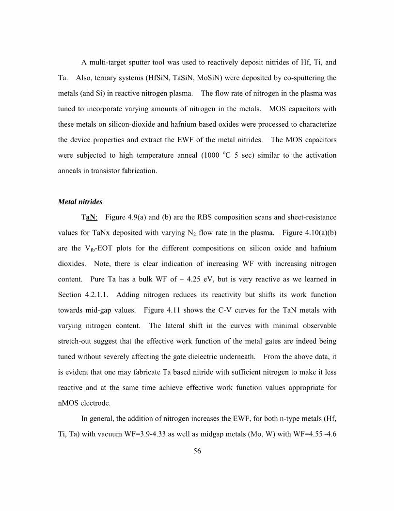
56
A multi-target sputter tool was used to reactively deposit nitrides of Hf, Ti, and
Ta. Also, ternary systems (HfSiN, TaSiN, MoSiN) were deposited by co-sputtering the
metals (and Si) in reactive nitrogen plasma. The flow rate of nitrogen in the plasma was
tuned to incorporate varying amounts of nitrogen in the metals. MOS capacitors with
these metals on silicon-dioxide and hafnium based oxides were processed to characterize
the device properties and extract the EWF of the metal nitrides. The MOS capacitors
were subjected to high temperature anneal (1000 oC 5 sec) similar to the activation
anneals in transistor fabrication.
Metal nitrides
TaN: Figure 4.9(a) and (b) are the RBS composition scans and sheet-resistance
values for TaNx deposited with varying N2 flow rate in the plasma. Figure 4.10(a)(b)
are the Vfb-EOT plots for the different compositions on silicon oxide and hafnium
dioxides. Note, there is clear indication of increasing WF with increasing nitrogen
content. Pure Ta has a bulk WF of ~ 4.25 eV, but is very reactive as we learned in
Section 4.2.1.1. Adding nitrogen reduces its reactivity but shifts its work function
towards mid-gap values. Figure 4.11 shows the C-V curves for the TaN metals with
varying nitrogen content. The lateral shift in the curves with minimal observable
stretch-out suggest that the effective work function of the metal gates are indeed being
tuned without severely affecting the gate dielectric underneath. From the above data, it
is evident that one may fabricate Ta based nitride with sufficient nitrogen to make it less
reactive and at the same time achieve effective work function values appropriate for
nMOS electrode.
In general, the addition of nitrogen increases the EWF, for both n-type metals (Hf,
Ti, Ta) with vacuum WF=3.9-4.33 as well as midgap metals (Mo, W) with WF=4.55~4.6
57
(Figure 4.12). Contrary to popular beliefs, the EWF is not merging toward midgap. This
is believed to be related to the increased electronegativity (XM) of the film. [9] The
vacuum work function (Φvac) exhibits a reasonable agreement with electronegativity with
the relationship below:
34.027.2 +Χ=Φ Mvac
Nitrogen has an electronegativity value of 3.04, which is higher than that of our elemental
metals (Hf=1.3, Ti=1.54, Ta=1.5, Mo=2.16, W=2.36). This also suggests the effect on the
EWF from addition of other elements in row 2 of the periodic table (B, C, N, O) should
also depend on their relative XM, which is 2.04, 2.55, 3.04, 3.44, respectively, and agrees
with values reported in [10]. EWF tunability by nitrogen control is ~200meV.
Metal-silicon-nitride
Amorphous materials, owing to the absence of grains and good diffusion barrier
properties, are preferred over crystalline systems, since they exhibit less dependence of
the effective work function on device processing conditions. Ternary films of the generic
composition (early transition metal (TM))-Si-(nitrogen or oxygen) are likely to form
amorphous or near-amorphous structures [11, 12]. Materials highlighted in Figure
4.13indicate compositions, which may form these near-amorphous systems due to self-
limited grain growth mechanisms.
TiSiN, MoSiN and TaSiN ternary phase diagrams are shown in Figure 4.14. The
tie line connecting 2 compounds in the binary systems (TM-N and Si-N) represent
potential composition regimes wherein the ternary system may remain amorphous even
after annealing due to limited nucleation and grain growth of the two immiscible phases
[11]. From the XRD spectrums in Figure 4.15, reduction in the TM-N peaks after
adding Si is observed for films after 1000oC thermal treatment, which is consistent with
58
the formation of amorphous metal materials. No significant binary (crystalline) phase
formation is detected for TaSiN, MoSiN, and TiSiN. The EWF of TaSiN extracted
from terraced oxides is shown in Figure 4.16(a). The parallel Vfb vs. EOT trends for
different %Si in the film clearly demonstrate the sensitivity of the work function
extraction method to the film composition. Low fixed interface charge values
(5E10~1E11/cm2) are measured for both SiO2 and HfSiOx gate dielectric films. EWF of
TaSiN (Figure 4.16(b)) decreases with increasing atomic %Si. Based on this
observation, a novel process was developed to deposit Ta-Si-N material with the EWF as
low as 4.2eV even after the 1000oC anneal, making it a suitable N-type metal candidate.
Figure 4.18(a) shows the HRTEM images of TaSiN confirming its amorphous material
structure. Decrease in the EWF values with increasing %Si was also observed in other
ternary metal nitride systems such as PVD MoSiN and HfSiN. The EWF values decrease
from 4.5eV (MoN) to 4.3eV (MoSiN) with increasing Si content (Figure 4.17(a)), and 4.5
(HfN) to 4.4 for HfSiN (Figure 4.17(b)). EELS scans across the gate stack did not
indicate any diffusion of elements across the metal-dielectric interface for the TaSiN and
HfSiN films. Hence, nitrogen induced fixed charges in the dielectric cannot be
responsible for the reduction of the EWF value. A plausible explanation for the lower
EWF values in these systems could be related to the Si-N like interface at the dielectric
surface. Figure 4.18(b) shows the HRTEM of extremely Si rich versus a Ta rich TaSiN
film. The extremely Si rich film exhibits some degree of phase separation after high
thermal budgets. Figure 4.19 is the EWF for stacks with intentional deposition of various
thickness PVD SiN on the terraced oxide prior to TaN electrode deposition. Reduction in
the EWF ~200meV is observed consistent with that of Si rich TaSiN films.
Interestingly, CVD Ti-Si-N systems were evaluated also to study the effect of Si
addition on EWF. The Vfb-EOT plots of CVD TiN and TiSiN are compared in (Figure
59
4.20). Here, an increase in the EWF of ~0.3 eV by incorporating Si has been observed for
the TiSiN metals on both SiO2 and HfSiOx. The specific role of Si in altering the
bonding structure of these ternary systems is not yet clear, but the role of the different
reaction processes (CVD for TiSiN and PVD for MoSiN, TaSiN, HfSiN) may also be
significant in determining the eventual nanostructure of the films. Out of many metal
systems evaluated, amorphous TM-Si-N are identified and their EWF are reported in
Figure 4.21. EWF of the amorphous metals with 1000oC thermal budget can be tuned
within a 600meV range (4.2~4.8eV) on both SiO2 and high-k dielectrics. Other
amorphous materials besides the TM-Si-N system are also of high interest for metal gate
applications, and dual work function amorphous metal gates could be anticipated from
proper engineering of amorphous metal materials.
4.3 IMPACT OF GATE STACK CHARGES ON EWF
Process induced charges is a critical term in impacting the extracted EWF. One
typical source of process induced charges is from nitrogen during the high-k nitridation
process. N has been reported to exhibit positive charge within the dielectric [13], and will
lower the Vfb. An experiment is conducted using intentional plasma nitridation of the
dielectric for N incorporation. Figure 4.22 shows the Vfb-EOT of a TaN/HfSiOx/terraced
oxide stack, where the dielectric is exposed to various plasma nitridation times. It is
observed with longer nitridation, an lowering in the EWF is observed. Comparison of the
Vfb shows a difference of ~0.2eV with 5s versus 60s nitridation. Utilizing the leakage
current technique, we are able to extract the actual barrier height between TaN and
HfSiOx. Figure 4.23, shows the ∆ln(Jg)/∆Vg relationship, where the peak voltage is the
barrier height. Despite the differences in Vfb due to nitridation, no changes was observed
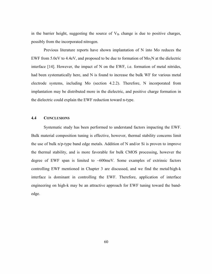
60
in the barrier height, suggesting the source of Vfb change is due to positive charges,
possibly from the incorporated nitrogen.
Previous literature reports have shown implantation of N into Mo reduces the
EWF from 5.0eV to 4.4eV, and proposed to be due to formation of Mo2N at the dielectric
interface [14]. However, the impact of N on the EWF, i.e. formation of metal nitrides,
had been systematically here, and N is found to increase the bulk WF for various metal
electrode systems, including Mo (section 4.2.2). Therefore, N incorporated from
implantation may be distributed more in the dielectric, and positive charge formation in
the dielectric could explain the EWF reduction toward n-type.
4.4 CONCLUSIONS
Systematic study has been performed to understand factors impacting the EWF.
Bulk material composition tuning is effective, however, thermal stability concerns limit
the use of bulk n/p-type band edge metals. Addition of N and/or Si is proven to improve
the thermal stability, and is more favorable for bulk CMOS processing, however the
degree of EWF span is limited to ~600meV. Some examples of extrinsic factors
controlling EWF mentioned in Chapter 3 are discussed, and we find the metal/high-k
interface is dominant in controlling the EWF. Therefore, application of interface
engineering on high-k may be an attractive approach for EWF tuning toward the band-
edge.
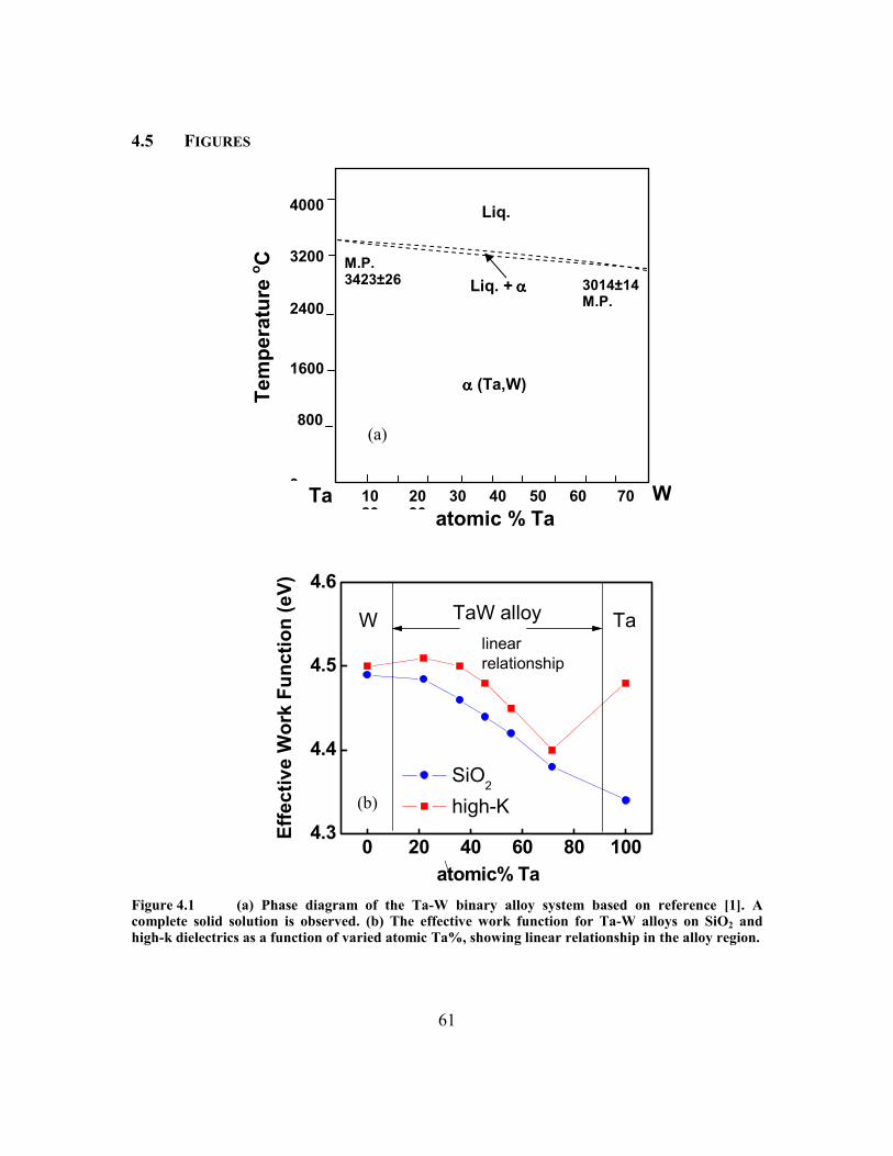
61
4.5 FIGURES
\
Figure 4.1 (a) Phase diagram of the Ta-W binary alloy system based on reference [1]. A complete solid solution is observed. (b) The effective work function for Ta-W alloys on SiO2 and high-k dielectrics as a function of varied atomic Ta%, showing linear relationship in the alloy region.
Ta W atomic % Ta
10 20 30 40 50 60 70 80 90
4000 3200 2400 1600 800 0
Tem
pera
ture
o C
α α α α (Ta,W)
Liq.
Liq. + αααα 3014±14 M.P.
M.P. 3423±26
(a)
0 20 40 60 80 1004.3
4.4
4.5
4.6
W Ta
SiO2
high-K
Effe
ctiv
e W
ork
Func
tion
(eV)
atomic% Ta
TaW alloylinear relationship
(b)
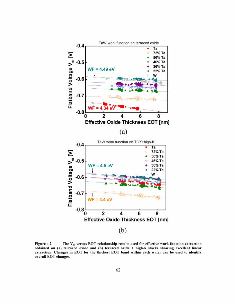
62
Figure 4.2 The Vfb versus EOT relationship results used for effective work function extraction obtained on (a) terraced oxide and (b) terraced oxide + high-k stacks showing excellent linear extraction. Changes in EOT for the thickest EOT band within each wafer can be used to identify overall EOT changes.
0 2 4 6 8-0.8
-0.7
-0.6
-0.5
-0.4 Ta 72% Ta 56% Ta 46% Ta 36% Ta 22% Ta W
WF = 4.34 eV
WF = 4.49 eVFl
atba
nd V
olta
ge V
fb [V
]
Effective Oxide Thickness EOT [nm]
TaW work function on terraced oxide
0 2 4 6 8-0.8
-0.7
-0.6
-0.5
-0.4
WF = 4.4 eV
WF = 4.5 eV
Ta 72% Ta 56% Ta 46% Ta 36% Ta 22% Ta W
Flat
band
Vol
tage
Vfb [V
]
Effective Oxide Thickness EOT [nm]
TaW work function on TOX+high-K
(a)
(b)
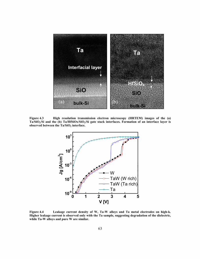
63
Figure 4.3 High resolution transmission electron microscopy (HRTEM) images of the (a) Ta/SiO2/Si and the (b) Ta/HfSiOx/SiO2/Si gate stack interfaces. Formation of an interface layer is observed between the Ta/SiO2 interface.
0 1 2 3 4 510-9
10-6
10-3
100
103
W TaW (W rich) TaW (Ta rich) Ta
Jg [A
/cm
2 ]
V [V]
Figure 4.4 Leakage current density of W, Ta-W alloys and Ta metal electrodes on high-k. Higher leakage current is observed only with the Ta sample, suggesting degradation of the dielectric, while Ta-W alloys and pure W are similar.
bulk-Si
SiO
Ta
Interfacial layer
bulk-Si
SiO
HfSiOx
Ta
(a) (b)
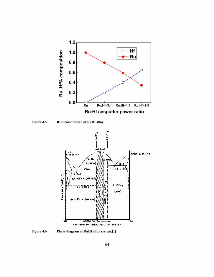
64
Ru Ru:Hf=3:1 Ru:Hf=1:1 Ru:Hf=1:30.0
0.2
0.4
0.6
0.8
1.0
1.2
Ru:Hf cosputter power ratio
Ru,
Hf%
com
posi
tion Hf
Ru
Figure 4.5 RBS composition of RuHf alloy.
Figure 4.6 Phase diagram of RuHf alloy system.[1]
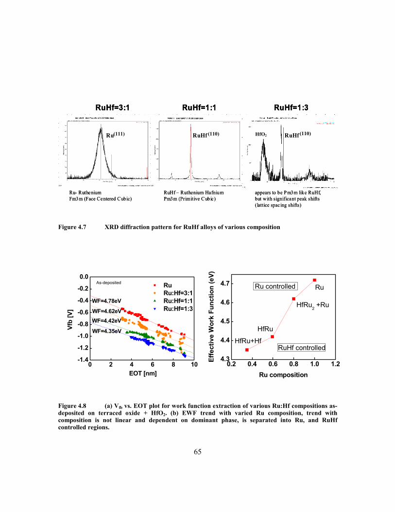
65
Figure 4.7 XRD diffraction pattern for RuHf alloys of various composition
0 2 4 6 8 10-1.4
-1.2
-1.0
-0.8
-0.6
-0.4
-0.2
0.0
WF=4.62eV
Ru Ru:Hf=3:1 Ru:Hf=1:1 Ru:Hf=1:3
Vfb
[V]
EOT [nm]
WF=4.78eV
WF=4.42eV
WF=4.35eV
As-deposited
Figure 4.8 (a) Vfb vs. EOT plot for work function extraction of various Ru:Hf compositions as-deposited on terraced oxide + HfO2. (b) EWF trend with varied Ru composition, trend with composition is not linear and dependent on dominant phase, is separated into Ru, and RuHf controlled regions.
Ru- RutheniumFm3m (Face Centered Cubic)
RuHf – Ruthenium Hafnium Pm3m (Primitive C ubic)
appears to be Pm3m like RuHf, but with significant peak shifts (lattice spacing shifts)
RuHf=3:1 RuHf=1:1 RuHf=1:3
Ru RuHf RuHf
Ru- RutheniumFm3m (Face Centered Cubic)
RuHf – Ruthenium Hafnium Pm3m (Primitive C ubic)
appears to be Pm3m like RuHf, but with significant peak shifts (lattice spacing shifts)
RuHf=3:1 RuHf=1:1 RuHf=1:3
Ru RuHf RuHf
RuHf=3:1 RuHf=1:1 RuHf=1:3
RuRu RuHfRuHf RuHf RuHf (111) (110) (110) HfO2
0.2 0.4 0.6 0.8 1.0 1.24.3
4.4
4.5
4.6
4.7 Ru controlled
HfRu+Hf
HfRu
HfRu2 +Ru
Effe
ctiv
e W
ork
Func
tion
(eV)
Ru composition
Ru
RuHf controlled
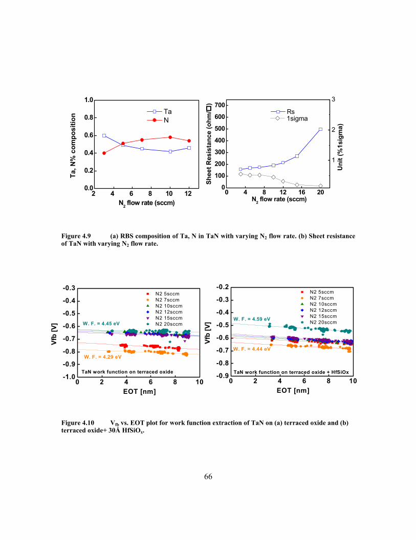
66
2 4 6 8 10 120.0
0.2
0.4
0.6
0.8
1.0
N2 flow rate (sccm)
Ta, N
% c
ompo
sitio
n Ta N
Figure 4.9 (a) RBS composition of Ta, N in TaN with varying N2 flow rate. (b) Sheet resistance of TaN with varying N2 flow rate.
Figure 4.10 Vfb vs. EOT plot for work function extraction of TaN on (a) terraced oxide and (b) terraced oxide+ 30Å HfSiOx.
0 2 4 6 8 10-1.0
-0.9
-0.8
-0.7
-0.6
-0.5
-0.4
-0.3
W. F. = 4.29 eV
W. F. = 4.45 eV
N2 5sccm N2 7sccm N2 10sccm N2 12sccm N2 15sccm N2 20sccm
Vfb
[V]
EOT [nm]
TaN work function on terraced oxide
0 2 4 6 8 10-0.9
-0.8
-0.7
-0.6
-0.5
-0.4
-0.3
-0.2
W. F. = 4.44 eV
W. F. = 4.59 eV
N2 5sccm N2 7sccm N2 10sccm N2 12sccm N2 15sccm N2 20sccm
Vfb
[V]
EOT [nm]
TaN work function on terraced oxide + HfSiOx
0 4 8 12 16 200
100
200
300
400
500
600
700
1
2
3
Rs
N2 flow rate (sccm)
Shee
t Res
ista
nce
(ohm
/)
Uni
t (%
1sig
ma)
1sigma
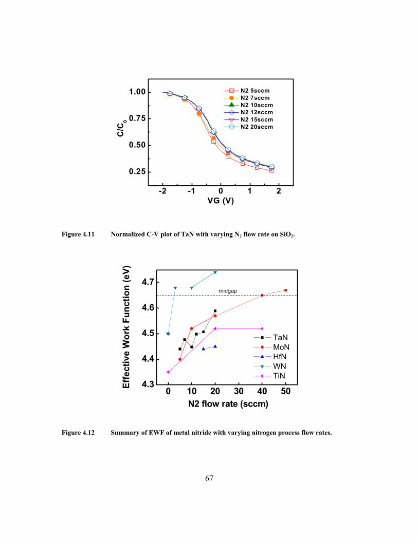
67
-2 -1 0 1 2
0.25
0.50
0.75
1.00 N2 5sccm N2 7sccm N2 10sccm N2 12sccm N2 15sccm N2 20sccm
VG (V)
C/C
0
Figure 4.11 Normalized C-V plot of TaN with varying N2 flow rate on SiO2.
0 10 20 30 40 504.3
4.4
4.5
4.6
4.7
TaN MoN HfN WN TiN
Effe
ctiv
e W
ork
Func
tion
(eV)
N2 flow rate (sccm)
midgap
Figure 4.12 Summary of EWF of metal nitride with varying nitrogen process flow rates.
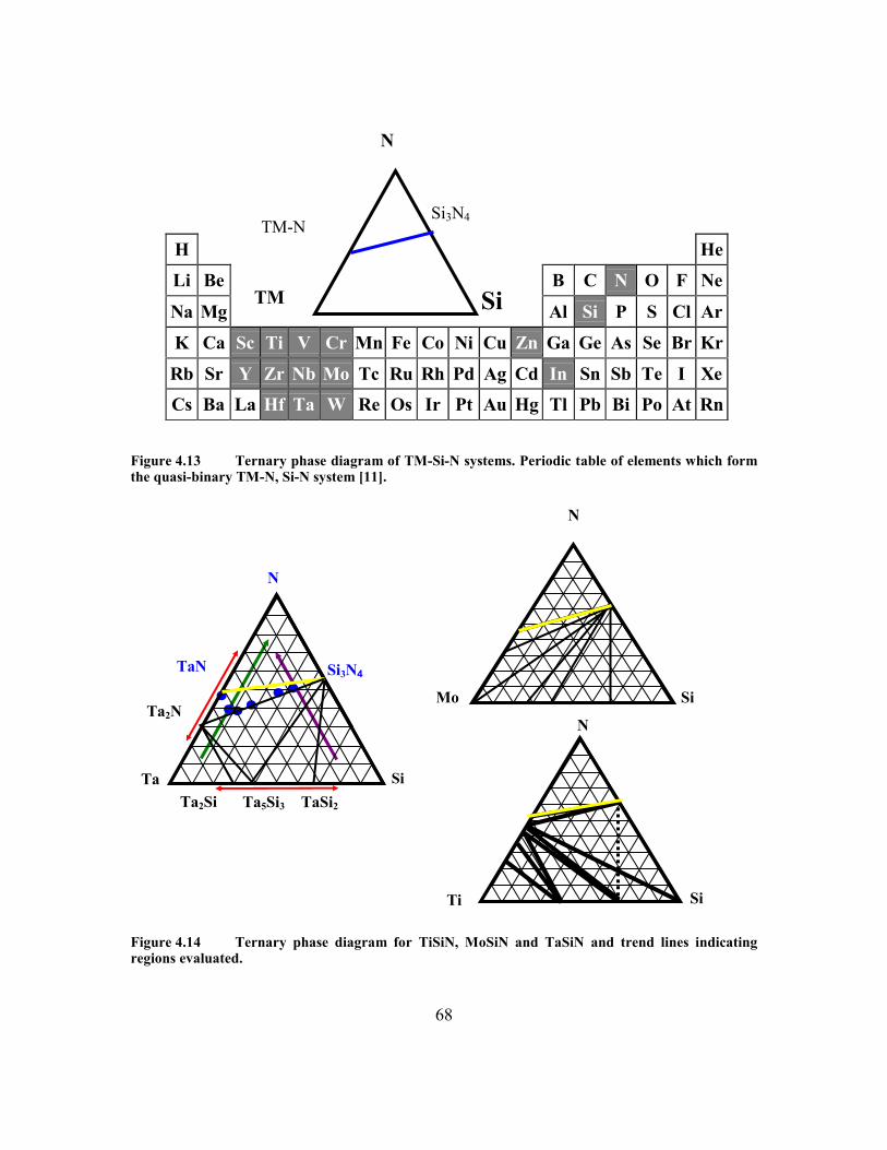
68
H He Li Be B C N O F Ne
Na Mg Al Si P S Cl Ar
K Ca Sc Ti V Cr Mn Fe Co Ni Cu Zn Ga Ge As Se Br Kr
Rb Sr Y Zr Nb Mo Tc Ru Rh Pd Ag Cd In Sn Sb Te I Xe Cs Ba La Hf Ta W Re Os Ir Pt Au Hg Tl Pb Bi Po At Rn
Figure 4.13 Ternary phase diagram of TM-Si-N systems. Periodic table of elements which form the quasi-binary TM-N, Si-N system [11].
Figure 4.14 Ternary phase diagram for TiSiN, MoSiN and TaSiN and trend lines indicating regions evaluated.
Ta SiTa2Si Ta5Si3 TaSi2
Ta2N
Si3N4 TaN
N
N
Mo Si
Ti
N
Si
TM
N
Si
TM-N Si3N4
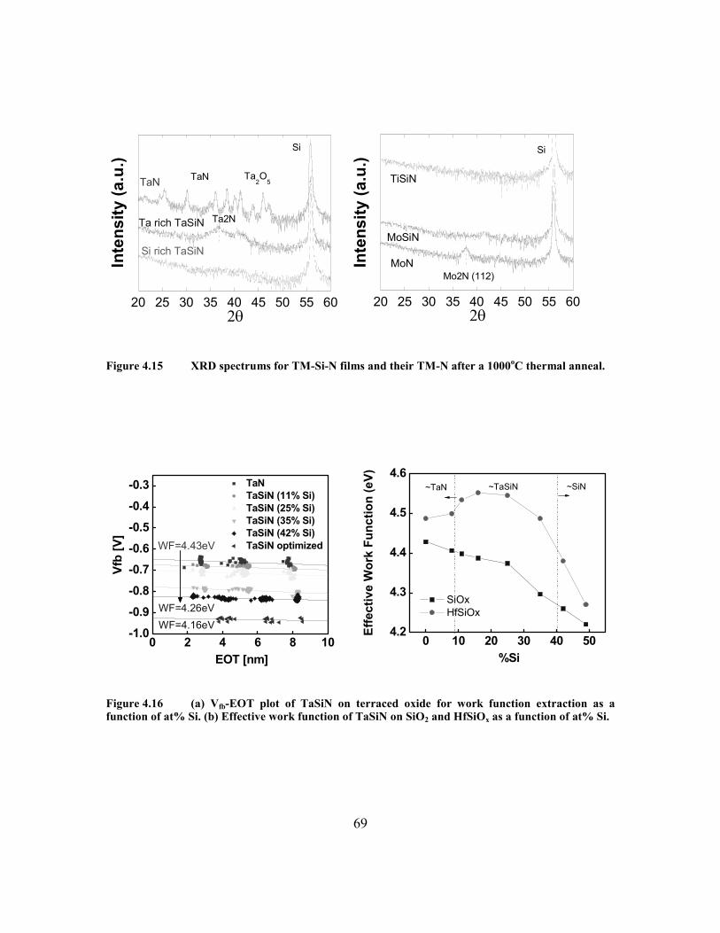
69
Figure 4.15 XRD spectrums for TM-Si-N films and their TM-N after a 1000oC thermal anneal.
Figure 4.16 (a) Vfb-EOT plot of TaSiN on terraced oxide for work function extraction as a function of at% Si. (b) Effective work function of TaSiN on SiO2 and HfSiOx as a function of at% Si.
20 25 30 35 40 45 50 55 60
Inte
nsity
(a.u
.)
2θ
TaN
Ta rich TaSiN
Si rich TaSiN
Si
Ta2N
Ta2O
5TaN
20 25 30 35 40 45 50 55 60
Inte
nsity
(a.u
.)
2θ
MoSiN
MoN
Si
Mo2N (112)
TiSiN
0 2 4 6 8 10-1.0
-0.9
-0.8
-0.7-0.6
-0.5
-0.4
-0.3 TaN TaSiN (11% Si) TaSiN (25% Si) TaSiN (35% Si) TaSiN (42% Si) TaSiN optimized
WF=4.16eV
WF=4.43eV
Vfb
[V]
EOT [nm]
WF=4.26eV
0 10 20 30 40 504.2
4.3
4.4
4.5
4.6~SiN
SiOx HfSiOx
Effe
ctiv
e W
ork
Func
tion
(eV)
%Si
~TaN ~TaSiN
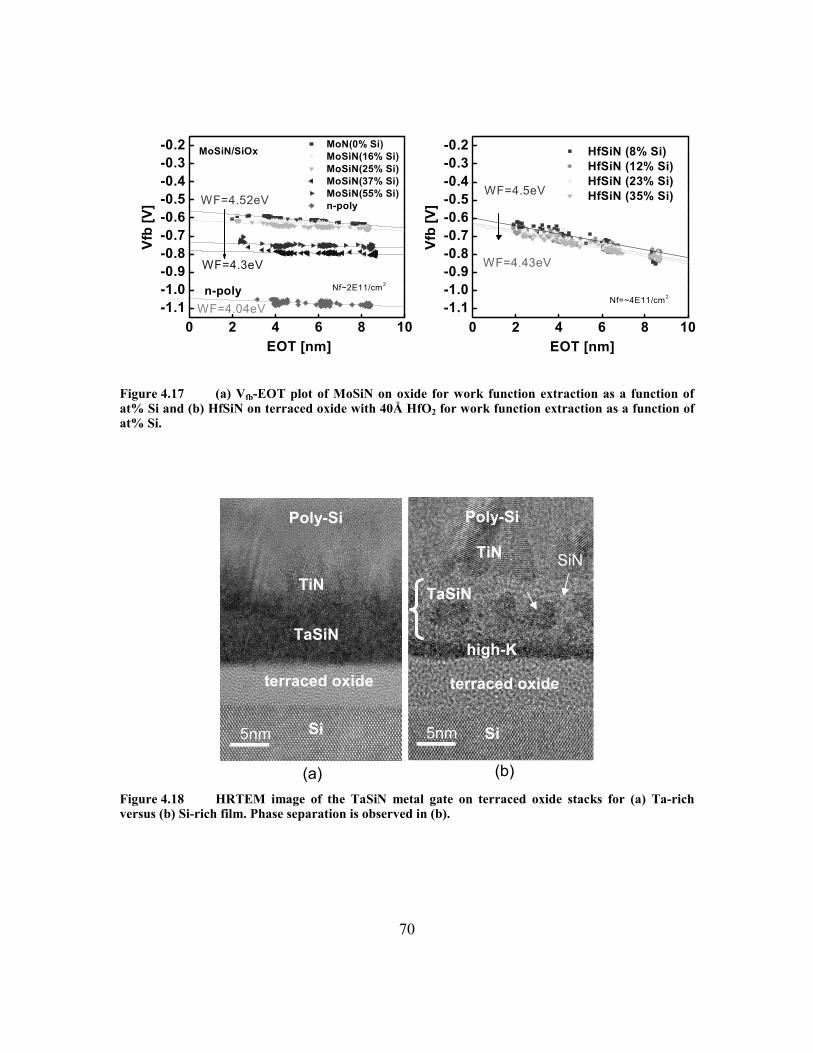
70
Figure 4.17 (a) Vfb-EOT plot of MoSiN on oxide for work function extraction as a function of at% Si and (b) HfSiN on terraced oxide with 40Å HfO2 for work function extraction as a function of at% Si.
Figure 4.18 HRTEM image of the TaSiN metal gate on terraced oxide stacks for (a) Ta-rich versus (b) Si-rich film. Phase separation is observed in (b).
0 2 4 6 8 10-1.1-1.0-0.9-0.8-0.7-0.6-0.5-0.4-0.3-0.2
WF=4.5eV
HfSiN (8% Si) HfSiN (12% Si) HfSiN (23% Si) HfSiN (35% Si)
Vfb
[V]
EOT [nm]
WF=4.43eV
Nf=~4E11/cm2
0 2 4 6 8 10-1.1-1.0-0.9-0.8-0.7-0.6-0.5-0.4-0.3-0.2
n-poly
WF=4.3eV
WF=4.52eV
MoN(0% Si) MoSiN(16% Si) MoSiN(25% Si) MoSiN(37% Si) MoSiN(55% Si) n-poly
Vfb
[V]
EOT [nm]
WF=4.04eV
MoSiN/SiOx
Nf~2E11/cm2
5nm
TaSiN
TiN
Poly-Si
terraced oxide
Si
(a) (b)
Si
high-K
TiN
Poly-Si
terraced oxide
5nm
SiN
TaSiN
TaN
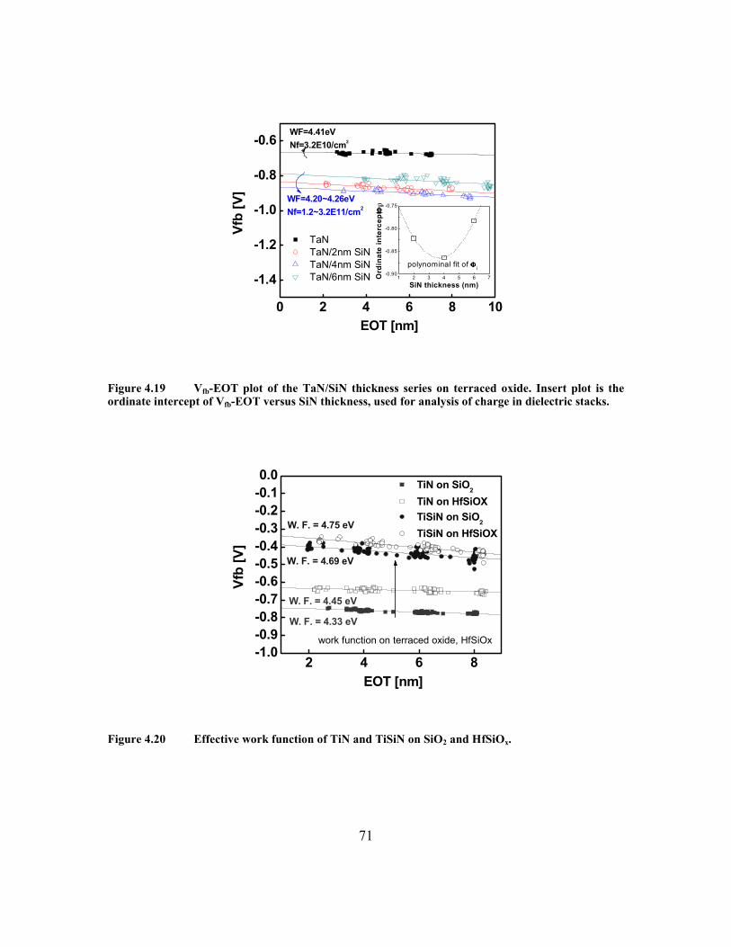
71
0 2 4 6 8 10
-1.4
-1.2
-1.0
-0.8
-0.6
1 2 3 4 5 6 7-0.90
-0.85
-0.80
-0.75
Ord
inat
e in
terc
ept ( ΦΦ ΦΦ
i)
SiN thickness (nm)
polynominal fit of ΦΦΦΦ i
TaN TaN/2nm SiN TaN/4nm SiN TaN/6nm SiN
WF=4.41eV Nf=3.2E10/cm2
Vfb
[V]
EOT [nm]
WF=4.20~4.26eVNf=1.2~3.2E11/cm2
Figure 4.19 Vfb-EOT plot of the TaN/SiN thickness series on terraced oxide. Insert plot is the ordinate intercept of Vfb-EOT versus SiN thickness, used for analysis of charge in dielectric stacks.
2 4 6 8-1.0-0.9-0.8-0.7-0.6-0.5-0.4-0.3-0.2-0.10.0
W. F. = 4.33 eV
W. F. = 4.45 eV
W. F. = 4.75 eV
TiN on SiO2
TiN on HfSiOX TiSiN on SiO2
TiSiN on HfSiOX
Vfb
[V]
EOT [nm]
work function on terraced oxide, HfSiOx
W. F. = 4.69 eV
Figure 4.20 Effective work function of TiN and TiSiN on SiO2 and HfSiOx.
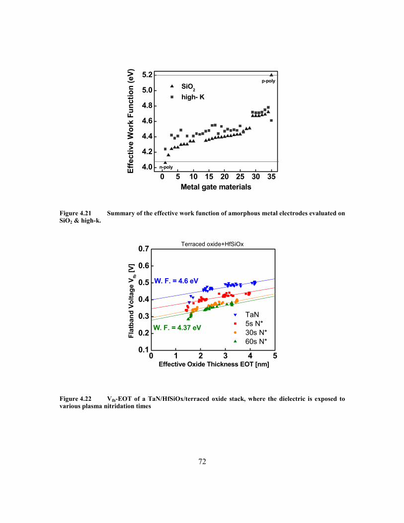
72
0 5 10 15 20 25 30 354.0
4.2
4.4
4.6
4.8
5.0
5.2p-poly
SiO2
high- K
Effe
ctiv
e W
ork
Func
tion
(eV)
Metal gate materials
n-poly
Figure 4.21 Summary of the effective work function of amorphous metal electrodes evaluated on SiO2 & high-k.
0 1 2 3 4 50.1
0.2
0.3
0.4
0.5
0.6
0.7
W. F. = 4.37 eV
W. F. = 4.6 eV
TaN 5s N* 30s N* 60s N*
Flat
band
Vol
tage
Vfb
[V]
Effective Oxide Thickness EOT [nm]
Terraced oxide+HfSiOx
Figure 4.22 Vfb-EOT of a TaN/HfSiOx/terraced oxide stack, where the dielectric is exposed to various plasma nitridation times
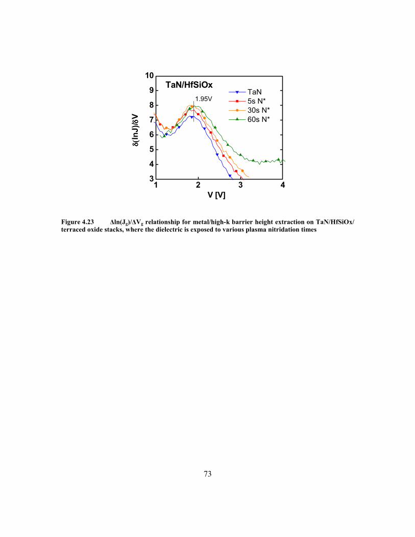
73
1 2 3 43
4
5
6
7
8
9
10
TaN 5s N* 30s N* 60s N*
δδ δδ (( ((ln
J)/ δδ δδ
V
V [V]
TaN/HfSiOx1.95V
Figure 4.23 ∆ln(Jg)/∆Vg relationship for metal/high-k barrier height extraction on TaN/HfSiOx/ terraced oxide stacks, where the dielectric is exposed to various plasma nitridation times
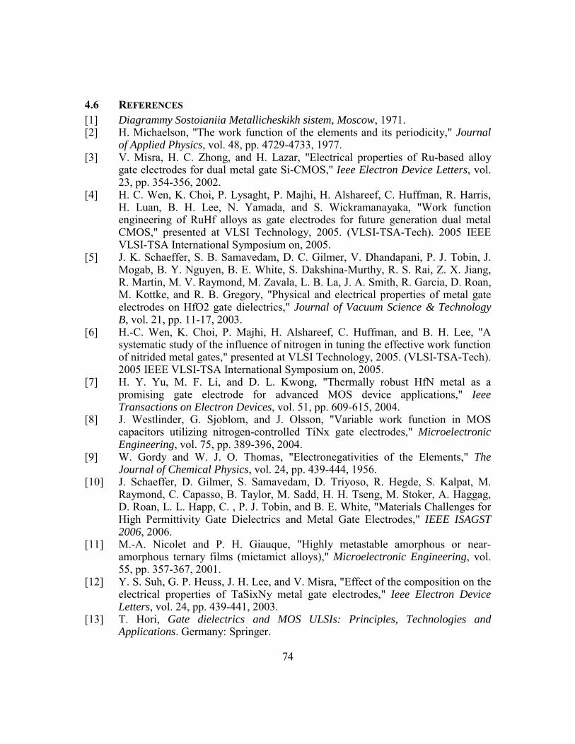
74
4.6 REFERENCES [1] Diagrammy Sostoianiia Metallicheskikh sistem, Moscow, 1971. [2] H. Michaelson, "The work function of the elements and its periodicity," Journal
of Applied Physics, vol. 48, pp. 4729-4733, 1977. [3] V. Misra, H. C. Zhong, and H. Lazar, "Electrical properties of Ru-based alloy
gate electrodes for dual metal gate Si-CMOS," Ieee Electron Device Letters, vol. 23, pp. 354-356, 2002.
[4] H. C. Wen, K. Choi, P. Lysaght, P. Majhi, H. Alshareef, C. Huffman, R. Harris, H. Luan, B. H. Lee, N. Yamada, and S. Wickramanayaka, "Work function engineering of RuHf alloys as gate electrodes for future generation dual metal CMOS," presented at VLSI Technology, 2005. (VLSI-TSA-Tech). 2005 IEEE VLSI-TSA International Symposium on, 2005.
[5] J. K. Schaeffer, S. B. Samavedam, D. C. Gilmer, V. Dhandapani, P. J. Tobin, J. Mogab, B. Y. Nguyen, B. E. White, S. Dakshina-Murthy, R. S. Rai, Z. X. Jiang, R. Martin, M. V. Raymond, M. Zavala, L. B. La, J. A. Smith, R. Garcia, D. Roan, M. Kottke, and R. B. Gregory, "Physical and electrical properties of metal gate electrodes on HfO2 gate dielectrics," Journal of Vacuum Science & Technology B, vol. 21, pp. 11-17, 2003.
[6] H.-C. Wen, K. Choi, P. Majhi, H. Alshareef, C. Huffman, and B. H. Lee, "A systematic study of the influence of nitrogen in tuning the effective work function of nitrided metal gates," presented at VLSI Technology, 2005. (VLSI-TSA-Tech). 2005 IEEE VLSI-TSA International Symposium on, 2005.
[7] H. Y. Yu, M. F. Li, and D. L. Kwong, "Thermally robust HfN metal as a promising gate electrode for advanced MOS device applications," Ieee Transactions on Electron Devices, vol. 51, pp. 609-615, 2004.
[8] J. Westlinder, G. Sjoblom, and J. Olsson, "Variable work function in MOS capacitors utilizing nitrogen-controlled TiNx gate electrodes," Microelectronic Engineering, vol. 75, pp. 389-396, 2004.
[9] W. Gordy and W. J. O. Thomas, "Electronegativities of the Elements," The Journal of Chemical Physics, vol. 24, pp. 439-444, 1956.
[10] J. Schaeffer, D. Gilmer, S. Samavedam, D. Triyoso, R. Hegde, S. Kalpat, M. Raymond, C. Capasso, B. Taylor, M. Sadd, H. H. Tseng, M. Stoker, A. Haggag, D. Roan, L. L. Happ, C. , P. J. Tobin, and B. E. White, "Materials Challenges for High Permittivity Gate Dielectrics and Metal Gate Electrodes," IEEE ISAGST 2006, 2006.
[11] M.-A. Nicolet and P. H. Giauque, "Highly metastable amorphous or near-amorphous ternary films (mictamict alloys)," Microelectronic Engineering, vol. 55, pp. 357-367, 2001.
[12] Y. S. Suh, G. P. Heuss, J. H. Lee, and V. Misra, "Effect of the composition on the electrical properties of TaSixNy metal gate electrodes," Ieee Electron Device Letters, vol. 24, pp. 439-441, 2003.
[13] T. Hori, Gate dielectrics and MOS ULSIs: Principles, Technologies and Applications. Germany: Springer.
75
[14] R. Lin, Q. Lu, P. Ranade, T. J. King, and C. M. Hu, "An adjustable work function technology using Mo gate for CMOS devices," Ieee Electron Device Letters, vol. 23, pp. 49-51, 2002.
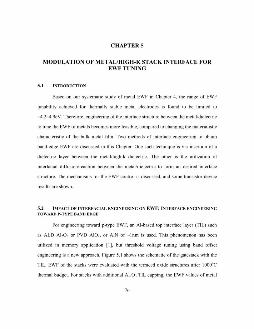
76
CHAPTER 5
MODULATION OF METAL/HIGH-K STACK INTERFACE FOR EWF TUNING
5.1 INTRODUCTION
Based on our systematic study of metal EWF in Chapter 4, the range of EWF
tunability achieved for thermally stable metal electrodes is found to be limited to
~4.2~4.9eV. Therefore, engineering of the interface structure between the metal/dielectric
to tune the EWF of metals becomes more feasible, compared to changing the materialistic
characteristic of the bulk metal film. Two methods of interface engineering to obtain
band-edge EWF are discussed in this Chapter. One such technique is via insertion of a
dielectric layer between the metal/high-k dielectric. The other is the utilization of
interfacial diffusion/reaction between the metal/dielectric to form an desired interface
structure. The mechanisms for the EWF control is discussed, and some transistor device
results are shown.
5.2 IMPACT OF INTERFACIAL ENGINEERING ON EWF: INTERFACE ENGINEERING TOWARD P-TYPE BAND EDGE
For engineering toward p-type EWF, an Al-based top interface layer (TIL) such
as ALD Al2O3 or PVD AlOx, or AlN of ~1nm is used. This phenomenon has been
utilized in memory application [1], but threshold voltage tuning using band offset
engineering is a new approach. Figure 5.1 shows the schematic of the gatestack with the
TIL. EWF of the stacks were evaluated with the terraced oxide structures after 1000oC
thermal budget. For stacks with additional Al2O3 TIL capping, the EWF values of metal
77
electrodes increased by ~250±50 meV from their initial values(Figure 5.2(a)). Figure
5.2(b) shows the similar shift with the Al2O3 TIL (and AlN stacks) independent of the
metal electrode system. There have been previous reports on the EWF shift by Al
containing high-k dielectrics [2, 3]. However, the physical mechanism behind such EWF
shift has not been fully investigated and mainly attributed to negative charge within AlOx
layer or Al diffusion into interfacial oxide or silicon [2,3]. Since the Vfb change in Figure
5.2(a), is independent of EOT, there can be two main sources for the constant Vfb (EWF)
change: 1) Similar to common explanations, the Vfb shift can be due to negative charges
induced by the AlOx TIL; 2) The second source of a constant Vfb shift can be due to a
fixed dipole formation within the gatestack.
5.2.1 Possibility of negative charge on Vfb shift
First to address the possibility of negative charges causing the Vfb shifts. Sources
of the charge can be from a) Al2O3 bulk charge, b) charge (QHfO-Al) formed by Al
diffusion into the dielectric, c) interface charge formed at the high-k/AlO interface or d)
below the high-k at the SiO2 (QHfO_SiO)or Si interface due to Al diffusion. Figure 5.3 is
the schematic showing location of such charges with in the dielectric stack. Thickness
series of Al2O3 (2, 4, 6 and 8nm) were deposited on terraced oxide dielectrics for bulk
charge density calculations. The Vfb-EOT relationship for the various Al2O3 thickness are
shown in Figure 5.4. Utilizing the Vfb equation based in Chapter 2, we are able to
estimate the bulk charge density for Al2O3 to be ~-7E18/cm3. Thus, for a 1nm Al2O3 film,
the bulk charge contribution on the Vfb is <20meV, and cannot explain the ~300meV Vfb
shift with Al TIL (not charge from Figure 5.3-a). Temperature dependent studies of the
Al2O3/HfSiOx stack EWF, shows no EWF increase for samples just after a FG anneal,
while increased EWF is observed only after 700~1000oC (Figure 5.5). The same EWF
78
observed for the Al2O3 sample after FG anneal, and the no TIL control, also suggests
minimal impact of Al2O3 bulk charge on Vfb. Secondary ion mass spectroscopy (SIMS)
profile comparison of the sample after FG anneal, 700oC, and 900oC show Al diffusion
into the high-k layer after anneal. The diffusion of Al is limited to the high-k/SiO2
interface (700oC), and is not enhanced with additional annealing (900oC), but higher
temperature causes the Al profile to redistribute toward the electrode. Interestingly, the
EWF for the annealed samples are constant even up to 1000oC, suggesting the charges
caused by Al diffusion into the high-k (charge from Figure 5.3-b) may not be the source
of the Vfb shift from the TIL. If charges are located at the high-k/SiO2 interface (Figure
5.3-c), there should be a linear dependence in the Vfb change with the distance to the
electrode (x):
Therefore, an experiment with a TIL on varied high-k thickness (2.5, 3.5, 4.5 and 6.5nm
HfSiOx) on terraced oxide has been conducted to change the distance of the charge frm
the electrode (x) (Figure 5.7). A constant ~240meV difference is observed with the TIL
independent of the high-k thickness, suggesting the charge at location c) is not
responsible for the Vfb change. SIMS analysis of the 65Å HfSiOx stack also shows Al
distribution throughout the high-k dielectric. However, limited Al diffusion is observed
through SiO2, with no detectable Al is observed at the Si/SiO2 interface (Figure 5.8).
Also, since the Vfb change is independent on the terraced oxide band thickness, this
supports charge at the Si/SiO2 interface (d) is also not the source of Vfb shift.
5.2.1 Possibility of dipole on Vfb shift
The other possibility for such constant Vfb shift would be explained by a dipole
formation in the dielectric stack. An electric dipole is a separation of positive and
xQ
Vh
SiOHfOFB ε
_−=∆
79
negative charge. Figure 5.9 is a schematic showing the formation of a dipole within the
dielectric due to charge q, its effect on the Vfb is shown in the equation below:
Figure 5.9 also shows the possible dipole locations within the stack, this includes a)
interface dipole formation between metal/high-k; similar to Fermi-level pinning, b)
interface dipole formation at Al2O3/high-k interface, c) SiO2/high-k interface, and d)
remote interaction between the high-k/Si. Since nearly constant EWF shift is observed for
several metals covering a wide range of EWF (4.2~4.8 eV), change in the interface dipole
at the metal/dielectric interface may not explain these shifts. To determine which
interface is the effective dipole location, a complementary set of samples to modulate Al
distribution in the gate stack is processed. (Figure 5.10). Since dipole formation may be a
thermally activated process, direct comparison of the stacks after an equal high thermal
budget (1000oC) is needed. Set (A) is the baseline AlO/HfO stack. In the as-deposited
low thermal budget state, the EWF of the stack is similar to the without TIL as shown in
Figure 5.5 (4.75eV). With process changes in the high-k (with and without high-k post
deposition anneal (PDA)), we can control the Al-diffusion profile to two forms. First,
even after a 1000oC anneal, the Al profile however is limited, and the top dielectric
surface is Al-rich (Figure 5.11 (a)). This sample exhibits an EWF similar to the without
TIL control (4.8eV) (Figure 5.12), suggesting the AlO/high-k interface dipole (Figure
5.9-b), and the metal/AlOx interface dipole (Figure 5.9-a) is not effective in changing
Vfb. Second, an uniform distribution of Al toward the high-k/SiO2 interface is obtained if
the high-k does not have a PDA (Figure 5.11 (b)). Here, allowing Al diffusion to the SiO2
interface exhibits the Vfb increase effect (EWF=5.05eV) (Figure 5.12). This is consistent
with the temperature dependence in EWF, where high EWF is only observed when Al
oxoxoxFB
dqxqdxqVεεε⋅
−=⋅
++
−=∆)(
80
diffuses to the SiO2 interface (Figure 5.6). Set (B) HfO/AlO in Figure 5.10 is the reversed
stack of (A), with direct deposition of AlOx on SiO2, and represents intentional Al
incorporation at the SiO2 interface. This sample exhibits equal EWF as the AlO/HfO
stack (5.05eV), and would support the concept of dipole formation at the high-k/SiO2
interface (Figure 5.9-c).
Based on these analysis, previous reports of Al containing dielectrics exhibiting a
characteristic negative charge at the Si interface [4, 5] could be interpreted by the
formation of a dipole layer between Al-dielectrics and the inevitable bottom interfacial
oxide layer. A schematic of how interface dipole formation will shift the band offset and
result in increased EWF is shown in Figure 5.13. Origin of the possible mechanisms for
the dipole may be the formation of Al-O bonds at the interface, or the high reactivity of
Al with SiO2. Figure 5.14 shows the Al 2p and Si 2p binding energies before and after
anneal at 1000 °C, 5 s in N2. Note that there is a chemical shift in the Al 2p binding
energy after the anneal indicative of Al–O bond formation, and a shift in the Si 2p
binding energy indicative of sub-oxide formation (SiOx) [6]. This result suggests Al in
the AlNx layer may reduce the Si–O bonds in the gate dielectric, resulting in Al–O bond
formation at the AlNx /SiO2 interface. Such a reaction is thermodynamically favorable
since the free energies of formation, for Al2O3, SiO2, and AlNx are −1582, −853, −287
kJ/mol, respectively.
81
5.3 INTERFACE MODULATION VIA BULK METAL ELECTRODES
Al-based metal electrodes for p-type band edge metal: Metal-Aluminum-Nitride
Use of an AlOx or AlN capping layer on high-k dielectrics has been proposed as
an effective method for modulating the effective work function toward the p-type band
edge (Section [6-8]). However, the effective oxide thickness (EOT) increases ~1-2Å with
these dielectric capping layers. To utilize the advantage of maintaining an Al-like
interface between the high-k and metal electrode, interest has focused on incorporating
Al in the electrode. TiAlN [9]and TaAlN [10] have been proposed to exhibit a 5.0eV
EWF on SiO2, however EWF on high-k is limited to less than 4.8eV. Based on the
learning in Section 5.2, the key to high EWF is to allow Al diffusion for engineering at
the high-k/SiO2 interface. This study includes a systematic EWF evaluation of M-Al-N,
M=Mo, W and Ru, to increase the starting metal EWF, targeting near band-edge p-type
EWF of 4.9~5.1eV on high-k dielectrics.
Figure 5.15 is the phase diagram for MoAlN [11]. No ternary phase is observed
for these M-Al-N systems, however, a tie line exists between the MoN and AlN phase.
The MoAlN film deposited by PVD targets compositions along this tie line. Figure 5.16
is the EWF extracted from the Vfb-EOT relationship on terraced oxide structures.
Consistent with that observed in Al TIL stacks, an EWF increase of ~200meV is
observed for several MAlN systems compared to their MNx counterparts. The parallel
shift in the Vfb-EOT relationship suggests a constant fixed oxide charge and minimum
effect on the interface with Al incorporation. An EWF as high as 5.08eV can be obtained
with RuAlN systems. A systematic study of the EWF as a function of Al sputtering
power is shown in
Figure 5.17. The addition of Al is shown to increase the EWF for a series of
MAlN (M=Ta, Ti, Mo, W) and saturates as atomic % if Al is >15%. The metal/dielectric
82
barrier height was measured using the current derivative technique [12], where the
voltage at the peak of the current derivative corresponds to the metal/dielectric barrier
height (Figure 5.18(a)). The TaN and WN controls exhibit a 2V and 2.1V peak,
respectively, and the addition of the electron affinity for HfSiOx (2.6eV [13]) equals
4.6eV, 4.7eV, which correlates to the EWF extracted from the terraced oxide. An
increase in the barrier height (2.4V) is observed for WAlN, which is consistent with the
change in the bulk WF of the electrode, as well as the formation of an interface dipole at
the metal/high-k interface. Careful examination of the film properties by X-ray
diffraction (XRD) shows the film is crystalline and composed of mainly Mo2N with
possible AlN phases after a 900oC thermal budget, thus the change in bulk work function
may not be able to completely explain the EWF differences (Figure 5.18(b)). The
mechanism for the EWF increase is found to be consistent with that of AlOx TIL. Figure
5.19 shows the temperature dependence of the EWF. Only the samples after annealing,
where the interfacial Al distributes to the dielectric (confirmed by SIMS), will exhibit the
EWF increase.
Demonstration of MAlN transistor devices shows that compared with TiSiN
electrodes with an AlOx interface layer, a comparable Vfb is achieved with no evident
EOT increase. Therefore, an Al-containing metal is a more favorable approach for
interface modulations compared to the TIL approach (Figure 5.20). Comparable device
performance is maintained with MoAlN exhibiting mobility ~96% of its control TaN
electrode (Figure 5.21(a)). A slight degradation in the interface state density measured by
charge pumping technique (Figure 5.21(b)), could be the source of the degraded mobility.
The increased interface states would be consistent with Al interaction with the SiO2
interface layer. Threshold voltage can be reduced ~0.2eV with MoAlN electrodes;
however, it still is 150meV higher than that expected from an 4.95eV work function
83
electrode (Figure 5.22). This is believed to be due to a newly identified Vfb roll-off
effect commonly observed in high work function electrodes as devices scale to lower
EOTs. More discussion of this new phenomena will be discussed in the Chapter 7.
Nevertheless, interface engineering is identified to be feasible technique for EWF control
with good device performance.
5.4 INTERFACE ENGINEERING TOWARD N-TYPE EWF
With a similar approach, the insertion of an interfacial layer to engineer the
interface toward n-type EWF is shown with the use of La2O3 dielectrics (Figure
5.23)[14]. The La2O3 film thickness are 0.5 and 1.0 nm thick interlayers. These thickness
values result, upon mixing of the two dielectrics after a thermal budget, and results in a
dielectric layer with 15 and 28 atomic % La, respectively. Figure 5.24 shows a backside
SIMS depth profile of the gate stack after La2O3 deposition and annealing at 1070 °C
spike anneal. The results show that La and Hf signal overlap, indicating that the La has
completely mixed with the HfSiOx gate dielectric after device fabrication. The
transistor CV curves for devices with HfSiO film and for devices with HfLaSiO dielectric
formed using the La2O3 capping process indicate a distinct shift in the Vfb and Vt of the
devices with increasing La2O3 content (Figure 5.25). Notice that the CV curves are
shifted in parallel without any stretch or distortion in the transistor CV curves. The
threshold voltage shifted by nearly 400 mV with the initial addition of about 15% La (0.5
nm La2O3 capping layer) and another 550mV with the addition of 28% La (1.0 nm
capping layer) (Figure 5.26). In fact the Vt of the device with 1.0 nm La2O3 capping is
the same as that of our reference n+ poly-Si using the same transistor fabrication flow
(0.27 V). The significant reduction in Vt actually takes place without compromising the
EOT of the stack. Figure 5.27(a) shows the high field mobility of the gate stack is not

84
degraded by the incorporation of the La2O3 capping layer and that mobilities as high as
92% of the universal SiO2 curve can be achieved. However, the low-field mobility is
somewhat degraded, with the degradation amount being dependent on the amount of
La2O3 added. Pulsed Id-Vg technique is applied to investigate the degree of dielectric
charge trapping with the addition of La doping, and no significant increase is observed.
Concurrently, it is unlikely that all La2O3 remains on top of the dielectric. La2O3 is one of
the most aggressive silicate formers in the lanthanide series [15]and therefore La may
seek out the interfacial SiOx to form La silicate [16]. Peak mobility loss (Figure 5.27)
may be due to coulomb scattering from La near the IL SiOx.
The mechanism by which the work function shift may occur may be related to
either bulk or interfacial phenomenon. One possibility is that La-related bulk positive
charges in the HfSiOx dielectric shift the C-V curve to lower (more negative Vfb) values
and hence lower NMOSFET Vt. Support for this hypothesis comes from the La2O3
thickness dependence of the Vt shift (Figure 5.26) and also from the low-field mobility
degradation shown in Figure 5.27. However, La-related bulk charges cannot alone
entirely account for the entire Vfb shifts. An alternative explanation, consistent with other
reports [17, 18], is that electropositive La forms a La-O dipole at the high-k interface that
shifts the band offset and therefore the EWF of the metal. Yamamoto et al. has reported a
systematic comparison of HfLaO stacks with various La concentrations similar to that we
have done for the Al stack, and also believes the location for the dipole is located at the
high-k/SiO2 interface [19]. Concurrently, the interface engineering technique can also be
applied for other Lanthanide doped metal gates and exhibit near n-type band edge EWF.
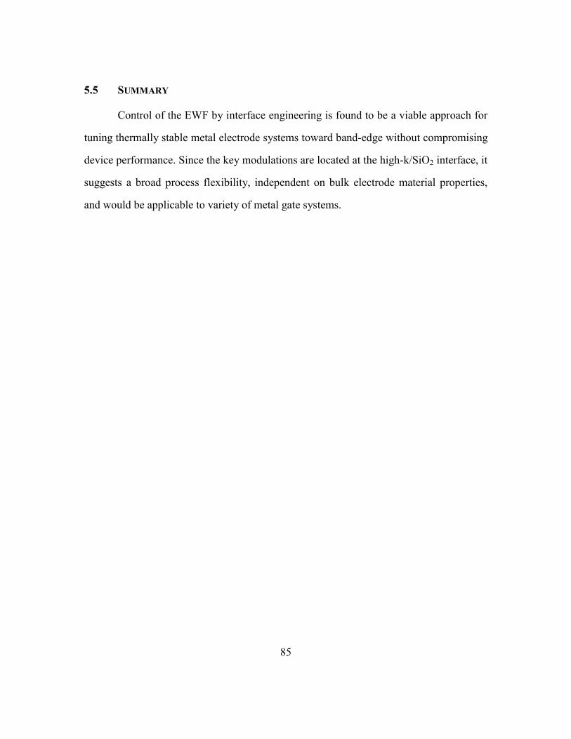
85
5.5 SUMMARY
Control of the EWF by interface engineering is found to be a viable approach for
tuning thermally stable metal electrode systems toward band-edge without compromising
device performance. Since the key modulations are located at the high-k/SiO2 interface, it
suggests a broad process flexibility, independent on bulk electrode material properties,
and would be applicable to variety of metal gate systems.
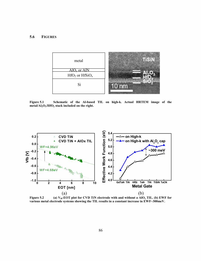
86
5.6 FIGURES
Figure 5.1 Schematic of the Al-based TIL on high-k. Actual HRTEM image of the metal/Al2O3/HfO2 stack included on the right. (a) (b) Figure 5.2 (a) Vfb-EOT plot for CVD TiN electrode with and without a AlOx TIL. (b) EWF for various metal electrode systems showing the TIL results in a constant increase in EWF~300meV.
metal
AlOx or AlN HfO2 or HfSiOx
Si
GdTaN TiN HfSi TaN TiN TiSiN TaCN4.0
4.2
4.4
4.6
4.8
5.0
5.2
5.4 on High-k on High-k with Al2O3 cap
Metal Gate
Effe
ctiv
e W
ork
Func
tion
(eV)
~300 meV
0 2 4 6 8 10-1.0
-0.8
-0.6
-0.4
-0.2
0.0
0.2
WF=4.68eV
CVD TiNCVD TiN + AlOx TIL
WF=4.96eV
Vfb
[V]
EOT [nm]
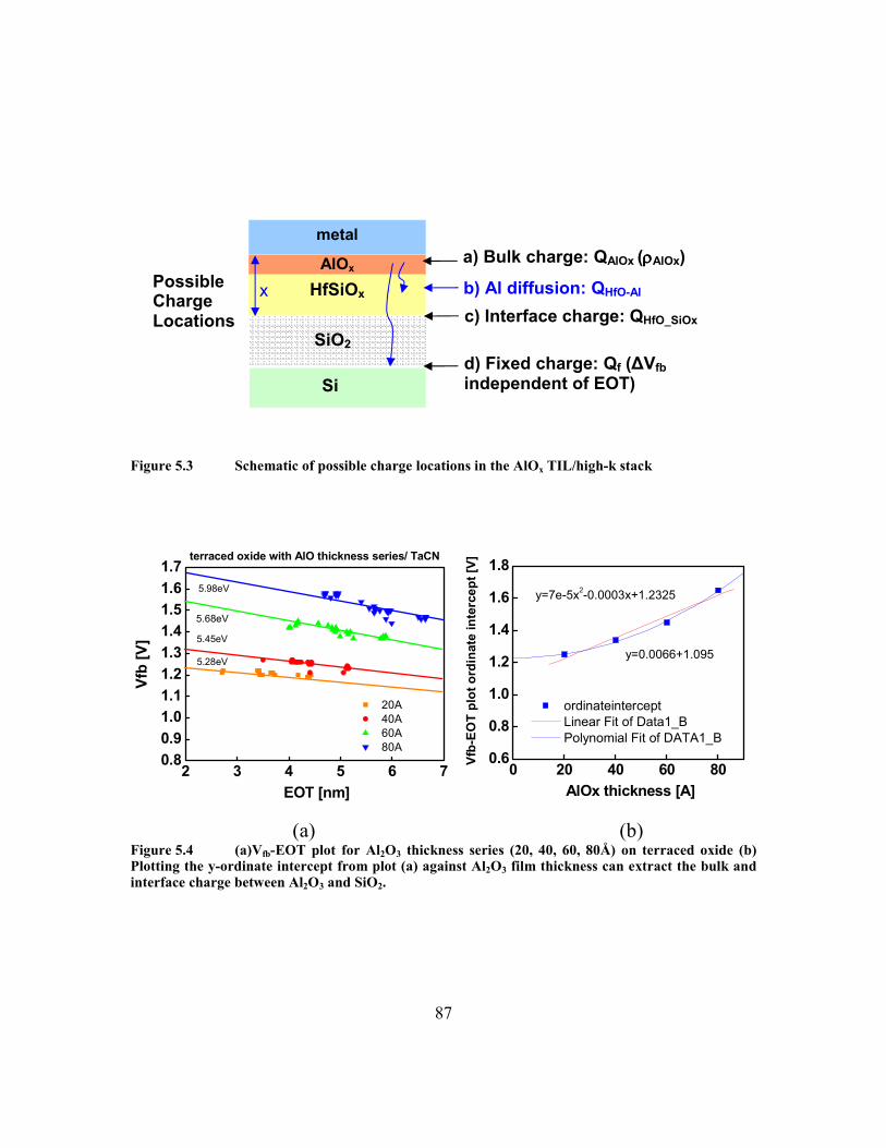
87
Figure 5.3 Schematic of possible charge locations in the AlOx TIL/high-k stack
2 3 4 5 6 70.80.91.01.11.21.31.41.51.61.7
5.45eV
5.28eV
5.68eV
20A 40A 60A 80A
Vfb
[V]
EOT [nm]
terraced oxide with AlO thickness series/ TaCN
5.98eV
(a) (b) Figure 5.4 (a)Vfb-EOT plot for Al2O3 thickness series (20, 40, 60, 80Å) on terraced oxide (b) Plotting the y-ordinate intercept from plot (a) against Al2O3 film thickness can extract the bulk and interface charge between Al2O3 and SiO2.
AlOx
metal
HfSiOx
Si
SiO2
d) Fixed charge: Qf (∆Vfb independent of EOT)
c) Interface charge: QHfO_SiOx
b) Al diffusion: QHfO-Al
a) Bulk charge: QAlOx (ρρρρAlOx) Possible Charge Locations
x
0 20 40 60 800.6
0.8
1.0
1.2
1.4
1.6
1.8
ordinateintercept Linear Fit of Data1_B Polynomial Fit of DATA1_B
y=0.0066+1.095
y=7e-5x2-0.0003x+1.2325
Vfb-
EOT
plot
ord
inat
e in
terc
ept [
V]
AlOx thickness [A]

88
no Al FG 700 800 900 10004.7
4.8
4.9
5.0
5.1
Critical temperature for dipole formation
TiSiN metal gate AlOx
Effe
ctiv
e W
ork
Func
tion
(eV)
Annealing Temperature (oC)
Figure 5.5 Temperature dependence of EWF for TiSiN metal electrode with AlOx TIL capping on high-k.
0 5 10 15 20 25 30 35 4010-4
10-3
10-2
10-1
100
101
CsAl-FG
CsSi CsTi CsO
W
Cou
nts/
sec
Depth (nm)
SiO2 HfAlSiOx TiSiN
CsAl-800C
CsAl-900C
Figure 5.6 Secondary ion mass spectroscopy profiles of the TiSiN/AlOx/HfSiOx stack after FG, 700oC and 900oC annealing, showing the Al redistribution and diffusion into the high-k.
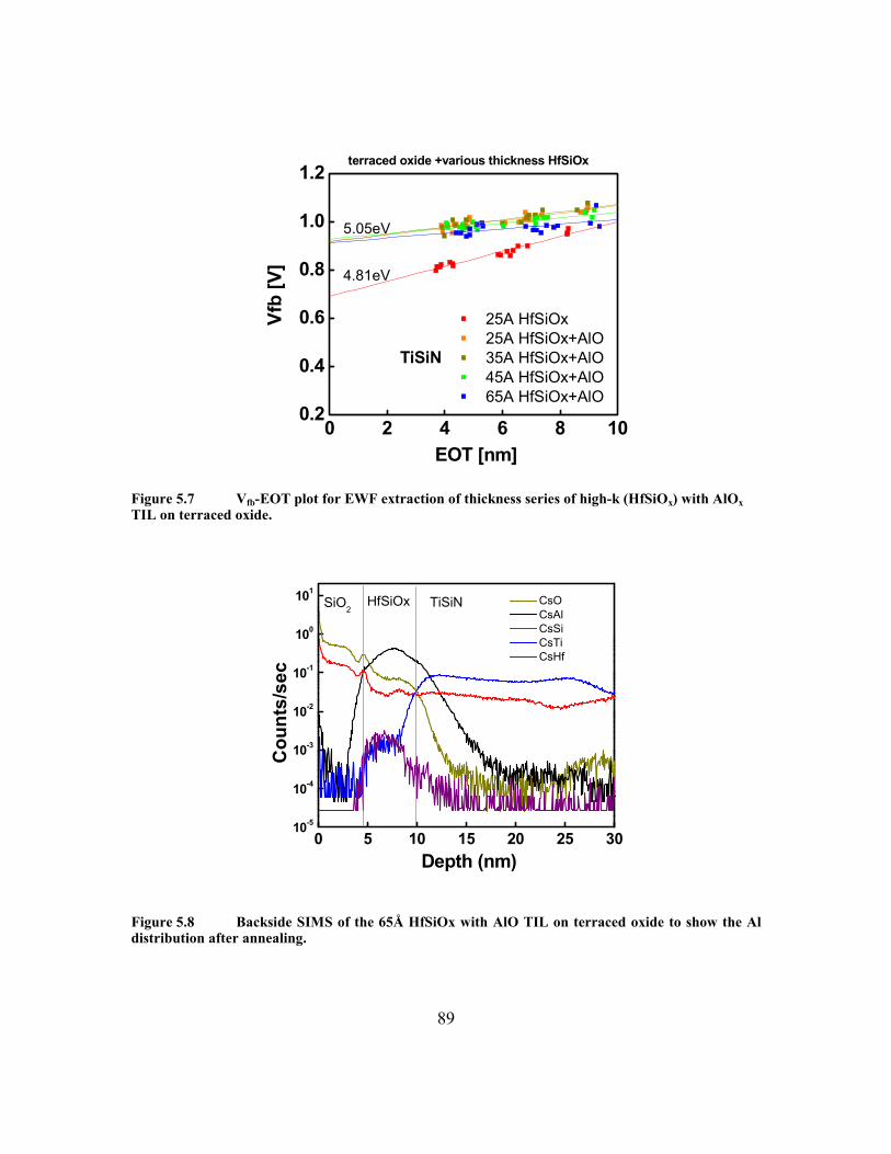
89
0 2 4 6 8 100.2
0.4
0.6
0.8
1.0
1.2
5.05eV
4.81eV
25A HfSiOx 25A HfSiOx+AlO 35A HfSiOx+AlO 45A HfSiOx+AlO 65A HfSiOx+AlO
Vfb
[V]
EOT [nm]
terraced oxide +various thickness HfSiOx
TiSiN
Figure 5.7 Vfb-EOT plot for EWF extraction of thickness series of high-k (HfSiOx) with AlOx TIL on terraced oxide.
0 5 10 15 20 25 3010-5
10-4
10-3
10-2
10-1
100
101 CsO CsAl CsSi CsTi CsHf
Cou
nts/
sec
Depth (nm)
SiO2HfSiOx TiSiN
Figure 5.8 Backside SIMS of the 65Å HfSiOx with AlO TIL on terraced oxide to show the Al distribution after annealing.
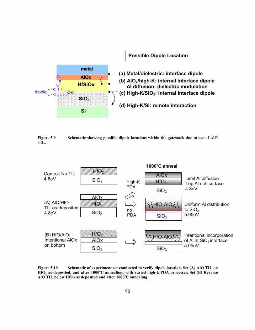
90
Figure 5.9 Schematic showing possible dipole locations within the gatestack due to use of AlO TIL.
Figure 5.10 Schematic of experiment set conducted to verify dipole location. Set (A) AlO TIL on HfO2 as-deposited, and after 1000oC annealing; with varied high-k PDA processes. Set (B) Reverse AlO TIL below HfO2 as deposited and after 1000oC annealing
AlOx HfO2
SiO2
HfO2
SiO2
AlOx HfO2
SiO2
SiO2
HfO-AlOx
SiO2
HfO-AlOx
SiO2
AlOxHfO2
Control: No TIL 4.8eV
(A) AlO/HfO: TIL as-deposited 4.8eV
Limit Al diffusionTop Al rich surface 4.8eV
Uniform Al distributionto SiO2 5.05eV
Intentional incorporation of Al at SiO2 interface 5.05eV
(B) HfO/AlO: Intentional AlOx on bottom
1000oC anneal
noPDA
High-KPDA
AlOx
metal
HfSiOx
Si
SiO2
++++ - - - -
+q - q dipole
x
d
(d) High-K/Si: remote interaction
(c) High-K/SiO2: Internal interface dipole
(b) AlOx/high-K: internal interface dipole Al diffusion: dielectric modulation
(a) Metal/dielectric: interface dipole
Possible Dipole Location
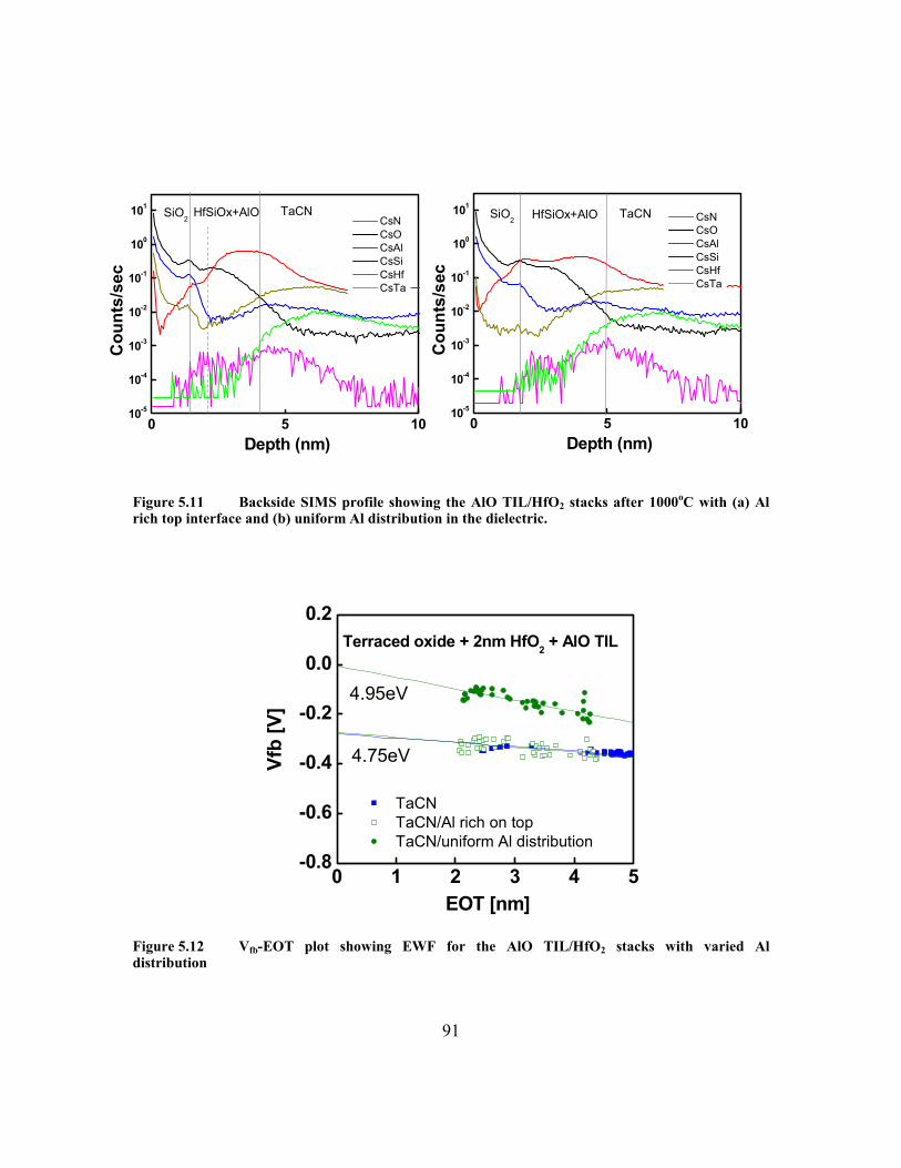
91
Figure 5.11 Backside SIMS profile showing the AlO TIL/HfO2 stacks after 1000oC with (a) Al rich top interface and (b) uniform Al distribution in the dielectric.
0 1 2 3 4 5-0.8
-0.6
-0.4
-0.2
0.0
0.2
4.95eV
TaCN TaCN/Al rich on top TaCN/uniform Al distribution
Vfb
[V]
EOT [nm]
Terraced oxide + 2nm HfO2 + AlO TIL
4.75eV
Figure 5.12 Vfb-EOT plot showing EWF for the AlO TIL/HfO2 stacks with varied Al distribution
0 5 1010-5
10-4
10-3
10-2
10-1
100
101TaCN CsN
CsO CsAl CsSi CsHf CsTa
Cou
nts/
sec
Depth (nm)
SiO2 HfSiOx+AlO
0 5 1010-5
10-4
10-3
10-2
10-1
100
101 TaCN CsN CsO CsAl CsSi CsHf CsTa
Cou
nts/
sec
Depth (nm)
SiO2
HfSiOx+AlO
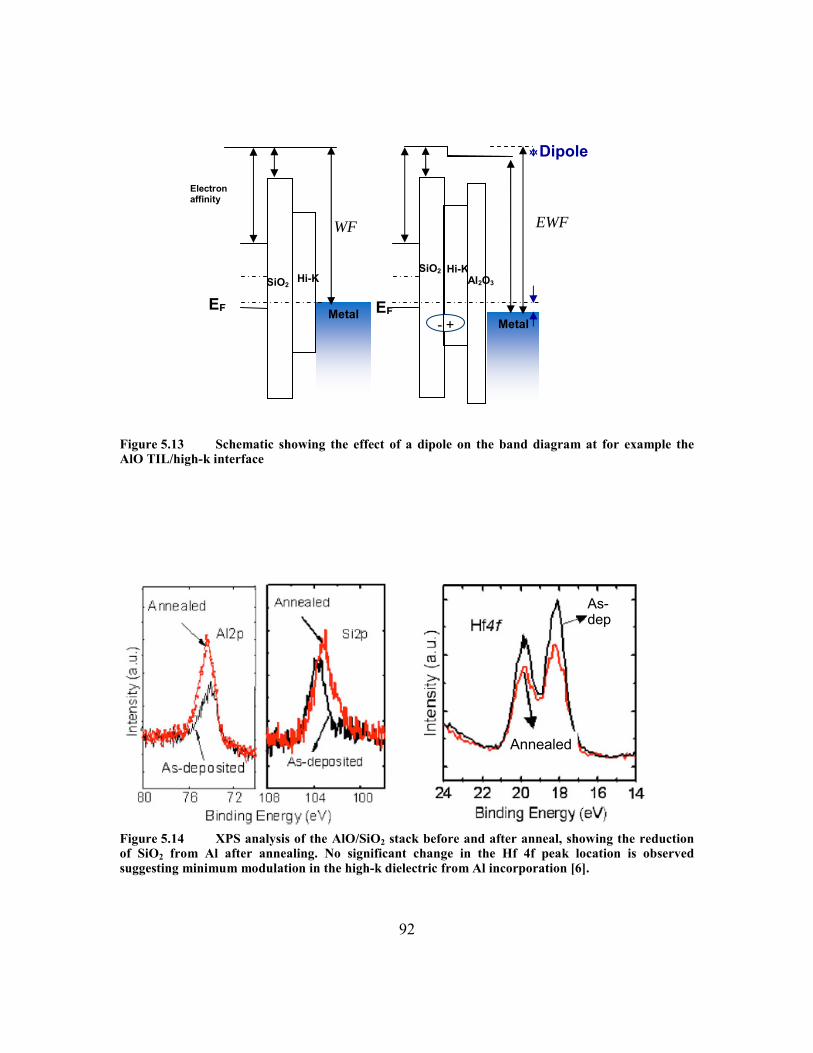
92
Figure 5.13 Schematic showing the effect of a dipole on the band diagram at for example the AlO TIL/high-k interface
Figure 5.14 XPS analysis of the AlO/SiO2 stack before and after anneal, showing the reduction of SiO2 from Al after annealing. No significant change in the Hf 4f peak location is observed suggesting minimum modulation in the high-k dielectric from Al incorporation [6].
Dipole
Metal
SiO2
Electron affinity
WF
EFMetal
SiO2
EF
Al2O3
- +
Hi-K Hi-K
EWF
Annealed
As-dep
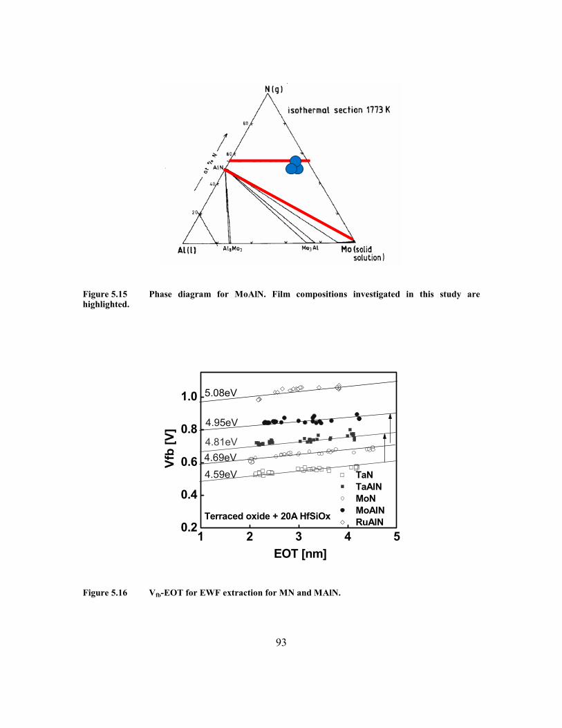
93
Figure 5.15 Phase diagram for MoAlN. Film compositions investigated in this study are highlighted.
1 2 3 4 50.2
0.4
0.6
0.8
1.0
TaN TaAlN MoN MoAlN RuAlN
5.08eV
4.81eV
4.59eV
Vfb
[V]
EOT [nm]
Terraced oxide + 20A HfSiOx
4.95eV
4.69eV
Figure 5.16 Vfb-EOT for EWF extraction for MN and MAlN.
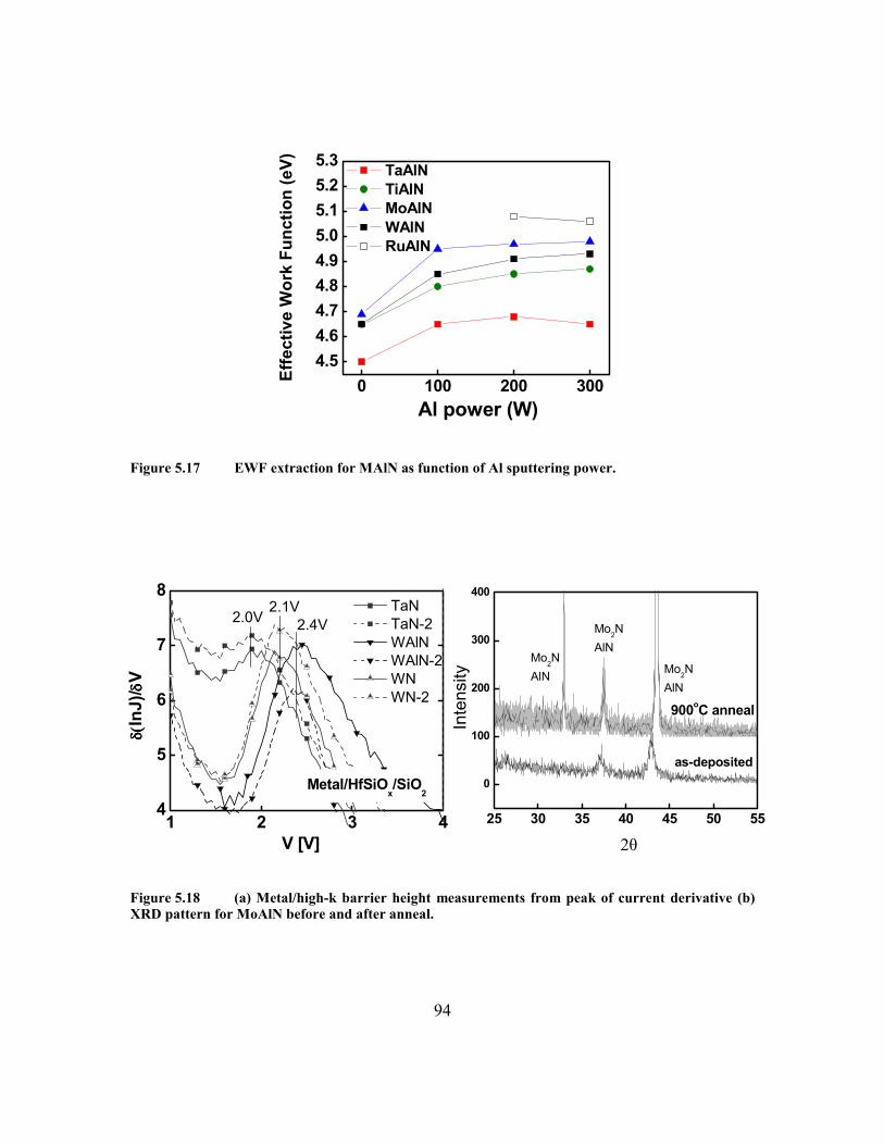
94
0 100 200 3004.54.64.74.84.95.05.15.25.3 TaAlN
TiAlN MoAlN WAlN RuAlN
Effe
ctiv
e W
ork
Func
tion
(eV)
Al power (W)
Figure 5.17 EWF extraction for MAlN as function of Al sputtering power.
Figure 5.18 (a) Metal/high-k barrier height measurements from peak of current derivative (b) XRD pattern for MoAlN before and after anneal.
25 30 35 40 45 50 55
0
100
200
300
400
900oC anneal
Mo2NAlN
Mo2NAlN
Mo2NAlN
Cou
nts/
sec
Depth (nm)
as-deposited
1 2 3 44
5
6
7
82.0V 2.4V
TaN TaN-2 WAlN WAlN-2 WN WN-2
δδ δδ (( ((ln
J)/ δδ δδ
V
V [V]
Metal/HfSiOx/SiO
2
2.1V
2θ
Inte
nsity
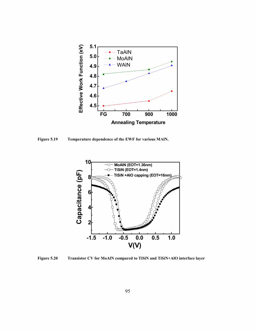
95
FG 700 900 10004.5
4.6
4.7
4.8
4.9
5.0
5.1 TaAlN MoAlN WAlN
Effe
ctiv
e W
ork
Func
tion
(eV)
Annealing Temperature
Figure 5.19 Temperature dependence of the EWF for various MAlN.
-1.5 -1.0 -0.5 0.0 0.5 1.0
2
4
6
8
10 MoAlN (EOT=1.36nm) TiSiN (EOT=1.4nm)
Cap
acita
nce
(pF)
V(V)
TiSiN +AlO capping (EOT=16nm)
Figure 5.20 Transistor CV for MoAlN compared to TiSiN and TiSiN+AlO interface layer
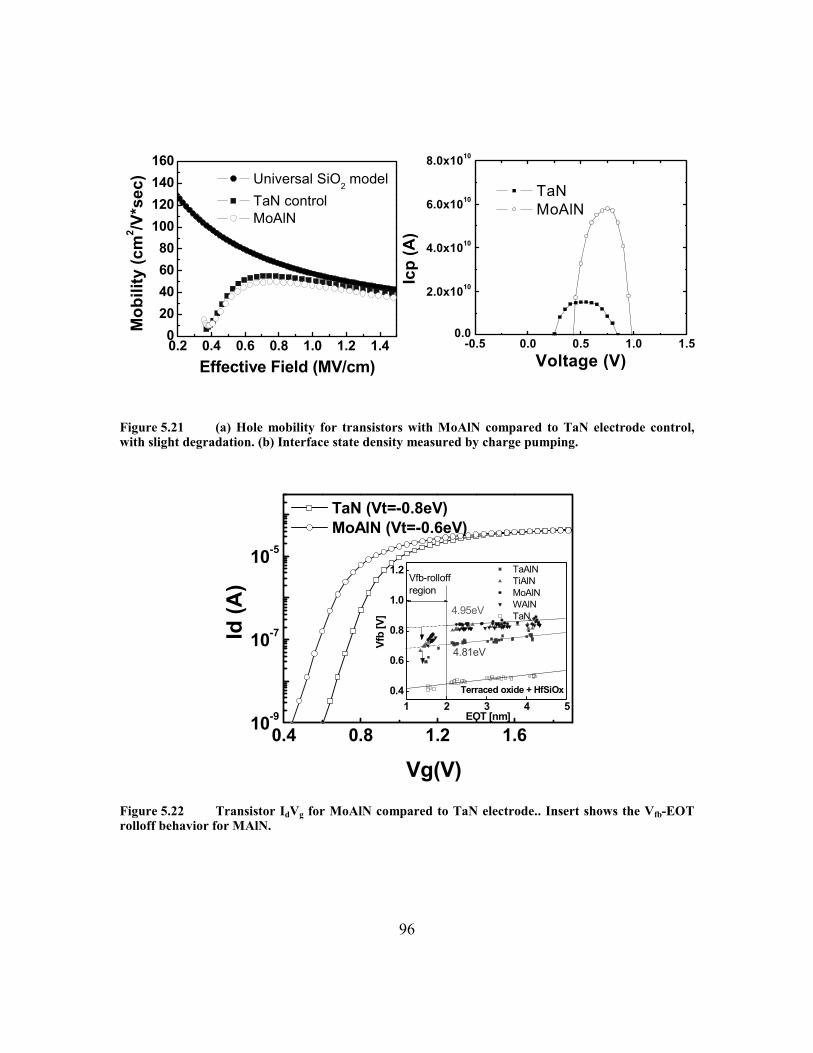
96
Figure 5.21 (a) Hole mobility for transistors with MoAlN compared to TaN electrode control, with slight degradation. (b) Interface state density measured by charge pumping.
0.4 0.8 1.2 1.610-9
10-7
10-5
1 2 3 4 50.4
0.6
0.8
1.0
1.2 TaAlN TiAlN MoAlN WAlN TaN
4.81eV
Vfb
[V]
EOT [nm]
Terraced oxide + HfSiOx
4.95eV
Vfb-rolloffregion
Vg(V)
TaN (Vt=-0.8eV) MoAlN (Vt=-0.6eV)
Id (A
)
Figure 5.22 Transistor IdVg for MoAlN compared to TaN electrode.. Insert shows the Vfb-EOT rolloff behavior for MAlN.
0.2 0.4 0.6 0.8 1.0 1.2 1.40
20406080
100120140160
Universal SiO2 model TaN control MoAlN
M
obili
ty (c
m2 /V
*sec
)
Effective Field (MV/cm)-0.5 0.0 0.5 1.0 1.5
0.0
2.0x10¹⁰
4.0x10¹⁰
6.0x10¹⁰
8.0x10¹⁰
TaN MoAlN
Voltage (V)
Icp
(A)
97
Figure 5.23 Vfb-EOT plot for EWF extraction of various metals on high-k with an La2O3 TIL.
14 16 18 20 22 24 26
Subs
trate
Inte
nsity
(a.u
.)
Depth (nm)
Si
TaN
Hf
La
(b)
Figure 5.24 Backside SIMS profile of the gate stack showing distribution of La into the high-k dielectric after anneal.
1 2 3 4 5 6 7 8 9 10-1.2
-1.0
-0.8
-0.6
-0.4
HfSix/La2O3/HfSiO: 4.01eV
TaN/La2O3/HfSiO: 4.09 eVFl
atba
nd V
olta
ge (V
)
EOT (nm)
TaN/HfSiO: 4.56 eV
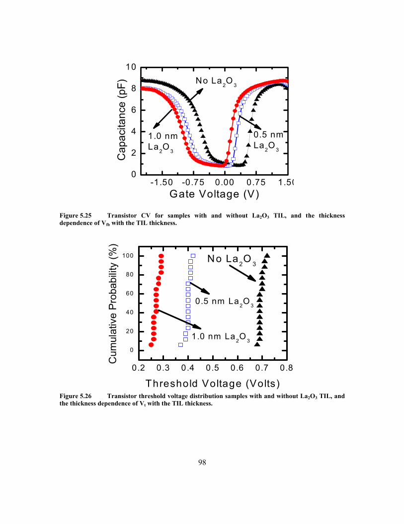
98
-1.50 -0.75 0.00 0.75 1.500
2
4
6
8
10
1.0 nm La2O 3
Cap
acita
nce
(pF)
Gate Voltage (V)
No La2O
3
0.5 nm La2O 3
Figure 5.25 Transistor CV for samples with and without La2O3 TIL, and the thickness dependence of Vfb with the TIL thickness.
0.2 0.3 0.4 0.5 0.6 0.7 0.8
0
20
40
60
80
100
1.0 nm La2O 3
0.5 nm La2O 3
Cum
ulat
ive
Prob
abili
ty (%
)
Threshold Voltage (Volts)
No La2O 3
Figure 5.26 Transistor threshold voltage distribution samples with and without La2O3 TIL, and the thickness dependence of Vt with the TIL thickness.
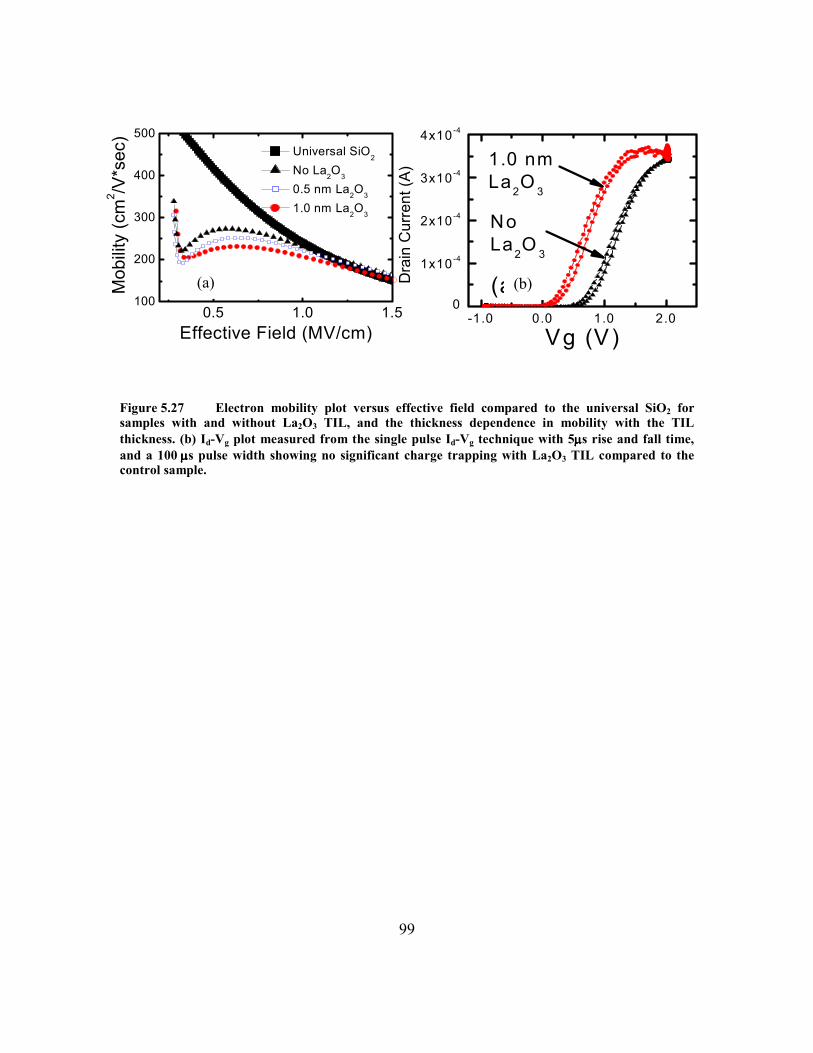
99
Figure 5.27 Electron mobility plot versus effective field compared to the universal SiO2 for samples with and without La2O3 TIL, and the thickness dependence in mobility with the TIL thickness. (b) Id-Vg plot measured from the single pulse Id-Vg technique with 5µµµµs rise and fall time, and a 100 µ µ µ µs pulse width showing no significant charge trapping with La2O3 TIL compared to the control sample.
0.5 1.0 1.5100
200
300
400
500
Mob
ility
(cm
2 /V*s
ec)
Effective Field (MV/cm)
Universal SiO2
No La2O3
0.5 nm La2O3
1.0 nm La2O3
-1.0 0.0 1.0 2.00
1x10⁻⁴
2x10⁻⁴
3x10⁻⁴
4x10⁻⁴
NoLa2O 3
Dra
in C
urre
nt (A
)
Vg (V)
1.0 nm La2O 3
(a)(b)(a)
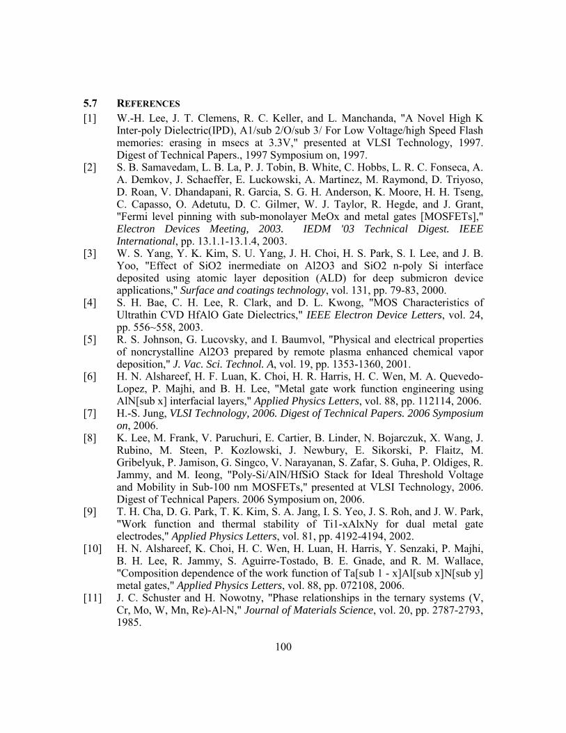
100
5.7 REFERENCES [1] W.-H. Lee, J. T. Clemens, R. C. Keller, and L. Manchanda, "A Novel High K
Inter-poly Dielectric(IPD), A1/sub 2/O/sub 3/ For Low Voltage/high Speed Flash memories: erasing in msecs at 3.3V," presented at VLSI Technology, 1997. Digest of Technical Papers., 1997 Symposium on, 1997.
[2] S. B. Samavedam, L. B. La, P. J. Tobin, B. White, C. Hobbs, L. R. C. Fonseca, A. A. Demkov, J. Schaeffer, E. Luckowski, A. Martinez, M. Raymond, D. Triyoso, D. Roan, V. Dhandapani, R. Garcia, S. G. H. Anderson, K. Moore, H. H. Tseng, C. Capasso, O. Adetutu, D. C. Gilmer, W. J. Taylor, R. Hegde, and J. Grant, "Fermi level pinning with sub-monolayer MeOx and metal gates [MOSFETs]," Electron Devices Meeting, 2003. IEDM '03 Technical Digest. IEEE International, pp. 13.1.1-13.1.4, 2003.
[3] W. S. Yang, Y. K. Kim, S. U. Yang, J. H. Choi, H. S. Park, S. I. Lee, and J. B. Yoo, "Effect of SiO2 inermediate on Al2O3 and SiO2 n-poly Si interface deposited using atomic layer deposition (ALD) for deep submicron device applications," Surface and coatings technology, vol. 131, pp. 79-83, 2000.
[4] S. H. Bae, C. H. Lee, R. Clark, and D. L. Kwong, "MOS Characteristics of Ultrathin CVD HfAlO Gate Dielectrics," IEEE Electron Device Letters, vol. 24, pp. 556~558, 2003.
[5] R. S. Johnson, G. Lucovsky, and I. Baumvol, "Physical and electrical properties of noncrystalline Al2O3 prepared by remote plasma enhanced chemical vapor deposition," J. Vac. Sci. Technol. A, vol. 19, pp. 1353-1360, 2001.
[6] H. N. Alshareef, H. F. Luan, K. Choi, H. R. Harris, H. C. Wen, M. A. Quevedo-Lopez, P. Majhi, and B. H. Lee, "Metal gate work function engineering using AlN[sub x] interfacial layers," Applied Physics Letters, vol. 88, pp. 112114, 2006.
[7] H.-S. Jung, VLSI Technology, 2006. Digest of Technical Papers. 2006 Symposium on, 2006.
[8] K. Lee, M. Frank, V. Paruchuri, E. Cartier, B. Linder, N. Bojarczuk, X. Wang, J. Rubino, M. Steen, P. Kozlowski, J. Newbury, E. Sikorski, P. Flaitz, M. Gribelyuk, P. Jamison, G. Singco, V. Narayanan, S. Zafar, S. Guha, P. Oldiges, R. Jammy, and M. Ieong, "Poly-Si/AlN/HfSiO Stack for Ideal Threshold Voltage and Mobility in Sub-100 nm MOSFETs," presented at VLSI Technology, 2006. Digest of Technical Papers. 2006 Symposium on, 2006.
[9] T. H. Cha, D. G. Park, T. K. Kim, S. A. Jang, I. S. Yeo, J. S. Roh, and J. W. Park, "Work function and thermal stability of Ti1-xAlxNy for dual metal gate electrodes," Applied Physics Letters, vol. 81, pp. 4192-4194, 2002.
[10] H. N. Alshareef, K. Choi, H. C. Wen, H. Luan, H. Harris, Y. Senzaki, P. Majhi, B. H. Lee, R. Jammy, S. Aguirre-Tostado, B. E. Gnade, and R. M. Wallace, "Composition dependence of the work function of Ta[sub 1 - x]Al[sub x]N[sub y] metal gates," Applied Physics Letters, vol. 88, pp. 072108, 2006.
[11] J. C. Schuster and H. Nowotny, "Phase relationships in the ternary systems (V, Cr, Mo, W, Mn, Re)-Al-N," Journal of Materials Science, vol. 20, pp. 2787-2793, 1985.
101
[12] S. Zafar, C. Cabral, A. R., and A. Callegari, "A method for measuring barrier heights, metal work functions and fixed charge densities in metal/SiO2/Si capacitors," Applied Physics Letters, vol. 80, pp. 4858-4860, 2002.
[13] H. C. Wen, R. N. Choi, G. A. Brown, T. Boscke, K. Matthews, H. R. Harris, K. Choi, H. N. Alshareef, H. F. Luan, G. Bersuker, P. Majhi, D. L. Kwong, and B. H. Lee, "Comparison of effective work function extraction methods using capacitance and current measurement techniques," Ieee Electron Device Letters, vol. 27, pp. 598-601, 2006.
[14] H. Alshareef, H. Harris, H. Wen, C. Park, C. Huffman, K. Choi, H. Luan, P. Majhi, B. Lee, R. Jammy, D. Lichtenwalner, J. Jur, and A. Kingon, "Thermally Stable N-Metal Gate MOSFETs Using La-Incorporated HfSiO Dielectric," VLSI Technology, 2006. Digest of Technical Papers. 2006 Symposium on, pp. 7-8, 2006.
[15] H. Ono, Applied Physics Letters, vol. 78, pp. 1832, 2001. [16] N. Kimizuka, VLSI Technology, 1999. Digest of Technical Papers, pp. 73, 1999. [17] L. Pantisano, T. Schram, B. O'Sullivan, T. Conard, S. D. Gendt, G. Groeseneken,
P. Zimmerman, A. Akheyar, M. M. Heyns, S. Shamuilla, V. V. Afanas'ev, and A. Stesmans, "Effective work function modulation by controlled dielectric monolayer deposition," Applied Physics Letters, vol. 89, pp. 113505, 2006.
[18] V. Narayanan, V. Paruchuri, N. Bojarczuk, B. Linder, B. Doris, Y. Kim, S. Zafar, J. Stathis, S. Brown, J. Arnold, M. Copel, M. Steen, E. Cartier, A. Callegari, P. Jamison, J.-P. Locquet, D. Lacey, Y. Wang, P. Batson, P. Ronsheim, R. Jammy, and M. Chudzik, "Band-Edge High-Performance High-k/Metal Gate n-MOSFETs Using Cap Layers Containing Group IIA and IIIB Elements with Gate-First Processing for 45 nm and Beyond," VLSI Technology, 2006. Digest of Technical Papers. 2006 Symposium on, pp. 178-179, 2006.
[19] Y. Yamamoto, K. Kita, K. Kyuno, and A. Toriumi, "Study of La concentration dependent Vfb shift in metal/HfLaOx/Si capacitors," International Conference on Solid State Devices and Materials 2006, pp. 212, 2006.
102
CHAPTER 6
IMPACT OF METAL GATE ON DEVICE PERFORMANCE AND RELIABILITY
6.1 INTRODUCTION
The use of metal gate in place of poly-Si with high-k dielectrics has been shown
to improve overall device performance, and reliability [1]. With the use of metal gate
electrodes, improvement in electron mobility is observed possibly due to a reduction in
the dielectric defect density or suppression of soft optical phonon scattering [2].
However, studies on comparison of impact on device performance from various metal
electrodes has shown to strongly depend on the metal gate [3]. Variations in the metal
gate can contribute to changes in the SiOx interface layer quality, defect trap density in
the high-k and roughness at the metal/high-k interface [4, 5]. Since the initial goal of
obtaining band edge EWF metal gate were to enable EOT scaling with maximized drive
current, it is crucial to study the impact of electrodes on transistor device performance as
well as its implications on reliability. The device performance for our proposed n/p-type
metal gate candidates had been discussed in Chapter 5. In this chapter, the impact of the
EWF engineering species on the reliability of the devices will be discussed. Moreover,
studies of other materials systems which would give implications of possible impact of
metal gate electrodes on the device reliability is also performed.
6.2 IMPACT OF METAL GATE PROCESSES
The candidate metal gate material systems are mainly PVD metal electrodes. The
reliability of any potential band-edge metal gate deposited by PVD may be a concern,
103
since plasma damage has been an issue for PVD metal electrode films. Park et al.[6] have
compared the device performance of atomic layer deposited (ALD) versus PVD WN and
TaN. The difference for a higher leakage current and lower Gm observed for PVD metals
is attributed to process plasma induced damage. Since Ta and W are metals with large
mass which will sputter with higher incident energies and induce greater damage to the
dielectric. However, if the PVD processing is fine controlled by a low power deposition
process, sputtering damage can be significantly reduced. In this study, the device
performance and reliability of a controlled PVD TaN film is compared with TaN
deposited by an ALD process.
Experimental procedure
Transistor devices are formed in a standard planar gate-first process scheme. The
gate dielectric is ALD HfO2 and the metal gate is PVD TaN or ALD TaN. All transistor
gates are capped with 100nm of polysilicon and endure the full 1000oC poly and S/D
activation anneal. PVD deposition of the TaN was performed in a DC sputter tool with a
Ta target and Ar/N2 co-flow. ALD deposition was performed by surface saturation of
metal-organic precursor, followed by reduction using ammonia [4].
Results and Discussion
The effective work function of the TaN metal system has been shown to be
roughly a mid-gap metal. Figure 6.1 shows the flat band versus EOT plot of 1:1
stoichiometric ALD and PVD TaN deposited on ALD HfO2 and a similar EWF value is
observed. The actual transistor devices show a similar EOT (~1.2 nm for PVD TaN and
1.35nm for ALD TaN) and the threshold voltage (Vt) is similar consistent with the EWF.
This is important for determining whether the PVD process induces additional charges in
104
the dielectric that do not change the flat band voltage but have a deleterious effect on the
threshold voltage. The Vt as a function of gate length for the long channel devices is
shown in Figure 6.2(a). A tight Vt distribution indicates that the short channel devices are
working even with PVD electrode. The accumulation leakage current of large area
capacitors (A=5E-5 cm2, same wafer) is shown in Figure 6.2(b). The leakage current of
the PVD TaN gate stack (Jg= -2E-1 A/cm2) is slightly higher than that of the ALD TaN
gate stack (Jg= -8E-2 A/cm2) at Vfb-1V. This difference is relatively small, but the PVD
electrode sample shows slightly higher current possibly due to the slightly lower EOT.
In this case it can be concluded that PVD metal process has minimal effects on the gate
stack EOT and Vt as compared to ALD.
The 10µm x 1µm transistor Id-Vg curves are shown in Figure 6.3(a). The
saturation current for the PVD TaN device is significantly higher than the ALD TaN (log
scale). This is also reflected in the offset, where across a large sample set the distribution
is ~10% higher for the PVD case. Both devices have low sub-threshold swing (SS), 73
mV/dec for the ALD device and 71mV/dec for the PVD device, a strong indicator that he
Si interface is very high quality across device structure [7]. This is confirmed by the
charge pumping data (1MHz) in Figure 6.3(b), where the PVD device has slightly lower
interface states density. However, both devices are in the low 1010 eV-1 cm-2 range, and
thus the difference can be considered negligible.
[8][9]Another metric that can be used to probe the quality of the gate dielectric is
a constant voltage stress of transistor devices. We have shown that, during positive
constant voltage stress, charge trapping is the dominant mechanism for the threshold
voltage instability of high-k devices [4, 10]. Furthermore, this is recoverable with the
appropriate negative bias to de-trap electrons from shallow traps. Figure 6.4 depicts the
change in threshold voltage at 90oC with +1.8V stress, followed by a relaxation period
105
with 0V applied. There is a threefold increase in the change in threshold voltage for the
ALD TaN. To understand the source of the threshold voltage change, the sub-threshold
voltage of the Id-Vg curves is calculated and shown on the right axis. Since the ∆SS
density increase is a good indicator of the amount of interface state density increase, it is
apparent from the small change for both cases (<1%) that the source of charges that are
increasing threshold voltage is due to trapped charge in the dielectric. From this, it can be
concluded that the amount of transient charge trapping is significantly reduced when
PVD TaN is used. Furthermore, the dielectric quality is not compromised by the PVD
deposition of a heavy metal. This is in contradiction to previous reports, but may be
attributed to the high quality of the controlled sputtering process used in this case.
Conclusion
It is shown that, given the right metal PVD deposition conditions, the dielectric is
not adversely affected by sputtering of the metal gate when compared to ALD deposition.
Highly scaled transistor devices have a low EOT, excellent overdrive current and
superior interface properties independent of metal deposition. The PVD TaN transistors
display an improved mobility and charge trapping characteristics when compared to ALD
TaN transistors and the implementation of PVD, even when sputtering heavy elements, is
not precluded based on the quality of transistors and improvement in reliability. And
therefore candidate metal gate material systems can be deposited by PVD without
roadblocks in the reliability.
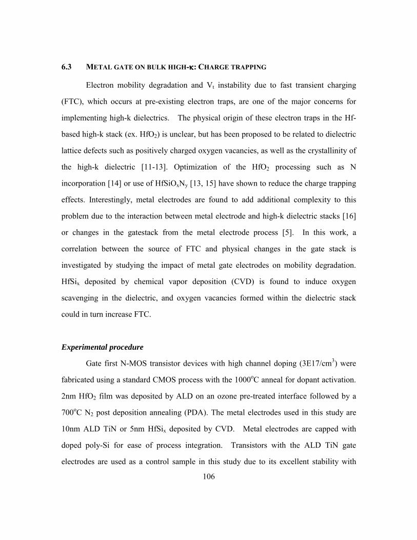
106
6.3 METAL GATE ON BULK HIGH-κκκκ: CHARGE TRAPPING
Electron mobility degradation and Vt instability due to fast transient charging
(FTC), which occurs at pre-existing electron traps, are one of the major concerns for
implementing high-k dielectrics. The physical origin of these electron traps in the Hf-
based high-k stack (ex. HfO2) is unclear, but has been proposed to be related to dielectric
lattice defects such as positively charged oxygen vacancies, as well as the crystallinity of
the high-k dielectric [11-13]. Optimization of the HfO2 processing such as N
incorporation [14] or use of HfSiOxNy [13, 15] have shown to reduce the charge trapping
effects. Interestingly, metal electrodes are found to add additional complexity to this
problem due to the interaction between metal electrode and high-k dielectric stacks [16]
or changes in the gatestack from the metal electrode process [5]. In this work, a
correlation between the source of FTC and physical changes in the gate stack is
investigated by studying the impact of metal gate electrodes on mobility degradation.
HfSix deposited by chemical vapor deposition (CVD) is found to induce oxygen
scavenging in the dielectric, and oxygen vacancies formed within the dielectric stack
could in turn increase FTC.
Experimental procedure
Gate first N-MOS transistor devices with high channel doping (3E17/cm3) were
fabricated using a standard CMOS process with the 1000oC anneal for dopant activation.
2nm HfO2 film was deposited by ALD on an ozone pre-treated interface followed by a
700oC N2 post deposition annealing (PDA). The metal electrodes used in this study are
10nm ALD TiN or 5nm HfSix deposited by CVD. Metal electrodes are capped with
doped poly-Si for ease of process integration. Transistors with the ALD TiN gate
electrodes are used as a control sample in this study due to its excellent stability with
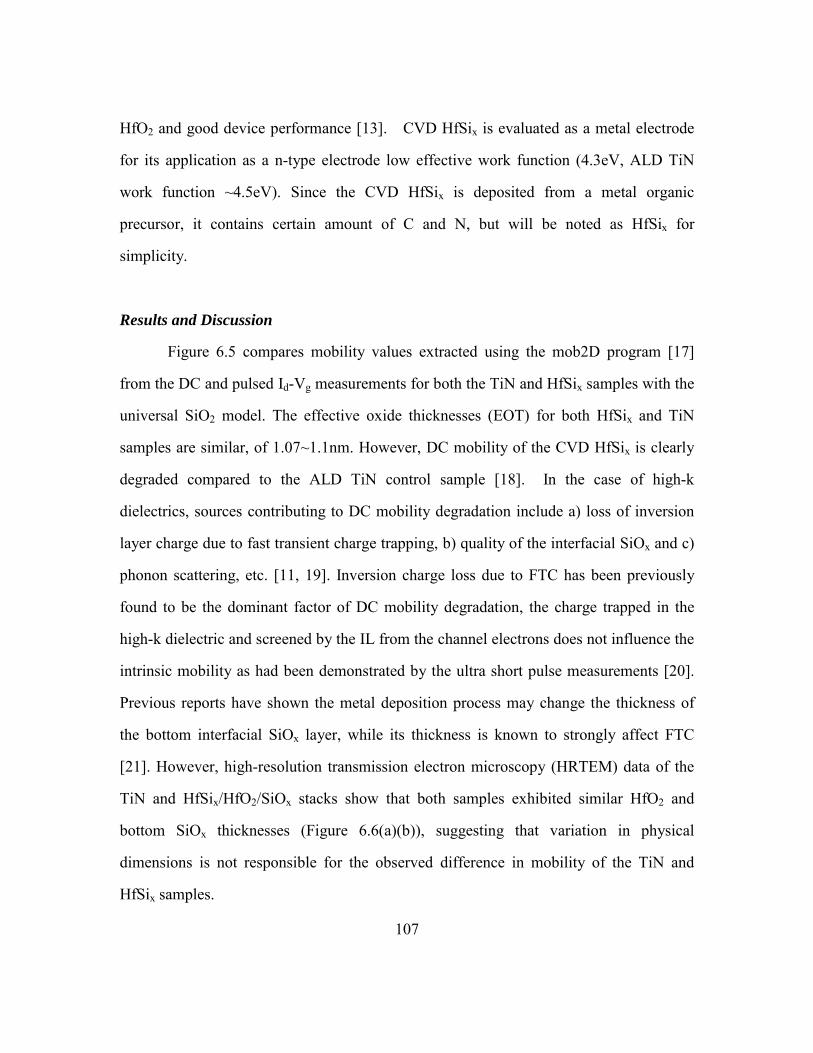
107
HfO2 and good device performance [13]. CVD HfSix is evaluated as a metal electrode
for its application as a n-type electrode low effective work function (4.3eV, ALD TiN
work function ~4.5eV). Since the CVD HfSix is deposited from a metal organic
precursor, it contains certain amount of C and N, but will be noted as HfSix for
simplicity.
Results and Discussion
Figure 6.5 compares mobility values extracted using the mob2D program [17]
from the DC and pulsed Id-Vg measurements for both the TiN and HfSix samples with the
universal SiO2 model. The effective oxide thicknesses (EOT) for both HfSix and TiN
samples are similar, of 1.07~1.1nm. However, DC mobility of the CVD HfSix is clearly
degraded compared to the ALD TiN control sample [18]. In the case of high-k
dielectrics, sources contributing to DC mobility degradation include a) loss of inversion
layer charge due to fast transient charge trapping, b) quality of the interfacial SiOx and c)
phonon scattering, etc. [11, 19]. Inversion charge loss due to FTC has been previously
found to be the dominant factor of DC mobility degradation, the charge trapped in the
high-k dielectric and screened by the IL from the channel electrons does not influence the
intrinsic mobility as had been demonstrated by the ultra short pulse measurements [20].
Previous reports have shown the metal deposition process may change the thickness of
the bottom interfacial SiOx layer, while its thickness is known to strongly affect FTC
[21]. However, high-resolution transmission electron microscopy (HRTEM) data of the
TiN and HfSix/HfO2/SiOx stacks show that both samples exhibited similar HfO2 and
bottom SiOx thicknesses (Figure 6.6(a)(b)), suggesting that variation in physical
dimensions is not responsible for the observed difference in mobility of the TiN and
HfSix samples.
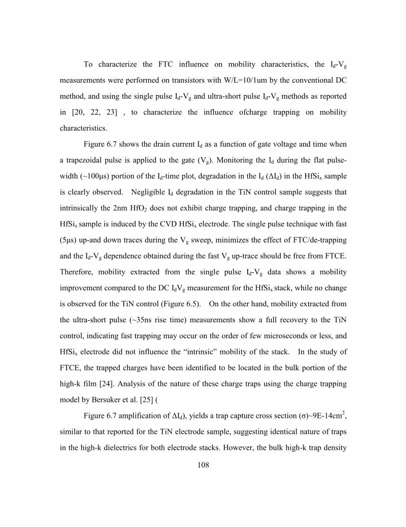
108
To characterize the FTC influence on mobility characteristics, the Id-Vg
measurements were performed on transistors with W/L=10/1um by the conventional DC
method, and using the single pulse Id-Vg and ultra-short pulse Id-Vg methods as reported
in [20, 22, 23] , to characterize the influence ofcharge trapping on mobility
characteristics.
Figure 6.7 shows the drain current Id as a function of gate voltage and time when
a trapezoidal pulse is applied to the gate (Vg). Monitoring the Id during the flat pulse-
width (~100µs) portion of the Id-time plot, degradation in the Id (∆Id) in the HfSix sample
is clearly observed. Negligible Id degradation in the TiN control sample suggests that
intrinsically the 2nm HfO2 does not exhibit charge trapping, and charge trapping in the
HfSix sample is induced by the CVD HfSix electrode. The single pulse technique with fast
(5µs) up-and down traces during the Vg sweep, minimizes the effect of FTC/de-trapping
and the Id-Vg dependence obtained during the fast Vg up-trace should be free from FTCE.
Therefore, mobility extracted from the single pulse Id-Vg data shows a mobility
improvement compared to the DC IdVg measurement for the HfSix stack, while no change
is observed for the TiN control (Figure 6.5). On the other hand, mobility extracted from
the ultra-short pulse (~35ns rise time) measurements show a full recovery to the TiN
control, indicating fast trapping may occur on the order of few microseconds or less, and
HfSix electrode did not influence the “intrinsic” mobility of the stack. In the study of
FTCE, the trapped charges have been identified to be located in the bulk portion of the
high-k film [24]. Analysis of the nature of these charge traps using the charge trapping
model by Bersuker et al. [25] (
Figure 6.7 amplification of ∆Id), yields a trap capture cross section (σ)~9E-14cm2,
similar to that reported for the TiN electrode sample, suggesting identical nature of traps
in the high-k dielectrics for both electrode stacks. However, the bulk high-k trap density

109
(No) in the HfSix sample ~2E22/cm3, is higher than the TiN sample (1E22/cm3) indicating
increased defects induced in the high-k from HfSix.
For further investigation, the quality of interfacial oxide is compared using the
fixed amplitude charge pumping (CP) method at various frequencies (Figure 6.8(b)) [26].
The density of traps at high frequencies, which correspond to the trap location near the
interface with the substrate, is similar in the TiN and HfSix samples. A gradual increase
in Nit is observed at lower frequencies towards the HfO2/SiOx interface [24, 26, 27].
However, the HfSix sample exhibits a slightly higher Nit than the TiN control, and
previous results indicate interfacial oxides with similar trap density differences only
exhibit 5% drive current differences. Therefore, Nit differences cannot completely
explain the mobility degradation [26].
CVD HfSix process with higher Hf concentration is found to exhibit the “oxygen
gettering” or “scavenging” effect from the interfacial SiOx layer as shown in the HRTEM
in Figure 6.6(c). The oxygen gettering effect has been commonly reported due to the
high energy of oxide formation and high oxygen solubility of Hf, resulting in the
reduction of the gate dielectric and subsequent oxygen diffusion to the gate electrode [28,
29]. Since O diffusion via oxygen lattice exchange is the predominant diffusion
mechanism in HfO2 [30], the O scavenging effects will result in O depletion in both the
bulk of HfO2 and the interfacial SiOx. In the case of our samples shown in Figure
6.6(b), the oxygen gettering effect is not visible via imaging since the interfacial SiOx
thickness remains similar to the control. However, the higher Nit observed in the HfSix
sample at lower frequencies correlates to an increased degree of interaction, possibly
indicating enhanced O scavenging effects in the HfSix, and its effect is more pronounced
closer to the high-k/electrode side. Due to increased charge trapping, reliability
degradation is also observed in the PBTI characteristics for samples heavily impacted by
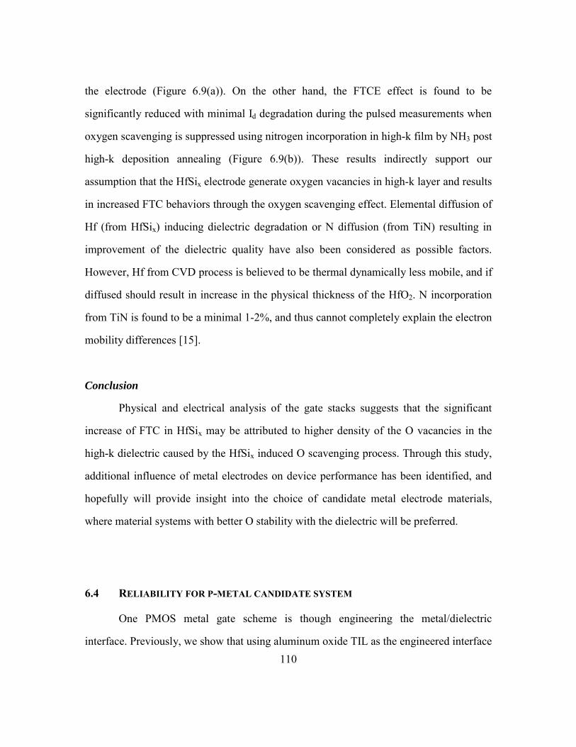
110
the electrode (Figure 6.9(a)). On the other hand, the FTCE effect is found to be
significantly reduced with minimal Id degradation during the pulsed measurements when
oxygen scavenging is suppressed using nitrogen incorporation in high-k film by NH3 post
high-k deposition annealing (Figure 6.9(b)). These results indirectly support our
assumption that the HfSix electrode generate oxygen vacancies in high-k layer and results
in increased FTC behaviors through the oxygen scavenging effect. Elemental diffusion of
Hf (from HfSix) inducing dielectric degradation or N diffusion (from TiN) resulting in
improvement of the dielectric quality have also been considered as possible factors.
However, Hf from CVD process is believed to be thermal dynamically less mobile, and if
diffused should result in increase in the physical thickness of the HfO2. N incorporation
from TiN is found to be a minimal 1-2%, and thus cannot completely explain the electron
mobility differences [15].
Conclusion
Physical and electrical analysis of the gate stacks suggests that the significant
increase of FTC in HfSix may be attributed to higher density of the O vacancies in the
high-k dielectric caused by the HfSix induced O scavenging process. Through this study,
additional influence of metal electrodes on device performance has been identified, and
hopefully will provide insight into the choice of candidate metal electrode materials,
where material systems with better O stability with the dielectric will be preferred.
6.4 RELIABILITY FOR P-METAL CANDIDATE SYSTEM
One PMOS metal gate scheme is though engineering the metal/dielectric
interface. Previously, we show that using aluminum oxide TIL as the engineered interface
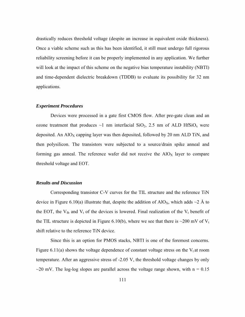
111
drastically reduces threshold voltage (despite an increase in equivalent oxide thickness).
Once a viable scheme such as this has been identified, it still must undergo full rigorous
reliability screening before it can be properly implemented in any application. We further
will look at the impact of this scheme on the negative bias temperature instability (NBTI)
and time-dependent dielectric breakdown (TDDB) to evaluate its possibility for 32 nm
applications.
Experiment Procedures
Devices were processed in a gate first CMOS flow. After pre-gate clean and an
ozone treatment that produces ~1 nm interfacial SiO2, 2.5 nm of ALD HfSiOx were
deposited. An AlOX capping layer was then deposited, followed by 20 nm ALD TiN, and
then polysilicon. The transistors were subjected to a source/drain spike anneal and
forming gas anneal. The reference wafer did not receive the AlOX layer to compare
threshold voltage and EOT.
Results and Discussion
Corresponding transistor C-V curves for the TIL structure and the reference TiN
device in Figure 6.10(a) illustrate that, despite the addition of AlOX, which adds ~2 Å to
the EOT, the Vfb and Vt of the devices is lowered. Final realization of the Vt benefit of
the TIL structure is depicted in Figure 6.10(b), where we see that there is ~200 mV of Vt
shift relative to the reference TiN device.
Since this is an option for PMOS stacks, NBTI is one of the foremost concerns.
Figure 6.11(a) shows the voltage dependence of constant voltage stress on the Vt at room
temperature. After an aggressive stress of -2.05 V, the threshold voltage changes by only
~20 mV. The log-log slopes are parallel across the voltage range shown, with n = 0.15
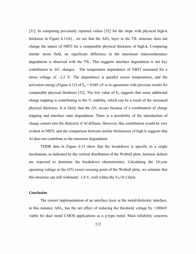
112
[31]. In comparing previously reported values [32] for the slope with physical high-k
thickness in Figure 6.11(b) , we see that the AlOx layer in the TIL structure does not
change the nature of NBTI for a comparable physical thickness of high-k. Comparing
similar stress field, no significant difference in the maximum transconductance
degradation is observed with the TIL. This suggests interface degradation is not key
contribution to ∆Vt changes. The temperature dependence of NBTI measured for a
stress voltage of –2.2 V. The dependence is parallel across temperatures, and the
activation energy (Figure 6.12) of Ea = 0.045 eV is in agreement with previous results for
comparable physical thickness [32]. The low value of Ea suggests that some additional
charge trapping is contributing to the Vt stability, which can be a result of the increased
physical thickness. It is likely that the ∆Vt occurs because of a combination of charge
trapping and interface state degradation. There is a possibility of the introduction of
charge centers into the dielectric if Al diffuses. However, this contribution would be very
evident in NBTI, and the comparison between similar thicknesses of high k suggests that
Al does not contribute to the transistor degradation.
TDDB data in Figure 6.13 show that the breakdown is specific to a single
mechanism, as indicated by the vertical distribution of the Weibull plots. Intrinsic defects
are expected to dominate the breakdown characteristics. Calculating the 10-year
operating voltage at the 63% (zero) crossing point of the Weibull plots, we estimate that
this structure can still withstand –1.6 V, well within the VD+0.2 limit.
Conclusion
The correct implementation of an interface layer at the metal/dielectric interface,
in this instance AlOx, has the net effect of reducing the threshold voltage by >200mV
viable for dual metal CMOS applications as a p-type metal. Main reliability concerns
113
associated with Al-containing stacks are consistent with those observed for comparable
thickness of Hf-based high-k. Al is not found to be a roadblock in the PMOS reliability,
and should apply to the metal-Al-nitride metal gate systems. Scaling the dielectric to 32
nm specifications with excellent reliability can be realizable.
114
6.5 FIGURES
Figure 6.1 Flat band voltage versus EOT for ALD (closed symbols) and PVD (open symbols) TaN on HfO2.
Figure 6.2 Threshold voltage variation for the long channel devices. Accumulation Jg for the ALD and PVD TaN transistors.
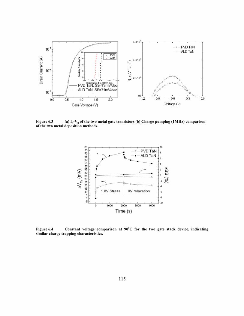
115
Figure 6.3 (a) Id-Vg of the two metal gate transistors (b) Charge pumping (1MHz) comparison of the two metal deposition methods.
Figure 6.4 Constant voltage comparison at 90oC for the two gate stack device, indicating similar charge trapping characteristics.
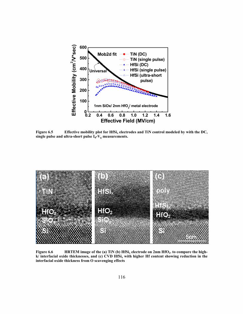
116
0.2 0.4 0.6 0.8 1.0 1.2 1.4 1.60
100
200
300
400
500
600 TiN (DC) TiN (single pulse) HfSi (DC) HfSi (single pulse) HfSi (ultra-short
pulse)
Effe
ctiv
e M
obili
ty (c
m2 /V
*sec
)
Effective Field (MV/cm)
1nm SiOx/ 2nm HfO2/ metal electrode
Mob2d fit
Universal
Figure 6.5 Effective mobility plot for HfSix electrodes and TiN control modeled by with the DC, single pulse and ultra-short pulse Id-Vg measurements.
Figure 6.6 HRTEM image of the (a) TiN (b) HfSix electrode on 2nm HfO2. to compare the high-k/ interfacial oxide thicknesses, and (c) CVD HfSix with higher Hf content showing reduction in the interfacial oxide thickness from O scavenging effects
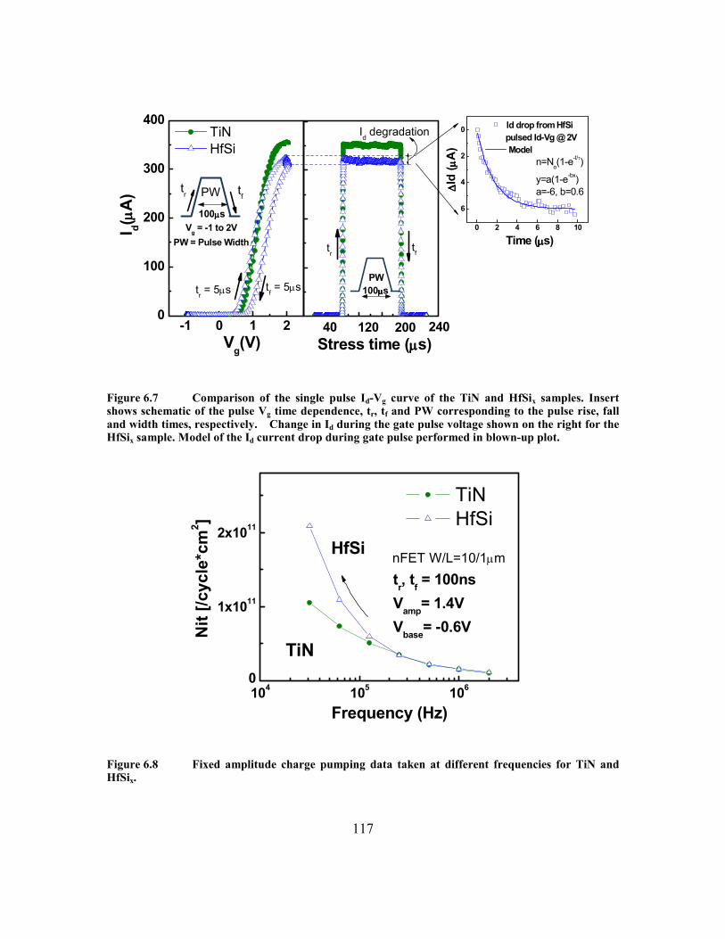
117
-1 0 1 20
100
200
300
400 TiN HfSi
I d( µµ µµA
)
Vg(V)
tf = 5µstr = 5µs
tftr PW
Vg = -1 to 2VPW = Pulse Width
100µµµµs0 2 4 6 8 10
6
4
2
0
Id drop from HfSi pulsed Id-Vg @ 2V
Model
∆∆ ∆∆Id
( µµ µµA
)
Time (µµµµs)
n=No(1-e-t/τ)
y=a(1-e-bx)a=-6, b=0.6
PW
240200120
tf tr
Stress time (µµµµs)
100µµµµs
Id degradation
40
Figure 6.7 Comparison of the single pulse Id-Vg curve of the TiN and HfSix samples. Insert shows schematic of the pulse Vg time dependence, tr, tf and PW corresponding to the pulse rise, fall and width times, respectively. Change in Id during the gate pulse voltage shown on the right for the HfSix sample. Model of the Id current drop during gate pulse performed in blown-up plot.
104 105 1060
1x10¹¹
2x10¹¹
TiN HfSi
tr, tf = 100nsVamp= 1.4VVbase= -0.6V
TiN
Nit
[/cyc
le*c
m2 ]
Frequency (Hz)
HfSi nFET W/L=10/1µm
Figure 6.8 Fixed amplitude charge pumping data taken at different frequencies for TiN and HfSix.
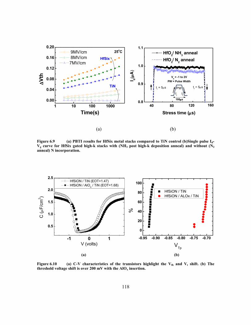
118
1 10 100 10000.00
0.04
0.08
0.12
0.16
0.20
TiN
9MV/cm 8MV/cm7MV/cm
∆∆ ∆∆
Vth
Time(s)
25oC
HfSix
(a) (b) Figure 6.9 (a) PBTI results for HfSix metal stacks compared to TiN control (b)Single pulse Id-Vg curve for HfSix gated high-k stacks with (NH3 post high-k deposition anneal) and without (N2 anneal) N incorporation.
-1 0 1
0.5
1.0
1.5
2.0
2.5
C (µ
F/cm
2 )
V (volts)
HfSiON / TiN (EOT=1.47) HfSiON / AlO
X / TiN (EOT=1.68)
(a) (b) Figure 6.10 (a) C-V characteristics of the transistors highlight the Vfb and Vt shift. (b) The threshold voltage shift is over 200 mV with the AlOx insertion.
0.8
0.9
1.0
1.1
160
Stress time (µµµµs)
I d( µµ µµA
)
HfO2/ NH3 anneal HfO2/ N2 anneal
40 12080
tf = 5µstr = 5µs
tf
tr
PW
Vg = -1 to 2VPW = Pulse Width
100µµµµs
-0.95 -0.90 -0.85 -0.80 -0.75 -0.70
0
20
40
60
80
100
%
VTp
HfSiON / TiN HfSiON / ALOx / TiN
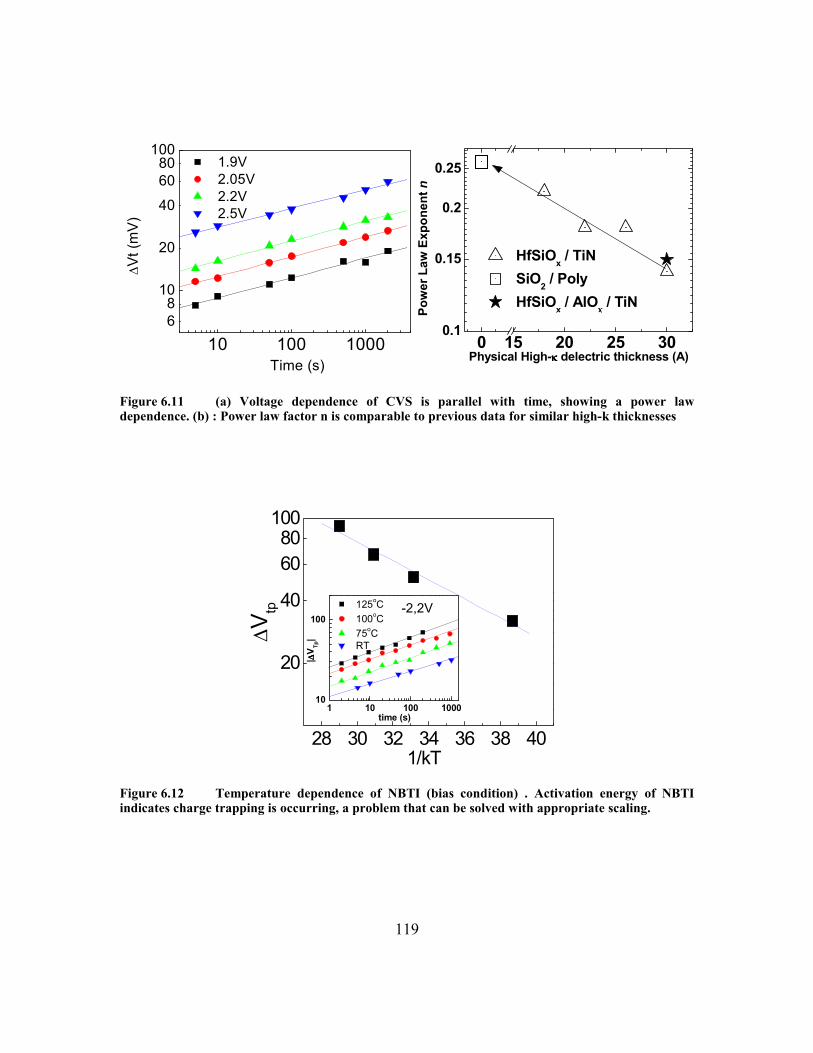
119
10 100 100068
10
20
40
6080
100
1.9V 2.05V 2.2V 2.5V
∆Vt
(mV
)
Time (s) Figure 6.11 (a) Voltage dependence of CVS is parallel with time, showing a power law dependence. (b) : Power law factor n is comparable to previous data for similar high-k thicknesses
Figure 6.12 Temperature dependence of NBTI (bias condition) . Activation energy of NBTI indicates charge trapping is occurring, a problem that can be solved with appropriate scaling.
28 30 32 34 36 38 40
20
40
6080
100
∆Vtp
1/kT
1 10 100 100010
100 125oC 100oC 75oC RT
| ∆∆ ∆∆V Tp
|
time (s)
-2,2V
0 15 20 25 300.1
0.15
0.2
0.25
HfSiOx / TiN SiO2 / Poly HfSiOx / AlOx / TiN
Pow
er L
aw E
xpon
ent n
Physical High-κκκκ delectric thickness (A)
SiO2(20A)
log (∆∆∆∆VTH) = nlog (t) + c
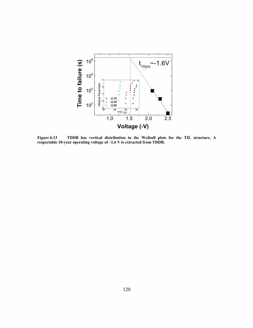
120
Figure 6.13 TDDB has vertical distribution in the Weibull plots for the TIL structure. A respectable 10-year operating voltage of –1.6 V is extracted from TDDB.
1.0 1.5 2.0 2.5
102
104
106
108
Tim
e to
failu
re (s
)
Voltage (-V)
t10yrs~-1.6V
10-2 100 102 104-3
-2
-1
0
1
-2.1V -2.3V -2.5V
Wie
bull
Para
met
er
TTF (s)
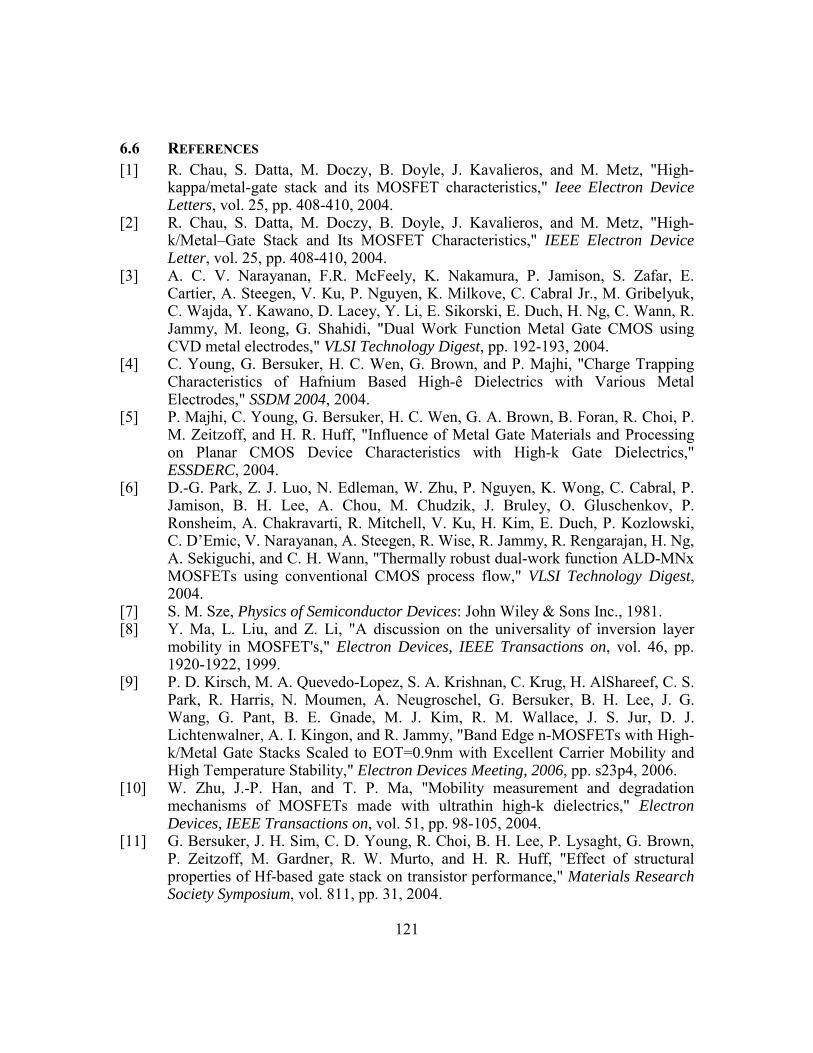
121
6.6 REFERENCES [1] R. Chau, S. Datta, M. Doczy, B. Doyle, J. Kavalieros, and M. Metz, "High-
kappa/metal-gate stack and its MOSFET characteristics," Ieee Electron Device Letters, vol. 25, pp. 408-410, 2004.
[2] R. Chau, S. Datta, M. Doczy, B. Doyle, J. Kavalieros, and M. Metz, "High-k/Metal–Gate Stack and Its MOSFET Characteristics," IEEE Electron Device Letter, vol. 25, pp. 408-410, 2004.
[3] A. C. V. Narayanan, F.R. McFeely, K. Nakamura, P. Jamison, S. Zafar, E. Cartier, A. Steegen, V. Ku, P. Nguyen, K. Milkove, C. Cabral Jr., M. Gribelyuk, C. Wajda, Y. Kawano, D. Lacey, Y. Li, E. Sikorski, E. Duch, H. Ng, C. Wann, R. Jammy, M. Ieong, G. Shahidi, "Dual Work Function Metal Gate CMOS using CVD metal electrodes," VLSI Technology Digest, pp. 192-193, 2004.
[4] C. Young, G. Bersuker, H. C. Wen, G. Brown, and P. Majhi, "Charge Trapping Characteristics of Hafnium Based High-ê Dielectrics with Various Metal Electrodes," SSDM 2004, 2004.
[5] P. Majhi, C. Young, G. Bersuker, H. C. Wen, G. A. Brown, B. Foran, R. Choi, P. M. Zeitzoff, and H. R. Huff, "Influence of Metal Gate Materials and Processing on Planar CMOS Device Characteristics with High-k Gate Dielectrics," ESSDERC, 2004.
[6] D.-G. Park, Z. J. Luo, N. Edleman, W. Zhu, P. Nguyen, K. Wong, C. Cabral, P. Jamison, B. H. Lee, A. Chou, M. Chudzik, J. Bruley, O. Gluschenkov, P. Ronsheim, A. Chakravarti, R. Mitchell, V. Ku, H. Kim, E. Duch, P. Kozlowski, C. D’Emic, V. Narayanan, A. Steegen, R. Wise, R. Jammy, R. Rengarajan, H. Ng, A. Sekiguchi, and C. H. Wann, "Thermally robust dual-work function ALD-MNx MOSFETs using conventional CMOS process flow," VLSI Technology Digest, 2004.
[7] S. M. Sze, Physics of Semiconductor Devices: John Wiley & Sons Inc., 1981. [8] Y. Ma, L. Liu, and Z. Li, "A discussion on the universality of inversion layer
mobility in MOSFET's," Electron Devices, IEEE Transactions on, vol. 46, pp. 1920-1922, 1999.
[9] P. D. Kirsch, M. A. Quevedo-Lopez, S. A. Krishnan, C. Krug, H. AlShareef, C. S. Park, R. Harris, N. Moumen, A. Neugroschel, G. Bersuker, B. H. Lee, J. G. Wang, G. Pant, B. E. Gnade, M. J. Kim, R. M. Wallace, J. S. Jur, D. J. Lichtenwalner, A. I. Kingon, and R. Jammy, "Band Edge n-MOSFETs with High-k/Metal Gate Stacks Scaled to EOT=0.9nm with Excellent Carrier Mobility and High Temperature Stability," Electron Devices Meeting, 2006, pp. s23p4, 2006.
[10] W. Zhu, J.-P. Han, and T. P. Ma, "Mobility measurement and degradation mechanisms of MOSFETs made with ultrathin high-k dielectrics," Electron Devices, IEEE Transactions on, vol. 51, pp. 98-105, 2004.
[11] G. Bersuker, J. H. Sim, C. D. Young, R. Choi, B. H. Lee, P. Lysaght, G. Brown, P. Zeitzoff, M. Gardner, R. W. Murto, and H. R. Huff, "Effect of structural properties of Hf-based gate stack on transistor performance," Materials Research Society Symposium, vol. 811, pp. 31, 2004.
122
[12] J. L. Gavartin, A. L. Shluger, A. S. Foster, and G. Bersuker, "The role of nitrogen-related defects in high-k dielectric oxides: Density-functional studies," Journal of Applied Physics, vol. 97, pp. 053704-1~12, 2005.
[13] P. D. Kirsch, J. H. Sim, S. C. Song, S. Krishnan, J. Peterson, H. J. Li, M. Quevedo-Lopez, C. D. Young, R. Choi, N. Moumen, P. Majhi, Q. Wang, J. G. Ekerdt, G. Bersuker, and B. H. Lee, "Mobility enhancement of high-k gate stacks through reduced transient charging," Solid-State Device Research Conference, 2005. ESSDERC 2005. Proceedings of 35th European, pp. 367-370, 2005.
[14] M. Koike, T. Ino, Y. Kamimuta, M. Koyama, Y. Kamata, M. Suzuki, Y. Mitani, A. Nishiyama, and Y. Tsunashima, "Effect of Hf-N bond on properties of thermally stable amorphous HfSiON and applicability of this material to sub-50nm technology node LSIs," Electron Devices Meeting, 2003. IEDM '03 Technical Digest. IEEE International, pp. 4.7.1-4.7.4, 2003.
[15] M. A. Quevedo-Lopez, S. A. Krishnan, P. D. Kirsch, H. J. Li, J. H. Sim, C. Huffman, J. J. Peterson, B. H. Lee, G. Pant, B. E. Gnade, M. J. Kim, R. M. Wallace, D. Guo, H. Bu, and T. P. Ma, "High Performance Gate First HfSiON Dielectric Satisfying 45nm Node Requirements," IEEE Electron Device Meeting, vol. 17.4, 2005.
[16] Y. Akasaka, K. Miyagawa, T. Sasaki, K. Shiraishi, S. Kamiyama, O. Ogawa, F. Ootsuka, and Y. Nara, "Impact of electrode-side chemical structures on electron mobility in metal/HfO/sub 2/ MISFETs with sub-1nm EOT," VLSI Technology, 2005. Digest of Technical Papers. 2005 Symposium on, pp. 228-229, 2005.
[17] J. R. Hauser, "Extraction of experimental mobility data for MOS devices," Electron Devices, IEEE Transactions on, vol. 43, pp. 1981-1988, 1996.
[18] G. Bersuker, P. Zeitzoff, J. H. Sim, B. H. Lee, R. Choi, G. Brown, and C. D. Young, "Mobility Evaluation in Transistors with Charge Trapping Gate Dielectrics," Applied Physics Letters, vol. 87, pp. 042905, 2005.
[19] T. Yamaguchi, R. Iijima, T. Ino, A. Nishiyama, H. Satake, and N. Fukushima, "Additional scattering effects for mobility degradation in Hf-silicate gate MISFETs," IEEE Electron Device Meeting, vol. Technology Digest, pp. 621-624, 2002.
[20] C. D. Young, R. Choi, J. H. Sim, B. H. Lee, P. Zeitzoff, Y. Zhao, K. Matthews, G. A. Brown, and G. Bersuker, "Interfacial layer dependence of HFSI/sub x/O/sub y/ gate stacks on V/sub T/ instability and charge trapping using ultra-short pulse in characterization," Reliability Physics Symposium, 2005. Proceedings. 43rd Annual. 2005 IEEE International, pp. 75-79, 2005.
[21] P. Majhi, H. C. Wen, H. Alshareef, K. Choi, R. Harris, P. Lysaght, H. Luan, Y. Senzaki, S. C. Song, B. H. Lee, and C. Ramiller, "Evaluation and integration of metal gate electrodes for future generation dual metal CMOS," Integrated Circuit Design and Technology, 2005. ICICDT 2005. 2005 International Conference on, pp. 69-72, 2005.
[22] C. D. Young, P. Zeitzoff, G. A. Brown, G. Bersuker, B. H. Lee, and J. R. Hauser, "Intrinsic mobility evaluation of high-/spl kappa/ gate dielectric transistors using pulsed I/sub d/-V/sub g/," Electron Device Letters, IEEE, vol. 26, pp. 586-589, 2005.
123
[23] A. Kerber, E. Cartier, L. A. Ragnarsson, M. Rosmeulen, L. Pantisano, R. Degraeve, Y. Kim, and G. Groesenenken, "Direct measurment of the inversion charge in MOSFETs: Application to mobility extraction in alternative gate dielectrics," VLSI Symosium Tech. Dig., pp. 159-160, 2003.
[24] C. D. Young, S. Nadkarni, D. Heh, H. R. Harris, R. Choi, J. Peterson, J. H. Sim, S. Krishnan, J. Barnett, E. Vogel, B. H. Lee, P. Zeitzoff, G. Brown, and G. Bersuker, "Detection of electron trap generation due to constant voltage stress on high-k gate stacks," International reliability physics symposium, vol. 3.A.1, 2006.
[25] G. Bersuker, B. H. Lee, H. R. Huff, J. Gavartin, and A. Shluger, "Mechanism of charge trapping reduction in scaled high-k gate stacks," presented at Proceedings of the NATO Advanced Research Workshop on Defects in Advanced High-k Dielectric Nano-Electronic Semiconductor Devices, St. Petersburg, Russia, 2006.
[26] C. D. Young, G. Bersuker, Y. Zhao, J. Peterson, J. Barnett, G. Brown, J. H. Sim, R. Choi, B. H. Lee, and P. Zeitzoff, "Probing stress effects in HfO2 gate stacks with time dependent measurements," Microelectronics Reliability, vol. 45, pp. 806-810, 2005.
[27] R. Degraeve, A. Kerber, E. Cartier, L. Pantisano, and G. Groesenenken, "Effect of bulk trap density on HfO2 reliability and yield," IEEE Electron Device Meeting, pp. 935-938, 2003.
[28] V. Misra, G. P. Heuss, and Z. H., "Use of metal-oxide-semiconductor capacitors to detect interactions of Hf and Zr gate electrodes with SiO2 and ZrO2," Applied Physics Letters, vol. 78, pp. 4166-4168, 2001.
[29] C. Choi, C. Y. Kang, S. J. Rhee, M. Akbar, S. Krishnan, M. Zhang, H. Kim, T. Lee, I. Ok, F. Zhu, and J. C. Lee, "Aggressively scaled ultra thin undoped HfO2 gate dielectric (EOT<0.7nm) with TaN gate electrode using engineered interface layer," IEEE Electron Device Letters, vol. 26, pp. 454-456, 2005.
[30] L. V. Goncharova, M. Dalponte, D. G. Starodub, T. Gustafsson, E. Garfunkel, P. S. Lysaght, B. F. Barnett, and G. I. Bersuker, "Oxygen diffusion and reactions in Hf-based dielectrics," Applied Physics Letters, vol. 89, pp. 044108, 2006.
[31] J. H. Sim, S. C. Song, P. D. kirsch, C. D. Young, R. Choi, D. L. Kwong, B. H. Lee, and G. Bersuker, "Effects of ALD HfO2 thickness on charge trapping and mobility," Insulating films on semiconductors INFOS 2005, pp. 8.1, 2005.
[32] S. A. Krishnan, M. Quevedo, R. Harris, P. D. Kirsch, R. Choi, B. H. Lee, G. Bersuker, J. Peterson, H.-J. Li, C. D. Young, and J. C. Lee, "NBTI Dependence on Dielectric Thickness in Ultra-scaled HfSiO Dielectric/ ALD-TiN Gate Stacks," 2005 International conference on SOLID STATE DEVICES AND MATERIALS, pp. A.2-4, 2005.
124
CHAPTER 7
CONCLUSIONS AND FUTURE WORK
7.1 SUMMARY AND CONCLUSION
Metal gate electrodes have the advantage of eliminating poly depletion and
poly/high-k interaction, as well as addressing the issue of high Vt values in pFETs caused
by Fermi-level pinning between the poly and high-k. To reduce Vt for maximized drive
current, the metal work function values should be near the band-edge of Si, i.e. EWF of
~5.0-5.2eV for p-MOS, and 4.1-4.3eV for n-MOS. A systematic study on the metal gate
EWF has been performed with the goal of identifying band-edge metal gate electrode
candidates.
Potential error sources in the EWF extraction from high-k thickness series have
presented a need for alternative EWF extraction techniques on high-k dielectrics. The
terraced oxide technique has been developed and demonstrated as an accurate technique
for EWF extraction on high-k. In combination with the leakage current barrier height
extraction technique, we are able to distinguish true EWF changes and the impact from
gate stack charges. With the terraced oxide technique as the metric for EWF
measurement, a study of factors controlling EWF is performed.
Fermi-level pinning is proposed to limit the EWF tuning on high-k dielectrics,
and a intrinsic roadblock to the identification of band-edge metal gates on high-k. A
summary of literature proposed models of Fermi-level pinning is discussed and compared
with our experimental data. It is concluded that an intrinsic limitation (MIGS pinning)
should not exist and the source for most EWF pinning on high-k is due to extrinsic
contributions, such as interfacial reactions, or possible O vacancy formation induced in
125
the dielectric. Therefore, through careful control of extrinsic factors, potential band-edge
metal gate electrodes could be achieved.
To investigate possible controlling factors on the EWF, analysis based on the
systematic breakdown of the EWF equation is performed. EWF is found to not only be
controlled by the bulk metal characteristic, but the interface properties between the metal
and dielectric exhibits a greater impact on EWF. Charges can be induced in the gate stack
during device processing, in addition to intrinsic dielectric charges and shift the Vfb. EWF
engineering by interface engineering, possibly from formation of an internal dielectric
interface dipole, is also identified as a plausible approach for EWF tuning.
Al-containing electrode stacks, either via interface engineering with a AlOx
interface layer between the metal and high-k or in bulk metal-aluminum-nitride form is
identified as potential p-type metal gate electrode candidates (EWF=4.95~5.1eV).
Lanthanide metal electrode stacks are identified as a suitable n-type metal gate solution
(EWF=4.1eV) without compromising device performance.
Comparison of metal gates on device performance and reliability studies are
performed. Potential impact of candidate metal gates systems is studied, as well as other
material systems which may give implications on the influence of metal gates on the gate
stack. Comparison of the deposition technique, shows that even PVD metal electrodes
can exhibit high performance. Metal systems which will impact the bulk high-k are
materials with high O solubility or reactivity with O. Reduction of the high-k will result
in increased charge trapping behavior and degraded electron mobility.
7.2 FUTURE WORK: THE VFB ROLLOFF ISSUE FOR P-TYPE EWF METALS
Although band edge metal electrodes candidates have been identified, a new
challenge in the integration for p-type EWF metals is found in the device integration at
126
low EOT regimes. A gradual reduction in the Vfb as the gate stacks are scaled to lower
EOT, with the onset of “roll-off” occurring at EOT of ~2-3nm (Figure 7.1(a)). The
magnitude of roll-off (∆Vfb) is found to be enhanced with higher EWF (p-type) metals.
Compensating for EOT differences from the high-k, the onset of roll-off occurs at similar
thicknesses in the interfacial SiO2. Enhanced roll-off is also observed with increased
thermal budget of the gate stacks, pointing to its thermally activated mechanism (Figure
7.1(b)). Interestingly, a similar observation was independently reported by Schaeffer et
al. [1], showing an independent confirmation of this phenomenon. Physical mechanisms
of this effect may be simply extrinsic (localized material interdiffusion [metal, N, O]),
inducing changes in the physical barrier height, or they may be intrinsic and related to
communication between the electrode with charge states in the dielectric (generated by O
vacancy formation) or induced as the SiO2 becomes less stoichiometric. The roll-off
effect in transistors prevents Vt scaling as EOT reduces (Figure 7.2), and therefore, may
require trade-offs in the optimization of p-MOS devices. Resolving the Vfb roll-off issue
is the key factor to implementing p-MOS metal gate electrodes with a low Vt, and more
understanding on the actual mechanism would be required.
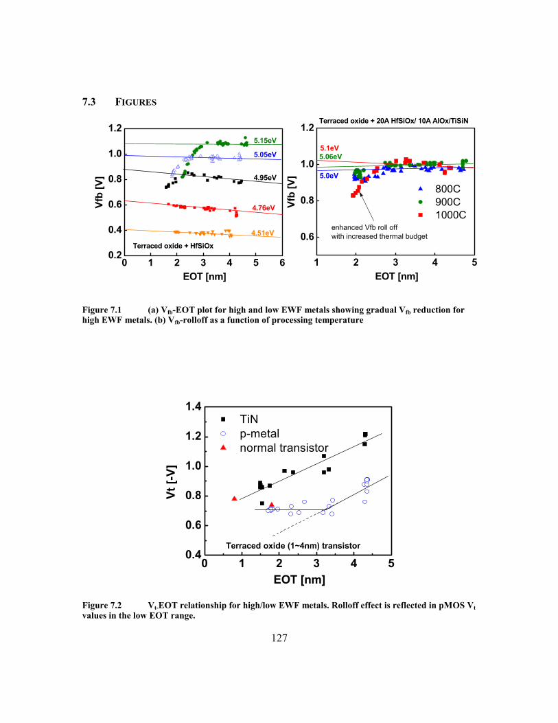
127
7.3 FIGURES Figure 7.1 (a) Vfb-EOT plot for high and low EWF metals showing gradual Vfb reduction for high EWF metals. (b) Vfb-rolloff as a function of processing temperature
0 1 2 3 4 50.4
0.6
0.8
1.0
1.2
1.4
Terraced oxide (1~4nm) transistor
TiN p-metal normal transistor
Vt [-
V]
EOT [nm]
Figure 7.2 Vt-EOT relationship for high/low EWF metals. Rolloff effect is reflected in pMOS Vt values in the low EOT range.
1 2 3 4 5
0.6
0.8
1.0
1.2
800C 900C 1000C
5.1eV
5.0eV
Vfb
[V]
EOT [nm]
Terraced oxide + 20A HfSiOx/ 10A AlOx/TiSiN
5.06eV
enhanced Vfb roll offwith increased thermal budget
0 1 2 3 4 5 60.2
0.4
0.6
0.8
1.0
1.2
4.51eV
4.76eV
4.95eV
5.05eV
Vfb
[V]
EOT [nm]
Terraced oxide + HfSiOx
5.15eV
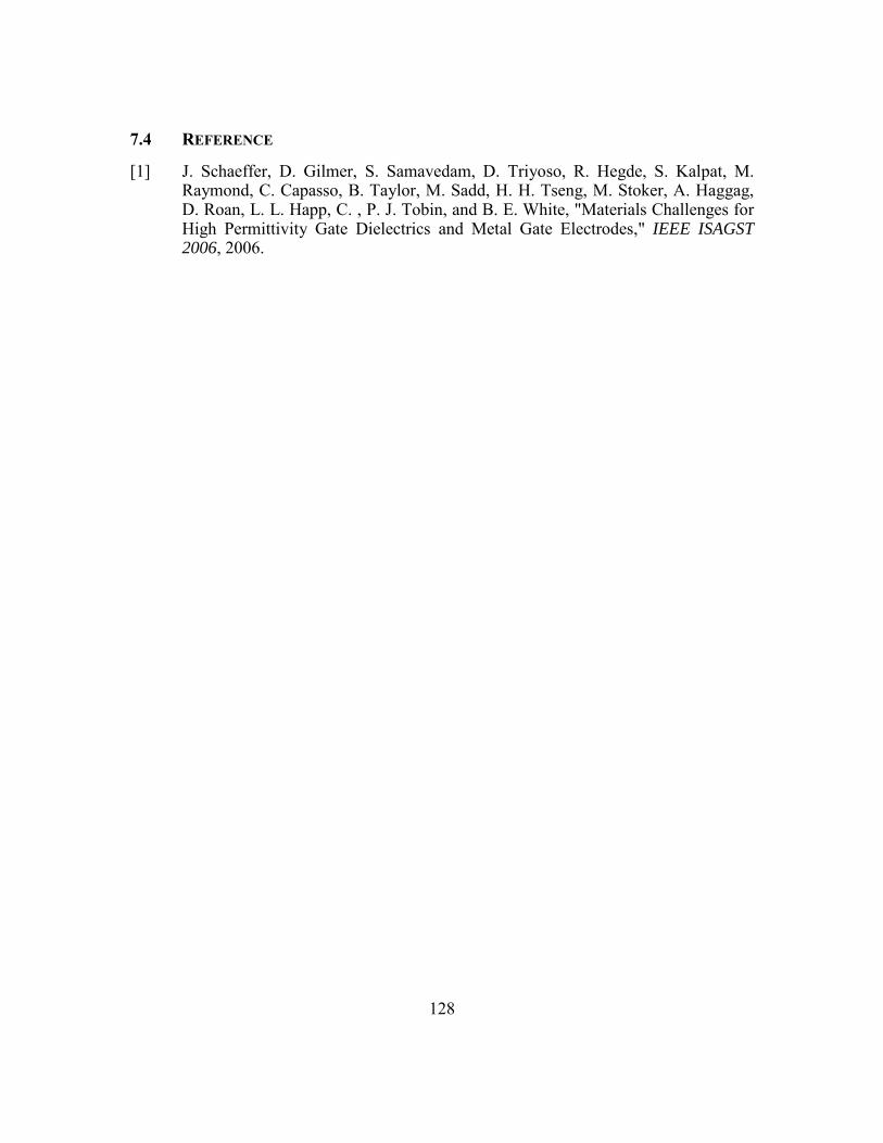
128
7.4 REFERENCE
[1] J. Schaeffer, D. Gilmer, S. Samavedam, D. Triyoso, R. Hegde, S. Kalpat, M. Raymond, C. Capasso, B. Taylor, M. Sadd, H. H. Tseng, M. Stoker, A. Haggag, D. Roan, L. L. Happ, C. , P. J. Tobin, and B. E. White, "Materials Challenges for High Permittivity Gate Dielectrics and Metal Gate Electrodes," IEEE ISAGST 2006, 2006.
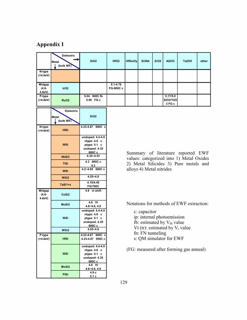
129
Appendix I
SiO2 HfO2 HfSixOy Si3N4 ZrO2 Al2O3 Ta2O5 other
N-type (<4.6eV)
Midgap (4.6-
4.8eV)IrO2
5.1-4.76 FG-900C c
P-type (>4.8eV) RuO2
5.04 600C fb 5.06 FG c
5.17/5.0 SiO2/Y2O
3 FG c
Metal (bulk WF)
Dielectric
SiO2
N-type (<4.6eV) HfSi
4.23-4.87 900C c
NiSi
undoped: 4.4-4.9 ntype: 4.6 c ptype: 5.1 c
undoped: 4.35 800C c
NbSi2 4.35~4.53
TiSi 4.3 800C c 4.3
WSi 4.2~4.65 600C c
WSi2 4.55~4.8
TaSi1+x4.15/4.45 FG/700C
Midgap (4.6-
4.8eV)CoSi2
4.6 vt shift
MoSi24.6 Vt
4.6~4.8, 4.9
NiSi
undoped: 4.4-4.9 ntype: 4.6 c ptype: 5.1 c
undoped: 4.35 800C c
WSi2 4.55~4.8
P-type (>4.8eV) HfSi
4.23-4.87 900C c 4.23-4.87 950C c
NiSi
undoped: 4.4-4.9 ntype: 4.6 c ptype: 5.1 c
undoped: 4.35 800C c
MoSi2 4.6 Vt 4.6~4.8, 4.9
PtSi 4.9 c 5.1 c
Metal (bulk WF)
Dielectric
Summary of literature reported EWF values: categorized into 1) Metal Oxides 2) Metal Silicides 3) Pure metals and alloys 4) Metal nitrides
Notations for methods of EWF extraction:
c: capacitor ip: internal photoemission fb: estimated by Vfb value Vt (tr): estimated by Vt value fn: FN tunneling s: QM simulator for EWF
(FG: measured after forming gas anneal)
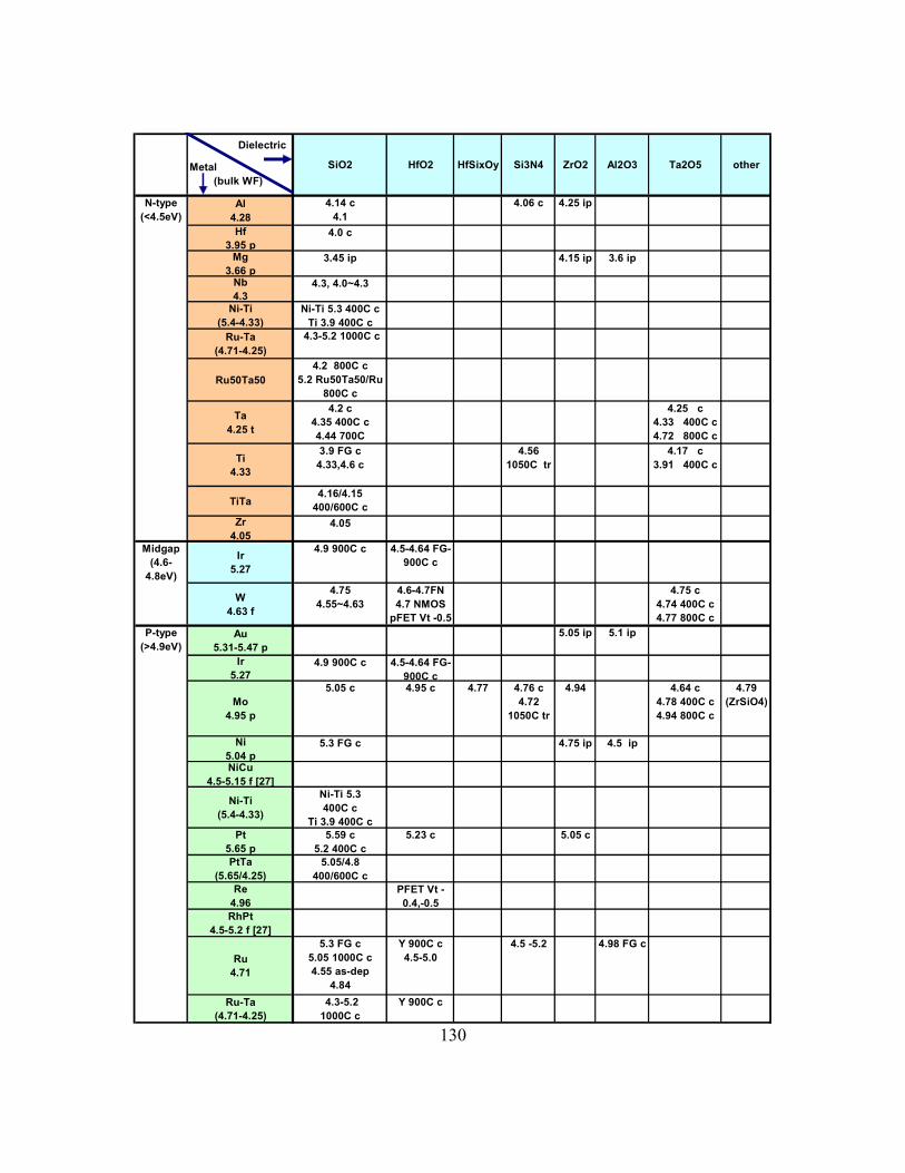
130
SiO2 HfO2 HfSixOy Si3N4 ZrO2 Al2O3 Ta2O5 other
N-type (<4.5eV)
Al4.28
4.14 c 4.1
4.06 c 4.25 ip
Hf3.95 p
4.0 c
Mg3.66 p
3.45 ip 4.15 ip 3.6 ip
Nb 4.3
4.3, 4.0~4.3
Ni-Ti (5.4-4.33)
Ni-Ti 5.3 400C c Ti 3.9 400C c
Ru-Ta (4.71-4.25)
4.3-5.2 1000C c
Ru50Ta504.2 800C c
5.2 Ru50Ta50/Ru 800C c
Ta4.25 t
4.2 c 4.35 400C c 4.44 700C
4.25 c4.33 400C c4.72 800C c
Ti 4.33
3.9 FG c 4.33,4.6 c
4.56 1050C tr
4.17 c3.91 400C c
TiTa4.16/4.15
400/600C cZr
4.054.05
Midgap (4.6-
4.8eV)
Ir 5.27
4.9 900C c 4.5-4.64 FG-900C c
W4.63 f
4.75 4.55~4.63
4.6-4.7FN 4.7 NMOS
pFET Vt -0.5
4.75 c4.74 400C c4.77 800C c
P-type (>4.9eV)
Au5.31-5.47 p
5.05 ip 5.1 ip
Ir 5.27
4.9 900C c 4.5-4.64 FG-900C c
Mo4.95 p
5.05 c 4.95 c 4.77 4.76 c 4.72
1050C tr
4.94 4.64 c4.78 400C c4.94 800C c
4.79 (ZrSiO4)
Ni5.04 p
5.3 FG c 4.75 ip 4.5 ip
NiCu 4.5-5.15 f [27]
Ni-Ti (5.4-4.33)
Ni-Ti 5.3 400C c
Ti 3.9 400C cPt
5.65 p5.59 c
5.2 400C c5.23 c 5.05 c
PtTa (5.65/4.25)
5.05/4.8 400/600C c
Re 4.96
PFET Vt -0.4,-0.5
RhPt 4.5-5.2 f [27]
Ru 4.71
5.3 FG c 5.05 1000C c 4.55 as-dep
4.84
Y 900C c 4.5-5.0
4.5 -5.2 4.98 FG c
Ru-Ta (4.71-4.25)
4.3-5.2 1000C c
Y 900C c
Metal (bulk WF)
Dielectric
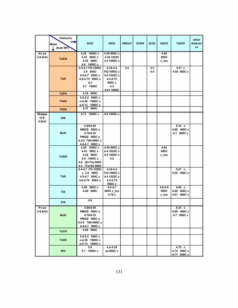
131
SiO2 HfO2 HfSixO Si3N4 ZrO2 Al2O3 Ta2O5other
dielectrics
N-t pe (<4.6eV) TaSiN
4.25 1000C c 4.43 900C c 4.52 600C
4.8 1000C c
4.55 900C c 4.36 1025C 4.4 1000C c
4.84 900C c_tox
TaN
4.4-4.7 FG-1000C 3.9 600C
4.5-4.7 950C c 4.0-4.75 950C c
4.2 4.7 1000C
4.34-4.4 FG-1000C c 4.4 1025C c
4.2-4.75 950C c
4.3 4.41 1000C
4.4 4.3 4.5
5.41 c4.55 400C c
TaPN 4.35 600C
TiAlN5.0-5.2 950C c n-4.36 1000C c p-5.13 1000C c
TiSiN 4.37 600C
Midgap (4.6-
4.8eV)HfN
4.71 1000C c 4.8 1000C c
MoN
4.94/4.95 NMOS 800C s
4.70/4.53 PMOS 800C s
4.4-5 700+900C c 4.4-4.7 900C c
5.33 c4.89 400C c4.7 800C c
TaSiN
4.25 1000C c 4.43 900C c 4.52 600C
4.8 1000C c 4.8 (Si>Ta) 900C 4.4 (Ta>Si) 900C
4.55 900C c 4.4 1025C c 4.4 1000C c
4.2
4.84 900C c_tox
TaN
4.4-4.7 FG-1000C c 3.9 600C
4.5-4.7 950C c 4.0-4.75 950C c
4.34-4.4 FG-1000C c 4.4 1025C c
4.2-4.75 950C c
5.41 c4.55 400C c
TiN4.58 900C c 4.48 600C
4.6-4.7 900C c_tox
4.78 c
4.8-4.9 900C c_tox
4.95 c4.80 400C c4.81 800C c
ZrN 4.6
P-t pe (>4.8eV)
MoN
4.94/4.95 NMOS 800C s
4.70/4.53 PMOS 800C s
4.4-5 700+900C c 4.4-4.7 900C c
5.33 c4.89 400C c4.7 800C c
TaCN 4.94 600C
TiAlN5.0-5.2 950C c n-4.36 1000C c p-5.13 1000C c
WN5.0
5.1 1000C c4.2-4.35
as-900C c4.75 c
4.74 400C c4.77 800C c
Metal (bulk WF)
Dielectric
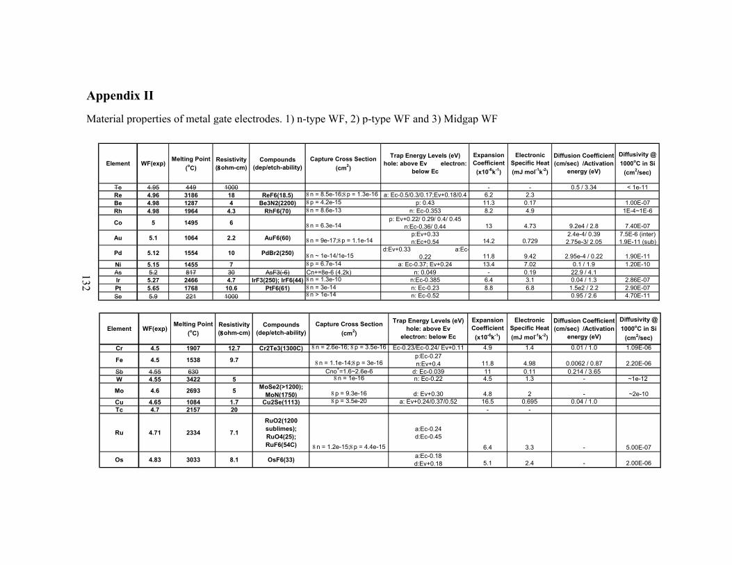
132
Appendix II
Material properties of metal gate electrodes. 1) n-type WF, 2) p-type WF and 3) Midgap WF
Element WF(exp)Melting Point
(oC)Resistivity (8888ohm-cm)
Compounds (dep/etch-ability)
Capture Cross Section (cm2)
Trap Energy Levels (eV) hole: above Ev electron:
below Ec
Expansion Coefficient (x10-6k-1)
Electronic Specific Heat (mJ mol-1k-2)
Diffusion Coefficient (cm/sec) /Activation
energy (eV)
Diffusivity @ 1000oC in Si
(cm2/sec)
Te 4.95 449 1000 - - 0.5 / 3.34 < 1e-11Re 4.96 3186 18 ReF6(18.5) 8n = 8.5e-16;8p = 1.3e-16 a: Ec-0.5/0.3/0.17;Ev+0.18/0.4 6.2 2.3Be 4.98 1287 4 Be3N2(2200) 8p = 4.2e-15 p: 0.43 11.3 0.17 1.00E-07Rh 4.98 1964 4.3 RhF6(70) 8n = 8.6e-13 n: Ec-0.353 8.2 4.9 1E-4~1E-6
Co 5 1495 6 8n = 6.3e-14 p: Ev+0.22/ 0.29/ 0.4/ 0.45
n:Ec-0.36/ 0.44 13 4.73 9.2e4 / 2.8 7.40E-07
Au 5.1 1064 2.2 AuF6(60) 8n = 9e-17;8p = 1.1e-14 p:Ev+0.33 n:Ec+0.54 14.2 0.729
2.4e-4/ 0.39 2.75e-3/ 2.05
7.5E-6 (inter) 1.9E-11 (sub)
Pd 5.12 1554 10 PdBr2(250) 8n ~ 1e-14/1e-15 d:Ev+0.33 a:Ec-
0.22 11.8 9.42 2.95e-4 / 0.22 1.90E-11Ni 5.15 1455 7 8p = 6.7e-14 a: Ec-0.37; Ev+0.24 13.4 7.02 0.1 / 1.9 1.20E-10As 5.2 817 30 AsF3(-6) Cn+=8e-6 (4.2k) n: 0.049 - 0.19 22.9 / 4.1Ir 5.27 2466 4.7 IrF3(250); IrF6(44) 8n = 1.3e-10 n:Ec-0.385 6.4 3.1 0.04 / 1.3 2.86E-07Pt 5.65 1768 10.6 PtF6(61) 8n = 3e-14 n: Ec-0.23 8.8 6.8 1.5e2 / 2.2 2.90E-07Se 5.9 221 1000 8n > 1e-14 n: Ec-0.52 0.95 / 2.6 4.70E-11
Element WF(exp)Melting Point
(oC)Resistivity (8888ohm-cm)
Compounds (dep/etch-ability)
Capture Cross Section (cm2)
Trap Energy Levels (eV) hole: above Ev
electron: below Ec
Expansion Coefficient (x10-6k-1)
Electronic Specific Heat (mJ mol-1k-2)
Diffusion Coefficient (cm/sec) /Activation
energy (eV)
Diffusivity @ 1000oC in Si
(cm2/sec)Cr 4.5 1907 12.7 Cr2Te3(1300C) 8n = 2.6e-16; 8p = 3.5e-16 Ec-0.23/Ec-0.24/ Ev+0.11 4.9 1.4 0.01 / 1.0 1.09E-06
Fe 4.5 1538 9.7 8n = 1.1e-14;8p = 3e-16 p:Ec-0.27 n:Ev+0.4 11.8 4.98 0.0062 / 0.87 2.20E-06
Sb 4.55 630 Cno+=1.6~2.6e-6 d: Ec-0.039 11 0.11 0.214 / 3.65W 4.55 3422 5 8n = 1e-16 n: Ec-0.22 4.5 1.3 - ~1e-12
Mo 4.6 2693 5 MoSe2(>1200); MoN(1750) 8p = 9.3e-16 d: Ev+0.30 4.8 2 - ~2e-10
Cu 4.65 1084 1.7 Cu2Se(1113) 8p = 3.5e-20 a: Ev+0.24/0.37/0.52 16.5 0.695 0.04 / 1.0Tc 4.7 2157 20 - -
Ru 4.71 2334 7.1
RuO2(1200 sublimes); RuO4(25); RuF6(54C) 8n = 1.2e-15;8p = 4.4e-15
a:Ec-0.24 d:Ec-0.45
6.4 3.3 - 5.00E-07
Os 4.83 3033 8.1 OsF6(33) a:Ec-0.18 d:Ev+0.18 5.1 2.4 - 2.00E-06
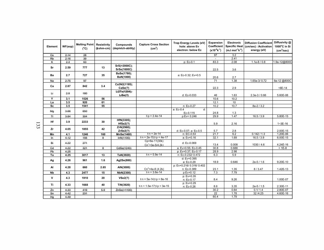
133
Element WF(exp)Melting Point
(oC)Resistivity (8888ohm-cm)
Compounds (dep/etch-ability)
Capture Cross Section (cm2)
Trap Energy Levels (eV) hole: above Ev
electron: below Ec
Expansion Coefficient (x10-6k-1)
Electronic Specific Heat (mJ mol-1k-2)
Diffusion Coefficient (cm/sec) /Activation
energy (eV)
Diffusivity @ 1000oC in Si
(cm2/sec)Cs 2.14 28 97 3.2Rb 2.16 39 - 2.41K 2.3 63 p: Ec-0.1 83.3 2.08 1.1e-8 / 0.8 1.9e-12@800C
Sr 2.59 777 13 SrS(>2000C); SrSe(1600C) 22.5 3.6
Ba 2.7 727 35 BaSe(1780); BaN(1000) a: Ec-0.32; Ev+0.5
20.6 2.7Na 2.75 97 71 1.38 1.65e-3/ 0.72 6e-12 @800C
Ca 2.87 842 3.4 Ca3N2(1195); CaSe(?) 22.3 2.9 ~6E-14
Li 2.9 180 Li2Te(1204); LiSe(?) d: Ec-0.033 46 1.63 2.3e-3 / 0.66 5.60E-06
Y 3.1 1526 56 10.6 10.2La 3.5 920 61 12.1 10Sc 3.5 1541 55 n: Ec-0.27 10.2 10.7 8e-2 / 3.2
Mg 3.66 650 a: Ec-0.4 d: Ec-0.115 24.8 1.3
Tl 3.84 304 8p = 2.4e-14 p:Ev+ 0.246 29.9 1.47 16.5 / 3.9 5.80E-15
Hf 3.9 2233 30 HfN(3305); HfSe2(?) 5.9 2.16 1~3E-16
Zr 4.05 1855 42 ZrN(2960); ZrSe2(?) d: Ec-0.07; a: Ec-0.5 5.7 2.8 2.00E-15
Mn 4.1 1246 160 MnSe(1460) 8n = 2e-14 n: EC-0.53 21.7 9.2 0.142 / 1.3 1.20E-06In 4.12 156 8 InN(1100) 8n = 2e-15;8p = 4e-17 a: Ev+0.16 32.1 1.69 16.5 / 3.9 6.00E-15
Bi 4.22 271Cp=6e-11(30k) Cn+=3e-5(4.2k)
d: Ec-0.069 13.4 0.008 1030 / 4.6 4.24E-16Cd 4.22 321 8 CdSe(1240) a: Ev+0.55; Ec-0.45 30.8 0.688 < 1E-8Pb 4.25 p: Ev+0.37; Ec-0.17 28.9 2.98Ta 4.25 3017 13 TaN(3920) 8n = 5.9e-14 n: Ec-0.232/ 0.472 6.3 5.9
Ag 4.26 961 1.6 Ag2Se(880) d: Ev+0.395 a: Ec-0.29 18.9 0.646 2e-5 / 1.6 9.20E-10
Al 4.28 660 2.65 AlN(3000) Cno=4e-8 (4.2k)p: Ev+0.216/ 0.316/ 0.402
n: Ec-0.389 23.1 1.35 8 / 3.47 1.42E-13Nb 4.3 2477 15 NbN(2300) 8n = 3.6e-14 p:Ev+0.12 7.3 7.79
V 4.3 1910 20 VSe2(?) 8n = 5e-14;8p = 8e-16 p: Ev+0.35 n: Ec-0.17 8.4 9.26 1.00E-07
Ti 4.33 1668 40 TiN(3920) 8n = 1.5e-17;8p = 3e-15 p: Ev+0.29 n: Ec-0.26 8.6 3.35 2e-5 / 1.5 2.30E-11
Zn 4.33 419 5.9 ZnSe(>1100) 30.2 0.64 0.1/ 1.4 2.80E-07Sn 4.42 231 22 1.78 32 /4.25 4.60E-16Hg 4.49 60.4 1.79
134
Bibliography
[1] G. E. Moore, "Progress in digital integrated electronics," presented at Electron Devices Meeting, 1975 International, 1975.
[2] G. D. Wilk, R. M. Wallace, and J. M. Anthony, "High-k gate dielectrics: Current status and materials properties considerations," Journal of Applied Physics, vol. 89, pp. 5243-5275, 2001.
[3] B. H. Lee, L. Kang, W.-J. Qi, R. Nieh, Y. Jeon, K. Onishi, and J. C. Lee, "Ultrathin hafnium oxide with low leakage and excellent reliability for alternative gate dielectric application," presented at Electron Devices Meeting, 1999. IEDM Technical Digest. International, 1999.
[4] L. Kang, B. H. Lee, W.-J. Qi, Y. Jeon, R. Nieh, S. Gopalan, K. Onishi, and J. C. Lee, "Electrical characteristics of highly reliable ultrathin hafnium oxide gate dielectric," Electron Device Letters, IEEE, vol. 21, pp. 181-183, 2000.
[5] C. Hobbs, L. Fonseca, V. Dhandapani, S. Samavedam, B. Taylor, J. Grant, L. Dip, D. Triyoso, R. Hegde, D. Gilmer, R. Garcla, D. Roan, L. Lovejoy, R. Rai, L. Hebert, H. Tseng, B. White, and P. Tobin, "Fermi Level Pinning at the PolySietal Oxide Interface," VLSI Technology Digest, pp. 9-10, 2003.
[6] Y. C. Yeo, T. J. King, and C. M. Hu, "Metal-dielectric band alignment and its implications for metal gate complementary metal-oxide-semiconductor technology," Journal of Applied Physics, vol. 92, pp. 7266-7271, 2002.
[7] S. Samavedam, L. B. La, P. J. Tobin, B. White, C. Hobbs, L. R. C. Fonseca, A. Demkov, J. Schaeffer, E. Luckowski, A. Martinez, M. Raymond, D. Triyoso, D. Roan, V. Dhandapani, R. Garcia, S. G. H. Anderson, K. Moore, H. H. Tseng, C. Capasso, O. Adetutu, D. C. Gilmer, W. J. Taylor, R. Hegde, and J. Grant, "Fermi level pinning with sub-monolayer MeOx and metal gates," IEEE Electron Device Meeting, pp. 307-310, 2003.
[8] C. C. Hobbs, L. R. C. Fonseca, A. Knizhnik, V. Dhandapani, S. B. Samavedam, W. J. Taylor, J. M. Grant, L. G. Dip, D. H. Triyoso, R. I. Hegde, D. C. Gilmer, R. Garcia, D. Roan, M. L. Lovejoy, R. S. Rai, E. A. Hebert, H.-H. Tseng, S. G. H. Anderson, B. E. White, and P. J. Tobin, "Fermi-level pinning at the polysilicon/metal-oxide interface-Part II," Electron Devices, IEEE Transactions on, vol. 51, pp. 978-984, 2004.
[9] C. Hobbs, L. Fonseca, V. Dhandapani, S. Samavedam, B. Taylor, J. Grant, L. Dip, D. Triyoso, R. Hegde, D. Gilmer, R. Garcia, D. Roan, L. Lovejoy, R. Rai, L. Hebert, H. Tseng, B. White, and P. Tobin, "Fermi level pinning at the polySi/metal oxide interface," VLSI Technology, 2003. Digest of Technical Papers. 2003 Symposium on, pp. 9-10, 2003.
[10] C. Y. Wong, J. Y.-C. Sun, Y. Taur, C. S. Oh, R. Angelucci, and B. Davari, "Doping of n+ and p+ polysilicon in a dual-gate CMOS process," presented at
135
Electron Devices Meeting, 2003. IEDM '03 Technical Digest. IEEE International, 1988.
[11] J. C. Hu, H. Yang, R. Kraft, A. L. P. Rotondaro, S. Hattangady, W. W. Lee, R. A. Chapman, C.-P. Chao, A. Chatterjee, M. Hanratty, M. Rodder, and I.-C. Chen, "Feasibility of using W/TiN as metal gate for conventional 0.13 μm CMOS technology and beyond," Electron Devices Meeting, 1997. Technical Digest., International, pp. 825-828, 1997.
[12] ITRS, "ITRS Roadmap 2003," 2003. [13] I. De, D. Johri, A. Srivastava, and C. M. Osburn, "Impact of gate work function
on device performance at the 50 nm technology node," Solid-State-Electronics, vol. 44, pp. 1077-1080, 2000.
[14] E. H. Nicollian and J. R. Brews, MOS Physics and Technology. New york: Wiley, 1982.
[15] H. Michaelson, "The work function of the elements and its periodicity," Journal of Applied Physics, vol. 48, pp. 4729-4733, 1977.
[16] Y.-C. Yeo, T.-J. King, and C. Hu, "Metal-dielectric band alignment and its implications for metal gate complementary metal-oxide-semiconductor technology," Journal of Applied Physics, vol. 92, pp. 7266-7271, 2002.
[17] B.-Y. Tsui and C.-F. Huang, "Wide range work function modulation of binary alloys for MOSFET application," IEEE Electron Device Letter, vol. 24, pp. 153-155, 2003.
[18] M. A. Pawlak, T. Schram, K. Maex, and A. Vantomme, "Investigation of Iridium as a gate electrode for deep sub-micron CMOS technology," Microelectronic Engineering, vol. 70, pp. 373-376, 2003.
[19] B. Maiti and P. J. Tobin, "Metal Gates for Advanced CMOS Technology," SPIE Conference on Microelectronic Device Technology III, vol. 3881, pp. 46-57, 1999.
[20] H. Zhong, S. N. Hong, Y.-S. Suh, H. Lazar, G. Heuss, and V. Misra, "Properties of Ru-Ta alloys as gate electrodes for NMOS and PMOS silicon devices," IEEE Electron Device Meeting, 2001.
[21] I. Polishchuk, P. Ranade, T.-J. King, and C. Hu, "Dual work function metal gate CMOS transistors by Ni-Ti interdiffusion," IEEE Electron Device Letter, vol. 23, pp. 200-202, 2002.
[22] H. N. Alshareef, H. C. Wen, H. Luan, K. Choi, H. R. Harris, Y. Senzaki, P. Majhi, B. H. Lee, B. Foran, and G. Lian, "Temperature dependence of the work function of ruthenium-based gate electrodes," Thin Solid Films, vol. article in press Temperature dependence of the work function of ruthenium-based gate electrodes, 2006.
136
[23] R. Lin, Q. Lu, P. Ranade, T. J. King, and C. M. Hu, "An adjustable work function technology using Mo gate for CMOS devices," Ieee Electron Device Letters, vol. 23, pp. 49-51, 2002.
[24] S. H. Bae, W. P. Bai, H. C. Wen, S. Mathew, L. K. Bera, N. Balasubramanian, N. Yamada, M. F. Li, and D. L. Kwong, "Laminated metal gate electrode with tunable work function for advanced CMOS," presented at VLSI Technology, 2004. Digest of Technical Papers. 2004 Symposium on, 2004.
[25] G. Bersuker, P. Zeitzoff, J. H. Sim, B. H. Lee, R. Choi, G. Brown, and C. D. Young, "Mobility Evaluation in Transistors with Charge Trapping Gate Dielectrics," Applied Physics Letters, vol. 87, pp. 042905, 2005.
[26] H. N. Alshareef, H. C. Wen, H. R. Harris, K. Choi, H. F. Luan, P. Lysaght, P. Majhi, B. H. Lee, M. El-Bouanani, and V. Ukride, "Modulation of the work function of silicon gate electrode using thin TaN interlayers," Applied Physics Letters, vol. 87, 2005.
[27] S. Zafar, V. Narayanan, A. Callegari, F. R. McFeely, P. Jamison, E. Gusev, C. Cabral, and R. Jammy, "HfO/sub 2//metal stacks: determination of energy level diagram, work functions & their dependence on metal deposition," VLSI Technology, 2005. Digest of Technical Papers. 2005 Symposium on, pp. 44-45, 2005.
[28] C. C. Jr., C. Lavoie, A. S. Ozcan, R. S. Amos, V. Narayanan, E. P. Gusev, J. L. Jordam-Sweet, and J. M. E. Harper, "Evaluation of CMOS Gate Materials Using IN SITU Characterization Techniques," Electrochemical Society Proceedings, Advanced Short-Time Thermal Processing for Si-Based CMOS Devices, pp. 375-384, 2003.
[29] J. K. Schaeffer, S. B. Samavedam, D. C. Gilmer, V. Dhandapani, P. J. Tobin, J. Mogab, B. Y. Nguyen, B. E. White, S. Dakshina-Murthy, R. S. Rai, Z. X. Jiang, R. Martin, M. V. Raymond, M. Zavala, L. B. La, J. A. Smith, R. Garcia, D. Roan, M. Kottke, and R. B. Gregory, "Physical and electrical properties of metal gate electrodes on HfO2 gate dielectrics," Journal of Vacuum Science & Technology B, vol. 21, pp. 11-17, 2003.
[30] CRC Handbook of Chemistry and Physics, 70 ed. Boca Raton, Florida: CRC Press, Inc., 1989-1990.
[31] S. B. Samavedam, L. B. La, P. J. Tobin, B. White, C. Hobbs, L. R. C. Fonseca, A. A. Demkov, J. Schaeffer, E. Luckowski, A. Martinez, M. Raymond, D. Triyoso, D. Roan, V. Dhandapani, R. Garcia, S. G. H. Anderson, K. Moore, H. H. Tseng, C. Capasso, O. Adetutu, D. C. Gilmer, W. J. Taylor, R. Hegde, and J. Grant, "Fermi level pinning with sub-monolayer MeOx and metal gates [MOSFETs]," Electron Devices Meeting, 2003. IEDM '03 Technical Digest. IEEE International, pp. 13.1.1-13.1.4, 2003.
[32] J. Schaeffer, C. Capasso, L. R. C. Fonseca, S. Samavedam, L. B. La, J. Smith, S. Dakshina-Murthy, D. C. Gilmer, Luckowski, Y. Liang, S. Kalpat, B. Adetutu, H.
137
H. Tseng, Y. Shiho, A. Demkov, R. Hegde, W. J. Taylor, R. Gregory, J. Jiang, E. Luckowski, M. Raymond, K. Moore, D. Triyoso, D. Roan, B. White, and P. J. Tobin, "Challenges for the integration of metal gate electrodes," IEEE Electron Device Meeting, 2004.
[33] K. Shiraishi, Y. Akasaka, S. Miyazaki, T. Nakayama, T. Nakaoka, G. Nakamura, K. Torii, H. Furutou, A. Ohta, P. Ahmet, K. Ohmori, H. Watanabe, T. Chikyo, M. L. Green, Y. Nara, and K. Yamada, "Universal theory of workfunctions at metal/Hf-based high-k dielectrics interfaces - guiding principles for gate metal selection," Electron Devices Meeting, 2005. IEDM Technical Digest. IEEE International, pp. 39-42, 2005.
[34] J. K. Schaeffer, L. R. C. Fonseca, S. B. Samavedam, Y. Liang, P. J. Tobin, and B. E. White, "Contributions to the effective work function of platinum on hafnium dioxide," Applied Physics Letters, vol. 85, pp. 1826-1828, 2004.
[35] E. Cartier, F. R. McFeely, V. Narayanan, P. Jamison, B. P. Linder, M. Copel, V. K. Paruchuri, V. S. Basker, R. Haight, D. Lim, R. Carruthers, T. Shaw, M. Steen, J. Sleight, J. Rubino, H. Deligianni, S. Guha, R. Jammy, and G. Shahidi, "Role of oxygen vacancies in V/sub FB//V/sub t/ stability of pFET metals on HfO/sub 2/," VLSI Technology, 2005. Digest of Technical Papers. 2005 Symposium on, pp. 230-231, 2005.
[36] D. Gu, S. K. Dey, and P. Majhi, "Effective work function of Pt, Pd, and Re on atomic layer deposited HfO[sub 2]," Applied Physics Letters, vol. 89, pp. 082907, 2006.
[37] H. Yang, Y. Son, S. Baek, H. Hwang, H. Lim, and H.-S. Jung, "Ti gate compatible with atomic-layer-deposited HfO[sub 2] for n-type metal-oxide-semiconductor devices," Applied Physics Letters, vol. 86, pp. 092107, 2005.
[38] R. Chau, S. Datta, M. Doczy, B. Doyle, J. Kavalieros, and M. Metz, "High-K/Metal–Gate Stack and Its MOSFET Characteristics," IEEE Electron Device Letter, vol. 25, pp. 408-410, 2004.
[39] A. C. V. Narayanan, F.R. McFeely, K. Nakamura, P. Jamison, S. Zafar, E. Cartier, A. Steegen, V. Ku, P. Nguyen, K. Milkove, C. Cabral Jr., M. Gribelyuk, C. Wajda, Y. Kawano, D. Lacey, Y. Li, E. Sikorski, E. Duch, H. Ng, C. Wann, R. Jammy, M. Ieong, G. Shahidi, "Dual Work Function Metal Gate CMOS using CVD metal electrodes," VLSI Technology Digest, pp. 192-193, 2004.
[40] C. Young, G. Bersuker, H. C. Wen, G. Brown, and P. Majhi, "Charge Trapping Characteristics of Hafnium Based High-ê Dielectrics with Various Metal Electrodes," SSDM 2004, 2004.
[41] P. Majhi, C. Young, G. Bersuker, H. C. Wen, G. A. Brown, B. Foran, R. Choi, P. M. Zeitzoff, and H. R. Huff, "Influence of Metal Gate Materials and Processing on Planar CMOS Device Characteristics with High-k Gate Dielectrics," ESSDERC, 2004.
138
[42] http://www.intel.com/technology/mooreslaw/index.htm, "Moore's Law Means More Performance."
[43] D. V. Lang, Thermally Stimulated Relaxation in Solids, vol. 37. Berlin: Springer, 1979.
[44] R. Jha, J. Gurganos, Y. H. Kim, R. Choi, J. Lee, and V. Misra, "A capacitance-based methodology for work function extraction for metals on high-K," IEEE Electron Device Letter, vol. 25, pp. 420-423, 2004.
[45] P. Majhi, H. C. Wen, H. Alshareef, K. Choi, R. Harris, P. Lysaght, H. Luan, Y. Senzaki, S. C. Song, B. H. Lee, and C. Ramiller, "Evaluation and integration of metal gate electrodes for future generation dual metal CMOS," Integrated Circuit Design and Technology, 2005. ICICDT 2005. 2005 International Conference on, pp. 69-72, 2005.
[46] H. C. Wen, R. N. Choi, G. A. Brown, T. Boscke, K. Matthews, H. R. Harris, K. Choi, H. N. Alshareef, H. F. Luan, G. Bersuker, P. Majhi, D. L. Kwong, and B. H. Lee, "Comparison of effective work function extraction methods using capacitance and current measurement techniques," Ieee Electron Device Letters, vol. 27, pp. 598-601, 2006.
[47] J. R. Hauser and K. Ahmed, "Characterization of Ultra-Thin Oxides Using Electrical C-V and I-V Measurements," Characterization and Metrology for ULSI Technology: 1998 International Conference, vol. 449, pp. 235-239, 1998.
[48] G. Brown, G. Smith, J. Saulters, K. Matthews, H. C. Wen, P. Majhi, and B. H. Lee, "An Improved Methodology for Gate Electrode Work Function Extraction in SiO2 and High-k Gate Stack Systems Using Terraced Oxide Structures," IEEE SISC conference, 2004.
[49] H. N. Alshareef, Z. Zhang, P. Majhi, G. Brown, P. Zeitzoff, H. Huff, and B. H. Lee, "Gate electrode development for dual metal-gate CMOS applications," in Future Fab, vol. 19, 2005, pp. 91-93.
[50] G. D. Wilk, M. L. Green, M.-Y. Ho, B. W. Busch, T. W. Sorsch, F. P. Klemens, B. Brijs, R. B. van Dover, A. Kornblit, T. Gustafsson, E. Garfunkel, S. Hillenius, D. Monroe, P. Kalavade, and J. M. Hergenrother, "Improved film growth and flatband voltage control of ALD HfO/sub 2/ and Hf-Al-O with n/sup +/ poly-Si gates using chemical oxides and optimized post-annealing," presented at VLSI Technology, 2002. Digest of Technical Papers. 2002 Symposium on, 2002.
[51] C. C. Hobbs, L. .Fonseca, A. Knizhnik, V. Dhandapani, S. B. Samavedam, W. J. Taylor, J. M. Grant, L. G. Dip, D. H. Triyoso, R. I. Hegde, D. C. Gilmer, R. Garcia, D. Roan, M. L. Lovejoy, R. S. Rai, E. A. Hebert, H.-H. Tseng, S. G. H. Anderson, B. E. White, and P. J. Tobin, "Fermi-Level Pinning at the Polysilicon/Metal–Oxide Interface—Part II," IEEE Transactions on Electron Devices, vol. 51, pp. 978-984, 2004.
139
[52] S. Zafar, C. Cabral, A. R., and A. Callegari, "A method for measuring barrier heights, metal work functions and fixed charge densities in metal/SiO2/Si capacitors," Applied Physics Letters, vol. 80, pp. 4858-4860, 2002.
[53] S. Zafar, E. Cartier, and E. P. Gusev, "Measurement of barrier heights in high permittivity gate dielectric films," Applied Physics Letters, vol. 80, pp. 2749-2751, 2002.
[54] T. Hori, Gate Dielectrics and MOS ULSI Principles, Technologies and Application: Springer-Verlag Berlin Heidelberg, 1997.
[55] J. Robertson, "Band offsets of wide-band-gap oxides and implications for future electronic devices," presented at Papers from the international conference on silicon dielectric interfaces, 2000.
[56] A. A. Demkov, L. R. C. Fonseca, E. Verret, J. Tomfohr, and O. F. Sankey, "Complex band structure and the band alignment problem at the Si--high-k dielectric interface," Physical Review B (Condensed Matter and Materials Physics), vol. 71, pp. 195306, 2005.
[57] A. S. Grove, Physics and Technology of Semiconductor Devices. New York: Wiley, 1967.
[58] P. Majhi, H.-C. Wen, K. Choi, H. Alshareef, C. Huffman, and B. H. Lee, "A systematic study of the influence of nitrogen in tuning the effective work function of nitrided metal gates," presented at VLSI Technology, 2005. (VLSI-TSA-Tech). 2005 IEEE VLSI-TSA International Symposium on, 2005.
[59] C. Ren, H. Y. Yu, J. F. Kang, Y. T. Hou, M. E. Li, W. D. Wang, D. S. H. Chan, and D. L. Kwong, "Fermi-level pinning induced thermal instability in the effective work function of TaN in TaN/SiO2 gate stack," Ieee Electron Device Letters, vol. 25, pp. 123-125, 2004.
[60] Y. C. Yeo, P. Ranade, T. J. King, and C. M. Hu, "Effects of high-kappa gate dielectric materials on metal and silicon gate workfunctions," Ieee Electron Device Letters, vol. 23, pp. 342-344, 2002.
[61] H. Y. Yu, C. Ren, Y. C. Yeo, J. F. Kang, X. P. Wang, H. H. H. Ma, M. F. Li, D. S. H. Chan, and A. L. Kwong, "Fermi pinning-induced thermal instability of metal-gate work functions," Ieee Electron Device Letters, vol. 25, pp. 337-339, 2004.
[62] Y. Liang, J. Curless, C. J. Tracy, D. C. Gilmer, J. K. Schaeffer, D. H. Triyoso, and P. J. Tobin, "Interface dipole and effective work function of Re in Re/HfO[sub 2]/SiO[sub x]/n-Si gate stack," Applied Physics Letters, vol. 88, pp. 072907, 2006.
[63] M. Copel, R. P. Pezzi, D. Neumayer, and P. Jamison, "Reduction of hafnium oxide and hafnium silicate by rhenium and platinum," Applied Physics Letters, vol. 88, pp. 072914, 2006.
140
[64] L. Pantisano, T. Schram, Z. Li, J. G. Lisoni, G. Pourtois, S. D. Gendt, D. P. Brunco, A. Akheyar, V. V. Afanas'ev, S. Shamuilia, and A. Stesmans, "Ruthenium gate electrodes on SiO[sub 2] and HfO[sub 2]: Sensitivity to hydrogen and oxygen ambients," Applied Physics Letters, vol. 88, pp. 243514, 2006.
[65] H. C. Wen, P. Lysaght, H. N. Alshareef, C. Huffman, H. R. Harris, K. Choi, Y. Senzaki, H. Luan, P. Majhi, B. H. Lee, M. J. Campin, B. Foran, G. D. Lian, and D. L. Kwong, "Thermal response of Ru electrodes in contact with SiO2 and Hf-based high-k gate dielectrics," Journal of Applied Physics, vol. 98, 2005.
[66] H.-C. Wen, K. Choi, P. Majhi, H. Alshareef, C. Huffman, and B. H. Lee, "A systematic study of the influence of nitrogen in tuning the effective work function of nitrided metal gates," presented at VLSI Technology, 2005. (VLSI-TSA-Tech). 2005 IEEE VLSI-TSA International Symposium on, 2005.
[67] J. Robertson, "Invited talk at EMRS 2006," 2006. [68] G. Pant, A. Gnade, M. J. Kim, R. M. Wallace, B. E. Gnade, M. A. Quevedo-
Lopez, and P. D. Kirsch, "Effect of thickness on the crystallization of ultrathin HfSiON gate dielectrics," Applied Physics Letters, vol. 88, pp. 032901, 2006.
[69] Diagrammy Sostoianiia Metallicheskikh sistem, Moscow, 1971. [70] V. Misra, H. C. Zhong, and H. Lazar, "Electrical properties of Ru-based alloy
gate electrodes for dual metal gate Si-CMOS," Ieee Electron Device Letters, vol. 23, pp. 354-356, 2002.
[71] H. C. Wen, K. Choi, P. Lysaght, P. Majhi, H. Alshareef, C. Huffman, R. Harris, H. Luan, B. H. Lee, N. Yamada, and S. Wickramanayaka, "Work function engineering of RuHf alloys as gate electrodes for future generation dual metal CMOS," presented at VLSI Technology, 2005. (VLSI-TSA-Tech). 2005 IEEE VLSI-TSA International Symposium on, 2005.
[72] H. Y. Yu, M. F. Li, and D. L. Kwong, "Thermally robust HfN metal as a promising gate electrode for advanced MOS device applications," Ieee Transactions on Electron Devices, vol. 51, pp. 609-615, 2004.
[73] J. Westlinder, G. Sjoblom, and J. Olsson, "Variable work function in MOS capacitors utilizing nitrogen-controlled TiNx gate electrodes," Microelectronic Engineering, vol. 75, pp. 389-396, 2004.
[74] W. Gordy and W. J. O. Thomas, "Electronegativities of the Elements," The Journal of Chemical Physics, vol. 24, pp. 439-444, 1956.
[75] J. Schaeffer, D. Gilmer, S. Samavedam, D. Triyoso, R. Hegde, S. Kalpat, M. Raymond, C. Capasso, B. Taylor, M. Sadd, H. H. Tseng, M. Stoker, A. Haggag, D. Roan, L. L. Happ, C. , P. J. Tobin, and B. E. White, "Materials Challenges for High Permittivity Gate Dielectrics and Metal Gate Electrodes," IEEE ISAGST 2006, 2006.
141
[76] M.-A. Nicolet and P. H. Giauque, "Highly metastable amorphous or near-amorphous ternary films (mictamict alloys)," Microelectronic Engineering, vol. 55, pp. 357-367, 2001.
[77] Y. S. Suh, G. P. Heuss, J. H. Lee, and V. Misra, "Effect of the composition on the electrical properties of TaSixNy metal gate electrodes," Ieee Electron Device Letters, vol. 24, pp. 439-441, 2003.
[78] T. Hori, Gate dielectrics and MOS ULSIs: Principles, Technologies and Applications. Germany: Springer.
[79] W.-H. Lee, J. T. Clemens, R. C. Keller, and L. Manchanda, "A Novel High K Inter-poly Dielectric(IPD), A1/sub 2/O/sub 3/ For Low Voltage/high Speed Flash memories: erasing in msecs at 3.3V," presented at VLSI Technology, 1997. Digest of Technical Papers., 1997 Symposium on, 1997.
[80] W. S. Yang, Y. K. Kim, S. U. Yang, J. H. Choi, H. S. Park, S. I. Lee, and J. B. Yoo, "Effect of SiO2 inermediate on Al2O3 and SiO2 n-poly Si interface deposited using atomic layer deposition (ALD) for deep submicron device applications," Surface and coatings technology, vol. 131, pp. 79-83, 2000.
[81] S. H. Bae, C. H. Lee, R. Clark, and D. L. Kwong, "MOS Characteristics of Ultrathin CVD HfAlO Gate Dielectrics," IEEE Electron Device Letters, vol. 24, pp. 556~558, 2003.
[82] R. S. Johnson, G. Lucovsky, and I. Baumvol, "Physical and electrical properties of noncrystalline Al2O3 prepared by remote plasma enhanced chemical vapor deposition," J. Vac. Sci. Technol. A, vol. 19, pp. 1353-1360, 2001.
[83] H. N. Alshareef, H. F. Luan, K. Choi, H. R. Harris, H. C. Wen, M. A. Quevedo-Lopez, P. Majhi, and B. H. Lee, "Metal gate work function engineering using AlN[sub x] interfacial layers," Applied Physics Letters, vol. 88, pp. 112114, 2006.
[84] H.-S. Jung, VLSI Technology, 2006. Digest of Technical Papers. 2006 Symposium on, 2006.
[85] K. Lee, M. Frank, V. Paruchuri, E. Cartier, B. Linder, N. Bojarczuk, X. Wang, J. Rubino, M. Steen, P. Kozlowski, J. Newbury, E. Sikorski, P. Flaitz, M. Gribelyuk, P. Jamison, G. Singco, V. Narayanan, S. Zafar, S. Guha, P. Oldiges, R. Jammy, and M. Ieong, "Poly-Si/AlN/HfSiO Stack for Ideal Threshold Voltage and Mobility in Sub-100 nm MOSFETs," presented at VLSI Technology, 2006. Digest of Technical Papers. 2006 Symposium on, 2006.
[86] T. H. Cha, D. G. Park, T. K. Kim, S. A. Jang, I. S. Yeo, J. S. Roh, and J. W. Park, "Work function and thermal stability of Ti1-xAlxNy for dual metal gate electrodes," Applied Physics Letters, vol. 81, pp. 4192-4194, 2002.
[87] H. N. Alshareef, K. Choi, H. C. Wen, H. Luan, H. Harris, Y. Senzaki, P. Majhi, B. H. Lee, R. Jammy, S. Aguirre-Tostado, B. E. Gnade, and R. M. Wallace, "Composition dependence of the work function of Ta[sub 1 - x]Al[sub x]N[sub y] metal gates," Applied Physics Letters, vol. 88, pp. 072108, 2006.
142
[88] J. C. Schuster and H. Nowotny, "Phase relationships in the ternary systems (V, Cr, Mo, W, Mn, Re)-Al-N," Journal of Materials Science, vol. 20, pp. 2787-2793, 1985.
[89] H. Alshareef, H. Harris, H. Wen, C. Park, C. Huffman, K. Choi, H. Luan, P. Majhi, B. Lee, R. Jammy, D. Lichtenwalner, J. Jur, and A. Kingon, "Thermally Stable N-Metal Gate MOSFETs Using La-Incorporated HfSiO Dielectric," VLSI Technology, 2006. Digest of Technical Papers. 2006 Symposium on, pp. 7-8, 2006.
[90] H. Ono, Applied Physics Letters, vol. 78, pp. 1832, 2001. [91] N. Kimizuka, VLSI Technology, 1999. Digest of Technical Papers, pp. 73, 1999. [92] L. Pantisano, T. Schram, B. O'Sullivan, T. Conard, S. D. Gendt, G. Groeseneken,
P. Zimmerman, A. Akheyar, M. M. Heyns, S. Shamuilla, V. V. Afanas'ev, and A. Stesmans, "Effective work function modulation by controlled dielectric monolayer deposition," Applied Physics Letters, vol. 89, pp. 113505, 2006.
[93] V. Narayanan, V. Paruchuri, N. Bojarczuk, B. Linder, B. Doris, Y. Kim, S. Zafar, J. Stathis, S. Brown, J. Arnold, M. Copel, M. Steen, E. Cartier, A. Callegari, P. Jamison, J.-P. Locquet, D. Lacey, Y. Wang, P. Batson, P. Ronsheim, R. Jammy, and M. Chudzik, "Band-Edge High-Performance High-k/Metal Gate n-MOSFETs Using Cap Layers Containing Group IIA and IIIB Elements with Gate-First Processing for 45 nm and Beyond," VLSI Technology, 2006. Digest of Technical Papers. 2006 Symposium on, pp. 178-179, 2006.
[94] Y. Yamamoto, K. Kita, K. Kyuno, and A. Toriumi, "Study of La concentration dependent Vfb shift in metal/HfLaOx/Si capacitors," International Conference on Solid State Devices and Materials 2006, pp. 212, 2006.
[95] R. Chau, S. Datta, M. Doczy, B. Doyle, J. Kavalieros, and M. Metz, "High-kappa/metal-gate stack and its MOSFET characteristics," Ieee Electron Device Letters, vol. 25, pp. 408-410, 2004.
[96] D.-G. Park, Z. J. Luo, N. Edleman, W. Zhu, P. Nguyen, K. Wong, C. Cabral, P. Jamison, B. H. Lee, A. Chou, M. Chudzik, J. Bruley, O. Gluschenkov, P. Ronsheim, A. Chakravarti, R. Mitchell, V. Ku, H. Kim, E. Duch, P. Kozlowski, C. D’Emic, V. Narayanan, A. Steegen, R. Wise, R. Jammy, R. Rengarajan, H. Ng, A. Sekiguchi, and C. H. Wann, "Thermally robust dual-work function ALD-MNx MOSFETs using conventional CMOS process flow," VLSI Technology Digest, 2004.
[97] S. M. Sze, Physics of Semiconductor Devices: John Wiley & Sons Inc., 1981. [98] Y. Ma, L. Liu, and Z. Li, "A discussion on the universality of inversion layer
mobility in MOSFET's," Electron Devices, IEEE Transactions on, vol. 46, pp. 1920-1922, 1999.
[99] P. D. Kirsch, M. A. Quevedo-Lopez, S. A. Krishnan, C. Krug, H. AlShareef, C. S. Park, R. Harris, N. Moumen, A. Neugroschel, G. Bersuker, B. H. Lee, J. G.
143
Wang, G. Pant, B. E. Gnade, M. J. Kim, R. M. Wallace, J. S. Jur, D. J. Lichtenwalner, A. I. Kingon, and R. Jammy, "Band Edge n-MOSFETs with High-k/Metal Gate Stacks Scaled to EOT=0.9nm with Excellent Carrier Mobility and High Temperature Stability," Electron Devices Meeting, 2006, pp. s23p4, 2006.
[100] W. Zhu, J.-P. Han, and T. P. Ma, "Mobility measurement and degradation mechanisms of MOSFETs made with ultrathin high-k dielectrics," Electron Devices, IEEE Transactions on, vol. 51, pp. 98-105, 2004.
[101] G. Bersuker, J. H. Sim, C. D. Young, R. Choi, B. H. Lee, P. Lysaght, G. Brown, P. Zeitzoff, M. Gardner, R. W. Murto, and H. R. Huff, "Effect of structural properties of Hf-based gate stack on transistor performance," Materials Research Society Symposium, vol. 811, pp. 31, 2004.
[102] J. L. Gavartin, A. L. Shluger, A. S. Foster, and G. Bersuker, "The role of nitrogen-related defects in high-K dielectric oxides: Density-functional studies," Journal of Applied Physics, vol. 97, pp. 053704-1~12, 2005.
[103] P. D. Kirsch, J. H. Sim, S. C. Song, S. Krishnan, J. Peterson, H. J. Li, M. Quevedo-Lopez, C. D. Young, R. Choi, N. Moumen, P. Majhi, Q. Wang, J. G. Ekerdt, G. Bersuker, and B. H. Lee, "Mobility enhancement of high-k gate stacks through reduced transient charging," Solid-State Device Research Conference, 2005. ESSDERC 2005. Proceedings of 35th European, pp. 367-370, 2005.
[104] M. Koike, T. Ino, Y. Kamimuta, M. Koyama, Y. Kamata, M. Suzuki, Y. Mitani, A. Nishiyama, and Y. Tsunashima, "Effect of Hf-N bond on properties of thermally stable amorphous HfSiON and applicability of this material to sub-50nm technology node LSIs," Electron Devices Meeting, 2003. IEDM '03 Technical Digest. IEEE International, pp. 4.7.1-4.7.4, 2003.
[105] M. A. Quevedo-Lopez, S. A. Krishnan, P. D. Kirsch, H. J. Li, J. H. Sim, C. Huffman, J. J. Peterson, B. H. Lee, G. Pant, B. E. Gnade, M. J. Kim, R. M. Wallace, D. Guo, H. Bu, and T. P. Ma, "High Performance Gate First HfSiON Dielectric Satisfying 45nm Node Requirements," IEEE Electron Device Meeting, vol. 17.4, 2005.
[106] Y. Akasaka, K. Miyagawa, T. Sasaki, K. Shiraishi, S. Kamiyama, O. Ogawa, F. Ootsuka, and Y. Nara, "Impact of electrode-side chemical structures on electron mobility in metal/HfO/sub 2/ MISFETs with sub-1nm EOT," VLSI Technology, 2005. Digest of Technical Papers. 2005 Symposium on, pp. 228-229, 2005.
[107] J. R. Hauser, "Extraction of experimental mobility data for MOS devices," Electron Devices, IEEE Transactions on, vol. 43, pp. 1981-1988, 1996.
[108] T. Yamaguchi, R. Iijima, T. Ino, A. Nishiyama, H. Satake, and N. Fukushima, ="Additional scattering effects for mobility degradation in Hf-silicate gate MISFETs," IEEE Electron Device Meeting, vol. Technology Digest, pp. 621-624, 2002.
144
[109] C. D. Young, R. Choi, J. H. Sim, B. H. Lee, P. Zeitzoff, Y. Zhao, K. Matthews, G. A. Brown, and G. Bersuker, "Interfacial layer dependence of HFSI/sub x/O/sub y/ gate stacks on V/sub T/ instability and charge trapping using ultra-short pulse in characterization," Reliability Physics Symposium, 2005. Proceedings. 43rd Annual. 2005 IEEE International, pp. 75-79, 2005.
[110] C. D. Young, P. Zeitzoff, G. A. Brown, G. Bersuker, B. H. Lee, and J. R. Hauser, "Intrinsic mobility evaluation of high-/spl kappa/ gate dielectric transistors using pulsed I/sub d/-V/sub g/," Electron Device Letters, IEEE, vol. 26, pp. 586-589, 2005.
[111] A. Kerber, E. Cartier, L. A. Ragnarsson, M. Rosmeulen, L. Pantisano, R. Degraeve, Y. Kim, and G. Groesenenken, "Direct measurment of the inversion charge in MOSFETs: Application to mobility extraction in alternative gate dielectrics," VLSI Symosium Tech. Dig., pp. 159-160, 2003.
[112] C. D. Young, S. Nadkarni, D. Heh, H. R. Harris, R. Choi, J. Peterson, J. H. Sim, S. Krishnan, J. Barnett, E. Vogel, B. H. Lee, P. Zeitzoff, G. Brown, and G. Bersuker, "Detection of electron trap generation due to constant voltage stress on high-K gate stacks," International reliability physics symposium, vol. 3.A.1, 2006.
[113] G. Bersuker, B. H. Lee, H. R. Huff, J. Gavartin, and A. Shluger, "Mechanism of charge trapping reduction in scaled high-K gate stacks," presented at Proceedings of the NATO Advanced Research Workshop on Defects in Advanced High-K Dielectric Nano-Electronic Semiconductor Devices, St. Petersburg, Russia, 2006.
[114] C. D. Young, G. Bersuker, Y. Zhao, J. Peterson, J. Barnett, G. Brown, J. H. Sim, R. Choi, B. H. Lee, and P. Zeitzoff, "Probing stress effects in HfO2 gate stacks with time dependent measurements," Microelectronics Reliability, vol. 45, pp. 806-810, 2005.
[115] R. Degraeve, A. Kerber, E. Cartier, L. Pantisano, and G. Groesenenken, "Effect of bulk trap density on HfO2 reliability and yield," IEEE Electron Device Meeting, pp. 935-938, 2003.
[116] V. Misra, G. P. Heuss, and Z. H., "Use of metal-oxide-semiconductor capacitors to detect interactions of Hf and Zr gate electrodes with SiO2 and ZrO2," Applied Physics Letters, vol. 78, pp. 4166-4168, 2001.
[117] C. Choi, C. Y. Kang, S. J. Rhee, M. Akbar, S. Krishnan, M. Zhang, H. Kim, T. Lee, I. Ok, F. Zhu, and J. C. Lee, "Aggressively scaled ultra thin undoped HfO2 gate dielectric (EOT<0.7nm) with TaN gate electrode using engineered interface layer," IEEE Electron Device Letters, vol. 26, pp. 454-456, 2005.
[118] L. V. Goncharova, M. Dalponte, D. G. Starodub, T. Gustafsson, E. Garfunkel, P. S. Lysaght, B. F. Barnett, and G. I. Bersuker, "Oxygen diffusion and reactions in Hf-based dielectrics," Applied Physics Letters, vol. 89, pp. 044108, 2006.
145
[119] J. H. Sim, S. C. Song, P. D. kirsch, C. D. Young, R. Choi, D. L. Kwong, B. H. Lee, and G. Bersuker, "Effects of ALD HfO2 thickness on charge trapping and mobility," Insulating films on semiconductors INFOS 2005, pp. 8.1, 2005.
[120] S. A. Krishnan, M. Quevedo, R. Harris, P. D. Kirsch, R. Choi, B. H. Lee, G. Bersuker, J. Peterson, H.-J. Li, C. D. Young, and J. C. Lee, "NBTI Dependence on Dielectric Thickness in Ultra-scaled HfSiO Dielectric/ ALD-TiN Gate Stacks," 2005 International conference on SOLID STATE DEVICES AND MATERIALS, pp. A.2-4, 2005.
146
VITA
Huang-Chun Wen was born in the city of Tainan, Taiwan on July 27th,
1978, daughter of Dr. Ching-Rong Wen and Ya-Ling Yang. She received the Bachelor of
Engineering degree from the Electrical Engineering Department at the National Chiao
Tung University (NCTU), Taiwan in 2000. She later completed the Masters of Science
degree in Electrical Engineering from NCTU in 2002. Starting fall 2002, she joined the
Electrical and Computer Engineering Department at the University of Texas at Austin to
pursue her Ph.D degree. She joined SEMATECH as an full time intern in the metal gate
electrode group from 2004. Her research is mainly on metal gate electrodes for the
CMOS technology. Identification of band-edge metal gate candidates, evaluation of
factors controlling the effective work function, and impact of metal gate on device
performance and reliability are among the key topics for her work. During her graduate
studies, she has authored and co-authored the following papers:
[1] H. C. Wen, R. N. Choi, G. A. Brown, T. Boscke, K. Matthews, H. R. Harris, K. Choi, H.
N. Alshareef, H. F. Luan, G. Bersuker, P. Majhi, D. L. Kwong, and B. H. Lee, "Comparison of effective work function extraction methods using capacitance and current measurement techniques," Ieee Electron Device Letters, vol. 27, pp. 598-601, 2006.
[2] H.-C. Wen, H. R. Harris, C. Young, H. Luan, H. Alshareef, K. Choi, D. L. Kwong, P. Majhi, G. Bersuker, and B. H. Lee, "On oxygen deficiency and fast transient charge trapping effects in high-K dielectrics," Ieee Electron Device Letters, 2006.
[3] H. C. Wen, P. Lysaght, H. N. Alshareef, C. Huffman, H. R. Harris, K. Choi, Y. Senzaki, H. Luan, P. Majhi, B. H. Lee, M. J. Campin, B. Foran, G. D. Lian, and D. L. Kwong, "Thermal response of Ru electrodes in contact with SiO2 and Hf-based high-k gate dielectrics," Journal of Applied Physics, vol. 98, 2005.
[4] H. C. Wen, J. H. Sim, J. P. Lu, and D. L. Kwong, "Effect of Ni thickness dependence on NiSiFUSI metal gate characteristics," Electrochemical and Solid State Letters, vol. 7, pp. G258-G260, 2004.
[5] H. C. Wen, J. Liu, J. H. Sim, J. P. Lu, and D. L. Kwong, "Investigation of dopant effects in CoSi2 and NiSi fully silicided metal gates," Electrochemical and Solid State Letters, vol. 8, pp. G119-G121, 2005.
147
[6] J. H. Sim, H. C. Wen, J. P. Lu, and D. L. Kwong, "Dual work function metal gates using full nickel silicidation of doped poly-Si," Electron Device Letters, IEEE, vol. 24, pp. 631-633, 2003.
[7] J. H. Sim, H. C. Wen, J. P. Lu, and D. L. Kwong, "Dual work function metal gates using full nickel silicidation of doped poly-Si," Ieee Electron Device Letters, vol. 24, pp. 631-633, 2003.
[8] K. Choi, H. N. Alshareef, H. C. Wen, H. Harris, H. Luan, Y. Senzaki, P. Lysaght, P. Majhi, and B. H. Lee, "Effective work function modification of atomic-layer-deposited-TaN film by capping layer," Applied Physics Letters, vol. 89, 2006.
[9] K. Choi, P. Lysaght, H. Alshareef, C. Huffman, H. C. Wen, R. Harris, H. Luan, P. Y. Hung, C. Sparks, M. Cruz, K. Matthews, P. Majhi, and B. H. Lee, "Growth mechanism of TiN film on dielectric films and the effects on the work function," Thin Solid Films, vol. 486, pp. 141-144, 2005.
[10] J. Liu, H. C. Wen, J. P. Lu, and D. L. Kwong, "Dual-work-function metal gatesby full silicidation of poly-Si with Co-NiBi-layers," Ieee Electron Device Letters, vol. 26, pp. 228-230, 2005.
[11] G. Thareja, H. C. Wen, R. Harris, P. Majhi, B. H. Lee, and J. C. Lee, "NMOS Compatible Work Function of TaN Metal Gate With Gadolinium Oxide Buffer Layer on Hf-Based Dielectrics," Electron Device Letters, IEEE, vol. 27, pp. 802-804, 2006.
[12] H. N. Alshareef, H. C. Wen, H. R. Harris, K. Choi, H. F. Luan, P. Lysaght, P. Majhi, B. H. Lee, M. El-Bouanani, and V. Ukride, "Modulation of the work function of silicon gate electrode using thin TaN interlayers," Applied Physics Letters, vol. 87, 2005.
[13] J. Liu, H. C. Wen, J. P. Lu, and D. L. Kwong, "Improving gate-oxide reliability by TiN capping layer on NiSi FUSI metal gate," Electron Device Letters, IEEE, vol. 26, pp. 458-460, 2005.
[14] J. Liu, H. C. Wen, J. P. Lu, and D. L. Kwong, "The impact of TiN capping layer on NiSi, COSi2, and CoxNi1-xSi2FUSI metal gate work function adjustment," Ieee Transactions on Electron Devices, vol. 52, pp. 2703-2709, 2005.
[15] W. P. Bai, S. H. Bae, H. C. Wen, S. Mathew, L. K. Bera, N. Balasubramanian, N. Yamada, M. F. Li, and D.-L. Kwong, "Three-Layer laminated metal gate electrodes with tunable work functions for CMOS applications," Electron Device Letters, IEEE, vol. 26, pp. 231-233, 2005.
[16] H. N. Alshareef, H. C. Wen, H. Luan, K. Choi, H. R. Harris, Y. Senzaki, P. Majhi, B. H. Lee, B. Foran, and G. Lian, "Temperature dependence of the work function of ruthenium-based gate electrodes," Thin Solid Films, vol. article in press Temperature dependence of the work function of ruthenium-based gate electrodes, 2006.
[17] H. Luan, H. N. Alshareef, H. R. Harris, H. C. Wen, K. Choi, Y. Senzaki, P. Majhi, and B. H. Lee, "Evaluation of titanium silicon nitride as gate electrodes for complementary metal-oxide semiconductor," Applied Physics Letters, vol. 88, 2006.
[18] H. N. Alshareef, K. Choi, H. C. Wen, H. Luan, H. Harris, Y. Senzaki, P. Majhi, B. H. Lee, R. Jammy, S. Aguirre-Tostado, B. E. Gnade, and R. M. Wallace, "Composition dependence of the work function of Ta1-xAlxNy metal gates," Applied Physics Letters, vol. 88, 2006.
[19] H. N. Alshareef, H. F. Luan, K. Choi, H. R. Harris, H. C. Wen, M. A. Quevedo-Lopez, P. Majhi, and B. H. Lee, "Metal gate work function engineering using AlNx interfacial layers," Applied Physics Letters, vol. 88, 2006.
[20] H. Luan, H. N. Alshareef, P. S. Lysaght, H. R. Harris, H. C. Wen, K. Choi, Y. Senzaki, P. Majhi, and B. H. Lee, "Evaluation of tantalum silicon alloy systems as gate electrodes," Applied Physics Letters, vol. 87, 2005.
148
[21] T. Y. Chang, T. F. Lei, T. S. Chao, H. C. Wen, and H. W. Chen, "Improvement of low-temperature gate dielectric formed in N2O plasma by an additional CF4 pretreatment process," Ieee Electron Device Letters, vol. 23, pp. 389-391, 2002.
[22] T. Y. Chang, J. W. Lee, T. F. Lei, C. L. Lee, and H. C. Wen, "Growing high-performance tunneling oxide by CF4 plasma pretreatment," Journal of the Electrochemical Society, vol. 150, pp. G33-G38, 2003.
[23] H. C. Wen, P. Lysaght, M. J. Campin, B. Foran, C. Huffman, H. N. Alshareef, K. Choi, and P. Majhi, "Thermal Response of Ru Electrodes in Contact with SiO2 and HfSiOx Gate Dielectrics," presented at Materials Reserach Society Symposium, 2004.
[24] H. C. Wen, H. N. Alshareef, H. Luan, K. Choi, P. Lysaght, H. R. Harris, C. Huffman, G. A. Brown, G. Bersuker, P. Zeitzoff, H. Huff, P. Majhi, and B. H. Lee, "Systematic investigation of amorphous transition-metal-silicon-nitride electrodes for metal gate CMOS applications," VLSI Technology, 2005. Digest of Technical Papers. 2005 Symposium on, pp. 46-47, 2005.
[25] H. C. Wen, K. Choi, P. Lysaght, P. Majhi, H. Alshareef, C. Huffman, R. Harris, H. Luan, B. H. Lee, N. Yamada, and S. Wickramanayaka, "Work function engineering of RuHf alloys as gate electrodes for future generation dual metal CMOS," presented at VLSI Technology, 2005. (VLSI-TSA-Tech). 2005 IEEE VLSI-TSA International Symposium on, 2005.
[26] K. Choi, P. Lysaght, H.-C. Wen, K. Matthews, H. Alshareef, C. Huffman, R. Harris, H. Luan, P. Majhi, and B. H. Lee, "Growth mechanism of ALD-TiN and the thickness dependence of work function," presented at VLSI Technology, 2005. (VLSI-TSA-Tech). 2005 IEEE VLSI-TSA International Symposium on, 2005.
[27] P. S. Lysaght, H.-C. Wen, H. Alshareef, K. Choi, R. Harris, H. Luan, Y. Senzaki, G. Lian, M. Campin, M. Clark, B. Foran, P. Majhi, and B.-H. Lee, "Physical Characterization of Novel Metal Electrodes for Hf-based Transistors," presented at CHARACTERIZATION AND METROLOGY FOR ULSI TECHNOLOGY 2005, Richardson, Texas (USA), 2005.
[28] H. Alshareef, H. Harris, H. Wen, C. Park, C. Huffman, K. Choi, H. Luan, P. Majhi, B. Lee, R. Jammy, D. Lichtenwalner, J. Jur, and A. Kingon, "Thermally Stable N-Metal Gate MOSFETs Using La-Incorporated HfSiO Dielectric," presented at VLSI Technology, 2006. Digest of Technical Papers. 2006 Symposium on, 2006.
[29] H. R. Harris, H. C. Wen, K. Choi, H. Alshareef, H. Luan, Y. Senzaki, C. D. Young, S. C. Song, Z. Zhang, G. Bersuker, P. Majhi, and B. H. Lee, "Demonstration of high performance transistors with PVD metal gate," Solid-State Device Research Conference, 2005. ESSDERC 2005. Proceedings of 35th European, pp. 431-434, 2005.
[30] K. Choi, H.-C. Wen, H. Alshareef, R. Harris, P. Lysaght, H. Luan, P. Majhi, and B. H. Lee, "The effect of metal thickness, overlayer and high-k surface treatment on the effective work function of metal electrode," presented at Solid-State Device Research Conference, 2005. ESSDERC 2005. Proceedings of 35th European, 2005.
[31] P. Majhi, H. C. Wen, H. Alshareef, K. Choi, R. Harris, P. Lysaght, H. Luan, Y. Senzaki, S. C. Song, B. H. Lee, and C. Ramiller, "Evaluation and integration of metal gate electrodes for future generation dual metal CMOS," Integrated Circuit Design and Technology, 2005. ICICDT 2005. 2005 International Conference on, pp. 69-72, 2005.
[32] B. H. Lee, H. C. Wen, H. Harris, S. C. Song, K. Choi, P. Kirsch, P. Majhi, and R. Jammy, "Advances and Challenges in Gate Stack Technology for Nano Scale CMOS Devices," presented at 7th International Conference on Microelectronics and Interfaces, Austin, Texas, 2006.
149
[33] P. Majhi, H. C. Wen, G. Bersuker, G. Brown, B. H. Lee, and H. Huff, "Advanced gate electrodes for future generation CMOS," in Semiconductor FABTECH, 2004, pp. 122-127.
[34] S. H. Bae, W. P. Bai, H. C. Wen, S. Mathew, L. K. Bera, N. Balasubramanian, N. Yamada, M. F. Li, and D. L. Kwong, "Laminated metal gate electrode with tunable work function for advanced CMOS," VLSI Technology Digest, 2004.
[35] P. Majhi, C. Young, G. Bersuker, H. C. Wen, G. A. Brown, B. Foran, R. Choi, P. M. Zeitzoff, and H. R. Huff, "Influence of metal gate materials and processing on planar CMOS device characteristics with high-k gate dielectrics," presented at Solid-State Device Research conference, 2004. ESSDERC 2004. Proceeding of the 34th European, 2004.
[36] G. Brown, G. Smith, J. Saulters, K. Matthews, H. C. Wen, P. Majhi, and B. H. Lee, "An Improved Methodology for Gate Electrode Work Function Extraction in SiO2 and High-k Gate Stack Systems Using Terraced Oxide Structures," IEEE SISC conference, 2004.
[37] C. Young, G. Bersuker, H. C. Wen, G. Brown, and P. Majhi, "Charge Trapping Characteristics of Hafnium Based High-ê Dielectrics with Various Metal Electrodes," SSDM 2004, 2004.
[38] B. H. Lee, C. D. Young, R. Choi, J. H. Sim, G. Bersuker, C. Y. Kang, R. Harris, G. A. Brown, K. Matthews, S. C. Song, N. Moumen, J. Barnett, P. Lysaght, K. S. Choi, H. C. Wen, C. Huffman, H. Alshareef, P. Majhi, S. Gopalan, J. Peterson, P. Kirsh, H.-J. Li, J. Gutt, M. Gardner, H. R. Huff, P. Zeitzoff, R. W. Murto, L. Larson, and C. Ramiller, "Intrinsic characteristics of high-k devices and implications of fast transient charging effects (FTCE)," presented at Electron Devices Meeting, 2004. IEDM Technical Digest. IEEE International, 2004.
[39] S. C. Song, B. Lee, Z. Zhang, K. Choi, S. H. Bae, H. Alshareef, P. Majhi, H. Wen, J. Bennett, B. Sassman, and P. Zeitzoff, "Comparision of MOSFET Characteristics Between ALD and MOCVD TiN Metal Gate on Hf Silicate," presented at 207th ECS Meeting, Quebec City, Canada, 2005.
[40] P. Majhi, H. Wen, K. Choi, P. Lysaght, C. Huffman, H. Luan, H. Harris, B. Lee, and C. Ramiller, "On the Structure-Property Inter-Relationships of Metal Gate Electrodes for Future Generation CMOS," presented at ECS ISTC, Shanghai, China, 2005.
[41] H. Alshareef, K. Choi, H. C. Wen, H. Harris, H. Luan, P. Lysaght, P. Majhi, and B. H. Lee, "Gate Work Function Modification Using Ultra-Thin Metal Interlayers," presented at 207th ECS meeting, Quebec City, Canada, 2005.
[42] K. Choi, Y. Senzaki, H. Luan, H. Alshareef, H. Harris, H. Wen, C. Park, P. Majhi, and B. H. Lee, "N-type band edge work function demonstration employing plasma-enhanced ALD HfSiN gate electrodes on high-k dielectrics," presented at AVS 5th International Conference on Atomic Layer Deposition, San Jose, California, 2005.
[43] G. Thareja, S. J. Rhee, H. C. Wen, H. Harris, P. Majhi, B. H. Lee, and J. C. Lee, "Low Work-Function TaN-metal gate with Gadolinium Oxide Buffer Layer on Hf-based Dielectrics," presented at IEEE Device Research Conference, University Park, PA, 2006.
[44] H. Harris, S. Krishnan, H. C. Wen, H. Alshareef, A. Rao, L. Solis, P. Majhi, R. Choi, B. H. Lee, G. Bersuker, and G. A. Brown, "Reliability Characteristics of Metal/High-? PMOS with Top Interface Engineered Band Offset Dielectric (BOD)," presented at IEEE International Reliability Physics Symposium, San Jose, California, 2006.
[45] B. H. Lee, S. C. Song, R. Choi, H. C. Wen, P. Majhi, P. Kirsch, C. Young, and G. Bersuker, "Challenges in implementing high-k dielectrics in the 45nm technology node,"
150
presented at Integrated Circuit Design and Technology, 2005. ICICDT 2005. 2005 International Conference on, 2005.
[46] Y. Senzaki, J. Gutt, G. A. Brown, P. Kirsch, H. Alshareef, K. Choi, C. Huffman, H. Wen, P. Majhi, B. H. Lee, H. Chatham, S. Park, and S. Lanee, "ALD of Advanced High-k and Metal Gate Stacks for MOS Devices," presented at 207th ECS Meeting, Quebec City, Canada, 2005.
Permanent Address:
188 Bei Men Road, Tainan, Taiwan
This dissertation was typed by the author.


![DE-JUN FENG AND WEN HUANG arXiv:1012.1103v1 [math.DS] 6 ... · DE-JUN FENG AND WEN HUANG Abstract. Let(X,T)be atopologicaldynamicalsystem. We definethe measure-theoretical lower](https://img.pdfslide.net/doc/110x75/607919ccfce16747323ae7e3/de-jun-feng-and-wen-huang-arxiv10121103v1-mathds-6-de-jun-feng-and-wen.jpg)