Embed Size (px)
Citation preview
CoreLink™ CCI-400 Cache CoherentInterconnect
Revision: r1p1
Technical Reference Manual
Copyright © 2011, 2012 ARM. All rights reserved.ARM DDI 0470G (ID111612)
CoreLink CCI-400 Cache Coherent InterconnectTechnical Reference Manual
Copyright © 2011, 2012 ARM. All rights reserved.
Release Information
The following changes have been made to this book.
Proprietary Notice
Words and logos marked with ® or ™ are registered trademarks or trademarks of ARM® in the EU and other countries, except as otherwise stated below in this proprietary notice. Other brands and names mentioned herein may be the trademarks of their respective owners.
Neither the whole nor any part of the information contained in, or the product described in, this document may be adapted or reproduced in any material form except with the prior written permission of the copyright holder.
The product described in this document is subject to continuous developments and improvements. All particulars of the product and its use contained in this document are given by ARM® in good faith. However, all warranties implied or expressed, including but not limited to implied warranties of merchantability, or fitness for purpose, are excluded.
This document is intended only to assist the reader in the use of the product. ARM® shall not be liable for any loss or damage arising from the use of any information in this document, or any error or omission in such information, or any incorrect use of the product.
Where the term ARM® is used it means “ARM® or any of its subsidiaries as appropriate”.
Confidentiality Status
This document is Non-Confidential. The right to use, copy and disclose this document may be subject to license restrictions in accordance with the terms of the agreement entered into by ARM and the party that ARM delivered this document to.
Product Status
The information in this document is final, that is for a developed product.
Web Address
http://www.arm.com
Change history
Date Issue Confidentiality Change
16 May 2011 A Non-Confidential First release for r0p0.
07 July 2011 B Non-Confidential First release for r0p1.
16 September 2011 C Non-Confidential First release for r0p2.
12 March 2012 D Non-Confidential First release for r0p3.
13 September 2012 E Non-Confidential First release for r0p4.
25 September 2012 F Non-Confidential First release for r1p0.
16 November 2012 G Non-Confidential First release for r1p1.
ARM DDI 0470G Copyright © 2011, 2012 ARM. All rights reserved. iiID111612 Non-Confidential
ContentsCoreLink CCI-400 Cache Coherent Interconnect Technical Reference Manual
PrefaceAbout this book ........................................................................................................... viFeedback .................................................................................................................... ix
Chapter 1 Introduction1.1 About the CoreLink Cache Coherent Interconnect .................................................. 1-21.2 Compliance .............................................................................................................. 1-31.3 Features ................................................................................................................... 1-41.4 Interfaces ................................................................................................................. 1-51.5 Configurable options ................................................................................................ 1-61.6 Test features ............................................................................................................ 1-71.7 Product documentation, design flow, and architecture ............................................ 1-81.8 Product revisions ................................................................................................... 1-10
Chapter 2 Functional Description2.1 About the functions .................................................................................................. 2-22.2 Snoop connectivity and control ................................................................................ 2-32.3 Speculative fetch ..................................................................................................... 2-42.4 Performance Monitoring Unit ................................................................................... 2-52.5 Security .................................................................................................................. 2-102.6 Error responses ..................................................................................................... 2-122.7 Cache maintenance operations ............................................................................. 2-132.8 Barriers .................................................................................................................. 2-142.9 Exclusive accesses ................................................................................................ 2-152.10 DVM messages ..................................................................................................... 2-162.11 Quality of Service ................................................................................................... 2-172.12 Clock and reset ...................................................................................................... 2-21
ARM DDI 0470G Copyright © 2011, 2012 ARM. All rights reserved. iiiID111612 Non-Confidential
Chapter 3 Programmers Model3.1 About this programmers model ................................................................................ 3-23.2 Register summary .................................................................................................... 3-33.3 Register descriptions ............................................................................................... 3-83.4 Address map .......................................................................................................... 3-22
Appendix A Signal DescriptionsA.1 Signal descriptions ................................................................................................... A-2A.2 Miscellaneous signals ............................................................................................ A-12
Appendix B Revisions
ARM DDI 0470G Copyright © 2011, 2012 ARM. All rights reserved. ivID111612 Non-Confidential
Preface
This preface introduces the CoreLink™ CCI-400 Cache Coherent Interconnect Technical Reference Manual (TRM). It contains the following sections:• About this book on page vi.• Feedback on page ix.
ARM DDI 0470G Copyright © 2011, 2012 ARM. All rights reserved. vID111612 Non-Confidential
Preface
About this book
This book is for CoreLink™ CCI-400 Cache Coherent Interconnect.
Product revision status
The rnpn identifier indicates the revision status of the product described in this book, where:rn Identifies the major revision of the product.pn Identifies the minor revision or modification status of the product.
Intended audience
This book is written for system designers, system integrators, and programmers who are designing or programming a System-on-Chip (SoC) that uses the CoreLink CCI-400 Cache Coherent Interconnect.
Using this book
This book is organized into the following chapters:
Chapter 1 Introduction Read this for a high-level view of the CoreLink CCI-400 Cache Coherent Interconnect and a description of its features.
Chapter 2 Functional Description Read this for a description of the major interfaces and components of the CoreLink CCI-400 Cache Coherent Interconnect. This chapter also describes how the components operate.
Chapter 3 Programmers Model Read this for a description of the address map and registers of the CoreLink CCI-400 Cache Coherent Interconnect.
Appendix A Signal Descriptions Read this for a description of the signals that the CoreLink CCI-400 Cache Coherent Interconnect uses.
Appendix B Revisions Read this for a description of the technical changes between released issues of this book.
Glossary
The ARM Glossary is a list of terms used in ARM documentation, together with definitions for those terms. The ARM Glossary does not contain terms that are industry standard unless the ARM meaning differs from the generally accepted meaning.
See ARM Glossary, http://infocenter.arm.com/help/topic/com.arm.doc.aeg0014-/index.html.
Conventions
This book uses the conventions that are described in:• Typographical conventions on page vii.• Signals on page vii.
ARM DDI 0470G Copyright © 2011, 2012 ARM. All rights reserved. viID111612 Non-Confidential
Preface
Typographical conventions
The following table describes the typographical conventions:
Signals
The signal conventions are:
Signal level The level of an asserted signal depends on whether the signal is active-HIGH or active-LOW. Asserted means:• HIGH for active-HIGH signals.• LOW for active-LOW signals.
Lower-case n At the start or end of a signal name denotes an active-LOW signal.
Additional reading
This section lists publications by ARM and by third parties.
See Infocenter, http://infocenter.arm.com, for access to ARM documentation.
ARM publications
This book contains information that is specific to this product. See the following documents for other relevant information:• AMBA® AXI™ and ACE™ Protocol Specification, AXI3™, AXI4™, AXI4-Lite™, ACE and
ACE-Lite™ (ARM IHI 0022).
The following confidential books are only available to licensees:• CoreLink CCI-400 Cache Coherent Interconnect Integration Manual (ARM DII 0264).• CoreLink CCI-400 Cache Coherent Interconnect Implementation Guide
(ARM DII 0263).• CoreLink QVN Protocol Specification (ARM IHI 0063).
Typographical conventions
Style Purpose
italic Introduces special terminology, denotes cross-references, and citations.
bold Highlights interface elements, such as menu names. Denotes signal names. Also used for terms in descriptive lists, where appropriate.
monospace Denotes text that you can enter at the keyboard, such as commands, file and program names, and source code.
monospace Denotes a permitted abbreviation for a command or option. You can enter the underlined text instead of the full command or option name.
monospace italic Denotes arguments to monospace text where the argument is to be replaced by a specific value.
monospace bold Denotes language keywords when used outside example code.
<and> Encloses replaceable terms for assembler syntax where they appear in code or code fragments. For example:MRC p15, 0 <Rd>, <CRn>, <CRm>, <Opcode_2>
SMALL CAPITALS Used in body text for a few terms that have specific technical meanings, that are defined in the ARM glossary. For example, IMPLEMENTATION DEFINED, IMPLEMENTATION SPECIFIC, UNKNOWN, and UNPREDICTABLE.
ARM DDI 0470G Copyright © 2011, 2012 ARM. All rights reserved. viiID111612 Non-Confidential

Preface
Other publications
This section lists relevant documents published by third parties:• JEDEC Standard Manufacturer’s Identification Code, JEP106, http://www.jedec.org.
ARM DDI 0470G Copyright © 2011, 2012 ARM. All rights reserved. viiiID111612 Non-Confidential
Preface
FeedbackARM welcomes feedback on this product and its documentation.
Feedback on this product
If you have any comments or suggestions about this product, contact your supplier and give:• The product name.• The product revision or version.• An explanation with as much information as you can provide. Include symptoms and
diagnostic procedures if appropriate.
Feedback on content
If you have comments on content then send an e-mail to [email protected]. Give:• The title.• The number, ARM DDI 0470G.• The page numbers to which your comments apply.• A concise explanation of your comments.
ARM also welcomes general suggestions for additions and improvements.
Note ARM tests the PDF only in Adobe Acrobat and Acrobat Reader, and cannot guarantee the quality of the represented document when used with any other PDF reader.
ARM DDI 0470G Copyright © 2011, 2012 ARM. All rights reserved. ixID111612 Non-Confidential
Chapter 1 Introduction
This chapter introduces the CoreLink™ CCI-400 Cache Coherent Interconnect. It contains the following sections:• About the CoreLink Cache Coherent Interconnect on page 1-2.• Compliance on page 1-3.• Features on page 1-4.• Interfaces on page 1-5.• Configurable options on page 1-6.• Test features on page 1-7.• Product documentation, design flow, and architecture on page 1-8.• Product revisions on page 1-10.
ARM DDI 0470G Copyright © 2011, 2012 ARM. All rights reserved. 1-1ID111612 Non-Confidential
Introduction
1.1 About the CoreLink Cache Coherent InterconnectThe CCI-400 combines interconnect and coherency functions into a single module. It supports connectivity for up to two ACE masters, for example, Cortex-A15 or Cortex-A7, and three ACE-Lite masters, for example, Mali-T604, and optional Distributed Virtual Memory (DVM) message support on these interfaces to manage distributed Memory Management Units (MMUs), for example, MMU-400. These can communicate through the CCI-400 with up to three ACE-Lite slaves.
Hardware-managed coherency can improve system performance and reduce system power by sharing on-chip data. Managing coherency has benefits in the following:• Reducing external memory accesses.• Reducing the software overhead.
ARM DDI 0470G Copyright © 2011, 2012 ARM. All rights reserved. 1-2ID111612 Non-Confidential
Introduction
1.2 ComplianceThe CCI-400 Cache Coherent Interconnect complies with, or implements, the following specifications:• AMBA AXI and ACE Protocol Specification.• CoreLink QVN Protocol Specification.
Note The CoreLink QVN Protocol Specification is available from ARM. This is a confidential document and a separate license is required.
This TRM complements architecture reference manuals, architecture specifications, protocol specifications, and relevant external standards. It does not duplicate information from these sources.
ARM DDI 0470G Copyright © 2011, 2012 ARM. All rights reserved. 1-3ID111612 Non-Confidential
Introduction
1.3 FeaturesThe CCI-400 Cache Coherent Interconnect is an infrastructure component that supports the following:
• Data coherency between up to two ACE masters, and three ACE-Lite masters with three independent Points-of-Serialization (PoS) and full barrier support.
• High-bandwidth, cross-bar interconnect functionality between the masters and up to three slaves.
• DVM message transport between masters.
• QoS Virtual Networks (QVN).
• Quality-of-Service (QoS) regulation for shaping traffic profiles.
• A Performance Monitoring Unit (PMU) to count performance-related events.
• A Programmers View (PV) to control the coherency and interconnect functionality.
ARM DDI 0470G Copyright © 2011, 2012 ARM. All rights reserved. 1-4ID111612 Non-Confidential
Introduction
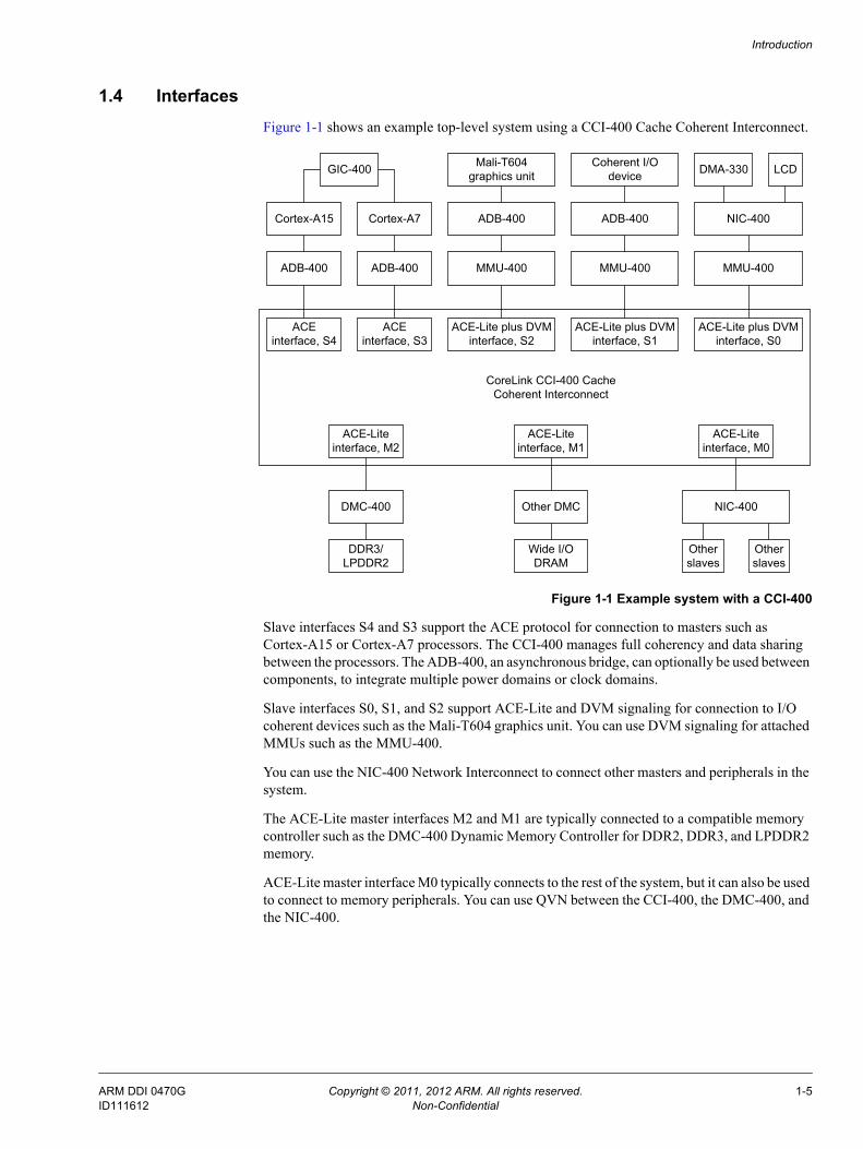
1.4 InterfacesFigure 1-1 shows an example top-level system using a CCI-400 Cache Coherent Interconnect.
Figure 1-1 Example system with a CCI-400
Slave interfaces S4 and S3 support the ACE protocol for connection to masters such as Cortex-A15 or Cortex-A7 processors. The CCI-400 manages full coherency and data sharing between the processors. The ADB-400, an asynchronous bridge, can optionally be used between components, to integrate multiple power domains or clock domains.
Slave interfaces S0, S1, and S2 support ACE-Lite and DVM signaling for connection to I/O coherent devices such as the Mali-T604 graphics unit. You can use DVM signaling for attached MMUs such as the MMU-400.
You can use the NIC-400 Network Interconnect to connect other masters and peripherals in the system.
The ACE-Lite master interfaces M2 and M1 are typically connected to a compatible memory controller such as the DMC-400 Dynamic Memory Controller for DDR2, DDR3, and LPDDR2 memory.
ACE-Lite master interface M0 typically connects to the rest of the system, but it can also be used to connect to memory peripherals. You can use QVN between the CCI-400, the DMC-400, and the NIC-400.
CoreLink CCI-400 Cache Coherent Interconnect
ACEinterface, S4
ACEinterface, S3
ACE-Lite plus DVMinterface, S2
ACE-Lite plus DVMinterface, S1
ACE-Lite plus DVMinterface, S0
Cortex-A15 Cortex-A7
MMU-400 MMU-400 MMU-400
NIC-400
DMA-330 LCD
ADB-400ADB-400
Coherent I/O device
Mali-T604graphics unitGIC-400
ACE-Liteinterface, M2
ACE-Liteinterface, M1
ACE-Liteinterface, M0
DMC-400 Other DMC NIC-400
Other slaves
Other slaves
Wide I/O DRAM
DDR3/LPDDR2
ADB-400 ADB-400
ARM DDI 0470G Copyright © 2011, 2012 ARM. All rights reserved. 1-5ID111612 Non-Confidential
Introduction
1.5 Configurable optionsThe CCI-400 has design-time options for the following:• Options for 40-bit or 44-bit address width for DVM transactions.• Width of ID signals on the slave interfaces.• Maximum number of outstanding transactions at each slave and master interface.• Registering options at each slave and master interface.• User-defined additional signaling.• QoS values for read queue slot reservation.• Write ordering observation.• The exclusion of QVN logic.
The CCI-400 has input signals that are sampled at reset and define the following behaviors:• Address map. See Address map on page 3-22 for more information.• Base address of internal registers.• Master interface behavior regarding barriers and cache maintenance operations.• Snoop request and DVM message propagation.• QoS provision.• QVN configuration.
Note You cannot modify other parameters in the design.
ARM DDI 0470G Copyright © 2011, 2012 ARM. All rights reserved. 1-6ID111612 Non-Confidential
Introduction
1.6 Test featuresThe CCI-400 Cache Coherent Interconnect contains a DFTRSTDISABLE input signal that disables the reset during scan shift.
ARM DDI 0470G Copyright © 2011, 2012 ARM. All rights reserved. 1-7ID111612 Non-Confidential

Introduction
1.7 Product documentation, design flow, and architectureThis section describes the CCI-400 Cache Coherent Interconnect books and how they relate to the design flow. It includes:• Documentation.• Design flow on page 1-9.
See Additional reading on page vii for more information about the books described in this section. For information on the relevant architectural standards and protocols, see Compliance on page 1-3.
1.7.1 Documentation
The CCI-400 Cache Coherent Interconnect documentation is as follows:
Technical Reference Manual The Technical Reference Manual (TRM) describes the functionality and the effects of functional options on the behavior of the CCI-400 Cache Coherent Interconnect. It is required at all stages of the design flow. The choices made in the design flow can mean that some behavior described in the TRM is not relevant. If you are programming the CCI-400 Cache Coherent Interconnect then contact:• The implementer to determine:
— The build configuration of the implementation.— What integration, if any, was performed before implementing the
CCI-400 Cache Coherent Interconnect.• The integrator to determine the pin configuration of the device that you are
using.
Implementation Guide The Implementation Guide (IG) contains:• A description of the CCI-400 deliverables.• Out-of-box procedures for verifying and synthesizing your CCI-400
installation.The ARM product deliverables include reference scripts and information about using them to implement your design.The IG is a confidential book that is only available to licensees.
Integration Manual The Integration Manual (IM) describes how to integrate the CCI-400 Cache Coherent Interconnect into a SoC. It includes:• A description of the CCI-400 features.• A list of the design-time configuration options.• A list of the reset-time configuration options.• Considerations when integrating CCI-400 into your system.The IM is a confidential book that is only available to licensees.
ARM DDI 0470G Copyright © 2011, 2012 ARM. All rights reserved. 1-8ID111612 Non-Confidential
Introduction
1.7.2 Design flow
The CCI-400 Cache Coherent Interconnect is delivered as synthesizable RTL. Before you can use it in a product, it must go through the following processes:
Implementation The implementer configures and synthesizes the RTL to produce a hard macrocell.
Integration The integrator connects the implemented design into a SoC. This includes connecting it to a memory system and peripherals.
Programming This is the last process. The system programmer develops the software required to configure and initialize the CCI-400, and tests the required application software.
Each process:
• Is separate, and a different person can complete it.
• Can include implementation and integration choices that affect the behavior and features of the CCI-400 Cache Coherent Interconnect.
The operation of the final device depends on:
Build configuration The implementer chooses the options that affect how the RTL source files are pre-processed. These options usually include or exclude logic that affects one or more of the area, maximum frequency, and features of the resulting macrocell. For example, the numbers of outstanding transactions that each master and slave interface support.
Configuration inputs The integrator configures some features of the CCI-400 Cache Coherent Interconnect by tying inputs to specific values. These configurations affect the start-up behavior before any software configuration is made. They can also limit the options available to the software. For example, the ACCHANNELEN inputs that prevent AC requests from being emitted from an unconnected slave interface.
Software configuration The programmer configures the CCI-400 Cache Coherent Interconnect by programming particular values into registers. This affects the behavior of the CCI-400, for example, by enabling or disabling speculative fetches.
Note This manual provides a reference for implementation-defined features that are applicable to build configuration options. Reference to a feature that is included means that the appropriate build and pin configuration options are selected. Reference to an enabled feature means one that has also been configured by software.
ARM DDI 0470G Copyright © 2011, 2012 ARM. All rights reserved. 1-9ID111612 Non-Confidential
Introduction
1.8 Product revisionsThis section describes differences in functionality between product revisions:
r0p0 First release.
r0p0-r0p1 New exclusive access functionality. See Exclusive accesses on page 2-15.
r0p1-r0p2 Configuration improvements for the following:• Maximum ID width on slave interfaces increased from 8 to 28.• Maximum size of read and write trackers in master interfaces increased
from 32 to 128.• Read and write trackers in master interfaces is now configurable in steps of
1 rather than 2n.Improvements for the following:• Master interface read tracker slot re-use time to reduce stalls.• Slave interface PMU events redefined to improve the counting of device
and non-cacheable transactions.
r0p2-r0p3 The CCI-400 now supports up to four exclusive access threads from each ACE master and has separate monitors for secure and non-secure transactions. See Exclusive accesses on page 2-15.
r0p3-r0p4 No functional changes.
r0p4-r1p0 Major upgrade with new or improved functionality for the following:• Performance improvements:
— Increased bandwidth for WriteUnique and WriteLineUnique transactions.
— Improvements to performance when using heterogeneous processor clusters.
— Reduced read latency.— Improved performance with hazards. An ID or address hazard no
longer blocks the master interface.— Improved performance when a master reuses IDs. A stalled
transaction is released earlier.— Optimizations in barrier performance.— Exclusive access monitor for each processor rather than for each
cluster. This improves performance for shareable exclusive transactions.
• QoS improvements:— Support for QVN.— QoS value bandwidth regulation in addition to the existing latency
regulation.— Reservation for read queue slot.— Avoidance of head-of-line blocking using priority promotion.— Improved visibility of QoS regulator values.See also Quality of Service on page 2-17.
• Additional functionality:— WID output on master interfaces helps to connect to AXI3 slaves.
ARM DDI 0470G Copyright © 2011, 2012 ARM. All rights reserved. 1-10ID111612 Non-Confidential
Introduction
— Speculative fetches can be disabled for each slave interface and also for each master interface.
— Configurable option for 44-bit DVM messages.— Additional PMU events to support new functionality.
r1p0-r1p1 Configuration improvements for the following:• Frequency improvement at the expense of one cycle of latency on read
transactions.• Added configurability of WriteUnique and WriteLineUnique tracker sizes.• New write ordering configuration options.• Option to remove QVN logic when it is not required.
ARM DDI 0470G Copyright © 2011, 2012 ARM. All rights reserved. 1-11ID111612 Non-Confidential
Chapter 2 Functional Description
This chapter describes the functionality of the CoreLink™ CCI-400 Cache Coherent Interconnect. It contains the following sections:• About the functions on page 2-2.• Snoop connectivity and control on page 2-3.• Speculative fetch on page 2-4.• Performance Monitoring Unit on page 2-5.• Security on page 2-10.• Error responses on page 2-12.• Cache maintenance operations on page 2-13.• Barriers on page 2-14.• Exclusive accesses on page 2-15.• DVM messages on page 2-16.• Quality of Service on page 2-17.• Clock and reset on page 2-21.
ARM DDI 0470G Copyright © 2011, 2012 ARM. All rights reserved. 2-1ID111612 Non-Confidential
Functional Description
2.1 About the functionsThe CCI-400 combines interconnect and coherency functions into a single module. It supports connectivity for up to two ACE masters, for example, Cortex-A15 or Cortex-A7, and three ACE-Lite masters, for example, Mali-T604, plus optional DVM message support on these interfaces to manage distributed MMUs, for example, MMU-400. These can communicate through the CCI-400 with up to three ACE-Lite slaves.
ARM DDI 0470G Copyright © 2011, 2012 ARM. All rights reserved. 2-2ID111612 Non-Confidential

Functional Description
2.2 Snoop connectivity and controlThe CCI-400 has a fully-connected snoop topology, so if they are enabled:• Each ACE slave interface snoops the other ACE slave interface.• ACE-Lite slave interfaces snoop both ACE slave interfaces.• DVM messages are broadcast through all enabled slave interfaces.
Snooping and DVM message broadcast are disabled at reset, so you must enable the appropriate masters for snooping and DVM messages using the Snoop Control Registers before shareable or DVM messages are sent to the CCI-400. See Snoop Control Registers on page 3-14.
ARM DDI 0470G Copyright © 2011, 2012 ARM. All rights reserved. 2-3ID111612 Non-Confidential
Functional Description
2.3 Speculative fetchFor an application where the probability of a miss is high, then the snoop request and response time adds directly to the latency for each transaction labelled as shareable. To mitigate this, you can program each master interface to issue a fetch downstream in parallel with issuing a snoop request. This is known as a speculative fetch.
In the event that the snoop associated with a speculative fetch hits in a cache, then the data from the snoop is returned in preference to the data from the speculative fetch.
A speculative fetch is issued before all hazards that had arised from the corresponding snoop have been resolved. Therefore, it is sometimes necessary to discard the data returned from memory and retry the fetch. These cases are:
• When a hazarding write transaction is detected. This hazarding write transaction must be ordered before the speculative fetch.
• When data from the speculative fetch returns before the snoop response for that transaction.
You can use the PMU to record the number of retry transactions for each master interface. See Performance Monitoring Unit on page 2-5.
Note Speculative fetches are only issued for these read-type transactions: • ReadOnce.• ReadClean.• ReadNotSharedDirty.• ReadUnique.• ReadShared.
Although speculative fetches reduce the latency in the case of a snoop miss, there is a bandwidth and power penalty because of the additional transactions on a snoop hit. Therefore, only enable speculative fetches where you expect most snoops to miss. You can use the Speculation Control Register to disable speculative fetches for a master or a slave interface. For example, you can disable speculative fetches for transactions from a master that is not latency sensitive. See Speculation Control Register on page 3-9.
ARM DDI 0470G Copyright © 2011, 2012 ARM. All rights reserved. 2-4ID111612 Non-Confidential
Functional Description
2.4 Performance Monitoring UnitThe CCI-400 includes logic to gather various statistics on the operation of the interconnect during runtime, using events and counters. These events provide useful information about the behavior of the interconnect that you can use when debugging or profiling traffic.
The PMU provides four counters. Each counter can count any of the events available in the CCI-400. To keep the PMU logic overhead to a minimum, the absolute counts and timing of events might vary slightly. This has negligible effect except in cases where the counters are enabled for a very short time.
The PMU consists of:
• A 159-bit event bus, EVNTBUS, that you can export from the CCI-400.
• Ten 4-bit event outputs that track the value of the read and write QoS regulators for each slave interface.
• Four 32-bit event counters, that you can program to count one event from the event bus.
• A clock cycle counter, CCNT, for calculating timing information from the event counters.
• An input signal, NIDEN, that if HIGH, enables the counting and exporting of events.
• An input signal, SPNIDEN, that if HIGH, enables the counting of both non-secure and secure events.
• A set of counter overflow outputs, nEVNTCNTOVERFLOW, that can raise an interrupt when a number of events have occurred.
This section describes:• PMU event list.• PMU registers on page 2-8.• Using the PMU on page 2-8.
2.4.1 PMU event list
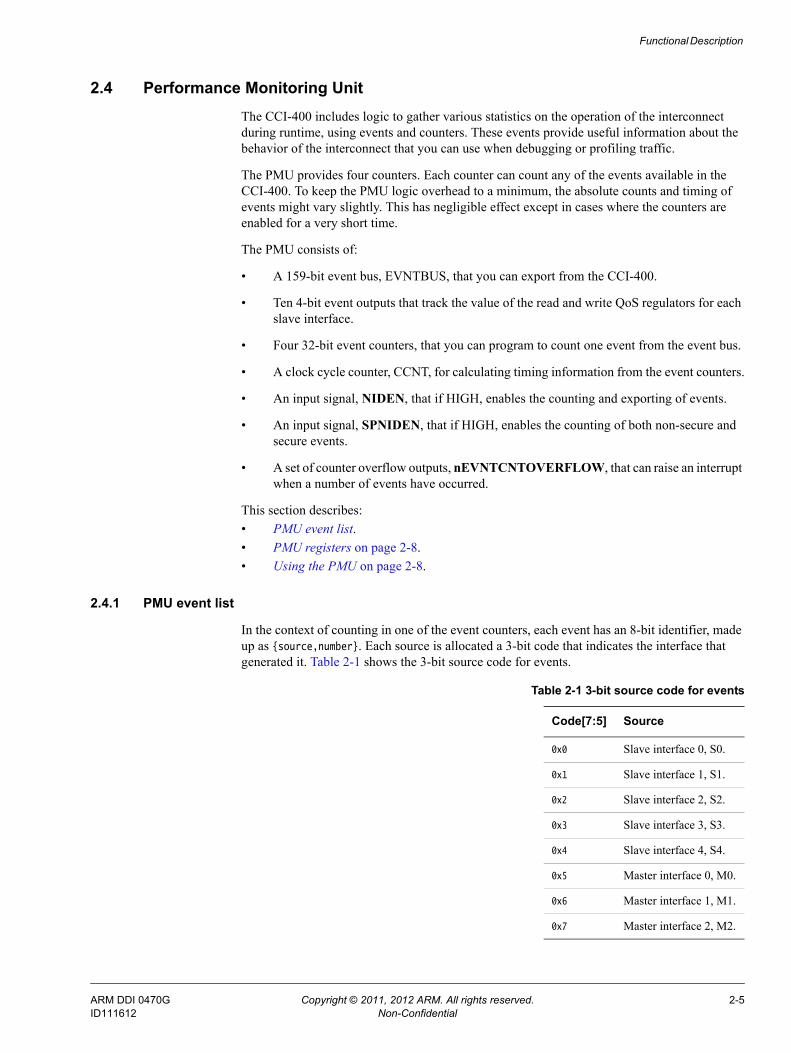
In the context of counting in one of the event counters, each event has an 8-bit identifier, made up as {source,number}. Each source is allocated a 3-bit code that indicates the interface that generated it. Table 2-1 shows the 3-bit source code for events.
Table 2-1 3-bit source code for events
Code[7:5] Source
0x0 Slave interface 0, S0.
0x1 Slave interface 1, S1.
0x2 Slave interface 2, S2.
0x3 Slave interface 3, S3.
0x4 Slave interface 4, S4.
0x5 Master interface 0, M0.
0x6 Master interface 1, M1.
0x7 Master interface 2, M2.
ARM DDI 0470G Copyright © 2011, 2012 ARM. All rights reserved. 2-5ID111612 Non-Confidential
Functional Description
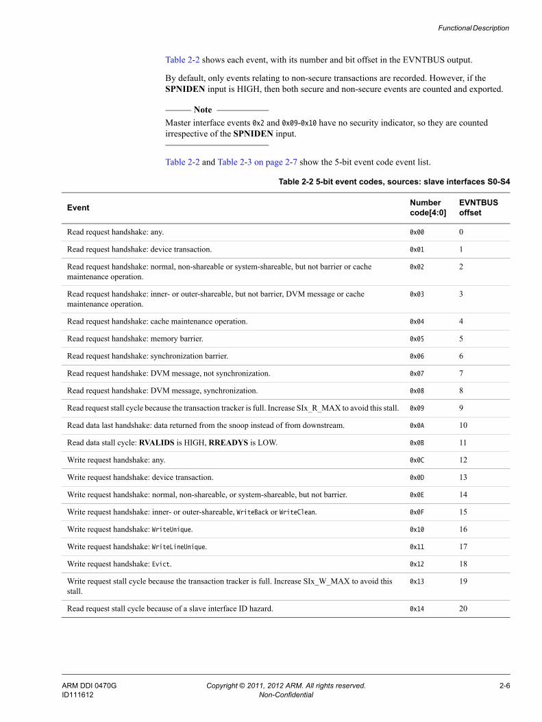
Table 2-2 shows each event, with its number and bit offset in the EVNTBUS output.
By default, only events relating to non-secure transactions are recorded. However, if the SPNIDEN input is HIGH, then both secure and non-secure events are counted and exported.
Note Master interface events 0x2 and 0x09-0x10 have no security indicator, so they are counted irrespective of the SPNIDEN input.
Table 2-2 and Table 2-3 on page 2-7 show the 5-bit event code event list.
Table 2-2 5-bit event codes, sources: slave interfaces S0-S4
Event Number code[4:0]
EVNTBUS offset
Read request handshake: any. 0x00 0
Read request handshake: device transaction. 0x01 1
Read request handshake: normal, non-shareable or system-shareable, but not barrier or cache maintenance operation.
0x02 2
Read request handshake: inner- or outer-shareable, but not barrier, DVM message or cache maintenance operation.
0x03 3
Read request handshake: cache maintenance operation. 0x04 4
Read request handshake: memory barrier. 0x05 5
Read request handshake: synchronization barrier. 0x06 6
Read request handshake: DVM message, not synchronization. 0x07 7
Read request handshake: DVM message, synchronization. 0x08 8
Read request stall cycle because the transaction tracker is full. Increase SIx_R_MAX to avoid this stall. 0x09 9
Read data last handshake: data returned from the snoop instead of from downstream. 0x0A 10
Read data stall cycle: RVALIDS is HIGH, RREADYS is LOW. 0x0B 11
Write request handshake: any. 0x0C 12
Write request handshake: device transaction. 0x0D 13
Write request handshake: normal, non-shareable, or system-shareable, but not barrier. 0x0E 14
Write request handshake: inner- or outer-shareable, WriteBack or WriteClean. 0x0F 15
Write request handshake: WriteUnique. 0x10 16
Write request handshake: WriteLineUnique. 0x11 17
Write request handshake: Evict. 0x12 18
Write request stall cycle because the transaction tracker is full. Increase SIx_W_MAX to avoid this stall.
0x13 19
Read request stall cycle because of a slave interface ID hazard. 0x14 20
ARM DDI 0470G Copyright © 2011, 2012 ARM. All rights reserved. 2-6ID111612 Non-Confidential
Functional Description
Event bus
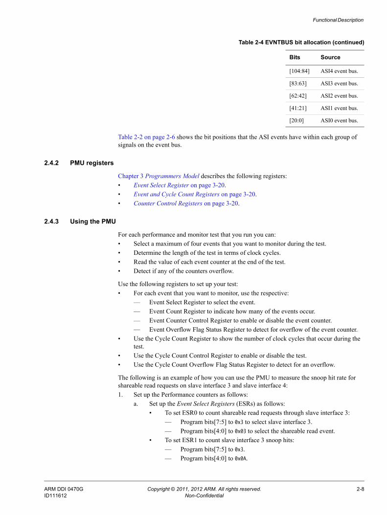
The CCI-400 exports a vector of event signals, EVNTBUS, with the bit allocation that Table 2-4 shows. When an event is triggered, the relevant bit of EVNTBUS is set to HIGH for one clock period.
Table 2-3 5-bit event codes, sources: master interfaces M0-M2
Event Number code[4:0]
EVNTBUS offset
Source: master interface, M0-M2
RETRY of speculative fetch transaction.a 0x00 0
Stall cycle because of an address hazard. A read or write invalidation is stalled because of an outstanding transaction to an overlapping address.
0x01 1
Read request stall cycle because of a master interface ID hazard. 0x02 2
A read request with a QoS value in the high priority group is stalled for a cycle because the read transaction queue is full. Increase MIx_R_MAX to avoid this stall.
0x03 3
Read request stall cycle because of a barrier hazard. 0x04 4
Write request stall cycle because of a barrier hazard. 0x05 5
A write request is stalled for a cycle because the write transaction tracker is full. Increase MIx_W_MAX to avoid this stall.
0x06 6
A read request with a QoS value in the low priority group is stalled for a cycle because there are no slots available in the read queue for the low priority group.
0x07 7
A read request with a QoS value in the medium priority group is stalled for a cycle because there are no slots available in the read queue for the medium priority group.
0x08 8
A read request is stalled for a cycle while it was waiting for a QVN token on VN0. 0x09 9
A read request is stalled for a cycle while it was waiting for a QVN token on VN1. 0x0A 10
A read request is stalled for a cycle while it was waiting for a QVN token on VN2. 0x0B 11
A read request is stalled for a cycle while it was waiting for a QVN token on VN3. 0x0C 12
A write request is stalled for a cycle while it was waiting for a QVN token on VN0. 0x0D 13
A write request is stalled for a cycle while it was waiting for a QVN token on VN1. 0x0E 14
A write request is stalled for a cycle while it was waiting for a QVN token on VN2. 0x0F 15
A write request is stalled for a cycle while it was waiting for a QVN token on VN3. 0x10 16
A WriteUnique or WriteLineUnique request is stalled for a cycle because of an address hazard. 0x11 17
a. This event fires when retries are scheduled. If two retries are scheduled simultaneously, only one event is generated.
Table 2-4 EVNTBUS bit allocation
Bits Source
[158:141] AMI2 event bus.
[140:123] AMI1 event bus.
[122:105] AMI0 event bus.
ARM DDI 0470G Copyright © 2011, 2012 ARM. All rights reserved. 2-7ID111612 Non-Confidential
Functional Description
Table 2-2 on page 2-6 shows the bit positions that the ASI events have within each group of signals on the event bus.
2.4.2 PMU registers
Chapter 3 Programmers Model describes the following registers:• Event Select Register on page 3-20.• Event and Cycle Count Registers on page 3-20.• Counter Control Registers on page 3-20.
2.4.3 Using the PMU
For each performance and monitor test that you run you can:• Select a maximum of four events that you want to monitor during the test.• Determine the length of the test in terms of clock cycles.• Read the value of each event counter at the end of the test.• Detect if any of the counters overflow.
Use the following registers to set up your test:• For each event that you want to monitor, use the respective:
— Event Select Register to select the event.— Event Count Register to indicate how many of the events occur.— Event Counter Control Register to enable or disable the event counter.— Event Overflow Flag Status Register to detect for overflow of the event counter.
• Use the Cycle Count Register to show the number of clock cycles that occur during the test.
• Use the Cycle Count Control Register to enable or disable the test.• Use the Cycle Count Overflow Flag Status Register to detect for an overflow.
The following is an example of how you can use the PMU to measure the snoop hit rate for shareable read requests on slave interface 3 and slave interface 4:1. Set up the Performance counters as follows:
a. Set up the Event Select Registers (ESRs) as follows:• To set ESR0 to count shareable read requests through slave interface 3:
— Program bits[7:5] to 0x3 to select slave interface 3.— Program bits[4:0] to 0x03 to select the shareable read event.
• To set ESR1 to count slave interface 3 snoop hits:— Program bits[7:5] to 0x3.— Program bits[4:0] to 0x0A.
[104:84] ASI4 event bus.
[83:63] ASI3 event bus.
[62:42] ASI2 event bus.
[41:21] ASI1 event bus.
[20:0] ASI0 event bus.
Table 2-4 EVNTBUS bit allocation (continued)
Bits Source
ARM DDI 0470G Copyright © 2011, 2012 ARM. All rights reserved. 2-8ID111612 Non-Confidential
Functional Description
• To set ESR2 to count shareable read requests through slave interface 4:— Program bits[7:5] to 0x4.— Program bits[4:0] to 0x03.
• To set ESR3 to count slave interface 4 snoop hits:— Program bits[7:5] to 0x4.— Program bits[4:0] to 0x0A.
b. Enable all of the event counters by doing the following:• Program Counter Control Register 0 bit[0] to 0b1.• Program Counter Control Register 1 bit[0] to 0b1.• Program Counter Control Register 2 bit[0] to 0b1.• Program Counter Control Register 3 bit[0] to 0b1.
2. Program the following bits in the Performance Monitor Control Register (PMCR):• Bits[2:1] to 0b11 to reset the cycle counter and all of the event counters.• Bit[0] to 0b1 to enable all of the counters.
3. Allow the test to run for an appropriate amount of time4. Do the following to disable all of the counters to stop the test:
• Program PMCR bit[0] to 0b0.5. Read the results of the test from the cycle counter and event counters:
• The cycle counter holds the number of clock cycles for which the test ran.• Counter 0 holds the number of reads for slave interface 3.• Counter 1 holds the number of snoop hits for slave interface 3.• Counter 2 holds the number of reads for slave interface 4.• Counter 3 holds the number of snoop hits for slave interface 4.
6. Check the overflow bits of all the counters and adjust your results accordingly.
ARM DDI 0470G Copyright © 2011, 2012 ARM. All rights reserved. 2-9ID111612 Non-Confidential
Functional Description
2.5 SecurityIf you are building a system based on the secure and non-secure capabilities that TrustZone technology provides, then you must consider security issues. This section describes:• Internal programmers view.• Non-TrustZone-aware masters made secure.• Security of master interfaces.• Security and the PMU.
2.5.1 Internal programmers view
With the exception of the PMU registers, the programmers view defaults to secure access only, as follows:
• Non-secure read requests to secure registers receive a DECERR response, RRESP[1:0] == 0b11, and zeroed data.
• Non-secure write requests to secure registers receive a DECERR response, BRESP[1:0] == 0b11 and are Write-Ignored (WI).
Note Some accesses might receive a response before they reach the CCI-400 registers and so do not receive a DECERR response nor affect the register values. An example of this is a cache maintenance operation that incorrectly addresses the CCI-400 register space.
You can override these security settings in the Secure Access Register. At reset, you can only access this using secure requests, but if you write to it, this enables non-secure access to all registers in the CCI-400 except for the Control Override Register and Secure Access Register. See Control Override Register on page 3-8 and Secure Access Register on page 3-9.
2.5.2 Non-TrustZone-aware masters made secure
A master might require access to the CCI-400 registers, and in this case, you can tie the security transaction indicator bits, ARPROT[1] and AWPROT[1] LOW, so that all accesses by that master are indicated as secure. This places that master permanently in the secure domain. However, depending on the other usage of that master, this might mean that the overall system is not as secure under all circumstances.
2.5.3 Security of master interfaces
Transactions from the CCI-400 master interfaces always retain the security setting of the originating transactions. This applies to:• Non-shareable transactions.• Snoop misses.• Speculative fetches.• CCI-400-generated writes.
2.5.4 Security and the PMU
You can use both secure and non-secure transactions to access the PMU registers. However, you can configure the PMU to count only non-secure events, or both secure and non-secure events, depending on the SPNIDEN input. The default is non-secure events.
ARM DDI 0470G Copyright © 2011, 2012 ARM. All rights reserved. 2-10ID111612 Non-Confidential
Functional Description
If the SPNIDEN input is taken HIGH, there is a potential security risk because non-secure software can observe security activity through the performance counters. See Appendix A Signal Descriptions. ARM advises that you consider the security to be breached for devices placed in this state and that you take appropriate action.
If the SPNIDEN input goes from HIGH to LOW, that is, the PMUs go from counting all events to counting only non-secure events, the counters could contain information relating to secure transactions. Therefore, ARM recommends that software sets the counters to zero if access to that information could represent a potential security risk.
Note Unlike ARM processors, SPNIDEN applies to events from both user and privileged transactions and the CCI-400 makes no distinction between them.
ARM DDI 0470G Copyright © 2011, 2012 ARM. All rights reserved. 2-11ID111612 Non-Confidential
Functional Description
2.6 Error responsesThe CCI-400 uses a mixture of precise and imprecise signaling of error responses, where:
• Precise errors are signalled back to the master on the R and B channels for the precise transaction that caused the error.
• Imprecise errors are not signalled on R and B channels but are instead signalled using the nERRORIRQ output pin. You can identify the interface that received the error response by reading the Imprecise Error Register. See Imprecise Error Register on page 3-10.
2.6.1 Imprecise errors
Table 2-5 shows the errors that are signalled as imprecise. All other sources of error are signalled precisely.
Note An error is signalled either precisely or imprecisely, but never both.
The CCI-400 generates a precise DECERR response in the case of a security violation on a CCI-400 register access. See Imprecise Error Register on page 3-10 and Security on page 2-10.
Table 2-5 Imprecise errors
Transaction causing error Channel receiving error Imprecise error indicator from
A ReadX snoop that misses in the cache and fetches data from downstream.
CR Slave interface receiving the CR response.
Distributed Virtual Memory message. CR Slave interface receiving the CR response.
Speculative fetch that must be retried. R Master interface receiving the R response.
Write that the CCI-400 generated. B Master interface receiving the B response.
Snoop error generated by a WriteLineUnique or WriteUnique transaction.
CR Master interface receiving the CR response.
Write error for WriteUnique transactions that have been split but not the last transaction in the split sequence.
B Slave interface that received the transaction that was split.
ARM DDI 0470G Copyright © 2011, 2012 ARM. All rights reserved. 2-12ID111612 Non-Confidential
Functional Description
2.7 Cache maintenance operationsThe CCI-400 supports the snooping of cache maintenance operations based on the Snoop Control Register. See Snoop Control Registers on page 3-14. Snooping and cache maintenance can be used to manage level 1 and 2 caches within the same domain as the CCI-400. You can optionally send cache maintenance operations downstream to manage a level 3 cache, depending on the BROADCASTCACHEMAINT inputs.
ARM DDI 0470G Copyright © 2011, 2012 ARM. All rights reserved. 2-13ID111612 Non-Confidential
Functional Description
2.8 BarriersThe CCI-400 supports all types of AMBA 4 barrier transactions. Each slave interface broadcasts these to every master interface, ensuring that intermediate transaction source and sink points observe the barrier correctly.
ARM DDI 0470G Copyright © 2011, 2012 ARM. All rights reserved. 2-14ID111612 Non-Confidential
Functional Description
2.9 Exclusive accessesThe CCI-400 supports exclusive accesses to shareable and non-shareable locations as the ACE and AXI4 protocols describe. The AMBA AXI and ACE Protocol Specification permits shareable exclusive accesses on ACE interfaces only.
ARM DDI 0470G Copyright © 2011, 2012 ARM. All rights reserved. 2-15ID111612 Non-Confidential
Functional Description
2.10 DVM messagesThe ACE slave interfaces support DVM messages through their regular AC and CR channels. The ACE-Lite interfaces all contain AC and CR channels to support DVM messages only. Each slave interface has a programmable enable bit to determine whether it supports the issuing of AC requests for DVM messages. DVM messages are handled as regular transactions in the CCI-400, except that they are decoded based on the DVM message indicator, instead of the address, to ensure that multi-transaction DVM messages are correctly ordered.
The Snoop Control Registers and Control Override Register control the issuing of DVM message requests. See Snoop Control Registers on page 3-14 and Control Override Register on page 3-8.
Note A master that issues DVM messages must also be able to receive DVM messages. The slave interface through which the master connects must have DVM messages enabled.
ARM DDI 0470G Copyright © 2011, 2012 ARM. All rights reserved. 2-16ID111612 Non-Confidential
Functional Description
2.11 Quality of ServiceThe CCI-400 supports QoS with the following independent mechanisms:• QoS value.• Regulation based on outstanding transactions on page 2-19.
2.11.1 QoS value
Each CCI-400 slave interface has ARQOS and AWQOS input signals that transport a transaction-based QoS value. This determines the relative priority between transactions on that interface, or between interfaces. The CCI-400 uses the QoS value when it chooses between transaction requests at arbitration points and within queues. Transaction requests with the highest QoS value are prioritized. The CCI-400 uses a Least Recently Granted (LRG) scheme when two or more transactions share the highest value.
QoS values are propagated by CCI-400. If downstream interconnect and slave devices are sensitive to the QoS value, then the service rate is dependent on this value. The NIC-400 Network Interconnect and the DMC-400 Dynamic Memory Controller are both sensitive to QoS value.
Note Ensure that you balance the relative priorities of all slave interfaces. For example, setting each to the highest QoS value reduces the arbitration to LRG and no advantage is gained from having a QoS value.
You can override the ARQOS and AWQOS input signals from each slave interface by using a programmable register if the relevant static input signal, QOSOVERRIDE[4:0], with one bit for each of slave interfaces 4-0, is HIGH. The QoS override is either based on a programmable value or uses performance feedback to set the value within a programmable range. Transactions that the CCI-400 generates use the same QoS value as the instigating transaction or the override value if QOSOVERRIDE is set.
Note QOSOVERRIDE only applies to transactions that have a ARQOS or AWQOS value of 0. Therefore, each interface can have a mixture of traffic that is overridden or regulated and other traffic, with non-zero QoS value, that is unaffected. For example, high priority MMU page table requests might be mixed with high-bandwidth media requests that require regulation.
QoS value regulation
CCI-400 regulation mechanisms vary the transaction QoS value depending on latency or bandwidth achieved through that slave interface. You can program target latency or bandwidth and a QoS value range for each regulator. ARM recommends that achievable targets are set such that the regulator uses the minimum QoS value in most cases and only increases the QoS value, up to the programmed maximum, under worst case conditions. The maximum value for each regulator is 0 at reset, so you must program a maximum value before the regulator can be used.
You can control the rate of change of the regulator integrator by using a programmable scale factor. There are two types of QoS value regulation:• Regulation based on latency.• Regulation based on bandwidth.
Regulation based on latency
ARM DDI 0470G Copyright © 2011, 2012 ARM. All rights reserved. 2-17ID111612 Non-Confidential
Functional Description
In this regulation mode, QoS values change based on measured latency. The value tends to increase if the latency is greater than the target and decrease if the latency is lower than the target.
Regulation based on bandwidth
For bandwidth regulation, the target used for feedback is the period between successive request handshakes, in cycles. The value tends to increase if the period is greater than the target and decrease if the period is lower than the target. If the average number of bytes per request is known, this is equivalent to a bandwidth measure. Shareable transactions in the CCI-400 are 64B in size, so this is usually a good approximation to use.
There are two modes of operation available when you are using this type of regulation:
• Normal mode.In this mode the QoS value remains stable when the master is idle, this is equivalent to measuring the average bandwidth only when the master is active. This is the default mode.
• Quiesce High modeIn this mode, the QoS value tends to the maximum programmed value when the master is idle, so when it becomes active, the initial transactions have a high QoS value. This mode is suitable for latency sensitive masters because it allows the master to be serviced with high priority while the bandwidth requirement is below that set. If the master starts to exceed its programmed bandwidth, the priority is reduced. This mechanism can be used to ensure that other masters are not excluded when latency sensitive masters take significant bandwidth.
You enable QoS value regulation by setting the appropriate control bits. See QoS Control Register on page 3-16. When you enable QoS value regulation, ARQOS and AWQOS values are driven by those generated by the regulators, if the original transaction has a zero QoS value and the QOSOVERRIDE configuration input is HIGH.
You can program the regulator mode using the QoS Control Registers.
Note • Turning QoS value regulation on when QOSOVERRIDE[x] is set LOW for a specific
interface has no effect.
• Transactions that do not transfer data are not counted for QoS value regulation and do not have their QoS value overridden. These transactions are:— CleanUnique.— MakeUnique.— CleanShared.— CleanInvalid.— MakeInvalid.— Evict.— Barriers.— DVM transactions.
ARM DDI 0470G Copyright © 2011, 2012 ARM. All rights reserved. 2-18ID111612 Non-Confidential

Functional Description
2.11.2 Regulation based on outstanding transactions
The CCI-400 offers an additional mechanism for regulating traffic flows for the benefit of overall performance. Each ACE-Lite slave interface has an optional, programmable mechanism for limiting the number of outstanding read and write transactions, where an Outstanding Transaction (OT) is a read request without read data, or a write request without a response. This can be used where QoS value regulation is not effective because the system is not sensitive to QoS value. The disadvantage of this form of regulation is that it might stall the master even when the system is idle and traffic from this master is not affecting the performance of other masters.
You can characterize a sequence of transactions, with periods when there are no outstanding transactions, by using a fractional outstanding transaction number. For example, if requests occur every 100 cycles, but it only takes 50 cycles for the last response to arrive, then this would correspond to 0.5 OTs. The sum of the integer and fractional values represents a maximum of the mean number of OTs in a sliding window and, consequently, also over all time. If the fractional part is 0, the number of OTs is never permitted to exceed the integer part. If the fractional part is not 0, the number of OTs is not permitted to exceed one more than the integer part. This mean value is only achieved if the attached master maintains the maximum number of transactions it is able to issue at all times. Therefore, if the integer part is 0 and the fractional part 0.5, and transactions have a lifespan of 50 cycles, a master could issue a transaction, it would finish after 50 cycles and it could not issue the next transaction until 100 cycles, maintaining a mean number of outstanding transactions as 0.5.
If you enable regulation, the following programmable values set the permitted number of outstanding transactions:• OT integer.• OT fraction.
Note • Outstanding transaction regulation only counts transactions with a zero QoS value.
• Outstanding transaction regulation does not count or override transactions that have no data associated with them. These transactions are:— CleanUnique.— MakeUnique.— CleanShared.— CleanInvalid.— MakeInvalid.— Evict.— Barriers.— DVM transactions.
Read Queue Slot Reservation
Each master interface of the CCI-400 has a queue that stores read requests. If this becomes full with low priority requests, higher priority requests are blocked. To avoid this, the CCI-400 reserves a number of slots for high priority requests and a number of slots for high or medium priority requests. You can configure which QoS values are considered as high and medium priority at design time using the R_THRESHOLD_UPPER and R_THRESHOLD_LOWER parameters.
ARM DDI 0470G Copyright © 2011, 2012 ARM. All rights reserved. 2-19ID111612 Non-Confidential
Functional Description
Avoidance of Head-of-Line Blocking
Head-of-line blocking occurs when an interface is shared by transactions with different priorities and a high priority transaction is blocked by an earlier lower priority transaction. To prevent this for read transactions, CCI-400 has an input, ARQOSARB that can be used to promote the priority of the earlier transaction. This is a 4-bit QoS value that propagates through the CCI-400 and is used for arbitration. ARQOSARB is sampled when ARVALID and ARREADY are both HIGH, but unlike other AR payload signals, it is permitted to change when ARVALID is HIGH and ARREADY is LOW.
2.11.3 QoS programmable registers
Chapter 3 Programmers Model describes the following registers:• Read Channel QoS Value Override Register on page 3-15.• Write Channel QoS Value Override Register on page 3-16.• QoS Control Register on page 3-16.• Max OT Registers on page 3-17.• Regulator Target Registers on page 3-18.• QoS Regulator Scale Factor Registers on page 3-18.
2.11.4 QoS Virtual Networks (QVN)
QVN is a technology that enables transactions that are associated with different virtual networks and makes independent progress possible from a source to a destination. This ensures that a transaction on one Virtual Network (VN) can progress towards its destination even if a transaction on a different VN is blocked.
In an interconnect that supports QVN the use of physical wires to send a transfer is negotiated before the transfer is sent. This ensures that when a transfer is sent on the physical wires it is guaranteed to be accepted.
The QVN protocol provides extensions to the AMBA protocol to enable the support of virtual networks within the AXI3, AXI4, ACE, and ACE-Lite bus infrastructures. Using virtual networks and tokens improves system performance because it stops high-bandwidth AXI and ACE sources from preventing the flow of latency critical transactions.
CCI-400 supports QVN on read and write channels of master and slave interfaces. Each slave interface can be assigned to one of four virtual networks. Each master interface supports up to four virtual networks. Each virtual network on the master interfaces can be configured to have a pre-allocated token. If a virtual network does not have a pre-allocated token, there is a minimum 2-cycle delay for each request while the virtual network requests and is granted a token.
See also the CoreLink QVN Protocol Specification.
Note The CoreLink QVN Protocol Specification is available from ARM. This is a confidential document and a separate license is required.
ARM DDI 0470G Copyright © 2011, 2012 ARM. All rights reserved. 2-20ID111612 Non-Confidential
Functional Description
2.12 Clock and resetThis section describes:• Clocking.• Reset.
2.12.1 Clocking
The CCI-400 has a single main clock, ACLK, that is distributed to all sub-blocks. Where masters and slaves connecting to the CCI-400 are in a different clock domain, it is necessary to use external clock-domain-crossing bridges.
Using the Low Power Interface (LPI), it is possible to disable the clock to the CCI-400 when it is idle. When the clock has been disabled, incoming transactions are stalled and any changes to other inputs are not registered until the clock is re-applied.
2.12.2 Reset
The CCI-400 has a single reset domain with an active LOW reset input signal, ARESETn. This is synchronized to ACLK with a double-register on the input to the CCI-400.
Note There must be no activity on the slave interfaces, and the configuration inputs must be static for at least three ACLK cycles after ARESETn goes HIGH.
ARM DDI 0470G Copyright © 2011, 2012 ARM. All rights reserved. 2-21ID111612 Non-Confidential
Chapter 3 Programmers Model
This chapter describes the programmers model. It contains the following sections:• About this programmers model on page 3-2.• Register summary on page 3-3.• Register descriptions on page 3-8.• Address map on page 3-22.
ARM DDI 0470G Copyright © 2011, 2012 ARM. All rights reserved. 3-1ID111612 Non-Confidential
Programmers Model
3.1 About this programmers modelThe following information applies to the CCI-400 Cache Coherent Interconnect registers:
• The base address is not fixed, and can be different for any particular system implementation. The offset of each register from the base address is fixed.
• Do not attempt to access reserved or unused address locations. Attempting to access these locations can result in unpredictable behavior.
• Unless otherwise stated in the accompanying text:— Do not modify undefined register bits.— Ignore undefined register bits on reads.— All register bits are reset to a logic 0 by a system or power-on reset.
• Table 3-1 on page 3-3 describes access types as follows:
R/W Read and write.
RAZ Read as zero.
WI Write ignored.
The CCI-400 registers occupy a 64KB region and are offset using the PERIPHBASE[39:15] static input. PERIPHBASE is a system-level signal that defines the base address of a 64KB region of the physical address space for memory-mapped registers. Different components can co-exist in the system by defining different offsets from PERIPHBASE for their own memory-mapped registers.
The following rules apply:
• You can access the PV using only Device-type transactions, AxCACHE[1] = 0, of length 1 and up to 32 bits in size. Transactions that do not meet these requirements and reach the CCI-400 register region receive a DECERR response.
• A transaction to a reserved block, or a transaction that violates security restrictions, receives a DECERR response.
The programmers view contains regions for control, slave interface, and performance counter registers. See Table 3-1 on page 3-3.
ARM DDI 0470G Copyright © 2011, 2012 ARM. All rights reserved. 3-2ID111612 Non-Confidential
Programmers Model
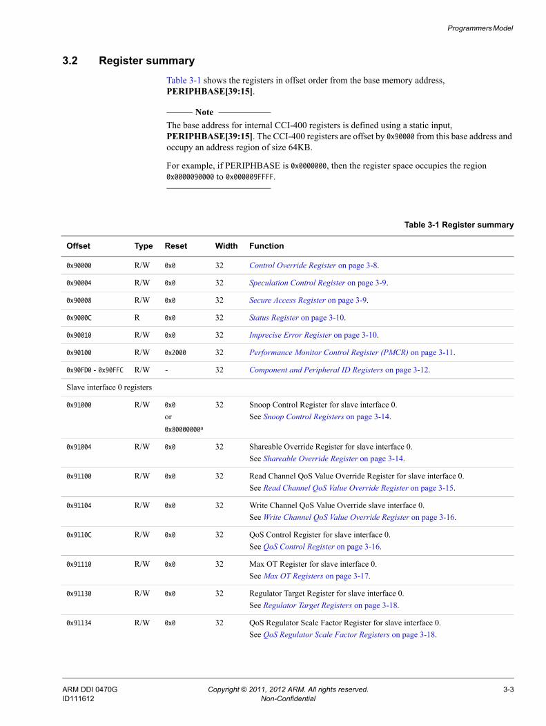
3.2 Register summaryTable 3-1 shows the registers in offset order from the base memory address, PERIPHBASE[39:15].
Note The base address for internal CCI-400 registers is defined using a static input, PERIPHBASE[39:15]. The CCI-400 registers are offset by 0x90000 from this base address and occupy an address region of size 64KB.
For example, if PERIPHBASE is 0x0000000, then the register space occupies the region 0x0000090000 to 0x000009FFFF.
Table 3-1 Register summary
Offset Type Reset Width Function
0x90000 R/W 0x0 32 Control Override Register on page 3-8.
0x90004 R/W 0x0 32 Speculation Control Register on page 3-9.
0x90008 R/W 0x0 32 Secure Access Register on page 3-9.
0x9000C R 0x0 32 Status Register on page 3-10.
0x90010 R/W 0x0 32 Imprecise Error Register on page 3-10.
0x90100 R/W 0x2000 32 Performance Monitor Control Register (PMCR) on page 3-11.
0x90FD0 - 0x90FFC R/W - 32 Component and Peripheral ID Registers on page 3-12.
Slave interface 0 registers
0x91000 R/W 0x0
or0x80000000a
32 Snoop Control Register for slave interface 0.See Snoop Control Registers on page 3-14.
0x91004 R/W 0x0 32 Shareable Override Register for slave interface 0.See Shareable Override Register on page 3-14.
0x91100 R/W 0x0 32 Read Channel QoS Value Override Register for slave interface 0.See Read Channel QoS Value Override Register on page 3-15.
0x91104 R/W 0x0 32 Write Channel QoS Value Override slave interface 0.See Write Channel QoS Value Override Register on page 3-16.
0x9110C R/W 0x0 32 QoS Control Register for slave interface 0.See QoS Control Register on page 3-16.
0x91110 R/W 0x0 32 Max OT Register for slave interface 0.See Max OT Registers on page 3-17.
0x91130 R/W 0x0 32 Regulator Target Register for slave interface 0.See Regulator Target Registers on page 3-18.
0x91134 R/W 0x0 32 QoS Regulator Scale Factor Register for slave interface 0.See QoS Regulator Scale Factor Registers on page 3-18.
ARM DDI 0470G Copyright © 2011, 2012 ARM. All rights reserved. 3-3ID111612 Non-Confidential
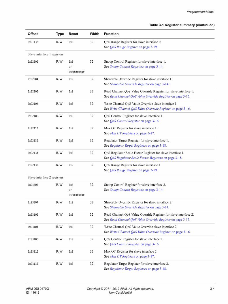
Programmers Model
0x91138 R/W 0x0 32 QoS Range Register for slave interface 0.See QoS Range Register on page 3-19.
Slave interface 1 registers
0x92000 R/W 0x0
or0x80000000b
32 Snoop Control Register for slave interface 1.See Snoop Control Registers on page 3-14.
0x92004 R/W 0x0 32 Shareable Override Register for slave interface 1.See Shareable Override Register on page 3-14.
0x92100 R/W 0x0 32 Read Channel QoS Value Override Register for slave interface 1.See Read Channel QoS Value Override Register on page 3-15.
0x92104 R/W 0x0 32 Write Channel QoS Value Override slave interface 1.See Write Channel QoS Value Override Register on page 3-16.
0x9210C R/W 0x0 32 QoS Control Register for slave interface 1.See QoS Control Register on page 3-16.
0x92110 R/W 0x0 32 Max OT Register for slave interface 1.See Max OT Registers on page 3-17.
0x92130 R/W 0x0 32 Regulator Target Register for slave interface 1.See Regulator Target Registers on page 3-18.
0x92134 R/W 0x0 32 QoS Regulator Scale Factor Register for slave interface 1.See QoS Regulator Scale Factor Registers on page 3-18.
0x92138 R/W 0x0 32 QoS Range Register for slave interface 1.See QoS Range Register on page 3-19.
Slave interface 2 registers
0x93000 R/W 0x0
or0x80000000c
32 Snoop Control Register for slave interface 2.See Snoop Control Registers on page 3-14.
0x93004 R/W 0x0 32 Shareable Override Register for slave interface 2.See Shareable Override Register on page 3-14.
0x93100 R/W 0x0 32 Read Channel QoS Value Override Register for slave interface 2.See Read Channel QoS Value Override Register on page 3-15.
0x93104 R/W 0x0 32 Write Channel QoS Value Override slave interface 2.See Write Channel QoS Value Override Register on page 3-16.
0x9310C R/W 0x0 32 QoS Control Register for slave interface 2.See QoS Control Register on page 3-16.
0x93110 R/W 0x0 32 Max OT Register for slave interface 2.See Max OT Registers on page 3-17.
0x93130 R/W 0x0 32 Regulator Target Register for slave interface 2.See Regulator Target Registers on page 3-18.
Table 3-1 Register summary (continued)
Offset Type Reset Width Function
ARM DDI 0470G Copyright © 2011, 2012 ARM. All rights reserved. 3-4ID111612 Non-Confidential
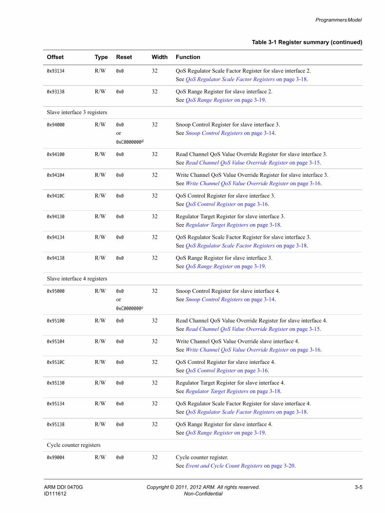
Programmers Model
0x93134 R/W 0x0 32 QoS Regulator Scale Factor Register for slave interface 2.See QoS Regulator Scale Factor Registers on page 3-18.
0x93138 R/W 0x0 32 QoS Range Register for slave interface 2.See QoS Range Register on page 3-19.
Slave interface 3 registers
0x94000 R/W 0x0
or0xC0000000d
32 Snoop Control Register for slave interface 3.See Snoop Control Registers on page 3-14.
0x94100 R/W 0x0 32 Read Channel QoS Value Override Register for slave interface 3.See Read Channel QoS Value Override Register on page 3-15.
0x94104 R/W 0x0 32 Write Channel QoS Value Override Register for slave interface 3.See Write Channel QoS Value Override Register on page 3-16.
0x9410C R/W 0x0 32 QoS Control Register for slave interface 3.See QoS Control Register on page 3-16.
0x94130 R/W 0x0 32 Regulator Target Register for slave interface 3.See Regulator Target Registers on page 3-18.
0x94134 R/W 0x0 32 QoS Regulator Scale Factor Register for slave interface 3.See QoS Regulator Scale Factor Registers on page 3-18.
0x94138 R/W 0x0 32 QoS Range Register for slave interface 3.See QoS Range Register on page 3-19.
Slave interface 4 registers
0x95000 R/W 0x0
or0xC0000000e
32 Snoop Control Register for slave interface 4.See Snoop Control Registers on page 3-14.
0x95100 R/W 0x0 32 Read Channel QoS Value Override Register for slave interface 4.See Read Channel QoS Value Override Register on page 3-15.
0x95104 R/W 0x0 32 Write Channel QoS Value Override slave interface 4.See Write Channel QoS Value Override Register on page 3-16.
0x9510C R/W 0x0 32 QoS Control Register for slave interface 4.See QoS Control Register on page 3-16.
0x95130 R/W 0x0 32 Regulator Target Register for slave interface 4.See Regulator Target Registers on page 3-18.
0x95134 R/W 0x0 32 QoS Regulator Scale Factor Register for slave interface 4.See QoS Regulator Scale Factor Registers on page 3-18.
0x95138 R/W 0x0 32 QoS Range Register for slave interface 4.See QoS Range Register on page 3-19.
Cycle counter registers
0x99004 R/W 0x0 32 Cycle counter register.See Event and Cycle Count Registers on page 3-20.
Table 3-1 Register summary (continued)
Offset Type Reset Width Function
ARM DDI 0470G Copyright © 2011, 2012 ARM. All rights reserved. 3-5ID111612 Non-Confidential
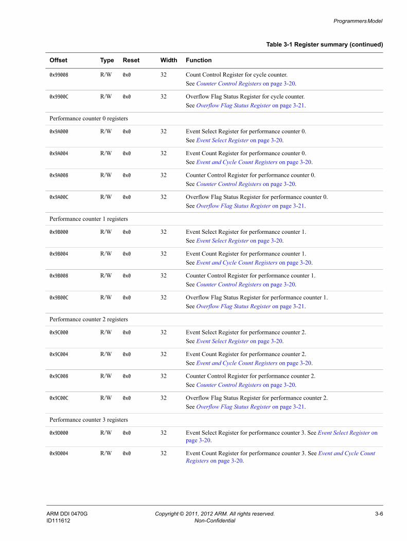
Programmers Model
0x99008 R/W 0x0 32 Count Control Register for cycle counter.See Counter Control Registers on page 3-20.
0x9900C R/W 0x0 32 Overflow Flag Status Register for cycle counter.See Overflow Flag Status Register on page 3-21.
Performance counter 0 registers
0x9A000 R/W 0x0 32 Event Select Register for performance counter 0.See Event Select Register on page 3-20.
0x9A004 R/W 0x0 32 Event Count Register for performance counter 0.See Event and Cycle Count Registers on page 3-20.
0x9A008 R/W 0x0 32 Counter Control Register for performance counter 0.See Counter Control Registers on page 3-20.
0x9A00C R/W 0x0 32 Overflow Flag Status Register for performance counter 0.See Overflow Flag Status Register on page 3-21.
Performance counter 1 registers
0x9B000 R/W 0x0 32 Event Select Register for performance counter 1.See Event Select Register on page 3-20.
0x9B004 R/W 0x0 32 Event Count Register for performance counter 1.See Event and Cycle Count Registers on page 3-20.
0x9B008 R/W 0x0 32 Counter Control Register for performance counter 1.See Counter Control Registers on page 3-20.
0x9B00C R/W 0x0 32 Overflow Flag Status Register for performance counter 1.See Overflow Flag Status Register on page 3-21.
Performance counter 2 registers
0x9C000 R/W 0x0 32 Event Select Register for performance counter 2.See Event Select Register on page 3-20.
0x9C004 R/W 0x0 32 Event Count Register for performance counter 2.See Event and Cycle Count Registers on page 3-20.
0x9C008 R/W 0x0 32 Counter Control Register for performance counter 2.See Counter Control Registers on page 3-20.
0x9C00C R/W 0x0 32 Overflow Flag Status Register for performance counter 2.See Overflow Flag Status Register on page 3-21.
Performance counter 3 registers
0x9D000 R/W 0x0 32 Event Select Register for performance counter 3. See Event Select Register on page 3-20.
0x9D004 R/W 0x0 32 Event Count Register for performance counter 3. See Event and Cycle Count Registers on page 3-20.
Table 3-1 Register summary (continued)
Offset Type Reset Width Function
ARM DDI 0470G Copyright © 2011, 2012 ARM. All rights reserved. 3-6ID111612 Non-Confidential
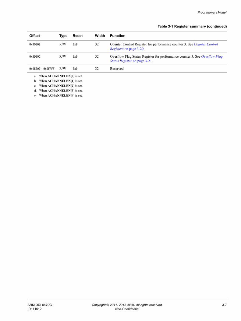
Programmers Model
0x9D008 R/W 0x0 32 Counter Control Register for performance counter 3. See Counter Control Registers on page 3-20.
0x9D00C R/W 0x0 32 Overflow Flag Status Register for performance counter 3. See Overflow Flag Status Register on page 3-21.
0x9E000 - 0x9FFFF R/W 0x0 32 Reserved.
a. When ACHANNELEN[0] is set.b. When ACHANNELEN[1] is set.c. When ACHANNELEN[2] is set.d. When ACHANNELEN[3] is set.e. When ACHANNELEN[4] is set.
Table 3-1 Register summary (continued)
Offset Type Reset Width Function
ARM DDI 0470G Copyright © 2011, 2012 ARM. All rights reserved. 3-7ID111612 Non-Confidential
Programmers Model
3.3 Register descriptionsThis section describes the CCI-400 registers. Table 3-1 on page 3-3 provides cross references to individual registers.
3.3.1 Control Override Register
The Control Override Register characteristics are:
Purpose Additional control register that provides a fail-safe override for some CCI-400 functions, if these cause problems that you cannot otherwise work around.
Usage constraints If you cannot avoid using them, only set them using non-bufferable transactions, and before barriers, shareable transactions, or DVM messages are issued into the CCI-400. This could be, for example, very early in the boot sequence, prior to the installation of any secure OS. You can access the Control Override Register using secure transactions only, irrespective of the programming of the Secure Access Register.
Configurations Available in all CCI-400 configurations.
Attributes See Table 3-1 on page 3-3.
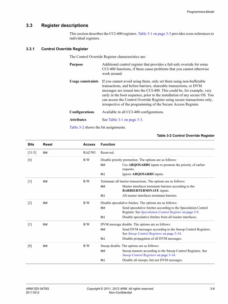
Table 3-2 shows the bit assignments.
Table 3-2 Control Override Register
Bits Reset Access Function
[31:5] 0b0 RAZ/WI Reserved.
[4] R/W Disable priority promotion. The options are as follows:0b0 Use ARQOSARBS inputs to promote the priority of earlier
requests.0b1 Ignore ARQOSARBS inputs.
[3] 0b0 R/W Terminate all barrier transactions. The options are as follows:0b0 Master interfaces terminate barriers according to the
BARRIERTERMINATE inputs.0b1 All master interfaces terminate barriers.
[2] 0b0 R/W Disable speculative fetches. The options are as follows:0b0 Send speculative fetches according to the Speculation Control
Register. See Speculation Control Register on page 3-9.0b1 Disable speculative fetches from all master interfaces.
[1] 0b0 R/W DVM message disable. The options are as follows:0b0 Send DVM messages according to the Snoop Control Registers.
See Snoop Control Registers on page 3-14.0b1 Disable propagation of all DVM messages.
[0] 0b0 R/W Snoop disable. The options are as follows:0b0 Snoop masters according to the Snoop Control Registers. See
Snoop Control Registers on page 3-14.0b1 Disable all snoops, but not DVM messages.
ARM DDI 0470G Copyright © 2011, 2012 ARM. All rights reserved. 3-8ID111612 Non-Confidential
Programmers Model
3.3.2 Speculation Control Register
The Speculation Control Register characteristics are:
Purpose Disables speculative fetches for a master interface or for traffic through a specific slave interface. Speculative fetches are not issued if they are disabled in either the slave or master interface for a particular transaction.
Usage constraints Access controlled by Secure Access Register, see Secure Access Register.
Configurations Available in all CCI-400 configurations.
Attributes See Table 3-1 on page 3-3.
Table 3-3 shows the bit assignments.
3.3.3 Secure Access Register
The Secure Access Register characteristics are:
Purpose Controls secure access.
Usage constraints You can only write to this register using secure transactions.
Configurations Available in all CCI-400 configurations.
Attributes See Table 3-1 on page 3-3.
Warning This register enables non-secure access to the CCI-400 registers for all masters. This compromises the security of your system.
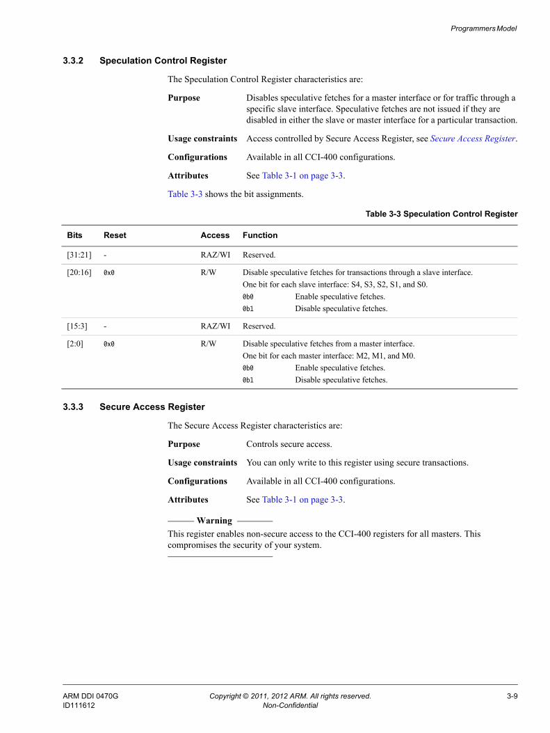
Table 3-3 Speculation Control Register
Bits Reset Access Function
[31:21] - RAZ/WI Reserved.
[20:16] 0x0 R/W Disable speculative fetches for transactions through a slave interface.One bit for each slave interface: S4, S3, S2, S1, and S0.0b0 Enable speculative fetches.0b1 Disable speculative fetches.
[15:3] - RAZ/WI Reserved.
[2:0] 0x0 R/W Disable speculative fetches from a master interface.One bit for each master interface: M2, M1, and M0.0b0 Enable speculative fetches.0b1 Disable speculative fetches.
ARM DDI 0470G Copyright © 2011, 2012 ARM. All rights reserved. 3-9ID111612 Non-Confidential
Programmers Model
Table 3-4 shows the bit assignments.
3.3.4 Status Register
The Status Register characteristics are:
Purpose Safely enables and disables snooping. When changing the snoop or DVM message enables using the Snoop Control Registers, see Snoop Control Registers on page 3-14, there is a delay until the changes are registered in all parts of the CCI-400. The change_pending bit in the Status Register indicates whether there are any changes to the enables that have not yet been applied, or whether a slave interface has been disabled for future snoop and DVM messages, but has outstanding AC requests.
Usage constraints There are no usage constraints.
Configurations Available in all CCI-400 configurations.
Attributes See Table 3-1 on page 3-3.
Note After writing to the snoop or DVM enable bits, the controller must wait for the register write to complete, then test that the change_pending bit is LOW before it turns an attached device on or off.
Table 3-5 shows the bit assignments.
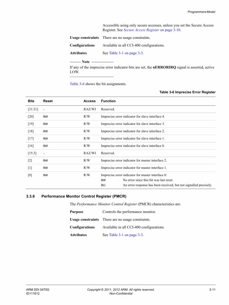
3.3.5 Imprecise Error Register
The Imprecise Error Register characteristics are:
Purpose Records the CCI-400 interfaces that received an error that is not signalled precisely. The appropriate bit is set, with respect to the interface on which the error was received. Bits are set when one or more error responses are detected, and they are reset on a write of 1 to the corresponding bit.
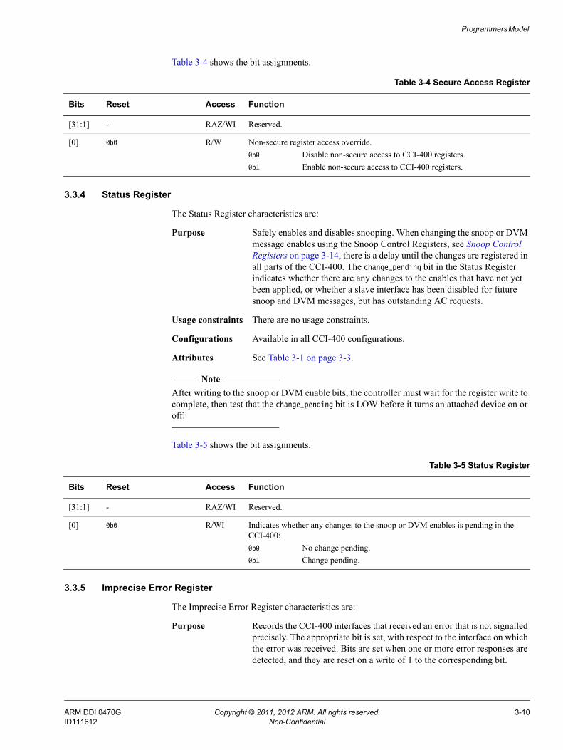
Table 3-4 Secure Access Register
Bits Reset Access Function
[31:1] - RAZ/WI Reserved.
[0] 0b0 R/W Non-secure register access override.0b0 Disable non-secure access to CCI-400 registers.0b1 Enable non-secure access to CCI-400 registers.
Table 3-5 Status Register
Bits Reset Access Function
[31:1] - RAZ/WI Reserved.
[0] 0b0 R/WI Indicates whether any changes to the snoop or DVM enables is pending in the CCI-400:0b0 No change pending.0b1 Change pending.
ARM DDI 0470G Copyright © 2011, 2012 ARM. All rights reserved. 3-10ID111612 Non-Confidential
Programmers Model
Accessible using only secure accesses, unless you set the Secure Access Register. See Secure Access Register on page 3-10.
Usage constraints There are no usage constraints.
Configurations Available in all CCI-400 configurations.
Attributes See Table 3-1 on page 3-3.
Note If any of the imprecise error indicator bits are set, the nERRORIRQ signal is asserted, active LOW.
Table 3-6 shows the bit assignments.
3.3.6 Performance Monitor Control Register (PMCR)
The Performance Monitor Control Register (PMCR) characteristics are:
Purpose Controls the performance monitor.
Usage constraints There are no usage constraints.
Configurations Available in all CCI-400 configurations.
Attributes See Table 3-1 on page 3-3.
Table 3-6 Imprecise Error Register
Bits Reset Access Function
[31:21] - RAZ/WI Reserved.
[20] 0b0 R/W Imprecise error indicator for slave interface 4.
[19] 0b0 R/W Imprecise error indicator for slave interface 3.
[18] 0b0 R/W Imprecise error indicator for slave interface 2.
[17] 0b0 R/W Imprecise error indicator for slave interface 1.
[16] 0b0 R/W Imprecise error indicator for slave interface 0.
[15:3] - RAZ/WI Reserved.
[2] 0b0 R/W Imprecise error indicator for master interface 2.
[1] 0b0 R/W Imprecise error indicator for master interface 1.
[0] 0b0 R/W Imprecise error indicator for master interface 0:0b0 No error since this bit was last reset.0b1 An error response has been received, but not signalled precisely.
ARM DDI 0470G Copyright © 2011, 2012 ARM. All rights reserved. 3-11ID111612 Non-Confidential
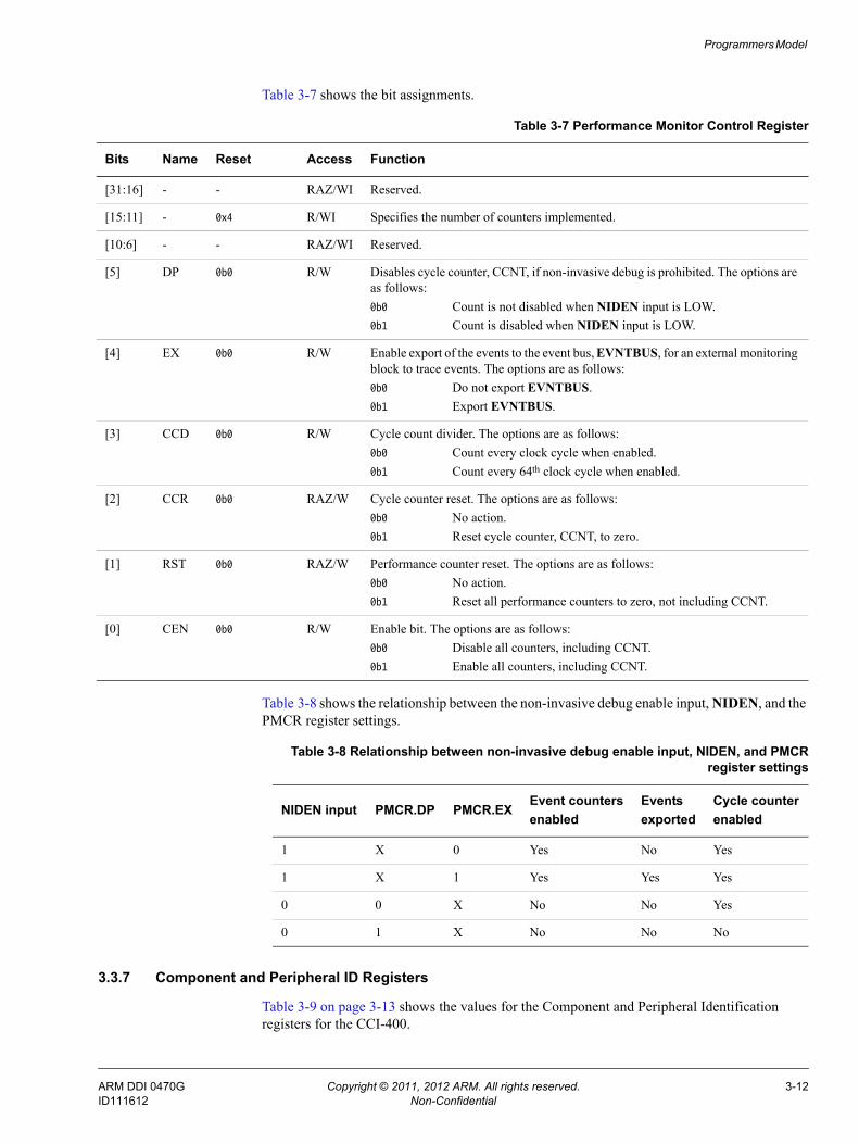
Programmers Model
Table 3-7 shows the bit assignments.
Table 3-8 shows the relationship between the non-invasive debug enable input, NIDEN, and the PMCR register settings.
3.3.7 Component and Peripheral ID Registers
Table 3-9 on page 3-13 shows the values for the Component and Peripheral Identification registers for the CCI-400.
Table 3-7 Performance Monitor Control Register
Bits Name Reset Access Function
[31:16] - - RAZ/WI Reserved.
[15:11] - 0x4 R/WI Specifies the number of counters implemented.
[10:6] - - RAZ/WI Reserved.
[5] DP 0b0 R/W Disables cycle counter, CCNT, if non-invasive debug is prohibited. The options are as follows:0b0 Count is not disabled when NIDEN input is LOW.0b1 Count is disabled when NIDEN input is LOW.
[4] EX 0b0 R/W Enable export of the events to the event bus, EVNTBUS, for an external monitoring block to trace events. The options are as follows:0b0 Do not export EVNTBUS.0b1 Export EVNTBUS.
[3] CCD 0b0 R/W Cycle count divider. The options are as follows:0b0 Count every clock cycle when enabled.0b1 Count every 64th clock cycle when enabled.
[2] CCR 0b0 RAZ/W Cycle counter reset. The options are as follows:0b0 No action.0b1 Reset cycle counter, CCNT, to zero.
[1] RST 0b0 RAZ/W Performance counter reset. The options are as follows:0b0 No action.0b1 Reset all performance counters to zero, not including CCNT.
[0] CEN 0b0 R/W Enable bit. The options are as follows:0b0 Disable all counters, including CCNT.0b1 Enable all counters, including CCNT.
Table 3-8 Relationship between non-invasive debug enable input, NIDEN, and PMCRregister settings
NIDEN input PMCR.DP PMCR.EXEvent countersenabled
Eventsexported
Cycle counterenabled
1 X 0 Yes No Yes
1 X 1 Yes Yes Yes
0 0 X No No Yes
0 1 X No No No
ARM DDI 0470G Copyright © 2011, 2012 ARM. All rights reserved. 3-12ID111612 Non-Confidential
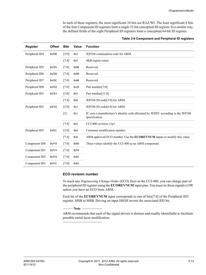
Programmers Model
In each of these registers, the most significant 24 bits are RAZ/WI. The least significant 8 bits of the four Component ID registers form a single 32-bit conceptual ID register. In a similar way, the defined fields of the eight Peripheral ID registers form a conceptual 64-bit ID register.
ECO revision number
To track any Engineering Change Order (ECO) fixes in the CCI-400, you can change part of the peripheral ID register using the ECOREVNUM input pins. You must tie these signals LOW unless you have an ECO from ARM.
Each bit of the ECOREVNUM input corresponds to one of bits[7:4] of the Peripheral ID3 register, MSB to MSB. Driving an input HIGH inverts the associated ID3 bit.
Note ARM recommends that each of the signal drivers is distinct and readily identifiable to facilitate possible metal layer modification.
Table 3-9 Component and Peripheral ID registers
Register Offset Bits Value Function
Peripheral ID4 0xFD0 [3:0] 0x4 JEP106 continuation code for ARM.
[7:4] 0x4 4KB region count.
Peripheral ID5 0xFD4 [7:0] 0x00 Reserved.
Peripheral ID6 0xFD8 [7:0] 0x00 Reserved.
Peripheral ID7 0xFDC [7:0] 0x00 Reserved.
Peripheral ID0 0xFE0 [7:0] 0x20 Part number[7:0].
Peripheral ID1 0xFE4 [3:0] 0x4 Part number[11:8].
[7:4] 0xB JEP106 ID code[3:0] for ARM.
Peripheral ID2 0xFE8 [2:0] 0x3 JEP106 ID code[6:4] for ARM.
[3] 0x1 IC uses a manufacturer’s identity code allocated by JEDEC according to the JEP106 specification.
[7:4] 0x6 CCI-400 revision, r1p1.
Peripheral ID3 0xFEC [3:0] 0x0 Customer modification number.
[7:4] 0x0 ARM approved ECO number. Use the ECOREVNUM inputs to modify this value.
Component ID0 0xFF0 [7:0] 0x0D These values identify the CCI-400 as an ARM component.
Component ID1 0xFF4 [7:0] 0xF0
Component ID2 0xFF8 [7:0] 0x05
Component ID3 0xFFC [7:0] 0xB1
ARM DDI 0470G Copyright © 2011, 2012 ARM. All rights reserved. 3-13ID111612 Non-Confidential
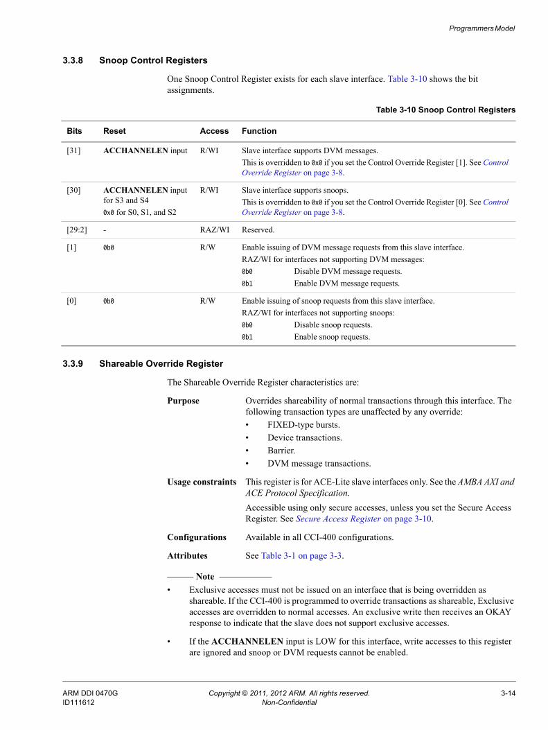
Programmers Model
3.3.8 Snoop Control Registers
One Snoop Control Register exists for each slave interface. Table 3-10 shows the bit assignments.
3.3.9 Shareable Override Register
The Shareable Override Register characteristics are:
Purpose Overrides shareability of normal transactions through this interface. The following transaction types are unaffected by any override:• FIXED-type bursts.• Device transactions.• Barrier.• DVM message transactions.
Usage constraints This register is for ACE-Lite slave interfaces only. See the AMBA AXI and ACE Protocol Specification.Accessible using only secure accesses, unless you set the Secure Access Register. See Secure Access Register on page 3-10.
Configurations Available in all CCI-400 configurations.
Attributes See Table 3-1 on page 3-3.
Note • Exclusive accesses must not be issued on an interface that is being overridden as
shareable. If the CCI-400 is programmed to override transactions as shareable, Exclusive accesses are overridden to normal accesses. An exclusive write then receives an OKAY response to indicate that the slave does not support exclusive accesses.
• If the ACCHANNELEN input is LOW for this interface, write accesses to this register are ignored and snoop or DVM requests cannot be enabled.
Table 3-10 Snoop Control Registers
Bits Reset Access Function
[31] ACCHANNELEN input R/WI Slave interface supports DVM messages.This is overridden to 0x0 if you set the Control Override Register [1]. See Control Override Register on page 3-8.
[30] ACCHANNELEN input for S3 and S40x0 for S0, S1, and S2
R/WI Slave interface supports snoops.This is overridden to 0x0 if you set the Control Override Register [0]. See Control Override Register on page 3-8.
[29:2] - RAZ/WI Reserved.
[1] 0b0 R/W Enable issuing of DVM message requests from this slave interface.RAZ/WI for interfaces not supporting DVM messages:0b0 Disable DVM message requests.0b1 Enable DVM message requests.
[0] 0b0 R/W Enable issuing of snoop requests from this slave interface.RAZ/WI for interfaces not supporting snoops:0b0 Disable snoop requests.0b1 Enable snoop requests.
ARM DDI 0470G Copyright © 2011, 2012 ARM. All rights reserved. 3-14ID111612 Non-Confidential
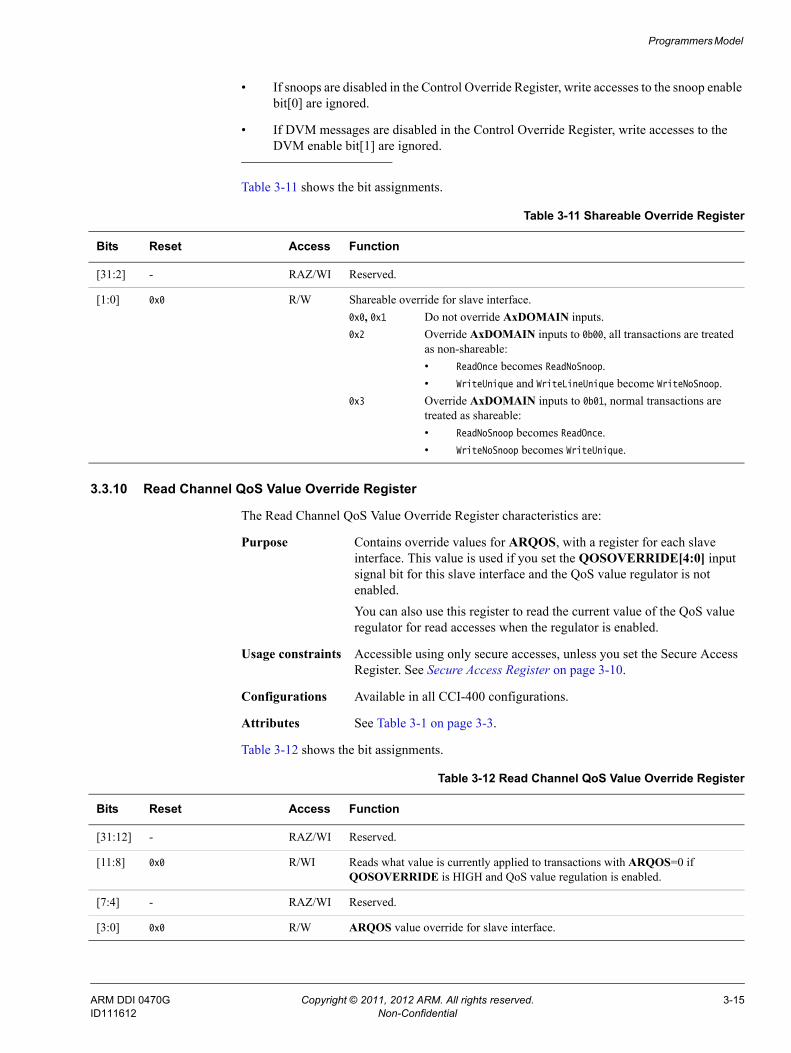
Programmers Model
• If snoops are disabled in the Control Override Register, write accesses to the snoop enable bit[0] are ignored.
• If DVM messages are disabled in the Control Override Register, write accesses to the DVM enable bit[1] are ignored.
Table 3-11 shows the bit assignments.
3.3.10 Read Channel QoS Value Override Register
The Read Channel QoS Value Override Register characteristics are:
Purpose Contains override values for ARQOS, with a register for each slave interface. This value is used if you set the QOSOVERRIDE[4:0] input signal bit for this slave interface and the QoS value regulator is not enabled.You can also use this register to read the current value of the QoS value regulator for read accesses when the regulator is enabled.
Usage constraints Accessible using only secure accesses, unless you set the Secure Access Register. See Secure Access Register on page 3-10.
Configurations Available in all CCI-400 configurations.
Attributes See Table 3-1 on page 3-3.
Table 3-12 shows the bit assignments.
Table 3-11 Shareable Override Register
Bits Reset Access Function
[31:2] - RAZ/WI Reserved.
[1:0] 0x0 R/W Shareable override for slave interface.0x0, 0x1 Do not override AxDOMAIN inputs.0x2 Override AxDOMAIN inputs to 0b00, all transactions are treated
as non-shareable:• ReadOnce becomes ReadNoSnoop.• WriteUnique and WriteLineUnique become WriteNoSnoop.
0x3 Override AxDOMAIN inputs to 0b01, normal transactions are treated as shareable:• ReadNoSnoop becomes ReadOnce.• WriteNoSnoop becomes WriteUnique.
Table 3-12 Read Channel QoS Value Override Register
Bits Reset Access Function
[31:12] - RAZ/WI Reserved.
[11:8] 0x0 R/WI Reads what value is currently applied to transactions with ARQOS=0 if QOSOVERRIDE is HIGH and QoS value regulation is enabled.
[7:4] - RAZ/WI Reserved.
[3:0] 0x0 R/W ARQOS value override for slave interface.
ARM DDI 0470G Copyright © 2011, 2012 ARM. All rights reserved. 3-15ID111612 Non-Confidential
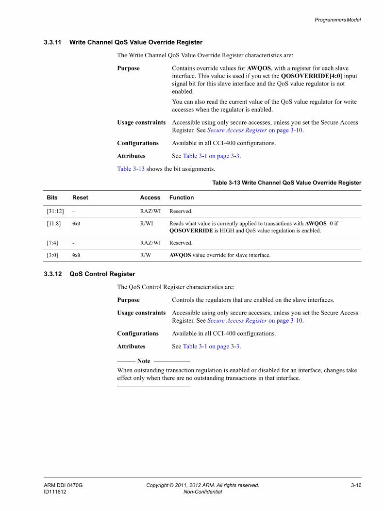
Programmers Model
3.3.11 Write Channel QoS Value Override Register
The Write Channel QoS Value Override Register characteristics are:
Purpose Contains override values for AWQOS, with a register for each slave interface. This value is used if you set the QOSOVERRIDE[4:0] input signal bit for this slave interface and the QoS value regulator is not enabled.You can also read the current value of the QoS value regulator for write accesses when the regulator is enabled.
Usage constraints Accessible using only secure accesses, unless you set the Secure Access Register. See Secure Access Register on page 3-10.
Configurations Available in all CCI-400 configurations.
Attributes See Table 3-1 on page 3-3.
Table 3-13 shows the bit assignments.
3.3.12 QoS Control Register
The QoS Control Register characteristics are:
Purpose Controls the regulators that are enabled on the slave interfaces.
Usage constraints Accessible using only secure accesses, unless you set the Secure Access Register. See Secure Access Register on page 3-10.
Configurations Available in all CCI-400 configurations.
Attributes See Table 3-1 on page 3-3.
Note When outstanding transaction regulation is enabled or disabled for an interface, changes take effect only when there are no outstanding transactions in that interface.
Table 3-13 Write Channel QoS Value Override Register
Bits Reset Access Function
[31:12] - RAZ/WI Reserved.
[11:8] 0x0 R/WI Reads what value is currently applied to transactions with AWQOS=0 if QOSOVERRIDE is HIGH and QoS value regulation is enabled.
[7:4] - RAZ/WI Reserved.
[3:0] 0x0 R/W AWQOS value override for slave interface.
ARM DDI 0470G Copyright © 2011, 2012 ARM. All rights reserved. 3-16ID111612 Non-Confidential
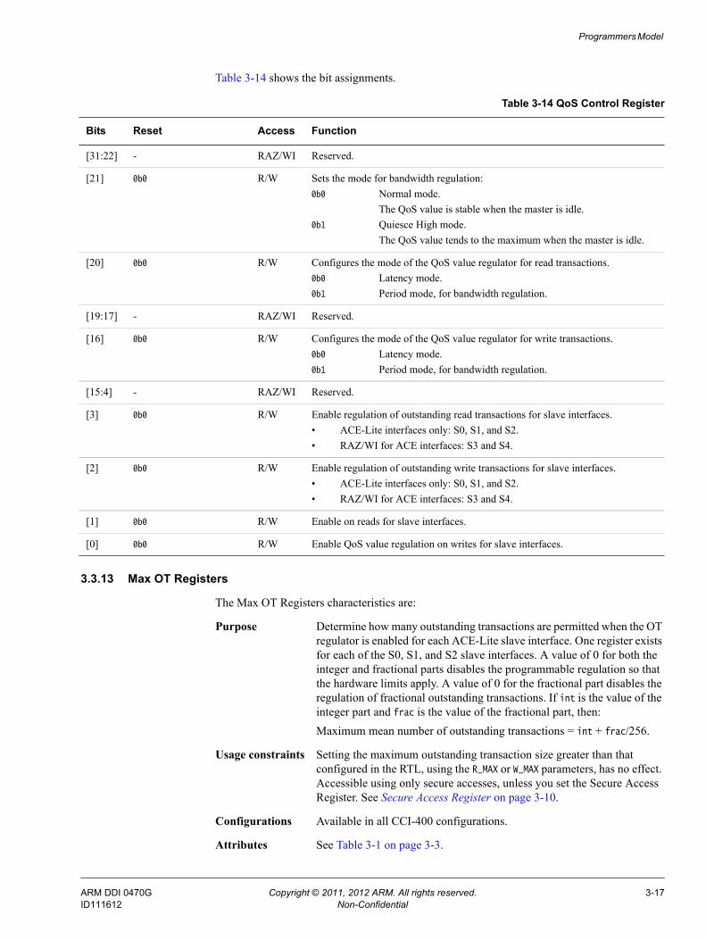
Programmers Model
Table 3-14 shows the bit assignments.
3.3.13 Max OT Registers
The Max OT Registers characteristics are:
Purpose Determine how many outstanding transactions are permitted when the OT regulator is enabled for each ACE-Lite slave interface. One register exists for each of the S0, S1, and S2 slave interfaces. A value of 0 for both the integer and fractional parts disables the programmable regulation so that the hardware limits apply. A value of 0 for the fractional part disables the regulation of fractional outstanding transactions. If int is the value of the integer part and frac is the value of the fractional part, then:Maximum mean number of outstanding transactions = int + frac/256.
Usage constraints Setting the maximum outstanding transaction size greater than that configured in the RTL, using the R_MAX or W_MAX parameters, has no effect. Accessible using only secure accesses, unless you set the Secure Access Register. See Secure Access Register on page 3-10.
Configurations Available in all CCI-400 configurations.
Attributes See Table 3-1 on page 3-3.
Table 3-14 QoS Control Register
Bits Reset Access Function
[31:22] - RAZ/WI Reserved.
[21] 0b0 R/W Sets the mode for bandwidth regulation:0b0 Normal mode.
The QoS value is stable when the master is idle.0b1 Quiesce High mode.
The QoS value tends to the maximum when the master is idle.
[20] 0b0 R/W Configures the mode of the QoS value regulator for read transactions.0b0 Latency mode.0b1 Period mode, for bandwidth regulation.
[19:17] - RAZ/WI Reserved.
[16] 0b0 R/W Configures the mode of the QoS value regulator for write transactions.0b0 Latency mode.0b1 Period mode, for bandwidth regulation.
[15:4] - RAZ/WI Reserved.
[3] 0b0 R/W Enable regulation of outstanding read transactions for slave interfaces.• ACE-Lite interfaces only: S0, S1, and S2.• RAZ/WI for ACE interfaces: S3 and S4.
[2] 0b0 R/W Enable regulation of outstanding write transactions for slave interfaces.• ACE-Lite interfaces only: S0, S1, and S2.• RAZ/WI for ACE interfaces: S3 and S4.
[1] 0b0 R/W Enable on reads for slave interfaces.
[0] 0b0 R/W Enable QoS value regulation on writes for slave interfaces.
ARM DDI 0470G Copyright © 2011, 2012 ARM. All rights reserved. 3-17ID111612 Non-Confidential
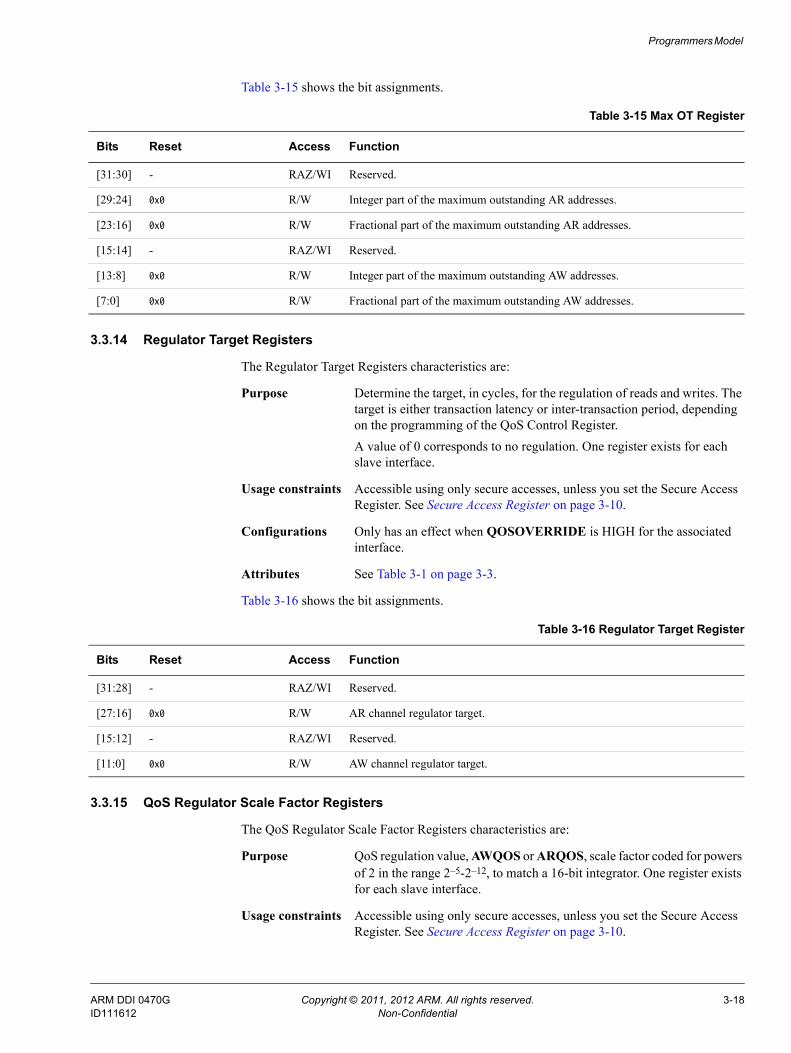
Programmers Model
Table 3-15 shows the bit assignments.
3.3.14 Regulator Target Registers
The Regulator Target Registers characteristics are:
Purpose Determine the target, in cycles, for the regulation of reads and writes. The target is either transaction latency or inter-transaction period, depending on the programming of the QoS Control Register.A value of 0 corresponds to no regulation. One register exists for each slave interface.
Usage constraints Accessible using only secure accesses, unless you set the Secure Access Register. See Secure Access Register on page 3-10.
Configurations Only has an effect when QOSOVERRIDE is HIGH for the associated interface.
Attributes See Table 3-1 on page 3-3.
Table 3-16 shows the bit assignments.
3.3.15 QoS Regulator Scale Factor Registers
The QoS Regulator Scale Factor Registers characteristics are:
Purpose QoS regulation value, AWQOS or ARQOS, scale factor coded for powers of 2 in the range 2–5-2–12, to match a 16-bit integrator. One register exists for each slave interface.
Usage constraints Accessible using only secure accesses, unless you set the Secure Access Register. See Secure Access Register on page 3-10.
Table 3-15 Max OT Register
Bits Reset Access Function
[31:30] - RAZ/WI Reserved.
[29:24] 0x0 R/W Integer part of the maximum outstanding AR addresses.
[23:16] 0x0 R/W Fractional part of the maximum outstanding AR addresses.
[15:14] - RAZ/WI Reserved.
[13:8] 0x0 R/W Integer part of the maximum outstanding AW addresses.
[7:0] 0x0 R/W Fractional part of the maximum outstanding AW addresses.
Table 3-16 Regulator Target Register
Bits Reset Access Function
[31:28] - RAZ/WI Reserved.
[27:16] 0x0 R/W AR channel regulator target.
[15:12] - RAZ/WI Reserved.
[11:0] 0x0 R/W AW channel regulator target.
ARM DDI 0470G Copyright © 2011, 2012 ARM. All rights reserved. 3-18ID111612 Non-Confidential
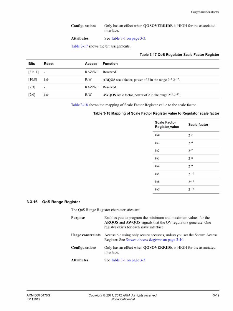
Programmers Model
Configurations Only has an effect when QOSOVERRIDE is HIGH for the associated interface.
Attributes See Table 3-1 on page 3-3.
Table 3-17 shows the bit assignments.
Table 3-18 shows the mapping of Scale Factor Register value to the scale factor.
3.3.16 QoS Range Register
The QoS Range Register characteristics are:
Purpose Enables you to program the minimum and maximum values for the ARQOS and AWQOS signals that the QV regulators generate. One register exists for each slave interface.
Usage constraints Accessible using only secure accesses, unless you set the Secure Access Register. See Secure Access Register on page 3-10.
Configurations Only has an effect when QOSOVERRIDE is HIGH for the associated interface.
Attributes See Table 3-1 on page 3-3.
Table 3-17 QoS Regulator Scale Factor Register
Bits Reset Access Function
[31:11] - RAZ/WI Reserved.
[10:8] 0x0 R/W ARQOS scale factor, power of 2 in the range 2–5-2–12.
[7:3] - RAZ/WI Reserved.
[2:0] 0x0 R/W AWQOS scale factor, power of 2 in the range 2–5-2–12.
Table 3-18 Mapping of Scale Factor Register value to Regulator scale factor
Scale FactorRegister value Scale factor
0x0 2–5
0x1 2–6
0x2 2–7
0x3 2–8
0x4 2–9
0x5 2–10
0x6 2–11
0x7 2–12
ARM DDI 0470G Copyright © 2011, 2012 ARM. All rights reserved. 3-19ID111612 Non-Confidential
Programmers Model
Table 3-19 shows the bit assignments.
3.3.17 Event Select Register
The Event Select Register (ESR) characteristics are:
Purpose Determines the event that a particular counter counts. One register exists per counter. This register is not present for the cycle counter.
Usage constraints There are no usage constraints.
Configurations Available in all CCI-400 configurations.
Attributes See Table 3-1 on page 3-3.
Table 3-20 shows the bit assignments.
3.3.18 Event and Cycle Count Registers
A read-write, 32-bit register for each of the four event counters and cycle counter. The cycle counter counts either every CCI-400 clock cycle, or every 64 clock cycles, depending on the PMCR bit[3].
You can reset all event counter values to zero by writing a 1 to the PMCR bit[1] and reset all clock counter values by writing a 1 to PMCR bit[2].
3.3.19 Counter Control Registers
The Counter Control Registers characteristics are:
Purpose Enable or disable the Cycle and Event Counters. One register exists per counter.
Table 3-19 QoS Range Register
Bits Reset Access Function
[31:28] - RAZ/WI Reserved.
[27:24] 0x0 R/W Maximum ARQOS value.
[23:20] - RAZ/WI Reserved.
[19:16] 0x0 R/W Minimum ARQOS value.
[15:12] - RAZ/WI Reserved.
[11:8] 0x0 R/W Maximum AWQOS value.
[7:4] - RAZ/WI Reserved.
[3:0] 0x0 R/W Minimum AWQOS value.
Table 3-20 Event Select Register
Bits Reset Access Function
[31:8] - RAZ/WI Reserved.
[7:0] 0x0 R/W Event code to define which interface to monitor. See PMU event list on page 2-5.
[4:0] 0x0 R/W Event code to define which event to monitor. See PMU event list on page 2-5.
ARM DDI 0470G Copyright © 2011, 2012 ARM. All rights reserved. 3-20ID111612 Non-Confidential
Programmers Model
Usage constraints There are no usage constraints.
Configurations Available in all CCI-400 configurations.
Attributes See Table 3-1 on page 3-3.
Table 3-21 shows the bit assignments.
3.3.20 Overflow Flag Status Register
The Overflow Flag Status Register characteristics are:
Purpose Contains the state of the overflow flags for the Cycle Count Register and event counters. One register exists for each event counter, and one register exists for the cycle counter.
Usage constraints There are no usage constraints.
Configurations Available in all CCI-400 configurations.
Attributes See Table 3-1 on page 3-3.
Table 3-22 shows the bit assignments.
When reading this register, any overflow flag that reads as 0 indicates that the counter has not overflowed. An overflow flag that reads as 1 indicates that the counter has overflowed.
When writing to this register, any overflow flag written with a value of 0 is ignored, that is, no change. An overflow flag written with a value of 1 clears the counter overflow flag. The negated counter overflow bits are exported from the CCI-400 on the nEVNTCNTOVERFLOW[4:0] signal. You can use this to trigger interrupts. The MSB corresponds to the cycle count overflow.
Table 3-21 Counter Control Register bit assignments
Bits Reset Access Function
[31:1] - RAZ/WI Reserved.
[0] 0b0 R/W Counter enable. The options are as follows:0b0 Counter disabled.0b1 Counter enabled.
Table 3-22 Overflow Flag Status Register
Bits Reset Access Function
[31:1] - RAZ/WI Reserved.
[0] 0x0 R/W Event counter and cycle counter overflow flag.
ARM DDI 0470G Copyright © 2011, 2012 ARM. All rights reserved. 3-21ID111612 Non-Confidential

Programmers Model
3.4 Address mapThe CCI-400 supports 40-bit addressing, with a global address map. This means that each master has the same view of memory. This is split into 16 regions across the 40-bit address. The decode for each region is determined using a number of CCI-400 inputs that are expected to be static, that is, they are sampled only at reset. The inputs are ADDRMAPx[1:0], where x is an integer from 0-15.
Note If the CCI-400 is configured to support 44-bit DVM transactions, ARADDRSx inputs are 44 bits wide. In this case the CCI-400 still only supports a 40-bit address map and the top address bits are ignored for non-DVM transactions and are not propagated to master interfaces. The CCI master interfaces always have 40-bit address buses.
Figure 3-1 shows the CCI-400 address map.
Figure 3-1 Address map
Table 3-23 shows the decoder mapping.
ADDRMAP15[1:0]1 TB
512 GBADDRMAP14[1:0]
256 GBADDRMAP13[1:0]
128 GBADDRMAP12[1:0]
64 GBADDRMAP11[1:0]
32 GBADDRMAP10[1:0]
16 GBADDRMAP9[1:0]
8 GBADDRMAP8[1:0]
4 GBADDRMAP7[1:0]
3.5 GBADDRMAP6[1:0]
3 GBADDRMAP5[1:0]
2.5 GBADDRMAP4[1:0]
2 GBADDRMAP3[1:0]
1.5 GBADDRMAP2[1:0]
1 GBADDRMAP1[1:0]
0.5 GBADDRMAP0[1:0]
0 GB
Table 3-23 Decoder mapping
ADDRMAPx[1:0] Decode
0b00 M0, expected to be connected to the system.
0b01 M1, expected to be connected to a memory controller.
0b10 M2, expected to be connected to a memory controller.
0b11 M1 and M2, striped in 4KB regions, used to load-balance between two memory controllers.
ARM DDI 0470G Copyright © 2011, 2012 ARM. All rights reserved. 3-22ID111612 Non-Confidential
Programmers Model
The base address for internal CCI-400 registers is defined using a static input, PERIPHBASE[39:15]. The CCI-400 registers are offset by 0x90000 from this base address and occupy an address region of size 64KB.
For example, if PERIPHBASE is 0x0000000, then the register space occupies the following region:
0x0000090000 to 0x000009FFFF.
Accesses within this region, but not to a valid CCI-400 register, generate a DECERR response.
Note ARM recommends that PERIPHBASE[39:15] occupies the bottom 4GB address space.
ARM DDI 0470G Copyright © 2011, 2012 ARM. All rights reserved. 3-23ID111612 Non-Confidential
Appendix A Signal Descriptions
This appendix describes the external signals of the CCI-400. This appendix contains the following section:• Signal descriptions on page A-2.
ARM DDI 0470G Copyright © 2011, 2012 ARM. All rights reserved. A-1ID111612 Non-Confidential
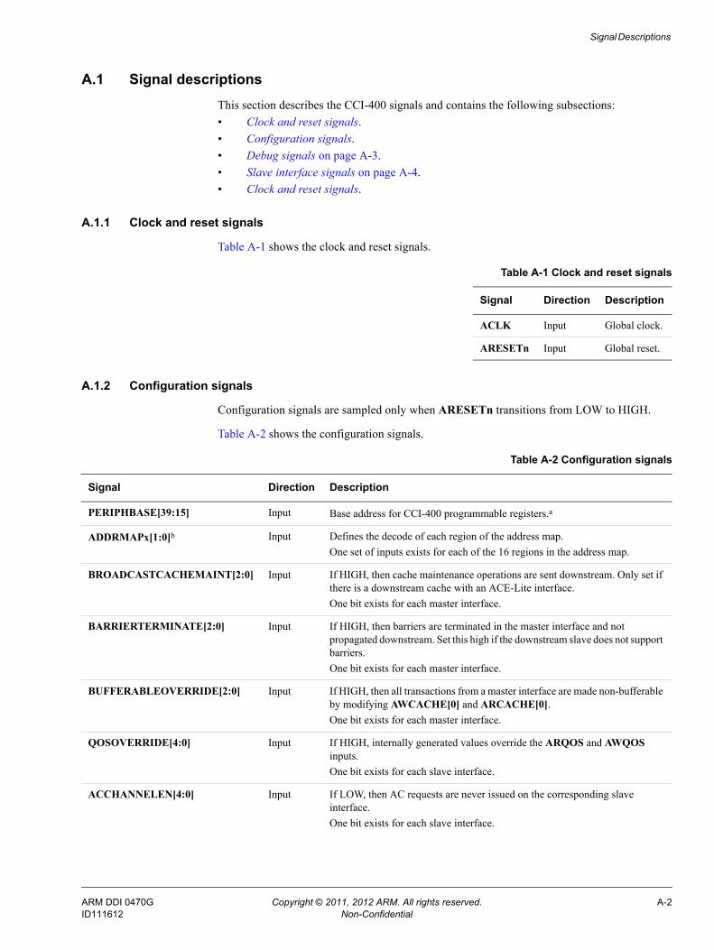
Signal Descriptions
A.1 Signal descriptionsThis section describes the CCI-400 signals and contains the following subsections:• Clock and reset signals.• Configuration signals.• Debug signals on page A-3.• Slave interface signals on page A-4.• Clock and reset signals.
A.1.1 Clock and reset signals
Table A-1 shows the clock and reset signals.
A.1.2 Configuration signals
Configuration signals are sampled only when ARESETn transitions from LOW to HIGH.
Table A-2 shows the configuration signals.
Table A-1 Clock and reset signals
Signal Direction Description
ACLK Input Global clock.
ARESETn Input Global reset.
Table A-2 Configuration signals
Signal Direction Description
PERIPHBASE[39:15] Input Base address for CCI-400 programmable registers.a
ADDRMAPx[1:0]b Input Defines the decode of each region of the address map.One set of inputs exists for each of the 16 regions in the address map.
BROADCASTCACHEMAINT[2:0] Input If HIGH, then cache maintenance operations are sent downstream. Only set if there is a downstream cache with an ACE-Lite interface.One bit exists for each master interface.
BARRIERTERMINATE[2:0] Input If HIGH, then barriers are terminated in the master interface and not propagated downstream. Set this high if the downstream slave does not support barriers.One bit exists for each master interface.
BUFFERABLEOVERRIDE[2:0] Input If HIGH, then all transactions from a master interface are made non-bufferable by modifying AWCACHE[0] and ARCACHE[0].One bit exists for each master interface.
QOSOVERRIDE[4:0] Input If HIGH, internally generated values override the ARQOS and AWQOS inputs.One bit exists for each slave interface.
ACCHANNELEN[4:0] Input If LOW, then AC requests are never issued on the corresponding slave interface.One bit exists for each slave interface.
ARM DDI 0470G Copyright © 2011, 2012 ARM. All rights reserved. A-2ID111612 Non-Confidential
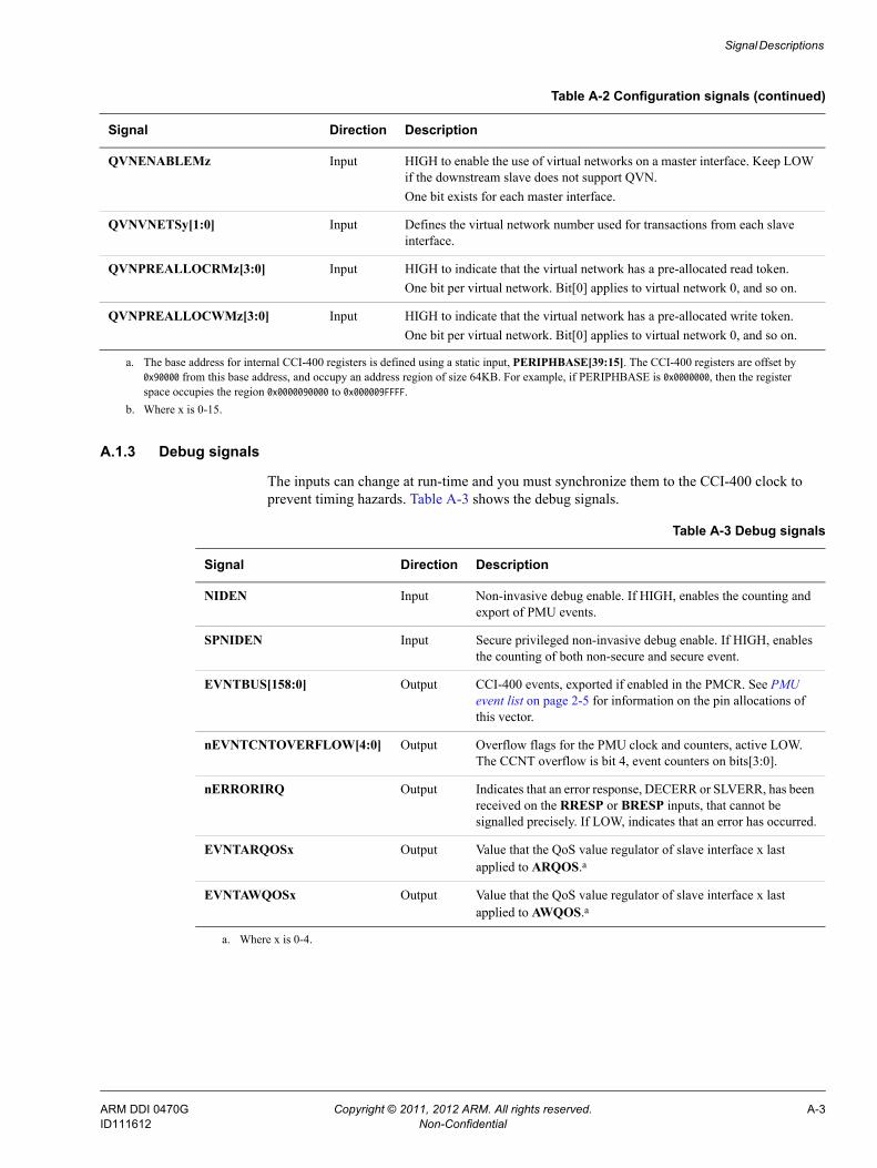
Signal Descriptions
A.1.3 Debug signals
The inputs can change at run-time and you must synchronize them to the CCI-400 clock to prevent timing hazards. Table A-3 shows the debug signals.
QVNENABLEMz Input HIGH to enable the use of virtual networks on a master interface. Keep LOW if the downstream slave does not support QVN.One bit exists for each master interface.
QVNVNETSy[1:0] Input Defines the virtual network number used for transactions from each slave interface.
QVNPREALLOCRMz[3:0] Input HIGH to indicate that the virtual network has a pre-allocated read token.One bit per virtual network. Bit[0] applies to virtual network 0, and so on.
QVNPREALLOCWMz[3:0] Input HIGH to indicate that the virtual network has a pre-allocated write token.One bit per virtual network. Bit[0] applies to virtual network 0, and so on.
a. The base address for internal CCI-400 registers is defined using a static input, PERIPHBASE[39:15]. The CCI-400 registers are offset by 0x90000 from this base address, and occupy an address region of size 64KB. For example, if PERIPHBASE is 0x0000000, then the register space occupies the region 0x0000090000 to 0x000009FFFF.
b. Where x is 0-15.
Table A-2 Configuration signals (continued)
Signal Direction Description
Table A-3 Debug signals
Signal Direction Description
NIDEN Input Non-invasive debug enable. If HIGH, enables the counting and export of PMU events.
SPNIDEN Input Secure privileged non-invasive debug enable. If HIGH, enables the counting of both non-secure and secure event.
EVNTBUS[158:0] Output CCI-400 events, exported if enabled in the PMCR. See PMU event list on page 2-5 for information on the pin allocations of this vector.
nEVNTCNTOVERFLOW[4:0] Output Overflow flags for the PMU clock and counters, active LOW. The CCNT overflow is bit 4, event counters on bits[3:0].
nERRORIRQ Output Indicates that an error response, DECERR or SLVERR, has been received on the RRESP or BRESP inputs, that cannot be signalled precisely. If LOW, indicates that an error has occurred.
EVNTARQOSx Output Value that the QoS value regulator of slave interface x last applied to ARQOS.a
EVNTAWQOSx Output Value that the QoS value regulator of slave interface x last applied to AWQOS.a
a. Where x is 0-4.
ARM DDI 0470G Copyright © 2011, 2012 ARM. All rights reserved. A-3ID111612 Non-Confidential
Signal Descriptions
A.1.4 DFT signal
Table A-4 shows the Design For Test (DFT) signal.
A.1.5 Slave interface signals
A set of slave interface signals exists for each slave interface. The suffix is Sx, where x is 0-4.
This section describes:• Write address channel signals.• Write data channel signals on page A-5.• Write data response channel signals on page A-5.• Read address channel signals on page A-6.• Read data channel signals on page A-6.• Coherency address channel signals on page A-7.• Coherency response channel signals on page A-7.• Coherency data channel signals, full ACE interfaces, S3 and S4 only on page A-7.• Acknowledge signals, full ACE interfaces, S3 and S4 only on page A-8.
Write address channel signals
Table A-5 shows the write address channel signals.
Table A-4 DFT signal
Signal Direction Description
DFTRSTDISABLE Input Disable reset during scan shift.
Table A-5 Write address channel signals
Signal Direction Description
AWIDSx[n:0] Input Write address ID. You can configure the width of this signal.
AWADDRSx[39:0] Input Write address.
AWREGIONSx[3:0] Input Write address region. You can tie this signal LOW if the master does not drive it.
AWLENSx[7:0] Input Write burst length.
AWSIZESx[2:0] Input Write burst size.
AWBURSTSx[1:0] Input Write burst type.
AWLOCKSx Input Write lock type.
AWCACHESx[3:0] Input Write cache type.
AWPROTSx[2:0] Input Write protection type.
AWSNOOPSx[2:0] Input Write snoop request type.
AWDOMAINSx[1:0] Input Write domain.
AWBARSx[1:0] Input Write barrier type.
AWQOSSx[3:0] Input Write QoS value.
ARM DDI 0470G Copyright © 2011, 2012 ARM. All rights reserved. A-4ID111612 Non-Confidential
Signal Descriptions
Write data channel signals
Table A-6 shows the write data channel signals.
Write data response channel signals
Table A-7 shows the write data response channel signals.
AWUSERSx[n:0] Input User-specified extension to AW payload.
AWVALIDSx Input Write address valid.
AWREADYSx Output Write address ready.
Table A-5 Write address channel signals (continued)
Signal Direction Description
Table A-6 Write data channel signals
Signal Direction Description
WDATASx[127:0] Input Write data.
WSTRBSx[15:0] Input Write byte-lane strobes.
WLASTSx Input Write data last transfer indication.
WUSERSx[n:0] Input User-specified extension to W payload.
WVALIDSx Input Write data valid.
WREADYSx Output Write data ready.
Table A-7 Write data response channel signals
Signal Direction Description
BIDSx[n:0] Output Write response ID. You can configure the width.
BRESPSx[1:0] Output Write response.
BUSERSx[n:0] Output User-specified extension to B payload.
BVALIDSx Output Write response valid.
BREADYSx Input Write response ready.
ARM DDI 0470G Copyright © 2011, 2012 ARM. All rights reserved. A-5ID111612 Non-Confidential

Signal Descriptions
Read address channel signals
Table A-8 shows the read address channel signals.
Read data channel signals
Table A-9 shows the read data channel signals.
Table A-8 Read address channel signals
Signal Direction Description
ARIDSx[n:0] Input Read address ID. You can configure the width of this signal.
ARADDRSx[39:0] Input Read address when the CCI-400 is configured to support 40-bit DVM transactions.
ARADDRSx[43:0] Input Read address when the CCI-400 is configured to support 44-bit DVM transactions.
ARREGIONSx[3:0] Input Read address region. You can tie this signal LOW if the master does not drive it.
ARLENSx[7:0] Input Read burst length.
ARSIZESx[2:0] Input Read burst size.
ARBURSTSx[1:0] Input Read burst type.
ARLOCKSx Input Read lock type.
ARCACHESx[3:0] Input Read cache type.
ARPROTSx[2:0] Input Read protection type.
ARDOMAINSx[1:0] Input Read domain.
ARSNOOPSx[3:0] Input Read snoop request type.
ARBARSx[1:0] Input Read barriers.
ARQOSSx[3:0] Input Read QoS.
ARUSERSx[n:0] Input User-specified extension to AR payload.
ARQOSARBSx[3:0] Input Arbitration priority promotion for read requests.You can tie this signal LOW if the master does not drive it.
ARVALIDSx Input Read address valid.
ARREADYSx Output Read address ready.
Table A-9 Read data channel signals
Signal Direction Description
RIDSx[n:0] Output Read data ID. You can configure the width of this signal.
RDATASx[127:0] Output Read data.
RRESPSx[3:0] Output Read data response for ACE interfaces: S3 and S4.
RRESPSx[1:0] Output Read data response for ACE-Lite interfaces: S0, S1, and S2.
RLASTSx Output Read data last transfer indication.
ARM DDI 0470G Copyright © 2011, 2012 ARM. All rights reserved. A-6ID111612 Non-Confidential
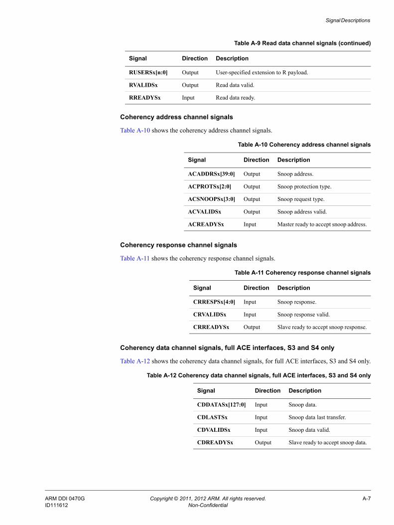
Signal Descriptions
Coherency address channel signals
Table A-10 shows the coherency address channel signals.
Coherency response channel signals
Table A-11 shows the coherency response channel signals.
Coherency data channel signals, full ACE interfaces, S3 and S4 only
Table A-12 shows the coherency data channel signals, for full ACE interfaces, S3 and S4 only.
RUSERSx[n:0] Output User-specified extension to R payload.
RVALIDSx Output Read data valid.
RREADYSx Input Read data ready.
Table A-10 Coherency address channel signals
Signal Direction Description
ACADDRSx[39:0] Output Snoop address.
ACPROTSx[2:0] Output Snoop protection type.
ACSNOOPSx[3:0] Output Snoop request type.
ACVALIDSx Output Snoop address valid.
ACREADYSx Input Master ready to accept snoop address.
Table A-11 Coherency response channel signals
Signal Direction Description
CRRESPSx[4:0] Input Snoop response.
CRVALIDSx Input Snoop response valid.
CRREADYSx Output Slave ready to accept snoop response.
Table A-12 Coherency data channel signals, full ACE interfaces, S3 and S4 only
Signal Direction Description
CDDATASx[127:0] Input Snoop data.
CDLASTSx Input Snoop data last transfer.
CDVALIDSx Input Snoop data valid.
CDREADYSx Output Slave ready to accept snoop data.
Table A-9 Read data channel signals (continued)
Signal Direction Description
ARM DDI 0470G Copyright © 2011, 2012 ARM. All rights reserved. A-7ID111612 Non-Confidential
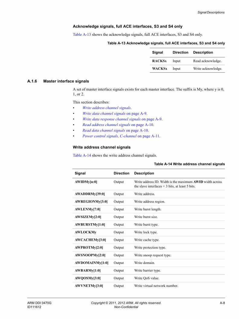
Signal Descriptions
Acknowledge signals, full ACE interfaces, S3 and S4 only
Table A-13 shows the acknowledge signals, full ACE interfaces, S3 and S4 only.
A.1.6 Master interface signals
A set of master interface signals exists for each master interface. The suffix is My, where y is 0, 1, or 2.
This section describes:• Write address channel signals.• Write data channel signals on page A-9.• Write data response channel signals on page A-9.• Read address channel signals on page A-10.• Read data channel signals on page A-10.• Power control signals, C-channel on page A-11.
Write address channel signals
Table A-14 shows the write address channel signals.
Table A-13 Acknowledge signals, full ACE interfaces, S3 and S4 only
Signal Direction Description
RACKSx Input Read acknowledge.
WACKSx Input Write acknowledge.
Table A-14 Write address channel signals
Signal Direction Description
AWIDMy[n:0] Output Write address ID. Width is the maximum AWID width across the slave interfaces + 3 bits, at least 5 bits.
AWADDRMy[39:0] Output Write address.
AWREGIONMy[3:0] Output Write address region.
AWLENMy[7:0] Output Write burst length.
AWSIZEMy[2:0] Output Write burst size.
AWBURSTMy[1:0] Output Write burst type.
AWLOCKMy Output Write lock type.
AWCACHEMy[3:0] Output Write cache type.
AWPROTMy[2:0] Output Write protection type.
AWSNOOPMy[2:0] Output Write snoop request type.
AWDOMAINMy[1:0] Output Write domain.
AWBARMy[1:0] Output Write barrier type.
AWQOSMy[3:0] Output Write QoS value.
AWVNETMy[3:0] Output Write virtual network number.
ARM DDI 0470G Copyright © 2011, 2012 ARM. All rights reserved. A-8ID111612 Non-Confidential
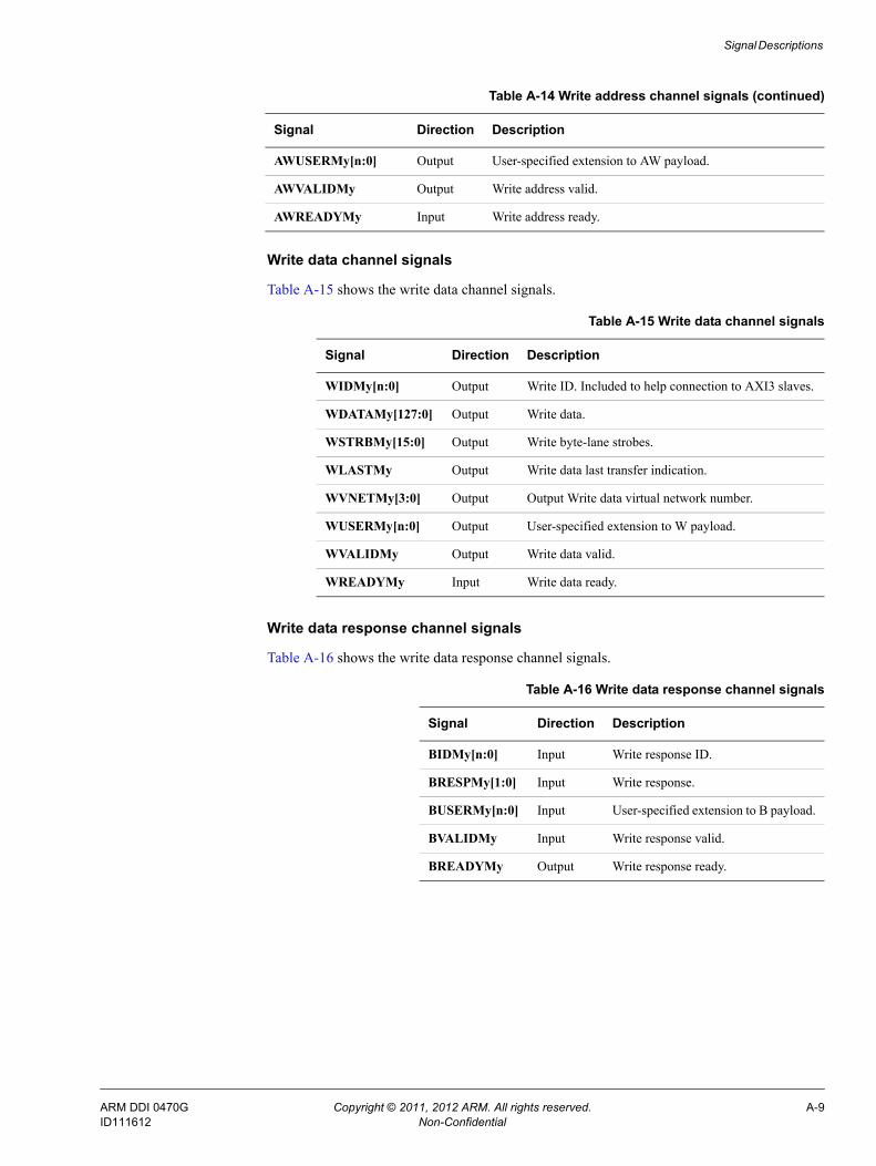
Signal Descriptions
Write data channel signals
Table A-15 shows the write data channel signals.
Write data response channel signals
Table A-16 shows the write data response channel signals.
AWUSERMy[n:0] Output User-specified extension to AW payload.
AWVALIDMy Output Write address valid.
AWREADYMy Input Write address ready.
Table A-15 Write data channel signals
Signal Direction Description
WIDMy[n:0] Output Write ID. Included to help connection to AXI3 slaves.
WDATAMy[127:0] Output Write data.
WSTRBMy[15:0] Output Write byte-lane strobes.
WLASTMy Output Write data last transfer indication.
WVNETMy[3:0] Output Output Write data virtual network number.
WUSERMy[n:0] Output User-specified extension to W payload.
WVALIDMy Output Write data valid.
WREADYMy Input Write data ready.
Table A-16 Write data response channel signals
Signal Direction Description
BIDMy[n:0] Input Write response ID.
BRESPMy[1:0] Input Write response.
BUSERMy[n:0] Input User-specified extension to B payload.
BVALIDMy Input Write response valid.
BREADYMy Output Write response ready.
Table A-14 Write address channel signals (continued)
Signal Direction Description
ARM DDI 0470G Copyright © 2011, 2012 ARM. All rights reserved. A-9ID111612 Non-Confidential
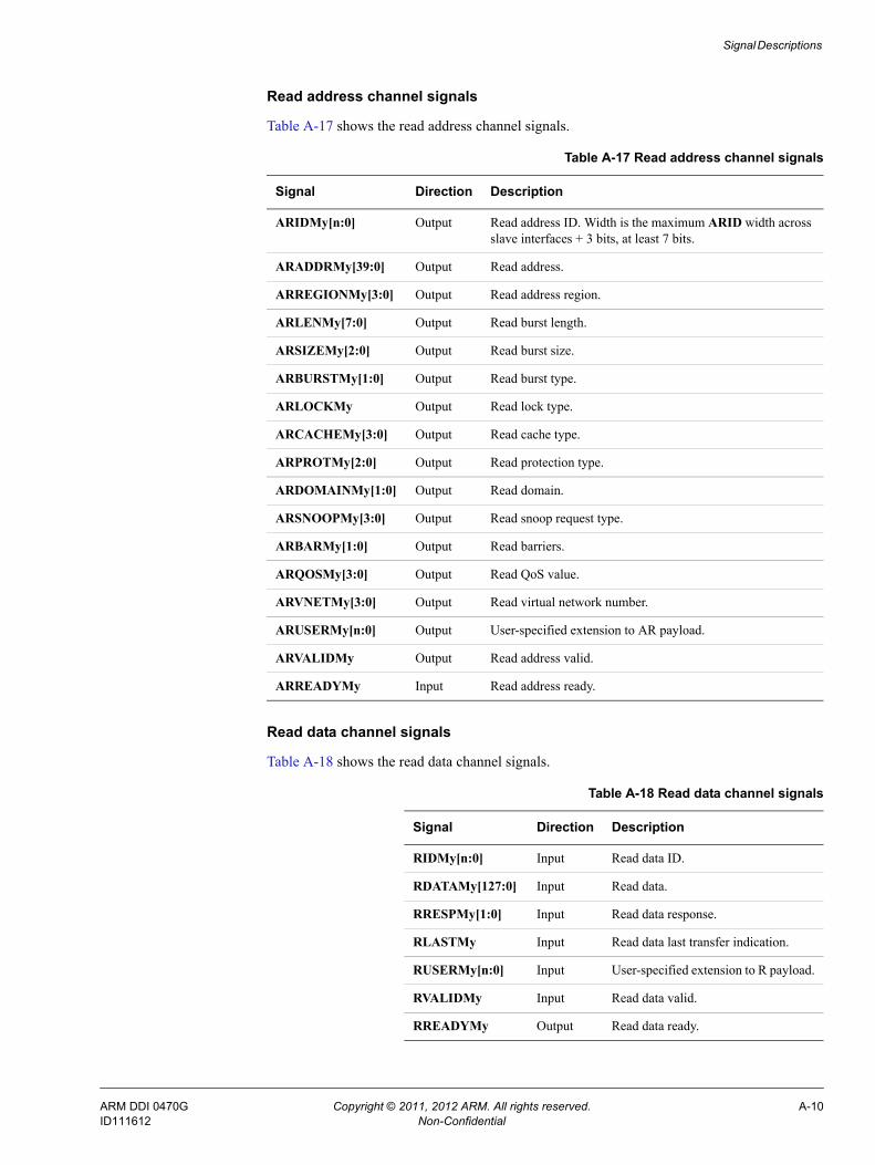
Signal Descriptions
Read address channel signals
Table A-17 shows the read address channel signals.
Read data channel signals
Table A-18 shows the read data channel signals.
Table A-17 Read address channel signals
Signal Direction Description
ARIDMy[n:0] Output Read address ID. Width is the maximum ARID width across slave interfaces + 3 bits, at least 7 bits.
ARADDRMy[39:0] Output Read address.
ARREGIONMy[3:0] Output Read address region.
ARLENMy[7:0] Output Read burst length.
ARSIZEMy[2:0] Output Read burst size.
ARBURSTMy[1:0] Output Read burst type.
ARLOCKMy Output Read lock type.
ARCACHEMy[3:0] Output Read cache type.
ARPROTMy[2:0] Output Read protection type.
ARDOMAINMy[1:0] Output Read domain.
ARSNOOPMy[3:0] Output Read snoop request type.
ARBARMy[1:0] Output Read barriers.
ARQOSMy[3:0] Output Read QoS value.
ARVNETMy[3:0] Output Read virtual network number.
ARUSERMy[n:0] Output User-specified extension to AR payload.
ARVALIDMy Output Read address valid.
ARREADYMy Input Read address ready.
Table A-18 Read data channel signals
Signal Direction Description
RIDMy[n:0] Input Read data ID.
RDATAMy[127:0] Input Read data.
RRESPMy[1:0] Input Read data response.
RLASTMy Input Read data last transfer indication.
RUSERMy[n:0] Input User-specified extension to R payload.
RVALIDMy Input Read data valid.
RREADYMy Output Read data ready.
ARM DDI 0470G Copyright © 2011, 2012 ARM. All rights reserved. A-10ID111612 Non-Confidential
Signal Descriptions
Power control signals, C-channel
Table A-19 shows the power control signals, C-channel.
QVN signals
Table A-20 shows the QVN signals,
Table A-19 Power control signals, C-channel
Signal Direction Description
ACTIVEMy Output Indicates that the master interface has active transactions. You can use it to gate the clock to downstream components.
CSYSREQ Input Request to disable the ACLK input.
CSYSACK Output Clock disable response.
CACTIVE Output Indicates that the CCI-400 requires the ACLK input to run.
Table A-20 QVN signals
Signal Direction Descriptiona
a. z is the virtual network number, 0 to 3.y is the master interface number, 0 to 2
VARQOSVNzMy[3:0] Output Read token request priority.
VARVALIDVNzMy Output Read token request.
VARREADYVNzMy Input Read token grant.
VAWQOSVNzMy Output Write token request priority.
VAWVALIDVNzMy Output Write token request.
VAWREADYVNzMy Input Write token grant.
VWVALIDVNzMy Output Write data token request.
VWREADYVNzMy Input Write data token grant.
ARM DDI 0470G Copyright © 2011, 2012 ARM. All rights reserved. A-11ID111612 Non-Confidential
Signal Descriptions
A.2 Miscellaneous signalsTable A-21 shows an ECO-related signal.
Table A-21 Miscellaneous signals
Signal Direction Description
ECOREVNUM[3:0] Input Used to ease the update of the revision field register in case of an ECO. See ECO revision number on page 3-13.
ARM DDI 0470G Copyright © 2011, 2012 ARM. All rights reserved. A-12ID111612 Non-Confidential
Appendix B Revisions
This appendix describes the technical changes between released issues of this book.
Table B-1 Issue A
Change Location Affects
First release - -
Table B-2 Differences between issue A and issue B
Change Location Affects
Added a new section on exclusive accesses Exclusive accesses on page 2-15 All revisions
Removed the erroneous reference to the TSPEC regulator Regulation based on outstanding transactions on page 2-19
All revisions
Changed the Component and Peripheral ID registers table so that the cells are in order of address offset instead of register name
Table 3-9 on page 3-13 All revisions
Updated the revision number in the Peripheral ID2 register Table 3-9 on page 3-13 r0p1
ARM DDI 0470G Copyright © 2011, 2012 ARM. All rights reserved. B-1ID111612 Non-Confidential
Revisions
Table B-3 Differences between issue B and issue C
Change Location Affects
Updated the parameter values for maximum ID width on slave interfaces and maximum size of read and write trackers in master interfaces
Product revisions on page 1-10 r0p2
Changed the configuration of read and write trackers in master interfaces
Product revisions on page 1-10 r0p2
Added a description for product improvements Product revisions on page 1-10 r0p2
Added a note to the Event list section PMU event list on page 2-5 All revisions
Updated the revision number in the Peripheral ID2 register Table 3-9 on page 3-13 r0p2
Added more information to the description of the Shareable Override Register
Shareable Override Register on page 3-14 All revisions
Added a description of how to calculate the number of outstanding transactions for the MAX OT Registers
Max OT Registers on page 3-17 All revisions
Changed the bit range of the RRESPSx signal to cover ACE interfaces and ACE-Lite interfaces. For ACE interfaces it is RRESPSx[3:0] and for ACE-Lite interfaces it is RRESPSx[1:0].
Table A-9 on page A-6 All revisions
Changed the bit range of the RRESPMy signal from [3:0] to [1:0] so it becomes RRESPMy[1:0] instead of RRESPMy[3:0].
Table A-18 on page A-10 All revisions
Table B-4 Differences between issue C and issue D
Change Location Affects
Note added to QoS value based on latency QoS value regulation on page 2-17 All revisions
Regulation based on outstanding transactions moved to new section Regulation based on outstanding transactions on page 2-19
All revisions
Repeat the explanation about the PERIPHBASE offset at strategic locations
Register summary on page 3-3 and Table A-2 on page A-2
All revisions
Configurations within Regulator Target Registers updated Regulator Target Registers on page 3-18 All revisions
Configurations within QoS Regulator Scale Factor Registers updated QoS Regulator Scale Factor Registers on page 3-18
All revisions
Configurations within QoS Range Register updated QoS Range Register on page 3-19 All revisions
ACBARSx signal removed from table because it is not used Table A-10 on page A-7 All revisions
Table B-5 Differences between issue D and issue E
Change Location Affects
Updated the usage example of the PMU. Using the PMU on page 2-8 All revisions
Clarification of the base address for the memory-mapped registers. About this programmers model on page 3-2 All revisions
Snoop control register reset values updated. Table 3-1 on page 3-3 All revisions
Clarification of how to set the event that a counter counts. Table 3-20 on page 3-20 All revisions
ARM DDI 0470G Copyright © 2011, 2012 ARM. All rights reserved. B-2ID111612 Non-Confidential
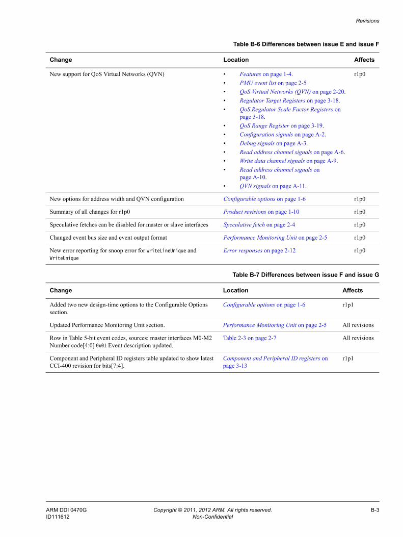
Revisions
Table B-6 Differences between issue E and issue F
Change Location Affects
New support for QoS Virtual Networks (QVN) • Features on page 1-4.• PMU event list on page 2-5• QoS Virtual Networks (QVN) on page 2-20.• Regulator Target Registers on page 3-18.• QoS Regulator Scale Factor Registers on
page 3-18.• QoS Range Register on page 3-19.• Configuration signals on page A-2.• Debug signals on page A-3.• Read address channel signals on page A-6.• Write data channel signals on page A-9.• Read address channel signals on
page A-10.• QVN signals on page A-11.
r1p0
New options for address width and QVN configuration Configurable options on page 1-6 r1p0
Summary of all changes for r1p0 Product revisions on page 1-10 r1p0
Speculative fetches can be disabled for master or slave interfaces Speculative fetch on page 2-4 r1p0
Changed event bus size and event output format Performance Monitoring Unit on page 2-5 r1p0
New error reporting for snoop error for WriteLineUnique and WriteUnique
Error responses on page 2-12 r1p0
Table B-7 Differences between issue F and issue G
Change Location Affects
Added two new design-time options to the Configurable Options section.
Configurable options on page 1-6 r1p1
Updated Performance Monitoring Unit section. Performance Monitoring Unit on page 2-5 All revisions
Row in Table 5-bit event codes, sources: master interfaces M0-M2 Number code[4:0] 0x01 Event description updated.
Table 2-3 on page 2-7 All revisions
Component and Peripheral ID registers table updated to show latest CCI-400 revision for bits[7:4].
Component and Peripheral ID registers on page 3-13
r1p1
ARM DDI 0470G Copyright © 2011, 2012 ARM. All rights reserved. B-3ID111612 Non-Confidential