Embed Size (px)
Citation preview
CoreSight™ SoCRevision: r0p0
Technical Reference Manual
Copyright © 2011 ARM. All rights reserved.ARM DDI 0480A (ID111211)
CoreSight SoCTechnical Reference Manual
Copyright © 2011 ARM. All rights reserved.
Release Information
Proprietary Notice
Words and logos marked with ® or ™ are registered trademarks or trademarks of ARM® in the EU and other countries, except as otherwise stated below in this proprietary notice. Other brands and names mentioned herein may be the trademarks of their respective owners.
Neither the whole nor any part of the information contained in, or the product described in, this document may be adapted or reproduced in any material form except with the prior written permission of the copyright holder.
The product described in this document is subject to continuous developments and improvements. All particulars of the product and its use contained in this document are given by ARM in good faith. However, all warranties implied or expressed, including but not limited to implied warranties of merchantability, or fitness for purpose, are excluded.
This document is intended only to assist the reader in the use of the product. ARM shall not be liable for any loss or damage arising from the use of any information in this document, or any error or omission in such information, or any incorrect use of the product.
Where the term ARM is used it means “ARM or any of its subsidiaries as appropriate”.
Confidentiality Status
This document is Non-Confidential. The right to use, copy and disclose this document may be subject to license restrictions in accordance with the terms of the agreement entered into by ARM and the party that ARM delivered this document to.
Product Status
The information in this document is final, that is for a developed product.
Web Address
http://www.arm.com
Change history
Date Issue Confidentiality Change
04 November 2011 A Non-Confidential First release for r0p0
ARM DDI 0480A Copyright © 2011 ARM. All rights reserved. iiID111211 Non-Confidential
ContentsCoreSight SoC Technical Reference Manual
PrefaceAbout this book ............................................................................................. viiFeedback ....................................................................................................... xi
Chapter 1 Introduction1.1 About the CoreSight SoC ........................................................................... 1-21.2 CoreSight block summary ........................................................................... 1-41.3 Typical CoreSight debugging environment ................................................. 1-61.4 Product revisions ........................................................................................ 1-7
Chapter 2 Functional Overview2.1 DAP components ........................................................................................ 2-22.2 ATB interconnect components .................................................................... 2-52.3 Timestamp components ............................................................................. 2-92.4 Standard CoreSight components .............................................................. 2-13
Chapter 3 Programmers Model3.1 About this programmers model ................................................................... 3-23.2 APB interconnect register summary ........................................................... 3-33.3 APB interconnect register descriptions ....................................................... 3-43.4 ATB funnel register summary ................................................................... 3-123.5 ATB funnel register descriptions ............................................................... 3-133.6 ATB replicator register summary .............................................................. 3-373.7 ATB replicator register descriptions .......................................................... 3-383.8 ETB register summary .............................................................................. 3-553.9 ETB register descriptions .......................................................................... 3-573.10 CTI register summary ............................................................................... 3-843.11 CTI register descriptions ........................................................................... 3-863.12 TPIU register summary ........................................................................... 3-123
ARM DDI 0480A Copyright © 2011 ARM. All rights reserved. iiiID111211 Non-Confidential
3.13 TPIU register descriptions ...................................................................... 3-1253.14 DAP register summary ............................................................................ 3-1633.15 DAP register descriptions ....................................................................... 3-1673.16 Timestamp generator register summary ................................................. 3-1943.17 Timestamp generator register description .............................................. 3-195
Chapter 4 Debug Access Port4.1 About the Debug Access Port ..................................................................... 4-24.2 SWJ-DP ...................................................................................................... 4-74.3 JTAG-DP .................................................................................................. 4-104.4 SW-DP ...................................................................................................... 4-114.5 Common debug port features and registers ............................................. 4-164.6 Access ports ............................................................................................. 4-184.7 AHB-AP .................................................................................................... 4-194.8 AXI-AP ...................................................................................................... 4-234.9 APB-AP ..................................................................................................... 4-294.10 JTAG-AP ................................................................................................... 4-314.11 Auxiliary Access Port ................................................................................ 4-334.12 Authentication requirements for Debug Access Port ................................ 4-344.13 Clocks, power, and resets ........................................................................ 4-35
Chapter 5 APB Interconnect5.1 Introduction ................................................................................................. 5-25.2 APB interconnect interfaces ....................................................................... 5-35.3 Device operation ......................................................................................... 5-4
Chapter 6 ATB Interconnect Components6.1 ATB replicator ............................................................................................. 6-26.2 ATB funnel .................................................................................................. 6-46.3 ATB upsizer .............................................................................................. 6-126.4 ATB downsizer .......................................................................................... 6-15
Chapter 7 DAPBUS Interconnect7.1 About the DAPBUS interconnect ................................................................ 7-27.2 DAPBUS interconnect interfaces ................................................................ 7-37.3 Main modes of operation ............................................................................ 7-4
Chapter 8 Timestamp Components8.1 About the timestamp components .............................................................. 8-28.2 Timestamp solution ..................................................................................... 8-3
Chapter 9 Embedded Cross Trigger9.1 About the ECT ............................................................................................ 9-29.2 ECT programmers model ........................................................................... 9-59.3 ECT connectivity recommendations ........................................................... 9-69.4 ECT authentication requirements ............................................................... 9-7
Chapter 10 Trace Port Interface Unit10.1 About the Trace Port Interface Unit .......................................................... 10-210.2 Trace Out Port .......................................................................................... 10-310.3 Miscellaneous connections ....................................................................... 10-410.4 TPIU trace port sizes ................................................................................ 10-510.5 TPIU triggers ............................................................................................. 10-710.6 Other TPIU design considerations ............................................................ 10-810.7 Authentication requirements for TPIUs ................................................... 10-1010.8 TPIU pattern generator ........................................................................... 10-1110.9 TPIU formatter and FIFO ........................................................................ 10-1310.10 Configuration options .............................................................................. 10-15
ARM DDI 0480A Copyright © 2011 ARM. All rights reserved. ivID111211 Non-Confidential
10.11 Example configuration scenarios ............................................................ 10-16
Chapter 11 Embedded Trace Buffer11.1 About the ETB .......................................................................................... 11-211.2 ETB clocks, resets, and synchronization .................................................. 11-511.3 ETB trace capture and formatting ............................................................. 11-611.4 Flush assertion ......................................................................................... 11-811.5 Triggers ..................................................................................................... 11-911.6 Write address generation for trace data storage .................................... 11-1011.7 Trace data storage .................................................................................. 11-1111.8 APB configuration and RAM access ....................................................... 11-1211.9 Trace RAM .............................................................................................. 11-1311.10 Authentication requirements for CoreSight ETBs ................................... 11-1411.11 ETB RAM support ................................................................................... 11-15
Appendix A Signal DescriptionsA.1 Clock domains ............................................................................................ A-2A.2 AXI slave interface signals .......................................................................... A-3A.3 AXI master interface signals ....................................................................... A-7A.4 CoreSight DAP signals ............................................................................. A-10A.5 CoreSight ECT signals ............................................................................. A-15A.6 CoreSight TPIU signals ............................................................................ A-18A.7 CoreSight ETB signals .............................................................................. A-20A.8 CoreSight timestamp component signals ................................................. A-22A.9 APB IC signals .......................................................................................... A-24A.10 Debug interconnect signals ...................................................................... A-25
Appendix B Revisions
ARM DDI 0480A Copyright © 2011 ARM. All rights reserved. vID111211 Non-Confidential

Preface
This preface introduces the CoreSight™ SoC Technical Reference Manual. It contains the following sections:• About this book on page vii• Feedback on page xi.
ARM DDI 0480A Copyright © 2011 ARM. All rights reserved. viID111211 Non-Confidential
Preface
About this bookThis is the Technical Reference Manual (TRM) for the CoreSight components.
Product revision status
The rnpn identifier indicates the revision status of the products described in this book, where:rn Identifies the major revision of the product.pn Identifies the minor revision or modification status of the product.
Intended audience
This book is written for the following target audiences:
• Hardware and software engineers who want to incorporate a CoreSight SoC into their design and produce real-time instruction and data trace information from an ASIC.
• Software engineers writing tools to use CoreSight SoC.
This book assumes that readers are familiar with AMBA bus design and JTAG methodology.
Using this book
This book is organized into the following chapters:
Chapter 1 Introduction Read this for an overview of the CoreSight components.
Chapter 2 Functional Overview Read this for a description of the major functional blocks and the operation of the CoreSight SoC.
Chapter 3 Programmers Model Read this for a description of the memory map and registers.
Chapter 4 Debug Access Port Read this for a description of the Debug Access Port (DAP) components.
Chapter 5 APB Interconnect Read this for a description of the Advanced Peripheral Bus (APB) interconnect components.
Chapter 6 ATB Interconnect Components Read this for a description of the AMBA Trace Bus (ATB) interconnect components.
Chapter 7 DAPBUS Interconnect Read this for a description of the Debug Access Port Bus (DAPBUS) interconnect components.
Chapter 8 Timestamp Components Read this for a description of the timestamp components.
Chapter 9 Embedded Cross Trigger Read this for a description of the Embedded Cross Trigger (ECT) components.
ARM DDI 0480A Copyright © 2011 ARM. All rights reserved. viiID111211 Non-Confidential
Preface
Chapter 10 Trace Port Interface Unit Read this for a description of the Trace Port Interface Unit (TPIU) components.
Chapter 11 Embedded Trace Buffer Read this for a description of the Embedded Trace Buffer (ETB) components.
Appendix A Signal Descriptions Read this for a description of the CoreSight SoC component signals.
Appendix B Revisions Read this for a description of the technical changes between released issues of this book.
Glossary
The ARM Glossary is a list of terms used in ARM documentation, together with definitions for those terms. The ARM Glossary does not contain terms that are industry standard unless the ARM meaning differs from the generally accepted meaning.
See ARM Glossary, http://infocenter.arm.com/help/topic/com.arm.doc.aeg0014-/index.html.
Conventions
Conventions that this book can use are described in:• Typographical• Timing diagrams on page ix• Signals on page ix.
Typographical
The typographical conventions are:
italic Highlights important notes, introduces special terminology, denotes internal cross-references, and citations.
bold Highlights interface elements, such as menu names. Denotes signal names. Also used for terms in descriptive lists, where appropriate.
monospace Denotes text that you can enter at the keyboard, such as commands, file and program names, and source code.
monospace Denotes a permitted abbreviation for a command or option. You can enter the underlined text instead of the full command or option name.
monospace italic Denotes arguments to monospace text where the argument is to be replaced by a specific value.
monospace bold Denotes language keywords when used outside example code.
< and > Enclose replaceable terms for assembler syntax where they appear in code or code fragments. For example:MRC p15, 0 <Rd>, <CRn>, <CRm>, <Opcode_2>
ARM DDI 0480A Copyright © 2011 ARM. All rights reserved. viiiID111211 Non-Confidential
Preface
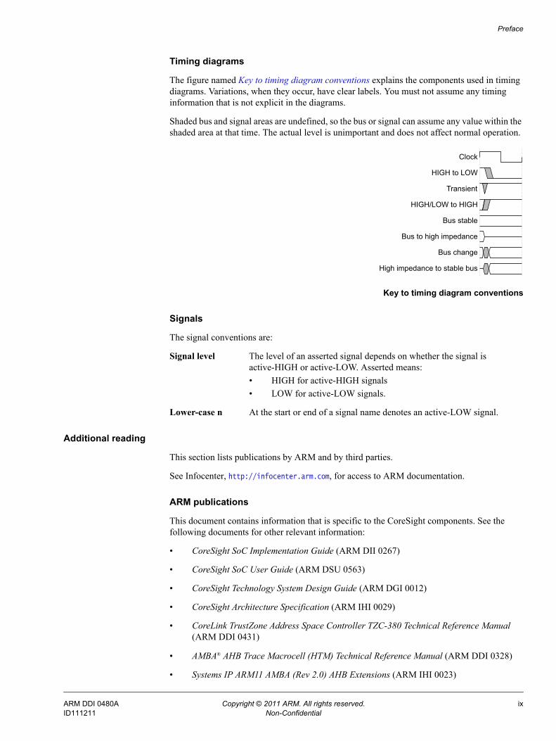
Timing diagrams
The figure named Key to timing diagram conventions explains the components used in timing diagrams. Variations, when they occur, have clear labels. You must not assume any timing information that is not explicit in the diagrams.
Shaded bus and signal areas are undefined, so the bus or signal can assume any value within the shaded area at that time. The actual level is unimportant and does not affect normal operation.
Key to timing diagram conventions
Signals
The signal conventions are:
Signal level The level of an asserted signal depends on whether the signal is active-HIGH or active-LOW. Asserted means:• HIGH for active-HIGH signals• LOW for active-LOW signals.
Lower-case n At the start or end of a signal name denotes an active-LOW signal.
Additional reading
This section lists publications by ARM and by third parties.
See Infocenter, http://infocenter.arm.com, for access to ARM documentation.
ARM publications
This document contains information that is specific to the CoreSight components. See the following documents for other relevant information:
• CoreSight SoC Implementation Guide (ARM DII 0267)
• CoreSight SoC User Guide (ARM DSU 0563)
• CoreSight Technology System Design Guide (ARM DGI 0012)
• CoreSight Architecture Specification (ARM IHI 0029)
• CoreLink TrustZone Address Space Controller TZC-380 Technical Reference Manual (ARM DDI 0431)
• AMBA® AHB Trace Macrocell (HTM) Technical Reference Manual (ARM DDI 0328)
• Systems IP ARM11 AMBA (Rev 2.0) AHB Extensions (ARM IHI 0023)
Clock
HIGH to LOW
Transient
HIGH/LOW to HIGH
Bus stable
Bus to high impedance
Bus change
High impedance to stable bus
ARM DDI 0480A Copyright © 2011 ARM. All rights reserved. ixID111211 Non-Confidential

Preface
• AMBA 3 APB Protocol (ARM IHI 0024)
• ARM Debug Interface v5 Architecture Specification (ARM IHI 0031)
• ARM Debug Interface v5.1 Architecture Supplement (DSA09-PRDC-008772).
Other publications
This section lists relevant documents published by third parties:
• IEEE 1149.1-2001 IEEE Standard Test Access Port and Boundary Scan Architecture (JTAG).
ARM DDI 0480A Copyright © 2011 ARM. All rights reserved. xID111211 Non-Confidential
Preface
FeedbackARM welcomes feedback on this product and its documentation.
Feedback on this product
If you have any comments or suggestions about this product, contact your supplier and give:
• The product name.
• The product revision or version.
• An explanation with as much information as you can provide. Include symptoms and diagnostic procedures if appropriate.
Feedback on content
If you have comments on content then send an e-mail to [email protected]. Give:• the title• the number, ARM DDI 0480A• the page numbers to which your comments apply• a concise explanation of your comments.
ARM also welcomes general suggestions for additions and improvements.
Note ARM tests the PDF only in Adobe Acrobat and Acrobat Reader, and cannot guarantee the quality of the represented document when used with any other PDF reader.
ARM DDI 0480A Copyright © 2011 ARM. All rights reserved. xiID111211 Non-Confidential

Chapter 1 Introduction
This chapter introduces the CoreSight SoC. It contains the following sections:• About the CoreSight SoC on page 1-2• CoreSight block summary on page 1-4• Typical CoreSight debugging environment on page 1-6• Product revisions on page 1-7.
ARM DDI 0480A Copyright © 2011 ARM. All rights reserved. 1-1ID111211 Non-Confidential
Introduction
1.1 About the CoreSight SoCThe CoreSight SoC is a set of highly configurable components that you can use to:
• build CoreSight systems
• graphically configure all acceptable configuration options of components
• run the design rule checks to ensure that the configurations match the compliance limitations
• create a testbench infrastructure to run system-level tests to certify the debug and trace system operation.
1.1.1 CoreSight SoC features
The CoreSight SoC provide the following features for system-wide trace:• configurability• debug and trace visibility of whole systems• cross triggering support between SoC subsystems• multi-source trace in a single stream• higher data compression than previous solutions• standard programmers models for standard tools support• open interfaces for third-party cores• low pin count• low silicon overhead.
1.1.2 Structure of the CoreSight SoC
The CoreSight SoC include the following:
Control and access components Configure, access, and control the generation of trace. They do not generate trace, and process the trace data. Examples include:• DAP. See Chapter 4 Debug Access Port.
Sources Generate trace data for output through the AMBA Trace Bus (ATB). Examples include:• AHB Trace Macrocell (HTM), documented separately.
See Additional reading on page ix.• CoreSight Embedded Trace Macrocells (ETMs), documented
separately. See Additional reading on page ix.• Instrumentation Trace Macrocell (ITM). See Additional reading on
page ix.
Links Provide connection, triggering, and flow of trace data. Examples include:• Synchronous 1:1 ATB bridge• Replicator• Trace funnel.
Sinks Are the end points for trace data on the SoC. Examples include:• TPIU for output of trace data off-chip• ETB for on-chip storage of trace data in RAM
ARM DDI 0480A Copyright © 2011 ARM. All rights reserved. 1-2ID111211 Non-Confidential

Introduction
• Serial Wire Output (SWO) for output of STM trace through a single pin.
ARM DDI 0480A Copyright © 2011 ARM. All rights reserved. 1-3ID111211 Non-Confidential
Introduction
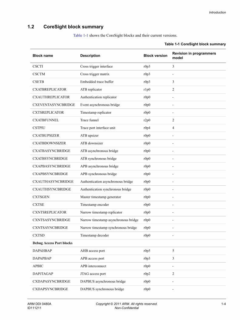
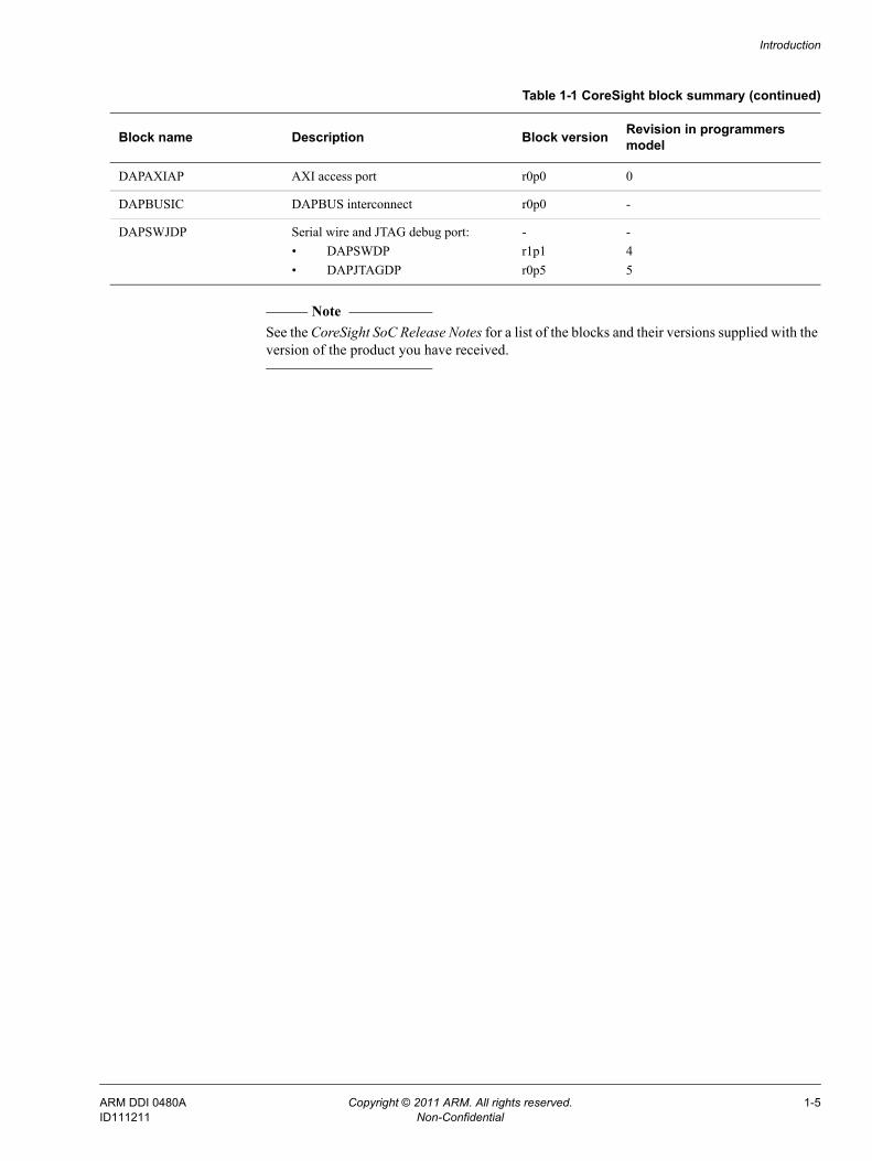
1.2 CoreSight block summaryTable 1-1 shows the CoreSight blocks and their current versions.
Table 1-1 CoreSight block summary
Block name Description Block version Revision in programmers model
CSCTI Cross trigger interface r0p3 3
CSCTM Cross trigger matrix r0p3 -
CSETB Embedded trace buffer r0p3 3
CXATBREPLICATOR ATB replicator r1p0 2
CXAUTHREPLICATOR Authentication replicator r0p0 -
CXEVENTASYNCBRIDGE Event asynchronous bridge r0p0 -
CXTSREPLICATOR Timestamp replicator r0p0 -
CXATBFUNNEL Trace funnel r2p0 2
CSTPIU Trace port interface unit r0p4 4
CXATBUPSIZER ATB upsizer r0p0 -
CXATBDOWNSIZER ATB downsizer r0p0 -
CXATBASYNCBRIDGE ATB asynchronous bridge r0p0 -
CXATBSYNCBRIDGE ATB synchronous bridge r0p0 -
CXAPBASYNCBRIDGE APB asynchronous bridge r0p0 -
CXAPBSYNCBRIDGE APB synchronous bridge r0p0 -
CXAUTHASYNCBRIDGE Authentication asynchronous bridge r0p0 -
CXAUTHSYNCBRIDGE Authentication synchronous bridge r0p0 -
CXTSGEN Master timestamp generator r0p0 -
CXTSE Timestamp encoder r0p0 -
CXNTSREPLICATOR Narrow timestamp replicator r0p0 -
CXNTSASYNCBRIDGE Narrow timestamp asynchronous bridge r0p0 -
CXNTSAYNCBRIDGE Narrow timestamp synchronous bridge r0p0 -
CXTSD Timestamp decoder r0p0 -
Debug Access Port blocks
DAPAHBAP AHB access port r0p5 5
DAPAPBAP APB access port r0p3 3
APBIC APB interconnect r0p0 -
DAPJTAGAP JTAG access port r0p2 2
CXDAPASYNCBRIDGE DAPBUS asynchronous bridge r0p0 -
CXDAPSYNCBRIDGE DAPBUS synchronous bridge r0p0 -
ARM DDI 0480A Copyright © 2011 ARM. All rights reserved. 1-4ID111211 Non-Confidential
Introduction
Note See the CoreSight SoC Release Notes for a list of the blocks and their versions supplied with the version of the product you have received.
DAPAXIAP AXI access port r0p0 0
DAPBUSIC DAPBUS interconnect r0p0 -
DAPSWJDP Serial wire and JTAG debug port:• DAPSWDP• DAPJTAGDP
-r1p1r0p5
-45
Table 1-1 CoreSight block summary (continued)
Block name Description Block version Revision in programmers model
ARM DDI 0480A Copyright © 2011 ARM. All rights reserved. 1-5ID111211 Non-Confidential
Introduction
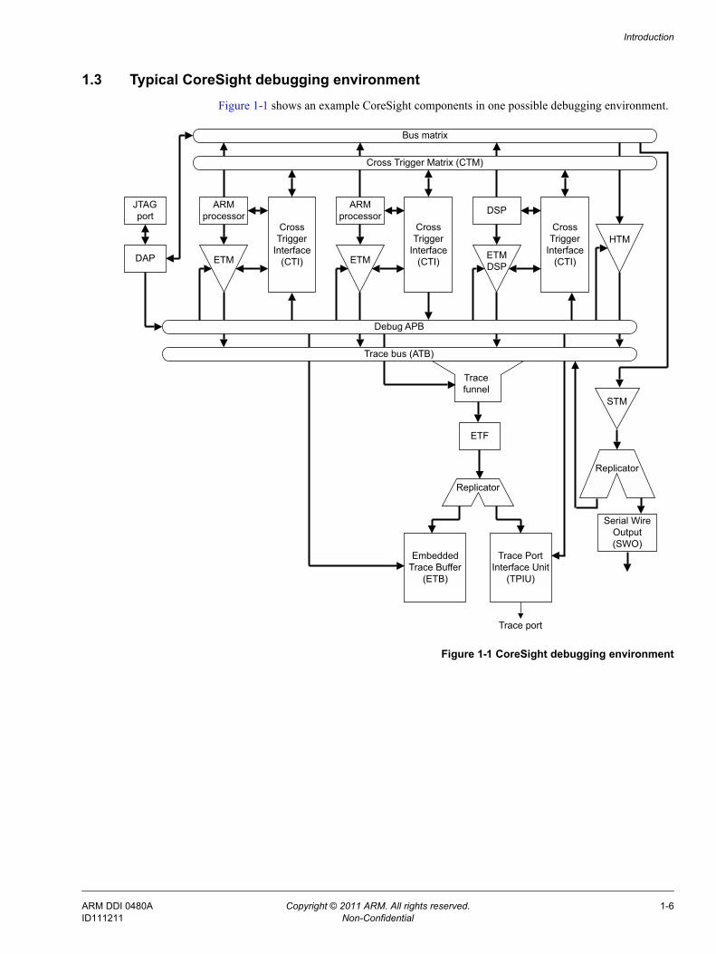
1.3 Typical CoreSight debugging environmentFigure 1-1 shows an example CoreSight components in one possible debugging environment.
Figure 1-1 CoreSight debugging environment
Bus matrix
Cross Trigger Matrix (CTM)
JTAG port
DAP
ARM processor
ARM processor DSP
Debug APB
Trace bus (ATB)
Tracefunnel
Replicator
Cross Trigger
Interface (CTI)
Cross Trigger
Interface (CTI)
Cross Trigger
Interface (CTI)ETM ETM ETM
DSP
HTM
Embedded Trace Buffer
(ETB)
Trace Port Interface Unit
(TPIU)
Trace port
STM
Replicator
Serial Wire Output (SWO)
ETF
ARM DDI 0480A Copyright © 2011 ARM. All rights reserved. 1-6ID111211 Non-Confidential

Introduction
1.4 Product revisionsThis section describes the differences in functionality between product revisions:
r0p0 First release.
ARM DDI 0480A Copyright © 2011 ARM. All rights reserved. 1-7ID111211 Non-Confidential
Chapter 2 Functional Overview
This chapter describes the various components of the CoreSight SoC and its features. It contains the following sections:• DAP components on page 2-2• ATB interconnect components on page 2-5• Timestamp components on page 2-9• Standard CoreSight components on page 2-13.
ARM DDI 0480A Copyright © 2011 ARM. All rights reserved. 2-1ID111211 Non-Confidential
Functional Overview
2.1 DAP componentsThe DAP components include:• Serial Wire or JTAG (SWJ) debug port• DAPBUS interconnect• Advanced eXtensible Interface Access Port (AXI-AP) on page 2-3• Advanced Peripheral Bus Access Port (APB-AP) on page 2-3• Advanced High-performance Bus Access Port (AHB-AP) on page 2-4• JTAG-AP on page 2-4.
For more information about the configurable parameters and its options of the DAP components, see the CoreSight SoC User Guide.
2.1.1 Serial Wire or JTAG (SWJ) debug port
The SWJ debug port connects to either a Serial Wire Debug or JTAG probe to a target.
See Chapter 4 Debug Access Port for more information.
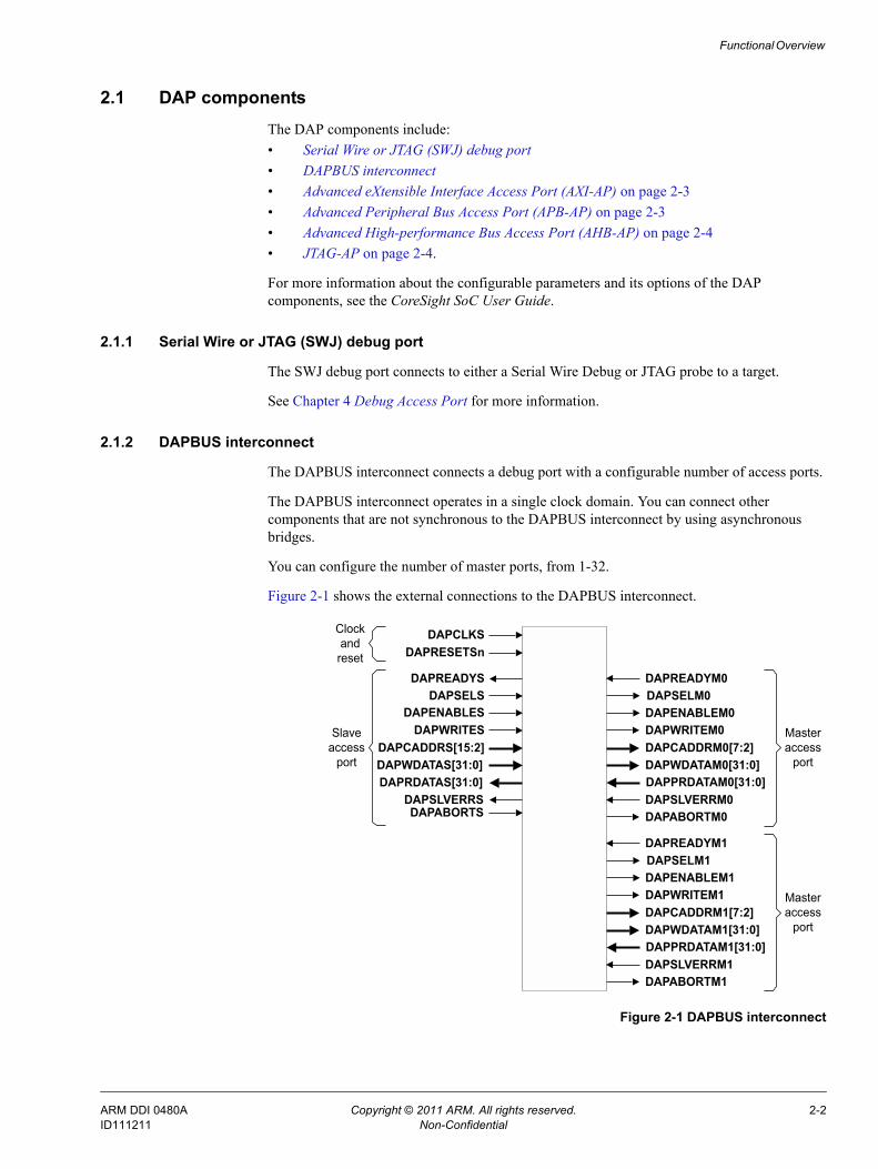
2.1.2 DAPBUS interconnect
The DAPBUS interconnect connects a debug port with a configurable number of access ports.
The DAPBUS interconnect operates in a single clock domain. You can connect other components that are not synchronous to the DAPBUS interconnect by using asynchronous bridges.
You can configure the number of master ports, from 1-32.
Figure 2-1 shows the external connections to the DAPBUS interconnect.
Figure 2-1 DAPBUS interconnect
DAPCLKS
DAPRDATAS[31:0]
DAPREADYS
DAPWRITES
DAPWDATAS[31:0]
DAPENABLESDAPSELS
DAPSLVERRS
Clockandreset
DAPCADDRS[15:2]
DAPABORTS
Slaveaccess
port
DAPRESETSn
DAPPRDATAM0[31:0]
DAPWRITEM0
DAPWDATAM0[31:0]DAPCADDRM0[7:2]
DAPREADYM0
DAPENABLEM0DAPSELM0
DAPSLVERRM0DAPABORTM0
Masteraccess
port
DAPPRDATAM1[31:0]
DAPWRITEM1
DAPWDATAM1[31:0]DAPCADDRM1[7:2]
DAPREADYM1
DAPENABLEM1DAPSELM1
DAPSLVERRM1DAPABORTM1
Masteraccess
port
ARM DDI 0480A Copyright © 2011 ARM. All rights reserved. 2-2ID111211 Non-Confidential
Functional Overview
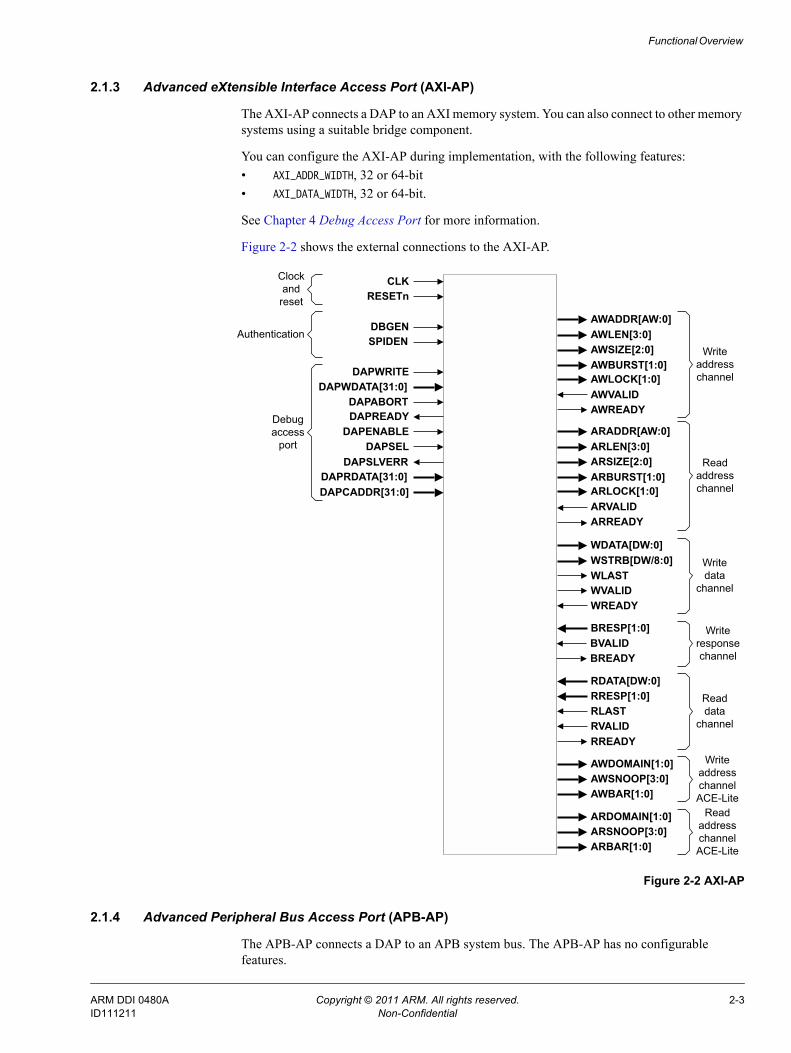
2.1.3 Advanced eXtensible Interface Access Port (AXI-AP)
The AXI-AP connects a DAP to an AXI memory system. You can also connect to other memory systems using a suitable bridge component.
You can configure the AXI-AP during implementation, with the following features:• AXI_ADDR_WIDTH, 32 or 64-bit• AXI_DATA_WIDTH, 32 or 64-bit.
See Chapter 4 Debug Access Port for more information.
Figure 2-2 shows the external connections to the AXI-AP.
Figure 2-2 AXI-AP
2.1.4 Advanced Peripheral Bus Access Port (APB-AP)
The APB-AP connects a DAP to an APB system bus. The APB-AP has no configurable features.
CLKRESETn
DAPRDATA[31:0]
DAPREADY
DAPWRITEDAPWDATA[31:0]
DAPENABLEDAPSEL
DAPSLVERR
Clockandreset
AWADDR[AW:0]
DAPCADDR[31:0]
DAPABORT
DBGENSPIDEN AWLEN[3:0]
AWSIZE[2:0]AWBURST[1:0]AWLOCK[1:0]AWVALIDAWREADY
WDATA[DW:0]
ARADDR[AW:0]ARLEN[3:0]ARSIZE[2:0]ARBURST[1:0]ARLOCK[1:0]ARVALIDARREADY
WSTRB[DW/8:0]WLASTWVALIDWREADY
BRESP[1:0]BVALIDBREADY
RDATA[DW:0]RRESP[1:0]RLASTRVALIDRREADY
AWDOMAIN[1:0]AWSNOOP[3:0]AWBAR[1:0]
ARDOMAIN[1:0]ARSNOOP[3:0]ARBAR[1:0]
Writeaddresschannel
Readaddresschannel
Writedata
channel
Writeresponsechannel
Readdata
channel
WriteaddresschannelACE-Lite
ReadaddresschannelACE-Lite
Authentication
Debugaccess
port
ARM DDI 0480A Copyright © 2011 ARM. All rights reserved. 2-3ID111211 Non-Confidential
Functional Overview
See Chapter 4 Debug Access Port for more information.
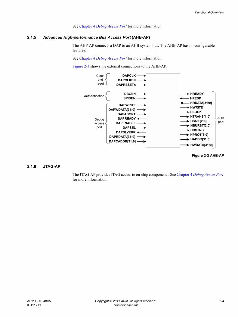
2.1.5 Advanced High-performance Bus Access Port (AHB-AP)
The AHP-AP connects a DAP to an AHB system bus. The AHB-AP has no configurable features.
See Chapter 4 Debug Access Port for more information.
Figure 2-3 shows the external connections to the AHB-AP.
Figure 2-3 AHB-AP
2.1.6 JTAG-AP
The JTAG-AP provides JTAG access to on-chip components. See Chapter 4 Debug Access Port for more information.
DAPCLK
DAPRESETn
DAPRDATA[31:0]
DAPREADY
DAPWRITEDAPWDATA[31:0]
DAPENABLEDAPSEL
DAPSLVERR
Clockandreset
DAPCADDR[31:0]
DAPABORT
DBGENSPIDEN
HSIZE[2:0]HBURST[2:0]
HPROT[3:0]HADDR[31:0]
HWDATA[31:0]
HBSTRB
AHBport
Authentication
Debugaccess
port
HREADY
HWRITEHRDATA[31:0]
HTRANS[1:0]
HRESP
HLOCK
DAPCLKEN
ARM DDI 0480A Copyright © 2011 ARM. All rights reserved. 2-4ID111211 Non-Confidential
Functional Overview
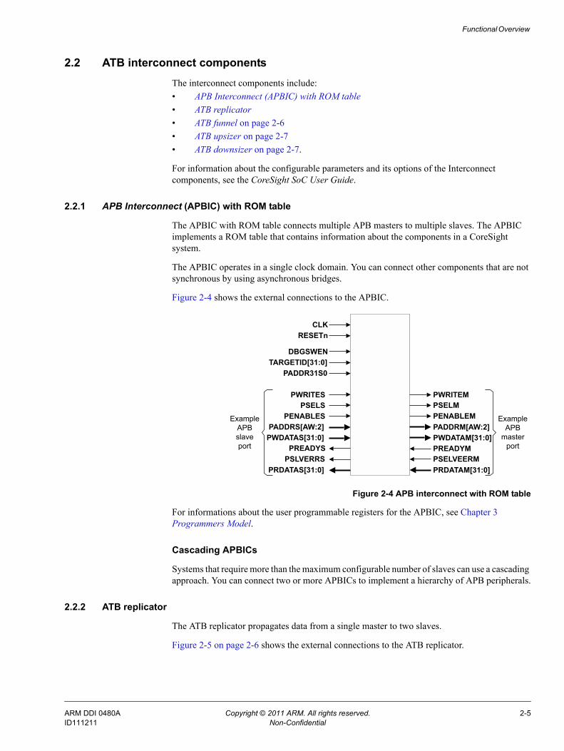
2.2 ATB interconnect componentsThe interconnect components include:• APB Interconnect (APBIC) with ROM table• ATB replicator• ATB funnel on page 2-6• ATB upsizer on page 2-7• ATB downsizer on page 2-7.
For information about the configurable parameters and its options of the Interconnect components, see the CoreSight SoC User Guide.
2.2.1 APB Interconnect (APBIC) with ROM table
The APBIC with ROM table connects multiple APB masters to multiple slaves. The APBIC implements a ROM table that contains information about the components in a CoreSight system.
The APBIC operates in a single clock domain. You can connect other components that are not synchronous by using asynchronous bridges.
Figure 2-4 shows the external connections to the APBIC.
Figure 2-4 APB interconnect with ROM table
For informations about the user programmable registers for the APBIC, see Chapter 3 Programmers Model.
Cascading APBICs
Systems that require more than the maximum configurable number of slaves can use a cascading approach. You can connect two or more APBICs to implement a hierarchy of APB peripherals.
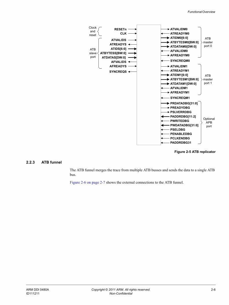
2.2.2 ATB replicator
The ATB replicator propagates data from a single master to two slaves.
Figure 2-5 on page 2-6 shows the external connections to the ATB replicator.
ExampleAPB
masterport
CLK
DBGSWEN
PWRITES
PRDATAS[31:0]
PREADYS
ExampleAPBslaveport
PWDATAM[31:0]
PWRITEM
PADDRM[AW:2]
PSELVEERMPREADYM
PSELSPENABLES
PADDRS[AW:2]PWDATAS[31:0]
PSLVERRS
PSELMPENABLEM
PRDATAM[31:0]
RESETn
TARGETID[31:0]PADDR31S0
ARM DDI 0480A Copyright © 2011 ARM. All rights reserved. 2-5ID111211 Non-Confidential
Functional Overview
Figure 2-5 ATB replicator
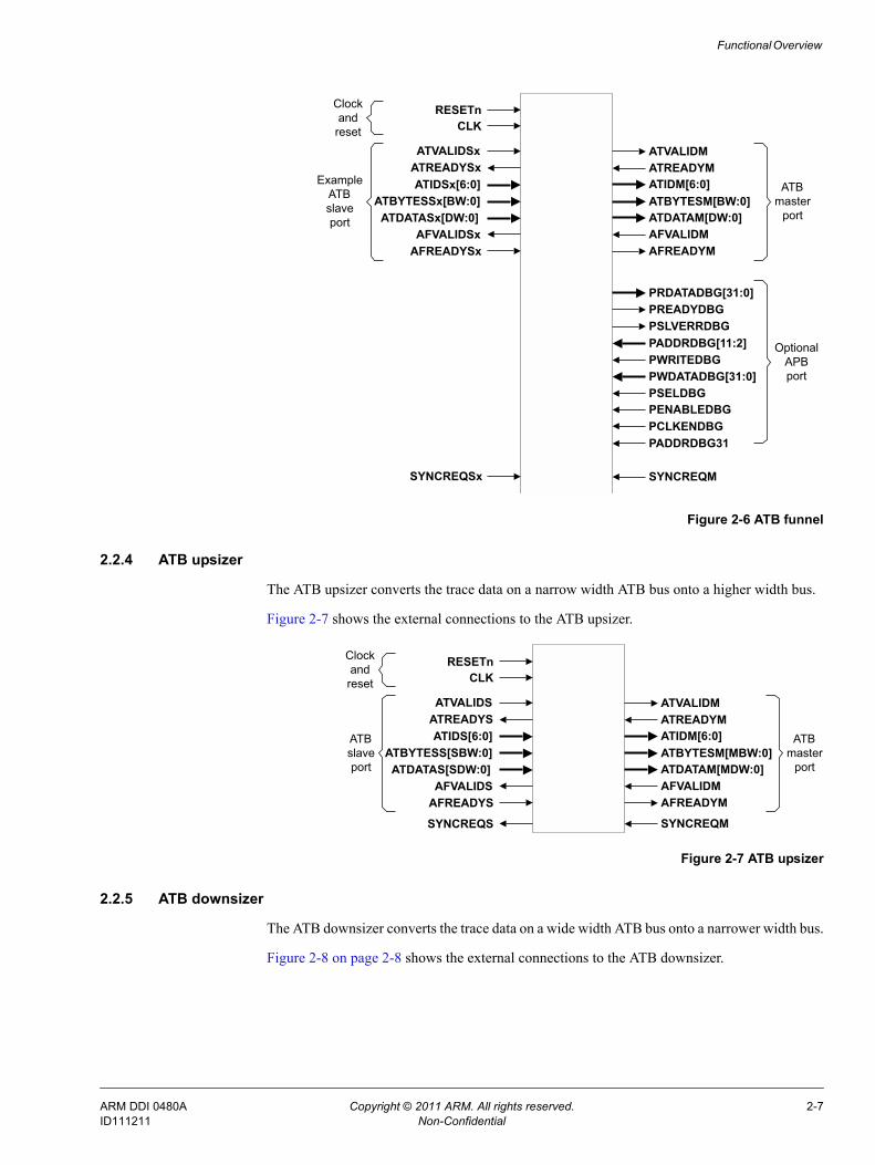
2.2.3 ATB funnel
The ATB funnel merges the trace from multiple ATB busses and sends the data to a single ATB bus.
Figure 2-6 on page 2-7 shows the external connections to the ATB funnel.
RESETn
ATIDM0[6:0] ATBmasterport 0
Clockandreset CLK
ATIDS[6:0]
ATDATAS[DW:0]AFVALIDS
ATBYTESS[BW:0]
ATREADYSATVALIDS
AFREADYS
SYNCREQS
ATBslaveport
ATDATAM0[DW:0]
ATVALIDM0
ATBYTESM0[BW:0]
ATREADYM0
AFVALIDM0AFREADYM0
SYNCREQM0
ATIDM1[6:0] ATBmasterport 1ATDATAM1[DW:0]
ATVALIDM1
PRDATADBG[31:0]
ATREADYM1
AFVALIDM1AFREADYM1
SYNCREQM1
PREADYDBG
ATBYTESM1[BW:0]
PADDRDBG[11:2]PSLVERRDBG
PWDATADBG[31:0]PWRITEDBG
PSELDBGPENABLEDBG
OptionalAPBport
PCLKENDBGPADDRDBG31
ARM DDI 0480A Copyright © 2011 ARM. All rights reserved. 2-6ID111211 Non-Confidential
Functional Overview
Figure 2-6 ATB funnel
2.2.4 ATB upsizer
The ATB upsizer converts the trace data on a narrow width ATB bus onto a higher width bus.
Figure 2-7 shows the external connections to the ATB upsizer.
Figure 2-7 ATB upsizer
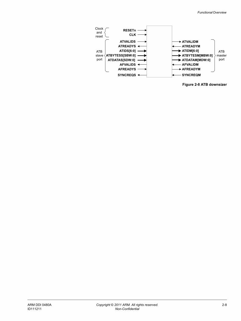
2.2.5 ATB downsizer
The ATB downsizer converts the trace data on a wide width ATB bus onto a narrower width bus.
Figure 2-8 on page 2-8 shows the external connections to the ATB downsizer.
RESETn
ATIDM[6:0] ATBmaster
port
Clockandreset CLK
ATIDSx[6:0]
ATDATASx[DW:0]AFVALIDSx
ATBYTESSx[BW:0]
ATREADYSxATVALIDSx
AFREADYSx
ExampleATBslaveport ATDATAM[DW:0]
ATVALIDM
ATBYTESM[BW:0]
ATREADYM
AFVALIDMAFREADYM
PRDATADBG[31:0]PREADYDBG
PADDRDBG[11:2]PSLVERRDBG
PWDATADBG[31:0]PWRITEDBG
PSELDBGPENABLEDBGPCLKENDBG
OptionalAPBport
SYNCREQMSYNCREQSx
PADDRDBG31
RESETn
ATIDM[6:0] ATBmaster
port
Clockandreset CLK
ATIDS[6:0]
ATDATAS[SDW:0]AFVALIDS
ATBYTESS[SBW:0]
ATREADYSATVALIDS
AFREADYS
ATBslaveport ATDATAM[MDW:0]
ATVALIDM
ATBYTESM[MBW:0]
ATREADYM
AFVALIDMAFREADYM
SYNCREQS SYNCREQM
ARM DDI 0480A Copyright © 2011 ARM. All rights reserved. 2-7ID111211 Non-Confidential
Functional Overview
Figure 2-8 ATB downsizer
RESETn
ATIDM[6:0] ATBmaster
port
Clockandreset CLK
ATIDS[6:0]
ATDATAS[SDW:0]AFVALIDS
ATBYTESS[SBW:0]
ATREADYSATVALIDS
AFREADYS
ATBslaveport ATDATAM[MDW:0]
ATVALIDM
ATBYTESM[MBW:0]
ATREADYM
AFVALIDMAFREADYM
SYNCREQS SYNCREQM
ARM DDI 0480A Copyright © 2011 ARM. All rights reserved. 2-8ID111211 Non-Confidential
Functional Overview
2.3 Timestamp componentsThe timestamp components generate and distribute a consistent timestamp value for multiple processors and other IPs within a SoC.
See Chapter 8 Timestamp Components for more information.
For information about the configurable parameters of the timestamp components, see the CoreSight SoC User Guide.
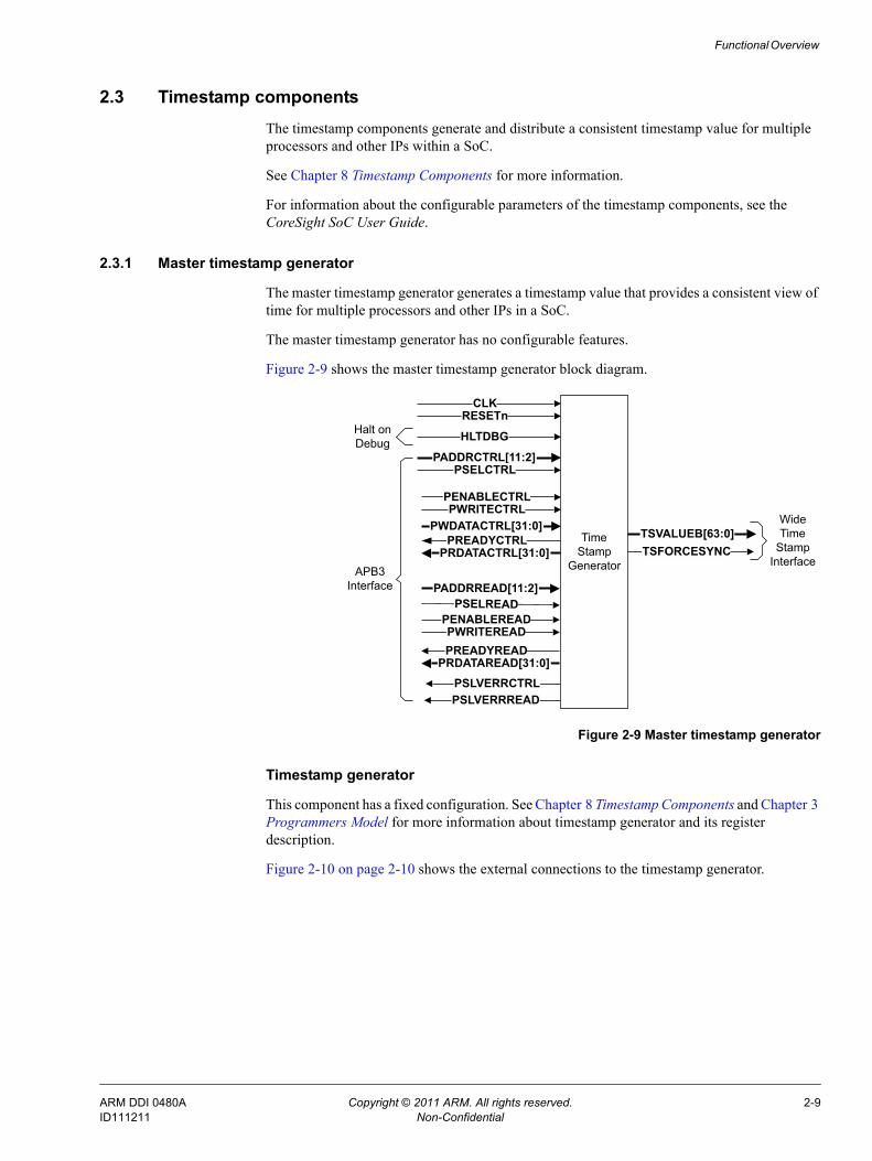
2.3.1 Master timestamp generator
The master timestamp generator generates a timestamp value that provides a consistent view of time for multiple processors and other IPs in a SoC.
The master timestamp generator has no configurable features.
Figure 2-9 shows the master timestamp generator block diagram.
Figure 2-9 Master timestamp generator
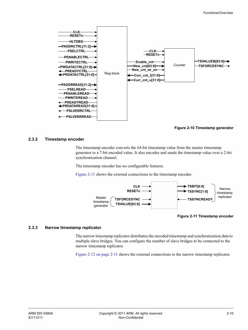
Timestamp generator
This component has a fixed configuration. See Chapter 8 Timestamp Components and Chapter 3 Programmers Model for more information about timestamp generator and its register description.
Figure 2-10 on page 2-10 shows the external connections to the timestamp generator.
Time Stamp
Generator
CLKRESETn
TSVALUEB[63:0]PREADYCTRL
PADDRCTRL[11:2]PSELCTRL
PENABLECTRLPWRITECTRL
PWDATACTRL[31:0]
PRDATACTRL[31:0]
HLTDBG
APB3Interface
WideTime
StampInterface
Halt on Debug
TSFORCESYNC
PREADYREAD
PADDRREAD[11:2]
PENABLEREADPWRITEREAD
PRDATAREAD[31:0]
PSELREAD
PSLVERRCTRLPSLVERRREAD
ARM DDI 0480A Copyright © 2011 ARM. All rights reserved. 2-9ID111211 Non-Confidential
Functional Overview
Figure 2-10 Timestamp generator
2.3.2 Timestamp encoder
The timestamp encoder converts the 64-bit timestamp value from the master timestamp generator to a 7-bit encoded value. It also encodes and sends the timestamp value over a 2-bit synchronization channel.
The timestamp encoder has no configurable features.
Figure 2-11 shows the external connections to the timestamp encoder.
Figure 2-11 Timestamp encoder
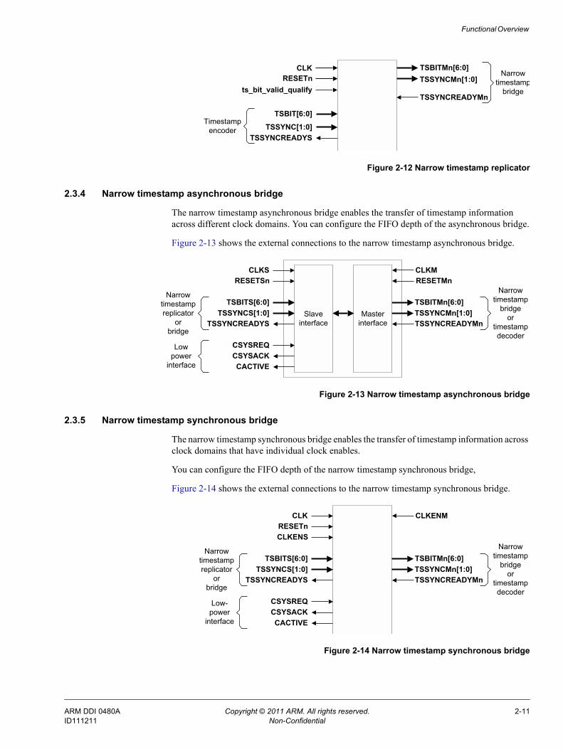
2.3.3 Narrow timestamp replicator
The narrow timestamp replicator distributes the encoded timestamp and synchronization data to multiple slave bridges. You can configure the number of slave bridges to be connected to the narrow timestamp replicator.
Figure 2-12 on page 2-11 shows the external connections to the narrow timestamp replicator.
Reg block
CounterEnable_cnt
Curr_cnt_l[31:0]Curr_cnt_u[31:0]
TSVALUEB[63:0]TSFORCESYNCNew_cnt[63:0]
New_cnt_wr_en
CLKRESETn
CLKRESETn
PREADYCTRL
PADDRCTRL[11:2]PSELCTRL
PENABLECTRLPWRITECTRL
PWDATACTRL[31:0]
PRDATACTRL[31:0]
HLTDBG
PREADYREAD
PADDRREAD[11:2]
PENABLEREADPWRITEREAD
PRDATAREAD[31:0]
PSELREAD
PSLVERRCTRL
PSLVERRREAD
CLKRESETn
TSFORCESYNC
TSBIT[6:0]TSSYNC[1:0]
TSSYNCREADYTSVALUE[63:0]
NarrowtimestampreplicatorMaster
timestampgenerator
ARM DDI 0480A Copyright © 2011 ARM. All rights reserved. 2-10ID111211 Non-Confidential
Functional Overview
Figure 2-12 Narrow timestamp replicator
2.3.4 Narrow timestamp asynchronous bridge
The narrow timestamp asynchronous bridge enables the transfer of timestamp information across different clock domains. You can configure the FIFO depth of the asynchronous bridge.
Figure 2-13 shows the external connections to the narrow timestamp asynchronous bridge.
Figure 2-13 Narrow timestamp asynchronous bridge
2.3.5 Narrow timestamp synchronous bridge
The narrow timestamp synchronous bridge enables the transfer of timestamp information across clock domains that have individual clock enables.
You can configure the FIFO depth of the narrow timestamp synchronous bridge,
Figure 2-14 shows the external connections to the narrow timestamp synchronous bridge.
Figure 2-14 Narrow timestamp synchronous bridge
ts_bit_valid_qualify
CLKRESETn
TSBITMn[6:0]TSSYNCMn[1:0]
TSSYNCREADYMn
Narrow timestamp
bridge
Timestampencoder
TSBIT[6:0]
TSSYNC[1:0]TSSYNCREADYS
Slaveinterface
CLKSRESETSn
Narrowtimestampreplicator
orbridge
TSBITS[6:0]TSSYNCS[1:0]
TSSYNCREADYS
CSYSREQCSYSACKCACTIVE
Lowpower
interface
TSBITMn[6:0]TSSYNCMn[1:0]TSSYNCREADYMn
Narrow timestamp
bridgeor
timestampdecoder
CLKMRESETMn
Masterinterface
CLKRESETn
Narrowtimestampreplicator
orbridge
TSBITS[6:0]TSSYNCS[1:0]
TSSYNCREADYS
CSYSREQCSYSACKCACTIVE
Low-power
interface
TSBITMn[6:0]TSSYNCMn[1:0]TSSYNCREADYMn
Narrow timestamp
bridgeor
timestampdecoder
CLKENM
CLKENS
ARM DDI 0480A Copyright © 2011 ARM. All rights reserved. 2-11ID111211 Non-Confidential
Functional Overview
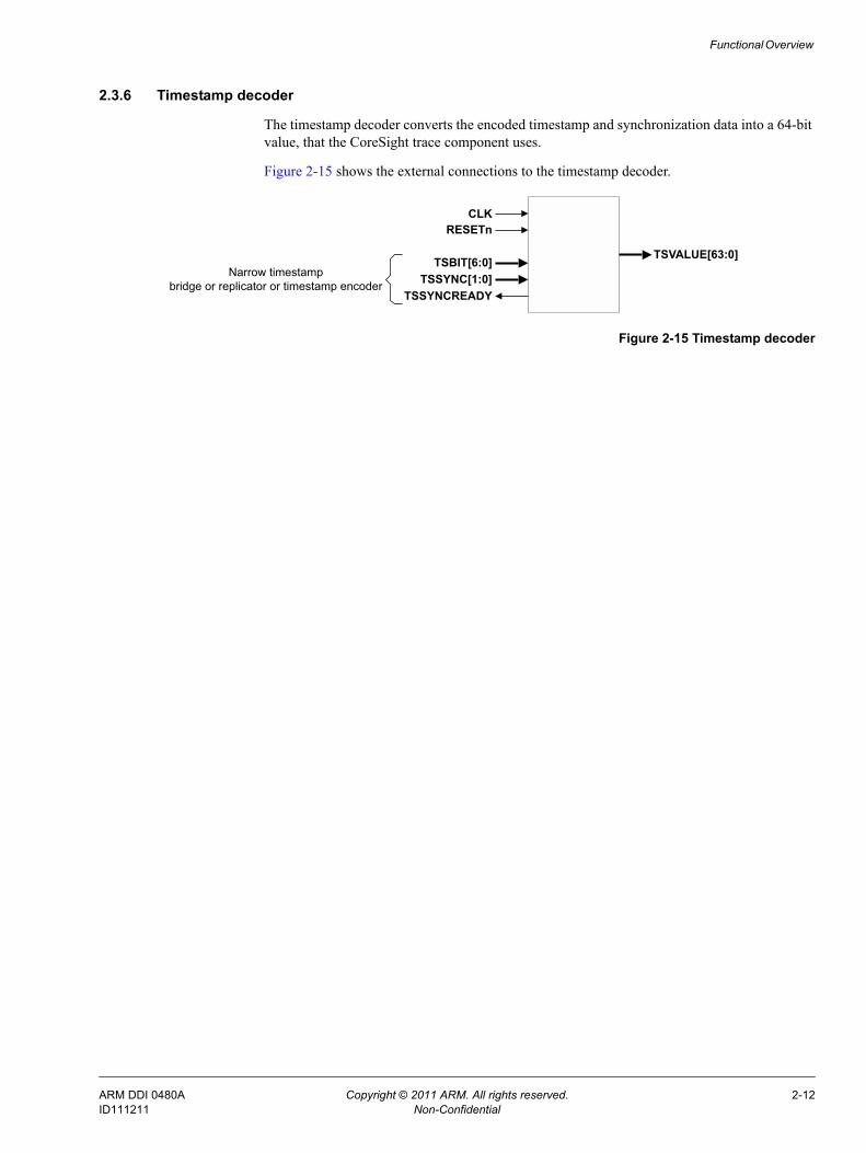
2.3.6 Timestamp decoder
The timestamp decoder converts the encoded timestamp and synchronization data into a 64-bit value, that the CoreSight trace component uses.
Figure 2-15 shows the external connections to the timestamp decoder.
Figure 2-15 Timestamp decoder
CLKRESETn
TSBIT[6:0]TSSYNC[1:0]
TSSYNCREADY
TSVALUE[63:0]Narrow timestamp
bridge or replicator or timestamp encoder
ARM DDI 0480A Copyright © 2011 ARM. All rights reserved. 2-12ID111211 Non-Confidential

Functional Overview
2.4 Standard CoreSight componentsThe CoreSight SoC includes the following standard CoreSight components. • ECT• TPIU• ETB• Cross Trigger Matrix (CTM)• System Trace Macrocell (STM)• Trace Memory Controller (TMC).
ARM DDI 0480A Copyright © 2011 ARM. All rights reserved. 2-13ID111211 Non-Confidential
Chapter 3 Programmers Model
This chapter describes the programmers model for the CoreSight components. It contains the following sections:• About this programmers model on page 3-2• APB interconnect register summary on page 3-3• APB interconnect register descriptions on page 3-4• ATB funnel register summary on page 3-12• ATB funnel register descriptions on page 3-13• ATB replicator register summary on page 3-37• ATB replicator register descriptions on page 3-38• ETB register summary on page 3-55• ETB register descriptions on page 3-57• CTI register summary on page 3-84• CTI register descriptions on page 3-86• TPIU register summary on page 3-123• TPIU register descriptions on page 3-125• DAP register summary on page 3-163• DAP register descriptions on page 3-167.• Timestamp generator register summary on page 3-194• Timestamp generator register description on page 3-195.
ARM DDI 0480A Copyright © 2011 ARM. All rights reserved. 3-1ID111211 Non-Confidential
Programmers Model
3.1 About this programmers modelThis section describes register information for the following components:• APB interconnect• ATB funnel• ATB replicator• ETB • CTI• TPIU• DAP• Timestamp generator.
APB interconnect, ATB funnel, and ATB replicator registers:
• The base address is not fixed, and can be different for any particular system implementation. The offset of each register from the base address is fixed.
• Do not attempt to access reserved or unused address locations. Attempting to access these locations can result in UNPREDICTABLE behavior.
• Unless otherwise stated in the accompanying text:— do not modify undefined register bits— ignore undefined register bits on reads— all register bits are reset to a logic 0 by a system or power-on reset.
• Access type in Table 3-1 on page 3-3 is described as follows:RW Read and write.R/W Read or write.RO Read-only.WO Write-only.SBZ Should-Be-Zero.RAZ Read-As-Zero.RAZ/WI Read-As-Zero, Writes Ignored.
ARM DDI 0480A Copyright © 2011 ARM. All rights reserved. 3-2ID111211 Non-Confidential
Programmers Model
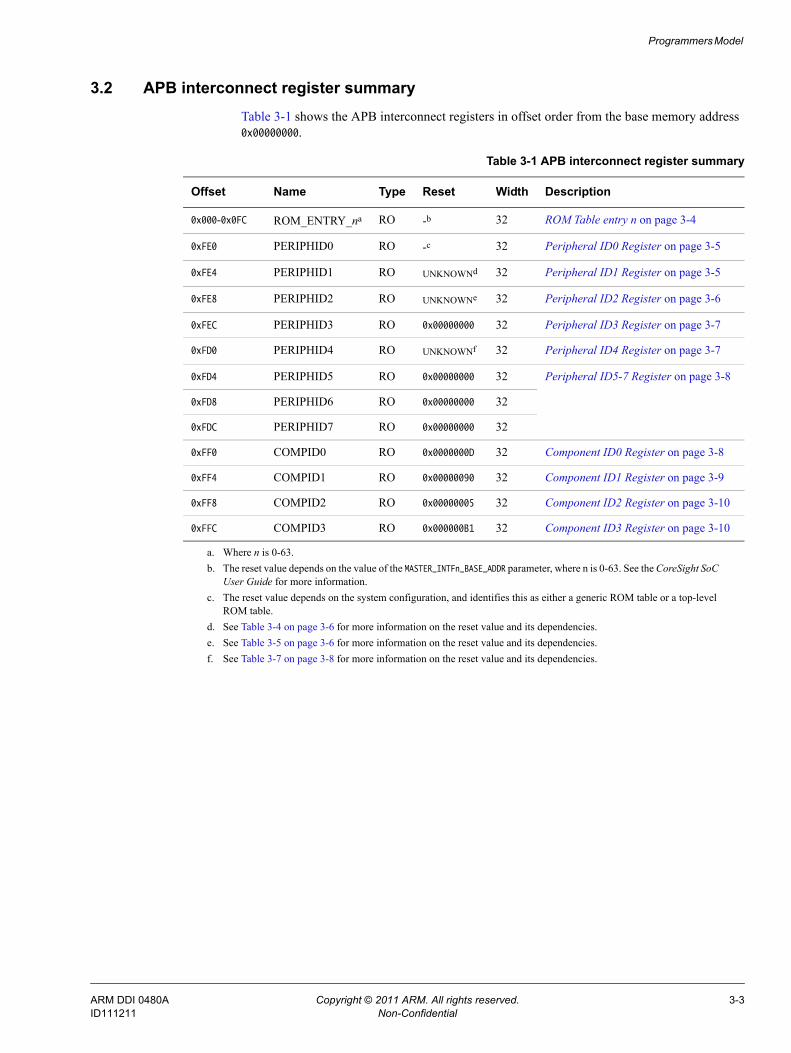
3.2 APB interconnect register summaryTable 3-1 shows the APB interconnect registers in offset order from the base memory address 0x00000000.
Table 3-1 APB interconnect register summary
Offset Name Type Reset Width Description
0x000-0x0FC ROM_ENTRY_na RO -b 32 ROM Table entry n on page 3-4
0xFE0 PERIPHID0 RO -c 32 Peripheral ID0 Register on page 3-5
0xFE4 PERIPHID1 RO UNKNOWNd 32 Peripheral ID1 Register on page 3-5
0xFE8 PERIPHID2 RO UNKNOWNe 32 Peripheral ID2 Register on page 3-6
0xFEC PERIPHID3 RO 0x00000000 32 Peripheral ID3 Register on page 3-7
0xFD0 PERIPHID4 RO UNKNOWNf 32 Peripheral ID4 Register on page 3-7
0xFD4 PERIPHID5 RO 0x00000000 32 Peripheral ID5-7 Register on page 3-8
0xFD8 PERIPHID6 RO 0x00000000 32
0xFDC PERIPHID7 RO 0x00000000 32
0xFF0 COMPID0 RO 0x0000000D 32 Component ID0 Register on page 3-8
0xFF4 COMPID1 RO 0x00000090 32 Component ID1 Register on page 3-9
0xFF8 COMPID2 RO 0x00000005 32 Component ID2 Register on page 3-10
0xFFC COMPID3 RO 0x000000B1 32 Component ID3 Register on page 3-10
a. Where n is 0-63.b. The reset value depends on the value of the MASTER_INTFn_BASE_ADDR parameter, where n is 0-63. See the CoreSight SoC
User Guide for more information.c. The reset value depends on the system configuration, and identifies this as either a generic ROM table or a top-level
ROM table.d. See Table 3-4 on page 3-6 for more information on the reset value and its dependencies.e. See Table 3-5 on page 3-6 for more information on the reset value and its dependencies.f. See Table 3-7 on page 3-8 for more information on the reset value and its dependencies.
ARM DDI 0480A Copyright © 2011 ARM. All rights reserved. 3-3ID111211 Non-Confidential
Programmers Model
3.3 APB interconnect register descriptionsThis section describes the CXAPBIC registers. Table 3-1 on page 3-3 provides cross references to individual registers.
3.3.1 ROM Table entry n
The ROM_ENTRY_n Register characteristics are:
Purpose Returns the value of ROM Entry n, where n is 0-63.
Usage constraints There are no usage constraints.
Configurations This register is available when the NUM_MASTER_INTF configuration option is set to a value greater than n. For example: • the ROM_ENTRY_1 Register is available when the
NUM_MASTER_INTF configuration option is set to a value greater than 1• the ROM_ENTRY_62 Register is available when the
NUM_MASTER_INTF configuration option is set to a value greater than 62.
Attributes See the register summary in Table 3-1 on page 3-3.
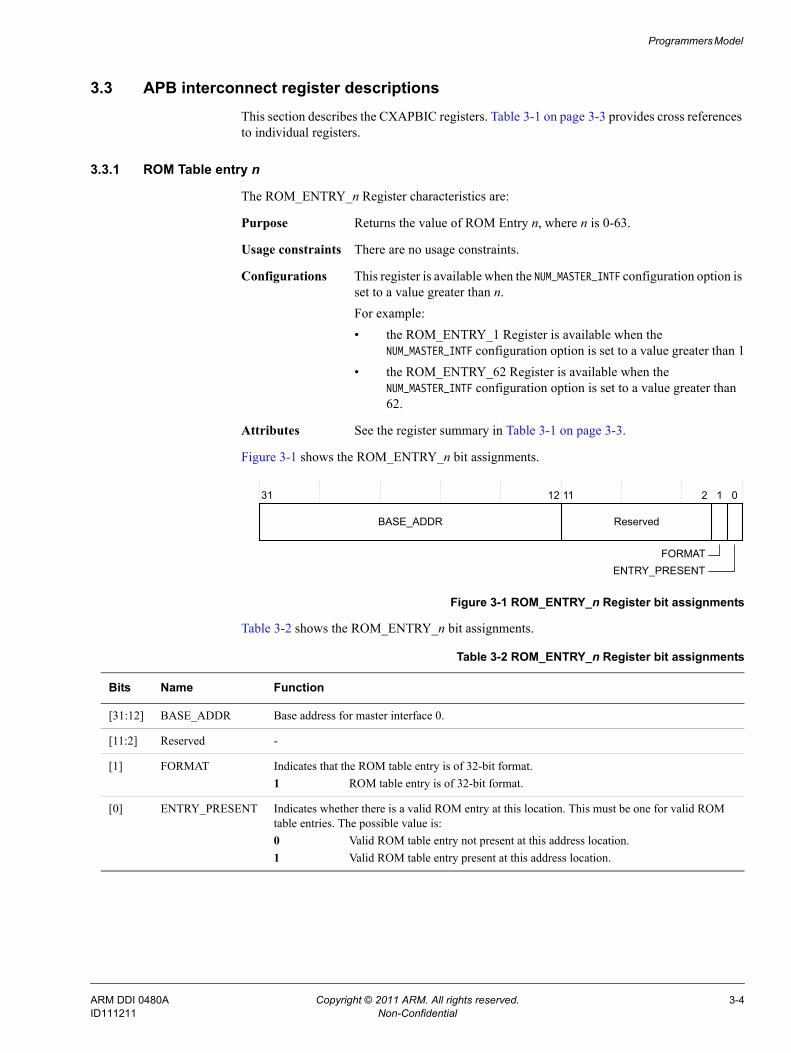
Figure 3-1 shows the ROM_ENTRY_n bit assignments.
Figure 3-1 ROM_ENTRY_n Register bit assignments
Table 3-2 shows the ROM_ENTRY_n bit assignments.
31 0
Reserved
2
ENTRY_PRESENT
1
FORMAT
12 11
BASE_ADDR
Table 3-2 ROM_ENTRY_n Register bit assignments
Bits Name Function
[31:12] BASE_ADDR Base address for master interface 0.
[11:2] Reserved -
[1] FORMAT Indicates that the ROM table entry is of 32-bit format.1 ROM table entry is of 32-bit format.
[0] ENTRY_PRESENT Indicates whether there is a valid ROM entry at this location. This must be one for valid ROM table entries. The possible value is:0 Valid ROM table entry not present at this address location.1 Valid ROM table entry present at this address location.
ARM DDI 0480A Copyright © 2011 ARM. All rights reserved. 3-4ID111211 Non-Confidential
Programmers Model
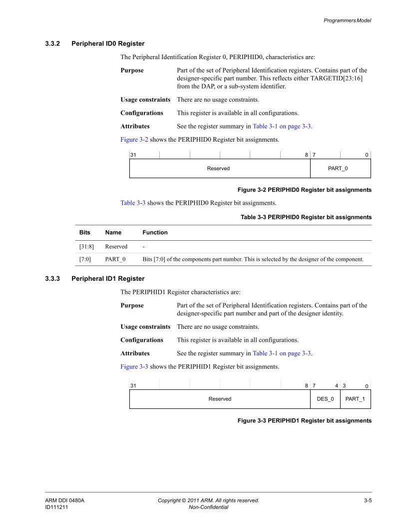
3.3.2 Peripheral ID0 Register
The Peripheral Identification Register 0, PERIPHID0, characteristics are:
Purpose Part of the set of Peripheral Identification registers. Contains part of the designer-specific part number. This reflects either TARGETID[23:16] from the DAP, or a sub-system identifier.
Usage constraints There are no usage constraints.
Configurations This register is available in all configurations.
Attributes See the register summary in Table 3-1 on page 3-3.
Figure 3-2 shows the PERIPHID0 Register bit assignments.
Figure 3-2 PERIPHID0 Register bit assignments
Table 3-3 shows the PERIPHID0 Register bit assignments.
3.3.3 Peripheral ID1 Register
The PERIPHID1 Register characteristics are:
Purpose Part of the set of Peripheral Identification registers. Contains part of the designer-specific part number and part of the designer identity.
Usage constraints There are no usage constraints.
Configurations This register is available in all configurations.
Attributes See the register summary in Table 3-1 on page 3-3.
Figure 3-3 shows the PERIPHID1 Register bit assignments.
Figure 3-3 PERIPHID1 Register bit assignments
31 8 7 0
PART_0Reserved
Table 3-3 PERIPHID0 Register bit assignments
Bits Name Function
[31:8] Reserved -
[7:0] PART_0 Bits [7:0] of the components part number. This is selected by the designer of the component.
31 0
Reserved
78
PART_1
4 3
DES_0
ARM DDI 0480A Copyright © 2011 ARM. All rights reserved. 3-5ID111211 Non-Confidential
Programmers Model
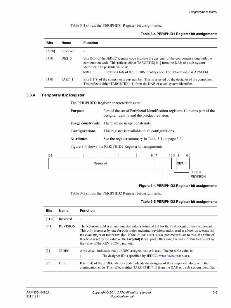
Table 3-4 shows the PERIPHID1 Register bit assignments.
3.3.4 Peripheral ID2 Register
The PERIPHID2 Register characteristics are:
Purpose Part of the set of Peripheral Identification registers. Contains part of the designer identity and the product revision.
Usage constraints There are no usage constraints.
Configurations This register is available in all configurations.
Attributes See the register summary in Table 3-1 on page 3-3.
Figure 3-4 shows the PERIPHID2 Register bit assignments.
Figure 3-4 PERIPHID2 Register bit assignments
Table 3-5 shows the PERIPHID2 Register bit assignments.
Table 3-4 PERIPHID1 Register bit assignments
Bits Name Function
[31:8] Reserved -
[7:4] DES_0 Bits [3:0] of the JEDEC identity code indicate the designer of the component along with the continuation code. This reflects either TARGETID[4:1] from the DAP, or a sub-system identifier. The possible value is:b1011 Lowest 4 bits of the JEP106 Identity code. The default value is ARM Ltd.
[3:0] PART_1 Bits [11:8] of the components part number. This is selected by the designer of the component. This reflects either TARGETID[4:1] from the DAP, or a sub-system identifier.
31 8 7 4 3 2 0
DES_1Reserved
REVISIONJEDEC
Table 3-5 PERIPHID2 Register bit assignments
Bits Name Function
[31:8] Reserved -
[7:4] REVISION The Revision field is an incremental value starting at 0x0 for the first design of this component. This only increases by one for both major and minor revisions and is used as a look-up to establish the exact major or minor revision. If the IS_TOP_LEVEL_APBIC parameter is set to true, the value of this field is set by the value on the targetid[31:28] port. Otherwise, the value of this field is set by the value of the REVISION parameter.
[3] JEDEC Always set. Indicates that a JEDEC assigned value is used. The possible value is:1 The designer ID is specified by JEDEC, http://www.jedec.org.
[2:0] DES_1 Bits [6:4] of the JEDEC identity code indicate the designer of the component along with the continuation code. This reflects either TARGETID[4:1] from the DAP, or a sub-system identifier.
ARM DDI 0480A Copyright © 2011 ARM. All rights reserved. 3-6ID111211 Non-Confidential
Programmers Model
3.3.5 Peripheral ID3 Register
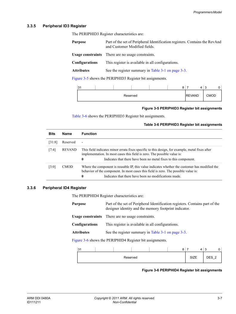
The PERIPHID3 Register characteristics are:
Purpose Part of the set of Peripheral Identification registers. Contains the RevAnd and Customer Modified fields.
Usage constraints There are no usage constraints.
Configurations This register is available in all configurations.
Attributes See the register summary in Table 3-1 on page 3-3.
Figure 3-5 shows the PERIPHID3 Register bit assignments.
Figure 3-5 PERIPHID3 Register bit assignments
Table 3-6 shows the PERIPHID3 Register bit assignments.
3.3.6 Peripheral ID4 Register
The PERIPHID4 Register characteristics are:
Purpose Part of the set of Peripheral Identification registers. Contains part of the designer identity and the memory footprint indicator.
Usage constraints There are no usage constraints.
Configurations This register is available in all configurations.
Attributes See the register summary in Table 3-1 on page 3-3.
Figure 3-6 shows the PERIPHID4 Register bit assignments.
Figure 3-6 PERIPHID4 Register bit assignments
31 8 7 4 3 0
CMODREVANDReserved
Table 3-6 PERIPHID3 Register bit assignments
Bits Name Function
[31:8] Reserved -
[7:4] REVAND This field indicates minor errata fixes specific to this design, for example, metal fixes after implementation. In most cases this field is zero. The possible value is:0 Indicates that there have been no metal fixes to this component.
[3:0] CMOD Where the component is reusable IP, this value indicates whether the customer has modified the behavior of the component. In most cases this field is zero. The possible value is:0 Indicates that there have been no modifications made.
31 8 7 4 3 0
DES_2SIZEReserved
ARM DDI 0480A Copyright © 2011 ARM. All rights reserved. 3-7ID111211 Non-Confidential
Programmers Model
Table 3-7 shows the PERIPHID4 Register bit assignments.
3.3.7 Peripheral ID5-7 Register
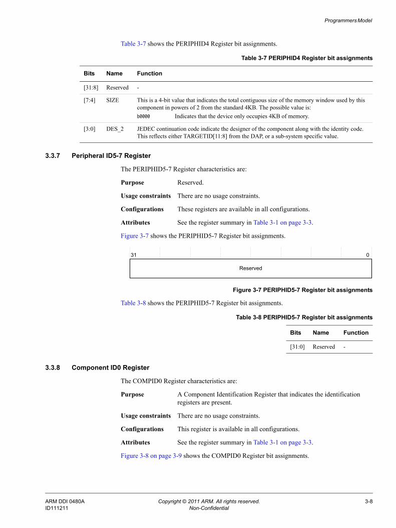
The PERIPHID5-7 Register characteristics are:
Purpose Reserved.
Usage constraints There are no usage constraints.
Configurations These registers are available in all configurations.
Attributes See the register summary in Table 3-1 on page 3-3.
Figure 3-7 shows the PERIPHID5-7 Register bit assignments.
Figure 3-7 PERIPHID5-7 Register bit assignments
Table 3-8 shows the PERIPHID5-7 Register bit assignments.
3.3.8 Component ID0 Register
The COMPID0 Register characteristics are:
Purpose A Component Identification Register that indicates the identification registers are present.
Usage constraints There are no usage constraints.
Configurations This register is available in all configurations.
Attributes See the register summary in Table 3-1 on page 3-3.
Figure 3-8 on page 3-9 shows the COMPID0 Register bit assignments.
Table 3-7 PERIPHID4 Register bit assignments
Bits Name Function
[31:8] Reserved -
[7:4] SIZE This is a 4-bit value that indicates the total contiguous size of the memory window used by this component in powers of 2 from the standard 4KB. The possible value is:b0000 Indicates that the device only occupies 4KB of memory.
[3:0] DES_2 JEDEC continuation code indicate the designer of the component along with the identity code. This reflects either TARGETID[11:8] from the DAP, or a sub-system specific value.
31 0
Reserved
Table 3-8 PERIPHID5-7 Register bit assignments
Bits Name Function
[31:0] Reserved -
ARM DDI 0480A Copyright © 2011 ARM. All rights reserved. 3-8ID111211 Non-Confidential
Programmers Model
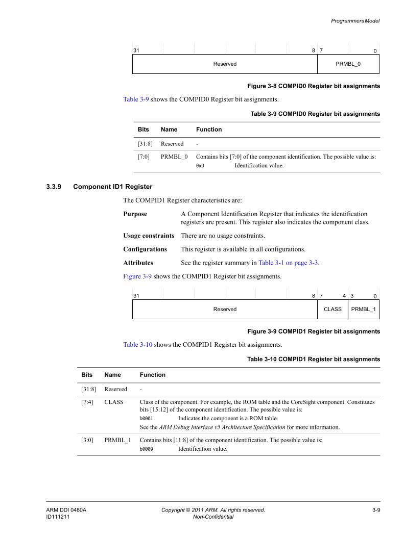
Figure 3-8 COMPID0 Register bit assignments
Table 3-9 shows the COMPID0 Register bit assignments.
3.3.9 Component ID1 Register
The COMPID1 Register characteristics are:
Purpose A Component Identification Register that indicates the identification registers are present. This register also indicates the component class.
Usage constraints There are no usage constraints.
Configurations This register is available in all configurations.
Attributes See the register summary in Table 3-1 on page 3-3.
Figure 3-9 shows the COMPID1 Register bit assignments.
Figure 3-9 COMPID1 Register bit assignments
Table 3-10 shows the COMPID1 Register bit assignments.
31 0
Reserved
78
PRMBL_0
Table 3-9 COMPID0 Register bit assignments
Bits Name Function
[31:8] Reserved -
[7:0] PRMBL_0 Contains bits [7:0] of the component identification. The possible value is:0xD Identification value.
31 0
Reserved
78
PRMBL_1
4 3
CLASS
Table 3-10 COMPID1 Register bit assignments
Bits Name Function
[31:8] Reserved -
[7:4] CLASS Class of the component. For example, the ROM table and the CoreSight component. Constitutes bits [15:12] of the component identification. The possible value is:b0001 Indicates the component is a ROM table.See the ARM Debug Interface v5 Architecture Specification for more information.
[3:0] PRMBL_1 Contains bits [11:8] of the component identification. The possible value is:b0000 Identification value.
ARM DDI 0480A Copyright © 2011 ARM. All rights reserved. 3-9ID111211 Non-Confidential
Programmers Model
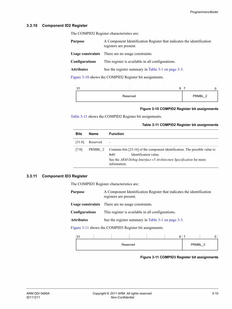
3.3.10 Component ID2 Register
The COMPID2 Register characteristics are:
Purpose A Component Identification Register that indicates the identification registers are present.
Usage constraints There are no usage constraints.
Configurations This register is available in all configurations.
Attributes See the register summary in Table 3-1 on page 3-3.
Figure 3-10 shows the COMPID2 Register bit assignments.
Figure 3-10 COMPID2 Register bit assignments
Table 3-11 shows the COMPID2 Register bit assignments.
3.3.11 Component ID3 Register
The COMPID3 Register characteristics are:
Purpose A Component Identification Register that indicates the identification registers are present.
Usage constraints There are no usage constraints.
Configurations This register is available in all configurations.
Attributes See the register summary in Table 3-1 on page 3-3.
Figure 3-11 shows the COMPID3 Register bit assignments.
Figure 3-11 COMPID3 Register bit assignments
31 0
Reserved
78
PRMBL_2
Table 3-11 COMPID2 Register bit assignments
Bits Name Function
[31:8] Reserved -
[7:0] PRMBL_2 Contains bits [23:16] of the component identification. The possible value is:0x05 Identification value.See the ARM Debug Interface v5 Architecture Specification for more information.
31 8 7 0
PRMBL_3Reserved
ARM DDI 0480A Copyright © 2011 ARM. All rights reserved. 3-10ID111211 Non-Confidential
Programmers Model
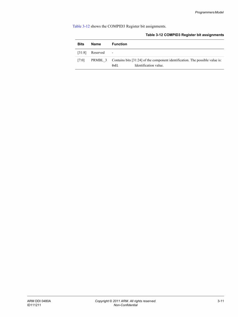
Table 3-12 shows the COMPID3 Register bit assignments.
Table 3-12 COMPID3 Register bit assignments
Bits Name Function
[31:8] Reserved -
[7:0] PRMBL_3 Contains bits [31:24] of the component identification. The possible value is:0xB1 Identification value.
ARM DDI 0480A Copyright © 2011 ARM. All rights reserved. 3-11ID111211 Non-Confidential
Programmers Model
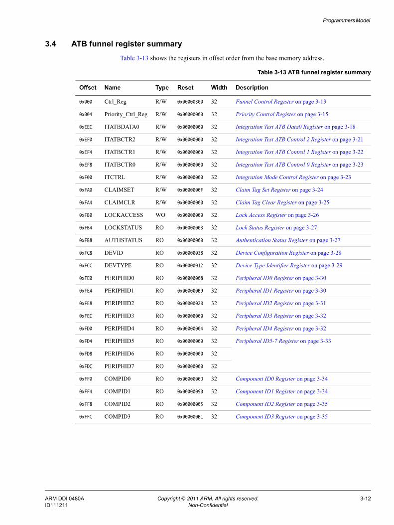
3.4 ATB funnel register summaryTable 3-13 shows the registers in offset order from the base memory address.
Table 3-13 ATB funnel register summary
Offset Name Type Reset Width Description
0x000 Ctrl_Reg R/W 0x00000300 32 Funnel Control Register on page 3-13
0x004 Priority_Ctrl_Reg R/W 0x00000000 32 Priority Control Register on page 3-15
0xEEC ITATBDATA0 R/W 0x00000000 32 Integration Test ATB Data0 Register on page 3-18
0xEF0 ITATBCTR2 R/W 0x00000000 32 Integration Test ATB Control 2 Register on page 3-21
0xEF4 ITATBCTR1 R/W 0x00000000 32 Integration Test ATB Control 1 Register on page 3-22
0xEF8 ITATBCTR0 R/W 0x00000000 32 Integration Test ATB Control 0 Register on page 3-23
0xF00 ITCTRL R/W 0x00000000 32 Integration Mode Control Register on page 3-23
0xFA0 CLAIMSET R/W 0x0000000F 32 Claim Tag Set Register on page 3-24
0xFA4 CLAIMCLR R/W 0x00000000 32 Claim Tag Clear Register on page 3-25
0xFB0 LOCKACCESS WO 0x00000000 32 Lock Access Register on page 3-26
0xFB4 LOCKSTATUS RO 0x00000003 32 Lock Status Register on page 3-27
0xFB8 AUTHSTATUS RO 0x00000000 32 Authentication Status Register on page 3-27
0xFC8 DEVID RO 0x00000038 32 Device Configuration Register on page 3-28
0xFCC DEVTYPE RO 0x00000012 32 Device Type Identifier Register on page 3-29
0xFE0 PERIPHID0 RO 0x00000008 32 Peripheral ID0 Register on page 3-30
0xFE4 PERIPHID1 RO 0x000000B9 32 Peripheral ID1 Register on page 3-30
0xFE8 PERIPHID2 RO 0x0000002B 32 Peripheral ID2 Register on page 3-31
0xFEC PERIPHID3 RO 0x00000000 32 Peripheral ID3 Register on page 3-32
0xFD0 PERIPHID4 RO 0x00000004 32 Peripheral ID4 Register on page 3-32
0xFD4 PERIPHID5 RO 0x00000000 32 Peripheral ID5-7 Register on page 3-33
0xFD8 PERIPHID6 RO 0x00000000 32
0xFDC PERIPHID7 RO 0x00000000 32
0xFF0 COMPID0 RO 0x0000000D 32 Component ID0 Register on page 3-34
0xFF4 COMPID1 RO 0x00000090 32 Component ID1 Register on page 3-34
0xFF8 COMPID2 RO 0x00000005 32 Component ID2 Register on page 3-35
0xFFC COMPID3 RO 0x000000B1 32 Component ID3 Register on page 3-35
ARM DDI 0480A Copyright © 2011 ARM. All rights reserved. 3-12ID111211 Non-Confidential
Programmers Model
3.5 ATB funnel register descriptionsThis section describes the CXATBFUNNEL registers. Table 3-13 on page 3-12 provides cross-references to individual registers.
The registers are only present if the APB programming interface has been chosen.
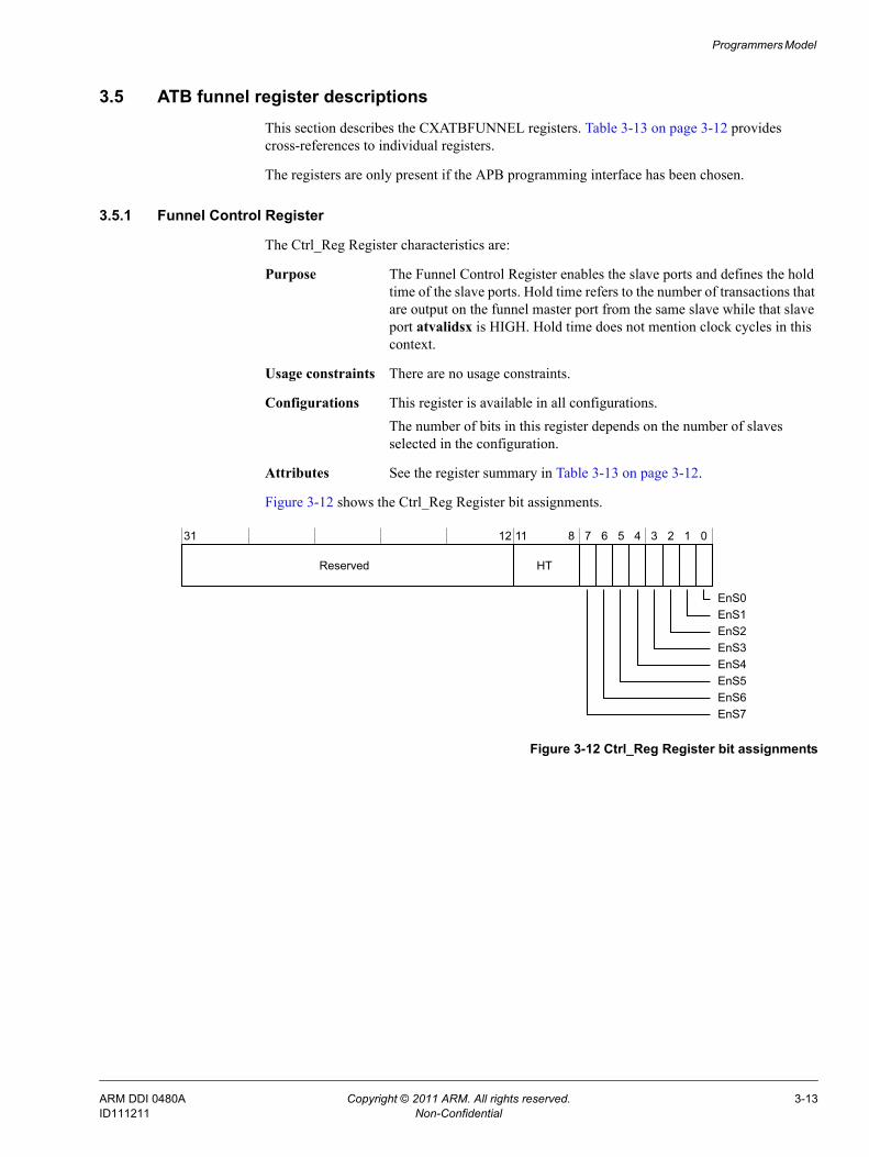
3.5.1 Funnel Control Register
The Ctrl_Reg Register characteristics are:
Purpose The Funnel Control Register enables the slave ports and defines the hold time of the slave ports. Hold time refers to the number of transactions that are output on the funnel master port from the same slave while that slave port atvalidsx is HIGH. Hold time does not mention clock cycles in this context.
Usage constraints There are no usage constraints.
Configurations This register is available in all configurations.The number of bits in this register depends on the number of slaves selected in the configuration.
Attributes See the register summary in Table 3-13 on page 3-12.
Figure 3-12 shows the Ctrl_Reg Register bit assignments.
Figure 3-12 Ctrl_Reg Register bit assignments
31 12 11 8 7 6 5 4 3 2 1 0
HTReserved
EnS2EnS1EnS0
EnS3EnS4
EnS7EnS6EnS5
ARM DDI 0480A Copyright © 2011 ARM. All rights reserved. 3-13ID111211 Non-Confidential
Programmers Model
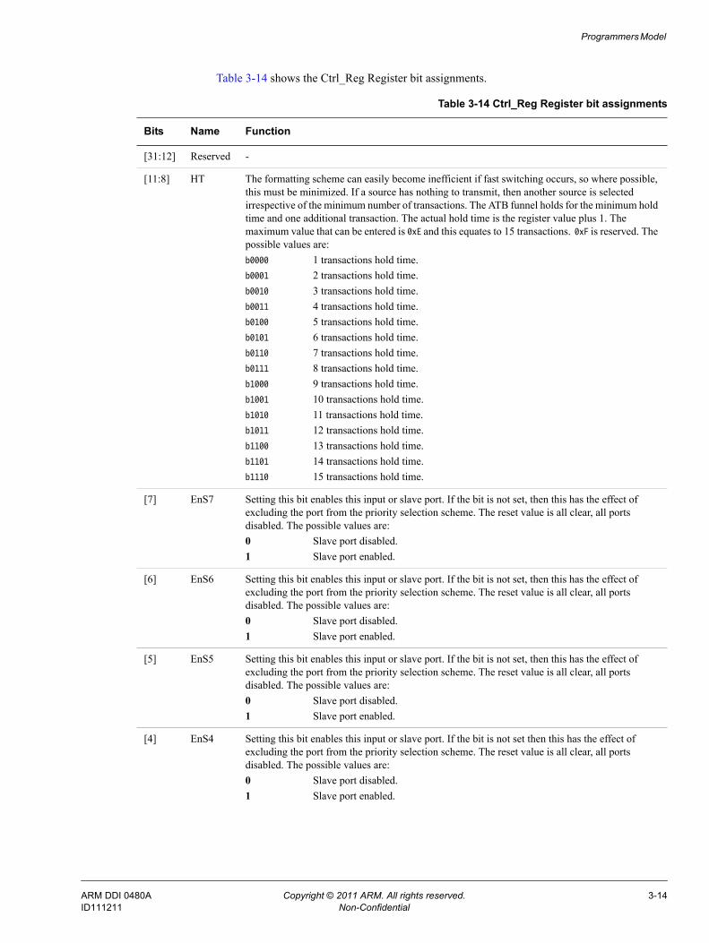
Table 3-14 shows the Ctrl_Reg Register bit assignments.
Table 3-14 Ctrl_Reg Register bit assignments
Bits Name Function
[31:12] Reserved -
[11:8] HT The formatting scheme can easily become inefficient if fast switching occurs, so where possible, this must be minimized. If a source has nothing to transmit, then another source is selected irrespective of the minimum number of transactions. The ATB funnel holds for the minimum hold time and one additional transaction. The actual hold time is the register value plus 1. The maximum value that can be entered is 0xE and this equates to 15 transactions. 0xF is reserved. The possible values are:b0000 1 transactions hold time.b0001 2 transactions hold time.b0010 3 transactions hold time.b0011 4 transactions hold time.b0100 5 transactions hold time.b0101 6 transactions hold time.b0110 7 transactions hold time.b0111 8 transactions hold time.b1000 9 transactions hold time.b1001 10 transactions hold time.b1010 11 transactions hold time.b1011 12 transactions hold time.b1100 13 transactions hold time.b1101 14 transactions hold time.b1110 15 transactions hold time.
[7] EnS7 Setting this bit enables this input or slave port. If the bit is not set, then this has the effect of excluding the port from the priority selection scheme. The reset value is all clear, all ports disabled. The possible values are:0 Slave port disabled.1 Slave port enabled.
[6] EnS6 Setting this bit enables this input or slave port. If the bit is not set, then this has the effect of excluding the port from the priority selection scheme. The reset value is all clear, all ports disabled. The possible values are:0 Slave port disabled.1 Slave port enabled.
[5] EnS5 Setting this bit enables this input or slave port. If the bit is not set, then this has the effect of excluding the port from the priority selection scheme. The reset value is all clear, all ports disabled. The possible values are:0 Slave port disabled.1 Slave port enabled.
[4] EnS4 Setting this bit enables this input or slave port. If the bit is not set then this has the effect of excluding the port from the priority selection scheme. The reset value is all clear, all ports disabled. The possible values are:0 Slave port disabled.1 Slave port enabled.
ARM DDI 0480A Copyright © 2011 ARM. All rights reserved. 3-14ID111211 Non-Confidential
Programmers Model
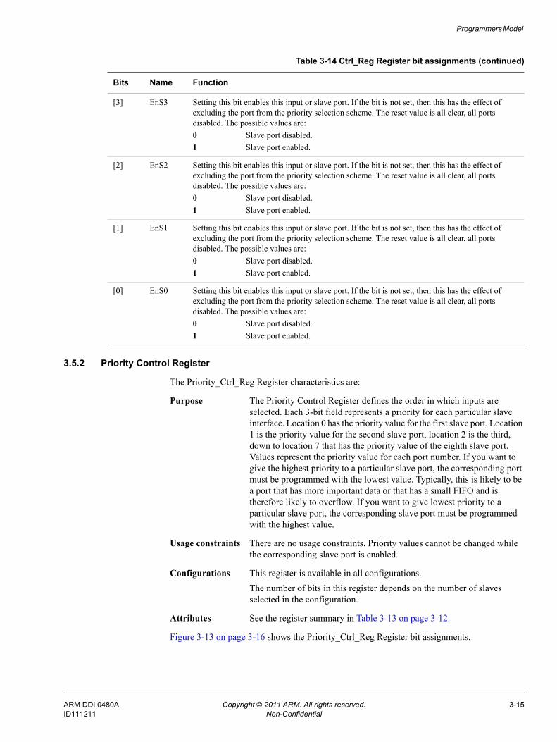
3.5.2 Priority Control Register
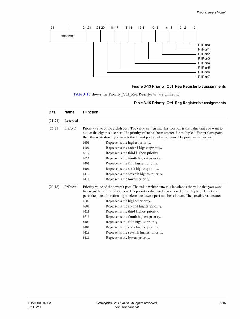
The Priority_Ctrl_Reg Register characteristics are:
Purpose The Priority Control Register defines the order in which inputs are selected. Each 3-bit field represents a priority for each particular slave interface. Location 0 has the priority value for the first slave port. Location 1 is the priority value for the second slave port, location 2 is the third, down to location 7 that has the priority value of the eighth slave port. Values represent the priority value for each port number. If you want to give the highest priority to a particular slave port, the corresponding port must be programmed with the lowest value. Typically, this is likely to be a port that has more important data or that has a small FIFO and is therefore likely to overflow. If you want to give lowest priority to a particular slave port, the corresponding slave port must be programmed with the highest value.
Usage constraints There are no usage constraints. Priority values cannot be changed while the corresponding slave port is enabled.
Configurations This register is available in all configurations.The number of bits in this register depends on the number of slaves selected in the configuration.
Attributes See the register summary in Table 3-13 on page 3-12.
Figure 3-13 on page 3-16 shows the Priority_Ctrl_Reg Register bit assignments.
[3] EnS3 Setting this bit enables this input or slave port. If the bit is not set, then this has the effect of excluding the port from the priority selection scheme. The reset value is all clear, all ports disabled. The possible values are:0 Slave port disabled.1 Slave port enabled.
[2] EnS2 Setting this bit enables this input or slave port. If the bit is not set, then this has the effect of excluding the port from the priority selection scheme. The reset value is all clear, all ports disabled. The possible values are:0 Slave port disabled.1 Slave port enabled.
[1] EnS1 Setting this bit enables this input or slave port. If the bit is not set, then this has the effect of excluding the port from the priority selection scheme. The reset value is all clear, all ports disabled. The possible values are:0 Slave port disabled.1 Slave port enabled.
[0] EnS0 Setting this bit enables this input or slave port. If the bit is not set, then this has the effect of excluding the port from the priority selection scheme. The reset value is all clear, all ports disabled. The possible values are:0 Slave port disabled.1 Slave port enabled.
Table 3-14 Ctrl_Reg Register bit assignments (continued)
Bits Name Function
ARM DDI 0480A Copyright © 2011 ARM. All rights reserved. 3-15ID111211 Non-Confidential
Programmers Model
Figure 3-13 Priority_Ctrl_Reg Register bit assignments
Table 3-15 shows the Priority_Ctrl_Reg Register bit assignments.
31 24 23 21 20 18 17 15 14 12 11 9 8 6 5 3 2 0
Reserved
PriPort2PriPort1PriPort0
PriPort3PriPort4
PriPort7PriPort6PriPort5
Table 3-15 Priority_Ctrl_Reg Register bit assignments
Bits Name Function
[31:24] Reserved -
[23:21] PriPort7 Priority value of the eighth port. The value written into this location is the value that you want to assign the eighth slave port. If a priority value has been entered for multiple different slave ports then the arbitration logic selects the lowest port number of them. The possible values are:b000 Represents the highest priority.b001 Represents the second highest priority.b010 Represents the third highest priority.b011 Represents the fourth highest priority.b100 Represents the fifth highest priority.b101 Represents the sixth highest priority.b110 Represents the seventh highest priority.b111 Represents the lowest priority.
[20:18] PriPort6 Priority value of the seventh port. The value written into this location is the value that you want to assign the seventh slave port. If a priority value has been entered for multiple different slave ports then the arbitration logic selects the lowest port number of them. The possible values are:b000 Represents the highest priority.b001 Represents the second highest priority.b010 Represents the third highest priority.b011 Represents the fourth highest priority.b100 Represents the fifth highest priority.b101 Represents the sixth highest priority.b110 Represents the seventh highest priority.b111 Represents the lowest priority.
ARM DDI 0480A Copyright © 2011 ARM. All rights reserved. 3-16ID111211 Non-Confidential
Programmers Model
[17:15] PriPort5 Priority value of the sixth port. The value written into this location is the value that you want to assign the sixth slave port. If a priority value has been entered for multiple different slave ports then the arbitration logic selects the lowest port number of them. The possible values are:b000 Represents the highest priority.b001 Represents the second highest priority.b010 Represents the third highest priority.b011 Represents the fourth highest priority.b100 Represents the fifth highest priority.b101 Represents the sixth highest priority.b110 Represents the seventh highest priority.b111 Represents the lowest priority.
[14:12] PriPort4 Priority value of the fifth port. The value written into this location is the value that you want to assign the fifth slave port. If a priority value has been entered for multiple different slave ports then the arbitration logic selects the lowest port number of them. The possible values are:b000 Represents the highest priority.b001 Represents the second highest priority.b010 Represents the third highest priority.b011 Represents the fourth highest priority.b100 Represents the fifth highest priority.b101 Represents the sixth highest priority.b110 Represents the seventh highest priority.b111 Represents the lowest priority.
[11:9] PriPort3 Priority value of the fourth port.The value written into this location is the value that you want to assign the fourth slave port. If a priority value has been entered for multiple different slave ports then the arbitration logic selects the lowest port number of them. The possible values are:b000 Represents the highest priority.b001 Represents the second highest priority.b010 Represents the third highest priority.b011 Represents the fourth highest priority.b100 Represents the fifth highest priority.b101 Represents the sixth highest priority.b110 Represents the seventh highest priority.b111 Represents the lowest priority.
Table 3-15 Priority_Ctrl_Reg Register bit assignments (continued)
Bits Name Function
ARM DDI 0480A Copyright © 2011 ARM. All rights reserved. 3-17ID111211 Non-Confidential
Programmers Model
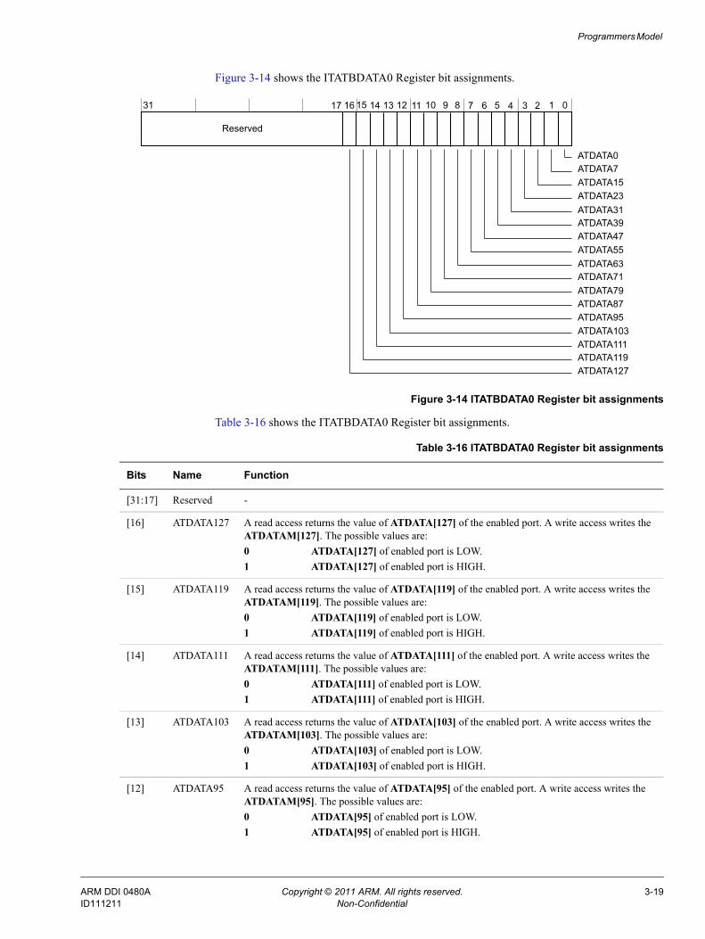
3.5.3 Integration Test ATB Data0 Register
The ITATBDATA0 Register characteristics are:
Purpose The Integration Test ATB Data 0 Register performs different functions depending on whether the access is a read or a write. A write outputs data on byte boundaries of ATDATAM. A read returns the data from ATDATASn, where n is defined by the status of the Funnel Control register at 0x000. The read data is only valid when ATVALIDSn is HIGH.
Usage constraints There are no usage constraints.
Configurations This register is available in all configurations.
Attributes See the register summary in Table 3-13 on page 3-12.
[8:6] PriPort2 Priority value of the third port. The value written into this location is the value that you want to assign the third slave port. If a priority value has been entered for multiple different slave ports then the arbitration logic selects the lowest port number of them. The possible values are:b000 Represents the highest priority.b001 Represents the second highest priority.b010 Represents the third highest priority.b011 Represents the fourth highest priority.b100 Represents the fifth highest priority.b101 Represents the sixth highest priority.b110 Represents the seventh highest priority.b111 Represents the lowest priority.
[5:3] PriPort1 Priority value of the second port. The value written into this location is the value that you want to assign the second slave port. If a priority value has been entered for multiple different slave ports then the arbitration logic selects the lowest port number of them. The possible values are:b000 Represents the highest priority.b001 Represents the second highest priority.b010 Represents the third highest priority.b011 Represents the fourth highest priority.b100 Represents the fifth highest priority.b101 Represents the sixth highest priority.b110 Represents the seventh highest priority.b111 Represents the lowest priority.
[2:0] PriPort0 Priority value of the first slave port. The value written into this location is the value that you want to assign the first slave port.The value written into this location is the value that you want to assign the first slave port. If a priority value has been entered for multiple different slave ports then the arbitration logic selects the lowest port number of them. The possible values are:b000 Represents the highest priority.b001 Represents the second highest priority.b010 Represents the third highest priority.b011 Represents the fourth highest priority.b100 Represents the fifth highest priority.b101 Represents the sixth highest priority.b110 Represents the seventh highest priority.b111 Represents the lowest priority.
Table 3-15 Priority_Ctrl_Reg Register bit assignments (continued)
Bits Name Function
ARM DDI 0480A Copyright © 2011 ARM. All rights reserved. 3-18ID111211 Non-Confidential
Programmers Model
Figure 3-14 shows the ITATBDATA0 Register bit assignments.
Figure 3-14 ITATBDATA0 Register bit assignments
Table 3-16 shows the ITATBDATA0 Register bit assignments.
31 12 10 89 5 46 1 0
Reserved
15 14 13
ATDATA87
237111617
ATDATA0ATDATA7ATDATA15ATDATA23ATDATA31ATDATA39ATDATA47ATDATA55ATDATA63ATDATA71ATDATA79
ATDATA95ATDATA103ATDATA111ATDATA119ATDATA127
Table 3-16 ITATBDATA0 Register bit assignments
Bits Name Function
[31:17] Reserved -
[16] ATDATA127 A read access returns the value of ATDATA[127] of the enabled port. A write access writes the ATDATAM[127]. The possible values are:0 ATDATA[127] of enabled port is LOW.1 ATDATA[127] of enabled port is HIGH.
[15] ATDATA119 A read access returns the value of ATDATA[119] of the enabled port. A write access writes the ATDATAM[119]. The possible values are:0 ATDATA[119] of enabled port is LOW.1 ATDATA[119] of enabled port is HIGH.
[14] ATDATA111 A read access returns the value of ATDATA[111] of the enabled port. A write access writes the ATDATAM[111]. The possible values are:0 ATDATA[111] of enabled port is LOW.1 ATDATA[111] of enabled port is HIGH.
[13] ATDATA103 A read access returns the value of ATDATA[103] of the enabled port. A write access writes the ATDATAM[103]. The possible values are:0 ATDATA[103] of enabled port is LOW.1 ATDATA[103] of enabled port is HIGH.
[12] ATDATA95 A read access returns the value of ATDATA[95] of the enabled port. A write access writes the ATDATAM[95]. The possible values are:0 ATDATA[95] of enabled port is LOW.1 ATDATA[95] of enabled port is HIGH.
ARM DDI 0480A Copyright © 2011 ARM. All rights reserved. 3-19ID111211 Non-Confidential
Programmers Model
[11] ATDATA87 A read access returns the value of ATDATA[87] of the enabled port. A write access writes the ATDATAM[87]. The possible values are:0 ATDATA[87] of enabled port is LOW.1 ATDATA[87] of enabled port is HIGH.
[10] ATDATA79 A read access returns the value of ATDATA[79] of the enabled port. A write access writes the ATDATAM[79]. The possible values are:0 ATDATA[79] of enabled port is LOW.1 ATDATA[79] of enabled port is HIGH.
[9] ATDATA71 A read access returns the value of ATDATA[71] of the enabled port. A write access writes the ATDATAM[71]. The possible values are:0 ATDATA[71] of enabled port is LOW.1 ATDATA[71] of enabled port is HIGH.
[8] ATDATA63 A read access returns the value of ATDATA[63] of the enabled port. A write access writes the ATDATAM[63]. The possible values are:0 ATDATA[63] of enabled port is LOW.1 ATDATA[63] of enabled port is HIGH.
[7] ATDATA55 A read access returns the value of ATDATA[55] of the enabled port. A write access writes the ATDATAM[55]. The possible values are:0 ATDATA[55] of enabled port is LOW.1 ATDATA[55] of enabled port is HIGH.
[6] ATDATA47 A read access returns the value of ATDATA[47] of the enabled port. A write access writes the ATDATAM[47]. The possible values are:0 ATDATA[47] of enabled port is LOW.1 ATDATA[47] of enabled port is HIGH.
[5] ATDATA39 A read access returns the value of ATDATA[39] of the enabled port. A write access writes the ATDATAM[39]. The possible values are:0 ATDATA[39] of enabled port is LOW.1 ATDATA[39] of enabled port is HIGH.
[4] ATDATA31 A read access returns the value of ATDATA[31] of the enabled port. A write access writes the ATDATAM[31]. The possible values are:0 ATDATA[31] of enabled port is LOW.1 ATDATA[31] of enabled port is HIGH.
[3] ATDATA23 A read access returns the value of ATDATA[23] of the enabled port. A write access writes the ATDATAM[23]. The possible values are:0 ATDATA[23] of enabled port is LOW.1 ATDATA[23] of enabled port is HIGH.
Table 3-16 ITATBDATA0 Register bit assignments (continued)
Bits Name Function
ARM DDI 0480A Copyright © 2011 ARM. All rights reserved. 3-20ID111211 Non-Confidential
Programmers Model
3.5.4 Integration Test ATB Control 2 Register
The ITATBCTR2 Register characteristics are:
Purpose The Integration Test ATB Control 2 Register performs different functions depending on whether the access is a read or a write:• a write outputs data on atreadysn and afvalidsn, where n is defined
by the status of the ATB Funnel Control Register at 0x000• a read returns the data from atreadym and afvalidm.
Usage constraints There are no usage constraints.
Configurations This register is available in all configurations.
Attributes See the register summary in Table 3-13 on page 3-12.
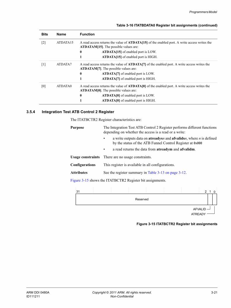
Figure 3-15 shows the ITATBCTR2 Register bit assignments.
Figure 3-15 ITATBCTR2 Register bit assignments
[2] ATDATA15 A read access returns the value of ATDATA[15] of the enabled port. A write access writes the ATDATAM[15]. The possible values are:0 ATDATA[15] of enabled port is LOW.1 ATDATA[15] of enabled port is HIGH.
[1] ATDATA7 A read access returns the value of ATDATA[7] of the enabled port. A write access writes the ATDATAM[7]. The possible values are:0 ATDATA[7] of enabled port is LOW.1 ATDATA[7] of enabled port is HIGH.
[0] ATDATA0 A read access returns the value of ATDATA[0] of the enabled port. A write access writes the ATDATAM[0]. The possible values are:0 ATDATA[0] of enabled port is LOW.1 ATDATA[0] of enabled port is HIGH.
Table 3-16 ITATBDATA0 Register bit assignments (continued)
Bits Name Function
31 0
Reserved
AFVALID
2 1
ATREADY
ARM DDI 0480A Copyright © 2011 ARM. All rights reserved. 3-21ID111211 Non-Confidential
Programmers Model
Table 3-17 shows the ITATBCTR2 Register bit assignments.
3.5.5 Integration Test ATB Control 1 Register
The ITATBCTR1 Register characteristics are:
Purpose The Integration Test ATB Control 1 Register performs different functions depending on whether the access is a read or a write: • a write sets the value of the atidm. • a read returns the value of the atidsn signals, where n is defined by
the status of the Control register at 0x000.The read data is only valid when ATVALIDSn is HIGH.
Usage constraints There are no usage constraints.
Configurations This register is available in all configurations.
Attributes See the register summary in Table 3-13 on page 3-12.
Figure 3-16 shows the ITATBCTR1 Register bit assignments.
Figure 3-16 ITATBCTR1 Register bit assignments
Table 3-18 shows the ITATBCTR1 Register bit assignments.
Table 3-17 ITATBCTR2 Register bit assignments
Bits Name Function
[31:2] Reserved -
[1] AFVALID A read access returns the value of afvalidm, and a write access outputs the data on afvalidsn, where n is defined by the status of the ATB Funnel Control Register at 0x000.0 Pin is at logic 0.1 Pin is at logic 1.
[0] ATREADY A read access returns the value of atreadym, and a write access outputs the data on atreadysn, where n is defined by the status of the ATB Funnel Control Register at 0x000.0 Pin is at logic 0.1 Pin is at logic 1.
31 0
Reserved
7 6
ATID
Table 3-18 ITATBCTR1 Register bit assignments
Bits Name Function
[31:7] Reserved -
[6:0] ATID A read returns the value of the atidsn signals where n is defined by the status of the Control register at 0x000.A write returns the value on atidm.
ARM DDI 0480A Copyright © 2011 ARM. All rights reserved. 3-22ID111211 Non-Confidential
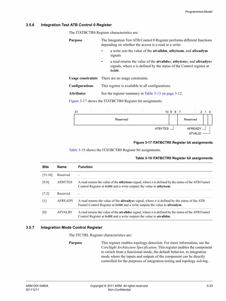
Programmers Model
3.5.6 Integration Test ATB Control 0 Register
The ITATBCTR0 Register characteristics are:
Purpose The Integration Test ATB Control 0 Register performs different functions depending on whether the access is a read or a write: • a write sets the value of the atvalidm, atbytesm, and afreadym
signals• a read returns the value of the atvalidsn, atbytessn, and afreadysn
signals, where n is defined by the status of the Control register at 0x000.
Usage constraints There are no usage constraints.
Configurations This register is available in all configurations.
Attributes See the register summary in Table 3-13 on page 3-12.
Figure 3-17 shows the ITATBCTR0 Register bit assignments.
Figure 3-17 ITATBCTR0 Register bit assignments
Table 3-19 shows the ITATBCTR0 Register bit assignments.
3.5.7 Integration Mode Control Register
The ITCTRL Register characteristics are:
Purpose This register enables topology-detection. For more information, see the CoreSight Architecture Specification. This register enables the component to switch from a functional mode, the default behavior, to integration mode where the inputs and outputs of the component can be directly controlled for the purposes of integration testing and topology solving.
31 0
Reserved
7 2
Reserved
10 9 8 1
ATVALIDAFREADYATBYTES
Table 3-19 ITATBCTR0 Register bit assignments
Bits Name Function
[31:10] Reserved -
[9:8] ATBYTES A read returns the value of the atbytessn signal, where n is defined by the status of the ATB Funnel Control Register at 0x000 and a write outputs the value to atbytesm.
[7:2] Reserved -
[1] AFREADY A read returns the value of the afreadysn signal, where n is defined by the status of the ATB Funnel Control Register at 0x000 and a write outputs the value to afreadym.
[0] ATVALID A read returns the value of the atvalidsn signal, where n is defined by the status of the ATB Funnel Control Register at 0x000 and a write outputs the value to atvalidm.
ARM DDI 0480A Copyright © 2011 ARM. All rights reserved. 3-23ID111211 Non-Confidential
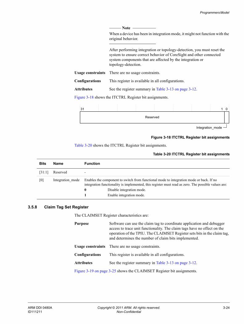
Programmers Model
Note When a device has been in integration mode, it might not function with the
original behavior.
After performing integration or topology-detection, you must reset the system to ensure correct behavior of CoreSight and other connected system components that are affected by the integration or topology-detection.
Usage constraints There are no usage constraints.
Configurations This register is available in all configurations.
Attributes See the register summary in Table 3-13 on page 3-12.
Figure 3-18 shows the ITCTRL Register bit assignments.
Figure 3-18 ITCTRL Register bit assignments
Table 3-20 shows the ITCTRL Register bit assignments.
3.5.8 Claim Tag Set Register
The CLAIMSET Register characteristics are:
Purpose Software can use the claim tag to coordinate application and debugger access to trace unit functionality. The claim tags have no effect on the operation of the TPIU. The CLAIMSET Register sets bits in the claim tag, and determines the number of claim bits implemented.
Usage constraints There are no usage constraints.
Configurations This register is available in all configurations.
Attributes See the register summary in Table 3-13 on page 3-12.
Figure 3-19 on page 3-25 shows the CLAIMSET Register bit assignments.
31 0
Reserved
1
Integration_mode
Table 3-20 ITCTRL Register bit assignments
Bits Name Function
[31:1] Reserved -
[0] Integration_mode Enables the component to switch from functional mode to integration mode or back. If no integration functionality is implemented, this register must read as zero. The possible values are:0 Disable integration mode.1 Enable integration mode.
ARM DDI 0480A Copyright © 2011 ARM. All rights reserved. 3-24ID111211 Non-Confidential
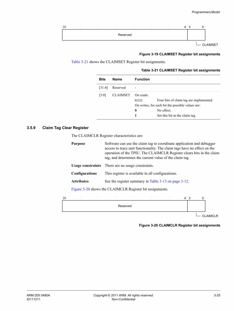
Programmers Model
Figure 3-19 CLAIMSET Register bit assignments
Table 3-21 shows the CLAIMSET Register bit assignments.
3.5.9 Claim Tag Clear Register
The CLAIMCLR Register characteristics are:
Purpose Software can use the claim tag to coordinate application and debugger access to trace unit functionality. The claim tags have no effect on the operation of the TPIU. The CLAIMCLR Register clears bits in the claim tag, and determines the current value of the claim tag.
Usage constraints There are no usage constraints.
Configurations This register is available in all configurations.
Attributes See the register summary in Table 3-13 on page 3-12.
Figure 3-20 shows the CLAIMCLR Register bit assignments.
Figure 3-20 CLAIMCLR Register bit assignments
31 4 3 0
CLAIMSET
Reserved
Table 3-21 CLAIMSET Register bit assignments
Bits Name Function
[31:4] Reserved -
[3:0] CLAIMSET On reads:b1111 Four bits of claim tag are implemented.On writes, for each bit the possible values are:0 No effect.1 Set this bit in the claim tag.
31 4 3 0
CLAIMCLR
Reserved
ARM DDI 0480A Copyright © 2011 ARM. All rights reserved. 3-25ID111211 Non-Confidential
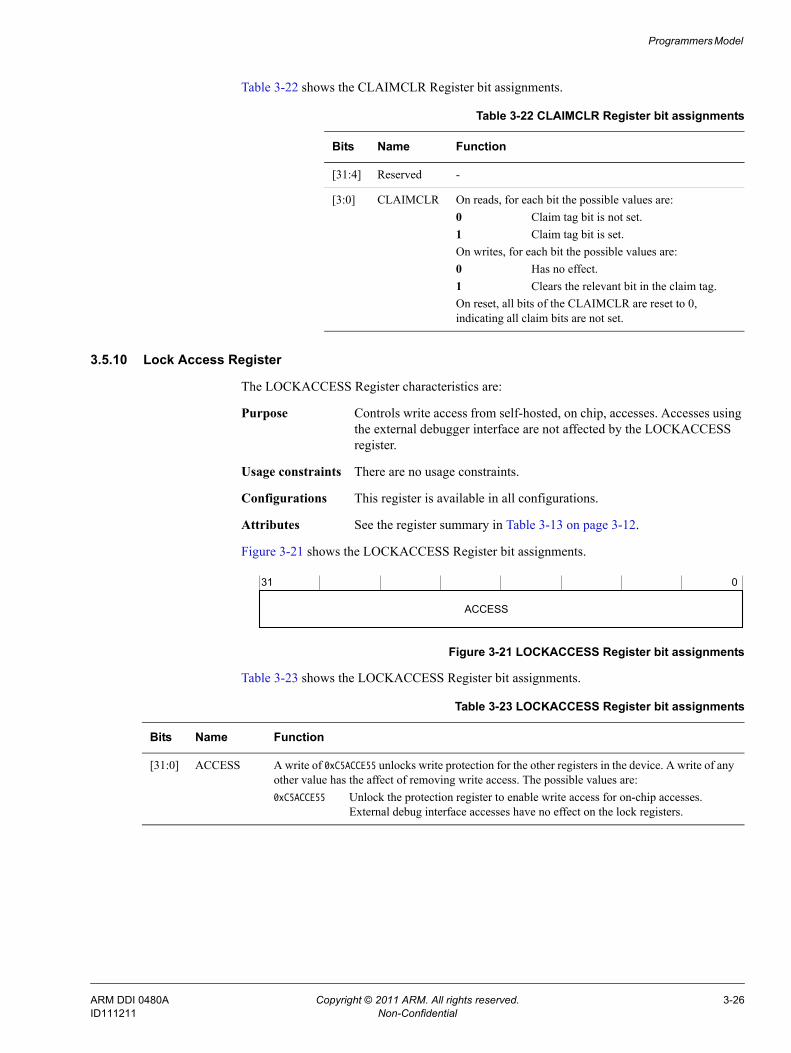
Programmers Model
Table 3-22 shows the CLAIMCLR Register bit assignments.
3.5.10 Lock Access Register
The LOCKACCESS Register characteristics are:
Purpose Controls write access from self-hosted, on chip, accesses. Accesses using the external debugger interface are not affected by the LOCKACCESS register.
Usage constraints There are no usage constraints.
Configurations This register is available in all configurations.
Attributes See the register summary in Table 3-13 on page 3-12.
Figure 3-21 shows the LOCKACCESS Register bit assignments.
Figure 3-21 LOCKACCESS Register bit assignments
Table 3-23 shows the LOCKACCESS Register bit assignments.
Table 3-22 CLAIMCLR Register bit assignments
Bits Name Function
[31:4] Reserved -
[3:0] CLAIMCLR On reads, for each bit the possible values are:0 Claim tag bit is not set.1 Claim tag bit is set.On writes, for each bit the possible values are:0 Has no effect.1 Clears the relevant bit in the claim tag.On reset, all bits of the CLAIMCLR are reset to 0, indicating all claim bits are not set.
31 0
ACCESS
Table 3-23 LOCKACCESS Register bit assignments
Bits Name Function
[31:0] ACCESS A write of 0xC5ACCE55 unlocks write protection for the other registers in the device. A write of any other value has the affect of removing write access. The possible values are:0xC5ACCE55 Unlock the protection register to enable write access for on-chip accesses.
External debug interface accesses have no effect on the lock registers.
ARM DDI 0480A Copyright © 2011 ARM. All rights reserved. 3-26ID111211 Non-Confidential
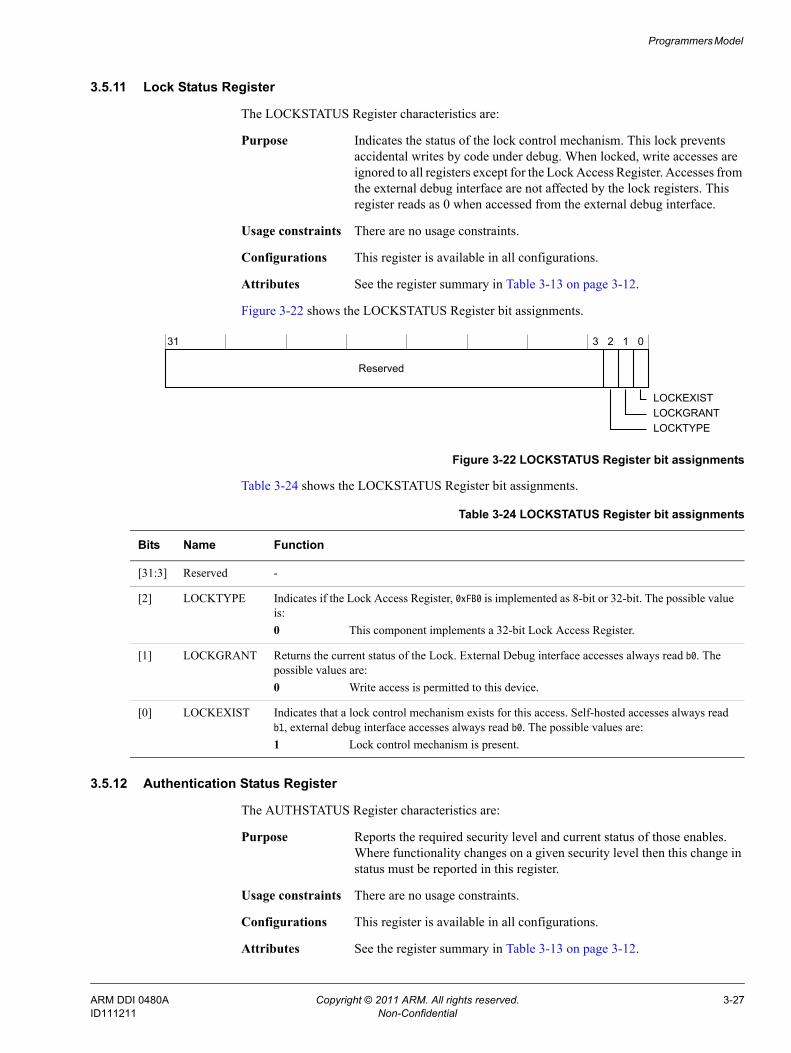
Programmers Model
3.5.11 Lock Status Register
The LOCKSTATUS Register characteristics are:
Purpose Indicates the status of the lock control mechanism. This lock prevents accidental writes by code under debug. When locked, write accesses are ignored to all registers except for the Lock Access Register. Accesses from the external debug interface are not affected by the lock registers. This register reads as 0 when accessed from the external debug interface.
Usage constraints There are no usage constraints.
Configurations This register is available in all configurations.
Attributes See the register summary in Table 3-13 on page 3-12.
Figure 3-22 shows the LOCKSTATUS Register bit assignments.
Figure 3-22 LOCKSTATUS Register bit assignments
Table 3-24 shows the LOCKSTATUS Register bit assignments.
3.5.12 Authentication Status Register
The AUTHSTATUS Register characteristics are:
Purpose Reports the required security level and current status of those enables. Where functionality changes on a given security level then this change in status must be reported in this register.
Usage constraints There are no usage constraints.
Configurations This register is available in all configurations.
Attributes See the register summary in Table 3-13 on page 3-12.
31 3 2 1 0
Reserved
LOCKTYPELOCKGRANTLOCKEXIST
Table 3-24 LOCKSTATUS Register bit assignments
Bits Name Function
[31:3] Reserved -
[2] LOCKTYPE Indicates if the Lock Access Register, 0xFB0 is implemented as 8-bit or 32-bit. The possible value is:0 This component implements a 32-bit Lock Access Register.
[1] LOCKGRANT Returns the current status of the Lock. External Debug interface accesses always read b0. The possible values are:0 Write access is permitted to this device.
[0] LOCKEXIST Indicates that a lock control mechanism exists for this access. Self-hosted accesses always read b1, external debug interface accesses always read b0. The possible values are:1 Lock control mechanism is present.
ARM DDI 0480A Copyright © 2011 ARM. All rights reserved. 3-27ID111211 Non-Confidential
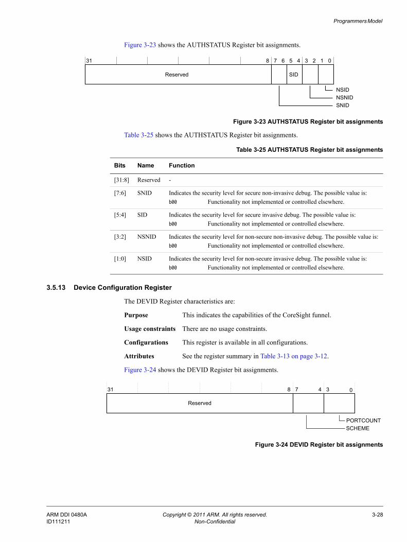
Programmers Model
Figure 3-23 shows the AUTHSTATUS Register bit assignments.
Figure 3-23 AUTHSTATUS Register bit assignments
Table 3-25 shows the AUTHSTATUS Register bit assignments.
3.5.13 Device Configuration Register
The DEVID Register characteristics are:
Purpose This indicates the capabilities of the CoreSight funnel.
Usage constraints There are no usage constraints.
Configurations This register is available in all configurations.
Attributes See the register summary in Table 3-13 on page 3-12.
Figure 3-24 shows the DEVID Register bit assignments.
Figure 3-24 DEVID Register bit assignments
31 8 7 6 5 4 3 2 1 0
SIDReserved
SNIDNSNIDNSID
Table 3-25 AUTHSTATUS Register bit assignments
Bits Name Function
[31:8] Reserved -
[7:6] SNID Indicates the security level for secure non-invasive debug. The possible value is:b00 Functionality not implemented or controlled elsewhere.
[5:4] SID Indicates the security level for secure invasive debug. The possible value is:b00 Functionality not implemented or controlled elsewhere.
[3:2] NSNID Indicates the security level for non-secure non-invasive debug. The possible value is:b00 Functionality not implemented or controlled elsewhere.
[1:0] NSID Indicates the security level for non-secure invasive debug. The possible value is:b00 Functionality not implemented or controlled elsewhere.
31 0
Reserved
7
SCHEME
8 4
PORTCOUNT
3
ARM DDI 0480A Copyright © 2011 ARM. All rights reserved. 3-28ID111211 Non-Confidential
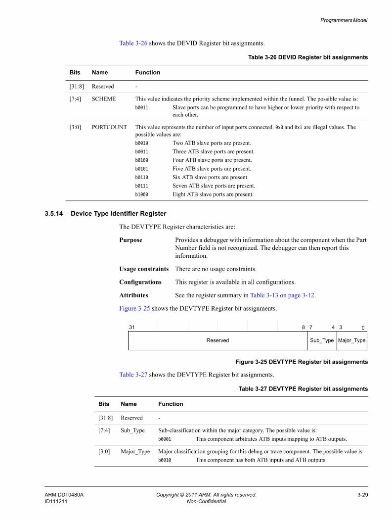
Programmers Model
Table 3-26 shows the DEVID Register bit assignments.
3.5.14 Device Type Identifier Register
The DEVTYPE Register characteristics are:
Purpose Provides a debugger with information about the component when the Part Number field is not recognized. The debugger can then report this information.
Usage constraints There are no usage constraints.
Configurations This register is available in all configurations.
Attributes See the register summary in Table 3-13 on page 3-12.
Figure 3-25 shows the DEVTYPE Register bit assignments.
Figure 3-25 DEVTYPE Register bit assignments
Table 3-27 shows the DEVTYPE Register bit assignments.
Table 3-26 DEVID Register bit assignments
Bits Name Function
[31:8] Reserved -
[7:4] SCHEME This value indicates the priority scheme implemented within the funnel. The possible value is:b0011 Slave ports can be programmed to have higher or lower priority with respect to
each other.
[3:0] PORTCOUNT This value represents the number of input ports connected. 0x0 and 0x1 are illegal values. The possible values are:b0010 Two ATB slave ports are present.b0011 Three ATB slave ports are present.b0100 Four ATB slave ports are present.b0101 Five ATB slave ports are present.b0110 Six ATB slave ports are present.b0111 Seven ATB slave ports are present.b1000 Eight ATB slave ports are present.
31 0
Reserved
7
Sub_Type
8 4
Major_Type
3
Table 3-27 DEVTYPE Register bit assignments
Bits Name Function
[31:8] Reserved -
[7:4] Sub_Type Sub-classification within the major category. The possible value is:b0001 This component arbitrates ATB inputs mapping to ATB outputs.
[3:0] Major_Type Major classification grouping for this debug or trace component. The possible value is:b0010 This component has both ATB inputs and ATB outputs.
ARM DDI 0480A Copyright © 2011 ARM. All rights reserved. 3-29ID111211 Non-Confidential
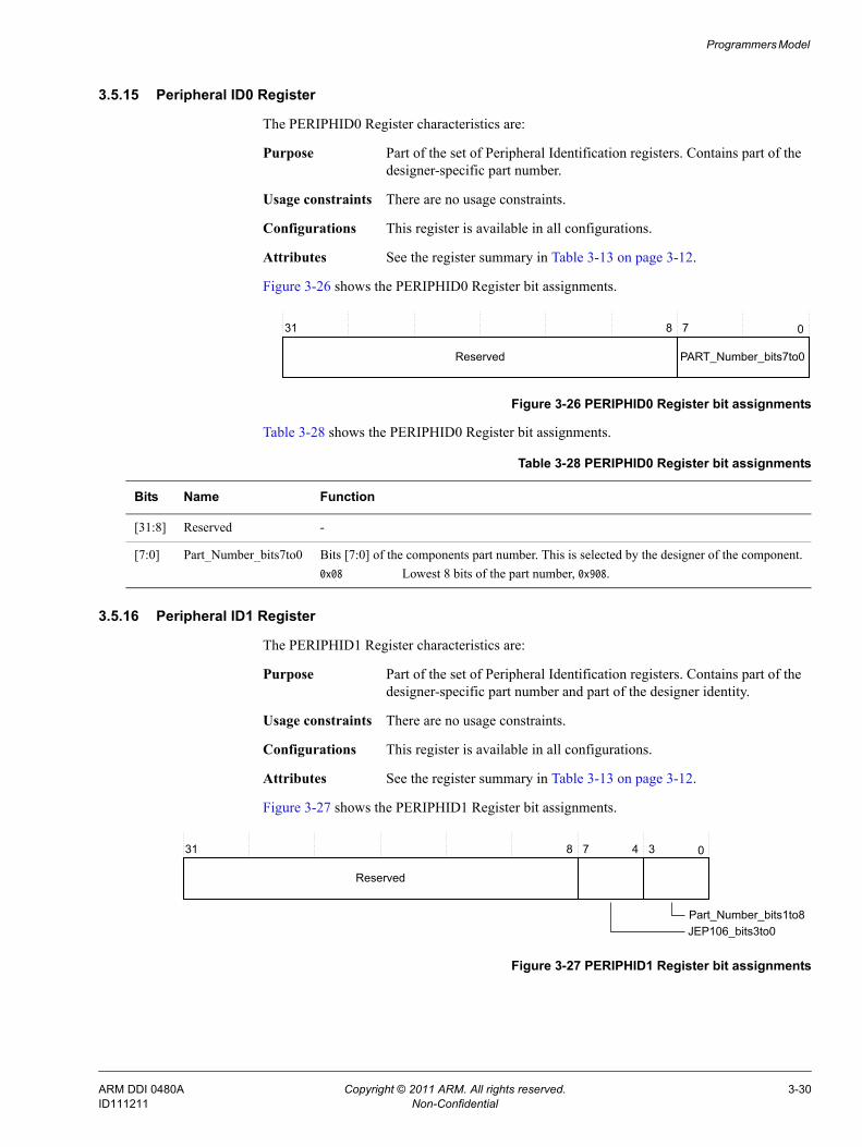
Programmers Model
3.5.15 Peripheral ID0 Register
The PERIPHID0 Register characteristics are:
Purpose Part of the set of Peripheral Identification registers. Contains part of the designer-specific part number.
Usage constraints There are no usage constraints.
Configurations This register is available in all configurations.
Attributes See the register summary in Table 3-13 on page 3-12.
Figure 3-26 shows the PERIPHID0 Register bit assignments.
Figure 3-26 PERIPHID0 Register bit assignments
Table 3-28 shows the PERIPHID0 Register bit assignments.
3.5.16 Peripheral ID1 Register
The PERIPHID1 Register characteristics are:
Purpose Part of the set of Peripheral Identification registers. Contains part of the designer-specific part number and part of the designer identity.
Usage constraints There are no usage constraints.
Configurations This register is available in all configurations.
Attributes See the register summary in Table 3-13 on page 3-12.
Figure 3-27 shows the PERIPHID1 Register bit assignments.
Figure 3-27 PERIPHID1 Register bit assignments
31 0
Reserved
78
PART_Number_bits7to0
Table 3-28 PERIPHID0 Register bit assignments
Bits Name Function
[31:8] Reserved -
[7:0] Part_Number_bits7to0 Bits [7:0] of the components part number. This is selected by the designer of the component.0x08 Lowest 8 bits of the part number, 0x908.
31 0
Reserved
78 4 3
JEP106_bits3to0Part_Number_bits1to8
ARM DDI 0480A Copyright © 2011 ARM. All rights reserved. 3-30ID111211 Non-Confidential
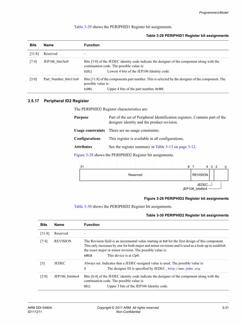
Programmers Model
Table 3-29 shows the PERIPHID1 Register bit assignments.
3.5.17 Peripheral ID2 Register
The PERIPHID2 Register characteristics are:
Purpose Part of the set of Peripheral Identification registers. Contains part of the designer identity and the product revision.
Usage constraints There are no usage constraints.
Configurations This register is available in all configurations.
Attributes See the register summary in Table 3-13 on page 3-12.
Figure 3-28 shows the PERIPHID2 Register bit assignments.
Figure 3-28 PERIPHID2 Register bit assignments
Table 3-30 shows the PERIPHID2 Register bit assignments.
Table 3-29 PERIPHID1 Register bit assignments
Bits Name Function
[31:8] Reserved -
[7:4] JEP106_bits3to0 Bits [3:0] of the JEDEC identity code indicate the designer of the component along with the continuation code. The possible value is:b1011 Lowest 4 bits of the JEP106 Identity code.
[3:0] Part_Number_bits11to8 Bits [11:8] of the components part number. This is selected by the designer of the component. The possible value is:b1001 Upper 4 bits of the part number, 0x909.
31 0
Reserved
7
REVISION
8 4 3 2
JEDECJEP106_bits6to4
Table 3-30 PERIPHID2 Register bit assignments
Bits Name Function
[31:8] Reserved -
[7:4] REVISION The Revision field is an incremental value starting at 0x0 for the first design of this component. This only increases by one for both major and minor revisions and is used as a look-up to establish the exact major or minor revision. The possible value is:b0010 This device is at r2p0.
[3] JEDEC Always set. Indicates that a JEDEC-assigned value is used. The possible value is:1 The designer ID is specified by JEDEC , http://www.jedec.org.
[2:0] JEP106_bits6to4 Bits [6:4] of the JEDEC identity code indicate the designer of the component along with the continuation code. The possible value is:b011 Upper 3 bits of the JEP106 Identity code.
ARM DDI 0480A Copyright © 2011 ARM. All rights reserved. 3-31ID111211 Non-Confidential
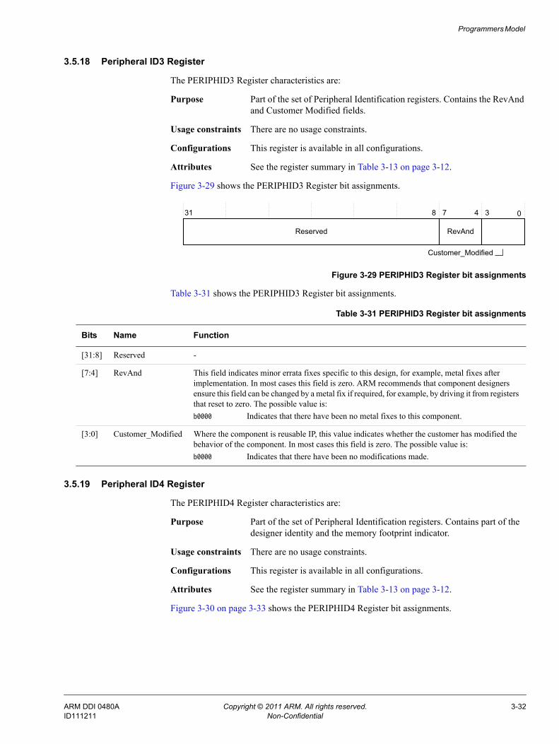
Programmers Model
3.5.18 Peripheral ID3 Register
The PERIPHID3 Register characteristics are:
Purpose Part of the set of Peripheral Identification registers. Contains the RevAnd and Customer Modified fields.
Usage constraints There are no usage constraints.
Configurations This register is available in all configurations.
Attributes See the register summary in Table 3-13 on page 3-12.
Figure 3-29 shows the PERIPHID3 Register bit assignments.
Figure 3-29 PERIPHID3 Register bit assignments
Table 3-31 shows the PERIPHID3 Register bit assignments.
3.5.19 Peripheral ID4 Register
The PERIPHID4 Register characteristics are:
Purpose Part of the set of Peripheral Identification registers. Contains part of the designer identity and the memory footprint indicator.
Usage constraints There are no usage constraints.
Configurations This register is available in all configurations.
Attributes See the register summary in Table 3-13 on page 3-12.
Figure 3-30 on page 3-33 shows the PERIPHID4 Register bit assignments.
31 0
Reserved
7
RevAnd
8 4
Customer_Modified
3
Table 3-31 PERIPHID3 Register bit assignments
Bits Name Function
[31:8] Reserved -
[7:4] RevAnd This field indicates minor errata fixes specific to this design, for example, metal fixes after implementation. In most cases this field is zero. ARM recommends that component designers ensure this field can be changed by a metal fix if required, for example, by driving it from registers that reset to zero. The possible value is:b0000 Indicates that there have been no metal fixes to this component.
[3:0] Customer_Modified Where the component is reusable IP, this value indicates whether the customer has modified the behavior of the component. In most cases this field is zero. The possible value is:b0000 Indicates that there have been no modifications made.
ARM DDI 0480A Copyright © 2011 ARM. All rights reserved. 3-32ID111211 Non-Confidential
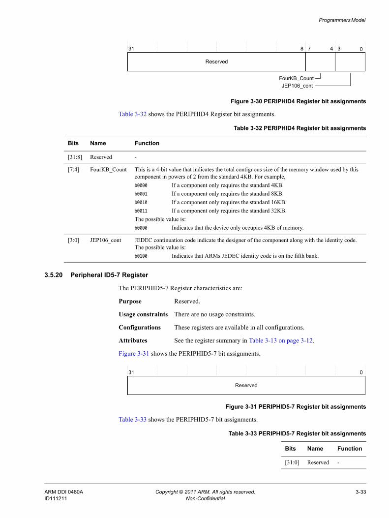
Programmers Model
Figure 3-30 PERIPHID4 Register bit assignments
Table 3-32 shows the PERIPHID4 Register bit assignments.
3.5.20 Peripheral ID5-7 Register
The PERIPHID5-7 Register characteristics are:
Purpose Reserved.
Usage constraints There are no usage constraints.
Configurations These registers are available in all configurations.
Attributes See the register summary in Table 3-13 on page 3-12.
Figure 3-31 shows the PERIPHID5-7 bit assignments.
Figure 3-31 PERIPHID5-7 Register bit assignments
Table 3-33 shows the PERIPHID5-7 bit assignments.
31 0
Reserved
7
FourKB_Count
8 4
JEP106_cont
3
Table 3-32 PERIPHID4 Register bit assignments
Bits Name Function
[31:8] Reserved -
[7:4] FourKB_Count This is a 4-bit value that indicates the total contiguous size of the memory window used by this component in powers of 2 from the standard 4KB. For example,b0000 If a component only requires the standard 4KB.b0001 If a component only requires the standard 8KB.b0010 If a component only requires the standard 16KB.b0011 If a component only requires the standard 32KB.The possible value is:b0000 Indicates that the device only occupies 4KB of memory.
[3:0] JEP106_cont JEDEC continuation code indicate the designer of the component along with the identity code. The possible value is:b0100 Indicates that ARMs JEDEC identity code is on the fifth bank.
31 0
Reserved
Table 3-33 PERIPHID5-7 Register bit assignments
Bits Name Function
[31:0] Reserved -
ARM DDI 0480A Copyright © 2011 ARM. All rights reserved. 3-33ID111211 Non-Confidential
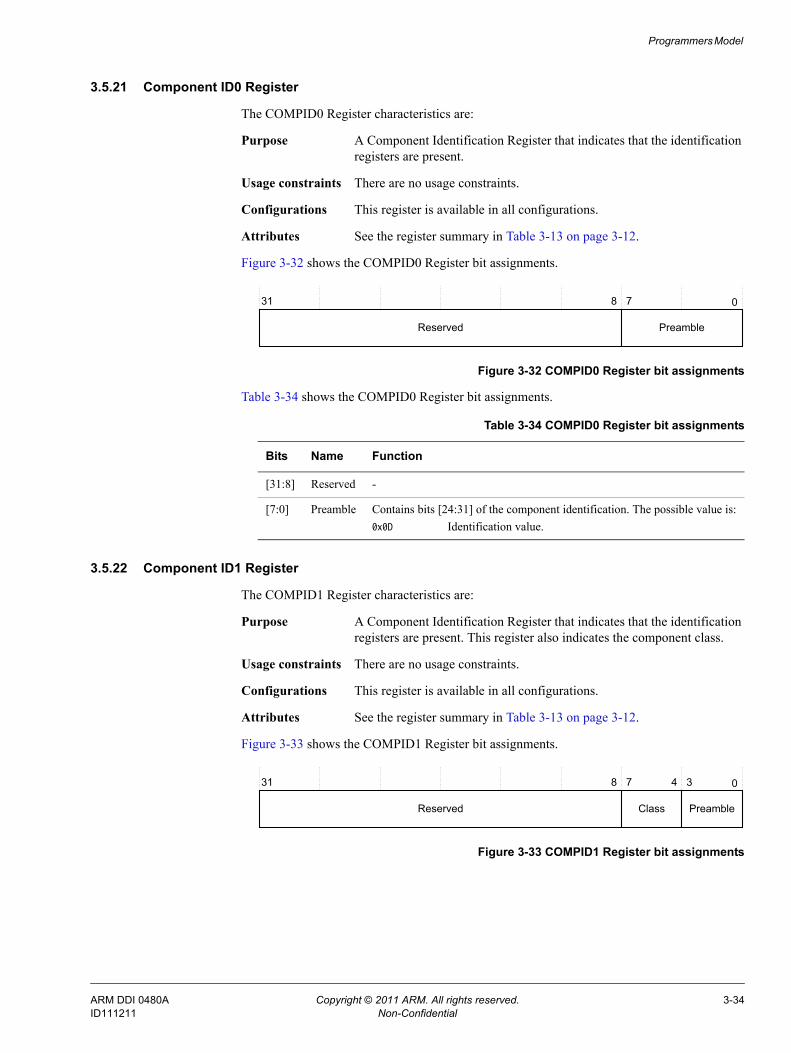
Programmers Model
3.5.21 Component ID0 Register
The COMPID0 Register characteristics are:
Purpose A Component Identification Register that indicates that the identification registers are present.
Usage constraints There are no usage constraints.
Configurations This register is available in all configurations.
Attributes See the register summary in Table 3-13 on page 3-12.
Figure 3-32 shows the COMPID0 Register bit assignments.
Figure 3-32 COMPID0 Register bit assignments
Table 3-34 shows the COMPID0 Register bit assignments.
3.5.22 Component ID1 Register
The COMPID1 Register characteristics are:
Purpose A Component Identification Register that indicates that the identification registers are present. This register also indicates the component class.
Usage constraints There are no usage constraints.
Configurations This register is available in all configurations.
Attributes See the register summary in Table 3-13 on page 3-12.
Figure 3-33 shows the COMPID1 Register bit assignments.
Figure 3-33 COMPID1 Register bit assignments
31 0
Reserved
78
Preamble
Table 3-34 COMPID0 Register bit assignments
Bits Name Function
[31:8] Reserved -
[7:0] Preamble Contains bits [24:31] of the component identification. The possible value is:0x0D Identification value.
31 0
Reserved
78
Preamble
4 3
Class
ARM DDI 0480A Copyright © 2011 ARM. All rights reserved. 3-34ID111211 Non-Confidential
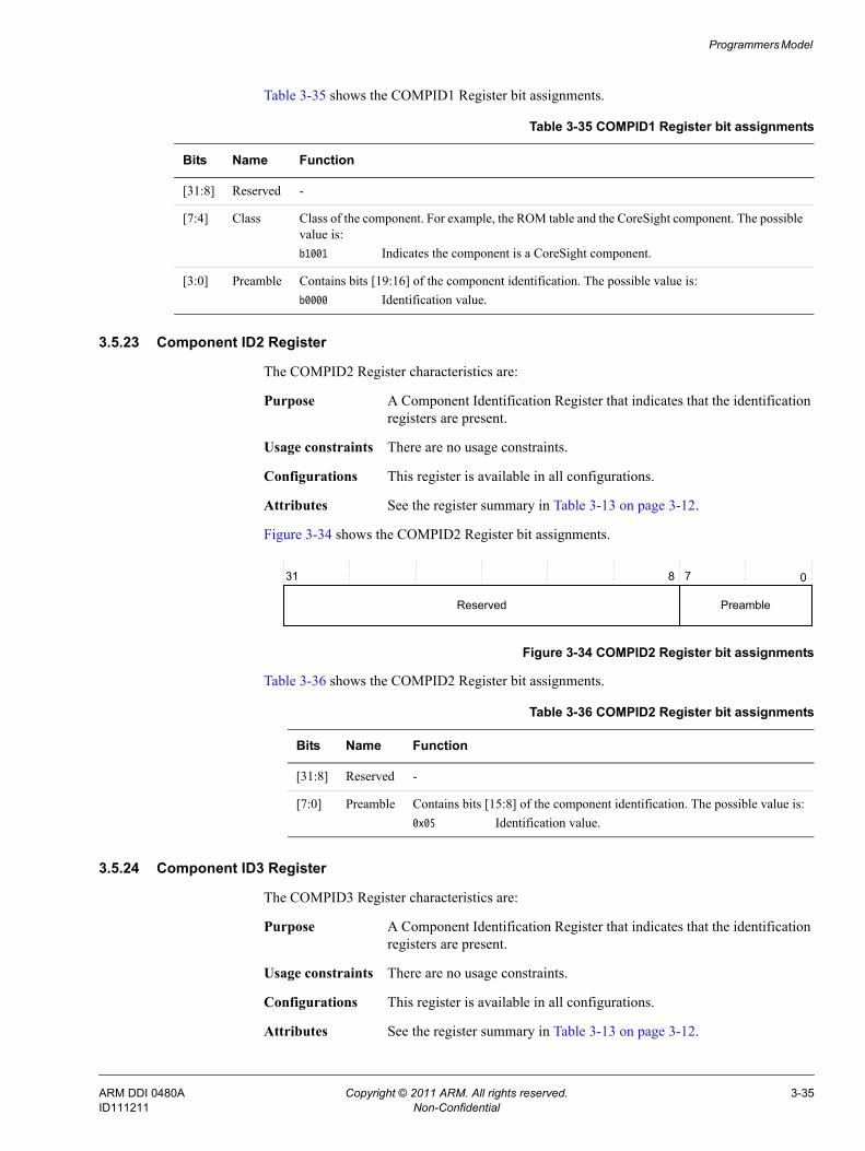
Programmers Model
Table 3-35 shows the COMPID1 Register bit assignments.
3.5.23 Component ID2 Register
The COMPID2 Register characteristics are:
Purpose A Component Identification Register that indicates that the identification registers are present.
Usage constraints There are no usage constraints.
Configurations This register is available in all configurations.
Attributes See the register summary in Table 3-13 on page 3-12.
Figure 3-34 shows the COMPID2 Register bit assignments.
Figure 3-34 COMPID2 Register bit assignments
Table 3-36 shows the COMPID2 Register bit assignments.
3.5.24 Component ID3 Register
The COMPID3 Register characteristics are:
Purpose A Component Identification Register that indicates that the identification registers are present.
Usage constraints There are no usage constraints.
Configurations This register is available in all configurations.
Attributes See the register summary in Table 3-13 on page 3-12.
Table 3-35 COMPID1 Register bit assignments
Bits Name Function
[31:8] Reserved -
[7:4] Class Class of the component. For example, the ROM table and the CoreSight component. The possible value is:b1001 Indicates the component is a CoreSight component.
[3:0] Preamble Contains bits [19:16] of the component identification. The possible value is:b0000 Identification value.
31 0
Reserved
78
Preamble
Table 3-36 COMPID2 Register bit assignments
Bits Name Function
[31:8] Reserved -
[7:0] Preamble Contains bits [15:8] of the component identification. The possible value is:0x05 Identification value.
ARM DDI 0480A Copyright © 2011 ARM. All rights reserved. 3-35ID111211 Non-Confidential
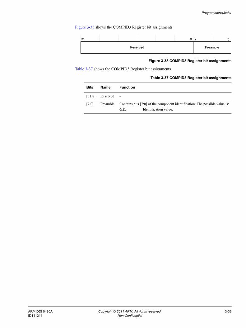
Programmers Model
Figure 3-35 shows the COMPID3 Register bit assignments.
Figure 3-35 COMPID3 Register bit assignments
Table 3-37 shows the COMPID3 Register bit assignments.
31 0
Reserved
78
Preamble
Table 3-37 COMPID3 Register bit assignments
Bits Name Function
[31:8] Reserved -
[7:0] Preamble Contains bits [7:0] of the component identification. The possible value is:0xB1 Identification value.
ARM DDI 0480A Copyright © 2011 ARM. All rights reserved. 3-36ID111211 Non-Confidential
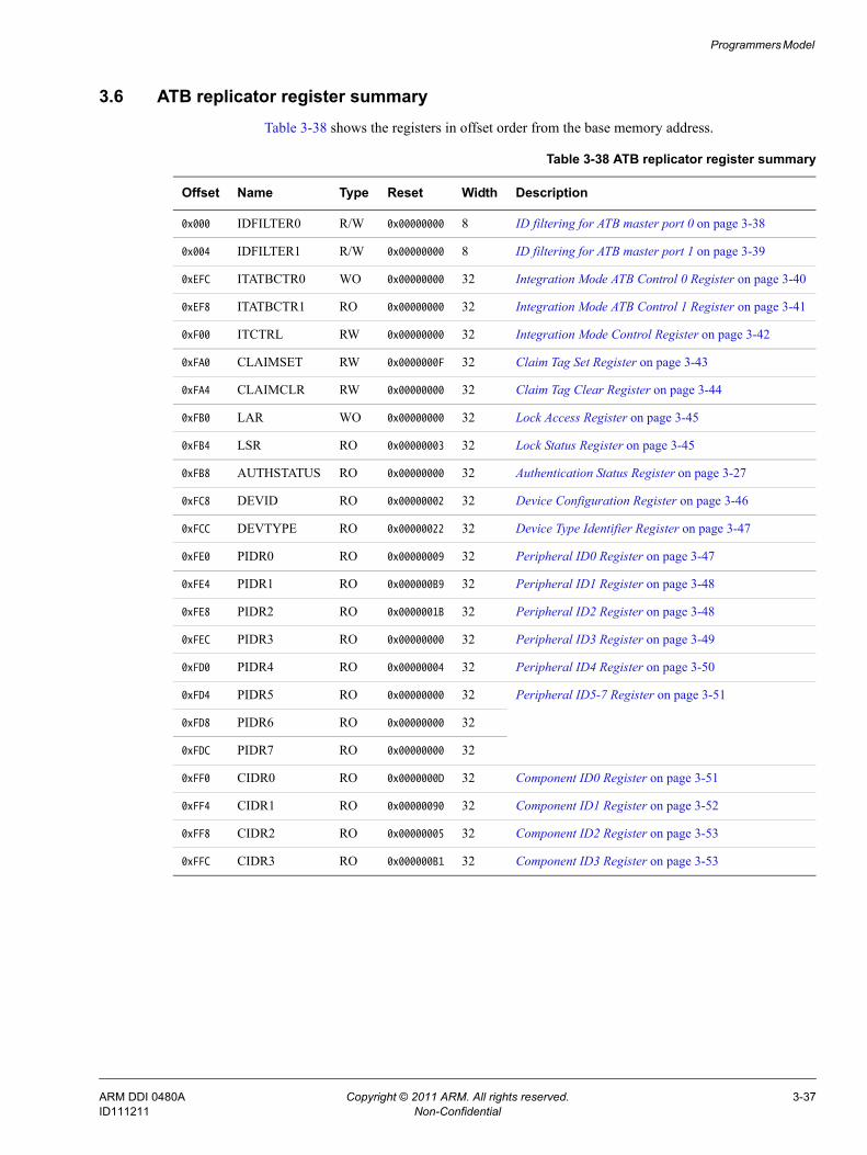
Programmers Model
3.6 ATB replicator register summaryTable 3-38 shows the registers in offset order from the base memory address.
Table 3-38 ATB replicator register summary
Offset Name Type Reset Width Description
0x000 IDFILTER0 R/W 0x00000000 8 ID filtering for ATB master port 0 on page 3-38
0x004 IDFILTER1 R/W 0x00000000 8 ID filtering for ATB master port 1 on page 3-39
0xEFC ITATBCTR0 WO 0x00000000 32 Integration Mode ATB Control 0 Register on page 3-40
0xEF8 ITATBCTR1 RO 0x00000000 32 Integration Mode ATB Control 1 Register on page 3-41
0xF00 ITCTRL RW 0x00000000 32 Integration Mode Control Register on page 3-42
0xFA0 CLAIMSET RW 0x0000000F 32 Claim Tag Set Register on page 3-43
0xFA4 CLAIMCLR RW 0x00000000 32 Claim Tag Clear Register on page 3-44
0xFB0 LAR WO 0x00000000 32 Lock Access Register on page 3-45
0xFB4 LSR RO 0x00000003 32 Lock Status Register on page 3-45
0xFB8 AUTHSTATUS RO 0x00000000 32 Authentication Status Register on page 3-27
0xFC8 DEVID RO 0x00000002 32 Device Configuration Register on page 3-46
0xFCC DEVTYPE RO 0x00000022 32 Device Type Identifier Register on page 3-47
0xFE0 PIDR0 RO 0x00000009 32 Peripheral ID0 Register on page 3-47
0xFE4 PIDR1 RO 0x000000B9 32 Peripheral ID1 Register on page 3-48
0xFE8 PIDR2 RO 0x0000001B 32 Peripheral ID2 Register on page 3-48
0xFEC PIDR3 RO 0x00000000 32 Peripheral ID3 Register on page 3-49
0xFD0 PIDR4 RO 0x00000004 32 Peripheral ID4 Register on page 3-50
0xFD4 PIDR5 RO 0x00000000 32 Peripheral ID5-7 Register on page 3-51
0xFD8 PIDR6 RO 0x00000000 32
0xFDC PIDR7 RO 0x00000000 32
0xFF0 CIDR0 RO 0x0000000D 32 Component ID0 Register on page 3-51
0xFF4 CIDR1 RO 0x00000090 32 Component ID1 Register on page 3-52
0xFF8 CIDR2 RO 0x00000005 32 Component ID2 Register on page 3-53
0xFFC CIDR3 RO 0x000000B1 32 Component ID3 Register on page 3-53
ARM DDI 0480A Copyright © 2011 ARM. All rights reserved. 3-37ID111211 Non-Confidential
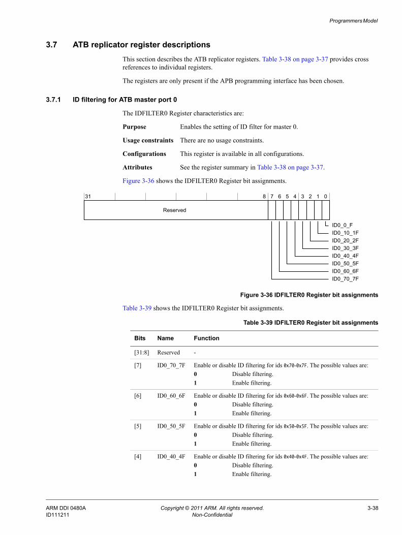
Programmers Model
3.7 ATB replicator register descriptionsThis section describes the ATB replicator registers. Table 3-38 on page 3-37 provides cross references to individual registers.
The registers are only present if the APB programming interface has been chosen.
3.7.1 ID filtering for ATB master port 0
The IDFILTER0 Register characteristics are:
Purpose Enables the setting of ID filter for master 0.
Usage constraints There are no usage constraints.
Configurations This register is available in all configurations.
Attributes See the register summary in Table 3-38 on page 3-37.
Figure 3-36 shows the IDFILTER0 Register bit assignments.
Figure 3-36 IDFILTER0 Register bit assignments
Table 3-39 shows the IDFILTER0 Register bit assignments.
31 8 7 6 5 4 3 2 1 0
Reserved
ID0_20_2FID0_10_1FID0_0_F
ID0_30_3FID0_40_4F
ID0_70_7FID0_60_6FID0_50_5F
Table 3-39 IDFILTER0 Register bit assignments
Bits Name Function
[31:8] Reserved -
[7] ID0_70_7F Enable or disable ID filtering for ids 0x70-0x7F. The possible values are:0 Disable filtering.1 Enable filtering.
[6] ID0_60_6F Enable or disable ID filtering for ids 0x60-0x6F. The possible values are:0 Disable filtering.1 Enable filtering.
[5] ID0_50_5F Enable or disable ID filtering for ids 0x50-0x5F. The possible values are:0 Disable filtering.1 Enable filtering.
[4] ID0_40_4F Enable or disable ID filtering for ids 0x40-0x4F. The possible values are:0 Disable filtering.1 Enable filtering.
ARM DDI 0480A Copyright © 2011 ARM. All rights reserved. 3-38ID111211 Non-Confidential
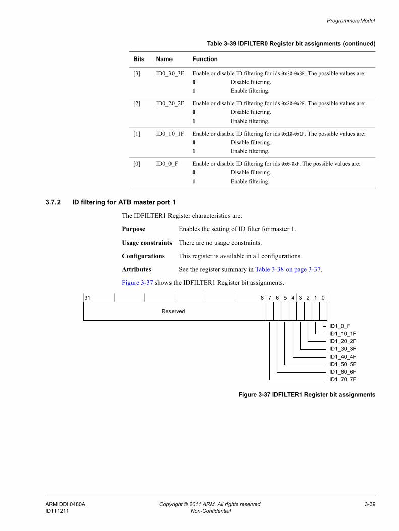
Programmers Model
3.7.2 ID filtering for ATB master port 1
The IDFILTER1 Register characteristics are:
Purpose Enables the setting of ID filter for master 1.
Usage constraints There are no usage constraints.
Configurations This register is available in all configurations.
Attributes See the register summary in Table 3-38 on page 3-37.
Figure 3-37 shows the IDFILTER1 Register bit assignments.
Figure 3-37 IDFILTER1 Register bit assignments
[3] ID0_30_3F Enable or disable ID filtering for ids 0x30-0x3F. The possible values are:0 Disable filtering.1 Enable filtering.
[2] ID0_20_2F Enable or disable ID filtering for ids 0x20-0x2F. The possible values are:0 Disable filtering.1 Enable filtering.
[1] ID0_10_1F Enable or disable ID filtering for ids 0x10-0x1F. The possible values are:0 Disable filtering.1 Enable filtering.
[0] ID0_0_F Enable or disable ID filtering for ids 0x0-0xF. The possible values are:0 Disable filtering.1 Enable filtering.
Table 3-39 IDFILTER0 Register bit assignments (continued)
Bits Name Function
31 8 7 6 5 4 3 2 1 0
Reserved
ID1_20_2FID1_10_1FID1_0_F
ID1_30_3FID1_40_4F
ID1_70_7FID1_60_6FID1_50_5F
ARM DDI 0480A Copyright © 2011 ARM. All rights reserved. 3-39ID111211 Non-Confidential
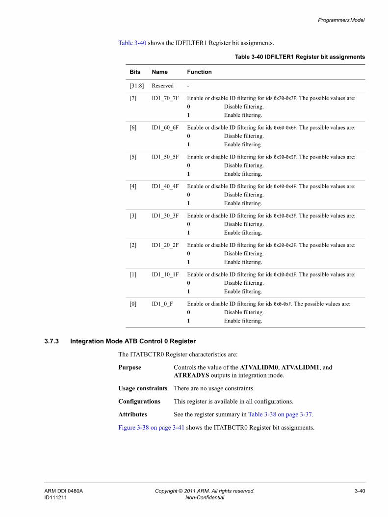
Programmers Model
Table 3-40 shows the IDFILTER1 Register bit assignments.
3.7.3 Integration Mode ATB Control 0 Register
The ITATBCTR0 Register characteristics are:
Purpose Controls the value of the ATVALIDM0, ATVALIDM1, and ATREADYS outputs in integration mode.
Usage constraints There are no usage constraints.
Configurations This register is available in all configurations.
Attributes See the register summary in Table 3-38 on page 3-37.
Figure 3-38 on page 3-41 shows the ITATBCTR0 Register bit assignments.
Table 3-40 IDFILTER1 Register bit assignments
Bits Name Function
[31:8] Reserved -
[7] ID1_70_7F Enable or disable ID filtering for ids 0x70-0x7F. The possible values are:0 Disable filtering.1 Enable filtering.
[6] ID1_60_6F Enable or disable ID filtering for ids 0x60-0x6F. The possible values are:0 Disable filtering.1 Enable filtering.
[5] ID1_50_5F Enable or disable ID filtering for ids 0x50-0x5F. The possible values are:0 Disable filtering.1 Enable filtering.
[4] ID1_40_4F Enable or disable ID filtering for ids 0x40-0x4F. The possible values are:0 Disable filtering.1 Enable filtering.
[3] ID1_30_3F Enable or disable ID filtering for ids 0x30-0x3F. The possible values are:0 Disable filtering.1 Enable filtering.
[2] ID1_20_2F Enable or disable ID filtering for ids 0x20-0x2F. The possible values are:0 Disable filtering.1 Enable filtering.
[1] ID1_10_1F Enable or disable ID filtering for ids 0x10-0x1F. The possible values are:0 Disable filtering.1 Enable filtering.
[0] ID1_0_F Enable or disable ID filtering for ids 0x0-0xF. The possible values are:0 Disable filtering.1 Enable filtering.
ARM DDI 0480A Copyright © 2011 ARM. All rights reserved. 3-40ID111211 Non-Confidential
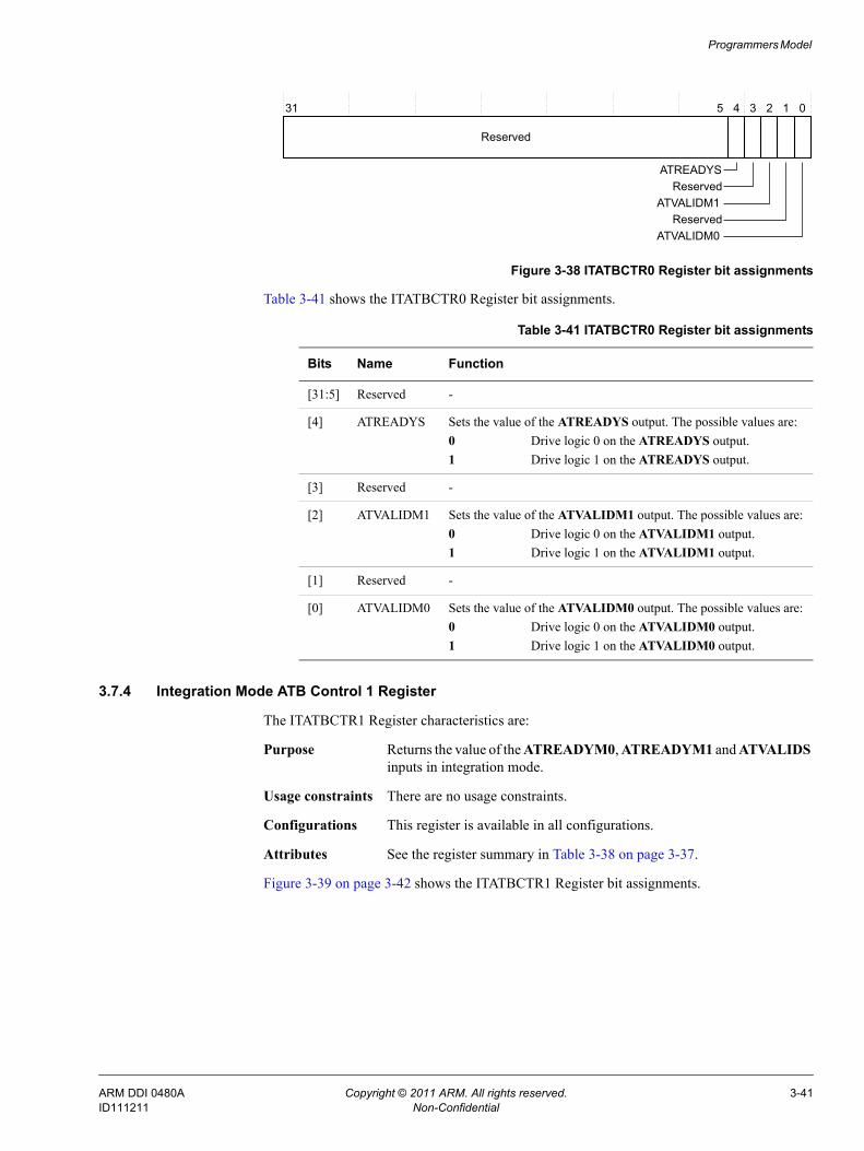
Programmers Model
Figure 3-38 ITATBCTR0 Register bit assignments
Table 3-41 shows the ITATBCTR0 Register bit assignments.
3.7.4 Integration Mode ATB Control 1 Register
The ITATBCTR1 Register characteristics are:
Purpose Returns the value of the ATREADYM0, ATREADYM1 and ATVALIDS inputs in integration mode.
Usage constraints There are no usage constraints.
Configurations This register is available in all configurations.
Attributes See the register summary in Table 3-38 on page 3-37.
Figure 3-39 on page 3-42 shows the ITATBCTR1 Register bit assignments.
31 0
Reserved
4 2
Reserved
3 1
ATVALIDM0
ATREADYS
5
ATVALIDM1Reserved
Table 3-41 ITATBCTR0 Register bit assignments
Bits Name Function
[31:5] Reserved -
[4] ATREADYS Sets the value of the ATREADYS output. The possible values are:0 Drive logic 0 on the ATREADYS output.1 Drive logic 1 on the ATREADYS output.
[3] Reserved -
[2] ATVALIDM1 Sets the value of the ATVALIDM1 output. The possible values are:0 Drive logic 0 on the ATVALIDM1 output.1 Drive logic 1 on the ATVALIDM1 output.
[1] Reserved -
[0] ATVALIDM0 Sets the value of the ATVALIDM0 output. The possible values are:0 Drive logic 0 on the ATVALIDM0 output.1 Drive logic 1 on the ATVALIDM0 output.
ARM DDI 0480A Copyright © 2011 ARM. All rights reserved. 3-41ID111211 Non-Confidential
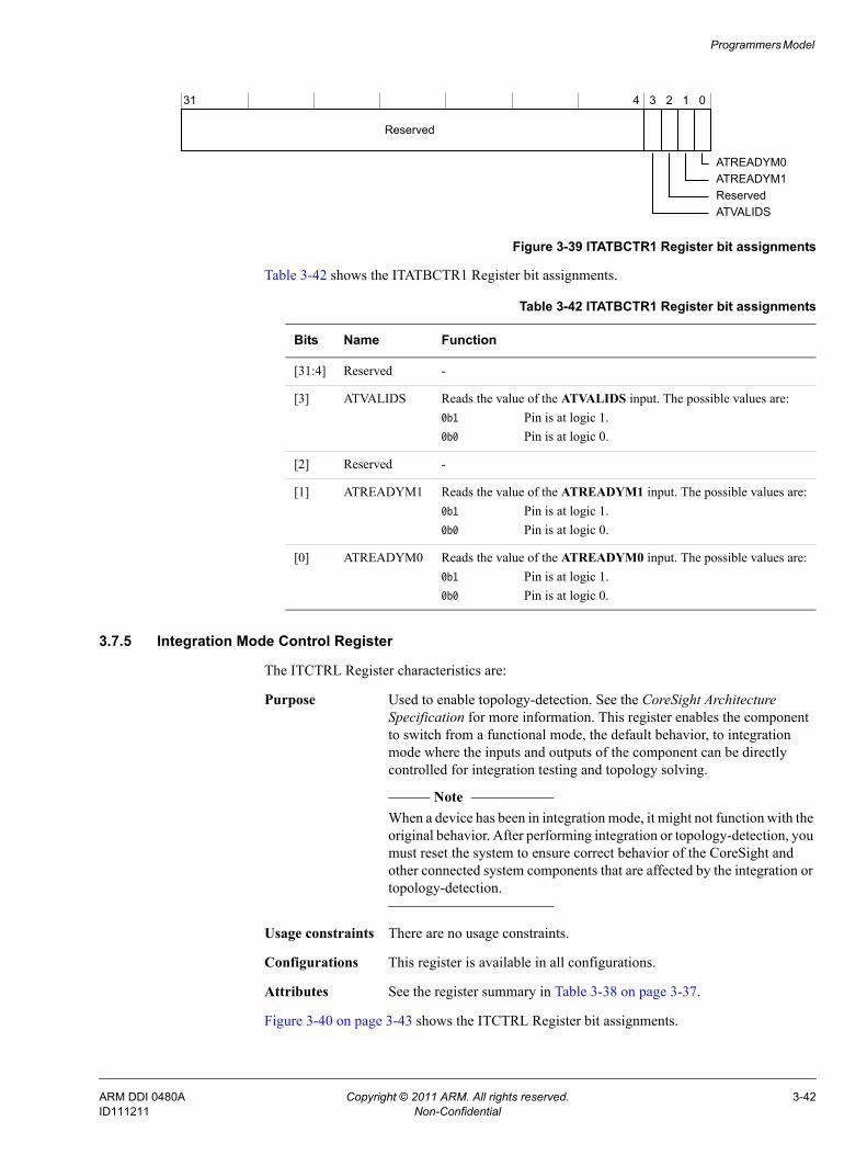
Programmers Model
Figure 3-39 ITATBCTR1 Register bit assignments
Table 3-42 shows the ITATBCTR1 Register bit assignments.
3.7.5 Integration Mode Control Register
The ITCTRL Register characteristics are:
Purpose Used to enable topology-detection. See the CoreSight Architecture Specification for more information. This register enables the component to switch from a functional mode, the default behavior, to integration mode where the inputs and outputs of the component can be directly controlled for integration testing and topology solving.
Note When a device has been in integration mode, it might not function with the
original behavior. After performing integration or topology-detection, you must reset the system to ensure correct behavior of the CoreSight and other connected system components that are affected by the integration or topology-detection.
Usage constraints There are no usage constraints.
Configurations This register is available in all configurations.
Attributes See the register summary in Table 3-38 on page 3-37.
Figure 3-40 on page 3-43 shows the ITCTRL Register bit assignments.
31 4 3 2 1 0
Reserved
ReservedATREADYM1ATREADYM0
ATVALIDS
Table 3-42 ITATBCTR1 Register bit assignments
Bits Name Function
[31:4] Reserved -
[3] ATVALIDS Reads the value of the ATVALIDS input. The possible values are:0b1 Pin is at logic 1.0b0 Pin is at logic 0.
[2] Reserved -
[1] ATREADYM1 Reads the value of the ATREADYM1 input. The possible values are:0b1 Pin is at logic 1.0b0 Pin is at logic 0.
[0] ATREADYM0 Reads the value of the ATREADYM0 input. The possible values are:0b1 Pin is at logic 1.0b0 Pin is at logic 0.
ARM DDI 0480A Copyright © 2011 ARM. All rights reserved. 3-42ID111211 Non-Confidential
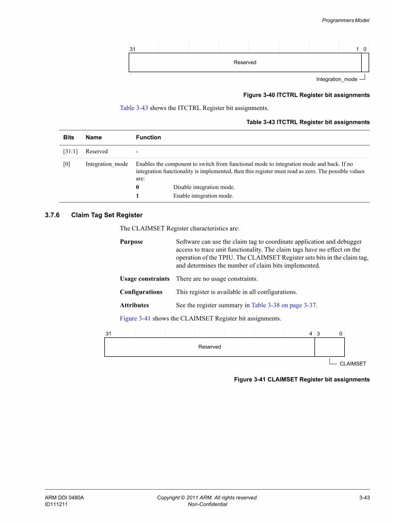
Programmers Model
Figure 3-40 ITCTRL Register bit assignments
Table 3-43 shows the ITCTRL Register bit assignments.
3.7.6 Claim Tag Set Register
The CLAIMSET Register characteristics are:
Purpose Software can use the claim tag to coordinate application and debugger access to trace unit functionality. The claim tags have no effect on the operation of the TPIU. The CLAIMSET Register sets bits in the claim tag, and determines the number of claim bits implemented.
Usage constraints There are no usage constraints.
Configurations This register is available in all configurations.
Attributes See the register summary in Table 3-38 on page 3-37.
Figure 3-41 shows the CLAIMSET Register bit assignments.
Figure 3-41 CLAIMSET Register bit assignments
31 0
Reserved
1
Integration_mode
Table 3-43 ITCTRL Register bit assignments
Bits Name Function
[31:1] Reserved -
[0] Integration_mode Enables the component to switch from functional mode to integration mode and back. If no integration functionality is implemented, then this register must read as zero. The possible values are:0 Disable integration mode.1 Enable integration mode.
31 4 3 0
CLAIMSET
Reserved
ARM DDI 0480A Copyright © 2011 ARM. All rights reserved. 3-43ID111211 Non-Confidential
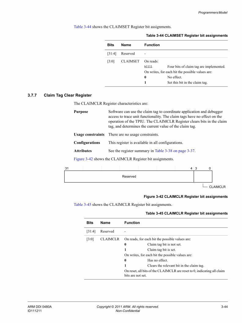
Programmers Model
Table 3-44 shows the CLAIMSET Register bit assignments.
3.7.7 Claim Tag Clear Register
The CLAIMCLR Register characteristics are:
Purpose Software can use the claim tag to coordinate application and debugger access to trace unit functionality. The claim tags have no effect on the operation of the TPIU. The CLAIMCLR Register clears bits in the claim tag, and determines the current value of the claim tag.
Usage constraints There are no usage constraints.
Configurations This register is available in all configurations.
Attributes See the register summary in Table 3-38 on page 3-37.
Figure 3-42 shows the CLAIMCLR Register bit assignments.
Figure 3-42 CLAIMCLR Register bit assignments
Table 3-45 shows the CLAIMCLR Register bit assignments.
Table 3-44 CLAIMSET Register bit assignments
Bits Name Function
[31:4] Reserved -
[3:0] CLAIMSET On reads:b1111 Four bits of claim tag are implemented.On writes, for each bit the possible values are:0 No effect.1 Set this bit in the claim tag.
31 4 3 0
CLAIMCLR
Reserved
Table 3-45 CLAIMCLR Register bit assignments
Bits Name Function
[31:4] Reserved -
[3:0] CLAIMCLR On reads, for each bit the possible values are:0 Claim tag bit is not set.1 Claim tag bit is set.On writes, for each bit the possible values are:0 Has no effect.1 Clears the relevant bit in the claim tag.On reset, all bits of the CLAIMCLR are reset to 0, indicating all claim bits are not set.
ARM DDI 0480A Copyright © 2011 ARM. All rights reserved. 3-44ID111211 Non-Confidential
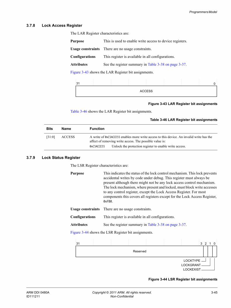
Programmers Model
3.7.8 Lock Access Register
The LAR Register characteristics are:
Purpose This is used to enable write access to device registers.
Usage constraints There are no usage constraints.
Configurations This register is available in all configurations.
Attributes See the register summary in Table 3-38 on page 3-37.
Figure 3-43 shows the LAR Register bit assignments.
Figure 3-43 LAR Register bit assignments
Table 3-46 shows the LAR Register bit assignments.
3.7.9 Lock Status Register
The LSR Register characteristics are:
Purpose This indicates the status of the lock control mechanism. This lock prevents accidental writes by code under debug. This register must always be present although there might not be any lock access control mechanism. The lock mechanism, where present and locked, must block write accesses to any control register, except the Lock Access Register. For most components this covers all registers except for the Lock Access Register, 0xFB0.
Usage constraints There are no usage constraints.
Configurations This register is available in all configurations.
Attributes See the register summary in Table 3-38 on page 3-37.
Figure 3-44 shows the LSR Register bit assignments.
Figure 3-44 LSR Register bit assignments
31 0
ACCESS
Table 3-46 LAR Register bit assignments
Bits Name Function
[31:0] ACCESS A write of 0xC5ACCE55 enables more write access to this device. An invalid write has the affect of removing write access. The possible value is:0xC5ACCE55 Unlock the protection register to enable write access.
31 0
Reserved
1
LOCKTYPE
23
LOCKGRANTLOCKEXIST
ARM DDI 0480A Copyright © 2011 ARM. All rights reserved. 3-45ID111211 Non-Confidential
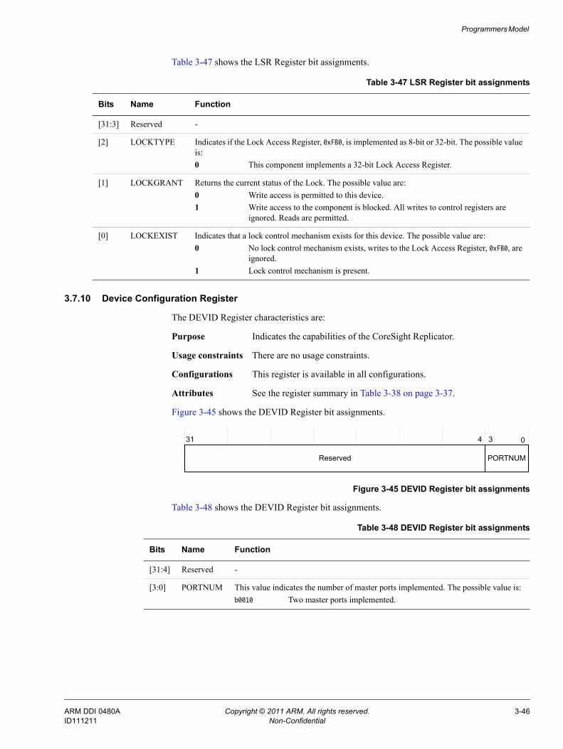
Programmers Model
Table 3-47 shows the LSR Register bit assignments.
3.7.10 Device Configuration Register
The DEVID Register characteristics are:
Purpose Indicates the capabilities of the CoreSight Replicator.
Usage constraints There are no usage constraints.
Configurations This register is available in all configurations.
Attributes See the register summary in Table 3-38 on page 3-37.
Figure 3-45 shows the DEVID Register bit assignments.
Figure 3-45 DEVID Register bit assignments
Table 3-48 shows the DEVID Register bit assignments.
Table 3-47 LSR Register bit assignments
Bits Name Function
[31:3] Reserved -
[2] LOCKTYPE Indicates if the Lock Access Register, 0xFB0, is implemented as 8-bit or 32-bit. The possible value is:0 This component implements a 32-bit Lock Access Register.
[1] LOCKGRANT Returns the current status of the Lock. The possible value are:0 Write access is permitted to this device.1 Write access to the component is blocked. All writes to control registers are
ignored. Reads are permitted.
[0] LOCKEXIST Indicates that a lock control mechanism exists for this device. The possible value are:0 No lock control mechanism exists, writes to the Lock Access Register, 0xFB0, are
ignored.1 Lock control mechanism is present.
31 0
Reserved
4
PORTNUM
3
Table 3-48 DEVID Register bit assignments
Bits Name Function
[31:4] Reserved -
[3:0] PORTNUM This value indicates the number of master ports implemented. The possible value is: b0010 Two master ports implemented.
ARM DDI 0480A Copyright © 2011 ARM. All rights reserved. 3-46ID111211 Non-Confidential
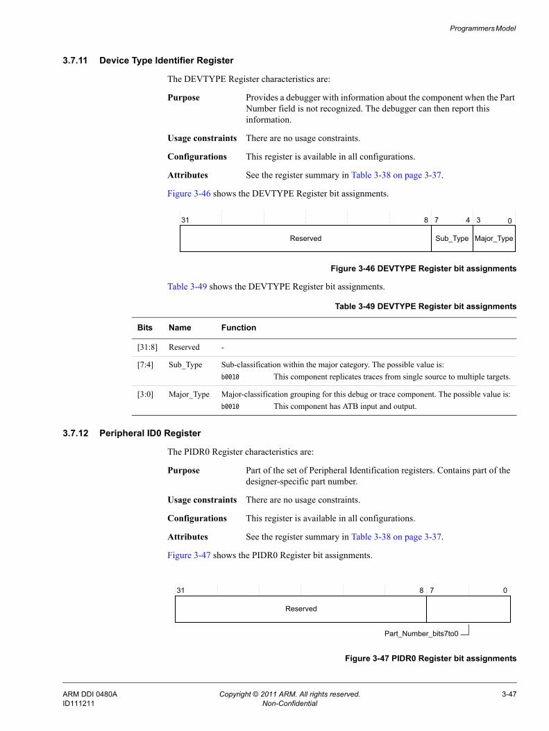
Programmers Model
3.7.11 Device Type Identifier Register
The DEVTYPE Register characteristics are:
Purpose Provides a debugger with information about the component when the Part Number field is not recognized. The debugger can then report this information.
Usage constraints There are no usage constraints.
Configurations This register is available in all configurations.
Attributes See the register summary in Table 3-38 on page 3-37.
Figure 3-46 shows the DEVTYPE Register bit assignments.
Figure 3-46 DEVTYPE Register bit assignments
Table 3-49 shows the DEVTYPE Register bit assignments.
3.7.12 Peripheral ID0 Register
The PIDR0 Register characteristics are:
Purpose Part of the set of Peripheral Identification registers. Contains part of the designer-specific part number.
Usage constraints There are no usage constraints.
Configurations This register is available in all configurations.
Attributes See the register summary in Table 3-38 on page 3-37.
Figure 3-47 shows the PIDR0 Register bit assignments.
Figure 3-47 PIDR0 Register bit assignments
31 0
Reserved
7
Sub_Type
8 4
Major_Type
3
Table 3-49 DEVTYPE Register bit assignments
Bits Name Function
[31:8] Reserved -
[7:4] Sub_Type Sub-classification within the major category. The possible value is:b0010 This component replicates traces from single source to multiple targets.
[3:0] Major_Type Major-classification grouping for this debug or trace component. The possible value is:b0010 This component has ATB input and output.
31 0
Part_Number_bits7to0
Reserved
8 7
ARM DDI 0480A Copyright © 2011 ARM. All rights reserved. 3-47ID111211 Non-Confidential
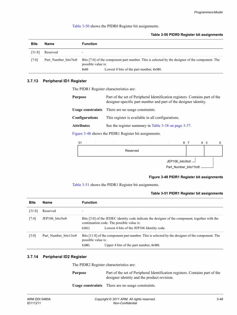
Programmers Model
Table 3-50 shows the PIDR0 Register bit assignments.
3.7.13 Peripheral ID1 Register
The PIDR1 Register characteristics are:
Purpose Part of the set of Peripheral Identification registers. Contains part of the designer-specific part number and part of the designer identity.
Usage constraints There are no usage constraints.
Configurations This register is available in all configurations.
Attributes See the register summary in Table 3-38 on page 3-37.
Figure 3-48 shows the PIDR1 Register bit assignments.
Figure 3-48 PIDR1 Register bit assignments
Table 3-51 shows the PIDR1 Register bit assignments.
3.7.14 Peripheral ID2 Register
The PIDR2 Register characteristics are:
Purpose Part of the set of Peripheral Identification registers. Contains part of the designer identity and the product revision.
Usage constraints There are no usage constraints.
Table 3-50 PIDR0 Register bit assignments
Bits Name Function
[31:8] Reserved -
[7:0] Part_Number_bits7to0 Bits [7:0] of the component part number. This is selected by the designer of the component. The possible value is:0x09 Lowest 8 bits of the part number, 0x909.
31 0
JEP106_bits3to0
Reserved
8 7 4 3
Part_Number_bits11to8
Table 3-51 PIDR1 Register bit assignments
Bits Name Function
[31:8] Reserved -
[7:4] JEP106_bits3to0 Bits [3:0] of the JEDEC identity code indicate the designer of the component, together with the continuation code. The possible value is:b1011 Lowest 4 bits of the JEP106 Identity code.
[3:0] Part_Number_bits11to8 Bits [11:8] of the component part number. This is selected by the designer of the component. The possible value is:b1001 Upper 4 bits of the part number, 0x909.
ARM DDI 0480A Copyright © 2011 ARM. All rights reserved. 3-48ID111211 Non-Confidential
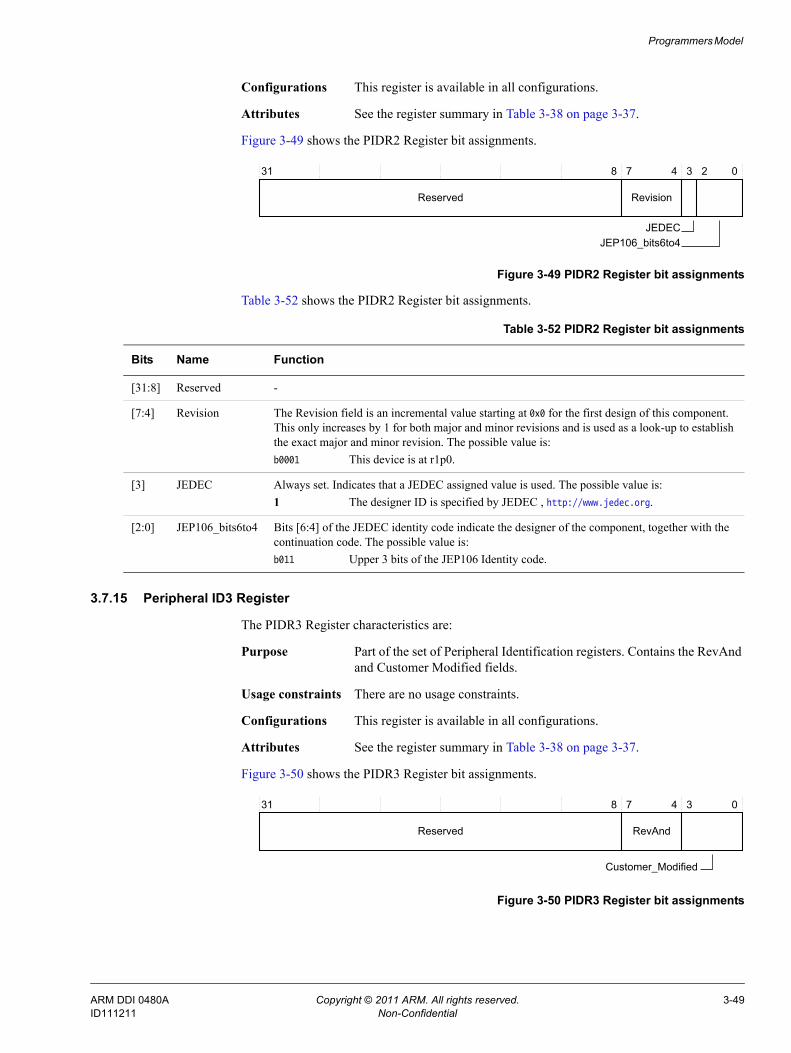
Programmers Model
Configurations This register is available in all configurations.
Attributes See the register summary in Table 3-38 on page 3-37.
Figure 3-49 shows the PIDR2 Register bit assignments.
Figure 3-49 PIDR2 Register bit assignments
Table 3-52 shows the PIDR2 Register bit assignments.
3.7.15 Peripheral ID3 Register
The PIDR3 Register characteristics are:
Purpose Part of the set of Peripheral Identification registers. Contains the RevAnd and Customer Modified fields.
Usage constraints There are no usage constraints.
Configurations This register is available in all configurations.
Attributes See the register summary in Table 3-38 on page 3-37.
Figure 3-50 shows the PIDR3 Register bit assignments.
Figure 3-50 PIDR3 Register bit assignments
31 0
JEP106_bits6to4
Reserved
8 7 4 3
JEDEC
Revision
2
Table 3-52 PIDR2 Register bit assignments
Bits Name Function
[31:8] Reserved -
[7:4] Revision The Revision field is an incremental value starting at 0x0 for the first design of this component. This only increases by 1 for both major and minor revisions and is used as a look-up to establish the exact major and minor revision. The possible value is:b0001 This device is at r1p0.
[3] JEDEC Always set. Indicates that a JEDEC assigned value is used. The possible value is:1 The designer ID is specified by JEDEC , http://www.jedec.org.
[2:0] JEP106_bits6to4 Bits [6:4] of the JEDEC identity code indicate the designer of the component, together with the continuation code. The possible value is:b011 Upper 3 bits of the JEP106 Identity code.
31 4 3 0
Customer_Modified
Reserved
8 7
RevAnd
ARM DDI 0480A Copyright © 2011 ARM. All rights reserved. 3-49ID111211 Non-Confidential
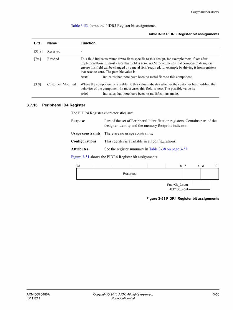
Programmers Model
Table 3-53 shows the PIDR3 Register bit assignments.
3.7.16 Peripheral ID4 Register
The PIDR4 Register characteristics are:
Purpose Part of the set of Peripheral Identification registers. Contains part of the designer identity and the memory footprint indicator.
Usage constraints There are no usage constraints.
Configurations This register is available in all configurations.
Attributes See the register summary in Table 3-38 on page 3-37.
Figure 3-51 shows the PIDR4 Register bit assignments.
Figure 3-51 PIDR4 Register bit assignments
Table 3-53 PIDR3 Register bit assignments
Bits Name Function
[31:8] Reserved -
[7:4] RevAnd This field indicates minor errata fixes specific to this design, for example metal fixes after implementation. In most cases this field is zero. ARM recommends that component designers ensure this field can be changed by a metal fix if required, for example by driving it from registers that reset to zero. The possible value is:b0000 Indicates that there have been no metal fixes to this component.
[3:0] Customer_Modified Where the component is reusable IP, this value indicates whether the customer has modified the behavior of the component. In most cases this field is zero. The possible value is:b0000 Indicates that there have been no modifications made.
31 4 3 0
JEP106_cont
Reserved
8 7
FourKB_Count
ARM DDI 0480A Copyright © 2011 ARM. All rights reserved. 3-50ID111211 Non-Confidential
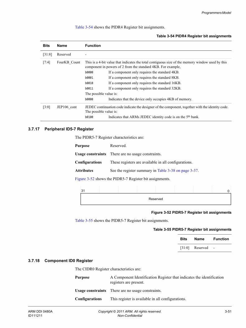
Programmers Model
Table 3-54 shows the PIDR4 Register bit assignments.
3.7.17 Peripheral ID5-7 Register
The PIDR5-7 Register characteristics are:
Purpose Reserved.
Usage constraints There are no usage constraints.
Configurations These registers are available in all configurations.
Attributes See the register summary in Table 3-38 on page 3-37.
Figure 3-52 shows the PIDR5-7 Register bit assignments.
Figure 3-52 PIDR5-7 Register bit assignments
Table 3-55 shows the PIDR5-7 Register bit assignments.
3.7.18 Component ID0 Register
The CIDR0 Register characteristics are:
Purpose A Component Identification Register that indicates the identification registers are present.
Usage constraints There are no usage constraints.
Configurations This register is available in all configurations.
Table 3-54 PIDR4 Register bit assignments
Bits Name Function
[31:8] Reserved -
[7:4] FourKB_Count This is a 4-bit value that indicates the total contiguous size of the memory window used by this component in powers of 2 from the standard 4KB. For example, b0000 If a component only requires the standard 4KB.b0001 If a component only requires the standard 8KB.b0010 If a component only requires the standard 16KB.b0011 If a component only requires the standard 32KB.The possible value is:b0000 Indicates that the device only occupies 4KB of memory.
[3:0] JEP106_cont JEDEC continuation code indicate the designer of the component, together with the identity code. The possible value is:b0100 Indicates that ARMs JEDEC identity code is on the 5th bank.
31 0
Reserved
Table 3-55 PIDR5-7 Register bit assignments
Bits Name Function
[31:0] Reserved -
ARM DDI 0480A Copyright © 2011 ARM. All rights reserved. 3-51ID111211 Non-Confidential
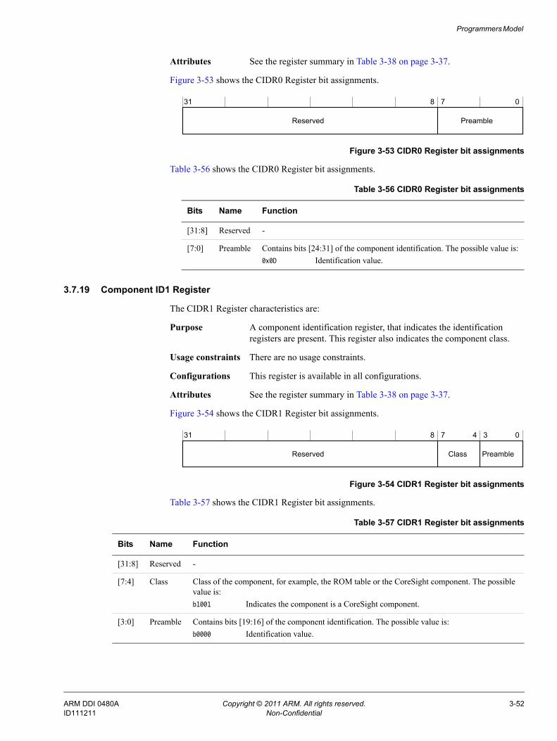
Programmers Model
Attributes See the register summary in Table 3-38 on page 3-37.
Figure 3-53 shows the CIDR0 Register bit assignments.
Figure 3-53 CIDR0 Register bit assignments
Table 3-56 shows the CIDR0 Register bit assignments.
3.7.19 Component ID1 Register
The CIDR1 Register characteristics are:
Purpose A component identification register, that indicates the identification registers are present. This register also indicates the component class.
Usage constraints There are no usage constraints.
Configurations This register is available in all configurations.
Attributes See the register summary in Table 3-38 on page 3-37.
Figure 3-54 shows the CIDR1 Register bit assignments.
Figure 3-54 CIDR1 Register bit assignments
Table 3-57 shows the CIDR1 Register bit assignments.
31 8 7 0
PreambleReserved
Table 3-56 CIDR0 Register bit assignments
Bits Name Function
[31:8] Reserved -
[7:0] Preamble Contains bits [24:31] of the component identification. The possible value is:0x0D Identification value.
31 8 7 4 3 0
PreambleClassReserved
Table 3-57 CIDR1 Register bit assignments
Bits Name Function
[31:8] Reserved -
[7:4] Class Class of the component, for example, the ROM table or the CoreSight component. The possible value is:b1001 Indicates the component is a CoreSight component.
[3:0] Preamble Contains bits [19:16] of the component identification. The possible value is:b0000 Identification value.
ARM DDI 0480A Copyright © 2011 ARM. All rights reserved. 3-52ID111211 Non-Confidential
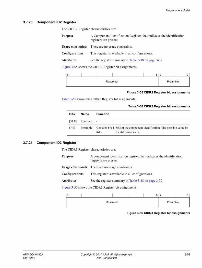
Programmers Model
3.7.20 Component ID2 Register
The CIDR2 Register characteristics are:
Purpose A Component Identification Register, that indicates the identification registers are present.
Usage constraints There are no usage constraints.
Configurations This register is available in all configurations.
Attributes See the register summary in Table 3-38 on page 3-37.
Figure 3-55 shows the CIDR2 Register bit assignments.
Figure 3-55 CIDR2 Register bit assignments
Table 3-58 shows the CIDR2 Register bit assignments.
3.7.21 Component ID3 Register
The CIDR3 Register characteristics are:
Purpose A component identification register, that indicates the identification registers are present.
Usage constraints There are no usage constraints.
Configurations This register is available in all configurations.
Attributes See the register summary in Table 3-38 on page 3-37.
Figure 3-56 shows the CIDR3 Register bit assignments.
Figure 3-56 CIDR3 Register bit assignments
31 8 7 0
PreambleReserved
Table 3-58 CIDR2 Register bit assignments
Bits Name Function
[31:8] Reserved -
[7:0] Preamble Contains bits [15:8] of the component identification. The possible value is:0x05 Identification value.
31 8 7 0
PreambleReserved
ARM DDI 0480A Copyright © 2011 ARM. All rights reserved. 3-53ID111211 Non-Confidential

Programmers Model
Table 3-59 shows the CIDR3 Register bit assignments.
Table 3-59 CIDR3 Register bit assignments
Bits Name Function
[31:8] Reserved -
[7:0] Preamble Contains bits [7:0] of the component identification. The possible value is:0xB1 Identification value.
ARM DDI 0480A Copyright © 2011 ARM. All rights reserved. 3-54ID111211 Non-Confidential
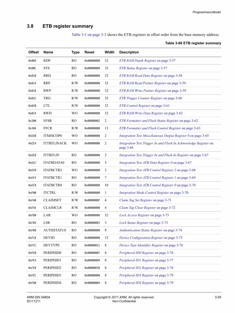
Programmers Model
3.8 ETB register summaryTable 3-1 on page 3-3 shows the ETB registers in offset order from the base memory address.
Table 3-60 ETB register summary
Offset Name Type Reset Width Description
0x004 RDP RO 0x00000000 32 ETB RAM Depth Register on page 3-57
0x00C STS RO 0x00000008 32 ETB Status Register on page 3-57
0x010 RRD RO 0x00000000 32 ETB RAM Read Data Register on page 3-58
0x014 RRP R/W 0x00000000 32 ETB RAM Read Pointer Register on page 3-59
0x018 RWP R/W 0x00000000 32 ETB RAM Write Pointer Register on page 3-59
0x01C TRG R/W 0x00000000 32 ETB Trigger Counter Register on page 3-60
0x020 CTL R/W 0x00000000 32 ETB Control Register on page 3-61
0x024 RWD WO 0x00000000 32 ETB RAM Write Data Register on page 3-62
0x300 FFSR RO 0x00000002 2 ETB Formatter and Flush Status Register on page 3-62
0x304 FFCR R/W 0x00000000 13 ETB Formatter and Flush Control Register on page 3-63
0xEE0 ITMISCOP0 WO 0x00000000 2 Integration Test Miscellaneous Output Register 0 on page 3-65
0xEE4 ITTRFLINACK WO 0x00000000 2 Integration Test Trigger In and Flush In Acknowledge Register on page 3-66
0xEE8 ITTRFLIN RO 0x00000000 2 Integration Test Trigger In and Flush In Register on page 3-67
0xEEC ITATBDATA0 RO 0x00000000 5 Integration Test ATB Data Register 0 on page 3-67
0xEF0 ITATBCTR2 WO 0x00000000 2 Integration Test ATB Control Register 2 on page 3-68
0xEF4 ITATBCTR1 RO 0x00000000 7 Integration Test ATB Control Register 1 on page 3-69
0xEF8 ITATBCTR0 RO 0x00000000 10 Integration Test ATB Control Register 0 on page 3-70
0xF00 ITCTRL R/W 0x00000000 1 Integration Mode Control Register on page 3-70
0xFA0 CLAIMSET R/W 0x0000000F 4 Claim Tag Set Register on page 3-71
0xFA4 CLAIMCLR R/W 0x00000000 4 Claim Tag Clear Register on page 3-72
0xFB0 LAR WO 0x00000000 32 Lock Access Register on page 3-73
0xFB4 LSR RO 0x00000003 3 Lock Status Register on page 3-73
0xFB8 AUTHSTATUS RO 0x00000000 8 Authentication Status Register on page 3-74
0xFC8 DEVID RO 0x00000000 32 Device Configuration Register on page 3-75
0xFCC DEVTYPE RO 0x00000021 8 Device Type Identifier Register on page 3-76
0xFE0 PERIPHID0 RO 0x00000007 8 Peripheral ID0 Register on page 3-76
0xFE4 PERIPHID1 RO 0x000000B9 8 Peripheral ID1 Register on page 3-77
0xFE8 PERIPHID2 RO 0x0000003B 8 Peripheral ID2 Register on page 3-78
0xFEC PERIPHID3 RO 0x00000000 8 Peripheral ID3 Register on page 3-79
0xFD0 PERIPHID4 RO 0x00000004 8 Peripheral ID4 Register on page 3-79
ARM DDI 0480A Copyright © 2011 ARM. All rights reserved. 3-55ID111211 Non-Confidential
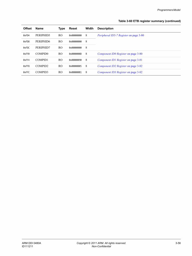
Programmers Model
0xFD4 PERIPHID5 RO 0x00000000 8 Peripheral ID5-7 Register on page 3-80
0xFD8 PERIPHID6 RO 0x00000000 8
0xFDC PERIPHID7 RO 0x00000000 8
0xFF0 COMPID0 RO 0x0000000D 8 Component ID0 Register on page 3-80
0xFF4 COMPID1 RO 0x00000090 8 Component ID1 Register on page 3-81
0xFF8 COMPID2 RO 0x00000005 8 Component ID2 Register on page 3-82
0xFFC COMPID3 RO 0x000000B1 8 Component ID3 Register on page 3-82
Table 3-60 ETB register summary (continued)
Offset Name Type Reset Width Description
ARM DDI 0480A Copyright © 2011 ARM. All rights reserved. 3-56ID111211 Non-Confidential
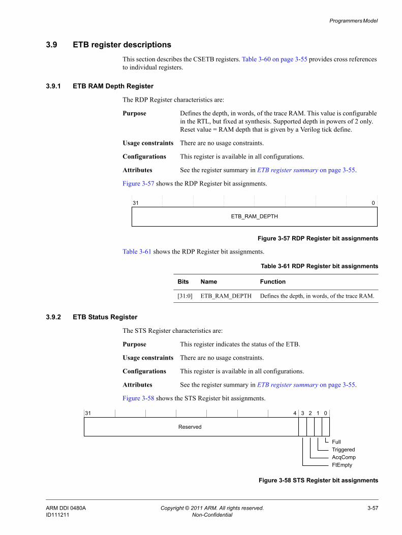
Programmers Model
3.9 ETB register descriptionsThis section describes the CSETB registers. Table 3-60 on page 3-55 provides cross references to individual registers.
3.9.1 ETB RAM Depth Register
The RDP Register characteristics are:
Purpose Defines the depth, in words, of the trace RAM. This value is configurable in the RTL, but fixed at synthesis. Supported depth in powers of 2 only. Reset value = RAM depth that is given by a Verilog tick define.
Usage constraints There are no usage constraints.
Configurations This register is available in all configurations.
Attributes See the register summary in ETB register summary on page 3-55.
Figure 3-57 shows the RDP Register bit assignments.
Figure 3-57 RDP Register bit assignments
Table 3-61 shows the RDP Register bit assignments.
3.9.2 ETB Status Register
The STS Register characteristics are:
Purpose This register indicates the status of the ETB.
Usage constraints There are no usage constraints.
Configurations This register is available in all configurations.
Attributes See the register summary in ETB register summary on page 3-55.
Figure 3-58 shows the STS Register bit assignments.
Figure 3-58 STS Register bit assignments
31 0
ETB_RAM_DEPTH
Table 3-61 RDP Register bit assignments
Bits Name Function
[31:0] ETB_RAM_DEPTH Defines the depth, in words, of the trace RAM.
31 4 3 2 1 0
Reserved
AcqCompTriggeredFull
FtEmpty
ARM DDI 0480A Copyright © 2011 ARM. All rights reserved. 3-57ID111211 Non-Confidential
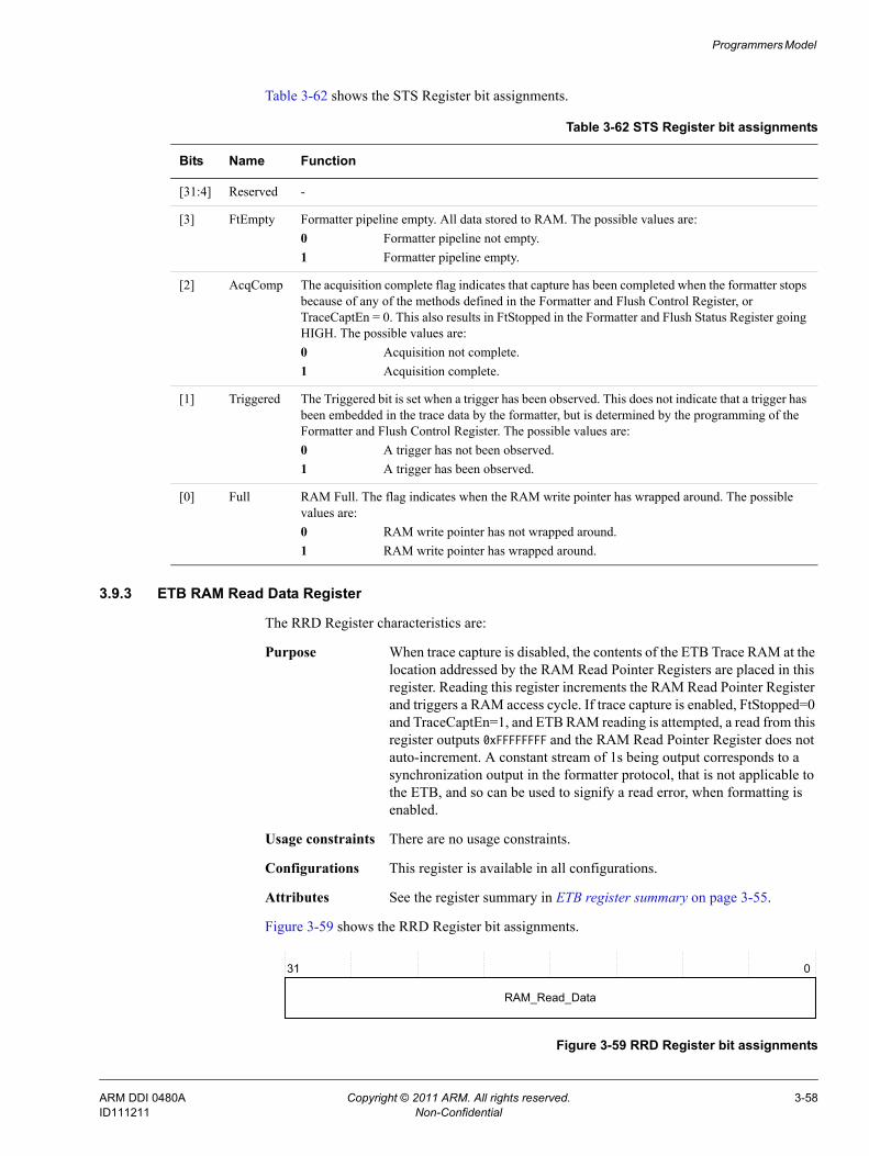
Programmers Model
Table 3-62 shows the STS Register bit assignments.
3.9.3 ETB RAM Read Data Register
The RRD Register characteristics are:
Purpose When trace capture is disabled, the contents of the ETB Trace RAM at the location addressed by the RAM Read Pointer Registers are placed in this register. Reading this register increments the RAM Read Pointer Register and triggers a RAM access cycle. If trace capture is enabled, FtStopped=0 and TraceCaptEn=1, and ETB RAM reading is attempted, a read from this register outputs 0xFFFFFFFF and the RAM Read Pointer Register does not auto-increment. A constant stream of 1s being output corresponds to a synchronization output in the formatter protocol, that is not applicable to the ETB, and so can be used to signify a read error, when formatting is enabled.
Usage constraints There are no usage constraints.
Configurations This register is available in all configurations.
Attributes See the register summary in ETB register summary on page 3-55.
Figure 3-59 shows the RRD Register bit assignments.
Figure 3-59 RRD Register bit assignments
Table 3-62 STS Register bit assignments
Bits Name Function
[31:4] Reserved -
[3] FtEmpty Formatter pipeline empty. All data stored to RAM. The possible values are:0 Formatter pipeline not empty.1 Formatter pipeline empty.
[2] AcqComp The acquisition complete flag indicates that capture has been completed when the formatter stops because of any of the methods defined in the Formatter and Flush Control Register, or TraceCaptEn = 0. This also results in FtStopped in the Formatter and Flush Status Register going HIGH. The possible values are:0 Acquisition not complete.1 Acquisition complete.
[1] Triggered The Triggered bit is set when a trigger has been observed. This does not indicate that a trigger has been embedded in the trace data by the formatter, but is determined by the programming of the Formatter and Flush Control Register. The possible values are:0 A trigger has not been observed.1 A trigger has been observed.
[0] Full RAM Full. The flag indicates when the RAM write pointer has wrapped around. The possible values are:0 RAM write pointer has not wrapped around.1 RAM write pointer has wrapped around.
31 0
RAM_Read_Data
ARM DDI 0480A Copyright © 2011 ARM. All rights reserved. 3-58ID111211 Non-Confidential
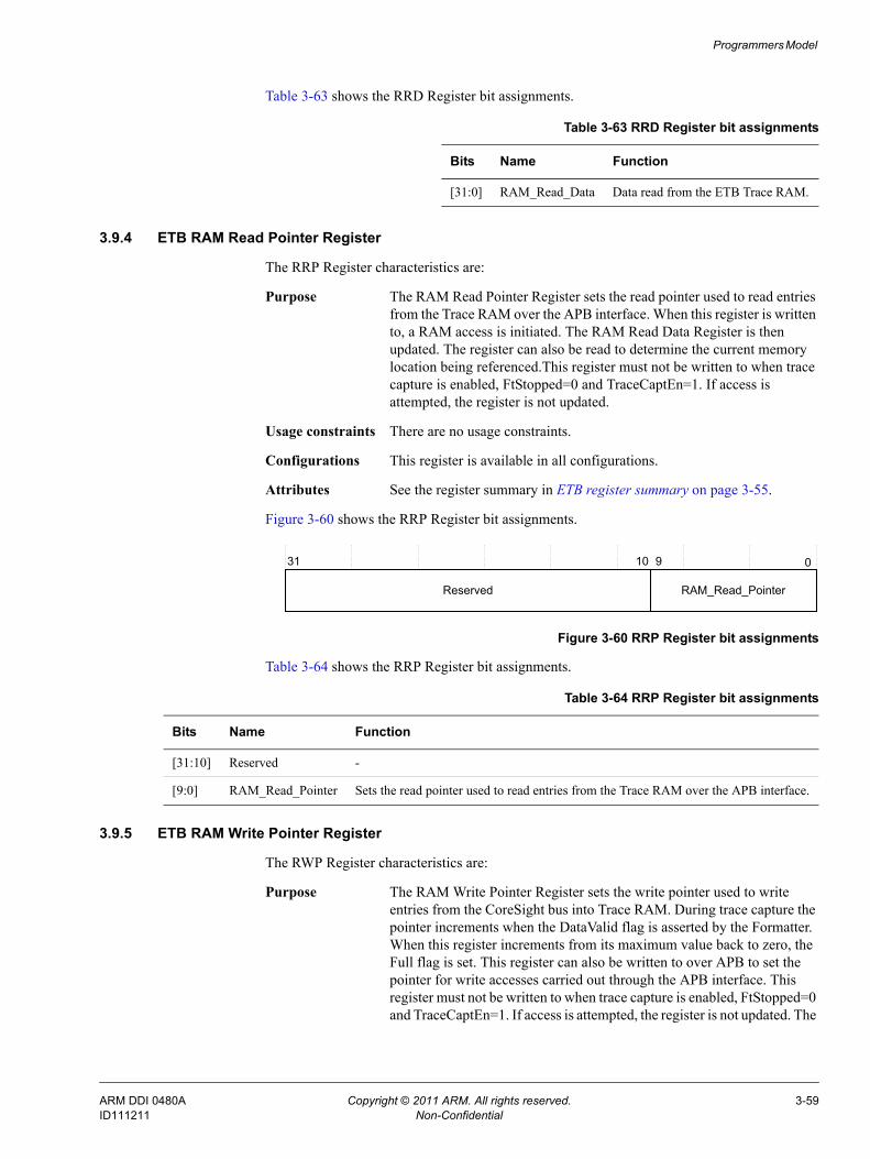
Programmers Model
Table 3-63 shows the RRD Register bit assignments.
3.9.4 ETB RAM Read Pointer Register
The RRP Register characteristics are:
Purpose The RAM Read Pointer Register sets the read pointer used to read entries from the Trace RAM over the APB interface. When this register is written to, a RAM access is initiated. The RAM Read Data Register is then updated. The register can also be read to determine the current memory location being referenced.This register must not be written to when trace capture is enabled, FtStopped=0 and TraceCaptEn=1. If access is attempted, the register is not updated.
Usage constraints There are no usage constraints.
Configurations This register is available in all configurations.
Attributes See the register summary in ETB register summary on page 3-55.
Figure 3-60 shows the RRP Register bit assignments.
Figure 3-60 RRP Register bit assignments
Table 3-64 shows the RRP Register bit assignments.
3.9.5 ETB RAM Write Pointer Register
The RWP Register characteristics are:
Purpose The RAM Write Pointer Register sets the write pointer used to write entries from the CoreSight bus into Trace RAM. During trace capture the pointer increments when the DataValid flag is asserted by the Formatter. When this register increments from its maximum value back to zero, the Full flag is set. This register can also be written to over APB to set the pointer for write accesses carried out through the APB interface. This register must not be written to when trace capture is enabled, FtStopped=0 and TraceCaptEn=1. If access is attempted, the register is not updated. The
Table 3-63 RRD Register bit assignments
Bits Name Function
[31:0] RAM_Read_Data Data read from the ETB Trace RAM.
31 0
Reserved
10 9
RAM_Read_Pointer
Table 3-64 RRP Register bit assignments
Bits Name Function
[31:10] Reserved -
[9:0] RAM_Read_Pointer Sets the read pointer used to read entries from the Trace RAM over the APB interface.
ARM DDI 0480A Copyright © 2011 ARM. All rights reserved. 3-59ID111211 Non-Confidential
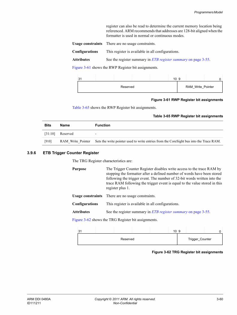
Programmers Model
register can also be read to determine the current memory location being referenced. ARM recommends that addresses are 128-bit aligned when the formatter is used in normal or continuous modes.
Usage constraints There are no usage constraints.
Configurations This register is available in all configurations.
Attributes See the register summary in ETB register summary on page 3-55.
Figure 3-61 shows the RWP Register bit assignments.
Figure 3-61 RWP Register bit assignments
Table 3-65 shows the RWP Register bit assignments.
3.9.6 ETB Trigger Counter Register
The TRG Register characteristics are:
Purpose The Trigger Counter Register disables write access to the trace RAM by stopping the formatter after a defined number of words have been stored following the trigger event. The number of 32-bit words written into the trace RAM following the trigger event is equal to the value stored in this register plus 1.
Usage constraints There are no usage constraints.
Configurations This register is available in all configurations.
Attributes See the register summary in ETB register summary on page 3-55.
Figure 3-62 shows the TRG Register bit assignments.
Figure 3-62 TRG Register bit assignments
31 0
Reserved
10 9
RAM_Write_Pointer
Table 3-65 RWP Register bit assignments
Bits Name Function
[31:10] Reserved -
[9:0] RAM_Write_Pointer Sets the write pointer used to write entries from the CoreSight bus into the Trace RAM.
31 0
Reserved
10 9
Trigger_Counter
ARM DDI 0480A Copyright © 2011 ARM. All rights reserved. 3-60ID111211 Non-Confidential
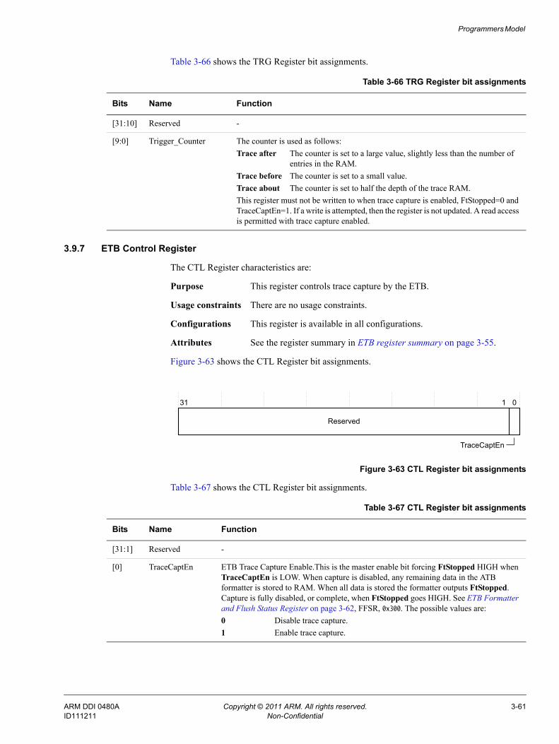
Programmers Model
Table 3-66 shows the TRG Register bit assignments.
3.9.7 ETB Control Register
The CTL Register characteristics are:
Purpose This register controls trace capture by the ETB.
Usage constraints There are no usage constraints.
Configurations This register is available in all configurations.
Attributes See the register summary in ETB register summary on page 3-55.
Figure 3-63 shows the CTL Register bit assignments.
Figure 3-63 CTL Register bit assignments
Table 3-67 shows the CTL Register bit assignments.
Table 3-66 TRG Register bit assignments
Bits Name Function
[31:10] Reserved -
[9:0] Trigger_Counter The counter is used as follows: Trace after The counter is set to a large value, slightly less than the number of
entries in the RAM.Trace before The counter is set to a small value.Trace about The counter is set to half the depth of the trace RAM.This register must not be written to when trace capture is enabled, FtStopped=0 and TraceCaptEn=1. If a write is attempted, then the register is not updated. A read access is permitted with trace capture enabled.
31 0
Reserved
1
TraceCaptEn
Table 3-67 CTL Register bit assignments
Bits Name Function
[31:1] Reserved -
[0] TraceCaptEn ETB Trace Capture Enable.This is the master enable bit forcing FtStopped HIGH when TraceCaptEn is LOW. When capture is disabled, any remaining data in the ATB formatter is stored to RAM. When all data is stored the formatter outputs FtStopped. Capture is fully disabled, or complete, when FtStopped goes HIGH. See ETB Formatter and Flush Status Register on page 3-62, FFSR, 0x300. The possible values are:0 Disable trace capture.1 Enable trace capture.
ARM DDI 0480A Copyright © 2011 ARM. All rights reserved. 3-61ID111211 Non-Confidential
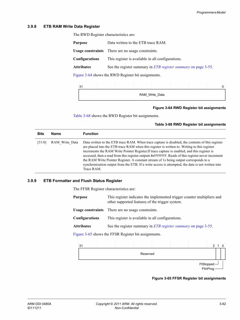
Programmers Model
3.9.8 ETB RAM Write Data Register
The RWD Register characteristics are:
Purpose Data written to the ETB trace RAM.
Usage constraints There are no usage constraints.
Configurations This register is available in all configurations.
Attributes See the register summary in ETB register summary on page 3-55.
Figure 3-64 shows the RWD Register bit assignments.
Figure 3-64 RWD Register bit assignments
Table 3-68 shows the RWD Register bit assignments.
3.9.9 ETB Formatter and Flush Status Register
The FFSR Register characteristics are:
Purpose This register indicates the implemented trigger counter multipliers and other supported features of the trigger system.
Usage constraints There are no usage constraints.
Configurations This register is available in all configurations.
Attributes See the register summary in ETB register summary on page 3-55.
Figure 3-65 shows the FFSR Register bit assignments.
Figure 3-65 FFSR Register bit assignments
31 0
RAM_Write_Data
Table 3-68 RWD Register bit assignments
Bits Name Function
[31:0] RAM_Write_Data Data written to the ETB trace RAM. When trace capture is disabled, the contents of this register are placed into the ETB trace RAM when this register is written to. Writing to this register increments the RAM Write Pointer Register.If trace capture is enabled, and this register is accessed, then a read from this register outputs 0xFFFFFFFF. Reads of this register never increment the RAM Write Pointer Register. A constant stream of 1s being output corresponds to a synchronization output from the ETB. If a write access is attempted, the data is not written into Trace RAM.
31 0
Reserved
1
FlInProg
2
FtStopped
ARM DDI 0480A Copyright © 2011 ARM. All rights reserved. 3-62ID111211 Non-Confidential
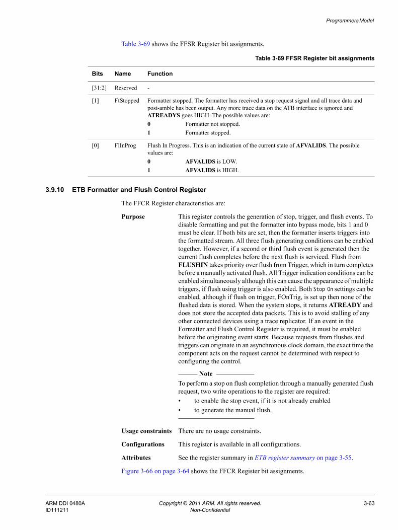
Programmers Model
Table 3-69 shows the FFSR Register bit assignments.
3.9.10 ETB Formatter and Flush Control Register
The FFCR Register characteristics are:
Purpose This register controls the generation of stop, trigger, and flush events. To disable formatting and put the formatter into bypass mode, bits 1 and 0 must be clear. If both bits are set, then the formatter inserts triggers into the formatted stream. All three flush generating conditions can be enabled together. However, if a second or third flush event is generated then the current flush completes before the next flush is serviced. Flush from FLUSHIN takes priority over flush from Trigger, which in turn completes before a manually activated flush. All Trigger indication conditions can be enabled simultaneously although this can cause the appearance of multiple triggers, if flush using trigger is also enabled. Both Stop On settings can be enabled, although if flush on trigger, FOnTrig, is set up then none of the flushed data is stored. When the system stops, it returns ATREADY and does not store the accepted data packets. This is to avoid stalling of any other connected devices using a trace replicator. If an event in the Formatter and Flush Control Register is required, it must be enabled before the originating event starts. Because requests from flushes and triggers can originate in an asynchronous clock domain, the exact time the component acts on the request cannot be determined with respect to configuring the control.
Note To perform a stop on flush completion through a manually generated flush
request, two write operations to the register are required: • to enable the stop event, if it is not already enabled• to generate the manual flush.
Usage constraints There are no usage constraints.
Configurations This register is available in all configurations.
Attributes See the register summary in ETB register summary on page 3-55.
Figure 3-66 on page 3-64 shows the FFCR Register bit assignments.
Table 3-69 FFSR Register bit assignments
Bits Name Function
[31:2] Reserved -
[1] FtStopped Formatter stopped. The formatter has received a stop request signal and all trace data and post-amble has been output. Any more trace data on the ATB interface is ignored and ATREADYS goes HIGH. The possible values are:0 Formatter not stopped.1 Formatter stopped.
[0] FlInProg Flush In Progress. This is an indication of the current state of AFVALIDS. The possible values are:0 AFVALIDS is LOW.1 AFVALIDS is HIGH.
ARM DDI 0480A Copyright © 2011 ARM. All rights reserved. 3-63ID111211 Non-Confidential
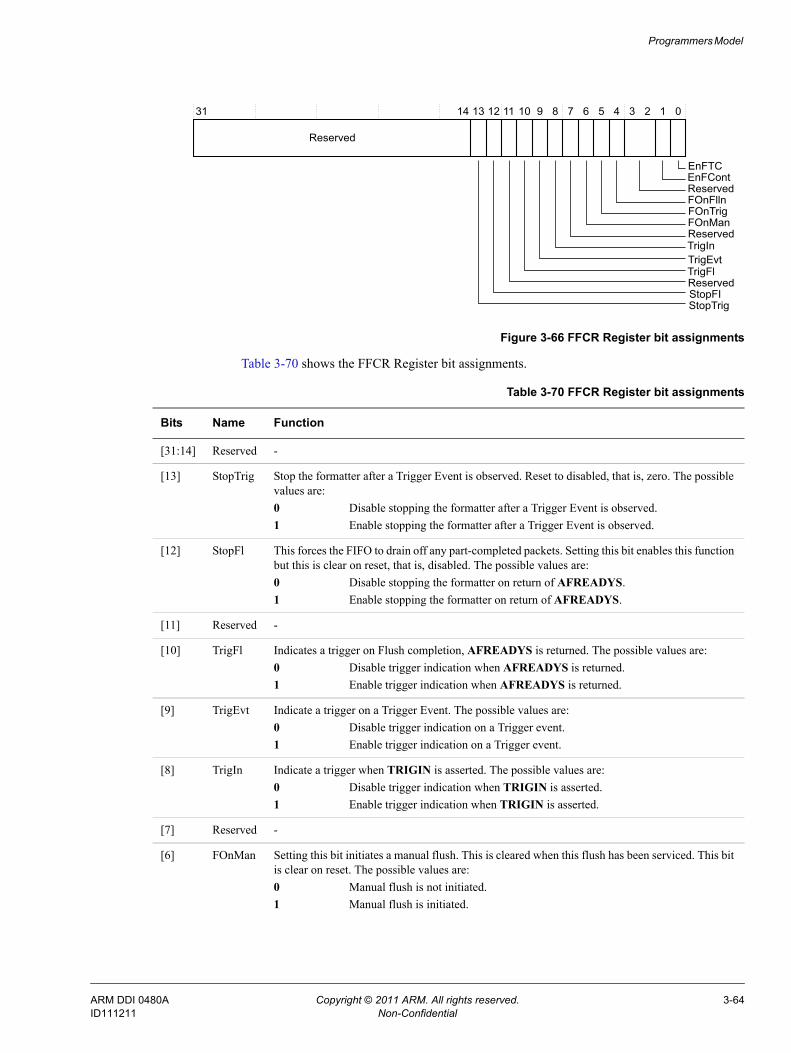
Programmers Model
Figure 3-66 FFCR Register bit assignments
Table 3-70 shows the FFCR Register bit assignments.
31 14 13 12 11 10 9 8 7 6 5 4 3 2 1 0
Reserved
EnFTCEnFContReservedFOnFllnFOnTrigFOnManReserved
TrigEvtTrigIn
TrigFlReservedStopFIStopTrig
Table 3-70 FFCR Register bit assignments
Bits Name Function
[31:14] Reserved -
[13] StopTrig Stop the formatter after a Trigger Event is observed. Reset to disabled, that is, zero. The possible values are:0 Disable stopping the formatter after a Trigger Event is observed.1 Enable stopping the formatter after a Trigger Event is observed.
[12] StopFl This forces the FIFO to drain off any part-completed packets. Setting this bit enables this function but this is clear on reset, that is, disabled. The possible values are:0 Disable stopping the formatter on return of AFREADYS.1 Enable stopping the formatter on return of AFREADYS.
[11] Reserved -
[10] TrigFl Indicates a trigger on Flush completion, AFREADYS is returned. The possible values are:0 Disable trigger indication when AFREADYS is returned.1 Enable trigger indication when AFREADYS is returned.
[9] TrigEvt Indicate a trigger on a Trigger Event. The possible values are:0 Disable trigger indication on a Trigger event.1 Enable trigger indication on a Trigger event.
[8] TrigIn Indicate a trigger when TRIGIN is asserted. The possible values are:0 Disable trigger indication when TRIGIN is asserted.1 Enable trigger indication when TRIGIN is asserted.
[7] Reserved -
[6] FOnMan Setting this bit initiates a manual flush. This is cleared when this flush has been serviced. This bit is clear on reset. The possible values are:0 Manual flush is not initiated.1 Manual flush is initiated.
ARM DDI 0480A Copyright © 2011 ARM. All rights reserved. 3-64ID111211 Non-Confidential
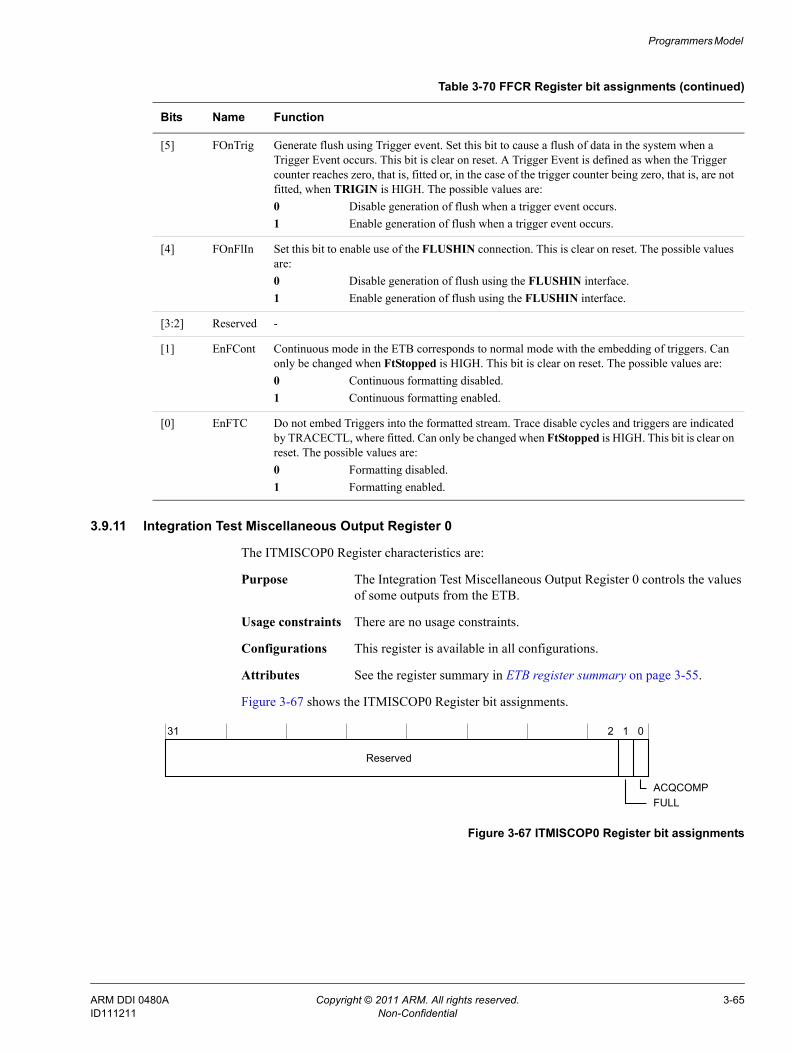
Programmers Model
3.9.11 Integration Test Miscellaneous Output Register 0
The ITMISCOP0 Register characteristics are:
Purpose The Integration Test Miscellaneous Output Register 0 controls the values of some outputs from the ETB.
Usage constraints There are no usage constraints.
Configurations This register is available in all configurations.
Attributes See the register summary in ETB register summary on page 3-55.
Figure 3-67 shows the ITMISCOP0 Register bit assignments.
Figure 3-67 ITMISCOP0 Register bit assignments
[5] FOnTrig Generate flush using Trigger event. Set this bit to cause a flush of data in the system when a Trigger Event occurs. This bit is clear on reset. A Trigger Event is defined as when the Trigger counter reaches zero, that is, fitted or, in the case of the trigger counter being zero, that is, are not fitted, when TRIGIN is HIGH. The possible values are:0 Disable generation of flush when a trigger event occurs.1 Enable generation of flush when a trigger event occurs.
[4] FOnFlIn Set this bit to enable use of the FLUSHIN connection. This is clear on reset. The possible values are:0 Disable generation of flush using the FLUSHIN interface.1 Enable generation of flush using the FLUSHIN interface.
[3:2] Reserved -
[1] EnFCont Continuous mode in the ETB corresponds to normal mode with the embedding of triggers. Can only be changed when FtStopped is HIGH. This bit is clear on reset. The possible values are:0 Continuous formatting disabled.1 Continuous formatting enabled.
[0] EnFTC Do not embed Triggers into the formatted stream. Trace disable cycles and triggers are indicated by TRACECTL, where fitted. Can only be changed when FtStopped is HIGH. This bit is clear on reset. The possible values are:0 Formatting disabled.1 Formatting enabled.
Table 3-70 FFCR Register bit assignments (continued)
Bits Name Function
31 2 1 0
Reserved
FULLACQCOMP
ARM DDI 0480A Copyright © 2011 ARM. All rights reserved. 3-65ID111211 Non-Confidential
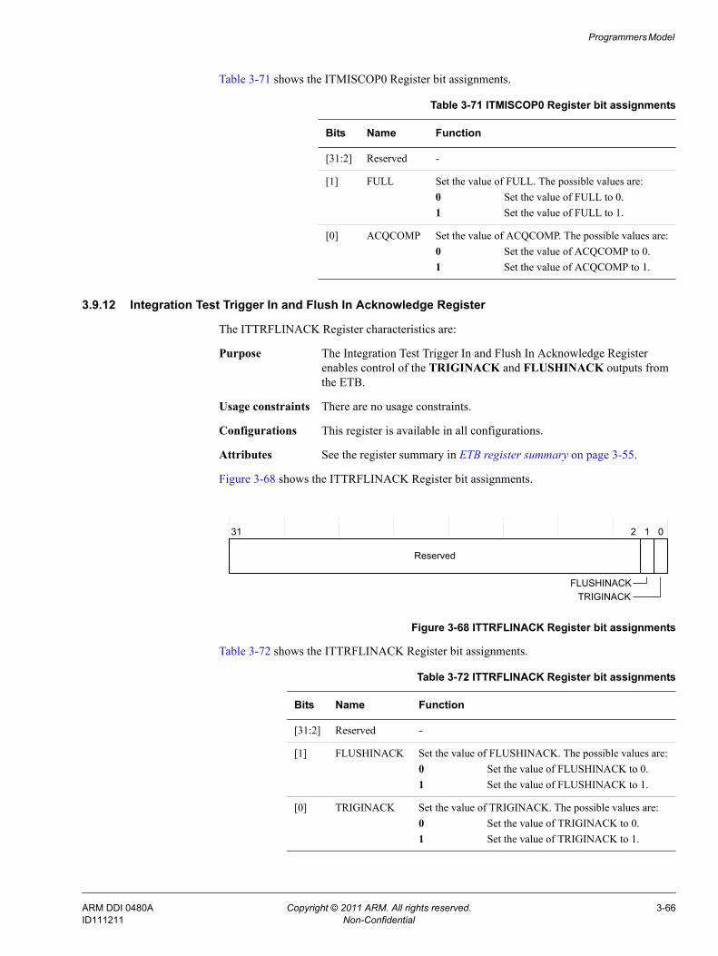
Programmers Model
Table 3-71 shows the ITMISCOP0 Register bit assignments.
3.9.12 Integration Test Trigger In and Flush In Acknowledge Register
The ITTRFLINACK Register characteristics are:
Purpose The Integration Test Trigger In and Flush In Acknowledge Register enables control of the TRIGINACK and FLUSHINACK outputs from the ETB.
Usage constraints There are no usage constraints.
Configurations This register is available in all configurations.
Attributes See the register summary in ETB register summary on page 3-55.
Figure 3-68 shows the ITTRFLINACK Register bit assignments.
Figure 3-68 ITTRFLINACK Register bit assignments
Table 3-72 shows the ITTRFLINACK Register bit assignments.
Table 3-71 ITMISCOP0 Register bit assignments
Bits Name Function
[31:2] Reserved -
[1] FULL Set the value of FULL. The possible values are:0 Set the value of FULL to 0.1 Set the value of FULL to 1.
[0] ACQCOMP Set the value of ACQCOMP. The possible values are:0 Set the value of ACQCOMP to 0.1 Set the value of ACQCOMP to 1.
31 0
Reserved
FLUSHINACK
2 1
TRIGINACK
Table 3-72 ITTRFLINACK Register bit assignments
Bits Name Function
[31:2] Reserved -
[1] FLUSHINACK Set the value of FLUSHINACK. The possible values are:0 Set the value of FLUSHINACK to 0.1 Set the value of FLUSHINACK to 1.
[0] TRIGINACK Set the value of TRIGINACK. The possible values are:0 Set the value of TRIGINACK to 0.1 Set the value of TRIGINACK to 1.
ARM DDI 0480A Copyright © 2011 ARM. All rights reserved. 3-66ID111211 Non-Confidential
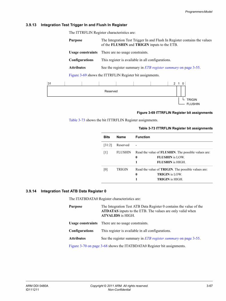
Programmers Model
3.9.13 Integration Test Trigger In and Flush In Register
The ITTRFLIN Register characteristics are:
Purpose The Integration Test Trigger In and Flush In Register contains the values of the FLUSHIN and TRIGIN inputs to the ETB.
Usage constraints There are no usage constraints.
Configurations This register is available in all configurations.
Attributes See the register summary in ETB register summary on page 3-55.
Figure 3-69 shows the ITTRFLIN Register bit assignments.
Figure 3-69 ITTRFLIN Register bit assignments
Table 3-73 shows the bit ITTRFLIN Register assignments.
3.9.14 Integration Test ATB Data Register 0
The ITATBDATA0 Register characteristics are:
Purpose The Integration Test ATB Data Register 0 contains the value of the ATDATAS inputs to the ETB. The values are only valid when ATVALIDS is HIGH.
Usage constraints There are no usage constraints.
Configurations This register is available in all configurations.
Attributes See the register summary in ETB register summary on page 3-55.
Figure 3-70 on page 3-68 shows the ITATBDATA0 Register bit assignments.
31 2 1 0
Reserved
FLUSHINTRIGIN
Table 3-73 ITTRFLIN Register bit assignments
Bits Name Function
[31:2] Reserved -
[1] FLUSHIN Read the value of FLUSHIN. The possible values are:0 FLUSHIN is LOW.1 FLUSHIN is HIGH.
[0] TRIGIN Read the value of TRIGIN. The possible values are:0 TRIGIN is LOW.1 TRIGIN is HIGH.
ARM DDI 0480A Copyright © 2011 ARM. All rights reserved. 3-67ID111211 Non-Confidential
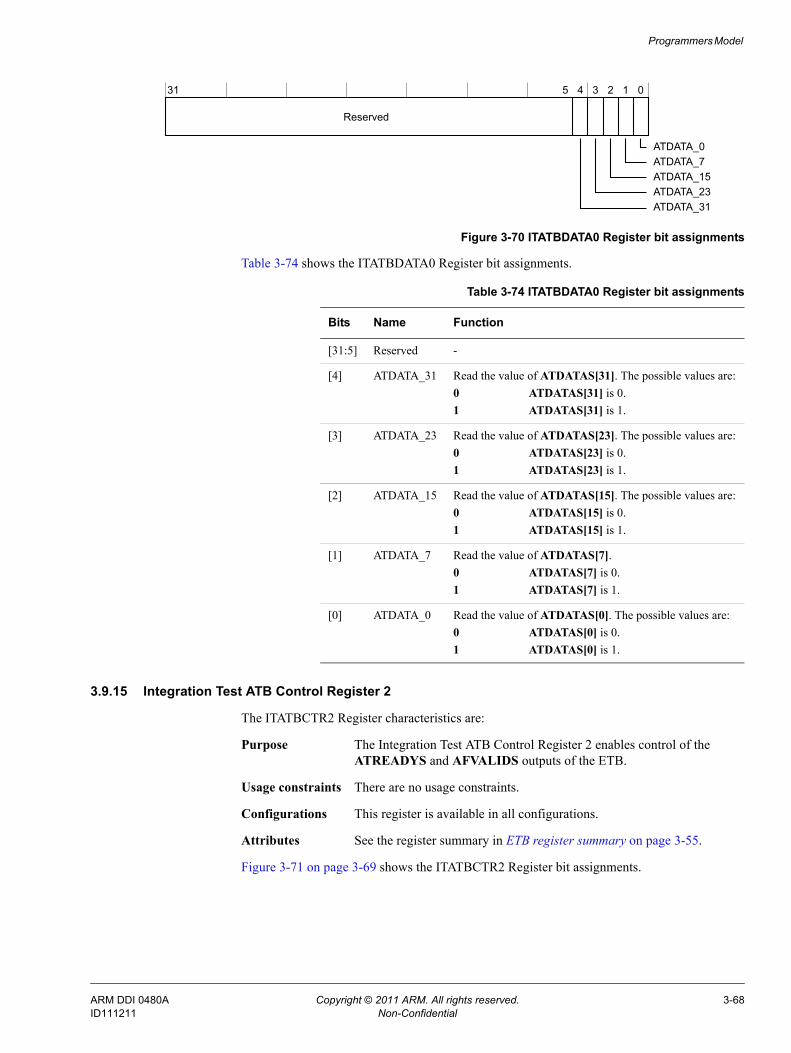
Programmers Model
Figure 3-70 ITATBDATA0 Register bit assignments
Table 3-74 shows the ITATBDATA0 Register bit assignments.
3.9.15 Integration Test ATB Control Register 2
The ITATBCTR2 Register characteristics are:
Purpose The Integration Test ATB Control Register 2 enables control of the ATREADYS and AFVALIDS outputs of the ETB.
Usage constraints There are no usage constraints.
Configurations This register is available in all configurations.
Attributes See the register summary in ETB register summary on page 3-55.
Figure 3-71 on page 3-69 shows the ITATBCTR2 Register bit assignments.
31 5 4 3 2 1 0
Reserved
ATDATA_15ATDATA_7ATDATA_0
ATDATA_23ATDATA_31
Table 3-74 ITATBDATA0 Register bit assignments
Bits Name Function
[31:5] Reserved -
[4] ATDATA_31 Read the value of ATDATAS[31]. The possible values are:0 ATDATAS[31] is 0.1 ATDATAS[31] is 1.
[3] ATDATA_23 Read the value of ATDATAS[23]. The possible values are:0 ATDATAS[23] is 0.1 ATDATAS[23] is 1.
[2] ATDATA_15 Read the value of ATDATAS[15]. The possible values are:0 ATDATAS[15] is 0.1 ATDATAS[15] is 1.
[1] ATDATA_7 Read the value of ATDATAS[7].0 ATDATAS[7] is 0.1 ATDATAS[7] is 1.
[0] ATDATA_0 Read the value of ATDATAS[0]. The possible values are: 0 ATDATAS[0] is 0.1 ATDATAS[0] is 1.
ARM DDI 0480A Copyright © 2011 ARM. All rights reserved. 3-68ID111211 Non-Confidential
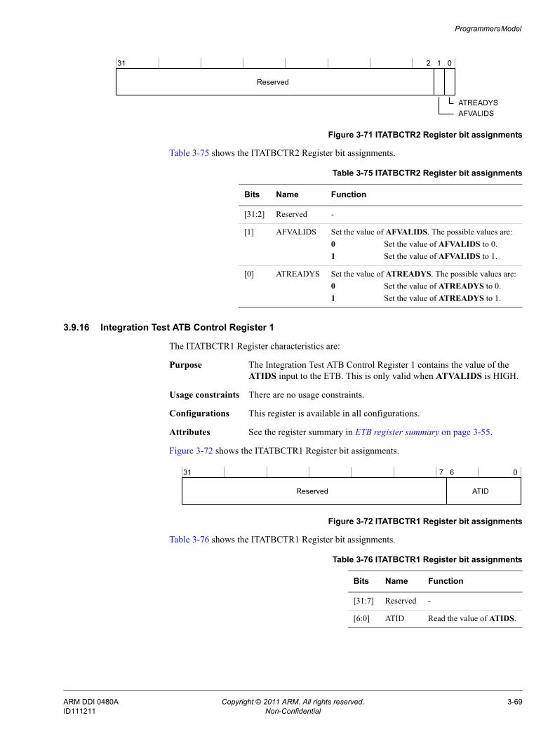
Programmers Model
Figure 3-71 ITATBCTR2 Register bit assignments
Table 3-75 shows the ITATBCTR2 Register bit assignments.
3.9.16 Integration Test ATB Control Register 1
The ITATBCTR1 Register characteristics are:
Purpose The Integration Test ATB Control Register 1 contains the value of the ATIDS input to the ETB. This is only valid when ATVALIDS is HIGH.
Usage constraints There are no usage constraints.
Configurations This register is available in all configurations.
Attributes See the register summary in ETB register summary on page 3-55.
Figure 3-72 shows the ITATBCTR1 Register bit assignments.
Figure 3-72 ITATBCTR1 Register bit assignments
Table 3-76 shows the ITATBCTR1 Register bit assignments.
31 2 1 0
Reserved
AFVALIDSATREADYS
Table 3-75 ITATBCTR2 Register bit assignments
Bits Name Function
[31:2] Reserved -
[1] AFVALIDS Set the value of AFVALIDS. The possible values are:0 Set the value of AFVALIDS to 0.1 Set the value of AFVALIDS to 1.
[0] ATREADYS Set the value of ATREADYS. The possible values are:0 Set the value of ATREADYS to 0.1 Set the value of ATREADYS to 1.
31 7 6 0
ATIDReserved
Table 3-76 ITATBCTR1 Register bit assignments
Bits Name Function
[31:7] Reserved -
[6:0] ATID Read the value of ATIDS.
ARM DDI 0480A Copyright © 2011 ARM. All rights reserved. 3-69ID111211 Non-Confidential
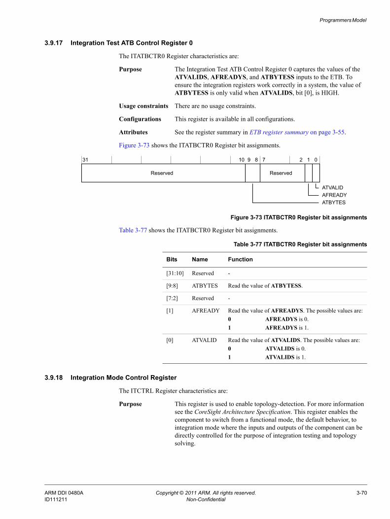
Programmers Model
3.9.17 Integration Test ATB Control Register 0
The ITATBCTR0 Register characteristics are:
Purpose The Integration Test ATB Control Register 0 captures the values of the ATVALIDS, AFREADYS, and ATBYTESS inputs to the ETB. To ensure the integration registers work correctly in a system, the value of ATBYTESS is only valid when ATVALIDS, bit [0], is HIGH.
Usage constraints There are no usage constraints.
Configurations This register is available in all configurations.
Attributes See the register summary in ETB register summary on page 3-55.
Figure 3-73 shows the ITATBCTR0 Register bit assignments.
Figure 3-73 ITATBCTR0 Register bit assignments
Table 3-77 shows the ITATBCTR0 Register bit assignments.
3.9.18 Integration Mode Control Register
The ITCTRL Register characteristics are:
Purpose This register is used to enable topology-detection. For more information see the CoreSight Architecture Specification. This register enables the component to switch from a functional mode, the default behavior, to integration mode where the inputs and outputs of the component can be directly controlled for the purpose of integration testing and topology solving.
31 10 9 8 7 2 1 0
ReservedReserved
ATBYTESAFREADYATVALID
Table 3-77 ITATBCTR0 Register bit assignments
Bits Name Function
[31:10] Reserved -
[9:8] ATBYTES Read the value of ATBYTESS.
[7:2] Reserved -
[1] AFREADY Read the value of AFREADYS. The possible values are:0 AFREADYS is 0.1 AFREADYS is 1.
[0] ATVALID Read the value of ATVALIDS. The possible values are:0 ATVALIDS is 0.1 ATVALIDS is 1.
ARM DDI 0480A Copyright © 2011 ARM. All rights reserved. 3-70ID111211 Non-Confidential
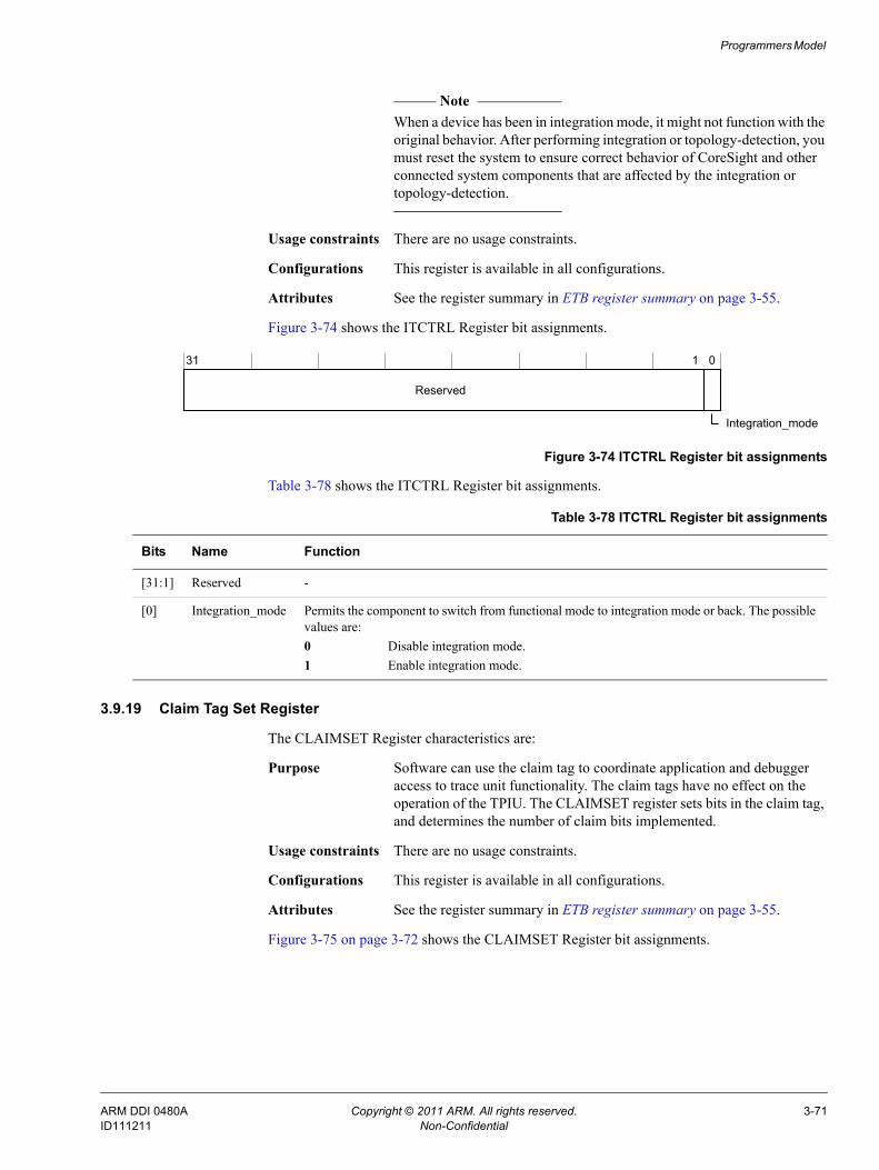
Programmers Model
Note When a device has been in integration mode, it might not function with the
original behavior. After performing integration or topology-detection, you must reset the system to ensure correct behavior of CoreSight and other connected system components that are affected by the integration or topology-detection.
Usage constraints There are no usage constraints.
Configurations This register is available in all configurations.
Attributes See the register summary in ETB register summary on page 3-55.
Figure 3-74 shows the ITCTRL Register bit assignments.
Figure 3-74 ITCTRL Register bit assignments
Table 3-78 shows the ITCTRL Register bit assignments.
3.9.19 Claim Tag Set Register
The CLAIMSET Register characteristics are:
Purpose Software can use the claim tag to coordinate application and debugger access to trace unit functionality. The claim tags have no effect on the operation of the TPIU. The CLAIMSET register sets bits in the claim tag, and determines the number of claim bits implemented.
Usage constraints There are no usage constraints.
Configurations This register is available in all configurations.
Attributes See the register summary in ETB register summary on page 3-55.
Figure 3-75 on page 3-72 shows the CLAIMSET Register bit assignments.
31 1 0
Reserved
Integration_mode
Table 3-78 ITCTRL Register bit assignments
Bits Name Function
[31:1] Reserved -
[0] Integration_mode Permits the component to switch from functional mode to integration mode or back. The possible values are:0 Disable integration mode.1 Enable integration mode.
ARM DDI 0480A Copyright © 2011 ARM. All rights reserved. 3-71ID111211 Non-Confidential
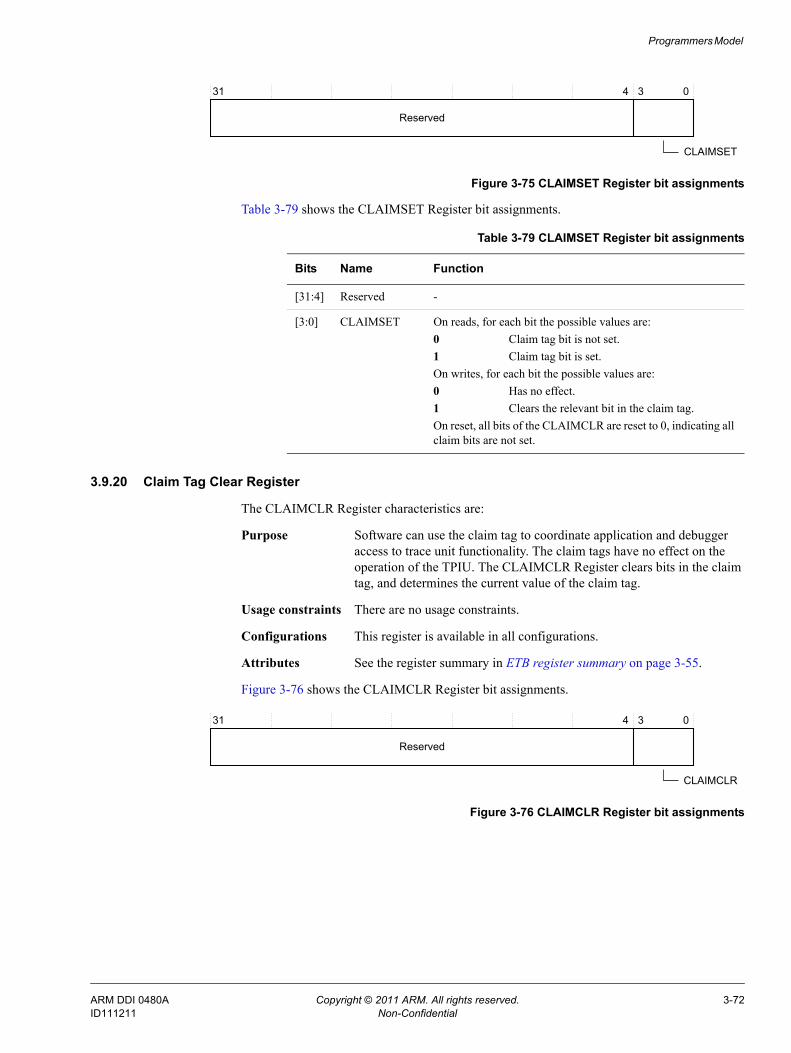
Programmers Model
Figure 3-75 CLAIMSET Register bit assignments
Table 3-79 shows the CLAIMSET Register bit assignments.
3.9.20 Claim Tag Clear Register
The CLAIMCLR Register characteristics are:
Purpose Software can use the claim tag to coordinate application and debugger access to trace unit functionality. The claim tags have no effect on the operation of the TPIU. The CLAIMCLR Register clears bits in the claim tag, and determines the current value of the claim tag.
Usage constraints There are no usage constraints.
Configurations This register is available in all configurations.
Attributes See the register summary in ETB register summary on page 3-55.
Figure 3-76 shows the CLAIMCLR Register bit assignments.
Figure 3-76 CLAIMCLR Register bit assignments
31 4 3 0
CLAIMSET
Reserved
Table 3-79 CLAIMSET Register bit assignments
Bits Name Function
[31:4] Reserved -
[3:0] CLAIMSET On reads, for each bit the possible values are:0 Claim tag bit is not set.1 Claim tag bit is set.On writes, for each bit the possible values are:0 Has no effect.1 Clears the relevant bit in the claim tag.On reset, all bits of the CLAIMCLR are reset to 0, indicating all claim bits are not set.
31 4 3 0
CLAIMCLR
Reserved
ARM DDI 0480A Copyright © 2011 ARM. All rights reserved. 3-72ID111211 Non-Confidential
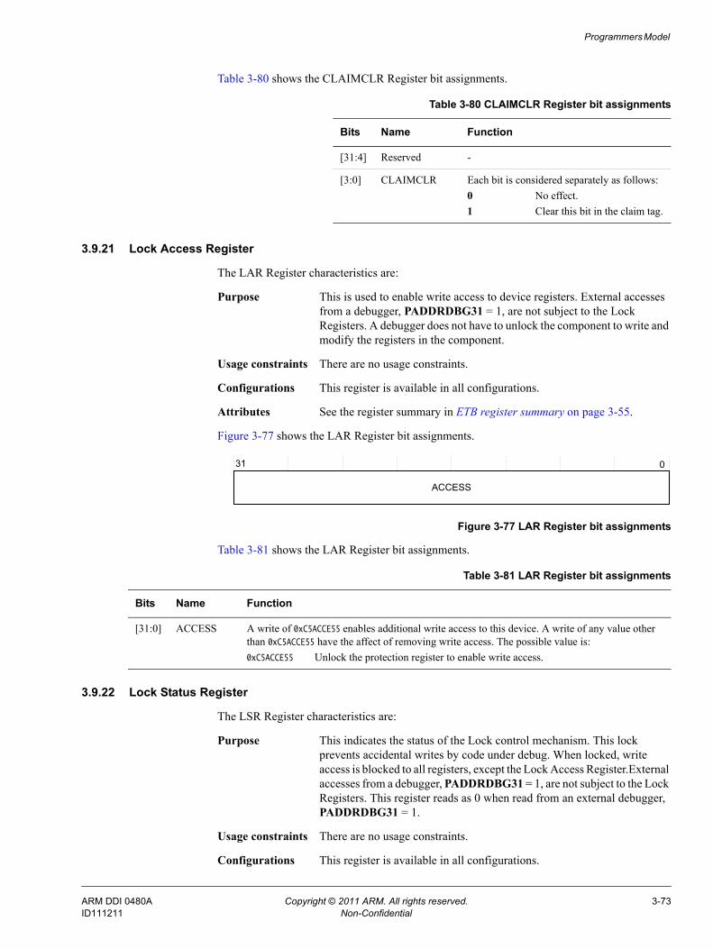
Programmers Model
Table 3-80 shows the CLAIMCLR Register bit assignments.
3.9.21 Lock Access Register
The LAR Register characteristics are:
Purpose This is used to enable write access to device registers. External accesses from a debugger, PADDRDBG31 = 1, are not subject to the Lock Registers. A debugger does not have to unlock the component to write and modify the registers in the component.
Usage constraints There are no usage constraints.
Configurations This register is available in all configurations.
Attributes See the register summary in ETB register summary on page 3-55.
Figure 3-77 shows the LAR Register bit assignments.
Figure 3-77 LAR Register bit assignments
Table 3-81 shows the LAR Register bit assignments.
3.9.22 Lock Status Register
The LSR Register characteristics are:
Purpose This indicates the status of the Lock control mechanism. This lock prevents accidental writes by code under debug. When locked, write access is blocked to all registers, except the Lock Access Register.External accesses from a debugger, PADDRDBG31 = 1, are not subject to the Lock Registers. This register reads as 0 when read from an external debugger, PADDRDBG31 = 1.
Usage constraints There are no usage constraints.
Configurations This register is available in all configurations.
Table 3-80 CLAIMCLR Register bit assignments
Bits Name Function
[31:4] Reserved -
[3:0] CLAIMCLR Each bit is considered separately as follows: 0 No effect.1 Clear this bit in the claim tag.
31 0
ACCESS
Table 3-81 LAR Register bit assignments
Bits Name Function
[31:0] ACCESS A write of 0xC5ACCE55 enables additional write access to this device. A write of any value other than 0xC5ACCE55 have the affect of removing write access. The possible value is:0xC5ACCE55 Unlock the protection register to enable write access.
ARM DDI 0480A Copyright © 2011 ARM. All rights reserved. 3-73ID111211 Non-Confidential
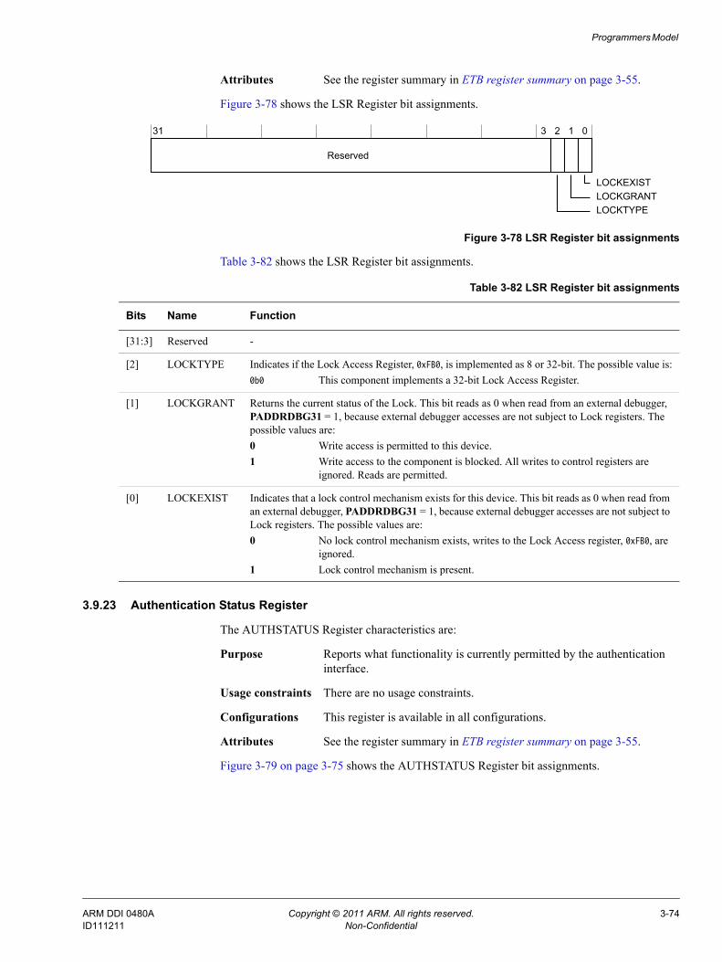
Programmers Model
Attributes See the register summary in ETB register summary on page 3-55.
Figure 3-78 shows the LSR Register bit assignments.
Figure 3-78 LSR Register bit assignments
Table 3-82 shows the LSR Register bit assignments.
3.9.23 Authentication Status Register
The AUTHSTATUS Register characteristics are:
Purpose Reports what functionality is currently permitted by the authentication interface.
Usage constraints There are no usage constraints.
Configurations This register is available in all configurations.
Attributes See the register summary in ETB register summary on page 3-55.
Figure 3-79 on page 3-75 shows the AUTHSTATUS Register bit assignments.
31 3 2 1 0
Reserved
LOCKTYPELOCKGRANTLOCKEXIST
Table 3-82 LSR Register bit assignments
Bits Name Function
[31:3] Reserved -
[2] LOCKTYPE Indicates if the Lock Access Register, 0xFB0, is implemented as 8 or 32-bit. The possible value is:0b0 This component implements a 32-bit Lock Access Register.
[1] LOCKGRANT Returns the current status of the Lock. This bit reads as 0 when read from an external debugger, PADDRDBG31 = 1, because external debugger accesses are not subject to Lock registers. The possible values are:0 Write access is permitted to this device.1 Write access to the component is blocked. All writes to control registers are
ignored. Reads are permitted.
[0] LOCKEXIST Indicates that a lock control mechanism exists for this device. This bit reads as 0 when read from an external debugger, PADDRDBG31 = 1, because external debugger accesses are not subject to Lock registers. The possible values are:0 No lock control mechanism exists, writes to the Lock Access register, 0xFB0, are
ignored.1 Lock control mechanism is present.
ARM DDI 0480A Copyright © 2011 ARM. All rights reserved. 3-74ID111211 Non-Confidential
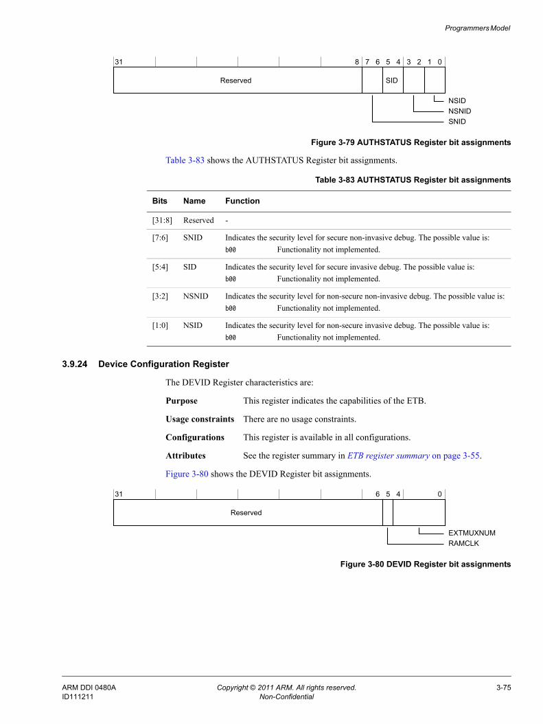
Programmers Model
Figure 3-79 AUTHSTATUS Register bit assignments
Table 3-83 shows the AUTHSTATUS Register bit assignments.
3.9.24 Device Configuration Register
The DEVID Register characteristics are:
Purpose This register indicates the capabilities of the ETB.
Usage constraints There are no usage constraints.
Configurations This register is available in all configurations.
Attributes See the register summary in ETB register summary on page 3-55.
Figure 3-80 shows the DEVID Register bit assignments.
Figure 3-80 DEVID Register bit assignments
31 8 7 6 5 4 3 2 1 0
SIDReserved
SNIDNSNIDNSID
Table 3-83 AUTHSTATUS Register bit assignments
Bits Name Function
[31:8] Reserved -
[7:6] SNID Indicates the security level for secure non-invasive debug. The possible value is:b00 Functionality not implemented.
[5:4] SID Indicates the security level for secure invasive debug. The possible value is:b00 Functionality not implemented.
[3:2] NSNID Indicates the security level for non-secure non-invasive debug. The possible value is:b00 Functionality not implemented.
[1:0] NSID Indicates the security level for non-secure invasive debug. The possible value is:b00 Functionality not implemented.
31 6 5 4 0
Reserved
RAMCLKEXTMUXNUM
ARM DDI 0480A Copyright © 2011 ARM. All rights reserved. 3-75ID111211 Non-Confidential
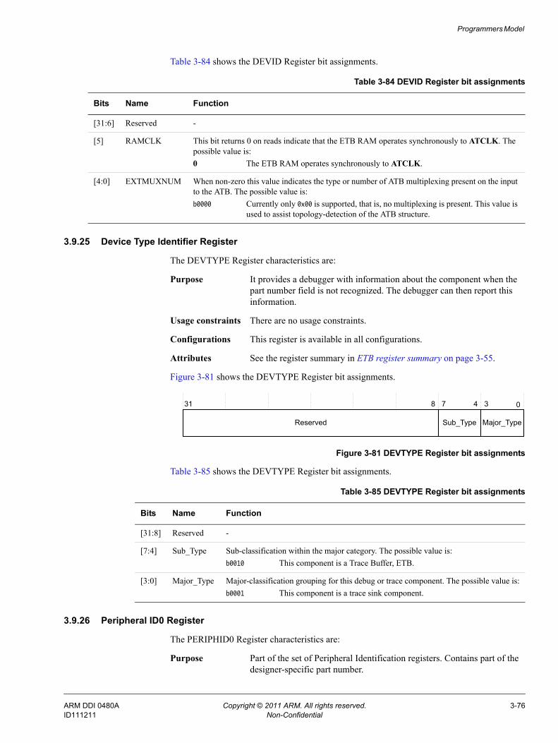
Programmers Model
Table 3-84 shows the DEVID Register bit assignments.
3.9.25 Device Type Identifier Register
The DEVTYPE Register characteristics are:
Purpose It provides a debugger with information about the component when the part number field is not recognized. The debugger can then report this information.
Usage constraints There are no usage constraints.
Configurations This register is available in all configurations.
Attributes See the register summary in ETB register summary on page 3-55.
Figure 3-81 shows the DEVTYPE Register bit assignments.
Figure 3-81 DEVTYPE Register bit assignments
Table 3-85 shows the DEVTYPE Register bit assignments.
3.9.26 Peripheral ID0 Register
The PERIPHID0 Register characteristics are:
Purpose Part of the set of Peripheral Identification registers. Contains part of the designer-specific part number.
Table 3-84 DEVID Register bit assignments
Bits Name Function
[31:6] Reserved -
[5] RAMCLK This bit returns 0 on reads indicate that the ETB RAM operates synchronously to ATCLK. The possible value is:0 The ETB RAM operates synchronously to ATCLK.
[4:0] EXTMUXNUM When non-zero this value indicates the type or number of ATB multiplexing present on the input to the ATB. The possible value is:b0000 Currently only 0x00 is supported, that is, no multiplexing is present. This value is
used to assist topology-detection of the ATB structure.
31 0
Reserved
7
Sub_Type
8 4
Major_Type
3
Table 3-85 DEVTYPE Register bit assignments
Bits Name Function
[31:8] Reserved -
[7:4] Sub_Type Sub-classification within the major category. The possible value is:b0010 This component is a Trace Buffer, ETB.
[3:0] Major_Type Major-classification grouping for this debug or trace component. The possible value is:b0001 This component is a trace sink component.
ARM DDI 0480A Copyright © 2011 ARM. All rights reserved. 3-76ID111211 Non-Confidential
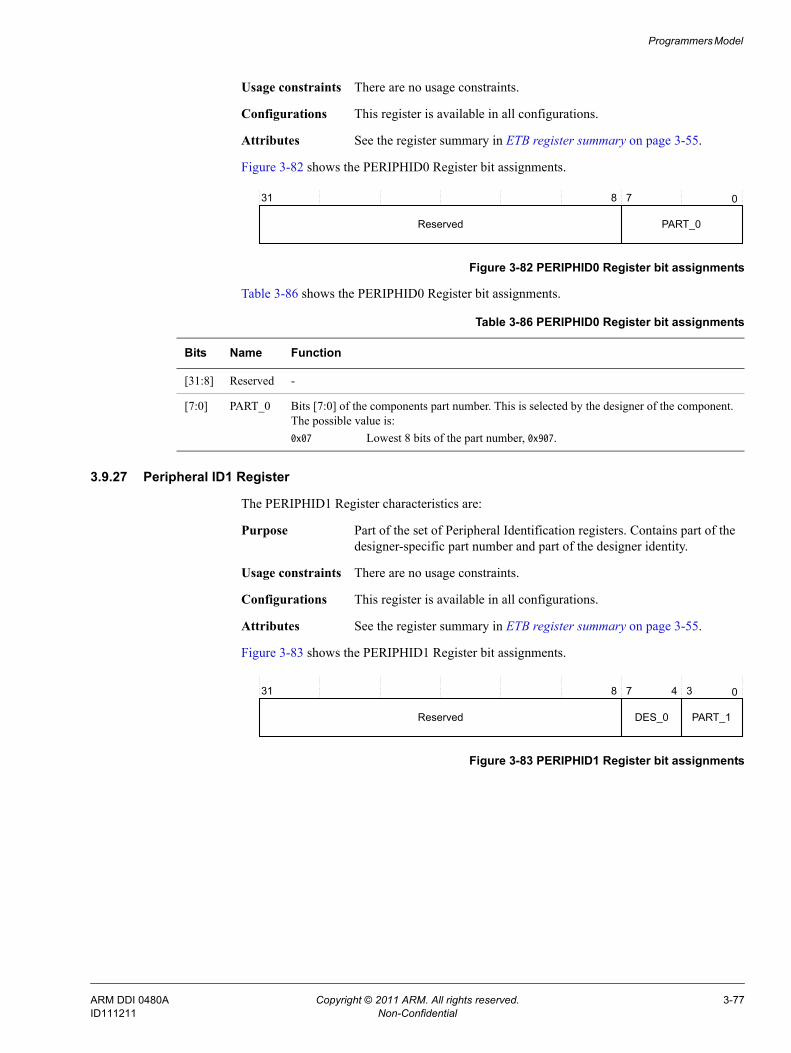
Programmers Model
Usage constraints There are no usage constraints.
Configurations This register is available in all configurations.
Attributes See the register summary in ETB register summary on page 3-55.
Figure 3-82 shows the PERIPHID0 Register bit assignments.
Figure 3-82 PERIPHID0 Register bit assignments
Table 3-86 shows the PERIPHID0 Register bit assignments.
3.9.27 Peripheral ID1 Register
The PERIPHID1 Register characteristics are:
Purpose Part of the set of Peripheral Identification registers. Contains part of the designer-specific part number and part of the designer identity.
Usage constraints There are no usage constraints.
Configurations This register is available in all configurations.
Attributes See the register summary in ETB register summary on page 3-55.
Figure 3-83 shows the PERIPHID1 Register bit assignments.
Figure 3-83 PERIPHID1 Register bit assignments
31 0
Reserved
78
PART_0
Table 3-86 PERIPHID0 Register bit assignments
Bits Name Function
[31:8] Reserved -
[7:0] PART_0 Bits [7:0] of the components part number. This is selected by the designer of the component. The possible value is:0x07 Lowest 8 bits of the part number, 0x907.
31 0
Reserved
78
PART_1
4 3
DES_0
ARM DDI 0480A Copyright © 2011 ARM. All rights reserved. 3-77ID111211 Non-Confidential
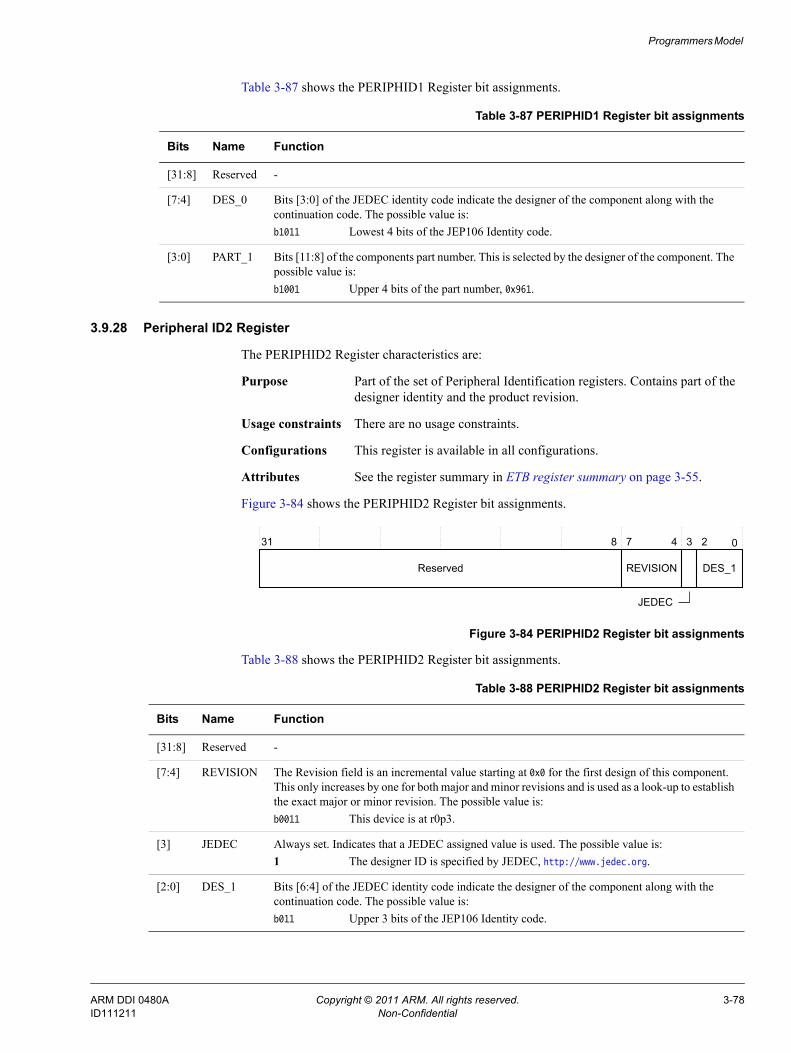
Programmers Model
Table 3-87 shows the PERIPHID1 Register bit assignments.
3.9.28 Peripheral ID2 Register
The PERIPHID2 Register characteristics are:
Purpose Part of the set of Peripheral Identification registers. Contains part of the designer identity and the product revision.
Usage constraints There are no usage constraints.
Configurations This register is available in all configurations.
Attributes See the register summary in ETB register summary on page 3-55.
Figure 3-84 shows the PERIPHID2 Register bit assignments.
Figure 3-84 PERIPHID2 Register bit assignments
Table 3-88 shows the PERIPHID2 Register bit assignments.
Table 3-87 PERIPHID1 Register bit assignments
Bits Name Function
[31:8] Reserved -
[7:4] DES_0 Bits [3:0] of the JEDEC identity code indicate the designer of the component along with the continuation code. The possible value is:b1011 Lowest 4 bits of the JEP106 Identity code.
[3:0] PART_1 Bits [11:8] of the components part number. This is selected by the designer of the component. The possible value is:b1001 Upper 4 bits of the part number, 0x961.
31 0
Reserved
7
REVISION
8 4
DES_1
3 2
JEDEC
Table 3-88 PERIPHID2 Register bit assignments
Bits Name Function
[31:8] Reserved -
[7:4] REVISION The Revision field is an incremental value starting at 0x0 for the first design of this component. This only increases by one for both major and minor revisions and is used as a look-up to establish the exact major or minor revision. The possible value is:b0011 This device is at r0p3.
[3] JEDEC Always set. Indicates that a JEDEC assigned value is used. The possible value is:1 The designer ID is specified by JEDEC, http://www.jedec.org.
[2:0] DES_1 Bits [6:4] of the JEDEC identity code indicate the designer of the component along with the continuation code. The possible value is:b011 Upper 3 bits of the JEP106 Identity code.
ARM DDI 0480A Copyright © 2011 ARM. All rights reserved. 3-78ID111211 Non-Confidential
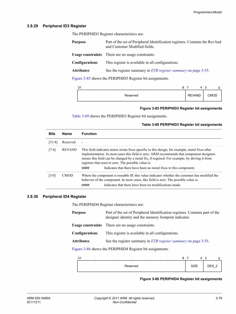
Programmers Model
3.9.29 Peripheral ID3 Register
The PERIPHID3 Register characteristics are:
Purpose Part of the set of Peripheral Identification registers. Contains the RevAnd and Customer Modified fields.
Usage constraints There are no usage constraints.
Configurations This register is available in all configurations.
Attributes See the register summary in ETB register summary on page 3-55.
Figure 3-85 shows the PERIPHID3 Register bit assignments.
Figure 3-85 PERIPHID3 Register bit assignments
Table 3-89 shows the PERIPHID3 Register bit assignments.
3.9.30 Peripheral ID4 Register
The PERIPHID4 Register characteristics are:
Purpose Part of the set of Peripheral Identification registers. Contains part of the designer identity and the memory footprint indicator.
Usage constraints There are no usage constraints.
Configurations This register is available in all configurations.
Attributes See the register summary in ETB register summary on page 3-55.
Figure 3-86 shows the PERIPHID4 Register bit assignments.
Figure 3-86 PERIPHID4 Register bit assignments
31 0
Reserved
7
REVAND
8 4
CMOD
3
Table 3-89 PERIPHID3 Register bit assignments
Bits Name Function
[31:8] Reserved -
[7:4] REVAND This field indicates minor errata fixes specific to this design, for example, metal fixes after implementation. In most cases this field is zero. ARM recommends that component designers ensure this field can be changed by a metal fix, if required. For example, by driving it from registers that reset to zero. The possible value is:b0000 Indicates that there have been no metal fixes to this component.
[3:0] CMOD Where the component is reusable IP, this value indicates whether the customer has modified the behavior of the component. In most cases, this field is zero. The possible value is:b0000 Indicates that there have been no modifications made.
31 0
Reserved
7
SIZE
8 4
DES_2
3
ARM DDI 0480A Copyright © 2011 ARM. All rights reserved. 3-79ID111211 Non-Confidential
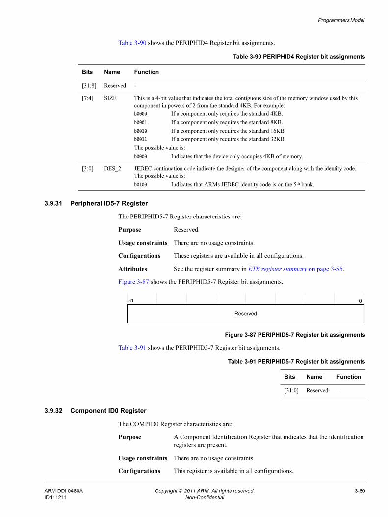
Programmers Model
Table 3-90 shows the PERIPHID4 Register bit assignments.
3.9.31 Peripheral ID5-7 Register
The PERIPHID5-7 Register characteristics are:
Purpose Reserved.
Usage constraints There are no usage constraints.
Configurations These registers are available in all configurations.
Attributes See the register summary in ETB register summary on page 3-55.
Figure 3-87 shows the PERIPHID5-7 Register bit assignments.
Figure 3-87 PERIPHID5-7 Register bit assignments
Table 3-91 shows the PERIPHID5-7 Register bit assignments.
3.9.32 Component ID0 Register
The COMPID0 Register characteristics are:
Purpose A Component Identification Register that indicates that the identification registers are present.
Usage constraints There are no usage constraints.
Configurations This register is available in all configurations.
Table 3-90 PERIPHID4 Register bit assignments
Bits Name Function
[31:8] Reserved -
[7:4] SIZE This is a 4-bit value that indicates the total contiguous size of the memory window used by this component in powers of 2 from the standard 4KB. For example: b0000 If a component only requires the standard 4KB.b0001 If a component only requires the standard 8KB.b0010 If a component only requires the standard 16KB.b0011 If a component only requires the standard 32KB.The possible value is:b0000 Indicates that the device only occupies 4KB of memory.
[3:0] DES_2 JEDEC continuation code indicate the designer of the component along with the identity code. The possible value is:b0100 Indicates that ARMs JEDEC identity code is on the 5th bank.
31 0
Reserved
Table 3-91 PERIPHID5-7 Register bit assignments
Bits Name Function
[31:0] Reserved -
ARM DDI 0480A Copyright © 2011 ARM. All rights reserved. 3-80ID111211 Non-Confidential
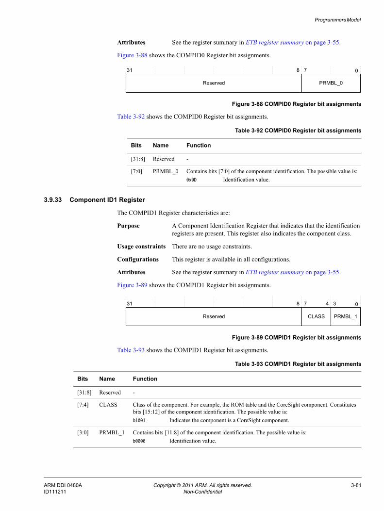
Programmers Model
Attributes See the register summary in ETB register summary on page 3-55.
Figure 3-88 shows the COMPID0 Register bit assignments.
Figure 3-88 COMPID0 Register bit assignments
Table 3-92 shows the COMPID0 Register bit assignments.
3.9.33 Component ID1 Register
The COMPID1 Register characteristics are:
Purpose A Component Identification Register that indicates that the identification registers are present. This register also indicates the component class.
Usage constraints There are no usage constraints.
Configurations This register is available in all configurations.
Attributes See the register summary in ETB register summary on page 3-55.
Figure 3-89 shows the COMPID1 Register bit assignments.
Figure 3-89 COMPID1 Register bit assignments
Table 3-93 shows the COMPID1 Register bit assignments.
31 0
Reserved
78
PRMBL_0
Table 3-92 COMPID0 Register bit assignments
Bits Name Function
[31:8] Reserved -
[7:0] PRMBL_0 Contains bits [7:0] of the component identification. The possible value is:0x0D Identification value.
31 0
Reserved
78
PRMBL_1
4 3
CLASS
Table 3-93 COMPID1 Register bit assignments
Bits Name Function
[31:8] Reserved -
[7:4] CLASS Class of the component. For example, the ROM table and the CoreSight component. Constitutes bits [15:12] of the component identification. The possible value is:b1001 Indicates the component is a CoreSight component.
[3:0] PRMBL_1 Contains bits [11:8] of the component identification. The possible value is:b0000 Identification value.
ARM DDI 0480A Copyright © 2011 ARM. All rights reserved. 3-81ID111211 Non-Confidential
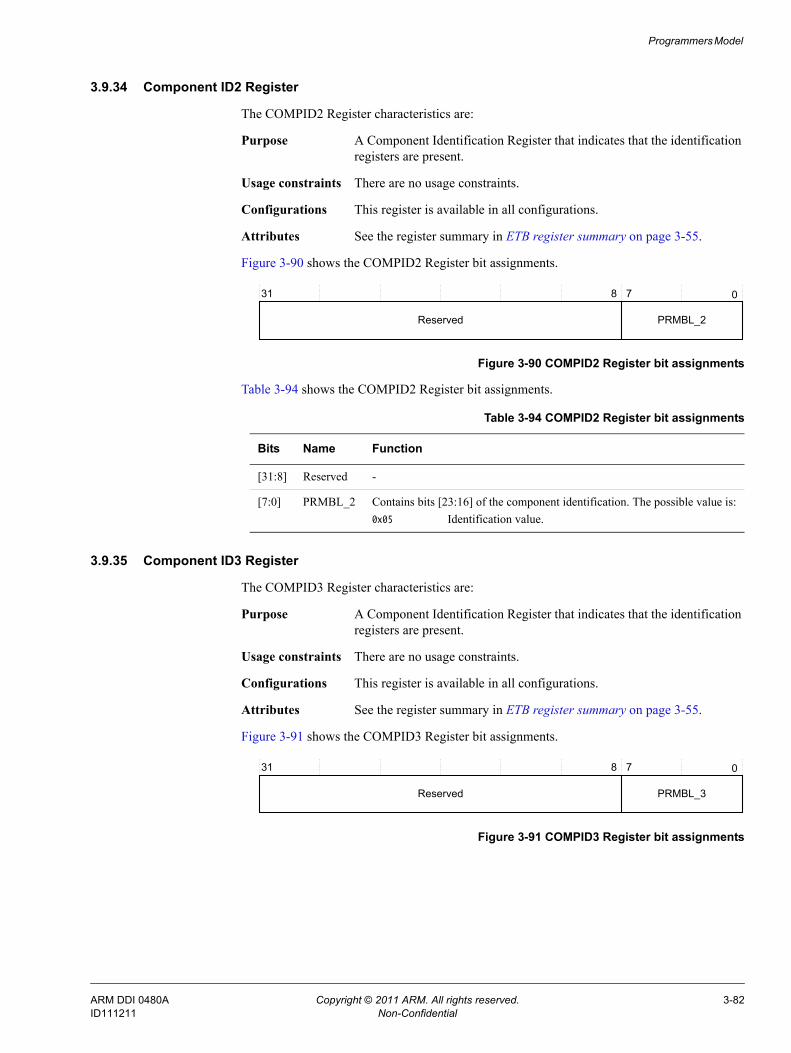
Programmers Model
3.9.34 Component ID2 Register
The COMPID2 Register characteristics are:
Purpose A Component Identification Register that indicates that the identification registers are present.
Usage constraints There are no usage constraints.
Configurations This register is available in all configurations.
Attributes See the register summary in ETB register summary on page 3-55.
Figure 3-90 shows the COMPID2 Register bit assignments.
Figure 3-90 COMPID2 Register bit assignments
Table 3-94 shows the COMPID2 Register bit assignments.
3.9.35 Component ID3 Register
The COMPID3 Register characteristics are:
Purpose A Component Identification Register that indicates that the identification registers are present.
Usage constraints There are no usage constraints.
Configurations This register is available in all configurations.
Attributes See the register summary in ETB register summary on page 3-55.
Figure 3-91 shows the COMPID3 Register bit assignments.
Figure 3-91 COMPID3 Register bit assignments
31 0
Reserved
78
PRMBL_2
Table 3-94 COMPID2 Register bit assignments
Bits Name Function
[31:8] Reserved -
[7:0] PRMBL_2 Contains bits [23:16] of the component identification. The possible value is:0x05 Identification value.
31 0
Reserved
78
PRMBL_3
ARM DDI 0480A Copyright © 2011 ARM. All rights reserved. 3-82ID111211 Non-Confidential

Programmers Model
Table 3-95 shows the COMPID3 Register bit assignments.
Table 3-95 COMPID3 Register bit assignments
Bits Name Function
[31:8] Reserved -
[7:0] PRMBL_3 Contains bits [31:24] of the component identification. The possible value is:0xB1 Identification value.
ARM DDI 0480A Copyright © 2011 ARM. All rights reserved. 3-83ID111211 Non-Confidential
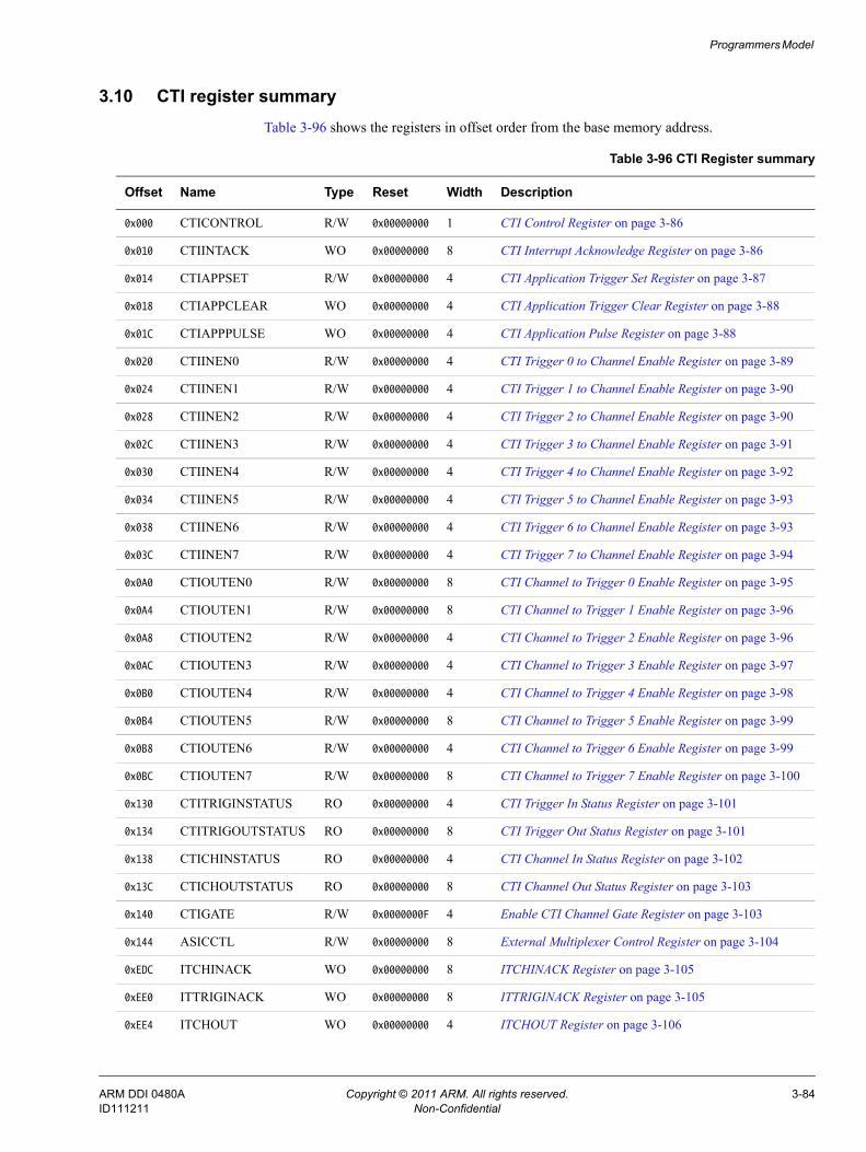
Programmers Model
3.10 CTI register summaryTable 3-96 shows the registers in offset order from the base memory address.
Table 3-96 CTI Register summary
Offset Name Type Reset Width Description
0x000 CTICONTROL R/W 0x00000000 1 CTI Control Register on page 3-86
0x010 CTIINTACK WO 0x00000000 8 CTI Interrupt Acknowledge Register on page 3-86
0x014 CTIAPPSET R/W 0x00000000 4 CTI Application Trigger Set Register on page 3-87
0x018 CTIAPPCLEAR WO 0x00000000 4 CTI Application Trigger Clear Register on page 3-88
0x01C CTIAPPPULSE WO 0x00000000 4 CTI Application Pulse Register on page 3-88
0x020 CTIINEN0 R/W 0x00000000 4 CTI Trigger 0 to Channel Enable Register on page 3-89
0x024 CTIINEN1 R/W 0x00000000 4 CTI Trigger 1 to Channel Enable Register on page 3-90
0x028 CTIINEN2 R/W 0x00000000 4 CTI Trigger 2 to Channel Enable Register on page 3-90
0x02C CTIINEN3 R/W 0x00000000 4 CTI Trigger 3 to Channel Enable Register on page 3-91
0x030 CTIINEN4 R/W 0x00000000 4 CTI Trigger 4 to Channel Enable Register on page 3-92
0x034 CTIINEN5 R/W 0x00000000 4 CTI Trigger 5 to Channel Enable Register on page 3-93
0x038 CTIINEN6 R/W 0x00000000 4 CTI Trigger 6 to Channel Enable Register on page 3-93
0x03C CTIINEN7 R/W 0x00000000 4 CTI Trigger 7 to Channel Enable Register on page 3-94
0x0A0 CTIOUTEN0 R/W 0x00000000 8 CTI Channel to Trigger 0 Enable Register on page 3-95
0x0A4 CTIOUTEN1 R/W 0x00000000 8 CTI Channel to Trigger 1 Enable Register on page 3-96
0x0A8 CTIOUTEN2 R/W 0x00000000 4 CTI Channel to Trigger 2 Enable Register on page 3-96
0x0AC CTIOUTEN3 R/W 0x00000000 4 CTI Channel to Trigger 3 Enable Register on page 3-97
0x0B0 CTIOUTEN4 R/W 0x00000000 4 CTI Channel to Trigger 4 Enable Register on page 3-98
0x0B4 CTIOUTEN5 R/W 0x00000000 8 CTI Channel to Trigger 5 Enable Register on page 3-99
0x0B8 CTIOUTEN6 R/W 0x00000000 4 CTI Channel to Trigger 6 Enable Register on page 3-99
0x0BC CTIOUTEN7 R/W 0x00000000 8 CTI Channel to Trigger 7 Enable Register on page 3-100
0x130 CTITRIGINSTATUS RO 0x00000000 4 CTI Trigger In Status Register on page 3-101
0x134 CTITRIGOUTSTATUS RO 0x00000000 8 CTI Trigger Out Status Register on page 3-101
0x138 CTICHINSTATUS RO 0x00000000 4 CTI Channel In Status Register on page 3-102
0x13C CTICHOUTSTATUS RO 0x00000000 8 CTI Channel Out Status Register on page 3-103
0x140 CTIGATE R/W 0x0000000F 4 Enable CTI Channel Gate Register on page 3-103
0x144 ASICCTL R/W 0x00000000 8 External Multiplexer Control Register on page 3-104
0xEDC ITCHINACK WO 0x00000000 8 ITCHINACK Register on page 3-105
0xEE0 ITTRIGINACK WO 0x00000000 8 ITTRIGINACK Register on page 3-105
0xEE4 ITCHOUT WO 0x00000000 4 ITCHOUT Register on page 3-106
ARM DDI 0480A Copyright © 2011 ARM. All rights reserved. 3-84ID111211 Non-Confidential
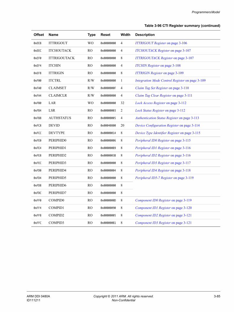
Programmers Model
0xEE8 ITTRIGOUT WO 0x00000000 4 ITTRIGOUT Register on page 3-106
0xEEC ITCHOUTACK RO 0x00000000 4 ITCHOUTACK Register on page 3-107
0xEF0 ITTRIGOUTACK RO 0x00000000 8 ITTRIGOUTACK Register on page 3-107
0xEF4 ITCHIN RO 0x00000000 4 ITCHIN Register on page 3-108
0xEF8 ITTRIGIN RO 0x00000000 8 ITTRIGIN Register on page 3-109
0xF00 ITCTRL R/W 0x00000000 1 Integration Mode Control Register on page 3-109
0xFA0 CLAIMSET R/W 0x0000000F 4 Claim Tag Set Register on page 3-110
0xFA4 CLAIMCLR R/W 0x00000000 4 Claim Tag Clear Register on page 3-111
0xFB0 LAR WO 0x00000000 32 Lock Access Register on page 3-112
0xFB4 LSR RO 0x00000003 2 Lock Status Register on page 3-112
0xFB8 AUTHSTATUS RO 0x00000005 4 Authentication Status Register on page 3-113
0xFC8 DEVID RO 0x00040800 20 Device Configuration Register on page 3-114
0xFCC DEVTYPE RO 0x00000014 8 Device Type Identifier Register on page 3-115
0xFE0 PERIPHID0 RO 0x00000006 8 Peripheral ID0 Register on page 3-115
0xFE4 PERIPHID1 RO 0x000000B9 8 Peripheral ID1 Register on page 3-116
0xFE8 PERIPHID2 RO 0x0000003B 8 Peripheral ID2 Register on page 3-116
0xFEC PERIPHID3 RO 0x00000000 8 Peripheral ID3 Register on page 3-117
0xFD0 PERIPHID4 RO 0x00000004 8 Peripheral ID4 Register on page 3-118
0xFD4 PERIPHID5 RO 0x00000000 8 Peripheral ID5-7 Register on page 3-119
0xFD8 PERIPHID6 RO 0x00000000 8
0xFDC PERIPHID7 RO 0x00000000 8
0xFF0 COMPID0 RO 0x0000000D 8 Component ID0 Register on page 3-119
0xFF4 COMPID1 RO 0x00000090 8 Component ID1 Register on page 3-120
0xFF8 COMPID2 RO 0x00000005 8 Component ID2 Register on page 3-121
0xFFC COMPID3 RO 0x000000B1 8 Component ID3 Register on page 3-121
Table 3-96 CTI Register summary (continued)
Offset Name Type Reset Width Description
ARM DDI 0480A Copyright © 2011 ARM. All rights reserved. 3-85ID111211 Non-Confidential
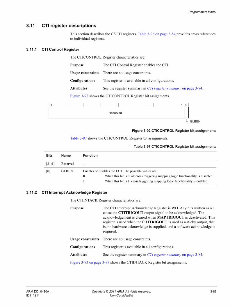
Programmers Model
3.11 CTI register descriptionsThis section describes the CSCTI registers. Table 3-96 on page 3-84 provides cross references to individual registers.
3.11.1 CTI Control Register
The CTICONTROL Register characteristics are:
Purpose The CTI Control Register enables the CTI.
Usage constraints There are no usage constraints.
Configurations This register is available in all configurations.
Attributes See the register summary in CTI register summary on page 3-84.
Figure 3-92 shows the CTICONTROL Register bit assignments.
Figure 3-92 CTICONTROL Register bit assignments
Table 3-97 shows the CTICONTROL Register bit assignments.
3.11.2 CTI Interrupt Acknowledge Register
The CTIINTACK Register characteristics are:
Purpose The CTI Interrupt Acknowledge Register is WO. Any bits written as a 1 cause the CTITRIGOUT output signal to be acknowledged. The acknowledgement is cleared when MAPTRIGOUT is deactivated. This register is used when the CTITRIGOUT is used as a sticky output, that is, no hardware acknowledge is supplied, and a software acknowledge is required.
Usage constraints There are no usage constraints.
Configurations This register is available in all configurations.
Attributes See the register summary in CTI register summary on page 3-84.
Figure 3-93 on page 3-87 shows the CTIINTACK Register bit assignments.
31 1 0
Reserved
GLBEN
Table 3-97 CTICONTROL Register bit assignments
Bits Name Function
[31:1] Reserved -
[0] GLBEN Enables or disables the ECT. The possible values are:0 When this bit is 0, all cross triggering mapping logic functionality is disabled.1 When this bit is 1, cross triggering mapping logic functionality is enabled.
ARM DDI 0480A Copyright © 2011 ARM. All rights reserved. 3-86ID111211 Non-Confidential
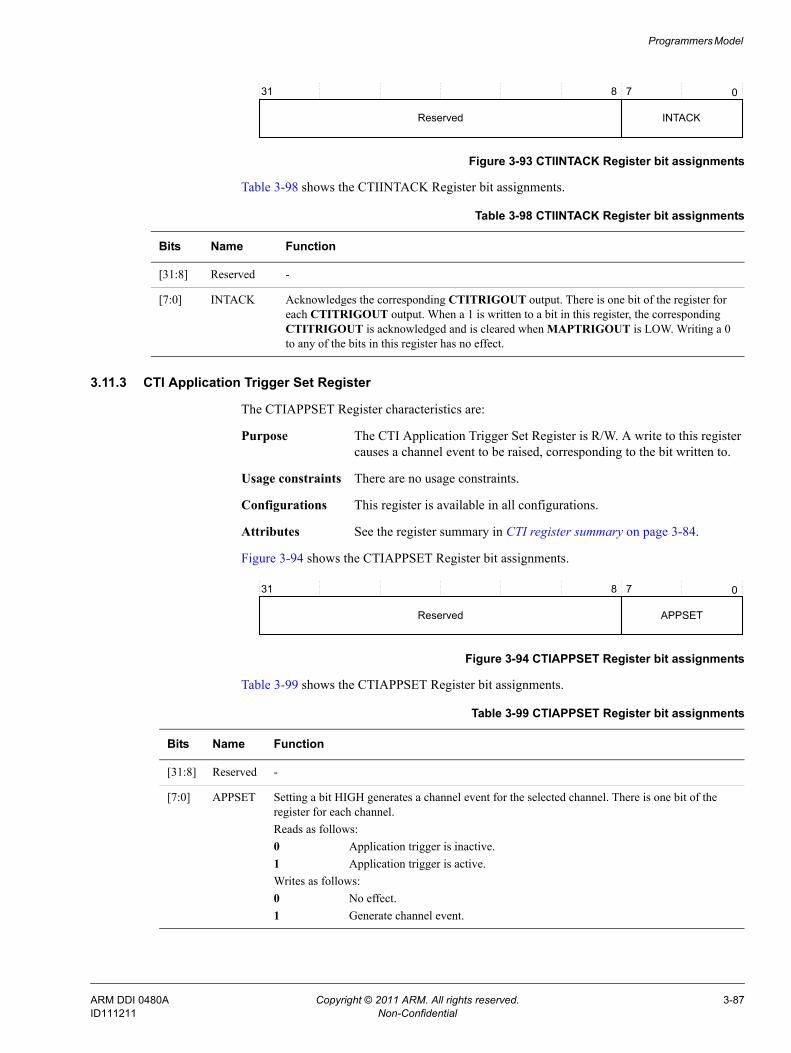
Programmers Model
Figure 3-93 CTIINTACK Register bit assignments
Table 3-98 shows the CTIINTACK Register bit assignments.
3.11.3 CTI Application Trigger Set Register
The CTIAPPSET Register characteristics are:
Purpose The CTI Application Trigger Set Register is R/W. A write to this register causes a channel event to be raised, corresponding to the bit written to.
Usage constraints There are no usage constraints.
Configurations This register is available in all configurations.
Attributes See the register summary in CTI register summary on page 3-84.
Figure 3-94 shows the CTIAPPSET Register bit assignments.
Figure 3-94 CTIAPPSET Register bit assignments
Table 3-99 shows the CTIAPPSET Register bit assignments.
31 0
Reserved
78
INTACK
Table 3-98 CTIINTACK Register bit assignments
Bits Name Function
[31:8] Reserved -
[7:0] INTACK Acknowledges the corresponding CTITRIGOUT output. There is one bit of the register for each CTITRIGOUT output. When a 1 is written to a bit in this register, the corresponding CTITRIGOUT is acknowledged and is cleared when MAPTRIGOUT is LOW. Writing a 0 to any of the bits in this register has no effect.
31 0
Reserved
78
APPSET
Table 3-99 CTIAPPSET Register bit assignments
Bits Name Function
[31:8] Reserved -
[7:0] APPSET Setting a bit HIGH generates a channel event for the selected channel. There is one bit of the register for each channel. Reads as follows: 0 Application trigger is inactive.1 Application trigger is active.Writes as follows: 0 No effect.1 Generate channel event.
ARM DDI 0480A Copyright © 2011 ARM. All rights reserved. 3-87ID111211 Non-Confidential
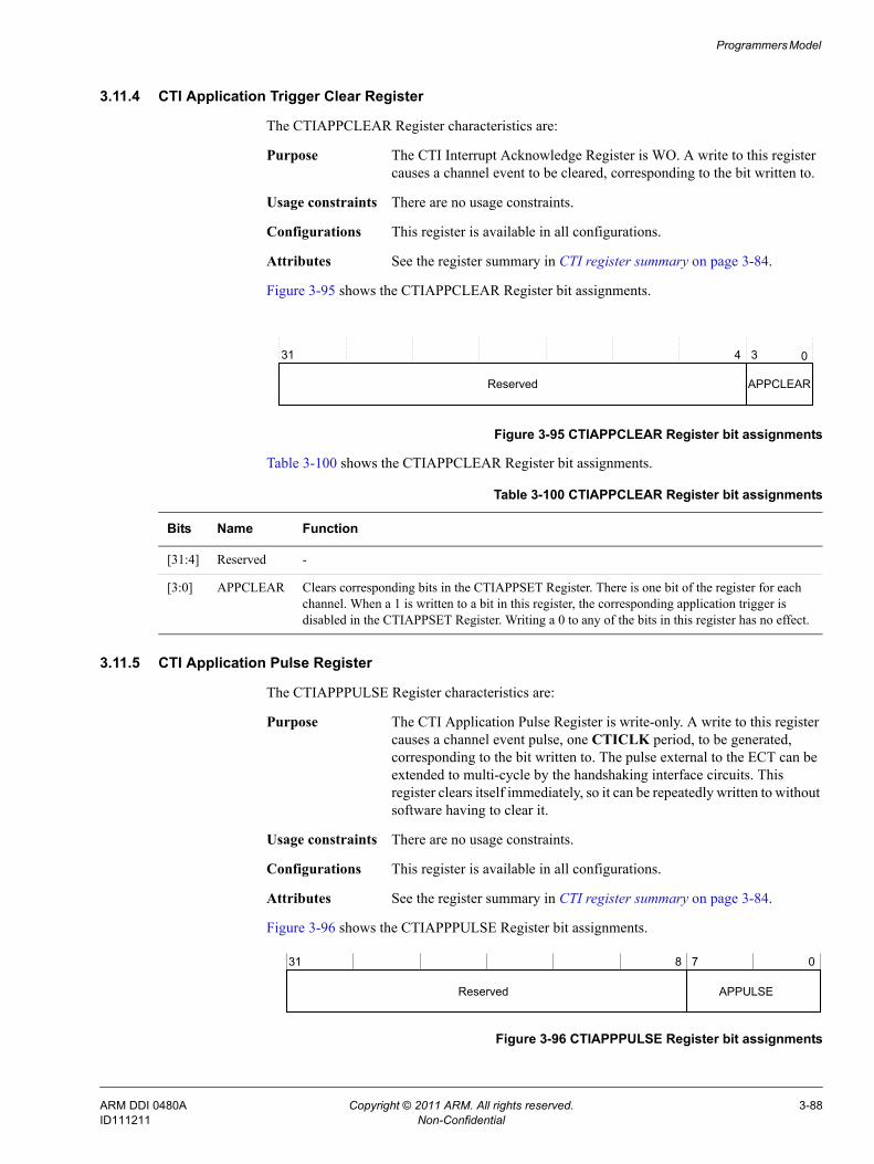
Programmers Model
3.11.4 CTI Application Trigger Clear Register
The CTIAPPCLEAR Register characteristics are:
Purpose The CTI Interrupt Acknowledge Register is WO. A write to this register causes a channel event to be cleared, corresponding to the bit written to.
Usage constraints There are no usage constraints.
Configurations This register is available in all configurations.
Attributes See the register summary in CTI register summary on page 3-84.
Figure 3-95 shows the CTIAPPCLEAR Register bit assignments.
Figure 3-95 CTIAPPCLEAR Register bit assignments
Table 3-100 shows the CTIAPPCLEAR Register bit assignments.
3.11.5 CTI Application Pulse Register
The CTIAPPPULSE Register characteristics are:
Purpose The CTI Application Pulse Register is write-only. A write to this register causes a channel event pulse, one CTICLK period, to be generated, corresponding to the bit written to. The pulse external to the ECT can be extended to multi-cycle by the handshaking interface circuits. This register clears itself immediately, so it can be repeatedly written to without software having to clear it.
Usage constraints There are no usage constraints.
Configurations This register is available in all configurations.
Attributes See the register summary in CTI register summary on page 3-84.
Figure 3-96 shows the CTIAPPPULSE Register bit assignments.
Figure 3-96 CTIAPPPULSE Register bit assignments
31 0
Reserved
4
APPCLEAR
3
Table 3-100 CTIAPPCLEAR Register bit assignments
Bits Name Function
[31:4] Reserved -
[3:0] APPCLEAR Clears corresponding bits in the CTIAPPSET Register. There is one bit of the register for each channel. When a 1 is written to a bit in this register, the corresponding application trigger is disabled in the CTIAPPSET Register. Writing a 0 to any of the bits in this register has no effect.
31 8 7 0
APPULSEReserved
ARM DDI 0480A Copyright © 2011 ARM. All rights reserved. 3-88ID111211 Non-Confidential
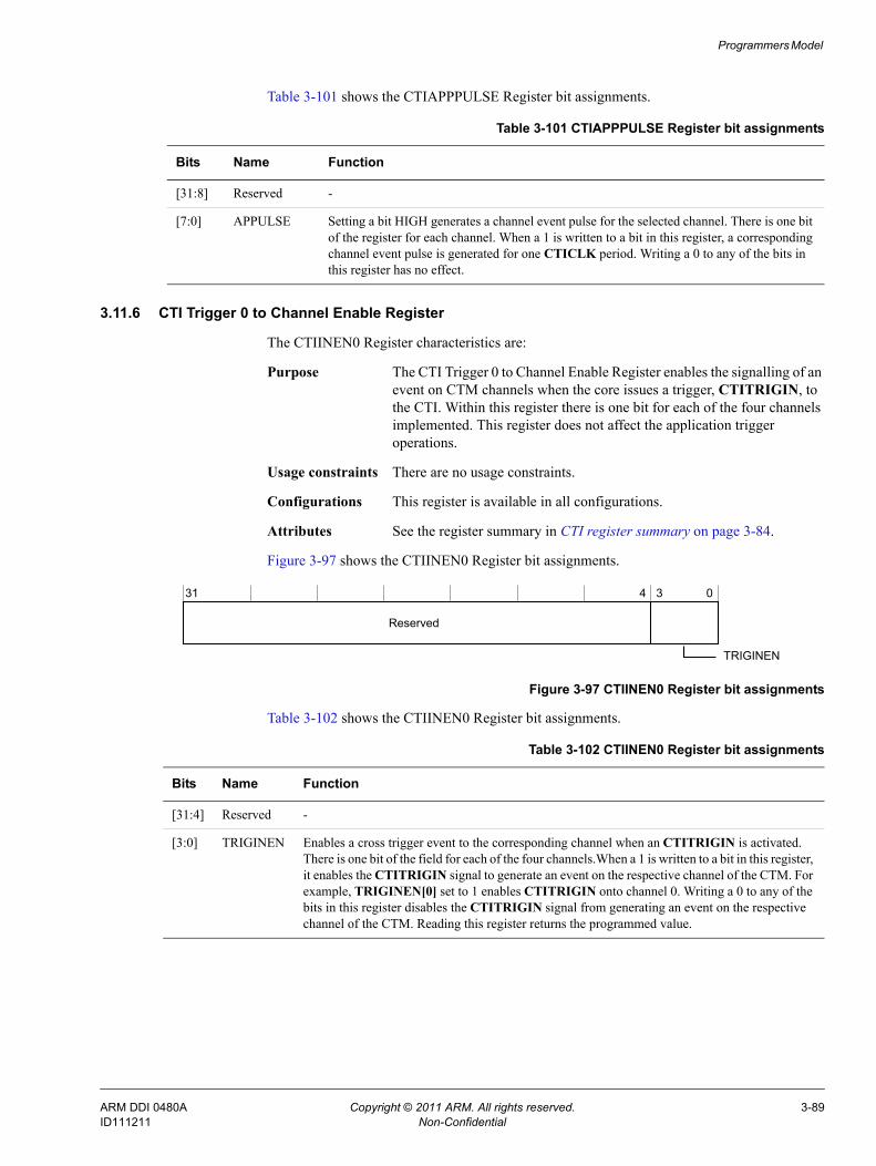
Programmers Model
Table 3-101 shows the CTIAPPPULSE Register bit assignments.
3.11.6 CTI Trigger 0 to Channel Enable Register
The CTIINEN0 Register characteristics are:
Purpose The CTI Trigger 0 to Channel Enable Register enables the signalling of an event on CTM channels when the core issues a trigger, CTITRIGIN, to the CTI. Within this register there is one bit for each of the four channels implemented. This register does not affect the application trigger operations.
Usage constraints There are no usage constraints.
Configurations This register is available in all configurations.
Attributes See the register summary in CTI register summary on page 3-84.
Figure 3-97 shows the CTIINEN0 Register bit assignments.
Figure 3-97 CTIINEN0 Register bit assignments
Table 3-102 shows the CTIINEN0 Register bit assignments.
Table 3-101 CTIAPPPULSE Register bit assignments
Bits Name Function
[31:8] Reserved -
[7:0] APPULSE Setting a bit HIGH generates a channel event pulse for the selected channel. There is one bit of the register for each channel. When a 1 is written to a bit in this register, a corresponding channel event pulse is generated for one CTICLK period. Writing a 0 to any of the bits in this register has no effect.
31 4 3 0
Reserved
TRIGINEN
Table 3-102 CTIINEN0 Register bit assignments
Bits Name Function
[31:4] Reserved -
[3:0] TRIGINEN Enables a cross trigger event to the corresponding channel when an CTITRIGIN is activated. There is one bit of the field for each of the four channels.When a 1 is written to a bit in this register, it enables the CTITRIGIN signal to generate an event on the respective channel of the CTM. For example, TRIGINEN[0] set to 1 enables CTITRIGIN onto channel 0. Writing a 0 to any of the bits in this register disables the CTITRIGIN signal from generating an event on the respective channel of the CTM. Reading this register returns the programmed value.
ARM DDI 0480A Copyright © 2011 ARM. All rights reserved. 3-89ID111211 Non-Confidential
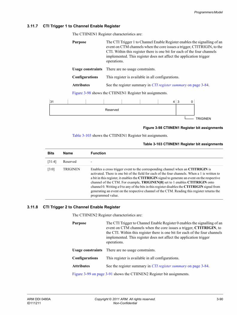
Programmers Model
3.11.7 CTI Trigger 1 to Channel Enable Register
The CTIINEN1 Register characteristics are:
Purpose The CTI Trigger 1 to Channel Enable Register enables the signalling of an event on CTM channels when the core issues a trigger, CTITRIGIN, to the CTI. Within this register there is one bit for each of the four channels implemented. This register does not affect the application trigger operations.
Usage constraints There are no usage constraints.
Configurations This register is available in all configurations.
Attributes See the register summary in CTI register summary on page 3-84.
Figure 3-98 shows the CTIINEN1 Register bit assignments.
Figure 3-98 CTIINEN1 Register bit assignments
Table 3-103 shows the CTIINEN1 Register bit assignments.
3.11.8 CTI Trigger 2 to Channel Enable Register
The CTIINEN2 Register characteristics are:
Purpose The CTI Trigger to Channel Enable Register 0 enables the signalling of an event on CTM channels when the core issues a trigger, CTITRIGIN, to the CTI. Within this register there is one bit for each of the four channels implemented. This register does not affect the application trigger operations.
Usage constraints There are no usage constraints.
Configurations This register is available in all configurations.
Attributes See the register summary in CTI register summary on page 3-84.
Figure 3-99 on page 3-91 shows the CTIINEN2 Register bit assignments.
31 4 3 0
Reserved
TRIGINEN
Table 3-103 CTIINEN1 Register bit assignments
Bits Name Function
[31:4] Reserved -
[3:0] TRIGINEN Enables a cross trigger event to the corresponding channel when an CTITRIGIN is activated. There is one bit of the field for each of the four channels. When a 1 is written to a bit in this register, it enables the CTITRIGIN signal to generate an event on the respective channel of the CTM. For example, TRIGINEN[0] set to 1 enables CTITRIGIN onto channel 0. Writing a 0 to any of the bits in this register disables the CTITRIGIN signal from generating an event on the respective channel of the CTM. Reading this register returns the programmed value.
ARM DDI 0480A Copyright © 2011 ARM. All rights reserved. 3-90ID111211 Non-Confidential
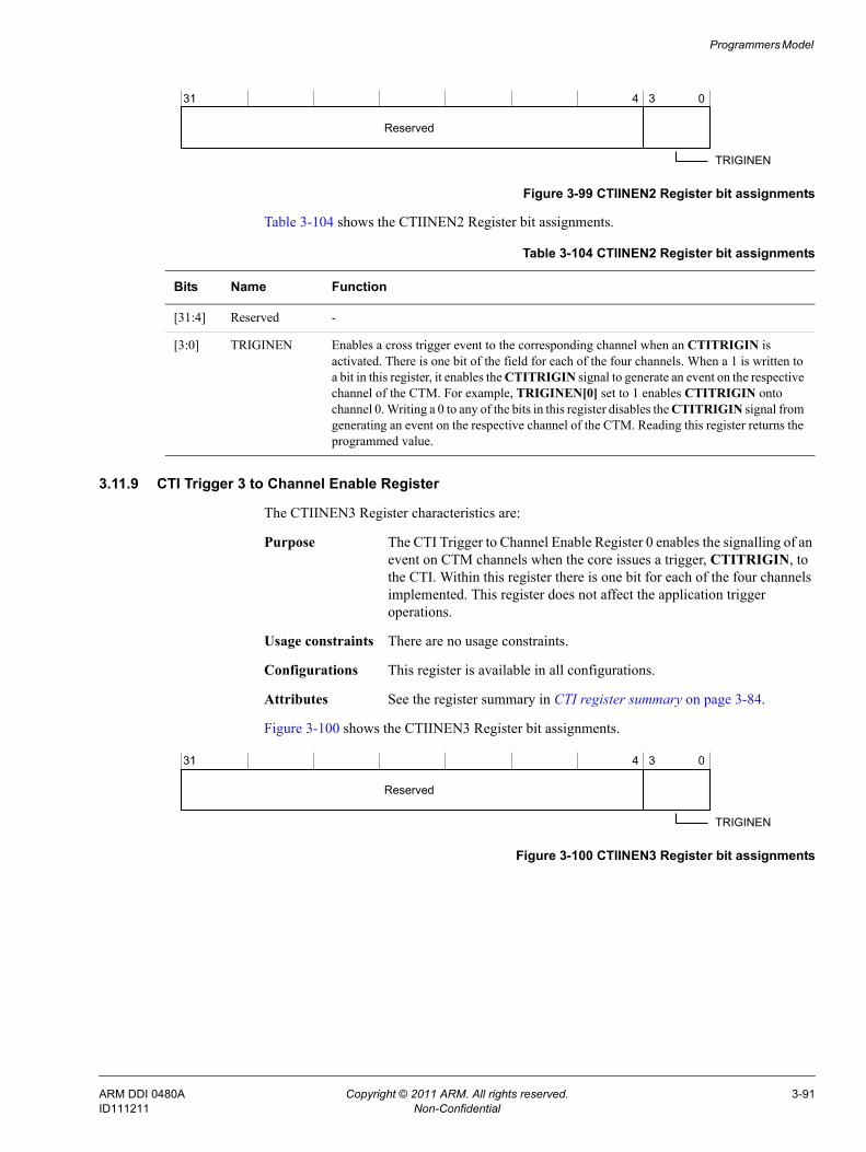
Programmers Model
Figure 3-99 CTIINEN2 Register bit assignments
Table 3-104 shows the CTIINEN2 Register bit assignments.
3.11.9 CTI Trigger 3 to Channel Enable Register
The CTIINEN3 Register characteristics are:
Purpose The CTI Trigger to Channel Enable Register 0 enables the signalling of an event on CTM channels when the core issues a trigger, CTITRIGIN, to the CTI. Within this register there is one bit for each of the four channels implemented. This register does not affect the application trigger operations.
Usage constraints There are no usage constraints.
Configurations This register is available in all configurations.
Attributes See the register summary in CTI register summary on page 3-84.
Figure 3-100 shows the CTIINEN3 Register bit assignments.
Figure 3-100 CTIINEN3 Register bit assignments
31 4 3 0
Reserved
TRIGINEN
Table 3-104 CTIINEN2 Register bit assignments
Bits Name Function
[31:4] Reserved -
[3:0] TRIGINEN Enables a cross trigger event to the corresponding channel when an CTITRIGIN is activated. There is one bit of the field for each of the four channels. When a 1 is written to a bit in this register, it enables the CTITRIGIN signal to generate an event on the respective channel of the CTM. For example, TRIGINEN[0] set to 1 enables CTITRIGIN onto channel 0. Writing a 0 to any of the bits in this register disables the CTITRIGIN signal from generating an event on the respective channel of the CTM. Reading this register returns the programmed value.
31 4 3 0
Reserved
TRIGINEN
ARM DDI 0480A Copyright © 2011 ARM. All rights reserved. 3-91ID111211 Non-Confidential
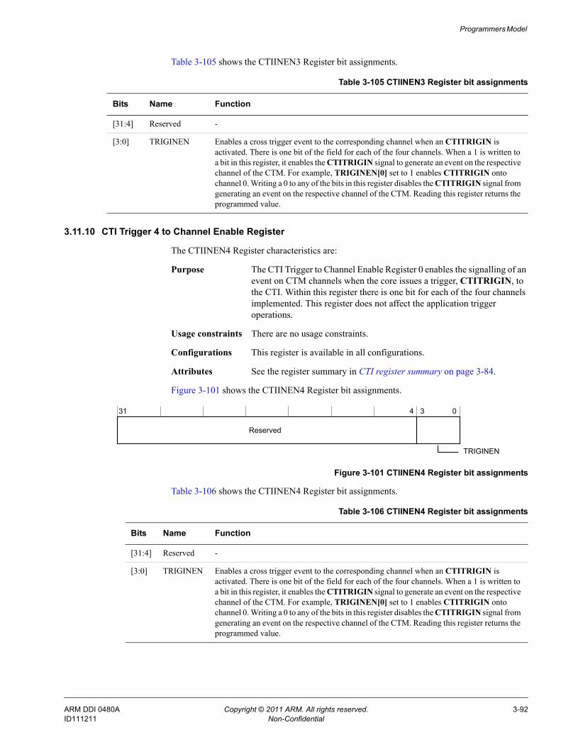
Programmers Model
Table 3-105 shows the CTIINEN3 Register bit assignments.
3.11.10 CTI Trigger 4 to Channel Enable Register
The CTIINEN4 Register characteristics are:
Purpose The CTI Trigger to Channel Enable Register 0 enables the signalling of an event on CTM channels when the core issues a trigger, CTITRIGIN, to the CTI. Within this register there is one bit for each of the four channels implemented. This register does not affect the application trigger operations.
Usage constraints There are no usage constraints.
Configurations This register is available in all configurations.
Attributes See the register summary in CTI register summary on page 3-84.
Figure 3-101 shows the CTIINEN4 Register bit assignments.
Figure 3-101 CTIINEN4 Register bit assignments
Table 3-106 shows the CTIINEN4 Register bit assignments.
Table 3-105 CTIINEN3 Register bit assignments
Bits Name Function
[31:4] Reserved -
[3:0] TRIGINEN Enables a cross trigger event to the corresponding channel when an CTITRIGIN is activated. There is one bit of the field for each of the four channels. When a 1 is written to a bit in this register, it enables the CTITRIGIN signal to generate an event on the respective channel of the CTM. For example, TRIGINEN[0] set to 1 enables CTITRIGIN onto channel 0. Writing a 0 to any of the bits in this register disables the CTITRIGIN signal from generating an event on the respective channel of the CTM. Reading this register returns the programmed value.
31 4 3 0
Reserved
TRIGINEN
Table 3-106 CTIINEN4 Register bit assignments
Bits Name Function
[31:4] Reserved -
[3:0] TRIGINEN Enables a cross trigger event to the corresponding channel when an CTITRIGIN is activated. There is one bit of the field for each of the four channels. When a 1 is written to a bit in this register, it enables the CTITRIGIN signal to generate an event on the respective channel of the CTM. For example, TRIGINEN[0] set to 1 enables CTITRIGIN onto channel 0. Writing a 0 to any of the bits in this register disables the CTITRIGIN signal from generating an event on the respective channel of the CTM. Reading this register returns the programmed value.
ARM DDI 0480A Copyright © 2011 ARM. All rights reserved. 3-92ID111211 Non-Confidential
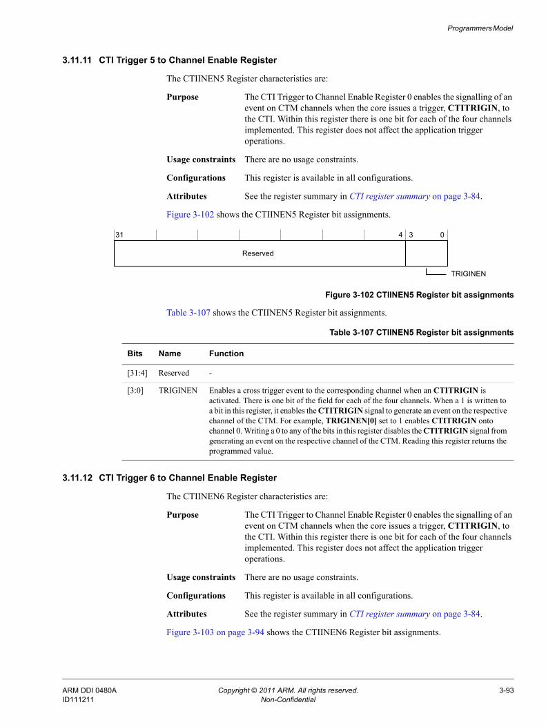
Programmers Model
3.11.11 CTI Trigger 5 to Channel Enable Register
The CTIINEN5 Register characteristics are:
Purpose The CTI Trigger to Channel Enable Register 0 enables the signalling of an event on CTM channels when the core issues a trigger, CTITRIGIN, to the CTI. Within this register there is one bit for each of the four channels implemented. This register does not affect the application trigger operations.
Usage constraints There are no usage constraints.
Configurations This register is available in all configurations.
Attributes See the register summary in CTI register summary on page 3-84.
Figure 3-102 shows the CTIINEN5 Register bit assignments.
Figure 3-102 CTIINEN5 Register bit assignments
Table 3-107 shows the CTIINEN5 Register bit assignments.
3.11.12 CTI Trigger 6 to Channel Enable Register
The CTIINEN6 Register characteristics are:
Purpose The CTI Trigger to Channel Enable Register 0 enables the signalling of an event on CTM channels when the core issues a trigger, CTITRIGIN, to the CTI. Within this register there is one bit for each of the four channels implemented. This register does not affect the application trigger operations.
Usage constraints There are no usage constraints.
Configurations This register is available in all configurations.
Attributes See the register summary in CTI register summary on page 3-84.
Figure 3-103 on page 3-94 shows the CTIINEN6 Register bit assignments.
31 4 3 0
Reserved
TRIGINEN
Table 3-107 CTIINEN5 Register bit assignments
Bits Name Function
[31:4] Reserved -
[3:0] TRIGINEN Enables a cross trigger event to the corresponding channel when an CTITRIGIN is activated. There is one bit of the field for each of the four channels. When a 1 is written to a bit in this register, it enables the CTITRIGIN signal to generate an event on the respective channel of the CTM. For example, TRIGINEN[0] set to 1 enables CTITRIGIN onto channel 0. Writing a 0 to any of the bits in this register disables the CTITRIGIN signal from generating an event on the respective channel of the CTM. Reading this register returns the programmed value.
ARM DDI 0480A Copyright © 2011 ARM. All rights reserved. 3-93ID111211 Non-Confidential
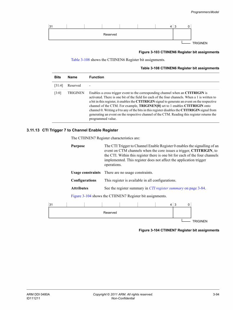
Programmers Model
Figure 3-103 CTIINEN6 Register bit assignments
Table 3-108 shows the CTIINEN6 Register bit assignments.
3.11.13 CTI Trigger 7 to Channel Enable Register
The CTIINEN7 Register characteristics are:
Purpose The CTI Trigger to Channel Enable Register 0 enables the signalling of an event on CTM channels when the core issues a trigger, CTITRIGIN, to the CTI. Within this register there is one bit for each of the four channels implemented. This register does not affect the application trigger operations.
Usage constraints There are no usage constraints.
Configurations This register is available in all configurations.
Attributes See the register summary in CTI register summary on page 3-84.
Figure 3-104 shows the CTIINEN7 Register bit assignments.
Figure 3-104 CTIINEN7 Register bit assignments
31 4 3 0
Reserved
TRIGINEN
Table 3-108 CTIINEN6 Register bit assignments
Bits Name Function
[31:4] Reserved -
[3:0] TRIGINEN Enables a cross trigger event to the corresponding channel when an CTITRIGIN is activated. There is one bit of the field for each of the four channels. When a 1 is written to a bit in this register, it enables the CTITRIGIN signal to generate an event on the respective channel of the CTM. For example, TRIGINEN[0] set to 1 enables CTITRIGIN onto channel 0. Writing a 0 to any of the bits in this register disables the CTITRIGIN signal from generating an event on the respective channel of the CTM. Reading this register returns the programmed value.
31 4 3 0
Reserved
TRIGINEN
ARM DDI 0480A Copyright © 2011 ARM. All rights reserved. 3-94ID111211 Non-Confidential
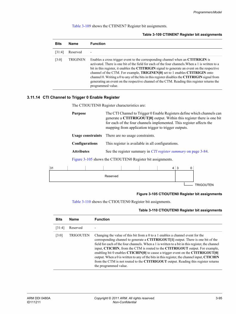
Programmers Model
Table 3-109 shows the CTIINEN7 Register bit assignments.
3.11.14 CTI Channel to Trigger 0 Enable Register
The CTIOUTEN0 Register characteristics are:
Purpose The CTI Channel to Trigger 0 Enable Registers define which channels can generate a CTITRIGOUT[0] output. Within this register there is one bit for each of the four channels implemented. This register affects the mapping from application trigger to trigger outputs.
Usage constraints There are no usage constraints.
Configurations This register is available in all configurations.
Attributes See the register summary in CTI register summary on page 3-84.
Figure 3-105 shows the CTIOUTEN0 Register bit assignments.
Figure 3-105 CTIOUTEN0 Register bit assignments
Table 3-110 shows the CTIOUTEN0 Register bit assignments.
Table 3-109 CTIINEN7 Register bit assignments
Bits Name Function
[31:4] Reserved -
[3:0] TRIGINEN Enables a cross trigger event to the corresponding channel when an CTITRIGIN is activated. There is one bit of the field for each of the four channels.When a 1 is written to a bit in this register, it enables the CTITRIGIN signal to generate an event on the respective channel of the CTM. For example, TRIGINEN[0] set to 1 enables CTITRIGIN onto channel 0. Writing a 0 to any of the bits in this register disables the CTITRIGIN signal from generating an event on the respective channel of the CTM. Reading this register returns the programmed value.
31 4 3 0
Reserved
TRIGOUTEN
Table 3-110 CTIOUTEN0 Register bit assignments
Bits Name Function
[31:4] Reserved -
[3:0] TRIGOUTEN Changing the value of this bit from a 0 to a 1 enables a channel event for the corresponding channel to generate a CTITRIGOUT[1] output. There is one bit of the field for each of the four channels. When a 1 is written to a bit in this register, the channel input, CTICHIN, from the CTM is routed to the CTITRIGOUT output. For example, enabling bit 0 enables CTICHIN[0] to cause a trigger event on the CTITRIGOUT[0] output. When a 0 is written to any of the bits in this register, the channel input, CTICHIN from the CTM is not routed to the CTITRIGOUT output. Reading this register returns the programmed value.
ARM DDI 0480A Copyright © 2011 ARM. All rights reserved. 3-95ID111211 Non-Confidential
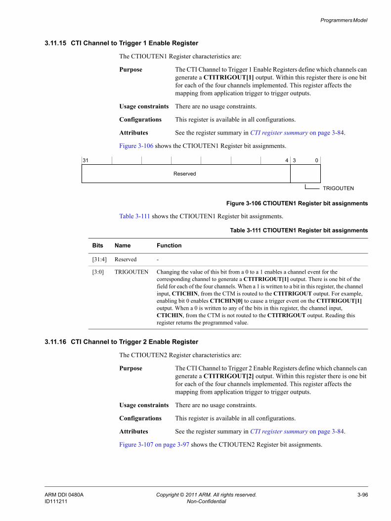
Programmers Model
3.11.15 CTI Channel to Trigger 1 Enable Register
The CTIOUTEN1 Register characteristics are:
Purpose The CTI Channel to Trigger 1 Enable Registers define which channels can generate a CTITRIGOUT[1] output. Within this register there is one bit for each of the four channels implemented. This register affects the mapping from application trigger to trigger outputs.
Usage constraints There are no usage constraints.
Configurations This register is available in all configurations.
Attributes See the register summary in CTI register summary on page 3-84.
Figure 3-106 shows the CTIOUTEN1 Register bit assignments.
Figure 3-106 CTIOUTEN1 Register bit assignments
Table 3-111 shows the CTIOUTEN1 Register bit assignments.
3.11.16 CTI Channel to Trigger 2 Enable Register
The CTIOUTEN2 Register characteristics are:
Purpose The CTI Channel to Trigger 2 Enable Registers define which channels can generate a CTITRIGOUT[2] output. Within this register there is one bit for each of the four channels implemented. This register affects the mapping from application trigger to trigger outputs.
Usage constraints There are no usage constraints.
Configurations This register is available in all configurations.
Attributes See the register summary in CTI register summary on page 3-84.
Figure 3-107 on page 3-97 shows the CTIOUTEN2 Register bit assignments.
31 4 3 0
Reserved
TRIGOUTEN
Table 3-111 CTIOUTEN1 Register bit assignments
Bits Name Function
[31:4] Reserved -
[3:0] TRIGOUTEN Changing the value of this bit from a 0 to a 1 enables a channel event for the corresponding channel to generate a CTITRIGOUT[1] output. There is one bit of the field for each of the four channels. When a 1 is written to a bit in this register, the channel input, CTICHIN, from the CTM is routed to the CTITRIGOUT output. For example, enabling bit 0 enables CTICHIN[0] to cause a trigger event on the CTITRIGOUT[1] output. When a 0 is written to any of the bits in this register, the channel input, CTICHIN, from the CTM is not routed to the CTITRIGOUT output. Reading this register returns the programmed value.
ARM DDI 0480A Copyright © 2011 ARM. All rights reserved. 3-96ID111211 Non-Confidential

Programmers Model
Figure 3-107 CTIOUTEN2 Register bit assignments
Table 3-112 shows the CTIOUTEN2 Register bit assignments.
3.11.17 CTI Channel to Trigger 3 Enable Register
The CTIOUTEN3 Register characteristics are:
Purpose The CTI Channel to Trigger 3 Enable Registers define which channels can generate a CTITRIGOUT[3] output. Within this register there is one bit for each of the four channels implemented. This register affects the mapping from application trigger to trigger outputs.
Usage constraints There are no usage constraints.
Configurations This register is available in all configurations.
Attributes See the register summary in CTI register summary on page 3-84.
Figure 3-108 shows the CTIOUTEN3 Register bit assignments.
Figure 3-108 CTIOUTEN3 Register bit assignments
31 4 3 0
Reserved
TRIGOUTEN
Table 3-112 CTIOUTEN2 Register bit assignments
Bits Name Function
[31:4] Reserved -
[3:0] TRIGOUTEN Changing the value of this bit from a 0 to a 1 enables a channel event for the corresponding channel to generate a CTITRIGOUT[2] output. There is one bit of the field for each of the four channels. When a 1 is written to a bit in this register, the channel input, CTICHIN, from the CTM is routed to the CTITRIGOUT output. For example, enabling bit 0 enables CTICHIN[0] to cause a trigger event on the CTITRIGOUT[2] output. When a 0 is written to any of the bits in this register, the channel input, CTICHIN, from the CTM is not routed to the CTITRIGOUT output. Reading this register returns the programmed value.
31 4 3 0
Reserved
TRIGOUTEN
ARM DDI 0480A Copyright © 2011 ARM. All rights reserved. 3-97ID111211 Non-Confidential
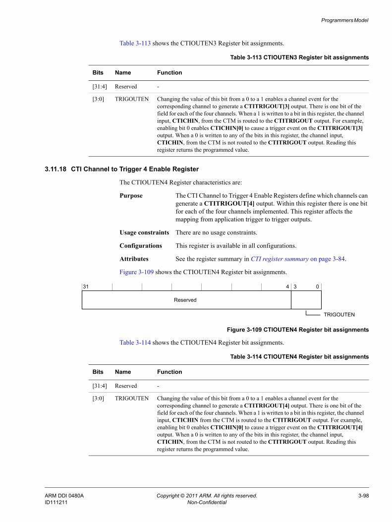
Programmers Model
Table 3-113 shows the CTIOUTEN3 Register bit assignments.
3.11.18 CTI Channel to Trigger 4 Enable Register
The CTIOUTEN4 Register characteristics are:
Purpose The CTI Channel to Trigger 4 Enable Registers define which channels can generate a CTITRIGOUT[4] output. Within this register there is one bit for each of the four channels implemented. This register affects the mapping from application trigger to trigger outputs.
Usage constraints There are no usage constraints.
Configurations This register is available in all configurations.
Attributes See the register summary in CTI register summary on page 3-84.
Figure 3-109 shows the CTIOUTEN4 Register bit assignments.
Figure 3-109 CTIOUTEN4 Register bit assignments
Table 3-114 shows the CTIOUTEN4 Register bit assignments.
Table 3-113 CTIOUTEN3 Register bit assignments
Bits Name Function
[31:4] Reserved -
[3:0] TRIGOUTEN Changing the value of this bit from a 0 to a 1 enables a channel event for the corresponding channel to generate a CTITRIGOUT[3] output. There is one bit of the field for each of the four channels. When a 1 is written to a bit in this register, the channel input, CTICHIN, from the CTM is routed to the CTITRIGOUT output. For example, enabling bit 0 enables CTICHIN[0] to cause a trigger event on the CTITRIGOUT[3] output. When a 0 is written to any of the bits in this register, the channel input, CTICHIN, from the CTM is not routed to the CTITRIGOUT output. Reading this register returns the programmed value.
31 4 3 0
Reserved
TRIGOUTEN
Table 3-114 CTIOUTEN4 Register bit assignments
Bits Name Function
[31:4] Reserved -
[3:0] TRIGOUTEN Changing the value of this bit from a 0 to a 1 enables a channel event for the corresponding channel to generate a CTITRIGOUT[4] output. There is one bit of the field for each of the four channels. When a 1 is written to a bit in this register, the channel input, CTICHIN from the CTM is routed to the CTITRIGOUT output. For example, enabling bit 0 enables CTICHIN[0] to cause a trigger event on the CTITRIGOUT[4] output. When a 0 is written to any of the bits in this register, the channel input, CTICHIN, from the CTM is not routed to the CTITRIGOUT output. Reading this register returns the programmed value.
ARM DDI 0480A Copyright © 2011 ARM. All rights reserved. 3-98ID111211 Non-Confidential
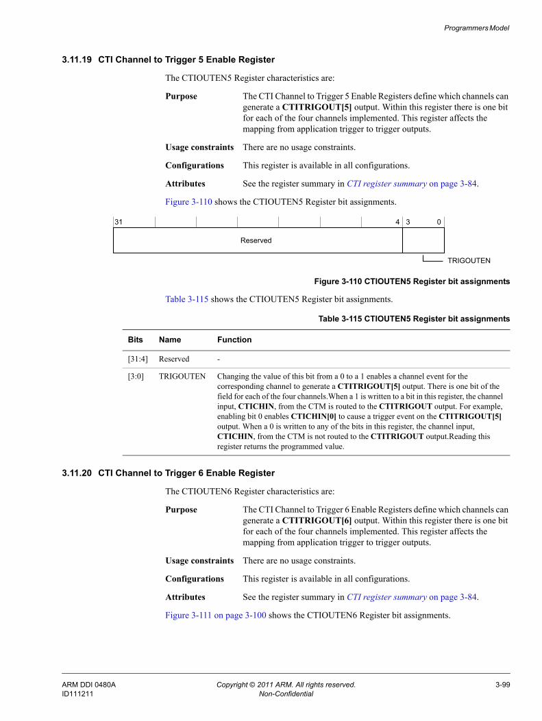
Programmers Model
3.11.19 CTI Channel to Trigger 5 Enable Register
The CTIOUTEN5 Register characteristics are:
Purpose The CTI Channel to Trigger 5 Enable Registers define which channels can generate a CTITRIGOUT[5] output. Within this register there is one bit for each of the four channels implemented. This register affects the mapping from application trigger to trigger outputs.
Usage constraints There are no usage constraints.
Configurations This register is available in all configurations.
Attributes See the register summary in CTI register summary on page 3-84.
Figure 3-110 shows the CTIOUTEN5 Register bit assignments.
Figure 3-110 CTIOUTEN5 Register bit assignments
Table 3-115 shows the CTIOUTEN5 Register bit assignments.
3.11.20 CTI Channel to Trigger 6 Enable Register
The CTIOUTEN6 Register characteristics are:
Purpose The CTI Channel to Trigger 6 Enable Registers define which channels can generate a CTITRIGOUT[6] output. Within this register there is one bit for each of the four channels implemented. This register affects the mapping from application trigger to trigger outputs.
Usage constraints There are no usage constraints.
Configurations This register is available in all configurations.
Attributes See the register summary in CTI register summary on page 3-84.
Figure 3-111 on page 3-100 shows the CTIOUTEN6 Register bit assignments.
31 4 3 0
Reserved
TRIGOUTEN
Table 3-115 CTIOUTEN5 Register bit assignments
Bits Name Function
[31:4] Reserved -
[3:0] TRIGOUTEN Changing the value of this bit from a 0 to a 1 enables a channel event for the corresponding channel to generate a CTITRIGOUT[5] output. There is one bit of the field for each of the four channels.When a 1 is written to a bit in this register, the channel input, CTICHIN, from the CTM is routed to the CTITRIGOUT output. For example, enabling bit 0 enables CTICHIN[0] to cause a trigger event on the CTITRIGOUT[5] output. When a 0 is written to any of the bits in this register, the channel input, CTICHIN, from the CTM is not routed to the CTITRIGOUT output.Reading this register returns the programmed value.
ARM DDI 0480A Copyright © 2011 ARM. All rights reserved. 3-99ID111211 Non-Confidential
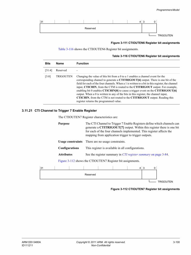
Programmers Model
Figure 3-111 CTIOUTEN6 Register bit assignments
Table 3-116 shows the CTIOUTEN6 Register bit assignments.
3.11.21 CTI Channel to Trigger 7 Enable Register
The CTIOUTEN7 Register characteristics are:
Purpose The CTI Channel to Trigger 7 Enable Registers define which channels can generate a CTITRIGOUT[7] output. Within this register there is one bit for each of the four channels implemented. This register affects the mapping from application trigger to trigger outputs.
Usage constraints There are no usage constraints.
Configurations This register is available in all configurations.
Attributes See the register summary in CTI register summary on page 3-84.
Figure 3-112 shows the CTIOUTEN7 Register bit assignments.
Figure 3-112 CTIOUTEN7 Register bit assignments
31 4 3 0
Reserved
TRIGOUTEN
Table 3-116 CTIOUTEN6 Register bit assignments
Bits Name Function
[31:4] Reserved -
[3:0] TRIGOUTEN Changing the value of this bit from a 0 to a 1 enables a channel event for the corresponding channel to generate a CTITRIGOUT[6] output. There is one bit of the field for each of the four channels. When a 1 is written to a bit in this register, the channel input, CTICHIN, from the CTM is routed to the CTITRIGOUT output. For example, enabling bit 0 enables CTICHIN[0] to cause a trigger event on the CTITRIGOUT[6] output. When a 0 is written to any of the bits in this register, the channel input, CTICHIN, from the CTM is not routed to the CTITRIGOUT output. Reading this register returns the programmed value.
31 4 3 0
Reserved
TRIGOUTEN
ARM DDI 0480A Copyright © 2011 ARM. All rights reserved. 3-100ID111211 Non-Confidential
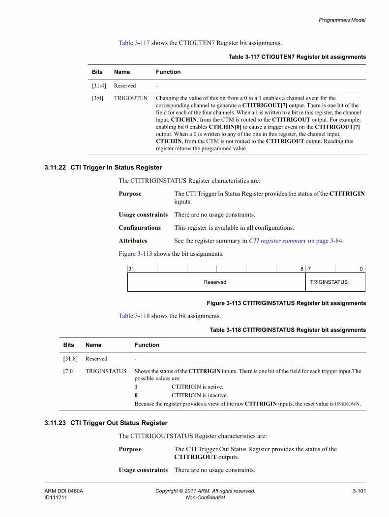
Programmers Model
Table 3-117 shows the CTIOUTEN7 Register bit assignments.
3.11.22 CTI Trigger In Status Register
The CTITRIGINSTATUS Register characteristics are:
Purpose The CTI Trigger In Status Register provides the status of the CTITRIGIN inputs.
Usage constraints There are no usage constraints.
Configurations This register is available in all configurations.
Attributes See the register summary in CTI register summary on page 3-84.
Figure 3-113 shows the bit assignments.
Figure 3-113 CTITRIGINSTATUS Register bit assignments
Table 3-118 shows the bit assignments.
3.11.23 CTI Trigger Out Status Register
The CTITRIGOUTSTATUS Register characteristics are:
Purpose The CTI Trigger Out Status Register provides the status of the CTITRIGOUT outputs.
Usage constraints There are no usage constraints.
Table 3-117 CTIOUTEN7 Register bit assignments
Bits Name Function
[31:4] Reserved -
[3:0] TRIGOUTEN Changing the value of this bit from a 0 to a 1 enables a channel event for the corresponding channel to generate a CTITRIGOUT[7] output. There is one bit of the field for each of the four channels. When a 1 is written to a bit in this register, the channel input, CTICHIN, from the CTM is routed to the CTITRIGOUT output. For example, enabling bit 0 enables CTICHIN[0] to cause a trigger event on the CTITRIGOUT[7] output. When a 0 is written to any of the bits in this register, the channel input, CTICHIN, from the CTM is not routed to the CTITRIGOUT output. Reading this register returns the programmed value.
31 8 7 0
TRIGINSTATUSReserved
Table 3-118 CTITRIGINSTATUS Register bit assignments
Bits Name Function
[31:8] Reserved -
[7:0] TRIGINSTATUS Shows the status of the CTITRIGIN inputs. There is one bit of the field for each trigger input.The possible values are:1 CTITRIGIN is active.0 CTITRIGIN is inactive.Because the register provides a view of the raw CTITRIGIN inputs, the reset value is UNKNOWN.
ARM DDI 0480A Copyright © 2011 ARM. All rights reserved. 3-101ID111211 Non-Confidential
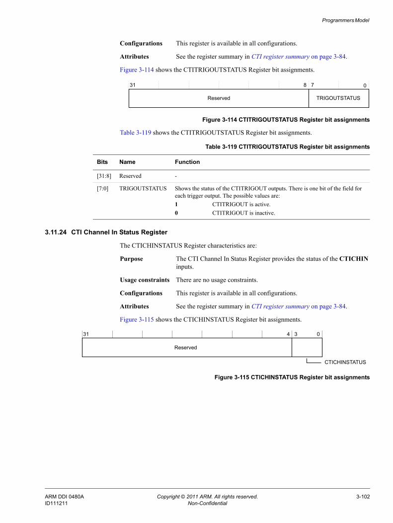
Programmers Model
Configurations This register is available in all configurations.
Attributes See the register summary in CTI register summary on page 3-84.
Figure 3-114 shows the CTITRIGOUTSTATUS Register bit assignments.
Figure 3-114 CTITRIGOUTSTATUS Register bit assignments
Table 3-119 shows the CTITRIGOUTSTATUS Register bit assignments.
3.11.24 CTI Channel In Status Register
The CTICHINSTATUS Register characteristics are:
Purpose The CTI Channel In Status Register provides the status of the CTICHIN inputs.
Usage constraints There are no usage constraints.
Configurations This register is available in all configurations.
Attributes See the register summary in CTI register summary on page 3-84.
Figure 3-115 shows the CTICHINSTATUS Register bit assignments.
Figure 3-115 CTICHINSTATUS Register bit assignments
31 0
Reserved
78
TRIGOUTSTATUS
Table 3-119 CTITRIGOUTSTATUS Register bit assignments
Bits Name Function
[31:8] Reserved -
[7:0] TRIGOUTSTATUS Shows the status of the CTITRIGOUT outputs. There is one bit of the field for each trigger output. The possible values are:1 CTITRIGOUT is active.0 CTITRIGOUT is inactive.
31 4 3 0
Reserved
CTICHINSTATUS
ARM DDI 0480A Copyright © 2011 ARM. All rights reserved. 3-102ID111211 Non-Confidential
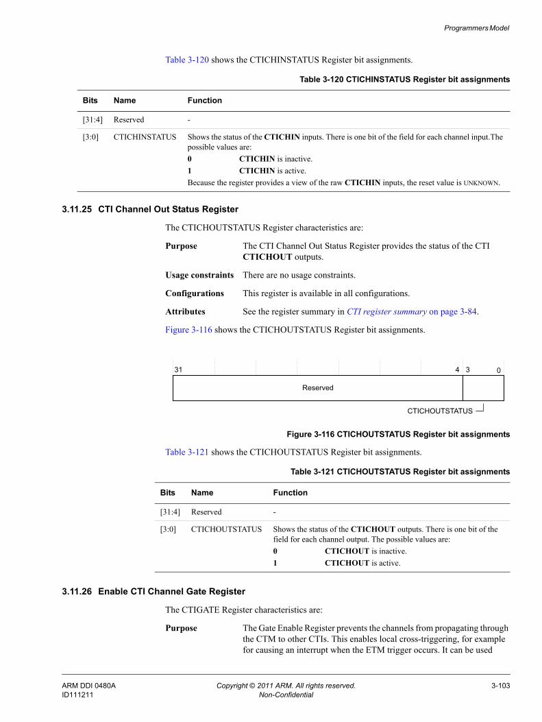
Programmers Model
Table 3-120 shows the CTICHINSTATUS Register bit assignments.
3.11.25 CTI Channel Out Status Register
The CTICHOUTSTATUS Register characteristics are:
Purpose The CTI Channel Out Status Register provides the status of the CTI CTICHOUT outputs.
Usage constraints There are no usage constraints.
Configurations This register is available in all configurations.
Attributes See the register summary in CTI register summary on page 3-84.
Figure 3-116 shows the CTICHOUTSTATUS Register bit assignments.
Figure 3-116 CTICHOUTSTATUS Register bit assignments
Table 3-121 shows the CTICHOUTSTATUS Register bit assignments.
3.11.26 Enable CTI Channel Gate Register
The CTIGATE Register characteristics are:
Purpose The Gate Enable Register prevents the channels from propagating through the CTM to other CTIs. This enables local cross-triggering, for example for causing an interrupt when the ETM trigger occurs. It can be used
Table 3-120 CTICHINSTATUS Register bit assignments
Bits Name Function
[31:4] Reserved -
[3:0] CTICHINSTATUS Shows the status of the CTICHIN inputs. There is one bit of the field for each channel input.The possible values are:0 CTICHIN is inactive.1 CTICHIN is active.Because the register provides a view of the raw CTICHIN inputs, the reset value is UNKNOWN.
31 0
Reserved
CTICHOUTSTATUS
4 3
Table 3-121 CTICHOUTSTATUS Register bit assignments
Bits Name Function
[31:4] Reserved -
[3:0] CTICHOUTSTATUS Shows the status of the CTICHOUT outputs. There is one bit of the field for each channel output. The possible values are:0 CTICHOUT is inactive.1 CTICHOUT is active.
ARM DDI 0480A Copyright © 2011 ARM. All rights reserved. 3-103ID111211 Non-Confidential
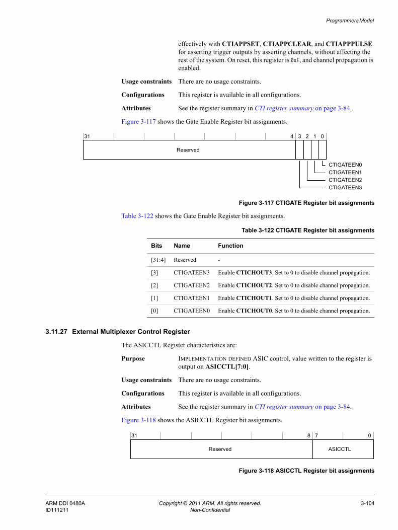
Programmers Model
effectively with CTIAPPSET, CTIAPPCLEAR, and CTIAPPPULSE for asserting trigger outputs by asserting channels, without affecting the rest of the system. On reset, this register is 0xF, and channel propagation is enabled.
Usage constraints There are no usage constraints.
Configurations This register is available in all configurations.
Attributes See the register summary in CTI register summary on page 3-84.
Figure 3-117 shows the Gate Enable Register bit assignments.
Figure 3-117 CTIGATE Register bit assignments
Table 3-122 shows the Gate Enable Register bit assignments.
3.11.27 External Multiplexer Control Register
The ASICCTL Register characteristics are:
Purpose IMPLEMENTATION DEFINED ASIC control, value written to the register is output on ASICCTL[7:0].
Usage constraints There are no usage constraints.
Configurations This register is available in all configurations.
Attributes See the register summary in CTI register summary on page 3-84.
Figure 3-118 shows the ASICCTL Register bit assignments.
Figure 3-118 ASICCTL Register bit assignments
31 4 3 2 1 0
Reserved
CTIGATEEN2CTIGATEEN1CTIGATEEN0
CTIGATEEN3
Table 3-122 CTIGATE Register bit assignments
Bits Name Function
[31:4] Reserved -
[3] CTIGATEEN3 Enable CTICHOUT3. Set to 0 to disable channel propagation.
[2] CTIGATEEN2 Enable CTICHOUT2. Set to 0 to disable channel propagation.
[1] CTIGATEEN1 Enable CTICHOUT1. Set to 0 to disable channel propagation.
[0] CTIGATEEN0 Enable CTICHOUT0. Set to 0 to disable channel propagation.
31 8 7 0
ASICCTLReserved
ARM DDI 0480A Copyright © 2011 ARM. All rights reserved. 3-104ID111211 Non-Confidential
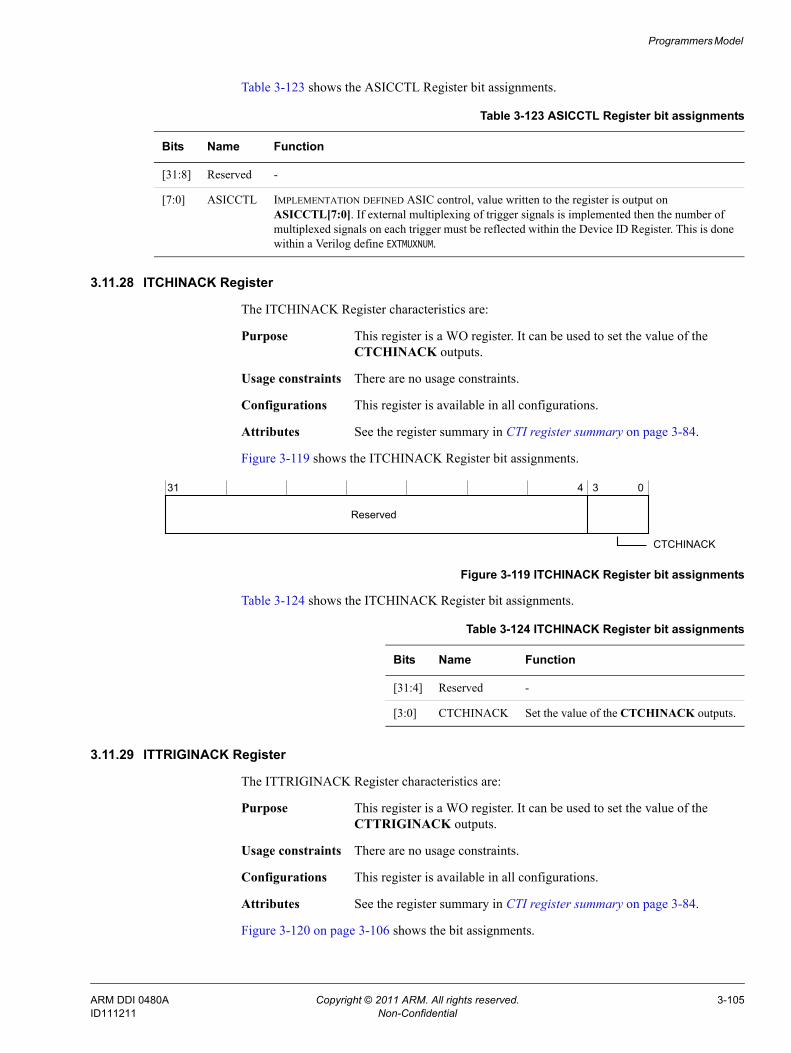
Programmers Model
Table 3-123 shows the ASICCTL Register bit assignments.
3.11.28 ITCHINACK Register
The ITCHINACK Register characteristics are:
Purpose This register is a WO register. It can be used to set the value of the CTCHINACK outputs.
Usage constraints There are no usage constraints.
Configurations This register is available in all configurations.
Attributes See the register summary in CTI register summary on page 3-84.
Figure 3-119 shows the ITCHINACK Register bit assignments.
Figure 3-119 ITCHINACK Register bit assignments
Table 3-124 shows the ITCHINACK Register bit assignments.
3.11.29 ITTRIGINACK Register
The ITTRIGINACK Register characteristics are:
Purpose This register is a WO register. It can be used to set the value of the CTTRIGINACK outputs.
Usage constraints There are no usage constraints.
Configurations This register is available in all configurations.
Attributes See the register summary in CTI register summary on page 3-84.
Figure 3-120 on page 3-106 shows the bit assignments.
Table 3-123 ASICCTL Register bit assignments
Bits Name Function
[31:8] Reserved -
[7:0] ASICCTL IMPLEMENTATION DEFINED ASIC control, value written to the register is output on ASICCTL[7:0]. If external multiplexing of trigger signals is implemented then the number of multiplexed signals on each trigger must be reflected within the Device ID Register. This is done within a Verilog define EXTMUXNUM.
31 4 3 0
Reserved
CTCHINACK
Table 3-124 ITCHINACK Register bit assignments
Bits Name Function
[31:4] Reserved -
[3:0] CTCHINACK Set the value of the CTCHINACK outputs.
ARM DDI 0480A Copyright © 2011 ARM. All rights reserved. 3-105ID111211 Non-Confidential
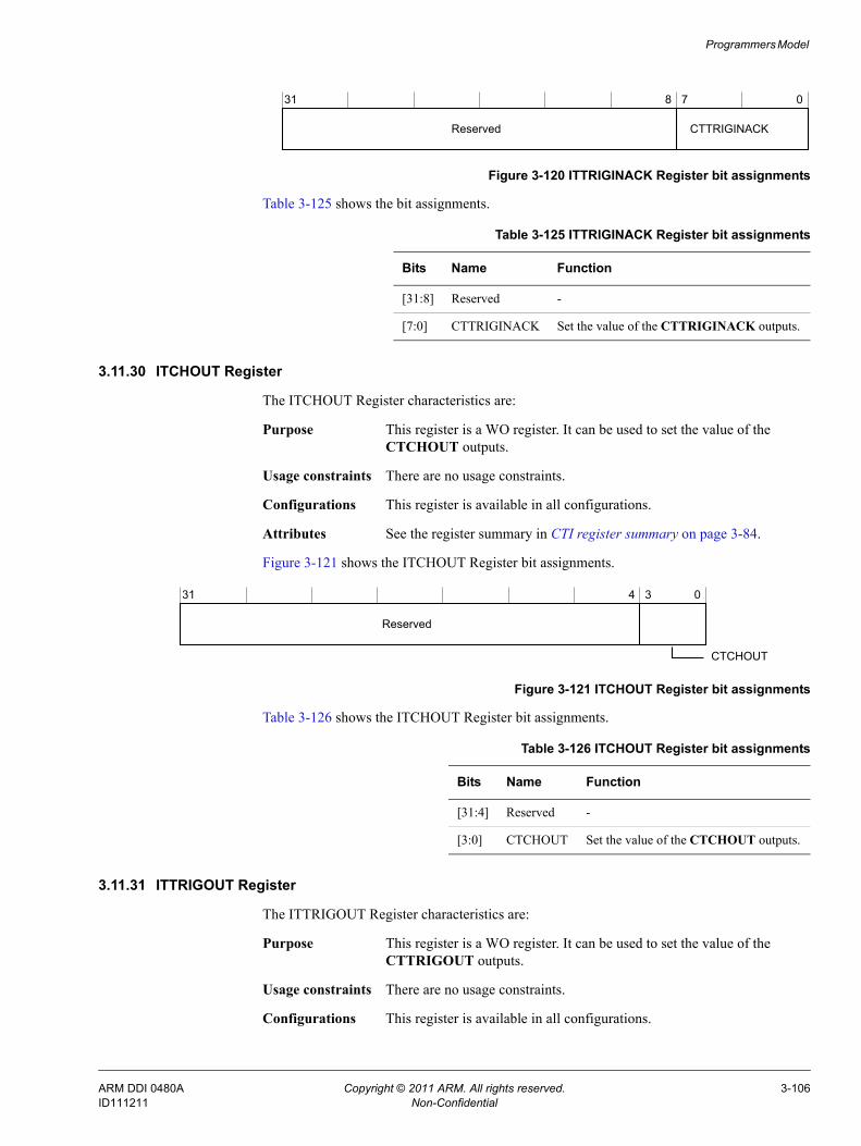
Programmers Model
Figure 3-120 ITTRIGINACK Register bit assignments
Table 3-125 shows the bit assignments.
3.11.30 ITCHOUT Register
The ITCHOUT Register characteristics are:
Purpose This register is a WO register. It can be used to set the value of the CTCHOUT outputs.
Usage constraints There are no usage constraints.
Configurations This register is available in all configurations.
Attributes See the register summary in CTI register summary on page 3-84.
Figure 3-121 shows the ITCHOUT Register bit assignments.
Figure 3-121 ITCHOUT Register bit assignments
Table 3-126 shows the ITCHOUT Register bit assignments.
3.11.31 ITTRIGOUT Register
The ITTRIGOUT Register characteristics are:
Purpose This register is a WO register. It can be used to set the value of the CTTRIGOUT outputs.
Usage constraints There are no usage constraints.
Configurations This register is available in all configurations.
31 8 7 0
CTTRIGINACKReserved
Table 3-125 ITTRIGINACK Register bit assignments
Bits Name Function
[31:8] Reserved -
[7:0] CTTRIGINACK Set the value of the CTTRIGINACK outputs.
31 4 3 0
Reserved
CTCHOUT
Table 3-126 ITCHOUT Register bit assignments
Bits Name Function
[31:4] Reserved -
[3:0] CTCHOUT Set the value of the CTCHOUT outputs.
ARM DDI 0480A Copyright © 2011 ARM. All rights reserved. 3-106ID111211 Non-Confidential
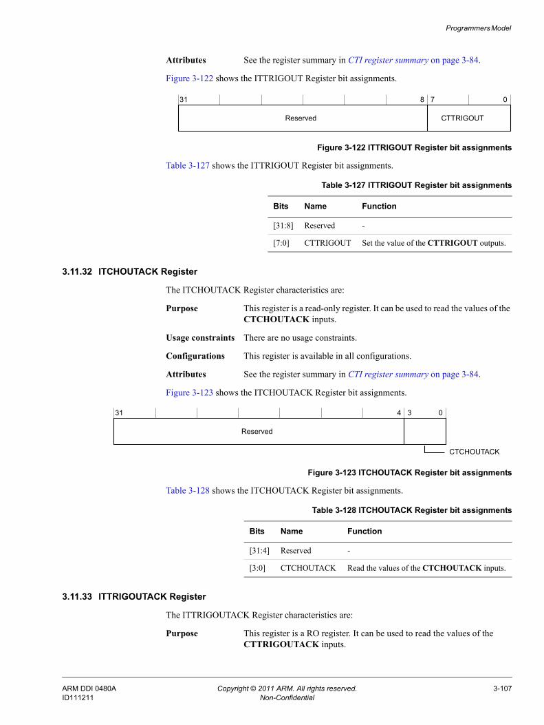
Programmers Model
Attributes See the register summary in CTI register summary on page 3-84.
Figure 3-122 shows the ITTRIGOUT Register bit assignments.
Figure 3-122 ITTRIGOUT Register bit assignments
Table 3-127 shows the ITTRIGOUT Register bit assignments.
3.11.32 ITCHOUTACK Register
The ITCHOUTACK Register characteristics are:
Purpose This register is a read-only register. It can be used to read the values of the CTCHOUTACK inputs.
Usage constraints There are no usage constraints.
Configurations This register is available in all configurations.
Attributes See the register summary in CTI register summary on page 3-84.
Figure 3-123 shows the ITCHOUTACK Register bit assignments.
Figure 3-123 ITCHOUTACK Register bit assignments
Table 3-128 shows the ITCHOUTACK Register bit assignments.
3.11.33 ITTRIGOUTACK Register
The ITTRIGOUTACK Register characteristics are:
Purpose This register is a RO register. It can be used to read the values of the CTTRIGOUTACK inputs.
31 8 7 0
CTTRIGOUTReserved
Table 3-127 ITTRIGOUT Register bit assignments
Bits Name Function
[31:8] Reserved -
[7:0] CTTRIGOUT Set the value of the CTTRIGOUT outputs.
31 4 3 0
Reserved
CTCHOUTACK
Table 3-128 ITCHOUTACK Register bit assignments
Bits Name Function
[31:4] Reserved -
[3:0] CTCHOUTACK Read the values of the CTCHOUTACK inputs.
ARM DDI 0480A Copyright © 2011 ARM. All rights reserved. 3-107ID111211 Non-Confidential
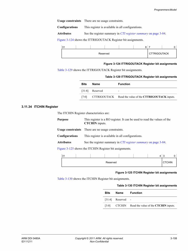
Programmers Model
Usage constraints There are no usage constraints.
Configurations This register is available in all configurations.
Attributes See the register summary in CTI register summary on page 3-84.
Figure 3-124 shows the ITTRIGOUTACK Register bit assignments.
Figure 3-124 ITTRIGOUTACK Register bit assignments
Table 3-129 shows the ITTRIGOUTACK Register bit assignments.
3.11.34 ITCHIN Register
The ITCHIN Register characteristics are:
Purpose This register is a RO register. It can be used to read the values of the CTCHIN inputs.
Usage constraints There are no usage constraints.
Configurations This register is available in all configurations.
Attributes See the register summary in CTI register summary on page 3-84.
Figure 3-125 shows the ITCHIN Register bit assignments.
Figure 3-125 ITCHIN Register bit assignments
Table 3-130 shows the ITCHIN Register bit assignments.
31 8 7 0
CTTRIGOUTACKReserved
Table 3-129 ITTRIGOUTACK Register bit assignments
Bits Name Function
[31:8] Reserved -
[7:0] CTTRIGOUTACK Read the value of the CTTRIGOUTACK inputs.
31 4 3 0
CTCHINReserved
Table 3-130 ITCHIN Register bit assignments
Bits Name Function
[31:4] Reserved -
[3:0] CTCHIN Read the value of the CTCHIN inputs.
ARM DDI 0480A Copyright © 2011 ARM. All rights reserved. 3-108ID111211 Non-Confidential
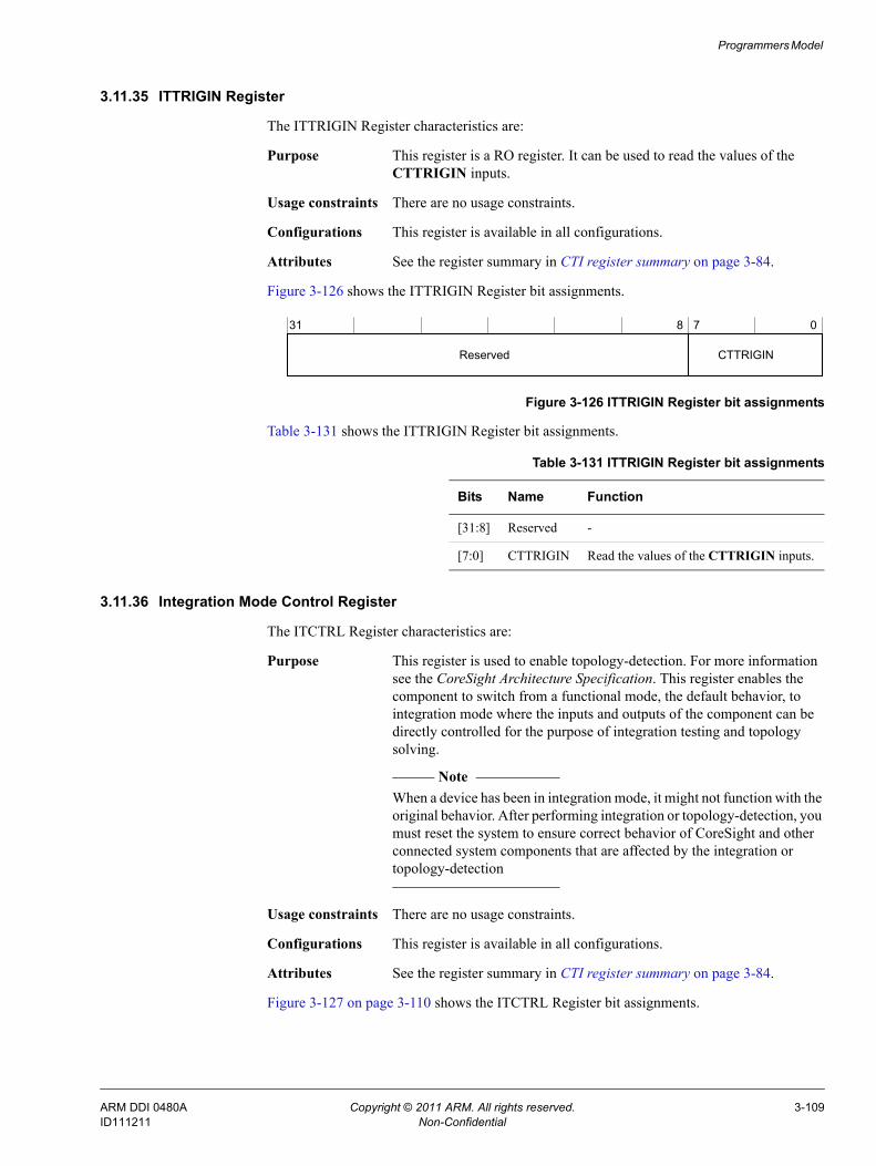
Programmers Model
3.11.35 ITTRIGIN Register
The ITTRIGIN Register characteristics are:
Purpose This register is a RO register. It can be used to read the values of the CTTRIGIN inputs.
Usage constraints There are no usage constraints.
Configurations This register is available in all configurations.
Attributes See the register summary in CTI register summary on page 3-84.
Figure 3-126 shows the ITTRIGIN Register bit assignments.
Figure 3-126 ITTRIGIN Register bit assignments
Table 3-131 shows the ITTRIGIN Register bit assignments.
3.11.36 Integration Mode Control Register
The ITCTRL Register characteristics are:
Purpose This register is used to enable topology-detection. For more information see the CoreSight Architecture Specification. This register enables the component to switch from a functional mode, the default behavior, to integration mode where the inputs and outputs of the component can be directly controlled for the purpose of integration testing and topology solving.
Note When a device has been in integration mode, it might not function with the
original behavior. After performing integration or topology-detection, you must reset the system to ensure correct behavior of CoreSight and other connected system components that are affected by the integration or topology-detection
Usage constraints There are no usage constraints.
Configurations This register is available in all configurations.
Attributes See the register summary in CTI register summary on page 3-84.
Figure 3-127 on page 3-110 shows the ITCTRL Register bit assignments.
31 8 7 0
CTTRIGINReserved
Table 3-131 ITTRIGIN Register bit assignments
Bits Name Function
[31:8] Reserved -
[7:0] CTTRIGIN Read the values of the CTTRIGIN inputs.
ARM DDI 0480A Copyright © 2011 ARM. All rights reserved. 3-109ID111211 Non-Confidential
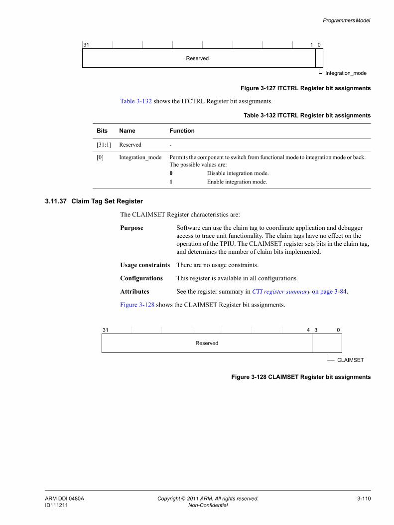
Programmers Model
Figure 3-127 ITCTRL Register bit assignments
Table 3-132 shows the ITCTRL Register bit assignments.
3.11.37 Claim Tag Set Register
The CLAIMSET Register characteristics are:
Purpose Software can use the claim tag to coordinate application and debugger access to trace unit functionality. The claim tags have no effect on the operation of the TPIU. The CLAIMSET register sets bits in the claim tag, and determines the number of claim bits implemented.
Usage constraints There are no usage constraints.
Configurations This register is available in all configurations.
Attributes See the register summary in CTI register summary on page 3-84.
Figure 3-128 shows the CLAIMSET Register bit assignments.
Figure 3-128 CLAIMSET Register bit assignments
31 1 0
Reserved
Integration_mode
Table 3-132 ITCTRL Register bit assignments
Bits Name Function
[31:1] Reserved -
[0] Integration_mode Permits the component to switch from functional mode to integration mode or back. The possible values are:0 Disable integration mode.1 Enable integration mode.
31 4 3 0
CLAIMSET
Reserved
ARM DDI 0480A Copyright © 2011 ARM. All rights reserved. 3-110ID111211 Non-Confidential
Programmers Model
Table 3-133 shows the CLAIMSET Register bit assignments.
3.11.38 Claim Tag Clear Register
The CLAIMCLR Register characteristics are:
Purpose Software can use the claim tag to coordinate application and debugger access to trace unit functionality. The claim tags have no effect on the operation of the TPIU. CLAIMCLR is used to clear bits in the claim tag, and determine the current value of the claim tag.
Usage constraints There are no usage constraints.
Configurations This register is available in all configurations.
Attributes See the register summary in CTI register summary on page 3-84.
Figure 3-129 shows the CLAIMCLR Register bit assignments.
Figure 3-129 CLAIMCLR Register bit assignments
Table 3-134 shows the CLAIMCLR Register bit assignments.
Table 3-133 CLAIMSET Register bit assignments
Bits Name Function
[31:4] Reserved -
[3:0] CLAIMSET On reads:b1111 Four bits of claim tag are implemented.On writes, for each bit the possible values are:0 No effect.1 Set this bit in the claim tag.
31 4 3 0
CLAIMCLR
Reserved
Table 3-134 CLAIMCLR Register bit assignments
Bits Name Function
[31:4] Reserved -
[3:0] CLAIMCLR On reads, for each bit the possible values are:0 Claim tag bit is not set.1 Claim tag bit is set.On writes, for each bit the possible values are:0 Has no effect.1 Clears the relevant bit in the claim tag.On reset, all bits of the CLAIMCLR are reset to 0, indicating all claim bits are not set.
ARM DDI 0480A Copyright © 2011 ARM. All rights reserved. 3-111ID111211 Non-Confidential
Programmers Model
3.11.39 Lock Access Register
The LAR Register characteristics are:
Purpose This is used to enable write access to device registers. External accesses from a debugger, PADDRDBG31 = 1, are not subject to the Lock Registers. A debugger does not have to unlock the component to write and modify the registers in the component.
Usage constraints There are no usage constraints.
Configurations This register is available in all configurations.
Attributes See the register summary in CTI register summary on page 3-84.
Figure 3-130 shows the LAR Register bit assignments.
Figure 3-130 LAR Register bit assignments
Table 3-135 shows the LAR Register bit assignments.
3.11.40 Lock Status Register
The LSR Register characteristics are:
Purpose This indicates the status of the Lock control mechanism. This lock prevents accidental writes by code under debug. When locked, write access is blocked to all registers, except the Lock Access Register. External accesses from a debugger, PADDRDBG31 = 1, are not subject to the Lock Registers. This register reads as 0 when read from an external debugger PADDRDBG31 = 1.
Usage constraints There are no usage constraints.
Configurations This register is available in all configurations.
Attributes See the register summary in CTI register summary on page 3-84.
Figure 3-131 on page 3-113 shows the LSR Register bit assignments.
31 0
ACCESS
Table 3-135 LAR Register bit assignments
Bits Name Function
[31:0] ACCESS A write of 0xC5ACCE55 enables more write access to this device. A write of any value other than 0xC5ACCE55 have the affect of removing write access. The possible value is:0xC5ACCE55 Unlock the protection register to enable write access.
ARM DDI 0480A Copyright © 2011 ARM. All rights reserved. 3-112ID111211 Non-Confidential
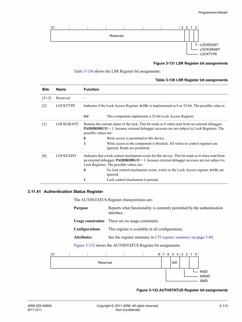
Programmers Model
Figure 3-131 LSR Register bit assignments
Table 3-136 shows the LSR Register bit assignments.
3.11.41 Authentication Status Register
The AUTHSTATUS Register characteristics are:
Purpose Reports what functionality is currently permitted by the authentication interface.
Usage constraints There are no usage constraints.
Configurations This register is available in all configurations.
Attributes See the register summary in CTI register summary on page 3-84.
Figure 3-132 shows the AUTHSTATUS Register bit assignments.
Figure 3-132 AUTHSTATUS Register bit assignments
31 3 2 1 0
Reserved
LOCKTYPELOCKGRANTLOCKEXIST
Table 3-136 LSR Register bit assignments
Bits Name Function
[31:3] Reserved -
[2] LOCKTYPE Indicates if the Lock Access Register, 0xFB0, is implemented as 8 or 32-bit. The possible value is: 0b0 This component implements a 32-bit Lock Access Register.
[1] LOCKGRANT Returns the current status of the lock. This bit reads as 0 when read from an external debugger, PADDRDBG31 = 1, because external debugger accesses are not subject to Lock Registers. The possible values are:0 Write access is permitted to this device.1 Write access to the component is blocked. All writes to control registers are
ignored. Reads are permitted.
[0] LOCKEXIST Indicates that a lock control mechanism exists for this device. This bit reads as 0 when read from an external debugger, PADDRDBG31 = 1, because external debugger accesses are not subject to Lock Registers. The possible values are:0 No lock control mechanism exists, writes to the Lock Access register, 0xFB0, are
ignored.1 Lock control mechanism is present.
31 8 7 6 5 4 3 2 1 0
SIDReserved
SNIDNSNIDNSID
ARM DDI 0480A Copyright © 2011 ARM. All rights reserved. 3-113ID111211 Non-Confidential
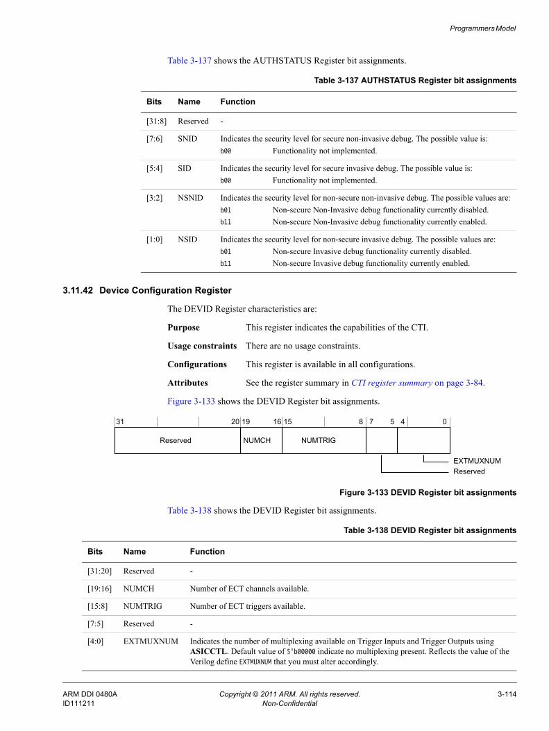
Programmers Model
Table 3-137 shows the AUTHSTATUS Register bit assignments.
3.11.42 Device Configuration Register
The DEVID Register characteristics are:
Purpose This register indicates the capabilities of the CTI.
Usage constraints There are no usage constraints.
Configurations This register is available in all configurations.
Attributes See the register summary in CTI register summary on page 3-84.
Figure 3-133 shows the DEVID Register bit assignments.
Figure 3-133 DEVID Register bit assignments
Table 3-138 shows the DEVID Register bit assignments.
Table 3-137 AUTHSTATUS Register bit assignments
Bits Name Function
[31:8] Reserved -
[7:6] SNID Indicates the security level for secure non-invasive debug. The possible value is:b00 Functionality not implemented.
[5:4] SID Indicates the security level for secure invasive debug. The possible value is:b00 Functionality not implemented.
[3:2] NSNID Indicates the security level for non-secure non-invasive debug. The possible values are:b01 Non-secure Non-Invasive debug functionality currently disabled.b11 Non-secure Non-Invasive debug functionality currently enabled.
[1:0] NSID Indicates the security level for non-secure invasive debug. The possible values are:b01 Non-secure Invasive debug functionality currently disabled.b11 Non-secure Invasive debug functionality currently enabled.
31 20 19 16 15 8 7 5 4 0
NUMTRIGNUMCHReserved
ReservedEXTMUXNUM
Table 3-138 DEVID Register bit assignments
Bits Name Function
[31:20] Reserved -
[19:16] NUMCH Number of ECT channels available.
[15:8] NUMTRIG Number of ECT triggers available.
[7:5] Reserved -
[4:0] EXTMUXNUM Indicates the number of multiplexing available on Trigger Inputs and Trigger Outputs using ASICCTL. Default value of 5'b00000 indicate no multiplexing present. Reflects the value of the Verilog define EXTMUXNUM that you must alter accordingly.
ARM DDI 0480A Copyright © 2011 ARM. All rights reserved. 3-114ID111211 Non-Confidential
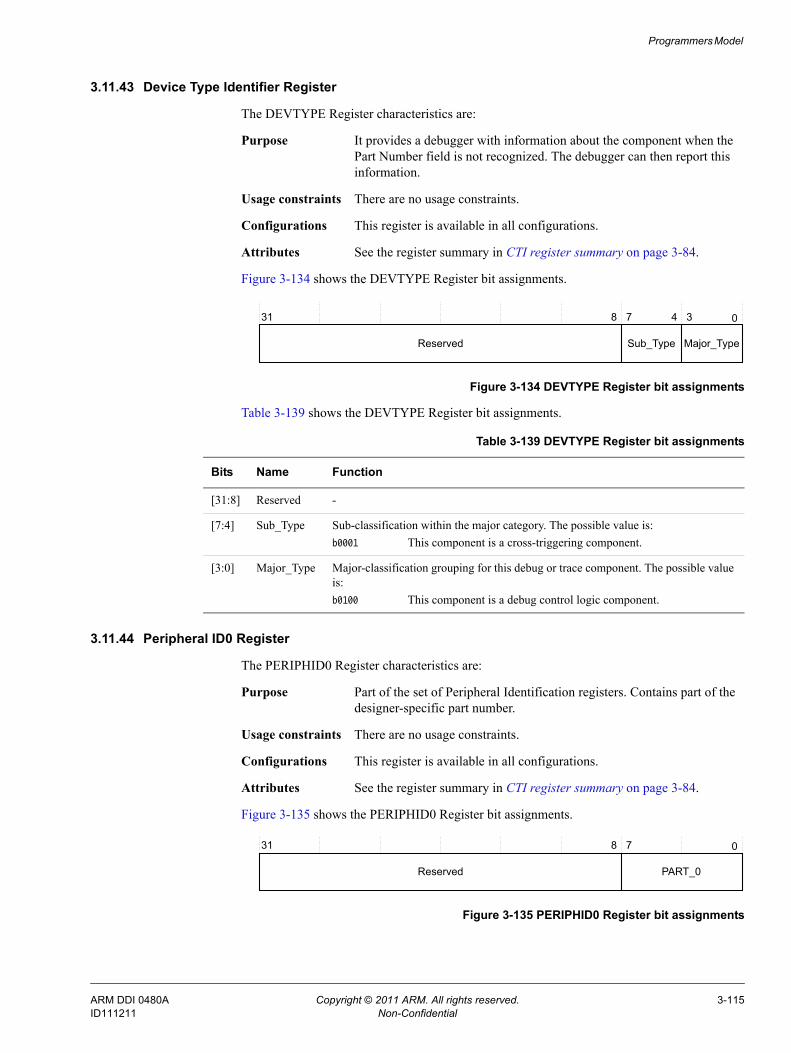
Programmers Model
3.11.43 Device Type Identifier Register
The DEVTYPE Register characteristics are:
Purpose It provides a debugger with information about the component when the Part Number field is not recognized. The debugger can then report this information.
Usage constraints There are no usage constraints.
Configurations This register is available in all configurations.
Attributes See the register summary in CTI register summary on page 3-84.
Figure 3-134 shows the DEVTYPE Register bit assignments.
Figure 3-134 DEVTYPE Register bit assignments
Table 3-139 shows the DEVTYPE Register bit assignments.
3.11.44 Peripheral ID0 Register
The PERIPHID0 Register characteristics are:
Purpose Part of the set of Peripheral Identification registers. Contains part of the designer-specific part number.
Usage constraints There are no usage constraints.
Configurations This register is available in all configurations.
Attributes See the register summary in CTI register summary on page 3-84.
Figure 3-135 shows the PERIPHID0 Register bit assignments.
Figure 3-135 PERIPHID0 Register bit assignments
31 0
Reserved
7
Sub_Type
8 4
Major_Type
3
Table 3-139 DEVTYPE Register bit assignments
Bits Name Function
[31:8] Reserved -
[7:4] Sub_Type Sub-classification within the major category. The possible value is:b0001 This component is a cross-triggering component.
[3:0] Major_Type Major-classification grouping for this debug or trace component. The possible value is:b0100 This component is a debug control logic component.
31 0
Reserved
78
PART_0
ARM DDI 0480A Copyright © 2011 ARM. All rights reserved. 3-115ID111211 Non-Confidential
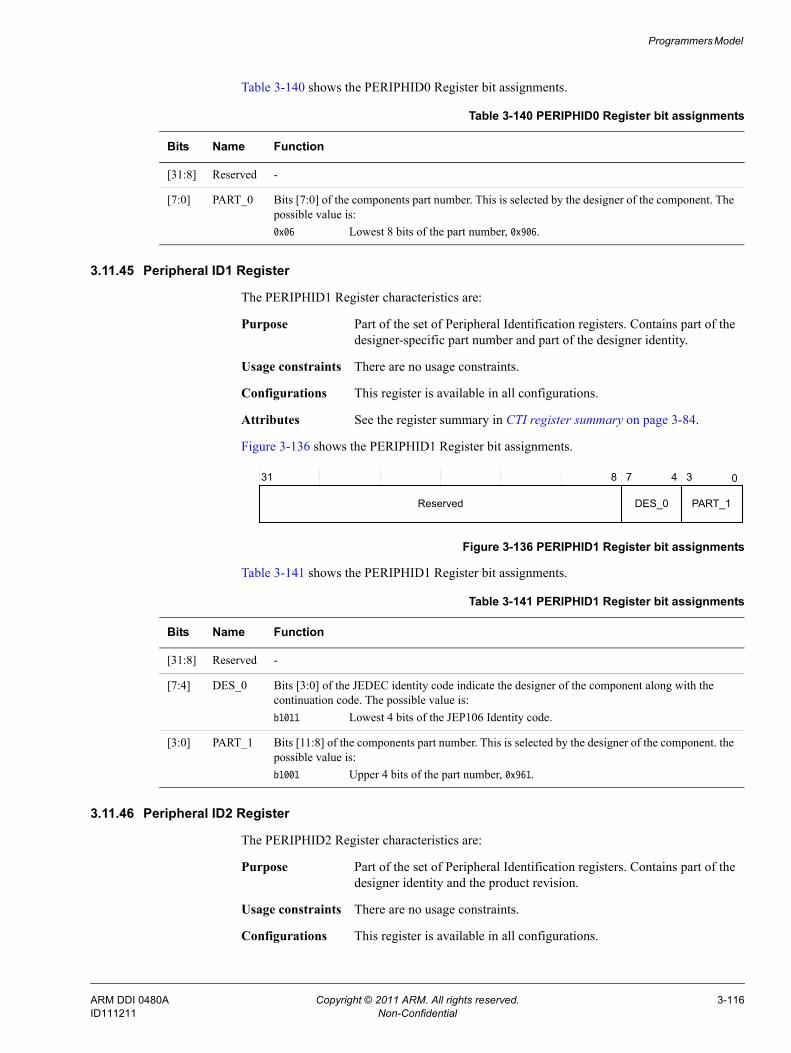
Programmers Model
Table 3-140 shows the PERIPHID0 Register bit assignments.
3.11.45 Peripheral ID1 Register
The PERIPHID1 Register characteristics are:
Purpose Part of the set of Peripheral Identification registers. Contains part of the designer-specific part number and part of the designer identity.
Usage constraints There are no usage constraints.
Configurations This register is available in all configurations.
Attributes See the register summary in CTI register summary on page 3-84.
Figure 3-136 shows the PERIPHID1 Register bit assignments.
Figure 3-136 PERIPHID1 Register bit assignments
Table 3-141 shows the PERIPHID1 Register bit assignments.
3.11.46 Peripheral ID2 Register
The PERIPHID2 Register characteristics are:
Purpose Part of the set of Peripheral Identification registers. Contains part of the designer identity and the product revision.
Usage constraints There are no usage constraints.
Configurations This register is available in all configurations.
Table 3-140 PERIPHID0 Register bit assignments
Bits Name Function
[31:8] Reserved -
[7:0] PART_0 Bits [7:0] of the components part number. This is selected by the designer of the component. The possible value is:0x06 Lowest 8 bits of the part number, 0x906.
31 0
Reserved
78
PART_1
4 3
DES_0
Table 3-141 PERIPHID1 Register bit assignments
Bits Name Function
[31:8] Reserved -
[7:4] DES_0 Bits [3:0] of the JEDEC identity code indicate the designer of the component along with the continuation code. The possible value is:b1011 Lowest 4 bits of the JEP106 Identity code.
[3:0] PART_1 Bits [11:8] of the components part number. This is selected by the designer of the component. the possible value is:b1001 Upper 4 bits of the part number, 0x961.
ARM DDI 0480A Copyright © 2011 ARM. All rights reserved. 3-116ID111211 Non-Confidential
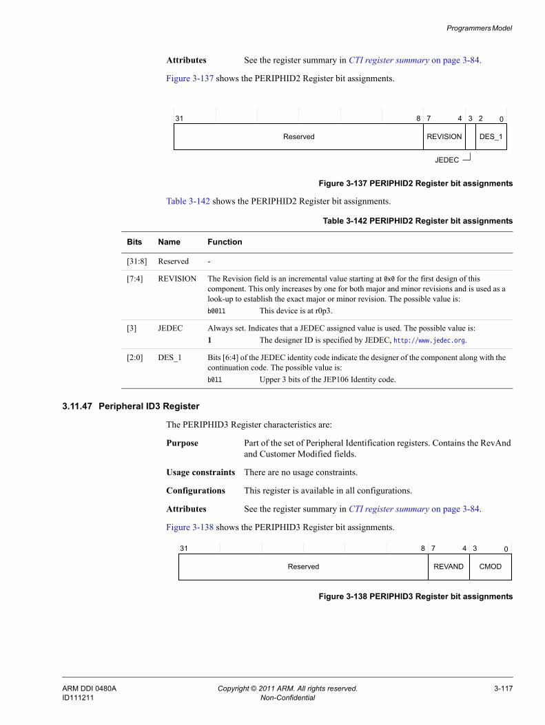
Programmers Model
Attributes See the register summary in CTI register summary on page 3-84.
Figure 3-137 shows the PERIPHID2 Register bit assignments.
Figure 3-137 PERIPHID2 Register bit assignments
Table 3-142 shows the PERIPHID2 Register bit assignments.
3.11.47 Peripheral ID3 Register
The PERIPHID3 Register characteristics are:
Purpose Part of the set of Peripheral Identification registers. Contains the RevAnd and Customer Modified fields.
Usage constraints There are no usage constraints.
Configurations This register is available in all configurations.
Attributes See the register summary in CTI register summary on page 3-84.
Figure 3-138 shows the PERIPHID3 Register bit assignments.
Figure 3-138 PERIPHID3 Register bit assignments
31 0
Reserved
7
REVISION
8 4
DES_1
3 2
JEDEC
Table 3-142 PERIPHID2 Register bit assignments
Bits Name Function
[31:8] Reserved -
[7:4] REVISION The Revision field is an incremental value starting at 0x0 for the first design of this component. This only increases by one for both major and minor revisions and is used as a look-up to establish the exact major or minor revision. The possible value is:b0011 This device is at r0p3.
[3] JEDEC Always set. Indicates that a JEDEC assigned value is used. The possible value is:1 The designer ID is specified by JEDEC, http://www.jedec.org.
[2:0] DES_1 Bits [6:4] of the JEDEC identity code indicate the designer of the component along with the continuation code. The possible value is:b011 Upper 3 bits of the JEP106 Identity code.
31 0
Reserved
7
REVAND
8 4
CMOD
3
ARM DDI 0480A Copyright © 2011 ARM. All rights reserved. 3-117ID111211 Non-Confidential
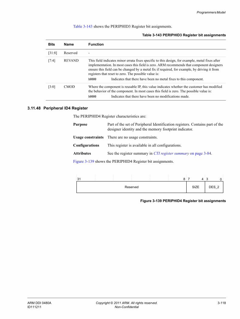
Programmers Model
Table 3-143 shows the PERIPHID3 Register bit assignments.
3.11.48 Peripheral ID4 Register
The PERIPHID4 Register characteristics are:
Purpose Part of the set of Peripheral Identification registers. Contains part of the designer identity and the memory footprint indicator.
Usage constraints There are no usage constraints.
Configurations This register is available in all configurations.
Attributes See the register summary in CTI register summary on page 3-84.
Figure 3-139 shows the PERIPHID4 Register bit assignments.
Figure 3-139 PERIPHID4 Register bit assignments
Table 3-143 PERIPHID3 Register bit assignments
Bits Name Function
[31:8] Reserved -
[7:4] REVAND This field indicates minor errata fixes specific to this design, for example, metal fixes after implementation. In most cases this field is zero. ARM recommends that component designers ensure this field can be changed by a metal fix if required, for example, by driving it from registers that reset to zero. The possible value is:b0000 Indicates that there have been no metal fixes to this component.
[3:0] CMOD Where the component is reusable IP, this value indicates whether the customer has modified the behavior of the component. In most cases this field is zero. The possible value is:b0000 Indicates that there have been no modifications made.
31 0
Reserved
7
SIZE
8 4
DES_2
3
ARM DDI 0480A Copyright © 2011 ARM. All rights reserved. 3-118ID111211 Non-Confidential
Programmers Model
Table 3-144 shows the PERIPHID4 Register bit assignments.
3.11.49 Peripheral ID5-7 Register
The PERIPHID5-7 Register characteristics are:
Purpose Reserved.
Usage constraints There are no usage constraints.
Configurations These registers are available in all configurations.
Attributes See the register summary in CTI register summary on page 3-84.
Figure 3-140 shows the PERIPHID5-7 Register bit assignments.
Figure 3-140 PERIPHID5-7 Register bit assignments
Table 3-145 shows the PERIPHID5-7 Register bit assignments.
3.11.50 Component ID0 Register
The COMPID0 Register characteristics are:
Purpose A Component Identification Register that indicates that the identification registers are present.
Usage constraints There are no usage constraints.
Configurations This register is available in all configurations.
Table 3-144 PERIPHID4 Register bit assignments
Bits Name Function
[31:8] Reserved -
[7:4] SIZE This is a 4-bit value that indicates the total contiguous size of the memory window used by this component in powers of 2 from the standard 4KB. For example:b0000 If a component only requires the standard 4KB.b0001 If a component only requires the standard 8KB.b0010 If a component only requires the standard 16KB.b0011 If a component only requires the standard 32KB.The possible value is:b0000 Indicates that the device only occupies 4KB of memory.
[3:0] DES_2 JEDEC continuation code indicate the designer of the component along with the identity code. The possible value is:b0100 Indicates that ARMs JEDEC identity code is on the 5th bank.
31 0
Reserved
Table 3-145 PERIPHID5-7 Register bit assignments
Bits Name Function
[31:0] Reserved -
ARM DDI 0480A Copyright © 2011 ARM. All rights reserved. 3-119ID111211 Non-Confidential
Programmers Model
Attributes See the register summary in CTI register summary on page 3-84.
Figure 3-141 shows the COMPID0 Register bit assignments.
Figure 3-141 COMPID0 Register bit assignments
Table 3-146 shows the COMPID0 Register bit assignments.
3.11.51 Component ID1 Register
The COMPID1 Register characteristics are:
Purpose A Component Identification Register that indicates that the identification registers are present. This register also indicates the component class.
Usage constraints There are no usage constraints.
Configurations This register is available in all configurations.
Attributes See the register summary in CTI register summary on page 3-84.
Figure 3-142 shows the COMPID1 Register bit assignments.
Figure 3-142 COMPID1 Register bit assignments
Table 3-147 shows the COMPID1 Register bit assignments.
31 8 7 0
PRMBL_0Reserved
Table 3-146 COMPID0 Register bit assignments
Bits Name Function
[31:8] Reserved -
[7:0] PRMBL_0 Contains bits [7:0] of the component identification. The possible value is:0x0D Identification value.
31 8 7 4 3 0
CLASSReserved
PRMBL_1
Table 3-147 COMPID1 Register bit assignments
Bits Name Function
[31:8] Reserved -
[7:4] CLASS Class of the component. For example, the ROM table and the CoreSight component. Constitutes bits [15:12] of the component identification. The possible value is:b1001 Indicates the component is a CoreSight component.
[3:0] PRMBL_1 Contains bits [11:8] of the component identification. The possible value is:b0000 Identification value.
ARM DDI 0480A Copyright © 2011 ARM. All rights reserved. 3-120ID111211 Non-Confidential

Programmers Model
3.11.52 Component ID2 Register
The COMPID2 Register characteristics are:
Purpose A Component Identification Register that indicates that the identification registers are present.
Usage constraints There are no usage constraints.
Configurations This register is available in all configurations.
Attributes See the register summary in CTI register summary on page 3-84.
Figure 3-143 shows the COMPID2 Register bit assignments.
Figure 3-143 COMPID2 Register bit assignments
Table 3-148 shows the COMPID2 Register bit assignments.
3.11.53 Component ID3 Register
The COMPID3 Register characteristics are:
Purpose A Component Identification Register that indicates that the identification registers are present.
Usage constraints There are no usage constraints.
Configurations This register is available in all configurations.
Attributes See the register summary in CTI register summary on page 3-84.
Figure 3-144 shows the COMPID3 Register bit assignments.
Figure 3-144 COMPID3 Register bit assignments
31 8 7 0
PRMBL_2Reserved
Table 3-148 COMPID2 Register bit assignments
Bits Name Function
[31:8] Reserved -
[7:0] PRMBL_2 Contains bits [23:16] of the component identification. The possible value is:0x5 Identification value.
31 0
Reserved
78
PRMBL_3
ARM DDI 0480A Copyright © 2011 ARM. All rights reserved. 3-121ID111211 Non-Confidential
Programmers Model
Table 3-149 shows the COMPID3 Register bit assignments.
Table 3-149 COMPID3 Register bit assignments
Bits Name Function
[31:8] Reserved -
[7:0] PRMBL_3 Contains bits [31:24] of the component identification. The possible value is:0xB1 Identification value.
ARM DDI 0480A Copyright © 2011 ARM. All rights reserved. 3-122ID111211 Non-Confidential
Programmers Model
3.12 TPIU register summaryTable 3-150 shows the registers in offset order from the base memory address.
Table 3-150 TPIU Register summary
Offset Name Type Reset Width Description
0x000 Supported_Port_Sizes RO 0x00000001 32 Supported Port Size Register on page 3-125
0x004 Current_port_size R/W 0x00000001 32 Current Port Size Register on page 3-129
0x100 Supported_trigger_modes RO 0x0000011F 18 Supported Trigger Modes Register on page 3-133
0x104 Trigger_counter_value R/W 0x00000000 8 Trigger Counter Value Register on page 3-134
0x108 Trigger_multiplier R/W 0x00000000 5 Trigger Multiplier Register on page 3-135
0x200 Supported_test_pattern_modes RO 0x0003000F 18 Supported Test Patterns/Modes Register on page 3-136
0x204 Current_test_pattern_mode R/W 0x00000000 18 Current Test Pattern/Modes Register on page 3-137
0x208 TPRCR R/W 0x00000000 8 TPIU Test Pattern Repeat Counter Register on page 3-138
0x300 FFSR RO 0x00000000 3 Formatter and Flush Status Register on page 3-139
0x304 FFCR R/W 0x00000000 14 Formatter and Flush Control Register on page 3-140
0x308 FSCR R/W 0x00000040 12 Formatter Synchronization Counter Register on page 3-142
0x400 EXTCTL_In_Port RO 0x00000000 8 TPIU EXCTL Port Register - In on page 3-143
0x404 EXTCTL_Out_Port R/W 0x00000000 8 TPIU EXCTL Port Register - Out on page 3-144
0xEE4 ITTRFLINACK WO 0x00000000 2 Integration Test Trigger In and Flush In Acknowledge Register on page 3-144
0xEE8 ITTRFLIN RO 0x00000000 2 Integration Test Trigger In and Flush In Register on page 3-145
0xEEC ITATBDATA0 RO 0x00000000 5 Integration Test ATB Data Register 0 on page 3-146
0xEF0 ITATBCTR2 WO 0x00000000 2 Integration Test ATB Control Register 2 on page 3-147
0xEF4 ITATBCTR1 RO 0x00000000 7 Integration Test ATB Control Register 1 on page 3-148
0xEF8 ITATBCTR0 RO 0x00000000 10 Integration Test ATB Control Register 0 on page 3-148
0xF00 ITCTRL R/W 0x00000000 1 Integration Mode Control Register on page 3-149
0xFA0 CLAIMSET R/W 0x0000000F 4 Claim Tag Set Register on page 3-150
0xFA4 CLAIMCLR R/W 0x00000000 4 Claim Tag Clear Register on page 3-151
0xFB0 LAR WO 0x00000000 32 Lock Access Register on page 3-152
0xFB4 LSR RO 0x00000003 3 Lock Status Register on page 3-152
0xFB8 AUTHSTATUS RO 0x00000000 8 Authentication Status Register on page 3-153
0xFC8 DEVID RO 0x000000A0 8 Device Configuration Register on page 3-154
0xFCC DEVTYPE RO 0x00000011 8 Device Type Identifier Register on page 3-155
0xFE0 PERIPHID0 RO 0x00000012 8 Peripheral ID0 Register on page 3-156
ARM DDI 0480A Copyright © 2011 ARM. All rights reserved. 3-123ID111211 Non-Confidential
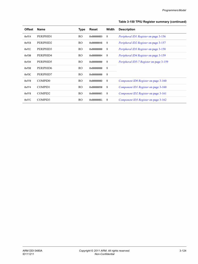
Programmers Model
0xFE4 PERIPHID1 RO 0x000000B9 8 Peripheral ID1 Register on page 3-156
0xFE8 PERIPHID2 RO 0x0000004B 8 Peripheral ID2 Register on page 3-157
0xFEC PERIPHID3 RO 0x00000000 8 Peripheral ID3 Register on page 3-158
0xFD0 PERIPHID4 RO 0x00000004 8 Peripheral ID4 Register on page 3-159
0xFD4 PERIPHID5 RO 0x00000000 8 Peripheral ID5-7 Register on page 3-159
0xFD8 PERIPHID6 RO 0x00000000 8
0xFDC PERIPHID7 RO 0x00000000 8
0xFF0 COMPID0 RO 0x0000000D 8 Component ID0 Register on page 3-160
0xFF4 COMPID1 RO 0x00000090 8 Component ID1 Register on page 3-160
0xFF8 COMPID2 RO 0x00000005 8 Component ID2 Register on page 3-161
0xFFC COMPID3 RO 0x000000B1 8 Component ID3 Register on page 3-162
Table 3-150 TPIU Register summary (continued)
Offset Name Type Reset Width Description
ARM DDI 0480A Copyright © 2011 ARM. All rights reserved. 3-124ID111211 Non-Confidential
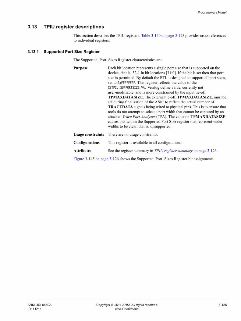
Programmers Model
3.13 TPIU register descriptionsThis section describes the TPIU registers. Table 3-150 on page 3-123 provides cross references to individual registers.
3.13.1 Supported Port Size Register
The Supported_Port_Sizes Register characteristics are:
Purpose Each bit location represents a single port size that is supported on the device, that is, 32-1 in bit locations [31:0]. If the bit is set then that port size is permitted. By default the RTL is designed to support all port sizes, set to 0xFFFFFFFF. This register reflects the value of the CSTPIU_SUPPORTSIZE_VAL Verilog define value, currently not user-modifiable, and is more constrained by the input tie-off TPMAXDATASIZE. The external tie-off, TPMAXDATASIZE, must be set during finalization of the ASIC to reflect the actual number of TRACEDATA signals being wired to physical pins. This is to ensure that tools do not attempt to select a port width that cannot be captured by an attached Trace Port Analyzer (TPA). The value on TPMAXDATASIZE causes bits within the Supported Port Size register that represent wider widths to be clear, that is, unsupported.
Usage constraints There are no usage constraints.
Configurations This register is available in all configurations.
Attributes See the register summary in TPIU register summary on page 3-123.
Figure 3-145 on page 3-126 shows the Supported_Port_Sizes Register bit assignments.
ARM DDI 0480A Copyright © 2011 ARM. All rights reserved. 3-125ID111211 Non-Confidential
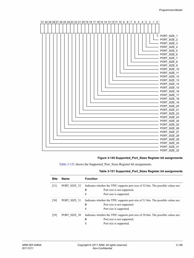
Programmers Model
Figure 3-145 Supported_Port_Sizes Register bit assignments
Table 3-151 shows the Supported_Port_Sizes Register bit assignments.
31 30 29 28 27 26 25 24 23 22 21 20 19 18 17 16 15 14 13 12 11 10 9 8 7 6 5 4 3 2 1 0
PORT_SIZE_3PORT_SIZE_2PORT_SIZE_1
PORT_SIZE_4PORT_SIZE_5
PORT_SIZE_8PORT_SIZE_7PORT_SIZE_6
PORT_SIZE_11PORT_SIZE_10PORT_SIZE_9
PORT_SIZE_12PORT_SIZE_13
PORT_SIZE_16PORT_SIZE_15PORT_SIZE_14
PORT_SIZE_19PORT_SIZE_18PORT_SIZE_17
PORT_SIZE_20PORT_SIZE_21
PORT_SIZE_24PORT_SIZE_23PORT_SIZE_22
PORT_SIZE_27PORT_SIZE_26PORT_SIZE_25
PORT_SIZE_28PORT_SIZE_29
PORT_SIZE_32PORT_SIZE_31PORT_SIZE_30
Table 3-151 Supported_Port_Sizes Register bit assignments
Bits Name Function
[31] PORT_SIZE_32 Indicates whether the TPIU supports port size of 32 bits. The possible values are:0 Port size is not supported.1 Port size is supported.
[30] PORT_SIZE_31 Indicates whether the TPIU supports port size of 31 bits. The possible values are:0 Port size is not supported.1 Port size is supported.
[29] PORT_SIZE_30 Indicates whether the TPIU supports port size of 30 bits. The possible values are:0 Port size is not supported.1 Port size is supported.
ARM DDI 0480A Copyright © 2011 ARM. All rights reserved. 3-126ID111211 Non-Confidential
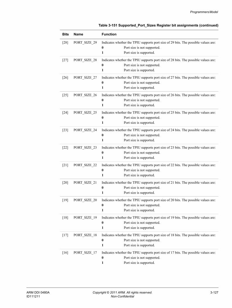
Programmers Model
[28] PORT_SIZE_29 Indicates whether the TPIU supports port size of 29 bits. The possible values are:0 Port size is not supported.1 Port size is supported.
[27] PORT_SIZE_28 Indicates whether the TPIU supports port size of 28 bits. The possible values are:0 Port size is not supported.1 Port size is supported.
[26] PORT_SIZE_27 Indicates whether the TPIU supports port size of 27 bits. The possible values are:0 Port size is not supported.1 Port size is supported.
[25] PORT_SIZE_26 Indicates whether the TPIU supports port size of 26 bits. The possible values are:0 Port size is not supported.1 Port size is supported.
[24] PORT_SIZE_25 Indicates whether the TPIU supports port size of 25 bits. The possible values are:0 Port size is not supported.1 Port size is supported.
[23] PORT_SIZE_24 Indicates whether the TPIU supports port size of 24 bits. The possible values are:0 Port size is not supported.1 Port size is supported.
[22] PORT_SIZE_23 Indicates whether the TPIU supports port size of 23 bits. The possible values are:0 Port size is not supported.1 Port size is supported.
[21] PORT_SIZE_22 Indicates whether the TPIU supports port size of 22 bits. The possible values are:0 Port size is not supported.1 Port size is supported.
[20] PORT_SIZE_21 Indicates whether the TPIU supports port size of 21 bits. The possible values are:0 Port size is not supported.1 Port size is supported.
[19] PORT_SIZE_20 Indicates whether the TPIU supports port size of 20 bits. The possible values are:0 Port size is not supported.1 Port size is supported.
[18] PORT_SIZE_19 Indicates whether the TPIU supports port size of 19 bits. The possible values are:0 Port size is not supported.1 Port size is supported.
[17] PORT_SIZE_18 Indicates whether the TPIU supports port size of 18 bits. The possible values are:0 Port size is not supported.1 Port size is supported.
[16] PORT_SIZE_17 Indicates whether the TPIU supports port size of 17 bits. The possible values are:0 Port size is not supported.1 Port size is supported.
Table 3-151 Supported_Port_Sizes Register bit assignments (continued)
Bits Name Function
ARM DDI 0480A Copyright © 2011 ARM. All rights reserved. 3-127ID111211 Non-Confidential
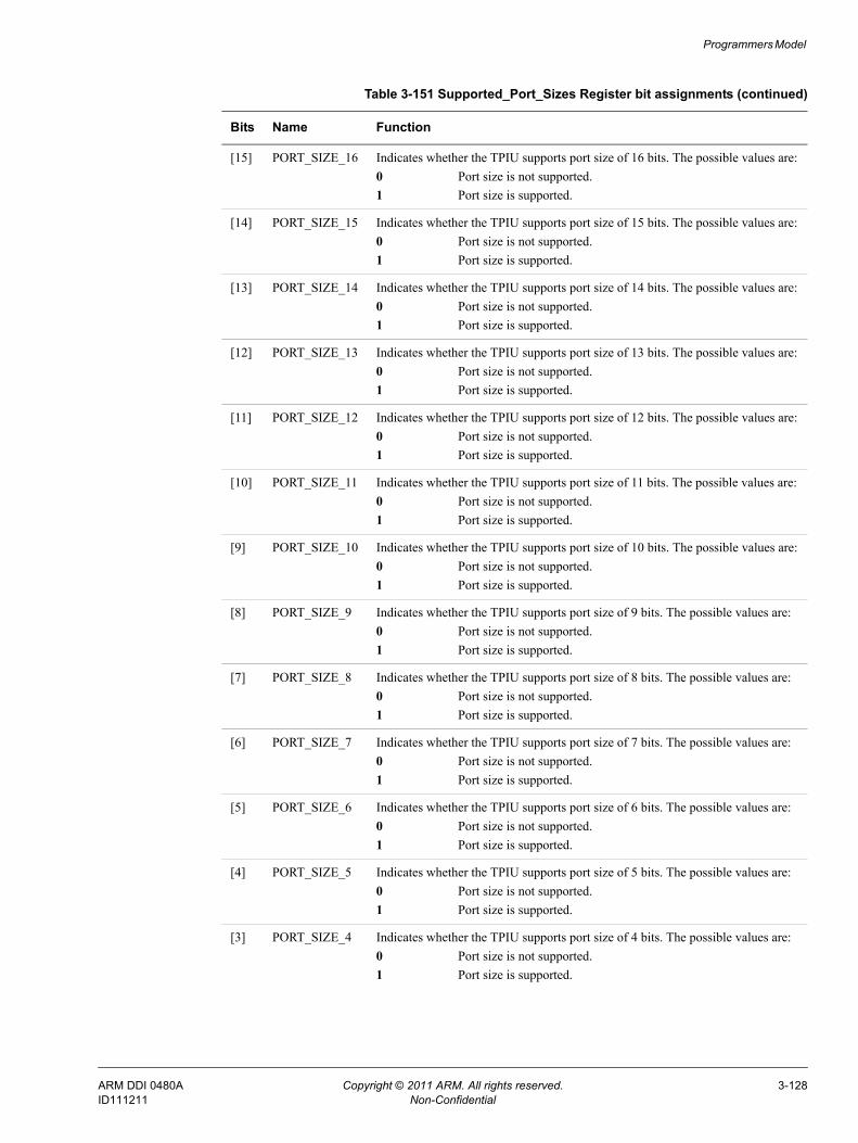
Programmers Model
[15] PORT_SIZE_16 Indicates whether the TPIU supports port size of 16 bits. The possible values are:0 Port size is not supported.1 Port size is supported.
[14] PORT_SIZE_15 Indicates whether the TPIU supports port size of 15 bits. The possible values are:0 Port size is not supported.1 Port size is supported.
[13] PORT_SIZE_14 Indicates whether the TPIU supports port size of 14 bits. The possible values are:0 Port size is not supported.1 Port size is supported.
[12] PORT_SIZE_13 Indicates whether the TPIU supports port size of 13 bits. The possible values are:0 Port size is not supported.1 Port size is supported.
[11] PORT_SIZE_12 Indicates whether the TPIU supports port size of 12 bits. The possible values are:0 Port size is not supported.1 Port size is supported.
[10] PORT_SIZE_11 Indicates whether the TPIU supports port size of 11 bits. The possible values are:0 Port size is not supported.1 Port size is supported.
[9] PORT_SIZE_10 Indicates whether the TPIU supports port size of 10 bits. The possible values are:0 Port size is not supported.1 Port size is supported.
[8] PORT_SIZE_9 Indicates whether the TPIU supports port size of 9 bits. The possible values are:0 Port size is not supported.1 Port size is supported.
[7] PORT_SIZE_8 Indicates whether the TPIU supports port size of 8 bits. The possible values are:0 Port size is not supported.1 Port size is supported.
[6] PORT_SIZE_7 Indicates whether the TPIU supports port size of 7 bits. The possible values are:0 Port size is not supported.1 Port size is supported.
[5] PORT_SIZE_6 Indicates whether the TPIU supports port size of 6 bits. The possible values are:0 Port size is not supported.1 Port size is supported.
[4] PORT_SIZE_5 Indicates whether the TPIU supports port size of 5 bits. The possible values are:0 Port size is not supported.1 Port size is supported.
[3] PORT_SIZE_4 Indicates whether the TPIU supports port size of 4 bits. The possible values are:0 Port size is not supported.1 Port size is supported.
Table 3-151 Supported_Port_Sizes Register bit assignments (continued)
Bits Name Function
ARM DDI 0480A Copyright © 2011 ARM. All rights reserved. 3-128ID111211 Non-Confidential
Programmers Model
3.13.2 Current Port Size Register
The Current_port_size Register characteristics are:
Purpose The Current Port Size Register has the same format as the Supported Port Sizes register but only one bit is set, and all others must be zero. Writing values with more than one bit set or setting a bit that is not indicated as supported is not supported and causes UNPREDICTABLE behavior.On reset this defaults to the smallest possible port size, 1 bit, and so reads as 0x00000001.
Note Do not modify the value while the Trace Port is still active, or without
correctly stopping the formatter. See Formatter and Flush Control Register on page 3-140. This can result in data not being aligned to the port width. For example, data on an 8-bit Trace Port might not be byte aligned.
Usage constraints There are no usage constraints.
Configurations This register is available in all configurations.
Attributes See the register summary in TPIU register summary on page 3-123.
Figure 3-146 on page 3-130 shows the Current_port_size Register bit assignments.
[2] PORT_SIZE_3 Indicates whether the TPIU supports port size of 3 bits. The possible values are:0 Port size is not supported.1 Port size is supported.
[1] PORT_SIZE_2 Indicates whether the TPIU supports port size of 2 bits. The possible values are:0 Port size is not supported.1 Port size is supported.
[0] PORT_SIZE_1 Indicates whether the TPIU supports port size of 1 bit. The possible values are:0 Port size is not supported.1 Port size is supported.
Table 3-151 Supported_Port_Sizes Register bit assignments (continued)
Bits Name Function
ARM DDI 0480A Copyright © 2011 ARM. All rights reserved. 3-129ID111211 Non-Confidential
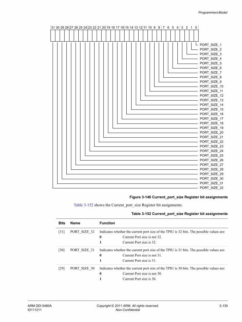
Programmers Model
Figure 3-146 Current_port_size Register bit assignments
Table 3-152 shows the Current_port_size Register bit assignments.
31 30 29 28 27 26 25 24 23 22 21 20 19 18 17 16 15 14 13 12 11 10 9 8 7 6 5 4 3 2 1 0
PORT_SIZE_3PORT_SIZE_2PORT_SIZE_1
PORT_SIZE_4PORT_SIZE_5
PORT_SIZE_8PORT_SIZE_7PORT_SIZE_6
PORT_SIZE_11PORT_SIZE_10PORT_SIZE_9
PORT_SIZE_12PORT_SIZE_13
PORT_SIZE_16PORT_SIZE_15PORT_SIZE_14
PORT_SIZE_19PORT_SIZE_18PORT_SIZE_17
PORT_SIZE_20PORT_SIZE_21
PORT_SIZE_24PORT_SIZE_23PORT_SIZE_22
PORT_SIZE_27PORT_SIZE_26PORT_SIZE_25
PORT_SIZE_28PORT_SIZE_29
PORT_SIZE_32PORT_SIZE_31PORT_SIZE_30
Table 3-152 Current_port_size Register bit assignments
Bits Name Function
[31] PORT_SIZE_32 Indicates whether the current port size of the TPIU is 32 bits. The possible values are:0 Current Port size is not 32.1 Current Port size is 32.
[30] PORT_SIZE_31 Indicates whether the current port size of the TPIU is 31 bits. The possible values are:0 Current Port size is not 31.1 Current Port size is 31.
[29] PORT_SIZE_30 Indicates whether the current port size of the TPIU is 30 bits. The possible values are:0 Current Port size is not 30.1 Current Port size is 30.
ARM DDI 0480A Copyright © 2011 ARM. All rights reserved. 3-130ID111211 Non-Confidential

Programmers Model
[28] PORT_SIZE_29 Indicates whether the current port size of the TPIU is 29 bits. The possible values are:0 Current Port size is not 29.1 Current Port size is 29.
[27] PORT_SIZE_28 Indicates whether the current port size of the TPIU is 28 bits. The possible values are:0 Current Port size is not 28.1 Current Port size is 28.
[26] PORT_SIZE_27 Indicates whether the current port size of the TPIU is 27 bits. The possible values are:0 Current Port size is not 27.1 Current Port size is 27.
[25] PORT_SIZE_26 Indicates whether the current port size of the TPIU is 26 bits. The possible values are:0 Current Port size is not 26.1 Current Port size is 26.
[24] PORT_SIZE_25 Indicates whether the current port size of the TPIU is 25 bits. The possible values are:0 Current Port size is not 25.1 Current Port size is 25.
[23] PORT_SIZE_24 Indicates whether the current port size of the TPIU is 24 bits. The possible values are:0 Current Port size is not 24.1 Current Port size is 24.
[22] PORT_SIZE_23 Indicates whether the current port size of the TPIU is 23 bits. The possible values are:0 Current Port size is not 23.1 Current Port size is 23.
[21] PORT_SIZE_22 Indicates whether the current port size of the TPIU is 22 bits. The possible values are:0 Current Port size is not 22.1 Current Port size is 22.
[20] PORT_SIZE_21 Indicates whether the current port size of the TPIU is 21 bits. The possible values are:0 Current Port size is not 21.1 Current Port size is 21.
[19] PORT_SIZE_20 Indicates whether the current port size of the TPIU is 20 bits. The possible values are:0 Current Port size is not 20.1 Current Port size is 20.
[18] PORT_SIZE_19 Indicates whether the current port size of the TPIU is 19 bits. The possible values are:0 Current Port size is not 19.1 Current Port size is 19.
[17] PORT_SIZE_18 Indicates whether the current port size of the TPIU is 18 bits. The possible values are:0 Current Port size is not 18.1 Current Port size is 18.
[16] PORT_SIZE_17 Indicates whether the current port size of the TPIU is 17 bits. The possible values are:0 Current Port size is not 17.1 Current Port size is 17.
Table 3-152 Current_port_size Register bit assignments (continued)
Bits Name Function
ARM DDI 0480A Copyright © 2011 ARM. All rights reserved. 3-131ID111211 Non-Confidential
Programmers Model
[15] PORT_SIZE_16 Indicates whether the current port size of the TPIU is 16 bits. The possible values are:0 Current Port size is not 16.1 Current Port size is 16.
[14] PORT_SIZE_15 Indicates whether the current port size of the TPIU is 15 bits. The possible values are:0 Current Port size is not 15.1 Current Port size is 15.
[13] PORT_SIZE_14 Indicates whether the current port size of the TPIU is 14 bits. The possible values are:0 Current Port size is not 14.1 Current Port size is 14.
[12] PORT_SIZE_13 Indicates whether the current port size of the TPIU is 13 bits. The possible values are:0 Current Port size is not 13.1 Current Port size is 13.
[11] PORT_SIZE_12 Indicates whether the current port size of the TPIU is 12 bits. The possible values are:0 Current Port size is not 12.1 Current Port size is 12.
[10] PORT_SIZE_11 Indicates whether the current port size of the TPIU is 11 bits. The possible values are:0 Current Port size is not 11.1 Current Port size is 11.
[9] PORT_SIZE_10 Indicates whether the current port size of the TPIU is 10 bits. The possible values are:0 Current Port size is not 10.1 Current Port size is 10.
[8] PORT_SIZE_9 Indicates whether the current port size of the TPIU is 9 bits. The possible values are:0 Current Port size is not 9.1 Current Port size is 9.
[7] PORT_SIZE_8 Indicates whether the current port size of the TPIU is 8 bits. The possible values are:0 Current Port size is not 8.1 Current Port size is 8.
[6] PORT_SIZE_7 Indicates whether the current port size of the TPIU is 7 bits. The possible values are:0 Current Port size is not 7.1 Current Port size is 7.
[5] PORT_SIZE_6 Indicates whether the current port size of the TPIU is 6 bits. The possible values are:0 Current Port size is not 6.1 Current Port size is 6.
[4] PORT_SIZE_5 Indicates whether the current port size of the TPIU is 5 bits. The possible values are:0 Current Port size is not 5.1 Current Port size is 5.
[3] PORT_SIZE_4 Indicates whether the current port size of the TPIU is 4 bits. The possible values are:0 Current Port size is not 4.1 Current Port size is 4.
Table 3-152 Current_port_size Register bit assignments (continued)
Bits Name Function
ARM DDI 0480A Copyright © 2011 ARM. All rights reserved. 3-132ID111211 Non-Confidential
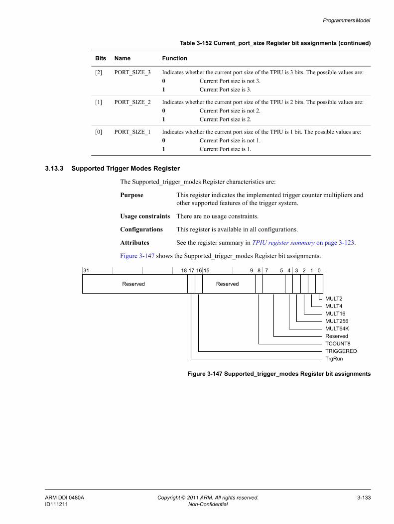
Programmers Model
3.13.3 Supported Trigger Modes Register
The Supported_trigger_modes Register characteristics are:
Purpose This register indicates the implemented trigger counter multipliers and other supported features of the trigger system.
Usage constraints There are no usage constraints.
Configurations This register is available in all configurations.
Attributes See the register summary in TPIU register summary on page 3-123.
Figure 3-147 shows the Supported_trigger_modes Register bit assignments.
Figure 3-147 Supported_trigger_modes Register bit assignments
[2] PORT_SIZE_3 Indicates whether the current port size of the TPIU is 3 bits. The possible values are:0 Current Port size is not 3.1 Current Port size is 3.
[1] PORT_SIZE_2 Indicates whether the current port size of the TPIU is 2 bits. The possible values are:0 Current Port size is not 2.1 Current Port size is 2.
[0] PORT_SIZE_1 Indicates whether the current port size of the TPIU is 1 bit. The possible values are:0 Current Port size is not 1.1 Current Port size is 1.
Table 3-152 Current_port_size Register bit assignments (continued)
Bits Name Function
31 18 17 16 15 9 8 7 5 4 3 2 1 0
ReservedReserved
MULT16MULT4MULT2
MULT256MULT64K
TRIGGEREDTCOUNT8Reserved
TrgRun
ARM DDI 0480A Copyright © 2011 ARM. All rights reserved. 3-133ID111211 Non-Confidential
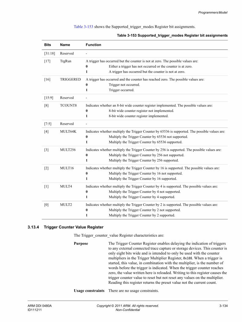
Programmers Model
Table 3-153 shows the Supported_trigger_modes Register bit assignments.
3.13.4 Trigger Counter Value Register
The Trigger_counter_value Register characteristics are:
Purpose The Trigger Counter Register enables delaying the indication of triggers to any external connected trace capture or storage devices. This counter is only eight bits wide and is intended to only be used with the counter multipliers in the Trigger Multiplier Register, 0x108. When a trigger is started, this value, in combination with the multiplier, is the number of words before the trigger is indicated. When the trigger counter reaches zero, the value written here is reloaded. Writing to this register causes the trigger counter value to reset but not reset any values on the multiplier. Reading this register returns the preset value not the current count.
Usage constraints There are no usage constraints.
Table 3-153 Supported_trigger_modes Register bit assignments
Bits Name Function
[31:18] Reserved -
[17] TrgRun A trigger has occurred but the counter is not at zero. The possible values are:0 Either a trigger has not occurred or the counter is at zero.1 A trigger has occurred but the counter is not at zero.
[16] TRIGGERED A trigger has occurred and the counter has reached zero. The possible values are:0 Trigger not occurred.1 Trigger occurred.
[15:9] Reserved -
[8] TCOUNT8 Indicates whether an 8-bit wide counter register implemented. The possible values are:0 8-bit wide counter register not implemented.1 8-bit wide counter register implemented.
[7:5] Reserved -
[4] MULT64K Indicates whether multiply the Trigger Counter by 65536 is supported. The possible values are:0 Multiply the Trigger Counter by 65536 not supported.1 Multiply the Trigger Counter by 65536 supported.
[3] MULT256 Indicates whether multiply the Trigger Counter by 256 is supported. The possible values are:0 Multiply the Trigger Counter by 256 not supported.1 Multiply the Trigger Counter by 256 supported.
[2] MULT16 Indicates whether multiply the Trigger Counter by 16 is supported. The possible values are:0 Multiply the Trigger Counter by 16 not supported.1 Multiply the Trigger Counter by 16 supported.
[1] MULT4 Indicates whether multiply the Trigger Counter by 4 is supported. The possible values are:0 Multiply the Trigger Counter by 4 not supported.1 Multiply the Trigger Counter by 4 supported.
[0] MULT2 Indicates whether multiply the Trigger Counter by 2 is supported. The possible values are:0 Multiply the Trigger Counter by 2 not supported.1 Multiply the Trigger Counter by 2 supported.
ARM DDI 0480A Copyright © 2011 ARM. All rights reserved. 3-134ID111211 Non-Confidential
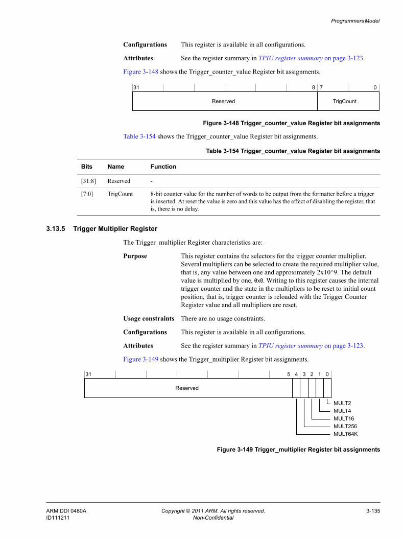
Programmers Model
Configurations This register is available in all configurations.
Attributes See the register summary in TPIU register summary on page 3-123.
Figure 3-148 shows the Trigger_counter_value Register bit assignments.
Figure 3-148 Trigger_counter_value Register bit assignments
Table 3-154 shows the Trigger_counter_value Register bit assignments.
3.13.5 Trigger Multiplier Register
The Trigger_multiplier Register characteristics are:
Purpose This register contains the selectors for the trigger counter multiplier. Several multipliers can be selected to create the required multiplier value, that is, any value between one and approximately 2x10^9. The default value is multiplied by one, 0x0. Writing to this register causes the internal trigger counter and the state in the multipliers to be reset to initial count position, that is, trigger counter is reloaded with the Trigger Counter Register value and all multipliers are reset.
Usage constraints There are no usage constraints.
Configurations This register is available in all configurations.
Attributes See the register summary in TPIU register summary on page 3-123.
Figure 3-149 shows the Trigger_multiplier Register bit assignments.
Figure 3-149 Trigger_multiplier Register bit assignments
31 8 7 0
TrigCountReserved
Table 3-154 Trigger_counter_value Register bit assignments
Bits Name Function
[31:8] Reserved -
[7:0] TrigCount 8-bit counter value for the number of words to be output from the formatter before a trigger is inserted. At reset the value is zero and this value has the effect of disabling the register, that is, there is no delay.
31 5 4 3 2 1 0
Reserved
MULT16MULT4MULT2
MULT256MULT64K
ARM DDI 0480A Copyright © 2011 ARM. All rights reserved. 3-135ID111211 Non-Confidential
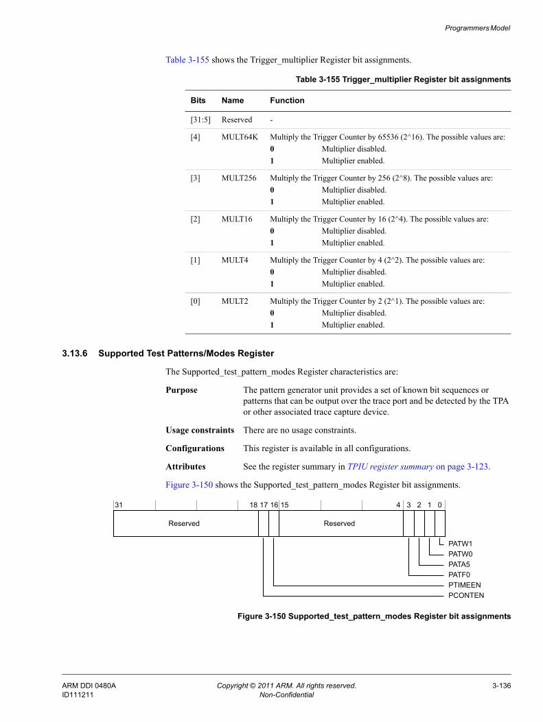
Programmers Model
Table 3-155 shows the Trigger_multiplier Register bit assignments.
3.13.6 Supported Test Patterns/Modes Register
The Supported_test_pattern_modes Register characteristics are:
Purpose The pattern generator unit provides a set of known bit sequences or patterns that can be output over the trace port and be detected by the TPA or other associated trace capture device.
Usage constraints There are no usage constraints.
Configurations This register is available in all configurations.
Attributes See the register summary in TPIU register summary on page 3-123.
Figure 3-150 shows the Supported_test_pattern_modes Register bit assignments.
Figure 3-150 Supported_test_pattern_modes Register bit assignments
Table 3-155 Trigger_multiplier Register bit assignments
Bits Name Function
[31:5] Reserved -
[4] MULT64K Multiply the Trigger Counter by 65536 (2^16). The possible values are:0 Multiplier disabled.1 Multiplier enabled.
[3] MULT256 Multiply the Trigger Counter by 256 (2^8). The possible values are:0 Multiplier disabled.1 Multiplier enabled.
[2] MULT16 Multiply the Trigger Counter by 16 (2^4). The possible values are:0 Multiplier disabled.1 Multiplier enabled.
[1] MULT4 Multiply the Trigger Counter by 4 (2^2). The possible values are:0 Multiplier disabled.1 Multiplier enabled.
[0] MULT2 Multiply the Trigger Counter by 2 (2^1). The possible values are:0 Multiplier disabled.1 Multiplier enabled.
31 18 17 16 15 4 3 2 1 0
ReservedReserved
PATA5PATW0PATW1
PATF0PTIMEENPCONTEN
ARM DDI 0480A Copyright © 2011 ARM. All rights reserved. 3-136ID111211 Non-Confidential
Programmers Model
Table 3-156 shows the Supported_test_pattern_modes Register bit assignments.
3.13.7 Current Test Pattern/Modes Register
The Current_test_pattern_mode Register characteristics are:
Purpose This register indicates the current test pattern or mode selected. Only one of the modes can be set, using bits 17-16, but a multiple number of bits for the patterns can be set using bits 3-0. If timed mode is selected, then after the allotted number of cycles has been reached, the mode automatically switches to off mode. On reset this register is set to 18'h00000, off mode with no selected patterns.
Usage constraints There are no usage constraints.
Configurations This register is available in all configurations.
Attributes See the register summary in TPIU register summary on page 3-123.
Figure 3-151 on page 3-138 shows the Current_test_pattern_mode Register bit assignments.
Table 3-156 Supported_test_pattern_modes Register bit assignments
Bits Name Function
[31:18] Reserved -
[17] PCONTEN Indicates whether continuous mode is supported. The possible values are:0 Mode not supported.1 Mode supported.
[16] PTIMEEN Indicates whether timed mode is supported. The possible values are:0 Mode not supported.1 Mode supported.
[15:4] Reserved -
[3] PATF0 FF/00 pattern supported to be output over the trace port. The possible values are:0 Pattern not supported.1 Pattern supported.
[2] PATA5 AA/55 pattern supported to be output over the trace port. The possible values are:0 Pattern not supported.1 Pattern supported.
[1] PATW0 Walking 0s Pattern supported to be output over the trace port. The possible values are:0 Pattern not supported.1 Pattern supported.
[0] PATW1 Walking 1s Pattern supported to be output over the trace port. The possible values are:0 Pattern not supported.1 Pattern supported.
ARM DDI 0480A Copyright © 2011 ARM. All rights reserved. 3-137ID111211 Non-Confidential
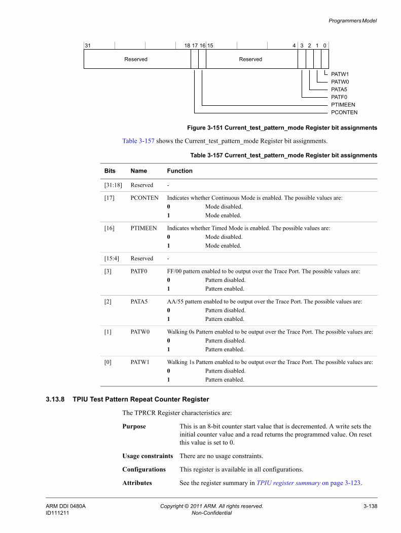
Programmers Model
Figure 3-151 Current_test_pattern_mode Register bit assignments
Table 3-157 shows the Current_test_pattern_mode Register bit assignments.
3.13.8 TPIU Test Pattern Repeat Counter Register
The TPRCR Register characteristics are:
Purpose This is an 8-bit counter start value that is decremented. A write sets the initial counter value and a read returns the programmed value. On reset this value is set to 0.
Usage constraints There are no usage constraints.
Configurations This register is available in all configurations.
Attributes See the register summary in TPIU register summary on page 3-123.
31 18 17 16 15 4 3 2 1 0
ReservedReserved
PATA5PATW0PATW1
PATF0PTIMEENPCONTEN
Table 3-157 Current_test_pattern_mode Register bit assignments
Bits Name Function
[31:18] Reserved -
[17] PCONTEN Indicates whether Continuous Mode is enabled. The possible values are:0 Mode disabled.1 Mode enabled.
[16] PTIMEEN Indicates whether Timed Mode is enabled. The possible values are:0 Mode disabled.1 Mode enabled.
[15:4] Reserved -
[3] PATF0 FF/00 pattern enabled to be output over the Trace Port. The possible values are:0 Pattern disabled.1 Pattern enabled.
[2] PATA5 AA/55 pattern enabled to be output over the Trace Port. The possible values are:0 Pattern disabled.1 Pattern enabled.
[1] PATW0 Walking 0s Pattern enabled to be output over the Trace Port. The possible values are:0 Pattern disabled.1 Pattern enabled.
[0] PATW1 Walking 1s Pattern enabled to be output over the Trace Port. The possible values are:0 Pattern disabled.1 Pattern enabled.
ARM DDI 0480A Copyright © 2011 ARM. All rights reserved. 3-138ID111211 Non-Confidential
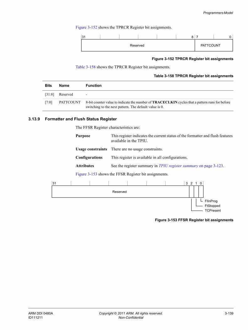
Programmers Model
Figure 3-152 shows the TPRCR Register bit assignments.
Figure 3-152 TPRCR Register bit assignments
Table 3-158 shows the TPRCR Register bit assignments.
3.13.9 Formatter and Flush Status Register
The FFSR Register characteristics are:
Purpose This register indicates the current status of the formatter and flush features available in the TPIU.
Usage constraints There are no usage constraints.
Configurations This register is available in all configurations.
Attributes See the register summary in TPIU register summary on page 3-123.
Figure 3-153 shows the FFSR Register bit assignments.
Figure 3-153 FFSR Register bit assignments
31 8 7 0
PATTCOUNTReserved
Table 3-158 TPRCR Register bit assignments
Bits Name Function
[31:8] Reserved -
[7:0] PATTCOUNT 8-bit counter value to indicate the number of TRACECLKIN cycles that a pattern runs for before switching to the next pattern. The default value is 0.
31 3 2 1 0
Reserved
TCPresentFtStoppedFlInProg
ARM DDI 0480A Copyright © 2011 ARM. All rights reserved. 3-139ID111211 Non-Confidential
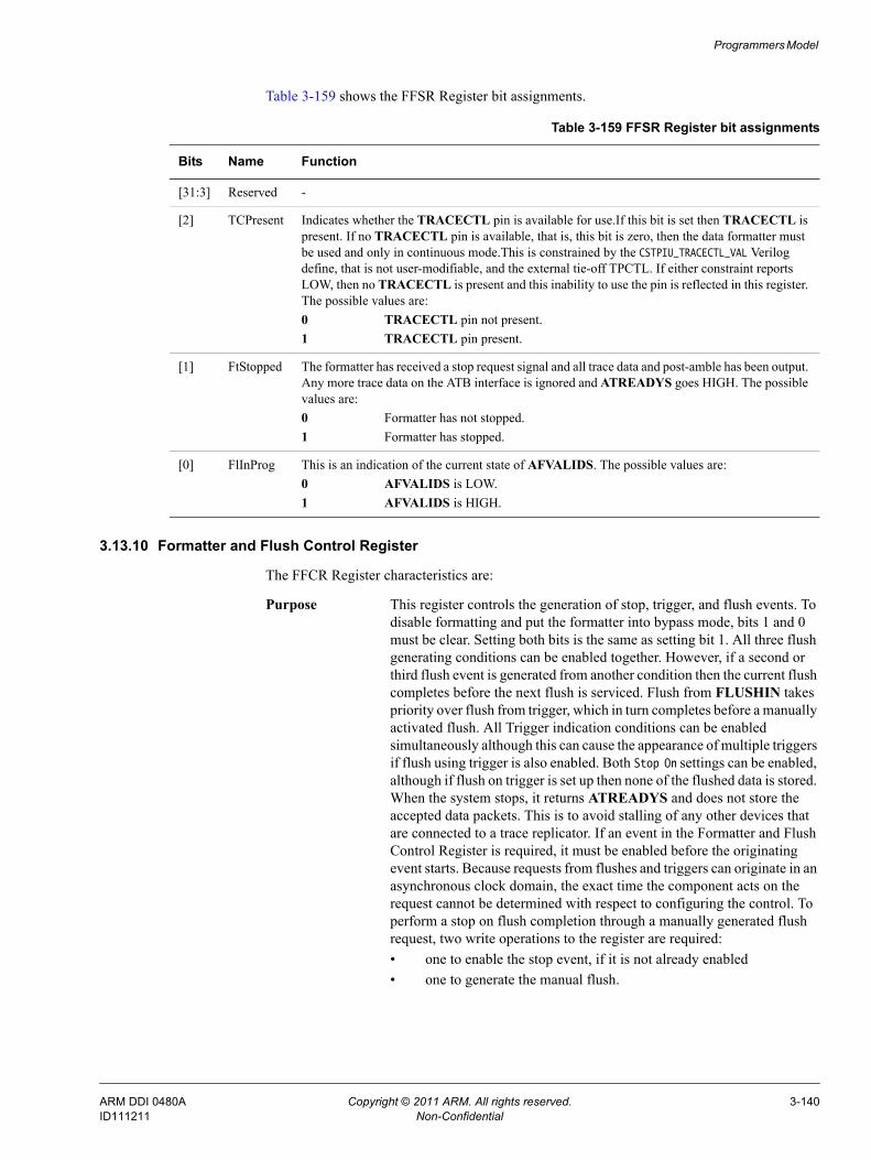
Programmers Model
Table 3-159 shows the FFSR Register bit assignments.
3.13.10 Formatter and Flush Control Register
The FFCR Register characteristics are:
Purpose This register controls the generation of stop, trigger, and flush events. To disable formatting and put the formatter into bypass mode, bits 1 and 0 must be clear. Setting both bits is the same as setting bit 1. All three flush generating conditions can be enabled together. However, if a second or third flush event is generated from another condition then the current flush completes before the next flush is serviced. Flush from FLUSHIN takes priority over flush from trigger, which in turn completes before a manually activated flush. All Trigger indication conditions can be enabled simultaneously although this can cause the appearance of multiple triggers if flush using trigger is also enabled. Both Stop On settings can be enabled, although if flush on trigger is set up then none of the flushed data is stored. When the system stops, it returns ATREADYS and does not store the accepted data packets. This is to avoid stalling of any other devices that are connected to a trace replicator. If an event in the Formatter and Flush Control Register is required, it must be enabled before the originating event starts. Because requests from flushes and triggers can originate in an asynchronous clock domain, the exact time the component acts on the request cannot be determined with respect to configuring the control. To perform a stop on flush completion through a manually generated flush request, two write operations to the register are required: • one to enable the stop event, if it is not already enabled• one to generate the manual flush.
Table 3-159 FFSR Register bit assignments
Bits Name Function
[31:3] Reserved -
[2] TCPresent Indicates whether the TRACECTL pin is available for use.If this bit is set then TRACECTL is present. If no TRACECTL pin is available, that is, this bit is zero, then the data formatter must be used and only in continuous mode.This is constrained by the CSTPIU_TRACECTL_VAL Verilog define, that is not user-modifiable, and the external tie-off TPCTL. If either constraint reports LOW, then no TRACECTL is present and this inability to use the pin is reflected in this register. The possible values are:0 TRACECTL pin not present.1 TRACECTL pin present.
[1] FtStopped The formatter has received a stop request signal and all trace data and post-amble has been output. Any more trace data on the ATB interface is ignored and ATREADYS goes HIGH. The possible values are:0 Formatter has not stopped.1 Formatter has stopped.
[0] FlInProg This is an indication of the current state of AFVALIDS. The possible values are:0 AFVALIDS is LOW.1 AFVALIDS is HIGH.
ARM DDI 0480A Copyright © 2011 ARM. All rights reserved. 3-140ID111211 Non-Confidential
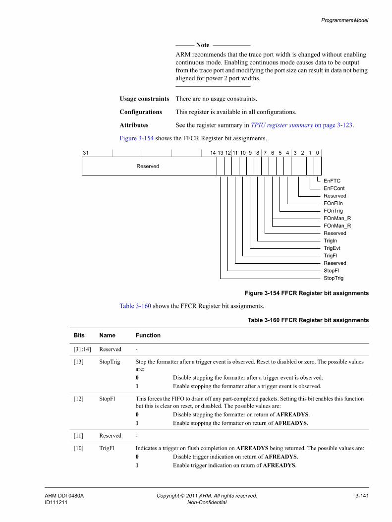
Programmers Model
Note ARM recommends that the trace port width is changed without enabling
continuous mode. Enabling continuous mode causes data to be output from the trace port and modifying the port size can result in data not being aligned for power 2 port widths.
Usage constraints There are no usage constraints.
Configurations This register is available in all configurations.
Attributes See the register summary in TPIU register summary on page 3-123.
Figure 3-154 shows the FFCR Register bit assignments.
Figure 3-154 FFCR Register bit assignments
Table 3-160 shows the FFCR Register bit assignments.
31 14 13 12 11 10 9 8 7 6 5 4 3 2 1 0
Reserved
ReservedEnFContEnFTC
FOnFlInFOnTrig
ReservedFOnMan_RFOnMan_R
TrigFlTrigEvtTrigIn
ReservedStopFlStopTrig
Table 3-160 FFCR Register bit assignments
Bits Name Function
[31:14] Reserved -
[13] StopTrig Stop the formatter after a trigger event is observed. Reset to disabled or zero. The possible values are:0 Disable stopping the formatter after a trigger event is observed.1 Enable stopping the formatter after a trigger event is observed.
[12] StopFl This forces the FIFO to drain off any part-completed packets. Setting this bit enables this function but this is clear on reset, or disabled. The possible values are:0 Disable stopping the formatter on return of AFREADYS.1 Enable stopping the formatter on return of AFREADYS.
[11] Reserved -
[10] TrigFl Indicates a trigger on flush completion on AFREADYS being returned. The possible values are:0 Disable trigger indication on return of AFREADYS.1 Enable trigger indication on return of AFREADYS.
ARM DDI 0480A Copyright © 2011 ARM. All rights reserved. 3-141ID111211 Non-Confidential
Programmers Model
3.13.11 Formatter Synchronization Counter Register
The FSCR Register characteristics are:
Purpose The Formatter Synchronization Counter Register enables effective use on different sized TPAs without wasting large amounts of the storage capacity of the capture device. This counter is the number of formatter frames since the last synchronization packet of 128 bits, and is a 12-bit counter with a maximum count value of 4096. This equates to synchronization every 65536 bytes, that is, 4096 packets x 16 bytes per packet. The default is set up for a synchronization packet every 1024 bytes, that is, every 64
[9] TrigEvt Indicate a trigger on a trigger event. The possible values are:0 Disable trigger indication on a trigger event.1 Enable trigger indication on a trigger event.
[8] TrigIn Indicate a trigger on TRIGIN being asserted. The possible values are:0 Disable trigger indication when TRIGIN is asserted.1 Enable trigger indication when TRIGIN is asserted.
[7] Reserved -
[6] FOnMan_R Setting this bit causes a flush to be generated. This is cleared when this flush has been serviced. This bit is clear on reset. The possible values are:0 Manual flush is not initiated.1 Manual flush is initiated.
[6] FOnMan_R Setting this bit initiates a manual flush. This is cleared when this flush has been serviced. This bit is clear on reset. The possible values are:0 Manual flush is not initiated.1 Manual flush is initiated.
[5] FOnTrig Set this bit to initiates a manual flush of data in the system when a trigger event occurs. On reset this bit is clear. A trigger event is defined as when the trigger counter reaches zero, or in the case of the trigger counter being zero, when TRIGIN is HIGH. The possible values are:0 Disable generation of flush when a Trigger Event occurs.1 Enable generation of flush when a Trigger Event occurs.
[4] FOnFlIn Set this bit to enable use of the FLUSHIN connection. This is clear on reset. The possible values are:0 Disable generation of flush using the FLUSHIN interface.1 Enable generation of flush using the FLUSHIN interface.
[3:2] Reserved -
[1] EnFCont Embed in trigger packets and indicate null cycles using sync packets. Reset value is this bit clear. Can only be changed when FtStopped is HIGH. The possible values are:0 Continuous formatting disabled.1 Continuous formatting enabled.
[0] EnFTC Do not embed triggers into the formatted stream. Trace disable cycles and triggers are indicated by TRACECTL, where fitted. On reset this bit clear. Can only be changed when FtStopped is HIGH. The possible values are:0 Formatting disabled.1 Formatting enabled.
Table 3-160 FFCR Register bit assignments (continued)
Bits Name Function
ARM DDI 0480A Copyright © 2011 ARM. All rights reserved. 3-142ID111211 Non-Confidential
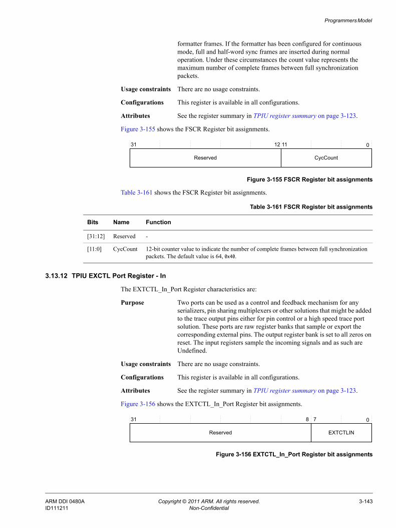
Programmers Model
formatter frames. If the formatter has been configured for continuous mode, full and half-word sync frames are inserted during normal operation. Under these circumstances the count value represents the maximum number of complete frames between full synchronization packets.
Usage constraints There are no usage constraints.
Configurations This register is available in all configurations.
Attributes See the register summary in TPIU register summary on page 3-123.
Figure 3-155 shows the FSCR Register bit assignments.
Figure 3-155 FSCR Register bit assignments
Table 3-161 shows the FSCR Register bit assignments.
3.13.12 TPIU EXCTL Port Register - In
The EXTCTL_In_Port Register characteristics are:
Purpose Two ports can be used as a control and feedback mechanism for any serializers, pin sharing multiplexers or other solutions that might be added to the trace output pins either for pin control or a high speed trace port solution. These ports are raw register banks that sample or export the corresponding external pins. The output register bank is set to all zeros on reset. The input registers sample the incoming signals and as such are Undefined.
Usage constraints There are no usage constraints.
Configurations This register is available in all configurations.
Attributes See the register summary in TPIU register summary on page 3-123.
Figure 3-156 shows the EXTCTL_In_Port Register bit assignments.
Figure 3-156 EXTCTL_In_Port Register bit assignments
31 0
Reserved
12 11
CycCount
Table 3-161 FSCR Register bit assignments
Bits Name Function
[31:12] Reserved -
[11:0] CycCount 12-bit counter value to indicate the number of complete frames between full synchronization packets. The default value is 64, 0x40.
31 0
Reserved
8 7
EXTCTLIN
ARM DDI 0480A Copyright © 2011 ARM. All rights reserved. 3-143ID111211 Non-Confidential
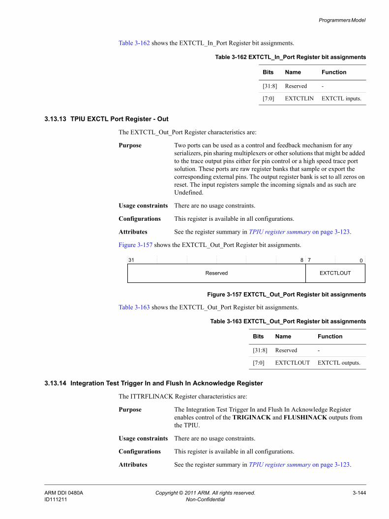
Programmers Model
Table 3-162 shows the EXTCTL_In_Port Register bit assignments.
3.13.13 TPIU EXCTL Port Register - Out
The EXTCTL_Out_Port Register characteristics are:
Purpose Two ports can be used as a control and feedback mechanism for any serializers, pin sharing multiplexers or other solutions that might be added to the trace output pins either for pin control or a high speed trace port solution. These ports are raw register banks that sample or export the corresponding external pins. The output register bank is set to all zeros on reset. The input registers sample the incoming signals and as such are Undefined.
Usage constraints There are no usage constraints.
Configurations This register is available in all configurations.
Attributes See the register summary in TPIU register summary on page 3-123.
Figure 3-157 shows the EXTCTL_Out_Port Register bit assignments.
Figure 3-157 EXTCTL_Out_Port Register bit assignments
Table 3-163 shows the EXTCTL_Out_Port Register bit assignments.
3.13.14 Integration Test Trigger In and Flush In Acknowledge Register
The ITTRFLINACK Register characteristics are:
Purpose The Integration Test Trigger In and Flush In Acknowledge Register enables control of the TRIGINACK and FLUSHINACK outputs from the TPIU.
Usage constraints There are no usage constraints.
Configurations This register is available in all configurations.
Attributes See the register summary in TPIU register summary on page 3-123.
Table 3-162 EXTCTL_In_Port Register bit assignments
Bits Name Function
[31:8] Reserved -
[7:0] EXTCTLIN EXTCTL inputs.
31 0
Reserved
8 7
EXTCTLOUT
Table 3-163 EXTCTL_Out_Port Register bit assignments
Bits Name Function
[31:8] Reserved -
[7:0] EXTCTLOUT EXTCTL outputs.
ARM DDI 0480A Copyright © 2011 ARM. All rights reserved. 3-144ID111211 Non-Confidential
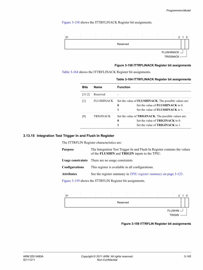
Programmers Model
Figure 3-158 shows the ITTRFLINACK Register bit assignments.
Figure 3-158 ITTRFLINACK Register bit assignments
Table 3-164 shows the ITTRFLINACK Register bit assignments.
3.13.15 Integration Test Trigger In and Flush In Register
The ITTRFLIN Register characteristics are:
Purpose The Integration Test Trigger In and Flush In Register contains the values of the FLUSHIN and TRIGIN inputs to the TPIU.
Usage constraints There are no usage constraints.
Configurations This register is available in all configurations.
Attributes See the register summary in TPIU register summary on page 3-123.
Figure 3-159 shows the ITTRFLIN Register bit assignments.
Figure 3-159 ITTRFLIN Register bit assignments
31 0
Reserved
FLUSHINACK
2 1
TRIGINACK
Table 3-164 ITTRFLINACK Register bit assignments
Bits Name Function
[31:2] Reserved -
[1] FLUSHINACK Set the value of FLUSHINACK. The possible values are:0 Set the value of FLUSHINACK to 0.1 Set the value of FLUSHINACK to 1.
[0] TRIGINACK Set the value of TRIGINACK. The possible values are:0 Set the value of TRIGINACK to 0.1 Set the value of TRIGINACK to 1.
31 0
Reserved
FLUSHIN
2 1
TRIGIN
ARM DDI 0480A Copyright © 2011 ARM. All rights reserved. 3-145ID111211 Non-Confidential
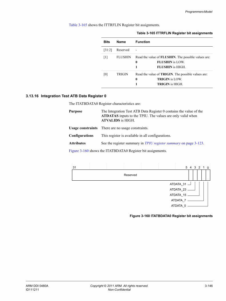
Programmers Model
Table 3-165 shows the ITTRFLIN Register bit assignments.
3.13.16 Integration Test ATB Data Register 0
The ITATBDATA0 Register characteristics are:
Purpose The Integration Test ATB Data Register 0 contains the value of the ATDATAS inputs to the TPIU. The values are only valid when ATVALIDS is HIGH.
Usage constraints There are no usage constraints.
Configurations This register is available in all configurations.
Attributes See the register summary in TPIU register summary on page 3-123.
Figure 3-160 shows the ITATBDATA0 Register bit assignments.
Figure 3-160 ITATBDATA0 Register bit assignments
Table 3-165 ITTRFLIN Register bit assignments
Bits Name Function
[31:2] Reserved -
[1] FLUSHIN Read the value of FLUSHIN. The possible values are:0 FLUSHIN is LOW.1 FLUSHIN is HIGH.
[0] TRIGIN Read the value of TRIGIN. The possible values are:0 TRIGIN is LOW.1 TRIGIN is HIGH.
31 0
Reserved
ATDATA_0
5 4 3 2 1
ATDATA_7
ATDATA_15
ATDATA_23
ATDATA_31
ARM DDI 0480A Copyright © 2011 ARM. All rights reserved. 3-146ID111211 Non-Confidential
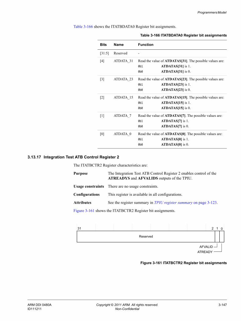
Programmers Model
Table 3-166 shows the ITATBDATA0 Register bit assignments.
3.13.17 Integration Test ATB Control Register 2
The ITATBCTR2 Register characteristics are:
Purpose The Integration Test ATB Control Register 2 enables control of the ATREADYS and AFVALIDS outputs of the TPIU.
Usage constraints There are no usage constraints.
Configurations This register is available in all configurations.
Attributes See the register summary in TPIU register summary on page 3-123.
Figure 3-161 shows the ITATBCTR2 Register bit assignments.
Figure 3-161 ITATBCTR2 Register bit assignments
Table 3-166 ITATBDATA0 Register bit assignments
Bits Name Function
[31:5] Reserved -
[4] ATDATA_31 Read the value of ATDATAS[31]. The possible values are:0b1 ATDATAS[31] is 1.0b0 ATDATAS[31] is 0.
[3] ATDATA_23 Read the value of ATDATAS[23]. The possible values are:0b1 ATDATAS[23] is 1.0b0 ATDATAS[23] is 0.
[2] ATDATA_15 Read the value of ATDATAS[15]. The possible values are:0b1 ATDATAS[15] is 1.0b0 ATDATAS[15] is 0.
[1] ATDATA_7 Read the value of ATDATAS[7]. The possible values are:0b1 ATDATAS[7] is 1.0b0 ATDATAS[7] is 0.
[0] ATDATA_0 Read the value of ATDATAS[0]. The possible values are:0b1 ATDATAS[0] is 1.0b0 ATDATAS[0] is 0.
31 0
Reserved
AFVALID
2 1
ATREADY
ARM DDI 0480A Copyright © 2011 ARM. All rights reserved. 3-147ID111211 Non-Confidential
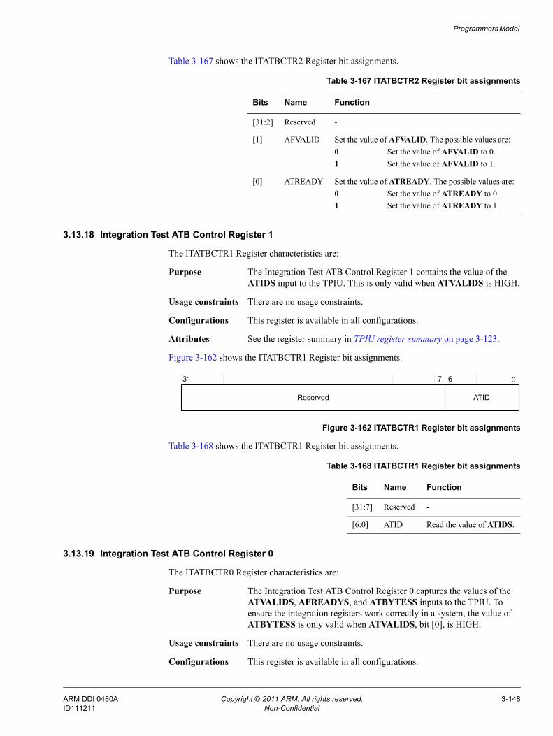
Programmers Model
Table 3-167 shows the ITATBCTR2 Register bit assignments.
3.13.18 Integration Test ATB Control Register 1
The ITATBCTR1 Register characteristics are:
Purpose The Integration Test ATB Control Register 1 contains the value of the ATIDS input to the TPIU. This is only valid when ATVALIDS is HIGH.
Usage constraints There are no usage constraints.
Configurations This register is available in all configurations.
Attributes See the register summary in TPIU register summary on page 3-123.
Figure 3-162 shows the ITATBCTR1 Register bit assignments.
Figure 3-162 ITATBCTR1 Register bit assignments
Table 3-168 shows the ITATBCTR1 Register bit assignments.
3.13.19 Integration Test ATB Control Register 0
The ITATBCTR0 Register characteristics are:
Purpose The Integration Test ATB Control Register 0 captures the values of the ATVALIDS, AFREADYS, and ATBYTESS inputs to the TPIU. To ensure the integration registers work correctly in a system, the value of ATBYTESS is only valid when ATVALIDS, bit [0], is HIGH.
Usage constraints There are no usage constraints.
Configurations This register is available in all configurations.
Table 3-167 ITATBCTR2 Register bit assignments
Bits Name Function
[31:2] Reserved -
[1] AFVALID Set the value of AFVALID. The possible values are:0 Set the value of AFVALID to 0.1 Set the value of AFVALID to 1.
[0] ATREADY Set the value of ATREADY. The possible values are:0 Set the value of ATREADY to 0.1 Set the value of ATREADY to 1.
31 0
Reserved
7 6
ATID
Table 3-168 ITATBCTR1 Register bit assignments
Bits Name Function
[31:7] Reserved -
[6:0] ATID Read the value of ATIDS.
ARM DDI 0480A Copyright © 2011 ARM. All rights reserved. 3-148ID111211 Non-Confidential
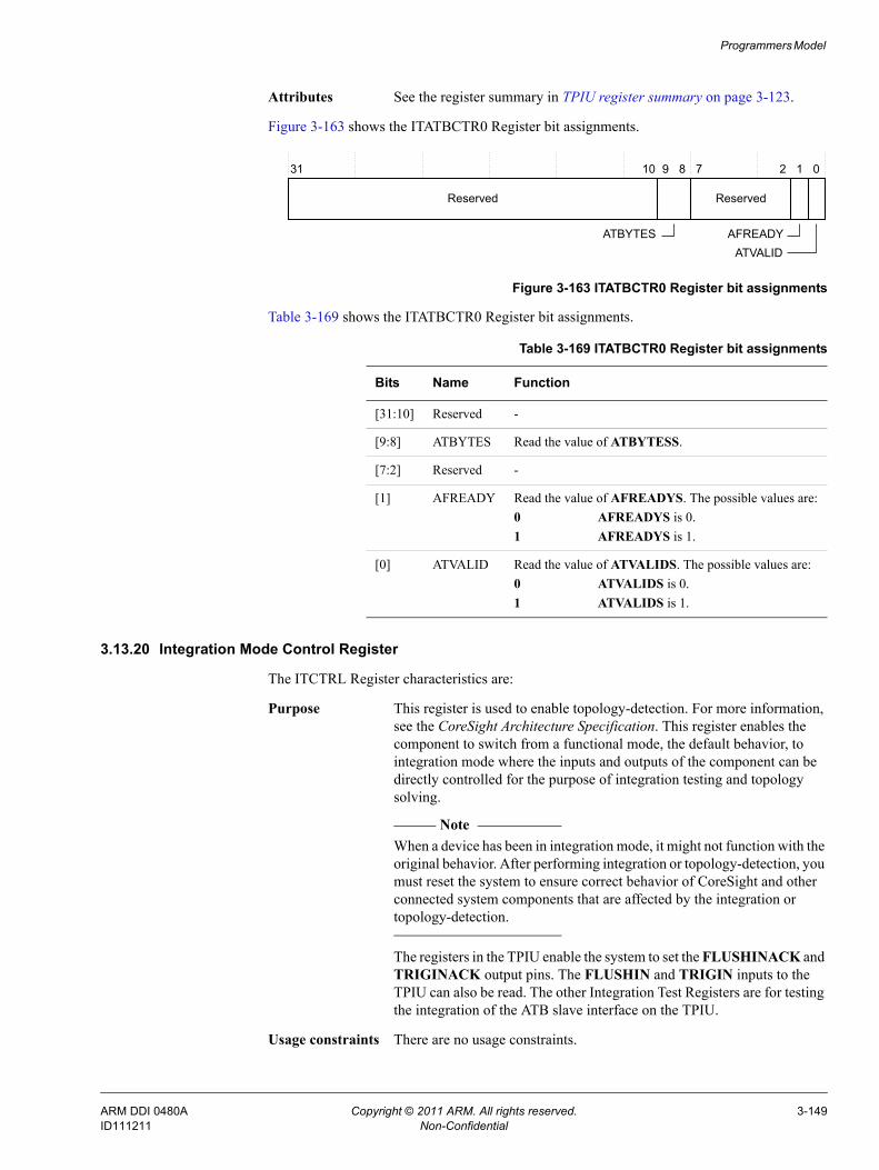
Programmers Model
Attributes See the register summary in TPIU register summary on page 3-123.
Figure 3-163 shows the ITATBCTR0 Register bit assignments.
Figure 3-163 ITATBCTR0 Register bit assignments
Table 3-169 shows the ITATBCTR0 Register bit assignments.
3.13.20 Integration Mode Control Register
The ITCTRL Register characteristics are:
Purpose This register is used to enable topology-detection. For more information, see the CoreSight Architecture Specification. This register enables the component to switch from a functional mode, the default behavior, to integration mode where the inputs and outputs of the component can be directly controlled for the purpose of integration testing and topology solving.
Note When a device has been in integration mode, it might not function with the
original behavior. After performing integration or topology-detection, you must reset the system to ensure correct behavior of CoreSight and other connected system components that are affected by the integration or topology-detection.
The registers in the TPIU enable the system to set the FLUSHINACK and TRIGINACK output pins. The FLUSHIN and TRIGIN inputs to the TPIU can also be read. The other Integration Test Registers are for testing the integration of the ATB slave interface on the TPIU.
Usage constraints There are no usage constraints.
31 0
Reserved
7 2
Reserved
10 9 8 1
ATVALIDAFREADYATBYTES
Table 3-169 ITATBCTR0 Register bit assignments
Bits Name Function
[31:10] Reserved -
[9:8] ATBYTES Read the value of ATBYTESS.
[7:2] Reserved -
[1] AFREADY Read the value of AFREADYS. The possible values are:0 AFREADYS is 0.1 AFREADYS is 1.
[0] ATVALID Read the value of ATVALIDS. The possible values are:0 ATVALIDS is 0.1 ATVALIDS is 1.
ARM DDI 0480A Copyright © 2011 ARM. All rights reserved. 3-149ID111211 Non-Confidential
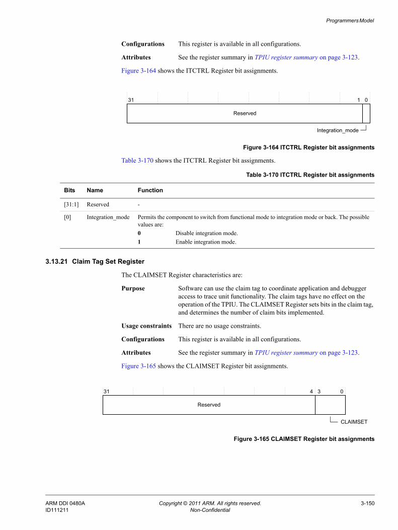
Programmers Model
Configurations This register is available in all configurations.
Attributes See the register summary in TPIU register summary on page 3-123.
Figure 3-164 shows the ITCTRL Register bit assignments.
Figure 3-164 ITCTRL Register bit assignments
Table 3-170 shows the ITCTRL Register bit assignments.
3.13.21 Claim Tag Set Register
The CLAIMSET Register characteristics are:
Purpose Software can use the claim tag to coordinate application and debugger access to trace unit functionality. The claim tags have no effect on the operation of the TPIU. The CLAIMSET Register sets bits in the claim tag, and determines the number of claim bits implemented.
Usage constraints There are no usage constraints.
Configurations This register is available in all configurations.
Attributes See the register summary in TPIU register summary on page 3-123.
Figure 3-165 shows the CLAIMSET Register bit assignments.
Figure 3-165 CLAIMSET Register bit assignments
31 0
Reserved
1
Integration_mode
Table 3-170 ITCTRL Register bit assignments
Bits Name Function
[31:1] Reserved -
[0] Integration_mode Permits the component to switch from functional mode to integration mode or back. The possible values are:0 Disable integration mode.1 Enable integration mode.
31 4 3 0
CLAIMSET
Reserved
ARM DDI 0480A Copyright © 2011 ARM. All rights reserved. 3-150ID111211 Non-Confidential
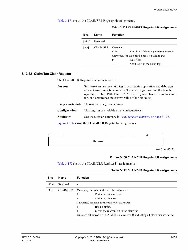
Programmers Model
Table 3-171 shows the CLAIMSET Register bit assignments.
3.13.22 Claim Tag Clear Register
The CLAIMCLR Register characteristics are:
Purpose Software can use the claim tag to coordinate application and debugger access to trace unit functionality. The claim tags have no effect on the operation of the TPIU. The CLAIMCLR Register clears bits in the claim tag, and determines the current value of the claim tag.
Usage constraints There are no usage constraints.
Configurations This register is available in all configurations.
Attributes See the register summary in TPIU register summary on page 3-123.
Figure 3-166 shows the CLAIMCLR Register bit assignments.
Figure 3-166 CLAIMCLR Register bit assignments
Table 3-172 shows the CLAIMCLR Register bit assignments.
Table 3-171 CLAIMSET Register bit assignments
Bits Name Function
[31:4] Reserved -
[3:0] CLAIMSET On reads:b1111 Four bits of claim tag are implemented.On writes, for each bit the possible values are:0 No effect.1 Set this bit in the claim tag.
31 4 3 0
CLAIMCLR
Reserved
Table 3-172 CLAIMCLR Register bit assignments
Bits Name Function
[31:4] Reserved -
[3:0] CLAIMCLR On reads, for each bit the possible values are:0 Claim tag bit is not set.1 Claim tag bit is set.On writes, for each bit the possible values are:0 Has no effect.1 Clears the relevant bit in the claim tag.On reset, all bits of the CLAIMCLR are reset to 0, indicating all claim bits are not set.
ARM DDI 0480A Copyright © 2011 ARM. All rights reserved. 3-151ID111211 Non-Confidential
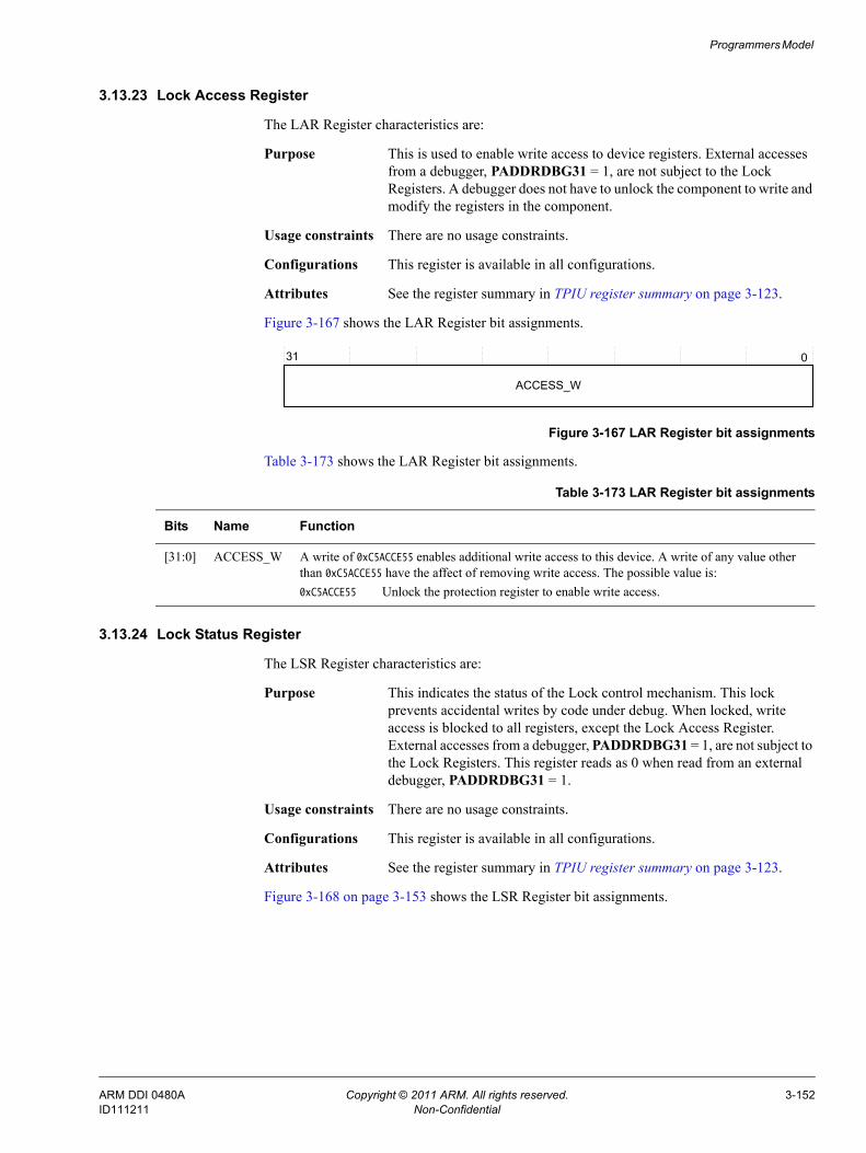
Programmers Model
3.13.23 Lock Access Register
The LAR Register characteristics are:
Purpose This is used to enable write access to device registers. External accesses from a debugger, PADDRDBG31 = 1, are not subject to the Lock Registers. A debugger does not have to unlock the component to write and modify the registers in the component.
Usage constraints There are no usage constraints.
Configurations This register is available in all configurations.
Attributes See the register summary in TPIU register summary on page 3-123.
Figure 3-167 shows the LAR Register bit assignments.
Figure 3-167 LAR Register bit assignments
Table 3-173 shows the LAR Register bit assignments.
3.13.24 Lock Status Register
The LSR Register characteristics are:
Purpose This indicates the status of the Lock control mechanism. This lock prevents accidental writes by code under debug. When locked, write access is blocked to all registers, except the Lock Access Register. External accesses from a debugger, PADDRDBG31 = 1, are not subject to the Lock Registers. This register reads as 0 when read from an external debugger, PADDRDBG31 = 1.
Usage constraints There are no usage constraints.
Configurations This register is available in all configurations.
Attributes See the register summary in TPIU register summary on page 3-123.
Figure 3-168 on page 3-153 shows the LSR Register bit assignments.
31 0
ACCESS_W
Table 3-173 LAR Register bit assignments
Bits Name Function
[31:0] ACCESS_W A write of 0xC5ACCE55 enables additional write access to this device. A write of any value other than 0xC5ACCE55 have the affect of removing write access. The possible value is:0xC5ACCE55 Unlock the protection register to enable write access.
ARM DDI 0480A Copyright © 2011 ARM. All rights reserved. 3-152ID111211 Non-Confidential
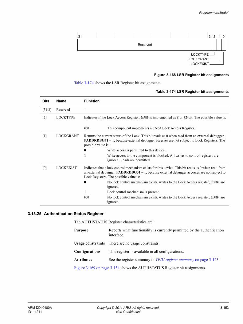
Programmers Model
Figure 3-168 LSR Register bit assignments
Table 3-174 shows the LSR Register bit assignments.
3.13.25 Authentication Status Register
The AUTHSTATUS Register characteristics are:
Purpose Reports what functionality is currently permitted by the authentication interface.
Usage constraints There are no usage constraints.
Configurations This register is available in all configurations.
Attributes See the register summary in TPIU register summary on page 3-123.
Figure 3-169 on page 3-154 shows the AUTHSTATUS Register bit assignments.
31 0
Reserved
1
LOCKTYPE
23
LOCKGRANTLOCKEXIST
Table 3-174 LSR Register bit assignments
Bits Name Function
[31:3] Reserved -
[2] LOCKTYPE Indicates if the Lock Access Register, 0xFB0 is implemented as 8 or 32-bit. The possible value is: 0b0 This component implements a 32-bit Lock Access Register.
[1] LOCKGRANT Returns the current status of the Lock. This bit reads as 0 when read from an external debugger, PADDRDBG31 = 1, because external debugger accesses are not subject to Lock Registers. The possible value is:0 Write access is permitted to this device.1 Write access to the component is blocked. All writes to control registers are
ignored. Reads are permitted.
[0] LOCKEXIST Indicates that a lock control mechanism exists for this device. This bit reads as 0 when read from an external debugger, PADDRDBG31 = 1, because external debugger accesses are not subject to Lock Registers. The possible value is:0 No lock control mechanism exists, writes to the Lock Access register, 0xFB0, are
ignored.1 Lock control mechanism is present.0b0 No lock control mechanism exists, writes to the Lock Access register, 0xFB0, are
ignored.
ARM DDI 0480A Copyright © 2011 ARM. All rights reserved. 3-153ID111211 Non-Confidential
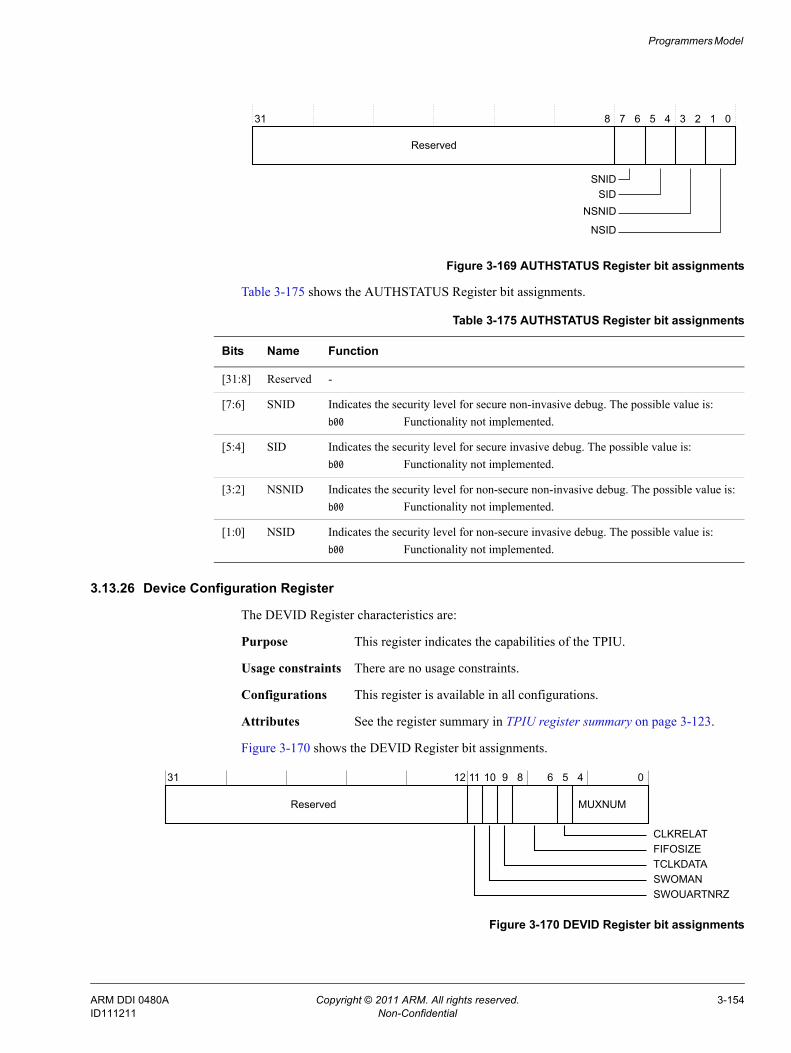
Programmers Model
Figure 3-169 AUTHSTATUS Register bit assignments
Table 3-175 shows the AUTHSTATUS Register bit assignments.
3.13.26 Device Configuration Register
The DEVID Register characteristics are:
Purpose This register indicates the capabilities of the TPIU.
Usage constraints There are no usage constraints.
Configurations This register is available in all configurations.
Attributes See the register summary in TPIU register summary on page 3-123.
Figure 3-170 shows the DEVID Register bit assignments.
Figure 3-170 DEVID Register bit assignments
31 0
Reserved
NSNID
2 1
SNID
7 6 5 4 38
NSID
SID
Table 3-175 AUTHSTATUS Register bit assignments
Bits Name Function
[31:8] Reserved -
[7:6] SNID Indicates the security level for secure non-invasive debug. The possible value is:b00 Functionality not implemented.
[5:4] SID Indicates the security level for secure invasive debug. The possible value is:b00 Functionality not implemented.
[3:2] NSNID Indicates the security level for non-secure non-invasive debug. The possible value is:b00 Functionality not implemented.
[1:0] NSID Indicates the security level for non-secure invasive debug. The possible value is:b00 Functionality not implemented.
31 12 11 10 9 8 6 5 4 0
MUXNUMReserved
TCLKDATAFIFOSIZECLKRELAT
SWOMANSWOUARTNRZ
ARM DDI 0480A Copyright © 2011 ARM. All rights reserved. 3-154ID111211 Non-Confidential
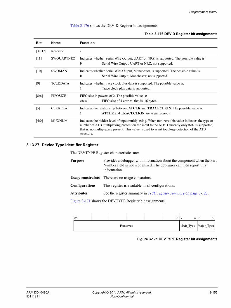
Programmers Model
Table 3-176 shows the DEVID Register bit assignments.
3.13.27 Device Type Identifier Register
The DEVTYPE Register characteristics are:
Purpose Provides a debugger with information about the component when the Part Number field is not recognized. The debugger can then report this information.
Usage constraints There are no usage constraints.
Configurations This register is available in all configurations.
Attributes See the register summary in TPIU register summary on page 3-123.
Figure 3-171 shows the DEVTYPE Register bit assignments.
Figure 3-171 DEVTYPE Register bit assignments
Table 3-176 DEVID Register bit assignments
Bits Name Function
[31:12] Reserved -
[11] SWOUARTNRZ Indicates whether Serial Wire Output, UART or NRZ, is supported. The possible value is:0 Serial Wire Output, UART or NRZ, not supported.
[10] SWOMAN Indicates whether Serial Wire Output, Manchester, is supported. The possible value is:0 Serial Wire Output, Manchester, not supported.
[9] TCLKDATA Indicates whether trace clock plus data is supported. The possible value is:1 Trace clock plus data is supported.
[8:6] FIFOSIZE FIFO size in powers of 2. The possible value is:0b010 FIFO size of 4 entries, that is, 16 bytes.
[5] CLKRELAT Indicates the relationship between ATCLK and TRACECLKIN. The possible value is:1 ATCLK and TRACECLKIN are asynchronous.
[4:0] MUXNUM Indicates the hidden level of input multiplexing. When non-zero this value indicates the type or number of ATB multiplexing present on the input to the ATB. Currently only 0x00 is supported, that is, no multiplexing present. This value is used to assist topology-detection of the ATB structure.
31 0
Reserved
7
Sub_Type
8 4
Major_Type
3
ARM DDI 0480A Copyright © 2011 ARM. All rights reserved. 3-155ID111211 Non-Confidential
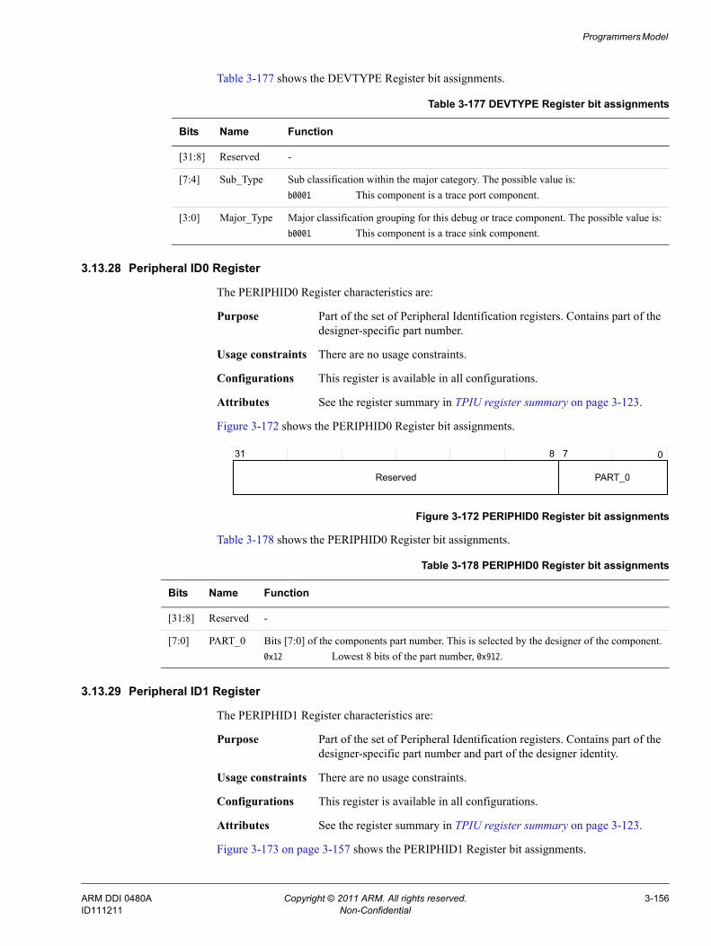
Programmers Model
Table 3-177 shows the DEVTYPE Register bit assignments.
3.13.28 Peripheral ID0 Register
The PERIPHID0 Register characteristics are:
Purpose Part of the set of Peripheral Identification registers. Contains part of the designer-specific part number.
Usage constraints There are no usage constraints.
Configurations This register is available in all configurations.
Attributes See the register summary in TPIU register summary on page 3-123.
Figure 3-172 shows the PERIPHID0 Register bit assignments.
Figure 3-172 PERIPHID0 Register bit assignments
Table 3-178 shows the PERIPHID0 Register bit assignments.
3.13.29 Peripheral ID1 Register
The PERIPHID1 Register characteristics are:
Purpose Part of the set of Peripheral Identification registers. Contains part of the designer-specific part number and part of the designer identity.
Usage constraints There are no usage constraints.
Configurations This register is available in all configurations.
Attributes See the register summary in TPIU register summary on page 3-123.
Figure 3-173 on page 3-157 shows the PERIPHID1 Register bit assignments.
Table 3-177 DEVTYPE Register bit assignments
Bits Name Function
[31:8] Reserved -
[7:4] Sub_Type Sub classification within the major category. The possible value is:b0001 This component is a trace port component.
[3:0] Major_Type Major classification grouping for this debug or trace component. The possible value is:b0001 This component is a trace sink component.
31 0
Reserved
78
PART_0
Table 3-178 PERIPHID0 Register bit assignments
Bits Name Function
[31:8] Reserved -
[7:0] PART_0 Bits [7:0] of the components part number. This is selected by the designer of the component.0x12 Lowest 8 bits of the part number, 0x912.
ARM DDI 0480A Copyright © 2011 ARM. All rights reserved. 3-156ID111211 Non-Confidential
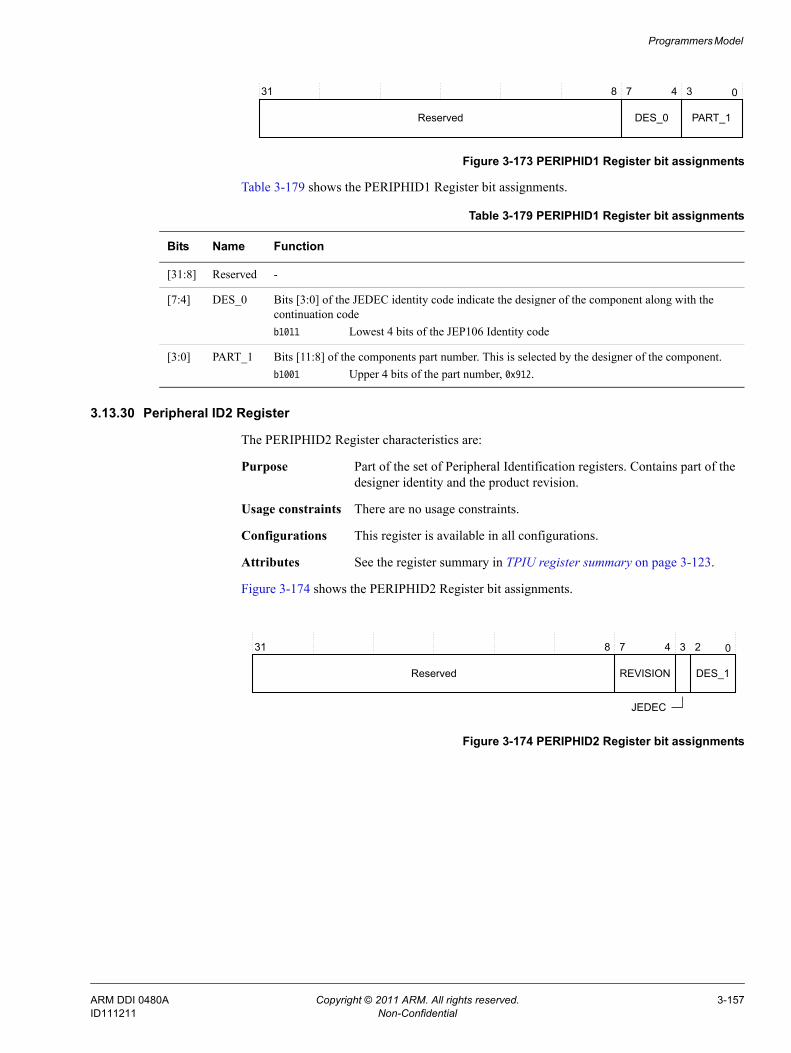
Programmers Model
Figure 3-173 PERIPHID1 Register bit assignments
Table 3-179 shows the PERIPHID1 Register bit assignments.
3.13.30 Peripheral ID2 Register
The PERIPHID2 Register characteristics are:
Purpose Part of the set of Peripheral Identification registers. Contains part of the designer identity and the product revision.
Usage constraints There are no usage constraints.
Configurations This register is available in all configurations.
Attributes See the register summary in TPIU register summary on page 3-123.
Figure 3-174 shows the PERIPHID2 Register bit assignments.
Figure 3-174 PERIPHID2 Register bit assignments
31 0
Reserved
78
PART_1
4 3
DES_0
Table 3-179 PERIPHID1 Register bit assignments
Bits Name Function
[31:8] Reserved -
[7:4] DES_0 Bits [3:0] of the JEDEC identity code indicate the designer of the component along with the continuation codeb1011 Lowest 4 bits of the JEP106 Identity code
[3:0] PART_1 Bits [11:8] of the components part number. This is selected by the designer of the component.b1001 Upper 4 bits of the part number, 0x912.
31 0
Reserved
7
REVISION
8 4
DES_1
3 2
JEDEC
ARM DDI 0480A Copyright © 2011 ARM. All rights reserved. 3-157ID111211 Non-Confidential
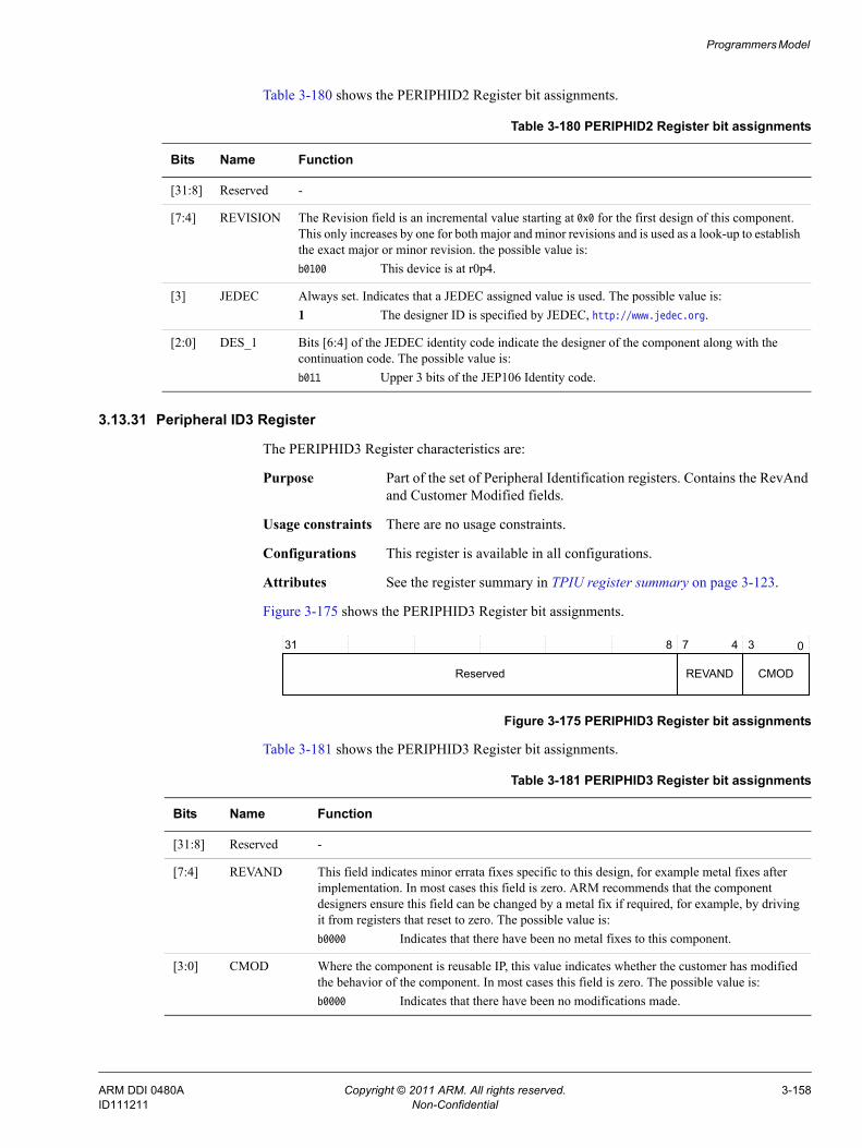
Programmers Model
Table 3-180 shows the PERIPHID2 Register bit assignments.
3.13.31 Peripheral ID3 Register
The PERIPHID3 Register characteristics are:
Purpose Part of the set of Peripheral Identification registers. Contains the RevAnd and Customer Modified fields.
Usage constraints There are no usage constraints.
Configurations This register is available in all configurations.
Attributes See the register summary in TPIU register summary on page 3-123.
Figure 3-175 shows the PERIPHID3 Register bit assignments.
Figure 3-175 PERIPHID3 Register bit assignments
Table 3-181 shows the PERIPHID3 Register bit assignments.
Table 3-180 PERIPHID2 Register bit assignments
Bits Name Function
[31:8] Reserved -
[7:4] REVISION The Revision field is an incremental value starting at 0x0 for the first design of this component. This only increases by one for both major and minor revisions and is used as a look-up to establish the exact major or minor revision. the possible value is:b0100 This device is at r0p4.
[3] JEDEC Always set. Indicates that a JEDEC assigned value is used. The possible value is:1 The designer ID is specified by JEDEC, http://www.jedec.org.
[2:0] DES_1 Bits [6:4] of the JEDEC identity code indicate the designer of the component along with the continuation code. The possible value is:b011 Upper 3 bits of the JEP106 Identity code.
31 0
Reserved
7
REVAND
8 4
CMOD
3
Table 3-181 PERIPHID3 Register bit assignments
Bits Name Function
[31:8] Reserved -
[7:4] REVAND This field indicates minor errata fixes specific to this design, for example metal fixes after implementation. In most cases this field is zero. ARM recommends that the component designers ensure this field can be changed by a metal fix if required, for example, by driving it from registers that reset to zero. The possible value is:b0000 Indicates that there have been no metal fixes to this component.
[3:0] CMOD Where the component is reusable IP, this value indicates whether the customer has modified the behavior of the component. In most cases this field is zero. The possible value is:b0000 Indicates that there have been no modifications made.
ARM DDI 0480A Copyright © 2011 ARM. All rights reserved. 3-158ID111211 Non-Confidential
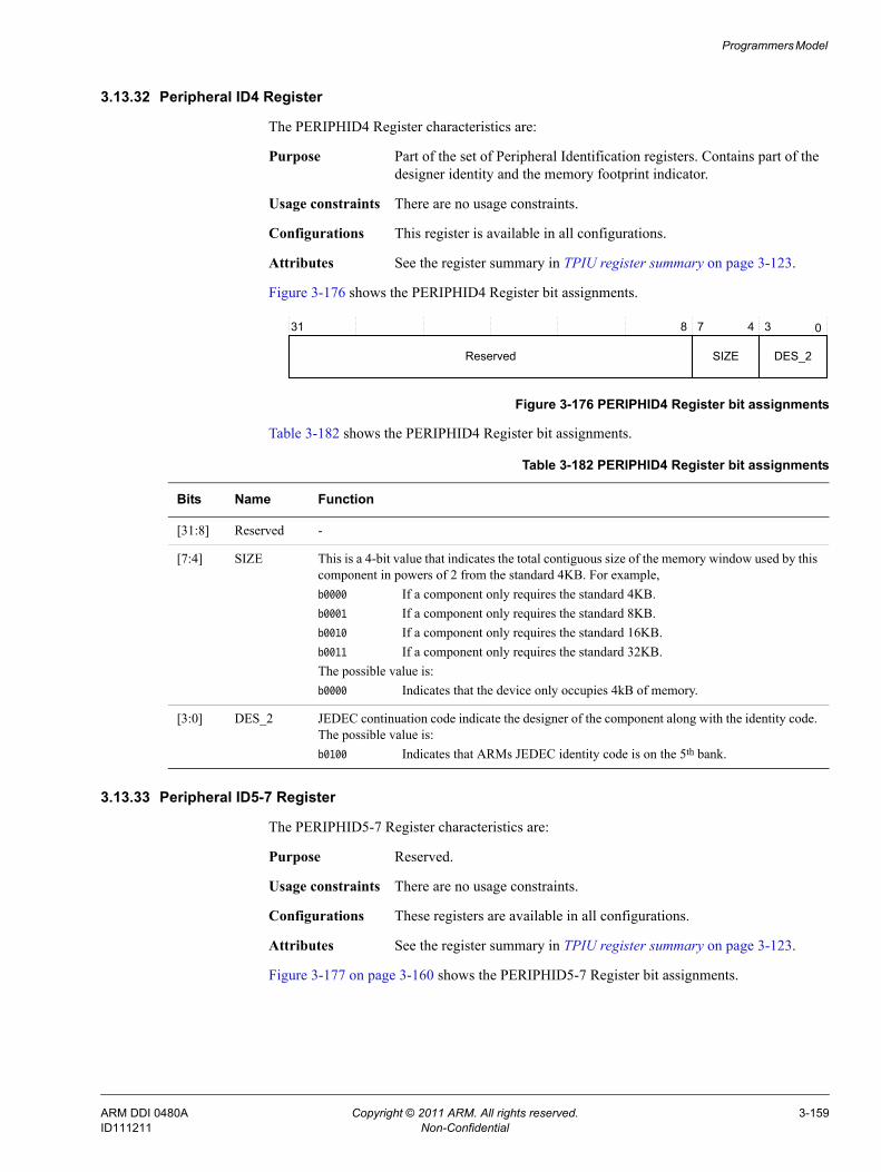
Programmers Model
3.13.32 Peripheral ID4 Register
The PERIPHID4 Register characteristics are:
Purpose Part of the set of Peripheral Identification registers. Contains part of the designer identity and the memory footprint indicator.
Usage constraints There are no usage constraints.
Configurations This register is available in all configurations.
Attributes See the register summary in TPIU register summary on page 3-123.
Figure 3-176 shows the PERIPHID4 Register bit assignments.
Figure 3-176 PERIPHID4 Register bit assignments
Table 3-182 shows the PERIPHID4 Register bit assignments.
3.13.33 Peripheral ID5-7 Register
The PERIPHID5-7 Register characteristics are:
Purpose Reserved.
Usage constraints There are no usage constraints.
Configurations These registers are available in all configurations.
Attributes See the register summary in TPIU register summary on page 3-123.
Figure 3-177 on page 3-160 shows the PERIPHID5-7 Register bit assignments.
31 0
Reserved
7
SIZE
8 4
DES_2
3
Table 3-182 PERIPHID4 Register bit assignments
Bits Name Function
[31:8] Reserved -
[7:4] SIZE This is a 4-bit value that indicates the total contiguous size of the memory window used by this component in powers of 2 from the standard 4KB. For example,b0000 If a component only requires the standard 4KB.b0001 If a component only requires the standard 8KB.b0010 If a component only requires the standard 16KB.b0011 If a component only requires the standard 32KB.The possible value is:b0000 Indicates that the device only occupies 4kB of memory.
[3:0] DES_2 JEDEC continuation code indicate the designer of the component along with the identity code. The possible value is:b0100 Indicates that ARMs JEDEC identity code is on the 5th bank.
ARM DDI 0480A Copyright © 2011 ARM. All rights reserved. 3-159ID111211 Non-Confidential
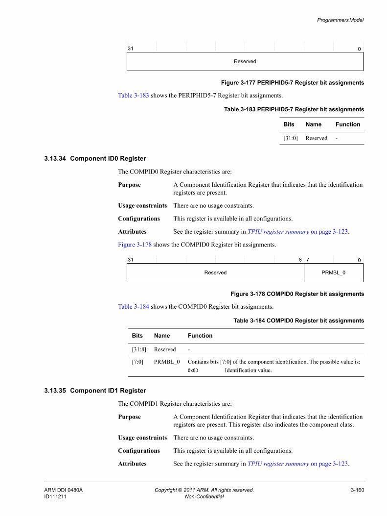
Programmers Model
Figure 3-177 PERIPHID5-7 Register bit assignments
Table 3-183 shows the PERIPHID5-7 Register bit assignments.
3.13.34 Component ID0 Register
The COMPID0 Register characteristics are:
Purpose A Component Identification Register that indicates that the identification registers are present.
Usage constraints There are no usage constraints.
Configurations This register is available in all configurations.
Attributes See the register summary in TPIU register summary on page 3-123.
Figure 3-178 shows the COMPID0 Register bit assignments.
Figure 3-178 COMPID0 Register bit assignments
Table 3-184 shows the COMPID0 Register bit assignments.
3.13.35 Component ID1 Register
The COMPID1 Register characteristics are:
Purpose A Component Identification Register that indicates that the identification registers are present. This register also indicates the component class.
Usage constraints There are no usage constraints.
Configurations This register is available in all configurations.
Attributes See the register summary in TPIU register summary on page 3-123.
31 0
Reserved
Table 3-183 PERIPHID5-7 Register bit assignments
Bits Name Function
[31:0] Reserved -
31 0
Reserved
78
PRMBL_0
Table 3-184 COMPID0 Register bit assignments
Bits Name Function
[31:8] Reserved -
[7:0] PRMBL_0 Contains bits [7:0] of the component identification. The possible value is:0x0D Identification value.
ARM DDI 0480A Copyright © 2011 ARM. All rights reserved. 3-160ID111211 Non-Confidential
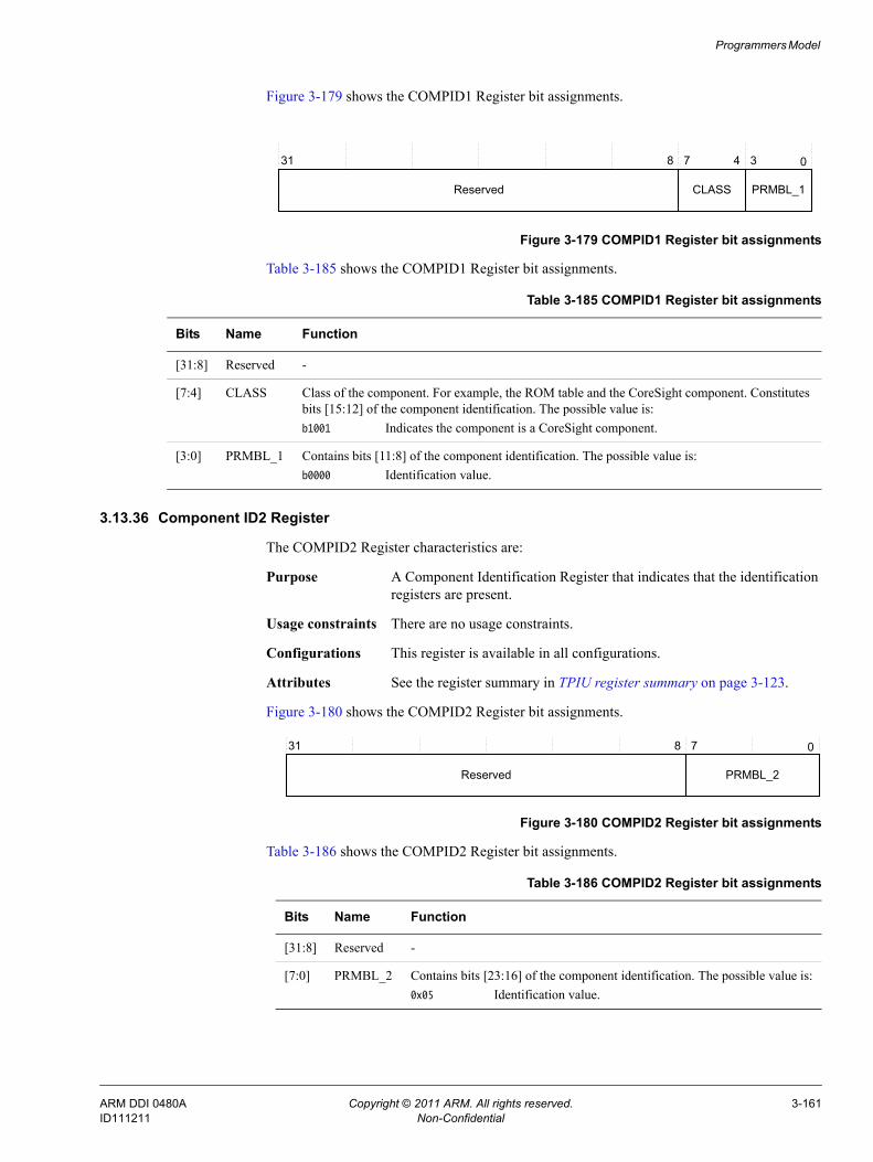
Programmers Model
Figure 3-179 shows the COMPID1 Register bit assignments.
Figure 3-179 COMPID1 Register bit assignments
Table 3-185 shows the COMPID1 Register bit assignments.
3.13.36 Component ID2 Register
The COMPID2 Register characteristics are:
Purpose A Component Identification Register that indicates that the identification registers are present.
Usage constraints There are no usage constraints.
Configurations This register is available in all configurations.
Attributes See the register summary in TPIU register summary on page 3-123.
Figure 3-180 shows the COMPID2 Register bit assignments.
Figure 3-180 COMPID2 Register bit assignments
Table 3-186 shows the COMPID2 Register bit assignments.
31 0
Reserved
78
PRMBL_1
4 3
CLASS
Table 3-185 COMPID1 Register bit assignments
Bits Name Function
[31:8] Reserved -
[7:4] CLASS Class of the component. For example, the ROM table and the CoreSight component. Constitutes bits [15:12] of the component identification. The possible value is:b1001 Indicates the component is a CoreSight component.
[3:0] PRMBL_1 Contains bits [11:8] of the component identification. The possible value is:b0000 Identification value.
31 0
Reserved
78
PRMBL_2
Table 3-186 COMPID2 Register bit assignments
Bits Name Function
[31:8] Reserved -
[7:0] PRMBL_2 Contains bits [23:16] of the component identification. The possible value is:0x05 Identification value.
ARM DDI 0480A Copyright © 2011 ARM. All rights reserved. 3-161ID111211 Non-Confidential
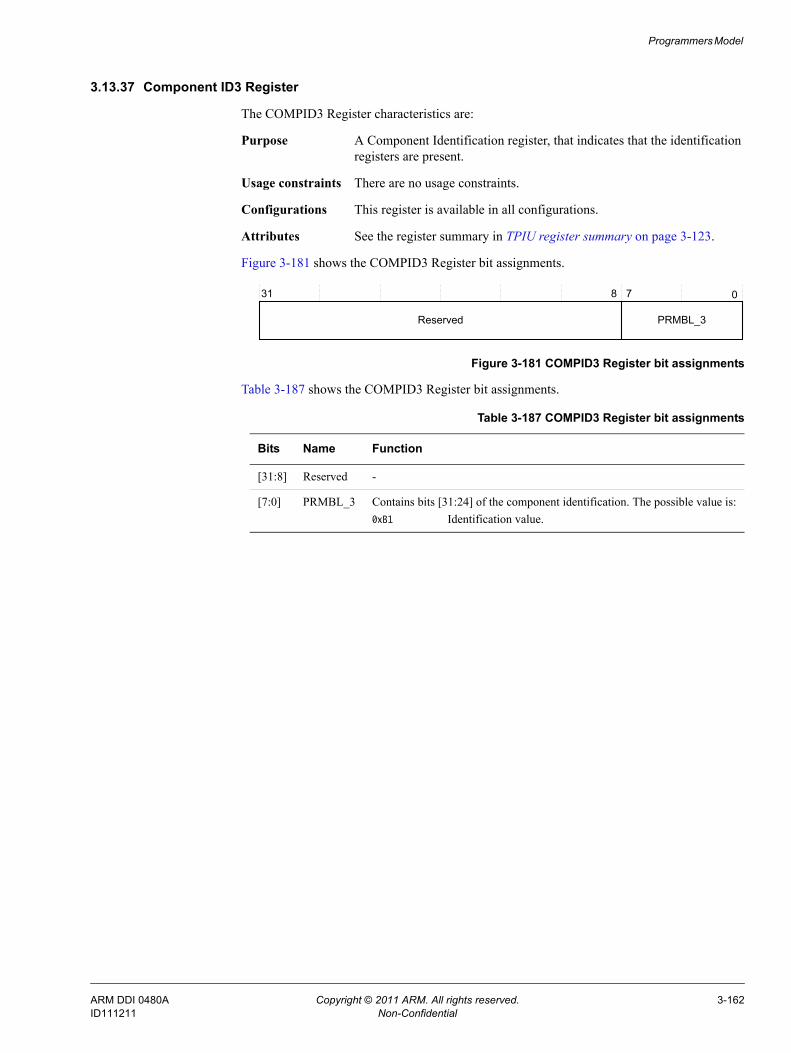
Programmers Model
3.13.37 Component ID3 Register
The COMPID3 Register characteristics are:
Purpose A Component Identification register, that indicates that the identification registers are present.
Usage constraints There are no usage constraints.
Configurations This register is available in all configurations.
Attributes See the register summary in TPIU register summary on page 3-123.
Figure 3-181 shows the COMPID3 Register bit assignments.
Figure 3-181 COMPID3 Register bit assignments
Table 3-187 shows the COMPID3 Register bit assignments.
31 0
Reserved
78
PRMBL_3
Table 3-187 COMPID3 Register bit assignments
Bits Name Function
[31:8] Reserved -
[7:0] PRMBL_3 Contains bits [31:24] of the component identification. The possible value is:0xB1 Identification value.
ARM DDI 0480A Copyright © 2011 ARM. All rights reserved. 3-162ID111211 Non-Confidential
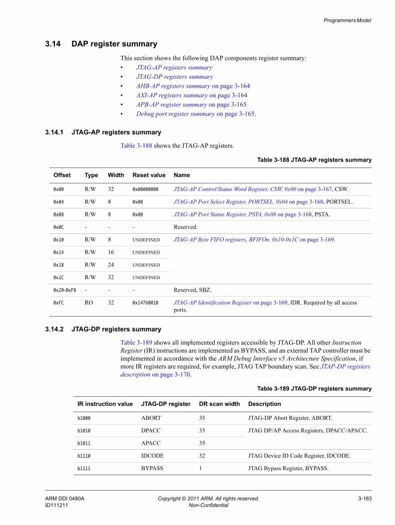
Programmers Model
3.14 DAP register summaryThis section shows the following DAP components register summary:• JTAG-AP registers summary• JTAG-DP registers summary• AHB-AP registers summary on page 3-164• AXI-AP registers summary on page 3-164• APB-AP register summary on page 3-165• Debug port register summary on page 3-165.
3.14.1 JTAG-AP registers summary
Table 3-188 shows the JTAG-AP registers.
3.14.2 JTAG-DP registers summary
Table 3-189 shows all implemented registers accessible by JTAG-DP. All other Instruction Register (IR) instructions are implemented as BYPASS, and an external TAP controller must be implemented in accordance with the ARM Debug Interface v5 Architecture Specification, if more IR registers are required, for example, JTAG TAP boundary scan. See JTAP-DP registers description on page 3-170.
Table 3-188 JTAG-AP registers summary
Offset Type Width Reset value Name
0x00 R/W 32 0x00000000 JTAG-AP Control/Status Word Register, CSW, 0x00 on page 3-167, CSW.
0x04 R/W 8 0x00 JTAG-AP Port Select Register, PORTSEL, 0x04 on page 3-168, PORTSEL.
0x08 R/W 8 0x00 JTAG-AP Port Status Register, PSTA, 0x08 on page 3-168, PSTA.
0x0C - - - Reserved.
0x10 R/W 8 UNDEFINED JTAG-AP Byte FIFO registers, BFIFOn, 0x10-0x1C on page 3-169.
0x14 R/W 16 UNDEFINED
0x18 R/W 24 UNDEFINED
0x1C R/W 32 UNDEFINED
0x20-0xF8 - - - Reserved, SBZ.
0xFC RO 32 0x14760010 JTAG-AP Identification Register on page 3-169, IDR. Required by all access ports.
Table 3-189 JTAG-DP registers summary
IR instruction value JTAG-DP register DR scan width Description
b1000 ABORT 35 JTAG-DP Abort Register, ABORT.
b1010 DPACC 35 JTAG DP/AP Access Registers, DPACC/APACC.
b1011 APACC 35
b1110 IDCODE 32 JTAG Device ID Code Register, IDCODE.
b1111 BYPASS 1 JTAG Bypass Register, BYPASS.
ARM DDI 0480A Copyright © 2011 ARM. All rights reserved. 3-163ID111211 Non-Confidential
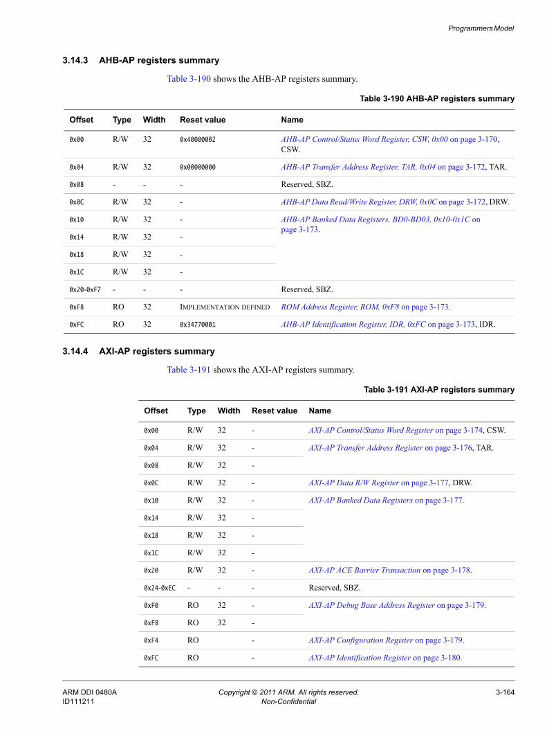
Programmers Model
3.14.3 AHB-AP registers summary
Table 3-190 shows the AHB-AP registers summary.
3.14.4 AXI-AP registers summary
Table 3-191 shows the AXI-AP registers summary.
Table 3-190 AHB-AP registers summary
Offset Type Width Reset value Name
0x00 R/W 32 0x40000002 AHB-AP Control/Status Word Register, CSW, 0x00 on page 3-170, CSW.
0x04 R/W 32 0x00000000 AHB-AP Transfer Address Register, TAR, 0x04 on page 3-172, TAR.
0x08 - - - Reserved, SBZ.
0x0C R/W 32 - AHB-AP Data Read/Write Register, DRW, 0x0C on page 3-172, DRW.
0x10 R/W 32 - AHB-AP Banked Data Registers, BD0-BD03, 0x10-0x1C on page 3-173.
0x14 R/W 32 -
0x18 R/W 32 -
0x1C R/W 32 -
0x20-0xF7 - - - Reserved, SBZ.
0xF8 RO 32 IMPLEMENTATION DEFINED ROM Address Register, ROM, 0xF8 on page 3-173.
0xFC RO 32 0x34770001 AHB-AP Identification Register, IDR, 0xFC on page 3-173, IDR.
Table 3-191 AXI-AP registers summary
Offset Type Width Reset value Name
0x00 R/W 32 - AXI-AP Control/Status Word Register on page 3-174, CSW.
0x04 R/W 32 - AXI-AP Transfer Address Register on page 3-176, TAR.
0x08 R/W 32 -
0x0C R/W 32 - AXI-AP Data R/W Register on page 3-177, DRW.
0x10 R/W 32 - AXI-AP Banked Data Registers on page 3-177.
0x14 R/W 32 -
0x18 R/W 32 -
0x1C R/W 32 -
0x20 R/W 32 - AXI-AP ACE Barrier Transaction on page 3-178.
0x24-0xEC - - - Reserved, SBZ.
0xF0 RO 32 - AXI-AP Debug Base Address Register on page 3-179.
0xF8 RO 32 -
0xF4 RO - AXI-AP Configuration Register on page 3-179.
0xFC RO - AXI-AP Identification Register on page 3-180.
ARM DDI 0480A Copyright © 2011 ARM. All rights reserved. 3-164ID111211 Non-Confidential
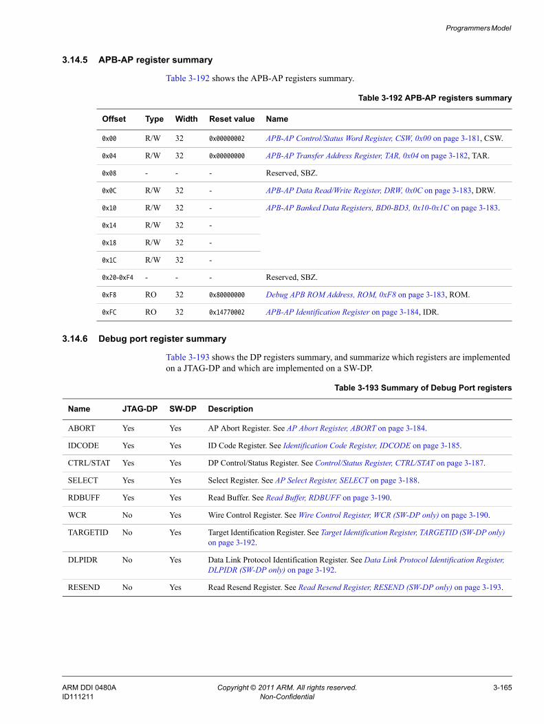
Programmers Model
3.14.5 APB-AP register summary
Table 3-192 shows the APB-AP registers summary.
3.14.6 Debug port register summary
Table 3-193 shows the DP registers summary, and summarize which registers are implemented on a JTAG-DP and which are implemented on a SW-DP.
Table 3-192 APB-AP registers summary
Offset Type Width Reset value Name
0x00 R/W 32 0x00000002 APB-AP Control/Status Word Register, CSW, 0x00 on page 3-181, CSW.
0x04 R/W 32 0x00000000 APB-AP Transfer Address Register, TAR, 0x04 on page 3-182, TAR.
0x08 - - - Reserved, SBZ.
0x0C R/W 32 - APB-AP Data Read/Write Register, DRW, 0x0C on page 3-183, DRW.
0x10 R/W 32 - APB-AP Banked Data Registers, BD0-BD3, 0x10-0x1C on page 3-183.
0x14 R/W 32 -
0x18 R/W 32 -
0x1C R/W 32 -
0x20-0xF4 - - - Reserved, SBZ.
0xF8 RO 32 0x80000000 Debug APB ROM Address, ROM, 0xF8 on page 3-183, ROM.
0xFC RO 32 0x14770002 APB-AP Identification Register on page 3-184, IDR.
Table 3-193 Summary of Debug Port registers
Name JTAG-DP SW-DP Description
ABORT Yes Yes AP Abort Register. See AP Abort Register, ABORT on page 3-184.
IDCODE Yes Yes ID Code Register. See Identification Code Register, IDCODE on page 3-185.
CTRL/STAT Yes Yes DP Control/Status Register. See Control/Status Register, CTRL/STAT on page 3-187.
SELECT Yes Yes Select Register. See AP Select Register, SELECT on page 3-188.
RDBUFF Yes Yes Read Buffer. See Read Buffer, RDBUFF on page 3-190.
WCR No Yes Wire Control Register. See Wire Control Register, WCR (SW-DP only) on page 3-190.
TARGETID No Yes Target Identification Register. See Target Identification Register, TARGETID (SW-DP only) on page 3-192.
DLPIDR No Yes Data Link Protocol Identification Register. See Data Link Protocol Identification Register, DLPIDR (SW-DP only) on page 3-192.
RESEND No Yes Read Resend Register. See Read Resend Register, RESEND (SW-DP only) on page 3-193.
ARM DDI 0480A Copyright © 2011 ARM. All rights reserved. 3-165ID111211 Non-Confidential
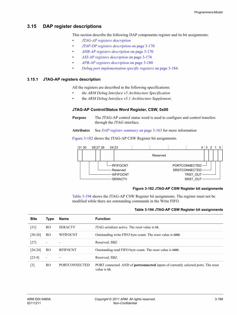
Programmers Model
3.15 DAP register descriptionsThis section describe the following DAP components register and its bit assignments:• JTAG-AP registers description• JTAP-DP registers description on page 3-170• AHB-AP registers description on page 3-170• AXI-AP registers description on page 3-174• APB-AP registers description on page 3-180• Debug port implementation specific registers on page 3-184.
3.15.1 JTAG-AP registers description
All the registers are described in the following specifications: • the ARM Debug Interface v5 Architecture Specification • the ARM Debug Interface v5.1 Architecture Supplement.
JTAG-AP Control/Status Word Register, CSW, 0x00
Purpose The JTAG-AP control status word is used to configure and control transfers through the JTAG interface.
Attributes See DAP register summary on page 3-163 for more information
Figure 3-182 shows the JTAG-AP CSW Register bit assignments.
Figure 3-182 JTAG-AP CSW Register bit assignments
Table 3-194 shows the JTAG-AP CSW Register bit assignments. The register must not be modified while there are outstanding commands in the Write FIFO.
31 30 28 27 26 24 23 4 3 2 1 0
Reserved
RFIFOCNTReservedWFIFOCNTSERACTV
PORTCONNECTEDSRSTCONNECTED
TRST_OUTSRST_OUT
Table 3-194 JTAG-AP CSW Register bit assignments
Bits Type Name Function
[31] RO SERACTV JTAG serializer active. The reset value is b0.
[30:28] RO WFIFOCNT Outstanding write FIFO byte count. The reset value is b000.
[27] - - Reserved, SBZ.
[26:24] RO RFIFOCNT Outstanding read FIFO byte count. The reset value is b000.
[23:4] - - Reserved, SBZ.
[3] RO PORTCONNECTED PORT connected. AND of portconnected inputs of currently selected ports. The reset value is b0.
ARM DDI 0480A Copyright © 2011 ARM. All rights reserved. 3-166ID111211 Non-Confidential
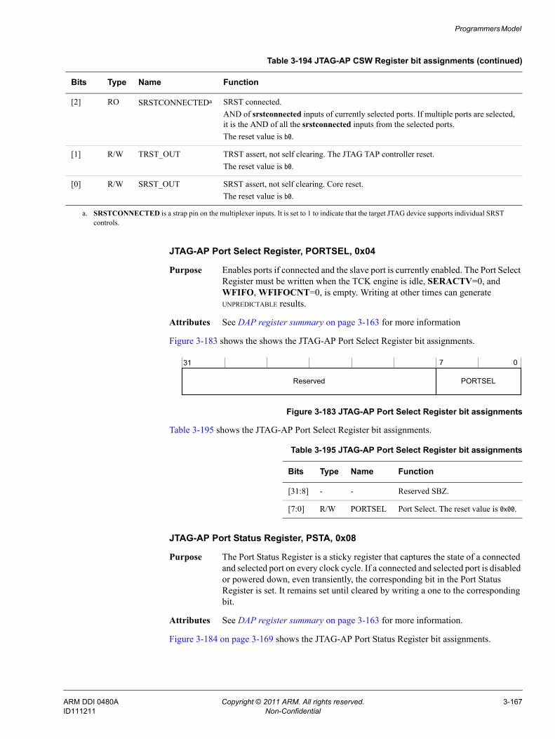
Programmers Model
JTAG-AP Port Select Register, PORTSEL, 0x04
Purpose Enables ports if connected and the slave port is currently enabled. The Port Select Register must be written when the TCK engine is idle, SERACTV=0, and WFIFO, WFIFOCNT=0, is empty. Writing at other times can generate UNPREDICTABLE results.
Attributes See DAP register summary on page 3-163 for more information
Figure 3-183 shows the shows the JTAG-AP Port Select Register bit assignments.
Figure 3-183 JTAG-AP Port Select Register bit assignments
Table 3-195 shows the JTAG-AP Port Select Register bit assignments.
JTAG-AP Port Status Register, PSTA, 0x08
Purpose The Port Status Register is a sticky register that captures the state of a connected and selected port on every clock cycle. If a connected and selected port is disabled or powered down, even transiently, the corresponding bit in the Port Status Register is set. It remains set until cleared by writing a one to the corresponding bit.
Attributes See DAP register summary on page 3-163 for more information.
Figure 3-184 on page 3-169 shows the JTAG-AP Port Status Register bit assignments.
[2] RO SRSTCONNECTEDa SRST connected.AND of srstconnected inputs of currently selected ports. If multiple ports are selected, it is the AND of all the srstconnected inputs from the selected ports.The reset value is b0.
[1] R/W TRST_OUT TRST assert, not self clearing. The JTAG TAP controller reset.The reset value is b0.
[0] R/W SRST_OUT SRST assert, not self clearing. Core reset.The reset value is b0.
a. SRSTCONNECTED is a strap pin on the multiplexer inputs. It is set to 1 to indicate that the target JTAG device supports individual SRST controls.
Table 3-194 JTAG-AP CSW Register bit assignments (continued)
Bits Type Name Function
0
PORTSEL
7
Reserved
31
Table 3-195 JTAG-AP Port Select Register bit assignments
Bits Type Name Function
[31:8] - - Reserved SBZ.
[7:0] R/W PORTSEL Port Select. The reset value is 0x00.
ARM DDI 0480A Copyright © 2011 ARM. All rights reserved. 3-167ID111211 Non-Confidential
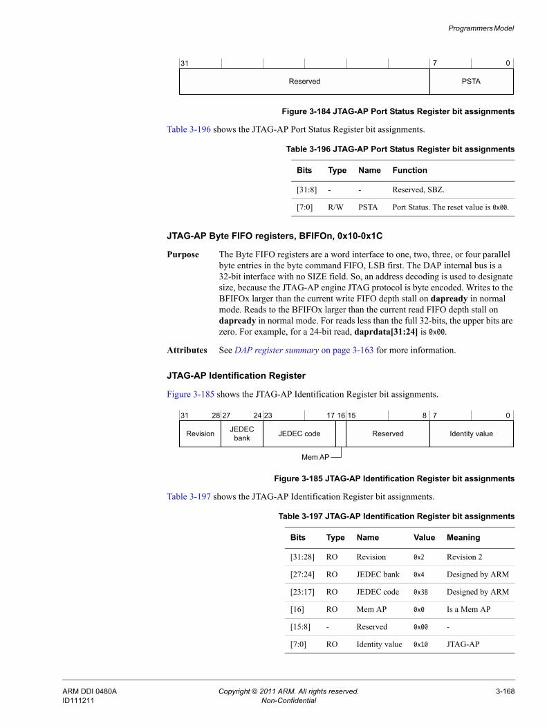
Programmers Model
Figure 3-184 JTAG-AP Port Status Register bit assignments
Table 3-196 shows the JTAG-AP Port Status Register bit assignments.
JTAG-AP Byte FIFO registers, BFIFOn, 0x10-0x1C
Purpose The Byte FIFO registers are a word interface to one, two, three, or four parallel byte entries in the byte command FIFO, LSB first. The DAP internal bus is a 32-bit interface with no SIZE field. So, an address decoding is used to designate size, because the JTAG-AP engine JTAG protocol is byte encoded. Writes to the BFIFOx larger than the current write FIFO depth stall on dapready in normal mode. Reads to the BFIFOx larger than the current read FIFO depth stall on dapready in normal mode. For reads less than the full 32-bits, the upper bits are zero. For example, for a 24-bit read, daprdata[31:24] is 0x00.
Attributes See DAP register summary on page 3-163 for more information.
JTAG-AP Identification Register
Figure 3-185 shows the JTAG-AP Identification Register bit assignments.
Figure 3-185 JTAG-AP Identification Register bit assignments
Table 3-197 shows the JTAG-AP Identification Register bit assignments.
0
PSTA
7
Reserved
31
Table 3-196 JTAG-AP Port Status Register bit assignments
Bits Type Name Function
[31:8] - - Reserved, SBZ.
[7:0] R/W PSTA Port Status. The reset value is 0x00.
Revision
31 28 27 24 23 17 16 15 8 7 0
JEDEC bank JEDEC code Reserved Identity value
Mem AP
Table 3-197 JTAG-AP Identification Register bit assignments
Bits Type Name Value Meaning
[31:28] RO Revision 0x2 Revision 2
[27:24] RO JEDEC bank 0x4 Designed by ARM
[23:17] RO JEDEC code 0x3B Designed by ARM
[16] RO Mem AP 0x0 Is a Mem AP
[15:8] - Reserved 0x00 -
[7:0] RO Identity value 0x10 JTAG-AP
ARM DDI 0480A Copyright © 2011 ARM. All rights reserved. 3-168ID111211 Non-Confidential
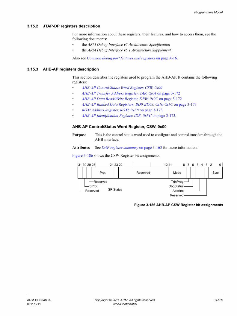
Programmers Model
3.15.2 JTAP-DP registers description
For more information about these registers, their features, and how to access them, see the following documents:• the ARM Debug Interface v5 Architecture Specification • the ARM Debug Interface v5.1 Architecture Supplement.
Also see Common debug port features and registers on page 4-16.
3.15.3 AHB-AP registers description
This section describes the registers used to program the AHB-AP. It contains the following registers:• AHB-AP Control/Status Word Register, CSW, 0x00• AHB-AP Transfer Address Register, TAR, 0x04 on page 3-172• AHB-AP Data Read/Write Register, DRW, 0x0C on page 3-172• AHB-AP Banked Data Registers, BD0-BD03, 0x10-0x1C on page 3-173• ROM Address Register, ROM, 0xF8 on page 3-173• AHB-AP Identification Register, IDR, 0xFC on page 3-173.
AHB-AP Control/Status Word Register, CSW, 0x00
Purpose This is the control status word used to configure and control transfers through the AHB interface.
Attributes See DAP register summary on page 3-163 for more information.
Figure 3-186 shows the CSW Register bit assignments.
Figure 3-186 AHB-AP CSW Register bit assignments
Size
31 30 29 28 24 23 12 11 8 7 6 5 4 3 2 0
Prot Reserved Mode
TrInProgDbgStatus
AddrIncReserved
ReservedSProt
Reserved SPIStatus
22
ARM DDI 0480A Copyright © 2011 ARM. All rights reserved. 3-169ID111211 Non-Confidential
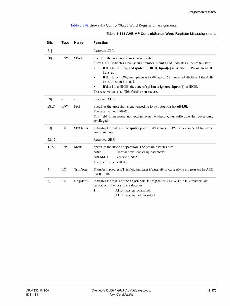
Programmers Model
Table 3-198 shows the Control/Status Word Register bit assignments.
Table 3-198 AHB-AP Control/Status Word Register bit assignments
Bits Type Name Function
[31] - - Reserved SBZ.
[30] R/W SProt Specifies that a secure transfer is requested.SProt HIGH indicates a non-secure transfer. SProt LOW indicates a secure transfer.• If this bit is LOW, and spiden is HIGH, hprot[6] is asserted LOW on an AHB
transfer. • If this bit is LOW, and spiden is LOW, hprot[6] is asserted HIGH and the AHB
transfer is not initiated. • If this bit is HIGH, the state of spiden is ignored. hprot[6] is HIGH.The reset value is b1. This field is non-secure.
[29] - - Reserved, SBZ.
[28:24] R/W Prot Specifies the protection signal encoding to be output on hprot[4:0].The reset value is b00011.This field is non secure, non-exclusive, non cacheable, non bufferable, data access, and privileged.
[23] RO SPIStatus Indicates the status of the spiden port. If SPIStatus is LOW, no secure AHB transfers are carried out.
[22:12] - - Reserved, SBZ.
[11:8] R/W Mode Specifies the mode of operation. The possible values are:b0000 Normal download or upload modelb0001-b1111 Reserved, SBZ.The reset value is b0000.
[7] RO TrInProg Transfer in progress. This field indicates if a transfer is currently in progress on the AHB master port.
[6] RO DbgStatus Indicates the status of the dbgen port. If DbgStatus is LOW, no AHB transfers are carried out. The possible values are:1 AHB transfers permitted.0 AHB transfers not permitted.
ARM DDI 0480A Copyright © 2011 ARM. All rights reserved. 3-170ID111211 Non-Confidential
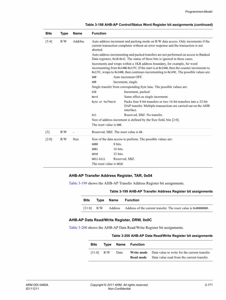
Programmers Model
AHB-AP Transfer Address Register, TAR, 0x04
Table 3-199 shows the AHB-AP Transfer Address Register bit assignments.
AHB-AP Data Read/Write Register, DRW, 0x0C
Table 3-200 shows the AHB-AP Data Read/Write Register bit assignments.
[5:4] R/W AddrInc Auto address increment and packing mode on R/W data access. Only increments if the current transaction completes without an error response and the transaction is not aborted.Auto address incrementing and packed transfers are not performed on access to Banked Data registers, 0x10-0x1C. The status of these bits is ignored in these cases.Increments and wraps within a 1KB address boundary, for example, for word incrementing from 0x1400-0x17FC. If the start is at 0x14A0, then the counter increments to 0x17FC, wraps to 0x1400, then continues incrementing to 0x149C. The possible values are:b00 Auto increment OFF.b00 Increment, single.Single transfer from corresponding byte lane. The possible values are:b10 Increment, packed.Word Same effect as single increment.Byte or halfword Packs four 8-bit transfers or two 16-bit transfers into a 32-bit
DAP transfer. Multiple transactions are carried out on the AHB interface.
b11 Reserved, SBZ. No transfer.Size of address increment is defined by the Size field, bits [2:0].The reset value is b00.
[3] R/W - Reserved, SBZ. The reset value is b0.
[2:0] R/W Size Size of the data access to perform. The possible values are:b000 8 bits.b001 16 bits.b010 32 bits.b011-b111 Reserved, SBZ.The reset value is b010.
Table 3-198 AHB-AP Control/Status Word Register bit assignments (continued)
Bits Type Name Function
Table 3-199 AHB-AP Transfer Address Register bit assignments
Bits Type Name Function
[31:0] R/W Address Address of the current transfer. The reset value is 0x00000000.
Table 3-200 AHB-AP Data Read/Write Register bit assignments
Bits Type Name Function
[31:0] R/W Data Write mode Data value to write for the current transfer.Read mode Data value read from the current transfer.
ARM DDI 0480A Copyright © 2011 ARM. All rights reserved. 3-171ID111211 Non-Confidential
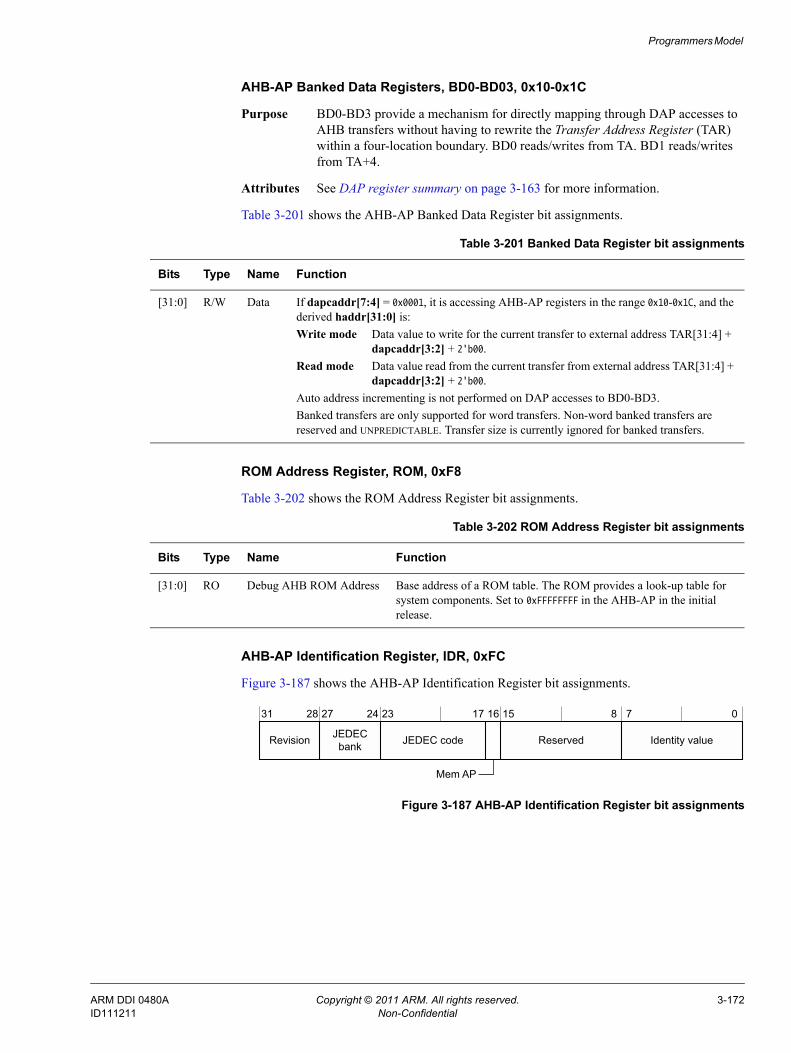
Programmers Model
AHB-AP Banked Data Registers, BD0-BD03, 0x10-0x1C
Purpose BD0-BD3 provide a mechanism for directly mapping through DAP accesses to AHB transfers without having to rewrite the Transfer Address Register (TAR) within a four-location boundary. BD0 reads/writes from TA. BD1 reads/writes from TA+4.
Attributes See DAP register summary on page 3-163 for more information.
Table 3-201 shows the AHB-AP Banked Data Register bit assignments.
ROM Address Register, ROM, 0xF8
Table 3-202 shows the ROM Address Register bit assignments.
AHB-AP Identification Register, IDR, 0xFC
Figure 3-187 shows the AHB-AP Identification Register bit assignments.
Figure 3-187 AHB-AP Identification Register bit assignments
Table 3-201 Banked Data Register bit assignments
Bits Type Name Function
[31:0] R/W Data If dapcaddr[7:4] = 0x0001, it is accessing AHB-AP registers in the range 0x10-0x1C, and the derived haddr[31:0] is:Write mode Data value to write for the current transfer to external address TAR[31:4] +
dapcaddr[3:2] + 2'b00.Read mode Data value read from the current transfer from external address TAR[31:4] +
dapcaddr[3:2] + 2'b00.Auto address incrementing is not performed on DAP accesses to BD0-BD3.Banked transfers are only supported for word transfers. Non-word banked transfers are reserved and UNPREDICTABLE. Transfer size is currently ignored for banked transfers.
Table 3-202 ROM Address Register bit assignments
Bits Type Name Function
[31:0] RO Debug AHB ROM Address Base address of a ROM table. The ROM provides a look-up table for system components. Set to 0xFFFFFFFF in the AHB-AP in the initial release.
Revision
31 28 27 24 23 17 16 15 8 7 0
JEDEC bank JEDEC code Reserved Identity value
Mem AP
ARM DDI 0480A Copyright © 2011 ARM. All rights reserved. 3-172ID111211 Non-Confidential
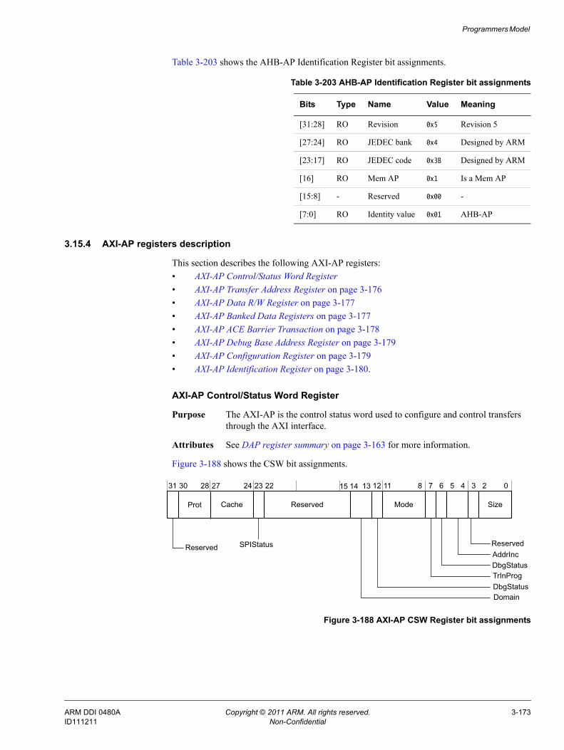
Programmers Model
Table 3-203 shows the AHB-AP Identification Register bit assignments.
3.15.4 AXI-AP registers description
This section describes the following AXI-AP registers:• AXI-AP Control/Status Word Register• AXI-AP Transfer Address Register on page 3-176• AXI-AP Data R/W Register on page 3-177• AXI-AP Banked Data Registers on page 3-177• AXI-AP ACE Barrier Transaction on page 3-178• AXI-AP Debug Base Address Register on page 3-179• AXI-AP Configuration Register on page 3-179• AXI-AP Identification Register on page 3-180.
AXI-AP Control/Status Word Register
Purpose The AXI-AP is the control status word used to configure and control transfers through the AXI interface.
Attributes See DAP register summary on page 3-163 for more information.
Figure 3-188 shows the CSW bit assignments.
Figure 3-188 AXI-AP CSW Register bit assignments
Table 3-203 AHB-AP Identification Register bit assignments
Bits Type Name Value Meaning
[31:28] RO Revision 0x5 Revision 5
[27:24] RO JEDEC bank 0x4 Designed by ARM
[23:17] RO JEDEC code 0x3B Designed by ARM
[16] RO Mem AP 0x1 Is a Mem AP
[15:8] - Reserved 0x00 -
[7:0] RO Identity value 0x01 AHB-AP
Size
31 30 28 24 23 12 11 8 7 6 5 4 3 2 0
Cache Reserved Mode
TrInProgDbgStatusAddrIncReservedReserved SPIStatus
22
DbgStatus
1314
Domain
15
Prot
27
ARM DDI 0480A Copyright © 2011 ARM. All rights reserved. 3-173ID111211 Non-Confidential
Programmers Model
Table 3-204 shows the CSW bit assignments.
Table 3-204 AXI-AP CSW Register bit assignments
Bits Type Name Reset value Function
[31] - Reserved - -
[30:28] R/W Prot b011 Specifies protection encoding as AMBA AXI protocol describes.
[27:24] R/W Cache b0000 Specifies the cache encoding as AMBA AXI protocol describes.
[23] RO SPIStatus - Indicates the status of the spiden port. If SPIStatus is LOW, then no secure AXI transfers are carried out.
[22:15] - Reserved - -
[14:13] R/W Domain b00 Shareable transaction encoding for ACE. The possible values are:b00 Non shareable.b01 Shareable, inner domain includes additional masters.b10 Shareable, outer domain, also includes inner or additional
masterb11 Shareable, system domain, all masters included.
[12] R/W DbgStatus b0 Enable ACE transactions, including barriers. The possible values are: b0 Disable.b1 Enable.
[11:8] R/W Mode b0000 Specifies the mode of operation: The possible values are:b0000 Normal download or upload.b0001 Barrier transaction.b0010-b1111 Reserved, SBZ.
[7] RO TrInProg - Transfer in progress. This field indicates if a transfer is currently in progress on the AXI master port.
[6] RO DbgStatus Indicates the status of DBGEN port. If DbgStatus is LOW, then no AXI transfers are carried out. The possible values are: b0 AXI transactions are stopped.b1 AXI transactions are permitted.
ARM DDI 0480A Copyright © 2011 ARM. All rights reserved. 3-174ID111211 Non-Confidential
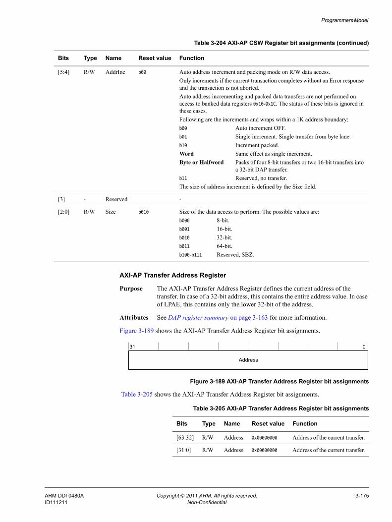
Programmers Model
AXI-AP Transfer Address Register
Purpose The AXI-AP Transfer Address Register defines the current address of the transfer. In case of a 32-bit address, this contains the entire address value. In case of LPAE, this contains only the lower 32-bit of the address.
Attributes See DAP register summary on page 3-163 for more information.
Figure 3-189 shows the AXI-AP Transfer Address Register bit assignments.
Figure 3-189 AXI-AP Transfer Address Register bit assignments
Table 3-205 shows the AXI-AP Transfer Address Register bit assignments.
[5:4] R/W AddrInc b00 Auto address increment and packing mode on R/W data access. Only increments if the current transaction completes without an Error response and the transaction is not aborted.Auto address incrementing and packed data transfers are not performed on access to banked data registers 0x10-0x1C. The status of these bits is ignored in these cases.Following are the increments and wraps within a 1K address boundary:b00 Auto increment OFF.b01 Single increment. Single transfer from byte lane.b10 Increment packed.Word Same effect as single increment.Byte or Halfword Packs of four 8-bit transfers or two 16-bit transfers into
a 32-bit DAP transfer.b11 Reserved, no transfer.The size of address increment is defined by the Size field.
[3] - Reserved -
[2:0] R/W Size b010 Size of the data access to perform. The possible values are:b000 8-bit.b001 16-bit.b010 32-bit.b011 64-bit.b100-b111 Reserved, SBZ.
Table 3-204 AXI-AP CSW Register bit assignments (continued)
Bits Type Name Reset value Function
Address
31 0
Table 3-205 AXI-AP Transfer Address Register bit assignments
Bits Type Name Reset value Function
[63:32] R/W Address 0x00000000 Address of the current transfer.
[31:0] R/W Address 0x00000000 Address of the current transfer.
ARM DDI 0480A Copyright © 2011 ARM. All rights reserved. 3-175ID111211 Non-Confidential
Programmers Model
AXI-AP Data R/W Register
Purpose The AXI-AP Data R/W Register stores the read data to be read in case of a read transfer. In case of a write transfer, write data must be written in the register.
Attributes See DAP register summary on page 3-163 for more information.
Figure 3-190 shows the AXI-AP Data R/W Register bit assignments.
Figure 3-190 AXI-AP Data R/W Register bit assignments
Table 3-206 shows the AXI-AP Data R/W Register bit assignments.
Note In case of a 64-bit access, multiple accesses must be initiated to DRW to make a single AXI access.
Read The first read of DRW in a sequence initiates a memory access. The first read returns the lower 32-bits of data. Subsequent read access returns the upper 32-bits of data. If a write to the CSW or TAR is initiated before the sequence completes, then the read access is terminated, and read data is no longer available.
Write The first write to DRW specifies the lower 32-bits of data to be written. Subsequent write access specifies the upper 32-bits to be written. If a write to the CSW is initiated before the sequence completes, then the write access is not initiated on the AXI interface.• combining partial reads and writes within a sequence terminates the earlier
access and the latest access is not recognized• any write access to CSW Register, TAR Register, or to any other register in
the AP during a sequence terminates the ongoing access and the current access is not recognized
• if a write sequence is terminated, then there is no write on AXI interface.
AXI-AP Banked Data Registers
Purpose BD0-3 provide a mechanism for direct mapping through DAP accesses to AXI transfers without having to rewrite the Transfer Address Register within a 4-location boundary. For example, BD0 reads and writes from TAR. BD1 reads and writes from TAR+4. This is applicable for a 32-bit access.
Attributes See DAP register summary on page 3-163 for more information.
Figure 3-191 on page 3-178 shows the bit assignments.
Data
31 0
Table 3-206 AXI-AP Data R/W Register bit assignments
Bits Type Name Function
[31:0] R/W Data In case of a 32-bit data access on the AXI-interface, store or write the 32-bits of data into this register once. Following are the modes for this register:Read mode Data value read from the current transfer.Write mode Data value to write for the current transfer.
ARM DDI 0480A Copyright © 2011 ARM. All rights reserved. 3-176ID111211 Non-Confidential
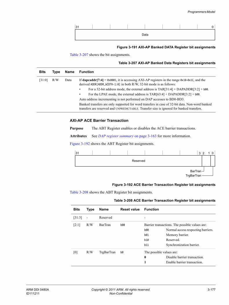
Programmers Model
Figure 3-191 AXI-AP Banked DATA Register bit assignments
Table 3-207 shows the bit assignments.
AXI-AP ACE Barrier Transaction
Purpose The ABT Register enables or disables the ACE barrier transactions.
Attributes See DAP register summary on page 3-163 for more information.
Figure 3-192 shows the ABT Register bit assignments.
Figure 3-192 ACE Barrier Transaction Register bit assignments
Table 3-208 shows the ABT Register bit assignments.
Data
31 0
Table 3-207 AXI-AP Banked Data Registers bit assignments
Bits Type Name Function
[31:0] R/W Data If dapcaddr[7:4] = 0x0001, it is accessing AXI-AP registers in the range 0x10-0x1C, and the derived ADDR[ADDR_WIDTH-1:0] in both R/W, 32-bit mode is as follows:• For a 32-bit address mode, the external address is TAR[31:4] + DAPADDR[3:2] + b00.• For the LPAE mode, the external address is TAR[63:4] + DAPADDR[3:2] + b00.Auto address incrementing is not performed on DAP accesses to BD0-BD3.Banked transfers are only supported for word transfers in case of 32-bit data. Non-word banked transfers are reserved and UNPREDICTABLE. Transfer size is ignored for banked transfers.
Reserved
31 03 12
BarTranTrgBarTran
Table 3-208 ACE Barrier Transaction Register bit assignments
Bits Type Name Reset value Function
[31:3] - Reserved -
[2:1] R/W BarTran b00 Barrier transactions. The possible values are:b00 Normal access respecting barriers.b01 Memory barrier.b10 Reserved.b11 Synchronization barrier.
[0] R/W TrgBarTran b0 The possible values are:0 Disable barrier transaction.1 Enable barrier transaction.
ARM DDI 0480A Copyright © 2011 ARM. All rights reserved. 3-177ID111211 Non-Confidential
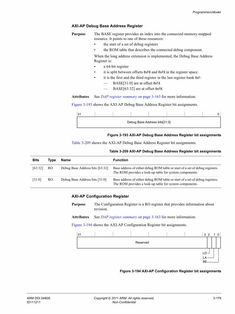
Programmers Model
AXI-AP Debug Base Address Register
Purpose The BASE register provides an index into the connected memory-mapped resource. It points to one of these resources:• the start of a set of debug registers• the ROM table that describes the connected debug component.When the long address extension is implemented, the Debug Base Address Register is:• a 64-bit register• it is split between offsets 0xF0 and 0xF8 in the register space.• it is the first and the third register in the last register bank 0xF:
— BASE[31:0] are at offset 0xF8— BASE[63:32] are at offset 0xF0.
Attributes See DAP register summary on page 3-163 for more information.
Figure 3-193 shows the AXI-AP Debug Base Address Register bit assignments.
Figure 3-193 AXI-AP Debug Base Address Register bit assignments
Table 3-209 shows the AXI-AP Debug Base Address Register bit assignments.
AXI-AP Configuration Register
Purpose The Configuration Register is a RO register that provides information about revision.
Attributes See DAP register summary on page 3-163 for more information.
Figure 3-194 shows the AXI-AP Configuration Register bit assignments.
Figure 3-194 AXI-AP Configuration Register bit assignments
Debug Base Address bits[31:0]
31 0
Table 3-209 AXI-AP Debug Base Address Register bit assignments
Bits Type Name Function
[63:32] RO Debug Base Address bits [63:32] Base address of either debug ROM table or start of a set of debug registers. The ROM provides a look-up table for system components.
[31:0] RO Debug Base Address bits [31:0] Base address of either debug ROM table or start of a set of debug registers. The ROM provides a look-up table for system components.
Reserved
31 03 12
LDLABE
ARM DDI 0480A Copyright © 2011 ARM. All rights reserved. 3-178ID111211 Non-Confidential
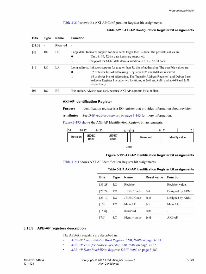
Programmers Model
Table 3-210 shows the AXI-AP Configuration Register bit assignments.
AXI-AP Identification Register
Purpose Identification register is a RO register that provides information about revision.
Attributes See DAP register summary on page 3-163 for more information.
Figure 3-195 shows the AXI-AP Identification Register bit assignments.
Figure 3-195 AXI-AP Identification Register bit assignments
Table 3-211 shows AXI-AP Identification Register bit assignments.
3.15.5 APB-AP registers description
The APB-AP registers are described in:• APB-AP Control/Status Word Register, CSW, 0x00 on page 3-181• APB-AP Transfer Address Register, TAR, 0x04 on page 3-182• APB-AP Data Read/Write Register, DRW, 0x0C on page 3-183
Table 3-210 AXI-AP Configuration Register bit assignments
Bits Type Name Function
[31:3] - Reserved -
[2] RO LD Large data. Indicates support for data items larger then 32-bits. The possible values are:0 Only 8, 16, 32-bit data items are supported.1 Support for 64-bit data item in addition to 8, 16, 32-bit data.
[1] RO LA Long address. Indicates support for greater than 32-bits of addressing. The possible values are:0 32 or fewer bits of addressing. Registers 0x08 and 0xF0 are reserved.1 64 or fewer bits of addressing. The Transfer Address Register l and Debug Base
Address Register l occupy two locations, at 0x04 and 0x08, and at 0xF8 and 0xF0 respectively.
[0] RO BE Big-endian. Always read as 0, because AXI-AP supports little-endian.
Identity value
31 28 24 23 8 7 0
JEDECBank ReservedRevision
17
Code
1527
JEDECcode
16
Table 3-211 AXI-AP Identification Register bit assignments
Bits Type Name Reset value Function
[31:28] RO Revision Revision value.
[27:24] RO JEDEC Bank 0x4 Designed by ARM.
[23:17] RO JEDEC Code 0x38 Designed by ARM.
[16] RO Mem AP 0x1 Mem AP.
[15:8] - Reserved 0x00 -
[7:0] RO Identity value 0x43 AXI-AP.
ARM DDI 0480A Copyright © 2011 ARM. All rights reserved. 3-179ID111211 Non-Confidential
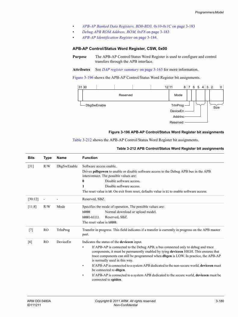
Programmers Model
• APB-AP Banked Data Registers, BD0-BD3, 0x10-0x1C on page 3-183• Debug APB ROM Address, ROM, 0xF8 on page 3-183• APB-AP Identification Register on page 3-184.
APB-AP Control/Status Word Register, CSW, 0x00
Purpose The APB-AP Control/Status Word Register is used to configure and control transfers through the APB interface.
Attributes See DAP register summary on page 3-163 for more information.
Figure 3-196 shows the APB-AP Control/Status Word Register bit assignments.
Figure 3-196 APB-AP Control/Status Word Register bit assignments
Table 3-212 shows the APB-AP Control/Status Word Register bit assignments.
31 30 12 11 8 7 6 5 4 3 2
DbgSwEnable
Reserved Mode
0
SizeTrInProg
DeviceEn
AddrInc
Reserved
Table 3-212 APB Control/Status Word Register bit assignments
Bits Type Name Function
[31] R/W DbgSwEnable Software access enable.Drives pdbgswen to enable or disable software access to the Debug APB bus in the APB interconnect. The possible values are:0 Disable software access.1 Disable software access.The reset value is b0. On exit from reset, defaults value is b1 to enable software access.
[30:12] - - Reserved, SBZ.
[11:8] R/W Mode Specifies the mode of operation. The possible values are:b0000 Normal download or upload model.b0001-b1111 Reserved, SBZ.The reset value is b0000.
[7] RO TrInProg Transfer in progress. This field indicates if a transfer is currently in progress on the APB master port.
[6] RO DeviceEn Indicates the status of the deviceen input.• If APB-AP is connected to the Debug APB, a bus connected only to debug and trace
components, it must be permanently enabled by tying deviceen HIGH. This ensures that trace components can still be programmed when dbgen is LOW. In practice, the APB-AP is normally used in this way.
• If APB-AP is connected to a system APB dedicated to the non-secure world, deviceen must be connected to dbgen.
• If APB-AP is connected to a system APB dedicated to the secure world, deviceen must be connected to spiden.
ARM DDI 0480A Copyright © 2011 ARM. All rights reserved. 3-180ID111211 Non-Confidential
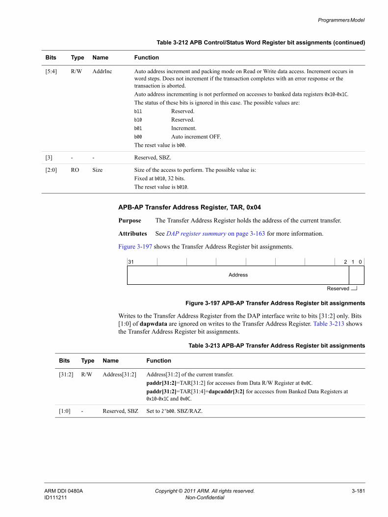
Programmers Model
APB-AP Transfer Address Register, TAR, 0x04
Purpose The Transfer Address Register holds the address of the current transfer.
Attributes See DAP register summary on page 3-163 for more information.
Figure 3-197 shows the Transfer Address Register bit assignments.
Figure 3-197 APB-AP Transfer Address Register bit assignments
Writes to the Transfer Address Register from the DAP interface write to bits [31:2] only. Bits [1:0] of dapwdata are ignored on writes to the Transfer Address Register. Table 3-213 shows the Transfer Address Register bit assignments.
[5:4] R/W AddrInc Auto address increment and packing mode on Read or Write data access. Increment occurs in word steps. Does not increment if the transaction completes with an error response or the transaction is aborted.Auto address incrementing is not performed on accesses to banked data registers 0x10-0x1C.The status of these bits is ignored in this case. The possible values are:b11 Reserved.b10 Reserved.b01 Increment.b00 Auto increment OFF.The reset value is b00.
[3] - - Reserved, SBZ.
[2:0] RO Size Size of the access to perform. The possible value is: Fixed at b010, 32 bits.The reset value is b010.
Table 3-212 APB Control/Status Word Register bit assignments (continued)
Bits Type Name Function
31 2 1 0
Reserved
Address
Table 3-213 APB-AP Transfer Address Register bit assignments
Bits Type Name Function
[31:2] R/W Address[31:2] Address[31:2] of the current transfer. paddr[31:2]=TAR[31:2] for accesses from Data R/W Register at 0x0C.paddr[31:2]=TAR[31:4]+dapcaddr[3:2] for accesses from Banked Data Registers at 0x10-0x1C and 0x0C.
[1:0] - Reserved, SBZ Set to 2'b00. SBZ/RAZ.
ARM DDI 0480A Copyright © 2011 ARM. All rights reserved. 3-181ID111211 Non-Confidential
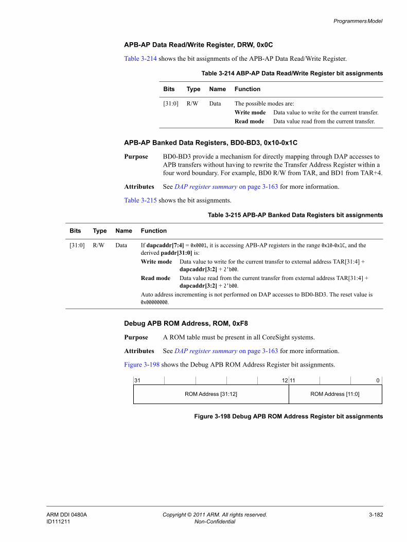
Programmers Model
APB-AP Data Read/Write Register, DRW, 0x0C
Table 3-214 shows the bit assignments of the APB-AP Data Read/Write Register.
APB-AP Banked Data Registers, BD0-BD3, 0x10-0x1C
Purpose BD0-BD3 provide a mechanism for directly mapping through DAP accesses to APB transfers without having to rewrite the Transfer Address Register within a four word boundary. For example, BD0 R/W from TAR, and BD1 from TAR+4.
Attributes See DAP register summary on page 3-163 for more information.
Table 3-215 shows the bit assignments.
Debug APB ROM Address, ROM, 0xF8
Purpose A ROM table must be present in all CoreSight systems.
Attributes See DAP register summary on page 3-163 for more information.
Figure 3-198 shows the Debug APB ROM Address Register bit assignments.
Figure 3-198 Debug APB ROM Address Register bit assignments
Table 3-214 ABP-AP Data Read/Write Register bit assignments
Bits Type Name Function
[31:0] R/W Data The possible modes are:Write mode Data value to write for the current transfer.Read mode Data value read from the current transfer.
Table 3-215 APB-AP Banked Data Registers bit assignments
Bits Type Name Function
[31:0] R/W Data If dapcaddr[7:4] = 0x0001, it is accessing APB-AP registers in the range 0x10-0x1C, and the derived paddr[31:0] is:Write mode Data value to write for the current transfer to external address TAR[31:4] +
dapcaddr[3:2] + 2'b00.Read mode Data value read from the current transfer from external address TAR[31:4] +
dapcaddr[3:2] + 2'b00.Auto address incrementing is not performed on DAP accesses to BD0-BD3. The reset value is 0x00000000.
31 12 11 0
ROM Address [31:12] ROM Address [11:0]
ARM DDI 0480A Copyright © 2011 ARM. All rights reserved. 3-182ID111211 Non-Confidential
Programmers Model
Table 3-216 shows the Debug APB ROM Address Register bit assignments.
APB-AP Identification Register
Figure 3-199 shows the APB-AP Identification Register bit assignments.
Figure 3-199 APB-AP Identification Register bit assignments
Table 3-217 shows the APB-AP Identification Register bit assignments.
3.15.6 Debug port implementation specific registers
This section describes the implementation specific registers.
AP Abort Register, ABORT
Purpose The AP Abort Register is always present on all debug port implementations. It forces a DAP abort and, on a SW-DP, it is also used to clear error and sticky flag conditions. The AP Abort is always accessible, and returns an OK response if a valid transaction is received.JTAG-DP It is at address 0x0 when the IR contains ABORT.SW-DP It is at address 0x0 on write operations when the APnDP bit
= 0. Access to the AP Abort Register is not affected by the value of the CTRLSEL bit in the Select Register.
Table 3-216 Debug APB ROM Address Register bit assignments
Bits Type Name Function
[31:12] RO ROM Address [31:12] Base address of the ROM table. The ROM provides a look-up table of all CoreSight Debug APB components. Set to 0xFFFFF if no ROM is present. In the initial CoreSight release this must be set to 0x80000.
[11:0] RO ROM Address [11:0] Set to 0x000 if ROM is present. Set to 0xFFF if ROM table is not present. In the initial CoreSight release this must be set to 0x000.
Revision
31 28 27 24 23 17 16 15 8 7 0
JEDEC bank JEDEC code Reserved Identity value
Mem AP
Table 3-217 APB-AP Identification Register bit assignments
Bits Type Name
[31:28] RO Revision. Reset value is 0x1 for APB-AP.
[27:24] RO JEDEC bank. 0x4 indicates ARM.
[23:17] RO JEDEC code. 0x3B indicates ARM.
[16] RO Memory AP. 0x1 indicates a standard register map is used.
[15:8] - Reserved, SBZ.
[7:0] RO Identity value. The Reset value is 0x03 for APB-AP.
ARM DDI 0480A Copyright © 2011 ARM. All rights reserved. 3-183ID111211 Non-Confidential
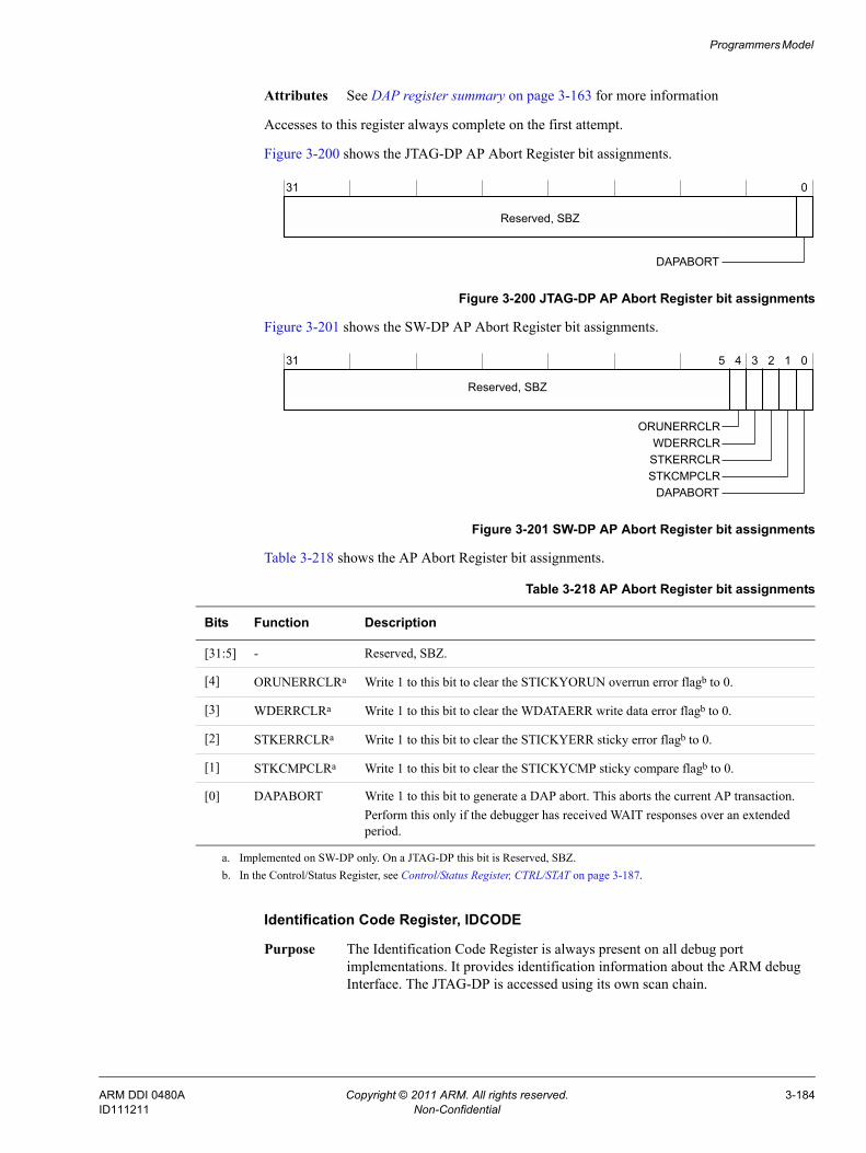
Programmers Model
Attributes See DAP register summary on page 3-163 for more information
Accesses to this register always complete on the first attempt.
Figure 3-200 shows the JTAG-DP AP Abort Register bit assignments.
Figure 3-200 JTAG-DP AP Abort Register bit assignments
Figure 3-201 shows the SW-DP AP Abort Register bit assignments.
Figure 3-201 SW-DP AP Abort Register bit assignments
Table 3-218 shows the AP Abort Register bit assignments.
Identification Code Register, IDCODE
Purpose The Identification Code Register is always present on all debug port implementations. It provides identification information about the ARM debug Interface. The JTAG-DP is accessed using its own scan chain.
31 0
Reserved, SBZ
DAPABORT
31 5 4 3 2 1 0
Reserved, SBZ
ORUNERRCLRWDERRCLR
STKERRCLRSTKCMPCLR
DAPABORT
Table 3-218 AP Abort Register bit assignments
Bits Function Description
[31:5] - Reserved, SBZ.
[4] ORUNERRCLRa Write 1 to this bit to clear the STICKYORUN overrun error flagb to 0.
[3] WDERRCLRa Write 1 to this bit to clear the WDATAERR write data error flagb to 0.
[2] STKERRCLRa Write 1 to this bit to clear the STICKYERR sticky error flagb to 0.
[1] STKCMPCLRa Write 1 to this bit to clear the STICKYCMP sticky compare flagb to 0.
[0] DAPABORT Write 1 to this bit to generate a DAP abort. This aborts the current AP transaction.Perform this only if the debugger has received WAIT responses over an extended period.
a. Implemented on SW-DP only. On a JTAG-DP this bit is Reserved, SBZ.b. In the Control/Status Register, see Control/Status Register, CTRL/STAT on page 3-187.
ARM DDI 0480A Copyright © 2011 ARM. All rights reserved. 3-184ID111211 Non-Confidential
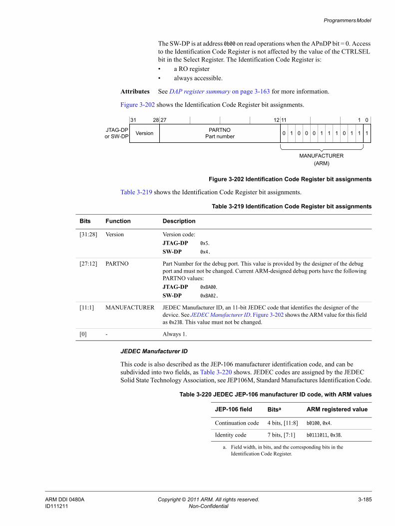
Programmers Model
The SW-DP is at address 0b00 on read operations when the APnDP bit = 0. Access to the Identification Code Register is not affected by the value of the CTRLSEL bit in the Select Register. The Identification Code Register is:• a RO register• always accessible.
Attributes See DAP register summary on page 3-163 for more information.
Figure 3-202 shows the Identification Code Register bit assignments.
Figure 3-202 Identification Code Register bit assignments
Table 3-219 shows the Identification Code Register bit assignments.
JEDEC Manufacturer ID
This code is also described as the JEP-106 manufacturer identification code, and can be subdivided into two fields, as Table 3-220 shows. JEDEC codes are assigned by the JEDEC Solid State Technology Association, see JEP106M, Standard Manufactures Identification Code.
1Version
31 28 27 12 11 1 0
PARTNOPart number 0 1 0 0 0 1 1 1 0 1 1JTAG-DP
or SW-DP
MANUFACTURER(ARM)
Table 3-219 Identification Code Register bit assignments
Bits Function Description
[31:28] Version Version code:JTAG-DP 0x5.SW-DP 0x4.
[27:12] PARTNO Part Number for the debug port. This value is provided by the designer of the debug port and must not be changed. Current ARM-designed debug ports have the following PARTNO values:JTAG-DP 0xBA00.SW-DP 0xBA02.
[11:1] MANUFACTURER JEDEC Manufacturer ID, an 11-bit JEDEC code that identifies the designer of the device. See JEDEC Manufacturer ID. Figure 3-202 shows the ARM value for this field as 0x23B. This value must not be changed.
[0] - Always 1.
Table 3-220 JEDEC JEP-106 manufacturer ID code, with ARM values
JEP-106 field Bitsa
a. Field width, in bits, and the corresponding bits in the Identification Code Register.
ARM registered value
Continuation code 4 bits, [11:8] b0100, 0x4.
Identity code 7 bits, [7:1] b0111011, 0x3B.
ARM DDI 0480A Copyright © 2011 ARM. All rights reserved. 3-185ID111211 Non-Confidential
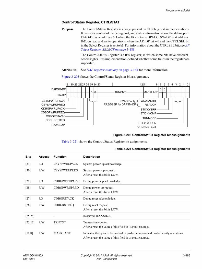
Programmers Model
Control/Status Register, CTRL/STAT
Purpose The Control/Status Register is always present on all debug port implementations. It provides control of the debug port, and status information about the debug port. JTAG-DP is at address 0x4 when the IR contains DPACC. SW-DP is at address 0b01 on read and write operations when the APnDP bit = 0 and the CTRLSEL bit in the Select Register is set to b0. For information about the CTRLSEL bit, see AP Select Register, SELECT on page 3-188.The Control/Status Register is a RW register, in which some bits have different access rights. It is implementation-defined whether some fields in the register are supported.
Attributes See DAP register summary on page 3-163 for more information.
Figure 3-203 shows the Control/Status Register bit assignments.
Figure 3-203 Control/Status Register bit assignments
Table 3-221 shows the Control/Status Register bit assignments.
0000
31 5 4 3 2 1 0
DAPSM-DP
SW-DP
WDATAERRREADOK
STICKYERR
TRNMODE
SW-DP only,RAZ/SBZP for DAPSM-DP
30 29 28 27 26 25 24 23 12 11 8 7 6
TRNCNT
CSYSPWRUPACKCSYSPWRUPREQCDBGPWRUPACKCDBGPWRUPREQ
CDBGRSTACKCDBGRSTREQ
RAZ/SBZP
MASKLANE
STICKYCMP
STICKYORUNORUNDETECT
Table 3-221 Control/Status Register bit assignments
Bits Access Function Description
[31] RO CSYSPWRUPACK System power-up acknowledge.
[30] R/W CSYSPWRUPREQ System power-up request.After a reset this bit is LOW.
[29] RO CDBGPWRUPACK Debug power-up acknowledge.
[28] R/W CDBGPWRUPREQ Debug power-up request.After a reset this bit is LOW.
[27] RO CDBGRSTACK Debug reset acknowledge.
[26] R/W CDBGRSTREQ Debug reset request.After a reset this bit is LOW.
[25:24] - - Reserved, RAZ/SBZP.
[23:12] R/W TRNCNT Transaction counter.After a reset the value of this field is UNPREDICTABLE.
[11:8] R/W MASKLANE Indicates the bytes to be masked in pushed compare and pushed verify operations.After a reset the value of this field is UNPREDICTABLE.
ARM DDI 0480A Copyright © 2011 ARM. All rights reserved. 3-186ID111211 Non-Confidential
Programmers Model
AP Select Register, SELECT
Purpose The AP Select Register is always present on all debug port implementations. Its main purpose is to select the current access port and the active 4-word register window in that access port. On a SW-DP, it also selects the debug port address bank.JTAG-DP It is at address 0x8 when the IR contains DPACC, and is a R/W
register.SW-DP It is at address 0b10 on write operations when the APnDP bit = 0, and
is a WO register. Access to the AP Select Register is not affected by the value of the CTRLSEL bit.
Attributes See DAP register summary on page 3-163 for more information.
[7] ROa WDATAERRa This bit is set to 1 if a Write Data Error occurs. It is set if:• there is a a parity or framing error on the data phase of a write• a write that has been accepted by the debug port is then discarded without being
submitted to the access port.This bit can only be cleared by writing b1 to the WDERRCLR field of the Abort Register.After a power-on reset this bit is LOW.
[6] ROa READOKa This bit is set to 1 if the response to a previous access port or RDBUFF was OK. It is cleared to 0 if the response was not OK. This flag always indicates the response to the last access port read access.After a power-on reset this bit is LOW.
[5] ROb STICKYERR This bit is set to 1 if an error is returned by an access port transaction. To clear this bit:JTAG-DP Write b1 to this bit of this register.SW-DP Write b1 to the STKERRCLR field of the Abort Register.After a power-on reset this bit is LOW.
[4] ROa STICKYCMP This bit is set to 1 when a match occurs on a pushed compare or a pushed verify operation. To clear this bit:JTAG-DP Write b1 to this bit of this register.SW-DP Write b1 to the STKCMPCLR field of the Abort Register.After a power-on reset this bit is LOW.
[3:2] R/W TRNMODE This field sets the transfer mode for access port operations.After a power-on reset the value of this field is UNPREDICTABLE.
[1] ROa STICKYORUN If overrun detection is enabled, this bit is set to 1 when an overrun occurs. To clear this bit:JTAG-DP Write b1 to this bit of this register.SW-DP Write b1 to the ORUNERRCLR field of the Abort Register.After a power-on reset this bit is LOW. See bit [0] of this register.
[0] R/W ORUNDETECT This bit is set to b1 to enable overrun detection.After a reset this bit is LOW.
a. Implemented on SW-DP only. On a JTAG-DP this bit is Reserved, RAZ/SBZP.b. RO on SW-DP. On a JTAG-DP, this bit can be read normally, and writing b1 to this bit clears the bit to b0.
Table 3-221 Control/Status Register bit assignments (continued)
Bits Access Function Description
ARM DDI 0480A Copyright © 2011 ARM. All rights reserved. 3-187ID111211 Non-Confidential
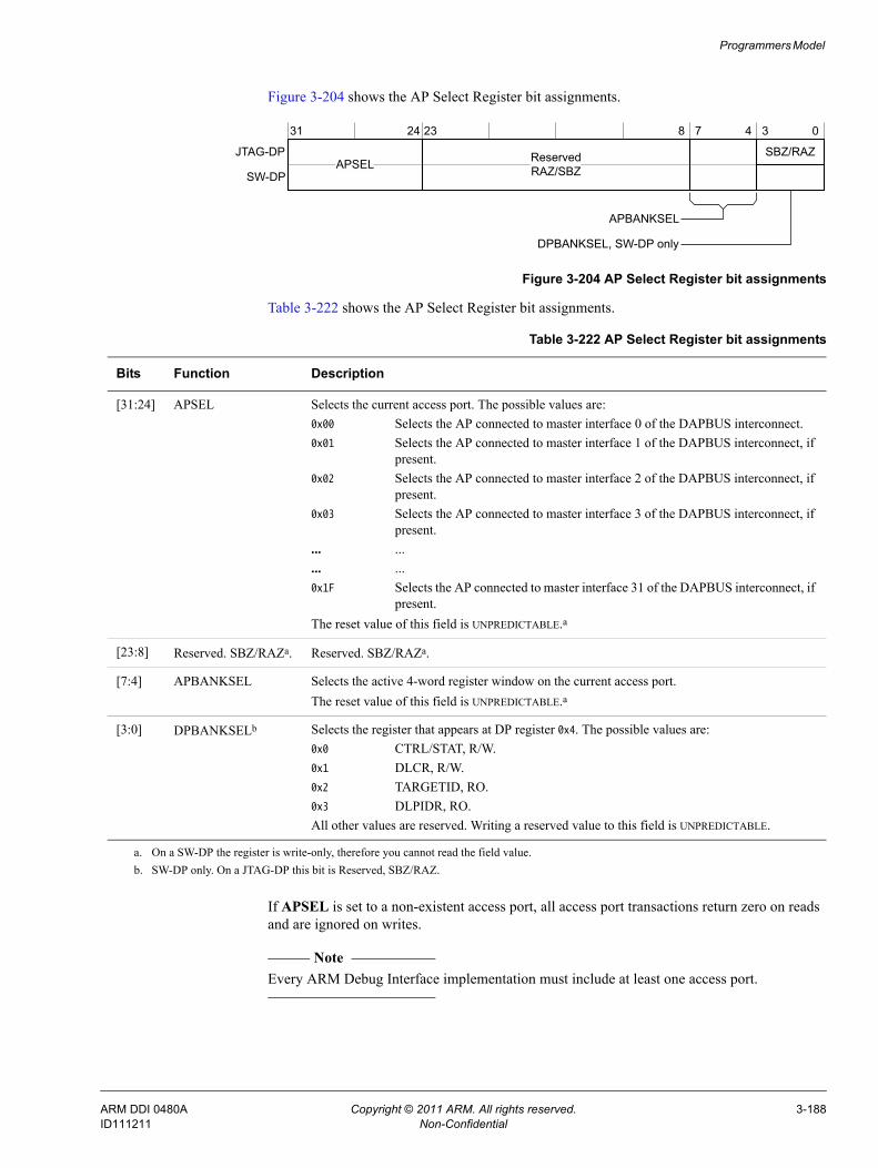
Programmers Model
Figure 3-204 shows the AP Select Register bit assignments.
Figure 3-204 AP Select Register bit assignments
Table 3-222 shows the AP Select Register bit assignments.
If APSEL is set to a non-existent access port, all access port transactions return zero on reads and are ignored on writes.
Note Every ARM Debug Interface implementation must include at least one access port.
SBZ/RAZAPSEL
31 4 3 0
JTAG-DP
SW-DP
APBANKSEL
DPBANKSEL, SW-DP only
24 23 8 7
ReservedRAZ/SBZ
Table 3-222 AP Select Register bit assignments
Bits Function Description
[31:24] APSEL Selects the current access port. The possible values are:0x00 Selects the AP connected to master interface 0 of the DAPBUS interconnect.0x01 Selects the AP connected to master interface 1 of the DAPBUS interconnect, if
present.0x02 Selects the AP connected to master interface 2 of the DAPBUS interconnect, if
present.0x03 Selects the AP connected to master interface 3 of the DAPBUS interconnect, if
present.... ...... ...0x1F Selects the AP connected to master interface 31 of the DAPBUS interconnect, if
present.The reset value of this field is UNPREDICTABLE.a
[23:8] Reserved. SBZ/RAZa. Reserved. SBZ/RAZa.
[7:4] APBANKSEL Selects the active 4-word register window on the current access port.The reset value of this field is UNPREDICTABLE.a
[3:0] DPBANKSELb Selects the register that appears at DP register 0x4. The possible values are:0x0 CTRL/STAT, R/W.0x1 DLCR, R/W.0x2 TARGETID, RO.0x3 DLPIDR, RO.All other values are reserved. Writing a reserved value to this field is UNPREDICTABLE.
a. On a SW-DP the register is write-only, therefore you cannot read the field value.b. SW-DP only. On a JTAG-DP this bit is Reserved, SBZ/RAZ.
ARM DDI 0480A Copyright © 2011 ARM. All rights reserved. 3-188ID111211 Non-Confidential
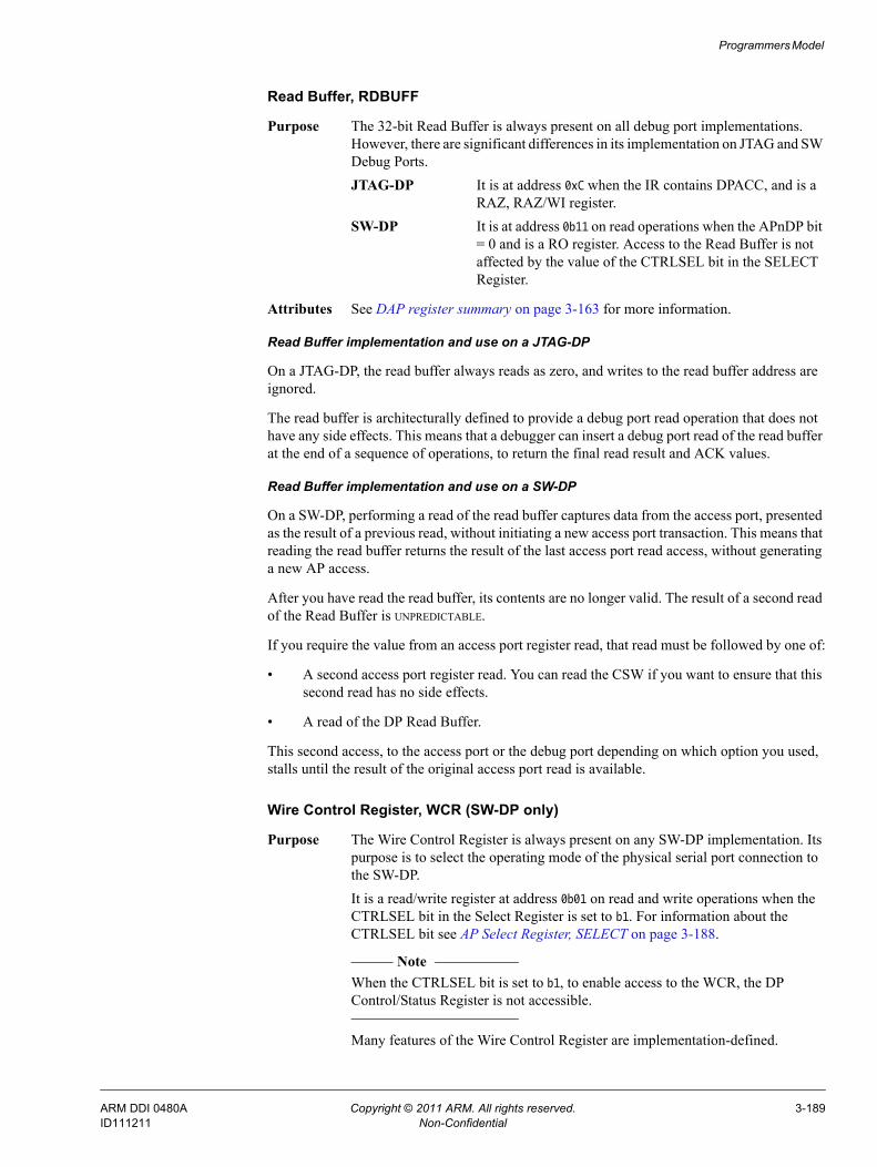
Programmers Model
Read Buffer, RDBUFF
Purpose The 32-bit Read Buffer is always present on all debug port implementations. However, there are significant differences in its implementation on JTAG and SW Debug Ports.JTAG-DP It is at address 0xC when the IR contains DPACC, and is a
RAZ, RAZ/WI register.SW-DP It is at address 0b11 on read operations when the APnDP bit
= 0 and is a RO register. Access to the Read Buffer is not affected by the value of the CTRLSEL bit in the SELECT Register.
Attributes See DAP register summary on page 3-163 for more information.
Read Buffer implementation and use on a JTAG-DP
On a JTAG-DP, the read buffer always reads as zero, and writes to the read buffer address are ignored.
The read buffer is architecturally defined to provide a debug port read operation that does not have any side effects. This means that a debugger can insert a debug port read of the read buffer at the end of a sequence of operations, to return the final read result and ACK values.
Read Buffer implementation and use on a SW-DP
On a SW-DP, performing a read of the read buffer captures data from the access port, presented as the result of a previous read, without initiating a new access port transaction. This means that reading the read buffer returns the result of the last access port read access, without generating a new AP access.
After you have read the read buffer, its contents are no longer valid. The result of a second read of the Read Buffer is UNPREDICTABLE.
If you require the value from an access port register read, that read must be followed by one of:
• A second access port register read. You can read the CSW if you want to ensure that this second read has no side effects.
• A read of the DP Read Buffer.
This second access, to the access port or the debug port depending on which option you used, stalls until the result of the original access port read is available.
Wire Control Register, WCR (SW-DP only)
Purpose The Wire Control Register is always present on any SW-DP implementation. Its purpose is to select the operating mode of the physical serial port connection to the SW-DP.It is a read/write register at address 0b01 on read and write operations when the CTRLSEL bit in the Select Register is set to b1. For information about the CTRLSEL bit see AP Select Register, SELECT on page 3-188.
Note When the CTRLSEL bit is set to b1, to enable access to the WCR, the DP
Control/Status Register is not accessible.
Many features of the Wire Control Register are implementation-defined.
ARM DDI 0480A Copyright © 2011 ARM. All rights reserved. 3-189ID111211 Non-Confidential
Programmers Model
Attributes See DAP register summary on page 3-163 for more information.
Figure 3-205 shows the Wire Control Register bit assignments.
Figure 3-205 Wire Control Register bit assignments
Table 3-223 shows the Wire Control Register bit assignments.
Turnaround tristate period, TURNROUND, bits [9:8]
This field defines the turnaround tristate period. This turnaround period permits pad delays when using a high sample clock frequency. Table 3-224 shows the permitted values of this field, and their meanings.
SBZ/RAZSBZ/RAZ
31 0
SW-DPonly
10 9 8 7 6 5 3 2
TURNROUND
WIREMODEPRESCALER
Implementation-defined, see text
Table 3-223 Wire Control Register bit assignments
Bits Function Description
[31:10] - Reserved, SBZ/RAZ.
[9:8] TURNROUND Turnaround tristate period, see Turnaround tristate period, TURNROUND, bits [9:8].After a reset this field is b00.
[7:6] WIREMODE Identifies the operating mode for the wire connection to the debug port, see Wire operating mode, WIREMODE, bits [7:6] on page 3-192.After a reset this field is b01.
[5:3] - Reserved, SBZ/RAZ.
[2:0] PRESCALER Reserved, SBZ/RAZ.
Table 3-224 Turnaround tristate period field bit definitions
TURNROUNDa
a. Bits [9:8] of the WCR Register.
Turnaround tristate period
b00 1 sample period
b01 2 sample periods
b10 3 sample periods
b11 4 sample periods
ARM DDI 0480A Copyright © 2011 ARM. All rights reserved. 3-190ID111211 Non-Confidential
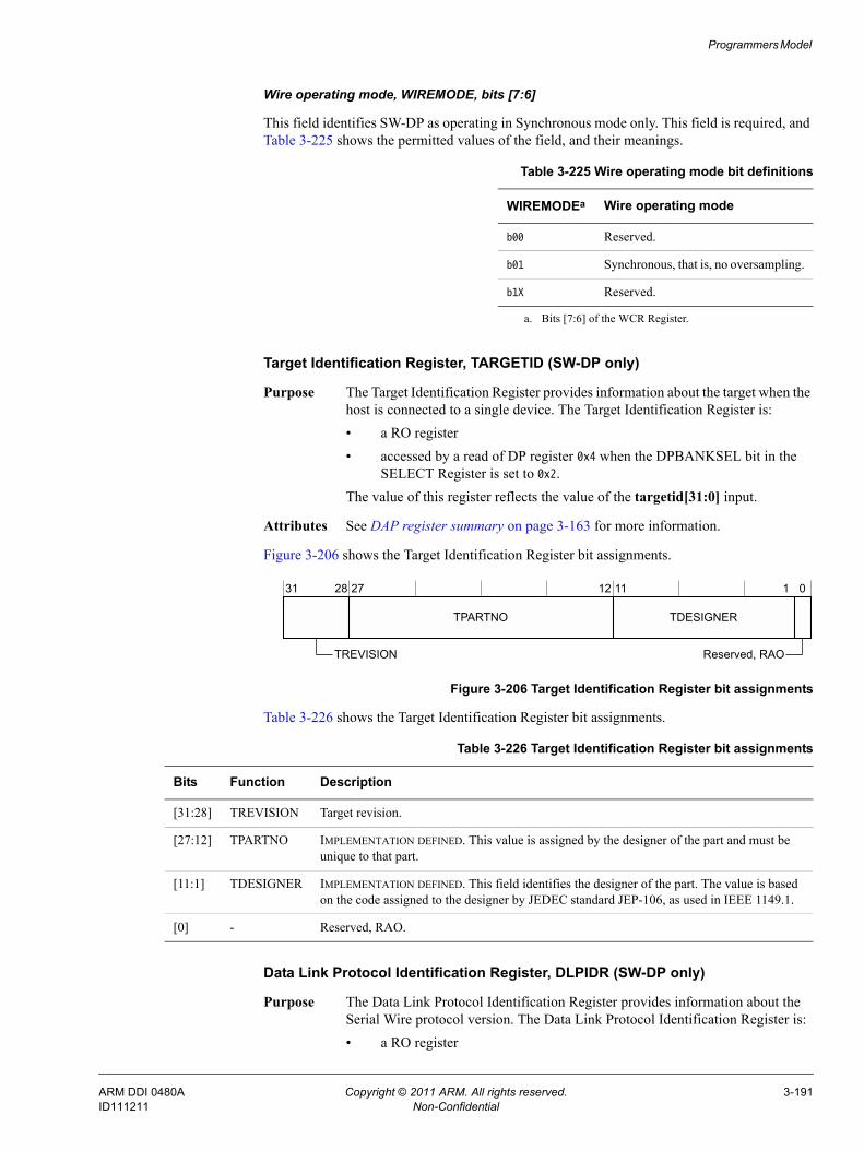
Programmers Model
Wire operating mode, WIREMODE, bits [7:6]
This field identifies SW-DP as operating in Synchronous mode only. This field is required, and Table 3-225 shows the permitted values of the field, and their meanings.
Target Identification Register, TARGETID (SW-DP only)
Purpose The Target Identification Register provides information about the target when the host is connected to a single device. The Target Identification Register is:• a RO register• accessed by a read of DP register 0x4 when the DPBANKSEL bit in the
SELECT Register is set to 0x2.The value of this register reflects the value of the targetid[31:0] input.
Attributes See DAP register summary on page 3-163 for more information.
Figure 3-206 shows the Target Identification Register bit assignments.
Figure 3-206 Target Identification Register bit assignments
Table 3-226 shows the Target Identification Register bit assignments.
Data Link Protocol Identification Register, DLPIDR (SW-DP only)
Purpose The Data Link Protocol Identification Register provides information about the Serial Wire protocol version. The Data Link Protocol Identification Register is:• a RO register
Table 3-225 Wire operating mode bit definitions
WIREMODEa
a. Bits [7:6] of the WCR Register.
Wire operating mode
b00 Reserved.
b01 Synchronous, that is, no oversampling.
b1X Reserved.
31 28 27 12 11 1 0
TPARTNO TDESIGNER
TREVISION Reserved, RAO
Table 3-226 Target Identification Register bit assignments
Bits Function Description
[31:28] TREVISION Target revision.
[27:12] TPARTNO IMPLEMENTATION DEFINED. This value is assigned by the designer of the part and must be unique to that part.
[11:1] TDESIGNER IMPLEMENTATION DEFINED. This field identifies the designer of the part. The value is based on the code assigned to the designer by JEDEC standard JEP-106, as used in IEEE 1149.1.
[0] - Reserved, RAO.
ARM DDI 0480A Copyright © 2011 ARM. All rights reserved. 3-191ID111211 Non-Confidential
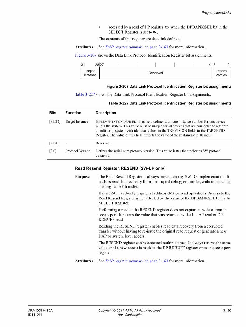
Programmers Model
• accessed by a read of DP register 0x4 when the DPBANKSEL bit in the SELECT Register is set to 0x3.
The contents of this register are data link defined.
Attributes See DAP register summary on page 3-163 for more information.
Figure 3-207 shows the Data Link Protocol Identification Register bit assignments.
Figure 3-207 Data Link Protocol Identification Register bit assignments
Table 3-227 shows the Data Link Protocol Identification Register bit assignments.
Read Resend Register, RESEND (SW-DP only)
Purpose The Read Resend Register is always present on any SW-DP implementation. It enables read data recovery from a corrupted debugger transfer, without repeating the original AP transfer.It is a 32-bit read-only register at address 0b10 on read operations. Access to the Read Resend Register is not affected by the value of the DPBANKSEL bit in the SELECT Register.Performing a read to the RESEND register does not capture new data from the access port. It returns the value that was returned by the last AP read or DP RDBUFF read.Reading the RESEND register enables read data recovery from a corrupted transfer without having to re-issue the original read request or generate a new DAP or system level access.The RESEND register can be accessed multiple times. It always returns the same value until a new access is made to the DP RDBUFF register or to an access port register.
Attributes See DAP register summary on page 3-163 for more information.
Protocol Version
Target Instance
31 28 27 4 3 0
Reserved
Table 3-227 Data Link Protocol Identification Register bit assignments
Bits Function Description
[31:28] Target Instance IMPLEMENTATION DEFINED. This field defines a unique instance number for this device within the system. This value must be unique for all devices that are connected together in a multi-drop system with identical values in the TREVISION fields in the TARGETID Register. The value of this field reflects the value of the instanceid[3:0] input.
[27:4] - Reserved.
[3:0] Protocol Version Defines the serial wire protocol version. This value is 0x1 that indicates SW protocol version 2.
ARM DDI 0480A Copyright © 2011 ARM. All rights reserved. 3-192ID111211 Non-Confidential
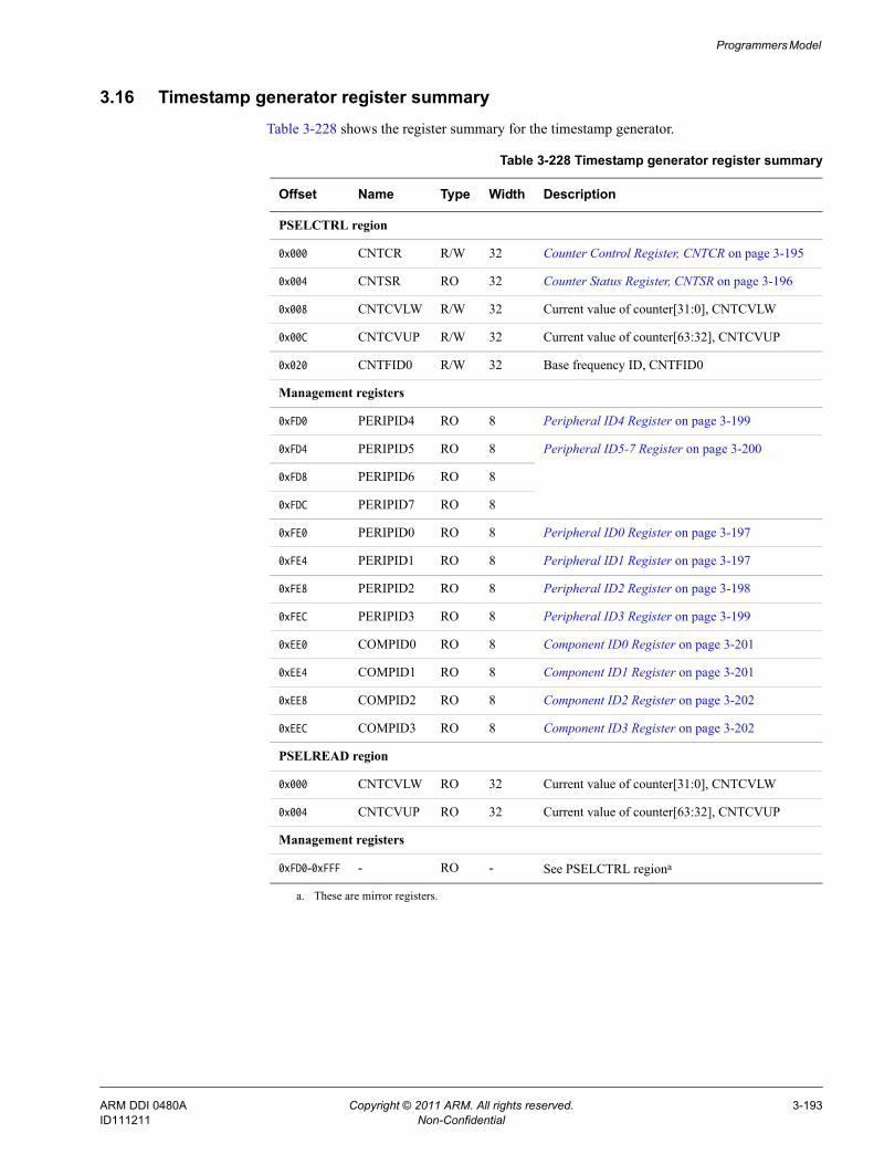
Programmers Model
3.16 Timestamp generator register summaryTable 3-228 shows the register summary for the timestamp generator.
Table 3-228 Timestamp generator register summary
Offset Name Type Width Description
PSELCTRL region
0x000 CNTCR R/W 32 Counter Control Register, CNTCR on page 3-195
0x004 CNTSR RO 32 Counter Status Register, CNTSR on page 3-196
0x008 CNTCVLW R/W 32 Current value of counter[31:0], CNTCVLW
0x00C CNTCVUP R/W 32 Current value of counter[63:32], CNTCVUP
0x020 CNTFID0 R/W 32 Base frequency ID, CNTFID0
Management registers
0xFD0 PERIPID4 RO 8 Peripheral ID4 Register on page 3-199
0xFD4 PERIPID5 RO 8 Peripheral ID5-7 Register on page 3-200
0xFD8 PERIPID6 RO 8
0xFDC PERIPID7 RO 8
0xFE0 PERIPID0 RO 8 Peripheral ID0 Register on page 3-197
0xFE4 PERIPID1 RO 8 Peripheral ID1 Register on page 3-197
0xFE8 PERIPID2 RO 8 Peripheral ID2 Register on page 3-198
0xFEC PERIPID3 RO 8 Peripheral ID3 Register on page 3-199
0xEE0 COMPID0 RO 8 Component ID0 Register on page 3-201
0xEE4 COMPID1 RO 8 Component ID1 Register on page 3-201
0xEE8 COMPID2 RO 8 Component ID2 Register on page 3-202
0xEEC COMPID3 RO 8 Component ID3 Register on page 3-202
PSELREAD region
0x000 CNTCVLW RO 32 Current value of counter[31:0], CNTCVLW
0x004 CNTCVUP RO 32 Current value of counter[63:32], CNTCVUP
Management registers
0xFD0-0xFFF - RO - See PSELCTRL regiona
a. These are mirror registers.
ARM DDI 0480A Copyright © 2011 ARM. All rights reserved. 3-193ID111211 Non-Confidential
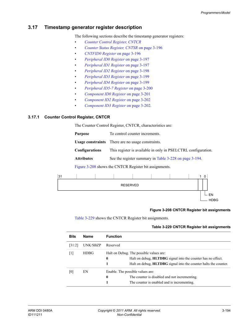
Programmers Model
3.17 Timestamp generator register descriptionThe following sections describe the timestamp generator registers:• Counter Control Register, CNTCR• Counter Status Register, CNTSR on page 3-196• CNTFID0 Register on page 3-196• Peripheral ID0 Register on page 3-197• Peripheral ID1 Register on page 3-197• Peripheral ID2 Register on page 3-198• Peripheral ID3 Register on page 3-199• Peripheral ID4 Register on page 3-199• Peripheral ID5-7 Register on page 3-200• Component ID0 Register on page 3-201• Component ID2 Register on page 3-202• Component ID3 Register on page 3-202.
3.17.1 Counter Control Register, CNTCR
The Counter Control Register, CNTCR, characteristics are:
Purpose To control counter increments.
Usage constraints There are no usage constraints.
Configurations This register is available in only in PSELCTRL configuration.
Attributes See the register summary in Table 3-228 on page 3-194.
Figure 3-208 shows the CNTCR Register bit assignments.
Figure 3-208 CNTCR Register bit assignments
Table 3-229 shows the CNTCR Register bit assignments.
HDBG
31 1 0
RESERVED
EN
Table 3-229 CNTCR Register bit assignments
Bits Name Function
[31:2] UNK/SBZP Reserved
[1] HDBG Halt on Debug. The possible values are:0 Halt on debug, HLTDBG signal into the counter has no effect.1 Halt on debug, HLTDBG signal into the counter halts the counter.
[0] EN Enable. The possible values are:0 The counter is disabled and not incrementing. 1 The counter is enabled and is incrementing.
ARM DDI 0480A Copyright © 2011 ARM. All rights reserved. 3-194ID111211 Non-Confidential
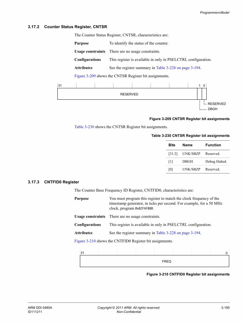
Programmers Model
3.17.2 Counter Status Register, CNTSR
The Counter Status Register, CNTSR, characteristics are:
Purpose To identify the status of the counter.
Usage constraints There are no usage constraints.
Configurations This register is available in only in PSELCTRL configuration.
Attributes See the register summary in Table 3-228 on page 3-194.
Figure 3-209 shows the CNTSR Register bit assignments.
Figure 3-209 CNTSR Register bit assignments
Table 3-230 shows the CNTSR Register bit assignments.
3.17.3 CNTFID0 Register
The Counter Base Frequency ID Register, CNTFID0, characteristics are:
Purpose You must program this register to match the clock frequency of the timestamp generator, in ticks per second. For example, for a 50 MHz clock, program 0x02FAF080.
Usage constraints There are no usage constraints.
Configurations This register is available in only in PSELCTRL configuration.
Attributes See the register summary in Table 3-228 on page 3-194.
Figure 3-210 shows the CNTFID0 Register bit assignments.
Figure 3-210 CNTFID0 Register bit assignments
DBGH
31 1 0
RESERVED
RESERVED
Table 3-230 CNTSR Register bit assignments
Bits Name Function
[31:2] UNK/SBZP Reserved.
[1] DBGH Debug Halted.
[0] UNK/SBZP Reserved.
31 0
FREQ
ARM DDI 0480A Copyright © 2011 ARM. All rights reserved. 3-195ID111211 Non-Confidential
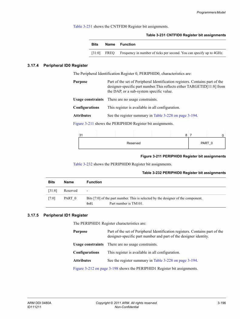
Programmers Model
Table 3-231 shows the CNTFID0 Register bit assignments.
3.17.4 Peripheral ID0 Register
The Peripheral Identification Register 0, PERIPHID0, characteristics are:
Purpose Part of the set of Peripheral Identification registers. Contains part of the designer-specific part number.This reflects either TARGETID[11:8] from the DAP, or a sub-system specific value.
Usage constraints There are no usage constraints.
Configurations This register is available in all configuration.
Attributes See the register summary in Table 3-228 on page 3-194.
Figure 3-211 shows the PERIPHID0 Register bit assignments.
Figure 3-211 PERIPHID0 Register bit assignments
Table 3-232 shows the PERIPHID0 Register bit assignments.
3.17.5 Peripheral ID1 Register
The PERIPHID1 Register characteristics are:
Purpose Part of the set of Peripheral Identification registers. Contains part of the designer-specific part number and part of the designer identity.
Usage constraints There are no usage constraints.
Configurations This register is available in all configuration.
Attributes See the register summary in Table 3-228 on page 3-194.
Figure 3-212 on page 3-198 shows the PERIPHID1 Register bit assignments.
Table 3-231 CNTFID0 Register bit assignments
Bits Name Function
[31:0] FREQ Frequency in number of ticks per second. You can specify up to 4GHz.
31 0
Reserved
78
PART_0
Table 3-232 PERIPHID0 Register bit assignments
Bits Name Function
[31:8] Reserved -
[7:0] PART_0 Bits [7:0] of the part number. This is selected by the designer of the component.0x01 Part number is TM101.
ARM DDI 0480A Copyright © 2011 ARM. All rights reserved. 3-196ID111211 Non-Confidential
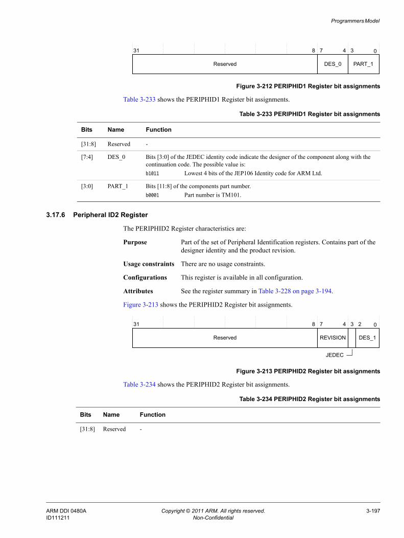
Programmers Model
Figure 3-212 PERIPHID1 Register bit assignments
Table 3-233 shows the PERIPHID1 Register bit assignments.
3.17.6 Peripheral ID2 Register
The PERIPHID2 Register characteristics are:
Purpose Part of the set of Peripheral Identification registers. Contains part of the designer identity and the product revision.
Usage constraints There are no usage constraints.
Configurations This register is available in all configuration.
Attributes See the register summary in Table 3-228 on page 3-194.
Figure 3-213 shows the PERIPHID2 Register bit assignments.
Figure 3-213 PERIPHID2 Register bit assignments
Table 3-234 shows the PERIPHID2 Register bit assignments.
31 0
Reserved
78
PART_1
4 3
DES_0
Table 3-233 PERIPHID1 Register bit assignments
Bits Name Function
[31:8] Reserved -
[7:4] DES_0 Bits [3:0] of the JEDEC identity code indicate the designer of the component along with the continuation code. The possible value is:b1011 Lowest 4 bits of the JEP106 Identity code for ARM Ltd.
[3:0] PART_1 Bits [11:8] of the components part number.b0001 Part number is TM101.
31 0
Reserved
7
REVISION
8 4
DES_1
3 2
JEDEC
Table 3-234 PERIPHID2 Register bit assignments
Bits Name Function
[31:8] Reserved -
ARM DDI 0480A Copyright © 2011 ARM. All rights reserved. 3-197ID111211 Non-Confidential
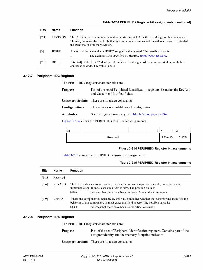
Programmers Model
3.17.7 Peripheral ID3 Register
The PERIPHID3 Register characteristics are:
Purpose Part of the set of Peripheral Identification registers. Contains the RevAnd and Customer Modified fields.
Usage constraints There are no usage constraints.
Configurations This register is available in all configuration.
Attributes See the register summary in Table 3-228 on page 3-194.
Figure 3-214 shows the PERIPHID3 Register bit assignments.
Figure 3-214 PERIPHID3 Register bit assignments
Table 3-235 shows the PERIPHID3 Register bit assignments.
3.17.8 Peripheral ID4 Register
The PERIPHID4 Register characteristics are:
Purpose Part of the set of Peripheral Identification registers. Contains part of the designer identity and the memory footprint indicator.
Usage constraints There are no usage constraints.
[7:4] REVISION The Revision field is an incremental value starting at 0x0 for the first design of this component. This only increases by one for both major and minor revisions and is used as a look-up to establish the exact major or minor revision.
[3] JEDEC Always set. Indicates that a JEDEC assigned value is used. The possible value is:1 The designer ID is specified by JEDEC, http://www.jedec.org.
[2:0] DES_1 Bits [6:4] of the JEDEC identity code indicate the designer of the component along with the continuation code. The value is b011.
Table 3-234 PERIPHID2 Register bit assignments (continued)
Bits Name Function
31 0
Reserved
7
REVAND
8 4
CMOD
3
Table 3-235 PERIPHID3 Register bit assignments
Bits Name Function
[31:8] Reserved -
[7:4] REVAND This field indicates minor errata fixes specific to this design, for example, metal fixes after implementation. In most cases this field is zero. The possible value is:b0000 Indicates that there have been no metal fixes to this component.
[3:0] CMOD Where the component is reusable IP, this value indicates whether the customer has modified the behavior of the component. In most cases this field is zero. The possible value is:b0000 Indicates that there have been no modifications made.
ARM DDI 0480A Copyright © 2011 ARM. All rights reserved. 3-198ID111211 Non-Confidential
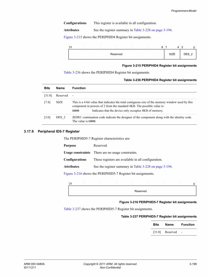
Programmers Model
Configurations This register is available in all configuration.
Attributes See the register summary in Table 3-228 on page 3-194.
Figure 3-215 shows the PERIPHID4 Register bit assignments.
Figure 3-215 PERIPHID4 Register bit assignments
Table 3-236 shows the PERIPHID4 Register bit assignments.
3.17.9 Peripheral ID5-7 Register
The PERIPHID5-7 Register characteristics are:
Purpose Reserved.
Usage constraints There are no usage constraints.
Configurations These registers are available in all configuration.
Attributes See the register summary in Table 3-228 on page 3-194.
Figure 3-216 shows the PERIPHID5-7 Register bit assignments.
Figure 3-216 PERIPHID5-7 Register bit assignments
Table 3-237 shows the PERIPHID5-7 Register bit assignments.
31 0
Reserved
7
SIZE
8 4
DES_2
3
Table 3-236 PERIPHID4 Register bit assignments
Bits Name Function
[31:8] Reserved -
[7:4] SIZE This is a 4-bit value that indicates the total contiguous size of the memory window used by this component in powers of 2 from the standard 4KB. The possible value is:b0000 Indicates that the device only occupies 4KB of memory.
[3:0] DES_2 JEDEC continuation code indicate the designer of the component along with the identity code. The value is b0000.
31 0
Reserved
Table 3-237 PERIPHID5-7 Register bit assignments
Bits Name Function
[31:0] Reserved -
ARM DDI 0480A Copyright © 2011 ARM. All rights reserved. 3-199ID111211 Non-Confidential
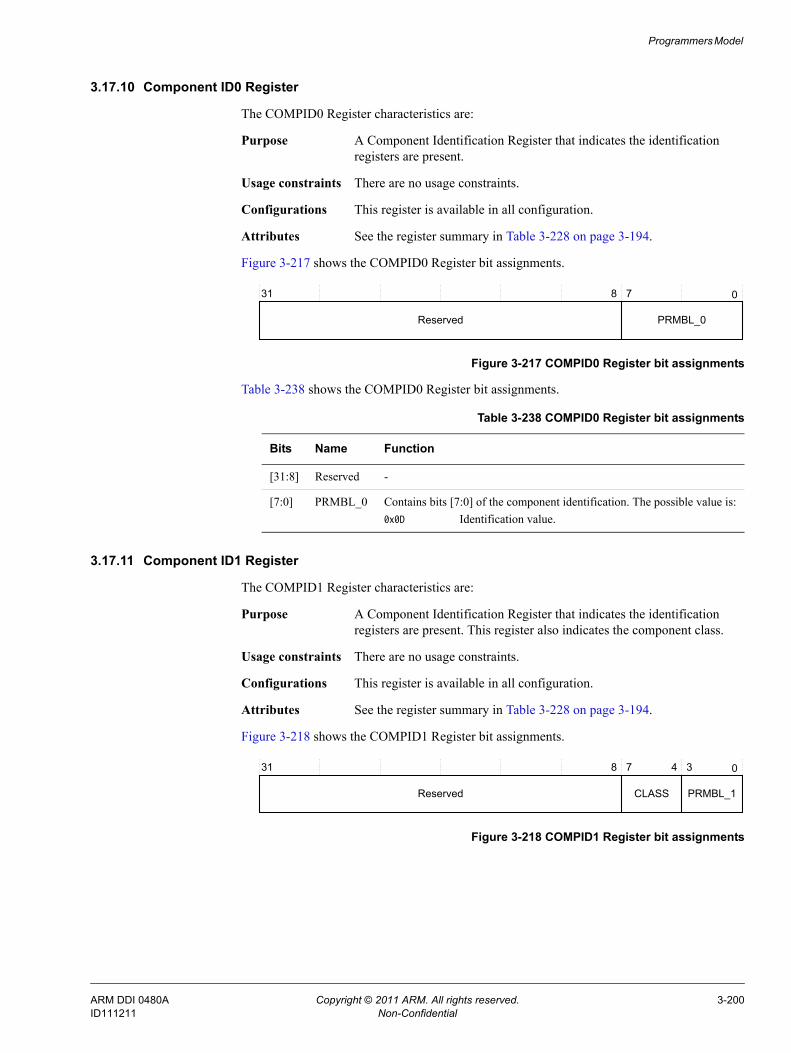
Programmers Model
3.17.10 Component ID0 Register
The COMPID0 Register characteristics are:
Purpose A Component Identification Register that indicates the identification registers are present.
Usage constraints There are no usage constraints.
Configurations This register is available in all configuration.
Attributes See the register summary in Table 3-228 on page 3-194.
Figure 3-217 shows the COMPID0 Register bit assignments.
Figure 3-217 COMPID0 Register bit assignments
Table 3-238 shows the COMPID0 Register bit assignments.
3.17.11 Component ID1 Register
The COMPID1 Register characteristics are:
Purpose A Component Identification Register that indicates the identification registers are present. This register also indicates the component class.
Usage constraints There are no usage constraints.
Configurations This register is available in all configuration.
Attributes See the register summary in Table 3-228 on page 3-194.
Figure 3-218 shows the COMPID1 Register bit assignments.
Figure 3-218 COMPID1 Register bit assignments
31 0
Reserved
78
PRMBL_0
Table 3-238 COMPID0 Register bit assignments
Bits Name Function
[31:8] Reserved -
[7:0] PRMBL_0 Contains bits [7:0] of the component identification. The possible value is:0x0D Identification value.
31 0
Reserved
78
PRMBL_1
4 3
CLASS
ARM DDI 0480A Copyright © 2011 ARM. All rights reserved. 3-200ID111211 Non-Confidential
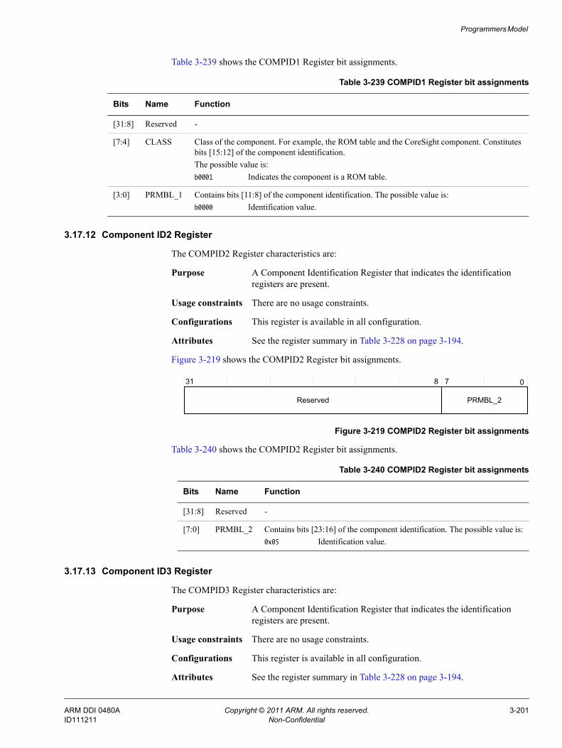
Programmers Model
Table 3-239 shows the COMPID1 Register bit assignments.
3.17.12 Component ID2 Register
The COMPID2 Register characteristics are:
Purpose A Component Identification Register that indicates the identification registers are present.
Usage constraints There are no usage constraints.
Configurations This register is available in all configuration.
Attributes See the register summary in Table 3-228 on page 3-194.
Figure 3-219 shows the COMPID2 Register bit assignments.
Figure 3-219 COMPID2 Register bit assignments
Table 3-240 shows the COMPID2 Register bit assignments.
3.17.13 Component ID3 Register
The COMPID3 Register characteristics are:
Purpose A Component Identification Register that indicates the identification registers are present.
Usage constraints There are no usage constraints.
Configurations This register is available in all configuration.
Attributes See the register summary in Table 3-228 on page 3-194.
Table 3-239 COMPID1 Register bit assignments
Bits Name Function
[31:8] Reserved -
[7:4] CLASS Class of the component. For example, the ROM table and the CoreSight component. Constitutes bits [15:12] of the component identification.The possible value is:b0001 Indicates the component is a ROM table.
[3:0] PRMBL_1 Contains bits [11:8] of the component identification. The possible value is:b0000 Identification value.
31 0
Reserved
78
PRMBL_2
Table 3-240 COMPID2 Register bit assignments
Bits Name Function
[31:8] Reserved -
[7:0] PRMBL_2 Contains bits [23:16] of the component identification. The possible value is:0x05 Identification value.
ARM DDI 0480A Copyright © 2011 ARM. All rights reserved. 3-201ID111211 Non-Confidential
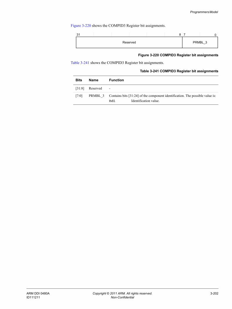
Programmers Model
Figure 3-220 shows the COMPID3 Register bit assignments.
Figure 3-220 COMPID3 Register bit assignments
Table 3-241 shows the COMPID3 Register bit assignments.
31 0
Reserved
78
PRMBL_3
Table 3-241 COMPID3 Register bit assignments
Bits Name Function
[31:8] Reserved -
[7:0] PRMBL_3 Contains bits [31:24] of the component identification. The possible value is:0xB1 Identification value.
ARM DDI 0480A Copyright © 2011 ARM. All rights reserved. 3-202ID111211 Non-Confidential
Chapter 4 Debug Access Port
This chapter describes the DAP. It contains the following sections:• About the Debug Access Port on page 4-2• SWJ-DP on page 4-7• JTAG-DP on page 4-10• SW-DP on page 4-11• Common debug port features and registers on page 4-16• Access ports on page 4-18• AHB-AP on page 4-19• AXI-AP on page 4-23• APB-AP on page 4-29• JTAG-AP on page 4-31• Auxiliary Access Port on page 4-33• Authentication requirements for Debug Access Port on page 4-34• Clocks, power, and resets on page 4-35.
ARM DDI 0480A Copyright © 2011 ARM. All rights reserved. 4-1ID111211 Non-Confidential
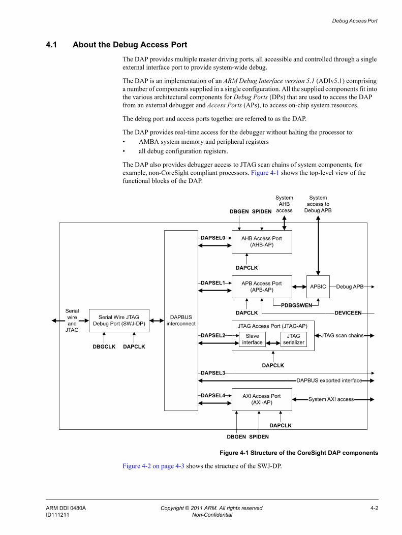
Debug Access Port
4.1 About the Debug Access PortThe DAP provides multiple master driving ports, all accessible and controlled through a single external interface port to provide system-wide debug.
The DAP is an implementation of an ARM Debug Interface version 5.1 (ADIv5.1) comprising a number of components supplied in a single configuration. All the supplied components fit into the various architectural components for Debug Ports (DPs) that are used to access the DAP from an external debugger and Access Ports (APs), to access on-chip system resources.
The debug port and access ports together are referred to as the DAP.
The DAP provides real-time access for the debugger without halting the processor to:• AMBA system memory and peripheral registers• all debug configuration registers.
The DAP also provides debugger access to JTAG scan chains of system components, for example, non-CoreSight compliant processors. Figure 4-1 shows the top-level view of the functional blocks of the DAP.
Figure 4-1 Structure of the CoreSight DAP components
Figure 4-2 on page 4-3 shows the structure of the SWJ-DP.
Serial Wire JTAG Debug Port (SWJ-DP)
DAPBUS interconnect
AHB Access Port(AHB-AP)
APB Access Port(APB-AP)
AXI Access Port(AXI-AP)
DAPSEL0
DAPSEL1
DBGEN SPIDEN
DAPCLK
SystemAHB
access
JTAG Access Port (JTAG-AP)
Slave interface
JTAG serializer
APBIC
Systemaccess to
Debug APB
Debug APB
PDBGSWENDEVICEENDAPCLK
DAPSEL2 JTAG scan chains
DAPSEL4System AXI access
DAPBUS exported interfaceDAPSEL3
DBGCLK DAPCLK
Serial wire and
JTAG
DAPCLK
DBGEN SPIDEN
DAPCLK
ARM DDI 0480A Copyright © 2011 ARM. All rights reserved. 4-2ID111211 Non-Confidential
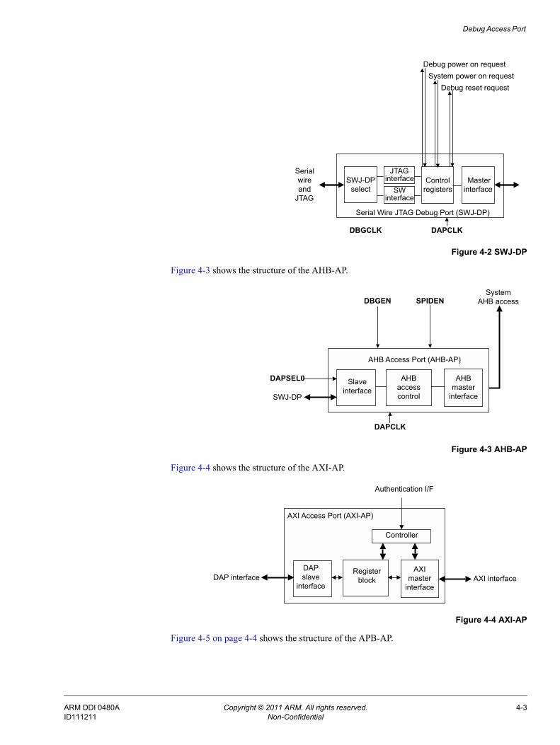
Debug Access Port
Figure 4-2 SWJ-DP
Figure 4-3 shows the structure of the AHB-AP.
Figure 4-3 AHB-AP
Figure 4-4 shows the structure of the AXI-AP.
Figure 4-4 AXI-AP
Figure 4-5 on page 4-4 shows the structure of the APB-AP.
Controlregisters
Masterinterface
Debug power on requestSystem power on request
Debug reset request
Serial Wire JTAG Debug Port (SWJ-DP)
JTAGinterface
DAPCLKDBGCLK
SWinterface
Serial wire and
JTAG
SWJ-DP select
DBGEN SPIDEN
AHB Access Port (AHB-AP)
AHB master
interface
AHBaccesscontrol
DAPCLK
Slave interface
DAPSEL0
SWJ-DP
System AHB access
AXI Access Port (AXI-AP)
AXI master
interface
DAPslave
interfaceDAP interface AXI interface
Registerblock
Controller
Authentication I/F
ARM DDI 0480A Copyright © 2011 ARM. All rights reserved. 4-3ID111211 Non-Confidential
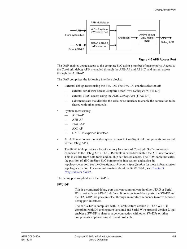
Debug Access Port
Figure 4-5 APB Access Port
The DAP enables debug access to the complete SoC using a number of master ports. Access to the CoreSight debug APB is enabled through the APB-AP and APBIC, and system access through the AHB-AP.
The DAP comprises the following interface blocks:
• External debug access using the SWJ-DP. The SWJ-DP enables selection of:— external serial wire access using the Serial Wire Debug Port (SW-DP)— external JTAG access using the JTAG Debug Port (JTAG-DP)— a dormant state that disables the serial wire interface to enable the connection to be
shared with other protocols.
• System access using:— AHB-AP— APB-AP— JTAG-AP— AXI-AP— DAPBUS exported interface.
• An APB interconnect to enable system access to CoreSight SoC components connected to the Debug APB.
• The ROM table provides a list of memory locations of CoreSight SoC components connected to the Debug APB. The ROM Table is embedded within the APB interconnect. This is visible from both tools and on-chip self hosted access. The ROM table indicates the position of all CoreSight SoC components in a system and assists in topology-detection. See the CoreSight Architecture Specification for more information on topology-detection. For more information about the ROM Table, see Chapter 3 Programmers Model.
The debug port supplied with the DAP is:
SWJ-DP This is a combined debug port that can communicate in either JTAG or Serial Wire protocols as ADIv5.1 defines. It contains two debug ports, the SW-DP and the JTAG-DP that you can select through an interface sequence to move between debug port interfaces.The JTAG-DP is compliant with DP architecture version 0. The SW-DP is compliant with DP architecture version 2 and Serial Wire protocol version 2, that enables a SW-DP to share a target connection with other SW-DPs or other components implementing different protocols.
APBv3 system, SYS slave port
APBv3 APB-AP, AP slave port
APBv3 debug(DBG master
port)Arbitration APB
APB
APB
APB-Multiplexer
From system bus
From APB-AP
Debug APB
ARM DDI 0480A Copyright © 2011 ARM. All rights reserved. 4-4ID111211 Non-Confidential
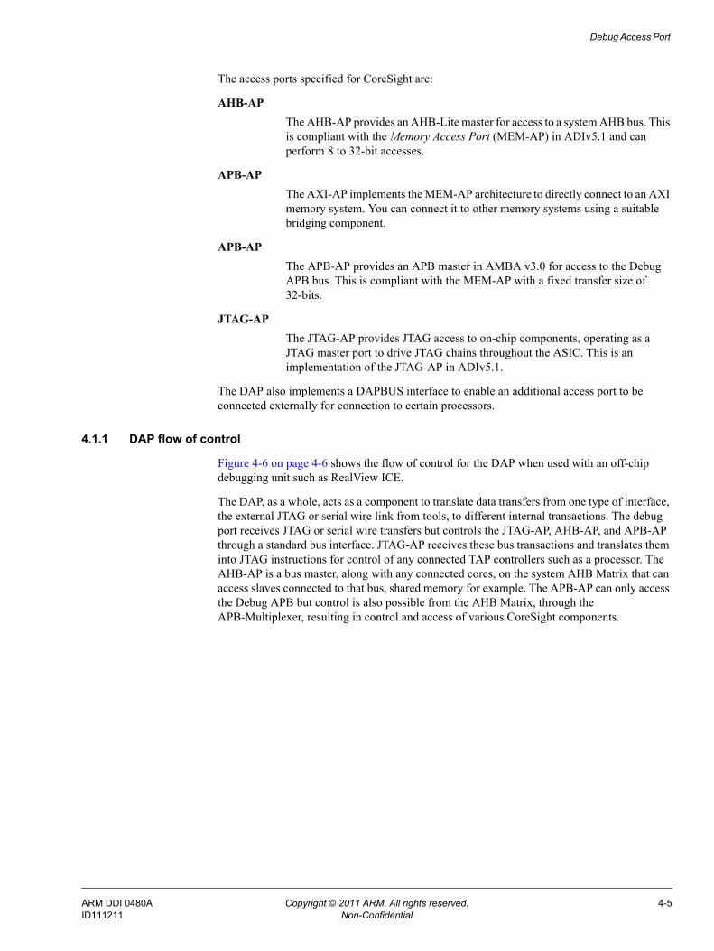
Debug Access Port
The access ports specified for CoreSight are:
AHB-AP The AHB-AP provides an AHB-Lite master for access to a system AHB bus. This is compliant with the Memory Access Port (MEM-AP) in ADIv5.1 and can perform 8 to 32-bit accesses.
APB-AP The AXI-AP implements the MEM-AP architecture to directly connect to an AXI memory system. You can connect it to other memory systems using a suitable bridging component.
APB-AP The APB-AP provides an APB master in AMBA v3.0 for access to the Debug APB bus. This is compliant with the MEM-AP with a fixed transfer size of 32-bits.
JTAG-AP The JTAG-AP provides JTAG access to on-chip components, operating as a JTAG master port to drive JTAG chains throughout the ASIC. This is an implementation of the JTAG-AP in ADIv5.1.
The DAP also implements a DAPBUS interface to enable an additional access port to be connected externally for connection to certain processors.
4.1.1 DAP flow of control
Figure 4-6 on page 4-6 shows the flow of control for the DAP when used with an off-chip debugging unit such as RealView ICE.
The DAP, as a whole, acts as a component to translate data transfers from one type of interface, the external JTAG or serial wire link from tools, to different internal transactions. The debug port receives JTAG or serial wire transfers but controls the JTAG-AP, AHB-AP, and APB-AP through a standard bus interface. JTAG-AP receives these bus transactions and translates them into JTAG instructions for control of any connected TAP controllers such as a processor. The AHB-AP is a bus master, along with any connected cores, on the system AHB Matrix that can access slaves connected to that bus, shared memory for example. The APB-AP can only access the Debug APB but control is also possible from the AHB Matrix, through the APB-Multiplexer, resulting in control and access of various CoreSight components.
ARM DDI 0480A Copyright © 2011 ARM. All rights reserved. 4-5ID111211 Non-Confidential
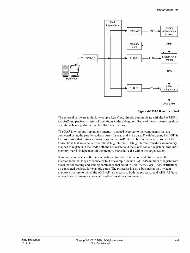
Debug Access Port
Figure 4-6 DAP flow of control
The external hardware tools, for example RealView, directly communicate with the SWJ-DP in the DAP and perform a series of operations to the debug port. Some of these accesses result in operations being performed on the DAP internal bus.
The DAP internal bus implements memory mapped accesses to the components that are connected using the parallel address buses for read and write data. The debug port, SWJ-DP, is the bus master that initiates transactions on the DAP internal bus in response to some of the transactions that are received over the debug interface. Debug interface transfers are memory mapped to registers in the DAP, both the bus master and the slaves contain registers. This DAP memory-map is independent of the memory maps that exist within the target system.
Some of the registers in the access ports can translate interactions into transfers on the interconnects that they are connected to. For example, in the JTAG-AP a number of registers are allocated for reading and writing commands that result in Test Access Port (TAP) instructions on connected devices, for example cores. The processor is also a bus master on a system memory structure to which the AHB-AP has access, so both the processor and AHB-AP have access to shared memory devices, or other bus slave components.
AHB
SWJ-DP
DAPinternal bus
Existing scan chains
in coreJTAGJTAG-AP
APB
Debug APB
APB-AP
AHBAHB-AP System AHB matrix
APB
APB-multiplexer
RealView
Memoryblock
ARM DDI 0480A Copyright © 2011 ARM. All rights reserved. 4-6ID111211 Non-Confidential
Debug Access Port
4.2 SWJ-DPThe SWJ-DP is a combined JTAG-DP and SW-DP that enables you to connect either a SWD or JTAG probe to a target. It is the standard CoreSight debug port, and enables access either to the JTAG-DP or SW-DP blocks. To make efficient use of package pins, serial wire shares, or overlays, the JTAG pins use an auto detect mechanism that switches between JTAG-DP and SW-DP depending on which probe is connected. A special sequence on the swdiotms pin is used to switch between JTAG-DP and SW-DP. When the switching sequence has been transmitted to the SWJ-DP, it behaves as a dedicated JTAG-DP or SW-DP depending on which sequence had been performed.
Note For more information about the programming capabilities and features of the SWJ-DP, see JTAG-DP on page 4-10 and SW-DP on page 4-11.
The following section describe the SWJ-DP:• Structure of the SWJ-DP• Operation of the SWJ-DP• JTAG and SWD interface on page 4-8• Clock, reset and power domain support on page 4-8• SWD and JTAG selection mechanism on page 4-8.
4.2.1 Structure of the SWJ-DP
The SWJ-DP consists of a wrapper around the JTAG-DP and SW-DP. It selects JTAG or SWD as the connection mechanism and enables either JTAG-DP or SW-DP as the interface to the DAP.
4.2.2 Operation of the SWJ-DP
SWJ-DP enables you to design an Application Specific Integrated Circuit (ASIC) that you can use in systems that require either a JTAG interface or a SWD interface. There is a trade-off between the number of pins used and compatibility with existing hardware and test equipment. There are several scenarios where you must use a JTAG debug interface. These enable:
• inclusion in an existing scan chain, usually on-chip TAPs used for test or other purposes.
• the device to be cascaded with legacy devices that use JTAG for debug
• use of existing debug hardware with the corresponding test TAPs, for example in Automatic Test Equipment (ATE).
You can connect an ASIC fitted with SWJ-DP support to legacy JTAG equipment without making any changes. If an SWD tool is available, only two pins are required, instead of the usual four pins used for JTAG. You can therefore use the other two pins for other purpose
You can only use these two pins if there is no conflict with their use in JTAG mode. To support use of SWJ-DP in a scan chain with other JTAG devices, the default state after reset must be to use these pins for their JTAG function. If the direction of the alternative function is compatible driven by a JTAG debug device, the transition to a shift state can be used to transition from the alternative function to JTAG mode. You cannot use the other function while the ASIC is in JTAG debug mode.
The switching scheme is arranged so that, provided there is no conflict on the tdi and tdo pins, a JTAG debugger can connect by sending a specific sequence. The connection sequence used for SWD is safe when applied to the JTAG interface, even if hot-plugged, enabling the debugger
ARM DDI 0480A Copyright © 2011 ARM. All rights reserved. 4-7ID111211 Non-Confidential
Debug Access Port
to continually retry its access sequence. A sequence with tms=1 ensures that JTAG-DP, SW-DP, and the watcher circuit are in a known reset state. The pattern used to select SWD has no effect on JTAG targets. SWJ-DP is compatible with a free-running tck, or a gated clock supplied by external tools.
4.2.3 JTAG and SWD interface
The external JTAG interface has four mandatory pins, tck, tms, tdi, and tdo, and an optional reset, ntrst. JTAG-DP and SW-DP also require a separate power-on reset, npotrst.
The external SWD interface requires two pins:• a bidirectional swdio signal• a clock, swclk, that can be input or output from the device.
The block level interface has two pins for data plus an output enable that must be used to drive a bidirectional pad for the external interface, and clock and reset signals. To enable sharing of the connector for either JTAG or SWD, connections must be made external to the SWJ-DP block. In particular, tms must be a bidirectional pin to support the bidirectional swdio pin in SWD mode. When SWD mode is used, the tdo pin is expected to be re-used for SWO. You can use the tdi pin as an alternative input function.
Note If you require SWO functionality in JTAG mode, you must have a dedicated pin for traceswo.
4.2.4 Clock, reset and power domain support
In the swclktck clock domain, there are registers to enable power control for the on-chip debug infrastructure. This enables the majority of the debug logic, such as ETM and ETB, to be powered down by default, and only the serial engine must be clocked. A debug session then starts by powering up the remainder of the debug components. In SWJ-DP, either JTAG-DP or SW-DP can make power-up or reset requests but only if they are the selected device. Even in a system that does not provide a clock and reset control interface to the DAP, it is necessary to connect these signals so it appears that a clock and reset controller is present. This permits correct handshaking of the request and acknowledge signals.
The SWJDP must be placed in an always-on domain. By instantiating an asynchronous DAPBUS bridge on the DAPBUS output of the SWJDP, the SWJDP can be power-isolated from the Debug domain.
4.2.5 SWD and JTAG selection mechanism
SWJ-DP enables one of the following modes to be selected:• JTAG protocol• Serial Wire Debug protocol• Dormant.
When in dormant mode, the tms, tdi, and tdo signals can be used for other purposes, enabling other devices connected to the same pins to use alternative debug protocols.
The switcher defaults to JTAG operation on power-on reset, therefore the JTAG protocol can be used from reset without sending a selection sequence.
ARM DDI 0480A Copyright © 2011 ARM. All rights reserved. 4-8ID111211 Non-Confidential
Debug Access Port
The SWJ-DP contains a mode status output, jtagnsw, that is HIGH when the SWJ-DP is in JTAG mode and LOW when in SWD or Dormant mode. This signal can be used to:
• disable other TAP controllers when the SWJ-DP is in SWD or dormant mode, for example by disabling tck or forcing tms HIGH
• multiplex the serial wire output, traceswo, onto another pin such as tdo when not in JTAG mode.
Another status output, jtagtop, indicates the state of the JTAG-DP TAP controller. These states are:• Test-Logic-Reset• Run-Test/Idle• Select-DR-Scan• Select-IR-Scan.
This signal can be used with jtagnsw to control multiplexers so that, for example, tdo and tdi can be reused as General Purpose Input/Output (GPIO) signals when the device is not in JTAG mode, or during cycles when these signals are not in use by the JTAG-DP TAP controller.
See the ARM Debug Interface v5 Architecture Specification and the ARM Debug Interface v5.1 Architecture Supplement for information on the SWJ-DP switching sequences.
ARM DDI 0480A Copyright © 2011 ARM. All rights reserved. 4-9ID111211 Non-Confidential
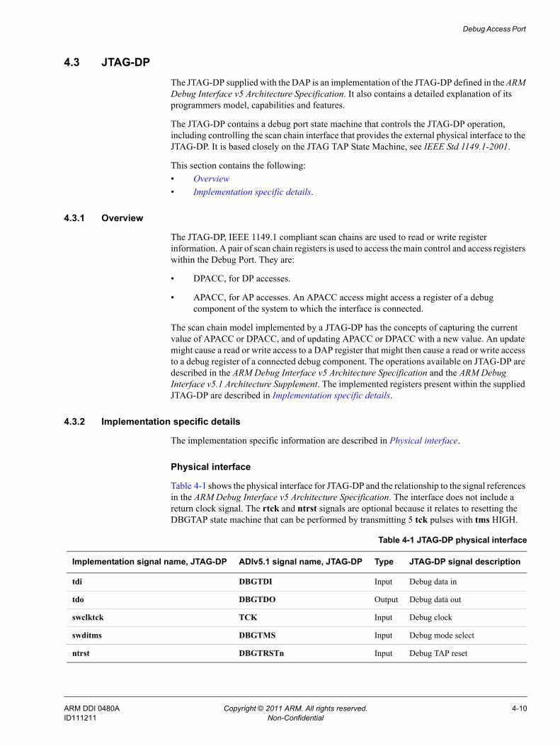
Debug Access Port
4.3 JTAG-DPThe JTAG-DP supplied with the DAP is an implementation of the JTAG-DP defined in the ARM Debug Interface v5 Architecture Specification. It also contains a detailed explanation of its programmers model, capabilities and features.
The JTAG-DP contains a debug port state machine that controls the JTAG-DP operation, including controlling the scan chain interface that provides the external physical interface to the JTAG-DP. It is based closely on the JTAG TAP State Machine, see IEEE Std 1149.1-2001.
This section contains the following:• Overview• Implementation specific details.
4.3.1 Overview
The JTAG-DP, IEEE 1149.1 compliant scan chains are used to read or write register information. A pair of scan chain registers is used to access the main control and access registers within the Debug Port. They are:
• DPACC, for DP accesses.
• APACC, for AP accesses. An APACC access might access a register of a debug component of the system to which the interface is connected.
The scan chain model implemented by a JTAG-DP has the concepts of capturing the current value of APACC or DPACC, and of updating APACC or DPACC with a new value. An update might cause a read or write access to a DAP register that might then cause a read or write access to a debug register of a connected debug component. The operations available on JTAG-DP are described in the ARM Debug Interface v5 Architecture Specification and the ARM Debug Interface v5.1 Architecture Supplement. The implemented registers present within the supplied JTAG-DP are described in Implementation specific details.
4.3.2 Implementation specific details
The implementation specific information are described in Physical interface.
Physical interface
Table 4-1 shows the physical interface for JTAG-DP and the relationship to the signal references in the ARM Debug Interface v5 Architecture Specification. The interface does not include a return clock signal. The rtck and ntrst signals are optional because it relates to resetting the DBGTAP state machine that can be performed by transmitting 5 tck pulses with tms HIGH.
Table 4-1 JTAG-DP physical interface
Implementation signal name, JTAG-DP ADIv5.1 signal name, JTAG-DP Type JTAG-DP signal description
tdi DBGTDI Input Debug data in
tdo DBGTDO Output Debug data out
swclktck TCK Input Debug clock
swditms DBGTMS Input Debug mode select
ntrst DBGTRSTn Input Debug TAP reset
ARM DDI 0480A Copyright © 2011 ARM. All rights reserved. 4-10ID111211 Non-Confidential
Debug Access Port
4.4 SW-DPThis section describes the SW-DP Interface. This implementation is taken from the ARM Debug Interface v5 Architecture Specification and operates with a synchronous serial interface. This uses a single bidirectional data signal and a clock signal.
4.4.1 Overview
The SW-DP provides a low pin count bidirectional serial connection to the DAP with a reference clock signal for synchronous operation.
Communications with the SW-DP use a 3-phase protocol:
• A host-to-target packet request.
• A target-to-host acknowledge response.
• A data transfer phase, if required. This can be target-to-host or host-to-target, depending on the request made in the first phase.
A packet request from a debugger indicates whether the required access is to a DP register, DPACC or to an AP register, APACC, and includes a 2-bit register address. For more information about the protocol, see the ARM Debug Interface v5 Architecture Specification and the ARM Debug Interface v5.1 Architecture Supplement.
4.4.2 Implementation specific details
This section contains the following:• Clocking• Overview of debug interface.
Clocking
The SW-DP clock, swclktck, can be asynchronous to the dapclk. swclktck can be stopped when the debug port is idle.
The host must continue to clock the interface for a number of cycles after the data phase of any data transfer. This ensures that the transfer can be clocked through the SW-DP. This means that after the data phase of any transfer the host must do one of the following:
• immediately start a new SW-DP operation
• continue to clock the SW-DP serial interface until the host starts a new SW-DP operation
• after clocking out the data parity bit, continue to clock the SW-DP serial interface until it has clocked out at least 8 more clock rising edges, before stopping the clock.
Overview of debug interface
This section gives an overview of the physical interface used by the SW-DP.
Line interface
The SW-DP uses a serial wire for both host and target sourced signals. The host emulator drives the protocol timing, that is, only the host emulator generates packet headers.
The SW-DP operates in synchronous mode, and requires a clock pin and a data pin.
ARM DDI 0480A Copyright © 2011 ARM. All rights reserved. 4-11ID111211 Non-Confidential
Debug Access Port
Synchronous mode uses a clock reference signal that can be sourced from an on-chip source and exported, or provided by the host device. The host uses this clock as a reference for generation and sampling of data so that the target is not required to perform any oversampling.
Both the target and host are capable of driving the bus HIGH and LOW, or tristating it. The ports must be able to tolerate short periods of contention to enable for loss of synchronization.
Line pullup
Both the host and target are able to drive the line HIGH or LOW, so it is important to ensure that contention does not occur by providing undriven time slots as part of the handover. So that the line can be assumed to be in a known state when neither is driving the line, a 100kΩ pullup is required at the target, but this can only be relied on to maintain the state of the wire. If the wire is tied LOW and released, the pullup resistor eventually brings the line to the HIGH state, but this takes many bit periods.
The pullup is intended to prevent false detection of signals when no host device is connected. It must be of a high value to reduce IDLE state current consumption from the target when the host actively pulls down the line.
Note Whenever the line is tied LOW, this results in a small current drain from the target. If the interface is left connected for extended periods when the target must use a low-power mode, the line must be held HIGH, or reset, by the host until the interface must be activated.
Line turn-round
To avoid contention, a turnaround period is required when the device driving the wire changes.
Idle and reset
Between transfers, the host must either drive the line LOW to the IDLE state, or continue immediately with the start bit of a new transfer. The host is also free to leave the line HIGH, either driven or tristated, after a packet. This reduces the static current drain, but if this approach is used with a free running clock, a minimum of 50 clock cycles must be used, followed by a read ID as a new reconnection sequence.
There is no explicit reset signal for the protocol. A reset is detected by either host or target when the expected protocol is not observed. It is important that both ends of the link become reset before the protocol can be restarted with a reconnection sequence. Resynchronization following the detection of protocol errors or after reset is achieved by providing 50 clock cycles with the line HIGH, or tristate, followed by a read ID request.
If the SW-DP detects that it has lost synchronization, for example, if no stop bit is seen when expected, it leaves the line undriven and waits for the host to either re-try with a new header after a minimum of one cycle with the line LOW, or signals a reset by not driving the line itself. If the SW-DP detects two bad data sequences in a row, it locks out until a reset sequence of 50 clock cycles with DBGDI HIGH is seen.
If the host does not see an expected response from SW-DP, it must permit time for SW-DP to return a data payload. The host can then retry with a read to the SW-DP ID code register. If this is unsuccessful, the host must attempt a reset.
ARM DDI 0480A Copyright © 2011 ARM. All rights reserved. 4-12ID111211 Non-Confidential
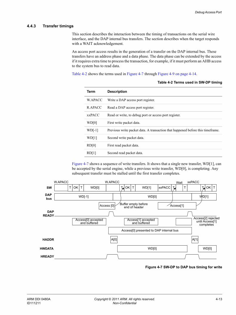
Debug Access Port
4.4.3 Transfer timings
This section describes the interaction between the timing of transactions on the serial wire interface, and the DAP internal bus transfers. The section describes when the target responds with a WAIT acknowledgement.
An access port access results in the generation of a transfer on the DAP internal bus. These transfers have an address phase and a data phase. The data phase can be extended by the access if it requires extra time to process the transaction, for example, if it must perform an AHB access to the system bus to read data.
Table 4-2 shows the terms used in Figure 4-7 through Figure 4-9 on page 4-14.
Figure 4-7 shows a sequence of write transfers. It shows that a single new transfer, WD[1], can be accepted by the serial engine, while a previous write transfer, WD[0], is completing. Any subsequent transfer must be stalled until the first transfer completes.
Figure 4-7 SW-DP to DAP bus timing for write
Table 4-2 Terms used in SW-DP timing
Term Description
W.APACC Write a DAP access port register.
R.APACC Read a DAP access port register.
xxPACC Read or write, to debug port or access port register.
WD[0] First write packet data.
WD[-1] Previous write packet data. A transaction that happened before this timeframe.
WD[1] Second write packet data.
RD[0] First read packet data.
RD[1] Second read packet data.
T OK T WD[0] T OK T WD[1] xxPACC T T T OK TSW
WD[-1] WD[0] WD[1]
Access [0] Access[1]
Access[0] accepted and buffered
Access[1] accepted and buffered
Access[2] rejected until Access[1]
completes
Access[0] presented to DAP internal bus
A[0] A[1]
WD[0] WD[0]
Buffer empty before end of header
DAP bus
DAP READY
HADDR
HWDATA
HREADY
W.APACC W.APACC Wait xxPACC
ARM DDI 0480A Copyright © 2011 ARM. All rights reserved. 4-13ID111211 Non-Confidential
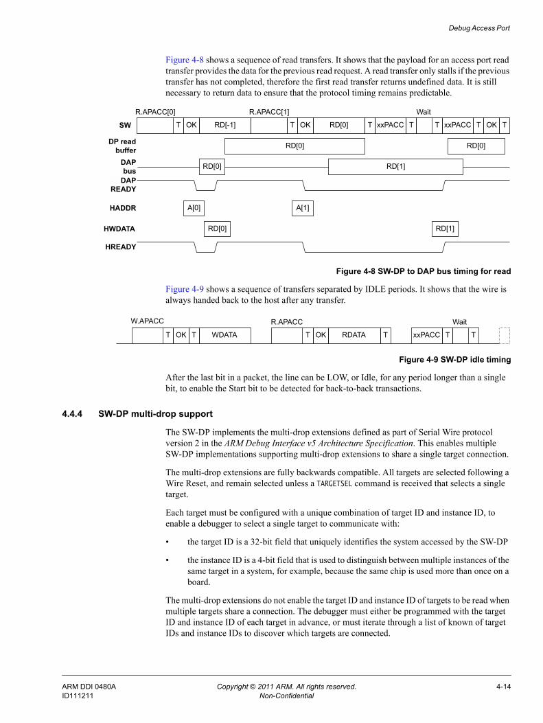
Debug Access Port
Figure 4-8 shows a sequence of read transfers. It shows that the payload for an access port read transfer provides the data for the previous read request. A read transfer only stalls if the previous transfer has not completed, therefore the first read transfer returns undefined data. It is still necessary to return data to ensure that the protocol timing remains predictable.
Figure 4-8 SW-DP to DAP bus timing for read
Figure 4-9 shows a sequence of transfers separated by IDLE periods. It shows that the wire is always handed back to the host after any transfer.
Figure 4-9 SW-DP idle timing
After the last bit in a packet, the line can be LOW, or Idle, for any period longer than a single bit, to enable the Start bit to be detected for back-to-back transactions.
4.4.4 SW-DP multi-drop support
The SW-DP implements the multi-drop extensions defined as part of Serial Wire protocol version 2 in the ARM Debug Interface v5 Architecture Specification. This enables multiple SW-DP implementations supporting multi-drop extensions to share a single target connection.
The multi-drop extensions are fully backwards compatible. All targets are selected following a Wire Reset, and remain selected unless a TARGETSEL command is received that selects a single target.
Each target must be configured with a unique combination of target ID and instance ID, to enable a debugger to select a single target to communicate with:
• the target ID is a 32-bit field that uniquely identifies the system accessed by the SW-DP
• the instance ID is a 4-bit field that is used to distinguish between multiple instances of the same target in a system, for example, because the same chip is used more than once on a board.
The multi-drop extensions do not enable the target ID and instance ID of targets to be read when multiple targets share a connection. The debugger must either be programmed with the target ID and instance ID of each target in advance, or must iterate through a list of known of target IDs and instance IDs to discover which targets are connected.
T OK RD[-1] T OK RD[0] xxPACC T T xxPACC T OK TSW
RD[0] RD[1]
A[0] A[1]
RD[0] RD[1]
DAP bus
DAP READY
HADDR
HWDATA
HREADY
T
RD[0] RD[0]DP read buffer
R.APACC[0] R.APACC[1] Wait
T OK T WDATA T OK RDATA T xxPACC T T
W.APACC R.APACC Wait
ARM DDI 0480A Copyright © 2011 ARM. All rights reserved. 4-14ID111211 Non-Confidential
Debug Access Port
Target ID
The SW-DP target ID is configured using a 32-bit input to the SW-DP, targetid[31:0]. It must be connected as shown in Table 4-3.
The target ID must be configured even in systems where multi-drop operation is not required, because it can be used for more part identification. In most cases, it can be configured with the same information provided in the DAP ROM table identification registers described in Chapter 3 Programmers Model. Table 4-4 shows the ROM table identification registers map to the target ID.
Instance ID
The SW-DP instance ID is configured using a 4-bit input to the SW-DP, instanceid[3:0]. If multiple targets with the same target ID might share a connection, instanceid must be driven differently for each target, for example by using non-volatile storage configured differently for each target. In most cases, this input can be tied LOW.
Table 4-3 TARGETID input connections
Bits Name Description
[31:28] Revision The revision of the part. This field is not used when selecting a target.
[27:12] Part number Identifies the part.
[11:1] Designer Identifies the designer of the part. The code used is assigned by JEDEC standard JEP-106 as used in IEEE 1149.1 and CoreSight identification registers. Bits [11:8] identify the bank, and bits [7:1] identify the position within that bank.
[0] Reserved Must be HIGH.
Table 4-4 TARGETID mapping
TARGETID ROM table register
[31:28] Peripheral ID2 [7:4]
[27:24] Peripheral ID1 [3:0]
[23:16] Peripheral ID0 [7:0]
[15:12] Drive LOW
[11:8] Peripheral ID4 [3:0]
[7:5] Peripheral ID2 [2:0]
[4:1] Peripheral ID1 [7:4]
[0] Drive HIGH
ARM DDI 0480A Copyright © 2011 ARM. All rights reserved. 4-15ID111211 Non-Confidential
Debug Access Port
4.5 Common debug port features and registersThis section describes specific information about features and registers that are present within this implementation of SW-DP and JTAG-DP as part of the SWJ-DP. For all the features and registers present within SW-DP and JTAG-DP, see the ARM Debug Interface v5 Architecture Specification and the ARM Debug Interface v5.1 Architecture Supplement. This section contains the following implementation specific information:• Features overview• Example pushed operations.
4.5.1 Features overview
Both the SW-DP and JTAG-DP views within the SWJ-DP contain the same features defined in the ARM Debug Interface v5 Architecture Specification. The following features are included:
• Sticky flags and debug port error responses as a result of either a read and write error response from the system or because of an overrun detection, STICKYORUN.
• Pushed compare and pushed verify to enable more optimized control from a debugger by performing a set of write transactions and enabling any comparison operation to be done within the debug port. See Example pushed operations for specific examples with the DAP.
• Transaction counter to recover to a point within a repeated operation.
• System and debug power and debug reset control. This is to enable an external debugger to connect to a potentially turned-off system and power up as much as required to get a basic level of debug access with minimal understanding of the system.
For more information, see the ARM Debug Interface v5 Architecture Specification and the ARM Debug Interface v5.1 Architecture Supplement.
4.5.2 Example pushed operations
These are two examples using this specific implementation of the ARM Debug Interface v5 Architecture Specification. All register and feature references are related to those described in their respective chapters and the ARM Debug Interface v5 Architecture Specification and the ARM Debug Interface v5.1 Architecture Supplement.
This section contains the following examples:• Example 4-1• Example 4-2 on page 4-17.
Example 4-1 Example use of pushed verify operation on an AHB-AP
You can use pushed verify to verify the contents of system memory as follows:
1. Make sure that the AHB-AP Control/Status Word (CSW) is set up to increment the Transfer Address Register (TAR) after each access.
2. Write to the TAR to indicate the start address of the Debug Register region that is to be verified.
ARM DDI 0480A Copyright © 2011 ARM. All rights reserved. 4-16ID111211 Non-Confidential
Debug Access Port
3. Write a series of expected values as access port transactions. On each write transaction, the debug port issues an access port read access, compares the result against the value supplied in the access port write transaction, and sets the STICKYCMP bit in the CRL/STAT Register if the values do not match. The TAR is incremented on each transaction.
In this way, the series of values supplied is compared against the contents of the access port locations, and STICKYCMP set if they do not match.
Example 4-2 Example use of pushed find operation on an AHB-AP
You can use pushed find to search system memory for a particular word. If you use pushed find with byte lane masking you can search for one or more bytes.
1. Make sure that the AHB-AP CSW is set up to increment the TAR after each access.
2. Write to the TAR to indicate the start address of the Debug Register region that is to be searched.
3. Write the value to be searched for as an AP write transaction. The debug port repeatedly reads the location indicated by the TAR. On each debug port read:• The value returned is compared with the value supplied in the access port write
transaction. If they match, the STICKYCMP flag is set.• The TAR is incremented.
This continues until STICKYCMP is set, or ABORT is used to terminate the search.
You can also use pushed find without address incrementing to poll a single location, for example, to test for a flag being set on completion of an operation.
ARM DDI 0480A Copyright © 2011 ARM. All rights reserved. 4-17ID111211 Non-Confidential
Debug Access Port
4.6 Access portsAn access port provides the interface between the debug port interface and one or more debug components present within the system. There are two kinds of access port supplied with this DAP:
• MEM-AP, designed for connection to memory bus system with address and data controls.
• JTAG-AP for connecting to on-chip based debug TAPs.
All access ports follow a base standard for identification, and debuggers must be able to recognize and ignore access ports that they do not support. The connection method does not depend on the type of debug port used and the type of access port being accessed.
For more information on access ports and recommend debugger interaction with access ports, see the ARM Debug Interface v5 Architecture Specification and the ARM Debug Interface v5.1 Architecture Supplement.
4.6.1 Overview
There are four access ports supplied in the DAP. It is possible to connect a fourth access port externally. The supplied access ports within this release are:• AHB-AP for connection to the main system bus• APB-AP to enable direct connection to the dedicated debug bus• JTAG-AP to control up to eight scan chains• AXI-AP for connection to an AXI interconnect.
ARM DDI 0480A Copyright © 2011 ARM. All rights reserved. 4-18ID111211 Non-Confidential
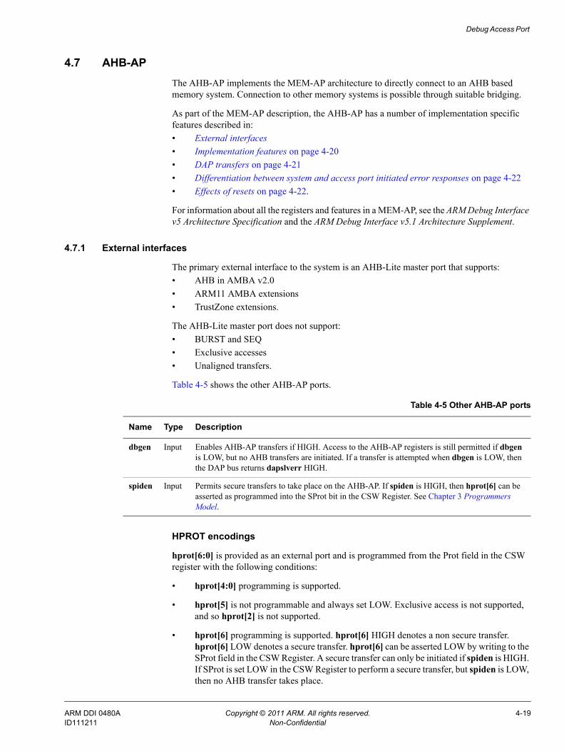
Debug Access Port
4.7 AHB-APThe AHB-AP implements the MEM-AP architecture to directly connect to an AHB based memory system. Connection to other memory systems is possible through suitable bridging.
As part of the MEM-AP description, the AHB-AP has a number of implementation specific features described in:• External interfaces• Implementation features on page 4-20• DAP transfers on page 4-21• Differentiation between system and access port initiated error responses on page 4-22• Effects of resets on page 4-22.
For information about all the registers and features in a MEM-AP, see the ARM Debug Interface v5 Architecture Specification and the ARM Debug Interface v5.1 Architecture Supplement.
4.7.1 External interfaces
The primary external interface to the system is an AHB-Lite master port that supports:• AHB in AMBA v2.0• ARM11 AMBA extensions• TrustZone extensions.
The AHB-Lite master port does not support:• BURST and SEQ• Exclusive accesses• Unaligned transfers.
Table 4-5 shows the other AHB-AP ports.
HPROT encodings
hprot[6:0] is provided as an external port and is programmed from the Prot field in the CSW register with the following conditions:
• hprot[4:0] programming is supported.
• hprot[5] is not programmable and always set LOW. Exclusive access is not supported, and so hprot[2] is not supported.
• hprot[6] programming is supported. hprot[6] HIGH denotes a non secure transfer. hprot[6] LOW denotes a secure transfer. hprot[6] can be asserted LOW by writing to the SProt field in the CSW Register. A secure transfer can only be initiated if spiden is HIGH. If SProt is set LOW in the CSW Register to perform a secure transfer, but spiden is LOW, then no AHB transfer takes place.
Table 4-5 Other AHB-AP ports
Name Type Description
dbgen Input Enables AHB-AP transfers if HIGH. Access to the AHB-AP registers is still permitted if dbgen is LOW, but no AHB transfers are initiated. If a transfer is attempted when dbgen is LOW, then the DAP bus returns dapslverr HIGH.
spiden Input Permits secure transfers to take place on the AHB-AP. If spiden is HIGH, then hprot[6] can be asserted as programmed into the SProt bit in the CSW Register. See Chapter 3 Programmers Model.
ARM DDI 0480A Copyright © 2011 ARM. All rights reserved. 4-19ID111211 Non-Confidential
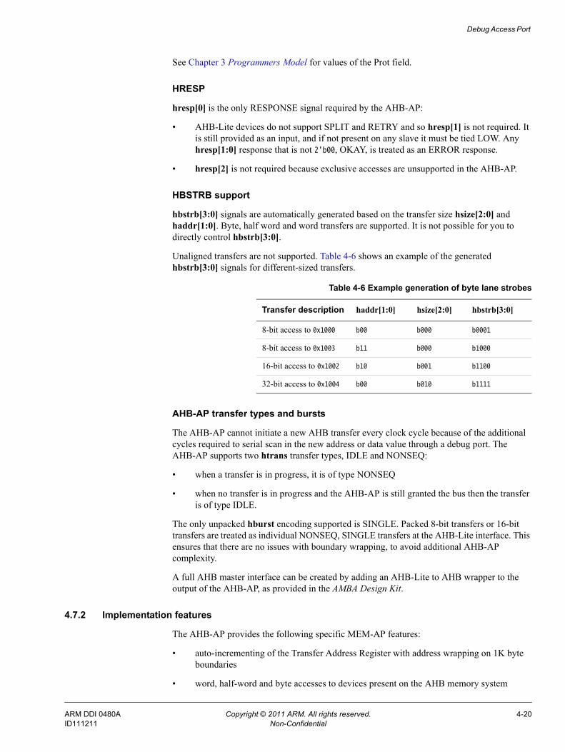
Debug Access Port
See Chapter 3 Programmers Model for values of the Prot field.
HRESP
hresp[0] is the only RESPONSE signal required by the AHB-AP:
• AHB-Lite devices do not support SPLIT and RETRY and so hresp[1] is not required. It is still provided as an input, and if not present on any slave it must be tied LOW. Any hresp[1:0] response that is not 2'b00, OKAY, is treated as an ERROR response.
• hresp[2] is not required because exclusive accesses are unsupported in the AHB-AP.
HBSTRB support
hbstrb[3:0] signals are automatically generated based on the transfer size hsize[2:0] and haddr[1:0]. Byte, half word and word transfers are supported. It is not possible for you to directly control hbstrb[3:0].
Unaligned transfers are not supported. Table 4-6 shows an example of the generated hbstrb[3:0] signals for different-sized transfers.
AHB-AP transfer types and bursts
The AHB-AP cannot initiate a new AHB transfer every clock cycle because of the additional cycles required to serial scan in the new address or data value through a debug port. The AHB-AP supports two htrans transfer types, IDLE and NONSEQ:
• when a transfer is in progress, it is of type NONSEQ
• when no transfer is in progress and the AHB-AP is still granted the bus then the transfer is of type IDLE.
The only unpacked hburst encoding supported is SINGLE. Packed 8-bit transfers or 16-bit transfers are treated as individual NONSEQ, SINGLE transfers at the AHB-Lite interface. This ensures that there are no issues with boundary wrapping, to avoid additional AHB-AP complexity.
A full AHB master interface can be created by adding an AHB-Lite to AHB wrapper to the output of the AHB-AP, as provided in the AMBA Design Kit.
4.7.2 Implementation features
The AHB-AP provides the following specific MEM-AP features:
• auto-incrementing of the Transfer Address Register with address wrapping on 1K byte boundaries
• word, half-word and byte accesses to devices present on the AHB memory system
Table 4-6 Example generation of byte lane strobes
Transfer description haddr[1:0] hsize[2:0] hbstrb[3:0]
8-bit access to 0x1000 b00 b000 b0001
8-bit access to 0x1003 b11 b000 b1000
16-bit access to 0x1002 b10 b001 b1100
32-bit access to 0x1004 b00 b010 b1111
ARM DDI 0480A Copyright © 2011 ARM. All rights reserved. 4-20ID111211 Non-Confidential
Debug Access Port
• packed transfers on sub-word transfers.
The AHB-AP does not support the following MEM-AP features:
• Big-endian. All accesses performed as expected to be to a little-endian memory structure.
• Slave memory port disabling. The AHB-Lite master interface is not shared with any other connection so there is no slave port to disable access to this interface. If the memory-map presented to the AHB-AP is to be shared with another AHB-Lite master then this is implemented externally to the DAP.
4.7.3 DAP transfers
This section describes:• DAP transfer aborts• Error response generation.
DAP transfer aborts
The AHB-AP does not cancel the system-facing operation and returns dapready HIGH one cycle after dapabort has been asserted by the driving debug port. The externally driving AHB master port does not violate the AHB protocol. After a transfer has been aborted, the CSW Register can be read to determine the state of the transfer in progress bit, TrInProg. When TrInProg returns to zero, either because the external transfer completes, or because of a reset, the AHB-AP returns to normal operation. All other writes to the AHB-AP are ignored until this bit is returned LOW after a transfer abort.
Error response generation
This section describes:• System initiated error response• Access port initiated error response• AHB-AP reads after an abort• AHB-AP writes after an abort on page 4-22.
System initiated error response
An error response received on the system driving master propagates onto the DAP bus when the transfer is completed. This response is received by the debug ports.
Access port initiated error response
Access port initiated error responses are:• AHB-AP reads after an abort• AHB-AP writes after an abort on page 4-22.
AHB-AP reads after an abort
After a dapabort operation is carried out, and an external transfer is still pending, that is, the TrInProg bit remains HIGH, reads of all registers return a normal response except for reads of the Data R/W Register and banked registers. Reads of the Data R/W Register and banked registers return an error response because they cannot initiate a new system read transfer until the TrInProg bit in the CSW Register is cleared by either completing the system transfer or a reset.
ARM DDI 0480A Copyright © 2011 ARM. All rights reserved. 4-21ID111211 Non-Confidential
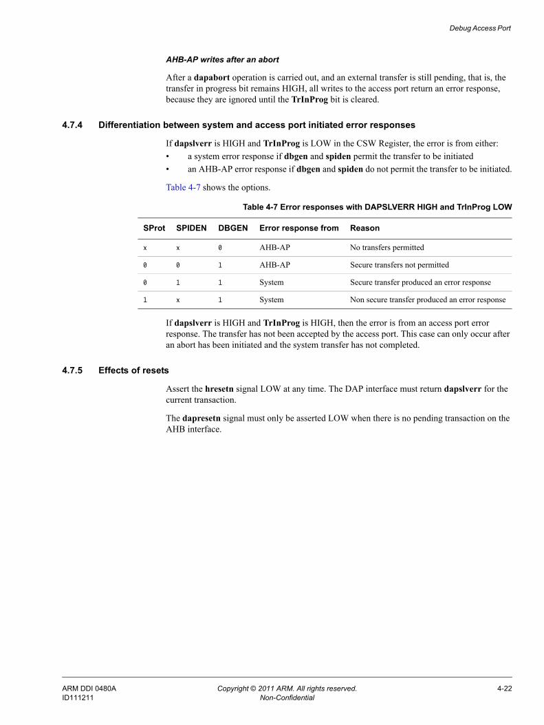
Debug Access Port
AHB-AP writes after an abort
After a dapabort operation is carried out, and an external transfer is still pending, that is, the transfer in progress bit remains HIGH, all writes to the access port return an error response, because they are ignored until the TrInProg bit is cleared.
4.7.4 Differentiation between system and access port initiated error responses
If dapslverr is HIGH and TrInProg is LOW in the CSW Register, the error is from either:• a system error response if dbgen and spiden permit the transfer to be initiated• an AHB-AP error response if dbgen and spiden do not permit the transfer to be initiated.
Table 4-7 shows the options.
If dapslverr is HIGH and TrInProg is HIGH, then the error is from an access port error response. The transfer has not been accepted by the access port. This case can only occur after an abort has been initiated and the system transfer has not completed.
4.7.5 Effects of resets
Assert the hresetn signal LOW at any time. The DAP interface must return dapslverr for the current transaction.
The dapresetn signal must only be asserted LOW when there is no pending transaction on the AHB interface.
Table 4-7 Error responses with DAPSLVERR HIGH and TrInProg LOW
SProt SPIDEN DBGEN Error response from Reason
x x 0 AHB-AP No transfers permitted
0 0 1 AHB-AP Secure transfers not permitted
0 1 1 System Secure transfer produced an error response
1 x 1 System Non secure transfer produced an error response
ARM DDI 0480A Copyright © 2011 ARM. All rights reserved. 4-22ID111211 Non-Confidential
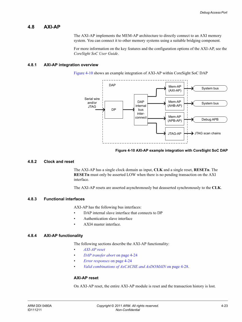
Debug Access Port
4.8 AXI-APThe AXI-AP implements the MEM-AP architecture to directly connect to an AXI memory system. You can connect it to other memory systems using a suitable bridging component.
For more information on the key features and the configuration options of the AXI-AP, see the CoreSight SoC User Guide.
4.8.1 AXI-AP integration overview
Figure 4-10 shows an example integration of AXI-AP within CoreSight SoC DAP
Figure 4-10 AXI-AP example integration with CoreSight SoC DAP
4.8.2 Clock and reset
The AXI-AP has a single clock domain as input, CLK and a single reset, RESETn. The RESETn must only be asserted LOW when there is no pending transaction on the AXI interface.
The AXI-AP resets are asserted asynchronously but deasserted synchronously to the CLK.
4.8.3 Functional interfaces
AXI-AP has the following bus interfaces:• DAP internal slave interface that connects to DP• Authentication slave interface• AXI4 master interface.
4.8.4 AXI-AP functionality
The following sections describe the AXI-AP functionality:• AXI-AP reset• DAP transfer abort on page 4-24• Error responses on page 4-24• Valid combinations of AxCACHE and AxDOMAIN on page 4-28.
AXI-AP reset
On AXI-AP reset, the entire AXI-AP module is reset and the transaction history is lost.
DP
Mem-AP(APB-AP)
DAP internal
bus inter-
connect
Mem-AP(AXI-AP)
JTAG-AP
Mem-AP(AHB-AP)
Serial wire and/or JTAG
System bus
System bus
Debug APB
JTAG scan chains
DAP
ARM DDI 0480A Copyright © 2011 ARM. All rights reserved. 4-23ID111211 Non-Confidential
Debug Access Port
ARM recommends that reset must not be asserted while AXI transfer is ongoing, however AXI-AP permits reset to be asserted with the understanding that all transaction history is lost.
DAP transfer abort
On DAP transfer abort, the AXI-AP asserts DAPREADY one cycle after DAPABORT. The DAP transfer abort does not cancel the ongoing AXI transfer.
Error responses
This section describes the following:• AXI initiated error responses• AP initiated error response• AXI and AP initiated error responses on page 4-25.
AXI initiated error responses
An error response received on the AXI master interface propagates onto the DAP bus as the transfer is completed.
In case of a 64-bit data transfer, a sequence of two reads or writes must be generated on the DAP I/F for a single 64-bit access on the AXI interface. In case of reads, the first read request on DAP I/F sends a read request on the AXI interface while in case of writes, a write access is sent on the AXI interface only after two write requests are received on the DAP I/F.
Therefore, error response received for a read request is for the first read request on DAP I/F while error response received for a write request is for the second write request on the DAP I/F.
AP initiated error response
AXI-AP writes after an abort After a DAPABORT operation is carried out, and an external transfer is still pending, that is, the transfer in progress bit remains HIGH, all writes to the AXI-AP return an error response and you can ignore it.AXI-AP writes return an error until the transfer in progress, the TrInProg bit, is cleared when the system transfer completes.
AXI-AP reads after a 64-bit AXI read sequence is broken Read requests from DAP I/F must access both the BDx registers of the pair, with the lower numbered register accessed first. For a DRW, it must access it twice to get the entire 64-bit word from AXI interface.All other accesses such as a read followed by write access to the same or different register, return an error response by asserting DAPSLVERR.
AXI-AP writes after a 64-bit write sequence is broken Write requests from DAP I/F must access both the BDx registers of the pair with the lower numbered register accessed first. For a DRW, it must access twice to build a 64-bit packet as write data on the AXI interface.All other accesses such as a write followed by another R/W access to different register, return an error response. For example, after accessing DRW, the next access on DAP I/F must be a write to DRW, any other access returns an error response.Similarly, after accessing BD0, the next access must be a write to BD1, any other access returns an error response.
ARM DDI 0480A Copyright © 2011 ARM. All rights reserved. 4-24ID111211 Non-Confidential
Debug Access Port
Aborted AXI barrier transaction It is possible to abort a barrier transaction that has not yet completed. When the abort request is generated, the DAPREADY is asserted HIGH in the next cycle. However CSW.TrInPrg bit remains set to indicate the AXI-Interface is busy waiting to complete the transaction. While the AXI-Interface is busy, a R/W request to DRW or BDx registers that results in a transaction on the AXI interface, causes the AXI-AP to return an error response by asserting DAPSLVERR.
AXI and AP initiated error responses
If DAPSLVERR is HIGH and TrInProg is LOW in the CSW Register, the error is from either:
• a system error response if registered versions of DBGEN and SPIDEN permit the transfer to be initiated
• an AXI-AP error response if registered versions of DBGEN and SPIDEN do not permit the transfer.
If DAPSLVERR is HIGH and TrInProg is HIGH, then the error is from an access port error response. This case can only occur after the initiation of an abort and the system transfer has not completed.
AXI-AP
Table 4-9 shows the implemented features.
Table 4-8 Difference between AXI and AP initiated error response
Sprot SPIDEN_registered DBGEN Error response from Reason
X X 0 AXI-AP All transfers blocked
0 0 1 AXI-AP Secure transfers blocked
0 1 1 System Secure transfer produced an error response
1 X 1 System Non secure transfer produced an error response
Table 4-9 AXI-AP features at a glance
Feature Comment
AXI4 interface support -
Auto-incrementing TAR -
Stalling accesses -
Access size 8, 16, 32, or 64 bits.
Endianness Little-endian.
Error response -
Packed transfers -
ROM table pointer register -
Long address support -
ARM DDI 0480A Copyright © 2011 ARM. All rights reserved. 4-25ID111211 Non-Confidential
Debug Access Port
AXI transfers
The AMBA4 AXI compliant Master Port supports the following features:• bursts of single transfer• masters processes one transaction at a time in the order they are issued.• no out-of-order transactions • no issuing of multiple outstanding addresses.
Burst length The AXI-AP supports burst length of one transfer only ARLEN[3:0] and AWLEN[3:0] are always 4’b0000.Packed 8 or 16-bit transfers are treated as individual burst length of one transfer at the AXI interface. This ensures that there are no issues with boundary wrapping to avoid additional AXI-AP complexity.
Burst size Supported burst sizes are:• 8-bit• 16-bit• 32-bit• 64-bit.
Burst type ARBURST or AWBURST is always 2’b00.Because only bursts of one transfer are supported, burst type has no meaning in this context.
Atomic accesses AXI-AP supports normal accesses only.ARLOCK[1:0] and AWLOCK[1:0] signals are always 2’b00.
AXI transfers Write, read transfers.
Burst size of 1 only.
No out-of-order transactions.
No multiple outstanding accesses.
Only aligned transfers are supported.
ACE-Lite Limited set of commands to support coherency in the system.
All transactions to non-shareable memory regions.
Limited subset of transactions to shareable memory regions.
For reads only. The Read-once is supported.
For writes only. The Write-unique is supported.
Barrier transactions
Table 4-9 AXI-AP features at a glance (continued)
Feature Comment
ARM DDI 0480A Copyright © 2011 ARM. All rights reserved. 4-26ID111211 Non-Confidential
Debug Access Port
Unaligned accesses Unaligned accesses are not supported. Depending on the size of the transfers, addresses must be aligned.• for 16-bit half word transfers:
— base address 0x01 is aligned and AxADDR[7:0] = 0x00— base address 0x02 is retained and AxADDR[7:0] = 0x02
• for 32-bit word transfers:— base address 0x01 to 0x03 is aligned and AxADDR[7:0] = 0x00— base address 0x04 is retained and AxADDR[7:0] = 0x04
• for 64-bit word transfers:— base address 0x04 is aligned and AxADDR[7:0] = 0x00— base address 0x08 is retained and AxADDR[7:0] = 0x08
For example, for 16-bit transfers address must be aligned to 16-bit half word boundary, for 32-bit word transfer, address must be word aligned and for 64-bit double word transfer, address must be double word aligned.
Packed Transfers
32-bit Transactions:
The DAP internal interface is a 32-bit data bus, however 8-bit or 16-bit transfers can be formed on AXI according to the size field in the CSW register, 0x000. The AddrInc field in the CSW Register permits optimized use of the DAP internal bus to reduce the number of accesses to the DAP. It indicates if the entire data word can be used to pack more than one transfer. If packed transfers are initiated, then the address incrementing is automatically enabled. Multiple transfers are carried out in sequential addresses, with the size of the address increment based on the size of the transfer.
An example of the transactions are:
For an unpacked 16-bit write to base address of base 0x2, that is, CSW[2:0]=0b001, CSW[5:4]=0b01, WDATA[31:16] is written from bits [31:16] in the DRW register.
For an unpacked 8-bit read to base address of base 0x1, that is, CSW[2:0]=0b000, CSW[5:4]=0b01, RDATA[31:16] and RDATA[7:0] are zero, RDATA[15:8] contains read data.
For a packed byte write at base address of base 0x2, that is, CSW[2:0]=0b000 and CSW[5:4]=0b10, four write transfers are initiated, and the order of data being sent is:• WDATA[23:16], from DRW[23:16] to AWADDR[31:0]=0x00000002 • WDATA[31:24], from DRW[31:24] to AWADDR[31:0]=0x00000003• WDATA[7:0], from DRW[7:0] to AWADDR[31:0]=0x00000004• WDATA[15:8], from DRW[15:8] to AWADDR[31:0]=0x00000005.
For a packed half word reading at a base address of base 0x2, that is, CSW[2:0]=0b001, CSW[5:4]=0b10, two read transfers are initiated:• RDATA[31:16] is stored into DRW[31:16] from ARADDR[31:0]=0x00000002• RDATA[15:0] is stored into DRW[15:0] from ARADDR[31:0]=0x00000004.
The AXI-AP only asserts DAPREADY HIGH when all packed transfers from the AXI interface have completed.
If the current transfer is aborted or the current transfer receives an ERROR response, the AXI-AP does not complete the following packed transfers and returns DAPREADY HIGH immediately after the current packed transfer.
ARM DDI 0480A Copyright © 2011 ARM. All rights reserved. 4-27ID111211 Non-Confidential
Debug Access Port
Valid combinations of AxCACHE and AxDOMAIN
Table 4-10 shows the valid combinations of AxCACHE and AxDOMAIN.
Table 4-10 Valid combination of AxCACHE and AxDOMAIN values
AxCACHE Access Type AxDOMAIN Domain Type Valid
0000 Device 00 Non-shareable NO
0001 01 Inner-shareable NO
10 Outer-shareable NO
11 System YES
0010 Non-Cacheable 00 Non-shareable Enabled
0011 01 Inner-shareable Enabled
10 Outer-shareable Enabled
11 System YES
010x - - - NO
100x - - -
110x - - -
011x Write 00 Non-shareable YES
101x Through 01 Inner-shareable YES
111x Write 10 Outer-shareable YES
Back 11 System NO
ARM DDI 0480A Copyright © 2011 ARM. All rights reserved. 4-28ID111211 Non-Confidential
Debug Access Port
4.9 APB-APThe APB-AP implements the MEM-AP architecture to connect directly to an APB based system. The intention is that this bus is dedicated to CoreSight and other debug components.
As part of the MEM-AP description, the APB-AP has a number of implementation specific features. These are described in:• External interfaces• Implementation features• DAP transfers.
For information on all the registers and features in a MEM-AP, see the ARM Debug Interface v5 Architecture Specification and the ARM Debug Interface v5.1 Architecture Supplement.
4.9.1 External interfaces
The primary interface on APB-AP is an APB AMBAv3 compliant interface supporting:• extended slave transfers• transfer response errors.
Table 4-11 shows the other APB-AP ports.
4.9.2 Implementation features
The APB-AP provides the following specific MEM-AP features:
• Auto-incrementing of the Transfer Address Register with address wrapping on 1K byte boundaries.
• Slave memory port disabling a slave interface is provided through the APB interconnect to enable another APB master to connect to the same memory-map as the APB-AP
The APB-AP does not support the following MEM-AP features:• Big-endian. All accesses performed as expected to be to a little-endian memory structure.• Sub-word transfers. Only word transfers are supported.
The APB-AP supports a synchronous APB interface. The internal DAP interface and the APB interface operate from dapclk.
The APB-AP has one clock domain, dapclk. It drives the complete APB-AP. This must be connected to pclkdbg for the APB interface.
dapresetn resets the internal DAP interface and the APB interface.
4.9.3 DAP transfers
This section describes DAP transfers.
Table 4-11 APB-AP other ports
Name Type Description
pdbgswen Output Enables self-hosted access to the debug APB at the APB multiplexer.
deviceen Input Disables device when LOW.
ARM DDI 0480A Copyright © 2011 ARM. All rights reserved. 4-29ID111211 Non-Confidential
Debug Access Port
Effects of DAPABORT
The APB-AP does not cancel the system-facing operation and returns dapready HIGH one cycle after dapabort is asserted by the debug port. The externally driving APB master port does not violate the APB protocol. After a transfer is aborted, the Control and Status Register can be read to determine the state of the transfer in progress bit, TrInProg. When TrInProg returns to zero, after completing the external transfer or a reset, the APB-AP returns to normal operation. All other writes to the APB-AP are ignored until the TrInProg bit is returned LOW after a Transfer Abort.
APB-AP error response generation
APB-AP error response generation is described in:• System initiated error response• AP-initiated error response• Differentiation between System-initiated and AP-initiated error responses.
System initiated error response
An error response received on the APB master interface propagates onto the DAP bus when the transfer is completed. This is received by the debug ports.
AP-initiated error response
• APB-AP reads after an abort:After a transfer abort operation is carried out, and an external transfer is still pending, that is, the TrInProg bit in the CSW Register remains HIGH. Reads of all registers return a normal response except for reads of the Data R/W Register and banked registers. Reads of the Data R/W Register and banked registers return an error response because they cannot initiate a new system read transfer until the TrInProg bit in the CSW Register is cleared by either completing the system transfer or a reset.
• APB-AP writes after an abort:After a Transfer Abort operation is carried out, and an external transfer is still pending, that is, the transfer in progress bit remains HIGH. All writes to the access port return an error response, because they are ignored until the TrInProg bit has cleared.
Differentiation between System-initiated and AP-initiated error responses
If dapslverr is HIGH and TrInProg is LOW, then the error is from a system error response.
If dapslverr is HIGH and TrInProg is HIGH, then the error is from an access port error response. The transfer has not been accepted by the access port. This case can occur after an abort has been initiated and the system transfer has not completed.
ARM DDI 0480A Copyright © 2011 ARM. All rights reserved. 4-30ID111211 Non-Confidential
Debug Access Port
4.10 JTAG-APThe JTAG Access Port (JTAG-AP) provides JTAG access to on-chip components operating as a JTAG master port to drive JTAG chains throughout a SoC. The JTAG command protocol is byte-oriented, with a word wrapper on the read and write ports to yield acceptable performance from the 32-bit internal data bus in the DAP. Daisy chaining is avoided by using a port multiplexer. In this way, slower cores do not impede faster cores. For more information about the JTAG-AP, see the description of the JTAG-AP in the ARM Debug Interface v5 Architecture Specification and the ARM Debug Interface v5.1 Architecture Supplement.
The implementation specific features of the JTAG-AP is described in the following sections:• External interfaces• RTCK connections.
4.10.1 External interfaces
Table 4-12 shows the JTAG to slave device signals.
Each of the eight JTAG scan chains are on the same bit positions for each JTAG signal. For example, connections for scan chain 0 can be located on bit [0] of each bus connection of cstck, cstms, cstdi, and portconnected.
4.10.2 RTCK connections
This section describes the rtck connections.
Global port and RTCK
When more than one bit of portsel[7:0] is set, all active JTAG-AP multiplexer port rtcks are combinatorially joined, so that:• If tck=0 then select OR of active rtcks• tck=1 then select AND of active rtcks.
An active rtck is generated by an active port that is defined as a port which:• is selected, when its portsel[7:0] bit is set• is connected, when its portconnected[7:0] bit is set
Table 4-12 JTAG to slave device signals
Name Type Description
nsrstout[7:0] Output Subsystem reset out
srstconnected[7:0] Input Subsystem reset is present.
ncstrst[7:0] Output JTAG test reset
cstck[7:0] Output JTAG test clock
cstms[7:0] Output JTAG test mode select
cstdi[7:0] Output JTAG test data in, to external TAP
cstdo[7:0] Input JTAG test data out, from external TAP
csrtck[7:0] Input Return test clock, target pacing signal
portconnected[7:0] Input JTAG port is connected, status signal
portenabled[7:0] Input JTAG port is enabled, for example, it might be deasserted by a processor powering down
ARM DDI 0480A Copyright © 2011 ARM. All rights reserved. 4-31ID111211 Non-Confidential
Debug Access Port
• has not been disabled or powered down in this session, when its PSTA bit is 0.
If no ports are active, rtck is connected directly to tck. This means that disabling or powering down a JTAG slave cannot lock up the rtck interface.
Asynchronous TAP controllers that do not require an rtck connection must connect their tck output from JTAG-AP to the corresponding rtck input.
RTCK wrapper
Note This section applies only to synchronous TAP controllers.
Where devices do not have a return clock, a rtck wrapper must be used to register tck against the processor clock. See the CoreSight SoC Implementation Guide and the applicable Integration Manual for information on how to implement an rtck wrapper.
ARM DDI 0480A Copyright © 2011 ARM. All rights reserved. 4-32ID111211 Non-Confidential

Debug Access Port
4.11 Auxiliary Access PortAn auxiliary interface is an interface on the DAPBUS Interconnect that does not connect to any of the supplied APs. An auxiliary interface can be connected to the access port of processors that have a compliant debug interface, such as the Cortex-M3 processor.
ARM DDI 0480A Copyright © 2011 ARM. All rights reserved. 4-33ID111211 Non-Confidential
Debug Access Port
4.12 Authentication requirements for Debug Access PortThis section describes the functionality that is available in the debug and trace components to permit authentication using the signals, and describes how they are connected. If you do not require the system to support this level of control, you can simplify the system design.
The full authentication requirements are defined in the CoreSight Architecture Specification.
APB-AP has one authentication signal, called deviceen:
• If the APB-AP is connected to a debug bus, this signal must be tied HIGH , the APB-AP must be connected to a debug bus, and deviceen must be tied HIGH.
• If the APB-AP is connected to a system bus dedicated to the secure state, this signal must be connected to spiden.
• If the APB-AP is connected to a system bus dedicated to the non-secure state, this signal must be connected to dbgen.
For more information about spiden and dbgen, see the CoreSight Architecture Specification.
ARM DDI 0480A Copyright © 2011 ARM. All rights reserved. 4-34ID111211 Non-Confidential

Debug Access Port
4.13 Clocks, power, and resetsImplement the DAP to use multiple clock domains. Synchronous bridges must be instantiated when the clock domains of interacting components are edge-aligned but of different frequencies. Asynchronous bridges have to be instantiated when the clock domains of interacting components are asynchronous.
The SWJ-DP must be present in the always on power domain.
Bridges with LPI must be instantiated where there is a power domain boundary between interacting components.
ARM DDI 0480A Copyright © 2011 ARM. All rights reserved. 4-35ID111211 Non-Confidential
Chapter 5 APB Interconnect
This chapter describes the Advanced Peripheral Bus Interconnect (APBIC). It contains the following sections:• Introduction on page 5-2• APB interconnect interfaces on page 5-3• Device operation on page 5-4.
ARM DDI 0480A Copyright © 2011 ARM. All rights reserved. 5-1ID111211 Non-Confidential
APB Interconnect
5.1 IntroductionThe APB interconnect includes the following features:
• Single-layer, bus-type interconnect. Supports up to four slave interfaces and up to 64 master interfaces.
• Tightly-coupled ROM Table at fixed base address of 0x00000000.
• Support for cascading of APB interconnects and ROM tables.
• Single clock and power domains.
• Compliant to AMBA3 APB protocol and CoreSight architecture.
• 32-bit data bus for each APB interface.
• APB slave interfaces address bus width automatically scaled based on the APB master interfaces and memory map configuration.
• Address width on APB master interface depends on size of the address space allocated to each interface.
• Fixed priority arbitration.
• Control to enable or disable SoC system masters accessing the debug sub-system.
The master or slave naming of the APB interfaces in the component is done from the APB interconnect component. The interface that responds to accesses is named the slave interface. In the APB interconnect, this corresponds to the interfaces that connect to external APB masters. The interface that initiates accesses is named the master interface. In the APB interconnect, this corresponds to the interfaces that connect to the external debug APB slaves.
ARM DDI 0480A Copyright © 2011 ARM. All rights reserved. 5-2ID111211 Non-Confidential
APB Interconnect
5.2 APB interconnect interfacesThis section describe the APB interconnect interfaces in:• Clock and reset• Functional interfaces.
5.2.1 Clock and reset
This component has a single clock domain, clk, driven by the debug APB clock. The master and slave interfaces operate on the same clock, clk.
This component has a single reset input, resetn, that is an asynchronous active-LOW reset input.
5.2.2 Functional interfaces
The APB interconnect with ROM table has a configurable number of AMBA3 APB-compliant slave interfaces based on the NUM_SLAVE_INTF configuration option. Similarly, it has a configurable number of AMBA3 APB -compliant master interfaces, based on the NUM_MASTER_INTF configuration option.
The DbgSwEnable bit in the APB-AP can be used to prevent self-hosted, on chip, accesses.
ARM DDI 0480A Copyright © 2011 ARM. All rights reserved. 5-3ID111211 Non-Confidential
APB Interconnect
5.3 Device operationThis section describes device operation in the following subsections:• Accesses to ROM table• Arbitration• Error response• Address width on master interfaces• Address width on slave interfaces on page 5-5.
5.3.1 Accesses to ROM table
Accesses to addresses in the range 0x0000 - 0x0FFC are decoded to the ROM table. See the ARM Debug Interface v5 Architecture Specification for information on ROM tables.
5.3.2 Arbitration
The internal arbiter arbitrates between competing slave interfaces for access to debug APB as the following algorithm demonstrates:
• When a slave interface raises a request, the highest priority is given to the slave interface with the lowest instance suffix, that is, SlvIntf0 > SlvIntf1 > SlvIntf2 > … > SlvIntf(n-1). The order in which these slave interfaces raised their requests relative to each other is not used in arbitration.
• The arbitration is re-evaluated after every access.
5.3.3 Error response
The APB interconnect returns an error on its slave interface under any of the following conditions:
• the targeted debug APB device returns an error response
• the address accessed by a slave interface does not decode to any debug APB device
• a system access is attempted to a debug APB device when not permitted.
• when the DbgSwEnable bit in the APB-AP is cleared, and self-hosted, on chip, accesses are attempted.
5.3.4 Address width on master interfaces
The width of the address bus on the master interface depends on the size of the address space allocated to that interface through the master_intfn_size parameter. Bit [31] of the address bus is always exported onto the master interface. Table 5-1 shows the address bus widths for each setting of size.
Table 5-1 Address width on master interfaces
Value of parametermaster_ intfn_size
Size of address spaceAddress bus on the master interface,where x=0 to NUM_MASTER_INTF-1
0 4KB paddrmx[11:2]
1 8KB paddrmx[12:2]
2 16 KB paddrmx[13:2]
ARM DDI 0480A Copyright © 2011 ARM. All rights reserved. 5-4ID111211 Non-Confidential
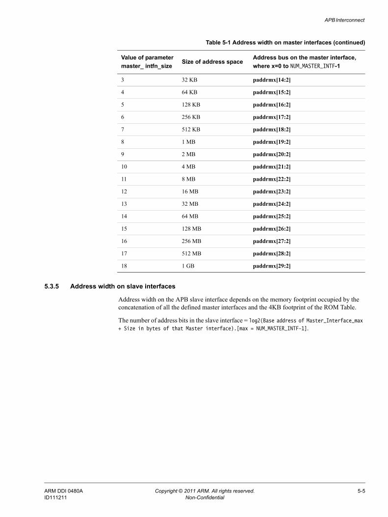
APB Interconnect
5.3.5 Address width on slave interfaces
Address width on the APB slave interface depends on the memory footprint occupied by the concatenation of all the defined master interfaces and the 4KB footprint of the ROM Table.
The number of address bits in the slave interface = log2(Base address of Master_Interface_max + Size in bytes of that Master interface).[max = NUM_MASTER_INTF–1].
3 32 KB paddrmx[14:2]
4 64 KB paddrmx[15:2]
5 128 KB paddrmx[16:2]
6 256 KB paddrmx[17:2]
7 512 KB paddrmx[18:2]
8 1 MB paddrmx[19:2]
9 2 MB paddrmx[20:2]
10 4 MB paddrmx[21:2]
11 8 MB paddrmx[22:2]
12 16 MB paddrmx[23:2]
13 32 MB paddrmx[24:2]
14 64 MB paddrmx[25:2]
15 128 MB paddrmx[26:2]
16 256 MB paddrmx[27:2]
17 512 MB paddrmx[28:2]
18 1 GB paddrmx[29:2]
Table 5-1 Address width on master interfaces (continued)
Value of parametermaster_ intfn_size
Size of address spaceAddress bus on the master interface,where x=0 to NUM_MASTER_INTF-1
ARM DDI 0480A Copyright © 2011 ARM. All rights reserved. 5-5ID111211 Non-Confidential
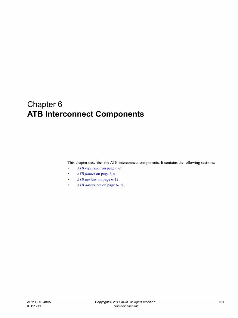
Chapter 6 ATB Interconnect Components
This chapter describes the ATB interconnect components. It contains the following sections:• ATB replicator on page 6-2• ATB funnel on page 6-4• ATB upsizer on page 6-12• ATB downsizer on page 6-15.
ARM DDI 0480A Copyright © 2011 ARM. All rights reserved. 6-1ID111211 Non-Confidential
ATB Interconnect Components
6.1 ATB replicatorThe ATB replicator propagates the data from a single ATB master to two ATB slaves at the same time.
See the CoreSight SoC User Guide for a description of the key features and configuration options of the ATB replicator.
Figure 6-1 shows an example ATB replicator.
Figure 6-1 Example ATB replicator
6.1.1 Clock and reset
The ATB replicator contains only one clock domain. The block uses RESETn to reset all the flip flops in the design. The clock and reset signals of the ATB replicator are:
PCLKENDBG Clock enable for an optional debug APB port.
CLK ATB clock.
RESETn ATB reset.
6.1.2 Functional interfaces
The ATB replicator has a single slave ATB port, two ATB master ports, and one optional APB port.
6.1.3 Functional overview
The ATB replicator permits the connection of two trace sinks. Buses cannot be connected directly together.
Any connected blocks, on both the inputs and the outputs, must operate on the same CLK domain.
Trace data flow As data is received from the trace source, it is passed on to all trace sinks at the same time. The replicator does not accept more data from the trace source until all the trace sinks have accepted this data. This has the impact of reducing the throughput of the replicator to match that of the slowest trace sink.If the replicator is programmed to be configurable, this adds the ability to ignore specific trace sinks so they are unable to influence the throughput to other ports.
ATB input slave port
ATB output master port 0
ATB outputmaster port1
ARM DDI 0480A Copyright © 2011 ARM. All rights reserved. 6-2ID111211 Non-Confidential
ATB Interconnect Components
Flushing AFVALIDM and AFREADYM Whenever one of the trace sinks initiates a flush to remove old information from the system, then the replicator must propagate this request even when the other sink has not requested it.This does not cause any problems with the non-requested trace sink. It receives the flushed data, if a request to start a flush is received from the other trace sink. When there is already a flush operation under way that was begun by the first trace sink, then the replicator must wait until the first request is serviced, and then service the second request.
SYNCREQ The synchronization merging logic generates synchronization requests at a rate corresponding to the most frequent of the input requests from all active trace sinks.
ID Filtering When the APB programmable interface is configured, the bit in the IDFILTERx Register determines whether the ATB transaction with the corresponding ID must discarded or must be transparent. On reset, these IDFILTERx Registers are reset to 0, so all ATB transactions are transparent. There is no limitation on the IDFILTERx Register programming. The programmed value takes effect when the ongoing ATB transactions are completed, or when the APB programming is completed, if there are no ongoing transactions.
ARM DDI 0480A Copyright © 2011 ARM. All rights reserved. 6-3ID111211 Non-Confidential
ATB Interconnect Components
6.2 ATB funnelThe ATB funnel component merges multiple ATB buses into a single ATB bus.
See the CoreSight SoC User Guide for a description of the key features and configuration options of the ATB funnel.
6.2.1 Clock and reset
The optional APB interface has a clock enable PCLKENDBG. The ATB funnel has a single clock domain with clock input, CLK.
The funnel has a single reset input, RESETn.
The RESETn signal is asynchronous active-LOW reset.
6.2.2 Functional interface
The ATB funnel has a configurable number of ATB slave interfaces and one ATB master interface.
The slave ATB interfaces connect to replicators, trace sources, trace links, or any other component with a standard ATB master.
The master interface connects to replicators, trace sinks, trace links, or any other component with a standard ATB slave.
All ATB interfaces are configurable for the ATB DATA width.
6.2.3 Funnel functionality
This section describes the functionality of the ATB funnel.
Port enable Set or clear the corresponding enable slave port bit in the Control Register to enable or disable the ATB slave interface respectively.Disabling of the ATB slave is effective at the transaction boundary when ATREADYSx is set to 1. If there is no valid transaction on the slave port, the disable is effective immediately.You can enable or disable the ATB slaves at any time without any restriction with regard to the state of the trace system.In configurations with no programmers model, all ATB slaves are enabled and cannot be disabled.
6.2.4 Arbitration
The funnel combines trace streams from multiple ATB buses into a single ATB bus. Streams are combined by switching between ATB masters connected to funnel inputs.
The selection of the ATB slave is performed using a priority-based arbitration scheme.
However, the following adverse consequences associated with frequent switching exist:• loss of efficiency in the formatter, therefore losing trace bandwidth downstream of a
formatter• loss of bus efficiency in the upsizer.
ARM DDI 0480A Copyright © 2011 ARM. All rights reserved. 6-4ID111211 Non-Confidential
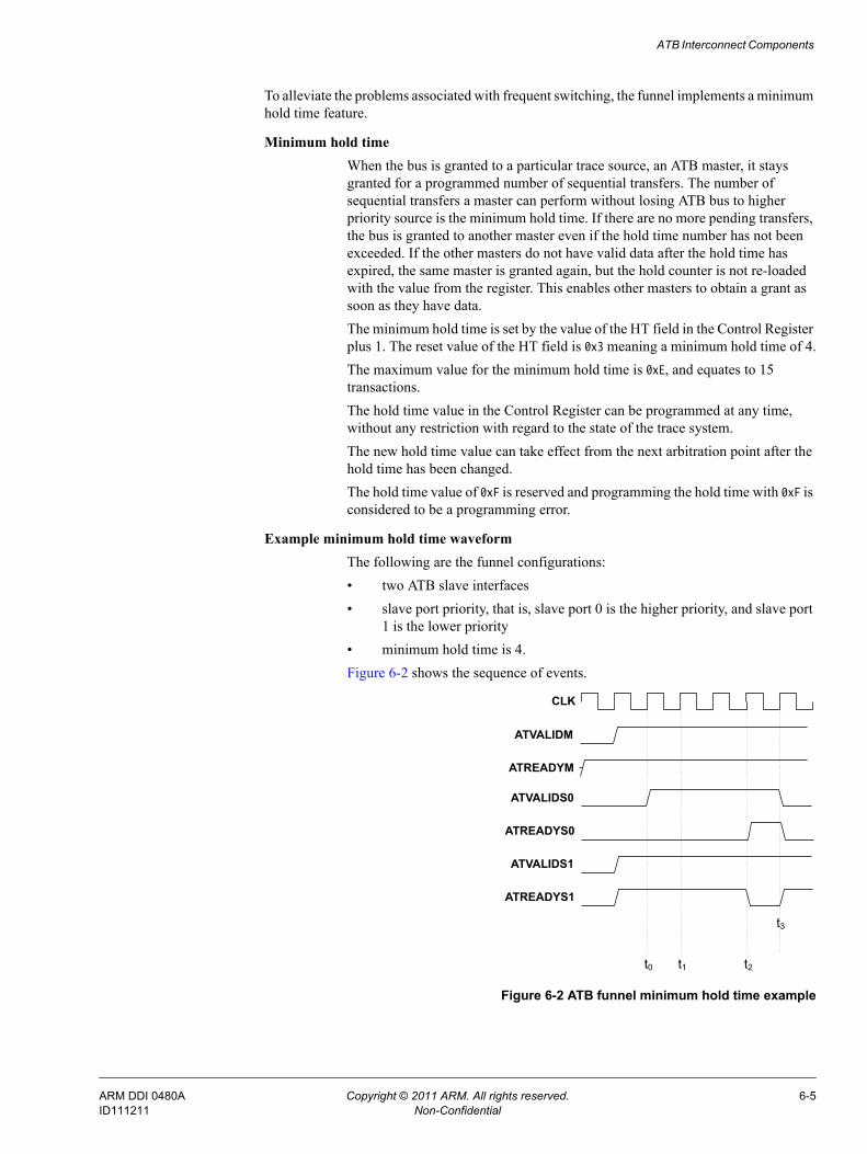
ATB Interconnect Components
To alleviate the problems associated with frequent switching, the funnel implements a minimum hold time feature.
Minimum hold time When the bus is granted to a particular trace source, an ATB master, it stays granted for a programmed number of sequential transfers. The number of sequential transfers a master can perform without losing ATB bus to higher priority source is the minimum hold time. If there are no more pending transfers, the bus is granted to another master even if the hold time number has not been exceeded. If the other masters do not have valid data after the hold time has expired, the same master is granted again, but the hold counter is not re-loaded with the value from the register. This enables other masters to obtain a grant as soon as they have data.The minimum hold time is set by the value of the HT field in the Control Register plus 1. The reset value of the HT field is 0x3 meaning a minimum hold time of 4.The maximum value for the minimum hold time is 0xE, and equates to 15 transactions.The hold time value in the Control Register can be programmed at any time, without any restriction with regard to the state of the trace system.The new hold time value can take effect from the next arbitration point after the hold time has been changed.The hold time value of 0xF is reserved and programming the hold time with 0xF is considered to be a programming error.
Example minimum hold time waveform The following are the funnel configurations:• two ATB slave interfaces• slave port priority, that is, slave port 0 is the higher priority, and slave port
1 is the lower priority• minimum hold time is 4.Figure 6-2 shows the sequence of events.
Figure 6-2 ATB funnel minimum hold time example
CLK
ATVALIDS0
ATREADYS0
ATVALIDS1
ATREADYS1
t0 t1 t2
t3
ATVALIDM
ATREADYM
ARM DDI 0480A Copyright © 2011 ARM. All rights reserved. 6-5ID111211 Non-Confidential
ATB Interconnect Components
Table 6-1 shows the sequence of events in Figure 6-2 on page 6-5.
Priority setting The funnel implements programmable priority for the attached ATB masters. Priority values for each ATB slave interface are defined in a 3-bit field in the Priority Control register. A port programmed with the value 0 gets the highest priority. A port programmed with the value 7 gets the lowest priority. At reset, the default configuration assigns priority 0 to all ports.The bandwidth sharing scheme is used when selecting the next funnel input among masters with equal priority. The priority value for the ATB slave interface is only changed when the ATB slave interface is disabled. Programming the priority value for the enabled ATB slave is considered to be a programming error. The funnel takes the newly programmed priority values at the arbitration point.
Additional consideration for ATID changes Frequent funnel switching results in a trace stream with frequent ATID changes leading to inefficiency in the formatter. In the case of cascaded funnels, even with hold time implemented, some unnecessary ATID changes can still be present in the trace stream.To minimize ATID switching, transfers from a single funnel input are considered sequential only if they have the same ATID.An ID change overrides hold time and causes the funnel to switch to another master with pending transfers.
Arbitration scheme Funnel implements a round robin arbitration scheme.A new arbitration is performed at every arbitration point. An arbitration point occurs when no sources were selected on the previous cycle or when the state of the previously selected source is:• its hold time has expired• its ATID has changed from the previous cycle• its ATVALID signal is LOW• its input has been disabled• its flush has been acknowledged after transfer has been completed.
Table 6-1 Event sequence
Time Event
t0 • slave port 1 is currently selected • higher priority slave port 0 has a pending transfer• slave port 1 remains selected because the minimum hold time has not expired.
t1 • Slave port 1 remains selected because the minimum hold time has not expired.
t2 • Minimum hold time expires for slave port 1 and funnel switches to slave port 0.
t3 • Slave port 0 has no more data to transfer and the funnel switches back to slave port 1.
ARM DDI 0480A Copyright © 2011 ARM. All rights reserved. 6-6ID111211 Non-Confidential
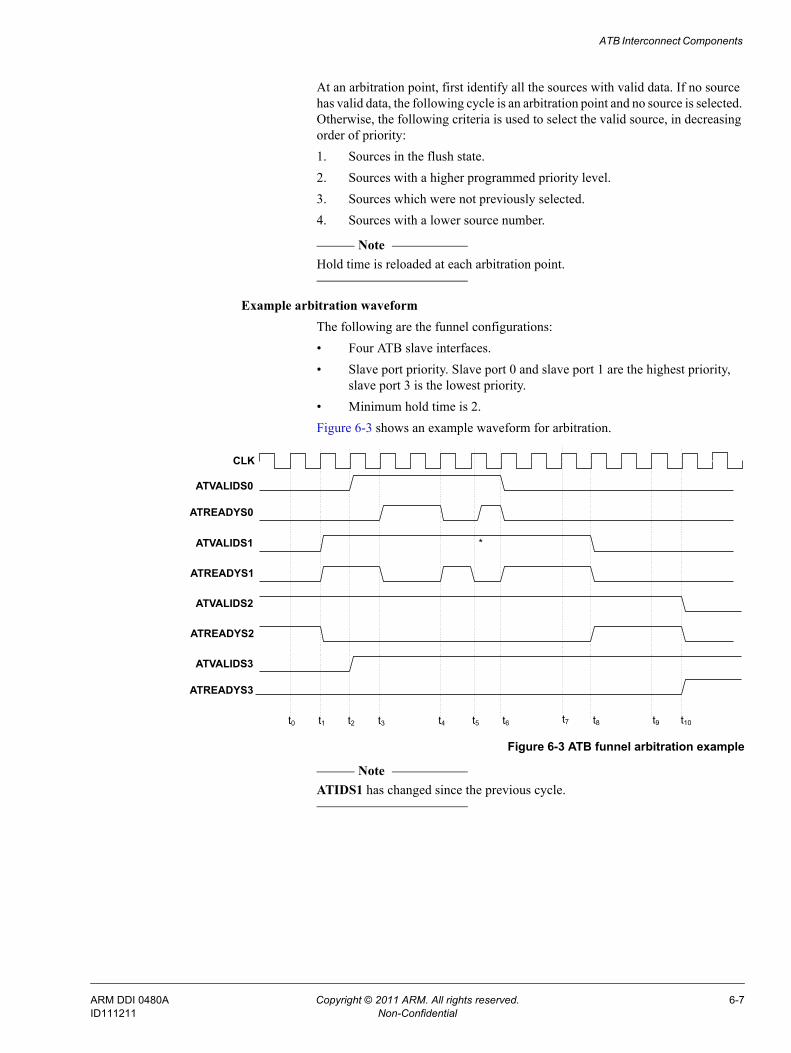
ATB Interconnect Components
At an arbitration point, first identify all the sources with valid data. If no source has valid data, the following cycle is an arbitration point and no source is selected. Otherwise, the following criteria is used to select the valid source, in decreasing order of priority:1. Sources in the flush state.2. Sources with a higher programmed priority level.3. Sources which were not previously selected. 4. Sources with a lower source number.
Note Hold time is reloaded at each arbitration point.
Example arbitration waveform The following are the funnel configurations:• Four ATB slave interfaces.• Slave port priority. Slave port 0 and slave port 1 are the highest priority,
slave port 3 is the lowest priority.• Minimum hold time is 2.Figure 6-3 shows an example waveform for arbitration.
Figure 6-3 ATB funnel arbitration example
Note ATIDS1 has changed since the previous cycle.
CLK
ATVALIDS0
ATVALIDS1
ATREADYS1
ATVALIDS2
ATREADYS3
ATVALIDS3
ATREADYS2
t0 t1 t2 t3 t4
ATREADYS0
t5 t6 t10t8
*
t7 t9
ARM DDI 0480A Copyright © 2011 ARM. All rights reserved. 6-7ID111211 Non-Confidential
ATB Interconnect Components
Table 6-2shows the sequence of events in Figure 6-3 on page 6-7.
6.2.5 Flushing
The funnel implements the flush mechanism. When a flush request is received at the master port of the funnel, all slave ports request a flush together to ensure that all historical trace data is collected. The funnel acknowledges the flush only after all slave ports have completed their flush sequence.
The funnel can assert AFREADYM HIGH when all slave ports have returned AFREADYS HIGH.
To enable devices to drain at different rates, for example, if they were on different clock domains, when the funnel is flushing trace sources, the arbitration process can still be in place. This method stops high priority sources from locking the system if they take a number of cycles to present valid data. Under normal operation, if a high priority source does not present any valid data, then the next highest priority source that does have valid data is selected.
Example flushing waveform The following are the funnel configurations:• four ATB slave interfaces• slave port priority, slave port 0 is the highest priority, and slave port 3 is the
lowest priority• minimum hold time is 2.Figure 6-4 on page 6-9 shows an example waveform for arbitration.
Table 6-2 Event sequence
Time Event
t0 • slave port 2 is currently selected.
t1 • funnel switches to high priority slave port 1.
t2 • high priority slave port 0 asserts ATVALIDS0• lowest priority slave port 3 asserts ATVALIDS3.
t3 • Minimum hold time expires for slave port 1 and the next highest priority port, slave port 0 is selected.
t4 • Minimum hold time expires for slave port 0 and the next highest priority port, slave port 1 is selected.
t5 • ATID changes for slave port 1, minimum hold time is overridden so the next highest priority port, slave port 0 is selected.
t6 • slave port 0 finishes• funnel switches to the next highest priority port, that is, back to slave port 1.
t7 • Minimum hold time expires for slave port 1, but being highest priority it remains selected.
t8 • slave port 1 finishes • funnel switches to next highest priority port that is slave port 2.
t9 • Minimum hold time expires for slave port 2, but being higher priority than slave port 3, it remains selected.
t10 • slave port 3 finishes• funnel switches to the last remaining port, slave port 3.
ARM DDI 0480A Copyright © 2011 ARM. All rights reserved. 6-8ID111211 Non-Confidential
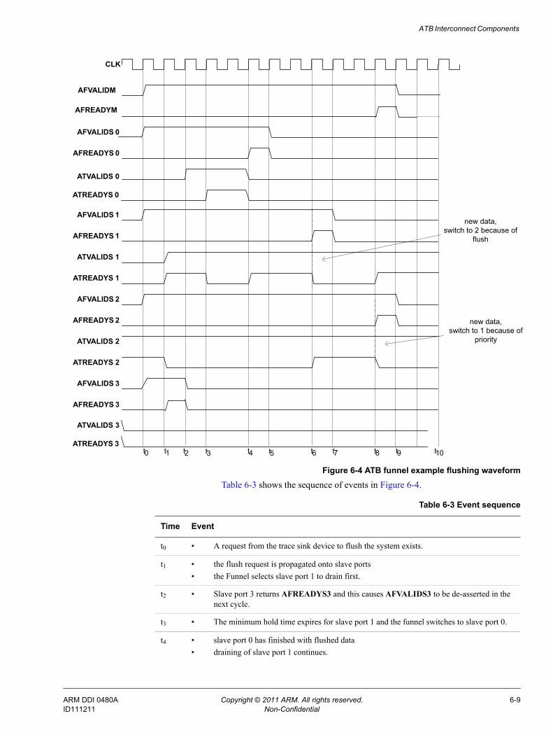
ATB Interconnect Components
Figure 6-4 ATB funnel example flushing waveform
Table 6-3 shows the sequence of events in Figure 6-4.
AFVALIDM
AFREADYM
AFVALIDS 0
AFREADYS 0
AFVALIDS 1
AFREADYS 1
AFVALIDS 2
AFREADYS 2
AFVALIDS 3
AFREADYS 3
ATVALIDS 0
ATVALIDS 1
ATREADYS 1
ATVALIDS 2
ATREADYS 3
ATVALIDS 3
ATREADYS 2
t0 t1 t2 t3 t7
ATREADYS 0
t9
new data,switch to 2 because of
flush
new data,switch to 1 because of
priority
t4 t5 t6 t8 t10
CLK
Table 6-3 Event sequence
Time Event
t0 • A request from the trace sink device to flush the system exists.
t1 • the flush request is propagated onto slave ports• the Funnel selects slave port 1 to drain first.
t2 • Slave port 3 returns AFREADYS3 and this causes AFVALIDS3 to be de-asserted in the next cycle.
t3 • The minimum hold time expires for slave port 1 and the funnel switches to slave port 0.
t4 • slave port 0 has finished with flushed data• draining of slave port 1 continues.
ARM DDI 0480A Copyright © 2011 ARM. All rights reserved. 6-9ID111211 Non-Confidential
ATB Interconnect Components
6.2.6 Syncreq propagation
The funnel can propagate ATB synchronization requests, SYNCREQ, received on ATB master port to all enabled ATB slave ports.
6.2.7 Configuration
The funnel is configured using the debug APB interface.
6.2.8 Cascaded funnel support
The funnel is a combinatorial block and when a cascaded funnel configuration is implemented, a register slice that is a forward, reverse or full register slice, must be instantiated between the cascaded funnels to avoid combinatorial timing loops.
6.2.9 Unlocking funnel access
The Lock Status Register and Lock Access Register control access to the CoreSight funnel to ensure that the possibility of accidental access is extremely small.
The funnel implements a 32-bit Lock Access Register.
6.2.10 Claim scheme
To facilitate cooperation of debug, the funnel implements a CoreSight claim scheme. The Claim Tag registers provide 4 bits that can be separately set and cleared to indicate the current owner of the funnel.
6.2.11 Topology-detection
The funnel supports topology-detection through a set of integration registers that enable reading or writing ATVALID and ATREADY of all the ATB interfaces. Integration mode is enabled by setting the Integration mode bit in the ITCTRL Register.
t5 • AFREADYS0 goes HIGH.
t6 • slave port 1 has finished with flushed data• slave port 1 continues with new data• the funnel selects the last remaining slave in the flush state, slave port 2.
t7 • AFREADYS1 goes HIGH.
t8 • slave port 2 has finished with flushed data• slave port 2 continues with new data• the funnel selects slave port 1 because it is a higher priority port.
t9 • AFREADYS2 goes HIGH• All slave ports have responded with AFREADY HIGH to indicate that there is no more
historical information remaining at this level. This is indicated on AFREADYM with a HIGH response, and this in turn results in AFVALIDM returning LOW.
• The flush sequence is now complete.
Table 6-3 Event sequence (continued)
Time Event
ARM DDI 0480A Copyright © 2011 ARM. All rights reserved. 6-10ID111211 Non-Confidential
ATB Interconnect Components
Register ITATBCTR2 is the Integration Test ATB Control 2 Register. A write to ITATBCTR2 outputs data on ATREADYSn, where n is defined by the status of the Funnel Control Register. A read from ITATBCTR2 returns the data from ATREADYM.
Register ITATBCTR0 is the Integration Test ATB Control 0 Register. A write to ITATBCTR0 sets the value of ATVALIDM. A read from ITATBCTR0 returns the value of ATVALIDSn, where n is defined by the status of the Funnel Control register.
It is illegal to have more than one ATB slave port enabled while in integration mode and performing topology-detection. No hardware protection exists and enabling multiple ports is considered to be a programming error.
After performing integration or topology-detection, you must reset the system to ensure the correct behavior of CoreSight and other connected system components that are affected by the integration or topology-detection.
6.2.12 Fixed configuration funnel
In a fixed configuration, the funnel can not have any user-programmable registers and it can not have an APB slave interface.
The fixed configuration funnel supports the following features:
• all ATB slave ports are enabled
• all ATB slave ports have a priority defined by the port number and a round-robin scheme is implemented if the corresponding configuration option is selected
• the hold time is set to 4 transfers, that is, the HT field value is set to 0x3
• the funnel is transparent for topology-detection.
ARM DDI 0480A Copyright © 2011 ARM. All rights reserved. 6-11ID111211 Non-Confidential
ATB Interconnect Components
6.3 ATB upsizerThe ATB upsizer combines narrow trace data into wider data.
See the CoreSight SoC User Guide for a description of the key features and configuration options of the ATB upsizer.
6.3.1 Clocks and reset
The bridge operates on a single clock CLK.
RESETn is used as an asynchronous reset in the entire design.
6.3.2 Functional interface
The ATB upsizer has a slave port of narrow width and a master port of wider width. The widths of the master and slave ports are configurable.
6.3.3 Component functionality
The following describes the functionality of the ATB upsizer:
Normal operation The ATB upsizer merges transfers from the narrow ATB slave interface, and outputs buffered data on a wider master interface.The ATB upsizer preserves the ATB features, LSB-aligned, and packed data.The following are the rules for transfer merging:• Merge the transfers with same ATID. The ATID change stops the merging
process.• Data is merged until:
— the wide ATB bus data word is completed— less than the full narrow ATB data bus is received.
• When data is part of a flush, flush acknowledges, AFVALIDS, and AFREADYS can end the merging process.— Any data transferred along with a flush acknowledge must not be
merged with the flush data.
ATREADYS and ATVALIDM generation The upsizer data path consists of wide and narrow buffers.Data from a slave port is written to a wide buffer until:• the wide buffer is full• there is a merge stop event such as a ATID change.The ATREADYS signal is HIGH when an upsizer is ready to accept new data, that is, until data is written to a narrow buffer. The ATVALIDM is asserted HIGH after:• the wide buffer is filled• there is a merge stop event such as a ATID change.
ATBYTES calculation The ATB upsizer calculates the master side ATBYTES to match the number of bytes in the output transfer.
ARM DDI 0480A Copyright © 2011 ARM. All rights reserved. 6-12ID111211 Non-Confidential
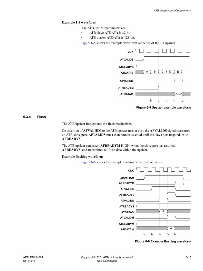
ATB Interconnect Components
Example 1:4 waveform The ATB upsizer parameters are:• ATB slave ATDATA is 32-bit• ATB master ATDATA is 128-bit.Figure 6-5 shows the example waveform sequence of the 1:4 upsizer.
Figure 6-5 Upsizer example waveform
6.3.4 Flush
The ATB upsizer implements the flush mechanism.
On assertion of AFVALIDM to the ATB upsizer master port, the AFVALIDS signal is asserted on ATB slave port. AFVALIDS must then remain asserted until the slave port responds with AFREADYS.
The ATB upsizer can assert AFREADYM HIGH, when the slave port has returned AFREADYS, and transmitted all flush data within the upsizer.
Example flushing waveform Figure 6-6 shows the example flushing waveform sequence.
Figure 6-6 Example flushing waveform
CLK
ATVALIDS
ATREADYS
ATVALIDM
ATREADYM
t0 t1 t2
ATDATAS A B C
DCBA
D E
t4t3
ATDATAM
CLK
AFVALIDM
AFREADYM
t0 t1 t2
ATDATAS A
AFVALIDS
AFREADYS
ATVALIDS
ATREADYS
t4ATDATAM A
ATVALIDM
ATREADYM
t3
ARM DDI 0480A Copyright © 2011 ARM. All rights reserved. 6-13ID111211 Non-Confidential
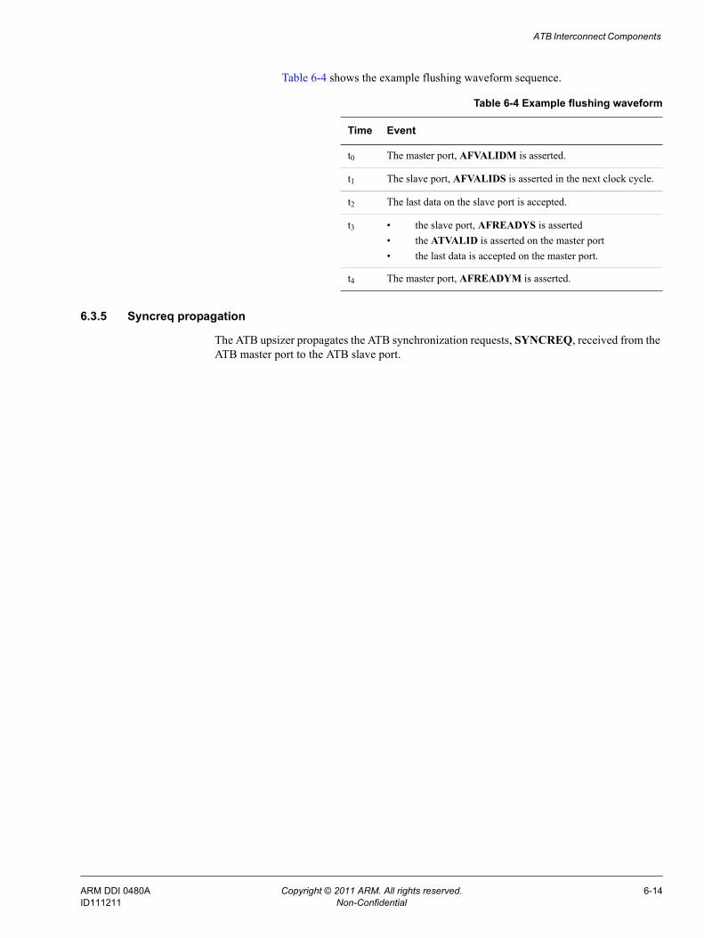
ATB Interconnect Components
Table 6-4 shows the example flushing waveform sequence.
6.3.5 Syncreq propagation
The ATB upsizer propagates the ATB synchronization requests, SYNCREQ, received from the ATB master port to the ATB slave port.
Table 6-4 Example flushing waveform
Time Event
t0 The master port, AFVALIDM is asserted.
t1 The slave port, AFVALIDS is asserted in the next clock cycle.
t2 The last data on the slave port is accepted.
t3 • the slave port, AFREADYS is asserted• the ATVALID is asserted on the master port• the last data is accepted on the master port.
t4 The master port, AFREADYM is asserted.
ARM DDI 0480A Copyright © 2011 ARM. All rights reserved. 6-14ID111211 Non-Confidential
ATB Interconnect Components
6.4 ATB downsizerThe ATB downsizer splits the wide trace data into multiple items of narrow data.
See the CoreSight SoC User Guide for a description of the key features and configuration options of the ATB downsizer.
6.4.1 Clocks and reset
The ATB downsizer has a single clock domain with clock input, CLK. The ATB downsizer has a single reset input, RESETn.
RESETn is used as the asynchronous active LOW reset.
6.4.2 Functional interface
The ATB downsizer has one ATB slave interface and one ATB master interface.
The slave ATB interface connects to replicators, trace sources, and trace links, or any other component with a standard ATB master.
The master interface connects to replicators, trace sinks, and trace links, or any other component with a standard ATB slave.
6.4.3 Component functionality
The following describes the functionality of the ATB downsizer:
Normal operation The downsizer splits transfers from the wide ATB slave interface, and outputs them as multiple transfers on a narrower master interface.The ATB master data remains LSB-aligned and packed.
Splitting rules The rules for transfer split are:• break the transfer into a number of multiple smaller sub-transfers based on
ATBYTESS• the ATIDM of each sub-transfer is the same as the original transfer ATIDS• the ATBYTESM is calculated for each sub-transfer.
ATREADYS and ATVALIDM generation The ATB downsizer data path consists of a data multiplexor.A transaction on the slave port is held until all sub-transfers are finished on the master port. The ATREADYS signal goes HIGH, when the last ATREADYM signal goes HIGH.The ATVALIDM signal is asserted when the ATVALIDS signal is asserted. It stays asserted until the last sub-transfer is acknowledged with ATREADYM.
ATBYTES calculation The downsizer calculates the master side, ATBYTESM, to match the number of bytes in the output transfer.
ARM DDI 0480A Copyright © 2011 ARM. All rights reserved. 6-15ID111211 Non-Confidential
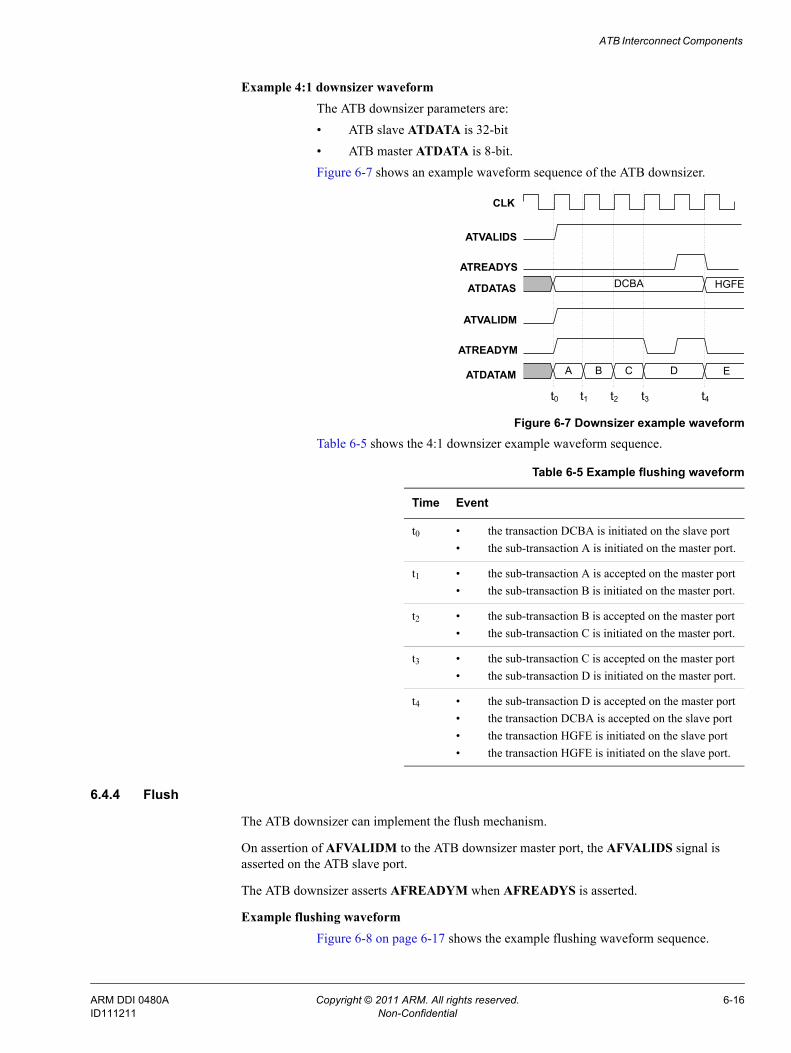
ATB Interconnect Components
Example 4:1 downsizer waveform The ATB downsizer parameters are:• ATB slave ATDATA is 32-bit• ATB master ATDATA is 8-bit.Figure 6-7 shows an example waveform sequence of the ATB downsizer.
Figure 6-7 Downsizer example waveform
Table 6-5 shows the 4:1 downsizer example waveform sequence.
6.4.4 Flush
The ATB downsizer can implement the flush mechanism.
On assertion of AFVALIDM to the ATB downsizer master port, the AFVALIDS signal is asserted on the ATB slave port.
The ATB downsizer asserts AFREADYM when AFREADYS is asserted.
Example flushing waveform Figure 6-8 on page 6-17 shows the example flushing waveform sequence.
ATVALIDS
ATREADYS
ATVALIDM
ATREADYM
t0 t1 t2
ATDATAS DCBA
t4t3
A B C DATDATAM
HGFE
E
CLK
Table 6-5 Example flushing waveform
Time Event
t0 • the transaction DCBA is initiated on the slave port• the sub-transaction A is initiated on the master port.
t1 • the sub-transaction A is accepted on the master port• the sub-transaction B is initiated on the master port.
t2 • the sub-transaction B is accepted on the master port• the sub-transaction C is initiated on the master port.
t3 • the sub-transaction C is accepted on the master port• the sub-transaction D is initiated on the master port.
t4 • the sub-transaction D is accepted on the master port• the transaction DCBA is accepted on the slave port• the transaction HGFE is initiated on the slave port• the transaction HGFE is initiated on the slave port.
ARM DDI 0480A Copyright © 2011 ARM. All rights reserved. 6-16ID111211 Non-Confidential
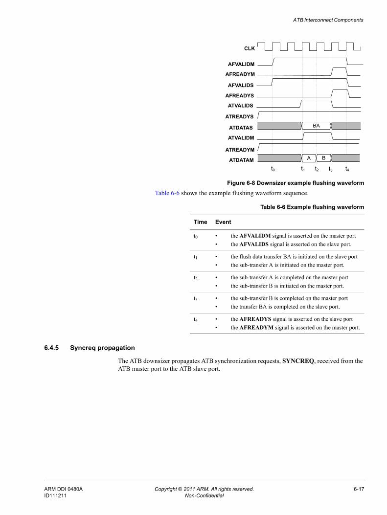
ATB Interconnect Components
Figure 6-8 Downsizer example flushing waveform
Table 6-6 shows the example flushing waveform sequence.
6.4.5 Syncreq propagation
The ATB downsizer propagates ATB synchronization requests, SYNCREQ, received from the ATB master port to the ATB slave port.
CLK
AFVALIDM
AFREADYM
t0 t1 t2
ATDATAS BA
AFVALIDS
AFREADYS
ATVALIDS
ATREADYS
t4ATDATAM B
ATVALIDM
ATREADYM
t3
A
Table 6-6 Example flushing waveform
Time Event
t0 • the AFVALIDM signal is asserted on the master port• the AFVALIDS signal is asserted on the slave port.
t1 • the flush data transfer BA is initiated on the slave port• the sub-transfer A is initiated on the master port.
t2 • the sub-transfer A is completed on the master port• the sub-transfer B is initiated on the master port.
t3 • the sub-transfer B is completed on the master port• the transfer BA is completed on the slave port.
t4 • the AFREADYS signal is asserted on the slave port• the AFREADYM signal is asserted on the master port.
ARM DDI 0480A Copyright © 2011 ARM. All rights reserved. 6-17ID111211 Non-Confidential
Chapter 7 DAPBUS Interconnect
This chapter describes the DAPBUS interconnect. It contains the following sections:• About the DAPBUS interconnect on page 7-2• DAPBUS interconnect interfaces on page 7-3• Main modes of operation on page 7-4.
ARM DDI 0480A Copyright © 2011 ARM. All rights reserved. 7-1ID111211 Non-Confidential
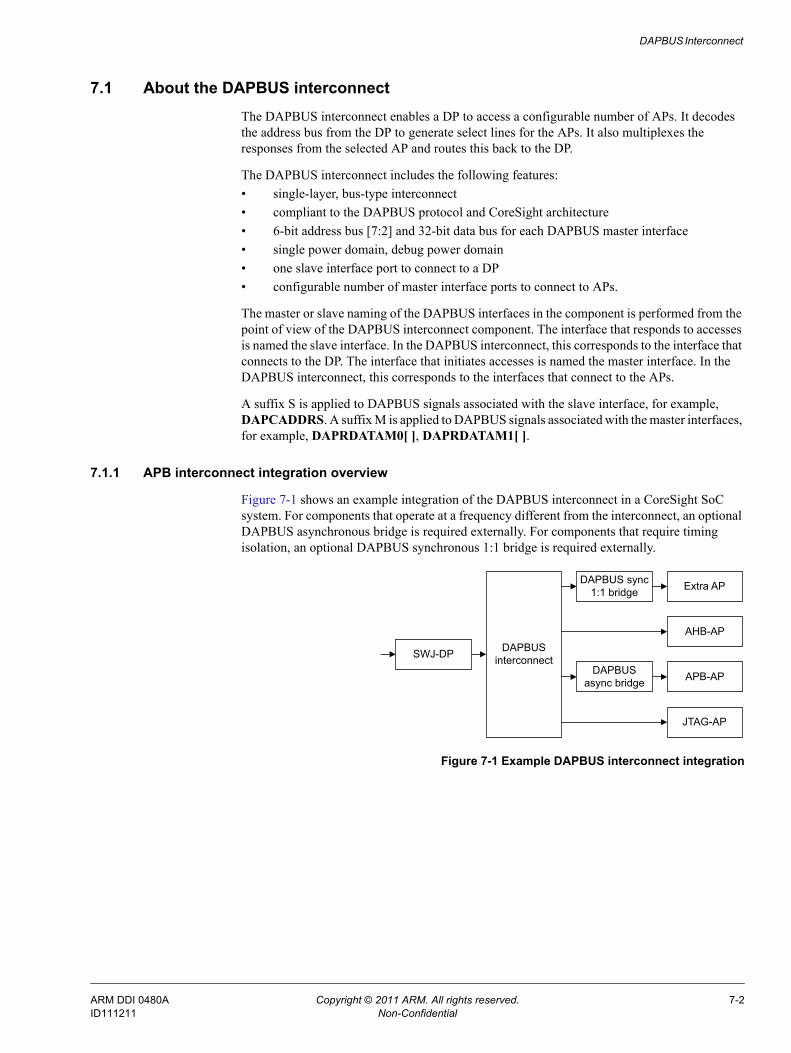
DAPBUS Interconnect
7.1 About the DAPBUS interconnectThe DAPBUS interconnect enables a DP to access a configurable number of APs. It decodes the address bus from the DP to generate select lines for the APs. It also multiplexes the responses from the selected AP and routes this back to the DP.
The DAPBUS interconnect includes the following features:• single-layer, bus-type interconnect• compliant to the DAPBUS protocol and CoreSight architecture• 6-bit address bus [7:2] and 32-bit data bus for each DAPBUS master interface• single power domain, debug power domain• one slave interface port to connect to a DP• configurable number of master interface ports to connect to APs.
The master or slave naming of the DAPBUS interfaces in the component is performed from the point of view of the DAPBUS interconnect component. The interface that responds to accesses is named the slave interface. In the DAPBUS interconnect, this corresponds to the interface that connects to the DP. The interface that initiates accesses is named the master interface. In the DAPBUS interconnect, this corresponds to the interfaces that connect to the APs.
A suffix S is applied to DAPBUS signals associated with the slave interface, for example, DAPCADDRS. A suffix M is applied to DAPBUS signals associated with the master interfaces, for example, DAPRDATAM0[ ], DAPRDATAM1[ ].
7.1.1 APB interconnect integration overview
Figure 7-1 shows an example integration of the DAPBUS interconnect in a CoreSight SoC system. For components that operate at a frequency different from the interconnect, an optional DAPBUS asynchronous bridge is required externally. For components that require timing isolation, an optional DAPBUS synchronous 1:1 bridge is required externally.
Figure 7-1 Example DAPBUS interconnect integration
SWJ-DP DAPBUS interconnect
DAPBUS async bridge
DAPBUS sync 1:1 bridge
AHB-AP
Extra AP
JTAG-AP
APB-AP
ARM DDI 0480A Copyright © 2011 ARM. All rights reserved. 7-2ID111211 Non-Confidential
DAPBUS Interconnect
7.2 DAPBUS interconnect interfacesThis section describes the DAPBUS interconnect interfaces in:• Clock and reset• Functional interfaces.
7.2.1 Clock and reset
This component is a combinational block. All interfaces to this component are synchronous to the same clock, CLK. This component has an asynchronous active-LOW reset input, RESETn. The CLK and RESETn signals are not used internally in the DAPBUS interconnect.
7.2.2 Functional interfaces
The DAPBUS interconnect has one DAPBUS slave interface. It has a configurable number of DAPBUS master interfaces, based on the NUM_MASTER_INTF configuration option.
ARM DDI 0480A Copyright © 2011 ARM. All rights reserved. 7-3ID111211 Non-Confidential
DAPBUS Interconnect
7.3 Main modes of operationThe following are the main modes of operation of the device:• Address decoding accesses from the DP• Multiplexing responses from the selected AP.
7.3.1 Address decoding accesses from the DP
To address a particular Access Port (AP), the Debug Port (DP) uses the eight MSBs of its address bus, DAPCADDRS[15:2]. The value driven on these address lines is determined by the APSEL[7:0] field in the AP Select register that is present on all DP implementations compliant with the ARM Debug Interface v5 Architecture.
When DAPSELS from the slave interface is asserted, the master interfaces 0 to NUM_MASTER_INTF are selected by comparing DAPCADDRS[15:8] with values 0x00 to (NUM_MASTER_INTF – 1). DAPSELMx of the selected master is also asserted. Addresses outside this range result in an internal default slave being selected.
The default slave, when selected, returns a DAPREADYS without an error on DAPSLVERRS.
DAPCADDRS[7:2] is routed to the master interfaces to select registers within APs.
7.3.2 Multiplexing responses from the selected AP
The DAPSELMx, where x = 0-(NUM_MASTER_INTF-1) set of select lines is one-hot. The DAPSELMx signals are used to multiplex the responses from the selected master interface to the slave interface, for example, DAPRDATAS[31:0], DAPSLVERRS, and DAPREADYS.
ARM DDI 0480A Copyright © 2011 ARM. All rights reserved. 7-4ID111211 Non-Confidential
Chapter 8 Timestamp Components
This chapter describes the timestamp component. It contains the following sections:• About the timestamp components on page 8-2• Timestamp solution on page 8-3.
ARM DDI 0480A Copyright © 2011 ARM. All rights reserved. 8-1ID111211 Non-Confidential
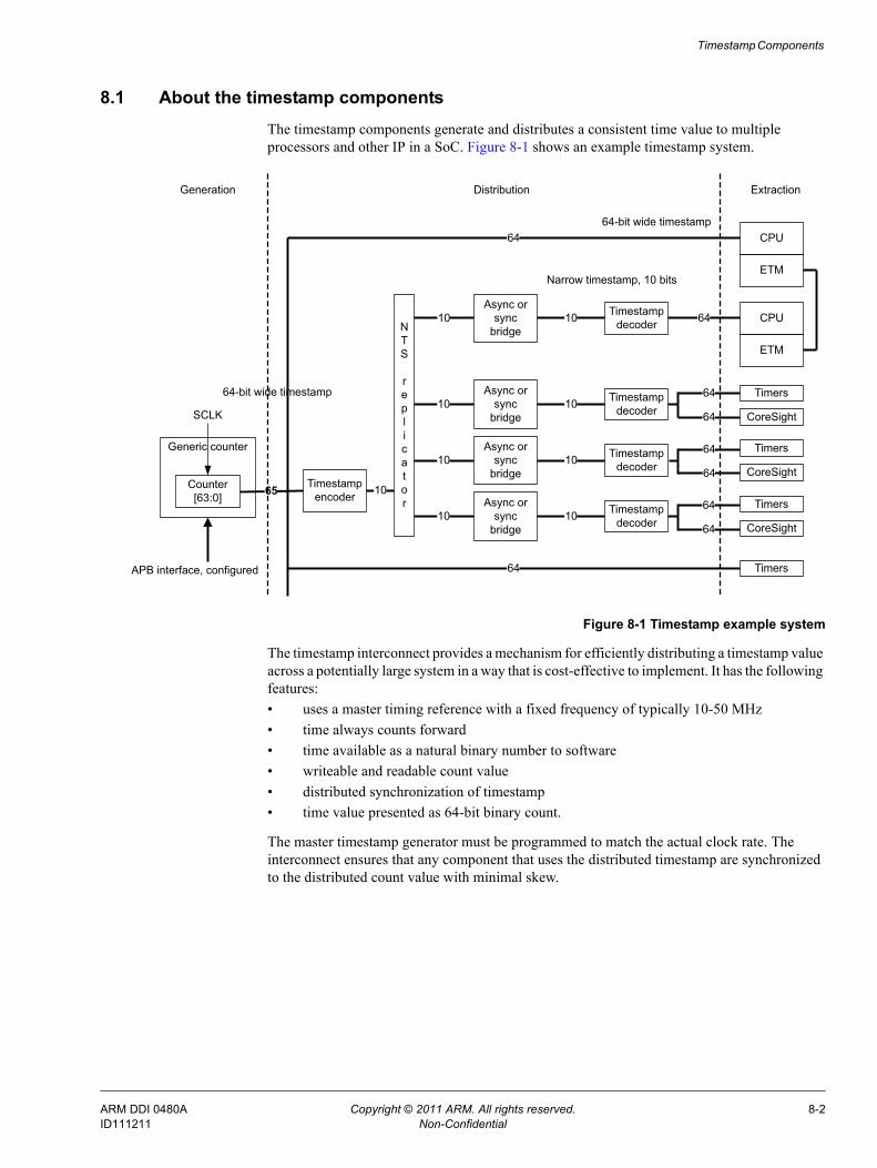
Timestamp Components
8.1 About the timestamp componentsThe timestamp components generate and distributes a consistent time value to multiple processors and other IP in a SoC. Figure 8-1 shows an example timestamp system.
Figure 8-1 Timestamp example system
The timestamp interconnect provides a mechanism for efficiently distributing a timestamp value across a potentially large system in a way that is cost-effective to implement. It has the following features:• uses a master timing reference with a fixed frequency of typically 10-50 MHz• time always counts forward• time available as a natural binary number to software• writeable and readable count value• distributed synchronization of timestamp• time value presented as 64-bit binary count.
The master timestamp generator must be programmed to match the actual clock rate. The interconnect ensures that any component that uses the distributed timestamp are synchronized to the distributed count value with minimal skew.
65
APB interface, configured
Generation Distribution
Counter [63:0]
Generic counter
SCLK
Async or sync
bridge
Async or sync
bridge
Timestampdecoder
Timestampdecoder
10
10
Timestampencoder
NTS
replicator
Async or sync
bridge
Timestampdecoder10
Timers
CoreSight
Timers
CoreSight
Extraction
Timers
CoreSight
CPU
CPU
ETM
ETM
6464-bit wide timestamp
Narrow timestamp, 10 bits
10
10
10
Async or sync
bridge
Timestampdecoder10 10 64
10
Timers64
64
64
64
64
64
64
64-bit wide timestamp
ARM DDI 0480A Copyright © 2011 ARM. All rights reserved. 8-2ID111211 Non-Confidential
Timestamp Components
8.2 Timestamp solutionThe timestamp solution includes the following individual components:• Master timestamp generator• Timestamp encoder on page 8-7• Narrow timestamp replicator on page 8-7• Timestamp decoder on page 8-7.
Only the master timestamp generator is programmable. All other components have no programmers model and operate autonomously.
See Chapter 2 Functional Overview for more information about block diagrams and its key features.
See the CoreSight SoC User Guide for more information about the configurable parameters and its options timestamp components.
8.2.1 Master timestamp generator
The timestamp generator has the following features:
• Writeable or readable count value.
• Clocked by SCLK.
• SCLK is fixed frequency.
• Outputs time as a 64-bit binary number using the wide timestamp interface, with an indicator that the value has been written and must be resynchronized to all receivers.
• Increments at each tick of SCLK.
• It can be optionally halted when any processor enters debug state.
This section describes the timestamp generator component and its functionality. It contains the following sections:• Clock and reset• Functionality• Register block on page 8-4• Counter on page 8-6.
Clock and reset
The Timestamp Generator has the following clock and reset domain:• a single clock, CLK• a reset, RESETn.
The reset, RESETn, must be asserted asynchronously, but deasserted synchronous to the clock, CLK.
Functionality
The counter has the following functions:
• Runs at a constant clock frequency, regardless of the power and clocking state of the processor cores using it.
• Continues to run in all levels of power-down other than completely turning off the system.
ARM DDI 0480A Copyright © 2011 ARM. All rights reserved. 8-3ID111211 Non-Confidential
Timestamp Components
• Its size is 64-bits.
• It starts from 0.
• The counter value can be read or written using 32-bit read on an APB interface.
• The counter value can be written only when it is either halted or disabled.
• Has an APB interface, access protections requires assistance from other peripherals such as the Trustzone Address Space Controller (TZASC). See the CoreLink TrustZone Address Space Controller TZC-380 Technical Reference Manual.
• When the system is halted as a result of debug, the counter can be programmed to either halt or continue incrementing.
Register block
The register block has the following features:
• Implements all the programmable registers and status registers, see Chapter 3 Programmers Model for more information.
• Implements APB interfaces, that is, a control interface and a RO interface, in which all the inputs are registered using a single stage of flip-flops
• The RO interface is expected to map to a non-secure memory region and only supports read access to a limited subset of the register map.
• The control interface is expected to map to a secure memory region if the system supports it, and also supports read and write access.— it generates control signals to enable and disable counter operation— it enables update of counter value based on a new programmed value.
• The control interface has a higher priority over the RO interface.— A fixed priority is implemented where if a read or a write request on this interface
coincides with the read request on the RO interface, then requests on the RO have wait states while the control interface completes its transaction.
— The read data path is registered. Therefore, all read-access have at least one cycle of wait state.
Note Because the control interface has higher priority, it always has only one cycle of wait state.
At best, the RO interface has a single wait state, but if it coincides with an access on the control interface, then it has two wait-states before the read access is complete.
Figure 8-2 on page 8-5 shows the write access to enable counter and read access.
ARM DDI 0480A Copyright © 2011 ARM. All rights reserved. 8-4ID111211 Non-Confidential
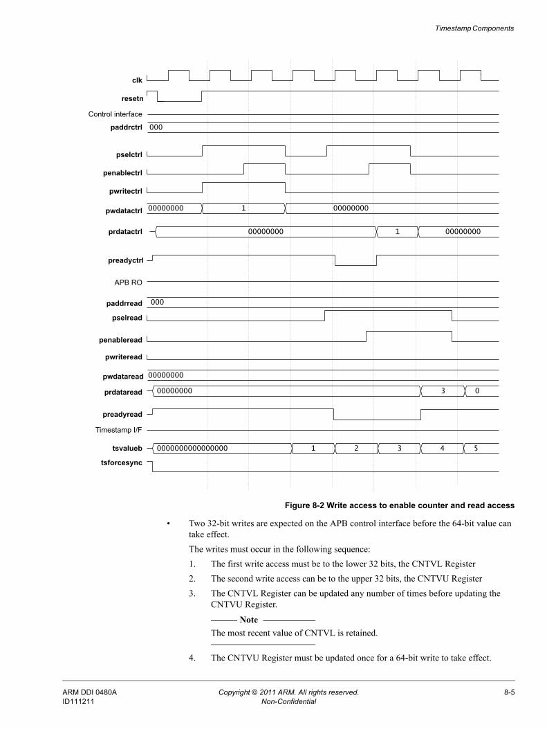
Timestamp Components
Figure 8-2 Write access to enable counter and read access
• Two 32-bit writes are expected on the APB control interface before the 64-bit value can take effect.The writes must occur in the following sequence:1. The first write access must be to the lower 32 bits, the CNTVL Register2. The second write access can be to the upper 32 bits, the CNTVU Register3. The CNTVL Register can be updated any number of times before updating the
CNTVU Register.
Note The most recent value of CNTVL is retained.
4. The CNTVU Register must be updated once for a 64-bit write to take effect.
00000000
1 00000000
00000000 1 00000000
00000000
3
0000000000000000 1 2 3 4
clk
resetn
Control interface
pselctrl
penablectrl
pwritectrl
pwdatactrl
prdatactrl
preadyctrl
Timestamp I/F
tsvalueb
tsforcesync
paddrctrl
APB RO
pselread
penableread
pwriteread
pwdataread
prdataread
preadyread
paddrread
000
000
5
0
00000000
ARM DDI 0480A Copyright © 2011 ARM. All rights reserved. 8-5ID111211 Non-Confidential
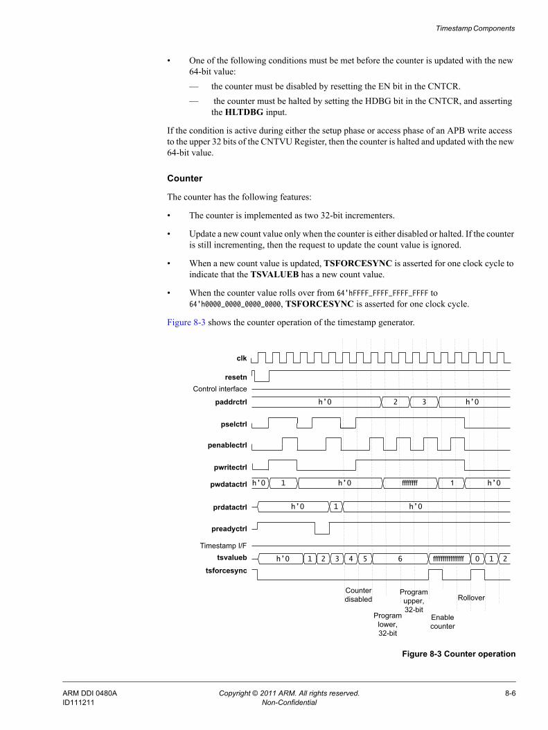
Timestamp Components
• One of the following conditions must be met before the counter is updated with the new 64-bit value:— the counter must be disabled by resetting the EN bit in the CNTCR.— the counter must be halted by setting the HDBG bit in the CNTCR, and asserting
the HLTDBG input.
If the condition is active during either the setup phase or access phase of an APB write access to the upper 32 bits of the CNTVU Register, then the counter is halted and updated with the new 64-bit value.
Counter
The counter has the following features:
• The counter is implemented as two 32-bit incrementers.
• Update a new count value only when the counter is either disabled or halted. If the counter is still incrementing, then the request to update the count value is ignored.
• When a new count value is updated, TSFORCESYNC is asserted for one clock cycle to indicate that the TSVALUEB has a new count value.
• When the counter value rolls over from 64'hFFFF_FFFF_FFFF_FFFF to 64'h0000_0000_0000_0000, TSFORCESYNC is asserted for one clock cycle.
Figure 8-3 shows the counter operation of the timestamp generator.
Figure 8-3 Counter operation
2 3 h’0 h’0
1 h’0 ffffffff 1 h’0
h’0 1
h’0 4 5321 6 ffffffffffffffff 10
Counterdisabled
Programlower, 32-bit
Programupper, 32-bit
Enable counter
Rollover
clk
resetnControl interface
paddrctrl
pselctrl
penablectrl
pwritectrl
pwdatactrl
prdatactrl
preadyctrl
Timestamp I/Ftsvalueb
tsforcesync
h’0
h’0
2
ARM DDI 0480A Copyright © 2011 ARM. All rights reserved. 8-6ID111211 Non-Confidential
Timestamp Components
8.2.2 Timestamp encoder
The timestamp encoder has the following features:
• Transforms a 64-bit binary count value to a 7-bit encoded value.
• Encodes and sends the binary count value over a 2-bit synchronization channel. Other CoreSight trace components use this information when they are powered-up and must re-establish the latest timestamp.
• Works on a single clock input.
Synchronization information is continuously output over the 2-bit synchronization channel.
8.2.3 Narrow timestamp replicator
The narrow timestamp replicator is connected to the output of the encoder and has the following features:
• Distributes encoded data and the synchronization channel to multiple slave bridges.
• Can be connected to the output of an asynchronous or synchronous bridge for additional distribution to multiple bridges downstream. It can only be used to distribute to bridges in the same power domain.
• Combines the ready input from multiple slave bridges and provides a unified ready output to the master encoder or bridge.
• When it is connected to encoder, ts_bit_valid_qualify must be tied LOW and when it is connected to an asynchronous or synchronous bridge, ts_bit_valid_qualify must be tied HIGH.
8.2.4 Timestamp decoder
The narrow timestamp decoder decodes the 7-bit encoded value to generate a 64-bit binary count value and:
• uses this information from a CoreSight trace component that is powered-up and requires the latest timestamp value
• decodes the timestamp value in the following steps:— reconstructs the latest timestamp value by using information from the
synchronization channel— increments the count value based on the encoded value.
When the timestamp decoder reconstructs the latest timestamp value, it drives tsvalue[63:0] to 0 to indicate that the timestamp value is invalid and it is in the process of reconstructing a new timestamp value.
When the timestamp decoder detects a value of 0x7F on the tsbit, it stops incrementing the count value and starts monitoring the sync-channel to reconstruct the new timestamp.
ARM DDI 0480A Copyright © 2011 ARM. All rights reserved. 8-7ID111211 Non-Confidential
Chapter 9 Embedded Cross Trigger
This chapter describes the ECT, CTI, and the CTM. It contains the following sections:• About the ECT on page 9-2• ECT programmers model on page 9-5• ECT connectivity recommendations on page 9-6• ECT authentication requirements on page 9-7.
ARM DDI 0480A Copyright © 2011 ARM. All rights reserved. 9-1ID111211 Non-Confidential
Embedded Cross Trigger
9.1 About the ECTThe ECT for CoreSight consists of a number of CTIs and CTMs connected together. You can operate a single CTI without the requirement for a CTM.
9.1.1 How ECT works
The ECT provides an interface to the debug system as Figure 9-1shows. This enables ARM/ETM subsystems to interact, that is, cross trigger with each other. The debug system enables debug support for multiple cores, together with cross triggering between the cores and their respective ETMs.
The main function of the ECT is to pass debug events from one core to another. For example, the ECT can communicate debug state information from one core to another, so that program execution on both processors can be stopped at the same time, if required.
Cross Trigger Interface (CTI) The CTI combines and maps the trigger requests, and broadcasts them to all other interfaces on the ECT as channel events. When the CTI receives a channel event it maps this onto a trigger output. This enables subsystems to cross trigger with each other. The receiving and transmitting of triggers is performed through the trigger interface.
Cross Trigger Matrix (CTM) This block controls the distribution of channel events. It provides Channel Interfaces (CIs) for connection to either CTIs or CTMs. This enables multiple CTIs to be linked together.
Figure 9-1 CoreSight CTI and CTM block diagram
9.1.2 CTI handshaking, synchronization, and clocks
This section describes handshaking, synchronization, and clocks. It contains the following sections:• Interfaces handshake protocol on page 9-3• Synchronization on page 9-3• Clock domains on page 9-3.
APB interface
Control registers
MappingChannel
handshaking
Triggerhandshaking
Cross Trigger Interface
Cross Trigger Matrix
Trigger Inputs
Trigger Outputs
Debug Channel
Bus
APB
ARM DDI 0480A Copyright © 2011 ARM. All rights reserved. 9-2ID111211 Non-Confidential
Embedded Cross Trigger
Interfaces handshake protocol
The CTI does not interpret the signals on the CI or Trigger Interface (TI). If handshaking is enabled, then it is assumed the events are edge-triggered. As a result, closely occurring events can be unreliably recognized. An event is transmitted as a level. If you require edge detection or single pulse output you must implement the necessary shaping logic in the external wrapper.
To avoid any incompatibility, the following protocol are defined:
• Only logic 1 is interpreted as an event.
• If the handshake is enabled, an output must stay active until an acknowledgement by hardware or optionally acknowledged by software for the TI is received, even if the acknowledge signal driver is deactivated.
If the handshaking is enabled, the CTI can only handle one-shot events. If events are close to one another, or multi-shot, and mapped to the same channel they are possibly merged into one event on an output trigger. For debug events such as breakpoint, trace start, and trace stop this does not cause a problem because input events mapped to the same triggers are required to do the same thing.
Events arising from different interfaces but mapped to the same channel might also be merged. This is acceptable because the mapping logic can be programmed to enable this. Events can be merged because blocks handshake between asynchronous clock domains or channels events are mapped onto the same output trigger.
If the events sent on the CTI emanate from the same clock domain then you can bypass the handshaking and synchronizing logic. The output does not receive an acknowledgement. In such cases you can use the CTI to transmit multiple shot events. The output has to remain active for at least one clock cycle to ensure it is captured at the destination interface.
Synchronization
Some systems might require clock-domain crossing synchronizers for inputs and outputs to the CTI, this can result in variations in the delay that can be expected between a signal that is generated and the signal that is sampled.
Clock domains
In most systems, the CTICLK is connected to the same clock as its local processor and the CTMCLK is connected to the fastest processor clock in the system so reducing the trigger latency and the requirement for clock enable ports.
If a CTI is going to be disabled while the processor enters a clock stopped mode, ARM recommends that:
• The CTI turns off the event-to-channel mapping, so that unwanted events are not generated to the CTM.
• The channel-to-event mapping circuit is turned off or disabled for a few clock cycles after the clock is on.
• This version of the CTI must not be connected to clocks that might be removed, that is stopped. This version of the CTI must not be placed within a power domain that can be turned off. In these scenarios, ARM recommends that CTICLK is the same as CTMCLK.
ARM DDI 0480A Copyright © 2011 ARM. All rights reserved. 9-3ID111211 Non-Confidential
Embedded Cross Trigger
When a processor clock is stopped, for example, waiting for an interrupt, the corresponding CTI can receive an event from the CTM. When the CTI clock is the same as the subsystem clock and the handshaking is not bypassed, the CTM keeps the signal active until an acknowledgement is received, which only occurs when the clock is started again. In this case, out-of-date events can happen on the core. This does not inhibit the channel being used by other processors.
However, if the CTI clock differs from the local processor clock, for example, it is gated differently, it is possible for the CTI to raise an event to the core using CTITRIGOUT, while the processor clock is off. If raising an event to the core must be avoided, the processor must disable its CTI before stopping the clock.
Linking CTIs and CTMs
Where the clock used on a CTI and a connected CTM, or CTM to CTM, or CTI to CTI, is asynchronous, then both the handshaking logic and synchronization registers must be left enabled, that is, CIHSBYPASS and CISBYPASS must be tied LOW.
If both devices have synchronous clocks then synchronization can be bypassed, CISBYPASS tied HIGH, to reduce latency.
If both clocks are the same, that is, CTMCLK = CTICLK, and the channel is required to send multi-shot events, the handshaking can be bypassed by tying CIHSBYPASS HIGH.
ARM DDI 0480A Copyright © 2011 ARM. All rights reserved. 9-4ID111211 Non-Confidential
Embedded Cross Trigger
9.2 ECT programmers modelThe base addresses of the CTIs are not fixed, and can be different for any particular system implementation. However, the offset of any particular register from the base address is fixed. Each CTI has a 4KB programmers model. Each CTI must be programmed separately. All unused memory space is reserved.
The following applies to all registers:
• Reserved or unused bits of registers must be written as 0, and ignored on a read unless otherwise stated in the text.
• All register bits are reset to 0 unless otherwise stated in the text.
• All registers must be accessed as words and so are compatible with big-endian and little-endian systems.
Note The CTM does not have a programmers model itself because it is a link between two or more CTIs, or additional CTMs.
For more information, see Chapter 3 Programmers Model.
ARM DDI 0480A Copyright © 2011 ARM. All rights reserved. 9-5ID111211 Non-Confidential

Embedded Cross Trigger
9.3 ECT connectivity recommendationsContact ARM for full details on the standardized connections between ARM processors, CoreSight components, and the ECT interconnect.
ARM DDI 0480A Copyright © 2011 ARM. All rights reserved. 9-6ID111211 Non-Confidential
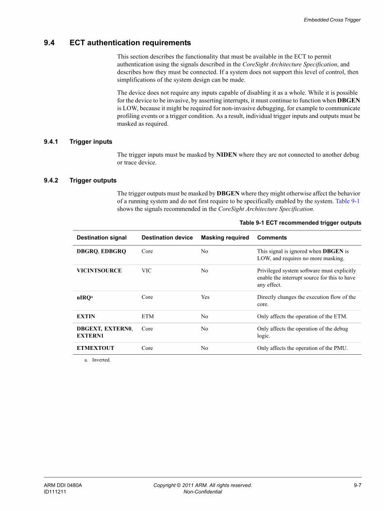
Embedded Cross Trigger
9.4 ECT authentication requirementsThis section describes the functionality that must be available in the ECT to permit authentication using the signals described in the CoreSight Architecture Specification, and describes how they must be connected. If a system does not support this level of control, then simplifications of the system design can be made.
The device does not require any inputs capable of disabling it as a whole. While it is possible for the device to be invasive, by asserting interrupts, it must continue to function when DBGEN is LOW, because it might be required for non-invasive debugging, for example to communicate profiling events or a trigger condition. As a result, individual trigger inputs and outputs must be masked as required.
9.4.1 Trigger inputs
The trigger inputs must be masked by NIDEN where they are not connected to another debug or trace device.
9.4.2 Trigger outputs
The trigger outputs must be masked by DBGEN where they might otherwise affect the behavior of a running system and do not first require to be specifically enabled by the system. Table 9-1 shows the signals recommended in the CoreSight Architecture Specification.
Table 9-1 ECT recommended trigger outputs
Destination signal Destination device Masking required Comments
DBGRQ, EDBGRQ Core No This signal is ignored when DBGEN is LOW, and requires no more masking.
VICINTSOURCE VIC No Privileged system software must explicitly enable the interrupt source for this to have any effect.
nIRQa Core Yes Directly changes the execution flow of the core.
EXTIN ETM No Only affects the operation of the ETM.
DBGEXT, EXTERN0, EXTERN1
Core No Only affects the operation of the debug logic.
ETMEXTOUT Core No Only affects the operation of the PMU.
a. Inverted.
ARM DDI 0480A Copyright © 2011 ARM. All rights reserved. 9-7ID111211 Non-Confidential
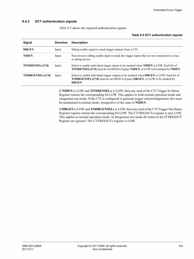
Embedded Cross Trigger
9.4.3 ECT authentication signals
Table 9-2 shows the required authentication signals.
If NIDEN is LOW and TINIDENSELx is LOW, then any read of the CTI Trigger In Status Register returns the corresponding bit LOW. This applies to both normal operation mode and integration test mode. If the CTI is configured to generate trigger acknowledgements this must be maintained in normal mode, irrespective of the state of NIDEN.
If DBGEN is LOW and TODBGENSELx is LOW, then any read of the CTI Trigger Out Status Register register returns the corresponding bit LOW. The CTTRIGOUTx register is also LOW. This applies to normal operation mode. In Integration test mode all writes to the ITTRIGOUT Register are ignored. The CTTRIGOUTx register is LOW.
Table 9-2 ECT authentication signals
Signal Direction Description
DBGEN Input Debug enable signal to mask trigger outputs from a CTI.
NIDEN Input Non-invasive debug enable input to mask the trigger inputs that are not connected to a trace or debug device.
TINIDENSELx[7:0] Input Select to enable individual trigger inputs to be masked when NIDEN is LOW. Each bit of TINIDENSELx[7:0] must be set HIGH to bypass NIDEN, or LOW to be masked by NIDEN.
TODBGENSELx[7:0] Input Select to enable individual trigger outputs to be masked when DBGEN is LOW. Each bit of TODBGENSELx[7:0] must be set HIGH to bypass DBGEN, or LOW to be masked by DBGEN.
ARM DDI 0480A Copyright © 2011 ARM. All rights reserved. 9-8ID111211 Non-Confidential
Chapter 10 Trace Port Interface Unit
This chapter describes the Trace Port Interface Unit (TPIU). It contains the following sections:• About the Trace Port Interface Unit on page 10-2• Trace Out Port on page 10-3• Miscellaneous connections on page 10-4• TPIU trace port sizes on page 10-5• TPIU triggers on page 10-7• Other TPIU design considerations on page 10-8• Authentication requirements for TPIUs on page 10-10• TPIU pattern generator on page 10-11• TPIU formatter and FIFO on page 10-13• Configuration options on page 10-15• Example configuration scenarios on page 10-16.
ARM DDI 0480A Copyright © 2011 ARM. All rights reserved. 10-1ID111211 Non-Confidential
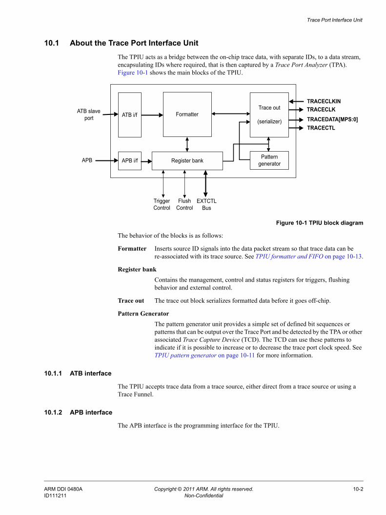
Trace Port Interface Unit
10.1 About the Trace Port Interface UnitThe TPIU acts as a bridge between the on-chip trace data, with separate IDs, to a data stream, encapsulating IDs where required, that is then captured by a Trace Port Analyzer (TPA). Figure 10-1 shows the main blocks of the TPIU.
Figure 10-1 TPIU block diagram
The behavior of the blocks is as follows:
Formatter Inserts source ID signals into the data packet stream so that trace data can be re-associated with its trace source. See TPIU formatter and FIFO on page 10-13.
Register bank Contains the management, control and status registers for triggers, flushing behavior and external control.
Trace out The trace out block serializes formatted data before it goes off-chip.
Pattern Generator The pattern generator unit provides a simple set of defined bit sequences or patterns that can be output over the Trace Port and be detected by the TPA or other associated Trace Capture Device (TCD). The TCD can use these patterns to indicate if it is possible to increase or to decrease the trace port clock speed. See TPIU pattern generator on page 10-11 for more information.
10.1.1 ATB interface
The TPIU accepts trace data from a trace source, either direct from a trace source or using a Trace Funnel.
10.1.2 APB interface
The APB interface is the programming interface for the TPIU.
Register bank
FormatterATB i/f
APB i/f
TRACECLKINTrace out
(serializer)
PatterngeneratorAPB
TRACECTL
EXTCTL Bus
TRACEDATA[MPS:0]TRACECLK
Flush Control
ATB slave port
Trigger Control
ARM DDI 0480A Copyright © 2011 ARM. All rights reserved. 10-2ID111211 Non-Confidential
Trace Port Interface Unit
10.2 Trace Out PortTable 10-1 shows the Trace Out Port signals. For more information about TPIU register, see Chapter 3 Programmers Model.
Table 10-1 Trace Out Port signals
Name Type Description
TRACECLKIN Input Decoupled clock from ATB to enable easy control of the trace port speed. This is typically derived from a controllable clock source on chip but can be driven by an external clock generator if a high speed pin is used. Data changes on the rising edge only. See Off-chip based TRACECLKIN on page 10-8 for more details of off-chip operated TRACECLKIN.
TRACECLK Output Exported version of TRACECLKIN. This is TRACECLKIN/2, and data changes on both rising edges and falling edges. See TRACECLK generation on page 10-8 for more details about TRACECLK generation.
TRACEDATA[MPS:0] Output Output data. MPS is TPMAXDATASIZE.
TRACECTL Output Used to indicate non valid trace data and triggers. See Other TPIU design considerations on page 10-8.
TRESETn Input This is a reset signal for the TRACECLKIN domain. Because off-chip devices connect to the Trace Out port, this signal is related to the Trace Bus Resetting signal, ATRESETn.
TPCTL Input ASIC tie-off to report the presence of the TRACECTL pin. If TRACECTL is not present then this must be tied LOW. This input affects bit 2 of the Formatter and Flush Status Register.
TPMAXDATASIZE[4:0] Input Tie-off to indicate the maximum TRACEDATA width available on the ASIC. The valid values are 1-32 (0x00-0x1F), for example if only a maximum of a 16-bit data port is available then this takes the value 0x0F. This input affects the Supported Port Size Register.
ARM DDI 0480A Copyright © 2011 ARM. All rights reserved. 10-3ID111211 Non-Confidential
Trace Port Interface Unit
10.3 Miscellaneous connectionsThese ports supplement the operation of the TPIU and are for the connection of other CoreSight components or other ASIC blocks. Table 10-2 shows the ports not described elsewhere. For more information about TPIU register, see Chapter 3 Programmers Model
Table 10-2 TPIU miscellaneous ports
Name Type Description
TRIGIN Input From either a CTI or direct from a trace source. Used to enable the trigger to affect the output trace stream.
TRIGINACK Output Return response to the CTI acknowledgement to TRIGIN.
FLUSHIN Input External control used to invoke an ATB signal and drain any old historical information on the bus.
FLUSHINACK Output Flush response, goes HIGH to acknowledge FLUSHIN. If the completion of a flush is required then this can be established by the Formatter Flush and Control Register.
EXTCTLOUT[7:0] Output Used as control signals for any configurable drivers on the output of the trace port such as serializers and output multiplexor.
EXTCTLIN[7:0] Input Used as an input port for any configurable drivers on the output of the trace port such as serializers and output multiplexor.
ARM DDI 0480A Copyright © 2011 ARM. All rights reserved. 10-4ID111211 Non-Confidential
Trace Port Interface Unit
10.4 TPIU trace port sizesThe TPIU is configured for the largest port size permissible, 32 bits of TRACEDATA, TRACECLK, and TRACECTL.
• TRACECLK is always exported to enable synchronization back with the data and so is not optional.
• TRACECTL is required unless a new TPA is used that is aware of the formatter protocol which can remove extra packets used to expand data sequences. For Normal and Bypass modes, TRACECTL must be present.
• TRACEDATA can be defined as any size up to 32 bits. For backwards compatibility and usage with ETMv3 trace capture devices, a minimum port width of 2 bits is permitted, that is, TRACEDATA[1:0].
Table 10-3 shows some typical Trace Out Port sizes.
10.4.1 Programming registers
There are two registers that contain information relating to the physical Trace Out port. These are the Supported Port Size Register and the Formatter and Flush Status Register. For more information about these registers, see Chapter 3 Programmers Model.
Constraining the supported TRACEDATA port widths
When placing on an Application Specific Integrated Circuit (ASIC), not all the signals of TRACEDATA can go to pads, that is, only TRACEDATA[(MDS-1):0] go to pins, where MDS represents the Maximum Data Size going to pins. If MDS is not 32, that is, the maximum supported data width for capture by a TPA is less than 32 bits of data, this must be reflected in the programmers view of the Supported Port Size Register through the tie-off input TPMAXDATASIZE[4:0].
Table 10-3 Example Trace Out Port sizes
TRACECLK present TRACECTL present TRACEDATA width Total pin count Comment
Yes Yes 32 bits [31:0] 34 Largest implementation
Yes No 9 bits [8:0] 10 Extra data pin available in comparison to the typical ETM implementation.
Yes Yes 8 bits [7:0] 10 Typical ETM-compatible TPA implementation.
Yes Yes 2 bits [1:0] 4 Smallest implementation with typical TPAs.
Yes No 1 bit [0] 2 Smallest implementation with a protocol-aware TPA
ARM DDI 0480A Copyright © 2011 ARM. All rights reserved. 10-5ID111211 Non-Confidential
Trace Port Interface Unit
The tie-off must be set to represent the number of TRACEDATA connections that go to ASIC pads, with all LOW indicates 1 pin, which is the minimum possible, and all HIGH indicates 32 pins, which is a full TRACEDATA bus. For example, if a 16-bit trace port is implemented, that is TRACEDATA[15:0] is connected, then TPMAXDATASIZE[4:0] must be tied to 0x0F. With a maximum TRACEDATA[7:0] connected to the ASIC, the tie-offs must be set to 0x07.
10.4.2 Omission of TRACECTL
For restricted pin devices where removal of the trace data is important, the TRACECTL can be removed. Omitting TRACECTL is only possible with the formatter enabled and continuous mode selected. See For more information about the Formatter and Flush Control Register, see Chapter 3 Programmers Model.
The presence of the TRACECTL pin can be checked by reading the TCPresent bit in the FFSR, see Formatter and Flush Status Register on page 3-139.
ARM DDI 0480A Copyright © 2011 ARM. All rights reserved. 10-6ID111211 Non-Confidential
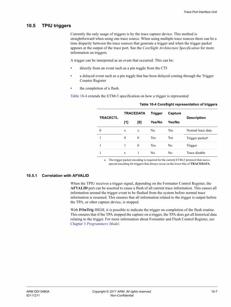
Trace Port Interface Unit
10.5 TPIU triggersCurrently the only usage of triggers is by the trace capture device. This method is straightforward when using one trace source. When using multiple trace sources there can be a time disparity between the trace sources that generate a trigger and when the trigger packet appears at the output of the trace port. See the CoreSight Architecture Specification for more information on triggers.
A trigger can be interpreted as an event that occurred. This can be:
• directly from an event such as a pin toggle from the CTI
• a delayed event such as a pin toggle that has been delayed coming through the Trigger Counter Register
• the completion of a flush.
Table 10-4 extends the ETMv3 specification on how a trigger is represented
10.5.1 Correlation with AFVALID
When the TPIU receives a trigger signal, depending on the Formatter Control Register, the AFVALID port can be asserted to cause a flush of all current trace information. This causes all information around the trigger event to be flushed from the system before normal trace information is resumed. This ensures that all information related to the trigger is output before the TPA, or other capture device, is stopped.
With FOnTrig HIGH, it is possible to indicate the trigger on completion of the flush routine. This ensures that if the TPA stopped the capture on a trigger, the TPA does get all historical data relating to the trigger. For more information about Formatter and Flush Control Register, see Chapter 3 Programmers Model.
Table 10-4 CoreSight representation of triggers
TRACECTLTRACEDATA Trigger Capture
Description[1] [0] Yes/No Yes/No
0 x x No Yes Normal trace data
1 0 0 Yes Yes Trigger packeta
a. The trigger packet encoding is required for the current ETMv3 protocol that uses a special encoding for triggers that always occur on the lower bits of TRACEDATA.
1 1 0 Yes No Trigger
1 x 1 No No Trace disable
ARM DDI 0480A Copyright © 2011 ARM. All rights reserved. 10-7ID111211 Non-Confidential
Trace Port Interface Unit
10.6 Other TPIU design considerationsThis section describes TPIU design considerations in:• TRACECLK generation• TRACECTL removal• TRACECTL and TRACEDATA multiplexing• Off-chip based TRACECLKIN.
10.6.1 TRACECLK generation
At implementation time, a TRACECLK output must be generated as a sampling reference for TRACEDATA. Frequently, this is specified to fall mid-way between TRACEDATA transitions, however for optimum performance a TPA can implement variable delays for sampling each individual TRACEDATA signal.
10.6.2 TRACECTL removal
The TPIU supports two modes:• data + control + clock, with a minimum data width of 2• data + clock, with a minimum data width of 1.
The chosen mode depends on the connected trace port analyzer/capture device. Legacy capture devices use the control pin to indicate the packet type. Newer capture devices can use more pins for data and do not require a reserved data pin.
Support for both of these modes is required to ensure backwards compatibility and for future, higher port speeds. If a low pin count or an optimized design is required, it is not necessary to implement the TRACECTL pin. This design choice must be reflected in the programmer's model to enable tools to always enable the formatter and run in continuous mode.
10.6.3 TRACECTL and TRACEDATA multiplexing
If pin minimization is a priority, and it is also necessary to support legacy TPAs that still require TRACECTL, it is possible to support both systems in the same implementation by multiplexing the TRACECTL pin with a data pin. This enables the support of the current method of using the control pin at the same time as enabling the connection of a next generation trace capture device with the added advantage of an extra data pin. A possible choice for this extra data pin is the most significant bit because this can be switched without having to change the signal paths of any other connection.
The ability to switch TRACECTL with a data pin is not directly supported by the TPIU. Problems can arise when trying to drive multiple connector pins, for connector reuse, because of impedance and load differences. In addition, timing can be affected because of the inclusion of a multiplexor on a limited number of signals
10.6.4 Off-chip based TRACECLKIN
Future CoreSight-aware TPAs might directly control a clock source for the Trace Out port. By running through a known sequence of patterns, from the pattern generator within the TPIU, a TPA can automatically establish the port width and ramp up the clock speed until the patterns degrade, thereby establishing a maximum data rate. Figure 10-2 on page 10-9 shows how an off-chip TRACECLKIN can be generated.
ARM DDI 0480A Copyright © 2011 ARM. All rights reserved. 10-8ID111211 Non-Confidential
Trace Port Interface Unit
Figure 10-2 Externally derived TRACECLK
The off-chip clock can operate in a similar way to the currently exported TRACECLK. For example, an externally derived clock source can be double clocked to enable the exported data to change at both edges of the clock.
User-supplied
externally generatedTRACECLK
Clock-doubler
inputclk x 2 = outputclk
TRACECLKIN
D Q
Q
D Q
other on-chip TRACECLKIN registers
TPIU
TRACEDATATRACECTL
TRACECLK
on-chip (ASIC) off-chip
TRACECLKIN domain
ARM DDI 0480A Copyright © 2011 ARM. All rights reserved. 10-9ID111211 Non-Confidential

Trace Port Interface Unit
10.7 Authentication requirements for TPIUsTPIUs do not require any authentication signals capable of disabling them.
ARM DDI 0480A Copyright © 2011 ARM. All rights reserved. 10-10ID111211 Non-Confidential
Trace Port Interface Unit
10.8 TPIU pattern generatorA simple set of defined bit sequences or patterns can be output over the trace port and be detected by the TPA or other associated trace capture device. Analysis of the output can indicate if it was possible to increase or, for reliability, to decrease the trace port clock speed. The patterns can also be used to determine the timing characteristics and so alter any delay components on the data channels in a TCD, to ensure reliable data capture.
10.8.1 Pattern generator modes of operation
There are a number of supported patterns to enable a number of metrics to be determined, for example, timing between pins, data edge timing, voltage fluctuations, ground bounce, and cross talk. When examining the trace port you can choose from the following pattern modes:
Timed Each pattern runs for a programmable number of TRACECLKIN cycles after which the pattern generator unit reverts back to an off state where normal trace is output, assuming trace output is enabled. The first thing the trace port outputs after returning to normal trace is a synchronization packet. This is useful with special trace port analyzers and capture devices that are aware of the pattern generator. The TPIU can be set to a standard configuration that the capture device expects. The preset test pattern can then be run, by the end of which, the TCD is calibrated ready for normal operation, which the TPIU switches to automatically, without the requirement to reprogram the TPIU.
Continuous The selected pattern runs continuously until manually disabled. This is primarily intended for manual refinement of electrical characteristics and timing.
Off When neither of the other two modes is selected the device reverts to outputting any trace data. After timed operation finishes, the pattern generator reverts back to the off mode.
10.8.2 Supported options
Patterns operate over all the TRACEDATA pins for a given port width setting. Test patterns are aware of port sizes and always align to TRACEDATA[0]. Walking bit patterns wrap at the highest data pin for the selected port width even if the device has a larger port width available. Also, the alternating patterns do not affect disabled data pins on smaller trace port sizes.
Walking 1s
All output pins clear with a single bit set at a time, tracking across every TRACEDATA output pin. This can be used to watch for data edge timing, or synchronization, high voltage level of logic 1 and cross talk against adjacent wires. Walking 1s can also be used as a simple way to test for broken or faulty cables and data signals.
Walking 0s
All output pins are set with a single bit cleared at a time, tracking across every TRACEDATA output pin. In a similar way to the walking 1s, walking 0s can be used to watch for data edge timing, or synchronization, low voltage level of logic 0, cross talk, and ground lift.
ARM DDI 0480A Copyright © 2011 ARM. All rights reserved. 10-11ID111211 Non-Confidential
Trace Port Interface Unit
Alternating AA/55 pattern
Alternate TRACEDATA pins set with the others clear. This alternates every cycle with the sequence starting with TRACEDATA[1] set AA pattern = 8'b1010_1010, and then TRACEDATA[0] set 55 pattern = 8'b0101_0101. The pattern repeats over the entire selected bus width. This pattern can be used to check voltage levels, cross talk and data edge timing.
Alternating FF/00 pattern
On each clock cycle the TRACEDATA pins are either all set FF pattern or all cleared 00 pattern. This sequence of alternating the entire set of data pins is a good way to check any power supply stability to the TPIU and the final pads because of the stresses the drivers are under.
Combinations of patterns
Each selected pattern is repeated for a defined number of cycles before moving onto the next pattern. After all patterns are performed, the unit switches to normal tracing data mode. If some combination is chosen and the continuous mode is selected, each pattern runs for the number of cycles indicated in the repeat counter register before looping around enabled parameters.
ARM DDI 0480A Copyright © 2011 ARM. All rights reserved. 10-12ID111211 Non-Confidential
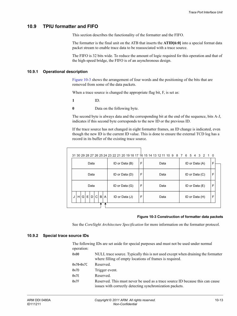
Trace Port Interface Unit
10.9 TPIU formatter and FIFOThis section describes the functionality of the formatter and the FIFO.
The formatter is the final unit on the ATB that inserts the ATID[6:0] into a special format data packet stream to enable trace data to be reassociated with a trace source.
The FIFO is 32 bits wide. To reduce the amount of logic required for this operation and that of the high-speed bridge, the FIFO is of an asynchronous design.
10.9.1 Operational description
Figure 10-3 shows the arrangement of four words and the positioning of the bits that are removed from some of the data packets.
When a trace source is changed the appropriate flag bit, F, is set as:
1 ID.
0 Data on the following byte.
The second byte is always data and the corresponding bit at the end of the sequence, bits A-J, indicates if this second byte corresponds to the new ID or the previous ID.
If the trace source has not changed in eight formatter frames, an ID change is indicated, even though the new ID is the current ID value. This is done to ensure the external TCD log has a record in its buffer of the existing trace source.
Figure 10-3 Construction of formatter data packets
See the CoreSight Architecture Specification for more information on the formatter protocol.
10.9.2 Special trace source IDs
The following IDs are set aside for special purposes and must not be used under normal operation:0x00 NULL trace source. Typically this is not used except when draining the formatter
where filling of empty locations of frames is required.0x70-0x7C Reserved.0x7D Trigger event.0x7E Reserved.0x7F Reserved. This must never be used as a trace source ID because this can cause
issues with correctly detecting synchronization packets.
ID or Data (J)
ID or Data (C)DataID or Data (D)Data
ID or Data (E)DataID or Data (G)Data
ID or Data (H)Data
FF
FF
FFJ ABCDEGH
31 30 29 28 27 26 25 24 23 22 21 20 19 18 17 16 15 14 13 12 11 10 9 8 7 6 5 4 3 2 1 0
ID or Data (B)Data ID or Data (A)Data FF
ARM DDI 0480A Copyright © 2011 ARM. All rights reserved. 10-13ID111211 Non-Confidential
Trace Port Interface Unit
10.9.3 Supported modes of operation
The formatter within the TPIU supports the following basic modes of operation:
Bypass IDs are not incorporated and raw trace data is emitted. It is assumed that the trace source does not change. This requires the use of TRACECTL.
Normal Typical operation with capture devices that require use of a TRACECTL pin.
Continuous An extension of normal mode except when the control pin normally indicates no data to be captured, there is data emitted that shows this fact. Also, triggers are embedded into the data stream because they cannot be indicated otherwise.
See the CoreSight Architecture Specification for more information on these modes.
10.9.4 Periodic synchronization
When the formatter is in continuous mode it can output more synchronization packets, both intraframe and interframe. When an interframe synchronization packet is emitted because of continuous mode, this causes the synchronization counter to restart counting. Full and half synchronization packets are output within interframe and intraframe respectively. See the CoreSight Architecture Specification for more information.
ARM DDI 0480A Copyright © 2011 ARM. All rights reserved. 10-14ID111211 Non-Confidential
Trace Port Interface Unit
10.10 Configuration optionsExisting TPAs that are only capable of operation with TRACECTL must only use the formatter in either bypass or normal mode, not continuous.
10.10.1 Configuration guidelines
The TPIU configuration guidelines are as follows:
• ARM recommends that following a trigger event within a multi-trace source configuration, a flush must be performed to ensure that all historical information related to the trigger is output.
• If Flush on Trigger Event and Stop on Trigger Event options are chosen then any data after the trigger is not captured by the TPA. When the TPIU is instructed to stop, it returns ATREADYS HIGH and does not store any of the accepted data.
• Although multiple flushes can be scheduled using Flush on Trigger Event, Flush on FLUSHIN and manual flush, when one of these requests are made it masks additional requests of the same type. This means repeated writing to the manual flush bit does not schedule multiple manual requests unless each is permitted to complete first.
• Unless multiple triggers are required, it is not advisable to set both Trigger on Trigger Event and Trigger on Flush Completion, if Flush on Trigger Event is also enabled. In addition, if Trigger on TRIGIN is enabled with this configuration, it can also cause multiple trigger markers from one trigger request.
ARM DDI 0480A Copyright © 2011 ARM. All rights reserved. 10-15ID111211 Non-Confidential
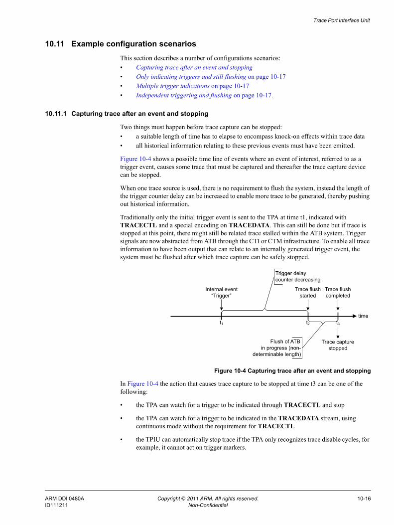
Trace Port Interface Unit
10.11 Example configuration scenariosThis section describes a number of configurations scenarios:• Capturing trace after an event and stopping• Only indicating triggers and still flushing on page 10-17• Multiple trigger indications on page 10-17• Independent triggering and flushing on page 10-17.
10.11.1 Capturing trace after an event and stopping
Two things must happen before trace capture can be stopped:• a suitable length of time has to elapse to encompass knock-on effects within trace data• all historical information relating to these previous events must have been emitted.
Figure 10-4 shows a possible time line of events where an event of interest, referred to as a trigger event, causes some trace that must be captured and thereafter the trace capture device can be stopped.
When one trace source is used, there is no requirement to flush the system, instead the length of the trigger counter delay can be increased to enable more trace to be generated, thereby pushing out historical information.
Traditionally only the initial trigger event is sent to the TPA at time t1, indicated with TRACECTL and a special encoding on TRACEDATA. This can still be done but if trace is stopped at this point, there might still be related trace stalled within the ATB system. Trigger signals are now abstracted from ATB through the CTI or CTM infrastructure. To enable all trace information to have been output that can relate to an internally generated trigger event, the system must be flushed after which trace capture can be safely stopped.
Figure 10-4 Capturing trace after an event and stopping
In Figure 10-4 the action that causes trace capture to be stopped at time t3 can be one of the following:
• the TPA can watch for a trigger to be indicated through TRACECTL and stop
• the TPA can watch for a trigger to be indicated in the TRACEDATA stream, using continuous mode without the requirement for TRACECTL
• the TPIU can automatically stop trace if the TPA only recognizes trace disable cycles, for example, it cannot act on trigger markers.
time
Internal event“Trigger”
Trace flush started
Trace flush completed
Trace capture stopped
t1 t2 t3
Trigger delay counter decreasing
Flush of ATB in progress (non-
determinable length)
ARM DDI 0480A Copyright © 2011 ARM. All rights reserved. 10-16ID111211 Non-Confidential
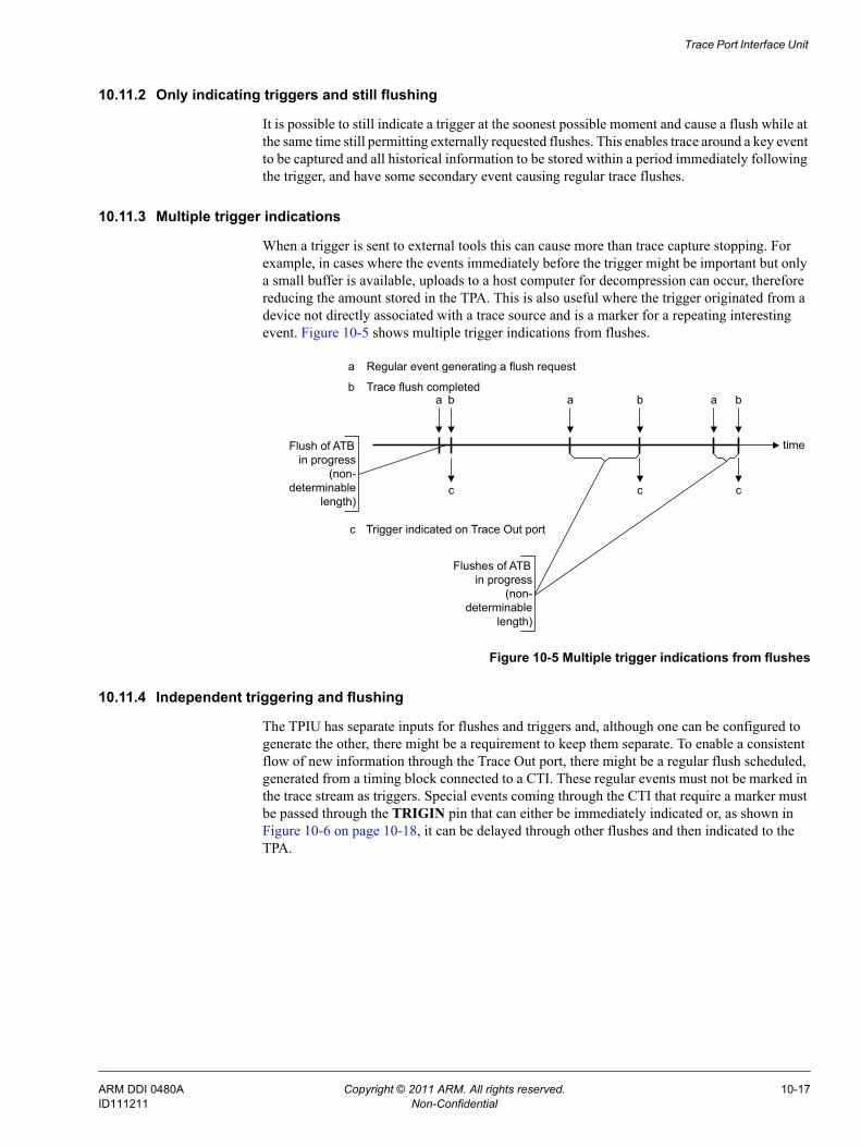
Trace Port Interface Unit
10.11.2 Only indicating triggers and still flushing
It is possible to still indicate a trigger at the soonest possible moment and cause a flush while at the same time still permitting externally requested flushes. This enables trace around a key event to be captured and all historical information to be stored within a period immediately following the trigger, and have some secondary event causing regular trace flushes.
10.11.3 Multiple trigger indications
When a trigger is sent to external tools this can cause more than trace capture stopping. For example, in cases where the events immediately before the trigger might be important but only a small buffer is available, uploads to a host computer for decompression can occur, therefore reducing the amount stored in the TPA. This is also useful where the trigger originated from a device not directly associated with a trace source and is a marker for a repeating interesting event. Figure 10-5 shows multiple trigger indications from flushes.
Figure 10-5 Multiple trigger indications from flushes
10.11.4 Independent triggering and flushing
The TPIU has separate inputs for flushes and triggers and, although one can be configured to generate the other, there might be a requirement to keep them separate. To enable a consistent flow of new information through the Trace Out port, there might be a regular flush scheduled, generated from a timing block connected to a CTI. These regular events must not be marked in the trace stream as triggers. Special events coming through the CTI that require a marker must be passed through the TRIGIN pin that can either be immediately indicated or, as shown in Figure 10-6 on page 10-18, it can be delayed through other flushes and then indicated to the TPA.
time
a a ab b b
c c c
Trigger indicated on Trace Out portc
Flush of ATB in progress
(non-determinable
length)
Regular event generating a flush requesta
Trace flush completedb
Flushes of ATB in progress
(non-determinable
length)
ARM DDI 0480A Copyright © 2011 ARM. All rights reserved. 10-17ID111211 Non-Confidential
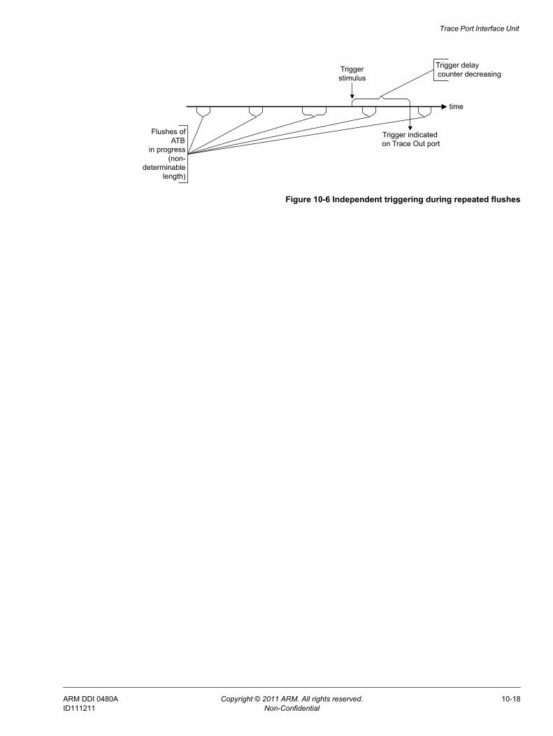
Trace Port Interface Unit
Figure 10-6 Independent triggering during repeated flushes
time
Trigger stimulus
Flushes of ATB
in progress (non-
determinable length)
Trigger indicated on Trace Out port
Trigger delay counter decreasing
ARM DDI 0480A Copyright © 2011 ARM. All rights reserved. 10-18ID111211 Non-Confidential
Chapter 11 Embedded Trace Buffer
This chapter describes the Embedded Trace Buffer (ETB) for CoreSight. It contains the following sections:• About the ETB on page 11-2• ETB clocks, resets, and synchronization on page 11-5• ETB trace capture and formatting on page 11-6• Flush assertion on page 11-8• Triggers on page 11-9• Write address generation for trace data storage on page 11-10• Trace data storage on page 11-11• APB configuration and RAM access on page 11-12• Trace RAM on page 11-13• Authentication requirements for CoreSight ETBs on page 11-14• ETB RAM support on page 11-15.
ARM DDI 0480A Copyright © 2011 ARM. All rights reserved. 11-1ID111211 Non-Confidential
Embedded Trace Buffer
11.1 About the ETBThe ETB provides on-chip storage of trace data using 32-bit RAM. Figure 11-1 shows the main ETB blocks.
Figure 11-1 ETB block diagram
The ETB accepts trace data from the CoreSight trace source components through an AMBA Trace Bus (ATB). See the CoreSight Architecture Specification for a detailed description.
The ETB contains the following blocks:
Formatter Inserts source ID signals into the data packet stream so that trace data can be re-associated with its trace source after the data is read back out of the ETB.
Control Control registers for trace capture and flushing.
APB interface Read, write, and data pointers provide access to ETB registers. In addition, the APB interface supports wait states through the use of a PREADYDBG signal output by the ETB. The APB interface is synchronous to the ATB domain.
Register bank Contains the management, control, and status registers for triggers, flushing behavior, and external control.
Trace RAM interface Controls reads and writes to the Trace RAM.
Memory Built-In Self Test (MBIST) interface Provides test access to the Trace RAM.
11.1.1 ATB interface
The ETB accepts trace data from any CoreSight-compliant component trace source with an ATB master port, such as a trace source or a trace funnel.
PCLK domain
APBi/f Register bank
Formatter
APB
ATCLK domain
ATB slave portATB
i/f
Trace RAMControl
Trace RAM interface
FULLACQCOMP
TRIGINTRIGINACK
FLUSHINFLUSHINACK
Memory BIST
ARM DDI 0480A Copyright © 2011 ARM. All rights reserved. 11-2ID111211 Non-Confidential
Embedded Trace Buffer
11.1.2 ETB triggering and flushing ports
Table 11-1 shows the ETB triggering and flushing ports.
11.1.3 ETB status ports
The ETB continuously captures and writes data into RAM when trace capture is enabled and either:
• the trigger counter is static at 0
• the trigger counter has not yet decremented to zero. The trigger counter begins to decrement when a trigger is observed.
A trigger event occurs when the trigger counter reaches zero, or if the trigger counter is zero when the trigger input is HIGH.
When the trigger counter reaches zero the acquisition complete flag, AcqComp, is activated and trace capture stops. The value loaded into the trigger counter therefore sets the number of data words stored in the trace RAM after a trigger event.
Table 11-2 shows the ETB status ports.
11.1.4 Memory BIST interface
Table 11-3 on page 11-4 shows the Memory BIST interface ports.
Table 11-1 ETB triggering and flushing ports
Name Type Description
TRIGIN Input From either a CTI or direct from a trace source. Used to enable the trigger to affect the captured trace stream.
TRIGINACK Output Return response to the CTI. Acknowledgement to TRIGIN.
FLUSHIN Input External control used to assert the ATB signal AFVALIDS and drain any historical FIFO information on the bus.
FLUSHINACK Output Return acknowledgement to FLUSHIN.
Table 11-2 ETB status ports
Name Type Description
ACQCOMP Output When HIGH, indicates that trace acquisition is complete, the trigger counter is at zero.
FULL Output When HIGH indicates that the ETB RAM has overflowed or wrapped around to address zero.
ARM DDI 0480A Copyright © 2011 ARM. All rights reserved. 11-3ID111211 Non-Confidential
Embedded Trace Buffer
Table 11-3 ETB Memory BIST interface ports
Name Type Description
MBISTADDR [CSETB_ADDR_WIDTH-1:0] Input Address bus for the external BIST controller, active when MTESTON is HIGH.CSETB_ADDR_WIDTH defines the address bus width used, and therefore the RAM depth supported.
MBISTCE Input Active-HIGH chip select for external BIST controller, active when MTESTON is HIGH.
MBISTDIN[31:0] Input Write data bus for external BIST controller, active when MTESTON is HIGH.
MBISTDOUT[31:0] Output Read data bus for external BIST controller, active when MTESTON is HIGH.
MBISTWE Input Active-HIGH write enable for external BIST controller, active when MTESTON is HIGH.
MTESTON Input Enable signal for the external BIST controller.
ARM DDI 0480A Copyright © 2011 ARM. All rights reserved. 11-4ID111211 Non-Confidential
Embedded Trace Buffer
11.2 ETB clocks, resets, and synchronizationThis section describes ETB clocks, resets, and synchronization in:• ETB clock domains• ETB resets• ETB synchronization.
11.2.1 ETB clock domains
The ETB has the following clock domains:
PCLKDBG Drives the APB interface and selected control registers.
ATCLK Drives the ATB interface, all control logic, and RAM.
11.2.2 ETB resets
ATRESETn resets all of the ETB registers in the ATCLK domain. ATRESETn must be synchronized externally in the CoreSight infrastructure by a global CoreSight reset signal that asserts ATRESETn asynchronously and deasserts ATRESETn synchronously with ATCLK.
PRESETDBGn resets the APB interface of the ETB. PRESETDBGn must be synchronized externally in the CoreSight infrastructure by a global CoreSight reset signal that asserts PRESETDBGn asynchronously and deasserts PRESETDBGn synchronously with PCLKDBG.
11.2.3 ETB synchronization
ATCLK and PCLKDBG are synchronous domains.
Note PCLKDBG must be equivalent to, or an integer division of ATCLK.
ARM DDI 0480A Copyright © 2011 ARM. All rights reserved. 11-5ID111211 Non-Confidential
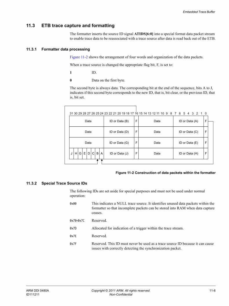
Embedded Trace Buffer
11.3 ETB trace capture and formattingThe formatter inserts the source ID signal ATIDS[6:0] into a special format data packet stream to enable trace data to be reassociated with a trace source after data is read back out of the ETB.
11.3.1 Formatter data processing
Figure 11-2 shows the arrangement of four words and organization of the data packets.
When a trace source is changed the appropriate flag bit, F, is set to:
1 ID.
0 Data on the first byte.
The second byte is always data. The corresponding bit at the end of the sequence, bits A to J, indicates if this second byte corresponds to the new ID, that is, bit clear, or the previous ID, that is, bit set.
Figure 11-2 Construction of data packets within the formatter
11.3.2 Special Trace Source IDs
The following IDs are set aside for special purposes and must not be used under normal operation:
0x00 This indicates a NULL trace source. It identifies unused data packets within the formatter so that incomplete packets can be stored into RAM when data capture ceases.
0x70-0x7C Reserved.
0x7D Allocated for indication of a trigger within the trace stream.
0x7E Reserved.
0x7F Reserved. This ID must never be used as a trace source ID because it can cause issues with correctly detecting the synchronization packet.
ID or Data (J)
ID or Data (C)DataID or Data (D)Data
ID or Data (E)DataID or Data (G)Data
ID or Data (H)Data
FF
FF
FFJ ABCDEGH
31 30 29 28 27 26 25 24 23 22 21 20 19 18 17 16 15 14 13 12 11 10 9 8 7 6 5 4 3 2 1 0
ID or Data (B)Data ID or Data (A)Data FF
ARM DDI 0480A Copyright © 2011 ARM. All rights reserved. 11-6ID111211 Non-Confidential
Embedded Trace Buffer
11.3.3 Special modes of operation
The Formatter supports the following distinct modes of operation as specified by bits [1:0] in the Formatter and Flush Control Register:
Bypass In this mode, no formatting information is inserted into the trace stream and a raw reproduction of the incoming trace stream is stored. If any bytes remain in the formatter when tracing is stopped, because of non 32-bit ATDATAS, then the word stored to RAM is appended with a single logic 1 bit and filled in with zeros. A second word, 0x00000000 is then stored. If no bytes remain in the formatter, when capture is stopped, four additional words are stored, 0x00000001 then three words of 0x00000000. When data is later decompressed it is then possible to determine that a post-amble is present by back tracking the trailing zero data at then end of the trace stream until the last single bit at logic 1 is detected. All data preceding this first logic 1 is then treated as decompressible data. When all data has been stored in the RAM, FtStopped in the Formatter and Flush Status Register is set HIGH.
Note This mode assumes that the source ID does not change.
Normal Normal mode has the option of embedding triggers into the data packets.Formatting information is added to indicate the change of source ID along with the associated wrapping additions, as described in TPIU formatter and FIFO on page 10-13. If any data remains in the formatter when tracing is stopped then the formatter is filled with NULL packets, ID = 0x00, to ensure all data is stored in RAM. When all remaining data has been stored in the RAM, FtStopped in the Formatter and Flush Status Register is set HIGH.
Continuous Continuous mode in the ETB corresponds to normal mode with the embedding of triggers. Unlike continuous mode in the TPIU, no formatter synchronization packets are added because alignment of data to the RAM locations is assumed.
11.3.4 Stopping trace
The stopping of trace is indicated by FtStopped set to HIGH in the Formatter and Flush Status Register. This is set by:
• TraceCaptEn = 0 in the Control Register.
• A trigger event occurring, TRIGIN goes HIGH and the Trigger Counter Register reaches zero, and StopTrig is set to HIGH in the Formatter and Flush Control Register, 0x304.
• A flush completing and StopFl is set to HIGH in the Formatter and Flush Control Register.
StopTrig and StopFl in the Formatter and Flush Control Register can be enabled at the same time. For example, if FOnTrig in the Formatter and Flush Control Register is set to perform a flush on a trigger event, but StopTrig is HIGH, none of the flushed data is stored, because StopTrig is HIGH. If the situation requires that all the flushed data is captured StopTrig must be LOW and StopFl must be HIGH in this situation.
When the formatter stops, ATREADYS is output HIGH to prevent an ATB bus from stalling. This is important when a replicator is present, but the received data is ignored.
ARM DDI 0480A Copyright © 2011 ARM. All rights reserved. 11-7ID111211 Non-Confidential
Embedded Trace Buffer
11.4 Flush assertionAll three flush generating conditions can be enabled together:• flush from FLUSHIN• flush from Trigger• manually activated flush.
If more flush events are generated while a flush is in progress, the current flush is serviced before the next flush is started. Only one request for each source of flush can be pended. If a subsequent flush request signal is deasserted while the flush is still being serviced or pended, a second flush is not generated.
Flush from FLUSHIN takes priority over Flush from Trigger, which in turn is completed before a manually activated flush. The operation of the flush mechanism is defined in the CoreSight Architecture Specification.
ARM DDI 0480A Copyright © 2011 ARM. All rights reserved. 11-8ID111211 Non-Confidential
Embedded Trace Buffer
11.5 TriggersA trigger event is defined as when the Trigger Counter reaches zero, or when the trigger counter is zero, when TRIGIN is HIGH. All trigger indication conditions, TrigEvt, TrigFl, and TrigIn, in the Formatter and Flush Control Register can be enabled simultaneously. This results in multiple triggers appearing in the trace stream.
The trigger counter register controls how many words are written into the Trace RAM after a trigger event. After the formatter is flushed in normal or continuous mode a complete empty frame is generated. This is a data overhead of seven extra words in the worst case. The trigger counter defines the number of 32-bit words remaining to be stored in the ETB Trace RAM. If the formatter is in bypass mode, a maximum of two additional words are stored for the trace capture post-amble. See Chapter 3 Programmers Model.
ARM DDI 0480A Copyright © 2011 ARM. All rights reserved. 11-9ID111211 Non-Confidential

Embedded Trace Buffer
11.6 Write address generation for trace data storageThe RAM Write Pointer is automatically selected to address the Trace RAM when trace capture is enabled in the Control Register. Data is written into the Trace RAM when the formatter asserts the Data valid flag on generation of a formatted word. On completion of a write access to the Trace RAM, the register is automatically incremented.
The RAM Write Pointer Register must be programmed before trace capture is enabled.
ARM DDI 0480A Copyright © 2011 ARM. All rights reserved. 11-10ID111211 Non-Confidential
Embedded Trace Buffer
11.7 Trace data storageData is received by the ETB ATB Formatter block. When TraceCaptEn is asserted the Formatter starts the process of embedding the source IDs into the data stream, or normal mode, then outputs 32-bit words to be stored in the ETB Trace RAM. When data is ready to be stored in the Trace RAM, data is written to at the address stored in the RAM Write Pointer Register. When the Trigger Counter Register reaches zero, the acquisition complete flag AcqComp is asserted and trace capture is stopped.
ARM DDI 0480A Copyright © 2011 ARM. All rights reserved. 11-11ID111211 Non-Confidential
Embedded Trace Buffer
11.8 APB configuration and RAM accessThis section describes APB configuration and RAM accesses:• Read access• Write access.
11.8.1 Read access
When trace capture is disabled, TraceCaptEn=0, the RAM Read Pointer is used to generate the RAM address for reading data stored in the ETB Trace RAM. Updating the RAM Read Pointer automatically triggers a RAM access to ensure all RAM data present in the RAM Read Data Register is up-to-date.
The RAM Read Pointer is updated either by writing directly to it, or performing a read of the RAM Read Data Register, causing the RAM Read Pointer to be incremented. Therefore, a read of the RAM Read Data Register consequentially causes the next memory location to be read and loaded into the RAM Read Data Register.
11.8.2 Write access
When trace capture is disabled, TraceCaptEn=0, the RAM Write Pointer Register is used to generate the RAM address for writing data from the RAM Read Data Register. The data to be stored in the RAM Write Data Register is derived from an APB write transfer to the APB interface.
Updating the RAM Read Data Register automatically triggers a RAM access to write the register contents into the Trace RAM at the address present in the RAM Write Pointer Register. On completion of the write cycle the RAM Write Pointer Register is automatically incremented.
Note A write access to the RAM Write Pointer Register does not initiate a write transfer to the Trace RAM, only a write to the RAM Read Data Register causes a RAM write.
The RAM Write Pointer Register must be programmed before trace capture is enabled again.
ARM DDI 0480A Copyright © 2011 ARM. All rights reserved. 11-12ID111211 Non-Confidential

Embedded Trace Buffer
11.9 Trace RAMSee the CoreSight SoC Implementation Guide for information about Trace RAM and RAM integration.
ARM DDI 0480A Copyright © 2011 ARM. All rights reserved. 11-13ID111211 Non-Confidential

Embedded Trace Buffer
11.10 Authentication requirements for CoreSight ETBsCoreSight ETBs do not require any inputs capable of disabling them.
ARM DDI 0480A Copyright © 2011 ARM. All rights reserved. 11-14ID111211 Non-Confidential
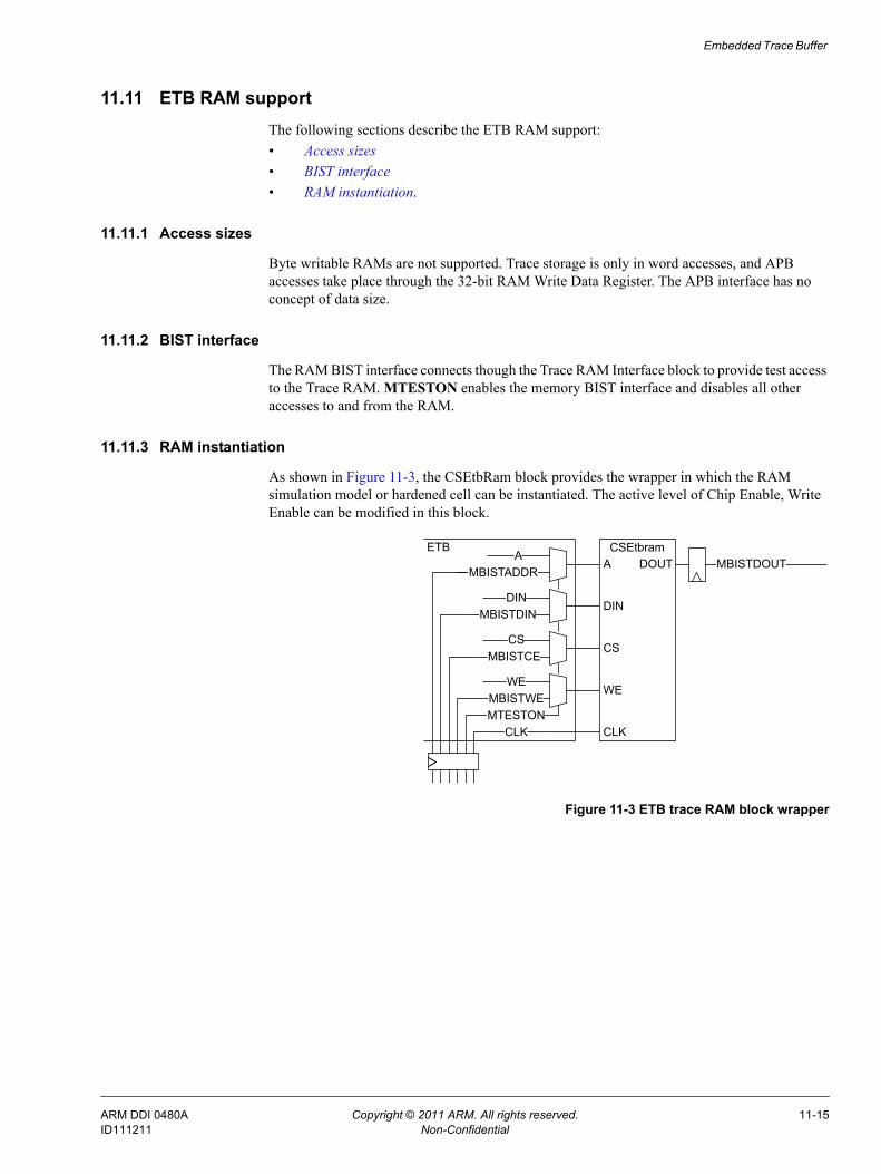
Embedded Trace Buffer
11.11 ETB RAM supportThe following sections describe the ETB RAM support:• Access sizes• BIST interface• RAM instantiation.
11.11.1 Access sizes
Byte writable RAMs are not supported. Trace storage is only in word accesses, and APB accesses take place through the 32-bit RAM Write Data Register. The APB interface has no concept of data size.
11.11.2 BIST interface
The RAM BIST interface connects though the Trace RAM Interface block to provide test access to the Trace RAM. MTESTON enables the memory BIST interface and disables all other accesses to and from the RAM.
11.11.3 RAM instantiation
As shown in Figure 11-3, the CSEtbRam block provides the wrapper in which the RAM simulation model or hardened cell can be instantiated. The active level of Chip Enable, Write Enable can be modified in this block.
Figure 11-3 ETB trace RAM block wrapper
AMBISTADDR
DINMBISTDIN
CSMBISTCE
WEMBISTWEMTESTON
CLK
ETBMBISTDOUT
CSEtbramA
DIN
CS
WE
CLK
DOUT
ARM DDI 0480A Copyright © 2011 ARM. All rights reserved. 11-15ID111211 Non-Confidential
Appendix A Signal Descriptions
This appendix describes the CoreSight port and interface signals. It contains the following sections:• Clock domains on page A-2• AXI slave interface signals on page A-3• AXI master interface signals on page A-7• CoreSight DAP signals on page A-10• CoreSight ECT signals on page A-15• CoreSight TPIU signals on page A-18• CoreSight ETB signals on page A-20• CoreSight timestamp component signals on page A-22• APB IC signals on page A-24• Debug interconnect signals on page A-25.
ARM DDI 0480A Copyright © 2011 ARM. All rights reserved. A-1ID111211 Non-Confidential

Signal Descriptions
A.1 Clock domainsIn addition to the names of clock domains there are the following entries in the port lists:
• N/A, not applicable. This is used for the clock signals.
• None. This signal is an asynchronous input. This input can be from any clock domain because the block has internal synchronizers for this signal.
• xx/None. This signal can be from clock domain xx or it can be asynchronous. The signal has bypassable synchronizers. It depends on which configuration the designer chooses.
ARM DDI 0480A Copyright © 2011 ARM. All rights reserved. A-2ID111211 Non-Confidential
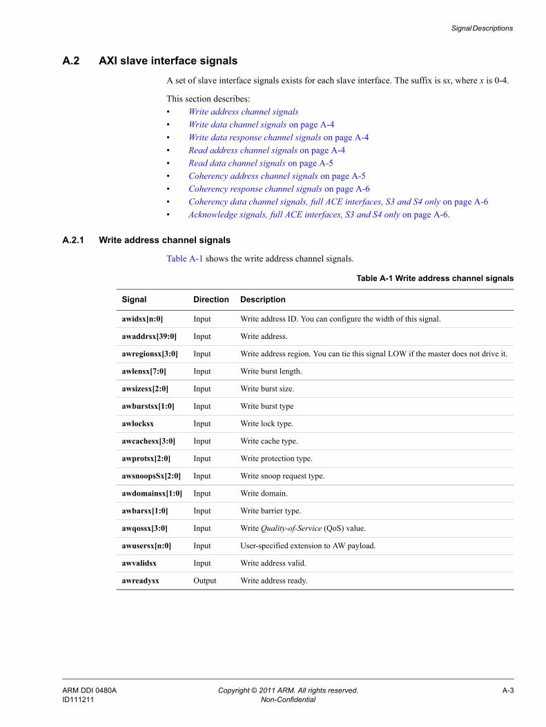
Signal Descriptions
A.2 AXI slave interface signalsA set of slave interface signals exists for each slave interface. The suffix is sx, where x is 0-4.
This section describes:• Write address channel signals• Write data channel signals on page A-4• Write data response channel signals on page A-4• Read address channel signals on page A-4• Read data channel signals on page A-5• Coherency address channel signals on page A-5• Coherency response channel signals on page A-6• Coherency data channel signals, full ACE interfaces, S3 and S4 only on page A-6• Acknowledge signals, full ACE interfaces, S3 and S4 only on page A-6.
A.2.1 Write address channel signals
Table A-1 shows the write address channel signals.
Table A-1 Write address channel signals
Signal Direction Description
awidsx[n:0] Input Write address ID. You can configure the width of this signal.
awaddrsx[39:0] Input Write address.
awregionsx[3:0] Input Write address region. You can tie this signal LOW if the master does not drive it.
awlensx[7:0] Input Write burst length.
awsizesx[2:0] Input Write burst size.
awburstsx[1:0] Input Write burst type
awlocksx Input Write lock type.
awcachesx[3:0] Input Write cache type.
awprotsx[2:0] Input Write protection type.
awsnoopsSx[2:0] Input Write snoop request type.
awdomainsx[1:0] Input Write domain.
awbarsx[1:0] Input Write barrier type.
awqossx[3:0] Input Write Quality-of-Service (QoS) value.
awusersx[n:0] Input User-specified extension to AW payload.
awvalidsx Input Write address valid.
awreadysx Output Write address ready.
ARM DDI 0480A Copyright © 2011 ARM. All rights reserved. A-3ID111211 Non-Confidential
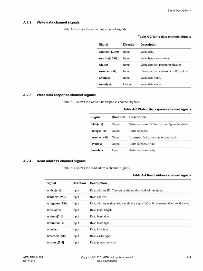
Signal Descriptions
A.2.2 Write data channel signals
Table A-2 shows the write data channel signals.
A.2.3 Write data response channel signals
Table A-3 shows the write data response channel signals.
A.2.4 Read address channel signals
Table A-4 shows the read address channel signals.
Table A-2 Write data channel signals
Signal Direction Description
wdatasx[127:0] Input Write data.
wstrbsx[15:0] Input Write byte-lane strobes.
wlastsx Input Write data last transfer indication.
wusersx[n:0] Input User-specified extension to W payload.
wvalidsx Input Write data valid.
wreadysx Output Write data ready.
Table A-3 Write data response channel signals
Signal Direction Description
bids[n:0] Output Write response ID. You can configure the width.
brespsx[1:0] Output Write response.
busersx[n:0] Output User-specified extension to B payload.
bvalidsx Output Write response valid.
breadysx Input Write response ready.
Table A-4 Read address channel signals
Signal Direction Description
aridsx[n:0] Input Read address ID. You can configure the width of this signal.
araddrsx[39:0] Input Read address.
arregionsx[3:0] Input Read address region. You can tie this signal LOW if the master does not drive it.
arlensx[7:0] Input Read burst length.
arsizesx[2:0] Input Read burst size.
arburstsx[1:0] Input Read burst type.
arlocksx Input Read lock type.
arcachesx[3:0] Input Read cache type.
arprotsx[2:0] Input Read protection type.
ARM DDI 0480A Copyright © 2011 ARM. All rights reserved. A-4ID111211 Non-Confidential
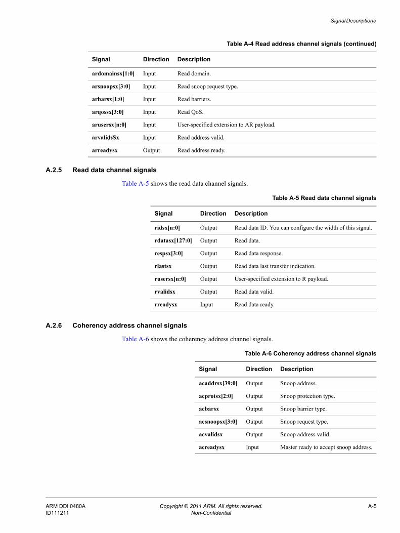
Signal Descriptions
A.2.5 Read data channel signals
Table A-5 shows the read data channel signals.
A.2.6 Coherency address channel signals
Table A-6 shows the coherency address channel signals.
ardomainsx[1:0] Input Read domain.
arsnoopsx[3:0] Input Read snoop request type.
arbarsx[1:0] Input Read barriers.
arqossx[3:0] Input Read QoS.
arusersx[n:0] Input User-specified extension to AR payload.
arvalidsSx Input Read address valid.
arreadysx Output Read address ready.
Table A-4 Read address channel signals (continued)
Signal Direction Description
Table A-5 Read data channel signals
Signal Direction Description
ridsx[n:0] Output Read data ID. You can configure the width of this signal.
rdatasx[127:0] Output Read data.
respsx[3:0] Output Read data response.
rlastsx Output Read data last transfer indication.
rusersx[n:0] Output User-specified extension to R payload.
rvalidsx Output Read data valid.
rreadysx Input Read data ready.
Table A-6 Coherency address channel signals
Signal Direction Description
acaddrsx[39:0] Output Snoop address.
acprotsx[2:0] Output Snoop protection type.
acbarsx Output Snoop barrier type.
acsnoopsx[3:0] Output Snoop request type.
acvalidsx Output Snoop address valid.
acreadysx Input Master ready to accept snoop address.
ARM DDI 0480A Copyright © 2011 ARM. All rights reserved. A-5ID111211 Non-Confidential
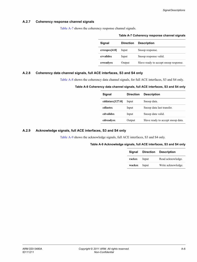
Signal Descriptions
A.2.7 Coherency response channel signals
Table A-7 shows the coherency response channel signals.
A.2.8 Coherency data channel signals, full ACE interfaces, S3 and S4 only
Table A-8 shows the coherency data channel signals, for full ACE interfaces, S3 and S4 only.
A.2.9 Acknowledge signals, full ACE interfaces, S3 and S4 only
Table A-9 shows the acknowledge signals, full ACE interfaces, S3 and S4 only.
Table A-7 Coherency response channel signals
Signal Direction Description
crrespsx[4:0] Input Snoop response.
crvalidsx Input Snoop response valid.
crreadysx Output Slave ready to accept snoop response.
Table A-8 Coherency data channel signals, full ACE interfaces, S3 and S4 only
Signal Direction Description
cddatasx[127:0] Input Snoop data.
cdlastsx Input Snoop data last transfer.
cdvalidsx Input Snoop data valid.
cdreadysx Output Slave ready to accept snoop data.
Table A-9 Acknowledge signals, full ACE interfaces, S3 and S4 only
Signal Direction Description
racksx Input Read acknowledge.
wacksx Input Write acknowledge.
ARM DDI 0480A Copyright © 2011 ARM. All rights reserved. A-6ID111211 Non-Confidential
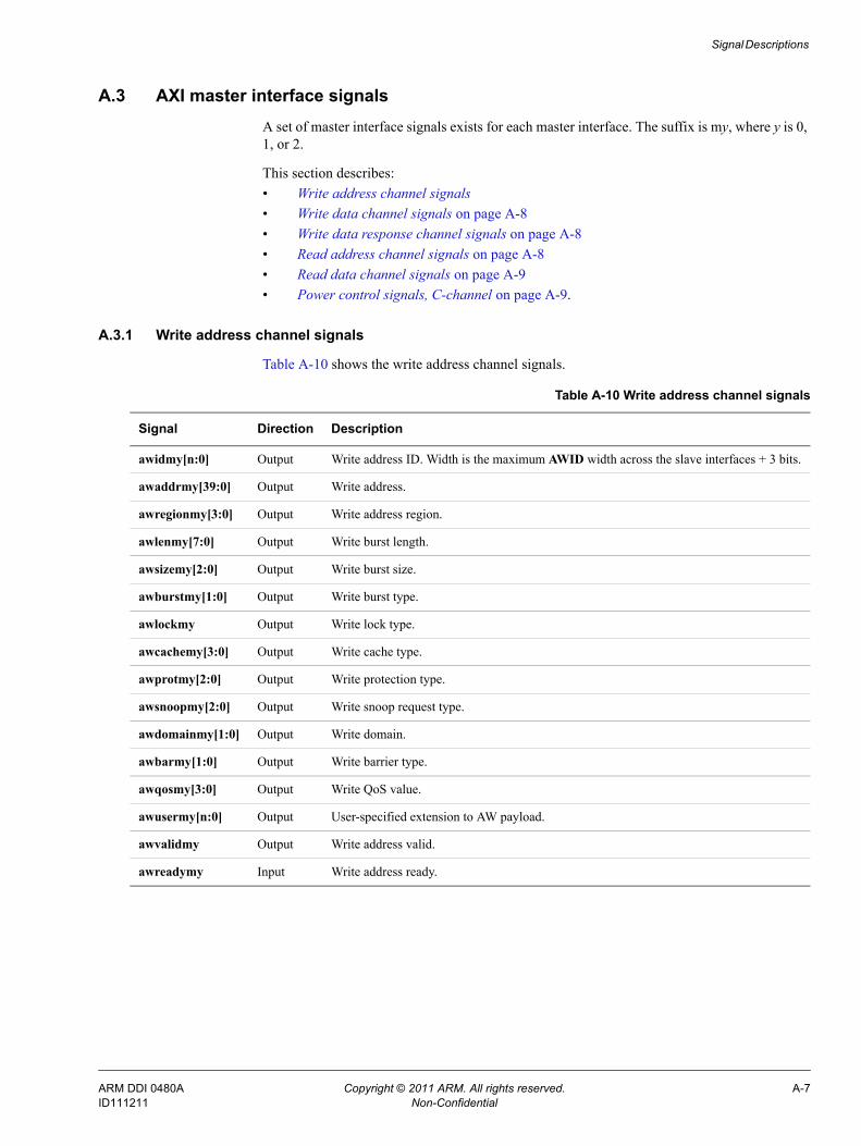
Signal Descriptions
A.3 AXI master interface signalsA set of master interface signals exists for each master interface. The suffix is my, where y is 0, 1, or 2.
This section describes:• Write address channel signals• Write data channel signals on page A-8• Write data response channel signals on page A-8• Read address channel signals on page A-8• Read data channel signals on page A-9• Power control signals, C-channel on page A-9.
A.3.1 Write address channel signals
Table A-10 shows the write address channel signals.
Table A-10 Write address channel signals
Signal Direction Description
awidmy[n:0] Output Write address ID. Width is the maximum AWID width across the slave interfaces + 3 bits.
awaddrmy[39:0] Output Write address.
awregionmy[3:0] Output Write address region.
awlenmy[7:0] Output Write burst length.
awsizemy[2:0] Output Write burst size.
awburstmy[1:0] Output Write burst type.
awlockmy Output Write lock type.
awcachemy[3:0] Output Write cache type.
awprotmy[2:0] Output Write protection type.
awsnoopmy[2:0] Output Write snoop request type.
awdomainmy[1:0] Output Write domain.
awbarmy[1:0] Output Write barrier type.
awqosmy[3:0] Output Write QoS value.
awusermy[n:0] Output User-specified extension to AW payload.
awvalidmy Output Write address valid.
awreadymy Input Write address ready.
ARM DDI 0480A Copyright © 2011 ARM. All rights reserved. A-7ID111211 Non-Confidential
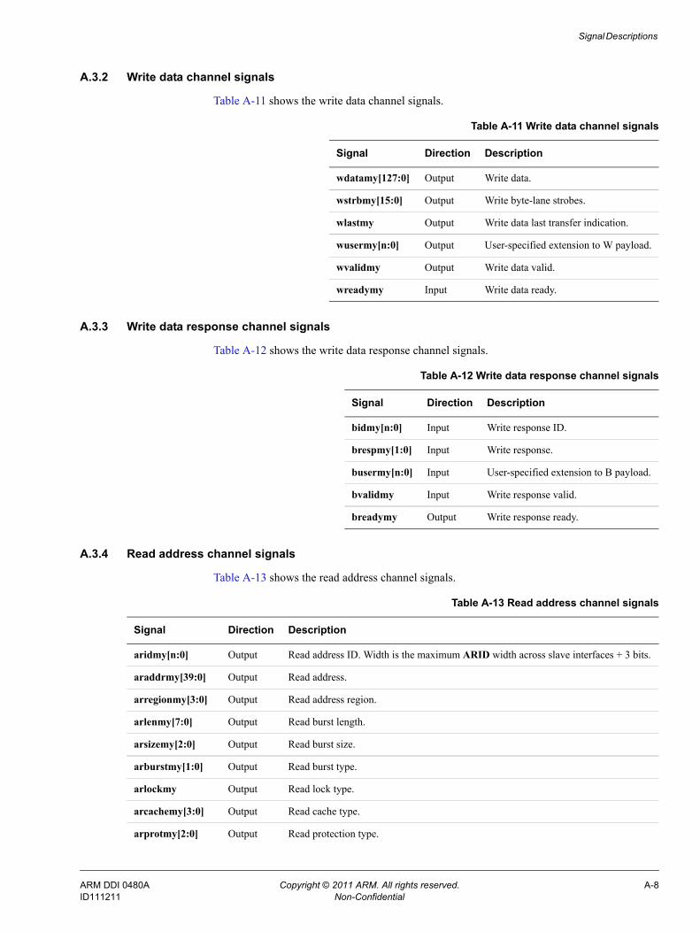
Signal Descriptions
A.3.2 Write data channel signals
Table A-11 shows the write data channel signals.
A.3.3 Write data response channel signals
Table A-12 shows the write data response channel signals.
A.3.4 Read address channel signals
Table A-13 shows the read address channel signals.
Table A-11 Write data channel signals
Signal Direction Description
wdatamy[127:0] Output Write data.
wstrbmy[15:0] Output Write byte-lane strobes.
wlastmy Output Write data last transfer indication.
wusermy[n:0] Output User-specified extension to W payload.
wvalidmy Output Write data valid.
wreadymy Input Write data ready.
Table A-12 Write data response channel signals
Signal Direction Description
bidmy[n:0] Input Write response ID.
brespmy[1:0] Input Write response.
busermy[n:0] Input User-specified extension to B payload.
bvalidmy Input Write response valid.
breadymy Output Write response ready.
Table A-13 Read address channel signals
Signal Direction Description
aridmy[n:0] Output Read address ID. Width is the maximum ARID width across slave interfaces + 3 bits.
araddrmy[39:0] Output Read address.
arregionmy[3:0] Output Read address region.
arlenmy[7:0] Output Read burst length.
arsizemy[2:0] Output Read burst size.
arburstmy[1:0] Output Read burst type.
arlockmy Output Read lock type.
arcachemy[3:0] Output Read cache type.
arprotmy[2:0] Output Read protection type.
ARM DDI 0480A Copyright © 2011 ARM. All rights reserved. A-8ID111211 Non-Confidential
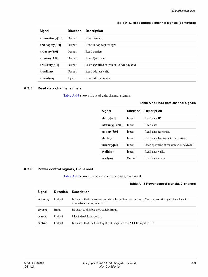
Signal Descriptions
A.3.5 Read data channel signals
Table A-14 shows the read data channel signals.
A.3.6 Power control signals, C-channel
Table A-15 shows the power control signals, C-channel.
ardomainmy[1:0] Output Read domain.
arsnoopmy[3:0] Output Read snoop request type.
arbarmy[1:0] Output Read barriers.
arqosmy[3:0] Output Read QoS value.
arusermy[n:0] Output User-specified extension to AR payload.
arvalidmy Output Read address valid.
arreadymy Input Read address ready.
Table A-13 Read address channel signals (continued)
Signal Direction Description
Table A-14 Read data channel signals
Signal Direction Description
ridmy[n:0] Input Read data ID.
rdatamy[127:0] Input Read data.
respmy[3:0] Input Read data response.
rlastmy Input Read data last transfer indication.
rusermy[n:0] Input User-specified extension to R payload.
rvalidmy Input Read data valid.
readymy Output Read data ready.
Table A-15 Power control signals, C-channel
Signal Direction Description
activemy Output Indicates that the master interface has active transactions. You can use it to gate the clock to downstream components.
csysreq Input Request to disable the ACLK input.
cysack Output Clock disable response.
cactive Output Indicates that the CoreSight SoC requires the ACLK input to run.
ARM DDI 0480A Copyright © 2011 ARM. All rights reserved. A-9ID111211 Non-Confidential
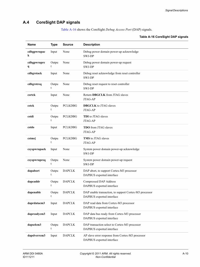
Signal Descriptions
A.4 CoreSight DAP signalsTable A-16 shows the CoreSight Debug Access Port (DAP) signals.
Table A-16 CoreSight DAP signals
Name Type Source Description
cdbgpwrupack
Input None Debug power domain power-up acknowledgeSWJ-DP
cdbgpwrupreq
Output
None Debug power domain power-up requestSWJ-DP
cdbgrstack Input None Debug reset acknowledge from reset controllerSWJ-DP
cdbgrstreq Output
None Debug reset request to reset controllerSWJ-DP
csrtck Input None Return DBGCLK from JTAG slavesJTAG-AP
cstck Output
PCLKDBG DBGCLK to JTAG slavesJTAG-AP
cstdi Output
PCLKDBG TDI to JTAG slavesJTAG-AP
cstdo Input PCLKDBG TDO from JTAG slavesJTAG-AP
cstms] Output
PCLKDBG TMS to JTAG slavesJTAG-AP
csyspwrupack Input None System power domain power-up acknowledgeSWJ-DP
csyspwrupreq Output
None System power domain power-up requestSWJ-DP
dapabort Output
DAPCLK DAP abort, to support Cortex-M3 processorDAPBUS exported interface
dapcaddr Output
DAPCLK Compressed DAP AddressDAPBUS exported interface
dapenable Output
DAPCLK DAP enable transaction, to support Cortex-M3 processorDAPBUS exported interface
daprdatacm3 Input DAPCLK DAP read data from Cortex-M3 processorDAPBUS exported interface
dapreadycm3 Input DAPCLK DAP data bus ready from Cortex-M3 processorDAPBUS exported interface
dapselcm3 Output
DAPCLK DAP transaction select to Cortex-M3 processorDAPBUS exported interface
dapslverrcm3 Input DAPCLK AP slave error response from Cortex-M3 processorDAPBUS exported interface
ARM DDI 0480A Copyright © 2011 ARM. All rights reserved. A-10ID111211 Non-Confidential
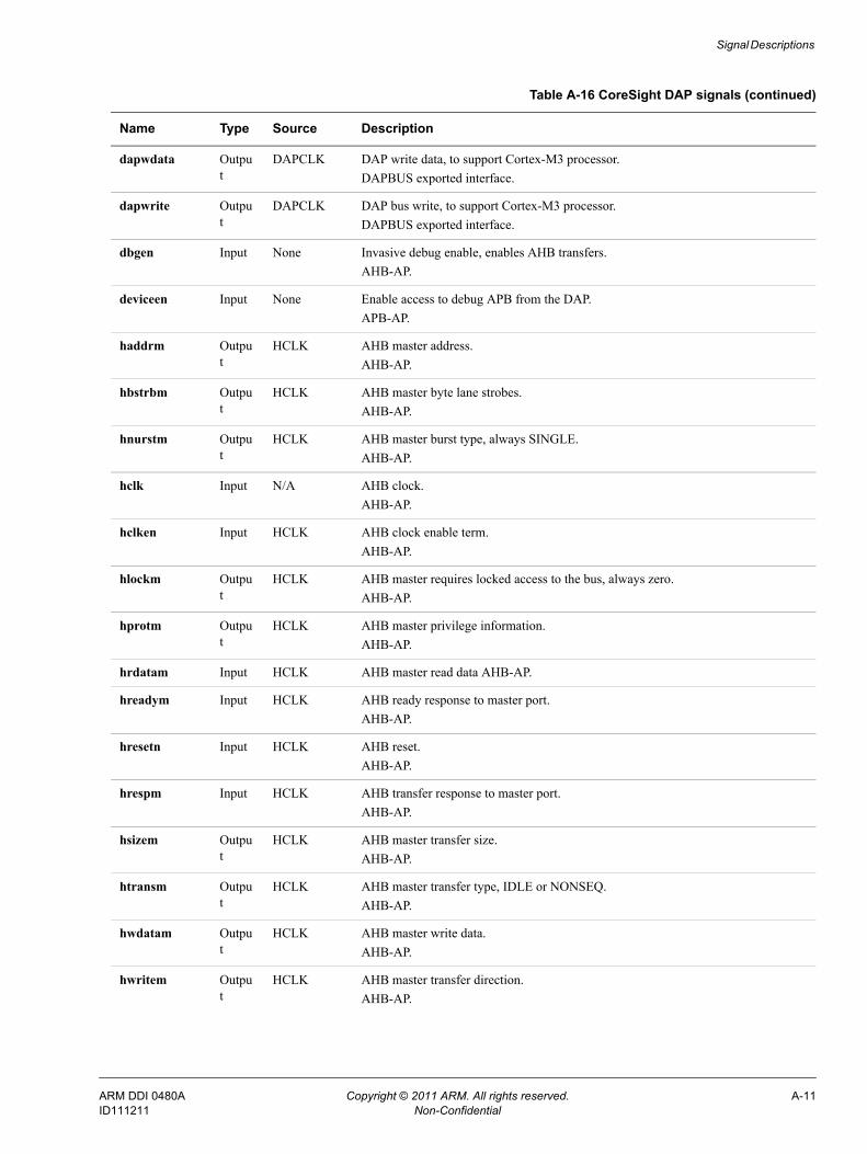
Signal Descriptions
dapwdata Output
DAPCLK DAP write data, to support Cortex-M3 processor.DAPBUS exported interface.
dapwrite Output
DAPCLK DAP bus write, to support Cortex-M3 processor.DAPBUS exported interface.
dbgen Input None Invasive debug enable, enables AHB transfers.AHB-AP.
deviceen Input None Enable access to debug APB from the DAP.APB-AP.
haddrm Output
HCLK AHB master address.AHB-AP.
hbstrbm Output
HCLK AHB master byte lane strobes.AHB-AP.
hnurstm Output
HCLK AHB master burst type, always SINGLE.AHB-AP.
hclk Input N/A AHB clock.AHB-AP.
hclken Input HCLK AHB clock enable term.AHB-AP.
hlockm Output
HCLK AHB master requires locked access to the bus, always zero.AHB-AP.
hprotm Output
HCLK AHB master privilege information.AHB-AP.
hrdatam Input HCLK AHB master read data AHB-AP.
hreadym Input HCLK AHB ready response to master port.AHB-AP.
hresetn Input HCLK AHB reset.AHB-AP.
hrespm Input HCLK AHB transfer response to master port.AHB-AP.
hsizem Output
HCLK AHB master transfer size.AHB-AP.
htransm Output
HCLK AHB master transfer type, IDLE or NONSEQ.AHB-AP.
hwdatam Output
HCLK AHB master write data.AHB-AP.
hwritem Output
HCLK AHB master transfer direction.AHB-AP.
Table A-16 CoreSight DAP signals (continued)
Name Type Source Description
ARM DDI 0480A Copyright © 2011 ARM. All rights reserved. A-11ID111211 Non-Confidential
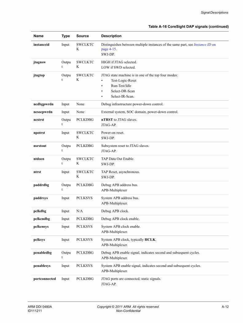
Signal Descriptions
instanceid Input SWCLKTCK
Distinguishes between multiple instances of the same part, see Instance ID on page 4-15.SWJ-DP.
jtagnsw Output
SWCLKTCK
HIGH if JTAG selected.LOW if SWD selected.
jtagtop Output
SWCLKTCK
JTAG state machine is in one of the top four modes:• Test-Logic-Reset• Run-Test/Idle• Select-DR-Scan• Select-IR-Scan.
ncdbgpwrdn Input None Debug infrastructure power-down control.
ncsocpwrdn Input None External system, SOC domain, power-down control.
ncstrst Output
PCLKDBG nTRST to JTAG slaves.JTAG-AP.
npotrst Input SWCLKTCK
Power-on reset.SWJ-DP.
nsrstout Output
PCLKDBG Subsystem reset to JTAG slaves.JTAG-AP.
ntdoen Output
SWCLKTCK
TAP Data Out Enable.SWJ-DP.
ntrst Input SWCLKTCK
TAP Reset, asynchronous.SWJ-DP.
paddrdbg Output
PCLKDBG Debug APB address bus.APB-Multiplexer
paddrsys Input PCLKSYS System APB address bus.APB-Multiplexer.
pclkdbg Input N/A Debug APB clock.
pclkendbg Input PCLKDBG Debug APB clock enable.
pclkensys Input PCLKSYS System APB clock enable.APB-Multiplexer.
pclksys Input PCLKSYS System APB clock, typically HCLK.APB-Multiplexer.
penabledbg Output
PCLKDBG Debug APB enable signal, indicates second and subsequent cycles.APB-Multiplexer.
penablesys Input PCLKSYS System APB enable signal, indicates second and subsequent cycles.APB-Multiplexer.
portconnected Input PCLKDBG JTAG ports are connected, static signals.JTAG-AP.
Table A-16 CoreSight DAP signals (continued)
Name Type Source Description
ARM DDI 0480A Copyright © 2011 ARM. All rights reserved. A-12ID111211 Non-Confidential
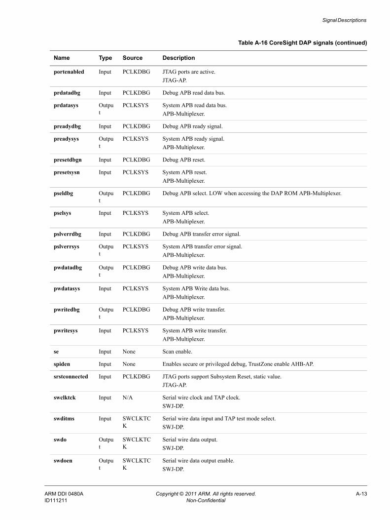
Signal Descriptions
portenabled Input PCLKDBG JTAG ports are active.JTAG-AP.
prdatadbg Input PCLKDBG Debug APB read data bus.
prdatasys Output
PCLKSYS System APB read data bus.APB-Multiplexer.
preadydbg Input PCLKDBG Debug APB ready signal.
preadysys Output
PCLKSYS System APB ready signal.APB-Multiplexer.
presetdbgn Input PCLKDBG Debug APB reset.
presetsysn Input PCLKSYS System APB reset.APB-Multiplexer.
pseldbg Output
PCLKDBG Debug APB select. LOW when accessing the DAP ROM APB-Multiplexer.
pselsys Input PCLKSYS System APB select.APB-Multiplexer.
pslverrdbg Input PCLKDBG Debug APB transfer error signal.
pslverrsys Output
PCLKSYS System APB transfer error signal.APB-Multiplexer.
pwdatadbg Output
PCLKDBG Debug APB write data bus.APB-Multiplexer.
pwdatasys Input PCLKSYS System APB Write data bus.APB-Multiplexer.
pwritedbg Output
PCLKDBG Debug APB write transfer.APB-Multiplexer.
pwritesys Input PCLKSYS System APB write transfer.APB-Multiplexer.
se Input None Scan enable.
spiden Input None Enables secure or privileged debug, TrustZone enable AHB-AP.
srstconnected Input PCLKDBG JTAG ports support Subsystem Reset, static value.JTAG-AP.
swclktck Input N/A Serial wire clock and TAP clock.SWJ-DP.
swditms Input SWCLKTCK
Serial wire data input and TAP test mode select.SWJ-DP.
swdo Output
SWCLKTCK
Serial wire data output.SWJ-DP.
swdoen Output
SWCLKTCK
Serial wire data output enable.SWJ-DP.
Table A-16 CoreSight DAP signals (continued)
Name Type Source Description
ARM DDI 0480A Copyright © 2011 ARM. All rights reserved. A-13ID111211 Non-Confidential

Signal Descriptions
targetid Input SWCLKTCK
Uniquely identifies the part, see Target ID on page 4-15.SWJ-DP.
tdi Input SWCLKTCK
TAP data in.SWJ-DP.
tdo Output
SWCLKTCK
TAP data out.SWJ-DP.
Table A-16 CoreSight DAP signals (continued)
Name Type Source Description
ARM DDI 0480A Copyright © 2011 ARM. All rights reserved. A-14ID111211 Non-Confidential
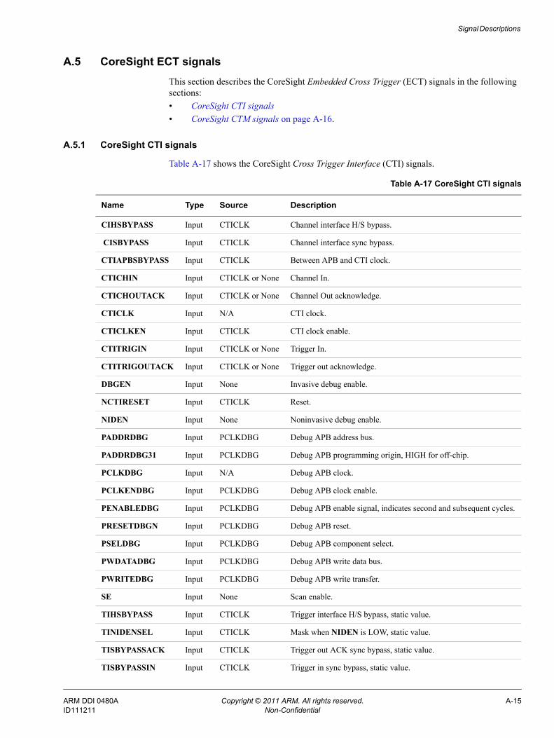
Signal Descriptions
A.5 CoreSight ECT signalsThis section describes the CoreSight Embedded Cross Trigger (ECT) signals in the following sections:• CoreSight CTI signals• CoreSight CTM signals on page A-16.
A.5.1 CoreSight CTI signals
Table A-17 shows the CoreSight Cross Trigger Interface (CTI) signals.
Table A-17 CoreSight CTI signals
Name Type Source Description
CIHSBYPASS Input CTICLK Channel interface H/S bypass.
CISBYPASS Input CTICLK Channel interface sync bypass.
CTIAPBSBYPASS Input CTICLK Between APB and CTI clock.
CTICHIN Input CTICLK or None Channel In.
CTICHOUTACK Input CTICLK or None Channel Out acknowledge.
CTICLK Input N/A CTI clock.
CTICLKEN Input CTICLK CTI clock enable.
CTITRIGIN Input CTICLK or None Trigger In.
CTITRIGOUTACK Input CTICLK or None Trigger out acknowledge.
DBGEN Input None Invasive debug enable.
NCTIRESET Input CTICLK Reset.
NIDEN Input None Noninvasive debug enable.
PADDRDBG Input PCLKDBG Debug APB address bus.
PADDRDBG31 Input PCLKDBG Debug APB programming origin, HIGH for off-chip.
PCLKDBG Input N/A Debug APB clock.
PCLKENDBG Input PCLKDBG Debug APB clock enable.
PENABLEDBG Input PCLKDBG Debug APB enable signal, indicates second and subsequent cycles.
PRESETDBGN Input PCLKDBG Debug APB reset.
PSELDBG Input PCLKDBG Debug APB component select.
PWDATADBG Input PCLKDBG Debug APB write data bus.
PWRITEDBG Input PCLKDBG Debug APB write transfer.
SE Input None Scan enable.
TIHSBYPASS Input CTICLK Trigger interface H/S bypass, static value.
TINIDENSEL Input CTICLK Mask when NIDEN is LOW, static value.
TISBYPASSACK Input CTICLK Trigger out ACK sync bypass, static value.
TISBYPASSIN Input CTICLK Trigger in sync bypass, static value.
ARM DDI 0480A Copyright © 2011 ARM. All rights reserved. A-15ID111211 Non-Confidential
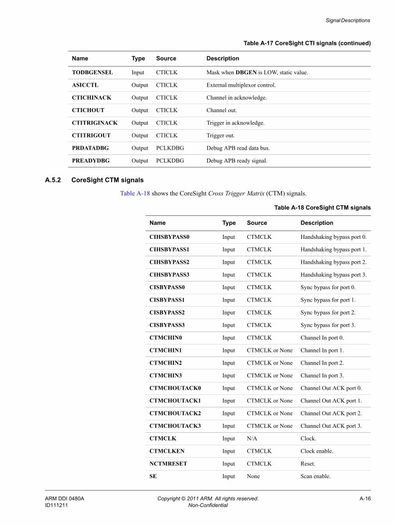
Signal Descriptions
A.5.2 CoreSight CTM signals
Table A-18 shows the CoreSight Cross Trigger Matrix (CTM) signals.
TODBGENSEL Input CTICLK Mask when DBGEN is LOW, static value.
ASICCTL Output CTICLK External multiplexor control.
CTICHINACK Output CTICLK Channel in acknowledge.
CTICHOUT Output CTICLK Channel out.
CTITRIGINACK Output CTICLK Trigger in acknowledge.
CTITRIGOUT Output CTICLK Trigger out.
PRDATADBG Output PCLKDBG Debug APB read data bus.
PREADYDBG Output PCLKDBG Debug APB ready signal.
Table A-17 CoreSight CTI signals (continued)
Name Type Source Description
Table A-18 CoreSight CTM signals
Name Type Source Description
CIHSBYPASS0 Input CTMCLK Handshaking bypass port 0.
CIHSBYPASS1 Input CTMCLK Handshaking bypass port 1.
CIHSBYPASS2 Input CTMCLK Handshaking bypass port 2.
CIHSBYPASS3 Input CTMCLK Handshaking bypass port 3.
CISBYPASS0 Input CTMCLK Sync bypass for port 0.
CISBYPASS1 Input CTMCLK Sync bypass for port 1.
CISBYPASS2 Input CTMCLK Sync bypass for port 2.
CISBYPASS3 Input CTMCLK Sync bypass for port 3.
CTMCHIN0 Input CTMCLK Channel In port 0.
CTMCHIN1 Input CTMCLK or None Channel In port 1.
CTMCHIN2 Input CTMCLK or None Channel In port 2.
CTMCHIN3 Input CTMCLK or None Channel In port 3.
CTMCHOUTACK0 Input CTMCLK or None Channel Out ACK port 0.
CTMCHOUTACK1 Input CTMCLK or None Channel Out ACK port 1.
CTMCHOUTACK2 Input CTMCLK or None Channel Out ACK port 2.
CTMCHOUTACK3 Input CTMCLK or None Channel Out ACK port 3.
CTMCLK Input N/A Clock.
CTMCLKEN Input CTMCLK Clock enable.
NCTMRESET Input CTMCLK Reset.
SE Input None Scan enable.
ARM DDI 0480A Copyright © 2011 ARM. All rights reserved. A-16ID111211 Non-Confidential
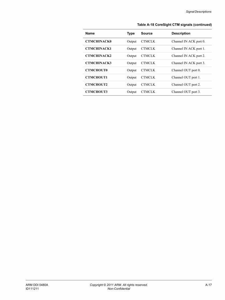
Signal Descriptions
CTMCHINACK0 Output CTMCLK Channel IN ACK port 0.
CTMCHINACK1 Output CTMCLK Channel IN ACK port 1.
CTMCHINACK2 Output CTMCLK Channel IN ACK port 2.
CTMCHINACK3 Output CTMCLK Channel IN ACK port 3.
CTMCHOUT0 Output CTMCLK Channel OUT port 0.
CTMCHOUT1 Output CTMCLK Channel OUT port 1.
CTMCHOUT2 Output CTMCLK Channel OUT port 2.
CTMCHOUT3 Output CTMCLK Channel OUT port 3.
Table A-18 CoreSight CTM signals (continued)
Name Type Source Description
ARM DDI 0480A Copyright © 2011 ARM. All rights reserved. A-17ID111211 Non-Confidential
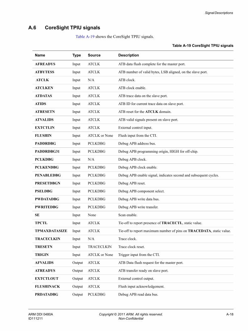
Signal Descriptions
A.6 CoreSight TPIU signalsTable A-19 shows the CoreSight TPIU signals.
Table A-19 CoreSight TPIU signals
Name Type Source Description
AFREADYS Input ATCLK ATB data flush complete for the master port.
ATBYTESS Input ATCLK ATB number of valid bytes, LSB aligned, on the slave port.
ATCLK Input N/A ATB clock.
ATCLKEN Input ATCLK ATB clock enable.
ATDATAS Input ATCLK ATB trace data on the slave port.
ATIDS Input ATCLK ATB ID for current trace data on slave port.
ATRESETN Input ATCLK ATB reset for the ATCLK domain.
ATVALIDS Input ATCLK ATB valid signals present on slave port.
EXTCTLIN Input ATCLK External control input.
FLUSHIN Input ATCLK or None Flush input from the CTI.
PADDRDBG Input PCLKDBG Debug APB address bus.
PADDRDBG31 Input PCLKDBG Debug APB programming origin, HIGH for off-chip.
PCLKDBG Input N/A Debug APB clock.
PCLKENDBG Input PCLKDBG Debug APB clock enable.
PENABLEDBG Input PCLKDBG Debug APB enable signal, indicates second and subsequent cycles.
PRESETDBGN Input PCLKDBG Debug APB reset.
PSELDBG Input PCLKDBG Debug APB component select.
PWDATADBG Input PCLKDBG Debug APB write data bus.
PWRITEDBG Input PCLKDBG Debug APB write transfer.
SE Input None Scan enable.
TPCTL Input ATCLK Tie-off to report presence of TRACECTL, static value.
TPMAXDATASIZE Input ATCLK Tie-off to report maximum number of pins on TRACEDATA, static value.
TRACECLKIN Input N/A Trace clock.
TRESETN Input TRACECLKIN Trace clock reset.
TRIGIN Input ATCLK or None Trigger input from the CTI.
AFVALIDS Output ATCLK ATB Data flush request for the master port.
ATREADYS Output ATCLK ATB transfer ready on slave port.
EXTCTLOUT Output ATCLK External control output.
FLUSHINACK Output ATCLK Flush input acknowledgement.
PRDATADBG Output PCLKDBG Debug APB read data bus.
ARM DDI 0480A Copyright © 2011 ARM. All rights reserved. A-18ID111211 Non-Confidential
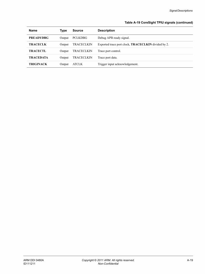
Signal Descriptions
PREADYDBG Output PCLKDBG Debug APB ready signal.
TRACECLK Output TRACECLKIN Exported trace port clock, TRACECLKIN divided by 2.
TRACECTL Output TRACECLKIN Trace port control.
TRACEDATA Output TRACECLKIN Trace port data.
TRIGINACK Output ATCLK Trigger input acknowledgement.
Table A-19 CoreSight TPIU signals (continued)
Name Type Source Description
ARM DDI 0480A Copyright © 2011 ARM. All rights reserved. A-19ID111211 Non-Confidential
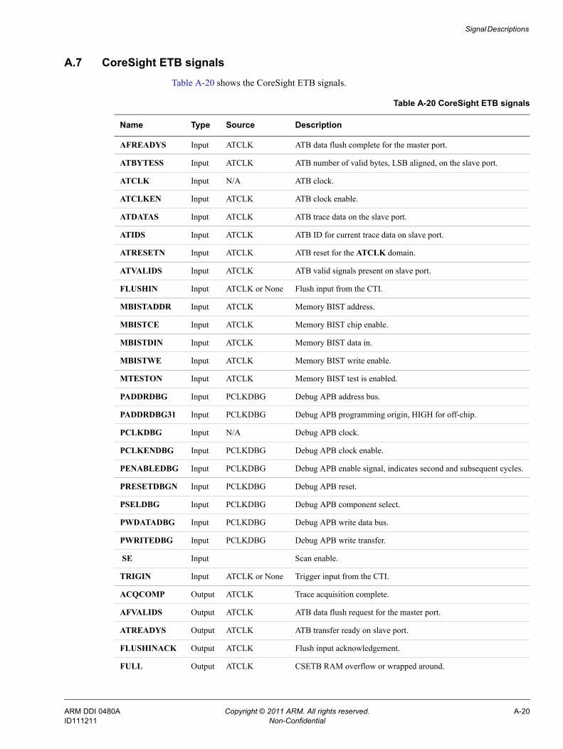
Signal Descriptions
A.7 CoreSight ETB signalsTable A-20 shows the CoreSight ETB signals.
Table A-20 CoreSight ETB signals
Name Type Source Description
AFREADYS Input ATCLK ATB data flush complete for the master port.
ATBYTESS Input ATCLK ATB number of valid bytes, LSB aligned, on the slave port.
ATCLK Input N/A ATB clock.
ATCLKEN Input ATCLK ATB clock enable.
ATDATAS Input ATCLK ATB trace data on the slave port.
ATIDS Input ATCLK ATB ID for current trace data on slave port.
ATRESETN Input ATCLK ATB reset for the ATCLK domain.
ATVALIDS Input ATCLK ATB valid signals present on slave port.
FLUSHIN Input ATCLK or None Flush input from the CTI.
MBISTADDR Input ATCLK Memory BIST address.
MBISTCE Input ATCLK Memory BIST chip enable.
MBISTDIN Input ATCLK Memory BIST data in.
MBISTWE Input ATCLK Memory BIST write enable.
MTESTON Input ATCLK Memory BIST test is enabled.
PADDRDBG Input PCLKDBG Debug APB address bus.
PADDRDBG31 Input PCLKDBG Debug APB programming origin, HIGH for off-chip.
PCLKDBG Input N/A Debug APB clock.
PCLKENDBG Input PCLKDBG Debug APB clock enable.
PENABLEDBG Input PCLKDBG Debug APB enable signal, indicates second and subsequent cycles.
PRESETDBGN Input PCLKDBG Debug APB reset.
PSELDBG Input PCLKDBG Debug APB component select.
PWDATADBG Input PCLKDBG Debug APB write data bus.
PWRITEDBG Input PCLKDBG Debug APB write transfer.
SE Input Scan enable.
TRIGIN Input ATCLK or None Trigger input from the CTI.
ACQCOMP Output ATCLK Trace acquisition complete.
AFVALIDS Output ATCLK ATB data flush request for the master port.
ATREADYS Output ATCLK ATB transfer ready on slave port.
FLUSHINACK Output ATCLK Flush input acknowledgement.
FULL Output ATCLK CSETB RAM overflow or wrapped around.
ARM DDI 0480A Copyright © 2011 ARM. All rights reserved. A-20ID111211 Non-Confidential
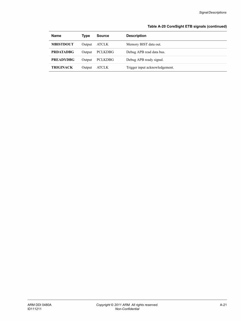
Signal Descriptions
MBISTDOUT Output ATCLK Memory BIST data out.
PRDATADBG Output PCLKDBG Debug APB read data bus.
PREADYDBG Output PCLKDBG Debug APB ready signal.
TRIGINACK Output ATCLK Trigger input acknowledgement.
Table A-20 CoreSight ETB signals (continued)
Name Type Source Description
ARM DDI 0480A Copyright © 2011 ARM. All rights reserved. A-21ID111211 Non-Confidential
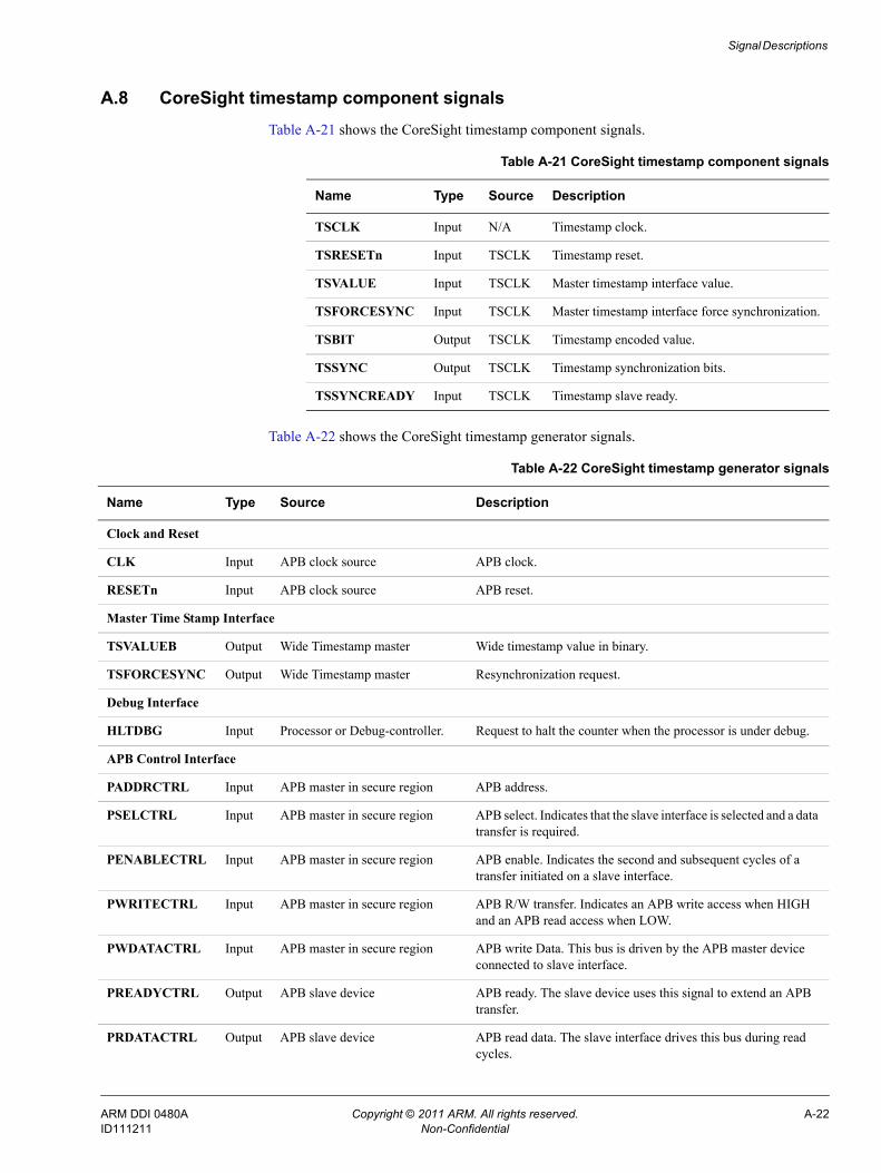
Signal Descriptions
A.8 CoreSight timestamp component signalsTable A-21 shows the CoreSight timestamp component signals.
Table A-22 shows the CoreSight timestamp generator signals.
Table A-21 CoreSight timestamp component signals
Name Type Source Description
TSCLK Input N/A Timestamp clock.
TSRESETn Input TSCLK Timestamp reset.
TSVALUE Input TSCLK Master timestamp interface value.
TSFORCESYNC Input TSCLK Master timestamp interface force synchronization.
TSBIT Output TSCLK Timestamp encoded value.
TSSYNC Output TSCLK Timestamp synchronization bits.
TSSYNCREADY Input TSCLK Timestamp slave ready.
Table A-22 CoreSight timestamp generator signals
Name Type Source Description
Clock and Reset
CLK Input APB clock source APB clock.
RESETn Input APB clock source APB reset.
Master Time Stamp Interface
TSVALUEB Output Wide Timestamp master Wide timestamp value in binary.
TSFORCESYNC Output Wide Timestamp master Resynchronization request.
Debug Interface
HLTDBG Input Processor or Debug-controller. Request to halt the counter when the processor is under debug.
APB Control Interface
PADDRCTRL Input APB master in secure region APB address.
PSELCTRL Input APB master in secure region APB select. Indicates that the slave interface is selected and a data transfer is required.
PENABLECTRL Input APB master in secure region APB enable. Indicates the second and subsequent cycles of a transfer initiated on a slave interface.
PWRITECTRL Input APB master in secure region APB R/W transfer. Indicates an APB write access when HIGH and an APB read access when LOW.
PWDATACTRL Input APB master in secure region APB write Data. This bus is driven by the APB master device connected to slave interface.
PREADYCTRL Output APB slave device APB ready. The slave device uses this signal to extend an APB transfer.
PRDATACTRL Output APB slave device APB read data. The slave interface drives this bus during read cycles.
ARM DDI 0480A Copyright © 2011 ARM. All rights reserved. A-22ID111211 Non-Confidential
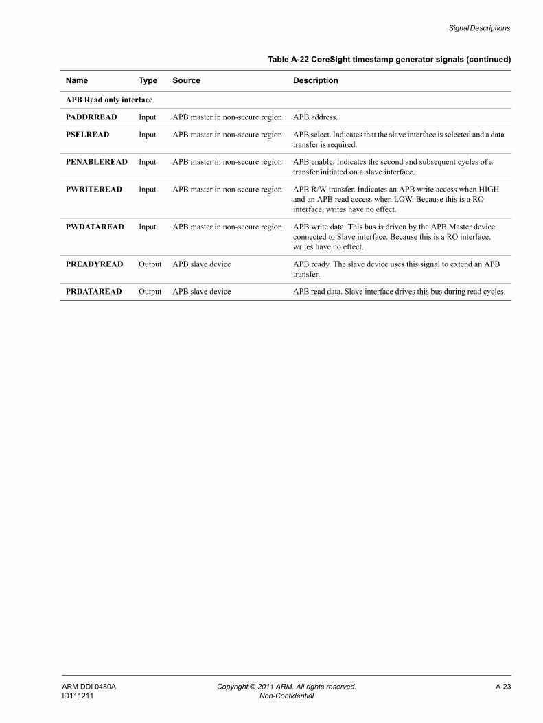
Signal Descriptions
APB Read only interface
PADDRREAD Input APB master in non-secure region APB address.
PSELREAD Input APB master in non-secure region APB select. Indicates that the slave interface is selected and a data transfer is required.
PENABLEREAD Input APB master in non-secure region APB enable. Indicates the second and subsequent cycles of a transfer initiated on a slave interface.
PWRITEREAD Input APB master in non-secure region APB R/W transfer. Indicates an APB write access when HIGH and an APB read access when LOW. Because this is a RO interface, writes have no effect.
PWDATAREAD Input APB master in non-secure region APB write data. This bus is driven by the APB Master device connected to Slave interface. Because this is a RO interface, writes have no effect.
PREADYREAD Output APB slave device APB ready. The slave device uses this signal to extend an APB transfer.
PRDATAREAD Output APB slave device APB read data. Slave interface drives this bus during read cycles.
Table A-22 CoreSight timestamp generator signals (continued)
Name Type Source Description
ARM DDI 0480A Copyright © 2011 ARM. All rights reserved. A-23ID111211 Non-Confidential
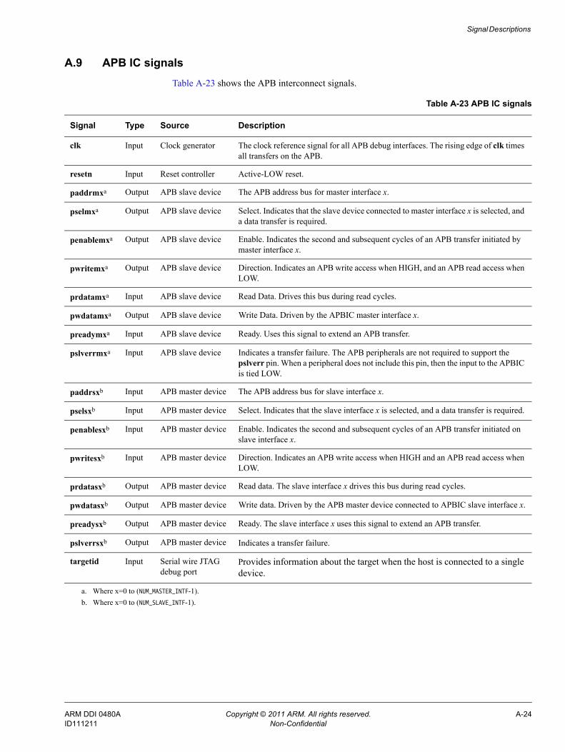
Signal Descriptions
A.9 APB IC signalsTable A-23 shows the APB interconnect signals.
Table A-23 APB IC signals
Signal Type Source Description
clk Input Clock generator The clock reference signal for all APB debug interfaces. The rising edge of clk times all transfers on the APB.
resetn Input Reset controller Active-LOW reset.
paddrmxa Output APB slave device The APB address bus for master interface x.
pselmxa Output APB slave device Select. Indicates that the slave device connected to master interface x is selected, and a data transfer is required.
penablemxa Output APB slave device Enable. Indicates the second and subsequent cycles of an APB transfer initiated by master interface x.
pwritemxa Output APB slave device Direction. Indicates an APB write access when HIGH, and an APB read access when LOW.
prdatamxa Input APB slave device Read Data. Drives this bus during read cycles.
pwdatamxa Output APB slave device Write Data. Driven by the APBIC master interface x.
preadymxa Input APB slave device Ready. Uses this signal to extend an APB transfer.
pslverrmxa Input APB slave device Indicates a transfer failure. The APB peripherals are not required to support the pslverr pin. When a peripheral does not include this pin, then the input to the APBIC is tied LOW.
paddrsxb Input APB master device The APB address bus for slave interface x.
pselsxb Input APB master device Select. Indicates that the slave interface x is selected, and a data transfer is required.
penablesxb Input APB master device Enable. Indicates the second and subsequent cycles of an APB transfer initiated on slave interface x.
pwritesxb Input APB master device Direction. Indicates an APB write access when HIGH and an APB read access when LOW.
prdatasxb Output APB master device Read data. The slave interface x drives this bus during read cycles.
pwdatasxb Output APB master device Write data. Driven by the APB master device connected to APBIC slave interface x.
preadysxb Output APB master device Ready. The slave interface x uses this signal to extend an APB transfer.
pslverrsxb Output APB master device Indicates a transfer failure.
targetid Input Serial wire JTAG debug port
Provides information about the target when the host is connected to a single device.
a. Where x=0 to (NUM_MASTER_INTF-1).b. Where x=0 to (NUM_SLAVE_INTF-1).
ARM DDI 0480A Copyright © 2011 ARM. All rights reserved. A-24ID111211 Non-Confidential
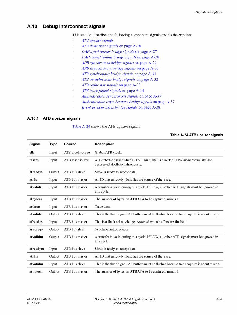
Signal Descriptions
A.10 Debug interconnect signalsThis section describes the following component signals and its description:• ATB upsizer signals• ATB downsizer signals on page A-26• DAP synchronous bridge signals on page A-27• DAP asynchronous bridge signals on page A-28• APB synchronous bridge signals on page A-29• APB asynchronous bridge signals on page A-30• ATB synchronous bridge signals on page A-31• ATB asynchronous bridge signals on page A-32• ATB replicator signals on page A-33• ATB trace funnel signals on page A-34• Authentication synchronous signals on page A-37• Authentication asynchronous bridge signals on page A-37• Event asynchronous bridge signals on page A-38.
A.10.1 ATB upsizer signals
Table A-24 shows the ATB upsizer signals.
Table A-24 ATB upsizer signals
Signal Type Source Description
clk Input ATB clock source Global ATB clock.
resetn Input ATB reset source ATB interface reset when LOW. This signal is asserted LOW asynchronously, and deasserted HIGH synchronously.
atreadys Output ATB bus slave Slave is ready to accept data.
atids Input ATB bus master An ID that uniquely identifies the source of the trace.
atvalids Input ATB bus master A transfer is valid during this cycle. If LOW, all other ATB signals must be ignored in this cycle.
atbytess Input ATB bus master The number of bytes on ATDATA to be captured, minus 1.
atdatas Input ATB bus master Trace data.
afvalids Output ATB bus slave This is the flush signal. All buffers must be flushed because trace capture is about to stop.
afreadys Input ATB bus master This is a flush acknowledge. Asserted when buffers are flushed.
syncreqs Output ATB bus slave Synchronization request.
atvalidm Output ATB bus master A transfer is valid during this cycle. If LOW, all other ATB signals must be ignored in this cycle.
atreadym Input ATB bus slave Slave is ready to accept data.
atidm Output ATB bus master An ID that uniquely identifies the source of the trace.
afvalidm Input ATB bus slave This is the flush signal. All buffers must be flushed because trace capture is about to stop.
atbytesm Output ATB bus master The number of bytes on ATDATA to be captured, minus 1.
ARM DDI 0480A Copyright © 2011 ARM. All rights reserved. A-25ID111211 Non-Confidential
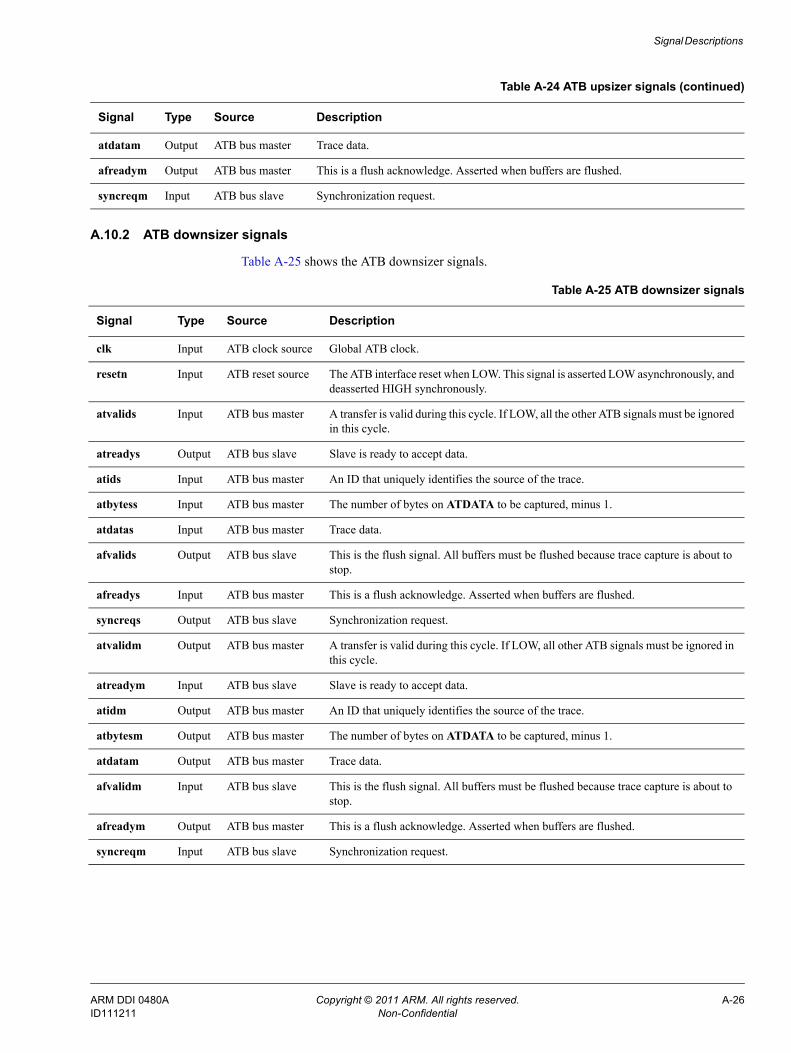
Signal Descriptions
A.10.2 ATB downsizer signals
Table A-25 shows the ATB downsizer signals.
atdatam Output ATB bus master Trace data.
afreadym Output ATB bus master This is a flush acknowledge. Asserted when buffers are flushed.
syncreqm Input ATB bus slave Synchronization request.
Table A-24 ATB upsizer signals (continued)
Signal Type Source Description
Table A-25 ATB downsizer signals
Signal Type Source Description
clk Input ATB clock source Global ATB clock.
resetn Input ATB reset source The ATB interface reset when LOW. This signal is asserted LOW asynchronously, and deasserted HIGH synchronously.
atvalids Input ATB bus master A transfer is valid during this cycle. If LOW, all the other ATB signals must be ignored in this cycle.
atreadys Output ATB bus slave Slave is ready to accept data.
atids Input ATB bus master An ID that uniquely identifies the source of the trace.
atbytess Input ATB bus master The number of bytes on ATDATA to be captured, minus 1.
atdatas Input ATB bus master Trace data.
afvalids Output ATB bus slave This is the flush signal. All buffers must be flushed because trace capture is about to stop.
afreadys Input ATB bus master This is a flush acknowledge. Asserted when buffers are flushed.
syncreqs Output ATB bus slave Synchronization request.
atvalidm Output ATB bus master A transfer is valid during this cycle. If LOW, all other ATB signals must be ignored in this cycle.
atreadym Input ATB bus slave Slave is ready to accept data.
atidm Output ATB bus master An ID that uniquely identifies the source of the trace.
atbytesm Output ATB bus master The number of bytes on ATDATA to be captured, minus 1.
atdatam Output ATB bus master Trace data.
afvalidm Input ATB bus slave This is the flush signal. All buffers must be flushed because trace capture is about to stop.
afreadym Output ATB bus master This is a flush acknowledge. Asserted when buffers are flushed.
syncreqm Input ATB bus slave Synchronization request.
ARM DDI 0480A Copyright © 2011 ARM. All rights reserved. A-26ID111211 Non-Confidential
Signal Descriptions
A.10.3 DAP synchronous bridge signals
Table A-26 shows the DAP synchronous bridge signals.
Table A-26 DAP synchronous bridge signals
Signal Type Source Description
dapclk Input DAP clock source The DAP clock.
dapresetn Input DAP reset source The DAP reset.
dapclkens Input DAP clock source The DAP clock enable.
dapsels Input DAP bus master The DAP select. Indicates that the slave device is selected and a data transfer is required.
dapaborts Input DAP bus master The DAP abort. When this signal is asserted HIGH, then the DAP slave aborts the current DAP transfer and assert its ready in the next cycle.
dapenables Input DAP bus master The DAP enable. Indicates the second and subsequent cycles of an DAP transfer
dapwrites Input DAP bus master The DAP R/W. Indicates an DAP write access when HIGH and an DAP read access when LOW.
dapaddrs Input DAP bus master The DAP address bus from master.
dapwdatas Input DAP bus master The DAP write data. The DAP master drives this bus.
dapreadys Output DAP bus slave The DAP slave ready. When asserted HIGH, it indicates that the slave has completed the current DAP transfer and is ready for the next transfer.
dapslverrs Output DAP bus slave The DAP slave error. The current DAP transaction had an error.
daprdatas Output DAP bus slave The DAP read data. Carries the read-data of a DAP read transfer.
dapclkenm Input DAP clock source The DAP clock enable.
dapselm Output DAP bus master The DAP select. Indicates that the master is selecting a particular slave for R/W transfer.
dapabortm Output DAP bus master The DAP master abort. When asserted HIGH, it indicates that the master is aborting the current transaction.
dapenablem Output DAP bus master The DAP enable. Indicates the second and subsequent cycles of an DAP transfer.
dapwritem Output DAP bus master The DAP R/W. Indicates a write transfer when HIGH and a read transfer when LOW.
dapaddrm Output DAP address bus. The DAP bus master
dapwdatam Output DAP bus master The DAP write data. The master drives this bus and carries the write data for the current write transfer.
dapreadym Input DAP bus slave The DAP ready. The slave indicates whether it has completed current transfer and is ready for the next transfer.
dapslverrm Input DAP bus slave The DAP slave error. The slave indicates that the current transfer was in error.
daprdatam Input DAP bus slave The DAP read data. The read data of the current DAP read transfer.
ARM DDI 0480A Copyright © 2011 ARM. All rights reserved. A-27ID111211 Non-Confidential
Signal Descriptions
A.10.4 DAP asynchronous bridge signals
Table A-27 shows the DAP asynchronous bridge signals.
csysreq Input AXI-C Bus master
An AXI-C low-power request. When this is asserted LOW, it requests slave or master device enter low-power state. When it is de-asserted HIGH it requests slave or master device to exit low-power state.
csysack Output AXI-C slave An AXI-C low-power acknowledge. When asserted LOW, it indicates that the slave or master device has entered low-power state in response to csysreq being asserted LOW. When de-asserted HIGH, it indicates that slave or master device has exited low-power state.
cactive Output AXI-C slave An AXI-C clock required. When asserted HIGH, it indicates that the slave or master device requires the clock to be turned on. When de-asserted LOW, indicates that the clock controller can shut-off the clock at any instant.
Table A-26 DAP synchronous bridge signals (continued)
Signal Type Source Description
Table A-27 DAP asynchronous bridge signals
Signal Type Source Description
dapclks Input DAP clock source DAP slave clock.
dapresetsn Input DAP reset source DAP slave reset.
dapclkm DAP clock source DAP master clock.
dapresetm DAP reset source DAP master reset.
dapsels Input DAP bus master The DAP select. Indicates that the slave device is selected and a data transfer is required.
dapaborts Input DAP bus master The DAP abort. When this signal is asserted HIGH, then the DAP slave aborts the current DAP transfer and assert its ready in the next cycle.
dapenables Input DAP bus master The DAP enable. Indicates the second and subsequent cycles of an DAP transfer
dapwrites Input DAP bus master The DAP R/W. Indicates an DAP write access when HIGH and an DAP read access when LOW.
dapaddrs Input DAP bus master The DAP address bus from master.
dapwdatas Input DAP bus master The DAP write data. The DAP master drives this bus.
dapreadys Output DAP bus slave The DAP slave ready. When asserted HIGH, it indicates that the slave has completed the current DAP transfer and is ready for the next transfer.
dapslverrs Output DAP bus slave The DAP slave error. The current DAP transaction had an error.
daprdatas Output DAP bus slave The DAP read data. Carries the read-data of a DAP read transfer.
dapclkenm Input DAP clock source The DAP clock enable.
dapselm Output DAP bus master The DAP select. Indicates that the master is selecting a particular slave for R/W transfer.
dapabortm Output DAP bus master The DAP master abort. When asserted HIGH, it indicates that the master is aborting the current transaction.
dapenablem Output DAP bus master The DAP enable. Indicates the second and subsequent cycles of an DAP transfer.
ARM DDI 0480A Copyright © 2011 ARM. All rights reserved. A-28ID111211 Non-Confidential
Signal Descriptions
A.10.5 APB synchronous bridge signals
Table A-28 shows the APB synchronous bridge signals.
dapwritem Output DAP bus master The DAP R/W. Indicates a write transfer when HIGH and a read transfer when LOW.
dapaddrm Output DAP address bus. The DAP bus master.
dapwdatam Output DAP bus master The DAP write data. The master drives this bus and carries the write data for the current write transfer.
dapreadym Input DAP bus slave The DAP ready. The slave indicates whether it has completed current transfer and is ready for the next transfer.
dapslverrm Input DAP bus slave The DAP slave error. The slave indicates that the current transfer was in error.
daprdatam Input DAP bus slave The DAP read data. The read data of the current DAP read transfer.
Table A-27 DAP asynchronous bridge signals (continued)
Signal Type Source Description
Table A-28 APB synchronous bridge signals
Signal Type Source Description
pclk Input APB clock APB clock signal for all downstream APB debug interfaces.
presetn Input APB reset APB asynchronous active-low reset.
pclken Input APB slave clock APB slave interface clock enable.
psels Input APB master APB select. Indicates that the slave interface is selected and a data transfer is required.
penables Input APB master APB enable. Indicates the second and subsequent cycles of an APB transfer initiated on slave interface.
pwrites Input APB master APB R/W transfer. Indicates an APB write access when HIGH and an APB read access when LOW.
paddrs Input APB master APB address bus for slave interface.
pwdatas Input APB master APB write data.
preadys Output APB slave APB ready. The slave interface uses this signal to extend an APB transfer.
pslverrs Output APB slave APB transfer error. Indicates a transfer failure. The APB peripherals are not required to support the pslverr pin. Where a peripheral does not include this pin, then this input is tied LOW.
prdatas Output APB slave APB read data. The slave interface drives this bus during read cycles.
pclkenm Input APB master clock APB master interface clock enable.
pselm Output APB master APB select. Indicates that the slave device connected to master interface is selected and a data transfer is required.
penablem Output APB master APB Enable. Indicates the second and subsequent cycles of an APB transfer initiated by Master interface.
pwritem Output APB master APB R/W transfer. Indicates an APB write access when HIGH and an APB read access when LOW.
paddrm Output APB master APB address bus for master interface.
ARM DDI 0480A Copyright © 2011 ARM. All rights reserved. A-29ID111211 Non-Confidential
Signal Descriptions
A.10.6 APB asynchronous bridge signals
Table A-29 shows the APB asynchronous bridge signals.
pwdatam Output APB master APB write data. The APB master interface drives this bus.
preadym Input APB slave APB ready. The slave device uses this signal to extend an APB transfer.
pslverrm Input APB slave APB transfer error. Indicates a transfer failure. The APB peripherals are not required to support the pslverr pin. Where a peripheral does not include this pin then this input is tied LOW.
prdatam Input APB slave APB read data. The selected slave drives this bus during read cycles.
csysreq Input AXI-C master AXI-C low-power request. When it is asserted LOW, it requests slave or master device to enter low-power state. When it is de-asserted HIGH, it requests slave or master device to exit low-power state.
csysack Output AXI-C slave AXI-C low-power acknowledge. When it is asserted LOW, indicates that the slave or master device has entered low-power state in response to csysreq being asserted LOW. When it is de-asserted HIGH, indicates that slave or master device has exited low-power state.
cactive Output AXI-C slave AXI-C clock required. When it is asserted HIGH, indicates that the slave or master device requires the clock to be turned-on. When it is de-asserted LOW, indicates that the clock controller can shut-off the clock at any instant.
Table A-28 APB synchronous bridge signals (continued)
Signal Type Source Description
Table A-29 APB asynchronous bridge signals
Signal Type Source Description
pclks Input APB clock APB slave clock.
presetsn Input APB reset APB slave reset.
pclkens Input APB slave clock APB slave interface clock enable.
pclkm Input APB clock APB master clock.
presetmn Input APB reset APB master reset.
pclkenm Input APB clock APB master interface clock enable.
psels Input APB master APB select. Indicates that the slave interface is selected and a data transfer is required.
penables Input APB master APB enable. Indicates the second and subsequent cycles of an APB transfer initiated on slave interface.
pwrites Input APB master APB R/W transfer. Indicates an APB write access when HIGH and an APB read access when LOW.
paddrs Input APB master APB address bus for slave interface.
pwdatas Input APB master APB write data.
preadys Output
APB slave APB ready. The slave interface uses this signal to extend an APB transfer.
ARM DDI 0480A Copyright © 2011 ARM. All rights reserved. A-30ID111211 Non-Confidential
Signal Descriptions
A.10.7 ATB synchronous bridge signals
Table A-30 shows the CoreSight synchronous bridge signals.
pslverrs Output
APB slave APB transfer error. Indicates a transfer failure. The APB peripherals are not required to support the pslverr pin. Where a peripheral does not include this pin, then this input is tied LOW.
prdatas Output
APB slave APB read data. The slave interface drives this bus during read cycles.
pselm Output
APB master APB select. Indicates that the slave device connected to master interface is selected and a data transfer is required.
penablem Output
APB master APB Enable. Indicates the second and subsequent cycles of an APB transfer initiated by Master interface.
pwritem Output
APB master APB R/W transfer. Indicates an APB write access when HIGH and an APB read access when LOW.
paddrm Output
APB master APB address bus for master interface.
pwdatam Output
APB master APB write data. The APB master interface drives this bus.
preadym Input APB slave APB ready. The slave device uses this signal to extend an APB transfer.
pslverrm Input APB slave APB transfer error. Indicates a transfer failure. The APB peripherals are not required to support the pslverr pin. Where a peripheral does not include this pin then this input is tied LOW.
prdatam Input APB slave APB read data. The selected slave drives this bus during read cycles.
csysreq Input AXI-C master AXI-C low-power request. When it is asserted LOW, it requests slave or master device to enter low-power state. When it is de-asserted HIGH, it requests slave or master device to exit low-power state.
csysack Output
AXI-C slave AXI-C low-power acknowledge. When it is asserted LOW, indicates that the slave or master device has entered low-power state in response to csysreq being asserted LOW. When it is de-asserted HIGH, indicates that slave or master device has exited low-power state.
cactive Output
AXI-C slave APB clock active. When it is asserted HIGH, indicates that the slave or master device requires the clock to be turned-on. When it is de-asserted LOW, indicates that the clock controller can shut-off the clock at any instant.
Table A-29 APB asynchronous bridge signals (continued)
Signal Type Source Description
Table A-30 ATB synchronous bridge signals
Name Type Source Description
afreadys Input CLK ATB data flush complete for the master port.
afvalidm Input CLK ATB data flush request for the master port.
atbytess Input CLK ATB number of valid bytes, LSB aligned, on the slave port.
clk Input N/A ATB clock.
clkens Input CLK ATB clock enable on slave port. Only in FULL bridge configuration.
ARM DDI 0480A Copyright © 2011 ARM. All rights reserved. A-31ID111211 Non-Confidential
Signal Descriptions
A.10.8 ATB asynchronous bridge signals
Table A-31 shows the CoreSight ATB asynchronous bridge signals.
clkenm Input CLK ATB clock enable on master port. Only in FULL bridge configuration.
atdatas Input CLK ATB trace data on the slave port.
atids Input CLK ATB ID for current trace data on slave port.
atreadym Input CLK ATB transfer ready on master port.
resetn Input CLK ATB reset for the ATCLK domain.
atvalids Input CLK ATB valid signals present on slave port.
afreadym Output CLK ATB data flush complete for the master port.
afvalids Output CLK ATB data flush request for the master port.
atbytesm Output CLK ATB number of valid bytes, LSB aligned, on the master port.
atdatam Output CLK ATB trace data on the master port.
atidm Output CLK ATB ID for current trace data on master port.
atreadys Output CLK ATB transfer ready on slave port.
atvalidm Output CLK ATB valid signals present on master port.
Table A-30 ATB synchronous bridge signals (continued)
Name Type Source Description
Table A-31 ATB asynchronous bridge signals
Name Type Source Description
clks Input ATB clock ATB slave clock.
resetsn Input ATB reset ATB reset for the slave domain.
clkens Input ATB clock ATB clock enable on slave port.a
clkm Input ATB clock ATB master clock.
resetmn Input ATB reset ATB reset for the master domain.
clkenm Input ATB clock ATB clock enable on master port.a
atvalids Input ATB master device ATB valid signals present on slave port.
atvalidm Output ATB slave device ATB valid signals present on master port.
atreadys Output ATB slave device ATB transfer ready on slave port.
atreadym Input ATB slave device ATB transfer ready on master port.
atids Input ATB master device ATB ID for current trace data on slave port.
atidm Output ATB master device ATB ID for current trace data on master port.
atbytess Input ATB master device ATB number of valid bytes, LSB aligned, on the slave port.
atbytesm Output ATB master device ATB number of valid bytes, LSB aligned, on the master port.
ARM DDI 0480A Copyright © 2011 ARM. All rights reserved. A-32ID111211 Non-Confidential
Signal Descriptions
A.10.9 ATB replicator signals
Table A-32 shows the ATB replicator signals.
atdatas Input ATB master device ATB trace data on the slave port.
atdatam Output ATB master device ATB trace data on the master port.
afvalids Output ATB slave device ATB data flush request for the slave port.
afvalidm Input ATB slave device ATB data flush request for the master port.
afreadys Input ATB master device ATB data flush complete for the slave port.
afreadym Input ATB master device ATB data flush complete for the master port.
syncreqs Output ATB slave device Synchronization request on slave port.
syncreqm Input ATB slave device Synchronization request on master port.
a. Only in FULL bridge configuration.
Table A-31 ATB asynchronous bridge signals (continued)
Name Type Source Description
Table A-32 ATB replicator signals
Name Type Source Description
afreadys Input CLK ATB Data flush complete for the master port.
afvalidm0 Input CLK ATB Data flush request for the master port 0.
afvalidm1 Input CLK ATB Data flush request for the master port 1.
atbytess Input CLK ATB number of valid bytes, LSB aligned, on the slave port.
clk Input N/A ATB clock.
atdatas Input CLK ATB trace data on the slave port.
atids Input CLK ATB ID for current trace data on slave port.
atreadym0 Input CLK ATB transfer ready on master port 0.
atreadym1 Input CLK ATB transfer ready on master port 1.
resetn Input CLK ATB reset for the ATCLK domain.
atvalids Input CLK ATB valid signals present on slave port.
afreadym0 Output CLK ATB data flush complete for the master port 0.
afreadym1 Output CLK ATB data flush complete for the master port 1.
afvalids Output CLK ATB data flush request for the master port.
atbytesm0 Output CLK ATB number of valid bytes, LSB aligned, on the master port.
atbytesm1 Output CLK ATB number of valid bytes, LSB aligned, on the master port.
atdatam0 Output CLK ATB trace data on the master port 0.
atdatam1 Output CLK ATB trace data on the master port 1.
atidm0 Output CLK ATB ID for current trace data on master port 0.
ARM DDI 0480A Copyright © 2011 ARM. All rights reserved. A-33ID111211 Non-Confidential
Signal Descriptions
A.10.10 ATB trace funnel signals
Table A-33 shows the ATB trace funnel signals.
atidm1 Output CLK ATB ID for current trace data on master port 1.
atreadys Output CLK ATB transfer ready on slave port.
atvalidm0 Output CLK ATB valid signals present on master port 0.
atvalidm1 Output CLK ATB valid signals present on master port 1.
paddrdbg Input CLK Debug APB address bus.
penabledbg Input CLK Debug APB enable signal, indicates second and subsequent cycles.
pseldbg Input CLK Debug APB component select.
pwdatadbg Input CLK Debug APB write data bus.
pwritedbg Input CLK Debug APB write transfer.
pclkendbg Input CLK Debug APB clock enable.
preadydbg Output CLK Debug APB ready signal.
prdata Output CLK Debug APB read data bus.
pslverrdbg Output CLK Debug APB transfer error signal.
Table A-32 ATB replicator signals (continued)
Name Type Source Description
Table A-33 ATB trace funnel signals
Name Type Source Description
afreadys0 Input CLK ATB data flush complete for the slave port 0.
afreadys1 Input CLK ATB data flush complete for the slave port 1.
afreadys2 Input CLK ATB data flush complete for the slave port 2.
afreadys3 Input CLK ATB data flush complete for the slave port 3.
afreadys4 Input CLK ATB data flush complete for the slave port 4.
afreadys5 Input CLK ATB data flush complete for the slave port 5.
afreadys6 Input CLK ATB data flush complete for the slave port 6.
afreadys7 Input CLK ATB data flush complete for the slave port 7.
afvalidm Input CLK ATB data flush request for the master port.
atbytess0 Input CLK ATB number of valid bytes, LSB aligned, on the slave port 0.
atbytess1 Input CLK ATB number of valid bytes, LSB aligned, on the slave port 1.
atbytess2 Input CLK ATB number of valid bytes, LSB aligned, on the slave port 2.
atbytess3 Input CLK ATB number of valid bytes, LSB aligned, on the slave port 3.
atbytess4 Input CLK ATB number of valid bytes, LSB aligned, on the slave port 4.
ARM DDI 0480A Copyright © 2011 ARM. All rights reserved. A-34ID111211 Non-Confidential
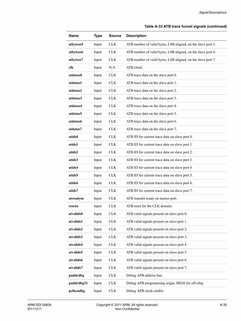
Signal Descriptions
atbytess5 Input CLK ATB number of valid bytes, LSB aligned, on the slave port 5.
atbytess6 Input CLK ATB number of valid bytes, LSB aligned, on the slave port 6.
atbytess7 Input CLK ATB number of valid bytes, LSB aligned, on the slave port 7.
clk Input N/A ATB clock.
atdatas0 Input CLK ATB trace data on the slave port 0.
atdatas1 Input CLK ATB trace data on the slave port 1.
atdatas2 Input CLK ATB trace data on the slave port 2.
atdatas3 Input CLK ATB trace data on the slave port 3.
atdatas4 Input CLK ATB trace data on the slave port 4.
atdatas5 Input CLK ATB trace data on the slave port 5.
atdatas6 Input CLK ATB trace data on the slave port 6.
atdatas7 Input CLK ATB trace data on the slave port 7.
atids0 Input CLK ATB ID for current trace data on slave port 0.
atids1 Input CLK ATB ID for current trace data on slave port 1.
atids2 Input CLK ATB ID for current trace data on slave port 2.
atids3 Input CLK ATB ID for current trace data on slave port 3.
atids4 Input CLK ATB ID for current trace data on slave port 4.
atids5 Input CLK ATB ID for current trace data on slave port 5.
atids6 Input CLK ATB ID for current trace data on slave port 6.
atids7 Input CLK ATB ID for current trace data on slave port 7.
atreadym Input CLK ATB transfer ready on master port.
resetn Input CLK ATB reset for the CLK domain.
atvalids0 Input CLK ATB valid signals present on slave port 0.
atvalids1 Input CLK ATB valid signals present on slave port 1.
atvalids2 Input CLK ATB valid signals present on slave port 2.
atvalids3 Input CLK ATB valid signals present on slave port 3.
atvalids4 Input CLK ATB valid signals present on slave port 4.
atvalids5 Input CLK ATB valid signals present on slave port 5.
atvalids6 Input CLK ATB valid signals present on slave port 6.
atvalids7 Input CLK ATB valid signals present on slave port 7.
paddrdbg Input CLK Debug APB address bus.
paddrdbg31 Input CLK Debug APB programming origin, HIGH for off-chip.
pclkendbg Input CLK Debug APB clock enable.
Table A-33 ATB trace funnel signals (continued)
Name Type Source Description
ARM DDI 0480A Copyright © 2011 ARM. All rights reserved. A-35ID111211 Non-Confidential
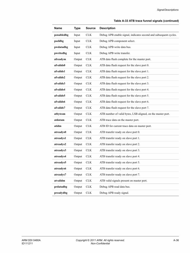
Signal Descriptions
penabledbg Input CLK Debug APB enable signal, indicates second and subsequent cycles.
pseldbg Input CLK Debug APB component select.
pwdatadbg Input CLK Debug APB write data bus.
pwritedbg Input CLK Debug APB write transfer.
afreadym Output CLK ATB data flush complete for the master port.
afvalids0 Output CLK ATB data flush request for the slave port 0.
afvalids1 Output CLK ATB data flush request for the slave port 1.
afvalids2 Output CLK ATB data flush request for the slave port 2.
afvalids3 Output CLK ATB data flush request for the slave port 3.
afvalids4 Output CLK ATB data flush request for the slave port 4.
afvalids5 Output CLK ATB data flush request for the slave port 5.
afvalids6 Output CLK ATB data flush request for the slave port 6.
afvalids7 Output CLK ATB data flush request for the slave port 7.
atbytesm Output CLK ATB number of valid bytes, LSB aligned, on the master port.
atdatam Output CLK ATB trace data on the master port.
atidm Output CLK ATB ID for current trace data on master port.
atreadys0 Output CLK ATB transfer ready on slave port 0.
atreadys1 Output CLK ATB transfer ready on slave port 1.
atreadys2 Output CLK ATB transfer ready on slave port 2.
atreadys3 Output CLK ATB transfer ready on slave port 3.
atreadys4 Output CLK ATB transfer ready on slave port 4.
atreadys5 Output CLK ATB transfer ready on slave port 5.
atreadys6 Output CLK ATB transfer ready on slave port 6.
atreadys7 Output CLK ATB transfer ready on slave port 7.
atvalidm Output CLK ATB valid signals present on master port.
prdatadbg Output CLK Debug APB read data bus.
preadydbg Output CLK Debug APB ready signal.
Table A-33 ATB trace funnel signals (continued)
Name Type Source Description
ARM DDI 0480A Copyright © 2011 ARM. All rights reserved. A-36ID111211 Non-Confidential
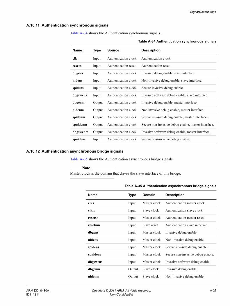
Signal Descriptions
A.10.11 Authentication synchronous signals
Table A-34 shows the Authentication synchronous signals.
A.10.12 Authentication asynchronous bridge signals
Table A-35 shows the Authentication asynchronous bridge signals.
Note Master clock is the domain that drives the slave interface of this bridge.
Table A-34 Authentication synchronous signals
Name Type Source Description
clk Input Authentication clock Authentication clock.
resetn Input Authentication reset Authentication reset.
dbgens Input Authentication clock Invasive debug enable, slave interface.
nidens Input Authentication clock Non-invasive debug enable, slave interface.
spidens Input Authentication clock Secure invasive debug enable
dbgswens Input Authentication clock Invasive software debug enable, slave interface.
dbgenm Output Authentication clock Invasive debug enable, master interface.
nidenm Output Authentication clock Non invasive debug enable, master interface.
spidenm Output Authentication clock Secure invasive debug enable, master interface.
spnidenm Output Authentication clock Secure non-invasive debug enable, master interface.
dbgswenm Output Authentication clock Invasive software debug enable, master interface.
spnidens Input Authentication clock Secure non-invasive debug enable.
Table A-35 Authentication asynchronous bridge signals
Name Type Domain Description
clks Input Master clock Authentication master clock.
clkm Input Slave clock Authentication slave clock.
resetsn Input Master clock Authentication master reset.
resetmn Input Slave reset Authentication slave interface.
dbgens Input Master clock Invasive debug enable.
nidens Input Master clock Non-invasive debug enable.
spidens Input Master clock Secure invasive debug enable.
spnidens Input Master clock Secure non-invasive debug enable.
dbgswens Input Master clock Invasive software debug enable.
dbgenm Output Slave clock Invasive debug enable.
nidenm Output Slave clock Non-invasive debug enable.
ARM DDI 0480A Copyright © 2011 ARM. All rights reserved. A-37ID111211 Non-Confidential
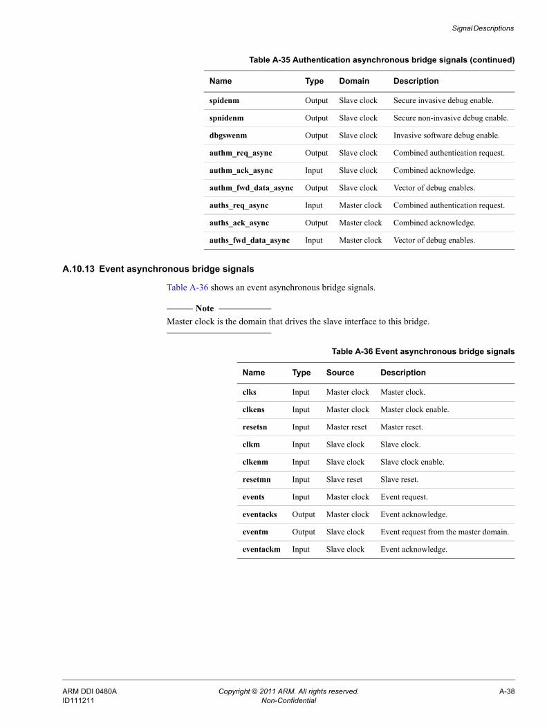
Signal Descriptions
A.10.13 Event asynchronous bridge signals
Table A-36 shows an event asynchronous bridge signals.
Note Master clock is the domain that drives the slave interface to this bridge.
spidenm Output Slave clock Secure invasive debug enable.
spnidenm Output Slave clock Secure non-invasive debug enable.
dbgswenm Output Slave clock Invasive software debug enable.
authm_req_async Output Slave clock Combined authentication request.
authm_ack_async Input Slave clock Combined acknowledge.
authm_fwd_data_async Output Slave clock Vector of debug enables.
auths_req_async Input Master clock Combined authentication request.
auths_ack_async Output Master clock Combined acknowledge.
auths_fwd_data_async Input Master clock Vector of debug enables.
Table A-35 Authentication asynchronous bridge signals (continued)
Name Type Domain Description
Table A-36 Event asynchronous bridge signals
Name Type Source Description
clks Input Master clock Master clock.
clkens Input Master clock Master clock enable.
resetsn Input Master reset Master reset.
clkm Input Slave clock Slave clock.
clkenm Input Slave clock Slave clock enable.
resetmn Input Slave reset Slave reset.
events Input Master clock Event request.
eventacks Output Master clock Event acknowledge.
eventm Output Slave clock Event request from the master domain.
eventackm Input Slave clock Event acknowledge.
ARM DDI 0480A Copyright © 2011 ARM. All rights reserved. A-38ID111211 Non-Confidential

ARM DDI 0480A Copyright © 2011 ARM. All rights reserved. B-1ID111211 Non-Confidential
Appendix B Revisions
This appendix describes the technical changes between released issues of this book.
Table B-1 Issue A
Change Location Affects
No changes, first release - -