Embed Size (px)
Citation preview

The IEE Measurement, Sensors, Instrumentation and NDT Professional Network m m
Attenuation Measurements
Alan Coster, CSL
0 The IEE Printed and published by the IEE, Michael Faraday House, Six Hills Way,
Stevenage, Herts SG12AY, TJK

Abstract
The paper details basic definitions and equations related to attenuation and describes various measurement techniques including power ratio, voltage ratio, AF substitution and IF substitution. Various attenuator types are described and a worked example of attenuation measurement is shown, complete with a measurement uncertainty budget.
About the Speaker
Alan Coster MIEE is Read of UKAS Laboratory at Dowding & Mills Calibration, Camberley (formally Calibration Systems Limited), where he has worked for 30 years.
Attenuation Measurement
Alan Coster Dowding & Mills
INTRODUCTION
Accurate attenuation measurement is an important part of characterising rf or microwave circuits and devices. For example, attenuation measurement of the component parts of a radar system will enable a designer to calculate the power delivered to the antenna from the transmitter, the noise figure of the receiver and hence the fidelity or bit error rate of the system. A precision power measurement system, such as a
calorimeter described by Oldfield (1), requires the transmission line preceding the measurement element to be characterised in order to determine the effective efficiency of the system. A thermal electrical noise standard described by Sinclair (2) requires accurate attenuation measurement of the transition or thermal block between the hot termination and the ambient temperature output connector, in order to determine its excess noise ratio.
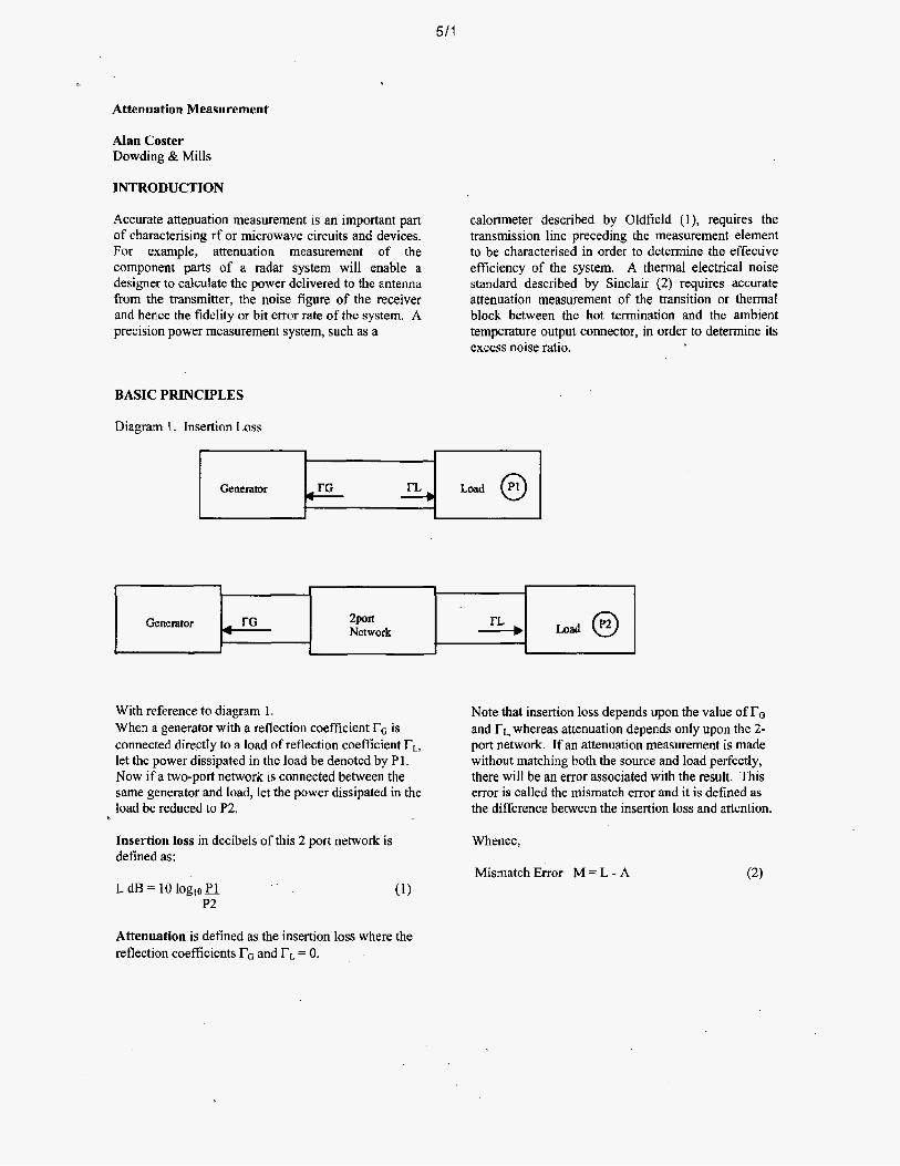
BASIC PRINCIPLES
Diagram 1. Insertion Loss
I f 1
With reference to diagram 1. When a generator with a reflection coefficient rG is connected directly to a load of reflection coefficient YL, let the power dissipated in the load be denoted by P 1. Now if a two-port network is connected between the same generator and load, let the power dissipated in the load be reduced to P2.
Insertion loss in decibels of this 2 port network is defined as:
Note that insertion loss depends upon the value of rG and rL, whereas attenuation depends only upon the 2- port network. If an attenuation measurement is made without matching both the source and load perfectly, there will be an error associated with the result. This error is called the mismatch error and it is defined as the difference between the insertion loss and attention.
Whence,
Mismatch Error M = L - A
Attenuation is defined as the insertion loss where the reflection coefficients rG and rL = 0.

512
Diagram 2 shows a signal flow diagram of a 2 port network between a generator and load where:
SI1 is the voltage reflection coefficient.looking into the input port when the output port is perfectly matched.
Szr is the voltage reflection coefficient looking into the output port when the input port is perfectly matched.
SZl is the ratio of the complex wave amplitude emerging from.the output port to that incident upon the input port when the output port is perfectly matched.
S12 is the ratio of the complex wave amplitude emerging from the input port to that incident upon the output port when the input port is perfectly matched.
From the above, the equation from Warner (3), for insertion loss is given as:
It can now be seen that the insertion loss is dependent upon rG and rL as well as the S parameters of the 2 port network. When rG and rL are matched, ( rF and' rL = 0), then equation 3 is simplified to:
where A = attenuation dB
From equation 2, the mismatch error M is the difference between equations 3 and 4.
(4)
Note that all the independent variables of equation 5 are complex. In practice it may be difficult to measure
the phase relationships where the magnitudes are small. Where this is the case, and only magnitudes are known, the mismatch uncertainty is given as a maximum and minimum limit thus:
If the 2 port network is a variable attenuator then the mismatch limit is expanded from equation 6 to give:
Where suffix b denotes the attenuator at zero or datum position, (residual attenuation) and suffix e denotes the attenuator incremented to another setting, (incremental attenuation).
MEASUREMENT SYSTEMS
Many different and ingenious ways of measuring attenuation have been developed over the years, and most methods in use today embody the following principles:
1. Power ratio 2. Voltage ratio 3. AF substitution 4. IF substitution 5 . RF substitution
Power Ratio Method
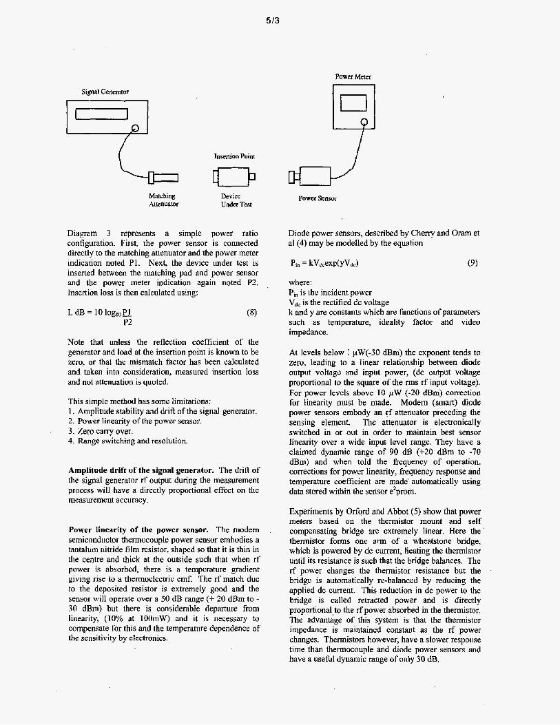
The power ratio method of measuring attenuation is perhaps one of the easiest to configure.
Diagram 3. Power Ratio
513
Signal Generator
Insellion Point
L o Marchmg Device
Attenuamr Under Test
Diagram 3 represents a simple power ratio configuration. First, the power sensor is connected directly to the matching attenuator and the power meter indication noted P1. Next, the device under test is inserted between the matching pad and power sensor and the power meter indication again noted P2. Insertion loss is then calculated using:
L dB = 10 log,,pI P2
Note that unless the reflection coefficient of the generator and load at the insertion point is known to be zero, or that the mismatch factor has been calculated and taken into consideration, measured insertion loss and not attenuation is quoted.
This simple method has some Limitations: 1. Amplitude stability and dnft of the signal generator. 2. Power linearity of the power sensor. 3. Zero carry over. 4. Range switching and resolution.
Amplitude drift of the signal generator. The drift of the signal generator rf output during the measurement process will have a directly proportional effect on the measurement accuracy.
Power linearity of the power sensor. The modem semiconductor thermocouple power sensor embodies a tantalum nitride film resistor, shaped so that it is thin in the centre and thick at the outside such that when rf power is absorbed, there is a temperature gradient giving rise to a thermoelectric emf. The rf match due to the deposited resistor is extremely good and the sensor will operate over a 50 dB range (+ 20 dBm to - 30 dBm) but there is considerable departure from linearity, (10% at 100mW) and it is necessary to compensate for this and the temperature dependence of the sensitivity by electronics.
Power Meter
Power Sensor
Diode power sensors, described by Cherry and Oram et a1 (4) may be modelled by the equation
where: Pi, is the incident power Vdc is the rectified dc voltage k and y are constants which are functions of parameters such as temperature, ideality factor and video impedance.
At levels below I pW(-30 d3m) the exponent tends to zero, leading to a linear relationship between diode output voltage and input power, (dc output voltage proportional to the square of the rms rf input voltage). For power levels above 10 p W (-20 dBm) correction for linearity must be made. Modern (smart) diode power sensors embody an If attenuator preceding the sensing element. The attenuator is electronically switched in or out in order to maintain best sensor linearity over a wide input level range. They have a claimed dynamic range of 90 dE! (+20 dBm to -70 dBm) and when told the frequency of operation, corrections for power linearity, frequency response and temperature coefficient are made' automatically using data stored within the sensor e'prom.
Experiments by Orford and Abbot ( 5 ) show that power meters based on the thermistor mount and self compensating bridge are extremely linear. Here the thermistor forms one arm of a Wheatstone bridge, which is powered by dc current, heating the thermistor until its resistance is such that the bridge balances. The rf power changes the thermistor resistance but the bridge is automatically re-balanced by reducing the applied dc current. This reduction in dc power to the bridge is called retracted power and is directly proportional, to the rf power absorbed in the thermistor. The advantage of this system is that the thermistor impedance is maintained constant as the rf power changes. Thermistors however, have a slower response time than thermocouple and diode power sensors and have a useful dynamic range of only 30 dB.
h Zero carry over. Due to the electronic circiits, small errors may occur when a power meter is zeroed on one range and then used on another.
noise of the power meter indication will be good. However, the resolution and noise contribution at a low scale reading may be an order worse. (This should be borne in mind when making measurements and all effort made to ensure that the power meter is near full scale for at least one of the two power measurements Pl,P2.)
Range switching and resolution. Most power meters
dl3. With a near f i l l scale reading, the resolution and operate over several ranges, each of approximately 5
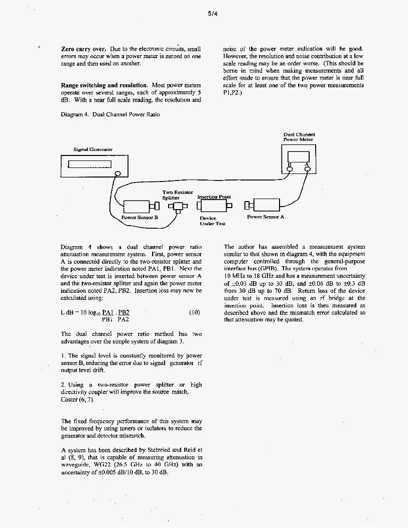
Diagram 4. Dual Channel Power Ratio
Dual Channel Power Meter
Signal Generator - Two Resistor
Insertion Point
D e v h Power Sensor A Under Tesl
Diagram 4 shows a dual channel power ratio attenuation measurement system. First, power sensor A is connected directly to the two-resistor splitter and the power meter indication noted PA 1, PB 1 Next the device under test is inserted between power sensor A and the two-resistor splitter and again the power meter indication noted PA2, PB2. lnsertion loss may now be calculated using:
L dB = 10 loglo PA1 . PB2 PI31 PA2
The dual channel power ratio method has two advantages over the simple system of diagram 3.
1. The signal level is constantly monitored by power sensor B, reducing the error due to signal generator rf output level drift.
2. Using a two-resistor power splitter or high directivity coupler will improve the source match, Coster (6, 7).
,
The fixed frequency performance of this system may be improved by using tuners or isolators to reduce the generator and detector mismatch.
A system has been described by Stelzried and Reid et a1 (8, 9), that is capable of measuring attenuation in waveguide, WG22 (26.5 GHz to 40 GHz) with an uncertainty of +0.005 dB/10 dB, to 30 dB.
The author has assembled a measurement system similar to that shown in diagram 4, with the equipment computer controlled through the general-purpose interface bus (GPIB). The system operates from 10 MHz to 18 GHz and has a measurement uncertainty of k0.03 dB up to 30 dB, and k0.06 dB to k0.3 dB from 30 dB up to 70 dB. Return loss of the device under test is measured using an r€ bridge at the insertion point. Insertion loss is then measured as described above and the mismatch error calculated so that attenuation may be quoted.
5 15
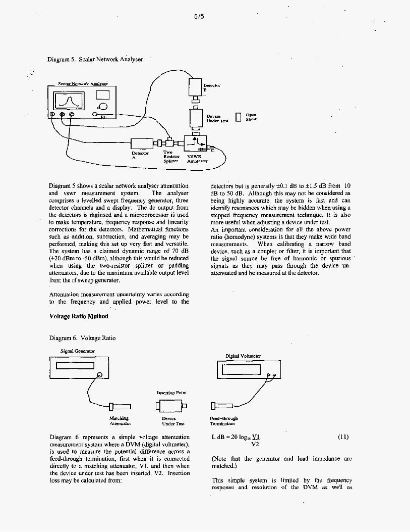
Diagram 5. Scalar Network Analyser
0 Imol I :tor
L&
Splirter Autotesser
Diagram 5 shows a scalar network analyser attenuation and vswr measurement system. The analyser comprises a levelled swept frequency generator, three detector channels and a display. The dc output from the detectors is digitised and a microprocessor is used to make temperature, frequency response and linearity corrections for the detectors. Mathematical hnctions such as addition, subtraction, and averaging may be performed, making this set up very fast and versatile. The system has a claimed dynamic range of 70 dB (120 dBm to -50 dBm), although this would be reduced when using the two-resistor splitter or padding attenuators, due to the maximum available output level from the rfsweep generator.
Attenuation measurement uncertainty varies according to the frequency and applied power level to the
Voltage Ratio Method
Diagram 6. Voltage Ratio
Signal Genmtor
Y Matching Aaenuator
0 open Shon
detectors but is generally k0.l dB to k1.5 dl3 from 10 dB to 50 dB. Although this may not be considered as being highly accurate, the system is fast and can identify resonances which may be hidden when using a stepped frequency measurement technique. It. is also more useful when adjusting a device under test. An important consideration for all the above power ratio (homodyne) systems is that they make wide band measurements. When calibrating a narrow band device, such as a coupler or filter, it is important that the signal source be free of harmonic or spurious . signals as they may pass through the device un- attenuated and be measured at the detector.
/ Illsenion Point
Device Peed-WUgh Under Test Termination
Diagram 6 represents a simple voltage attenuation L dB 20 lOg,,u (1 1) measurement system where a DVM (digital voltmeter), i s used to measure the potential difference across a feed-through termination, first when it is connected directly to a matching attenuator, V1, and then when the device under test has been inserted, V2. Insertion loss may be calculated from: This simple system is limited by the frequency
response and resolution of the DVM as well as
v2
(Note that the generator and load impedance are matched.)
5 I6
variations in the output of the signal generator. The linearity of the DVM used, which may be typically voltage coefficient of the device under test and 0.01 dB / 10 dB for a good quality eight digit DVM. resolution of the DVM will determine the range, This may be measured using an inductive voltage typically 40 dB to 50 dB from dc to 100 kHz. A major divider, and corrections made. contribution to the measurement uncertainty is the
The Inductive Voltage Divider.
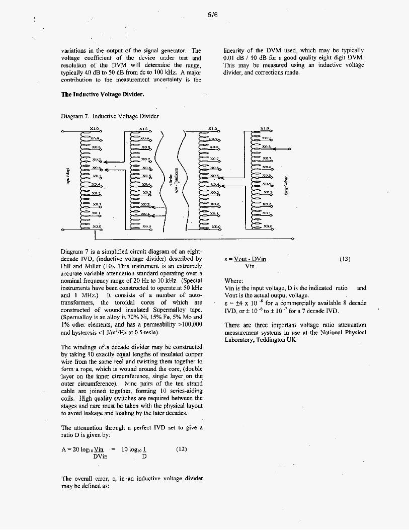
Diagram 7. Inductive Voltage Divider
x1.0 x1.0
Diagram 7 is a simplified circuit diagram of an eight- decade IVD, [inductive voltage divider) described by Hill and Miller (IO). This instrument is an extremely accurate variable attenuation standard operating over a nominal frequency range of 20 Hz to 10 kHz. (Special instruments have been constructed to operate.at 50 lcHz and 1 MHz.) It .consists of a number of auto- transformers, the toroidal cores of which are constructed of wound insulated Supermalloy tape. (Spermalloy is an alloy is 70% Ni, 15% Fe, 5% MO and 1% other elements, and has a permeability >100,000 and hysteresis <1 J/m’/Hz at 05tesla).
The windings 0f.a decade divider may be constructed by taking 10 exactly equal lengths of insulated copper wire from the same reel and twisting them together to form a rope, which is wound around the core, (double layer on the inner circumference, single layer on the, outer circumference). Nine pairs of the ten strand cable are joined together, forming 10 series-aiding coils. High quality switches are required between the stages and care must be taken with the physical layout to avoid leakage and loading by the later decades.
The attenuation through a perfect IVD set to give a ratio D is given by:
A = 20 loglo% .= lb loglo 1 (12) DVin D
E = Vout - DVin Vin
Where: Vin is the input voltage, D is the indicated ratio and Vout is the actual output voltage. E = k4 x 10 -’ for a commercially available 8 decade IVD, or f 10 -6 to & 10 -’ for a 7 decade IVD.
There are three important voltage ratio attenuation measurement systems in use at the National Physical Laboratory, Teddington UK
The overall error, E, in’an inductive voltage divider may be defined as:
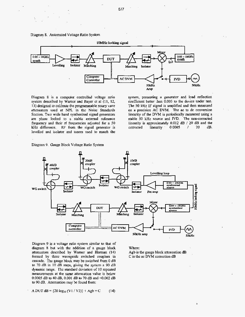
Diagram 8. Automated Voltage Ratio System
lOMHz locking signal <
DUT 0.05 - 18Gk synth
Matching Isolator .I
Diagram 8 is a computer controlled voltage ratio system described by Warner and Bayer et a1 (11, 12, 13) designed to calibrate the programmable rotary vane attenuators used at NPL in the Noise Standards Section. Two wide band synthesized signal generators are phase locked to a stable external reference frequency and their rf frequencies adjusted for a 50 W z difference. RF from the signal generator is levelled and isolator and tuners used to match the
Diagram 9. Gauge Block Voltage Ratio System
# coupler
I 2 U L
WG switch
system, presenting a generator and load reflection coefficient better than 0.005 to the device under test. The 50 kHz IF signal is amplified and then measured on a precision AC DVM. The ac to dc conversion linearity of the DVM is periodically measured using’a stable 50 kHz source and IVD. The non-corrected linearity is approximately 0.012 dB / 20 dB and the corrected linearity 0*0005 / 20 dB.
coupler
Levelling loop
I 0 . 0 s - 180112 q”aLsed 5cdJIvc I-a i Isolator Pet amp
Diagram 9 is a voltage ratio system similar to that of diagram 8 but with the addition of a gauge block attenuators described by Wamer and Herman (14) formed by three waveguide switched couplers in C is the ac DVM correction dB cascade. The gauge block may be switched from 0 dB to 70 dB in I O dB steps, giving the system a 90 dB dynamic range. The standard deviation of I O repeated measurements at the same attenuation value is below 0.0005 dB to 40 dB, 0.001 dB to 70 dB and 4 .002 dB to 90 dB. Attenuation may be found from:
Where: Agb is the gauge block attenuation dB
’ A DUT dB = (20 loglo (V1/ V2)) + Agb + C (14)
3

5 I8
Diagram 10. Dual Channel Voltage Ratio System
low noise Mixer isolation P=--;rmP -P
Diagram 10 shows a dual channel voltage ratio system developed by NPL Warner and Kilby et a1 (15, 16) to provide extremely accurate attenuation measurements for the calibration of standard piston attenuators. It operates over the frequency range 0.5 MHz to 100 MHz, is fully automatic and has a dynamic range of 160 dB without the need for noise balancing. The upper channel provides a reference signal for a lock-in analyser whilst the measurement process takes place in the lower channel. The lock-in analyser contains in- phase and quadrature phase sensitive detectors (PSDs), whose output (VI = cos \v and VQ = sin y ~ ) are combined in quadrature to yield a direct voltage given
This dual channel system also yields the phase changes that occur in the device under test. From the vector diagram in diagram 10 we have:
tan y~ = VQ /VI
hence, y = arctan (VQNI)
by:
Vout = (VI2+ VQs)'.' ( ' 5 ) = ((v cos w>' + v sin y)210.5 = V
Thus, Vout is directly related to the peak value, V, of the 10 kHz signal emerging from the lower channel and is independent ,of the phase difference, y, between signals in the upper and lower channels.
Attenuation may be found from:
A DUT = (20 loglo (Voutl)) Agba + Aivd (16) V O U t 2
Where: Vout I and Vout 2 are the output voltages for the datum and calibration setting. Agba and, Aivd are the attenuations in d 3 removed from the gauge block and IVD when the device under test is inserted.
519
Diagram 1 1. A Commercial Attenuator Calibrator
Autoranging
30- cd s o w e
Autoranging O/I0/20 dB
3 1.25MHz vco
isoiarion -P
Mixer 5 P
30: m z 1F
0.01 - 180Hz
fdter
Diagram 11 is a simplified diagram of a commercially available voltage ratio attenuator calibrator fitom Weinschel ( I 7). The instrument is a microprocessor controlled 30 MAz triple conversion receiver and may be used at other frequencies with the addition of an rf generator, local oscillator and mixer.
The 30 MHz input signal is routed through a 10 dB isolation amplifier to a series of pin-switched attenuators, which are automatically selected to present the first mixer with a 30 MWz signal at the correct level €or low noise linear mixing. A phase locked loop referenced to the instrument 10 MHz xtal oscillator provides the correction for the first voltage controlled local oscillator (31.25 MHz), resulting in a first IF of 1.25 MHz. The first IF is routed through a variable gain amplifier, having switched gains of 0, 10 and 20 dB, to the second mixer. The signal is then mixed with a 1.26 MHz local oscillator derived from the 10 MI-lz reference to form a second IF of 10 Id-Iz. This 10 kHz signal is applied to a second variable gain amplifier, having switched gains of 0, 10, 20 and 30 dB. The variable gain amplifiers and auto-ranging attenuator are microprocessor controlled in the auto-ranging sequence involved in making a measurement.
Chart 1. VM7 AID Calibration
The final conversion is made by a sample and hold amplifier within the 15 bit analogue to digital converter. The sample and hold amplifier is clocked at 8 kHz. The sampling of the 10 lcHz signal every 8 lcHz provides a quasi-mixing action that results in a 2 kHz signal with four samples per cycle. This analogue signal is then converted to digital form.
Before use, the instrument is calibrated by switching the 30 MHz receiver input to a 30 MHz internal oscillator. Each attenuation and gain block is automatically calibrated against the dd converter and the calibration results stored in ram to be used during the measurement process. The linearity of the dd converter is paramount to the overall accuracy of the system and this may be checked by inserting a precision IVD into the 10 kHz path preceding the dd.
This system has a sensitivity of -127 d 3 m and measurement accuracy of 5 0.015 dB, + 0.005 dB per 10 dB to 80dB and5 0.1 dB per 10 dB from SO dB to 105 dB.
0.003 - 0.0025 ~
0.002 . ~
Attenuation dB

5/10
Mixer signal processing . a-d canvertec
3 RF input
. lOOMHz to 2.4GHz
Chart 1,shows the results 'of the A/D calibration using an eight decade inductive.voltage divider matched to to-12dBm. . the system. The 10 kX-Iz signal is held between +14 to -
2 dBm on all but the last range, where it may cover +14
Display IQ clock s y n c m
Diagram 12. IFR 2309 FFT Signal Analyser
' control
Diagram 12 is a simplified diagram of an IFR 2309 FFT Signal Analyser. Input signals are down converted to a 10.7 MHz IF and then routed through signal conditioning circuits to a 3 1 bit sigma-delta analogue to digital converter (better known for its use. in CD players, giving low noise and high linearity). The a to d converter contains a comparator and quantizer with a feed back loop having a 2 bit delay.
The comparator compares the present input sample with the previous sample and outputs into a digital signal processor for complex analysis. The unit operates from I00 MHz to 2.4 GHz and has a maximum sensitivity of -168 dBm, resolution of 0.0001 dB and a claimed linearity of *0.01 &.per 10 dB.
AF Substitution Method
Diagram 13. Audio Frequency Substitution System
Synth
I ' I
Synth D~JT I Bufferamp Mixer LOkHz
ultra linear -P
I ... U. dctector Backing off voltage
Noise generator
In an audio frequency substitution system, the standards level over the frequency range 0.5 to 100 attenuation through the device under test is measured MHz and has a dynamic range of 150 dB. An external by comparison with an audio . frequency standard, .IO MHz reference frequency is used to lock the two usually a resistive or inductive voltage divider. synthesiser time bases and the local oscillator is Diagram 13 is a simplified diagram of an AF operated at a frequency difference of 10 kHz to the rf substitution system designed and used at NPL, source, giving a stable 10 lcHz @ after mixing. The described by Warner (18). It is used at national

5/11
attenuation standard is a 7 decade precision IVD inserted between two 10 kHz tuned amplifiers.
The gauge block attenuator, which is a repeatable step attenuator, DUT and IVD are adjusted during the measurement so that the voltage to the null detector remains the same. The 10 kHz amplifiers are purpose built and are extremely linear (better than 1 O.OOl%), are low noise and very stable. The IVD is driven from a low impedance source and its output is loaded with a high impedance. From 100 to 150 dB, noise must be injected into the system to compensate for the noise generated by the mixer. This is normally accomplished by setting the gauge block attenuator to zero, the IVD to unity and gain of the second 10 kHz amplifier for 2 voks rms output. The backing off voltage is adjusted for a null meter reading. The signal source is now switched off and the output voltage caused by the noise alone is measured on the DVM. After this, the gauge block attenuator is switched to a value, Agba and the DUT moved to its datum position, the IVD is set to zero, the noise generator is switched on and adjusted to give the same output reading as before. Finally, the signal source is switched back on and the IVD is
.
Diagram 14. Piston Attenuator
Circular tub
adjusted to a ratio R, which gives a null reading on the output meter.
The attenuation change in the DUT is then given by:
Adut = Agba + 20 loglo( 1/R) (18)
With great care being taken to reduce the effects of mismatch and leakage, the total uncertainty of measurement using this system is from & 0.0006 dB at 10 dB to 0.01 dB at 100 dB, for 95% CL.
IF Substitution Method
An IF substitution attenuation system compares the attenuation through the device under test with an IF attenuation standard, usually an IF piston attenuator, high frequency IVD or a box of x or T type resistive attenuators.
Fiwed inout coil E. ! M d e i Filter
m -. i
Diagram 14 shows a simplified piston attenuator arrangement normally used as the IF substitution standard. The tube acts as a waveguide below cut off transmission line. An IF signal, usually 30 or 60 MHz, is launched into the tube from the fixed input coil. A metallic grid acts as a mode filter ensuring that only a single mode, (Hl l , Eo,, Hzl, Ell or Hal), is transmitted. The voltage in the output coil falls exponentially as the separation between the two coils increases. For perfectly conducting cylinder walls with a coil separation 21 to 22, the attenuation in dB may be found from:
a p = 8.686 x 2x(Z2 - Zl) ((Snm / 2 ~ r ) * - ( l / h ~ ) } ~ . ~ (19)
where: r is the cylinder radius
Snm is a constant dependent upon the excitation mode. is the free space wavelength
Precision engineering is required in manufacturing the piston attenuator. A tolerance of*l p a i i n io4 on the internal radius is equivalent to 0.001 dB per 10 dB. The cylinder is sometimes temperature stabilised and a
laser interferometer employed to measure the piston displacement.
When the piston attenuator i s adjusted for a low attenuation setting, there is a systematic error resulting in non-linearity due to the interaction between the coils. This error reduces as the coils part, and is negligible at about 30 dB insertion loss.
A piston attenuator has been developed at NPL for use as a national standard, Yell (18, 19) The piston is mounted vertically and supported on air bearings to prevent contact with the cylinder wall. Displacements are measured with a laser interferometer. The cylinder is made of electroformed copper deposited on a stainless steel mandrel. This unit has a range of I20 dB, resolution of 0.0002 dB and a stated accuracy of 0.001 dB in I20 dB.

511 2
Diagram 15. Parallel IF Substitution System
.............
0.01 - 18GHt
Diagram 15 shows the basic layout of a parallel IF substitution system. Here, the 30 MHz IF input signal is compared with a 30 MHz reference signal, which may be adjusted in level by using a calibrated precision piston attenuator. These two signals are 100% square wave modulated in counter phase and are fed to the IF amplifier. A tuned phase sensitive detector (PSD) is used to detect and display the difference between the two altemately received signals. This circuit is very effective and can detect a null in the presence of much noise. The system is insensitive to changes in IF amplifier gain, but an automatic gain control loop is provided, to automatically keep the detector sensitivity constant. In operation, the two signals are adjusted to be the same amplitude, indicated by a null on the amplitude balance indicator. After the DUT is inserted, the system is again brought to a null by adjusting the precision piston attenuator. The difference in the two
Diagram 16. Rotary Vane Attenuator
settings of the standard attenuator is a measure of the insertion loss of the unknown device.
For signal levels below -90 dBm, noise generated by the mixer in the signal channel may cause an error and it is necessary to balance this by introducing extra noise into the reference channel. The system described above has a specification of k0.01 dB per 10 dB up to 40 dB, f 0.27 dB at 80 dB and* 0.5 dB at 100 dB.
RF. Substitution Method
With the RF substitution method, the attenuation through the device under test is compared with a standard microwave attenuator operating at the same frequency. The standard microwave attenuator is usually a precision waveguide rotary vane attenuator or microwave piston attenuator.
*....T-=. /. .... y ....... ...-- .... ..4. .... .........
- glassvaws
511 3
Diagram 16 shows the basic parts of a waveguide rotary vane attenuator, described by Banning (21). It consists of three metalised glass vanes, the two end vanes fixed in a direction perpendicular to the incident electric vector and a third vane, which is lossy and abIe to rotate, set diametrically across the circular waveguide, When the central vane is at an angle 8 relative to the two fixed vanes, the total attenuation is given by:
Arva = 40 log,* (sec0) + A. (20)
where: A0 is the residual attenuation when all three vanes lie in the same plane (0 = 0 )
The wa is extremely useful as the attenuation is%almost independent of frequency and there is little phase change as the attenuation is varied. As can be seen from equation 20, attenuation is not a linear hnction of the central vane angle. A change in 8 from 0,000" to 0.615" = 0.001 dl3, but a change in 0 from 86.776" to 88.188" changes the attenuation from 50 dB to 60 dB. A high quality rva can have an attenuation range of 0 to 70 dB, dependent upon the attenuation of the central vane and the vane alignment error. The accuracy of a commercially available rva is in the order of * 2% of reading or 0.1 dB whichever is the larger. Rotary vane attenuators have been made at NPL with a display resolution of 0.0001" and they follow the 40 loglo ( sec 8 ) law to within * 0.006 dB up to 40 dB.
Diagram 17. Series RF Substitution
Insertion point
@ Dewtor DUT
Indicator
Diagram 17 is a block diagram of a very simple series rf substitution system, employing two precision was. As attenuation through the DUT is increased, the attenuation in the was is adjusted from the datum setting to keep the detector output constant. The difference between the new rva setting and the datum setting is equal to the loss through the DUT. This system could be enhanced by square wave modulation
the signal source k d using a synchronous detector. By using two precision rva attenuators it is possible to obtain a dynamic range of 100 dB. A very stable high power signal generator is necessary and the output power must be within the power coefficient limits of the microwave components used. Great care must be taken to reduce RF leakage.
5/14
The Automatic Network Analyser
Diagram 18. Vector Network Analyser
S21 or S22 S11 or 512
Diagram 18 is a greatly simplified bock diagram of a commercially available microwave network analyser. The instrument is basically a microprocessor controlled two-channel superhetrodyne receiver, employing an ultra linear phase sensitive detector to detect magnitude and phase difference between the channels. The signal generator rf output is split into a reference channel and a measurement channel, which consists of a high directivity directional coupler or rf Wheatstone bridge, capable to splitting the forward and reflected waves to and from the device under test.
With reference to diagram 18, when both switches are positioned to the right, channel 1 provides the reference signals for the phase sensitive detectors, channel 2 gives the real and imaginary parts of s1 and channel 3 yields the real and imaginary parts of s21. With the switches to the left, channel 4 provides the reference signals for the phase sensitive detectors, channe1 2 gives the real and imaginary parts of s12 and channel 3 yields the real and. imaginary parts of s22. Thus, all four s parameters may be determined without reversing the device under test.
In use, the instrument is treated as a black box, where known calibration standards, such as open and short circuits, air lines and sliding or fixed termination are measured at the test ports and the results stored and used to correct measurements made on the device . under test. With the device under test removed and port 1 connected to port 2, the instrument wiil measure the complex impedance of its generator and detector. This data is stored and used in the equation for calculating attenuation.
'
These instruments &e extremely fast and versatile and results may be displayed in frequency or time domain. using a fast Fourier transform process. They are very accurate when measuring reflection coefficient but have a limited dynamic range for attenuation measurement, due to the available signal source level, harmonic mixing and channel crosstalk or leakage. The network analyser bridge or coupler sensitivity decreases with frequency, (roll off), and so one may find an rf network analyser, operating from 300 lcHz to 6 GHz, a microwave network analyser, operating from 50 MHz to 50 GHz and a millimetric wave network analyser, operating from 75 GHz to 110 GHz.
Typical measurement uncertainties are:
RF Vector Network Analyser Attenuation 3OOkHz 3GHz 6GHz 0 dB 50 75
+0.03 dB i0.04 dB +0.05 dB io.11 io.09 *0.12 k1.65 *1.34 i1.68
Microwave Vector Network Analyser Attenuation 5OMHz 26.5GHz 0 dB *0.03 dB *0.11 dB 50 *0.05 rt0.21 80 *0.60 *3.50
IMPORTANT CONSIDERATIONS WHEN MAKING ATTENUATION MEASUREMENTS

5/15
Mismatch Uncertainty
Mismatch between the generator, detector and device under test' is usually one of the most significant contributions to attenuation measurement uncertainty. With reference to equation 617, these parameters must be measured in order to calculate the attenuation of the DUT from the measured insertion loss. It may be possible to measure the device under test and the detector by using) a slotted line, rf bridge or scalarhetwork analyser. The signal generator used , may have an active levelling loop or switched attenuator in its rf output stage, making it difficult to determine the generator output impedance accurately,
If single frequency measurements are to be made then the generator and detector match may be improved by
Diagram 19. Two-Resistor Power Splitter
Diagram 19 shows a two-resistor power splitter, which is constructed to have a 50 C l resistor in series between port 1 and port 2, and an identical resistor between port 1 and port 3. This type of splitter should only ever be used in a generator level?ing circuit configuration as in diagram 19 and must never be used as a power divider in a 50 R system. (If you connect a 50 Ct termination to port 1 and port 2 then the impedance seen at port 3 is approximately 83.33 a.) This power splitter has been specifically designed to level the power from the signal source and to improve the generator source match. In diagram 19, if a detector is connected to port 3 and the output of the detector is compared with a stable reference and then connected to the signal generator amplitude. control via a high gain amplifier (levelling loop), then any change in the generator output at port 1 is seen across the both 50 Tz series resistors and detected at port 3. This change is used to correct the generator output for a constant level at port 3. As port 2 is connected to port I by an identical resistor, port 2 is also hetd level.
,
if an imperfect termination is connected to port 2 then voltage will be reflected back into port 2 at some phase. This voltage will be seen across the 50 !2 resistor and the generator internal impedance. If the
using ferrite isolators and tuners such as in diagram 8. The tuner must be adjusted for each frequency and this once tedious process has been improved by the introduction of computer controlled motorised tuners. Tuners and isolators are narrow band devices and are not practical for low rf frequencies (long wavelength) use due to their physical size. They are also prone to rf leakage and great care must be taken when making high attenuation measurements with these devices in circuit.
For wide band measurements, the generator match may be improved by using a high directivity directional coupler or a two-resistor splitter in a levelling loop circuit. A high quality 'padding' attenuator placed before the detector will also improve the detector match but its attenuation may restrict the dynamic range of the system.
generator intemal impedance is imperfect then some of the voitage will be re-reflected by the generator, causing a change in level at port 1. This change in level is detected at port 3 and used to correct the generator to maintain a constant output level at the junction of the two resistors. Port 1 is perceived as a virtual earth, thus when the levelling circuit is active, the impedance measured at port 2 will effectively be the impedance of the 50 R series resistor.
Two resistor splitters are characterised in terms of output tracking and equivalent output reflection coefficient. A typical specification for a splitter fitted with type ?v' connectors would be h 0.2 dB tracking between ports at 18 GHz, and an effective reflection coefficient of + 0.025 to f 0.075 from dc to 18 GHz. The splitter has a nominal insertion loss of 3 dB between the input and output ports.
In keeping with the UKAS document M3003 (22), the equation recommended for calculating mismatch uncertainty for a step attenuator is:
M = 8.686 / (2)O.' . [ITc12 . ( l S ~ ~ ~ l * + ISllbI2) + l rL lz .
(21) (IS22af 1S22d2> + I r G l 2 . I r L l . ( 1 s 2 1 ~ 1 ~ -t 1s21b14>10's
where:

r, and rL are the source and load reflection coefficients. SI], S22r SzI are the scattering coefficients of the attenuator, a and b referring to the starting and finishing value.
The probability distribution for mismatch using this formula is considered to be normal, compared to the limit distribution of formula 6 and 7 shown earlier in this paper.
RF leakage
In wide dynamic range measurements it is essential to check for rf leakage bypassing the device under test. This may be done by setting the system to the highest attenuation and moving a dielectric, such as a hand or metal object, over the equipment and cables. In a leaky system the detector output will vary as the leakage path is disturbed. If the measurement set up incorporates a levelling power meter, this can be used to produce a known repeatable step which should be constant for any setting of the device under test.
RF leakage may be reduced by using good condition precision connectors and semi rigid cables, wrapping connectors, isolators and other components in aluminium foil, keeping the if source a distance from the detector and ensuring that there is no other laboratory work at the critical frequencies. When the measured attenuation is much greater than the leakage, A1 >> Aathen:
U,, is approx f 8.686*104A’~Aap0) (22)
where: AI = leakage path
Diagram 20. Detector Linearity Tests
neratm
S k T I
Aa = DUT attenuator setting ULK = uncertainty due to leakage
For example, if a leakage path 40 dB below the DUT attenuator setting is assumed, then error due to leakage could be:
Measured Step Assumed Leakage Error 10 dB *o.ooo dB 20 30 40 50 60 70 80 90 100 1 I O
+0.000 +o.ooo ~ 0 . 0 0 0 *o.ooo *o.oo 1 k0.003 *0.009 *0.027 ’
M.087 k0.275
This contribution is a probability distribution.
limit having a rectangular
Detector Linearity
This includes the linearity of the analogue to digital circuits of a digital voltmeter, square law of a diode or thermocouple detector, or mixer linearity of a superhetrodyne receiver. The linearity may be determined by applying the same small repeatable level change to the detector over its entire dynamic range. This level change may be produced with a very repeatable switched attenuator operating in a matched system.
.
Powermeter
Thermistor mount
5117
Diagram 20 shows a variation of a technique described at the 22nd ARMMS Conference 1995 and at BEMC 1995. It involves applying a precise and repeatable 5 dB step, at various levels, to a power sensor detector or receiver under test. If the signal generator is extemally levelled from .the power meter recorder output as in diagram 20, then switching to a consecutive range, say 3 mW to 1 mW, produces a nominal but highly repeatable 5 dB step. The power level applied to the device under test is adjusted using the step attenuators such that the 5 dB step is applied over the instrument's operating range.
Measurements are best made starting with minimum power applied to the DUT and increasing the power to a maximum. The system may be automated using a GPIB controller to set the signal generator output and switch the step attenuator. The HP432A power meter bridge output voltages VO, V1, Vcomp are measured using a long scale digital voltmeter.
Chart 2. Power Sensor Linearity
Detector linearity measurement uncertainty budget.
Linearity of the 5 dB step due to the thermistor and power meter = *0.0005 dB
Measurement repeatability = *0.01 dB nominal, (but should be determined by multiple measurements).
Drift is determined by experiment and dependent upon power meter range.
Leakageeffect is dependent upon step attenuator setting.
Mismatch: The effective source match, r e , remains constant for the 5 dB step and any change in load impedance is seen as contributing to the measured non- linearity,
n 4 0 - + 0 16
0.14 0:12
0.1 0 08 0.06 0.04
aJ P
45-- 55--45--
Applied Level dB
Chart 2 shows a typical diode power sensor linearity response using the measurement method described above. Note that drift and noise effect the measurement at levels less than -50 dBm .
analogue meters must be determined by experiment. The contribution due to resolution is taken as a limit having a rectangular probability distribution.
System noise System resolution
If a power meter or measurement receiver incorporating measurement ranges is used as the detector, then it is possible that the resolution of the instrument will depend upon whether it is measuring at near full scale or low scale. A power meter for instance, may resolve to 3 decimal places at full scale but only 2 decimal places at low scale. A digital voltmeter resolution is limited by the scale of its analogue to digital converter and the resolution of
The system noise is a measure of the receiver or detector sensitivity, where:as a measurement gets close to the sensitivity limit. thermal, shot and l/f noise creates a fluctuating reading. The detector output may be time averaged to present a more stable indication but there is a limit to applying averaging, after which, this process becomes unhelpful and may obscure the correct answer. The system noise may be reduced by increasing the generator output level, using a phase sensitive detector, or using a low noise amplifier before
-
the detector. The gauge block technique shown in diagram 9 is another way around this problem.
Noise is considered as a random (type A) uncertainty contribution, where multiple measurements using the same equipment set up will give different results. (For systematic (type B) uncertainties, results change if the system set up changes.)
when they are flexed. Chokeless waveguide flanges give better repeatability than choked joints. For precision . measurements or where a microwave network analyser is employed it is usehl to allow several people to make the same measurement in order quantify operator uncertainty. Where an instrument or system contains mechanical microwave switches it has been found beneficial to exercise the switches several times if they have not been in use for some hours (a small s o h a r e routine can do this).
Stability and drift
Calibration standard System stability and drift are particularly uncertainty contributions for single measurement systems, where any drift in
important channel
generator output or detector sensitivity will have a first order effect upon. the measurement results. It is always good measurement practice to allow test equipment to temperature stabilise and to measure system drift over the possible time required to make a'measurement.
Repeatability
The repeatability of a particular measurement may only be derived by fully repeating that measurement a number of times. Statistics, such as those described in UKAS document M3003, are used to determine the contribution to measurement uncertainty. If the device under test is a coaxial device inserted into the measurement system, it is usual to rotate the connector by 45' for each insertion. Uncertainty contributions due to the effect of flexing rf cables, mechanical vibrations, operator contribution, system noise, and rf switch contacts, to Iist but a few, should be fully explored.
Semi-rigid rf cables give lower leakage and attenuatiodphase change than screened coaxial cables
4
Calibration standards such as the inductive voltage divider, IF piston attenuator, rf piston attenuator, rotary vane attenuator, switched coaxial attenuator and various power sensors have been covered previously in the text. These standards would normally be calibrated by the National Physical Laboratory or a UKAS Accredited Laboratory providing national traceability.
The National Standards are proven by exhaustive physical and scientific research and international intercomparison. The measurement uncertainties are usually calculated for approximately 95% confidence probability.
When using the calibration results from the higher Laboratory, the uncertainties must be increased to include the drift of the attenuator between calibrations and any interpolation between calibrated points. It is also important that the standard be used at the same temperature at which it was calibrated, particularly a piston or switched step attenuator. A 100 dB coaxial attenuator having a temperature coefficient of 0.0001 dBPC will change by 0.04 dB for a 4°C
change in temperature.
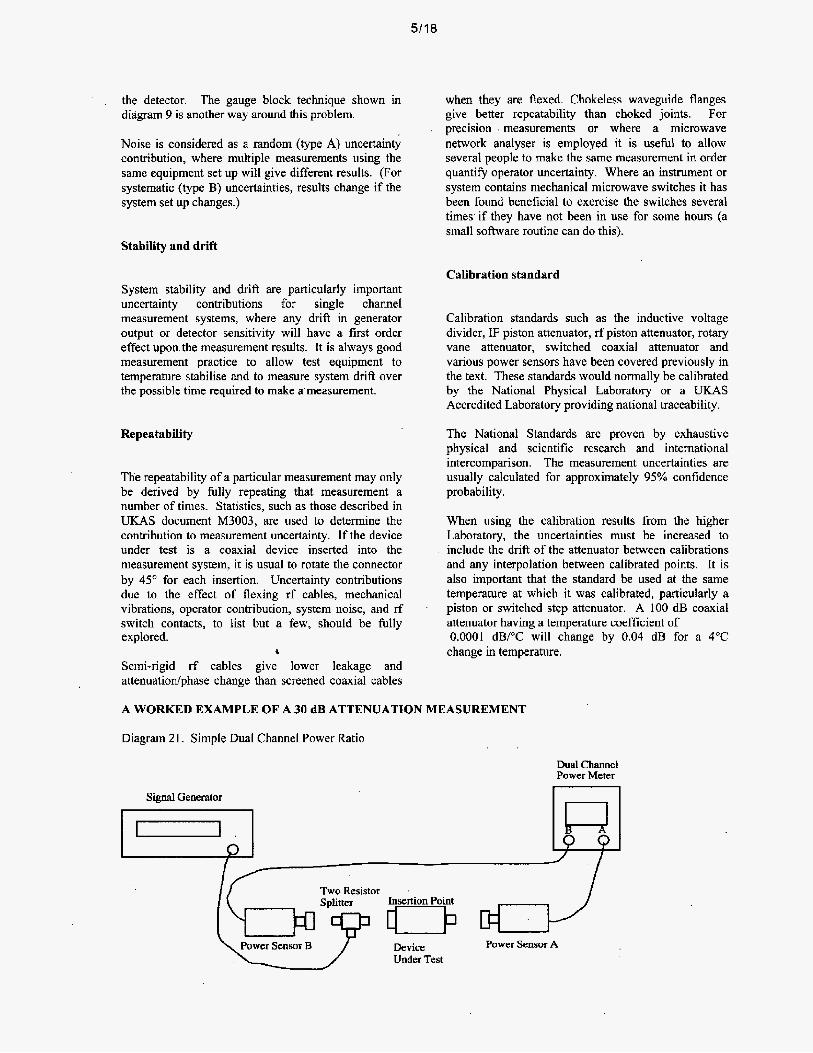
A WORKED EXAMPLE OF A 30 dB ATTENUATION MEASUREMENT
Diagram 2 I. Simple Dual Channel Power Ratio
Dual Channel Power Meter
Si& Generator
Two Resistor .
Power Sensor B Device Under Test
9mQ
Power Sensor A

5/19
This worked example is for a simple case of a coaxial 30 dB attenuator, measured using the dual channel power ratio system shown in diagram 21. The measurement is repeated 5 times, from which the mean result and standard deviation are calculated. This example follows the requirements of UKAS document M3 003.
* Insertion loss is calculated from:
10 log,, (PlA/PlB). (P2BP2A) (23)
The mean value of the five calculated samples = 30.053 dB
Contributions to Measurement Uncertainty Are:
Type A random contributions, Uran. The estimated standard deviation of the uncorrected mean = 0.009 dB (normal probability distribution).
This may calculated using (on- l ) / ( n p (24)
Where: (J ,is the standard deviation of the population n is the number of measurements
Mismatch contribution, Umis Where:
= 0.03 1 rG = 0.05, r =0.02, sl, = 0.07, sZ2 = 0.05, s , ~ & sI1
The measurement uncertainty of these values is taken as *0.02
and combining the measured value and its uncertainty in quadrature, we have:
rG = 0.054, r = 0.028, SI1 = 0.073 and S2* = 0.054
Putting these values into the mismatch formuIa (21) we arrive at an uncertainty of:
0.026 d 3 (normal probability distribution)
Detector linearity, Ulin. The detector linearity was measured and found to be:
h 0.02 dB over 30 dB range (limit distribution).
No account has been taken for the measurement uncertainty of the detector linearity, as it is in the order of f 0.002 dB. In practice, if this contribution was significant, it may be included by partial differentiation or by adding in quadrature, with the measured linearity error.
Power meter resolution, Ures. The uncertainty due to power meter resolution was determined by experiment and found to be a maximum of: & 0.03 dB (limit distribution).
Leakage. The leakage was found to be less than 0.0001 dB and has not been included in the uncertainty calculations.
Power meter range and zero carry over are included in the power sensor linearity measurements and cannot be separated. Similarly, noise and drift cannot be separated from the random measurement of the five samples.
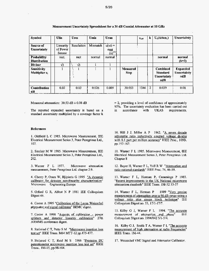
The followi'ng spreadsheet is a convenient way to list the uncertainly contributions and calculate the measurement uncertainty.
5/20
Symbol
Source of Uncertainty
Probability Distribution Divisor Sensitivity Multiplier ci
Contribution
Measurement Uncertainty Spreadsheet for a 30 dB Coaxial Attenuator at 10 GHz
Ulin Ures Umis Uran ueli k U,(Atten,) Uncertainty
Linearity Resolution Mismatch u(xi) =
Sensor (n>ln of Power mm
normal rect. rect normal normal normal \ (k=2)
43 \ 43 1 1 1 1 Measured Combined Expanded
Step Standard Uncertainty I Uncertainty hdB
*dB
0.02 0.03 I 0.026 0.009 30,053 1386 2 0.039 0.08
Measured attenuation: 30.53 dB f 0.08 dB
The reported expanded uncertainty is based on a standard uncertainty multiplied by a coverage factor k
References
I . OIdfieId L C 1985. Microwave Measurement, IEE Electrical Measurement Series 3, Peter Peregrinus Ltd., 107.
2. Sinclair M W 1985. Microwave Measurement, IEE Electrical Measurement Series 3 , Peter Peregrinus Ltd., 202.
3. Warner F L 1977. Microwave attenuation measurement, Peter Peregrinus Ltd. chapter 2.9.
4. Cherry P, Oram W, Hjipieris G 1995 "A dynamic calibrator for detector non-linearity characterization" Microwave Engineering Europe
5 . Orford G R, Abbot N P 1981 IEE Colloquium Digest 49.
6. Coster A 1995 "Calibration of the Lucas Weinschel attenuator and signal calibrator" BEMC digest.
7. Coster A 1998 "Aspects of calibration - power s~litters and detector linearitv calibration" 27th ARMMS conference digest.
8. Stelzried C T, Petty S M "Microwave insertion loss test set" IEEE Trans. M64 MTT-12 pp.475-477.
9. Stelzried C T, Reid M S 1966 "Precision DC potentiometer microwave insertion loss test set" IEEE Trans.. 1M-15, pp.98-104.
= 2, providing a level of confidence of approximately 95%. The uncertainty evaluation has been carried out in accordance with UKAS requirements.
10. Hill J J, Miller A P 1962. "A seven decade adiustable ratio inductivelv couded voltape divider with 0.1 Dart per million accuracy" IEEE Proc., 1093. pp. 157- 162.
11. Warner F L 1985. Microwave Measurement, IEE Electrical Measurement Series 3, Peter Peregrinus Ltd. Chapter 8
12. Bayer H, Warner F L, Yell R W "Attenuation and ratio national standards" IEEE Proc. 74,46-59.
13. Warner F L, Herman P, Cummings P 1983. "Recent improvements to the UK National microwave attenuation standards" IEEE Trans. 1M-32 33-37
14. Warner F L, Herman P 1989 "Very precise measurement of attenuation over a 90 dB range using a voltage ratio plus gauge block technique" IEE Colloquium Digest no. 53, 17/1-17/7.
15. Kilby G J, Warner F L 1994. "The accurate measurement of attenuation and phase" IEE Colloquium Digest no. 1994/042 511 -5/4.
16. Kilby G J, Smith T A, Warner F L "The accurate measurement of high attenuation at radio frequencies" IEEE Trans. 1M-44.
17. Weinschel VM7 Signal and Attenuator Calibrator.

5/21
18. Warner F L 1990. "High accuracs 150 dB attenuation measurement ssstem for traceability at RF" IEE Colloquium Digest no. 1990/174,3/1-3/7.
19. Yell R W 1972. "Develoument of hieh precision waveguide besond cut-off attenuator" CPEm digest
, L
' .
' ' 108-1 IO, 1972.
20. Yell R W 1981. "DeveloDment in wavenuide below cut-off attenuators at NPL" IEE Colloquium Digest no. 1981/49, 1/1-,1/5.
21 Banning H W. "The measurement of attenuation: a practical mide" Weinschel Engineeering Co.Inc.
. ,
22. UKAS 1997 The Expression of Uncertainty and Confidence in Measurement M3003, Edition I
Recommended Reading Warner F L. 1977 Microwave Attenuation Measurement, Peter Peregrinus Ltd. For IEE