Embed Size (px)
Citation preview
HAL Id: tel-00950769https://tel.archives-ouvertes.fr/tel-00950769v2
Submitted on 3 May 2013
HAL is a multi-disciplinary open accessarchive for the deposit and dissemination of sci-entific research documents, whether they are pub-lished or not. The documents may come fromteaching and research institutions in France orabroad, or from public or private research centers.
L’archive ouverte pluridisciplinaire HAL, estdestinée au dépôt et à la diffusion de documentsscientifiques de niveau recherche, publiés ou non,émanant des établissements d’enseignement et derecherche français ou étrangers, des laboratoirespublics ou privés.
Couplage de systèmes magnétiques et mécaniques àéchelle moléculaire
Marc Ganzhorn
To cite this version:Marc Ganzhorn. Couplage de systèmes magnétiques et mécaniques à échelle moléculaire. Physique[physics]. Université de Grenoble, 2013. Français. <NNT : 2013GRENY004>. <tel-00950769v2>
THÈSEPour obtenir le grade de
DOCTEUR DE L’UNIVERSITÉ DE GRENOBLESpécialité : Physique
Arrêté ministériel : 7 Aout 2006
Présentée par
Marc GANZHORN
Thèse dirigée par Wolfgang WERNSDORFER
préparée au sein Institut Neel, CNRS/UJFet de Ecole Doctorale de Physique, Grenoble
CouplingMagnetism and Mechanics
at a molecular scale
Thèse soutenue publiquement le 13 Mars 2012,devant le jury composé de :
Prof. Mairbek ChshievProfesseur, Spintec-UDG Grenoble, PrésidentDr. Takis KontosCharge de recherche, LPA-ENS Paris, RapporteurDr. Gary SteeleProfesseur assistant, TU Delft, RapporteurDr. Benjamin LassagneMaitre de conference, LPCNO-CNRS-INSA Toulouse, ExaminateurDr, Wolfgang WernsdorferDirecteur de recherche, Institut Neel-CNRS Grenoble, Directeur de thèse

"Truth suffers from too much analysis"’Fremen saying on Arrakis, Dune, Frank Herbert
Acknowledgements
I performed my PhD research at the Nanoscience department of the Neel Institute inGrenoble. I thank the heads of the Institute, Alain Fontaine and Alain Schuhl, anddepartment heads, Joel Cibert and Herve Courtois, for the warm welcome at the Institute.
I thank Prof. Mairbek Chshiev for presiding my thesis comittee, Takis Kontos andGary Steele as referees for my manuscript and Benjamin Lassagne for participating tomy jury.
Ma these a ete financier par la Fondation Nanoscience a Grenoble. Je remercie lesdirecteurs, Roland Herino et son successeur Alain Fontaine pour avoir financer cette theseet le support en continu durant ces trois dernieres annees. Merci a Maud Dayez, FerielKouiten, Marie-Anne Carre et Karine Argento pour m’avoir guider a travers la jungle del’administration francaise. Enfin, merci a toi Steph pour tous les pots et fetes organise,les news de la Fondation, les fous rires au bureau, les histoires "Kinder surprise", tesconseils et ton soutien moral.
I thank in particular Wolfgang Wernsdorfer for supervising my work over the lastthree years. For one, I would like to thank you for all the fruitfull scientific (and non-scientific) discussions and all the valuable advice, given literally at any time, anywhere...Thank you for allowing me to use your sionludi, for all the countless overnight cooldownsand exchange of helium bottles and for reparing all the things I broke. Finally, I thankyou for your patience (for instance reading my papers and manuscript), your confidenceand your faith in me and my work. It was a real pleasure!
I’d also like to thank all the former, present and new members of the Nanospingroup: The "graphene man" Andrea Candini, Edgar Bonet and Christophe Thirion,our programming masters, "Ramanpes" Manuel Lopes, Romain "roro" Maurand andOksana Gaier; I’d also like to thank the former group members, now part of the newlyformed Hybrid group Adrien Allain, Zheng "Vitto" Han, Laetitia Marty, Nedjma Bendiab,Vincent Bouchiat. My former officemates Subhadeep Datta, for spreading your goodmood from my first day on, and Jarno Jarvinen, for numerous late night sessions of funin the lab and the office and for showing me the way to the "D’Enfer pub"! Thanks toyou Jean-Pierre Cleuziou and Viet Ngoc-Nguyen for your big help with this mysteriousCVD setup of yours and for giving me a headstart on how to make ther perfect sample.
Merci aussi a toi Anastasia Varlet, pour les fous rire au bureau et la multitude demidis et soirees "Nanos"; Raoul Piquerel, pour debugger mon NanoQt et pour les bellestranches de rigolades; Antoine Reserbat, pour ton introduction au Raman et les sessionsde badminton; "Sergeant" Romain Vincent et Matias Urdampilleta pour les weekendset nuits de manips collective, pour m’avoir expliquer le magnetisme moleculaire et la
iv
cryogenie et avoir remplis mon piege a azote. Danke an Dich Stefan fuer die wertvollewissenschaftliche und moralische Unterstuetzung, die vielen Ueberraschungen, Ideen undso vieles mehr....
Finalement un grand merci a toi Franck Balestro, d’avoir relu et corriger tout articleet manuscript de these que je t’ai fais lire, d’avoir assister et insister sur les repet desoutenance/presentation, pour me donner un deuxieme point de vue et pour toujoursavoir une oreille ouverte a tout probleme, scientifique ou non!
Un grand merci a la "Dreamteam" Nanofab, qui a du me supporter ma presence toutles jours en salle blanche ou a H2! Le "Grand Fournier" Thierry pour ton aide en salleblanche et litho eletronique; Evidement merci a toi Thierry Crozes pour m’avoir montrercomment faire une belle litho de facon professionelle, les soirees tennis et tes observationset reflexions "pertinentes" a certains propos..... Merci a Bruno pour m’avoir montrer lefonctionnement d’une salle blanche et d’avoir reparer tout equipement que j’ai maltraiter(surtout le Plassys). Merci a toi Gwenaelle pour avoir subi la presence d’un autre gamindans ton entourage et merci a toi Jeff "FIB" Motte. Finalement a toi Sebastien, aka"Petit Fournier", merci pour tout les bons moments en salle, a la PTA, a midi et aucafe!!! Sans oublier les "Y faut y....." bien entendu.
Merci aussi a Ioan et Eva, pour les gros fous rires et tout les lapins qui ont envahitnotre bureau. Un grand merci aussi a Eric Eyraud, pour avoir reparer tout les pieces dedilution que j’ai casse, ta bonne humeur et une fameuse bataille de polochon (les autresparticipants s’en souviendront...). Merci aussi a Laurent Cagnon pour un coup de maina l’ALD. Merci a toi Richard Haettel, Didier Dufeu, David Barral, Daniel Lepoittevin,Christophe Hoarau, Valerie Reita, Philippe David et tout les membres du pole magne-tometrie, pole optique, du pole couches minces, du pole cryogenie, pole informatique(merci a Patrick Belmain pour avoir sauver mes donnees apres une greve totale de monordi) et du liquefacteur..... Merci aussi a l’administration, notament Veronique Fauvelet Sabine Gadal pour avoir resolu tous petit probleme concernant la paperasse et d’unesalle de soutenance de these etant inacessible.
Finalement merci a tout les collegues de l’Institut Neel, Spintec ou autres que j’ai ren-contrer ces dernieres annees et ayant contribuer a une ambiance de travail tres chaleureuseet agreable: Romain Thalineau, Christophe Blanc, Tobias, Johanna, Laetitia Pascal, Syl-vain Martin, Olivier Bougeois, Olivier Buisson, Emilie, Mihai, Josephine, Christophe,Selma, Nora, etc.....
Thanks a lot to a bunch of awesome guys: Angela the Tiramisu queen, Liza alias thelittle devil, Stefan, Martin, Ovidiu, Iulia, Claudio, Elena, Christoph, Carina, Valentina,Francesca, Tommaso, Simone.... Thank you so much for all those awesome moments inGrenoble at Bayard, d’Enfer, Bobine or Scarpe mobile concerts ..... Or all the trips toParis, Parma, Firenze, Stuttgart and all the place we have been together and the placeswe still have to go to! Thank you for your support in good and bad times (very bad times
v
after a certain Germany-Italy game...)!Special thanks to Teo and Geta for some special moments (yeeees that kind of special)
around Grenoble, Spain, France, Italy or Romania.Merci a la famille Dufresnes: Seb, Elo et la petite Charlie pour des moments et
weekends inoubliables a Izeaux et autour de Grenoble!Merci aussi aux Strasbourgeois Mario et Julie, Caro, Julie, Maud, Colette, Eric pour
votre support a distance ou de pres, a tout moment ou que vous soyez. Merci Servicecomme dirais Kansas !!!
Finally, I owe you, Anca, some very special thanks for your support and your helpanytime, anywhere. Thank you for being there for me!!
Last, I would like to thank my family for all the unconditional support from far away.It wouldn’t have been possible without you.

Contents
1 General introduction 1
2 Introduction to Molecular Spintronics 72.1 Towards Molecular spintronics . . . . . . . . . . . . . . . . . . . . . . . . 8
2.1.1 Giant magnetoresistance and metallic spintronic devices . . . . . 82.1.2 Semiconductor and organic spintronic devices: Towards coherent
spin manipulation . . . . . . . . . . . . . . . . . . . . . . . . . . . 102.1.3 Molecular building block for spintronics: Single Molecule Magnets 12
2.2 Terbium Double Decker Single Molecule Magnet . . . . . . . . . . . . . . 152.2.1 Structural and magnetic properties . . . . . . . . . . . . . . . . . 162.2.2 Quantum tunneling of magnetization and Landau-Zener model . . 212.2.3 Spin-lattice relaxation . . . . . . . . . . . . . . . . . . . . . . . . 22
2.3 Carbon based supramolecular spintronics . . . . . . . . . . . . . . . . . . 252.3.1 NanoSQUID: Probing via magnetic flux . . . . . . . . . . . . . . 272.3.2 Supramolecular Spin Valve: Probing via electron transport . . . . 282.3.3 Magnetic torque detector: Probing via mechanical motion . . . . 30
2.4 Outlook . . . . . . . . . . . . . . . . . . . . . . . . . . . . . . . . . . . . 33
3 Introduction to carbon nanotube based NEMS 353.1 Introduction: Si based vs. carbon based NEMS . . . . . . . . . . . . . . 353.2 High-Q mechanical bending modes in ultraclean carbon nanotube NEMS 39
3.2.1 Carbon nanotube beam mechanics: Linear harmonic oscillator . . 393.2.2 Carbon nanotube beam mechanics: Nonlinear Duffing oscillator . 443.2.3 Actuation and detection principle . . . . . . . . . . . . . . . . . . 453.2.4 Strong coupling between single-electron tunneling and mechanical
bending modes . . . . . . . . . . . . . . . . . . . . . . . . . . . . 473.3 Quantized longitudinal stretching modes in ultraclean carbon nanotube
NEMS . . . . . . . . . . . . . . . . . . . . . . . . . . . . . . . . . . . . . 543.3.1 Weak and intermediate coupling g ≤ 1: Quantized longitudinal
stretching modes . . . . . . . . . . . . . . . . . . . . . . . . . . . 553.3.2 Strong coupling g 1: Franck-Condon blockade . . . . . . . . . . 58
3.4 Outlook . . . . . . . . . . . . . . . . . . . . . . . . . . . . . . . . . . . . 60
4 Nanofabrication and characterisation of carbon nanotube based NEMSand molecular spintronic devices 614.1 Substrate selection . . . . . . . . . . . . . . . . . . . . . . . . . . . . . . 624.2 Nanofabrication of the ’back-bone’ junction for a carbon nanotube NEMS 63
viii Contents
4.2.1 Optical contact lithography . . . . . . . . . . . . . . . . . . . . . 654.2.2 Junctions with a Si backgate . . . . . . . . . . . . . . . . . . . . . 664.2.3 Junctions with a high efficiency local gate . . . . . . . . . . . . . 69
4.3 Ultraclean on-chip growth of carbon nanotube NEMS via chemical vapordeposition . . . . . . . . . . . . . . . . . . . . . . . . . . . . . . . . . . . 754.3.1 Catalyst deposition . . . . . . . . . . . . . . . . . . . . . . . . . . 754.3.2 Growth condition . . . . . . . . . . . . . . . . . . . . . . . . . . . 77
4.4 Real-time data acquisition system for nanoelectronics . . . . . . . . . . . 794.4.1 ADWIN automate and NanoQt control interface . . . . . . . . . . 794.4.2 Advantages of real-time measurement system . . . . . . . . . . . . 81
4.5 Selection of carbon nanotube NEMS at room temperature . . . . . . . . 834.5.1 Lock-in detection and measurement setup . . . . . . . . . . . . . 834.5.2 Selection procedure for carbon nanotube NEMS at room temperature 85
4.6 Probing nanomechanical bending modes in carbon nanotube NEMS atcryogenic temperature . . . . . . . . . . . . . . . . . . . . . . . . . . . . 884.6.1 Inverse dilution refrigerator . . . . . . . . . . . . . . . . . . . . . 884.6.2 Measurement setup . . . . . . . . . . . . . . . . . . . . . . . . . 904.6.3 Detection procedure for nanomechanical bending modes at cryo-
genic temperature . . . . . . . . . . . . . . . . . . . . . . . . . . . 934.7 Functionnalization of carbon nanotube NEMS with Single Molecule Magnets 97
4.7.1 Grafting TbPc2 single molecule magnets to carbon nanotube NEMS 984.7.2 Conservation of the NEMS’s mechanical and the TbPc2 magnetic
properties . . . . . . . . . . . . . . . . . . . . . . . . . . . . . . . 101
5 Dynamics and dissipation induced by SET in carbon nanotube NEMS1055.1 Introduction . . . . . . . . . . . . . . . . . . . . . . . . . . . . . . . . . . 105
5.1.1 Nanofabrication . . . . . . . . . . . . . . . . . . . . . . . . . . . . 1065.1.2 SET backaction on a carbon nanotube NEMS’s mechanical motion 1075.1.3 Estimating the quantum dot capacitance of carbon nanotube NEMS1085.1.4 Estimating the tunnel coupling Γ in CNT quantum dot . . . . . . 109
5.2 Frequency shift induced by SET in carbon nanotube NEMS . . . . . . . 1105.3 Dissipation induced by SET in carbon nanotube NEMS . . . . . . . . . . 1135.4 Dissipation mechanisms in carbon nanotube NEMS . . . . . . . . . . . . 1155.5 Conclusion and Outlook . . . . . . . . . . . . . . . . . . . . . . . . . . . 119
6 Strong Spin-Phonon Coupling of a Single Molecular Spin to a CarbonNanotube NEMS 1216.1 Nanofabrication and measurement setup . . . . . . . . . . . . . . . . . . 1226.2 Spin-lattice relaxation in TbPc2* SMM coupled to a carbon nanotube . . 123
6.2.1 Magnetization reversal in a TbPc2* SMM . . . . . . . . . . . . . 1236.2.2 Spin-lattice relaxation time for a direct process . . . . . . . . . . 126
Contents ix
6.3 Evidence for quantized longitudinal stretching modes in carbon nanotubeNEMS . . . . . . . . . . . . . . . . . . . . . . . . . . . . . . . . . . . . . 1296.3.1 Electronic actuation and detection for longitudinal stretching modes1306.3.2 Phonon energy and linewidth . . . . . . . . . . . . . . . . . . . . 1326.3.3 Electron-phonon coupling . . . . . . . . . . . . . . . . . . . . . . 132
6.4 Strong coupling of a single TbPc2* spin to a quantized longitudinal res-onator mode . . . . . . . . . . . . . . . . . . . . . . . . . . . . . . . . . . 1336.4.1 Coupling mechanism between a single TbPc2* spin to a quantized
longitudinal resonator mode . . . . . . . . . . . . . . . . . . . . . 1346.4.2 Current detection of a TbPc2* magnetization reversal . . . . . . . 1356.4.3 Nuclear spin-resolved phonon-assisted magnetization reversal of a
single TbPc2* spin coupled to a CNT NEMS . . . . . . . . . . . . 1396.4.4 Spin-phonon coupling between a molecular and quantized mechan-
ical motion . . . . . . . . . . . . . . . . . . . . . . . . . . . . . . 1476.5 Conclusion and Outlook . . . . . . . . . . . . . . . . . . . . . . . . . . . 149
7 General conclusion and perspectives 151
Bibliography 161
A Nanofabrication of alternate carbon nanotube NEMS designs 173A.1 Carbon nanotube NEMS with multiple local gates . . . . . . . . . . . . . 173A.2 Ultrashort and high frequency carbon nanotube NEMS . . . . . . . . . . 181
B Stevens operators 183
C Publications 185

Chapter 1
General introduction
Mechanics at a molecular scale
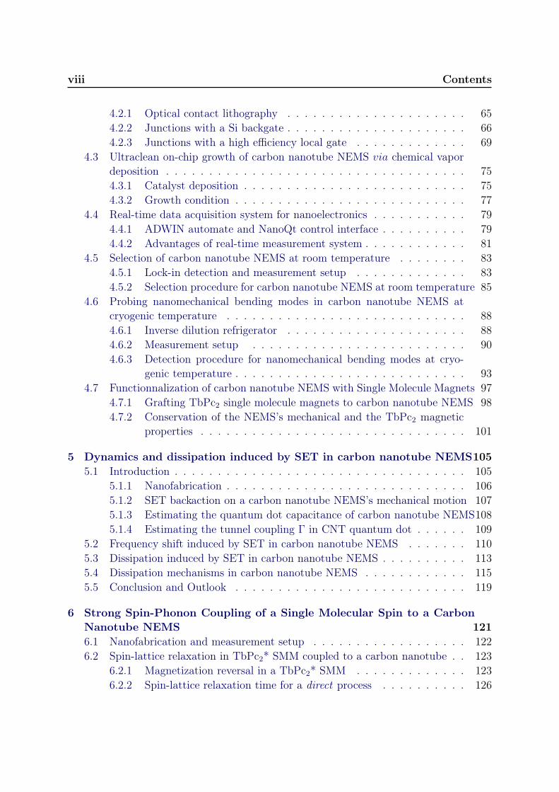
Mechanical systems exist in various forms, compositions and dimensions, ranging fromastronomic objects like galaxies (1020 m, 1042 kg) to molecule-size vibrating strings (10−9
m, 10−21 kg) as depicted in Fig. 1.1.
Astronomical phenomena such as the motion of a planet around its star or the trappingof light by a black hole can be described with amazing accuracy by the laws of specialand general relativity established by Einstein for large and massive objects. On a morehuman scale (1 m, 1 kg) the dynamics of mechanical systems are governed by the classicallaws of motion, such as the oscillation of a pendulum or the vibration of a guitar string.
Sound generation,….
NEMS CNT NEMS
10-12 10-15103 V (mm3)10-6 10-9
AFM cantilever MEMS guitar string, human vocal cords
10-31
109103 106 f (Hz)104 105 107 108
graphene NEMS
Sensor applications(AFM,MFM, pressure sensing,….)
Single atom mass/force sensing,Efficient RF and MW signal processing,
quantum limit of motion
Classical physics Quantum physics
Figure 1.1: From macroscopic to quantum harmonic oscillators
Using integrated circuit technology, one can reduce the dimensions of mechanical sys-tems even further down to the micrometer scale. Enabled by the smaller mass and higherresonance frequencies of a few hundred kilohertz, such micro-electromechanical systems
2 Chapter 1. General introduction
(MEMS) are widely used for sensing applications, most notably for atomic or magneticforce microscopy [1].
Upon scaling mechanical systems down to the nanometer scale, the resonance fre-quency further increases while the mass of the system becomes smaller. Such nano-electromechanical systems (NEMS) are therefore ideal candidates for mass or force sens-ing at the atomic scale [1]. If cooled to very low temperatures, such a NEMS can reacha state where its dynamics are governed by the laws of quantum mechanics. In this case,one can observe a NEMS’ zero point motion and quantum mechanical ground state [2, 3].In such quantum oscillators one could achieve and probe the superposition of two quan-tum states [1].
In this context, carbon nanotubes turned out to be ideal building blocks for NEMSdue to their extremely low mass (m = 10−21 kg) and high Young’s modulus (E = 1
TPa). In such a supramolecular NEMS, one easily reaches resonance frequencies above1 GHz with quality factors as high as Q = 105 [1]. Indeed, carbon nanotube NEMScan detect masses as small as 10−24 g [4, 5] or forces down to 10−18 N [6], thus reachingsingle atom sensitivity. Due to the high resonance frequencies above 1 GHz, carbonnanotube resonators can furthermore be cooled to their quantum mechanical ground statein dilution refrigerators with a base temperature below 50 mK. Under those conditions,a carbon nanotube NEMS can be seen as the experimental implementation of a quantum(harmonic or anharmonic) oscillator.
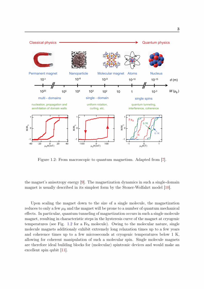
Magnetism at a molecular scale
In analogy to mechanical systems, one can observe a large variety of magnetic systemsranging from permanent magnets (1 mm, 1020µB) down to a single nuclear spin (10−15
m, 10−3µB) as depicted in Fig. 1.2.
On a macroscopic scale, the magnetism results from the collective behaviour of alarge number of magnetic moments or spins. Below the so called Curie temperature, thiscollective behaviour results in the formation of many areas with uniform magnetizationinside the macroscopic magnet, so called magnetic domains [8]. Under the influence ofa magnetic field, one can observe the creation, propagation and annihilation of thesedomains until the magnet reaches its full magnetization. The magnetization dynamics insuch a macroscopic ferromagnet translates in a characterisic hysteresis loop depicted inFig. 1.2.
If the size the magnet becomes smaller than the size of a magnetic domain, for examplein magnetic nanoparticles or molecular clusters, one can observe a uniform reversal of themagnetization, typically on the order of 105µB, when the magnetic field compensates for
3
Permanent magnet Nanoparticle Molecular magnet Atoms Nucleus
105 104 103 102 10 1 10-31020 M (µ )B
single - domain single spins
-1
0
1
-40 -20 0 20 40
M/M
S
µ0H(mT)
nucleation, propagation and annihilation of domain walls
-1
0
1
-1 0 1
M/M
S
µ0H(T )
F e8
1K0.1K
0.7K
quantum tunneling,interference, coherence
-1
0
1
-100 0 100
M/M
S
µ0H(mT)
uniform rotation,curling, etc.
multi - domains
10-9 10-10 10-1510-3 d (m)10-8
Classical physics Quantum physics
Figure 1.2: From macroscopic to quantum magnetism. Adapted from [7].
the magnet’s anisotropy energy [9]. The magnetization dynamics in such a single-domainmagnet is usually described in its simplest form by the Stoner-Wolfahrt model [10].
Upon scaling the magnet down to the size of a single molecule, the magnetizationreduces to only a few µB and the magnet will be prone to a number of quantum mechanicaleffects. In particular, quantum tunneling of magnetization occurs in such a single moleculemagnet, resulting in characteristic steps in the hysteresis curve of the magnet at cryogenictemperatures (see Fig. 1.2 for a Fe8 molecule). Owing to the molecular nature, singlemolecule magnets additionaly exhibit extremely long relaxation times up to a few yearsand coherence times up to a few microseconds at cryogenic temperatures below 1 K,allowing for coherent manipulation of such a molecular spin. Single molecule magnetsare therefore ideal building blocks for (molecular) spintronic devices and would make anexcellent spin qubit [11].
4 Chapter 1. General introduction
Coupling Magnetism and Mechanics on a molecular scale
One can now probe the properties of micro- or nanoscopic magnetic objects using micro-or nano-electromechanical systems.
For instance, micromechanical (magnetic) cantilever are commonly used in magneticforce microscopy (MFM) to probe the magnetization dynamics (domain wall motion andformation, hysteresis, collective behaviour, etc...) in micro- and nano-scale structures suchas magnetic thin films [12], nanoparticles [13], nanowires [14]. The spatial resolution istypically on the order of 20-100 nm, which enables the detection of a magnetic momentdown to 107µB and forces on the order of 10−12 N [15]. By pushing force microscopy toits limits, Rugar et al. recently demonstrated the detection of a force of 10−18 N from asingle electron spin using an improved magnetic resonance force microscopy technique atcryogenic temperatures [15].
In an alternative approach, micro-cantilevers are used as magnetic torque detec-tors [16, 17]. A magnetic thin film deposited on the cantilever will induce a torsionof the latter, if exposed to an oscillating magnetic field. By those means, one can probea magnetic moment on the order of 1011µB at room temperature.
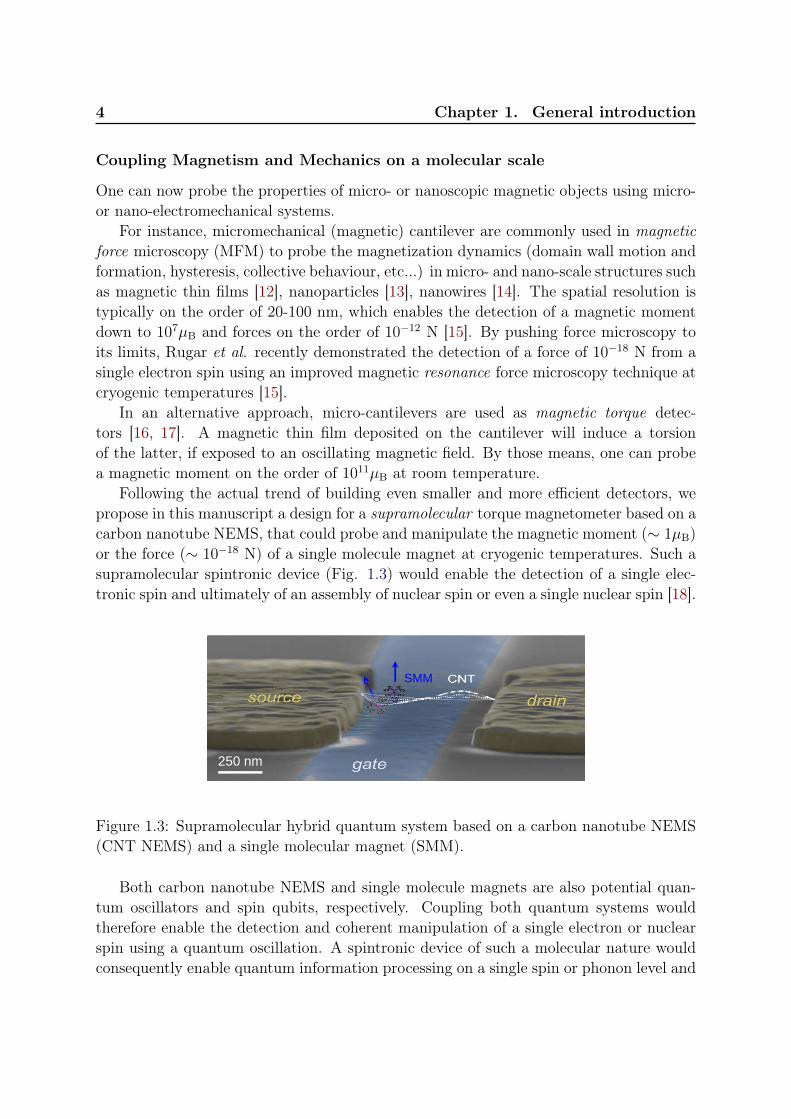
Following the actual trend of building even smaller and more efficient detectors, wepropose in this manuscript a design for a supramolecular torque magnetometer based on acarbon nanotube NEMS, that could probe and manipulate the magnetic moment (∼ 1µB)or the force (∼ 10−18 N) of a single molecule magnet at cryogenic temperatures. Such asupramolecular spintronic device (Fig. 1.3) would enable the detection of a single elec-tronic spin and ultimately of an assembly of nuclear spin or even a single nuclear spin [18].
SMM
250 nm
Figure 1.3: Supramolecular hybrid quantum system based on a carbon nanotube NEMS(CNT NEMS) and a single molecular magnet (SMM).
Both carbon nanotube NEMS and single molecule magnets are also potential quan-tum oscillators and spin qubits, respectively. Coupling both quantum systems wouldtherefore enable the detection and coherent manipulation of a single electron or nuclearspin using a quantum oscillation. A spintronic device of such a molecular nature wouldconsequently enable quantum information processing on a single spin or phonon level and
5
allow for example the entanglement of two individual molecular spins or phonons.
In this manuscript, we will first present the ultimate molecular building block forspintronic devices, so called single-molecule magnets (Chapter 2). In particular we willfocus on a TbPc2 complex and various approaches of probing its magnetization usingcarbon nanotube detectors and different coupling mechanisms (magnetic flux, electronicand mechanical coupling).
With the aim of building a supramolecular torque magnetometer capable of probingthe magnetic moment of a molecular magnet, we will describe in Chapter 3 a promis-ing candidate, a carbon nanotube nanoelectromechanical system (NEMS). We will firstdescribe the advantages of carbon based NEMS over classical Si based resonators. Subse-quently we will present the state of art of carbon nanotube NEMS and focus in particularon two different nanomechanical motions, a transverse bending mode and a longitudinalstretching mode.
In Chapter 4, we present the experimental implementation of a supramolecular torquemagnetometer based on carbon nanotube NEMS and single molecule magnets. We firstdescribe the ultraclean bottom-up fabrication process and the extensive characterisationsteps of carbon nanotube NEMS at room and cryogenic temperatures. We will finallydemonstrate a method of grafting a TbPc2 single molecules magnet on such a carbonnanotube NEMS, that conserves both the magnetic properties of the molecule and themechanical properties of the resonator.
In Chapter 5, we will then perform a systematic study of the transverse bending modevibration in a carbon nanotube NEMS. We demonstrate for instance, that the dissipa-tion of a carbon nanotube’s bending mode vibration to single electron tunneling throughthe carbon nanotube NEMS-quantum dot critically depends on the dot’s electronic en-vironment, i.e. the capacitance, the tunnel coupling to the metal leads, the current andtemperature. The findings suggest that one could achieve quality factors of 106 or higherby choosing appropriate gate dielectrics and/or by improving the tunnel coupling to theleads, which would notably increase the sensitivity of the carbon nanotube NEMS withrespect to a magnetic torque generate by a rotating molecular magnet [19].
In Chapter 6, we demonstrate the presence of a quantized longitudinal stretchingmode vibration in a carbon nanotube NEMS functionnalized with TbPc2 single moleculequantum magnets. We will in particular demonstrate that the quantum mechanicalnature of both systems, results in a strong coupling between the longitudinal stretchingmode and the magnetization of an individual TbPc2 single molecule magnet grafted tothe carbon nanotube’s sidewall. The strong coupling in fact enables the detection of thenuclear spin states in the TbPc2 molecule [20].
Finally, we present in the conclusion of this manuscript some future prospects forthe detection and (coherent) manipulation of a single (nuclear) spin using a mechanicalquantum system.

Chapter 2
Introduction to Molecular Spintronics
With the discovery of the giant magnetoresistivity effect (GMR) in 1988 [21, 22], a newgeneration of electronics has emerged using the spin degree of freedom of the electron,so called spin transport eletronics or spintronics. Spintronics takes advantage of theexistence of both spin-up and spin-down carriers in the electric current of micro- or na-noeletronic devices. Using various spin dependent effects arising from the interactionbetween the electron spin and the magnetic material, one can encode information in thespin state of the electron. Information stored in spin-dependent transport structures, likespin valves or magnetic tunnel junctions, is potentially nonvolatile and can be processedmuch faster and with lower power consumption than in conventional semiconductor de-vices [23].
New approaches involving the use of semiconductors [24] or organic materials [25]in spintronic devices were explored in order to enhance and exploit quantum coherence.Following the same trend, the dimensions of electronic devices were driven beyond thenanoscale to a molecular level [26, 11], where one could take advantage of the quantummechanical nature of such a system.
In an effort of combining spintronics with such molecular scale electronics, a new fieldof molecular spintronics has thus emerged during the last decade. The main idea consistsin integrating single magnetic molecules into nanoelectronic devices [11]. In this context,so called single-molecule magnets (SMM) seem to be an ideal candidate for such molecularspintronic devices [11]. Owing to the large variety of magnetic properties, for instancea large magnetic moment and a strong magnetic anisotropy, one can expect extremelylong relaxation and coherence times for SMM based spintronic devices, making thempotentially attractive for quantum information processing or quantum computing [11].
In the following chapter, we will first point out the advantages of single moleculemagnets as building block for molecular spintronics (Section 2.1) and we will present aTerbium Double Decker SMM (Section 2.2), which is the main object studied throughoutthis manuscript. Finally, we propose different approaches of integrating an SMM intocarbon based devices, thus designing a supramolecular spintronic device and a single spindetector (Section 2.3).
8 Chapter 2. Introduction to Molecular Spintronics
2.1 Towards Molecular spintronics
2.1.1 Giant magnetoresistance and metallic spintronic devices
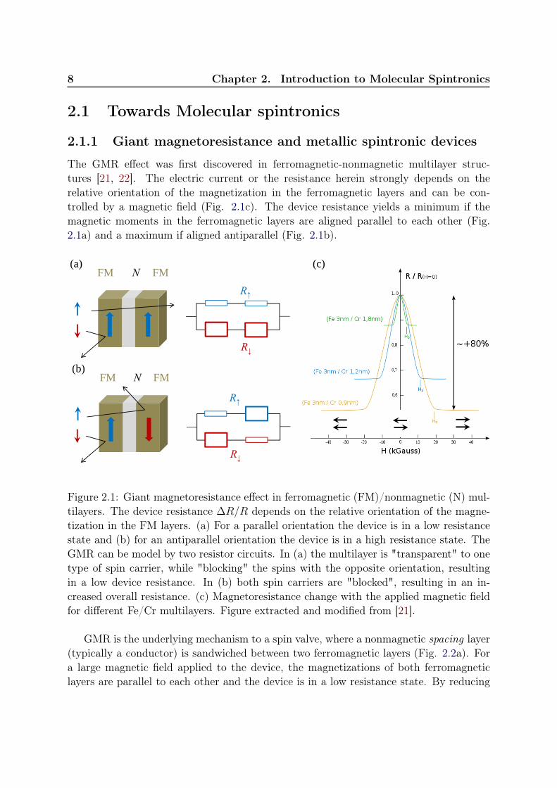
The GMR effect was first discovered in ferromagnetic-nonmagnetic multilayer struc-tures [21, 22]. The electric current or the resistance herein strongly depends on therelative orientation of the magnetization in the ferromagnetic layers and can be con-trolled by a magnetic field (Fig. 2.1c). The device resistance yields a minimum if themagnetic moments in the ferromagnetic layers are aligned parallel to each other (Fig.2.1a) and a maximum if aligned antiparallel (Fig. 2.1b).
FM R↑
R↓
FM(a)
N
FM FM(b)
N
R↑
R↓
(c)
Figure 2.1: Giant magnetoresistance effect in ferromagnetic (FM)/nonmagnetic (N) mul-tilayers. The device resistance ∆R/R depends on the relative orientation of the magne-tization in the FM layers. (a) For a parallel orientation the device is in a low resistancestate and (b) for an antiparallel orientation the device is in a high resistance state. TheGMR can be model by two resistor circuits. In (a) the multilayer is "transparent" to onetype of spin carrier, while "blocking" the spins with the opposite orientation, resultingin a low device resistance. In (b) both spin carriers are "blocked", resulting in an in-creased overall resistance. (c) Magnetoresistance change with the applied magnetic fieldfor different Fe/Cr multilayers. Figure extracted and modified from [21].
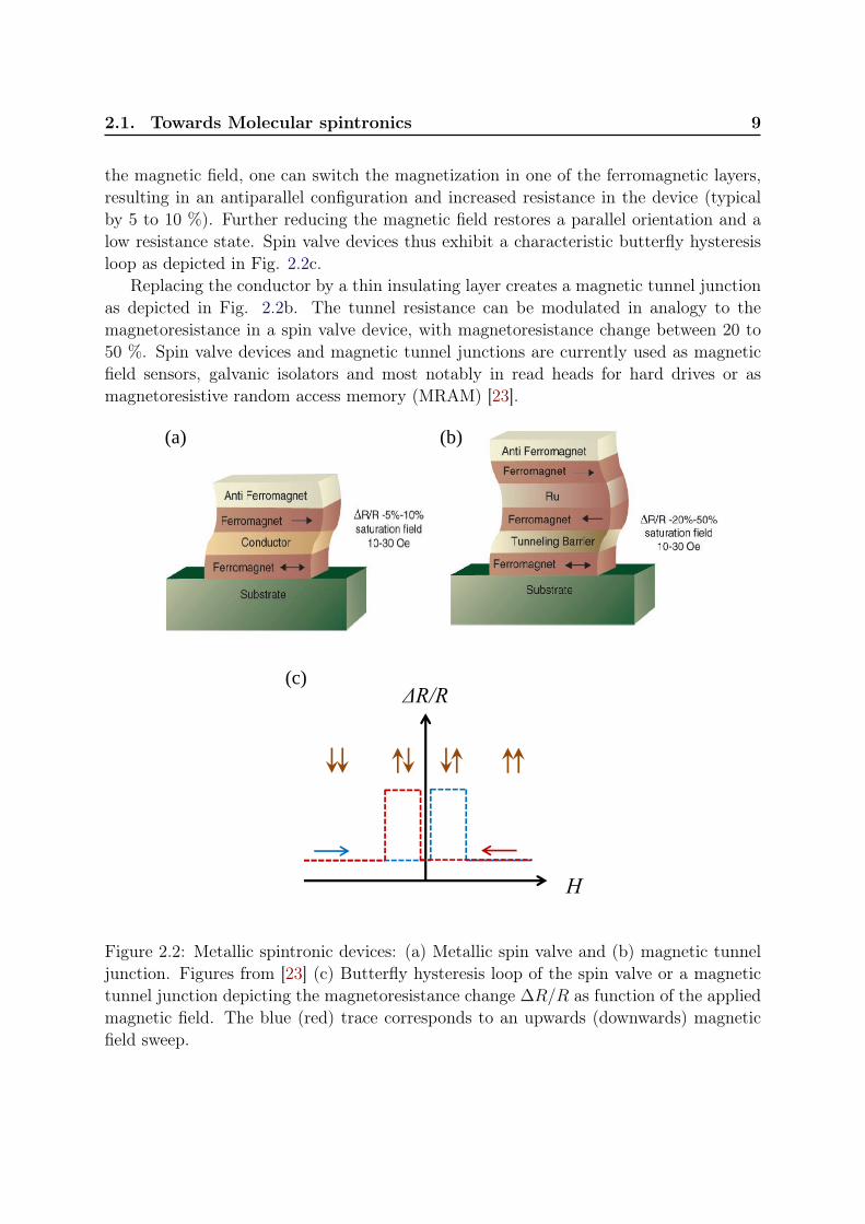
GMR is the underlying mechanism to a spin valve, where a nonmagnetic spacing layer(typically a conductor) is sandwiched between two ferromagnetic layers (Fig. 2.2a). Fora large magnetic field applied to the device, the magnetizations of both ferromagneticlayers are parallel to each other and the device is in a low resistance state. By reducing
2.1. Towards Molecular spintronics 9
the magnetic field, one can switch the magnetization in one of the ferromagnetic layers,resulting in an antiparallel configuration and increased resistance in the device (typicalby 5 to 10 %). Further reducing the magnetic field restores a parallel orientation and alow resistance state. Spin valve devices thus exhibit a characteristic butterfly hysteresisloop as depicted in Fig. 2.2c.
Replacing the conductor by a thin insulating layer creates a magnetic tunnel junctionas depicted in Fig. 2.2b. The tunnel resistance can be modulated in analogy to themagnetoresistance in a spin valve device, with magnetoresistance change between 20 to50 %. Spin valve devices and magnetic tunnel junctions are currently used as magneticfield sensors, galvanic isolators and most notably in read heads for hard drives or asmagnetoresistive random access memory (MRAM) [23].
ΔR/R
H
(a) (b)
(c)
Figure 2.2: Metallic spintronic devices: (a) Metallic spin valve and (b) magnetic tunneljunction. Figures from [23] (c) Butterfly hysteresis loop of the spin valve or a magnetictunnel junction depicting the magnetoresistance change ∆R/R as function of the appliedmagnetic field. The blue (red) trace corresponds to an upwards (downwards) magneticfield sweep.
10 Chapter 2. Introduction to Molecular Spintronics
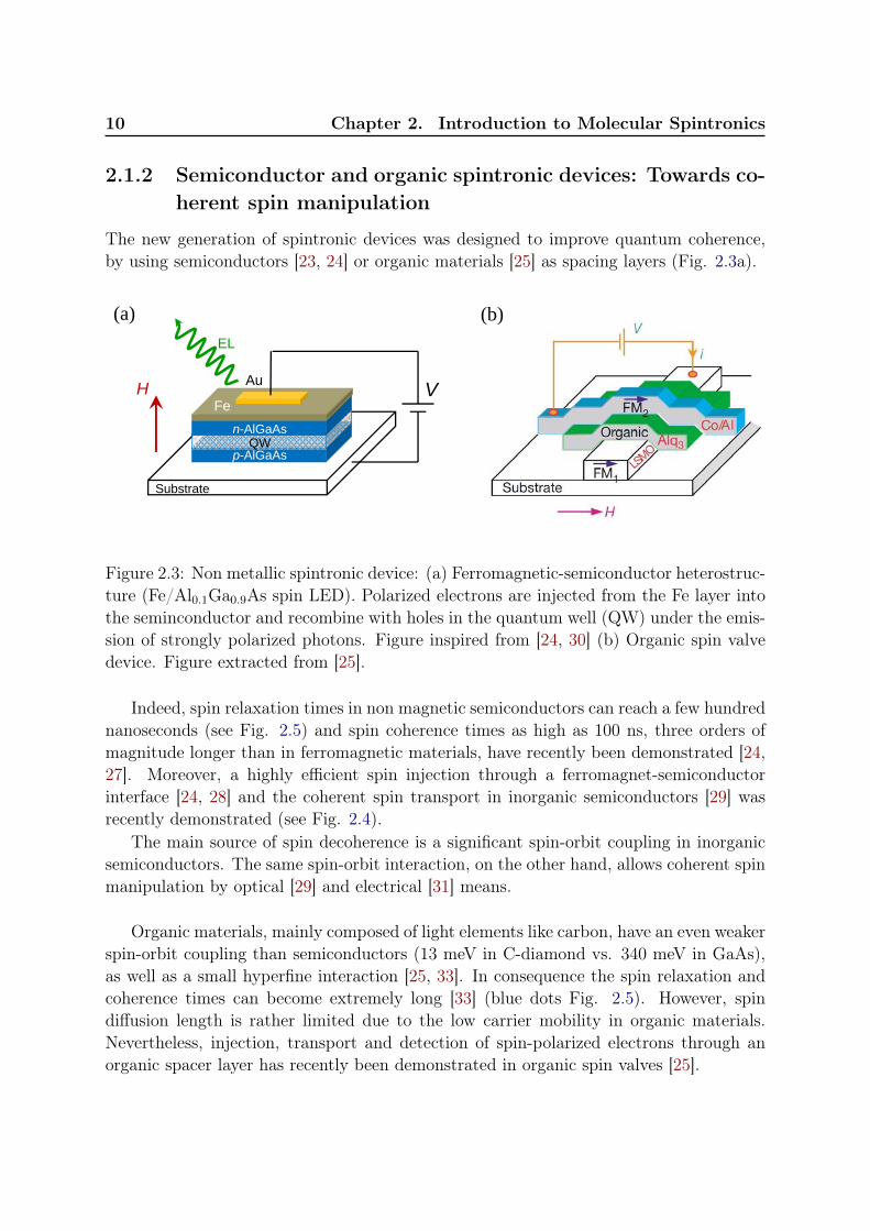
2.1.2 Semiconductor and organic spintronic devices: Towards co-herent spin manipulation
The new generation of spintronic devices was designed to improve quantum coherence,by using semiconductors [23, 24] or organic materials [25] as spacing layers (Fig. 2.3a).
p-AlGaAs
n-AlGaAsQW
Fe
Au
Substrate
H V
EL
(b)(a)
Figure 2.3: Non metallic spintronic device: (a) Ferromagnetic-semiconductor heterostruc-ture (Fe/Al0.1Ga0.9As spin LED). Polarized electrons are injected from the Fe layer intothe seminconductor and recombine with holes in the quantum well (QW) under the emis-sion of strongly polarized photons. Figure inspired from [24, 30] (b) Organic spin valvedevice. Figure extracted from [25].
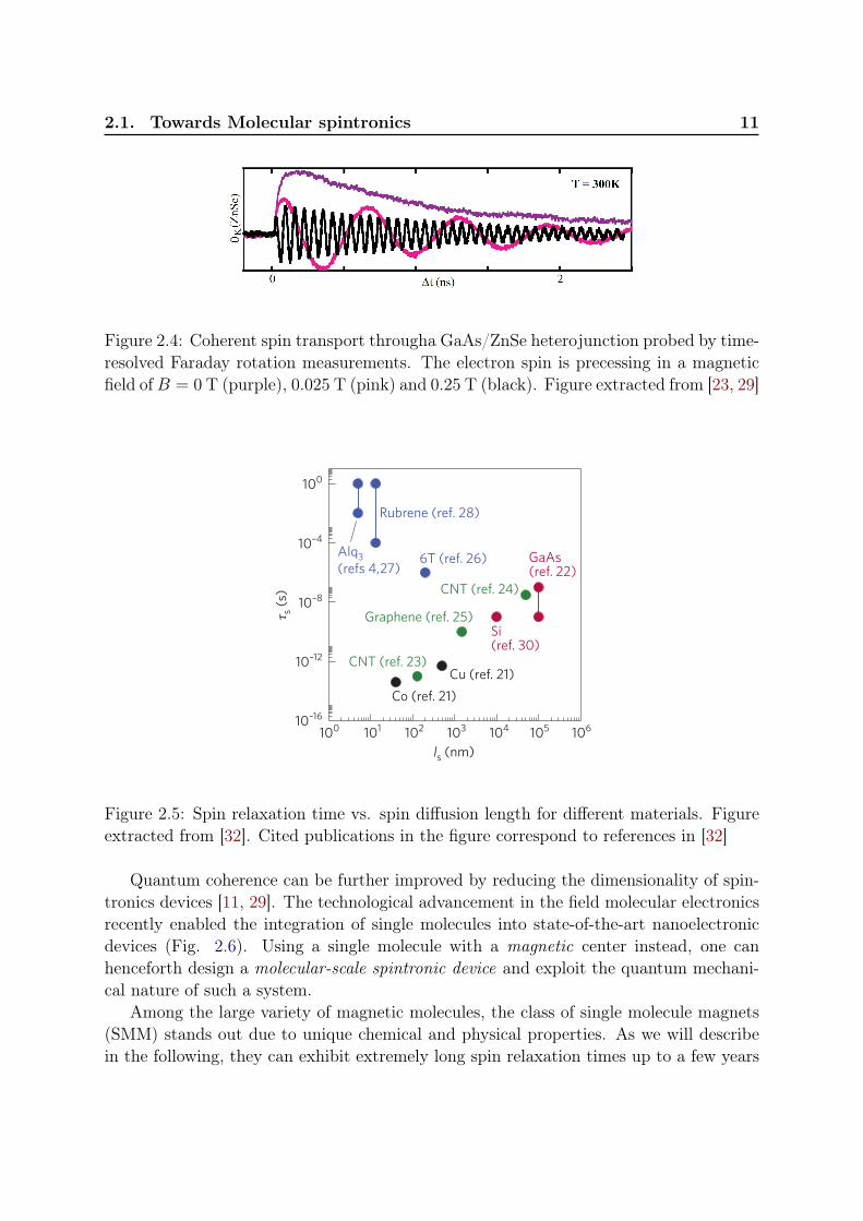
Indeed, spin relaxation times in non magnetic semiconductors can reach a few hundrednanoseconds (see Fig. 2.5) and spin coherence times as high as 100 ns, three orders ofmagnitude longer than in ferromagnetic materials, have recently been demonstrated [24,27]. Moreover, a highly efficient spin injection through a ferromagnet-semiconductorinterface [24, 28] and the coherent spin transport in inorganic semiconductors [29] wasrecently demonstrated (see Fig. 2.4).
The main source of spin decoherence is a significant spin-orbit coupling in inorganicsemiconductors. The same spin-orbit interaction, on the other hand, allows coherent spinmanipulation by optical [29] and electrical [31] means.
Organic materials, mainly composed of light elements like carbon, have an even weakerspin-orbit coupling than semiconductors (13 meV in C-diamond vs. 340 meV in GaAs),as well as a small hyperfine interaction [25, 33]. In consequence the spin relaxation andcoherence times can become extremely long [33] (blue dots Fig. 2.5). However, spindiffusion length is rather limited due to the low carrier mobility in organic materials.Nevertheless, injection, transport and detection of spin-polarized electrons through anorganic spacer layer has recently been demonstrated in organic spin valves [25].
2.1. Towards Molecular spintronics 11
Figure 2.4: Coherent spin transport througha GaAs/ZnSe heterojunction probed by time-resolved Faraday rotation measurements. The electron spin is precessing in a magneticfield ofB = 0 T (purple), 0.025 T (pink) and 0.25 T (black). Figure extracted from [23, 29]
nature materials | VOL 8 | SEPTEMBER 2009 | www.nature.com/naturematerials 695
commentary
valves3— have work functions between 4.5 and 5 eV. Even with the pillow effect, it is unsafe to assume that electrons are injected rather than holes13. In fact, a two-terminal device can be unipolar or bipolar. There is an urgent need to study three-terminal devices, where the sign of the carriers is defined by the bias on the gate, and the mobility and charge density can be deduced independently.
From a practical point of view, although most work has been done on the LSMO/Alq3 couple, there are good reasons to explore new combinations. Advantages of LSMO are its high spin polarization at low temperature and stable surface on exposure to air. A big disadvantage is its low Curie temperature, ≈ 340 K in thin films, which probably precludes room-temperature device operation. Alq3 is the archetypical light-emitting organic semiconductor, widely used in OLEDs. It is commercially available and inexpensive, but Alq3 has only low mobility (10–5 cm2 V–1 s–1) at room temperature. It exists in many polymorphs and isomers, and can even conduct holes. It reacts with evaporated Co (ref 14), and commercial-grade Alq3 tends to contain paramagnetic impurities15. There are opportunities to investigate other highly spin-polarized, high-Curie-temperature electrodes such as Fe3O4 or Co2MnSi in organic spin valves, although difficulties in the growth and in the definition of the terminations in these materials have to be overcome first. A good guess would be to use Co-based alloys that work well with metallic and insulating interlayers. In any case, the quality of the interfaces is critical, as the experience of the OLED and organic-electronics communities teach us.
What is it all good for?There are accepted metrics for organic-semiconductor devices, namely light output and quantum efficiency for OLEDs, and mobility, turn-on voltage and on/off ratios for OFETs. Similarly, inorganic spintronics also has its own set of metrics: room-temperature magnetoresistance, bias-dependence and spin-torque switching current. What should the metrics be for organic spin valves? We need to have some robust working devices, but once a thorough electrical characterization has established the charge-carrier regime, resistance changes at magnetic fields corresponding to the coercivity of the electrodes are needed to provide proof of spin transport across the entire junction. The variation of magnetoresistance with the organic layer thickness will then give an idea of the spin-diffusion length ls. Extracting the transport spin lifetime τs is more difficult. One needs to measure the layer mobility and spin
lifetime in a working device, something only recently achieved for unpolarized electrons16. A mobility value may be plucked from the literature, but the typical experimental range varies across several orders of magnitude.
Optical methods of measuring spin lifetime in inorganic semiconductors, based on Kerr or Faraday rotation, depend on spin–orbit interaction. Spin–orbit coupling is very weak in organic materials, so we need to look elsewhere. Other possibilities are noise measurements, electron paramagnetic resonance, muon spin resonance17, electrically detected magnetic resonance and spin-polarized two-photon photoemission18, which could help us follow the fate of spin-polarized electrons in organic semiconductors.
Once a well-characterized organic device is achieved, the fundamental question that still remains is what can this device do that is not already done by conventional spintronics? The plot of spin lifetime versus diffusion length for spin-polarized electrons in Fig. 4 is based on published data. When only one quantity is available, the other is calculated by using literature values for the mobility. Despite the uncertainties, organic materials cluster in the top-left corner of the plot — they possess long spin lifetimes, but the spins do not travel far. This suggests that potential applications will rely on interfacial properties.
We can therefore look forward to a phase of ‘spinterface engineering’ as spin electronics learns from organic electronics and organic chemistry on how best to get the spins moving into these structures. There are prospects for spin optics, quantum computing and non-volatile memory, but organic synthesis will not really affect this field until we can control the experimental conditions sufficiently to make reproducible
devices. A concerted effort is needed to understand how vacuum conditions, growth rates, film morphology, surface roughness and impurities influence the performance of organic-based magnetic devices. Some encouraging pointers are beginning to emerge from theory19,20. However, evidence for spin injection and transport is scarce and the first reproducible results have only recently been obtained17,18. It is certainly safe to say that organic spintronics is still a young field that needs more working hands and thinking heads for its potential to be fulfilled.
Greg Szulczewski†, Stefano Sanvito and Michael Coey are at the School of Physics and CRANN, Trinity College Dublin, Ireland. †Permanent address, Department of Chemistry, University of Alabama, Tuscaloosa, USA. e‑mail: [email protected]; [email protected]; [email protected]
References1. Coey, J. M. D. Magnetism and Magnetic Materials (Cambridge
Univ. Press, 2009).2. Awschalom, D. A. & Flatté, M. E. Nature Phys. 3, 153–159 (2007).3. Dediu, V. A., Hueso, L. E., Bergenti, I. & Taliani, C. Nature Mater.
8, 707–716 (2009).4. Xiong, Z. H., Wu, D., Vardeny, Z. V. & Shi, J. Nature
427, 821–824 (2004).5. Santos, T. S. et al. Phys. Rev. Lett. 98, 016601 (2007).6. Wagemans, W., Bloom, F. L., Bobbert, P. A., Wohlgenannt, M. &
Koopmans, B. J. App. Phys. 103, 07F303 (2008).7. Parkin, S. S. P. in Handbook of Magnetism and Advanced Magentic
Materials Vol. 5 (eds Kronmüller, H. & Parkin, S. S. P.) Ch. 1 (Wiley, 2008).
8. Smidt, G. J. Phys. D. 38, R107–R122 (2005).9. Rashba, E. I. Phys Rev B 62, R16262 (2000).10. Hwang, J., Wan, A. & Kahn, A. Mater. Sci. Eng. R 64, 1–31 (2009). 11. Maruyama, T. et al. Nature Nanotech. 4, 158–161 (2009).12. Krause, S., Casu, M. B., Schöll, A. & Umbach, E. New J. Phys.
10, 085001 (2008).13. Jiang, J. S., Pearson, J. E. & Bader, S. D. Phys. Rev. B
77, 035303 (2008).14. Xu, W., Brauer, J., Szulczewski, G., Diver, M. S. & Caruso, A. N.
App. Phys. Lett. 94, 233302 (2009).15. Burke, F., Abid, M., Stamenov, P. & Coey, J. M. D.
J. Magn. Magn. Mater. (in the press).16. Matsui, H., Hasegawa, T., Tokura, Y., Hiraoka, M. & Yamada, T.
Phys. Rev. Lett. 100, 122601 (2008).17. Drew, A. J. et al. Nature Mater. 8, 109–114 (2009).18. Cinchetti, M. et al. Nature Mater. 8, 115–119 (2009).19. Bobbert, P. A., Wagemans, W., van Oost, F. W. A. & Koopmans, B.
Phys. Rev. Lett. 102, 156604 (2009).20. Xie, S. J., Ahn, K. H., Smith, D. L., Bishop, A. R. & Saxena, A.
Phys. Rev. B 67, 125202 (2003).21. Bass, J. & Pratt, W. P. Jr J. Phys. Condens. Matter 19, 183201 (2007).22. Kikkawa, J. & Awschalom, D. D. Nature 397, 139–141 (1999).23. Tsukagoshi, K., Alphenaar, B. W. & Ago, H. Nature
401, 572–574 (1999).24. Hueso, L. E. et al. Nature 445, 410–413 (2007).25. Tombros, N., Jozsa, C., Popinciuc, M., Jonkman, H. T. &
van Wees, B. J. Nature 448, 571–574 (2007).26. Dediu, V. A., Murgia, M., Matacotta, F. C., Taliani, C. &
Barbanera, S. Solid State Commun. 122, 181–184 (2002).27. Pramanik, S., Stefanita, C.-G., Patibandla, S. &
Bandyopadhyay, S. et al. Nature Nanotech. 2, 216–218 (2007).28. Shim, J. H. et al. Phys. Rev. Lett. 100, 226603 (2008).29. Limketkai, D. M., Jadhav, P. & Baldo, M. A. Phys. Rev. B
75, 113203 (2007).30. Appelbaum, I., Huang, B. & Monsma, D. Nature
447, 295–298 (2007).
Corrected after print: 24 August 2009
Figure 4 | Spin-diffusion length lS versus spin-diffusion time τs, for various materials. The organic semiconductors appear in the top-left corner. They have a long spin lifetime but, owing to their low mobilities, spin-diffusion lengths are short. The data are taken from the literature as indicated.
6T (ref. 26)
100 101 102 103 104 105 106
ls (nm)
10–16
10–12
10–8
10–4
100
τ s (s
)
GaAs(ref. 22)
CNT (ref. 24)
Graphene (ref. 25)
CNT (ref. 23)Cu (ref. 21)
Co (ref. 21)
Rubrene (ref. 28)
Si (ref. 30)
Alq3(refs 4,27)
nmat_2518_SEP09.indd 695 20/8/09 10:48:03
© 2009 Macmillan Publishers Limited. All rights reserved
Figure 2.5: Spin relaxation time vs. spin diffusion length for different materials. Figureextracted from [32]. Cited publications in the figure correspond to references in [32]
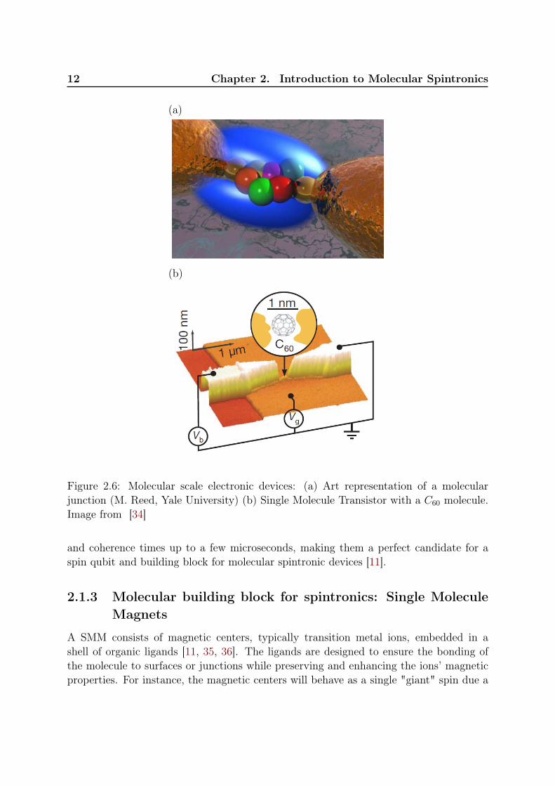
Quantum coherence can be further improved by reducing the dimensionality of spin-tronics devices [11, 29]. The technological advancement in the field molecular electronicsrecently enabled the integration of single molecules into state-of-the-art nanoelectronicdevices (Fig. 2.6). Using a single molecule with a magnetic center instead, one canhenceforth design a molecular-scale spintronic device and exploit the quantum mechani-cal nature of such a system.
Among the large variety of magnetic molecules, the class of single molecule magnets(SMM) stands out due to unique chemical and physical properties. As we will describein the following, they can exhibit extremely long spin relaxation times up to a few years
12 Chapter 2. Introduction to Molecular Spintronics
(a)
(b)
Figure 2.6: Molecular scale electronic devices: (a) Art representation of a molecularjunction (M. Reed, Yale University) (b) Single Molecule Transistor with a C60 molecule.Image from [34]
and coherence times up to a few microseconds, making them a perfect candidate for aspin qubit and building block for molecular spintronic devices [11].
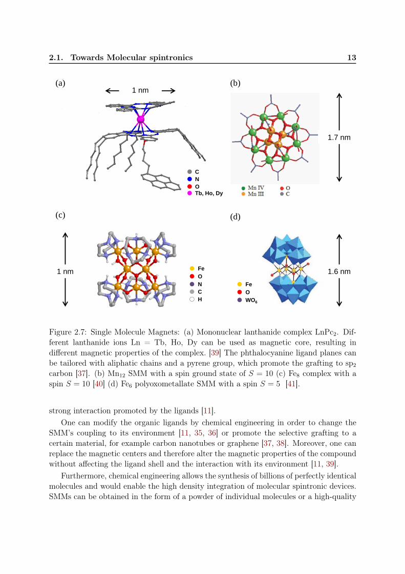
2.1.3 Molecular building block for spintronics: Single MoleculeMagnets
A SMM consists of magnetic centers, typically transition metal ions, embedded in ashell of organic ligands [11, 35, 36]. The ligands are designed to ensure the bonding ofthe molecule to surfaces or junctions while preserving and enhancing the ions’ magneticproperties. For instance, the magnetic centers will behave as a single "giant" spin due a
2.1. Towards Molecular spintronics 13
1 nm(a)
1.7 nm
(b)
FeONCH
(c)
FeOWO6
1.6 nm
(d)
1 nm
OTb, Ho, DyONC
Figure 2.7: Single Molecule Magnets: (a) Mononuclear lanthanide complex LnPc2. Dif-ferent lanthanide ions Ln = Tb, Ho, Dy can be used as magnetic core, resulting indifferent magnetic properties of the complex. [39] The phthalocyanine ligand planes canbe tailored with aliphatic chains and a pyrene group, which promote the grafting to sp2
carbon [37]. (b) Mn12 SMM with a spin ground state of S = 10 (c) Fe8 complex with aspin S = 10 [40] (d) Fe6 polyoxometallate SMM with a spin S = 5 [41].
strong interaction promoted by the ligands [11].One can modify the organic ligands by chemical engineering in order to change the
SMM’s coupling to its environment [11, 35, 36] or promote the selective grafting to acertain material, for example carbon nanotubes or graphene [37, 38]. Moreover, one canreplace the magnetic centers and therefore alter the magnetic properties of the compoundwithout affecting the ligand shell and the interaction with its environment [11, 39].
Furthermore, chemical engineering allows the synthesis of billions of perfectly identicalmolecules and would enable the high density integration of molecular spintronic devices.SMMs can be obtained in the form of a powder of individual molecules or a high-quality
14 Chapter 2. Introduction to Molecular Spintronics
molecular crystal, which gives an experimental access to the structural and magneticproperties of the molecules.
The magnetic properties of a single molecule magnet can be described by a single"giant" spin and a Hamiltonian of the form
H = DS2z + E
(S2x − S2
y
)+ gµBµ0~S · ~H (2.1)
where Sx, Sy, Sz are the spin components, D the axial and E the transverse magneticanisotropy constants (with D E) and gµBµ0~S · ~H the Zeeman energy associated withan applied external magnetic field.
A SMM is characterized by a large magnetic moment and spin ground state S ≥ 1
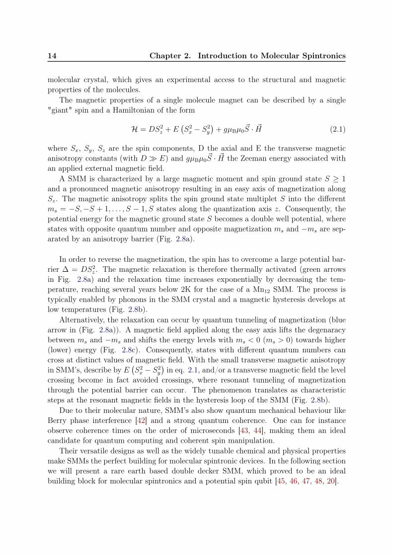
and a pronounced magnetic anisotropy resulting in an easy axis of magnetization alongSz. The magnetic anisotropy splits the spin ground state multiplet S into the differentms = −S,−S + 1, . . . , S − 1, S states along the quantization axis z. Consequently, thepotential energy for the magnetic ground state S becomes a double well potential, wherestates with opposite quantum number and opposite magnetization ms and −ms are sep-arated by an anisotropy barrier (Fig. 2.8a).
In order to reverse the magnetization, the spin has to overcome a large potential bar-rier ∆ = DS2
z . The magnetic relaxation is therefore thermally activated (green arrowsin Fig. 2.8a) and the relaxation time increases exponentially by decreasing the tem-perature, reaching several years below 2K for the case of a Mn12 SMM. The process istypically enabled by phonons in the SMM crystal and a magnetic hysteresis develops atlow temperatures (Fig. 2.8b).
Alternatively, the relaxation can occur by quantum tunneling of magnetization (bluearrow in (Fig. 2.8a)). A magnetic field applied along the easy axis lifts the degenaracybetween ms and −ms and shifts the energy levels with ms < 0 (ms > 0) towards higher(lower) energy (Fig. 2.8c). Consequently, states with different quantum numbers cancross at distinct values of magnetic field. With the small transverse magnetic anisotropyin SMM’s, describe by E
(S2x − S2
y
)in eq. 2.1, and/or a transverse magnetic field the level
crossing become in fact avoided crossings, where resonant tunneling of magnetizationthrough the potential barrier can occur. The phenomenon translates as characteristicsteps at the resonant magnetic fields in the hysteresis loop of the SMM (Fig. 2.8b).
Due to their molecular nature, SMM’s also show quantum mechanical behaviour likeBerry phase interference [42] and a strong quantum coherence. One can for instanceobserve coherence times on the order of microseconds [43, 44], making them an idealcandidate for quantum computing and coherent spin manipulation.
Their versatile designs as well as the widely tunable chemical and physical propertiesmake SMMs the perfect building for molecular spintronic devices. In the following sectionwe will present a rare earth based double decker SMM, which proved to be an idealbuilding block for molecular spintronics and a potential spin qubit [45, 46, 47, 48, 20].
2.2. Terbium Double Decker Single Molecule Magnet 15
(a) (b)
(c)
ms= +4
ms= -10
Figure 2.8: Magnetization dynamics in a SMM: (a) Double well potential of a SMMwith a magnetic ground state S = 10. Magnetization reversal will occur via quantumtunneling of magnetization between two resonant energy levels (QTM, blue arrow) orby thermally activated, phonon assisted relaxation (green arrows). Figure from [11].(b) Hysteresis loops of a Mn12 single crystal at different temperatures and for a sweeprate of 2 mT/s. Steps in the hysteresis loops are attributed to quantum tunneling ofmagnetization. Figure from [11]. (c) Zeeman diagram of a SMM with a magnetic groundstate of S = 10.
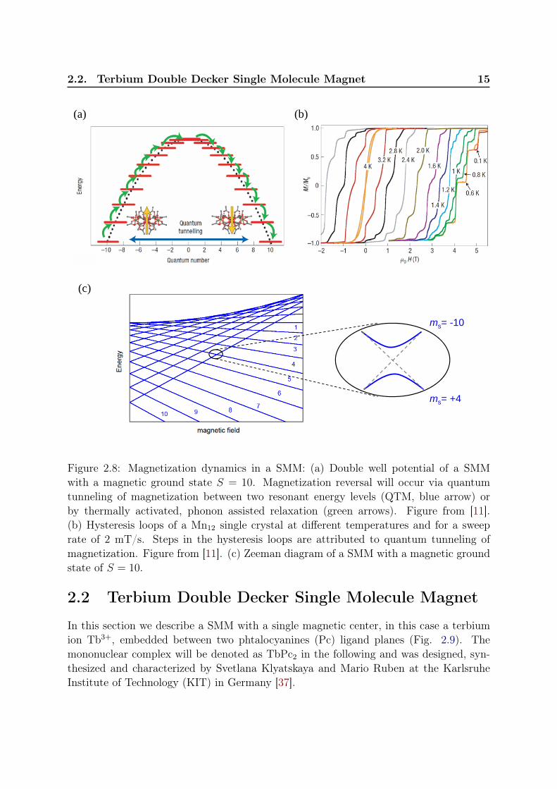
2.2 Terbium Double Decker Single Molecule Magnet
In this section we describe a SMM with a single magnetic center, in this case a terbiumion Tb3+, embedded between two phtalocyanines (Pc) ligand planes (Fig. 2.9). Themononuclear complex will be denoted as TbPc2 in the following and was designed, syn-thesized and characterized by Svetlana Klyatskaya and Mario Ruben at the KarlsruheInstitute of Technology (KIT) in Germany [37].
16 Chapter 2. Introduction to Molecular Spintronics
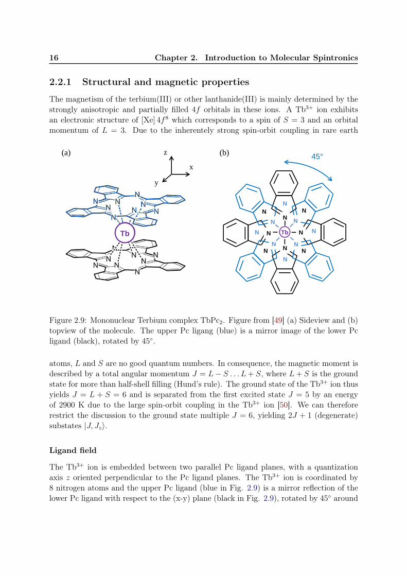
2.2.1 Structural and magnetic properties
The magnetism of the terbium(III) or other lanthanide(III) is mainly determined by thestrongly anisotropic and partially filled 4f orbitals in these ions. A Tb3+ ion exhibitsan electronic structure of [Xe] 4f 8 which corresponds to a spin of S = 3 and an orbitalmomentum of L = 3. Due to the inherentely strong spin-orbit coupling in rare earth
NN
NN
N
N
NN
N
N N
N
N
N
N
NTb
45°
Tb
(a) (b)z
y
x
Figure 2.9: Mononuclear Terbium complex TbPc2. Figure from [49] (a) Sideview and (b)topview of the molecule. The upper Pc ligang (blue) is a mirror image of the lower Pcligand (black), rotated by 45.
atoms, L and S are no good quantum numbers. In consequence, the magnetic moment isdescribed by a total angular momentum J = L− S . . . L+ S, where L+ S is the groundstate for more than half-shell filling (Hund’s rule). The ground state of the Tb3+ ion thusyields J = L + S = 6 and is separated from the first excited state J = 5 by an energyof 2900 K due to the large spin-orbit coupling in the Tb3+ ion [50]. We can thereforerestrict the discussion to the ground state multiple J = 6, yielding 2J + 1 (degenerate)substates |J, Jz〉.
Ligand field
The Tb3+ ion is embedded between two parallel Pc ligand planes, with a quantizationaxis z oriented perpendicular to the Pc ligand planes. The Tb3+ ion is coordinated by8 nitrogen atoms and the upper Pc ligand (blue in Fig. 2.9) is a mirror reflection of thelower Pc ligand with respect to the (x-y) plane (black in Fig. 2.9), rotated by 45 around
2.2. Terbium Double Decker Single Molecule Magnet 17
the z-axis. The Tb3+ is therefore exposed to a ligand electric field with a antiprismaticsymmetry D4d which is described by the following Hamiltonian [51]
Hlf = αA02O
02 + β
(A0
4O04 + A4
4O44
)+ γ
(A0
6O06 + A4
6O46
)(2.2)
where α = −1/99, β = 2/16335 and γ = −1/891891 are constant parameters related tothe ion [52], Ok
q the equivalent Stevens operators and Akq the ligand field parameters.
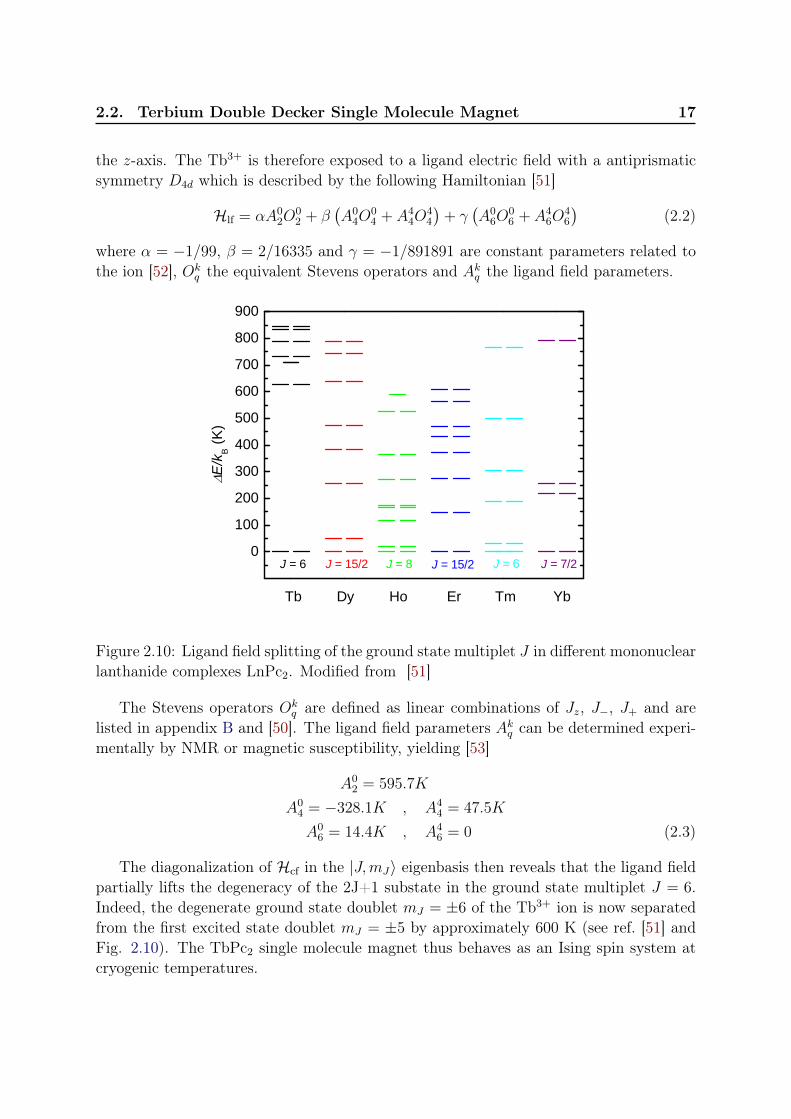
01 0 02 0 03 0 04 0 05 0 06 0 07 0 08 0 09 0 0
Y bT mE rH oD y J = 7 / 2J = 6J = 1 5 / 2J = 8J = 1 5 / 2
E/k B (K
)
J = 6
T b
Figure 2.10: Ligand field splitting of the ground state multiplet J in different mononuclearlanthanide complexes LnPc2. Modified from [51]
The Stevens operators Okq are defined as linear combinations of Jz, J−, J+ and are
listed in appendix B and [50]. The ligand field parameters Akq can be determined experi-mentally by NMR or magnetic susceptibility, yielding [53]
A02 = 595.7K
A04 = −328.1K , A4
4 = 47.5K
A06 = 14.4K , A4
6 = 0 (2.3)
The diagonalization of Hcf in the |J,mJ〉 eigenbasis then reveals that the ligand fieldpartially lifts the degeneracy of the 2J+1 substate in the ground state multiplet J = 6.Indeed, the degenerate ground state doublet mJ = ±6 of the Tb3+ ion is now separatedfrom the first excited state doublet mJ = ±5 by approximately 600 K (see ref. [51] andFig. 2.10). The TbPc2 single molecule magnet thus behaves as an Ising spin system atcryogenic temperatures.
18 Chapter 2. Introduction to Molecular Spintronics
- 1 0 - 5 0 5 1 0- 8 0 0
- 6 0 0
- 4 0 0
- 2 0 0
0
2 0 0
|+ 6 ⟩
E/kB (K)
0 H z ( T )
|− 6 ⟩
|+ 5 ⟩
|− 5 ⟩
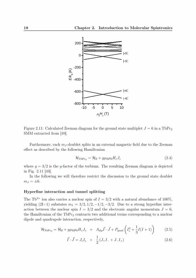
Figure 2.11: Calculated Zeeman diagram for the ground state multiplet J = 6 in a TbPc2
SMM extracted from [49].
Furthermore, each mJ -doublet splits in an external magnetic field due to the Zeemaneffect as described by the following Hamiltonian
HTbPc2 = Hlf + gµBµ0HzJz (2.4)
where g = 3/2 is the g-factor of the terbium. The resulting Zeeman diagram is depictedin Fig. 2.11 [49].
In the following we will therefore restrict the discussion to the ground state doubletmJ = ±6.
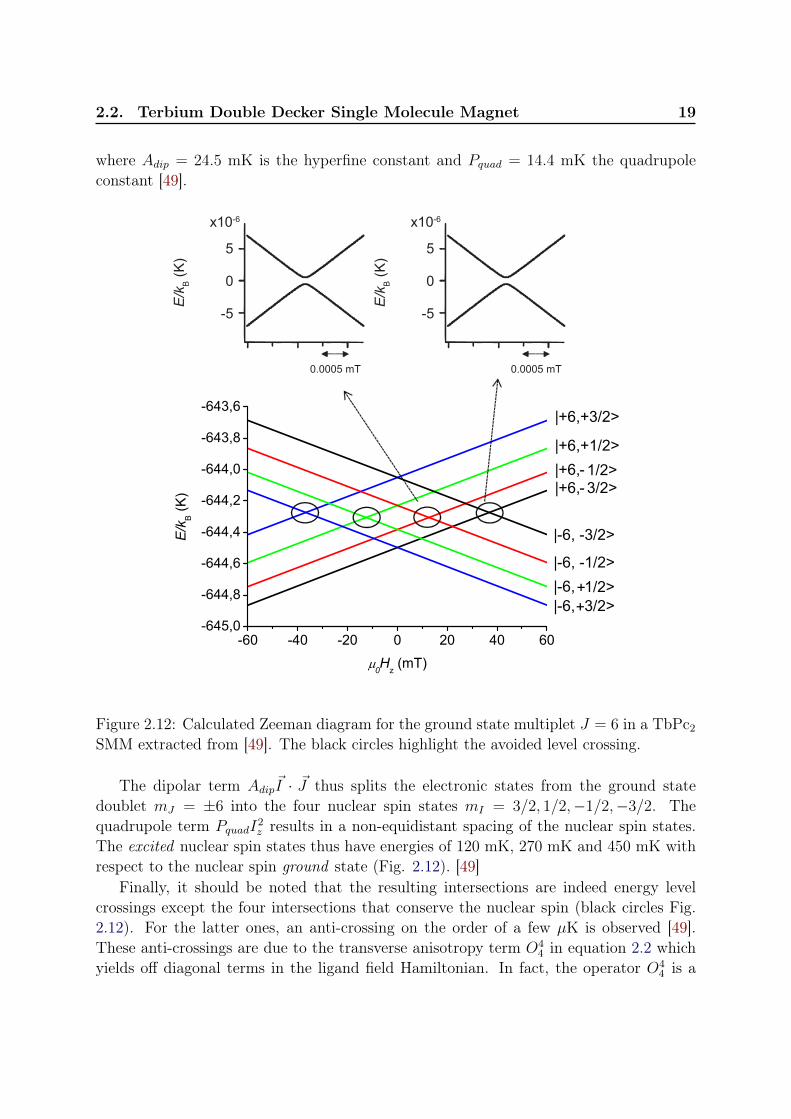
Hyperfine interaction and tunnel splitting
The Tb3+ ion also carries a nuclear spin of I = 3/2 with a natural abundance of 100%,yielding (2I+1) substates mI = 3/2, 1/2,−1/2,−3/2. Due to a strong hyperfine inter-action between the nuclear spin I = 3/2 and the electronic angular momentum J = 6,the Hamiltonian of the TbPc2 contracts two additional terms corresponding to a nucleardipole and quadrupole interaction, respectively,
HTbPc2 = Hlf + gµBµ0HzJz + Adip~I · ~J + Pquad
(I2z +
1
3I(I + 1)
)(2.5)
~I · ~J = JzIz +1
2(J+I− + J−I+) (2.6)
2.2. Terbium Double Decker Single Molecule Magnet 19
where Adip = 24.5 mK is the hyperfine constant and Pquad = 14.4 mK the quadrupoleconstant [49].
-60 -40 -20 0 20 40 60-645,0
-644,8
-644,6
-644,4
-644,2
-644,0
-643,8
-643,6
E/k
B (K
)
0Hz (mT)
E/k
B (K
)
5
-5
x10-6
0
0.0005 mTE
/kB (K
)
5
-5
x10-6
0
0.0005 mT
|-6, -3/2>
|-6, -1/2>|-6,+1/2>|-6,+3/2>
|+6,+3/2>
|+6,+1/2>|+6,- 1/2>|+6,- 3/2>
Figure 2.12: Calculated Zeeman diagram for the ground state multiplet J = 6 in a TbPc2
SMM extracted from [49]. The black circles highlight the avoided level crossing.
The dipolar term Adip~I · ~J thus splits the electronic states from the ground statedoublet mJ = ±6 into the four nuclear spin states mI = 3/2, 1/2,−1/2,−3/2. Thequadrupole term PquadI
2z results in a non-equidistant spacing of the nuclear spin states.
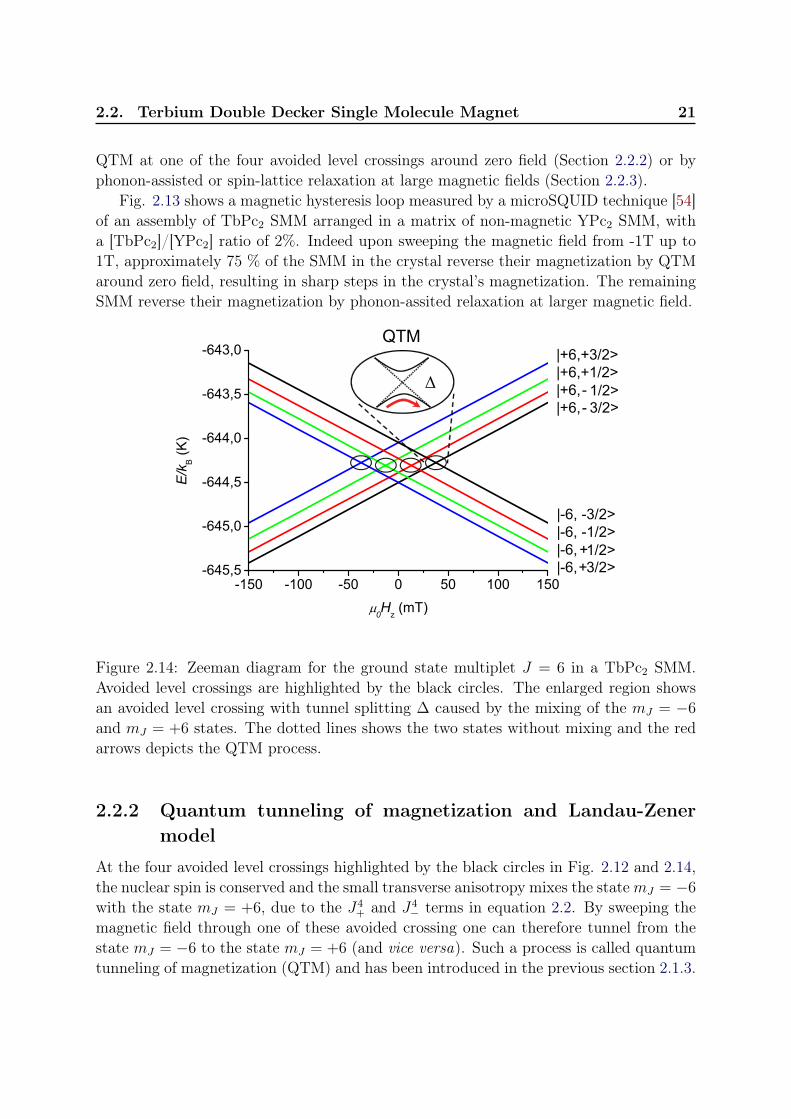
The excited nuclear spin states thus have energies of 120 mK, 270 mK and 450 mK withrespect to the nuclear spin ground state (Fig. 2.12). [49]
Finally, it should be noted that the resulting intersections are indeed energy levelcrossings except the four intersections that conserve the nuclear spin (black circles Fig.2.12). For the latter ones, an anti-crossing on the order of a few µK is observed [49].These anti-crossings are due to the transverse anisotropy term O4
4 in equation 2.2 whichyields off diagonal terms in the ligand field Hamiltonian. In fact, the operator O4
4 is a
20 Chapter 2. Introduction to Molecular Spintronics
linear combination of J4+ and J4
−, which mixes states with mJ and states with mJ ± 4n.Hence, the mJ = +6 state mixes with the mJ = −6 state, generating an avoided levelcrossing at the four highlighted intersections close to zero magnetic field (Fig. 2.12).
- 1 , 0
- 0 , 5
0 , 0
0 , 5
1 , 0
- 2 0 0 - 1 0 0 0 1 0 0 2 0 0- 6 4 6
- 6 4 5
- 6 4 4
- 6 4 3
M/
M S E/
k B (K)
0 H z ( m T )
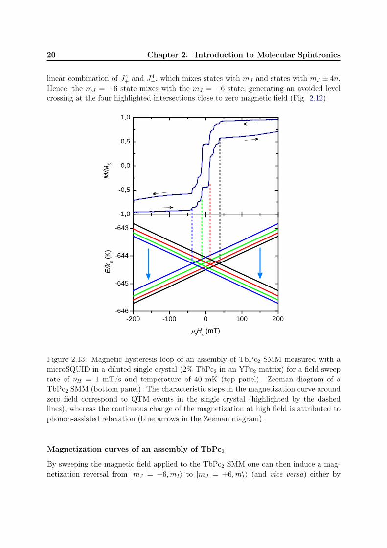
Figure 2.13: Magnetic hysteresis loop of an assembly of TbPc2 SMM measured with amicroSQUID in a diluted single crystal (2% TbPc2 in an YPc2 matrix) for a field sweeprate of νH = 1 mT/s and temperature of 40 mK (top panel). Zeeman diagram of aTbPc2 SMM (bottom panel). The characteristic steps in the magnetization curve aroundzero field correspond to QTM events in the single crystal (highlighted by the dashedlines), whereas the continuous change of the magnetization at high field is attributed tophonon-assisted relaxation (blue arrows in the Zeeman diagram).
Magnetization curves of an assembly of TbPc2
By sweeping the magnetic field applied to the TbPc2 SMM one can then induce a mag-netization reversal from |mJ = −6,mI〉 to |mJ = +6,m′I〉 (and vice versa) either by
2.2. Terbium Double Decker Single Molecule Magnet 21
QTM at one of the four avoided level crossings around zero field (Section 2.2.2) or byphonon-assisted or spin-lattice relaxation at large magnetic fields (Section 2.2.3).
Fig. 2.13 shows a magnetic hysteresis loop measured by a microSQUID technique [54]of an assembly of TbPc2 SMM arranged in a matrix of non-magnetic YPc2 SMM, witha [TbPc2]/[YPc2] ratio of 2%. Indeed upon sweeping the magnetic field from -1T up to1T, approximately 75 % of the SMM in the crystal reverse their magnetization by QTMaround zero field, resulting in sharp steps in the crystal’s magnetization. The remainingSMM reverse their magnetization by phonon-assited relaxation at larger magnetic field.
-150 -100 -50 0 50 100 150-645,5
-645,0
-644,5
-644,0
-643,5
-643,0
E/k
B (K
)
0Hz (mT)
|+6,+3/2>|+6,+1/2>|+6,- 1/2>|+6,- 3/2>
QTM
Δ
|-6, -3/2>|-6, -1/2>|-6,+1/2>|-6,+3/2>
Figure 2.14: Zeeman diagram for the ground state multiplet J = 6 in a TbPc2 SMM.Avoided level crossings are highlighted by the black circles. The enlarged region showsan avoided level crossing with tunnel splitting ∆ caused by the mixing of the mJ = −6
and mJ = +6 states. The dotted lines shows the two states without mixing and the redarrows depicts the QTM process.
2.2.2 Quantum tunneling of magnetization and Landau-Zenermodel
At the four avoided level crossings highlighted by the black circles in Fig. 2.12 and 2.14,the nuclear spin is conserved and the small transverse anisotropy mixes the statemJ = −6
with the state mJ = +6, due to the J4+ and J4
− terms in equation 2.2. By sweeping themagnetic field through one of these avoided crossing one can therefore tunnel from thestate mJ = −6 to the state mJ = +6 (and vice versa). Such a process is called quantumtunneling of magnetization (QTM) and has been introduced in the previous section 2.1.3.
22 Chapter 2. Introduction to Molecular Spintronics
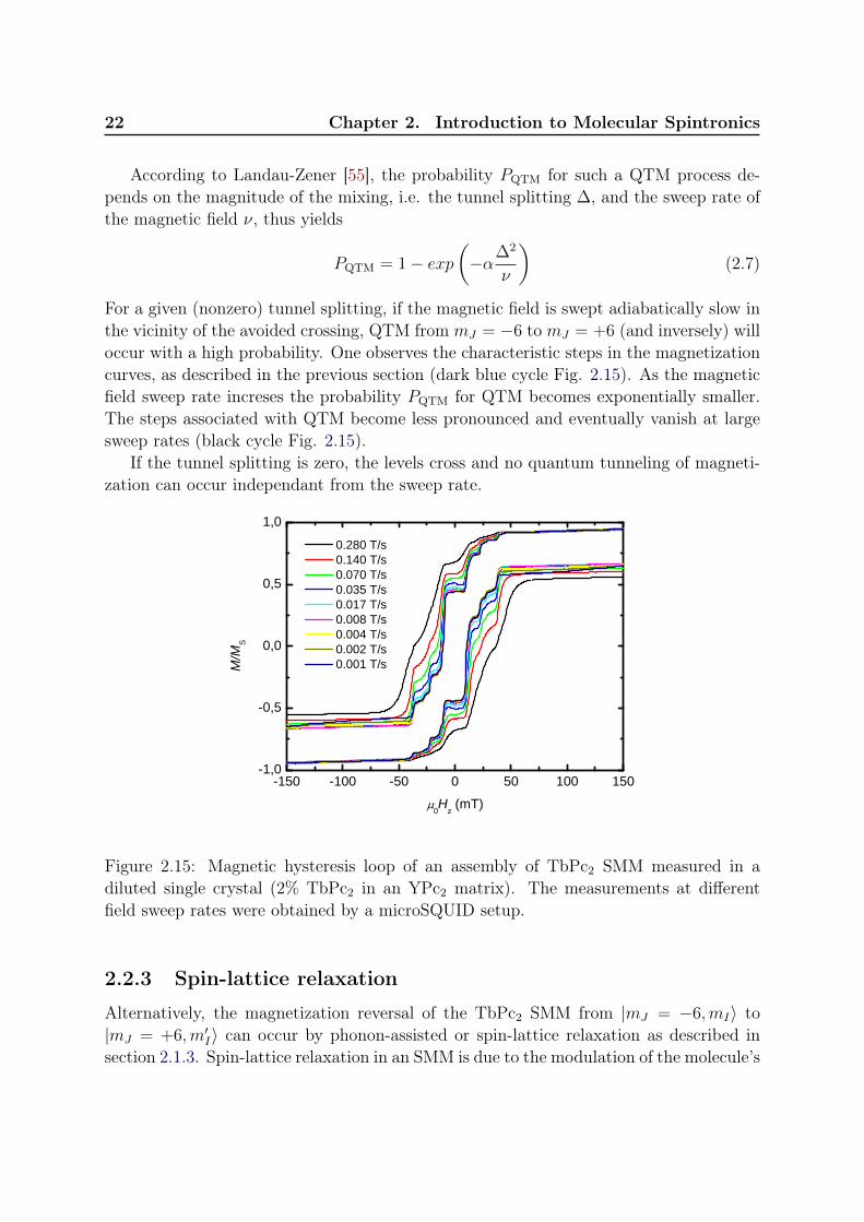
According to Landau-Zener [55], the probability PQTM for such a QTM process de-pends on the magnitude of the mixing, i.e. the tunnel splitting ∆, and the sweep rate ofthe magnetic field ν, thus yields
PQTM = 1− exp(−α∆2
ν
)(2.7)
For a given (nonzero) tunnel splitting, if the magnetic field is swept adiabatically slow inthe vicinity of the avoided crossing, QTM from mJ = −6 to mJ = +6 (and inversely) willoccur with a high probability. One observes the characteristic steps in the magnetizationcurves, as described in the previous section (dark blue cycle Fig. 2.15). As the magneticfield sweep rate increses the probability PQTM for QTM becomes exponentially smaller.The steps associated with QTM become less pronounced and eventually vanish at largesweep rates (black cycle Fig. 2.15).
If the tunnel splitting is zero, the levels cross and no quantum tunneling of magneti-zation can occur independant from the sweep rate.
- 1 5 0 - 1 0 0 - 5 0 0 5 0 1 0 0 1 5 0- 1 , 0
- 0 , 5
0 , 0
0 , 5
1 , 0 0 . 2 8 0 T / s 0 . 1 4 0 T / s 0 . 0 7 0 T / s 0 . 0 3 5 T / s 0 . 0 1 7 T / s 0 . 0 0 8 T / s 0 . 0 0 4 T / s 0 . 0 0 2 T / s 0 . 0 0 1 T / s
M/M S
0 H z ( m T )
Figure 2.15: Magnetic hysteresis loop of an assembly of TbPc2 SMM measured in adiluted single crystal (2% TbPc2 in an YPc2 matrix). The measurements at differentfield sweep rates were obtained by a microSQUID setup.
2.2.3 Spin-lattice relaxation
Alternatively, the magnetization reversal of the TbPc2 SMM from |mJ = −6,mI〉 to|mJ = +6,m′I〉 can occur by phonon-assisted or spin-lattice relaxation as described insection 2.1.3. Spin-lattice relaxation in an SMM is due to the modulation of the molecule’s
2.2. Terbium Double Decker Single Molecule Magnet 23
-150 -100 -50 0 50 100 150-645,5
-645,0
-644,5
-644,0
-643,5
-643,0 E
/kB (K
)
0Hz (mT)
|+6,+3/2>|+6,+1/2>|+6,- 1/2>|+6,- 3/2>
QTM
Δ
|-6, -3/2>|-6, -1/2>|-6,+1/2>|-6,+3/2>
Phonon assistedrelaxation
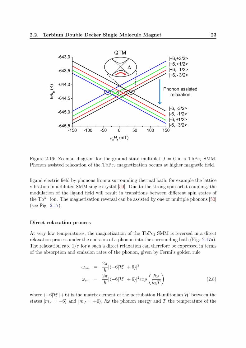
Figure 2.16: Zeeman diagram for the ground state multiplet J = 6 in a TbPc2 SMM.Phonon assisted relaxation of the TbPc2 magnetization occurs at higher magnetic field.
ligand electric field by phonons from a surrounding thermal bath, for example the latticevibration in a diluted SMM single crystal [50]. Due to the strong spin-orbit coupling, themodulation of the ligand field will result in transitions between different spin states ofthe Tb3+ ion. The magnetization reversal can be assisted by one or multiple phonons [50](see Fig. 2.17).
Direct relaxation process
At very low temperatures, the magnetization of the TbPc2 SMM is reversed in a directrelaxation process under the emission of a phonon into the surrounding bath (Fig. 2.17a).The relaxation rate 1/τ for a such a direct relaxation can therefore be expressed in termsof the absorption and emission rates of the phonon, given by Fermi’s golden rule
ωabs =2π
~|〈−6|H′|+ 6〉|2
ωem =2π
~|〈−6|H′|+ 6〉|2exp
(~ωkBT
)(2.8)
where 〈−6|H′|+ 6〉 is the matrix element of the pertubation Hamiltonian H′ between thestates |mJ = −6〉 and |mJ = +6〉, ~ω the phonon energy and T the temperature of the
24 Chapter 2. Introduction to Molecular Spintronics
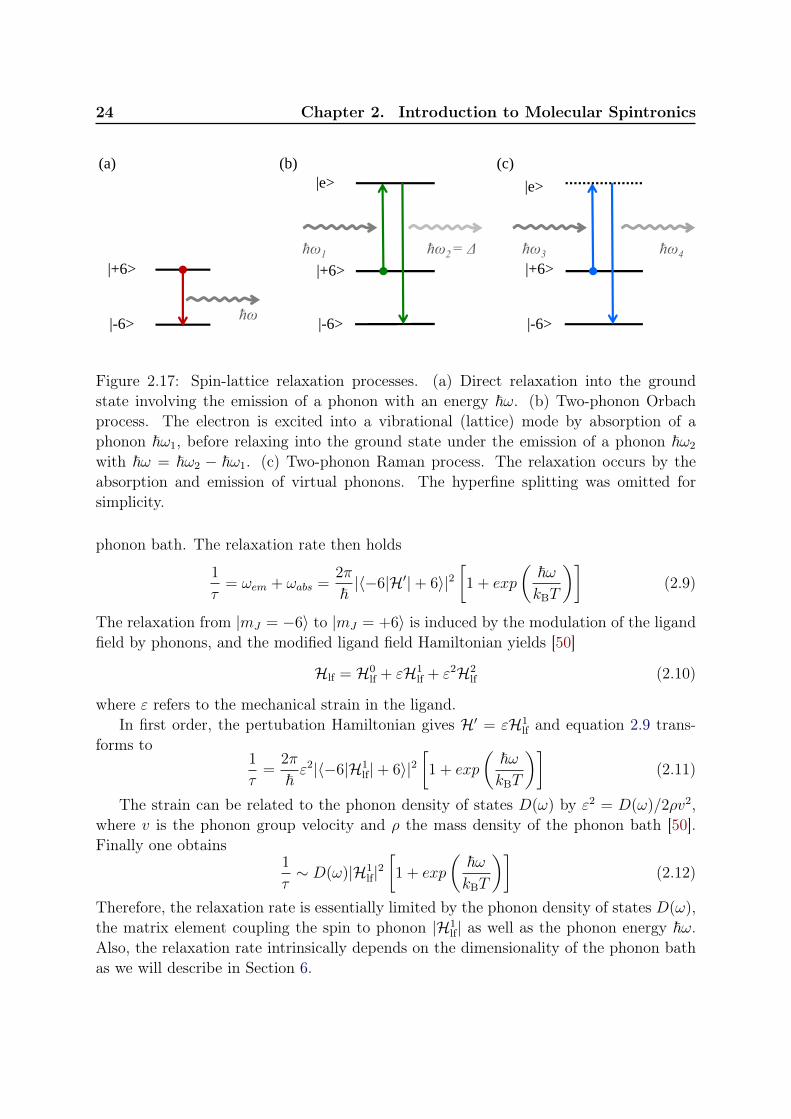
(a) (b) (c)|e> |e>
|+6> |+6>|+6>ħω1 ħω2 = Δ ħω3 ħω4
|-6> |-6>|-6> ħω
Figure 2.17: Spin-lattice relaxation processes. (a) Direct relaxation into the groundstate involving the emission of a phonon with an energy ~ω. (b) Two-phonon Orbachprocess. The electron is excited into a vibrational (lattice) mode by absorption of aphonon ~ω1, before relaxing into the ground state under the emission of a phonon ~ω2
with ~ω = ~ω2 − ~ω1. (c) Two-phonon Raman process. The relaxation occurs by theabsorption and emission of virtual phonons. The hyperfine splitting was omitted forsimplicity.
phonon bath. The relaxation rate then holds
1
τ= ωem + ωabs =
2π
~|〈−6|H′|+ 6〉|2
[1 + exp
(~ωkBT
)](2.9)
The relaxation from |mJ = −6〉 to |mJ = +6〉 is induced by the modulation of the ligandfield by phonons, and the modified ligand field Hamiltonian yields [50]
Hlf = H0lf + εH1
lf + ε2H2lf (2.10)
where ε refers to the mechanical strain in the ligand.In first order, the pertubation Hamiltonian gives H′ = εH1
lf and equation 2.9 trans-forms to
1
τ=
2π
~ε2|〈−6|H1
lf|+ 6〉|2[1 + exp
(~ωkBT
)](2.11)
The strain can be related to the phonon density of states D(ω) by ε2 = D(ω)/2ρv2,where v is the phonon group velocity and ρ the mass density of the phonon bath [50].Finally one obtains
1
τ∼ D(ω)|H1
lf|2[1 + exp
(~ωkBT
)](2.12)
Therefore, the relaxation rate is essentially limited by the phonon density of states D(ω),the matrix element coupling the spin to phonon |H1
lf| as well as the phonon energy ~ω.Also, the relaxation rate intrinsically depends on the dimensionality of the phonon bathas we will describe in Section 6.
2.3. Carbon based supramolecular spintronics 25
Two phonon relaxation processes
Upon increasing the temperature higher excited phonon states become accessible and aso called two-phonon Orbach process contributes to the relaxation of the SMM’s mag-netization. As depicted in Fig. 2.17b, the electron is excited from |mJ = +6〉 into avibrational state |e〉 under absorption of a phonon with an energy ~ω1. In a second step,the electron then relaxes into the ground state |mJ = −6〉 under emission of a secondphonon with an energy ~ω2 = ~ωph. The process can occur if ω2 − ω1 = ω, where ω isthe energy separation of the two spin states. The relaxation rate yields [50]
1
τ∼ |H1′
lf |2∆3 1
exp (∆/kBT )− 1(2.13)
where |H1′
lf | is the product of the matrix elements between the states |mJ = −6〉, |mJ =
+6〉 and |e〉. The process is therefore thermally activated if kBT & ∆.Finally, the relaxation can occur in a Raman like process(Fig. 2.17c). The mechanism
is similar to the Orbach process, however involves a virtual excited state, resulting in arelaxation time of the form [50]
1
τ∼ |H2
lf|2(kBT
~
)7
(2.14)
where |H2lf| is the second order pertubation from equation 2.10.
2.3 Carbon based supramolecular spintronics
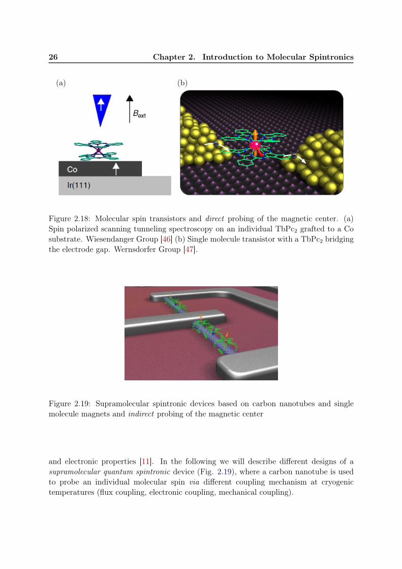
Various designs for molecular spintronic devices using individual SMM’s were proposedover the last decade [11]. One can use for instance a scanning tunneling microscopy toprobe an isolated SMM on a conducting surface [56, 45, 46] (Fig. 2.18a). Alternatively,one can built a three-terminal molecular spin-transistor where an individual SMM isbridging the gap between two non-magnetic leads [47] (Fig. 2.18b). In such a configu-ration, the electric current is flowing directly through the molecule, leading to a strongcoupling between the electrons and the magnetic core. This direct coupling thus enablesa readout of the molecule’s magnetic properties with the electronic current, but also leadsto a strong back-action on the molecule’s magnetic core [11].
An less invasive approach consists in coupling the SMM to a second non-magneticmolecular conductor which is subsequently used as detector. For such an indirect cou-pling, the magnetic core of the molecule is only weakly coupled to the conductor but canstill affect its transport properties, thus enabling an electronic readout with only minimalback-action.
Among the different possible detectors (nanowires, carbon nanotubes, quantum dot,molecules), the carbon nanotube stands out due to its unique structural, mechanical
26 Chapter 2. Introduction to Molecular Spintronics
(a) (b)
Figure 2.18: Molecular spin transistors and direct probing of the magnetic center. (a)Spin polarized scanning tunneling spectroscopy on an individual TbPc2 grafted to a Cosubstrate. Wiesendanger Group [46] (b) Single molecule transistor with a TbPc2 bridgingthe electrode gap. Wernsdorfer Group [47].
Figure 2.19: Supramolecular spintronic devices based on carbon nanotubes and singlemolecule magnets and indirect probing of the magnetic center
and electronic properties [11]. In the following we will describe different designs of asupramolecular quantum spintronic device (Fig. 2.19), where a carbon nanotube is usedto probe an individual molecular spin via different coupling mechanism at cryogenictemperatures (flux coupling, electronic coupling, mechanical coupling).
2.3. Carbon based supramolecular spintronics 27
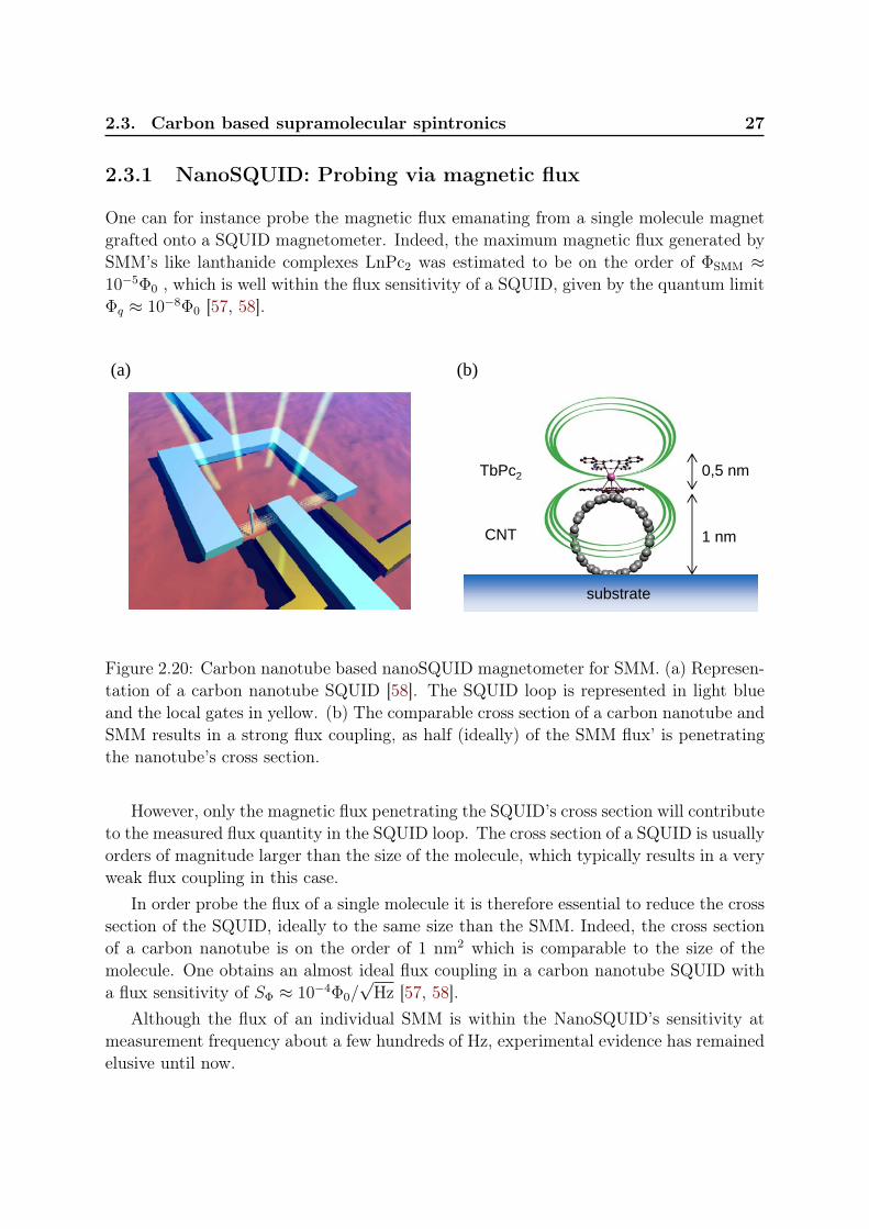
2.3.1 NanoSQUID: Probing via magnetic flux
One can for instance probe the magnetic flux emanating from a single molecule magnetgrafted onto a SQUID magnetometer. Indeed, the maximum magnetic flux generated bySMM’s like lanthanide complexes LnPc2 was estimated to be on the order of ΦSMM ≈10−5Φ0 , which is well within the flux sensitivity of a SQUID, given by the quantum limitΦq ≈ 10−8Φ0 [57, 58].
1 nm
0,5 nm
substrate
CNT
TbPc2
(a) (b)
Figure 2.20: Carbon nanotube based nanoSQUID magnetometer for SMM. (a) Represen-tation of a carbon nanotube SQUID [58]. The SQUID loop is represented in light blueand the local gates in yellow. (b) The comparable cross section of a carbon nanotube andSMM results in a strong flux coupling, as half (ideally) of the SMM flux’ is penetratingthe nanotube’s cross section.
However, only the magnetic flux penetrating the SQUID’s cross section will contributeto the measured flux quantity in the SQUID loop. The cross section of a SQUID is usuallyorders of magnitude larger than the size of the molecule, which typically results in a veryweak flux coupling in this case.
In order probe the flux of a single molecule it is therefore essential to reduce the crosssection of the SQUID, ideally to the same size than the SMM. Indeed, the cross sectionof a carbon nanotube is on the order of 1 nm2 which is comparable to the size of themolecule. One obtains an almost ideal flux coupling in a carbon nanotube SQUID witha flux sensitivity of SΦ ≈ 10−4Φ0/
√Hz [57, 58].
Although the flux of an individual SMM is within the NanoSQUID’s sensitivity atmeasurement frequency about a few hundreds of Hz, experimental evidence has remainedelusive until now.
28 Chapter 2. Introduction to Molecular Spintronics
2.3.2 Supramolecular Spin Valve: Probing via electron transport
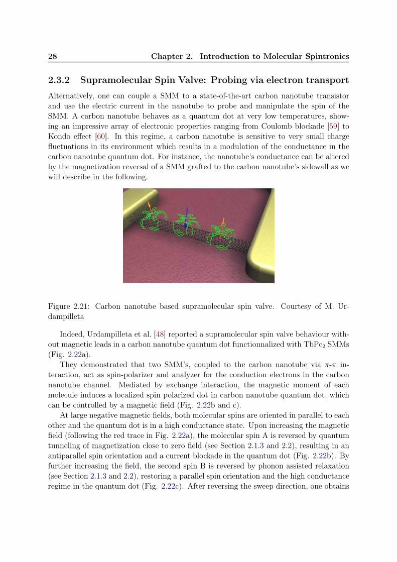
Alternatively, one can couple a SMM to a state-of-the-art carbon nanotube transistorand use the electric current in the nanotube to probe and manipulate the spin of theSMM. A carbon nanotube behaves as a quantum dot at very low temperatures, show-ing an impressive array of electronic properties ranging from Coulomb blockade [59] toKondo effect [60]. In this regime, a carbon nanotube is sensitive to very small chargefluctuations in its environment which results in a modulation of the conductance in thecarbon nanotube quantum dot. For instance, the nanotube’s conductance can be alteredby the magnetization reversal of a SMM grafted to the carbon nanotube’s sidewall as wewill describe in the following.
Figure 2.21: Carbon nanotube based supramolecular spin valve. Courtesy of M. Ur-dampilleta
Indeed, Urdampilleta et al. [48] reported a supramolecular spin valve behaviour with-out magnetic leads in a carbon nanotube quantum dot functionnalized with TbPc2 SMMs(Fig. 2.22a).
They demonstrated that two SMM’s, coupled to the carbon nanotube via π-π in-teraction, act as spin-polarizer and analyzer for the conduction electrons in the carbonnanotube channel. Mediated by exchange interaction, the magnetic moment of eachmolecule induces a localized spin polarized dot in carbon nanotube quantum dot, whichcan be controlled by a magnetic field (Fig. 2.22b and c).
At large negative magnetic fields, both molecular spins are oriented in parallel to eachother and the quantum dot is in a high conductance state. Upon increasing the magneticfield (following the red trace in Fig. 2.22a), the molecular spin A is reversed by quantumtunneling of magnetization close to zero field (see Section 2.1.3 and 2.2), resulting in anantiparallel spin orientation and a current blockade in the quantum dot (Fig. 2.22b). Byfurther increasing the field, the second spin B is reversed by phonon assisted relaxation(see Section 2.1.3 and 2.2), restoring a parallel spin orientation and the high conductanceregime in the quantum dot (Fig. 2.22c). After reversing the sweep direction, one obtains
2.3. Carbon based supramolecular spintronics 29
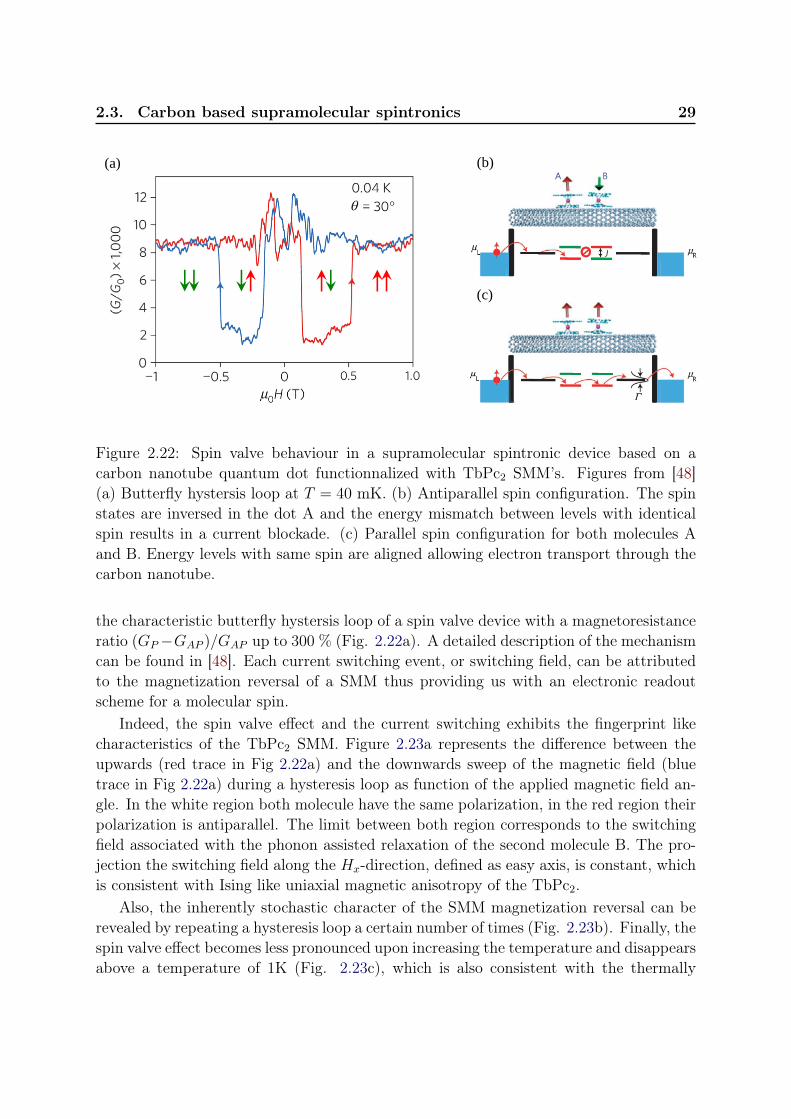
(a) (b)
(c)
Figure 2.22: Spin valve behaviour in a supramolecular spintronic device based on acarbon nanotube quantum dot functionnalized with TbPc2 SMM’s. Figures from [48](a) Butterfly hystersis loop at T = 40 mK. (b) Antiparallel spin configuration. The spinstates are inversed in the dot A and the energy mismatch between levels with identicalspin results in a current blockade. (c) Parallel spin configuration for both molecules Aand B. Energy levels with same spin are aligned allowing electron transport through thecarbon nanotube.
the characteristic butterfly hystersis loop of a spin valve device with a magnetoresistanceratio (GP−GAP )/GAP up to 300 % (Fig. 2.22a). A detailed description of the mechanismcan be found in [48]. Each current switching event, or switching field, can be attributedto the magnetization reversal of a SMM thus providing us with an electronic readoutscheme for a molecular spin.
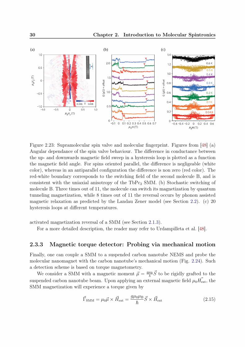
Indeed, the spin valve effect and the current switching exhibits the fingerprint likecharacteristics of the TbPc2 SMM. Figure 2.23a represents the difference between theupwards (red trace in Fig 2.22a) and the downwards sweep of the magnetic field (bluetrace in Fig 2.22a) during a hysteresis loop as function of the applied magnetic field an-gle. In the white region both molecule have the same polarization, in the red region theirpolarization is antiparallel. The limit between both region corresponds to the switchingfield associated with the phonon assisted relaxation of the second molecule B. The pro-jection the switching field along the Hx-direction, defined as easy axis, is constant, whichis consistent with Ising like uniaxial magnetic anisotropy of the TbPc2.
Also, the inherently stochastic character of the SMM magnetization reversal can berevealed by repeating a hysteresis loop a certain number of times (Fig. 2.23b). Finally, thespin valve effect becomes less pronounced upon increasing the temperature and disappearsabove a temperature of 1K (Fig. 2.23c), which is also consistent with the thermally
30 Chapter 2. Introduction to Molecular Spintronics
(a) (b) (c)
Figure 2.23: Supramolecular spin valve and molecular fingerprint. Figures from [48] (a)Angular dependance of the spin valve behaviour. The difference in conductance betweenthe up- and downwards magnetic field sweep in a hysteresis loop is plotted as a functionthe magnetic field angle. For spins oriented parallel, the difference is negligeable (whitecolor), whereas in an antiparallel configuration the difference is non zero (red color). Thered-white boundary corresponds to the switching field of the second molecule B, and isconsistent with the uniaxial anisotropy of the TbPc2 SMM. (b) Stochastic switching ofmolecule B. Three times out of 11, the molecule can switch its magnetization by quantumtunneling magnetization, while 8 times out of 11 the reversal occurs by phonon assistedmagnetic relaxation as predicted by the Landau Zener model (see Section 2.2). (c) 20hysteresis loops at different temperatures.
activated magnetization reversal of a SMM (see Section 2.1.3).For a more detailed description, the reader may refer to Urdampilleta et al. [48].
2.3.3 Magnetic torque detector: Probing via mechanical motion
Finally, one can couple a SMM to a suspended carbon nanotube NEMS and probe themolecular nanomagnet with the carbon nanotube’s mechanical motion (Fig. 2.24). Sucha detection scheme is based on torque magnetometry.
We consider a SMM with a magnetic moment ~µ = gµB~~S to be rigidly grafted to the
suspended carbon nanotube beam. Upon applying an external magnetic field µ0~Hext, the
SMM magnetization will experience a torque given by
~ΓSMM = µ0~µ× ~Hext =gµ0µB
~~S × ~Hext (2.15)
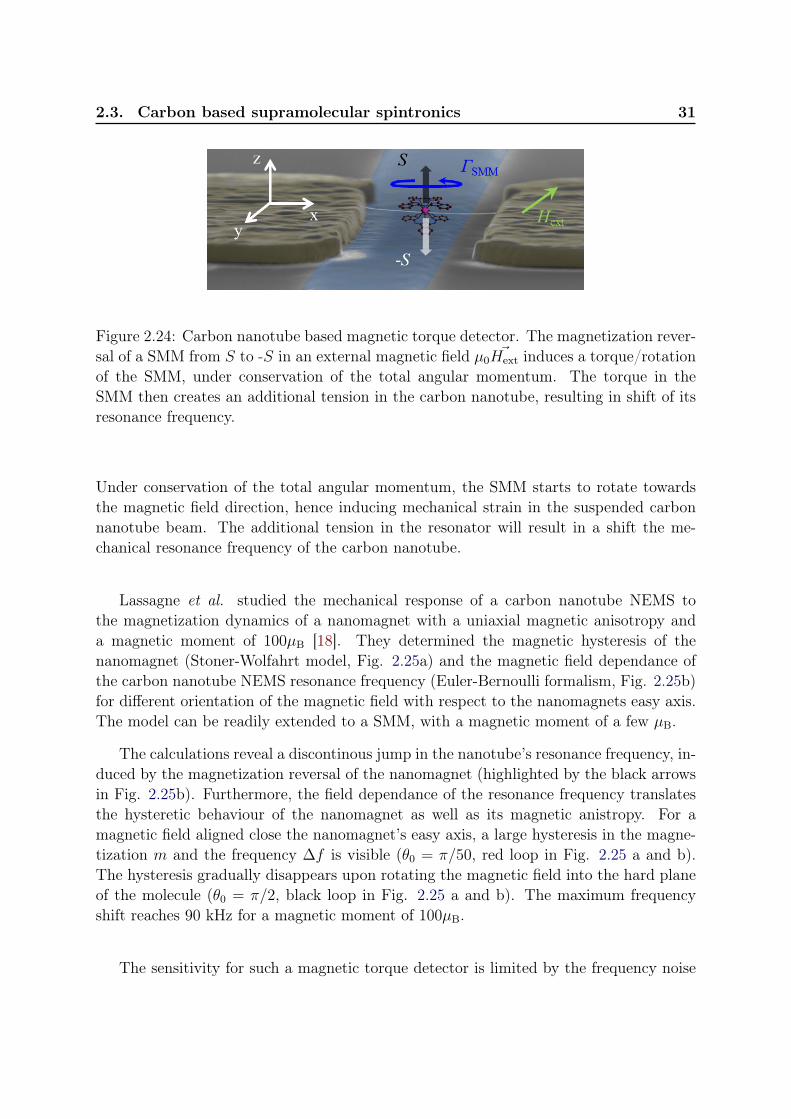
2.3. Carbon based supramolecular spintronics 31
Figure 2.24: Carbon nanotube based magnetic torque detector. The magnetization rever-sal of a SMM from S to -S in an external magnetic field µ0
~Hext induces a torque/rotationof the SMM, under conservation of the total angular momentum. The torque in theSMM then creates an additional tension in the carbon nanotube, resulting in shift of itsresonance frequency.
Under conservation of the total angular momentum, the SMM starts to rotate towardsthe magnetic field direction, hence inducing mechanical strain in the suspended carbonnanotube beam. The additional tension in the resonator will result in a shift the me-chanical resonance frequency of the carbon nanotube.
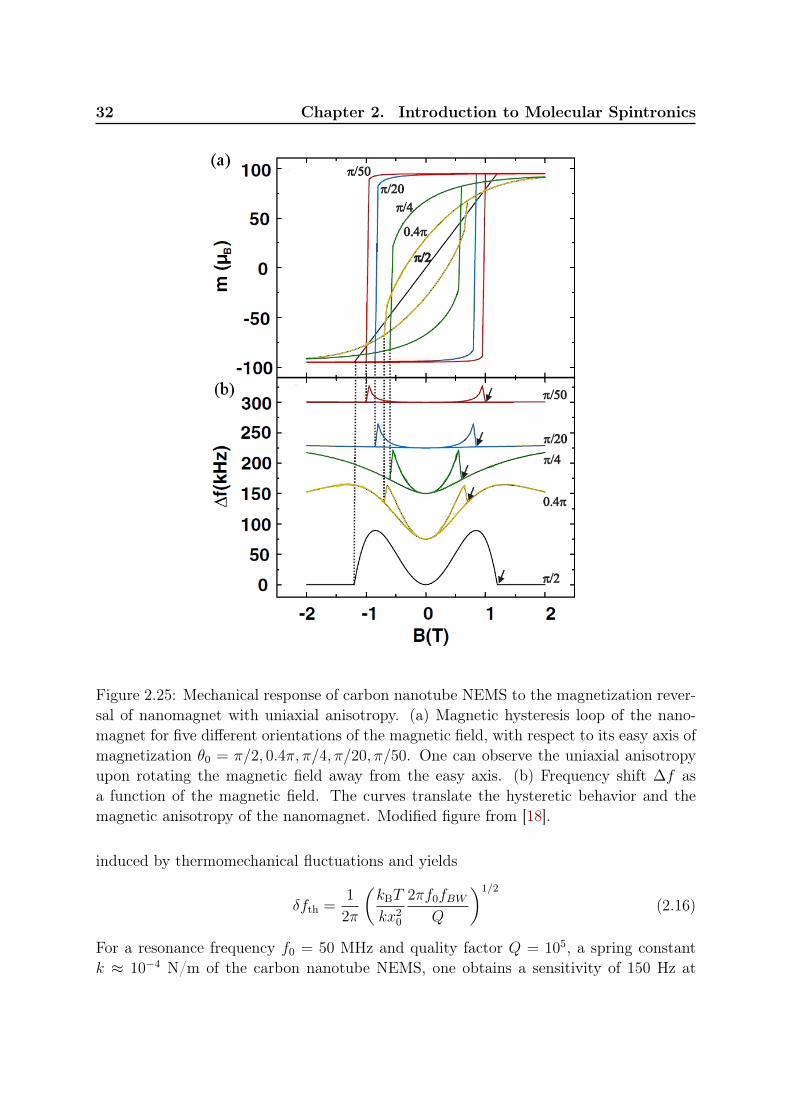
Lassagne et al. studied the mechanical response of a carbon nanotube NEMS tothe magnetization dynamics of a nanomagnet with a uniaxial magnetic anisotropy anda magnetic moment of 100µB [18]. They determined the magnetic hysteresis of thenanomagnet (Stoner-Wolfahrt model, Fig. 2.25a) and the magnetic field dependance ofthe carbon nanotube NEMS resonance frequency (Euler-Bernoulli formalism, Fig. 2.25b)for different orientation of the magnetic field with respect to the nanomagnets easy axis.The model can be readily extended to a SMM, with a magnetic moment of a few µB.
The calculations reveal a discontinous jump in the nanotube’s resonance frequency, in-duced by the magnetization reversal of the nanomagnet (highlighted by the black arrowsin Fig. 2.25b). Furthermore, the field dependance of the resonance frequency translatesthe hysteretic behaviour of the nanomagnet as well as its magnetic anistropy. For amagnetic field aligned close the nanomagnet’s easy axis, a large hysteresis in the magne-tization m and the frequency ∆f is visible (θ0 = π/50, red loop in Fig. 2.25 a and b).The hysteresis gradually disappears upon rotating the magnetic field into the hard planeof the molecule (θ0 = π/2, black loop in Fig. 2.25 a and b). The maximum frequencyshift reaches 90 kHz for a magnetic moment of 100µB.
The sensitivity for such a magnetic torque detector is limited by the frequency noise
32 Chapter 2. Introduction to Molecular Spintronics
Figure 2.25: Mechanical response of carbon nanotube NEMS to the magnetization rever-sal of nanomagnet with uniaxial anisotropy. (a) Magnetic hysteresis loop of the nano-magnet for five different orientations of the magnetic field, with respect to its easy axis ofmagnetization θ0 = π/2, 0.4π, π/4, π/20, π/50. One can observe the uniaxial anisotropyupon rotating the magnetic field away from the easy axis. (b) Frequency shift ∆f asa function of the magnetic field. The curves translate the hysteretic behavior and themagnetic anisotropy of the nanomagnet. Modified figure from [18].
induced by thermomechanical fluctuations and yields
δfth =1
2π
(kBT
kx20
2πf0fBWQ
)1/2
(2.16)
For a resonance frequency f0 = 50 MHz and quality factor Q = 105, a spring constantk ≈ 10−4 N/m of the carbon nanotube NEMS, one obtains a sensitivity of 150 Hz at
2.4. Outlook 33
40 mK for a measurement bandwidth of fBW = 1 Hz. One should therefore be able toreach a sensitivity of 1µB at cryogenic temperatures with such a carbon based torquemagnetometer, thus providing a mechanical readout scheme for a single (molecular) spin.
2.4 Outlook
In the following chapters of this manuscript, we will report on the first experimental real-ization of such a supramolecular spintronic device based on a single molecule magnet anda carbon nanotube NEMS. We will ultimately demonstrate the strong coupling betweena single molecular spin and a single quantized mode of motion in a carbon nanotubeNEMS and the detection of a single nuclear spin (Chapter 6). Enabled by the strongspin-motion coupling, such a supramolecular spintronic device can be the first imple-mentation of a supramolecular torque magnetometer with a single molecule sensitivity.Coupling the magnetism and the mechanical motion of a molecular sized object couldfurthermore open the path quantum entanglement and quantum information processingin nanoscale solid state matter.

Chapter 3
Introduction to carbon nanotube basedNEMS
Carbon nanotubes have become an essential building block for nanoelectromechanicalsystems (NEMS). Their very low mass and the highest known Young’s modulus E = 1
TPa results in high resonance frequencies, high quality factors and large motion ampli-tudes for flexural (bending) modes in carbon nanotube NEMS compared to conventionalSi based NEMS [1]. Therefore they are a perfect candidate for ultrasensitive mass sens-ing and force detection over a wide range of frequencies and the small carbon nanotubediameter (dCNT ∼ 1 nm) should even enable single molecule detection [19].
In the previous chapter, we proposed different designs of carbon nanotube basedsupramolecular spintronic devices and single molecule detectors. In particular we de-scribed the design of a supramolecular torque magnetometer based on a carbon nanotubeNEMS and single molecule magnets that could achieve single molecule/spin sensitivity(see Section 2.3). With the ambition of detecting and manipulating a single molecularspin, we propose in the following chapters the first implementation of a supramolecularspintronic device, based on single molecule magnets and carbon nanotube NEMS.
In this context we described the first building block, the single molecule magnets inthe previous chapter 2. We will present in the following chapters 3, 4 and 5 the secondbuilding block for such a supramolecular torque detector, the carbon nanotube NEMS.
3.1 Introduction: Si based vs. carbon based NEMS
Conventional semiconductor NEMS as depicted in Fig. 3.1 are usually obtained in top-down fabrication processes by etching of a larger structure (thin film, etc...) or by de-positing material (metal, semiconductor) on a resist mask which is subsequently lifted off.Upon reducing the dimensions and therefore the mass of the resonating beams, the reso-nance frequency for flexural modes can be increased up to a few gigahertz [1]. Top-downfabrication procedures however introduce defects into the resonator’s surface, resulting inlarge dissipation and a low quality factor Q. Upon reducing the dimensions of the NEMS,the surface-to-volume ratio and thus the defect density increases [1]. In consequence thequality factor decreases with reduced device dimensions as depicted by the dashed linein Fig. 3.3.
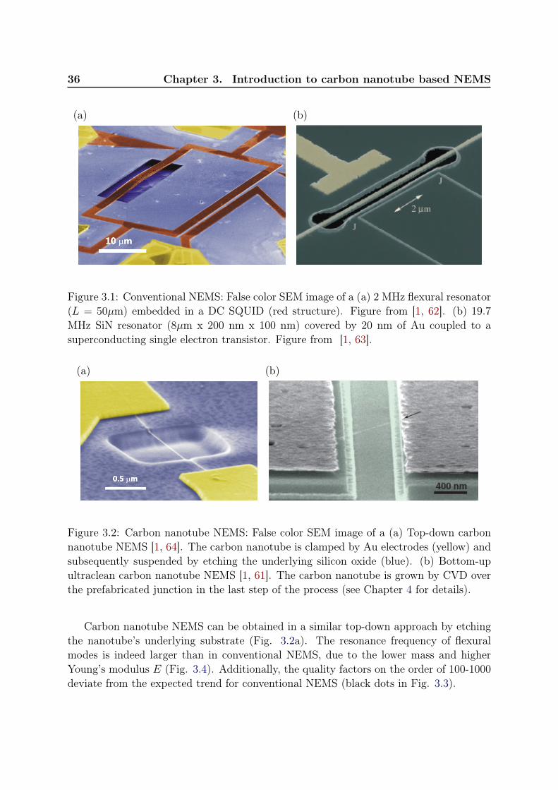
36 Chapter 3. Introduction to carbon nanotube based NEMS
(a) (b)
Figure 3.1: Conventional NEMS: False color SEM image of a (a) 2 MHz flexural resonator(L = 50µm) embedded in a DC SQUID (red structure). Figure from [1, 62]. (b) 19.7MHz SiN resonator (8µm x 200 nm x 100 nm) covered by 20 nm of Au coupled to asuperconducting single electron transistor. Figure from [1, 63].
(a) (b)
Figure 3.2: Carbon nanotube NEMS: False color SEM image of a (a) Top-down carbonnanotube NEMS [1, 64]. The carbon nanotube is clamped by Au electrodes (yellow) andsubsequently suspended by etching the underlying silicon oxide (blue). (b) Bottom-upultraclean carbon nanotube NEMS [1, 61]. The carbon nanotube is grown by CVD overthe prefabricated junction in the last step of the process (see Chapter 4 for details).
Carbon nanotube NEMS can be obtained in a similar top-down approach by etchingthe nanotube’s underlying substrate (Fig. 3.2a). The resonance frequency of flexuralmodes is indeed larger than in conventional NEMS, due to the lower mass and higherYoung’s modulus E (Fig. 3.4). Additionally, the quality factors on the order of 100-1000deviate from the expected trend for conventional NEMS (black dots in Fig. 3.3).
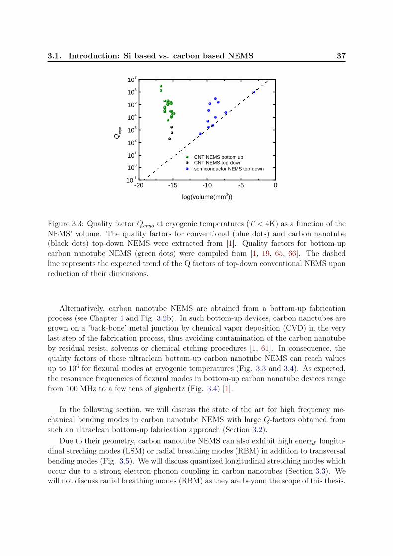
3.1. Introduction: Si based vs. carbon based NEMS 37
- 2 0 - 1 5 - 1 0 - 5 01 0 - 11 0 01 0 11 0 21 0 31 0 41 0 51 0 61 0 7
C N T N E M S b o t t o m u p C N T N E M S t o p - d o w n s e m i c o n d u c t o r N E M S t o p - d o w n
Q cryo
l o g ( v o l u m e ( m m 3 ) )
Figure 3.3: Quality factor Qcryo at cryogenic temperatures (T < 4K) as a function of theNEMS’ volume. The quality factors for conventional (blue dots) and carbon nanotube(black dots) top-down NEMS were extracted from [1]. Quality factors for bottom-upcarbon nanotube NEMS (green dots) were compiled from [1, 19, 65, 66]. The dashedline represents the expected trend of the Q factors of top-down conventional NEMS uponreduction of their dimensions.
Alternatively, carbon nanotube NEMS are obtained from a bottom-up fabricationprocess (see Chapter 4 and Fig. 3.2b). In such bottom-up devices, carbon nanotubes aregrown on a ’back-bone’ metal junction by chemical vapor deposition (CVD) in the verylast step of the fabrication process, thus avoiding contamination of the carbon nanotubeby residual resist, solvents or chemical etching procedures [1, 61]. In consequence, thequality factors of these ultraclean bottom-up carbon nanotube NEMS can reach valuesup to 106 for flexural modes at cryogenic temperatures (Fig. 3.3 and 3.4). As expected,the resonance frequencies of flexural modes in bottom-up carbon nanotube devices rangefrom 100 MHz to a few tens of gigahertz (Fig. 3.4) [1].
In the following section, we will discuss the state of the art for high frequency me-chanical bending modes in carbon nanotube NEMS with large Q-factors obtained fromsuch an ultraclean bottom-up fabrication approach (Section 3.2).
Due to their geometry, carbon nanotube NEMS can also exhibit high energy longitu-dinal streching modes (LSM) or radial breathing modes (RBM) in addition to transversalbending modes (Fig. 3.5). We will discuss quantized longitudinal stretching modes whichoccur due to a strong electron-phonon coupling in carbon nanotubes (Section 3.3). Wewill not discuss radial breathing modes (RBM) as they are beyond the scope of this thesis.
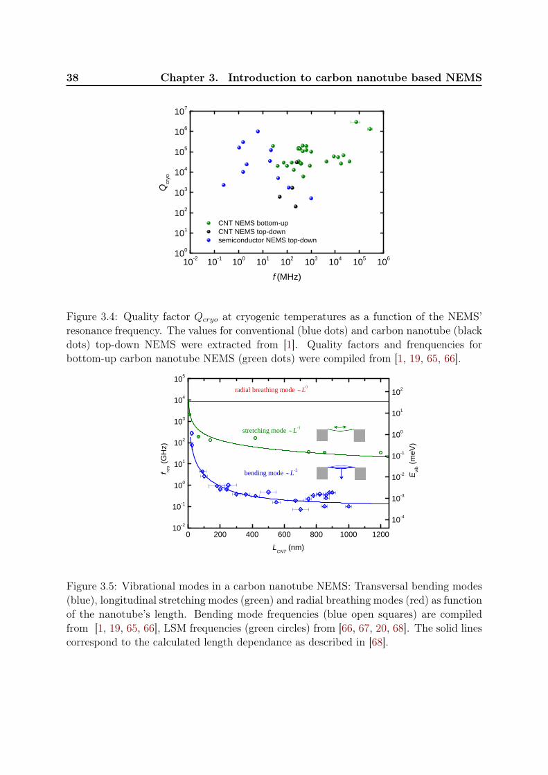
38 Chapter 3. Introduction to carbon nanotube based NEMS
1 0 - 2 1 0 - 1 1 0 0 1 0 1 1 0 2 1 0 3 1 0 4 1 0 5 1 0 61 0 0
1 0 1
1 0 2
1 0 3
1 0 4
1 0 5
1 0 6
1 0 7
C N T N E M S b o t t o m - u p C N T N E M S t o p - d o w n s e m i c o n d u c t o r N E M S t o p - d o w n
Q cryo
f ( M H z )
Figure 3.4: Quality factor Qcryo at cryogenic temperatures as a function of the NEMS’resonance frequency. The values for conventional (blue dots) and carbon nanotube (blackdots) top-down NEMS were extracted from [1]. Quality factors and frenquencies forbottom-up carbon nanotube NEMS (green dots) were compiled from [1, 19, 65, 66].
0 2 0 0 4 0 0 6 0 0 8 0 0 1 0 0 0 1 2 0 01 0 - 2
1 0 - 1
1 0 0
1 0 1
1 0 2
1 0 3
1 0 4
1 0 5
E vib (m
eV)
r a d i a l b r e a t h i n g m o d e L 0
s t r e t c h i n g m o d e L - 1
f res (G
Hz)
L C N T ( n m )
b e n d i n g m o d e L - 2
1 0 - 4
1 0 - 3
1 0 - 2
1 0 - 1
1 0 0
1 0 1
1 0 2
Figure 3.5: Vibrational modes in a carbon nanotube NEMS: Transversal bending modes(blue), longitudinal stretching modes (green) and radial breathing modes (red) as functionof the nanotube’s length. Bending mode frequencies (blue open squares) are compiledfrom [1, 19, 65, 66], LSM frequencies (green circles) from [66, 67, 20, 68]. The solid linescorrespond to the calculated length dependance as described in [68].
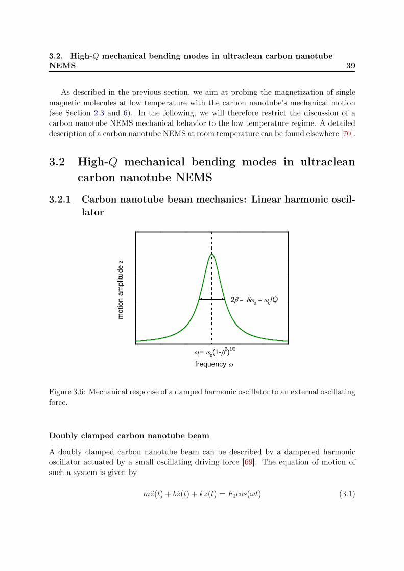
3.2. High-Q mechanical bending modes in ultraclean carbon nanotubeNEMS 39
As described in the previous section, we aim at probing the magnetization of singlemagnetic molecules at low temperature with the carbon nanotube’s mechanical motion(see Section 2.3 and 6). In the following, we will therefore restrict the discussion of acarbon nanotube NEMS mechanical behavior to the low temperature regime. A detaileddescription of a carbon nanotube NEMS at room temperature can be found elsewhere [70].
3.2 High-Q mechanical bending modes in ultracleancarbon nanotube NEMS
3.2.1 Carbon nanotube beam mechanics: Linear harmonic oscil-lator
motio
n amp
litude
z
f r e q u e n c y r = 0 ( 1 - 2 ) 1 / 2
2 = 0 = 0 / Q
Figure 3.6: Mechanical response of a damped harmonic oscillator to an external oscillatingforce.
Doubly clamped carbon nanotube beam
A doubly clamped carbon nanotube beam can be described by a dampened harmonicoscillator actuated by a small oscillating driving force [69]. The equation of motion ofsuch a system is given by
mz(t) + bz(t) + kz(t) = F0cos(ωt) (3.1)
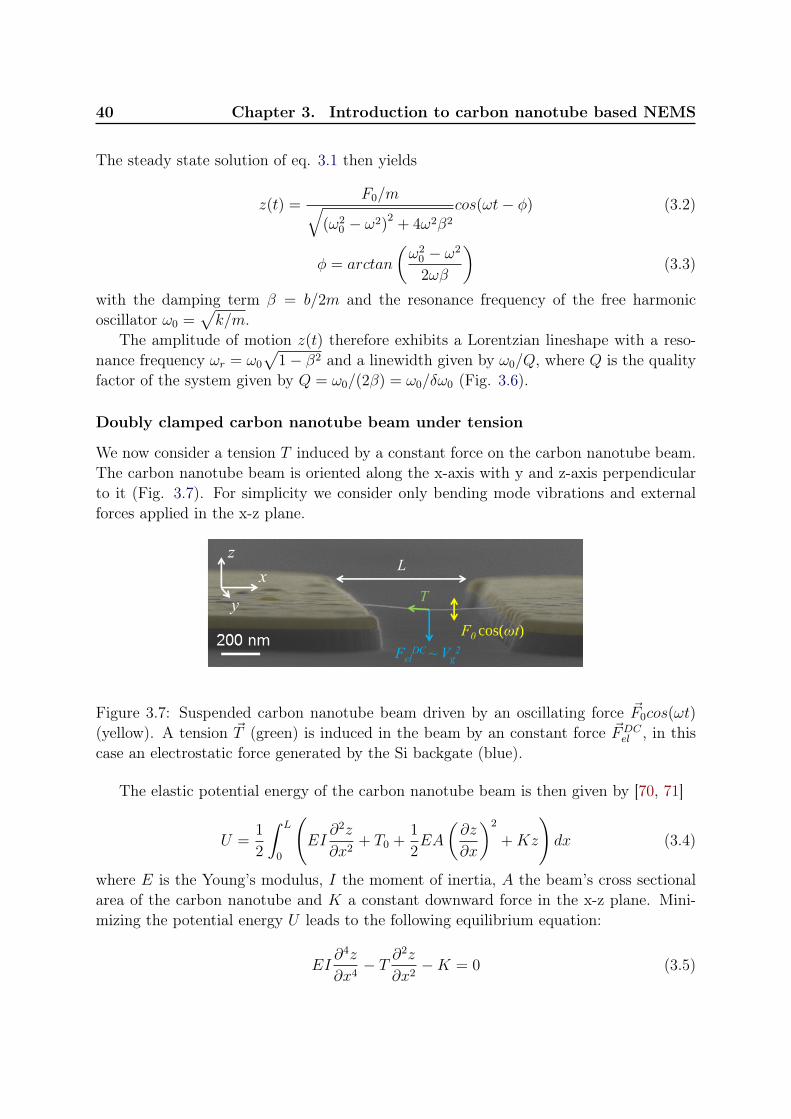
40 Chapter 3. Introduction to carbon nanotube based NEMS
The steady state solution of eq. 3.1 then yields
z(t) =F0/m√
(ω20 − ω2)
2+ 4ω2β2
cos(ωt− φ) (3.2)
φ = arctan
(ω2
0 − ω2
2ωβ
)(3.3)
with the damping term β = b/2m and the resonance frequency of the free harmonicoscillator ω0 =
√k/m.
The amplitude of motion z(t) therefore exhibits a Lorentzian lineshape with a reso-nance frequency ωr = ω0
√1− β2 and a linewidth given by ω0/Q, where Q is the quality
factor of the system given by Q = ω0/(2β) = ω0/δω0 (Fig. 3.6).
Doubly clamped carbon nanotube beam under tension
We now consider a tension T induced by a constant force on the carbon nanotube beam.The carbon nanotube beam is oriented along the x-axis with y and z-axis perpendicularto it (Fig. 3.7). For simplicity we consider only bending mode vibrations and externalforces applied in the x-z plane.
xz
yF0 cos(ωt)
FelDC ~ Vg
2
T
L
Figure 3.7: Suspended carbon nanotube beam driven by an oscillating force ~F0cos(ωt)
(yellow). A tension ~T (green) is induced in the beam by an constant force ~FDCel , in this
case an electrostatic force generated by the Si backgate (blue).
The elastic potential energy of the carbon nanotube beam is then given by [70, 71]
U =1
2
∫ L
0
(EI
∂2z
∂x2+ T0 +
1
2EA
(∂z
∂x
)2
+Kz
)dx (3.4)
where E is the Young’s modulus, I the moment of inertia, A the beam’s cross sectionalarea of the carbon nanotube and K a constant downward force in the x-z plane. Mini-mizing the potential energy U leads to the following equilibrium equation:
EI∂4z
∂x4− T ∂
2z
∂x2−K = 0 (3.5)
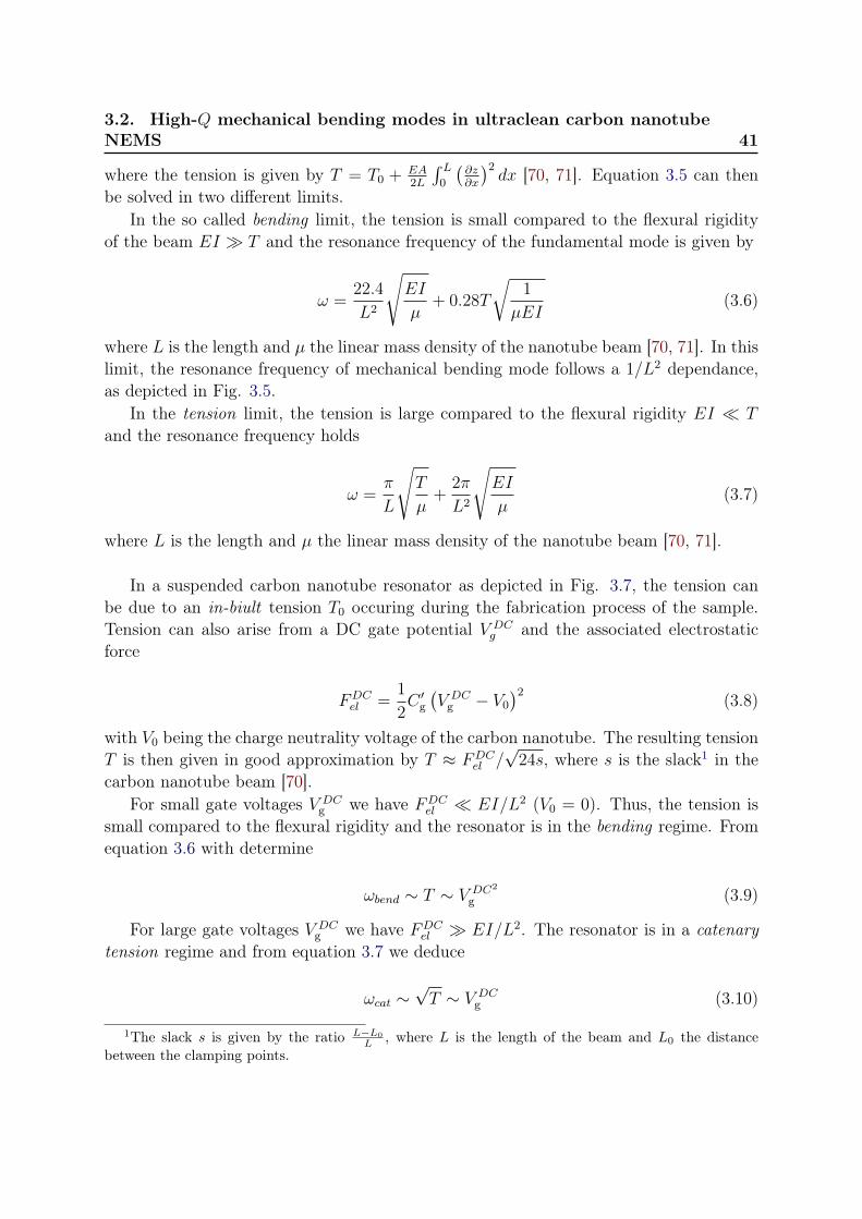
3.2. High-Q mechanical bending modes in ultraclean carbon nanotubeNEMS 41
where the tension is given by T = T0 + EA2L
∫ L0
(∂z∂x
)2dx [70, 71]. Equation 3.5 can then
be solved in two different limits.In the so called bending limit, the tension is small compared to the flexural rigidity
of the beam EI T and the resonance frequency of the fundamental mode is given by
ω =22.4
L2
√EI
µ+ 0.28T
√1
µEI(3.6)
where L is the length and µ the linear mass density of the nanotube beam [70, 71]. In thislimit, the resonance frequency of mechanical bending mode follows a 1/L2 dependance,as depicted in Fig. 3.5.
In the tension limit, the tension is large compared to the flexural rigidity EI T
and the resonance frequency holds
ω =π
L
√T
µ+
2π
L2
√EI
µ(3.7)
where L is the length and µ the linear mass density of the nanotube beam [70, 71].
In a suspended carbon nanotube resonator as depicted in Fig. 3.7, the tension canbe due to an in-biult tension T0 occuring during the fabrication process of the sample.Tension can also arise from a DC gate potential V DC
g and the associated electrostaticforce
FDCel =
1
2C ′g(V DC
g − V0)2 (3.8)
with V0 being the charge neutrality voltage of the carbon nanotube. The resulting tensionT is then given in good approximation by T ≈ FDC
el /√
24s, where s is the slack1 in thecarbon nanotube beam [70].
For small gate voltages V DCg we have FDC
el EI/L2 (V0 = 0). Thus, the tension issmall compared to the flexural rigidity and the resonator is in the bending regime. Fromequation 3.6 with determine
ωbend ∼ T ∼ V DC2
g (3.9)
For large gate voltages V DCg we have FDC
el EI/L2. The resonator is in a catenarytension regime and from equation 3.7 we deduce
ωcat ∼√T ∼ V DC
g (3.10)
1The slack s is given by the ratio L−L0
L , where L is the length of the beam and L0 the distancebetween the clamping points.
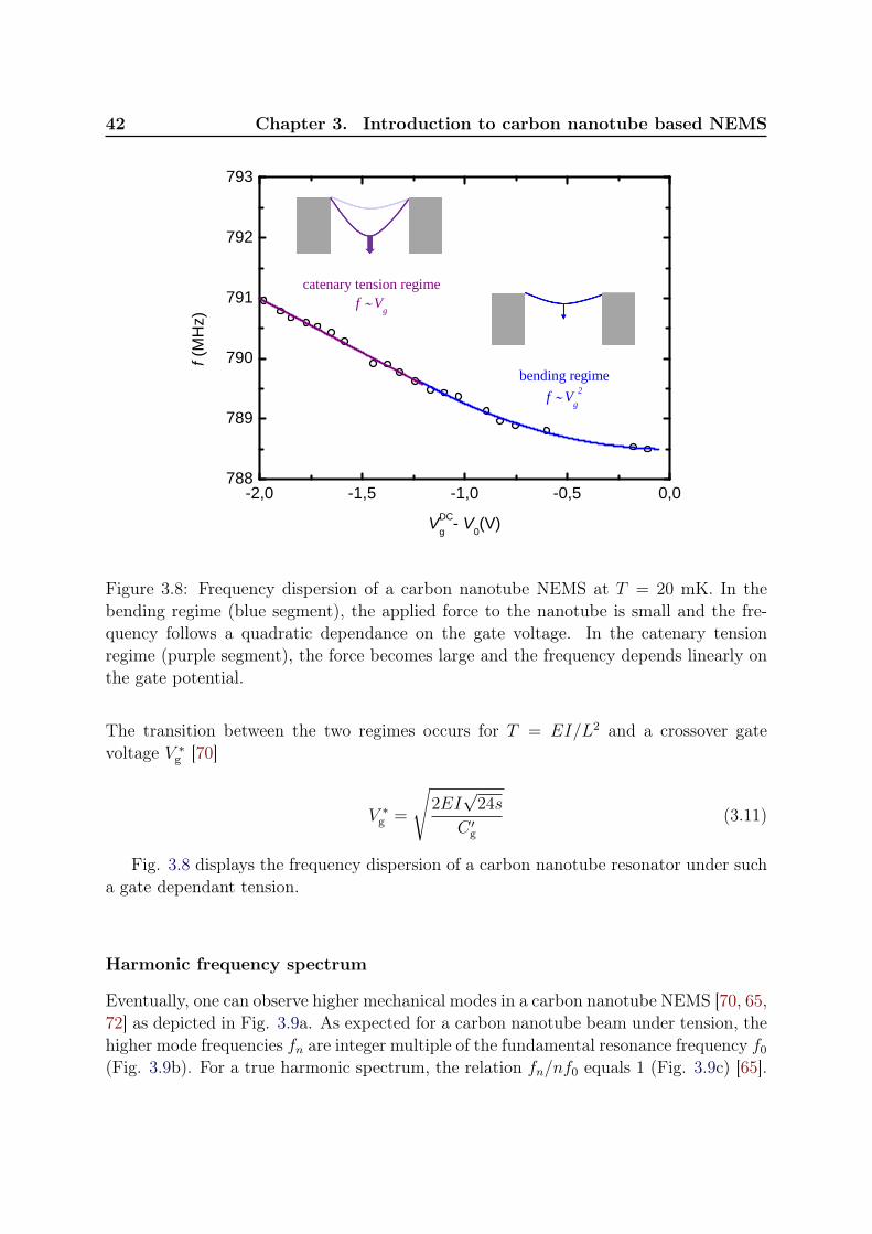
42 Chapter 3. Introduction to carbon nanotube based NEMS
- 2 , 0 - 1 , 5 - 1 , 0 - 0 , 5 0 , 07 8 8
7 8 9
7 9 0
7 9 1
7 9 2
7 9 3
c a t e n a r y t e n s i o n r e g i m ef V g
f (MHz
)
V D Cg - V 0 ( V )
b e n d i n g r e g i m ef V g
2
Figure 3.8: Frequency dispersion of a carbon nanotube NEMS at T = 20 mK. In thebending regime (blue segment), the applied force to the nanotube is small and the fre-quency follows a quadratic dependance on the gate voltage. In the catenary tensionregime (purple segment), the force becomes large and the frequency depends linearly onthe gate potential.
The transition between the two regimes occurs for T = EI/L2 and a crossover gatevoltage V ∗g [70]
V ∗g =
√2EI√
24s
C ′g(3.11)
Fig. 3.8 displays the frequency dispersion of a carbon nanotube resonator under sucha gate dependant tension.
Harmonic frequency spectrum
Eventually, one can observe higher mechanical modes in a carbon nanotube NEMS [70, 65,72] as depicted in Fig. 3.9a. As expected for a carbon nanotube beam under tension, thehigher mode frequencies fn are integer multiple of the fundamental resonance frequency f0
(Fig. 3.9b). For a true harmonic spectrum, the relation fn/nf0 equals 1 (Fig. 3.9c) [65].
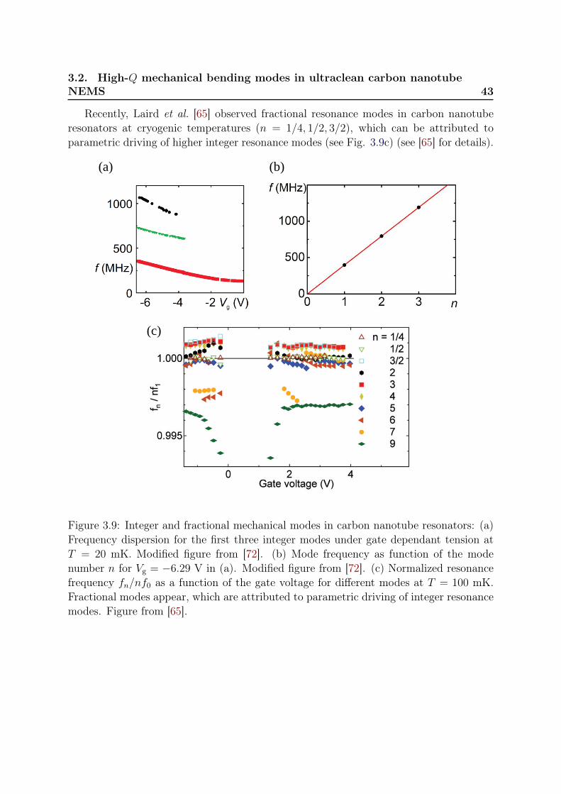
3.2. High-Q mechanical bending modes in ultraclean carbon nanotubeNEMS 43
Recently, Laird et al. [65] observed fractional resonance modes in carbon nanotuberesonators at cryogenic temperatures (n = 1/4, 1/2, 3/2), which can be attributed toparametric driving of higher integer resonance modes (see Fig. 3.9c) (see [65] for details).
(a) (b)
(c)
Figure 3.9: Integer and fractional mechanical modes in carbon nanotube resonators: (a)Frequency dispersion for the first three integer modes under gate dependant tension atT = 20 mK. Modified figure from [72]. (b) Mode frequency as function of the modenumber n for Vg = −6.29 V in (a). Modified figure from [72]. (c) Normalized resonancefrequency fn/nf0 as a function of the gate voltage for different modes at T = 100 mK.Fractional modes appear, which are attributed to parametric driving of integer resonancemodes. Figure from [65].
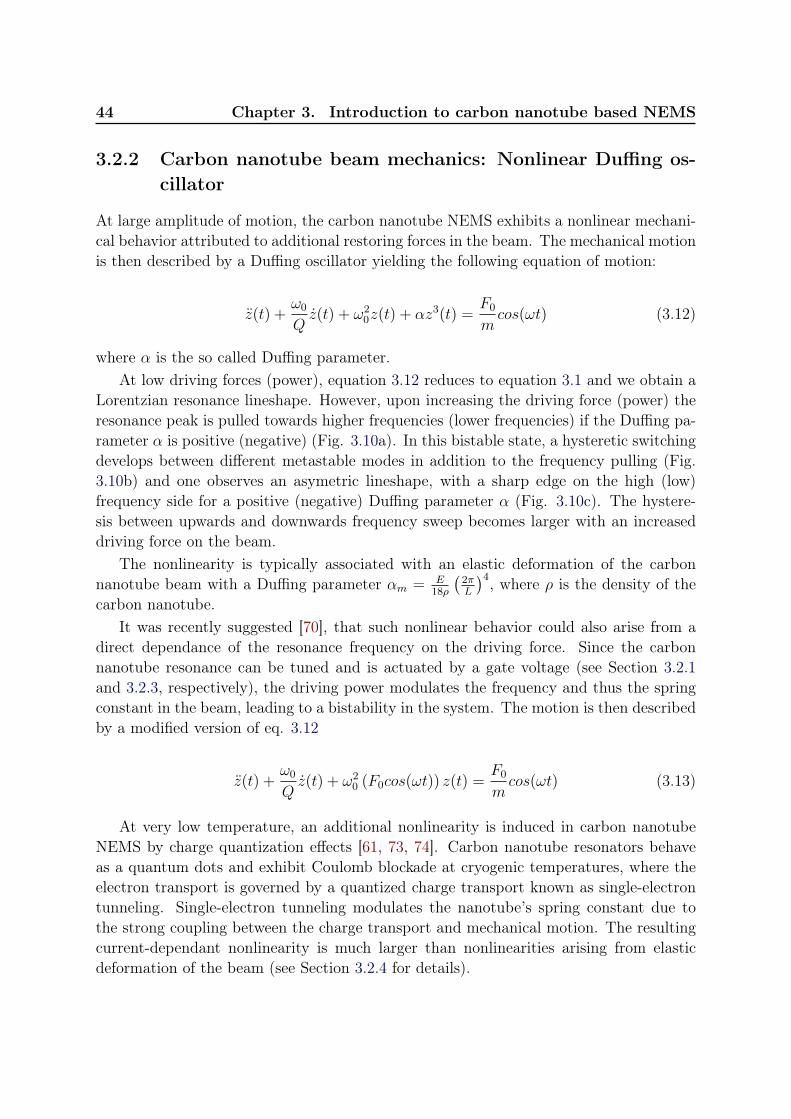
44 Chapter 3. Introduction to carbon nanotube based NEMS
3.2.2 Carbon nanotube beam mechanics: Nonlinear Duffing os-cillator
At large amplitude of motion, the carbon nanotube NEMS exhibits a nonlinear mechani-cal behavior attributed to additional restoring forces in the beam. The mechanical motionis then described by a Duffing oscillator yielding the following equation of motion:
z(t) +ω0
Qz(t) + ω2
0z(t) + αz3(t) =F0
mcos(ωt) (3.12)
where α is the so called Duffing parameter.At low driving forces (power), equation 3.12 reduces to equation 3.1 and we obtain a
Lorentzian resonance lineshape. However, upon increasing the driving force (power) theresonance peak is pulled towards higher frequencies (lower frequencies) if the Duffing pa-rameter α is positive (negative) (Fig. 3.10a). In this bistable state, a hysteretic switchingdevelops between different metastable modes in addition to the frequency pulling (Fig.3.10b) and one observes an asymetric lineshape, with a sharp edge on the high (low)frequency side for a positive (negative) Duffing parameter α (Fig. 3.10c). The hystere-sis between upwards and downwards frequency sweep becomes larger with an increaseddriving force on the beam.
The nonlinearity is typically associated with an elastic deformation of the carbonnanotube beam with a Duffing parameter αm = E
18ρ
(2πL
)4, where ρ is the density of thecarbon nanotube.
It was recently suggested [70], that such nonlinear behavior could also arise from adirect dependance of the resonance frequency on the driving force. Since the carbonnanotube resonance can be tuned and is actuated by a gate voltage (see Section 3.2.1and 3.2.3, respectively), the driving power modulates the frequency and thus the springconstant in the beam, leading to a bistability in the system. The motion is then describedby a modified version of eq. 3.12
z(t) +ω0
Qz(t) + ω2
0 (F0cos(ωt)) z(t) =F0
mcos(ωt) (3.13)
At very low temperature, an additional nonlinearity is induced in carbon nanotubeNEMS by charge quantization effects [61, 73, 74]. Carbon nanotube resonators behaveas a quantum dots and exhibit Coulomb blockade at cryogenic temperatures, where theelectron transport is governed by a quantized charge transport known as single-electrontunneling. Single-electron tunneling modulates the nanotube’s spring constant due tothe strong coupling between the charge transport and mechanical motion. The resultingcurrent-dependant nonlinearity is much larger than nonlinearities arising from elasticdeformation of the beam (see Section 3.2.4 for details).
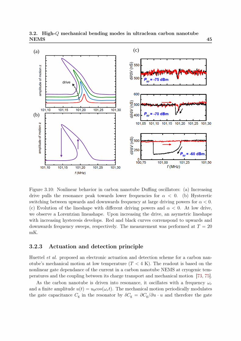
3.2. High-Q mechanical bending modes in ultraclean carbon nanotubeNEMS 45
drive
(a)
(b)
(c)
Figure 3.10: Nonlinear behavior in carbon nanotube Duffing oscillators: (a) Increasingdrive pulls the resonance peak towards lower frequencies for α < 0. (b) Hystereticswitching between upwards and downwards frequency at large driving powers for α < 0.(c) Evolution of the lineshape with different driving powers and α < 0. At low drive,we observe a Lorentzian lineashape. Upon increasing the drive, an asymetric lineshapewith increasing hysteresis develops. Red and black curves correnspond to upwards anddownwards frequency sweeps, respectively. The measurement was performed at T = 20
mK.
3.2.3 Actuation and detection principle
Huettel et al. proposed an electronic actuation and detection scheme for a carbon nan-otube’s mechanical motion at low temperature (T < 4 K). The readout is based on thenonlinear gate dependance of the current in a carbon nanotube NEMS at cryogenic tem-peratures and the coupling between its charge transport and mechanical motion [73, 75].
As the carbon nanotube is driven into resonance, it oscillates with a frequency ωrand a finite amplitude u(t) = u0cos(ωrt). The mechanical motion periodically modulatesthe gate capacitance Cg in the resonator by δCg = ∂Cg/∂u · u and therefore the gate
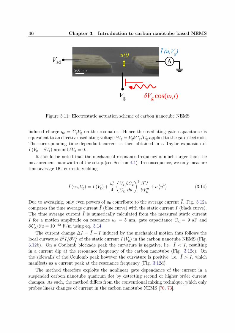
46 Chapter 3. Introduction to carbon nanotube based NEMS
Vsd
Vg δVg cos(ωrt)
250 nm
Vlg
Vsd
Vbg RF signal
u(t) A
Ī (u,Vg)
Figure 3.11: Electrostatic actuation scheme of carbon nanotube NEMS
induced charge qc = CgVg on the resonator. Hence the oscillating gate capacitance isequivalent to an effective oscillating voltage δVg = VgδCg/Cg applied to the gate electrode.The corresponding time-dependant current is then obtained in a Taylor expansion ofI (Vg + δVg) around δVg = 0.
It should be noted that the mechanical resonance frequency is much larger than themeasurement bandwidth of the setup (see Section 4.4). In consequence, we only measuretime-average DC currents yielding
I (u0, Vg) = I (Vg) +u2
0
4
(Vg
Cg
∂Cg
∂u
)2∂2I
∂V 2g
+ o(u4)
(3.14)
Due to averaging, only even powers of u0 contribute to the average current I. Fig. 3.12acompares the time average current I (blue curve) with the static current I (black curve).The time average current I is numerically calculated from the measured static currentI for a motion amplitude on resonance u0 = 5 nm, gate capacitance Cg = 9 aF and∂Cg/∂u = 10−12 F/m using eq. 3.14.
The current change ∆I = I − I induced by the mechanical motion thus follows thelocal curvature ∂2I/∂V 2
g of the static current I (Vg) in the carbon nanotube NEMS (Fig.3.12b). On a Coulomb blockade peak the curvature is negative, i.e. I < I, resultingin a current dip at the resonance frequency of the carbon nanotube (Fig. 3.12c). Onthe sidewalls of the Coulomb peak however the curvature is positive, i.e. I > I, whichmanifests as a current peak at the resonance frequency (Fig. 3.12d).
The method therefore exploits the nonlinear gate dependance of the current in asuspended carbon nanotube quantum dot by detecting second or higher order currentchanges. As such, the method differs from the conventional mixing technique, which onlyprobes linear changes of current in the carbon nanotube NEMS [70, 73].
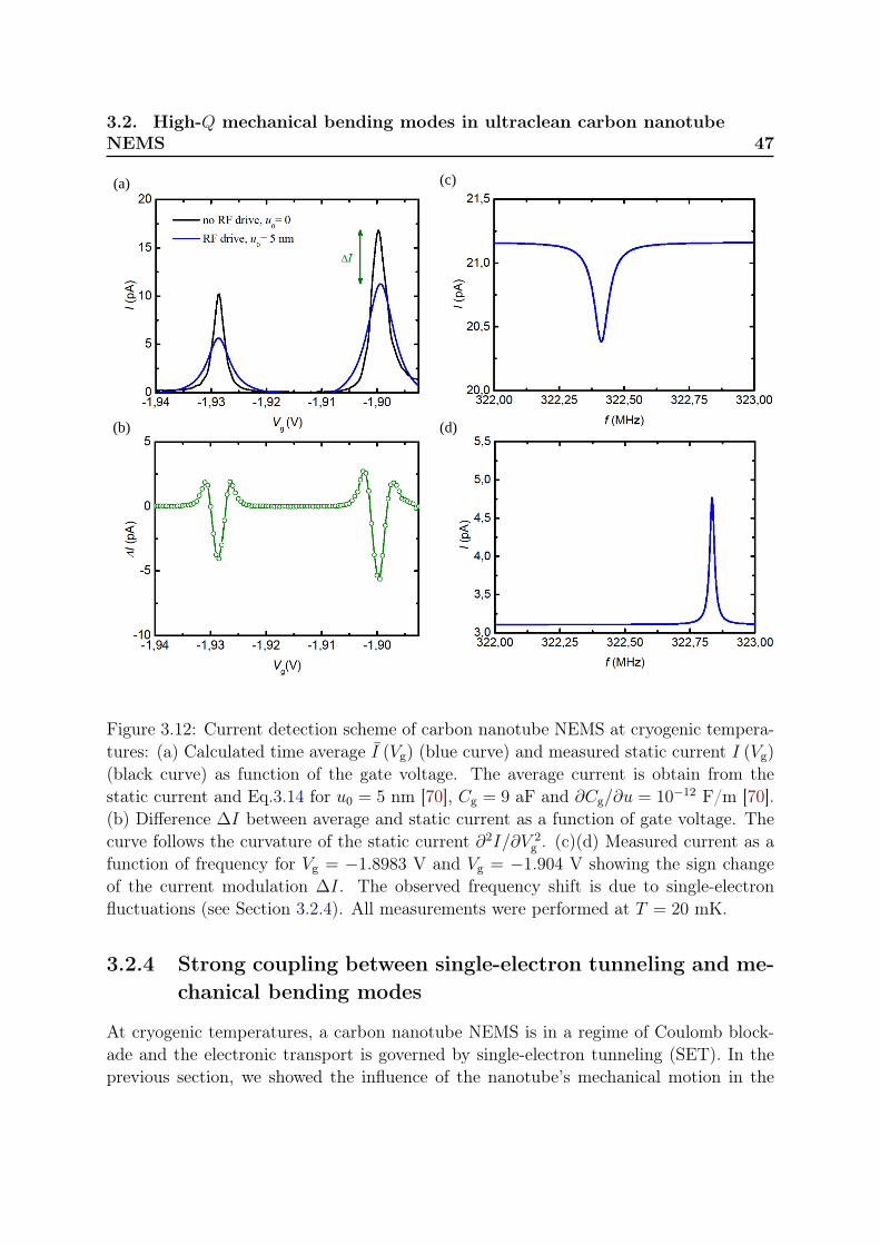
3.2. High-Q mechanical bending modes in ultraclean carbon nanotubeNEMS 47
(a)
(b)
(c)
(d)
Figure 3.12: Current detection scheme of carbon nanotube NEMS at cryogenic tempera-tures: (a) Calculated time average I (Vg) (blue curve) and measured static current I (Vg)
(black curve) as function of the gate voltage. The average current is obtain from thestatic current and Eq.3.14 for u0 = 5 nm [70], Cg = 9 aF and ∂Cg/∂u = 10−12 F/m [70].(b) Difference ∆I between average and static current as a function of gate voltage. Thecurve follows the curvature of the static current ∂2I/∂V 2
g . (c)(d) Measured current as afunction of frequency for Vg = −1.8983 V and Vg = −1.904 V showing the sign changeof the current modulation ∆I. The observed frequency shift is due to single-electronfluctuations (see Section 3.2.4). All measurements were performed at T = 20 mK.
3.2.4 Strong coupling between single-electron tunneling and me-chanical bending modes
At cryogenic temperatures, a carbon nanotube NEMS is in a regime of Coulomb block-ade and the electronic transport is governed by single-electron tunneling (SET). In theprevious section, we showed the influence of the nanotube’s mechanical motion in the
48 Chapter 3. Introduction to carbon nanotube based NEMS
electronic transport enabling its detection. In this section we will describe the inverseeffect, i.e. the impact of the SET on the nanotube’s mechanical motion.
SET in a CNT NEMS-QD can be considered as an external perturbation to theCNT mechanical motion, and vice versa. This perturbation can be described as anelectrodynamic force acting on the CNT. The contribution of this force, which is in phasewith the mechanical motion, is responsible for a frequency modulation ∆f , whereasa contribution of the force which is out of phase with mechanical motion induces amodification of the dissipation and the quality factor Q. The model and the experimentaldata presented in the following section, were first published by Lassagne et al. [74] andby Steele et al. [61] in 2009.
First we consider the mechanical response of a CNT NEMS-QD, i.e. the frequencyshift due to SET. The electrostatic force acting on a CNT quantum dot is given by
Fel =1
2C
′
g
(V DC
g − Vdot)2 ≈ 1
2C
′
g
(V DC2
g − 2VdotVDCg
)+ o(V 2
dot) (3.15)
where Vdot is the electrostatic potential on the quantum dot yielding
Vdot =−PeCdot
+CgV
DCg
Cdot(3.16)
with the control charge qc = CgVDCg , the charge on the dot qdot = −Pe and the dot
capacitance Cdot.The relevant electrodynamic force related to SET is described by the second term in
Eq. 3.15 and reads:
F = −C
′gV
DCg
Cdot(qdot − qc) (3.17)
If the CNT is driven into mechanical motion by an oscillating field with the frequencyf and a drive amplitude δz0, the amplitude of motion is given by
δz = δz0ei2πft (3.18)
As a consequence, the distance between the CNT and gate and hence the CNT-gatecapacitance and the control charge oscillate as
δCg = C′
gδz = C′
gδz0ei2πft (3.19)
δqc = δCgVDCg (3.20)
The charge on the quantum dot qdot exhibits staircase dependance on the controlcharge qc (Fig. 3.13). In consequence the charge on the quantum dot also oscillates inresponse to the mechanical motion and the oscillation can be written as
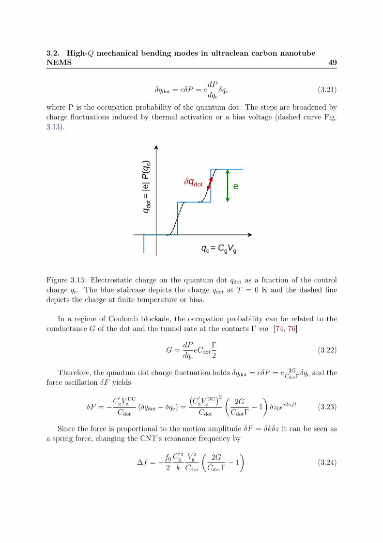
3.2. High-Q mechanical bending modes in ultraclean carbon nanotubeNEMS 49
δqdot = eδP = edP
dqcδqc (3.21)
where P is the occupation probability of the quantum dot. The steps are broadened bycharge fluctuations induced by thermal activation or a bias voltage (dashed curve Fig.3.13).
δqdot e
q dot
= |e
| P(q
c)
qc = CgVg
Figure 3.13: Electrostatic charge on the quantum dot qdot as a function of the controlcharge qc. The blue staircase depicts the charge qdot at T = 0 K and the dashed linedepicts the charge at finite temperature or bias.
In a regime of Coulomb blockade, the occupation probability can be related to theconductance G of the dot and the tunnel rate at the contacts Γ via [74, 76]
G =dP
dqceCdot
Γ
2(3.22)
Therefore, the quantum dot charge fluctuation holds δqdot = eδP = e 2GCdotΓ
δqc and theforce oscillation δF yields
δF = −C
′gV
DCg
Cdot(δqdot − δqc) =
(C
′gV
DCg
)2
Cdot
(2G
CdotΓ− 1
)δz0e
i2πft (3.23)
Since the force is proportional to the motion amplitude δF = δkδz it can be seen asa spring force, changing the CNT’s resonance frequency by
∆f = −f0
2
C′2g
k
V 2g
Cdot
(2G
CdotΓ− 1
)(3.24)
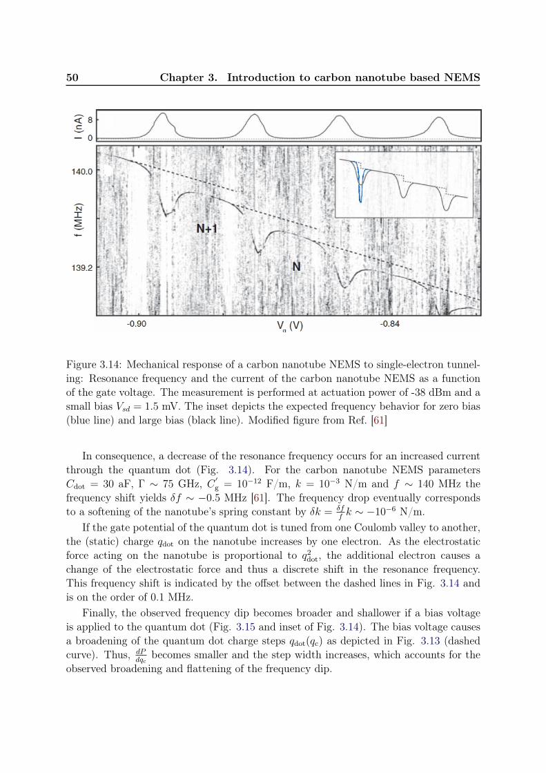
50 Chapter 3. Introduction to carbon nanotube based NEMS
Figure 3.14: Mechanical response of a carbon nanotube NEMS to single-electron tunnel-ing: Resonance frequency and the current of the carbon nanotube NEMS as a functionof the gate voltage. The measurement is performed at actuation power of -38 dBm and asmall bias Vsd = 1.5 mV. The inset depicts the expected frequency behavior for zero bias(blue line) and large bias (black line). Modified figure from Ref. [61]
In consequence, a decrease of the resonance frequency occurs for an increased currentthrough the quantum dot (Fig. 3.14). For the carbon nanotube NEMS parametersCdot = 30 aF, Γ ∼ 75 GHz, C ′
g = 10−12 F/m, k = 10−3 N/m and f ∼ 140 MHz thefrequency shift yields δf ∼ −0.5 MHz [61]. The frequency drop eventually correspondsto a softening of the nanotube’s spring constant by δk = δf
fk ∼ −10−6 N/m.
If the gate potential of the quantum dot is tuned from one Coulomb valley to another,the (static) charge qdot on the nanotube increases by one electron. As the electrostaticforce acting on the nanotube is proportional to q2
dot, the additional electron causes achange of the electrostatic force and thus a discrete shift in the resonance frequency.This frequency shift is indicated by the offset between the dashed lines in Fig. 3.14 andis on the order of 0.1 MHz.
Finally, the observed frequency dip becomes broader and shallower if a bias voltageis applied to the quantum dot (Fig. 3.15 and inset of Fig. 3.14). The bias voltage causesa broadening of the quantum dot charge steps qdot(qc) as depicted in Fig. 3.13 (dashedcurve). Thus, dP
dqcbecomes smaller and the step width increases, which accounts for the
observed broadening and flattening of the frequency dip.
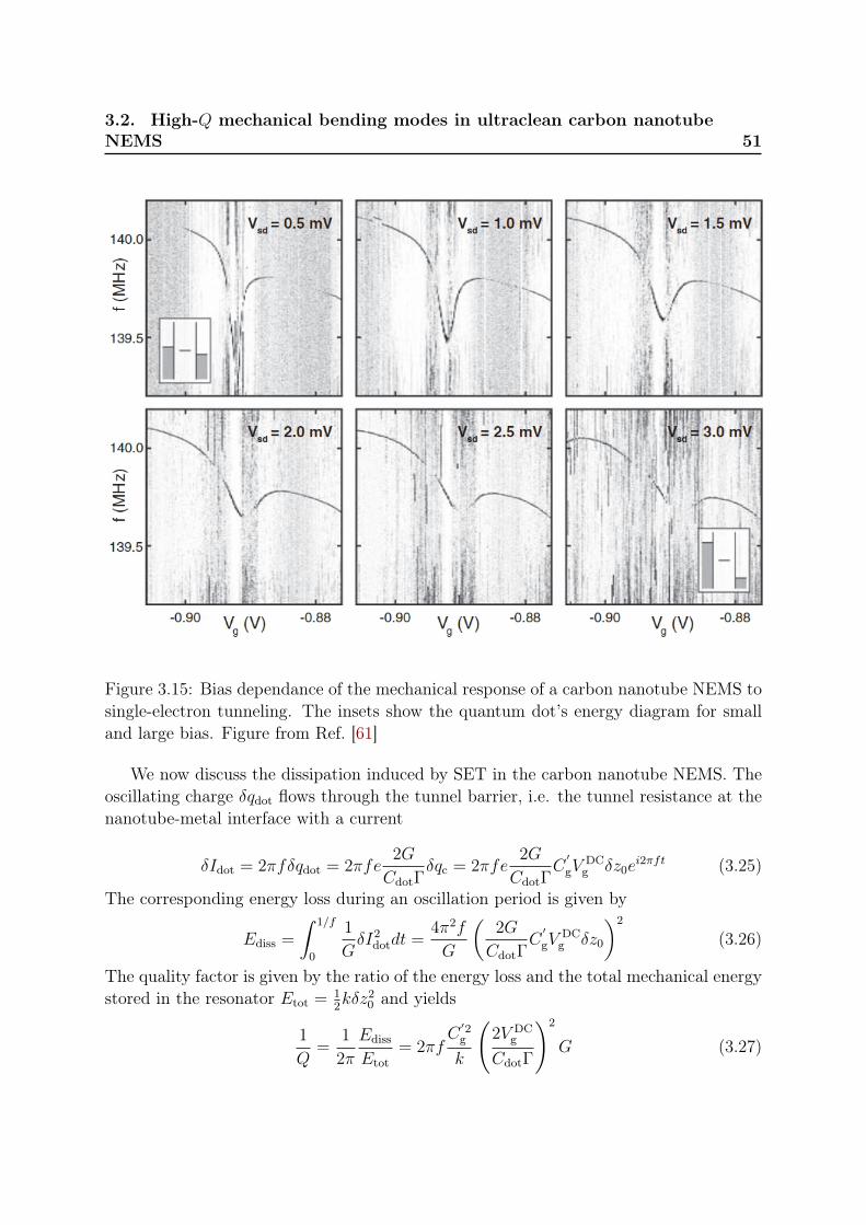
3.2. High-Q mechanical bending modes in ultraclean carbon nanotubeNEMS 51
Figure 3.15: Bias dependance of the mechanical response of a carbon nanotube NEMS tosingle-electron tunneling. The insets show the quantum dot’s energy diagram for smalland large bias. Figure from Ref. [61]
We now discuss the dissipation induced by SET in the carbon nanotube NEMS. Theoscillating charge δqdot flows through the tunnel barrier, i.e. the tunnel resistance at thenanotube-metal interface with a current
δIdot = 2πfδqdot = 2πfe2G
CdotΓδqc = 2πfe
2G
CdotΓC
′
gVDCg δz0e
i2πft (3.25)
The corresponding energy loss during an oscillation period is given by
Ediss =
∫ 1/f
0
1
GδI2
dotdt =4π2f
G
(2G
CdotΓC
′
gVDCg δz0
)2
(3.26)
The quality factor is given by the ratio of the energy loss and the total mechanical energystored in the resonator Etot = 1
2kδz2
0 and yields
1
Q=
1
2π
Ediss
Etot= 2πf
C′2g
k
(2V DC
g
CdotΓ
)2
G (3.27)

52 Chapter 3. Introduction to carbon nanotube based NEMS
Therefore, a current increase results in stronger dissipation at the carbon nanotube-metalinterface and a decrease of the quality factor Q as depicted in Fig. 3.16 and 3.18.
0 , 0
0 , 1
0 , 2
0 , 3
- 1 , 0 2 5 - 1 , 0 0 0 - 0 , 9 7 5 - 0 , 9 5 01 0 3
1 0 4
1 0 5
1 0 6
I sd
(nA)
Q
V g ( V )
Figure 3.16: Dissipation induced by single-electron tunneling in a carbon nanotubeNEMS. The measurement is performed under zero bias and a driving power of -60 dBm.Due to very strong Coulomb blockade, no resonance was observe and therefore no qualityfactor calculated in the Coulomb valley. The green lines are fits with equation 3.27.
Finally, SET affects the nonlinearity in a carbon nanotube NEMS. If the carbonnanotube NEMS is driven at higher power, the resonance peak becomes asymmetricand shows a significant hysteresis between upward and downward frequency sweeps (seeSection 3.2.2). In such a Duffing oscillator, the spring constant k is modulated by the largemechanical displacement u yielding k′ = k + αu2, with α being the Duffing parameter.For a spring hardening α > 0, the resonance exhibits a sharp edge on the high frequencyside, whereas for a spring softening α < 0 the sharp edge of the resonance is found onthe low frequency side [61].
The SET Duffing parameter αSET can be determined from the third derivative of thedriving force.
αSET = −d3F
dz3=
d2
dz2δk =
V 2g
C2g
k
f
(dC
dz
)2d2δf
dV 2g
(3.28)
Therefore, the sign of αSET follows the sign of the curvature of δf , leading to a spring
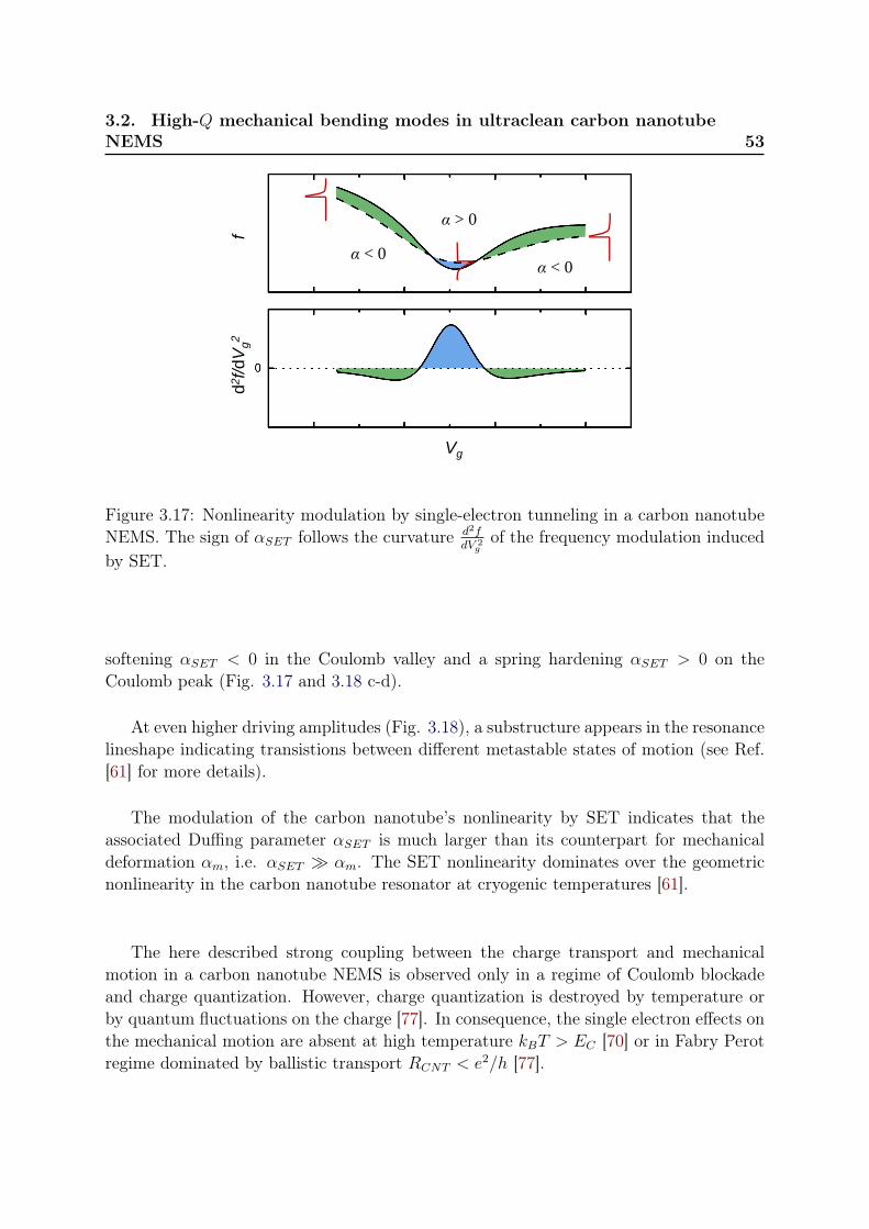
3.2. High-Q mechanical bending modes in ultraclean carbon nanotubeNEMS 53
α > 0
α < 0α < 0
Vg
d2f/d
Vg2
f
Figure 3.17: Nonlinearity modulation by single-electron tunneling in a carbon nanotubeNEMS. The sign of αSET follows the curvature d2f
dV 2gof the frequency modulation induced
by SET.
softening αSET < 0 in the Coulomb valley and a spring hardening αSET > 0 on theCoulomb peak (Fig. 3.17 and 3.18 c-d).
At even higher driving amplitudes (Fig. 3.18), a substructure appears in the resonancelineshape indicating transistions between different metastable states of motion (see Ref.[61] for more details).
The modulation of the carbon nanotube’s nonlinearity by SET indicates that theassociated Duffing parameter αSET is much larger than its counterpart for mechanicaldeformation αm, i.e. αSET αm. The SET nonlinearity dominates over the geometricnonlinearity in the carbon nanotube resonator at cryogenic temperatures [61].
The here described strong coupling between the charge transport and mechanicalmotion in a carbon nanotube NEMS is observed only in a regime of Coulomb blockadeand charge quantization. However, charge quantization is destroyed by temperature orby quantum fluctuations on the charge [77]. In consequence, the single electron effects onthe mechanical motion are absent at high temperature kBT > EC [70] or in Fabry Perotregime dominated by ballistic transport RCNT < e2/h [77].
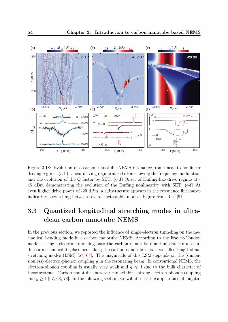
54 Chapter 3. Introduction to carbon nanotube based NEMS
(a)
(b)
(c)
(d)
(e)
(f)
Figure 3.18: Evolution of a carbon nanotube NEMS resonance from linear to nonlineardriving regime. (a-b) Linear driving regime at -60 dBm showing the frequency modulationand the evolution of the Q factor by SET. (c-d) Onset of Duffing-like drive regime at -45 dBm demonstrating the evolution of the Duffing nonlinearity with SET. (e-f) Ateven higher drive power of -20 dBm, a substructure appears in the resonance lineshapesindicating a switching between several metastable modes. Figure from Ref. [61].
3.3 Quantized longitudinal stretching modes in ultra-clean carbon nanotube NEMS
In the previous section, we reported the influence of single-electron tunneling on the me-chanical bending mode in a carbon nanotube NEMS. According to the Franck-Condonmodel, a single-electron tunneling onto the carbon nanotube quantum dot can also in-duce a mechanical displacement along the carbon nanotube’s axis, so called longitudinalstretching modes (LSM) [67, 68]. The magnitude of this LSM depends on the (dimen-sionless) electron-phonon coupling g in the resonating beam. In conventional NEMS, theelectron-phonon coupling is usually very weak and g 1 due to the bulk character ofthose systems. Carbon nanotubes however can exhibit a strong electron-phonon couplingand g ≥ 1 [67, 68, 78]. In the following section, we will discuss the appearance of longitu-
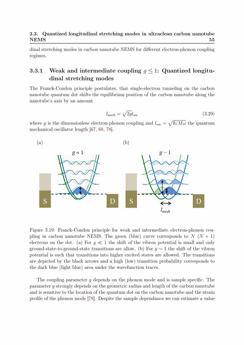
3.3. Quantized longitudinal stretching modes in ultraclean carbon nanotubeNEMS 55
dinal stretching modes in carbon nanotube NEMS for different electron-phonon couplingregimes.
3.3.1 Weak and intermediate coupling g ≤ 1: Quantized longitu-dinal stretching modes
The Franck-Condon principle postulates, that single-electron tunneling on the carbonnanotube quantum dot shifts the equilibrium position of the carbon nanotube along thenanotube’s axis by an amount
lmech =√
2glosc (3.29)
where g is the dimensionless electron-phonon coupling and losc =√~/Mω the quantum
mechanical oscillator length [67, 68, 78].
(a) (b)
Figure 3.19: Franck-Condon principle for weak and intermediate electron-phonon cou-pling in carbon nanotube NEMS. The green (blue) curve corresponds to N (N + 1)electrons on the dot. (a) For g 1 the shift of the vibron potential is small and onlyground-state-to-ground-state transitions are allow. (b) For g ∼ 1 the shift of the vibronpotential is such that transitions into higher excited states are allowed. The transitionsare depicted by the black arrows and a high (low) transition probability corresponds tothe dark blue (light blue) area under the wavefunction traces.
The coupling parameter g depends on the phonon mode and is sample specific. Theparameter g strongly depends on the geometric radius and length of the carbon nanotubeand is sensitive to the location of the quantum dot on the carbon nanotube and the strainprofile of the phonon mode [78]. Despite the sample dependance we can estimate a value
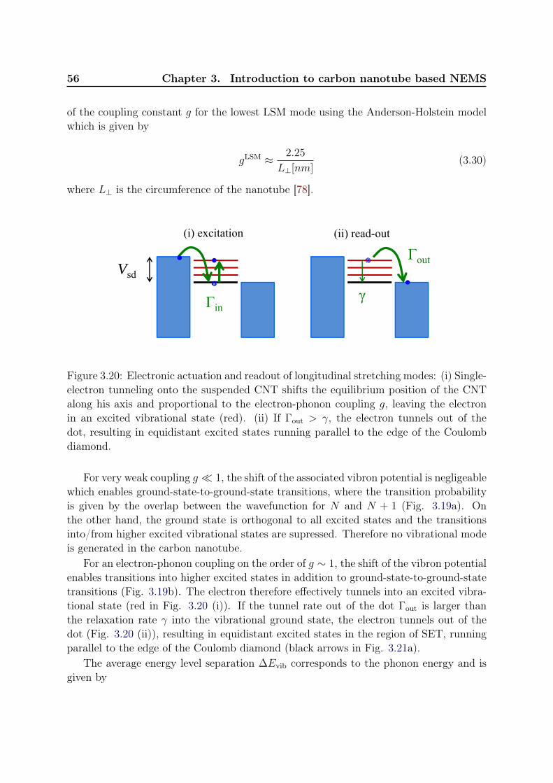
56 Chapter 3. Introduction to carbon nanotube based NEMS
of the coupling constant g for the lowest LSM mode using the Anderson-Holstein modelwhich is given by
gLSM ≈ 2.25
L⊥[nm](3.30)
where L⊥ is the circumference of the nanotube [78].
Γin
Vsd
(i) excitation
Γout
γ
(ii) read-out
Figure 3.20: Electronic actuation and readout of longitudinal stretching modes: (i) Single-electron tunneling onto the suspended CNT shifts the equilibrium position of the CNTalong his axis and proportional to the electron-phonon coupling g, leaving the electronin an excited vibrational state (red). (ii) If Γout > γ, the electron tunnels out of thedot, resulting in equidistant excited states running parallel to the edge of the Coulombdiamond.
For very weak coupling g 1, the shift of the associated vibron potential is negligeablewhich enables ground-state-to-ground-state transitions, where the transition probabilityis given by the overlap between the wavefunction for N and N + 1 (Fig. 3.19a). Onthe other hand, the ground state is orthogonal to all excited states and the transitionsinto/from higher excited vibrational states are supressed. Therefore no vibrational modeis generated in the carbon nanotube.
For an electron-phonon coupling on the order of g ∼ 1, the shift of the vibron potentialenables transitions into higher excited states in addition to ground-state-to-ground-statetransitions (Fig. 3.19b). The electron therefore effectively tunnels into an excited vibra-tional state (red in Fig. 3.20 (i)). If the tunnel rate out of the dot Γout is larger thanthe relaxation rate γ into the vibrational ground state, the electron tunnels out of thedot (Fig. 3.20 (ii)), resulting in equidistant excited states in the region of SET, runningparallel to the edge of the Coulomb diamond (black arrows in Fig. 3.21a).
The average energy level separation ∆Evib corresponds to the phonon energy and isgiven by
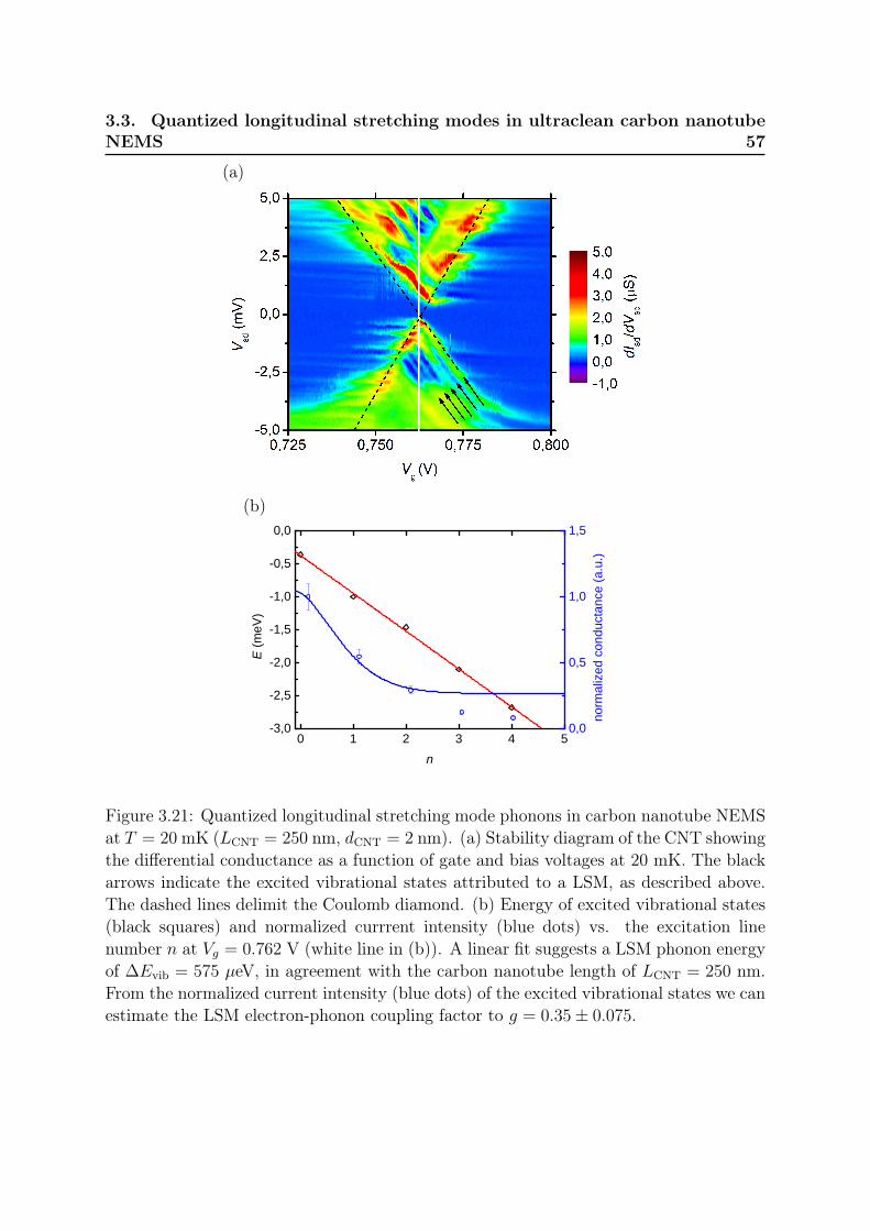
3.3. Quantized longitudinal stretching modes in ultraclean carbon nanotubeNEMS 57
(a)
(b)
0 1 2 3 4 5- 3 , 0
- 2 , 5
- 2 , 0
- 1 , 5
- 1 , 0
- 0 , 5
0 , 0
E (m
eV)
n0 , 0
0 , 5
1 , 0
1 , 5
norm
alized
cond
uctan
ce (a
.u.)
Figure 3.21: Quantized longitudinal stretching mode phonons in carbon nanotube NEMSat T = 20 mK (LCNT = 250 nm, dCNT = 2 nm). (a) Stability diagram of the CNT showingthe differential conductance as a function of gate and bias voltages at 20 mK. The blackarrows indicate the excited vibrational states attributed to a LSM, as described above.The dashed lines delimit the Coulomb diamond. (b) Energy of excited vibrational states(black squares) and normalized currrent intensity (blue dots) vs. the excitation linenumber n at Vg = 0.762 V (white line in (b)). A linear fit suggests a LSM phonon energyof ∆Evib = 575 µeV, in agreement with the carbon nanotube length of LCNT = 250 nm.From the normalized current intensity (blue dots) of the excited vibrational states we canestimate the LSM electron-phonon coupling factor to g = 0.35± 0.075.
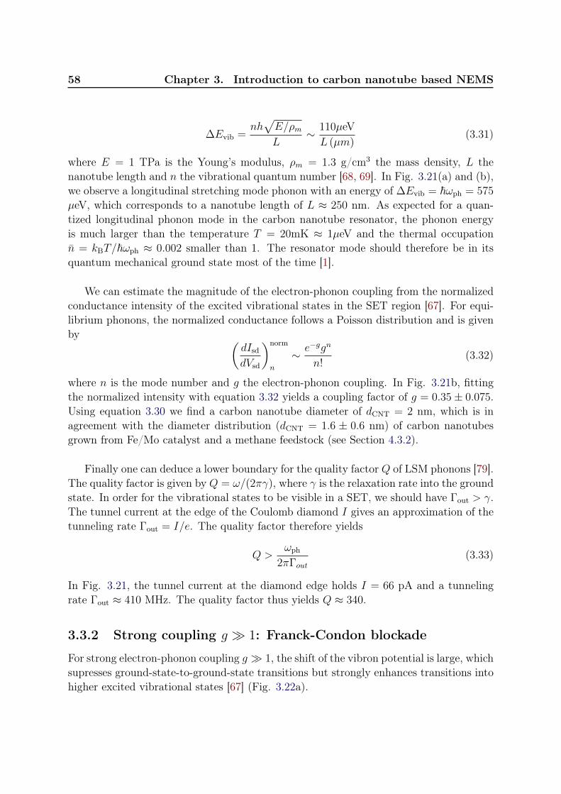
58 Chapter 3. Introduction to carbon nanotube based NEMS
∆Evib =nh√E/ρmL
∼ 110µeVL (µm)
(3.31)
where E = 1 TPa is the Young’s modulus, ρm = 1.3 g/cm3 the mass density, L thenanotube length and n the vibrational quantum number [68, 69]. In Fig. 3.21(a) and (b),we observe a longitudinal stretching mode phonon with an energy of ∆Evib = ~ωph = 575
µeV, which corresponds to a nanotube length of L ≈ 250 nm. As expected for a quan-tized longitudinal phonon mode in the carbon nanotube resonator, the phonon energyis much larger than the temperature T = 20mK ≈ 1µeV and the thermal occupationn = kBT/~ωph ≈ 0.002 smaller than 1. The resonator mode should therefore be in itsquantum mechanical ground state most of the time [1].
We can estimate the magnitude of the electron-phonon coupling from the normalizedconductance intensity of the excited vibrational states in the SET region [67]. For equi-librium phonons, the normalized conductance follows a Poisson distribution and is givenby (
dIsddVsd
)norm
n
∼ e−ggn
n!(3.32)
where n is the mode number and g the electron-phonon coupling. In Fig. 3.21b, fittingthe normalized intensity with equation 3.32 yields a coupling factor of g = 0.35± 0.075.Using equation 3.30 we find a carbon nanotube diameter of dCNT = 2 nm, which is inagreement with the diameter distribution (dCNT = 1.6 ± 0.6 nm) of carbon nanotubesgrown from Fe/Mo catalyst and a methane feedstock (see Section 4.3.2).
Finally one can deduce a lower boundary for the quality factor Q of LSM phonons [79].The quality factor is given by Q = ω/(2πγ), where γ is the relaxation rate into the groundstate. In order for the vibrational states to be visible in a SET, we should have Γout > γ.The tunnel current at the edge of the Coulomb diamond I gives an approximation of thetunneling rate Γout = I/e. The quality factor therefore yields
Q >ωph
2πΓout(3.33)
In Fig. 3.21, the tunnel current at the diamond edge holds I = 66 pA and a tunnelingrate Γout ≈ 410 MHz. The quality factor thus yields Q ≈ 340.
3.3.2 Strong coupling g 1: Franck-Condon blockade
For strong electron-phonon coupling g 1, the shift of the vibron potential is large, whichsupresses ground-state-to-ground-state transitions but strongly enhances transitions intohigher excited vibrational states [67] (Fig. 3.22a).
3.3. Quantized longitudinal stretching modes in ultraclean carbon nanotubeNEMS 59
(a) (b)
(c)
Figure 3.22: Franck-Condon blockade for strong electron-phonon coupling in carbon nan-otube NEMS. (a) For g 1, the shift of the vibron potential is such that transitionsinto higher excited states are strongly enhanced, whereas ground state transitions areforbidden. The green (blue) curve corresponds to N (N + 1) electrons on the dot. Thetransitions are depicted by the black arrows and a high (low) transition probability cor-responds to the dark blue (light blue) area under the wavefunction traces. (b) Stabilitydiagram for a suspended carbon nanotube NEMS at 1.3 K showing the current suppre-sion at low bias (dotted line labeled i) and enhanced current in the high bias regime.Figure from [67]. (c) Differential conductance as function of bias voltage at Vtg = 0.1570
V (solid vertical line in (b)). From the maxima of the conductance peaks (red circles,green squares), one can extract an electron-phonon coupling g = 4.5 (positive bias) andg = 3 (negative bias) using equation 3.32. Figure from [67]
60 Chapter 3. Introduction to carbon nanotube based NEMS
The effect known as Franck-Condon blockade, results in a current suppresion at lowbias (dotted line (i) in Fig. 3.22b). In the same time, the tunneling current through higherexcited vibrational states is strongly enhanced in the high bias regime [67] (Fig. 3.22band c). From Fig. 3.22c, the magnitude of the electron-phonon coupling can be estimatedwith equation 3.32 to g = 3 and g = 4.5 for negative and positive bias, respectively.
3.4 Outlook
In this chapter, we described the fingerprint like characteristics of transverse bendingmodes (Section 3.2) and longitudinal stretching modes (Section 3.3) in a carbon nan-otube NEMS.
In the following chapter 4, we will describe the ultraclean bottom-up nanofabricationprocess of such a carbon nanotube NEMS as well as the experimental setup used to probethe nanotube’s mechanical motion at cryogenic temperatures.
In Chapter 5 we present a systematic study of the transverse bending mode vibrationin a carbon nanotube NEMS. We demonstrate that the response and dissipation of a car-bon nanotube’s bending mode vibration to single-electron tunneling through the carbonnanotube NEMS-quantum dot critically depends on the dot’s electronic environment, i.e.the capacitance, the tunnel coupling to the metal leads, the current and temperature.The findings suggest that one could achieve quality factors of 106 or higher by choosingappropriate gate dielectrics and/or by improving the tunnel coupling to the leads. Owingto these large and highly tunable quality factors, a carbon nanotube NEMS thereforerepresents an ideal plateform for magnetic torque detection, with a maximum sensitivityof 1µB as described in section 2.3 [19].
In Chapter 6 on the other hand, we present the strong interaction of a quantized longi-tudinal streching mode vibration with a single molecule magnet, which allows for instancethe detection of a single nuclear spin. The magnitude of the observed interaction suggeststhe possiblity of quantum entanglement between a single nuclear spin (or electronic spin)and single phonon mode. Moreover the coupling indicates that a carbon nanotube NEMSfunctionalized with single molecule magnets can be the first experimental realization ofa supramolecular torque magnetometer with single molecule sensitivity [20].
Chapter 4
Nanofabrication and characterisation ofcarbon nanotube based NEMS and
molecular spintronic devices
In this section we will present the complete nanofabrication and characterization processof a high-Q carbon nanotube NEMS. It was recently demonstrated, that such high-Qcarbon nanotube NEMS can be obtained from a bottom-up fabrication process, wherecarbon nanotubes are grown on a ’back-bone’ metal junction by chemical vapor deposition(CVD) in the very last step of the fabrication process, thus avoiding contamination ofthe carbon nanotube by residual resist, solvents or chemical etching procedures [80, 81,1, 61, 65].
Such a process needs to be performed in a clean environment, in our case the CNRSclean room facility ’Nanofab’ in Grenoble. Moreover, the ’back-bone’ structure has towithstand the extreme temperatures of 800 reached during a CVD growth, which typ-ically requires the use of materials such as platinum or tungsten. Finally, one needs tohave a good control on CVD growth conditions, in order to obtain a reproducible pro-cess and a good yield of working carbon nanotube resonators. In the following we willdescribe an ultraclean, bottom-up fabrication process for carbon nanotube NEMS withquality factors as high as 105 and a yield of working devices around 5%.
The fabrication starts from a degeneratly p-doped silicon 2" wafer covered by a layerof dry chlorinated thermal SiO2, serving as gate dielectric (Section 4.1). Using state of theart lithography techniques, we pattern the back-bone junction for the carbon nanotubeNEMS with a standard Si backgate (Section 4.2.2) or a high efficiency local gate (Section4.2.3). After extensive cleaning of this back-bone structure in an oxygen plasma, carbonnanotubes are grown by CVD at 800C from a CH4 carbon feedstock and iron basedcatalyst island patterned on the source-drain electrodes next to the junction (Section4.3). Using the real-time data acquisition system ADWIN (Section 4.4), the devices arethen characterized by electric transport measurements at room temperature, in orderto select the best devices prior to a cooldown to cryogenic temperatures (Section 4.5).Finally, real-time measurements via ADWIN of the nanotube’s nanomechanical motionare carried out in a 3He/4He dilution refrigerator at a base temperature of 30 mK. TheNEMS actuation and detection scheme used in our experiment is similar to the one usedby Steele and co-workers [61, 75]. As the induced mechanical motion changes the charge
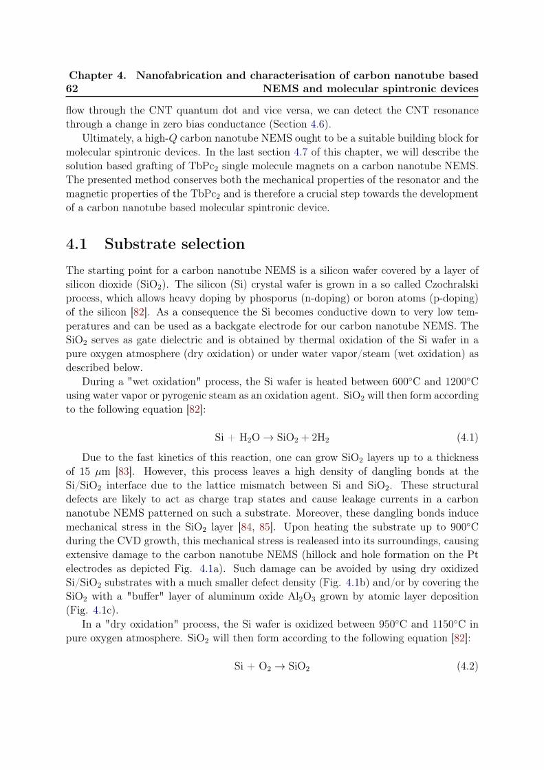
62Chapter 4. Nanofabrication and characterisation of carbon nanotube based
NEMS and molecular spintronic devices
flow through the CNT quantum dot and vice versa, we can detect the CNT resonancethrough a change in zero bias conductance (Section 4.6).
Ultimately, a high-Q carbon nanotube NEMS ought to be a suitable building block formolecular spintronic devices. In the last section 4.7 of this chapter, we will describe thesolution based grafting of TbPc2 single molecule magnets on a carbon nanotube NEMS.The presented method conserves both the mechanical properties of the resonator and themagnetic properties of the TbPc2 and is therefore a crucial step towards the developmentof a carbon nanotube based molecular spintronic device.
4.1 Substrate selection
The starting point for a carbon nanotube NEMS is a silicon wafer covered by a layer ofsilicon dioxide (SiO2). The silicon (Si) crystal wafer is grown in a so called Czochralskiprocess, which allows heavy doping by phosporus (n-doping) or boron atoms (p-doping)of the silicon [82]. As a consequence the Si becomes conductive down to very low tem-peratures and can be used as a backgate electrode for our carbon nanotube NEMS. TheSiO2 serves as gate dielectric and is obtained by thermal oxidation of the Si wafer in apure oxygen atmosphere (dry oxidation) or under water vapor/steam (wet oxidation) asdescribed below.
During a "wet oxidation" process, the Si wafer is heated between 600C and 1200Cusing water vapor or pyrogenic steam as an oxidation agent. SiO2 will then form accordingto the following equation [82]:
Si + H2O→ SiO2 + 2H2 (4.1)
Due to the fast kinetics of this reaction, one can grow SiO2 layers up to a thicknessof 15 µm [83]. However, this process leaves a high density of dangling bonds at theSi/SiO2 interface due to the lattice mismatch between Si and SiO2. These structuraldefects are likely to act as charge trap states and cause leakage currents in a carbonnanotube NEMS patterned on such a substrate. Moreover, these dangling bonds inducemechanical stress in the SiO2 layer [84, 85]. Upon heating the substrate up to 900Cduring the CVD growth, this mechanical stress is realeased into its surroundings, causingextensive damage to the carbon nanotube NEMS (hillock and hole formation on the Ptelectrodes as depicted Fig. 4.1a). Such damage can be avoided by using dry oxidizedSi/SiO2 substrates with a much smaller defect density (Fig. 4.1b) and/or by covering theSiO2 with a "buffer" layer of aluminum oxide Al2O3 grown by atomic layer deposition(Fig. 4.1c).
In a "dry oxidation" process, the Si wafer is oxidized between 950C and 1150C inpure oxygen atmosphere. SiO2 will then form according to the following equation [82]:
Si + O2 → SiO2 (4.2)
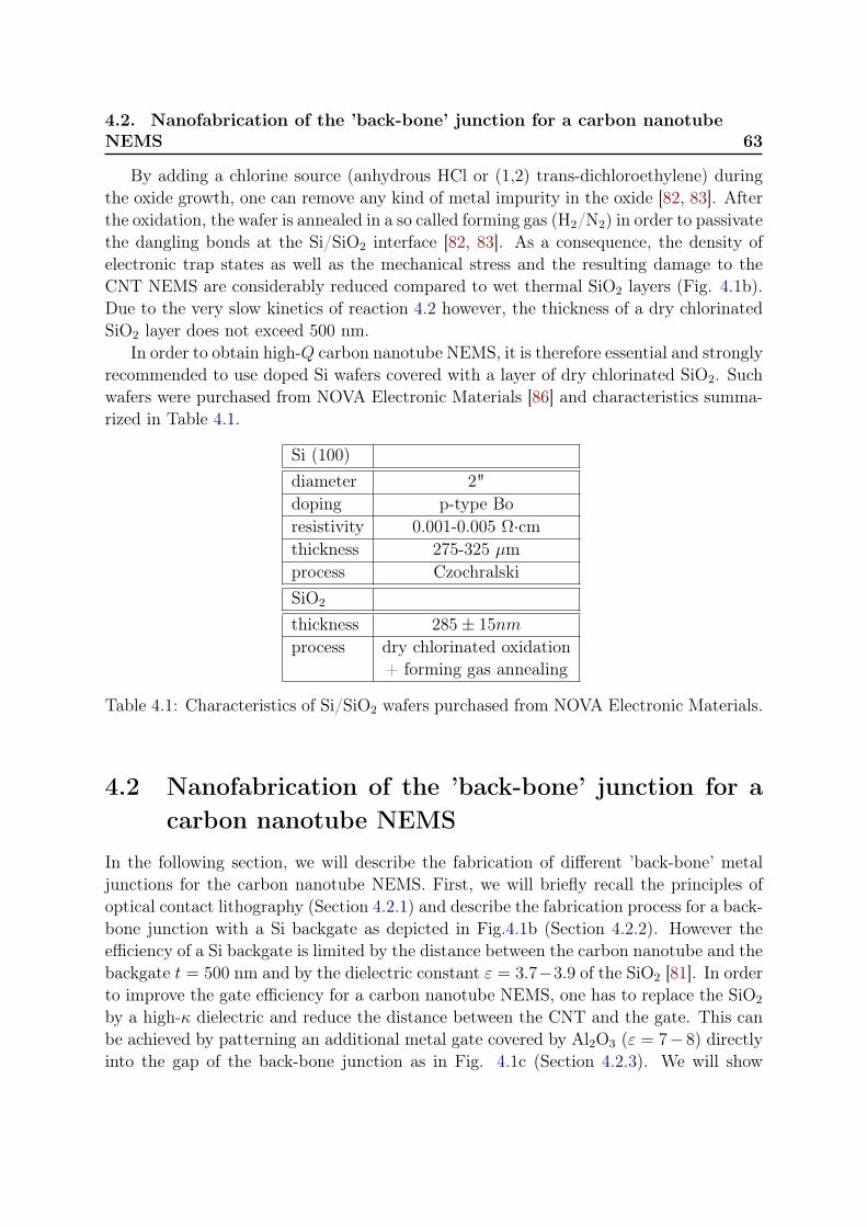
4.2. Nanofabrication of the ’back-bone’ junction for a carbon nanotubeNEMS 63
By adding a chlorine source (anhydrous HCl or (1,2) trans-dichloroethylene) duringthe oxide growth, one can remove any kind of metal impurity in the oxide [82, 83]. Afterthe oxidation, the wafer is annealed in a so called forming gas (H2/N2) in order to passivatethe dangling bonds at the Si/SiO2 interface [82, 83]. As a consequence, the density ofelectronic trap states as well as the mechanical stress and the resulting damage to theCNT NEMS are considerably reduced compared to wet thermal SiO2 layers (Fig. 4.1b).Due to the very slow kinetics of reaction 4.2 however, the thickness of a dry chlorinatedSiO2 layer does not exceed 500 nm.
In order to obtain high-Q carbon nanotube NEMS, it is therefore essential and stronglyrecommended to use doped Si wafers covered with a layer of dry chlorinated SiO2. Suchwafers were purchased from NOVA Electronic Materials [86] and characteristics summa-rized in Table 4.1.
Si (100)diameter 2"doping p-type Boresistivity 0.001-0.005 Ω·cmthickness 275-325 µmprocess CzochralskiSiO2
thickness 285± 15nm
process dry chlorinated oxidation+ forming gas annealing
Table 4.1: Characteristics of Si/SiO2 wafers purchased from NOVA Electronic Materials.
4.2 Nanofabrication of the ’back-bone’ junction for acarbon nanotube NEMS
In the following section, we will describe the fabrication of different ’back-bone’ metaljunctions for the carbon nanotube NEMS. First, we will briefly recall the principles ofoptical contact lithography (Section 4.2.1) and describe the fabrication process for a back-bone junction with a Si backgate as depicted in Fig.4.1b (Section 4.2.2). However theefficiency of a Si backgate is limited by the distance between the carbon nanotube and thebackgate t = 500 nm and by the dielectric constant ε = 3.7−3.9 of the SiO2 [81]. In orderto improve the gate efficiency for a carbon nanotube NEMS, one has to replace the SiO2
by a high-κ dielectric and reduce the distance between the CNT and the gate. This canbe achieved by patterning an additional metal gate covered by Al2O3 (ε = 7− 8) directlyinto the gap of the back-bone junction as in Fig. 4.1c (Section 4.2.3). We will show
64Chapter 4. Nanofabrication and characterisation of carbon nanotube based
NEMS and molecular spintronic devices
(a)
(b)
(c)
Figure 4.1: Impact of substrate quality on carbon nanotube NEMS: False color SEMimage (side view) of a CNT NEMS on a (a) wet thermal SiO2 layer ; (b) dry chlorinatedthermal SiO2 layer; (c) dry chlorinated thermal SiO2 layer covered by an alumina "buffer"layer obtained by atomic layer deposition. Mechanical stress in wet oxide layers (a) isreleased during the CVD growth at 900C, causing hole and hillock formation in Ptelectrodes (yellow) of the CNT NEMS. Due to the extensive damage to the electrodes,the CNT are not suspended. This effect can be avoided by using (b) dry oxide layerswith a much smaller defect density and/or (c) by covering the SiO2 with a "‘buffer"’ layerof alumina grown by atomic layer deposition. The blue electrodes correspond to localmetallic gates (see Section 4.2).
in Chapter 5, that the total capacitance and ultimately the Q-factor of such a carbonnanotube NEMS increase by an order of magnitude, due to the higher efficiency of theAl2O3 covered localgate.
4.2. Nanofabrication of the ’back-bone’ junction for a carbon nanotubeNEMS 65
substrate
resist
substrate
resist
mask
λ = 230 nm
substrate
resist
(a) resist coating (b) DUV exposure (c) development
(d) metal deposition(e) lift off
substrate
resist
metal
substrate
metal
Figure 4.2: Principal of optical contact lithography: (a) Spin coating of photosensitiveresist. (b) Contacting with optical mask and exposure to UV radiation λ = 230 nm. Agood contact is essential, as the resolution of the process is proportional to the gap sizebetween the mask and the coated substrate (see text). (c) Removal of exposed resistregions in a developper solution. (d) Metal coating and (e) lift off.
4.2.1 Optical contact lithography
The concept of optical contact lithography (Fig. 4.2) shares some fundamental principleswith photography [87]. A layer of positive, organic photoresist is deposited on a substrateand brought in close mechanical contact with an optical mask yielding the negative ofdesired pattern (Fig. 4.2a). The photoresist is then exposed through the optical maskwith UV radiation (λ = 230 nm). The UV radiation causes a breakdown of the chemicalbonds in the exposed parts of the photoresist (light blue, Fig. 4.2b). The exposedregions can then be removed by an appropriate developper leaving the desired pattern"imprinted" into the photoresist (Fig. 4.2c). A layer of metal is then deposited onto the"imprinted" photoresist (Fig. 4.2d). By dissolving the rest of the photoresist, the excessmetal is lifted off and leaving only the desired pattern on the substrate (Fig. 4.2e).
The imprinted feature size is limited by diffraction, thus by the wavelength λ of theincident radiation, and by the gap size g between the photoresist and the optical mask.The maximal resolution is given in good approximation by d = (λg)1/2 [88]. The shortradiation wavelength and a good mechanical contact between the photoresist and themask, i.e. a small gap size g, are therefore crucial for a high resolution optical lithography.
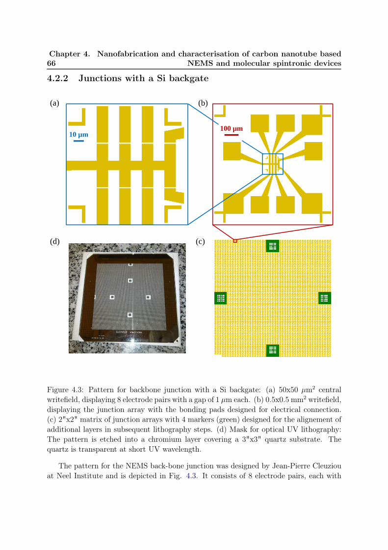
66Chapter 4. Nanofabrication and characterisation of carbon nanotube based
NEMS and molecular spintronic devices
4.2.2 Junctions with a Si backgate
100 µm10 µm
(a) (b)
(d) (c)
Figure 4.3: Pattern for backbone junction with a Si backgate: (a) 50x50 µm2 centralwritefield, displaying 8 electrode pairs with a gap of 1 µm each. (b) 0.5x0.5 mm2 writefield,displaying the junction array with the bonding pads designed for electrical connection.(c) 2"x2" matrix of junction arrays with 4 markers (green) designed for the alignement ofadditional layers in subsequent lithography steps. (d) Mask for optical UV lithography:The pattern is etched into a chromium layer covering a 3"x3" quartz substrate. Thequartz is transparent at short UV wavelength.
The pattern for the NEMS back-bone junction was designed by Jean-Pierre Cleuziouat Neel Institute and is depicted in Fig. 4.3. It consists of 8 electrode pairs, each with

4.2. Nanofabrication of the ’back-bone’ junction for a carbon nanotubeNEMS 67
a gap of 1 µm (Fig. 4.3a). The electrodes are connected to 100x100 µm2 pads designedfor electrical connection (Fig. 4.3b). This junction array is reproduced and arranged ina matrix, including 4 alignement markers (green) for following lithography steps (Fig.4.3c). This matrix is then patterned and etched into a chromium layer covering a 3"x3"quartz substrate in order to obtain the optical mask depicted in Fig. 4.3d.
As described in the previous section, we will use a 2" Si wafer (p-doped) covered with285 nm of dry chlorinated SiO2 (Section 4.1). After a cleaning step in an oxygen plasma,the wafer is coated with two layers of photoresist LOR3A (bottom layer) and UV3 (toplayer). The coated substrate is then exposed to UV radiation (λ = 230 nm) through theoptical mask in a Suess MJB3 mask aligner. After a post exposure bake, the exposedregions of the resist are removed in a developper solution (MF 26A). The developer isthen neutralized in distilled water. It should be noted that without the post exposurebake, the development would be impossible or only occur at strongly reduced rate.
substrate
LOR3A
UV3
substrate
LOR3A
UV3
metal(a)
substrate
UV3
substrate
LOR3AUV3
metal(b)
200 nm
Figure 4.4: (a) Bilayer resist vs. (b) monolayer resist: The undercut formed duringthe development in the bilayer resist and the directional deposition via electron beamevaporation prevents the metal deposition on the sidewalls of the resist and thus theformation of fence-like structures after lift off, which usually occurs with monolayer resist(red arrows in (b)).
Metal is then deposited via electron beam evaporation followed by a lift off in hotacetone and the LOR3A removal with PG remover. It should be noted, that the bot-tom LOR3A layer is more reactive to the developper and thus an undercut forms in thebilayer resist during the development. This undercut and the directional deposition by
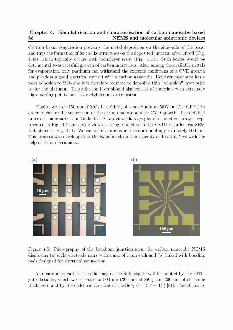
68Chapter 4. Nanofabrication and characterisation of carbon nanotube based
NEMS and molecular spintronic devices
electron beam evaporation prevents the metal deposition on the sidewalls of the resistand thus the formation of fence-like structures on the deposited junction after lift off (Fig.4.4a), which typically occurs with monolayer resist (Fig. 4.4b). Such fences would bedetrimental to successfull growth of carbon nanotubes. Also, among the available metalsfor evaporation, only platinum can withstand the extreme conditions of a CVD growthand provides a good electrical contact with a carbon nanotube. However, platinum has apoor adhesion to SiO2 and it is therefore required to deposit a thin "adhesion" layer priorto/for the platinum. This adhesion layer should also consist of materials with extremelyhigh melting points, such as molybdenum or tungsten.
Finally, we etch 150 nm of SiO2 in a CHF3 plasma (8 min at 50W in 15cc CHF3) inorder to ensure the suspension of the carbon nanotube after CVD growth. The detailedprocess is summarized in Table 4.2. A top view photography of a junction array is rep-resented in Fig. 4.5 and a side view of a single junction (after CVD) recorded via SEMis depicted in Fig. 4.1b. We can achieve a maximal resolution of approximately 500 nm.This process was developped at the Nanofab clean room facility at Institut Neel with thehelp of Bruno Fernandez.
(a) (b)
Figure 4.5: Photography of the backbone junction array for carbon nanotube NEMSdisplaying (a) eight electrode pairs with a gap of 1 µm each and (b) linked with bondingpads designed for electrical connection.
As mentionned earlier, the efficiency of the Si backgate will be limited by the CNT-gate distance, which we estimate to 500 nm (300 nm of SiO2 and 200 nm of electrodethickness), and by the dielectric constant of the SiO2 (ε = 3.7− 3.9) [81]. The efficiency
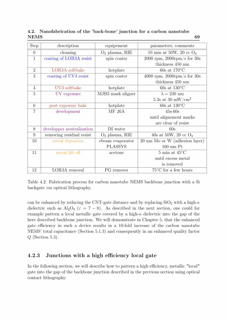
4.2. Nanofabrication of the ’back-bone’ junction for a carbon nanotubeNEMS 69
Step description equipement parameters, comments0 cleaning O2 plasma, RIE 10 min at 50W, 20 cc O2
1 coating of LOR3A resist spin coater 2000 rpm, 2000rpm/s for 30sthickness 450 nm
2 LOR3A softbake hotplate 60s at 170C3 coating of UV3 resist spin coater 4000 rpm, 2000rpm/s for 30s
thickness 450 nm4 UV3 softbake hotplate 60s at 130C5 UV exposure MJB3 mask aligner λ = 230 nm
5.3s at 30 mW/cm2
6 post exposure bake hotplate 60s at 130C7 development MF 26A 45s-60s
until alignement marksare clear of resist
8 developper neutralization DI water 60s9 removing residual resist O2 plasma, RIE 40s at 50W, 20 cc O2
10 metal depostion ebeam evaporator 20 nm Mo or W (adhesion layer)PLASSYS 160 nm Pt
11 metal lift off acetone 5 min at 45Cuntil excess metal
is removed12 LOR3A removal PG remover 75C for a few hours
Table 4.2: Fabrication process for carbon nanotube NEMS backbone junction with a Sibackgate via optical lithography.
can be enhanced by reducing the CNT-gate distance and by replacing SiO2 with a high-κdielectric such as Al2O3 (ε = 7 − 8). As described in the next section, one could forexample pattern a local metallic gate covered by a high-κ dielectric into the gap of thehere described backbone junction. We will demonstrate in Chapter 5, that the enhancedgate efficiency in such a device results in a 10-fold increase of the carbon nanotubeNEMS’ total capacitance (Section 5.1.3) and consequently in an enhanced quality factorQ (Section 5.3).
4.2.3 Junctions with a high efficiency local gate
In the following section, we will describe how to pattern a high efficiency, metallic "local"gate into the gap of the backbone junction described in the previous section using opticalcontact lithography.
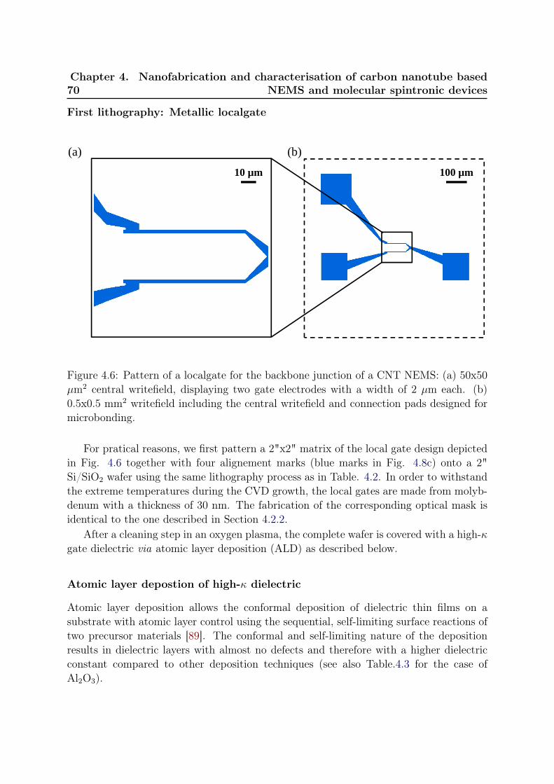
70Chapter 4. Nanofabrication and characterisation of carbon nanotube based
NEMS and molecular spintronic devices
First lithography: Metallic localgate
10 µm 100 µm
(a) (b)
Figure 4.6: Pattern of a localgate for the backbone junction of a CNT NEMS: (a) 50x50µm2 central writefield, displaying two gate electrodes with a width of 2 µm each. (b)0.5x0.5 mm2 writefield including the central writefield and connection pads designed formicrobonding.
For pratical reasons, we first pattern a 2"x2" matrix of the local gate design depictedin Fig. 4.6 together with four alignement marks (blue marks in Fig. 4.8c) onto a 2"Si/SiO2 wafer using the same lithography process as in Table. 4.2. In order to withstandthe extreme temperatures during the CVD growth, the local gates are made from molyb-denum with a thickness of 30 nm. The fabrication of the corresponding optical mask isidentical to the one described in Section 4.2.2.
After a cleaning step in an oxygen plasma, the complete wafer is covered with a high-κgate dielectric via atomic layer deposition (ALD) as described below.
Atomic layer depostion of high-κ dielectric
Atomic layer deposition allows the conformal deposition of dielectric thin films on asubstrate with atomic layer control using the sequential, self-limiting surface reactions oftwo precursor materials [89]. The conformal and self-limiting nature of the depositionresults in dielectric layers with almost no defects and therefore with a higher dielectricconstant compared to other deposition techniques (see also Table.4.3 for the case ofAl2O3).
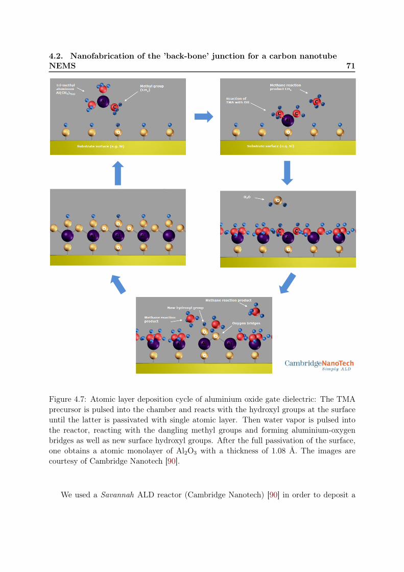
4.2. Nanofabrication of the ’back-bone’ junction for a carbon nanotubeNEMS 71
Figure 4.7: Atomic layer deposition cycle of aluminium oxide gate dielectric: The TMAprecursor is pulsed into the chamber and reacts with the hydroxyl groups at the surfaceuntil the latter is passivated with single atomic layer. Then water vapor is pulsed intothe reactor, reacting with the dangling methyl groups and forming aluminium-oxygenbridges as well as new surface hydroxyl groups. After the full passivation of the surface,one obtains a atomic monolayer of Al2O3 with a thickness of 1.08 Å. The images arecourtesy of Cambridge Nanotech [90].
We used a Savannah ALD reactor (Cambridge Nanotech) [90] in order to deposit a
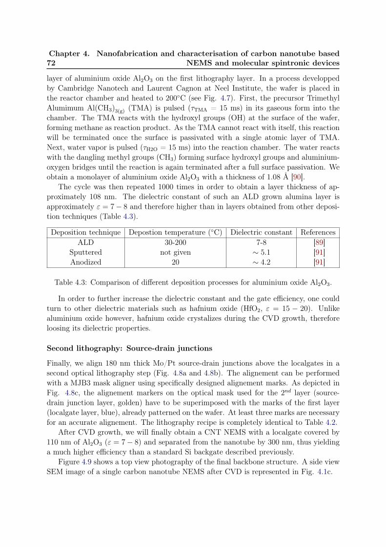
72Chapter 4. Nanofabrication and characterisation of carbon nanotube based
NEMS and molecular spintronic devices
layer of aluminium oxide Al2O3 on the first lithography layer. In a process developpedby Cambridge Nanotech and Laurent Cagnon at Neel Institute, the wafer is placed inthe reactor chamber and heated to 200C (see Fig. 4.7). First, the precursor TrimethylAlumimum Al(CH3)3(g) (TMA) is pulsed (τTMA = 15 ms) in its gaseous form into thechamber. The TMA reacts with the hydroxyl groups (OH) at the surface of the wafer,forming methane as reaction product. As the TMA cannot react with itself, this reactionwill be terminated once the surface is passivated with a single atomic layer of TMA.Next, water vapor is pulsed (τH2O = 15 ms) into the reaction chamber. The water reactswith the dangling methyl groups (CH3) forming surface hydroxyl groups and aluminium-oxygen bridges until the reaction is again terminated after a full surface passivation. Weobtain a monolayer of aluminium oxide Al2O3 with a thickness of 1.08 Å [90].
The cycle was then repeated 1000 times in order to obtain a layer thickness of ap-proximately 108 nm. The dielectric constant of such an ALD grown alumina layer isapproximately ε = 7− 8 and therefore higher than in layers obtained from other deposi-tion techniques (Table 4.3).
Deposition technique Depostion temperature (C) Dielectric constant ReferencesALD 30-200 7-8 [89]
Sputtered not given ∼ 5.1 [91]Anodized 20 ∼ 4.2 [91]
Table 4.3: Comparison of different deposition processes for aluminium oxide Al2O3.
In order to further increase the dielectric constant and the gate efficiency, one couldturn to other dielectric materials such as hafnium oxide (HfO2, ε = 15 − 20). Unlikealuminium oxide however, hafnium oxide crystalizes during the CVD growth, thereforeloosing its dielectric properties.
Second lithography: Source-drain junctions
Finally, we align 180 nm thick Mo/Pt source-drain junctions above the localgates in asecond optical lithography step (Fig. 4.8a and 4.8b). The alignement can be performedwith a MJB3 mask aligner using specifically designed alignement marks. As depicted inFig. 4.8c, the alignement markers on the optical mask used for the 2nd layer (source-drain junction layer, golden) have to be superimposed with the marks of the first layer(localgate layer, blue), already patterned on the wafer. At least three marks are necessaryfor an accurate alignement. The lithography recipe is completely identical to Table 4.2.
After CVD growth, we will finally obtain a CNT NEMS with a localgate covered by110 nm of Al2O3 (ε = 7− 8) and separated from the nanotube by 300 nm, thus yieldinga much higher efficiency than a standard Si backgate described previously.
Figure 4.9 shows a top view photography of the final backbone structure. A side viewSEM image of a single carbon nanotube NEMS after CVD is represented in Fig. 4.1c.
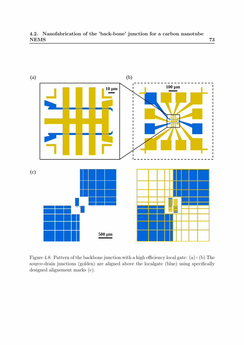
4.2. Nanofabrication of the ’back-bone’ junction for a carbon nanotubeNEMS 73
(a) (b)
10 µm 100 µm
(c)
500 µm
Figure 4.8: Pattern of the backbone junction with a high efficiency local gate: (a)+(b) Thesource-drain junctions (golden) are aligned above the localgate (blue) using specificallydesigned alignement marks (c).
74Chapter 4. Nanofabrication and characterisation of carbon nanotube based
NEMS and molecular spintronic devices
(a) (b)
Figure 4.9: Photography of the backbone junction array for carbon nanotube NEMSdisplaying (a) eight electrode pairs with a gap of 1 µm each aligned over a localgate(blue) and (b) linked with bonding pads designed for electrical connection.
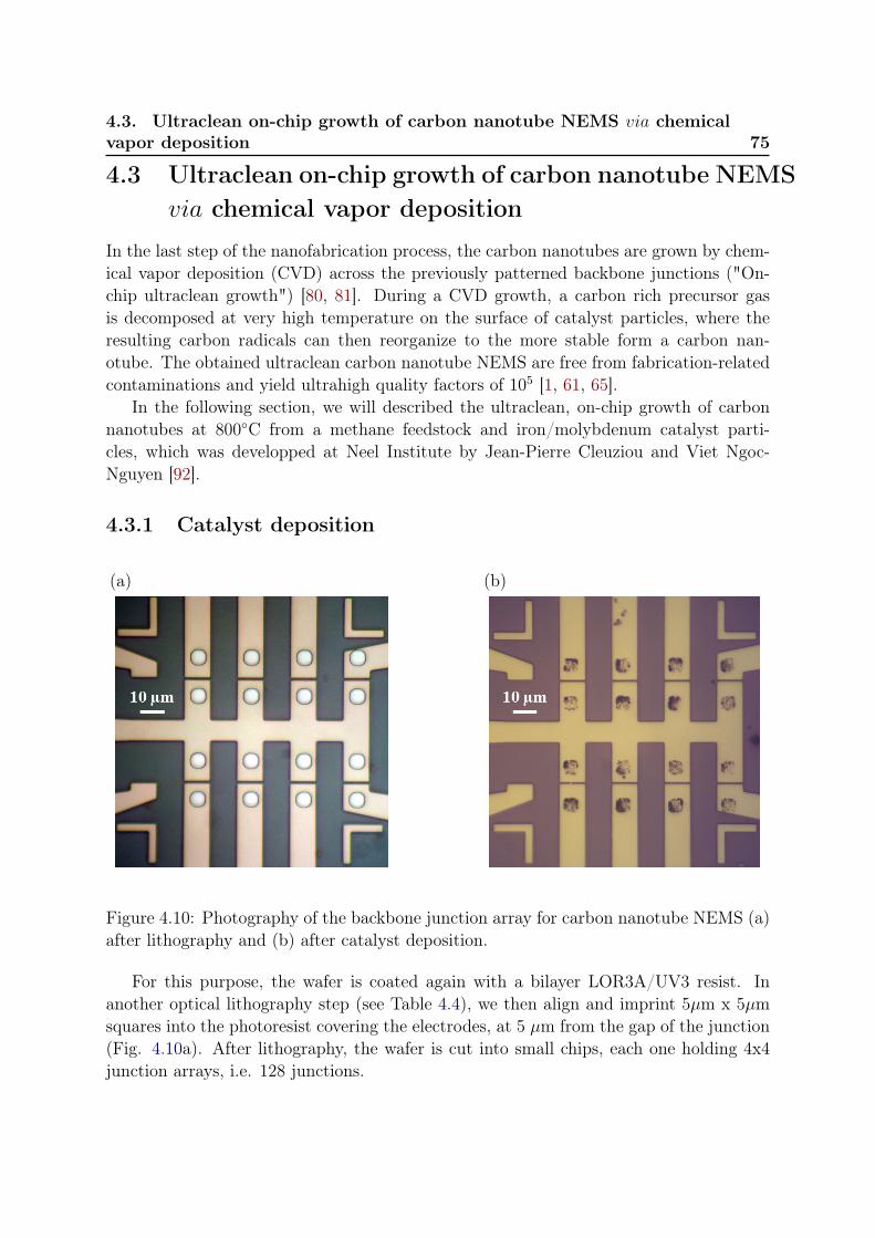
4.3. Ultraclean on-chip growth of carbon nanotube NEMS via chemicalvapor deposition 75
4.3 Ultraclean on-chip growth of carbon nanotube NEMSvia chemical vapor deposition
In the last step of the nanofabrication process, the carbon nanotubes are grown by chem-ical vapor deposition (CVD) across the previously patterned backbone junctions ("On-chip ultraclean growth") [80, 81]. During a CVD growth, a carbon rich precursor gasis decomposed at very high temperature on the surface of catalyst particles, where theresulting carbon radicals can then reorganize to the more stable form a carbon nan-otube. The obtained ultraclean carbon nanotube NEMS are free from fabrication-relatedcontaminations and yield ultrahigh quality factors of 105 [1, 61, 65].
In the following section, we will described the ultraclean, on-chip growth of carbonnanotubes at 800C from a methane feedstock and iron/molybdenum catalyst parti-cles, which was developped at Neel Institute by Jean-Pierre Cleuziou and Viet Ngoc-Nguyen [92].
4.3.1 Catalyst deposition
(a) (b)
Figure 4.10: Photography of the backbone junction array for carbon nanotube NEMS (a)after lithography and (b) after catalyst deposition.
For this purpose, the wafer is coated again with a bilayer LOR3A/UV3 resist. Inanother optical lithography step (see Table 4.4), we then align and imprint 5µm x 5µmsquares into the photoresist covering the electrodes, at 5 µm from the gap of the junction(Fig. 4.10a). After lithography, the wafer is cut into small chips, each one holding 4x4junction arrays, i.e. 128 junctions.
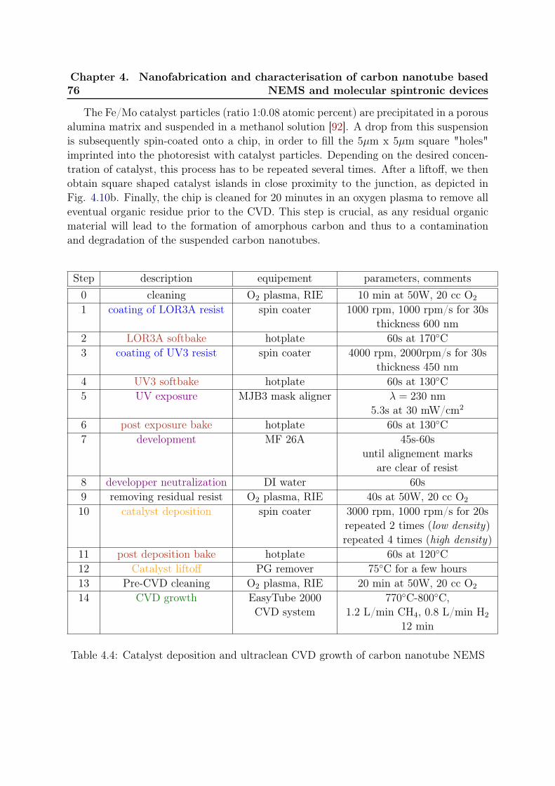
76Chapter 4. Nanofabrication and characterisation of carbon nanotube based
NEMS and molecular spintronic devices
The Fe/Mo catalyst particles (ratio 1:0.08 atomic percent) are precipitated in a porousalumina matrix and suspended in a methanol solution [92]. A drop from this suspensionis subsequently spin-coated onto a chip, in order to fill the 5µm x 5µm square "holes"imprinted into the photoresist with catalyst particles. Depending on the desired concen-tration of catalyst, this process has to be repeated several times. After a liftoff, we thenobtain square shaped catalyst islands in close proximity to the junction, as depicted inFig. 4.10b. Finally, the chip is cleaned for 20 minutes in an oxygen plasma to remove alleventual organic residue prior to the CVD. This step is crucial, as any residual organicmaterial will lead to the formation of amorphous carbon and thus to a contaminationand degradation of the suspended carbon nanotubes.
Step description equipement parameters, comments0 cleaning O2 plasma, RIE 10 min at 50W, 20 cc O2
1 coating of LOR3A resist spin coater 1000 rpm, 1000 rpm/s for 30sthickness 600 nm
2 LOR3A softbake hotplate 60s at 170C3 coating of UV3 resist spin coater 4000 rpm, 2000rpm/s for 30s
thickness 450 nm4 UV3 softbake hotplate 60s at 130C5 UV exposure MJB3 mask aligner λ = 230 nm
5.3s at 30 mW/cm2
6 post exposure bake hotplate 60s at 130C7 development MF 26A 45s-60s
until alignement marksare clear of resist
8 developper neutralization DI water 60s9 removing residual resist O2 plasma, RIE 40s at 50W, 20 cc O2
10 catalyst deposition spin coater 3000 rpm, 1000 rpm/s for 20srepeated 2 times (low density)repeated 4 times (high density)
11 post deposition bake hotplate 60s at 120C12 Catalyst liftoff PG remover 75C for a few hours13 Pre-CVD cleaning O2 plasma, RIE 20 min at 50W, 20 cc O2
14 CVD growth EasyTube 2000 770C-800C,CVD system 1.2 L/min CH4, 0.8 L/min H2
12 min
Table 4.4: Catalyst deposition and ultraclean CVD growth of carbon nanotube NEMS
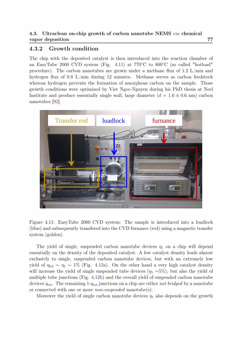
4.3. Ultraclean on-chip growth of carbon nanotube NEMS via chemicalvapor deposition 77
4.3.2 Growth condition
The chip with the deposited catalyst is then introduced into the reaction chamber ofan EasyTube 2000 CVD system (Fig. 4.11) at 770C to 800C (so called "hotload"procedure). The carbon nanotubes are grown under a methane flux of 1.2 L/min andhydrogen flux of 0.8 L/min during 12 minutes. Methane serves as carbon feedstockwhereas hydrogen prevents the formation of amorphous carbon on the sample. Thosegrowth conditions were optimized by Viet Ngoc-Nguyen during his PhD thesis at NeelInstitute and produce essentially single wall, large diameter (d = 1.6 ± 0.6 nm) carbonnanotubes [92].
furnanceloadlockTransfer rod
Figure 4.11: EasyTube 2000 CVD system: The sample is introduced into a loadlock(blue) and subsequently transfered into the CVD furnance (red) using a magnetic transfersystem (golden).
The yield of single, suspended carbon nanotube devices η1 on a chip will dependessentially on the density of the deposited catalyst. A low catalyst density leads almostexclusivly to single, suspended carbon nanotube devices, but with an extremely lowyield of ηtot ∼ η1 ∼ 1% (Fig. 4.12a). On the other hand a very high catalyst densitywill increase the yield of single suspended tube devices (η1 ∼5%), but also the yield ofmultiple tube junctions (Fig. 4.12b) and the overall yield of suspended carbon nanotubedevices ηtot. The remaining 1-ηtot junctions on a chip are either not bridged by a nanotubeor connected with one or more non-suspended nanotube(s).
Moreover the yield of single carbon nanotube devices η1 also depends on the growth
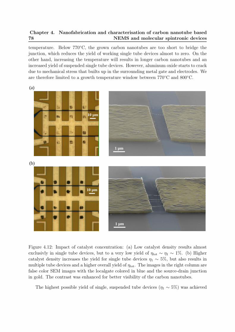
78Chapter 4. Nanofabrication and characterisation of carbon nanotube based
NEMS and molecular spintronic devices
temperature. Below 770C, the grown carbon nanotubes are too short to bridge thejunction, which reduces the yield of working single tube devices almost to zero. On theother hand, increasing the temperature will results in longer carbon nanotubes and anincreased yield of suspended single tube devices. However, aluminum oxide starts to crackdue to mechanical stress that builts up in the surrounding metal gate and electrodes. Weare therefore limited to a growth temperature window between 770C and 800C.
10 µm
1 µm
10 µm
1 µm
(a)
(b)
Figure 4.12: Impact of catalyst concentration: (a) Low catalyst density results almostexclusivly in single tube devices, but to a very low yield of ηtot ∼ η1 ∼ 1%. (b) Highercatalyst density increases the yield for single tube devices η1 ∼ 5%, but also results inmultiple tube devices and a higher overall yield of ηtot. The images in the right column arefalse color SEM images with the localgate colored in blue and the source-drain junctionin gold. The contrast was enhanced for better visibility of the carbon nanotubes.
The highest possible yield of single, suspended tube devices (η1 ∼ 5%) was achieved
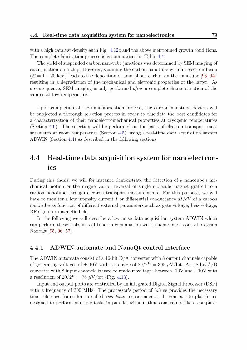
4.4. Real-time data acquisition system for nanoelectronics 79
with a high catalyst density as in Fig. 4.12b and the above mentionned growth conditions.The complete fabrication process is is summarized in Table 4.4.
The yield of suspended carbon nanotube junctions was determined by SEM imaging ofeach junction on a chip. However, scanning the carbon nanotube with an electron beam(E = 1− 20 keV) leads to the deposition of amorphous carbon on the nanotube [93, 94],resulting in a degradation of the mechanical and eletronic properties of the latter. Asa consequence, SEM imaging is only performed after a complete characterisation of thesample at low temperature.
Upon completion of the nanofabrication process, the carbon nanotube devices willbe subjected a thorough selection process in order to elucidate the best candidates fora characterization of their nanoelectromechanical properties at cryogenic temperatures(Section 4.6). The selection will be performed on the basis of electron transport mea-surements at room temperature (Section 4.5), using a real-time data acquisition systemADWIN (Section 4.4) as described in the following sections.
4.4 Real-time data acquisition system for nanoelectron-ics
During this thesis, we will for instance demonstrate the detection of a nanotube’s me-chanical motion or the magnetization reversal of single molecule magnet grafted to acarbon nanotube through electron transport measurements. For this purpose, we willhave to monitor a low intensity current I or differential conductance dI/dV of a carbonnanotube as function of different external parameters such as gate voltage, bias voltage,RF signal or magnetic field.
In the following we will describe a low noise data acquisition system ADWIN whichcan perform these tasks in real-time, in combination with a home-made control programNanoQt [95, 96, 57].
4.4.1 ADWIN automate and NanoQt control interface
The ADWIN automate consist of a 16-bit D/A converter with 8 output channels capableof generating voltages of ± 10V with a stepsize of 20/216 = 305 µV/bit. An 18-bit A/Dconverter with 8 input channels is used to readout voltages between -10V and +10V witha resolution of 20/218 = 76 µV/bit (Fig. 4.13).
Input and output ports are controlled by an integrated Digital Signal Processor (DSP)with a frequency of 300 MHz. The processor’s period of 3.3 ns provides the necessarytime reference frame for so called real time measurements. In contrast to plateformsdesigned to perform multiple tasks in parallel without time constraints like a computer
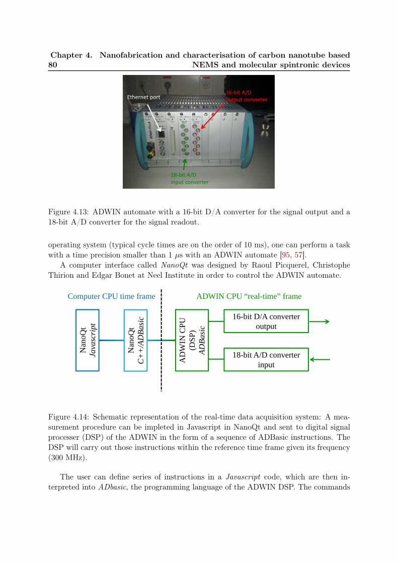
80Chapter 4. Nanofabrication and characterisation of carbon nanotube based
NEMS and molecular spintronic devices
16‐bit A/D output converter
18‐bit A/D input converter
Ethernet port
Figure 4.13: ADWIN automate with a 16-bit D/A converter for the signal output and a18-bit A/D converter for the signal readout.
operating system (typical cycle times are on the order of 10 ms), one can perform a taskwith a time precision smaller than 1 µs with an ADWIN automate [95, 57].
A computer interface called NanoQt was designed by Raoul Picquerel, ChristopheThirion and Edgar Bonet at Neel Institute in order to control the ADWIN automate.
16-bit D/A converteroutput
18-bit A/D converterinputA
DW
IN C
PU(D
SP)
ADBa
sic
Nan
oQt
C+
+/A
DBa
sic
Nan
oQt
Java
scri
pt
ADWIN CPU “real-time” frameComputer CPU time frame
Figure 4.14: Schematic representation of the real-time data acquisition system: A mea-surement procedure can be impleted in Javascript in NanoQt and sent to digital signalprocesser (DSP) of the ADWIN in the form of a sequence of ADBasic instructions. TheDSP will carry out those instructions within the reference time frame given its frequency(300 MHz).
The user can define series of instructions in a Javascript code, which are then in-terpreted into ADbasic, the programming language of the ADWIN DSP. The commands
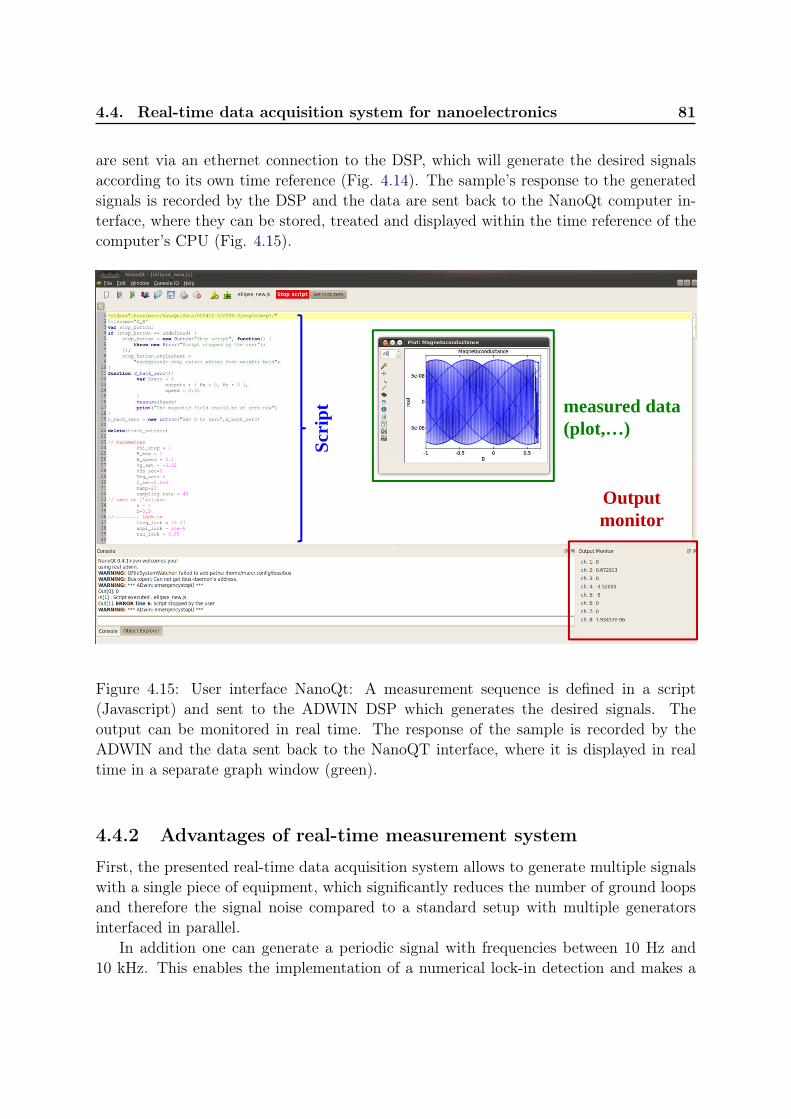
4.4. Real-time data acquisition system for nanoelectronics 81
are sent via an ethernet connection to the DSP, which will generate the desired signalsaccording to its own time reference (Fig. 4.14). The sample’s response to the generatedsignals is recorded by the DSP and the data are sent back to the NanoQt computer in-terface, where they can be stored, treated and displayed within the time reference of thecomputer’s CPU (Fig. 4.15).
Output monitor
Scri
pt measured data(plot,…)
Figure 4.15: User interface NanoQt: A measurement sequence is defined in a script(Javascript) and sent to the ADWIN DSP which generates the desired signals. Theoutput can be monitored in real time. The response of the sample is recorded by theADWIN and the data sent back to the NanoQT interface, where it is displayed in realtime in a separate graph window (green).
4.4.2 Advantages of real-time measurement system
First, the presented real-time data acquisition system allows to generate multiple signalswith a single piece of equipment, which significantly reduces the number of ground loopsand therefore the signal noise compared to a standard setup with multiple generatorsinterfaced in parallel.
In addition one can generate a periodic signal with frequencies between 10 Hz and10 kHz. This enables the implementation of a numerical lock-in detection and makes a
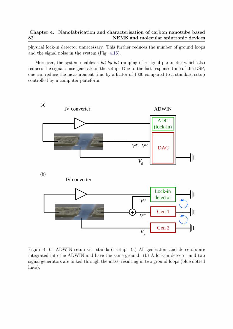
82Chapter 4. Nanofabrication and characterisation of carbon nanotube based
NEMS and molecular spintronic devices
physical lock-in detector unnecessary. This further reduces the number of ground loopsand the signal noise in the system (Fig. 4.16).
Moreover, the system enables a bit by bit ramping of a signal parameter which alsoreduces the signal noise generate in the setup. Due to the fast response time of the DSP,one can reduce the measurement time by a factor of 1000 compared to a standard setupcontrolled by a computer plateform.
(a)IV converter ADWIN
Vg
DAC
IV converter(b)
Lock-indetector
Vg
Vdc+ Gen 1
Gen 2
Vac
Vdc+Vac
ADC(lock-in)
Figure 4.16: ADWIN setup vs. standard setup: (a) All generators and detectors areintegrated into the ADWIN and have the same ground. (b) A lock-in detector and twosignal generators are linked through the mass, resulting in two ground loops (blue dottedlines).
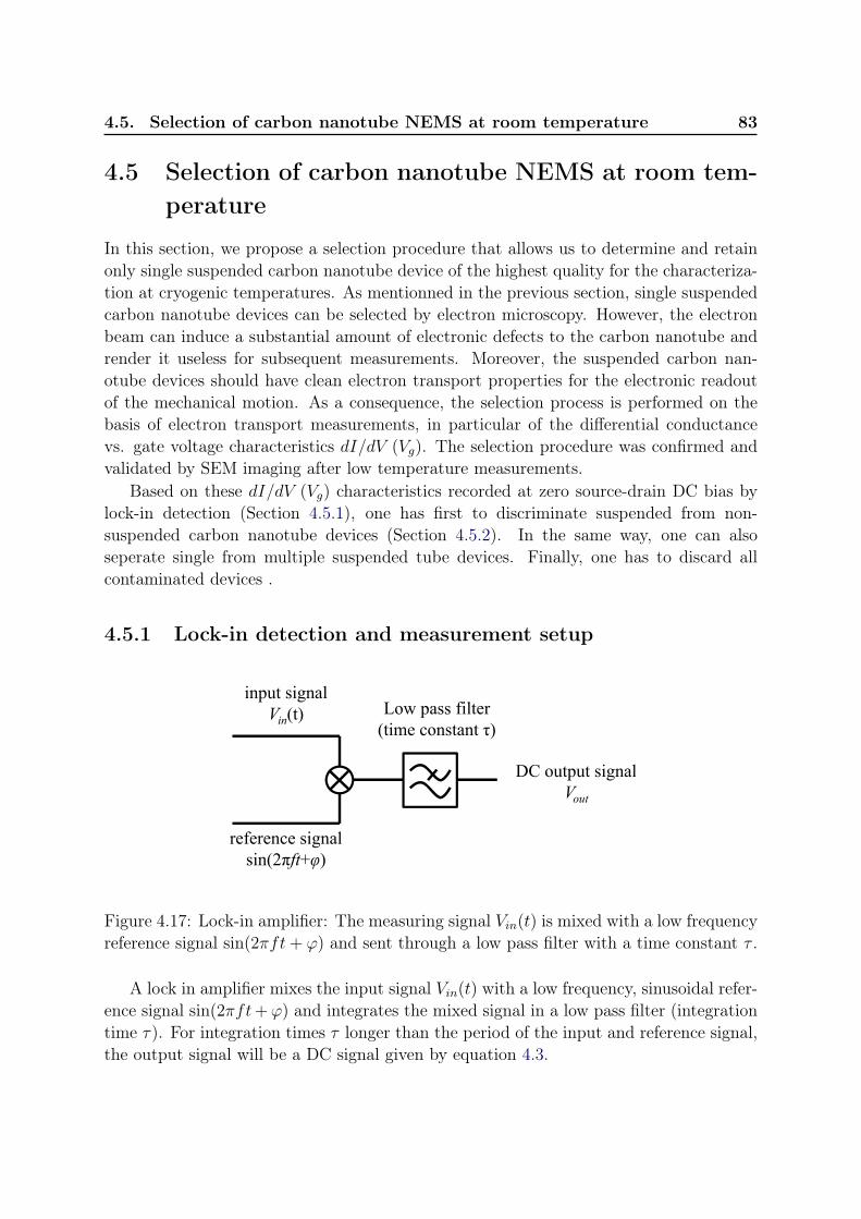
4.5. Selection of carbon nanotube NEMS at room temperature 83
4.5 Selection of carbon nanotube NEMS at room tem-perature
In this section, we propose a selection procedure that allows us to determine and retainonly single suspended carbon nanotube device of the highest quality for the characteriza-tion at cryogenic temperatures. As mentionned in the previous section, single suspendedcarbon nanotube devices can be selected by electron microscopy. However, the electronbeam can induce a substantial amount of electronic defects to the carbon nanotube andrender it useless for subsequent measurements. Moreover, the suspended carbon nan-otube devices should have clean electron transport properties for the electronic readoutof the mechanical motion. As a consequence, the selection process is performed on thebasis of electron transport measurements, in particular of the differential conductancevs. gate voltage characteristics dI/dV (Vg). The selection procedure was confirmed andvalidated by SEM imaging after low temperature measurements.
Based on these dI/dV (Vg) characteristics recorded at zero source-drain DC bias bylock-in detection (Section 4.5.1), one has first to discriminate suspended from non-suspended carbon nanotube devices (Section 4.5.2). In the same way, one can alsoseperate single from multiple suspended tube devices. Finally, one has to discard allcontaminated devices .
4.5.1 Lock-in detection and measurement setup
reference signal sin(2πft+φ)
input signalVin(t) Low pass filter
(time constant τ)
DC output signalVout
Figure 4.17: Lock-in amplifier: The measuring signal Vin(t) is mixed with a low frequencyreference signal sin(2πft+ ϕ) and sent through a low pass filter with a time constant τ .
A lock in amplifier mixes the input signal Vin(t) with a low frequency, sinusoidal refer-ence signal sin(2πft+ϕ) and integrates the mixed signal in a low pass filter (integrationtime τ). For integration times τ longer than the period of the input and reference signal,the output signal will be a DC signal given by equation 4.3.
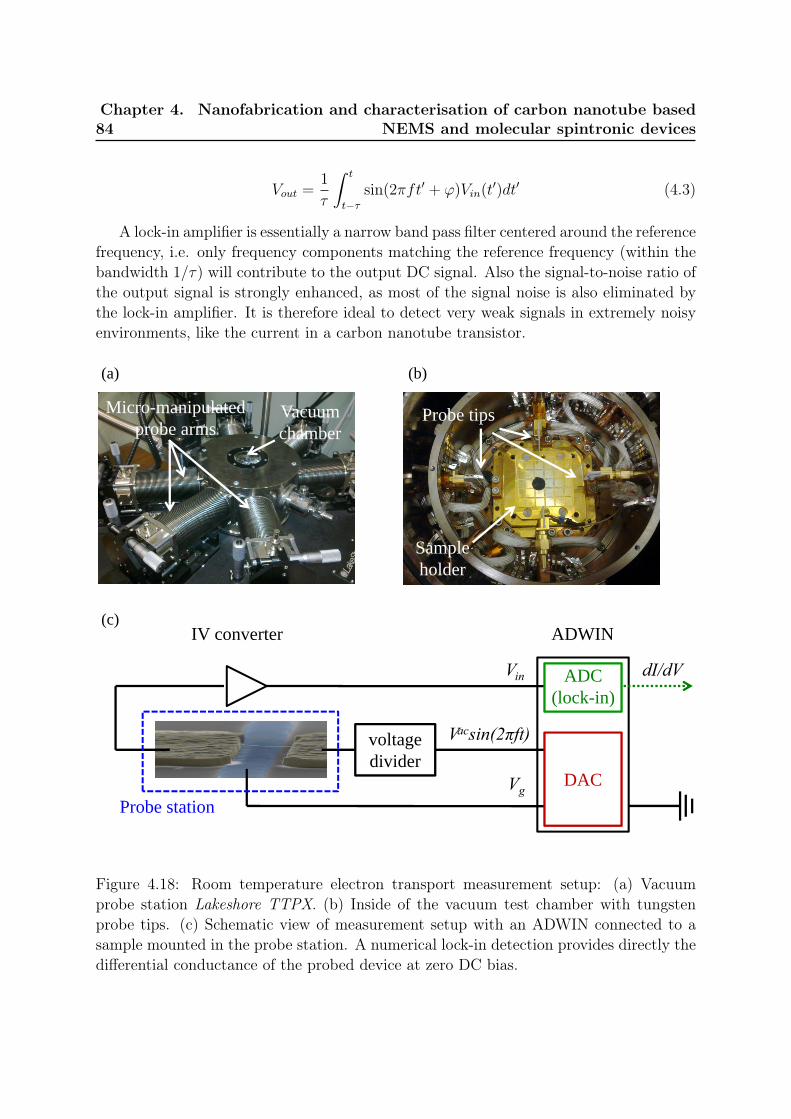
84Chapter 4. Nanofabrication and characterisation of carbon nanotube based
NEMS and molecular spintronic devices
Vout =1
τ
∫ t
t−τsin(2πft′ + ϕ)Vin(t′)dt′ (4.3)
A lock-in amplifier is essentially a narrow band pass filter centered around the referencefrequency, i.e. only frequency components matching the reference frequency (within thebandwidth 1/τ) will contribute to the output DC signal. Also the signal-to-noise ratio ofthe output signal is strongly enhanced, as most of the signal noise is also eliminated bythe lock-in amplifier. It is therefore ideal to detect very weak signals in extremely noisyenvironments, like the current in a carbon nanotube transistor.
Vacuum chamber
Probe tips
Sampleholder
Micro-manipulated probe arms
(a) (b)
IV converter
voltage divider
ADWIN
ADC(lock-in)
Vg
Vacsin(2πft)
(c)
Probe stationDAC
dI/dVVin
Figure 4.18: Room temperature electron transport measurement setup: (a) Vacuumprobe station Lakeshore TTPX. (b) Inside of the vacuum test chamber with tungstenprobe tips. (c) Schematic view of measurement setup with an ADWIN connected to asample mounted in the probe station. A numerical lock-in detection provides directly thedifferential conductance of the probed device at zero DC bias.
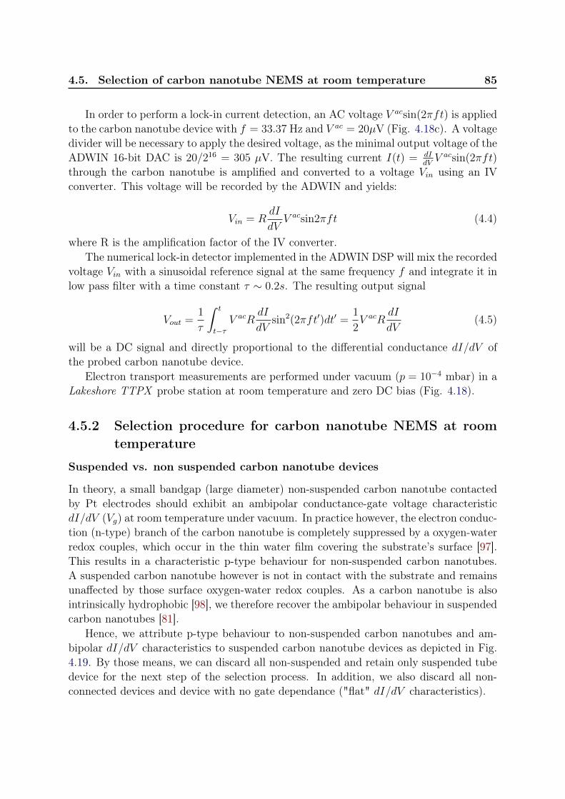
4.5. Selection of carbon nanotube NEMS at room temperature 85
In order to perform a lock-in current detection, an AC voltage V acsin(2πft) is appliedto the carbon nanotube device with f = 33.37 Hz and V ac = 20µV (Fig. 4.18c). A voltagedivider will be necessary to apply the desired voltage, as the minimal output voltage of theADWIN 16-bit DAC is 20/216 = 305 µV. The resulting current I(t) = dI
dVV acsin(2πft)
through the carbon nanotube is amplified and converted to a voltage Vin using an IVconverter. This voltage will be recorded by the ADWIN and yields:
Vin = RdI
dVV acsin2πft (4.4)
where R is the amplification factor of the IV converter.The numerical lock-in detector implemented in the ADWIN DSP will mix the recorded
voltage Vin with a sinusoidal reference signal at the same frequency f and integrate it inlow pass filter with a time constant τ ∼ 0.2s. The resulting output signal
Vout =1
τ
∫ t
t−τV acR
dI
dVsin2(2πft′)dt′ =
1
2V acR
dI
dV(4.5)
will be a DC signal and directly proportional to the differential conductance dI/dV ofthe probed carbon nanotube device.
Electron transport measurements are performed under vacuum (p = 10−4 mbar) in aLakeshore TTPX probe station at room temperature and zero DC bias (Fig. 4.18).
4.5.2 Selection procedure for carbon nanotube NEMS at roomtemperature
Suspended vs. non suspended carbon nanotube devices
In theory, a small bandgap (large diameter) non-suspended carbon nanotube contactedby Pt electrodes should exhibit an ambipolar conductance-gate voltage characteristicdI/dV (Vg) at room temperature under vacuum. In practice however, the electron conduc-tion (n-type) branch of the carbon nanotube is completely suppressed by a oxygen-waterredox couples, which occur in the thin water film covering the substrate’s surface [97].This results in a characteristic p-type behaviour for non-suspended carbon nanotubes.A suspended carbon nanotube however is not in contact with the substrate and remainsunaffected by those surface oxygen-water redox couples. As a carbon nanotube is alsointrinsically hydrophobic [98], we therefore recover the ambipolar behaviour in suspendedcarbon nanotubes [81].
Hence, we attribute p-type behaviour to non-suspended carbon nanotubes and am-bipolar dI/dV characteristics to suspended carbon nanotube devices as depicted in Fig.4.19. By those means, we can discard all non-suspended and retain only suspended tubedevice for the next step of the selection process. In addition, we also discard all non-connected devices and device with no gate dependance ("flat" dI/dV characteristics).
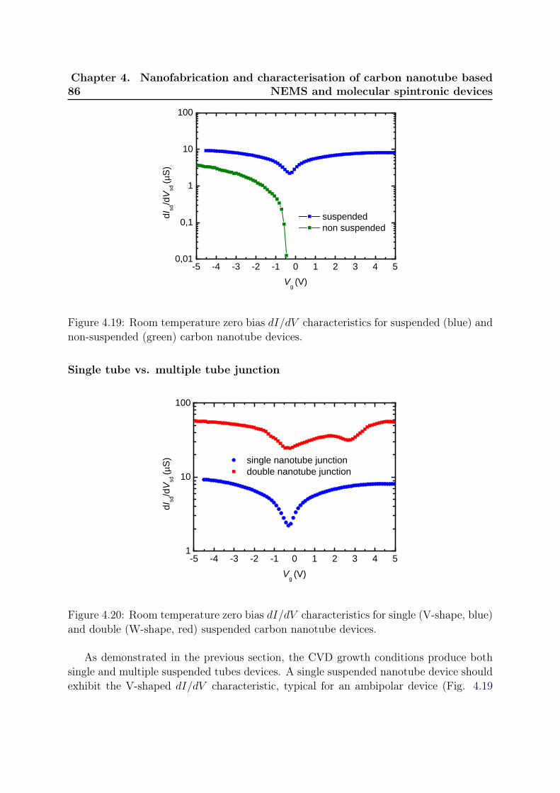
86Chapter 4. Nanofabrication and characterisation of carbon nanotube based
NEMS and molecular spintronic devices
- 5 - 4 - 3 - 2 - 1 0 1 2 3 4 50 , 0 1
0 , 1
1
1 0
1 0 0
s u s p e n d e d n o n s u s p e n d e d
dI sd/dV
sd (µS
)
V g ( V )
Figure 4.19: Room temperature zero bias dI/dV characteristics for suspended (blue) andnon-suspended (green) carbon nanotube devices.
Single tube vs. multiple tube junction
- 5 - 4 - 3 - 2 - 1 0 1 2 3 4 51
1 0
1 0 0
s i n g l e n a n o t u b e j u n c t i o n d o u b l e n a n o t u b e j u n c t i o n
dI sd/dV
sd (µS
)
V g ( V )
Figure 4.20: Room temperature zero bias dI/dV characteristics for single (V-shape, blue)and double (W-shape, red) suspended carbon nanotube devices.
As demonstrated in the previous section, the CVD growth conditions produce bothsingle and multiple suspended tubes devices. A single suspended nanotube device shouldexhibit the V-shaped dI/dV characteristic, typical for an ambipolar device (Fig. 4.19
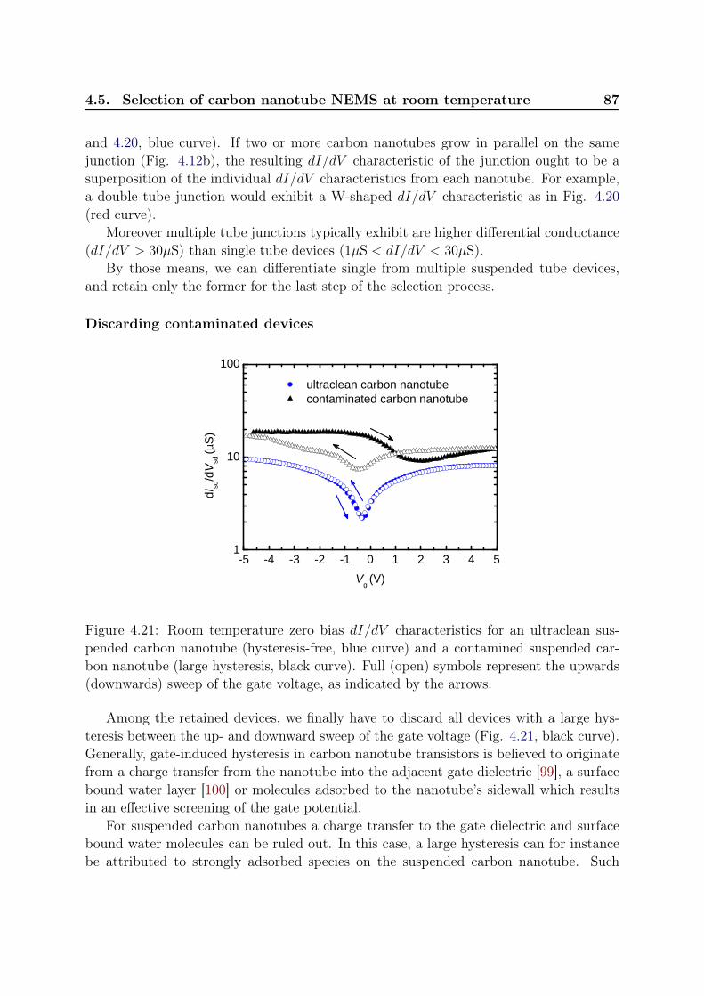
4.5. Selection of carbon nanotube NEMS at room temperature 87
and 4.20, blue curve). If two or more carbon nanotubes grow in parallel on the samejunction (Fig. 4.12b), the resulting dI/dV characteristic of the junction ought to be asuperposition of the individual dI/dV characteristics from each nanotube. For example,a double tube junction would exhibit a W-shaped dI/dV characteristic as in Fig. 4.20(red curve).
Moreover multiple tube junctions typically exhibit are higher differential conductance(dI/dV > 30µS) than single tube devices (1µS < dI/dV < 30µS).
By those means, we can differentiate single from multiple suspended tube devices,and retain only the former for the last step of the selection process.
Discarding contaminated devices
- 5 - 4 - 3 - 2 - 1 0 1 2 3 4 51
1 0
1 0 0 u l t r a c l e a n c a r b o n n a n o t u b e c o n t a m i n a t e d c a r b o n n a n o t u b e
dI sd/dV
sd (µS
)
V g ( V )
Figure 4.21: Room temperature zero bias dI/dV characteristics for an ultraclean sus-pended carbon nanotube (hysteresis-free, blue curve) and a contamined suspended car-bon nanotube (large hysteresis, black curve). Full (open) symbols represent the upwards(downwards) sweep of the gate voltage, as indicated by the arrows.
Among the retained devices, we finally have to discard all devices with a large hys-teresis between the up- and downward sweep of the gate voltage (Fig. 4.21, black curve).Generally, gate-induced hysteresis in carbon nanotube transistors is believed to originatefrom a charge transfer from the nanotube into the adjacent gate dielectric [99], a surfacebound water layer [100] or molecules adsorbed to the nanotube’s sidewall which resultsin an effective screening of the gate potential.
For suspended carbon nanotubes a charge transfer to the gate dielectric and surfacebound water molecules can be ruled out. In this case, a large hysteresis can for instancebe attributed to strongly adsorbed species on the suspended carbon nanotube. Such
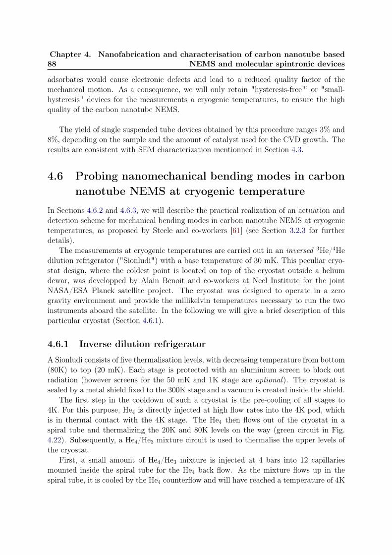
88Chapter 4. Nanofabrication and characterisation of carbon nanotube based
NEMS and molecular spintronic devices
adsorbates would cause electronic defects and lead to a reduced quality factor of themechanical motion. As a consequence, we will only retain "hysteresis-free"’ or "small-hysteresis" devices for the measurements a cryogenic temperatures, to ensure the highquality of the carbon nanotube NEMS.
The yield of single suspended tube devices obtained by this procedure ranges 3% and8%, depending on the sample and the amount of catalyst used for the CVD growth. Theresults are consistent with SEM characterization mentionned in Section 4.3.
4.6 Probing nanomechanical bending modes in carbonnanotube NEMS at cryogenic temperature
In Sections 4.6.2 and 4.6.3, we will describe the practical realization of an actuation anddetection scheme for mechanical bending modes in carbon nanotube NEMS at cryogenictemperatures, as proposed by Steele and co-workers [61] (see Section 3.2.3 for furtherdetails).
The measurements at cryogenic temperatures are carried out in an inversed 3He/4Hedilution refrigerator ("Sionludi") with a base temperature of 30 mK. This peculiar cryo-stat design, where the coldest point is located on top of the cryostat outside a heliumdewar, was developped by Alain Benoit and co-workers at Neel Institute for the jointNASA/ESA Planck satellite project. The cryostat was designed to operate in a zerogravity environment and provide the millikelvin temperatures necessary to run the twoinstruments aboard the satellite. In the following we will give a brief description of thisparticular cryostat (Section 4.6.1).
4.6.1 Inverse dilution refrigerator
A Sionludi consists of five thermalisation levels, with decreasing temperature from bottom(80K) to top (20 mK). Each stage is protected with an aluminium screen to block outradiation (however screens for the 50 mK and 1K stage are optional). The cryostat issealed by a metal shield fixed to the 300K stage and a vacuum is created inside the shield.
The first step in the cooldown of such a cryostat is the pre-cooling of all stages to4K. For this purpose, He4 is directly injected at high flow rates into the 4K pod, whichis in thermal contact with the 4K stage. The He4 then flows out of the cryostat in aspiral tube and thermalizing the 20K and 80K levels on the way (green circuit in Fig.4.22). Subsequently, a He4/He3 mixture circuit is used to thermalise the upper levels ofthe cryostat.
First, a small amount of He4/He3 mixture is injected at 4 bars into 12 capillariesmounted inside the spiral tube for the He4 back flow. As the mixture flows up in thespiral tube, it is cooled by the He4 counterflow and will have reached a temperature of 4K
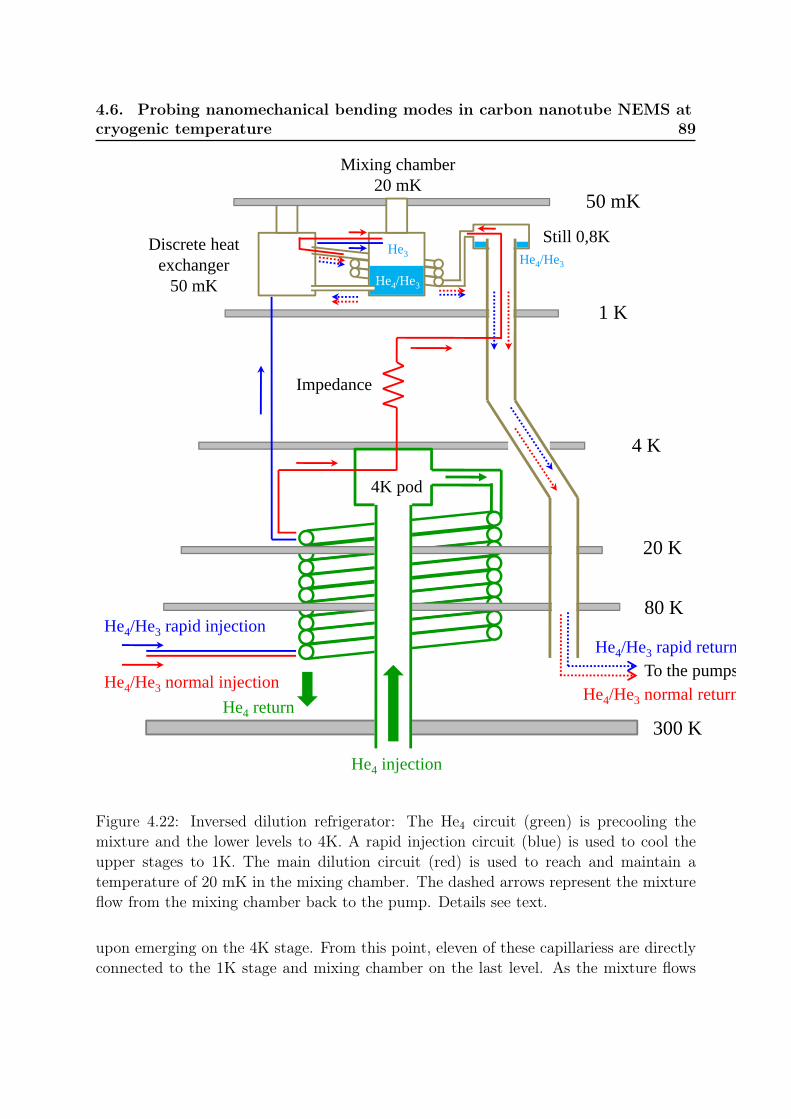
4.6. Probing nanomechanical bending modes in carbon nanotube NEMS atcryogenic temperature 89
300 K
80 K
20 K
4 K
1 K
50 mK
He4 injection
He4 return
Still 0,8K
He4/He3 rapid injection
He4/He3 normal injection
MCDiscrete heat
exchanger50 mK
He4/He3 rapid return
He4/He3 normal return
Mixing chamber20 mK
Impedance
He4/He3
He4/He3
4K pod
He3
To the pumps
Figure 4.22: Inversed dilution refrigerator: The He4 circuit (green) is precooling themixture and the lower levels to 4K. A rapid injection circuit (blue) is used to cool theupper stages to 1K. The main dilution circuit (red) is used to reach and maintain atemperature of 20 mK in the mixing chamber. The dashed arrows represent the mixtureflow from the mixing chamber back to the pump. Details see text.
upon emerging on the 4K stage. From this point, eleven of these capillariess are directlyconnected to the 1K stage and mixing chamber on the last level. As the mixture flows
90Chapter 4. Nanofabrication and characterisation of carbon nanotube based
NEMS and molecular spintronic devices
through this rapid injection circuit (blue circuit in Fig. 4.22), the upper levels can becooled to 4K. The remaining capillary leads through a Joule-Thomson impedance intothe still, thermalized to the 1K stage, and from there into the mixing chamber throughtwo heat exchangers (a countinuous counterflow and a discrete exchanger). This normalinjection capillarity is the main dilution circuit of the cryostat (red circuit in Fig. 4.22).From the mixing chamber both circuits flow back through the heat exchangers, the stilland out of the cryostat (dashed arrows). A primary pump and a compressor ensures thecirculation of the mixture.
Once all stages have reached a temperature of 4K, an additional roots pump is turnedon in order to enhance the vacuum in the dilution circuit. The circulating mixture willundergo an expansion at the Joule-Thomson impedance and cool to approximately 1K.As the mixture starts to condense in the still and the mixing chamber, the rapid injectioncircuit is closed.
Once a temperature of 800 mK is reached in the circuit, the phase separation of He4
and He3 will start in the mixing chamber. The continuous pumping with the primary andthe roots pump, will extract He3 from the consended mixture in the still and reinject itinto the mixing chamber through the dilution circuit. The He3 will then diffuse throughthe phase boundary from He3-rich phase into the He4-rich phases. This diffusion drawsheat energy from its surroundings which results in a cooling of the mixing chamber.This so called dilution process will provide the necessary cooling power to reach a basetemperature of 20 mK. This process sustains itself, as long as there is enough He4 in theprecooling circuit.
4.6.2 Measurement setup
After the fabrication and selection process is completed, the sample is mounted in thecryostat for low temperature measurement.
For this purpose, the sample is fixed on a specifically designed sampleholder usingsilver conductive paint. The selected carbon nanotube junctions on the sample are con-nected to Au strip lines integrated into the sampleholder by microbonded Al wires. Thesampleholder yields 24 Au strip lines in total, with 12 lines embedded into the sample-holder re-emerging above the sample (DC lines 1-12 Fig. 4.23) and 12 embedded linesre-emerging below the sample (DC lines 13-24 Fig. 4.23). Among the latter, four are alsoconnected to Au strip lines patterned on the surface, which are highlighted in blue in Fig.4.23. Each strip line is connected to a Au contact pad at the bottom of the sampleholder.The embedded Au lines are used to contact the gate and the source-drain electrodes ofeach selected device and perform DC current measurement. The four strip lines at thesurface (blue in Fig. 4.23) are used to inject a RF microwave signal to the gate of theselected devices and actuate the carbon nanotube resonator.
The sampleholder is subsequently mounted on a copper support above the mixingchamber in the cryostat, which will provide the necessary thermal contact between the
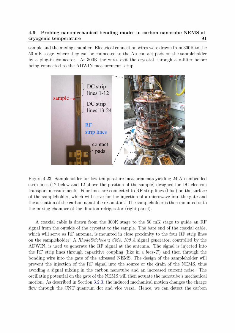
4.6. Probing nanomechanical bending modes in carbon nanotube NEMS atcryogenic temperature 91
sample and the mixing chamber. Electrical connection wires were drawn from 300K to the50 mK stage, where they can be connected to the Au contact pads on the sampleholderby a plug-in connector. At 300K the wires exit the cryostat through a π-filter beforebeing connected to the ADWIN measurement setup.
RFstrip lines
sample
DC strip lines 1-12
DC strip lines 13-24
contactpads
Figure 4.23: Sampleholder for low temperature measurements yielding 24 Au embeddedstrip lines (12 below and 12 above the position of the sample) designed for DC electrontransport measurements. Four lines are connected to RF strip lines (blue) on the surfaceof the sampleholder, which will serve for the injection of a microwave into the gate andthe actuation of the carbon nanotube resonators. The sampleholder is then mounted ontothe mixing chamber of the dilution refrigerator (right panel).
A coaxial cable is drawn from the 300K stage to the 50 mK stage to guide an RFsignal from the outside of the cryostat to the sample. The bare end of the coaxial cable,which will serve as RF antenna, is mounted in close proximity to the four RF strip lineson the sampleholder. A Rhode&Schwarz SMA 100 A signal generator, controlled by theADWIN, is used to generate the RF signal at the antenna. The signal is injected intothe RF strip lines through capacitive coupling (like in a bias-T ) and then through thebonding wire into the gate of the adressed NEMS. The design of the sampleholder willprevent the injection of the RF signal into the source or the drain of the NEMS, thusavoiding a signal mixing in the carbon nanotube and an increased current noise. Theoscillating potential on the gate of the NEMS will then actuate the nanotube’s mechanicalmotion. As described in Section 3.2.3, the induced mechanical motion changes the chargeflow through the CNT quantum dot and vice versa. Hence, we can detect the carbon
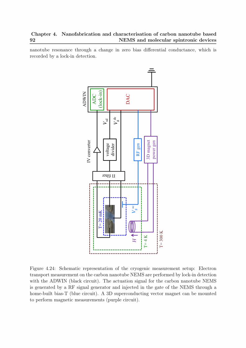
92Chapter 4. Nanofabrication and characterisation of carbon nanotube based
NEMS and molecular spintronic devices
nanotube resonance through a change in zero bias differential conductance, which isrecorded by a lock-in detection.
AD
C(lo
ck-in
)
DA
C
RF
gen
IV c
onve
rter
3D m
agne
t po
wer
gen
T= 4
K
T= 2
0 m
Kvo
ltage
di
vide
r
Πfilter
T= 3
00 K
V gac
V gdc
V sd
H
AD
WIN
Figure 4.24: Schematic representation of the cryogenic measurement setup: Electrontransport measurement on the carbon nanotube NEMS are performed by lock-in detectionwith the ADWIN (black circuit). The actuation signal for the carbon nanotube NEMSis generated by a RF signal generator and injected in the gate of the NEMS through ahome-built bias-T (blue circuit). A 3D superconducting vector magnet can be mountedto perform magnetic measurements (purple circuit).
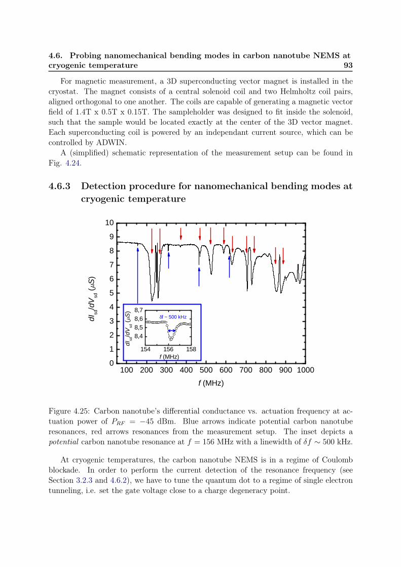
4.6. Probing nanomechanical bending modes in carbon nanotube NEMS atcryogenic temperature 93
For magnetic measurement, a 3D superconducting vector magnet is installed in thecryostat. The magnet consists of a central solenoid coil and two Helmholtz coil pairs,aligned orthogonal to one another. The coils are capable of generating a magnetic vectorfield of 1.4T x 0.5T x 0.15T. The sampleholder was designed to fit inside the solenoid,such that the sample would be located exactly at the center of the 3D vector magnet.Each superconducting coil is powered by an independant current source, which can becontrolled by ADWIN.
A (simplified) schematic representation of the measurement setup can be found inFig. 4.24.
4.6.3 Detection procedure for nanomechanical bending modes atcryogenic temperature
1 0 0 2 0 0 3 0 0 4 0 0 5 0 0 6 0 0 7 0 0 8 0 0 9 0 0 1 0 0 00123456789
1 0
1 5 4 1 5 6 1 5 88 , 48 , 58 , 68 , 7
dI sd/dV
sd (
S)
f ( M H z )
dI sd/dV
sd (
S)
f ( M H z )
δf ~ 5 0 0 k H z
Figure 4.25: Carbon nanotube’s differential conductance vs. actuation frequency at ac-tuation power of PRF = −45 dBm. Blue arrows indicate potential carbon nanotuberesonances, red arrows resonances from the measurement setup. The inset depicts apotential carbon nanotube resonance at f = 156 MHz with a linewidth of δf ∼ 500 kHz.
At cryogenic temperatures, the carbon nanotube NEMS is in a regime of Coulombblockade. In order to perform the current detection of the resonance frequency (seeSection 3.2.3 and 4.6.2), we have to tune the quantum dot to a regime of single electrontunneling, i.e. set the gate voltage close to a charge degeneracy point.
94Chapter 4. Nanofabrication and characterisation of carbon nanotube based
NEMS and molecular spintronic devices
A RF actuation signal is injected into the gate of the corresponding NEMS. As de-scribed in Section 3.2, the resonance frequency of the mechanical bending mode from acarbon nanotube resonator is on the order of a few hundred MHz for nanotube length’sbetween 500 nm and 1 µm. In order to find the nanotube’s resonance frequency, wetherefore sweep the RF frequency between 50 MHz and 1 GHz, while monitoring theconductance of the carbon nanotube NEMS recorded by lock-in detection. The outputpower of the signal generator is set between -40dBm and -50 dBm, to generate a largemotion amplitude and thus facilitating its detection. An example of such a sweep isdepicted in Fig. 4.25.
In Fig. 4.25, one will notice wide resonance features with a FWHM of a few tens ofMHz. Those low-Q resonances (Q ∼ 10−100) can be attributed for instance to resonancesin the measurement setup itself (RF coax cable, etc...) and shall be disregarded in thefollowing (red arrows in Fig. 4.25).
More interestingly, one can observe sharp conductance peaks (∆dI/dV > 0) or dips(∆dI/dV < 0), with a FWHM of a few hundred kHz and a relative amplitude change of|∆dI/dV |/|dI/dV | ≈ 5% at those RF power settings (blue arrows and inset Fig. 4.25).Those high-Q resonance lines (Q ∼ 1000) are a first strong indication for a mechanicalbending mode in the resonator.
However, one has to the confirm the nature of those resonances using a set of "fin-gerprints" unique to mechanical bending modes in carbon nanotube NEMS which weintroduced in chapter 3.
Driving power and high quality factor Q
According to Section 3.2, a first characteristic fingerprint of a carbon nanotube resonanceis its dependance on the actuation power. At high driving power, a carbon nanotuberesonator exhibits a strongly nonlinear behavior. Upon decreasing the driving power, theresonator is evolving from a Duffing-like oscillator to a harmonic oscillator (Fig. 4.26a).The resonance eventually vanishes, once the driving power drops below a threshold value,which is typically on the order of -80 dBm for our devices.
At a driving power just above threshold, the resonator behaves as a harmonic oscillatorand exhibits a typical Lorentzian line shape. The corresponding quality factor is on theorder of Q ∼ 104−105 (Fig. 4.26b) which is to be expected for ultraclean carbon nanotubeNEMS (Section 3.2).
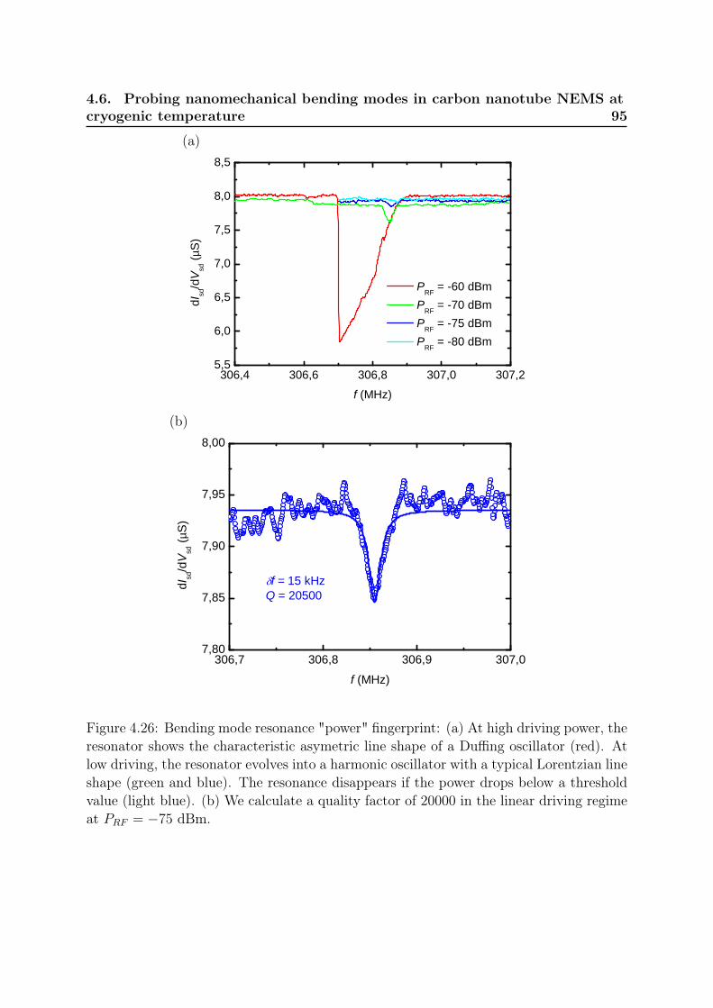
4.6. Probing nanomechanical bending modes in carbon nanotube NEMS atcryogenic temperature 95
(a)
3 0 6 , 4 3 0 6 , 6 3 0 6 , 8 3 0 7 , 0 3 0 7 , 25 , 5
6 , 0
6 , 5
7 , 0
7 , 5
8 , 0
8 , 5
P R F = - 6 0 d B m P R F = - 7 0 d B m P R F = - 7 5 d B m P R F = - 8 0 d B m
dI sd/dV
sd (µ
S)
f ( M H z )(b)
3 0 6 , 7 3 0 6 , 8 3 0 6 , 9 3 0 7 , 07 , 8 0
7 , 8 5
7 , 9 0
7 , 9 5
8 , 0 0
dI sd/dV
sd (µ
S)
f ( M H z )
f = 1 5 k H zQ = 2 0 5 0 0
Figure 4.26: Bending mode resonance "power" fingerprint: (a) At high driving power, theresonator shows the characteristic asymetric line shape of a Duffing oscillator (red). Atlow driving, the resonator evolves into a harmonic oscillator with a typical Lorentzian lineshape (green and blue). The resonance disappears if the power drops below a thresholdvalue (light blue). (b) We calculate a quality factor of 20000 in the linear driving regimeat PRF = −75 dBm.
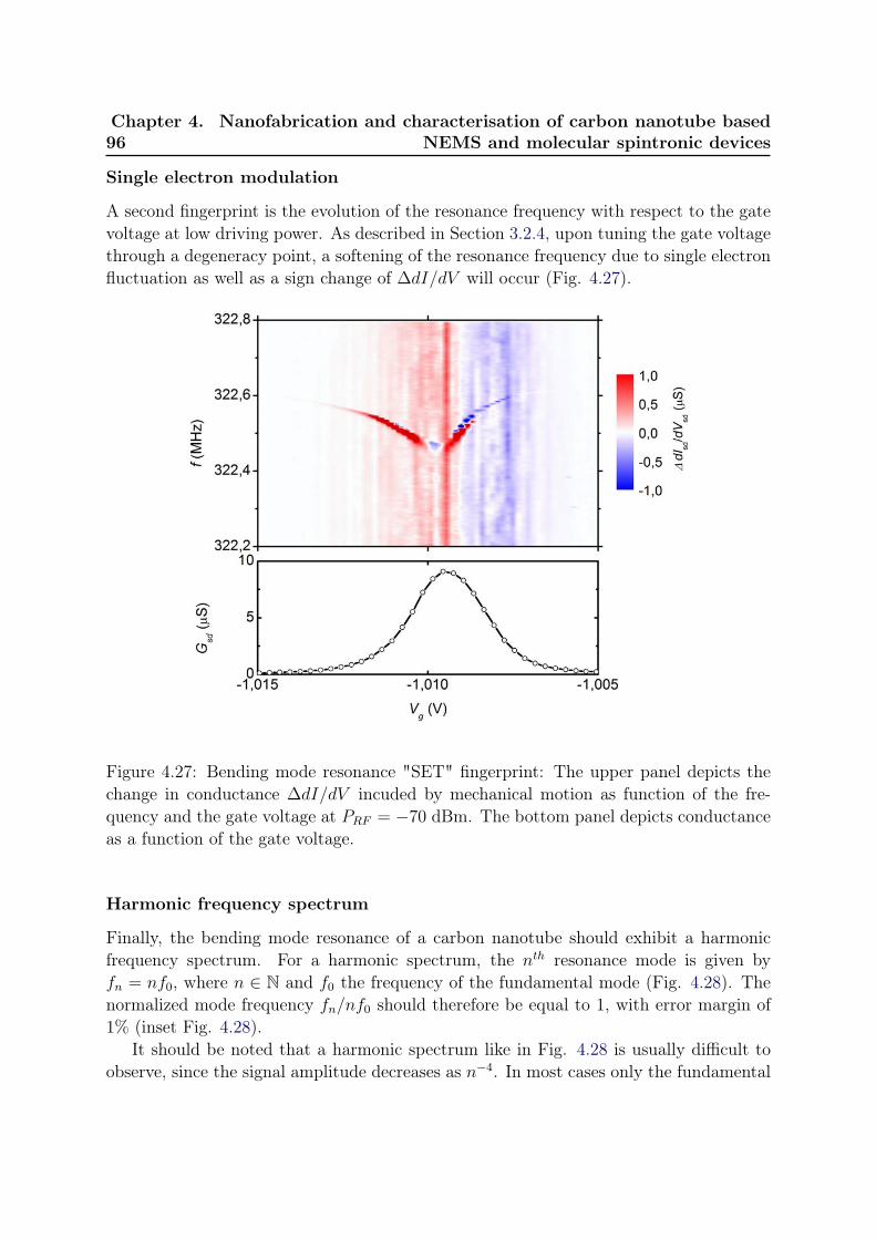
96Chapter 4. Nanofabrication and characterisation of carbon nanotube based
NEMS and molecular spintronic devices
Single electron modulation
A second fingerprint is the evolution of the resonance frequency with respect to the gatevoltage at low driving power. As described in Section 3.2.4, upon tuning the gate voltagethrough a degeneracy point, a softening of the resonance frequency due to single electronfluctuation as well as a sign change of ∆dI/dV will occur (Fig. 4.27).
Figure 4.27: Bending mode resonance "SET" fingerprint: The upper panel depicts thechange in conductance ∆dI/dV incuded by mechanical motion as function of the fre-quency and the gate voltage at PRF = −70 dBm. The bottom panel depicts conductanceas a function of the gate voltage.
Harmonic frequency spectrum
Finally, the bending mode resonance of a carbon nanotube should exhibit a harmonicfrequency spectrum. For a harmonic spectrum, the nth resonance mode is given byfn = nf0, where n ∈ N and f0 the frequency of the fundamental mode (Fig. 4.28). Thenormalized mode frequency fn/nf0 should therefore be equal to 1, with error margin of1% (inset Fig. 4.28).
It should be noted that a harmonic spectrum like in Fig. 4.28 is usually difficult toobserve, since the signal amplitude decreases as n−4. In most cases only the fundamental
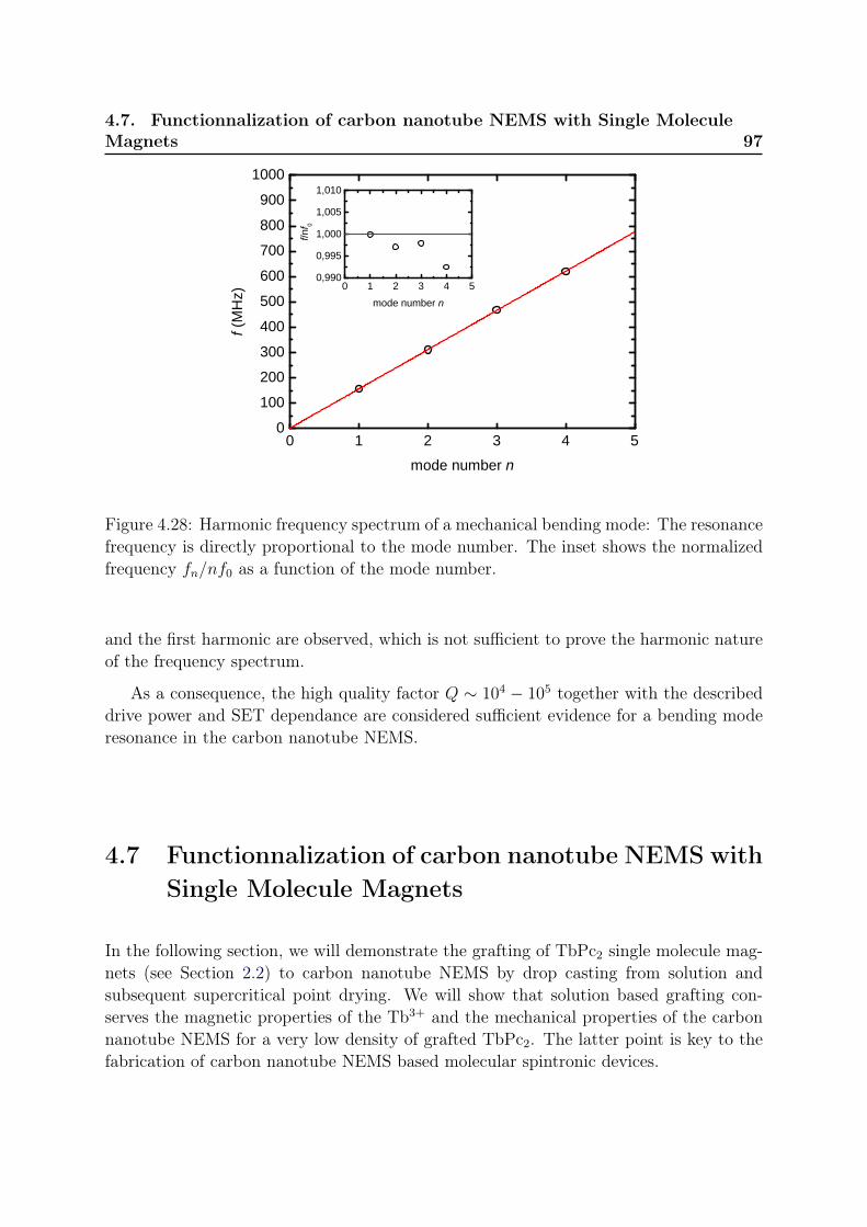
4.7. Functionnalization of carbon nanotube NEMS with Single MoleculeMagnets 97
0 1 2 3 4 501 0 02 0 03 0 04 0 05 0 06 0 07 0 08 0 09 0 0
1 0 0 0
0 1 2 3 4 50 , 9 9 00 , 9 9 51 , 0 0 01 , 0 0 51 , 0 1 0
f (MHz
)
m o d e n u m b e r n
f/nf 0
m o d e n u m b e r n
Figure 4.28: Harmonic frequency spectrum of a mechanical bending mode: The resonancefrequency is directly proportional to the mode number. The inset shows the normalizedfrequency fn/nf0 as a function of the mode number.
and the first harmonic are observed, which is not sufficient to prove the harmonic natureof the frequency spectrum.
As a consequence, the high quality factor Q ∼ 104 − 105 together with the describeddrive power and SET dependance are considered sufficient evidence for a bending moderesonance in the carbon nanotube NEMS.
4.7 Functionnalization of carbon nanotube NEMS withSingle Molecule Magnets
In the following section, we will demonstrate the grafting of TbPc2 single molecule mag-nets (see Section 2.2) to carbon nanotube NEMS by drop casting from solution andsubsequent supercritical point drying. We will show that solution based grafting con-serves the magnetic properties of the Tb3+ and the mechanical properties of the carbonnanotube NEMS for a very low density of grafted TbPc2. The latter point is key to thefabrication of carbon nanotube NEMS based molecular spintronic devices.
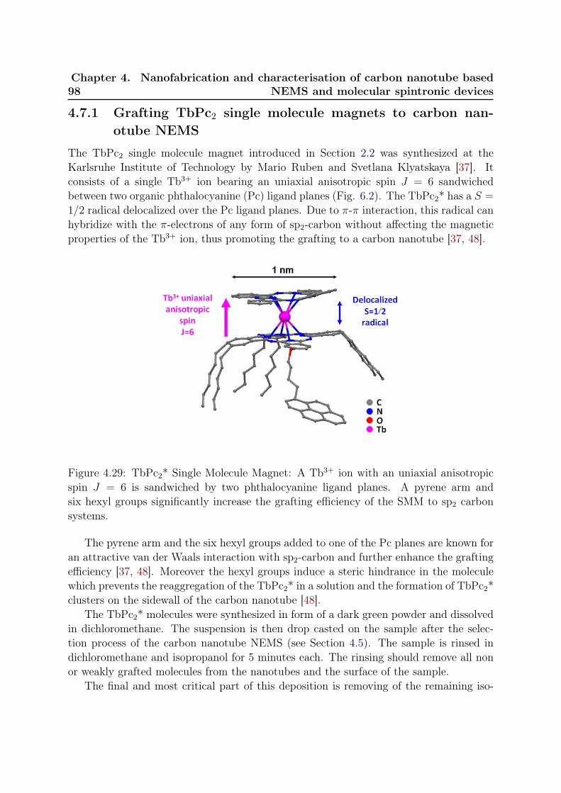
98Chapter 4. Nanofabrication and characterisation of carbon nanotube based
NEMS and molecular spintronic devices
4.7.1 Grafting TbPc2 single molecule magnets to carbon nan-otube NEMS
The TbPc2 single molecule magnet introduced in Section 2.2 was synthesized at theKarlsruhe Institute of Technology by Mario Ruben and Svetlana Klyatskaya [37]. Itconsists of a single Tb3+ ion bearing an uniaxial anisotropic spin J = 6 sandwichedbetween two organic phthalocyanine (Pc) ligand planes (Fig. 6.2). The TbPc2* has a S =
1/2 radical delocalized over the Pc ligand planes. Due to π-π interaction, this radical canhybridize with the π-electrons of any form of sp2-carbon without affecting the magneticproperties of the Tb3+ ion, thus promoting the grafting to a carbon nanotube [37, 48].
Figure 4.29: TbPc2* Single Molecule Magnet: A Tb3+ ion with an uniaxial anisotropicspin J = 6 is sandwiched by two phthalocyanine ligand planes. A pyrene arm andsix hexyl groups significantly increase the grafting efficiency of the SMM to sp2 carbonsystems.
The pyrene arm and the six hexyl groups added to one of the Pc planes are known foran attractive van der Waals interaction with sp2-carbon and further enhance the graftingefficiency [37, 48]. Moreover the hexyl groups induce a steric hindrance in the moleculewhich prevents the reaggregation of the TbPc2* in a solution and the formation of TbPc2*clusters on the sidewall of the carbon nanotube [48].
The TbPc2* molecules were synthesized in form of a dark green powder and dissolvedin dichloromethane. The suspension is then drop casted on the sample after the selec-tion process of the carbon nanotube NEMS (see Section 4.5). The sample is rinsed indichloromethane and isopropanol for 5 minutes each. The rinsing should remove all nonor weakly grafted molecules from the nanotubes and the surface of the sample.
The final and most critical part of this deposition is removing of the remaining iso-
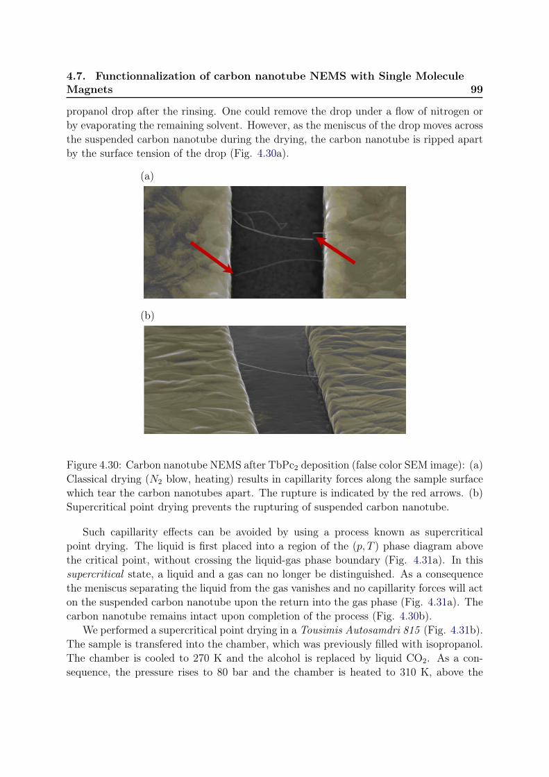
4.7. Functionnalization of carbon nanotube NEMS with Single MoleculeMagnets 99
propanol drop after the rinsing. One could remove the drop under a flow of nitrogen orby evaporating the remaining solvent. However, as the meniscus of the drop moves acrossthe suspended carbon nanotube during the drying, the carbon nanotube is ripped apartby the surface tension of the drop (Fig. 4.30a).
(a)
CO2 (l) chamber
CO2 (l) inlet
(b)
Figure 4.30: Carbon nanotube NEMS after TbPc2 deposition (false color SEM image): (a)Classical drying (N2 blow, heating) results in capillarity forces along the sample surfacewhich tear the carbon nanotubes apart. The rupture is indicated by the red arrows. (b)Supercritical point drying prevents the rupturing of suspended carbon nanotube.
Such capillarity effects can be avoided by using a process known as supercriticalpoint drying. The liquid is first placed into a region of the (p, T ) phase diagram abovethe critical point, without crossing the liquid-gas phase boundary (Fig. 4.31a). In thissupercritical state, a liquid and a gas can no longer be distinguished. As a consequencethe meniscus separating the liquid from the gas vanishes and no capillarity forces will acton the suspended carbon nanotube upon the return into the gas phase (Fig. 4.31a). Thecarbon nanotube remains intact upon completion of the process (Fig. 4.30b).
We performed a supercritical point drying in a Tousimis Autosamdri 815 (Fig. 4.31b).The sample is transfered into the chamber, which was previously filled with isopropanol.The chamber is cooled to 270 K and the alcohol is replaced by liquid CO2. As a con-sequence, the pressure rises to 80 bar and the chamber is heated to 310 K, above the
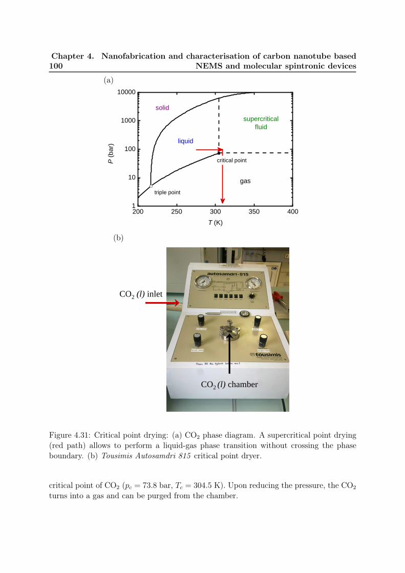
100Chapter 4. Nanofabrication and characterisation of carbon nanotube based
NEMS and molecular spintronic devices
(a)
2 0 0 2 5 0 3 0 0 3 5 0 4 0 01
1 0
1 0 0
1 0 0 0
1 0 0 0 0
t r i p l e p o i n t
P (ba
r)
T ( K )
s o l i d
l i q u i d
g a s
s u p e r c r i t i c a lf l u i d
c r i t i c a l p o i n t
(b)
CO2 (l) chamber
CO2 (l) inlet
Figure 4.31: Critical point drying: (a) CO2 phase diagram. A supercritical point drying(red path) allows to perform a liquid-gas phase transition without crossing the phaseboundary. (b) Tousimis Autosamdri 815 critical point dryer.
critical point of CO2 (pc = 73.8 bar, Tc = 304.5 K). Upon reducing the pressure, the CO2
turns into a gas and can be purged from the chamber.
4.7. Functionnalization of carbon nanotube NEMS with Single MoleculeMagnets 101
4.7.2 Conservation of the NEMS’s mechanical and the TbPc2magnetic properties
We performed depositions of TbPc2* molecules on carbon nanotube NEMS from solutionswith TbPc2* concentrations ranging from 10−7 to 5 · 10−6 mol/L. The functionnalizedcarbon nanotube NEMS are cooled down to temperatures of 20 mK to characterize theTbPc2* magnetic properties and the NEMS mechanical motion.
Magnetic fingerprint
It was previously demonstrated, that the van der Waals interaction between the TbPc2*Pc ligand planes and the sidewall of the carbon nanotube leaves the magnetism of theTb3+ ion intact [37, 48]. As described in Section 2.3.2, a characteristic spin valve behavioris observed in the electronic transport of carbon nanotube quantum dots functionnalizedwith TbPc2*. It was demonstrated that the magnetic anisotropy of this spin valve effectis in very good agreement with the uniaxial anisotropy of the Tb3+ spin and thereforeprovides a magnetic fingerprint for the TbPc2* SMM [48].
We observe this magnetic fingerprint on 100 % of the carbon nanotube devices aftergrafting, indicating a highly efficient grafting process which conserves the magnetic prop-erties of Tb3+ ion as demonstrated in previous works [37, 48]. We performed magneticfield sweeps (trace and retrace) at different field orientations. Fig. 4.32 depicts the differ-ence in conductance between trace and retrace, i.e. the magnetic hysteresis as a functionof the magnetic field angle for two TbPc2* concentrations. At high TbPc2* concentrationof 5·10−6 mol/L one observes at least two easy axis of magnetization corresponding to twoTbPc2* SMM’s with different orientations (Fig. 4.32a). One can subsequently reduce theTbPc2* concentration until one easy axis of magnetization attributed to a single TbPc2*molecule remains (Fig. 4.32b).
Mechanical fingerprint
The mechanical motion of the carbon nanotube resonator is characterized as describedin Section 4.6.3.
For a concentration of TbPc2* of 10−7 mol/L in solution, we observe a mechanicalresonance with a frequency around 100 MHz and a quality factors on the order of Q ∼6000 for low drive power (Fig. 4.33a). The drive power and the gate dependances areconsistent with the mechanical bending mode of a carbon nanotube NEMS (Fig. 4.33 band c, respectively).
The observed quality factor at low drive power is at least an order of magnitude smallerthan for ultraclean carbon nanotube NEMS. The result indicates that the grafted TbPc2*molecules induce additional dampening to the mechanical motion of the nanotube. Indeeda TbPc2* SMM grafted to the sidewall of a carbon nanotube can be considered as two-levelsystem (TLS) and induce additional dissipation in the NEMS (see Section 5.4 for details
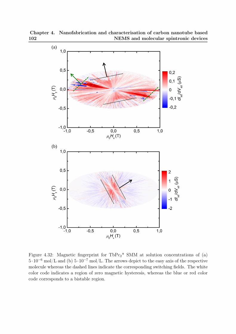
102Chapter 4. Nanofabrication and characterisation of carbon nanotube based
NEMS and molecular spintronic devices
(a)
(b)
Figure 4.32: Magnetic fingerprint for TbPc2* SMM at solution concentrations of (a)5 ·10−6 mol/L and (b) 5 ·10−7 mol/L. The arrows depict to the easy axis of the respectivemolecule whereas the dashed lines indicate the corresponding switching fields. The whitecolor code indicates a region of zero magnetic hysteresis, whereas the blue or red colorcode corresponds to a bistable region.
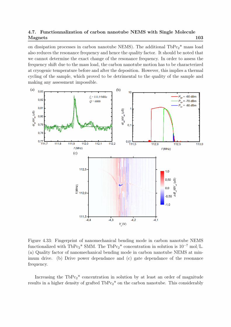
4.7. Functionnalization of carbon nanotube NEMS with Single MoleculeMagnets 103
on dissipation processes in carbon nanotube NEMS). The additional TbPc2* mass loadalso reduces the resonance frequency and hence the quality factor. It should be noted thatwe cannot determine the exact change of the resonance frequency. In order to assess thefrequency shift due to the mass load, the carbon nanotube motion has to be characterizedat cryogenic temperature before and after the deposition. However, this implies a thermalcycling of the sample, which proved to be detrimental to the quality of the sample andmaking any assessment impossible.
(a)
(c)
(b)
Figure 4.33: Fingerprint of nanomechanical bending mode in carbon nanotube NEMSfunctionalized with TbPc2* SMM. The TbPc2* concentration in solution is 10−7 mol/L.(a) Quality factor of nanomechanical bending mode in carbon nanotube NEMS at min-imum drive. (b) Drive power dependance and (c) gate dependance of the resonancefrequency.
Increasing the TbPc2* concentration in solution by at least an order of magnituderesults in a higher density of grafted TbPc2* on the carbon nanotube. This considerably
104Chapter 4. Nanofabrication and characterisation of carbon nanotube based
NEMS and molecular spintronic devices
increases the number of two level systems as well as the mass load and therefore the dis-sipation. Indeed, no carbon nanotube resonance was detected for TbPc2* concentrationsin solution higher than 10−7 mol/L.
We can conclude, that grafting TbPc2* single molecule magnets from low concentra-tion TbPc2* solution onto carbon nanotube NEMS conserves both the magnetic proper-ties of the TbPc2* (chapter 2) and the mechanical properties of the resonator (describedin chapters 3&5) and is therefore a key component for the fabrication of carbon nanotubesupramolecular spintronic device.
Chapter 5
Dynamics and dissipation induced bySET in carbon nanotube NEMS
In section 3.2.4 we demonstrated that a CNT NEMS’ nanomechanical motion at verylow temperature (i.e. in Coulomb blockade regime) is strongly affected by the electronictransport through the CNT quantum dot (QD), and vice versa: For instance, single-electron tunneling (SET) caused a frequency softening and increased dissipation whentuning the CNT dot’s potential through a Coulomb peak [74, 61, 75].
Here we demonstrate that the response and dissipation of a CNT NEMS at verylow temperature induced by zero bias SET through the CNT NEMS-QD critically de-pends on the dot capacitance, the tunnel coupling to the metal leads and temperature.We studied the frequency and dissipation response of nanomechanical bending modes tozero-bias SET in suspended CNT devices with tunable tunnel couplings and differentgate dielectrics, i.e. different dot capacitance. We observe that SET causes a frequencysoftening for small dot capacitance and/or tunnel coupling, whereas a frequency hard-ening or no frequency modulation is observed for large dot capacitance and/or tunnelcoupling (section 5.2). We show that the dissipation of the CNT NEMS is mainly dom-inated by the capacitance, when electron tunneling through the dot is suppressed (i.e.in the Coulomb valley), whereas it is limited by the mean tunneling rate Γ and the con-ductance, when electron tunneling through the dot is allowed (i.e. on a Coulomb peak)(section 5.3). Finally we demonstrate that the tunnel current is the dominant dissipationmechanism in CNT NEMS at low temperature (section 5.4). Our findings, published inPhysical Review Letters [19], are in fair agreement with a theoretical model providedpreviously [74, 61] (section 5.1).
5.1 Introduction
In this section, we recall briefly the fabrication of single gated, suspended CNT deviceswith tunable tunnel couplings on different gate dielectrics, i.e. with different dot ca-pacitances (see Sections 4.2.2 and 4.2.3), as well as the the model describing the SETbackaction on the nanomechanical motion of a carbon nanotube resonator, which waspresented in Section 3.2.4 of this manuscript and the work of Lassagne et al. and Steeleet al. [74, 61].
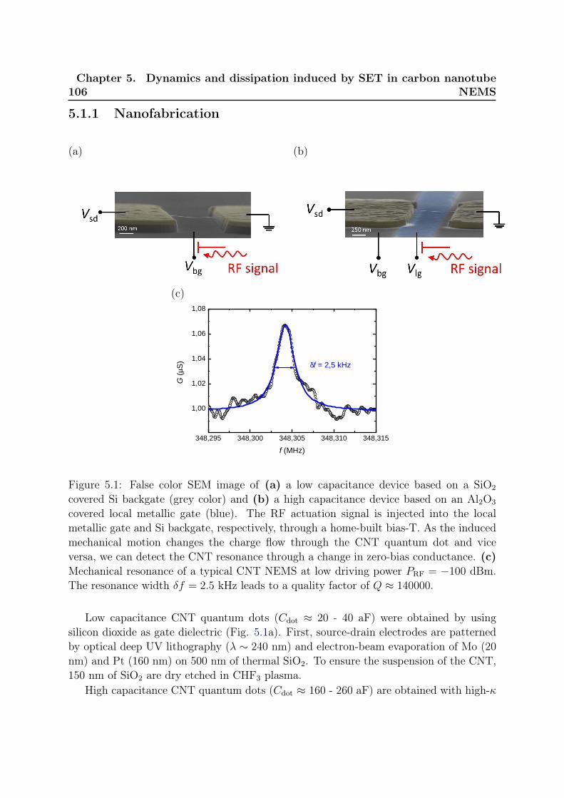
106Chapter 5. Dynamics and dissipation induced by SET in carbon nanotube
NEMS
5.1.1 Nanofabrication
(a) (b)
(c)
3 4 8 , 2 9 5 3 4 8 , 3 0 0 3 4 8 , 3 0 5 3 4 8 , 3 1 0 3 4 8 , 3 1 5
1 , 0 0
1 , 0 2
1 , 0 4
1 , 0 6
1 , 0 8
G (µS
)
f ( M H z )
δf = 2 , 5 k H z
Figure 5.1: False color SEM image of (a) a low capacitance device based on a SiO2
covered Si backgate (grey color) and (b) a high capacitance device based on an Al2O3
covered local metallic gate (blue). The RF actuation signal is injected into the localmetallic gate and Si backgate, respectively, through a home-built bias-T. As the inducedmechanical motion changes the charge flow through the CNT quantum dot and viceversa, we can detect the CNT resonance through a change in zero-bias conductance. (c)Mechanical resonance of a typical CNT NEMS at low driving power PRF = −100 dBm.The resonance width δf = 2.5 kHz leads to a quality factor of Q ≈ 140000.
Low capacitance CNT quantum dots (Cdot ≈ 20 - 40 aF) were obtained by usingsilicon dioxide as gate dielectric (Fig. 5.1a). First, source-drain electrodes are patternedby optical deep UV lithography (λ ∼ 240 nm) and electron-beam evaporation of Mo (20nm) and Pt (160 nm) on 500 nm of thermal SiO2. To ensure the suspension of the CNT,150 nm of SiO2 are dry etched in CHF3 plasma.
High capacitance CNT quantum dots (Cdot ≈ 160 - 260 aF) are obtained with high-κ
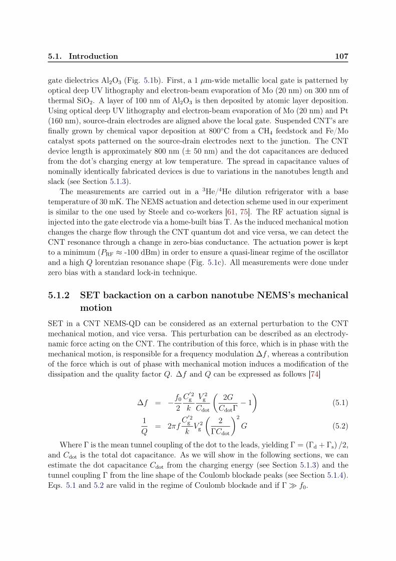
5.1. Introduction 107
gate dielectrics Al2O3 (Fig. 5.1b). First, a 1 µm-wide metallic local gate is patterned byoptical deep UV lithography and electron-beam evaporation of Mo (20 nm) on 300 nm ofthermal SiO2. A layer of 100 nm of Al2O3 is then deposited by atomic layer deposition.Using optical deep UV lithography and electron-beam evaporation of Mo (20 nm) and Pt(160 nm), source-drain electrodes are aligned above the local gate. Suspended CNT’s arefinally grown by chemical vapor deposition at 800C from a CH4 feedstock and Fe/Mocatalyst spots patterned on the source-drain electrodes next to the junction. The CNTdevice length is approximately 800 nm (± 50 nm) and the dot capacitances are deducedfrom the dot’s charging energy at low temperature. The spread in capacitance values ofnominally identically fabricated devices is due to variations in the nanotubes length andslack (see Section 5.1.3).
The measurements are carried out in a 3He/4He dilution refrigerator with a basetemperature of 30 mK. The NEMS actuation and detection scheme used in our experimentis similar to the one used by Steele and co-workers [61, 75]. The RF actuation signal isinjected into the gate electrode via a home-built bias T. As the induced mechanical motionchanges the charge flow through the CNT quantum dot and vice versa, we can detect theCNT resonance through a change in zero-bias conductance. The actuation power is keptto a minimum (PRF ≈ -100 dBm) in order to ensure a quasi-linear regime of the oscillatorand a high Q lorentzian resonance shape (Fig. 5.1c). All measurements were done underzero bias with a standard lock-in technique.
5.1.2 SET backaction on a carbon nanotube NEMS’s mechanicalmotion
SET in a CNT NEMS-QD can be considered as an external perturbation to the CNTmechanical motion, and vice versa. This perturbation can be described as an electrody-namic force acting on the CNT. The contribution of this force, which is in phase with themechanical motion, is responsible for a frequency modulation ∆f , whereas a contributionof the force which is out of phase with mechanical motion induces a modification of thedissipation and the quality factor Q. ∆f and Q can be expressed as follows [74]
∆f = −f0
2
C′2g
k
V 2g
Cdot
(2G
CdotΓ− 1
)(5.1)
1
Q= 2πf
C′2g
kV 2
g
(2
ΓCdot
)2
G (5.2)
Where Γ is the mean tunnel coupling of the dot to the leads, yielding Γ = (Γd + Γs) /2,and Cdot is the total dot capacitance. As we will show in the following sections, we canestimate the dot capacitance Cdot from the charging energy (see Section 5.1.3) and thetunnel coupling Γ from the line shape of the Coulomb blockade peaks (see Section 5.1.4).Eqs. 5.1 and 5.2 are valid in the regime of Coulomb blockade and if Γ f0.
108Chapter 5. Dynamics and dissipation induced by SET in carbon nanotube
NEMS
5.1.3 Estimating the quantum dot capacitance of carbon nan-otube NEMS
(a) (b)
(c) (d)
Figure 5.2: Estimating the dot capacitance via bias spectroscopy: (a)(c) Coulomb dia-monds for two Al2O3 based devices with a length of 780 nm and 820 nm, respectively.(b)(d) Coulomb diamonds for two SiO2 based devices.
The total dot capacitance is obtained from bias spectroscopy measurements. Thetotal dot capacitance Cdot is related to the charging energy Ec of the dot via Cdot = e/Ec.The charging energy is deduced from the size of the Coulomb diamonds (Fig. 5.2a).Alternatively one can determine the capacitances Cs and Cd from the slope of the diamondedges and the gate capacitance Cg from the distance between 2 degeneracy points (Fig5.2b). The total dot capacitance then yields Cdot = Cs + Cd + Cg.
For SiO2 based devices we obtain capacitance between 20 and 40 aF, whereas forAl2O3 based devices the values range from 160 aF to 260 aF. The spread in capacitance
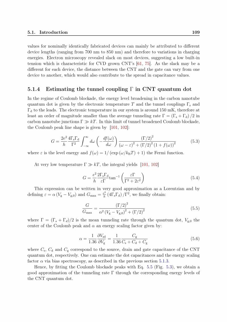
5.1. Introduction 109
values for nominally identically fabricated devices can mainly be attributed to differentdevice lengths (ranging from 700 nm to 850 nm) and therefore to variations in chargingenergies. Electron microscopy revealed slack on most devices, suggesting a low built-intension which is characteristic for CVD grown CNT’s [61, 75]. As the slack may be adifferent for each device, the distance between the CNT and the gate can vary from onedevice to another, which would also contribute to the spread in capacitance values.
5.1.4 Estimating the tunnel coupling Γ in CNT quantum dot
In the regime of Coulomb blockade, the energy level broadening in the carbon nanotubequantum dot is given by the electronic temperature T and the tunnel couplings Γs andΓd to the leads. The electronic temperature in our system is around 150 mK, therefore atleast an order of magnitude smaller than the average tunneling rate Γ = (Γs + Γd) /2 incarbon nanotube junctions Γ kT . In this limit of tunnel broadened Coulomb blockade,the Coulomb peak line shape is given by [101, 102]:
G =2e2
h
4ΓsΓd
Γ2
∫ ∞−∞
dω
(−df(ω)
dω
)(Γ/2)2
(ω − ε)2 + (Γ/2)2 (1 + f(ω))2 (5.3)
where ε is the level energy and f(ω) = 1/ (exp (ω/kBT ) + 1) the Fermi function.
At very low temperature Γ kT , the integral yields [101, 102]
G =e2
h
2ΓsΓd
εΓtan−1
(εΓ
Γ2 + 2ε2
)(5.4)
This expression can be written in very good approximation as a Lorentzian and bydefining ε = α (Vg − Vg,0) and Gmax = e2
h(4ΓsΓd) /Γ2, we finally obtain:
G
Gmax=
(Γ/2)2
α2 (Vg − Vg,0)2 + (Γ/2)2 (5.5)
where Γ = (Γs + Γd)/2 is the mean tunneling rate through the quantum dot, Vg,0 thecenter of the Coulomb peak and α an energy scaling factor given by:
α =1
1.36
∂Vsd
∂Vg=
1
1.36
Cg
Cs + Cd + Cg(5.6)
where Cs, Cd and Cg correspond to the source, drain and gate capacitance of the CNTquantum dot, respectively. One can estimate the dot capacitances and the energy scalingfactor α via bias spectroscopy, as described in the previous section 5.1.3.
Hence, by fitting the Coulomb blockade peaks with Eq. 5.5 (Fig. 5.3), we obtain agood approximation of the tunneling rate Γ through the corresponding energy levels ofthe CNT quantum dot.
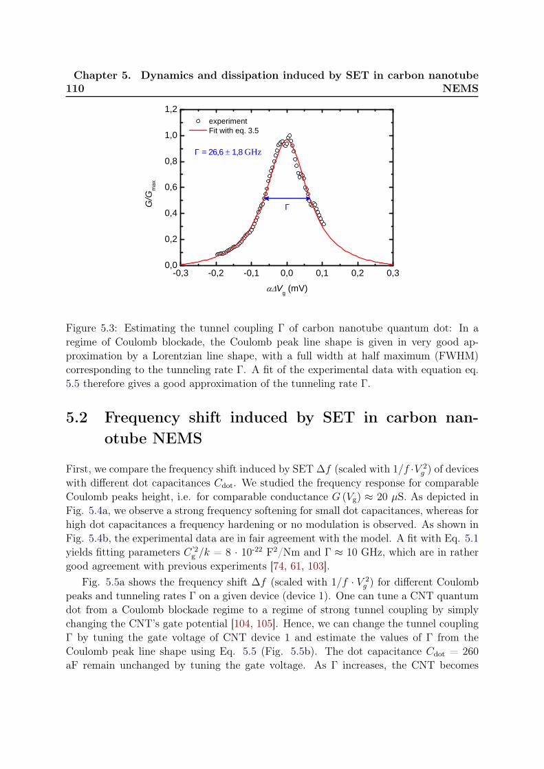
110Chapter 5. Dynamics and dissipation induced by SET in carbon nanotube
NEMS
- 0 , 3 - 0 , 2 - 0 , 1 0 , 0 0 , 1 0 , 2 0 , 30 , 0
0 , 2
0 , 4
0 , 6
0 , 8
1 , 0
1 , 2 e x p e r i m e n t F i t w i t h e q . 3 . 5
G/G ma
x
V g ( m V )
Γ
Γ = 26,6 1,8 G H z
Figure 5.3: Estimating the tunnel coupling Γ of carbon nanotube quantum dot: In aregime of Coulomb blockade, the Coulomb peak line shape is given in very good ap-proximation by a Lorentzian line shape, with a full width at half maximum (FWHM)corresponding to the tunneling rate Γ. A fit of the experimental data with equation eq.5.5 therefore gives a good approximation of the tunneling rate Γ.
5.2 Frequency shift induced by SET in carbon nan-otube NEMS
First, we compare the frequency shift induced by SET ∆f (scaled with 1/f ·V 2g ) of devices
with different dot capacitances Cdot. We studied the frequency response for comparableCoulomb peaks height, i.e. for comparable conductance G (Vg) ≈ 20 µS. As depicted inFig. 5.4a, we observe a strong frequency softening for small dot capacitances, whereas forhigh dot capacitances a frequency hardening or no modulation is observed. As shown inFig. 5.4b, the experimental data are in fair agreement with the model. A fit with Eq. 5.1yields fitting parameters C ’2
g /k = 8 · 10-22 F2/Nm and Γ ≈ 10 GHz, which are in rathergood agreement with previous experiments [74, 61, 103].
Fig. 5.5a shows the frequency shift ∆f (scaled with 1/f · V 2g ) for different Coulomb
peaks and tunneling rates Γ on a given device (device 1). One can tune a CNT quantumdot from a Coulomb blockade regime to a regime of strong tunnel coupling by simplychanging the CNT’s gate potential [104, 105]. Hence, we can change the tunnel couplingΓ by tuning the gate voltage of CNT device 1 and estimate the values of Γ from theCoulomb peak line shape using Eq. 5.5 (Fig. 5.5b). The dot capacitance Cdot = 260aF remain unchanged by tuning the gate voltage. As Γ increases, the CNT becomes
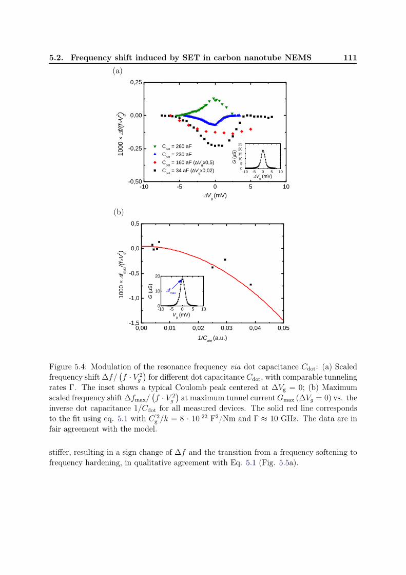
5.2. Frequency shift induced by SET in carbon nanotube NEMS 111
(a)
- 1 0 - 5 0 5 1 0- 0 , 5 0
- 0 , 2 5
0 , 0 0
0 , 2 5
- 1 0 - 5 0 5 1 005
1 01 52 02 5 C d o t = 2 6 0 a F
C d o t = 2 3 0 a F C d o t = 1 6 0 a F ( ∆V g x 0 , 5 ) C d o t = 3 4 a F ( ∆V g x 0 , 0 2 )
1000
× f/
(fV2 g)
V g ( m V )
G (µS
)
V g ( m V )
(b)
0 , 0 0 0 , 0 1 0 , 0 2 0 , 0 3 0 , 0 4 0 , 0 5- 1 , 5
- 1 , 0
- 0 , 5
0 , 0
0 , 5
- 1 0 - 5 0 5 1 00
1 0
2 0
1000
× f ma
x/(fV
2 g)
1 / C d o t ( a . u . )
G (µS
)
V g ( m V )
f m a x
Figure 5.4: Modulation of the resonance frequency via dot capacitance Cdot: (a) Scaledfrequency shift ∆f/
(f · V 2
g
)for different dot capacitance Cdot, with comparable tunneling
rates Γ. The inset shows a typical Coulomb peak centered at ∆Vg = 0; (b) Maximumscaled frequency shift ∆fmax/
(f · V 2
g
)at maximum tunnel currentGmax (∆Vg = 0) vs. the
inverse dot capacitance 1/Cdot for all measured devices. The solid red line correspondsto the fit using eq. 5.1 with C ’2
g /k = 8 · 10-22 F2/Nm and Γ ≈ 10 GHz. The data are infair agreement with the model.
stiffer, resulting in a sign change of ∆f and the transition from a frequency softening tofrequency hardening, in qualitative agreement with Eq. 5.1 (Fig. 5.5a).
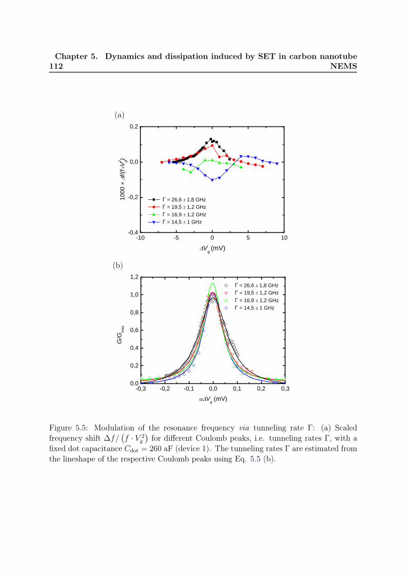
112Chapter 5. Dynamics and dissipation induced by SET in carbon nanotube
NEMS
(a)
- 1 0 - 5 0 5 1 0- 0 , 4
- 0 , 2
0 , 0
0 , 2
Γ = 2 6 , 6 1 , 8 G H z Γ = 1 9 , 5 1 , 2 G H z Γ = 1 6 , 9 1 , 2 G H z Γ = 1 4 , 5 1 G H z
10
00 ×
f/(f
V2 g)
V g ( m V )
(b)
- 0 , 3 - 0 , 2 - 0 , 1 0 , 0 0 , 1 0 , 2 0 , 30 , 0
0 , 2
0 , 4
0 , 6
0 , 8
1 , 0
1 , 2 Γ = 2 6 , 6 1 , 8 G H z Γ = 1 9 , 5 1 , 2 G H z Γ = 1 6 , 9 1 , 2 G H z Γ = 1 4 , 5 1 G H z
G/G ma
x
V g ( m V )
Figure 5.5: Modulation of the resonance frequency via tunneling rate Γ: (a) Scaledfrequency shift ∆f/
(f · V 2
g
)for different Coulomb peaks, i.e. tunneling rates Γ, with a
fixed dot capacitance Cdot = 260 aF (device 1). The tunneling rates Γ are estimated fromthe lineshape of the respective Coulomb peaks using Eq. 5.5 (b).
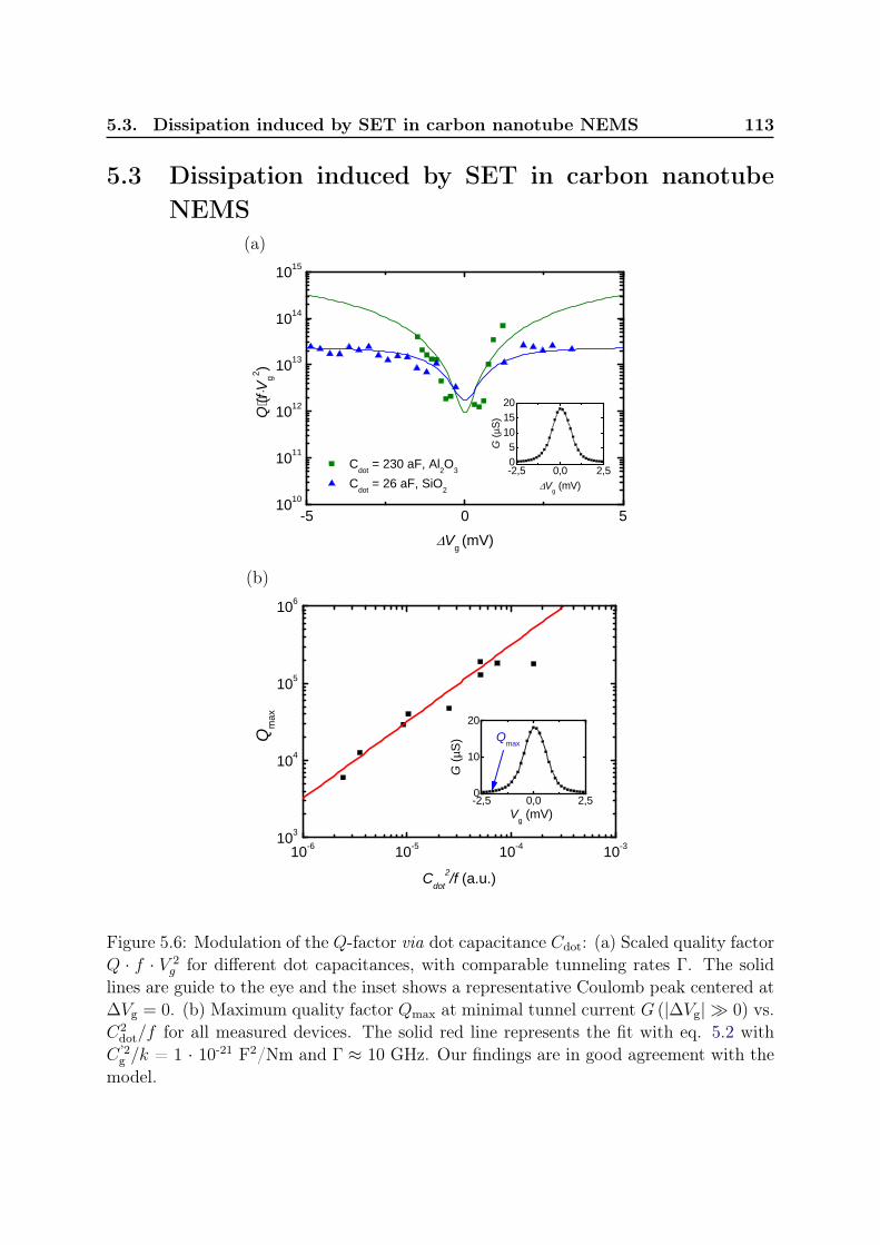
5.3. Dissipation induced by SET in carbon nanotube NEMS 113
5.3 Dissipation induced by SET in carbon nanotubeNEMS
(a)
- 5 0 51 0 1 0
1 0 1 1
1 0 1 2
1 0 1 3
1 0 1 4
1 0 1 5
- 2 , 5 0 , 0 2 , 505
1 01 52 0
C d o t = 2 3 0 a F , A l 2 O 3 C d o t = 2 6 a F , S i O 2
Q⋅(
fVg2 )
V g ( m V )
G (µS
) V g ( m V )
(b)
1 0 - 6 1 0 - 5 1 0 - 4 1 0 - 31 0 3
1 0 4
1 0 5
1 0 6
- 2 , 5 0 , 0 2 , 50
1 0
2 0
Q max
C d o t2 / f ( a . u . )
G (µS
)
V g ( m V )
Q m a x
Figure 5.6: Modulation of the Q-factor via dot capacitance Cdot: (a) Scaled quality factorQ · f · V 2
g for different dot capacitances, with comparable tunneling rates Γ. The solidlines are guide to the eye and the inset shows a representative Coulomb peak centered at∆Vg = 0. (b) Maximum quality factor Qmax at minimal tunnel current G (|∆Vg| 0) vs.C2
dot/f for all measured devices. The solid red line represents the fit with eq. 5.2 withC ’2
g /k = 1 · 10-21 F2/Nm and Γ ≈ 10 GHz. Our findings are in good agreement with themodel.
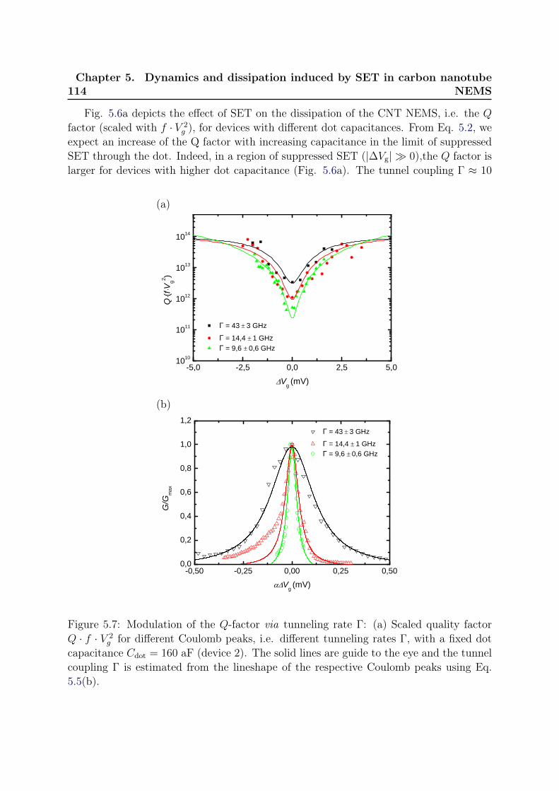
114Chapter 5. Dynamics and dissipation induced by SET in carbon nanotube
NEMS
Fig. 5.6a depicts the effect of SET on the dissipation of the CNT NEMS, i.e. the Qfactor (scaled with f · V 2
g ), for devices with different dot capacitances. From Eq. 5.2, weexpect an increase of the Q factor with increasing capacitance in the limit of suppressedSET through the dot. Indeed, in a region of suppressed SET (|∆Vg| 0),the Q factor islarger for devices with higher dot capacitance (Fig. 5.6a). The tunnel coupling Γ ≈ 10
(a)
- 5 , 0 - 2 , 5 0 , 0 2 , 5 5 , 01 0 1 0
1 0 1 1
1 0 1 2
1 0 1 3
1 0 1 4
Γ = 4 3 3 G H z Γ = 1 4 , 4 1 G H z Γ = 9 , 6 0 , 6 G H z
Q(fV
g2 )
V g ( m V )
(b)
- 0 , 5 0 - 0 , 2 5 0 , 0 0 0 , 2 5 0 , 5 00 , 0
0 , 2
0 , 4
0 , 6
0 , 8
1 , 0
1 , 2 Γ = 4 3 3 G H z Γ = 1 4 , 4 1 G H z Γ = 9 , 6 0 , 6 G H z
G/G ma
x
V g ( m V )
Figure 5.7: Modulation of the Q-factor via tunneling rate Γ: (a) Scaled quality factorQ · f · V 2
g for different Coulomb peaks, i.e. different tunneling rates Γ, with a fixed dotcapacitance Cdot = 160 aF (device 2). The solid lines are guide to the eye and the tunnelcoupling Γ is estimated from the lineshape of the respective Coulomb peaks using Eq.5.5(b).
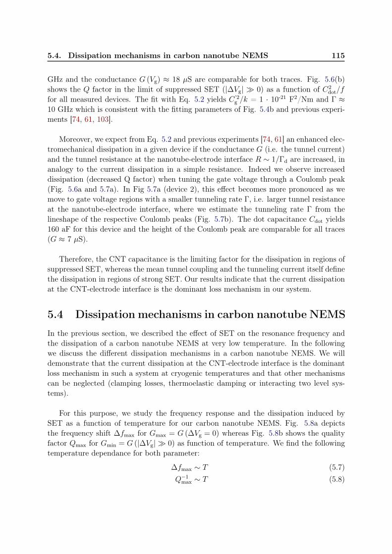
5.4. Dissipation mechanisms in carbon nanotube NEMS 115
GHz and the conductance G (Vg) ≈ 18 µS are comparable for both traces. Fig. 5.6(b)shows the Q factor in the limit of suppressed SET (|∆Vg| 0) as a function of C2
dot/f
for all measured devices. The fit with Eq. 5.2 yields C ’2g /k = 1 · 10-21 F2/Nm and Γ ≈
10 GHz which is consistent with the fitting parameters of Fig. 5.4b and previous experi-ments [74, 61, 103].
Moreover, we expect from Eq. 5.2 and previous experiments [74, 61] an enhanced elec-tromechanical dissipation in a given device if the conductance G (i.e. the tunnel current)and the tunnel resistance at the nanotube-electrode interface R ∼ 1/Γd are increased, inanalogy to the current dissipation in a simple resistance. Indeed we observe increaseddissipation (decreased Q factor) when tuning the gate voltage through a Coulomb peak(Fig. 5.6a and 5.7a). In Fig 5.7a (device 2), this effect becomes more pronouced as wemove to gate voltage regions with a smaller tunneling rate Γ, i.e. larger tunnel resistanceat the nanotube-electrode interface, where we estimate the tunneling rate Γ from thelineshape of the respective Coulomb peaks (Fig. 5.7b). The dot capacitance Cdot yields160 aF for this device and the height of the Coulomb peak are comparable for all traces(G ≈ 7 µS).
Therefore, the CNT capacitance is the limiting factor for the dissipation in regions ofsuppressed SET, whereas the mean tunnel coupling and the tunneling current itself definethe dissipation in regions of strong SET. Our results indicate that the current dissipationat the CNT-electrode interface is the dominant loss mechanism in our system.
5.4 Dissipation mechanisms in carbon nanotube NEMS
In the previous section, we described the effect of SET on the resonance frequency andthe dissipation of a carbon nanotube NEMS at very low temperature. In the followingwe discuss the different dissipation mechanisms in a carbon nanotube NEMS. We willdemonstrate that the current dissipation at the CNT-electrode interface is the dominantloss mechanism in such a system at cryogenic temperatures and that other mechanismscan be neglected (clamping losses, thermoelastic damping or interacting two level sys-tems).
For this purpose, we study the frequency response and the dissipation induced bySET as a function of temperature for our carbon nanotube NEMS. Fig. 5.8a depictsthe frequency shift ∆fmax for Gmax = G (∆Vg = 0) whereas Fig. 5.8b shows the qualityfactor Qmax for Gmin = G (|∆Vg| 0) as function of temperature. We find the followingtemperature dependance for both parameter:
∆fmax ∼ T (5.7)Q−1
max ∼ T (5.8)
116Chapter 5. Dynamics and dissipation induced by SET in carbon nanotube
NEMS
(a)
0 2 0 0 4 0 0 6 0 0 8 0 0 1 0 0 0- 5 0
- 2 5
0
2 5
5 0
2 5 0 5 0 0 7 5 0 1 0 0 01 , 01 , 52 , 02 , 5
f max (k
Hz)
T ( m K )
f m a x ∼ T
G m a x ∼ - T
G max (µ
S)T ( m K )
(b)
1 0 0 1 0 0 01 0 4
1 0 5
1 0 6
2 5 0 5 0 0 7 5 0 1 0 0 00 , 00 , 51 , 01 , 5
Q max
T ( m K )
Q m a x ∼ T - 1
G min (µ
S)
T ( m K )
G m i n ∼ T
Figure 5.8: Temperature dependance: (a) Maximum frequency shift ∆fmax at maximumtunnel current Gmax (∆Vg = 0) vs. temperature for a device yielding Cdot = 160 aF (de-vice 2). The inset shows the evolution of Gmax as a function of temperature.(b) Maximumquality factor Qmax at minimal tunnel current Gmin (|∆Vg| = 1mV) vs. temperature fora device yielding Cdot = 160 aF (device 2). The inset shows the evolution of Gmin as afunction of temperature.
These observation however do not agree with previous experiments on carbon nanotubeNEMS [75], lattice matched GaAs/InGaP/GaAs MEMS [106] and silicon single crystalNEMS [107] at cryogenic temperatures:
5.4. Dissipation mechanisms in carbon nanotube NEMS 117
They reported a weak power law dependance for the quality factor yielding
Q−1 ∼ T 1/3 (5.9)
which is in very good agreement with the quantum dissipation arising from interactingtwo-level systems (TLS) [108]. Moreover, resonant interactions between two-level systems(TLS) also lead to a shift of the resonance frequency, which reads [106, 107]
∆f
f∼ logT (5.10)
This suggests that the main dissipation mechanism in our suspended carbon nanotuberesonators does not arise from quantum friction between interacting TLS.
Clamping losses, due to a transfer of strain energy from the double-clamped carbonnanotube beam into its supporting structure, are described by
Q−1clamping ≈
dt4
L5(5.11)
with the CNT diameter d, the CNT length L and the base thickness t (i.e. the thicknessof the electrodes) [70].
Those losses are temperature independant and for the values d ≈ 1 nm, L ≈ 1 µmand t ≈ 100 nm, we obtain Q−1
clamping ≈ 10−7, which is at least two orders of magnitudesmaller than the observed dissipation in our NEMS. We can therefore exclude clampinglosses as main dissipation mechanism.
We now consider thermoelastic damping in a suspended CNT resonator. Mechanicalvibrations can for instance induce a local change in volume of the CNT, creating localizedexpanded and contracted regions on the CNT. As a consequence of thermoelastic couplinga temperature gradient develops and a heat transfer from the expanded to the contractedregions occurs. The associated dissipation of the CNT resonator is then given by
Q−1thermoelastic ≈
α2TE
C
(ωτ
1 + (ωτ)2
)(5.12)
with the temperature T , the Young’s modulus E, the heat capacitance C, the thermalexpansion coefficient α, the NEMS resonance frequency ω and the timescale τ of theheat transfer from hot to cold region, i.e. from expanded to contracted regions of thebeam [70].
At temperatures around 1K, the heat capacitance evolves as C ∼ T [70, 109] and thethermal expansion coefficient yields α ≈ −3 · 10−7K−1 · T [70, 110]. Therefore we havethe following temperature dependance for thermoelastic damping at low temperature:
Q−1thermoelastic ∼ T 2 (5.13)
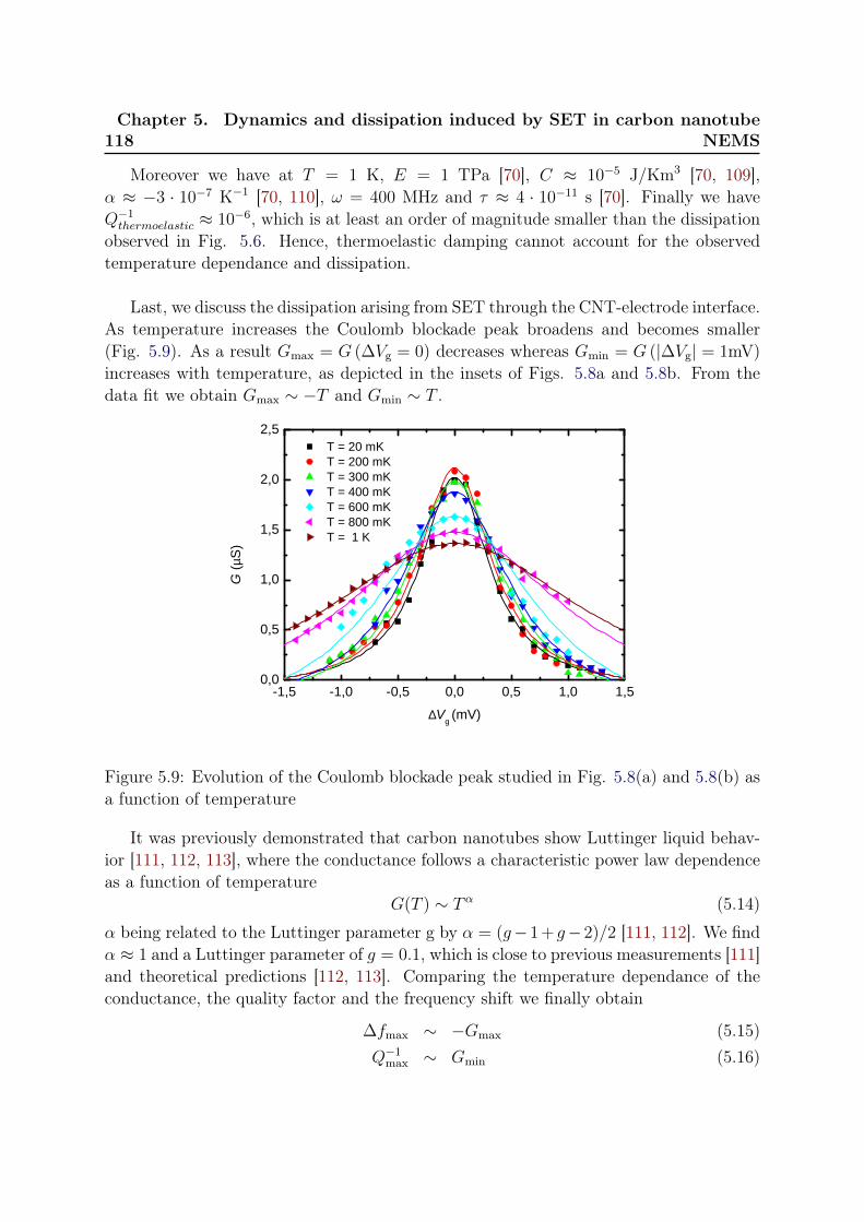
118Chapter 5. Dynamics and dissipation induced by SET in carbon nanotube
NEMS
Moreover we have at T = 1 K, E = 1 TPa [70], C ≈ 10−5 J/Km3 [70, 109],α ≈ −3 · 10−7 K−1 [70, 110], ω = 400 MHz and τ ≈ 4 · 10−11 s [70]. Finally we haveQ−1thermoelastic ≈ 10−6, which is at least an order of magnitude smaller than the dissipation
observed in Fig. 5.6. Hence, thermoelastic damping cannot account for the observedtemperature dependance and dissipation.
Last, we discuss the dissipation arising from SET through the CNT-electrode interface.As temperature increases the Coulomb blockade peak broadens and becomes smaller(Fig. 5.9). As a result Gmax = G (∆Vg = 0) decreases whereas Gmin = G (|∆Vg| = 1mV)
increases with temperature, as depicted in the insets of Figs. 5.8a and 5.8b. From thedata fit we obtain Gmax ∼ −T and Gmin ∼ T .
- 1 , 5 - 1 , 0 - 0 , 5 0 , 0 0 , 5 1 , 0 1 , 50 , 0
0 , 5
1 , 0
1 , 5
2 , 0
2 , 5 T = 2 0 m K T = 2 0 0 m K T = 3 0 0 m K T = 4 0 0 m K T = 6 0 0 m K T = 8 0 0 m K T = 1 K
G (µS
)
∆V g ( m V )
Figure 5.9: Evolution of the Coulomb blockade peak studied in Fig. 5.8(a) and 5.8(b) asa function of temperature
It was previously demonstrated that carbon nanotubes show Luttinger liquid behav-ior [111, 112, 113], where the conductance follows a characteristic power law dependenceas a function of temperature
G(T ) ∼ Tα (5.14)
α being related to the Luttinger parameter g by α = (g−1 + g−2)/2 [111, 112]. We findα ≈ 1 and a Luttinger parameter of g = 0.1, which is close to previous measurements [111]and theoretical predictions [112, 113]. Comparing the temperature dependance of theconductance, the quality factor and the frequency shift we finally obtain
∆fmax ∼ −Gmax (5.15)Q−1
max ∼ Gmin (5.16)
5.5. Conclusion and Outlook 119
which is in full agreement with Eqs. 5.1 and 5.2.We can conclude that SET is the dominant dissipation mechanism for carbon nan-
otube based NEMS in a Coulomb blockade regime at cryogenic temperatures.
5.5 Conclusion and Outlook
Despite the good agreement between theory and experiment, we observe deviations fromthe model for some devices in Fig. 5.4b and 5.6b, which we attribute to variations inC ’2
g /k and the tunneling rates Γ.According to ref. [103], a good approximation for C ’2
g /k is given by
C ’2g /k ≈ (Cg/Z)2 /k (5.17)
with Cg being the gate capacitance, Z the CNT-gate distance and k the CNT’s springconstant.
We studied two different device layouts: Single gated SiO2 based CNT QD with anaverage gate capacitance of Cg = 2 ± 1 aF and Z = 700 nm and single gated Al2O3
based CNT QD with an average gate capacitance of Cg = 3± 1 aF and Z = 300 nm. Cg
is estimated from the voltage separation of two adjacent Coulomb peaks (see Fig. 5.2)and Z is given by the sum of the oxide thickness and thickness of the metal electrodes(see section 5.1). With an average spring constant k = 10−3 N/m (value extracted fromref. [74] and [103]) we obtain values for C ’2
g /k = (6± 2) · 10−21 F2/Nm, which is close tovalues obtained from the fit in Fig. 5.4b and 5.6b.
The above estimation shows that we indeed have variations in C ’2g /k, caused by a small
spread in capacitance values Cg and CNT-gate distance Z, which leads to deviations ofsome devices from the model fit.
Moreover we have to consider an uncertainty in the estimation of the tunneling ratesΓ. Although Eq. 5.5 provides a good approximation for Γ, we obtain an uncertainty ofδΓ ≈ 7%, which could also account for the above mentionned deviation from the model.
We have demonstrated that single-electron tunneling causes a modulation of the res-onance frequency (Section 5.2) and the dissipation (Section 5.3) in carbon nanotubeNEMS at low temperature, depending on the dot capacitance and the tunnel couplingto the leads [19]. The experimental data are in close agreement with theoretical predic-tions [74, 61]. Based on this evidence one could significantly increase the quality factorQ up to 106, by choosing high-κ dielectrics (HfO2 or ZrO2) and improving the tunnelcontact to the metal leads.
A study as a function of temperature reveals that single-electron tunneling is thedominant loss mechanism at low temperature for carbon nanotube NEMS (Section 5.4),which stands in contrast to previous experiments [75, 106, 107] were dissipation is due tointeracting two-level systems (TLS) [108].
120Chapter 5. Dynamics and dissipation induced by SET in carbon nanotube
NEMS
It was proposed in theoretical calculation that one can use such high−Q CNT NEMSas magnetic torque or force detectors for nanoparticles [18] or single molecule mag-nets [114, 115] grafted to the CNT NEMS. In principle one can achieve a sensitivityof one µB at low temperature, whereas the best magnetometers, for instance the micro-SQUID, only have a sensitivity of 103 µB [54]. Finally, such molecular quantum spintronicdevice would allow single spin manipulation on a molecular level.
Chapter 6
Strong Spin-Phonon Coupling of aSingle Molecular Spin to a Carbon
Nanotube NEMS
The magnetization reversal of a single spin at low temperature is mediated by the ex-change of an energy quantum between the spin system and a thermal reservoir. Suchmagnetic relaxation processes were first discussed for a crystal of paramagnetic transitionions [50]. It was suggested that mechanical vibrations of the crystal lattice (’phonons’)modulate the crystal electric field of the magnetic ion, thus inducing a so called ’direct’relaxation between two different spin states [50, 116, 117]. Direct relaxation has alsobeen predicted for single molecule magnets (SMM) with a large spin and a high mag-netic anisotropy [50, 36, 118, 119, 120] and was first demonstrated in a Mn12 acetatecrystal [121]. The spin-lattice relaxation time for such a direct transition is essentiallylimited by the phonon density of states at the spin resonance and the spin-phonon cou-pling [50]. In a macroscopic 3D system, like a SMM crystal, the phonon energy spectrumis continuous whereas in a 1D system, like a suspended carbon nanotube (CNT), the en-ergy spectrum is discrete and can be engineered to an extremely low density of states [122].An individual SMM, coupled to a suspended carbon nanotube, should therefore exhibitextremely long relaxation times [122] and the reduced size and dimensionality of the sys-tem should result in a strongly enhanced spin-phonon coupling [114, 115]. In this section,we will provide the first experimental evidence for a strong spin-phonon coupling betweena single molecule spin and a carbon nanotube resonator. This could ultimately enablecoherent spin manipulation and quantum entanglement [114, 115].
Carbon nanotubes (CNT) have become an essential building block for nanoelectrome-chanical systems (NEMS). Their low mass and high Young’s modulus give rise to highoscillation frequencies for transverse [65, 123] and longitudinal modes [68, 79, 67], there-fore enabling ground state cooling with state of the art cryogenics and a large zero pointmotion in the quantum regime [1]. Moreover, the strong coupling between nanomechan-ical motion and single-electron tunneling in high-Q CNT NEMS allows an electronicactuation and detection of its nanomechanical motion [19, 74, 61, 75]. As such, a CNTNEMS can be used for ultrasensitive mass sensing [124, 125, 5] or as magnetic torquedetectors for single spin systems [18].
122Chapter 6. Strong Spin-Phonon Coupling of a Single Molecular Spin to a
Carbon Nanotube NEMS
A single spin, strongly coupled with a CNT NEMS in the quantum regime, couldserve as elementary qubit in quantum information processing. It has been recently sug-gested that a strong coupling between a quantum CNT NEMS and a single electron spinwould enable basic qubit control and the implementation of entangled states [122]. Inthis framework, coupling a single-molecule magnet (SMM) to the quantized nanomechan-ical motion of a CNT NEMS is a very attractive alternative [11]. Chemical engineeringallows the synthesis of perfectly identical SMM’s and integration into nanoscale devicessuch as electromigrated junctions [126, 127, 47] or carbon nanotube transistors [48]. Alarge magnetic moment and a strong, uniaxial magnetic anisotropy enable for instancequantum tunneling of magnetization [128, 129] or quantum phase interference [42], andyields coherence times on the order of seconds in crystalline form [43]. Moreover, it wasrecently predicted that the spin-phonon coupling between an SMM and a quantum CNTNEMS is strong enough to perform coherent spin manipulation and quantum entangle-ment of a spin and a resonator [114, 115].
In this chapter, we first present the spin relaxation in a TbPc2 SMM coupled to a car-bon nanotube (Section 6.2) and provide evidence for a quantized longitudinal stretchingmode in carbon nanotube NEMS (Section 6.3). We then establish a strong spin-phononcoupling between both systems, that is, between an individual TbPc2 SMM and thequantized high-Q longitudinal stretching mode (LSM) of the CNT resonator (Section6.4). The strong spin-phonon coupling presented here would enable the quantum controlof magnetization at a single-phonon level [122, 114] and the entanglement of a single spinwith quantized mechanical motion [122, 115].
6.1 Nanofabrication and measurement setup
Here we will briefly recall the fabrication of high capacitance carbon nanotube resonators(see Section 4.2.3 for details) and the grafting procedure for TbPc2* SMM (see Section4.7 for details).
A 1 µm-wide metallic local gate is patterned by optical deep ultraviolet (DUV) lithog-raphy and subsequent e-beam evaporation of Mo (20 nm) on a degenerately p-dopedsilicon wafer with a 300 nm thick layer of thermal SiO2. A layer of 100nm of Al2O3 isthen deposited by atomic layer deposition. Using optical DUV lithography and e-beamevaporation of Mo (20nm) and Pt (160nm), source-drain electrodes are aligned above thelocal gate. Suspended CNT’s are finally grown by CVD at 800oC from a CH4 feedstockand Fe/Mo catalyst spots patterned on the source-drain electrodes next to the junction(Section 4.2.3). The CNT device length is approximately 800 nm.
The pyrene-substituted TbPc2* were synthesized as reported in Ref. [37]. The TbPc2
powder was dissolved in a solution of dichloromethane with a TbPc∗2 concentration of10−7 mol/L and drop casted onto the sample. The droplet was subsequently dried in
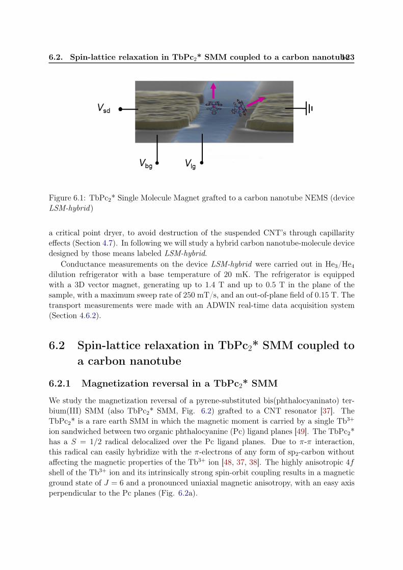
6.2. Spin-lattice relaxation in TbPc2* SMM coupled to a carbon nanotube123
Figure 6.1: TbPc2* Single Molecule Magnet grafted to a carbon nanotube NEMS (deviceLSM-hybrid)
a critical point dryer, to avoid destruction of the suspended CNT’s through capillarityeffects (Section 4.7). In following we will study a hybrid carbon nanotube-molecule devicedesigned by those means labeled LSM-hybrid.
Conductance measurements on the device LSM-hybrid were carried out in He3/He4
dilution refrigerator with a base temperature of 20 mK. The refrigerator is equippedwith a 3D vector magnet, generating up to 1.4 T and up to 0.5 T in the plane of thesample, with a maximum sweep rate of 250 mT/s, and an out-of-plane field of 0.15 T. Thetransport measurements were made with an ADWIN real-time data acquisition system(Section 4.6.2).
6.2 Spin-lattice relaxation in TbPc2* SMM coupled toa carbon nanotube
6.2.1 Magnetization reversal in a TbPc2* SMM
We study the magnetization reversal of a pyrene-substituted bis(phthalocyaninato) ter-bium(III) SMM (also TbPc2* SMM, Fig. 6.2) grafted to a CNT resonator [37]. TheTbPc2* is a rare earth SMM in which the magnetic moment is carried by a single Tb3+
ion sandwiched between two organic phthalocyanine (Pc) ligand planes [49]. The TbPc2*has a S = 1/2 radical delocalized over the Pc ligand planes. Due to π-π interaction,this radical can easily hybridize with the π-electrons of any form of sp2-carbon withoutaffecting the magnetic properties of the Tb3+ ion [48, 37, 38]. The highly anisotropic 4f
shell of the Tb3+ ion and its intrinsically strong spin-orbit coupling results in a magneticground state of J = 6 and a pronounced uniaxial magnetic anisotropy, with an easy axisperpendicular to the Pc planes (Fig. 6.2a).
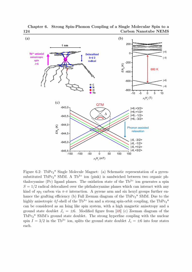
124Chapter 6. Strong Spin-Phonon Coupling of a Single Molecular Spin to a
Carbon Nanotube NEMS
-10 -5 0 5 10-800
-600
-400
-200
0
200
|+6⟩
E/k
B (K
)
0Hz (T)
|−6⟩
|+5⟩
|−5⟩
600 K
(a) (b)
(c)
-150 -100 -50 0 50 100 150-645,5
-645,0
-644,5
-644,0
-643,5
-643,0
E/k
B (K
)
0Hz (mT)
|+6,+3/2>|+6,+1/2>|+6,- 1/2>|+6,- 3/2>
QTM
Δ
|-6, -3/2>|-6, -1/2>|-6,+1/2>|-6,+3/2>
Phonon assistedrelaxation
Figure 6.2: TbPc2* Single Molecule Magnet: (a) Schematic representation of a pyren-substituted TbPc2* SMM. A Tb3+ ion (pink) is sandwiched between two organic ph-thalocyanine (Pc) ligand planes. The oxidation state of the Tb3+ ion generates a spinS = 1/2 radical delocalized over the phthalocyanine planes which can interact with anykind of sp2 carbon via π-π interaction. A pyrene arm and six hexyl groups further en-hance the grafting efficiency (b) Full Zeeman diagram of the TbPc2* SMM. Due to thehighly anisotropic 4f -shell of the Tb3+ ion and a strong spin-orbit coupling, the TbPc2*can be considered as an Ising like spin system, with a high magnetic anisotropy and aground state doublet Jz = ±6. Modified figure from [48] (c) Zeeman diagram of theTbPc2* SMM’s ground state doublet. The strong hyperfine coupling with the nuclearspin I = 3/2 in the Tb3+ ion, splits the ground state doublet Jz = ±6 into four stateseach.
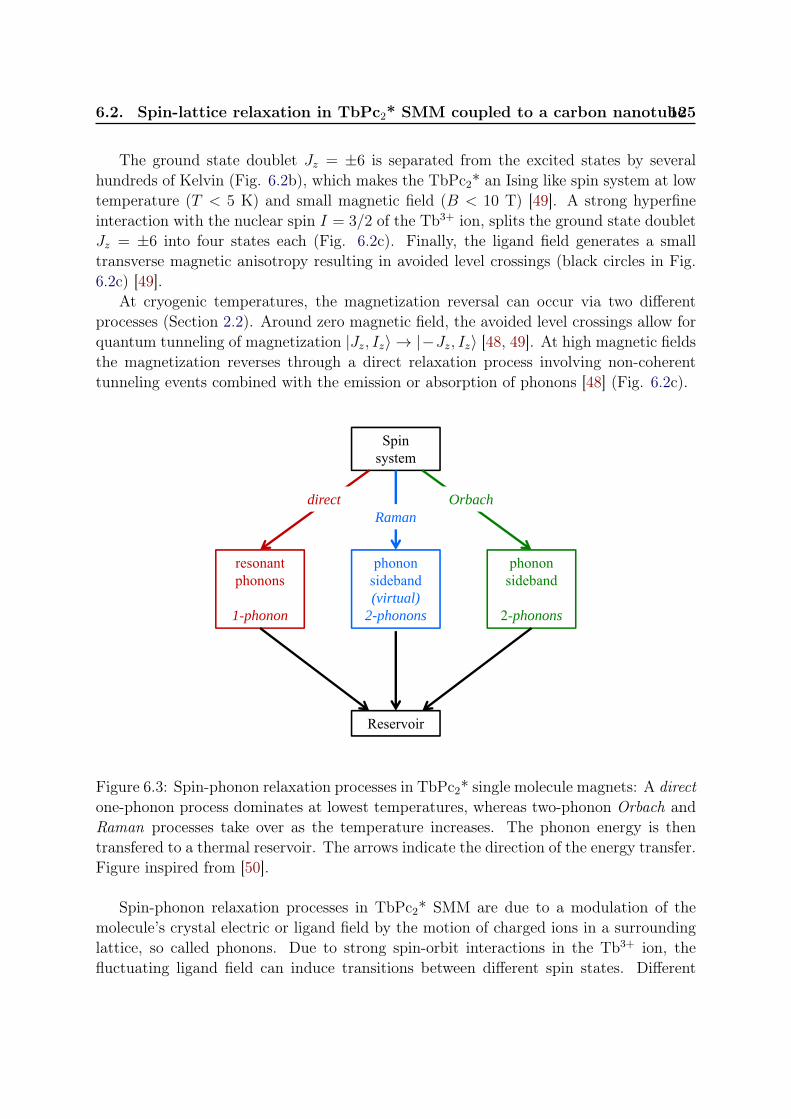
6.2. Spin-lattice relaxation in TbPc2* SMM coupled to a carbon nanotube125
The ground state doublet Jz = ±6 is separated from the excited states by severalhundreds of Kelvin (Fig. 6.2b), which makes the TbPc2* an Ising like spin system at lowtemperature (T < 5 K) and small magnetic field (B < 10 T) [49]. A strong hyperfineinteraction with the nuclear spin I = 3/2 of the Tb3+ ion, splits the ground state doubletJz = ±6 into four states each (Fig. 6.2c). Finally, the ligand field generates a smalltransverse magnetic anisotropy resulting in avoided level crossings (black circles in Fig.6.2c) [49].
At cryogenic temperatures, the magnetization reversal can occur via two differentprocesses (Section 2.2). Around zero magnetic field, the avoided level crossings allow forquantum tunneling of magnetization |Jz, Iz〉 → |−Jz, Iz〉 [48, 49]. At high magnetic fieldsthe magnetization reverses through a direct relaxation process involving non-coherenttunneling events combined with the emission or absorption of phonons [48] (Fig. 6.2c).
spinsystem
Ts
phonon DOSTph
Thermalreservoir
T0
γs-ph γph-bath
Spinsystem
resonant phonons
1-phonon
phononsideband(virtual)
2-phonons
phononsideband
2-phonons
Reservoir
direct OrbachRaman
Figure 6.3: Spin-phonon relaxation processes in TbPc2* single molecule magnets: A directone-phonon process dominates at lowest temperatures, whereas two-phonon Orbach andRaman processes take over as the temperature increases. The phonon energy is thentransfered to a thermal reservoir. The arrows indicate the direction of the energy transfer.Figure inspired from [50].
Spin-phonon relaxation processes in TbPc2* SMM are due to a modulation of themolecule’s crystal electric or ligand field by the motion of charged ions in a surroundinglattice, so called phonons. Due to strong spin-orbit interactions in the Tb3+ ion, thefluctuating ligand field can induce transitions between different spin states. Different
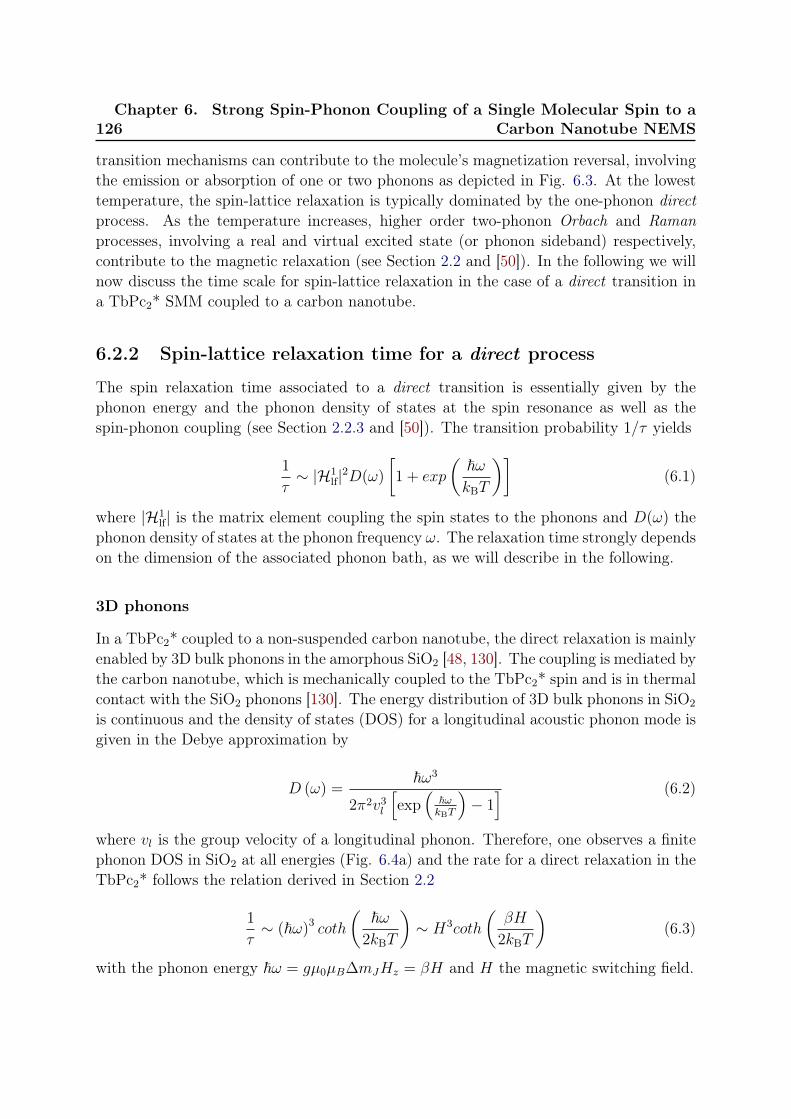
126Chapter 6. Strong Spin-Phonon Coupling of a Single Molecular Spin to a
Carbon Nanotube NEMS
transition mechanisms can contribute to the molecule’s magnetization reversal, involvingthe emission or absorption of one or two phonons as depicted in Fig. 6.3. At the lowesttemperature, the spin-lattice relaxation is typically dominated by the one-phonon directprocess. As the temperature increases, higher order two-phonon Orbach and Ramanprocesses, involving a real and virtual excited state (or phonon sideband) respectively,contribute to the magnetic relaxation (see Section 2.2 and [50]). In the following we willnow discuss the time scale for spin-lattice relaxation in the case of a direct transition ina TbPc2* SMM coupled to a carbon nanotube.
6.2.2 Spin-lattice relaxation time for a direct process
The spin relaxation time associated to a direct transition is essentially given by thephonon energy and the phonon density of states at the spin resonance as well as thespin-phonon coupling (see Section 2.2.3 and [50]). The transition probability 1/τ yields
1
τ∼ |H1
lf|2D(ω)
[1 + exp
(~ωkBT
)](6.1)
where |H1lf| is the matrix element coupling the spin states to the phonons and D(ω) the
phonon density of states at the phonon frequency ω. The relaxation time strongly dependson the dimension of the associated phonon bath, as we will describe in the following.
3D phonons
In a TbPc2* coupled to a non-suspended carbon nanotube, the direct relaxation is mainlyenabled by 3D bulk phonons in the amorphous SiO2 [48, 130]. The coupling is mediated bythe carbon nanotube, which is mechanically coupled to the TbPc2* spin and is in thermalcontact with the SiO2 phonons [130]. The energy distribution of 3D bulk phonons in SiO2
is continuous and the density of states (DOS) for a longitudinal acoustic phonon mode isgiven in the Debye approximation by
D (ω) =~ω3
2π2v3l
[exp
(~ωkBT
)− 1] (6.2)
where vl is the group velocity of a longitudinal phonon. Therefore, one observes a finitephonon DOS in SiO2 at all energies (Fig. 6.4a) and the rate for a direct relaxation in theTbPc2* follows the relation derived in Section 2.2
1
τ∼ (~ω)3 coth
(~ω
2kBT
)∼ H3coth
(βH
2kBT
)(6.3)
with the phonon energy ~ω = gµ0µB∆mJHz = βH and H the magnetic switching field.
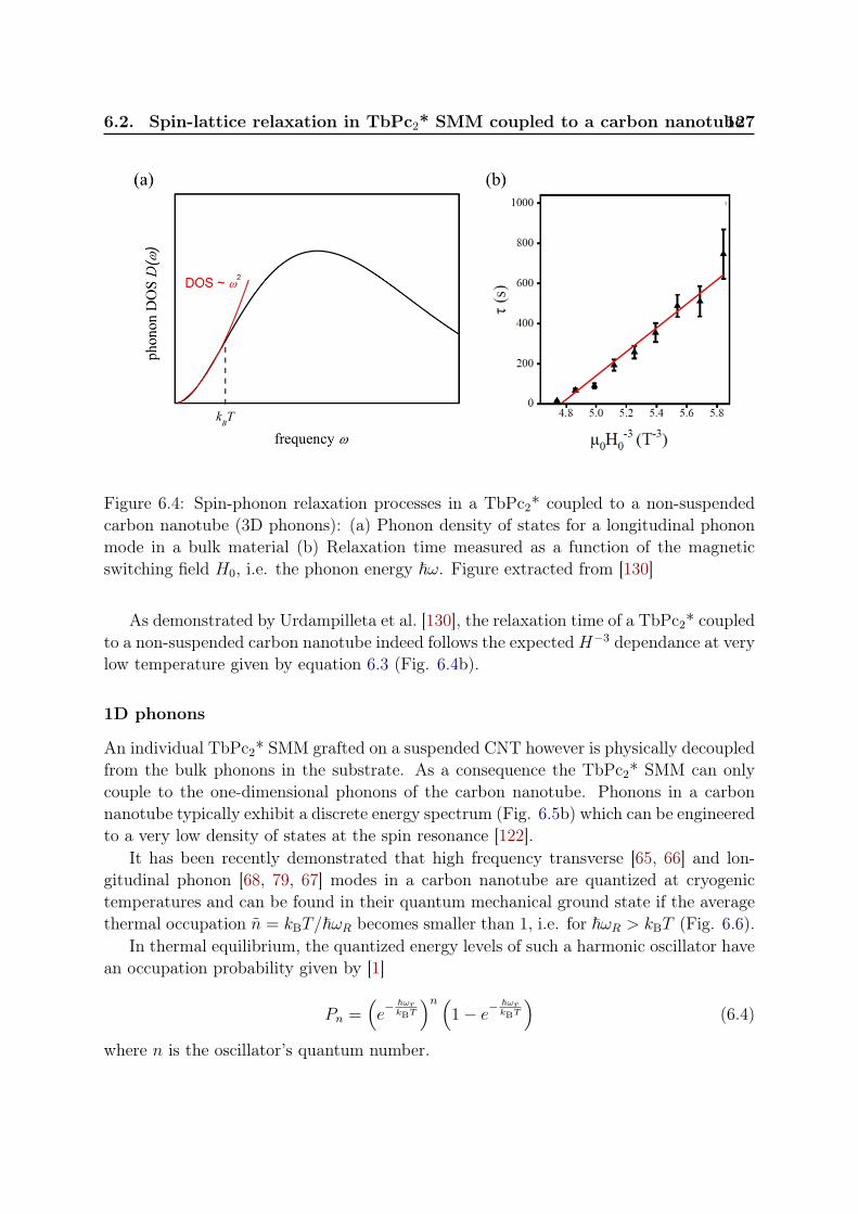
6.2. Spin-lattice relaxation in TbPc2* SMM coupled to a carbon nanotube127
Figure 6.4: Spin-phonon relaxation processes in a TbPc2* coupled to a non-suspendedcarbon nanotube (3D phonons): (a) Phonon density of states for a longitudinal phononmode in a bulk material (b) Relaxation time measured as a function of the magneticswitching field H0, i.e. the phonon energy ~ω. Figure extracted from [130]
As demonstrated by Urdampilleta et al. [130], the relaxation time of a TbPc2* coupledto a non-suspended carbon nanotube indeed follows the expectedH−3 dependance at verylow temperature given by equation 6.3 (Fig. 6.4b).
1D phonons
An individual TbPc2* SMM grafted on a suspended CNT however is physically decoupledfrom the bulk phonons in the substrate. As a consequence the TbPc2* SMM can onlycouple to the one-dimensional phonons of the carbon nanotube. Phonons in a carbonnanotube typically exhibit a discrete energy spectrum (Fig. 6.5b) which can be engineeredto a very low density of states at the spin resonance [122].
It has been recently demonstrated that high frequency transverse [65, 66] and lon-gitudinal phonon [68, 79, 67] modes in a carbon nanotube are quantized at cryogenictemperatures and can be found in their quantum mechanical ground state if the averagethermal occupation n = kBT/~ωR becomes smaller than 1, i.e. for ~ωR > kBT (Fig. 6.6).
In thermal equilibrium, the quantized energy levels of such a harmonic oscillator havean occupation probability given by [1]
Pn =(e− ~ωr
kBT
)n (1− e−
~ωrkBT
)(6.4)
where n is the oscillator’s quantum number.
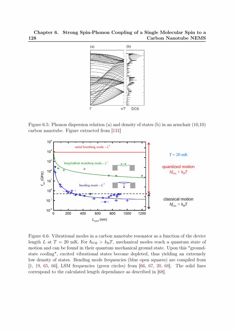
128Chapter 6. Strong Spin-Phonon Coupling of a Single Molecular Spin to a
Carbon Nanotube NEMS
(a) (b)
Figure 6.5: Phonon dispersion relation (a) and density of states (b) in an armchair (10,10)carbon nanotube. Figure extracted from [131]
quantized motionhfres > kBT
classical motionhfres < kBT
T = 20 mK
Figure 6.6: Vibrational modes in a carbon nanotube resonator as a function of the devicelength L at T = 20 mK. For ~ωR > kBT , mechanical modes reach a quantum state ofmotion and can be found in their quantum mechanical ground state. Upon this "ground-state cooling", excited vibrational states become depleted, thus yielding an extremelylow density of states. Bending mode frequencies (blue open squares) are compiled from[1, 19, 65, 66], LSM frequencies (green circles) from [66, 67, 20, 68]. The solid linescorrespond to the calculated length dependance as described in [68].
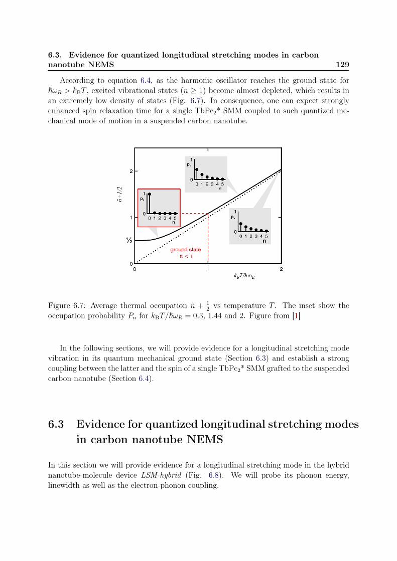
6.3. Evidence for quantized longitudinal stretching modes in carbonnanotube NEMS 129
According to equation 6.4, as the harmonic oscillator reaches the ground state for~ωR > kBT , excited vibrational states (n ≥ 1) become almost depleted, which results inan extremely low density of states (Fig. 6.7). In consequence, one can expect stronglyenhanced spin relaxation time for a single TbPc2* SMM coupled to such quantized me-chanical mode of motion in a suspended carbon nanotube.
Figure 6.7: Average thermal occupation n + 12vs temperature T . The inset show the
occupation probability Pn for kBT/~ωR = 0.3, 1.44 and 2. Figure from [1]
In the following sections, we will provide evidence for a longitudinal stretching modevibration in its quantum mechanical ground state (Section 6.3) and establish a strongcoupling between the latter and the spin of a single TbPc2* SMM grafted to the suspendedcarbon nanotube (Section 6.4).
6.3 Evidence for quantized longitudinal stretching modesin carbon nanotube NEMS
In this section we will provide evidence for a longitudinal stretching mode in the hybridnanotube-molecule device LSM-hybrid (Fig. 6.8). We will probe its phonon energy,linewidth as well as the electron-phonon coupling.
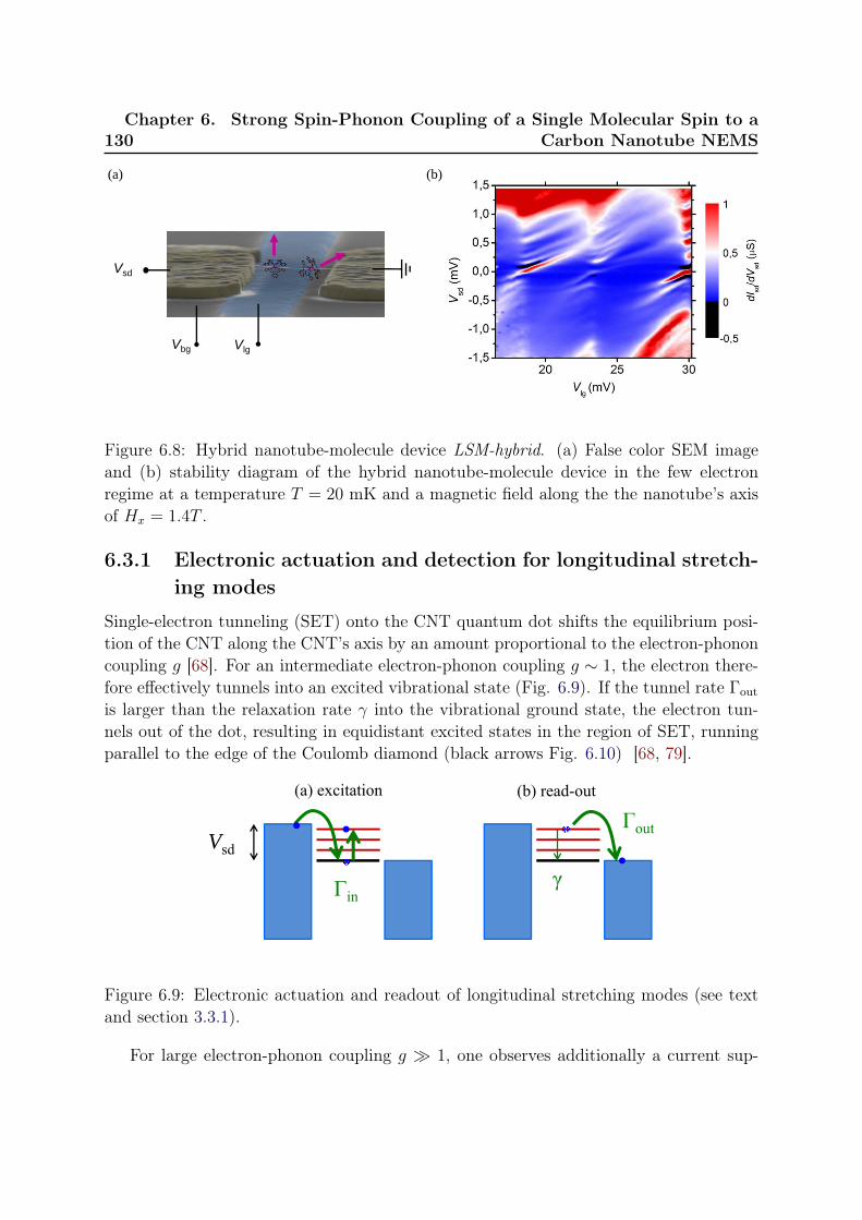
130Chapter 6. Strong Spin-Phonon Coupling of a Single Molecular Spin to a
Carbon Nanotube NEMS
Vsd
VlgVbg
(a) (b)
Figure 6.8: Hybrid nanotube-molecule device LSM-hybrid. (a) False color SEM imageand (b) stability diagram of the hybrid nanotube-molecule device in the few electronregime at a temperature T = 20 mK and a magnetic field along the the nanotube’s axisof Hx = 1.4T .
6.3.1 Electronic actuation and detection for longitudinal stretch-ing modes
Single-electron tunneling (SET) onto the CNT quantum dot shifts the equilibrium posi-tion of the CNT along the CNT’s axis by an amount proportional to the electron-phononcoupling g [68]. For an intermediate electron-phonon coupling g ∼ 1, the electron there-fore effectively tunnels into an excited vibrational state (Fig. 6.9). If the tunnel rate Γout
is larger than the relaxation rate γ into the vibrational ground state, the electron tun-nels out of the dot, resulting in equidistant excited states in the region of SET, runningparallel to the edge of the Coulomb diamond (black arrows Fig. 6.10) [68, 79].
Γin
Vsd
(a) excitation
Γout
γ
(b) read-out
Figure 6.9: Electronic actuation and readout of longitudinal stretching modes (see textand section 3.3.1).
For large electron-phonon coupling g 1, one observes additionally a current sup-
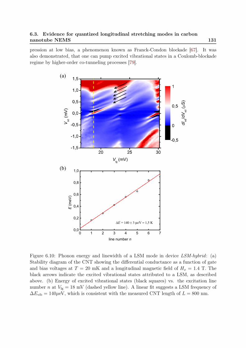
6.3. Evidence for quantized longitudinal stretching modes in carbonnanotube NEMS 131
pression at low bias, a phenomenon known as Franck-Condon blockade [67]. It wasalso demonstrated, that one can pump excited vibrational states in a Coulomb-blockaderegime by higher-order co-tunneling processes [79].
(a)
(b)
0 1 2 3 4 5 6 70,0
0,2
0,4
0,6
0,8
1,0
∆E = 140 3 µeV = 1,5 Κ
E (m
eV)
line number n
Figure 6.10: Phonon energy and linewidth of a LSM mode in device LSM-hybrid : (a)Stability diagram of the CNT showing the differential conductance as a function of gateand bias voltages at T = 20 mK and a longitudinal magnetic field of Hx = 1.4 T. Theblack arrows indicate the excited vibrational states attributed to a LSM, as describedabove. (b) Energy of excited vibrational states (black squares) vs. the excitation linenumber n at Vlg = 18 mV (dashed yellow line). A linear fit suggests a LSM frequency of∆Evib = 140µeV, which is consistent with the measured CNT length of L = 800 nm.
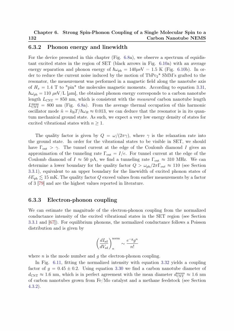
132Chapter 6. Strong Spin-Phonon Coupling of a Single Molecular Spin to a
Carbon Nanotube NEMS
6.3.2 Phonon energy and linewidth
For the device presented in this chapter (Fig. 6.8a), we observe a spectrum of equidis-tant excited states in the region of SET (black arrows in Fig. 6.10a) with an averageenergy separation and phonon energy of ~ωph = 140µeV = 1.5 K (Fig. 6.10b). In or-der to reduce the current noise induced by the motion of TbPc2* SMM’s grafted to theresonator, the measurement was performed in a magnetic field along the nanotube axisof Hx = 1.4 T to "pin" the molecules magnetic moments. According to equation 3.31,~ωph = 110 µeV/L [µm], the obtained phonon energy corresponds to a carbon nanotubelength LCNT = 850 nm, which is consistent with the measured carbon nanotube lengthLmeas
CNT = 800 nm (Fig. 6.8a). From the average thermal occupation of this harmonicoscillator mode n = kBT/~ωR ≈ 0.013, we can deduce that the resonator is in its quan-tum mechanical ground state. As such, we expect a very low energy density of states forexcited vibrational states with n ≥ 1.
The quality factor is given by Q = ω/(2πγ), where γ is the relaxation rate intothe ground state. In order for the vibrational states to be visible in SET, we shouldhave Γout > γ. The tunnel current at the edge of the Coulomb diamond I gives anapproximation of the tunneling rate Γout = I/e. For tunnel current at the edge of theCoulomb diamond of I ≈ 50 pA, we find a tunneling rate Γout ≈ 310 MHz. We candetermine a lower boundary for the quality factor Q > ωph/2πΓout ≈ 110 (see Section3.3.1), equivalent to an upper boundary for the linewidth of excited phonon states ofδEph . 15 mK. The quality factor Q exceed values from earlier measurements by a factorof 3 [79] and are the highest values reported in literature.
6.3.3 Electron-phonon coupling
We can estimate the magnitude of the electron-phonon coupling from the normalizedconductance intensity of the excited vibrational states in the SET region (see Section3.3.1 and [67]). For equilibrium phonons, the normalized conductance follows a Poissondistribution and is given by (
dIsddVsd
)norm
n
∼ e−ggn
n!
where n is the mode number and g the electron-phonon coupling.In Fig. 6.11, fitting the normalized intensity with equation 3.32 yields a coupling
factor of g = 0.45 ± 0.2. Using equation 3.30 we find a carbon nanotube diameter ofdCNT ≈ 1.6 nm, which is in perfect agreement with the mean diameter dmeanCNT ≈ 1.6 nmof carbon nanotubes grown from Fe/Mo catalyst and a methane feedstock (see Section4.3.2).
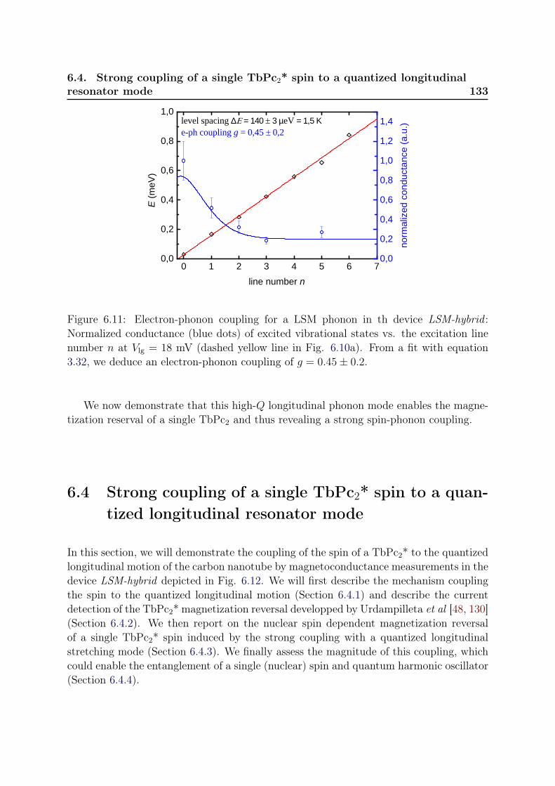
6.4. Strong coupling of a single TbPc2* spin to a quantized longitudinalresonator mode 133
0 1 2 3 4 5 6 70 , 0
0 , 2
0 , 4
0 , 6
0 , 8
1 , 0 l e v e l s p a c i n g ∆ = 140 3 µe V = 1,5 Κ e - p h c o u p l i n g g = 0 , 4 5 0 , 2
E (m
eV)
l i n e n u m b e r n0 , 00 , 20 , 40 , 60 , 81 , 01 , 21 , 4
norm
alized
cond
uctan
ce (a
.u.)
Figure 6.11: Electron-phonon coupling for a LSM phonon in th device LSM-hybrid :Normalized conductance (blue dots) of excited vibrational states vs. the excitation linenumber n at Vlg = 18 mV (dashed yellow line in Fig. 6.10a). From a fit with equation3.32, we deduce an electron-phonon coupling of g = 0.45± 0.2.
We now demonstrate that this high-Q longitudinal phonon mode enables the magne-tization reserval of a single TbPc2 and thus revealing a strong spin-phonon coupling.
6.4 Strong coupling of a single TbPc2* spin to a quan-tized longitudinal resonator mode
In this section, we will demonstrate the coupling of the spin of a TbPc2* to the quantizedlongitudinal motion of the carbon nanotube by magnetoconductance measurements in thedevice LSM-hybrid depicted in Fig. 6.12. We will first describe the mechanism couplingthe spin to the quantized longitudinal motion (Section 6.4.1) and describe the currentdetection of the TbPc2* magnetization reversal developped by Urdampilleta et al [48, 130](Section 6.4.2). We then report on the nuclear spin dependent magnetization reversalof a single TbPc2* spin induced by the strong coupling with a quantized longitudinalstretching mode (Section 6.4.3). We finally assess the magnitude of this coupling, whichcould enable the entanglement of a single (nuclear) spin and quantum harmonic oscillator(Section 6.4.4).
134Chapter 6. Strong Spin-Phonon Coupling of a Single Molecular Spin to a
Carbon Nanotube NEMS
Vsd
VlgVbg
(a) (b)
Figure 6.12: Hybrid nanotube-molecule device LSM-hybrid. (a) False color SEM imageand (b) stability diagram of the hybrid nanotube-molecule device in the few electronregime at T = 20 mK and Hx = 1.4T . The black arrows depict excited vibrational statesassociated with the LSM phonon described in the previous section and the green dasheddepicts the working point for the measurements shown in section 6.4.3.
6.4.1 Coupling mechanism between a single TbPc2* spin to aquantized longitudinal resonator mode
First, we tune our CNT quantum dot to a regime of Coulomb blockade (Vlg = 16.5 mV,green dashed line in Fig. 6.12b). In the case of a strong spin-phonon coupling, themagnetization reversal of an individual TbPc2 SMM via direct transition can induce theexcitation of the longitudinal stretching mode phonon described in the previous section6.3 (Fig. 6.13).
An upper boundary for the linewidth of an excited LSM phonon state was estimated toδEph . 15 mK (Section 6.3) and is therefore smaller than the energy level spacing ∆EI =
120, 150, 180 mK between the nuclear spin states of the Tb3+ ion [47, 49]. Sweepingthe magnetic field from negative to positive values, we should thus observe four differenttransitions matching the phonon energy ~ωph = 140µeV = 1.5 K and corresponding tothe different nuclear spin states of the Tb3+ ion as depicted by the colored arrows in Fig.6.13.
We can evaluate the magnetic field associated with each transition, the so calledswitching field µ0H‖,sw, from the Zeeman energy difference between the spin states |mJ =
+6,mI〉 and |m′J = −6,mI〉
∆Ez =(gµBµ0H‖,sw + AmI
)∆mJ (6.5)
where g = 3/2 is the gyromagnetic factor of the Tb3+ ion, µB = 0.673 K/T the Bohr
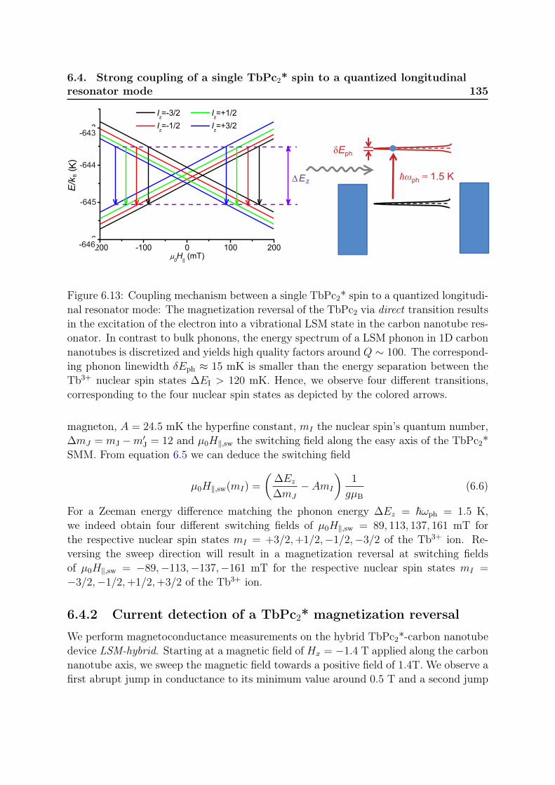
6.4. Strong coupling of a single TbPc2* spin to a quantized longitudinalresonator mode 135
ħωph = 1.5 K
δEph
-200 -100 0 100 200-6
-5
-4
-3
Iz=-3/2 Iz=+1/2 Iz=-1/2 Iz=+3/2
E (K
)
0H|| (mT)
δEph
= 1
,5 K
-646
-645
-644
-643
E/k
( K)
B
∆E z
Figure 6.13: Coupling mechanism between a single TbPc2* spin to a quantized longitudi-nal resonator mode: The magnetization reversal of the TbPc2 via direct transition resultsin the excitation of the electron into a vibrational LSM state in the carbon nanotube res-onator. In contrast to bulk phonons, the energy spectrum of a LSM phonon in 1D carbonnanotubes is discretized and yields high quality factors around Q ∼ 100. The correspond-ing phonon linewidth δEph ≈ 15 mK is smaller than the energy separation between theTb3+ nuclear spin states ∆EI > 120 mK. Hence, we observe four different transitions,corresponding to the four nuclear spin states as depicted by the colored arrows.
magneton, A = 24.5 mK the hyperfine constant, mI the nuclear spin’s quantum number,∆mJ = mJ −m′J = 12 and µ0H‖,sw the switching field along the easy axis of the TbPc2*SMM. From equation 6.5 we can deduce the switching field
µ0H‖,sw(mI) =
(∆Ez∆mJ
− AmI
)1
gµB(6.6)
For a Zeeman energy difference matching the phonon energy ∆Ez = ~ωph = 1.5 K,we indeed obtain four different switching fields of µ0H‖,sw = 89, 113, 137, 161 mT forthe respective nuclear spin states mI = +3/2,+1/2,−1/2,−3/2 of the Tb3+ ion. Re-versing the sweep direction will result in a magnetization reversal at switching fieldsof µ0H‖,sw = −89,−113,−137,−161 mT for the respective nuclear spin states mI =
−3/2,−1/2,+1/2,+3/2 of the Tb3+ ion.
6.4.2 Current detection of a TbPc2* magnetization reversal
We perform magnetoconductance measurements on the hybrid TbPc2*-carbon nanotubedevice LSM-hybrid. Starting at a magnetic field of Hx = −1.4 T applied along the carbonnanotube axis, we sweep the magnetic field towards a positive field of 1.4T. We observe afirst abrupt jump in conductance to its minimum value around 0.5 T and a second jump
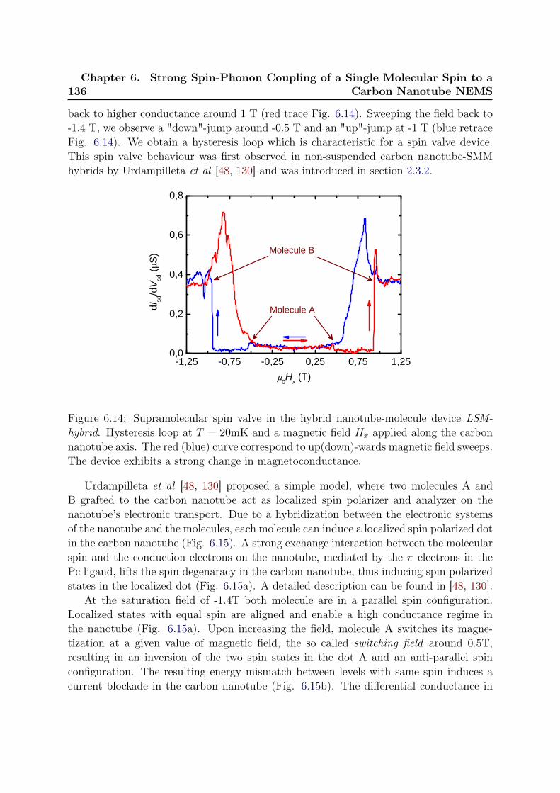
136Chapter 6. Strong Spin-Phonon Coupling of a Single Molecular Spin to a
Carbon Nanotube NEMS
back to higher conductance around 1 T (red trace Fig. 6.14). Sweeping the field back to-1.4 T, we observe a "down"-jump around -0.5 T and an "up"-jump at -1 T (blue retraceFig. 6.14). We obtain a hysteresis loop which is characteristic for a spin valve device.This spin valve behaviour was first observed in non-suspended carbon nanotube-SMMhybrids by Urdampilleta et al [48, 130] and was introduced in section 2.3.2.
- 1 , 2 5 - 0 , 7 5 - 0 , 2 5 0 , 2 5 0 , 7 5 1 , 2 50 , 0
0 , 2
0 , 4
0 , 6
0 , 8
M o l e c u l e B
dI sd/dV
sd (µ
S)
0 H x ( T )
M o l e c u l e A
Figure 6.14: Supramolecular spin valve in the hybrid nanotube-molecule device LSM-hybrid. Hysteresis loop at T = 20mK and a magnetic field Hx applied along the carbonnanotube axis. The red (blue) curve correspond to up(down)-wards magnetic field sweeps.The device exhibits a strong change in magnetoconductance.
Urdampilleta et al [48, 130] proposed a simple model, where two molecules A andB grafted to the carbon nanotube act as localized spin polarizer and analyzer on thenanotube’s electronic transport. Due to a hybridization between the electronic systemsof the nanotube and the molecules, each molecule can induce a localized spin polarized dotin the carbon nanotube (Fig. 6.15). A strong exchange interaction between the molecularspin and the conduction electrons on the nanotube, mediated by the π electrons in thePc ligand, lifts the spin degenaracy in the carbon nanotube, thus inducing spin polarizedstates in the localized dot (Fig. 6.15a). A detailed description can be found in [48, 130].
At the saturation field of -1.4T both molecule are in a parallel spin configuration.Localized states with equal spin are aligned and enable a high conductance regime inthe nanotube (Fig. 6.15a). Upon increasing the field, molecule A switches its magne-tization at a given value of magnetic field, the so called switching field around 0.5T,resulting in an inversion of the two spin states in the dot A and an anti-parallel spinconfiguration. The resulting energy mismatch between levels with same spin induces acurrent blockade in the carbon nanotube (Fig. 6.15b). The differential conductance in
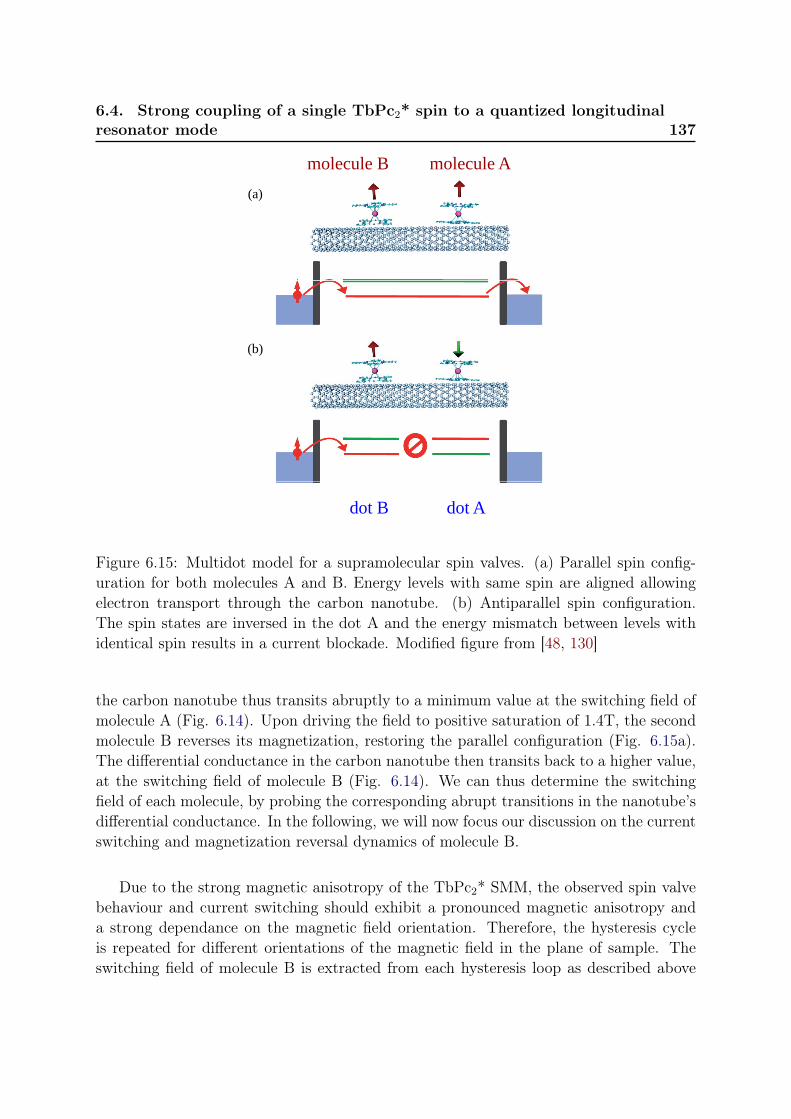
6.4. Strong coupling of a single TbPc2* spin to a quantized longitudinalresonator mode 137
molecule Amolecule B(a)
(b)
dot Adot B
Figure 6.15: Multidot model for a supramolecular spin valves. (a) Parallel spin config-uration for both molecules A and B. Energy levels with same spin are aligned allowingelectron transport through the carbon nanotube. (b) Antiparallel spin configuration.The spin states are inversed in the dot A and the energy mismatch between levels withidentical spin results in a current blockade. Modified figure from [48, 130]
the carbon nanotube thus transits abruptly to a minimum value at the switching field ofmolecule A (Fig. 6.14). Upon driving the field to positive saturation of 1.4T, the secondmolecule B reverses its magnetization, restoring the parallel configuration (Fig. 6.15a).The differential conductance in the carbon nanotube then transits back to a higher value,at the switching field of molecule B (Fig. 6.14). We can thus determine the switchingfield of each molecule, by probing the corresponding abrupt transitions in the nanotube’sdifferential conductance. In the following, we will now focus our discussion on the currentswitching and magnetization reversal dynamics of molecule B.
Due to the strong magnetic anisotropy of the TbPc2* SMM, the observed spin valvebehaviour and current switching should exhibit a pronounced magnetic anisotropy anda strong dependance on the magnetic field orientation. Therefore, the hysteresis cycleis repeated for different orientations of the magnetic field in the plane of sample. Theswitching field of molecule B is extracted from each hysteresis loop as described above

138Chapter 6. Strong Spin-Phonon Coupling of a Single Molecular Spin to a
Carbon Nanotube NEMS
and plotted as a function of the in-plane magnetic field angle (Fig. 6.16a). The switchingfields strongly depend on the orientation of the in-plane magnetic field and follow fourparallel, straight lines in the field plane for both up- and downwards magnetic fieldssweeps (dashed lines in Fig. 6.16a). The projection of these switching fields on the"easy axis" is constant, which is consistent with the uniaxial magnetic anisotropy of theIsing-like Tb3+ ion.
As we will demonstrate in the following section 6.4.3, the four observed transitionsare in fact consistent with the nuclear spin-resolved phonon-assited the magnetizationreversal of the TbPc2* molecule B.
(a) (b)
Hx
Figure 6.16: Magnetic anisotropy of TbPc2 molecule B in the hybrid nanotube-moleculedevice LSM-hybrid. (a) Switching fields for upwards (full dots) and downwards (opendots) sweeps as a function of the angle of the magnetic field in the sample plane. Thedashed lines are guide to the eye. (b) Switching fields as a function of the in-planemagnetic field angle corrected for the out-of-plane misalignement β of the molecule.
Using Fig. 6.16a, we can determine the in the plane orientation of the easy axis formolecule B (i.e. in the sample plane). The easy axis is oriented perpendicular to the fourhighlighted transition lines, thus having an angle of α ∼ 28 with the nanotube axis Hx.
We can also determine the out-of-plane orientation of the SMM’s easy axis using theequation
cosβ =δH‖δH
(6.7)
where δH‖ = 23 mT is the magnetic field separation between the nuclear spin states fora field oriented parallel to the SMM’s easy axis and δH the magnetic field separationbetween the nuclear spin states for a field applied along the projection of the easy axis
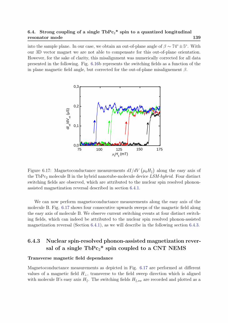
6.4. Strong coupling of a single TbPc2* spin to a quantized longitudinalresonator mode 139
into the sample plane. In our case, we obtain an out-of-plane angle of β ∼ 74±5. Withour 3D vector magnet we are not able to compensate for this out-of-plane orientation.However, for the sake of clarity, this misalignment was numerically corrected for all datapresented in the following. Fig. 6.16b represents the switching fields as a function of thein plane magnetic field angle, but corrected for the out-of-plane misalignement β.
0 , 0
0 , 1
0 , 2
0 , 3
7 5 1 0 0 1 2 5 1 5 0
dI sd/dV
sd (µ
S)
0 H | | ( m T )1 7 5
Figure 6.17: Magnetoconductance measurements dI/dV(µ0H‖
)along the easy axis of
the TbPc2 molecule B in the hybrid nanotube-molecule device LSM-hybrid. Four distinctswitching fields are observed, which are attributed to the nuclear spin resolved phonon-assisted magnetization reversal described in section 6.4.1.
We can now perform magnetoconductance measurements along the easy axis of themolecule B. Fig. 6.17 shows four consecutive upwards sweeps of the magnetic field alongthe easy axis of molecule B. We observe current switching events at four distinct switch-ing fields, which can indeed be attributed to the nuclear spin resolved phonon-assistedmagnetization reversal (Section 6.4.1), as we will describe in the following section 6.4.3.
6.4.3 Nuclear spin-resolved phonon-assisted magnetization rever-sal of a single TbPc2* spin coupled to a CNT NEMS
Transverse magnetic field dependance
Magnetoconductance measurements as depicted in Fig. 6.17 are performed at differentvalues of a magnetic field H⊥, transverse to the field sweep direction which is alignedwith molecule B’s easy axis H‖. The switching fields H‖,sw are recorded and plotted as a
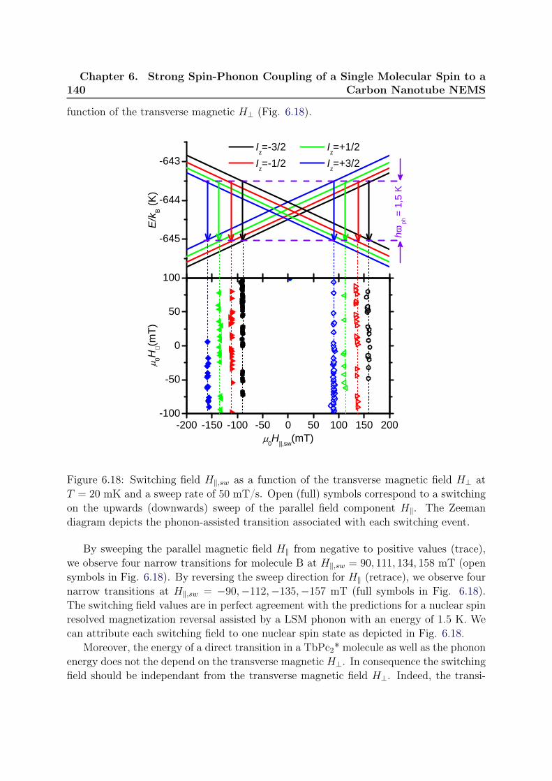
140Chapter 6. Strong Spin-Phonon Coupling of a Single Molecular Spin to a
Carbon Nanotube NEMS
function of the transverse magnetic H⊥ (Fig. 6.18).
- 6 4 5
- 6 4 4
- 6 4 3
I z = - 3 / 2 I z = + 1 / 2 I z = - 1 / 2 I z = + 3 / 2
E/k B (K
)
hω ph
= 1,5
K
- 2 0 0 - 1 5 0 - 1 0 0 - 5 0 0 5 0 1 0 0 1 5 0 2 0 0- 1 0 0
- 5 0
0
5 0
1 0 0
0 H | | , s w ( m T )
0H ⊥(mT)
Figure 6.18: Switching field H‖,sw as a function of the transverse magnetic field H⊥ atT = 20 mK and a sweep rate of 50 mT/s. Open (full) symbols correspond to a switchingon the upwards (downwards) sweep of the parallel field component H‖. The Zeemandiagram depicts the phonon-assisted transition associated with each switching event.
By sweeping the parallel magnetic field H‖ from negative to positive values (trace),we observe four narrow transitions for molecule B at H‖,sw = 90, 111, 134, 158 mT (opensymbols in Fig. 6.18). By reversing the sweep direction for H‖ (retrace), we observe fournarrow transitions at H‖,sw = −90,−112,−135,−157 mT (full symbols in Fig. 6.18).The switching field values are in perfect agreement with the predictions for a nuclear spinresolved magnetization reversal assisted by a LSM phonon with an energy of 1.5 K. Wecan attribute each switching field to one nuclear spin state as depicted in Fig. 6.18.
Moreover, the energy of a direct transition in a TbPc2* molecule as well as the phononenergy does not the depend on the transverse magnetic H⊥. In consequence the switchingfield should be independant from the transverse magnetic field H⊥. Indeed, the transi-
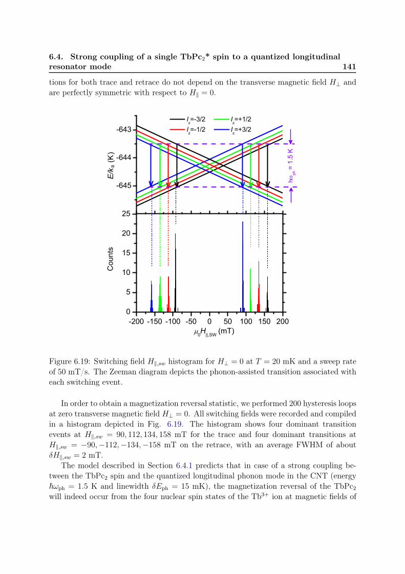
6.4. Strong coupling of a single TbPc2* spin to a quantized longitudinalresonator mode 141
tions for both trace and retrace do not depend on the transverse magnetic field H⊥ andare perfectly symmetric with respect to H‖ = 0.
-645
-644
-643
Iz=-3/2 I
z=+1/2
Iz=-1/2 I
z=+3/2
E
/k (K
)
hωph
= 1.
5 K
-200 -150 -100 -50 0 50 100 150 2000
5
10
15
20
25
Cou
nts
0H||,SW (mT)
B
Figure 6.19: Switching field H‖,sw histogram for H⊥ = 0 at T = 20 mK and a sweep rateof 50 mT/s. The Zeeman diagram depicts the phonon-assisted transition associated witheach switching event.
In order to obtain a magnetization reversal statistic, we performed 200 hysteresis loopsat zero transverse magnetic field H⊥ = 0. All switching fields were recorded and compiledin a histogram depicted in Fig. 6.19. The histogram shows four dominant transitionevents at H‖,sw = 90, 112, 134, 158 mT for the trace and four dominant transitions atH‖,sw = −90,−112,−134,−158 mT on the retrace, with an average FWHM of aboutδH‖,sw = 2 mT.
The model described in Section 6.4.1 predicts that in case of a strong coupling be-tween the TbPc2 spin and the quantized longitudinal phonon mode in the CNT (energy~ωph = 1.5 K and linewidth δEph = 15 mK), the magnetization reversal of the TbPc2
will indeed occur from the four nuclear spin states of the Tb3+ ion at magnetic fields of
142Chapter 6. Strong Spin-Phonon Coupling of a Single Molecular Spin to a
Carbon Nanotube NEMS
µ0H‖,sw = 89, 113, 137, 161 mT for an upwards magnetic field sweep (and at −µ0H‖,sw fora downwards magnetic field sweep).
The Zeeman energy δEz corresponding to the FWHM of each switching event in Fig.6.19 is approximately 30 mK, which is in close agreement with the phonon linewidth ofδEph = 15 mK determined in the previous section. Moreover, all four switching eventsin the TbPc2 can be associated with a transition energy of ∆Ez = 1.5 K, which is inperfect agreement with phonon energy of ~ωph = 1.5 K. The experimental findings arethus in excellent agreement with the provided model. The strong interaction between themolecular TbPc2 spin and the quantized longitudinal phonon is further supported by themagnitude of the spin-phonon coupling, which we will evaluate in Section 6.4.4.
The transverse field dependance and the statistics of the magnetization reversal ofmolecule B provides a strong evidence for a phonon-assisted and nuclear spin-resolvedmagnetic relaxation process in a TbPc2*. We will now demonstrate that the observedmagnetization reversal indeed follows the sweep rate and temperature dependance ex-pected for a Tb3+ nuclear spin.
Sweep rate dependance
We performed magnetization reversal statistics at sweep rates of the magnetic field of 10,50, 100 and 150 mT/s (Fig. 6.20).
At a sweep rate of 150 mT/s, the magnetization reversal essentially occurs from thenuclear spin ground state at a switching field H‖,sw = ±160 mT (Fig. 6.20a). Fig.6.21a depicts the integrated number of counts as a function of the magnetic field for anupwards magnetic field sweep. We can deduce the occupation probability of a nuclearspin state from the corresponding step height in the integrated histogram (Fig. 6.21a).Indeed, the occupation probability of the nuclear spin states follows a Maxwell Boltzmanndistribution P = P0exp(−E/kBTN), with a strong population of the nuclear spin groundstate (blue fit curve in Fig. 6.21b). We determine an upper boundary of nuclear spintemperature of TN = 150 mK, which is on the order of the electronic temperature in thesystem, indicating that the nuclear spin is close to thermal equilibrium.
By reducing the sweeping rate (non-adiabatic sweep), the finite energy level lifetime ofthe nuclear spin states results in transitions from higher nuclear spin states and eventuallyin an inversion of the nuclear spin population. Indeed, for a sweep rate of 10 mT/s, themagnetic relaxation essentially occurs from the highest nuclear spin states at a switchingfield H‖,sw = ±90 mT (Fig. 6.20d).
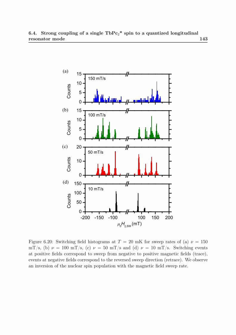
6.4. Strong coupling of a single TbPc2* spin to a quantized longitudinalresonator mode 143
-200 -150 -100 100 150 2000
50
100
150
Cou
nts
0H||,SW (mT)
0
10
20
Cou
nts
150 mT/s
100 mT/s
50 mT/s
10 mT/s
0
5
10
15
Cou
nts
0
5
10
15
(d)
(c)
(b)
C
ount
s(a)
Figure 6.20: Switching field histograms at T = 20 mK for sweep rates of (a) ν = 150
mT/s, (b) ν = 100 mT/s, (c) ν = 50 mT/s and (d) ν = 10 mT/s. Switching eventsat positive fields correspond to sweep from negative to positive magnetic fields (trace),events at negative fields correspond to the reversed sweep direction (retrace). We observean inversion of the nuclear spin population with the magnetic field sweep rate.
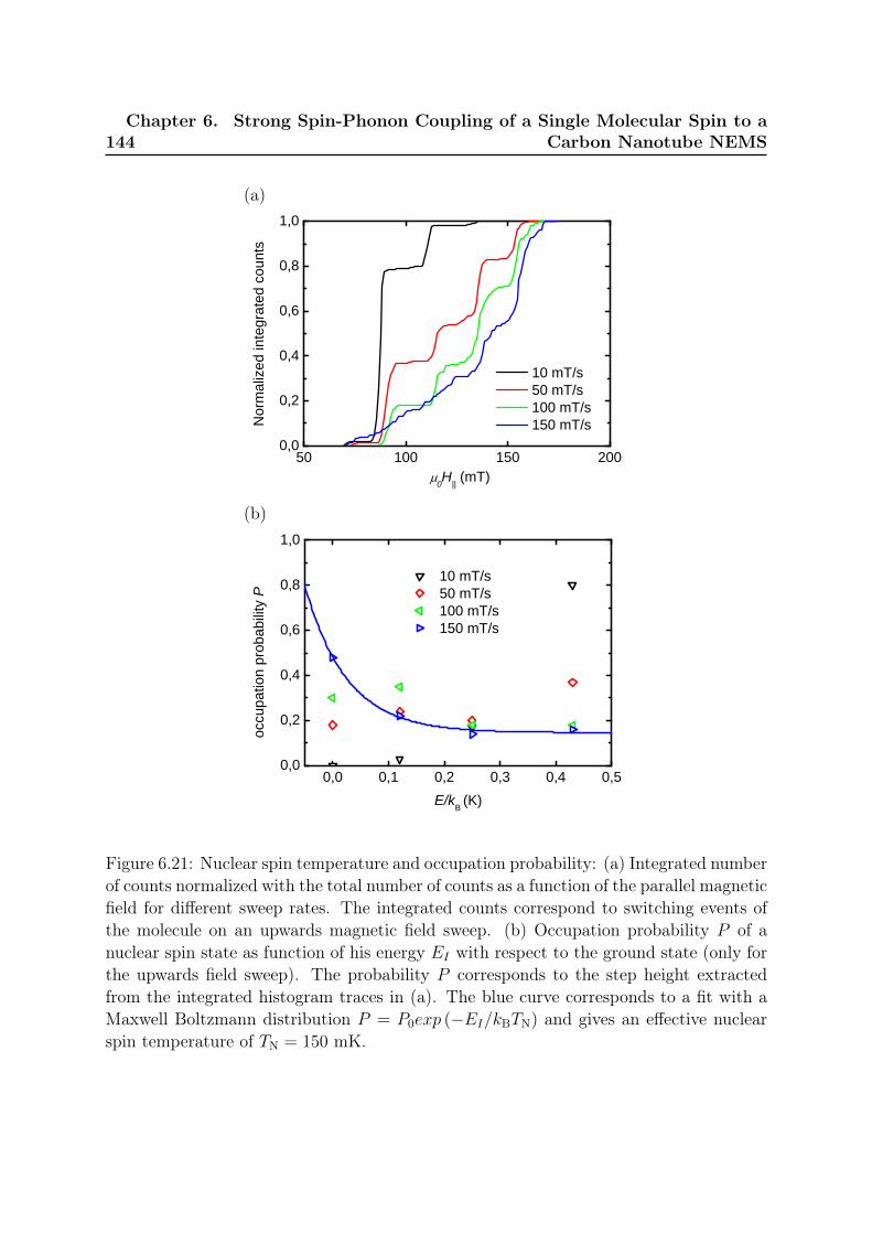
144Chapter 6. Strong Spin-Phonon Coupling of a Single Molecular Spin to a
Carbon Nanotube NEMS
(a)
5 0 1 0 0 1 5 0 2 0 00 , 0
0 , 2
0 , 4
0 , 6
0 , 8
1 , 0
1 0 m T / s 5 0 m T / s 1 0 0 m T / s 1 5 0 m T / s
Norm
alized
integ
rated
coun
ts
0 H | | ( m T )
(b)
0 , 0 0 , 1 0 , 2 0 , 3 0 , 4 0 , 50 , 0
0 , 2
0 , 4
0 , 6
0 , 8
1 , 0 1 0 m T / s 5 0 m T / s 1 0 0 m T / s 1 5 0 m T / s
occu
patio
n prob
ability
P
E / k B ( K )
Figure 6.21: Nuclear spin temperature and occupation probability: (a) Integrated numberof counts normalized with the total number of counts as a function of the parallel magneticfield for different sweep rates. The integrated counts correspond to switching events ofthe molecule on an upwards magnetic field sweep. (b) Occupation probability P of anuclear spin state as function of his energy EI with respect to the ground state (only forthe upwards field sweep). The probability P corresponds to the step height extractedfrom the integrated histogram traces in (a). The blue curve corresponds to a fit with aMaxwell Boltzmann distribution P = P0exp (−EI/kBTN) and gives an effective nuclearspin temperature of TN = 150 mK.
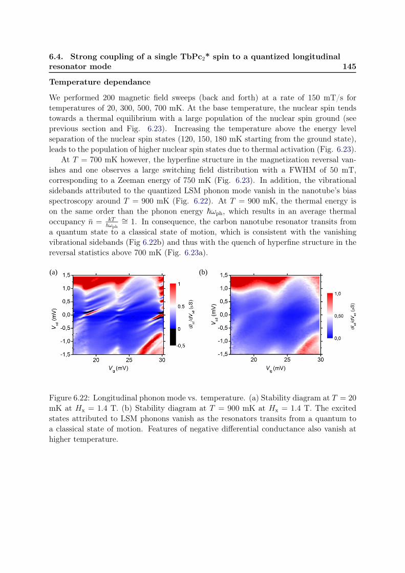
6.4. Strong coupling of a single TbPc2* spin to a quantized longitudinalresonator mode 145
Temperature dependance
We performed 200 magnetic field sweeps (back and forth) at a rate of 150 mT/s fortemperatures of 20, 300, 500, 700 mK. At the base temperature, the nuclear spin tendstowards a thermal equilibrium with a large population of the nuclear spin ground (seeprevious section and Fig. 6.23). Increasing the temperature above the energy levelseparation of the nuclear spin states (120, 150, 180 mK starting from the ground state),leads to the population of higher nuclear spin states due to thermal activation (Fig. 6.23).
At T = 700 mK however, the hyperfine structure in the magnetization reversal van-ishes and one observes a large switching field distribution with a FWHM of 50 mT,corresponding to a Zeeman energy of 750 mK (Fig. 6.23). In addition, the vibrationalsidebands attributed to the quantized LSM phonon mode vanish in the nanotube’s biasspectroscopy around T = 900 mK (Fig. 6.22). At T = 900 mK, the thermal energy ison the same order than the phonon energy ~ωph, which results in an average thermaloccupancy n = kT
~ωph∼= 1. In consequence, the carbon nanotube resonator transits from
a quantum state to a classical state of motion, which is consistent with the vanishingvibrational sidebands (Fig 6.22b) and thus with the quench of hyperfine structure in thereversal statistics above 700 mK (Fig. 6.23a).
(a) (b)
Figure 6.22: Longitudinal phonon mode vs. temperature. (a) Stability diagram at T = 20
mK at Hx = 1.4 T. (b) Stability diagram at T = 900 mK at Hx = 1.4 T. The excitedstates attributed to LSM phonons vanish as the resonators transits from a quantum toa classical state of motion. Features of negative differential conductance also vanish athigher temperature.
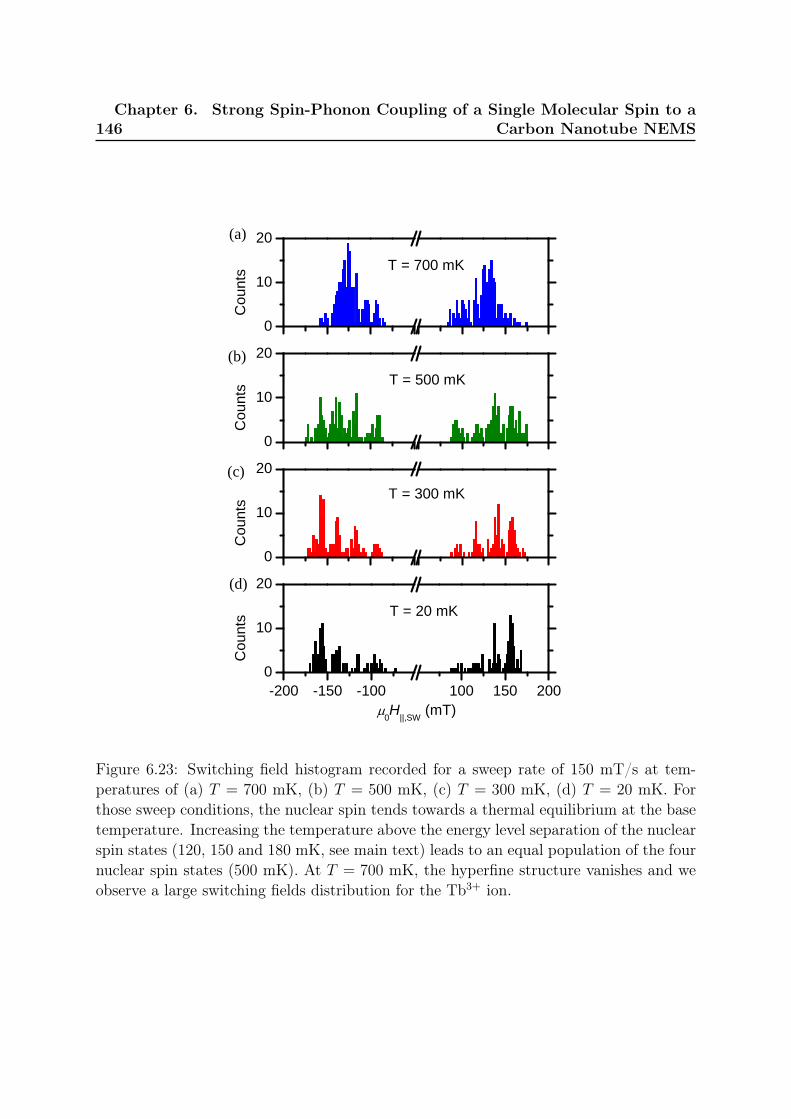
146Chapter 6. Strong Spin-Phonon Coupling of a Single Molecular Spin to a
Carbon Nanotube NEMS
- 2 0 0 - 1 5 0 - 1 0 0 1 0 0 1 5 0 2 0 00
1 0
2 0
Coun
ts
0 H | | , S W ( m T )
T = 7 0 0 m K
T = 5 0 0 m K
T = 3 0 0 m K
T = 2 0 m K
0
1 0
2 0
Coun
ts
0
1 0
2 0
Coun
ts
0
1 0
2 0
Co
unts
( a )
( b )
( c )
( d )
Figure 6.23: Switching field histogram recorded for a sweep rate of 150 mT/s at tem-peratures of (a) T = 700 mK, (b) T = 500 mK, (c) T = 300 mK, (d) T = 20 mK. Forthose sweep conditions, the nuclear spin tends towards a thermal equilibrium at the basetemperature. Increasing the temperature above the energy level separation of the nuclearspin states (120, 150 and 180 mK, see main text) leads to an equal population of the fournuclear spin states (500 mK). At T = 700 mK, the hyperfine structure vanishes and weobserve a large switching fields distribution for the Tb3+ ion.
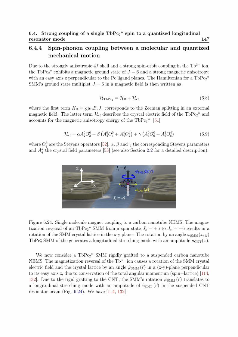
6.4. Strong coupling of a single TbPc2* spin to a quantized longitudinalresonator mode 147
6.4.4 Spin-phonon coupling between a molecular and quantizedmechanical motion
Due to the strongly anisotropic 4f shell and a strong spin-orbit coupling in the Tb3+ ion,the TbPc2* exhibits a magnetic ground state of J = 6 and a strong magnetic anisotropy,with an easy axis z perpendicular to the Pc ligand planes. The Hamiltonian for a TbPc2*SMM’s ground state multiplet J = 6 in a magnetic field is then written as
HTbPc2 = HB +Hcf (6.8)
where the first term HB = gµBBzJz corresponds to the Zeeman splitting in an externalmagnetic field. The latter term Hcf describes the crystal electric field of the TbPc2* andaccounts for the magnetic anisotropy energy of the TbPc2* [51]
Hcf = αA02O
02 + β
(A0
4O04 + A4
4O42
)+ γ
(A0
6O06 + A4
6O46
)(6.9)
where Okq are the Stevens operators [52], α, β and γ the corresponding Stevens parameters
and Akq the crystal field parameters [53] (see also Section 2.2 for a detailed description).
Figure 6.24: Single molecule magnet coupling to a carbon nanotube NEMS. The magne-tization reversal of an TbPc2* SMM from a spin state Jz = +6 to Jz = −6 results in arotation of the SMM crystal lattice in the x-y plane. The rotation by an angle ϕSMM(x, y)
TbPc∗2 SMM of the generates a longitudinal stretching mode with an amplitude uCNT(x).
We now consider a TbPc2* SMM rigidly grafted to a suspended carbon nanotubeNEMS. The magnetization reversal of the Tb3+ ion causes a rotation of the SMM crystalelectric field and the crystal lattice by an angle ϕSMM (~r) in a (x-y)-plane perpendicularto its easy axis z, due to conservation of the total angular momentum (spin+lattice) [114,132]. Due to the rigid grafting to the CNT, the SMM’s rotation ϕSMM (~r) translates toa longitudinal stretching mode with an amplitude of uCNT (~r) in the suspended CNTresonator beam (Fig. 6.24). We have [114, 132]
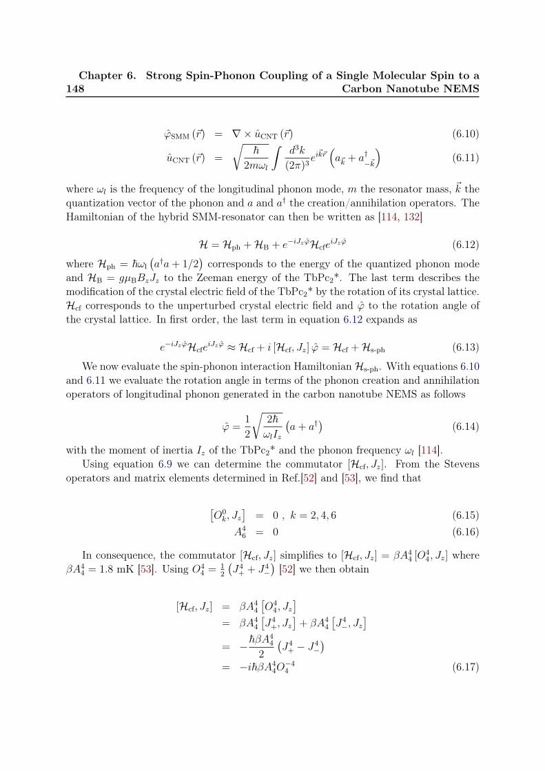
148Chapter 6. Strong Spin-Phonon Coupling of a Single Molecular Spin to a
Carbon Nanotube NEMS
ϕSMM (~r) = ∇× uCNT (~r) (6.10)
uCNT (~r) =
√~
2mωl
∫d3k
(2π)3ei~k~r(a~k + a†
−~k
)(6.11)
where ωl is the frequency of the longitudinal phonon mode, m the resonator mass, ~k thequantization vector of the phonon and a and a† the creation/annihilation operators. TheHamiltonian of the hybrid SMM-resonator can then be written as [114, 132]
H = Hph +HB + e−iJzϕHcfeiJzϕ (6.12)
where Hph = ~ωl(a†a+ 1/2
)corresponds to the energy of the quantized phonon mode
and HB = gµBBzJz to the Zeeman energy of the TbPc2*. The last term describes themodification of the crystal electric field of the TbPc2* by the rotation of its crystal lattice.Hcf corresponds to the unperturbed crystal electric field and ϕ to the rotation angle ofthe crystal lattice. In first order, the last term in equation 6.12 expands as
e−iJzϕHcfeiJzϕ ≈ Hcf + i [Hcf, Jz] ϕ = Hcf +Hs-ph (6.13)
We now evaluate the spin-phonon interaction Hamiltonian Hs-ph. With equations 6.10and 6.11 we evaluate the rotation angle in terms of the phonon creation and annihilationoperators of longitudinal phonon generated in the carbon nanotube NEMS as follows
ϕ =1
2
√2~ωlIz
(a+ a†
)(6.14)
with the moment of inertia Iz of the TbPc2* and the phonon frequency ωl [114].Using equation 6.9 we can determine the commutator [Hcf, Jz]. From the Stevens
operators and matrix elements determined in Ref.[52] and [53], we find that
[O0k, Jz
]= 0 , k = 2, 4, 6 (6.15)
A46 = 0 (6.16)
In consequence, the commutator [Hcf, Jz] simplifies to [Hcf, Jz] = βA44 [O4
4, Jz] whereβA4
4 = 1.8 mK [53]. Using O44 = 1
2
(J4
+ + J4−)[52] we then obtain
[Hcf, Jz] = βA44
[O4
4, Jz]
= βA44
[J4
+, Jz]
+ βA44
[J4−, Jz
]= −~βA4
4
2
(J4
+ − J4−)
= −i~βA44O−44 (6.17)
6.5. Conclusion and Outlook 149
Using equations 6.14 and 6.17 we obtain an interaction Hamiltonian
Hs-ph =~βA4
4
2
√2~ωlIz
(a+ a†
)O−4
4 (6.18)
The total Hamiltonian thus reduces to a Jaynes-Cummings type equation as describedin the following by
H = Hph +HB +Hcf + ~gs-ph(a+ a†
)O−4
4 (6.19)
where the spin-phonon coupling between the TbPc2* spin and the carbon nanotube lon-gitudinal phonon is given by
gs-ph =βA4
4
2
√2~ωlIz
= 1.5 MHz (6.20)
with the SMM’s moment of inertia Iz = 10−42 kg · m2, the phonon frequency ωl = 34
GHz and the crystal field parameter βA44 = 1.8 mK.
A spin-resonator coupling of this magnitude could result in a suppression of quantumtunneling of magnetization (QTM) on the SMM by nanomechanical quantum interfer-ence effects [114], the creation of coherent magneto-mechanical oscillations [114] or theentanglement of a single spin with quantum mechanical oscillator [122, 115]. We wouldlike to point out, that we did not observe quantum tunneling of magnetization in ourspin-resonator system. Although the absence of QTM could be related to nanomechan-ical quantum interference effects, as stated above, we do not have sufficient evidence tosupport such a claim.
6.5 Conclusion and Outlook
In this chapter, we probed the magnetization reversal via an electronic readout of aTbPc2* SMM coupled to the longitudinal streching mode vibration of a carbon nanotuberesonator.
We find the longitudinal stretching mode vibration to be in its quantum mechanicalground state, thus yielding a quantized energy spectrum and very low density of statesin excited vibrational states (Section 6.3). Upon coupling a TbPc2* SMM to this longi-tudinal stretching mode phonon, the quantization of the latter enables the detection ofthe four nuclear spin states of the Tb3+ in magnetization reversal measurements (Section6.4).
Moreover, we find a strong coupling between the the molecular spin and the quan-tized phonon mode on the order of 1 MHz. The value is comparable to the couplingstrength predicted for a carbon nanotube based spin qubit coupled to a carbon nan-otube’s nanomechanical motion [122] or to a superconducting coplanar waveguide [133].
150Chapter 6. Strong Spin-Phonon Coupling of a Single Molecular Spin to a
Carbon Nanotube NEMS
It has been predicted that a coupling of this magnitude would induce strong nonlin-earities in a carbon nanotube’s mechanical motion, which can for instance be used toenhance the sensitivity of carbon nanotube based magnetometers [122, 18]. A sensitivityof a few µB is to be expected, making this specific supramolecular spintronic device anideal candidate for a torque magnetometer with molecule sensitivity [18].
In addition, the strong spin-phonon coupling would enable the electric manipulationof a single molecular spin via microwave irradiation [122]. Reciprocally, a strong spin-phonon interaction would allow a spin-based detection of the nanotube’s mechanicalmotion or the ground state cooling of the resonator by manipulating the molecular spinvia electron spin resonance [122]. Ultimately, our results open the path to the quantumentanglement of a single spin and a quantized mechanical motion.
Chapter 7
General conclusion and perspectives
The achievements in the field of molecular magnetism and spintronics proved to be mile-stones on the ambitious path towards the implementation of a quantum computer. Theunique physical and chemical properties of molecular magnets provide a large variety ofquantum mechanical effects ranging from tunneling processes, interference phenomenato large quantum coherence, making them an ideal candidate for a so called spin qubitsystem. In this manuscript, we proposed to couple the quantum magnetism of singlemolecule magnets to the quantum oscillation of a molecular resonator which would al-low the detection and coherent manipulation of a single molecular spin or spin qubit bythe resonators’s quantum oscillation and vice versa. Such a supramolecular spintronicdevice could therefore be the first implementation of a so called supramolecular torquemagnetometer with single molecule sensitivity.
In this work, we present the first experimental realization of such a supramolecularquantum spintronic device by coupling a rare earth single molecular magnet and a car-bon nanotube nanoelectromechanical system (NEMS). Owing to their outstanding andelectrically tunable mechanical properties, such as the high resonance frenquencies andquality factors, carbon nanotube NEMS represent the perfect building block for this kindof supramolecular quantum spintronic device.
We presented in chapter 4 an ultraclean bottom-up nanofabrication process for carbonnanotube NEMS, where carbon nanotubes are grown by CVD on a pre-fabricated metal’backbone’ junction in the very last step of the fabrication process. In contrast to top-down fabricated device, these carbon nanotube NEMS are mostly free from contaminantsand defects, thus allowing a detailed study of their mechanical properties at cryogenictemperatures down to 20 mK.
Plateform for torque magnetometry: Transverse bending mode in carbonnanotube NEMS
In chapter 5, we discussed the dynamics and dissipation of transverse bending mode vi-brations actuated by an oscillating gate potential and measured by an electronic readoutat cryogenic temperatures. We demonstrated that the single-electron tunneling throughthe carbon nanotube quantum dot modulates the resonance frequency fbend and the dis-sipation, i.e. the quality factor Qbend, of a transverse bending mode vibration. We foundthat the frequency and quality factor modulation strongly depends on the electrostatic
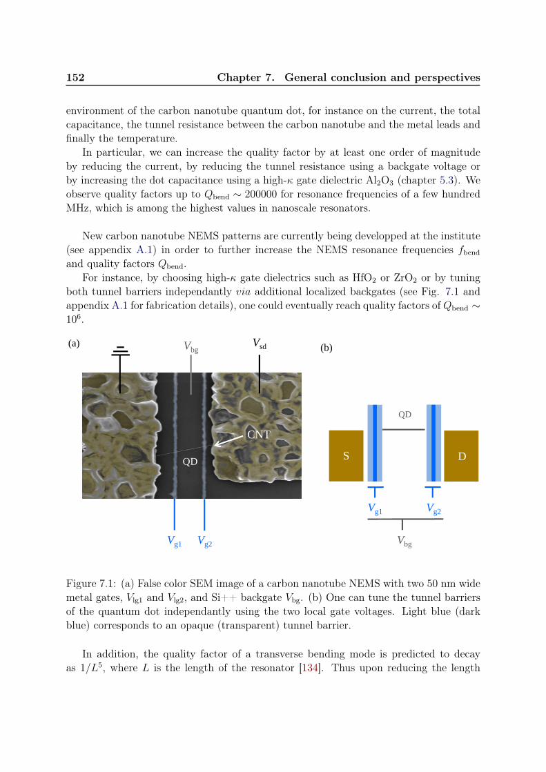
152 Chapter 7. General conclusion and perspectives
environment of the carbon nanotube quantum dot, for instance on the current, the totalcapacitance, the tunnel resistance between the carbon nanotube and the metal leads andfinally the temperature.
In particular, we can increase the quality factor by at least one order of magnitudeby reducing the current, by reducing the tunnel resistance using a backgate voltage orby increasing the dot capacitance using a high-κ gate dielectric Al2O3 (chapter 5.3). Weobserve quality factors up to Qbend ∼ 200000 for resonance frequencies of a few hundredMHz, which is among the highest values in nanoscale resonators.
New carbon nanotube NEMS patterns are currently being developped at the institute(see appendix A.1) in order to further increase the NEMS resonance frequencies fbend
and quality factors Qbend.For instance, by choosing high-κ gate dielectrics such as HfO2 or ZrO2 or by tuning
both tunnel barriers independantly via additional localized backgates (see Fig. 7.1 andappendix A.1 for fabrication details), one could eventually reach quality factors ofQbend ∼106.
Vg1 Vg2
Vsd
Vg1 Vg2
Vbg
QD
S D QD
Vbg(a) (b)
CNT
Figure 7.1: (a) False color SEM image of a carbon nanotube NEMS with two 50 nm widemetal gates, Vlg1 and Vlg2, and Si++ backgate Vbg. (b) One can tune the tunnel barriersof the quantum dot independantly using the two local gate voltages. Light blue (darkblue) corresponds to an opaque (transparent) tunnel barrier.
In addition, the quality factor of a transverse bending mode is predicted to decayas 1/L5, where L is the length of the resonator [134]. Thus upon reducing the length
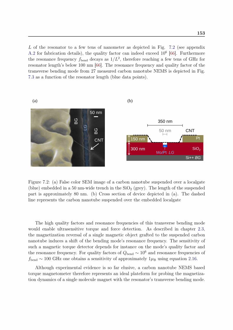
153
L of the resonator to a few tens of nanometer as depicted in Fig. 7.2 (see appendixA.2 for fabrication details), the quality factor can indeed exceed 106 [66]. Furthermorethe resonance frequency fbend decays as 1/L2, therefore reaching a few tens of GHz forresonator length’s below 100 nm [66]. The resonance frequency and quality factor of thetransverse bending mode from 27 measured carbon nanotube NEMS is depicted in Fig.7.3 as a function of the resonator length (blue data points).
50 nm
CNT
LG
BG
BG
Pt
Si++ BG
SiO2
50 nm
300 nm
150 nm
Mo/Pt LG
350 nm
(a) (b)
CNT
Figure 7.2: (a) False color SEM image of a carbon nanotube suspended over a localgate(blue) embedded in a 50 nm-wide trench in the SiO2 (grey). The length of the suspendedpart is approximately 80 nm. (b) Cross section of device depicted in (a). The dashedline represents the carbon nanotube suspended over the embedded localgate
The high quality factors and resonance frequencies of this transverse bending modewould enable ultrasensitive torque and force detection. As described in chapter 2.3,the magnetization reversal of a single magnetic object grafted to the suspended carbonnanotube induces a shift of the bending mode’s resonance frequency. The sensitivity ofsuch a magnetic torque detector depends for instance on the mode’s quality factor andthe resonance frequency. For quality factors of Qbend ∼ 106 and resonance frequencies offbend ∼ 100 GHz one obtains a sensitivity of approximately 1µB using equation 2.16.
Although experimental evidence is so far elusive, a carbon nanotube NEMS basedtorque magnetometer therefore represents an ideal plateform for probing the magnetiza-tion dynamics of a single molecule magnet with the resonator’s transverse bending mode.
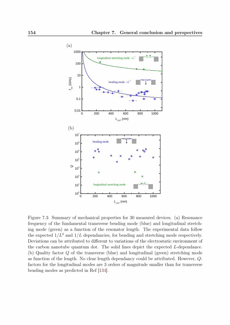
154 Chapter 7. General conclusion and perspectives
(a)
0 2 0 0 4 0 0 6 0 0 8 0 0 1 0 0 00 , 0 1
0 , 1
1
1 0
1 0 0
1 0 0 0l o n g i t u d i n a l s t r e t c h i n g m o d e L - 1
f res (G
Hz)
L C N T ( n m )
b e n d i n g m o d e L - 2
(b)
0 2 0 0 4 0 0 6 0 0 8 0 0 1 0 0 01 0 0
1 0 1
1 0 2
1 0 3
1 0 4
1 0 5
1 0 6
1 0 7
l o n g i t u d i n a l s t r e t c h i n g m o d e
Q
L C N T ( n m )
b e n d i n g m o d e
Figure 7.3: Summary of mechanical properties for 30 measured devices. (a) Resonancefrequency of the fundamental transverse bending mode (blue) and longitudinal stretch-ing mode (green) as a function of the resonator length. The experimental data followthe expected 1/L2 and 1/L dependancies, for bending and stretching mode respectively.Deviations can be attributed to different to variations of the electrostatic environment ofthe carbon nanotube quantum dot. The solid lines depict the expected L-dependance.(b) Quality factor Q of the transverse (blue) and longitudinal (green) stretching modeas function of the length. No clear length dependancy could be attributed. However, Q-factors for the longitudinal modes are 3 orders of magnitude smaller than for transversebending modes as predicted in Ref [134].
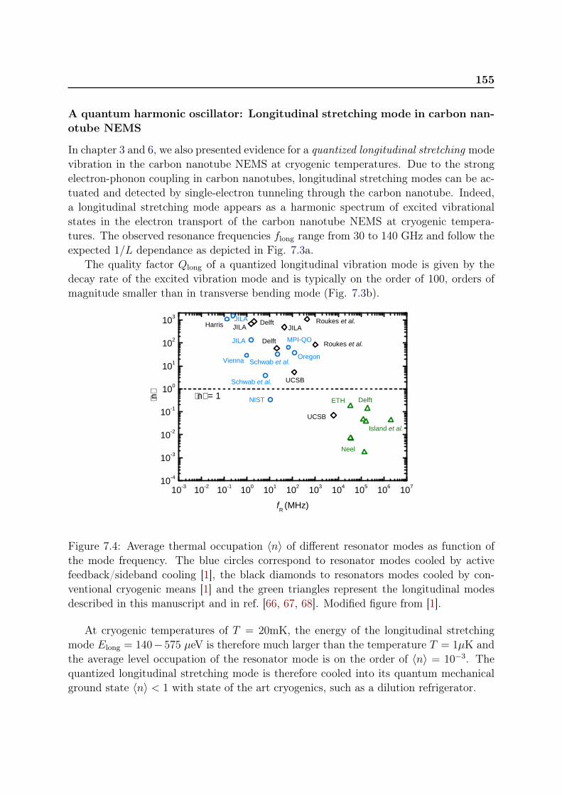
155
A quantum harmonic oscillator: Longitudinal stretching mode in carbon nan-otube NEMS
In chapter 3 and 6, we also presented evidence for a quantized longitudinal stretching modevibration in the carbon nanotube NEMS at cryogenic temperatures. Due to the strongelectron-phonon coupling in carbon nanotubes, longitudinal stretching modes can be ac-tuated and detected by single-electron tunneling through the carbon nanotube. Indeed,a longitudinal stretching mode appears as a harmonic spectrum of excited vibrationalstates in the electron transport of the carbon nanotube NEMS at cryogenic tempera-tures. The observed resonance frequencies flong range from 30 to 140 GHz and follow theexpected 1/L dependance as depicted in Fig. 7.3a.
The quality factor Qlong of a quantized longitudinal vibration mode is given by thedecay rate of the excited vibration mode and is typically on the order of 100, orders ofmagnitude smaller than in transverse bending mode (Fig. 7.3b).
1 0 - 3 1 0 - 2 1 0 - 1 1 0 0 1 0 1 1 0 2 1 0 3 1 0 4 1 0 5 1 0 6 1 0 71 0 - 4
1 0 - 3
1 0 - 2
1 0 - 1
1 0 0
1 0 1
1 0 2
1 0 3
S c h w a b e t a l .
I s l a n d e t a l .
D e l f tE T H
J I L AH a r r i s J I L A
J I L AJ I L A D e l f t
D e l f tO r e g o n
M P I - Q O
V i e n n a
R o u k e s e t a l .
R o u k e s e t a l .
S c h w a b e t a l . U C S B
⟨n⟩
f R ( M H z )
⟨ n ⟩ = 1U C S B
N I S T
N e e l
Figure 7.4: Average thermal occupation 〈n〉 of different resonator modes as function ofthe mode frequency. The blue circles correspond to resonator modes cooled by activefeedback/sideband cooling [1], the black diamonds to resonators modes cooled by con-ventional cryogenic means [1] and the green triangles represent the longitudinal modesdescribed in this manuscript and in ref. [66, 67, 68]. Modified figure from [1].
At cryogenic temperatures of T = 20mK, the energy of the longitudinal stretchingmode Elong = 140− 575 µeV is therefore much larger than the temperature T = 1µK andthe average level occupation of the resonator mode is on the order of 〈n〉 = 10−3. Thequantized longitudinal stretching mode is therefore cooled into its quantum mechanicalground state 〈n〉 < 1 with state of the art cryogenics, such as a dilution refrigerator.
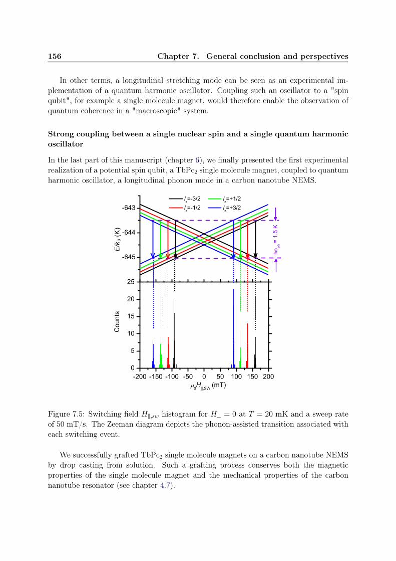
156 Chapter 7. General conclusion and perspectives
In other terms, a longitudinal stretching mode can be seen as an experimental im-plementation of a quantum harmonic oscillator. Coupling such an oscillator to a "spinqubit", for example a single molecule magnet, would therefore enable the observation ofquantum coherence in a "macroscopic" system.
Strong coupling between a single nuclear spin and a single quantum harmonicoscillator
In the last part of this manuscript (chapter 6), we finally presented the first experimentalrealization of a potential spin qubit, a TbPc2 single molecule magnet, coupled to quantumharmonic oscillator, a longitudinal phonon mode in a carbon nanotube NEMS.
-645
-644
-643
Iz=-3/2 I
z=+1/2
Iz=-1/2 I
z=+3/2
E
/k (K
)
hωph
= 1.
5 K
-200 -150 -100 -50 0 50 100 150 2000
5
10
15
20
25
Cou
nts
0H||,SW (mT)
B
Figure 7.5: Switching field H‖,sw histogram for H⊥ = 0 at T = 20 mK and a sweep rateof 50 mT/s. The Zeeman diagram depicts the phonon-assisted transition associated witheach switching event.
We successfully grafted TbPc2 single molecule magnets on a carbon nanotube NEMSby drop casting from solution. Such a grafting process conserves both the magneticproperties of the single molecule magnet and the mechanical properties of the carbonnanotube resonator (see chapter 4.7).
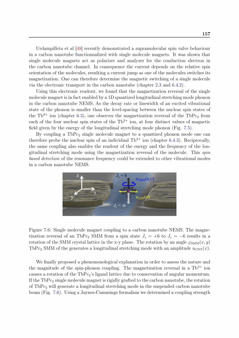
157
Urdampilleta et al [48] recently demonstrated a supramolecular spin valve behaviourin a carbon nanotube functionnalized with single molecule magnets. It was shown thatsingle molecule magnets act as polarizer and analyzer for the conduction electron inthe carbon nanotube channel. In consequence the current depends on the relative spinorientation of the molecules, resulting a current jump as one of the molecules switches itsmagnetization. One can therefore determine the magnetic switching of a single moleculevia the electronic transport in the carbon nanotube (chapter 2.3 and 6.4.2).
Using this electronic readout, we found that the magnetization reversal of the singlemolecule magnet is in fact enabled by a 1D quantized longitudinal stretching mode phononin the carbon nanotube NEMS. As the decay rate or linewidth of an excited vibrationalstate of the phonon is smaller than the level-spacing between the nuclear spin states ofthe Tb3+ ion (chapter 6.3), one observes the magnetization reversal of the TbPc2 fromeach of the four nuclear spin states of the Tb3+ ion, at four distinct values of magneticfield given by the energy of the longitudinal stretching mode phonon (Fig. 7.5).
By coupling a TbPc2 single molecule magnet to a quantized phonon mode one cantherefore probe the nuclear spin of an individual Tb3+ ion (chapter 6.4.3). Reciprocally,the same coupling also enables the readout of the energy and the frequency of the lon-gitudinal stretching mode using the magnetization reversal of the molecule. This spinbased detection of the resonance frequency could be extended to other vibrational modesin a carbon nanotube NEMS.
Figure 7.6: Single molecule magnet coupling to a carbon nanotube NEMS. The magne-tization reversal of an TbPc2 SMM from a spin state Jz = +6 to Jz = −6 results in arotation of the SMM crystal lattice in the x-y plane. The rotation by an angle ϕSMM(x, y)
TbPc2 SMM of the generates a longitudinal stretching mode with an amplitude uCNT(x).
We finally proposed a phenomenological explanation in order to assess the nature andthe magnitude of the spin-phonon coupling. The magnetization reversal in a Tb3+ ioncauses a rotation of the TbPc2’s ligand lattice due to conservation of angular momentum.If the TbPc2 single molecule magnet is rigidly grafted to the carbon nanotube, the rotationof TbPc2 will generate a longitudinal stretching mode in the suspended carbon nanotubebeam (Fig. 7.6). Using a Jaynes-Cummings formalism we determined a coupling strength
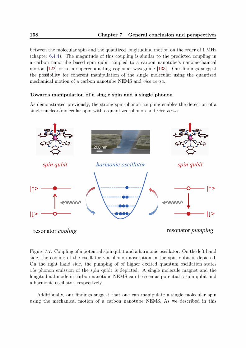
158 Chapter 7. General conclusion and perspectives
between the molecular spin and the quantized longitudinal motion on the order of 1 MHz(chapter 6.4.4). The magnitude of this coupling is similar to the predicted coupling ina carbon nanotube based spin qubit coupled to a carbon nanotube’s nanomechanicalmotion [122] or to a superconducting coplanar waveguide [133]. Our findings suggestthe possibility for coherent manipulation of the single molecular using the quantizedmechanical motion of a carbon nanotube NEMS and vice versa.
Towards manipulation of a single spin and a single phonon
As demonstrated previously, the strong spin-phonon coupling enables the detection of asingle nuclear/molecular spin with a quantized phonon and vice versa.
|↑>
|↓>
|↑>
|↓>
resonator cooling resonator pumping
200 nm
spin qubit spin qubitharmonic oscillator
Figure 7.7: Coupling of a potential spin qubit and a harmonic oscillator. On the left handside, the cooling of the oscillator via phonon absorption in the spin qubit is depicted.On the right hand side, the pumping of of higher excited quantum oscillation statesvia phonon emission of the spin qubit is depicted. A single molecule magnet and thelongitudinal mode in carbon nanotube NEMS can be seen as potential a spin qubit anda harmonic oscillator, respectively.
Additionally, our findings suggest that one can manipulate a single molecular spinusing the mechanical motion of a carbon nanotube NEMS. As we described in this
159
manuscript, the mechanical motion of a carbon nanotube NEMS can be controlled bystatic or oscillating electric fields due to strong coupling between the charge transportand mechanical motion in carbon nanotubes. Due to the strong coupling between the me-chanical motion and the spin of the molecule, a modulation of the nanotube’s mechanicalproperties, for example the resonance frequency, can therefore result in a modificationof the molecule magnetization dynamics. Hence, the strong spin-phonon coupling wouldenable an electric control of magnetization dynamics of a single electronic or nuclear spin.
On the other hand, one can also manipulate the carbon nanotube’s mechanical motionusing the single molecular spin. For instance, one can use the magnetization reversal of thesingle molecule magnet to pump the excited states of the harmonic oscillator and controlthe phonon population. Reversely, phonons can be absorbed by the single moleculemagnet resulting in a spin flip in the molecule and a cooling of the vibrational mode.Eventually one can reach the quantum mechanical ground state of the vibrational modeusing this "magnetic cooling" (Fig. 7.7).
Coupling magnetism and mechanics on a molecular quantum level is therefore thenext step towards coherent manipulation of a single spin or a single phonon and couldopen the path to quantum information processing in such a supramolecular quantumspintronic device.

Bibliography
[1] M. Poot and H. S. J. van der Zant, "Mechanical systems in the quantum regime",Physics Report , 511, 273-335, 2012. (Cited on pages 2, 35, 36, 37, 38, 58, 61, 75, 121,127, 128, 129 et 155.)
[2] J. Teufel et al., "Sideband Cooling Micromechanical Motion to the Quantum GroundState", Nature, 475, 359-363, 2011. (Cited on pages 2.)
[3] A.D. O’Connell, M. Hofheinz, M. Ansmann, R.C. Bialczak, M. Lenander, E. Lucero,M. Neeley, D. Sank, H. Wang, M. Weides, et al., "Quantum ground state and single-phonon control of a mechanical resonator", Nature, 464, 697-700, 2010. (Cited onpages 2.)
[4] J. Chaste, A. Eichler, J. Moser, G. Ceballos, R. Rurali, and A. Bachtold "A nanome-chanical mass sensor with yoctogram resolution", Nature Nanotechnology , 7, 301-304,2012. (Cited on pages 2.)
[5] K. Jensen, K. Kim, and A. Zettl "An atomic-resolution nanomechanical mass sensor",Nature Nanotechnology , 3, 533-37, 2008. (Cited on pages 2 et 121.)
[6] A. Eichler, J.Moser, J. Chaste, M. Zdrojek, I. Wilson-Rae and A. Bachtold "Nonlin-ear damping in mechanical resonators made from carbon nanotubes and graphene",Nature Nanotechnology , 6, 339-342, 2011. (Cited on pages 2.)
[7] W. Wernsdorfer, "Molecular Nanomagnets : towards molecular spintronics", Journalof Nanotechnology , 7, 497, 2010. (Cited on pages 3.)
[8] P. Weiss "La variation du ferromagnetism en temperature", Compte rendus , 146,1133-1149, 1906. (Cited on pages 2.)
[9] M. Jamet, W.Wernsdorfer, C. Thirion, D. Mailly, V. Dupuis, P. Mélinon, and A. Pérez"Magnetic Anisotropy of a Single Cobalt Nanocluster", Physical Review Letter , 86,4676-4679, 1998. (Cited on pages 3.)
[10] E. C. Stoner and E. P. Wohlfarth, "A mechanism of magnetic hysteresis in het-erogeneous alloys", IEEE Transactions on Magnetics , 27, 3475, 1991. (Cited onpages 3.)
[11] L. Bogani and W. Wernsdorfer, "Molecular spintronics using single-molecule mag-nets", Nature Materials , 7, 179-86, 2008. (Cited on pages 3, 7, 11, 12, 13, 15, 25, 26et 122.)
162 Bibliography
[12] H. Mamin, D. Rugar, J. E. Stern, R. E. Fontana, and P. Kasiraj "Magnetic forcemicroscopy of thin Permalloy films", Applied Physics Letters , 55, 318-321, 1989.(Cited on pages 4.)
[13] V. Puntes, P. Gorostiza, D. Aruguete, N. Bastus and P. Alivisatos "Collectivebehaviour in two-dimensional cobalt nanoparticle assemblies observed by magneticforce microscopy", Nature Materials , 7, 263-268, 2004. (Cited on pages 4.)
[14] A. Yamaguchi et al., "Real-Space Observation of Current-Driven Domain Wall Mo-tion in Submicron Magnetic Wires", Physical Review Letters , 92, 077205, 2004. (Citedon pages 4.)
[15] D. Rugar, R. Budakian, H. J. Mamin and B. W. Chui "Single spin detection bymagnetic resonance force microscopy", Nature, 430, 329-333, 2004. (Cited on pages 4.)
[16] M. Loehndorf, J. Moreland, P. Kabos, and N. Rizzo "Microcantilever torque magne-tometry of thin magnetic films", Journal of Applied Physics , 87, 5995, 2000. (Citedon pages 4.)
[17] D. Min, A. McCallum, S. Russek, J. Moreland "Micromechanical torque magnetome-ter with sub-monolayer sensitivity", Journal of Magnetism and Magnetic Materials ,286, 329-335, 2005. (Cited on pages 4.)
[18] B. Lassagne, D. Ugnati, and M. Respaud, "Ultrasensitive Magnetometers Based onCarbon-Nanotube Mechanical Resonators", Physical Review Letters , 107, 130801-805,2011. (Cited on pages 4, 31, 32, 120, 121 et 150.)
[19] M. Ganzhorn and W. Wernsdorfer, "Dynamics and dissipation induced by single-electron tunneling in carbon nanotube NEMS", Physical Review Letters , 108, 175502,2012. (Cited on pages 5, 35, 37, 38, 60, 105, 119, 121 et 128.)
[20] M. Ganzhorn S. Klyatskaya, M. Ruben, and W. Wernsdorfer "Strong Spin-PhononCoupling between a Single-Molecule Magnet and a Carbon Nanotube Nanoelectrome-chanical System", Nature Nanotechnology , XX, XXX-XXX , 2013. (Cited on pages 5,14, 38, 60 et 128.)
[21] M. Baibich et al., "Giant Magnetoresistance of (001)Fe/(001)Cr Magnetic Snperlat-tices", Physical Review Letters , 61, 2472, 1988. (Cited on pages 7 et 8.)
[22] J. Barnas, A. Fuss, R. E. Camley, P. Grunberg, and W. Zinn "Novel magnetore-sistance efFect in layered magnetic structures: Theory and experiment", PhysicalReview B , 42, 8110, 1988. (Cited on pages 7 et 8.)
[23] Wolf, S. A. et al. "Spintronics: a spin-based electronics vision for the future.",Science, 194, 1488-1495, 2001. (Cited on pages 7, 9, 10 et 11.)
Bibliography 163
[24] D. Awschalom and M.E. Flatte "Challenges for semiconductor spintronics", NaturePhysics , 3, 153-159, 2007. (Cited on pages 7 et 10.)
[25] Z.H. Xiong, D. Wu, Z. Valy Vardeny and J. Shi, "Giant magnetoresistance in organicspin-valves", Nature, 427, 821-824, 2004. (Cited on pages 7 et 10.)
[26] M.A. Ratner "Special feature on molecular electronics", Proc. Natl Acad. Sci., 102,8800-8837, 2005. (Cited on pages 7.)
[27] J.M. Kikkawa and D. Awschalom "Resonant spin amplification in n-type GaAs",Physical Review Letters , 80, 4313-4316, 1998. (Cited on pages 10.)
[28] Y. Ohno, D.K. Young, B. Beschoten, F. Matsukura, H. Ohno and D Awschalom"Electrical spin injection in a ferromagnetic semiconductor heterostructure", Nature,402, 790-792, 1999. (Cited on pages 10.)
[29] J.M. Kikkawa, J.A. Gupta, I. Malajovich, D.D. Awschalom "Spin coherence insemiconductors: storage, transport and reduced dimensionality", Physica E , 9, 194-201, 2001. (Cited on pages 10 et 11.)
[30] C. Adelmann, X. Lou, J. Strand, C. J. Palmstrøm, and P. A. Crowell "Spin injectionand relaxation in ferromagnet-semiconductor heterostructures", Physical Review B ,71, 121301, 2005. (Cited on pages 10.)
[31] J.M. Tang, J. Levy and M.E. Flatte "All electrical control of single ion spin insemiconductors", Physical Review Letters , 97, 106803, 2006. (Cited on pages 10.)
[32] G. Szulczewski, S. Sanvito and J. M. D. Coey, "A spin of their own", NatureMaterials , 8, 693-695, 2009. (Cited on pages 11.)
[33] S. Sanvito "Molecular Spintronics", Chem. Soc. Rev., 40, 3336-3355, 2011. (Citedon pages 10.)
[34] N. Roch, S. Florens, V. Bouchiat, W. Wernsdorfer and F. Balestro "Quantum phasetransition in a single molecule quantum dot", Nature, 453, 633-636, 2008. (Cited onpages 12.)
[35] George Christou, Dante Gatteschi, David N. Hendrickson, and Roberta Sessoli "Sin-gle Molecule Magnets", MSR bulletin 2000. (Cited on pages 12 et 13.)
[36] Gatteschi, D., Sessoli, R., Villain, J., "Molecular Nanomagnets", Oxford UniversityPress 2006. (Cited on pages 12, 13 et 121.)
[37] S. Klyatskaya, J.R. Galan Mascaros,L. Bogani, F. Hennrich, M. Kappes, W. Werns-dorfer, and M. Ruben "Anchoring of rare-earth-based single-molecule magnets on
164 Bibliography
single-walled carbon nanotubes", Journal of the American Chemical Society , 131,15143-51, 2009. (Cited on pages 13, 15, 98, 101, 122 et 123.)
[38] M. Lopes et al., "Surface-enhanced Raman signal for terbium single-molecule mag-nets grafted on graphene", ACS Nano, 4, 7531, 2010. (Cited on pages 13 et 123.)
[39] N. Ishikawa, M. Sugita, T. Ishikawa, S. Koshibara and Y. Kaizu "Mononuclear Lan-thanide Complexes with a long magnetization relaxation time at high temperature: Anew category of magnets at the single molecule level", Journal of Physical ChemistryB , 108, 11265-11271, 2004. (Cited on pages 13.)
[40] K. Wieghardt, K. Pohl, I. Jibril, and G. Huttner "Mononuclear Lanthanide Com-plexes with a long magnetization relaxation time at high temperature: A new categoryof magnets at the single molecule level", Angewandte Chemie, International EditionEnglish, 23, 77, 1984. (Cited on pages 13.)
[41] A. Giusti et al., "Magnetic Bistability of Individual Single-Molecule Magnets Graftedon Single-Wall Carbon Nanotubes", Angewandte Chemie, International Edition En-glish, 48, 1-5, 2009. (Cited on pages 13.)
[42] W. Wernsdorfer and R. Sessoli "Quantum phase interference and parity effects inmagnetic molecular clusters", Science, 284, 133-135, 1999. (Cited on pages 14 et 122.)
[43] Takahashi, S., et al. "Coherent manipulation and Decoherence of S = 10 Single-Molecule Magnet", Physical Review Letters , 102, 087603, 2009. (Cited on pages 14et 122.)
[44] A. Ardavan et al. "Will spin-relaxation times in molecular magnets permit quan-tum information processing?", Physical Review Letters , 98, 057201, 2007. (Cited onpages 14.)
[45] Y.-S. Fu, J. Schwobel, S.-W. Hla, A. Dilullo, G. Hoffmann, S. Klyatskaya, M. Ruben,R. Wiesendanger, "Reversible chiral switching of bis(phthalocyaninato) terbium(III)on a metal surface", Nano Letters , 12, 3931, 2012. (Cited on pages 14 et 25.)
[46] J. Schwöbel, Y. Fu, J. Brede, A. Dilullo, G. Hoffmann, S. Klyatskaya, M. Ruben andR. Wiesendanger "Real-space observation of spin-split molecular orbitals of adsorbedsingle-molecule magnets.", Nature communications , 3, 953, 2012. (Cited on pages 14,25 et 26.)
[47] R. Vincent, S. Klyatskaya, M. Ruben, W. Wernsdorfer and F. Balestro, "Electronicreadout of a single nuclear spin in a single molecule transistor", Nature, 488, 357-360, 2012. (Cited on pages 14, 25, 26, 122 et 134.)
Bibliography 165
[48] M. Urdampilleta, J.P. Cleuziou, S. Klyatskaya, M. Ruben, and W. Wernsdorfer"Supramolecular spin valves", Nature Materials , 10, 502-506 , 2011. (Cited onpages 14, 28, 29, 30, 98, 101, 122, 123, 124, 125, 126, 133, 136, 137 et 157.)
[49] N. Ishikawa, M. Sugita, and W. Wernsdorfer, "Quantum tunneling of magne-tization in lanthanide single-molecule magnets: bis(phthalocyaninato)terbium andbis(phthalocyaninato)dysprosium anions", Angewandte Chemie (International ed. inEnglish), 44, 2931-2935, 2005. (Cited on pages 16, 18, 19, 123, 125 et 134.)
[50] Abragam, A., Bleaney, B., "Electron Paramagnetic Resonance of transition ions",Oxford University Press 1970. (Cited on pages 16, 17, 23, 24, 25, 121, 125, 126 et 183.)
[51] N. Ishikawa, M. Sugita, T. Okubo, N. Tanaka, T. Iino, and Y. Kaizu, "Deter-mination of Ligand-Field Parameters and f-Electronic Structures of Double-DeckerBis(phthalocyaninato)lanthanide Complexes.", Inorganic Chemistry , 42, 2440-2446,2003. (Cited on pages 17 et 147.)
[52] K.W.H Stevens, "Matrix elements and operator equivalents connected with themagnetic properties of rare earth ions", Proceeding of the Physical Society A, 65, 209,1952. (Cited on pages 17, 147 et 148.)
[53] H. Konami, M. Hatano and A. Tajiri, "An analysis of paramagnetic shifts in pro-ton NMR spectra of non-radical lanthanide(III)-phthalocyanine sandwich complexes",Chemical Physics Letters , 160, 163-167, 1989. (Cited on pages 17, 147 et 148.)
[54] W. Wernsdorfer, "From micro- to nano-SQUIDs: applications to nanomagnetism",Superconductor Science and Technology , 22, 064013 , 2009. (Cited on pages 21 et 120.)
[55] C. Zener "Non-adiabatic crossing of energy levels", Proceeding of the royal societyof london serie A, 137, 696-702 , 1932. (Cited on pages 22.)
[56] T. Komeda, H. Isshiki, J. Liu, Y. Zhang, N. Lorente, K. Katoh, B. K. Breedloveand M. Yamashita "Observation and electric current control of a local spin in asingle-molecule magnet", Nature communications , 2, 217, 2011. (Cited on pages 25.)
[57] R. Maurand "Carbon nanotube SQUID’s: From Josephson junctions to quantumdots, Pi-junctions, Kondo effect and detection of single molecule magnets", PhDthesis, University Joseph Fourier et Institut Neel-CNRS, 2011. (Cited on pages 27,79 et 80.)
[58] J.-P. Cleuziou, W. Wernsdorfer, V. Bouchiat, Th. Ondarçuhu, M. Monthioux "Car-bon nanotube superconducting interference device", Nature Nanotechnology , 1, 53-59, 2006. (Cited on pages 27.)
166 Bibliography
[59] J.-C. Charlier, X. Blase, and S. Roche, "Electronic and transport properties ofnanotubes", Review of Modern Physics , 79, 677, 2007. (Cited on pages 28.)
[60] J. Nygård, D. H. Cobden, and P. E. Lindelof, "Kondo physics in carbon nanotubes",Nature (London), 408, 342-46, 2000. (Cited on pages 28.)
[61] G. A. Steele, A. K. Hüttel, B. Witkamp, M. Poot, H. B. Meerwaldt, L. P. Kouwen-hoven, and H. S. J. van der Zant, "Strong Coupling Between Single-Electron Tunnel-ing and Nanomechanical Motion", Science, 325, 1103-1106, 2009. (Cited on pages 36,37, 44, 48, 50, 51, 52, 53, 54, 61, 75, 88, 105, 107, 109, 110, 115, 119 et 121.)
[62] M. Poot, S. Etaki, H. Yamaguchi, and H. S. J. van der Zant "Discrete-time quadra-ture feedback cooling of a radio-frequency mechanical resonator", Applied PhysicsLetter , 99, 013113, 2011. (Cited on pages 36.)
[63] M. D. LaHaye, O. Buu, B. Camarota, K. C. Schwab "Approaching the quantumlimit of a nanomechanical resonator", Science, 304, 74, 2004. (Cited on pages 36.)
[64] B. Witkamp, M. Poot, H.S.J. van der Zant, "Bending-mode vibration of a suspendednanotube resonator", Nano Letters , 6, 2904, 2006. (Cited on pages 36.)
[65] E. Laird, F. Pei, W. Tang, G. A. Steele, and L. P. Kouwenhoven, "A High qualityfactor carbon nanotube mechanical resonator at 39 GHz", Nano Letters , 12, 193-197,2011. (Cited on pages 37, 38, 42, 43, 61, 75, 121, 127 et 128.)
[66] J. O. Island, V. Tayari, A. C. McRae, and A. R. Champagne "Few-Hundred GHzCarbon Nanotube Nanoelectromechanical Systems (NEMS)", Nano Letters , 12, 4564-4569, 2012. (Cited on pages 37, 38, 127, 128, 153 et 155.)
[67] R. Leturcq, C. Stampfer, K. Inderbitzin, L. Durrer, C. Hierold, E. Mariani, M.Schultz, F. von Oppen, and K. Ensslin, "Franck-Condon blockade in suspended carbonnanotube quantum dots", Nature Physics , 5, 327-331, 2009. (Cited on pages 38, 54,55, 58, 59, 60, 121, 127, 128, 131, 132 et 155.)
[68] S. Sapmaz, P. Jarillo-Herrero, Y.M. Blanter, C. Dekker, and H. S. J. van der Zant,"Tunneling in suspended carbon nanotubes assisted by longitudinal phonons", Phys-ical Review Letters , 96, 026801, 2006. (Cited on pages 38, 54, 55, 58, 121, 127, 128,130 et 155.)
[69] L. Landau, and E. Lifschitz "Course of Theoretical Physics: Theory of Elasticity",Elsevier 1986. (Cited on pages 39 et 58.)
[70] V. Sazonova "A tunable carbon nanotube resonator", PhD thesis, Cornell University,2004. (Cited on pages 39, 40, 41, 42, 44, 46, 47, 53, 117 et 118.)
Bibliography 167
[71] S. Sapmaz, Y.M. Blanter, L. Gurevich, and H.S.J van der Zant, "Carbon nanotubesas nanoelectromechanical systems", Physical Review B , 67, 235414, 2003. (Cited onpages 40 et 41.)
[72] A. K. Hüttel, H. B. Meerwaldt, G. A. Steele, M. Poot, B. Witkamp, L. P. Kouwen-hoven, H. S. J. van der Zant "Single electron tunnelling through high-Q single-wallcarbon nanotube NEMS resonators", Physica status solidi b, 247, 2974, 2010. (Citedon pages 42 et 43.)
[73] M. Poot "Mechanical systems at the nanoscale", PhD thesis, Technische UniversiteitDelft, 2009. (Cited on pages 44, 45 et 46.)
[74] B. Lassagne, Y. Tarakanov, J. Kinaret, D. Garcia-Sanchez, and A. Bachtold, "Cou-pling Mechanics to Charge Transport in Carbon Nanotube Mechanical Resonators",Science, 325, 1106-1111, 2009. (Cited on pages 44, 48, 49, 105, 107, 110, 115, 119et 121.)
[75] A. K. Hüttel, G. A. Steele, B. Witkamp, M. Poot, L. P. Kouwenhoven, and H.S. J. van der Zant, "Carbon Nanotubes as Ultrahigh Quality Factor MechanicalResonators", Nano Letters , 9, 2547-2552, 2009. (Cited on pages 45, 61, 105, 107, 109,116, 119 et 121.)
[76] C. W. J. Beenakker "Theory of Coulomb-blockade oscillations in the conductanceof a quantum dot", Physical Review B , 44, 1646-1656, 1991. (Cited on pages 49.)
[77] H.B. Meerwaldt, G. Labadze, B.H. Schneider, A. Taspinar, Ya.M. Blanter, H.S.J.van der Zant, and G.A. Steele "A nanomechanical resonator as a probe of the chargeof a quantum dot", Physical Review B , 86, 115454, 2012. (Cited on pages 53.)
[78] E. Mariani, and F. von Oppen "Electron-vibron coupling in suspended carbon nan-otube quantum dots", Physical Review B , 80, 155411, 2009. (Cited on pages 54, 55et 56.)
[79] A. K. Huettel, B. Witkamp, M. Leijnse, M. R. Wegewijs, and H. S. J. van derZant "Pumping of Vibrational Excitations in the Coulomb-Blockade Regime in aSuspended Carbon Nanotube", Physical Review Letters , 102, 225501, 2009. (Citedon pages 58, 121, 127, 130, 131 et 132.)
[80] N.R. Franklin, Q. Wang, T.W. Tombler, A. Javey, M. Shim, and H.J. Dai "Integra-tion of suspended carbon nanotube arrays into electronic devices and electromechan-ical systems", Applied Physics Letters ,81, 913, 2002. (Cited on pages 61 et 75.)
[81] J. Cao, Q. Wang, D. Wang, H. Dai "Suspended carbon nanotube quantum wireswith two gates", Small ,1, 138-141, 2005. (Cited on pages 61, 63, 68, 75 et 85.)
168 Bibliography
[82] L. Shon-Roy, A. Wiesnoski, and R. Zorich, "Advanced Semiconductor Fabrica-tion Handbook", Scottsdale, Ariz.: Integrated Circuit Engineering Corporation 1998.(Cited on pages 62 et 63.)
[83] Rogue Valley Microdevices Website:www.roguevalleymicro.com/DryChlorinatedThermalOxidation.php (Cited onpages 62 et 63.)
[84] H. Kahn, N. Jing, M. Huh and A.H. Heuer "Growth stresses and viscosity of thermaloxides on silicon and polysilicon", Journal of Materials Research, 21, 209-214, 2006.(Cited on pages 62.)
[85] A. Stesmans "Relationship between stress and dangling bond generation at the(111)Si/SiO2 interface", Physical Review Letters , 70, 1723-1726, 1993. (Cited onpages 62.)
[86] NOVA Electronic Materials Website:www.novawafers.com (Cited on pages 63.)
[87] Wikipedia Website, Photolithography :www.wikipedia.org/wiki/Photolithography (Cited on pages 65.)
[88] MicroChemicals Technical Handbook "Photolithography: Theory and Applicationof Photoresists, Etchants and Solvents", MicroChemicals 2012. (Cited on pages 65.)
[89] S. George "Atomic Layer Deposition: An Overview", Chemical Review , 110, 111-131, 2010. (Cited on pages 70 et 72.)
[90] Cambridge Nanotech Website, Atomic Layer Deposition:www.cambridgenanotech.com/ald, (Cited on pages 71 et 72.)
[91] H. Klauk (Ed.), "Organic Electronics: Materials, Manufacturing and Applications",Wiley-VCH Verlag GmBH & Co. KGaA 2006. (Cited on pages 72.)
[92] V. Ngoc-Nguyen "Synthesis and electronic transport of ultraclean single wall carbonnanotubes", PhD thesis, University Joseph Fourier et Institut Neel-CNRS, 2012.(Cited on pages 75, 76 et 77.)
[93] H. Koops, J. Kretz, M. Rudolph, M. Weber, G. Dahm and K.L. Lee "Character-ization and Application of Materials grown by electron-beam-induced deposition",Japanese Journal of Applied Physics ,33, 7099-7107, 1994. (Cited on pages 79.)
[94] M.F. Yu, O. Lourie, M.J. Dyer, K. Molony, T.F. Kelly, R.S. Ruoff "Strength andBreaking Mechanism of Multiwalled Carbon Nanotubes Under Tensile Load", Sci-ence,287, 637-640, 2000. (Cited on pages 79.)
Bibliography 169
[95] N. Roch "Single molecule transistors: From exotic Kondo effects to molecular spin-tronics", PhD thesis, University Joseph Fourier et Institut Neel-CNRS, 2009. (Citedon pages 79 et 80.)
[96] R. Picquerel "", PhD thesis, University Joseph Fourier et Institut Neel-CNRS, 2012.(Cited on pages 79.)
[97] C.M. Aguirre, P.L. Levesque, M. Paillet, F. Lapointe, B.C. St-Antoine, P. Desjardins,and R. Martel "The Role of the Oxygen/Water Redox Couple in Suppressing ElectronConduction in Field-Effect Transistors", Advanced Materials ,21, 1-5, 2009. (Cited onpages 85.)
[98] M.J. O’Connell, P. Boul, L.M. Ericson, C3 Huffman, Y. Wang, E. Haroz, C. Kuper,J. Tour, K.D. Ausman, and R.E. Smalley "Reversible water-solubilization of single-walled carbon nanotubes by polymer wrapping", Chemical Physics Letters ,342, 265-271, 2001. (Cited on pages 85.)
[99] A. Vijayaraghavan, S. Kar, C. Soldano, S. Talapatra, O. Nalamasu, and P.M.Ajayan "Charge-injection-induced dynamic screening and origin of hysteresis in field-modulated transport in single-wall carbon nanotubes", Applied Physics Letters ,89,162108, 2006. (Cited on pages 87.)
[100] W. Kim, A. Javey, O. Vermesh, Q. Wang, Y. Li, and H. Dai "Hysteresis Causedby Water Molecules in Carbon Nanotube Field-Effect Transistors", Nano Letters ,3,193-198, 2003. (Cited on pages 87.)
[101] H. Ingerslev Jørgensen, T. Novotny, K. Grove-Rasmussen, K. Flensberg, and P.E. Lindelof "Critical Current 0-π Transition in Designed Josephson Quantum DotJunctions", Nano Letters , 7, 2441-2445, 2007. (Cited on pages 109.)
[102] J. Koenig, J. Schmid, H. Schoeller, and G. Schoen, "Resonant tunneling throughultrasmall quantum dots: Zero-bias anomalies, magnetic-field dependence, and boson-assisted transport", Physical Review B , 54, 16820, 1996. (Cited on pages 109.)
[103] V. Sazonova, Y. Yaish, H. Ustunel, D.Roundy, T.A. Arias and P.L. McEuen, "Atunable carbon nanotube electromechanical oscillator", Nature (London), 431, 284-87,2004. (Cited on pages 110, 115 et 119.)
[104] T. S. Jespersen , K. Grove-Rasmussen, J. Paaske, K. Muraki, T. Fujisawa, J.Nygård, and K. Flensberg, "Gate dependant spin orbit coupling in multielectron car-bon nanotube quantum dots", Nature Physics , 7, 348-53, 2011. (Cited on pages 110.)
[105] G. A. Steele, G. Gotz, and L. P. Kouwenhoven, "Tunable few-electron doublequantum dots and Klein tunnelling in ultraclean carbon nanotubes", Nature Nan-otechnology , 4, 363-67, 2009. (Cited on pages 110.)
170 Bibliography
[106] S.B. Shim, J.S. Chun, S.W. Kang, S.W. Cho, and S.W. Cho "Micromechani-cal resonators fabricated from lattice-matched and etch-selective GaAs/InGaP/GaAsheterostructures", Applied Physics Letters , 91, 133505, 2007. (Cited on pages 116,117 et 119.)
[107] G. Zolfagharkhani, A. Gaidarzhy, S.B. Shim, R.L. Badzey, and P. Mohanty "Quan-tum friction in nanomechanical oscillators at millikelvin temperatures", Physical Re-view B , 72, 224101, 2005. (Cited on pages 116, 117 et 119.)
[108] C. Seoanez, F. Guinea and A. H. Castro Neto "Dissipation due to two-level systemsin nano-mechanical devices", EPL, 78, 60002, 2007. (Cited on pages 117 et 119.)
[109] J. Hone, M.C. Llaguno, M.J. Biercuk, A.T. Johnson, B. Batlogg, Z. Benes, J.E.Fischer "Thermal properties of carbon nanotubes and nanotube-based materials",Applied Physics A, 74, 339-343, 2002. (Cited on pages 117 et 118.)
[110] Y.-K. Kwon, S. Berber, and D. Tomanek "Thermal Contraction of CarbonFullerenes and Nanotubes", Physical Review Letters , 92, 015901, 2004. (Cited onpages 117 et 118.)
[111] M. Bockrath, D. H. Cobden, J. Lu, A. G. Rinzler, R. E. Smalley, L. Balents andP.L. McEuen, "Luttinger-liquid behaviour in carbon nanotubes", Nature (London),397, 598-601, 1999. (Cited on pages 118.)
[112] C. Kane, L. Balents, and M. Fisher, "Coulomb Interactions and Mesoscopic Ef-fects in Carbon Nanotubes", Physical Review Letters , 79, 5086-89, 1997. (Cited onpages 118.)
[113] R. Egger and A. Gogolin, "Effective Low-Energy Theory for Correlated CarbonNanotubes", Physical Review Letters , 79, 5082-85, 1997. (Cited on pages 118.)
[114] A. A. Kovalev, L. X. Hayden, G. E. W. Bauer, and Y. Tserkovnyak "MacrospinTunneling and Magnetopolaritons with Nanomechanical Interference", Physical Re-view Letters , 106, 147203 , 2011. (Cited on pages 120, 121, 122, 147, 148 et 149.)
[115] D. Garanin and E. Chudnovsky, "Quantum Entanglement of a Tunneling Spin withMechanical Modes of a Torsional Resonator", Physical Review X , 1, 011005 , 2011.(Cited on pages 120, 121, 122 et 149.)
[116] Heitler, W., Teller, E., "Time Effects in the Magnetic Cooling Method", Proc. R.Soc. Lond. A,155, 629, 1936. (Cited on pages 121.)
[117] Van Vleck, J.H., "Paramagnetic Relaxation Times for Titanium and ChromeAlum", Physics Review ,57, 426, 1940. (Cited on pages 121.)
Bibliography 171
[118] Villain, J., Hartman-Boutron, F,. Sessoli, R., Rettori, A., "Magnetic Relaxation inBig Magnetic Molecules", Europhysics Letters ,27, 159, 1994. (Cited on pages 121.)
[119] Garanin, D.A., Chudnosvky, E.M., "Thermally activated resonant magnetizationtunneling in molecular magnets: Mn12Ac and others", Physical Review B ,56, 11102,1997. (Cited on pages 121.)
[120] Leuenberger, M., Loss, D., "Spin relaxation in Mn12-acetate", Europhysics Let-ters ,46, 629, 1999. (Cited on pages 121.)
[121] Sessoli, R., Gatteschi, D., Caneschi, A., Novak, N.A., "Magnetic Bistability of ametal-ion cluster", Nature,365, 141, 1993. (Cited on pages 121.)
[122] Palyi, A., Struck, P.R., Rudner M., Flensberg, K. and Burkard, G., "Spin-orbit-induced strong coupling of a single spin to a nanomechanical resonator", PhysicalReview Letters ,108, 206811, 2012. (Cited on pages 121, 122, 127, 149, 150 et 158.)
[123] H.B. Peng, C.W. Chang, S. Aloni, T. Yuzvinsky, and A. Zettl, "Ultrahigh frequencynanotube resonator", Physical Review Letters , 97, 087203, 2006. (Cited on pages 121.)
[124] H.-Y. Chiu, P. Hung, H. W. C. Postma, and M. Bockrath "Ultrasensitive masssensing with a nanotube electromechanical resonator", Nano Letters , 8, 3735-3738,2008. (Cited on pages 121.)
[125] B. Lassagne, D. Garcia-Sanchez, A. Aguasca, and A. Bachtold, "Atomic-Scale MassSensing Using Carbon Nanotube Resonators", Nano Letters , 8, 4342-46, 2008. (Citedon pages 121.)
[126] H. Heersche et al. "Electron transport through single Mn12 molecular magnets",Physical Review Letters , 96, 206801 , 2006. (Cited on pages 122.)
[127] A.S. Zyazin, et al. "Electric field controlled magnetic anisotropy in a singlemolecule", Nano Letters , 10, 3307-3311 , 2010. (Cited on pages 122.)
[128] J.R. Friedman, M.P. Sarachik, J. Tejada, J., and R. Ziolo, "Macroscopic measure-ment of resonant magnetization tunnelling in high-spin molecules", Physical ReviewLetters , 76, 3830-3833 , 1996. (Cited on pages 122.)
[129] L. Thomas et al., "Macroscopic quantum tunnelling of magnetization in a singlecrystal of nanomagnets", Nature, 383, 145-147, 1996. (Cited on pages 122.)
[130] M. Urdampilleta "Molecular Spintronics: From a supramolecular spin valve tosingle spin detection", PhD thesis, University Joseph Fourier et Institut Neel-CNRS,2012. (Cited on pages 126, 127, 133, 136 et 137.)
172 Bibliography
[131] M.S. Dresselhaus, G. Dresselhaus, R. Saito, A. Jorio "Raman spectroscopy ofcarbon nanotubes", Physics Reports , 409, 47-99, 2005. (Cited on pages 128.)
[132] E. Chudnovsky, D.A. Garanin and R. Schilling "Universal mechanism of spin re-laxation in solids", Physical Review B , 72, 094426, 2005. (Cited on pages 147 et 148.)
[133] A. Cottet and T. Kontos "Spin Quantum Bit with Ferromagnetic Contacts forCircuit QED", Physical Review Letters , 105, 160502, 2010. (Cited on pages 149et 158.)
[134] A. De Martino, R. Egger, and A. O. Gogolin "Phonon-phonon interactions andphonon damping in carbon nanotubes", Physical Review B , 79, 205408, 2009. (Citedon pages 152 et 154.)
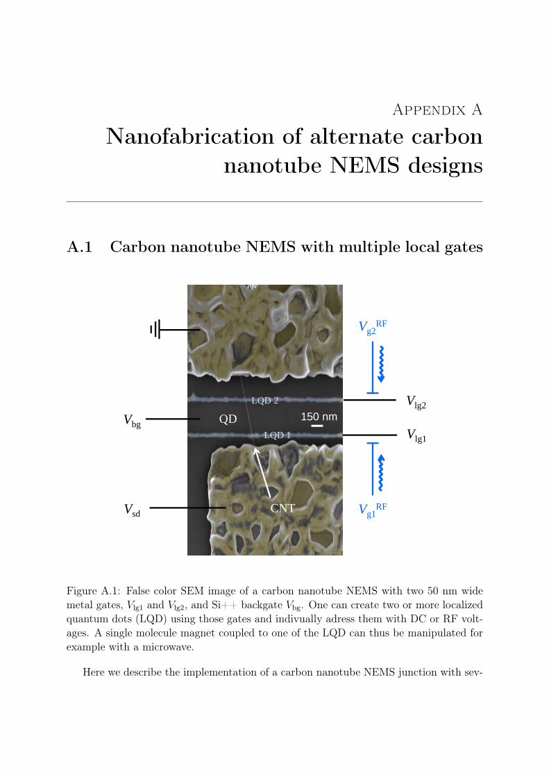
Appendix A
Nanofabrication of alternate carbonnanotube NEMS designs
A.1 Carbon nanotube NEMS with multiple local gates
Vg2RF
Vg1RF
Vlg1
Vlg2
Vsd
LQD 2
LQD 1QD Vbg
CNT
150 nm
Figure A.1: False color SEM image of a carbon nanotube NEMS with two 50 nm widemetal gates, Vlg1 and Vlg2, and Si++ backgate Vbg. One can create two or more localizedquantum dots (LQD) using those gates and indivually adress them with DC or RF volt-ages. A single molecule magnet coupled to one of the LQD can thus be manipulated forexample with a microwave.
Here we describe the implementation of a carbon nanotube NEMS junction with sev-
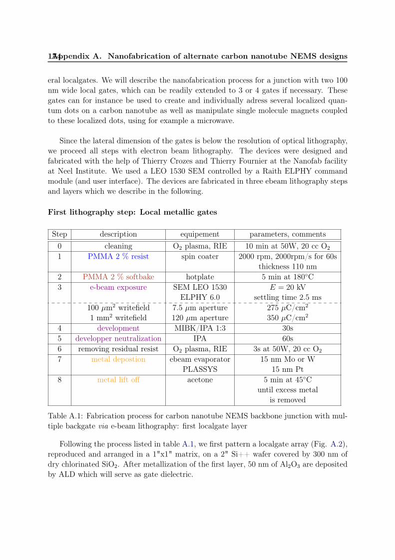
174Appendix A. Nanofabrication of alternate carbon nanotube NEMS designs
eral localgates. We will describe the nanofabrication process for a junction with two 100nm wide local gates, which can be readily extended to 3 or 4 gates if necessary. Thesegates can for instance be used to create and individually adress several localized quan-tum dots on a carbon nanotube as well as manipulate single molecule magnets coupledto these localized dots, using for example a microwave.
Since the lateral dimension of the gates is below the resolution of optical lithography,we proceed all steps with electron beam lithography. The devices were designed andfabricated with the help of Thierry Crozes and Thierry Fournier at the Nanofab facilityat Neel Institute. We used a LEO 1530 SEM controlled by a Raith ELPHY commandmodule (and user interface). The devices are fabricated in three ebeam lithography stepsand layers which we describe in the following.
First lithography step: Local metallic gates
Step description equipement parameters, comments0 cleaning O2 plasma, RIE 10 min at 50W, 20 cc O2
1 PMMA 2 % resist spin coater 2000 rpm, 2000rpm/s for 60sthickness 110 nm
2 PMMA 2 % softbake hotplate 5 min at 180C3 e-beam exposure SEM LEO 1530 E = 20 kV
ELPHY 6.0 settling time 2.5 ms100 µm2 writefield 7.5 µm aperture 275 µC/cm2
1 mm2 writefield 120 µm aperture 350 µC/cm2
4 development MIBK/IPA 1:3 30s5 developper neutralization IPA 60s6 removing residual resist O2 plasma, RIE 3s at 50W, 20 cc O2
7 metal depostion ebeam evaporator 15 nm Mo or WPLASSYS 15 nm Pt
8 metal lift off acetone 5 min at 45Cuntil excess metal
is removed
Table A.1: Fabrication process for carbon nanotube NEMS backbone junction with mul-tiple backgate via e-beam lithography: first localgate layer
Following the process listed in table A.1, we first pattern a localgate array (Fig. A.2),reproduced and arranged in a 1"x1" matrix, on a 2" Si++ wafer covered by 300 nm ofdry chlorinated SiO2. After metallization of the first layer, 50 nm of Al2O3 are depositedby ALD which will serve as gate dielectric.
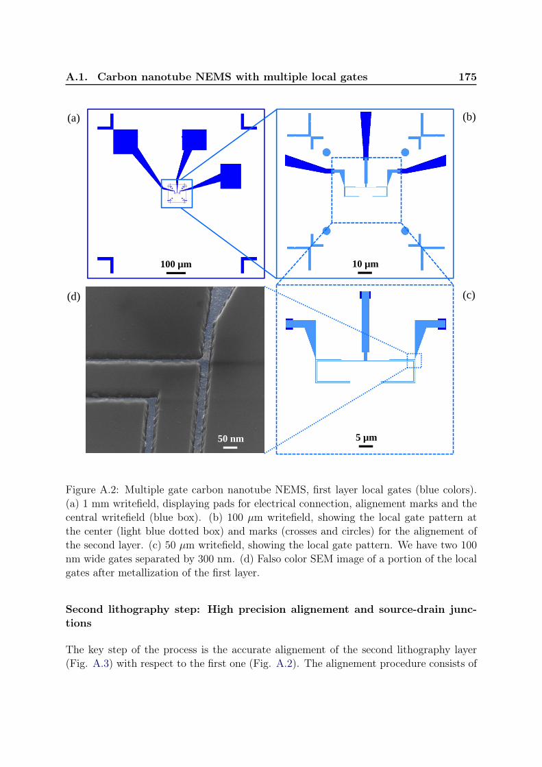
A.1. Carbon nanotube NEMS with multiple local gates 175
(a)
100 µm
50 nm
(d)
(b)
10 µm
5 µm
(c)
Figure A.2: Multiple gate carbon nanotube NEMS, first layer local gates (blue colors).(a) 1 mm writefield, displaying pads for electrical connection, alignement marks and thecentral writefield (blue box). (b) 100 µm writefield, showing the local gate pattern atthe center (light blue dotted box) and marks (crosses and circles) for the alignement ofthe second layer. (c) 50 µm writefield, showing the local gate pattern. We have two 100nm wide gates separated by 300 nm. (d) Falso color SEM image of a portion of the localgates after metallization of the first layer.
Second lithography step: High precision alignement and source-drain junc-tions
The key step of the process is the accurate alignement of the second lithography layer(Fig. A.3) with respect to the first one (Fig. A.2). The alignement procedure consists of
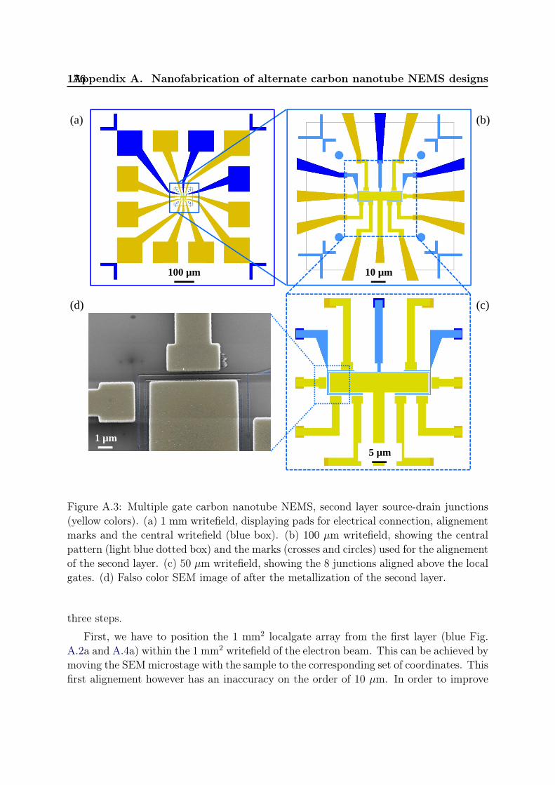
176Appendix A. Nanofabrication of alternate carbon nanotube NEMS designs
(a) (b)
10 µm100 µm
5 µm
(c)(d)
1 µm
Figure A.3: Multiple gate carbon nanotube NEMS, second layer source-drain junctions(yellow colors). (a) 1 mm writefield, displaying pads for electrical connection, alignementmarks and the central writefield (blue box). (b) 100 µm writefield, showing the centralpattern (light blue dotted box) and the marks (crosses and circles) used for the alignementof the second layer. (c) 50 µm writefield, showing the 8 junctions aligned above the localgates. (d) Falso color SEM image of after the metallization of the second layer.
three steps.
First, we have to position the 1 mm2 localgate array from the first layer (blue Fig.A.2a and A.4a) within the 1 mm2 writefield of the electron beam. This can be achieved bymoving the SEMmicrostage with the sample to the corresponding set of coordinates. Thisfirst alignement however has an inaccuracy on the order of 10 µm. In order to improve
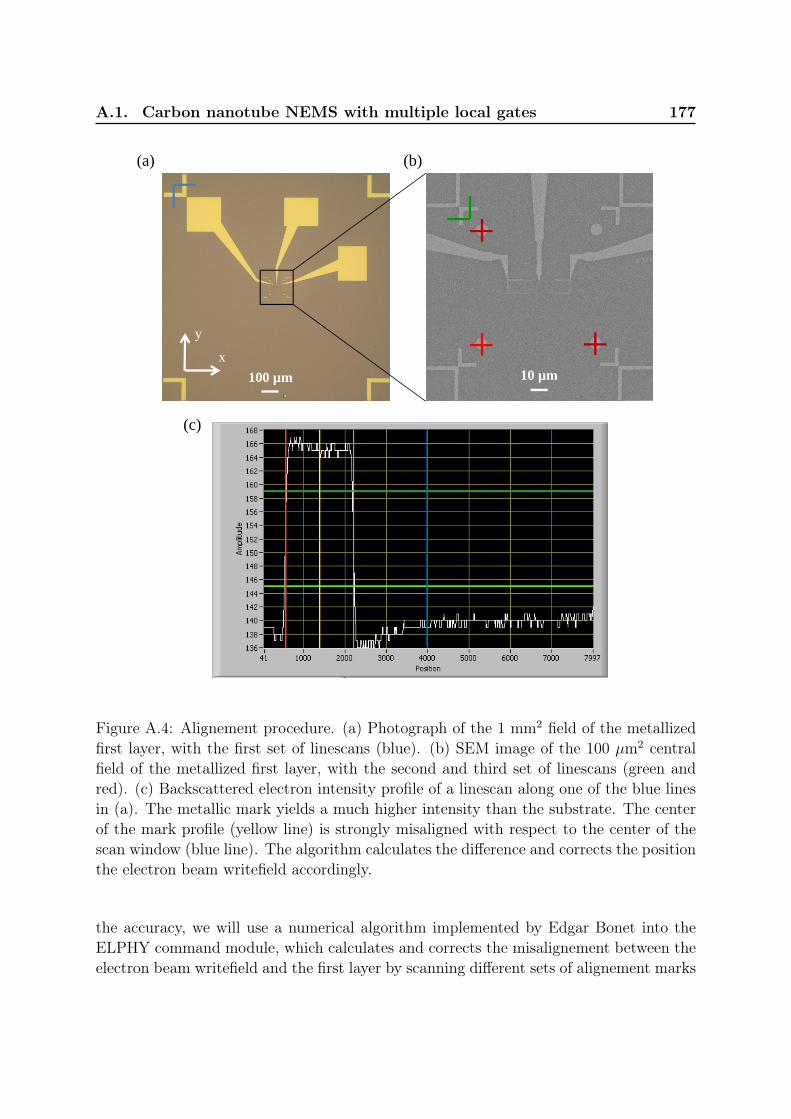
A.1. Carbon nanotube NEMS with multiple local gates 177
10 um100 um 10 µm100 µm
(a) (b)
(c)
x
y
Figure A.4: Alignement procedure. (a) Photograph of the 1 mm2 field of the metallizedfirst layer, with the first set of linescans (blue). (b) SEM image of the 100 µm2 centralfield of the metallized first layer, with the second and third set of linescans (green andred). (c) Backscattered electron intensity profile of a linescan along one of the blue linesin (a). The metallic mark yields a much higher intensity than the substrate. The centerof the mark profile (yellow line) is strongly misaligned with respect to the center of thescan window (blue line). The algorithm calculates the difference and corrects the positionthe electron beam writefield accordingly.
the accuracy, we will use a numerical algorithm implemented by Edgar Bonet into theELPHY command module, which calculates and corrects the misalignement between theelectron beam writefield and the first layer by scanning different sets of alignement marks
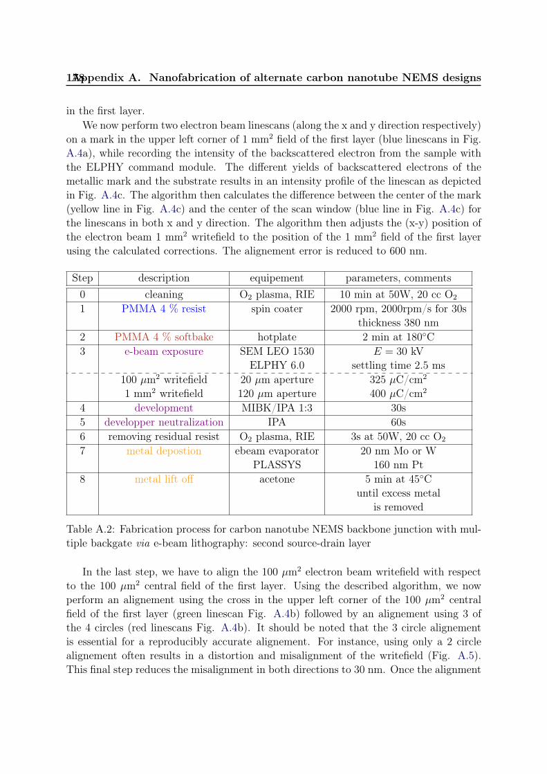
178Appendix A. Nanofabrication of alternate carbon nanotube NEMS designs
in the first layer.We now perform two electron beam linescans (along the x and y direction respectively)
on a mark in the upper left corner of 1 mm2 field of the first layer (blue linescans in Fig.A.4a), while recording the intensity of the backscattered electron from the sample withthe ELPHY command module. The different yields of backscattered electrons of themetallic mark and the substrate results in an intensity profile of the linescan as depictedin Fig. A.4c. The algorithm then calculates the difference between the center of the mark(yellow line in Fig. A.4c) and the center of the scan window (blue line in Fig. A.4c) forthe linescans in both x and y direction. The algorithm then adjusts the (x-y) position ofthe electron beam 1 mm2 writefield to the position of the 1 mm2 field of the first layerusing the calculated corrections. The alignement error is reduced to 600 nm.
Step description equipement parameters, comments0 cleaning O2 plasma, RIE 10 min at 50W, 20 cc O2
1 PMMA 4 % resist spin coater 2000 rpm, 2000rpm/s for 30sthickness 380 nm
2 PMMA 4 % softbake hotplate 2 min at 180C3 e-beam exposure SEM LEO 1530 E = 30 kV
ELPHY 6.0 settling time 2.5 ms100 µm2 writefield 20 µm aperture 325 µC/cm2
1 mm2 writefield 120 µm aperture 400 µC/cm2
4 development MIBK/IPA 1:3 30s5 developper neutralization IPA 60s6 removing residual resist O2 plasma, RIE 3s at 50W, 20 cc O2
7 metal depostion ebeam evaporator 20 nm Mo or WPLASSYS 160 nm Pt
8 metal lift off acetone 5 min at 45Cuntil excess metal
is removed
Table A.2: Fabrication process for carbon nanotube NEMS backbone junction with mul-tiple backgate via e-beam lithography: second source-drain layer
In the last step, we have to align the 100 µm2 electron beam writefield with respectto the 100 µm2 central field of the first layer. Using the described algorithm, we nowperform an alignement using the cross in the upper left corner of the 100 µm2 centralfield of the first layer (green linescan Fig. A.4b) followed by an alignement using 3 ofthe 4 circles (red linescans Fig. A.4b). It should be noted that the 3 circle alignementis essential for a reproducibly accurate alignement. For instance, using only a 2 circlealignement often results in a distortion and misalignment of the writefield (Fig. A.5).This final step reduces the misalignment in both directions to 30 nm. Once the alignment
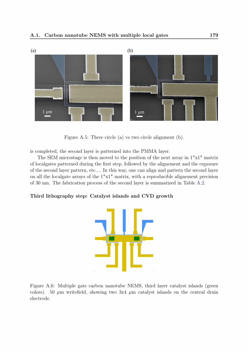
A.1. Carbon nanotube NEMS with multiple local gates 179
(a) (b)
1 µm 1 µm
Figure A.5: Three circle (a) vs two circle alignment (b).
is completed, the second layer is patterned into the PMMA layer.The SEM microstage is then moved to the position of the next array in 1"x1" matrix
of localgates patterned during the first step, followed by the alignement and the exposureof the second layer pattern, etc.... In this way, one can align and pattern the second layeron all the localgate arrays of the 1"x1" matrix, with a reproducible alignement precisionof 30 nm. The fabrication process of the second layer is summarized in Table A.2.
Third lithography step: Catalyst islands and CVD growth
(a) (b)
1 µm 1 µm
Figure A.6: Multiple gate carbon nanotube NEMS, third layer catalyst islands (greencolors). 50 µm writefield, showing two 3x4 µm catalyst islands on the central drainelectrode.
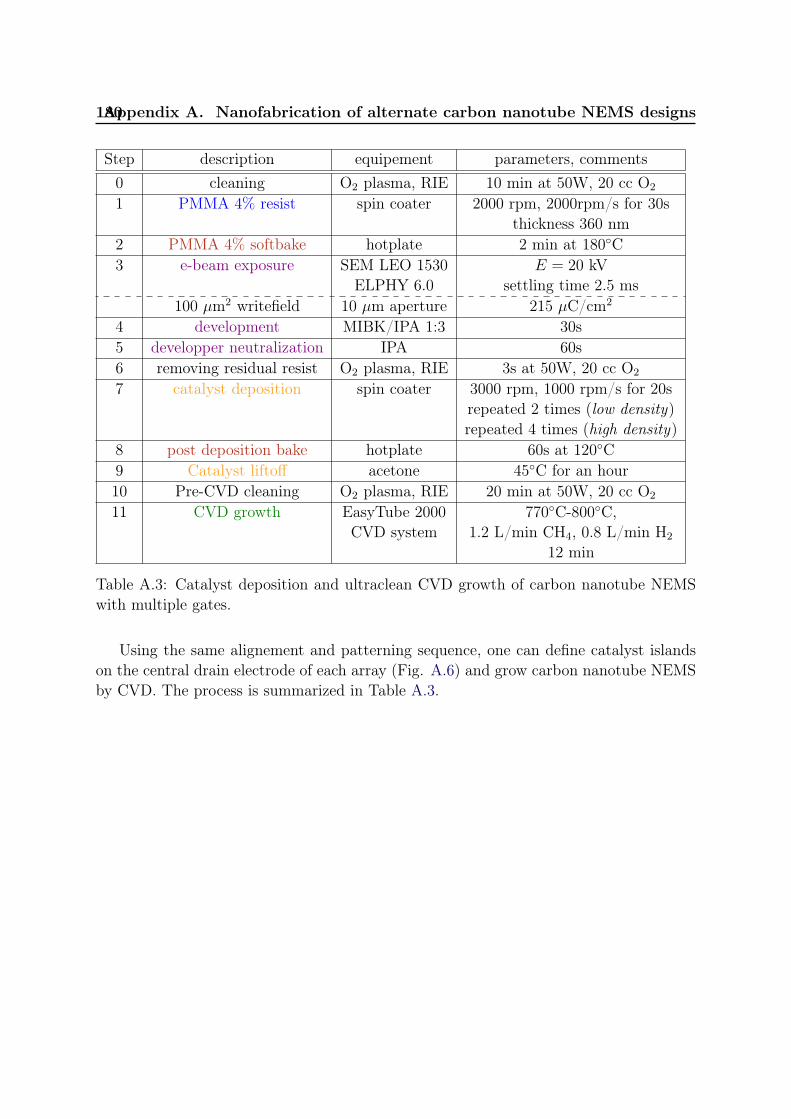
180Appendix A. Nanofabrication of alternate carbon nanotube NEMS designs
Step description equipement parameters, comments0 cleaning O2 plasma, RIE 10 min at 50W, 20 cc O2
1 PMMA 4% resist spin coater 2000 rpm, 2000rpm/s for 30sthickness 360 nm
2 PMMA 4% softbake hotplate 2 min at 180C3 e-beam exposure SEM LEO 1530 E = 20 kV
ELPHY 6.0 settling time 2.5 ms100 µm2 writefield 10 µm aperture 215 µC/cm2
4 development MIBK/IPA 1:3 30s5 developper neutralization IPA 60s6 removing residual resist O2 plasma, RIE 3s at 50W, 20 cc O2
7 catalyst deposition spin coater 3000 rpm, 1000 rpm/s for 20srepeated 2 times (low density)repeated 4 times (high density)
8 post deposition bake hotplate 60s at 120C9 Catalyst liftoff acetone 45C for an hour10 Pre-CVD cleaning O2 plasma, RIE 20 min at 50W, 20 cc O2
11 CVD growth EasyTube 2000 770C-800C,CVD system 1.2 L/min CH4, 0.8 L/min H2
12 min
Table A.3: Catalyst deposition and ultraclean CVD growth of carbon nanotube NEMSwith multiple gates.
Using the same alignement and patterning sequence, one can define catalyst islandson the central drain electrode of each array (Fig. A.6) and grow carbon nanotube NEMSby CVD. The process is summarized in Table A.3.
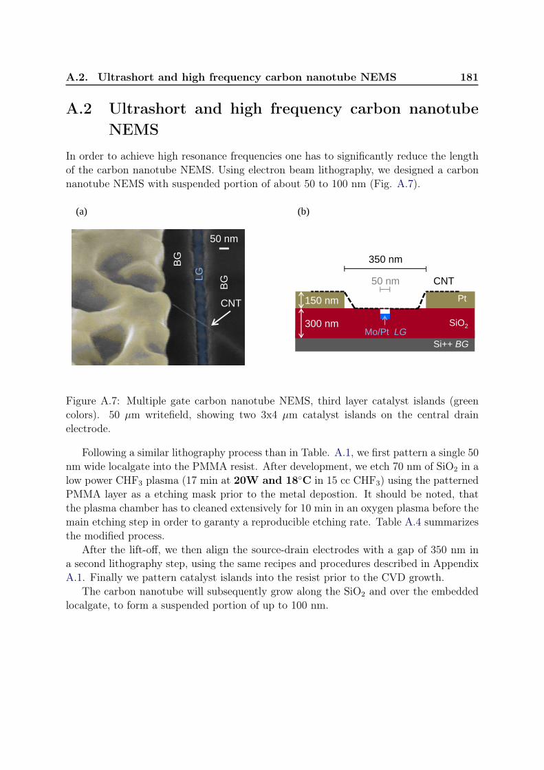
A.2. Ultrashort and high frequency carbon nanotube NEMS 181
A.2 Ultrashort and high frequency carbon nanotubeNEMS
In order to achieve high resonance frequencies one has to significantly reduce the lengthof the carbon nanotube NEMS. Using electron beam lithography, we designed a carbonnanotube NEMS with suspended portion of about 50 to 100 nm (Fig. A.7).
50 nm
CNT
LG
BG
BG
Pt
Si++ BG
SiO2
50 nm
300 nm
150 nm
Mo/Pt LG
350 nm
(a) (b)
CNT
Figure A.7: Multiple gate carbon nanotube NEMS, third layer catalyst islands (greencolors). 50 µm writefield, showing two 3x4 µm catalyst islands on the central drainelectrode.
Following a similar lithography process than in Table. A.1, we first pattern a single 50nm wide localgate into the PMMA resist. After development, we etch 70 nm of SiO2 in alow power CHF3 plasma (17 min at 20W and 18C in 15 cc CHF3) using the patternedPMMA layer as a etching mask prior to the metal depostion. It should be noted, thatthe plasma chamber has to cleaned extensively for 10 min in an oxygen plasma before themain etching step in order to garanty a reproducible etching rate. Table A.4 summarizesthe modified process.
After the lift-off, we then align the source-drain electrodes with a gap of 350 nm ina second lithography step, using the same recipes and procedures described in AppendixA.1. Finally we pattern catalyst islands into the resist prior to the CVD growth.
The carbon nanotube will subsequently grow along the SiO2 and over the embeddedlocalgate, to form a suspended portion of up to 100 nm.
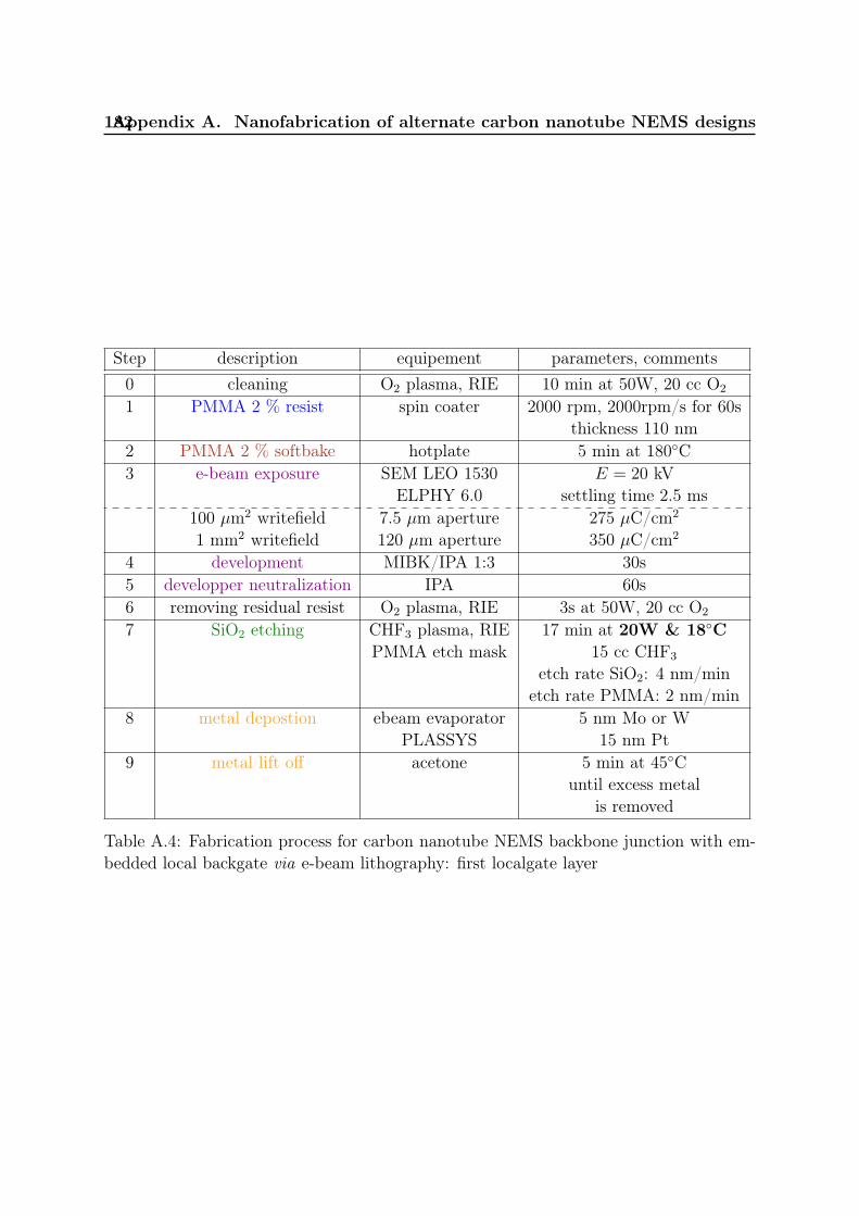
182Appendix A. Nanofabrication of alternate carbon nanotube NEMS designs
Step description equipement parameters, comments0 cleaning O2 plasma, RIE 10 min at 50W, 20 cc O2
1 PMMA 2 % resist spin coater 2000 rpm, 2000rpm/s for 60sthickness 110 nm
2 PMMA 2 % softbake hotplate 5 min at 180C3 e-beam exposure SEM LEO 1530 E = 20 kV
ELPHY 6.0 settling time 2.5 ms100 µm2 writefield 7.5 µm aperture 275 µC/cm2
1 mm2 writefield 120 µm aperture 350 µC/cm2
4 development MIBK/IPA 1:3 30s5 developper neutralization IPA 60s6 removing residual resist O2 plasma, RIE 3s at 50W, 20 cc O2
7 SiO2 etching CHF3 plasma, RIE 17 min at 20W & 18CPMMA etch mask 15 cc CHF3
etch rate SiO2: 4 nm/minetch rate PMMA: 2 nm/min
8 metal depostion ebeam evaporator 5 nm Mo or WPLASSYS 15 nm Pt
9 metal lift off acetone 5 min at 45Cuntil excess metal
is removed
Table A.4: Fabrication process for carbon nanotube NEMS backbone junction with em-bedded local backgate via e-beam lithography: first localgate layer
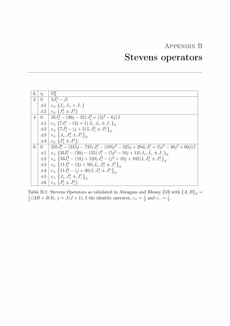
Appendix B
Stevens operators
k q Oqk
2 0 3J2z − jI
±1 c± Jz, J+ + J−±2 c±
(J2
+ ± J2−)
4 0 35J4z − (30j − 25) J2
z + (3j2 − 6j) I±1 c± 7J2
z − (3j + 1) Jz, J+ ± J−S±2 c±
7J2
z − (j + 5) I, J2+ ± J2
−S
±3 c±Jz, J
3+ ± J3
−S
±4 c±(J4
+ ± J4−)
6 0 231J6z − (315j − 735) J4
z − (105j2 − 525j + 294) J2z + (5j3 − 40j2 + 60j) I
±1 c± 33J5z − (30j − 155) J3
z − (5j2 − 10j + 12) Jz, J+ ± J−S±2 c±
33J4
z − (18j + 123) J2z − (j2 + 10j + 102) I, J2
+ ± J2−S
±3 c±
11J3z − (3j + 59) Jz, J
3+ ± J3
−S
±4 c±
11J2z − (j + 38) I, J4
+ ± J4−S
±5 c±Jz, J
5+ ± J5
−S
±6 c±(J6
+ ± J6−)
Table B.1: Stevens Operators as tabulated in Abragam and Bleany [50] with A,BS =12
(AB +BA), j = J(J + 1), I the identity operator, c+ = 12and c− = i
2.


Appendix C
Publications
Dynamics and Dissipation Induced by Single-Electron Tunneling in Carbon NanotubeNanoelectromechanical Systems
Marc Ganzhorn and Wolfgang Wernsdorfer
Institut Neel, CNRS & Universite Joseph Fourier, BP 166, 25 Avenue des Martyrs, 38042 Grenoble Cedex 9, France(Received 13 November 2011; revised manuscript received 28 January 2012; published 24 April 2012)
We demonstrate the effect of single-electron tunneling (SET) through a carbon nanotube quantum dot
on its nanomechanical motion. We find that the frequency response and the dissipation of the nano-
electromechanical system to SET strongly depends on the electronic environment of the quantum dot, in
particular, on the total dot capacitance and the tunnel coupling to the metal contacts. Our findings suggest
that one could achieve quality factors of 106 or higher by choosing appropriate gate dielectrics and/or by
improving the tunnel coupling to the leads.
DOI: 10.1103/PhysRevLett.108.175502 PACS numbers: 81.07.Oj, 81.07.De, 85.85.+j
Carbon nanotubes (CNT) have become an essentialbuilding block for nanoelectromechanical systems(NEMS). Their low mass and high Young’s modulus allowfor instance ultrasensitive mass [1–3] or force detection[4,5] (electric and magnetic) over a wide range of frequen-cies and its small diameter enables even single-moleculedetection [5–7]. Moreover, CNT devices exhibit remark-able electronic transport properties, ranging from Kondophysics [8] to Coulomb blockade at high temperature [9]. Itwas recently demonstrated that a CNT NEMS’ nanome-chanical motion at very low temperature (i.e., in Coulombblockade regime) is strongly affected by the electronictransport through the CNT quantum dot (QD), and viceversa: For instance, single-electron tunneling (SET) causeda frequency softening and increased dissipation whentuning the CNT dot’s potential through a Coulombpeak [10–12].
Here we demonstrate that the response and dissipation ofa CNT NEMS at very low temperature induced by zerobias SET through the CNT NEMS QD critically dependson the dot capacitance, the tunnel coupling to the metalleads, and temperature. We studied the frequency anddissipation response of nanomechanical bending modesto zero bias SET in suspended CNT devices with tunabletunnel couplings and different gate dielectrics, i.e., differ-ent dot capacitance. We observe that SET causes a fre-quency softening for small dot capacitance and/or tunnelcoupling, whereas a frequency hardening or no frequencymodulation is observed for large dot capacitance and/ortunnel coupling. We show that the dissipation of the CNTNEMS is mainly dominated by the capacitance, whenelectron tunneling through the dot is suppressed (i.e.. inthe Coulomb valley), whereas it is limited by the meantunneling rate and the conductance, when electron tun-neling through the dot is allowed (i.e., on a Coulomb peak).Finally we demonstrate that the tunnel current is the domi-nant dissipation mechanism in CNT NEMS at low tem-perature. Our findings are in fair agreement with atheoretical model provided previously [10,12].
Low capacitance CNT quantum dots (Cdot 20–40 aF)were obtained by using silicon dioxide as gate dielectric[Fig. 1(a)]. First, source-drain electrodes are patterned byoptical deep ultraviolet (DUV) lithography and e-beamevaporation of Mo (20 nm) and Pt (160 nm) on 500 nmof thermal SiO2. To ensure the suspension of the CNT,150 nm of SiO2 are dry etched in CHF3 plasma. Highcapacitance CNT quantum dots (Cdot 160–260 aF) areobtained with high- gate dielectrics Al2O3 [Fig. 1(b)].First, a 1 m-wide metallic local gate is patterned byoptical DUV lithography and e-beam evaporation of Mo(20 nm) on 300 nm of thermal SiO2. A layer of 100 nm ofAl2O3 is then deposited by atomic layer deposition. Usingoptical DUV lithography and e-beam evaporation of Mo(20 nm) and Pt (160 nm), source-drain electrodes arealigned above the local gate. Suspended CNT are finallygrown by chemical vapor deposition at 800 C from a CH4
feedstock and Fe/Mo catalyst spots patterned on the
FIG. 1 (color online). False color SEM image of (a) a lowcapacitance device based on a SiO2 covered Si backgate (grey)and (b) a high capacitance device based on an Al2O3 coveredlocal metallic gate (blue). The rf actuation signal is injected intothe local metallic gate and Si backgate, respectively, through ahome-built bias-T. As the induced mechanical motion changesthe charge flow through the CNT quantum dot and vice versa, wecan detect the CNT resonance through a change in zero biasconductance. (c) Mechanical resonance of a typical CNT NEMSat low driving power Prf ¼ 100 dBm. The resonance widthf ¼ 2:5 kHz leads to a quality factor of Q 140 000.
PRL 108, 175502 (2012) P HY S I CA L R EV I EW LE T T E R Sweek ending
27 APRIL 2012
0031-9007=12=108(17)=175502(4) 175502-1 2012 American Physical Society
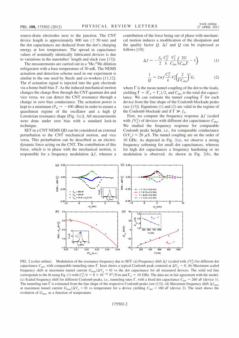
source-drain electrodes next to the junction. The CNTdevice length is approximately 800 nm ( 50 nm) andthe dot capacitances are deduced from the dot’s chargingenergy at low temperature. The spread in capacitancevalues of nominally identically fabricated devices is dueto variations in the nanotubes’ length and slack (see [13]).
The measurements are carried out in a 3He=4He dilutionrefrigerator with a base temperature of 30 mK. The NEMSactuation and detection scheme used in our experiment issimilar to the one used by Steele and co-workers [11,12].The rf actuation signal is injected into the gate electrodevia a home-built bias T. As the induced mechanical motionchanges the charge flow through the CNT quantum dot andvice versa, we can detect the CNT resonance through achange in zero bias conductance. The actuation power iskept to a minimum (Prf 100 dBm) in order to ensure aquasilinear regime of the oscillator and a high QLorentzian resonance shape [Fig. 1(c)]. All measurementswere done under zero bias with a standard lock-intechnique.
SET in a CNT NEMS QD can be considered an externalperturbation to the CNT mechanical motion, and viceversa. This perturbation can be described as an electro-dynamic force acting on the CNT. The contribution of thisforce, which is in phase with the mechanical motion, isresponsible for a frequency modulation f, whereas a
contribution of the force being out of phase with mechani-cal motion induces a modification of the dissipation andthe quality factor Q. f and Q can be expressed asfollows [10]:
f ¼ f02
C02g
k
V2g
Cdot
2G
Cdot 1
; (1)
1
Q¼ 2f
C02g
kV2g
2
Cdot
2G; (2)
where is the mean tunnel coupling of the dot to the leads,yielding ¼ ðd þ sÞ=2, and Cdot is the total dot capaci-tance. We can estimate the tunnel coupling for eachdevice from the line shape of the Coulomb blockade peaks(see [13]). Equations (1) and (2) are valid in the regime ofthe Coulomb blockade and if f0.First, we compare the frequency response f (scaled
with fV2g) of devices with different dot capacitances Cdot.
We studied the frequency response for comparableCoulomb peaks height, i.e., for comparable conductanceGðVgÞ 20 S. The tunnel coupling are on the order of
10 GHz. As depicted in Fig. 2(a), we observe a strongfrequency softening for small dot capacitances, whereasfor high dot capacitances a frequency hardening or nomodulation is observed. As shown in Fig. 2(b), the
FIG. 2 (color online). Modulation of the resonance frequency due to SET: (a) Frequency shift f (scaled with fV2g) for different dot
capacitance Cdot, with comparable tunneling rates . Inset shows a typical Coulomb peak centered at Vg ¼ 0. (b) Maximum scaled
frequency shift at maximum tunnel current GmaxðVg ¼ 0Þ vs the dot capacitance for all measured devices. The solid red line
corresponds to the fit using Eq. (1) with C02g =k ¼ 8 1022 F2=Nm and d 10 GHz. The data are in fair agreement with the model.
(c) Scaled frequency shift for different Coulomb peaks, i.e., tunneling rates , with a fixed dot capacitance Cdot ¼ 260 aF (device 1).The tunneling rate is estimated from the line shape of the respective Coulomb peaks (see [13]). (d) Maximum frequency shift fmax
at maximum tunnel current GmaxðVg ¼ 0Þ vs temperature for a device yielding Cdot ¼ 160 aF (device 2). The inset shows the
evolution of Gmax as a function of temperature.
PRL 108, 175502 (2012) P HY S I CA L R EV I EW LE T T E R Sweek ending
27 APRIL 2012
175502-2
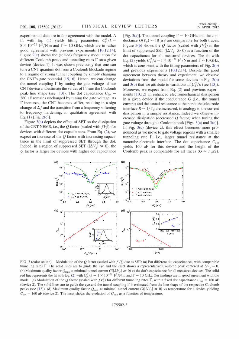
experimental data are in fair agreement with the model. Afit with Eq. (1) yields fitting parameters C02
g =k ¼8 1022 F2=Nm and 10 GHz, which are in rathergood agreement with previous experiments [10,12,14].Figure 2(c) shows the (scaled) frequency modulation fordifferent Coulomb peaks and tunneling rates on a givendevice (device 1). It was shown previously that one cantune a CNT quantum dot from a Coulomb blockade regimeto a regime of strong tunnel coupling by simply changingthe CNT’s gate potential [15,16]. Hence, we can changethe tunnel coupling by tuning the gate voltage of ourCNT device and estimate the values of from the Coulombpeak line shape (see [13]). The dot capacitance Cdot ¼260 aF remains unchanged by tuning the gate voltage. As increases, the CNT becomes stiffer, resulting in a signchange off and the transition from a frequency softeningto frequency hardening, in qualitative agreement withEq. (1) [Fig. 2(c)].
Figure 3(a) depicts the effect of SET on the dissipationof the CNT NEMS, i.e., theQ factor (scaled with fV2
g), for
devices with different dot capacitances. From Eq. (2), weexpect an increase of the Q factor with increasing capaci-tance in the limit of suppressed SET through the dot.Indeed, in a region of suppressed SET (jVgj 0), the
Q factor is larger for devices with higher dot capacitance
[Fig. 3(a)]. The tunnel coupling 10 GHz and the con-ductance GðVgÞ 18 S are comparable for both traces.
Figure 3(b) shows the Q factor (scaled with fV2g) in the
limit of suppressed SET (jVgj 0) as a function of the
dot capacitance for all measured devices. The fit withEq. (2) yields C02
g =k¼11021 F2=Nm and 10GHz,
which is consistent with the fitting parameters of Fig. 2(b)and previous experiments [10,12,14]. Despite the goodagreement between theory and experiment, we observedeviations from the model for some devices in Fig. 2(b)and 3(b) that we attribute to variations in C02
g =k (see [13]).
Moreover, we expect from Eq. (2) and previous experi-ments [10,12] an enhanced electromechanical dissipationin a given device if the conductance G (i.e., the tunnelcurrent) and the tunnel resistance at the nanotube-electrodeinterface R 1=d are increased, in analogy to the currentdissipation in a simple resistance. Indeed we observe in-creased dissipation (decreased Q factor) when tuning thegate voltage through a Coulomb peak [Figs. 3(a) and 3(c)].In Fig. 3(c) (device 2), this effect becomes more pro-nounced as we move to gate voltage regions with a smallertunneling rate , i.e., larger tunnel resistance at thenanotube-electrode interface. The dot capacitance Cdot
yields 160 aF for this device and the height of theCoulomb peak is comparable for all traces (G 7 S).
FIG. 3 (color online). Modulation of the Q factor (scaled with fV2g) due to SET: (a) For different dot capacitances, with comparable
tunneling rates . The solid lines are to guide the eye and the inset shows a representative Coulomb peak centered at Vg ¼ 0.
(b) Maximum quality factorQmax at minimal tunnel current GðjVgj 0Þ vs the dot’s capacitance for all measured devices. The solid
red line represents the fit with Eq. (2) with C02g =k ¼ 1 1021 F2=Nm and 10 GHz. Our findings are in good agreement with the
model. (c) Modulation of the Q factor (scaled with fV2g) for different tunneling rates , with a fixed dot capacitance Cdot ¼ 160 aF
(device 2). The solid lines are to guide the eye and the tunnel coupling is estimated from the line shape of the respective Coulombpeaks (see [13]). (d) Maximum quality factor Qmax at minimal tunnel current GðjVgj 0Þ vs temperature for a device yielding
Cdot ¼ 160 aF (device 2). The inset shows the evolution of Gmin as a function of temperature.
PRL 108, 175502 (2012) P HY S I CA L R EV I EW LE T T E R Sweek ending
27 APRIL 2012
175502-3
Therefore, the CNT capacitance is the limiting factor forthe dissipation in regions of suppressed SET, whereas themean tunnel coupling and the tunneling current itself de-fine the dissipation in regions of strong SET. We concludethat the electron transport through the CNT is the maindissipation mechanism in our nanoelectromechanicalsystem.
Finally, we study the temperature dependence of thefrequency response and the dissipation. Figure 2(d) depictsthe frequency shift fmax for Gmax ¼ GðVg ¼ 0Þwhereas Fig. 3(d) shows the quality factorQmax forGmin ¼GðjVgj 0Þ as a function of temperature. A fit of the
data yields fmax T and Qmax 1=T. As temperatureincreases the Coulomb blockade peak broadens and be-comes smaller (see[13], Fig. S3). As a result Gmax ¼GðVg ¼ 0Þ decreases whereasGmin ¼ GðjVgj 0Þ in-creases with temperature, as depicted in the insetsof Figs. 2(d) and 3(d). From the data fit we obtainGmax T and Gmin T. It was previously demonstratedthat carbon nanotubes show Luttinger liquid behavior[17–19], where the conductance follows a characteristicpower law dependence as a function of temperatureGðTÞ T, being related to the Luttinger parameter gby ¼ ðg 1þ g 2Þ=2 [17,18]. We find 1 and aLuttinger parameter of g ¼ 0,1, which is close to previousmeasurements [17] and theoretical predictions [18,19].Comparing the temperature dependence of the conduc-tance, the quality factor, and the frequency shift, we finallyobtain fmax Gmax and Qmax 1=Gmin, which is infull agreement with Eqs. (1) and (2). We can conclude thatthe current is the dominant dissipation mechanism forcarbon nanotube-based NEMS in a Coulomb blockaderegime at cryogenic temperatures.
We have demonstrated that the response and the dissi-pation to single-electron tunneling of carbon nanotubeNEMS at low temperature depends on the dot capacitanceand the tunnel coupling to the leads, the tunnel currentitself being the main dissipation mechanism in the system.By choosing high- dielectrics (HfO2 or ZrO2) and im-proving the tunnel contact to the metal leads, one couldsignificantly enhance the quality factorQ to values exceed-ing 106. It was proposed in theoretical calculation that onecan use such high -Q CNT NEMS as magnetic torque orforce detectors for nanoparticles [5] or single-moleculemagnets [20,21] grafted to the CNT NEMS. In principle,one can achieve a sensitivity of oneB at low temperature,whereas the best magnetometers, for instance the micro-SQUID, only have a sensitivity of 103 B [22]. Finally,such molecular quantum spintronic device would allowsingle spin manipulation on a molecular level.
This work is partially supported by the ANR-PNANOproject MolNanoSpin No. ANR-08-NANO-002 and ERCAdvanced Grant MolNanoSpin No. 226558. M.G. ac-knowledges financial support from the RTRANanosciences Foundation. Samples were fabricated in the
NANOFAB facility of the Neel Institute. We thank F.Balestro, E. Bonet, T. Crozes, J. P. Cleuziou, E. Eyraud,T. Fournier, R. Haettel, C. Hoarau, D. Lepoittevin, V.Nguyen, V. Reita, A. Reserbat-Plantey, C. Thirion, andM. Urdampilleta.
[1] B. Lassagne, D. Garcia-Sanchez, A. Aguasca, and A.Bachtold, Nano Lett. 8, 3735 (2008).
[2] H.-Y. Chiu, P. Hung, H.W. C. Postma, and M. Bockrath,Nano Lett. 8, 4342 (2008).
[3] K. Jensen, K. Kim, and A. Zettl, Nature Nanotech. 3, 533(2008).
[4] A. Eichler, J. Moser, J. Chaste, M. Zdrojek, I. Wilson-Rae,and A. Bachtold, Nature Nanotech. 6, 339 (2011).
[5] B. Lassagne, D. Ugnati, and M. Respaud, Phys. Rev. Lett.107, 130801 (2011).
[6] L. Bogani and W. Wernsdorfer, Nature Mater. 7, 179(2008).
[7] M. Urdampilleta, S. Klyatskaya, J.-P. Cleuziou, M. Ruben,and W. Wernsdorfer, Nature Mater. 10, 502 (2011).
[8] J. Nygard, D.H. Cobden, and P. E. Lindelof, Nature(London) 408, 342 (2000).
[9] J.-C. Charlier, X. Blase, and S. Roche, Rev. Mod. Phys.79, 677 (2007).
[10] B. Lassagne, Y. Tarakanov, J. Kinaret, D. Garcia-Sanchez,and A. Bachtold, Science 325, 1107 (2009).
[11] A. K. Huttel G.A. Steele, B. Witkamp, M. Poot, L. P.Kouwenhoven, and H. S. J. van der Zant, Nano Lett. 9,2547 (2009).
[12] G. A. Steele A.K. Huttel, B. Witkamp, M. Poot, H. B.Meerwaldt, L. P. Kouwenhoven, and H. S. J. van der Zant,Science 325, 1103 (2009).
[13] See Supplemental Material at http://link.aps.org/supplemental/10.1103/PhysRevLett.108.175502 for theestimation method of the dot capacitance and tunnelcoupling, a discussion about the model accuracy and thetemperature evolution of the zero bias conductance.
[14] V. Sazonova, Y. Yaish, H. Ustunel, D. Roundy, T. A. Arias,and P. L. McEuen, Nature (London) 431, 284 (2004).
[15] T. Jespersen K. Grove-Rasmussen, J. Paaske, K. Muraki,T. Fujisawa, J. Nygard, and K. Flensberg, Nature Phys. 7,348 (2011).
[16] G. A. Steele, G. Gotz, and L. P. Kouwenhoven, NatureNanotech. 4, 363 (2009).
[17] M. Bockrath, D.H. Cobden, J. Lu, A.G. Rinzler, R E.Smalley, L. Balents, and P. L. McEuen, Nature (London)397, 598 (1999).
[18] C. Kane, L. Balents, and M. P.A. Fisher, Phys. Rev. Lett.79, 5086 (1997).
[19] R. Egger and A. O. Gogolin, Phys. Rev. Lett. 79, 5082(1997).
[20] A. A. Kovalev, L. X. Hayden, G. E.W. Bauer, and Y.Tserkovnyak, Phys. Rev. Lett. 106, 147203 (2011).
[21] D. Garanin and E. Chudnovsky, Phys. Rev. X 1, 011005(2011).
[22] W. Wernsdorfer, Supercond. Sci. Technol. 22, 064013(2009).
PRL 108, 175502 (2012) P HY S I CA L R EV I EW LE T T E R Sweek ending
27 APRIL 2012
175502-4
Strong spin–phonon coupling between asingle-molecule magnet and a carbon nanotubenanoelectromechanical systemMarc Ganzhorn1, Svetlana Klyatskaya2, Mario Ruben2,3 and Wolfgang Wernsdorfer1*
Magnetic relaxation processes were first discussed for a crystalof paramagnetic transition ions1. It was suggested that mechan-ical vibrations of the crystal lattice (phonons) modulate thecrystal electric field of the magnetic ion, thus inducing a‘direct’ relaxation between two different spin states1–3. Directrelaxation has also been predicted for single-moleculemagnets with a large spin and a high magnetic anisotropy1,4–7
and was first demonstrated in a Mn12 acetate crystal8. Thespin-lattice relaxation time for such a direct transition islimited by the phonon density of states at the spin resonance1.In a three-dimensional system, such as a single-moleculemagnet crystal, the phonon energy spectrum is continuous,but in a one-dimensional system, like a suspended carbon nano-tube, the spectrum is discrete and can be engineered to anextremely low density of states9. An individual single-moleculemagnet, coupled to a suspended carbon nanotube, shouldtherefore exhibit extremely long relaxation times9 and thesystem’s reduced size should result in a strong spin–phononcoupling10,11. Here, we provide the first experimental evidencefor a strong spin–phonon coupling between a single moleculespin and a carbon nanotube resonator, ultimately enablingcoherent spin manipulation and quantum entanglement10,11.
Carbon nanotubes (CNT) have become an essential buildingblock for nanoelectromechanical systems (NEMS). Their low massand high Young’s modulus give rise to high oscillation frequenciesfor transverse12,13 and longitudinal modes14–16, therefore enablingground-state cooling with state-of-the-art cryogenics and a largezero point motion in the quantum regime17. Moreover, the strongcoupling between nanomechanical motion and single-electron tun-nelling in high-Q CNT NEMS allows electronic actuation and detec-tion of the nanomechanical motion18–21. As such, CNT NEMS canbe used for ultrasensitive mass sensing22–24 or as magnetic torquedetectors for single spin systems25.
A single spin, strongly coupled with a CNT NEMS in thequantum regime, could serve as an elementary qubit in quantuminformation processing. It has been suggested recently that astrong coupling between a quantum CNT NEMS and a single elec-tron spin would enable basic qubit control and the implementationof entangled states9. In this framework, coupling a single-moleculemagnet (SMM) to the quantized nanomechanical motion of aCNT NEMS is a very attractive option26. Chemical engineeringallows the synthesis of perfectly identical SMMs, as well as theirintegration into nanoscale devices such as electromigratedjunctions27–29 or CNT transistors30. A large magnetic moment anda strong, uniaxial magnetic anisotropy enable, for instance,quantum tunnelling of magnetization31,32 or quantum phase
interference33, yielding coherence times on the order of micro-seconds in crystalline form34. Moreover, it was recently predictedthat the spin–phonon coupling between an SMM and a quantumCNT NEMS is strong enough to allow coherent spin manipulationand quantum entanglement of a spin and a resonator10,11. In thisLetter, we first present the SMM and CNT NEMS. We then establisha strong spin–phonon coupling between the two systems, that is,between an individual TbPc2-SMM and the quantized high-Q longi-tudinal stretching mode (LSM) of the CNT resonator. The strongspin–phonon coupling presented here would enable the quantumcontrol of magnetization at a single-phonon level9,10 and the entan-glement of a single spin with quantized mechanical motion9,11.
We study the magnetization reversal of a pyrene-substitutedbis(phthalocyaninato)terbium(III) SMM (hereafter TbPc2, Fig. 1a)grafted to a CNT resonator36. The TbPc2 is a rare earth SMM inwhich the magnetic moment is carried by a single Tb3þ ion sand-wiched between two organic phthalocyanine (Pc) ligand planes35.The TbPc2 has a S¼ 1/2 radical delocalized over the Pc ligandplanes. As a result of p–p interaction, this radical can easilyhybridize with the p electrons of any form of sp2 carbon withoutaffecting the magnetic properties of the Tb3þ ion30,36,37. The highlyanisotropic 4f shell of the Tb3þ ion and its intrinsically strongspin–orbit coupling result in a magnetic ground state of J¼ 6 anda pronounced uniaxial magnetic anisotropy (Fig. 1a). The ground-state doublet Jz¼+6 is separated from the excited states byseveral hundreds of kelvin, which makes the TbPc2 an Ising-likespin system at low temperatures (T , 5 K) and small magneticfields (B , 10 T)35. A strong hyperfine interaction with the nuclearspin I¼ 3/2 of the Tb3þ ion splits the ground-state doubletJz ¼+6 into four states each (Fig. 1b). Finally, the ligand fieldgenerates a small transverse magnetic anisotropy resulting inavoided level crossings (black circles in Fig. 1b)35.
At cryogenic temperatures, magnetization reversal can occurthrough two different processes. Around zero magnetic field, theavoided level crossings allow for quantum tunnelling of magnetiza-tion |Jz,Izl |2Jz,Izl (refs 30,35). At high magnetic fields the mag-netization reverses through a direct relaxation process involvingnon-coherent tunnelling events combined with the emission of aphonon30 (Fig. 1b). Previous experiments on TbPc2 single crystals35
and on TbPc2 coupled to a non-suspended CNT30 have shown thatthe spin relaxation was mainly enabled by bulk phonons inthe environment of an individual SMM (crystal or substrate).However, an individual TbPc2-SMM grafted onto a suspendedCNT is physically decoupled from the bulk phonons in the substrateor the transistor leads. As a consequence, the TbPc2-SMM can onlycouple to one-dimensional phonons, associated with the
1Institut Neel, CNRS et Universite Joseph Fourier, BP 166, F-38042 Grenoble Cedex 9, France, 2Institute of Nanotechnology (INT), Karlsruhe Institute ofTechnology (KIT), 76344 Eggenstein-Leopoldshafen, Germany, 3Institut de Physique et Chimie des Materiaux de Strasbourg (IPCMS), CNRS-Universitede Strasbourg, 67034 Strasbourg, France. *e-mail: [email protected]
LETTERSPUBLISHED ONLINE: 3 FEBRUARY 2013 | DOI: 10.1038/NNANO.2012.258
NATURE NANOTECHNOLOGY | ADVANCE ONLINE PUBLICATION | www.nature.com/naturenanotechnology 1
© 2013 Macmillan Publishers Limited. All rights reserved.

nanomechanical motion of the CNT. It was recently demonstratedthat high-frequency and high-Q transverse12 and longitudinalphonon14–16 modes in a CNT at cryogenic temperatures should bequantized, thus yielding a discrete phonon energy spectrum.
Single-electron tunnelling (SET) onto the CNT quantum dotshifts the equilibrium position of the CNT along the axis of theCNT by an amount proportional to the electron–phonon couplingg (ref. 14). For an intermediate electron–phonon coupling g ≈ 1,the electron therefore effectively tunnels into an excited vibrationalstate (Fig. 2b). If the tunnel rate Gout is larger than the relaxationrate g into the vibrational ground state, the electron tunnelsout of the dot, resulting in equidistant excited states in the regionof SET, running parallel to the edge of the Coulomb diamond(black arrows, Fig. 2c)14,15. For large electron–phonon couplingg ≫ 1, one also observes a current suppression at low bias, aphenomenon known as Franck–Condon blockade16. It was alsodemonstrated that one can pump excited vibrational statesin a Coulomb-blockade regime by means of higher-orderco-tunnelling processes15.
For the device studied in this Letter, we observe a spectrum ofequidistant excited states in the region of SET (black arrows, Fig. 2c),with an average energy separation of hv¼ 140 meV¼ 1.5 K(Fig. 2d). According to hv¼ 110 meV/L [mm] (ref. 14) this corre-sponds to an oscillator length of L¼ 800 nm, which is consistentwith the length of the CNT quantum dot, LD¼ 850 nm (Fig. 2a).From the current intensity of these excited states we canestimate the electron–phonon coupling g (Fig. 2d) using thefollowing equation16:
DI /e−g gn
n!(1)
where n is the phonon quantum number. We obtain g¼ 0.6+0.3,which is comparable to the results of previous experiments14. Finally,we can estimate a lower boundary for the quality factor of this longi-tudinal phonon15. The quality factor is given by Q¼v/(2pg),where g is the relaxation rate into the ground state. For the vibrationalstates to be visible in a SET, we should have Gout . g. The tunnelcurrent at the edge of the Coulomb diamond I≈ 50 pA gives anapproximation of the tunnelling rate Gout ≈ 310 MHz. Hence, thequality factor yields Q . v/(2pGout) ≈ 110, corresponding to aphonon linewidth of the order of 15 mK. We now demonstratethat this high-Q longitudinal phonon mode can be activated by
the magnetization reversal of a single TbPc2, thus revealing strongspin–phonon coupling.
First, we tune our CNT quantum dot to a regime of Coulombblockade (Vsd¼ 0, Vlg¼ 16.5 mV). In a regime of strong spin–phonon coupling, the magnetization reversal of an individualTbPc2-SMM via direct transition can induce the excitation of thislongitudinal stretching mode phonon on the CNT quantum dot(Fig. 3a). The linewidth of the high-Q phonon was estimated tobe on the order of 15 mK and is therefore smaller than the energylevel spacing dEz¼ 120, 150 and 180 mK between the nuclearspin states of the Tb3þ ion29,35. Consequently, we should observefour different direct transitions matching the phonon energyhv¼ 1.5 K, that is, four switching fields at 89, 113, 137 and161 mT, corresponding to the different nuclear spin states of theTb3þ ion (Fig. 3a). By sweeping the magnetic field component par-allel to the TbPc2 easy axis, we can induce magnetization reversal ofthe Tb3þ ion. As described by Urdampilleta et al.30, reversal of theSMM causes an abrupt increase in the differential conductancethrough the CNT quantum dot, thus enabling an electronicreadout and revealing the four switching fields of the Tb3þ ion(Fig. 3b). Note that the field sweep direction was previouslyaligned with the TbPc2 easy axis (see Supplementary Information).
We performed magnetic field sweeps along the TbPc2 easy axis ata rate of 50 mT s21, from negative to positive field values at differenttransverse magnetic fields m0Htrans, while monitoring the differ-ential conductance in the CNT (Vsd¼ 0 and Vlg¼ 16.5 mV). Themagnetization reversal of the Tb3þ ion in a sweep translates as ajump in the differential conductance of the CNT, as describedabove (see also Fig. 3b). The corresponding magnetic field, theswitching field m0Hsw, is extracted and plotted as a function of thetransverse magnetic field m0Htrans (Fig. 4a). The measurementreveals four switching fields between 80 and 160 mT, which areindependent of the transverse magnetic field component m0Htrans.By reversing the field sweep direction, the TbPc2 magnetizationis reversed symmetrically between 280 mT and 2160 mT. Toobtain a magnetization reversal statistic, we performed 200 sweepsback and forth at zero transverse magnetic field. The histogram ofthe extracted switching fields shows four dominant switchingevents at 88, 112, 137 and 160 mT with an average full-width athalf-maximum (FWHM) of 2 mT (Fig. 4b). The model describedin Fig. 3 predicts that in the case of a strong coupling between theTbPc2 spin and the observed quantized longitudinal phononmode in the CNT (energy hv¼ 1.5 K and linewidth dEph¼ 15 mK),
|+6,+3/2|+6,+1/2|+6,−1/2|+6,−3/2
|−6,−3/2|−6,−1/2|−6,+1/2|−6,+3/2
QTM
−3.0
−3.5
−4.0
E (K
)
−4.5
−5.0
−5.5−150 −100 −50 500
µ0Hz (mT)
100 150
DelocalizedS = 1/2 radical
Tb3+ uniaxialanisotropic spin J = 6
C
N
O
Tb3+
1 nm
a b
Directtransitions
Figure 1 | Rare-earth SMM. a, Schematic representation of a pyren-substituted TbPc2-SMM. A Tb3þ ion (pink) is sandwiched between two organic
phthalocyanine (Pc) ligand planes. Owing to the highly anisotropic 4f shell of the Tb3þ ion and strong spin–orbit coupling, the TbPc2 can be considered as an
Ising-like spin system, with high magnetic anisotropy and a ground-state doublet Jz¼+6. The oxidation state of the Tb3þ ion generates a spin S¼ 1/2
radical delocalized over the phthalocyanine planes. b, Zeeman diagram presenting the energy E of the two ground states Jz ¼+6 as a function of the
magnetic field m0Hz. The strong hyperfine coupling with the nuclear spin I¼3/2 in the Tb3þ ion splits the ground-state doublet Jz ¼+6 into four states.
The corresponding Zeeman diagram reveals four avoided level crossings (black circles) around zero field, allowing for QTM |Jz,Izl |2Jz,Izl. Alternatively,
magnetization reversal can occur through a direct relaxation process, involving the excitation of a phonon.
LETTERS NATURE NANOTECHNOLOGY DOI: 10.1038/NNANO.2012.258
NATURE NANOTECHNOLOGY | ADVANCE ONLINE PUBLICATION | www.nature.com/naturenanotechnology2
© 2013 Macmillan Publishers Limited. All rights reserved.
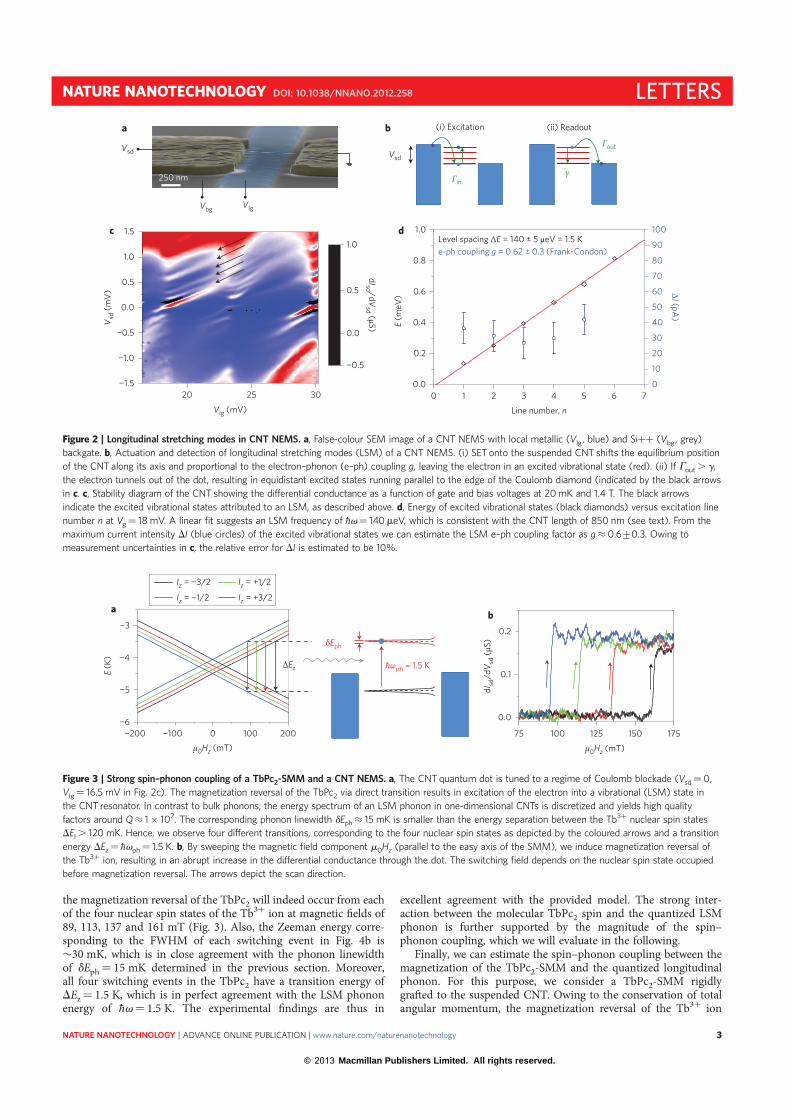
the magnetization reversal of the TbPc2 will indeed occur from eachof the four nuclear spin states of the Tb3þ ion at magnetic fields of89, 113, 137 and 161 mT (Fig. 3). Also, the Zeeman energy corre-sponding to the FWHM of each switching event in Fig. 4b is30 mK, which is in close agreement with the phonon linewidthof dEph¼ 15 mK determined in the previous section. Moreover,all four switching events in the TbPc2 have a transition energy ofDEz¼ 1.5 K, which is in perfect agreement with the LSM phononenergy of hv¼ 1.5 K. The experimental findings are thus in
excellent agreement with the provided model. The strong inter-action between the molecular TbPc2 spin and the quantized LSMphonon is further supported by the magnitude of the spin–phonon coupling, which we will evaluate in the following.
Finally, we can estimate the spin–phonon coupling between themagnetization of the TbPc2-SMM and the quantized longitudinalphonon. For this purpose, we consider a TbPc2-SMM rigidlygrafted to the suspended CNT. Owing to the conservation of totalangular momentum, the magnetization reversal of the Tb3þ ion
dIsd /dVsd (μS)
Vsd
(i) Excitation (ii) Readout
0.0
0.5
1.0
−0.5
0 1 2 3 4 5 6 70.0
0.2
0.4
0.6
0.8
1.0Level spacing ΔE = 140 ± 5 μeV = 1.5 Ke-ph coupling g = 0.62 ± 0.3 (Frank-Condon)
E (m
eV)
Line number, n
0
10
20
30
40
50
60
70
80
90
100
ΔI (pA
)
20 25 30−1.5
−1.0
−0.5
0.0
0.5
1.0
1.5
a b
c d
V sd (m
V)
Vbg
Vsd
Vlg
Vlg (mV)
Γin
Γout
γ250 nm
Figure 2 | Longitudinal stretching modes in CNT NEMS. a, False-colour SEM image of a CNT NEMS with local metallic (Vlg, blue) and Siþþ (Vbg, grey)
backgate. b, Actuation and detection of longitudinal stretching modes (LSM) of a CNT NEMS. (i) SET onto the suspended CNT shifts the equilibrium position
of the CNT along its axis and proportional to the electron–phonon (e–ph) coupling g, leaving the electron in an excited vibrational state (red). (ii) If Gout . g,
the electron tunnels out of the dot, resulting in equidistant excited states running parallel to the edge of the Coulomb diamond (indicated by the black arrows
in c. c, Stability diagram of the CNT showing the differential conductance as a function of gate and bias voltages at 20 mK and 1.4 T. The black arrows
indicate the excited vibrational states attributed to an LSM, as described above. d, Energy of excited vibrational states (black diamonds) versus excitation line
number n at Vg¼ 18 mV. A linear fit suggests an LSM frequency of hv¼ 140 meV, which is consistent with the CNT length of 850 nm (see text). From the
maximum current intensity DI (blue circles) of the excited vibrational states we can estimate the LSM e–ph coupling factor as g ≈ 0.6+0.3. Owing to
measurement uncertainties in c, the relative error for DI is estimated to be 10%.
μ0Hz (mT) μ0Hz (mT)
−200 −100 0 100 200 75 100 125 150 175
ħωph ≈ 1.5 K
−6
−5
−4
−3
E (K
)
δEph
0.0
0.1
0.2
ba
dIsd
/dV sd
(μS)
Iz = −3/2 Iz = +1/2
Iz = −1/2 Iz = +3/2
ΔEz
Figure 3 | Strong spin–phonon coupling of a TbPc2-SMM and a CNT NEMS. a, The CNT quantum dot is tuned to a regime of Coulomb blockade (Vsd¼0,
Vlg¼ 16.5 mV in Fig. 2c). The magnetization reversal of the TbPc2 via direct transition results in excitation of the electron into a vibrational (LSM) state in
the CNT resonator. In contrast to bulk phonons, the energy spectrum of an LSM phonon in one-dimensional CNTs is discretized and yields high quality
factors around Q ≈ 1 × 10². The corresponding phonon linewidth dEph ≈ 15 mK is smaller than the energy separation between the Tb3þ nuclear spin states
DEI . 120 mK. Hence, we observe four different transitions, corresponding to the four nuclear spin states as depicted by the coloured arrows and a transition
energy DEz¼ hvph¼ 1.5 K. b, By sweeping the magnetic field component m0Hz (parallel to the easy axis of the SMM), we induce magnetization reversal of
the Tb3þ ion, resulting in an abrupt increase in the differential conductance through the dot. The switching field depends on the nuclear spin state occupied
before magnetization reversal. The arrows depict the scan direction.
NATURE NANOTECHNOLOGY DOI: 10.1038/NNANO.2012.258 LETTERS
NATURE NANOTECHNOLOGY | ADVANCE ONLINE PUBLICATION | www.nature.com/naturenanotechnology 3
© 2013 Macmillan Publishers Limited. All rights reserved.
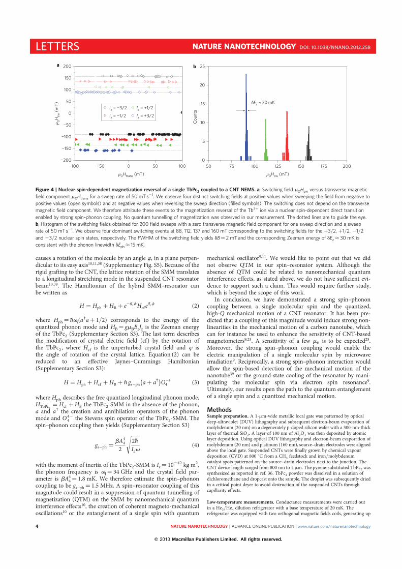
causes a rotation of the molecule by an angle w, in a plane perpen-dicular to its easy axis10,11,38 (Supplementary Fig. S5). Because of therigid grafting to the CNT, the lattice rotation of the SMM translatesto a longitudinal stretching mode in the suspended CNT resonatorbeam10,38. The Hamiltonian of the hybrid SMM–resonator canbe written as
H = Hph + HB + e−iJz wHcf eiJz w (2)
where Hph¼ hvl(a†aþ 1/2) corresponds to the energy of thequantized phonon mode and HB¼ gmBBzJz is the Zeeman energyof the TbPc2 (Supplementary Section S3). The last term describesthe modification of crystal electric field (cf) by the rotation ofthe TbPc2, where Hcf is the unperturbed crystal field and w isthe angle of rotation of the crystal lattice. Equation (2) can bereduced to an effective Jaynes–Cummings Hamiltonian(Supplementary Section S3):
H = Hph + Hcf + HB + h− gs−ph a + a†( )O−4
4 (3)
where Hph describes the free quantized longitudinal phonon mode,HTbPc2
= Hcf + HB the TbPc2-SMM in the absence of the phonon,a and a† the creation and annihilation operators of the phononmode and O 4
42 the Stevens spin operator of the TbPc2-SMM. Thespin–phonon coupling then yields (Supplementary Section S3)
gs−ph = bA44
2
2h−Izv
√(4)
with the moment of inertia of the TbPc2-SMM is Iz¼ 10242 kg m2,the phonon frequency is vl¼ 34 GHz and the crystal field par-ameter is bA4
4¼ 1.8 mK. We therefore estimate the spin–phononcoupling to be gs–ph¼ 1.5 MHz. A spin–resonator coupling of thismagnitude could result in a suppression of quantum tunnelling ofmagnetization (QTM) on the SMM by nanomechanical quantuminterference effects10, the creation of coherent magneto-mechanicaloscillations10 or the entanglement of a single spin with quantum
mechanical oscillator9,11. We would like to point out that we didnot observe QTM in our spin–resonator system. Although theabsence of QTM could be related to nanomechanical quantuminterference effects, as stated above, we do not have sufficient evi-dence to support such a claim. This would require further study,which is beyond the scope of this work.
In conclusion, we have demonstrated a strong spin–phononcoupling between a single molecular spin and the quantized,high-Q mechanical motion of a CNT resonator. It has been pre-dicted that a coupling of this magnitude would induce strong non-linearities in the mechanical motion of a carbon nanotube, whichcan for instance be used to enhance the sensitivity of CNT-basedmagnetometers9,25. A sensitivity of a few mB is to be expected25.Moreover, the strong spin–phonon coupling would enable theelectric manipulation of a single molecular spin by microwaveirradiation9. Reciprocally, a strong spin–phonon interaction wouldallow the spin-based detection of the mechanical motion of thenanotube39 or the ground-state cooling of the resonator by mani-pulating the molecular spin via electron spin resonance9.Ultimately, our results open the path to the quantum entanglementof a single spin and a quantized mechanical motion.
MethodsSample preparation. A 1-mm-wide metallic local gate was patterned by opticaldeep-ultraviolet (DUV) lithography and subsequent electron-beam evaporation ofmolybdenum (20 nm) on a degenerately p-doped silicon wafer with a 300-nm-thicklayer of thermal SiO2. A layer of 100 nm of Al2O3 was then deposited by atomiclayer deposition. Using optical DUV lithography and electron-beam evaporation ofmolybdenum (20 nm) and platinum (160 nm), source–drain electrodes were alignedabove the local gate. Suspended CNTs were finally grown by chemical vapourdeposition (CVD) at 800 8C from a CH4 feedstock and iron/molybdenumcatalyst spots patterned on the source–drain electrodes next to the junction. TheCNT device length ranged from 800 nm to 1 mm. The pyrene-substituted TbPc2 wassynthesized as reported in ref. 36. TbPc2 powder was dissolved in a solution ofdichloromethane and dropcast onto the sample. The droplet was subsequently driedin a critical point dryer to avoid destruction of the suspended CNTs throughcapillarity effects.
Low-temperature measurements. Conductance measurements were carried outin a He3/He4 dilution refrigerator with a base temperature of 20 mK. Therefrigerator was equipped with two orthogonal magnetic fields coils, generating up
μ0Hsw (mT)
μ 0H
sw (m
T)
μ0Htrans (mT)
a b
−100 −50 0 50 100−200
−150
−100
−50
0
50
100
150
200
50 75 100 125 150 175 2000
5
10
15
20
25
Cou
nts
δEz ≈ 30 mKIz = −3/2 Iz = +1/2
Iz = −1/2 Iz = +3/2
Figure 4 | Nuclear spin-dependent magnetization reversal of a single TbPc2 coupled to a CNT NEMS. a, Switching field m0Hsw versus transverse magnetic
field component m0Htrans for a sweep rate of 50 mT s21. We observe four distinct switching fields at positive values when sweeping the field from negative to
positive values (open symbols) and at negative values when reversing the sweep direction (filled symbols). The switching does not depend on the transverse
magnetic field component. We therefore attribute these events to the magnetization reversal of the Tb3þ ion via a nuclear spin-dependent direct transition
enabled by strong spin–phonon coupling. No quantum tunnelling of magnetization was observed in our measurement. The dotted lines are to guide the eye.
b, Histogram of the switching fields obtained for 200 field sweeps with a zero transverse magnetic field component for one sweep direction and a sweep
rate of 50 mT s21. We observe four dominant switching events at 88, 112, 137 and 160 mT corresponding to the switching fields for the þ3/2, þ1/2, 21/2
and 23/2 nuclear spin states, respectively. The FWHM of the switching field yields dB¼ 2 mT and the corresponding Zeeman energy of dEz ≈ 30 mK is
consistent with the phonon linewidth dEph ≈ 15 mK.
LETTERS NATURE NANOTECHNOLOGY DOI: 10.1038/NNANO.2012.258
NATURE NANOTECHNOLOGY | ADVANCE ONLINE PUBLICATION | www.nature.com/naturenanotechnology4
© 2013 Macmillan Publishers Limited. All rights reserved.
to 1.4 T and 0.5 T respectively for both coils, in the plane of the sample, with amaximum sweep rate of 250 mT s21. We could orient the field direction with respectto the easy axis of the TbPc2-SMM by probing the magnetization reversal at differentmagnetic field angles (Supplementary Section S1). The field sweep rate andtemperature dependences of the switching fields are presented in SupplementarySection S2. The transport measurements were made with an ADWIN real-time dataacquisition system.
Received 7 September 2012; accepted 11 December 2012;published online 3 February 2013
References1. Abragam, A. & Bleaney, B. Electron Paramagnetic Resonance of Transition Ions
(Oxford Univ. Press, 1970).2. Heitler, W. & Teller, E. Time effects in the magnetic cooling method.
Proc. R. Soc. Lond. A 155, 629–639 (1936).3. Van Vleck, J. H. Paramagnetic relaxation times for titanium and chrome alum.
Phys. Rev. 57, 426–447 (1940).4. Gatteschi, D., Sessoli, R. & Villain, J. Molecular Nanomagnets (Oxford Univ.
Press, 2006).5. Villain, J., Hartman-Boutron, F., Sessoli, R. & Rettori, A. Magnetic relaxation in
big magnetic molecules. Europhys. Lett. 27, 159–164 (1994).6. Garanin, D. A. & Chudnosvky, E. M. Thermally activated resonant
magnetization tunneling in molecular magnets: Mn12Ac and others. Phys. Rev. B56, 011102 (1997).
7. Leuenberger, M. & Loss, D. Spin relaxation in Mn12-acetate. Europhys. Lett.46, 692–699 (1999).
8. Sessoli, R., Gatteschi, D., Caneschi, A. & Novak, N. A. Magnetic bistabilityof a metal-ion cluster. Nature 365, 141–144 (1993).
9. Palyi, A., Struck, P. R., Rudner, M., Flensberg, K. & Burkard, G. Spin–orbit-induced strong coupling of a single spin to a nanomechanical resonator.Phys. Rev. Lett. 108, 206811 (2012).
10. Kovalev, A., Hayden, L., Bauer, G. & Tscherkovniak, Y. Macrospin tunneling andmagneto-polaritons with nanomechanical interference. Phys. Rev. Lett. 106,147203 (2011).
11. Garanin, D. A. & Chudnovsky, E. Quantum entanglement of a tunneling spinwith mechanical modes of a torsional resonator. Phys. Rev. X 1, 011005 (2011).
12. Laird, E., Pei, F., Tang, W., Steele, G. A. & Kouwenhoven L. P. A highquality factor carbon nanotube mechanical resonator at 39 GHz. Nano Lett.12, 193–197 (2011).
13. Peng, H. B., Chang, C. W., Aloni, S., Yuzvinsky, T. D. & Zettl, A. Ultrahighfrequency nanotube resonator. Phys. Rev. Lett. 97, 087203 (2006).
14. Sapmaz, S., Jarillo-Herrero, P., Blanter, Y. M., Dekker, C. & van der Zant, H. S. J.Tunneling in suspended carbon nanotubes assisted by longitudinal phonons.Phys. Rev. Lett. 96, 026801 (2006).
15. Huettel, A., Witkamp, B., Leijnse, M., Wegewijs, M. R. & van der Zant, H. S. J.Pumping of vibrational excitations in the Coulomb-blockade regime in asuspended carbon nanotube. Phys. Rev. Lett. 102, 225501 (2009).
16. Leturcq, R. et al. Franck–Condon blockade in suspended carbon nanotubequantum dots. Nature Phys. 5, 327–331 (2009).
17. Poot, M. & van der Zant, H. S. J. Mechanical systems in the quantum regime.Phys. Rep. 511, 273–335 (2011).
18. Ganzhorn, M. & Wernsdorfer, W. Dynamics and dissipation induced by singleelectron tunneling in carbon nanotube nanoelectromechanical system.Phys. Rev. Lett. 108, 175502 (2012).
19. Lassagne, B., Tarakanov, Y., Kinaret, J., Garcia-Sanchez, D. & Bachthold, A.Coupling mechanics to charge transport in carbon nanotube mechanicalresonators. Science 325, 1107–1110 (2009).
20. Steele, G. et al. Strong coupling between single electron tunneling andnanomechanical motion. Science 325, 1103–1107 (2009).
21. Huttel, A. K. Carbon nanotubes as ultrahigh quality factor mechanicalresonators. Nano Lett. 9, 2547–2552 (2009).
22. Lassagne, A., Garcia-Sanchez, D., Aguasca, A. & Bachtold, A. Ultrasensitivemass sensing with a nanotube electromechanical resonator. Nano Lett. 8,3735–3738 (2008).
23. Chiu, H., Hung, P., Postma, H. W. Ch. & Bockrath, M. Atomic scale masssensing using carbon nanotube resonators. Nano Lett. 8, 4342–4346 (2008).
24. Jensen, K., Kim, K. & Zettl, A. An atomic-resolution nanomechanical masssensor. Nature Nanotech. 3, 533–556 (2008).
25. Lassagne, B., Ugnati, D. & Respaud, M. Ultrasensitive magnetometers based oncarbon nanotube mechanical resonators. Phys. Rev. Lett. 107, 130801 (2011).
26. Bogani, L. & Wernsdorfer, W. Molecular spintronics using single-moleculemagnets. Nature Mater. 7, 179–186 (2008).
27. Heersche, H. et al. Electron transport through single Mn12 molecular magnets.Phys. Rev. Lett. 96, 206801 (2006).
28. Zyazin, A. S. et al. Electric field controlled magnetic anisotropy in a singlemolecule. Nano Lett. 10, 3307–3311 (2010).
29. Vincent, R., Klyatskaya, S., Ruben, M., Wernsdorfer, W. & Balestro, F. Electronicreadout of a single nuclear spin in a single molecule transistor. Nature 488,357–360 (2012).
30. Urdampilleta, M., Cleuziou, J-P., Klyatskaya, S., Ruben, M. & Wernsdorfer, W.Supramolecular spin valves. Nature Mater. 10, 502–506 (2011).
31. Friedman, J. R., Sarachik, M. P., Tejada, J. & Ziolo, R. Macroscopic measurementof resonant magnetization tunnelling in high-spin molecules. Phys. Rev. Lett. 76,3830–3833 (1996).
32. Thomas, L. et al. Macroscopic quantum tunnelling of magnetization in a singlecrystal of nanomagnets. Nature 383, 145–147 (1996).
33. Wernsdorfer, W. & Sessoli, R. Quantum phase interference and parity effects inmagnetic molecular clusters. Science 284, 133–135 (1999).
34. Takahashi, S. et al. Coherent manipulation and decoherence of S¼10single-molecule magnet. Phys. Rev. Lett. 102, 087603 (2009).
35. Ishikawa, N., Sugita, M. & Wernsdorfer, W. Quantum tunneling ofmagnetization in lanthanide single-molecule magnets:bis(phthalocyaninato)terbium and bis(phthalocyaninato)dysprosium anions.Angew. Chem. Int. Ed. 44, 2931–2935 (2005).
36. Kyatskaya, S. et al. Anchoring of rare-earth-based single-molecule magnets onsingle-walled carbon nanotubes. J. Am. Chem. Soc. 131, 15143–15151 (2009).
37. Lopes, M. et al. Surface-enhanced Raman signal for terbium single-moleculemagnets grafted on graphene. ACS Nano 4, 7531–7536 (2010).
38. Chudnovsky, E., Garanin, D. A. & Schilling, R. Universal mechanism of spinrelaxation in solids. Phys. Rev. B 72, 094426 (2005).
39. Ohm, C., Stampfer, C., Splettstoesser, J. & Wegewijs, M. R. Readout of carbonnanotube vibrations based on spin–phonon coupling. Appl. Phys. Lett. 100,143103 (2012).
AcknowledgementsThe authors thank E. Eyraud, D. Lepoittevin, L. Cagnon, R. Haettel, C. Hoarau, V. Reitaand P. Rodiere for technical contributions and discussions, T. Fournier, T. Crozes,B. Fernandez, S. Dufresnes and G. Julie for lithography development, and J.P. Cleuziou andN.V. Nguyen for CNT CVD growth development. The authors also thank E. Bonet,C. Thirion and R. Piquerel for help with software development and M. Urdampilleta,S. Thiele, R. Vincent and F. Balestro for fruitful discussions. Samples were fabricated in theNanofab facility of the Neel Institute. This work is partially supported by the FrenchNational Research Agency National Programme in Nanosciences and Nanotechnologies(ANR-PNANO) project MolNanoSpin (no. ANR-08-NANO-002), European ResearchCouncil Advanced Grant MolNanoSpin (no. 226558), ICT-2007.8.0 Future EmergingTechnologies Open, Quantum Information Processing Specific Targeted ResearchProject (no. 211284 MolSpinQIP), the German Research Foundation programme TRR 88‘3Met’, Cible 2009, and the Nanosciences Foundation of Grenoble. M.G. thanks theNanoscience Foundation for financial support.
Author contributionsM.G. and W.W. designed, conducted and analysed the experiments. S.K. and M.R.designed, synthesized and characterized the molecule. M.G. and W.W. co-wrote the paper.
Additional informationSupplementary information is available in the online version of the paper. Reprints andpermission information is available online at http://www.nature.com/reprints. Correspondenceand requests for materials should be addressed to W.W.
Competing financial interestsThe authors declare no competing financial interests.
NATURE NANOTECHNOLOGY DOI: 10.1038/NNANO.2012.258 LETTERS
NATURE NANOTECHNOLOGY | ADVANCE ONLINE PUBLICATION | www.nature.com/naturenanotechnology 5
© 2013 Macmillan Publishers Limited. All rights reserved.

195