Embed Size (px)
Citation preview
111
SRI CHANDRASEKHARENDRA SARASWATHI VISWA MAHAVIDYALAYA(University established under section 3 of UGC Act 1956) (Accredited
With ‘A’ Grade by NAAC)
DEPARTMENT OF ELECTRONICS AND COMMUNICATION ENGINEERING
COURSE MATERIAL
Prepared By:Dr.P.VENKATESAN,
Associate Professor, ECESCSVMV, Kanchipuram
DIGITAL SIGNAL PROCESSINGV SEMESTER - B.E (ECE)
during the academic year 2020-2021
DIGITAL SIGNAL PROCESSING
PRE-REQUISITE:
Signal & Systems, Digital System Design, Engineering Mathematics
AIM & OBJECTIVES:
To learn discrete Fourier transform, properties of DFT and its application to
linear filtering.
To understand the characteristics of digital filters, design digital FIR filters
and apply these filters to filter undesirable signals in various frequency
bands.
To design digital IIR filters and apply these filters to filter undesirable
signals in various frequency bands.
To understand the effects of finite precision representation on digital filters.
To understand the fundamental concepts of multi-rate signal processing and
its applications.

UNIT I DISCRETE FOURIER TRANSFORM
Review of discrete-time signals and systems – Discrete Fourier Transform (DFT) and its
properties, Circular convolution, Linear filtering using DFT, Filtering long data sequences -
overlap-save methods - Overlap-add, Fast Fourier Transform (FFT) algorithms – Fast
computation of DFT –Radix- 2 decimation in time FFT - Decimation in frequency FFT – Linear
filtering using FFT.
UNIT II DESIGN OF FINITE IMPULSE RESPONSE FILTERS
Structures for FIR systems – Transversal and Linear phase structures, Design of FIR filters –
Symmetric and Anti-symmetric FIR filters, Design of linear phase FIR filters using Windows
(Rectangular, Hamming and Hanning windows) and Frequency sampling methods
UNIT III DESIGN OF INFINITE IMPULSE RESPONSE FILTERS
Structures for IIR systems – direct, cascade, parallel forms, Comparison of FIR and IIR, Analog
filters – Butterworth filters - Chebyshev type – I filters (upto 3rd order), Analog transformation
of prototype LPF to BPF/BSF/HPF, Transformation of analog filters into equivalent digital
filters using Impulse invariant method and Bilinear Z-transform method.
UNIT IV FINITE WORD LENGTH EFFECTS
Representation of fixed and floating point numbers, ADC quantization -truncation and rounding
- quantization noise, Coefficient quantization Error – Product quantization error – Overflow error
- Round-off noise power, Limit cycle oscillation due to product round-off error- Limit cycle
oscillation due to overflow in digital filters – Principle of scaling.
UNIT V MULTI-RATE SIGNAL PROCESSING
Introduction to multi-rate signal processing – Decimation – Interpolation- Sampling rate
conversion by a rational factor - Polyphase decomposition of FIR filter – Multistage
implementation of sampling rate conversion – Design of narrow band filters–Applications of
multi-rate signal processing
UNIT -1
INTRODUCTION
REVIEW OF DISCRETE TIME SIGNALS AND SYSTEMS
Anything that carries some information can be called as signals. Some examples are ECG,
EEG, ac power, seismic, speech, interest rates of a bank, unemployment rate of a country,
temperature, pressure etc.
A signal is also defined as any physical quantity that varies with one or more independent variables.
A discrete time signal is the one which is not defined at intervals between two successive samples
of a signal. It is represented as graphical, functional, tabular representation and sequence.
Some of the elementary discrete time signals are unit step, unit impulse, unit ramp, exponential
and sinusoidal signals (as you read in signals and systems).
Classification of discrete time signals
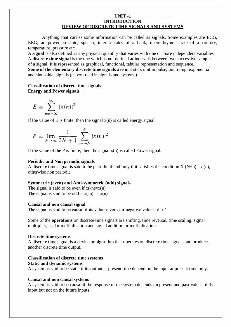
Energy and Power signals
If the value of E is finite, then the signal x(n) is called energy signal.
If the value of the P is finite, then the signal x(n) is called Power signal.
Periodic and Non periodic signals
A discrete time signal is said to be periodic if and only if it satisfies the condition X (N+n) =x (n),
otherwise non periodic
Symmetric (even) and Anti-symmetric (odd) signals
The signal is said to be even if x(-n)=x(n)
The signal is said to be odd if x(-n)= - x(n)
Causal and non causal signal
The signal is said to be causal if its value is zero for negative values of ‘n’.
Some of the operations on discrete time signals are shifting, time reversal, time scaling, signal
multiplier, scalar multiplication and signal addition or multiplication.
Discrete time systems
A discrete time signal is a device or algorithm that operates on discrete time signals and produces
another discrete time output.
Classification of discrete time systems
Static and dynamic systems
A system is said to be static if its output at present time depend on the input at present time only.
Causal and non causal systems
A system is said to be causal if the response of the system depends on present and past values of the
input but not on the future inputs.
Linear and non linear systems
A system is said to be linear if the response of the system to the weighted sum of inputs should be
equal to the corresponding weighted sum of outputs of the systems. This principle is called
superposition principle.
Time invariant and time variant systems
A system is said to be time invariant if the characteristics of the systems do not change with time.
Stable and unstable systems
A system is said to be stable if bounded input produces bounded output only.
TIME DOMAIN ANALYSIS OF DISCRETE TIME SIGNALS AND SYSTEMS
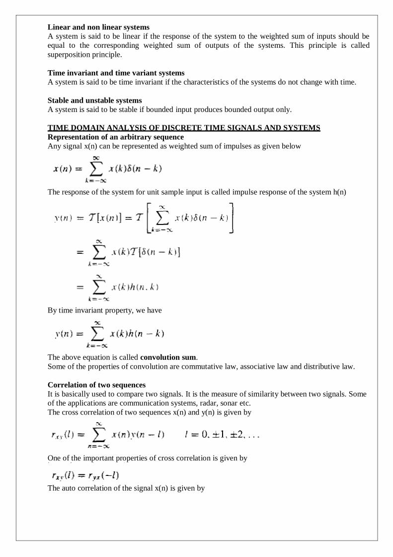
Representation of an arbitrary sequence
Any signal x(n) can be represented as weighted sum of impulses as given below
The response of the system for unit sample input is called impulse response of the system h(n)
By time invariant property, we have
The above equation is called convolution sum.
Some of the properties of convolution are commutative law, associative law and distributive law.
Correlation of two sequences
It is basically used to compare two signals. It is the measure of similarity between two signals. Some
of the applications are communication systems, radar, sonar etc.
The cross correlation of two sequences x(n) and y(n) is given by
One of the important properties of cross correlation is given by
The auto correlation of the signal x(n) is given by
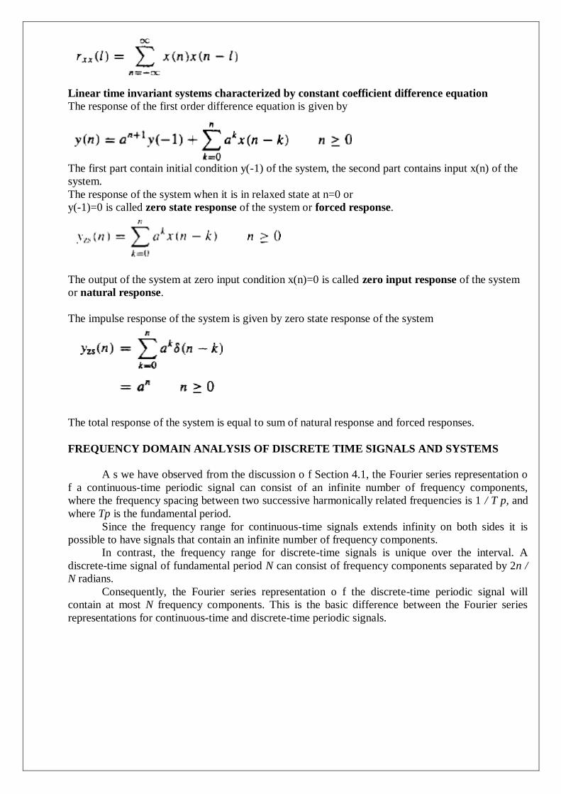
Linear time invariant systems characterized by constant coefficient difference equation
The response of the first order difference equation is given by
The first part contain initial condition y(-1) of the system, the second part contains input x(n) of the
system.
The response of the system when it is in relaxed state at n=0 or
y(-1)=0 is called zero state response of the system or forced response.
The output of the system at zero input condition x(n)=0 is called zero input response of the system
or natural response.
The impulse response of the system is given by zero state response of the system
The total response of the system is equal to sum of natural response and forced responses.
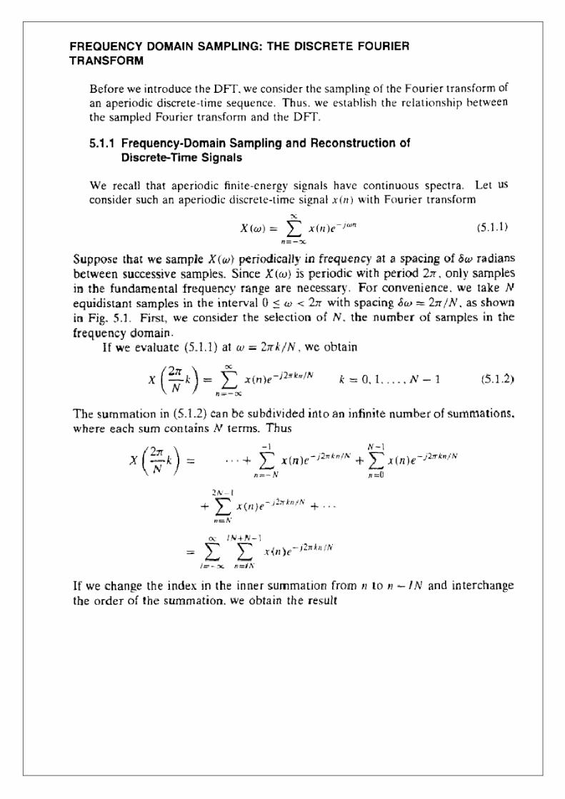
FREQUENCY DOMAIN ANALYSIS OF DISCRETE TIME SIGNALS AND SYSTEMS
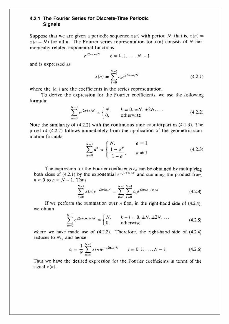
A s we have observed from the discussion o f Section 4.1, the Fourier series representation o
f a continuous-time periodic signal can consist of an infinite number of frequency components,
where the frequency spacing between two successive harmonically related frequencies is 1 / T p, and
where Tp is the fundamental period.
Since the frequency range for continuous-time signals extends infinity on both sides it is
possible to have signals that contain an infinite number of frequency components.
In contrast, the frequency range for discrete-time signals is unique over the interval. A
discrete-time signal of fundamental period N can consist of frequency components separated by 2n /
N radians.
Consequently, the Fourier series representation o f the discrete-time periodic signal will
contain at most N frequency components. This is the basic difference between the Fourier series
representations for continuous-time and discrete-time periodic signals.
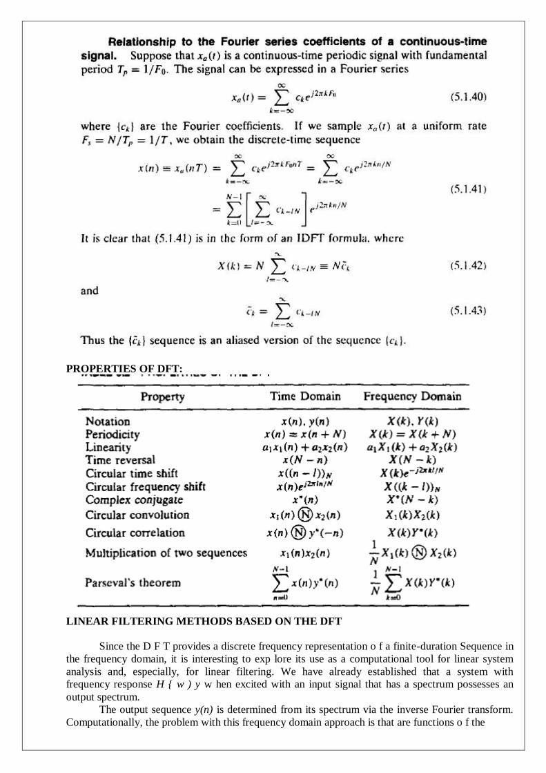
PROPERTIES OF DFT:
LINEAR FILTERING METHODS BASED ON THE DFT
Since the D F T provides a discrete frequency representation o f a finite-duration Sequence in
the frequency domain, it is interesting to exp lore its use as a computational tool for linear system
analysis and, especially, for linear filtering. We have already established that a system with
frequency response H { w ) y w hen excited with an input signal that has a spectrum possesses an
output spectrum.
The output sequence y(n) is determined from its spectrum via the inverse Fourier transform.
Computationally, the problem with this frequency domain approach is that are functions o f the
continuous variable. As a consequence, the computations cannot be done on a digital computer, since
the computer can only store and perform computations on quantities at discrete frequencies.
On the other hand, the DFT does lend itself to computation on a digital computer. In the discussion
that follows, we describe how the DFT can be used to perform linear filtering in the frequency
domain. In particular, we present a computational procedure that serves as an alternative to time-
domain convolution.
In fact, the frequency-domain approach based on the DFT, is computationally m ore efficient
than time-domain convolution due to the existence of efficient algorithms for computing the DFT .
These algorithms, which are described in Chapter 6, are collectively called fast Fourier transform
(FFT) algorithms.
In this section we represent several methods for computing dft efficiently. In view of the
importance of the DFT in various digital signal processing applications such as linear filtering,
correlation analysis and spectrum analysis, its efficient computation is a topic that has received
considerably attention by many mathematicians, engineers and scientists. Basically the computation
is done using the formula method.
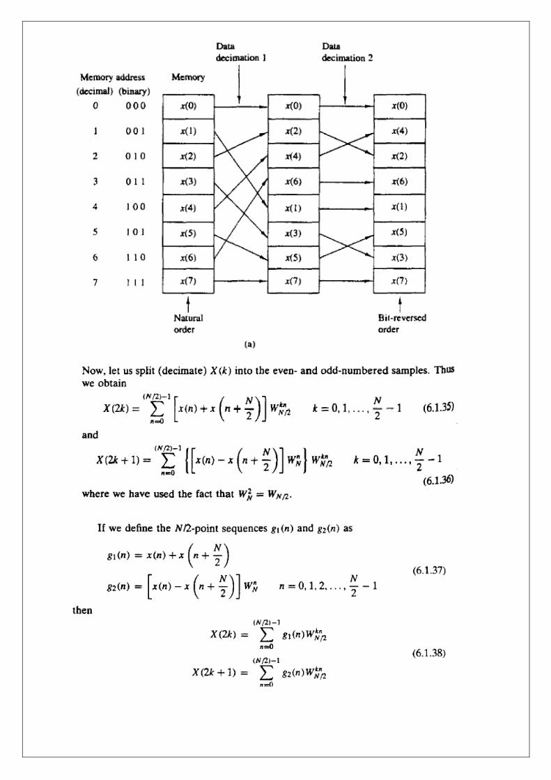
Divide-and-Conquer Approach to Computation of the DFT
The development of computationally efficient algorithms for the DFT is made possible if we
adopt a divide-and-conquer approach. This approach is based on the decomposition of an N-point
DFT into successively smaller DFT. This basic approach leads to a family o f computationally
efficient algorithm s know n collectively as FFT algorithms.
FAST FOURIER TRANSFORM
EFFICIENT COMPUTATION OF DFT:
T o illustrate the basic notions, let us consider the computation of an N point DFT , where N can be
factored as a product of two integers, that is, N = L M
An additional factor of 2 savings in storage of twiddle factors can be obtained by introducing
a 90° phase offset at the mid point of each twiddle array , which can be removed if necessary at the
ouput of the SRFFT computation. The incorporation of this improvement into the SRFFT results in
an other algorithm also due to price called the PFFT algorithm.
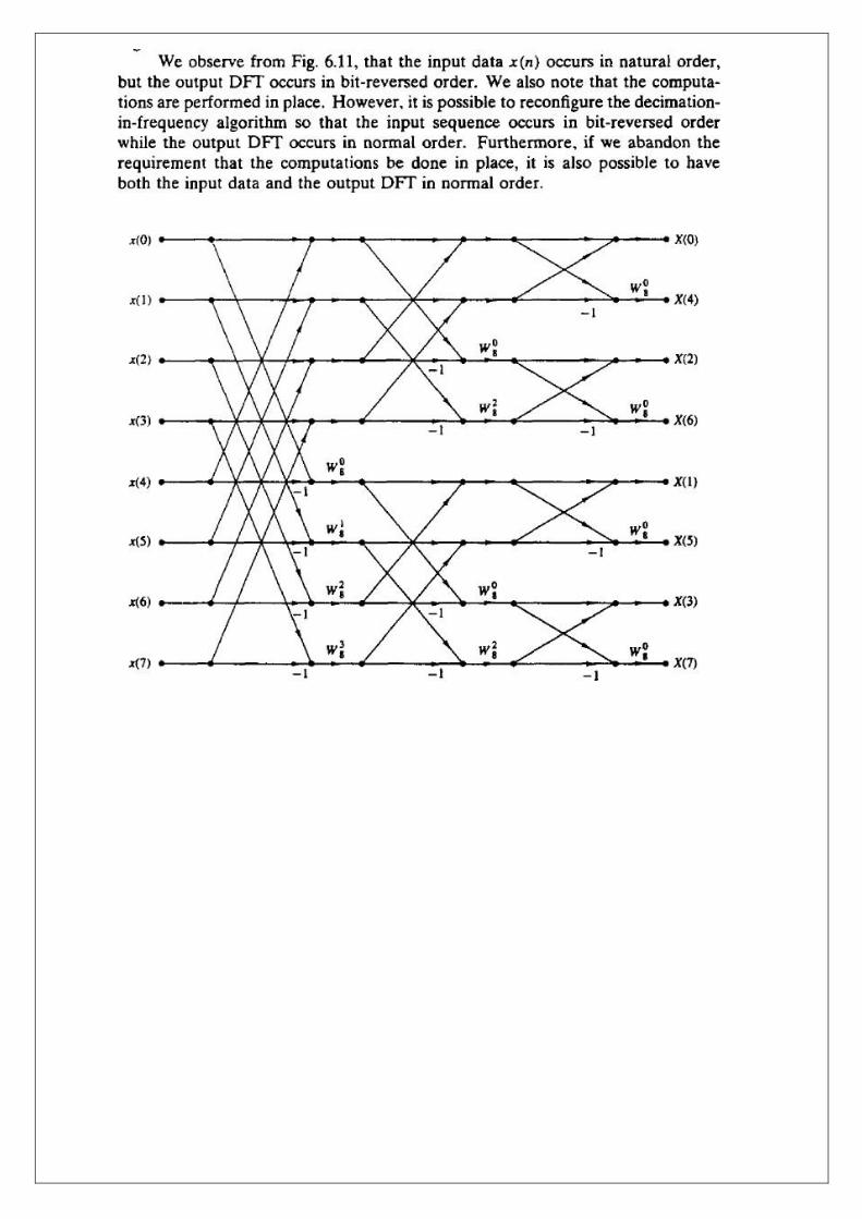
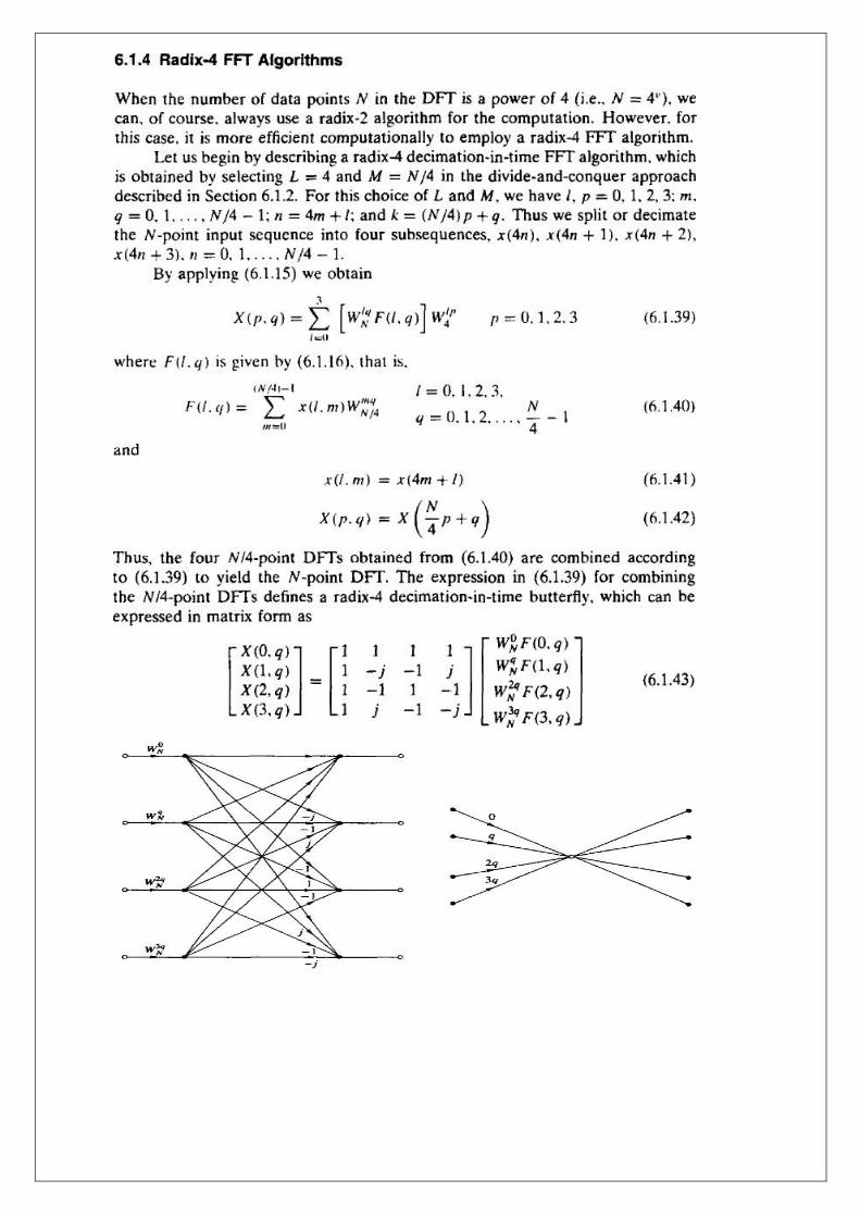
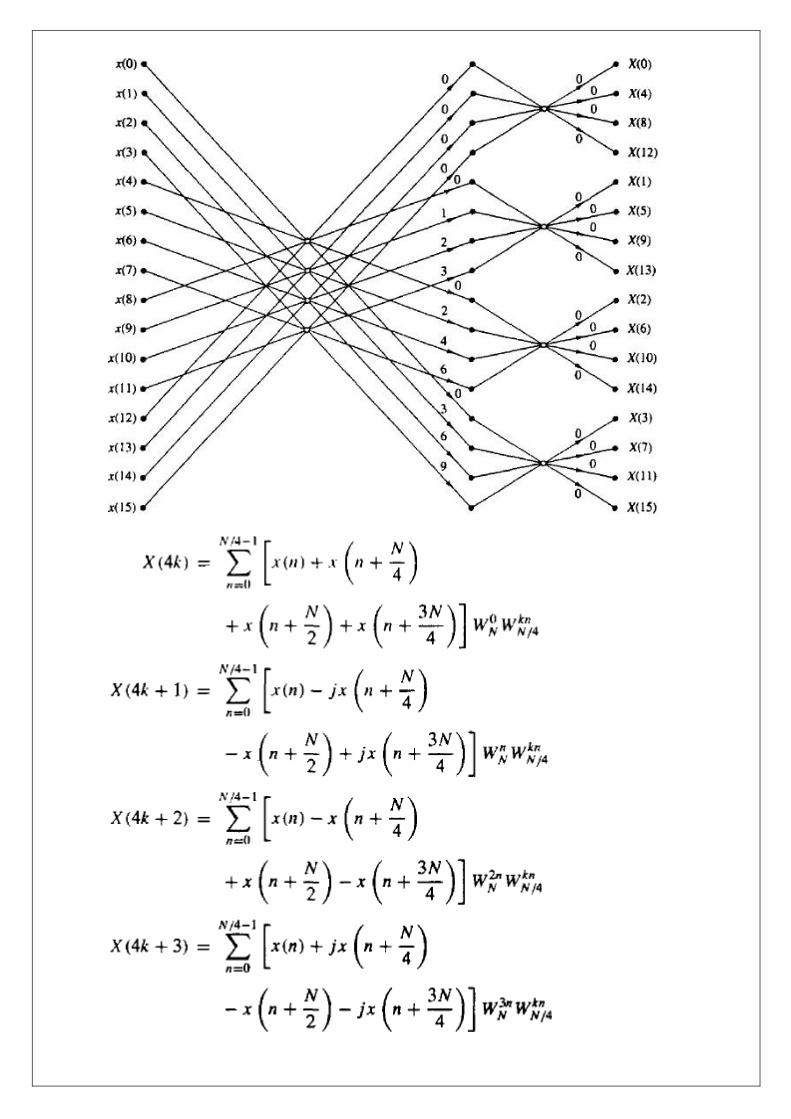
Implementation of FFT Algorithms
Now that w e has described the basic radix-2 and radix -4 F FT algorithm s, let us consider
some of the implementation issues. Our remarks apply directly to
STRUCTURES FOR THE REALIZATION OF DISCRETE-TIME SYSTEMS
The major factors that influence our choice o f a specific realization are computational complexity,
memory requirements, and finite-word-length effects in the computations.
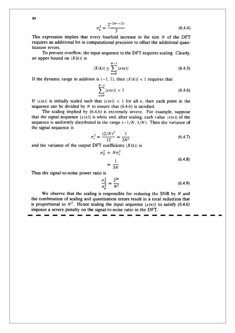
STRUCTURES FOR FIR SYSTEMS
Direct-Form Structure
The direct form realization follows immediately from the non recursive difference equation given
below
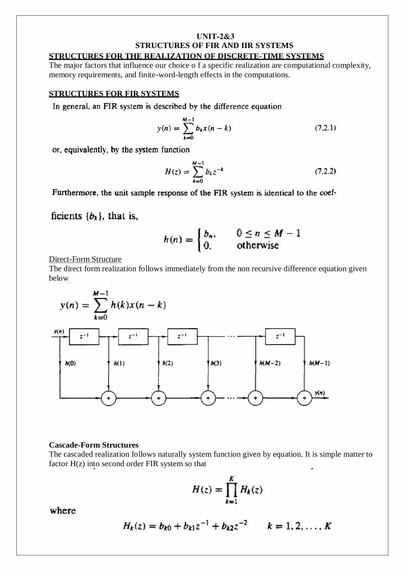
Cascade-Form Structures
The cascaded realization follows naturally system function given by equation. It is simple matter to
factor H(z) into second order FIR system so that
UNIT-2&3STRUCTURES OF FIR AND IIR SYSTEMS
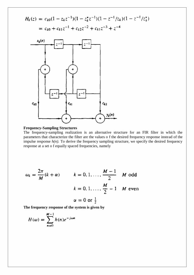
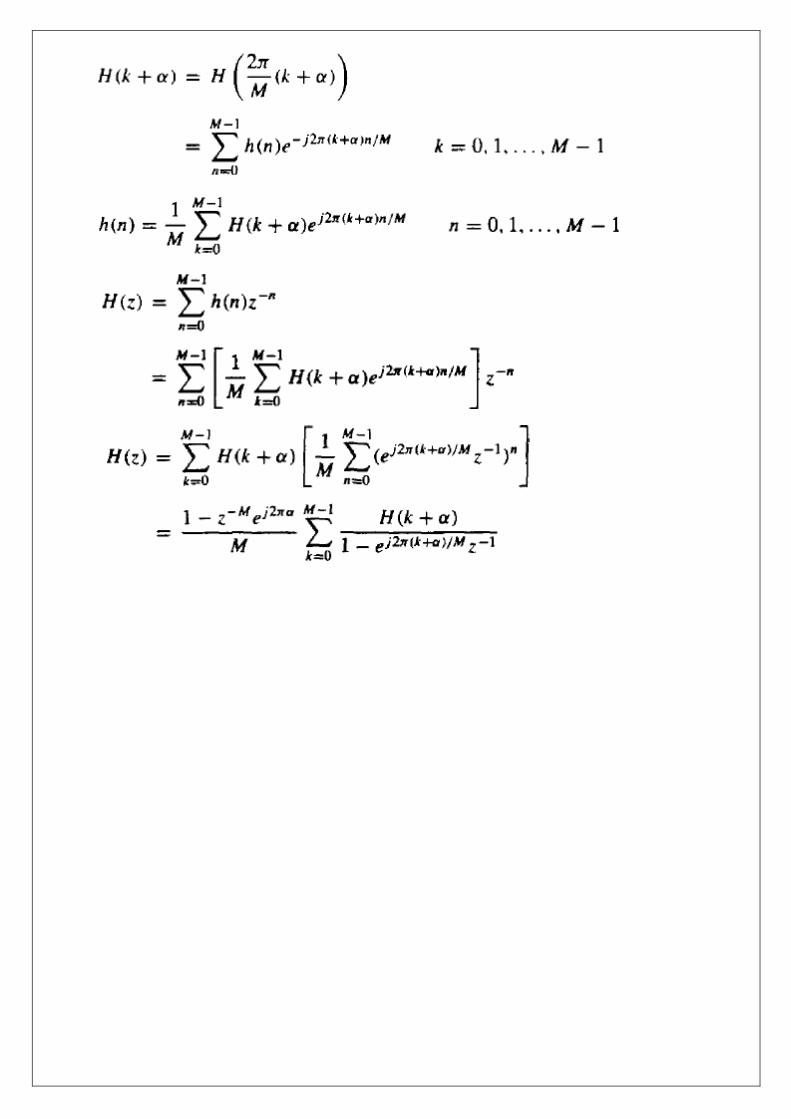
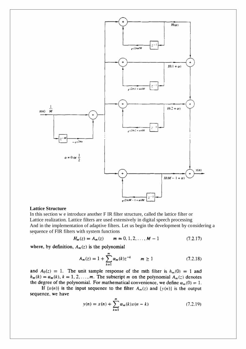
Frequency-Sampling Structures
The frequency-sampling realization is an alternative structure for an FIR filter in which the
parameters that characterize the filter are the values o f the desired frequency response instead of the
impulse response h(n). To derive the frequency sampling structure, we specify the desired frequency
response at a set o f equally spaced frequencies, namely
The frequency response of the system is given by
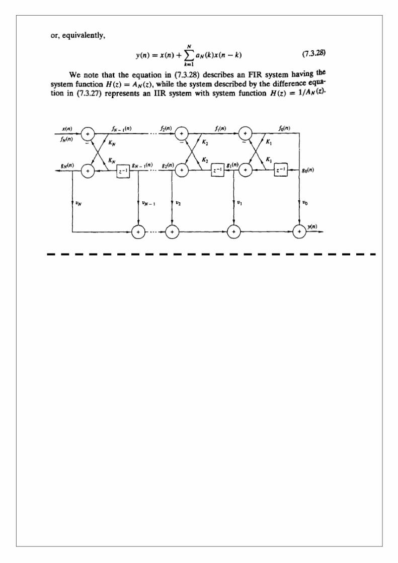
Lattice Structure
In this section w e introduce another F IR filter structure, called the lattice filter or
Lattice realization. Lattice filters are used extensively in digital speech processing
And in the implementation of adaptive filters. Let us begin the development by considering a
sequence of FIR filters with system functions
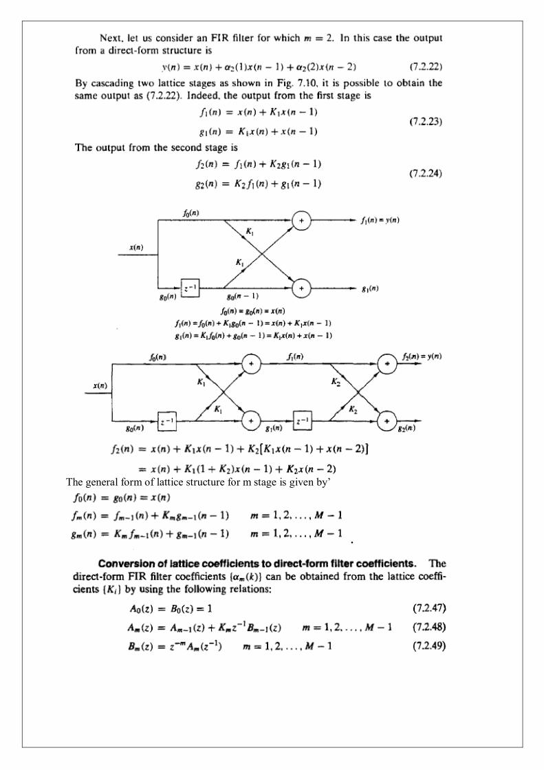
The general form of lattice structure for m stage is given by’
.
STRUCTURES FOR IIR SYSTEMS
In this section we consider different IIR system s structures described by the difference equation
given by the system function. Just as in the case o f FIR system s, there are several types o f
structures or realizations, including direct-form structures, cascade-form structures, lattice structures,
and lattice-ladder structures. In addition, IIR systems lend them selves to a parallel form realization.
We begin by describing two direct-form realizations.
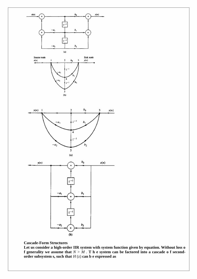
DIRECT FORM STRUCTURES:
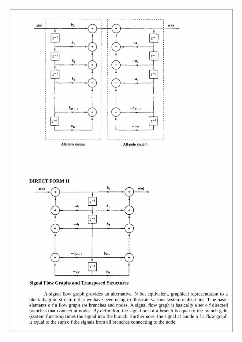
DIRECT FORM II
Signal Flow Graphs and Transposed Structures
A signal flow graph provides an alternative, N but equivalent, graphical representation to a
block diagram structure that we have been using to illustrate various system realizations. T he basic
elements o f a flow graph are branches and nodes. A signal flow graph is basically a set o f directed
branches that connect at nodes. By definition, the signal out of a branch is equal to the branch gain
(system function) times the signal into the branch. Furthermore, the signal at anode o f a flow graph
is equal to the sum o f the signals from all branches connecting to the node.
Cascade-Form Structures
Let us consider a high-order IIR system with system function given by equation. Without loss o
f generality we assume that N > M . T h e system can be factored into a cascade o f second-
order subsystem s, such that H (z) can b e expressed as
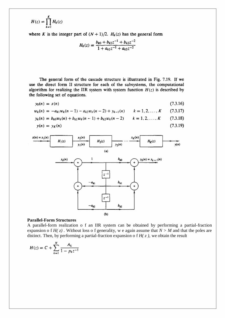
Parallel-Form Structures
A parallel-form realization o f an IIR system can be obtained by performing a partial-fraction
expansion o f H( z) . Without loss o f generality, w e again assume that N > M and that the poles are
distinct. Then, by performing a partial-fraction expansion o f H( z ), we obtain the result
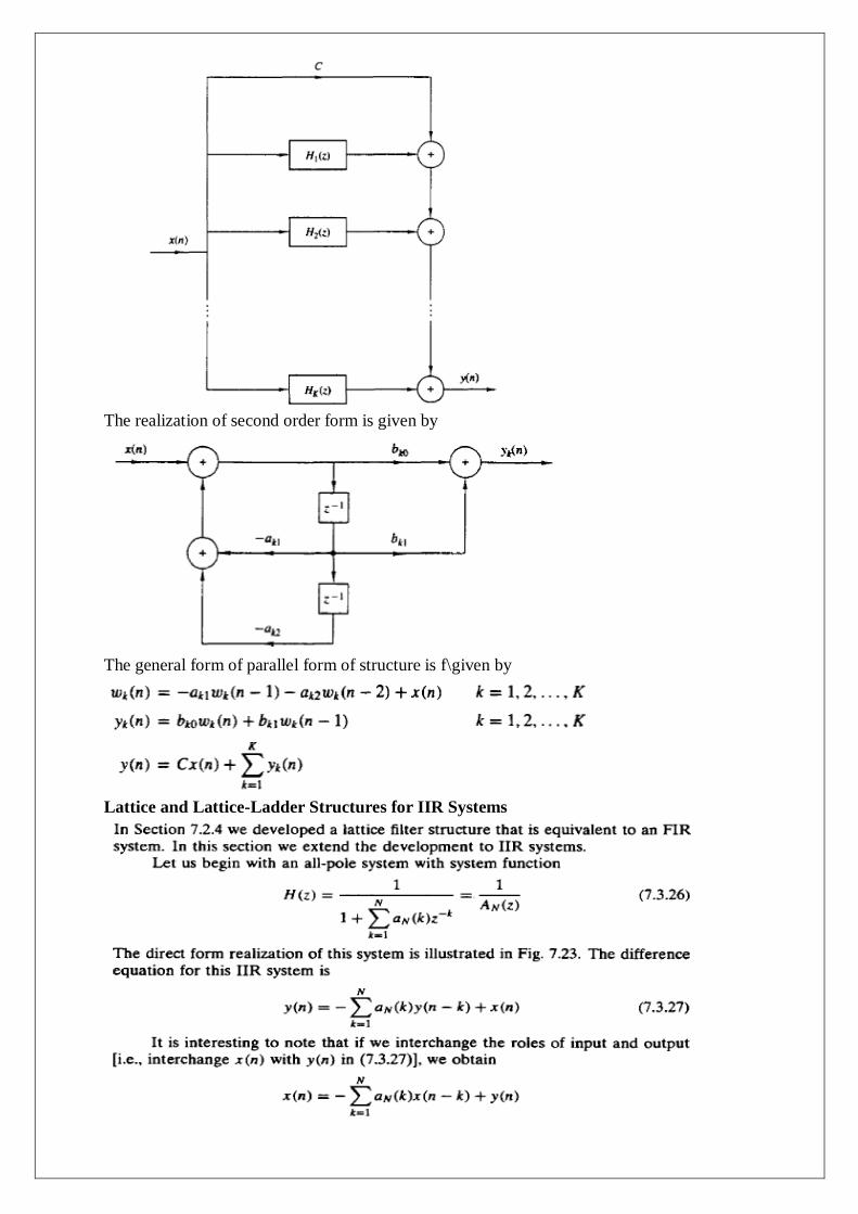
The realization of second order form is given by
The general form of parallel form of structure is f\given by
Lattice and Lattice-Ladder Structures for IIR Systems
The transfer function is obtained by taking Z transform of finite sample impulse response. The filters
designed by using finite samples of impulse response are called FIR filters.
Some of the advantages of FIR filter are linear phase, both recursive and non recursive, stable and
round off noise can be made smaller.
Some of the disadvantages of FIR filters are large amount of processing is required and non integral
delay may lead to problems.
DESIGN OF FIR FILTERS
IIR AND FIR FILTERS
IIR FILTER DESIGN
************************************************************************

UNIT - IV
FINITE WORD LENGTH EFFECTS IN DIGITAL FILTER
Finite Word length Effects: In the design of FIR Filters, The filter coefficients are determined by the system transfer functions. These
filter co-efficient are quantized/truncated while implementing DSP System because of finite length registers. Only Finite numbers of bits are used to perform arithmetic operations. Typical word length is 16 bits,
24 bits, 32 bits etc. This finite word length introduces an error which can affect the performance of the DSP system. The main errors are
1. Input quantization error2. Co-efficient quantization error3. Overflow & round off error (Product Quantization error)
The effect of error introduced by a signal process depend upon number of factors including the1. Type of arithmetic2. Quality of input signal3. Type of algorithm implemented
1. Input quantization error The conversion of continuous-time input signal into digital value produces an error which is known as
input quantization error.
This error arises due to the representation of the input signal by a fixed number of digits in A/Dconversion process.
2. Co-efficient quantization error The filter coefficients are compared to infinite precision. If they are quantized the frequency response of
the resulting filter may differ from the desired frequency response.i.e poles of the desired filter may change leading to instability.
3. Product Quantization error It arises at the output of the multiplier When a ‘b’ bit data is multiplied with another ‘b’ bit coefficient the product (‘2b’ bits) should be stored
in ‘b’ bits register. The multiplier Output must be rounded or truncated to ‘b’ bits. This known asoverflow and round off error.
*****************************************************************************************Types of number representation:There are two common forms that are used to represent the numbers in a digital or any other digital hardware.
1. Fixed point representation2. Floating point representation
* Explain the various formulas of the fixed point representation of binary numbers.1. Fixed point representation In the fixed point arithmetic, the position of the binary point is fixed. The bit to the right represents the
fractional part of the number and to those to the left represents the integer part.
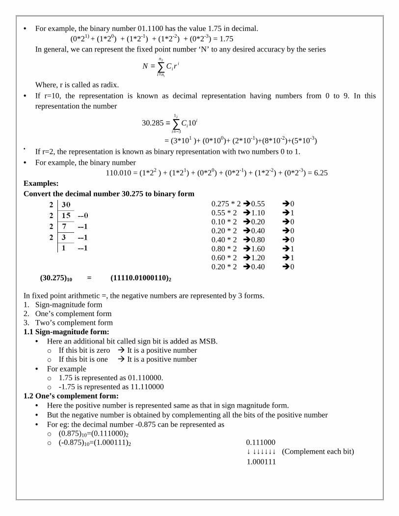
For example, the binary number 01.1100 has the value 1.75 in decimal.(0*21) + (1*20) + (1*2-1) + (1*2-2) + (0*2-3) = 1.75
In general, we can represent the fixed point number ‘N’ to any desired accuracy by the series
2n
ni
ii
i
rCN
Where, r is called as radix.
If r=10, the representation is known as decimal representation having numbers from 0 to 9. In thisrepresentation the number
285.30
21
3
10i
iiC
= (3*101 )+ (0*100)+ (2*10-1)+(8*10-2)+(5*10-3) If r=2, the representation is known as binary representation with two numbers 0 to 1.
For example, the binary number110.010 = (1*22 ) + (1*21) + (0*20) + (0*2-1) + (1*2-2) + (0*2-3) = 6.25
Examples:Convert the decimal number 30.275 to binary form
(30.275)10 = (11110.01000110)2
0.275 * 20.55 00.55 * 2 1.10 10.10 * 2 0.20 00.20 * 2 0.40 00.40 * 2 0.80 00.80 * 2 1.60 10.60 * 2 1.20 10.20 * 2 0.40 0
In fixed point arithmetic =, the negative numbers are represented by 3 forms.1. Sign-magnitude form2. One’s complement form3. Two’s complement form1.1 Sign-magnitude form:
Here an additional bit called sign bit is added as MSB.o If this bit is zero It is a positive numbero If this bit is one It is a positive number
For exampleo 1.75 is represented as 01.110000.o -1.75 is represented as 11.110000
1.2 One’s complement form: Here the positive number is represented same as that in sign magnitude form. But the negative number is obtained by complementing all the bits of the positive number For eg: the decimal number -0.875 can be represented as
o (0.875)10=(0.111000)2
o (-0.875)10=(1.000111)2 0.111000↓ ↓↓↓↓↓↓ (Complement each bit)1.000111
1.3 Two’s complement form: Here the positive numbers are represented as same in sign magnitude and one’s complement form. The negative numbers are obtained by complementing all the bits of the positive number and adding
one to the least significant bit(0.875)10=(0.111000)2
↓ ↓↓↓↓↓↓ (Complement each bit)1.000111
+ 11.001000
(-0.875)10=(1.001000)2
Examples: Find the sign magnitude, 1’s complement, 2’s complement for the given numbers.
1.32
7
2.8
7
3.8
7
1.32
7
0.21875 * 20.43750 00.43750 * 20.87500 00.87500* 2 1.750000 10.75* 2 1.50 10.50* 2 1.00 1
32
7 =(-0.21875)10 =(1.00111)2
Sign magnitude form = 1.001111’s complement form = 1.110002’s complement form = 1.11001
2.8
7
0.875 * 21.75 10.750 * 21.500 10.500 * 21.000 1
8
7 =(-0.875)10 =(0.111)2
Sign magnitude form = 0.1111’s complement form = 1.0002’s complement form = 1.001
3.8
7
Sign magnitude form = 0.1111’s complement form = 0.1112’s complement form = 0.111
Addition of two fixed point numbers:
Add (0.5)10 + (0.125)10
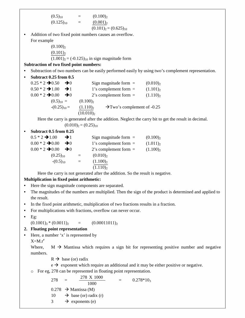
(0.5)10 = (0.100)2
(0.125)10 = (0.001)2
(0.101)2 = (0.625)10
Addition of two fixed point numbers causes an overflow.For example
(0.100)2
(0.101)2
(1.001)2 = (-0.125)10 in sign magnitude formSubtraction of two fixed point numbers: Subtraction of two numbers can be easily performed easily by using two’s complement representation. Subtract 0.25 from 0.5
0.25 * 20.50 0 Sign magnitude form = (0.010)2
0.50 * 21.00 1 1’s complement form = (1.101)2
0.00 * 20.00 0 2’s complement form = (1.110)2
(0.5)10 = (0.100)2
-(0.25)10 = (1.110)2 Two’s complement of -0.25(10.010)2
Here the carry is generated after the addition. Neglect the carry bit to get the result in decimal.(0.010)2 = (0.25)10
Subtract 0.5 from 0.250.5 * 21.00 1 Sign magnitude form = (0.100)2
0.00 * 20.00 0 1’s complement form = (1.011)2
0.00 * 20.00 0 2’s complement form = (1.100)2
(0.25)10 = (0.010)2
-(0.5)10 = (1.100)2
(1.110)2
Here the carry is not generated after the addition. So the result is negative.Multiplication in fixed point arithmetic: Here the sign magnitude components are separated.
The magnitudes of the numbers are multiplied. Then the sign of the product is determined and applied tothe result.
In the fixed point arithmetic, multiplication of two fractions results in a fraction.
For multiplications with fractions, overflow can never occur. Eg:
(0.1001)2 * (0.0011)2 = (0.00011011)2
2. Floating point representation Here, a number ‘x’ is represented by
X=M.re
Where, M Mantissa which requires a sign bit for representing positive number and negativenumbers.
R base (or) radixe exponent which require an additional and it may be either positive or negative.
o For eg, 278 can be represented in floating point representation.
278 =1000
1000X278= 0.278*103
0.278 Mantissa (M)10 base (or) radix (r)3 exponents (e)
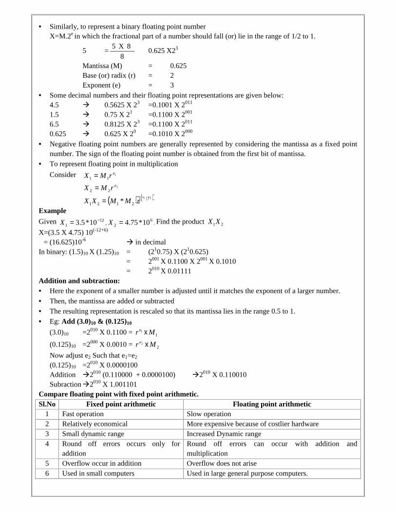
Similarly, to represent a binary floating point numberX=M.2e in which the fractional part of a number should fall (or) lie in the range of 1/2 to 1.
5 =8
8X50.625 X23
Mantissa (M) = 0.625Base (or) radix (r) = 2Exponent (e) = 3
Some decimal numbers and their floating point representations are given below:4.5 0.5625 X 23 =0.1001 X 2011
1.5 0.75 X 21 =0.1100 X 2001
6.5 0.8125 X 23 =0.1100 X 2011
0.625 0.625 X 20 =0.1010 X 2000
Negative floating point numbers are generally represented by considering the mantissa as a fixed pointnumber. The sign of the floating point number is obtained from the first bit of mantissa.
To represent floating point in multiplication
Consider 111
erMX 2
22erMX
21
2121 *ee
rMMXX Example
Given 121 10*5.3 X ,
62 10*75.4X . Find the product 21XX
X=(3.5 X 4.75) 10(-12+6)
= (16.625)10-6 in decimalIn binary: (1.5)10 X (1.25)10 = (210.75) X (210.625)
= 2001 X 0.1100 X 2001 X 0.1010= 2010 X 0.01111
Addition and subtraction: Here the exponent of a smaller number is adjusted until it matches the exponent of a larger number.
Then, the mantissa are added or subtracted The resulting representation is rescaled so that its mantissa lies in the range 0.5 to 1.
Eg: Add (3.0)10 & (0.125)10
(3.0)10 =2010 X 0.1100 = 1er X 1M
(0.125)10 =2000 X 0.0010 = 2er X 2M
Now adjust e2 Such that e1=e2
(0.125)10 =2010 X 0.0000100Addition 2010 (0.110000 + 0.0000100) 2010 X 0.110010Subraction2010 X 1.001101
Compare floating point with fixed point arithmetic.Sl.No Fixed point arithmetic Floating point arithmetic
1 Fast operation Slow operation2 Relatively economical More expensive because of costlier hardware3 Small dynamic range Increased Dynamic range4 Round off errors occurs only for
additionRound off errors can occur with addition andmultiplication
5 Overflow occur in addition Overflow does not arise6 Used in small computers Used in large general purpose computers.
Quantization:*Discuss the various methods of quantization.*Derive the expression for rounding and truncation errors* Discuss in detail about Quantization error that occurs due to finite word length of registers.The common methods of quantization are
1. Truncation2. Rounding
1. Truncation The abrupt termination of given number having a large string of bits (or) Truncation is a process of discarding all bits less significant than the LSB that is retained.
Suppose if we truncate the following binary number from 8 bits to 4 bits, we obtain 0.00110011 to 0.0011
(8 bits) (4 bits) 1.01001001 to 1.0100
(8 bits) (4 bits) When we truncate the number, the signal value is approximated by the highest quantization level that is
not greater than the signal.2. Rounding (or) Round off Rounding is the process of reducing the size of a binary number to finite word size of ‘b’ bits such that
the rounded b-bit number is closest to the original unquantised number.Error Due to truncation and rounding: While storing (or) computation on a number we face registers length problems. Hence given number is
quantized to truncation (or) round off.i.e. Number of bits in the original number is reduced register length.
Truncation error in sign magnitude form: Consider a 5 bit number which has value of
0.110012 (0.7815)10
This 5 bit number is truncated to a 4 bit number0.11002 (0.75)10
i.e. 5 bit number 0.11001 has ‘l’ bits4 bit number 0.1100 has ‘b’ bits
Truncation error, et = 0.1100 – 0.11001= -0.00001 (-0.03125)10
Here original length is ‘l’ bits. (l=5). The truncated length is ‘b’ bits. The truncation error, et = 2-b-2-l
= -(2-l-2-b)et = -(2-5-2-4) = -2-1
The truncation error for a positive number is
lb 22 te 0 Non causal
The truncation error for a negative number is
0 te lb 22 Causal
Truncation error in two’s complement: For a positive number, the truncation results in a smaller number and hence remains same as in the case
of sign magnitude form. For a negative number, the truncation produces negative error in two’s complement
lb 22 te lb 22
Round off error (Error due to rounding): Let us consider a number with original length as ‘5’ bits and round off length as ‘4’ bits.
0.11001 tooffRound 0.1101
Now error due to rounding re =2
22 lb
Where bNumber of bits to the right of binary point after roundingLNumber of bits to the right of binary point before rounding
Rounding off error for positive Number:
2
22 lb re 0
Rounding off error for negative Number:
0 re 2
22 lb
For two’s complement
2
22 lb re
2
22 lb
***************************************************************************************Quantization Noise:*Derive the expression for signal to quantization noise ratio*What is called Quantization Noise? Derive the expression for quantization noise power.
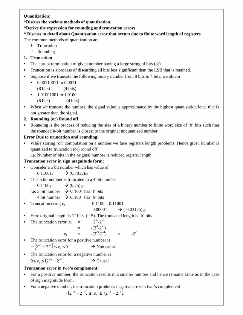
The analog signal is converted into digital signal by ADC At first, the signal x(t) is sampled at regular intervals t=nT, where n=0,1,2… to create sequence x(n).
This is done by a sampler.
Then the numeric equivalent of each sample x(n) is expressed by a finite number of bits giving thesequence xq(n)
The difference signal e(n)= xq(n)- x(n) is called quantization noise (or) A/D conversion noise.
Let us assume a sinusoidal signal varying between +1 & -1 having a dynamic range 2 ADC employs (b+1) bits including sign bit. In this case, the number of levels available for quantizing
x(n) is 2b+1. The interval between the successive levels is
q 12
2b
b2
Where q quantization step sizeIf b=3 bits, then q=2-3=0.125
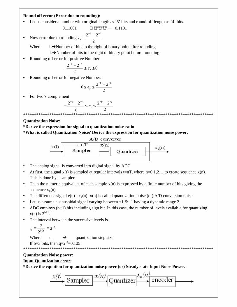
***************************************************************************************Quantization Noise power:Input Quantization error:*Derive the equation for quantization noise power (or) Steady state Input Noise Power.
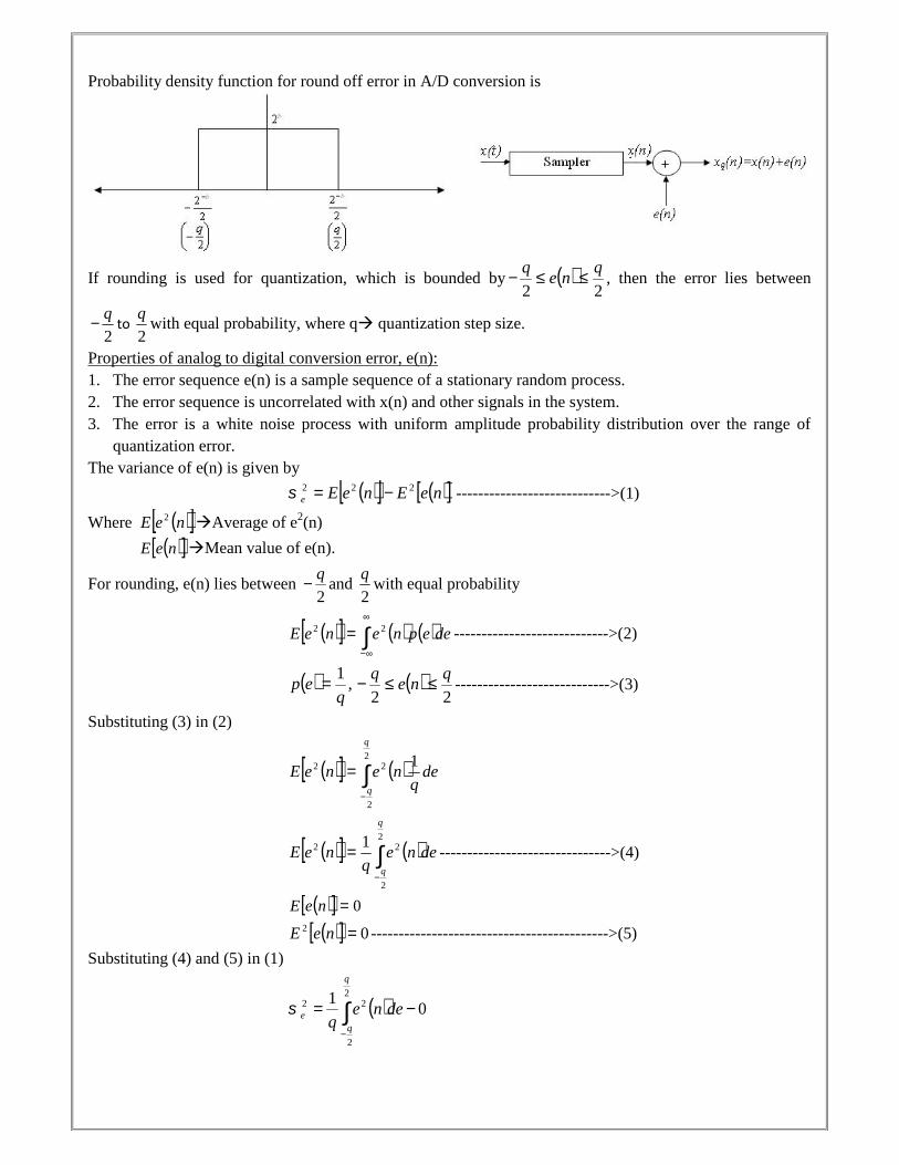
Probability density function for round off error in A/D conversion is
If rounding is used for quantization, which is bounded by 22
qne
q , then the error lies between
2
q to
2
qwith equal probability, where q quantization step size.
Properties of analog to digital conversion error, e(n):1. The error sequence e(n) is a sample sequence of a stationary random process.2. The error sequence is uncorrelated with x(n) and other signals in the system.3. The error is a white noise process with uniform amplitude probability distribution over the range of
quantization error.The variance of e(n) is given by
neEneEe222 ---------------------------->(1)
Where neE 2 Average of e2(n)
neE Mean value of e(n).
For rounding, e(n) lies between2
q and
2
qwith equal probability
deepneneE 22 ---------------------------->(2)
,1
qep
22
qne
q ---------------------------->(3)
Substituting (3) in (2)
2
2
22 1q
q
deq
neneE
2
2
22 1q
q
deneq
neE ------------------------------->(4)
0neE
02 neE ------------------------------------------->(5)
Substituting (4) and (5) in (1)
01 2
2
22
q
qe dene
q
2
2
3
3
1q
q
e
q
33
223
1 qq
q
883
1 33 qq
q
883
1 33 qq
q
8
2
3
1 3q
q
12
22 qe ------------------------------------------------->(6)
In general, qbb
22
1-------------------------------------------->(7)
12
22
2b
e
12
2 22
b
e
----------------------------------------------->(8)
Equation (8) is known as the steady state noise power due to input quantization.
b
Rq
2 in two’s complement representation.
12
b
Rq in sign magnitude (or) one’s complement representation.
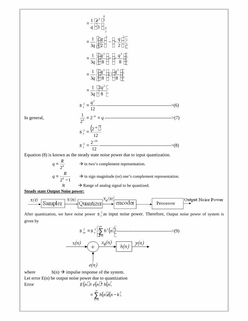
R Range of analog signal to be quantized.Steady state Output Noise power:
After quantization, we have noise power 2e as input noise power. Therefore, Output noise power of system is
given by
0
222
neeo nh ------------------------------------>(9)
where h(n) impulse response of the system.Let error E(n) be output noise power due to quantizationError nhnenE
0k
knenh
The variance of error E(n) is called output noise power, 2e .
By using Parseval’s theorem,2eo
0
22
ne nh
2e
z
dZZHZH
j1
2
1
Where the closed contour integration is evaluated using the method of residue by taking only the poles thatlie inside the unit circle.
Z transform of h(n), n
n
znhZH
0
Z transform of h2(n) = Z[h2(n)] n
n
znh
0
2 n
n
znhnh
0
-------------------->(10)
By Inverse Z transform, dZZZHj
nh n 1
2
1
-------------------------------->(11)
Substituting (11) in (10)
n
n
nn
n
znhdZZZHj
znh
0
1
0
2
2
1
dZZnhZHj n 0
1
2
1
nnn Z
dZZnhZH
jnh
0
1
0
2
2
1
dZZZnhZHj n
n 1
0
1
2
1
Z
dZZHZH
jnh
n
1
0
2
2
1
----------------------------------->(12)
Substituting (12) in (9)
dZZZHZH
jeeo1122
2
1
Problem:The output signal of an A/D converter is passed through a first order low pass filter, with transferfunction given by
1.a0for
az
zazH
1
)( Find the steady state output noise power due to quantization at the
output of the digital filter. [Nov/Dec-2015]Solution:
c
e
c
ee
1
1
c
ee
zaz
dz
az
a1
jdzz
az
za
az
za1
j
have we(1),equationinH(zandH(z)ngSubstituti
az
zaH(z
az
za1H(z)Given
dzzzHzHj
11
221
1
122
1
1
1122
)(2
1
)(2
)
1)
)(
)()(2
1
12
2,
1
11
01
1))
22
2
1
22
1
122
112
b
e
ee
e
11e
Where
a
a
az
a
azaz
zaaz
azatzH(zH(z)ofresidueazatzH(zH(z)ofresidue
Solution:The impulse response for the above filter is given by
Taking Z-transform on both sides we have
We know
( ) ( 1 ) ( )y n a y n x n
( ) ( )nh n a u n2 2 2
0
2 2
0
2 2 4
22
2
2
( )
1 ....
1
1
2 1( )
12 1
ek
ne
k
e
e
b
h n
a
a a
a
ora
1
1
11
1
( ) ( ) ( )
( ) 1( )
( ) 1
( )
Y z az Y z X z
Y z zH z
X z z aaz
zH z
z a
2 2 1 1
1
12 2 1
1
12 2
1
1( ) ( )
2
( ) ( ) s
1
2
1
2 ( )( )
e
c
e
c
e
c
H z H z z dzj
Substituting H z and H z value in the above equation we get
z zz dz
j z a z a
zdz
j z a z a
1
12
1
1
( )( )
1 /( )( )
e
zresidue of at z a
z a z a
zresidue of at z a
z a z a
1
21
( )( )( )e
z a
zz a
z a z a
**************************************************************************************Find the steady state variance of the noise in the output due to quantization of input for the first orderfilter.
***************************************************************************************The output of the A/D converter is applied to a digital filter with the system function
72.0
45.0
Z
ZZH
Find the output noise power of the digital filter, when the input signal is quantized to 7 bits.Given:
72.0
45.0
Z
ZZH
Solution:
11 ZZHZH 11
1
72.0
45.0
72.0
45.0
ZZ
Z
Z
Z
72.01
72.0
45.0 12
ZZ
Z
Z
ZZ
Z
72.0172.0
2025.0 1
72.0
172.0
2025.0 1
ZZ
ZZ
3889.172.0
28125.0
ZZ
Now the poles of H(Z)H(Z-1)Z-1 are p1=0.72 , p2=1.3889Output noise power due to input quantization
dZZZHZH
jeeo1122
2
1
ipz
N
ie ZZHZHs
1
112 Re
ipz
N
ie ZZHZHs
1
112 Re
Where p1,p2,…..pn are the poles of H(Z)H(Z-1) Z-1 that lies inside the unit circle in z-plane.
72.0
22
3889.172.0
28125.072.0
Z
eeo ZZZ
3889.172.0
28125.02
e
24205.0 e
***************************************************************************************
Consider the transfer function )()()( 21 zHzHzH where 12
211
1 1
1)(
1
1)(
za
zHandza
zH
12 2
1 2
1
1e e
a
a a a
Find the output round off noise power. Assume 6.05.0 21 and and find output round off noisepower.Solution:The round off noise model for )()()( 21 zHzHzH is given by,From the realization we can find that the noise transfer function seen by noise source e1(n) is H(z), where,
)2(1
1)(
,)(,
)1(11
1)(
12
2
12
11
zazH
isneby seenfunctiontransfernoisetheWhereas
zazazH
2
The total steady state noise variance can be obtained, we have)3(2
022
012
0
c
dzzzHzHj
11201 )()(
2
1
22e
c
e
a
1zand
azazazespoatzzHzHofresidueof
dzzzazazazaj
11
112
1
211
21
1
2
1,,1)()(
1
1
1
1
1
1
1
1
2
1
If a1 and a2 are less than the poles z=1/a1 and z=1/a2 lies outside of the circle .1z So, the residue of H(z) H(z-1) z-
1at z=1/a1 and z=1/a2 are zero. Consequently we have,
)4(1
1.
1
1.
1
1.
1
1.
111
1
111
1
11111111
,)
212
212
2
212
121
12201
2221
1
221
22
1
2
2
211
21
1
1
221
12
11
1
212
01
21
aaaaa
a
aaaaa
a
aaaa
aaaa
a
a
zazazaza
zaz
zazazaza
zaz
azazpo1esatzH(z)H(zofresidueof
e
e
azaz
1
11
In the same way,
22
12
1
22
1
21
2
2
1122
22
02
11
1
1
1
1
2
)()(2
az
e
c
e
c
e
zaza
zaz
dzzzazaj
dzzzHzHj
)5(1
1
11
22
2
21
2
11
22
2
a
zaza
zzaz
e
az
e
212
22
1
212
2
2
21212
22
1
21212
2
2
21212
22
1
21
22
221
2
2
212
212
2
212
121
12
2
220
111
1
1
1
12
2
111
1
1
1
111
11
1
1.
1
1.
1
1.
1
1.
1
1
aaaa
aa
a
aaaaaa
aaaa
a
aaaaaa
aaaa
a1
1
aaaaa
a
aaaaa
a
a
b
e
2
e
e
The steady state noise power for 6.0,5.0 21 aa is given by
4315.512
2
5.06.016.015.01
6.05.01
6.01
1
12
2
2
222
2
b
b
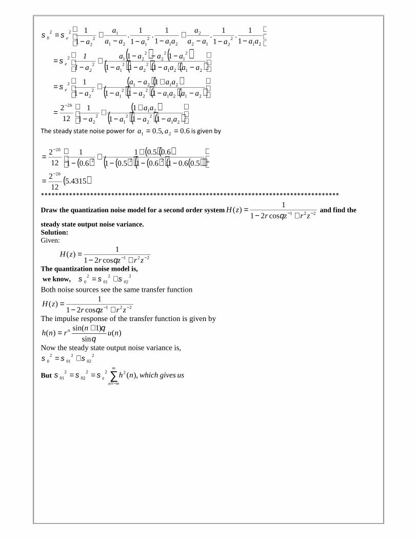
*************************************************************************************
Draw the quantization noise model for a second order system 221cos21
1)(
zrzr
zH
and find the
steady state output noise variance.Solution:Given:
221cos21
1)(
zrzr
zH
The quantization noise model is,
we know, 202
201
20
Both noise sources see the same transfer function
221cos21
1)(
zrzr
zH
The impulse response of the transfer function is given by
)(sin
)1sin()( nu
nrnh n
Now the steady state output noise variance is,2
022
012
0
But
n
e usgives whichnh ),(22202
201
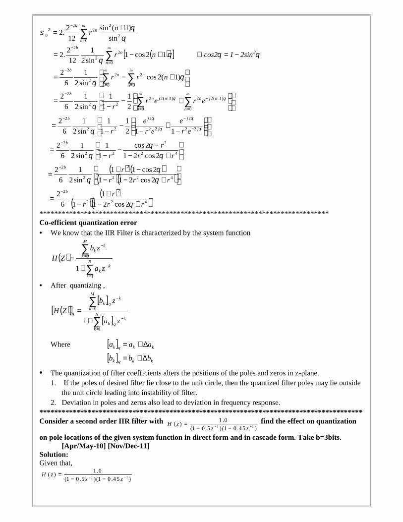
422
22
422
2
2
2
42
2
22
2
22
2
22
2
22
2
)1(2
0
2)1(2
0
222
2
0
2
0
22
2
0
22
2
02
22
22
0
2cos211
1
6
2
2cos211
2cos11
sin2
1
6
2
2cos21
2cos
1
1
sin2
1
6
2
112
1
1
1
sin2
1
6
2
2
1
1
1
sin2
1
6
2
)1(2cossin2
1
6
2
12cos1sin2
1
12
2.2
sin
)1(sin
12
2.2
rrr
r
rrr
r
rr
r
r
er
e
er
e
r
ererr
nrr
2sin1cos2nr
nr
b
b
b
j
j
j
jb
nj
n
nnj
n
nb
n
n
n
nb
2
n
nb
n
nb
******************************************************************************Co-efficient quantization error We know that the IIR Filter is characterized by the system function
N
k
kk
M
k
kk
za
zbZH
1
0
1
After quantizing ,
N
k
kqk
M
k
kqk
q
za
zbZH
1
0
1
Where qka kk aa
qkb kk bb
The quantization of filter coefficients alters the positions of the poles and zeros in z-plane.1. If the poles of desired filter lie close to the unit circle, then the quantized filter poles may lie outside
the unit circle leading into instability of filter.2. Deviation in poles and zeros also lead to deviation in frequency response.
***************************************************************************************Consider a second order IIR filter with find the effect on quantization
on pole locations of the given system function in direct form and in cascade form. Take b=3bits.[Apr/May-10] [Nov/Dec-11]
Solution:Given that,
1 1
1 .0( )
(1 0 .5 )(1 0 .4 5 )H z
z z
1 1
1 .0( )
(1 0 .5 )(1 0 .45 )H z
z z
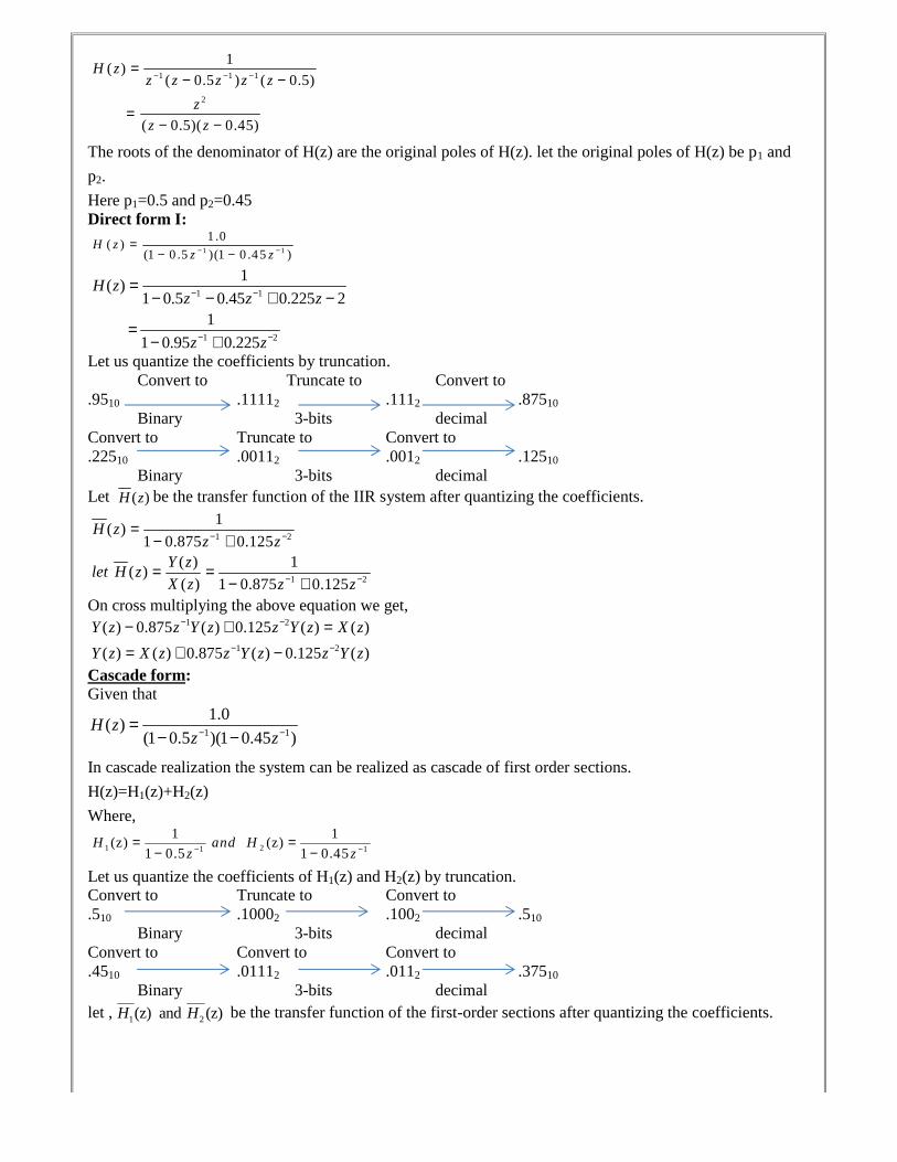
The roots of the denominator of H(z) are the original poles of H(z). let the original poles of H(z) be p1 and
p2.
Here p1=0.5 and p2=0.45Direct form I:
Let us quantize the coefficients by truncation.Convert to Truncate to Convert to
.9510 .11112 .1112 .87510
Binary 3-bits decimalConvert to Truncate to Convert to.22510 .00112 .0012 .12510
Binary 3-bits decimalLet be the transfer function of the IIR system after quantizing the coefficients.
On cross multiplying the above equation we get,
Cascade form:Given that
In cascade realization the system can be realized as cascade of first order sections.
H(z)=H1(z)+H2(z)
Where,
Let us quantize the coefficients of H1(z) and H2(z) by truncation.Convert to Truncate to Convert to.510 .10002 .1002 .510
Binary 3-bits decimalConvert to Convert to Convert to.4510 .01112 .0112 .37510
Binary 3-bits decimallet , be the transfer function of the first-order sections after quantizing the coefficients.
1 1 1
2
1( )
( 0.5 ) ( 0.5)
( 0.5)( 0.45)
H zz z z z z
z
z z
1 1
1 .0( )
(1 0 .5 )(1 0 .45 )H z
z z
1 1
1 2
1( )
1 0.5 0.45 0.225 21
1 0.95 0.225
H zz z z
z z
( )H z
1 2
1 2
1( )
1 0.875 0.125( ) 1
( )( ) 1 0.875 0.125
H zz z
Y zlet H z
X z z z
1 2
1 2
( ) 0.875 ( ) 0.125 ( ) ( )
( ) ( ) 0.875 ( ) 0.125 ( )
Y z z Y z z Y z X z
Y z X z z Y z z Y z
1 21 1
1 1(z) (z)
1 0.5 1 0.45H and H
z z
1 2(z) and (z)H H
1 1
1.0( )
(1 0.5 )(1 0.45 )H z
z z
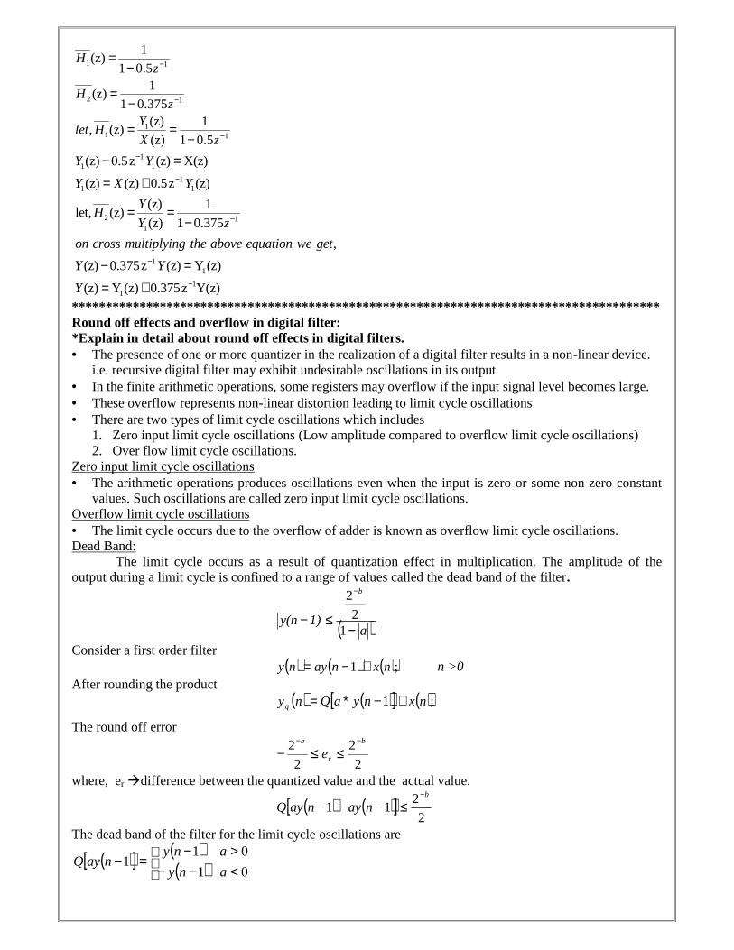
***************************************************************************************Round off effects and overflow in digital filter:*Explain in detail about round off effects in digital filters. The presence of one or more quantizer in the realization of a digital filter results in a non-linear device.
i.e. recursive digital filter may exhibit undesirable oscillations in its output In the finite arithmetic operations, some registers may overflow if the input signal level becomes large. These overflow represents non-linear distortion leading to limit cycle oscillations There are two types of limit cycle oscillations which includes
1. Zero input limit cycle oscillations (Low amplitude compared to overflow limit cycle oscillations)2. Over flow limit cycle oscillations.
Zero input limit cycle oscillations The arithmetic operations produces oscillations even when the input is zero or some non zero constant
values. Such oscillations are called zero input limit cycle oscillations.Overflow limit cycle oscillations The limit cycle occurs due to the overflow of adder is known as overflow limit cycle oscillations.Dead Band:
The limit cycle occurs as a result of quantization effect in multiplication. The amplitude of theoutput during a limit cycle is confined to a range of values called the dead band of the filter.
a1)y(n
b
12
2
Consider a first order filter ;1 nxnayny n >0
After rounding the product ;1 nxnyaQnyq
The round off error
2
2
2
2 b
r
b
e
where, erdifference between the quantized value and the actual value.
2
211
b
naynayQ
The dead band of the filter for the limit cycle oscillations are
01
011
any
anynayQ
1 1
2 1
11 1
1(z)
1 0.51
(z)1 0.375
(z) 1, (z)
(z) 1 0.5
Hz
Hz
Ylet H
X z
11 1
11 1
2 11
11
11
(z) 0.5z (z) X(z)
(z) (z) 0.5z (z)
(z) 1let, (z)
(z) 1 0.375
,
(z) 0.375z (z) Y (z)
(z) Y (z) 0.375z Y(z)
Y Y
Y X Y
YH
Y z
on cross multiplying the above equation we get
Y Y
Y
1)y(n 1)y(na 2
2 b
1)y(n a1 2
2 b
Dead band of the filter, 1)y(n a
b
12
2
**************************************************************************************Problem: Consider a 1st order FIR system equation )1()()( naynxny with
otherwise ,
0n ,nx
0
875.0)(
Find the limit cycle effect and the dead band. Assume b=4 and a=0.95. (Nov/Dec-12)(Nov/Dec-15)[May/June-2016]Solution:Given:
otherwise ,
0n ,nx
0
875.0)(
625.095.012
2
12
4
a
2bandDead
b
)1(95.0)()( nynxny
n x(n) )1( ny )1( nay )1( nayQ
(round off to 4-bits) )1()()( nayQnxny
0 0.875 0 0 0.0000 y(0)=0.875
1 0 0.875 2
10
11010.0
0.83125
0.95*0.875
8125.0
1101.0 2
y(1)=0.8125
2 0 0.8125 2
10
110001.0
0.77187
0.95*0.8125
75.0
1100.0 2
75.0)2( y
3 0 0.75 2
10
1011011.0
0.7125
0.95*0.75
6875.0
1011.0 2
6875.0)3( y
4 0 0.6875 2
10
101001.0
0.653125
0.95*0.6875
625.0
1010.0 2
625.0)4( y
5 0 0.625 2
10
10011.0
0.59375
0.95*0.625
625.0
1010.0 2
625.0)5( y
6 0 0.625 2
10
10011.0
0.59375
0.95*0.625
625.0
1010.0 2
625.0)6( y
Conclusion:
The dead band of the filter is 0.625. When 5n the output remains constant at 0.625 causinglimit cycle oscillations.***************************************************************************************Overflow Limit cycle oscillations:*What are called overflow oscillations? How it can be prevented? We know that the limit cycle oscillation is caused by rounding the result of multiplication. The limit cycle occurs due to the overflow of adder is known as overflow limit cycle oscillations.\ Several types of limit cycle oscillations are caused by addition, which makes the filter output oscilate
between maximum and minimum amplitudes. Let us consider 2 positive numbers n1 & n2
n1=0.1117/8n2=0.1106/8n1 + n2=1.101-5/8 in sign magnitude form.The sum is wrongly interpreted as a negative number.
The transfer characteristics of an saturation adder is shown in fig belowwhere n The input to the adder
f(n) The corresponding output
Saturation adder transfer characteristics From the transfer characteristics, we find that when overflow occurs, the sum of adder is set equal to the
maximum value.***************************************************************************************Signal Scaling:
Saturation arithmetic eliminates limit cycles due to overflow, but it causes undeniable signal distortiondue to the non linearity of the clipper.
In order to limit the amount of non linear distortion, it is important to scale input signal and unit sampleresponse between input and any internal summing node in the system to avoid overflow.
Realization of a second order IIR Filter Let us consider a second order IIR filter as shown in the above figure. Here a scale factor S0 is
introduced between the input x(n) and the adder 1 to prevent overflow at the output of adder 1.
Explain how reduction of round-off errors is achieved in digital filters.
Now the overall input-output transfer function is
Now the transfer function
From figure
Using Schwartz inequality
Applying parsevals theorem
By substituting all values
Which gives us,
1 20 1 2
0 1 21 2
0
( )1
( )
( )
b b z b zH z S
a z a z
N zS
D z
' 0 01 2
1 2
00
( )( )
( ) 1 ( )
( )( ) S( ) x(Z)
( )
1Where ( )
( )
S SW zH z
X z a z a z D z
S X zW z S z
D z
S zD z
0
2 22 0
2
( ) ( ) ( )( ) d2
w(n) ( ) ( )( ) d2
j j jn
j j jn
we have
Sw n S e X e e
SS e X e e
2 22 20 2 2w(n) ( ) d ( ) dj jS S e X e
22 2 20 2
0
1w(n) ( ) ( ) d
2j
n
j j
S x n S e
if z e then dz je d
which gives
dzd
jz
22 2 2 10
0
2 2 2 1 10
0
1w(n) ( ) ( ) z d
2
1w(n) ( ) ( ) ( ) z d
2
cn
cn
S x n S z zj
S x n S z S z zj
2 2
0
2 10
( ) ( )
1( ) ( ) d 1
2
n
c
w n x n when
S S z S z zj
Where I=
Note: Because of the process of scaling, the overflow is eliminated. Here so is the scaling factor for the first
stage.
Scaling factor for the second stage = S01 and it is given by2
20
201
1
ISS
Where
dZZDZD
ZZHZH
jI
c
1
22
1111
2 2
1
********************************************************************************************
For the given transfer function, 1
1
5.01
7.025.0
Z
ZZH , find scaling factor so as to avoid overflow in
the adder ‘1’ of the filter.
Given:D(Z) = 1-0.5Z-1
D(Z-1) = 1-0.5 ZSolution:
I Z
dZ
ZDZDj c
1
1
2
1
Z
dZ
ZZj c
5.015.01
1
2
11
Z
dZ
ZZ
Z
j c
5.01
1
5.02
1
Residue of 05.01
1
5.05.0
Z
ZZ
Z
I=1.3333
0S =I
1
20
1 1
1
1
20
11
( ) ( ) z d2
11
2 ( ) ( )
1
c
c
SS z S z z
j
z dz
j D z D z
SI
0S =333.1
1
= 0.866
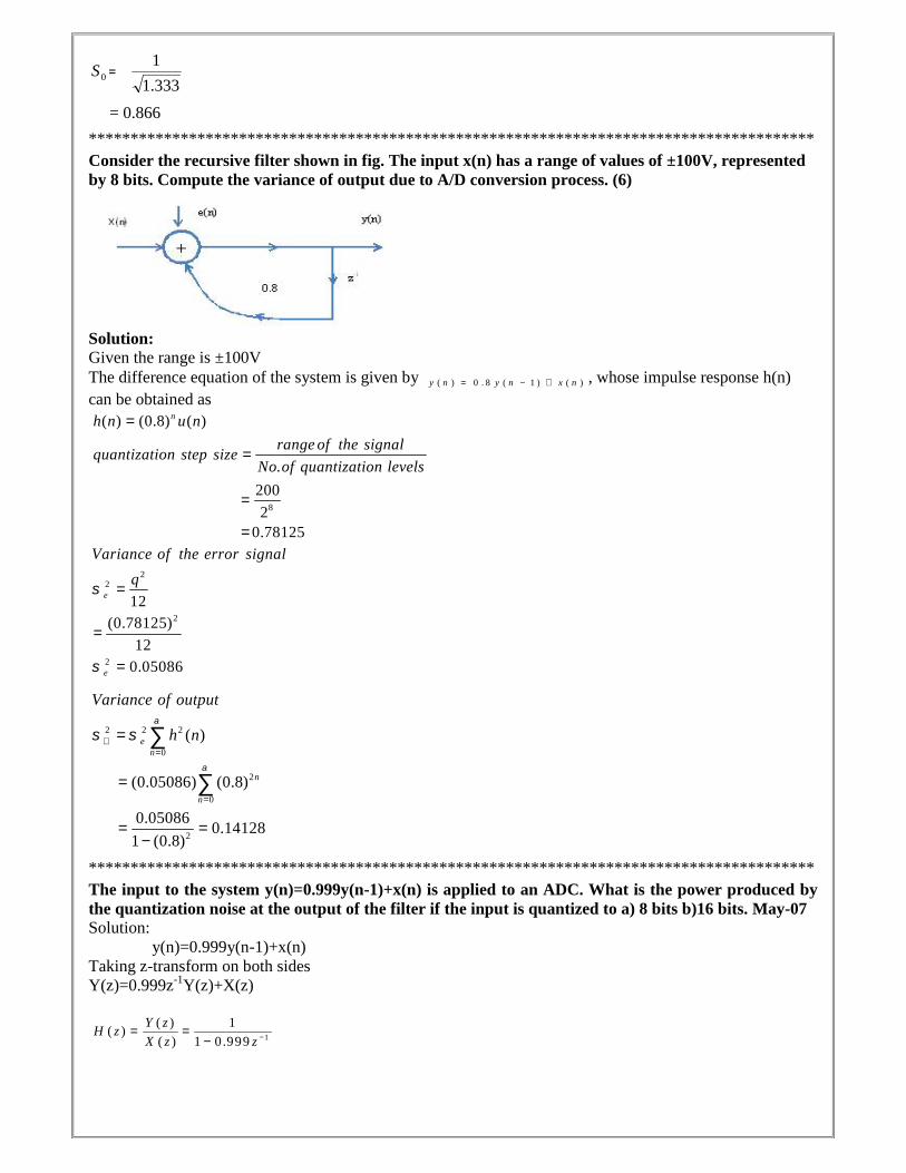
***************************************************************************************Consider the recursive filter shown in fig. The input x(n) has a range of values of ±100V, representedby 8 bits. Compute the variance of output due to A/D conversion process. (6)
Solution:Given the range is ±100VThe difference equation of the system is given by , whose impulse response h(n)can be obtained as
***************************************************************************************The input to the system y(n)=0.999y(n-1)+x(n) is applied to an ADC. What is the power produced bythe quantization noise at the output of the filter if the input is quantized to a) 8 bits b)16 bits. May-07Solution:
y(n)=0.999y(n-1)+x(n)Taking z-transform on both sidesY(z)=0.999z-1Y(z)+X(z)
( ) 0 . 8 ( 1 ) ( )y n y n x n
8
( ) (0.8) ( )
.
200
20.78125
nh n u n
range of the signalquantization step size
No of quantization levels
22
2
2
12(0.78125)
120.05086
e
e
Variance of the error signal
q
2 2 2
0
2
0
2
( )
(0.05086) (0.8)
0.050860.14128
1 (0.8)
en
n
n
Variance of output
h n
1
( ) 1( )
( ) 1 0.999
Y zH z
X z z
11 1 1
1
1
( ) ( ) ( )( )0.999 0.999
1( 0.999)( 0.999)( )
0.9990.001
( 0.999)( 0.001)
z zH z H z z z
z z
z
z z
z z
Where p1,p2,……pN are poles of H(z)H(z-1)z-1, that lies inside the unit circle in z-plane.
a) b+1=8 bits(Assuming including sign bit)
b) b+1=16 bits
***************************************************************************************Find the effect of coefficient quantization on pole locations of the given second order IIR system, whenit is realized in direct form I and in cascade form. Assume a word length of 4 bits through truncation.
Solution:Direct form ILet b=4 bits including a sign bit
2 2 1 1
2 1 1
1
2 1 1
1
1( ) ( )
2
R e ( ) ( )
( ) ( ) ( )
i
i
eoi e
c
N
ei z p
N
e ii z p
output noise pow er dueH z H z z dz
to input quantization j
s H z H z z
z p H z H z z
2 2
2
0.999
0.001( 0.999)( )
( 0.999)( 0.001)
500.25
eoi ez
e
zz z
2 ( 7 )2 32
(500.25) 2.544 1012
2 (1 5 )2 82
(5 0 0 .2 5) 3 .8 8 2 1 01 2
1 2
1( )
1 0.9 0.2H z
z z
After truncation we get(0.111)2=(0.875)10
(0.2)10=(0.00110…)2
After truncation we get(0.001)2=(0.125)10
The system function after coefficient quantization is
Now the pole locations are given byz1=0.695z2=0.178
If we compare the Poles of H(z) and we can observe that the poles of deviate very much fromthe original poles.
Cascade form
After truncation we get
10 2(0.9) (0.111001...)
0.9 2
1.8
1
0.8 2
1.61
0.6 21
1.2
0.2 2
0.40
0.4 2
0.80
0.8 2
1.61
Integer part
10
0.2 2(0.2)
0.4
0
0.4 2
0.80
0.8 2
1.61
0.6 2
1.21
0.2 2
0.40
1 2
1( )
1 0.875 0.125H z
z z
( )H z ( )H z
1 1
10 2
1( )
1 0.5 (1 0.4 )
(0.5) (0.1000)
H zz z
(0.100)2=(0.5)10
After truncation we get(0.011)2=(0.375)10
(0.4)10=(0.01100…)2
The system function after coefficient quantization is
The pole locations are given byz1=0.5z2=0.375on comparing the poles of the cascade system with original poles we can say that one of the poles is sameand other pole is very close to original pole.***************************************************************************************A LTI system is characterized by the difference equation y(n)=0.68y(n-1)+0.5x(n).The input signal x(n) has a range of -5V to +5V, represented by 8-bits. Find the quantization step size,variance of the error signal and variance of the quantization noise at the output.Solution:GivenRange R=-5V to +5V = 5-(-5) =10Size of binary, B= 8 bits (including sign bit)Quantization step size,
The difference equation governing the LTI system isY (n) =0.68y (n-1) +0.15x (n)On taking z transform of above equation we get
1 0
0 .4 2( 0 .4 )
0 .8
0
0 .8 2
1 .60
0 .6 2
1 .21
0 .2 2
0 .41
0 .4 2
0 .80
1 1
1( )
(1 0.5 )(1 0.375 )H z
z z
8 8
2 22 4
100.0390625
2 20.0390625
var , 1.27116*1012 12e
Rq
qiance of error signal
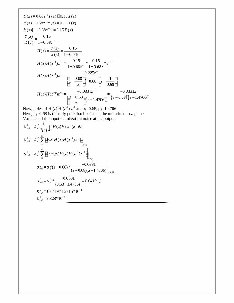
Now, poles of H (z) H (z-1) z-1 are p1=0.68, p2=1.4706Here, p1=0.68 is the only pole that lies inside the unit circle in z-planeVariance of the input quantization noise at the output.
1
1
1
1
( ) 0.68 ( ) 0.15 ( )
( ) 0.68 ( ) 0.15 ( )
( )[1 0.68 ] 0.15 ( )
( ) 0.15
( ) 1 0.68
Y z z Y z X z
Y z z Y z X z
Y z z X z
Y z
X z z
1
1 1 11
11 1
1 11 1
( ) 0.15( )
( ) 1 0.68
0.15 0.15( ) ( ) * *
1 0.68 1 0.68
0.225( ) ( )
0.68 11 0.68
0.68
0.0331 0.0331( ) ( )
0.68 0.68 1.47061.4706
Y zH z
X z z
H z H z z zz z
zH z H z z
zz
z zH z H z z
z z zz
z
2 2 1 1
2 2 1 1
1
2 2 1 1
1
1( ) ( )
2
Res ( ) ( )
( ) ( ) ( )
eoi e c
N
eoi ei z pi
N
eoi e ii z pi
H z H z z dzj
H z H z z
z p H z H z z
2 2
0.68
2 2 2
2 4
2 6
0.0331( 0.68)*
( 0.68)( 1.4706)
0.0331* 0.0419
(0.68 1.4706)
0.0419*1.2716*10
5.328*10
eoi e
z
eoi e e
eoi
eoi
zz z
Analog to digital conversion:
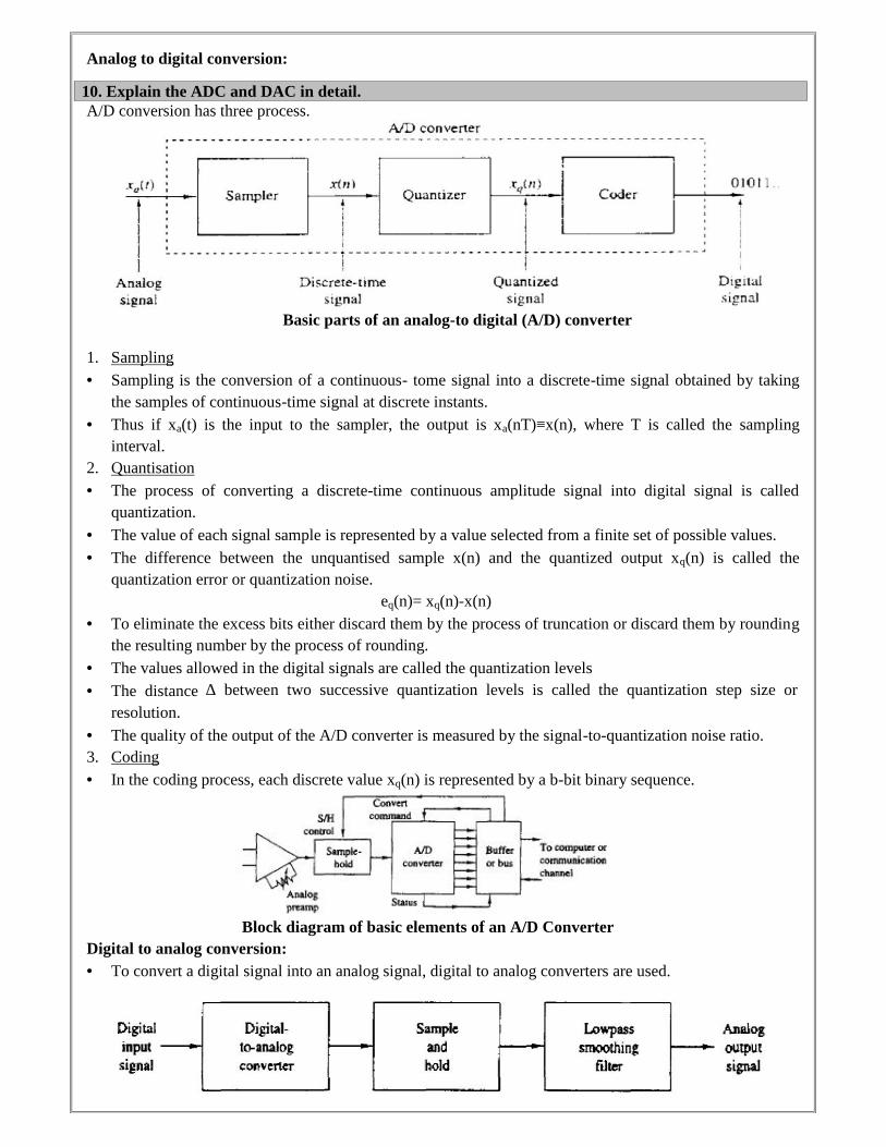
10. Explain the ADC and DAC in detail.A/D conversion has three process.
Basic parts of an analog-to digital (A/D) converter
1. Sampling Sampling is the conversion of a continuous- tome signal into a discrete-time signal obtained by taking
the samples of continuous-time signal at discrete instants. Thus if xa(t) is the input to the sampler, the output is xa(nT)≡x(n), where T is called the sampling
interval.2. Quantisation The process of converting a discrete-time continuous amplitude signal into digital signal is called
quantization.
The value of each signal sample is represented by a value selected from a finite set of possible values. The difference between the unquantised sample x(n) and the quantized output xq(n) is called the
quantization error or quantization noise.eq(n)= xq(n)-x(n)
To eliminate the excess bits either discard them by the process of truncation or discard them by roundingthe resulting number by the process of rounding.
The values allowed in the digital signals are called the quantization levels
The distance ∆ between two successive quantization levels is called the quantization step size orresolution.
The quality of the output of the A/D converter is measured by the signal-to-quantization noise ratio.3. Coding In the coding process, each discrete value xq(n) is represented by a b-bit binary sequence.
Block diagram of basic elements of an A/D ConverterDigital to analog conversion: To convert a digital signal into an analog signal, digital to analog converters are used.

Basic operations in converting a digital signal into an analog signal The D/A converter accepts, at its input, electrical signals that corresponds to a binary word, and
produces an output voltage or current that is proportional to the value of the binary word. The task of D/A converter is to interpolate between samples. The sampling theorem specifies the optimum interpolation for a band limited signal.
The simplest D/A converter is the zero order hold which holds constant value of sample until the nextone is received.
Additional improvement can be obtained by using linear interpolation to connect successive sampleswith straight line segment.
Better interpolation can be achieved y using more sophisticated higher order interpolation techniques. Suboptimum interpolation techniques result in passing frequencies above the folding frequency. Such
frequency components are undesirable and are removed by passing the output of the interpolator througha proper analog filter which is called as post filter or smoothing filter.
Thus D/A conversion usually involve a suboptimum interpolator followed by a post filter.***************************************************************************************
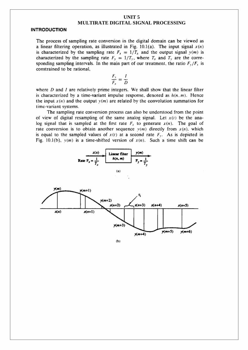
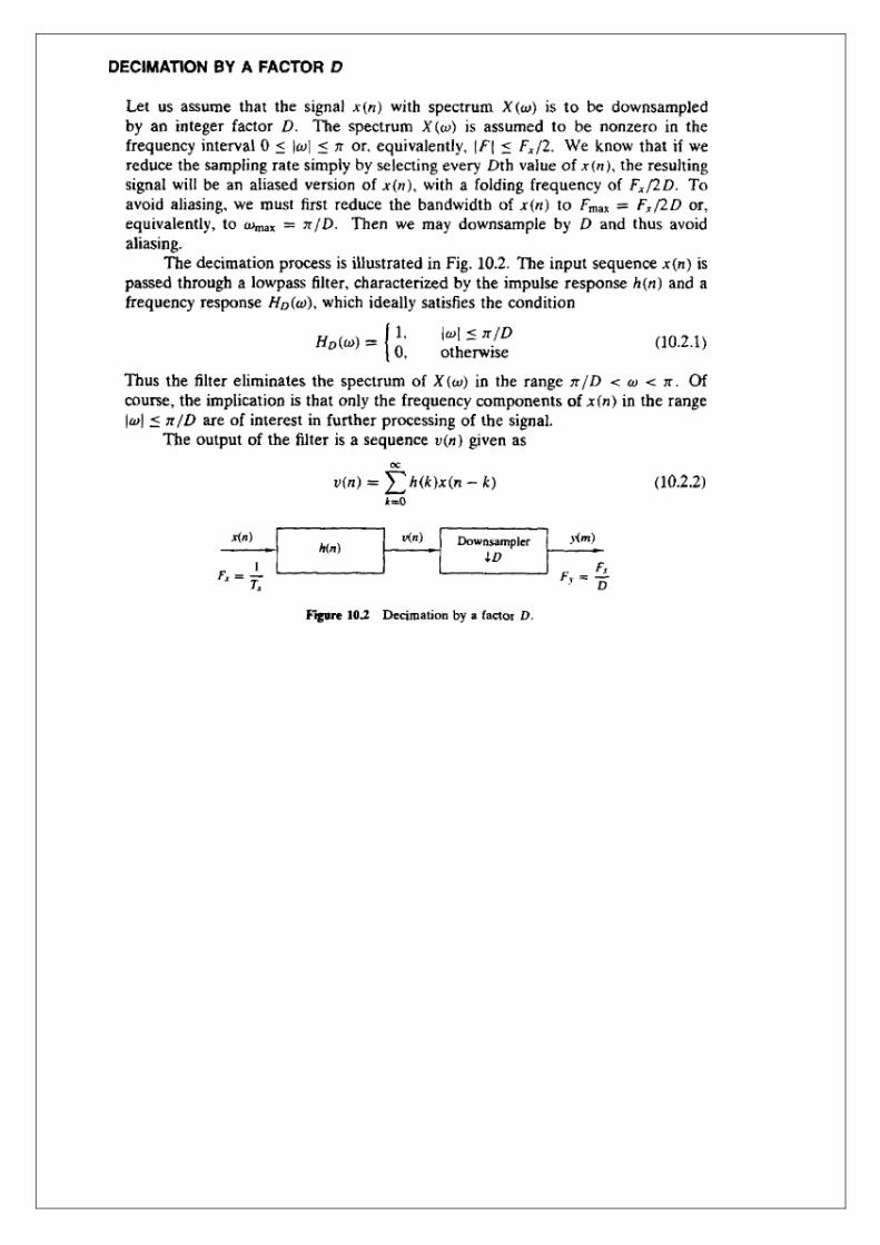
UNIT 5
MULTIRATE DIGITAL SIGNAL PROCESSING
****************************************************************************

OUTCOMES:
At the end of the course, the student should be able to
Apply DFT and FFT algorithms for the analysis of digital signals and systems.
Design FIR filters for various applications.
Design IIR filters for various applications.
Characterize the effects of finite precision representation on digital filters.
TEXT BOOKS:
1. John G.Proakis and Dimitris G. Manolakis, “Digital signal processing - Principles, algorithms
and applications”, Pearson education / Prentice hall, Fourth edition, 2007.
REFERENCES:
1. Sanjay K.Mithra, “Digital signal processing - A Computer based approach”, Tata McGraw-Hill, 2007.
2. M.H.Hayes, “Digital signal processing”, Schum’s outlines, Tata McGraw Hill, 2007.
3. A.V.Oppenheim, R. W. Schafer and J. R. Buck, “Discrete-time signal processing”, Pearson, 2004.
4. I.C.Ifeachor and B.W.Jervis, “Digital signal processing – A practical approach”, Pearson 2002
5. L.R. Rabiner and B. Gold, “Theory and application of digital signal processing”, Prentice Hall, 1992.