Embed Size (px)
Citation preview
Internationale Ausgabe: DOI: 10.1002/anie.201706895Solar Energy MaterialsDeutsche Ausgabe: DOI: 10.1002/ange.201706895
Cove-Edge Nanoribbon Materials for Efficient Inverted HalidePerovskite Solar CellsEdison Castro+, Thomas J. Sisto+, Elkin L. Romero, Fang Liu, Samuel R. Peurifoy, Jue Wang,Xiaoyang Zhu, Colin Nuckolls,* and Luis Echegoyen*
Abstract: Two cove-edge graphene nanoribbons hPDI2-Pyr-hPDI2 (1) and hPDI3-Pyr-hPDI3 (2) are used as efficientelectron-transporting materials (ETMs) in inverted planarperovskite solar cells (PSCs). Devices based on the newgraphene nanoribbons exhibit maximum power-conversionefficiencies (PCEs) of 15.6% and 16.5% for 1 and 2,respectively, while a maximum PCE of 14.9 % is achievedwith devices based on [6,6]-phenyl-C61-butyric acid methylester (PC61BM). The interfacial effects induced by these newmaterials are studied using photoluminescence (PL), and wefind that 1 and 2 act as efficient electron-extraction materials.Additionally, compared with PC61BM, these new materials aremore hydrophobic and have slightly higher LUMO energylevels, thus providing better device performance and higherdevice stability.
Herein, we describe the first use of graphene nanoribbonsas the electron-transporting layer in PSCs, leading toincreased device performance compared to widely usedPC61BM. Since their introduction in 2008, hybrid organic–inorganic perovskite materials have shown great promise asthe active layer in photovoltaic cells. Because of their efficientlight absorption and low cost, lead halide perovskites(CH3NH3PbX3; X = I, Br, Cl) have become high performancematerials that have the potential to fulfill the requirementsfor the large-scale deployment of solar energy.[1,2] Recently,there has been great interest in these materials, leading toremarkable increases in photoconversion efficiency, from3.8% in 2009 to 22.1 % in 2016.[3, 4] One area of focus forimproving PSCs are the hole- and electron-extracting layersthat encapsulate the active layer. These layers are invaluablebecause they determine the polarity of the device, improvestability, passivate surface charge traps, and aid in charge-extraction transport from the active layer to the electrodes(Figure 1).[5, 6]
To date, PSCs based on both meso-superstructure[7] andplanar device structures[8] have achieved PCEs over 20 %.Despite the lower PCE at present, the inverted planar devices,which are based on p-i-n configurations, are attractivebecause the relatively simple device architecture is promisingfor flexible devices and is amenable to low-temperature andscalable fabrication techniques.[9, 10] There are many holetransporting materials (HTMs) suitable for this type of solarcells. For example, poly(3,4-ethylenedioxythiophene):poly-(styrenesulfonate) (PEDOT:PSS), NiOx, CuI, and CuSCN areall commonly used.[11] However, the ETM is limited mainly tofullerenes such as PC61BM and other derivatives,[12–17] andthere are few examples of efficient non-fullerene invertedPSCs reported.[18–21] To further enhance PSCs, new ETMsmust be developed and studied.
Herein, we report that two atomically precise edge-functionalized graphene nanoribbons hPDI2-Pyr-hPDI2 (1)and hPDI3-Pyr-hPDI3 (2) outperform PC61BM as ETMs inPSCs, with average PCEs of 14.9� 0.7% and 15.9� 0.6 % for1 and 2, respectively, as compared to 14.2� 0.7% for PC61BM(Figure 1). These soluble, electron-poor ribbons providea facile fabrication process, high electron mobility, stronglight absorption, and HOMO/LUMO levels that match thoseof the lead-halide perovskite active layers.[22, 23] This is the firstexample of graphene nanoribbons being used as the transportlayer in PSCs, and points to the promise of functionalizedgraphene for the enhancement of the transport layers of solarcells.
Recently, some of us reported the bottom-up synthesis ofedge-functionalized graphene nanoribbons 1 and 2, and theirmaterials characterization as ETMs.[23] Notably, the cyclicvoltammograms of 1 and 2 showed multiple reduction eventsthat prompted us to explore the electrochemistry of thesenanoribbons further for their use as the ETMs in PSCs. It isvital for an electron-transport layer to have a LUMO that iswell matched with the active layer to aid in electronextraction, as well as a HOMO that is low enough to blockhole transport. Estimates of the HOMO/LUMO values fromcyclic voltammetry (CV) reveal that the nanoribbons 1 and 2fulfill these requirements. The energy level diagrams of 1 and2 are represented in Figure 1b, and the estimated LUMO of1 and 2 are located at�3.7 eVand�3.8 eV, respectively. Bothribbons� LUMO levels match the conduction band of theperovskite (�3.7 eV).[24] The HOMO energy levels of 1 and 2are both �5.8 eV, much deeper than the valence band of theperovskite (�5.4 eV),[24] and thereby should provide efficienthole-blocking ability.
To test the hypothesis that these ribbons would beeffective in PSCs, we fabricated devices using 1, 2, and
[*] E. Castro,[+] E. L. Romero, Prof. L. EchegoyenDepartment of Chemistry, University of Texas at El PasoEl Paso, TX, 79968 (USA)E-mail: [email protected]
Dr. T. J. Sisto,[+] F. Liu, S. R. Peurifoy, J. Wang, Prof. X. Zhu,Prof. C. NuckollsDepartment of Chemistry, Columbia UniversityNew York, NY, 10027 (USA)E-mail: [email protected]
[+] These authors contributed equally to this work.
Supporting information and the ORCID identification number(s) forthe author(s) of this article can be found under:https://doi.org/10.1002/anie.201706895.
AngewandteChemieZuschriften
1Angew. Chem. 2017, 129, 1 – 6 � 2017 Wiley-VCH Verlag GmbH & Co. KGaA, Weinheim
These are not the final page numbers! � �
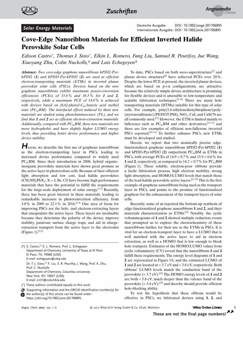
PC61BM. The current–voltage (J–V) curves of these devicesusing inverted planar structures are shown in Figure 2a. Thephotovoltaic parameters of the devices are summarized inTable 1.
The highest PCEs for devices based on 1 and 2 as ETMswere 15.6% and 16.5%, respectively. The efficiencies arehigher than those of devices based on PC61BM, which yieldeda highest PCE of 14.9% under the same conditions. Theexternal quantum efficiency (EQE) spectra (SupportingInformation, Figure S1) were higher for ribbon 2 baseddevices, and the integrated Jsc is in agreement with thevalues obtained from the J–V values (Table 1). The higher Jsc
values obtained from devices based on 2 can be attributed tothe slightly higher electron mobility of this compound. Thehigher Voc values obtained from both 1 and 2 compared withthat of the PC61BM can be associated with the higher LUMOlevels of the two ribbons.[25] To investigate the hysteresisbehavior, devices were tested in both forward and reversescan directions. As shown in Figure 2b, devices based on thetwo ribbons displayed relatively consistent J–V curves,independent of the scan direction, indicating a negligiblehysteresis effect in the PSCs.
To further verify device efficiencies, the maximal steady-state power outputs were monitored and plotted as a functionof time. As shown in Figure 2c, devices based on 1 and 2 at0.78 V resulted in 19.85 mAcm�2 and 20.95 mAcm�2, yieldingPCEs of 15.5% and 16.3%, respectively. Statistical histo-grams of PCEs from 15 individual devices using 1, 2, andPC61BM as the ETMs are shown in Figure 2d. The distribu-tion exhibited average efficiencies of 14.9� 0.7%, 15.9�0.6%, and 14.2� 0.7% for 1-, 2-, and PC61BM-based devices,respectively.
To understand the efficiency of transport through theelectron-transport layer, the electron mobilities of 1, 2, andPC61BM were obtained from space-charge-limited current(SCLC) experiments. The mobilities of all three devices weresimilar (10�4 cm2 V�1 s�1),[13, 23] which shows that the tworibbons conduct as efficiently as PC61BM.
To study recombination losses and the role of the tworibbons as the electron-transport layers, steady-state PL andtime-resolved (TR-PL) decay measurements were recordedfor perovskite, perovskite/1, perovskite/2, and for perovskite/PC61BM films as shown in Figure 2e. When the perovskitelayer forms a contact with 1, 2, or PC61BM, a significant PL-quenching effect was observed, indicating that all of theextracting layers are efficiently inhibiting electron-holerecombination.[26] As ribbon 1 and ribbon 2 exhibit pro-nounced PL between 600–750 nm,[23] the passivation effectwas not clearly observed in the steady-state PL. As shown inFigure 2 f, shorter PL decay times were observed for per-ovskite/ETMs (0.9, 0.9, and 1 ns for perovskite/1, perovskite/2, and perovskite/PC61BM, respectively) than that of onlyperovskite (3 ns). The shortened decay lifetime observed withall of the electron-transport layers shows fast extraction andtransport of charge carriers, which suppresses electron-holerecombination and increases the Jsc.
[27]
In addition to the energy levels, the CV of 1 and 2 in THF(Supporting Information, Figure S2; Table 2) show four andsix reversible reduction events grouped in pairs, respectively.We became interested in quantifying how many electronswere added to 1 and 2 for each of these reduction events. It iswell known from other perylene diimide (PDI) oligomers thateach PDI subunit accepts two electrons. If this is also the casefor 1 and 2, then 1 reversibly accepts 8 electrons, while 2reversibly accepts a remarkable 12 electrons. To confirm this,controlled potential electrolysis of 1 and 2 in THF containing0.1m TBAPF6 was performed at a potential circa 60 mV morenegative than each reduction potential (see Figure S2,arrows).
The stoichiometry of the charge (coulombs) transferredcorresponded to two electrons per molecule for each reduc-tion wave. Moreover, the anions showed no decompositionand were very stable under these conditions (Table 3).Subsequent re-oxidation at 0 V showed regeneration of theneutral species with no change in the CV nor in theOsteryoung square-wave voltammetry, indicating that eachprocess is completely chemically reversible. These results
Figure 1. a) Device structure of the inverted PSC using hPDI2-Pyr-hPDI2 (1) or hPDI3-Pyr-hPDI3 (2) as the ETMs. b) Schematic of the estimatedHOMO/LUMO energy levels.[23, 24]
AngewandteChemieZuschriften
2 www.angewandte.de � 2017 Wiley-VCH Verlag GmbH & Co. KGaA, Weinheim Angew. Chem. 2017, 129, 1 – 6� �
These are not the final page numbers!
Figure 2. a) J–V curves measured under 1 sun illumination (100 mWcm�2, AM 1.5 G). b) J–V curves under 1 sun illumination in forward andreverse voltage scans. c) Power output under maximum power point tracking for 60 s, resulting in a stabilized power output of 15.5% and 16.3%(at 0.78 V) when 1 and 2 were used as the ETMs, respectively. d) The PCE histograms measured for 15 independent devices. e) Steady-state PLspectra of the perovskite and perovskite/ETM films. f) TR-PL spectra of the perovskite and perovskite/ETM films.
Table 1: Summary of performance of devices based on 1, 2, and PC61BM.
ETM Jsc [mAcm�2][a] Jsc [mAcm�2] Voc
[V]FF [%] PCE (%)
PC61BM 21.08 21.10 0.88 0.80 14.2�0.7 (14.9)1 21.18 21.17 0.93 0.79 14.9�0.7 (15.6)2 22.66 22.68 0.93 0.78 15.9�0.6 (16.5)
[a] *Calculated current, highest PCE in parentheses. The average wascalculated from 15 devices.
Table 2: Cyclic voltammetric results for 1 and 2 obtained in THF + 0.1m
TBAPF6.
Compound Redox potentials (in V versus Fc+/Fc)I II III IV V VI
1 �1.26 �1.44 �1.79 �1.92 – –2 �1.05 �1.21 �1.38 �1.58 �1.76 �1.89
AngewandteChemieZuschriften
3Angew. Chem. 2017, 129, 1 – 6 � 2017 Wiley-VCH Verlag GmbH & Co. KGaA, Weinheim www.angewandte.de
These are not the final page numbers! � �
show that in solution, 1 reversibly accepts 8 electrons, while 2reversibly accepts 12.[28]
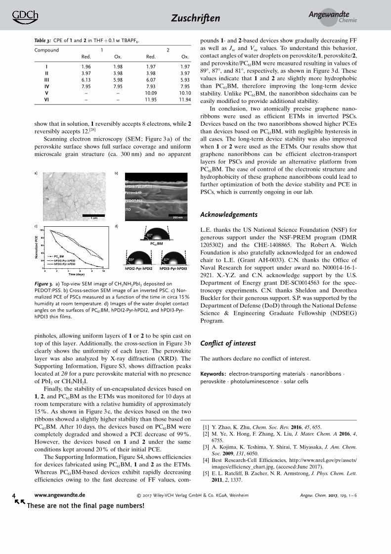
Scanning electron microscopy (SEM; Figure 3a) of theperovskite surface shows full surface coverage and uniformmicroscale grain structure (ca. 300 nm) and no apparent
pinholes, allowing uniform layers of 1 or 2 to be spin cast ontop of this layer. Additionally, the cross-section in Figure 3bclearly shows the uniformity of each layer. The perovskitelayer was also analyzed by X-ray diffraction (XRD). TheSupporting Information, Figure S3, shows diffraction peakslocated at 2q for a pure perovskite material with no presenceof PbI2 or CH3NH2I.
Finally, the stability of un-encapsulated devices based on1, 2, and PC61BM as the ETMs was monitored for 10 days atroom temperature with a relative humidity of approximately15%. As shown in Figure 3c, the devices based on the tworibbons showed a slightly higher stability than those based onPC61BM. After 10 days, the devices based on PC61BM werecompletely degraded and showed a PCE decrease of 99 %.However, the devices based on 1 and 2 under the sameconditions kept around 20% of their initial PCE.
The Supporting Information, Figure S4, shows efficienciesfor devices fabricated using PC61BM, 1 and 2 as the ETMs.Whereas PC61BM-based devices exhibit rapidly decreasingefficiencies owing to the fast decrease of FF values, com-
pounds 1- and 2-based devices show gradually decreasing FFas well as Jsc and Voc values. To understand this behavior,contact angles of water droplets on perovskite/1, perovskite/2,and perovskite/PC61BM were measured resulting in values of898, 878, and 818, respectively, as shown in Figure 3d. Thesevalues indicate that 1 and 2 are slightly more hydrophobicthan PC61BM, therefore improving the long-term devicestability. Unlike PC61BM, the nanoribbon sidechains can beeasily modified to provide additional stability.
In conclusion, two atomically precise graphene nano-ribbons were used as efficient ETMs in inverted PSCs.Devices based on the two nanoribbons showed higher PCEsthan devices based on PC61BM, with negligible hysteresis inall cases. The long-term device stability was also improvedwhen 1 or 2 were used as the ETMs. Our results show thatgraphene nanoribbons can be efficient electron-transportlayers for PSCs and provide an alternative platform fromPC61BM. The ease of control of the electronic structure andhydrophobicity of these graphene nanoribbons could lead tofurther optimization of both the device stability and PCE inPSCs, which is currently ongoing in our lab.
Acknowledgements
L.E. thanks the US National Science Foundation (NSF) forgenerous support under the NSF-PREM program (DMR1205302) and the CHE-1408865. The Robert A. WelchFoundation is also gratefully acknowledged for an endowedchair to L.E. (Grant AH-0033). C.N. thanks the Office ofNaval Research for support under award no. N00014-16-1-2921. X.-Y.Z. and C.N. acknowledge support by the U.S.Department of Energy grant DE-SC0014563 for the spec-troscopy experiments. C.N. thanks Sheldon and DorotheaBuckler for their generous support. S.P. was supported by theDepartment of Defense (DoD) through the National DefenseScience & Engineering Graduate Fellowship (NDSEG)Program.
Conflict of interest
The authors declare no conflict of interest.
Keywords: electron-transporting materials · nanoribbons ·perovskite · photoluminescence · solar cells
[1] Y. Zhao, K. Zhu, Chem. Soc. Rev. 2016, 45, 655.[2] M. Ye, X. Hong, F. Zhang, X. Liu, J. Mater. Chem. A 2016, 4,
6755.[3] A. Kojima, K. Teshima, Y. Shirai, T. Miyasaka, J. Am. Chem.
Soc. 2009, 131, 6050.[4] Best Research-Cell Efficiencies, http://www.nrel.gov/pv/assets/
images/efficiency_chart.jpg, (accesed:June 2017).[5] E. L. Ratcliff, B. Zacher, N. R. Armstrong, J. Phys. Chem. Lett.
2011, 2, 1337.
Table 3: CPE of 1 and 2 in THF +0.1m TBAPF6.
Compound 1 2Red. Ox. Red. Ox.
I 1.96 1.98 1.97 1.97II 3.97 3.98 3.98 3.97III 6.13 5.98 6.07 5.93IV 7.95 7.95 7.93 7.95V – – 10.09 10.10VI – – 11.95 11.94
Figure 3. a) Top-view SEM image of CH3NH3PbI3 deposited onPEDOT:PSS. b) Cross-section SEM image of an inverted PSC. c) Nor-malized PCE of PSCs measured as a function of the time in circa 15%humidity at room temperature. d) Images of the water droplet contactangles on the surfaces of PC61BM, hPDI2-Pyr-hPDI2, and hPDI3-Pyr-hPDI3 thin films.
AngewandteChemieZuschriften
4 www.angewandte.de � 2017 Wiley-VCH Verlag GmbH & Co. KGaA, Weinheim Angew. Chem. 2017, 129, 1 – 6� �
These are not the final page numbers!
[6] S. Yang, W. Fu, Z. Zhang, H. Chen, C.-Z. Li, J. Mater. Chem. A2017, 5, 11462.
[7] K. T. Cho, S. Paek, G. Grancini, C. Roldan-Carmona, P. Gao, Y.Lee, M. K. Nazeeruddin, Energy Environ. Sci. 2017, 10, 621. 0.
[8] D. Luo, L. Zhao, J. Wu, Q. Hu, Y. Zhang, Z. Xu, Y. Liu, T. Liu, K.Chen, W. Yang, W. Zhang, R. Zhu, Q. Gong, Adv. Mater. 2017,29, 1604758.
[9] J. H. Kim, S. T. Williams, N. Cho, C.-C. Chueh, A. K. Y. Jen, Adv.Energy Mater. 2015, 5, 1401229.
[10] Y. Deng, E. Peng, Y. Shao, Z. Xiao, Q. Dong, J. Huang, EnergyEnviron. Sci. 2015, 8, 1544.
[11] C.-C. Chueh, C.-Z. Li, A. K. Y. Jen, Energy Environ. Sci. 2015, 8,1160.
[12] C. Tian, E. Castro, T. Wang, G. Betancourt-Solis, G. Rodriguez,L. Echegoyen, ACS Appl. Mater. Interfaces 2016, 8, 31426.
[13] C. Tian, K. Kochiss, E. Castro, G. Betancourt-Solis, H. Han, L.Echegoyen, J. Mater. Chem. A 2017, 5, 7326.
[14] E. Castro, G. Zavala, S. Seetharaman, F. D�Souza, L. Echegoyen,J. Mater. Chem. A 2017, 5, 19485.
[15] S. Collavini, I. Kosta, S. F. Vçlker, G. Cabanero, H. J. Grande, R.Tena-Zaera, J. L. Delgado, ChemSusChem 2016, 9, 1263.
[16] T. Gatti, E. Menna, M. Meneghetti, M. Maggini, A. Petrozza, F.Lamberti, Nano Energy, DOI: https://doi.org/10.1016/j.nanoen.2017.09.016.
[17] R. Sandoval-Torrientes, J. Pascual, I. Garc�a-Benito, S. Collavini,I. Kosta, R. Tena-Zaera, N. Mart�n, J. L. Delgado, ChemSus-Chem 2017, 10, 2023.
[18] D. Zhao, Z. Zhu, M.-Y. Kuo, C.-C. Chueh, A. K. Y. Jen, Angew.Chem. Int. Ed. 2016, 55, 8999; Angew. Chem. 2016, 128, 9145.
[19] C. Sun, Z. Wu, H.-L. Yip, H. Zhang, X.-F. Jiang, Q. Xue, Z. Hu,Z. Hu, Y. Shen, M. Wang, F. Huang, Y. Cao, Adv. Energy Mater.2016, 6, 1501534.
[20] Z. Zhu, C.-C. Chueh, G. Zhang, F. Huang, H. Yan, A. K. Y. Jen,ChemSusChem 2016, 9, 2586.
[21] P.-Y. Gu, N. Wang, C. Wang, Y. Zhou, G. Long, M. Tian, W.Chen, X. W. Sun, M. G. Kanatzidis, Q. Zhang, J. Mater. Chem. A2017, 5, 7339.
[22] Y. Zhong, M. T. Trinh, R. Chen, G. E. Purdum, P. P. Khlyabich,M. Sezen, S. Oh, H. Zhu, B. Fowler, B. Zhang, W. Wang, C.-Y.Nam, M. Y. Sfeir, C. T. Black, M. L. Steigerwald, Y.-L. Loo, F.Ng, X. Y. Zhu, C. Nuckolls, Nat. Commun. 2015, 6, 8242.
[23] T. J. Sisto, Y. Zhong, B. Zhang, M. T. Trinh, K. Miyata, X. Zhong,X. Y. Zhu, M. L. Steigerwald, F. Ng, C. Nuckolls, J. Am. Chem.Soc. 2017, 139, 5648.
[24] P. Schulz, E. Edri, S. Kirmayer, G. Hodes, D. Cahen, A. Kahn,Energy Environ. Sci. 2014, 7, 1377.
[25] Y. Shao, Y. Yuan, J. Huang, Nat. Energy 2016, 1, 15001.[26] J. You, Z. Hong, Y. Yang, Q. Chen, M. Cai, T.-B. Song, C.-C.
Chen, S. Lu, Y. Liu, H. Zhou, ACS Nano 2014, 8, 1674.[27] P.-W. Liang, C.-Y. Liao, C.-C. Chueh, F. Zuo, S. T. Williams, X.-
K. Xin, J. Lin, A. K. Y. Jen, Adv. Mater. 2014, 26, 3748.[28] S. K. Lee, Y. Zu, A. Herrmann, Y. Geerts, K. M�llen, A. J. Bard,
J. Am. Chem. Soc. 1999, 121, 3513.
Manuscript received: July 6, 2017Accepted manuscript online: September 26, 2017Version of record online: && &&, &&&&
AngewandteChemieZuschriften
5Angew. Chem. 2017, 129, 1 – 6 � 2017 Wiley-VCH Verlag GmbH & Co. KGaA, Weinheim www.angewandte.de
These are not the final page numbers! � �

Zuschriften
Solarenergiematerialien
E. Castro, T. J. Sisto, E. L. Romero, F. Liu,S. R. Peurifoy, J. Wang, X. Zhu,C. Nuckolls,*L. Echegoyen* &&&&—&&&&
Cove-Edge Nanoribbon Materials forEfficient Inverted Halide Perovskite SolarCells
Blaue Nanob�nder-Solarzellen : Zweielektronenarme Graphen-Nanob�nderwerden als Elektronentransportmateria-lien (ETMs) in invertierten Perowskit-Solarzellen (PSCs) genutzt und zeigenhçhere Leistungen als das �blichePC61BM. Die wichtigsten Vorteile sind derhçhere Wirkungsgrad (>10 % alsPC61BM) und die l�ngere Lebensdauerder Zelle, die den hydrophoben Alkylket-ten in den B�ndern zu verdanken ist.
AngewandteChemieZuschriften
6 www.angewandte.de � 2017 Wiley-VCH Verlag GmbH & Co. KGaA, Weinheim Angew. Chem. 2017, 129, 1 – 6� �
These are not the final page numbers!