Embed Size (px)
DESCRIPTION
CPE 626: Advanced VLSI Design L02. Department of Electrical and Computer Engineering University of Alabama in Huntsville. Outline. Simple Processor – MU0 Datapath Design Control Logic ALU Design Pipeline Processor – DLX ISA Registers Addressing Modes and Data Types Instruction Format - PowerPoint PPT Presentation
Citation preview
CPE 626: Advanced VLSI DesignL02
Department of Electrical and Computer Engineering
University of Alabama in Huntsville
19/04/23 UAH-CPE631 2
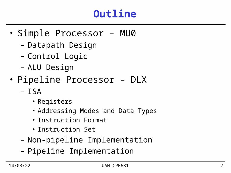
Outline
• Simple Processor – MU0– Datapath Design– Control Logic– ALU Design
• Pipeline Processor – DLX– ISA
• Registers• Addressing Modes and Data Types• Instruction Format• Instruction Set
– Non-pipeline Implementation– Pipeline Implementation
19/04/23 UAH-CPE631 3
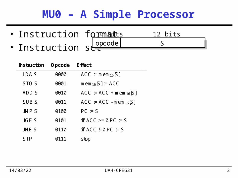
MU0 – A Simple Processor
• Instruction format• Instruction set opcode S
12 bits4 bits
Instruction Opcode Effect
LDA S 0000 ACC := mem16[S]
STO S 0001 mem16[S] := ACC
ADD S 0010 ACC := ACC + mem16[S]
SUB S 0011 ACC := ACC - mem16[S]
JMP S 0100 PC := S
JGE S 0101 if ACC >= 0 PC := S
JNE S 0110 if ACC !=0 PC := S
STP 0111 stop
19/04/23 UAH-CPE631 4
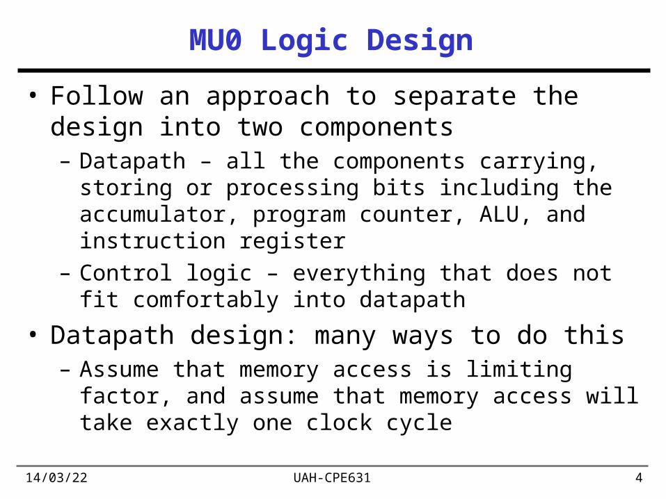
MU0 Logic Design
• Follow an approach to separate the design into two components– Datapath – all the components carrying, storing or
processing bits including the accumulator, program counter, ALU, and instruction register
– Control logic – everything that does not fit comfortably into datapath
• Datapath design: many ways to do this– Assume that memory access is limiting factor, and
assume that memory access will take exactly one clock cycle
19/04/23 UAH-CPE631 5
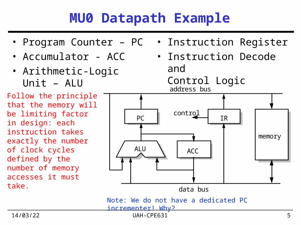
MU0 Datapath Example
• Program Counter – PC• Accumulator - ACC• Arithmetic-Logic Unit –
ALU
• Instruction Register• Instruction Decode and
Control Logic
IRPC
ACCALU
memory
control
address bus
data bus
Follow the principle that the memory will be limiting factor in design: each instruction takes exactly the number of clock cycles defined by the number of memory accesses it must take.
Note: We do not have a dedicated PC incrementer! Why?
19/04/23 UAH-CPE631 6
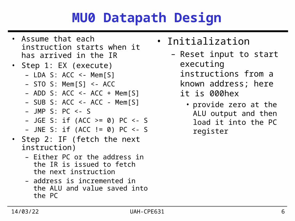
MU0 Datapath Design
• Assume that each instruction starts when it has arrived in the IR
• Step 1: EX (execute)– LDA S: ACC <- Mem[S]– STO S: Mem[S] <- ACC– ADD S: ACC <- ACC + Mem[S]– SUB S: ACC <- ACC - Mem[S]– JMP S: PC <- S– JGE S: if (ACC >= 0) PC <- S– JNE S: if (ACC != 0) PC <- S
• Step 2: IF (fetch the next instruction)– Either PC or the address in the IR
is issued to fetch the next instruction
– address is incremented in the ALU and value saved into the PC
• Initialization– Reset input to start
executing instructions from a known address; here it is 000hex
• provide zero at the ALU output and then load it into the PC register
19/04/23 UAH-CPE631 7
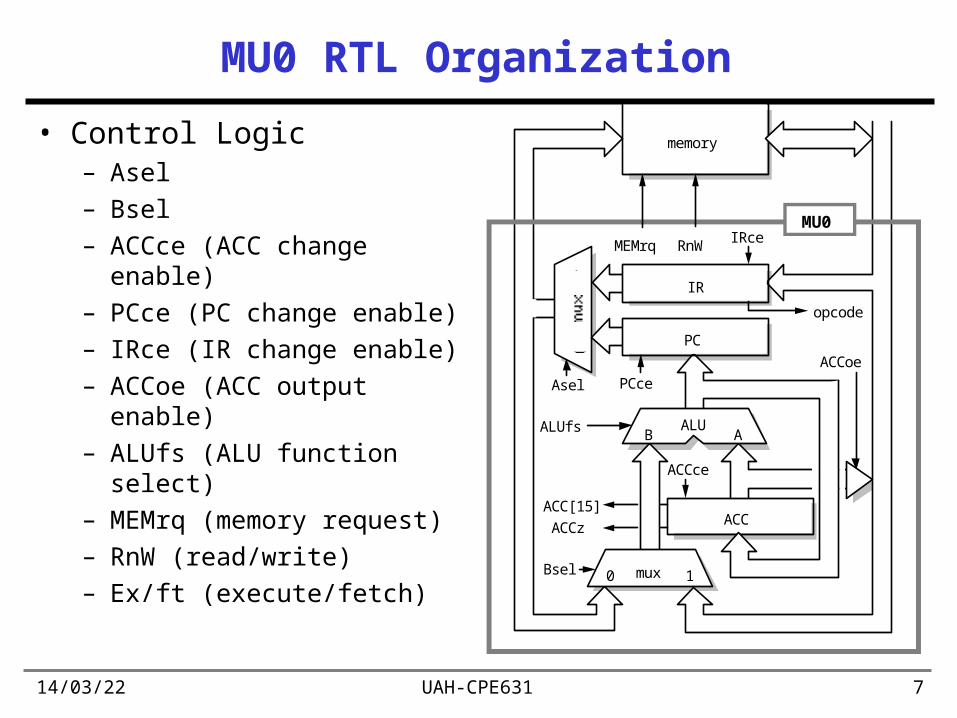
MU0 RTL Organization
• Control Logic– Asel– Bsel– ACCce (ACC change
enable) – PCce (PC change enable)– IRce (IR change enable)– ACCoe (ACC output enable)– ALUfs (ALU function select)– MEMrq (memory request)– RnW (read/write)– Ex/ft (execute/fetch)
memory
ACC
IRce
PCce
ALUfs
Bsel
ACCce
ACCoe
MEMrq RnW
mux0 1
Asel
ALUAB
PC
ACC[15]
ACCz
IR
opcode
MU0
19/04/23 UAH-CPE631 8
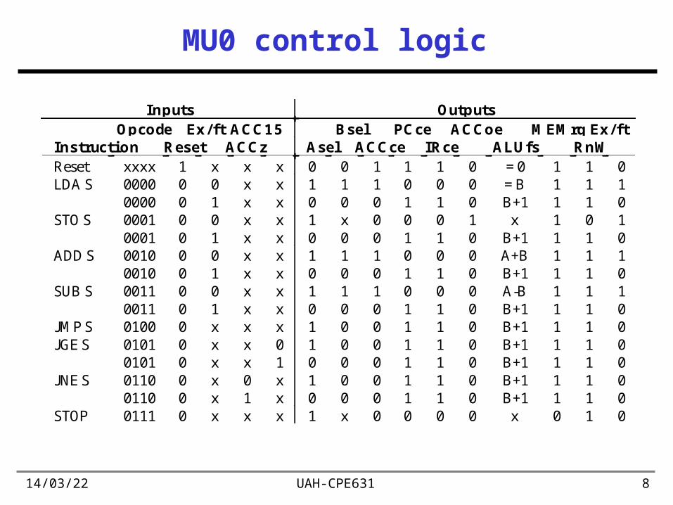
MU0 control logic
Inputs Outputs Opco de Ex / f t ACC1 5 Bs e l PCce ACCo e MEMrq Ex / f tIns truct i o n Res et ACCz As el ACCce IRce ALUfs RnWReset xxxx 1 x x x 0 0 1 1 1 0 = 0 1 1 0LDA S 0000
000000
01
xx
xx
10
10
10
01
01
00
= BB+1
11
11
10
STO S 00010001
00
01
xx
xx
10
x0
00
01
01
10
xB+1
11
01
10
ADD S 00100010
00
01
xx
xx
10
10
10
01
01
00
A+BB+1
11
11
10
SUB S 00110011
00
01
xx
xx
10
10
10
01
01
00
A-BB+1
11
11
10
JMP S 0100 0 x x x 1 0 0 1 1 0 B+1 1 1 0JGE S 0101
010100
xx
xx
01
10
00
00
11
11
00
B+1B+1
11
11
00
JNE S 01100110
00
xx
01
xx
10
00
00
11
11
00
B+1B+1
11
11
00
STOP 0111 0 x x x 1 x 0 0 0 0 x 0 1 0
19/04/23 UAH-CPE631 9
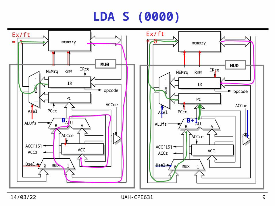
LDA S (0000)
memory
ACC
IRce
PCce
ALUfs
Bsel
ACCce
ACCoe
MEMrq RnW
mux0 1
Asel
ALUAB
PC
ACC[15]
ACCz
IR
opcode
MU0
memory
ACC
IRce
PCce
ALUfs
Bsel
ACCce
ACCoe
MEMrq RnW
mux0 1
Asel
ALUAB
PC
ACC[15]
ACCz
IR
opcode
MU0
B
Ex/ft = 1 Ex/ft = 0
B+1
19/04/23 UAH-CPE631 10
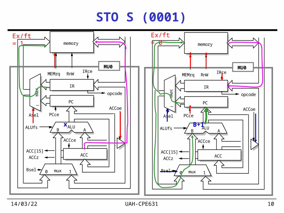
STO S (0001)
memory
ACC
IRce
PCce
ALUfs
Bsel
ACCce
ACCoe
MEMrq RnW
mux0 1
Asel
ALUAB
PC
ACC[15]
ACCz
IR
opcode
MU0
memory
ACC
IRce
PCce
ALUfs
Bsel
ACCce
ACCoe
MEMrq RnW
mux0 1
Asel
ALUAB
PC
ACC[15]
ACCz
IR
opcode
MU0
x
Ex/ft = 1 Ex/ft = 0
B+1
19/04/23 UAH-CPE631 11
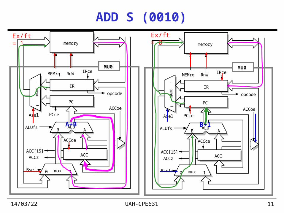
ADD S (0010)
memory
ACC
IRce
PCce
ALUfs
Bsel
ACCce
ACCoe
MEMrq RnW
mux0 1
Asel
ALUAB
PC
ACC[15]
ACCz
IR
opcode
MU0
memory
ACC
IRce
PCce
ALUfs
Bsel
ACCce
ACCoe
MEMrq RnW
mux0 1
Asel
ALUAB
PC
ACC[15]
ACCz
IR
opcode
MU0
A+B
Ex/ft = 1 Ex/ft = 0
B+1
19/04/23 UAH-CPE631 12
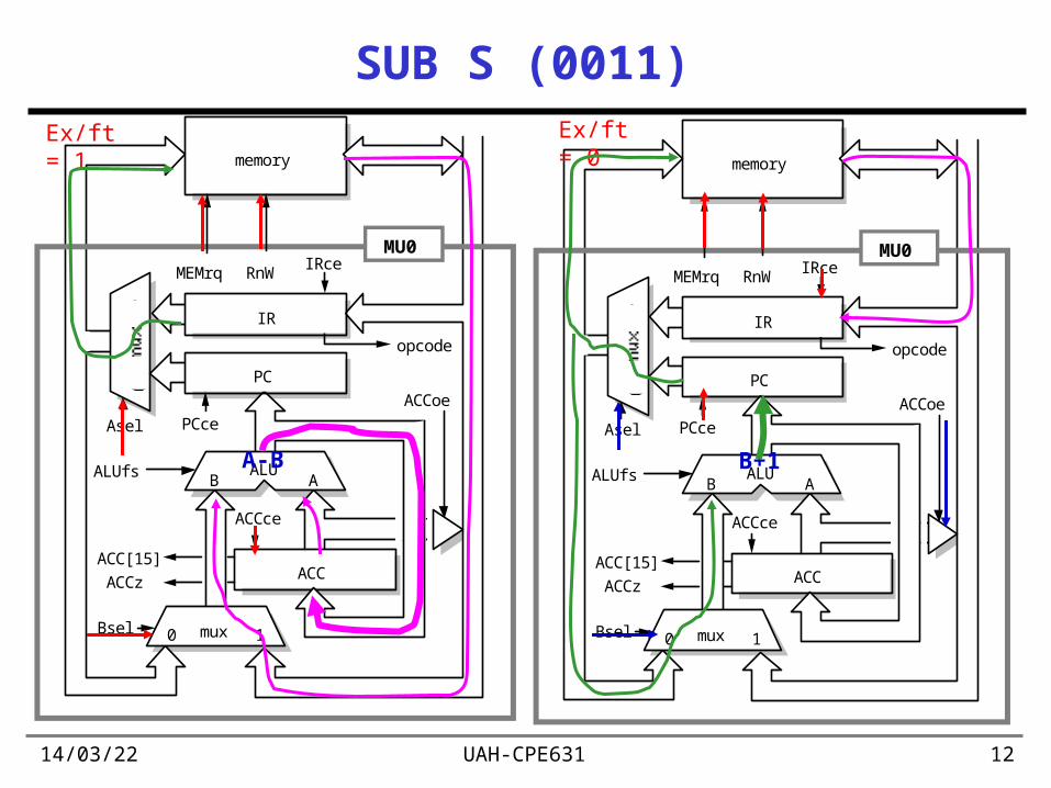
SUB S (0011)
memory
ACC
IRce
PCce
ALUfs
Bsel
ACCce
ACCoe
MEMrq RnW
mux0 1
Asel
ALUAB
PC
ACC[15]
ACCz
IR
opcode
MU0
memory
ACC
IRce
PCce
ALUfs
Bsel
ACCce
ACCoe
MEMrq RnW
mux0 1
Asel
ALUAB
PC
ACC[15]
ACCz
IR
opcode
MU0
A-B
Ex/ft = 1 Ex/ft = 0
B+1
19/04/23 UAH-CPE631 13
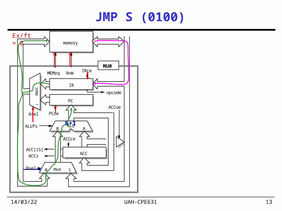
JMP S (0100)
memory
ACC
IRce
PCce
ALUfs
Bsel
ACCce
ACCoe
MEMrq RnW
mux0 1
Asel
ALUAB
PC
ACC[15]
ACCz
IR
opcode
MU0
B+1
Ex/ft = 0
19/04/23 UAH-CPE631 14
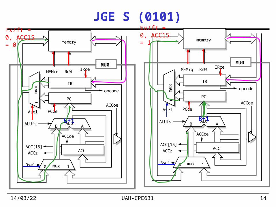
JGE S (0101)
memory
ACC
IRce
PCce
ALUfs
Bsel
ACCce
ACCoe
MEMrq RnW
mux0 1
Asel
ALUAB
PC
ACC[15]
ACCz
IR
opcode
MU0
B+1
Ex/ft = 0, ACC15 = 0 memory
ACC
IRce
PCce
ALUfs
Bsel
ACCce
ACCoe
MEMrq RnW
mux0 1
Asel
ALUAB
PC
ACC[15]
ACCz
IR
opcode
MU0
B+1
Ex/ft = 0, ACC15 = 1
19/04/23 UAH-CPE631 15
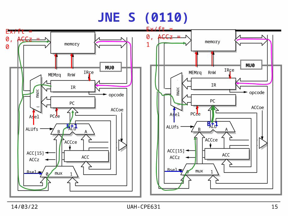
JNE S (0110)
memory
ACC
IRce
PCce
ALUfs
Bsel
ACCce
ACCoe
MEMrq RnW
mux0 1
Asel
ALUAB
PC
ACC[15]
ACCz
IR
opcode
MU0
B+1
Ex/ft = 0, ACCz = 0 memory
ACC
IRce
PCce
ALUfs
Bsel
ACCce
ACCoe
MEMrq RnW
mux0 1
Asel
ALUAB
PC
ACC[15]
ACCz
IR
opcode
MU0
B+1
Ex/ft = 0, ACCz = 1
19/04/23 UAH-CPE631 16
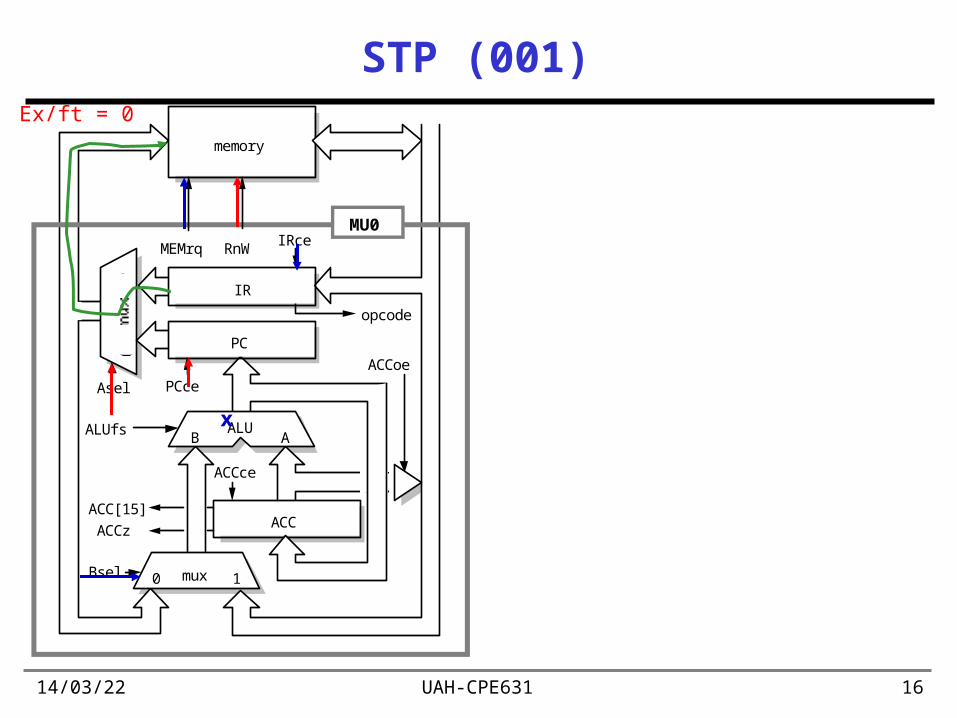
STP (001)
memory
ACC
IRce
PCce
ALUfs
Bsel
ACCce
ACCoe
MEMrq RnW
mux0 1
Asel
ALUAB
PC
ACC[15]
ACCz
IR
opcode
MU0
x
Ex/ft = 0
19/04/23 UAH-CPE631 17
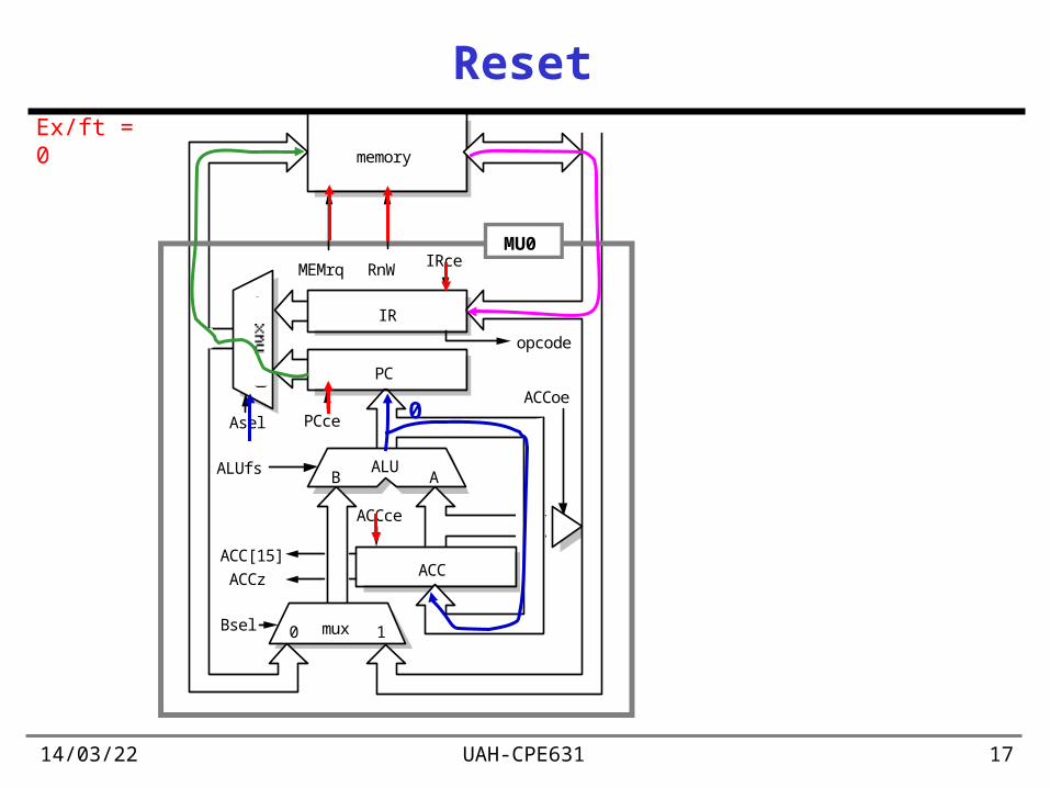
Reset
memory
ACC
IRce
PCce
ALUfs
Bsel
ACCce
ACCoe
MEMrq RnW
mux0 1
Asel
ALUAB
PC
ACC[15]
ACCz
IR
opcode
MU0
0
Ex/ft = 0
19/04/23 UAH-CPE631 18
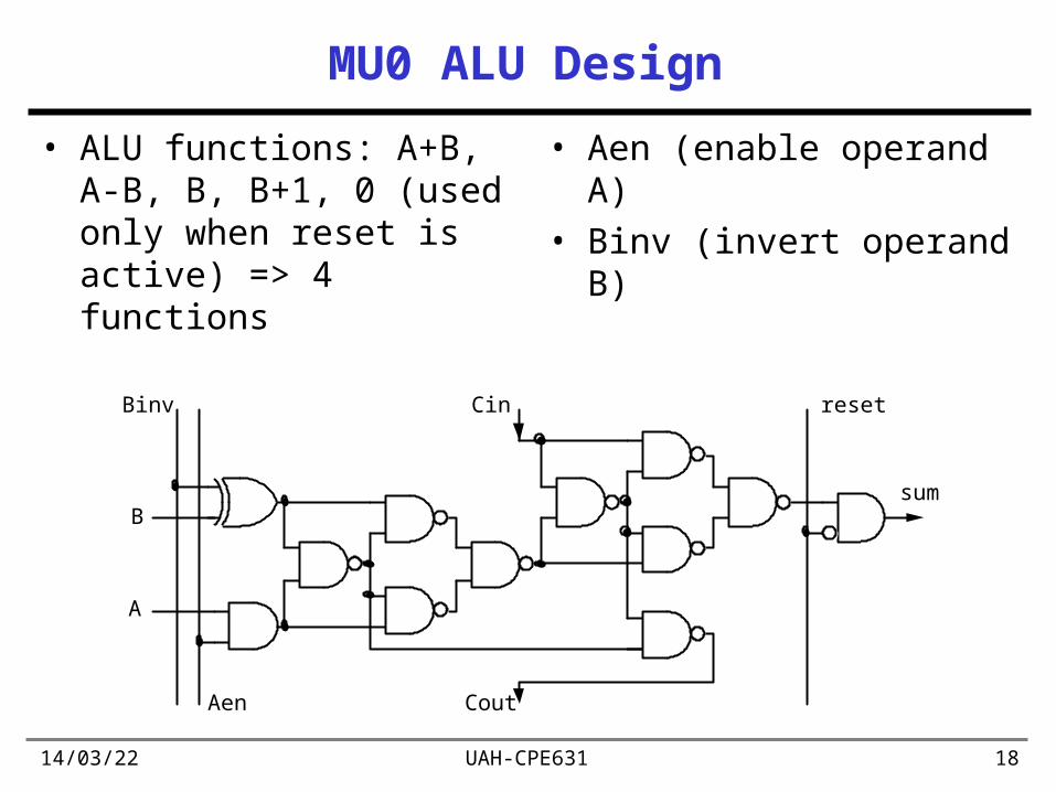
MU0 ALU Design
• ALU functions: A+B, A-B, B, B+1, 0 (used only when reset is active) => 4 functions
• Aen (enable operand A)• Binv (invert operand B)
Cin
Cout
sum
reset
B
A
Aen
Binv
Another Example:DLX Architecture
19/04/23 UAH-CPE631 20
DLX Registers
• GPRs with load-store architecture• GPR: 32 32-bit named R0, R1,... R31, R0=0• FPR (floating point registers):
– single precision:32 32-bit named F0, F1,... F31 (accessed independently)
– double precision:16 64-bit named F0, F2,... F30 (accessed in pairs)
• Instructions which support transfers between GPRs and FPRs
• Other status registers, e.g., floating-point status register (hold information about the results of FP ops)
19/04/23 UAH-CPE631 21
Addressing Modes and Data Types
• Immediate with a 16-bit value field• Displacement with a 16-bit displacement
– register deferred derived when disp=0– absolute derived from displacement with R0
• Byte addressable in big-endian with 32-bit address • All memory references are load/store through GPR
or FPR and must be aligned • Data types
– 8-bit bytes, 16-bit half words (loaded into registers with either zeros or the sign bit replicated to fill 32 bits)
– 32-bit integers– 32-bit single precision and 64-bit double-precision for FP
19/04/23 UAH-CPE631 22
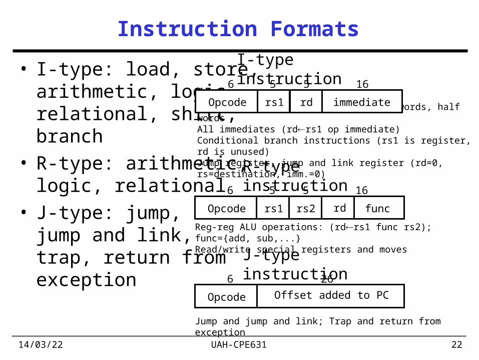
Instruction Formats
• I-type: load, store, arithmetic, logic, relational, shift, branch
• R-type: arithmetic, logic, relational
• J-type: jump, jump and link, trap, return from exception
I-type instruction
Encodes: Loads and stores of bytes, words, half wordsAll immediates (rdrs1 op immediate)Conditional branch instructions (rs1 is register, rd is unused)Jump register, jump and link register (rd=0, rs=destination, imm.=0)
Opcode rs1 rd immediate
16556
R-type instruction
Reg-reg ALU operations: (rdrs1 func rs2); func={add, sub,...}Read/write special registers and moves
Opcode rs1 rs2 func
16556
rd
J-type instruction
Jump and jump and link; Trap and return from exception
Opcode Offset added to PC
266
19/04/23 UAH-CPE631 23
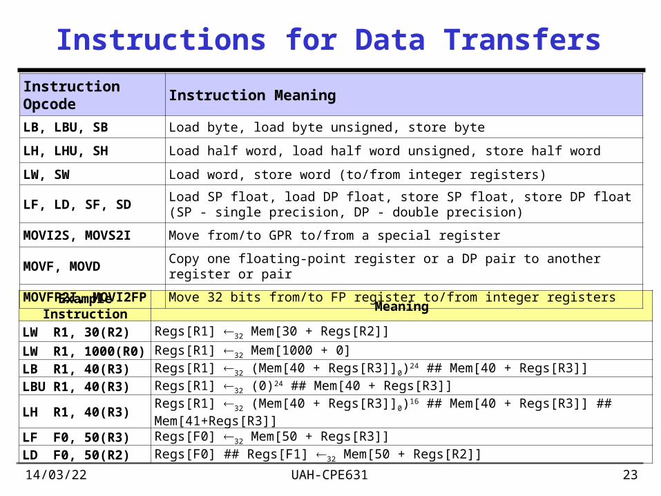
Instructions for Data Transfers
Example Instruction Meaning
LW R1, 30(R2) Regs[R1] 32 Mem[30 + Regs[R2]]
LW R1, 1000(R0) Regs[R1] 32 Mem[1000 + 0]
LB R1, 40(R3) Regs[R1] 32 (Mem[40 + Regs[R3]]0)24 ## Mem[40 + Regs[R3]]
LBU R1, 40(R3) Regs[R1] 32 (0)24 ## Mem[40 + Regs[R3]]
LH R1, 40(R3) Regs[R1] 32 (Mem[40 + Regs[R3]]0)16 ## Mem[40 + Regs[R3]] ## Mem[41+Regs[R3]]
LF F0, 50(R3) Regs[F0] 32 Mem[50 + Regs[R3]]
LD F0, 50(R2) Regs[F0] ## Regs[F1] 32 Mem[50 + Regs[R2]]
Instruction Opcode Instruction Meaning
LB, LBU, SB Load byte, load byte unsigned, store byte
LH, LHU, SH Load half word, load half word unsigned, store half word
LW, SW Load word, store word (to/from integer registers)
LF, LD, SF, SDLoad SP float, load DP float, store SP float, store DP float (SP - single precision, DP - double precision)
MOVI2S, MOVS2I Move from/to GPR to/from a special register
MOVF, MOVD Copy one floating-point register or a DP pair to another register or pair
MOVFP2I, MOVI2FP Move 32 bits from/to FP register to/from integer registers
19/04/23 UAH-CPE631 24
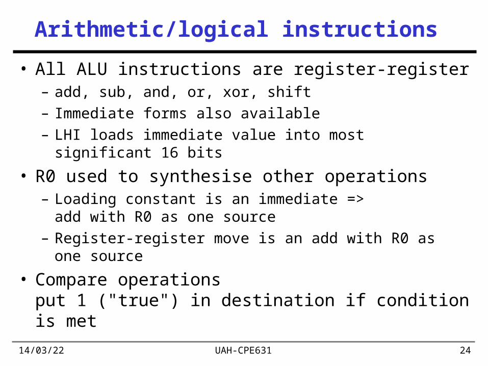
Arithmetic/logical instructions
• All ALU instructions are register-register – add, sub, and, or, xor, shift – Immediate forms also available – LHI loads immediate value into most significant 16 bits
• R0 used to synthesise other operations – Loading constant is an immediate =>
add with R0 as one source – Register-register move is an add with R0 as one source
• Compare operations put 1 ("true") in destination if condition is met
19/04/23 UAH-CPE631 25
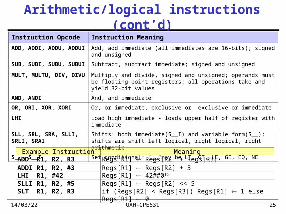
Arithmetic/logical instructions (cont’d)
Example Instruction MeaningADD R1, R2, R3 Regs[R1] Regs[R2] + Regs[R3]ADDI R1, R2, #3 Regs[R1] Regs[R2] + 3LHI R1, #42 Regs[R1] 42##016
SLLI R1, R2, #5 Regs[R1] Regs[R2] << 5SLT R1, R2, R3 if (Regs[R2] < Regs[R3]) Regs[R1] 1 else Regs[R1] 0
Instruction Opcode Instruction Meaning
ADD, ADDI, ADDU, ADDUI Add, add immediate (all immediates are 16-bits); signed and unsigned
SUB, SUBI, SUBU, SUBUI Subtract, subtract immediate; signed and unsigned
MULT, MULTU, DIV, DIVU Multiply and divide, signed and unsigned; operands must be floating-point registers; all operations take and yield 32-bit values
AND, ANDI And, and immediate
OR, ORI, XOR, XORI Or, or immediate, exclusive or, exclusive or immediate
LHI Load high immediate - loads upper half of register with immediate
SLL, SRL, SRA, SLLI, SRLI, SRAI
Shifts: both immediate(S__I) and variable form(S__); shifts are shift left logical, right logical, right arithmetic
S__, S__I Set conditional: "__"may be LT, GT, LE, GE, EQ, NE
19/04/23 UAH-CPE631 26
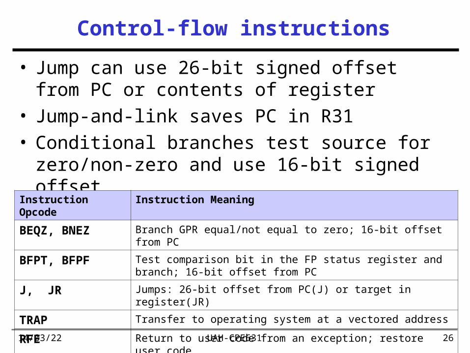
Control-flow instructions
• Jump can use 26-bit signed offset from PC or contents of register
• Jump-and-link saves PC in R31 • Conditional branches test source for zero/non-zero
and use 16-bit signed offset
Instruction Opcode Instruction Meaning
BEQZ, BNEZ Branch GPR equal/not equal to zero; 16-bit offset from PC
BFPT, BFPF Test comparison bit in the FP status register and branch; 16-bit offset from PC
J, JR Jumps: 26-bit offset from PC(J) or target in register(JR)
TRAP Transfer to operating system at a vectored address
RFE Return to user code from an exception; restore user code
19/04/23 UAH-CPE631 27
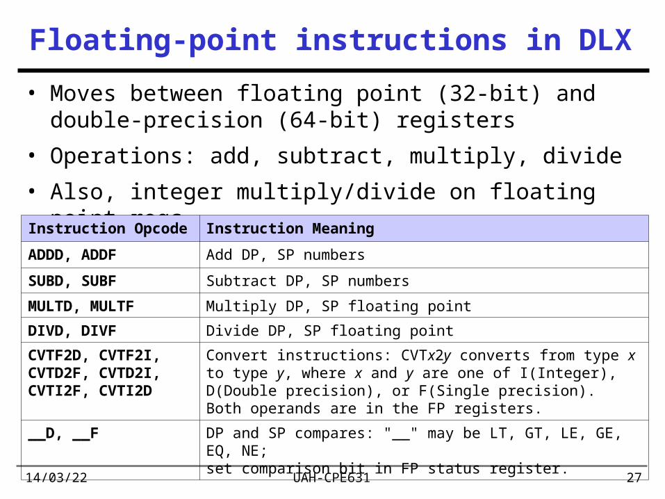
Floating-point instructions in DLX
• Moves between floating point (32-bit) and double-precision (64-bit) registers
• Operations: add, subtract, multiply, divide
• Also, integer multiply/divide on floating point regs
Instruction Opcode Instruction Meaning
ADDD, ADDF Add DP, SP numbers
SUBD, SUBF Subtract DP, SP numbers
MULTD, MULTF Multiply DP, SP floating point
DIVD, DIVF Divide DP, SP floating point
CVTF2D, CVTF2I, CVTD2F, CVTD2I, CVTI2F, CVTI2D
Convert instructions: CVTx2y converts from type x to type y, where x and y are one of I(Integer), D(Double precision), or F(Single precision). Both operands are in the FP registers.
__D, __F DP and SP compares: "__" may be LT, GT, LE, GE, EQ, NE; set comparison bit in FP status register.
A Simple Implementationof DLX
19/04/23 UAH-CPE631 29
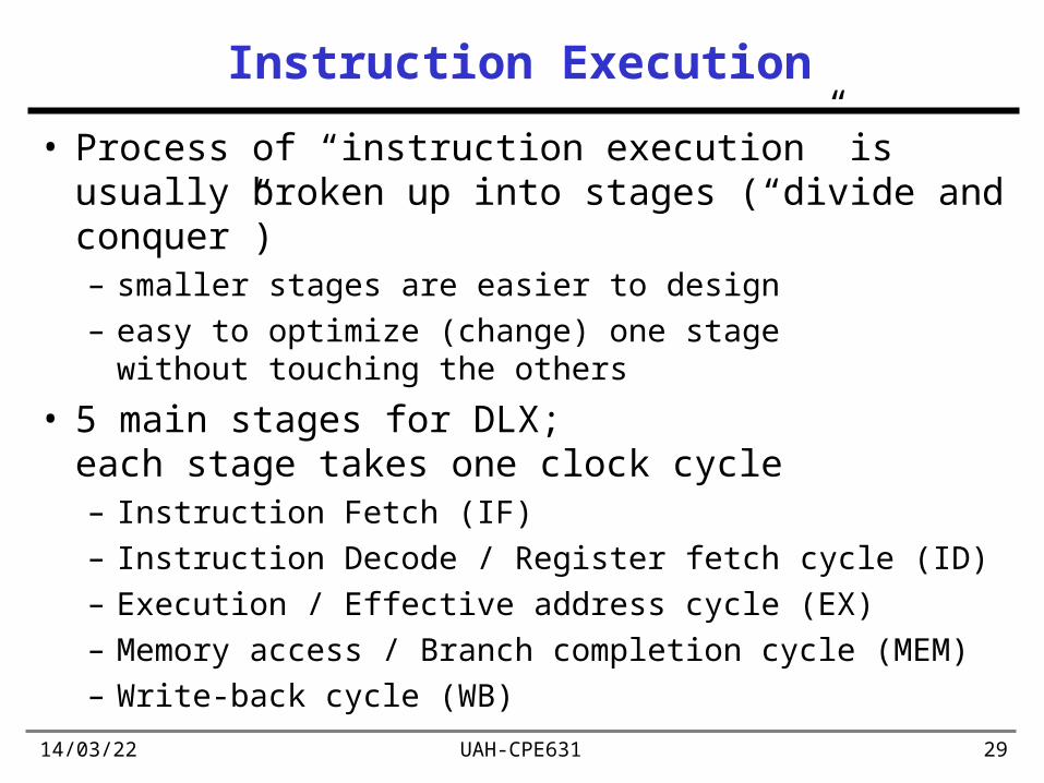
Instruction Execution
• Process of “instruction execution” is usually broken up into stages (“divide and conquer”)– smaller stages are easier to design– easy to optimize (change) one stage
without touching the others
• 5 main stages for DLX; each stage takes one clock cycle– Instruction Fetch (IF)– Instruction Decode / Register fetch cycle (ID)– Execution / Effective address cycle (EX)– Memory access / Branch completion cycle (MEM)– Write-back cycle (WB)
19/04/23 UAH-CPE631 30
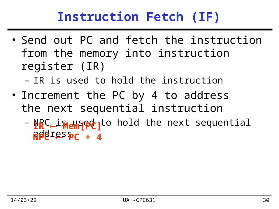
Instruction Fetch (IF)
• Send out PC and fetch the instruction from the memory into instruction register (IR)– IR is used to hold the instruction
• Increment the PC by 4 to address the next sequential instruction– NPC is used to hold the next sequential address
IR Mem[PC]NPC PC + 4
19/04/23 UAH-CPE631 31
Instruction Decode (ID)
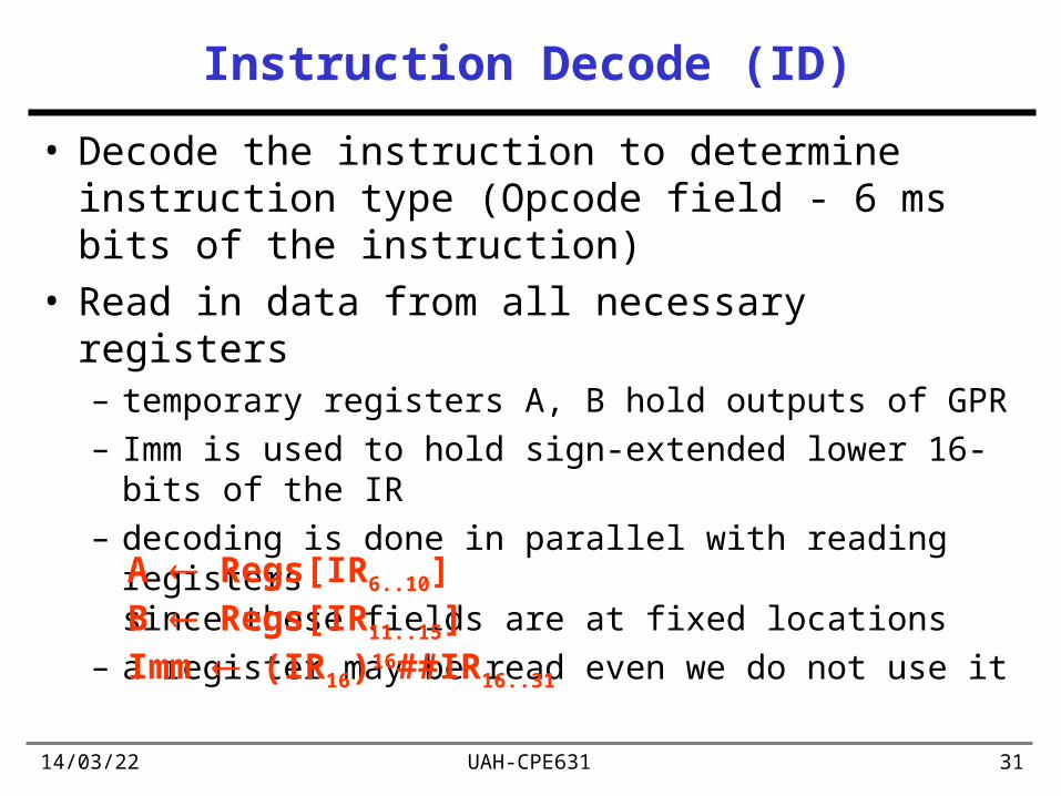
• Decode the instruction to determine instruction type (Opcode field - 6 ms bits of the instruction)
• Read in data from all necessary registers– temporary registers A, B hold outputs of GPR– Imm is used to hold sign-extended lower 16-bits of the IR– decoding is done in parallel with reading registers
since these fields are at fixed locations– a register may be read even we do not use it
A Regs[IR6..10]B Regs[IR11..15]Imm (IR16)16##IR16..31
19/04/23 UAH-CPE631 32
Execution [EX] (1/2)
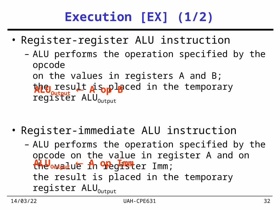
• Register-register ALU instruction– ALU performs the operation specified by the opcode
on the values in registers A and B;the result is placed in the temporary register ALUOutput
• Register-immediate ALU instruction– ALU performs the operation specified by the opcode on
the value in register A and on the value in register Imm;the result is placed in the temporary register ALUOutput
ALUOutput A op B
ALUOutput A op Imm
19/04/23 UAH-CPE631 33
Execution [EX] (2/2)
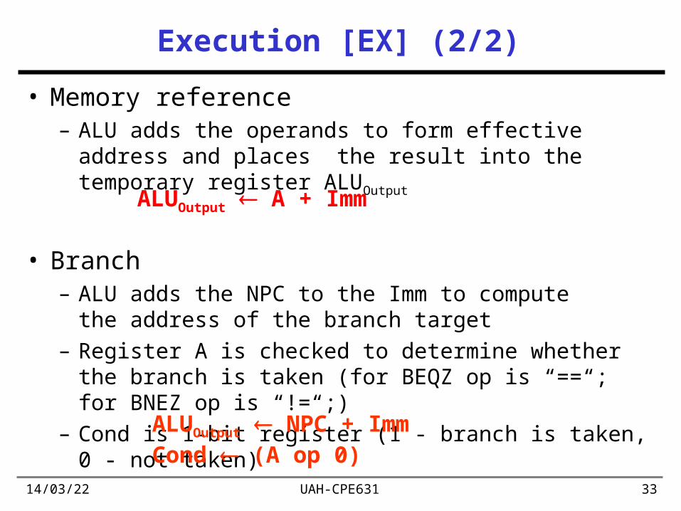
• Memory reference– ALU adds the operands to form effective address and
places the result into the temporary register ALUOutput
• Branch– ALU adds the NPC to the Imm to compute
the address of the branch target– Register A is checked to determine whether the branch
is taken (for BEQZ op is “==“; for BNEZ op is “!=“;)– Cond is 1-bit register (1 - branch is taken, 0 - not taken)
ALUOutput A + Imm
ALUOutput NPC + ImmCond (A op 0)
19/04/23 UAH-CPE631 34
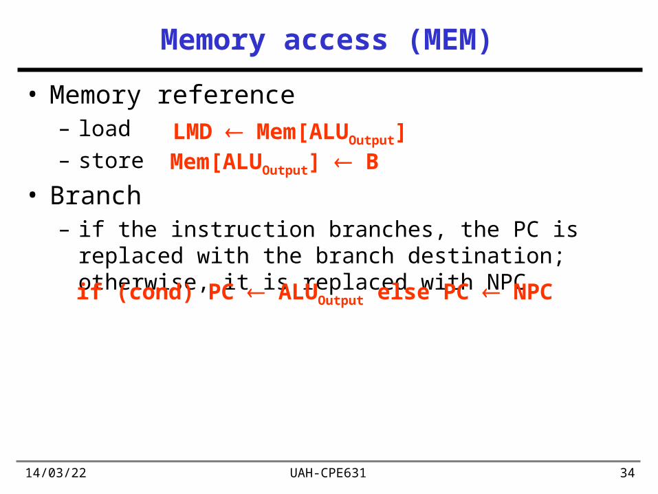
Memory access (MEM)
• Memory reference– load– store
• Branch– if the instruction branches, the PC is replaced with the
branch destination; otherwise, it is replaced with NPC
LMD Mem[ALUOutput]
if (cond) PC ALUOutput else PC NPC
Mem[ALUOutput] B
19/04/23 UAH-CPE631 35
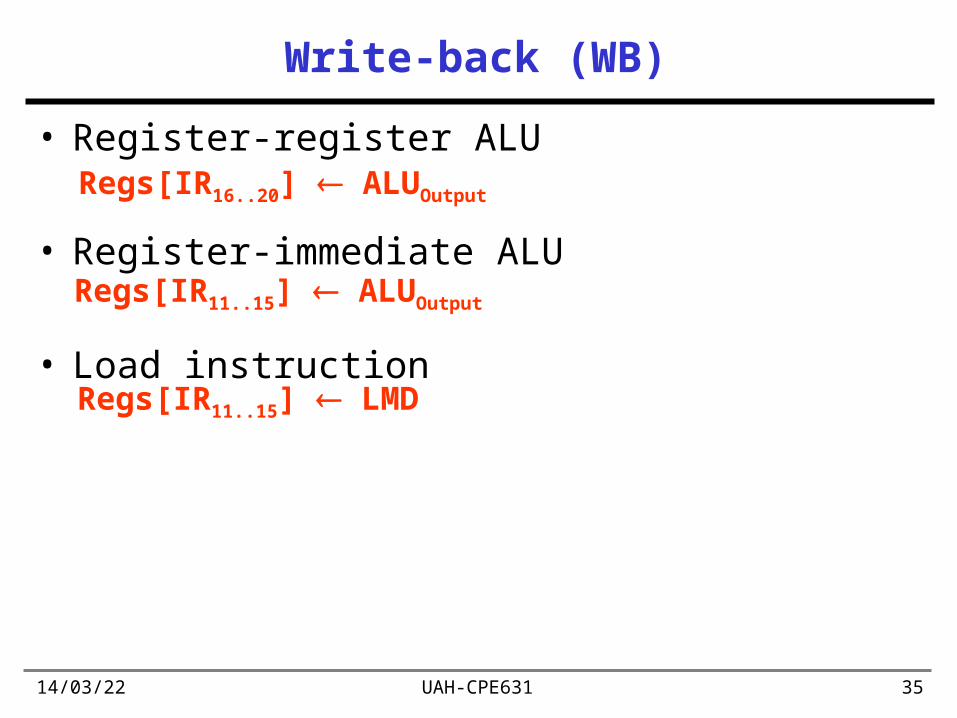
Write-back (WB)
• Register-register ALU
• Register-immediate ALU
• Load instruction
Regs[IR16..20] ALUOutput
Regs[IR11..15] ALUOutput
Regs[IR11..15] LMD
19/04/23 UAH-CPE631 36
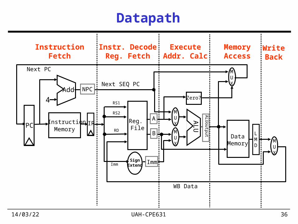
Datapath
MemoryAccess
WriteBack
InstructionFetch
Instr. DecodeReg. Fetch
ExecuteAddr. Calc
InstructionMemory
SignExtend
4 Zero?
Next SEQ PC
Next PC
WB Data
PCRD
RS1
RS2
Imm
Add
MUX
MUX
MUX
IR
MUX
DataMemory
ALU
LMD
Reg. File
A
B
NPC
Imm
ALU
output
19/04/23 UAH-CPE631 37
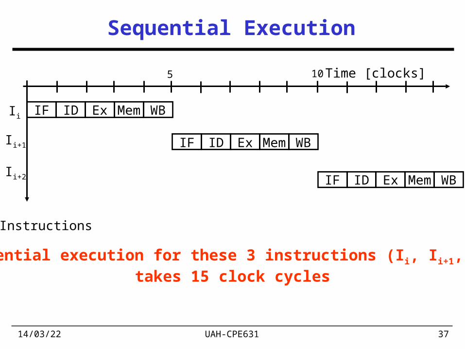
Sequential Execution
Time [clocks]
MemIF ID Ex WB
MemIF ID Ex WB
MemIF ID Ex WB
Instructions
Ii
Ii+1
Ii+2
Sequential execution for these 3 instructions (Ii, Ii+1, Ii+2)takes 15 clock cycles
5 10
19/04/23 UAH-CPE631 38
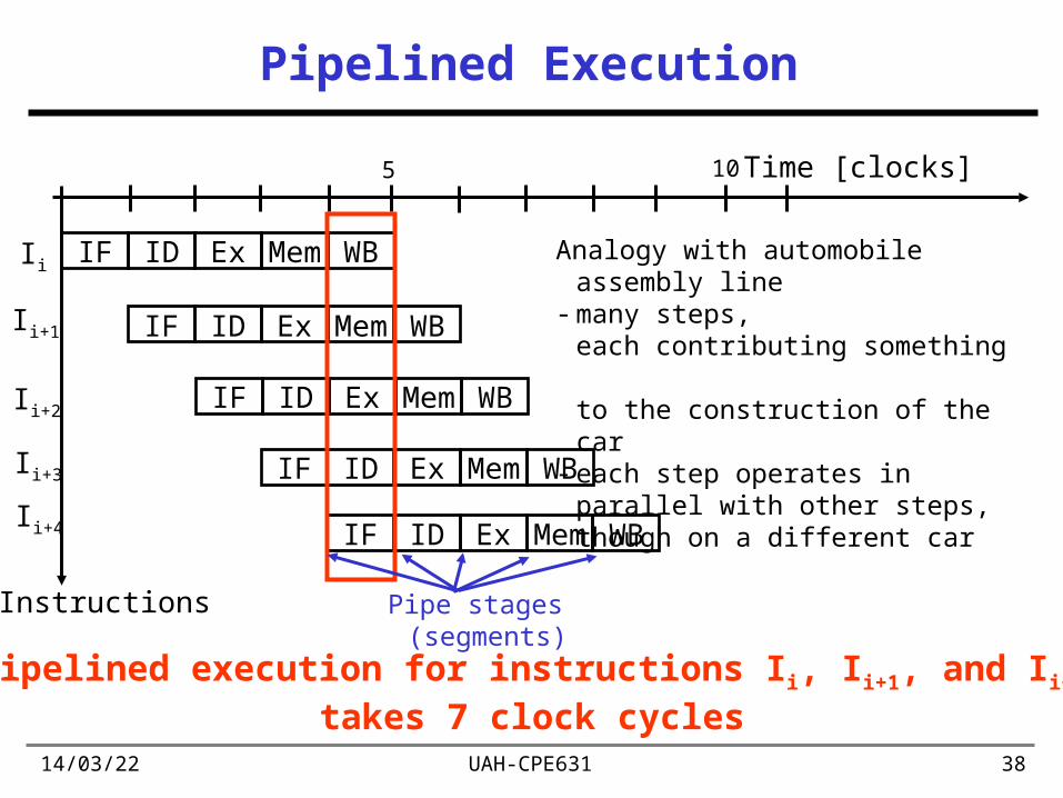
Pipelined Execution
Time [clocks]
MemIF ID Ex WB
MemIF ID Ex WB
MemIF ID Ex WB
Instructions
Ii
Ii+1
Ii+2
Pipelined execution for instructions Ii, Ii+1, and Ii+2
takes 7 clock cycles
5 10
Ii+3 MemIF ID Ex WB
MemIF ID Ex WBIi+4
Analogy with automobile assembly line- many steps,
each contributing something to the construction of the car
- each step operates in parallel with other steps, though on a different car
Pipe stages (segments)
19/04/23 UAH-CPE631 39
Pipelining Lessons
Time [clocks]
MemIF ID Ex WB
MemIF ID Ex WB
MemIF ID Ex WB
Instructions
Ii
Ii+1
Ii+2
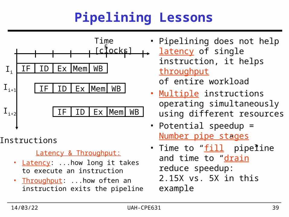
5• Pipelining does not help
latency of single instruction, it helps throughput of entire workload
• Multiple instructions operating simultaneously using different resources
• Potential speedup = Number pipe stages
• Time to “fill” pipeline and time to “drain” reduce speedup: 2.15X vs. 5X in this example
Latency & Throughput:• Latency: ...how long it takes to
execute an instruction• Throughput: ...how often an
instruction exits the pipeline
19/04/23 UAH-CPE631 40
Pipelining Lessons (cont’d)
Time [clocks]
MemIF ID Ex WB
MemIF ID Ex WB
MemIF ID Ex WB
Instructions
Ii
Ii+1
Ii+2
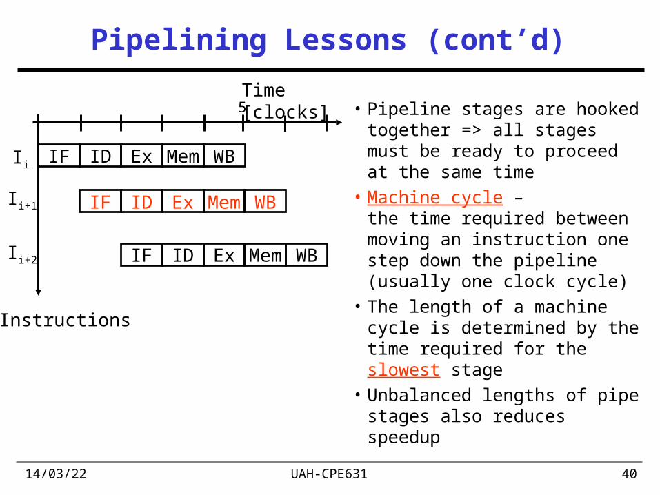
5 • Pipeline stages are hooked together => all stages must be ready to proceed at the same time
• Machine cycle – the time required between moving an instruction one step down the pipeline (usually one clock cycle)
• The length of a machine cycle is determined by the time required for the slowest stage
• Unbalanced lengths of pipe stages also reduces speedup
19/04/23 UAH-CPE631 41
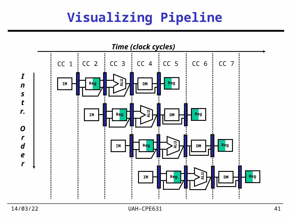
Visualizing Pipeline
Reg AL
U
DMIM Reg
Reg AL
U
DMIM Reg
Reg AL
U
DMIM Reg
Instr.
Order
Time (clock cycles)
Reg AL
U
DMIM Reg
CC 2 CC 3 CC 4 CC 6 CC 7CC 5CC 1
19/04/23 UAH-CPE631 42
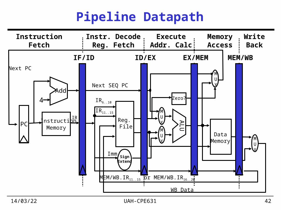
Pipeline Datapath
MemoryAccess
WriteBack
InstructionFetch
Instr. DecodeReg. Fetch
ExecuteAddr. Calc
InstructionMemory
SignExtend
4 Zero?
Next SEQ PC
Next PC
WB Data
PC
IR6..10
Imm
Add
MUX
MUX
MUX
MUX
DataMemory
ALU
Reg. File
IR11..15
ID/EXIF/ID EX/MEM MEM/WB
MEM/WB.IR11..15 or MEM/WB.IR16..20
IR
19/04/23 UAH-CPE631 43
Instruction Flow through Pipeline Regs
Reg
ALU
DM
IMR
eg
CC 2 CC 3CC 1
Reg
ALU
DM
IMR
eg
Reg
ALU
DM
IMR
eg
Add R1,R2,R3
Nop
Nop
Nop
Add R1,R2,R3
Nop
Nop
Lw R4,0(R2)
Add R1,R2,R3
Nop
Lw R4,0(R2)
Sub R6,R5,R7
Reg
ALU
DM
IMR
eg
Add R1,R2,R3
Lw R4,0(R2)
Sub R6,R5,R7
CC 4
Xor R9,R8,R1
Time (clock cycles)
19/04/23 UAH-CPE631 44
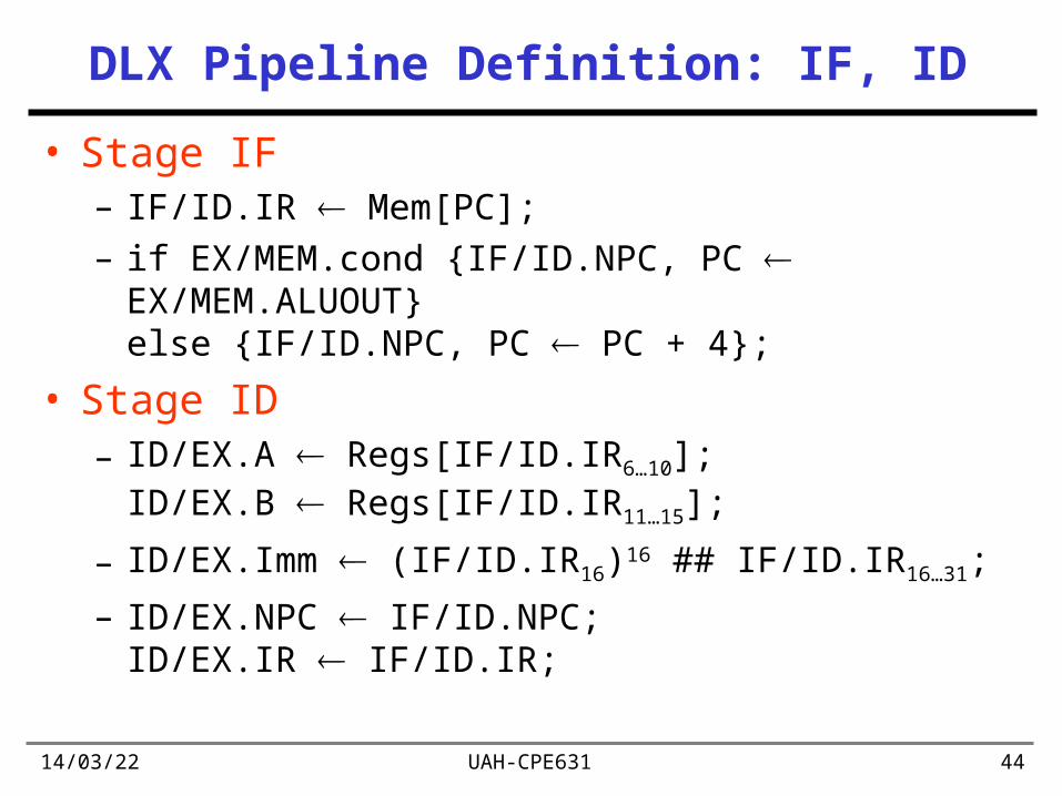
DLX Pipeline Definition: IF, ID
• Stage IF– IF/ID.IR Mem[PC];– if EX/MEM.cond {IF/ID.NPC, PC EX/MEM.ALUOUT}
else {IF/ID.NPC, PC PC + 4};
• Stage ID– ID/EX.A Regs[IF/ID.IR6…10];
ID/EX.B Regs[IF/ID.IR11…15];
– ID/EX.Imm (IF/ID.IR16)16 ## IF/ID.IR16…31;
– ID/EX.NPC IF/ID.NPC; ID/EX.IR IF/ID.IR;
19/04/23 UAH-CPE631 45
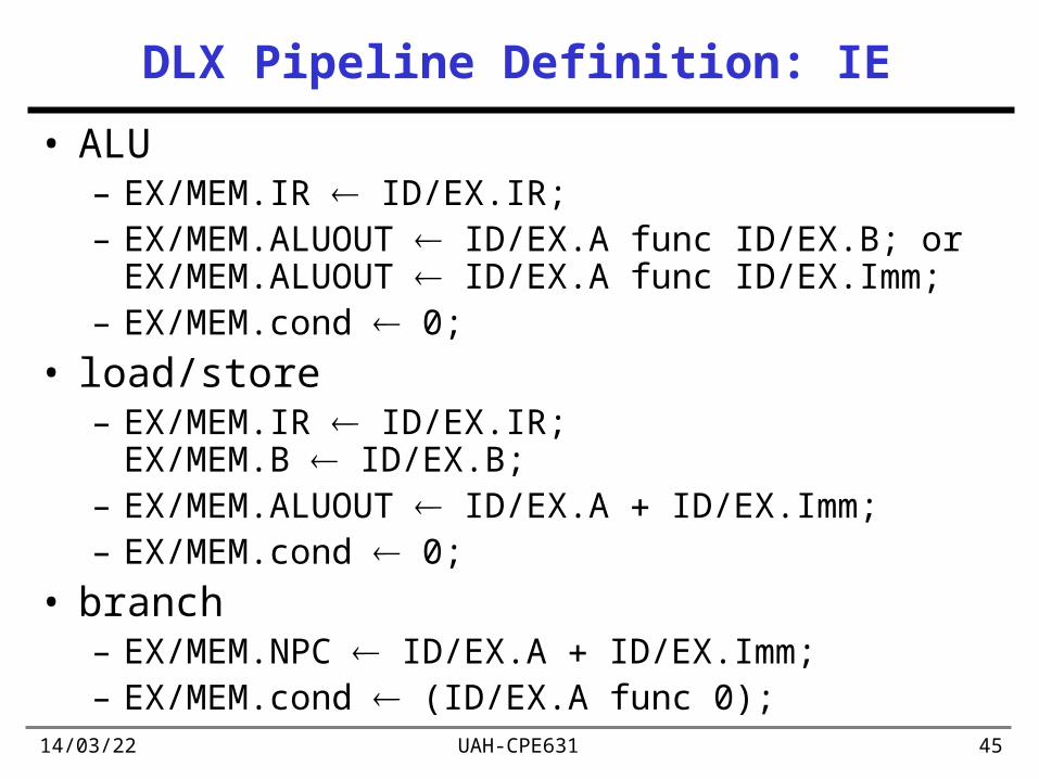
DLX Pipeline Definition: IE
• ALU – EX/MEM.IR ID/EX.IR;– EX/MEM.ALUOUT ID/EX.A func ID/EX.B; or
EX/MEM.ALUOUT ID/EX.A func ID/EX.Imm;– EX/MEM.cond 0;
• load/store– EX/MEM.IR ID/EX.IR;
EX/MEM.B ID/EX.B;– EX/MEM.ALUOUT ID/EX.A ID/EX.Imm; – EX/MEM.cond 0;
• branch – EX/MEM.NPC ID/EX.A ID/EX.Imm;– EX/MEM.cond (ID/EX.A func 0);
19/04/23 UAH-CPE631 46
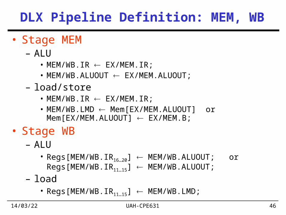
DLX Pipeline Definition: MEM, WB
• Stage MEM– ALU
• MEM/WB.IR EX/MEM.IR;• MEM/WB.ALUOUT EX/MEM.ALUOUT;
– load/store• MEM/WB.IR EX/MEM.IR;• MEM/WB.LMD Mem[EX/MEM.ALUOUT] or
Mem[EX/MEM.ALUOUT] EX/MEM.B;
• Stage WB– ALU
• Regs[MEM/WB.IR16…20] MEM/WB.ALUOUT; orRegs[MEM/WB.IR11…15] MEM/WB.ALUOUT;
– load• Regs[MEM/WB.IR11…15] MEM/WB.LMD;