Embed Size (px)
Citation preview
CPE/EE 421 Microcomputers:Motorola 68000 – The CPU Hardware Model
Instructor: Dr Aleksandar MilenkovicLecture Notes
CPE/EE 421/521 Microcomputers
2
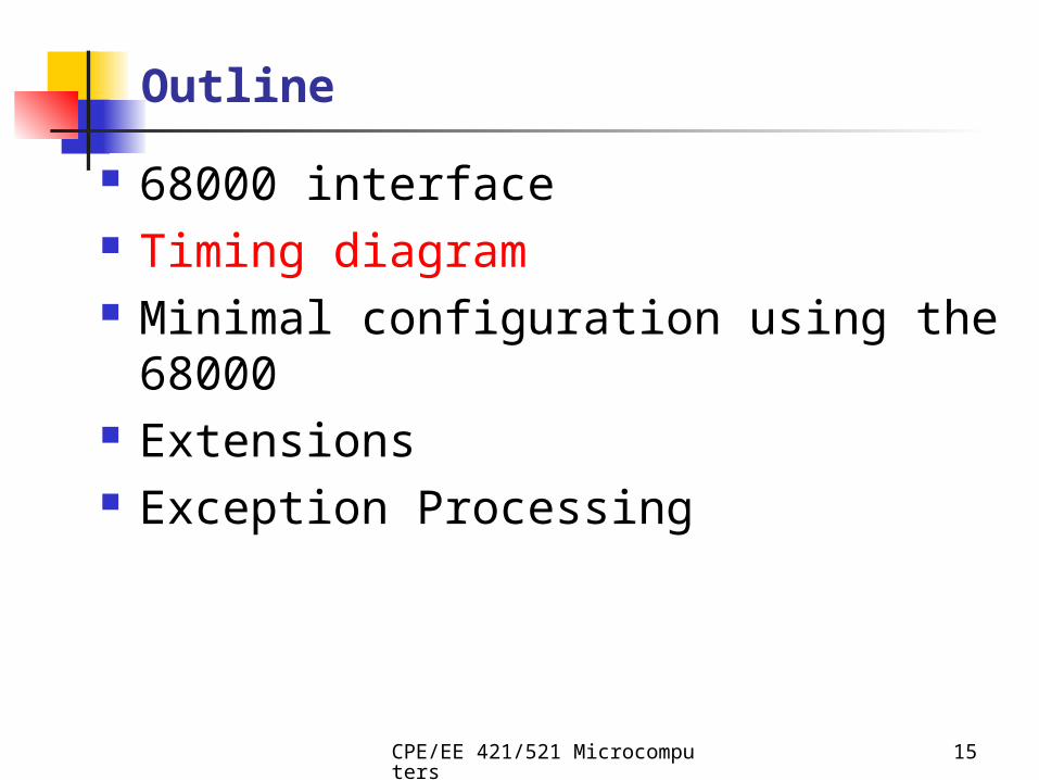
Outline
68000 interface Timing diagram Minimal configuration using the 68000 Extensions Exception Processing
CPE/EE 421/521 Microcomputers
3
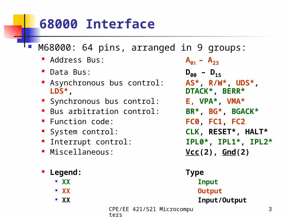
68000 Interface
M68000: 64 pins, arranged in 9 groups: Address Bus: A01 – A23
Data Bus: D00 – D15 Asynchronous bus control: AS*, R/W*, UDS*,
LDS*, DTACK*, BERR* Synchronous bus control: E, VPA*, VMA* Bus arbitration control: BR*, BG*, BGACK* Function code: FC0, FC1, FC2 System control: CLK, RESET*, HALT* Interrupt control: IPL0*, IPL1*, IPL2* Miscellaneous: Vcc(2), Gnd(2)
Legend: Type XX Input XX Output XX Input/Output
CPE/EE 421/521 Microcomputers
4
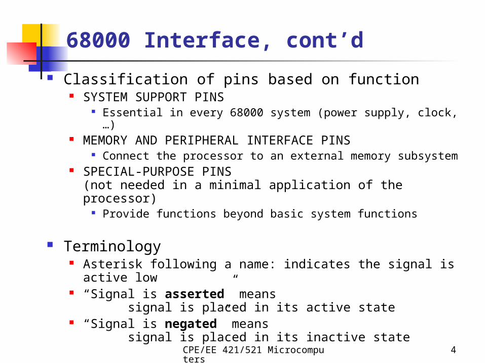
68000 Interface, cont’d
Classification of pins based on function SYSTEM SUPPORT PINS
Essential in every 68000 system (power supply, clock, …) MEMORY AND PERIPHERAL INTERFACE PINS
Connect the processor to an external memory subsystem SPECIAL-PURPOSE PINS
(not needed in a minimal application of the processor) Provide functions beyond basic system functions
Terminology Asterisk following a name: indicates the signal is active low “Signal is asserted” means
signal is placed in its active state “Signal is negated” means
signal is placed in its inactive state
CPE/EE 421/521 Microcomputers
5
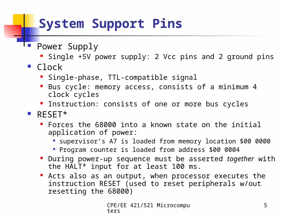
System Support Pins
Power Supply Single +5V power supply: 2 Vcc pins and 2 ground pins
Clock Single-phase, TTL-compatible signal Bus cycle: memory access, consists of a minimum 4 clock
cycles Instruction: consists of one or more bus cycles
RESET* Forces the 68000 into a known state on the initial application of
power: supervisor’s A7 is loaded from memory location $00 0000 Program counter is loaded from address $00 0004
During power-up sequence must be asserted together with the HALT* input for at least 100 ms.
Acts also as an output, when processor executes the instruction RESET (used to reset peripherals w/out resetting the 68000)
CPE/EE 421/521 Microcomputers
6
System Support Pins, cont’d
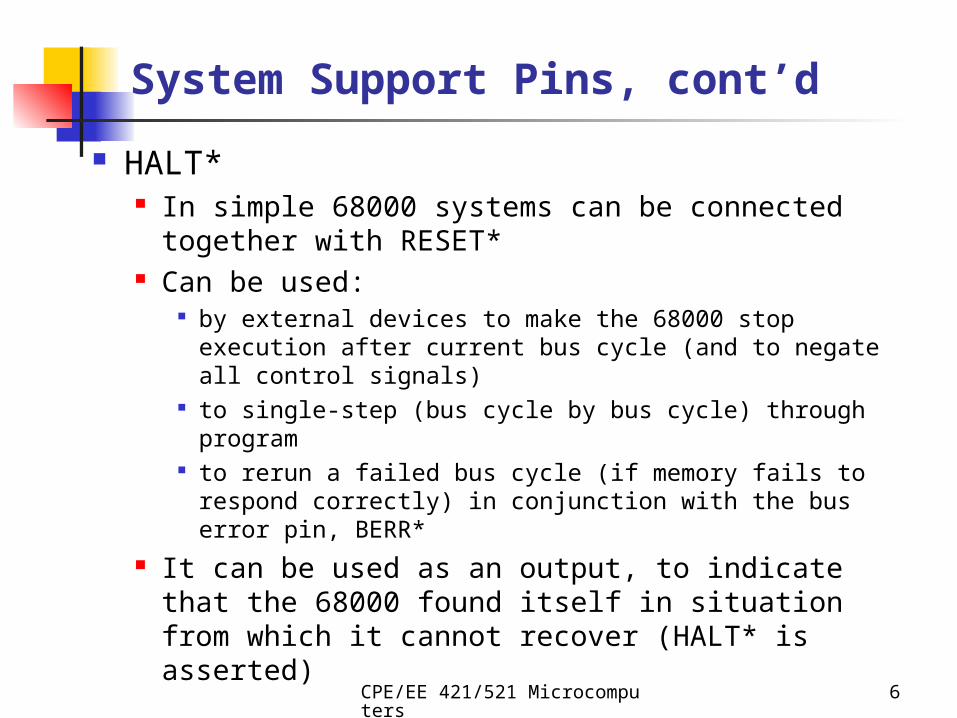
HALT* In simple 68000 systems can be connected together
with RESET* Can be used:
by external devices to make the 68000 stop execution after current bus cycle (and to negate all control signals)
to single-step (bus cycle by bus cycle) through program to rerun a failed bus cycle (if memory fails to respond
correctly) in conjunction with the bus error pin, BERR* It can be used as an output, to indicate that the
68000 found itself in situation from which it cannot recover (HALT* is asserted)
CPE/EE 421/521 Microcomputers
7
Memory and Peripheral Interface Pins
Address Bus 23-bit address bus, permits 223 16-bit words to be addressed Tri-state output pins (to permit devices other then the CPU to
take a control over it) Auxiliary function:
supports vectored interrupts Address lines A01, A02, A03 indicate the level of the interrupt being
serviced All other address lines are set to a high level
Data Bus Bi-directional 16-bit wide data bus
During a CPU read cycle acts as an input During a CPU write cycle acts as an output
Byte operations: only D00-D07 or D08-D15 are active Interrupting device identifies itself to the CPU by placing an
interrupt vector number on D00-D07 during an interrupt acknowledge cycle
CPE/EE 421/521 Microcomputers
8
Memory and Peripheral Interface Pins, cont’d
AS* When asserted, indicates that the content of the address bus is
valid. R/W*
Determines the type of a memory access cycle CPU is reading from memory: R/W* = 1 CPU is writing to memory: R/W* = 0 If CPU is performing internal operation, R/W* is always 1 When CPU relinquishes control of its busses, R/W* is undefined
UDS* and LDS* Used to determine the size of the data being accessed If both UDS* and LDS* are asserted, word is accessed R/W* UDS* LDS*
010: write lower byte (D00 – D07: data valid, replicated on D8-D15) 000: write word (D00 – D15: data valid) 101: read upper byte (D00 – D07: invalid, D8-D15 – data valid)
CPE/EE 421/521 Microcomputers
9
Memory and Peripheral Interface Pins, cont’d
DTACK* (Data Transfer Acknowledge) Handshake signal generated by the device being
accessed Indicates that the contents of the data bus is valid If DTACK* is not asserted, CPU generates wait-
states until DTACK goes low or until an error state is declared.
When DTACK* is asserted, CPU completes the current access and begins the next cycle
DTACK* has to be generated a certain time after the beginning of a valid memory access (timer supplied by the system designer).
CPE/EE 421/521 Microcomputers
10
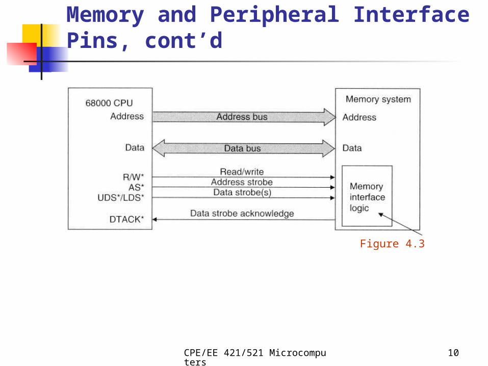
Memory and Peripheral Interface Pins, cont’d
Figure 4.3
CPE/EE 421/521 Microcomputers
11
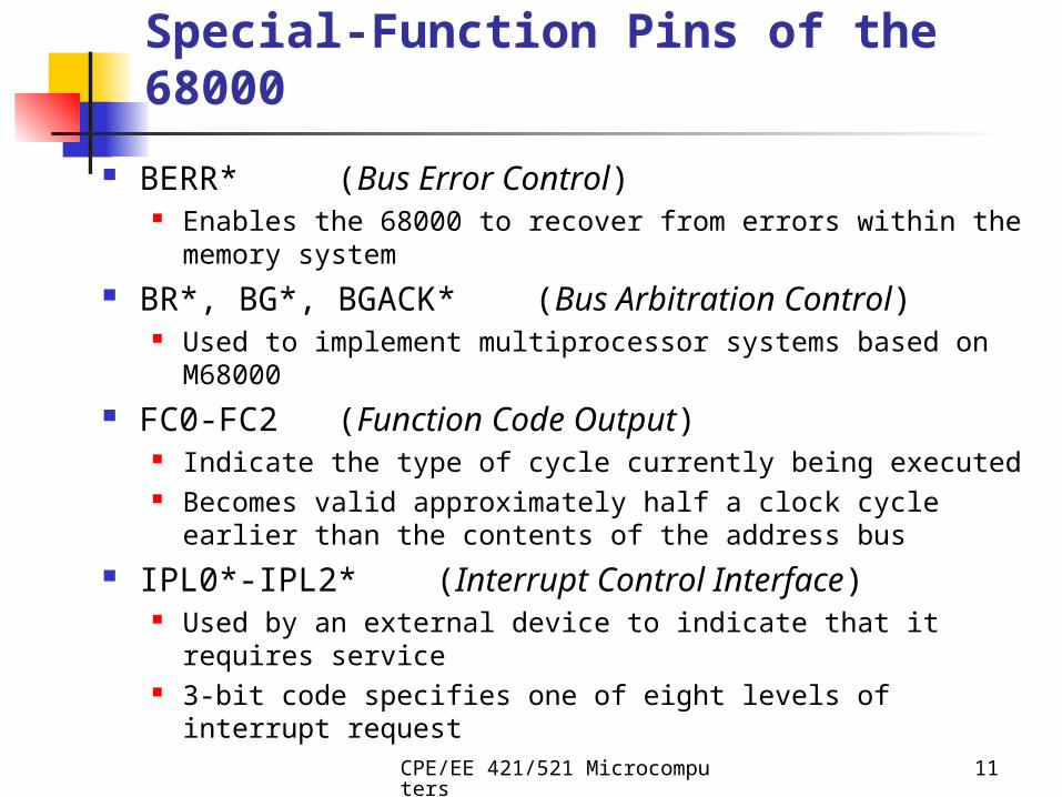
Special-Function Pins of the 68000
BERR* (Bus Error Control) Enables the 68000 to recover from errors within the memory
system BR*, BG*, BGACK* (Bus Arbitration Control)
Used to implement multiprocessor systems based on M68000 FC0-FC2 (Function Code Output)
Indicate the type of cycle currently being executed Becomes valid approximately half a clock cycle earlier than the
contents of the address bus IPL0*-IPL2* (Interrupt Control Interface)
Used by an external device to indicate that it requires service 3-bit code specifies one of eight levels of interrupt request
CPE/EE 421/521 Microcomputers
12
Special-Function Pins of the 68000Function Code Outputs
Function Code Output
FC2 FC1 FC0 Processor Cycle Type
0 0 0 Undefined, reserved
0 0 1 User data
0 1 0 User program
0 1 1 Undefined, reserved
1 0 0 Undefined, reserved
1 0 1 Supervisor data
1 1 0 Supervisor program
1 1 1 CPU space (interrupt acknowledge)
Function Code Output
FC2 FC1 FC0 Processor Cycle Type
0 0 0 Undefined, reserved
0 0 1 User data
0 1 0 User program
0 1 1 Undefined, reserved
1 0 0 Undefined, reserved
1 0 1 Supervisor data
1 1 0 Supervisor program
1 1 1 CPU space (interrupt acknowledge)
CPE/EE 421/521 Microcomputers
13
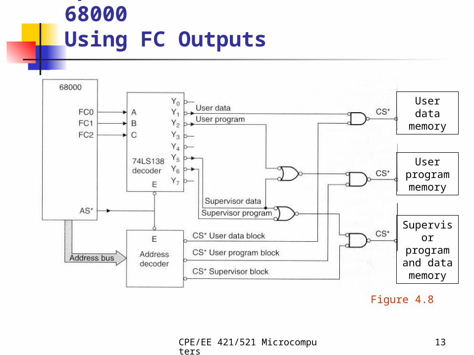
Special-Function Pins of the 68000Using FC Outputs
User data memory
User program memory
Supervisor program and data memory
Figure 4.8
CPE/EE 421/521 Microcomputers
14
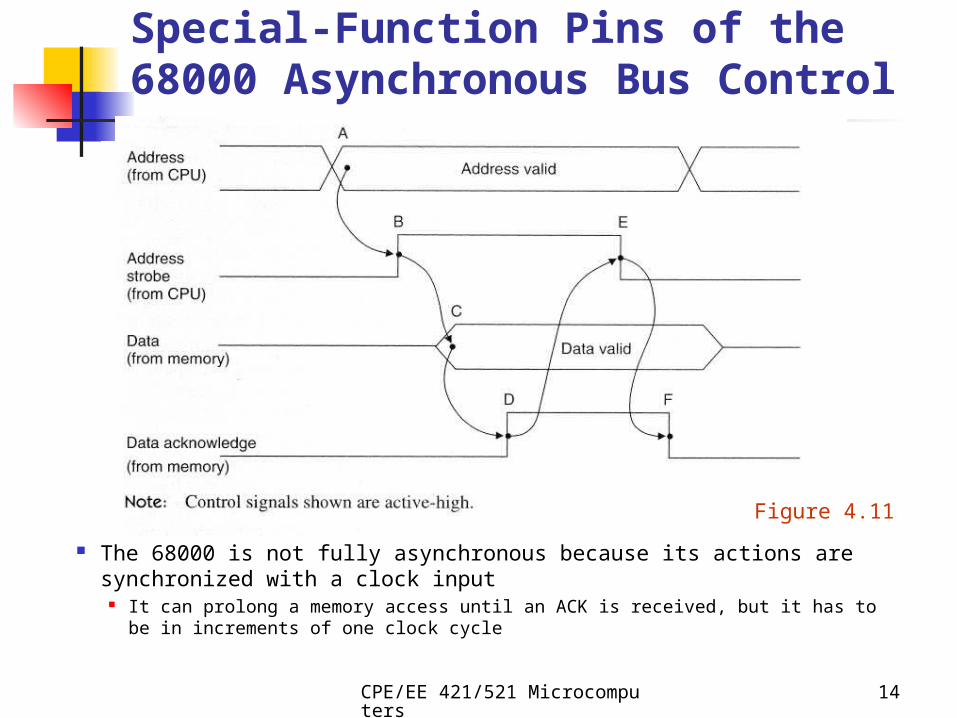
The 68000 is not fully asynchronous because its actions are synchronized with a clock input
It can prolong a memory access until an ACK is received, but it has to be in increments of one clock cycle
Figure 4.11
Special-Function Pins of the 68000 Asynchronous Bus Control
CPE/EE 421/521 Microcomputers
15
Outline
68000 interface Timing diagram Minimal configuration using the 68000 Extensions Exception Processing
CPE/EE 421/521 Microcomputers
16
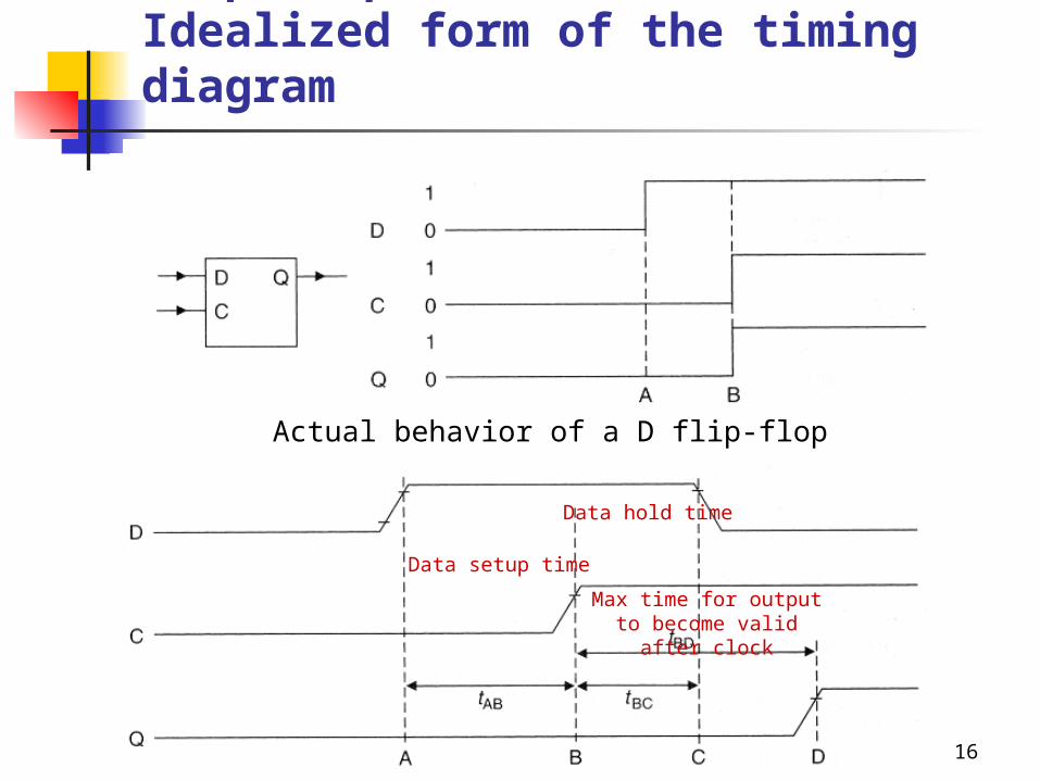
Actual behavior of a D flip-flop
Data hold time
Data setup time
Max time for output to become valid after clock
Timing Diagram of a Simple Flip-FlopIdealized form of the timing diagram
CPE/EE 421/521 Microcomputers
17
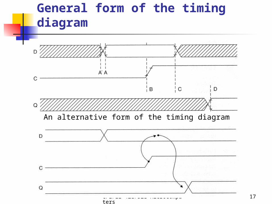
An alternative form of the timing diagram
General form of the timing diagram
CPE/EE 421/521 Microcomputers
18
The Clock
A microprocessor requires a clock that provides a stream of timing pulses to control its internal operations
A 68000 memory access takes a minimum of eight clock states numbered from clock state S0 to clock state S7
CPE/EE 421/521 Microcomputers
19
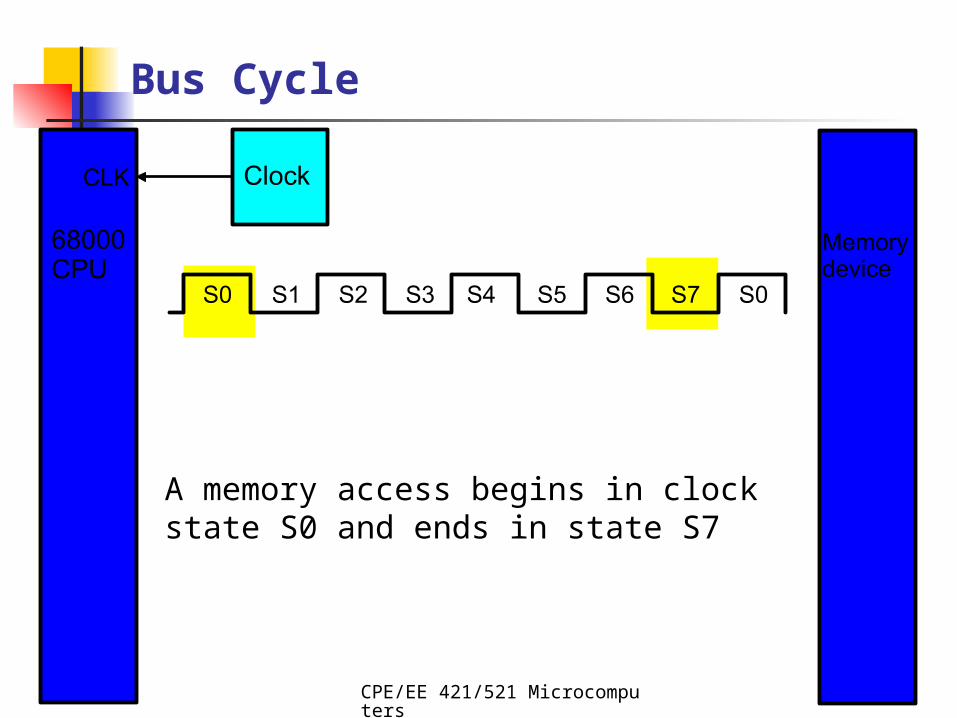
A memory access begins in clockstate S0 and ends in state S7
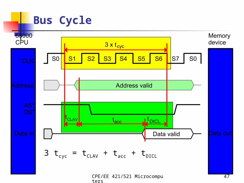
Bus Cycle
CPE/EE 421/521 Microcomputers
20
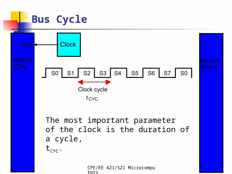
The most important parameterof the clock is the duration of a cycle,tCYC.
Bus Cycle
CPE/EE 421/521 Microcomputers
21
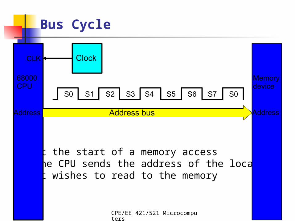
At the start of a memory accessthe CPU sends the address of the locationit wishes to read to the memory
Bus Cycle
CPE/EE 421/521 Microcomputers
22
Address Timing
We are interested in when the 68000 generates a new address for use in the current memory access
The next slide shows the relationship between the new address and the state of the 68000’s clock
CPE/EE 421/521 Microcomputers
23
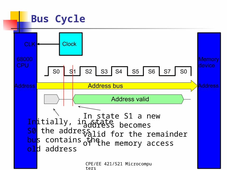
Initially, in stateS0 the addressbus contains theold address
In state S1 a newaddress becomesvalid for the remainderof the memory access
Bus Cycle
CPE/EE 421/521 Microcomputers
24
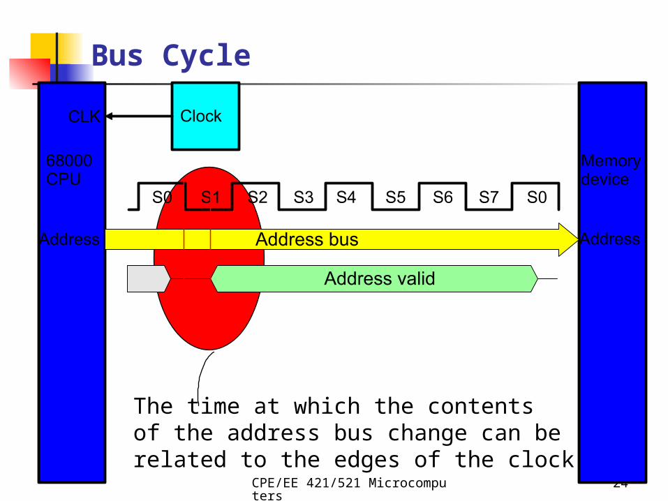
The time at which the contentsof the address bus change can berelated to the edges of the clock.
Bus Cycle
CPE/EE 421/521 Microcomputers
25
Address Timing
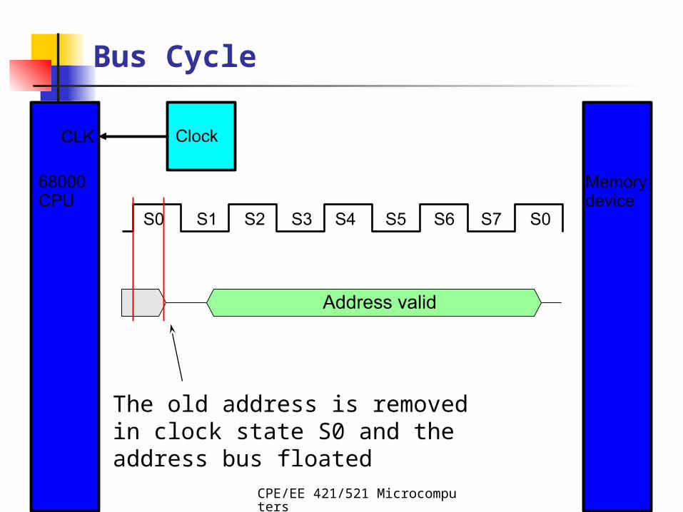
Let’s look at the sequence of events that govern the timing of the address bus
The “old” address is removed in state S0 The address bus is floated for a short
time, and the CPU puts out a new address in state S1
CPE/EE 421/521 Microcomputers
26
The old address is removedin clock state S0 and theaddress bus floated
Bus Cycle
CPE/EE 421/521 Microcomputers
27
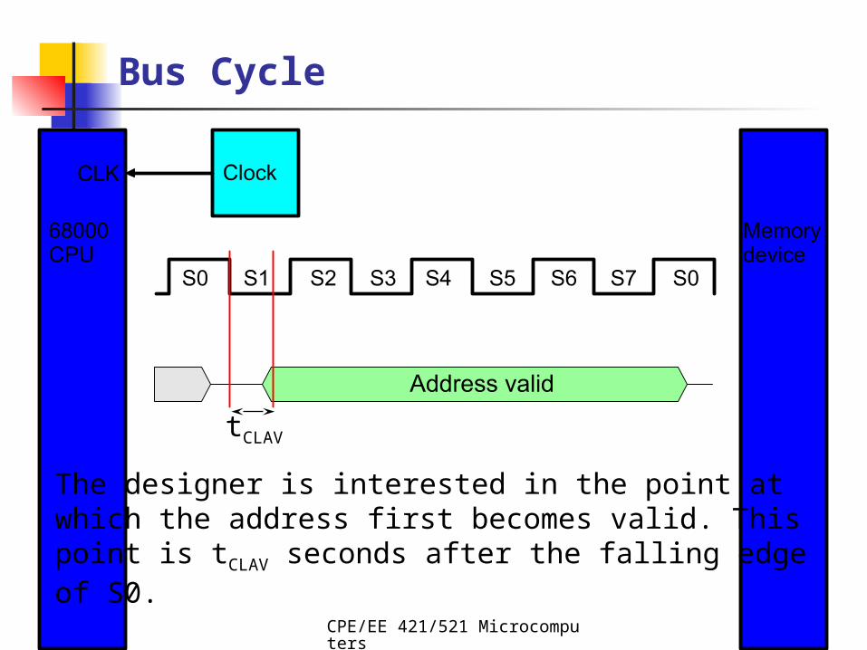
tCLAV
The designer is interested in the point atwhich the address first becomes valid. Thispoint is tCLAV seconds after the falling edgeof S0.
Bus Cycle
CPE/EE 421/521 Microcomputers
28
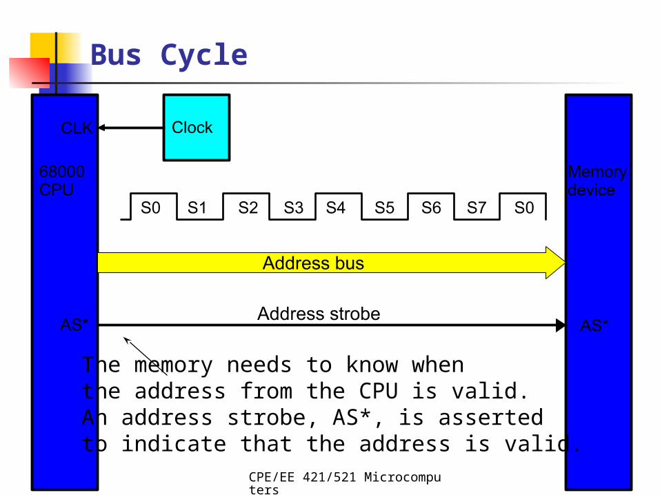
The memory needs to know whenthe address from the CPU is valid.An address strobe, AS*, is assertedto indicate that the address is valid.
Bus Cycle
CPE/EE 421/521 Microcomputers
29
Address and Address Strobe
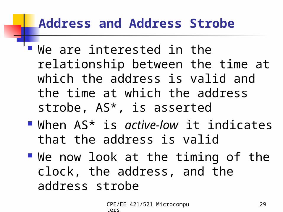
We are interested in the relationship between the time at which the address is valid and the time at which the address strobe, AS*, is asserted
When AS* is active-low it indicates that the address is valid
We now look at the timing of the clock, the address, and the address strobe
CPE/EE 421/521 Microcomputers
30
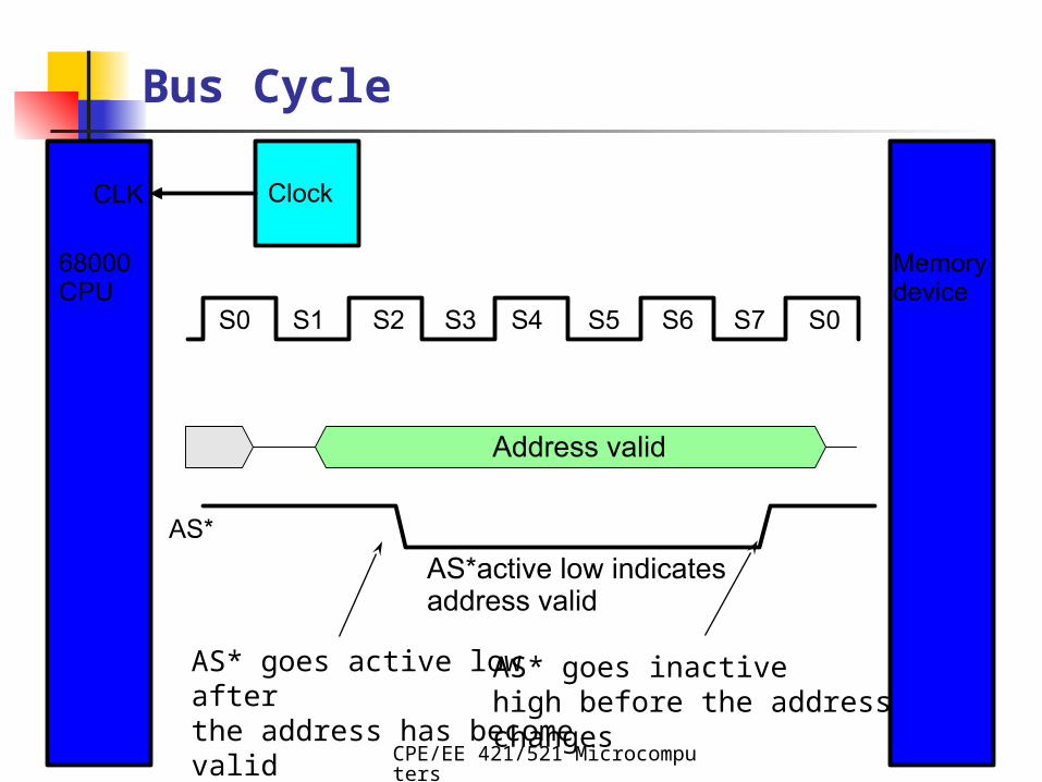
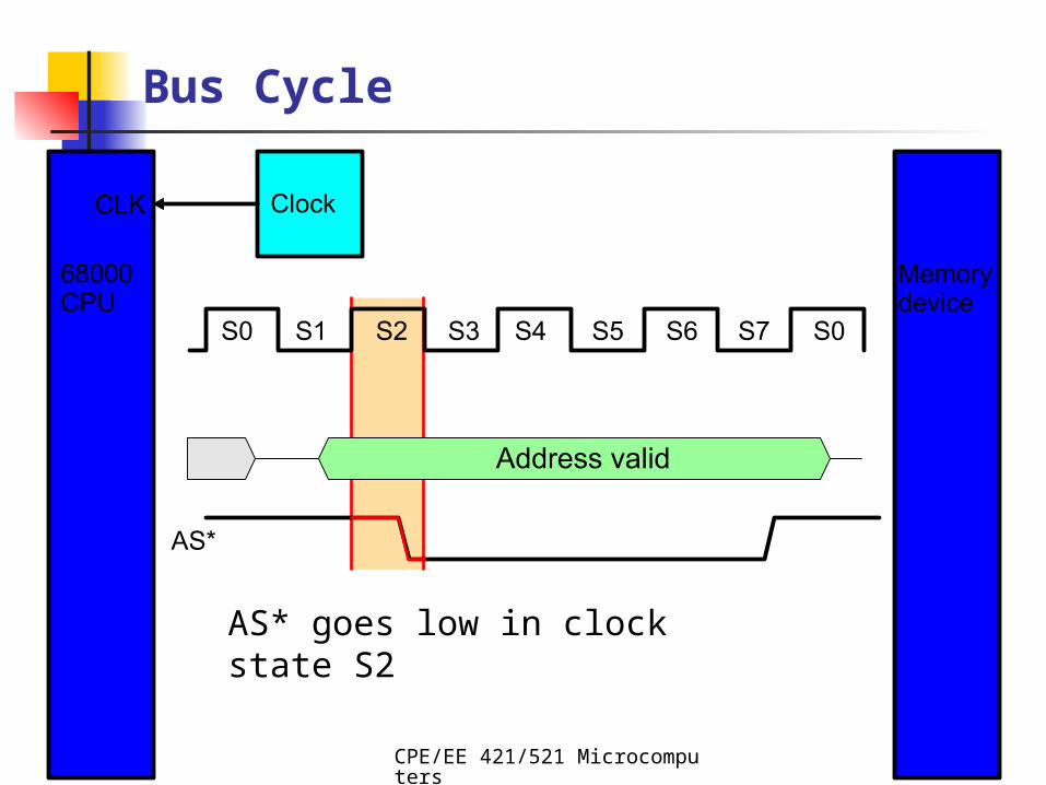
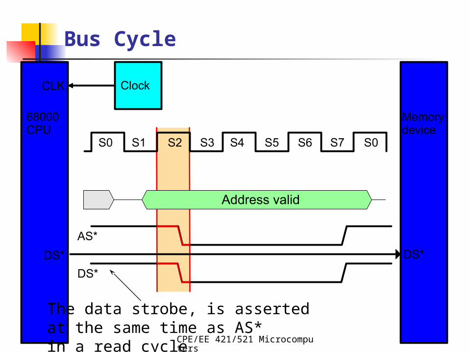
AS* goes active low afterthe address has become valid
AS* goes inactivehigh before the addresschanges
Bus Cycle
CPE/EE 421/521 Microcomputers
31
AS* goes low in clockstate S2
Bus Cycle
CPE/EE 421/521 Microcomputers
32
The Data Strobes
The 68000 has two data strobes LDS* and UDS*. These select the lower byte or the upper byte of a word during a memory access
To keep things simple, we will use a single data strobe, DS*
The timing of DS* in a read cycle is the same as the address strobe, AS*
CPE/EE 421/521 Microcomputers
33
The data strobe, is assertedat the same time as AS*in a read cycle
Bus Cycle
CPE/EE 421/521 Microcomputers
34
The Data Bus
During a read cycle the memory provides the CPU with data
The next slide shows the data bus and the timing of the data signal
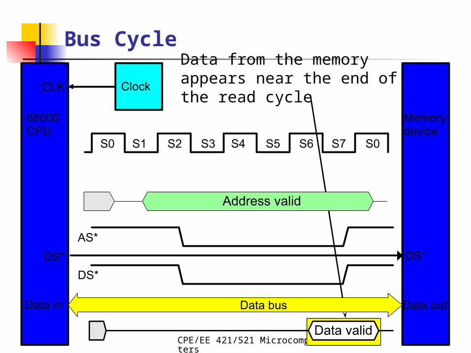
Note that valid data does not appear on the data bus until near the end of the read cycle
CPE/EE 421/521 Microcomputers
35
Data from the memoryappears near the end ofthe read cycle
Bus Cycle
CPE/EE 421/521 Microcomputers
36
Analyzing the Timing Diagram
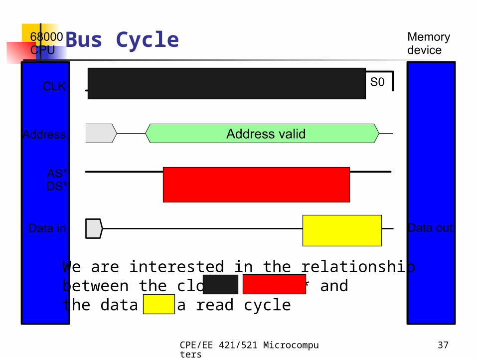
We are going to redraw the timing diagram to remove clutter
We aren’t interested in the signal paths themselves, only in the relationship between the signals
CPE/EE 421/521 Microcomputers
37
We are interested in the relationshipbetween the clock, AS*/DS* andthe data in a read cycle
Bus Cycle
CPE/EE 421/521 Microcomputers
38
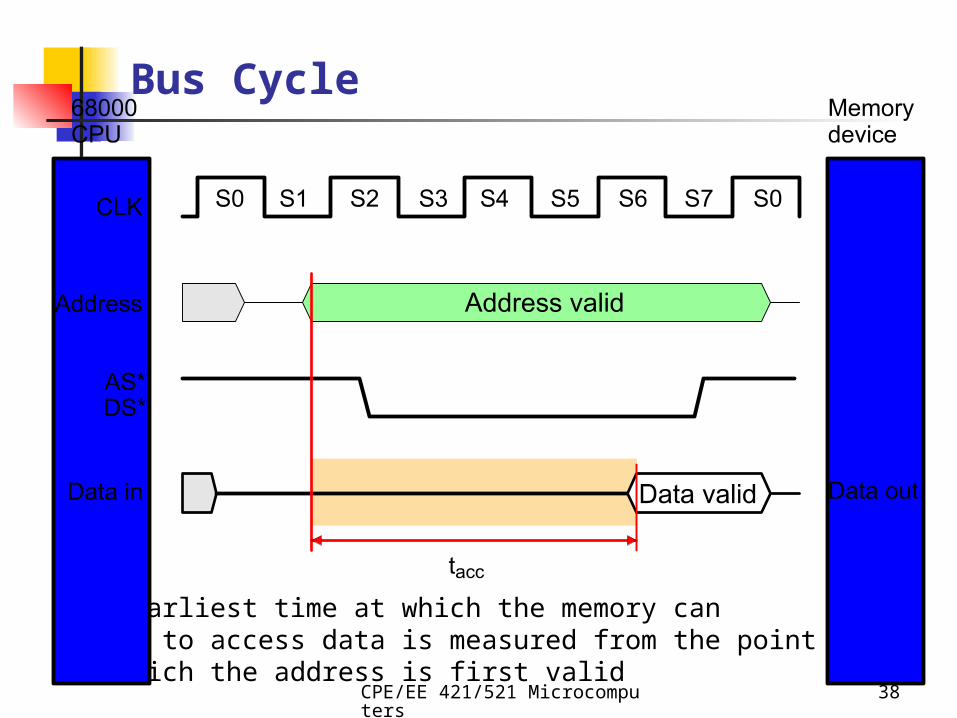
The earliest time at which the memory canbegin to access data is measured from the pointat which the address is first valid
Bus Cycle
CPE/EE 421/521 Microcomputers
39
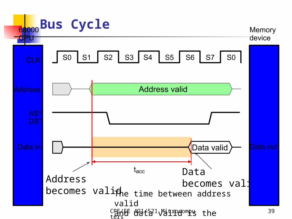
Addressbecomes valid
Databecomes valid
The time between address validand data valid is the memory’saccess time, tacc
Bus Cycle
CPE/EE 421/521 Microcomputers
40
Calculating the Access Time
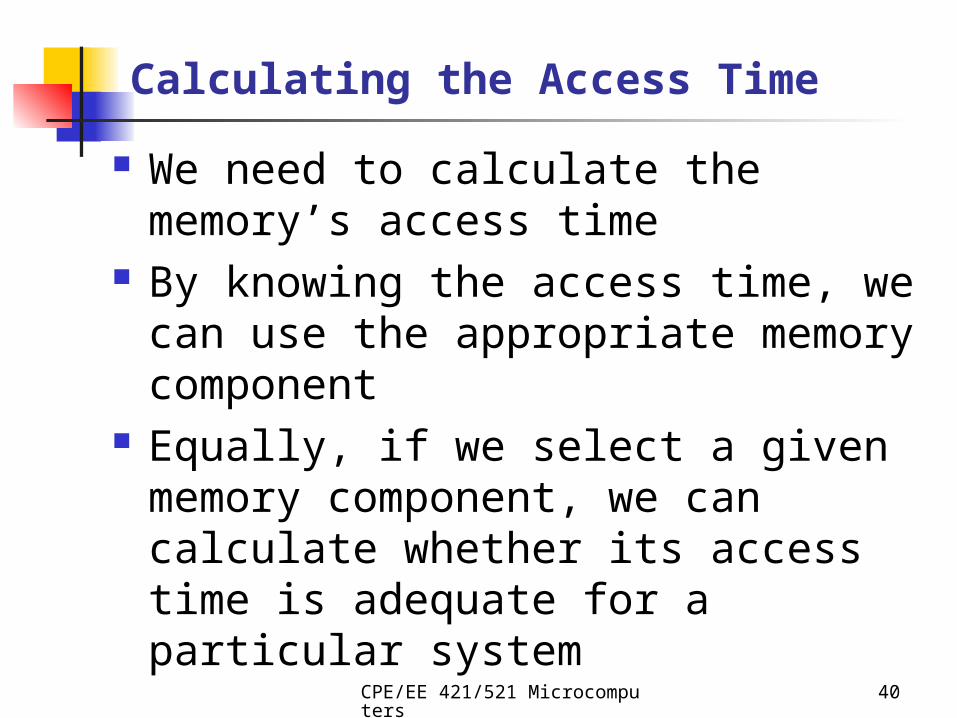
We need to calculate the memory’s access time
By knowing the access time, we can use the appropriate memory component
Equally, if we select a given memory component, we can calculate whether its access time is adequate for a particular system
CPE/EE 421/521 Microcomputers
41
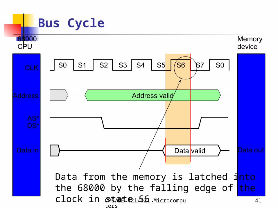
Data from the memory is latched intothe 68000 by the falling edge of theclock in state S6.
Bus Cycle
CPE/EE 421/521 Microcomputers
42
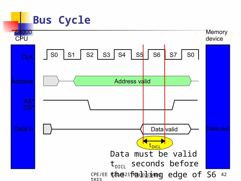
Data must be validtDICL seconds beforethe falling edge of S6
Bus Cycle
CPE/EE 421/521 Microcomputers
43
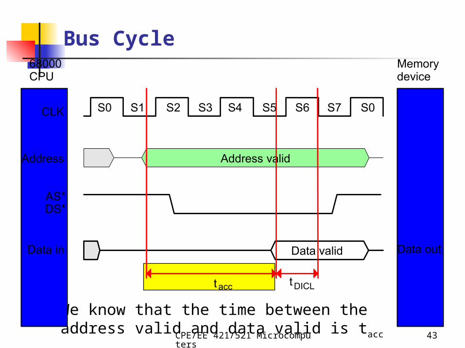
We know that the time between theaddress valid and data valid is tacc
Bus Cycle
CPE/EE 421/521 Microcomputers
44
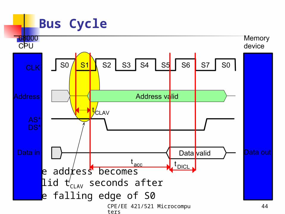
The address becomesvalid tCLAV seconds afterthe falling edge of S0
Bus Cycle
CPE/EE 421/521 Microcomputers
45
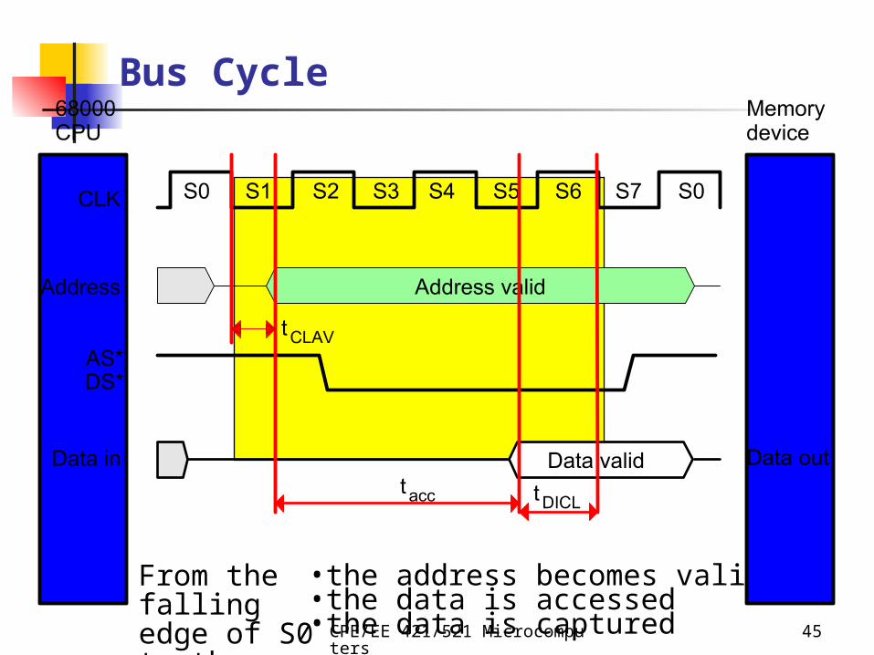
From the fallingedge of S0 to thefalling edge of S6:
•the address becomes valid•the data is accessed•the data is captured
Bus Cycle
CPE/EE 421/521 Microcomputers
46
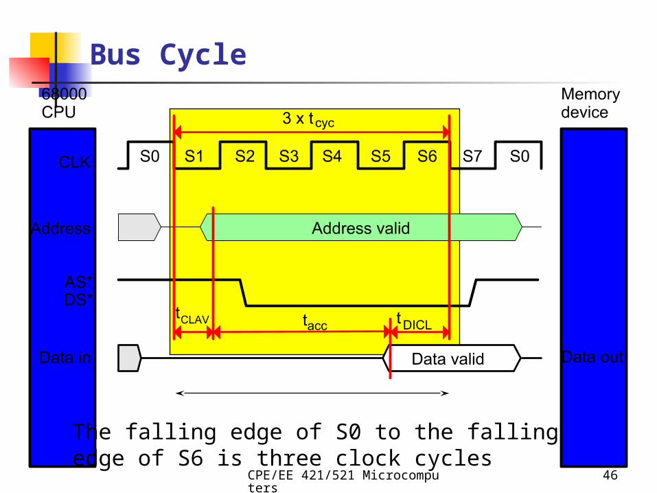
The falling edge of S0 to the fallingedge of S6 is three clock cycles
Bus Cycle
CPE/EE 421/521 Microcomputers
47
3 tcyc = tCLAV + tacc + tDICL
Bus Cycle
CPE/EE 421/521 Microcomputers
48
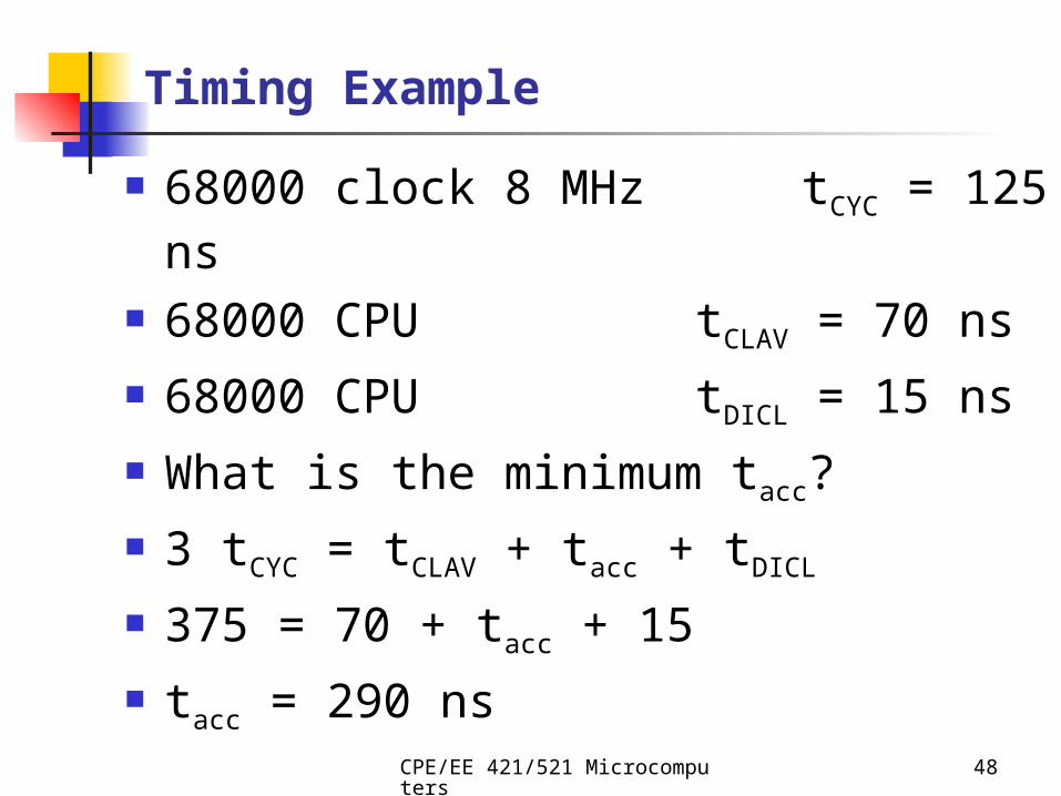
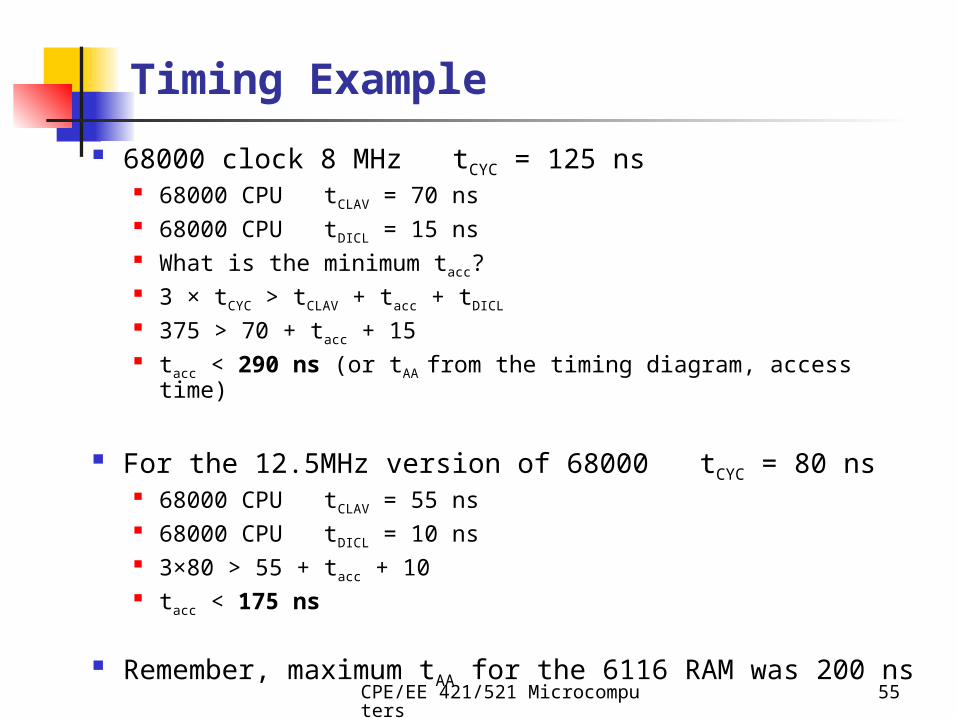
Timing Example
68000 clock 8 MHz tCYC = 125 ns
68000 CPU tCLAV = 70 ns
68000 CPU tDICL = 15 ns
What is the minimum tacc?
3 tCYC = tCLAV + tacc + tDICL
375 = 70 + tacc + 15
tacc = 290 ns
CPE/EE 421/521 Microcomputers
49
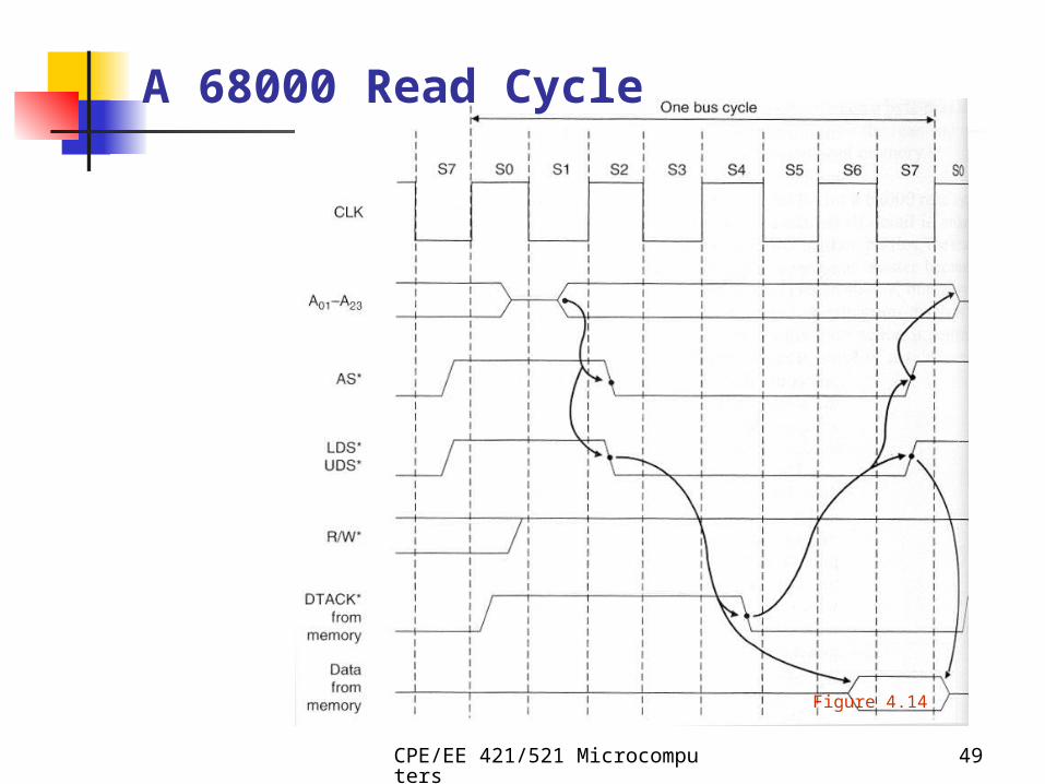
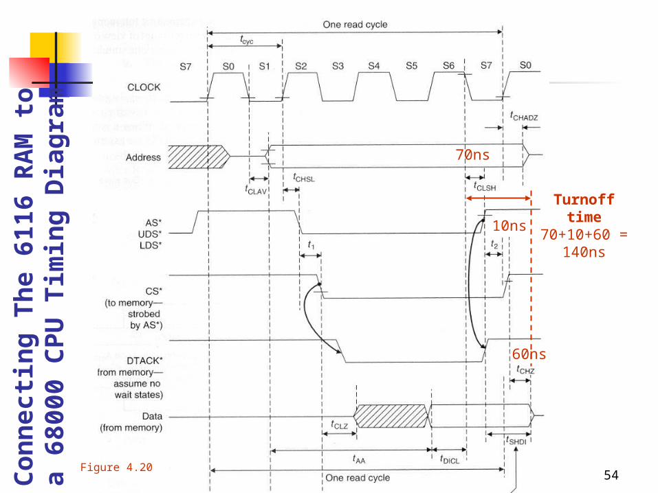
Figure 4.14
A 68000 Read Cycle
CPE/EE 421/521 Microcomputers
50
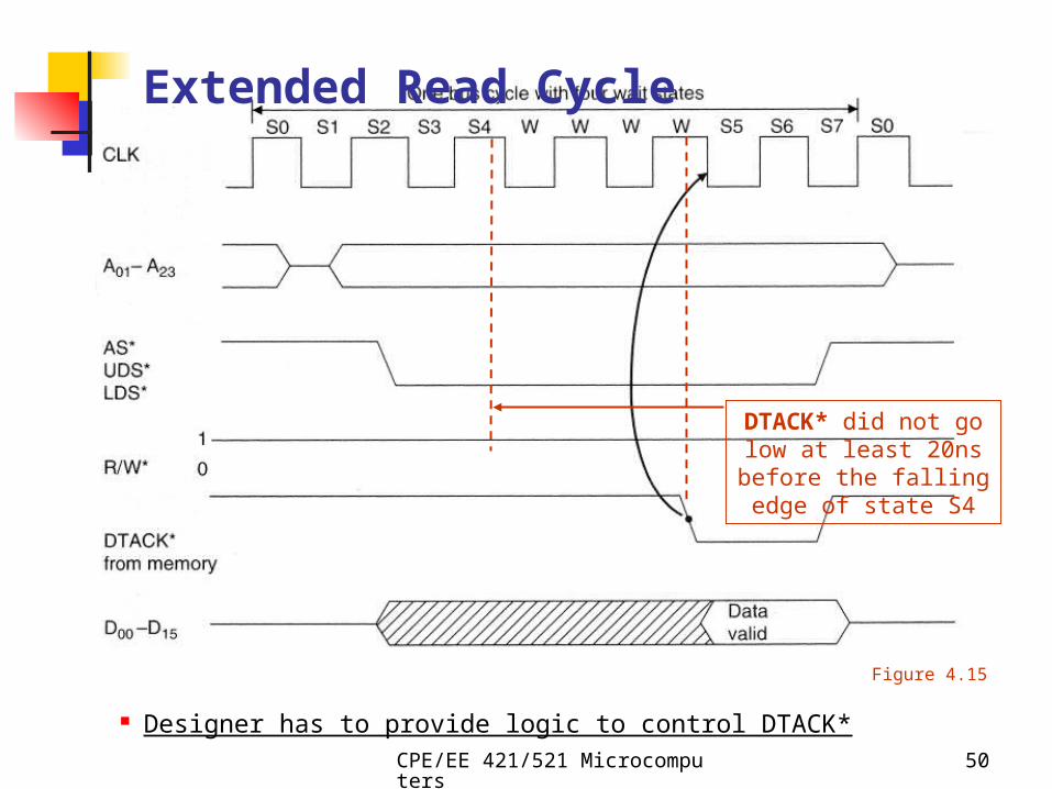
Figure 4.15
Extended Read Cycle
DTACK* did not go low at least 20ns before the falling edge of state S4
Designer has to provide logic to control DTACK*
CPE/EE 421/521 Microcomputers
51
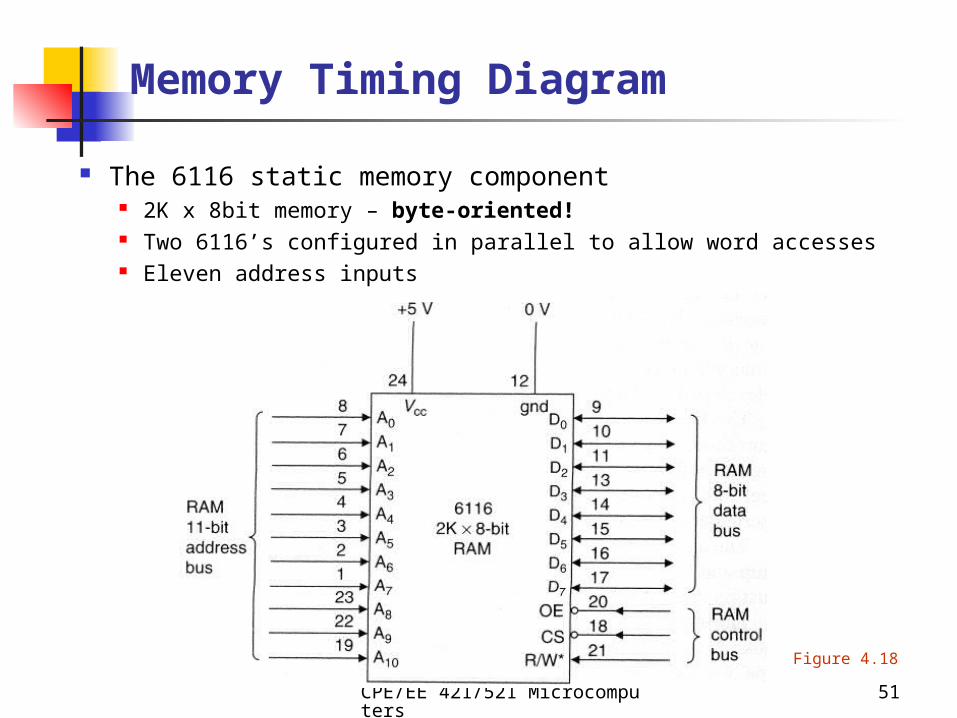
Figure 4.18
Memory Timing Diagram
The 6116 static memory component 2K x 8bit memory – byte-oriented! Two 6116’s configured in parallel to allow word accesses Eleven address inputs
CPE/EE 421/521 Microcomputers
52
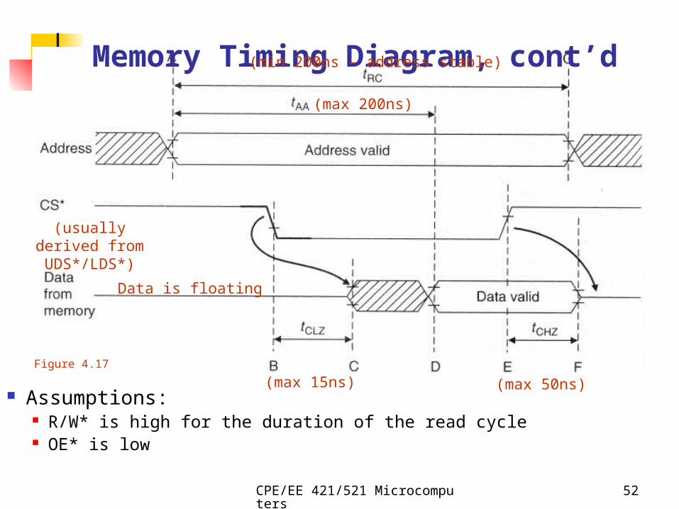
Figure 4.17
Memory Timing Diagram, cont’d
Assumptions: R/W* is high for the duration of the read cycle OE* is low
(min 200ns – address stable)
(max 200ns)
(max 15ns)
Data is floating
(max 50ns)
(usually derived from UDS*/LDS*)
CPE/EE 421/521 Microcomputers
53
D00
D07
D08
D15
A12
A23
A01
A11
A01
A11
A01
A11
Figure 4.19
Co
nn
ecti
ng
Th
e 61
16
RA
M t
o a
680
00 C
PU
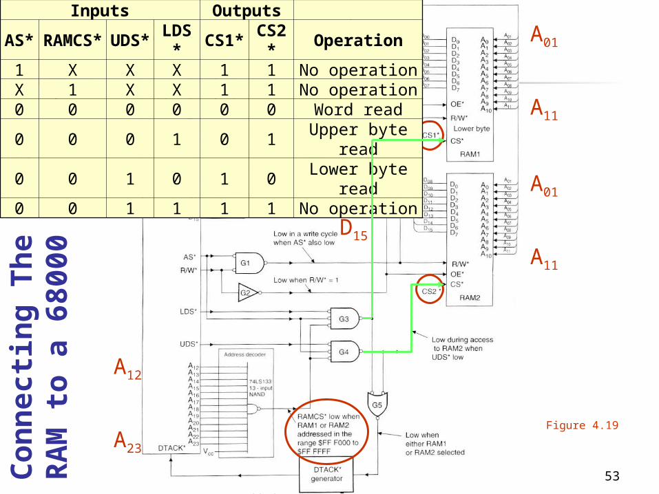
Inputs Outputs
AS*RAMCS
*UDS
*LDS* CS1* CS2* Operation
1 X X X 1 1 No operationX 1 X X 1 1 No operation0 0 0 0 0 0 Word read0 0 0 1 0 1 Upper byte read0 0 1 0 1 0 Lower byte read0 0 1 1 1 1 No operation
CPE/EE 421/521 Microcomputers
54Figure 4.20
Co
nn
ecti
ng
Th
e 61
16 R
AM
to
a
6800
0 C
PU
Tim
ing
Dia
gra
m
Turnoff time70+10+60 =
140ns
70ns
10ns
60ns
CPE/EE 421/521 Microcomputers
55
Timing Example
68000 clock 8 MHz tCYC = 125 ns 68000 CPU tCLAV = 70 ns 68000 CPU tDICL = 15 ns What is the minimum tacc? 3 × tCYC > tCLAV + tacc + tDICL 375 > 70 + tacc + 15 tacc < 290 ns (or tAA from the timing diagram, access time)
For the 12.5MHz version of 68000 tCYC = 80 ns 68000 CPU tCLAV = 55 ns 68000 CPU tDICL = 10 ns 3×80 > 55 + tacc + 10 tacc < 175 ns
Remember, maximum tAA for the 6116 RAM was 200 ns
CPE/EE 421/521 Microcomputers
56
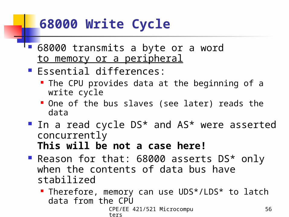
68000 Write Cycle
68000 transmits a byte or a word to memory or a peripheral
Essential differences: The CPU provides data at the beginning of a write
cycle One of the bus slaves (see later) reads the data
In a read cycle DS* and AS* were asserted concurrentlyThis will be not a case here!
Reason for that: 68000 asserts DS* only when the contents of data bus have stabilized Therefore, memory can use UDS*/LDS* to latch data
from the CPU
CPE/EE 421/521 Microcomputers
57
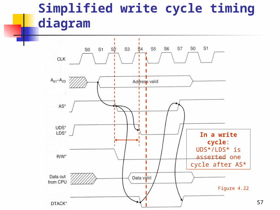
Simplified write cycle timing diagram
In a write cycle: UDS*/LDS* is
asserted one cycle after AS*
Figure 4.22
CPE/EE 421/521 Microcomputers
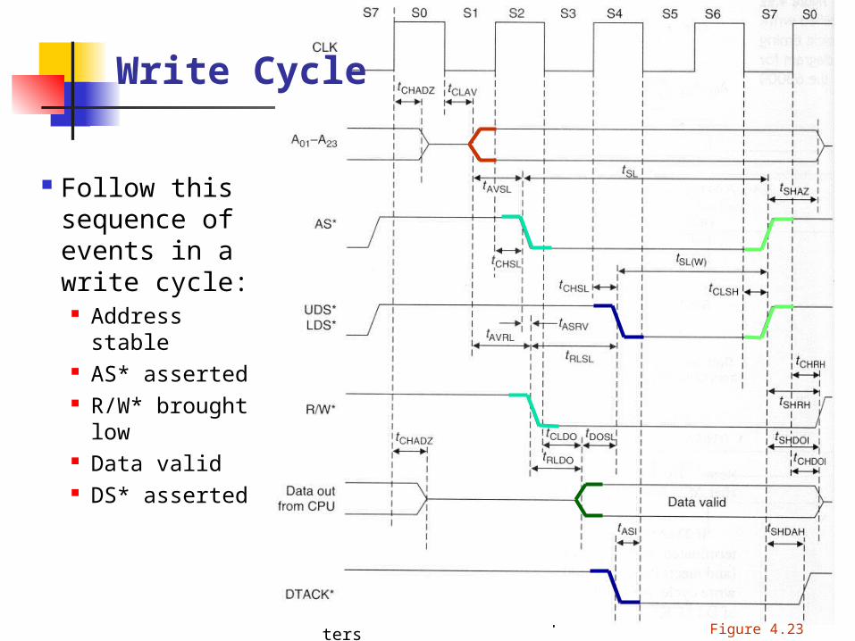
58Figure 4.23
Follow this sequence of events in a write cycle:
Address stable
AS* asserted R/W* brought
low Data valid DS* asserted
Write Cycle
CPE/EE 421/521 Microcomputers
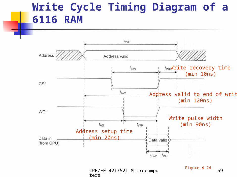
59Figure 4.24
Write Cycle Timing Diagram of a 6116 RAM
Address setup time(min 20ns)
Address valid to end of write(min 120ns)
Write pulse width(min 90ns)
Write recovery time(min 10ns)
CPE/EE 421/521 Microcomputers
60
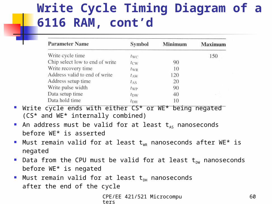
Write cycle ends with either CS* or WE* being negated (CS* and WE* internally combined)
An address must be valid for at least tAS nanoseconds before WE* is asserted
Must remain valid for at least tWR nanoseconds after WE* is negated
Data from the CPU must be valid for at least tDW nanoseconds before WE* is negated
Must remain valid for at least tDH nanoseconds after the end of the cycle
Write Cycle Timing Diagram of a 6116 RAM, cont’d
CPE/EE 421/521 Microcomputers
61
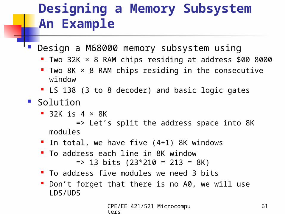
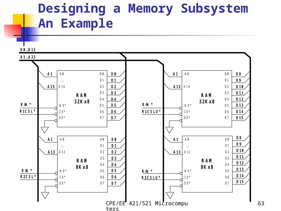
Designing a Memory Subsystem An Example
Design a M68000 memory subsystem using Two 32K × 8 RAM chips residing at address $00 8000 Two 8K × 8 RAM chips residing in the consecutive window LS 138 (3 to 8 decoder) and basic logic gates
Solution 32K is 4 × 8K
=> Let’s split the address space into 8K modules In total, we have five (4+1) 8K windows To address each line in 8K window
=> 13 bits (23*210 = 213 = 8K) To address five modules we need 3 bits Don’t forget that there is no A0, we will use LDS/UDS
CPE/EE 421/521 Microcomputers
62
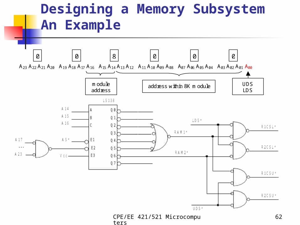
A23 A22 A21 A20 A19 A18 A17 A16 A15 A14 A13 A12 A11 A10 A09 A08 A07 A06 A05 A04 A03 A02 A01 A00
address within 8K module module address
UDS LDS
0 0 8 0 0 0
Designing a Memory Subsystem An Example
CPE/EE 421/521 Microcomputers
63
RAM32Kx8
A 0
A 14
...
CE*
OE*
D0
D7
D6
D5
D4
D3
D2
D1
RAM32Kx8
A 0
A 14
...
CE*
OE*
D0
D7
D6
D5
D4
D3
D2
D1
RAM8Kx8
A 0
A 12
...
CE*
OE*
D0
D7
D6
D5
D4
D3
D2
D1
W E*
A13
A1
A15
A1
D7
D6
D5D4
D3
D2
D1
D0
A1..A23
A15
A1
D0..D15
R/W *
R1CS L* R1CS LU*
R2CS L* R2CS LU*
RAM8Kx8
A 0
A 12
...
CE*
OE*
D0
D7
D6
D5
D4
D3
D2
D1
W E*
A13
A1
R/W *
W E*R/W * W E*R/W *
D7
D6
D5D4
D3
D2
D1
D0
D15
D14
D13D12
D11
D10
D9
D8
D15D14
D13
D12
D11
D10
D9
D8
Designing a Memory Subsystem An Example
CPE/EE 421/521 Microcomputers
64
Figure 4.9
Interrupt Control Interface (details later)
priority
low
high
CPE/EE 421/521 Microcomputers
65
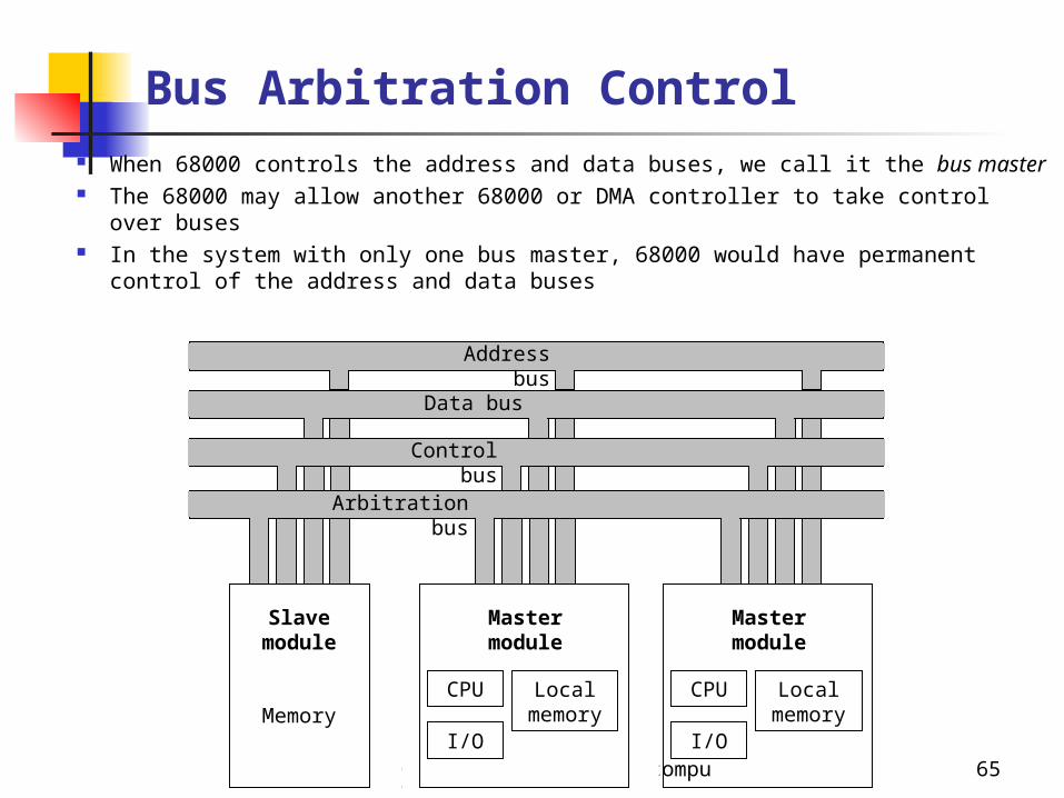
Data bus
Address bus
Control bus
Arbitration bus
Slave module
Memory
Master module
Local memory
CPU
I/O
Master module
Local memory
CPU
I/O
Bus Arbitration Control When 68000 controls the address and data buses, we call it the bus master The 68000 may allow another 68000 or DMA controller to take control over buses In the system with only one bus master, 68000 would have permanent control of the
address and data buses
CPE/EE 421/521 Microcomputers
66
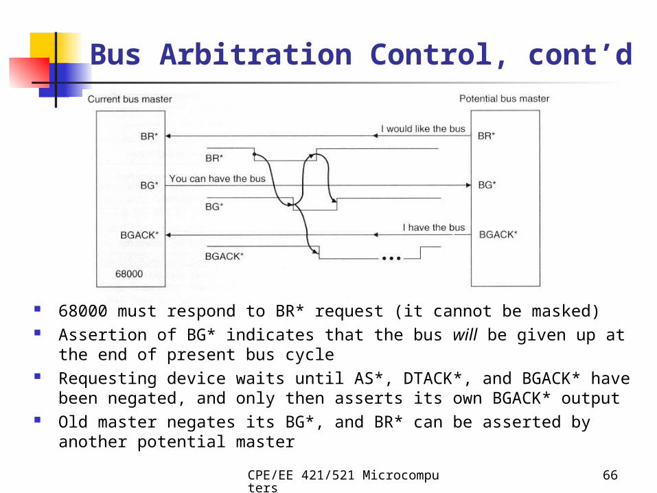
68000 must respond to BR* request (it cannot be masked) Assertion of BG* indicates that the bus will be given up at the end of present bus
cycle Requesting device waits until AS*, DTACK*, and BGACK* have been negated,
and only then asserts its own BGACK* output Old master negates its BG*, and BR* can be asserted by another potential
master
Bus Arbitration Control, cont’d
CPE/EE 421/521 Microcomputers
67
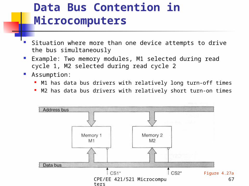
Figure 4.27a
Data Bus Contention in Microcomputers
Situation where more than one device attempts to drive the bus simultaneously
Example: Two memory modules, M1 selected during read cycle 1, M2 selected during read cycle 2
Assumption: M1 has data bus drivers with relatively long turn-off times M2 has data bus drivers with relatively short turn-on times
CPE/EE 421/521 Microcomputers
68
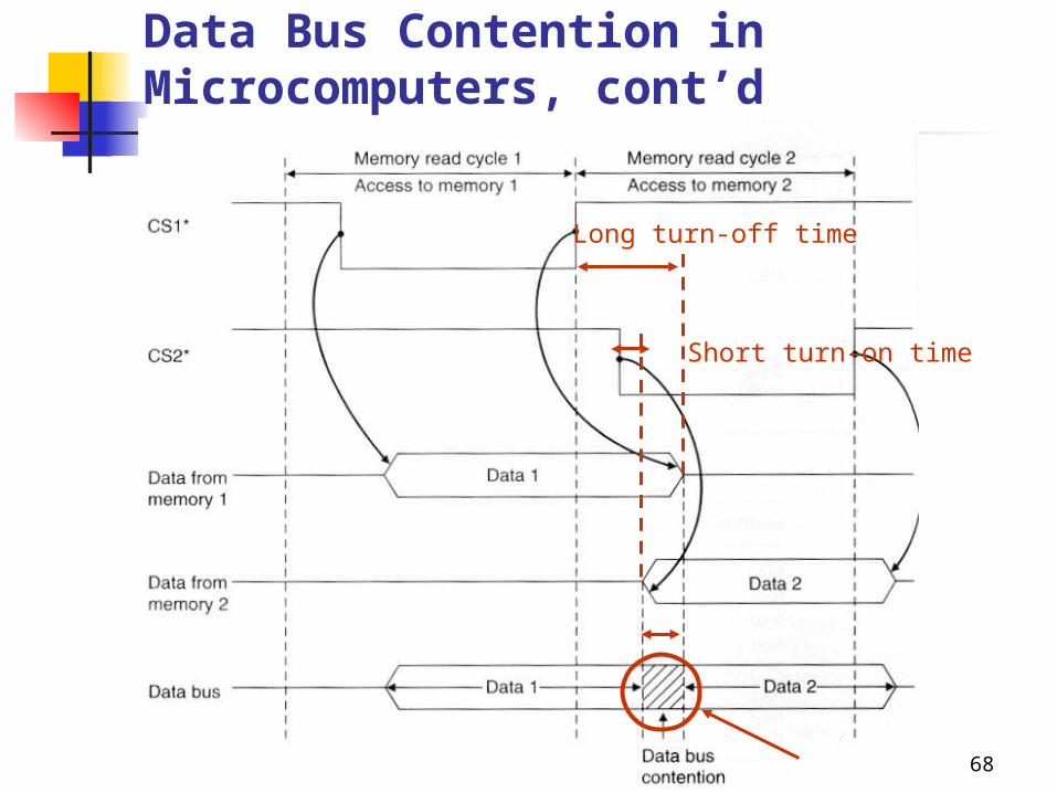
Long turn-off time
Short turn-on time
Data Bus Contention in Microcomputers, cont’d
CPE/EE 421/521 Microcomputers
69
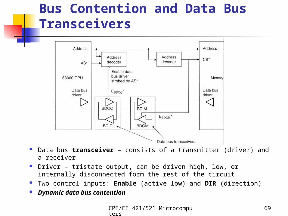
Bus Contention and Data Bus Transceivers
Data bus transceiver – consists of a transmitter (driver) and a receiver
Driver – tristate output, can be driven high, low, or internally disconnected form the rest of the circuit
Two control inputs: Enable (active low) and DIR (direction) Dynamic data bus contention
CPE/EE 421/521 Microcomputers
70
Outline
68000 interface Timing diagram Minimal configuration using the 68000 Extensions Exception Processing
CPE/EE 421/521 Microcomputers
71
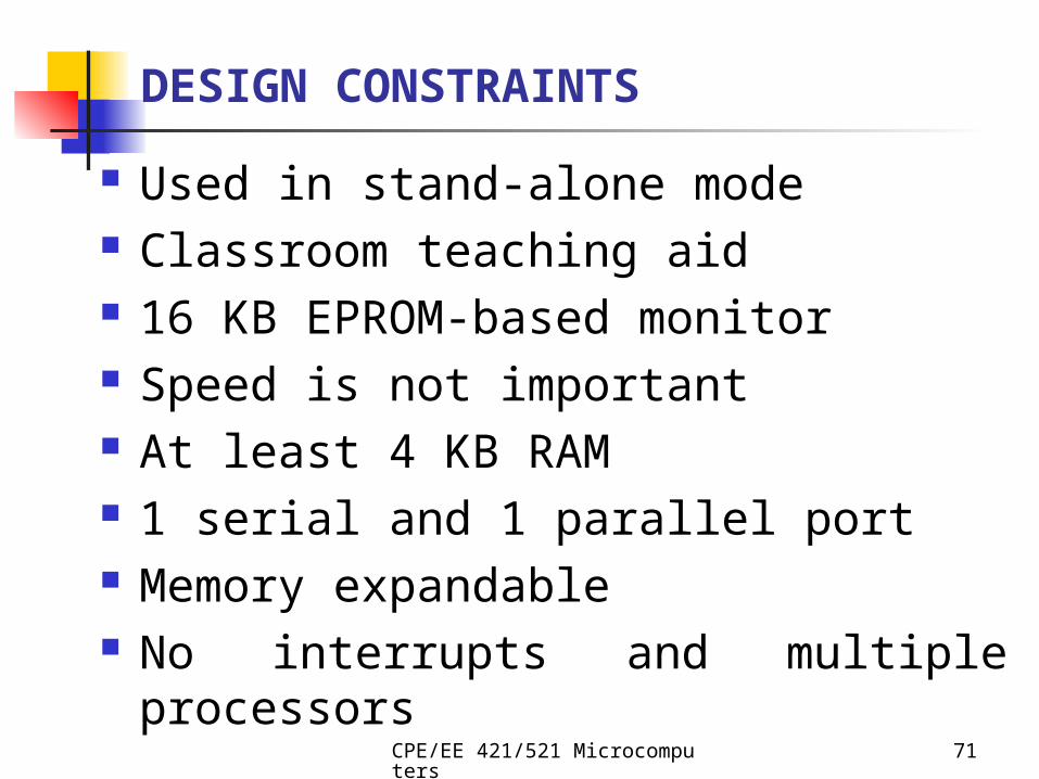
DESIGN CONSTRAINTS
Used in stand-alone mode Classroom teaching aid 16 KB EPROM-based monitor Speed is not important At least 4 KB RAM 1 serial and 1 parallel port Memory expandable No interrupts and multiple processors
CPE/EE 421/521 Microcomputers
72
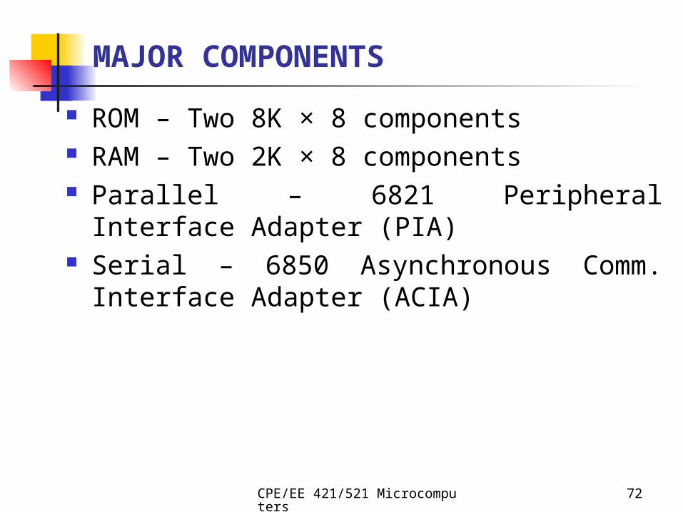
MAJOR COMPONENTS
ROM – Two 8K × 8 components RAM – Two 2K × 8 components Parallel – 6821 Peripheral Interface Adapter
(PIA) Serial – 6850 Asynchronous Comm. Interface
Adapter (ACIA)
CPE/EE 421/521 Microcomputers
73
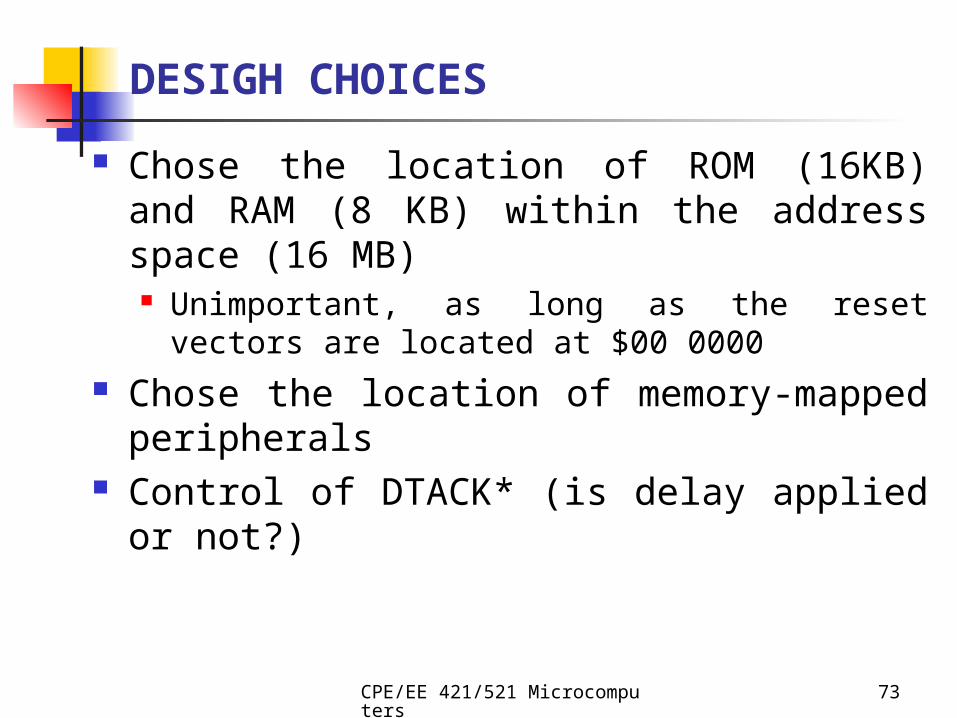
DESIGH CHOICES
Chose the location of ROM (16KB) and RAM (8 KB) within the address space (16 MB) Unimportant, as long as the reset vectors are located
at $00 0000 Chose the location of memory-mapped
peripherals Control of DTACK* (is delay applied or not?)
CPE/EE 421/521 Microcomputers
74
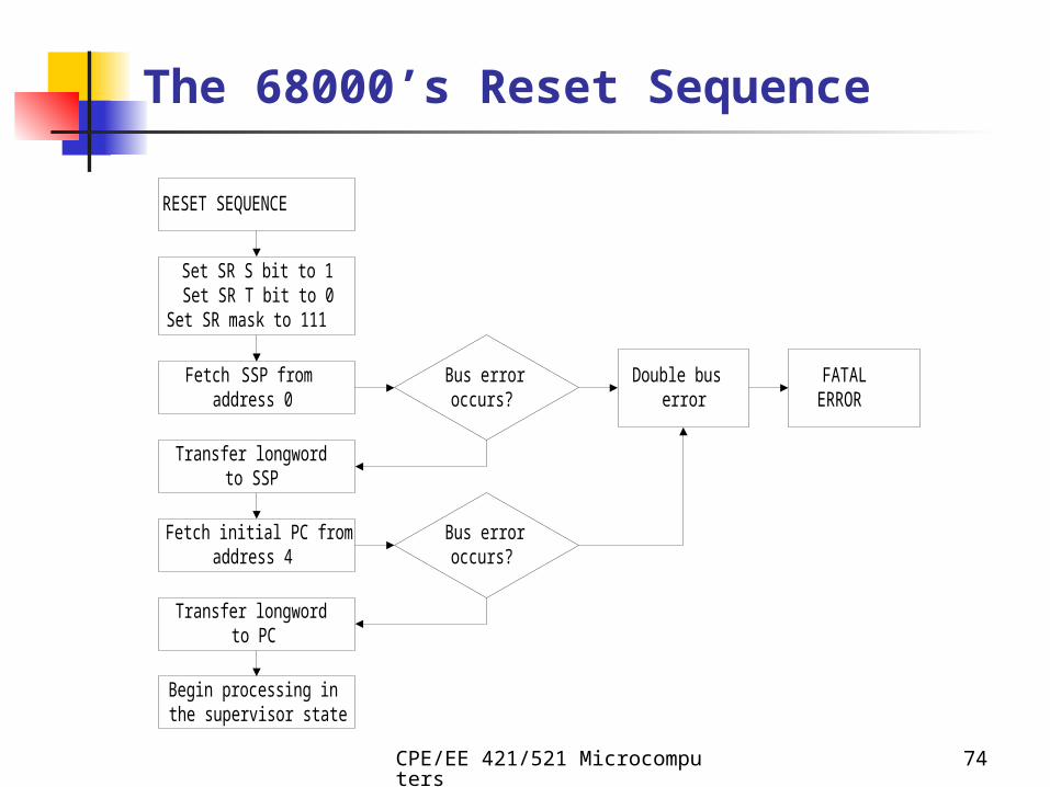
The 68000’s Reset Sequence
Fetch SSP fromaddress 0
RESET SEQUENCE
Set SR S bit to 1Set SR T bit to 0
Set SR mask to 111
Transfer longwordto SSP
Fetch initial PC fromaddress 4
Transfer longwordto PC
Begin processing inthe supervisor state
Bus erroroccurs?
Double buserror
Bus erroroccurs?
FATALERROR
CPE/EE 421/521 Microcomputers
75
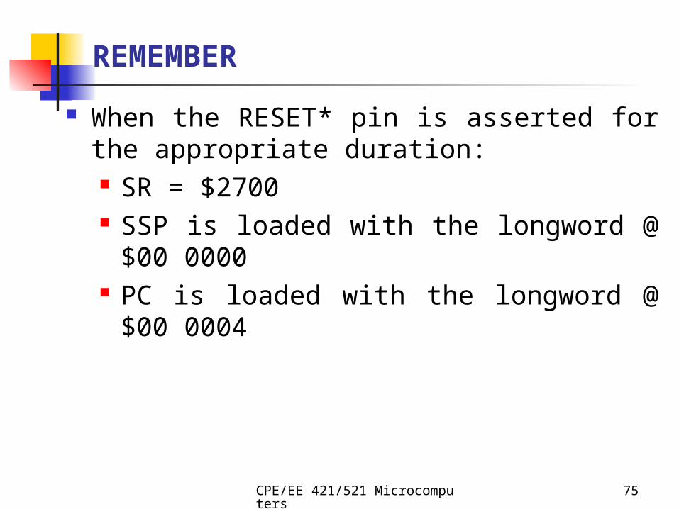
REMEMBER
When the RESET* pin is asserted for the appropriate duration: SR = $2700 SSP is loaded with the longword @ $00 0000 PC is loaded with the longword @ $00 0004
CPE/EE 421/521 Microcomputers
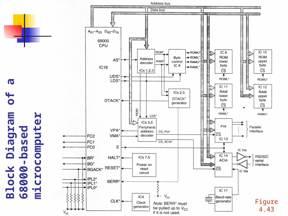
76Figure 4.43
Blo
ck D
iag
ram
of
a 68
000-
bas
ed m
icro
com
pu
ter
CPE/EE 421/521 Microcomputers
77
Memory and Peripheral Components
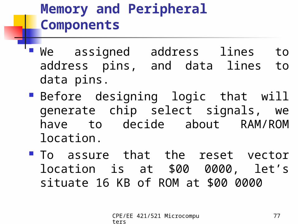
We assigned address lines to address pins, and data lines to data pins.
Before designing logic that will generate chip select signals, we have to decide about RAM/ROM location.
To assure that the reset vector location is at $00 0000, let’s situate 16 KB of ROM at $00 0000
CPE/EE 421/521 Microcomputers
78
Mem
ory
an
d P
erip
her
al
Co
mp
on
ents
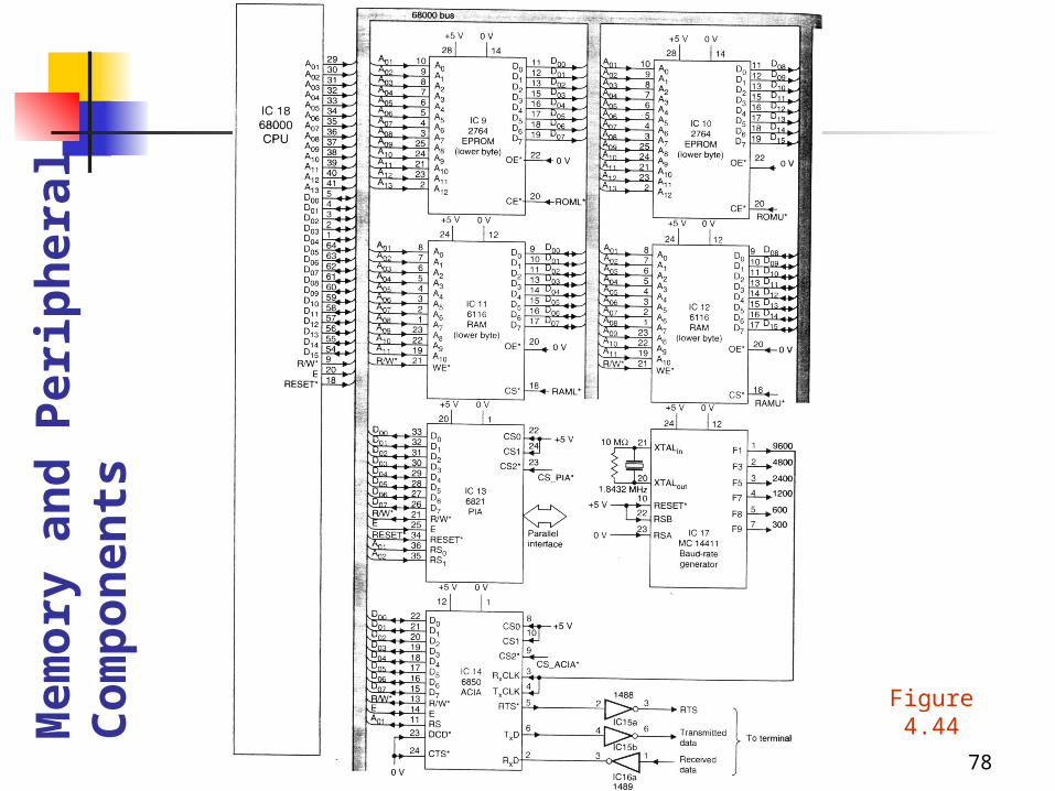
Figure 4.44
CPE/EE 421/521 Microcomputers
79
Control Section
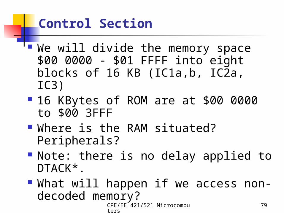
We will divide the memory space $00 0000 - $01 FFFF into eight blocks of 16 KB (IC1a,b, IC2a, IC3)
16 KBytes of ROM are at $00 0000 to $00 3FFF
Where is the RAM situated? Peripherals? Note: there is no delay applied to
DTACK*. What will happen if we access non-
decoded memory?
CPE/EE 421/521 Microcomputers
80
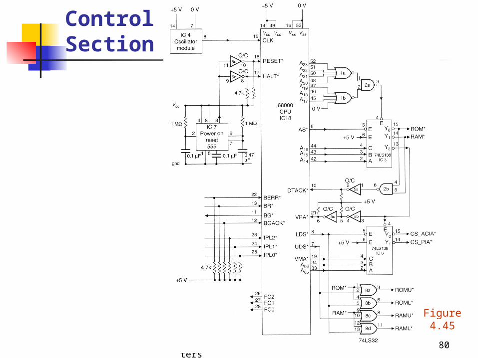
Control Section
Figure 4.45
CPE/EE 421/521 Microcomputers
81
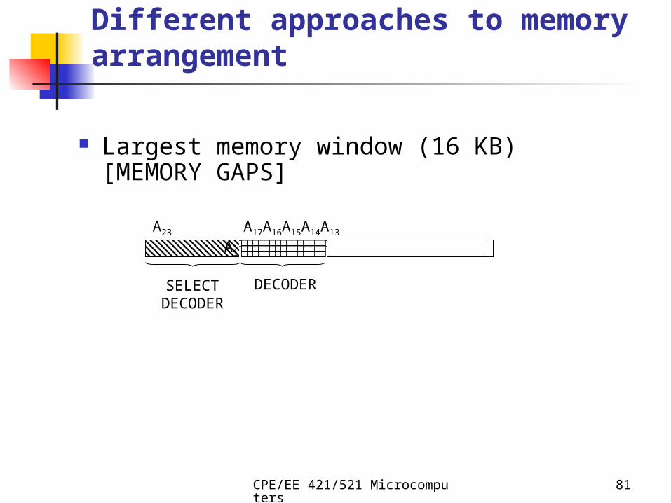
Different approaches to memory arrangement
Largest memory window (16 KB)[MEMORY GAPS]
A23 A17A16A15A14A13 A1
SELECT DECODER
DECODER
CPE/EE 421/521 Microcomputers
82
Different approaches to memory arrangement, cont’d
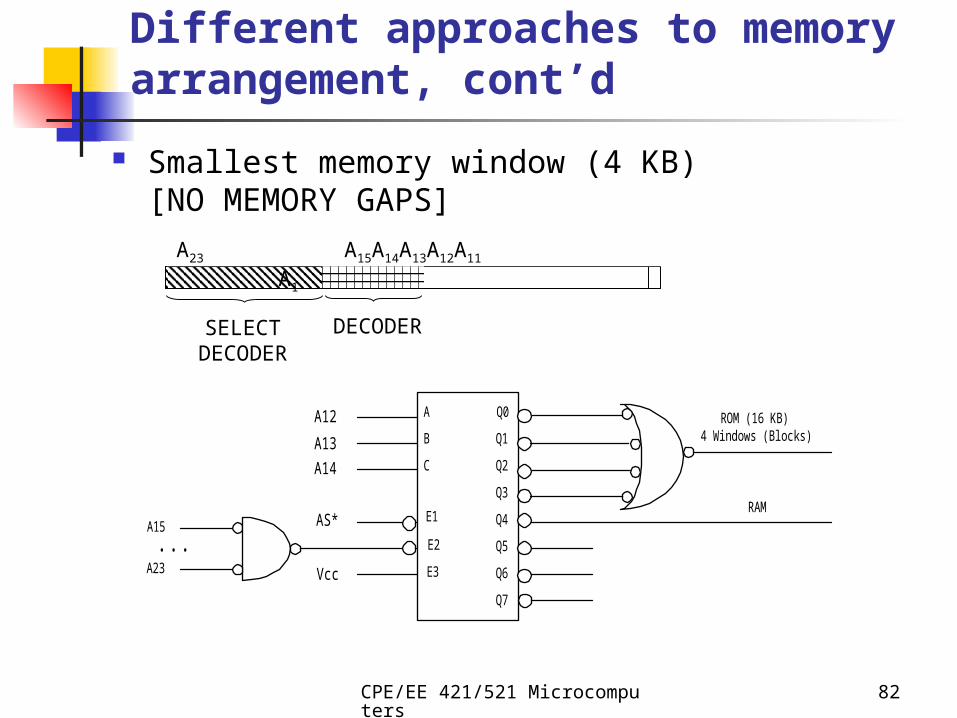
Smallest memory window (4 KB)[NO MEMORY GAPS]
A23 A15A14A13A12A11 A1
SELECT DECODER
DECODER
A Q0
Q1
Q2
Q3
Q4
Q5
Q6
Q7
B
C
E1
E2
E3
A12
A14
A13
ROM (16 KB)4 Windows (Blocks)
RAM
A23
...AS*A15
Vcc
CPE/EE 421/521 Microcomputers
83
Outline
68000 interface Timing diagram Minimal configuration using the 68000 Extensions Exception Processing
CPE/EE 421/521 Microcomputers
84
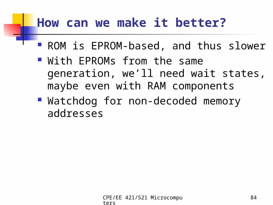
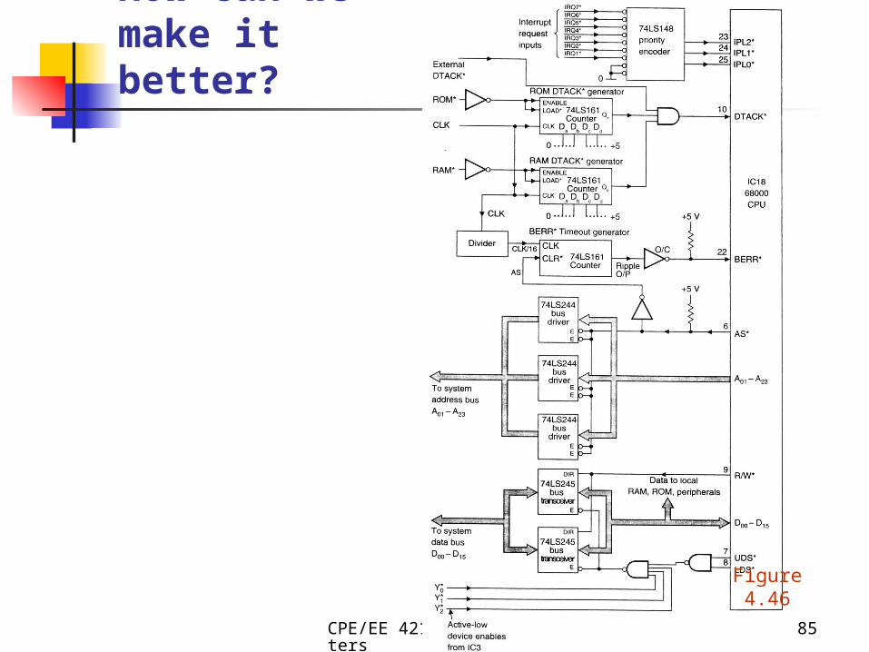
How can we make it better?
ROM is EPROM-based, and thus slower With EPROMs from the same generation, we’ll
need wait states, maybe even with RAM components
Watchdog for non-decoded memory addresses
CPE/EE 421/521 Microcomputers
85
How can we make it better?
Figure 4.46
CPE/EE 421/521 Microcomputers
86
How can we make it better? Cont’d
CONTROL OF INTERRUPTS Use 74LS148 priority encoder to provide 7 levels of
interrupt EXTERNAL BUS INTERFACE
CPU can supply only the limited current to drive the bus
SOLUTION: Bus drivers (buffers)
CPE/EE 421/521 Microcomputers
87
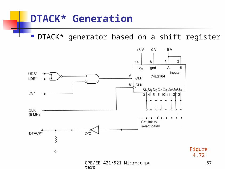
DTACK* Generation
DTACK* generator based on a shift register
Figure 4.72
CPE/EE 421/521 Microcomputers
88
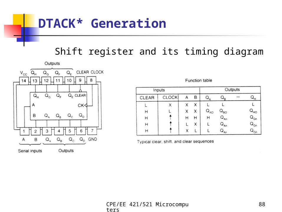
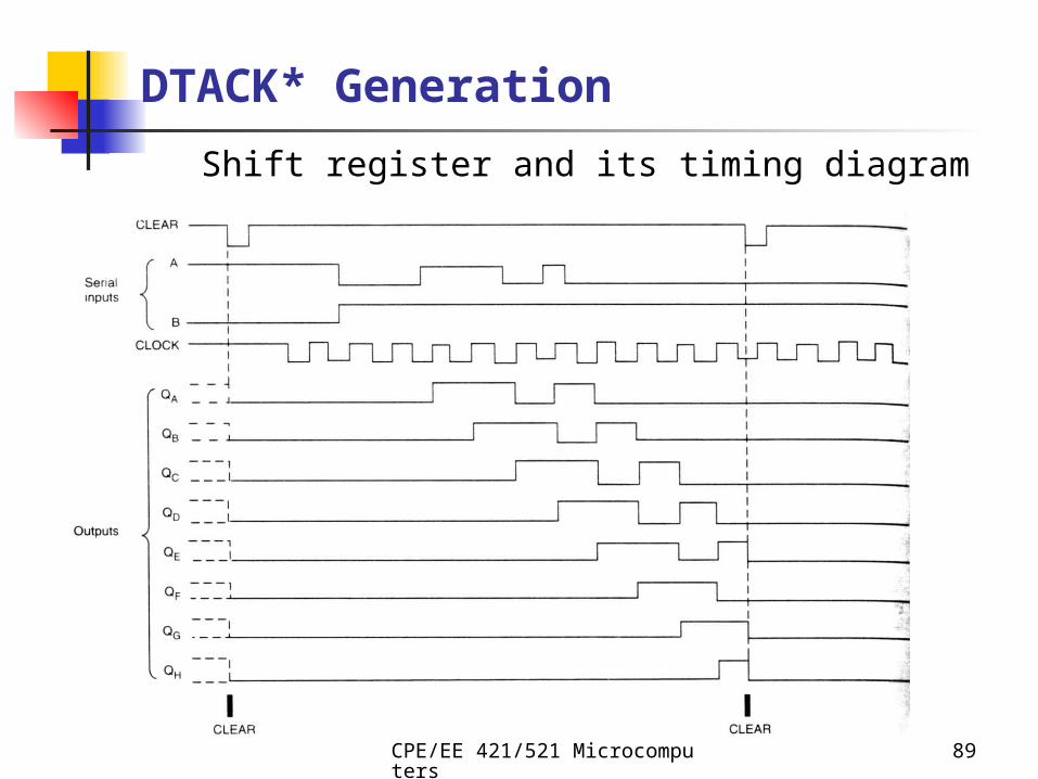
DTACK* Generation
Shift register and its timing diagram
CPE/EE 421/521 Microcomputers
89
DTACK* Generation
Shift register and its timing diagram
CPE/EE 421/521 Microcomputers
90
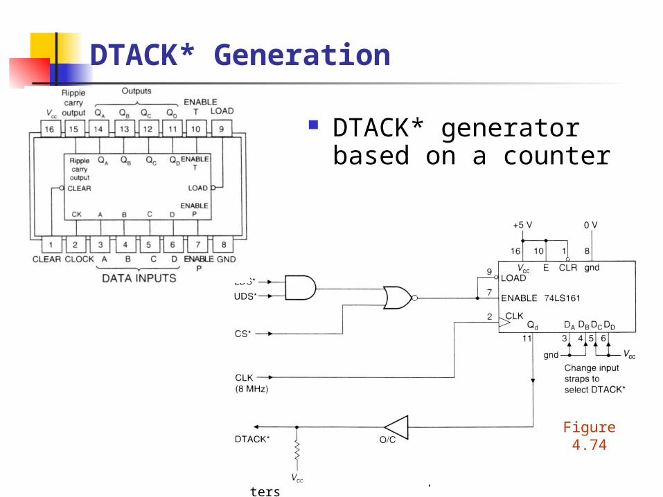
DTACK* Generation
DTACK* generator based on a counter
Figure 4.74
CPE/EE 421/521 Microcomputers
91
Outline
68000 interface Timing diagram Minimal configuration using the 68000 Extensions Exception Processing
CPE/EE 421/521 Microcomputers
92
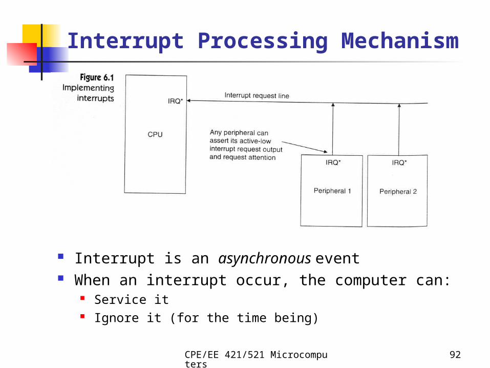
Interrupt Processing Mechanism
Interrupt is an asynchronous event When an interrupt occur, the computer can:
Service it Ignore it (for the time being)
CPE/EE 421/521 Microcomputers
93
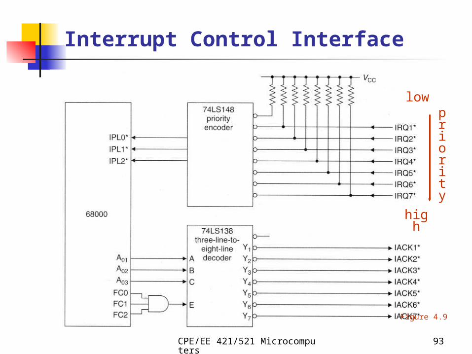
Figure 4.9
Interrupt Control Interface
priority
low
high
CPE/EE 421/521 Microcomputers
94
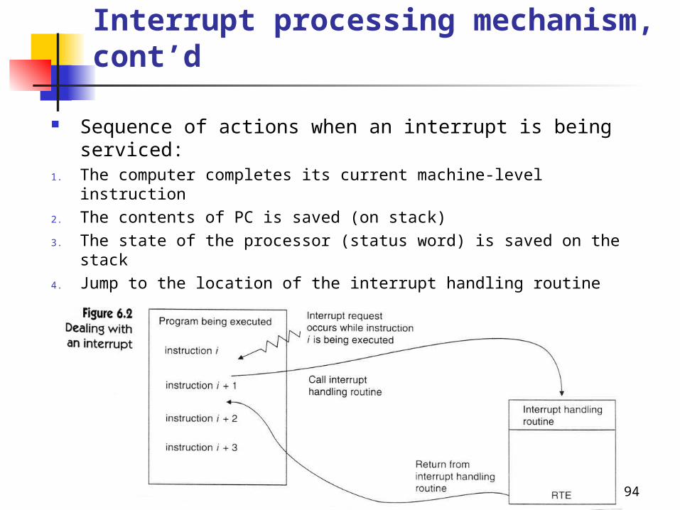
Interrupt processing mechanism, cont’d
Sequence of actions when an interrupt is being serviced:
1. The computer completes its current machine-level instruction
2. The contents of PC is saved (on stack)
3. The state of the processor (status word) is saved on the stack
4. Jump to the location of the interrupt handling routine
CPE/EE 421/521 Microcomputers
95
Interrupt processing mechanism, cont’d
The interrupt is transparent to the interrupted program
Interrupt request: Can be deferred or denied When it is deferred, it is said to be masked Special one: nonmaskable interrupt request (NMI) The 68000 NMI: IRQ7 (MSP430: RST*/NMI pin)
Prioritized interrupts Vectored interrupts
Requesting peripheral identifies itself, CPU doesn’t have to poll the status of each device to discover the interrupter
CPE/EE 421/521 Microcomputers
96
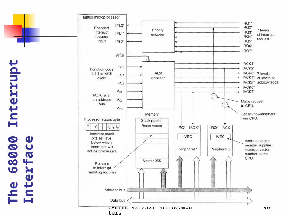
Th
e 68
000
Inte
rru
pt
Inte
rfac
e
CPE/EE 421/521 Microcomputers
97
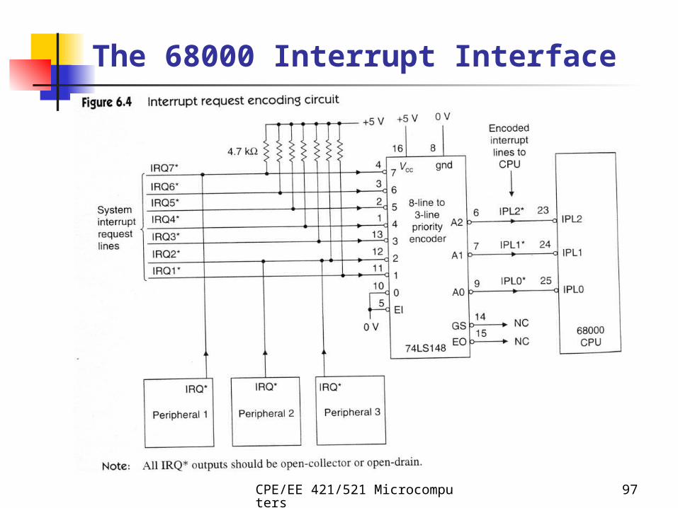
The 68000 Interrupt Interface
CPE/EE 421/521 Microcomputers
98
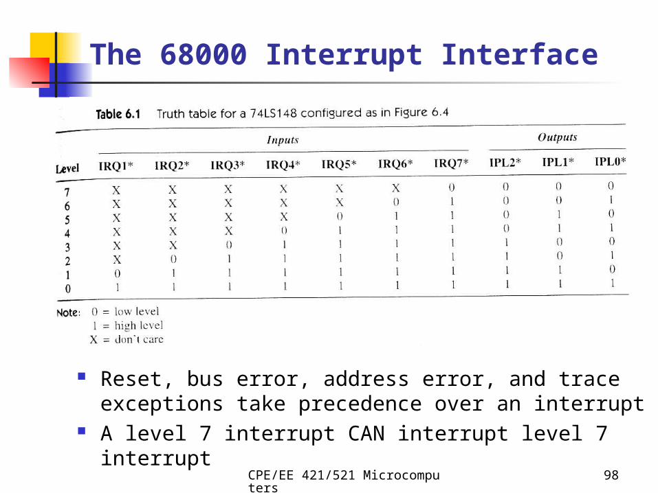
The 68000 Interrupt Interface
Reset, bus error, address error, and trace exceptions take precedence over an interrupt
A level 7 interrupt CAN interrupt level 7 interrupt
CPE/EE 421/521 Microcomputers
99
Pro
cess
ing
th
e In
terr
up
t
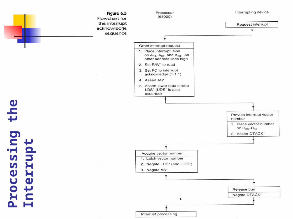
CPE/EE 421/521 Microcomputers
100
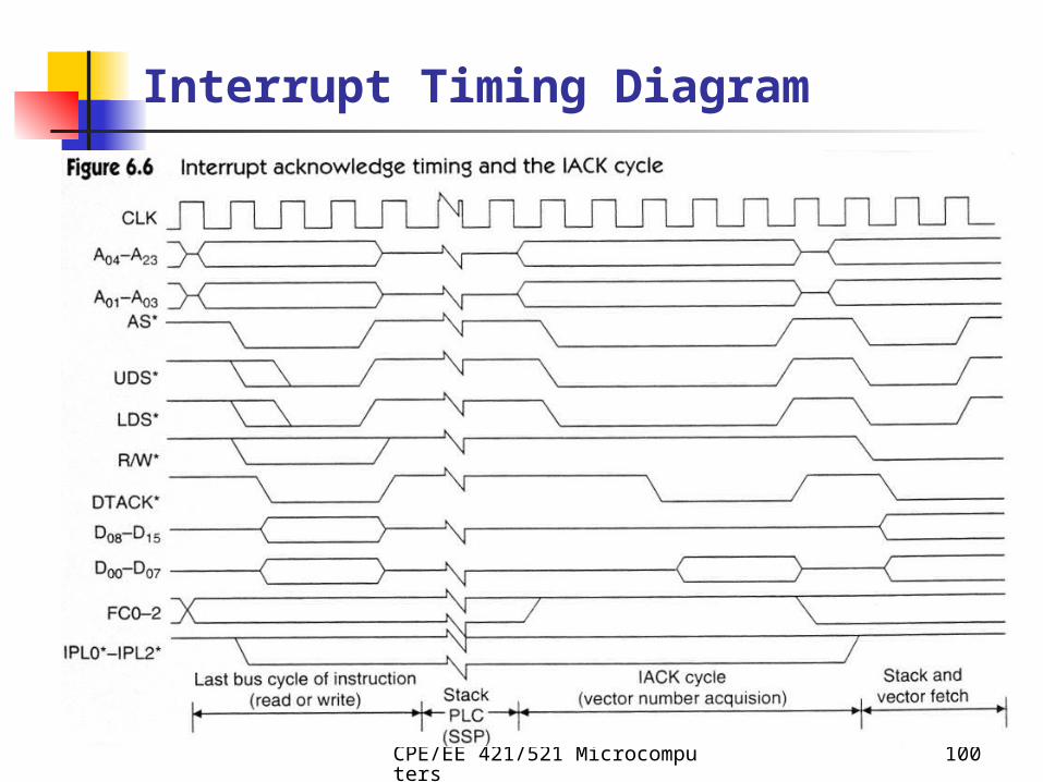
Interrupt Timing Diagram
CPE/EE 421/521 Microcomputers
101
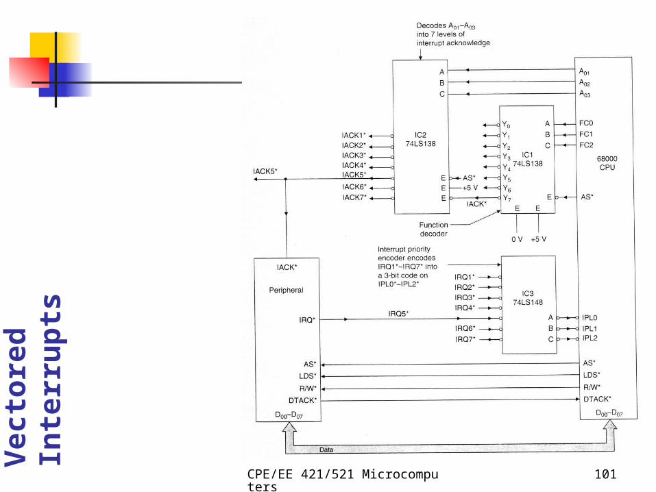
Vec
tore
d In
terr
up
ts
CPE/EE 421/521 Microcomputers
102
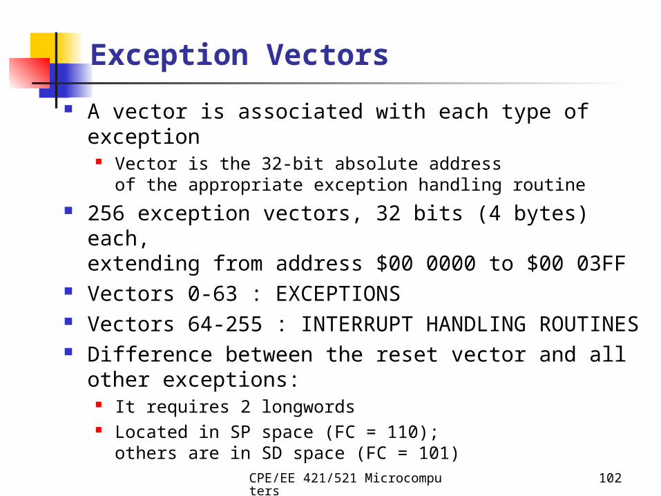
Exception Vectors
A vector is associated with each type of exception Vector is the 32-bit absolute address
of the appropriate exception handling routine 256 exception vectors, 32 bits (4 bytes) each,
extending from address $00 0000 to $00 03FF Vectors 0-63 : EXCEPTIONS Vectors 64-255 : INTERRUPT HANDLING ROUTINES Difference between the reset vector and all other
exceptions: It requires 2 longwords Located in SP space (FC = 110);
others are in SD space (FC = 101)
CPE/EE 421/521 Microcomputers
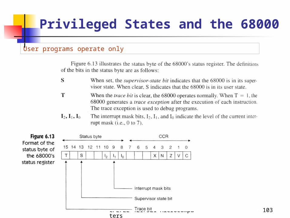
103
Privileged States and the 68000
User programs operate only
CPE/EE 421/521 Microcomputers
104
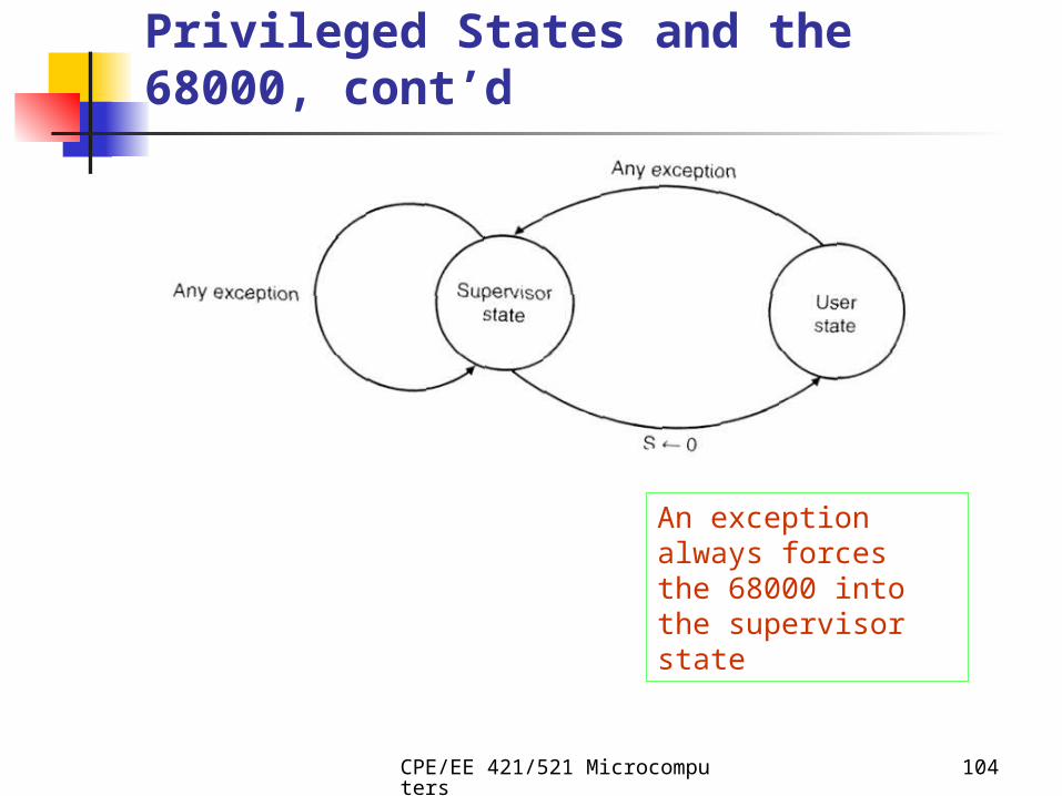
Privileged States and the 68000, cont’d
An exception always forces the 68000 into the supervisor state
CPE/EE 421/521 Microcomputers
105
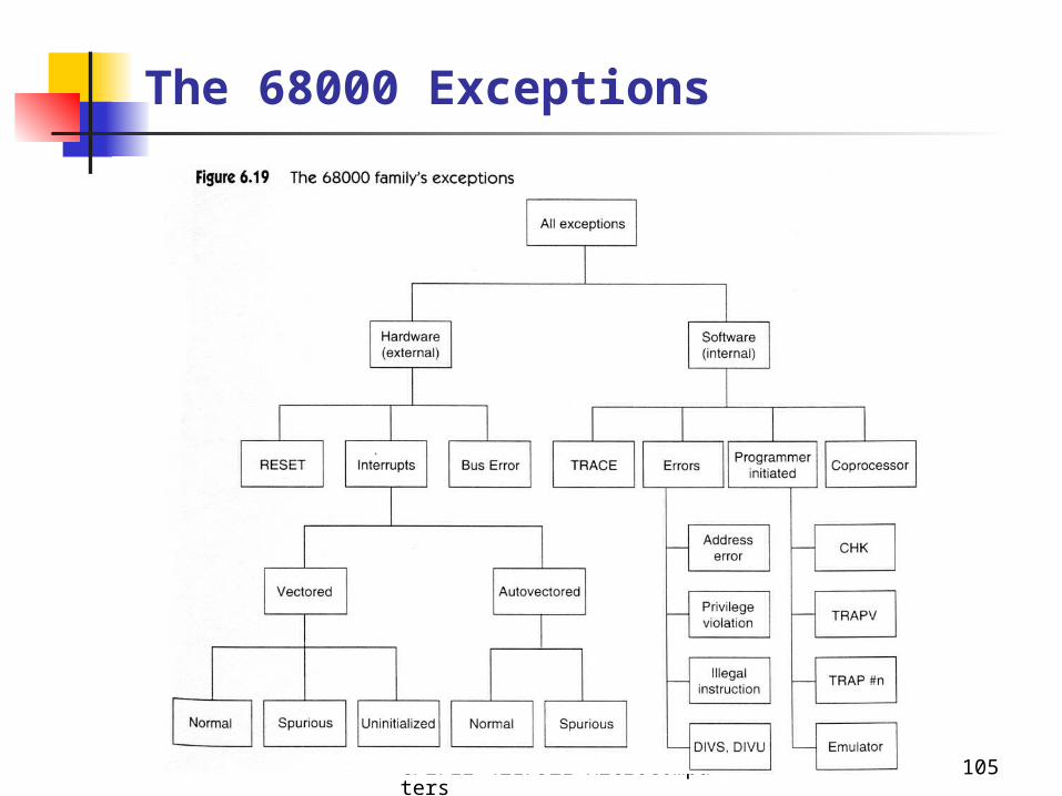
The 68000 Exceptions
CPE/EE 421/521 Microcomputers
106
Interrupts and Real-time Processing
Multitasking (multiprogramming) concurrent execution multiple tasks (processes) resource sharing (multiple users using the
same printer)
Multiprocessing parallel execution multiple PROCESSORS!
CPE/EE 421/521 Microcomputers
107
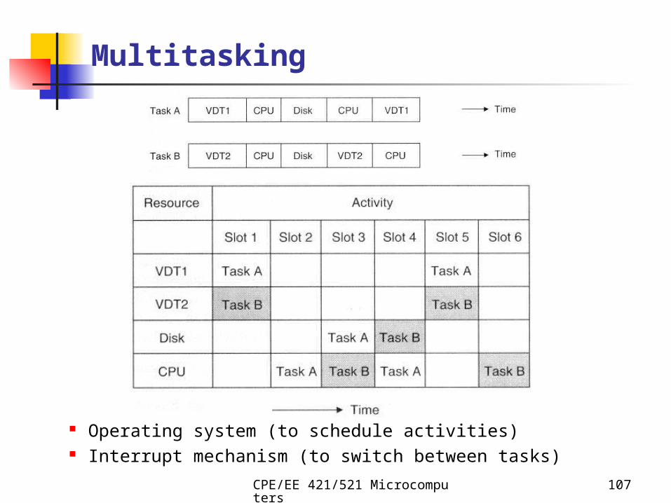
Multitasking
Operating system (to schedule activities) Interrupt mechanism (to switch between tasks)
CPE/EE 421/521 Microcomputers
108
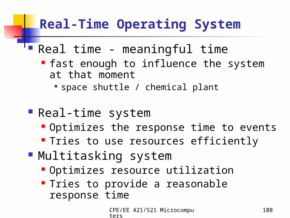
Real-Time Operating System
Real time - meaningful time fast enough to influence the system at that
moment space shuttle / chemical plant
Real-time system Optimizes the response time to events Tries to use resources efficiently
Multitasking system Optimizes resource utilization Tries to provide a reasonable response time
CPE/EE 421/521 Microcomputers
109
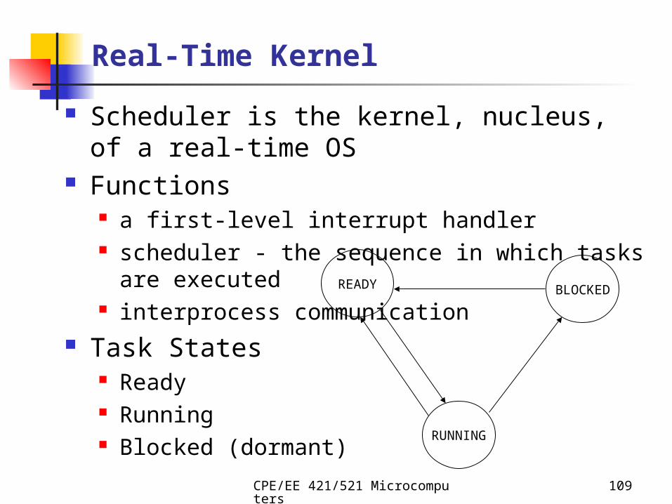
Real-Time Kernel
Scheduler is the kernel, nucleus, of a real-time OS
Functions a first-level interrupt handler scheduler - the sequence in which tasks are
executed interprocess communication
Task States Ready Running Blocked (dormant)
READY
RUNNING
BLOCKED
CPE/EE 421/521 Microcomputers
110
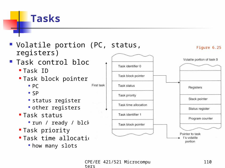
Tasks
Volatile portion (PC, status, registers) Task control block (TCB)
Task ID Task block pointer
PC SP status register other registers
Task status run / ready / blckd
Task priority Task time allocation
how many slots
Figure 6.25
CPE/EE 421/521 Microcomputers
111
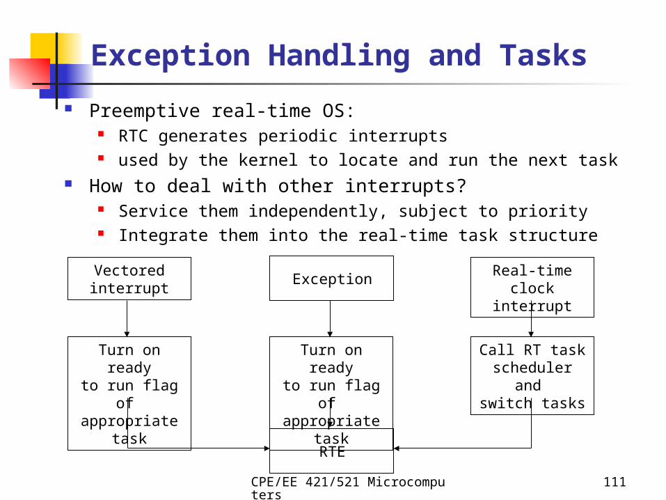
Exception Handling and Tasks
Preemptive real-time OS: RTC generates periodic interrupts used by the kernel to locate and run the next task
How to deal with other interrupts? Service them independently, subject to priority Integrate them into the real-time task structure
Vectoredinterrupt
Real-time clockinterrupt
Exception
Turn on readyto run flag of
appropriate task
Turn on readyto run flag of
appropriate task
Call RT taskscheduler and
switch tasks
RTE