Embed Size (px)
Citation preview
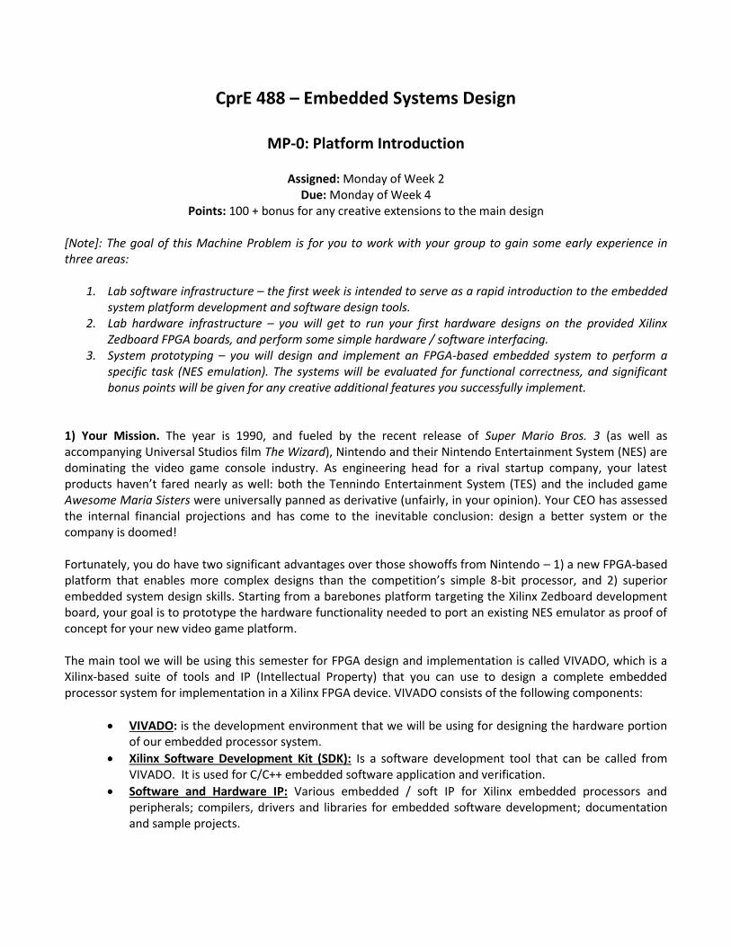
CprE 488 – Embedded Systems Design
MP-0: Platform Introduction
Assigned: Monday of Week 2 Due: Monday of Week 4
Points: 100 + bonus for any creative extensions to the main design [Note]: The goal of this Machine Problem is for you to work with your group to gain some early experience in three areas:
1. Lab software infrastructure – the first week is intended to serve as a rapid introduction to the embedded system platform development and software design tools.
2. Lab hardware infrastructure – you will get to run your first hardware designs on the provided Xilinx Zedboard FPGA boards, and perform some simple hardware / software interfacing.
3. System prototyping – you will design and implement an FPGA-based embedded system to perform a specific task (NES emulation). The systems will be evaluated for functional correctness, and significant bonus points will be given for any creative additional features you successfully implement.
1) Your Mission. The year is 1990, and fueled by the recent release of Super Mario Bros. 3 (as well as accompanying Universal Studios film The Wizard), Nintendo and their Nintendo Entertainment System (NES) are dominating the video game console industry. As engineering head for a rival startup company, your latest products haven’t fared nearly as well: both the Tennindo Entertainment System (TES) and the included game Awesome Maria Sisters were universally panned as derivative (unfairly, in your opinion). Your CEO has assessed the internal financial projections and has come to the inevitable conclusion: design a better system or the company is doomed! Fortunately, you do have two significant advantages over those showoffs from Nintendo – 1) a new FPGA-based platform that enables more complex designs than the competition’s simple 8-bit processor, and 2) superior embedded system design skills. Starting from a barebones platform targeting the Xilinx Zedboard development board, your goal is to prototype the hardware functionality needed to port an existing NES emulator as proof of concept for your new video game platform. The main tool we will be using this semester for FPGA design and implementation is called VIVADO, which is a Xilinx-based suite of tools and IP (Intellectual Property) that you can use to design a complete embedded processor system for implementation in a Xilinx FPGA device. VIVADO consists of the following components:
VIVADO: is the development environment that we will be using for designing the hardware portion of our embedded processor system.
Xilinx Software Development Kit (SDK): Is a software development tool that can be called from VIVADO. It is used for C/C++ embedded software application and verification.
Software and Hardware IP: Various embedded / soft IP for Xilinx embedded processors and peripherals; compilers, drivers and libraries for embedded software development; documentation and sample projects.
2
2) Getting Started. First, create a new directory for this class and lab: <SOME-PATH>\cpre488\Labs\MP-0 We are using Cybox to distribute the MPs: Download the provided MP0 starting directory structure from the link provided. Once you have unzipped the file you downloaded, your local directory tree should now look like the following (confirm):
|-- docs // MP-0 specific documentation
| |-- IP
| |-- Tools
| `-- ZedBoard
|-- sdcard.zip // Files for loading to SD card
|-- sw // Software code and project files
|-- nes_bootloader
`-- vga_test
Go to the software (sw) sub-directory, and examine the C code implementation of the existing NES bootloader and emulator, starting with nes_bootloader.c: In your report, describe how nes_bootloader.c currently works. Using a similar approach as what is presented in Chapter 1 of the Wolf textbook, draw a high-level structural diagram. How does
NESCore_Callback_OutputFrame() get called? Note that you won’t be able to compile the application outside of the Xilinx-specific SDK workspace we will be creating. 3) Creating a Hardware System. From the start menu open: Xilinx Design Tools -> Vivado 2018.3 Then, follow the instructions of Lab 1 of Tutorial 940 (UG940): "Embedded Processor Hardware Design" (docs/Tools/ug940-vivado-tutorial-embedded-design). With the following modifications: Step 1 modifications: Start the Vivado IDE and Create a Project i) skip instruction 1. ii) instruction 4: set project location to the folder you created (<SOME-PATH>\cpre488\Labs\MP-0) iii) instruction 6: set "Target language" to VHDL iv) instruction 8b: From the Vendor drop-down list, select em.avnet.com v) instruction 8c: Choose ZedBoard
3
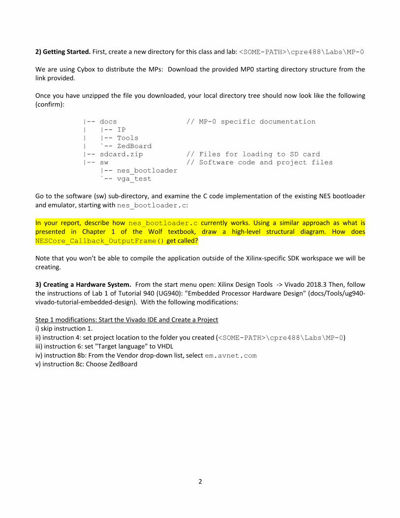
At this point you should have a window pop up similar to this:
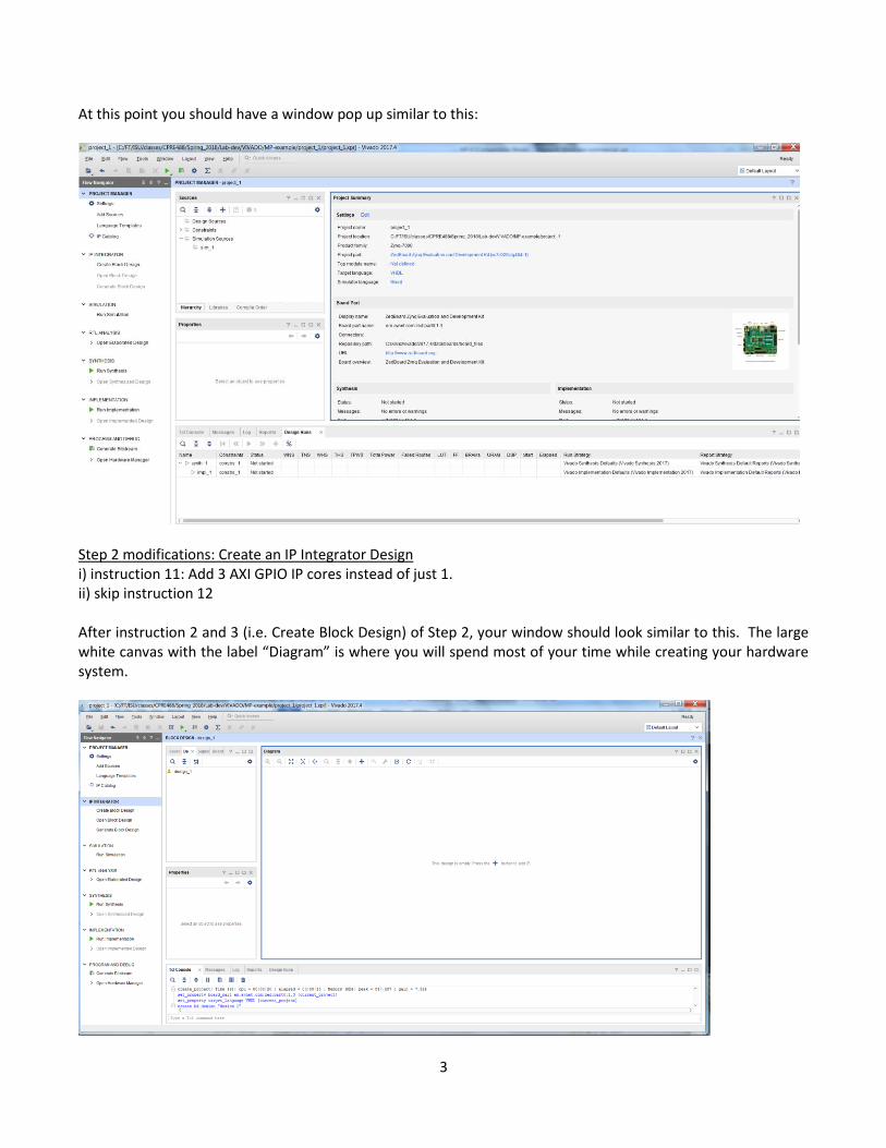
Step 2 modifications: Create an IP Integrator Design i) instruction 11: Add 3 AXI GPIO IP cores instead of just 1. ii) skip instruction 12 After instruction 2 and 3 (i.e. Create Block Design) of Step 2, your window should look similar to this. The large white canvas with the label “Diagram” is where you will spend most of your time while creating your hardware system.
4
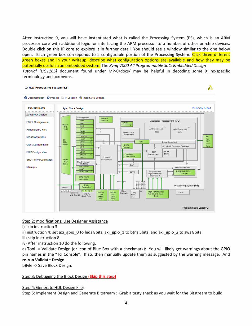
After instruction 9, you will have instantiated what is called the Processing System (PS), which is an ARM processor core with additional logic for interfacing the ARM processor to a number of other on-chip devices. Double click on this IP core to explore it in further detail. You should see a window similar to the one below open. Each green box corrseponds to a configurable portion of the Processing System. Click three different green boxes and in your writeup, describe what configuration options are available and how they may be potentially useful in an embedded system. The Zynq-7000 All Programmable SoC: Embedded Design Tutorial (UG1165) document found under MP-0/docs/ may be helpful in decoding some Xilinx-specific terminology and acronyms.
Step 2: modifications: Use Designer Assistance i) skip instruction 3 ii) instruction 4: set axi_gpio_0 to leds 8bits, axi_gpio_1 to btns 5bits, and axi_gpio_2 to sws 8bits iii) skip instruction 8 iv) After instruction 10 do the following: a) Tool -> Validate Design (or Icon of Blue Box with a checkmark): You will likely get warnings about the GPIO pin names in the “Tcl Console”. If so, then manually update them as suggested by the warning message. And re-run Validate Design. b)File -> Save Block Design. Step 3: Debugging the Block Design (Skip this step) Step 4: Generate HDL Design Files Step 5: Implement Design and Generate Bitstream : Grab a tasty snack as you wait for the Bitstream to build
5
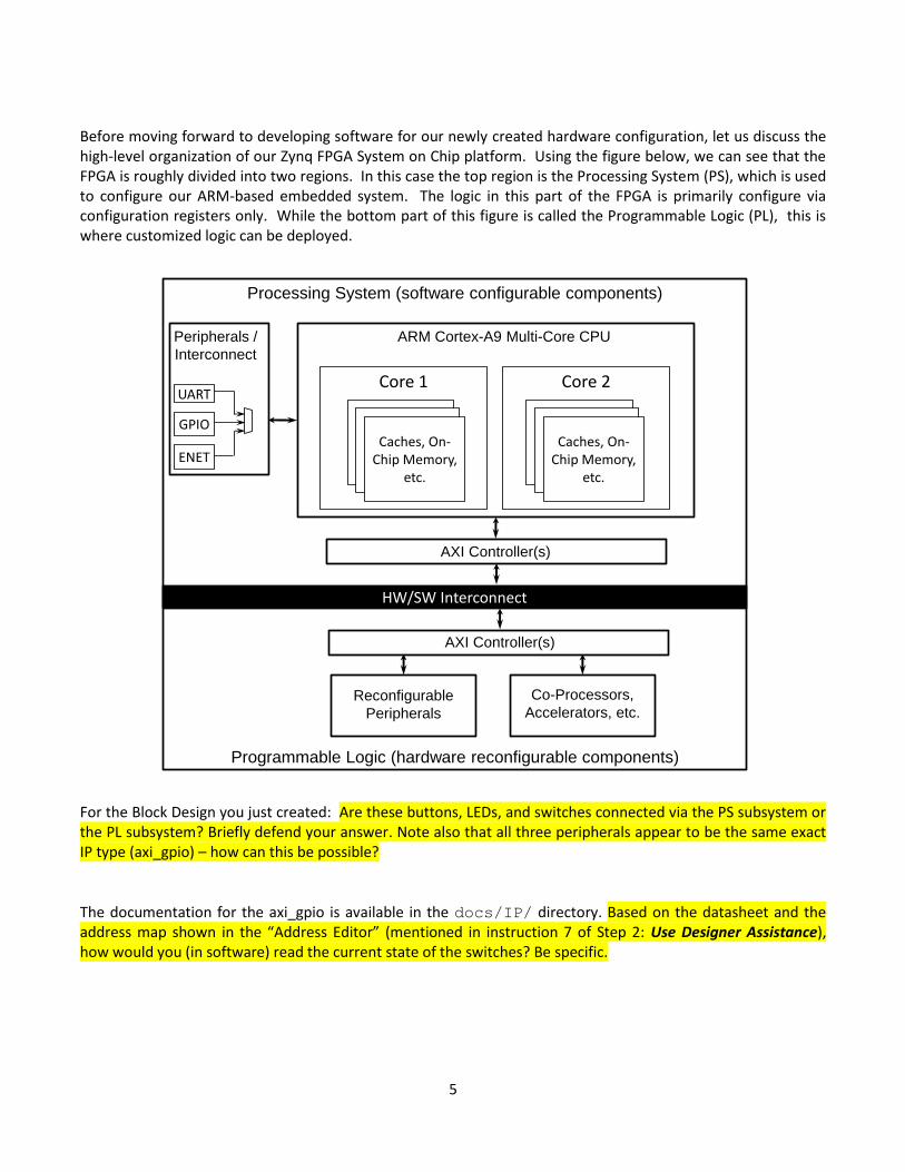
Before moving forward to developing software for our newly created hardware configuration, let us discuss the high-level organization of our Zynq FPGA System on Chip platform. Using the figure below, we can see that the FPGA is roughly divided into two regions. In this case the top region is the Processing System (PS), which is used to configure our ARM-based embedded system. The logic in this part of the FPGA is primarily configure via configuration registers only. While the bottom part of this figure is called the Programmable Logic (PL), this is where customized logic can be deployed. For the Block Design you just created: Are these buttons, LEDs, and switches connected via the PS subsystem or the PL subsystem? Briefly defend your answer. Note also that all three peripherals appear to be the same exact IP type (axi_gpio) – how can this be possible?
The documentation for the axi_gpio is available in the docs/IP/ directory. Based on the datasheet and the address map shown in the “Address Editor” (mentioned in instruction 7 of Step 2: Use Designer Assistance), how would you (in software) read the current state of the switches? Be specific.
ARM Cortex-A9 Multi-Core CPU
Core 1 Core 2
Data QueuesData Queues
Caches, On-Chip Memory,
etc.
Data QueuesData Queues
Caches, On-Chip Memory,
etc.
Processing System (software configurable components)
HW/SW Interconnect
Programmable Logic (hardware reconfigurable components)
Peripherals /
Interconnect
UART
GPIO
ENET
AXI Controller(s)
AXI Controller(s)
Reconfigurable
Peripherals
Co-Processors,
Accelerators, etc.
6
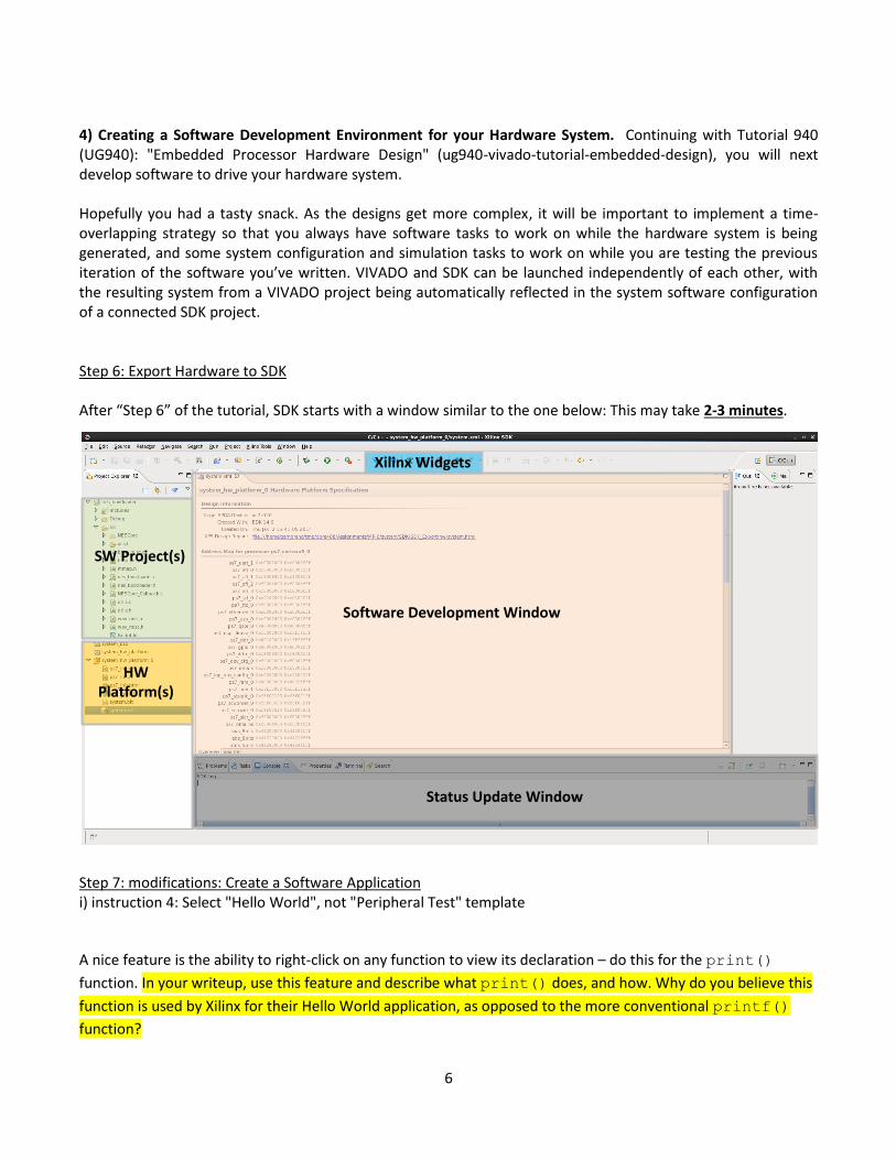
4) Creating a Software Development Environment for your Hardware System. Continuing with Tutorial 940 (UG940): "Embedded Processor Hardware Design" (ug940-vivado-tutorial-embedded-design), you will next develop software to drive your hardware system. Hopefully you had a tasty snack. As the designs get more complex, it will be important to implement a time-overlapping strategy so that you always have software tasks to work on while the hardware system is being generated, and some system configuration and simulation tasks to work on while you are testing the previous iteration of the software you’ve written. VIVADO and SDK can be launched independently of each other, with the resulting system from a VIVADO project being automatically reflected in the system software configuration of a connected SDK project. Step 6: Export Hardware to SDK After “Step 6” of the tutorial, SDK starts with a window similar to the one below: This may take 2-3 minutes. Step 7: modifications: Create a Software Application i) instruction 4: Select "Hello World", not "Peripheral Test" template
A nice feature is the ability to right-click on any function to view its declaration – do this for the print()
function. In your writeup, use this feature and describe what print() does, and how. Why do you believe this
function is used by Xilinx for their Hello World application, as opposed to the more conventional printf()
function?
Software Development Window
Status Update Window
SW Project(s)
Xilinx Widgets
HWPlatform(s)
7
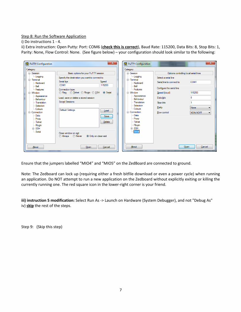
Step 8: Run the Software Application i) Do instructions 1 - 4. ii) Extra instruction: Open Putty: Port: COM6 (check this is correct), Baud Rate: 115200, Data Bits: 8, Stop Bits: 1, Parity: None, Flow Control: None. (See figure below) – your configuration should look similar to the following: Ensure that the jumpers labelled “MIO4” and “MIO5” on the ZedBoard are connected to ground. Note: The Zedboard can lock up (requiring either a fresh bitfile download or even a power cycle) when running an application. Do NOT attempt to run a new application on the Zedboard without explicitly exiting or killing the currently running one. The red square icon in the lower-right corner is your friend. iii) instruction 5 modification: Select Run As -> Launch on Hardware (System Debugger), and not "Debug As" iv) skip the rest of the steps. Step 9: (Skip this step)
8
5) Develop an interactive software application for your hardware system (Hardware/Software Interfacing). Now that you have “Hello World” working, it is time to dive into interacting with the hardware devices that you used to implement your hardware system. In this case, GPIO devices to interface with the LEDs, Pushbuttons and Switches of the ZedBoard. Modify the hello_world application to also interface with the switches, buttons, and LEDs that are configured in the programmable logic. For example, have the application print out the state of the switches when a button is pressed, or light up certain LEDs given an input integer. Here you will gain your first exposure to the Xilinx BSP structure, the extent to which you use it is up to you:
The built-in functions Xil_Out32() and Xil_In32() will serve as a good starting point, or you can explicitly access pointers in the memory map for your peripherals (a great way to get a solid understanding for how to interface with your IP hardware devices).
#include <xparameters.h> to use the automatically-generated memory map macros, or hard-code the pointers yourself based on the “Addresses Editor” tab in VIVADO. For the GPIO peripherals we have connected to the buttons / switches / LEDs, the peripheral base address is where the current on/off state is read or written to.
Not all of the buttons on the board are connected to the AXI_GPIO peripheral. Pins 50 and 51 of the I/O pins on the Processing System side are connected to buttons on the ZedBoard, and are accessed
via the more flexible (and complex) gpiops interface. You may want to access these buttons for step 7) below, so read up on this documentation as well at some point. .
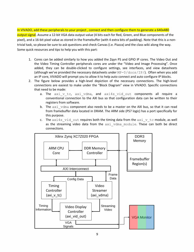
Continue experimenting until you have confidence in this aspect of memory-mapped peripheral interfacing. 6) Video Display. After tinkering with LEDs and switches enough to be confident in how your software and hardware are working together, it’s time to return our focus to the video game (emulation) system. One key feature we have not yet touched on is displaying video to a monitor, which in the context of our ZedBoard platform and Xilinx VIVADO tools can be accomplished via a combination of hardware peripherals and software configuration. Unlike other platforms that have dedicated video display controller hardware, on the ZedBoard we will need to drive all the necessary signals ourselves. Specifically, there are three components that we will be using to output a 640x480 display over VGA:
A Video Direct Memory Access (VDMA) peripheral – axi_vdma – which provides high-bandwidth direct memory access between a memory component (typically DRAM) and the AXI Stream video protocol.
A Video Timing Controller (VTC) peripheral – v_tc – which generates the necessary timing signals for video out, including horizontal and vertical synchronization pulses and blanking timing.
A Video Out peripheral – axi4s_vid_out – which interfaces with a video source using the AXI Stream protocol and in conjunction with a VTC core, produces the appropriate video output.
9
In VIVADO, add these peripherals to your project , connect and then configure them to generate a 640x480
output signal. Assume a 12-bit VGA data output value (4 bits each for Red, Green, and Blue components of the
pixel), and a 16-bit pixel value as stored in the framebuffer (with 4 extra bits of padding). Note that this is a non-
trivial task, so please be sure to ask questions and check Canvas (i.e. Piazza) and the class wiki along the way.
Some quick resources and tips to help you with this part:
1. Cores can be added similarly to how you added the Zqyn PS and GPIO IP cores. The Video Out and the Video Timing Controller peripherals cores are under the “Video and Image Processing”. Once added, they can be double-clicked to configure settings, see interfaces, and view datasheets (although we’ve provided the necessary datasheets under MP-0/docs/IP/). Often when you add an IP core, VIVADO will prompt you to allow it to help auto connect and auto configure IP blocks.
2. The figure below provides a high-level depiction of the necessary connections. The high-level connections are easiest to make under the “Block Diagram” view in VIVADO. Specific connections that need to be made:
a. The axi_v_tc, axi_vdma, and axi4s_vid_out components all require a conventional connection to the AXI bus so that configuration data can be written to their registers from software.
b. The axi_vdma component also needs to be a master on the AXI bus, so that it can read from framebuffer data located in DRAM. The ARM side (PS7 logic) has a port specifically for this purpose.
c. The axi4s_vid_out requires both the timing data from the axi_v_tc module, as well as the streaming video data from the axi_vdma_module. These can both be direct connections.
VGA Monitor
ARM CPUCore
Xilinx Zynq XC7Z020 FPGA
AXI Interconnect
Timing Controller (axi_v_tc)
Video Streamer
(axi_vdma)
Video Display Controller
(axi_vid_out)
Config Data
Streaming
Video
Timing
Information
VGA
Signals
DDR Memory Controller
DDR3
Memory
FramebufferRegion(s)
Frame
Data
10
3. Beyond the bus connections in the figure, there are also multiple connections needed to specific ports on the peripherals, as well as the Zynq FPGA itself. Some are more straightforward than others:
a. The axi_v_tc as well as the axi4s_vid_out have unique clocking requirements in order to drive a 640x480 VGA signal. HW #0 should provide some insight for this portion.
b. The VGA interface for the ZedBoard consists of HSYNC and VSYNC signals, as well as a 12-bit RGB signal. These ports must be constrained to the particular external pins on the Zynq FPGA. You will add an XDC file to your project to define these constraints (call it MP-0.xdc). This is where constrains are typically placed. The master constraints file (for every possible
I/O connection on the board) is located under MP-0/docs/ZedBoard/. In general, these peripherals can either be configured using hardware generics (in VIVADO), or via explicitly writing values to configuration registers (in SDK). The AXI Video Direct Memory Access guide found at MP-0/docs/IP/pg020_axi_vdma.pdf is extremely helpful for the software side of configuration, if you know where to look. Page 49 provides some explanation of the general operation of the VDMA core, and the configurable registers are described starting on page 15. We’ve provided a partially-completed vga_test application that you can use to test your configuration. In
SDK, make a “Blank” Project called vga_test. Then copy the provided file into the blank project’s source directory. The last few lines of vga_test.c (starting at line 61) are intended to set the VDMA configuration register values. Currently these are all set to a dummy value (the CHANGE_ME macro). Modify the configuration registers for correct VDMA operation, and in your writeup, provide a justification based on the VDMA documentation for how you set these values. Finally, create a new project called cyclone_checker, that draws a cyclone-colored checkerboard to the screen. A standard checkerboard is 8x8 squares, with the “Cyclone Cardinal” color having an RGB hex code of 0xC8103E, and the “Cyclone Gold” color having an RGB hex code of 0xF1BE48. In your writeup, explain how you converted these color values valid values for the 16-bit framebuffer.
11
7) NES Emulation. The starter code for the NES emulation can be found in the nes_bootloader application.
Add nes_bootloader code using the same steps as in the previous part for vga_test, and examine the code. While you previously built a system-level diagram, we can now focus on implementation aspects:
Function xil_init() in nes_bootloader.c is mostly complete, save for the VDMA
initialization code that you can copy/paste from vga_test.
Function nes_load() reads in the .nes file from the sdcard connected to your ZedBoard. Double-check that your card is loaded with these files – if not, the sdcard.zip file provided in the MP-0 repository can be unzipped and copied using any sdcard writer. Place the files directly on the top level of the sdcard; do not add any sub-directories.
There are two main callbacks (for now) that are left for you to complete: o Function NESCore_Callback_OutputFrame() takes as input a 256x240 frame of
pixel data from the current state of the emulator, and copies it as a 640x480 frame for the ZedBoard framebuffer. There are several valid approaches for how to perform this copy.
o Function NESCore_Callback_InputPadState() passes a pointer to data words representing the current controller state for players 1 and 2. Overwrite at least the player 1 pointer to reflect appropriate button presses on the ZedBoard.
Modify the nes_bootloader code such that the NES games are reasonably playable. In your report, describe your general approach to implementing both of the NESCore_Callback functions. What to submit: a .zip file containing your modified source files (modifications to hello_world.c,
system.mhs, system.ucf, vga_test.c, cyclone_checker.c, nes_bootloader.c, and NESCore_Callback.c) and your writeup in PDF format containing the sections highlighted above. In the Blackboard submission, list each team member with a percentage of their overall effort on MP-0 (with percentages summing to 100%). What to demo: at least one group member must be available to demo the current state of your implementation. A full demo score requires a correctly-emulated system, but partial credit will be given for effort. Be prepared to briefly discuss your source code. BONUS credit. MP-0’s bonus point criteria is creativity. The current nes_bootloader design is very limited in terms of functionality. Bonus points will be provided for groups that successfully implement the following features:
Interactive menu for selecting NES games, either a nice text-based menu (5 bonus points) or a graphical menu (20 bonus points).
A method for exiting a current game and returning back to the menu (5 bonus points).
Interfacing with arcade buttons and a joystick, for a more user-friendly input method (15 bonus points)
Interfacing with an original NES controller (15 bonus points)
The ability to emulate sound using the appropriate callback function (25 bonus points). Each group is limited to 100 bonus points for the entire semester.