Embed Size (px)
Citation preview
chapter 2Quickstart
In this chapter we will get to grips with EAGLE and create the schematic and board files for a simple project that uses a 555 timer to flash a light-emitting diode (LED).As the chapter title suggests, this chapter is all about doing it quickly rather
than doing it with best practice. In later chapters, especially Chapters 4 and 5, you will find a more thorough and considered approach to design. Seasoned electronic engineers might need to avert their eyes for some of this chapter.
Creating a New Project
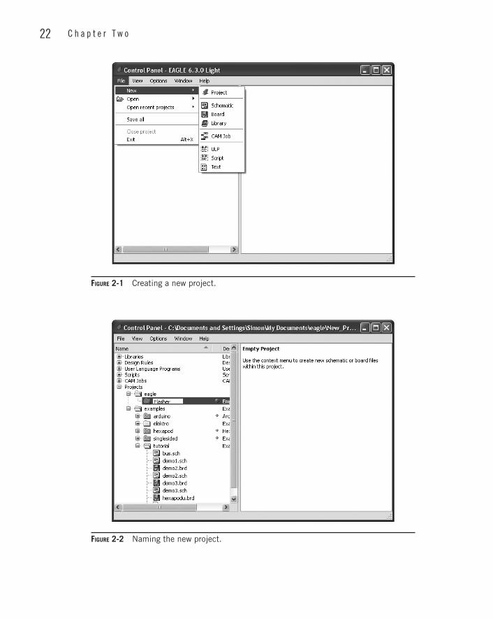
The first step is to create a new project. Thus, from the “File” menu, select “New” and then “Project” (Figure 2-1). This will allow you to edit the name of the project (Figure 2-2).
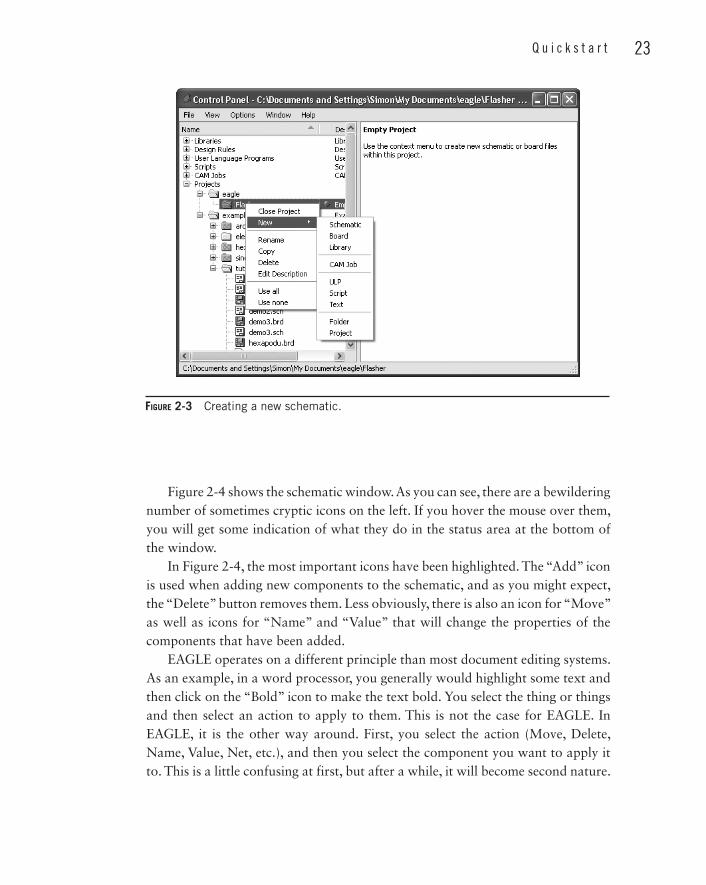
You now need to create a new schematic diagram so that you can start drawing out the circuit. To do this, right-click on the “Flasher” project icon and select “New” and then “Schematic” from the popup menu (Figure 2-3).
Initially, the schematic document will be labeled “Untitled.” It is a good idea to save it by selecting “File” and then “Save As” from the menu. Give it the name flasher.sch. You can actually have more than one schematic and board file within the same project. However, this can lead to confusion, and it is easier to just have one of each and give the files the same name as the project. I like to use an uppercase initial letter for the project and lowercase for the files.
Do not create a board file yet. We will do that after you have designed the schematic.
21
22 C h a p t e r T w o
Figure 2-1 Creating a new project.
Figure 2-2 Naming the new project.
Q u i c k s t a r t 23
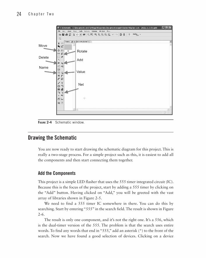
Figure 2-4 shows the schematic window. As you can see, there are a bewildering number of sometimes cryptic icons on the left. If you hover the mouse over them, you will get some indication of what they do in the status area at the bottom of the window.
In Figure 2-4, the most important icons have been highlighted. The “Add” icon is used when adding new components to the schematic, and as you might expect, the “Delete” button removes them. Less obviously, there is also an icon for “Move” as well as icons for “Name” and “Value” that will change the properties of the components that have been added.
EAGLE operates on a different principle than most document editing systems. As an example, in a word processor, you generally would highlight some text and then click on the “Bold” icon to make the text bold. You select the thing or things and then select an action to apply to them. This is not the case for EAGLE. In EAGLE, it is the other way around. First, you select the action (Move, Delete, Name, Value, Net, etc.), and then you select the component you want to apply it to. This is a little confusing at first, but after a while, it will become second nature.
Figure 2-3 Creating a new schematic.
24 C h a p t e r T w o
Drawing the Schematic
You are now ready to start drawing the schematic diagram for this project. This is really a two-stage process. For a simple project such as this, it is easiest to add all the components and then start connecting them together.
Add the Components
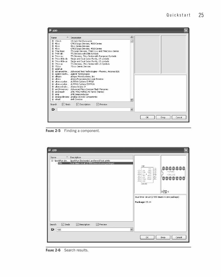
This project is a simple LED flasher that uses the 555 timer integrated circuit (IC). Because this is the focus of the project, start by adding a 555 timer by clicking on the “Add” button. Having clicked on “Add,” you will be greeted with the vast array of libraries shown in Figure 2-5.
We need to find a 555 timer IC somewhere in there. You can do this by searching. Start by entering “555” in the search field. The result is shown in Figure 2-6.
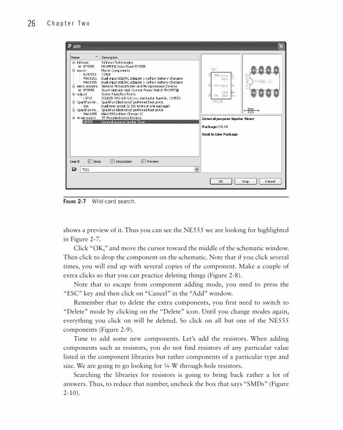
The result is only one component, and it’s not the right one. It’s a 556, which is the dual-timer version of the 555. The problem is that the search uses entire words. To find any words that end in “555,” add an asterisk (*) to the front of the search. Now we have found a good selection of devices. Clicking on a device
Figure 2-4 Schematic window.
Q u i c k s t a r t 25
Figure 2-5 Finding a component.
Figure 2-6 Search results.
26 C h a p t e r T w o
shows a preview of it. Thus you can see the NE555 we are looking for highlighted in Figure 2-7.
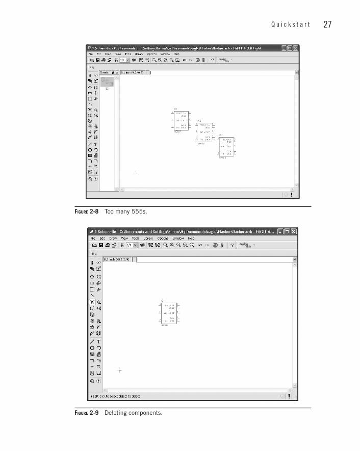
Click “OK,” and move the cursor toward the middle of the schematic window. Then click to drop the component on the schematic. Note that if you click several times, you will end up with several copies of the component. Make a couple of extra clicks so that you can practice deleting things (Figure 2-8).
Note that to escape from component adding mode, you need to press the “ESC” key and then click on “Cancel” in the “Add” window.
Remember that to delete the extra components, you first need to switch to “Delete” mode by clicking on the “Delete” icon. Until you change modes again, everything you click on will be deleted. So click on all but one of the NE555 components (Figure 2-9).
Time to add some new components. Let’s add the resistors. When adding components such as resistors, you do not find resistors of any particular value listed in the component libraries but rather components of a particular type and size. We are going to go looking for ¼-W through-hole resistors.
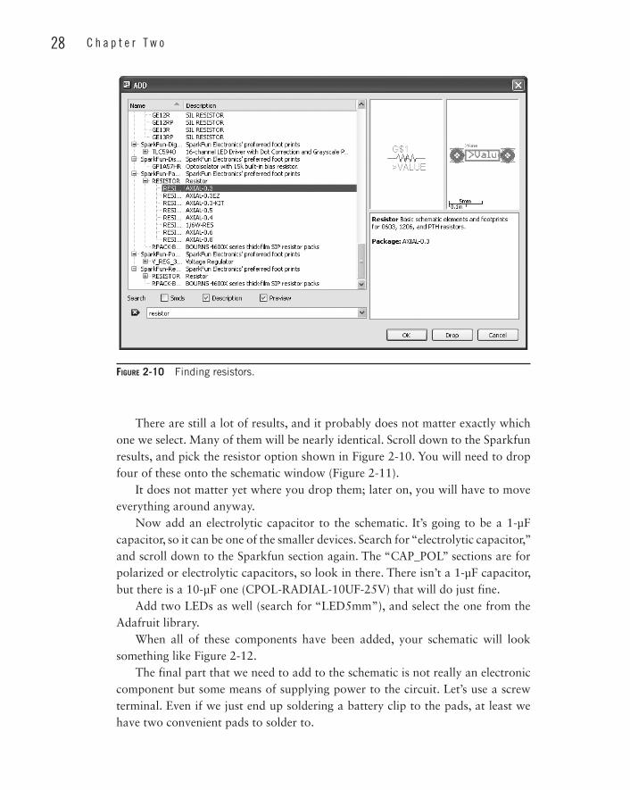
Searching the libraries for resistors is going to bring back rather a lot of answers. Thus, to reduce that number, uncheck the box that says “SMDs” (Figure 2-10).
Figure 2-7 Wild-card search.
Q u i c k s t a r t 27
Figure 2-8 Too many 555s.
Figure 2-9 Deleting components.
28 C h a p t e r T w o
Figure 2-10 Finding resistors.
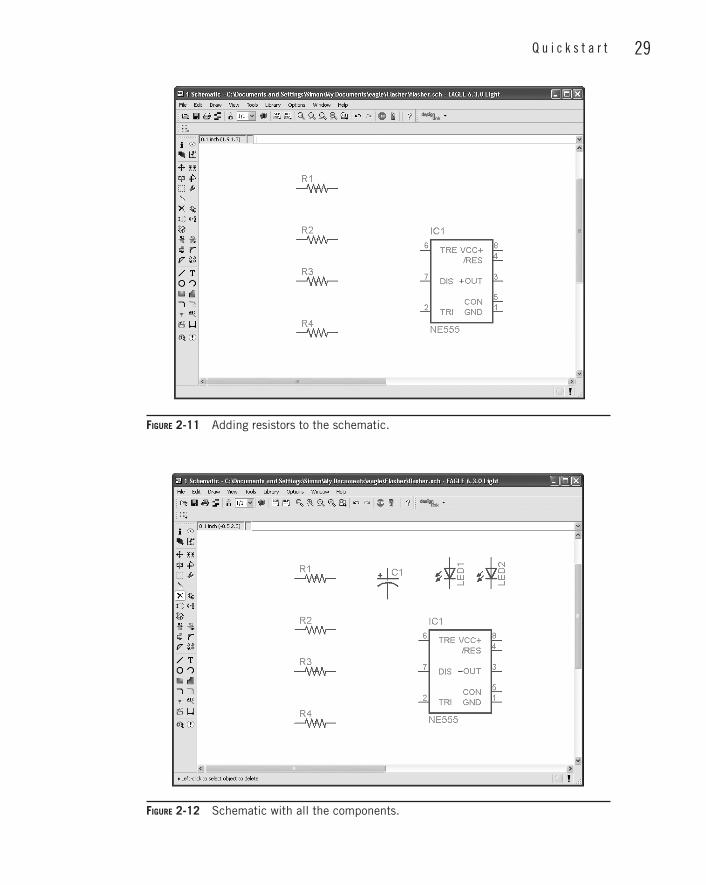
There are still a lot of results, and it probably does not matter exactly which one we select. Many of them will be nearly identical. Scroll down to the Sparkfun results, and pick the resistor option shown in Figure 2-10. You will need to drop four of these onto the schematic window (Figure 2-11).
It does not matter yet where you drop them; later on, you will have to move everything around anyway.
Now add an electrolytic capacitor to the schematic. It’s going to be a 1-μF capacitor, so it can be one of the smaller devices. Search for “electrolytic capacitor,” and scroll down to the Sparkfun section again. The “CAP_POL” sections are for polarized or electrolytic capacitors, so look in there. There isn’t a 1-µF capacitor, but there is a 10-µF one (CPOL-RADIAL-10UF-25V) that will do just fine.
Add two LEDs as well (search for “LED5mm”), and select the one from the Adafruit library.
When all of these components have been added, your schematic will look something like Figure 2-12.
The final part that we need to add to the schematic is not really an electronic component but some means of supplying power to the circuit. Let’s use a screw terminal. Even if we just end up soldering a battery clip to the pads, at least we have two convenient pads to solder to.
Q u i c k s t a r t 29
Figure 2-11 Adding resistors to the schematic.
Figure 2-12 Schematic with all the components.
30 C h a p t e r T w o
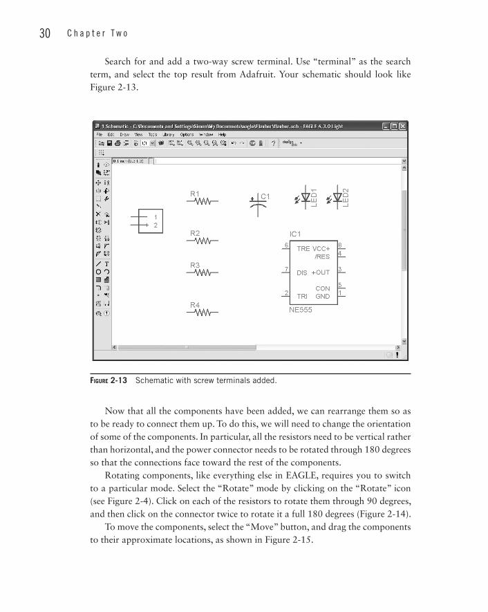
Search for and add a two-way screw terminal. Use “terminal” as the search term, and select the top result from Adafruit. Your schematic should look like Figure 2-13.
Figure 2-13 Schematic with screw terminals added.
Now that all the components have been added, we can rearrange them so as to be ready to connect them up. To do this, we will need to change the orientation of some of the components. In particular, all the resistors need to be vertical rather than horizontal, and the power connector needs to be rotated through 180 degrees so that the connections face toward the rest of the components.
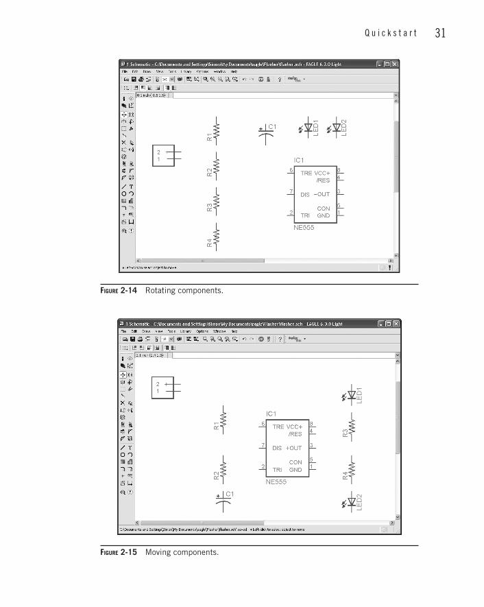
Rotating components, like everything else in EAGLE, requires you to switch to a particular mode. Select the “Rotate” mode by clicking on the “Rotate” icon (see Figure 2-4). Click on each of the resistors to rotate them through 90 degrees, and then click on the connector twice to rotate it a full 180 degrees (Figure 2-14).
To move the components, select the “Move” button, and drag the components to their approximate locations, as shown in Figure 2-15.
Q u i c k s t a r t 31
Figure 2-14 Rotating components.
Figure 2-15 Moving components.
32 C h a p t e r T w o
Join Them Together
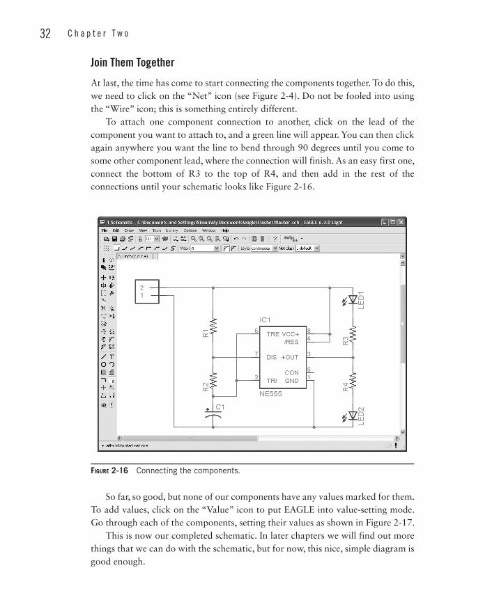
At last, the time has come to start connecting the components together. To do this, we need to click on the “Net” icon (see Figure 2-4). Do not be fooled into using the “Wire” icon; this is something entirely different.
To attach one component connection to another, click on the lead of the component you want to attach to, and a green line will appear. You can then click again anywhere you want the line to bend through 90 degrees until you come to some other component lead, where the connection will finish. As an easy first one, connect the bottom of R3 to the top of R4, and then add in the rest of the connections until your schematic looks like Figure 2-16.
Figure 2-16 Connecting the components.
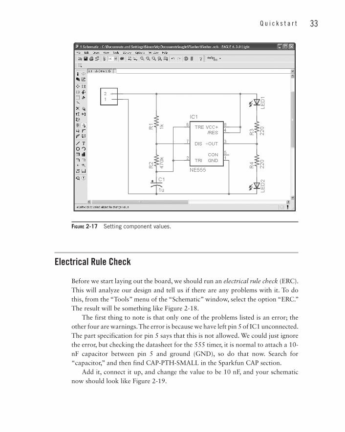
So far, so good, but none of our components have any values marked for them. To add values, click on the “Value” icon to put EAGLE into value-setting mode. Go through each of the components, setting their values as shown in Figure 2-17.
This is now our completed schematic. In later chapters we will find out more things that we can do with the schematic, but for now, this nice, simple diagram is good enough.
Q u i c k s t a r t 33
Figure 2-17 Setting component values.
Electrical Rule Check
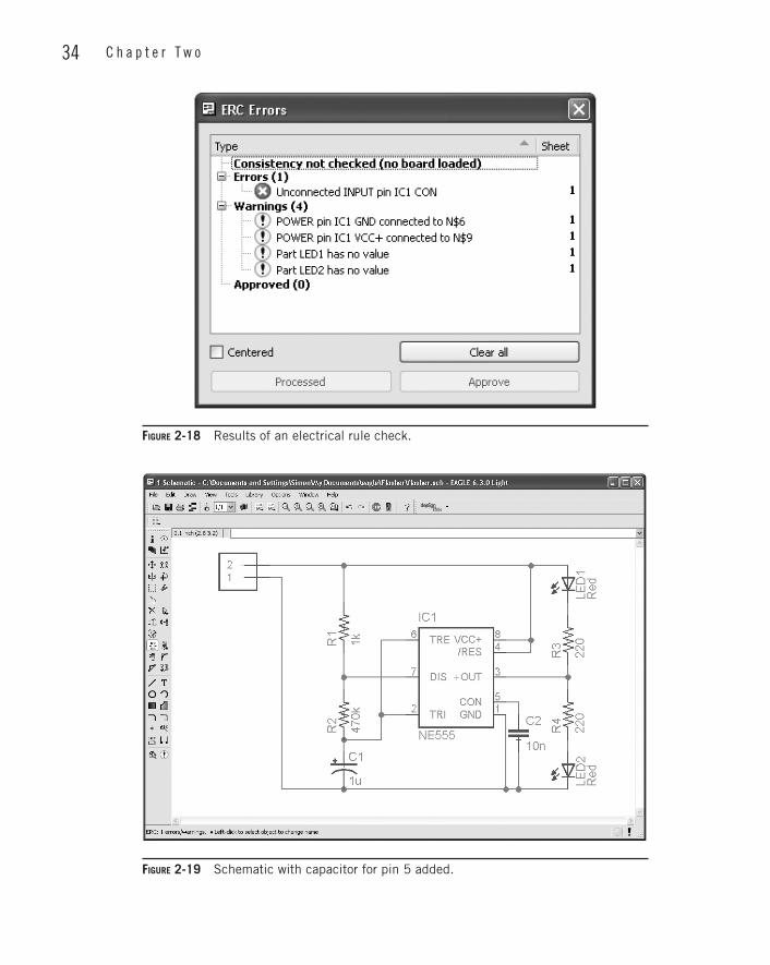
Before we start laying out the board, we should run an electrical rule check (ERC). This will analyze our design and tell us if there are any problems with it. To do this, from the “Tools” menu of the “Schematic” window, select the option “ERC.” The result will be something like Figure 2-18.
The first thing to note is that only one of the problems listed is an error; the other four are warnings. The error is because we have left pin 5 of IC1 unconnected. The part specification for pin 5 says that this is not allowed. We could just ignore the error, but checking the datasheet for the 555 timer, it is normal to attach a 10-nF capacitor between pin 5 and ground (GND), so do that now. Search for “capacitor,” and then find CAP-PTH-SMALL in the Sparkfun CAP section.
Add it, connect it up, and change the value to be 10 nF, and your schematic now should look like Figure 2-19.
34 C h a p t e r T w o
Figure 2-18 Results of an electrical rule check.
Figure 2-19 Schematic with capacitor for pin 5 added.
Q u i c k s t a r t 35
Close the “ERC” window, and run it again. Just the four warnings should remain. The last two of these just say that the LEDs do not have a value. We can either ignore these warnings or add a value of say Red to indicate the color of the LEDs.
This just leaves us with two warnings. They will say something like POWER pin IC1 GND connected to N$6. The N$6 probably will be different because it depends on the order in which you connected things together. N$6 is an automatically assigned name for a net. A net is, if you like, a line, and all the lines that connect to it between one component pin and another.
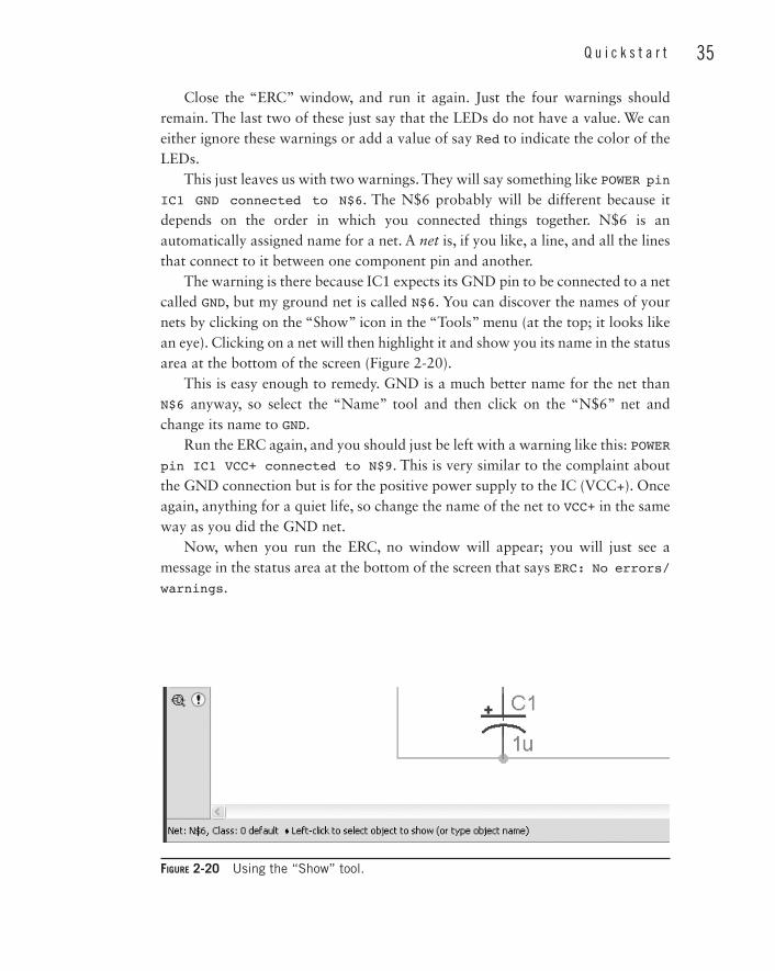
The warning is there because IC1 expects its GND pin to be connected to a net called GND, but my ground net is called N$6. You can discover the names of your nets by clicking on the “Show” icon in the “Tools” menu (at the top; it looks like an eye). Clicking on a net will then highlight it and show you its name in the status area at the bottom of the screen (Figure 2-20).
This is easy enough to remedy. GND is a much better name for the net than N$6 anyway, so select the “Name” tool and then click on the “N$6” net and change its name to GND.
Run the ERC again, and you should just be left with a warning like this: POWER pin IC1 VCC+ connected to N$9. This is very similar to the complaint about the GND connection but is for the positive power supply to the IC (VCC+). Once again, anything for a quiet life, so change the name of the net to VCC+ in the same way as you did the GND net.
Now, when you run the ERC, no window will appear; you will just see a message in the status area at the bottom of the screen that says ERC: No errors/warnings.
Figure 2-20 Using the “Show” tool.
36 C h a p t e r T w o
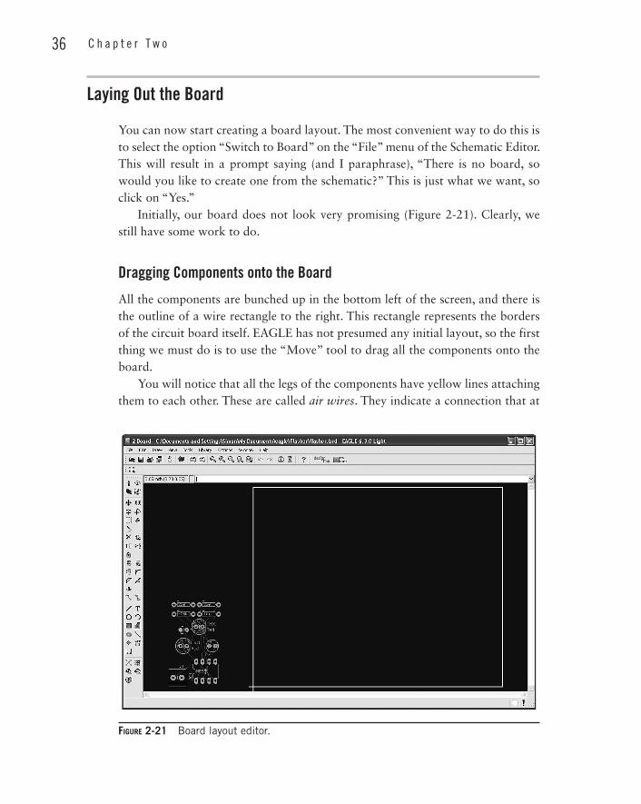
Laying Out the Board
You can now start creating a board layout. The most convenient way to do this is to select the option “Switch to Board” on the “File” menu of the Schematic Editor. This will result in a prompt saying (and I paraphrase), “There is no board, so would you like to create one from the schematic?” This is just what we want, so click on “Yes.”
Initially, our board does not look very promising (Figure 2-21). Clearly, we still have some work to do.
Dragging Components onto the Board
All the components are bunched up in the bottom left of the screen, and there is the outline of a wire rectangle to the right. This rectangle represents the borders of the circuit board itself. EAGLE has not presumed any initial layout, so the first thing we must do is to use the “Move” tool to drag all the components onto the board.
You will notice that all the legs of the components have yellow lines attaching them to each other. These are called air wires. They indicate a connection that at
Figure 2-21 Board layout editor.
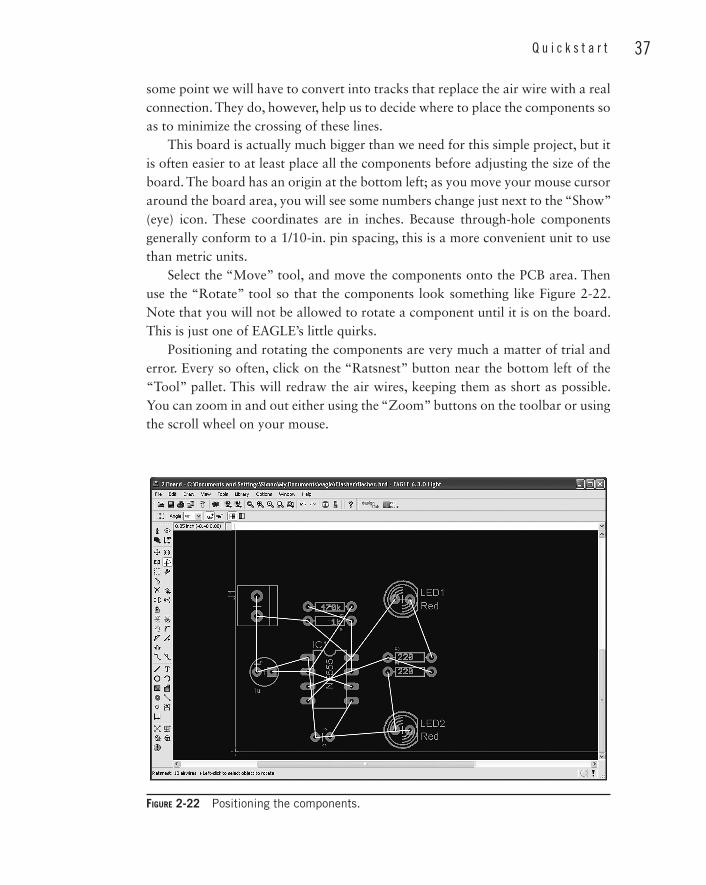
Q u i c k s t a r t 37
some point we will have to convert into tracks that replace the air wire with a real connection. They do, however, help us to decide where to place the components so as to minimize the crossing of these lines.
This board is actually much bigger than we need for this simple project, but it is often easier to at least place all the components before adjusting the size of the board. The board has an origin at the bottom left; as you move your mouse cursor around the board area, you will see some numbers change just next to the “Show” (eye) icon. These coordinates are in inches. Because through-hole components generally conform to a 1/10-in. pin spacing, this is a more convenient unit to use than metric units.
Select the “Move” tool, and move the components onto the PCB area. Then use the “Rotate” tool so that the components look something like Figure 2-22. Note that you will not be allowed to rotate a component until it is on the board. This is just one of EAGLE’s little quirks.
Positioning and rotating the components are very much a matter of trial and error. Every so often, click on the “Ratsnest” button near the bottom left of the “Tool” pallet. This will redraw the air wires, keeping them as short as possible. You can zoom in and out either using the “Zoom” buttons on the toolbar or using the scroll wheel on your mouse.
Figure 2-22 Positioning the components.
38 C h a p t e r T w o
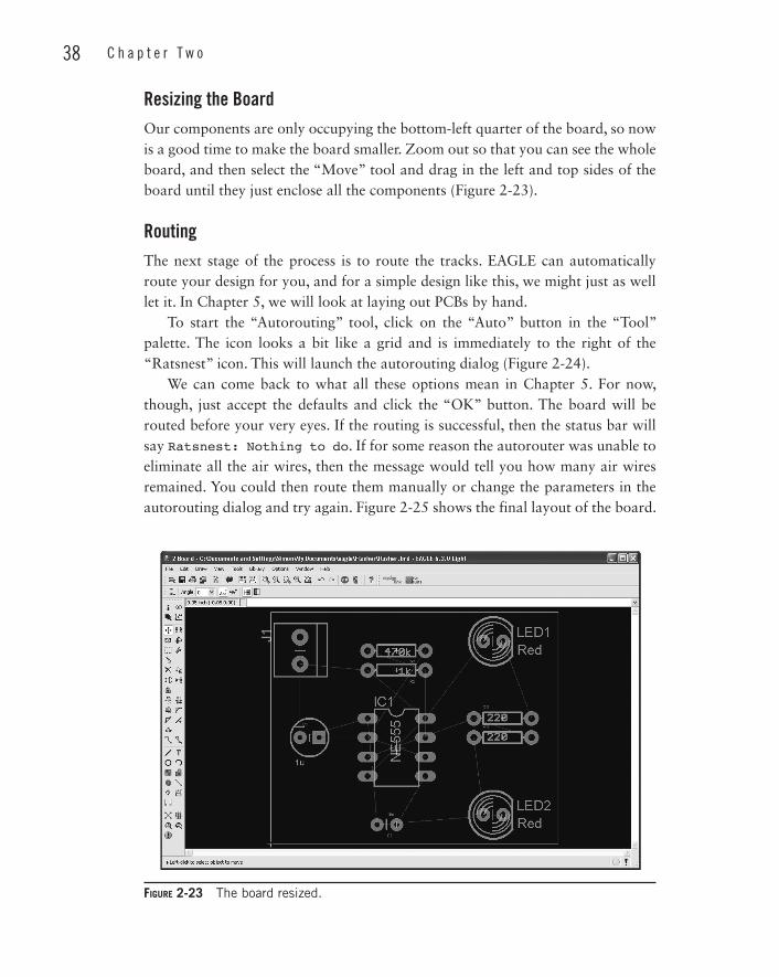
Resizing the BoardOur components are only occupying the bottom-left quarter of the board, so now is a good time to make the board smaller. Zoom out so that you can see the whole board, and then select the “Move” tool and drag in the left and top sides of the board until they just enclose all the components (Figure 2-23).
RoutingThe next stage of the process is to route the tracks. EAGLE can automatically route your design for you, and for a simple design like this, we might just as well let it. In Chapter 5, we will look at laying out PCBs by hand.
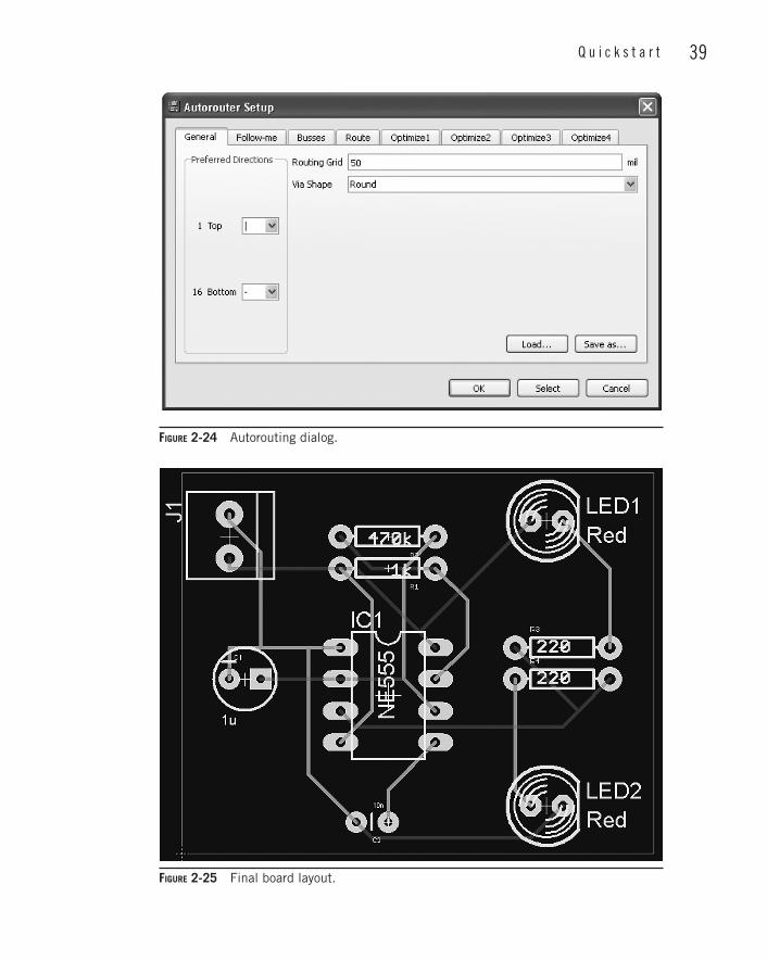
To start the “Autorouting” tool, click on the “Auto” button in the “Tool” palette. The icon looks a bit like a grid and is immediately to the right of the “Ratsnest” icon. This will launch the autorouting dialog (Figure 2-24).
We can come back to what all these options mean in Chapter 5. For now, though, just accept the defaults and click the “OK” button. The board will be routed before your very eyes. If the routing is successful, then the status bar will say Ratsnest: Nothing to do. If for some reason the autorouter was unable to eliminate all the air wires, then the message would tell you how many air wires remained. You could then route them manually or change the parameters in the autorouting dialog and try again. Figure 2-25 shows the final layout of the board.
Figure 2-23 The board resized.
Q u i c k s t a r t 39
Figure 2-24 Autorouting dialog.
Figure 2-25 Final board layout.
40 C h a p t e r T w o
If you have been following this in EAGLE as you read or are reading a color edition of this book on an e-book reader, then you will notice that the board is starting to look quite colorful. The red lines represent tracks on the top of the board, and the blue lines track on the bottom. The pads are shown in bright green, and the white lines show the silkscreen layer.
Summary
This chapter has shown you just enough to draw a schematic and then lay out a board from the design. By design, a lot of material and background have been omitted so that you can at least get started with EAGLE.
In Chapter 3, we will take a more detailed look at components and libraries because identifying the right parts for your design can be time-consuming and difficult.