Embed Size (px)
Citation preview

PIONEER CORPORATION 4-1, Meguro 1-Chome, Meguro-ku, Tokyo 153-8654, Japan PIONEER ELECTRONICS SERVICE INC. P.O.Box 1760, Long Beach, CA 90801-1760 U.S.A.PIONEER EUROPE NV Haven 1087 Keetberglaan 1, 9120 Melsele, Belgium PIONEER ELECTRONICS ASIACENTRE PTE.LTD. 253 Alexandra Road, #04-01, Singapore 159936
C PIONEER CORPORATION 2001 K-ZZY. MAY 2001 Printed in Japan
ORDER NO.
CRT2691
COLOR LCD DISPLAY
ServiceManual
AVD-W6010/UC
CONTENTS
1. SAFETY INFORMATION ............................................2
2. EXPLODED VIEWS AND PARTS LIST.......................2
3. BLOCK DIAGRAM AND SCHEMATIC DIAGRAM.....8
4. PCB CONNECTION DIAGRAM ................................30
5. ELECTRICAL PARTS LIST ........................................40
6. ADJUSTMENT..........................................................49
7. GENERAL INFORMATION.......................................58
7.1 DIAGNOSIS ........................................................58
7.1.1 TEST MODE..............................................58
7.1.2 DISASSEMBLY .........................................60
7.1.3 CONNECTOR FUNCTION DESCRIPTION62
7.2 IC ........................................................................63
7.3 OPERATIONAL FLOW CHART...........................72
8. OPERATIONS AND SPECIFICATIONS....................74
AVD-W6010 UC
AVD-W6010 EW
- This product has the unit part numbers as below.Unit Part No. (AVD-W6010/UC) Unit Part No. (AVD-W6010/EW) Description
CPN1701 CPN1750 Monitor Assy
CPN1702 CPN1751 Power Supply Assy
*) The unit part numbers listed above are not for the service components.

2
AVD-W6010
2. EXPLODED VIEWS AND PARTS LIST
2.1 PACKING
14 16
1719
181
13
10 11
12
3
8
7
6
4
5
9
15
2
1. SAFETY INFORMATION
CAUTION
This service manual is intended for qualified service technicians; it is not meant for the casual do-it-yourselfer.Qualified technicians have the necessary test equipment and tools, and have been trained to properly and safely repaircomplex products such as those covered by this manual.Improperly performed repairs can adversely affect the safety and reliability of the product and may void the warranty.If you are not qualified to perform the repair of this product properly and safely, you should not risk trying to do soand refer the repair to a qualified service technician.
WARNING
This product contains lead in solder and certain electrical parts contain chemicals which are known to the state ofCalifornia to cause cancer, birth defects or other reproductive harm. Health & Safety Code Section 25249.6 - Proposition 65

3
AVD-W6010
- Owner's ManualModel Part No. LanguageAVD-W6010/UC CRD3429 English, FrenchAVD-W6010/EW CRD3477 English, Spanish, German
CRD3478 French, Italian, Dutch
* 1-1 Card See Contrast table(2)1-2 Owner’s Manual See Contrast table(2)1-3 Owner’s Manual See Contrast table(2)1-4 Owner’s Manual See Contrast table(2)
* 1-5 Warranty Card See Contrast table(2)
1-6 Cushion See Contrast table(2)* 1-7 Caution Card CRP1197
1-8 Polyethylene Bag CEG11162 Cord Assy CDE6544
* 3 Packing Cover CEG-186
4 Carton See Contrast table(2)5 Contain Box See Contrast table(2)6 Protector CHP23687 Protector CHP23698 Polyethylene Bag CEG1260
9 Installation Metal Fittings See Contrast table(2)* 10 Screw Assy CEA2826
11 Screw HMB40P060FZK12 Cord Assy CDE661313 Bracket Pack Assy CEA2823
14 Bracket CNC7617* 15 Polyethylene Bag E36-634
16 Accessory Assy CEA2657* 17 Polyethylene Bag CEG1101
18 Fastener(Rough) CNM6888
19 Fastener(Soft) CNM6889
(1) PACKING SECTION PARTS LIST
Mark No. Description Part No. Mark No. Description Part No.
NOTE:
- Parts marked by “*” are generally unavailable because they are not in our Master Spare Parts List.
- Screws adjacent to ∇ mark on the product are used for disassembly.
(2) CONTRAST TABLE
AVD-W6010/UC and AVD-W6010/EW are constructed same except for the following:Part No.
Mark No. Description AVD-W6010/UC AVD-W6010/EW* 1-1 Card ARY1048 Not Used
1-2 Owner’s Manual CRD3429 Not Used1-3 Owner’s Manual Not Used CRD34771-4 Owner’s Manual Not Used CRD3478
* 1-5 Warranty Card Not used CRY1157
1-6 Cushion Not used CNM46804 Carton CHG4386 CHG43855 Contain Box CHL4386 CHL43859 Installation Metal Fittings Not used CXB3629

4
AVD-W6010
43
39
36
36
36
33
38
3333
3344
37
37
41
36
36
42
1
9
1
2
2
2
2
2
8
35
34
30
34
2
40
2
14
21 22
16
17
18
19
23
2524
32 31
15
28
27
29
26
45
121212
131313
11
7
47
47
54
51
53
4848
59
57
58
48
48
46 46
46
52
55
49
50
56
5656
56
5
2.2 EXTERIOR(1)

5
AVD-W6010
1 Screw BPZ20P060FMC2 Screw BPZ20P080FZK3 Button(POWER,V,SP,W) CAC70794 Button( ) CAC70805 Holder CNC7283
6 •••••7 Filter CNM65838 Case CNS64799 Speaker CPV1041
10 •••••
11 LCD Assy CXB677512 Screw(M2x5) CBA150113 Spacer CNC889314 Insulator CNM645815 Monitor Unit CWM7610
16 Connector(CN3001) CKS312417 Connector(CN3251) CKS319218 Connector(CN3101) CKS196219 Connector(CN3701) CKS399120 •••••
21 Shield CNC848622 Shield CNC848723 Earth CNC866724 Spacer CNM626325 Spacer CNM6618
26 LCD Module CWX246027 Front Case NML5592091128 Back Case NML5592332129 Back Light Unit NML7592331130 Grille Unit CXB6999
31 IC(IC3051) PNA4603H00LB32 IC(IC3071) SBX8035-H33 Screw BPZ20P050FMC34 Knob CAC554035 Screw(M2x3) CBA1082
36 Screw(M2x3) CBA115437 Spring CBH170838 Spring CBH209439 Connector CKS376540 Cushion CNM5905
41 Cover CNM715942 Cushion CNM720743 PCB CNP623744 Slider Unit CXB231245 Detach Assy CXB6966
46 Screw BPZ26P080FZK47 Screw(M2x3) CBA108248 Screw CBA108349 Cord Assy CDE654250 Bracket CNC7510
51 Bracket CNC751152 Case CNS481653 Cover CNS488354 Cover CNS488455 Cover CNV5716
56 Screw CPZ26P080FZK57 Plug(CN2002) CKS327458 Plug(CN2003) CKS3282
* 59 Connector(CN2001) CKS3764
/ / /
- EXTERIOR(1) SECTION PARTS LIST
Mark No. Description Part No. Mark No. Description Part No.

6
AVD-W6010
15
13
1
2
37
23
2521
20
27
6
10
17
12
8
24
22
19
18
16
95
4
4
44
414
1128
26
3
2
A
29
A
30
B
B
2.3 EXTERIOR(2)

7
AVD-W6010
1 Cord Assy CDE65442 Cap CNS14723 Resistor RS1/2PMF102J4 Screw BSZ30P060FMC5 Cord Assy CDE6543
6 Transistor(Q911) 2SD23757 Fuse(4A) CEK10018 Holder CNC88699 FFC CDE6393
10 IC(IC912) BA178M05T
11 Holder CNC912912 Holder CNC901213 Chassis CNA229914 Case CNB258515 Insulator CNM6725
16 Mother Unit CWM761217 Screw BMZ30P060FMC18 Clamper CEF100819 Terminal(CN757) CKF-04720 Plug(CN752) CKM1136
21 Pin Jack(CN754) CKS314422 Connector(CN756) CKS323623 Connector(CN101) CKS375124 Connector(CN102) CKS375125 Connector(CN751) CKS4458
26 Connector(CN755) CKS440527 Holder CNC886828 Pin Jack(CN753) CKB104729 Cord Assy(CN301) CDE654130 Connector(CN801) CKS3124
- EXTERIOR(2) SECTION PARTS LIST
Mark No. Description Part No.

A
1 2 3 4
B
C
D
1 2 3 4
8
AVD-W6010
3. BLOCK DIAGRAM AND SCHEMATIC DIAGRAM
3.1 BLOCK DIAGRAM
B.U
Q841PS MUTE
NAVI AL
CCC VBS
1 3
LOUT
19232617
14REOUT
3
34
38 36 37
32CY/CV
8
1116
141
6
2 12 7
CCSYNC
SWACC5
PWRVI
PWRVI
PWRFLPWRFLPWRFL
PWRFL
SWACPW
HTXD
HRXD
SPOUT
MVISEL
MUTEV
HTXD
HRXD
SPOUT
MVISEL
MUTEV
SYNMTE SYNMTE
CCB
CCGCCR
CB
CG
CR
217
V1C
V1Y
V2CV2Y
VTR1AL
VTR2AL
26
3 1 2
12
50 51
2
29
27
30
1564
5458
SEL SP
1
4
SP +SP –
IC 821NJM4558M
AUX AUDIOBUFFER MUTE
75
Q911
AUDIO/VIDEOSELECTOR
75Ω DRIVER
CHROMA DECODER YUV TO RGB
IC 761TA2050S
SCL
AO1LVO2VO0
AO2L
AI1L
4 VI2
28 VI0
9 AI2L
13 AI0L
VI1VI3
RGBARI
ASENS
DSENS
22SDA
IC 801CXA1114M
Q821Q823
Q601
Q221
Q222
IC 332NJM2267M
CINVOUTYOUTUOUTCVBS/YIN
VSYNC
IC 301CXA2019AQ
20 1210
1116
13514
724
15
9
1819
VTINHTIN
14
15
4
Z1Y1
ZYW
4X
W1Z0Y0W0
3 X1
2 X0
CONT
INININ
CN754
CN101 CN102
CCREM
SWACC5
PWRVI
PWRVI
PWRFLPWRFLPWRFL
PWRFL
SWACPW
CCREM
TXD
RXD
12
4
31
Q603
IC 781NJM4558M
IC 841 TC4S66F
Q844
IC 842NJM4558E
MIX AMP
SCL
MIXSP
MU
TE
SP
MU
TE
PS
11
S1
10
SIN
MUTEV
TXDRXD
31
MU
TE
AU
3
MO
NP
W
79
77
98
SYNMTE
78RGBSELSDA
RGBARIDSENS
SELSENSPBKSEN
63
AS
EN
S
62
BS
EN
S
60
RE
SE
T
X1
X2
IC 302CXL5520M
7
IC 281
SYSTEM CONTROLLER
IC 601 PE5233A
8
6
5
3
2
1
Q501
Q508
Q509
Q503
B.U
GND
BUP
ACC
PARK
OPT
REOUT
4A
L901 IN3
IN2
RSTIN
OUT3
OUT2
RSTOUT
IC 501PAJ001A
70
13
3
9
5
7
6
BSEN
RESET
ASEN
69
SY
SP
W
66
X601
Q931
Q932
SYSPW
B.U
VIDEOOUT
P.BREAK
ACC
BACK UP
GND
Q301
Q901
Q902
IC 901TA78L05F
IC 602 TC4S81F
5V REGULATOR
B.U B.U FU702
FU701
PWRFL
PWRVI
Q651 Q652
Q843
Q604
FU911
VSY5
VSY9
S752RESET
SWITCH
VTR1AL
VTR2AL
VTR1V
CN755
CN753
VTR2V
MUTEAU
A
BU4551BF
RGB SELECTOR
Q504
Q505
SELSENS
PBSENS
CN752
REMOTE CONTROLBUFFER
31 IC 912BA178M05T
A
IC 603S-29131AFJ
Q291
5841
IC 251NJM2268V
IC 241NJM2285V
SDASCL
78
3433
93
3238
45
3736
DV1229
DH
CCSYNC
CCB
CCGCCRCB
CG
CR
DV
DH1130
140
1922
374383392401
365
356
2219
1823
2120
2021
2318
1625
1526
1724
296
111418
IC 1601NJM2116V
Q701
Q702
Q703
Q704
Q271
5
10IC 271
TC74HC123AF
2
14
IC 272 TC7S86F
S/VSELECTOR
CT
L1
SIN
S1
CT
L2
CT
L3
OUT1OUT3
IN2A
IN1AIN2B
IN1B
IN3A
EXTAL
VTR1S
VTR2S
2
9GNDV
C
C
DSEN DSEN2417
39
HSYNC
ISOLATOR
AUXILIARYISOLATOR
CN801 CN301
1
2
PRV
PRH
RETV
RETH
CCAUL
CCCVBSCCSYNCCCRCCGCCB
GNDA
VSWCCREMONSEI +ONSEI –
MONON
13
56123
15
178
1920
18
DSEN9
CN751
RG
B(A
UX
ILIA
RY
)
RETVRETH
1112
ISOLATOR
ISOLATOR
1 3IC 261TA2050S
1 3IC 771
TA2050S
2
2
1
2
ANR
ANG
ANB
CSYNC
PRH
PWRVI
PWRFL
SWACC5
SWACPW
MOREM
HTXD
HRXD
AUDIO
DSEN
PRV
SWACC5
ANR
SWACPW
DSEN
PRH
PRV
HRXD
MOREM
CSYNC
ANG
ANB
AUDIO
PWRFL
PWRVI
HTXD
1
2
3
4
5
6
7
8
9
10
11
12
6
2
4
CN2002
CN2003
579
6
12
19
20
11
18
3
2
15
1
14
10
A MAIN PCB
B SUB PCB
D DETAC
AUTOMATICINPUT
SWITCHING

5
IC 331TK15405MI
13514
724
101513
ANRANGANB
CSYNC
PRH
PWRVI
PWRFL
SWACC5
9
1
34
1
ZYW
4X
ONT
OUTc1OUTa1OUTb1
INcINaINb M
UT
E
CN756
79
6
12
19
20
SWACPW11
MOREM
HTXD
HRXD
AUDIO
4
3
2
15
1
RGB75Ω DRIVER
IC 351BA7660FS
C 281U4551BF
ELECTOR
75Ω DRIVER
DSEN14
PRV10
6
5
6
48 14
2
4718
89
16
131415
IC 3451TC7W34FU
24ANR
CSYNC
OSDDTOSDCKOSDCS
ANR/ANG/ANB
ANGANB
CSYNC
RETH
PWRVI
PWRFL
ACC5V
CN3101
2322
20
17
8
6
ACPW15
REM
TXB
RX
AUDIO
SPEAKER VOLUME
18
19
10
14
12
11
353229
VB
VCOM
VGVR
IC 3331NJM2235V
Q3431
Q3426
Q3421
OSR
ODG
OSB
171513
71
RETH 5 3
62
PWRVI
41
P1/RP3/GP5/B
18
2
1
HOR
123
PO
19VERT
SINCSKCS –
OSC2
OSC1
RIN2GIN2BIN2
ROUTGOUTBOUT
46
27
1COMOUT
HFILIN
RIN1GIN1BIN1
SW
SY
NC
IN
SY
NC
OU
T
46
FR
P
45
13
4
50
57 CX
44
DRR/DRG/DRB
3
21
8
11
12
CO
MF
RP
VIDEO SIGNALPROCESSOR
IC 3301IR3Y26A1
OSD
IC 3401PD5582A
IC 3446TC7W00FU
Q3303
IC 3351TC7S08FU
POLS OS
CI
PD
O
CX
NVD
BLK
NDSV
NCLP
9NDSH
Q3751
IC 3731NJM2107F
LCD CONTROLLER
IC 3701TC160G11AF-1146
SWACC5
Q3601SWACC5
SWACC5
VU5VF5
Q3604
Q3603
Q3061
Q3071
IC 3071SBX8035-H
IC 3051PNA4603H00LB
VDDSEN
MV
IPW
61REM IN
9TXD
8RXD
79LSEN
S30
87
S30
88
S30
89
S30
86
S30
85
S30
83
S30
84
S30
82
6
5
8
4
1
1
1
3
2SPVDL
RESET
KDT2
KDT1KDT0
DIMMER
45BEEP
X1
X2
Q3102
T3101
Q3103
IC 3651M62352GP
IC 3371NJM082BV
Q3371
Q3372
IC 3651M62352GP
IC 3651M62352GP
IC 3651M62352GP
IC 3001TDA7052BT
Q30019V
VU5
9V
BZ3601ALARM
BUZZER
70
69
78
60 6 7
77
76
5
OVICHK56
1
5
5
4
15
4
3 1
X36
01
VIDEO CONTROLLER
IC 3601PE5232A
BACK LIGHTDRIVE
POWER SUPPLY
+ 5V
+ 8V
282726
17
22
+ 5V12
+ 18V15
13– 15V
2
CN3701
CN3251
6
+
PWRFL
DC-AC INVERTER
Q3201
Q3203
Q3271
IC 3101FA7610CN
IC 3271NJM2903V
IC 3681S-29131AFJ
Q3255 Q3253
T3251
T3101
Q3101
LENS
SP
T3252
Q3252 Q3251
IC 3631M51957BFP
21
LCD
LCDBACK LIGHT
+
Q3202
IC 3211FA7612CN
REMOTE CONTROL SENSOR
AUTOMATICDIMMER SENSOR
POWER AMP
CN3001
1
2 3
IC 3261NJM2903V
DSEN13
Q3602
RETV16
RETV 7 1
22NHD
PWRVI
2
14
IC 3602 TC7S32FU
Q3004
PWRVI
Q3005
Q3002
DD
ON
55
Q3211
Q3212
CN3601
8ANRANGANB
CSYNC
PRH
PWRVI
PWRFL
SWACC5
1820
17
14
5
3
SWACPW12
MOREM
HTXD
HRXD
AUDIO
15
6
16
11
7
DSEN10
PRV13
WACC5
NR
WACPW
SEN
RH
RV
RXD
OREM
SYNC
NG
NB
UDIO
WRFL
WRVI
TXD
CN2001
N2002
N2003
C MONITOR UNIT LCD MODULE
DETACH UNIT
1 2
5 6 7 8
A
B
C
D
5 6 7 8
9
AVD-W6010

A
1 2 3 4
B
C
D
1 2 3 4
10
AVD-W6010
A-a A-b
A-a A-b
A-b A-a
Large sizeSCH diagram
Guide page
Detailed page
R101
0R0
V1 AUDIO ISOLATOR
NAVI RGB INPUT
SOURCE SELECTOR
PARKING ON/OFFOPTION
SENSOR
BACK UP AND REMOTE CONTROL POWER SUPPLY
SYSTEM POWER SUPPLY
V2 AUDIO ISOLATORMONITOR SPEAKER ISOLATOR
AUDIO OUTPUT BU
MONITOR SPEAKER AUDIO OUTP
AUXILIARY AUDIO ISOLATOR
RESET
RG
B(A
UX
ILIA
RY
INP
UT
)
AU
DIO
OU
TV
IDE
O IN
AU
DIO
IN
A
A
A
A
A
A
A
AA
A
A
Y
R
R
R
R: RED SIGNAL
A: AUDIO SIGNAL
Y: Y SIGNAL
1
2.4mH
>
A. I. S.
>
A MAIN PCB
B CN301
A-a
A
3.2 MAIN PCB (GUIDE PAGE)
Note: When ordering service parts, be sure to refer to “EXPLODED VIEWS AND PARTS LIST” or “ELECTRICAL
PARTS LIST”.

5 6 7 8
A
B
C
D
5 6 7 8
11
AVD-W6010
11
ATT BUFFER
S/V SELECTOR
CHROMA DECODER
YUV TO RGB DECODER
SYSTEM CONTROLLER
75Ω DRIVER
MONITOR POWER SUPPLY
DETACHAUXILIARY
UFFER MUTE
PUT
A
A
A
A
A
A A
Y
Y
Y
Y Y
Y
Y
Y
Y
R
R R
R R
25
1116
15
63
1213
14
18
19
17
20
21
100µH
6.29
0MH
z
4.433619MHz
3.579545MHz
>
>
Decimal points for resistorand capacitor fixed valuesare expressed as :2.2 2R20.022 R022
← ←
The > mark found on some component parts indicatesthe importance of the safety factor of the part.Therefore, when replacing, be sure to use parts ofidentical designation.
Symbol indicates a resistor.No differentiation is made between chip resistors anddiscrete resistors.
NOTE :
Symbol indicates a capacitor.No differentiation is made between chip capacitors anddiscrete capacitors.
MOTHER UNITConsists of MAIN PCB SUB PCB
R702-704 : (1/4W)R706-708 : (1/4W)
BC
N10
2
A-b
A

V1
AU
DIO
ISO
LAT
OR
NA
VI R
GB
INP
UT
SO
UR
CE
SE
LEC
TO
R
V2
AU
DIO
ISO
LAT
OR
MO
NIT
OR
SP
EA
KE
R IS
OLA
TO
R
MO
NIT
OR
SP
EA
KE
R A
UD
IO O
UT
PU
T
AU
XIL
IAR
Y A
UD
IO IS
OLA
TO
R
RGB(AUXILIARY INPUT)
AUDIO OUTVIDEO INAUDIO IN
A
A
A
A
A
A
A
A
A
A
AA
A
A
A
A
Y
R
R
R
R: R
ED
SIG
NA
L
A: A
UD
IO S
IGN
AL
Y: Y
SIG
NA
L
1
AM
AIN
PC
B
BC
N30
1
A
1 2 3 4
B
C
D
1 2 3 4
12
AVD-W6010A
-aA
-b
A-a
1 2

R10
1
0R0
DA
UX
ILIA
RY
PA
RK
ING
ON
/OFF
OP
TIO
N
SE
NS
OR
BA
CK
UP
AN
D R
EM
OT
E
CO
NT
RO
L P
OW
ER
SU
PP
LY
SY
ST
EM
PO
WE
R S
UP
PLY
AU
DIO
OU
TP
UT
BU
FFE
R M
UT
E
RE
SE
T
(AUX
2.4m
H
>
A. I
. S.
>
5 6 7 8
A
B
C
D
5 6 7 8
AVD-W60105 6 7 8
A
B
C
D
5 6 7 8
A-a
A-b
13A-a
3 4 5

A
1 2 3 4
B
C
D
1 2 3 4
14
AVD-W6010
11
AT
T B
UFF
ER
S/V
SE
LEC
TO
R
CH
RO
MA
DE
CO
DE
R
YU
V T
O R
GB
DE
CO
DE
R
75Ω
DR
IVE
R
A
Y
Y
Y
YY
Y
Y
Y
Y
R
25
1116
15
63
1213
14
18 19
17
20
21
4.43
3619
MH
z
3.57
9545
MH
z
Dec
imal
po
ints
fo
r re
sist
or
and
cap
acit
or
fixe
d v
alu
esar
e ex
pre
ssed
as
:2.
2
2R2
0.02
2
R02
2
←
←
Th
e >
mar
k fo
un
d o
n s
om
e co
mp
on
ent
par
ts in
dic
ates
the
imp
ort
ance
of
the
safe
ty f
acto
r o
f th
e p
art.
Th
eref
ore
, wh
en r
epla
cin
g, b
e su
re t
o u
se p
arts
of
iden
tica
l des
ign
atio
n.
Sym
bo
l in
dic
ates
a r
esis
tor.
No
dif
fere
nti
atio
n is
mad
e b
etw
een
ch
ip r
esis
tors
an
dd
iscr
ete
resi
sto
rs.
NO
TE
: Sym
bo
l in
dic
ates
a c
apac
ito
r.N
o d
iffe
ren
tiat
ion
is m
ade
bet
wee
n c
hip
cap
acit
ors
an
dd
iscr
ete
cap
acit
ors
.
A-a
A-b
A-b
1 2

5 6 7 8
A
B
C
D
5 6 7 8
15
AVD-W6010
SY
ST
EM
CO
NT
RO
LLE
R
MO
NIT
OR
PO
WE
R S
UP
PLY
DE
TA
CH
AR
Y
AA
RR
RR
20
100µ
H
6.290MHz
>
>
MO
TH
ER
UN
ITC
on
sist
s o
f
MA
IN P
CB
S
UB
PC
B
R70
2-70
4 : (
1/4W
)R
706-
708
: (1/
4W)
BCN102
A-b
A-a
A-b
3 4 5

RGB SELECTOR
75Ω DRIVER R
SYNCRONIZING GENERATOR
R: RED SIGNAL
A: AUDIO SIGNAL
A
R
R
R
R
R
RR
8
7
4
9
B SUB PCB
AC
N10
1
C29247/16
A
1 2 3 4
B
C
D
1 2 3 4
16
AVD-W6010
3.3 SUB PCB
B

RGB 75Ω DRIVER
REMOTE CONTROL BUFFER
A
R R
R
MOTHER UNITConsists of MAIN PCB SUB PCB
1 24
35 6
87
9 1012
1113 14
1615
1817
19 20
3
2
12
1
8
9
6
5
7
20
13
4
14
17
10
19
15
16
18
11
E
AC
N80
1
DC
N20
02, 2
003
R111
0R0
5 6 7 8
A
B
C
D
5 6 7 8
17
AVD-W6010
B
AVD-W6010
18
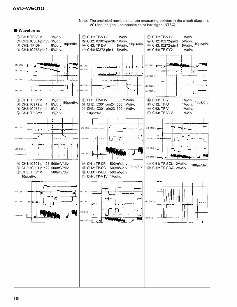
1 CH1: TP·V1V 1V/div.2 CH2: IC301·pin39 1V/div.3 CH3: TP DH 5V/div.4 CH4: IC272·pin2 5V/div.
1 CH1: TP·V1V 1V/div.5 CH2: IC301·pin38 1V/div.6 CH3: TP DV 5V/div.7 CH4: IC272·pin1 5V/div.
10µs/div.
1 CH1: TP·V1V 1V/div.4 CH2: IC272·pin2 5V/div.8 CH3: IC272·pin4 5V/div.9 CH4: TP·CY2 1V/div.
1 CH1: TP·V1V 1V/div.7 CH2: IC272·pin1 5V/div.8 CH3: IC272·pin4 5V/div.9 CH4: TP·CY2 1V/div.
50µs/div.1 CH1: TP·V1V 500mV/div.0 CH2: IC301·pin24 500mV/div.! CH3: IC301·pin23 500mV/div.
10µs/div.
@ CH1: TP·Y 1V/div.# CH2: TP·U 1V/div.$ CH3: TP·V 1V/div.1 CH4: TP·V1V 1V/div.
10µs/div.
ch3 GND →
% CH1: IC301·pin21 500mV/div.^ CH2: IC301·pin22 500mV/div.1 CH3: TP·V1V 500mV/div.
& CH1: TP·CR 500mV/div.* CH2: TP·CG 500mV/div.( CH3: TP·CB 500mV/div.1 CH4: TP·V1V 1V/div.
) CH1: TP·SCL 2V/div.⁄ CH2: TP·SDA 2V/div.
100µs/div.
ch2 GND →
ch4 GND →
ch3 GND →
ch1 GND →
ch1 GND →
ch2 GND →
ch1 GND →
ch2 GND →ch4 GND →
ch3 GND →
ch2 GND →
ch3 GND →
- Waveforms
ch3 GND →
ch4 GND →
ch2 GND →
ch3 GND →
ch2 GND →
ch1 GND →
ch4 GND →
50µs/div.
ch1 GND →
ch2 GND →
10µs/div.
ch1 GND →
ch4 GND →
ch3 GND →
ch1 GND → ch2 GND →
ch3 GND →
ch4 GND →
10µs/div.
ch1 GND →
10µs/div.
ch2 GND →
ch1 GND →
Note: The encircled numbers denote measuring pointes in the circuit diagram.VC1 input signal : composite color bar signal(NTSC)

19
AVD-W6010

CC
P13
381k
(B)
4.19
MH
z
100µH
SYNCHRONIZING OUTPUT BUFFER
VIDEO POWER SUPPLY
OSD CO
VIDEO SIGNAL PROCESSOR
VIDEO CONTROLLER
3-2
3-1
1-1
3-3
3-4
V
V
V
V
V
V
V
VVV
V
V
V
V
V
A
A
C MONITOR UNITD
CN
2001
A
1 2 3 4
B
C
D
1 2 3 4
20
AVD-W6010
3.4 MONITOR UNIT (GUIDE PAGE)
C
C-a

CC
P13
4410
k(B
)
CC
P13
3647
0(B
)
82µHEEPROM
AUDIO AMP
BACK LIGHT AND AUDIO POWER SUPPLY
AUTOMATIC DIMMERSENSOR
REMOTE CONTROLSENSOR
LCD
MO
DU
LE
BRIGHTNESS CONTROL
OVERCURRENT DETECTOR
BACK LIGHT DRIVER POWER SUPPLY
LCD CONTROL
VCOM
ONTROL
LCD
MO
DU
LE
3-5
7-87-10
7-127-11
7-5
7-2
7-4
7-1
7-3
7-7
7-6
7-9
2-52-6
2-7
2-1
2-3
2-2
>
V
V
V
V
A
A
A: AUDIO SIGNAL
V: VIDEO SIGNAL
5 6 7 8
A
B
C
D
5 6 7 8
21
AVD-W6010
C
C-b

CCP13381k(B)
4.19MHz
100µ
H
SY
NC
HR
ON
IZIN
G O
UT
PU
T
BU
FFE
RV
IDE
O P
OW
ER
SU
PP
LY
VID
EO
CO
NT
RO
LLE
R
3-2
3-1
1-1
V V V V
A
A
CM
ON
ITO
R U
NIT
DCN2001
A
1 2 3 4
B
C
D
1 2 3 4
22
AVD-W6010
C-a
C-b
C-a
1 2

5 6 7 8
A
B
C
D
5 6 7 8
23
AVD-W6010
OS
D C
ON
TR
OL
VID
EO
SIG
NA
L P
RO
CE
SS
OR
3-3
3-4
V V V
V
V
V
V
V
V
V
V
C-a
C-b
C-a
3 4

A
1 2 3 4
B
C
D
1 2 3 4
24
AVD-W6010
CCP1336470(B)
82µH
EE
PR
OM
AU
DIO
AM
P
BA
CK
LIG
HT
AN
D A
UD
IO P
OW
ER
SU
PP
LY
AU
TO
MA
TIC
DIM
ME
RS
EN
SO
R
RE
MO
TE
CO
NT
RO
LS
EN
SO
R
LCD MODULE
BR
IGH
TN
ES
S C
ON
TR
OL
OV
ER
CU
RR
EN
T D
ET
EC
TO
R
BA
CK
LIG
HT
DR
IVE
R P
OW
ER
SU
PP
LY
2-5
2-6
2-7
2-1
2-3
2-2
>
A
A
C-a
C-b
C-b
1 2

5 6 7 8
A
B
C
D
5 6 7 8
25
AVD-W6010
CCP134410k(B)
LCD
CO
NT
RO
L
VC
OM
TR
OL
LCD MODULE
3-5
7-8
7-10
7-12
7-11
7-5
7-27-
4 7-17-
3
7-7
7-6
7-9
V V V
V
A: A
UD
IO S
IGN
AL
V: V
IDE
O S
IGN
AL
C-a
C-b
C-b
3 4

26
AVD-W6010
Note: The encircled numbers denote measuring pointes in the circuit diagram.5 step signal and color bar signal : NTSC type
CH2 : T3251 Pin 3
CH1 : TP DIMDCCH2 : TP DIMAC
CH3 : TP DIMDTY
CH1 : Input (5 Step Signal)CH2 : TP CSYNC
CH3 : TP ANG CH1 : Input (5 Step Signal)CH2 : TP ANG
CH3 : TP DRG
2-3
2-7
2-6
2-5
3-1
3-2
3-2
3-3
CH1 : Q3101 Collector CH1 : Q3201 Collector1-1 2-1
CH1 : Q3251 Collector2-2

27
AVD-W6010
CH1 : Input (Color Bar Signal) TP CSYNCCH2 : IC3301 Pin 48
CH1 : IN (Color Bar Signal) TP CSYNCCH2 : IC3701 Pin 9 CH3 : IC3701 Pin 12
CH1 : IN (Color Bar Signal) TP CSYNCCH2 : IC3701 Pin 8
CH1 : IN (Color Bar Signal) TP CSYNCCH2 : IC3701 Pin 113-4
3-1
7-1
3-1
7-2
7-3
3-1
7-4
3-1
CH1 : IN (Color Bar Signal) TP CSYNCCH2 : IC3701 Pin 13 CH3 : TP COM7-5
3-1
3-5
CH1 : IN (Color Bar Signal) TP CSYNCCH2 : IC3701 Pin 57 CH3 : IC3701 Pin 547-6
3-1
7-7

28
AVD-W6010
Normal mode
Full and Zoom mode
CH1 : IN (Color Bar Signal) TP CSYNCCH2 : IC3701 Pin 31CH3 : IC3701 Pin 30 CH4 : IC3701 Pin 29
CH1 : IN (Color Bar Signal) TP CSYNCCH2 : IC3701 Pin 57 CH3 : IC3701 Pin 327-6
3-1
7-8
CH1 : IN (Color Bar Signal) TP CSYNCCH2 : IC3701 Pin 597-9
3-1
CH1 : IN (Color Bar Signal) TP CSYNCCH2 : IC3701 Pin 597-9
3-1
CH1 : IN (Color Bar Signal) TP CSYNCCH2 : IC3701 Pin 597-9
3-1
Just and Cinema mode
Normal, Just and Full mode
3-1
7-10
7-11 7-12
Zoom mode
CH1 : IN (Color Bar Signal) TP CSYNCCH2 : IC3701 Pin 31CH3 : IC3701 Pin 30 CH4 : IC3701 Pin 29
3-1
7-10
7-11 7-12

A
B
C
D
29
AVD-W6010
CH1 : IN (Color Bar Signal) TP CSYNCCH2 : IC3701 Pin 31CH3 : IC3701 Pin 30CH4 : IC3701 Pin 29
3-1
7-10
7-11
7-12
3.5 DETACH UNIT
D DETACH UNIT
BC
N75
6,75
7
CC
N31
01
1 2 3 4
1 2 3 4D

RAUDIO OUT
RGB
B CN301
B CN102
A MAIN PCB
30
AVD-W6010
A
1 2 3 4
B
C
D
1 2 3 4A
NOTE FOR PCB DIAGRAMS
1. The parts mounted on this PCB
include all necessary parts for
several destination.
For further information for
respective destinations, be sure
to check with the schematic
diagram.
2. Viewpoint of PCB diagrams
CapacitorConnector
P.C.Board Chip Part
SIDE A
SIDE B
4. PCB CONNECTION DIAGRAM
4.1 MAIN PCB

R L V
S
VCR IN
RESET
LIO OUT
CORD ASSY
31
AVD-W60105 6 7 8
A
B
C
D
5 6 7 8A
SIDE A

(Prin
t "L902")
(Prin
t "R901")
S9V
S5V
STEST
STES
D
A MAIN PCB
32
AVD-W6010
A
1 2 3 4
B
C
D
1 2 3 4A

33
AVD-W60105 6 7 8
A
B
C
D
5 6 7 8A
STEST2
STEST1
DCDTST
CGY
SIDE B

AVD-W6010
ADJ
RED
WHITE
TP3001
TP3002
LCD MODULE
C MONITOR UNIT
A
1 2 3 4
B
C
D
1 2 3 4
34 C
4.2 MONITOR UNIT

35
AVD-W6010
LCD MODULE
SPEAKERCN2001D
5 6 7 8
A
B
C
D
5 6 7 8
C
SIDE A

AVD-W6010
POWER V.SEL SP.SEL WIDE VOL-
DRB
DRG
R2
CNT
BRT
DRR
TP8V
TP18
COM
TP5V
PD
T
C MONITOR UNIT
A
1 2 3 4
B
C
D
1 2 3 4
36 C

L- VOL+ CH- CH+
TP15MTP18V
V
TP9V
37
AVD-W60105 6 7 8
A
B
C
D
5 6 7 8C
SIDE B

38
AVD-W6010
A
1 2 3 4
B
C
D
1 2 3 4
A CN801 A CN101
B SUB PCB
D CN2002,2003
B SUB PCB
4.3 SUB PCB
B
SIDE B
SIDE A

39
AVD-W60101 2 3 4
A
B
C
D
1 2 3 4
4.4 DETACH UNIT
D
D C
B CN756,757
CN3101DETACH UNIT
D DETACH UNIT SIDE B
SIDE A

40
AVD-W6010
Unit Number : CWM7612Unit Name : Mother Unit
MISCELLANEOUS
IC 241 IC NJM2285VIC 251 IC NJM2268VIC 261 IC TA2050SIC 271 IC TC74HC123AFIC 272 IC TC7S86F
IC 281 IC BU4551BFIC 301 IC CXA2019AQIC 302 IC CXL5520MIC 331 IC TK15405MIIC 332 IC NJM2267M
IC 351 IC BA7660FSIC 501 IC PAJ001AIC 601 IC PE5233AIC 602 IC TC4S81FIC 603 IC S-29131AFJ
IC 604 IC TC7S02FIC 761 IC TA2050SIC 771 IC TA2050SIC 781 IC NJM4558EIC 801 IC CXA1114M
IC 821 IC NJM4558EIC 841 IC TC4S66FIC 842 IC NJM4558EIC 901 IC TA78L05FIC 912 IC BA178M05T
IC 1601 IC NJM2116VQ 221 Transistor 2SC2412KQ 222 Transistor 2SC2412KQ 271 Transistor 2SC2412KQ 291 Transistor 2SC2412K
Q 301 Transistor 2SA1036KQ 501 Transistor 2SC2412KQ 503 Transistor DTC114EKQ 504 Transistor 2SC2412KQ 505 Transistor 2SA1037K
Q 508 Transistor 2SC2412KQ 509 Transistor 2SC2412KQ 601 Transistor DTA144EKQ 603 Transistor DTA144EKQ 604 Transistor DTA144EK
Q 651 Transistor 2SC2412KQ 652 Transistor 2SA1037KQ 701 Transistor 2SA1615-ZQ 702 Transistor DTC114EKQ 703 Transistor 2SB1184F5
Q 704 Transistor DTC114EKQ 821 Transistor 2SC2412KQ 822 Transistor 2SC2412KQ 823 Transistor FMG12Q 841 Transistor FMG12
Q 843 Transistor DTC323TKQ 844 Transistor DTC144EKQ 901 Transistor 2SA1036KQ 902 Transistor 2SC2412KQ 911 Transistor 2SD2375
Q 931 Transistor 2SB1188Q 932 Transistor DTC114EKQ 1629 Transistor UMG8ND 201 Diode UDZS5R6(B)D 202 Diode UDZS5R6(B)
D 203 Diode UDZS5R6(B)D 204 Diode UDZS5R6(B)D 205 Diode UDZS5R6(B)D 206 Diode UDZS5R6(B)D 261 Diode UDZS5R6(B)
D 262 Diode UDZS5R6(B)D 263 Diode UDZS5R6(B)D 264 Diode UDZS5R6(B)D 271 Diode 1SS355D 331 Diode MA153
D 332 Diode MA153D 333 Diode MA153D 351 Diode MA153D 352 Diode MA153D 353 Diode MA153
D 501 Diode SC016-2D 502 Diode MA8180(M)D 503 Diode MA8056(L)D 504 Chip Diode MA151WKD 507 Diode 1SS355
D 601 Diode MA153D 602 Diode MA153D 603 Diode MA153D 651 Diode MA153D 653 Diode 1SS355
D 761 Diode UDZS5R6(B)D 762 Diode UDZS5R6(B)D 763 Diode UDZS5R6(B)D 764 Diode UDZS5R6(B)D 771 Diode UDZS5R6(B)
D 772 Diode UDZS5R6(B)D 773 Diode UDZS5R6(B)D 774 Diode UDZS5R6(B)D 801 Diode UDZ2R0(B)D 802 Diode UDZ2R0(B)
D 803 Diode UDZ2R0(B)D 804 Diode UDZ2R0(B)D 805 Diode UDZ2R0(B)D 806 Diode UDZ2R0(B)D 807 Diode UDZ2R0(B)
5. ELECTRICAL PARTS LIST
NOTES:
- Parts whose parts numbers are omitted are subject to being not supplied.
- The part numbers shown below indicate chip components.Chip Resistor
RS1/_S___J,RS1/__S___JChip Capacitor (except for CQS.....)
CKS....., CCS....., CSZS.....
=====Circuit Symbol and No.===Part Name Part No.--- ------ ------------------------------------------ -------------------------
=====Circuit Symbol and No.===Part Name Part No.--- ------ ------------------------------------------ -------------------------
A B
Mother UnitConsists ofMain PCBSub PCB

41
AVD-W6010
D 808 Diode UDZ2R0(B)D 809 Diode UDZS5R6(B)D 810 Diode UDZS5R6(B)D 811 Diode MA153D 813 Diode UDZS5R6(B)
D 814 Diode UDZS5R6(B)D 815 Diode MA153D 821 Diode MA152WAD 841 Diode MA152WAD 843 Diode MA153
D 844 Diode 1SS355D 901 Diode SC016-2D 902 Diode 1SS355D 903 Diode 5KP24AD 905 Chip Diode MA151WK
D 911 Diode MA8100(L)L 241 Inductor LCTA150J3225L 251 Inductor LCTA150J3225L 271 Inductor LCTA150J3225L 281 Inductor LCTA150J3225
L 301 Inductor LCTA150J3225L 321 Inductor LCTA150J3225L 331 Inductor LCTA150J3225L 332 Inductor LCTA150J3225L 351 Inductor LCTA150J3225
L 502 Chip-Inductor LCTA2R2J3225L 503 Inductor CTF1295L 602 Inductor LCTA150J3225L 603 Inductor LCYC150K2125L 604 Inductor LCYC2R2K2125
L 701 Choke Coil 100µH CTH1140L 801 Inductor LCTA150J3225L 901 Choke Coil 2.4mH CTH1101L 1601 Inductor LCTA100J3225L 1629 Inductor LCTA390J3225
L 1901 Inductor CTF1295X 301 Ceramic Resonator 503kHz CSS1100X 302 Crystal Resonator 3.579545MHz CSS1465X 303 Crystal Resonator 4.433619MHz CSS1460X 601 Ceramic Resonator 6.290MHz CSS1537
S 752 Switch(RESET) CSG1020FU 701 Fuse 1A CEK1191FU 702 Fuse 2A CEK1190FU 911 Fuse 1A CEK1191
RESISTORS
R 101 RS1/10S0R0JR 111 RS1/10S0R0JR 201 RS1/16S750JR 205 RS1/16S750JR 209 RS1/16S750J
R 221 RN1/16SE1002DR 222 RN1/16SE1102DR 223 RS1/16S471JR 224 RS1/16S103JR 225 RS1/16S113J
R 226 RS1/16S471JR 227 RS1/10S103JR 228 RS1/10S113JR 229 RS1/10S471JR 241 RS1/10S750J
R 242 RS1/10S105JR 243 RS1/10S750JR 244 RS1/10S750JR 245 RS1/10S750JR 246 RS1/10S105J
R 247 RS1/10S105JR 248 RS1/10S105JR 249 RS1/10S103JR 250 RS1/10S562JR 251 RS1/10S103J
R 252 RS1/16S105JR 253 RS1/16S105JR 261 RS1/10S101JR 262 RS1/10S101JR 263 RS1/10S223J
R 264 RS1/10S223JR 265 RS1/10S102JR 266 RS1/10S102JR 267 RS1/16S105JR 268 RS1/16S105J
R 269 RS1/16S750JR 270 RS1/16S750JR 271 RS1/10S0R0JR 272 RS1/10S0R0JR 273 RS1/10S0R0J
R 274 RS1/10S0R0JR 275 RS1/16S101JR 281 RS1/16S133JR 282 RS1/16S153JR 283 RS1/16S103J
R 284 RS1/16S103JR 285 RS1/16S102JR 286 RS1/16S102JR 287 RS1/10S2402FR 289 RS1/10S273J
R 290 RS1/10S273JR 291 RS1/10S273JR 292 RS1/10S273JR 293 RS1/10S273JR 294 RS1/10S273J
R 295 RS1/10S273JR 296 RS1/16S273JR 298 RS1/16S102JR 301 RS1/10S332JR 302 RS1/10S332J
R 303 RS1/10S101JR 304 RS1/10S221JR 305 RS1/16S331JR 306 RS1/10S822JR 307 RN1/16SE1002D
R 308 RS1/16S334JR 309 RS1/16S101JR 310 RS1/16S101JR 311 RS1/10S103JR 312 RS1/10S103J
R 313 RN1/10SE4700DR 314 RN1/10SE1501DR 315 RS1/10S153JR 317 RS1/16S153JR 318 RS1/16S153J
R 321 RS1/10S103JR 322 RS1/10S105JR 332 RS1/16S750JR 333 RS1/10S105JR 334 RS1/10S750J
R 335 RS1/16S0R0JR 336 RS1/10S105JR 337 RS1/10S750JR 338 RS1/16S750JR 339 RS1/16S0R0J
=====Circuit Symbol and No.===Part Name Part No.--- ------ ------------------------------------------ -------------------------
=====Circuit Symbol and No.===Part Name Part No.--- ------ ------------------------------------------ -------------------------

42
AVD-W6010
R 352 RS1/10S684JR 353 RS1/10S104JR 354 RS1/10S684JR 355 RS1/10S104JR 356 RS1/10S684J
R 357 RS1/10S104JR 358 RS1/10S750JR 359 RS1/10S750JR 360 RS1/10S750JR 501 RS1/10S104J
R 502 RS1/10S104JR 503 RN1/10SE1001DR 504 RS1/16S223JR 505 RS1/16S103JR 506 RS1/16S104J
R 507 RS1/16S104JR 508 RS1/16S104JR 509 RS1/10S393JR 510 RS1/10S753JR 511 RS1/10S104J
R 512 RS1/10S563JR 513 RS1/10S363JR 516 RS1/10S102JR 517 RS1/10S473JR 518 RS1/10S223J
R 519 RS1/10S473JR 520 RS1/10S473JR 521 RS1/10S223JR 522 RS1/10S473JR 523 RS1/10S101J
R 525 RS1/16S0R0JR 532 RS1/10S473JR 533 RS1/10S473JR 534 RS1/10S473JR 535 RS1/10S473J
R 536 RS1/10S473JR 537 RS1/10S473JR 538 RS1/10S473JR 540 RS1/16S0R0JR 601 RS1/10S681J
R 602 RS1/10S681JR 603 RS1/16S103JR 604 RS1/16S103JR 605 RS1/10S103JR 606 RS1/10S103J
R 607 RS1/16S103JR 608 RS1/16S103JR 609 RS1/16S102JR 610 RS1/10S473JR 611 RS1/10S473J
R 612 RS1/10S473JR 613 RS1/16S681JR 614 RS1/16S681JR 616 RS1/16S473JR 617 RS1/16S473J
R 618 RS1/10S103JR 620 RS1/10S103JR 621 RS1/10S473JR 622 RAB4C473JR 623 RS1/10S681J
R 625 RAB4C681JR 626 RAB4C473JR 627 RAB4C681JR 628 RAB4C681JR 630 RAB4C681J
R 631 RAB4C681JR 632 RS1/16S681JR 635 RS1/10S470JR 636 RS1/10S470JR 637 RS1/10S473J
R 638 RS1/16S103JR 639 RAB4C102JR 641 RS1/10S681JR 642 RS1/16S473JR 643 RS1/16S473J
R 646 RS1/16S0R0JR 647 RS1/16S103JR 651 RS1/16S472JR 652 RS1/16S473JR 653 RS1/16S473J
R 655 RS1/16S473JR 656 RS1/16S473JR 663 RS1/10S681JR 664 RS1/16S473JR 667 RS1/16S473J
R 701 RS1/10S153JR 702 RS1/4S102JR 703 RS1/4S102JR 704 RS1/4S102JR 705 RS1/10S153J
R 706 RS1/4S102JR 707 RS1/4S102JR 708 RS1/4S102JR 761 RS1/10S101JR 762 RS1/10S223J
R 763 RS1/10S102JR 764 RS1/10S102JR 765 RS1/10S223JR 766 RS1/10S101JR 771 RS1/10S101J
R 772 RS1/10S223JR 773 RS1/10S102JR 774 RS1/10S102JR 775 RS1/10S223JR 776 RS1/10S101J
R 781 RS1/10S102JR 782 RS1/10S473JR 783 RS1/10S473JR 784 RS1/16S203JR 785 RS1/10S203J
R 786 RS1/16S473JR 787 RS1/16S473JR 796 RS1/16S473JR 807 RS1/10S563JR 808 RS1/10S563J
R 809 RS1/10S563JR 810 RS1/10S563JR 811 RS1/16S563JR 812 RS1/16S563JR 813 RS1/10S101J
R 814 RS1/10S101JR 815 RS1/10S750JR 816 RS1/10S750JR 817 RS1/16S750JR 818 RS1/10S750J
R 821 RS1/10S182JR 822 RS1/10S182JR 825 RS1/10S682JR 826 RS1/10S682JR 827 RS1/16S272J
=====Circuit Symbol and No.===Part Name Part No.--- ------ ------------------------------------------ -------------------------
=====Circuit Symbol and No.===Part Name Part No.--- ------ ------------------------------------------ -------------------------

43
AVD-W6010
R 828 RS1/16S272JR 829 RS1/10S471JR 830 RS1/10S471JR 831 RS1/10S821JR 832 RS1/10S821J
R 833 RS1/10S104JR 834 RS1/10S104JR 841 RS1/10S123JR 842 RS1/10S123JR 843 RS1/10S104J
R 844 RS1/10S104JR 847 RS1/10S153JR 848 RS1/10S153JR 849 RS1/10S822JR 850 RS1/16S223J
R 851 RS1/16S223JR 852 RS1/16S103JR 853 RS1/16S0R0JR 854 RS1/16S102JR 855 RS1/16S104J
R 856 RS1/10S473JR 902 RS1/10S562JR 903 RS1/10S153JR 904 RS1/10S473JR 905 RS1/10S473J
R 906 RS1/10S101JR 911 RS1/10S681JR 942 RS1/10S472JR 943 RS1/10S102JR 944 RS1/10S102J
R 1601 RN1/10SE1102DR 1602 RN1/10SE4701DR 1603 RN1/10SE5101DR 1604 RN1/10SE4701DR 1606 RN1/10SE4701D
R 1607 RN1/10SE5101DR 1608 RN1/10SE4701DR 1609 RN1/10SE4701DR 1611 RN1/10SE5101DR 1612 RN1/10SE4701D
R 1613 RN1/10SE4701DR 1615 RN1/10SE1202DR 1617 RN1/10SE5602DR 1618 RN1/10SE5602DR 1619 RN1/10SE4701D
R 1620 RN1/10SE4701DR 1622 RS1/16S2701FR 1623 RS1/16S2701FR 1625 RN1/10SE5601DR 1628 RN1/10SE6201D
R 1629 RS1/10S561JR 1630 RS1/10S561JR 1902 RS1/10S0R0J
CAPACITORS
C 221 CCSRCH7R0D50C 222 CCSQCH7R0D50C 223 CCSRCH7R0D50C 241 CEV220M16C 242 CKSRYB103K25
C 243 CKSQYB104K25C 244 CEV220M6R3C 245 CEV220M6R3C 246 CKSQYB104K25C 247 CEV220M6R3
C 248 CEV220M6R3C 249 CKSQYB104K25C 250 CKSQYB104K25C 251 CEV330M10C 252 CKSRYB104K16
C 253 CEV2R2M50C 254 CEV2R2M50C 255 CEV1R0M50C 256 CEV101M16C 257 CEV220M6R3
C 261 CKSQYB471K50C 262 CKSQYB471K50C 263 CKSQYB105K16C 264 CKSQYB105K16C 265 CKSQYB105K16
C 266 CKSQYB105K16C 267 CEV100M16C 268 CEV220M16C 281 CEV330M10C 282 CKSRYB104K16
C 283 CCSRCH471J50C 284 CKSRYB104K16C 285 CKSRYB104K16C 286 CEV4R7M35C 287 CEV4R7M35
C 288 CEV4R7M35C 289 CCSQCH102J50C 291 CKSQYB105K16C 292 CEV470M16C 301 CEV220M16
C 302 CKSRYB103K50C 303 CCSQCH101J50C 304 CKSQYB105K16C 305 CKSRYB472K50C 306 CKSQYB105K16
C 307 CKSQYB103K50C 308 CKSRYB474K10C 309 CKSQYB474K25C 310 CEV4R7M35C 311 CKSQYB474K25
C 312 CCSQCH471J50C 313 CKSQYB474K25C 314 CCSQCH150J50C 315 CCSQCH150J50C 316 CEV220M16
C 317 CKSQYB103K50C 319 CCSRCH221J50C 320 CCSRCH331J50C 321 CEV220M6R3C 322 CKSRYB103K50
C 323 CKSRYB104K16C 324 CKSQYB103K50C 325 CKSQYB105K16C 326 CKSQYB104K25C 327 CKSRYB105K6R3
C 328 CKSRYB105K6R3C 329 CKSRYB102K50C 330 CKSRYB102K50C 331 CEV4R7M35C 333 CKSRYB103K50
C 334 CEV330M10C 335 CEV101M4C 336 CEV330M10C 337 CEV2R2M50C 338 CEV2R2M50
=====Circuit Symbol and No.===Part Name Part No.--- ------ ------------------------------------------ -------------------------
=====Circuit Symbol and No.===Part Name Part No.--- ------ ------------------------------------------ -------------------------

44
AVD-W6010
C 339 CKSRYB103K50C 340 CEV101M16C 341 CEV220M6R3C 342 CEV101M16C 343 CEV101M16
C 344 CEV220M6R3C 345 CCSQCH471J50C 351 CKSQYB105K16C 352 CKSQYB105K16C 353 CKSQYB105K16
C 354 CEV101M16C 355 CKSRYB103K50C 356 CEV101M4C 357 CEV220M6R3C 358 CEV101M4
C 359 CEV220M6R3C 360 CEV101M4C 361 CEV220M6R3C 501 CEV100M16C 502 CEV101M16
C 503 CKSRYB103K50C 504 CEAT222M16C 505 CKSRYB103K50C 506 CKSQYF103Z50C 509 CKSQYB103K50
C 510 CKSQYB104K25C 511 CKSQYB103K50C 512 CKSQYB103K50C 601 CKSRYB103K50C 602 CKSQYB103K50
C 603 CKSQYF104Z25C 604 CKSRYB104K16C 605 CEV101M16C 606 CKSQYB104K25C 607 CKSQYB103K50
C 609 CKSQYF104Z25C 612 CKSRYB104K16C 614 CKSRYB104K16C 651 CKSRYB103K50C 701 CEV101M16
C 702 CKSQYB104K25C 703 CEAT102M16C 704 CKSQYB104K25C 705 CEV101M16C 706 CKSQYB104K25
C 761 CKSQYB105K16C 762 CKSQYB105K16C 763 CEV100M16C 764 CEV220M16C 765 CKSQYB105K16
C 766 CKSQYB105K16C 767 CKSQYB471K50C 771 CKSQYB105K16C 772 CKSQYB105K16C 773 CEV100M16
C 774 CEV220M16C 775 CKSQYB105K16C 776 CKSQYB105K16C 777 CKSQYB471K50C 778 CKSQYB471K50
C 781 CKSQYB105K16C 782 CKSQYB105K16C 783 CKSRYB105K6R3C 784 CKSRYB104K16C 801 CEV100M16
C 802 CEV220M16C 803 CEV220M16C 804 CEV220M16C 805 CEV220M16C 808 CKSQYB105K16
C 809 CKSQYB105K16C 810 CKSQYB105K16C 811 CKSQYB105K16C 812 CKSQYB105K16C 813 CKSQYB105K16
C 814 CKSRYB103K50C 815 CEV220M16C 816 CKSRYB103K50C 821 CCSRCH101J50C 822 CCSRCH101J50
C 823 CEV101M16C 824 CKSRYB104K16C 825 CEV100M16C 826 CEV100M16C 827 CKSQYB222K50
C 828 CKSQYB222K50C 842 CKSQYB105K16C 843 CKSQYB105K16C 844 CKSQYB104K25C 845 CKSQYB105K16
C 846 CKSQYB105K16C 847 CKSQYB105K16C 848 CKSRYB821K50C 849 CKSQYB105K16C 850 CKSRYB104K16
C 901 CEAT102M16C 902 CKSQYB104K25C 903 CKSQYB104K25C 904 CKSQYB104K25C 905 CEV101M16
C 906 CKSQYB103K50C 911 CEV100M16C 912 CKSRYB104K16C 931 CEV101M16C 932 CKSQYB105K16
C 933 CEV100M16C 934 CKSQYB105K16C 935 CEV100M16C 1601 CEV220M6R3C 1602 CKSRYB104K16
C 1609 CCSQCH5R0C50C 1613 CCSQCH5R0C50C 1620 CCSQCH5R0C50C 1622 CKSRYB104K16C 1629 CCSQCH680J50
C 1630 CCSQCH680J50
Unit Number : CWM7610Unit Name : Monitor Unit
MISCELLANEOUS
IC 3001 IC TDA7052BTIC 3051 IC PNA4603H00LBIC 3071 IC SBX8035-HIC 3101 IC FA7610CNIC 3211 IC FA7612CN
IC 3261 IC NJM2903VIC 3271 IC NJM2903VIC 3301 IC IR3Y26A1IC 3331 IC NJM2235VIC 3351 IC TC7S08FU
=====Circuit Symbol and No.===Part Name Part No.--- ------ ------------------------------------------ -------------------------
=====Circuit Symbol and No.===Part Name Part No.--- ------ ------------------------------------------ -------------------------
C

45
AVD-W6010
IC 3371 IC NJM082BVIC 3401 IC PD5582AIC 3446 IC TC7W00FUIC 3451 IC TC7W34FUIC 3601 IC PE5232A
IC 3602 IC TC7S32FUIC 3631 IC M51957BFPIC 3651 IC M62352GPIC 3681 IC S-29131AFJIC 3701 IC TC160G11AF-1146
IC 3731 IC NJM2107FQ 3001 Transistor 2SD1664Q 3002 Transistor 2SA1774Q 3004 Transistor 2SA1774Q 3005 Transistor DTC144EE
Q 3061 Transistor 2SC4617Q 3071 Transistor DTA144EEQ 3101 Transistor 2SC3518-ZQ 3102 Transistor 2SA1774Q 3103 Transistor DTC144EE
Q 3201 Transistor 2SA1385-ZQ 3202 Transistor 2SC2412KQ 3203 Transistor 2SA1037KQ 3211 Transistor 2SA1774Q 3212 Transistor DTC144EE
Q 3251 Transistor 2SC3518-ZQ 3252 Transistor 2SC3518-ZQ 3253 Transistor 2SC4617Q 3254 Transistor 2SD1767Q 3255 Transistor DTC144EE
Q 3271 Transistor DTA114EEQ 3303 Transistor DTA144EEQ 3371 Transistor FMY3AQ 3372 Transistor FMY4AQ 3421 Transistor 2SC4617
Q 3426 Transistor 2SC4617Q 3431 Transistor 2SC4617Q 3601 Transistor 2SA1774Q 3602 Transistor 2SC4617Q 3603 Transistor DTC144EE
Q 3604 Transistor 2SC4617Q 3651 Transistor 2SC4617Q 3751 Transistor 2SC4097D 3001 Diode MA8082(L)D 3002 Diode MA143
D 3061 Diode MA110D 3071 Diode RB520S-30D 3081 LED CL150PGCD(AB)D 3082 LED CL150PGCD(AB)D 3101 Diode 1SS250
D 3102 Diode SFPB-54VD 3103 Diode SFPB-54VD 3104 Diode 1SS250D 3105 Diode MA8180(H)D 3106 Diode MA8160(L)
D 3201 Diode SFPB-74VLD 3211 Diode MA143D 3301 Diode MA8062(H)D 3303 Diode MA8062(H)D 3305 Diode MA8062(H)
D 3307 Diode UDZ2R0(B)D 3308 Diode UDZ2R0(B)D 3309 Diode MA110D 3351 Diode MA110D 3401 Diode MA110
D 3451 Diode MA143D 3452 Diode MA143D 3601 Diode RB520S-30D 3602 Diode UDZ3R9(B)D 3603 Diode MA143
D 3604 Diode MA143D 3731 Diode MA110D 3751 Diode 1SV231L 3001 Coil CTH1195L 3101 Coil CTH1195
L 3102 Inductor LCTA101J3225L 3103 Inductor CTF1311L 3104 Choke Coil 100µH CTH1196L 3105 Inductor LCTA101J3225L 3106 Inductor LCTB100K2125
L 3201 Choke Coil 82µH CTH1200L 3211 Inductor LCTB100K2125L 3251 Choke Coil 100µH CTH1179L 3271 Inductor LCTA221J3225L 3301 Inductor LCTA680J3225
L 3302 Coil LCTB150K3216L 3371 Inductor LCTA101J3225L 3372 Inductor LCTA101J3225L 3401 Inductor LCTA101J3225L 3402 Inductor CTF1306
L 3403 Inductor CTF1306L 3404 Inductor CTF1306L 3405 Inductor LCTB150K2125L 3446 Inductor CTF1306L 3451 Inductor LCTB100K2125
L 3601 Inductor LCTA101J3225L 3602 Inductor LCTB100K2125L 3651 Inductor LCTB100K2125L 3652 Inductor LCTB100K2125L 3681 Inductor LCTB100K2125
L 3701 Inductor LCTA150J3225L 3702 Inductor CTF1306L 3751 Coil CTE1140L 3771 Inductor LCTB100K2125L 3772 Chip-Inductor LCTA2R2J3225
L 3773 Inductor LCTB100K2125T 3101 Transformer CTT1092T 3251 Trans Inverter CTT1093T 3252 Trans Inverter CTT1093X 3601 Radiator 4.19MHz CSS1436
S 3082 Switch CSG1106S 3083 Switch CSG1106S 3084 Switch CSG1106S 3085 Switch CSG1106S 3086 Switch CSG1106
S 3087 Switch CSG1105S 3088 Switch CSG1106S 3089 Switch CSG1106VR 3101 Semi-fixed 1kΩ(B) CCP1338VR 3211 Semi-fixed 470Ω(B) CCP1336
VR 3371 Semi-fixed 10kΩ(B) CCP1344FU 3201 Fuse 2A CEK1190EF 3401 EMI Filter CCG1067EF 3402 EMI Filter CCG1067EF 3403 EMI Filter CCG1067
EF 3404 EMI Filter CCG1067EF 3451 EMI Filter CCG1067EF 3452 EMI Filter CCG1067EF 3601 EMI Filter CCG1067EF 3701 EMI Filter CCG1067
=====Circuit Symbol and No.===Part Name Part No.--- ------ ------------------------------------------ -------------------------
=====Circuit Symbol and No.===Part Name Part No.--- ------ ------------------------------------------ -------------------------

46
AVD-W6010
EF 3703 EMI Filter CCG1067EF 3704 EMI Filter CCG1067EF 3705 EMI Filter CCG1067EF 3706 EMI Filter CCG1067EF 3714 EMI Filter CCG1060
EF 3715 EMI Filter CCG1097EF 3716 EMI Filter CCG1067EF 3717 EMI Filter CCG1060BZ 3601 Buzzer CPV1050
RESISTORS
R 3001 RS1/16S151JR 3002 RS1/16S100JR 3003 RS1/16S103JR 3004 RS1/16S223JR 3005 RS1/16S562J
R 3006 RS1/16S103JR 3007 RS1/16S0R0JR 3009 RS1/16S223JR 3010 RS1/16S103JR 3051 RS1/16S101J
R 3052 RS1/16S104JR 3061 RS1/16S472JR 3062 RS1/16S103JR 3063 RS1/16S103JR 3071 RS1/16S473J
R 3082 RS1/16S153JR 3083 RS1/10S333JR 3085 RS1/10S153JR 3088 RS1/16S153JR 3089 RS1/16S333J
R 3091 RS1/10S271JR 3092 RS1/10S271JR 3093 RS1/10S271JR 3094 RS1/10S271JR 3095 RS1/10S271J
R 3096 RS1/10S271JR 3097 RS1/10S271JR 3098 RS1/10S271JR 3099 RS1/10S271JR 3100 RS1/10S271J
R 3101 RS1/10S751JR 3102 RS1/10S123JR 3103 RS1/10S181JR 3104 RS1/10S123JR 3105 RS1/16S223J
R 3106 RS1/16S103JR 3107 RS1/16S562JR 3108 RS1/16S223JR 3109 RS1/16S222JR 3110 RS1/16S182J
R 3111 RS1/16S684JR 3112 RS1/16S202JR 3113 RS1/16S333JR 3114 RS1/16S684JR 3115 RS1/16S184J
R 3116 RS1/16S0R0JR 3201 RS1/10S182JR 3202 RS1/10S682JR 3203 RS1/16S223JR 3211 RS1/16S0R0J
R 3212 RS1/16S103JR 3214 RS1/16S471JR 3215 RS1/16S393JR 3216 RS1/16S333JR 3217 RS1/16S824J
R 3218 RS1/16S334JR 3219 RS1/16S102JR 3220 RS1/16S153JR 3221 RS1/16S223JR 3222 RS1/16S103J
R 3251 RS1/4S272JR 3252 RS1/16S103JR 3253 RS1/16S103JR 3254 RS1/16S472JR 3255 RS1/4S471J
R 3256 RS1/4S471JR 3257 RS1/4S471JR 3258 RS1/16S272JR 3259 RS1/16S223JR 3261 RS1/4SR68J
R 3262 RS1/4SR68JR 3263 RS1/16S5600FR 3264 RS1/16S2701FR 3265 RS1/16S5600FR 3266 RS1/16S2701F
R 3267 RS1/16S1500FR 3271 RS1/16S103JR 3272 RS1/16S392JR 3273 RS1/16S912JR 3274 RS1/16S104J
R 3275 RS1/16S153JR 3276 RS1/16S153JR 3277 RS1/16S103JR 3301 RS1/16S750JR 3302 RS1/16S750J
R 3303 RS1/16S750JR 3304 RS1/16S750JR 3305 RS1/16S683JR 3309 RS1/16S752JR 3310 RS1/16S271J
R 3311 RS1/16S101JR 3312 RS1/16S101JR 3313 RS1/16S101JR 3314 RS1/16S102JR 3315 RS1/16S102J
R 3316 RS1/16S473JR 3317 RS1/16S473JR 3318 RS1/16S563JR 3319 RS1/16S473JR 3320 RS1/16S473J
R 3321 RS1/16S563JR 3322 RS1/16S473JR 3323 RS1/16S473JR 3324 RS1/16S273JR 3325 RS1/16S473J
R 3326 RS1/16S473JR 3327 RS1/16S273JR 3328 RS1/16S333JR 3329 RS1/16S473JR 3330 RS1/16S223J
R 3331 RS1/16S102JR 3334 RS1/16S473JR 3335 RS1/16S473JR 3336 RS1/16S273JR 3337 RS1/16S473J
R 3338 RS1/16S473JR 3339 RS1/16S273JR 3340 RS1/16S104JR 3341 RS1/16S203JR 3342 RS1/16S163J
=====Circuit Symbol and No.===Part Name Part No.--- ------ ------------------------------------------ -------------------------
=====Circuit Symbol and No.===Part Name Part No.--- ------ ------------------------------------------ -------------------------

47
AVD-W6010
R 3343 RS1/16S102JR 3351 RS1/16S0R0JR 3353 RS1/16S102JR 3371 RS1/16S303JR 3373 RS1/16S223J
R 3374 RS1/16S913JR 3375 RS1/16S113JR 3376 RS1/16S363JR 3377 RS1/16S473JR 3378 RS1/16S473J
R 3379 RS1/16S101JR 3380 RS1/16S153JR 3381 RS1/16S100JR 3382 RS1/16S153JR 3383 RS1/16S100J
R 3401 RS1/16S473JR 3421 RS1/16S103JR 3422 RS1/16S392JR 3423 RS1/16S392JR 3424 RS1/16S102J
R 3426 RS1/16S103JR 3427 RS1/16S392JR 3428 RS1/16S392JR 3429 RS1/16S102JR 3431 RS1/16S103J
R 3432 RS1/16S392JR 3433 RS1/16S392JR 3434 RS1/16S102JR 3446 RS1/16S102JR 3451 RS1/16S101J
R 3452 RS1/16S101JR 3501 RS1/10S271JR 3502 RS1/10S271JR 3561 RS1/16S0R0JR 3601 RS1/16S223J
R 3602 RS1/16S562JR 3603 RS1/16S473JR 3604 RS1/16S473JR 3605 RAB4C473JR 3608 RS1/16S681J
R 3609 RS1/16S473JR 3610 RS1/16S473JR 3611 RAB4C473JR 3612 RS1/16S102JR 3613 RS1/16S473J
R 3614 RS1/16S223JR 3615 RS1/16S473JR 3616 RS1/16S102JR 3617 RS1/16S102JR 3618 RS1/16S102J
R 3619 RS1/16S101JR 3620 RS1/16S681JR 3631 RS1/16S154JR 3632 RS1/16S104JR 3633 RS1/16S222J
R 3651 RS1/16S273JR 3681 RAB4C102JR 3682 RS1/16S102JR 3683 RS1/16S102JR 3689 RS1/16S473J
R 3705 RAB4C102JR 3706 RS1/16S102JR 3709 RS1/16S681JR 3710 RS1/16S0R0JR 3712 RAB4C681J
R 3714 RS1/16S101JR 3716 RS1/16S220JR 3717 RS1/16S101JR 3725 RS1/16S0R0JR 3731 RS1/16S362J
R 3732 RS1/16S472JR 3733 RS1/16S473JR 3734 RS1/16S333JR 3735 RS1/16S683JR 3736 RS1/16S105J
R 3737 RS1/16S473JR 3738 RS1/16S153JR 3751 RS1/16S105JR 3752 RS1/16S1R0JR 3753 RS1/16S331J
R 3754 RS1/16S272JR 3755 RS1/16S332J
CAPACITORS
C 3001 CEV101M16C 3002 CKSRYF104Z25C 3003 220µF/10V CCH1148C 3004 CKSRYB474K10C 3005 CSZS100M10
C 3006 CKSQYB105K16C 3007 CEV101M16C 3051 CKSRYB103K25C 3052 CKSYB475K10C 3061 CKSRYF104Z25
C 3071 CEV330M10C 3072 CKSRYB103K25C 3101 10µF/16V CCG1138C 3102 CEV220M35C 3103 CKSRYF104Z25
C 3104 22µF/12V CCH1359C 3105 CKSRYF104Z25C 3106 22µF/8V CCH1360C 3107 CKSRYF104Z25C 3108 CEV220M35
C 3109 CKSRYF104Z25C 3110 CEV100M25C 3111 CKSRYF104Z25C 3112 CEV101M16C 3113 CKSRYF104Z25
C 3114 CEV101M16C 3115 CKSRYF104Z25C 3116 CEV100M25C 3117 CKSRYF104Z25C 3118 CCSRCH151J50
C 3119 CEV220M35C 3120 CKSRYF104Z25C 3121 CKSRYB104K16C 3123 CKSRYB333K16C 3124 CCSRCH102J50
C 3125 CSZS100M10C 3130 10µF/16V CCG1138C 3201 220µF/25V CCH1356C 3202 39µF/16V CCH1347C 3203 CKSQYB105K16
C 3204 CKSRYB272K50C 3211 CEV220M35C 3212 CKSRYF104Z25C 3214 CKSRYB104K16C 3216 CSZS4R7M6R3
=====Circuit Symbol and No.===Part Name Part No.--- ------ ------------------------------------------ -------------------------
=====Circuit Symbol and No.===Part Name Part No.--- ------ ------------------------------------------ -------------------------

48
AVD-W6010
C 3217 CCSRCH561J50C 3251 39µF/16V CCH1347C 3252 CKSRYF104Z25C 3253 CFHSN104J50C 3254 CFHSN823J50
C 3255 CKSRYF104Z25C 3256 CKSRYB562K50C 3267 CKSRYF104Z25C 3268 CKSRYB103K25C 3269 CKSRYB103K25
C 3271 CSZSR470M6R3C 3272 CKSRYF104Z25C 3273 CSZS100M10C 3275 CFHSQ822J16C 3276 CCSRCH102J50
C 3301 CSZSC101M6R3C 3302 CKSRYB103K25C 3303 CEV101M16C 3304 CKSRYF104Z25C 3305 CKSRYB152K50
C 3306 CKSRYB152K50C 3307 CKSRYB152K50C 3308 CKSQYB105K16C 3309 CSZS100M10C 3310 CSZS2R2M20
C 3311 CKSRYB103K25C 3312 CKSRYB103K25C 3313 CKSRYB103K25C 3314 CKSQYB105K16C 3315 CKSQYB105K16
C 3316 CKSQYB105K16C 3317 CCSRCH102J50C 3319 CKSRYF104Z25C 3320 CKSRYF104Z25C 3321 CKSRYF104Z25
C 3322 CKSRYF104Z25C 3323 CKSRYF104Z25C 3324 CKSQYF105Z16C 3325 CKSRYF104Z25C 3326 CKSRYF104Z25
C 3327 CKSRYF104Z25C 3328 CKSQYF105Z16C 3331 CKSRYF104Z25C 3332 CKSRYF104Z25C 3333 CKSRYF104Z25
C 3351 CKSRYF104Z25C 3353 CCSRCH561J50C 3371 CEV220M35C 3372 CKSRYF104Z25C 3373 CEV220M35
C 3374 CKSRYF104Z25C 3375 CKSQYB105K16C 3376 CKSRYF104Z25C 3377 CKSQYB105K16C 3378 CKSRYF104Z25
C 3401 CSZSR330M10C 3402 CKSQYB105K16C 3403 CKSRYB103K25C 3405 CCSRCH330J50C 3406 Trimmer CCG1039
C 3441 CKSRYF104Z25C 3451 CSZS100M10C 3452 CKSRYF104Z25C 3601 CEV101M16C 3602 CKSRYF104Z25
C 3603 CKSRYF104Z25C 3611 CKSRYB103K25C 3612 CKSRYB103K25C 3613 CKSRYB103K25C 3631 CKSRYF104Z25
C 3632 CKSRYB103K25C 3651 CEV330M10C 3652 CKSRYF104Z25C 3653 CSZSR330M10C 3654 CKSRYF104Z25
C 3681 CEV330M10C 3682 CKSRYF104Z25C 3701 CSZSR330M10C 3702 CKSRYF104Z25C 3703 CKSRYF104Z25
C 3704 CKSRYF104Z25C 3705 CKSRYF104Z25C 3706 CKSRYF104Z25C 3707 CKSRYF104Z25C 3708 CKSRYF104Z25
C 3709 CCSRCH220J50C 3731 CKSRYF104Z25C 3732 CKSRYF104Z25C 3733 CKSRYF104Z25C 3734 CKSRYB561K50
C 3735 CKSRYB102K50C 3751 CKSRYF104Z25C 3752 CKSRYB221K50C 3753 CCSRCH391J50C 3754 CKSRYB102K50
C 3755 CCSRCH221J50C 3771 CSZS1R0M25C 3772 CKSRYB103K25C 3773 100µF/10V CCH1332C 3774 CKSQYF105Z16
C 3775 CSZS1R0M25C 3776 CKSRYB103K25
Miscellaneous Parts List
Speaker CPV1041LCD Module CWX2460
=====Circuit Symbol and No.===Part Name Part No.--- ------ ------------------------------------------ -------------------------
=====Circuit Symbol and No.===Part Name Part No.--- ------ ------------------------------------------ -------------------------

SensorVIDEO
IN OUT
POWERON/OFF
CN4
PowerOUTAUDIO
IN
CN9
CN10
CN11
Monitor(AVIC-X77)
CN1
CN6
Monitor(AVX-P7000CD)
CN2
Hideaway(AVX-P7000CD)
CN7
CN3
CN8
Hideaway(TV-W808)
Monitor(TV-W808)
Navigation(AVIC-X77)
GNDW808/W818
Power ON/OFF
Monitor(AVIC-500)
Navigation(AVIC-500)
Please don`t connecttwo items at the sametime.
SP AMP SWOSD CONT
CN5
AMPLESS
AMP
PAL/NTSC SW
PAL
NTSC
GGW1010
Monitor for repair products
Pattern generator
Connect the VTR to the VIDEO IN terminal.
Connect to the CN4 terminal. (Use GGD1211.)
Set the NTSC. POWER ON is completed when the SW is raised upward pulling up it this side.
Monitor rear case
Remove the rear case and perform single power-on operation.
49
AVD-W6010
6. ADJUSTMENT
6.1 JIG CONNECTION DIAGRAM
- Method of singly operating the monitor section using GGW1010
Preparations for jigs
1. GGW1010
2. Equipment having composite image outputs (power generator, VTR, etc.)
3. RCA video cable
4. GGD1211 (20P RGB cable)
Setting of GGW1010
1. Connecting connector number: Connect to CN4.
2. PAL/NTSC SW: Set the NTSC side.
3. VIDEO IN terminal: Connect with a pattern generator.
Power-on method
1) Open the rear case of the monitor.
2) Strap the probe land (right side) of the monitor unit with GND.
3) Strap the TEST land (lower left/red silk printing) on the monitor base plate with GND.
4) Connect the monitor with jigs and turn on the power supply of the jigs.
Note) When the power could not be turned on, turn off the power supply of the jigs and perform the aforementioned operation
after about one minute.
Monitor unit
A probe land is installed in the component side of the monitor unit, and the land of red silk printing is strapped with GND.
A probe land is installed in the component side of the monitor unit, and this is strapped with GND.
TP3001(RED)TP3002(WHITE)
IC3601
IC3701
Connection method
Detach Assy
(CXB6966)

50
AVD-W6010
AUDIO OUTR L
RESET
BACK UP
GND
+14.4V
ACC
GNDC RegulatedPower Supply
Parking Brake
Color PatternGenarator
CN101
IC601
IC801
CN103 CN755CN753
CN752CN754
S9V
S5V
STEST2
STEST1
DCDTST
CG Y
6.2 HIDEAWAY SECTION ADJUSTMENT
- Connection Diagram
MAIN PCB(SIDE A)
MAIN PCB(SIDE B)

51
AVD-W6010
Mo
nit
or
ou
tpu
tV
CR
1
1No
.
9V p
ow
er s
up
ply
chec
k
2 3 4 5 6
5V p
ow
er s
up
ply
chec
k
Y d
rive
ch
eck
Su
b c
on
tras
t
U p
edes
tal c
hec
k
V p
edes
tal c
hec
k
-T
P ·
S9V
Valu
e d
isp
laye
do
n r
egis
ter
9.0±
0.5V
DC
- NT
SC
NT
SC
NT
SC
NT
SC
TP
· S
5V
Valu
e d
isp
laye
do
n r
egis
ter
TP
· C
G
Valu
e d
isp
laye
do
n r
egis
ter
5.0±
0.5V
DC
Y_D
RIV
E=F
∆V=0
.70±
0.03
V
U_P
ED
=7
V_P
ED
=7
Hsy
nc
Mea
sure
th
e vo
ltag
e fr
om
th
e b
lack
to
wh
ite
pea
k.M
ake
adju
stm
ents
in t
he
"Dec
od
er t
est
mo
de(
*1).
7N
TS
C t
rap
adju
stm
ent
NT
SC
TP
· Y
Ad
just
men
ts s
hal
l be
mad
e so
as
to
min
imiz
e th
e 3.
58 M
Hz
com
po
nen
tw
hic
h is
ou
tpu
t.
Mak
e ad
just
men
ts in
th
e "D
eco
der
tes
t m
od
e".
Mak
e ad
just
men
ts in
th
e "D
eco
der
tes
t m
od
e".
Ad
just
men
t It
emV
ideo
Sys
tem
No
sig
nal
No
sig
nal
100%
wh
ite
100%
wh
ite
NT
SC
/b
lack
NT
SC
/b
lack
NT
SC
/re
dra
ster
Inp
ut
Sig
nal
Mea
suri
ng
Po
int
CX
A20
19A
QU
_PE
D(R
egis
ter)
CX
A20
19A
QY
_DR
IVE
(Reg
iste
r)
CX
A20
19A
QS
_CO
NT
(Reg
iste
r)
CX
A20
19A
QV
_PE
D(R
egis
ter)
CX
A20
19A
QC
T_A
DJ
(Reg
iste
r)
8PA
L tr
apad
just
men
tPA
LT
P ·
YA
dju
stm
ents
sh
all b
e m
ade
so a
s to
m
inim
ize
the
4.43
MH
z co
mp
on
ent
wh
ich
is o
utp
ut.
PAL/
red
rast
er
CX
A20
19A
QC
T_A
DJ
(Reg
iste
r)
Ad
just
ing
P
oin
tO
utp
ut
Sig
nal
Sp
ecif
icat
ion
Rem
arks
Hid
eaw
ay S
ecti
on
Ad
just
men
t (P
ow
er S
up
ply
Ass
y)
∆V
*1 ··
· Dec
od
er t
est
mo
de
Th
is m
od
e st
arts
res
et in
th
e T
P/D
CD
TS
T =
Lo
w s
tate
.E
ach
reg
iste
r o
f C
XA
2019
AQ
is d
isp
laye
d o
n t
he
mo
nit
or
and
its
con
ten
ts c
an b
e ad
just
ed u
sin
g t
he
arro
w v
iew
key
of
the
TV
rem
ote
co
ntr
olle
r.*2
··· S
ervi
ce t
est
mo
de
Aft
er t
he
L/H
set
tin
g o
f T
P/S
TE
ST
1 o
r T
P/S
TE
ST
2 h
as b
een
per
form
ed, t
he
I/O s
etti
ng
of
the
sele
cto
r is
en
able
d b
y re
set
star
t.
Scr
een
Sp
eake
r
ST
ES
T1/
2=L/
L
VC
R1
(co
mp
osi
te in
pu
t)
VC
R1
(MIX
on
)
ST
ES
T1/
2=L/
H
VC
R2
VC
R2
(S in
pu
t)
VC
R2
(MIX
off
)
ST
ES
T1/
2=H
/LS
TE
ST
1/2=
H/H
RG
B
RG
B
RG
B (
MIX
off
)N
orm
al o
per
atio
n
(= p
rod
uct
sta
te)
Wh
en e
nte
rin
g t
he
serv
ice
test
mo
de
wit
ho
ut
con
nec
tin
g a
ny
mo
nit
or,
con
nec
t T
P/M
UT
EV
to
GN
D a
nd
TP
/SV
NM
TE
to
5 V
.W
hen
res
etti
ng
th
e se
rvic
e te
st m
od
e, h
old
th
e p
ow
er-o
n s
tate
[S
TE
ST
1/2
= H
/H]
and
pre
ss t
he
rese
t b
utt
on
, an
d t
hen
tu
rn o
ff t
he
po
wer
su
pp
ly a
fter
hav
ing
ret
urn
ed t
o t
he
pro
du
ct o
per
atin
g s
tate
.(T
his
is b
ecau
se t
he
sou
rce
sele
ctio
n c
on
ten
ts s
et in
ST
ES
T1/
2 ar
e st
ore
d la
st if
th
e p
ow
er s
up
ply
is t
urn
ed o
ff in
th
e se
rvic
e te
st m
od
e.)
RG
B r
etu
rnV
CR
1V
CR
1V
CR
1

52
AVD-W6010
RED
WHITETP3001
TP3002
VR3101
VR3371
VR3211
C3406
L3751
IC3601 IC3701
IC34
01IC
3651
IC3301
CN3601
6.3 MONITOR SECTION ADJUSTMENT
- Connection diagram
Monitor unit (Side A)
Monitor unit (Side B)
DRB
DRG
R2
CNT
BRT
DRR
TP8V
TP15MTP18V
COM
TP5V
PD
TP9V

53
AVD-W6010
1No
.It
emM
easu
rin
g
Po
int
Ad
just
ing
P
oin
tA
dju
stm
ent
Co
nte
nts
Po
wer
on
Rem
arks
Mo
nit
or
Sec
tio
n A
dju
stm
ent
(Po
wer
Su
pp
ly V
olt
age)
2 3 4 5 6
5V a
dju
stm
ent
8V
ch
eck
18.5
V c
hec
k
Bac
klig
ht
8.5V
ch
eck
5V li
ne
(TP
· T
P5V
)
8V li
ne
(TP
· T
P8V
)
18V
lin
e(T
P ·
TP
18V
)
-15V
lin
e(T
P ·
TP
15M
)
9 V
lin
e(T
P ·
TP
9V)
VR
3101
VR
3211
5.0V
±0.1
V D
C
8.0V
±0.5
V D
C
18.5
V±1
.0V
DC
-15.
5V±1
.0V
DC
8.5V
±0.1
V D
C
For
a si
ng
le m
on
ito
r (w
ith
ou
t h
idea
way
), c
on
nec
t th
e la
nd
TP
3001
an
d T
P30
02 t
o G
ND
an
d t
urn
on
th
e p
ow
er.
If a
hid
eaw
ay is
pro
vid
ed, c
on
nec
t th
e la
nd
TP
3002
to
GN
D a
nd
p
ress
th
e P
OW
ER
bu
tto
n(S
3089
) to
tu
rn o
n t
he
po
wer
.
-15V
ch
eck
1 2
Free
ru
nn
ing
PD
vo
ltag
e ch
eck
PD
vo
ltag
e ad
just
men
t
IC37
31 4
pin
s(T
P ·
PD
)
IC37
31 4
pin
s(T
P ·
PD
)L3
751
No
syn
chro
no
us
sig
nal
inp
ut
Ch
eck
the
TP
or
PD
vo
ltag
e.
Syn
chro
no
us
sig
nal
inp
ut
(Ch
ecke
r si
gn
al o
r te
st d
isk
sig
nal
)
Volt
age
chec
ked
in N
o. 1
is
±0.0
1 V
DC
.
No
.It
emM
easu
rin
g
Po
int
Ad
just
ing
P
oin
tA
dju
stm
ent
Co
nte
nts
Rem
arks
Mo
nit
or
Sec
tio
n A
dju
stm
ent
(PLL
)
Ch
eck
the
volt
age
for
a si
ng
le m
on
ito
r w
hic
h is
no
t co
nn
ecte
d t
oh
idea
way
.(H
idea
way
mak
es s
ynch
ron
ou
s si
gn
al.)

54
AVD-W6010
2No
.
Bri
gh
tnes
s vo
ltag
e
3 4 5 6 7
Gam
ma
2
Co
ntr
ast
volt
age
1 CO
M a
mp
Co
arse
ad
just
men
t o
f th
e V
CO
M
RG
B a
mp
IC33
01 4
1pin
s(T
P ·
BR
T)
DA
C o
utp
ut
VR
3371
2.10
V±0
.05(
0.02
)V D
C
IC33
01 2
7pin
s(T
P ·
R2)
IC33
01 5
pin
s(T
P ·
CN
T)
CN
3701
17p
ins
(TP
· C
OM
)
CN
3701
17p
ins
(TP
· C
OM
)
IC33
01 3
2pin
s(T
P ·
DR
G)
DA
C o
utp
ut
DA
C o
utp
ut
DA
C o
utp
ut
DA
C o
utp
ut
3.0V
±0.1
V D
C
2.30
V±0
.05(
0.02
)V D
C
Ten
-ste
p s
ign
al
(Ch
ecke
r si
gn
al o
r te
st d
isk
sig
nal
)
4.00
±0.0
5V
GN
D1.
3±0.
1V
4.40
±0.0
5V
Eve
n T
ES
T M
OD
E (
BR
IGH
T)
= 6B
h w
ill b
e ac
cep
tab
le.
Eve
n T
ES
T M
OD
E (
GA
MM
A2)
= E
5h w
ill b
e ac
cep
tab
le.
Eve
n T
ES
T M
OD
E (
CO
NT
RA
ST
) =
76h
will
be
acce
pta
ble
.
TE
ST
MO
DE
(C
OM
AM
P)
Th
e D
C v
alu
e o
f th
e V
com
cen
ter
volt
age
is m
easu
red
.
TE
ST
MO
DE
(R
GB
AM
P)
Item
Mea
suri
ng
P
oin
tA
dju
stin
g
Po
int
Ad
just
men
t C
on
ten
tsR
emar
ks
Mo
nit
or
Sec
tio
n A
dju
stm
ent
(Vis
ual
)
1A
dju
stm
ent
pre
par
atio
nC
N36
01W
hen
usi
ng
th
e re
mo
te c
on
tro
ller
for
the
visu
al a
dju
stm
ent,
so
lder
C
N36
01 u
p.
Aft
er t
he
adju
stm
ent,
nev
er f
org
et t
o r
emo
ve
the
sold
erin
g c
on
nec
tio
n.

55
AVD-W6010
9 10 11 12
Gam
ma
0
Bri
gh
tnes
s vo
ltag
e
Co
ntr
ast
volt
age
Gam
ma2
IC33
01 3
2pin
s(T
P ·
DR
G)
IC33
01 4
1pin
s(T
P ·
BR
T)
IC33
01 3
2pin
s(T
P ·
DR
G)
DA
C o
utp
ut
DA
C o
utp
ut
2.40
V±0
.05V
DC
Ten
-ste
p s
ign
al
(Ch
ecke
r si
gn
al o
r te
st d
isk
sig
nal
)
TE
ST
MO
DE
(G
AM
MA
0)Te
n-s
tep
sig
nal
(C
hec
ker
sig
nal
or
test
dis
k si
gn
al)
2.40
±0.0
5V
IC33
01 5
pin
s(T
P ·
CN
T)
DA
C o
utp
ut
DA
C o
utp
ut
2.47
V±0
.2V
DC
1.52
±0.0
5V
A
Eve
n T
ES
T M
OD
E (
BR
IGH
T)
= 79
h w
ill b
e ac
cep
tab
le.
Eve
n T
ES
T M
OD
E (
CO
NT
RA
ST
) =
7Eh
will
be
acce
pta
ble
.
TE
ST
MO
DE
(G
AM
MA
0)D
ue
to d
isp
ersi
on
of
com
po
nen
ts, a
dju
stm
ent
may
be
able
to
be
ob
tain
ed a
t tw
o p
oin
ts.
At
that
cas
e, s
elec
t th
e ad
just
men
t p
osi
tio
n
nea
r b
y th
e vo
lum
e ce
nte
r p
osi
tio
n a
nd
ch
eck
that
th
e vo
ltag
e va
lue
of
A (
bla
ck t
o w
hit
e p
eak)
exc
eed
s 2.
40 V
.
A ≥
2.4
0V
Fift
h s
cale
of
ten
ste
ps
13B
rig
htn
ess
volt
age
IC33
01 4
1pin
s(T
P ·
BR
T)
DA
C o
utp
ut
2.10
V±0
.05(
0.02
)V D
CE
ven
TE
ST
MO
DE
(B
RIG
HT
) =
6Bh
will
be
acce
pta
ble
.
Fift
h s
cale
of
ten
ste
ps
8B
rig
htn
ess
volt
age
IC33
01 4
1pin
s(T
P ·
BR
T)
DA
C o
utp
ut
1.27
V±0
.05(
0.02
)V D
CE
ven
TE
ST
MO
DE
(B
RIG
HT
) =
40h
will
be
acce
pta
ble
.

56
AVD-W6010
15 16
B s
ub
bri
gh
tnes
s m
atch
ing
IC33
01 3
2pin
s(T
P ·
DR
G)
and
IC33
01 3
5pin
s(T
P ·
DR
B)
DA
C o
utp
ut
TE
ST
MO
DE
(S
UB
_BR
IGH
T_B
LUE
)Te
n s
tep
s
R s
ub
bri
gh
tnes
s m
atch
ing
IC33
01 3
2pin
s(T
P ·
DR
G)
and
IC33
01 2
9pin
s(T
P ·
DR
R)
DA
C o
utp
ut
TE
ST
MO
DE
(S
UB
_BG
RIG
HT
_RE
D)
Ten
ste
ps
Mat
ch t
he
bla
ck le
vel p
ort
ion
s o
f w
avef
orm
s G
an
d B
.
Mat
ch t
he
bla
ck le
vel p
ort
ion
s o
f w
avef
orm
s G
an
d R
.
17B
su
b c
on
tras
t m
atch
ing
IC33
01 3
2pin
s(T
P ·
DR
G)
and
IC33
01 3
5pin
s(T
P ·
DR
B)
DA
C o
utp
ut
TE
ST
MO
DE
(S
UB
_CO
NT
RA
ST
_BLU
E)
Nin
th s
cale
of
ten
ste
ps
Mat
ch t
he
9th
sca
le p
ort
ion
s o
f w
avef
orm
s G
an
d B
.
18R
su
b c
on
tras
t m
atch
ing
IC33
01 3
2pin
s(T
P ·
DR
G)
and
IC33
01 2
9pin
s(T
P ·
DR
R)
DA
C o
utp
ut
TE
ST
MO
DE
(S
UB
_CO
NT
RA
ST
_RE
D)
Nin
th s
cale
of
ten
ste
ps
Mat
ch t
he
nin
th s
cale
po
rtio
ns
of
wav
efo
rms
G a
nd
R.
14C
on
tras
t vo
ltag
eIC
3301
5p
ins
(TP
· C
NT
)D
AC
ou
tpu
t2.
44V
±0.0
5V D
CE
ven
TE
ST
MO
DE
(C
ON
TR
AS
T)
= 7D
h w
ill b
e ac
cep
tab
le.

57
AVD-W6010
20 21
Ag
ing
Flic
ker
adju
stm
ent
Scr
een
VR
3371
Inp
ut
all s
cree
n w
hit
e si
gn
als
(or
mo
vin
g p
ictu
res)
an
d le
ave
them
al
on
e in
th
e o
per
atin
g s
tate
bey
on
d
30 m
inu
tes.
Inp
ut
a b
lack
an
d w
hit
e in
vers
e si
gn
al a
nd
mak
e ad
just
men
ts
so t
hat
th
e fl
icke
r o
f th
e sc
reen
ca
n b
e m
inim
ized
.
Bec
ause
ad
just
men
t is
mad
e o
bse
rvin
g t
he
scre
en, n
o t
est
po
int
is
nec
essa
ry.
Ad
vers
e ef
fect
: A
flic
ker
is g
ener
ated
.
19O
SD
po
siti
on
adju
stm
ent
Scr
een
C34
06
AB
Ad
just
A a
nd
B in
th
e sa
me
wid
th.
22C
N36
01 c
hec
kC
N36
01W
hen
usi
ng
th
e re
mo
te c
on
tro
ller
has
bee
n u
sed
fo
r th
e vi
sual
ad
just
men
t, r
emo
ve t
he
CN
3601
sold
erin
g c
on
nec
tio
n.
ME
NU

58
AVD-W6010
7. GENERAL INFORMATION
7.1 DIAGNOSIS
7.1.1 TEST MODE
- Method of using test modes
1) Connect TP3001 (Silk printing Red of the Monitor Unit) and TP3002 (Silk printing White of the Monitor Unit) to
GND.
2) Turn on BACKUP and ACC at the same time.
3) The following screen is displayed (See TEST modes (1) and (2).)
4) Perform item selection, numeric value change and mode switching (from TEST mode (1) to (2) or from TEST
mode (2) to (1)) by the AVX-P7700W/ES remote controller.
Note) The item selection, numeric value change and mode switching in the TEST modes can be performed only by the
remote controller.
- TEST mode (1)
Value (65) differs from a
practical one.
- TEST mode (2)
Backlight output MAX
Backlight output MIN
External light threshold HIGH
External light threshold LOW
External light point HIGH
External light point MID
External light point LOW
Backlight point HIGH
Backlight point MID
Backlight point LOW
If EEPROM data is damaged due to a fault, adjust and write it in TEST mode (1) and enter the aforementioned data as
the data of TEST mode (2).
BRIGHTCONTRASTSUB_BRIGHT_REDSUB_BRIGHT_BLUESUB_CONTRAST_REDSUB_CONTRAST_BLUEGAMMA0GAMMA2RGB_AMPCOM_AMP
65656565656565656565
6565656565656565
CS_CCS_R
6565
LINE
BL_MAXBL_MINREF_HIGHREF_LOWLUM_HIGHLUM_MIDLUM_LOWBL_HIGHBL_MIDBL_LOW
C4588040C26732C4C480
C4588040C26732C4C480
CS_CCS_R
C4C4
DIMMER

59
AVD-W6010
- Operation procedure by AVX-P7700W/ES accessory remote controller
Mode switching
(The aforementioned MODES (1) and (2) are toggle-operated.)
Item selection (The cursor on the screen moves up and down.)
Adjustment value selection
(The numeric value indicated by the cursor on the screen fluctuates.)
Area at night Area in the evening Area in the daytime
REF_LOW
LUM_LOW LUM_MID
REF_HIGH
LUM_HIGH
BL_MAX
BL_HIGH
BL_MID
BL_LOW
BL_MIN
Bac
klig
ht
bri
gh
tnes
s
Amount ofexternallight
- Reference diagram

60
AVD-W6010
- Removing the Monitor Unit (Fig.2)
Remove the three screws.
*(Use the spacer when installing the monitor unit, take
care not to forget to install it.)
Remove the two screws.
Disconnect the connector and then remove the
Monitor Unit.
- Removing the Case (Fig.1)
Remove the seven screws.
Disconnect the connector and then remove the Case.
Fig.1
7.1.2 DISASSEMBLY
Fig.2
Monitor Unit
Case- MONITOR SECTION

61
AVD-W6010
- Removing the Main PCB (Fig.4)
Remove the solder and then straight the tabs
at four locations indicated.
Remove the Main PCB.
- Removing the Sub PCB (Fig.3)
Remove the solder and then straight the tabs at
fore locations indicated.
Disconnect the connector and then remove the Sub PCB.
Fig.3
Fig.4
Main PCB
Sub PCB
- Removing the Case (not shown)
1. Remove the five screws and then remove the Case.
- HIDEAWAY SECTION

1 3 5 7 9 11 13 15 17 19
2 4 6 8 10 12 14 16 18 20
1 : CCR 2 : CCG 3 : CCB 4 : GNDSIG 5 : CCVBS 6 : CCSYNC 7 : YS
1 2 3 4 5 6 7 8 9
1 : GND 2 : BUP 3 : ACC 4 : NC 5 : PACK
6 : BACK 7 : NC 8 : REOUT 9 : GNDV
ALOUT AROUT
VTR2AR VTR2AL VTR2V
VTR1AR VTR1AL VTR1V
12
34
56
78
1 : GND 2 : GND 3 : V2Y 4 : V2C
5 : GND 6 : GND 7 : V1Y 8 : V1C
1 3 5 7 9 11 13 15 17 19
2 4 6 8 10 12 14 16 18 20
1 : ANR 2 : ANG 3 : ANB 4 : GNDSIG 5 : CSYNC 6 : HRXD 7 : HTXD
15 : GNDA16 : SWACC517 : PWRVI18 : PWRFL19 : GNDVI20 : GNDFL
MONITOR
HIDEAWAY REAR
FRONT
8 : CCREM 9 : DSEN10 : RVBS11 : RETV12 : GION13 : CCAUL14 : CCAUR
15 : GNDA16 : RETH17 : VSW18 : MONON19 : ONSEI+20 : ONSEI-
8 : MOREM 9 : PRH10 : PRV11 : NC12 : SWACPW13 : DSEN14 : AUDIO
20 18 16 14 12 10 8 6 4 2
19 17 15 13 11 9 7 5 3 1
1 : GNDVI 2 : GNDFL 3 : PWRFL 4 : GNDE 5 : PWRVI 6 : HTXD 7 : SWACC5
15 : MOREM16 : HRXD17 : CSYNC18 : ANG19 : GNDSIG20 : ANB
8 : ANR 9 : GNDA10 : DSEN11 : AUDIO12 : SWACPW13 : PRV14 : PRH
62
AVD-W6010
7.1.3 CONNECTOR FUNCTION DESCRIPTION

63
AVD-W6010
7.2 IC
NJM2285V
863 54 7
91114 1213 10
IN2B
V+
CT
L2
IN2A
GN
D3
IN3B
OU
T1
GN
D2
OU
T2
OU
T3
CT
L3
IN3A
15
GN
D1
2
CT
L1
1
IN1B
IN1A
16
L
H
BIAS TYPECLAMP TYPE
CLAMP TYPE
L
HH L
STANDBY 1
OUTPUT 2
SAG 3
Clamp
75ΩDRIVER
6
5
4
VCC
GND
INPUT
TK15405MI
641 32 75
VEE
111316 1415 1012
VDD W0 W Z Z1 Z0
Y Y0W1 X0 X1 X
8
9
VSS
CONTROLY1
*BU4551BF
IC's marked by * are MOS type.
Be careful in handling them because they are very
liable to be damaged by electrostatic induction.

AVD-W6010
64
641 32 75 9
1114 1213
8 10
D O
UT
PU
T
D -
INP
UT
D +
INP
UT
C O
UT
PU
T
A O
UT
PU
T
A -
INP
UT
A +
INP
UT
V+
B +
INP
UT
B -
INP
UT
B O
UT
PU
T
C +
INP
UT
C -
INP
UT
1518 16171920
E O
UT
PU
T
E -
INP
UT
E +
INP
UT
F O
UT
PU
T
F -I
NP
UT
F +I
NP
UT
V-
NJM2116V
Clamp Circuit
Clamp Circuit
Auto Bias Circuit
CCD Register (1H)
CCD Register (1H)
CCD Register (0H)
CCD Register (0H)
Timing Circuit
Frequency time (864 cycle)
VCO (13.5MHz)
Phase Comparator
Output Circuit
Output Circuit
Sand Castle Pulse Detector
1 2 3 4 5 6 7 8
9111213141516 10
VDD AB NC NC SAND VCOIN NC GND
NCNCVo (R-Y)Vo (B-Y)NCVi (B-Y)Vi (R-Y) NC
*CXL5520M

65
AVD-W6010
- Pin Functions(PE5233A)Pin No. Pin Name I/O Format Function and Operation
1 PMF Not used2 SVISEL Not used3 MONPW O C Monitor power supply output4 AVSS GND potential for A/D converter5 TVMPX Not used6 TXLEVEL Not used7 AVREF1 Reference voltage input for D/A converter8 RXD I Data input from monitor microcomputer (UART)9 TXD O C Data output to monitor microcomputer (UART)
10 SIN O C Output at S input setting11 S1 O C VTR1 / VTR2 switching output12 KILLER O C Image decoder IC, color killer output13 LOCK O C Image decoder IC, PLL locked output14 DCDTST I Image decoder IC, data setting mode input15 RGBARI I RGB navi (navigator) ON detection input
(ASENB from navigator for IP-BUS master)16 TSI I Test mode data input17 TSO O C Test mode data output18 TSCK I Test mode clock input19 IPORAD I Operation mode changeover SW input
(H = IP, L = add-on) Fixed to L20 IPLASW I IP-BUS slave/logical address changeover SW input
(Unused: fixed to L)21 COLSYS I Color system automatic judgment invalid input22 DUAL I PAL/NTSC manual switching valid input23 LIFTSW Not used24 REARUSE I Rear mode ON/OFF input25 SD/ST- Not used26 TVBIL Not used27 MIXSP O C Monitor speaker voice output mixing SW output28 ICRES O C Image decoder IC, VCO-F decision result output29 SCL O C I2C-bus clock output30 SDA I I2C-bus data output/ACC input31 MUTEAU O C Stereophonic voice output overall muting output32 DACCS Not used33 VSS GND potential34 DACDO Not used35 DACCK Not used
36,37 Nch Not used38 STEST1 I Hideaway single operation test mode input 139 STEST2 I Hideaway single operation test mode input 240 KILLER O C BYPASS output41 EPRRST I EEPROM data initialization mode input42 EPRTEST I EEPROM data setting mode input (Unused: L output fixed)43 EPRCS O C EEPROM chip select output44 PIPARI I Model sense input (Existence or absence of PIP substrate)
(H: provided, L: not provided) Fixed to L45 FLPARI Not used46 EPRCK O C EEPROM serial clock output47 EPRDI I EEPROM serial data input48 EPRDO O C EEPROM serial data output49 EPRPROT O C EEPROM memory protection output50 MUTEPS O C Monitor speaker voice output mixing front stage muting51 MUTESP O C Monitor speaker voice output overall muting52 ATTSP Not used53 TXPWR Not used54 SELSENS I Reverse gear sense input

AVD-W6010
66
Pin No. Pin Name I/O Format Function and Operation55 IPPW Not used56 TX- Not used57 RX- I IP-BUS data input (Unused: pull-down)58 PBKSEN I Parking brake sense input (H: parking, L: driving)59 ILMSEN Not used60 RESET I Reset input61 REMIN Not used62 BSENS I Backup sense input63 ASENS I Acc sense input64 DSENS I Monitor detachment sense input65 SWVDD O C Monitor microcomputer power supply output66 SYSPW O C System power output (Image or voice system power)67 TVPW Not used68 VDD Positive power supply69 X2 Connection of crystal for oscillating main system clock70 X1 Connection of crystal for oscillating main system clock71 IC Connected to GND (Directly coupled with GND)72 XT2 Not used73 TESTIN I Chip test input/test data enable input74 AVDD Analog power supply for A/D converter75 AVREF0 Reference voltage input for A/D converter
(Connected to Avdd in microcomputer)76 TVSL Not used77 MUTEV O C Image muting output78 RGBSEL O C Main image input selection output (L: RGB, H: selector)79 SYNMTE O C Image synchronous signal muting output80 OLEN Not used
*PE5233A
20
21
40
41 60
61
80
1
INP
UT
CO
MM
ON
1 2 3
OU
TP
UT
REGULATOR
BA178M05T
Format MeaningC C MOS

67
AVD-W6010
1 2 3 4 5 6 7 8 9 10
11
12
36
35
34
33
32
31
30 29 28 27 26 25
37
38
39
40
24 23 22 21
20
19
18
17
16
15
14
13I C BUSDECODER
2
IREF
H.SYNCSEP
PHASEDET.
32fHVCO
1/32
AFC HLOCK
2fH
H.DRIVEV.SYNCSEP
V COUNTDOWN
C MODE 50/60
V2 PED
V2 DRIVE
V2 PED V2 DRIVE
U2 PED U2 DRIVE
Y2 DRIVE
U2 PED
U2 DRIVE
Y2 DRIVE
ABL
ABL CENT
Y DRIVE U PED V PED
Y DRIVE
U PED
V PED
AUTOPEDESTAL
DC TRAN
CLAMP
SHARPNESS
SHARPNESS
SHP f0
PRE OVER
DELAY
DELAY
TRAP ON
TRAPTRAP
SUBCONT
SECAM
VIDEOSW
SUB CONT
CV/YC
COLOR
COLOR
DETSW
CLAMP
EXT COLOR
NT/PAL
CHROMADET.
DEMAXIS
NT/PAL
PAL ID
ID AXIS
NT/PAL
2fH
F.F
PHASEDET.
SUB HUE
HUE
HUE
LPFCHROMAVCO
PHASESHIFT
COLORKILLER
BST AMP
4.43/3.58SW
X'TAL PIN
KILLER
SECAM
ACCDET.
SUB COLOR
TOT ONTOT
DELAY
ACC
CERA AFC JVcc IREF J GND V2 OUT U2 OUT Y2 OUT ABLFILIN CP IN
Y2 IN
U2 IN
V2 IN
V TIM
H TIM
SCP
SGND2
Y OUT
U OUT
V OUT
-(R_Y) IN-(B_Y) IN-(B_Y) OUT-(R_Y) OUTSYccX NTSCX 358X 443/358APCSECAM REF
S GND
CIN
A PED
CVBS/Y IN
ADRS
SCL
SDA
V SYNC
H SYNC
V HOLD
CXA2019AQ

AVD-W6010
68
- Pin Functions(PD5582A)Pin No. Pin Name I/O Function and Operation
1 OSC1 I External terminal of oscillator circuit for display2 OSC2 O External terminal of oscillator circuit for display3 cs I Chip select input4 SCK I Serial clock input5 SI I Serial data input6 ac I Auto clear input
7-10 P6-P9 O Port output11 VSS GND12 P0 O Port output13 P1/R O Port output or R output14 P2 O Port output15 P3/G O Port output or G output16 P4 O Port output17 P5/B O Port output or B output18 HOR I Horizontal synchronous signal input19 VERT I Vertical synchronous signal input20 VDD Positive power supply terminal
110
11 20
PD5582A
BIAS
CLAMP
8 7 6 5
1 2 3 4
6dBAMP
75ΩDRIVER
V-IN 2 V+ NC
V-OUT 2
V-IN 1
V-SAG 1
V-OUT 1
GND
NJM2268V

69
AVD-W6010
- Pin Functions(PE5232A)Pin No. Pin Name I/O Format Function and Operation
1-3 NC Not used4 AVSS Ground potential for A/D converter5 DIMMER O Dimmer analog output6 SPVOL O Monitor speaker volume analog output7 AVREF1 D/A converter reference voltage8 RXD I Data input (UART) from hideaway microcomputer9 TXD O C Data output (UART) to hideaway microcomputer
10,11 NC Not used12 OSDDT O C OSD data output13 OSDCK O C OSD clock output14 OSDCS O C OSD chip select output15 SYNCSEL O C OSD internal/external synchronous select output16 TSI I Test program data input17 TSO O C Test program data output18 TSCK I Test program clock input19 WMODEC O C Wide mode switching output C20 WMODEB O C Wide mode switching output B21 WMODEA O C Wide mode switching output A22 MLR Not used23 MUPDN Not used
24-26 NC Not used27 DACDO O C D/A converter data output28 DACCK O C D/A converter clock output29 DACCS O C D/A converter chip select output
30-32 NC Not used33 VSS GND34 OSDPOS Connect to GND35 NTSC/PAL O C NTSC/PAL select output L : NTSC H : PAL
36-40 NC Not used41 MVIPW O C Image power supply control output42 MFLPW Connect to GND43 AMUTE Not used44 NC Not used45 BEEP O C BEEP sound output46 EPRCS O C EEPROM chip select output47 EPRSK O C EEPROM serial clock output48 EPRDI I EEPROM serial data input49 EPRDO O C EEPROM serial data output50 EPRPRO O C EEPROM memory protection output51 NC Not used52 TVIND Not used53 NAVIIND Not used54 ILMPW Not used55 DDON O C Backlight power supply control output56 OVICHK I Backlight system power supply overcurrent detection input57 EPRRST I EEPROM data initialization mode input58 EPRTEST I EEPROM data setting mode input59 STEST I Monitor single operation mode for aging60 RESET I Reset input61 REMIN I Remote controller data input62 VDDSENS I Monitor microcomputer/EEPROM power sense
63-66 NC Not used67 KEYTYP Connect to VDD68 VDD Positive power supply69 X2 Crystal connection for oscillating main system clock70 X1 Crystal connection for oscillating main system clock71 IC Connect to GND

70
AVD-W6010
Pin No. Pin Name I/O Format Function and Operation72 XT2 Not used73 TESTIN I Chip test input74 AVDD Analog power for A/D converter75 AVREF0 Reference voltage input for A/D converter76 KDT0 I Analog key data 077 KDT1 I Analog key data 178 KDT2 I Analog key data 279 LSEN I External light sense analog input80 MVICHK I Image system power supply voltage monitoring input
*PE5232A
20
21
40
41 60
61
80
1
- Pin Functions(TC160G11AF-1146)Pin No. Pin Name I/O Function and Operation
1 HPOS1 I Horizontal position switching setting 12 HPOS2 I Horizontal position switching setting 23 HPOS3 I Horizontal position switching setting 34 HPOS4 I Horizontal position switching setting 45 MODE1 I Display mode switching setting 16 MODE2 I Display mode switching setting 27 MODE3 I Display mode switching setting 38 NBLK O Blanking mask signal output9 NDSH O Horizontal synchronous output
10 VSS GND11 NDSV O Vertical synchronous output12 NCLP O Clamp signal output13 POLS O Image inverse signal output14 POLC O Common inverse signal output15 COMPS I Synchronous input switching setting16 VDD Power supply +5V17 UPSD I Vertical reversal switching setting18 MIRROR I Horizontal reversal switching setting19 PAL I Number of scanning lines switching setting20 VSS GND21 NVD I Vertical synchronous input22 NHD I Horizontal synchronous input23 RV I Mode setting and NBLK signal output reverse setting24 HSRV I NDSH phase and NHD signal polarity switching setting25 STV1 O Gate driver scanning start signal 126 VDD Power supply +5V27 GDIR O Gate driver scanning direction control signal
Format MeaningC C MOS

71
AVD-W6010
Pin No. Pin Name I/O Function and Operation28 CPV O Gate driver clock signal29 NGOE3 O Gate driver enable signal 330 NGOE2 O Gate driver enable signal 231 NGOE1 O Gate driver enable signal 132 STV2 O Gate driver scanning start signal 233 VDD Power supply +5V34 XCKE I Forced nonstandard switching setting35 SVSEP I Vertical synchronization switching36 TST1 I Test terminal 137 TST2 I Test terminal 238 TST3 I Test terminal 339 TST4 I Test terminal 440 XCKI I Test terminal 541 SIZE I Number of horizontal pixels switching setting42 VSS GND43 OSCO O Oscillation output44 OSCI I Oscillation input45 VDD Power supply +5V46 LPFO O Test output terminal47 LPFI I Mask switching terminal48 GND GND49 VDD Power supply +5V50 PDOS O Phase comparison signal output51 TSTD I Vertical sequence switching setting52 VSS GND53 STH1 O Horizontal sampling start signal 154 STH2 O Horizontal sampling start signal 255 VSS GND56 HDIR O Horizontal sampling direction control signal57 CX O Horizontal sampling latch switching signal58 VDD Power supply +5V59 CPH O Horizontal sampling clock signal60 VSS GND61 SCK O External output horizontal clock signal62 VSS GND63 SCKE I External output horizontal clock control signal64 VDD Power supply +5V
16
17
32
33
49
64
148
TC160G11AF-1146

AVD-W6010
72
VDD=5VPin 68
Power ON
BSENS=L
ASENS=L
DSENS=H
BSENSPin 62
ASENSPin 63
DSENSPin 64
SWVDD←HPin 65
Monitor POWER key valid
Completes power-on operation.
SYSPW←HPin 66
Starting the communication with the microcomputer of the monitor
500ms
300ms
When the timing is according to the above chart, there is a possibility of a monitor communication failure. When the timing is not according to the above chart, there is a possibility of occurrence of a vibrator failure.
MONPW←HPin 3
Monitor POWER ON (Image and voice
source ON)
7.3. OPERATIONAL FLOW CHART
- Mother Unit

73
AVD-W6010
VDD=5VPin 68
Power ON
L
H
POWER keyON
OVICHKPin 56
MVICHKPin 80
MVIPW←HPin 41
POWER key valid
MFLPW←HPin 42
If the MPLPW signal does not rise to "MPLPW = H" when the POWER key is turned on, there is a possibility of occurrence of "OVICHK = L" or "MVICHK ≤ 3.5[V]".
≤ 3.5[V]
>3.5[V]
Completes power-on operation.
- Monitor Unit

AVD-W6010
74
8. OPERATIONS AND SPECIFICATIONS
8.1 OPERATIONS
Key FinderComponent Parts and Features
1 SEL/POWER buttonSelects the system’s audio and videosimultaneously. If AV equipment isconnected to the system’s RCA audioand video output terminals, the audioand video of the source selected withthis button are generated.Pressing this button for 2 seconds alsoswitches power ON/OFF.
2 V.SEL buttonSelects only the display’s video.
3 SP.SEL buttonSelects only the built-in speaker’saudio.
4 WIDE/MENU buttonChanges the method of enlarging 4:3video to 16:9 video. Pressing thisbutton for 2 seconds, and displayed thesetup menu. Once the setup menu isdisplayed, its menu is switched eachtime the button is pressed.
5 Volume control (∞/5) buttonsAdjust the volume of the built-inspeaker 9, or change setup items whenthe setup menu is displayed.
Note:• Never set the volume so high that you
cannot hear outside traffic and emergencyvehicles.
6 2/3 buttonsAdjust the item when the setup menu isdisplayed.
7 Ambient light sensorSenses ambient light. This systemautomatically adjusts the brightness ofthe display to compensate for ambientlight.
8 Signal receptorThis receiver receives signals from theremote controller supplied with themobile navigation unit and other AVequipment.
9 Built-in speakerOutputs sound from audio equipmentconnected to this product.
0 Lock release lever

75
AVD-W6010
Con
nect
ing
the
Syst
em
Pow
er c
able
Fuse
res
isto
r
Lig
ht g
reen
Use
d to
det
ect t
he O
N/O
FF s
tatu
s of
the
park
ing
brak
e. T
his
lead
mus
t be
conn
ecte
d to
the
pow
ersu
pply
sid
e of
the
park
ing
brak
e sw
itch.
Park
ing
brak
e sw
itch Po
wer
sup
ply
side
Gro
und
side
Fuse
hol
der
(4 A
)
Hid
e-aw
ay U
nit
Lig
htgr
een/
oran
ge
Yel
low
To
the
term
inal
alw
ays
supp
lied
with
pow
erre
gard
less
of
igni
tion
switc
h po
sitio
n.
Con
nect
ing
met
hod
Cla
mp
the
park
ing
brak
e sw
itch
pow
ersu
pply
sid
e le
ad.
Cla
mp
firm
lyw
ith n
eedl
e-no
sed
plie
rs.
Red
To
the
elec
tric
term
inal
cont
rolle
d by
the
igni
tion
switc
h (1
2 V
DC
) O
N/O
FF.
Do
not c
onne
ct th
isle
ad to
pow
er s
ourc
e
Bla
ck (
grou
nd)
To
vehi
cle
(met
al)
body
.
RC
A v
ideo
out
put (
yello
w)
Not
e:•
The
pos
ition
of
the
park
ing
brak
e sw
itch
depe
nds
on th
e ve
hicl
e m
odel
. For
det
ails
,co
nsul
t the
veh
icle
Ow
ner’
s M
anua
l or
deal
er.
Conn
ectin
g th
e Po
wer
Cab
leN
ames
and
Fun
ctio
ns o
f Con
nect
ion
Term
inal
s
H
ide-
away
Uni
t
1V
CR
1 R
CA
aud
io in
put
(whi
te,
red)
Rec
eive
ste
reo
audi
o, a
s fr
om a
VC
R, D
VD
or o
ther
AV
equ
ipm
ent.
2V
CR
1 R
CA
vid
eo in
put
(yel
low
)R
ecei
ves
vide
o, a
s fr
om a
VC
R, D
VD
or
othe
r A
V e
quip
men
t.
3V
CR
1 S-
VID
EO
inpu
t (b
lack
)R
ecei
ves
S-V
IDE
O o
utpu
t vid
eo w
hen
the
disp
lay
is te
amed
up
with
AV
equ
ipm
ent
supp
ortin
g an
S-V
IDE
O o
utpu
t ter
min
al.
4V
CR
2 R
CA
aud
io in
put
(whi
te,
red)
Rec
eive
ste
reo
audi
o, a
s fr
om a
VC
R, D
VD
or o
ther
AV
equ
ipm
ent.
5V
CR
2 R
CA
vid
eo in
put
(yel
low
)R
ecei
ves
vide
o, a
s fr
om a
VC
R, D
VD
or
othe
r A
V e
quip
men
t.
6V
CR
2 S-
VID
EO
inpu
t (b
lack
)R
ecei
ves
S-V
IDE
O o
utpu
t vid
eo w
hen
the
disp
lay
is te
amed
up
with
AV
equ
ipm
ent
supp
ortin
g an
S-V
IDE
O o
utpu
t ter
min
al.
7R
ESE
T b
utto
nR
eset
s th
e di
spla
y m
icro
proc
esso
r. P
ress
with
the
tip o
f a
ballp
oint
pen
or
sim
ilar
obje
ct.
8D
ispl
ay R
GB
out
put
(whi
te)
Con
nect
s to
the
disp
lay
unit.
9P
ower
Sup
ply
Rec
eive
s th
e po
wer
cab
le s
uppl
ied.
0R
CA
vid
eo o
utpu
t (y
ello
w)
Con
nect
s to
oth
er A
V e
quip
men
t. V
ideo
sele
cted
with
this
dis
play
is d
irec
ted
to th
iste
rmin
al.
!R
CA
aud
io o
utpu
t (w
hite
, red
)C
onne
ct to
oth
er A
V e
quip
men
t. A
udio
sele
cted
with
this
dis
play
is d
irec
ted
toth
ese
term
inal
s.
@R
GB
inpu
t (p
urpl
e)U
se to
con
nect
a n
avig
atio
n un
it or
oth
erPi
onee
r A
V e
quip
men
t.
Fuse
res
isto
r

AVD-W6010
76
Conn
ectio
n D
iagr
am (V
CR in
put)
Dis
play
Uni
t
Not
e:•
Whe
n ot
her
AV
equ
ipm
ent i
s co
nnec
ted
to th
e V
CR
1 or
VC
R2
inpu
t, se
tting
may
be
requ
ired
. •
Eve
n w
hen
an S
-VID
EO
sig
nal i
s in
put t
o th
is u
nit,
also
inpu
t the
RC
A v
ideo
sig
nal (
yello
w)
atth
e sa
me
time;
oth
erw
ise,
vid
eo w
ill n
ot b
e ou
tput
fro
m th
e vi
deo
outp
ut ja
ck o
f th
is u
nit.
To
AU
DIO
out
put
To
VID
EO
out
put
To
S-V
IDE
O o
utpu
t
VC
R1
INPU
TV
CR
2 IN
PUT
Hid
e-aw
ay U
nit
S-V
IDE
O c
able
(so
ld s
epar
atel
y)
VC
R1
RC
A a
udio
inpu
t (w
hite
, red
)
VC
R1
RC
A v
ideo
inpu
t (ye
llow
)
VC
R1
S-V
IDE
O in
put (
blac
k)
Conn
ectio
n D
iagr
am (R
GB
inpu
t)Y
ou c
an c
onne
ct a
sep
arat
ely
sold
Pio
neer
uni
t.
Dis
play
Uni
t
Hid
e-aw
ay U
nit
RG
B c
able
(su
pplie
d)
RG
B in
put (
purp
le)
Purp
leG
reen
Nav
igat
ion
unit,
AV
mas
ter
unit,
Hid
e-aw
ay T
V tu
ner
(sol
d se
para
tely
)
RG
B o
utpu
t (gr
een)
Con
nect
to th
e R
GB
out
put (
gree
n) o
fan
othe
r A
V e
quip
men
t’s
disp
lay.
(Out
put o
f th
e na
viga
tion’
s gu
idan
cevo
ice
only
is p
ossi
ble.
)
Com
mer
cial
RC
A c
able
(sol
d se
para
tely
)
Com
mer
cial
lyav
aila
ble
port
able
vide
o co
mpo
nent
with
RC
A o
utpu
t
2.5
m
50 c
m
Gra
yW
hite
3 m
2.5
m
50 c
mG
ray
Whi
te

77
AVD-W6010
Conn
ectin
g th
e RC
A A
udio
and
Vid
eo O
utpu
t
Pow
er c
able
Hid
e-aw
ay U
nit
RC
A a
udio
out
put (
whi
te, r
ed)
RC
A v
ideo
out
put (
yello
w)
Com
mer
cial
RC
A c
able
(sol
d se
para
tely
)
To
audi
o in
put (
R)
To
audi
o in
put (
L)
To
vide
o in
put
Seco
nd d
ispl
ay, v
ideo
deck
, etc
.
15 c
m
Conn
ectin
g ”A
UTO
MAT
IC IN
PUT
SWIT
CHIN
G“
Lead
Whe
n us
ing
this
pro
duct
with
a b
ack-
up c
amer
a, a
utom
atic
sw
itchi
ng to
VC
R1
vide
o w
hen
the
gear
shi
ft is
mov
ed to
the
RE
VE
RSE
(R
) po
sitio
n is
pos
sibl
e.C
onne
ct th
e ba
ck-u
p ca
mer
a to
the
VT
R1
inpu
t.
Pow
er c
able
Hid
e-aw
ay U
nit
Fuse
res
isto
rL
ight
gre
en/O
rang
eO
f th
e tw
o le
ad w
ires
con
nect
ed to
the
back
lam
p,co
nnec
t the
one
in w
hich
the
volta
ge c
hang
es w
hen
the
gear
shi
ft is
in th
e R
EV
ER
SE (
R)
posi
tion.
Thi
s co
nnec
tion
enab
les
the
unit
to s
ense
whe
ther
the
car
is m
ovin
g fo
rwar
ds o
r ba
ckw
ards
.
Not
e:•
Whe
n yo
u ha
ve c
ompl
eted
lead
wir
eco
nnec
tion,
per
form
the
appr
opri
ate
setti
ngs
for
the
conn
ectio
n m
etho
d.
CAU
TIO
N
Thi
s fu
ncti
on is
des
igne
d fo
r us
e w
ith
a ba
ck-u
p ca
mer
a on
ly. U
sers
may
conn
ect
the
VT
R 1
inpu
t w
ith
“AU
TO
MA
TIC
INP
UT
SWIT
CH
ING
” on
lyto
suc
h a
back
-up
cam
era.
Use
rs m
ust
not
conn
ect
any
othe
r de
vice
s to
the
VT
R 1
inpu
t w
ith
“AU
TO
MA
TIC
INP
UT
SWIT
CH
ING
”.

AVD-W6010
8.2 SPECIFICATIONS
Specifications
GeneralPower source ...................................................................... 14.4 V DC (10.8 — 15.1 V allowed)Grounding system ................................................................ Negative typeMax. current consumption .................................................. 1.6 ABackup current .................................................................... 1 mA or less
Display UnitScreen size/Aspect ratio ...................................................... 6.5 inch wide/16:9
(effective display area: 144 × 80 mm)[5–5/8 × 3–1/8 in]
Pixels .................................................................................... 280,800 (234 × 1,200)Type .................................................................................... TFT active matrix, transmissive typeColor system ........................................................................ NTSCOperating temperature range .............................................. –10 — +50 °C [+14 to 122 ºF]Storage temperature range .................................................. –20 — +80 °C [–4 to +176 ºF]Built-in Speaker.................................................................... ø 36 mm [1–3/8 in]Dimensions .......................................................................... 187 (W) × 111 (H) × 37 (D) mm
[7–3/8 (W) × 4–3/8 (H) × 1–1/2 (D) in]Weight ................................................................................ 399 g (0.9 lbs)
Hide-away UnitExternal video input level .................................................... 1 Vp-p/75 ΩExternal audio input level .................................................... 1 V/22 kΩMax. output impedance ........................................................ 1 Vp-p/75 ΩExternal audio max. output level ........................................ 1 V/1 kΩDimensions .......................................................................... 156 (W) × 95 (H) × 37 (D) mm
[6–1/8 (W) × 3–3/4 (H) × 1–1/2 (D) in]Weight ................................................................................ 720 g (1.6 lbs)
Note:• The specifications and design are subject to change without prior notice. Products purchased may differ in
details from illustrations in this manual.