Embed Size (px)
Citation preview
CHAPTER 4Crystal Defects
and NoncrystallineStructure—
Imperfection
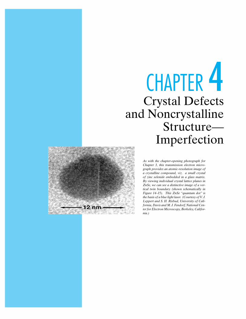
As with the chapter-opening photograph forChapter 3, this transmission electron micro-graph provides an atomic-resolution image ofa crystalline compound, viz. a small crystalof zinc selenide embedded in a glass matrix.By viewing individual crystal lattice planes inZnSe, we can see a distinctive image of a ver-tical twin boundary (shown schematically inFigure 14–15). This ZnSe “quantum dot” isthe basis of a blue light laser. (Courtesy of V. J.Leppert and S. H. Risbud, University of Cali-fornia, Davis and M. J. Fendorf, National Cen-ter for Electron Microscopy, Berkeley, Califor-nia.)
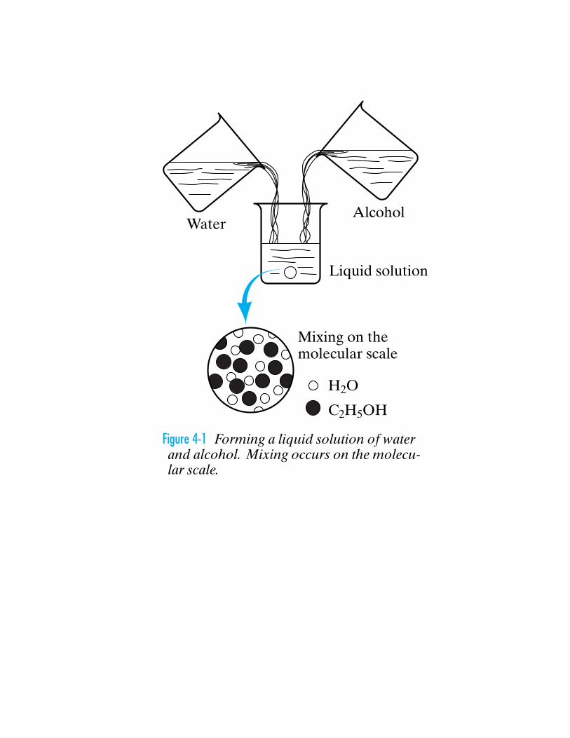
AlcoholWater
Liquid solution
Mixing on themolecular scale
H2O
C2H5OH
Figure 4-1 Forming a liquid solution of waterand alcohol. Mixing occurs on the molecu-lar scale.
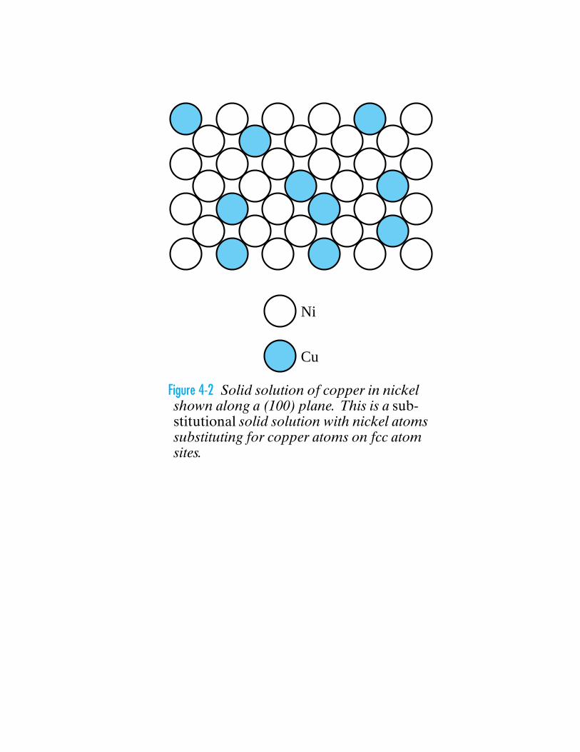
Ni
Cu
Figure 4-2 Solid solution of copper in nickelshown along a (100) plane. This is a sub-stitutional solid solution with nickel atomssubstituting for copper atoms on fcc atomsites.
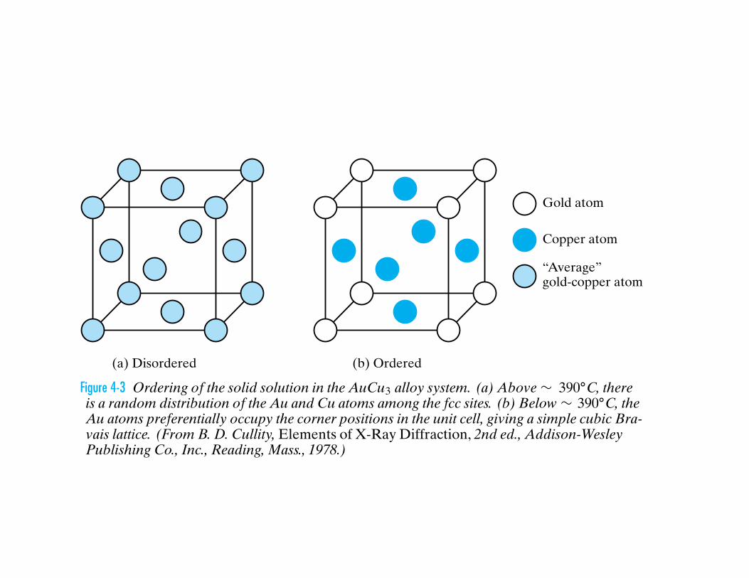
Gold atom
Copper atom
(a) Disordered (b) Ordered
“Average”gold-copper atom
Figure 4-3 Ordering of the solid solution in the AuCu3 alloy system. (a) Above ∼ 390◦C, thereis a random distribution of the Au and Cu atoms among the fcc sites. (b) Below ∼ 390◦C, theAu atoms preferentially occupy the corner positions in the unit cell, giving a simple cubic Bra-vais lattice. (From B. D. Cullity, Elements of X-Ray Diffraction, 2nd ed., Addison-WesleyPublishing Co., Inc., Reading, Mass., 1978.)
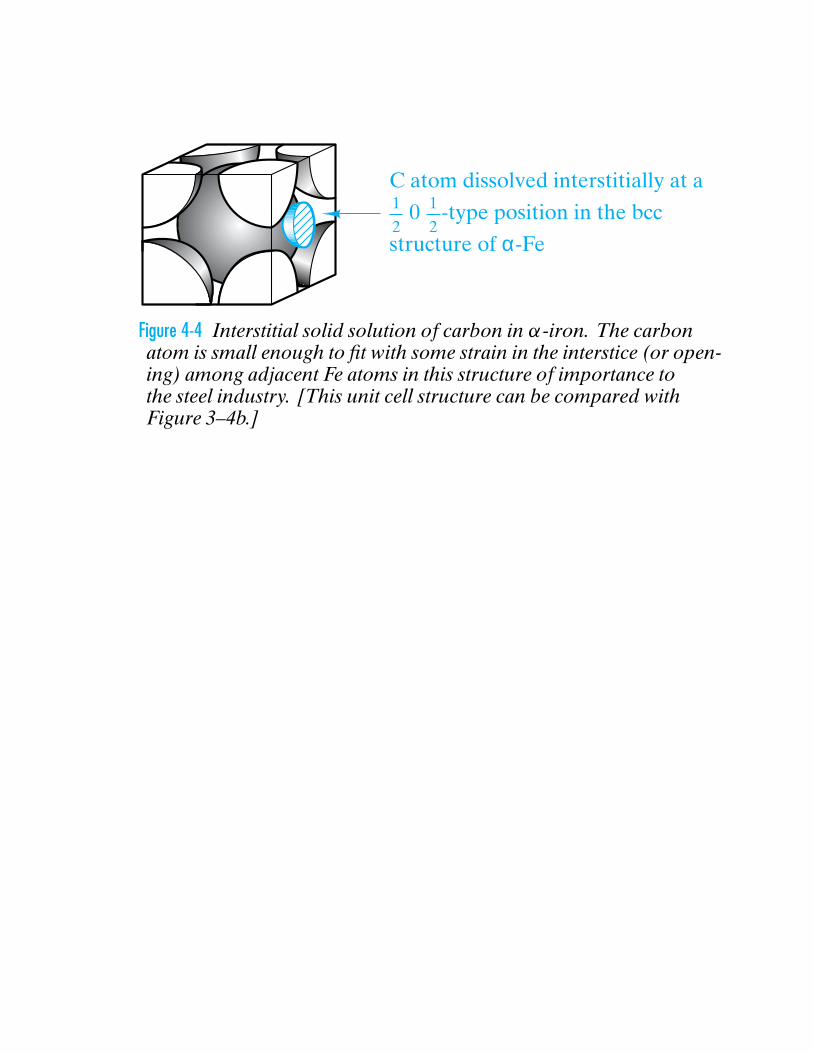
C atom dissolved interstitially at a
0 -type position in the bcc
structure of α-Fe
1
2
1
2
Figure 4-4 Interstitial solid solution of carbon in α-iron. The carbonatom is small enough to fit with some strain in the interstice (or open-ing) among adjacent Fe atoms in this structure of importance tothe steel industry. [This unit cell structure can be compared withFigure 3–4b.]
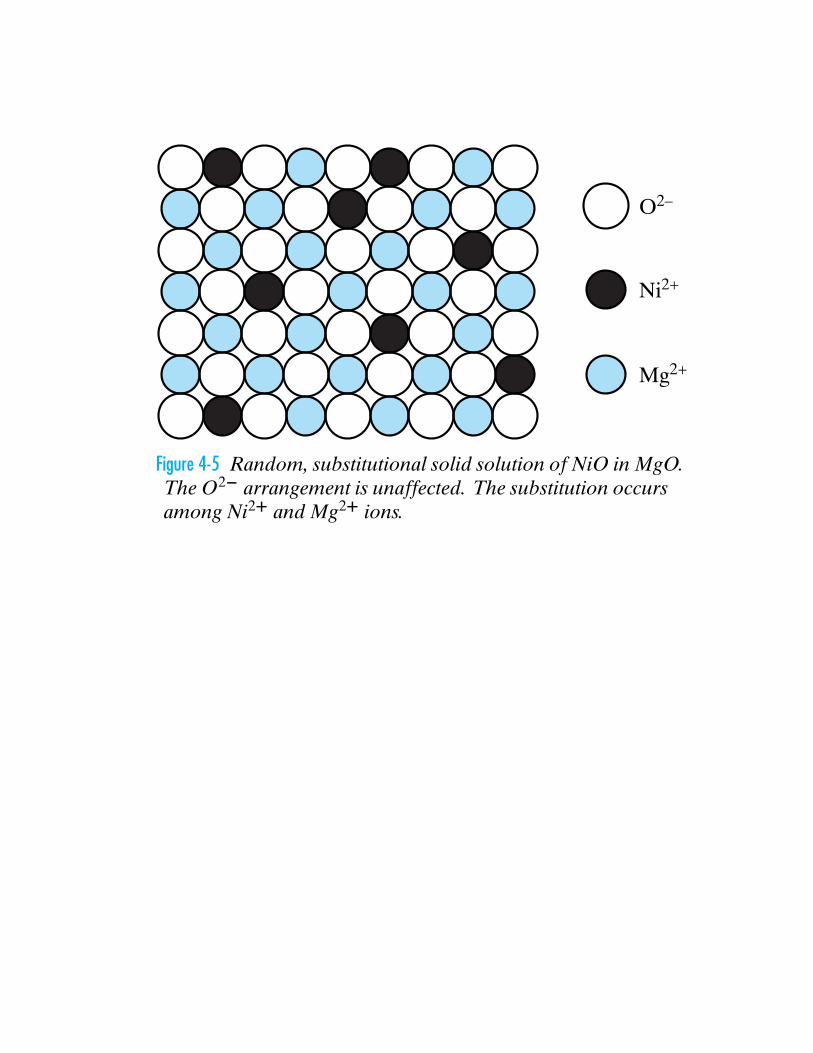
O2–
Ni2+
Mg2+
Figure 4-5 Random, substitutional solid solution of NiO in MgO.The O2− arrangement is unaffected. The substitution occursamong Ni2+ and Mg2+ ions.
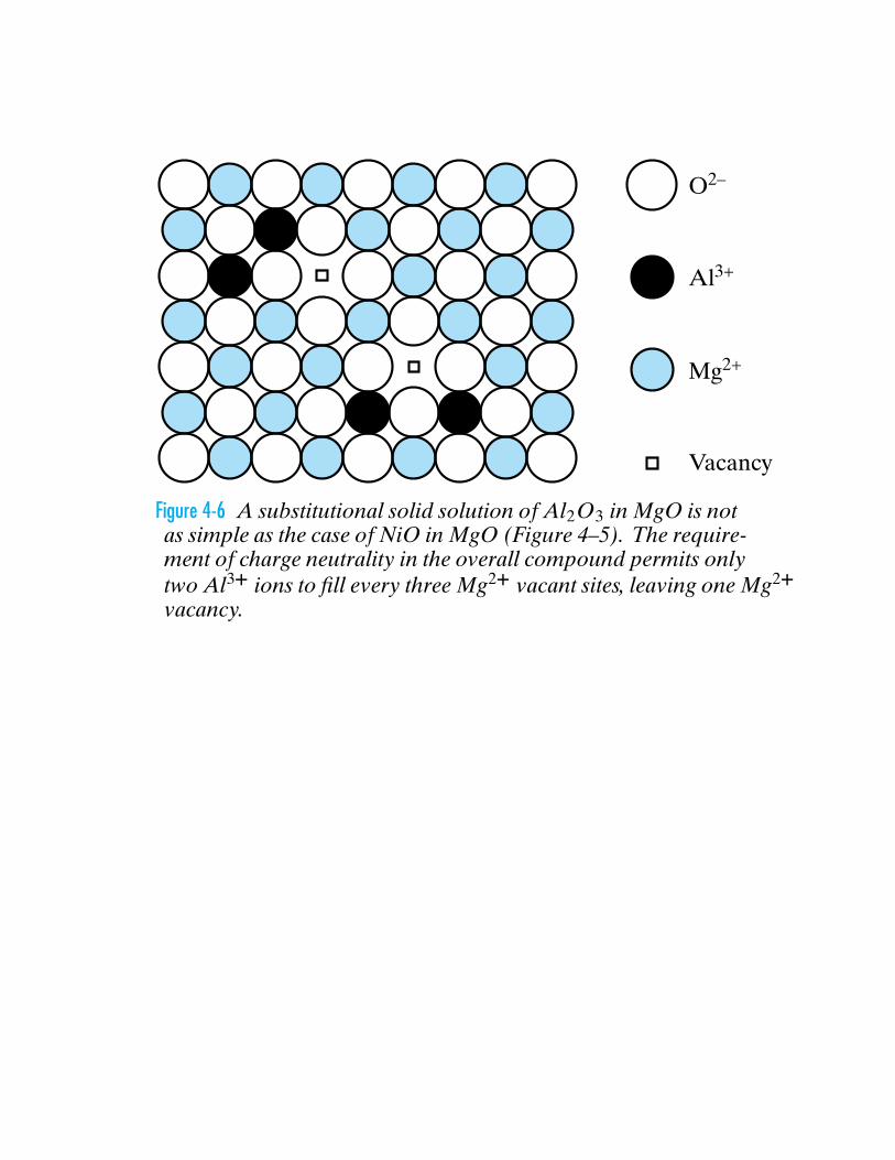
O2–
Al3+
Mg2+
Vacancy
Figure 4-6 A substitutional solid solution of Al2O3 in MgO is notas simple as the case of NiO in MgO (Figure 4–5). The require-ment of charge neutrality in the overall compound permits onlytwo Al3+ ions to fill every three Mg2+ vacant sites, leaving one Mg2+vacancy.
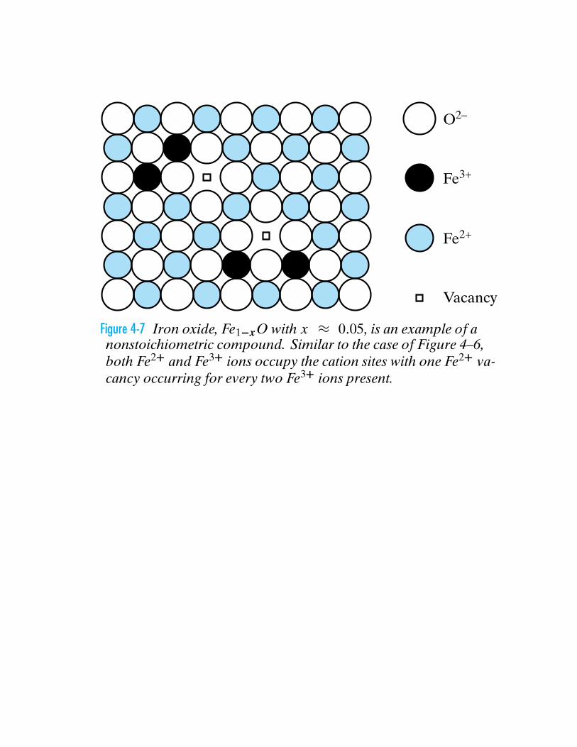
O2–
Fe3+
Fe2+
Vacancy
Figure 4-7 Iron oxide, Fe1−xO with x ≈ 0.05, is an example of anonstoichiometric compound. Similar to the case of Figure 4–6,both Fe2+ and Fe3+ ions occupy the cation sites with one Fe2+ va-cancy occurring for every two Fe3+ ions present.
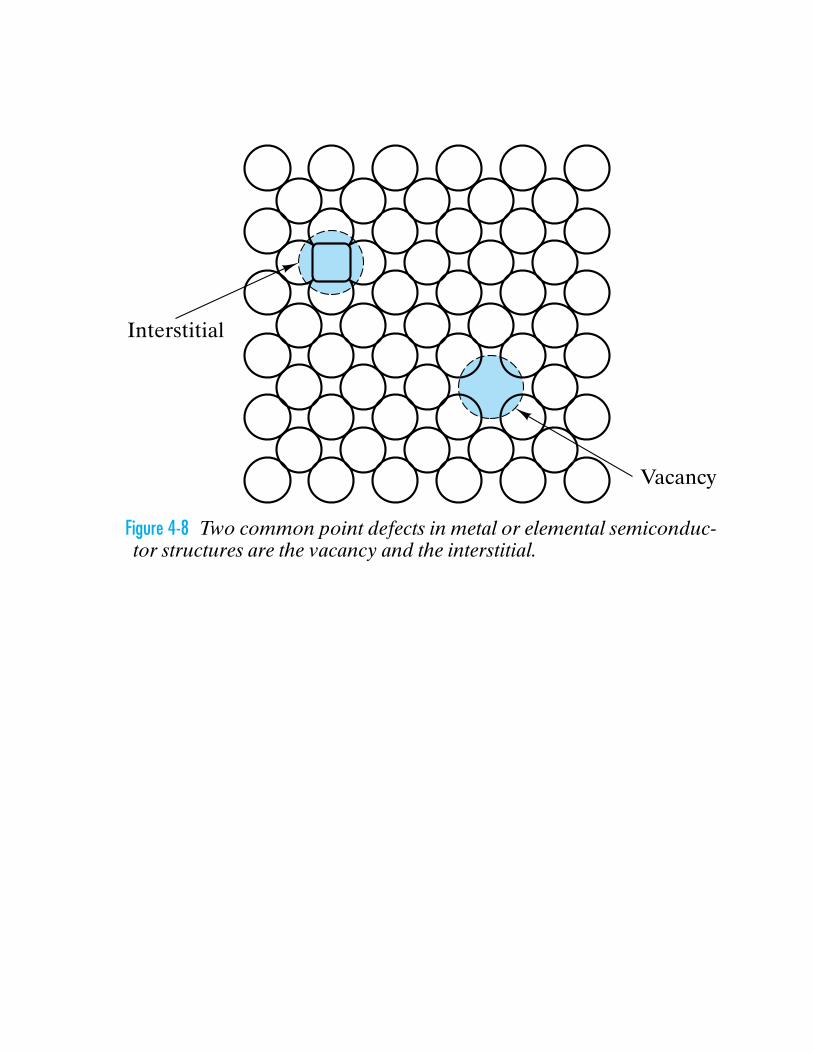
Vacancy
Interstitial
Figure 4-8 Two common point defects in metal or elemental semiconduc-tor structures are the vacancy and the interstitial.
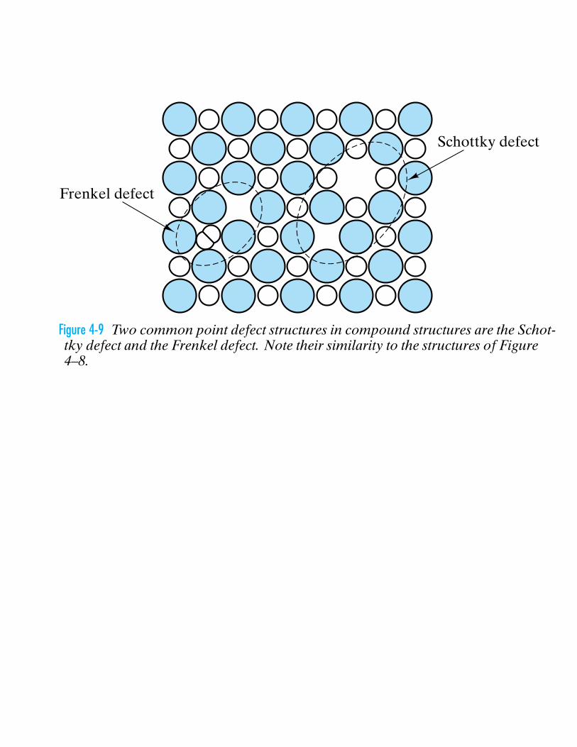
Schottky defect
Frenkel defect
Figure 4-9 Two common point defect structures in compound structures are the Schot-tky defect and the Frenkel defect. Note their similarity to the structures of Figure4–8.
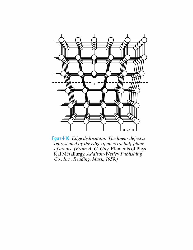
a
Figure 4-10 Edge dislocation. The linear defect isrepresented by the edge of an extra half-planeof atoms. (From A. G. Guy, Elements of Phys-ical Metallurgy, Addison-Wesley PublishingCo., Inc., Reading, Mass., 1959.)

Figure 4-11 Definition of the Burg-ers vector, b, relative to an edgedislocation. (a) In the perfect crys-tal, an m × n atomic step loopcloses at the starting point. (b)In the region of a dislocation, thesame loop does not close, and theclosure vector (b) represents themagnitude of the structural defect.For the edge dislocation, the Burg-ers vector is perpendicular to thedislocation line.
(a)
(b)
b
Burgers vector, b
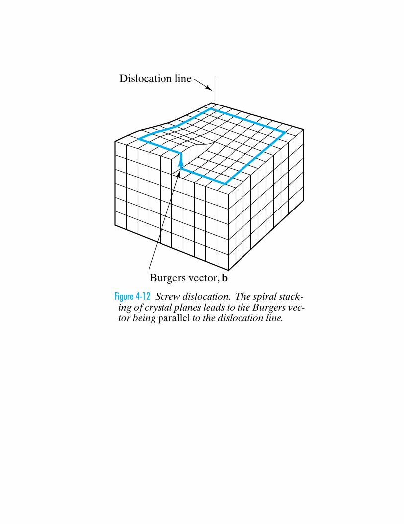
Dislocation line
Figure 4-12 Screw dislocation. The spiral stack-ing of crystal planes leads to the Burgers vec-tor being parallel to the dislocation line.
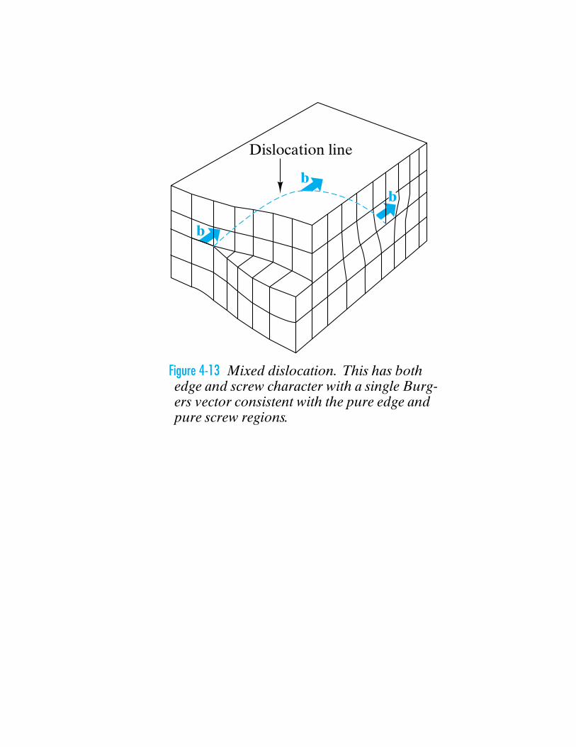
Dislocation line
b
bb
Figure 4-13 Mixed dislocation. This has bothedge and screw character with a single Burg-ers vector consistent with the pure edge andpure screw regions.
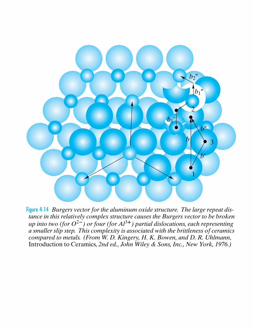
b2″
b1″
b1′2
b″
b′
b
1
3
Figure 4-14 Burgers vector for the aluminum oxide structure. The large repeat dis-tance in this relatively complex structure causes the Burgers vector to be brokenup into two (for O2−) or four (for Al3+) partial dislocations, each representinga smaller slip step. This complexity is associated with the brittleness of ceramicscompared to metals. (From W. D. Kingery, H. K. Bowen, and D. R. Uhlmann,Introduction to Ceramics, 2nd ed., John Wiley & Sons, Inc., New York, 1976.)
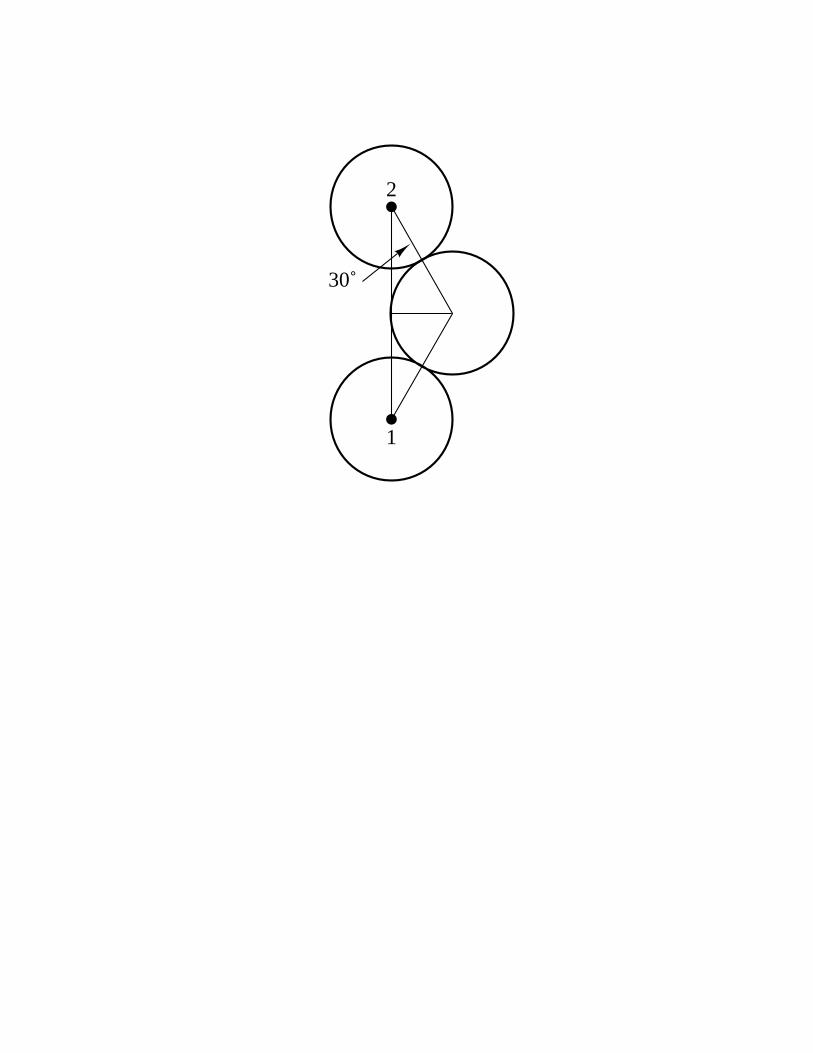
2
1
30˚
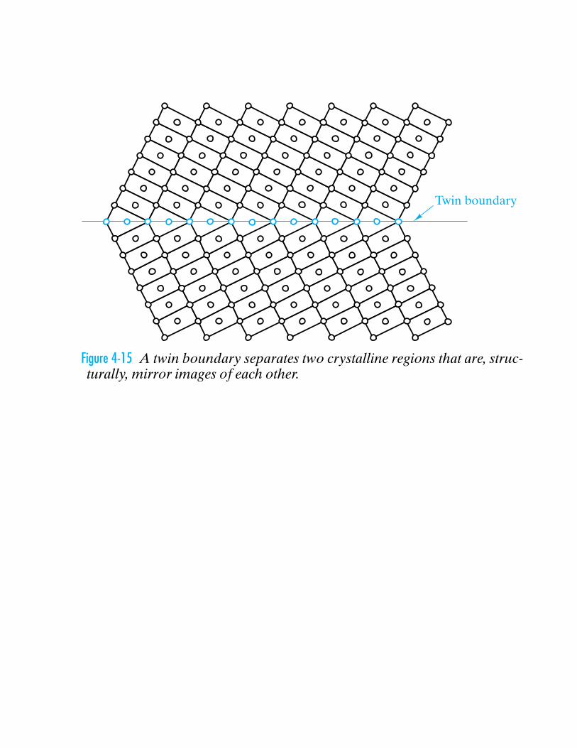
Twin boundary
Figure 4-15 A twin boundary separates two crystalline regions that are, struc-turally, mirror images of each other.
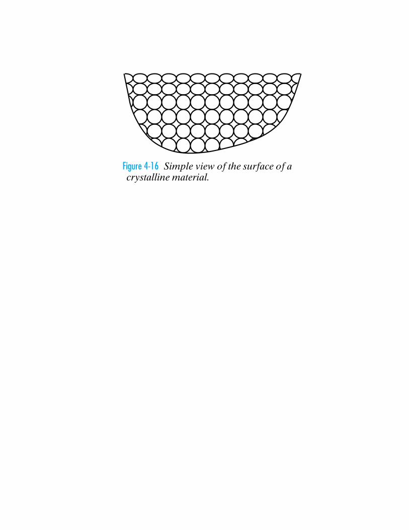
Figure 4-16 Simple view of the surface of acrystalline material.
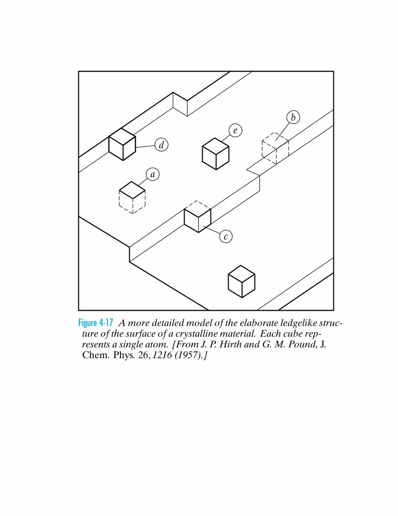
d
a
e
c
b
Figure 4-17 A more detailed model of the elaborate ledgelike struc-ture of the surface of a crystalline material. Each cube rep-resents a single atom. [From J. P. Hirth and G. M. Pound, J.Chem. Phys. 26, 1216 (1957).]
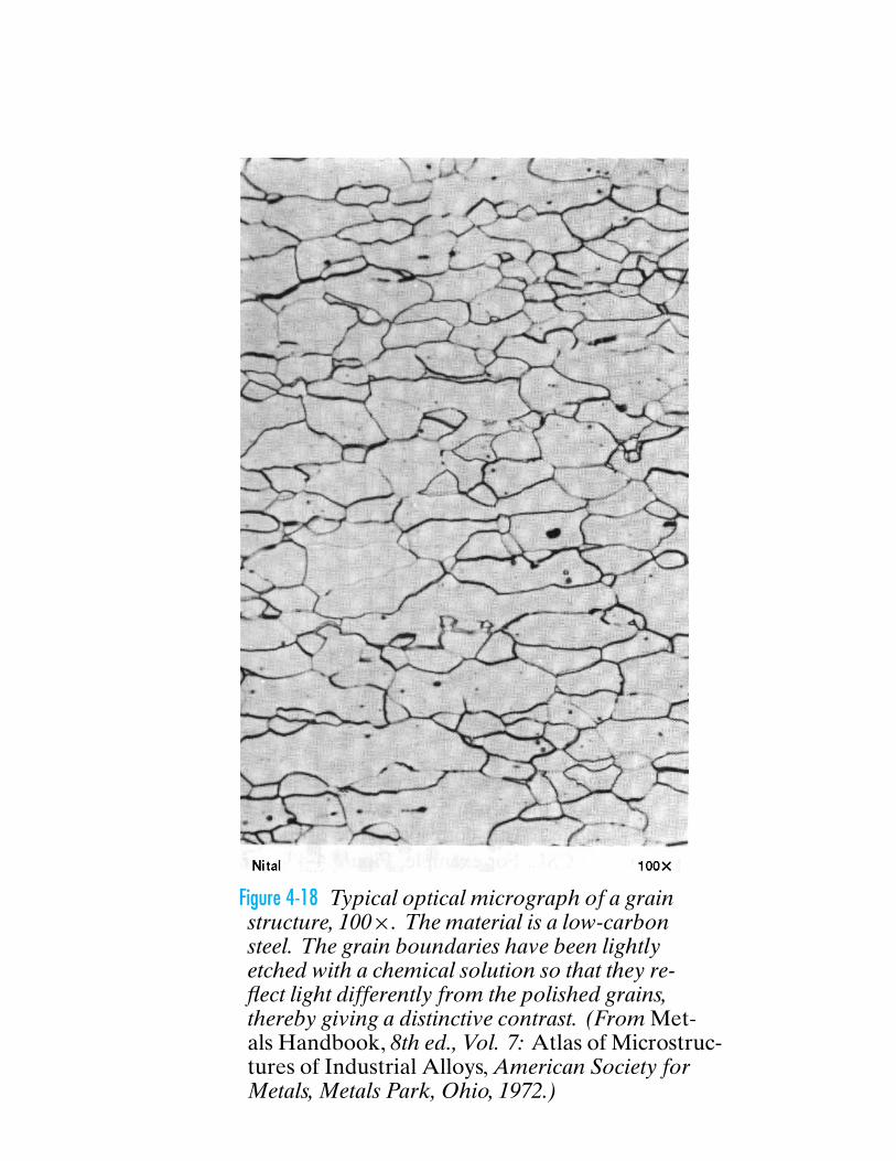
Figure 4-18 Typical optical micrograph of a grainstructure, 100×. The material is a low-carbonsteel. The grain boundaries have been lightlyetched with a chemical solution so that they re-flect light differently from the polished grains,thereby giving a distinctive contrast. (From Met-als Handbook, 8th ed., Vol. 7: Atlas of Microstruc-tures of Industrial Alloys, American Society forMetals, Metals Park, Ohio, 1972.)
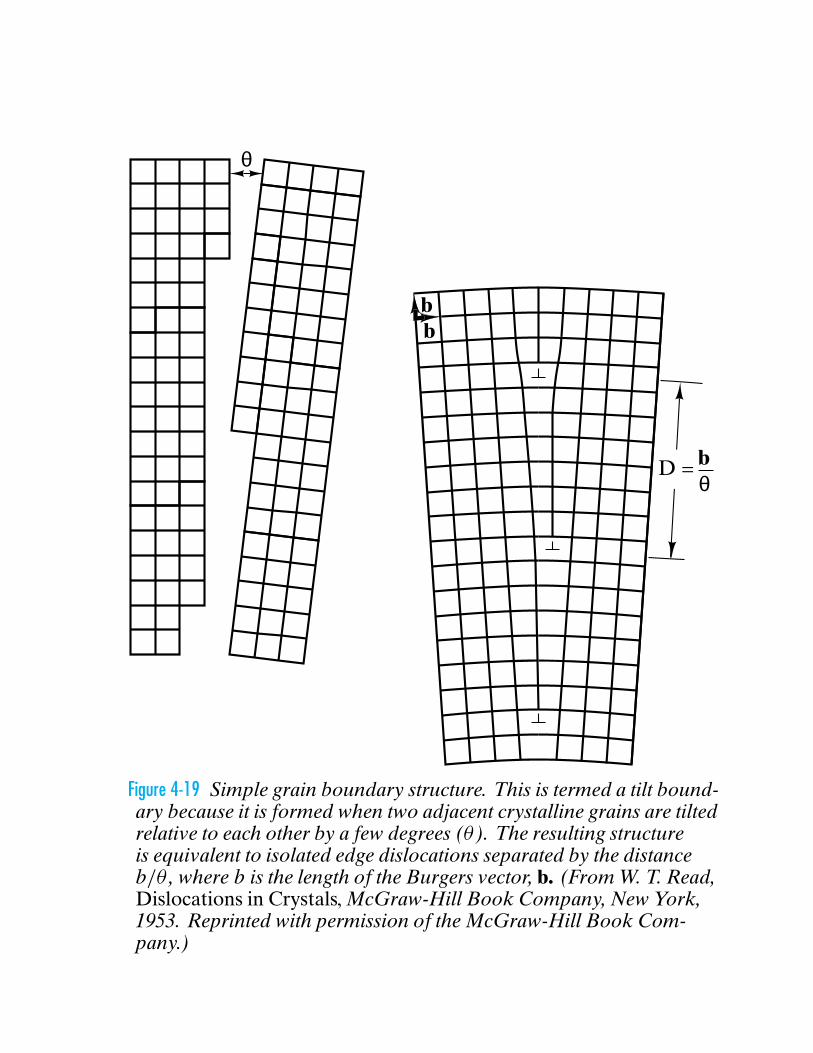
θ
b
bθ
D =
b
Figure 4-19 Simple grain boundary structure. This is termed a tilt bound-ary because it is formed when two adjacent crystalline grains are tiltedrelative to each other by a few degrees (θ ). The resulting structureis equivalent to isolated edge dislocations separated by the distanceb/θ , where b is the length of the Burgers vector, b. (From W. T. Read,Dislocations in Crystals, McGraw-Hill Book Company, New York,1953. Reprinted with permission of the McGraw-Hill Book Com-pany.)
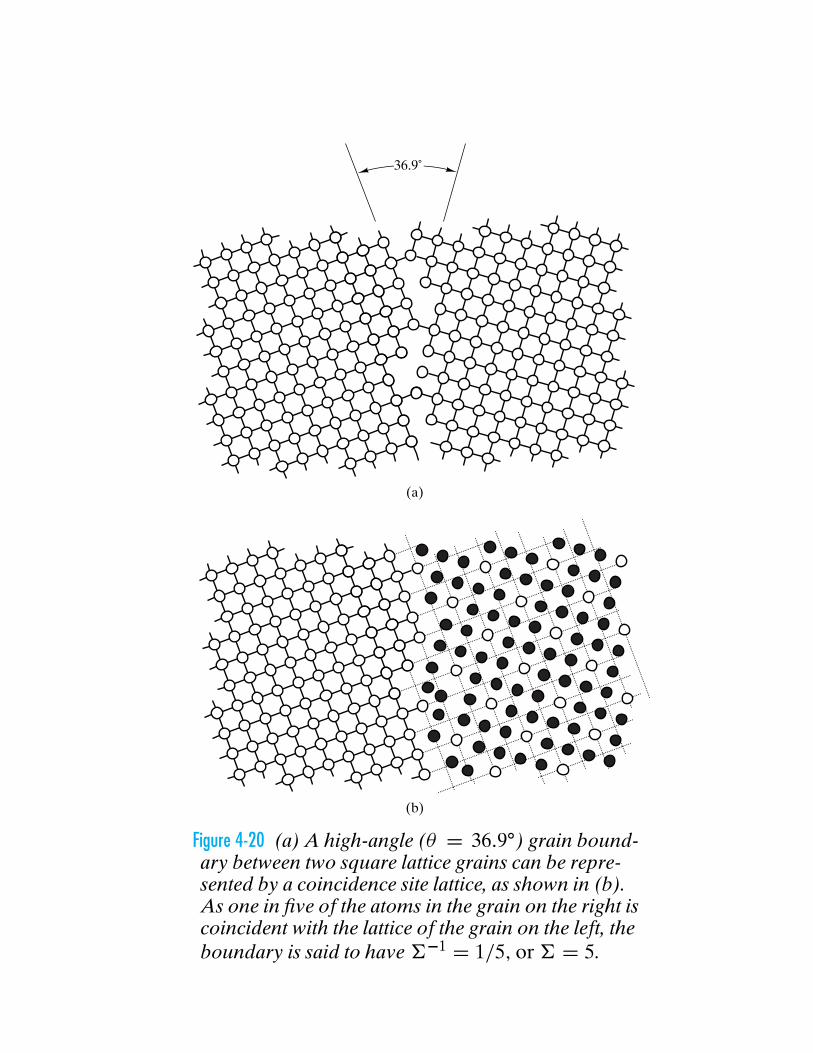
36.9˚
(a)
(b)
Figure 4-20 (a) A high-angle (θ = 36.9◦) grain bound-ary between two square lattice grains can be repre-sented by a coincidence site lattice, as shown in (b).As one in five of the atoms in the grain on the right iscoincident with the lattice of the grain on the left, theboundary is said to have 6−1 = 1/5, or 6 = 5.
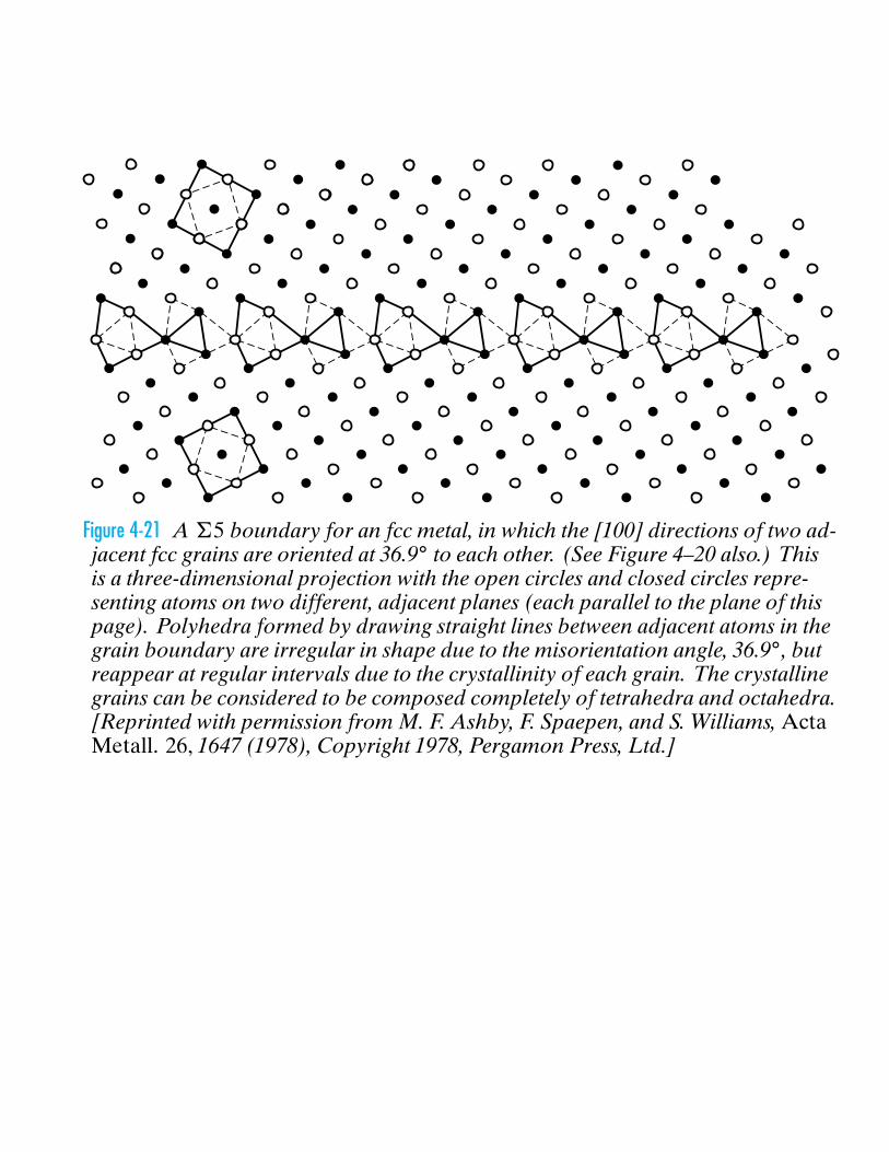
Figure 4-21 A 65 boundary for an fcc metal, in which the [100] directions of two ad-jacent fcc grains are oriented at 36.9◦ to each other. (See Figure 4–20 also.) Thisis a three-dimensional projection with the open circles and closed circles repre-senting atoms on two different, adjacent planes (each parallel to the plane of thispage). Polyhedra formed by drawing straight lines between adjacent atoms in thegrain boundary are irregular in shape due to the misorientation angle, 36.9◦, butreappear at regular intervals due to the crystallinity of each grain. The crystallinegrains can be considered to be composed completely of tetrahedra and octahedra.[Reprinted with permission from M. F. Ashby, F. Spaepen, and S. Williams, ActaMetall. 26, 1647 (1978), Copyright 1978, Pergamon Press, Ltd.]
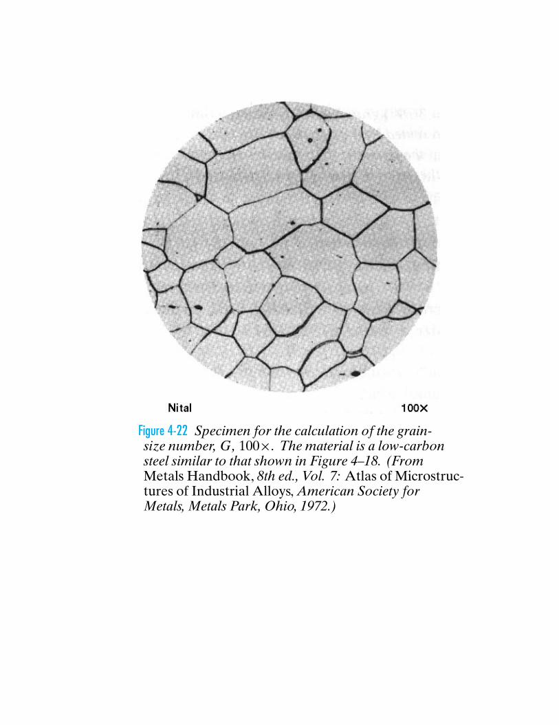
Figure 4-22 Specimen for the calculation of the grain-size number, G, 100×. The material is a low-carbonsteel similar to that shown in Figure 4–18. (FromMetals Handbook, 8th ed., Vol. 7: Atlas of Microstruc-tures of Industrial Alloys, American Society forMetals, Metals Park, Ohio, 1972.)
(a) (b)
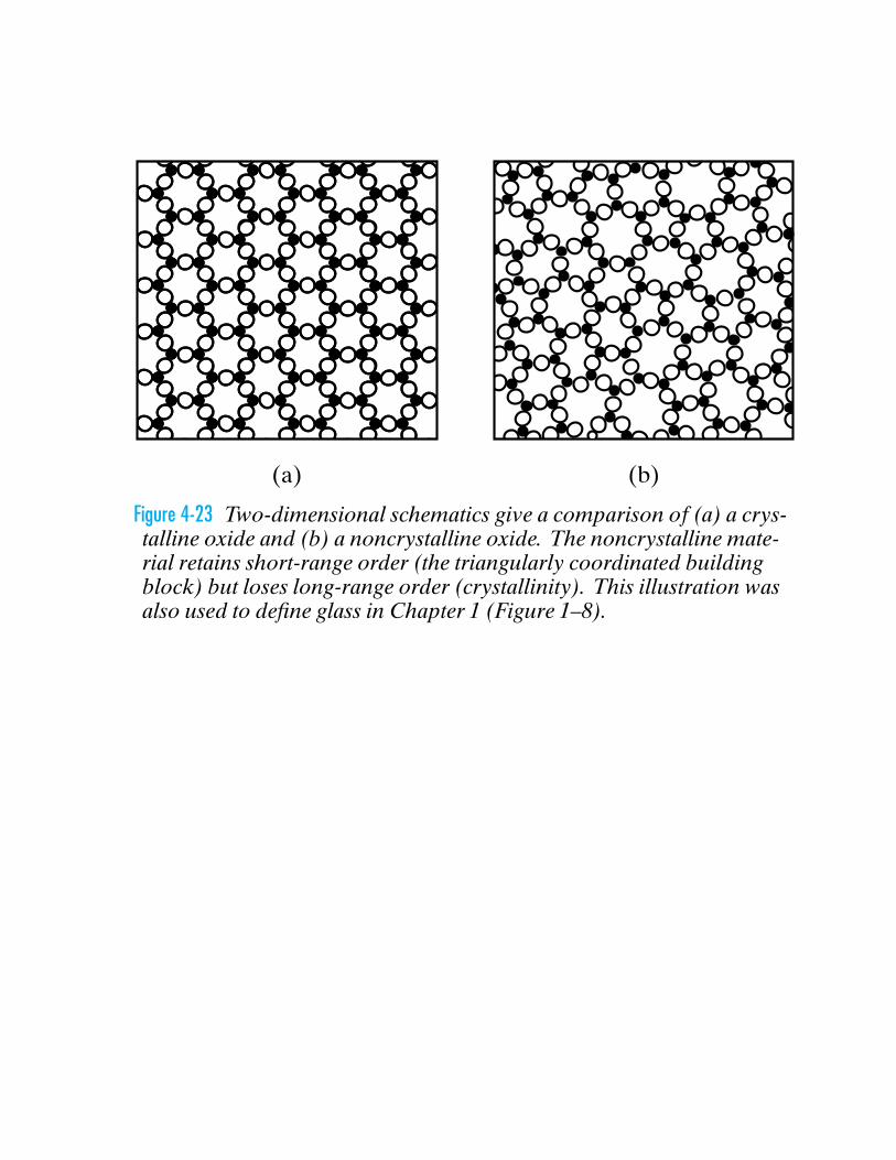
Figure 4-23 Two-dimensional schematics give a comparison of (a) a crys-talline oxide and (b) a noncrystalline oxide. The noncrystalline mate-rial retains short-range order (the triangularly coordinated buildingblock) but loses long-range order (crystallinity). This illustration wasalso used to define glass in Chapter 1 (Figure 1–8).
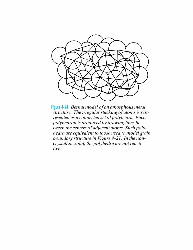
Figure 4-24 Bernal model of an amorphous metalstructure. The irregular stacking of atoms is rep-resented as a connected set of polyhedra. Eachpolyhedron is produced by drawing lines be-tween the centers of adjacent atoms. Such poly-hedra are equivalent to those used to model grainboundary structure in Figure 4–21. In the non-crystalline solid, the polyhedra are not repeti-tive.
Si4+ O2– Na+
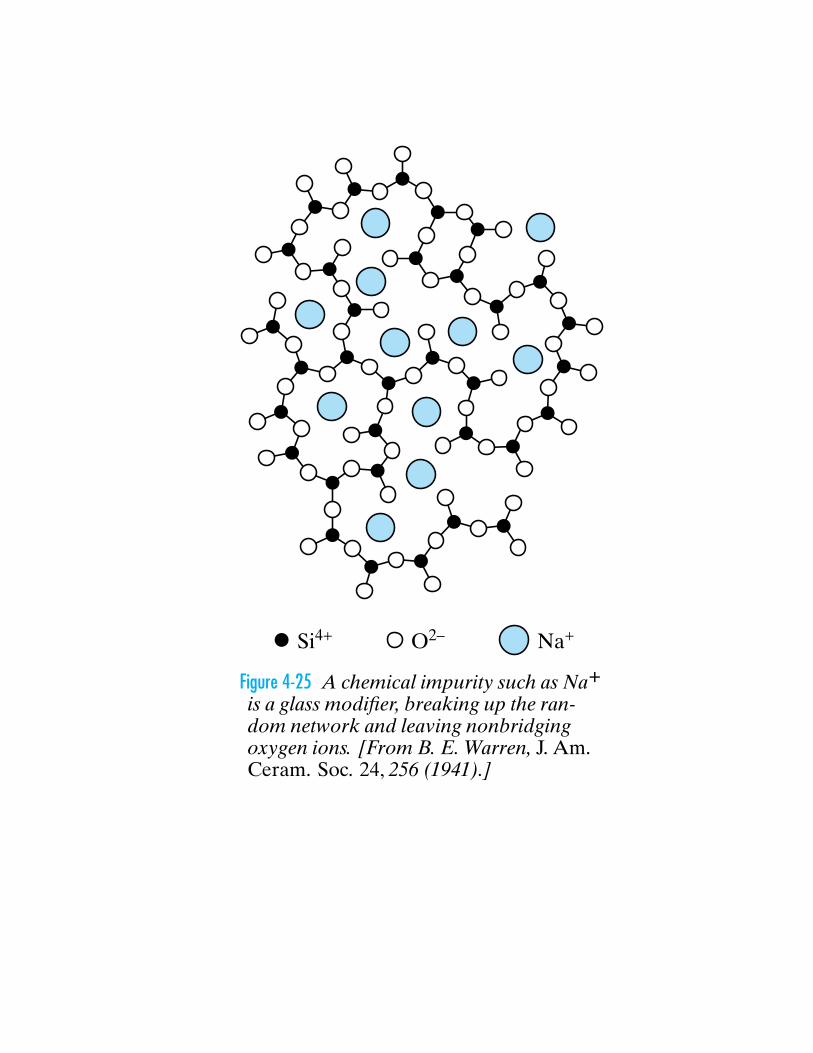
Figure 4-25 A chemical impurity such as Na+is a glass modifier, breaking up the ran-dom network and leaving nonbridgingoxygen ions. [From B. E. Warren, J. Am.Ceram. Soc. 24, 256 (1941).]
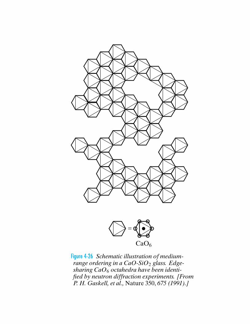
=
CaO6
Figure 4-26 Schematic illustration of medium-range ordering in a CaO-SiO2 glass. Edge-sharing CaO6 octahedra have been identi-fied by neutron diffraction experiments. [FromP. H. Gaskell, et al., Nature 350, 675 (1991).]
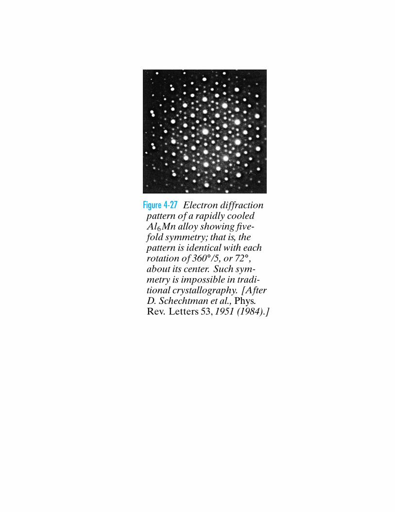
Figure 4-27 Electron diffractionpattern of a rapidly cooledAl6Mn alloy showing five-fold symmetry; that is, thepattern is identical with eachrotation of 360◦/5, or 72◦,about its center. Such sym-metry is impossible in tradi-tional crystallography. [AfterD. Schechtman et al., Phys.Rev. Letters 53, 1951 (1984).]
(a) (b)
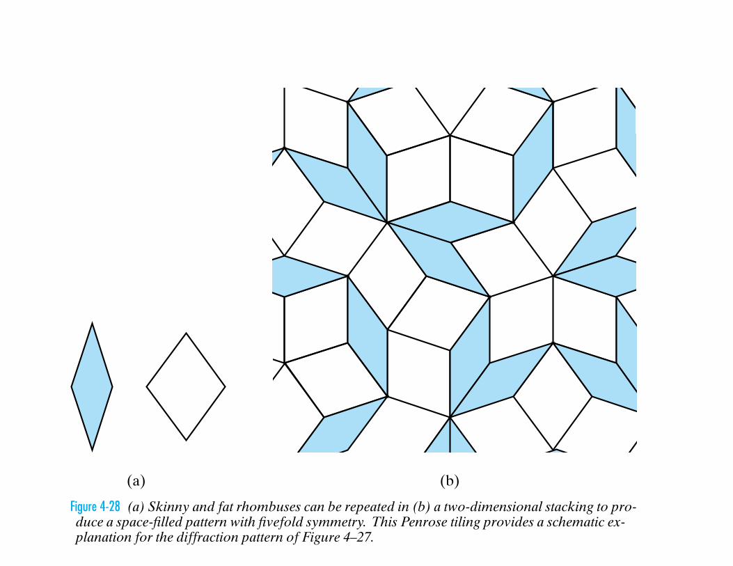
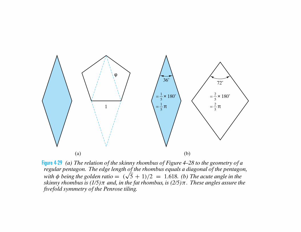
Figure 4-28 (a) Skinny and fat rhombuses can be repeated in (b) a two-dimensional stacking to pro-duce a space-filled pattern with fivefold symmetry. This Penrose tiling provides a schematic ex-planation for the diffraction pattern of Figure 4–27.
(a) (b)
1
36˚ 72˚
φ
= × 180˚1
5
= π1
5
= × 180˚2
5
= π2
5
Figure 4-29 (a) The relation of the skinny rhombus of Figure 4–28 to the geometry of aregular pentagon. The edge length of the rhombus equals a diagonal of the pentagon,with φ being the golden ratio = (
√5 + 1)/2 = 1.618. (b) The acute angle in the
skinny rhombus is (1/5)π and, in the fat rhombus, is (2/5)π . These angles assure thefivefold symmetry of the Penrose tiling.
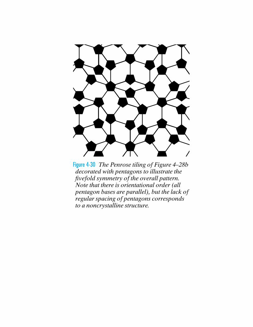
Figure 4-30 The Penrose tiling of Figure 4–28bdecorated with pentagons to illustrate thefivefold symmetry of the overall pattern.Note that there is orientational order (allpentagon bases are parallel), but the lack ofregular spacing of pentagons correspondsto a noncrystalline structure.
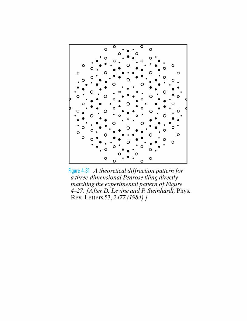
Figure 4-31 A theoretical diffraction pattern fora three-dimensional Penrose tiling directlymatching the experimental pattern of Figure4–27. [After D. Levine and P. Steinhardt, Phys.Rev. Letters 53, 2477 (1984).]
(a) (b) (c)
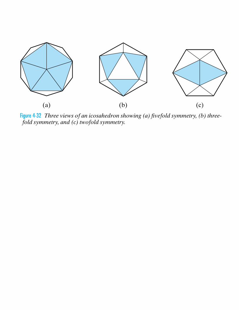
Figure 4-32 Three views of an icosahedron showing (a) fivefold symmetry, (b) three-fold symmetry, and (c) twofold symmetry.
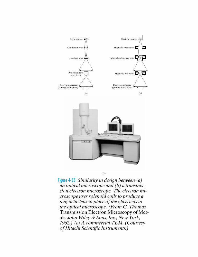
Light source Electron source
Condenser lens Magnetic condenser
Objective lens Magnetic objective lens
Magnetic projectorProjection lens(eyepiece)
Observation screen(photographic plate)
Fluorescent screen(photographic plate)
(a)
(c)
(b)
Figure 4-33 Similarity in design between (a)an optical microscope and (b) a transmis-sion electron microscope. The electron mi-croscope uses solenoid coils to produce amagnetic lens in place of the glass lens inthe optical microscope. (From G. Thomas,Transmission Electron Microscopy of Met-als, John Wiley & Sons, Inc., New York,1962.) (c) A commercial TEM. (Courtesyof Hitachi Scientific Instruments.)
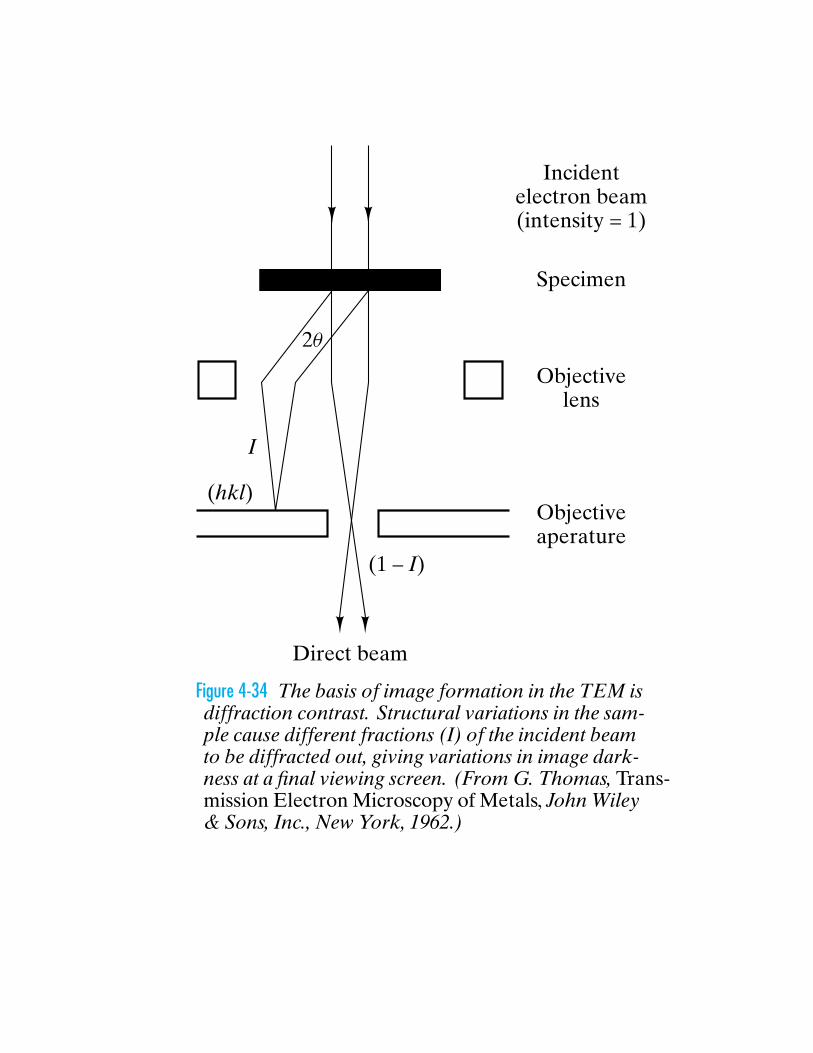
I
(hkl)
(1 – I)
Objectiveaperature
Objectivelens
Specimen
Incidentelectron beam(intensity = 1)
Direct beam
Figure 4-34 The basis of image formation in the TEM isdiffraction contrast. Structural variations in the sam-ple cause different fractions (I) of the incident beamto be diffracted out, giving variations in image dark-ness at a final viewing screen. (From G. Thomas, Trans-mission Electron Microscopy of Metals, John Wiley& Sons, Inc., New York, 1962.)
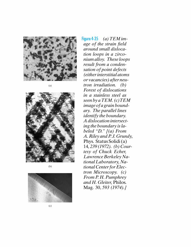
(a)
(b)
(c)
Figure 4-35 (a) TEM im-age of the strain fieldaround small disloca-tion loops in a zirco-nium alloy. These loopsresult from a conden-sation of point defects(either interstitial atomsor vacancies) after neu-tron irradiation. (b)Forest of dislocationsin a stainless steel asseen by a TEM. (c)TEMimage of a grain bound-ary. The parallel linesidentify the boundary.A dislocation intersect-ing the boundary is la-beled “D.” [(a) FromA. Riley and P. J. Grundy,Phys. Status Solidi (a)14, 239 (1972). (b) Cour-tesy of Chuck Echer,Lawrence Berkeley Na-tional Laboratory, Na-tional Center for Elec-tron Microscopy. (c)From P. H. Pumphreyand H. Gleiter, Philos.Mag. 30, 593 (1974).]
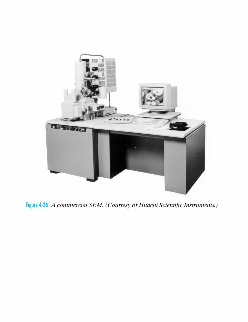
Figure 4-36 A commercial SEM. (Courtesy of Hitachi Scientific Instruments.)
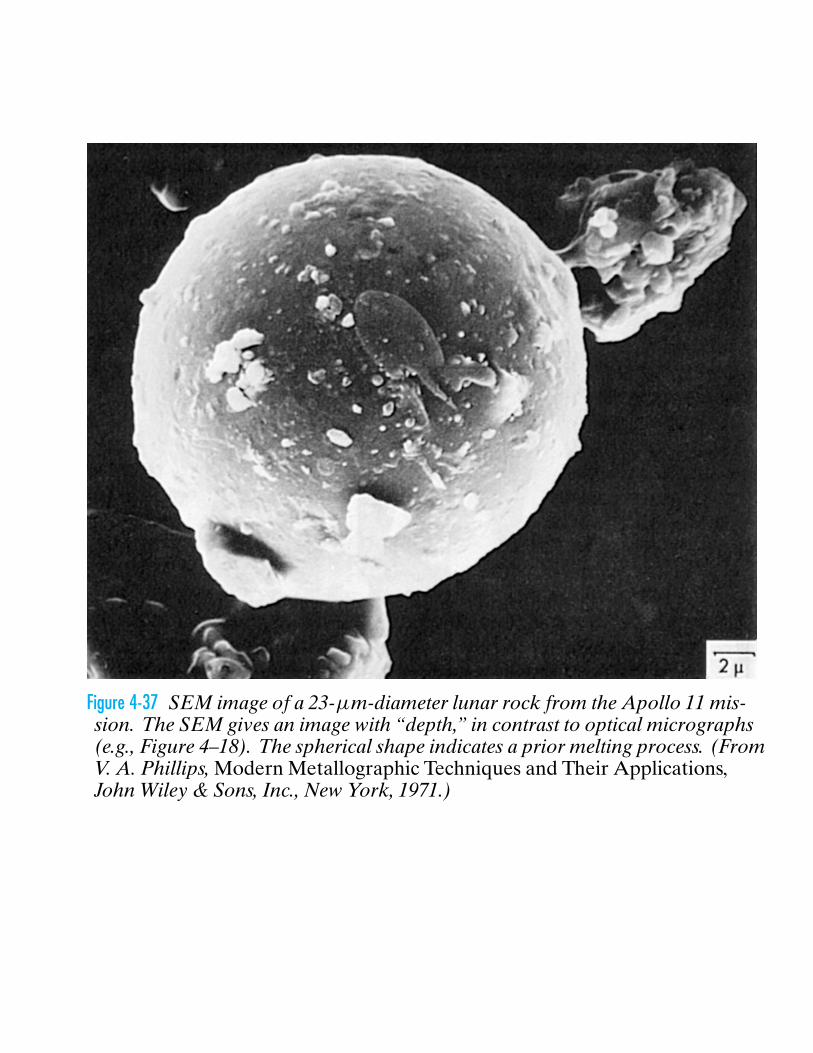
Figure 4-37 SEM image of a 23-µm-diameter lunar rock from the Apollo 11 mis-sion. The SEM gives an image with “depth,” in contrast to optical micrographs(e.g., Figure 4–18). The spherical shape indicates a prior melting process. (FromV. A. Phillips, Modern Metallographic Techniques and Their Applications,John Wiley & Sons, Inc., New York, 1971.)
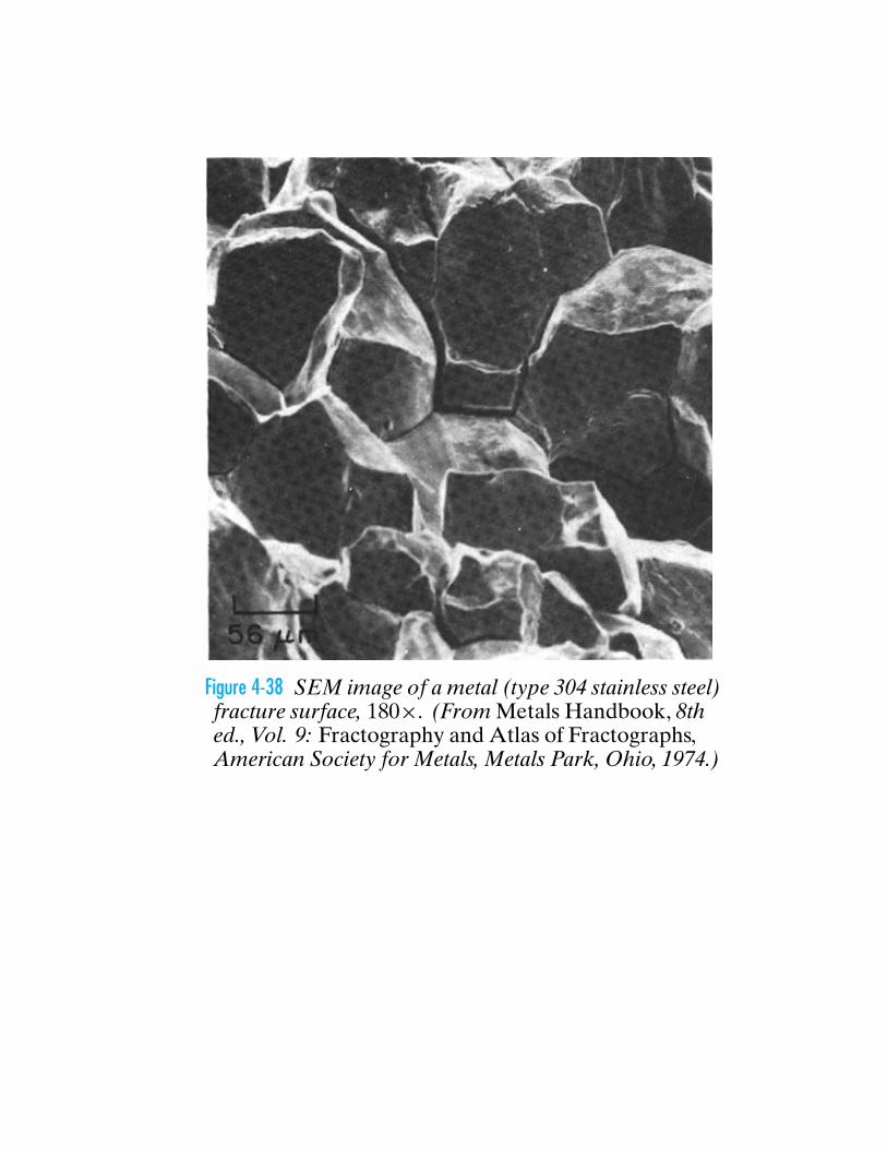
Figure 4-38 SEM image of a metal (type 304 stainless steel)fracture surface, 180×. (From Metals Handbook, 8thed., Vol. 9: Fractography and Atlas of Fractographs,American Society for Metals, Metals Park, Ohio, 1974.)

(a) (b) (c)
Figure 4-39 (a) SEM image of the topography of a lead–tin solder alloy with lead-rich and tin-richregions. (b) A map of the same area shown in (a) indicating the lead distribution (light area)in the microstructure. The light area corresponds to regions emitting characteristic lead x-rayswhen struck by the scanning electron beam. (c) A similar map of the tin distribution (light area)in the microstructure. [From J. B. Bindell, Advanced Materials and Processes 143, 20 (1993).]
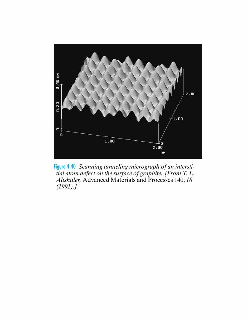
Figure 4-40 Scanning tunneling micrograph of an intersti-tial atom defect on the surface of graphite. [From T. L.Altshuler, Advanced Materials and Processes 140, 18(1991).]
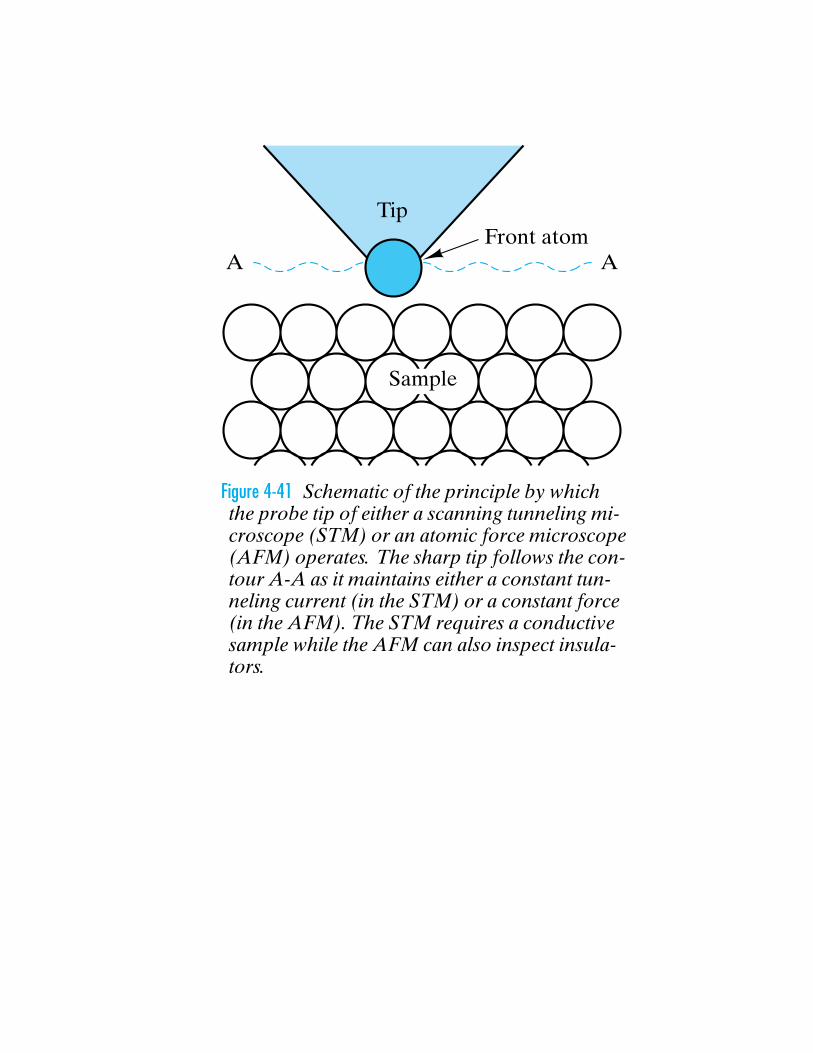
TipFront atom
AA
Sample
Figure 4-41 Schematic of the principle by whichthe probe tip of either a scanning tunneling mi-croscope (STM) or an atomic force microscope(AFM) operates. The sharp tip follows the con-tour A-A as it maintains either a constant tun-neling current (in the STM) or a constant force(in the AFM). The STM requires a conductivesample while the AFM can also inspect insula-tors.