Embed Size (px)
Citation preview
CrystEngComm
Publ
ishe
d on
22
Janu
ary
2014
. Dow
nloa
ded
by N
orth
wes
tern
Pol
ytec
hnic
Uni
vers
ity o
n 07
/01/
2015
11:
49:3
0.
PAPER View Article OnlineView Journal | View Issue
3186 | CrystEngComm, 2014, 16, 3186–3191 This journal is © The R
a State Key Laboratory of Solidification Processing, Northwestern Polytechnical
University, Xi'an 710072, PR China. E-mail: [email protected];
Fax: +86 29 88492642; Tel: +86 29 88495004b School of Mechanical Engineering, Northwestern Polytechnical University,
Xi'an 710072, PR China
Cite this: CrystEngComm, 2014, 16,
3186
Received 5th December 2013,Accepted 22nd January 2014
DOI: 10.1039/c3ce42478b
www.rsc.org/crystengcomm
Potential field emitters: HfC nanorods sheathedwith a HfO2 nanoshell
Song Tian,a Hejun Li,*a Yulei Zhang,a Jincui Ren,a Yixian Li,b Zhanwei Xu,a
Xinfa Qianga and Shouyang Zhanga
Large-scale hafnium carbide (HfC) nanorods sheathed by a hafnium oxide (HfO2) nanoshell were
fabricated using a vacuum catalytic chemical vapor deposition (CVD) method in a HfCl4–C3H6–H2–Ar
system containing a small amount of oxygen impurities. The microstructures and morphologies of the
products were characterized by an X-ray diffractometer, field-emission scanning electron microscope,
transmission electron microscope, and energy-dispersive X-ray spectrometer. The results show that the
synthesized needle-like nanostructures, with a diameter of ~100 nm and a length below 2 μm, consist of
a HfC core and a HfO2 shell with a thickness of ~5 nm surrounding the core. According to two comparative
experiments, a growth mechanism is proposed to explain the formation of the nanorods through a combination
of an oxygen-assisted growth process and a root-type vapor–liquid–solid process. The HfC nanorods exhibit
excellent field emission (FE) properties with a low turn-on field of 3.2–3.4 V μm−1, high field enhancement
factor of 2335, and stable emission current density with a fluctuation below 5% over two hours.
Introduction
In the past few decades, one-dimensional (1D) nanomaterialshave attracted much attention in the field of vacuum micro-electronics due to their ideal geometry for field emission.1–4
Various 1D materials, including carbon (CNTs,4 diamondnanorods5), metals (Mo,6 Co,7 Au8), oxides (ZnO,9 MoO2
10 ),sulfides (ZnS,11 CuS12), silicides (TaSi2
13 ), nitrides (AlN,14
Si3N415 ), and carbides (SiC,16 TiC,17 WC,18 Al3C4
19 ), haveexhibited good field emission (FE) properties as cathodeelectron emitters. However, their practical applications arelimited because of their poor thermal stability and mechani-cal properties for FE. High-performance field emitters withadequate long-term emission stability are highly desired.
As a key ultra-high temperature ceramic material in aero-space, hafnium carbide (HfC) has an ultra-high melting pointing(3928 °C), high hardness (Vickers hardness: 26.1 GPa), highmodulus of elasticity (350–510 GPa), and high resistance tooxidation and corrosion, resulting from its unique metal–carbon chemical bonds and noble-metal-like d-state densityaround the Fermi level.20,21 The outstanding physicochemicalproperties lead to good emission stability for HfC. In fact,
previous research has demonstrated that the good physico-chemical stability and low work function make a single sharpHfC tip an excellent candidate for an electron emission sourcefor ultrafast laser-triggered electron emission applications.22
Nevertheless, it is still a challenge to broaden the applicationsof small HfC tips in vacuum microelectronics due to theunavailability of large-scale 1D HfC nanostructures with regu-lar orientations. Recently, our group synthesized HfC nano-wires by a Ni-catalytic chemical vapor deposition (CVD) methodbelow the eutectic temperature (TE) of the Ni–C–Hf alloy.23
The synthesis provided large-scale pure nanowires but with arandom-oriented distribution, probably due to the metastablegrowth below TE. Although the large-scale low temperaturesynthesis of HfC nanowires is very intriguing for structurematerial purposes, disorder orientation inhibits their applica-tion in FE devices.
In the past, HfC was usually deposited as a film of W, Mo,and Si arrays to improve the FE properties for video displaysand microwave applications.24 In this work, large-scale needle-like HfC nanorods sheathed with a HfO2 nanoshell weresynthesized above the TE by CVD and directly used as cathodeemitters for FE measurements. The synthesized nanorodsexhibited radial upward growth. The nanorods were demon-strated to be potential field emitters with a low turn-onfield and high field enhancement factor. In addition, wethink the HfO2 nanoshell of the nanorods may enhance thestability by preventing the HfC core from oxidation inpractical applications.
oyal Society of Chemistry 2014
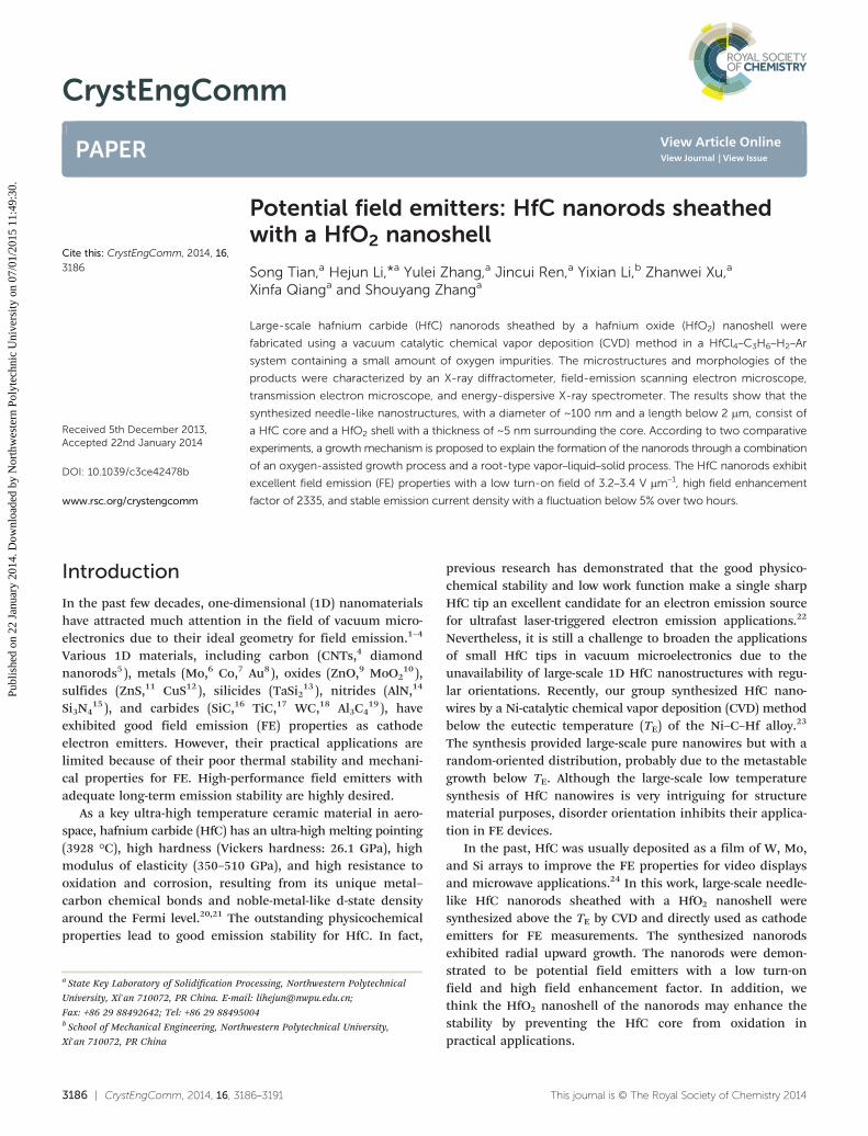
Fig. 2 (a) X-ray diffraction pattern of the synthesized product.(b) Low-magnification SEM image of the product growing on thesubstrate. The inset is a further magnified SEM image. (c) High-magnification SEM image showing the nanorods radially grew.
CrystEngComm Paper
Publ
ishe
d on
22
Janu
ary
2014
. Dow
nloa
ded
by N
orth
wes
tern
Pol
ytec
hnic
Uni
vers
ity o
n 07
/01/
2015
11:
49:3
0.
View Article Online
Experimental
The HfC nanorods were deposited on a graphite substrate bya vacuum catalytic chemical vapor deposition (CVD) methodin a HfCl4–C3H6–H2–Ar system containing a small amount ofoxygen (O) impurities. The synthesis was carried out in a verticaldual-zone CVD furnace, which consisted of a low-temperaturesublimation chamber and a high-temperature depositionchamber. A graphite sheet (15 mm × 10 mm × 10 mm)was soaked in an Ni(NO3)2–ethanol solution (molarity, 1 ±0.05 mol L−1) followed by a drying process. Ni(NO3)2 was usedas the catalyst. The treated graphite sheet was hung in thedeposition chamber as the substrate. The height of the depo-sition chamber was 45 cm. The distance of the substrate fromthe deposition chamber top was about 35 cm. A diagrammaticdrawing of the experiment setup is shown in Fig. 1. Duringthe deposition process, solid hafnium tetrachloride (HfCl4)was sublimated at 553 ± 5 K in the sublimation chamber andcarried by a mixed flowing gas of C3H6, H2, and Ar into thedeposition chamber, and then the synthesis reaction occurredat 1523–1623 K for 3 h under 200–300 Pa total pressure in thedeposition chamber. The flow rate of the mixed gas wasmaintained at ~1200 ml min−1. In addition, an unknownquantity of O participated in the synthesis reaction, whichprobably arose from inlet gases including diluted gas, reducinggas, gaseous precursor and even air due to impossibly absoluteseals in the entire reaction system.
The morphology and structure of the product were charac-terized using a Rigaku D/max-3C X-ray diffractometer (XRD)with a Cu Kα radiation source, a FEI Quanta 600 FEG field-emission scanning electron microscope (SEM), and a TecnaiF30 G2 field-emission transmission electron microscope(TEM) with energy-dispersive X-ray (EDX) mapping capabili-ties, respectively.
Results and discussion
Fig. 2a shows the XRD pattern of the synthesized product,from which the characteristic diffraction peaks of HfC andHfO2 can be observed. HfC is identified to be the face-centred cubic (fcc) structure (JCPDS file 65-0964), and thepeaks of HfO2 are indexed to the monoclinic structure (JCPDS
This journal is © The Royal Society of Chemistry 2014
Fig. 1 Diagrammatic drawing of the deposition apparatus for theproduction of the HfC nanorods sheathed with a HfO2 nanoshell.
file 78-0049). This indicates that the product consists of fccHfC and monoclinic HfO2. A low-magnification SEM imageof the product is shown in Fig. 2b, from which we can findthat large-scale nanorods were uniformly distributed on thesubstrate. Upon closer inspection of the inset in Fig. 2b, it isfound that massive micro-scale coralloid structures wereobtained due to the radial growth of these nanorods. Thehigh-magnification SEM image in Fig. 2c shows the nanorodsradially grew on the surface of the micro-scale structures.These nanorods have a needle-like structure with a diameterof ~100 nm and a length below 2 μm, indicating that theproduct has an ideal morphology for field emitters.
The detailed crystal microstructure of the nanorods wasfurther investigated by TEM observation. The product wassonicated and dispersed in an ethanol solution for 10 minand then deposited onto a holey copper grid coated with acarbon film for TEM measurements. The typical low-magnification TEM image (Fig. 3a) confirms the nanorodshave shrunk in diameter. The high-magnification TEM imageof a single needle-like nanorod is shown in Fig. 3b. Thenanorod has a core/shell structure. The thickness of the shellis ~5 nm (see the inset of Fig. 3b). The high-resolution TEM(HRTEM) image shown in Fig. 3c highlights the single-crystalline structure of the core. Besides, the lattice fringesfrom the core of the nanorod have a spacing of 2.64 Å, whichis close to that of the (111) crystal plane of fcc HfC. Theselected area electron diffraction (SAED) pattern recordedfrom the nanorod in the inset of Fig. 3c is identified to bealong the [1̄12] diffraction zone axis, which is consistent withthe fcc structure of HfC. Based on the [1̄12] zone-axis andanalysis of the lattice structure, the core of the nanorod is
CrystEngComm, 2014, 16, 3186–3191 | 3187
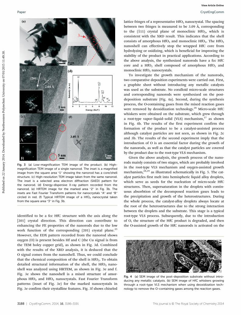
Fig. 3 (a) Low-magnification TEM image of the product. (b) High-magnification TEM image of a single nanorod. The inset is a magnifiedimage from the square area “1” showing the nanorod has a core/shellstructure. (c) High-resolution TEM image taken from the same nanorod.The inset is a selected area electron diffraction (SAED) pattern forthe nanorod. (d) Energy-dispersive X-ray pattern recorded from thenanorod. (e) HRTEM image for the marked area “2” in Fig. 3b. Theinsets are Fast Fourier Transform patterns for nanocrystals “A” and “B”circled in red. (f) Typical HRTEM image of a HfO2 nanocrystal takenfrom the square area “3” in Fig. 3b.
Fig. 4 (a) SEM image of the post-deposition substrate without intro-ducing any metallic catalysts. (b) SEM image of HfC whiskers growingthrough a root-type VLS mechanism when using deoxidization tech-nology to remove the O-containing gases among the reaction gases.
CrystEngCommPaper
Publ
ishe
d on
22
Janu
ary
2014
. Dow
nloa
ded
by N
orth
wes
tern
Pol
ytec
hnic
Uni
vers
ity o
n 07
/01/
2015
11:
49:3
0.
View Article Online
identified to be a fcc HfC structure with the axis along the[201] crystal direction. This direction can contribute toenhancing the FE properties of the nanorods due to the lowwork function of the corresponding (201) crystal plane.25
However, the EDX pattern recorded from the nanorod showsoxygen (O) is present besides Hf and C (the Cu signal is fromthe TEM holey copper grid), as shown in Fig. 3d. Combinedwith the results of the XRD analysis, it is deduced that theO signal comes from the nanoshell. Thus, we could concludethat the chemical composition of the shell is HfO2. To obtaindetailed structural information of the shell, the HfO2 nano-shell was analyzed using HRTEM, as shown in Fig. 3e and f.Fig. 3e shows the nanoshell is a mixed structure of amor-phous HfO2 and HfO2 nanocrystals. Fast Fourier Transformpatterns (inset of Fig. 3e) for the marked nanocrystals inFig. 3e confirm their crystalline features. Fig. 3f shows chiseled
3188 | CrystEngComm, 2014, 16, 3186–3191
lattice fringes of a representative HfO2 nanocrystal. The spacingbetween two fringes is measured to be 3.09 Å, correspondingto the (1̄11) crystal plane of monoclinic HfO2, which isconsistent with the XRD result. This indicates that the shellconsists of amorphous HfO2 and monoclinic HfO2. The HfO2
nanoshell can effectively stop the wrapped HfC core fromhydrolyzing or oxidizing, which is beneficial for improving thestability of the product in practical applications. According tothe above analysis, the synthesized nanorods have a fcc HfCcore and a HfO2 shell composed of amorphous HfO2 andmonoclinic HfO2 nanocrystals.
To investigate the growth mechanism of the nanorods,two comparative deposition experiments were carried out. First,a graphite sheet without introducing any metallic catalystswas used as the substrate. No coralloid micro-scale structuresand corresponding nanorods were synthesized on the post-deposition substrate (Fig. 4a). Second, during the synthesisprocess, the O-containing gases from the mixed reaction gaseswere removed by deoxidization technology.26 Micro-scale HfCwhiskers were obtained on the substrate, which grew througha root-type vapor–liquid–solid (VLS) mechanism,27 as shownin Fig. 4b. The results of the first experiment confirm theformation of the product to be a catalyst-assisted processalthough catalyst particles are not seen, as shown in Fig. 2cand 3b. The results of the second experiment imply that theintroduction of O is an essential factor during the growth ofthe nanorods, as well as that the catalyst particles are coveredby the product due to the root-type VLS mechanism.
Given the above analysis, the growth process of the nano-rods mainly consists of two stages, which are probably involvedin the root-type VLS mechanism and oxygen-assisted growthmechanism,28,29 as illustrated schematically in Fig. 5. The cat-alyst particles first melt into hemispheric liquid alloy droplets,which serve as seeds for the nucleation of micro-scale HfCstructures. Then, supersaturation in the droplets with contin-uous absorbtion of the decomposed reaction gases leads tothe precipitation and growth of the heterostructures. Duringthe whole process, the catalyst-alloy droplets always locate atthe root of the heterostructures due to the strong interactionbetween the droplets and the substrate. This stage is a typicalroot-type VLS process. Subsequently, due to the introductionof O, the structure of the HfC product is degraded, and thenthe O-assisted growth of the HfC nanorods is activated on the
This journal is © The Royal Society of Chemistry 2014
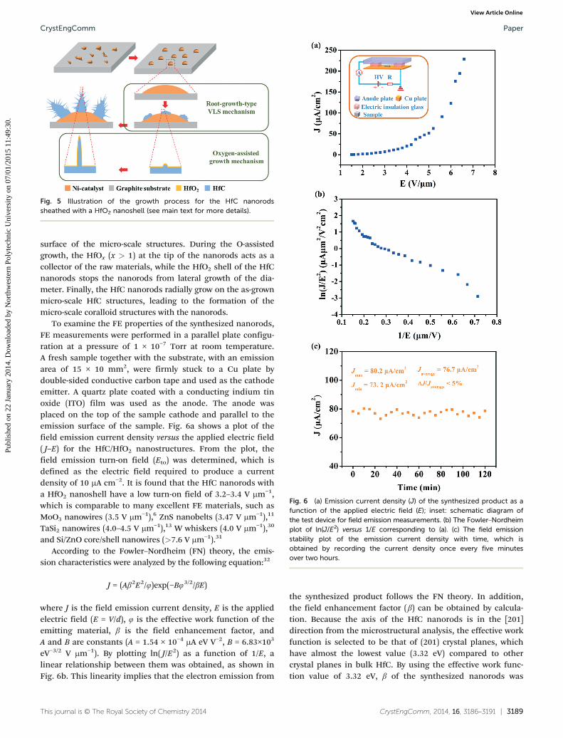
Fig. 5 Illustration of the growth process for the HfC nanorodssheathed with a HfO2 nanoshell (see main text for more details).
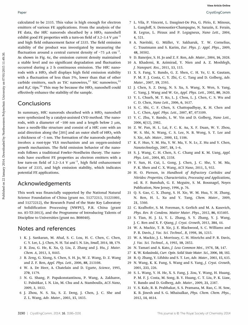
Fig. 6 (a) Emission current density (J) of the synthesized product as afunction of the applied electric field (E); inset: schematic diagram ofthe test device for field emission measurements. (b) The Fowler–Nordheimplot of ln(J/E2) versus 1/E corresponding to (a). (c) The field emissionstability plot of the emission current density with time, which isobtained by recording the current density once every five minutesover two hours.
CrystEngComm Paper
Publ
ishe
d on
22
Janu
ary
2014
. Dow
nloa
ded
by N
orth
wes
tern
Pol
ytec
hnic
Uni
vers
ity o
n 07
/01/
2015
11:
49:3
0.
View Article Online
surface of the micro-scale structures. During the O-assistedgrowth, the HfOx (x > 1) at the tip of the nanorods acts as acollector of the raw materials, while the HfO2 shell of the HfCnanorods stops the nanorods from lateral growth of the dia-meter. Finally, the HfC nanorods radially grow on the as-grownmicro-scale HfC structures, leading to the formation of themicro-scale coralloid structures with the nanorods.
To examine the FE properties of the synthesized nanorods,FE measurements were performed in a parallel plate configu-ration at a pressure of 1 × 10⁻⁷ Torr at room temperature.A fresh sample together with the substrate, with an emissionarea of 15 × 10 mm2, were firmly stuck to a Cu plate bydouble-sided conductive carbon tape and used as the cathodeemitter. A quartz plate coated with a conducting indium tinoxide (ITO) film was used as the anode. The anode wasplaced on the top of the sample cathode and parallel to theemission surface of the sample. Fig. 6a shows a plot of thefield emission current density versus the applied electric field( J–E) for the HfC/HfO2 nanostructures. From the plot, thefield emission turn-on field (Eto) was determined, which isdefined as the electric field required to produce a currentdensity of 10 μA cm−2. It is found that the HfC nanorods witha HfO2 nanoshell have a low turn-on field of 3.2–3.4 V μm−1,which is comparable to many excellent FE materials, such asMoO3 nanowires (3.5 V μm−1),6 ZnS nanobelts (3.47 V μm−1),11
TaSi2 nanowires (4.0–4.5 V μm−1),13 W whiskers (4.0 V μm−1),30
and Si/ZnO core/shell nanowires (>7.6 V μm−1).31
According to the Fowler–Nordheim (FN) theory, the emis-sion characteristics were analyzed by the following equation:32
J = (Aβ2E2/φ)exp(−Bφ3/2/βE)
where J is the field emission current density, E is the appliedelectric field (E = V/d), φ is the effective work function of theemitting material, β is the field enhancement factor, andA and B are constants (A = 1.54 × 10⁻⁴ μA eV V−2, B = 6.83×10³
eV−3/2 V μm−1). By plotting ln( J/E2) as a function of 1/E, alinear relationship between them was obtained, as shown inFig. 6b. This linearity implies that the electron emission from
This journal is © The Royal Society of Chemistry 2014
the synthesized product follows the FN theory. In addition,the field enhancement factor (β) can be obtained by calcula-tion. Because the axis of the HfC nanorods is in the [201]direction from the microstructural analysis, the effective workfunction is selected to be that of (201) crystal planes, whichhave almost the lowest value (3.32 eV) compared to othercrystal planes in bulk HfC. By using the effective work func-tion value of 3.32 eV, β of the synthesized nanorods was
CrystEngComm, 2014, 16, 3186–3191 | 3189
CrystEngCommPaper
Publ
ishe
d on
22
Janu
ary
2014
. Dow
nloa
ded
by N
orth
wes
tern
Pol
ytec
hnic
Uni
vers
ity o
n 07
/01/
2015
11:
49:3
0.
View Article Online
calculated to be 2335. This value is high enough for electronemitters of various FE applications. From the analysis of theFE data, the HfC nanorods sheathed by a HfO2 nanoshellexhibit good FE properties with a turn-on field of 3.2–3.4 V μm−1
and high field enhancement factor of 2335. The field emissionstability of the product was investigated by measuring thefluctuation around a central current density of ~75 μA cm−2.As shown in Fig. 6c, the emission current density maintaineda stable level and no significant degradation and fluctuationoccurred during a 2 h continuous emission. The HfC nano-rods with a HfO2 shell displays high field emission stabilitywith a fluctuation of less than 5%, lower than that of othercarbide emitters, such as TiC nanowires,17 SiC nanowires,33
and B4C tips.34 This may be because the HfO2 nanoshell couldeffectively enhance the stability of the sample.
Conclusions
In summary, HfC nanorods sheathed with a HfO2 nanoshellwere synthesized by a catalyst-assisted CVD method. The nano-rods, with a diameter of ~100 nm and a length below 2 μm,have a needle-like structure and consist of a HfC core with anaxial direction along the [201] and an outer shell of HfO2 witha thickness of ~5 nm. The formation of the nanorods probablyinvolves a root-type VLS mechanism and an oxygen-assistedgrowth mechanism. The field emission behavior of the nano-rods follows a traditional Fowler–Nordheim theory. The nano-rods have excellent FE properties as electron emitters with alow turn-on field of 3.2–3.4 V μm−1, high field enhancementfactor of 2335, and high emission stability, which indicatespotential FE applications.
Acknowledgements
This work was financially supported by the National NaturalScience Foundation of China (grant no. 51272213, 51221001,and 51272212), the Research Fund of the State Key Laboratoryof Solidification Processing (NWPU), P.R. China (grantno. 85-TZ-2013), and the Programme of Introducing Talents ofDiscipline to Universities (grant no. B08040).
Notes and references
1 K. J. Sankaran, M. Afsal, S. C. Lou, H. C. Chen, C. Chen,
C. Y. Lee, L. J. Chen, N. H. Tai and I. N. Lin, Small, 2014, 10, 179.2 R. Zou, G. He, K. Xu, Q. Liu, Z. Zhang and J. Hu, J. Mater.
Chem. A, 2013, 1, 8445.3 B. Zeng, G. Xiong, S. Chen, S. H. Jo, W. Z. Wang, D. Z. Wang
and Z. F. Ren, Appl. Phys. Lett., 2006, 88, 213108.4 W. A. De Heer, A. Chatelain and D. Ugarte, Science, 1995,
270, 1179.5 N. G. Shang, P. Papakonstantinou, P. Wang, A. Zakharov,
U. Palnitkar, I. N. Lin, M. Chu and A. Stamboulis, ACS Nano,2009, 3, 1032.6 J. Zhou, N. S. Xu, S. Z. Deng, J. Chen, J. C. She and
Z. L. Wang, Adv. Mater., 2003, 15, 1835.3190 | CrystEngComm, 2014, 16, 3186–3191
7 L. Vila, P. Vincent, L. Dauginet-De Pra, G. Pirio, E. Minoux,
L. Gangloff, S. Demoustier-Champagne, N. Sarazin, E. Ferain,R. Legras, L. Piraux and P. Legagneux, Nano Lett., 2004,4, 521.8 A. Navitski, G. Müller, V. Sakharuk, T. W. Cornelius,
C. Trautmann and S. Karim, Eur. Phys. J.: Appl. Phys., 2009,48, 30502.9 D. Banerjee, S. H. Jo and Z. F. Ren, Adv. Mater., 2004, 16, 2028.
10 A. Khademi, R. Azimirad, Y. Nien and A. Z. Moshfegh,J. Nanopart. Res., 2011, 13, 115.11 X. S. Fang, Y. Bando, G. Z. Shen, C. H. Ye, U. K. Gautam,
P. M. F. J. Costa, C. Y. Zhi, C. C. Tang and D. Golberg, Adv.Mater., 2007, 19, 2593.
12 J. Chen, S. Z. Deng, N. S. Xu, S. Wang, X. Wen, S. Yang,
C. Yang, J. Wang and W. Ge, Appl. Phys. Lett., 2002, 80, 3620.13 Y. L. Chueh, M. T. Ko, L. J. Chou, L. J. Chen, C. S. Wu and
C. D. Chen, Nano Lett., 2006, 6, 1637.14 S. C. Shi, C. F. Chen, S. Chattopadhyay, K. H. Chen and
L. C. Chen, Appl. Phys. Lett., 2007, 87, 073109.15 Y. C. Zhu, Y. Bando, L. W. Yin and D. Golberg, Nano Lett.,
2006, 6(12), 2982.16 Z. W. Pan, H. L. Lai, F. C. K. Au, X. F. Duan, W. Y. Zhou,
W. S. Shi, N. Wang, C. S. Lee, N. B. Wong, S. T. Lee andS. Xie, Adv. Mater., 2000, 12, 1186.17 K. F. Huo, Y. M. Hu, Y. W. Ma, Y. N. Lv, Z. Hu and Y. Chen,
Nanotechnology, 2007, 18, 1–6.18 S. J. Wang, C. H. Chen, S. C. Chang and K. M. Uang, Appl.
Phys. Lett., 2004, 85, 2358.19 Y. Sun, H. Cui, L. Gong, J. Chen, J. C. She, Y. M. Ma,
P. K. Shen and C. X. Wang, ACS Nano, 2011, 5, 932.20 H. O. Pierson, in Handbook of Refractory Carbides and
Nitrides: Properties, Characteristics, Processing and Applications,ed. R. F. Bunshah, G. E. Mcguire, S. M. Rossnagel, NoyesPublication, New Jersey, 1996, p. 76.21 Q. S. Gao, C. X. Zhang, S. H. Xie, W. M. Hua, Y. H. Zhang,
N. Ren, H. L. Xu and Y. Tang, Chem. Mater., 2009,21, 5560.22 C. Kealhofer, S. M. Foreman, S. Gerlich and M. A. Kasevich,
Phys. Rev. B: Condens. Matter Mater. Phys., 2012, 86, 035405.23 S. Tian, H. J. Li, Y. L. Zhang, S. Y. Zhang, Y. J. Wang,
J. C. Ren and X. F. Qiang, J. Cryst. Growth, 2013, 384, 44.24 W. A. Mackie, T. B. Xie, J. E. Blackwood, S. C. Williams and
P. R. Davis, J. Vac. Sci. Technol., B, 1998, 16, 1215.25 W. A. Mackie, J. L. Morrissey, C. H. Hinrichs and P. R. Davis,
J. Vac. Sci. Technol., A, 1992, 10, 2852.26 N. Tamari and A. Kato, J. Less Common Met., 1978, 58, 147.
27 K. W. Kolasinski, Curr. Opin. Solid State Mater. Sci., 2006, 10, 182. 28 R. Q. Zhang, Y. Lifshitz and S. T. Lee, Adv. Mater., 2003, 15, 635. 29 N. Wang, K. K. Fung, S. Wang and S. Yang, J. Cryst. Growth,2001, 233, 226.30 S. L. Wang, Y. H. He, X. S. Fang, J. Zou, Y. Wang, H. Huang,
P. M. F. J. Costa, M. Song, B. Y. Huang, C. T. Liu, P. K. Liaw,Y. Bando and D. Golberg, Adv. Mater., 2009, 21, 2387.
31 V. S. Kale, R. R. Prabhakar, S. S. Pramana, M. Rao, C. H. Sow,
K. B. Jinesh and S. G. Mhaisalkar, Phys. Chem. Chem. Phys.,2012, 14, 4614.This journal is © The Royal Society of Chemistry 2014

CrystEngComm Paper
Publ
ishe
d on
22
Janu
ary
2014
. Dow
nloa
ded
by N
orth
wes
tern
Pol
ytec
hnic
Uni
vers
ity o
n 07
/01/
2015
11:
49:3
0.
View Article Online
32 R. H. Fowler and L. W. Nordheim, Proc. R. Soc. London,
Ser. A, 1928, 119, 173.This journal is © The Royal Society of Chemistry 2014
33 K. Senthil and K. Yong, Mater. Chem. Phys., 2008, 112, 88.
34 A. J. Melmed, Surf. Interface Anal., 2007, 39, 123.CrystEngComm, 2014, 16, 3186–3191 | 3191