Embed Size (px)
Citation preview
UC Regents Spring 2005 © UCBCS 152 L1: The MIPS ISA
2005-1-18John Lazzaro
(www.cs.berkeley.edu/~lazzaro)
CS 152 Computer Architecture and Engineering
Lecture 1 – The MIPS ISA
www-inst.eecs.berkeley.edu/~cs152/
And also, an intro to the course.
TAs: Ted Hong and David Marquardt
UC Regents Spring 2005 © UCBCS 152 L1: The MIPS ISA
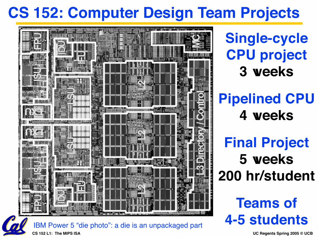
CS 152: Computer Design Team Projects
supp
orts
a 1
.875
-Mby
te o
n-ch
ip L
2 ca
che.
Pow
er4
and
Pow
er4+
sys
tem
s bo
th h
ave
32-
Mby
te L
3 ca
ches
, whe
reas
Pow
er5
syst
ems
have
a 3
6-M
byte
L3
cach
e.T
he L
3 ca
che
oper
ates
as a
bac
kdoo
r with
sepa
rate
bus
es fo
r rea
ds a
nd w
rites
that
ope
r-at
e at
hal
f pr
oces
sor
spee
d. I
n Po
wer
4 an
dPo
wer
4+ sy
stem
s, th
e L3
was
an
inlin
e ca
che
for
data
ret
riev
ed fr
om m
emor
y. B
ecau
se o
fth
e hi
gher
tran
sisto
r de
nsity
of t
he P
ower
5’s
130-
nm te
chno
logy
, we c
ould
mov
e the
mem
-or
y co
ntro
ller
on c
hip
and
elim
inat
e a
chip
prev
ious
ly n
eede
d fo
r the
mem
ory
cont
rolle
rfu
nctio
n. T
hese
two
chan
ges
in th
e Po
wer
5al
so h
ave t
he si
gnifi
cant
side
ben
efits
of r
educ
-in
g la
tenc
y to
the
L3 c
ache
and
mai
n m
emo-
ry, a
s w
ell a
s re
duci
ng t
he n
umbe
r of
chi
psne
cess
ary
to b
uild
a sy
stem
.
Chip
overv
iewFi
gure
2 s
how
s th
e Po
wer
5 ch
ip,
whi
chIB
M f
abri
cate
s us
ing
silic
on-o
n-in
sula
tor
(SO
I) d
evic
es a
nd c
oppe
r int
erco
nnec
t. SO
Ite
chno
logy
red
uces
dev
ice
capa
cita
nce
toin
crea
se t
rans
isto
r pe
rfor
man
ce.5
Cop
per
inte
rcon
nect
dec
reas
es w
ire
resi
stan
ce a
ndre
duce
s de
lays
in w
ire-d
omin
ated
chi
p-tim
-
ing
path
s. I
n 13
0 nm
lith
ogra
phy,
the
chi
pus
es ei
ght m
etal
leve
ls an
d m
easu
res 3
89 m
m2 .
The
Pow
er5
proc
esso
r su
ppor
ts th
e 64
-bit
Pow
erPC
arc
hite
ctur
e. A
sin
gle
die
cont
ains
two
iden
tical
pro
cess
or co
res,
each
supp
ortin
gtw
o lo
gica
l thr
eads
. Thi
s ar
chite
ctur
e m
akes
the c
hip
appe
ar as
a fo
ur-w
ay sy
mm
etric
mul
-tip
roce
ssor
to th
e op
erat
ing
syst
em. T
he tw
oco
res s
hare
a 1
.875
-Mby
te (1
,920
-Kby
te) L
2ca
che.
We i
mpl
emen
ted
the L
2 ca
che a
s thr
eeid
entic
al s
lices
with
sep
arat
e co
ntro
llers
for
each
. The
L2
slice
s are
10-
way
set-
asso
ciat
ive
with
512
cong
ruen
ce cl
asse
s of 1
28-b
yte l
ines
.T
he d
ata’s
rea
l add
ress
det
erm
ines
whi
ch L
2sli
ce th
e dat
a is c
ache
d in
. Eith
er p
roce
ssor
core
can
inde
pend
ently
acc
ess e
ach
L2 c
ontr
olle
r.W
e al
so in
tegr
ated
the
dire
ctor
y fo
r an
off-
chip
36-
Mby
te L
3 ca
che o
n th
e Pow
er5
chip
.H
avin
g th
e L3
cach
e dire
ctor
y on
chip
allo
ws
the
proc
esso
r to
che
ck th
e di
rect
ory
afte
r an
L2 m
iss w
ithou
t exp
erie
ncin
g of
f-ch
ip d
elay
s.To
red
uce
mem
ory
late
ncie
s, w
e in
tegr
ated
the m
emor
y co
ntro
ller o
n th
e chi
p. T
his e
lim-
inat
es d
rive
r an
d re
ceiv
er d
elay
s to
an
exte
r-na
l con
trol
ler.
Proce
ssor c
oreW
e de
signe
d th
e Po
wer
5 pr
oces
sor c
ore
tosu
ppor
t bo
th e
nhan
ced
SMT
and
sin
gle-
thre
aded
(ST
) op
erat
ion
mod
es.
Figu
re 3
show
s th
e Po
wer
5’s
inst
ruct
ion
pipe
line,
whi
ch is
iden
tical
to th
e Pow
er4’
s. A
ll pi
pelin
ela
tenc
ies i
n th
e Pow
er5,
incl
udin
g th
e bra
nch
misp
redi
ctio
n pe
nalty
and
load
-to-
use
late
n-cy
with
an
L1 d
ata
cach
e hi
t, ar
e th
e sa
me
asin
the
Pow
er4.
The
iden
tical
pip
elin
e st
ruc-
ture
lets
opt
imiz
atio
ns d
esig
ned
for
Pow
er4-
base
d sy
stem
s pe
rfor
m
equa
lly
wel
l on
Pow
er5-
base
d sy
stem
s. F
igur
e 4
show
s th
ePo
wer
5’s i
nstr
uctio
n flo
w d
iagr
am.
In S
MT
mod
e, th
e Po
wer
5 us
es tw
o se
pa-
rate
inst
ruct
ion
fetc
h ad
dres
s reg
ister
s to
stor
eth
e pr
ogra
m c
ount
ers
for
the
two
thre
ads.
Inst
ruct
ion
fetc
hes
(IF
stag
e)
alte
rnat
ebe
twee
n th
e tw
o th
read
s. I
n ST
mod
e, t
hePo
wer
5 us
es o
nly
one
prog
ram
cou
nter
and
can
fetc
h in
stru
ctio
ns fo
r th
at t
hrea
d ev
ery
cycl
e. I
t ca
n fe
tch
up t
o ei
ght
inst
ruct
ions
from
the
inst
ruct
ion
cach
e (I
C s
tage
) ev
ery
cycl
e. T
he tw
o th
read
s sh
are
the
inst
ruct
ion
cach
e an
d th
e in
stru
ctio
n tr
ansla
tion
faci
lity.
In a
give
n cy
cle,
all f
etch
ed in
stru
ctio
ns co
me
from
the
sam
e th
read
.
42
HOT
CHIP
S15
IEEE M
ICRO
Figu
re 2
. Pow
er5
chip
(FXU
= fi
xed-
poin
t exe
cutio
n un
it, IS
U=
inst
ruct
ion
sequ
enci
ng u
nit,
IDU
= in
stru
ctio
n de
code
uni
t,LS
U =
load
/sto
re u
nit,
IFU
= in
stru
ctio
n fe
tch
unit,
FPU
=flo
atin
g-po
int u
nit,
and
MC
= m
emor
y co
ntro
ller).
IBM Power 5 “die photo”: a die is an unpackaged part
Teams of4-5 students
Single-cycle CPU project
3 weeks
Pipelined CPU4 weeks
Final Project5 weeks
200 hr/student
UC Regents Spring 2005 © UCBCS 152 L1: The MIPS ISA
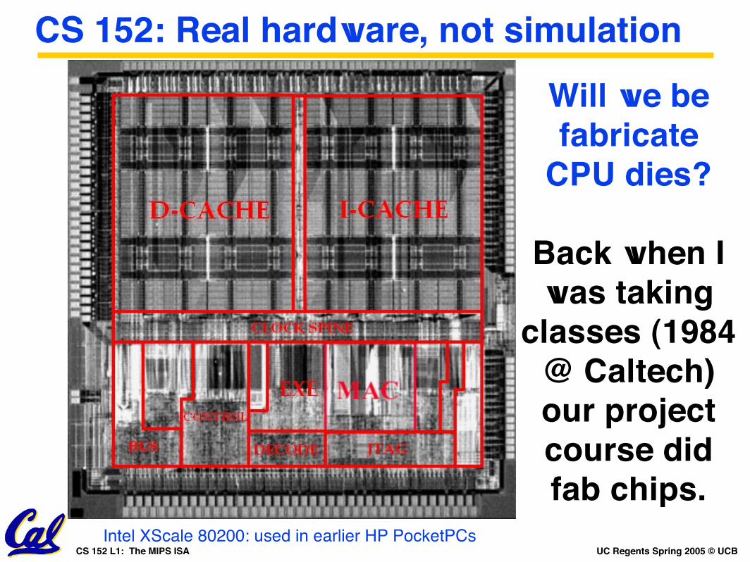
CS 152: Real hardware, not simulation
Intel XScale 80200: used in earlier HP PocketPCs
Will we be fabricate
CPU dies?
Back when I was taking
classes (1984 @ Caltech)our project course did fab chips.
UC Regents Spring 2005 © UCBCS 152 L1: The MIPS ISA
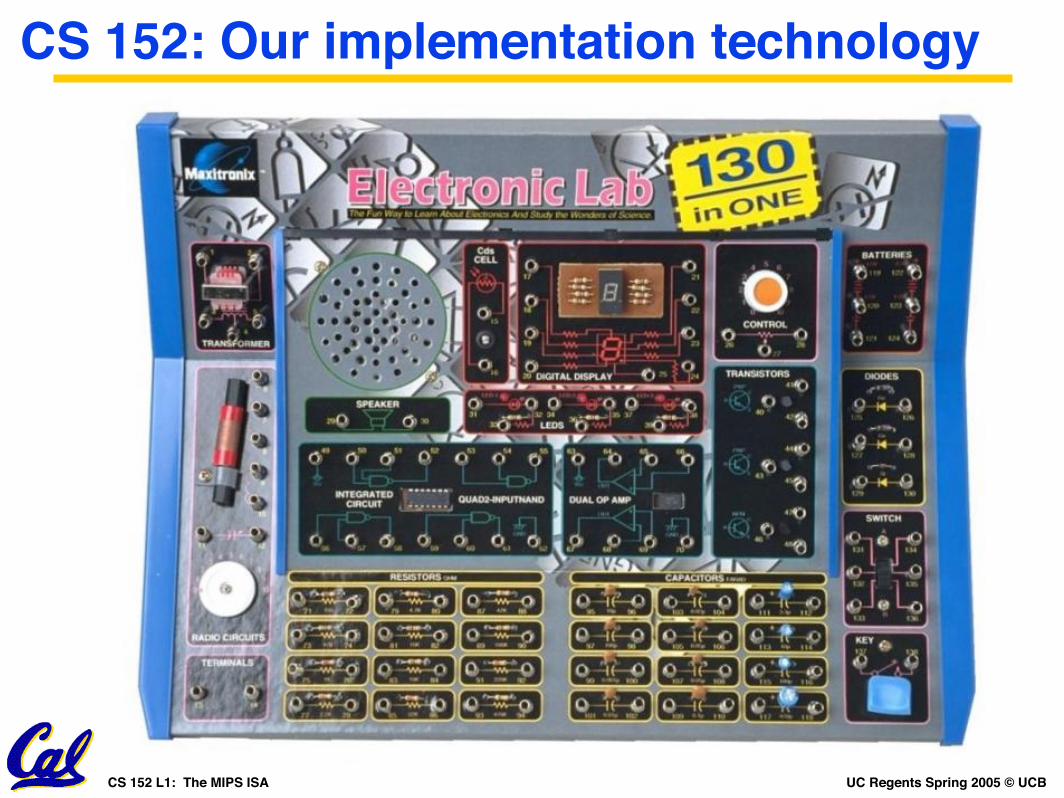
CS 152: Our implementation technology
UC Regents Spring 2005 © UCBCS 152 L1: The MIPS ISA
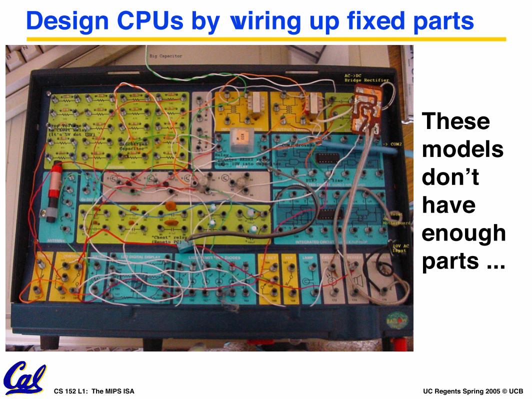
Design CPUs by wiring up fixed parts
Thesemodelsdon’thaveenoughparts ...
UC Regents Spring 2005 © UCBCS 152 L1: The MIPS ISA
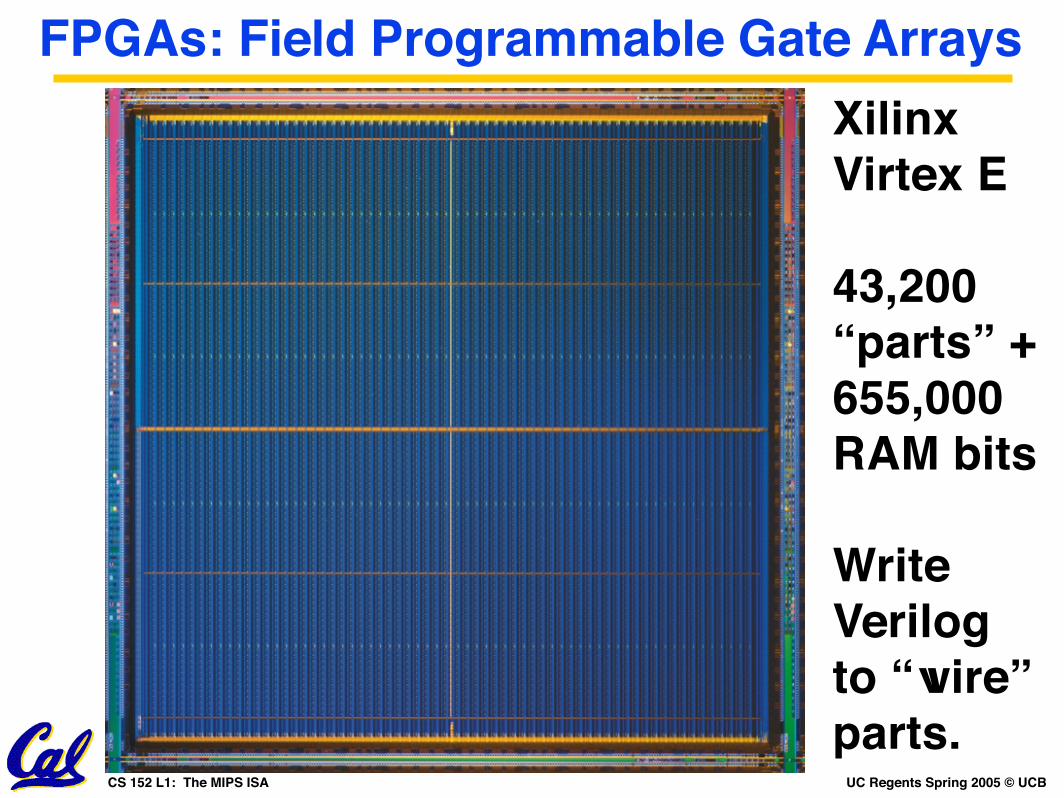
XilinxVirtex E
43,200“parts” +655,000RAM bits
WriteVerilog to “wire”parts.
FPGAs: Field Programmable Gate Arrays
UC Regents Spring 2005 © UCBCS 152 L1: The MIPS ISA
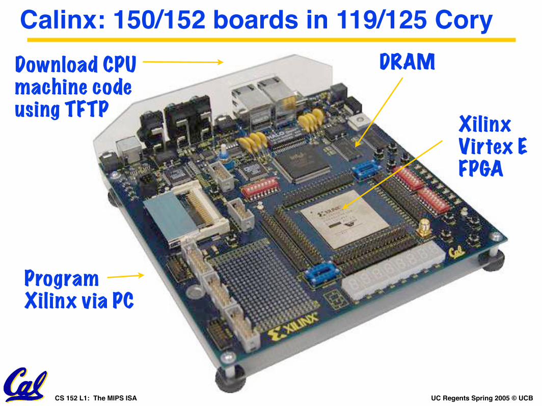
Calinx: 150/152 boards in 119/125 Cory
XilinxVirtex E FPGA
DRAM
Program Xilinx via PC
Download CPU machine code using TFTP
UC Regents Spring 2005 © UCBCS 152 L1: The MIPS ISA
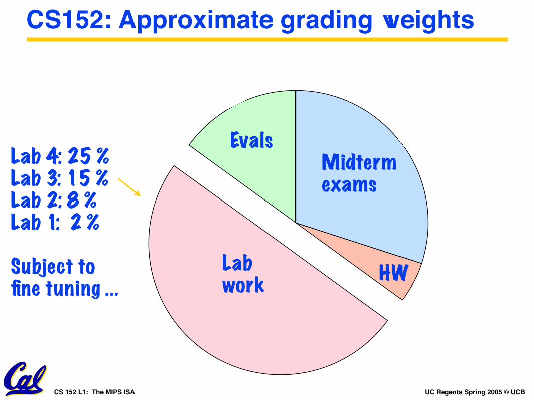
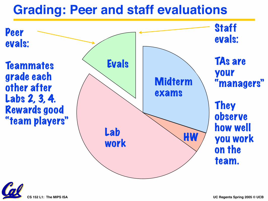
CS152: Approximate grading weights
Lab work
Midterm exams
HW
EvalsLab 4: 25 %Lab 3: 15 %Lab 2: 8 %Lab 1: 2 %
Subject tofine tuning ...
UC Regents Spring 2005 © UCBCS 152 L1: The MIPS ISA
Grading: Peer and staff evaluations
Lab work
Midterm exams
HW
Evals
Peer evals:
Teammatesgrade eachother afterLabs 2, 3, 4.Rewards good“team players”
Staffevals:
TAs areyour“managers”
They observehow wellyou workon the team.
UC Regents Spring 2005 © UCBCS 152 L1: The MIPS ISA
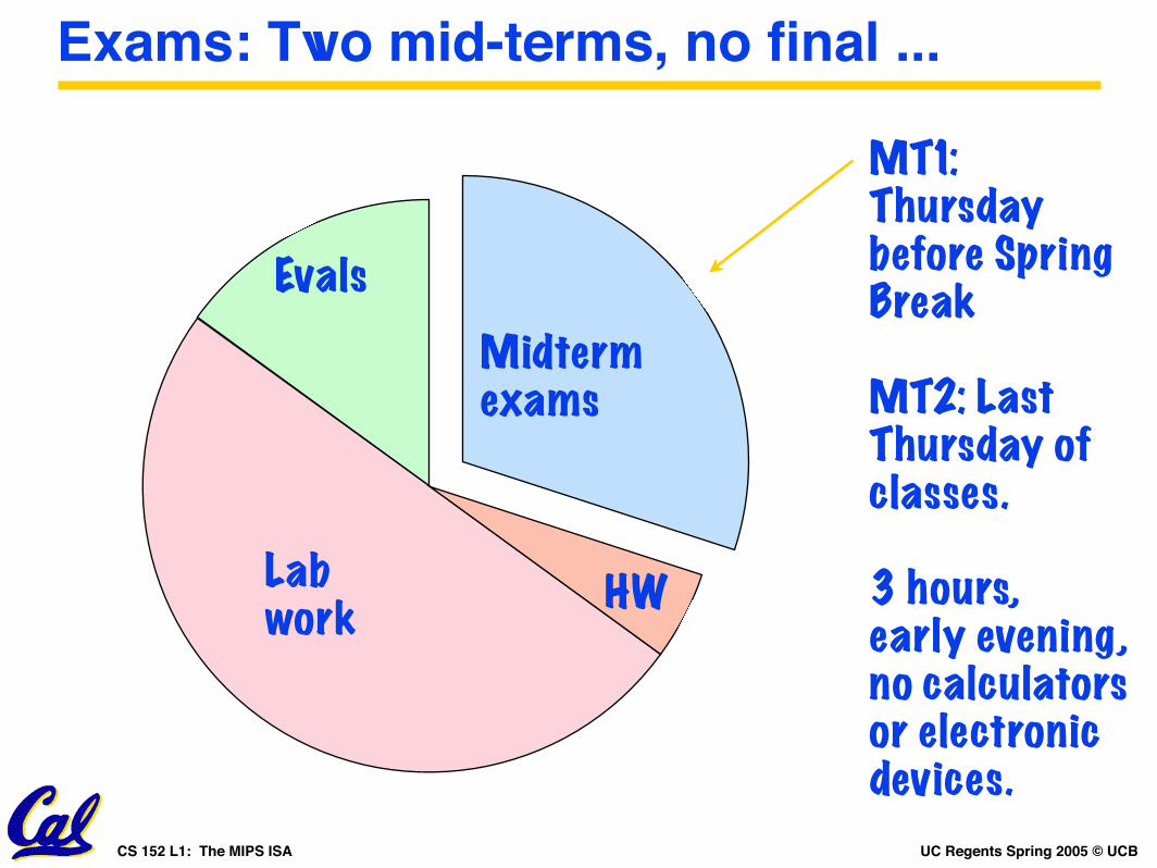
Exams: Two mid-terms, no final ...
Lab work
Midterm exams
HW
Evals
MT1: Thursdaybefore Spring Break
MT2: Last Thursday of classes.
3 hours,early evening,no calculatorsor electronicdevices.
UC Regents Spring 2005 © UCBCS 152 L1: The MIPS ISA
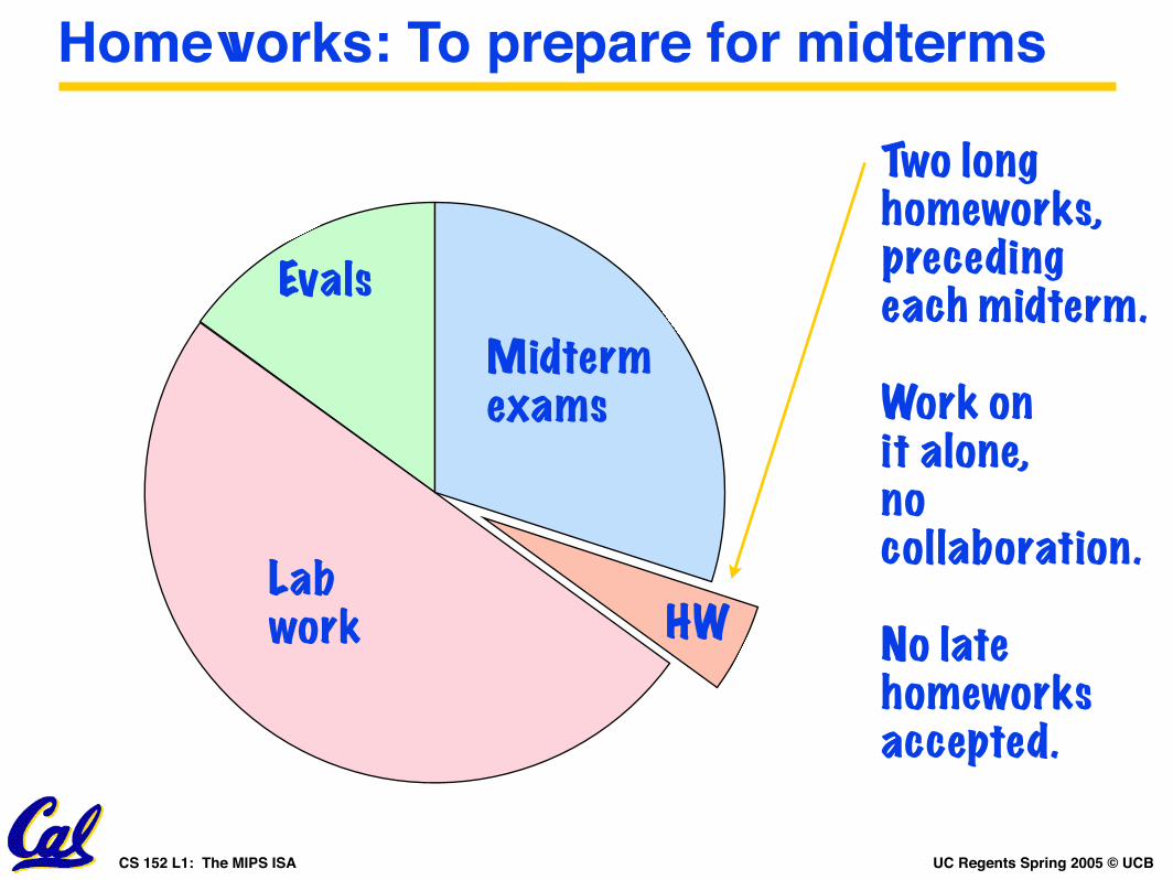
Homeworks: To prepare for midterms
Lab work
Midterm exams
HW
Evals
Two longhomeworks,preceding each midterm.
Work onit alone,no collaboration.
No latehomeworksaccepted.

UC Regents Spring 2005 © UCBCS 152 L1: The MIPS ISA
152: Semester Calendar
www-inst.eecs.berkeley.edu/~cs152/
See the class webpage for the most up to date version! Changes daily!
Also read our Usenet newsgroup: ucb.class.cs152
UC Regents Spring 2005 © UCBCS 152 L1: The MIPS ISA
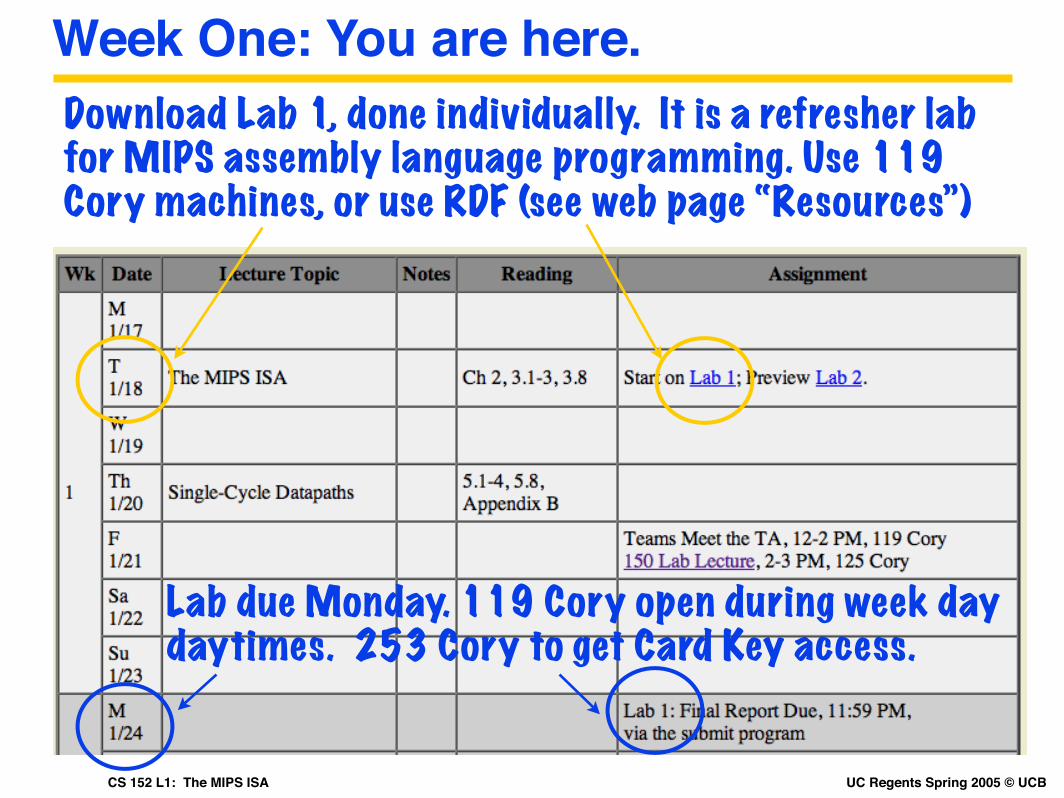
Week One: You are here.
Lab due Monday. 119 Cory open during week day daytimes. 253 Cory to get Card Key access.
Download Lab 1, done individually. It is a refresher lab for MIPS assembly language programming. Use 119 Cory machines, or use RDF (see web page “Resources”)
UC Regents Spring 2005 © UCBCS 152 L1: The MIPS ISA
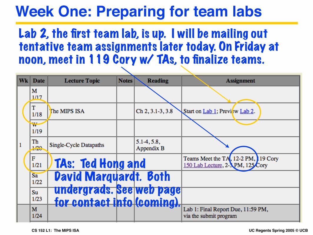
Week One: Preparing for team labsLab 2, the first team lab, is up. I will be mailing out tentative team assignments later today. On Friday at noon, meet in 119 Cory w/ TAs, to finalize teams.
TAs: Ted Hong andDavid Marquardt. Bothundergrads. See web pagefor contact info (coming).
UC Regents Spring 2005 © UCBCS 152 L1: The MIPS ISA
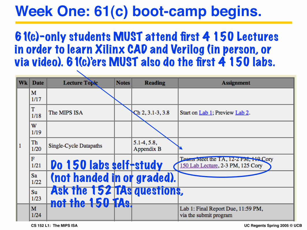
Week One: 61(c) boot-camp begins.61(c)-only students MUST attend first 4 150 Lectures in order to learn Xilinx CAD and Verilog (in person, or via video). 61(c)’ers MUST also do the first 4 150 labs.
Do 150 labs self-study(not handed in or graded).Ask the 152 TAs questions,not the 150 TAs.
UC Regents Spring 2005 © UCBCS 152 L1: The MIPS ISA
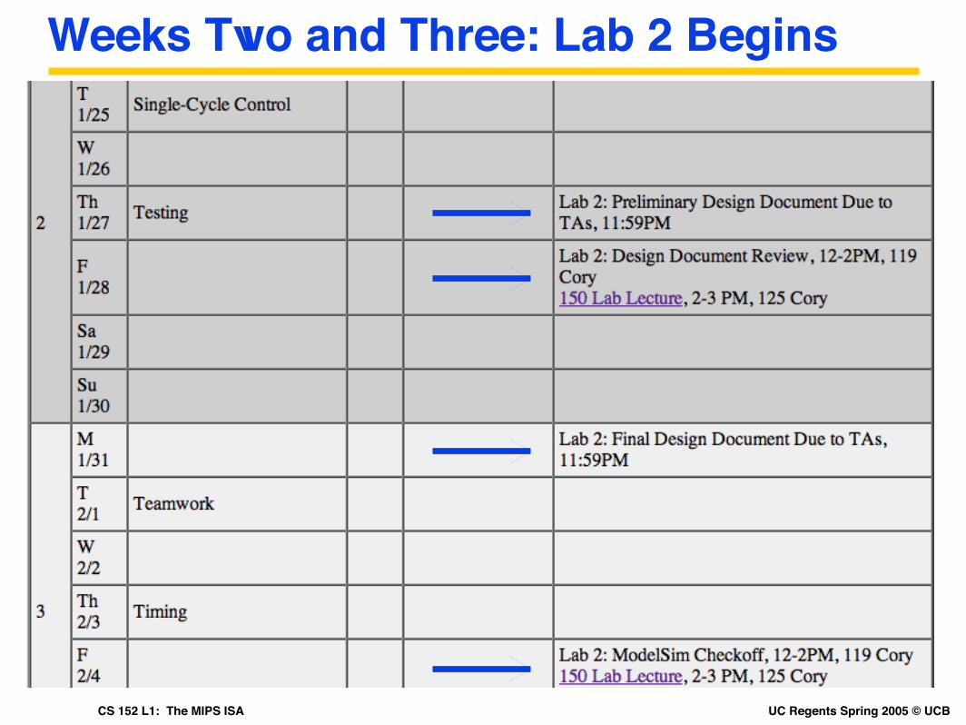
Weeks Two and Three: Lab 2 Begins
UC Regents Spring 2005 © UCBCS 152 L1: The MIPS ISA
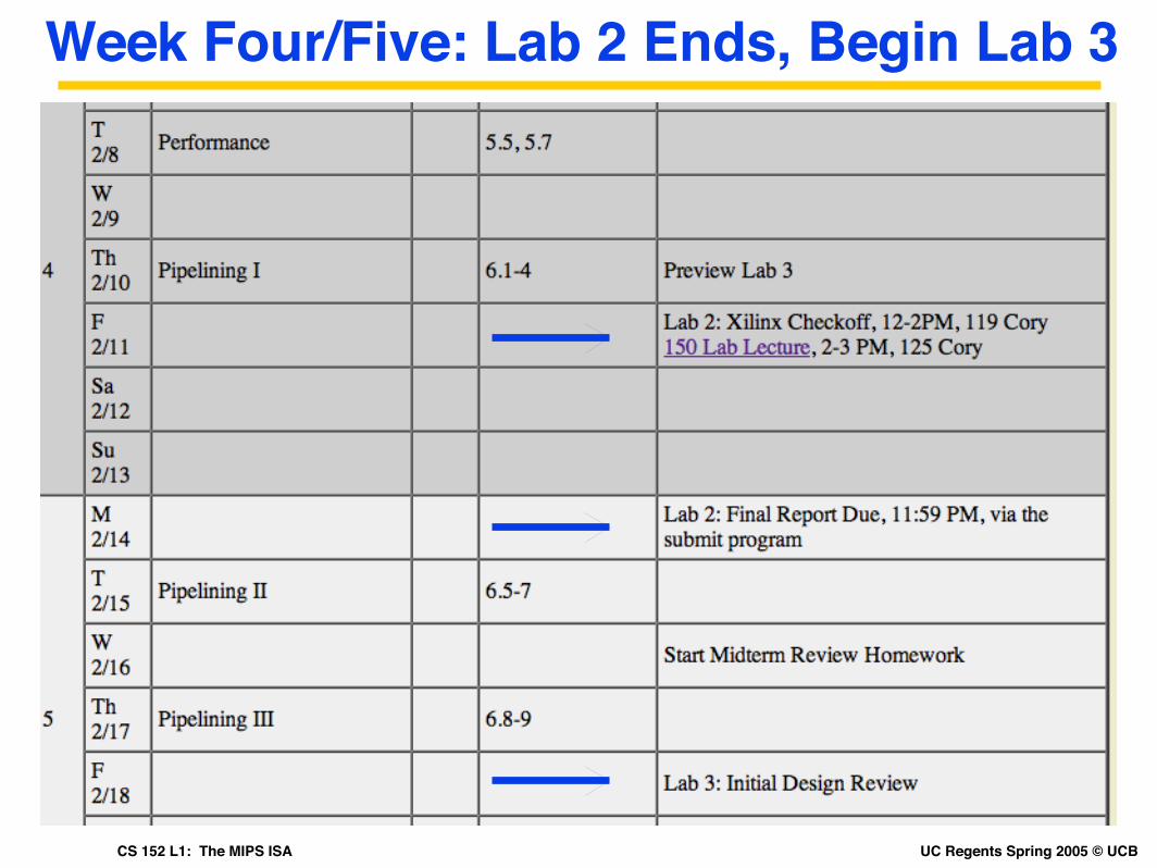
Week Four/Five: Lab 2 Ends, Begin Lab 3
UC Regents Spring 2005 © UCBCS 152 L1: The MIPS ISA
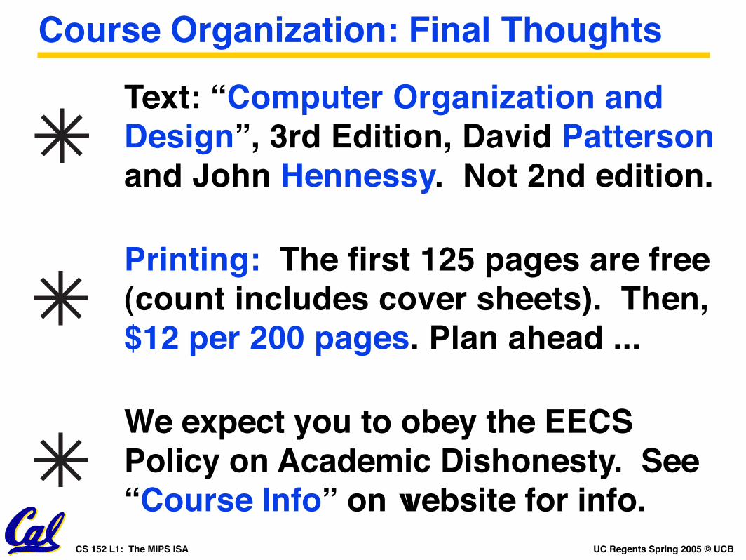
Course Organization: Final Thoughts
Text: “Computer Organization and Design”, 3rd Edition, David Patterson and John Hennessy. Not 2nd edition.
We expect you to obey the EECS Policy on Academic Dishonesty. See “Course Info” on website for info.
Printing: The first 125 pages are free (count includes cover sheets). Then,$12 per 200 pages. Plan ahead ...
UC Regents Spring 2005 © UCBCS 152 L1: The MIPS ISA
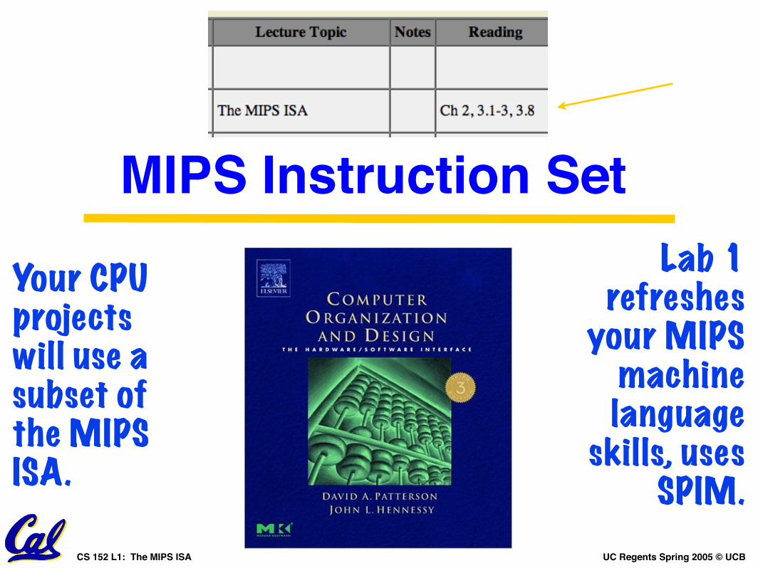
MIPS Instruction Set
Your CPU projects will use a subset of the MIPS ISA.
Lab 1 refreshes
your MIPS machine language
skills, uses SPIM.
UC Regents Spring 2005 © UCBCS 152 L1: The MIPS ISA
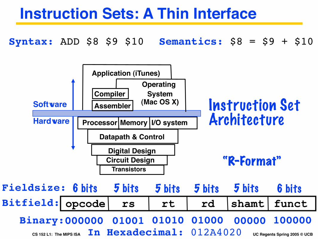
Instruction Sets: A Thin Interface
Instruction Set ArchitectureI/O systemProcessor
Digital DesignCircuit Design
Datapath & Control
Transistors
MemoryHardware
CompilerOperating
System(Mac OS X)
Application (iTunes)
Software Assembler
Syntax: ADD $8 $9 $10 Semantics: $8 = $9 + $10
In Hexadecimal: 012A4020000000 01001 01010 01000 00000 100000Binary:
6 bits 5 bits 5 bits 5 bits 5 bits 6 bitsFieldsize:opcode rs rt rd functshamtBitfield:
“R-Format”
UC Regents Spring 2005 © UCBCS 152 L1: The MIPS ISA
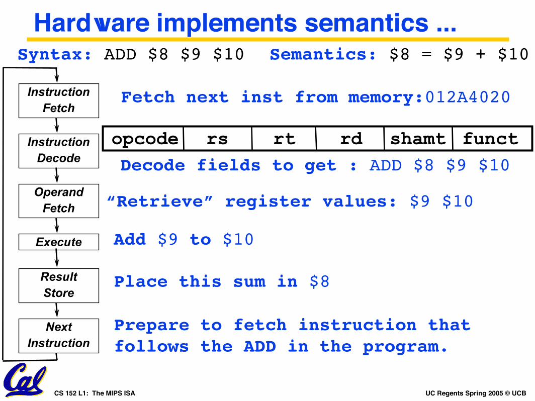
Hardware implements semantics ...
InstructionFetch
InstructionDecode
OperandFetch
Execute
ResultStore
NextInstruction
Fetch next inst from memory:012A4020
opcode rs rt rd functshamtDecode fields to get : ADD $8 $9 $10
“Retrieve” register values: $9 $10
Add $9 to $10
Place this sum in $8
Prepare to fetch instruction that follows the ADD in the program.
Syntax: ADD $8 $9 $10 Semantics: $8 = $9 + $10
UC Regents Spring 2005 © UCBCS 152 L1: The MIPS ISA
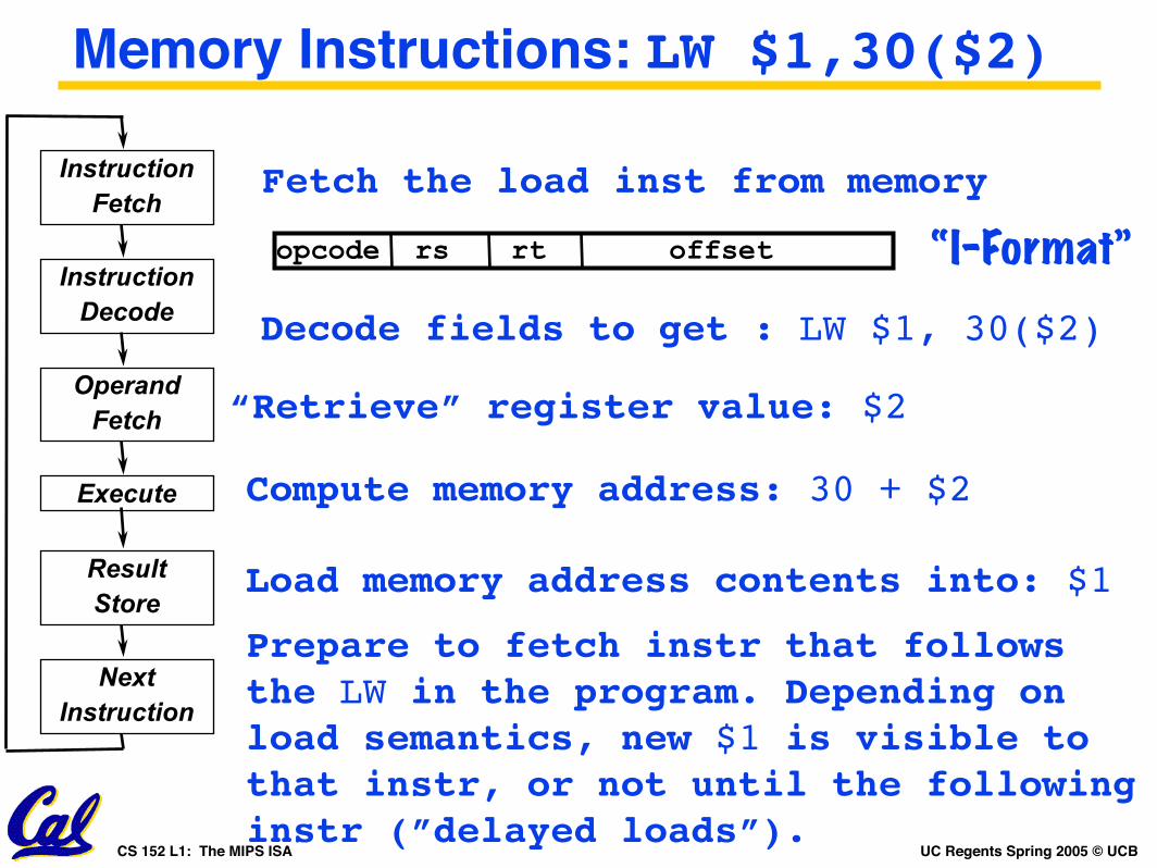
Memory Instructions: LW $1,30($2)
InstructionFetch
InstructionDecode
OperandFetch
Execute
ResultStore
NextInstruction
Fetch the load inst from memory
“Retrieve” register value: $2
Compute memory address: 30 + $2
Load memory address contents into: $1
Prepare to fetch instr that follows the LW in the program. Depending on load semantics, new $1 is visible to that instr, or not until the following instr (”delayed loads”).
Decode fields to get : LW $1, 30($2)
opcode rs rt offset “I-Format”
UC Regents Spring 2005 © UCBCS 152 L1: The MIPS ISA
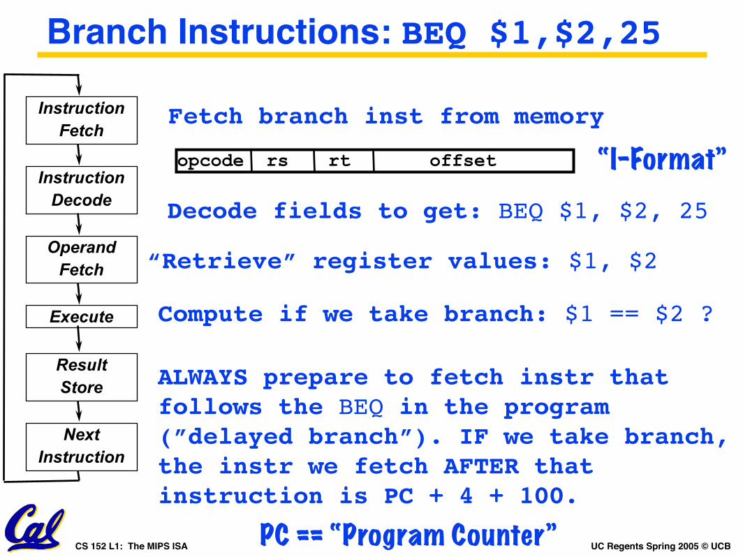
Branch Instructions: BEQ $1,$2,25
InstructionFetch
InstructionDecode
OperandFetch
Execute
ResultStore
NextInstruction
Fetch branch inst from memory
“Retrieve” register values: $1, $2
Compute if we take branch: $1 == $2 ?
Decode fields to get: BEQ $1, $2, 25
opcode rs rt offset “I-Format”
ALWAYS prepare to fetch instr that follows the BEQ in the program (”delayed branch”). IF we take branch, the instr we fetch AFTER that instruction is PC + 4 + 100.
PC == “Program Counter”
UC Regents Spring 2005 © UCBCS 152 L1: The MIPS ISA
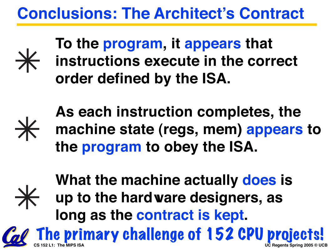
Conclusions: The Architect’s Contract
To the program, it appears that instructions execute in the correct order defined by the ISA.
What the machine actually does is up to the hardware designers, as long as the contract is kept.
As each instruction completes, themachine state (regs, mem) appears to the program to obey the ISA.
The primary challenge of 152 CPU projects!
UC Regents Spring 2005 © UCBCS 152 L1: The MIPS ISA
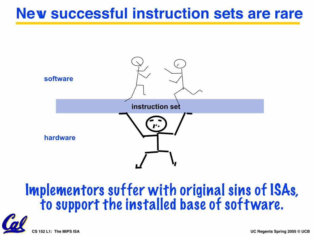
New successful instruction sets are rare
instruction set
software
hardware
Implementors suffer with original sins of ISAs, to support the installed base of software.