Embed Size (px)
Citation preview
1
CS 61C: Great Ideas in Computer Architecture
Lecture 9: Synchronous Digital Systems
Instructor: Sagar [email protected]
http://inst.eecs.berkeley.edu/~cs61c
2
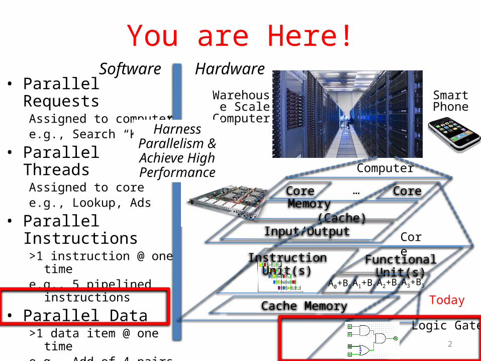
• Parallel RequestsAssigned to computere.g., Search “Katz”
• Parallel ThreadsAssigned to coree.g., Lookup, Ads
• Parallel Instructions>1 instruction @ one timee.g., 5 pipelined instructions
• Parallel Data>1 data item @ one timee.g., Add of 4 pairs of words
• Hardware descriptionsAll gates @ one time
• Programming Languages
SmartPhone
Warehouse Scale
Computer
Software Hardware
HarnessParallelism &Achieve HighPerformance
Logic Gates
Core Core…
Memory (Cache)
Input/Output
Computer
Cache Memory
Core
Instruction Unit(s) FunctionalUnit(s)
A3+B3A2+B2A1+B1A0+B0
Today
You are Here!
Levels of Representation/Interpretation
lw $t0, 0($2)lw $t1, 4($2)sw $t1, 0($2)sw $t0, 4($2)
High Level LanguageProgram (e.g., C)
Assembly Language Program (e.g., MIPS)
Machine Language Program (MIPS)
Hardware Architecture Description(e.g., block diagrams)
Compiler
Assembler
Machine Interpretation
temp = v[k];v[k] = v[k+1];v[k+1] = temp;
0000 1001 1100 0110 1010 1111 0101 10001010 1111 0101 1000 0000 1001 1100 0110 1100 0110 1010 1111 0101 1000 0000 1001 0101 1000 0000 1001 1100 0110 1010 1111
Logic Circuit Description(Circuit Schematic Diagrams)
Architecture Implementation
Anything can be representedas a number,
i.e., data or instructions
3
Hardware Design• Next several weeks: how a modern processor is built,
starting with basic elements as building blocks• Why study hardware design?
– Understand capabilities and limitations of HW in general and processors in particular
– What processors can do fast and what they can’t do fast (avoid slow things if you want your code to run fast!)
– Background for more in-depth HW courses (CS 150, CS 152)– Hard to know what you’ll need for next 30 years– There is only so much you can do with standard processors:
you may need to design own custom HW for extra performance– Even some commercial processors today have customizable hardware!
4
Synchronous Digital Systems
5
Synchronous:• All operations coordinated by a central clock
“Heartbeat” of the system!
Digital:• Represent all values by discrete values• Two binary digits: 1 and 0• Electrical signals are treated as 1’s and 0’s
• 1 and 0 are complements of each other• High /low voltage for true / false, 1 / 0
Hardware of a processor, such as the MIPS, is an example of a Synchronous Digital System
A Z
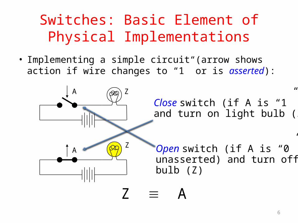
Switches: Basic Element of Physical Implementations
• Implementing a simple circuit (arrow shows action if wire changes to “1” or is asserted):
Z A
AZ
6
Close switch (if A is “1” or asserted)and turn on light bulb (Z)
Open switch (if A is “0” or unasserted) and turn off light bulb (Z)
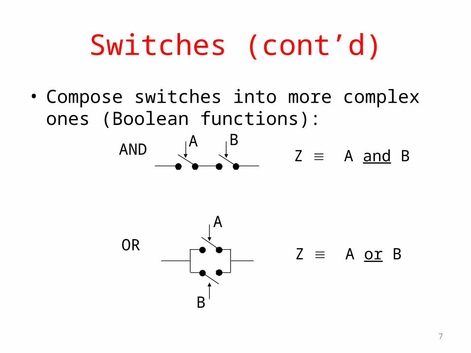
AND
OR
Z A and B
Z A or B
A B
A
B
Switches (cont’d)
• Compose switches into more complex ones (Boolean functions):
7
8
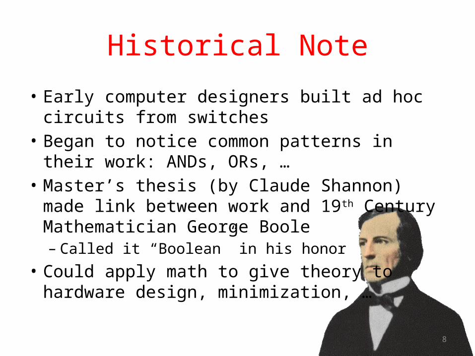
Historical Note
• Early computer designers built ad hoc circuits from switches
• Began to notice common patterns in their work: ANDs, ORs, …
• Master’s thesis (by Claude Shannon) made link between work and 19th Century Mathematician George Boole– Called it “Boolean” in his honor
• Could apply math to give theory to hardware design, minimization, …
9
Transistors
• High voltage (Vdd) represents 1, or true– In modern microprocessors, Vdd ~ 1.0 Volt
• Low voltage (0 Volt or Ground) represents 0, or false• Pick a midpoint voltage to decide if a 0 or a 1
– Voltage greater than midpoint = 1– Voltage less than midpoint = 0– This removes noise as signals propagate – a big advantage of
digital systems over analog systems
• If one switch can control another switch, we can build a computer!
• Our switches: CMOS transistors
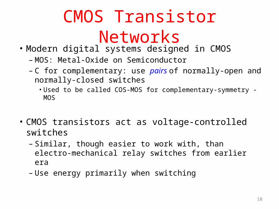
CMOS Transistor Networks• Modern digital systems designed in CMOS– MOS: Metal-Oxide on Semiconductor– C for complementary: use pairs of normally-open and
normally-closed switches• Used to be called COS-MOS for complementary-symmetry -
MOS
• CMOS transistors act as voltage-controlled switches– Similar, though easier to work with, than electro-
mechanical relay switches from earlier era – Use energy primarily when switching
10
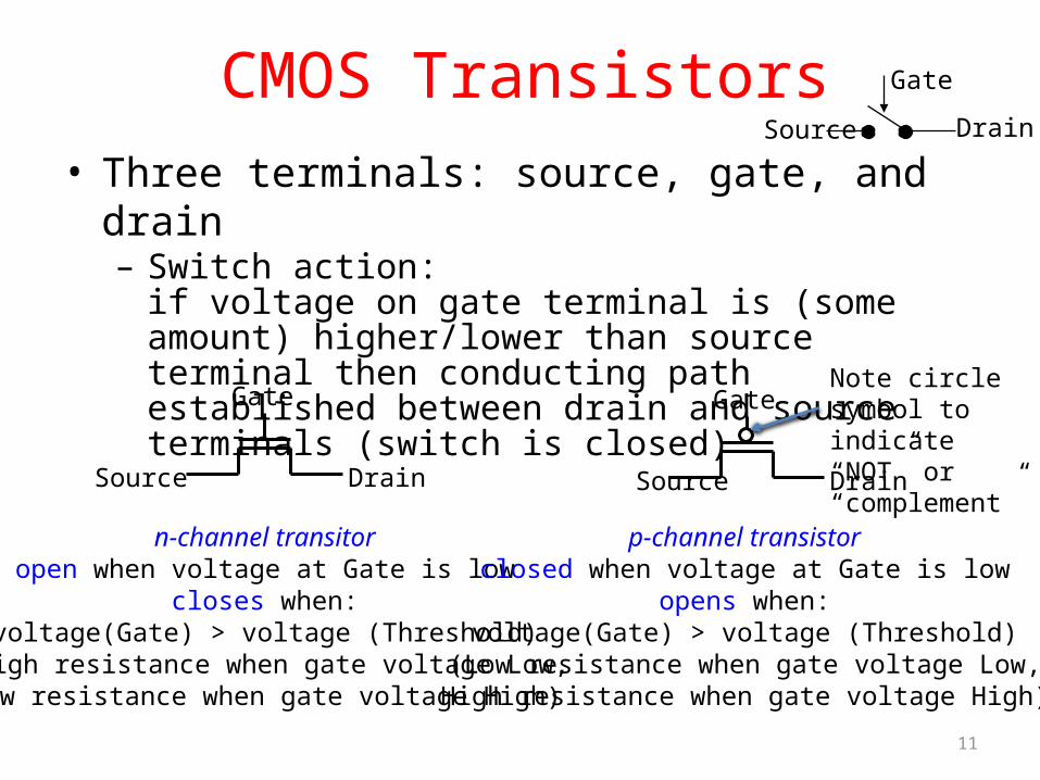
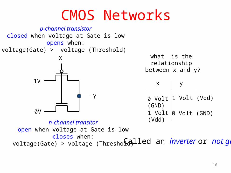
n-channel transitoropen when voltage at Gate is low
closes when:voltage(Gate) > voltage (Threshold)
(High resistance when gate voltage Low,Low resistance when gate voltage High)
p-channel transistorclosed when voltage at Gate is low
opens when:voltage(Gate) > voltage (Threshold)
(Low resistance when gate voltage Low,High resistance when gate voltage High)
CMOS Transistors• Three terminals: source, gate, and drain– Switch action:
if voltage on gate terminal is (some amount) higher/lower than source terminal then conducting path established between drain and source terminals (switch is closed)
Gate
Source Drain
Gate
Source Drain
11
Note circle symbol to indicate “NOT” or “complement”
Gate
DrainSource
12
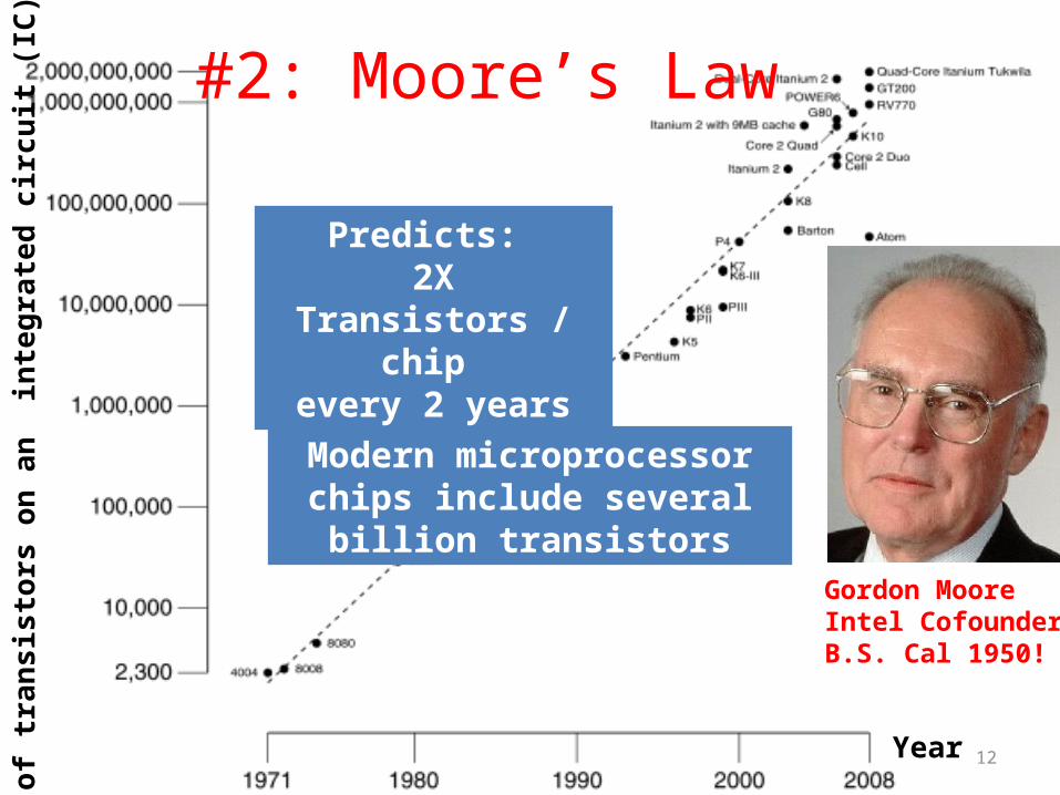
Gordon MooreIntel CofounderB.S. Cal 1950!#
of tr
ansi
stor
s on
an
inte
grat
ed c
ircui
t (IC
)
Year
#2: Moore’s Law
Predicts: 2X Transistors / chip
every 2 years
Modern microprocessor chips include several billion transistors
13
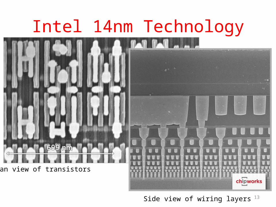
Intel 14nm Technology
Plan view of transistors
Side view of wiring layers
14
Scale of the Universe
http://htwins.net/scale2/
15
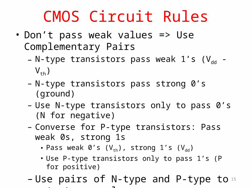
CMOS Circuit Rules• Don’t pass weak values => Use Complementary Pairs– N-type transistors pass weak 1’s (Vdd - Vth)– N-type transistors pass strong 0’s (ground)– Use N-type transistors only to pass 0’s (N for negative)– Converse for P-type transistors: Pass weak 0s, strong 1s
• Pass weak 0’s (Vth), strong 1’s (Vdd)• Use P-type transistors only to pass 1’s (P for positive)
– Use pairs of N-type and P-type to get strong values• Never leave a wire undriven– Make sure there’s always a path to Vdd or GND
• Never create a path from Vdd to GND (ground)– This would short-circuit the power supply!
1V
X
Y 0 Volt(GND)
x y
1 Volt(Vdd)
0V
what is the relationship
between x and y?
CMOS Networks
16
p-channel transistorclosed when voltage at Gate is low
opens when:voltage(Gate) > voltage (Threshold)
n-channel transitoropen when voltage at Gate is low
closes when:voltage(Gate) > voltage (Threshold) Called an inverter or not gate
1 Volt (Vdd)
0 Volt (GND)
what is the relationship between x, y and z?
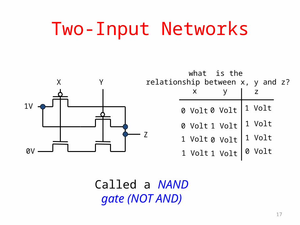
Two-Input Networks
1V
X Y
0V
Z
17
x y z
0 Volt
1 Volt
0 Volt
1 Volt
0 Volt
0 Volt
1 Volt
1 Volt
1 Volt
1 Volt
1 Volt
0 Volt
Called a NAND gate (NOT AND)
x y
0 Volt
1 Volt
0 Volt
1 Volt
0 Volt
0 Volt
1 Volt
1 Volt
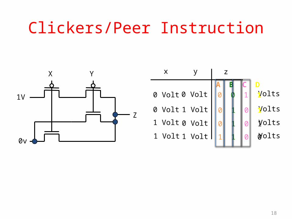
Clickers/Peer Instruction
1V
X Y
0v
Z
18
Volts
Volts
Volts
Volts
z
0 0 1 1
0 1 0 1
0 1 0 1
1 1 0 0
A B C D
19
Administrivia• HW2 out– We recommend doing this before the midterm
• Proj 2-1 out– Make sure you test your code on hive machines, that’s
where we’ll grade them– Team registration problems? Email Jay
20
Administrivia• Midterm this Thursday– In this room, at this time– One 8.5”x11” handwritten cheatsheet– We’ll provide a MIPS green sheet– No electronics– Covers up to and including last lecture (07/02)– TA-led review session tonight (07/06) from 5-8pm in HP
Auditorium
21
Break
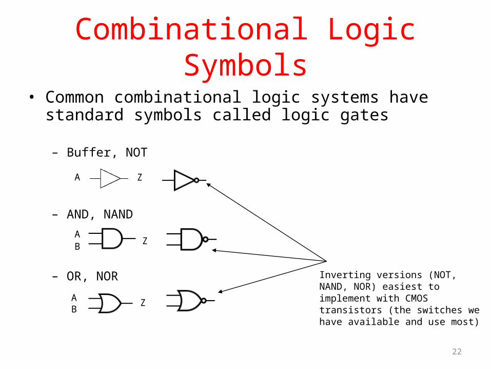
• Common combinational logic systems have standard symbols called logic gates
– Buffer, NOT
– AND, NAND
– OR, NOR
Combinational Logic Symbols
Z
AB Z
Z
A
AB
Inverting versions (NOT, NAND, NOR) easiest to implement with CMOS transistors (the switches we have available and use most)
22
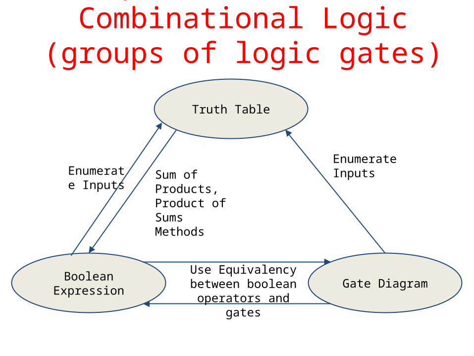
Representations of Combinational Logic (groups of logic gates)
Truth Table
Gate DiagramBoolean Expression
Sum of Products,Product of Sums Methods
Enumerate Inputs
Enumerate Inputs
Use Equivalency between boolean operators and
gates
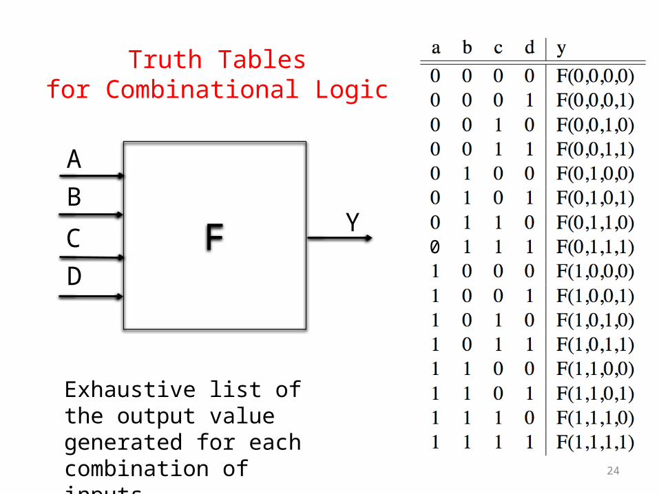
Truth Tablesfor Combinational Logic
24
F Y
AB
CD
0
Exhaustive list of the output value generated for each combination of inputs
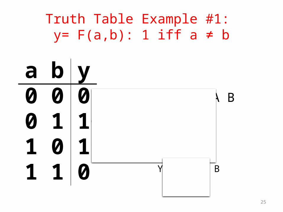
Truth Table Example #1: y= F(a,b): 1 iff a ≠ b
a b y0 0 00 1 11 0 11 1 0
25
Y = A B + A B
Y = A + B
XOR

Truth Table Example #2: 2-bit Adder
26
HowManyRows?
+ C1
A1A0
B1B0
C2
C0
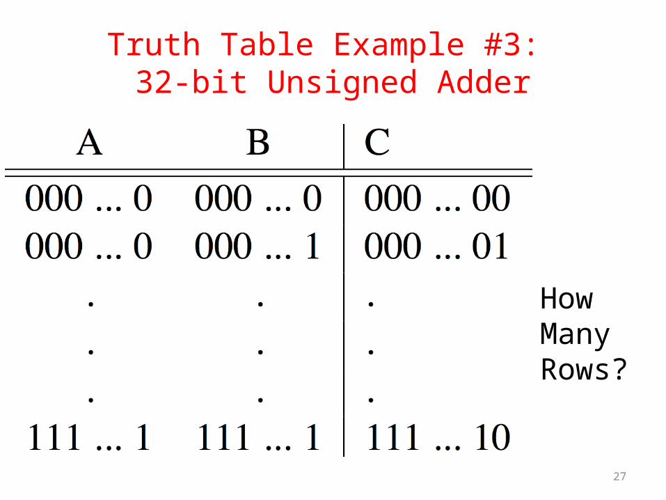
Truth Table Example #3: 32-bit Unsigned Adder
27
HowManyRows?
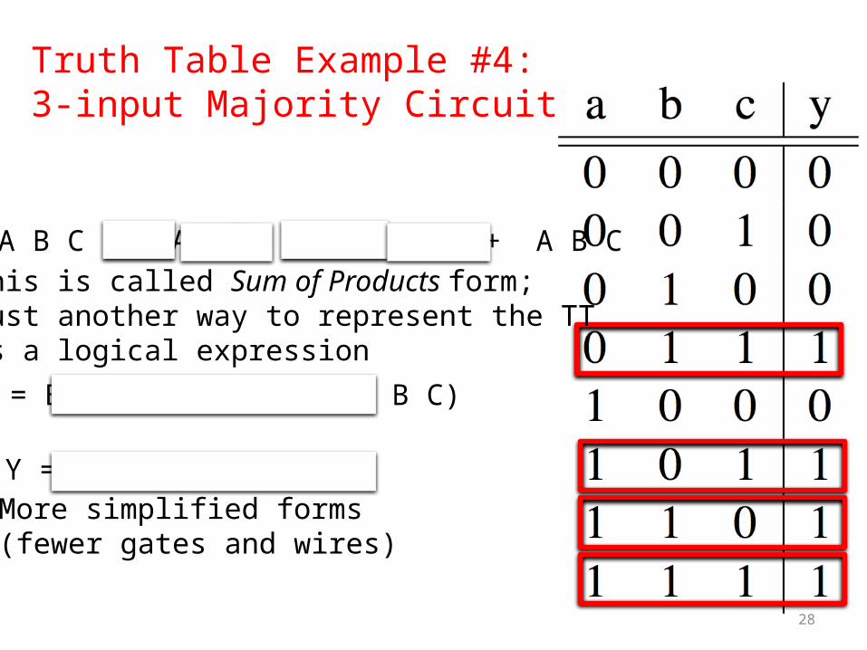
Truth Table Example #4: 3-input Majority Circuit
28
Y = A B C + A B C + A B C + A B C
Y = B C + A (B C + B C)
Y = B C + A (B + C)
This is called Sum of Products form;Just another way to represent the TTas a logical expression
More simplified forms (fewer gates and wires)
29
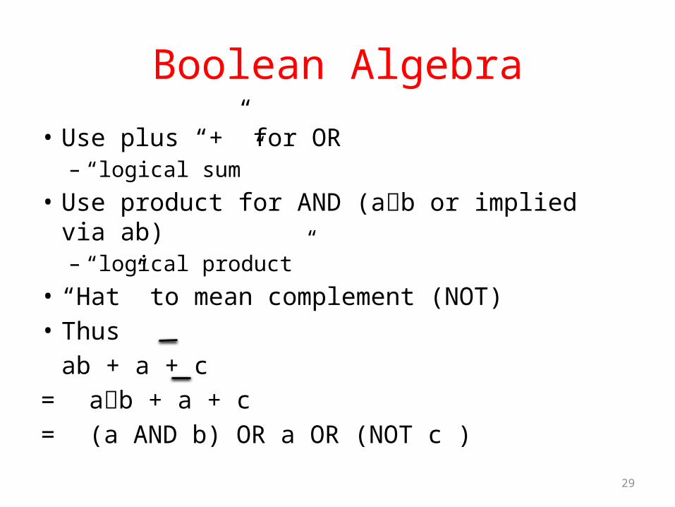
Boolean Algebra
• Use plus “+” for OR – “logical sum”
• Use product for AND (ab or implied via ab)– “logical product”
• “Hat” to mean complement (NOT) • Thus
ab + a + c = ab + a + c = (a AND b) OR a OR (NOT c )
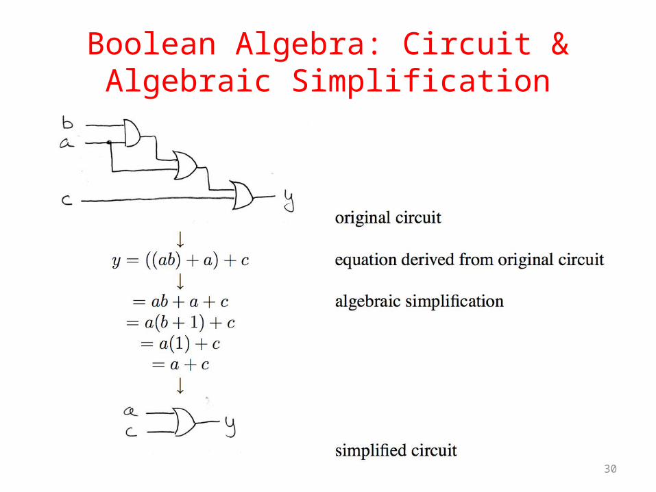
Boolean Algebra: Circuit & Algebraic Simplification
30
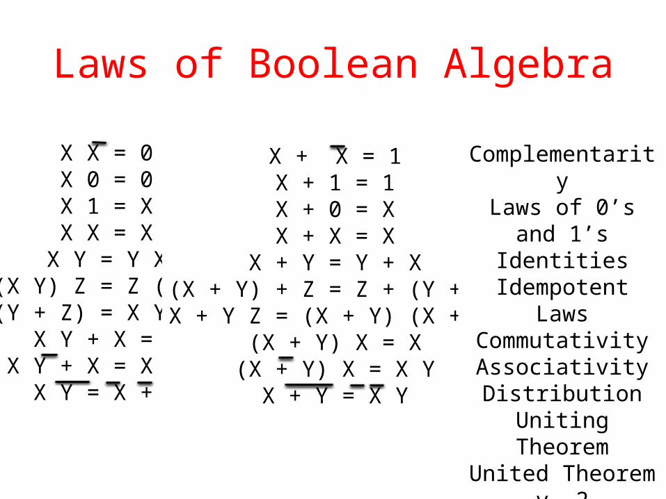
Laws of Boolean Algebra
31
X X = 0X 0 = 0X 1 = XX X = X
X Y = Y X(X Y) Z = Z (Y Z)
X (Y + Z) = X Y + X ZX Y + X = X
X Y + X = X + YX Y = X + Y
X + X = 1X + 1 = 1X + 0 = XX + X = X
X + Y = Y + X(X + Y) + Z = Z + (Y + Z)X + Y Z = (X + Y) (X + Z)
(X + Y) X = X(X + Y) X = X Y
X + Y = X Y
ComplementarityLaws of 0’s and 1’s
IdentitiesIdempotent Laws
CommutativityAssociativityDistribution
Uniting TheoremUnited Theorem v. 2
DeMorgan’s Law
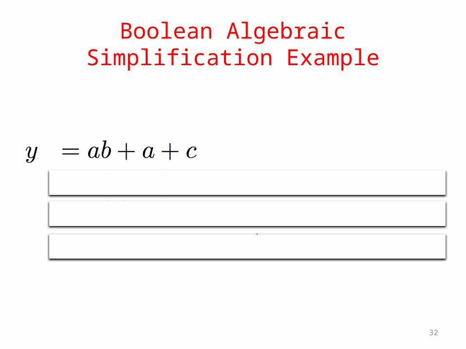
Boolean Algebraic Simplification Example
32
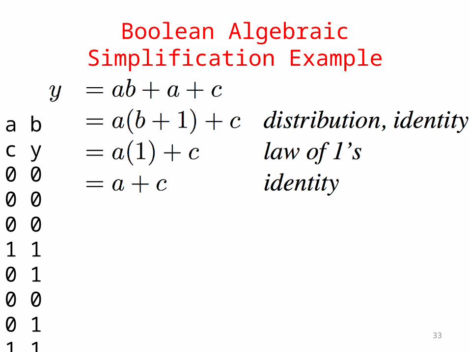
Boolean Algebraic Simplification Example
33
a b c y0 0 0 00 0 1 10 1 0 00 1 1 11 0 0 11 0 1 11 1 0 11 1 1 1
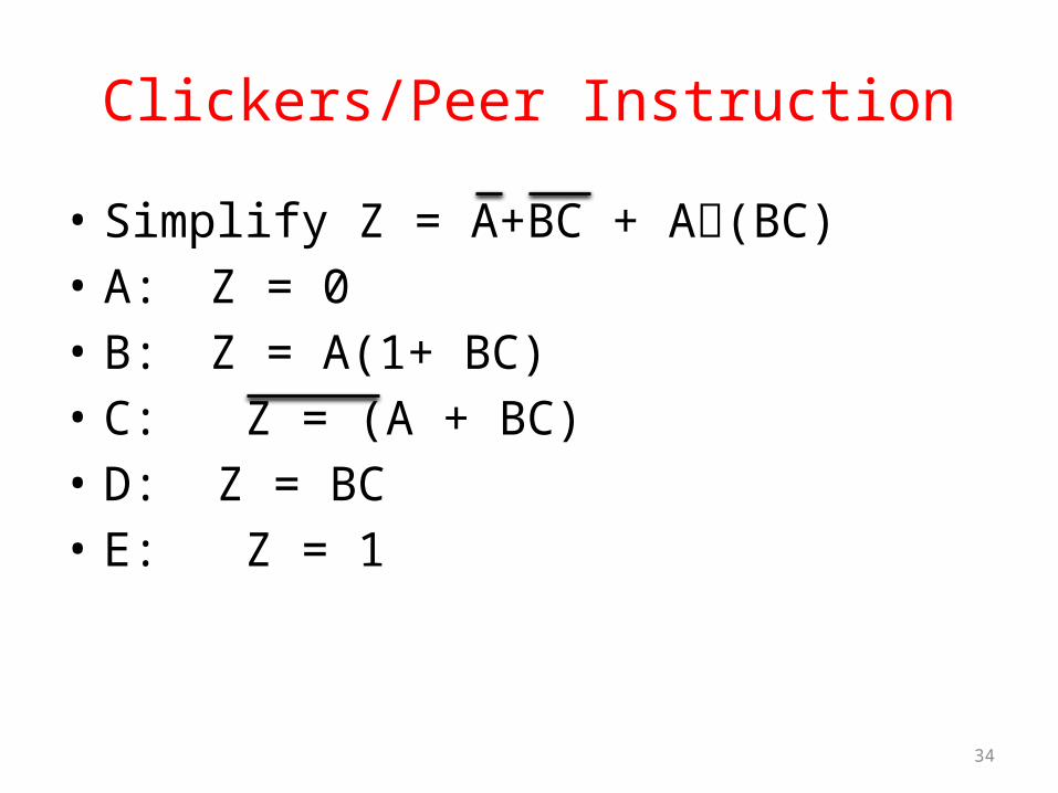
Clickers/Peer Instruction
• Simplify Z = A+BC + A(BC)• A: Z = 0• B: Z = A(1+ BC)• C: Z = (A + BC)• D: Z = BC• E: Z = 1
34
35
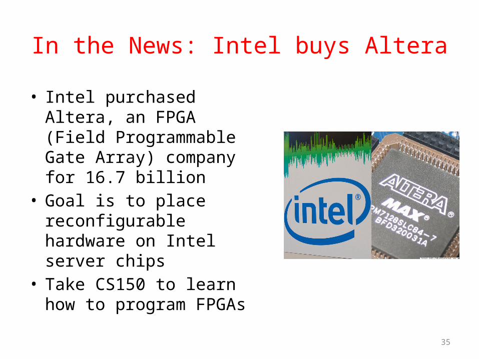
In the News: Intel buys Altera
• Intel purchased Altera, an FPGA (Field Programmable Gate Array) company for 16.7 billion
• Goal is to place reconfigurable hardware on Intel server chips
• Take CS150 to learn how to program FPGAs
36
Break
• (Maybe)
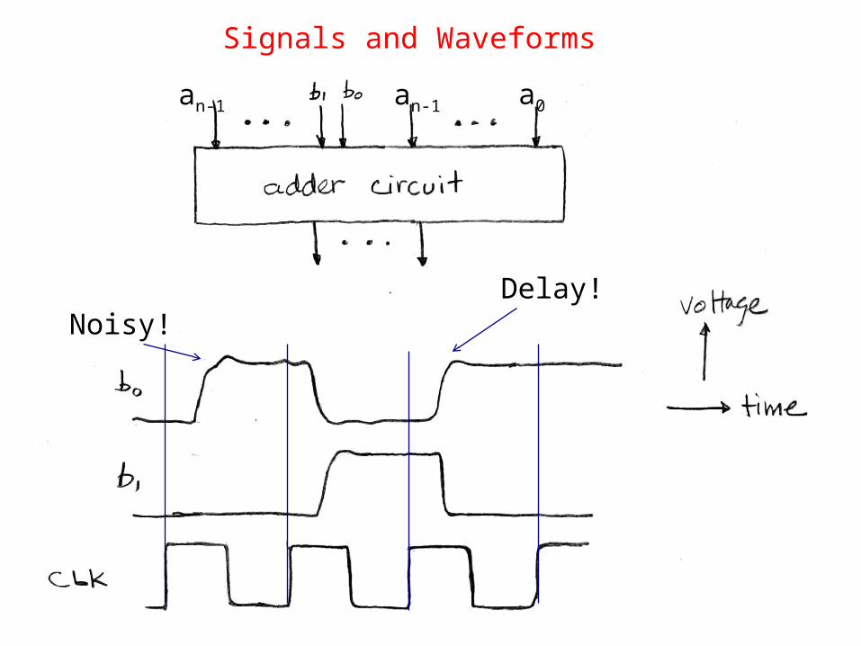
Signals and Waveforms
an-1 an-1 a0
Noisy!Delay!
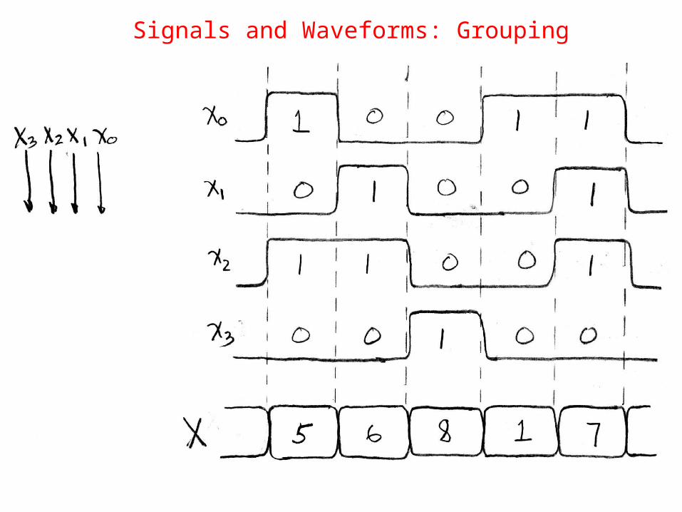
Signals and Waveforms: Grouping
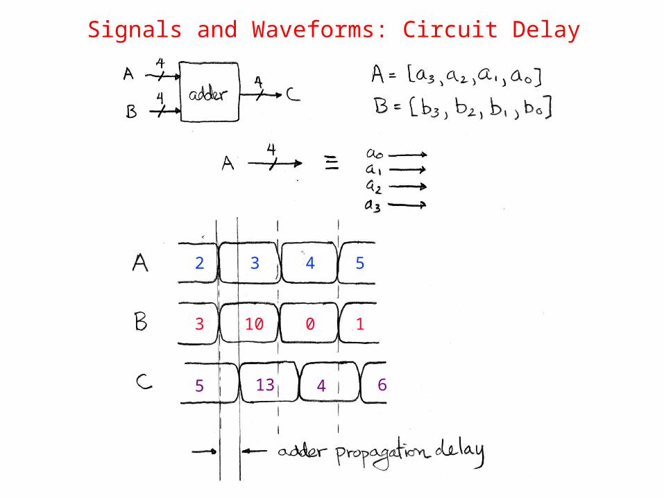
Signals and Waveforms: Circuit Delay
2
3
3 4 5
10 0 1
5 13 4 6

Sample Debugging Waveform
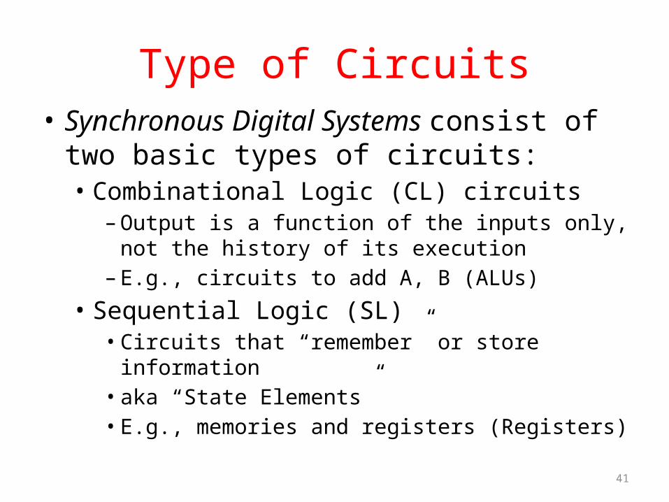
Type of Circuits• Synchronous Digital Systems consist of two
basic types of circuits:• Combinational Logic (CL) circuits–Output is a function of the inputs only, not the history
of its execution– E.g., circuits to add A, B (ALUs)
• Sequential Logic (SL)• Circuits that “remember” or store information• aka “State Elements”• E.g., memories and registers (Registers)
41
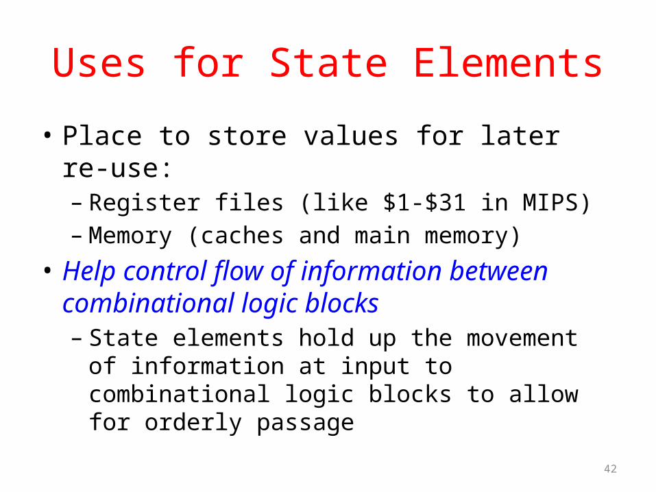
Uses for State Elements
• Place to store values for later re-use:– Register files (like $1-$31 in MIPS)– Memory (caches and main memory)
• Help control flow of information between combinational logic blocks– State elements hold up the movement of
information at input to combinational logic blocks to allow for orderly passage
42
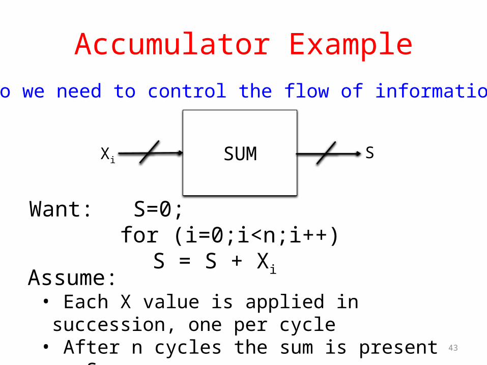
Accumulator Example
Want: S=0; for (i=0;i<n;i++)
S = S + Xi
Why do we need to control the flow of information?
Assume:• Each X value is applied in succession, one per cycle• After n cycles the sum is present on S
43
SUMXi S
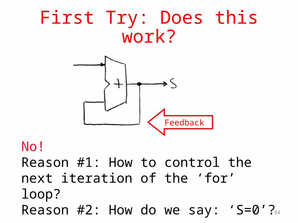
First Try: Does this work?
44
No! Reason #1: How to control the next iteration of the ‘for’ loop?Reason #2: How do we say: ‘S=0’?
Feedback
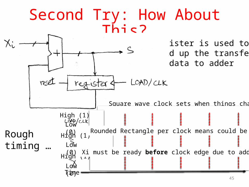
Second Try: How About This?
45
Roughtiming …
Register is used to hold up the transfer of data to adder
Time
High (1)Low (0)
High (1)
Low (0)
High (1)Low (0)
Square wave clock sets when things change
Rounded Rectangle per clock means could be 1 or 0
Xi must be ready before clock edge due to adder delay
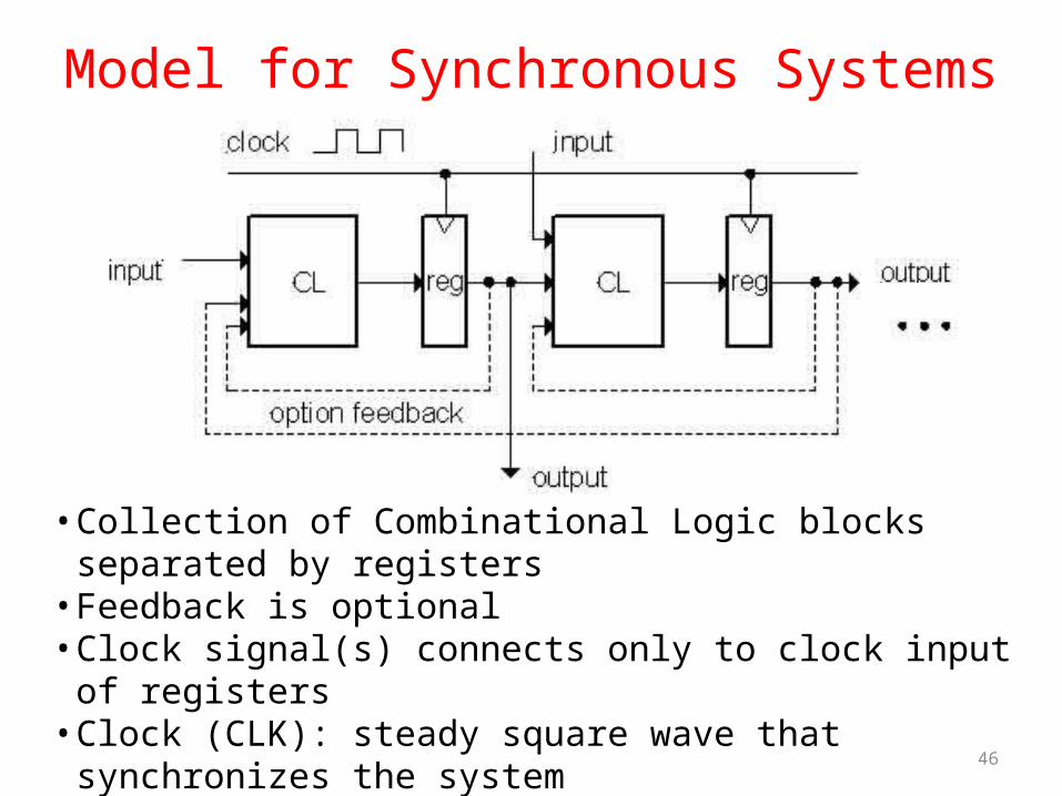
Model for Synchronous Systems
46
• Collection of Combinational Logic blocks separated by registers• Feedback is optional• Clock signal(s) connects only to clock input of registers• Clock (CLK): steady square wave that synchronizes the system• Register: several bits of state that samples on rising edge of CLK
(positive edge-triggered) or falling edge (negative edge-triggered)
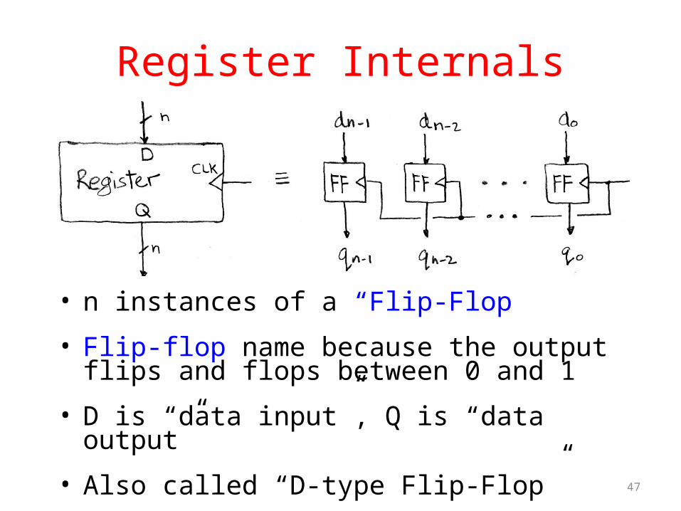
Register Internals
• n instances of a “Flip-Flop”
• Flip-flop name because the output flips and flops between 0 and 1
• D is “data input”, Q is “data output”
• Also called “D-type Flip-Flop”47
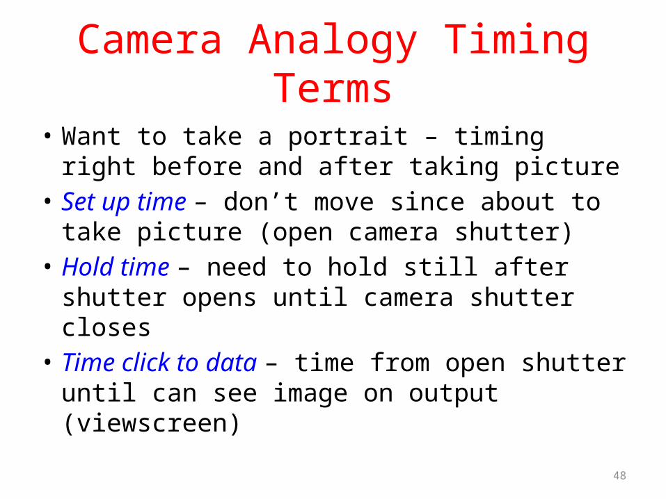
48
Camera Analogy Timing Terms
• Want to take a portrait – timing right before and after taking picture
• Set up time – don’t move since about to take picture (open camera shutter)
• Hold time – need to hold still after shutter opens until camera shutter closes
• Time click to data – time from open shutter until can see image on output (viewscreen)
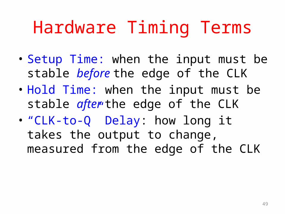
Hardware Timing Terms
• Setup Time: when the input must be stable before the edge of the CLK
• Hold Time: when the input must be stable after the edge of the CLK
• “CLK-to-Q” Delay: how long it takes the output to change, measured from the edge of the CLK
49
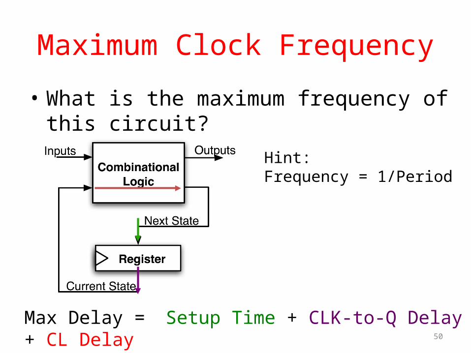
Maximum Clock Frequency
• What is the maximum frequency of this circuit?
50
Max Delay = Setup Time + CLK-to-Q Delay + CL Delay
Hint:Frequency = 1/Period
And in Conclusion, …
• Multiple Hardware Representations– Analog voltages quantized to represent logic 0 and logic 1– Transistor switches form gates: AND, OR, NOT, NAND, NOR– Truth table mapped to gates for combinational logic design– Boolean algebra for gate minimization
• State Machines– Finite State Machines: made from Stateless combinational
logic and Stateful “Memory” Logic (aka Registers)– Clocks synchronize D-FF change (Setup and Hold times
important!)– More about these next time
51