Embed Size (px)
Citation preview

Copyright Cirrus Logic, Inc. 2012(All Rights Reserved)
Cirrus Logic, Inc.http://www.cirrus.com
CS3002
Precision Low-voltage Amplifier; DC to 2kHz
Features & Description• Low Offset: 10V Max• Low Drift: 0.05V/°C Max• Low Noise
- 6nV/ @ 0.5Hz- 0.1 to 10Hz = 125 nVpp- 1/f corner @ 0.08Hz
• Open-loop Voltage Gain - 300dB Typical- 200dB Minimum
• Rail-to-rail Output Swing• Slew Rate: 5V/s
Applications• Thermocouple/Thermopile Amplifiers• Load Cell and Bridge Transducer Amplifiers• Precision Instrumentation• Battery-powered Systems
DescriptionThe CS3002 dual amplifier is designed for precision am-plification of low-level signals and is ideally suited forapplications that require very high closed-loop gains.These amplifiers achieve excellent offset stability, super-high open-loop gain, and low noise over time and tem-perature. The devices also exhibit excellent CMRR andPSRR. The common mode input range includes the neg-ative supply rail. The amplifiers operate with any totalsupply voltage from 2.7V to 6.7V (±1.35V to ±3.35V).
Pin Configuration
Hz
Out A
-In A
+In A
V-
V+
Out B
-In B
+In B
A
B-
-
+
+
1
2
3
4
8
7
6
5
CS3002
8-lead SOIC
Noise vs. Frequency (Measured)
1
10
100
0.001 0.01 0.1 1 10
Frequency (Hz)
nV
/√H
z
CS3002
R1100
R264.9k
C20.015F
Dexter Research Thermophile 1M
DEC ‘12DS490F10

CS3002
TABLE OF CONTENTS
1. Characteristics and Specifications . . . . . . . . . . . . . . . . . . . . . . . . . . . . . . . . . . . . . 31.1 Electrical Characteristics . . . . . . . . . . . . . . . . . . . . . . . . . . . . . . . . . . . . . . . . 31.2 Absolute Maximum Ratings . . . . . . . . . . . . . . . . . . . . . . . . . . . . . . . . . . . . . . 3
2. Typical Performance Plots . . . . . . . . . . . . . . . . . . . . . . . . . . . . . . . . . . . . . . . . . . . 43. Overview . . . . . . . . . . . . . . . . . . . . . . . . . . . . . . . . . . . . . . . . . . . . . . . . . . . . . . . . . . 8
3.1 Open-loop Gain and Phase Response . . . . . . . . . . . . . . . . . . . . . . . . . . . . . 83.2 Open-loop Gain and Stability . . . . . . . . . . . . . . . . . . . . . . . . . . . . . . . . . . . . . 9
3.2.1 Discussion . . . . . . . . . . . . . . . . . . . . . . . . . . . . . . . . . . . . . . . . . . . . . . 93.2.2 Gain Calculation Recommendations . . . . . . . . . . . . . . . . . . . . . . . . . 11
Calculate the Compensation Capacitor Value: . . . . . . . . . . . . . . . . . 11Verify the Op Amp Compensation: . . . . . . . . . . . . . . . . . . . . . . . . . . 11
3.3 Applications . . . . . . . . . . . . . . . . . . . . . . . . . . . . . . . . . . . . . . . . . . . . . . . . . 124. Package Drawing . . . . . . . . . . . . . . . . . . . . . . . . . . . . . . . . . . . . . . . . . . . . . . . . . . 135. Ordering Information . . . . . . . . . . . . . . . . . . . . . . . . . . . . . . . . . . . . . . . . . . . . . . . 136. Environmental, Manufacturing, & Handling Information . . . . . . . . . . . . . . . . . . 137. Revision History . . . . . . . . . . . . . . . . . . . . . . . . . . . . . . . . . . . . . . . . . . . . . . . . . . 14
LIST OF FIGURES
Figure 1. Noise vs. Frequency (Measured)................................................................................... 4
Figure 2. Noise vs. Frequency ...................................................................................................... 4
Figure 3. 0.01Hz to 10Hz Noise ................................................................................................... 4
Figure 4. Offset Voltage Stability (DC to 3.2Hz) ........................................................................... 4
Figure 5. Supply Current vs. Temperature.................................................................................... 4
Figure 6. Supply Current vs. Supply Voltage ................................................................................ 4
Figure 7. Open-loop Gain and Phase vs. Frequency.................................................................... 5
Figure 8. Open-loop Gain and Phase vs. Frequency (Expanded) ................................................ 5
Figure 9. Input Bias Current vs. Supply Voltage ........................................................................... 6
Figure 10. Input Bias Current vs. Common Mode Voltage ........................................................... 6
Figure 11. Voltage Swing vs. Output Current ............................................................................... 7
Figure 12. Voltage Swing vs. Output Current (5V) ....................................................................... 7
Figure 13. Open-loop Gain and Phase Response ........................................................................ 8
Figure 14. Non-inverting Gain Configuration ................................................................................ 9
Figure 15. Non-inverting Gain Configuration with Compensation................................................. 9
Figure 16. Loop Gain Plot: Unity Gain and with Pole-zero Compensation ................................. 10
Figure 17. Thermopile Amplifier with a Gain of 650V/V ............................................................. 12
Figure 18. Load Cell Bridge Amplifier and A/D Converter .......................................................... 12
2 DS490F10

CS3002
1. CHARACTERISTICS AND SPECIFICATIONS
1.1 Electrical CharacteristicsTypical characteristics conditions:
• TA = 25 °C, V+ = +5 V, V- = 0 V, VCM = 2.5V• All voltages are measured with respect to V-
Minimum/Maximum characteristics conditions:• TJ = -40°C to +125 °C, V+ = +5 V, V- = 0 V, VCM = 2.5V
Notes: 1. This parameter is guaranteed by design and laboratory characterization. Thermocouple effects prohibit accurate measurement of these parameters in automatic test systems.
2. 1000-hour life test data @ 125 °C indicates randomly distributed variation approximately equal to measurement repeatability of 1µV.
3. Measured within the specified common mode range limits.
4. Guaranteed within the output limits of (V+ - 0.3V) to (V- + 0.3V). Tested with proprietary production test method.
5. The device has a controlled start-up behavior due to its complex open-loop gain characteristics. Start-up time applies when supply voltage is applied or when PDWN is released.
1.2 Absolute Maximum Ratings
Parameter Condition Min Typ Max Unit
Input Offset Voltage (Note 1) - - ±10 µV
Average Input Offset Drift (Note 1) - ±0.01 ±0.05 µV/ºC
Long Term Input Offset Voltage Stability (Note 2)
Input Bias Current TA = 25ºC--
±100-
-±1000
pApA
Input Offset CurrentTA = 25ºC
--
±200-
-±2000
pApA
Input Noise Voltage DensityRS = 100, f0 = 1HzRS = 100, f0 = 1kHz
--
66
Input Noise Voltage 0.1 to 10Hz - 125 nVpp
Input Noise Current Density f0 = 1Hz - 100
Input Noise Current 0.1 to 10Hz - 1.9 pAp-p
Input Common Mode Voltage Range -0.1 - (V+)-1.25 V
Common Mode Rejection Ratio (DC) (Note 3) 115 120 - dB
Power Supply Rejection Ratio 120 136 - dB
Large Signal Voltage Gain (Note 4) RL = 2k to V+/2 200 300 - dB
Output Voltage SwingRL = 2k to V+/2
RL = 100k to V+/2+4.7 -
+4.99-
VV
Slew Rate RL = 2k, 100pF 5 - V/µs
Overload Recovery Time - 100 - µs
PWDN Threshold (Note 5) (V+) -1.0 - - V
Start-up Time (Note 5) - 9 12 ms
nV/ HznV/ Hz
fA/ Hz
Parameter Min Typ Max Unit
Supply Voltage [(V+) - (V-)] 6.8 V
Input Voltage (V-) - 0.3 (V+) + 0.3 V
Storage Temperature Range -65 +150 ºC
DS490F10 3
CS3002
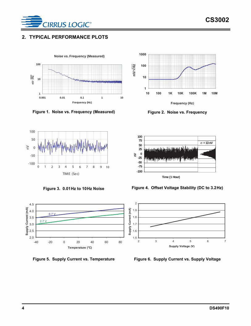
2. TYPICAL PERFORMANCE PLOTS
Figure 1. Noise vs. Frequency (Measured) Figure 2. Noise vs. Frequency
Figure 3. 0.01Hz to 10Hz Noise Figure 4. Offset Voltage Stability (DC to 3.2Hz)
Figure 5. Supply Current vs. Temperature Figure 6. Supply Current vs. Supply Voltage
Noise vs. Frequency (Measured)
1
10
100
0.001 0.01 0.1 1 10
Frequency (Hz)
nV
/√H
z
1
10
100
1000
10 100 1K 10K 100K 1M 10M
Frequency (Hz)
nV
/√H
z
-100
-50
0
50
100
TIME (Sec)
nV
0 1 2 3 4 5 6 7 8 9 10
Time (1 Hour)
-100
-75-50-25
0255075
100nV
= 13 nVσ
Temperature (°C)
Supp
ly C
urre
nt (m
A)
2.7 V
6.7 V
2.0
2.5
3.0
3.5
4.0
4.5
-40 -20 0 20 40 60 801.5
1.6
1.7
1.8
1.9
2
2 3 4 5 6 7
Supply Voltage (V)
Supp
ly C
urre
nt (m
A)
4 DS490F10

CS3002
-500-400-300-200-100
0
100200300400500
Figure 7. Open-loop Gain and Phase vs. Frequency
1 10 100 1k 10k 1M 10M
Frequency (Hz)
100k
GAIN
PHASE
-360
-315
-270
-225
-180
-135
-90
-45
10K 100K 1M 10M
Ga
in (
dB
)P
ha
se
(D
eg
ree
s)
0
20
40
60
80
100
Figure 8. Open-loop Gain and Phase vs. Frequency (Expanded)
DS490F10 5

CS3002
Supply Voltage (±V)
Inp
ut
Bia
s C
urr
ent
(pA
) A1-A1+B1-A2+B1+A2-
B2-B2+
±1.35 ±2 ±2.5 ±3.35-200
-150
-150
-100
-100
0
-50
-50
CM = 0 V
Figure 9. Input Bias Current vs. Supply Voltage
-3-2-10123
0 1 2 3 4 5
Common Mode Voltage (Vs = 5V)
B
ias
Cur
rent
Nor
mal
ized
to C
M =
2.5
V
Figure 10. Input Bias Current vs. Common Mode Voltage
6 DS490F10

CS3002
Figure 11. Voltage Swing vs. Output Current Figure 12. Voltage Swing vs. Output Current (5V)
-200
-150
-250
-100
-50
V+
V–
+50
+100
+150
+200
+250
0 1 2 3 4 5Output Current (mA)
Out
put V
olta
ge (m
V)
+125°C
-40°C
+125°C
+25°C
+25°C
-40°C
-200
-150
-250
-100
-50
V+
V–
+50
+100
+150
+200
+250
0 1 2 3 4 5Output Current (mA)
Out
put V
olta
ge (m
V) +125°C
-40°C
+125°C
+25°C
+25°C
-40°C
DS490F10 7
CS3002
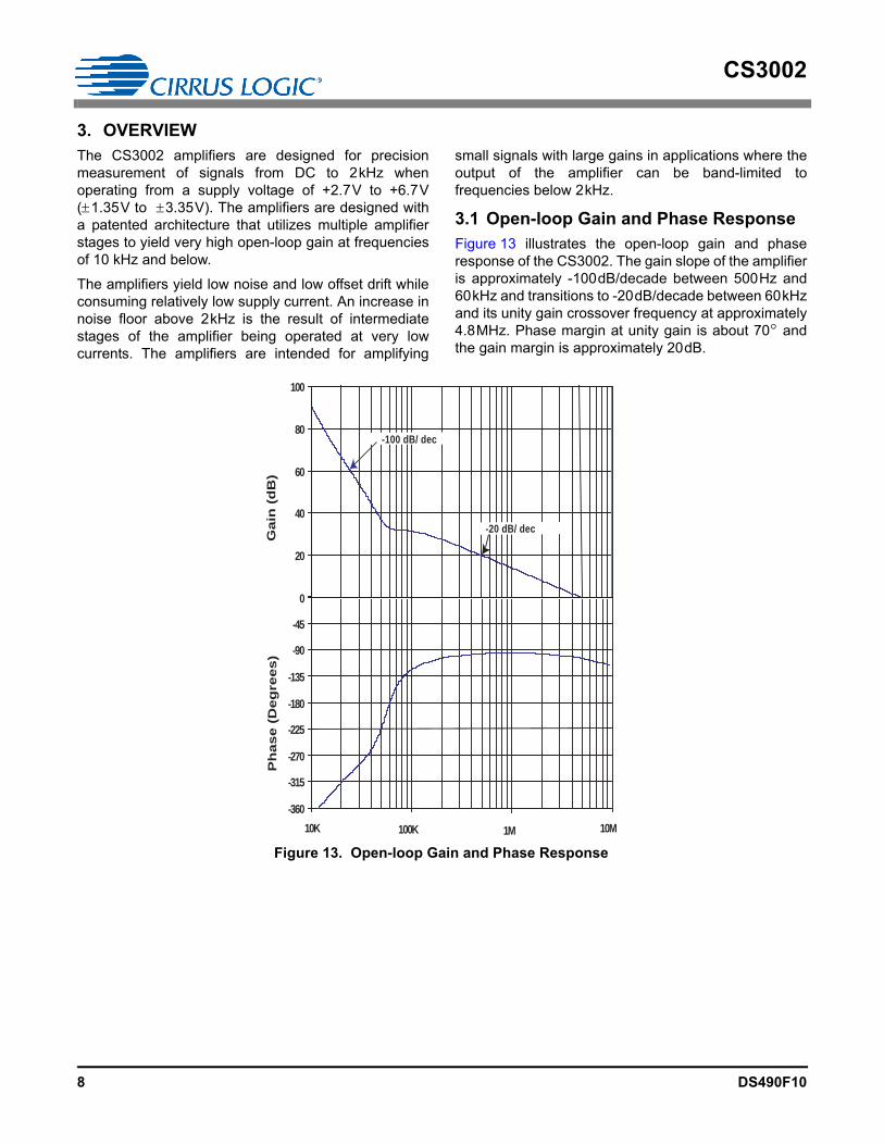
3. OVERVIEWThe CS3002 amplifiers are designed for precisionmeasurement of signals from DC to 2kHz whenoperating from a supply voltage of +2.7V to +6.7V(1.35V to 3.35V). The amplifiers are designed witha patented architecture that utilizes multiple amplifierstages to yield very high open-loop gain at frequenciesof 10 kHz and below.
The amplifiers yield low noise and low offset drift whileconsuming relatively low supply current. An increase innoise floor above 2kHz is the result of intermediatestages of the amplifier being operated at very lowcurrents. The amplifiers are intended for amplifying
small signals with large gains in applications where theoutput of the amplifier can be band-limited tofrequencies below 2kHz.
3.1 Open-loop Gain and Phase ResponseFigure 13 illustrates the open-loop gain and phaseresponse of the CS3002. The gain slope of the amplifieris approximately -100dB/decade between 500Hz and60kHz and transitions to -20dB/decade between 60kHzand its unity gain crossover frequency at approximately4.8MHz. Phase margin at unity gain is about 70 andthe gain margin is approximately 20dB.
-360
-315
-270
-225
-180
-135
-90
-45
10K 100K 1M 10M
Gain
(d
B)
Ph
ase (
Deg
rees)
0
20
40
60
80
100
-100 dB/ dec
-20 dB/ dec
Figure 13. Open-loop Gain and Phase Response
8 DS490F10

CS3002
3.2 Open-loop Gain and Stability
3.2.1 Discussion
The CS3002 achieves ultra-high open-loop gain.Figure 14 illustrates the amplifier in a non-inverting gainconfiguration. The open-loop gain and phase plotsindicate that the amplifier is stable for closed-loop gainsless than 50V/V and R1 100. For a gain of 50, thephase margin is between 40 and 60 depending uponthe loading conditions. As shown in Figure 15, onpage 9, the operational amplifier has an inputcapacitance at the + and – signal inputs of typically50pF. This capacitance adds an additional pole in theloop gain transfer function at a frequency defined usingEquation 1:
where
R = R1 R2; the parallel combination of R1 and R2
A higher value for R produces a pole at a lowerfrequency, thus reducing the phase margin. Resistor R1is recommended to be less than or equal to 100,which results in a pole at 30MHz or higher. If a highervalue of R1 is desired, compensation capacitor C2should be added in parallel with resistor R2. CapacitorC2 should be chosen using Equation 2:
The feedback capacitor C2 is required for closed-loopgains greater than 50V/V. The capacitor introduces apole P1 and a zero Z1 in the loop gain transfer functionT(s), see Equation 3
f1
2R Cin--------------------------= [Eq. 1]
R2 C2 R1 Cin [Eq. 2]
R1
R2
Vin
Vo
RS
CS3002
Figure 14. Non-inverting Gain Configuration
50 pF
50 pF
R1
R2
Vin
Vo
C2
Cin
Cin
Choose C2 so that R2 C2 �R1 Cin
CS3002
Figure 15. Non-inverting Gain Configuration with Compensation
T s
1s
Z1------+
–
1s
P1------+
------------------------- Aol= [Eq. 3]
DS490F10 9

CS3002
Equation 4 is used to determine transfer function zeroZ1.
where
|A| = R2/R1
Substituting A into Equation 4 then zero Z1 is:
Equation 6 is used to determine the transfer functionpole P1.
where
R2>>R1
This indicates that the separation of the pole and thezero is governed by the closed loop gain. It is requiredthat the zero falls on the steep slope (-100dB/decade)of the loop gain plot so that there is some gain higherthan 0dB (typically 20dB) at the hand-over frequency
(the frequency at which the slope changesfrom -100dB/decade to -20dB/decade). The loop gainplot shown in Figure 16 illustrates the unity gainconfiguration, and indicates how this is modified whenusing the amplifier in a higher gain configuration withcompensation. If it is configured for higher gain, forexample, 60dB, the x-axis will move up by 60dB (lineB). Capacitor C2 adds a zero and a pole. The modifiedplot indicates the effects of introducing the pole andzero due to capacitor C2. The pole can be located at anyfrequency higher than the hand-over frequency, thezero has to be at a frequency lower than the hand-overfrequency so as to provide adequate gain margin. Theseparation between the pole and the zero is governedby the closed loop gain. The zero (Z1) occurs at theintersection of the -100dB/decade and -80dB/decadeslopes. The point X in the figure should be at closedloop gain plus 20dB gain margin. The value forcapacitor C2 is determined by Equation 7. Setting the
pole of the filter to P1 = 1MHz works very well and isindependent of gain. As the closed loop gain ischanged, the zero location is also modified if R1remains fixed. Capacitor C2 can be increased in valueto limit the amplifier’s rising noise above 2kHz.
Z11
2 A R1 C2--------------------------------------------------= [Eq. 4]
Z11
2 R2 C2-----------------------------------= [Eq. 5]
P11
2 R1 R2 C2----------------------------------------------------- 1
2 R1 C2-----------------------------------= [Eq. 6]
C21
2 R1 P1----------------------------------= [Eq. 7]
-100 dB/dec
|T| (
Lo
g g
ain
)
-80 dB/dec
z1
p1
Margin
-20 dB/dec
50kHz 1MHz 5MHz
Desired ClosedLoop Gain
X
FREQUENCY
B
Figure 16. Loop Gain Plot: Unity Gain and with Pole-zero Compensation
10 DS490F10

CS3002
3.2.2 Gain Calculation Recommendations
Condition 1: |Av| 50 and R1 100
The op amp is inherently stable for |Av| 50 andR1 100. Capacitor C2 is not required forcompensation across resistor R2.
1) |Av| = 1 configuration has 70° phase margin and20dB gain margin.
2) |Av| = 50 configuration has phase margin between40° for CLOAD 100 pF and 60° for CLOAD 0pF.
Condition 2: |Av| 50 and R1 100
Compensation capacitor C2 across resistor R2 isrequired. Calculate C2 using Equation 8:
where
Cin = 50pF
Condition 3: |Av| 50
Compensation capacitor C2 across resistor R2 isrequired. Calculate and verify a value for C2 using thefollowing steps.
Calculate the Compensation Capacitor Value:
1) Calculate a value for C2 using Equation 9:
where
P1 = 1MHz
To simplify the calculation, set the pole of the filter toP1 = 1MHz. Pole P1 must be set higher than theop amp’s internal 50kHz crossover frequency.
2) Calculate a second value for C2 using Equation 10:
where
Cin = 50pF
3) Use the larger of the two values calculated in steps1 and 2.
Verify the Op Amp Compensation:
Verify the op amp compensation using the open-loopgain and phase response Bode plot in Figure 13. Plotthe calculated closed loop gain transfer function andverify the following design criteria are met:
1) Pole P1 > op amp internal 50kHz crossoverfrequency
where
P1 = 1MHz
To simplify the calculation, set the pole to P1 = 1MHz.
2) Z1 < op amp internal 50kHz crossover frequency
3) Gain margin above the open-loop gain transferfunction is required. A gain margin of +20dB abovethe open-loop gain transfer function is optimal.
C2R1 Cin
R2--------------------------- [Eq. 8]
C21
2 R1 R2 P1 ---------------------------------------------------= [Eq. 9]
C2R1 Cin
R2--------------------------- [Eq. 10]
P11
2 R1 R2 C2-----------------------------------------------= [Eq. 11]
Z11
2 R2 C2 ----------------------------------= [Eq. 12]
DS490F10 11
CS3002
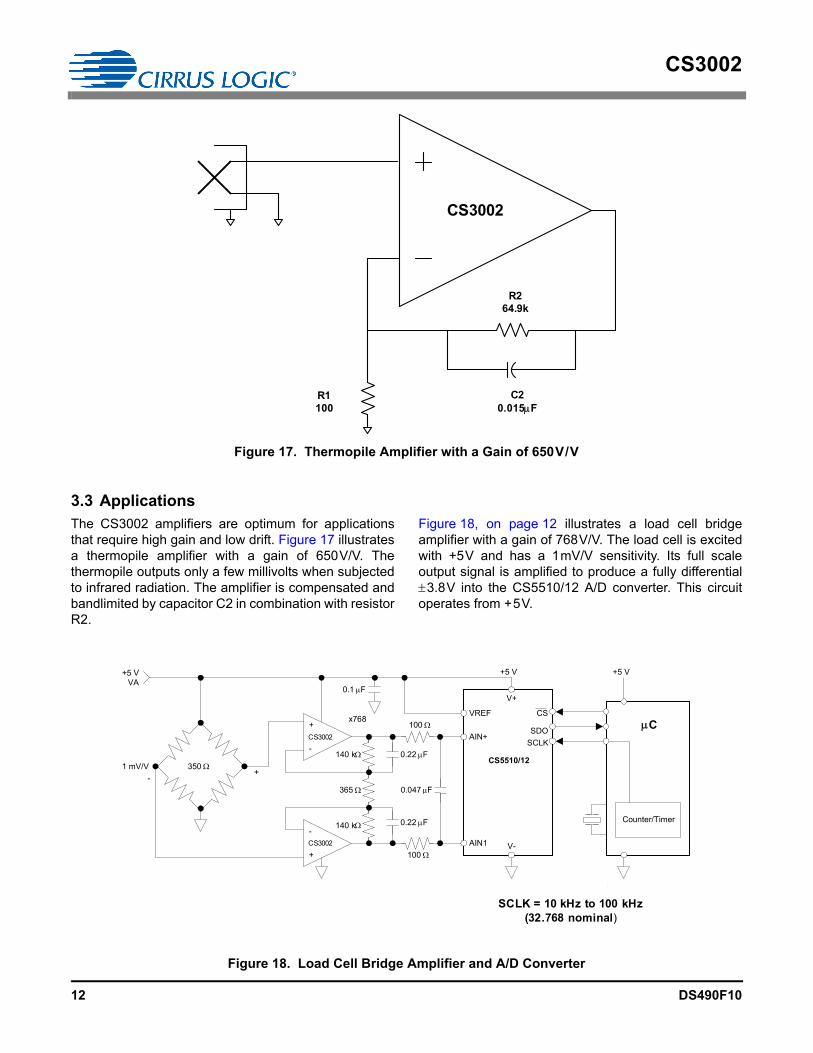
3.3 ApplicationsThe CS3002 amplifiers are optimum for applicationsthat require high gain and low drift. Figure 17 illustratesa thermopile amplifier with a gain of 650V/V. Thethermopile outputs only a few millivolts when subjectedto infrared radiation. The amplifier is compensated andbandlimited by capacitor C2 in combination with resistorR2.
Figure 18, on page 12 illustrates a load cell bridgeamplifier with a gain of 768V/V. The load cell is excitedwith +5V and has a 1mV/V sensitivity. Its full scaleoutput signal is amplified to produce a fully differential3.8V into the CS5510/12 A/D converter. This circuitoperates from +5V.
CS3002
R1100
R264.9k
C20.015F
Figure 17. Thermopile Amplifier with a Gain of 650V/V
+5 VVA
1 mV/V
-+
350
+
-
-
+
x768
140 k
365
140 k
100
100
0.22 F
0.22 F
0.047 F
0.1 F
VREF
AIN+
AIN1 V-
V+
CS
SDO
SCLK
CS5510/12
C
+5 V +5 V
Counter/Timer
SCLK = 10 kHz to 100(32.768
SCLK = 10 kHz to 100 kHz(32.768 nominal)
CS3002
CS3002
Figure 18. Load Cell Bridge Amplifier and A/D Converter
12 DS490F10

CS3002
4. PACKAGE DRAWING
5. ORDERING INFORMATION
6. ENVIRONMENTAL, MANUFACTURING, & HANDLING INFORMATION
* MSL (Moisture Sensitivity Level) as specified by IPC/JEDEC J-STD-020.
INCHES MILLIMETERS
DIM MIN MAX MIN MAX
A 0.053 0.069 1.35 1.75
A1 0.004 0.010 0.10 0.25
B 0.013 0.020 0.33 0.51
C 0.007 0.010 0.19 0.25
D 0.189 0.197 4.80 5.00
E 0.150 0.157 3.80 4.00
e 0.040 0.060 1.02 1.52
H 0.228 0.244 5.80 6.20
L 0.016 0.050 0.40 1.27
0° 8° 0° 8°
JEDEC #: MS-012
8L SOIC (150 MIL BODY) PACKAGE DRAWING
D
HE
e
b
A1
A
c
L
SEATINGPLANE
1
Model Container Temperature Package
CS3002-ISZ (lead free) Bulk-40 to +85 °C 8-pin SOIC (Lead Free)
CS3002-ISZR (lead free) Tape & Reel
Model Number Peak Reflow Temp MSL Rating* Max Floor Life
CS3002-ISZ (lead free) 260 °C 2 365 Days
DS490F10 13

CS3002
7. REVISION HISTORY
Contacting Cirrus Logic SupportFor all product questions and inquiries contact a Cirrus Logic Sales Representative. To find the one nearest to you go to www.cirrus.com
IMPORTANT NOTICECirrus Logic, Inc. and its subsidiaries (“Cirrus”) believe that the information contained in this document is accurate and reliable. However, the information is subjectto change without notice and is provided “AS IS” without warranty of any kind (express or implied). Customers are advised to obtain the latest version of relevantinformation to verify, before placing orders, that information being relied on is current and complete. All products are sold subject to the terms and conditions of salesupplied at the time of order acknowledgment, including those pertaining to warranty, indemnification, and limitation of liability. No responsibility is assumed by Cirrusfor the use of this information, including use of this information as the basis for manufacture or sale of any items, or for infringement of patents or other rights of thirdparties. This document is the property of Cirrus and by furnishing this information, Cirrus grants no license, express or implied under any patents, mask work rights,copyrights, trademarks, trade secrets or other intellectual property rights. Cirrus owns the copyrights associated with the information contained herein and givesconsent for copies to be made of the information only for use within your organization with respect to Cirrus integrated circuits or other products of Cirrus. Thisconsent does not extend to other copying such as copying for general distribution, advertising or promotional purposes, or for creating any work for resale.
CERTAIN APPLICATIONS USING SEMICONDUCTOR PRODUCTS MAY INVOLVE POTENTIAL RISKS OF DEATH, PERSONAL INJURY, OR SEVERE PROP-ERTY OR ENVIRONMENTAL DAMAGE (“CRITICAL APPLICATIONS”). CIRRUS PRODUCTS ARE NOT DESIGNED, AUTHORIZED OR WARRANTED FORUSE IN PRODUCTS SURGICALLY IMPLANTED INTO THE BODY, AUTOMOTIVE SAFETY OR SECURITY DEVICES, LIFE SUPPORT PRODUCTS OR OTHERCRITICAL APPLICATIONS. INCLUSION OF CIRRUS PRODUCTS IN SUCH APPLICATIONS IS UNDERSTOOD TO BE FULLY AT THE CUSTOMER'S RISKAND CIRRUS DISCLAIMS AND MAKES NO WARRANTY, EXPRESS, STATUTORY OR IMPLIED, INCLUDING THE IMPLIED WARRANTIES OF MERCHANT-ABILITY AND FITNESS FOR PARTICULAR PURPOSE, WITH REGARD TO ANY CIRRUS PRODUCT THAT IS USED IN SUCH A MANNER. IF THE CUSTOMEROR CUSTOMER'S CUSTOMER USES OR PERMITS THE USE OF CIRRUS PRODUCTS IN CRITICAL APPLICATIONS, CUSTOMER AGREES, BY SUCH USE,TO FULLY INDEMNIFY CIRRUS, ITS OFFICERS, DIRECTORS, EMPLOYEES, DISTRIBUTORS AND OTHER AGENTS FROM ANY AND ALL LIABILITY, IN-CLUDING ATTORNEYS' FEES AND COSTS, THAT MAY RESULT FROM OR ARISE IN CONNECTION WITH THESE USES.Cirrus Logic, Cirrus, and the Cirrus Logic logo designs are trademarks of Cirrus Logic, Inc. All other brand and product names in this document may be trademarksor service marks of their respective owners.
Revision Date Changes
F3 OCT 2004 Added lead-free device ordering information.
F4 AUG 2005 Added MSL specifications. Updated legal notice. Added leaded (Pb) devices.
F5 AUG 2006 Updated Typical Performance Plots.
F6 SEP 2006 Corrected error in Ordering Information section.
F7 NOV 2007 Added additional information regarding open-loop and gain stability compensation.
F8 OCT 2008 Minor, cosmetic correction to caption for Figure 10.
F9 JUL 2009 Removed lead-containing devices from ordering information.
F10 DEC 2012 Removed CS3001 and corrected typographical errors.
14 DS490F10