Embed Size (px)
Citation preview

CS4385
114 dB, 192 kHz 8-Channel D/A ConverterFeatures
Advanced Multi-bit Delta Sigma Architecture
24-bit Conversion
Automatic Detection of Sample Rates up to 192 kHz
114 dB Dynamic Range
-100 dB THD+N
Direct Stream Digital Mode– Non-Decimating Volume Control – On-Chip 50 kHz Filter – Matched PCM and DSD Analog Output
Levels
Compatible with Industry-Standard Time Division Multiplexed (TDM) Serial Interface
Selectable Digital Filters
Volume Control with 1/2-dB Step Size and Soft Ramp
Low Clock-Jitter Sensitivity
+5 V Analog Supply, +2.5 V Digital Supply
Separate 1.8 to 5 V Logic Supplies for the Control and Serial Ports
Description
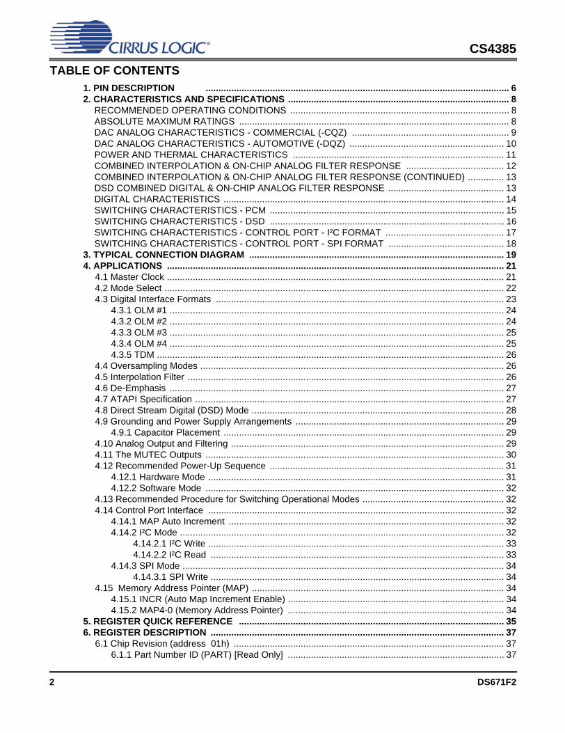
The CS4385 is a complete 8-channel digital-to-analogsystem. This D/A system includes digital de-emphasis,half-dB step size volume control, ATAPI channel mix-ing, selectable fast and slow digital interpolation filtersfollowed by an oversampled, multi-bit delta sigma mod-ulator which includes mismatch-shaping technologythat eliminates distortion due to capacitor mismatch.Following this stage is a multi-element switched capac-itor stage and low-pass filter with differential analogoutputs.
The CS4385 also has a proprietary DSD processorwhich allows for volume control and 50 kHz on-chip fil-tering without an intermediate decimation stage. It alsooffers an optional path for direct DSD conversion by di-rectly using the multi-element switched capacitor array.
The CS4385 is available in a 48-pin LQFP package inboth Commercial (-40°C to +85°C) and Automotive (-40°C to +105°C) grades. The CDB4385 CustomerDemonstration board is also available for device evalu-ation and implementation suggestions. Please see“Ordering Information” on page 54 for complete details.
The CS4385 accepts PCM data at sample rates from4 kHz to 216 kHz, DSD audio data, and delivers excel-lent sound quality. These features are ideal for multi-channel audio systems, including SACD players, A/Vreceivers, digital TV’s, mixing consoles, effects proces-sors, sound cards, and automotive audio systems.
Control Port Supply = 1.8 V to 5 V
Register/HardwareConfiguration
Internal VoltageReference
Reset
Ser
ial I
nter
face
Leve
l Tra
nsla
tor
Leve
l Tra
nsla
tor
TDM SerialAudio Input
Digital Supply = 2.5 V
Hardware Mode orI2C/SPI Software Mode
Control Data
Analog Supply = 5 V
Eight Channelsof DifferentialOutputs
8
8
PCM SerialAudio Input
VolumeControls
DigitalFilters
Switch-CapDAC and
Analog FiltersMulti-bit ΔΣModulators
DSD AudioInput
DSD Processor -Volume control -50 kHz filter
External MuteControl Mute Signals
2
8
Serial Audio PortSupply = 1.8 V to 5 V
Copyright © Cirrus Logic, Inc. 2008(All Rights Reserved)http://www.cirrus.com
FEB '08DS671F2
CS4385
TABLE OF CONTENTS1. PIN DESCRIPTION ...................................................................................................................... 62. CHARACTERISTICS AND SPECIFICATIONS ...................................................................................... 8
RECOMMENDED OPERATING CONDITIONS ..................................................................................... 8ABSOLUTE MAXIMUM RATINGS ......................................................................................................... 8DAC ANALOG CHARACTERISTICS - COMMERCIAL (-CQZ) ............................................................. 9DAC ANALOG CHARACTERISTICS - AUTOMOTIVE (-DQZ) ............................................................ 10POWER AND THERMAL CHARACTERISTICS .................................................................................. 11COMBINED INTERPOLATION & ON-CHIP ANALOG FILTER RESPONSE ...................................... 12COMBINED INTERPOLATION & ON-CHIP ANALOG FILTER RESPONSE (CONTINUED) .............. 13DSD COMBINED DIGITAL & ON-CHIP ANALOG FILTER RESPONSE ............................................. 13DIGITAL CHARACTERISTICS ............................................................................................................. 14SWITCHING CHARACTERISTICS - PCM ........................................................................................... 15SWITCHING CHARACTERISTICS - DSD ........................................................................................... 16SWITCHING CHARACTERISTICS - CONTROL PORT - I²C FORMAT .............................................. 17SWITCHING CHARACTERISTICS - CONTROL PORT - SPI FORMAT ............................................. 18
3. TYPICAL CONNECTION DIAGRAM ................................................................................................... 194. APPLICATIONS ................................................................................................................................... 21
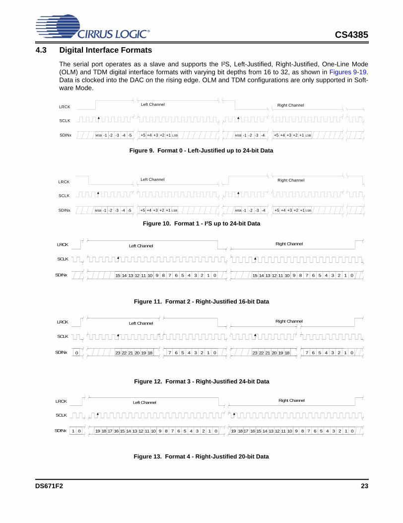
4.1 Master Clock ................................................................................................................................... 214.2 Mode Select .................................................................................................................................... 224.3 Digital Interface Formats ................................................................................................................ 23
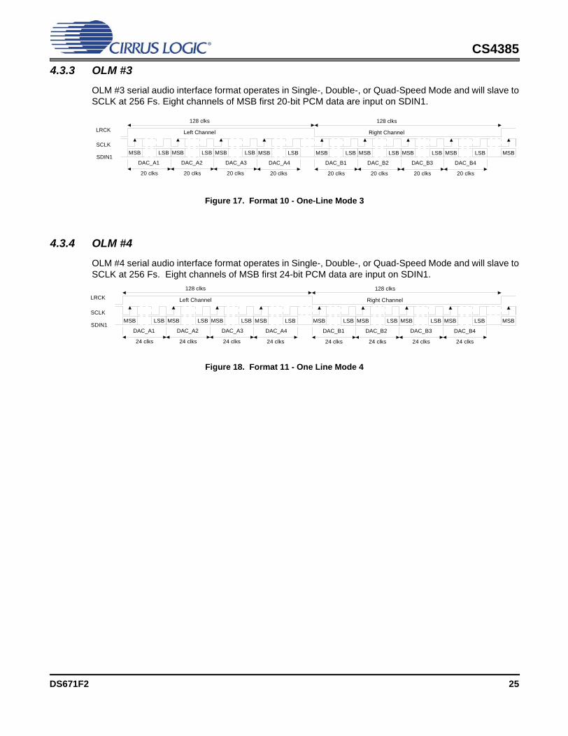
4.3.1 OLM #1 .................................................................................................................................. 244.3.2 OLM #2 .................................................................................................................................. 244.3.3 OLM #3 .................................................................................................................................. 254.3.4 OLM #4 .................................................................................................................................. 254.3.5 TDM ....................................................................................................................................... 26
4.4 Oversampling Modes ...................................................................................................................... 264.5 Interpolation Filter ........................................................................................................................... 264.6 De-Emphasis .................................................................................................................................. 274.7 ATAPI Specification ........................................................................................................................ 274.8 Direct Stream Digital (DSD) Mode .................................................................................................. 284.9 Grounding and Power Supply Arrangements ................................................................................. 29
4.9.1 Capacitor Placement ............................................................................................................. 294.10 Analog Output and Filtering .......................................................................................................... 294.11 The MUTEC Outputs .................................................................................................................... 304.12 Recommended Power-Up Sequence ........................................................................................... 31
4.12.1 Hardware Mode ................................................................................................................... 314.12.2 Software Mode .................................................................................................................... 32
4.13 Recommended Procedure for Switching Operational Modes ....................................................... 324.14 Control Port Interface ................................................................................................................... 32
4.14.1 MAP Auto Increment ........................................................................................................... 324.14.2 I²C Mode .............................................................................................................................. 32
4.14.2.1 I²C Write ................................................................................................................... 334.14.2.2 I²C Read .................................................................................................................. 33
4.14.3 SPI Mode ............................................................................................................................. 344.14.3.1 SPI Write .................................................................................................................. 34
4.15 Memory Address Pointer (MAP) .................................................................................................. 344.15.1 INCR (Auto Map Increment Enable) .................................................................................... 344.15.2 MAP4-0 (Memory Address Pointer) .................................................................................... 34
5. REGISTER QUICK REFERENCE ....................................................................................................... 356. REGISTER DESCRIPTION .................................................................................................................. 37
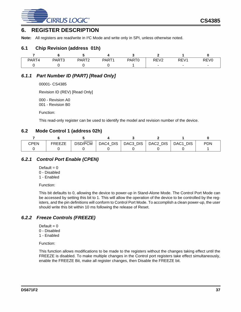
6.1 Chip Revision (address 01h) ......................................................................................................... 376.1.1 Part Number ID (PART) [Read Only] .................................................................................... 37
2 DS671F2
CS4385
6.2 Mode Control 1 (address 02h) ........................................................................................................ 376.2.1 Control Port Enable (CPEN) .................................................................................................. 376.2.2 Freeze Controls (FREEZE) ................................................................................................... 376.2.3 PCM/DSD Selection (DSD/PCM) .......................................................................................... 386.2.4 DAC Pair Disable (DACx_DIS) .............................................................................................. 386.2.5 Power Down (PDN) ............................................................................................................... 38
6.3 PCM Control (address 03h) ............................................................................................................ 386.3.1 Digital Interface Format (DIF) ................................................................................................ 386.3.2 Functional Mode (FM) ........................................................................................................... 39
6.4 DSD Control (address 04h) ............................................................................................................ 396.4.1 DSD Mode Digital Interface Format (DSD_DIF) .................................................................... 396.4.2 Direct DSD Conversion (DIR_DSD) ...................................................................................... 406.4.3 Static DSD Detect (STATIC_DSD) ........................................................................................ 406.4.4 Invalid DSD Detect (INVALID_DSD) ..................................................................................... 406.4.5 DSD Phase Modulation Mode Select (DSD_PM_MODE) ..................................................... 406.4.6 DSD Phase Modulation Mode Enable (DSD_PM_EN) ......................................................... 40
6.5 Filter Control (address 05h) ............................................................................................................ 416.5.1 Interpolation Filter Select (FILT_SEL) ................................................................................... 41
6.6 Invert Control (address 06h) ........................................................................................................... 416.6.1 Invert Signal Polarity (Inv_xx) ................................................................................................ 41
6.7 Group Control (address 07h) .......................................................................................................... 416.7.1 Mutec Pin Control (MUTEC) .................................................................................................. 416.7.2 Channel A Volume = Channel B Volume (Px_A=B) .............................................................. 426.7.3 Single Volume Control (SNGLVOL) ...................................................................................... 42
6.8 Ramp and Mute (address 08h) ....................................................................................................... 426.8.1 Soft Ramp and Zero Cross CONTROL (SZC) ...................................................................... 426.8.2 Soft Volume Ramp-Up after Error (RMP_UP) ....................................................................... 436.8.3 Soft Ramp-Down before Filter Mode Change (RMP_DN) ..................................................... 436.8.4 PCM Auto-Mute (PAMUTE) .................................................................................................. 436.8.5 DSD Auto-Mute (DAMUTE) ................................................................................................... 446.8.6 MUTE Polarity and DETECT (MUTEP1:0) ............................................................................ 44
6.9 Mute Control (address 09h) ............................................................................................................ 446.9.1 Mute (MUTE_xx) ................................................................................................................... 44
6.10 Mixing Control (address 0Ah, 0Dh, 10h, 13h) .............................................................................. 456.10.1 De-Emphasis Control (PX_DEM1:0) ................................................................................... 456.10.2 ATAPI Channel Mixing and Muting (ATAPI) ........................................................................ 45
6.11 Volume Control (address 0Bh, 0Ch, 0Eh, 0Fh, 11h, 12h, 14h, 15h) ............................................ 466.11.1 Digital Volume Control (xx_VOL7:0) ................................................................................... 46
6.12 PCM Clock Mode (address 16h) .................................................................................................. 476.12.1 Master Clock DIVIDE by 2 ENABLE (MCLKDIV) ................................................................ 47
7. FILTER PLOTS ..................................................................................................................................... 488. PARAMETER DEFINITIONS ................................................................................................................ 529. PACKAGE DIMENSIONS ................................................................................................................... 5310. ORDERING INFORMATION .............................................................................................................. 5411. REFERENCES .................................................................................................................................... 5412. REVISION HISTORY ......................................................................................................................... 54
DS671F2 3
CS4385
LIST OF FIGURESFigure 1.Serial Audio Interface Timing ...................................................................................................... 15Figure 2.TDM Serial Audio Interface Timing ............................................................................................. 15Figure 3.Direct Stream Digital - Serial Audio Input Timing ........................................................................ 16Figure 4.Direct Stream Digital - Serial Audio Input Timing for Phase Modulation Mode ........................... 16Figure 5.Control Port Timing - I²C Format ................................................................................................. 17Figure 6.Control Port Timing - SPI Format ................................................................................................ 18Figure 7.Typical Connection Diagram, Software Mode ............................................................................. 19Figure 8.Typical Connection Diagram, Hardware ..................................................................................... 20Figure 9.Format 0 - Left-Justified up to 24-bit Data .................................................................................. 23Figure 10.Format 1 - I²S up to 24-bit Data ................................................................................................ 23Figure 11.Format 2 - Right-Justified 16-bit Data ....................................................................................... 23Figure 12.Format 3 - Right-Justified 24-bit Data ....................................................................................... 23Figure 13.Format 4 - Right-Justified 20-bit Data ....................................................................................... 23Figure 14.Format 5 - Right-Justified 18-bit Data ....................................................................................... 24Figure 15.Format 8 - One-Line Mode 1 ..................................................................................................... 24Figure 16.Format 9 - One-Line Mode 2 ..................................................................................................... 24Figure 17.Format 10 - One-Line Mode 3 ................................................................................................... 25Figure 18.Format 11 - One Line Mode 4 ................................................................................................... 25Figure 19.Format 12 - TDM Mode ............................................................................................................. 26Figure 20.De-Emphasis Curve .................................................................................................................. 27Figure 21.ATAPI Block Diagram (x = channel pair 1, 2, 3, or 4) ............................................................... 27Figure 22.DSD Phase Modulation Mode Diagram .................................................................................... 28Figure 23.Full-Scale Output ...................................................................................................................... 29Figure 24.Recommended Output Filter ..................................................................................................... 30Figure 25.Recommended Mute Circuitry .................................................................................................. 31Figure 26.Control Port Timing, I²C Mode .................................................................................................. 33Figure 27.Control Port Timing, SPI Mode ................................................................................................. 34Figure 28.Single-Speed (fast) Stopband Rejection ................................................................................... 48Figure 29.Single-Speed (fast) Transition Band ......................................................................................... 48Figure 30.Single-Speed (fast) Transition Band (detail) ............................................................................. 48Figure 31.Single-Speed (fast) Passband Ripple ....................................................................................... 48Figure 32.Single-Speed (slow) Stopband Rejection ................................................................................. 48Figure 33.Single-Speed (slow) Transition Band ........................................................................................ 48Figure 34.Single-Speed (slow) Transition Band (detail) ............................................................................ 49Figure 35.Single-Speed (slow) Passband Ripple ...................................................................................... 49Figure 36.Double-Speed (fast) Stopband Rejection ................................................................................. 49Figure 37.Double-Speed (fast) Transition Band ........................................................................................ 49Figure 38.Double-Speed (fast) Transition Band (detail) ............................................................................ 49Figure 39.Double-Speed (fast) Passband Ripple ...................................................................................... 49Figure 40.Double-Speed (slow) Stopband Rejection ................................................................................ 50Figure 41.Double-Speed (slow) Transition Band ...................................................................................... 50Figure 42.Double-Speed (slow) Transition Band (detail) .......................................................................... 50Figure 43.Double-Speed (slow) Passband Ripple .................................................................................... 50Figure 44.Quad-Speed (fast) Stopband Rejection .................................................................................... 50Figure 45.Quad-Speed (fast) Transition Band .......................................................................................... 50Figure 46.Quad-Speed (fast) Transition Band (detail) .............................................................................. 51Figure 47.Quad-Speed (fast) Passband Ripple ........................................................................................ 51Figure 48.Quad-Speed (slow) Stopband Rejection ................................................................................... 51Figure 49.Quad-Speed (slow) Transition Band ......................................................................................... 51Figure 50.Quad-Speed (slow) Transition Band (detail) ............................................................................. 51Figure 51.Quad-Speed (slow) Passband Ripple ....................................................................................... 51
4 DS671F2
CS4385
LIST OF TABLESTable 1. Single-Speed Mode Standard Frequencies ................................................................................ 21Table 2. Double-Speed Mode Standard Frequencies ............................................................................... 21Table 3. Quad-Speed Mode Standard Frequencies ................................................................................. 21Table 4. PCM Digital Interface Format, Hardware Mode Options ............................................................. 22Table 5. Mode Selection, Hardware Mode Options .................................................................................. 22Table 6. Direct Stream Digital (DSD), Hardware Mode Options ............................................................... 22Table 7. Digital Interface Formats - PCM Mode ........................................................................................ 39Table 8. Digital Interface Formats - DSD Mode ........................................................................................ 39Table 9. ATAPI Decode Table .................................................................................................................. 45Table 10. Example Digital Volume Settings .............................................................................................. 46
DS671F2 5
CS4385
1. PIN DESCRIPTIONPin Name # Pin Description
VD 4 Digital Power (Input) - Positive power supply for the digital section. Refer to the Recommended Oper-ating Conditions for appropriate voltages.
GND 531 Ground (Input) - Ground reference. Should be connected to analog ground.
MCLK 6 Master Clock (Input) - Clock source for the delta-sigma modulator and digital filters. Tables 1-3 illus-trate several standard audio sample rates and the required master clock frequency.
LRCK 7 Left Right Clock (Input) - Determines which channel, Left or Right, is currently active on the serial audio data line. The frequency of the left/right clock must be at the audio sample rate, Fs.
SDIN1SDIN2SDIN3SDIN4
8111314
Serial Audio Data Input (Input) - Input for two’s complement serial audio data.
SCLK 9 Serial Clock (Input) - Serial clock for the serial audio interface.
VLC 18 Control Port Power (Input) - Determines the required signal level for the control port. Refer to the Recommended Operating Conditions for appropriate voltages.
RST 19 Reset (Input) - The device enters a low power mode and all internal registers are reset to their default settings when low.
FILT+ 20 Positive Voltage Reference (Output) - Positive reference voltage for the internal sampling circuits. Requires the capacitive decoupling to analog ground, as shown in the Typical Connection Diagram.
VQ 21
Quiescent Voltage (Output) - Filter connection for internal quiescent voltage. VQ must be capacitively coupled to analog ground, as shown in the Typical Connection Diagram. The nominal voltage level is specified in the Analog Characteristics and Specifications section. VQ presents an appreciable source impedance and any current drawn from this pin will alter device performance. However, VQ can be used to bias the analog circuitry assuming there is no AC signal component and the DC current is less than the maximum specified in the Analog Characteristics and Specifications section.
MUTEC1MUTEC234
4122
Mute Control (Output) - The Mute Control pins go high during power-up initialization, reset, muting, power-down or if the master clock to left/right clock frequency ratio is incorrect. These pins are intended to be used as a control for external mute circuits to prevent the clicks and pops that can occur in any single supply system. The use of external mute circuits are not mandatory but may be desired for designs requiring the absolute minimum in extraneous clicks and pops.
SD
IN3
GND
AOUTB2-
AOUTA3+
AOUTB3-
AOUTB2+
VA
AOUTA3-
AOUTB3+
AOUTA4-AOUTA4+
6
2
4
8
10
1
3
5
7
9
1112
13 14 15 16 17 18 19 20 21 22 23 24
31
35
33
29
27
36
34
32
30
28
2625
48 47 46 45 44 43 42 41 40 39 38 37
MCLK
DSDB1
VD
SDIN1
M4(TST)
DSDA2
DSDA1
GND
SCLK
SDIN2M3(TST)
LRCK
DS
D_S
CLK
DSD
B3
DSD
A3
DSD
A4
CS4385
DSD
B4
VLS
SD
IN4
M2(
SC
L/C
CLK
)M
1(SD
A/C
DIN
)
VLC
RST
FILT
+V
QM
UTE
C23
4A
OU
TB4-
AO
UTB
4+
M0(
AD0/
CS
)
AOUTA2+AOUTA2-
AOU
TB1+
AOU
TB1-
AO
UTA
1-A
OU
TA1+
DS
DB
2
MU
TEC
1
6 DS671F2
CS4385
AOUTA1 +,-AOUTB1 +,-AOUTA2 +,-AOUTB2 +,-AOUTA3 +,-AOUTB3 +,-AOUTA4 +,-AOUTB4 +,-
39, 4038, 3735, 3634, 3329, 3028, 2725, 2624, 23
Differential Analog Output (Output) - The full-scale differential analog output level is specified in the Analog Characteristics specification table.
VA 32 Analog Power (Input) - Positive power supply for the analog section. Refer to the Recommended Operating Conditions for appropriate voltages.
VLS 43 Serial Audio Interface Power (Input) - Determines the required signal level for the serial audio inter-face. Refer to the Recommended Operating Conditions for appropriate voltages.
Software Mode Definitions
SCL/CCLK 15Serial Control Port Clock (Input) - Serial clock for the serial control port. Requires an external pull-up resistor to the logic interface voltage in I²C® Mode as shown in the Typical Connection Diagram.
SDA/CDIN 16Serial Control Data (Input/Output) - SDA is a data I/O line in I²C Mode and requires an external pull-up resistor to the logic interface voltage, as shown in the Typical Connection Diagram. CDIN is the input data line for the control port interface in SPI™ Mode.
AD0/CS 17 Address Bit 0 (I²C) / Chip Select (SPI) (Input) - AD0 is a chip address pin in I²C Mode; CS is the chip select signal for SPI format.
TST 10, 12 Test (Input) - These pins are not used in Software Mode and should not be left floating (connect to ground).
Hardware Mode DefinitionsM0M1M2M3M4
1716151210
Mode Selection (Input) - Determines the operational mode of the device as detailed in Tables 4 and 5.
DSD DefinitionsDSD_SCLK 42 DSD Serial Clock (Input) - Serial clock for the Direct Stream Digital audio interface.DSDA1DSDB1DSDA2DSDB2DSDA3DSDB3DSDA4DSDB4
321
4847464544
Direct Stream Digital Input (Input) - Input for Direct Stream Digital serial audio data.
Pin Name # Pin Description
DS671F2 7
CS4385
2. CHARACTERISTICS AND SPECIFICATIONSRECOMMENDED OPERATING CONDITIONSGND = 0 V; all voltages with respect to ground.
ABSOLUTE MAXIMUM RATINGSGND = 0 V; all voltages with respect to ground.
WARNING: Operation at or beyond these limits may result in permanent damage to the device. Normal operationis not guaranteed at these extremes.
Parameters Symbol Min Typ Max UnitsDC Power Supply Analog power
Digital internal powerSerial data port interface power
Control port interface power
VAVDVLSVLC
4.752.371.711.71
5.02.55.05.0
5.252.635.255.25
VVVV
Ambient Operating Temperature (Power Applied) Commercial Grade (-CQZ)Automotive Grade (-DQZ)
TA -40-40
--
+ 85 +105
°C°C
Parameters Symbol Min Max UnitsDC Power Supply Analog power
Digital internal powerSerial data port interface power
Control port interface power
VAVDVLSVLC
-0.3-0.3-0.3-0.3
6.03.26.06.0
VVVV
Input Current Any Pin Except Supplies Iin - ±10 mADigital Input Voltage Serial data port interface
Control port interfaceVIND-SVIND-C
-0.3-0.3
VLS+ 0.4VLC+ 0.4
VV
Ambient Operating Temperature (Power Applied) Top -55 125 °CStorage Temperature Tstg -65 150 °C
8 DS671F2
CS4385
DAC ANALOG CHARACTERISTICS - COMMERCIAL (-CQZ)Test Conditions (unless otherwise specified): VA = VLS = VLC = 5 V; VD = 2.5 V; TA = 25°C; Full-scale 997 Hz input sine wave (Note 1); Tested under max ac-load resistance; Valid with FILT+ and VQ capacitors as shown in “Typical Connection Diagram” on page 19; Measurement Bandwidth 10 Hz to 20 kHz.Notes:1. One-half LSB of triangular PDF dither is added to data.2. Performance limited by 16-bit quantization noise.3. VFS is tested under load RL and includes attenuation due to ZOUT.
Parameters Symbol Min Typ Max UnitFs = 48 kHz, 96 kHz, 192 kHz and DSDDynamic Range 24-bit A-weighted
unweighted16-bit A-weighted
(Note 2) unweighted
108105
--
1141119794
----
dBdBdBdB
Total Harmonic Distortion + Noise 24-bit0 dB
-20 dB-60 dB
(Note 2) 16-bit 0 dB -20 dB
-60 dB
THD+N
------
-100-91-51-94-74-34
-94-
-45---
dBdBdBdBdBdB
Idle Channel Noise / Signal-to-noise ratio A-weighted - 114 - dBInterchannel Isolation (1 kHz) - 110 - dBDC AccuracyInterchannel Gain Mismatch - 0.1 - dBGain Drift - 100 - ppm/°
CAnalog Output Full-Scale Differential- PCM, DSD processorOutput Voltage (Note 3) Direct DSD Mode VFS
1.28•VA0.90•VA
1.32•VA0.94•VA
1.36•VA0.98•VA
VppVpp
Output Impedance ZOUT - 130 - Ω
Max DC Current draw from an AOUT pin IOUTmax - 1.0 - mAMin AC-Load Resistance RL - 3 - kΩ
Max Load Capacitance CL - 100 - pFQuiescent Voltage VQ - 50% VA - VDCMax Current draw from VQ IQMAX - 10 - μA
DS671F2 9
CS4385
DAC ANALOG CHARACTERISTICS - AUTOMOTIVE (-DQZ) Test Conditions (unless otherwise specified): VA = 4.75 to 5.25 V; VLS = 1.71 to 5.25 V; VLC = 1.71 to 5.25 V;VD = 2.37 to 2.63 V; TA = -40°C to 85°C; Full-scale 997 Hz input sine wave (Note 1); Tested under max ac-load resistance; Valid with FILT+ and VQ capacitors as shown in “Typical Connection Diagram” on page 19; Measure-ment Bandwidth 10 Hz to 20 kHz.Parameters Symbol Min Typ Max UnitsFs = 48 kHz, 96 kHz, 192 kHz and DSDDynamic Range (Note 1) 24-bit A-weighted
unweighted16-bit A-weighted
(Note 2) unweighted
105102
--
1141119794
----
dBdBdBdB
Total Harmonic Distortion + Noise (Note 1) 24-bit 0 dB
-20 dB-60 dB
(Note 2) 16-bit 0 dB -20 dB
-60 dB
THD+N
------
-100-91-51-94-74-34
-91-
-42---
dBdBdBdBdBdB
Idle Channel Noise / Signal-to-noise ratio A-weighted - 114 - dBInterchannel Isolation (1 kHz) - 110 - dBDC AccuracyInterchannel Gain Mismatch - 0.1 - dBGain Drift - 100 - ppm/°CAnalog Output Full-Scale Differential- PCM, DSD processorOutput Voltage (Note 3) Direct DSD Mode VFS
1.28•VA0.90•VA
1.32•VA0.94•VA
1.36•VA0.98•VA
VppVpp
Output Impedance ZOUT - 130 - ΩMax DC Current draw from an AOUT pin IOUTmax - 1.0 - mAMin AC-Load Resistance RL - 3 - kΩMax Load Capacitance CL - 100 - pFQuiescent Voltage VQ - 50% VA - VDCMax Current draw from VQ IQMAX - 10 - μA
10 DS671F2
CS4385
POWER AND THERMAL CHARACTERISTICSNotes:4. Current consumption increases with increasing Fs within a given speed mode and is signal dependent.
Max values are based on highest Fs and highest MCLK. 5. ILC measured with no external loading on the SDA pin.6. Power-Down Mode is defined as RST pin = Low with all clock and data lines held static. 7. Valid with the recommended capacitor values on FILT+ and VQ as shown in Figures 7 and 8.
Parameters Symbol Min Typ Max UnitsPower SuppliesPower Supply Current normal operation, VA= 5 V(Note 4) VD= 2.5 V
(Note 5) Interface current, VLC=5 VVLS=5 V
(Note 6) power-down state (all supplies)
IAIDILCILSIpd
-----
84202
75200
9125---
mAmAμAμAμA
Power Dissipation (Note 4) VA = 5 V, VD = 2.5 Vnormal operation
(Note 6) power-down--
4701
520-
mWmW
Package Thermal Resistance multi-layerdual-layer
θJAθJAθJC
---
486515
---
°C/Watt°C/Watt°C/Watt
Power Supply Rejection Ratio (Note 7) (1 kHz) (60 Hz) PSRR -
-6040
--
dBdB
DS671F2 11
CS4385
COMBINED INTERPOLATION & ON-CHIP ANALOG FILTER RESPONSEThe filter characteristics have been normalized to the sample rate (Fs) and can be referenced to the desired sam-ple rate by multiplying the given characteristic by Fs. See Note 12.Notes:8. Slow roll-off interpolation filter is only available in Software Mode.9. Response is clock-dependent and will scale with Fs.10. For Single-Speed Mode, the Measurement Bandwidth is from stopband to 3 Fs.
For Double-Speed Mode, the Measurement Bandwidth is from stopband to 3 Fs.For Quad-Speed Mode, the Measurement Bandwidth is from stopband to 1.34 Fs.
11. De-emphasis is available only in Single-Speed Mode; only 44.1 kHz De-emphasis is available in Hard-ware Mode.
12. Amplitude vs. Frequency plots of this data are available in Section 7. “Filter Plots” on page 48.
ParameterFast Roll-Off
UnitMin Typ Max
Combined Digital and On-chip Analog Filter Response - Single-Speed Mode - 48 kHz Passband (Note 9) to -0.01 dB corner
to -3 dB corner00
--
.454
.499FsFs
Frequency Response 10 Hz to 20 kHz -0.01 - +0.01 dBStopBand 0.547 - - FsStopBand Attenuation (Note 10) 102 - - dBGroup Delay - 10.4/Fs - sDe-emphasis Error (Note 11) Fs = 32 kHz(Relative to 1 kHz) Fs = 44.1 kHz
Fs = 48 kHz
---
---
±0.36±0.21±0.14
dBdBdB
Combined Digital and On-chip Analog Filter Response - Double-Speed Mode - 96 kHz Passband (Note 9) to -0.01 dB corner
to -3 dB corner00
--
.430
.499FsFs
Frequency Response 10 Hz to 20 kHz -0.01 - +0.01 dBStopBand .583 - - FsStopBand Attenuation (Note 10) 80 - - dBGroup Delay - 6.15/Fs - sCombined Digital and On-chip Analog Filter Response - Quad-Speed Mode - 192 kHz Passband (Note 9) to -0.01 dB corner
to -3 dB corner00
--
.105
.490FsFs
Frequency Response 10 Hz to 20 kHz -0.01 - +0.01 dBStopBand .635 - - FsStopBand Attenuation (Note 10) 90 - - dBGroup Delay - 7.1/Fs - s
12 DS671F2
CS4385
COMBINED INTERPOLATION & ON-CHIP ANALOG FILTER RESPONSE (CONTINUED)DSD COMBINED DIGITAL & ON-CHIP ANALOG FILTER RESPONSE
ParameterSlow Roll-Off (Note 8)
UnitMin Typ Max
Single-Speed Mode - 48 kHz Passband (Note 9) to -0.01 dB corner
to -3 dB corner00
--
0.4170.499
FsFs
Frequency Response 10 Hz to 20 kHz -0.01 - +0.01 dBStopBand .583 - - FsStopBand Attenuation (Note 10) 64 - - dBGroup Delay - 7.8/Fs - sDe-emphasis Error (Note 11) Fs = 32 kHz(Relative to 1 kHz) Fs = 44.1 kHz
Fs = 48 kHz
---
---
±0.36±0.21±0.14
dBdBdB
Double-Speed Mode - 96 kHzPassband (Note 9) to -0.01 dB corner
to -3 dB corner00
--
.296
.499FsFs
Frequency Response 10 Hz to 20 kHz -0.01 - +0.01 dBStopBand .792 - - FsStopBand Attenuation (Note 10) 70 - - dBGroup Delay - 5.4/Fs - sQuad-Speed Mode - 192 kHz Passband (Note 9) to -0.01 dB corner
to -3 dB corner00
--
.104
.481FsFs
Frequency Response 10 Hz to 20 kHz -0.01 - +0.01 dBStopBand .868 - - FsStopBand Attenuation (Note 10) 75 - - dBGroup Delay - 6.6/Fs - s
Parameter Min Typ Max UnitDSD Processor ModePassband (Note 9) to -3 dB corner 0 - 50 kHzFrequency Response 10 Hz to 20 kHz -0.05 - +0.05 dBRoll-off 27 - - dB/OctDirect DSD ModePassband (Note 9) to -0.1 dB corner
to -3 dB corner00
--
26.9176.4
kHzkHz
Frequency Response 10 Hz to 20 kHz -0.1 - 0 dB
DS671F2 13
CS4385
DIGITAL CHARACTERISTICSNotes:13. Any pin except supplies. Transient currents of up to ±100 mA on the input pins will not cause SCR latch-
up.
Parameters Symbol Min Typ Max UnitsInput Leakage Current (Note 13) Iin - - ±10 μAInput Capacitance - 8 - pFHigh-Level Input Voltage Serial I/O
Control I/OVIHVIH
0.70•VLS0.70•VLC
--
--
VV
Low-Level Input Voltage Serial I/OControl I/O
VILVIL
--
--
0.30•VLS0.30•VLC
VV
Low-Level Output Voltage (IOL = -1.2 mA) Control I/O = 3.3 V, 5 V VOL - - 0.20•VLC VLow-Level Output Voltage (IOL = -1.2 mA) Control I/O = 1.8 V, 2.5 V VOL - - 0.25•VLC VMUTEC auto detect input high voltage VIH 0.70•VA - - VMUTEC auto detect input low voltage VIL - - 0.30•VA VMaximum MUTEC Drive Current Imax - 3 - mAMUTEC High-Level Output Voltage VOH - VA - VMUTEC Low-Level Output Voltage VOL - 0 - V
14 DS671F2
CS4385
SWITCHING CHARACTERISTICS - PCMInputs: Logic 0 = GND, Logic 1 = VLS, CL = 20 pF.Notes:14. After powering up, RST should be held low until after the power supplies and clocks are settled.15. See Tables 1 - 3 for suggested MCLK frequencies.16. Not valid for TDM Mode.17. MSB of CH1 is always the second SCLK rising edge following LRCK rising edge.
Parameters Symbol Min Max UnitsRST pin Low Pulse Width (Note 14) 1 - ms
MCLK Frequency 1.024 55.2 MHzMCLK Duty Cycle (Note 15) 45 55 %Input Sample Rate - LRCK (Manual selection) Single-Speed Mode
Double-Speed ModeQuad-Speed Mode
FsFsFs
450
100
54108216
kHzkHzkHz
Input Sample Rate - LRCK (Auto detect) Single-Speed ModeDouble-Speed Mode
Quad-Speed Mode
FsFsFs
484
170
54108216
kHzkHzkHz
LRCK Duty Cycle (Note 16) 45 55 %SCLK Duty Cycle 45 55 %SCLK High Time tsckh 8 - nsSCLK Low Time tsckl 8 - nsLRCK Edge to SCLK Rising Edge tlcks 5 - nsSCLK Rising Edge to LRCK Falling Edge tlckd 5 - nsTDM LRCK hightime pulse (Note 17) tlpw 1/fSCLK 7/fSCLK nsSDIN Setup Time Before SCLK Rising Edge tds 3 - nsSDIN Hold Time After SCLK Rising Edge tdh 5 - ns
SDINx
tds
SCLK
LRCK
MSB
tdh
tsckh tsckltlcks
MSB-1
Figure 1. Serial Audio Interface Timing
s c k h s c k ltt
S D IN 1
d htd st
S C L K
L R C K
lc k st
M S B M S B -1
lp wt
lc k stlc k dt
Figure 2. TDM Serial Audio Interface Timing
DS671F2 15
CS4385
SWITCHING CHARACTERISTICS - DSDLogic 0 = GND; Logic 1 = VLS; CL = 20 pF.Parameter Symbol Min Typ Max UnitMCLK Duty Cycle 40 - 60 %DSD_SCLK Pulse Width Low tsclkl 160 - - nsDSD_SCLK Pulse Width High tsclkh 160 - - nsDSD_SCLK Frequency (64x Oversampled)
(128x Oversampled)1.0242.048
--
3.26.4
MHzMHz
DSD_A / _B valid to DSD_SCLK rising setup time tsdlrs 20 - - nsDSD_SCLK rising to DSD_A or DSD_B hold time tsdh 20 - - nsDSD clock to data transition (Phase Modulation Mode) tdpm -20 - 20 ns
sclkht
sclklt
DSDxx
DSD_SCLK
sdlrst sdht
Figure 3. Direct Stream Digital - Serial Audio Input Timing
dpmt
DSDxx
DSD_SCLK(64Fs)
DSD_SCLK(128Fs)
dpmt
Figure 4. Direct Stream Digital - Serial Audio Input Timing for Phase Modulation Mode
16 DS671F2
CS4385
SWITCHING CHARACTERISTICS - CONTROL PORT - I²C FORMATInputs: Logic 0 = GND, Logic 1 = VLC, CL = 20 pF.Notes:18. Data must be held for sufficient time to bridge the transition time, tfc, of SCL.
Parameter Symbol Min Max UnitSCL Clock Frequency fscl - 100 kHz
RST Rising Edge to Start tirs 500 - ns
Bus Free Time Between Transmissions tbuf 4.7 - µs
Start Condition Hold Time (prior to first clock pulse) thdst 4.0 - µs
Clock Low time tlow 4.7 - µs
Clock High Time thigh 4.0 - µs
Setup Time for Repeated Start Condition tsust 4.7 - µs
SDA Hold Time from SCL Falling (Note 18) thdd 0 - µs
SDA Setup time to SCL Rising tsud 250 - ns
Rise Time of SCL and SDA trc, trc - 1 µs
Fall Time SCL and SDA tfc, tfc - 300 ns
Setup Time for Stop Condition tsusp 4.7 - µs
Acknowledge Delay from SCL Falling tack 300 1000 ns
t buf t hdstt hdst
t low t r
t f
t hdd
t high
t sud tsust
tsusp
Stop Start Start StopRepeated
SDA
SCL
t irs
RST
Figure 5. Control Port Timing - I²C Format
DS671F2 17
CS4385
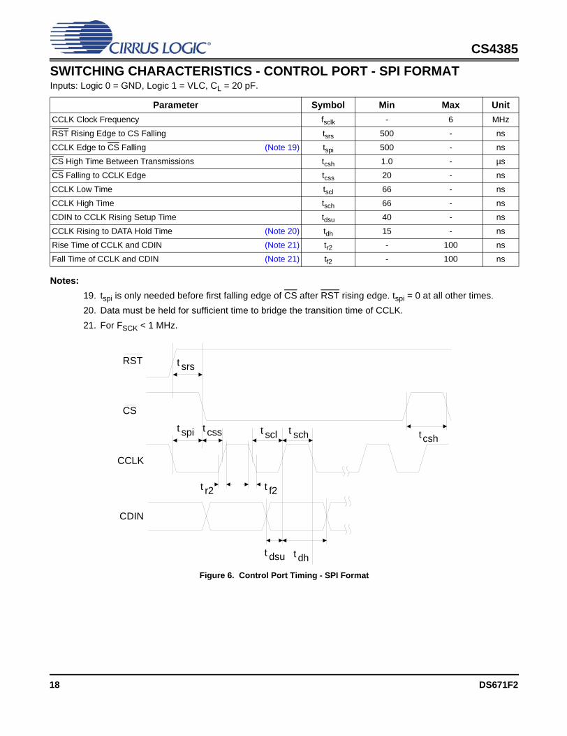
SWITCHING CHARACTERISTICS - CONTROL PORT - SPI FORMAT Inputs: Logic 0 = GND, Logic 1 = VLC, CL = 20 pF.Notes:19. tspi is only needed before first falling edge of CS after RST rising edge. tspi = 0 at all other times.20. Data must be held for sufficient time to bridge the transition time of CCLK.21. For FSCK < 1 MHz.
Parameter Symbol Min Max UnitCCLK Clock Frequency fsclk - 6 MHz
RST Rising Edge to CS Falling tsrs 500 - ns
CCLK Edge to CS Falling (Note 19) tspi 500 - ns
CS High Time Between Transmissions tcsh 1.0 - µs
CS Falling to CCLK Edge tcss 20 - ns
CCLK Low Time tscl 66 - ns
CCLK High Time tsch 66 - ns
CDIN to CCLK Rising Setup Time tdsu 40 - ns
CCLK Rising to DATA Hold Time (Note 20) tdh 15 - ns
Rise Time of CCLK and CDIN (Note 21) tr2 - 100 ns
Fall Time of CCLK and CDIN (Note 21) tf2 - 100 ns
t r2 t f2
t dsu t dh
t scht scl
CS
CCLK
CDIN
t css tcsht spi
t srsRST
Figure 6. Control Port Timing - SPI Format
18 DS671F2
CS4385
3. TYPICAL CONNECTION DIAGRAMVLS
MCLK
VD
AOUTA1+
8
32
0.1 µF+
1 µF
+2.5 V
SDIN1
9
1 µF0.1 µF
+
+
20
21
FILT+
VQ
7
6
LRCK
SCLK
SDIN3
SDIN2
39
40
0.1 µF47 µF
VA
0.1 µF+
1 µF
0.1 µF
+1.8 V to +5 V
+5 V
4
43
SDIN4
13
14
Analog Conditioningand MutingAOUTA1-
AOUTB1+ 38
37Analog Conditioning
and MutingAOUTB1-
AOUTA2+ 35
36Analog Conditioning
and MutingAOUTA2-
AOUTB2+ 34
33Analog Conditioning
and MutingAOUTB2-
AOUTA3+ 29
30Analog Conditioning
and MutingAOUTA3-
AOUTB3+ 28
27Analog Conditioning
and MutingAOUTB3-
AOUTA4+ 25
26Analog Conditioning
and MutingAOUTA4-
AOUTB4+ 24
23Analog Conditioning
and MutingAOUTB4-
MUTEC1 41
22MuteDriveMUTEC234
11
Micro-Controller
VLC
0.1 µF
+1.8 V to +5 V18
2
48DSDB2
3
42 DSD_SCLK
DSDA1
DSDB3
DSDA3
DSDA4
DSDB1
DSDA2
4645
47
1
44 DSDB4
1615 SCL/CCLK
SDA/CDIN
ADO/CS
RST19
17
2 K
Ω
2 K
Ω
Note: Necessary for I2Ccontrol port operation
Note*
CS4385
31GND GND5
NoteTST: Pins 10, 12
TST*
DSDAudio
Source
220 Ω
470 Ω
470 Ω
DigitalAudio
Source
PCM
Figure 7. Typical Connection Diagram, Software Mode
DS671F2 19

CS4385
VLS
CS4385
MCLK
VD
AOUTA1+
8
32
0.1 µF+
1 µF
+2.5 V
SDIN1
9
1 µF0.1 µF
+
+
20
21
FILT+
VQ
7
6
LRCK
SCLK
SDIN3
SDIN2
39
40
0.1 µF47 µF
VA
0.1 µF+
1 µF
+1.8 V to +5 V
+5 V
4
43
SDIN4
13
14
Analog Conditioningand MutingAOUTA1-
AOUTB1+ 38
37Analog Conditioning
and MutingAOUTB1-
AOUTA2+ 35
36Analog Conditioning
and MutingAOUTA2-
AOUTB2+ 34
33Analog Conditioning
and MutingAOUTB2-
AOUTA3+ 29
30Analog Conditioning
and MutingAOUTA3-
AOUTB3+ 28
27Analog Conditioning
and MutingAOUTB3-
AOUTA4+ 25
26Analog Conditioning
and MutingAOUTA4-
AOUTB4+ 24
23Analog Conditioning
and MutingAOUTB4-
MUTEC234 22
41
MuteDrive
MUTEC1
11
31GND GND5
Stand-AloneMode
Configuration
VLC
0.1 µF
+1.8 V to +5 V18
2
48DSDB2
3
12 M3
DSDA1
DSDB3
DSDA3
DSDA4
DSDB1
DSDA2
46
45
47
1
44 DSDB4
1615 M2
M1
M0RST
1917
MuteDrive
42 DSD_SCLK
10 M4
220 Ω
470 Ω
DigitalAudio
Source
PCM
DSDAudio
Source
470 Ω
0.1 µF
Optional47 KΩ
Figure 8. Typical Connection Diagram, Hardware
20 DS671F2
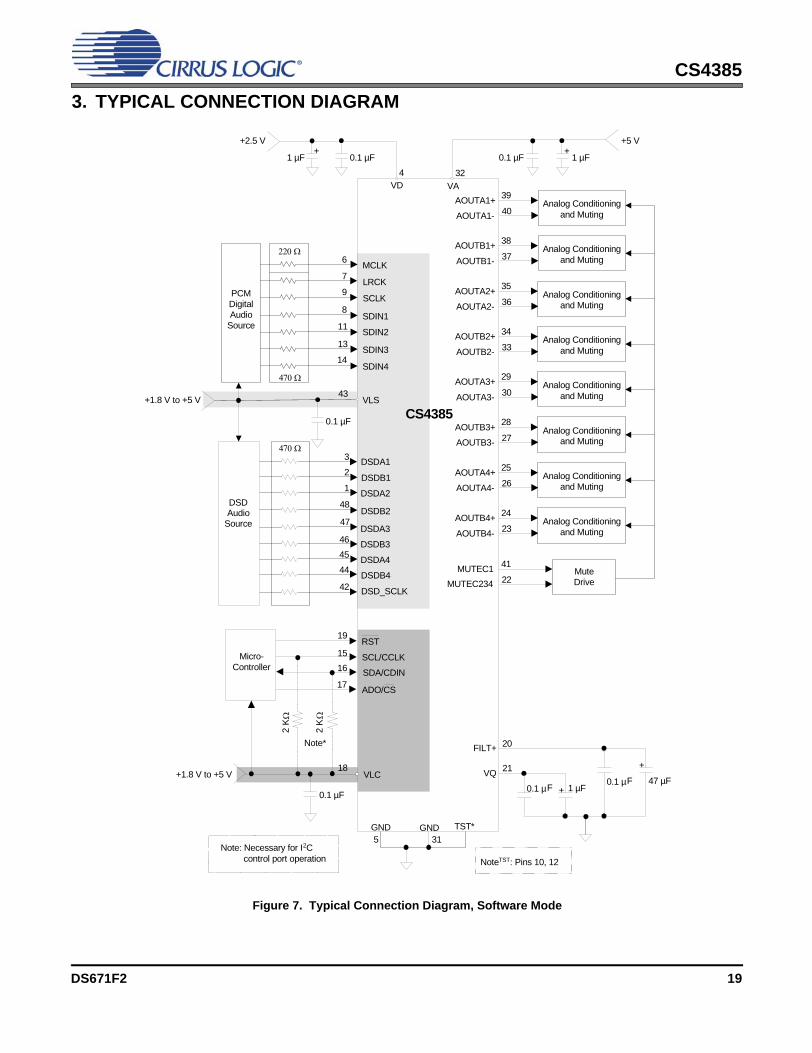
CS4385
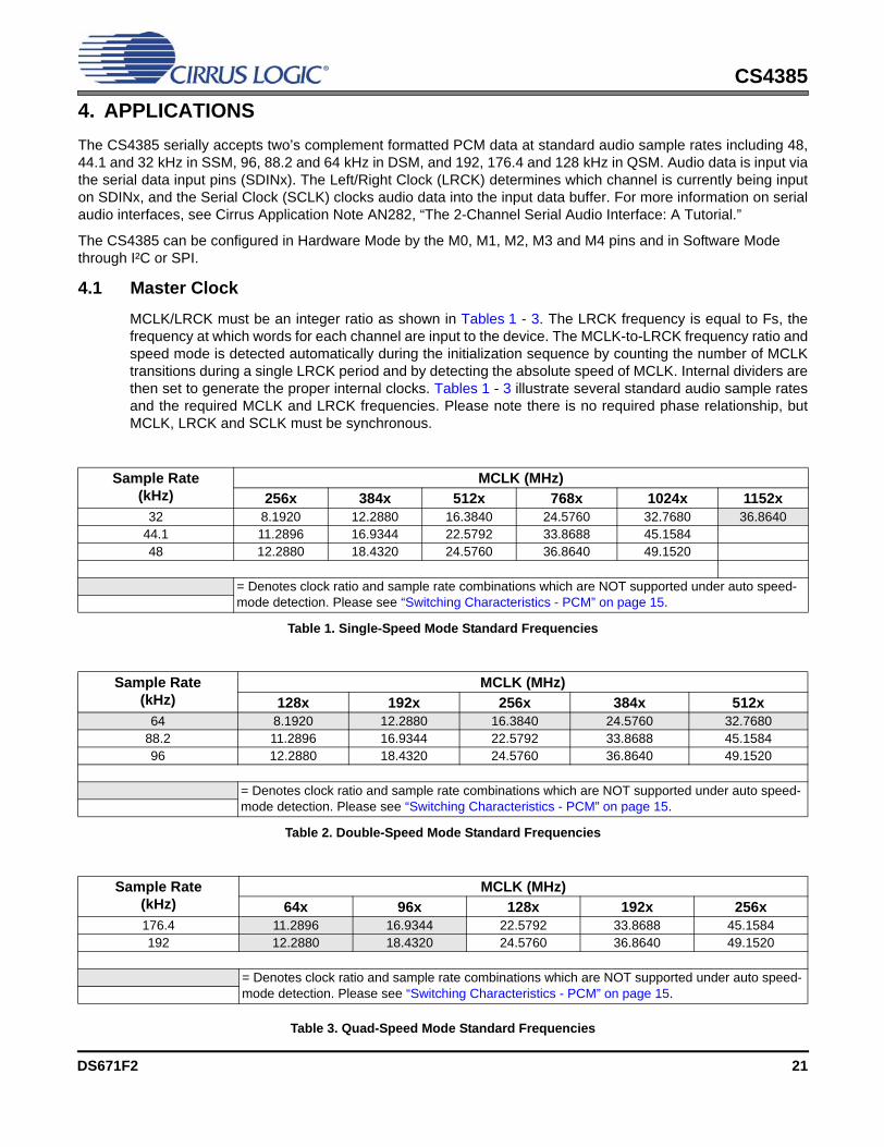
4. APPLICATIONS The CS4385 serially accepts two’s complement formatted PCM data at standard audio sample rates including 48,44.1 and 32 kHz in SSM, 96, 88.2 and 64 kHz in DSM, and 192, 176.4 and 128 kHz in QSM. Audio data is input viathe serial data input pins (SDINx). The Left/Right Clock (LRCK) determines which channel is currently being inputon SDINx, and the Serial Clock (SCLK) clocks audio data into the input data buffer. For more information on serialaudio interfaces, see Cirrus Application Note AN282, “The 2-Channel Serial Audio Interface: A Tutorial.”The CS4385 can be configured in Hardware Mode by the M0, M1, M2, M3 and M4 pins and in Software Mode through I²C or SPI.
4.1 Master Clock MCLK/LRCK must be an integer ratio as shown in Tables 1 - 3. The LRCK frequency is equal to Fs, thefrequency at which words for each channel are input to the device. The MCLK-to-LRCK frequency ratio andspeed mode is detected automatically during the initialization sequence by counting the number of MCLKtransitions during a single LRCK period and by detecting the absolute speed of MCLK. Internal dividers arethen set to generate the proper internal clocks. Tables 1 - 3 illustrate several standard audio sample ratesand the required MCLK and LRCK frequencies. Please note there is no required phase relationship, butMCLK, LRCK and SCLK must be synchronous.
Table 1. Single-Speed Mode Standard Frequencies
Table 2. Double-Speed Mode Standard Frequencies
Table 3. Quad-Speed Mode Standard Frequencies
Sample Rate(kHz)
MCLK (MHz)256x 384x 512x 768x 1024x 1152x
32 8.1920 12.2880 16.3840 24.5760 32.7680 36.864044.1 11.2896 16.9344 22.5792 33.8688 45.158448 12.2880 18.4320 24.5760 36.8640 49.1520
= Denotes clock ratio and sample rate combinations which are NOT supported under auto speed-mode detection. Please see “Switching Characteristics - PCM” on page 15.
Sample Rate(kHz)
MCLK (MHz)128x 192x 256x 384x 512x
64 8.1920 12.2880 16.3840 24.5760 32.768088.2 11.2896 16.9344 22.5792 33.8688 45.158496 12.2880 18.4320 24.5760 36.8640 49.1520
= Denotes clock ratio and sample rate combinations which are NOT supported under auto speed-mode detection. Please see “Switching Characteristics - PCM” on page 15.
Sample Rate(kHz)
MCLK (MHz)64x 96x 128x 192x 256x
176.4 11.2896 16.9344 22.5792 33.8688 45.1584192 12.2880 18.4320 24.5760 36.8640 49.1520
= Denotes clock ratio and sample rate combinations which are NOT supported under auto speed-mode detection. Please see “Switching Characteristics - PCM” on page 15.
DS671F2 21
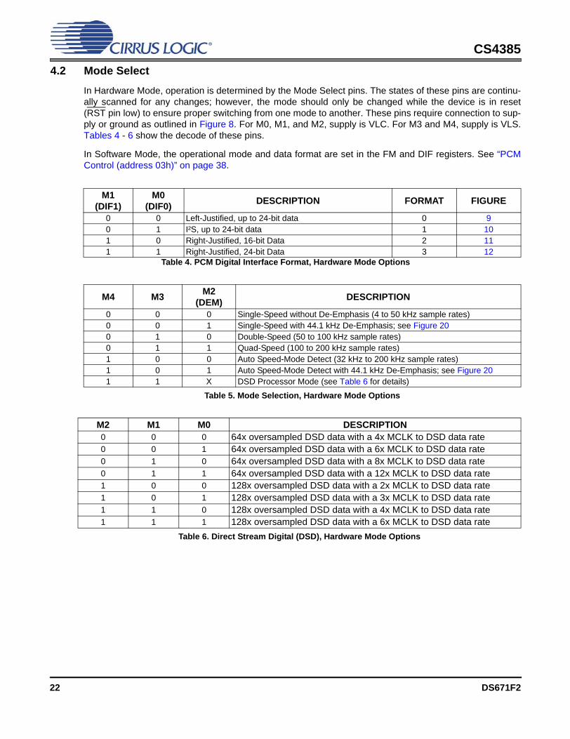
CS4385
4.2 Mode SelectIn Hardware Mode, operation is determined by the Mode Select pins. The states of these pins are continu-ally scanned for any changes; however, the mode should only be changed while the device is in reset(RST pin low) to ensure proper switching from one mode to another. These pins require connection to sup-ply or ground as outlined in Figure 8. For M0, M1, and M2, supply is VLC. For M3 and M4, supply is VLS.Tables 4 - 6 show the decode of these pins.
In Software Mode, the operational mode and data format are set in the FM and DIF registers. See “PCMControl (address 03h)” on page 38.
Table 4. PCM Digital Interface Format, Hardware Mode Options
M1(DIF1)
M0(DIF0) DESCRIPTION FORMAT FIGURE
0 0 Left-Justified, up to 24-bit data 0 90 1 I²S, up to 24-bit data 1 101 0 Right-Justified, 16-bit Data 2 111 1 Right-Justified, 24-bit Data 3 12
M4 M3 M2(DEM) DESCRIPTION
0 0 0 Single-Speed without De-Emphasis (4 to 50 kHz sample rates)0 0 1 Single-Speed with 44.1 kHz De-Emphasis; see Figure 200 1 0 Double-Speed (50 to 100 kHz sample rates)0 1 1 Quad-Speed (100 to 200 kHz sample rates)1 0 0 Auto Speed-Mode Detect (32 kHz to 200 kHz sample rates)1 0 1 Auto Speed-Mode Detect with 44.1 kHz De-Emphasis; see Figure 201 1 X DSD Processor Mode (see Table 6 for details)
Table 5. Mode Selection, Hardware Mode Options
M2 M1 M0 DESCRIPTION0 0 0 64x oversampled DSD data with a 4x MCLK to DSD data rate0 0 1 64x oversampled DSD data with a 6x MCLK to DSD data rate0 1 0 64x oversampled DSD data with a 8x MCLK to DSD data rate0 1 1 64x oversampled DSD data with a 12x MCLK to DSD data rate1 0 0 128x oversampled DSD data with a 2x MCLK to DSD data rate1 0 1 128x oversampled DSD data with a 3x MCLK to DSD data rate1 1 0 128x oversampled DSD data with a 4x MCLK to DSD data rate1 1 1 128x oversampled DSD data with a 6x MCLK to DSD data rate
Table 6. Direct Stream Digital (DSD), Hardware Mode Options
22 DS671F2
CS4385
4.3 Digital Interface FormatsThe serial port operates as a slave and supports the I²S, Left-Justified, Right-Justified, One-Line Mode(OLM) and TDM digital interface formats with varying bit depths from 16 to 32, as shown in Figures 9-19.Data is clocked into the DAC on the rising edge. OLM and TDM configurations are only supported in Soft-ware Mode.
LRCK
SCLK
Left Channel Right Channel
SDINx +3 +2 +1+5 +4-1 -2 -3 -4 -5 +3 +2 +1+5 +4-1 -2 -3 -4MSB LSB MSB LSB
Figure 9. Format 0 - Left-Justified up to 24-bit Data
LRCK
SCLK
Left Channel Right Channel
SDINx +3 +2 +1+5 +4-1 -2 -3 -4 -5 +3 +2 +1+5 +4-1 -2 -3 -4MSB MSBLSB LSB
Figure 10. Format 1 - I²S up to 24-bit Data
LRCK
SCLK
Left Channel Right Channel
SDINx 6 5 4 3 2 1 09 8 715 14 13 12 11 10 6 5 4 3 2 1 09 8 715 14 13 12 11 10
32 clocks
Figure 11. Format 2 - Right-Justified 16-bit Data
LRCK
SCLK
Left Channel
SDINx 6 5 4 3 2 1 0723 22 21 20 19 18 6 5 4 3 2 1 0723 22 21 20 19 18
32 clocks
0
Right Channel
Figure 12. Format 3 - Right-Justified 24-bit Data
LRCK
SCLK
Left Channel Right Channel
SDINx 6 5 4 3 2 1 09 8 715 14 13 12 11 101 0 6 5 4 3 2 1 09 8 715 14 13 12 11 1017 16 17 16
32 clocks
19 18 19 18
Figure 13. Format 4 - Right-Justified 20-bit Data
DS671F2 23

CS4385
4.3.1 OLM #1
OLM #1 serial audio interface format operates in Single-, Double-, or Quad-Speed Mode and will slave toSCLK at 128 Fs. Six channels of MSB first 20-bit PCM data are input on SDIN1. The last two channelsare input on SDIN4.
4.3.2 OLM #2
OLM #2 serial audio interface format operates in Single-, Double-, or Quad-Speed Mode and will slave toSCLK at 256 Fs. Six channels of MSB first 24-bit PCM data are input on SDIN1. The last two channelsare input on SDIN4.
LRCK
SCLK
Left Channel Right Channel
SDINx 6 5 4 3 2 1 09 8 715 14 13 12 11 101 0 6 5 4 3 2 1 09 8 715 14 13 12 11 1017 16 17 16
32 clocks
Figure 14. Format 5 - Right-Justified 18-bit Data
LRCK
SCLKLSBMSB
20 clks
64 clks 64 clks
LSBMSB LSBMSB LSBMSB LSBMSB LSBMSB MSB
DAC_A1
20 clks 20 clks 20 clks 20 clks 20 clks
Left Channel Right Channel
20 clks 20 clksSDIN4
SDIN1DAC_A2 DAC_A3
DAC_A4
DAC_B1
DAC_B4
DAC_B2 DAC_B3
Figure 15. Format 8 - One-Line Mode 1
LSBMSB
24 clks
128 clks
LSBMSB LSBMSB LSBMSB LSBMSB LSBMSB MSB
DAC_A1
24 clks 24 clks 24 clks 24 clks 24 clks
Left Channel Right Channel
24 clks 24 clks
128 clksLRCK
SCLK
SDIN1
SDIN4 DAC_A4
DAC_A2 DAC_A3 DAC_B1 DAC_B2 DAC_B3
DAC_B4
Figure 16. Format 9 - One-Line Mode 2
24 DS671F2
CS4385
4.3.3 OLM #3OLM #3 serial audio interface format operates in Single-, Double-, or Quad-Speed Mode and will slave toSCLK at 256 Fs. Eight channels of MSB first 20-bit PCM data are input on SDIN1.
4.3.4 OLM #4
OLM #4 serial audio interface format operates in Single-, Double-, or Quad-Speed Mode and will slave toSCLK at 256 Fs. Eight channels of MSB first 24-bit PCM data are input on SDIN1.
LSBMSB
20 clks
128 clks
LSBMSB LSBMSB LSBMSB LSBMSB LSBMSB MSB
DAC_A1
20 clks 20 clks 20 clks 20 clks 20 clks
Left Channel Right Channel
128 clksLRCK
SCLK
SDIN1DAC_A2 DAC_A3 DAC_B1 DAC_B2 DAC_B3
LSBMSB
20 clks
DAC_A4
LSBMSB
20 clks
DAC_B4
Figure 17. Format 10 - One-Line Mode 3
LSBMSB
24 clks
128 clks
LSBMSB LSBMSB LSBMSB LSBMSB LSBMSB MSB
DAC_A1
24 clks 24 clks 24 clks 24 clks 24 clks
Left Channel Right Channel
128 clksLRCK
SCLK
SDIN1DAC_A2 DAC_A3 DAC_B1 DAC_B2 DAC_B3
LSBMSB
24 clks
DAC_A4
LSBMSB
24 clks
DAC_B4
Figure 18. Format 11 - One Line Mode 4
DS671F2 25
CS4385
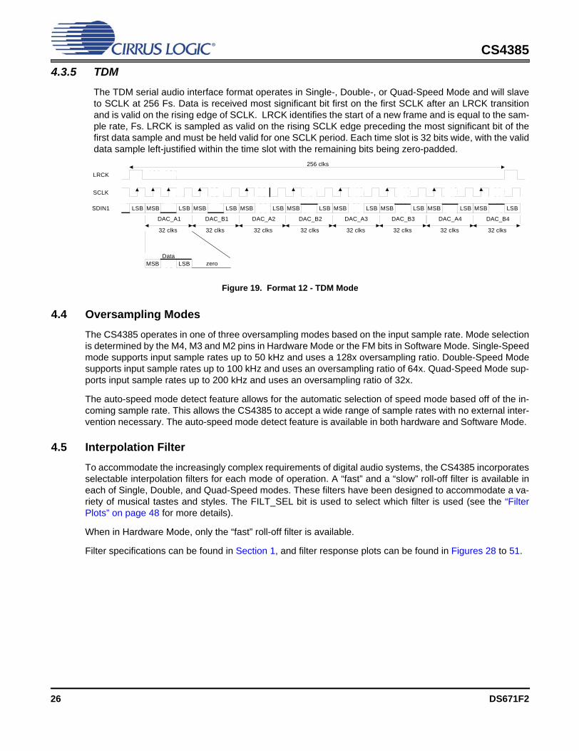
4.3.5 TDMThe TDM serial audio interface format operates in Single-, Double-, or Quad-Speed Mode and will slaveto SCLK at 256 Fs. Data is received most significant bit first on the first SCLK after an LRCK transitionand is valid on the rising edge of SCLK. LRCK identifies the start of a new frame and is equal to the sam-ple rate, Fs. LRCK is sampled as valid on the rising SCLK edge preceding the most significant bit of thefirst data sample and must be held valid for one SCLK period. Each time slot is 32 bits wide, with the validdata sample left-justified within the time slot with the remaining bits being zero-padded.
4.4 Oversampling ModesThe CS4385 operates in one of three oversampling modes based on the input sample rate. Mode selectionis determined by the M4, M3 and M2 pins in Hardware Mode or the FM bits in Software Mode. Single-Speedmode supports input sample rates up to 50 kHz and uses a 128x oversampling ratio. Double-Speed Modesupports input sample rates up to 100 kHz and uses an oversampling ratio of 64x. Quad-Speed Mode sup-ports input sample rates up to 200 kHz and uses an oversampling ratio of 32x.
The auto-speed mode detect feature allows for the automatic selection of speed mode based off of the in-coming sample rate. This allows the CS4385 to accept a wide range of sample rates with no external inter-vention necessary. The auto-speed mode detect feature is available in both hardware and Software Mode.
4.5 Interpolation FilterTo accommodate the increasingly complex requirements of digital audio systems, the CS4385 incorporatesselectable interpolation filters for each mode of operation. A “fast” and a “slow” roll-off filter is available ineach of Single, Double, and Quad-Speed modes. These filters have been designed to accommodate a va-riety of musical tastes and styles. The FILT_SEL bit is used to select which filter is used (see the “FilterPlots” on page 48 for more details).
When in Hardware Mode, only the “fast” roll-off filter is available.
Filter specifications can be found in Section 1, and filter response plots can be found in Figures 28 to 51.
DAC_B3
LRCK
SCLK
LSBMSB LSBMSB LSBMSB LSBMSB LSBMSBSDIN1
DAC_A1 DAC_B1 DAC_A3DAC_A2
256 clks
32 clks 32 clks 32 clks 32 clks 32 clks
LSBMSB
DAC_A4
32 clks
LSBMSB
DAC_B2
32 clks
LSBMSB
DAC_B4
32 clks
LSB
LSBMSB zeroData
Figure 19. Format 12 - TDM Mode
26 DS671F2
CS4385
4.6 De-EmphasisThe CS4385 includes on-chip digital de-emphasis filters. The de-emphasis feature is included to accommo-date older audio recordings that utilize pre-emphasis equalization as a means of noise reduction. Figure 20shows the de-emphasis curve. The frequency response of the de-emphasis curve will scale proportionallywith changes in sample rate, Fs if the input sample rate does not match the coefficient which has been se-lected.
In Software Mode the required de-emphasis filter coefficients for 32 kHz, 44.1 kHz, or 48 kHz are selectedvia the de-emphasis control bits.
In Hardware Mode only the 44.1 kHz coefficient is available (enabled through the M2 pin). If the input sam-ple rate is not 44.1 kHz and de-emphasis has been selected then the corner frequencies of the de-emphasisfilter will be scaled by a factor of the actual Fs over 44,100.
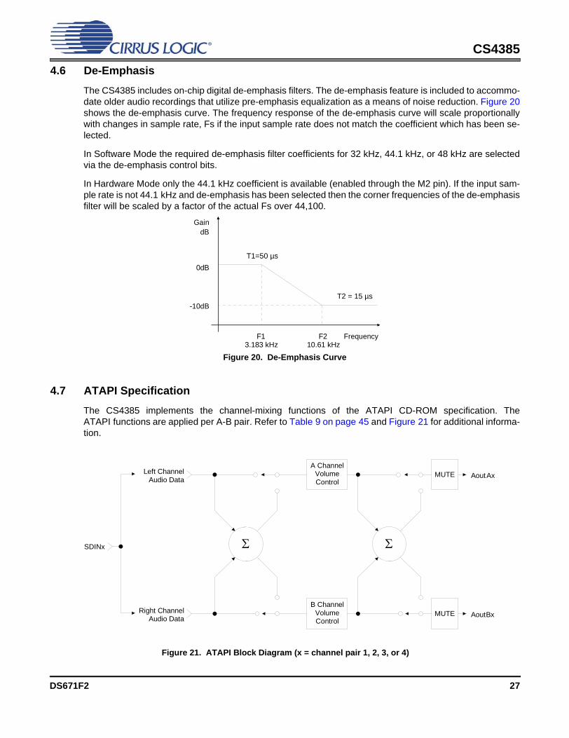
4.7 ATAPI SpecificationThe CS4385 implements the channel-mixing functions of the ATAPI CD-ROM specification. TheATAPI functions are applied per A-B pair. Refer to Table 9 on page 45 and Figure 21 for additional informa-tion.
GaindB
-10dB
0dB
Frequency
T2 = 15 µs
T1=50 µs
F1 F23.183 kHz 10.61 kHz
Figure 20. De-Emphasis Curve
Σ Σ
A ChannelVolumeControl
AoutAx
AoutBx
Left ChannelAudio Data
Right ChannelAudio Data
B ChannelVolumeControl
MUTE
MUTE
SDINx
Figure 21. ATAPI Block Diagram (x = channel pair 1, 2, 3, or 4)
DS671F2 27
CS4385
4.8 Direct Stream Digital (DSD) ModeIn Software Mode, the DSD/PCM bits (Reg. 02h) are used to configure the device for DSD Mode. TheDSD_DIF bits (Reg 04h) then control the expected DSD rate and MCLK ratio.
The DIR_DSD bit (Reg 04h) selects between two proprietary methods for DSD-to-analog conversion. Thefirst method uses a decimation-free DSD processing technique which allows for features such as matchedPCM-level output, DSD volume control, and 50kHz on-chip filter. The second method sends the DSD datadirectly to the on-chip switched-capacitor filter for conversion (without the above-mentioned features).
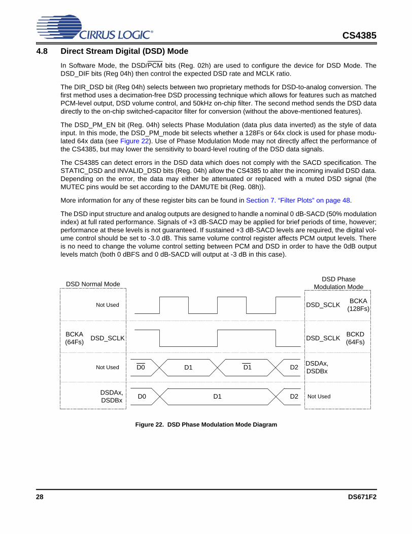
The DSD_PM_EN bit (Reg. 04h) selects Phase Modulation (data plus data inverted) as the style of datainput. In this mode, the DSD_PM_mode bit selects whether a 128Fs or 64x clock is used for phase modu-lated 64x data (see Figure 22). Use of Phase Modulation Mode may not directly affect the performance ofthe CS4385, but may lower the sensitivity to board-level routing of the DSD data signals.
The CS4385 can detect errors in the DSD data which does not comply with the SACD specification. TheSTATIC_DSD and INVALID_DSD bits (Reg. 04h) allow the CS4385 to alter the incoming invalid DSD data.Depending on the error, the data may either be attenuated or replaced with a muted DSD signal (theMUTEC pins would be set according to the DAMUTE bit (Reg. 08h)).
More information for any of these register bits can be found in Section 7. “Filter Plots” on page 48.
The DSD input structure and analog outputs are designed to handle a nominal 0 dB-SACD (50% modulationindex) at full rated performance. Signals of +3 dB-SACD may be applied for brief periods of time, however;performance at these levels is not guaranteed. If sustained +3 dB-SACD levels are required, the digital vol-ume control should be set to -3.0 dB. This same volume control register affects PCM output levels. Thereis no need to change the volume control setting between PCM and DSD in order to have the 0dB outputlevels match (both 0 dBFS and 0 dB-SACD will output at -3 dB in this case).
BCKA(128Fs)
BCKD(64Fs)DSD_SCLK
DSDAx,DSDBx
D1 D1
D1D0 D2
D2D0
DSD_SCLK
DSDAx,DSDBx
BCKA(64Fs)
DSD_SCLK
DSD PhaseModulation ModeDSD Normal Mode
Not Used
Not Used
Not Used
Figure 22. DSD Phase Modulation Mode Diagram
28 DS671F2
CS4385
4.9 Grounding and Power Supply ArrangementsAs with any high-resolution converter, the CS4385 requires careful attention to power supply and groundingarrangements if its potential performance is to be realized. The Typical Connection Diagram shows the rec-ommended power arrangements, with VA, VD, VLC, and VLS connected to clean supplies. If the groundplanes are split between digital ground and analog ground, the GND pins of the CS4385 should be connect-ed to the analog ground plane.
All signals, especially clocks, should be kept away from the FILT+ and VQ pins in order to avoid unwantedcoupling into the DAC.
4.9.1 Capacitor Placement
Decoupling capacitors should be placed as close to the DAC as possible, with the low value ceramic ca-pacitor being the closest. To further minimize impedance, these capacitors should be located on the samelayer as the DAC. If desired, all supply pins with similar voltage ratings may be connected to the samesupply, but a decoupling capacitor should still be placed on each supply pin.
Notes: All decoupling capacitors should be referenced to ground.
The CDB4385 evaluation board demonstrates the optimum layout and power supply arrangements.
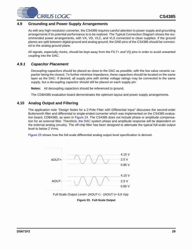
4.10 Analog Output and FilteringThe application note “Design Notes for a 2-Pole Filter with Differential Input” discusses the second-orderButterworth filter and differential to single-ended converter which was implemented on the CS4385 evalua-tion board, CDB4385, as seen in Figure 24. The CS4385 does not include phase or amplitude compensa-tion for an external filter. Therefore, the DAC system phase and amplitude response will be dependent onthe external analog circuitry. The off-chip filter has been designed to attenuate the typical full-scale outputlevel to below 2 Vrms.
Figure 23 shows how the full-scale differential analog output level specification is derived.
AOUT+
AOUT-
Full-Scale Output Level= (AOUT+) - (AOUT-)= 6.6 Vpp
4.15 V2.5 V
0.85 V
4.15 V
2.5 V0.85 V
Figure 23. Full-Scale Output
DS671F2 29
CS4385
4.11 The MUTEC OutputsThe MUTEC1 and MUTEC234 pins have an auto-polarity detect feature. The MUTEC output pins are highimpedance at the time of reset. The external mute circuitry needs to be self-biased into an active state inorder to be muted during reset. Upon release of reset, the CS4385 will detect the status of the MUTEC pins(high or low) and will then select that state as the polarity to drive when the mutes become active. The ex-ternal-bias voltage level that the MUTEC pins see at the time of release of reset must meet the “MUTECauto-detect input high/low voltage” specifications as outlined in the Digital Characteristics section.
Figure 25 shows a single example of both an active high and an active low mute drive circuit. In these de-signs, the pull-up and pull-down resistors have been especially chosen to meet the input high/low thresholdwhen used with the MMUN2111 and MMUN2211 internal bias resistances of 10 kΩ. Use of the Mute Controlfunction is not mandatory, but recommended, for designs requiring the absolute minimum in extraneousclicks and pops. Also, use of the Mute Control function can enable the system designer to achieve idle chan-nel noise/signal-to-noise ratios which are only limited by the external mute circuit.
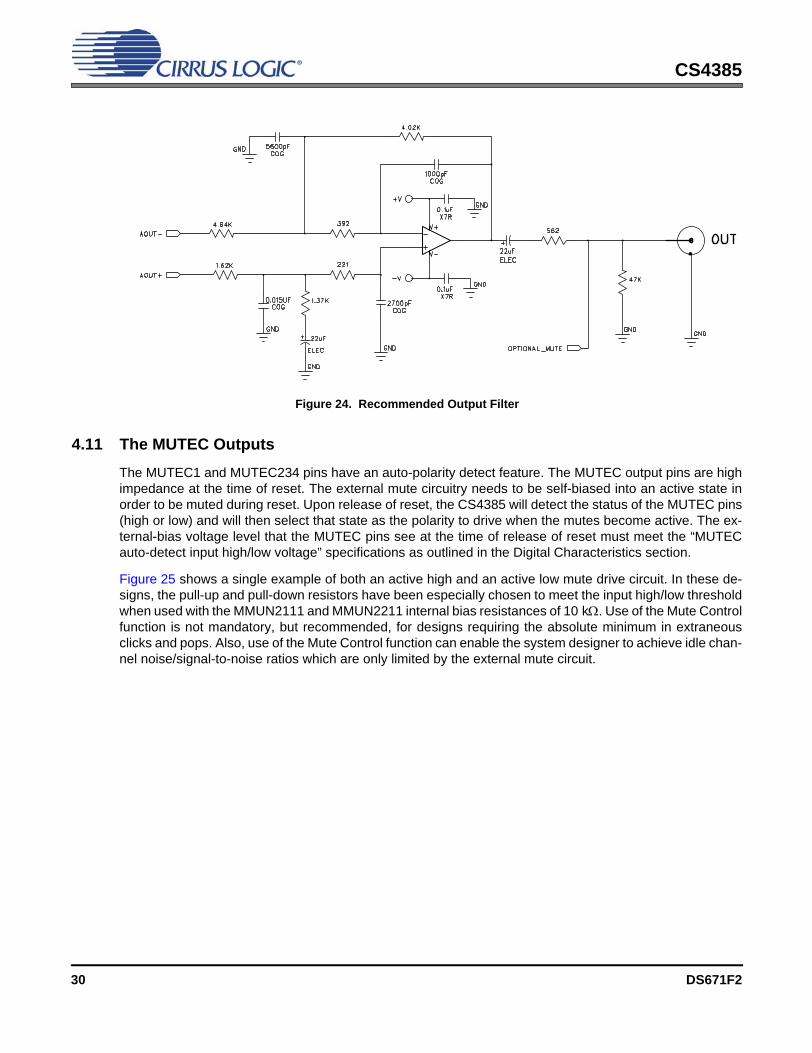
Figure 24. Recommended Output Filter
30 DS671F2

CS4385
4.12 Recommended Power-Up Sequence
4.12.1 Hardware Mode1. Hold RST low until the power supplies and configuration pins are stable, and the master and left/right
clocks are locked to the appropriate frequencies, as discussed in Section 4.1. In this state, the registers are reset to the default settings, FILT+ will remain low, and VQ will be connected to VA/2.If RST can not be held low long enough the SDINx pins should remain static low until all other clocks are stable, and if possible the RST should be toggled low again once the system is stable.
2. Bring RST high. The device will remain in a low power state with FILT+ low and will initiate the Hardware power-up sequence after approximately 512 LRCK cycles in Single-Speed Mode (1024 LRCK cycles in Double-Speed Mode, and 2048 LRCK cycles in Quad-Speed Mode).
Figure 25. Recommended Mute Circuitry
DS671F2 31
CS4385
4.12.2 Software Mode1. Hold RST low until the power supply is stable, and the master and left/right clocks are locked to the appropriate frequencies, as discussed in Section 4.1. In this state, the registers are reset to the default settings, FILT+ will remain low, and VQ will be connected to VA/2.
2. Bring RST high. The device will remain in a low power state with FILT+ low for 512 LRCK cycles in Single-Speed Mode (1024 LRCK cycles in Double-Speed Mode, and 2048 LRCK cycles in Quad-Speed Mode).
3. In order to reduce the chances of clicks and pops, perform a write to the CP_EN bit prior to the completion of approximately 512 LRCK cycles in Single-Speed Mode (1024 LRCK cycles in Double-Speed Mode, and 2048 LRCK cycles in Quad-Speed Mode). The desired register settings can be loaded while keeping the PDN bit set to 1. Set the RMP_UP and RMP_DN bits to 1; then set the format and mode control bits to the desired settings.
If more than the stated range of LRCK cycles passes before CPEN bit is written, the chip will enter Hardware Mode and begin to operate with the M0-M4 as the mode settings. CPEN bit may be written at anytime, even after the Hardware sequence has begun. It is advised that if the CPEN bit cannot be set in time, the SDINx pins should remain static low (this way no audio data can be converted incorrectly by the Hardware Mode settings).
4. Set the PDN bit to 0. This will initiate the power-up sequence, which lasts approximately 50 µs.
4.13 Recommended Procedure for Switching Operational ModesFor systems where the absolute minimum in clicks and pops is required, it is recommended that the MUTEbits are set prior to changing significant DAC functions (such as changing sample rates or clock sources).The mute bits may then be released after clocks have settled and the proper modes have been set.
It is required to have the device held in reset if the minimum high/low time specs of MCLK cannot be metduring clock source changes.
4.14 Control Port Interface The control port is used to load all the internal register settings in order to operate in Software Mode (seeSection 7. “Filter Plots” on page 48). The operation of the control port may be completely asynchronous withthe audio sample rate. However, to avoid potential interference problems, the control port pins should re-main static if no operation is required.
The control port operates in one of two modes: I²C or SPI.
4.14.1 MAP Auto Increment
The device has MAP (memory address pointer) auto-increment capability enabled by the INCR bit (alsothe MSB) of the MAP. If INCR is set to 0, MAP will stay constant for successive I²C writes or reads andSPI writes. If INCR is set to 1, MAP will auto-increment after each byte is written, allowing block reads orwrites of successive registers.
4.14.2 I²C Mode
In the I²C Mode, data is clocked into and out of the bi-directional serial control data line, SDA, by the serialcontrol port clock, SCL (see Figure 26 for the clock to data relationship). There is no CS pin. The AD0 pinenables the user to alter the chip address (001100[AD0][R/W]) and should be tied to VLC or GND, as re-quired, before powering up the device. If the device ever detects a high-to-low transition on the AD0/CSpin after power-up, SPI Mode will be selected.
32 DS671F2
CS4385
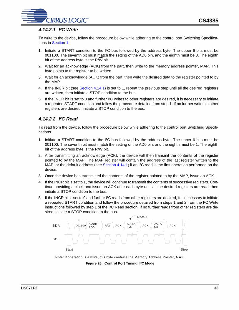
4.14.2.1 I²C WriteTo write to the device, follow the procedure below while adhering to the control port Switching Specifica-tions in Section 1.
1. Initiate a START condition to the I²C bus followed by the address byte. The upper 6 bits must be001100. The seventh bit must match the setting of the AD0 pin, and the eighth must be 0. The eighthbit of the address byte is the R/W bit.
2. Wait for an acknowledge (ACK) from the part, then write to the memory address pointer, MAP. Thisbyte points to the register to be written.
3. Wait for an acknowledge (ACK) from the part, then write the desired data to the register pointed to bythe MAP.
4. If the INCR bit (see Section 4.14.1) is set to 1, repeat the previous step until all the desired registersare written, then initiate a STOP condition to the bus.
5. If the INCR bit is set to 0 and further I²C writes to other registers are desired, it is necessary to initiatea repeated START condition and follow the procedure detailed from step 1. If no further writes to otherregisters are desired, initiate a STOP condition to the bus.
4.14.2.2 I²C Read
To read from the device, follow the procedure below while adhering to the control port Switching Specifi-cations.
1. Initiate a START condition to the I²C bus followed by the address byte. The upper 6 bits must be001100. The seventh bit must match the setting of the AD0 pin, and the eighth must be 1. The eighthbit of the address byte is the R/W bit.
2. After transmitting an acknowledge (ACK), the device will then transmit the contents of the registerpointed to by the MAP. The MAP register will contain the address of the last register written to theMAP, or the default address (see Section 4.14.1) if an I²C read is the first operation performed on thedevice.
3. Once the device has transmitted the contents of the register pointed to by the MAP, issue an ACK.4. If the INCR bit is set to 1, the device will continue to transmit the contents of successive registers. Con-
tinue providing a clock and issue an ACK after each byte until all the desired registers are read, theninitiate a STOP condition to the bus.
5. If the INCR bit is set to 0 and further I²C reads from other registers are desired, it is necessary to initiatea repeated START condition and follow the procedure detailed from steps 1 and 2 from the I²C Writeinstructions followed by step 1 of the I²C Read section. If no further reads from other registers are de-sired, initiate a STOP condition to the bus.
SDA
SCL
001100 ADDRAD0 R/W
Start
ACK DATA1-8 ACK DATA
1-8 ACK
Stop
Note: If operation is a write, th is byte contains the Memory Address Pointer, MAP.
Note 1
Figure 26. Control Port Timing, I²C Mode
DS671F2 33
CS4385
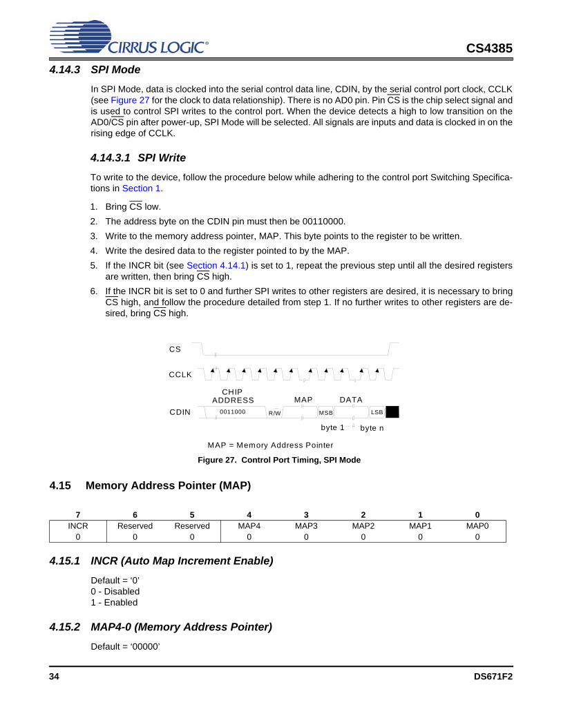
4.14.3 SPI ModeIn SPI Mode, data is clocked into the serial control data line, CDIN, by the serial control port clock, CCLK(see Figure 27 for the clock to data relationship). There is no AD0 pin. Pin CS is the chip select signal andis used to control SPI writes to the control port. When the device detects a high to low transition on theAD0/CS pin after power-up, SPI Mode will be selected. All signals are inputs and data is clocked in on therising edge of CCLK.
4.14.3.1 SPI WriteTo write to the device, follow the procedure below while adhering to the control port Switching Specifica-tions in Section 1.
1. Bring CS low.2. The address byte on the CDIN pin must then be 00110000. 3. Write to the memory address pointer, MAP. This byte points to the register to be written.4. Write the desired data to the register pointed to by the MAP.5. If the INCR bit (see Section 4.14.1) is set to 1, repeat the previous step until all the desired registers
are written, then bring CS high.6. If the INCR bit is set to 0 and further SPI writes to other registers are desired, it is necessary to bring
CS high, and follow the procedure detailed from step 1. If no further writes to other registers are de-sired, bring CS high.
4.15 Memory Address Pointer (MAP)
4.15.1 INCR (Auto Map Increment Enable)
Default = ‘0’0 - Disabled1 - Enabled
4.15.2 MAP4-0 (Memory Address Pointer)
Default = ‘00000’
7 6 5 4 3 2 1 0INCR Reserved Reserved MAP4 MAP3 MAP2 MAP1 MAP0
0 0 0 0 0 0 0 0
MAPMSB LSB
DATA
byte 1 byte n
R/W
MAP = Memory Address Pointer
ADDRESSCHIP
CDIN
CCLK
CS
0011000
Figure 27. Control Port Timing, SPI Mode
34 DS671F2
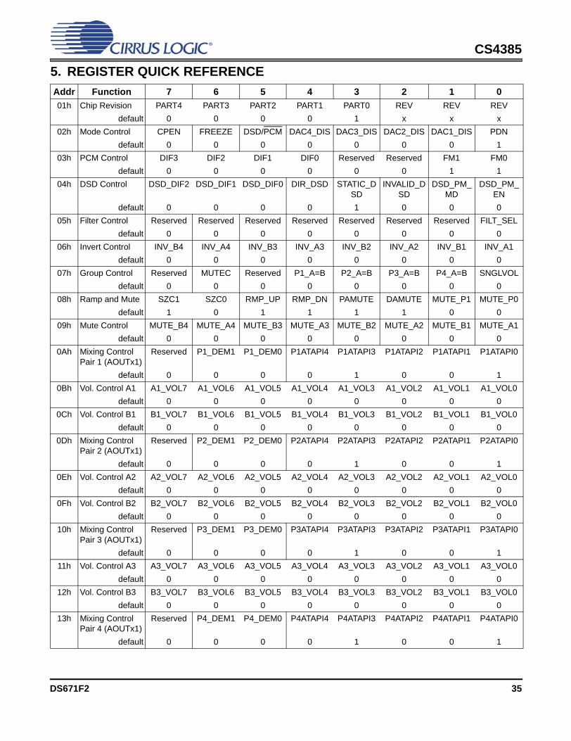
CS4385
5. REGISTER QUICK REFERENCE Addr Function 7 6 5 4 3 2 1 001h Chip Revision PART4 PART3 PART2 PART1 PART0 REV REV REVdefault 0 0 0 0 1 x x x02h Mode Control CPEN FREEZE DSD/PCM DAC4_DIS DAC3_DIS DAC2_DIS DAC1_DIS PDN
default 0 0 0 0 0 0 0 103h PCM Control DIF3 DIF2 DIF1 DIF0 Reserved Reserved FM1 FM0
default 0 0 0 0 0 0 1 104h DSD Control DSD_DIF2 DSD_DIF1 DSD_DIF0 DIR_DSD STATIC_D
SDINVALID_D
SDDSD_PM_
MDDSD_PM_
ENdefault 0 0 0 0 1 0 0 0
05h Filter Control Reserved Reserved Reserved Reserved Reserved Reserved Reserved FILT_SELdefault 0 0 0 0 0 0 0 0
06h Invert Control INV_B4 INV_A4 INV_B3 INV_A3 INV_B2 INV_A2 INV_B1 INV_A1default 0 0 0 0 0 0 0 0
07h Group Control Reserved MUTEC Reserved P1_A=B P2_A=B P3_A=B P4_A=B SNGLVOLdefault 0 0 0 0 0 0 0 0
08h Ramp and Mute SZC1 SZC0 RMP_UP RMP_DN PAMUTE DAMUTE MUTE_P1 MUTE_P0default 1 0 1 1 1 1 0 0
09h Mute Control MUTE_B4 MUTE_A4 MUTE_B3 MUTE_A3 MUTE_B2 MUTE_A2 MUTE_B1 MUTE_A1default 0 0 0 0 0 0 0 0
0Ah Mixing Control Pair 1 (AOUTx1)
Reserved P1_DEM1 P1_DEM0 P1ATAPI4 P1ATAPI3 P1ATAPI2 P1ATAPI1 P1ATAPI0
default 0 0 0 0 1 0 0 10Bh Vol. Control A1 A1_VOL7 A1_VOL6 A1_VOL5 A1_VOL4 A1_VOL3 A1_VOL2 A1_VOL1 A1_VOL0
default 0 0 0 0 0 0 0 00Ch Vol. Control B1 B1_VOL7 B1_VOL6 B1_VOL5 B1_VOL4 B1_VOL3 B1_VOL2 B1_VOL1 B1_VOL0
default 0 0 0 0 0 0 0 00Dh Mixing Control
Pair 2 (AOUTx1)Reserved P2_DEM1 P2_DEM0 P2ATAPI4 P2ATAPI3 P2ATAPI2 P2ATAPI1 P2ATAPI0
default 0 0 0 0 1 0 0 10Eh Vol. Control A2 A2_VOL7 A2_VOL6 A2_VOL5 A2_VOL4 A2_VOL3 A2_VOL2 A2_VOL1 A2_VOL0
default 0 0 0 0 0 0 0 00Fh Vol. Control B2 B2_VOL7 B2_VOL6 B2_VOL5 B2_VOL4 B2_VOL3 B2_VOL2 B2_VOL1 B2_VOL0
default 0 0 0 0 0 0 0 010h Mixing Control
Pair 3 (AOUTx1)Reserved P3_DEM1 P3_DEM0 P3ATAPI4 P3ATAPI3 P3ATAPI2 P3ATAPI1 P3ATAPI0
default 0 0 0 0 1 0 0 111h Vol. Control A3 A3_VOL7 A3_VOL6 A3_VOL5 A3_VOL4 A3_VOL3 A3_VOL2 A3_VOL1 A3_VOL0
default 0 0 0 0 0 0 0 012h Vol. Control B3 B3_VOL7 B3_VOL6 B3_VOL5 B3_VOL4 B3_VOL3 B3_VOL2 B3_VOL1 B3_VOL0
default 0 0 0 0 0 0 0 013h Mixing Control
Pair 4 (AOUTx1)Reserved P4_DEM1 P4_DEM0 P4ATAPI4 P4ATAPI3 P4ATAPI2 P4ATAPI1 P4ATAPI0
default 0 0 0 0 1 0 0 1
DS671F2 35
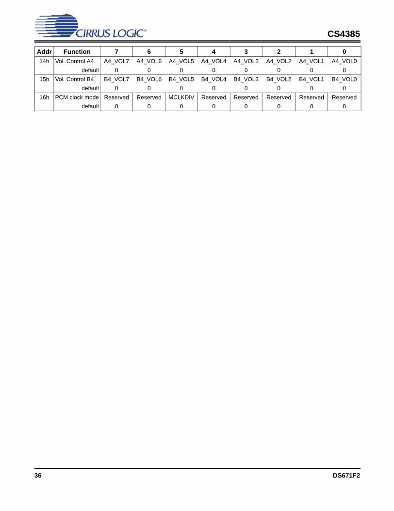
CS4385
14h Vol. Control A4 A4_VOL7 A4_VOL6 A4_VOL5 A4_VOL4 A4_VOL3 A4_VOL2 A4_VOL1 A4_VOL0default 0 0 0 0 0 0 0 0
15h Vol. Control B4 B4_VOL7 B4_VOL6 B4_VOL5 B4_VOL4 B4_VOL3 B4_VOL2 B4_VOL1 B4_VOL0default 0 0 0 0 0 0 0 0
16h PCM clock mode Reserved Reserved MCLKDIV Reserved Reserved Reserved Reserved Reserveddefault 0 0 0 0 0 0 0 0
Addr Function 7 6 5 4 3 2 1 0
36 DS671F2
CS4385
6. REGISTER DESCRIPTIONNote: All registers are read/write in I²C Mode and write only in SPI, unless otherwise noted.6.1 Chip Revision (address 01h)
6.1.1 Part Number ID (PART) [Read Only]00001- CS4385
Revision ID (REV) [Read Only]
000 - Revision A0001 - Revision B0
Function:
This read-only register can be used to identify the model and revision number of the device.
6.2 Mode Control 1 (address 02h)
6.2.1 Control Port Enable (CPEN)
Default = 00 - Disabled1 - Enabled
Function:
This bit defaults to 0, allowing the device to power-up in Stand-Alone Mode. The Control Port Mode canbe accessed by setting this bit to 1. This will allow the operation of the device to be controlled by the reg-isters, and the pin definitions will conform to Control Port Mode. To accomplish a clean power-up, the usershould write this bit within 10 ms following the release of Reset.
6.2.2 Freeze Controls (FREEZE)
Default = 00 - Disabled1 - Enabled
Function:
This function allows modifications to be made to the registers without the changes taking effect until theFREEZE is disabled. To make multiple changes in the Control port registers take effect simultaneously,enable the FREEZE Bit, make all register changes, then Disable the FREEZE bit.
7 6 5 4 3 2 1 0PART4 PART3 PART2 PART1 PART0 REV2 REV1 REV0
0 0 0 0 1 - - -
7 6 5 4 3 2 1 0CPEN FREEZE DSD/PCM DAC4_DIS DAC3_DIS DAC2_DIS DAC1_DIS PDN
0 0 0 0 0 0 0 1
DS671F2 37
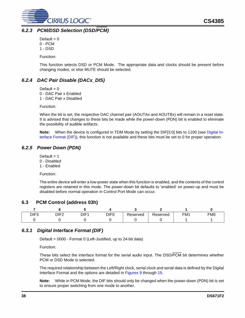
CS4385
6.2.3 PCM/DSD Selection (DSD/PCM)Default = 00 - PCM1 - DSD
Function:
This function selects DSD or PCM Mode. The appropriate data and clocks should be present beforechanging modes, or else MUTE should be selected.
6.2.4 DAC Pair Disable (DACx_DIS)
Default = 00 - DAC Pair x Enabled1 - DAC Pair x Disabled
Function:
When the bit is set, the respective DAC channel pair (AOUTAx and AOUTBx) will remain in a reset state.It is advised that changes to these bits be made while the power-down (PDN) bit is enabled to eliminatethe possibility of audible artifacts.
Note: When the device is configured in TDM Mode by setting the DIF[3:0] bits to 1100 (see Digital In-terface Format (DIF)), this function is not available and these bits must be set to 0 for proper operation.
6.2.5 Power Down (PDN)
Default = 10 - Disabled1 - Enabled
Function:
The entire device will enter a low-power state when this function is enabled, and the contents of the controlregisters are retained in this mode. The power-down bit defaults to ‘enabled’ on power-up and must bedisabled before normal operation in Control Port Mode can occur.
6.3 PCM Control (address 03h)
6.3.1 Digital Interface Format (DIF)Default = 0000 - Format 0 (Left-Justified, up to 24-bit data)
Function:
These bits select the interface format for the serial audio input. The DSD/PCM bit determines whetherPCM or DSD Mode is selected.
The required relationship between the Left/Right clock, serial clock and serial data is defined by the DigitalInterface Format and the options are detailed in Figures 9 through 19.
Note: While in PCM Mode, the DIF bits should only be changed when the power-down (PDN) bit is setto ensure proper switching from one mode to another.
7 6 5 4 3 2 1 0DIF3 DIF2 DIF1 DIF0 Reserved Reserved FM1 FM0
0 0 0 0 0 0 1 1
38 DS671F2

CS4385
6.3.2 Functional Mode (FM)Default = 1100 - Single-Speed Mode (4 to 50 kHz sample rates)01 - Double-Speed Mode (50 to 100 kHz sample rates)10 - Quad-Speed Mode (100 to 200 kHz sample rates)11 - Auto Speed Mode detect (32 kHz to 200 kHz sample rates)
Function:
Selects the required range of input sample rates or Auto Speed Mode.
6.4 DSD Control (address 04h)
6.4.1 DSD Mode Digital Interface Format (DSD_DIF)
Default = 000 - Format 0 (64x oversampled DSD data with a 4x MCLK to DSD data rate)
Function:
The relationship between the oversampling ratio of the DSD audio data and the required Master clock-to-DSD-data rate is defined by the Digital Interface Format pins.
The DSD/PCM bit determines whether PCM or DSD Mode is selected.
DIF3 DIF2 DIF1 DIF0 DESCRIPTION FORMAT0 0 0 0 Left-Justified, up to 24-bit data 00 0 0 1 I²S, up to 24-bit data 10 0 1 0 Right-Justified, 16-bit data 20 0 1 1 Right-Justified, 24-bit data 30 1 0 0 Right-Justified, 20-bit data 40 1 0 1 Right-Justified, 18-bit data 51 0 0 0 One-Line Mode 1, 24-bit Data +SDIN4 81 0 0 1 One-Line Mode 2, 20-bit Data +SDIN4 91 0 1 0 One-Line Mode 3, 24-bit 6-channel 101 0 1 1 One-Line Mode 4, 20-bit 6-channel 111 1 0 0 TDM 12X X X X All other combinations are Reserved
Table 7. Digital Interface Formats - PCM Mode
7 6 5 4 3 2 1 0DSD_DIF2 DSD_DIF1 DSD_DIF0 DIR_DSD STATIC_DSD INVALID_DSD DSD_PM_MD DSD_PM_EN
0 0 0 0 1 1 0 0
DIF2 DIF1 DIFO DESCRIPTION0 0 0 64x oversampled DSD data with a 4x MCLK to DSD data rate0 0 1 64x oversampled DSD data with a 6x MCLK to DSD data rate0 1 0 64x oversampled DSD data with a 8x MCLK to DSD data rate0 1 1 64x oversampled DSD data with a 12x MCLK to DSD data rate1 0 0 128x oversampled DSD data with a 2x MCLK to DSD data rate1 0 1 128x oversampled DSD data with a 3x MCLK to DSD data rate1 1 0 128x oversampled DSD data with a 4x MCLK to DSD data rate1 1 1 128x oversampled DSD data with a 6x MCLK to DSD data rate
Table 8. Digital Interface Formats - DSD Mode
DS671F2 39
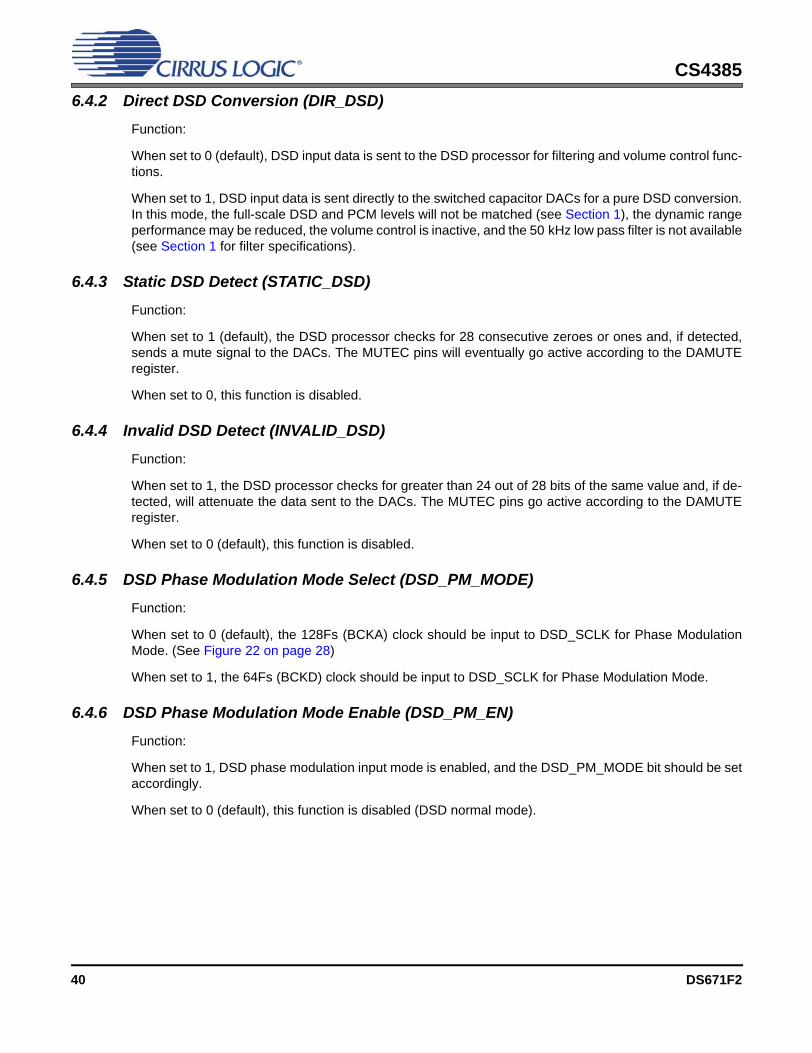
CS4385
6.4.2 Direct DSD Conversion (DIR_DSD)Function:
When set to 0 (default), DSD input data is sent to the DSD processor for filtering and volume control func-tions.
When set to 1, DSD input data is sent directly to the switched capacitor DACs for a pure DSD conversion.In this mode, the full-scale DSD and PCM levels will not be matched (see Section 1), the dynamic rangeperformance may be reduced, the volume control is inactive, and the 50 kHz low pass filter is not available(see Section 1 for filter specifications).
6.4.3 Static DSD Detect (STATIC_DSD)
Function:
When set to 1 (default), the DSD processor checks for 28 consecutive zeroes or ones and, if detected,sends a mute signal to the DACs. The MUTEC pins will eventually go active according to the DAMUTEregister.
When set to 0, this function is disabled.
6.4.4 Invalid DSD Detect (INVALID_DSD)Function:
When set to 1, the DSD processor checks for greater than 24 out of 28 bits of the same value and, if de-tected, will attenuate the data sent to the DACs. The MUTEC pins go active according to the DAMUTEregister.
When set to 0 (default), this function is disabled.
6.4.5 DSD Phase Modulation Mode Select (DSD_PM_MODE) Function:
When set to 0 (default), the 128Fs (BCKA) clock should be input to DSD_SCLK for Phase ModulationMode. (See Figure 22 on page 28)
When set to 1, the 64Fs (BCKD) clock should be input to DSD_SCLK for Phase Modulation Mode.
6.4.6 DSD Phase Modulation Mode Enable (DSD_PM_EN)
Function:
When set to 1, DSD phase modulation input mode is enabled, and the DSD_PM_MODE bit should be setaccordingly.
When set to 0 (default), this function is disabled (DSD normal mode).
40 DS671F2
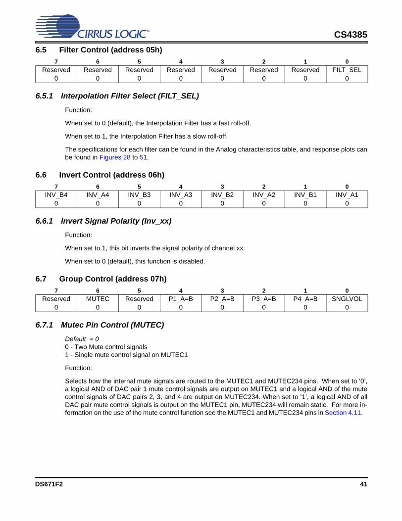
CS4385
6.5 Filter Control (address 05h)6.5.1 Interpolation Filter Select (FILT_SEL) Function:
When set to 0 (default), the Interpolation Filter has a fast roll-off.
When set to 1, the Interpolation Filter has a slow roll-off.
The specifications for each filter can be found in the Analog characteristics table, and response plots canbe found in Figures 28 to 51.
6.6 Invert Control (address 06h)
6.6.1 Invert Signal Polarity (Inv_xx)Function:
When set to 1, this bit inverts the signal polarity of channel xx.
When set to 0 (default), this function is disabled.
6.7 Group Control (address 07h)
6.7.1 Mutec Pin Control (MUTEC)
Default = 00 - Two Mute control signals1 - Single mute control signal on MUTEC1
Function:
Selects how the internal mute signals are routed to the MUTEC1 and MUTEC234 pins. When set to ‘0’,a logical AND of DAC pair 1 mute control signals are output on MUTEC1 and a logical AND of the mutecontrol signals of DAC pairs 2, 3, and 4 are output on MUTEC234. When set to ‘1’, a logical AND of allDAC pair mute control signals is output on the MUTEC1 pin, MUTEC234 will remain static. For more in-formation on the use of the mute control function see the MUTEC1 and MUTEC234 pins in Section 4.11.
7 6 5 4 3 2 1 0Reserved Reserved Reserved Reserved Reserved Reserved Reserved FILT_SEL
0 0 0 0 0 0 0 0
7 6 5 4 3 2 1 0INV_B4 INV_A4 INV_B3 INV_A3 INV_B2 INV_A2 INV_B1 INV_A1
0 0 0 0 0 0 0 0
7 6 5 4 3 2 1 0Reserved MUTEC Reserved P1_A=B P2_A=B P3_A=B P4_A=B SNGLVOL
0 0 0 0 0 0 0 0
DS671F2 41
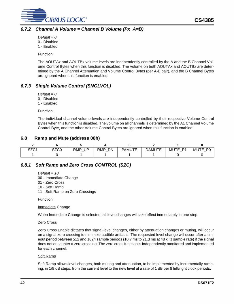
CS4385
6.7.2 Channel A Volume = Channel B Volume (Px_A=B)Default = 00 - Disabled1 - Enabled
Function:
The AOUTAx and AOUTBx volume levels are independently controlled by the A and the B Channel Vol-ume Control Bytes when this function is disabled. The volume on both AOUTAx and AOUTBx are deter-mined by the A Channel Attenuation and Volume Control Bytes (per A-B pair), and the B Channel Bytesare ignored when this function is enabled.
6.7.3 Single Volume Control (SNGLVOL)
Default = 00 - Disabled1 - Enabled
Function:
The individual channel volume levels are independently controlled by their respective Volume ControlBytes when this function is disabled. The volume on all channels is determined by the A1 Channel VolumeControl Byte, and the other Volume Control Bytes are ignored when this function is enabled.
6.8 Ramp and Mute (address 08h)
6.8.1 Soft Ramp and Zero Cross CONTROL (SZC)Default = 1000 - Immediate Change01 - Zero Cross 10 - Soft Ramp11 - Soft Ramp on Zero Crossings
Function:
Immediate Change
When Immediate Change is selected, all level changes will take effect immediately in one step.
Zero Cross
Zero Cross Enable dictates that signal-level changes, either by attenuation changes or muting, will occuron a signal zero crossing to minimize audible artifacts. The requested level change will occur after a tim-eout period between 512 and 1024 sample periods (10.7 ms to 21.3 ms at 48 kHz sample rate) if the signaldoes not encounter a zero crossing. The zero cross function is independently monitored and implementedfor each channel.
Soft Ramp
Soft Ramp allows level changes, both muting and attenuation, to be implemented by incrementally ramp-ing, in 1/8 dB steps, from the current level to the new level at a rate of 1 dB per 8 left/right clock periods.
7 6 5 4 3 2 1 0SZC1 SZC0 RMP_UP RMP_DN PAMUTE DAMUTE MUTE_P1 MUTE_P0
1 0 1 1 1 1 0 0
42 DS671F2
CS4385
Soft Ramp on Zero CrossingSoft Ramp and Zero Cross Enable dictates that signal-level changes, either by attenuation changes ormuting, will occur in 1/8 dB steps and be implemented on a signal zero crossing. The 1/8 dB level changewill occur after a timeout period between 512 and 1024 sample periods (10.7 ms to 21.3 ms at 48 kHzsample rate) if the signal does not encounter a zero crossing. The zero cross function is independentlymonitored and implemented for each channel.
6.8.2 Soft Volume Ramp-Up after Error (RMP_UP)
Function:
An un-mute will be performed after executing an LRCK/MCLK ratio change or error, and after changingthe Functional Mode.
When set to 1 (default), this unmute is effected, similar to attenuation changes, by the Soft and Zero Crossbits in the Volume and Mixing Control register.
When set to 0, an immediate unmute is performed in these instances.
Note: For best results, it is recommended that this feature be used in conjunction with the RMP_DN bit.
6.8.3 Soft Ramp-Down before Filter Mode Change (RMP_DN)
Function:
If either the FILT_SEL or DEM bits are changed the DAC will stop conversion for a period of time tochange its filter values. This bit selects how the data is effected prior to and after the change of the filtervalues.
When set to 1 (default), a mute will be performed prior to executing a filter mode change and an un-mutewill be performed after executing the filter mode change. This mute and un-mute are effected, similar toattenuation changes, by the Soft and Zero Cross bits in the Volume and Mixing Control register.
When set to 0, an immediate mute is performed prior to executing a filter mode change.
Note: For best results, it is recommended that this feature be used in conjunction with the RMP_UP bit.
6.8.4 PCM Auto-Mute (PAMUTE) Function:
When set to 1 (default), the Digital-to-Analog converter output will mute following the reception of 8192consecutive audio samples of static 0 or -1. A single sample of non-static data will release the mute. De-tection and muting is done independently for each channel. The quiescent voltage on the output will beretained and the Mute Control pin will go active during the mute period.
When set to 0, this function is disabled.
DS671F2 43
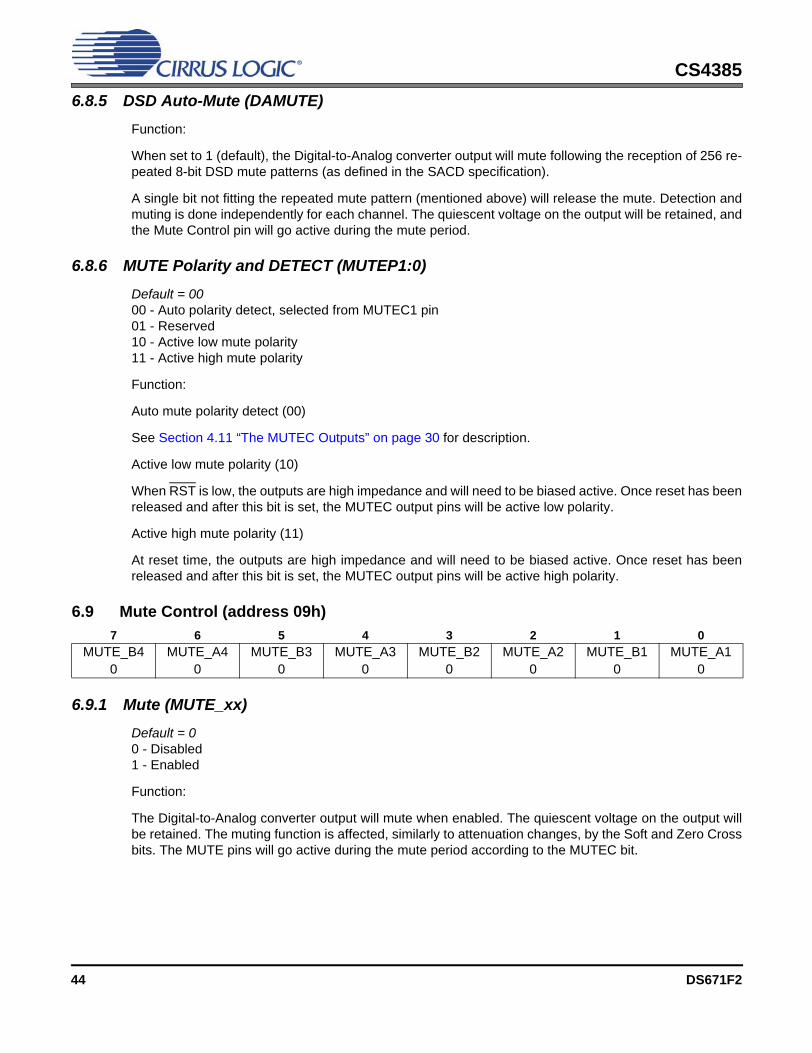
CS4385
6.8.5 DSD Auto-Mute (DAMUTE)Function:
When set to 1 (default), the Digital-to-Analog converter output will mute following the reception of 256 re-peated 8-bit DSD mute patterns (as defined in the SACD specification).
A single bit not fitting the repeated mute pattern (mentioned above) will release the mute. Detection andmuting is done independently for each channel. The quiescent voltage on the output will be retained, andthe Mute Control pin will go active during the mute period.
6.8.6 MUTE Polarity and DETECT (MUTEP1:0)
Default = 0000 - Auto polarity detect, selected from MUTEC1 pin01 - Reserved 10 - Active low mute polarity11 - Active high mute polarity
Function:
Auto mute polarity detect (00)
See Section 4.11 “The MUTEC Outputs” on page 30 for description.
Active low mute polarity (10)
When RST is low, the outputs are high impedance and will need to be biased active. Once reset has beenreleased and after this bit is set, the MUTEC output pins will be active low polarity.
Active high mute polarity (11)
At reset time, the outputs are high impedance and will need to be biased active. Once reset has beenreleased and after this bit is set, the MUTEC output pins will be active high polarity.
6.9 Mute Control (address 09h)
6.9.1 Mute (MUTE_xx)Default = 00 - Disabled1 - Enabled
Function:
The Digital-to-Analog converter output will mute when enabled. The quiescent voltage on the output willbe retained. The muting function is affected, similarly to attenuation changes, by the Soft and Zero Crossbits. The MUTE pins will go active during the mute period according to the MUTEC bit.
7 6 5 4 3 2 1 0MUTE_B4 MUTE_A4 MUTE_B3 MUTE_A3 MUTE_B2 MUTE_A2 MUTE_B1 MUTE_A1
0 0 0 0 0 0 0 0
44 DS671F2
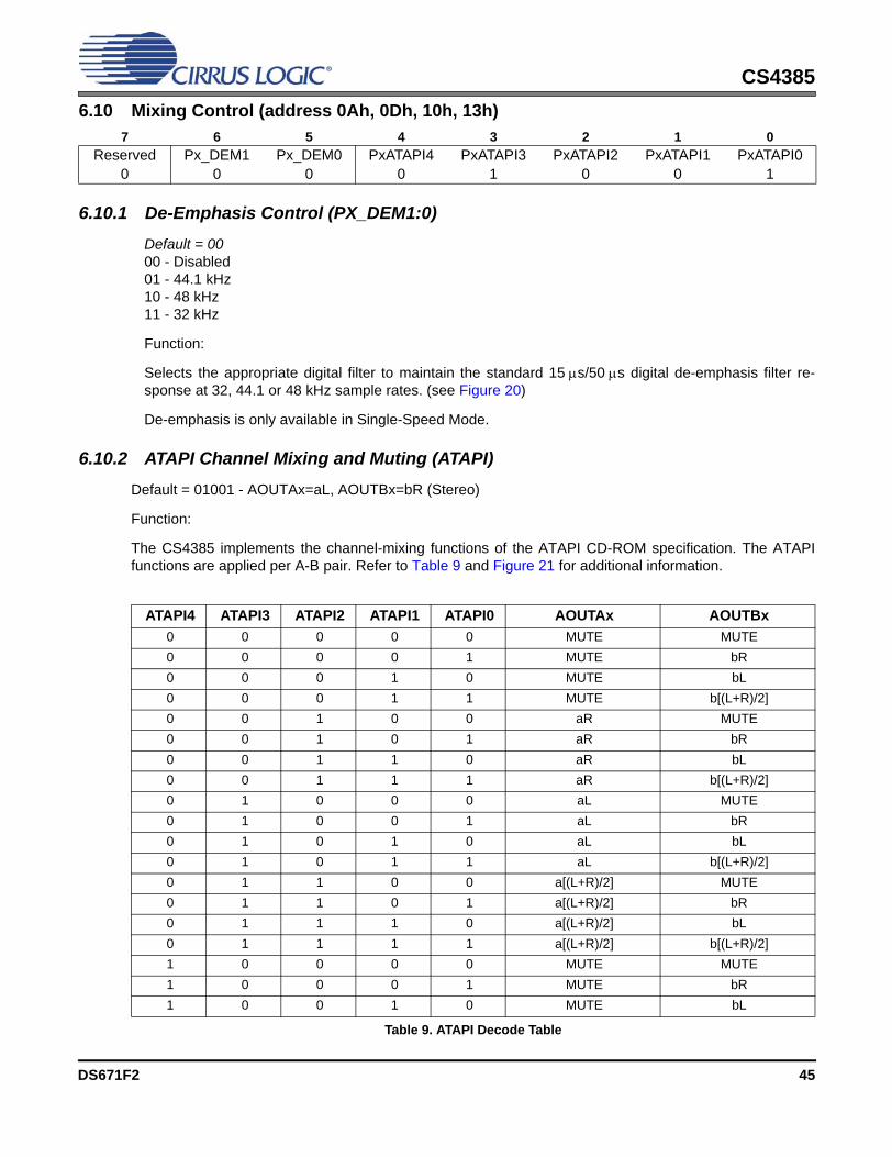
CS4385
6.10 Mixing Control (address 0Ah, 0Dh, 10h, 13h)6.10.1 De-Emphasis Control (PX_DEM1:0)Default = 0000 - Disabled01 - 44.1 kHz10 - 48 kHz11 - 32 kHz
Function:
Selects the appropriate digital filter to maintain the standard 15 μs/50 μs digital de-emphasis filter re-sponse at 32, 44.1 or 48 kHz sample rates. (see Figure 20)
De-emphasis is only available in Single-Speed Mode.
6.10.2 ATAPI Channel Mixing and Muting (ATAPI)
Default = 01001 - AOUTAx=aL, AOUTBx=bR (Stereo)
Function:
The CS4385 implements the channel-mixing functions of the ATAPI CD-ROM specification. The ATAPIfunctions are applied per A-B pair. Refer to Table 9 and Figure 21 for additional information.
7 6 5 4 3 2 1 0Reserved Px_DEM1 Px_DEM0 PxATAPI4 PxATAPI3 PxATAPI2 PxATAPI1 PxATAPI0
0 0 0 0 1 0 0 1
ATAPI4 ATAPI3 ATAPI2 ATAPI1 ATAPI0 AOUTAx AOUTBx0 0 0 0 0 MUTE MUTE0 0 0 0 1 MUTE bR0 0 0 1 0 MUTE bL0 0 0 1 1 MUTE b[(L+R)/2]0 0 1 0 0 aR MUTE0 0 1 0 1 aR bR0 0 1 1 0 aR bL0 0 1 1 1 aR b[(L+R)/2]0 1 0 0 0 aL MUTE0 1 0 0 1 aL bR0 1 0 1 0 aL bL0 1 0 1 1 aL b[(L+R)/2]0 1 1 0 0 a[(L+R)/2] MUTE0 1 1 0 1 a[(L+R)/2] bR0 1 1 1 0 a[(L+R)/2] bL0 1 1 1 1 a[(L+R)/2] b[(L+R)/2]1 0 0 0 0 MUTE MUTE1 0 0 0 1 MUTE bR1 0 0 1 0 MUTE bL
Table 9. ATAPI Decode Table
DS671F2 45
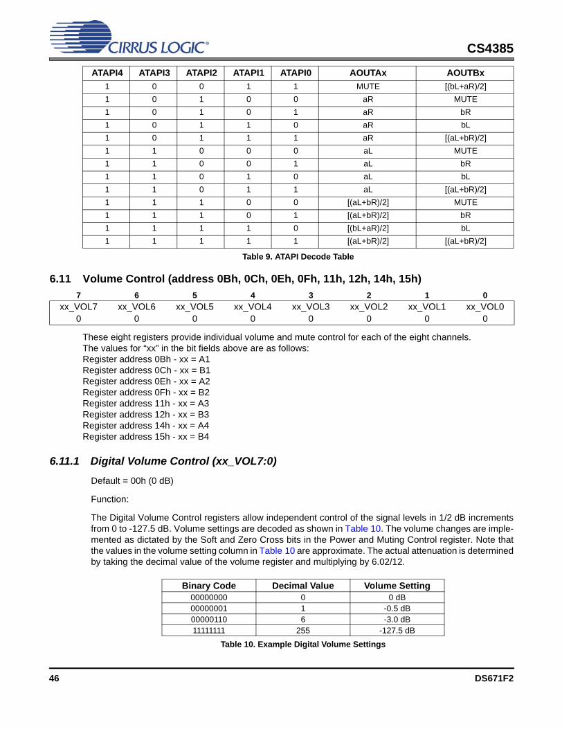
CS4385
6.11 Volume Control (address 0Bh, 0Ch, 0Eh, 0Fh, 11h, 12h, 14h, 15h)
These eight registers provide individual volume and mute control for each of the eight channels.The values for “xx” in the bit fields above are as follows:Register address 0Bh - xx = A1Register address 0Ch - xx = B1Register address 0Eh - xx = A2Register address 0Fh - xx = B2Register address 11h - xx = A3Register address 12h - xx = B3Register address 14h - xx = A4Register address 15h - xx = B4
6.11.1 Digital Volume Control (xx_VOL7:0)
Default = 00h (0 dB)
Function:
The Digital Volume Control registers allow independent control of the signal levels in 1/2 dB incrementsfrom 0 to -127.5 dB. Volume settings are decoded as shown in Table 10. The volume changes are imple-mented as dictated by the Soft and Zero Cross bits in the Power and Muting Control register. Note thatthe values in the volume setting column in Table 10 are approximate. The actual attenuation is determinedby taking the decimal value of the volume register and multiplying by 6.02/12.
1 0 0 1 1 MUTE [(bL+aR)/2]1 0 1 0 0 aR MUTE1 0 1 0 1 aR bR1 0 1 1 0 aR bL1 0 1 1 1 aR [(aL+bR)/2]1 1 0 0 0 aL MUTE1 1 0 0 1 aL bR1 1 0 1 0 aL bL1 1 0 1 1 aL [(aL+bR)/2]1 1 1 0 0 [(aL+bR)/2] MUTE1 1 1 0 1 [(aL+bR)/2] bR1 1 1 1 0 [(bL+aR)/2] bL1 1 1 1 1 [(aL+bR)/2] [(aL+bR)/2]
7 6 5 4 3 2 1 0xx_VOL7 xx_VOL6 xx_VOL5 xx_VOL4 xx_VOL3 xx_VOL2 xx_VOL1 xx_VOL0
0 0 0 0 0 0 0 0
Binary Code Decimal Value Volume Setting00000000 0 0 dB00000001 1 -0.5 dB00000110 6 -3.0 dB11111111 255 -127.5 dB
Table 10. Example Digital Volume Settings
ATAPI4 ATAPI3 ATAPI2 ATAPI1 ATAPI0 AOUTAx AOUTBx
Table 9. ATAPI Decode Table
46 DS671F2
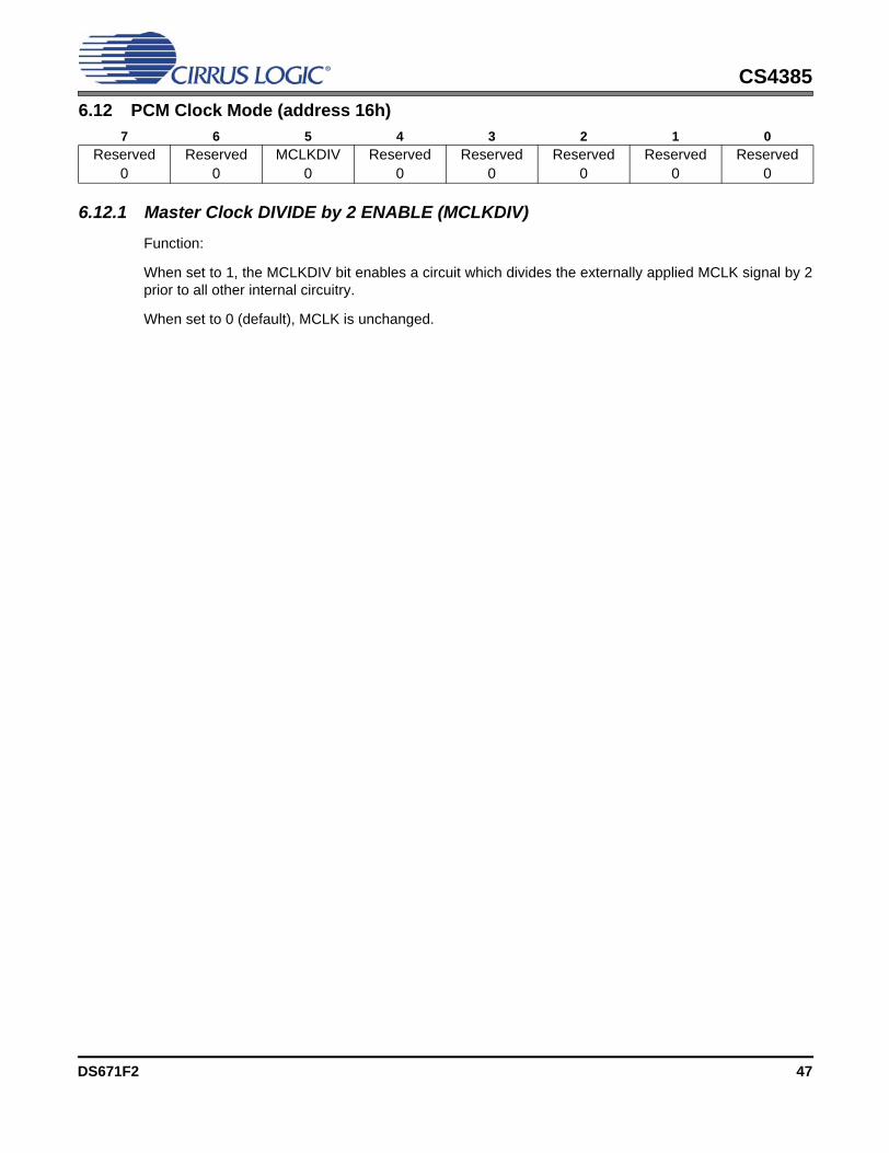
CS4385
6.12 PCM Clock Mode (address 16h)6.12.1 Master Clock DIVIDE by 2 ENABLE (MCLKDIV) Function:
When set to 1, the MCLKDIV bit enables a circuit which divides the externally applied MCLK signal by 2prior to all other internal circuitry.
When set to 0 (default), MCLK is unchanged.
7 6 5 4 3 2 1 0Reserved Reserved MCLKDIV Reserved Reserved Reserved Reserved Reserved
0 0 0 0 0 0 0 0
DS671F2 47
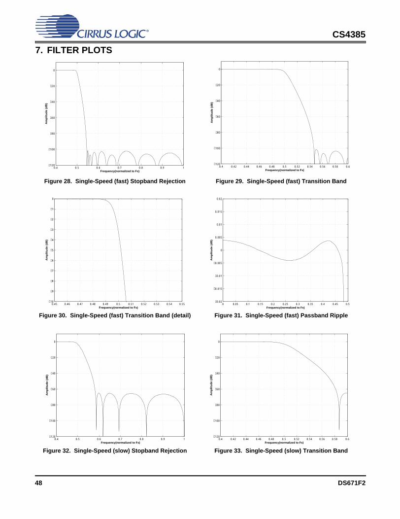
CS4385
7. FILTER PLOTS0.4 0.5 0.6 0.7 0.8 0.9 1−120
−100
−80
−60
−40
−20
0
Frequency(normalized to Fs)
Am
plit
ud
e (d
B)
0.4 0.42 0.44 0.46 0.48 0.5 0.52 0.54 0.56 0.58 0.6−120
−100
−80
−60
−40
−20
0
Frequency(normalized to Fs)
Am
plit
ud
e (d
B)
Figure 28. Single-Speed (fast) Stopband Rejection Figure 29. Single-Speed (fast) Transition Band
0.45 0.46 0.47 0.48 0.49 0.5 0.51 0.52 0.53 0.54 0.55−10
−9
−8
−7
−6
−5
−4
−3
−2
−1
0
Frequency(normalized to Fs)
Am
plit
ud
e (d
B)
0 0.05 0.1 0.15 0.2 0.25 0.3 0.35 0.4 0.45 0.5−0.02
−0.015
−0.01
−0.005
0
0.005
0.01
0.015
0.02
Frequency(normalized to Fs)
Am
plit
ud
e (d
B)
Figure 30. Single-Speed (fast) Transition Band (detail) Figure 31. Single-Speed (fast) Passband Ripple
0.4 0.5 0.6 0.7 0.8 0.9 1−120
−100
−80
−60
−40
−20
0
Frequency(normalized to Fs)
Am
plit
ud
e (d
B)
0.4 0.42 0.44 0.46 0.48 0.5 0.52 0.54 0.56 0.58 0.6−120
−100
−80
−60
−40
−20
0
Frequency(normalized to Fs)
Am
plit
ud
e (d
B)
Figure 32. Single-Speed (slow) Stopband Rejection Figure 33. Single-Speed (slow) Transition Band
48 DS671F2
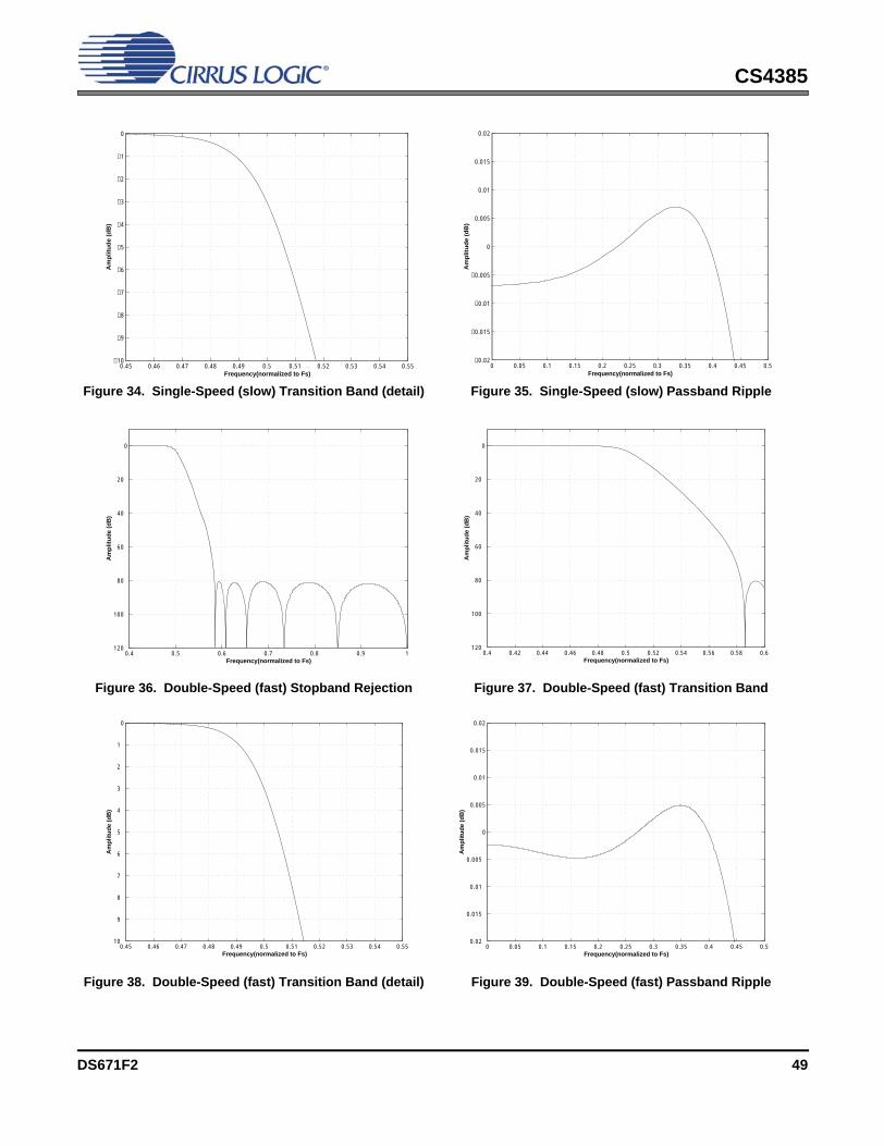
CS4385
0 0.05 0.1 0.15 0.2 0.25 0.3 0.35 0.4 0.45 0.5−0.02
−0.015
−0.01
−0.005
0
0.005
0.01
0.015
0.02
Frequency(normalized to Fs)
Am
plit
ud
e (d
B)
0.45 0.46 0.47 0.48 0.49 0.5 0.51 0.52 0.53 0.54 0.55−10
−9
−8
−7
−6
−5
−4
−3
−2
−1
0
Frequency(normalized to Fs)
Am
plit
ud
e (d
B)
Figure 34. Single-Speed (slow) Transition Band (detail) Figure 35. Single-Speed (slow) Passband Ripple
0.4 0.5 0.6 0.7 0.8 0.9 1120
100
80
60
40
20
0
Frequency(normalized to Fs)
Am
plit
ud
e (d
B)
0.4 0.42 0.44 0.46 0.48 0.5 0.52 0.54 0.56 0.58 0.6120
100
80
60
40
20
0
Frequency(normalized to Fs)
Am
plit
ud
e (d
B)
Figure 36. Double-Speed (fast) Stopband Rejection Figure 37. Double-Speed (fast) Transition Band
0.45 0.46 0.47 0.48 0.49 0.5 0.51 0.52 0.53 0.54 0.5510
9
8
7
6
5
4
3
2
1
0
Frequency(normalized to Fs)
Am
plit
ud
e (d
B)
0 0.05 0.1 0.15 0.2 0.25 0.3 0.35 0.4 0.45 0.50.02
0.015
0.01
0.005
0
0.005
0.01
0.015
0.02
Frequency(normalized to Fs)
Am
plit
ud
e (d
B)
Figure 38. Double-Speed (fast) Transition Band (detail) Figure 39. Double-Speed (fast) Passband Ripple
DS671F2 49
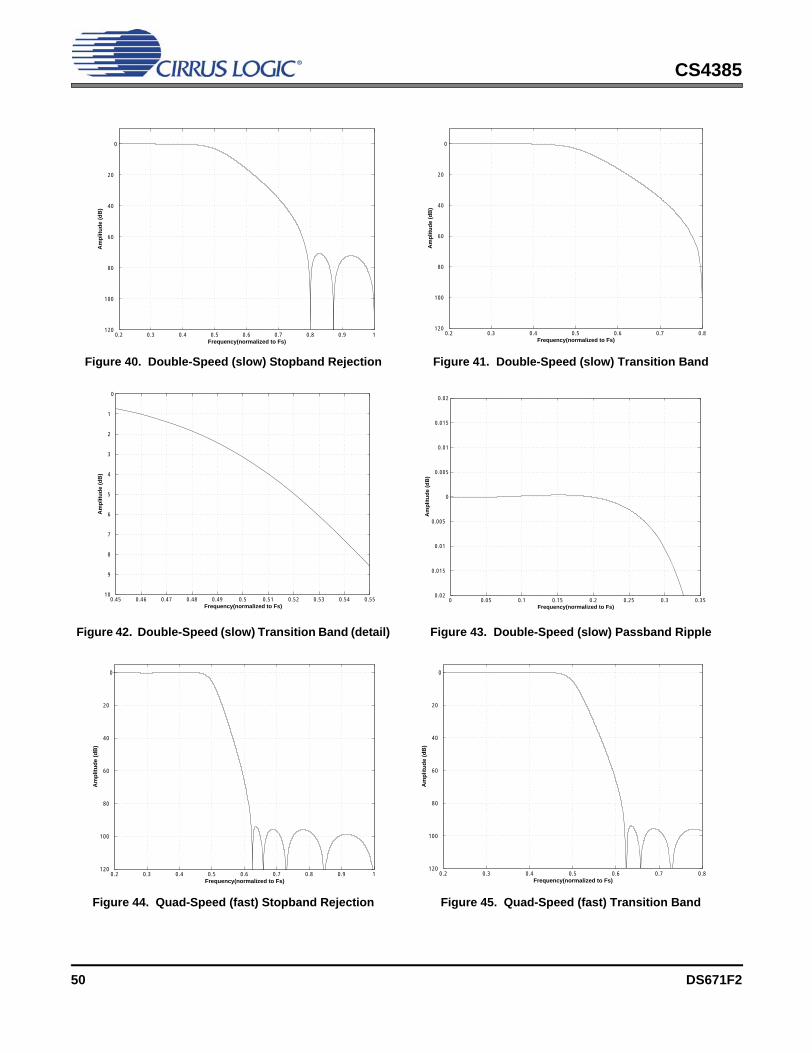
CS4385
0.2 0.3 0.4 0.5 0.6 0.7 0.8 0.9 1120
100
80
60
40
20
0
Frequency(normalized to Fs)
Am
plit
ud
e (d
B)
0.2 0.3 0.4 0.5 0.6 0.7 0.8120
100
80
60
40
20
0
Frequency(normalized to Fs)
Am
plit
ud
e (d
B)
Figure 40. Double-Speed (slow) Stopband Rejection Figure 41. Double-Speed (slow) Transition Band
0.45 0.46 0.47 0.48 0.49 0.5 0.51 0.52 0.53 0.54 0.5510
9
8
7
6
5
4
3
2
1
0
Frequency(normalized to Fs)
Am
plit
ud
e (d
B)
0 0.05 0.1 0.15 0.2 0.25 0.3 0.350.02
0.015
0.01
0.005
0
0.005
0.01
0.015
0.02
Frequency(normalized to Fs)
Am
plit
ud
e (d
B)
Figure 42. Double-Speed (slow) Transition Band (detail) Figure 43. Double-Speed (slow) Passband Ripple
0.2 0.3 0.4 0.5 0.6 0.7 0.8 0.9 1120
100
80
60
40
20
0
Frequency(normalized to Fs)
Am
plit
ud
e (d
B)
0.2 0.3 0.4 0.5 0.6 0.7 0.8120
100
80
60
40
20
0
Frequency(normalized to Fs)
Am
plit
ud
e (d
B)
Figure 44. Quad-Speed (fast) Stopband Rejection Figure 45. Quad-Speed (fast) Transition Band
50 DS671F2
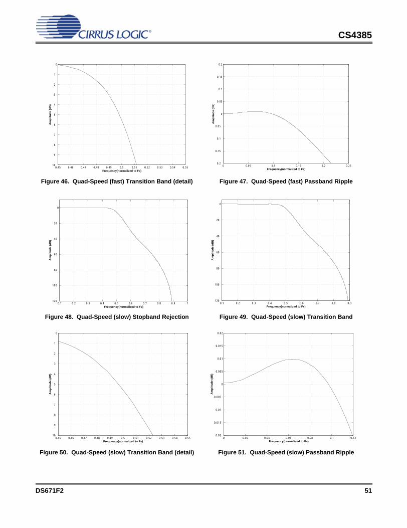
CS4385
0.45 0.46 0.47 0.48 0.49 0.5 0.51 0.52 0.53 0.54 0.5510
9
8
7
6
5
4
3
2
1
0
Frequency(normalized to Fs)
Am
plit
ud
e (d
B)
0 0.05 0.1 0.15 0.2 0.250.2
0.15
0.1
0.05
0
0.05
0.1
0.15
0.2
Frequency(normalized to Fs)
Am
plit
ud
e (d
B)
Figure 46. Quad-Speed (fast) Transition Band (detail) Figure 47. Quad-Speed (fast) Passband Ripple
0.1 0.2 0.3 0.4 0.5 0.6 0.7 0.8 0.9 1120
100
80
60
40
20
0
Frequency(normalized to Fs)
Am
plit
ud
e (d
B)
0.1 0.2 0.3 0.4 0.5 0.6 0.7 0.8 0.9120
100
80
60
40
20
0
Frequency(normalized to Fs)
Am
plit
ud
e (d
B)
Figure 48. Quad-Speed (slow) Stopband Rejection Figure 49. Quad-Speed (slow) Transition Band
0.1 0.2 0.3 0.4 0.5 0.6 0.7 0.8 0.9120
100
80
60
40
20
0
Frequency(normalized to Fs)
Am
plit
ud
e (d
B)
0.45 0.46 0.47 0.48 0.49 0.5 0.51 0.52 0.53 0.54 0.5510
9
8
7
6
5
4
3
2
1
0
Frequency(normalized to Fs)
Am
plit
ud
e (d
B)
0 0.02 0.04 0.06 0.08 0.1 0.120.02
0.015
0.01
0.005
0
0.005
0.01
0.015
0.02
Frequency(normalized to Fs)
Am
plit
ud
e (d
B)
Figure 50. Quad-Speed (slow) Transition Band (detail) Figure 51. Quad-Speed (slow) Passband Ripple
DS671F2 51

CS4385
8. PARAMETER DEFINITIONSTotal Harmonic Distortion + Noise (THD+N)The ratio of the rms value of the signal to the rms sum of all other spectral components over the specified bandwidth (typically 10 Hz to 20 kHz), including distortion components. Expressed in decibels.
Dynamic RangeThe ratio of the full-scale rms value of the signal to the rms sum of all other spectral components over the specified bandwidth. Dynamic range is a signal-to-noise measurement over the specified bandwidth made with a -60 dBFS signal. 60 dB is then added to the resulting measurement to refer the measure-ment to full scale. This technique ensures that the distortion components are below the noise level and do not affect the measurement. This measurement technique has been accepted by the Audio Engineer-ing Society, AES17-1991, and the Electronic Industries Association of Japan, EIAJ CP-307.
Interchannel IsolationA measure of crosstalk between the left and right channels. Measured for each channel at the converter's output with all zeros to the input under test and a full-scale signal applied to the other channel. Units in decibels.
Interchannel Gain MismatchThe gain difference between left and right channels. Units in decibels.
Gain DriftThe change in gain value with temperature. Units in ppm/°C.
52 DS671F2
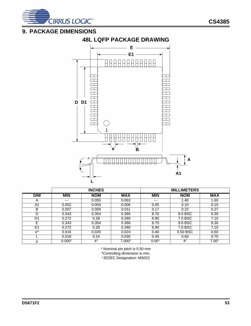
CS4385
9. PACKAGE DIMENSIONSINCHES MILLIMETERSDIM MIN NOM MAX MIN NOM MAX
A --- 0.055 0.063 --- 1.40 1.60A1 0.002 0.004 0.006 0.05 0.10 0.15B 0.007 0.009 0.011 0.17 0.22 0.27D 0.343 0.354 0.366 8.70 9.0 BSC 9.30
D1 0.272 0.28 0.280 6.90 7.0 BSC 7.10E 0.343 0.354 0.366 8.70 9.0 BSC 9.30E1 0.272 0.28 0.280 6.90 7.0 BSC 7.10e* 0.016 0.020 0.024 0.40 0.50 BSC 0.60L 0.018 0.24 0.030 0.45 0.60 0.75µ 0.000° 4° 7.000° 0.00° 4° 7.00°
* Nominal pin pitch is 0.50 mm*Controlling dimension is mm.*JEDEC Designation: MS022
48L LQFP PACKAGE DRAWING
E1E
D1D
1
e B
L
∝
A1
A
DS671F2 53
CS4385
10.ORDERING INFORMATION11.REFERENCES1. How to Achieve Optimum Performance from Delta-Sigma A/D & D/A Converters, by Steven Harris. Paper
presented at the 93rd Convention of the Audio Engineering Society, October 1992.2. CDB4385 data sheet, available at http://www.cirrus.com.3. Design Notes for a 2-Pole Filter with Differential Input, by Steven Green. Cirrus Logic Application Note AN484. The I²C-Bus Specification: Version 2.0, Philips Semiconductors, December 1998.
http://www.semiconductors.philips.com.
12.REVISION HISTORY
Product Description Package Pb-Free Grade Temp Range Container Order #
CS4385 114 dB, 192 kHz 8-chan-nel D/A Converter
48-pin LQFP YES
Commercial -40°C to +85°CTray CS4385-CQZ
Tape & Reel CS4385-CQZR
Automotive -40°C to +105°CTray CS4385-DQZ
Tape & Reel CS4385-DQZR CDB4385 CS4385 Evaluation Board - - - - CDB4385
Release Changes
PP3
Updated Guaranteed Operational Temperature Range in “Recommended Operating Conditions” on page 8.Updated VA, VLC, and VLS current cunsumption specsUpdated Fullscale output levelUpdated Dynamic perforamnce limits.Removed VOH specificationUpdated VOL specificationUpdated TDM timing specs
F1
Updated “Recommended Operating Conditions” on page 8Updated “DAC Analog Characteristics - Commercial (-CQZ)” on page 9Updated “DAC Analog Characteristics - Automotive (-DQZ)” on page 10Updated “Power and Thermal Characteristics” on page 11Updated Legal Information on page 55
F2
Updated “DAC Pair Disable (DACx_DIS)” on page 38Updated “Digital Interface Format (DIF)” on page 38Added PCM mode format changeable in reset only to “Mode Select” on page 22Updated Package Thermal Resistance in “Power and Thermal Characteristics” on page 11
54 DS671F2
CS4385
Contacting Cirrus Logic SupportFor all product questions and inquiries, contact a Cirrus Logic Sales Representative. To find the one nearest to you, go to www.cirrus.com
IMPORTANT NOTICECirrus Logic, Inc. and its subsidiaries ("Cirrus") believe that the information contained in this document is accurate and reliable. However, the information is subjectto change without notice and is provided "AS IS" without warranty of any kind (express or implied). Customers are advised to obtain the latest version of relevantinformation to verify, before placing orders, that information being relied on is current and complete. All products are sold subject to the terms and conditions of salesupplied at the time of order acknowledgment, including those pertaining to warranty, indemnification, and limitation of liability. No responsibility is assumed by Cirrusfor the use of this information, including use of this information as the basis for manufacture or sale of any items, or for infringement of patents or other rights of thirdparties. This document is the property of Cirrus and by furnishing this information, Cirrus grants no license, express or implied under any patents, mask work rights,copyrights, trademarks, trade secrets or other intellectual property rights. Cirrus owns the copyrights associated with the information contained herein and gives con-sent for copies to be made of the information only for use within your organization with respect to Cirrus integrated circuits or other products of Cirrus. This consentdoes not extend to other copying such as copying for general distribution, advertising or promotional purposes, or for creating any work for resale. CERTAIN APPLICATIONS USING SEMICONDUCTOR PRODUCTS MAY INVOLVE POTENTIAL RISKS OF DEATH, PERSONAL INJURY, OR SEVERE PROP-ERTY OR ENVIRONMENTAL DAMAGE (“CRITICAL APPLICATIONS”). CIRRUS PRODUCTS ARE NOT DESIGNED, AUTHORIZED OR WARRANTED FOR USEIN PRODUCTS SURGICALLY IMPLANTED INTO THE BODY, AUTOMOTIVE SAFETY OR SECURITY DEVICES, LIFE SUPPORT PRODUCTS OR OTHER CRIT-ICAL APPLICATIONS. INCLUSION OF CIRRUS PRODUCTS IN SUCH APPLICATIONS IS UNDERSTOOD TO BE FULLY AT THE CUSTOMER’S RISK AND CIR-RUS DISCLAIMS AND MAKES NO WARRANTY, EXPRESS, STATUTORY OR IMPLIED, INCLUDING THE IMPLIED WARRANTIES OF MERCHANTABILITY ANDFITNESS FOR PARTICULAR PURPOSE, WITH REGARD TO ANY CIRRUS PRODUCT THAT IS USED IN SUCH A MANNER. IF THE CUSTOMER OR CUSTOM-ER’S CUSTOMER USES OR PERMITS THE USE OF CIRRUS PRODUCTS IN CRITICAL APPLICATIONS, CUSTOMER AGREES, BY SUCH USE, TO FULLYINDEMNIFY CIRRUS, ITS OFFICERS, DIRECTORS, EMPLOYEES, DISTRIBUTORS AND OTHER AGENTS FROM ANY AND ALL LIABILITY, INCLUDING AT-TORNEYS’ FEES AND COSTS, THAT MAY RESULT FROM OR ARISE IN CONNECTION WITH THESE USES.Cirrus Logic, Cirrus, and the Cirrus Logic logo designs are trademarks of Cirrus Logic, Inc. All other brand and product names in this document may be trademarksor service marks of their respective owners.I²C is a registered trademark of Philips Semiconductor. SPI is a trademark of Motorola, Inc.
DS671F2 55