Embed Size (px)
Citation preview

C.Schrader; Oct 2008, CBM Collaboration Meeting, Dubna, Russia
R/O concept of the MVD demonstrator
C.Schrader, S. Amar-Youcef, A. Büdenbender, M. Deveaux, D. Doering, J. Heuser, I. Fröhlich, J. Michel, C. Müntz, S. Seddiki, J. Stroth, T. Tischler, and B. Wiedemann
C.Schrader; Oct 2008, CBM Collaboration Meeting, Dubna, Russia
Outline
readout concept of the MVD demonstrator
• hardware components
• data processing
• first results of measurements
subjects of this talk

C.Schrader; Oct 2008, CBM Collaboration Meeting, Dubna, Russia
2x mimosa20
Overview of hardware components
analogue output
sync. signals data transfer: OP
-link
monitorin
g
Demo-Aux-PCB MAPS add-on board
Trb2supportflex-print-cable
PC storage
data transfer: in future: optical link (trb2)at present: I/O-card
data transfer: I/O-card
or

C.Schrader; Oct 2008, CBM Collaboration Meeting, Dubna, Russia
Functionality of demo-Aux board
demo- Aux board: analogue buffers for pixel data
transfer low voltage regulated power supply
for Mi20-chips chip slow control wire JTAG convert of the analogue
temperature signals to analog LVDS signals
convert of the LVTTL sync. signals from M20-chip to digital LVDS signals
50
PIN
SU
B-D
Co
n
Fle
x-C
on
Flex-cable
Mi20 Demo-Aux-boardMi20
MAPS add-on-board
status of the demo-Aux: advanced schematics
will be developed by IKF
mimosa20:
4x analogue differential signal outputs for long-distance data transfer
LVTTL sync. signals for chip controlling
4x analogue signals for temperature monitoring
< 5cm

C.Schrader; Oct 2008, CBM Collaboration Meeting, Dubna, Russia
Functionality of the add-on board
• platform to study online data specification for data reduction
• close to hardware for chip integration in future times
• compatibility with HADES DAQ (Trb2) for testing purposes
This data rate is too high for data storage systems online data reduction
status: 12 layer board is completed and tested
developed by IK
F
mimosa20
add-on board with a FPGA
as reconfigurable hardware
demonstrator:2x mimosa, parallel readout,360 x 640 pixel/frame, 50MHz 2.4Gbit/s, uncompressed
CBM: ~2Gbit/scompressed
see talk of S. Seddiki

C.Schrader; Oct 2008, CBM Collaboration Meeting, Dubna, Russia
Components of the add-on-board
differential-to-differential amplifier to balance the analogue input for the ADCs
4 x 12bit ADCs to read out the analogue output signal of the two chips
LVDS differential drivers and receivers for chip controlling
Virtex IV LX 40 FPGA and memory banks for online data-processing
two high-speed connectors (15Gbit/s) for data transfer towards the Trb2-board
4x diff. analogue pixel data signals
LVDS digital sync. signals
add-on-board
I/O from demo-Aux
C.Schrader; Oct 2008, CBM Collaboration Meeting, Dubna, Russia
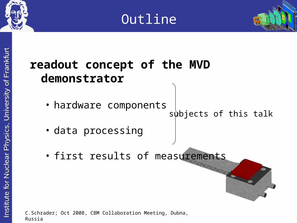
Trb2 and Add-on board concept
Trb2 provides:
• high data-rate digital interface
connector (15Gbit/s)
• FPGA configuration
• high data transfer with optical link (2Gbit/s), in future
• application process interface (API)
• power supply +5V,10A
• clock distribution
the general-propose trigger and
readout board (Trb2)
the Trb2 (HADES) has been designed in a way to be detector independent by using a flexible add-on board concept the MAPS Add-on board is mounted on the Trb2 back side
status: the Trb2-Add-on concept is in use

C.Schrader; Oct 2008, CBM Collaboration Meeting, Dubna, Russia
Data processing
processing steps:
• correlated double
sampling (CDS)
• bit reduction
• threshold(for hit identification)
• cluster finding(the hit and the 8 neighbor pixels are important)
pipelined algorithmsfor real-time applicationin stream mode
zero suppression
C.Schrader; Oct 2008, CBM Collaboration Meeting, Dubna, Russia
-30-28
-26
-24
-22
-20
-18-16
-14
-12
-10-8
-6
-4
-2
02
4
6
8
1012
14
16
18
20
2050 2550 3050 3550 4050
d ig ita l co d e [ADC co u n ts]
ide
al
- a
ctu
al
va
lue
[A
DC
co
un
ts]
ADCA
ADCB
ADCC
ADCD
idea ADC
ADCA: y = 0,0073x - 34,131
ADCB: y = 0,01x - 44,171
ADCC: y = 0,0138x - 54,975
ADCD: y = 0,0112x - 31,111
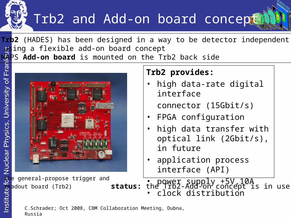
ADC calibration
devices intrinsic uncertainly: Integral Nonlinearity error (INL) = ±1.6LSB± 2LSB
ADC OP...result: the difference of ideal and actual value is: ±2 ADC counts uncertainties are uncertainties are dominated by ADCdominated by ADC readout chain is OKreadout chain is OK
calibration terms are included in data processing
with error bars
without error bars
C.Schrader; Oct 2008, CBM Collaboration Meeting, Dubna, Russia
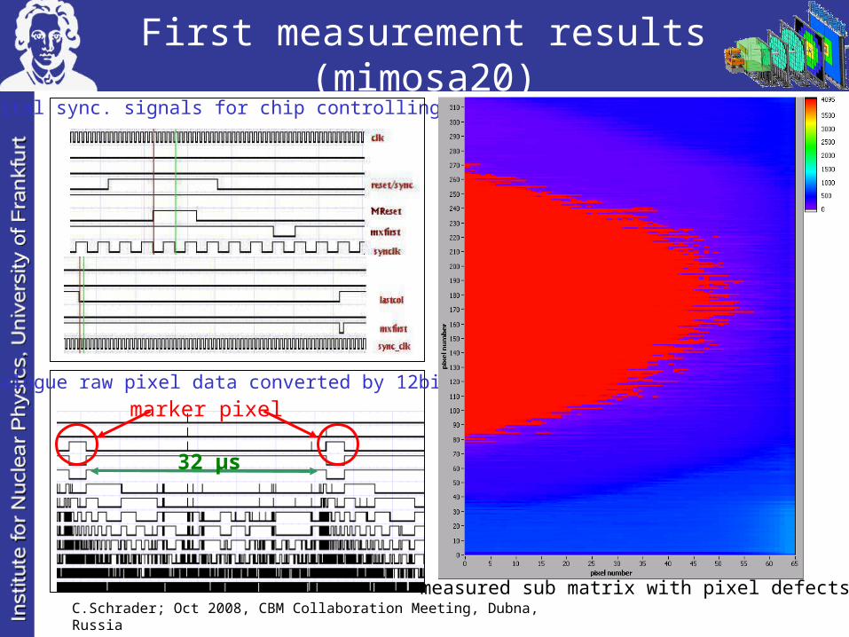
First measurement results (mimosa20)
marker pixel
32 µs
digital sync. signals for chip controlling
analogue raw pixel data converted by 12bit ADC
measured sub matrix with pixel defects

C.Schrader; Oct 2008, CBM Collaboration Meeting, Dubna, Russia
Project status
Hardware: add-on board: design manufacturing test
I/O interface to PC side: installation firmware development test
o demo-Aux board: specification ongoing design, manufacturing Nov2008
Data processing: VHDL: CDS bit-reduction threshold data-output-interface
cluster finding (S. Seddiki): specification ongoing implementation
data acquisition and storage software for PC : development installation test

THANK YOU

-20
-10
0
10
20
30
40
50
0 5 10 15 20 25
1850
1860
1870
1880
1890
1900
1910
1920
1005 1010 1015 1020 1025 1030
pixel with hit
pixel without hit
readout cycle
AD
C u
nits
∆ A
DC
acquisition cycle
Fig.8: The behaviour of SB-pixels
is observed by frames.
The constant current
leakage in the capacitor
is compensate through
a diode. After hit the diode
re-fill the capacitor
Fig.10: After CDS clear
hit identification
is possible
fx:px
fx-1:px
(fx:px - fx-1:px)
(fx-1:px - fx-2:px)
hit
Correlated double sampling by Self-Bias-Pixel
Fig.9: Equivalent circuit diagram of SB-Pixel
1900
threshold
threshold

Threshold
The hit and the
8 neighbour pixels
are important
Result: not the complete matrix is readout, only the hit with the neighbour pixel
Fig.12: Data selection with threshold

Add-on board design
Fig.11: Add-on board

bit-flipping
2,9
46,1
29,4
80,4
53,3 53,9
70,6
19,6
43,8
0,0
10,0
20,0
30,0
40,0
50,0
60,0
70,0
80,0
90,0
3078 3079 3080
A D C A
A D C B
A D C C
A D C D
RESULT: last bit is flipping
constant power supply: ~503mV± 10µV%
Digital code [ADC counts]
%
%
%
%
%
%