Embed Size (px)
Citation preview
CTI 2500 Series Controller
PROGRAMMING REFERENCE MANUAL
Version 1.26
CTI Part # 062-00371
2500PRM
ii CTI 2500 Series CPU Programming Reference Manual V1.26
Copyright 2009-2016 Control Technology Inc. All rights reserved. This manual is published by Control Technology Inc., 5734 Middlebrook Pike, Knoxville TN 37921. This manual contains references to brand and product names which are trade names, trademarks, and/or registered trademarks of Control Technology Inc.
Siemens®, SIMATIC®, and Series 505® are registered trademarks of Siemens AG and Siemens Energy and Automation, Inc.
TISOFT™ and PowerMath™ are trademarks of Siemens Energy and Automation. Inc.
PLC WorkShop® is a registered trademark of FasTrak Softworks, Inc.
Other references to brand and product names are trade names, trademarks, and/or registered trademarks of their respective holders. DOCUMENT DISCLAIMER STATEMENT Every effort has been made to ensure the accuracy of this document; however, errors do occasionally occur. CTI provides this document on an “as is” basis and assumes no responsibility for direct or consequential damages resulting from the use of this document. This document is provided without express or implied warranty of any kind, including but not limited to the warranties of merchantability or fitness for a particular purpose. This document and the products it references are subject to change without notice. If you have a comment or discover an error, please call us toll free at 1-800-537-8398 or email us at [email protected].
CTI 2500 Series CPU Programming Reference Manual V1.26 iii
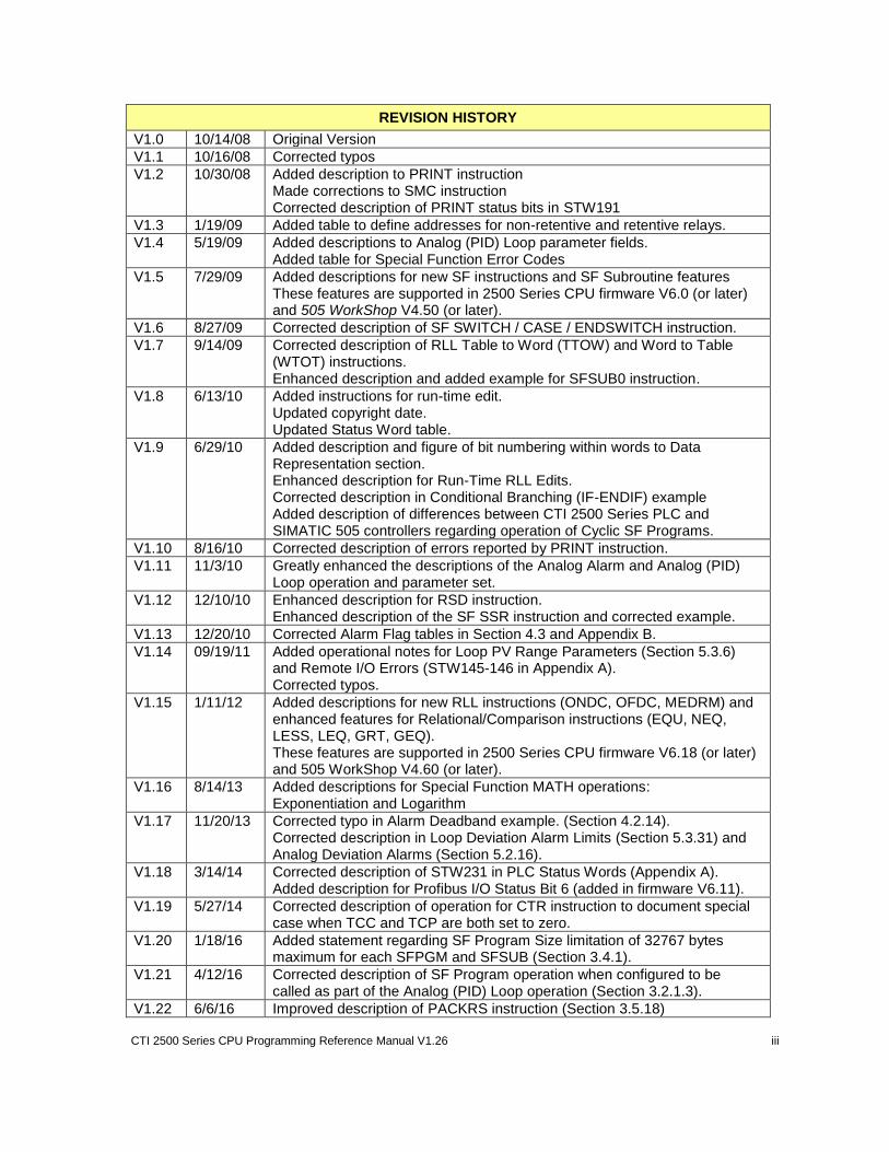
REVISION HISTORY
V1.0 10/14/08 Original Version
V1.1 10/16/08 Corrected typos
V1.2 10/30/08 Added description to PRINT instruction Made corrections to SMC instruction Corrected description of PRINT status bits in STW191
V1.3 1/19/09 Added table to define addresses for non-retentive and retentive relays.
V1.4 5/19/09 Added descriptions to Analog (PID) Loop parameter fields. Added table for Special Function Error Codes
V1.5 7/29/09 Added descriptions for new SF instructions and SF Subroutine features These features are supported in 2500 Series CPU firmware V6.0 (or later) and 505 WorkShop V4.50 (or later).
V1.6 8/27/09 Corrected description of SF SWITCH / CASE / ENDSWITCH instruction.
V1.7 9/14/09 Corrected description of RLL Table to Word (TTOW) and Word to Table (WTOT) instructions. Enhanced description and added example for SFSUB0 instruction.
V1.8 6/13/10 Added instructions for run-time edit. Updated copyright date. Updated Status Word table.
V1.9 6/29/10 Added description and figure of bit numbering within words to Data Representation section. Enhanced description for Run-Time RLL Edits. Corrected description in Conditional Branching (IF-ENDIF) example Added description of differences between CTI 2500 Series PLC and SIMATIC 505 controllers regarding operation of Cyclic SF Programs.
V1.10 8/16/10 Corrected description of errors reported by PRINT instruction.
V1.11 11/3/10 Greatly enhanced the descriptions of the Analog Alarm and Analog (PID) Loop operation and parameter set.
V1.12 12/10/10 Enhanced description for RSD instruction. Enhanced description of the SF SSR instruction and corrected example.
V1.13 12/20/10 Corrected Alarm Flag tables in Section 4.3 and Appendix B.
V1.14 09/19/11 Added operational notes for Loop PV Range Parameters (Section 5.3.6) and Remote I/O Errors (STW145-146 in Appendix A). Corrected typos.
V1.15 1/11/12 Added descriptions for new RLL instructions (ONDC, OFDC, MEDRM) and enhanced features for Relational/Comparison instructions (EQU, NEQ, LESS, LEQ, GRT, GEQ). These features are supported in 2500 Series CPU firmware V6.18 (or later) and 505 WorkShop V4.60 (or later).
V1.16 8/14/13 Added descriptions for Special Function MATH operations: Exponentiation and Logarithm
V1.17 11/20/13 Corrected typo in Alarm Deadband example. (Section 4.2.14). Corrected description in Loop Deviation Alarm Limits (Section 5.3.31) and Analog Deviation Alarms (Section 5.2.16).
V1.18 3/14/14 Corrected description of STW231 in PLC Status Words (Appendix A). Added description for Profibus I/O Status Bit 6 (added in firmware V6.11).
V1.19 5/27/14 Corrected description of operation for CTR instruction to document special case when TCC and TCP are both set to zero.
V1.20 1/18/16 Added statement regarding SF Program Size limitation of 32767 bytes maximum for each SFPGM and SFSUB (Section 3.4.1).
V1.21 4/12/16 Corrected description of SF Program operation when configured to be called as part of the Analog (PID) Loop operation (Section 3.2.1.3).
V1.22 6/6/16 Improved description of PACKRS instruction (Section 3.5.18)

iv CTI 2500 Series CPU Programming Reference Manual V1.26
REVISION HISTORY
Added details on difference between CTI 2500 Series CPU and SIMATIC® 505 controller when using PACKRS ‘FROM TABLE’ operation. Enhanced description for use of Short/Long Form Address formats used to specify Memory Type and Offset of Ramp/Soak step status bits.
V1.23 6/9/16 Improved operational descriptions for Search Table For Equal (Section 2.6.10) and Search Table For Not Equal (Section 2.6.11) instructions.
V1.24 8/18/16 Corrected description of SF Program execution queues (limit of 32 active programs applies only to Cyclic SFPGMs (Section 2.11.12). Added description for compilation of SF Programs and SF Subroutines with recommendations and procedures for on-line SF Program edits (Section 3.2.3).
V1.25 9/15/16 Corrected descriptions for RLL instructions: STFE (Section 2.6.10) and STFN (Section 2.6.11). Corrected memory tables in Sections 3.5.16-17, 3.6 and Appendix B. Added ‘Table of Contents’ hyperlinks and Bookmarks to the PDF document.
V1.26 11/29/16 Enhanced description of Special Function MATH statement (Section 3.4.18). Corrected various typos, document ‘Properties’ information, and PDF options to correct Font formatting issues.
CTI 2500 Series CPU Programming Reference Manual V1.26 v
PREFACE
This Programming Reference Manual provides reference information for the CTI 2500 Controller. The information in this manual is directed to individuals who will be developing user programs for the controller. For information regarding the product features, installation, and operation, you should also obtain the CTI 2500 Installation and Operation Guide (CTI Part # 062 -00370). This manual may be downloaded from the CTI Web site http: //www.controltechnology.com/support/manuals/.
vi CTI 2500 Series CPU Programming Reference Manual V1.26
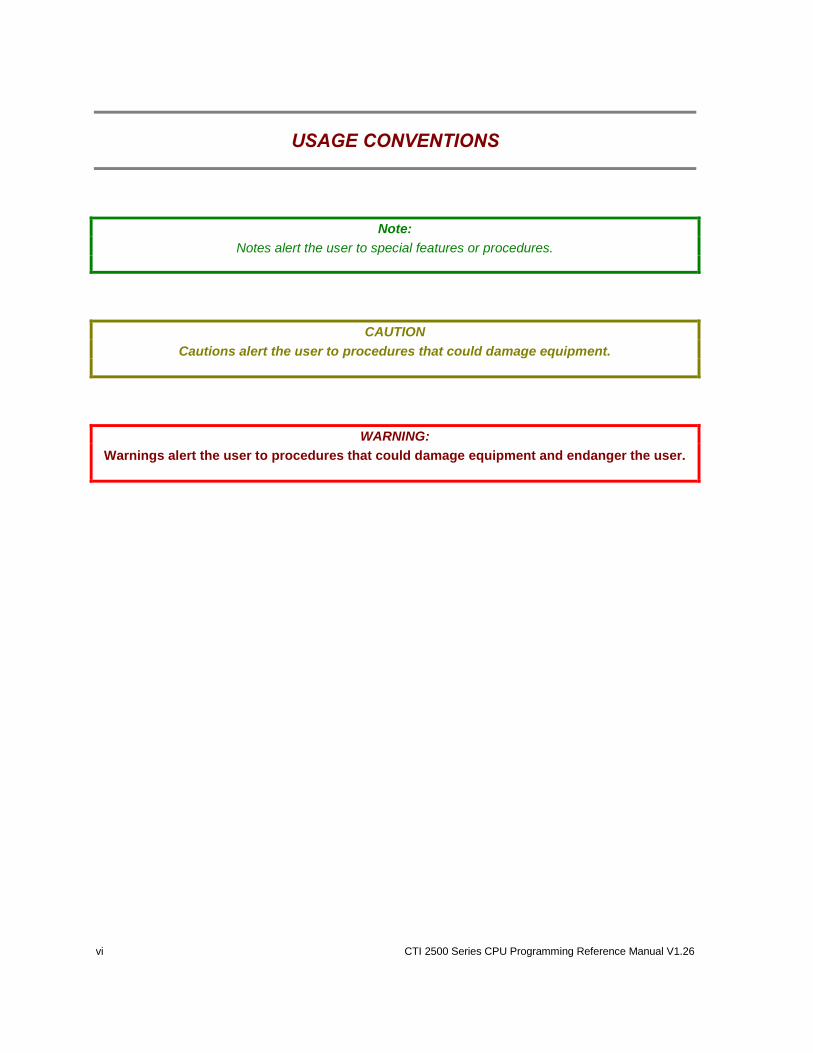
USAGE CONVENTIONS
Note:
Notes alert the user to special features or procedures.
CAUTION
Cautions alert the user to procedures that could damage equipment.
WARNING:
Warnings alert the user to procedures that could damage equipment and endanger the user.
CTI 2500 Series CPU Programming Reference Manual V1.26 vii
TABLE OF CONTENTS
CHAPTER 1 OVERVIEW .................................................................................................... 1
1.1 INTRODUCTION ........................................................................................................ 1
1.2 PROGRAMMING OVERVIEW ....................................................................................... 1 1.2.1 Relay Ladder Programming ............................................................................................ 1 1.2.2 Special Function Programs and Subroutines ................................................................. 2 1.2.3 Analog Alarms ................................................................................................................ 3 1.2.4 Analog Loops .................................................................................................................. 3
1.3 CONTROLLER DATA TYPES ....................................................................................... 4
1.4 DATA REPRESENTATION ........................................................................................... 6
1.5 RUN-TIME RLL EDITS .............................................................................................. 8 1.5.1 Syntax Checking ............................................................................................................. 9 1.5.2 Potential Sources of Run-Time Edit Compile Errors ...................................................... 9 1.5.3 Additional Considerations ............................................................................................. 10
CHAPTER 2 RELAY LADDER LOGIC ..............................................................................13
2.1 OVERVIEW..............................................................................................................13
2.2 RLL INSTRUCTION SUMMARY ..................................................................................13 2.2.1 Relay Instructions ......................................................................................................... 13 2.2.2 Electro-mechanical Operations (Timer / Counter / Drum) ............................................ 15 2.2.3 Relational and Comparison Operations ........................................................................ 16 2.2.4 Bit Operations ............................................................................................................... 17 2.2.5 Math Operations ........................................................................................................... 17 2.2.6 Logic Operations ........................................................................................................... 18 2.2.7 Word / Table Move Operations ..................................................................................... 19 2.2.8 Program Control Operations ......................................................................................... 20 2.2.9 Special Operations ....................................................................................................... 21
2.3 RLL MEMORY ACCESS ............................................................................................22
2.4 RELAY INSTRUCTIONS .............................................................................................23 2.4.1 Open Contact ................................................................................................................ 23 2.4.2 Closed Contact ............................................................................................................. 24 2.4.3 Logical NOT Contact .................................................................................................... 25 2.4.4 One-Shot Contact ......................................................................................................... 26 2.4.5 Normal Coil ................................................................................................................... 26 2.4.6 NOT Coil ....................................................................................................................... 27 2.4.7 Set Coil ......................................................................................................................... 28 2.4.8 Reset Coil ..................................................................................................................... 28 2.4.9 Immediate Open Contact .............................................................................................. 29 2.4.10 Immediate Closed Contact ........................................................................................... 29 2.4.11 Immediate Coil .............................................................................................................. 29 2.4.12 Immediate NOT Coil ..................................................................................................... 30 2.4.13 Immediate Set Coil ....................................................................................................... 30 2.4.14 Immediate Reset Coil ................................................................................................... 30
2.5 ELECTRO-MECHANICAL INSTRUCTIONS (TIMER/COUNTER/DRUM) ..............................31 2.5.1 Counter (CTR) .............................................................................................................. 31 2.5.2 Up-Down Counter (UDC) .............................................................................................. 33
viii CTI 2500 Series CPU Programming Reference Manual V1.26
2.5.3 On-Delay Timer (TMR / TMRF) .................................................................................... 35 2.5.4 Discrete Control Alarm Timer (DCAT).......................................................................... 37 2.5.5 Motor Control Alarm Timer (MCAT) ............................................................................. 39 2.5.6 On-Delay Coil (ONDC) ................................................................................................. 43 2.5.7 Off-Delay Coil (OFFDC) ............................................................................................... 45 2.5.8 DRUM (Time-Based) .................................................................................................... 47 2.5.9 Time/Event DRUM (EDRUM) ....................................................................................... 49 2.5.10 Maskable Event Drum with Discrete Outputs (MDRMD) ............................................. 52 2.5.11 Maskable Event Drum with Word Output (MDRMW) ................................................... 56 2.5.12 Mega Event DRUM (MEDRM) ..................................................................................... 60
2.6 RELATIONAL / COMPARISON OPERATIONS ................................................................ 67 2.6.1 Compare (CMP) ........................................................................................................... 67 2.6.2 Equal (EQU) ................................................................................................................. 68 2.6.3 Greater or Equal (GEQ) ............................................................................................... 70 2.6.4 Greater (GTR) .............................................................................................................. 72 2.6.5 Less or Equal (LEQ) ..................................................................................................... 74 2.6.6 Less (LESS) ................................................................................................................. 76 2.6.7 Not Equal (NEQ) .......................................................................................................... 78 2.6.8 Indexed Matrix Compare (IMC) .................................................................................... 80 2.6.9 Scan Matrix Compare (SMC) ....................................................................................... 82 2.6.10 Search Table For Equal (STFE) ................................................................................... 84 2.6.11 Search Table For Not Equal (STFN) ............................................................................ 86
2.7 BIT OPERATIONS .................................................................................................... 88 2.7.1 Bit Clear (BITC) ............................................................................................................ 88 2.7.2 Bit Set (BITS) ............................................................................................................... 89 2.7.3 Bit Pick (BITP) .............................................................................................................. 90 2.7.4 Bit Shift Register (SHRB) ............................................................................................. 91 2.7.5 Word Shift Register (SHRW) ........................................................................................ 93 2.7.6 Word Rotate (WROT) ................................................................................................... 95
2.8 MATH / LOGIC OPERATIONS .................................................................................... 97 2.8.1 Absolute Value (ABSV) ................................................................................................ 97 2.8.2 Addition (ADD) ............................................................................................................. 98 2.8.3 Subtraction (SUB) ........................................................................................................ 99 2.8.4 Multiplication (MUL).................................................................................................... 100 2.8.5 Division (DIV) ............................................................................................................. 102 2.8.6 Square Root (SQRT) .................................................................................................. 104 2.8.7 Binary to BCD Conversion (CBD) .............................................................................. 106 2.8.8 BCD to Binary Conversion (CDB) .............................................................................. 108
2.9 LOGIC OPERATIONS .............................................................................................. 110 2.9.1 Word AND (WAND) .................................................................................................... 110 2.9.2 Word OR (WOR) ........................................................................................................ 112 2.9.3 Word Exclusive-OR (WXOR) ..................................................................................... 114 2.9.4 Table AND (TAND)..................................................................................................... 116 2.9.5 Table OR (TOR) ......................................................................................................... 118 2.9.6 Table Exclusive-OR (TXOR) ...................................................................................... 120 2.9.7 Table Complement (TCPL) ........................................................................................ 122 2.9.8 Word-to-Table AND (WTTA) ...................................................................................... 123 2.9.9 Word-to-Table OR (WTTO) ........................................................................................ 125 2.9.10 Word-to-Table Exclusive-OR (WTTX) ........................................................................ 127
2.10 WORD / TABLE MOVE OPERATIONS ....................................................................... 129 2.10.1 Move Word (MOVW) .................................................................................................. 129 2.10.2 Move with Index (MWI) .............................................................................................. 131
CTI 2500 Series CPU Programming Reference Manual V1.26 ix
2.10.3 Move Word From Table (MWFT) ................................................................................ 133 2.10.4 Move Word To Table (MWTT) .................................................................................... 135 2.10.5 Move Image Register to Word (MIRW) ...................................................................... 137 2.10.6 Move Word to Image Register (MWIR) ...................................................................... 139 2.10.7 Move Image Register From Table (MIRFT)................................................................ 141 2.10.8 Move Image Register To Table (MIRTT) .................................................................... 143 2.10.9 Move Element (MOVE) ............................................................................................... 145 2.10.10 Table To Word (TTOW) ............................................................................................. 150 2.10.11 Word To Table (WTOT) ............................................................................................. 152
2.11 PROGRAM CONTROL OPERATIONS ......................................................................... 154 2.11.1 Unconditional END (END) .......................................................................................... 154 2.11.2 Conditional END (ENDC)............................................................................................ 155 2.11.3 Jump (JMP) / Jump End (JMPE) ................................................................................ 156 2.11.4 Skip (SKP) / Label (LBL)............................................................................................. 158 2.11.5 Master Control Relay (MCR) / MCR End (MCRE)...................................................... 161 2.11.6 Go To Subroutine (GTS)............................................................................................. 164 2.11.7 Parameterized Go To Subroutine (PGTS).................................................................. 166 2.11.8 Parameterized Go To Subroutine – Zero (PGTSZ) .................................................... 170 2.11.9 Start of Subroutine (SBR) ........................................................................................... 172 2.11.10 Return from Subroutine (RET) ................................................................................... 175 2.11.11 PID Fast Loop (PID) ................................................................................................... 176 2.11.12 Call SF Program (SFPGM) ........................................................................................ 178 2.11.13 Call SF Subroutine (SFSUB)...................................................................................... 181 2.11.14 Start RLL Task (TASK) .............................................................................................. 187 2.11.15 Special Operations ..................................................................................................... 190 2.11.16 Load Data Constant (LDC)......................................................................................... 190 2.11.17 Load Address (LDA) ................................................................................................... 191 2.11.18 Time Set (TSET) ........................................................................................................ 196 2.11.19 Time Compare (TCMP) .............................................................................................. 198 2.11.20 Date Set (DSET) ........................................................................................................ 200 2.11.21 Date Compare (DCMP) .............................................................................................. 202 2.11.22 Immediate I/O Read/Write (IORW) ............................................................................ 204 2.11.23 Read Slave Diagnostic (RSD) .................................................................................... 207 2.11.24 Text Box (TEXT) ........................................................................................................ 210 2.11.25 No Operation (NOP) ................................................................................................... 211
CHAPTER 3 SF PROGRAMS AND SUBROUTINES ................................................... 213
3.1 OVERVIEW............................................................................................................ 213
3.2 SF PROGRAM/SUBROUTINE EXECUTION................................................................. 213 3.2.1 SF Programs ............................................................................................................... 213 3.2.2 SF Subroutines ........................................................................................................... 218 3.2.3 Editing of SF Programs during Run Mode .................................................................. 220
3.3 SPECIAL FUNCTION ERROR REPORTING AND RESPONSE ......................................... 221
3.4 SPECIAL FUNCTION MEMORY USAGE ..................................................................... 223 3.4.1 SF Program Size ........................................................................................................ 223 3.4.2 SF Local Memory ........................................................................................................ 223 3.4.3 Memory Array Indexing ............................................................................................... 225
3.5 SPECIAL FUNCTION INSTRUCTIONS ........................................................................ 227 3.5.1 SF Instruction Data Fields .......................................................................................... 228 3.5.2 Comment ( * ) ............................................................................................................. 230 3.5.3 BCD-to-Binary Conversion (BCDBIN) ........................................................................ 231 3.5.4 Binary-to-BCD Conversion (BINBCD) ........................................................................ 232
x CTI 2500 Series CPU Programming Reference Manual V1.26
3.5.5 Call SF Subroutine (CALL) ......................................................................................... 233 3.5.6 Correlated Data Table (CDT) ..................................................................................... 235 3.5.7 Exit on Error (EXIT) .................................................................................................... 237 3.5.8 Fall Through Shift Register (FTSR-IN / FTSR-OUT) ................................................. 238 3.5.9 Conditional Looping - FOR / NEXT ............................................................................ 243 3.5.10 Unconditional Branching - GOTO / LABEL ................................................................ 246 3.5.11 Conditional Branching - IF (IIF) / ELSE / ENDIF ........................................................ 247 3.5.12 Integer Math Operations (IMATH) .............................................................................. 249 3.5.13 Lead/Lag Compensation (LEAD/LAG) ....................................................................... 252 3.5.14 Real Number Math Operations (MATH) ..................................................................... 254 3.5.15 Pack Data (PACK)...................................................................................................... 257 3.5.16 Pack Analog Alarm Data (PACKAA) .......................................................................... 260 3.5.17 Pack Loop Data (PACKLOOP) .................................................................................. 264 3.5.18 Pack Ramp/Soak Data (PACKRS) ............................................................................. 268 3.5.19 Pet Scan Watchdog (PETWD) ................................................................................... 274 3.5.20 Print Message (PRINT) .............................................................................................. 275 3.5.21 Return from SF Program / Subroutine (RETURN) ..................................................... 280 3.5.22 Scale Analog Input to Engineering Units (SCALE) .................................................... 281 3.5.23 Sequential Data Table (SDT) ..................................................................................... 283 3.5.24 Conditional Branching – SWITCH / CASE / ENDSWITCH ........................................ 285 3.5.25 Synchronous Shift Register (SSR) ............................................................................. 287 3.5.26 Scale Engineering Units to Analog Output (UNSCALE) ............................................ 290 3.5.27 Conditional Looping - WHILE / ENDWHILE ............................................................... 292
3.6 SF PROGRAM/SUBROUTINE DATA VARIABLES ........................................................ 294
3.7 SF PROGRAM/SUBROUTINE ERROR CODES ........................................................... 297
CHAPTER 4 ANALOG ALARMS ................................................................................. 299
4.1 OVERVIEW ........................................................................................................... 299
4.2 ALARM PARAMETERS ............................................................................................ 299 4.2.1 Alarm Title .................................................................................................................. 300 4.2.2 Alarm V-Flag Address ................................................................................................ 300 4.2.3 Sample Rate ............................................................................................................... 301 4.2.4 Process Variable Address (V, WX, WY, None) .......................................................... 301 4.2.5 PV Range Low/High (in Engr Units) ........................................................................... 301 4.2.6 PV is Bipolar (Yes/No) ............................................................................................... 301 4.2.7 20% Offset on PV (Yes/No) ....................................................................................... 301 4.2.8 Square Root of PV (Yes/No) ...................................................................................... 301 4.2.9 Monitor Absolute Alarms (Yes/No) ............................................................................. 301 4.2.10 Absolute Alarm Limits (in Engr Units) ........................................................................ 302 4.2.11 Monitor Remote Setpoint (Yes/No) ............................................................................ 302 4.2.12 Remote Setpoint (V, K, WX, WY, None) .................................................................... 302 4.2.13 Clamp Setpoint Low/High (in Engr Units) .................................................................. 302 4.2.14 Alarm Deadband (in Engr Units) ................................................................................ 302 4.2.15 Special Function ......................................................................................................... 303 4.2.16 Deviation Alarms (Yes/No) ......................................................................................... 303 4.2.17 Rate of Change Alarm Limit (in Engr Units per Minute) ............................................. 303 4.2.18 Broken Transmitter Alarm (Yes/No) ........................................................................... 303
4.3 ALARM CONTROL FLAGS ....................................................................................... 304
4.4 ALARM ACKNOWLEDGEMENT FLAGS (AACK) ......................................................... 305
CTI 2500 Series CPU Programming Reference Manual V1.26 xi
CHAPTER 5 ANALOG (PID) LOOPS ........................................................................... 307
5.1 OVERVIEW............................................................................................................ 307
5.2 LOOP MODES OF OPERATION ................................................................................ 307
5.3 LOOP PARAMETERS .............................................................................................. 308 5.3.1 Loop Title .................................................................................................................... 309 5.3.2 PID Algorithm (Position/Velocity) ................................................................................ 309 5.3.3 Loop V-Flag Address (None, C, Y, V, WY)................................................................. 310 5.3.4 Sample Rate (in Seconds) .......................................................................................... 310 5.3.5 PV Address (None, V, WX, WY) ................................................................................. 310 5.3.6 PV Range (Low/High) ................................................................................................. 311 5.3.7 PV Bipolar (Yes/No) .................................................................................................... 311 5.3.8 20% Offset on PV (Yes/No) ........................................................................................ 311 5.3.9 Square Root of PV (Yes/No) ...................................................................................... 311 5.3.10 Loop Output Address (None, WY, V) ......................................................................... 311 5.3.11 Output is Bipolar (Yes/No) .......................................................................................... 311 5.3.12 20% Offset on Output (Yes/No) .................................................................................. 312 5.3.13 Ramp/Soak for SP (Yes/No) ....................................................................................... 312 5.3.14 Monitor Absolute Alarms (Yes/No) ............................................................................. 312 5.3.15 Absolute Alarm Limits (in Engr Units) ......................................................................... 312 5.3.16 Remote SP (None, V, K, WX, WY, LMN) ................................................................... 312 5.3.17 Clamp Setpoint Limits Low/High (in Engr Units) ........................................................ 313 5.3.18 Loop Gain ................................................................................................................... 313 5.3.19 Loop Reset (Reset Time in Minutes) .......................................................................... 313 5.3.20 Rate (Derivative Time in Minutes) .............................................................................. 313 5.3.21 Freeze Bias (Yes/No) ................................................................................................. 314 5.3.22 Derivative Gain Limiting (Yes/No) .............................................................................. 314 5.3.23 Limiting Coefficient ..................................................................................................... 314 5.3.24 Alarm Deadband (in Engr Units) ................................................................................. 314 5.3.25 Special Calculation On (SP, PV, Output, None) ......................................................... 315 5.3.26 Special Function ......................................................................................................... 315 5.3.27 Lock Setpoint, Lock Auto/Man, Lock Cascade ........................................................... 315 5.3.28 Error Operation (Error Squared, Error Deadband, None) .......................................... 315 5.3.29 Reverse Acting (Yes/No) ............................................................................................ 316 5.3.30 Monitor Deviation (Yes/No)......................................................................................... 316 5.3.31 Deviation Alarm Limits (in Engr Units) ........................................................................ 316 5.3.32 Monitor Rate (Yes/No) ................................................................................................ 316 5.3.33 Rate of Change Alarm Limit (in Engr Units per Minute) ............................................. 316 5.3.34 Monitor Broken Xmit (Yes/No) .................................................................................... 316
5.4 LOOP CONTROL FLAGS (C-FLAGS) ........................................................................ 317
5.5 LOOP ALARM ACKNOWLEDGEMENT FLAGS ............................................................. 318
5.6 RAMP/SOAK OPERATION ....................................................................................... 319
xii CTI 2500 Series CPU Programming Reference Manual V1.26
CHAPTER 6 MEMORY CONFIGURATION .................................................................. 321
6.1 OVERVIEW ........................................................................................................... 321
6.2 MEMORY CONFIGURATION .................................................................................... 322 6.2.1 Ladder (L) Memory ..................................................................................................... 322 6.2.2 Variable (V) Memory .................................................................................................. 322 6.2.3 Constant (K) Memory ................................................................................................. 322 6.2.4 Special (S) Memory .................................................................................................... 322 6.2.5 Timer/Counter (TC) Memory ...................................................................................... 322 6.2.6 Drum Memory (D) Memory ........................................................................................ 322 6.2.7 Shift Register (SR) Memory ....................................................................................... 322 6.2.8 Table (T) Memory ....................................................................................................... 323 6.2.9 One Shot (OS) Memory ............................................................................................. 323
CHAPTER 7 SCAN CONFIGURATION ........................................................................ 325
7.1 OVERVIEW ........................................................................................................... 325
7.2 TIME SLICE CONFIGURATION ................................................................................. 326 7.2.1 Analog Loop Time Slice ............................................................................................. 326 7.2.2 Analog Alarm Time Slice ............................................................................................ 326 7.2.3 Cyclic Special Function Program Time Slice ............................................................. 326 7.2.4 Priority Special Function Program Time Slice ............................................................ 326 7.2.5 Normal Special Function Program Time Slice ........................................................... 326 7.2.6 Ladder Special Function Subroutine Time Slice ........................................................ 326 7.2.7 Normal Communications Time Slice .......................................................................... 326 7.2.8 Priority Communications Time Slice .......................................................................... 327 7.2.9 Ladder SF Subroutine 0 Time Slice ........................................................................... 327 7.2.10 Network Communications Time Slice ........................................................................ 327
7.3 FACILITIES FOR ANALOG SCAN OPTIMIZATION ........................................................ 327 7.3.1 Status Word 162......................................................................................................... 327 7.3.2 Program Elapsed Times ............................................................................................. 328
APPENDIX A – PLC STATUS WORDS ........................................................................... 329
APPENDIX B – LOOP AND ALARM FLAGS ................................................................... 337
LOOP V-FLAGS (LVF) ...................................................................................................... 337
LOOP CONTROL FLAGS (LCFH AND LCFL) ....................................................................... 338
ALARM V-FLAGS (AVF) ................................................................................................... 339
ALARM CONTROL FLAGS (ACFH AND ACFL) .................................................................... 339
ALARM ACKNOWLEDGEMENT FLAGS (LACK AND AACK) ................................................... 340
LIMITED PRODUCT WARRANTY ................................................................................... 341
REPAIR POLICY .............................................................................................................. 343

CTI 2500 Series CPU Programming Reference Manual V1.26 1
CHAPTER 1 OVERVIEW
1.1 Introduction
This manual is intended for use by individuals who are developing application programs for the CTI 2500 Series controller. Additional information about the controller, including the scan operation, is contained in a companion manual, the CTI 2500 Installation and Operation Guide.
The CTI 2500 is an advanced function controller that combines the features of a programmable logic controller and a loop controller. It is especially suitable for process control applications that require analog control as well as discrete control.
1.2 Programming Overview
The CTI 2500 controller provides several facilities for programming a control application.
Relay Ladder Programming
Special Function Programming
Analog Alarms
Analog Loops
1.2.1 Relay Ladder Programming
Relay Ladder Logic (RLL) is a graphical language similar to a relay diagram. It has traditionally been used for discrete control applications. The RLL language supported by the CTI 2500 is compatible with the RLL used in the Siemens SIMATIC® 505 PLC. The RLL language includes the following groups of instructions.
Electro-Mechanical Replacements
These instructions include contacts, coils, timers, counters, and drums (stepper switches).
Bit Manipulation
These instructions provide the capability of reading, setting, and clearing bits as well as performing logical AND / OR operations.
BCD Conversions
The BCD instructions allow you to convert numbers between binary and binary coded decimal formats.
Word Move Instructions
Word Move instructions copy bits of a word values from source location(s) to a destination, which may be another memory type or another address within the same memory type. You can also copy selected bits between a word data type and a discrete Boolean data type.
Math
The Math instructions perform traditional integer mathematical calculations, including addition, subtraction, multiplication, division and square root. You can also perform compare operations.
2 CTI 2500 Series CPU Programming Reference Manual V1.26
Table Instructions
The table instructions provide a means to manipulate array data. You can move data in and out of a table, perform table searches, and perform bit level comparisons between two tables. Real-time Clock Instructions
The clock instructions read and set the Time and Date for the Real-time Clock in RLL.
Subroutine Instructions
The subroutine instructions allow you to create and call RLL subroutines. They also include the ability to call Special Function programs and subroutines.
Immediate I/O instructions
The Immediate I/O instructions read or write to the physical I/O during RLL execution rather than waiting for the normal I/O update to take place later in the controller scan.
Miscellaneous
The RLL also contains instructions that allow you to turn on an output for a single scan (one-shot), read diagnostic data from Profibus, and execute a PID loop on demand.
1.2.2 Special Function Programs and Subroutines
Special Function (SF) programs and subroutines provide a statement-oriented procedural programming language. Using the Special Function instructions, you can derive solutions that cannot be done in RLL or would require complex RLL programming.
SF programs can be called from an RLL program or from analog loop or alarm tasks. SF subroutines can be called from RLL, SF programs, or other SF subroutines. SF programs and SF subroutines use a common instruction set.
Special Function Program instructions include the following groups:
Data Conversion
These instructions provide the capability to scale values and to convert between BCD and binary format.
Math
Math instructions support both integer and real numbers. Operators include standard math functions (add, subtract, multiply, divide, exponentiation, comparison, and bit operations) as well as a unique LEAD/LAG function that can be used with cyclic applications.
Program Flow
These instructions alter the order in which instructions are executed. They include the ability to call subroutines, to branch to a label, and to implement conditional branching (If, Then, Else).
Data Manipulation
These instructions provide the ability to search tables, pack and unpack data, and to perform various shift register operations.
CTI 2500 Series CPU Programming Reference Manual V1.26 3
1.2.3 Analog Alarms
Analog Alarms are parameter-driven functions that allow you to monitor the Process Variable (PV). Each alarm block allows you to configure up to four absolute-value alarms and two sets of alarms that monitor the deviation of PV from the Setpoint. In addition, you can monitor the rate-of change of the Process Variable and detect a broken transmitter. An analog alarm may call a special function program to perform additional calculations. The number of analog alarm functions supported is model dependent. See the CTI 2500 Installation and Operation Guide for CTI 2500 Series model capabilities.
1.2.4 Analog Loops
The Analog Loop function supports both VELOCITY and POSITION PID (Proportional-Integral-Derivative) algorithms. Analog Loops are used to control analog processes by varying the loop output so that the output of the process (PROCESS VARIABLE) matches a target value (SETPOINT).
The operation of a particular loop is established by parameters entered by the user. In addition to executing the control loop, the loop task also provides the same alarm monitoring capability as the Analog Alarm task described in the next section.
The SETPOINT can also be automatically varied using a RAMP/SOAK Table. The RAMP/SOAK Table allows you to program a change in the SETPOINT over time (RAMP) and followed by a period that the SETPOINT will remain the same (SOAK). Using a series of ramp/soak steps, you can control most batch processes.
Loops are typically executed on a cyclic basis, independent of the user RLL or SF program logic. Some models of the CTI 2500 also support the capability of calling a PID loop from the RLL.
Loops may be cascaded, where the output of one loop becomes the input for the next loop. A loop may call a Special Function program to perform additional calculations. The number of loops supported is model dependent. See the CTI 2500 Installation and Operation Guide for CTI 2500 Series model capabilities.
4 CTI 2500 Series CPU Programming Reference Manual V1.26
1.3 Controller Data Types
The following data types are accessible from the user program. The value within a data element is addressed by specifying the data type and a location number. For example discrete input 1 is referenced as X1. I/O Register Data
The I/O register contains the data obtained from the process (inputs) and data used to control the process (outputs). When the I/O is configured, this data is associated with input and output modules contained in the local base, remote bases, and slaves attached to the Profibus network. There is an I/O register representing discrete inputs and outputs and an I/O register representing Word Inputs and Outputs. The table below describes the contents:
Mnemonic Data Type Data Format Access
X Discrete Input Bit Read Only
Y Discrete Output Bit Read and Write
WX Word Input Word (16 bit) Read Only
WY Word Output Word (16 bit) Read and Write
Inputs and Outputs share the same I/O register location. Therefore X1 and Y1 are the same data point. Similarly WX1 and WY1 are the same. Control Relay Data
A Control Relay is an internal discrete value that can be written and read by user logic. It is not associated with any I/O point. The number of control relays supported depends on the controller model. See the CTI 2500 Installation and Operation Guide for CTI 2500 Series model capabilities.
Control relays may be retentive or non- retentive. Retentive control relays maintain their value when AC power is removed, assuming the controller battery is good. Whether a particular control relay is retentive or not depends on the control relay address. See the table below.
Non-Retentive Retentive
C1 – C768 C769 – C1024
C1025 – C1792 C1793 – C2048
C2049 – C2816 C2817 – C3072
C3073 – C3840 C3841 – C4096
C4097 – C4864 C4865 – C5120
C5121 – C5888 C5889 – C6144
C6145 – C6912 C6913 – C7168
C7169 – C7936 C7937 – C10240
C10241 – C56320
Variable Memory Data
Variable Memory (V Memory) is a collection of 16 bit words. The number of words available depends on the controller user configuration and the available user memory, which varies with the controller model. V memory can be read and written by the user program.

CTI 2500 Series CPU Programming Reference Manual V1.26 5
Constant Memory Data
Constant Memory (K Memory) is a collection of 16 bit words. The number of words available depends on the controller user configuration and the available user memory, which varies with the controller model. K memory can be read but not written by the user program. It can be modified by other sources, such as programming software. Status Word Memory Data
Status Word Memory (STW) is a collection of 16 bit words user to communicate the status of the controller, the user program, and the associated I/O to the user program. Status cannot be modified by the user program; however some status words can be modified by programming software. See Appendix A for a list of the status words used with the CTI 2500 controller. Timer Counter Memory Data
The Timer/Counter memory contains two values for each element as indicated below.
Mnemonic Data Type Data Format Access
TCP Timer Counter Preset Word (16 bit) Read/Write
TCC Timer Counter Current Word (16 Bit) Read/Write (RLL) Read Only (SF)
Note:
Changes to TCP do not modify the value save in the RLL program. TCP values modified by logic or HMI will be overwritten by the original stored value if the program is reloaded, the
network containing the Timer/Counter instruction is edited, or a Complete Restart is executed.
Drum Memory Data
The Drum memory contains four values for each drum as indicated below
Mnemonic Data Type Data Format Access
DSP Drum Step Preset Word (16 bit) Read/Write
DSC Drum Step Current Word (16 Bit) Read/Write
DCP Drum Count Preset Word (16 Bit) Read/Write
DCC Drum Count Current Word (16 Bit) Read/Write (RLL) Read Only (SF)
Note:
Changes to DSP and DCP do not modify the RLL program. If the program is reloaded, a network containing a drum instruction is edited, or a Complete Restart is executed,
modified DSP and DCP values will be replaced with the values stored in the RLL program.
6 CTI 2500 Series CPU Programming Reference Manual V1.26
Word
1 2 3 4 5 6 7 8 9 10 11 12 13 14 15 16
MSB LSB
1.4 Data Representation
Data is represented in the CTI 2500 controller as bits, bytes, words, and double words.
Bit A single binary digit that has either ON (1) or OFF (0) state. Bit locations are referenced by direct address in discrete memory areas (i.e., X32 or C86) or bit number in word memory areas (i.e., V52.3, K2.14, WY6.1, or STW1.16)
Note:
Bit assignments within words are numbered left to right so that Bit 1 is the MSB and Bit 16 is the LSB.
Bits within words are numbered 1-16 from left to right so that Bit 1 references the MSB
and Bit 16 references the LSB as shown below.
Byte A byte consists of 8 contiguous bits used to represent a maximum unsigned value of
255. Bytes are referenced only as “Most Significant Byte” (Bits 1-8) and “Least Significant Byte” (Bits 9-16). Only one RLL instruction (Move Element – MOVE) references the byte data type directly.
Word A word consists of 16 bits. The word may be used to store signed integers, unsigned
integers, binary coded decimal data, or a field of flag bits. .
Signed integers are stored in the two’s complement format, with the sign bit in the most significant bit. When the sign bit is 0 the number is positive; when the sign bit is set to 1, the number is negative. A signed integer can contain values ranging from -32,768 to +32,767.
Unsigned integers make use of the high bit to represent a positive number. Consequently, the value stored can range from 0 to 65, 535.
BCD data is stored by assigning 4 bits to represent a decimal digit. As a result, one 16 bit word using BCD can hold 4 decimal digits. For example, a decimal value of 2569 would be represented as shown below.
2 5 6 9
0 0 1 0 0 1 0 1 0 1 1 0 1 0 0 1
Hexadecimal (Hex) is simply an alternative “programmer friendly” way of representing binary data. Even though the data format is very similar to BCD, hexadecimal and BCD values are not equivalent.
CTI 2500 Series CPU Programming Reference Manual V1.26 7
Double Words consist of two consecutive words used to contain long integers, Real numbers, and address data. Although double words are stored internally as 32 bit entities, they are addressed as two consecutive memory locations.
MSB LSB MSB LSB
V100 Most Significant Word V101 Least Significant Word
LONG INTEGERS are stored in the two’s complement format. Long integer values can range from -2,147,483,628 to +2,147,483,647
REAL NUMBERS are stored in single-precision floating point format that complies with the ISEE Standard 754-1985 standard. This format provides 6 significant digits of resolution and supports numbers in the range of +3.4028x1038 (displayed as 3.4028E38). The following figure shows the data format for a real number addressed as (V201.).
V201
1 2 3 4 5 6 7 8 9 10 11 12 13 14 15 16
V202
1 2 3 4 5 6 7 8 9 10 11 12 13 14 15 16
Sign Bit
Exponent Mantissa
LOGICAL ADDRESS data, used by some instructions such as LDA, are stored in a special format that contains the memory type code and the address offset. The following figure shows the data format for a logical address stored in V315-V316.
V315
1 2 3 4 5 6 7 8 9 10 11 12 13 14 15 16
V316
1 2 3 4 5 6 7 8 9 10 11 12 13 14 15 16
Memory Type Offset
Memory Type codes (Hex)
V = 01 DSP = 10 K = 02 DSC = 11 WX = 09 DCP = 12 WY = 0A DCC = 1B TCP = 0E STW = 1A TCC = 0F
8 CTI 2500 Series CPU Programming Reference Manual V1.26
1.5 Run-Time RLL Edits
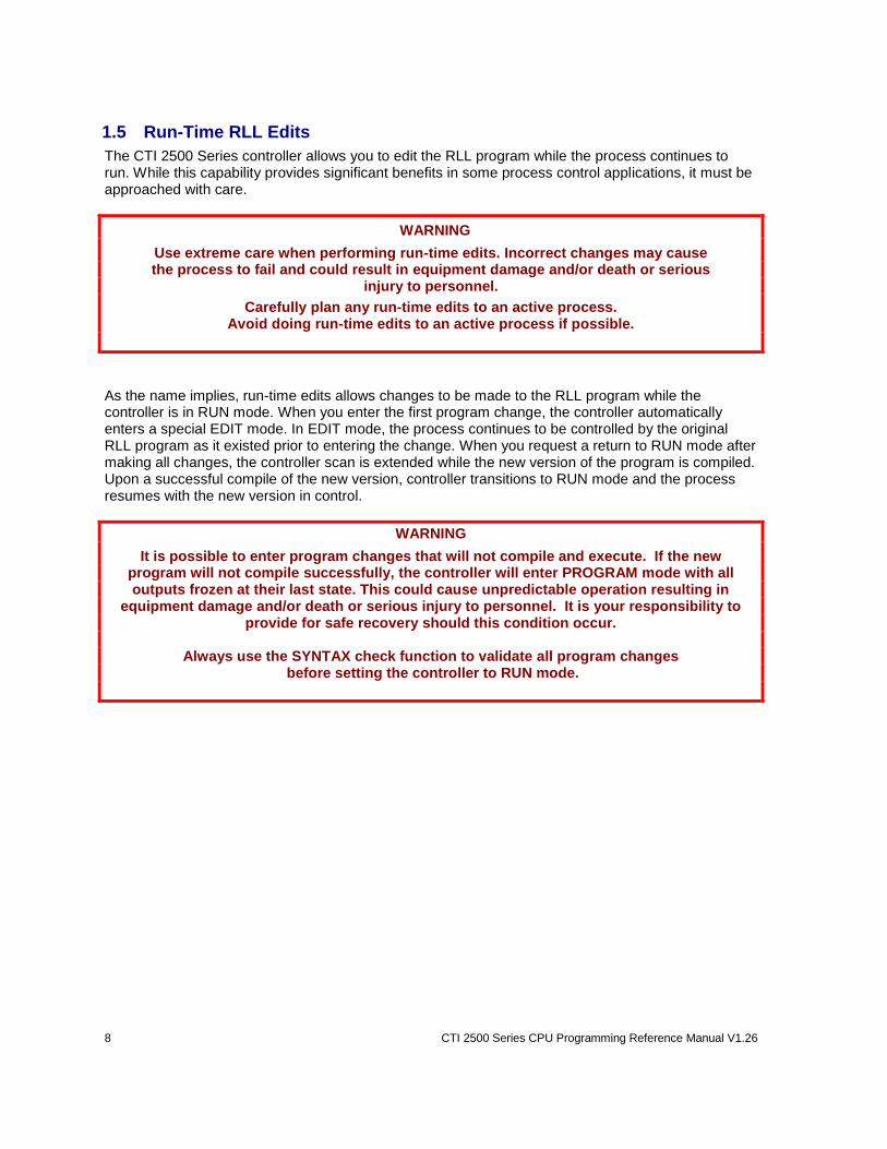
The CTI 2500 Series controller allows you to edit the RLL program while the process continues to run. While this capability provides significant benefits in some process control applications, it must be approached with care.
! WARNING
Use extreme care when performing run-time edits. Incorrect changes may cause the process to fail and could result in equipment damage and/or death or serious
injury to personnel.
Carefully plan any run-time edits to an active process. Avoid doing run-time edits to an active process if possible.
As the name implies, run-time edits allows changes to be made to the RLL program while the controller is in RUN mode. When you enter the first program change, the controller automatically enters a special EDIT mode. In EDIT mode, the process continues to be controlled by the original RLL program as it existed prior to entering the change. When you request a return to RUN mode after making all changes, the controller scan is extended while the new version of the program is compiled. Upon a successful compile of the new version, controller transitions to RUN mode and the process resumes with the new version in control.
WARNING
It is possible to enter program changes that will not compile and execute. If the new program will not compile successfully, the controller will enter PROGRAM mode with all outputs frozen at their last state. This could cause unpredictable operation resulting in
equipment damage and/or death or serious injury to personnel. It is your responsibility to provide for safe recovery should this condition occur.
Always use the SYNTAX check function to validate all program changes
before setting the controller to RUN mode.
CTI 2500 Series CPU Programming Reference Manual V1.26 9
1.5.1 Syntax Checking
After all required modifications are complete, you should request a syntax check to verify that the changes compile correctly before attempting to go to RUN mode. If errors are detected by syntax
check, you can correct these errors and then re-execute the syntax check. This process can be repeated until the syntax check is successful, at which time you can then set the controller to the RUN mode. For Workshop users, the syntax check function can be accessed under the Diagnostics menu item. TISOFT users can access the function under Auxiliary Functions (F6)
1.5.2 Potential Sources of Run-Time Edit Compile Errors
Following are some conditions that will cause the RLL compile to fail, resulting in the controller being placed in PROGRAM mode with outputs frozen. Always request a syntax check before attempting to go to RUN mode.
SKP Instruction without a Corresponding LBL
There must be a LBL statement associated with each SKP instruction and it must occur in the same program segment (SBR or TASK) as the SKP instruction.
SBR instruction without a terminating RTN
A subroutine must be terminated by an unconditional RTN instruction.
GTS, PGTS or PGTSZ without corresponding SBR
The subroutine referenced by a GTS, PGTS, or PGTSZ instruction must be defined before it can be referenced.
Use of unsupported features
Your RLL program must not use an instruction that is not supported by the firmware release installed in your controller or reference undefined or unconfigured data elements. This condition may not be detected by all versions of all programming software tools.
Exceeding L Memory
When you modify or add networks to an RLL program using the run-time edit function, it is possible for the edited program to exceed the amount of L-Memory that has been configured. If the configured L-Memory capacity is exceeded, one or more networks at the end of the program will be deleted when the new program is compiled. Workshop and TISOFT provide a warning of this condition prior to accepting the editing change. However, if you proceed with accepting the change and then select RUN, it is possible that the program will fail to compile or the program may execute incorrectly. Prior to making a run-time change you can determine L memory status by selecting the PLC Utilities/PLC Status menu item in Workshop or Auxiliary Functions (AUX 28) in TISOFT.
10 CTI 2500 Series CPU Programming Reference Manual V1.26
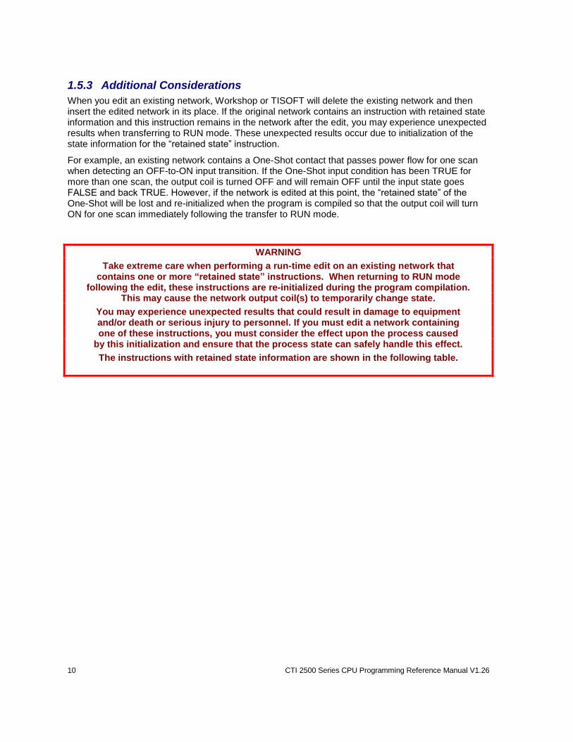
1.5.3 Additional Considerations
When you edit an existing network, Workshop or TISOFT will delete the existing network and then insert the edited network in its place. If the original network contains an instruction with retained state information and this instruction remains in the network after the edit, you may experience unexpected results when transferring to RUN mode. These unexpected results occur due to initialization of the state information for the “retained state” instruction.
For example, an existing network contains a One-Shot contact that passes power flow for one scan when detecting an OFF-to-ON input transition. If the One-Shot input condition has been TRUE for more than one scan, the output coil is turned OFF and will remain OFF until the input state goes FALSE and back TRUE. However, if the network is edited at this point, the “retained state” of the One-Shot will be lost and re-initialized when the program is compiled so that the output coil will turn ON for one scan immediately following the transfer to RUN mode.
!
WARNING
Take extreme care when performing a run-time edit on an existing network that contains one or more “retained state” instructions. When returning to RUN mode
following the edit, these instructions are re-initialized during the program compilation. This may cause the network output coil(s) to temporarily change state.
You may experience unexpected results that could result in damage to equipment and/or death or serious injury to personnel. If you must edit a network containing one of these instructions, you must consider the effect upon the process caused
by this initialization and ensure that the process state can safely handle this effect.
The instructions with retained state information are shown in the following table.
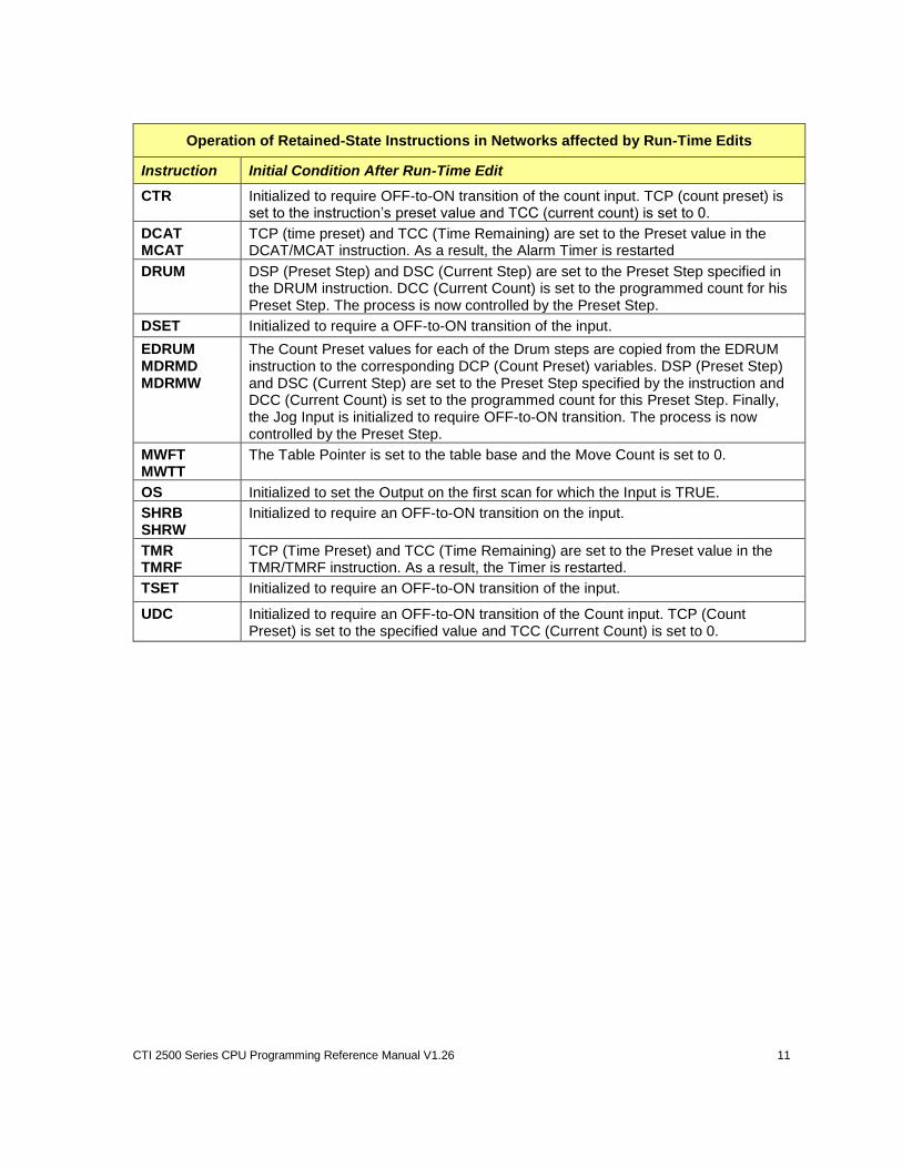
CTI 2500 Series CPU Programming Reference Manual V1.26 11
Operation of Retained-State Instructions in Networks affected by Run-Time Edits
Instruction Initial Condition After Run-Time Edit
CTR Initialized to require OFF-to-ON transition of the count input. TCP (count preset) is set to the instruction’s preset value and TCC (current count) is set to 0.
DCAT MCAT
TCP (time preset) and TCC (Time Remaining) are set to the Preset value in the DCAT/MCAT instruction. As a result, the Alarm Timer is restarted
DRUM DSP (Preset Step) and DSC (Current Step) are set to the Preset Step specified in the DRUM instruction. DCC (Current Count) is set to the programmed count for his Preset Step. The process is now controlled by the Preset Step.
DSET Initialized to require a OFF-to-ON transition of the input.
EDRUM MDRMD MDRMW
The Count Preset values for each of the Drum steps are copied from the EDRUM instruction to the corresponding DCP (Count Preset) variables. DSP (Preset Step) and DSC (Current Step) are set to the Preset Step specified by the instruction and DCC (Current Count) is set to the programmed count for this Preset Step. Finally, the Jog Input is initialized to require OFF-to-ON transition. The process is now controlled by the Preset Step.
MWFT MWTT
The Table Pointer is set to the table base and the Move Count is set to 0.
OS Initialized to set the Output on the first scan for which the Input is TRUE.
SHRB SHRW
Initialized to require an OFF-to-ON transition on the input.
TMR TMRF
TCP (Time Preset) and TCC (Time Remaining) are set to the Preset value in the TMR/TMRF instruction. As a result, the Timer is restarted.
TSET Initialized to require an OFF-to-ON transition of the input.
UDC Initialized to require an OFF-to-ON transition of the Count input. TCP (Count Preset) is set to the specified value and TCC (Current Count) is set to 0.

CTI 2500 Series CPU Programming Reference Manual V1.26 13
CHAPTER 2 RELAY LADDER LOGIC
2.1 Overview
This section describes the RLL Instruction Set supported by the 2500 Series controller. This set of instructions can be used to develop and modify the control program executed by the controller. Errors within the control program can result in inconsistent and unexpected behavior. It is important that the operation of each instruction is understood and verified before using the program to control field devices. In particular, the programmer must be aware of the instructions that retain state information and require multiple PLC scans to complete. These instructions (such as TMR and CTR) must be assigned a unique Reference Number corresponding to the memory type used.
The syntax and parameters for each instruction are provided along with a functional description of operation and usage examples. Any restrictions in parameter fields (such as Reference Number, memory type, and/or limits of constant values) are indicated in the description for each instruction.
Following is a list of the 2500 CPU RLL Instruction Set by functional category. A more detailed description is included in the specified Section.
2.2 RLL Instruction Summary
2.2.1 Relay Instructions
The primary function of RLL network is to control the state of one or more outputs based on input conditions. Inputs and Outputs can represent actual field devices such as switches, relay contacts, and relay coils or internal memory locations. The 2500 Series CPU supports the following instructions to simulate relay logic operations.
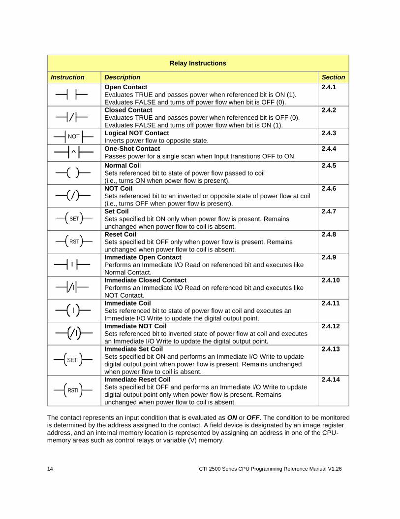
14 CTI 2500 Series CPU Programming Reference Manual V1.26
Relay Instructions
Instruction Description Section
Open Contact Evaluates TRUE and passes power when referenced bit is ON (1). Evaluates FALSE and turns off power flow when bit is OFF (0).
2.4.1
Closed Contact Evaluates TRUE and passes power when referenced bit is OFF (0). Evaluates FALSE and turns off power flow when bit is ON (1).
2.4.2
NOT
Logical NOT Contact Inverts power flow to opposite state.
2.4.3
^
One-Shot Contact Passes power for a single scan when Input transitions OFF to ON.
2.4.4
Normal Coil Sets referenced bit to state of power flow passed to coil (i.e., turns ON when power flow is present).
2.4.5
NOT Coil Sets referenced bit to an inverted or opposite state of power flow at coil (i.e., turns OFF when power flow is present).
2.4.6
SET
Set Coil Sets specified bit ON only when power flow is present. Remains unchanged when power flow to coil is absent.
2.4.7
RST
Reset Coil Sets specified bit OFF only when power flow is present. Remains unchanged when power flow to coil is absent.
2.4.8
I
Immediate Open Contact Performs an Immediate I/O Read on referenced bit and executes like Normal Contact.
2.4.9
I
Immediate Closed Contact Performs an Immediate I/O Read on referenced bit and executes like NOT Contact.
2.4.10
I
Immediate Coil Sets referenced bit to state of power flow at coil and executes an Immediate I/O Write to update the digital output point.
2.4.11
I
Immediate NOT Coil Sets referenced bit to inverted state of power flow at coil and executes an Immediate I/O Write to update the digital output point.
2.4.12
SETI
Immediate Set Coil Sets specified bit ON and performs an Immediate I/O Write to update digital output point when power flow is present. Remains unchanged when power flow to coil is absent.
2.4.13
RSTI
Immediate Reset Coil Sets specified bit OFF and performs an Immediate I/O Write to update digital output point only when power flow is present. Remains unchanged when power flow to coil is absent.
2.4.14
The contact represents an input condition that is evaluated as ON or OFF. The condition to be monitored is determined by the address assigned to the contact. A field device is designated by an image register address, and an internal memory location is represented by assigning an address in one of the CPU-memory areas such as control relays or variable (V) memory.
CTI 2500 Series CPU Programming Reference Manual V1.26 15
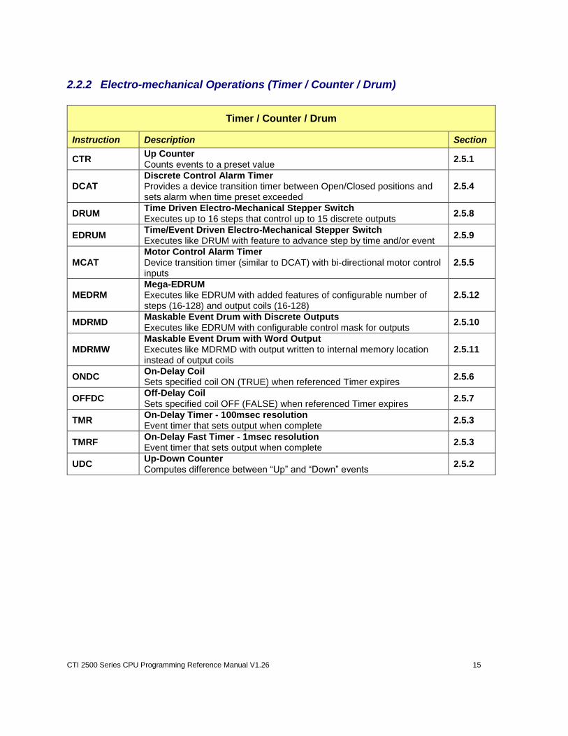
2.2.2 Electro-mechanical Operations (Timer / Counter / Drum)
Timer / Counter / Drum
Instruction Description Section
CTR Up Counter Counts events to a preset value
2.5.1
DCAT Discrete Control Alarm Timer Provides a device transition timer between Open/Closed positions and sets alarm when time preset exceeded
2.5.4
DRUM Time Driven Electro-Mechanical Stepper Switch Executes up to 16 steps that control up to 15 discrete outputs
2.5.8
EDRUM Time/Event Driven Electro-Mechanical Stepper Switch Executes like DRUM with feature to advance step by time and/or event
2.5.9
MCAT Motor Control Alarm Timer Device transition timer (similar to DCAT) with bi-directional motor control inputs
2.5.5
MEDRM Mega-EDRUM Executes like EDRUM with added features of configurable number of steps (16-128) and output coils (16-128)
2.5.12
MDRMD Maskable Event Drum with Discrete Outputs Executes like EDRUM with configurable control mask for outputs
2.5.10
MDRMW Maskable Event Drum with Word Output Executes like MDRMD with output written to internal memory location instead of output coils
2.5.11
ONDC On-Delay Coil Sets specified coil ON (TRUE) when referenced Timer expires
2.5.6
OFFDC Off-Delay Coil Sets specified coil OFF (FALSE) when referenced Timer expires
2.5.7
TMR On-Delay Timer - 100msec resolution Event timer that sets output when complete
2.5.3
TMRF On-Delay Fast Timer - 1msec resolution Event timer that sets output when complete
2.5.3
UDC Up-Down Counter Computes difference between “Up” and “Down” events
2.5.2
16 CTI 2500 Series CPU Programming Reference Manual V1.26
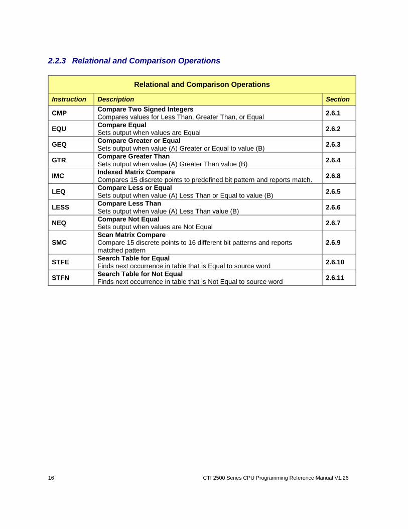
2.2.3 Relational and Comparison Operations
Relational and Comparison Operations
Instruction Description Section
CMP Compare Two Signed Integers Compares values for Less Than, Greater Than, or Equal
2.6.1
EQU Compare Equal Sets output when values are Equal
2.6.2
GEQ Compare Greater or Equal Sets output when value (A) Greater or Equal to value (B)
2.6.3
GTR Compare Greater Than Sets output when value (A) Greater Than value (B)
2.6.4
IMC Indexed Matrix Compare Compares 15 discrete points to predefined bit pattern and reports match.
2.6.8
LEQ Compare Less or Equal Sets output when value (A) Less Than or Equal to value (B)
2.6.5
LESS Compare Less Than Sets output when value (A) Less Than value (B)
2.6.6
NEQ Compare Not Equal Sets output when values are Not Equal
2.6.7
SMC Scan Matrix Compare Compare 15 discrete points to 16 different bit patterns and reports matched pattern
2.6.9
STFE Search Table for Equal Finds next occurrence in table that is Equal to source word
2.6.10
STFN Search Table for Not Equal Finds next occurrence in table that is Not Equal to source word
2.6.11
CTI 2500 Series CPU Programming Reference Manual V1.26 17
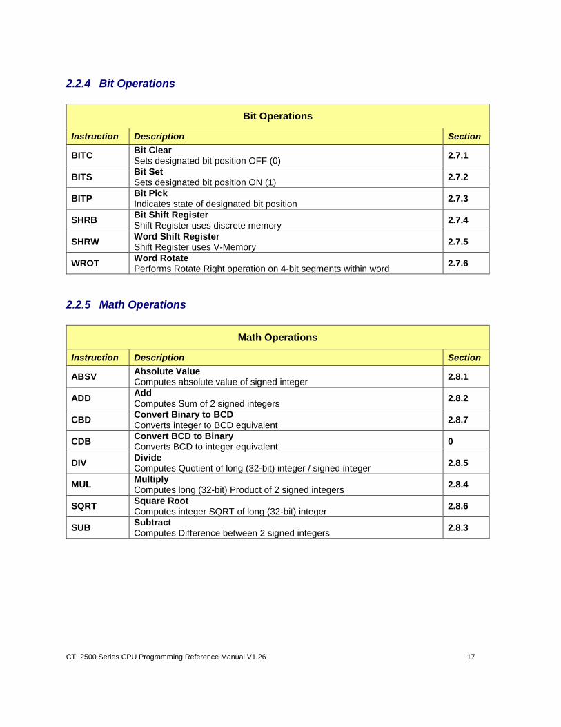
2.2.4 Bit Operations
Bit Operations
Instruction Description Section
BITC Bit Clear Sets designated bit position OFF (0)
2.7.1
BITS Bit Set Sets designated bit position ON (1)
2.7.2
BITP Bit Pick Indicates state of designated bit position
2.7.3
SHRB Bit Shift Register Shift Register uses discrete memory
2.7.4
SHRW Word Shift Register Shift Register uses V-Memory
2.7.5
WROT Word Rotate Performs Rotate Right operation on 4-bit segments within word
2.7.6
2.2.5 Math Operations
Math Operations
Instruction Description Section
ABSV Absolute Value Computes absolute value of signed integer
2.8.1
ADD Add Computes Sum of 2 signed integers
2.8.2
CBD Convert Binary to BCD Converts integer to BCD equivalent
2.8.7
CDB Convert BCD to Binary Converts BCD to integer equivalent
0
DIV Divide Computes Quotient of long (32-bit) integer / signed integer
2.8.5
MUL Multiply Computes long (32-bit) Product of 2 signed integers
2.8.4
SQRT Square Root Computes integer SQRT of long (32-bit) integer
2.8.6
SUB Subtract Computes Difference between 2 signed integers
2.8.3
18 CTI 2500 Series CPU Programming Reference Manual V1.26
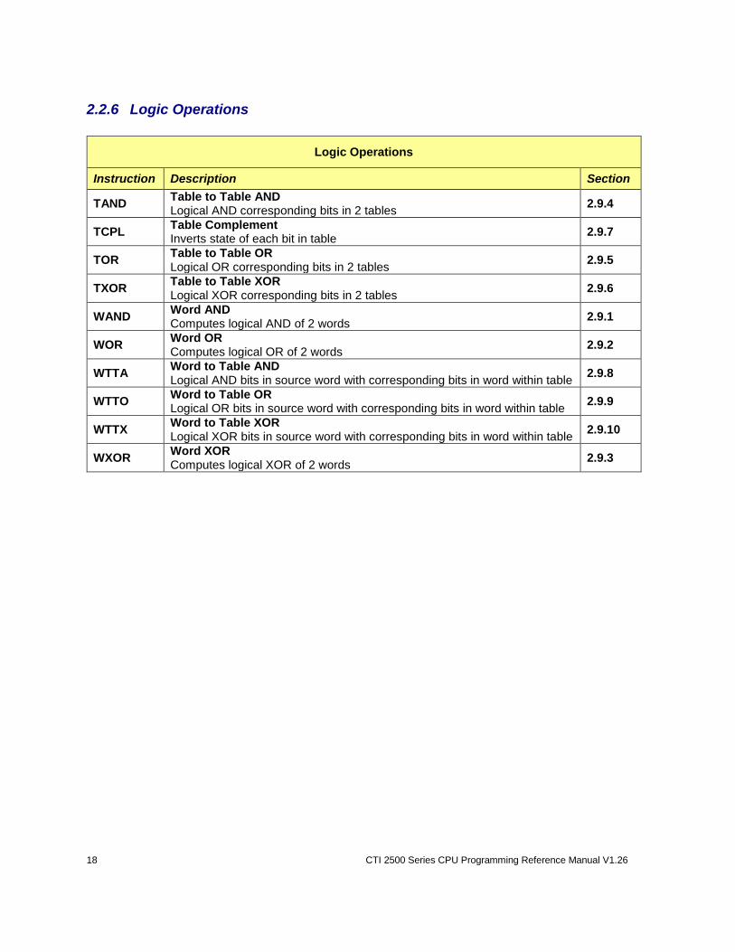
2.2.6 Logic Operations
Logic Operations
Instruction Description Section
TAND Table to Table AND Logical AND corresponding bits in 2 tables
2.9.4
TCPL Table Complement Inverts state of each bit in table
2.9.7
TOR Table to Table OR Logical OR corresponding bits in 2 tables
2.9.5
TXOR Table to Table XOR Logical XOR corresponding bits in 2 tables
2.9.6
WAND Word AND Computes logical AND of 2 words
2.9.1
WOR Word OR Computes logical OR of 2 words
2.9.2
WTTA Word to Table AND Logical AND bits in source word with corresponding bits in word within table
2.9.8
WTTO Word to Table OR Logical OR bits in source word with corresponding bits in word within table
2.9.9
WTTX Word to Table XOR Logical XOR bits in source word with corresponding bits in word within table
2.9.10
WXOR Word XOR Computes logical XOR of 2 words
2.9.3
CTI 2500 Series CPU Programming Reference Manual V1.26 19
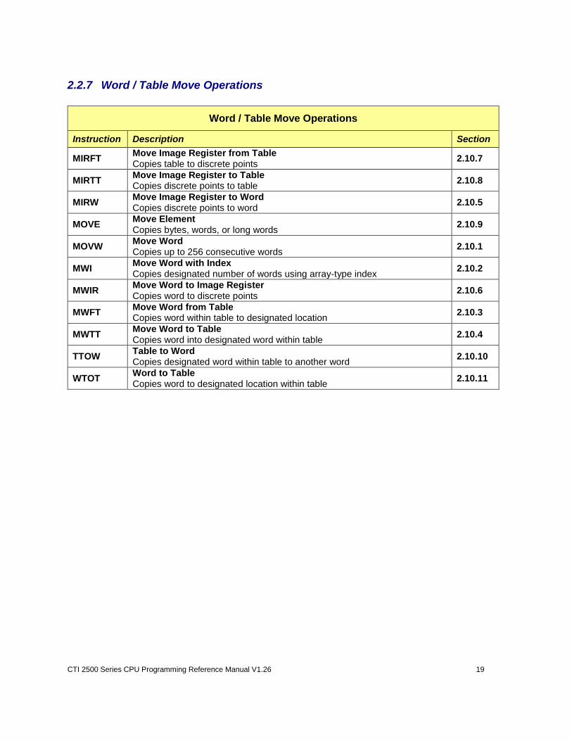
2.2.7 Word / Table Move Operations
Word / Table Move Operations
Instruction Description Section
MIRFT Move Image Register from Table Copies table to discrete points
2.10.7
MIRTT Move Image Register to Table Copies discrete points to table
2.10.8
MIRW Move Image Register to Word Copies discrete points to word
2.10.5
MOVE Move Element Copies bytes, words, or long words
2.10.9
MOVW Move Word Copies up to 256 consecutive words
2.10.1
MWI Move Word with Index Copies designated number of words using array-type index
2.10.2
MWIR Move Word to Image Register Copies word to discrete points
2.10.6
MWFT Move Word from Table Copies word within table to designated location
2.10.3
MWTT Move Word to Table Copies word into designated word within table
2.10.4
TTOW Table to Word Copies designated word within table to another word
2.10.10
WTOT Word to Table Copies word to designated location within table
2.10.11
20 CTI 2500 Series CPU Programming Reference Manual V1.26
2.2.8 Program Control Operations
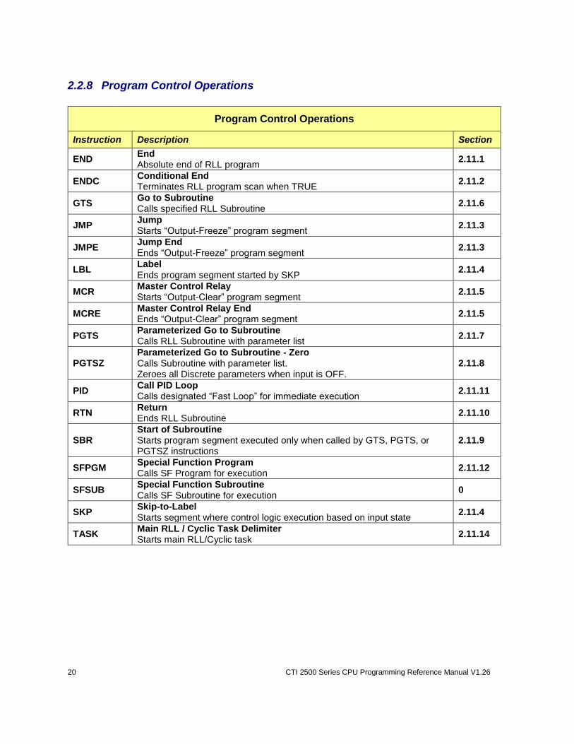
Program Control Operations
Instruction Description Section
END End Absolute end of RLL program
2.11.1
ENDC Conditional End Terminates RLL program scan when TRUE
2.11.2
GTS Go to Subroutine Calls specified RLL Subroutine
2.11.6
JMP Jump Starts “Output-Freeze” program segment
2.11.3
JMPE Jump End Ends “Output-Freeze” program segment
2.11.3
LBL Label Ends program segment started by SKP
2.11.4
MCR Master Control Relay Starts “Output-Clear” program segment
2.11.5
MCRE Master Control Relay End Ends “Output-Clear” program segment
2.11.5
PGTS Parameterized Go to Subroutine Calls RLL Subroutine with parameter list
2.11.7
PGTSZ Parameterized Go to Subroutine - Zero Calls Subroutine with parameter list. Zeroes all Discrete parameters when input is OFF.
2.11.8
PID Call PID Loop Calls designated “Fast Loop” for immediate execution
2.11.11
RTN Return Ends RLL Subroutine
2.11.10
SBR Start of Subroutine Starts program segment executed only when called by GTS, PGTS, or PGTSZ instructions
2.11.9
SFPGM Special Function Program Calls SF Program for execution
2.11.12
SFSUB Special Function Subroutine Calls SF Subroutine for execution
0
SKP Skip-to-Label Starts segment where control logic execution based on input state
2.11.4
TASK Main RLL / Cyclic Task Delimiter Starts main RLL/Cyclic task
2.11.14
CTI 2500 Series CPU Programming Reference Manual V1.26 21
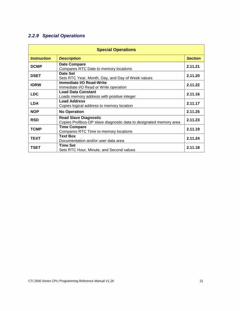
2.2.9 Special Operations
Special Operations
Instruction Description Section
DCMP Date Compare Compares RTC Date to memory locations
2.11.21
DSET Date Set Sets RTC Year, Month, Day, and Day of Week values
2.11.20
IORW Immediate I/O Read-Write Immediate I/O Read or Write operation
2.11.22
LDC Load Data Constant Loads memory address with positive integer
2.11.16
LDA Load Address Copies logical address to memory location
2.11.17
NOP No Operation 2.11.25
RSD Read Slave Diagnostic Copies Profibus-DP slave diagnostic data to designated memory area
2.11.23
TCMP Time Compare Compares RTC Time to memory locations
2.11.19
TEXT Text Box Documentation and/or user data area
2.11.24
TSET Time Set Sets RTC Hour, Minute, and Second values
2.11.18
22 CTI 2500 Series CPU Programming Reference Manual V1.26
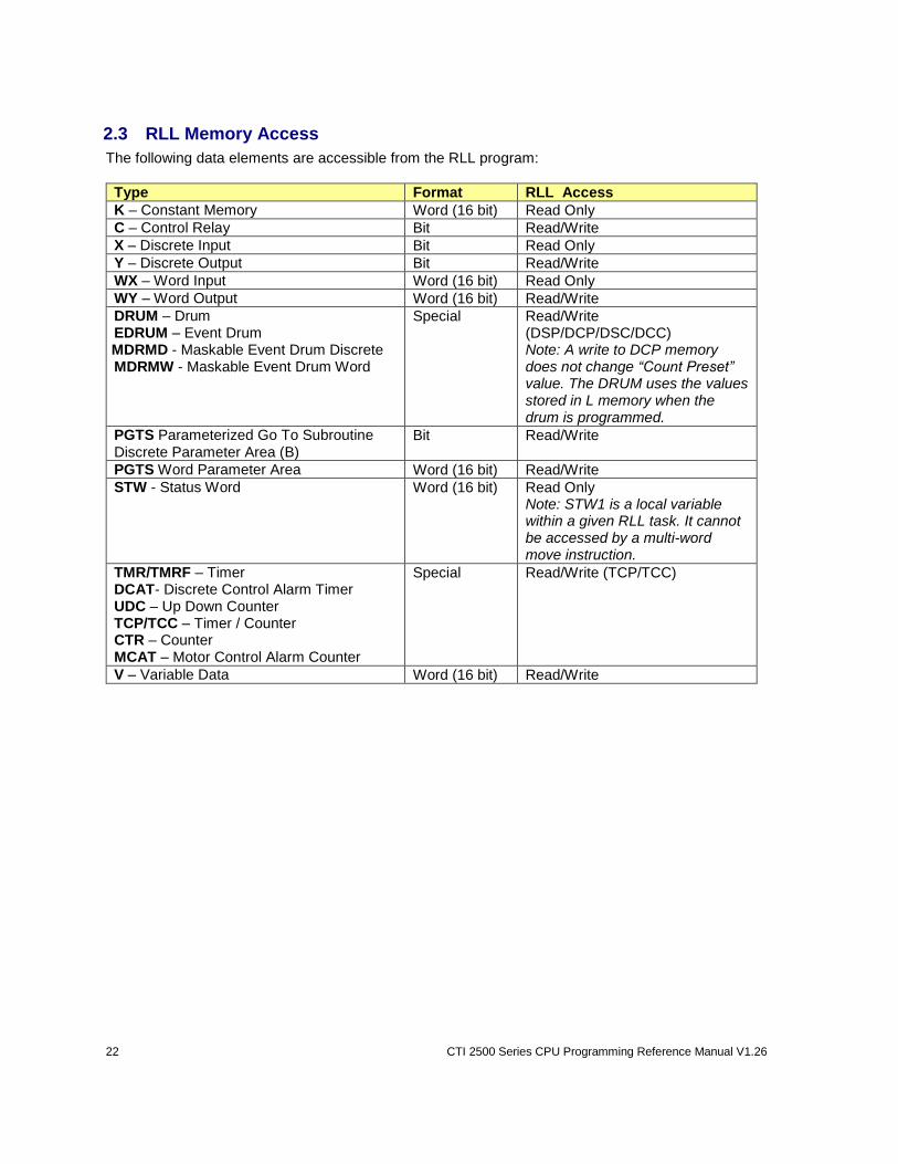
2.3 RLL Memory Access
The following data elements are accessible from the RLL program:
Type Format RLL Access
K – Constant Memory Word (16 bit) Read Only
C – Control Relay Bit Read/Write
X – Discrete Input Bit Read Only
Y – Discrete Output Bit Read/Write
WX – Word Input Word (16 bit) Read Only
WY – Word Output Word (16 bit) Read/Write
DRUM – Drum EDRUM – Event Drum
MDRMD - Maskable Event Drum Discrete MDRMW - Maskable Event Drum Word
Special Read/Write (DSP/DCP/DSC/DCC) Note: A write to DCP memory does not change “Count Preset” value. The DRUM uses the values stored in L memory when the drum is programmed.
PGTS Parameterized Go To Subroutine Discrete Parameter Area (B)
Bit Read/Write
PGTS Word Parameter Area Word (16 bit) Read/Write
STW - Status Word Word (16 bit) Read Only Note: STW1 is a local variable within a given RLL task. It cannot be accessed by a multi-word move instruction.
TMR/TMRF – Timer DCAT- Discrete Control Alarm Timer UDC – Up Down Counter TCP/TCC – Timer / Counter CTR – Counter MCAT – Motor Control Alarm Counter
Special Read/Write (TCP/TCC)
V – Variable Data Word (16 bit) Read/Write
CTI 2500 Series CPU Programming Reference Manual V1.26 23
2.4 Relay Instructions
This group of instructions simulates electro-mechanical devices such as timers, counters, and stepper switches.
CAUTION:
I/O points addressed as X and Y memory types refer to the same Discrete Image Register. X memory is used to specify field inputs and Y memory designates field outputs.
Therefore, contacts entered with the same X memory and Y memory reference number (i.e., X9 and Y9) read the same location in the Discrete Image Register.
Do not assign the same reference number to both input (X) and output (Y) contacts.
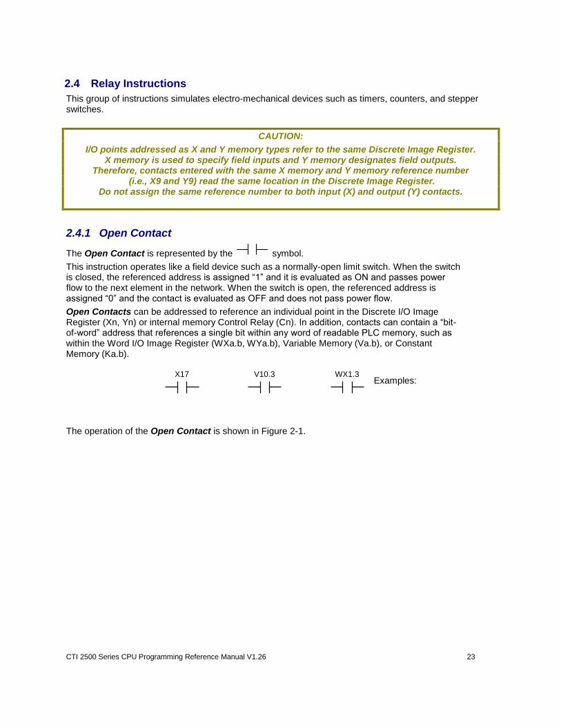
2.4.1 Open Contact
The Open Contact is represented by the symbol.
This instruction operates like a field device such as a normally-open limit switch. When the switch is closed, the referenced address is assigned “1” and it is evaluated as ON and passes power flow to the next element in the network. When the switch is open, the referenced address is assigned “0” and the contact is evaluated as OFF and does not pass power flow.
Open Contacts can be addressed to reference an individual point in the Discrete I/O Image Register (Xn, Yn) or internal memory Control Relay (Cn). In addition, contacts can contain a “bit-of-word” address that references a single bit within any word of readable PLC memory, such as within the Word I/O Image Register (WXa.b, WYa.b), Variable Memory (Va.b), or Constant Memory (Ka.b).
Examples:
The operation of the Open Contact is shown in Figure 2-1.
WX1.3X17 V10.3
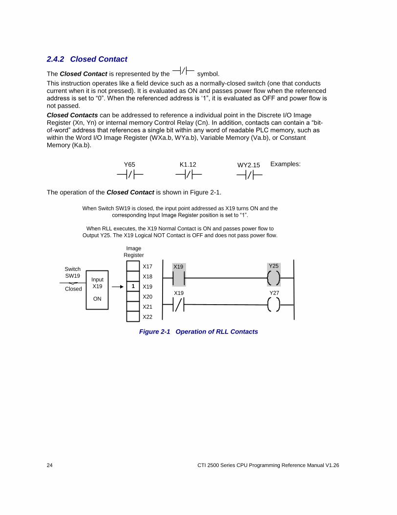
24 CTI 2500 Series CPU Programming Reference Manual V1.26
2.4.2 Closed Contact
The Closed Contact is represented by the symbol.
This instruction operates like a field device such as a normally-closed switch (one that conducts current when it is not pressed). It is evaluated as ON and passes power flow when the referenced address is set to “0”. When the referenced address is ‘1”, it is evaluated as OFF and power flow is not passed.
Closed Contacts can be addressed to reference a individual point in the Discrete I/O Image Register (Xn, Yn) or internal memory Control Relay (Cn). In addition, contacts can contain a “bit-of-word” address that references a single bit within any word of readable PLC memory, such as within the Word I/O Image Register (WXa.b, WYa.b), Variable Memory (Va.b), or Constant Memory (Ka.b).
Examples:
The operation of the Closed Contact is shown in Figure 2-1.
Input
X19
ON
Switch
SW19
X17
X18
X19
X22
X21
X20
Image
Register
Closed
Y25
Y27X19
X19
1
When Switch SW19 is closed, the input point addressed as X19 turns ON and the
corresponding Input Image Register position is set to “1”.
When RLL executes, the X19 Normal Contact is ON and passes power flow to
Output Y25. The X19 Logical NOT Contact is OFF and does not pass power flow.
Figure 2-1 Operation of RLL Contacts
WY2.15Y65 K1.12
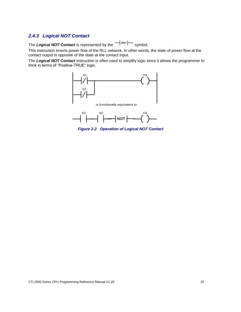
CTI 2500 Series CPU Programming Reference Manual V1.26 25
2.4.3 Logical NOT Contact
The Logical NOT Contact is represented by the NOTNOT
symbol.
This instruction inverts power flow of the RLL network. In other words, the state of power flow at the contact output is opposite of the state at the contact input.
The Logical NOT Contact instruction is often used to simplify logic since it allows the programmer to think in terms of “Positive-TRUE” logic.
is functionally equivalent to
X1 X2
NOTNOT
Y9
X1
X2
Y9
Figure 2-2 Operation of Logical NOT Contact
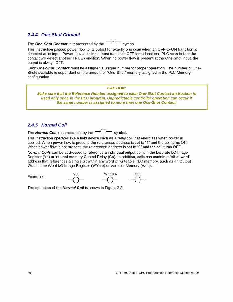
26 CTI 2500 Series CPU Programming Reference Manual V1.26
2.4.4 One-Shot Contact
The One-Shot Contact is represented by the ^
symbol.
This instruction passes power flow to its output for exactly one scan when an OFF-to-ON transition is detected at its input. Power flow at its input must transition OFF for at least one PLC scan before the contact will detect another TRUE condition. When no power flow is present at the One-Shot input, the output is always OFF.
Each One-Shot Contact must be assigned a unique number for proper operation. The number of One-Shots available is dependent on the amount of “One-Shot” memory assigned in the PLC Memory configuration.
CAUTION:
Make sure that the Reference Number assigned to each One-Shot Contact instruction is used only once in the PLC program. Unpredictable controller operation can occur if
the same number is assigned to more than one One-Shot Contact.
2.4.5 Normal Coil
The Normal Coil is represented by the symbol.
This instruction operates like a field device such as a relay coil that energizes when power is applied. When power flow is present, the referenced address is set to “1” and the coil turns ON. When power flow is not present, the referenced address is set to “0” and the coil turns OFF.
Normal Coils can be addressed to reference a individual output point in the Discrete I/O Image Register (Yn) or internal memory Control Relay (Cn). In addition, coils can contain a “bit-of-word” address that references a single bit within any word of writeable PLC memory, such as an Output Word in the Word I/O Image Register (WYa.b) or Variable Memory (Va.b).
Examples:
The operation of the Normal Coil is shown in Figure 2-3.
Y33 WY10.4 C21
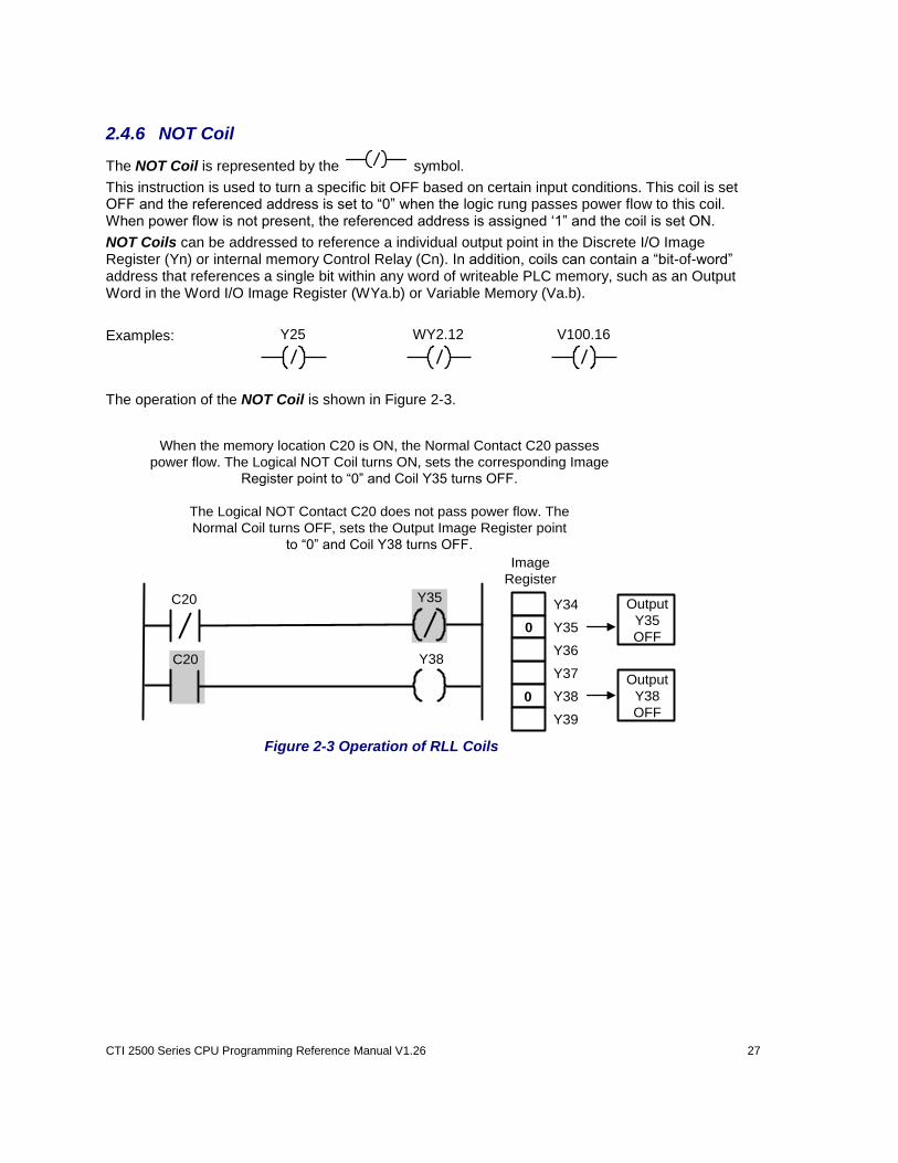
CTI 2500 Series CPU Programming Reference Manual V1.26 27
2.4.6 NOT Coil
The NOT Coil is represented by the symbol.
This instruction is used to turn a specific bit OFF based on certain input conditions. This coil is set OFF and the referenced address is set to “0” when the logic rung passes power flow to this coil. When power flow is not present, the referenced address is assigned ‘1” and the coil is set ON.
NOT Coils can be addressed to reference a individual output point in the Discrete I/O Image Register (Yn) or internal memory Control Relay (Cn). In addition, coils can contain a “bit-of-word” address that references a single bit within any word of writeable PLC memory, such as an Output Word in the Word I/O Image Register (WYa.b) or Variable Memory (Va.b).
Examples:
The operation of the NOT Coil is shown in Figure 2-3.
When the memory location C20 is ON, the Normal Contact C20 passes
power flow. The Logical NOT Coil turns ON, sets the corresponding Image
Register point to “0” and Coil Y35 turns OFF.
The Logical NOT Contact C20 does not pass power flow. The
Normal Coil turns OFF, sets the Output Image Register point
to “0” and Coil Y38 turns OFF.
Output
Y35
OFF
Y34
Y35
Y36
Y39
Y38
Y37
Image
Register
Output
Y38
OFF
Y35
Y38C20
C20
0
0
Figure 2-3 Operation of RLL Coils
Y25 WY2.12 V100.16
28 CTI 2500 Series CPU Programming Reference Manual V1.26
2.4.7 Set Coil
The Set Coil is represented by the SET
symbol.
This instruction operates like a field device circuit that energizing a latching relay coil. When power flow is present, the referenced address is set to “1” and the coil turns ON. When power flow is not present, the coil state remains unchanged.
The Set Coil instruction never sets its referenced address to “0”. The Reset Coil instruction must be used for that purpose.
Set Coils can be addressed to reference a individual output point in the Discrete I/O Image Register (Yn) or internal memory Control Relay (Cn). In addition, coils can contain a “bit-of-word” address that references a single bit within any word of writeable PLC memory, such as an Output Word in the Word I/O Image Register (WYa.b) or Variable Memory (Va.b). Examples:
2.4.8 Reset Coil
The Reset Coil is represented by the RST
symbol.
This instruction operates like a field device circuit that resets a latching relay coil. When power flow is present, the referenced address is set to “0” and the coil turns OFF. When power flow is not present, the coil state remains unchanged.
The Reset Coil instruction never sets its referenced address to “1”. The Set Coil instruction must be used for that purpose.
Reset Coils can be addressed to reference a individual output point in the Discrete I/O Image Register (Yn) or internal memory Control Relay (Cn). In addition, coils can contain a “bit-of-word” address that references a single bit within any word of writeable PLC memory, such as an Output Word in the Word I/O Image Register (WYa.b) or Variable Memory (Va.b). Examples:
SET
Y46
SET
C34
SET
V12.3
RST
Y29
RST
WY16.8
RST
V12.16
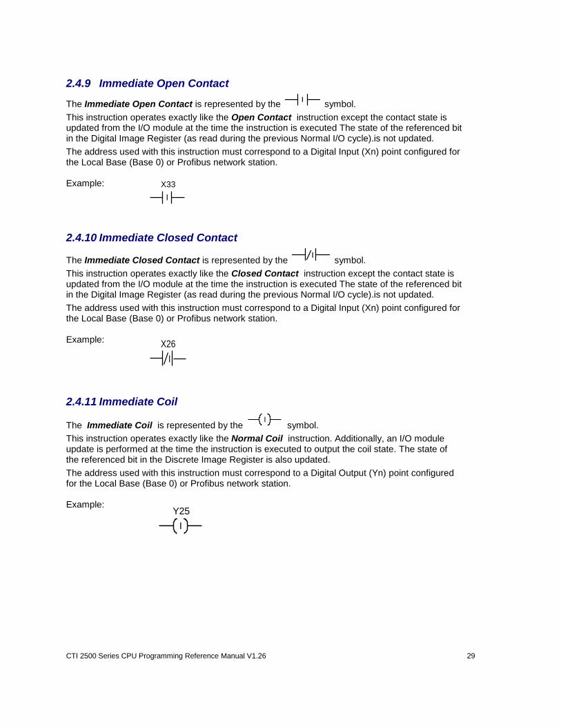
CTI 2500 Series CPU Programming Reference Manual V1.26 29
2.4.9 Immediate Open Contact
The Immediate Open Contact is represented by the I
symbol.
This instruction operates exactly like the Open Contact instruction except the contact state is updated from the I/O module at the time the instruction is executed The state of the referenced bit in the Digital Image Register (as read during the previous Normal I/O cycle).is not updated.
The address used with this instruction must correspond to a Digital Input (Xn) point configured for the Local Base (Base 0) or Profibus network station. Example:
2.4.10 Immediate Closed Contact
The Immediate Closed Contact is represented by the I
symbol.
This instruction operates exactly like the Closed Contact instruction except the contact state is updated from the I/O module at the time the instruction is executed The state of the referenced bit in the Digital Image Register (as read during the previous Normal I/O cycle).is not updated.
The address used with this instruction must correspond to a Digital Input (Xn) point configured for the Local Base (Base 0) or Profibus network station. Example:
2.4.11 Immediate Coil
The Immediate Coil is represented by the I
symbol.
This instruction operates exactly like the Normal Coil instruction. Additionally, an I/O module update is performed at the time the instruction is executed to output the coil state. The state of the referenced bit in the Discrete Image Register is also updated.
The address used with this instruction must correspond to a Digital Output (Yn) point configured for the Local Base (Base 0) or Profibus network station. Example:
I
X33
I
X26
Y25
I
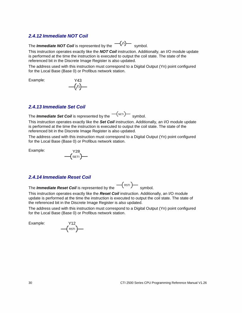
30 CTI 2500 Series CPU Programming Reference Manual V1.26
2.4.12 Immediate NOT Coil
The Immediate NOT Coil is represented by the I
symbol.
This instruction operates exactly like the NOT Coil instruction. Additionally, an I/O module update is performed at the time the instruction is executed to output the coil state. The state of the referenced bit in the Discrete Image Register is also updated.
The address used with this instruction must correspond to a Digital Output (Yn) point configured for the Local Base (Base 0) or Profibus network station. Example:
2.4.13 Immediate Set Coil
The Immediate Set Coil is represented by the SETI
symbol.
This instruction operates exactly like the Set Coil instruction. Additionally, an I/O module update is performed at the time the instruction is executed to output the coil state. The state of the referenced bit in the Discrete Image Register is also updated.
The address used with this instruction must correspond to a Digital Output (Yn) point configured for the Local Base (Base 0) or Profibus network station. Example:
2.4.14 Immediate Reset Coil
The Immediate Reset Coil is represented by the RSTI
symbol.
This instruction operates exactly like the Reset Coil instruction. Additionally, an I/O module update is performed at the time the instruction is executed to output the coil state. The state of the referenced bit in the Discrete Image Register is also updated.
The address used with this instruction must correspond to a Digital Output (Yn) point configured for the Local Base (Base 0) or Profibus network station.
Example:
I
Y43
SETI
Y28
Y12
RSTI
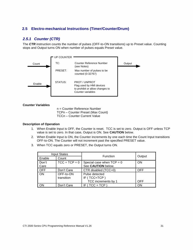
CTI 2500 Series CPU Programming Reference Manual V1.26 31
2.5 Electro-mechanical Instructions (Timer/Counter/Drum)
2.5.1 Counter (CTR)
The CTR instruction counts the number of pulses (OFF-to-ON transitions) up to Preset value. Counting stops and Output turns ON when number of pulses equals Preset value.
Counter Variables n = Counter Reference Number TCPn – Counter Preset (Max Count) TCCn – Counter Current Value
Description of Operation
1. When Enable Input is OFF, the Counter is reset. TCC is set to zero. Output is OFF unless TCP value is set to zero. In that case, Output is ON. See CAUTION below.
2. When Enable Input is ON, the Counter increments by one each time the Count Input transitions OFF-to-ON. The Counter will not increment past the specified PRESET value.
3. When TCC equals zero or PRESET, the Output turns ON.
UP COUNTER
TC: Counter Reference Number
(see Notes)
PRESET: Max number of pulses to be
counted (0-32767)
STATUS: PROT / UNPROT
Flag used by HMI devices
to prohibit or allow changes to
Counter variables
Enable
OutputCount
Input States Function Output
Enable Count
Don’t Care
TCC = TCP = 0 Special case when TCP = 0 See CAUTION below.
ON
OFF Don’t Care CTR disabled (TCC=0) OFF
ON OFF-to-ON transition
Pulse detected IF ( TCC<TCP ) TCC increments by 1
OFF
ON Don’t Care IF ( TCC = TCP ) ON
32 CTI 2500 Series CPU Programming Reference Manual V1.26
CAUTION:
The CTR instruction Output turns ON when Counter Preset (TCP) and Counter Current (TCC) values are both set to zero REGARDLESS of state of the Enable input. This replicates the
operation of the CTR instruction in the Siemens SIMATIC® 505 controller.
Note:
The Reference Number assigned to the instruction box must be unique for all Timers and Counters entered in the PLC program. Do NOT use the same Reference Number more than once for any T/C
instruction (TMR, TMRF, CTR, UDC, DCAT, MCAT, ONDC, OFFDC).
The number of available Timers and Counters is dependent on the amount of T/C Memory assigned in PLC Memory Configuration. Timer variables TCP (Timer Preset) and TCC (Timer Current) are maintained across power outage when ‘Battery Good’ LED is ON.
If these variables are changed by RLL instructions or HMI (if ‘Status = Unprotected’), the new values will not be retained if the original program is downloaded again to PLC.
Related instructions: UDC
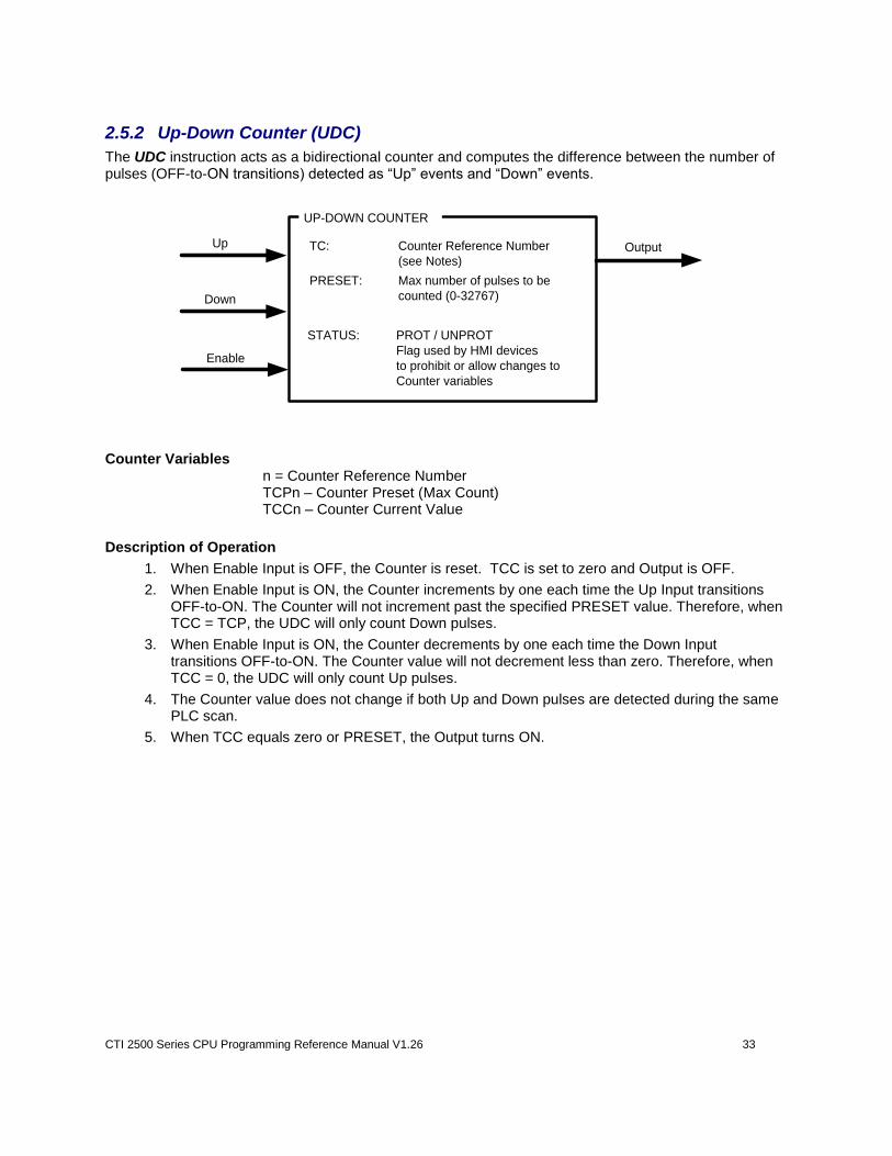
CTI 2500 Series CPU Programming Reference Manual V1.26 33
2.5.2 Up-Down Counter (UDC)
The UDC instruction acts as a bidirectional counter and computes the difference between the number of pulses (OFF-to-ON transitions) detected as “Up” events and “Down” events.
UP-DOWN COUNTER
TC: Counter Reference Number
(see Notes)
PRESET: Max number of pulses to be
counted (0-32767)
STATUS: PROT / UNPROT
Flag used by HMI devices
to prohibit or allow changes to
Counter variables
Output
Enable
Up
Down
Counter Variables n = Counter Reference Number TCPn – Counter Preset (Max Count) TCCn – Counter Current Value
Description of Operation
1. When Enable Input is OFF, the Counter is reset. TCC is set to zero and Output is OFF.
2. When Enable Input is ON, the Counter increments by one each time the Up Input transitions OFF-to-ON. The Counter will not increment past the specified PRESET value. Therefore, when TCC = TCP, the UDC will only count Down pulses.
3. When Enable Input is ON, the Counter decrements by one each time the Down Input transitions OFF-to-ON. The Counter value will not decrement less than zero. Therefore, when TCC = 0, the UDC will only count Up pulses.
4. The Counter value does not change if both Up and Down pulses are detected during the same PLC scan.
5. When TCC equals zero or PRESET, the Output turns ON.
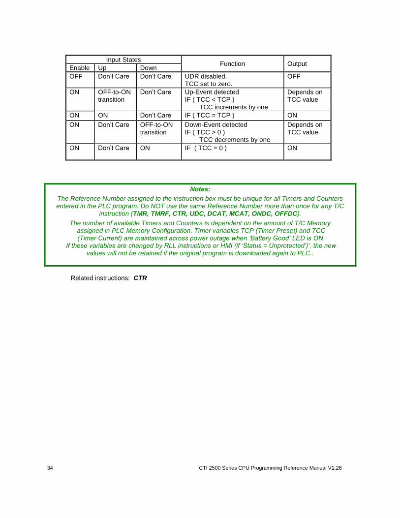
34 CTI 2500 Series CPU Programming Reference Manual V1.26
Input States Function Output
Enable Up Down
OFF Don’t Care Don’t Care UDR disabled. TCC set to zero.
OFF
ON OFF-to-ON transition
Don’t Care Up-Event detected IF ( TCC < TCP ) TCC increments by one
Depends on TCC value
ON ON Don’t Care IF ( TCC = TCP ) ON
ON Don’t Care OFF-to-ON transition
Down-Event detected IF ( TCC > 0 ) TCC decrements by one
Depends on TCC value
ON Don’t Care ON IF ( TCC = 0 ) ON
Notes:
The Reference Number assigned to the instruction box must be unique for all Timers and Counters entered in the PLC program. Do NOT use the same Reference Number more than once for any T/C
instruction (TMR, TMRF, CTR, UDC, DCAT, MCAT, ONDC, OFFDC).
The number of available Timers and Counters is dependent on the amount of T/C Memory assigned in PLC Memory Configuration. Timer variables TCP (Timer Preset) and TCC (Timer Current) are maintained across power outage when ‘Battery Good’ LED is ON.
If these variables are changed by RLL instructions or HMI (if ‘Status = Unprotected’)’, the new values will not be retained if the original program is downloaded again to PLC..
Related instructions: CTR

CTI 2500 Series CPU Programming Reference Manual V1.26 35
2.5.3 On-Delay Timer (TMR / TMRF)
The TMR and TMRF instructions are used to execute time-based events within the RLL program. The TMR (Slow Timer) and TMRF (Fast Timer) instructions are identical except for the time base as shown below:
TMR has time base of 100 msec (0.1 sec) with range of 0.1 – 3276.7 seconds
TMRF has time base of 1 msec (0.001 sec) with range of 0.001 – 32.767 seconds
TIMER
TC: Timer Reference Number
(see Notes)
PRESET: Number of “time-base”
increments to be timed
(0-32767)
STATUS: PROT / UNPROT
Flag used by HMI devices
to prohibit or allow changes to
Timer variables
Enable
OutputStart
Timer Variables n = Timer Reference Number TCPn – Timer Preset (PRESET) TCCn – Timer Current Value Description of Operation
1. When Enable Input is OFF, the Timer is reset to PRESET value and Output is OFF.
2. When Enable Input is ON, the Timer is enabled but does not advance when Start Input is OFF.
3. When Start Input turns ON, The Timer begins at PRESET and advances toward zero. The “elapsed time” is decremented each PLC scan the Timer is enabled and Start is ON.
4. If the Start Input transitions OFF (with Enable Input ON), the Timer stops and holds its current value. This state is held until either Start Input transitions ON (timing resumes) or Enable Input turns OFF (timer reset).
5. When Timer reaches zero, Output is turned ON and remains ON until the Enable Input turns OFF to reset the Timer.
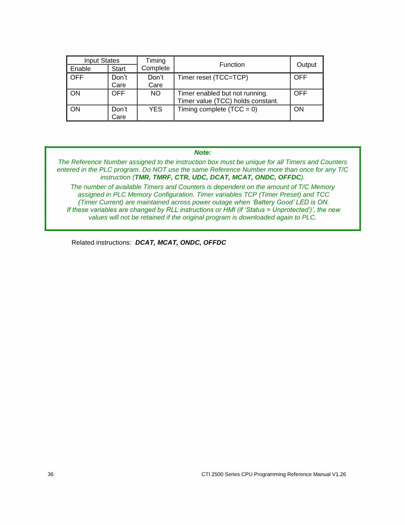
36 CTI 2500 Series CPU Programming Reference Manual V1.26
Input States Timing Complete
Function Output Enable Start
OFF Don’t Care
Don’t Care
Timer reset (TCC=TCP) OFF
ON OFF NO Timer enabled but not running. Timer value (TCC) holds constant.
OFF
ON Don’t Care
YES Timing complete (TCC = 0) ON
Note:
The Reference Number assigned to the instruction box must be unique for all Timers and Counters entered in the PLC program. Do NOT use the same Reference Number more than once for any T/C
instruction (TMR, TMRF, CTR, UDC, DCAT, MCAT, ONDC, OFFDC).
The number of available Timers and Counters is dependent on the amount of T/C Memory assigned in PLC Memory Configuration. Timer variables TCP (Timer Preset) and TCC (Timer Current) are maintained across power outage when ‘Battery Good’ LED is ON.
If these variables are changed by RLL instructions or HMI (if ‘Status = Unprotected’)’, the new values will not be retained if the original program is downloaded again to PLC.
Related instructions: DCAT, MCAT, ONDC, OFFDC
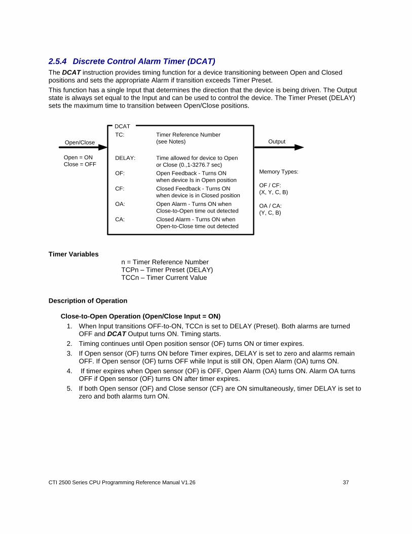
CTI 2500 Series CPU Programming Reference Manual V1.26 37
2.5.4 Discrete Control Alarm Timer (DCAT)
The DCAT instruction provides timing function for a device transitioning between Open and Closed positions and sets the appropriate Alarm if transition exceeds Timer Preset.
This function has a single Input that determines the direction that the device is being driven. The Output state is always set equal to the Input and can be used to control the device. The Timer Preset (DELAY) sets the maximum time to transition between Open/Close positions.
DCAT
DELAY: Time allowed for device to Open
or Close (0.,1-3276.7 sec)
CA: Closed Alarm - Turns ON when
Open-to-Close time out detected
TC: Timer Reference Number
(see Notes)
OA: Open Alarm - Turns ON when
Close-to-Open time out detected
CF: Closed Feedback - Turns ON
when device is in Closed position
OF: Open Feedback - Turns ON
when device Is in Open position
OutputOpen/Close
Open = ON
Close = OFF
Memory Types:
OF / CF:
(X, Y, C, B)
OA / CA:
(Y, C, B)
Timer Variables n = Timer Reference Number TCPn – Timer Preset (DELAY) TCCn – Timer Current Value Description of Operation
Close-to-Open Operation (Open/Close Input = ON)
1. When Input transitions OFF-to-ON, TCCn is set to DELAY (Preset). Both alarms are turned OFF and DCAT Output turns ON. Timing starts.
2. Timing continues until Open position sensor (OF) turns ON or timer expires.
3. If Open sensor (OF) turns ON before Timer expires, DELAY is set to zero and alarms remain OFF. If Open sensor (OF) turns OFF while Input is still ON, Open Alarm (OA) turns ON.
4. If timer expires when Open sensor (OF) is OFF, Open Alarm (OA) turns ON. Alarm OA turns OFF if Open sensor (OF) turns ON after timer expires.
5. If both Open sensor (OF) and Close sensor (CF) are ON simultaneously, timer DELAY is set to zero and both alarms turn ON.
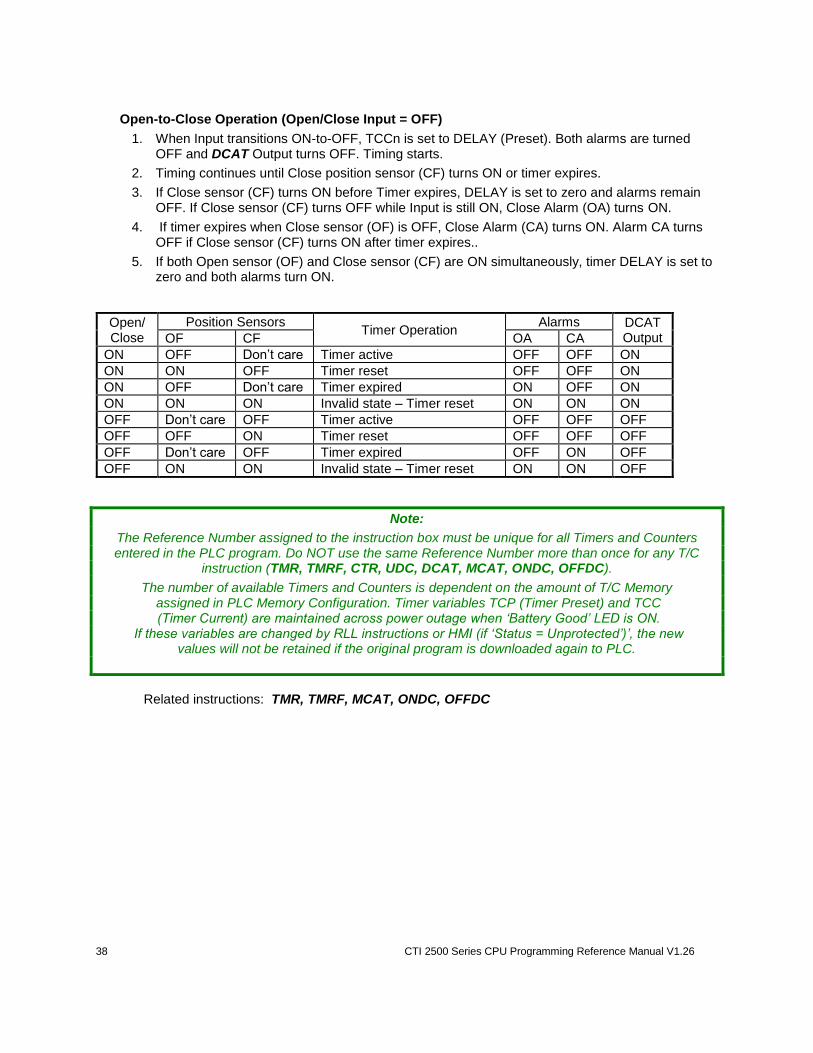
38 CTI 2500 Series CPU Programming Reference Manual V1.26
Open-to-Close Operation (Open/Close Input = OFF)
1. When Input transitions ON-to-OFF, TCCn is set to DELAY (Preset). Both alarms are turned OFF and DCAT Output turns OFF. Timing starts.
2. Timing continues until Close position sensor (CF) turns ON or timer expires.
3. If Close sensor (CF) turns ON before Timer expires, DELAY is set to zero and alarms remain OFF. If Close sensor (CF) turns OFF while Input is still ON, Close Alarm (OA) turns ON.
4. If timer expires when Close sensor (OF) is OFF, Close Alarm (CA) turns ON. Alarm CA turns OFF if Close sensor (CF) turns ON after timer expires..
5. If both Open sensor (OF) and Close sensor (CF) are ON simultaneously, timer DELAY is set to zero and both alarms turn ON.
Note:
The Reference Number assigned to the instruction box must be unique for all Timers and Counters entered in the PLC program. Do NOT use the same Reference Number more than once for any T/C
instruction (TMR, TMRF, CTR, UDC, DCAT, MCAT, ONDC, OFFDC).
The number of available Timers and Counters is dependent on the amount of T/C Memory assigned in PLC Memory Configuration. Timer variables TCP (Timer Preset) and TCC (Timer Current) are maintained across power outage when ‘Battery Good’ LED is ON.
If these variables are changed by RLL instructions or HMI (if ‘Status = Unprotected’)’, the new values will not be retained if the original program is downloaded again to PLC.
Related instructions: TMR, TMRF, MCAT, ONDC, OFFDC
Open/ Close
Position Sensors Timer Operation
Alarms DCAT Output OF CF OA CA
ON OFF Don’t care Timer active OFF OFF ON
ON ON OFF Timer reset OFF OFF ON
ON OFF Don’t care Timer expired ON OFF ON
ON ON ON Invalid state – Timer reset ON ON ON
OFF Don’t care OFF Timer active OFF OFF OFF
OFF OFF ON Timer reset OFF OFF OFF
OFF Don’t care OFF Timer expired OFF ON OFF
OFF ON ON Invalid state – Timer reset ON ON OFF
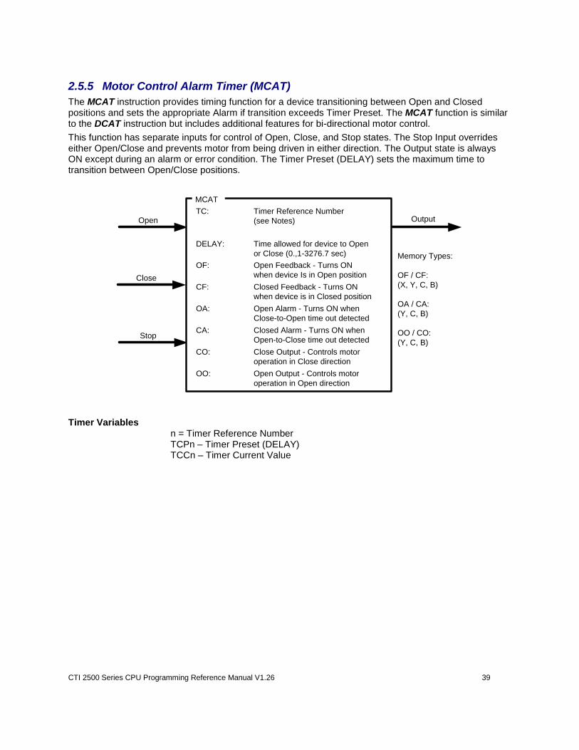
CTI 2500 Series CPU Programming Reference Manual V1.26 39
2.5.5 Motor Control Alarm Timer (MCAT)
The MCAT instruction provides timing function for a device transitioning between Open and Closed positions and sets the appropriate Alarm if transition exceeds Timer Preset. The MCAT function is similar to the DCAT instruction but includes additional features for bi-directional motor control.
This function has separate inputs for control of Open, Close, and Stop states. The Stop Input overrides either Open/Close and prevents motor from being driven in either direction. The Output state is always ON except during an alarm or error condition. The Timer Preset (DELAY) sets the maximum time to transition between Open/Close positions.
Memory Types:
OF / CF:
(X, Y, C, B)
OA / CA:
(Y, C, B)
OO / CO:
(Y, C, B)
OutputOpen
Close
Stop
MCAT
DELAY: Time allowed for device to Open
or Close (0.,1-3276.7 sec)
CA: Closed Alarm - Turns ON when
Open-to-Close time out detected
TC: Timer Reference Number
(see Notes)
OA: Open Alarm - Turns ON when
Close-to-Open time out detected
CF: Closed Feedback - Turns ON
when device is in Closed position
OF: Open Feedback - Turns ON
when device Is in Open position
CO: Close Output - Controls motor
operation in Close direction
OO: Open Output - Controls motor
operation in Open direction
Timer Variables n = Timer Reference Number TCPn – Timer Preset (DELAY) TCCn – Timer Current Value
40 CTI 2500 Series CPU Programming Reference Manual V1.26
Description of Operation
Close-to-Open Operation (Open Command Input = ON)
1. When Open Input transitions OFF-to-ON (and Close/Stop Inputs are OFF), control in Open direction is triggered. Open Output (OO) turns ON, both alarms (OA/CA) are turned OFF, and Timer starts.
2. Open Output (OO) is “latched” and remains ON and timing continues until one of the following events is detected:
a. Open Sensor (OF) turns ON before Timer expires while Close Sensor (CF) remains OFF. DELAY is set to zero and alarms remain OFF. If Open sensor (OF) subsequently turns OFF before Close Input turns ON, Open Alarm (OA) turns ON.
b. Stop Input turns ON.
Open Output (OO) and both alarms (OA/CA) turn OFF. Timer stops (TCC stays constant). If Stop Input turns OFF while Open Input is still ON, the action is treated like a new Close-to-Open operation. The Timer starts timing at Preset (DELAY).
c. Timer expires before Open Sensor (OF) turns ON. The Open Output (OO) turns OFF and Open Alarm (OA) turns ON.
d. Close Input turns ON (after Open Input has turned OFF). (See description of Open-to-Close Operation below)
Open-to-Close Operation (Close Command Input = ON)
1. When Close Input transitions OFF-to-ON (and Open/Stop Inputs are OFF), control in Close direction is triggered. Close Output (CO) turns ON, both alarms (OA/CA) are turned OFF, and Timer starts.
2. Close Output (CO) is “latched” and remains ON and timing continues until one of the following events is detected:
a. Close Sensor (CF) turns ON before Timer expires (while Open Sensor (OF) is OFF). DELAY is set to zero and alarms remain OFF. If Close Sensor (CF) subsequently turns OFF before Open Input turns ON, Close Alarm (CA) turns ON.
b. Stop Input turns ON. Close Output (CO) and both alarms (OA/CA) turn OFF. Timer stops (TCC stays constant). If Stop Input turns OFF while Close Input is still ON, the action is treated like a new Open-to-Close operation. The Timer starts timing at Preset (DELAY).
c. Timer expires before Close Sensor (CF) turns ON. The Close Output (CO) turns OFF and Close Alarm (CA) turns ON.
d. Open Input turns ON (after Close Input has turned OFF). (See description of Close-to-Open Operation above)
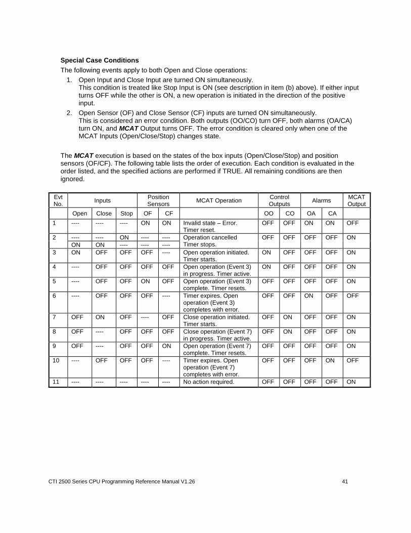
CTI 2500 Series CPU Programming Reference Manual V1.26 41
Special Case Conditions
The following events apply to both Open and Close operations:
1. Open Input and Close Input are turned ON simultaneously. This condition is treated like Stop Input is ON (see description in item (b) above). If either input turns OFF while the other is ON, a new operation is initiated in the direction of the positive input.
2. Open Sensor (OF) and Close Sensor (CF) inputs are turned ON simultaneously. This is considered an error condition. Both outputs (OO/CO) turn OFF, both alarms (OA/CA) turn ON, and MCAT Output turns OFF. The error condition is cleared only when one of the MCAT Inputs (Open/Close/Stop) changes state.
The MCAT execution is based on the states of the box inputs (Open/Close/Stop) and position sensors (OF/CF). The following table lists the order of execution. Each condition is evaluated in the order listed, and the specified actions are performed if TRUE. All remaining conditions are then ignored.
Evt No.
Inputs Position Sensors
MCAT Operation Control Outputs
Alarms MCAT Output
Open Close Stop OF CF OO CO OA CA
1 ---- ---- ---- ON ON Invalid state – Error. Timer reset.
OFF OFF ON ON OFF
2 ---- ---- ON ---- ---- Operation cancelled Timer stops.
OFF OFF OFF OFF ON
ON ON ---- ---- ----
3 ON OFF OFF OFF ---- Open operation initiated. Timer starts.
ON OFF OFF OFF ON
4 ---- OFF OFF OFF OFF Open operation (Event 3) in progress. Timer active.
ON OFF OFF OFF ON
5 ---- OFF OFF ON OFF Open operation (Event 3) complete. Timer resets.
OFF OFF OFF OFF ON
6 ---- OFF OFF OFF ---- Timer expires. Open operation (Event 3) completes with error.
OFF OFF ON OFF OFF
7 OFF ON OFF ---- OFF Close operation initiated. Timer starts.
OFF ON OFF OFF ON
8 OFF ---- OFF OFF OFF Close operation (Event 7) in progress. Timer active.
OFF ON OFF OFF ON
9 OFF ---- OFF OFF ON Open operation (Event 7) complete. Timer resets.
OFF OFF OFF OFF ON
10 ---- OFF OFF OFF ---- Timer expires. Open operation (Event 7) completes with error.
OFF OFF OFF ON OFF
11 ---- ---- ---- ---- ---- No action required. OFF OFF OFF OFF ON
42 CTI 2500 Series CPU Programming Reference Manual V1.26
Note:
The Reference Number assigned to the instruction box must be unique for all Timers and Counters entered in the PLC program. Do NOT use the same Reference Number more than once for any T/C
instruction (TMR, TMRF, CTR, UDC, DCAT, MCAT, ONDC, OFFDC).
The number of available Timers and Counters is dependent on the amount of T/C Memory assigned in PLC Memory Configuration. Timer variables TCP (Timer Preset) and TCC (Timer Current) are maintained across power outage when ‘Battery Good’ LED is ON.
If these variables are changed by RLL instructions or HMI (if ‘Status = Unprotected’)’, the new values will not be retained if the original program is downloaded again to PLC.
Related instructions: TMR, TMRF, DCAT, ONDC, OFFDC
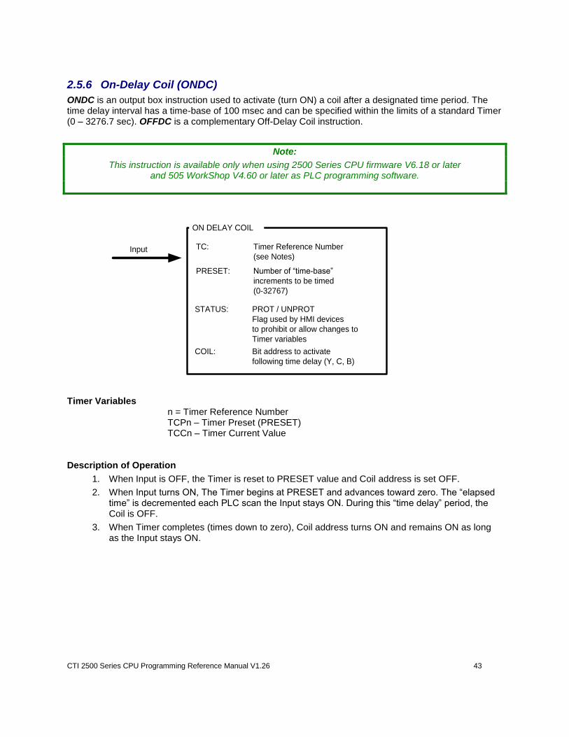
CTI 2500 Series CPU Programming Reference Manual V1.26 43
2.5.6 On-Delay Coil (ONDC)
ONDC is an output box instruction used to activate (turn ON) a coil after a designated time period. The time delay interval has a time-base of 100 msec and can be specified within the limits of a standard Timer (0 – 3276.7 sec). OFFDC is a complementary Off-Delay Coil instruction.
Note:
This instruction is available only when using 2500 Series CPU firmware V6.18 or later and 505 WorkShop V4.60 or later as PLC programming software.
ON DELAY COIL
TC: Timer Reference Number
(see Notes)
PRESET: Number of “time-base”
increments to be timed
(0-32767)
STATUS: PROT / UNPROT
Flag used by HMI devices
to prohibit or allow changes to
Timer variables
Input
COIL: Bit address to activate
following time delay (Y, C, B)
Timer Variables n = Timer Reference Number TCPn – Timer Preset (PRESET) TCCn – Timer Current Value Description of Operation
1. When Input is OFF, the Timer is reset to PRESET value and Coil address is set OFF.
2. When Input turns ON, The Timer begins at PRESET and advances toward zero. The “elapsed time” is decremented each PLC scan the Input stays ON. During this “time delay” period, the Coil is OFF.
3. When Timer completes (times down to zero), Coil address turns ON and remains ON as long as the Input stays ON.

44 CTI 2500 Series CPU Programming Reference Manual V1.26
Input Timing
Complete Function Coil
OFF Don’t Care
Timer reset (TCC=TCP) OFF
ON NO Timer active (TCC decrements) OFF
ON YES Timing complete (TCC = 0) ON
Note:
The Reference Number assigned to the instruction box must be unique for all Timers and Counters entered in the PLC program. Do NOT use the same Reference Number more than once for any T/C
instruction (TMR, TMRF, CTR, UDC, DCAT, MCAT, ONDC, OFFDC).
The number of available Timers and Counters is dependent on the amount of T/C Memory assigned in PLC Memory Configuration. Timer variables TCP (Timer Preset) and TCC (Timer Current) are maintained across power outage when ‘Battery Good’ LED is ON.
If these variables are changed by RLL instructions or HMI (if ‘Status = Unprotected’)’, the new values will not be retained if the original program is downloaded again to PLC.
Related instructions: TMR, TMRF, DCAT, MCAT, ONDC, OFFDC

CTI 2500 Series CPU Programming Reference Manual V1.26 45
2.5.7 Off-Delay Coil (OFFDC)
OFFDC is an output box instruction used to deactivate (turn OFF) a coil after a designated time period. The time delay interval has a time-base of 100 msec and can be specified within the limits of a standard Timer (0 – 3276.7 sec). ONDC is a complementary On-Delay Coil instruction.
Note:
This instruction is available only when using 2500 Series CPU firmware V6.18 or later and 505 WorkShop V4.60 or later as PLC programming software.
OFF DELAY COIL
TC: Timer Reference Number
(see Notes)
PRESET: Number of “time-base”
increments to be timed
(0-32767)
STATUS: PROT / UNPROT
Flag used by HMI devices
to prohibit or allow changes to
Timer variables
Input
COIL: Bit address to deactivate
following time delay (Y, C, B)
Timer Variables n = Timer Reference Number TCPn – Timer Preset (PRESET) TCCn – Timer Current Value
CAUTION:
The OFFDC instruction is unique in that it is enabled by an ON-to-OFF transition of the the Input contact and operates when the Input is FALSE. Keep this in consideration
when using this instruction in your RLL program.
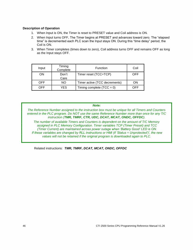
46 CTI 2500 Series CPU Programming Reference Manual V1.26
Description of Operation
1. When Input is ON, the Timer is reset to PRESET value and Coil address is ON.
2. When Input turns OFF, The Timer begins at PRESET and advances toward zero. The “elapsed time” is decremented each PLC scan the Input stays ON. During this “time delay” period, the Coil is ON.
3. When Timer completes (times down to zero), Coil address turns OFF and remains OFF as long as the Input stays OFF.
Input Timing
Complete Function Coil
ON Don’t
Care
Timer reset (TCC=TCP) OFF
OFF NO Timer active (TCC decrements) ON
OFF YES Timing complete (TCC = 0) OFF
Note:
The Reference Number assigned to the instruction box must be unique for all Timers and Counters entered in the PLC program. Do NOT use the same Reference Number more than once for any T/C
instruction (TMR, TMRF, CTR, UDC, DCAT, MCAT, ONDC, OFFDC).
The number of available Timers and Counters is dependent on the amount of T/C Memory assigned in PLC Memory Configuration. Timer variables TCP (Timer Preset) and TCC (Timer Current) are maintained across power outage when ‘Battery Good’ LED is ON.
If these variables are changed by RLL instructions or HMI (if ‘Status = Unprotected’)’, the new values will not be retained if the original program is downloaded again to PLC.
Related instructions: TMR, TMRF, DCAT, MCAT, ONDC, OFFDC
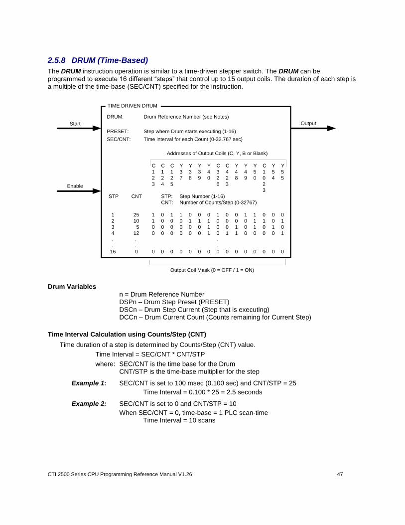
CTI 2500 Series CPU Programming Reference Manual V1.26 47
2.5.8 DRUM (Time-Based)
The DRUM instruction operation is similar to a time-driven stepper switch. The DRUM can be programmed to execute 16 different “steps” that control up to 15 output coils. The duration of each step is a multiple of the time-base (SEC/CNT) specified for the instruction.
TIME DRIVEN DRUM
Addresses of Output Coils (C, Y, B or Blank)
C C C Y Y Y Y C C Y Y Y C Y Y
1 1 1 3 3 3 4 3 4 4 4 5 1 5 5
2 2 2 7 8 9 0 2 2 8 9 0 0 4 5
3 4 5 6 3 2
3
STP CNT STP: Step Number (1-16)
CNT: Number of Counts/Step (0-32767)
1 25 1 0 1 1 0 0 0 1 0 0 1 1 0 0 0
2 10 1 0 0 0 1 1 1 0 0 0 0 1 1 0 1
3 5 0 0 0 0 0 0 1 0 0 1 0 1 0 1 0
4 12 0 0 0 0 0 0 1 0 1 1 0 0 0 0 1
. . .
. . .
16 0 0 0 0 0 0 0 0 0 0 0 0 0 0 0 0
Output Coil Mask (0 = OFF / 1 = ON)
PRESET: Step where Drum starts executing (1-16)
DRUM: Drum Reference Number (see Notes)
SEC/CNT: Time interval for each Count (0-32.767 sec)
Start
Enable
Output
Drum Variables n = Drum Reference Number DSPn – Drum Step Preset (PRESET) DSCn – Drum Step Current (Step that is executing) DCCn – Drum Current Count (Counts remaining for Current Step)
Time Interval Calculation using Counts/Step (CNT)
Time duration of a step is determined by Counts/Step (CNT) value.
Time Interval = SEC/CNT * CNT/STP
where: SEC/CNT is the time base for the Drum CNT/STP is the time-base multiplier for the step
Example 1: SEC/CNT is set to 100 msec (0.100 sec) and CNT/STP = 25
Time Interval = 0.100 * 25 = 2.5 seconds
Example 2: SEC/CNT is set to 0 and CNT/STP = 10
When SEC/CNT = 0, time-base = 1 PLC scan-time Time Interval = 10 scans
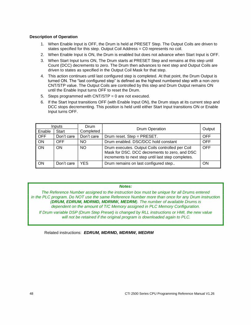
48 CTI 2500 Series CPU Programming Reference Manual V1.26
Description of Operation
1. When Enable Input is OFF, the Drum is held at PRESET Step. The Output Coils are driven to states specified for this step. Output Coil Address = C0 represents no coil.
2. When Enable Input is ON, the Drum is enabled but does not advance when Start Input is OFF.
3. When Start Input turns ON, The Drum starts at PRESET Step and remains at this step until Count (DCC) decrements to zero. The Drum then advances to next step and Output Coils are driven to states as specified in the Output Coil Mask for that step.
4. This action continues until last configured step is completed. At that point, the Drum Output is turned ON. The “last configured step” is defined as the highest numbered step with a non-zero CNT/STP value. The Output Coils are controlled by this step and Drum Output remains ON until the Enable Input turns OFF to reset the Drum.
5. Steps programmed with CNT/STP = 0 are not executed.
6. If the Start Input transitions OFF (with Enable Input ON), the Drum stays at its current step and DCC stops decrementing. This position is held until either Start Input transitions ON or Enable Input turns OFF.
Inputs Drum Completed
Drum Operation Output Enable Start
OFF Don’t care Don’t care Drum reset. Step = PRESET. OFF
ON OFF NO Drum enabled. DSC/DCC hold constant OFF
ON ON NO Drum executes. Output Coils controlled per Coil Mask for DSC. DCC decrements to zero, and DSC increments to next step until last step completes.
OFF
ON Don’t care YES Drum remains on last configured step.. ON
Notes:
The Reference Number assigned to the instruction box must be unique for all Drums entered in the PLC program. Do NOT use the same Reference Number more than once for any Drum instruction
(DRUM, EDRUM, MDRMD, MDRMW, MEDRM). The number of available Drums is dependent on the amount of T/C Memory assigned in PLC Memory Configuration.
If Drum variable DSP (Drum Step Preset) is changed by RLL instructions or HMI, the new value will not be retained if the original program is downloaded again to PLC.
Related instructions: EDRUM, MDRMD, MDRMW, MEDRM
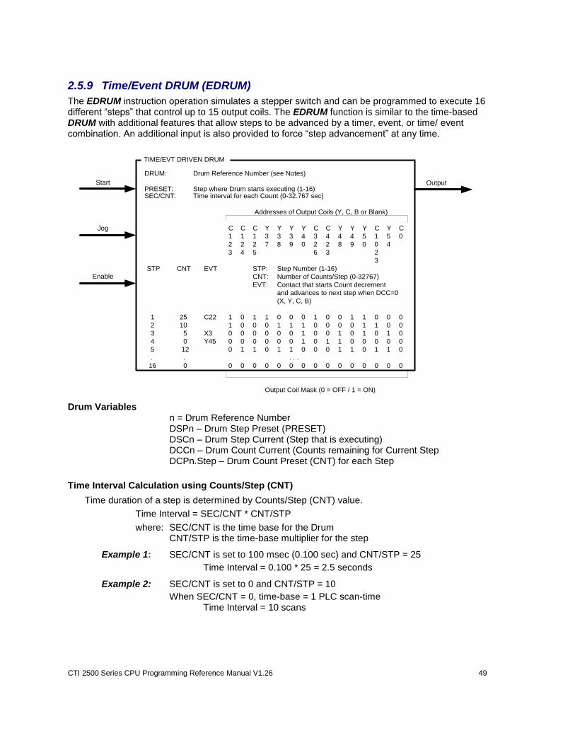
CTI 2500 Series CPU Programming Reference Manual V1.26 49
2.5.9 Time/Event DRUM (EDRUM)
The EDRUM instruction operation simulates a stepper switch and can be programmed to execute 16 different “steps” that control up to 15 output coils. The EDRUM function is similar to the time-based DRUM with additional features that allow steps to be advanced by a timer, event, or time/ event combination. An additional input is also provided to force “step advancement” at any time.
TIME/EVT DRIVEN DRUM
Addresses of Output Coils (Y, C, B or Blank)
C C C Y Y Y Y C C Y Y Y C Y C
1 1 1 3 3 3 4 3 4 4 4 5 1 5 0
2 2 2 7 8 9 0 2 2 8 9 0 0 4
3 4 5 6 3 2
3
STP CNT EVT STP: Step Number (1-16)
CNT: Number of Counts/Step (0-32767)
EVT: Contact that starts Count decrement
and advances to next step when DCC=0
(X, Y, C, B)
1 25 C22 1 0 1 1 0 0 0 1 0 0 1 1 0 0 0
2 10 1 0 0 0 1 1 1 0 0 0 0 1 1 0 0
3 5 X3 0 0 0 0 0 0 1 0 0 1 0 1 0 1 0
4 0 Y45 0 0 0 0 0 0 1 0 1 1 0 0 0 0 0
5 12 0 1 1 0 1 1 0 0 0 1 1 0 1 1 0
. . . . .
16 0 0 0 0 0 0 0 0 0 0 0 0 0 0 0 0
Output Coil Mask (0 = OFF / 1 = ON)
PRESET: Step where Drum starts executing (1-16)
DRUM: Drum Reference Number (see Notes)
SEC/CNT: Time interval for each Count (0-32.767 sec)
OutputStart
Jog
Enable
Drum Variables n = Drum Reference Number DSPn – Drum Step Preset (PRESET) DSCn – Drum Step Current (Step that is executing) DCCn – Drum Count Current (Counts remaining for Current Step DCPn.Step – Drum Count Preset (CNT) for each Step
Time Interval Calculation using Counts/Step (CNT)
Time duration of a step is determined by Counts/Step (CNT) value.
Time Interval = SEC/CNT * CNT/STP
where: SEC/CNT is the time base for the Drum CNT/STP is the time-base multiplier for the step
Example 1: SEC/CNT is set to 100 msec (0.100 sec) and CNT/STP = 25
Time Interval = 0.100 * 25 = 2.5 seconds
Example 2: SEC/CNT is set to 0 and CNT/STP = 10
When SEC/CNT = 0, time-base = 1 PLC scan-time Time Interval = 10 scans
50 CTI 2500 Series CPU Programming Reference Manual V1.26
Step Advancement Options
1. To program a step for Time-Based Operation Only:
Set Counts/Step (CNT) to value > 0
Do NOT insert a Contact in the Event (EVT) field for this step
The Drum remains on this step until DCC decrements to zero. Then the Drum advances to next step (see Step 2 in example).
2. To program a step for Event-Triggered Operation Only:
Set Counts/Step (CNT) to value = 0
Insert a Contact in the Event (EVT) field for this step
The Drum remains on the step until the Contact specified in the EVT field turns ON. The Drum then advances to the next step (see Step 4 in example).
3. To program a step for Timer and Event-Triggered Operation:
Set Counts/Step (CNT) to value > 0
Insert a Contact in the Event (EVT) field for this step
The Drum remains on this step until DCC decrements to zero (same as time-based operation). However, the DCC value decrements only when the Contact specified in the EVT field is ON). The Drum advances to the next step when DCC reaches zero (see Step 1 in example).
4. To program a step for Timer or Event-Triggered Operation:
Set Counts/Step (CNT) to value > 0
Do NOT Insert a Contact in the Event (EVT) field for this step
Implement logic external to the Drum so that the RLL program creates “Event-Trigger” to turn ON the Jog Input when Drum should advance to next step.
The Drum remains on this step until DCC decrements to zero (same as time-based operation) or Event-Trigger activates (Jog Input transitions OFF-to-ON).
Description of Operation
1. When Enable Input is OFF, the Drum is held at PRESET Step. The Output Coils are driven to states specified for this step. Output Coil Address = C0 represents no coil.
2. When Enable Input is ON, Drum does not advance when Start Input is OFF.
3. When Start Input turns ON, The Drum starts at PRESET Step and remains at this step until Timer and/or Event is triggered. The Drum then advances to next step and Output Coils are driven to states as specified in the Output Coil Mask for that step.
4. The Drum advances to the next step immediately when the Jog Input transitions OFF-to-ON regardless of DCC value and/or Event contact programmed for that step.
5. This action continues until last configured step is completed. At that point, the Drum Output is turned ON. The “last configured step” is defined as the highest numbered step programmed with a non-zero CNT/STP value and/or Event-Trigger. The Output Coils are controlled by this step and Drum Output remains ON until the Enable Input turns OFF to reset the Drum.
6. If the Start Input transitions OFF (with Enable Input ON), the Drum stays at its current step and DCC stops decrementing and Event Contacts are ignored. This position is held until either Start Input transitions ON or Enable Input turns OFF.
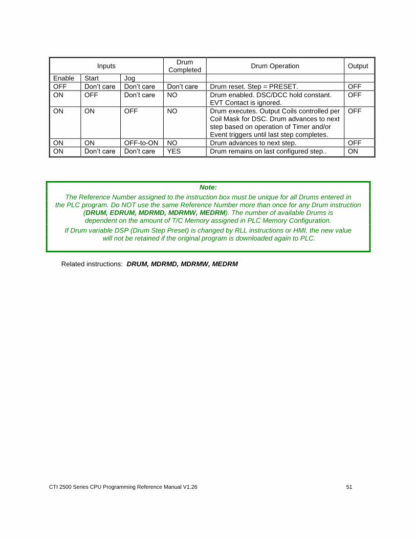
CTI 2500 Series CPU Programming Reference Manual V1.26 51
Inputs Drum
Completed Drum Operation Output
Enable Start Jog
OFF Don’t care Don’t care Don’t care Drum reset. Step = PRESET. OFF
ON OFF Don’t care NO Drum enabled. DSC/DCC hold constant. EVT Contact is ignored.
OFF
ON ON OFF NO Drum executes. Output Coils controlled per Coil Mask for DSC. Drum advances to next step based on operation of Timer and/or Event triggers until last step completes.
OFF
ON ON OFF-to-ON NO Drum advances to next step. OFF
ON Don’t care Don’t care YES Drum remains on last configured step.. ON
Note:
The Reference Number assigned to the instruction box must be unique for all Drums entered in the PLC program. Do NOT use the same Reference Number more than once for any Drum instruction
(DRUM, EDRUM, MDRMD, MDRMW, MEDRM). The number of available Drums is dependent on the amount of T/C Memory assigned in PLC Memory Configuration.
If Drum variable DSP (Drum Step Preset) is changed by RLL instructions or HMI, the new value will not be retained if the original program is downloaded again to PLC.
Related instructions: DRUM, MDRMD, MDRMW, MEDRM
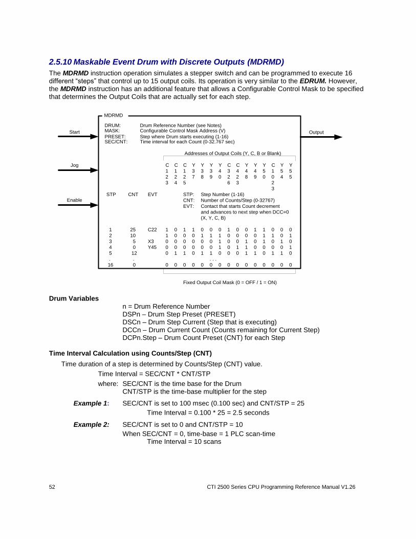
52 CTI 2500 Series CPU Programming Reference Manual V1.26
2.5.10 Maskable Event Drum with Discrete Outputs (MDRMD)
The MDRMD instruction operation simulates a stepper switch and can be programmed to execute 16 different “steps” that control up to 15 output coils. Its operation is very similar to the EDRUM. However, the MDRMD instruction has an additional feature that allows a Configurable Control Mask to be specified that determines the Output Coils that are actually set for each step.
MDRMD
Addresses of Output Coils (Y, C, B or Blank)
C C C Y Y Y Y C C Y Y Y C Y Y
1 1 1 3 3 3 4 3 4 4 4 5 1 5 5
2 2 2 7 8 9 0 2 2 8 9 0 0 4 5
3 4 5 6 3 2
3
STP CNT EVT STP: Step Number (1-16)
CNT: Number of Counts/Step (0-32767)
EVT: Contact that starts Count decrement
and advances to next step when DCC=0
(X, Y, C, B)
1 25 C22 1 0 1 1 0 0 0 1 0 0 1 1 0 0 0
2 10 1 0 0 0 1 1 1 0 0 0 0 1 1 0 1
3 5 X3 0 0 0 0 0 0 1 0 0 1 0 1 0 1 0
4 0 Y45 0 0 0 0 0 0 1 0 1 1 0 0 0 0 1
5 12 0 1 1 0 1 1 0 0 0 1 1 0 1 1 0
. . . . .
16 0 0 0 0 0 0 0 0 0 0 0 0 0 0 0 0
Fixed Output Coil Mask (0 = OFF / 1 = ON)
PRESET: Step where Drum starts executing (1-16)OutputStart
Jog
Enable
DRUM: Drum Reference Number (see Notes)
SEC/CNT: Time interval for each Count (0-32.767 sec)
MASK: Configurable Control Mask Address (V)
Drum Variables n = Drum Reference Number DSPn – Drum Step Preset (PRESET) DSCn – Drum Step Current (Step that is executing) DCCn – Drum Current Count (Counts remaining for Current Step) DCPn.Step – Drum Count Preset (CNT) for each Step Time Interval Calculation using Counts/Step (CNT)
Time duration of a step is determined by Counts/Step (CNT) value.
Time Interval = SEC/CNT * CNT/STP
where: SEC/CNT is the time base for the Drum CNT/STP is the time-base multiplier for the step
Example 1: SEC/CNT is set to 100 msec (0.100 sec) and CNT/STP = 25
Time Interval = 0.100 * 25 = 2.5 seconds
Example 2: SEC/CNT is set to 0 and CNT/STP = 10
When SEC/CNT = 0, time-base = 1 PLC scan-time Time Interval = 10 scans

CTI 2500 Series CPU Programming Reference Manual V1.26 53
Step Advancement Options
1. To program a step for Time-Based Operation Only:
Set Counts/Step (CNT) to value > 0
Do NOT insert a Contact in the Event (EVT) field for this step
The Drum remains on this step until DCC decrements to zero. Then the Drum advances to next step (see Step 2 in example).
2. To program a step for Event-Triggered Operation Only:
Set Counts/Step (CNT) to value = 0
Insert a Contact in the Event (EVT) field for this step
The Drum remains on the step until the Contact specified in the EVT field turns ON. The Drum then advances to the next step (see Step 4 in example).
3. To program a step for Timer and Event-Triggered Operation:
Set Counts/Step (CNT) to value > 0
Insert a Contact in the Event (EVT) field for this step
The Drum remains on this step until DCC decrements to zero (same as time-based operation). However, the DCC value decrements only when the Contact specified in the EVT field is ON). The Drum advances to the next step when DCC reaches zero (see Step 1 in example).
4. To program a step for Timer or Event-Triggered Operation:
Set Counts/Step (CNT) to value > 0
Do NOT Insert a Contact in the Event (EVT) field for this step
Implement logic external to the Drum so that the RLL program creates “Event-Trigger” to turn ON the Jog Input when Drum should advance to next step.
The Drum remains on this step until DCC decrements to zero (same as time-based operation) or Event-Trigger activates (Jog Input transitions OFF-to-ON).
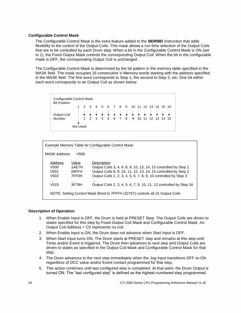
54 CTI 2500 Series CPU Programming Reference Manual V1.26
Configurable Control Mask
The Configurable Control Mask is the extra feature added to the MDRMD instruction that adds flexibility to the control of the Output Coils. This mask allows a run-time selection of the Output Coils that are to be controlled by each Drum step. When a bit in the Configurable Control Mask is ON (set to 1), the Fixed Output Mask controls the corresponding Output Coil. When the bit in the configurable mask is OFF, the corresponding Output Coil is unchanged. The Configurable Control Mask is determined by the bit pattern in the memory table specified in the MASK field. The mask occupies 16 consecutive V-Memory words starting with the address specified in the MASK field. The first word corresponds to Step 1, the second to Step 2, etc. One bit within each word corresponds to an Output Coil as shown below:
Configurable Control Mask
Bit Position
1 2 3 4 5 6 7 8 9 10 11 12 13 14 15 16
Output Coil
Number 1 2 3 4 5 6 7 8 9 10 11 12 13 14 15
Not Used
Example Memory Table for Configurable Control Mask:
MASK Address: V500
Address Value Description
V500 1AE7H Output Coils 3, 4, 6, 8, 9, 10, 13, 14, 15 controlled by Step 1
V501 00FFH Output Coils 8, 9, 10, 11, 12, 13, 14, 15 controlled by Step 2
V502 7FF0H Output Coils 1, 2, 3, 4, 5, 6, 7, 8, 9, 10 controlled by Step 3
… … …
V515 3F78H Output Coils 2, 3, 4, 5, 6, 7, 9, 10, 11, 12 controlled by Step 16
NOTE: Setting Control Mask Word to 7FFFH (32767) controls all 15 Output Coils
Description of Operation
1. When Enable Input is OFF, the Drum is held at PRESET Step. The Output Coils are driven to states specified for this step by Fixed Output Coil Mask and Configurable Control Mask. An Output Coil Address = C0 represents no coil.
2. When Enable Input is ON, the Drum does not advance when Start Input is OFF.
3. When Start Input turns ON, The Drum starts at PRESET step and remains at this step until Timer and/or Event is triggered. The Drum then advances to next step and Output Coils are driven to states as specified in the Output Coil Mask and Configurable Control Mask for that step.
4. The Drum advances to the next step immediately when the Jog Input transitions OFF-to-ON regardless of DCC value and/or Event contact programmed for that step.
5. This action continues until last configured step is completed. At that point, the Drum Output is turned ON. The “last configured step” is defined as the highest numbered step programmed
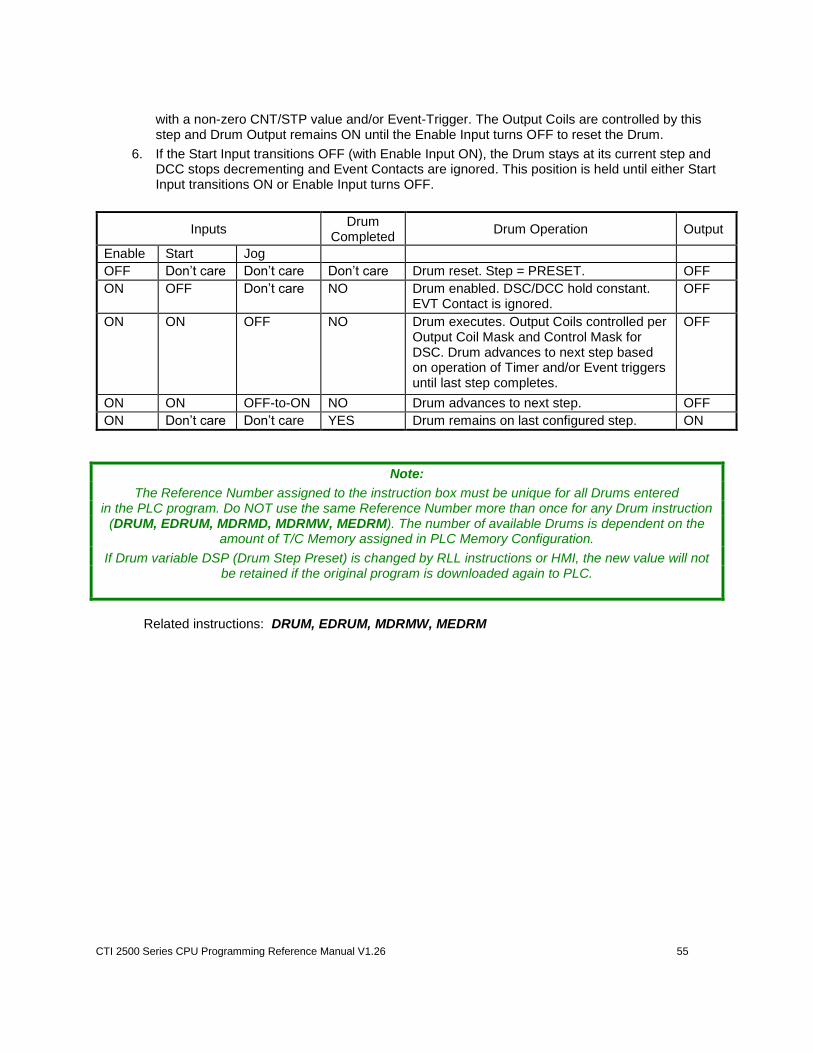
CTI 2500 Series CPU Programming Reference Manual V1.26 55
with a non-zero CNT/STP value and/or Event-Trigger. The Output Coils are controlled by this step and Drum Output remains ON until the Enable Input turns OFF to reset the Drum.
6. If the Start Input transitions OFF (with Enable Input ON), the Drum stays at its current step and DCC stops decrementing and Event Contacts are ignored. This position is held until either Start Input transitions ON or Enable Input turns OFF.
Inputs Drum
Completed Drum Operation Output
Enable Start Jog
OFF Don’t care Don’t care Don’t care Drum reset. Step = PRESET. OFF
ON OFF Don’t care NO Drum enabled. DSC/DCC hold constant. EVT Contact is ignored.
OFF
ON ON OFF NO Drum executes. Output Coils controlled per Output Coil Mask and Control Mask for DSC. Drum advances to next step based on operation of Timer and/or Event triggers until last step completes.
OFF
ON ON OFF-to-ON NO Drum advances to next step. OFF
ON Don’t care Don’t care YES Drum remains on last configured step. ON
Note:
The Reference Number assigned to the instruction box must be unique for all Drums entered in the PLC program. Do NOT use the same Reference Number more than once for any Drum instruction
(DRUM, EDRUM, MDRMD, MDRMW, MEDRM). The number of available Drums is dependent on the amount of T/C Memory assigned in PLC Memory Configuration.
If Drum variable DSP (Drum Step Preset) is changed by RLL instructions or HMI, the new value will not be retained if the original program is downloaded again to PLC.
Related instructions: DRUM, EDRUM, MDRMW, MEDRM
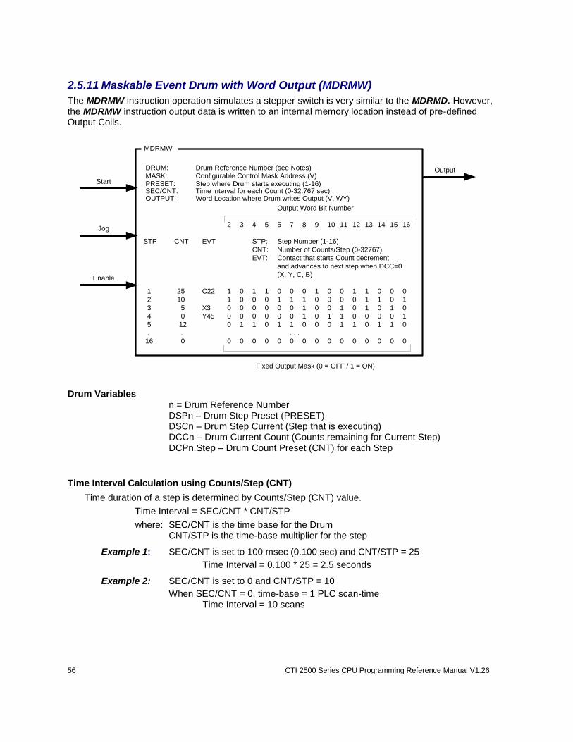
56 CTI 2500 Series CPU Programming Reference Manual V1.26
2.5.11 Maskable Event Drum with Word Output (MDRMW)
The MDRMW instruction operation simulates a stepper switch is very similar to the MDRMD. However, the MDRMW instruction output data is written to an internal memory location instead of pre-defined Output Coils.
MDRMW
Output Word Bit Number
2 3 4 5 5 7 8 9 10 11 12 13 14 15 16
STP CNT EVT STP: Step Number (1-16)
CNT: Number of Counts/Step (0-32767)
EVT: Contact that starts Count decrement
and advances to next step when DCC=0
(X, Y, C, B)
1 25 C22 1 0 1 1 0 0 0 1 0 0 1 1 0 0 0
2 10 1 0 0 0 1 1 1 0 0 0 0 1 1 0 1
3 5 X3 0 0 0 0 0 0 1 0 0 1 0 1 0 1 0
4 0 Y45 0 0 0 0 0 0 1 0 1 1 0 0 0 0 1
5 12 0 1 1 0 1 1 0 0 0 1 1 0 1 1 0
. . . . .
16 0 0 0 0 0 0 0 0 0 0 0 0 0 0 0 0
Fixed Output Mask (0 = OFF / 1 = ON)
Output
Start
Jog
Enable
PRESET: Step where Drum starts executing (1-16)
DRUM: Drum Reference Number (see Notes)
SEC/CNT: Time interval for each Count (0-32.767 sec)OUTPUT: Word Location where Drum writes Output (V, WY)
MASK: Configurable Control Mask Address (V)
Drum Variables n = Drum Reference Number DSPn – Drum Step Preset (PRESET) DSCn – Drum Step Current (Step that is executing) DCCn – Drum Current Count (Counts remaining for Current Step) DCPn.Step – Drum Count Preset (CNT) for each Step
Time Interval Calculation using Counts/Step (CNT)
Time duration of a step is determined by Counts/Step (CNT) value.
Time Interval = SEC/CNT * CNT/STP
where: SEC/CNT is the time base for the Drum CNT/STP is the time-base multiplier for the step
Example 1: SEC/CNT is set to 100 msec (0.100 sec) and CNT/STP = 25
Time Interval = 0.100 * 25 = 2.5 seconds
Example 2: SEC/CNT is set to 0 and CNT/STP = 10
When SEC/CNT = 0, time-base = 1 PLC scan-time Time Interval = 10 scans
CTI 2500 Series CPU Programming Reference Manual V1.26 57
Step Advancement Options
1. To program a step for Time-Based Operation Only:
Set Counts/Step (CNT) to value > 0
Do NOT insert a Contact in the Event (EVT) field for this step
The Drum remains on this step until DCC decrements to zero. Then the Drum advances to next step (see Step 2 in example).
2. To program a step for Event-Triggered Operation Only:
Set Counts/Step (CNT) to value = 0
Insert a Contact in the Event (EVT) field for this step
The Drum remains on the step until the Contact specified in the EVT field turns ON. The Drum then advances to the next step (see Step 4 in example).
3. To program a step for Timer and Event-Triggered Operation:
Set Counts/Step (CNT) to value > 0
Insert a Contact in the Event (EVT) field for this step
The Drum remains on this step until DCC decrements to zero (same as time-based operation). However, the DCC value decrements only when the Contact specified in the EVT field is ON). The Drum advances to the next step when DCC reaches zero (see Step 1 in example).
4. To program a step for Timer or Event-Triggered Operation:
Set Counts/Step (CNT) to value > 0
Do NOT Insert a Contact in the Event (EVT) field for this step
Implement logic external to the Drum so that the RLL program creates “Event-Trigger” to turn ON the Jog Input when Drum should advance to next step.
The Drum remains on this step until DCC decrements to zero (same as time-based operation) or Event-Trigger activates (Jog Input transitions OFF-to-ON).
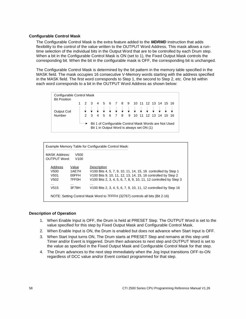
58 CTI 2500 Series CPU Programming Reference Manual V1.26
Configurable Control Mask
The Configurable Control Mask is the extra feature added to the MDRMD instruction that adds flexibility to the control of the value written to the OUTPUT Word Address. This mask allows a run-time selection of the individual bits in the Output Word that are to be controlled by each Drum step. When a bit in the Configurable Control Mask is ON (set to 1), the Fixed Output Mask controls the corresponding bit. When the bit in the configurable mask is OFF, the corresponding bit is unchanged. The Configurable Control Mask is determined by the bit pattern in the memory table specified in the MASK field. The mask occupies 16 consecutive V-Memory words starting with the address specified in the MASK field. The first word corresponds to Step 1, the second to Step 2, etc. One bit within each word corresponds to a bit in the OUTPUT Word Address as shown below:
Configurable Control Mask
Bit Position
1 2 3 4 5 6 7 8 9 10 11 12 13 14 15 16
Output Coil
Number 2 3 4 5 6 7 8 9 10 11 12 13 14 15 16
Bit 1 of Configurable Control Mask Words are Not Used
Bit 1 in Output Word is always set ON (1)
Example Memory Table for Configurable Control Mask:
MASK Address: V500
OUTPUT Word: V100
Address Value Description
V500 1AE7H V100 Bits 4, 5, 7, 9, 10, 11, 14, 15, 16 controlled by Step 1
V501 00FFH V100 Bits 9, 10, 11, 12, 13, 14, 15, 16 controlled by Step 2
V502 7FF0H V100 Bits 2, 3, 4, 5, 6, 7, 8, 9, 10, 11, 12 controlled by Step 3
… … …
V515 3F78H V100 Bits 2, 3, 4, 5, 6, 7, 9, 10, 11, 12 controlled by Step 16
NOTE: Setting Control Mask Word to 7FFFH (32767) controls all bits (Bit 2-16)
Description of Operation
1. When Enable Input is OFF, the Drum is held at PRESET Step. The OUTPUT Word is set to the value specified for this step by Fixed Output Mask and Configurable Control Mask.
2. When Enable Input is ON, the Drum is enabled but does not advance when Start Input is OFF.
3. When Start Input turns ON, The Drum starts at PRESET Step and remains at this step until Timer and/or Event is triggered. Drum then advances to next step and OUTPUT Word is set to the value as specified in the Fixed Output Mask and Configurable Control Mask for that step.
4. The Drum advances to the next step immediately when the Jog Input transitions OFF-to-ON regardless of DCC value and/or Event contact programmed for that step.
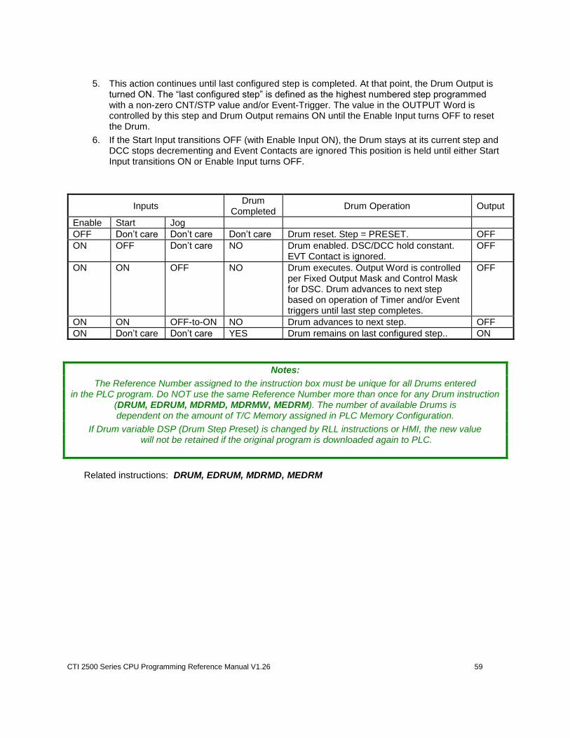
CTI 2500 Series CPU Programming Reference Manual V1.26 59
5. This action continues until last configured step is completed. At that point, the Drum Output is
turned ON. The “last configured step” is defined as the highest numbered step programmed with a non-zero CNT/STP value and/or Event-Trigger. The value in the OUTPUT Word is controlled by this step and Drum Output remains ON until the Enable Input turns OFF to reset the Drum.
6. If the Start Input transitions OFF (with Enable Input ON), the Drum stays at its current step and DCC stops decrementing and Event Contacts are ignored This position is held until either Start Input transitions ON or Enable Input turns OFF.
Inputs Drum
Completed Drum Operation Output
Enable Start Jog
OFF Don’t care Don’t care Don’t care Drum reset. Step = PRESET. OFF
ON OFF Don’t care NO Drum enabled. DSC/DCC hold constant. EVT Contact is ignored.
OFF
ON ON OFF NO Drum executes. Output Word is controlled per Fixed Output Mask and Control Mask for DSC. Drum advances to next step based on operation of Timer and/or Event triggers until last step completes.
OFF
ON ON OFF-to-ON NO Drum advances to next step. OFF
ON Don’t care Don’t care YES Drum remains on last configured step.. ON
Notes:
The Reference Number assigned to the instruction box must be unique for all Drums entered in the PLC program. Do NOT use the same Reference Number more than once for any Drum instruction
(DRUM, EDRUM, MDRMD, MDRMW, MEDRM). The number of available Drums is dependent on the amount of T/C Memory assigned in PLC Memory Configuration.
If Drum variable DSP (Drum Step Preset) is changed by RLL instructions or HMI, the new value will not be retained if the original program is downloaded again to PLC.
Related instructions: DRUM, EDRUM, MDRMD, MEDRM
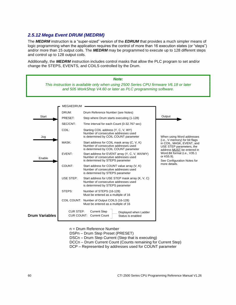
60 CTI 2500 Series CPU Programming Reference Manual V1.26
When using Word addresses(i.e., V-memory) for bit flagsin COIL, MASK, EVENT, andUSE STEP parameters, theaddress MUST be entered inWord.Bit format (i.e., V35.1or K55.9).
See Configuration Notes formore details.
Start
Jog
Enable
OutputPRESET: Step where Drum starts executing (1-128)
DRUM: Drum Reference Number (see Notes)
SEC/CNT: Time interval for each Count (0-32.767 sec)
MASK: Start address for COIL mask array (C, V, K)Number of consecutive addresses usedis determined by COIL COUNT parameter
COIL: Starting COIL address (Y, C, V, WY)Number of consecutive addresses usedis determined by COIL COUNT parameter
EVENT: Start address for EVENT array (Y, C, V, WX/WY)Number of consecutive addresses usedis determined by STEPS parameter
COUNT: Start address for COUNT value array (V, K)
Number of consecutive addresses used
is determined by STEPS parameter
USE STEP: Start address for USE STEP mask array (K, V, C)
Number of consecutive addresses used
is determined by STEPS parameter
COIL COUNT: Number of Output COILS (16-128)
Must be entered as a multiple of 16
CUR STEP: Current Step
CUR COUNT: Current CountDisplayed when Ladder
Status is enabled
STEPS: Number of STEPS (16-128)
Must be entered as a multiple of 16
MEGAEDRUM
2.5.12 Mega Event DRUM (MEDRM)
The MEDRM instruction is a “super-sized” version of the EDRUM that provides a much simpler means of logic programming when the application requires the control of more than 16 execution states (or “steps”) and/or more than 15 output coils. The MEDRM may be programmed to execute up to 128 different steps and control up to 128 output coils.
Additionally, the MEDRM instruction includes control masks that allow the PLC program to set and/or change the STEPS, EVENTS, and COILS controlled by the Drum.
Note:
This instruction is available only when using 2500 Series CPU firmware V6.18 or later and 505 WorkShop V4.60 or later as PLC programming software.
Drum Variables n = Drum Reference Number DSPn – Drum Step Preset (PRESET) DSCn – Drum Step Current (Step that is executing) DCCn – Drum Current Count (Counts remaining for Current Step) DCP – Represented by addresses used for COUNT parameter
CTI 2500 Series CPU Programming Reference Manual V1.26 61
Configuration Notes for MEGAEDRUM:
1. Drum Number (DRM), PRESET, and SEC/CNT is entered exactly as done for EDRUM.
Note:
The COIL, MASK, EVENT, and USE STEP parameters utilize a memory array of BITS for their operation (as detailed below). Therefore, the address assigned to each of these fields during configuration of the
MEDRM must specify a BIT address.
You may always use a Bit memory type (i.e. C-memory) for these parameters. However, some fields (such as MASK) can be quite large and better utilize available memory when
stored in configurable word memory (i.e. V or K-memory). This is accomplished by assigning the Start Address for these parameters in WORD.BIT format as shown below:
V1501.1 Start Address for bit memory array is Word V1501 / Bit 1 K500.1 Start Address for bit memory array is Word K500 / Bit 1
Any available bit number (1-16) within the word may be used for Start Address. However, the use of any bit other than Bit 1will result in the bit array “wrapping” into the following word since all parameter fields require the length of the bit arrays to be a multiple of 16. In order
to aid in data entry and debug process, we recommend that each address entered in WORD.BIT format start at “Bit 1”.
2. COIL parameter designates addresses to be used for Output Coils. The address entered here represents the start address for memory array. The total number of required consecutive (bit) addresses is specified by the COIL COUNT parameter.
The valid memory types are C, Y, V, and WY. If Bit address (C, Y) is used, the number of bits equals COIL COUNT. If Word.Bit address (V, WY) is entered, the required number of words equals COIL COUNT / 16.
3. MASK parameter specifies the ON/OFF states that are written to the Output Coils for each step as the Drum executes. In the EDRUM, these states are hard-coded into the instruction box for each step as it is inserted into the RLL program. In the MEDRM, these values are held in a memory array starting with the address entered in the MASK parameter field. The total number of required consecutive (bit) addresses is determined by COIL COUNT and number of STEPS.
The valid memory types are C, V, K. If Bit address (C) is used, the number of bits equals COIL COUNT * STEPS. If WORD.BIT Address is entered, the total number of words equals (COIL COUNT * STEPS) / 16.
4. EVENT parameter designates the conditions used to “hold” the Drum at a particular step and stop the Drum Count (DCC) from decrementing as long as the bit is FALSE. In the EDRUM, the EVT states are hard-coded into the instruction box for each step as it is inserted into the RLL program. In the MEDRM, these values are held in a memory array starting with the address entered in the EVENT parameter field. The total number of required consecutive (bit) addresses is determined by the value entered for the STEPS parameter.
The valid memory types are X/Y, C, V, WX/WY. If Bit address (X/Y, C) is used, the number of bits equals STEPS value. If WORD.BIT address (V, WX/WY) is entered, the required number of words equals STEPS / 16.
62 CTI 2500 Series CPU Programming Reference Manual V1.26
5. COUNT specifies the length of time the Drum remains on each particular step (as long as the
EVENT condition is TRUE). The actual time interval is determined by the number of COUNTS and the SEC/CNT value (see description on next page). In the EDRUM, the CNT values are hard-coded into the instruction box for each step as it is inserted into the RLL program. In the MEDRM, these values are held in a memory array starting with the address entered in the COUNT field.
The COUNT parameter must be entered as a Word address (V, K). The total number of required consecutive words is determined by the number of STEPS.
6. USE STEP parameter designates ON/OFF states that indicate whether the corresponding step is executed (ON) or skipped (OFF) by the Drum. In the EDRUM, a step can be skipped by setting CNT= 0 and leaving the EVT condition blank for a particular step while entering the instruction box. In the MEDRM, the execution of each step is dependent on the corresponding bit in the USE STEP memory array being set ON. The total number of required consecutive (bit) addresses is determined by the STEPS parameter.
The valid memory types are C, K, and V. If Bit address (C) is used, the number of bits equals STEPS value. If WORD.BIT address (K, V) is entered, the required number of words equals STEPS/16.
7. STEPS specify the number of output states programmed for the Drum. This value must be a constant in the range of 16-128, and an even multiple of 16 (i.e, 16, 32, 48, etc).
8. COIL COUNT specifies the number of Output Coils controlled by the Drum. This value must be a constant in the range of 16-128, and an even multiple of 16 (i.e, 16, 32, 48, etc).
Time Interval Calculation using Counts/Step (CNT)
Time duration of a step is determined by Counts/Step (CNT) value.
Time Interval = SEC/CNT * CNT/STP
where: SEC/CNT is the time base for the Drum CNT/STP is the time-base multiplier for the step
Example 1: SEC/CNT is set to 100 msec (0.100 sec) and CNT/STP = 25
Time Interval = 0.100 * 25 = 2.5 seconds
Example 2: SEC/CNT is set to 0 and CNT/STP = 10
When SEC/CNT = 0, time-base = 1 PLC scan-time Time Interval = 10 scans

CTI 2500 Series CPU Programming Reference Manual V1.26 63
Step Advancement Options
1. To program a step for Time-Based Operation Only:
Set word in COUNT memory array for the corresponding step to value > 0
Set the bit in the EVENT memory array for the corresponding step to ON (TRUE)
The Drum remains on this step until DCC decrements to zero. Then the Drum advances to next step.
2. To program a step for Event-Triggered Operation Only:
Set word in COUNT memory array for the corresponding step to 0
The Drum remains on the step until the bit in the EVENT memory array corresponding to the current step turns ON (via PLC logic or HMI interface). The Drum then advances to the next step.
3. To program a step for Timer and Event-Triggered Operation:
Set word in COUNT memory array for the corresponding step to value > 0
When the Drum reaches this step, the Drum timer advances only when the bit in the EVENT memory array corresponding to the current step turns ON (via PLC logic or HMI interface).
The Drum remains on this step until DCC decrements to zero (same as time-based operation). The Drum then advances to the next step.
4. To program a step for Timer or Event-Triggered Operation:
Set word in COUNT memory array for the corresponding step to value > 0
Set bit in the EVENT memory array for the corresponding step to OFF (FALSE)
Implement logic external to the Drum so that the RLL program creates “Event-Trigger” to turn ON the Jog Input when Drum should advance to next step.
The Drum remains on this step until DCC decrements to zero (same as time-based operation) or Event-Trigger activates (Jog Input transitions OFF-to-ON).
5. To Skip a programmed step:
Set bit in the USE STEP memory array for the corresponding step to OFF (FALSE)
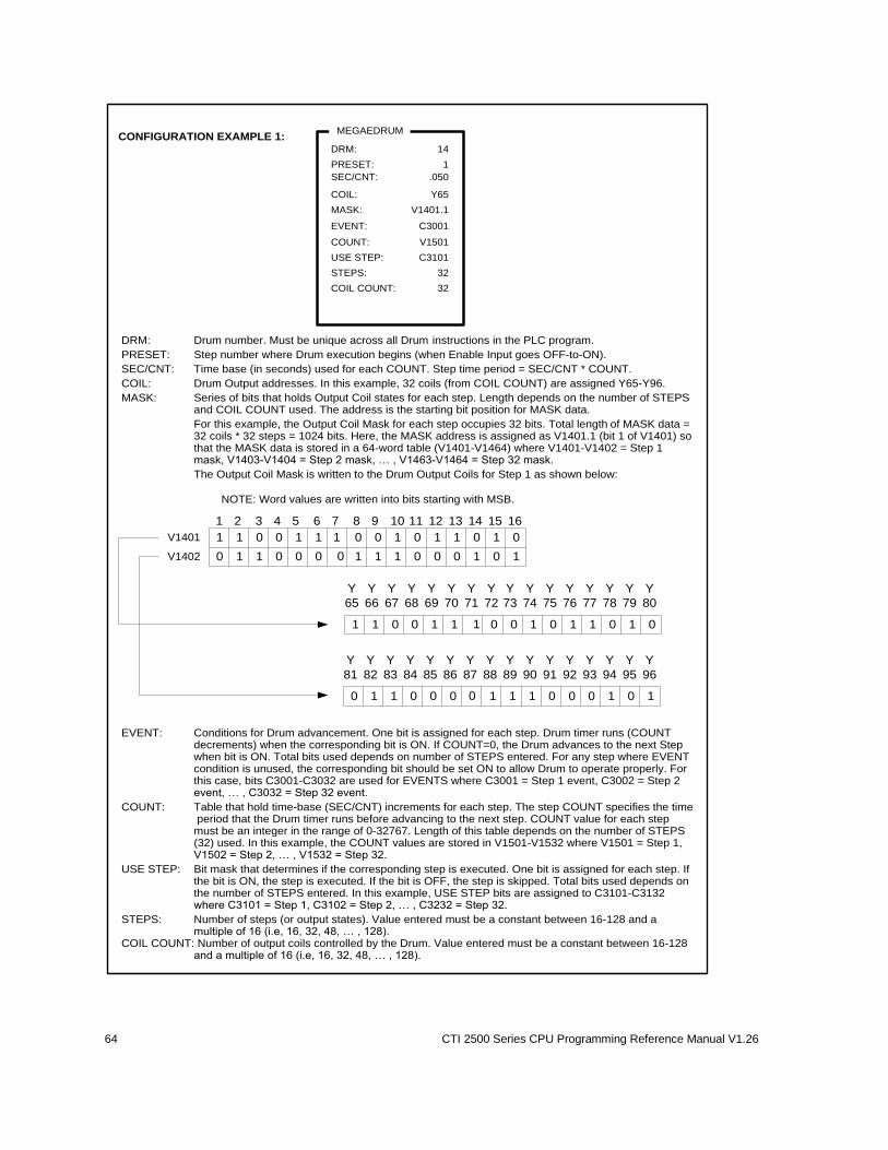
64 CTI 2500 Series CPU Programming Reference Manual V1.26
DRM: Drum number. Must be unique across all Drum instructions in the PLC program.
PRESET: Step number where Drum execution begins (when Enable Input goes OFF-to-ON).
SEC/CNT: Time base (in seconds) used for each COUNT. Step time period = SEC/CNT * COUNT.
COIL: Drum Output addresses. In this example, 32 coils (from COIL COUNT) are assigned Y65-Y96.
MASK: Series of bits that holds Output Coil states for each step. Length depends on the number of STEPSand COIL COUNT used. The address is the starting bit position for MASK data.
For this example, the Output Coil Mask for each step occupies 32 bits. Total length of MASK data =32 coils * 32 steps = 1024 bits. Here, the MASK address is assigned as V1401.1 (bit 1 of V1401) sothat the MASK data is stored in a 64-word table (V1401-V1464) where V1401-V1402 = Step 1mask, V1403-V1404 = Step 2 mask, … , V1463-V1464 = Step 32 mask.
The Output Coil Mask is written to the Drum Output Coils for Step 1 as shown below:
EVENT: Conditions for Drum advancement. One bit is assigned for each step. Drum timer runs (COUNTdecrements) when the corresponding bit is ON. If COUNT=0, the Drum advances to the next Stepwhen bit is ON. Total bits used depends on number of STEPS entered. For any step where EVENTcondition is unused, the corresponding bit should be set ON to allow Drum to operate properly. Forthis case, bits C3001-C3032 are used for EVENTS where C3001 = Step 1 event, C3002 = Step 2event, … , C3032 = Step 32 event.
COUNT: Table that hold time-base (SEC/CNT) increments for each step. The step COUNT specifies the time period that the Drum timer runs before advancing to the next step. COUNT value for each stepmust be an integer in the range of 0-32767. Length of this table depends on the number of STEPS(32) used. In this example, the COUNT values are stored in V1501-V1532 where V1501 = Step 1,V1502 = Step 2, … , V1532 = Step 32.
USE STEP: Bit mask that determines if the corresponding step is executed. One bit is assigned for each step. Ifthe bit is ON, the step is executed. If the bit is OFF, the step is skipped. Total bits used depends onthe number of STEPS entered. In this example, USE STEP bits are assigned to C3101-C3132where C3101 = Step 1, C3102 = Step 2, … , C3232 = Step 32.
STEPS: Number of steps (or output states). Value entered must be a constant between 16-128 and amultiple of 16 (i.e, 16, 32, 48, … , 128).
COIL COUNT: Number of output coils controlled by the Drum. Value entered must be a constant between 16-128and a multiple of 16 (i.e, 16, 32, 48, … , 128).
Y
73
Y
74
Y
75
Y
76
Y
77
Y
78
Y
79
Y
80
1 2 3 4 5 6 7 8 9 10 11 12 13 14 15 16
Y
65
Y
66
Y
67
Y
68
Y
69
Y
70
Y
71
Y
72
1 0 1 1 1 0 1 1 0011 0 0 0 1
1 0 1 1 1 0 1 1 0011 0 0 0 1
0 0 0 0 1 0 0 0 1101 1 1 1 0
V1401
V1402
Y
89
Y
90
Y
91
Y
92
Y
93
Y
94
Y
95
Y
96
Y
81
Y
82
Y
83
Y
84
Y
85
Y
86
Y
87
Y
88
0 0 0 0 1 0 0 0 1101 1 1 1 0
NOTE: Word values are written into bits starting with MSB.
PRESET: 1
DRM: 14
SEC/CNT: .050
MASK: V1401.1
COIL: Y65
EVENT: C3001
COUNT: V1501
USE STEP: C3101
COIL COUNT: 32
STEPS: 32
MEGAEDRUMCONFIGURATION EXAMPLE 1:
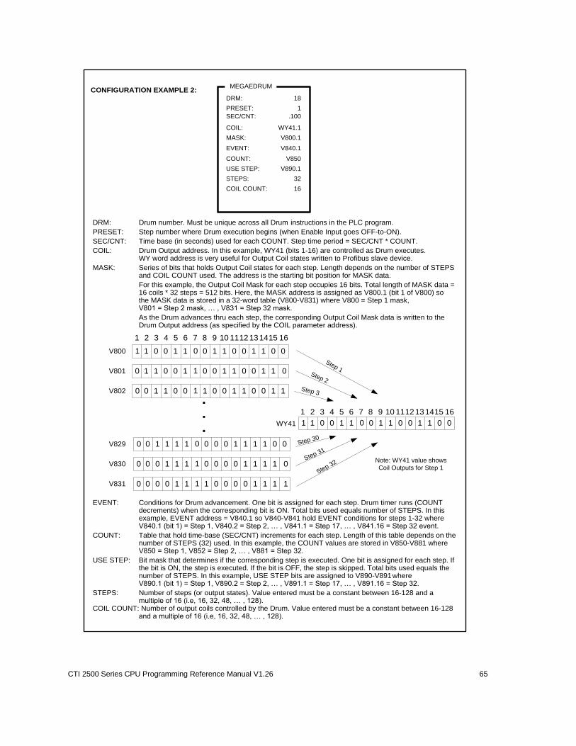
CTI 2500 Series CPU Programming Reference Manual V1.26 65
DRM: Drum number. Must be unique across all Drum instructions in the PLC program.
PRESET: Step number where Drum execution begins (when Enable Input goes OFF-to-ON).
SEC/CNT: Time base (in seconds) used for each COUNT. Step time period = SEC/CNT * COUNT.
COIL: Drum Output address. In this example, WY41 (bits 1-16) are controlled as Drum executes.WY word address is very useful for Output Coil states written to Profibus slave device.
MASK: Series of bits that holds Output Coil states for each step. Length depends on the number of STEPSand COIL COUNT used. The address is the starting bit position for MASK data.
For this example, the Output Coil Mask for each step occupies 16 bits. Total length of MASK data =16 coils * 32 steps = 512 bits. Here, the MASK address is assigned as V800.1 (bit 1 of V800) sothe MASK data is stored in a 32-word table (V800-V831) where V800 = Step 1 mask,V801 = Step 2 mask, … , V831 = Step 32 mask.
As the Drum advances thru each step, the corresponding Output Coil Mask data is written to theDrum Output address (as specified by the COIL parameter address).
EVENT: Conditions for Drum advancement. One bit is assigned for each step. Drum timer runs (COUNTdecrements) when the corresponding bit is ON. Total bits used equals number of STEPS. In thisexample, EVENT address = V840.1 so V840-V841 hold EVENT conditions for steps 1-32 whereV840.1 (bit 1) = Step 1, V840.2 = Step 2, … , V841.1 = Step 17, … , V841.16 = Step 32 event.
COUNT: Table that hold time-base (SEC/CNT) increments for each step. Length of this table depends on thenumber of STEPS (32) used. In this example, the COUNT values are stored in V850-V881 whereV850 = Step 1, V852 = Step 2, … , V881 = Step 32.
USE STEP: Bit mask that determines if the corresponding step is executed. One bit is assigned for each step. Ifthe bit is ON, the step is executed. If the bit is OFF, the step is skipped. Total bits used equals thenumber of STEPS. In this example, USE STEP bits are assigned to V890-V891whereV890.1 (bit 1) = Step 1, V890.2 = Step 2, … , V891.1 = Step 17, … , V891.16 = Step 32.
STEPS: Number of steps (or output states). Value entered must be a constant between 16-128 and amultiple of 16 (i.e, 16, 32, 48, … , 128).
COIL COUNT: Number of output coils controlled by the Drum. Value entered must be a constant between 16-128and a multiple of 16 (i.e, 16, 32, 48, … , 128).
PRESET: 1
DRM: 18
SEC/CNT: .100
MASK: V800.1
COIL: WY41.1
EVENT: V840.1
COUNT: V850
USE STEP: V890.1
COIL COUNT: 16
STEPS: 32
MEGAEDRUMCONFIGURATION EXAMPLE 2:
1 2 3 4 5 6 7 8 9 10 1112131415 16
1 0 1 1 1 0 1 0 0101 0 0 1 0
0 0 0 1 1 1 0 1 0111 1 0 0 0
V800
V801
0 1 0 0 0 1 0 1 1010 1 1 0 1
0 0 1 1 0 0 1 1 1110 0 1 0 0
0 1 1 1 0 1 1 0 0100 1 0 0 1
0 1 1 1 0 0 1 1 0110 0 0 0 1
.
.
.
V802
V829
V830
V831
Step 1Step 2
Step 3
Step 32Step 31
Step 30
Note: WY41 value shows
Coil Outputs for Step 1
1 2 3 4 5 6 7 8 9 10 1112131415 16
1 0 1 1 1 0 1 0 0101 0 0 1 0WY41

66 CTI 2500 Series CPU Programming Reference Manual V1.26
Description of Operation
1. When Enable Input is OFF, the Drum is held at PRESET Step. The Output Coil (COIL) addresses are driven to states specified for this step in the Coil Mask Array (MASK)..
2. When Enable Input is ON, the Drum is enabled but does not advance when the Start Input is OFF.
3. When Start Input turns ON, The Drum starts at PRESET Step and remains at this step until corresponding Event contact (EVENT) turns ON and COUNT value decrements to 0. The Drum then advances to next step and Output Coils are driven to states as specified in the Coil Mask Array (COIL) for that step.
4. The Drum advances to the next step immediately when the Jog Input transitions OFF-to-ON regardless of COUNT value and/or state of the Event contact used for that step.
5. This action continues until last step is completed. At that point, the Drum Output is turned ON. If the last step is bypassed due to the USE STEP contact turned OFF, the Drum Output turns ON when the last executed step is completed. The Output Coils are controlled by the states set for this step in the Coil Mask Array and Drum Output remains ON until the Enable Input turns OFF to reset the Drum.
6. If the Start Input transitions OFF (with Enable Input ON), the Drum stays at its current step and DCC stops decrementing and Event contact is ignored This position is held until either Start Input transitions ON or Enable Input turns OFF.
Inputs Drum
Completed Drum Operation Output
Enable Start Jog
OFF Don’t care Don’t care Don’t care Drum reset. Step = PRESET. OFF
ON OFF Don’t care NO Drum enabled. DSC/DCC hold constant. EVENT contact is ignored.
OFF
ON ON OFF NO Drum advances to next step based on operation of Timer and/or Event triggers until last step completes.
If USE STEP contact is OFF: Drum advances to next step ELSE: Output Coils controlled per COIL Mask for current step
OFF
ON ON OFF-to-ON NO Drum advances to next step. OFF
ON Don’t care Don’t care YES Drum remains on last configured step. ON
Note:
The Reference Number assigned to the instruction box must be unique for all Drums entered in the PLC program. Do NOT use the same Reference Number more than once for any Drum instruction
(DRUM, EDRUM, MDRMD, MDRMW, MEDRM). The number of available Drums is dependent on the amount of T/C Memory assigned in PLC Memory Configuration.
If Drum variable DSP (Drum Step Preset) is changed by RLL instructions or HMI, the new value will not be retained if the original program is downloaded again to PLC.
Related instructions: DRUM, EDRUM, MDRMD, MDRMW
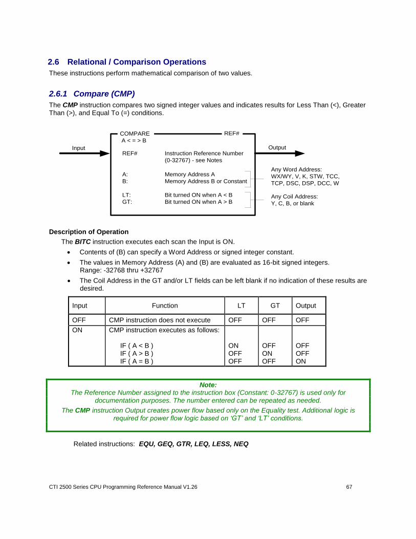
CTI 2500 Series CPU Programming Reference Manual V1.26 67
2.6 Relational / Comparison Operations
These instructions perform mathematical comparison of two values.
2.6.1 Compare (CMP)
The CMP instruction compares two signed integer values and indicates results for Less Than (<), Greater Than (>), and Equal To (=) conditions.
COMPARE
A < = > B
REF# Instruction Reference Number
(0-32767) - see Notes
OutputInput
A: Memory Address A
B: Memory Address B or Constant
LT: Bit turned ON when A < B
GT: Bit turned ON when A > B
Any Word Address:
WX/WY, V, K, STW, TCC,
TCP, DSC, DSP, DCC, W
Any Coil Address:
Y, C, B, or blank
REF#
Description of Operation
The BITC instruction executes each scan the Input is ON.
Contents of (B) can specify a Word Address or signed integer constant.
The values in Memory Address (A) and (B) are evaluated as 16-bit signed integers. Range: -32768 thru +32767
The Coil Address in the GT and/or LT fields can be left blank if no indication of these results are desired.
Input Function LT GT Output
OFF CMP instruction does not execute OFF OFF OFF
ON
CMP instruction executes as follows: IF ( A < B ) IF ( A > B ) IF ( A = B )
ON OFF OFF
OFF ON OFF
OFF OFF ON
Note: The Reference Number assigned to the instruction box (Constant: 0-32767) is used only for
documentation purposes. The number entered can be repeated as needed.
The CMP instruction Output creates power flow based only on the Equality test. Additional logic is required for power flow logic based on ‘GT’ and ‘LT’ conditions.
Related instructions: EQU, GEQ, GTR, LEQ, LESS, NEQ
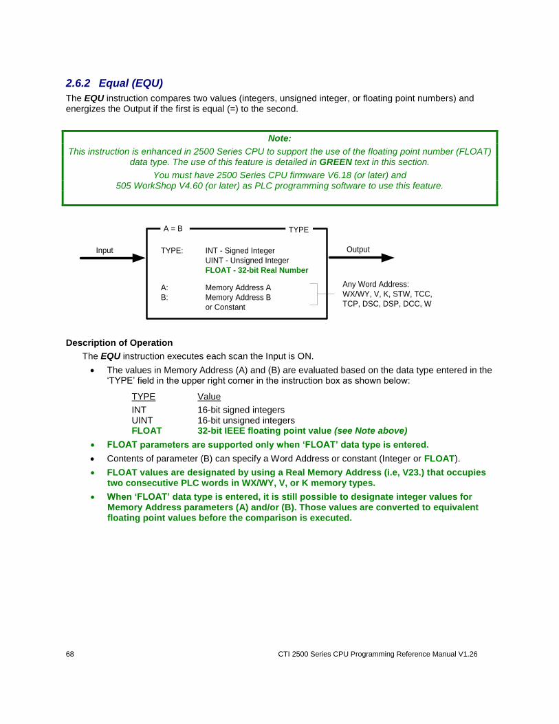
68 CTI 2500 Series CPU Programming Reference Manual V1.26
2.6.2 Equal (EQU)
The EQU instruction compares two values (integers, unsigned integer, or floating point numbers) and energizes the Output if the first is equal (=) to the second.
Note:
This instruction is enhanced in 2500 Series CPU to support the use of the floating point number (FLOAT) data type. The use of this feature is detailed in GREEN text in this section.
You must have 2500 Series CPU firmware V6.18 (or later) and 505 WorkShop V4.60 (or later) as PLC programming software to use this feature.
A = B
TYPE: INT - Signed Integer
UINT - Unsigned Integer
FLOAT - 32-bit Real Number
OutputInput
A: Memory Address A
B: Memory Address B
or Constant
Any Word Address:
WX/WY, V, K, STW, TCC,
TCP, DSC, DSP, DCC, W
TYPE
Description of Operation
The EQU instruction executes each scan the Input is ON.
The values in Memory Address (A) and (B) are evaluated based on the data type entered in the ‘TYPE’ field in the upper right corner in the instruction box as shown below:
TYPE Value
INT 16-bit signed integers UINT 16-bit unsigned integers FLOAT 32-bit IEEE floating point value (see Note above)
FLOAT parameters are supported only when ‘FLOAT’ data type is entered.
Contents of parameter (B) can specify a Word Address or constant (Integer or FLOAT).
FLOAT values are designated by using a Real Memory Address (i.e, V23.) that occupies two consecutive PLC words in WX/WY, V, or K memory types.
When ‘FLOAT’ data type is entered, it is still possible to designate integer values for Memory Address parameters (A) and/or (B). Those values are converted to equivalent floating point values before the comparison is executed.

CTI 2500 Series CPU Programming Reference Manual V1.26 69
Input Function Output
OFF EQU instruction does not execute OFF
ON
EQU instruction executes as follows:
IF ( A <> B )
IF ( A = B )
OFF
ON
Related instructions: CMP, GEQ, GTR, LEQ, LESS, NEQ

70 CTI 2500 Series CPU Programming Reference Manual V1.26
2.6.3 Greater or Equal (GEQ)
The GEQ instruction compares two values (signed integers, unsigned integers, or floating point numbers) and energizes the Output if the first is greater or equal (>=) to the second.
Note:
This instruction is enhanced in 2500 Series CPU to support the use of the floating point number (FLOAT) data type. The use of this feature is detailed in GREEN text in this section.
You must have 2500 Series CPU firmware V6.18 (or later) and 505 WorkShop V4.60 (or later) as PLC programming software to use this feature
A >= B
TYPE: INT - Signed Integer
UINT - Unsigned Integer
FLOAT - 32-bit Real Number
OutputInput
A: Memory Address A
B: Memory Address B
or Constant
Any Word Address:
WX/WY, V, K, STW, TCC,
TCP, DSC, DSP, DCC, W
TYPE
Description of Operation
The GEQ instruction executes each scan the Input is ON.
The values in Memory Address (A) and (B) are evaluated based on the data type entered in the ‘TYPE’ field in the upper right corner in the instruction box as shown below:
TYPE Value
INT 16-bit signed integers UINT 16-bit unsigned integers FLOAT 32-bit IEEE floating point value (see Note above)
FLOAT parameters are supported only when ‘FLOAT’ data type is entered.
Contents of parameter (B) can specify a Word Address or constant (Integer or FLOAT).
FLOAT values are designated by using a Real Memory Address (i.e, V23.) that occupies two consecutive PLC words in WX/WY, V, or K memory types.
When ‘FLOAT’ data type is entered, it is still possible to designate integer values for Memory Address parameters (A) and/or (B). Those values are converted to equivalent floating point values before the comparison is executed.

CTI 2500 Series CPU Programming Reference Manual V1.26 71
Input Function Output
OFF GEQ instruction does not execute OFF
ON
GEQ instruction executes as follows:
IF ( A < B )
IF ( A >= B )
OFF
ON
Related instructions: CMP, EQU, GTR, LEQ, LESS, NEQ
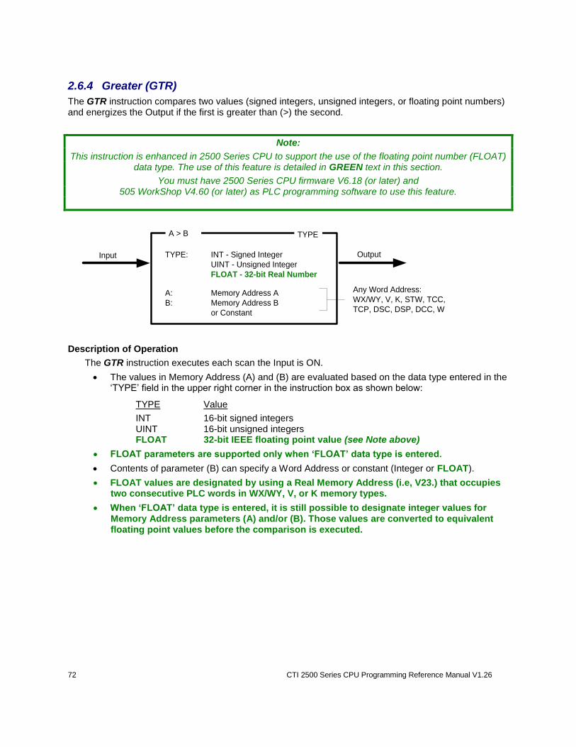
72 CTI 2500 Series CPU Programming Reference Manual V1.26
2.6.4 Greater (GTR)
The GTR instruction compares two values (signed integers, unsigned integers, or floating point numbers) and energizes the Output if the first is greater than (>) the second.
Note:
This instruction is enhanced in 2500 Series CPU to support the use of the floating point number (FLOAT) data type. The use of this feature is detailed in GREEN text in this section.
You must have 2500 Series CPU firmware V6.18 (or later) and 505 WorkShop V4.60 (or later) as PLC programming software to use this feature.
A > B
TYPE: INT - Signed Integer
UINT - Unsigned Integer
FLOAT - 32-bit Real Number
OutputInput
A: Memory Address A
B: Memory Address B
or Constant
Any Word Address:
WX/WY, V, K, STW, TCC,
TCP, DSC, DSP, DCC, W
TYPE
Description of Operation
The GTR instruction executes each scan the Input is ON.
The values in Memory Address (A) and (B) are evaluated based on the data type entered in the ‘TYPE’ field in the upper right corner in the instruction box as shown below:
TYPE Value
INT 16-bit signed integers UINT 16-bit unsigned integers FLOAT 32-bit IEEE floating point value (see Note above)
FLOAT parameters are supported only when ‘FLOAT’ data type is entered.
Contents of parameter (B) can specify a Word Address or constant (Integer or FLOAT).
FLOAT values are designated by using a Real Memory Address (i.e, V23.) that occupies two consecutive PLC words in WX/WY, V, or K memory types.
When ‘FLOAT’ data type is entered, it is still possible to designate integer values for Memory Address parameters (A) and/or (B). Those values are converted to equivalent floating point values before the comparison is executed.

CTI 2500 Series CPU Programming Reference Manual V1.26 73
Input Function Output
OFF GTR instruction does not execute OFF
ON
GTR instruction executes as follows:
IF ( A <= B )
IF ( A > B )
OFF
ON
Related instructions: CMP, EQU, GEQ, LEQ, LESS, NEQ
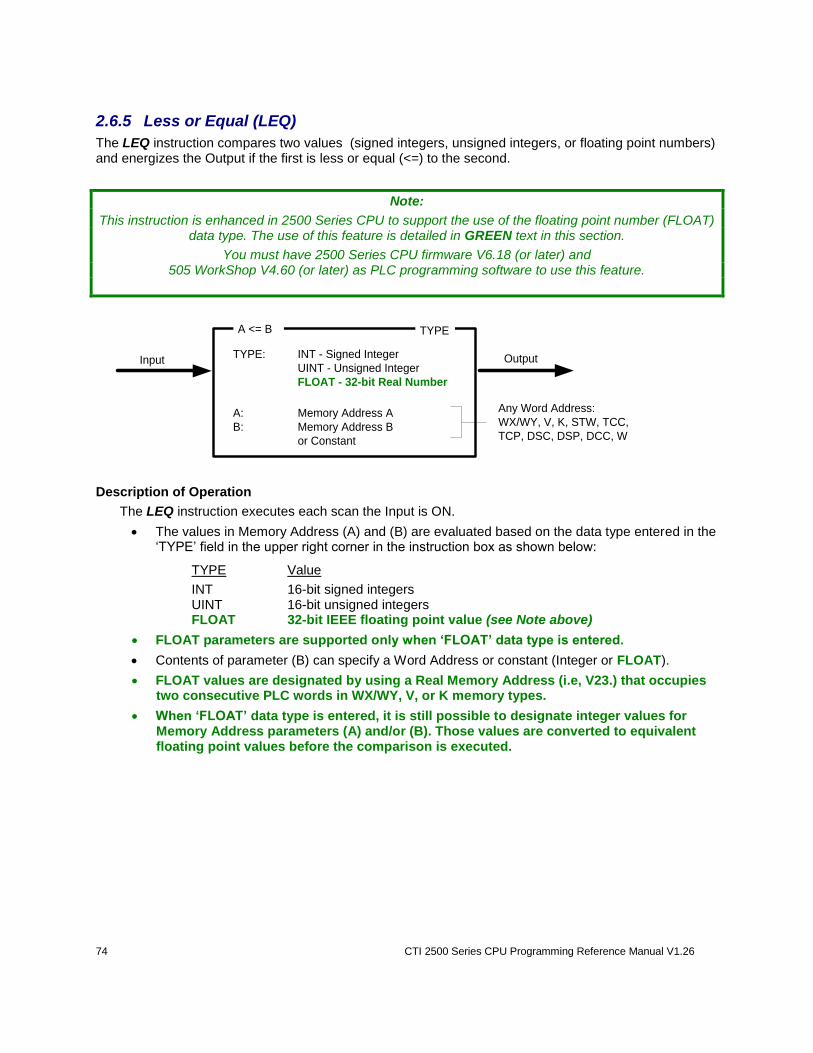
74 CTI 2500 Series CPU Programming Reference Manual V1.26
2.6.5 Less or Equal (LEQ)
The LEQ instruction compares two values (signed integers, unsigned integers, or floating point numbers) and energizes the Output if the first is less or equal (<=) to the second.
Note:
This instruction is enhanced in 2500 Series CPU to support the use of the floating point number (FLOAT) data type. The use of this feature is detailed in GREEN text in this section.
You must have 2500 Series CPU firmware V6.18 (or later) and 505 WorkShop V4.60 (or later) as PLC programming software to use this feature.
A <= B
TYPE: INT - Signed Integer
UINT - Unsigned Integer
FLOAT - 32-bit Real Number
OutputInput
A: Memory Address A
B: Memory Address B
or Constant
Any Word Address:
WX/WY, V, K, STW, TCC,
TCP, DSC, DSP, DCC, W
TYPE
Description of Operation
The LEQ instruction executes each scan the Input is ON.
The values in Memory Address (A) and (B) are evaluated based on the data type entered in the ‘TYPE’ field in the upper right corner in the instruction box as shown below:
TYPE Value
INT 16-bit signed integers UINT 16-bit unsigned integers FLOAT 32-bit IEEE floating point value (see Note above)
FLOAT parameters are supported only when ‘FLOAT’ data type is entered.
Contents of parameter (B) can specify a Word Address or constant (Integer or FLOAT).
FLOAT values are designated by using a Real Memory Address (i.e, V23.) that occupies two consecutive PLC words in WX/WY, V, or K memory types.
When ‘FLOAT’ data type is entered, it is still possible to designate integer values for Memory Address parameters (A) and/or (B). Those values are converted to equivalent floating point values before the comparison is executed.
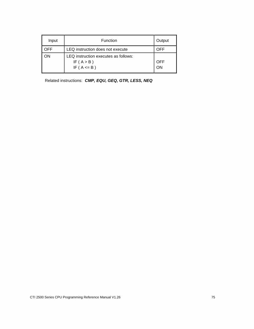
CTI 2500 Series CPU Programming Reference Manual V1.26 75
Input Function Output
OFF LEQ instruction does not execute OFF
ON
LEQ instruction executes as follows:
IF ( A > B )
IF ( A <= B )
OFF
ON
Related instructions: CMP, EQU, GEQ, GTR, LESS, NEQ
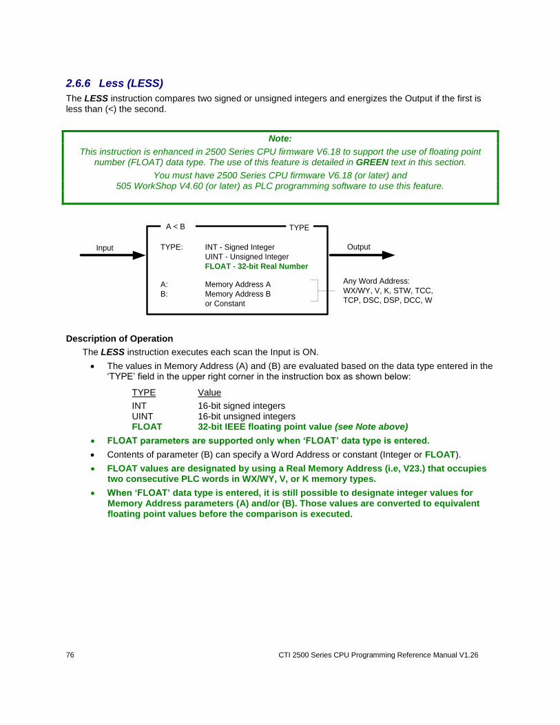
76 CTI 2500 Series CPU Programming Reference Manual V1.26
2.6.6 Less (LESS)
The LESS instruction compares two signed or unsigned integers and energizes the Output if the first is less than (<) the second.
Note:
This instruction is enhanced in 2500 Series CPU firmware V6.18 to support the use of floating point number (FLOAT) data type. The use of this feature is detailed in GREEN text in this section.
You must have 2500 Series CPU firmware V6.18 (or later) and 505 WorkShop V4.60 (or later) as PLC programming software to use this feature.
A < B
TYPE: INT - Signed Integer
UINT - Unsigned Integer
FLOAT - 32-bit Real Number
OutputInput
A: Memory Address A
B: Memory Address B
or Constant
Any Word Address:
WX/WY, V, K, STW, TCC,
TCP, DSC, DSP, DCC, W
TYPE
Description of Operation
The LESS instruction executes each scan the Input is ON.
The values in Memory Address (A) and (B) are evaluated based on the data type entered in the ‘TYPE’ field in the upper right corner in the instruction box as shown below:
TYPE Value
INT 16-bit signed integers UINT 16-bit unsigned integers FLOAT 32-bit IEEE floating point value (see Note above)
FLOAT parameters are supported only when ‘FLOAT’ data type is entered.
Contents of parameter (B) can specify a Word Address or constant (Integer or FLOAT).
FLOAT values are designated by using a Real Memory Address (i.e, V23.) that occupies two consecutive PLC words in WX/WY, V, or K memory types.
When ‘FLOAT’ data type is entered, it is still possible to designate integer values for Memory Address parameters (A) and/or (B). Those values are converted to equivalent floating point values before the comparison is executed.

CTI 2500 Series CPU Programming Reference Manual V1.26 77
Input Function Output
OFF LESS instruction does not execute OFF
ON
LESS instruction executes as follows:
IF ( A >= B )
IF ( A < B )
OFF
ON
Related instructions: CMP, EQU, GEQ, GTR, LESS, NEQ
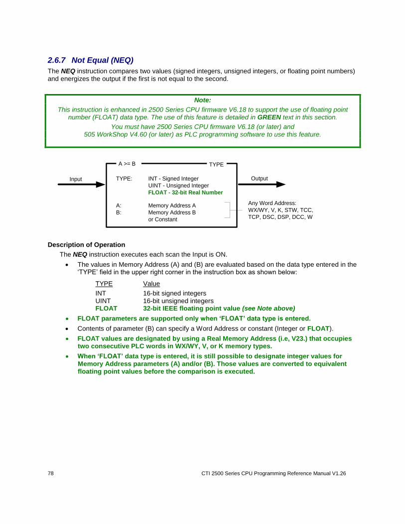
78 CTI 2500 Series CPU Programming Reference Manual V1.26
2.6.7 Not Equal (NEQ)
The NEQ instruction compares two values (signed integers, unsigned integers, or floating point numbers) and energizes the output if the first is not equal to the second.
Note:
This instruction is enhanced in 2500 Series CPU firmware V6.18 to support the use of floating point number (FLOAT) data type. The use of this feature is detailed in GREEN text in this section.
You must have 2500 Series CPU firmware V6.18 (or later) and 505 WorkShop V4.60 (or later) as PLC programming software to use this feature.
A >= B
TYPE: INT - Signed Integer
UINT - Unsigned Integer
FLOAT - 32-bit Real Number
OutputInput
A: Memory Address A
B: Memory Address B
or Constant
Any Word Address:
WX/WY, V, K, STW, TCC,
TCP, DSC, DSP, DCC, W
TYPE
Description of Operation
The NEQ instruction executes each scan the Input is ON.
The values in Memory Address (A) and (B) are evaluated based on the data type entered in the ‘TYPE’ field in the upper right corner in the instruction box as shown below:
TYPE Value
INT 16-bit signed integers UINT 16-bit unsigned integers FLOAT 32-bit IEEE floating point value (see Note above)
FLOAT parameters are supported only when ‘FLOAT’ data type is entered.
Contents of parameter (B) can specify a Word Address or constant (Integer or FLOAT).
FLOAT values are designated by using a Real Memory Address (i.e, V23.) that occupies two consecutive PLC words in WX/WY, V, or K memory types.
When ‘FLOAT’ data type is entered, it is still possible to designate integer values for Memory Address parameters (A) and/or (B). Those values are converted to equivalent floating point values before the comparison is executed.

CTI 2500 Series CPU Programming Reference Manual V1.26 79
Input Function Output
OFF NEQ instruction does not execute OFF
ON
NEQ instruction executes as follows:
IF ( A <> B )
IF ( A = B )
OFF
ON
Related instructions: CMP, EQU, GEQ, GTR, LEQ, LESS
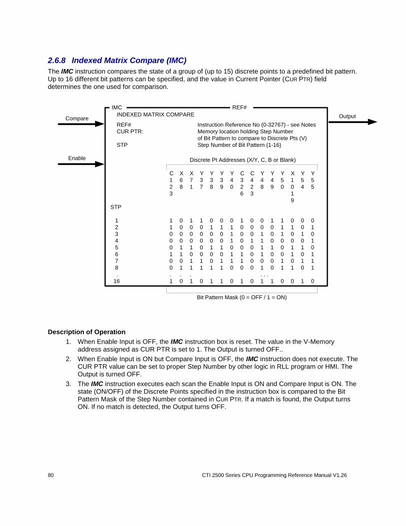
80 CTI 2500 Series CPU Programming Reference Manual V1.26
2.6.8 Indexed Matrix Compare (IMC)
The IMC instruction compares the state of a group of (up to 15) discrete points to a predefined bit pattern. Up to 16 different bit patterns can be specified, and the value in Current Pointer (CUR PTR) field determines the one used for comparison.
Output
IMC
Compare
Enable
INDEXED MATRIX COMPARE
REF# Instruction Reference No (0-32767) - see Notes
CUR PTR: Memory location holding Step Number
of Bit Pattern to compare to Discrete Pts (V)
STP Step Number of Bit Pattern (1-16)
REF#
Discrete Pt Addresses (X/Y, C, B or Blank)
C X X Y Y Y Y C C Y Y Y X Y Y
1 6 7 3 3 3 4 3 4 4 4 5 1 5 5
2 8 1 7 8 9 0 2 2 8 9 0 0 4 5
3 6 3 1
9
STP
1 1 0 1 1 0 0 0 1 0 0 1 1 0 0 0
2 1 0 0 0 1 1 1 0 0 0 0 1 1 0 1
3 0 0 0 0 0 0 1 0 0 1 0 1 0 1 0
4 0 0 0 0 0 0 1 0 1 1 0 0 0 0 1
5 0 1 1 0 1 1 0 0 0 1 1 0 1 1 0
6 1 1 0 0 0 0 1 1 0 1 0 0 1 0 1
7 0 0 1 1 0 1 1 1 0 0 0 1 0 1 1
8 0 1 1 1 1 1 0 0 0 1 0 1 1 0 1
. . . . . . .
16 1 0 1 0 1 1 0 1 0 1 1 0 0 1 0
Bit Pattern Mask (0 = OFF / 1 = ON)
Description of Operation
1. When Enable Input is OFF, the IMC instruction box is reset. The value in the V-Memory address assigned as CUR PTR is set to 1. The Output is turned OFF..
2. When Enable Input is ON but Compare Input is OFF, the IMC instruction does not execute. The CUR PTR value can be set to proper Step Number by other logic in RLL program or HMI. The Output is turned OFF.
3. The IMC instruction executes each scan the Enable Input is ON and Compare Input is ON. The state (ON/OFF) of the Discrete Points specified in the instruction box is compared to the Bit Pattern Mask of the Step Number contained in CUR PTR. If a match is found, the Output turns ON. If no match is detected, the Output turns OFF.

CTI 2500 Series CPU Programming Reference Manual V1.26 81
Input States Function Output
Enable Compare
OFF Don’t Care
IMC reset CUR PTR value set to 1
OFF
ON OFF IMC enabled but does not execute. CUR PTR value can be modified
OFF
ON ON IMC executes as follows: State of Discrete Pts compared to Bit Pattern Mask for Step Number loaded into CUR PTR. IF ( Bit Patterns match ) IF ( Bit Patterns do not match )
ON OFF
Notes:
The Reference Number assigned to the instruction box (Constant: 0-32767) is used only for documentation purposes. The number entered can be repeated as needed.\
If the value in CUR PTR memory location is out of range for a valid Step Number (1-16), the Bit Pattern Mask specified for Step Number 16 is used for comparison.
Related instructions: SMC, STFE, STFN

82 CTI 2500 Series CPU Programming Reference Manual V1.26
2.6.9 Scan Matrix Compare (SMC)
The SMC instruction compares the current states of a group of discrete points to 16 predefined bit patterns. Each bit pattern defines a mask to match up to 16 discrete points. If a match is detected, the Step Number of the matching pattern to written to the memory address specified in the CUR PTR field.
Output
SMC
CompareSCAN MATRIX COMPARE
REF# Instruction Reference No (0-32767) - see Notes
CUR PTR: Memory location holding Step Number of Bit
Pattern Mask that matched Discrete Pts State (V)
LAST STEP: Last Bit Pattern Step Mask to be compared (1-16)
STP Step Number of Bit Pattern (1-16)
REF#
Discrete Pt Addresses (X/Y, C, B or Blank)
C X X Y Y Y Y C C Y Y Y X Y Y
1 6 7 3 3 3 4 3 4 4 4 5 1 5 5
2 8 1 7 8 9 0 2 2 8 9 0 0 4 5
3 6 3 1
9
STP
1 1 0 1 1 0 0 0 1 0 0 1 1 0 0 0
2 1 0 0 0 1 1 1 0 0 0 0 1 1 0 1
3 0 0 0 0 0 0 1 0 0 1 0 1 0 1 0
4 0 0 0 0 0 0 1 0 1 1 0 0 0 0 1
5 0 1 1 0 1 1 0 0 0 1 1 0 1 1 0
6 1 1 0 0 0 0 1 1 0 1 0 0 1 0 1
7 0 0 1 1 0 1 1 1 0 0 0 1 0 1 1
8 0 1 1 1 1 1 0 0 0 1 0 1 1 0 1
. . . . . . .
16 1 0 1 0 1 1 0 1 0 1 1 0 0 1 0
Bit Pattern Mask (0 = OFF / 1 = ON)
Description of Operation
1. When Enable Input or Compare Input is OFF, the SMC instruction box does not execute. The value in CUR PTR address remains unchanged. The Output is turned OFF..
2. The SMC instruction executes each scan the Enable Input is ON and Compare Input is ON as described below:
Starting at Step Number 1, the state (ON/OFF) of the Discrete Points designated in the instruction box is compared to the predefined Bit Pattern Mask.
If no match is detected, the Step Number is incremented and the comparison process is repeated.
If a match is found, operation is complete. That Step Number is written to CUR PTR address and the Output turns ON.
If bit patterns for all 16 Steps are tested and no match is found, a value of zero is written to CUR PTR and Output turns OFF.
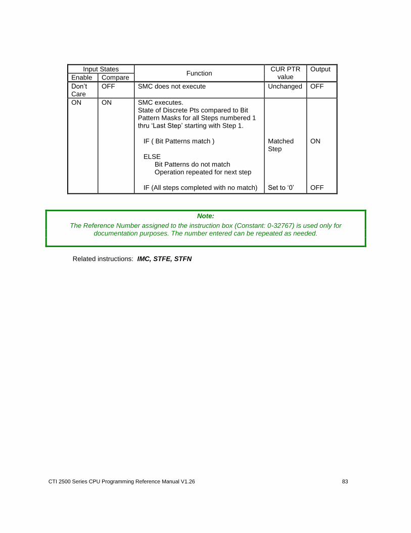
CTI 2500 Series CPU Programming Reference Manual V1.26 83
Input States Function
CUR PTR value
Output
Enable Compare
Don’t Care
OFF SMC does not execute
Unchanged OFF
ON ON SMC executes. State of Discrete Pts compared to Bit Pattern Masks for all Steps numbered 1 thru ‘Last Step’ starting with Step 1. IF ( Bit Patterns match ) ELSE Bit Patterns do not match Operation repeated for next step IF (All steps completed with no match)
Matched Step Set to ‘0’
ON OFF
Note:
The Reference Number assigned to the instruction box (Constant: 0-32767) is used only for documentation purposes. The number entered can be repeated as needed.
Related instructions: IMC, STFE, STFN
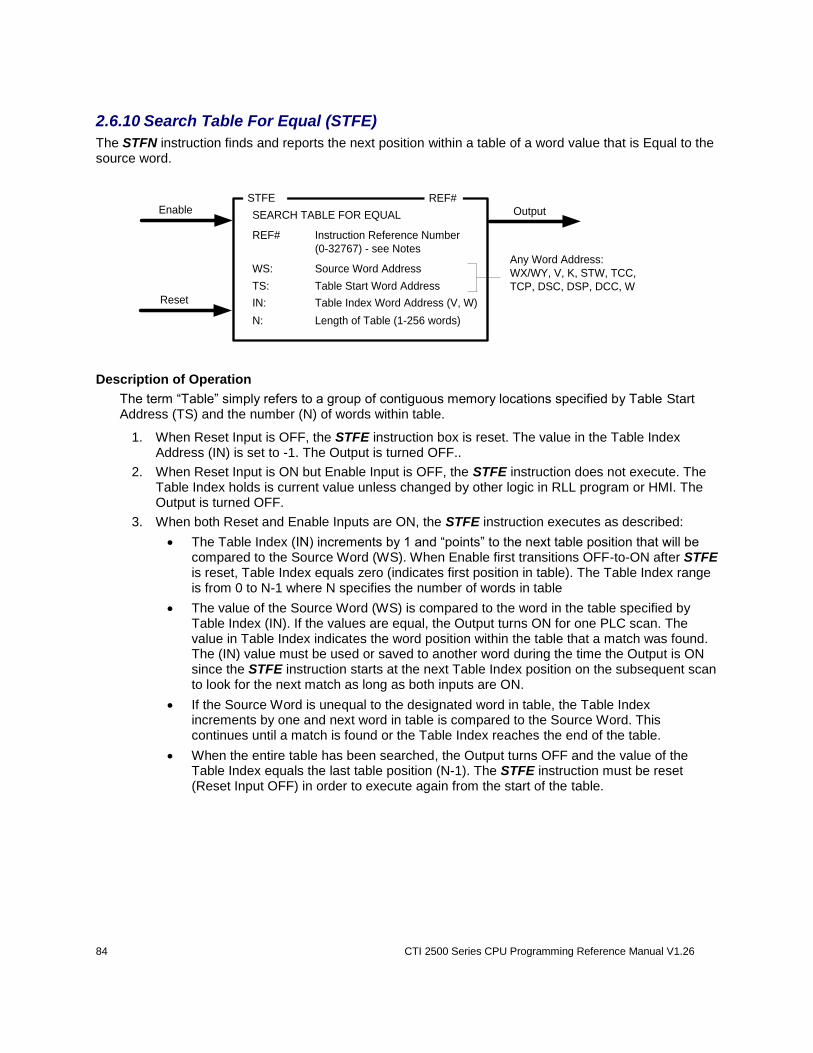
84 CTI 2500 Series CPU Programming Reference Manual V1.26
2.6.10 Search Table For Equal (STFE)
The STFN instruction finds and reports the next position within a table of a word value that is Equal to the source word.
Reset
STFE
OutputEnable
WS: Source Word Address
REF#
REF# Instruction Reference Number
(0-32767) - see Notes
SEARCH TABLE FOR EQUAL
TS: Table Start Word Address
N: Length of Table (1-256 words)
Any Word Address:
WX/WY, V, K, STW, TCC,
TCP, DSC, DSP, DCC, W
IN: Table Index Word Address (V, W)
Description of Operation
The term “Table” simply refers to a group of contiguous memory locations specified by Table Start Address (TS) and the number (N) of words within table.
1. When Reset Input is OFF, the STFE instruction box is reset. The value in the Table Index Address (IN) is set to -1. The Output is turned OFF..
2. When Reset Input is ON but Enable Input is OFF, the STFE instruction does not execute. The Table Index holds is current value unless changed by other logic in RLL program or HMI. The Output is turned OFF.
3. When both Reset and Enable Inputs are ON, the STFE instruction executes as described:
The Table Index (IN) increments by 1 and “points” to the next table position that will be compared to the Source Word (WS). When Enable first transitions OFF-to-ON after STFE is reset, Table Index equals zero (indicates first position in table). The Table Index range is from 0 to N-1 where N specifies the number of words in table
The value of the Source Word (WS) is compared to the word in the table specified by Table Index (IN). If the values are equal, the Output turns ON for one PLC scan. The value in Table Index indicates the word position within the table that a match was found. The (IN) value must be used or saved to another word during the time the Output is ON since the STFE instruction starts at the next Table Index position on the subsequent scan to look for the next match as long as both inputs are ON.
If the Source Word is unequal to the designated word in table, the Table Index increments by one and next word in table is compared to the Source Word. This continues until a match is found or the Table Index reaches the end of the table.
When the entire table has been searched, the Output turns OFF and the value of the Table Index equals the last table position (N-1). The STFE instruction must be reset (Reset Input OFF) in order to execute again from the start of the table.
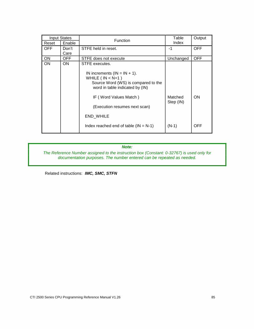
CTI 2500 Series CPU Programming Reference Manual V1.26 85
Input States Function
Table Index
Output
Reset Enable
OFF Don’t Care
STFE held in reset.
-1 OFF
ON OFF STFE does not execute Unchanged OFF
ON ON STFE executes. IN increments (IN = IN + 1). WHILE ( IN < N+1 ) Source Word (WS) is compared to the word in table indicated by (IN) IF ( Word Values Match ) (Execution resumes next scan) END_WHILE Index reached end of table (IN = N-1)
Matched Step (IN) (N-1)
ON OFF
Note:
The Reference Number assigned to the instruction box (Constant: 0-32767) is used only for documentation purposes. The number entered can be repeated as needed.
Related instructions: IMC, SMC, STFN
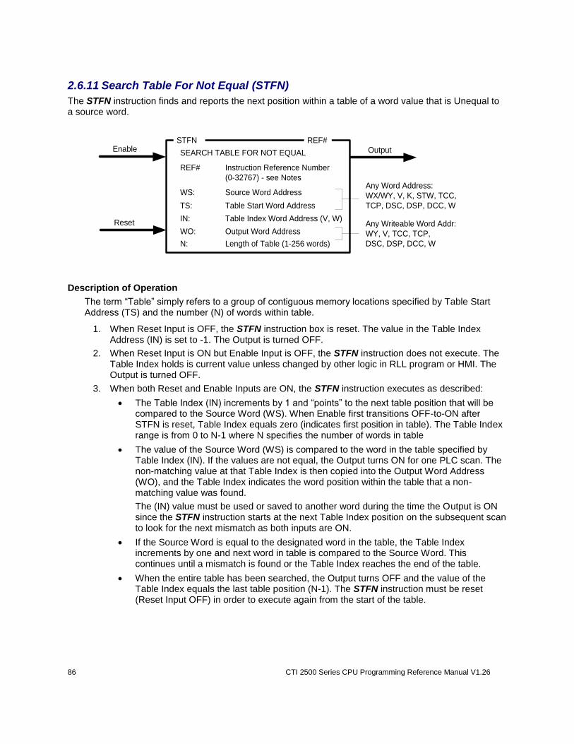
86 CTI 2500 Series CPU Programming Reference Manual V1.26
2.6.11 Search Table For Not Equal (STFN)
The STFN instruction finds and reports the next position within a table of a word value that is Unequal to a source word.
Reset
STFN
OutputEnable
WS: Source Word Address
REF#
REF# Instruction Reference Number
(0-32767) - see Notes
SEARCH TABLE FOR NOT EQUAL
TS: Table Start Word Address
WO: Output Word Address
Any Word Address:
WX/WY, V, K, STW, TCC,
TCP, DSC, DSP, DCC, W
IN: Table Index Word Address (V, W)
N: Length of Table (1-256 words)
Any Writeable Word Addr:
WY, V, TCC, TCP,
DSC, DSP, DCC, W
Description of Operation
The term “Table” simply refers to a group of contiguous memory locations specified by Table Start Address (TS) and the number (N) of words within table.
1. When Reset Input is OFF, the STFN instruction box is reset. The value in the Table Index Address (IN) is set to -1. The Output is turned OFF.
2. When Reset Input is ON but Enable Input is OFF, the STFN instruction does not execute. The Table Index holds is current value unless changed by other logic in RLL program or HMI. The Output is turned OFF.
3. When both Reset and Enable Inputs are ON, the STFN instruction executes as described:
The Table Index (IN) increments by 1 and “points” to the next table position that will be compared to the Source Word (WS). When Enable first transitions OFF-to-ON after STFN is reset, Table Index equals zero (indicates first position in table). The Table Index range is from 0 to N-1 where N specifies the number of words in table
The value of the Source Word (WS) is compared to the word in the table specified by Table Index (IN). If the values are not equal, the Output turns ON for one PLC scan. The non-matching value at that Table Index is then copied into the Output Word Address (WO), and the Table Index indicates the word position within the table that a non-matching value was found.
The (IN) value must be used or saved to another word during the time the Output is ON since the STFN instruction starts at the next Table Index position on the subsequent scan to look for the next mismatch as both inputs are ON.
If the Source Word is equal to the designated word in the table, the Table Index increments by one and next word in table is compared to the Source Word. This continues until a mismatch is found or the Table Index reaches the end of the table.
When the entire table has been searched, the Output turns OFF and the value of the Table Index equals the last table position (N-1). The STFN instruction must be reset (Reset Input OFF) in order to execute again from the start of the table.
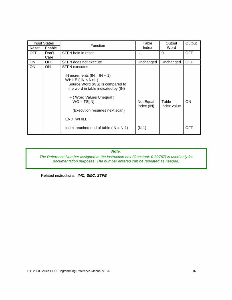
CTI 2500 Series CPU Programming Reference Manual V1.26 87
Input States Function
Table Index
Output Word
Output
Reset Enable
OFF Don’t Care
STFN held in reset
-1 0 OFF
ON OFF STFN does not execute Unchanged Unchanged OFF
ON ON STFN executes IN increments (IN = IN + 1). WHILE ( IN < N+1 ) Source Word (WS) is compared to the word in table indicated by (IN) IF ( Word Values Unequal ) WO = TS[IN] (Execution resumes next scan) END_WHILE Index reached end of table (IN = N-1)
Not Equal Index (IN) (N-1)
Table Index value
ON OFF
Note:
The Reference Number assigned to the instruction box (Constant: 0-32767) is used only for documentation purposes. The number entered can be repeated as needed.
Related instructions: IMC, SMC, STFE
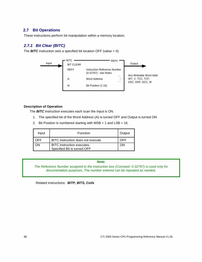
88 CTI 2500 Series CPU Programming Reference Manual V1.26
2.7 Bit Operations
These instructions perform bit manipulation within a memory location.
2.7.1 Bit Clear (BITC)
The BITC instruction sets a specified bit location OFF (value = 0).
BITCOutputInput
A: Word Address
N: Bit Position (1-16)
REF#
REF# Instruction Reference Number
(0-32767) - see Notes
BIT CLEAR
Any Writeable Word Addr:
WY, V, TCC, TCP,
DSC, DSP, DCC, W
Description of Operation
The BITC instruction executes each scan the Input is ON.
1. The specified bit of the Word Address (A) is turned OFF and Output is turned ON
2. Bit Position is numbered starting with MSB = 1 and LSB = 16.
Input Function Output
OFF BITC instruction does not execute OFF
ON
BITC instruction executes. Specified Bit is turned OFF
ON
Note:
The Reference Number assigned to the instruction box (Constant: 0-32767) is used only for documentation purposes. The number entered can be repeated as needed.
Related instructions: BITP, BITS, Coils

CTI 2500 Series CPU Programming Reference Manual V1.26 89
2.7.2 Bit Set (BITS)
The BITS instruction sets a specified bit location ON (value = 1).
BITCOutputInput
A: Word Address
N: Bit Position (1-16)
REF#
REF# Instruction Reference Number
(0-32767) - see Notes
BIT CLEAR
Any Writeable Word Addr:
WY, V, TCC, TCP,
DSC, DSP, DCC, W
Description of Operation
The BITS instruction executes each scan the Input is ON.
1. The specified bit of the Word Address (A) is turned ON and Output is turned ON..
2. Bit Position is numbered starting with MSB = 1 and LSB = 16.
Input Function Output
OFF BITS instruction does not execute OFF
ON
BITS instruction executes. Specified Bit is turned ON
ON
Note:
The Reference Number assigned to the instruction box (Constant: 0-32767) is used only for documentation purposes. The number entered can be repeated as needed.
Related instructions: BITC, BITP, Coils

90 CTI 2500 Series CPU Programming Reference Manual V1.26
2.7.3 Bit Pick (BITP)
The BITP instruction reports the state (ON/OFF) of a specified bit.
BITPOutputInput
A: Word Address to be examined
N: Bit Position (1-16)
REF#
REF# Instruction Reference Number
(0-32767) - see Notes
BIT PICK
Any Word Address:
WX/WY, V, K, STW, TCC,
TCP, DSC, DSP, DCC, W
Description of Operation
The BITP instruction executes each scan the Input is ON.
1. The specified bit of the Word entered in Memory Address field is examined.
2. BITP Output reports state of bit as follows:
Output turns ON if bit is ON
Output turns OFF if bit is OFF
3. Bit Position is numbered starting with MSB = 1 and LSB = 16.
Input Function Output
OFF BITP instruction does not execute OFF
ON
BITP instruction executes as follows: IF ( Specified Bit is ON ) IF ( Specified Bit is OFF )
ON OFF
Note:
The Reference Number assigned to the instruction box (Constant: 0-32767) is used only for documentation purposes. The number entered can be repeated as needed.
Related instructions: BITC, BITS, Contacts
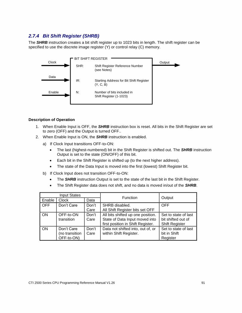
CTI 2500 Series CPU Programming Reference Manual V1.26 91
2.7.4 Bit Shift Register (SHRB)
The SHRB instruction creates a bit shift register up to 1023 bits in length. The shift register can be specified to use the discrete image register (Y) or control relay (C) memory.
BIT SHIFT REGISTER
SHR: Shift Register Reference Number
(see Notes)
IR: Starting Address for Bit Shift Register
(Y, C, B)
N: Number of bits included in
Shift Register (1-1023)
Output
Enable
Clock
Data
Description of Operation
1. When Enable Input is OFF, the SHRB instruction box is reset. All bits in the Shift Register are set to zero (OFF) and the Output is turned OFF..
2. When Enable Input is ON, the SHRB instruction is enabled.
a) If Clock Input transitions OFF-to-ON:
The last (highest-numbered) bit in the Shift Register is shifted out. The SHRB instruction Output is set to the state (ON/OFF) of this bit.
Each bit in the Shift Register is shifted up (to the next higher address).
The state of the Data Input is moved into the first (lowest) Shift Register bit.
b) If Clock Input does not transition OFF-to-ON:
The SHRB instruction Output is set to the state of the last bit in the Shift Register.
The Shift Register data does not shift, and no data is moved in/out of the SHRB.
Input States Function Output
Enable Clock Data
OFF Don’t Care Don’t Care
SHRB disabled. All Shift Register bits set OFF
OFF
ON OFF-to-ON transition
Don’t Care
All bits shifted up one position. State of Data Input moved into first position in Shift Register.
Set to state of last bit shifted out of Shift Register
ON Don’t Care (no transition OFF-to-ON)
Don’t Care
Data not shifted into, out of, or within Shift Register.
Set to state of last bit in Shift Register
92 CTI 2500 Series CPU Programming Reference Manual V1.26
Note:
The Reference Number assigned to the instruction box must be unique for all Shift Register instructions (SHRB, SHRW) entered in the PLC program.
The amount of Shift Register Memory that is assigned in PLC Memory Configuration determines the number of Shift Register instructions allowed in the RLL program.
One Byte of Shift Register Memory is used for each Shift Register instruction.
Related instructions: SHRW, WROT
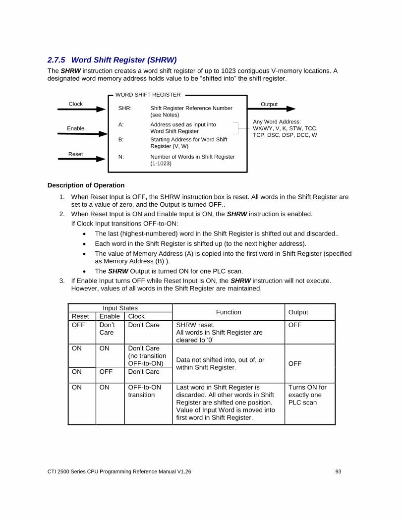
CTI 2500 Series CPU Programming Reference Manual V1.26 93
2.7.5 Word Shift Register (SHRW)
The SHRW instruction creates a word shift register of up to 1023 contiguous V-memory locations. A designated word memory address holds value to be “shifted into” the shift register.
Reset
Clock
Enable
WORD SHIFT REGISTER
Output
Any Word Address:
WX/WY, V, K, STW, TCC,
TCP, DSC, DSP, DCC, W
SHR: Shift Register Reference Number
(see Notes)
A: Address used as input into
Word Shift Register
N: Number of Words in Shift Register
(1-1023)
B: Starting Address for Word Shift
Register (V, W)
Description of Operation
1. When Reset Input is OFF, the SHRW instruction box is reset. All words in the Shift Register are set to a value of zero, and the Output is turned OFF..
2. When Reset Input is ON and Enable Input is ON, the SHRW instruction is enabled.
If Clock Input transitions OFF-to-ON:
The last (highest-numbered) word in the Shift Register is shifted out and discarded..
Each word in the Shift Register is shifted up (to the next higher address).
The value of Memory Address (A) is copied into the first word in Shift Register (specified as Memory Address (B) ).
The SHRW Output is turned ON for one PLC scan.
3. If Enable Input turns OFF while Reset Input is ON, the SHRW instruction will not execute. However, values of all words in the Shift Register are maintained.
Input States Function Output
Reset Enable Clock
OFF Don’t Care
Don’t Care SHRW reset. All words in Shift Register are cleared to ‘0’
OFF
ON ON Don’t Care (no transition OFF-to-ON)
Data not shifted into, out of, or within Shift Register.
OFF
ON OFF Don’t Care
ON ON OFF-to-ON transition
Last word in Shift Register is discarded. All other words in Shift Register are shifted one position. Value of Input Word is moved into first word in Shift Register.
Turns ON for exactly one PLC scan
94 CTI 2500 Series CPU Programming Reference Manual V1.26
Note:
The Reference Number assigned to the instruction box must be unique for all Shift Register instructions (SHRB, SHRW) entered in the PLC program.
The amount of Shift Register Memory that is assigned in PLC Memory Configuration determines the number of Shift Register instructions allowed in the RLL program.
One Byte of Shift Register Memory is used for each Shift Register instruction.
Related instructions: SHRB, WROT

CTI 2500 Series CPU Programming Reference Manual V1.26 95
2.7.6 Word Rotate (WROT)
The WROT instruction modifies a word memory location by shifting each 4-bit segment a designated number of times.
WROTOutputInput
A: Word Address to be rotated
N: Number of shifts (1-3)
REF#
REF# Instruction Reference Number
(0-32767) - see Notes
WORD ROTATE
Any Writeable Word Addr:
WY, V, TCC, TCP,
DSC, DSP, DCC, W
Description of Operation
The WROT instruction performs a “Rotate Right” operation as shown below.
Bits 1-4 Bits 5-8 Bits 9-12 Bits 13-16
Bits 1-4 Bits 5-8 Bits 9-12 Bits 13-16
For N = 2:
Bits 1-4 Bits 5-8 Bits 9-12 Bits 13-16
For N = 3:
For N = 1:
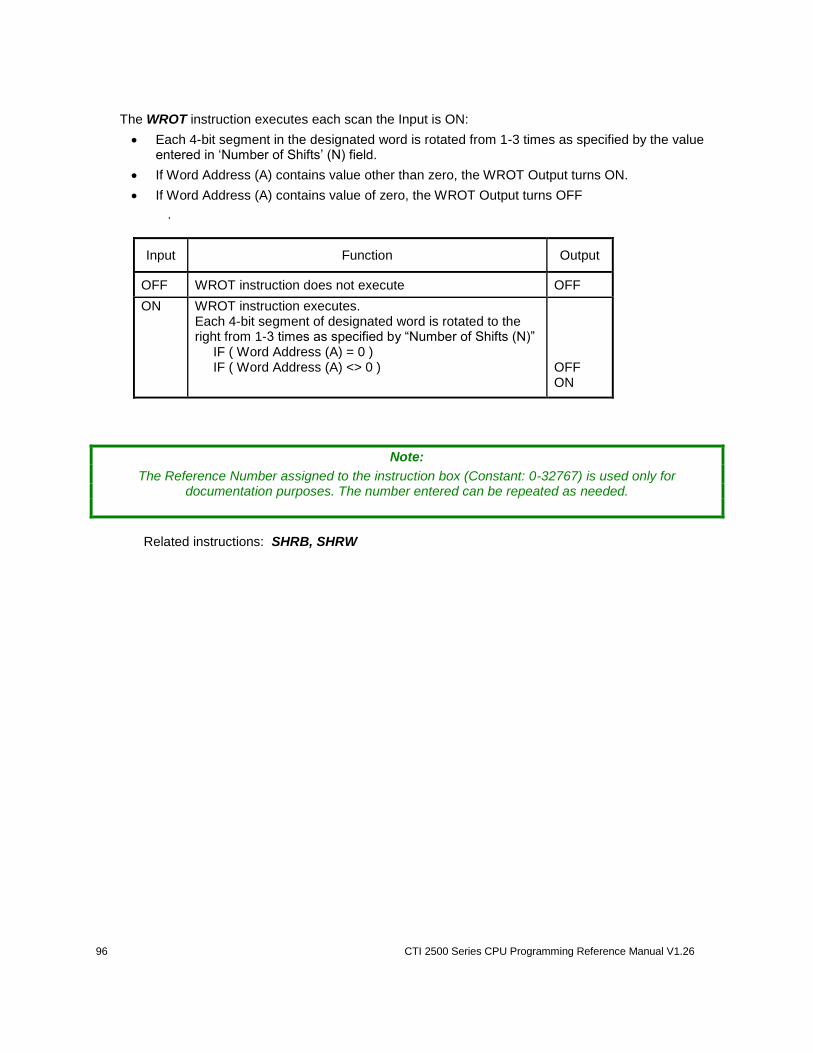
96 CTI 2500 Series CPU Programming Reference Manual V1.26
The WROT instruction executes each scan the Input is ON:
Each 4-bit segment in the designated word is rotated from 1-3 times as specified by the value entered in ‘Number of Shifts’ (N) field.
If Word Address (A) contains value other than zero, the WROT Output turns ON.
If Word Address (A) contains value of zero, the WROT Output turns OFF
.
Input Function Output
OFF WROT instruction does not execute OFF
ON
WROT instruction executes. Each 4-bit segment of designated word is rotated to the right from 1-3 times as specified by “Number of Shifts (N)” IF ( Word Address (A) = 0 ) IF ( Word Address (A) <> 0 )
OFF ON
Note:
The Reference Number assigned to the instruction box (Constant: 0-32767) is used only for documentation purposes. The number entered can be repeated as needed.
Related instructions: SHRB, SHRW
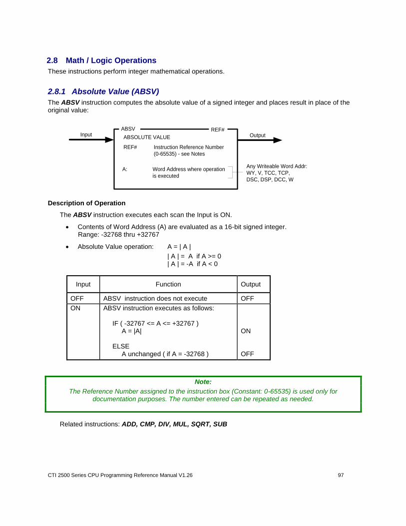
CTI 2500 Series CPU Programming Reference Manual V1.26 97
2.8 Math / Logic Operations
These instructions perform integer mathematical operations.
2.8.1 Absolute Value (ABSV)
The ABSV instruction computes the absolute value of a signed integer and places result in place of the original value:
ABSVOutputInput
A: Word Address where operation
is executed
REF#
REF# Instruction Reference Number
(0-65535) - see Notes
ABSOLUTE VALUE
Any Writeable Word Addr:
WY, V, TCC, TCP,
DSC, DSP, DCC, W
Description of Operation
The ABSV instruction executes each scan the Input is ON.
Contents of Word Address (A) are evaluated as a 16-bit signed integer. Range: -32768 thru +32767
Absolute Value operation: A = | A |
| A | = A if A >= 0 | A | = -A if A < 0
Input Function Output
OFF ABSV instruction does not execute OFF
ON
ABSV instruction executes as follows: IF ( -32767 <= A <= +32767 ) A = |A| ELSE A unchanged ( if A = -32768 )
ON OFF
Note:
The Reference Number assigned to the instruction box (Constant: 0-65535) is used only for documentation purposes. The number entered can be repeated as needed.
Related instructions: ADD, CMP, DIV, MUL, SQRT, SUB
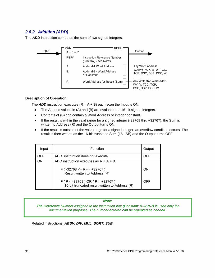
98 CTI 2500 Series CPU Programming Reference Manual V1.26
2.8.2 Addition (ADD)
The ADD instruction computes the sum of two signed integers.
ADD
OutputInput
A: Addend-1 Word Address
REF#
REF# Instruction Reference Number
(0-32767) - see Notes
A + B = R
Any Writeable Word Addr:
WY, V, TCC, TCP,
DSC, DSP, DCC, W
B: Addend-2 - Word Address
or Constant
R: Word Address for Result (Sum)
Any Word Address:
WX/WY, V, K, STW, TCC,
TCP, DSC, DSP, DCC, W
Description of Operation
The ADD instruction executes (R = A + B) each scan the Input is ON.
The Addend values in (A) and (B) are evaluated as 16-bit signed integers.
Contents of (B) can contain a Word Address or integer constant.
If the result is within the valid range for a signed integer (-32768 thru +32767), the Sum is written to Address (R) and the Output turns ON.
If the result is outside of the valid range for a signed integer, an overflow condition occurs. The result is then written as the 16-bit truncated Sum (16 LSB) and the Output turns OFF.
Input Function Output
OFF ADD instruction does not execute OFF
ON
ADD instruction executes as R = A + B. IF ( -32768 <= R <= +32767 ) Result written to Address (R) IF ( R < -32768 ) OR ( R > +32767 ) 16-bit truncated result written to Address (R)
ON OFF
Note:
The Reference Number assigned to the instruction box (Constant: 0-32767) is used only for documentation purposes. The number entered can be repeated as needed.
Related instructions: ABSV, DIV, MUL, SQRT, SUB
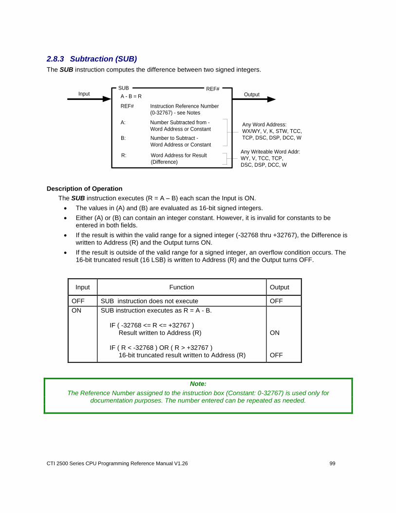
CTI 2500 Series CPU Programming Reference Manual V1.26 99
2.8.3 Subtraction (SUB)
The SUB instruction computes the difference between two signed integers.
SUB
OutputInput
A: Number Subtracted from -
Word Address or Constant
REF#
REF# Instruction Reference Number
(0-32767) - see Notes
A - B = R
Any Writeable Word Addr:
WY, V, TCC, TCP,
DSC, DSP, DCC, W
B: Number to Subtract -
Word Address or Constant
R: Word Address for Result
(Difference)
Any Word Address:
WX/WY, V, K, STW, TCC,
TCP, DSC, DSP, DCC, W
Description of Operation
The SUB instruction executes (R = A – B) each scan the Input is ON.
The values in (A) and (B) are evaluated as 16-bit signed integers.
Either (A) or (B) can contain an integer constant. However, it is invalid for constants to be entered in both fields.
If the result is within the valid range for a signed integer (-32768 thru +32767), the Difference is written to Address (R) and the Output turns ON.
If the result is outside of the valid range for a signed integer, an overflow condition occurs. The 16-bit truncated result (16 LSB) is written to Address (R) and the Output turns OFF.
Input Function Output
OFF SUB instruction does not execute OFF
ON
SUB instruction executes as R = A - B. IF ( -32768 <= R <= +32767 ) Result written to Address (R) IF ( R < -32768 ) OR ( R > +32767 ) 16-bit truncated result written to Address (R)
ON OFF
Note:
The Reference Number assigned to the instruction box (Constant: 0-32767) is used only for documentation purposes. The number entered can be repeated as needed.
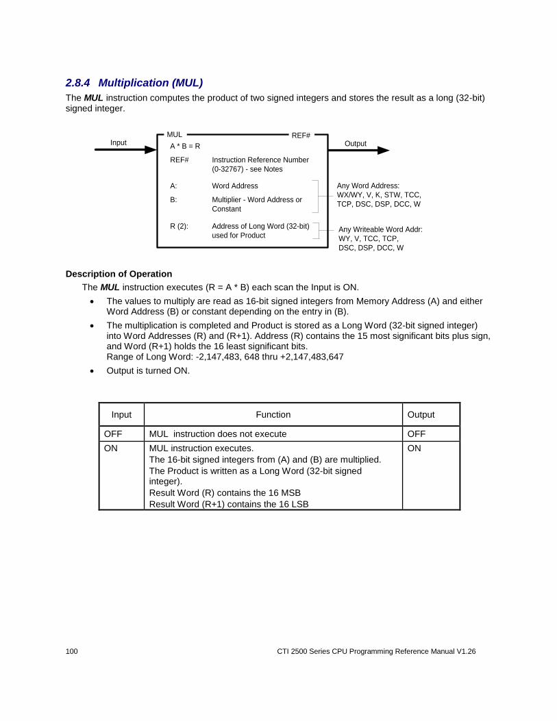
100 CTI 2500 Series CPU Programming Reference Manual V1.26
2.8.4 Multiplication (MUL)
The MUL instruction computes the product of two signed integers and stores the result as a long (32-bit) signed integer.
MUL
OutputInput
A: Word Address
REF#
REF# Instruction Reference Number
(0-32767) - see Notes
A * B = R
Any Writeable Word Addr:
WY, V, TCC, TCP,
DSC, DSP, DCC, W
B: Multiplier - Word Address or
Constant
Any Word Address:
WX/WY, V, K, STW, TCC,
TCP, DSC, DSP, DCC, W
R (2): Address of Long Word (32-bit)
used for Product
Description of Operation
The MUL instruction executes (R = A * B) each scan the Input is ON.
The values to multiply are read as 16-bit signed integers from Memory Address (A) and either Word Address (B) or constant depending on the entry in (B).
The multiplication is completed and Product is stored as a Long Word (32-bit signed integer) into Word Addresses (R) and (R+1). Address (R) contains the 15 most significant bits plus sign, and Word (R+1) holds the 16 least significant bits. Range of Long Word: -2,147,483, 648 thru +2,147,483,647
Output is turned ON.
Input Function Output
OFF MUL instruction does not execute OFF
ON
MUL instruction executes.
The 16-bit signed integers from (A) and (B) are multiplied.
The Product is written as a Long Word (32-bit signed integer).
Result Word (R) contains the 16 MSB
Result Word (R+1) contains the 16 LSB
ON
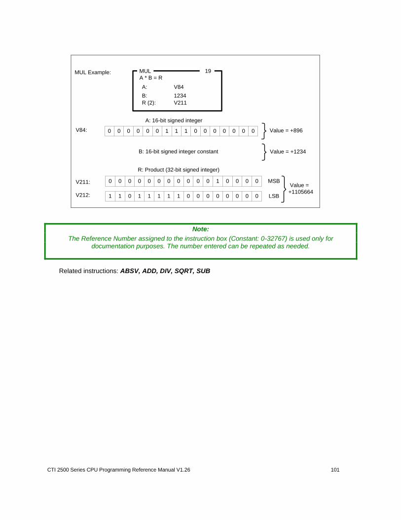
CTI 2500 Series CPU Programming Reference Manual V1.26 101
Value = +896
0 0 0 0 0 0 0 0 0 0 0 1 0 0 00V211:
1 1 1 1 0 0 0 0 00V212: 1 0 1 1 0 0
R: Product (32-bit signed integer)
MSB
LSB
Value =
+1105664
B: 16-bit signed integer constant
0 0 0 0 0 0 0 0 00V84: 0 0 1 1 1 0
A: 16-bit signed integer
Value = +1234
MUL
A: V84
19
A * B = R
B: 1234
R (2): V211
MUL Example:
Note:
The Reference Number assigned to the instruction box (Constant: 0-32767) is used only for documentation purposes. The number entered can be repeated as needed.
Related instructions: ABSV, ADD, DIV, SQRT, SUB
102 CTI 2500 Series CPU Programming Reference Manual V1.26
2.8.5 Division (DIV)
The DIV instruction performs an integer division operation. A long (32-bit) signed integer is divided by a 16-bit signed integer, and the quotient and remainder are stored.
DIV
OutputInput
A (2): Dividend Address - Long Word
(32-bit) or Constant
REF#
REF# Instruction Reference Number
(0-32767) - see Notes
A / B = R
Any Writeable Word Addr:
WY, V, TCC, TCP,
DSC, DSP, DCC, W
B: Divisor Address or Constant
Any Word Address:
WX/WY, V, K, STW, TCC,
TCP, DSC, DSP, DCC, W
R (2): Starting Address for Results
(Uses 2 Consecutive Words)
Description of Operation
The DIV instruction executes (R = A / B) each scan the Input is ON.
1. The Dividend is read from a memory address or constant depending on the contents in (A).
If (A) contains a Word Address, the Dividend is read as a Long Word (32-bit signed integer). Word (A) contains the 15 most significant bits plus sign, and Word (A+1) holds the 16 least significant bits. Range of Long Word: -2,147,483, 648 thru +2,147,483,647.
Otherwise, (A) is read as a 16-bit signed integer constant. Range: -32768 thru +32767.
2. The Divisor is read from a memory address or constant depending on the contents in (B).
If (B) contains a Word Address, the Divisor is read as a 16-bit signed integer.
Otherwise, (B) is read as a 16-bit signed integer constant.
It is invalid for both (A) and (B) to be entered as constants.
3. The division is completed and results are stored based on the following conditions:
If the Divisor is equal to zero, the operation is aborted. The Result Words (R) and (R+1) are unchanged, and the Output is turned OFF
If the Quotient is within the range of a 16-bit signed integer, the Quotient is written to Word Address (R). The Remainder to written to Address (R+1). The Output is turned ON.
If the Quotient is invalid (greater than +32767 or less than -32768), the operation is aborted. The Result Words (R) and (R+1) are unchanged, and Output is turned OFF.
CTI 2500 Series CPU Programming Reference Manual V1.26 103
Input Function Output
OFF DIV instruction does not execute OFF
ON
DIV instruction executes. IF ( Divisor (B) <> 0 ): Divide operation (A/B) is performed. IF ( -32768 <= Quotient <= +32767 ) Quotient written to Result Address (R) Remainder written to Address (R+1) IF (Quotient < -32768 ) OR (Quotient > +32767) Divide operation aborted. Result Addresses (R and R+1) unchanged. IF ( Divisor (B) = 0 ) Divide operation aborted. Result Addresses (R and R+1) unchanged.
ON OFF OFF
R: Quotient (16-bit signed integer)
R+1: Remainder (16-bit signed integer)
DIV
A (2): V78
23
A / B = R
B: K14
R (2): V101
B: Divisor (16-bit signed integer)
1 1 1 1 0 1 0 1 10K14 11 1 1 1 0 Value = -93
0 1 0 0 0 0 0 1 01V101 0 0 1 0 1 0 Value = - 4742
0 0 0 0 0 0 0 0 01V102 1 1 1 1 1 1 Value = +87
0 0 0 0 0 0 0 0 0 0 0 0 0 1 01V78:
1 1 1 0 0 0 0 0 11V79: 0 1 1 1 0 0
A: Dividend (32-bit signed integer)
MSB
LSB
Value =
+441093
DIV Example:
Note:
The Reference Number assigned to the instruction box (Constant: 0-32767) is used only for documentation purposes. The number entered can be repeated as needed.
104 CTI 2500 Series CPU Programming Reference Manual V1.26
2.8.6 Square Root (SQRT)
The SQRT instruction computes the integer square root of a long (32-bit) integer.
SQRT
OutputInput
A (2): Long Word Address
REF#
REF# Instruction Reference Number
(0-32767) - see Notes
B = SQRT(A)
Any Writeable Word Addr:
WY, V, TCC, TCP,
DSC, DSP, DCC, W
B: Word Address for Result
Any Word Address:
WX/WY, V, K, STW, TCC,
TCP, DSC, DSP, DCC, W
Description of Operation
The SQRT instruction executes ( R = SQRT(A) ) each scan the Input is ON.
The operation finds the positive integer Square Root of the Long Word (32-bit) integer value stored in Memory Addresses (A) and (A+1).and writes results based on the following:
The SQRT instruction reports only the integer portion of the Square Root. Any fractional content is truncated.
Example: Actual Square Root of 118 is = 10.86
SQRT instruction reports Result = 10
If the integer Square Root is within valid range of a positive 16-bit signed integer (0 thru +32767), the result is written to Address (B) and the Output turns ON.
If the integer Square Root is outside of the valid range, Address (B) is unchanged and the Output turns OFF.
Input Function Output
OFF SQRT instruction does not execute OFF
ON
SQRT instruction executes. The integer Square Root of Long Word (32-bit integer).stored in Memory Address (A) and (A+1) is computed. IF ( 0 <= Result <= +32767 ) Sq. Root Result is written as 16-bit integer to Address (B) ELSE Address (B) is unchanged
ON OFF
CTI 2500 Series CPU Programming Reference Manual V1.26 105
Note:
The Reference Number assigned to the instruction box (Constant: 0-32767) is used only for documentation purposes. The number entered can be repeated as needed.
Related instructions: ABSV, ADD, DIV, MUL, SUB

106 CTI 2500 Series CPU Programming Reference Manual V1.26
2.8.7 Binary to BCD Conversion (CBD)
The CBD instruction converts the binary representation of a 16-bit integer to its equivalent Binary Coded Decimal (BCD) value.
CBD
OutputInput
BIN: Word Address of integer in
Binary representation
REF#
REF# Instruction Reference Number
(0-32767) - see Notes
CONVERT BINARY TO BCD
Any Writeable Word Addr:
WY, V, TCC, TCP,
DSC, DSP, DCC, W
BCD (2) Address for Long Word
(32-bit) BCD value
Any Word Address:
WX/WY, V, K, STW, TCC,
TCP, DSC, DSP, DCC, W
Description of Operation
The CBD instruction executes each scan the Input is ON:
The value in (BIN) is evaluated as a 16-bit signed integer. If the value is in the positive range (0 to 32767), the BCD equivalent value is written to
Addresses (BCD) and (BCD+1) as shown below and the Output turns ON.
Each BCD digit occupies four bits and is written into two contiguous memory locations as shown below.
Bits 5-8Bits 1-4 Bits 9-12 Bits 13-16Address BCD:
Unused Unused Unused Ten
Thousands
Bits 5-8Bits 1-4 Bits 9-12 Bits 13-16Address BCD+1:
Thousands Hundreds Tens Ones
If the value in (BIN) is negative, the BCD conversion is aborted. The values in Addresses (BCD) and (BCD+1) are unchanged and the Output turns OFF.
.
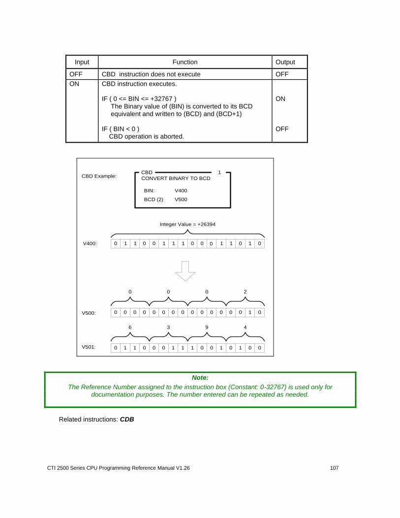
CTI 2500 Series CPU Programming Reference Manual V1.26 107
Input Function Output
OFF CBD instruction does not execute OFF
ON
CBD instruction executes. IF ( 0 <= BIN <= +32767 ) The Binary value of (BIN) is converted to its BCD equivalent and written to (BCD) and (BCD+1) IF ( BIN < 0 ) CBD operation is aborted.
ON OFF
CBD
BIN: V400
1
CONVERT BINARY TO BCD
BCD (2) V500
0 0 0 0 0 0 0 0 0 0 0 0 0 0 01
0 0 0 0 0 0 0 0 01
000 2
6 3 9 4
V500:
V501: 1 1 1 1 1 1
V400: 0 0 0 0 0 0 0 011 1 1 1 1 1 1
Integer Value = +26394
CBD Example:
Note:
The Reference Number assigned to the instruction box (Constant: 0-32767) is used only for documentation purposes. The number entered can be repeated as needed.
Related instructions: CDB

108 CTI 2500 Series CPU Programming Reference Manual V1.26
2.8.8 BCD to Binary Conversion (CDB)
The CDB instruction converts one to four Binary Coded Decimal (BCD) digits within a word to its equivalent binary integer value.
CDB
OutputInput
BCD: Word Address of BCD value
REF#
REF# Instruction Reference Number
(0-32767) - see Notes
CONVERT BCD TO BINARY
Any Writeable Word Addr:
WY, V, TCC, TCP,
DSC, DSP, DCC, W
BIN Word Address of integer in
Binary representation
Any Word Address:
WX/WY, V, K, STW, TCC,
TCP, DSC, DSP, DCC, W
N Number of BCD digits to convert
(1-4)
Description of Operation
The CDB instruction executes each scan the Input is ON:
The value in (N) determines the number of BCD digits to convert. The number of BCD digits are counted from the least significant digit (in Bits 13-16) to most significant digit (in Bits 1-4) as shown below:
Bits 5-8Bits 1-4 Bits 9-12 Bits 13-16
BCD Digit Count: Digit 2Digit 4 Digit 3 Digit 1
If the Input Word Address (BCD) contains a valid BCD value (0-9) in each 4-bit segment for the number of specified BCD digits (N), the equivalent binary integer is written to Output Word Address (BIN) and the Output turns ON.
If any segments in Input Word Address (BCD) marked for conversion are not valid, the BCD-to-Binary conversion is aborted. The Output Address (BIN) is unchanged and the Output turns OFF.
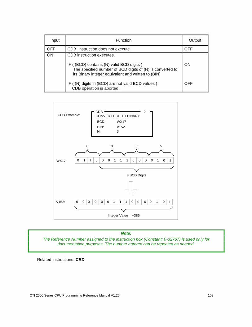
CTI 2500 Series CPU Programming Reference Manual V1.26 109
Input Function Output
OFF CDB instruction does not execute OFF
ON
CDB instruction executes. IF ( (BCD) contains (N) valid BCD digits ) The specified number of BCD digits of (N) is converted to its Binary integer equivalent and written to (BIN) IF ( (N) digits in (BCD) are not valid BCD values ) CDB operation is aborted.
ON OFF
0 0 0 0 0 0 0 0 1
836 5
11 1 101 1
CDB
BCD: WX17
2
CONVERT BCD TO BINARY
BIN: V152
N: 3
3 BCD Digits
WX17:
V152: 0 0 0 00 0 1 0 1
Integer Value = +385
0 0 0 1 1 1 0
CDB Example:
Note:
The Reference Number assigned to the instruction box (Constant: 0-32767) is used only for documentation purposes. The number entered can be repeated as needed.
Related instructions: CBD
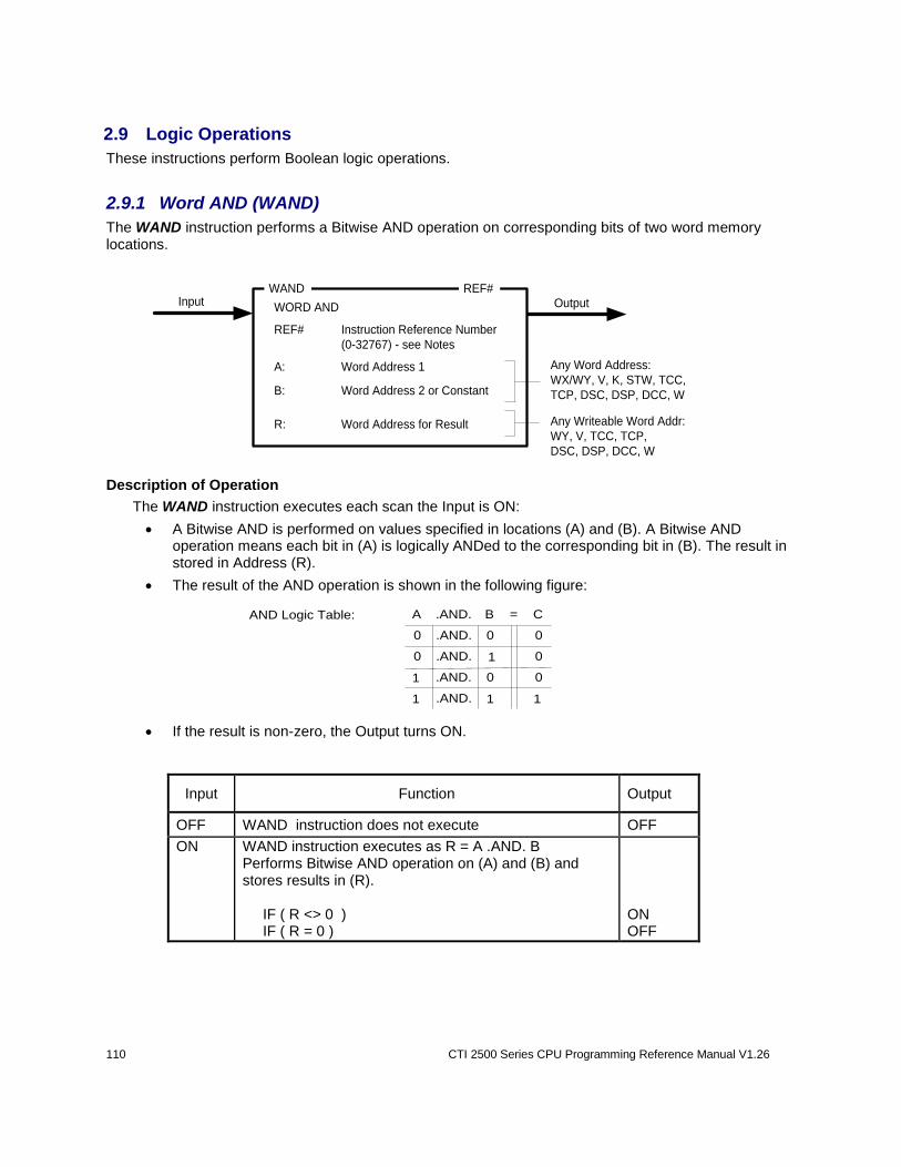
110 CTI 2500 Series CPU Programming Reference Manual V1.26
2.9 Logic Operations
These instructions perform Boolean logic operations.
2.9.1 Word AND (WAND)
The WAND instruction performs a Bitwise AND operation on corresponding bits of two word memory locations.
WAND
OutputInput
A: Word Address 1
REF#
REF# Instruction Reference Number
(0-32767) - see Notes
WORD AND
Any Writeable Word Addr:
WY, V, TCC, TCP,
DSC, DSP, DCC, W
B: Word Address 2 or Constant
R: Word Address for Result
Any Word Address:
WX/WY, V, K, STW, TCC,
TCP, DSC, DSP, DCC, W
Description of Operation
The WAND instruction executes each scan the Input is ON:
A Bitwise AND is performed on values specified in locations (A) and (B). A Bitwise AND operation means each bit in (A) is logically ANDed to the corresponding bit in (B). The result in stored in Address (R).
The result of the AND operation is shown in the following figure:
A B C.AND. =
.AND.
.AND.
.AND.
.AND.
1
1
1 1 1
0 0 0
0
00
0
AND Logic Table:
If the result is non-zero, the Output turns ON.
Input Function Output
OFF WAND instruction does not execute OFF
ON
WAND instruction executes as R = A .AND. B Performs Bitwise AND operation on (A) and (B) and stores results in (R). IF ( R <> 0 ) IF ( R = 0 )
ON OFF
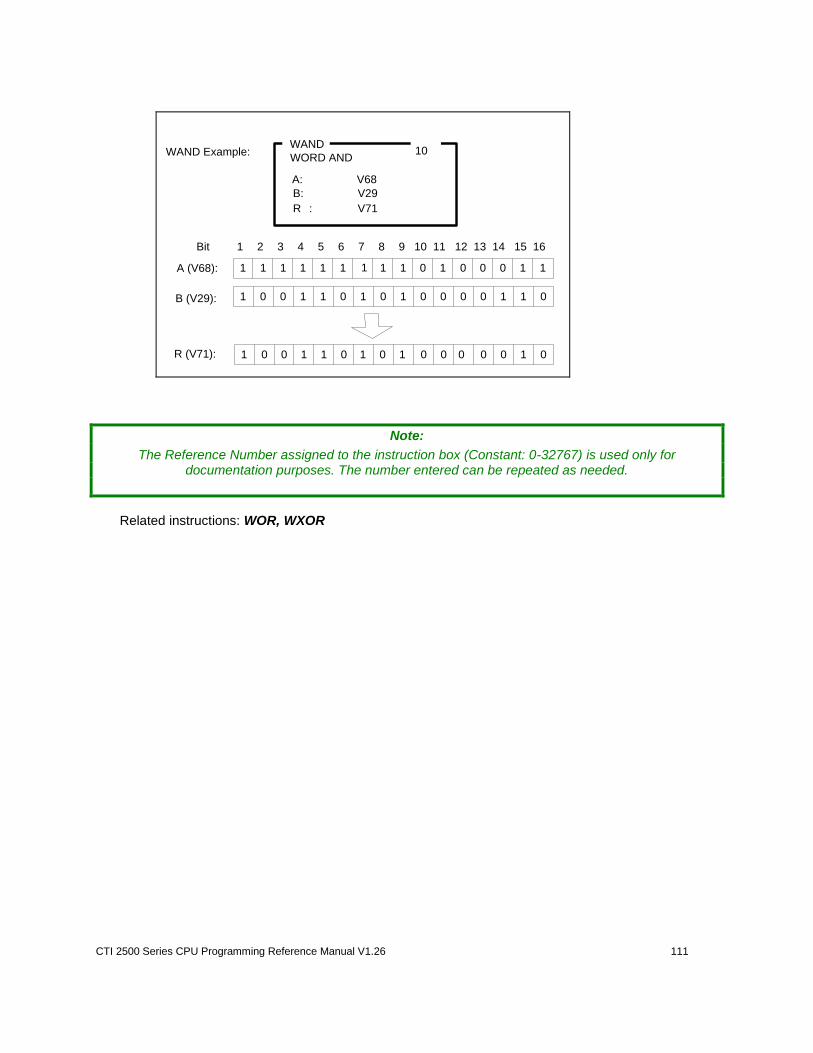
CTI 2500 Series CPU Programming Reference Manual V1.26 111
WAND
A: V68
10 WORD AND
B: V29
R : V71
1 1 1 1 0 1 0 1 10A (V68): 11 1 1 1 0
1 1 1 0 0 0 0 1 01B (V29): 0 0 1 0 1 0
1 1 1 0 0 0 0 1 00R (V71): 0 0 1 0 1 0
WAND Example:
Bit 1 2 3 4 5 6 7 8 9 10 11 12 13 14 15 16
Note:
The Reference Number assigned to the instruction box (Constant: 0-32767) is used only for documentation purposes. The number entered can be repeated as needed.
Related instructions: WOR, WXOR
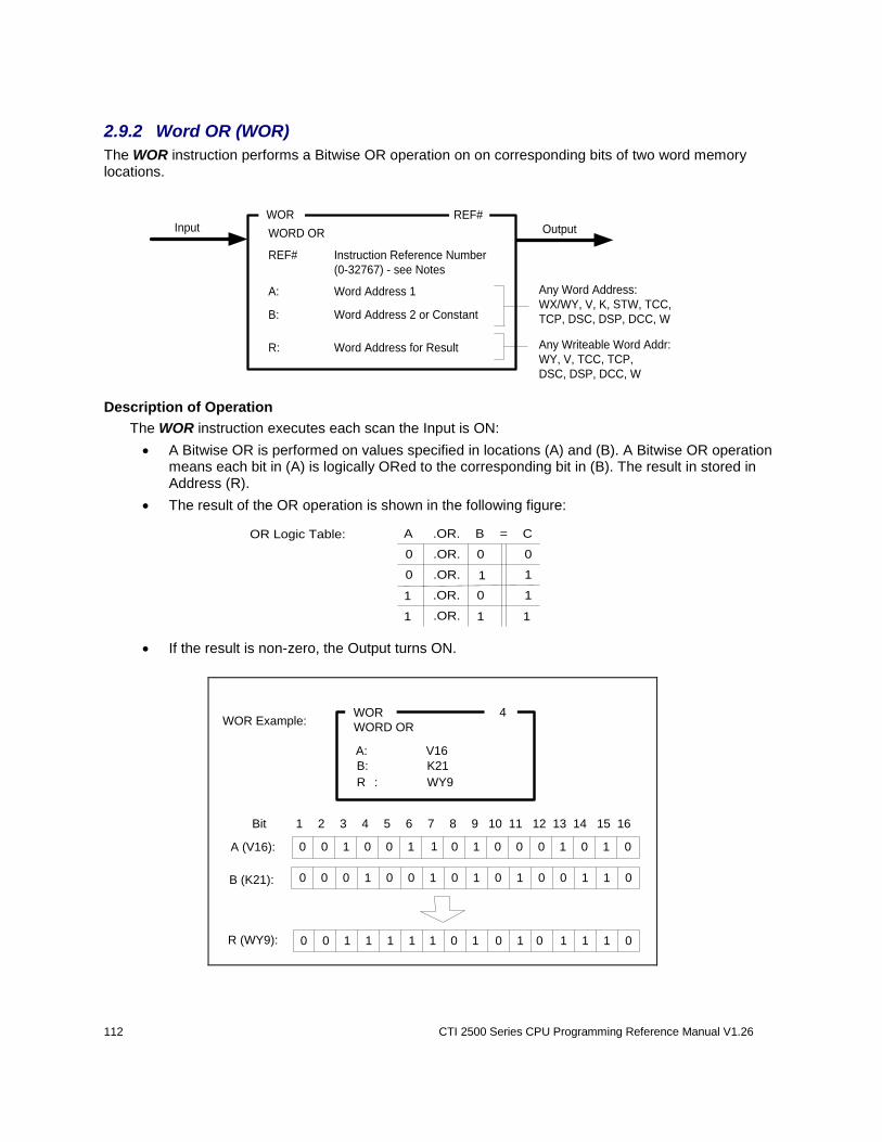
112 CTI 2500 Series CPU Programming Reference Manual V1.26
2.9.2 Word OR (WOR)
The WOR instruction performs a Bitwise OR operation on on corresponding bits of two word memory locations.
WOR
OutputInput
A: Word Address 1
REF#
REF# Instruction Reference Number
(0-32767) - see Notes
WORD OR
Any Writeable Word Addr:
WY, V, TCC, TCP,
DSC, DSP, DCC, W
B: Word Address 2 or Constant
R: Word Address for Result
Any Word Address:
WX/WY, V, K, STW, TCC,
TCP, DSC, DSP, DCC, W
Description of Operation
The WOR instruction executes each scan the Input is ON:
A Bitwise OR is performed on values specified in locations (A) and (B). A Bitwise OR operation means each bit in (A) is logically ORed to the corresponding bit in (B). The result in stored in Address (R).
The result of the OR operation is shown in the following figure:
A B C .OR. =
.OR.
.OR.
.OR.
.OR.
1
1
1 1 1
0 0 0
1
10
0
OR Logic Table:
If the result is non-zero, the Output turns ON.
WOR
A: V16
4
WORD OR
B: K21
R : WY9
0 0 0 1 0 0 1 1 00A (V16): 10 1 0 1 0
0 1 0 0 0 1 0 1 01B (K21): 0 0 1 0 1 0
0 1 1 1 0 1 1 1 01R (WY9): 0 1 1 0 1 0
WOR Example:
Bit 1 2 3 4 5 6 7 8 9 10 11 12 13 14 15 16

CTI 2500 Series CPU Programming Reference Manual V1.26 113
Input Function Output
OFF WOR instruction does not execute OFF
ON
WOR instruction executes as R = A .OR. B Performs Bitwise OR operation on (A) and (B) and stores results in (R). IF ( R <> 0 ) IF ( R = 0 )
ON OFF
Note:
The Reference Number assigned to the instruction box (Constant: 0-32767) is used only for documentation purposes. The number entered can be repeated as needed.
Related instructions: WAND, WXOR
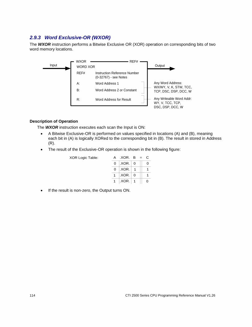
114 CTI 2500 Series CPU Programming Reference Manual V1.26
2.9.3 Word Exclusive-OR (WXOR)
The WXOR instruction performs a Bitwise Exclusive OR (XOR) operation on corresponding bits of two word memory locations.
WXOR
OutputInput
A: Word Address 1
REF#
REF# Instruction Reference Number
(0-32767) - see Notes
WORD XOR
Any Writeable Word Addr:
WY, V, TCC, TCP,
DSC, DSP, DCC, W
B: Word Address 2 or Constant
R: Word Address for Result
Any Word Address:
WX/WY, V, K, STW, TCC,
TCP, DSC, DSP, DCC, W
Description of Operation
The WXOR instruction executes each scan the Input is ON:
A Bitwise Exclusive-OR is performed on values specified in locations (A) and (B), meaning each bit in (A) is logically XORed to the corresponding bit in (B). The result in stored in Address (R).
The result of the Exclusive-OR operation is shown in the following figure:
A B C.XOR. =
.XOR.
.XOR.
.XOR.
.XOR.
1
1
1 1 0
0 0 0
1
10
0
XOR Logic Table:
If the result is non-zero, the Output turns ON.
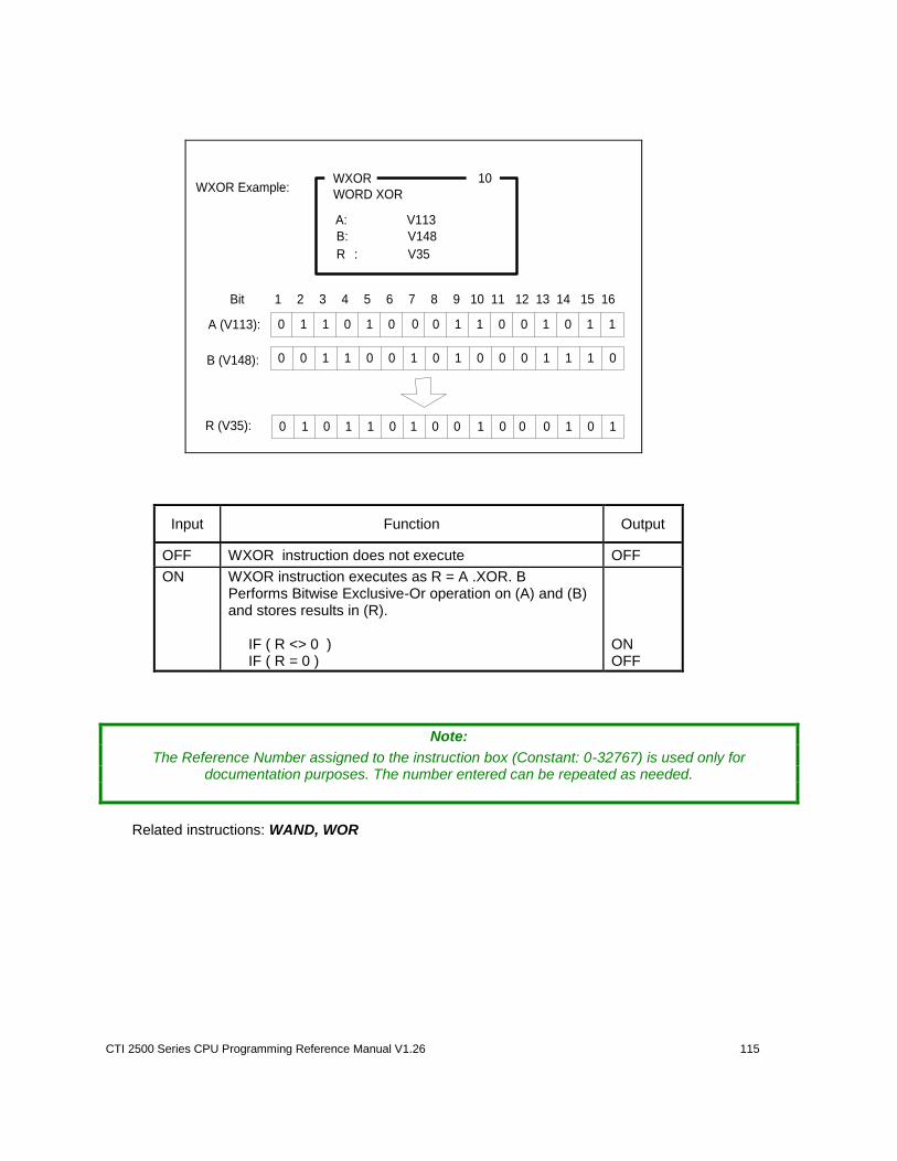
CTI 2500 Series CPU Programming Reference Manual V1.26 115
WXOR
A: V113
10
WORD XOR
B: V148
R : V35
0 0 1 0 1 0 1 1 10A (V113): 01 1 0 1 0
0 1 0 0 0 0 1 1 01B (V148): 0 1 1 0 1 0
0 1 1 0 1 0 0 0 11R (V35): 1 0 1 0 0 0
WXOR Example:
Bit 1 2 3 4 5 6 7 8 9 10 11 12 13 14 15 16
Input Function Output
OFF WXOR instruction does not execute OFF
ON
WXOR instruction executes as R = A .XOR. B Performs Bitwise Exclusive-Or operation on (A) and (B) and stores results in (R). IF ( R <> 0 ) IF ( R = 0 )
ON OFF
Note:
The Reference Number assigned to the instruction box (Constant: 0-32767) is used only for documentation purposes. The number entered can be repeated as needed.
Related instructions: WAND, WOR
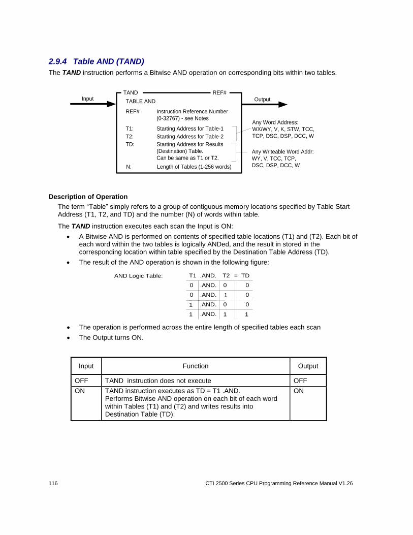
116 CTI 2500 Series CPU Programming Reference Manual V1.26
2.9.4 Table AND (TAND)
The TAND instruction performs a Bitwise AND operation on corresponding bits within two tables.
TAND
OutputInput
T1: Starting Address for Table-1
REF#
REF# Instruction Reference Number
(0-32767) - see Notes
TABLE AND
Any Writeable Word Addr:
WY, V, TCC, TCP,
DSC, DSP, DCC, W
T2: Starting Address for Table-2
N: Length of Tables (1-256 words)
Any Word Address:
WX/WY, V, K, STW, TCC,
TCP, DSC, DSP, DCC, W
TD: Starting Address for Results
(Destination) Table.
Can be same as T1 or T2.
Description of Operation
The term “Table” simply refers to a group of contiguous memory locations specified by Table Start Address (T1, T2, and TD) and the number (N) of words within table.
The TAND instruction executes each scan the Input is ON:
A Bitwise AND is performed on contents of specified table locations (T1) and (T2). Each bit of each word within the two tables is logically ANDed, and the result in stored in the corresponding location within table specified by the Destination Table Address (TD).
The result of the AND operation is shown in the following figure:
T1 T2 TD.AND. =
.AND.
.AND.
.AND.
.AND.
1
1
1 1 1
0 0 0
0
00
0
AND Logic Table:
The operation is performed across the entire length of specified tables each scan
The Output turns ON.
Input Function Output
OFF TAND instruction does not execute OFF
ON
TAND instruction executes as TD = T1 .AND. Performs Bitwise AND operation on each bit of each word within Tables (T1) and (T2) and writes results into Destination Table (TD).
ON
CTI 2500 Series CPU Programming Reference Manual V1.26 117
Note:
The Reference Number assigned to the instruction box (Constant: 0-32767) is used only for documentation purposes. The number entered can be repeated as needed.
Related instructions: WAND, TCPL, TOR, TXOR, WTTA
118 CTI 2500 Series CPU Programming Reference Manual V1.26
2.9.5 Table OR (TOR)
The TOR instruction performs a Bitwise OR operation on corresponding bits within two tables.
TOR
OutputInput
T1: Starting Address for Table-1
REF#
REF# Instruction Reference Number
(0-32767) - see Notes
TABLE OR
Any Writeable Word Addr:
WY, V, TCC, TCP,
DSC, DSP, DCC, W
T2: Starting Address for Table-2
N: Length of Tables (1-256 words)
Any Word Address:
WX/WY, V, K, STW, TCC,
TCP, DSC, DSP, DCC, W
TD: Starting Address for Results
(Destination) Table.
Can be same as T1 or T2.
Description of Operation
The term “Table” simply refers to a group of contiguous memory locations specified by the Table Start Address (T1, T2, and TD) and the number (N) of words within table.
The TOR instruction executes each scan the Input is ON:
A Bitwise OR is performed on contents of specified table locations (T1) and (T2). Each bit of each word within the two tables is logically ORed, and the result in stored in the corresponding location within table specified by the Destination Table Address (TD).
The result of the OR operation is shown in the following figure:
A B C .OR. =
.OR.
.OR.
.OR.
.OR.
1
1
1 1 1
0 0 0
1
10
0
OR Logic Table:
The operation is performed across the entire length of specified tables each scan
The Output turns ON.
Input Function Output
OFF TOR instruction does not execute OFF
ON
TOR instruction executes as TD = T1 .OR. T2 Performs Bitwise OR operation on each bit of each word within Tables (T1) and (T2) and writes results into Destination Table (TD).
ON
CTI 2500 Series CPU Programming Reference Manual V1.26 119
Note:
The Reference Number assigned to the instruction box (Constant: 0-32767) is used only for documentation purposes. The number entered can be repeated as needed.
Related instructions: WOR, TAND, TCPL, TXOR

120 CTI 2500 Series CPU Programming Reference Manual V1.26
2.9.6 Table Exclusive-OR (TXOR)
The TXOR instruction performs a Bitwise Exclusive-OR (XOR) operation on corresponding bits within two tables.
TXOR
OutputInput
T1: Starting Address for Table-1
REF#
REF# Instruction Reference Number
(0-32767) - see Notes
TABLE XOR
Any Writeable Word Addr:
WY, V, TCC, TCP,
DSC, DSP, DCC, W
T2: Starting Address for Table-2
N: Length of Tables (1-256 words)
Any Word Address:
WX/WY, V, K, STW, TCC,
TCP, DSC, DSP, DCC, W
TD: Starting Address for Results
(Destination) Table.
Can be same as T1 or T2.
Description of Operation
The term “Table” simply refers to a group of contiguous memory locations specified by the Table Start Address (T1, T2, and TD) and the number (N) of words within table.
The TXOR instruction executes each scan the Input is ON:
A Bitwise Exclusive-OR is performed on contents of specified table locations (T1) and (T2). Each bit of each word within the two tables is logically XORed, and the result in stored in the corresponding location within table specified by the Destination Table Address (TD).
The result of the XOR operation is shown in the following figure:
A B C.XOR. =
.XOR.
.XOR.
.XOR.
.XOR.
1
1
1 1 0
0 0 0
1
10
0
XOR Logic Table:
The operation is performed across the entire length of specified tables each scan
The Output turns ON.
Input Function Output
OFF TXOR instruction does not execute OFF
ON
TXOR instruction executes as TD = T1 .XOR. T2 Performs Bitwise Exclusive-OR operation on each bit of each word within Tables (T1) and (T2) and writes results into Destination Table (TD).
ON

CTI 2500 Series CPU Programming Reference Manual V1.26 121
Note:
The Reference Number assigned to the instruction box (Constant: 0-32767) is used only for documentation purposes. The number entered can be repeated as needed.
Related instructions: WXOR, TAND, TCPL, TOR
122 CTI 2500 Series CPU Programming Reference Manual V1.26
2.9.7 Table Complement (TCPL)
The TCPL instruction performs a logical NOT operation (inverts the state) of all bits within a table.
TCPL
OutputInput
TS: Starting Address for Source Table
REF#
REF# Instruction Reference Number
(0-32767) - see Notes
TABLE COMPLEMENT
Any Writeable Word Addr:
WY, V, TCC, TCP,
DSC, DSP, DCC, W
TD: Starting Address for Results
(Destination) Table.
Can be same as TS
N: Length of Tables (1-256 words)
Any Word Address:
WX/WY, V, K, STW, TCC,
TCP, DSC, DSP, DCC, W
Description of Operation
The term “Table” simply refers to a group of contiguous memory locations specified by the Table Start Address (TS and TD) and the number (N) of words within table.
The TCPL instruction executes each scan the Input is ON
A Logical NOT is performed on all bits contained in Source Table (TS). Each bit of each word within the table is inverted, and the result in stored in the corresponding location within the Destination Table (TD).
Each bit with state of zero (OFF) is inverted to one (ON). Each bit with state of one (ON) is inverted to zero (OFF).
The operation is performed across the entire length of specified table each scan
The Output turns ON.
Input Function Output
OFF TCPL instruction does not execute OFF
ON
TCPL instruction executes as TD = NOT(TS). Inverts each bit of each word within Source Table (TS) and writes results into Destination Table (TD).
ON
Note:
The Reference Number assigned to the instruction box (Constant: 0-32767) is used only for documentation purposes. The number entered can be repeated as needed.
Related instructions: NOT, TAND, TOR, TXOR

CTI 2500 Series CPU Programming Reference Manual V1.26 123
2.9.8 Word-to-Table AND (WTTA)
The WTTA instruction performs a Bitwise AND operation on corresponding bits of a word memory location and specified word position within a table.
WTTA
OutputEnable
IN: Address for Table Index (V, W)
REF#
REF# Instruction Reference Number
(0-32767) - see Notes
WORD-TO-TABLE AND
Any Writeable Word Addr:
WY, V, TCC, TCP,
DSC, DSP, DCC, W
TS: Starting Addr for Source Table
N: Length of Tables (1-256 words)
Any Word Address:
WX/WY, V, K, STW, TCC,
TCP, DSC, DSP, DCC, W
TD: Starting Addr for Dest Table
Can be same as TS.
WS: Starting Addr for Source Word
Reset
Description of Operation
The term “Table” simply refers to a group of contiguous memory locations specified by the Table Start Address (TS and TD) and the number (N) of words within table.
1. When Reset Input is OFF, the WTTA instruction box is reset. The value in the Table Index Address (IN) is set to zero. The Output is turned OFF.
2. When Reset Input is ON but Enable Input is OFF, the WTTA instruction does not execute. The Table Index holds its current value unless changed by other logic in RLL program or HMI. The Output is turned OFF.
3. When both Reset and Enable Inputs are ON, the WTTA instruction executes.
4. The value of Table Index (IN) designates the position within the Source Table (TS) for the word to be used in the WTTA operation. The Table Index represents an offset into the table. A value of 0 indicates the first word position in table, and the Table Index range is from 0 to N-1 where N specifies the number of words in table.
If Table Index is valid (between 0 and N-1, inclusive), WTTA instruction executes.
If Table Index is invalid, the operation aborts and Output turns OFF.
5. A Bitwise AND is performed on contents of Word Address (WS) and word position in Source Table (TS) designated by value of Table Index (IN). Each bit in Source Word is logically ANDed to the corresponding bit in word within table. The result is written to the word position within the Destination Table (TD) matching the Table Index (IN).
6. The Table Index value is incremented by one position.
7. If the Table Index is still in valid range (IN <= N-1), the Output turns ON. Otherwise, the Output turns OFF.
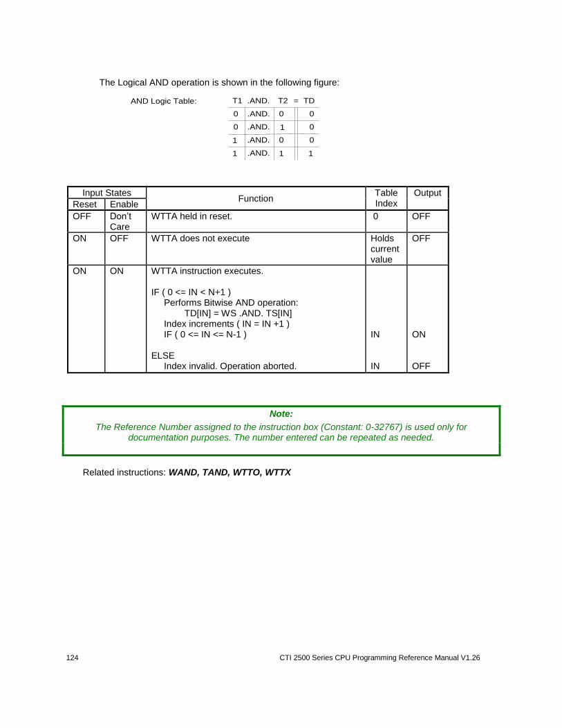
124 CTI 2500 Series CPU Programming Reference Manual V1.26
The Logical AND operation is shown in the following figure:
T1 T2 TD.AND. =
.AND.
.AND.
.AND.
.AND.
1
1
1 1 1
0 0 0
0
00
0
AND Logic Table:
Input States Function
Table Index
Output
Reset Enable
OFF Don’t Care
WTTA held in reset.
0 OFF
ON OFF WTTA does not execute Holds current value
OFF
ON ON WTTA instruction executes. IF ( 0 <= IN < N+1 ) Performs Bitwise AND operation: TD[IN] = WS .AND. TS[IN] Index increments ( IN = IN +1 ) IF ( 0 <= IN <= N-1 ) ELSE Index invalid. Operation aborted.
IN IN
ON OFF
Note:
The Reference Number assigned to the instruction box (Constant: 0-32767) is used only for documentation purposes. The number entered can be repeated as needed.
Related instructions: WAND, TAND, WTTO, WTTX
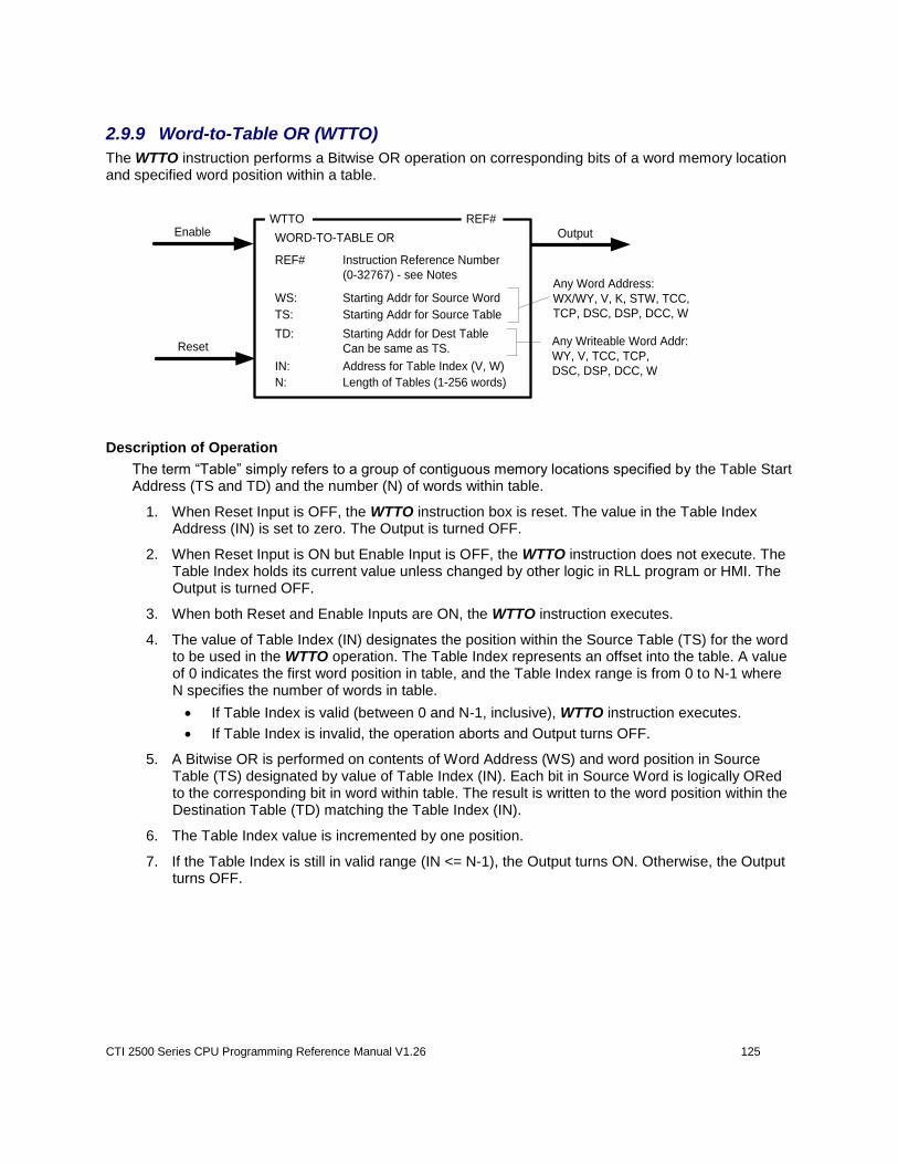
CTI 2500 Series CPU Programming Reference Manual V1.26 125
2.9.9 Word-to-Table OR (WTTO)
The WTTO instruction performs a Bitwise OR operation on corresponding bits of a word memory location and specified word position within a table.
WTTO
OutputEnable
IN: Address for Table Index (V, W)
REF#
REF# Instruction Reference Number
(0-32767) - see Notes
WORD-TO-TABLE OR
Any Writeable Word Addr:
WY, V, TCC, TCP,
DSC, DSP, DCC, W
TS: Starting Addr for Source Table
N: Length of Tables (1-256 words)
Any Word Address:
WX/WY, V, K, STW, TCC,
TCP, DSC, DSP, DCC, W
TD: Starting Addr for Dest Table
Can be same as TS.
WS: Starting Addr for Source Word
Reset
Description of Operation
The term “Table” simply refers to a group of contiguous memory locations specified by the Table Start Address (TS and TD) and the number (N) of words within table.
1. When Reset Input is OFF, the WTTO instruction box is reset. The value in the Table Index Address (IN) is set to zero. The Output is turned OFF.
2. When Reset Input is ON but Enable Input is OFF, the WTTO instruction does not execute. The Table Index holds its current value unless changed by other logic in RLL program or HMI. The Output is turned OFF.
3. When both Reset and Enable Inputs are ON, the WTTO instruction executes.
4. The value of Table Index (IN) designates the position within the Source Table (TS) for the word to be used in the WTTO operation. The Table Index represents an offset into the table. A value of 0 indicates the first word position in table, and the Table Index range is from 0 to N-1 where N specifies the number of words in table.
If Table Index is valid (between 0 and N-1, inclusive), WTTO instruction executes.
If Table Index is invalid, the operation aborts and Output turns OFF.
5. A Bitwise OR is performed on contents of Word Address (WS) and word position in Source Table (TS) designated by value of Table Index (IN). Each bit in Source Word is logically ORed to the corresponding bit in word within table. The result is written to the word position within the Destination Table (TD) matching the Table Index (IN).
6. The Table Index value is incremented by one position.
7. If the Table Index is still in valid range (IN <= N-1), the Output turns ON. Otherwise, the Output turns OFF.

126 CTI 2500 Series CPU Programming Reference Manual V1.26
The Logical OR operation is shown in the following figure:
A B C .OR. =
.OR.
.OR.
.OR.
.OR.
1
1
1 1 1
0 0 0
1
10
0
OR Logic Table:
Input States Function
Table Index
Output
Reset Enable
OFF Don’t Care
WTTO held in reset.
0 OFF
ON OFF WTTO does not execute Holds current value
OFF
ON ON WTTO instruction executes. IF ( 0 <= IN < N+1 ) Performs Bitwise OR operation: TD[IN] = WS .OR. TS[IN] Index increments ( IN = IN +1 ) IF ( 0 <= IN <= N-1 ) ELSE Index invalid. Operation aborted.
IN IN
ON OFF
Note:
The Reference Number assigned to the instruction box (Constant: 0-32767) is used only for documentation purposes. The number entered can be repeated as needed.
Related instructions: WOR, TOR, WTTA, WTTX
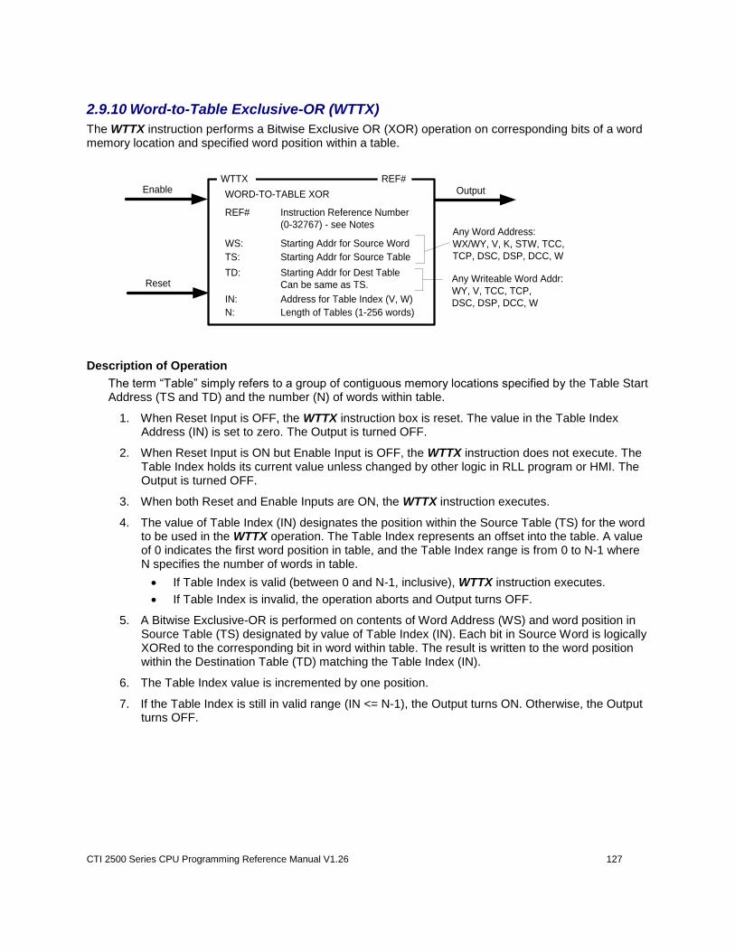
CTI 2500 Series CPU Programming Reference Manual V1.26 127
2.9.10 Word-to-Table Exclusive-OR (WTTX)
The WTTX instruction performs a Bitwise Exclusive OR (XOR) operation on corresponding bits of a word memory location and specified word position within a table.
WTTX
OutputEnable
IN: Address for Table Index (V, W)
REF#
REF# Instruction Reference Number
(0-32767) - see Notes
WORD-TO-TABLE XOR
Any Writeable Word Addr:
WY, V, TCC, TCP,
DSC, DSP, DCC, W
TS: Starting Addr for Source Table
N: Length of Tables (1-256 words)
Any Word Address:
WX/WY, V, K, STW, TCC,
TCP, DSC, DSP, DCC, W
TD: Starting Addr for Dest Table
Can be same as TS.
WS: Starting Addr for Source Word
Reset
Description of Operation
The term “Table” simply refers to a group of contiguous memory locations specified by the Table Start Address (TS and TD) and the number (N) of words within table.
1. When Reset Input is OFF, the WTTX instruction box is reset. The value in the Table Index Address (IN) is set to zero. The Output is turned OFF.
2. When Reset Input is ON but Enable Input is OFF, the WTTX instruction does not execute. The Table Index holds its current value unless changed by other logic in RLL program or HMI. The Output is turned OFF.
3. When both Reset and Enable Inputs are ON, the WTTX instruction executes.
4. The value of Table Index (IN) designates the position within the Source Table (TS) for the word to be used in the WTTX operation. The Table Index represents an offset into the table. A value of 0 indicates the first word position in table, and the Table Index range is from 0 to N-1 where N specifies the number of words in table.
If Table Index is valid (between 0 and N-1, inclusive), WTTX instruction executes.
If Table Index is invalid, the operation aborts and Output turns OFF.
5. A Bitwise Exclusive-OR is performed on contents of Word Address (WS) and word position in Source Table (TS) designated by value of Table Index (IN). Each bit in Source Word is logically XORed to the corresponding bit in word within table. The result is written to the word position within the Destination Table (TD) matching the Table Index (IN).
6. The Table Index value is incremented by one position.
7. If the Table Index is still in valid range (IN <= N-1), the Output turns ON. Otherwise, the Output turns OFF.
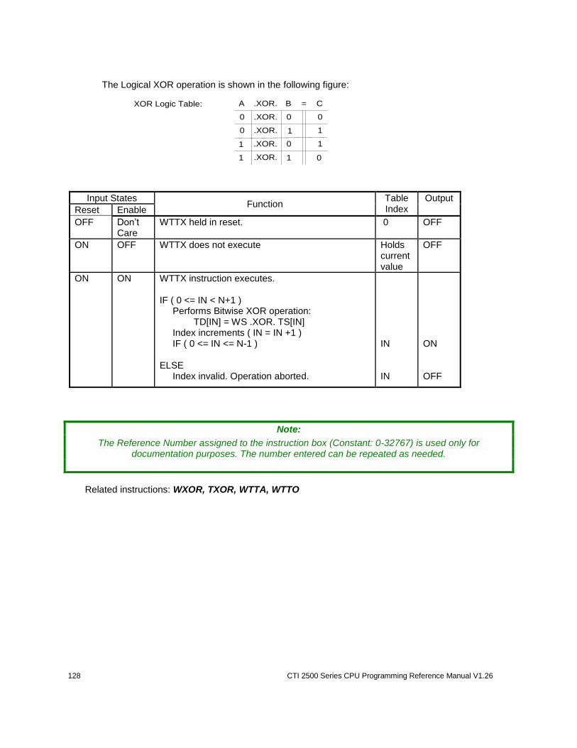
128 CTI 2500 Series CPU Programming Reference Manual V1.26
The Logical XOR operation is shown in the following figure:
A B C.XOR. =
.XOR.
.XOR.
.XOR.
.XOR.
1
1
1 1 0
0 0 0
1
10
0
XOR Logic Table:
Input States Function
Table Index
Output
Reset Enable
OFF Don’t Care
WTTX held in reset.
0 OFF
ON OFF WTTX does not execute Holds current value
OFF
ON ON WTTX instruction executes. IF ( 0 <= IN < N+1 ) Performs Bitwise XOR operation: TD[IN] = WS .XOR. TS[IN] Index increments ( IN = IN +1 ) IF ( 0 <= IN <= N-1 ) ELSE Index invalid. Operation aborted.
IN IN
ON OFF
Note:
The Reference Number assigned to the instruction box (Constant: 0-32767) is used only for documentation purposes. The number entered can be repeated as needed.
Related instructions: WXOR, TXOR, WTTA, WTTO
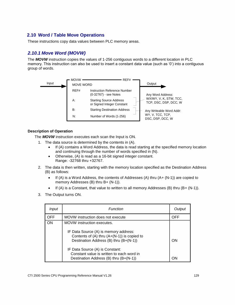
CTI 2500 Series CPU Programming Reference Manual V1.26 129
2.10 Word / Table Move Operations
These instructions copy data values between PLC memory areas.
2.10.1 Move Word (MOVW)
The MOVW instruction copies the values of 1-256 contiguous words to a different location in PLC memory. This instruction can also be used to insert a constant data value (such as ‘0’) into a contiguous group of words.
MOVW
OutputInput
A: Starting Source Address
or Signed Integer Constant
REF#
REF# Instruction Reference Number
(0-32767) - see Notes
MOVE WORD
Any Writeable Word Addr:
WY, V, TCC, TCP,
DSC, DSP, DCC, W
B: Starting Destination Address
N: Number of Words (1-256)
Any Word Address:
WX/WY, V, K, STW, TCC,
TCP, DSC, DSP, DCC, W
Description of Operation
The MOVW instruction executes each scan the Input is ON.
1. The data source is determined by the contents in (A).
If (A) contains a Word Address, the data is read starting at the specified memory location and continuing through the number of words specified in (N).
Otherwise, (A) is read as a 16-bit signed integer constant. Range: -32768 thru +32767.
2. The data is then written, starting with the memory location specified as the Destination Address (B) as follows:
If (A) is a Word Address, the contents of Addresses (A) thru (A+ (N-1)) are copied to memory Addresses (B) thru B+ (N-1)).
If (A) is a Constant, that value to written to all memory Addresses (B) thru (B+ (N-1)).
3. The Output turns ON.
Input Function Output
OFF MOVW instruction does not execute OFF
ON
MOVW instruction executes. IF Data Source (A) is memory address: Contents of (A) thru (A+(N-1)) is copied to Destination Address (B) thru (B+(N-1)) IF Data Source (A) is Constant: Constant value is written to each word in Destination Address (B) thru (B+(N-1))
ON ON

130 CTI 2500 Series CPU Programming Reference Manual V1.26
0 0 1 0 1 1 0 0 01K43: 1 1 0 1 0 1
0 0 0 1 1 0 1 0 00K41: 00 0 0 1 0
K42: 0 1 0 0 0 0 1 0 000 0 1 0 1 0
A: K41
26
MOVE WORD
B: TCP12
N: 3
0 0 0 1 1 0 1 0 00TCP12: 0 0 0 0 1 0
MOVW Example:
0 1 0 0 0 0 1 0 00TCP13: 0 0 1 0 1 0
0 0 1 0 1 1 0 0 01TCP14: 1 1 0 1 0 1
MOVW
Note:
The Reference Number assigned to the instruction box (Constant: 0-32767) is used only for documentation purposes. The number entered can be repeated as needed.
Related instructions: MWI, MOVE, MWIR, MIRW, MWFT, MWTT, WTOT, TTOW
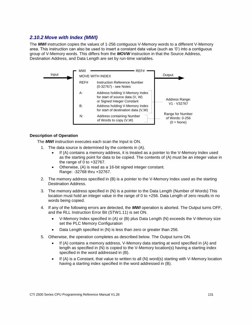
CTI 2500 Series CPU Programming Reference Manual V1.26 131
2.10.2 Move with Index (MWI)
The MWI instruction copies the values of 1-256 contiguous V-Memory words to a different V-Memory area. This instruction can also be used to insert a constant data value (such as ‘0’) into a contiguous group of V-Memory words. This differs from the MOVW instruction in that the Source Address, Destination Address, and Data Length are set by run-time variables.
MWI
OutputInput
A: Address holding V-Memory Index
for start of source data (V, W)
or Signed Integer Constant
REF#
REF# Instruction Reference Number
(0-32767) - see Notes
MOVE WITH INDEX
B: Address holding V-Memory Index
for start of destination data (V,W)
N: Address containing Number
of Words to copy (V,W)
Address Range:
V1 - V32767
Range for Number
of Words: 0-256
(0 = None)
Description of Operation
The MWI instruction executes each scan the Input is ON.
1. The data source is determined by the contents in (A).
If (A) contains a memory address, it is treated as a pointer to the V-Memory Index used as the starting point for data to be copied. The contents of (A) must be an integer value in the range of 0 to +32767.
Otherwise, (A) is read as a 16-bit signed integer constant. Range: -32768 thru +32767.
2. The memory address specified in (B) is a pointer to the V-Memory Index used as the starting Destination Address.
3. The memory address specified in (N) is a pointer to the Data Length (Number of Words) This location must hold an integer value in the range of 0 to +256. Data Length of zero results in no words being copied.
4. If any of the following errors are detected, the MWI operation is aborted. The Output turns OFF, and the RLL Instruction Error Bit (STW1.11) is set ON.
V-Memory Index specified in (A) or (B) plus Data Length (N) exceeds the V-Memory size set the PLC Memory Configuration
Data Length specified in (N) is less than zero or greater than 256.
5. Otherwise, the operation completes as described below. The Output turns ON.
If (A) contains a memory address, V-Memory data starting at word specified in (A) and length as specified in (N) is copied to the V-Memory location(s) having a starting index specified in the word addressed in (B).
If (A) is a Constant, that value to written to all (N) word(s) starting with V-Memory location having a starting index specified in the word addressed in (B).
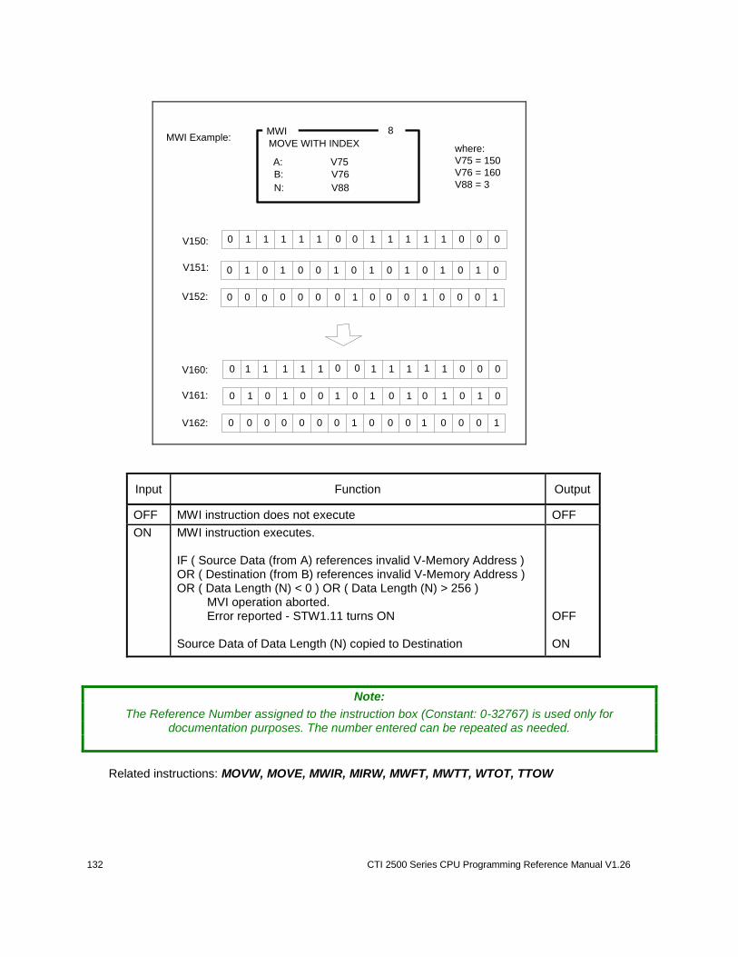
132 CTI 2500 Series CPU Programming Reference Manual V1.26
0 0 0 0 0 0 0 0 10V152: 0 0 0 1 0 1
0 1 1 1 1 1 1 0 00V150: 01 1 0 1 1
V151: 0 1 0 0 0 1 1 1 001 0 1 0 1 0
A: V75
8
MOVE WITH INDEX
B: V76
N: V88
0 1 1 1 1 1 1 0 00V160: 1 1 0 0 1 1
MWI Example:
0 1 0 0 0 1 1 1 00V161: 1 0 1 0 1 0
0 0 0 0 0 0 0 0 10V162: 0 0 0 1 0 1
MWI
where:
V75 = 150
V76 = 160
V88 = 3
Input Function Output
OFF MWI instruction does not execute OFF
ON
MWI instruction executes. IF ( Source Data (from A) references invalid V-Memory Address ) OR ( Destination (from B) references invalid V-Memory Address ) OR ( Data Length (N) < 0 ) OR ( Data Length (N) > 256 ) MVI operation aborted. Error reported - STW1.11 turns ON Source Data of Data Length (N) copied to Destination
OFF ON
Note:
The Reference Number assigned to the instruction box (Constant: 0-32767) is used only for documentation purposes. The number entered can be repeated as needed.
Related instructions: MOVW, MOVE, MWIR, MIRW, MWFT, MWTT, WTOT, TTOW
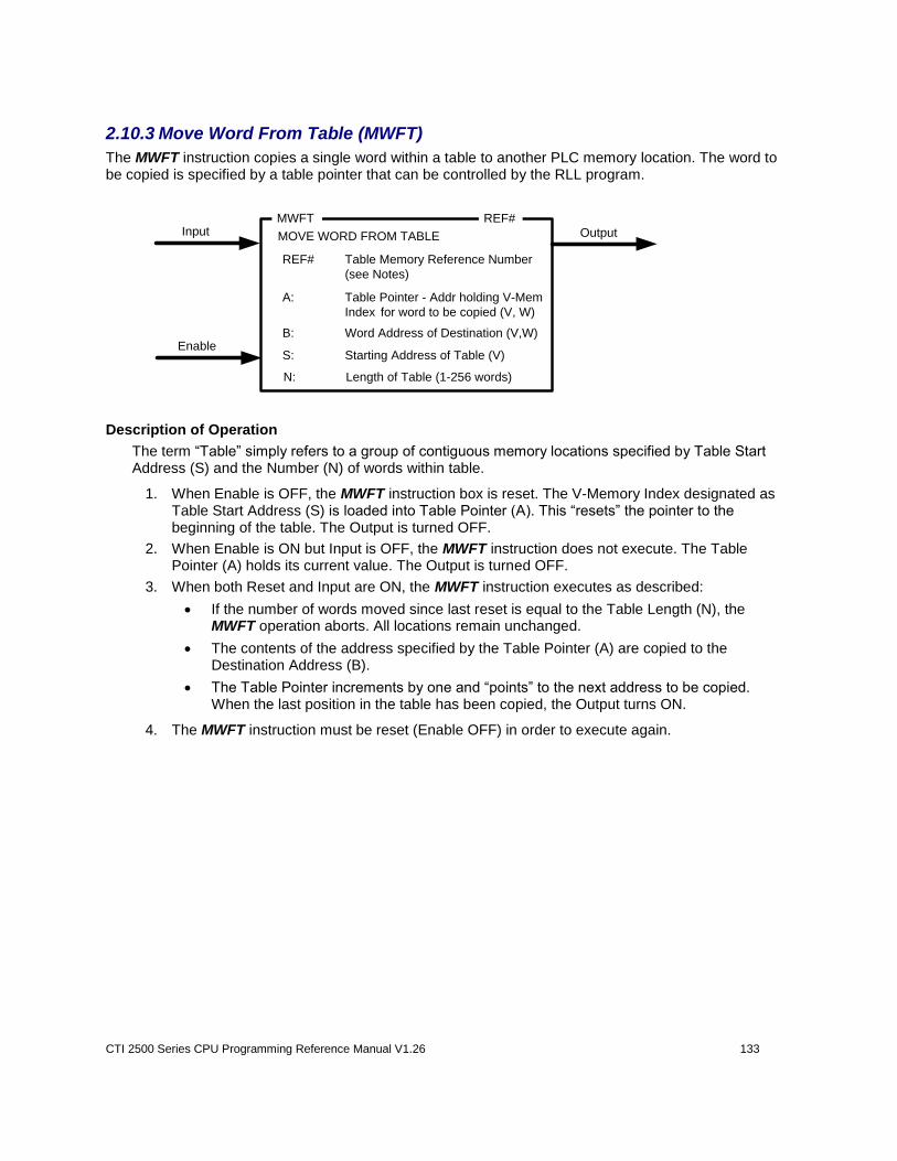
CTI 2500 Series CPU Programming Reference Manual V1.26 133
2.10.3 Move Word From Table (MWFT)
The MWFT instruction copies a single word within a table to another PLC memory location. The word to be copied is specified by a table pointer that can be controlled by the RLL program.
MWFT
OutputInput
S: Starting Address of Table (V)
REF#
REF# Table Memory Reference Number
(see Notes)
MOVE WORD FROM TABLE
N: Length of Table (1-256 words)
B: Word Address of Destination (V,W)
A: Table Pointer - Addr holding V-Mem
Index for word to be copied (V, W)
Enable
Description of Operation
The term “Table” simply refers to a group of contiguous memory locations specified by Table Start Address (S) and the Number (N) of words within table.
1. When Enable is OFF, the MWFT instruction box is reset. The V-Memory Index designated as Table Start Address (S) is loaded into Table Pointer (A). This “resets” the pointer to the beginning of the table. The Output is turned OFF.
2. When Enable is ON but Input is OFF, the MWFT instruction does not execute. The Table Pointer (A) holds its current value. The Output is turned OFF.
3. When both Reset and Input are ON, the MWFT instruction executes as described:
If the number of words moved since last reset is equal to the Table Length (N), the MWFT operation aborts. All locations remain unchanged.
The contents of the address specified by the Table Pointer (A) are copied to the Destination Address (B).
The Table Pointer increments by one and “points” to the next address to be copied. When the last position in the table has been copied, the Output turns ON.
4. The MWFT instruction must be reset (Enable OFF) in order to execute again.
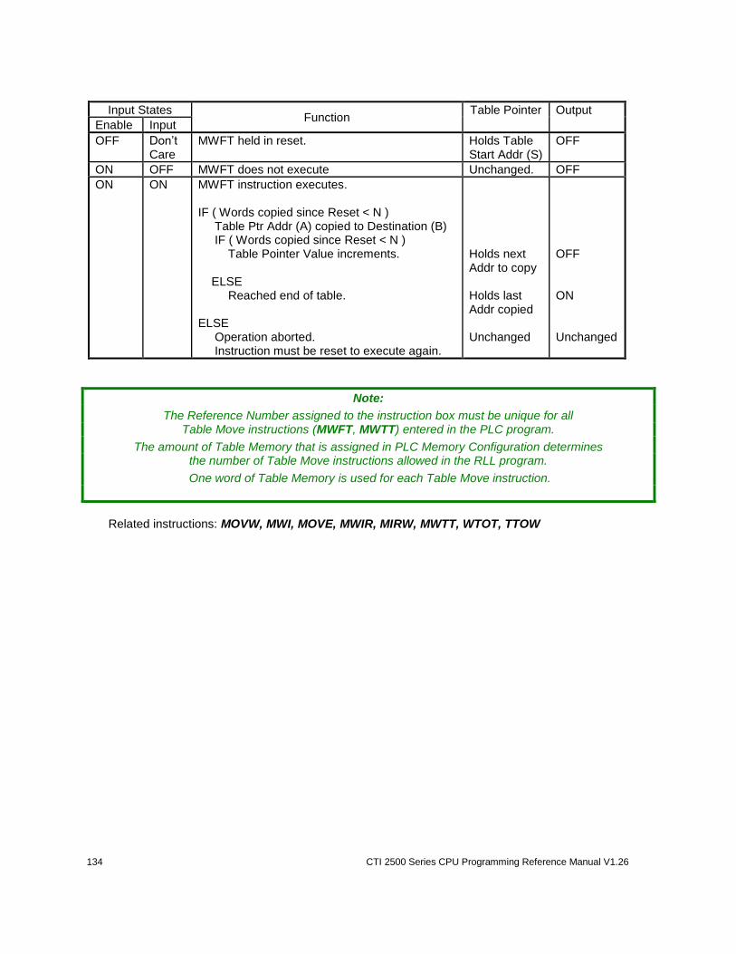
134 CTI 2500 Series CPU Programming Reference Manual V1.26
Input States Function
Table Pointer Output
Enable Input
OFF Don’t Care
MWFT held in reset.
Holds Table Start Addr (S)
OFF
ON OFF MWFT does not execute Unchanged. OFF
ON ON MWFT instruction executes. IF ( Words copied since Reset < N ) Table Ptr Addr (A) copied to Destination (B) IF ( Words copied since Reset < N ) Table Pointer Value increments. ELSE Reached end of table. ELSE Operation aborted. Instruction must be reset to execute again.
Holds next Addr to copy Holds last Addr copied Unchanged
OFF ON Unchanged
Note:
The Reference Number assigned to the instruction box must be unique for all Table Move instructions (MWFT, MWTT) entered in the PLC program.
The amount of Table Memory that is assigned in PLC Memory Configuration determines the number of Table Move instructions allowed in the RLL program.
One word of Table Memory is used for each Table Move instruction.
Related instructions: MOVW, MWI, MOVE, MWIR, MIRW, MWTT, WTOT, TTOW
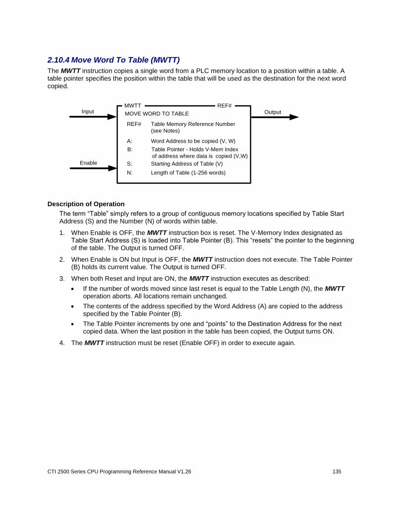
CTI 2500 Series CPU Programming Reference Manual V1.26 135
2.10.4 Move Word To Table (MWTT)
The MWTT instruction copies a single word from a PLC memory location to a position within a table. A table pointer specifies the position within the table that will be used as the destination for the next word copied.
MWTT
OutputInput
S: Starting Address of Table (V)
REF#
REF# Table Memory Reference Number
(see Notes)
MOVE WORD TO TABLE
N: Length of Table (1-256 words)
B: Table Pointer - Holds V-Mem Index
of address where data is copied (V,W)
A: Word Address to be copied (V, W)
Enable
Description of Operation
The term “Table” simply refers to a group of contiguous memory locations specified by Table Start Address (S) and the Number (N) of words within table.
1. When Enable is OFF, the MWTT instruction box is reset. The V-Memory Index designated as Table Start Address (S) is loaded into Table Pointer (B). This “resets” the pointer to the beginning of the table. The Output is turned OFF.
2. When Enable is ON but Input is OFF, the MWTT instruction does not execute. The Table Pointer (B) holds its current value. The Output is turned OFF.
3. When both Reset and Input are ON, the MWTT instruction executes as described:
If the number of words moved since last reset is equal to the Table Length (N), the MWTT operation aborts. All locations remain unchanged.
The contents of the address specified by the Word Address (A) are copied to the address specified by the Table Pointer (B).
The Table Pointer increments by one and “points” to the Destination Address for the next copied data. When the last position in the table has been copied, the Output turns ON.
4. The MWTT instruction must be reset (Enable OFF) in order to execute again.
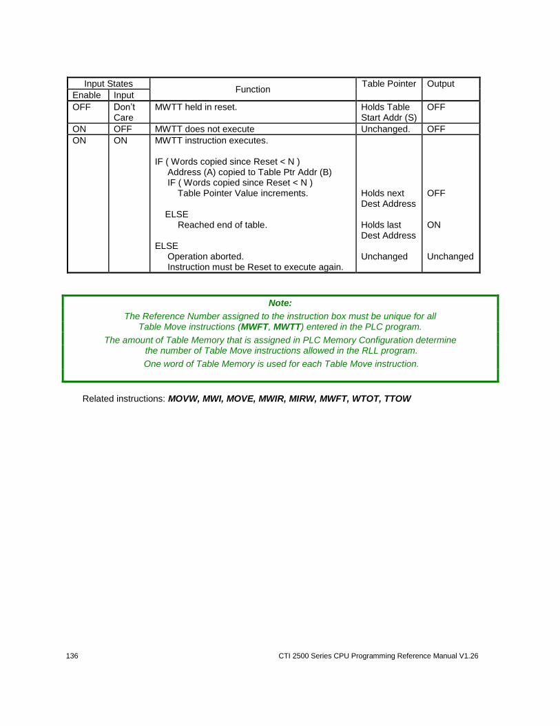
136 CTI 2500 Series CPU Programming Reference Manual V1.26
Input States Function
Table Pointer Output
Enable Input
OFF Don’t Care
MWTT held in reset.
Holds Table Start Addr (S)
OFF
ON OFF MWTT does not execute Unchanged. OFF
ON ON MWTT instruction executes. IF ( Words copied since Reset < N ) Address (A) copied to Table Ptr Addr (B) IF ( Words copied since Reset < N ) Table Pointer Value increments. ELSE Reached end of table. ELSE Operation aborted. Instruction must be Reset to execute again.
Holds next Dest Address Holds last Dest Address Unchanged
OFF ON Unchanged
Note:
The Reference Number assigned to the instruction box must be unique for all Table Move instructions (MWFT, MWTT) entered in the PLC program.
The amount of Table Memory that is assigned in PLC Memory Configuration determine the number of Table Move instructions allowed in the RLL program.
One word of Table Memory is used for each Table Move instruction.
Related instructions: MOVW, MWI, MOVE, MWIR, MIRW, MWFT, WTOT, TTOW
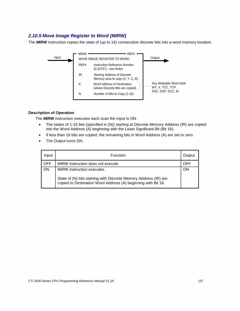
CTI 2500 Series CPU Programming Reference Manual V1.26 137
2.10.5 Move Image Register to Word (MIRW)
The MIRW instruction copies the state of (up to 16) consecutive discrete bits into a word memory location.
MIRW
OutputInput
IR: Starting Address of Discrete
Memory area to copy (X, Y, C, B)
REF#
REF# Instruction Reference Number
(0-32767) - see Notes
MOVE IMAGE REGISTER TO WORD
A: Word Address of Destination
(where Discrete Bits are copied)
N: Number of Bits to Copy (1-16)
Any Writeable Word Addr:
WY, V, TCC, TCP,
DSC, DSP, DCC, W
Description of Operation
The MIRW instruction executes each scan the Input is ON.
The states of 1-16 bits (specified in (N)) starting at Discrete Memory Address (IR) are copied into the Word Address (A) beginning with the Least Significant Bit (Bit 16).
If less than 16 bits are copied, the remaining bits in Word Address (A) are set to zero.
The Output turns ON.
Input Function Output
OFF MIRW instruction does not execute OFF
ON
MIRW instruction executes. State of (N) bits starting with Discrete Memory Address (IR) are copied to Destination Word Address (A) beginning with Bit 16.
ON
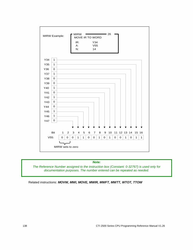
138 CTI 2500 Series CPU Programming Reference Manual V1.26
IR: Y34
26
MOVE IR TO WORD
A: V55
N: 14
MIRW Example:
1
1
0
0
0
0
1
0
1
0
1
0
1
1
Y34
Y35
Y36
Y37
Y38
Y39
Y40
Y41
Y42
Y43
Y44
Y45
Y46
Y47
V55: 0 1 1 0 1 0 1 1 100 0 1 0 00
Bit 1 2 3 4 5 6 7 8 9 10 11 12 13 14 15 16
MIRW sets to zero
MIRW
Note:
The Reference Number assigned to the instruction box (Constant: 0-32767) is used only for documentation purposes. The number entered can be repeated as needed.
Related instructions: MOVW, MWI, MOVE, MWIR, MWFT, MWTT, WTOT, TTOW
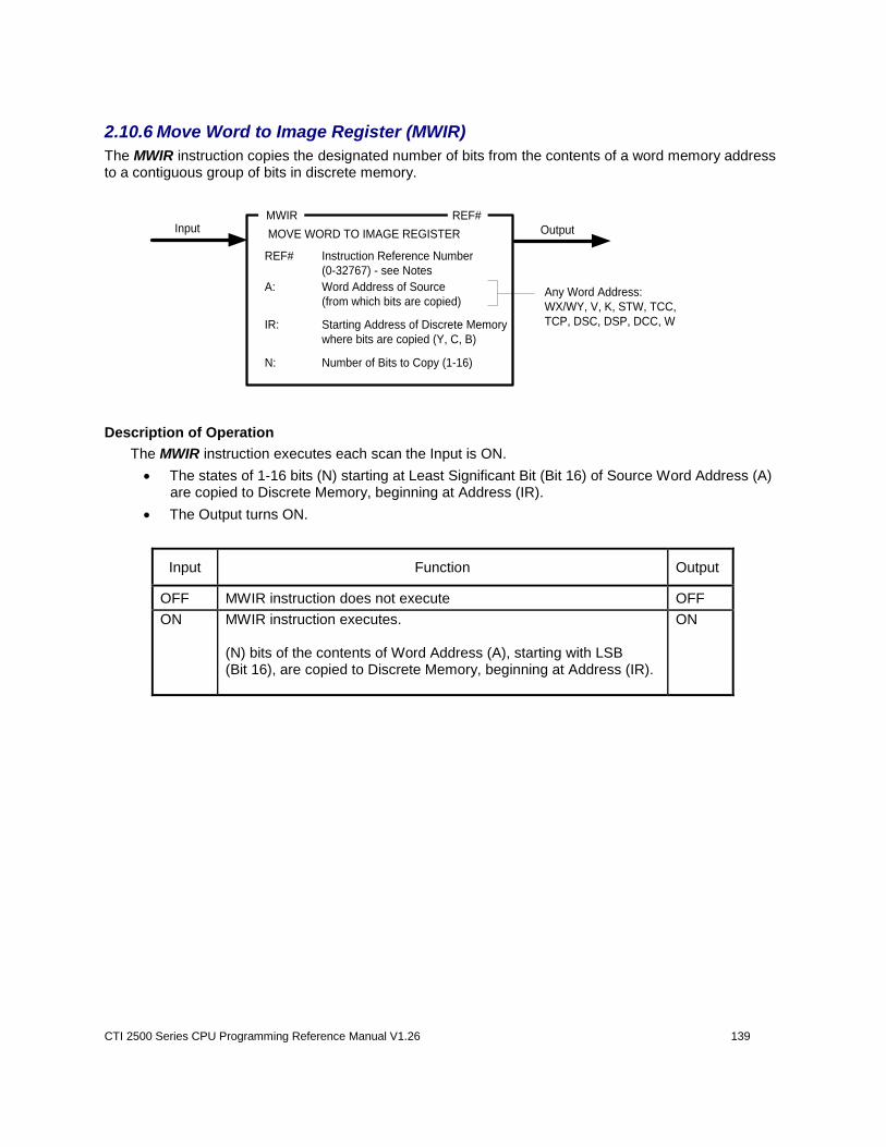
CTI 2500 Series CPU Programming Reference Manual V1.26 139
2.10.6 Move Word to Image Register (MWIR)
The MWIR instruction copies the designated number of bits from the contents of a word memory address to a contiguous group of bits in discrete memory.
MWIR
OutputInput
IR: Starting Address of Discrete Memory
where bits are copied (Y, C, B)
REF#
REF# Instruction Reference Number
(0-32767) - see Notes
MOVE WORD TO IMAGE REGISTER
A: Word Address of Source
(from which bits are copied)
N: Number of Bits to Copy (1-16)
Any Word Address:
WX/WY, V, K, STW, TCC,
TCP, DSC, DSP, DCC, W
Description of Operation
The MWIR instruction executes each scan the Input is ON.
The states of 1-16 bits (N) starting at Least Significant Bit (Bit 16) of Source Word Address (A) are copied to Discrete Memory, beginning at Address (IR).
The Output turns ON.
Input Function Output
OFF MWIR instruction does not execute OFF
ON
MWIR instruction executes. (N) bits of the contents of Word Address (A), starting with LSB (Bit 16), are copied to Discrete Memory, beginning at Address (IR).
ON
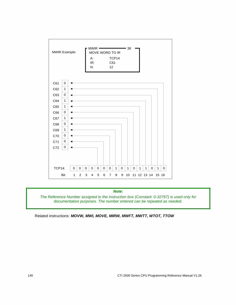
140 CTI 2500 Series CPU Programming Reference Manual V1.26
IR: C61
38
MOVE WORD TO IR
A: TCP14
N: 12
MWIR Example:
1
0
1
0
1
0
0
0
1
0
1
0
C61
C62
C63
C64
C65
C66
C67
C68
C69
C70
C71
C72
TCP14: 0 0 0 0 1 0 1 1 000 0 1 0 10
Bit 1 2 3 4 5 6 7 8 9 10 11 12 13 14 15 16
MWIR
Note:
The Reference Number assigned to the instruction box (Constant: 0-32767) is used only for documentation purposes. The number entered can be repeated as needed.
Related instructions: MOVW, MWI, MOVE, MIRW, MWFT, MWTT, WTOT, TTOW
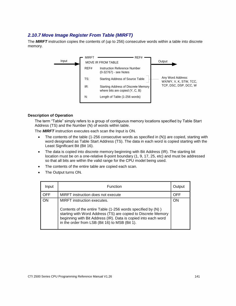
CTI 2500 Series CPU Programming Reference Manual V1.26 141
2.10.7 Move Image Register From Table (MIRFT)
The MIRFT instruction copies the contents of (up to 256) consecutive words within a table into discrete memory.
MIRFT
OutputInput
IR: Starting Address of Discrete Memory
where bits are copied (Y, C, B)
REF#
REF# Instruction Reference Number
(0-32767) - see Notes
MOVE IR FROM TABLE
TS: Starting Address of Source Table
N: Length of Table (1-256 words)
Any Word Address:
WX/WY, V, K, STW, TCC,
TCP, DSC, DSP, DCC, W
Description of Operation
The term “Table” simply refers to a group of contiguous memory locations specified by Table Start Address (TS) and the Number (N) of words within table.
The MIRFT instruction executes each scan the Input is ON.
The contents of the table (1-256 consecutive words as specified in (N)) are copied, starting with word designated as Table Start Address (TS). The data in each word is copied starting with the Least Significant Bit (Bit 16).
The data is copied into discrete memory beginning with Bit Address (IR). The starting bit location must be on a one-relative 8-point boundary (1, 9, 17, 25, etc) and must be addressed so that all bits are within the valid range for the CPU model being used.
The contents of the entire table are copied each scan.
The Output turns ON.
Input Function Output
OFF MIRFT instruction does not execute OFF
ON
MIRFT instruction executes. Contents of the entire Table (1-256 words specified by (N) ) starting with Word Address (TS) are copied to Discrete Memory beginning with Bit Address (IR). Data is copied into each word in the order from LSB (Bit 16) to MSB (Bit 1).
ON
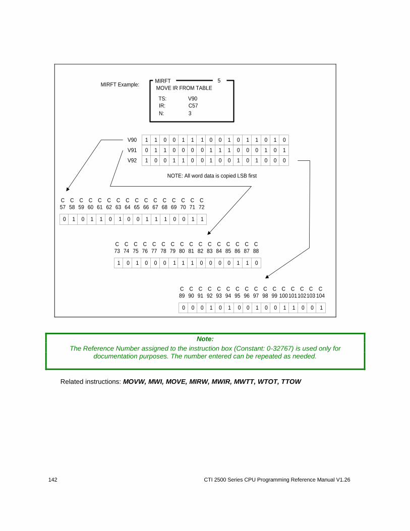
142 CTI 2500 Series CPU Programming Reference Manual V1.26
NOTE: All word data is copied LSB first
MIRFT Example:
TS: V90
5
MOVE IR FROM TABLE
IR: C57
N: 3
MIRFT
C
65
C
66
C
67
C
68
C
69
C
70
C
71
C
72
C
57
C
58
C
59
C
60
C
61
C
62
C
63
C
64
0 1 1 0 1 1 0 1 1011 0 0 0 1
C
97
C
98
C
99
C
100
C
101
C
102
C
103
C
104
C
89
C
90
C
91
C
92
C
93
C
94
C
95
C
96
0 1 0 1 0 0 1 0 1000 0 0 1 1
C
81
C
82
C
83
C
84
C
85
C
86
C
87
C
88
C
73
C
74
C
75
C
76
C
77
C
78
C
79
C
80
1 0 0 0 0 0 0 1 0110 1 1 1 0
1 0 1 1 1 0 1 1 0011 0 0 0 1
0 0 0 0 1 0 0 0 1101 1 1 1 0
1 1 1 0 0 1 1 0 0000 0 1 0 0
V90
V91
V92
Note:
The Reference Number assigned to the instruction box (Constant: 0-32767) is used only for documentation purposes. The number entered can be repeated as needed.
Related instructions: MOVW, MWI, MOVE, MIRW, MWIR, MWTT, WTOT, TTOW
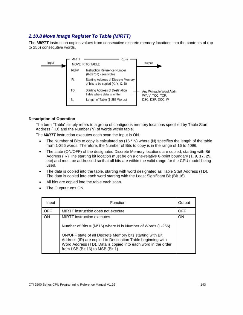
CTI 2500 Series CPU Programming Reference Manual V1.26 143
2.10.8 Move Image Register To Table (MIRTT)
The MIRTT instruction copies values from consecutive discrete memory locations into the contents of (up to 256) consecutive words.
MIRTT
OutputInput
IR: Starting Address of Discrete Memory
of bits to be copied (X, Y, C, B)
REF#
REF# Instruction Reference Number
(0-32767) - see Notes
MOVE IR TO TABLE
TD: Starting Address of Destination
Table where data is written
N: Length of Table (1-256 Words)
Any Writeable Word Addr:
WY, V, TCC, TCP,
DSC, DSP, DCC, W
Description of Operation
The term “Table” simply refers to a group of contiguous memory locations specified by Table Start Address (TD) and the Number (N) of words within table.
The MIRTT instruction executes each scan the Input is ON.
The Number of Bits to copy is calculated as (16 * N) where (N) specifies the length of the table from 1-256 words. Therefore, the Number of Bits to copy is in the range of 16 to 4096.
The state (ON/OFF) of the designated Discrete Memory locations are copied, starting with Bit Address (IR) The starting bit location must be on a one-relative 8-point boundary (1, 9, 17, 25, etc) and must be addressed so that all bits are within the valid range for the CPU model being used.
The data is copied into the table, starting with word designated as Table Start Address (TD). The data is copied into each word starting with the Least Significant Bit (Bit 16).
All bits are copied into the table each scan.
The Output turns ON.
Input Function Output
OFF MIRTT instruction does not execute OFF
ON
MIRTT instruction executes. Number of Bits = (N*16) where N is Number of Words (1-256) ON/OFF state of all Discrete Memory bits starting with Bit Address (IR) are copied to Destination Table beginning with Word Address (TD). Data is copied into each word in the order from LSB (Bit 16) to MSB (Bit 1).
ON
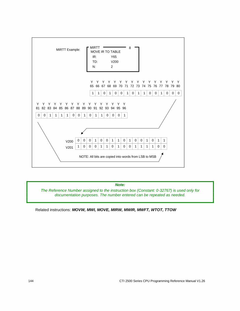
144 CTI 2500 Series CPU Programming Reference Manual V1.26
NOTE: All bits are copied into words from LSB to MSB
V200
V201
Y
73
Y
74
Y
75
Y
76
Y
77
Y
78
Y
79
Y
80
Y
65
Y
66
Y
67
Y
68
Y
69
Y
70
Y
71
Y
72
1 1 0 0 1 0 1 0 0011 0 0 1 0
Y
89
Y
90
Y
91
Y
92
Y
93
Y
94
Y
95
Y
96
Y
81
Y
82
Y
83
Y
84
Y
85
Y
86
Y
87
Y
88
0 1 1 1 0 1 0 0 1000 1 0 1 1
MIRTT Example:
TD: V200
8MOVE IR TO TABLE
IR: Y65
N: 2
MIRTT
0 1 0 0 1 0 1 1 1010 0 1 0 0
1 0 1 1 0 1 1 0 0100 0 1 0 1
Note:
The Reference Number assigned to the instruction box (Constant: 0-32767) is used only for documentation purposes. The number entered can be repeated as needed.
Related instructions: MOVW, MWI, MOVE, MIRW, MWIR, MWFT, WTOT, TTOW
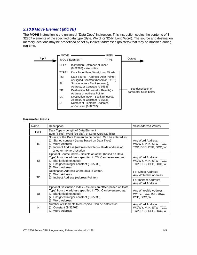
CTI 2500 Series CPU Programming Reference Manual V1.26 145
2.10.9 Move Element (MOVE)
The MOVE instruction is the universal “Data Copy” instruction. This instruction copies the contents of 1-32767 elements of the specified data type (Byte, Word, or 32-bit Long Word). The source and destination memory locations may be predefined or set by indirect addresses (pointers) that may be modified during run-time.
MOVE
OutputInput
TD: Destination Address (for Results) -
Address or Address Pointer
REF#
N: Number of Elements - Address
or Constant (1-32767)
TS: Data Source - Address, Addr Pointer,
or Signed Constant (based on TYPE)
REF# Instruction Reference Number
(0-32767) - see Notes
TYPE: Data Type (Byte, Word, Long Word)
SI: Source Index - Blank (unused),
Address, or Constant (0-65535)
DI: Destination Index - Blank (unused),
Address, or Constant (0-65535)
See description of
parameter fields below
MOVE ELEMENT TYPE
Parameter Fields
Name Description Valid Address Values
TYPE Data Type – Length of Data Element Byte (8 bits), Word (16 bits), or Long Word (32 bits)
TS
Source of the Data Element to be copied. Can be entered as: (1) Signed constant (range based on Data Type) (2) Word Address (3) Indirect Address (Address Pointer) – Holds address of another memory location
Any Word Address: WX/WY, V, K, STW, TCC, TCP, DSC, DSP, DCC, W
SI
Optional Source Index – Selects an offset (based on Data Type) from the address specified in TS. Can be entered as: (1) Blank (field not used) (2) Unsigned integer constant (0-65535) (3) Word Address
Any Word Address: WX/WY, V, K, STW, TCC, TCP, DSC, DSP, DCC, W
TD
Destination Address where data is written. (1) Word Address (2) Indirect Address (Address Pointer)
For Direct Address: Any Writeable Address
For Indirect Address: Any Word Address
DI
Optional Destination Index – Selects an offset (based on Data Type) from the address specified in TD. Can be entered as: (1) Blank (field not used) (2) Unsigned integer constant (0-65535) (3) Word Address
Any Writeable Address: WY, V, TCC, TCP, DSC, DSP, DCC, W
N
Number of Elements to be copied. Can be entered as: (1) Constant (1-32767) (2) Word Address
Any Word Address: WX/WY, V, K, STW, TCC, TCP, DSC, DSP, DCC, W
146 CTI 2500 Series CPU Programming Reference Manual V1.26
Entering Source Information
1. The (TS) field specifies the source of the Data Element to be copied by entering:
Signed Constant (range based on Data Type selected - Specified value is copied to each element in the Destination Table.
a) Byte – Range: -128 to +127 b) Word – Range: -32768 to +32767 c) Long Word – Range: -2147483648 to +2147483647
Word Address (any valid memory address) – Specifies the starting address in memory for data to be copied. The number of source elements (N) are read starting at this location and copied to the destination.
Indirect Address (Address Pointer) – Specified address holds the value of another memory location that is used as the starting address for data to be copied. An Address Pointer is a 32-bit value and is designated by inserting a “@” character as a prefix to the address, i.e., @V125 or @K20. The number of source elements (N) are read starting at this location and copied to the destination.
The LDA instruction can be used to load an address into a memory location.
2. The (SI) field designates an index (or relative offset) from the Start Address (TS) specified. When used, the actual starting location is Start Address (TS) plus Index (SI). The Source Index can be used with either Direct or Indirect Addresses through one of the following values:
Blank – No indexing performed and no entry is required
Constant Index – Range: 0 to 65535 (value of 0 results in no index)
Variable Index – Value of the Word Address entered is interpreted as an Unsigned Integer (0 to 65535) and used as relative offset from (TS).
Entering Destination Information
1. The (TD) field specifies the Destination Address for the Data Elements by entering:
Word Address (any writeable memory address) – Specifies the starting address in memory for the destination of the copied data. The number of elements (N) are written starting at this location.
Indirect Address (Address Pointer) – Specified address holds the value of another memory location that is used as the starting address for data to be written. An Address Pointer is a 32-bit value and is designated by inserting a “@” character as a prefix to the address, i.e., @V125 or @K20. The number of specified elements (N) are written starting at this location.
2. The (DI) field designates an index (or relative offset) from the Destination Address (TD) specified. When used, the actual starting location is Destination Address (TD) plus Index (DI). The Destination Index can be used with either Direct or Indirect Addresses through one of the following values:
Blank – No indexing performed and no entry is required
Constant Index – Range: 0 to 65535 (value of 0 results in no index)
Variable Index – Value of the Word Address entered is interpreted as an Unsigned Integer (0 to 65535) and used as relative offset from (TD).
If Source or Destination Address is specified as an Indirect Address with Index, the actual address is determined by first calculating the Indirect Address location and then indexing from that point.
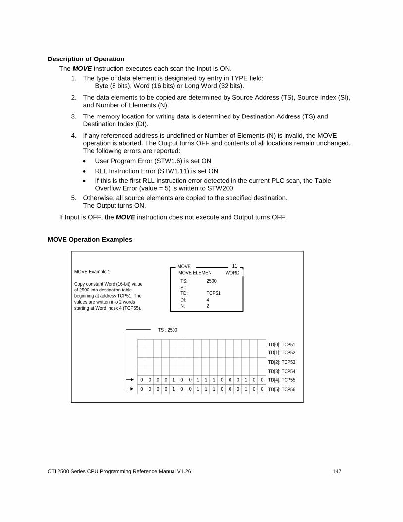
CTI 2500 Series CPU Programming Reference Manual V1.26 147
Description of Operation
The MOVE instruction executes each scan the Input is ON.
1. The type of data element is designated by entry in TYPE field: Byte (8 bits), Word (16 bits) or Long Word (32 bits).
2. The data elements to be copied are determined by Source Address (TS), Source Index (SI), and Number of Elements (N).
3. The memory location for writing data is determined by Destination Address (TS) and Destination Index (DI).
4. If any referenced address is undefined or Number of Elements (N) is invalid, the MOVE operation is aborted. The Output turns OFF and contents of all locations remain unchanged. The following errors are reported:
User Program Error (STW1.6) is set ON
RLL Instruction Error (STW1.11) is set ON
If this is the first RLL instruction error detected in the current PLC scan, the Table Overflow Error (value = 5) is written to STW200
5. Otherwise, all source elements are copied to the specified destination. The Output turns ON.
If Input is OFF, the MOVE instruction does not execute and Output turns OFF. MOVE Operation Examples
MOVE Example 1:
Copy constant Word (16-bit) value
of 2500 into destination table
beginning at address TCP51. The
values are written into 2 words
starting at Word index 4 (TCP55).
TS: 2500
11
MOVE ELEMENT
SI:
N: 2
MOVE
WORD
DI: 4
TD: TCP51
TD[0]: TCP51
TD[1]: TCP52
TD[2]: TCP53
0 0 1 0 1 0 0 0 0100 0 1 1 0
0 0 1 0 1 0 0 0 0100 0 1 1 0
TD[3]: TCP54
TD[4]: TCP55
TD[5]: TCP56
TS : 2500
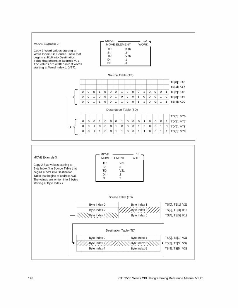
148 CTI 2500 Series CPU Programming Reference Manual V1.26
TS[0]: K16
TS[1]: K17
0 1 0 0 0 0 0 0 1000 0 1 0 1 TS[2]: K18
0 0 0 0 0 1 0 1 0010 1 0 0 0
0 1 0 0 0 1 0 1 1010 1 1 0 1
TS[3]: K19
TS[4]: K20
Source Table (TS)
MOVE Example 2:
Copy 3 Word values starting at
Word Index 2 in Source Table that
begins at K16 into Destination
Table that begins at address V76.
The values are written into 3 words
starting at Word Index 1 (V77).
TS: K16
12
MOVE ELEMENT
SI: 2
N: 3
MOVE
WORD
DI: 1
TD: V76
TD[0]: V76
0 1 0 0 0 0 0 0 1000 0 1 0 1 TD[1]: V77
0 0 0 0 0 1 0 1 0010 1 0 0 0
0 1 0 0 0 1 0 1 1010 1 1 0 1
TD[2]: V78
TD[3]: V79
Destination Table (TD)
MOVE Example 3:
Copy 2 Byte values starting at
Byte Index 3 in Source Table that
begins at V21 into Destination
Table that begins at address V31.
The values are written into 2 bytes
starting at Byte Index 2.
TS: V21
13
MOVE ELEMENT
SI: 3
N: 2
MOVE
BYTE
DI: 2
TD: V31
TS[0], TS[1]: V21
0 1 0 0 0 0 0 0 1000 0 1 0 1 TS[2], TS[3]: K18
0 0 0 0 0 1 0 1 0010 1 0 0 0 TS[4], TS[5]: K19
Source Table (TS)
Byte Index 1
Byte Index 2 Byte Index 3
Byte Index 4 Byte Index 5
Byte Index 0
TS[0], TS[1]: V31
0 1 0 0 0 0 0 0 1000 0 1 0 1 TS[2], TS[3]: V32
0 0 0 0 0 1 0 1 0010 1 0 0 0 TS[4], TS[5]: V33
Destination Table (TD)
Byte Index 1
Byte Index 2 Byte Index 3
Byte Index 4 Byte Index 5
Byte Index 0
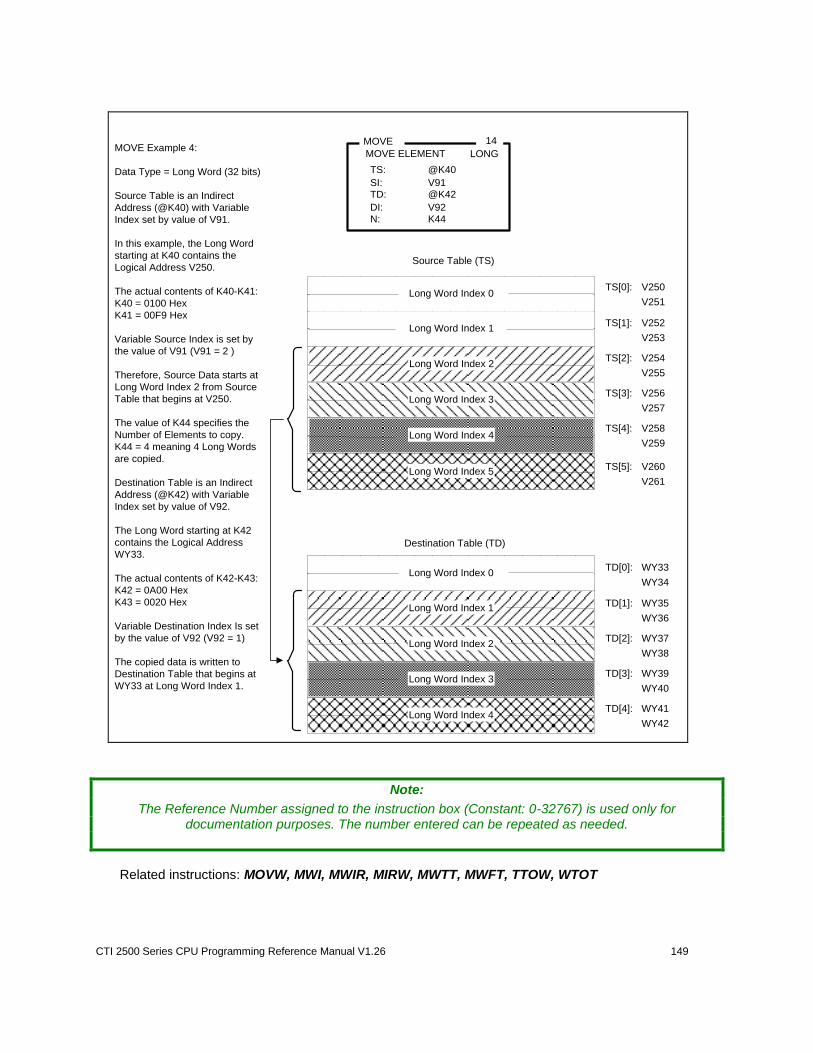
CTI 2500 Series CPU Programming Reference Manual V1.26 149
MOVE Example 4:
Data Type = Long Word (32 bits)
Source Table is an Indirect
Address (@K40) with Variable
Index set by value of V91.
In this example, the Long Word
starting at K40 contains the
Logical Address V250.
The actual contents of K40-K41:
K40 = 0100 Hex
K41 = 00F9 Hex
Variable Source Index is set by
the value of V91 (V91 = 2 )
Therefore, Source Data starts at
Long Word Index 2 from Source
Table that begins at V250.
The value of K44 specifies the
Number of Elements to copy.
K44 = 4 meaning 4 Long Words
are copied.
Destination Table is an Indirect
Address (@K42) with Variable
Index set by value of V92.
The Long Word starting at K42
contains the Logical Address
WY33.
The actual contents of K42-K43:
K42 = 0A00 Hex
K43 = 0020 Hex
Variable Destination Index Is set
by the value of V92 (V92 = 1)
The copied data is written to
Destination Table that begins at
WY33 at Long Word Index 1.
TS: @K40
14
MOVE ELEMENT
SI: V91
N: K44
MOVE
LONG
DI: V92
TD: @K42
Destination Table (TD)
TD[0]: WY33
WY340 1 0 0 0 0 0 0 1000 0 1 0 1
0 0 0 0 0 1 0 1 0010 1 0 0 0
Long Word Index 0
Long Word Index 1
Long Word Index 2
Long Word Index 3
Long Word Index 4
TD[1]: WY35
WY36
TD[2]: WY37
WY38
TD[3]: WY39
WY40
TD[4]: WY41
WY42
Source Table (TS)
TS[0]: V250
V2510 1 0 0 0 0 0 0 1000 0 1 0 1
0 0 0 0 0 1 0 1 0010 1 0 0 0
Long Word Index 0
Long Word Index 1
Long Word Index 2
Long Word Index 3
Long Word Index 4
TS[1]: V252
V253
TS[2]: V254
V255
TS[3]: V256
V257
TS[4]: V258
V259
Long Word Index 5TS[5]: V260
V261
Note:
The Reference Number assigned to the instruction box (Constant: 0-32767) is used only for documentation purposes. The number entered can be repeated as needed.
Related instructions: MOVW, MWI, MWIR, MIRW, MWTT, MWFT, TTOW, WTOT

150 CTI 2500 Series CPU Programming Reference Manual V1.26
2.10.10 Table To Word (TTOW)
The TTOW instruction copies a single word within a table to another PLC memory location. The word to be copied is specified by a table pointer that can be controlled by the RLL program. The TTOW function is very similar to MWFT, but this instruction supports additional memory types for data source and destination.
TTOW
OutputInput
TS: Starting Address of Source Table
REF#
TABLE TO WORD
N: Length of Table (1-256 words)
WD: Word Address of Destination
IN: Table Index Ptr - Memory location that
is used as Table Index (V, W)Enable
Any Writeable Word Addr:
WY, V, TCC, TCP,
DSC, DSP, DCC, W
Any Word Address:
WX/WY, V, K, STW, TCC,
TCP, DSC, DSP, DCC, W
REF# Instruction Reference Number
(0-32767) - see Notes
Description of Operation
The term “Table” simply refers to a group of contiguous memory locations specified by Table Start Address (TS) and the Number (N) of words within table.
1. When Reset Input is OFF, the TTOW instruction box is reset. A value of zero is loaded into the address specified as Table Index (IN). This “resets” the index to the beginning of the table. The Output is turned OFF.
2. When Reset Input is ON but Enable is OFF, the TTOW instruction does not execute. The Table Index (IN) address holds its current value unless modified by RLL instructions or HMI. The Output is turned OFF.
3. When both Reset and Enable Inputs are ON, the TTOW instruction executes as described:
If the value in the Table Index address (IN) does not correspond to a valid position offset within the table, the TTOW operation aborts and no copy is performed. The Table Index must be in the range of zero to (N-1) to be valid. A value of zero corresponds to the first word in table (TS) and (N-1) designates the last word in the table.
The contents of the word within the source table specified by Table Start Address (TS) and Index are copied to the Destination Address (WD). One word is copied each scan. The Table Index value increments by one and “points” to the next address to be copied. The Output turns ON each scan that a word is copied until the TTOW operation has completed.
If Table Index equals Table Length (indicating the last position in the table has been copied), the Output turns OFF
4. The TTOW instruction must be reset (Reset OFF) in order to execute again.
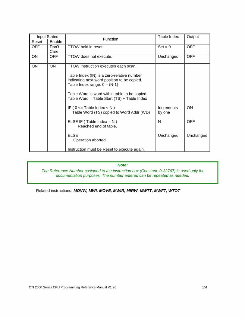
CTI 2500 Series CPU Programming Reference Manual V1.26 151
Input States Function
Table Index Output
Reset Enable
OFF Don’t Care
TTOW held in reset.
Set = 0 OFF
ON OFF TTOW does not execute.
Unchanged OFF
ON ON TTOW instruction executes each scan. Table Index (IN) is a zero-relative number indicating next word position to be copied. Table Index range: 0 – (N-1) Table Word is word within table to be copied. Table Word = Table Start (TS) + Table Index IF ( 0 <= Table Index < N ) Table Word (TS) copied to Word Addr (WD) ELSE IF ( Table Index = N ) Reached end of table. ELSE Operation aborted. Instruction must be Reset to execute again.
Increments by one N Unchanged
ON OFF Unchanged
Note:
The Reference Number assigned to the instruction box (Constant: 0-32767) is used only for documentation purposes. The number entered can be repeated as needed.
Related instructions: MOVW, MWI, MOVE, MWIR, MIRW, MWTT, MWFT, WTOT
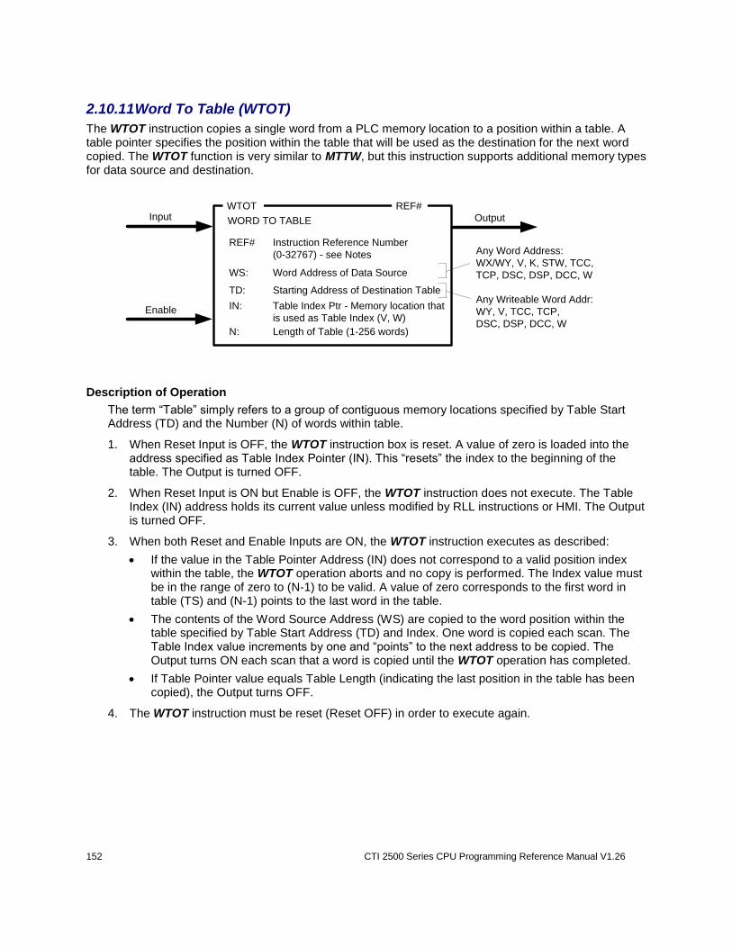
152 CTI 2500 Series CPU Programming Reference Manual V1.26
2.10.11 Word To Table (WTOT)
The WTOT instruction copies a single word from a PLC memory location to a position within a table. A table pointer specifies the position within the table that will be used as the destination for the next word copied. The WTOT function is very similar to MTTW, but this instruction supports additional memory types for data source and destination.
WTOT
OutputInput
TD: Starting Address of Destination Table
REF#
WORD TO TABLE
N: Length of Table (1-256 words)
WS: Word Address of Data Source
IN: Table Index Ptr - Memory location that
is used as Table Index (V, W)Enable
Any Writeable Word Addr:
WY, V, TCC, TCP,
DSC, DSP, DCC, W
Any Word Address:
WX/WY, V, K, STW, TCC,
TCP, DSC, DSP, DCC, W
REF# Instruction Reference Number
(0-32767) - see Notes
Description of Operation
The term “Table” simply refers to a group of contiguous memory locations specified by Table Start Address (TD) and the Number (N) of words within table.
1. When Reset Input is OFF, the WTOT instruction box is reset. A value of zero is loaded into the address specified as Table Index Pointer (IN). This “resets” the index to the beginning of the table. The Output is turned OFF.
2. When Reset Input is ON but Enable is OFF, the WTOT instruction does not execute. The Table Index (IN) address holds its current value unless modified by RLL instructions or HMI. The Output is turned OFF.
3. When both Reset and Enable Inputs are ON, the WTOT instruction executes as described:
If the value in the Table Pointer Address (IN) does not correspond to a valid position index within the table, the WTOT operation aborts and no copy is performed. The Index value must be in the range of zero to (N-1) to be valid. A value of zero corresponds to the first word in table (TS) and (N-1) points to the last word in the table.
The contents of the Word Source Address (WS) are copied to the word position within the table specified by Table Start Address (TD) and Index. One word is copied each scan. The Table Index value increments by one and “points” to the next address to be copied. The Output turns ON each scan that a word is copied until the WTOT operation has completed.
If Table Pointer value equals Table Length (indicating the last position in the table has been copied), the Output turns OFF.
4. The WTOT instruction must be reset (Reset OFF) in order to execute again.
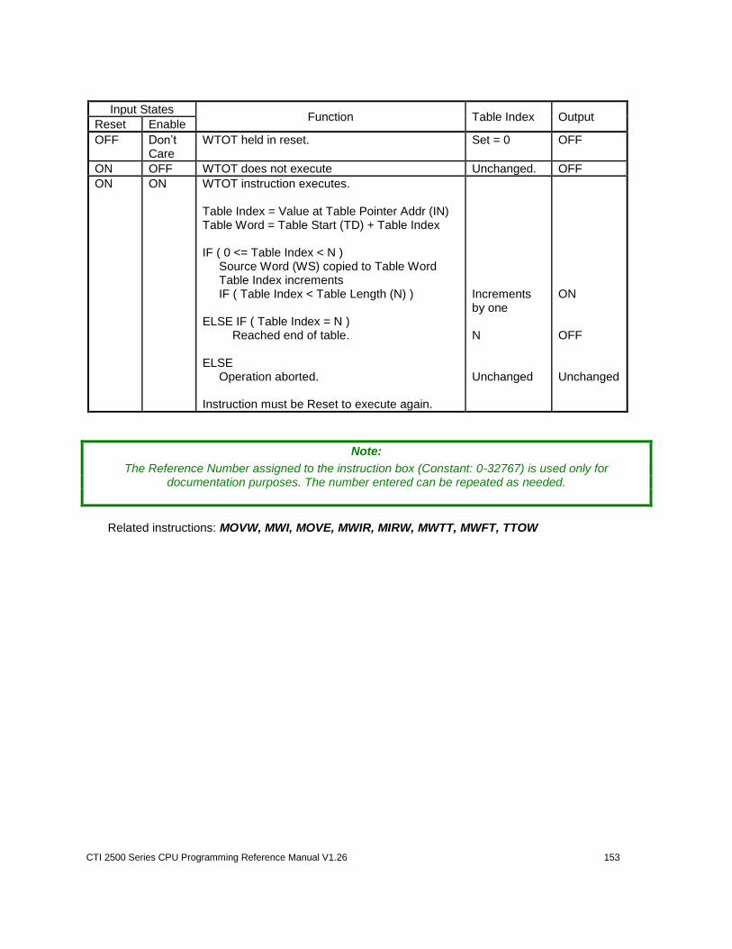
CTI 2500 Series CPU Programming Reference Manual V1.26 153
Input States Function Table Index Output
Reset Enable
OFF Don’t Care
WTOT held in reset.
Set = 0 OFF
ON OFF WTOT does not execute Unchanged. OFF
ON ON WTOT instruction executes. Table Index = Value at Table Pointer Addr (IN) Table Word = Table Start (TD) + Table Index IF ( 0 <= Table Index < N ) Source Word (WS) copied to Table Word Table Index increments IF ( Table Index < Table Length (N) ) ELSE IF ( Table Index = N ) Reached end of table. ELSE Operation aborted. Instruction must be Reset to execute again.
Increments by one N Unchanged
ON OFF Unchanged
Note:
The Reference Number assigned to the instruction box (Constant: 0-32767) is used only for documentation purposes. The number entered can be repeated as needed.
Related instructions: MOVW, MWI, MOVE, MWIR, MIRW, MWTT, MWFT, TTOW

154 CTI 2500 Series CPU Programming Reference Manual V1.26
2.11 Program Control Operations
These instructions affect the control flow or execution sequence of the PLC program scan.
2.11.1 Unconditional END (END)
The END instruction terminates the RLL scan.
END
Description of Operation
1. The END instruction has two functions:
Terminates execution of RLL scan
Separator between main RLL and RLL subroutine instructions
2. The END instruction must be only element in the network.
3. When the END instruction is executed, the controller terminates the RLL scan. Any instructions placed after the END instruction that are NOT part of an RLL subroutine will not execute.
4. If RLL subroutines are included in the PLC program, the END instruction must be inserted between the last network in the main RLL program and the first subroutine network.
Related instructions: ENDC
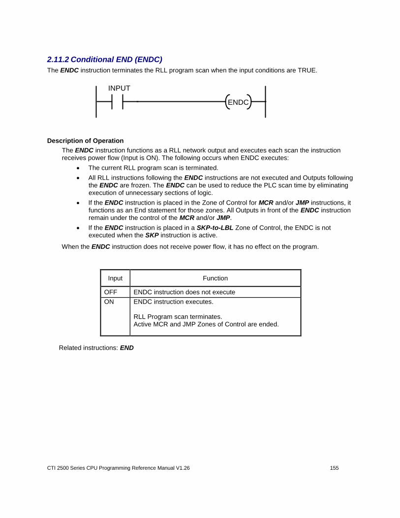
CTI 2500 Series CPU Programming Reference Manual V1.26 155
2.11.2 Conditional END (ENDC)
The ENDC instruction terminates the RLL program scan when the input conditions are TRUE.
ENDC
INPUT
Description of Operation
The ENDC instruction functions as a RLL network output and executes each scan the instruction receives power flow (Input is ON). The following occurs when ENDC executes:
The current RLL program scan is terminated.
All RLL instructions following the ENDC instructions are not executed and Outputs following the ENDC are frozen. The ENDC can be used to reduce the PLC scan time by eliminating execution of unnecessary sections of logic.
If the ENDC instruction is placed in the Zone of Control for MCR and/or JMP instructions, it functions as an End statement for those zones. All Outputs in front of the ENDC instruction remain under the control of the MCR and/or JMP.
If the ENDC instruction is placed in a SKP-to-LBL Zone of Control, the ENDC is not executed when the SKP instruction is active.
When the ENDC instruction does not receive power flow, it has no effect on the program.
Input Function
OFF ENDC instruction does not execute
ON
ENDC instruction executes. RLL Program scan terminates. Active MCR and JMP Zones of Control are ended.
Related instructions: END
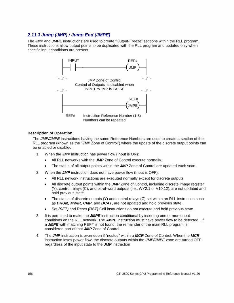
156 CTI 2500 Series CPU Programming Reference Manual V1.26
2.11.3 Jump (JMP) / Jump End (JMPE)
The JMP and JMPE instructions are used to create “Output-Freeze” sections within the RLL program. These instructions allow output points to be duplicated with the RLL program and updated only when specific input conditions are present.
REF#
REF#
JMP
INPUT
JMPE
JMP Zone of Control
Control of Outputs is disabled when
INPUT to JMP is FALSE
REF# Instruction Reference Number (1-8)
Numbers can be repeated
Description of Operation
The JMP/JMPE instructions having the same Reference Numbers are used to create a section of the RLL program (known as the “JMP Zone of Control”) where the update of the discrete output points can be enabled or disabled.
1. When the JMP instruction has power flow (Input is ON):
All RLL networks with the JMP Zone of Control execute normally.
The status of all output points within the JMP Zone of Control are updated each scan.
2. When the JMP instruction does not have power flow (Input is OFF):
All RLL network instructions are executed normally except for discrete outputs.
All discrete output points within the JMP Zone of Control, including discrete image register (Y), control relays (C), and bit-of-word outputs (i.e., WY2.1 or V10.12), are not updated and hold previous state.
The status of discrete outputs (Y) and control relays (C) set within an RLL instruction such as DRUM, MWIR, CMP, and DCAT, are not updated and hold previous state.
Set (SET) and Reset (RST) Coil instructions do not execute and hold previous state.
3. It is permitted to make the JMPE instruction conditional by inserting one or more input conditions on the RLL network. The JMPE instruction must have power flow to be detected. If a JMPE with matching REF# is not found, the remainder of the main RLL program is considered part of that JMP Zone of Control.
4. The JMP instruction is overridden if “nested” within a MCR Zone of Control. When the MCR instruction loses power flow, the discrete outputs within the JMP/JMPE zone are turned OFF regardless of the input state to the JMP instruction
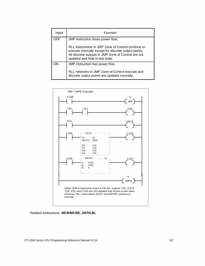
CTI 2500 Series CPU Programming Reference Manual V1.26 157
Input Function
OFF JMP instruction loses power flow. RLL instructions in JMP Zone of Control continue to execute normally except for discrete output points. All discrete outputs in JMP Zone of Control are not updated and held in last state.
ON
JMP instruction has power flow. RLL networks in JMP Zone of Control execute and discrete output points are updated normally.
JMP
C100 6
X12 X27 Y35
X14 V20.8
C105 DCAT
TC: 20
DELAY: 1000
OF: X15
CF: X16
OA: Y29
CA: Y30
C125
JMPE
6
JMP / JMPE Example:
When JMP-6 instruction input is FALSE, outputs Y35, V20.8
Y29, Y30, and C125 are not updated and frozen in last state.
However, RLL instructions DCAT and MOVW continue to
execute.
C125C105 MOVW
A: V100
B: V200
N: 3
10
Related instructions: MCR/MCRE, SKP/LBL
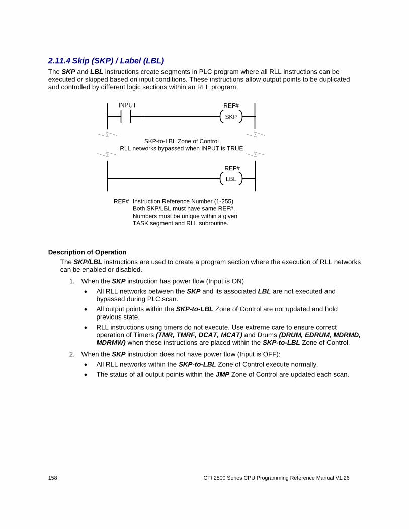
158 CTI 2500 Series CPU Programming Reference Manual V1.26
2.11.4 Skip (SKP) / Label (LBL)
The SKP and LBL instructions create segments in PLC program where all RLL instructions can be executed or skipped based on input conditions. These instructions allow output points to be duplicated and controlled by different logic sections within an RLL program.
REF#
REF#
SKP
INPUT
LBL
SKP-to-LBL Zone of Control
RLL networks bypassed when INPUT is TRUE
REF# Instruction Reference Number (1-255)
Both SKP/LBL must have same REF#.
Numbers must be unique within a given
TASK segment and RLL subroutine.
Description of Operation
The SKP/LBL instructions are used to create a program section where the execution of RLL networks can be enabled or disabled.
1. When the SKP instruction has power flow (Input is ON)
All RLL networks between the SKP and its associated LBL are not executed and bypassed during PLC scan.
All output points within the SKP-to-LBL Zone of Control are not updated and hold previous state.
RLL instructions using timers do not execute. Use extreme care to ensure correct operation of Timers (TMR, TMRF, DCAT, MCAT) and Drums (DRUM, EDRUM, MDRMD, MDRMW) when these instructions are placed within the SKP-to-LBL Zone of Control.
2. When the SKP instruction does not have power flow (Input is OFF):
All RLL networks within the SKP-to-LBL Zone of Control execute normally.
The status of all output points within the JMP Zone of Control are updated each scan.
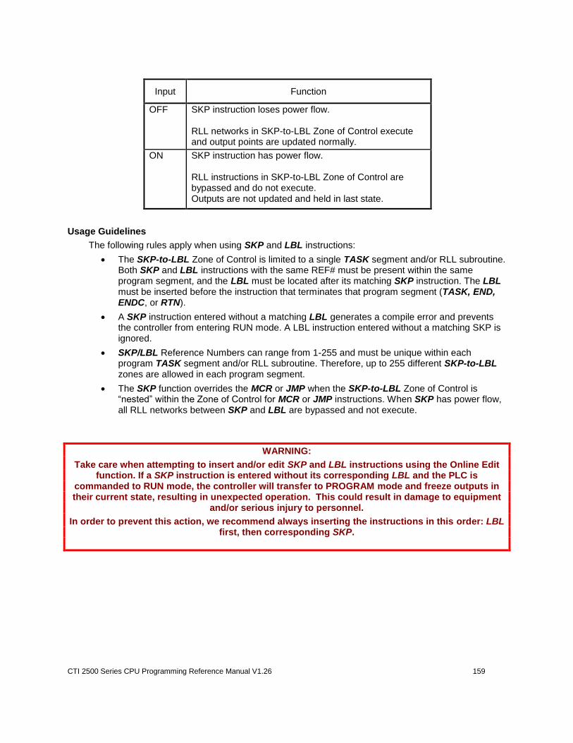
CTI 2500 Series CPU Programming Reference Manual V1.26 159
Input Function
OFF SKP instruction loses power flow. RLL networks in SKP-to-LBL Zone of Control execute and output points are updated normally.
ON
SKP instruction has power flow. RLL instructions in SKP-to-LBL Zone of Control are bypassed and do not execute. Outputs are not updated and held in last state.
Usage Guidelines
The following rules apply when using SKP and LBL instructions:
The SKP-to-LBL Zone of Control is limited to a single TASK segment and/or RLL subroutine. Both SKP and LBL instructions with the same REF# must be present within the same program segment, and the LBL must be located after its matching SKP instruction. The LBL must be inserted before the instruction that terminates that program segment (TASK, END, ENDC, or RTN).
A SKP instruction entered without a matching LBL generates a compile error and prevents the controller from entering RUN mode. A LBL instruction entered without a matching SKP is ignored.
SKP/LBL Reference Numbers can range from 1-255 and must be unique within each program TASK segment and/or RLL subroutine. Therefore, up to 255 different SKP-to-LBL zones are allowed in each program segment.
The SKP function overrides the MCR or JMP when the SKP-to-LBL Zone of Control is “nested” within the Zone of Control for MCR or JMP instructions. When SKP has power flow, all RLL networks between SKP and LBL are bypassed and not execute.
WARNING:
Take care when attempting to insert and/or edit SKP and LBL instructions using the Online Edit function. If a SKP instruction is entered without its corresponding LBL and the PLC is
commanded to RUN mode, the controller will transfer to PROGRAM mode and freeze outputs in their current state, resulting in unexpected operation. This could result in damage to equipment
and/or serious injury to personnel.
In order to prevent this action, we recommend always inserting the instructions in this order: LBL first, then corresponding SKP.
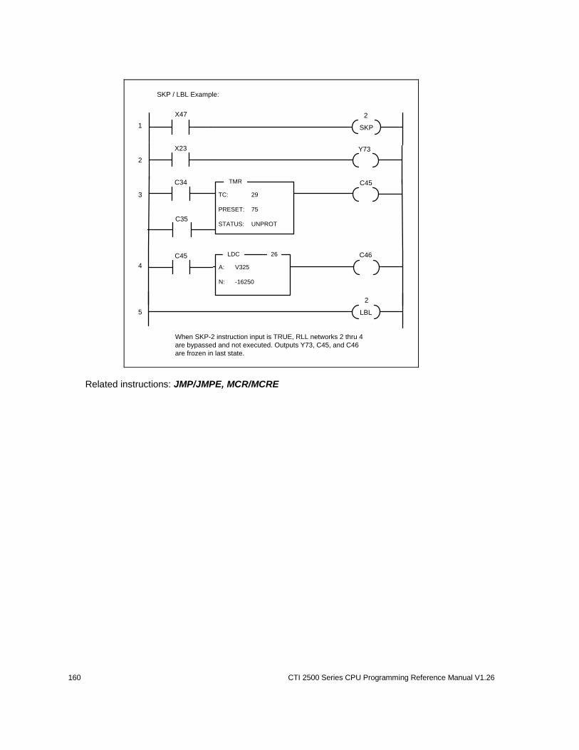
160 CTI 2500 Series CPU Programming Reference Manual V1.26
C35
SKP
X47 2
X23 Y73
C34 TMR
TC: 29
PRESET: 75
STATUS: UNPROT
C45
LBL
2
SKP / LBL Example:
When SKP-2 instruction input is TRUE, RLL networks 2 thru 4
are bypassed and not executed. Outputs Y73, C45, and C46
are frozen in last state.
C46C45 LDC
A: V325
N: -16250
26
1
2
3
4
5
Related instructions: JMP/JMPE, MCR/MCRE
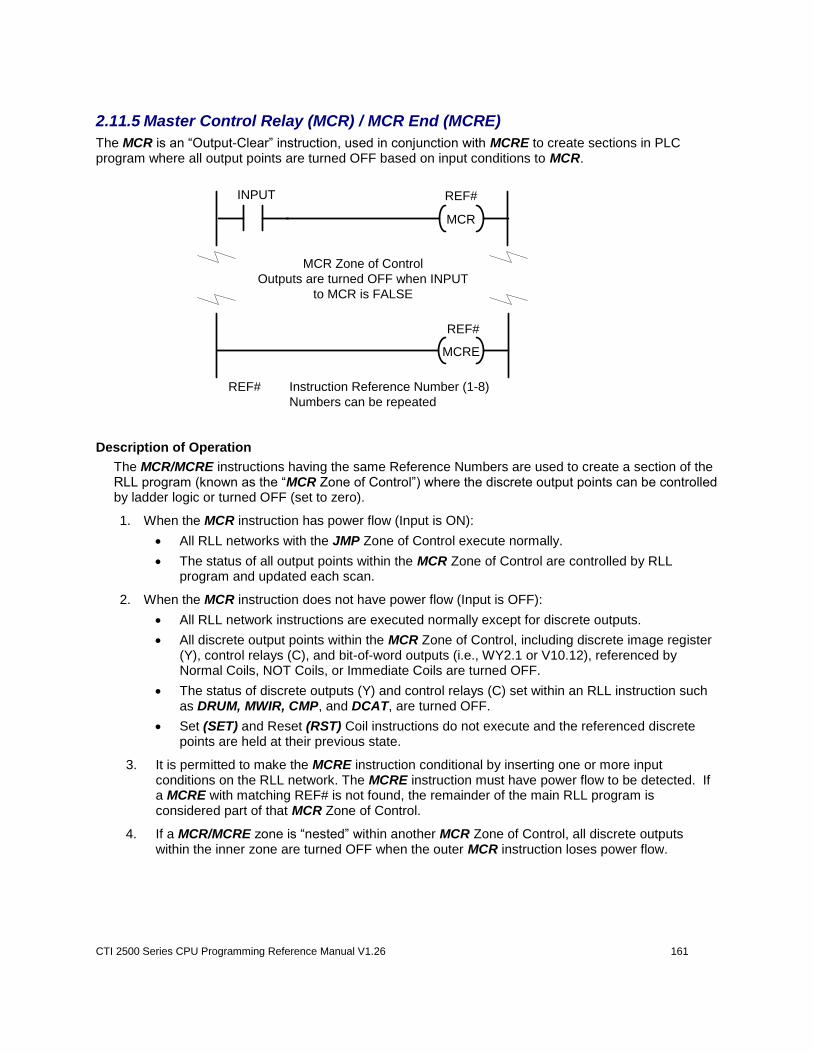
CTI 2500 Series CPU Programming Reference Manual V1.26 161
2.11.5 Master Control Relay (MCR) / MCR End (MCRE)
The MCR is an “Output-Clear” instruction, used in conjunction with MCRE to create sections in PLC program where all output points are turned OFF based on input conditions to MCR.
REF#
REF#
MCR
INPUT
MCRE
MCR Zone of Control
Outputs are turned OFF when INPUT
to MCR is FALSE
REF# Instruction Reference Number (1-8)
Numbers can be repeated
Description of Operation
The MCR/MCRE instructions having the same Reference Numbers are used to create a section of the RLL program (known as the “MCR Zone of Control”) where the discrete output points can be controlled by ladder logic or turned OFF (set to zero).
1. When the MCR instruction has power flow (Input is ON):
All RLL networks with the JMP Zone of Control execute normally.
The status of all output points within the MCR Zone of Control are controlled by RLL program and updated each scan.
2. When the MCR instruction does not have power flow (Input is OFF):
All RLL network instructions are executed normally except for discrete outputs.
All discrete output points within the MCR Zone of Control, including discrete image register (Y), control relays (C), and bit-of-word outputs (i.e., WY2.1 or V10.12), referenced by Normal Coils, NOT Coils, or Immediate Coils are turned OFF.
The status of discrete outputs (Y) and control relays (C) set within an RLL instruction such as DRUM, MWIR, CMP, and DCAT, are turned OFF.
Set (SET) and Reset (RST) Coil instructions do not execute and the referenced discrete points are held at their previous state.
3. It is permitted to make the MCRE instruction conditional by inserting one or more input conditions on the RLL network. The MCRE instruction must have power flow to be detected. If a MCRE with matching REF# is not found, the remainder of the main RLL program is considered part of that MCR Zone of Control.
4. If a MCR/MCRE zone is “nested” within another MCR Zone of Control, all discrete outputs within the inner zone are turned OFF when the outer MCR instruction loses power flow.
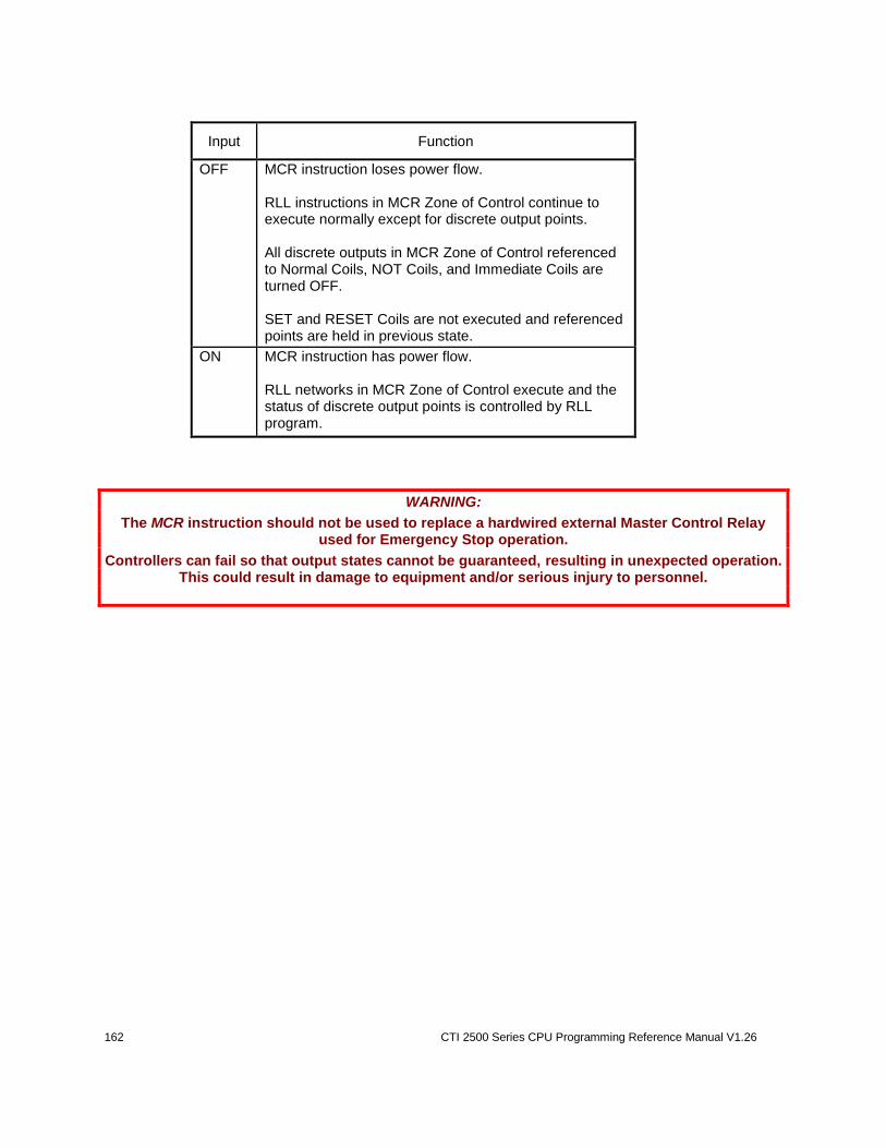
162 CTI 2500 Series CPU Programming Reference Manual V1.26
Input Function
OFF MCR instruction loses power flow. RLL instructions in MCR Zone of Control continue to execute normally except for discrete output points. All discrete outputs in MCR Zone of Control referenced to Normal Coils, NOT Coils, and Immediate Coils are turned OFF. SET and RESET Coils are not executed and referenced points are held in previous state.
ON
MCR instruction has power flow. RLL networks in MCR Zone of Control execute and the status of discrete output points is controlled by RLL program.
WARNING:
The MCR instruction should not be used to replace a hardwired external Master Control Relay used for Emergency Stop operation.
Controllers can fail so that output states cannot be guaranteed, resulting in unexpected operation. This could result in damage to equipment and/or serious injury to personnel.

CTI 2500 Series CPU Programming Reference Manual V1.26 163
X10
1
2
3
4
MCR
X4 1
X4 Y73
C12 CMP
A: V10
B: V12
GT: C23
LT: C24
C25
MCR / MCRE Example:
When MCR-1 instruction input is FALSE,
Outputs Y73, C23, C24, and C25 are turned OFF.
Y17 (controlled by SET Coil) is held in last state.
MCRE
1
Y17
SET
5
26
Related instructions: JMP/JMPE, SKP/LBL
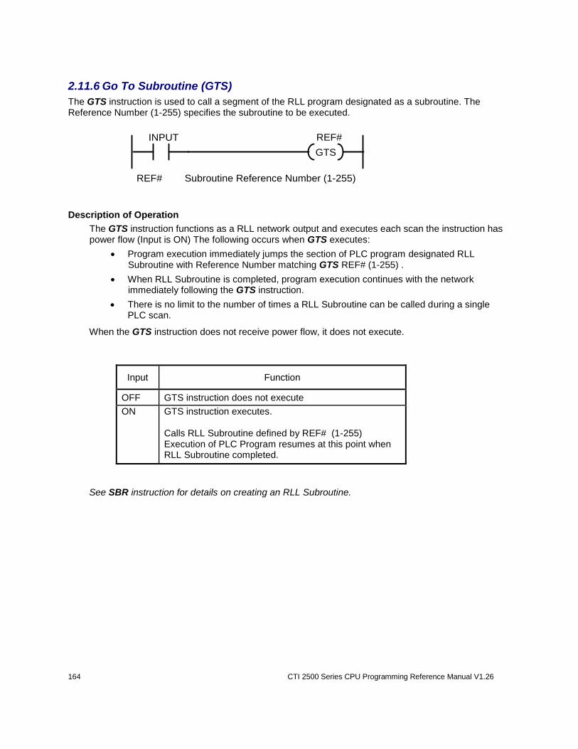
164 CTI 2500 Series CPU Programming Reference Manual V1.26
2.11.6 Go To Subroutine (GTS)
The GTS instruction is used to call a segment of the RLL program designated as a subroutine. The Reference Number (1-255) specifies the subroutine to be executed.
REF# Subroutine Reference Number (1-255)
REF#
GTS
INPUT
Description of Operation
The GTS instruction functions as a RLL network output and executes each scan the instruction has power flow (Input is ON) The following occurs when GTS executes:
Program execution immediately jumps the section of PLC program designated RLL Subroutine with Reference Number matching GTS REF# (1-255) .
When RLL Subroutine is completed, program execution continues with the network immediately following the GTS instruction.
There is no limit to the number of times a RLL Subroutine can be called during a single PLC scan.
When the GTS instruction does not receive power flow, it does not execute.
Input Function
OFF GTS instruction does not execute
ON
GTS instruction executes. Calls RLL Subroutine defined by REF# (1-255) Execution of PLC Program resumes at this point when RLL Subroutine completed.
See SBR instruction for details on creating an RLL Subroutine.

CTI 2500 Series CPU Programming Reference Manual V1.26 165
WARNING:
The referenced RLL Subroutine must exist and be properly delimited before the calling instruction (GTS, PGTS, or PGTSZ) can be executed.
Take care when attempting to insert and/or edit RLL Subroutines using the Online Edit function. If an instruction that calls a subroutine is entered without the associated RLL Subroutine properly defined and the PLC is commanded to RUN mode, the controller will transfer to PROGRAM mode and freeze outputs in their current state, resulting in unexpected operation. This could result in
damage to equipment and/or serious injury to personnel.
In order to prevent this action, we recommend always defining the RLL Subroutine section first, and then enter the instruction(s) to call that subroutine.
GTS
SBR
5
X1 5
GTS Example:
RTN
X3 Y9
C22C1 ADD
A: V35
B: V45
C: V50
END End of
main RLL
Start of RLL
Subroutine
End of RLL
Subroutine
Calls RLL
Subroutine
Related instructions: END, PGTS, PGTSZ, SBR, RTN
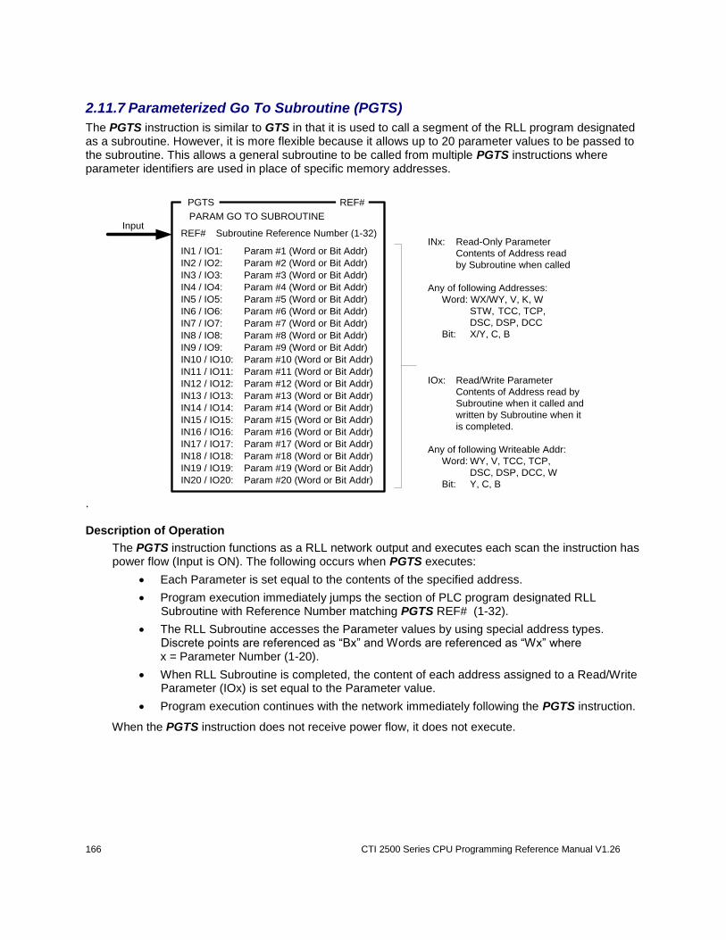
166 CTI 2500 Series CPU Programming Reference Manual V1.26
2.11.7 Parameterized Go To Subroutine (PGTS)
The PGTS instruction is similar to GTS in that it is used to call a segment of the RLL program designated as a subroutine. However, it is more flexible because it allows up to 20 parameter values to be passed to the subroutine. This allows a general subroutine to be called from multiple PGTS instructions where parameter identifiers are used in place of specific memory addresses.
.
PGTS REF#
PARAM GO TO SUBROUTINEInput
REF# Subroutine Reference Number (1-32)
IN1 / IO1: Param #1 (Word or Bit Addr)
IN2 / IO2: Param #2 (Word or Bit Addr)
IN3 / IO3: Param #3 (Word or Bit Addr)
IN4 / IO4: Param #4 (Word or Bit Addr)
IN5 / IO5: Param #5 (Word or Bit Addr)
IN6 / IO6: Param #6 (Word or Bit Addr)
IN7 / IO7: Param #7 (Word or Bit Addr)
IN8 / IO8: Param #8 (Word or Bit Addr)
IN9 / IO9: Param #9 (Word or Bit Addr)
IN10 / IO10: Param #10 (Word or Bit Addr)
IN11 / IO11: Param #11 (Word or Bit Addr)
IN12 / IO12: Param #12 (Word or Bit Addr)
IN13 / IO13: Param #13 (Word or Bit Addr)
IN14 / IO14: Param #14 (Word or Bit Addr)
IN15 / IO15: Param #15 (Word or Bit Addr)
IN16 / IO16: Param #16 (Word or Bit Addr)
IN17 / IO17: Param #17 (Word or Bit Addr)
IN18 / IO18: Param #18 (Word or Bit Addr)
IN19 / IO19: Param #19 (Word or Bit Addr)
IN20 / IO20: Param #20 (Word or Bit Addr)
INx: Read-Only Parameter
Contents of Address read
by Subroutine when called
Any of following Addresses:
Word: WX/WY, V, K, W
STW, TCC, TCP,
DSC, DSP, DCC
Bit: X/Y, C, B
IOx: Read/Write Parameter
Contents of Address read by
Subroutine when it called and
written by Subroutine when it
is completed.
Any of following Writeable Addr:
Word: WY, V, TCC, TCP,
DSC, DSP, DCC, W
Bit: Y, C, B
Description of Operation
The PGTS instruction functions as a RLL network output and executes each scan the instruction has power flow (Input is ON). The following occurs when PGTS executes:
Each Parameter is set equal to the contents of the specified address.
Program execution immediately jumps the section of PLC program designated RLL Subroutine with Reference Number matching PGTS REF# (1-32).
The RLL Subroutine accesses the Parameter values by using special address types. Discrete points are referenced as “Bx” and Words are referenced as “Wx” where
x = Parameter Number (1-20).
When RLL Subroutine is completed, the content of each address assigned to a Read/Write Parameter (IOx) is set equal to the Parameter value.
Program execution continues with the network immediately following the PGTS instruction.
When the PGTS instruction does not receive power flow, it does not execute.
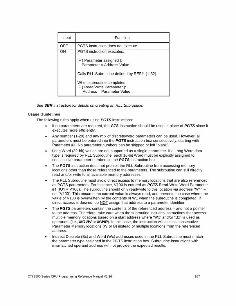
CTI 2500 Series CPU Programming Reference Manual V1.26 167
Input Function
OFF PGTS instruction does not execute
ON
PGTS instruction executes. IF ( Parameter assigned ): Parameter = Address Value Calls RLL Subroutine defined by REF# (1-32) When subroutine completes IF ( Read/Write Parameter ): Address = Parameter Value
See SBR instruction for details on creating an RLL Subroutine. Usage Guidelines
The following rules apply when using PGTS instructions:
If no parameters are required, the GTS instruction should be used in place of PGTS since it executes more efficiently.
Any number (1-20) and any mix of discrete/word parameters can be used. However, all parameters must be entered into the PGTS instruction box consecutively, starting with Parameter #1. No parameter numbers can be skipped or left “blank”.
Long Word (32-bit) values are not supported as a single parameter. If a Long Word data type is required by RLL Subroutine, each 16-bit Word must be explicitly assigned to consecutive parameter numbers in the PGTS instruction box.
The PGTS instruction does not prohibit the RLL Subroutine from accessing memory locations other than those referenced to the parameters. The subroutine can still directly read and/or write to all available memory addresses.
The RLL Subroutine must avoid direct access to memory locations that are also referenced as PGTS parameters. For instance, V100 is entered as PGTS Read-Write Word Parameter #1 (IO1 = V100). The subroutine should only read/write to this location via address “W1” – not “V100”. This ensures the current value is always read, and prevents the case where the value of V100 is overwritten by the contents of W1 when the subroutine is completed. If direct access is desired, do NOT assign that address to a parameter identifier.
The PGTS parameters contain the contents of the referenced address – and not a pointer to the address. Therefore, take care when the subroutine includes instructions that access multiple memory locations based on a start address where “Wx” and/or “Bx” is used as operands, (i.e., MOVW or MWIR). In this case, the instruction will access consecutive Parameter Memory locations (W or B) instead of multiple locations from the referenced address.
Indirect Discrete (Bx) and Word (Wx) addresses used in the RLL Subroutine must match the parameter type assigned in the PGTS instruction box. Subroutine instructions with mismatched operand address will not provide the expected results.
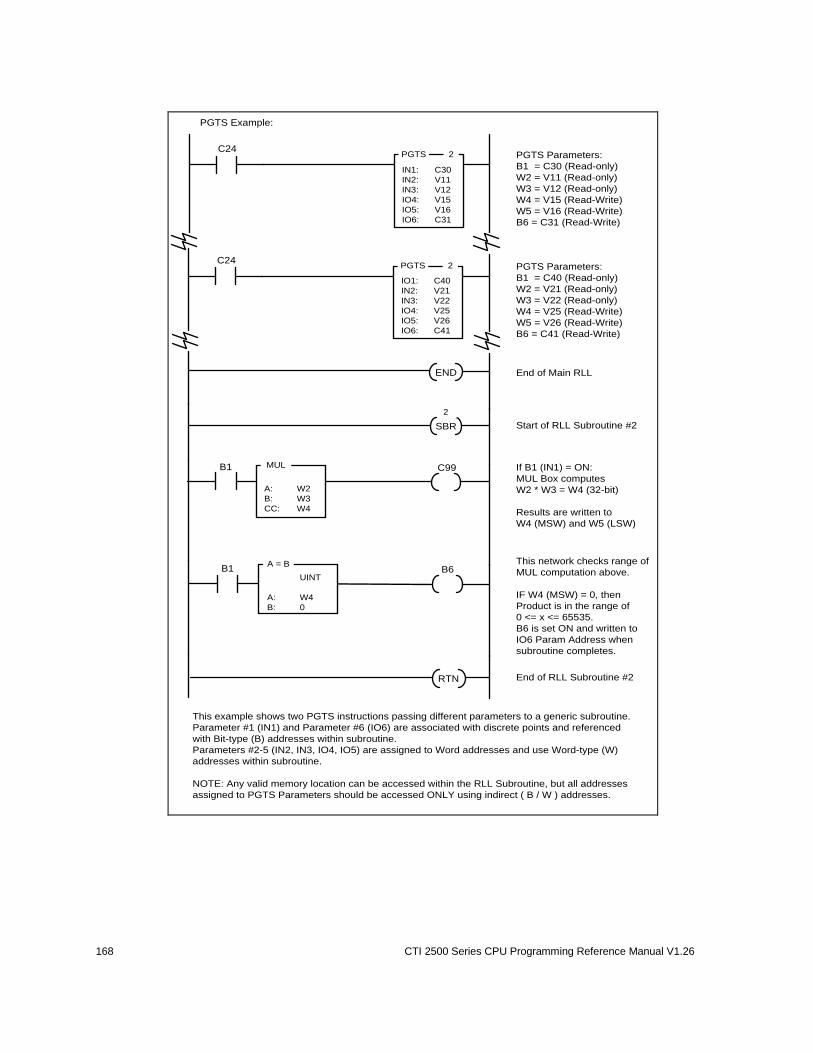
168 CTI 2500 Series CPU Programming Reference Manual V1.26
PGTS Example:
RTN
C24PGTS
IO1: C40
IN2: V21
IN3: V22
IO4: V25
IO5: V26
IO6: C41
2
PGTS Parameters:
B1 = C30 (Read-only)
W2 = V11 (Read-only)
W3 = V12 (Read-only)
W4 = V15 (Read-Write)
W5 = V16 (Read-Write)
B6 = C31 (Read-Write)
PGTS Parameters:
B1 = C40 (Read-only)
W2 = V21 (Read-only)
W3 = V22 (Read-only)
W4 = V25 (Read-Write)
W5 = V26 (Read-Write)
B6 = C41 (Read-Write)
Start of RLL Subroutine #2
If B1 (IN1) = ON:
MUL Box computes
W2 * W3 = W4 (32-bit)
Results are written to
W4 (MSW) and W5 (LSW)
This network checks range of
MUL computation above.
IF W4 (MSW) = 0, then
Product is in the range of
0 <= x <= 65535.
B6 is set ON and written to
IO6 Param Address when
subroutine completes.
End of RLL Subroutine #2
End of Main RLL
B1 C99MUL
A: W2
B: W3
CC: W4
END
C24PGTS
IN1: C30
IN2: V11
IN3: V12
IO4: V15
IO5: V16
IO6: C31
2
B1 B6A = B
UINT
A: W4
B: 0
SBR
2
This example shows two PGTS instructions passing different parameters to a generic subroutine.
Parameter #1 (IN1) and Parameter #6 (IO6) are associated with discrete points and referenced
with Bit-type (B) addresses within subroutine.
Parameters #2-5 (IN2, IN3, IO4, IO5) are assigned to Word addresses and use Word-type (W)
addresses within subroutine.
NOTE: Any valid memory location can be accessed within the RLL Subroutine, but all addresses
assigned to PGTS Parameters should be accessed ONLY using indirect ( B / W ) addresses.

CTI 2500 Series CPU Programming Reference Manual V1.26 169
WARNING:
The referenced RLL Subroutine must exist and be properly delimited before the calling instruction (GTS, PGTS, or PGTSZ) can be executed.
Take care when attempting to insert and/or edit RLL Subroutines using the Online Edit function. If an instruction that calls a subroutine is entered without the associated RLL Subroutine properly defined and the PLC is commanded to RUN mode, the controller will transfer to PROGRAM mode and freeze outputs in their current state, resulting in unexpected operation. This could result in
damage to equipment and/or serious injury to personnel.
In order to prevent this action, we recommend always defining the RLL Subroutine section first, and then enter the instruction(s) to call that subroutine.
Related instructions: END, GTS, PGTSZ, SBR, RTN
:
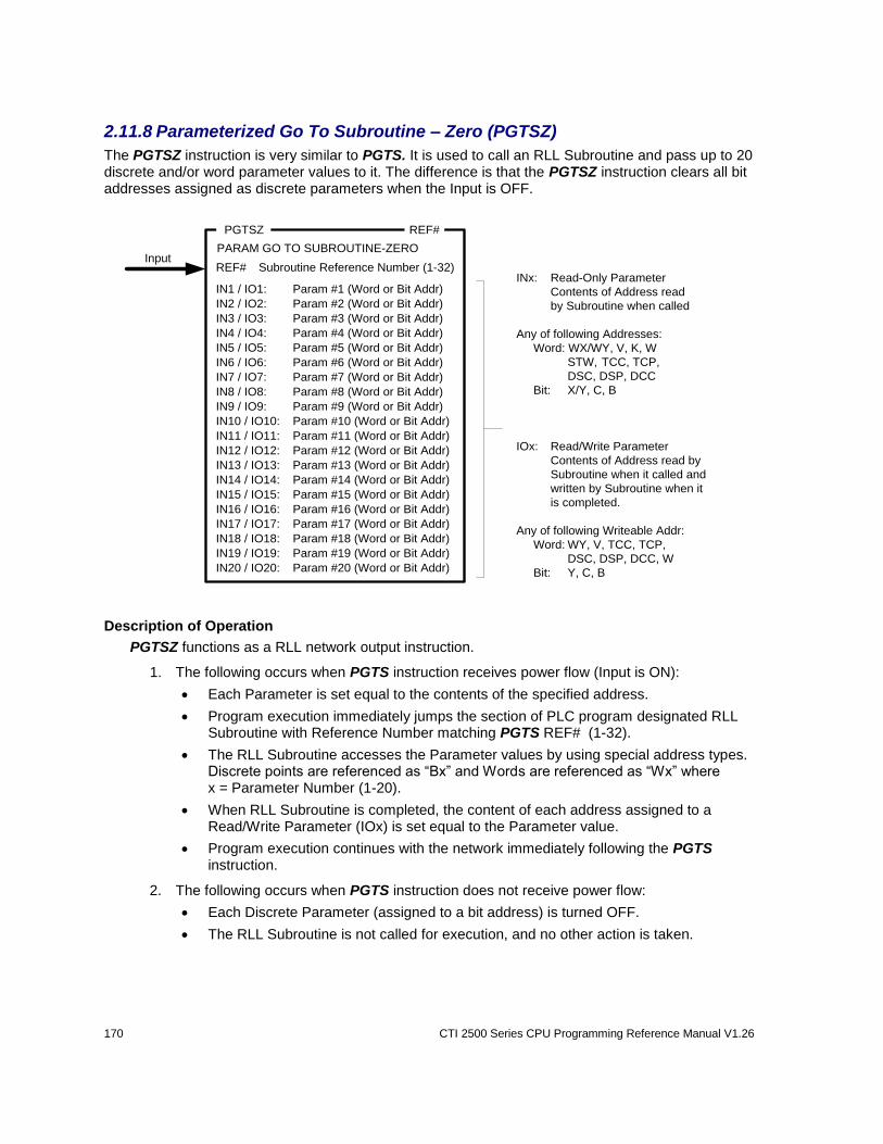
170 CTI 2500 Series CPU Programming Reference Manual V1.26
2.11.8 Parameterized Go To Subroutine – Zero (PGTSZ)
The PGTSZ instruction is very similar to PGTS. It is used to call an RLL Subroutine and pass up to 20 discrete and/or word parameter values to it. The difference is that the PGTSZ instruction clears all bit addresses assigned as discrete parameters when the Input is OFF.
PGTSZ REF#
PARAM GO TO SUBROUTINE-ZEROInput
REF# Subroutine Reference Number (1-32)
IN1 / IO1: Param #1 (Word or Bit Addr)
IN2 / IO2: Param #2 (Word or Bit Addr)
IN3 / IO3: Param #3 (Word or Bit Addr)
IN4 / IO4: Param #4 (Word or Bit Addr)
IN5 / IO5: Param #5 (Word or Bit Addr)
IN6 / IO6: Param #6 (Word or Bit Addr)
IN7 / IO7: Param #7 (Word or Bit Addr)
IN8 / IO8: Param #8 (Word or Bit Addr)
IN9 / IO9: Param #9 (Word or Bit Addr)
IN10 / IO10: Param #10 (Word or Bit Addr)
IN11 / IO11: Param #11 (Word or Bit Addr)
IN12 / IO12: Param #12 (Word or Bit Addr)
IN13 / IO13: Param #13 (Word or Bit Addr)
IN14 / IO14: Param #14 (Word or Bit Addr)
IN15 / IO15: Param #15 (Word or Bit Addr)
IN16 / IO16: Param #16 (Word or Bit Addr)
IN17 / IO17: Param #17 (Word or Bit Addr)
IN18 / IO18: Param #18 (Word or Bit Addr)
IN19 / IO19: Param #19 (Word or Bit Addr)
IN20 / IO20: Param #20 (Word or Bit Addr)
INx: Read-Only Parameter
Contents of Address read
by Subroutine when called
Any of following Addresses:
Word: WX/WY, V, K, W
STW, TCC, TCP,
DSC, DSP, DCC
Bit: X/Y, C, B
IOx: Read/Write Parameter
Contents of Address read by
Subroutine when it called and
written by Subroutine when it
is completed.
Any of following Writeable Addr:
Word: WY, V, TCC, TCP,
DSC, DSP, DCC, W
Bit: Y, C, B
Description of Operation
PGTSZ functions as a RLL network output instruction.
1. The following occurs when PGTS instruction receives power flow (Input is ON):
Each Parameter is set equal to the contents of the specified address.
Program execution immediately jumps the section of PLC program designated RLL Subroutine with Reference Number matching PGTS REF# (1-32).
The RLL Subroutine accesses the Parameter values by using special address types. Discrete points are referenced as “Bx” and Words are referenced as “Wx” where
x = Parameter Number (1-20).
When RLL Subroutine is completed, the content of each address assigned to a Read/Write Parameter (IOx) is set equal to the Parameter value.
Program execution continues with the network immediately following the PGTS instruction.
2. The following occurs when PGTS instruction does not receive power flow:
Each Discrete Parameter (assigned to a bit address) is turned OFF.
The RLL Subroutine is not called for execution, and no other action is taken.

CTI 2500 Series CPU Programming Reference Manual V1.26 171
Input Function
OFF PGTSZ executes as follows: IF ( Discrete Parameter) Bit Address turns OFF
ON
PGTSZ executes as follows: (Operation Identical to PGTS) IF ( Parameter assigned ): Parameter = Address Value Calls RLL Subroutine defined by REF# (1-32) When subroutine completes IF ( Read/Write Parameter ): Address = Parameter Value
See SBR instruction for description and example of an RLL Subroutine.
See PGTS instruction for description of operation when Input is ON.
WARNING:
The referenced RLL Subroutine must exist and be properly delimited before the calling instruction (GTS, PGTS, or PGTSZ) can be executed.
Take care when attempting to insert and/or edit RLL Subroutines using the Online Edit function. If an instruction that calls a subroutine is entered without the associated RLL Subroutine properly defined and the PLC is commanded to RUN mode, the controller will transfer to PROGRAM mode and freeze outputs in their current state, resulting in unexpected operation. This could result in
damage to equipment and/or serious injury to personnel.
In order to prevent this action, we recommend always defining the RLL Subroutine section first, and then enter the instruction(s) to call that subroutine.
Related instructions: END, GTS, PGTS, SBR, RTN
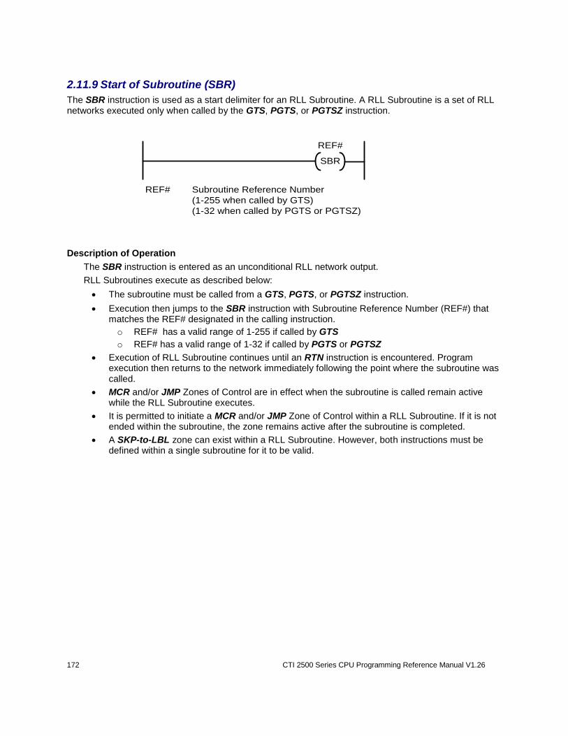
172 CTI 2500 Series CPU Programming Reference Manual V1.26
2.11.9 Start of Subroutine (SBR)
The SBR instruction is used as a start delimiter for an RLL Subroutine. A RLL Subroutine is a set of RLL networks executed only when called by the GTS, PGTS, or PGTSZ instruction.
SBR
REF#
REF# Subroutine Reference Number
(1-255 when called by GTS)
(1-32 when called by PGTS or PGTSZ)
Description of Operation
The SBR instruction is entered as an unconditional RLL network output.
RLL Subroutines execute as described below:
The subroutine must be called from a GTS, PGTS, or PGTSZ instruction.
Execution then jumps to the SBR instruction with Subroutine Reference Number (REF#) that matches the REF# designated in the calling instruction.
o REF# has a valid range of 1-255 if called by GTS
o REF# has a valid range of 1-32 if called by PGTS or PGTSZ
Execution of RLL Subroutine continues until an RTN instruction is encountered. Program execution then returns to the network immediately following the point where the subroutine was called.
MCR and/or JMP Zones of Control are in effect when the subroutine is called remain active while the RLL Subroutine executes.
It is permitted to initiate a MCR and/or JMP Zone of Control within a RLL Subroutine. If it is not ended within the subroutine, the zone remains active after the subroutine is completed.
A SKP-to-LBL zone can exist within a RLL Subroutine. However, both instructions must be defined within a single subroutine for it to be valid.
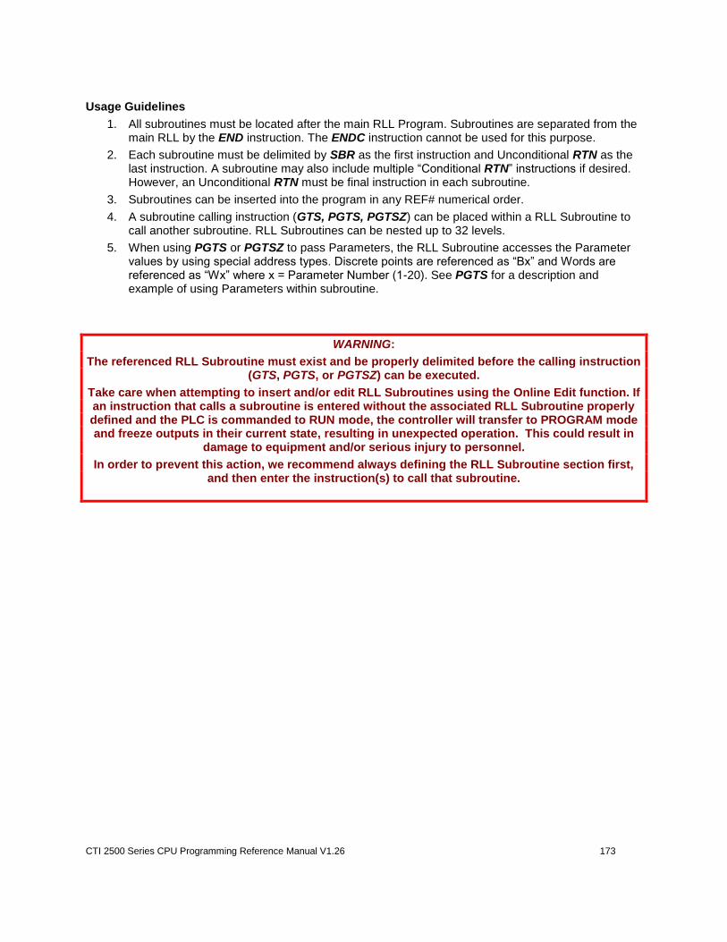
CTI 2500 Series CPU Programming Reference Manual V1.26 173
Usage Guidelines
1. All subroutines must be located after the main RLL Program. Subroutines are separated from the main RLL by the END instruction. The ENDC instruction cannot be used for this purpose.
2. Each subroutine must be delimited by SBR as the first instruction and Unconditional RTN as the last instruction. A subroutine may also include multiple “Conditional RTN” instructions if desired. However, an Unconditional RTN must be final instruction in each subroutine.
3. Subroutines can be inserted into the program in any REF# numerical order.
4. A subroutine calling instruction (GTS, PGTS, PGTSZ) can be placed within a RLL Subroutine to call another subroutine. RLL Subroutines can be nested up to 32 levels.
5. When using PGTS or PGTSZ to pass Parameters, the RLL Subroutine accesses the Parameter values by using special address types. Discrete points are referenced as “Bx” and Words are referenced as “Wx” where x = Parameter Number (1-20). See PGTS for a description and example of using Parameters within subroutine.
WARNING:
The referenced RLL Subroutine must exist and be properly delimited before the calling instruction (GTS, PGTS, or PGTSZ) can be executed.
Take care when attempting to insert and/or edit RLL Subroutines using the Online Edit function. If an instruction that calls a subroutine is entered without the associated RLL Subroutine properly defined and the PLC is commanded to RUN mode, the controller will transfer to PROGRAM mode and freeze outputs in their current state, resulting in unexpected operation. This could result in
damage to equipment and/or serious injury to personnel.
In order to prevent this action, we recommend always defining the RLL Subroutine section first, and then enter the instruction(s) to call that subroutine.
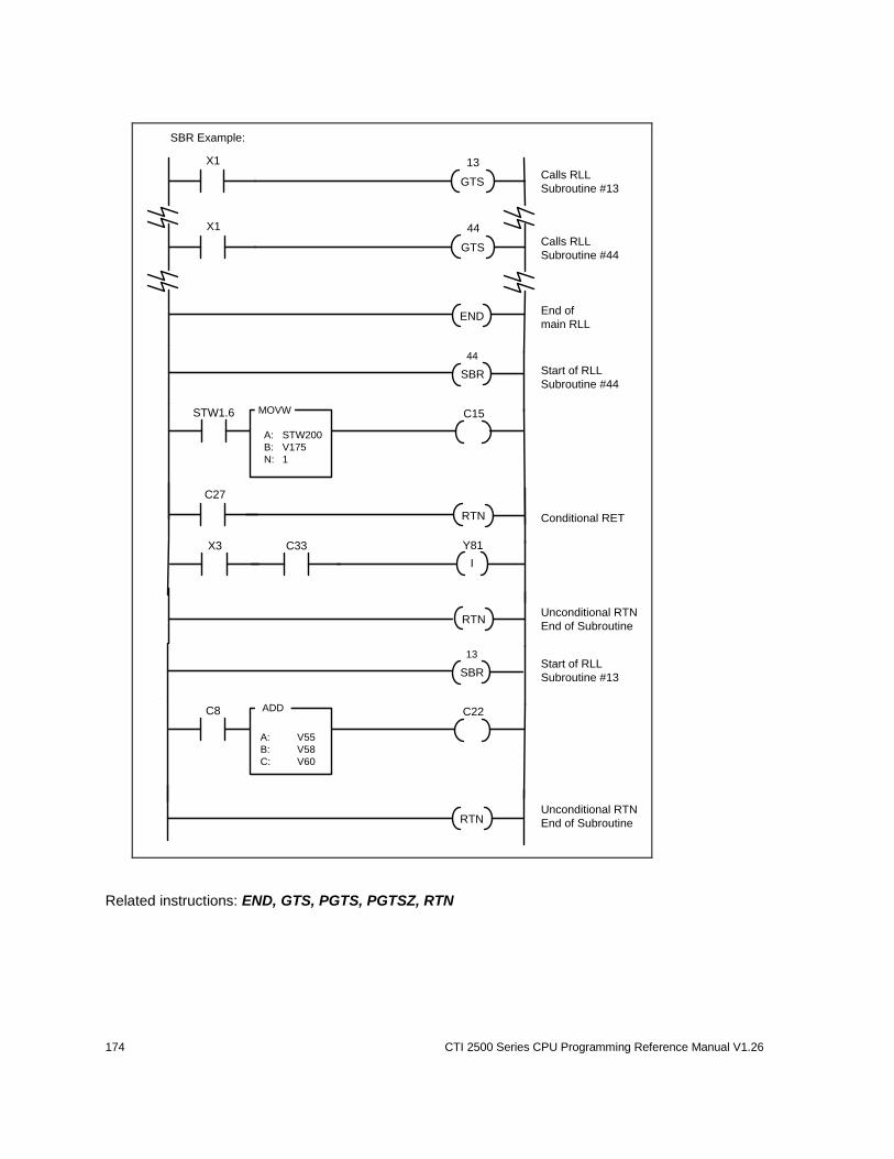
174 CTI 2500 Series CPU Programming Reference Manual V1.26
End of
main RLL
Start of RLL
Subroutine #44
Unconditional RTN
End of Subroutine
Calls RLL
Subroutine #13
Calls RLL
Subroutine #44
Conditional RET
Start of RLL
Subroutine #13
Unconditional RTN
End of Subroutine
SBR Example:
END
GTS
X1 13
RTN
C15STW1.6 MOVW
A: STW200
B: V175
N: 1
I
Y81X3 C33
RTN
SBR
44
SBR
13
C22C8 ADD
A: V55
B: V58
C: V60
GTS
X1 44
C27
RTN
Related instructions: END, GTS, PGTS, PGTSZ, RTN

CTI 2500 Series CPU Programming Reference Manual V1.26 175
2.11.10 Return from Subroutine (RET)
The RTN instruction is used to terminate execution of a RLL Subroutine. An Unconditional Return must be used as the last statement in each RLL Subroutine.
Conditional Return
RTN
Unconditional Return
RTN
INPUT
Description of Operation
The RTN instruction can only be entered as a network output within a RLL Subroutine.
Whenever it receives power flow, RTN executes. The RLL Subroutine currently running is ended and program execution returns to the network immediately following the instruction (GTS, PGTS, or PGTSZ) that called the subroutine.
The RTN instruction can exist in two forms:
1. Conditional Return
One or more of these networks may be included within a RLL Subroutine
If Input is ON, RTN executes as described above
If Input is OFF, the RLL Subroutine continues to execute.
2. Unconditional Return
Always executes
Must be included as the last instruction in each RLL Subroutine
See SBR instruction for description and example of an RLL Subroutine.
Input Function
OFF Conditional RTN instruction does not execute
ON
RTN instruction executes. RLL Subroutine execution is terminated. Program control returns to network immediately following the instruction (GTS, PGTS, PGTSZ) that called the subroutine.
Related instructions: END, GTS, PGTS, PGTSZ, SBR
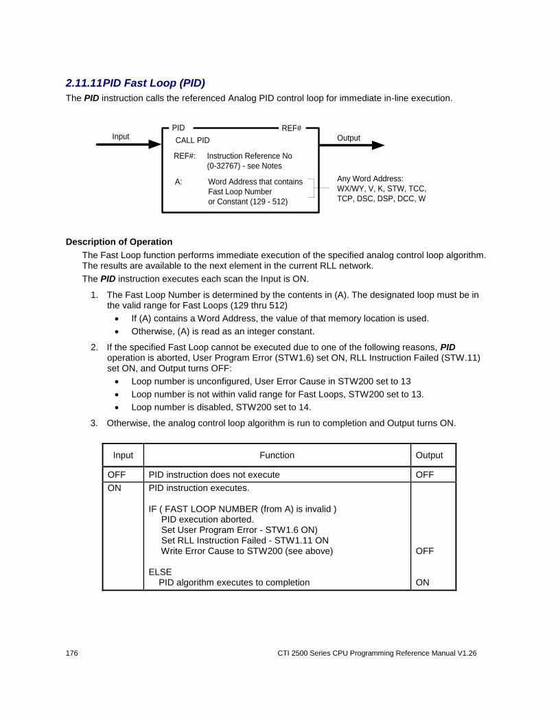
176 CTI 2500 Series CPU Programming Reference Manual V1.26
2.11.11 PID Fast Loop (PID)
The PID instruction calls the referenced Analog PID control loop for immediate in-line execution.
PID
OutputInput
A: Word Address that contains
Fast Loop Number
or Constant (129 - 512)
REF#
CALL PID
Any Word Address:
WX/WY, V, K, STW, TCC,
TCP, DSC, DSP, DCC, W
REF#: Instruction Reference No
(0-32767) - see Notes
Description of Operation
The Fast Loop function performs immediate execution of the specified analog control loop algorithm. The results are available to the next element in the current RLL network.
The PID instruction executes each scan the Input is ON.
1. The Fast Loop Number is determined by the contents in (A). The designated loop must be in the valid range for Fast Loops (129 thru 512)
If (A) contains a Word Address, the value of that memory location is used.
Otherwise, (A) is read as an integer constant.
2. If the specified Fast Loop cannot be executed due to one of the following reasons, PID operation is aborted, User Program Error (STW1.6) set ON, RLL Instruction Failed (STW.11) set ON, and Output turns OFF:
Loop number is unconfigured, User Error Cause in STW200 set to 13
Loop number is not within valid range for Fast Loops, STW200 set to 13.
Loop number is disabled, STW200 set to 14.
3. Otherwise, the analog control loop algorithm is run to completion and Output turns ON.
Input Function Output
OFF PID instruction does not execute OFF
ON
PID instruction executes. IF ( FAST LOOP NUMBER (from A) is invalid ) PID execution aborted. Set User Program Error - STW1.6 ON) Set RLL Instruction Failed - STW1.11 ON Write Error Cause to STW200 (see above) ELSE PID algorithm executes to completion
OFF ON

CTI 2500 Series CPU Programming Reference Manual V1.26 177
Usage Guidelines
1. Fast Loops are not supported by CPU Models 2500-C100 and 2500-C200.
2. Fast Loops are programmed using the same criteria as cyclic PID Loops (1-128) with the following exceptions:
SAMPLE RATE field is unused since it does not apply to loops initiated from RLL.
RAMP/SOAK function is unsupported
3. Fast Loops can be scheduled to execute every scan, based on TMR/TMRF instruction expiration, or placed within a Cyclic RLL Task. Proper execution is ensured only when the Fast Loop is scheduled on a fixed time interval.
Note:
The Reference Number assigned to the instruction box (Constant: 0-32767) is used only for documentation purposes. The number entered can be repeated as needed.

178 CTI 2500 Series CPU Programming Reference Manual V1.26
2.11.12 Call SF Program (SFPGM)
The SFPGM instruction calls the referenced Special Function (SF) Program for execution.
SFPGMOutputInput
SFP#
SF# Special Function Program
to execute - see Notes
CALL SF PROGRAM
IN-LINE: YES - Selects immediate in-line
execution within RLL Program
NO - Schedules SFPGM for
execution at end of RLL scan
SF Program Overview
SF Programs are written in a statement-driven programming language similar to BASIC. The controller automatically compiles all SF statements and utilizes a hardware floating point co-processor to greatly improve execution time, especially for complex mathematical and logical expressions.
When the SF Program is created, it is designated as one of the following types - Normal (Non-Priority), Priority, Cyclic, or Restricted.
NORMAL is the default SF Program type that can be called by the SFPGM instruction, PID Loops, or Analog Alarms. NORMAL programs can run IN-LINE or be queued for execution at the end of the RLL scan.
PRIORITY is identical to NORMAL program except for order of execution when queued to run at the end of RLL scan. PRIORITY programs are maintained in a separate queue and execute in a separate time slice that runs prior to the NORMAL SF time slice.
CYCLIC program is executed only when called by the SFPGM instruction. It must be queued for execution (IN-LINE = NO) and is automatically re-queued to run at the specified cycle time as long as the Input to SFPGM instruction is ON.
RESTRICTED programs can be called only from PID Loops or Analog Alarms. Restricted Programs cannot be called by the RLL SFPGM instruction.
See Chapter 3 for a detailed description on SF Programs.
Note:
The maximum number of Special Function Programs is dependent on the controller model. 2500-C100 supports SF Programs numbered 1-64.
Other models support SF Programs numbered 1-1023.
The number entered in SFP# field must be valid for the controller model used.
CTI 2500 Series CPU Programming Reference Manual V1.26 179
Description of Operation
The SFPGM instruction schedules the referenced SF Program for execution based on SF Program type and In-Line execution selection.
1. When In-Line execution is not selected (IN-LINE = NO), SFPGM executes as follows:
a. If SF Program (SFP#) type is NORMAL or PRIORITY:
When Input transitions OFF-to-ON, the SF Program (SFP#) is placed in the next available position in the appropriate FIFO queue for execution at the end of the RLL scan.
The Input must remain ON until the SF Program runs to completion. If Input turns OFF before the SF Program executes, it is removed from the queue.
When SF Program is completed, the Output turns ON.
When Input turns OFF, the Output turns OFF.
Input must transition OFF-to-ON for the SF Program to execute again.
b. If SF Program type is Cyclic:
When Input transitions OFF-to-ON, the SF Program (SFP#) is placed in the next available position in the cyclic FIFO queue for execution at the end of the RLL scan. If queue is full (32 Cyclic SF Programs already queued), SF Processor “Cyclic SFP Queue is Full” Error is reported in STW162.8 set ON. If the Input stays ON, queue entry is attempted again on the next PLC scan.
When the Cyclic SF Program executes one time, the Output turns ON.
As long as the Input remains ON, the Cyclic SF Program is re-queued for execution again based on programmed Cycle Time.
When Input turns OFF, the SF Program is immediately removed from the execution queue, and the Output turns OFF
2. When In-line execution is selected (IN-LINE = YES):
a. If SF Program type is NORMAL or PRIORITY:
Each scan Input is ON, the designated SF Program (SFP#) immediately runs to completion. Results can be used by the next RLL instruction in the current network. The Output turns ON.
If the Input is OFF, SFPGM does not execute. The Output turns OFF.
3. If the specified SF Program cannot execute due to one of the following reasons, SFPGM operation is aborted, User Program Error (STW1.6) set ON, RLL Instruction Failed (STW.11) set ON, and Output turns OFF:
SF Program does not exist, User Error Cause in STW200 set to 8.
SF Program is not enabled, STW200 set to 9.
SF Program type is CYCLIC and In-Line execution is selected (INLINE = YES), STW200 set to 10.
SF Program type is RESTRICTED, STW200 set to 10.
On-Line Edit operation is in progress, STW200 set to 11.
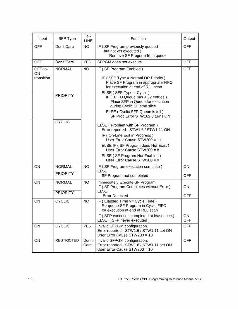
180 CTI 2500 Series CPU Programming Reference Manual V1.26
Input SFP Type IN-
LINE Function Output
OFF Don’t Care NO IF ( SF Program previously queued but not yet executed ) Remove SF Program from queue
OFF
OFF Don’t Care YES SFPGM does not execute OFF
OFF-to-ON transition
NORMAL NO IF ( SF Program Enabled ) IF ( SFP Type = Normal OR Priority ) Place SF Program in appropriate FIFO for execution at end of RLL scan
ELSE ( SFP Type = Cyclic ) IF ( FIFO Queue has < 32 entries ) Place SFP in Queue for execution during Cyclic SF time slice
ELSE ( Cyclic SFP Queue is full ) SF Proc Error STW162.8 turns ON ELSE ( Problem with SF Program ) Error reported - STW1.6 / STW1.11 ON
IF ( On-Line Edit in Progress ) User Error Cause STW200 = 11
ELSE IF ( SF Program does Not Exist ) User Error Cause STW200 = 8
ELSE ( SF Program Not Enabled ) User Error Cause STW200 = 9
OFF
PRIORITY
CYCLIC
ON NORMAL NO IF ( SF Program execution complete ) ELSE SF Program not completed
ON OFF
PRIORITY
ON NORMAL NO Immediately Execute SF Program IF ( SF Program Completes without Error ) ELSE Error Detected
ON OFF
PRIORITY
ON CYCLIC NO IF ( Elapsed Time >= Cycle Time ) Re-queue SF Program in Cyclic FIFO for execution at end of RLL scan
IF ( SFP execution completed at least once ) ELSE ( SFP never executed )
ON OFF
ON CYCLIC YES Invalid SFPGM configuration. Error reported - STW1.6 / STW1.11 set ON User Error Cause STW200 = 10
OFF
ON RESTRICTED Don’t Care
Invalid SFPGM configuration. Error reported - STW1.6 / STW1.11 set ON User Error Cause STW200 = 10
OFF
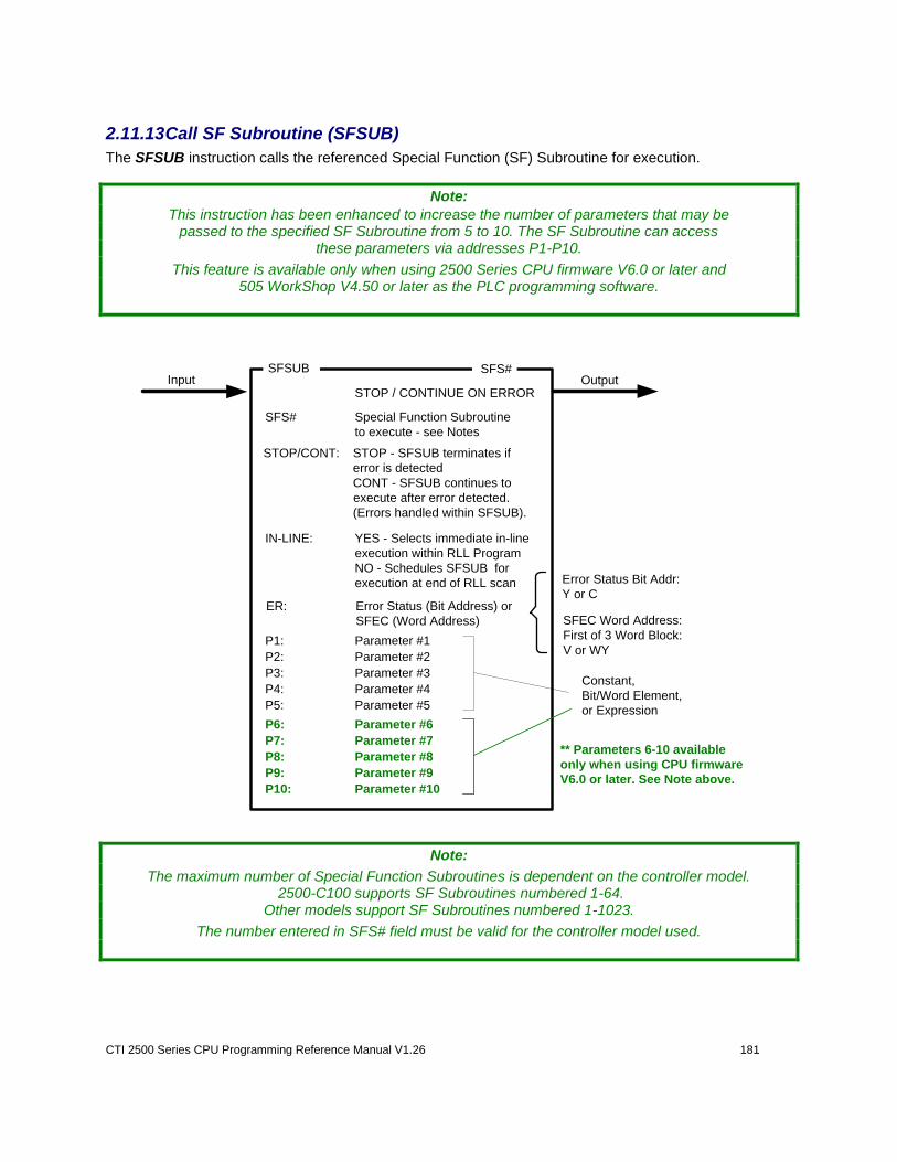
CTI 2500 Series CPU Programming Reference Manual V1.26 181
2.11.13 Call SF Subroutine (SFSUB)
The SFSUB instruction calls the referenced Special Function (SF) Subroutine for execution.
Note:
This instruction has been enhanced to increase the number of parameters that may be passed to the specified SF Subroutine from 5 to 10. The SF Subroutine can access
these parameters via addresses P1-P10.
This feature is available only when using 2500 Series CPU firmware V6.0 or later and 505 WorkShop V4.50 or later as the PLC programming software.
SFSUBOutputInput
SFS#
SFS# Special Function Subroutine
to execute - see Notes
IN-LINE: YES - Selects immediate in-line
execution within RLL Program
NO - Schedules SFSUB for
execution at end of RLL scan
STOP / CONTINUE ON ERROR
STOP/CONT: STOP - SFSUB terminates if
error is detected
CONT - SFSUB continues to
execute after error detected.
(Errors handled within SFSUB).
P1: Parameter #1
P2: Parameter #2
P3: Parameter #3
P4: Parameter #4
P5: Parameter #5
ER: Error Status (Bit Address) or
SFEC (Word Address) SFEC Word Address:
First of 3 Word Block:
V or WY
Error Status Bit Addr:
Y or C
Constant,
Bit/Word Element,
or ExpressionP6: Parameter #6
P7: Parameter #7
P8: Parameter #8
P9: Parameter #9
P10: Parameter #10
** Parameters 6-10 available
only when using CPU firmware
V6.0 or later. See Note above.
Note:
The maximum number of Special Function Subroutines is dependent on the controller model. 2500-C100 supports SF Subroutines numbered 1-64.
Other models support SF Subroutines numbered 1-1023.
The number entered in SFS# field must be valid for the controller model used.
182 CTI 2500 Series CPU Programming Reference Manual V1.26
SF Subroutine Overview
SF Subroutines are written in a statement-driven programming language similar to BASIC. The controller automatically compiles all SF statements and utilizes a hardware floating point co-processor to greatly improve execution time, especially for complex mathematical and logical expressions.
SFSUB instructions referencing the same SFS# can be included multiple places in an RLL program. This allows an application to execute the same SF Subroutine many times during a single scan using different parameter sets.
When inserted, the SFSUB instruction is displayed showing five (5) parameters. This parameter list may be extended to specify up to ten (10) parameters using the “Add CFUNC/SFSUB Parameter” function under the “Program” selection in the WorkShop main toolbar.
The Error Status (ER) can be assigned to a single bit (Y or C) or Word Address corresponding to the Special Function Error Code (SFEC). The SFEC is a contiguous 3-word block that provides detailed error information.
The “STOP/CONTINUE ON ERROR” field determines the SFSUB action when an error is detected during execution:
STOP terminates the SF Subroutine immediately. Error status is reported in Error Status Bit Address or SFEC Address designated in “ER” field.
CONT causes the SF Subroutine to continue execution after an error is detected. This allows the user to detect errors (via SFEC variable) and take corrective action as required.
SF Subroutines differ from SF Programs in that up to ten (10) parameters can be specified. Parameters must be entered in order starting with Parameter #1 and specified as follows:
Constant (32-bit integer or real number)
Discrete or Word element – Address consisting of data type and number.
Can be specified as Integer or Real Number (by adding a decimal point after the element) Examples: V150 = integer address, V160. = real (32-bit) address
Mathematical expression to be evaluated and/or passed to the referenced SF Subroutine. See example in this Section.
The controller maintains two separate queues for managing SF Subroutine operations. One queue handles SFSUB 0 instructions, and the other holds all other SFSUB instructions.
SFSUB 0 (SFS# = 0) is a special case where the instruction parameters entered as expressions are executed without calling an actual SF Subroutine (since SFSUB 0 program does not exist).
All other SFSUB instructions (SFS# 1-64 for Model 2500-C100 and SFS# 1-1023 for other models) are executed so that the parameters are first processed and then passed to the referenced SF Subroutine program.
See Chapter 3 for a detailed description on SF Subroutines.
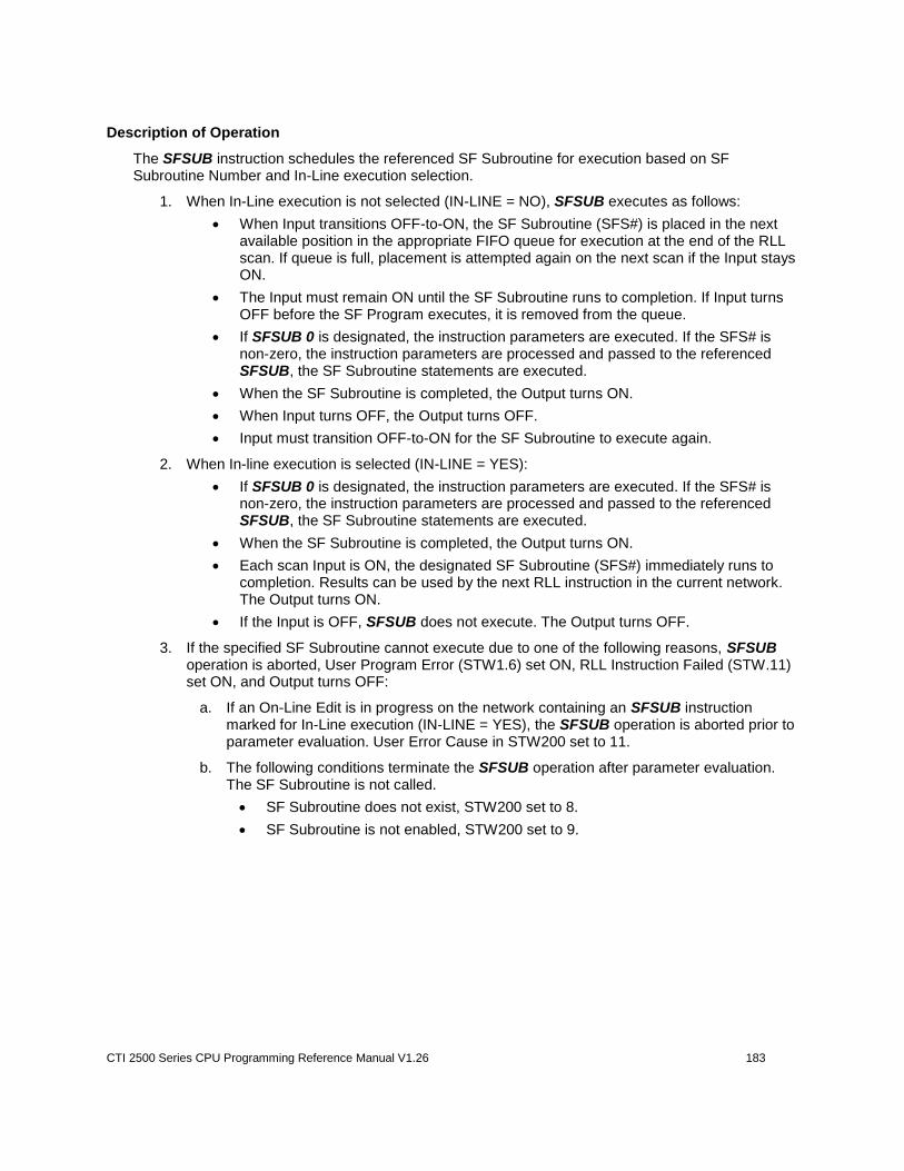
CTI 2500 Series CPU Programming Reference Manual V1.26 183
Description of Operation
The SFSUB instruction schedules the referenced SF Subroutine for execution based on SF Subroutine Number and In-Line execution selection.
1. When In-Line execution is not selected (IN-LINE = NO), SFSUB executes as follows:
When Input transitions OFF-to-ON, the SF Subroutine (SFS#) is placed in the next available position in the appropriate FIFO queue for execution at the end of the RLL scan. If queue is full, placement is attempted again on the next scan if the Input stays ON.
The Input must remain ON until the SF Subroutine runs to completion. If Input turns OFF before the SF Program executes, it is removed from the queue.
If SFSUB 0 is designated, the instruction parameters are executed. If the SFS# is non-zero, the instruction parameters are processed and passed to the referenced SFSUB, the SF Subroutine statements are executed.
When the SF Subroutine is completed, the Output turns ON.
When Input turns OFF, the Output turns OFF.
Input must transition OFF-to-ON for the SF Subroutine to execute again.
2. When In-line execution is selected (IN-LINE = YES):
If SFSUB 0 is designated, the instruction parameters are executed. If the SFS# is non-zero, the instruction parameters are processed and passed to the referenced SFSUB, the SF Subroutine statements are executed.
When the SF Subroutine is completed, the Output turns ON.
Each scan Input is ON, the designated SF Subroutine (SFS#) immediately runs to completion. Results can be used by the next RLL instruction in the current network. The Output turns ON.
If the Input is OFF, SFSUB does not execute. The Output turns OFF.
3. If the specified SF Subroutine cannot execute due to one of the following reasons, SFSUB operation is aborted, User Program Error (STW1.6) set ON, RLL Instruction Failed (STW.11) set ON, and Output turns OFF:
a. If an On-Line Edit is in progress on the network containing an SFSUB instruction marked for In-Line execution (IN-LINE = YES), the SFSUB operation is aborted prior to parameter evaluation. User Error Cause in STW200 set to 11.
b. The following conditions terminate the SFSUB operation after parameter evaluation. The SF Subroutine is not called.
SF Subroutine does not exist, STW200 set to 8.
SF Subroutine is not enabled, STW200 set to 9.
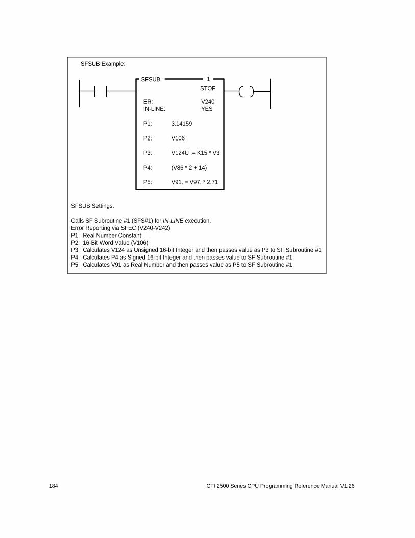
184 CTI 2500 Series CPU Programming Reference Manual V1.26
SFSUB Example:
SFSUB Settings:
Calls SF Subroutine #1 (SFS#1) for IN-LINE execution.
Error Reporting via SFEC (V240-V242)
P1: Real Number Constant
P2: 16-Bit Word Value (V106)
P3: Calculates V124 as Unsigned 16-bit Integer and then passes value as P3 to SF Subroutine #1
P4: Calculates P4 as Signed 16-bit Integer and then passes value to SF Subroutine #1
P5: Calculates V91 as Real Number and then passes value as P5 to SF Subroutine #1
ER: V240
IN-LINE: YES
1
STOP
P1: 3.14159
P2: V106
P3: V124U := K15 * V3
P4: (V86 * 2 + 14)
P5: V91. = V97. * 2.71
SFSUB
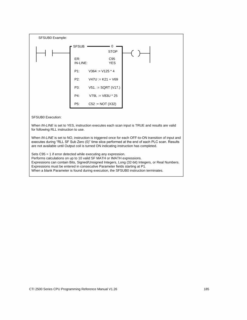
CTI 2500 Series CPU Programming Reference Manual V1.26 185
SFSUB0 Example:
SFSUB0 Execution:
When IN-LINE is set to YES, instruction executes each scan input is TRUE and results are valid
for following RLL instruction to use.
When IN-LINE is set to NO, instruction is triggered once for each OFF-to-ON transition of input and
executes during “RLL SF Sub Zero (0)” time slice performed at the end of each PLC scan. Results
are not available until Output coil is turned ON indicating instruction has completed.
Sets C95 = 1 if error detected while executing any expression.
Performs calculations on up to 10 valid SF MATH or IMATH expressions.
Expressions can contain Bits, Signed/Unsigned Integers, Long (32-bit) Integers, or Real Numbers.
Expressions must be entered in consecutive Parameter fields starting at P1.
When a blank Parameter is found during execution, the SFSUB0 instruction terminates.
ER: C95
IN-LINE: YES
0
STOP
P1: V364 := V125 * 4
P2: V47U := K21 + V69
P3: V51. := SQRT (V17.)
P4: V79L := V83U * 25
P5: C52 := NOT (X32)
SFSUB
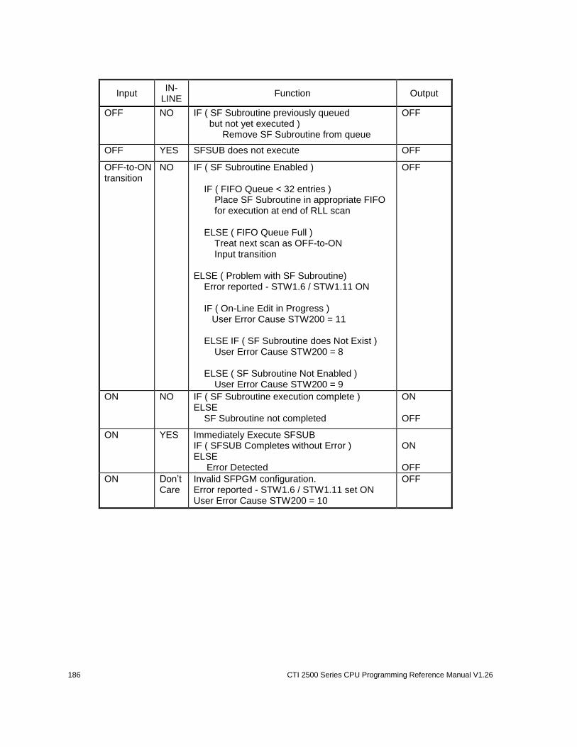
186 CTI 2500 Series CPU Programming Reference Manual V1.26
Input IN-
LINE Function Output
OFF NO IF ( SF Subroutine previously queued but not yet executed ) Remove SF Subroutine from queue
OFF
OFF YES SFSUB does not execute OFF
OFF-to-ON transition
NO IF ( SF Subroutine Enabled ) IF ( FIFO Queue < 32 entries ) Place SF Subroutine in appropriate FIFO for execution at end of RLL scan ELSE ( FIFO Queue Full ) Treat next scan as OFF-to-ON Input transition ELSE ( Problem with SF Subroutine) Error reported - STW1.6 / STW1.11 ON IF ( On-Line Edit in Progress ) User Error Cause STW200 = 11 ELSE IF ( SF Subroutine does Not Exist ) User Error Cause STW200 = 8 ELSE ( SF Subroutine Not Enabled ) User Error Cause STW200 = 9
OFF
ON NO IF ( SF Subroutine execution complete ) ELSE SF Subroutine not completed
ON OFF
ON YES Immediately Execute SFSUB IF ( SFSUB Completes without Error ) ELSE Error Detected
ON OFF
ON Don’t Care
Invalid SFPGM configuration. Error reported - STW1.6 / STW1.11 set ON User Error Cause STW200 = 10
OFF
CTI 2500 Series CPU Programming Reference Manual V1.26 187
2.11.14 Start RLL Task (TASK)
The TASK instruction designates the instructions to be executed as main RLL task (TASK1) and Cyclic RLL task (TASK2).
TASK TASK#
TASK#: Constant
1 = Main RLL Task
2 = Cyclic RLL Task
T: Cycle Time (ms)
Word Address or
Constant
Any Word Address:
WX/WY, V, K, STW, TCC,
TCP, DSC, DSP, DCC, W
Description of Operation
The TASK instruction is entered as an unconditional RLL network output.
The controller supports two different groups and priorities of RLL instructions:
1. Main RLL networks are the normal priority instructions that execute once per PLC scan
2. Cyclic RLL networks are the high priority instructions that execute on the specified time interval. The Cyclic RLL task interrupts all other PLC operations (Main RLL, Analog Tasks, I/O Update) in order to execute when required.
The RLL program is limited to one Main RLL Task (TASK1) and (optionally) one Cyclic RLL Task (TASK2). However, each task can consist of one or more segments of RLL instructions. Each task segment is delimited by the TASK instruction in the first RLL network. A task segment is terminated by another TASK instruction or END instruction. All task segments must be placed in front of the END instruction.
Each task executes RLL instructions in order from top to bottom as positioned in the program.
If the first RLL network does not include the TASK instruction, TASK1 is assumed. Therefore, all RLL instructions are executed as Main RLL until a TASK2 instruction is encountered.
The Task Cycle Time (T) applies only to the Cyclic RLL Task (TASK2). The Cycle Time can be designated in milliseconds as a signed integer constant (0-32767) or as an unsigned integer value (0-65535) in the specified Word Memory Address. The use of a Word Address allows the cycle interval to be altered during run time. If the Task Cycle Time = 0, the default time of 10 msec is used.
If the Cyclic RLL Task consists of more than one TASK2 segment, the Task Cycle Time (T) specified in first TASK2 instruction determines the Cyclic RLL Task interval.
188 CTI 2500 Series CPU Programming Reference Manual V1.26
Usage Guidelines
1. Cyclic RLL (TASK2) instructions are often used to execute Immediate I/O instructions. This provides a means to update critical I/O points at fixed intervals independent of PLC scan times. Note that I/O module response times are usually 5-10 msec, and updating an output point faster than 10 msec may not be reflected in the field device.
2. Careful consideration must be taken to determine the required Task Cycle Time for TASK2 operation. TASK2 execution interrupts other PLC scan functions and extends total scan time. The following criteria should be used to assess TASK2 time requirements:
Peak Execution Time can be displayed via HMI using SF variables TPET1 and TPET2. TPET1 shows maximum time to execute Main RLL instructions during a single PLC scan, and TPET2 shows the maximum time to complete a cycle of all Cyclic RLL instructions.
It is possible to set TASK2 Cycle Time so that almost all processing time is used executing only Cyclic RLL instructions. When TPET2 approaches the specified TASK2 Cycle Time, the total PLC scan time will be affected.
TASK2 execution can cause the PLC scan to extend beyond the specified time when. “Fixed” or “Variable with Upper Limit” scan mode is selected, If this occurs, RLL TASK1 Overrun (STW219.1) and Scan Overrun (STW1.14) bits are set ON.
If the Cyclic RLL does not complete execution within the specified Task Cycle Time, the RLL TASK2 Overrun Error (STW219.2) is set ON. In addition, one Cyclic RLL cycle is skipped due to the overrun condition. For instance, task with 5 msec cycle time that overruns then executes at 10 msec interval.
3. Subroutines can be called from any task. However, a given subroutine should not be called from both TASK1 and TASK2 instructions. RLL Subroutines are not re-entrant and cannot be executed by both tasks concurrently.
4. Due to inefficiencies between switching between Main RLL and Cyclic RLL tasks, we do not recommend setting TASK2 Cycle Time less than 4 msec regardless of TASK2 execution time unless there is a definite requirement for more frequent operation.
WARNING:
Take care when determining the time interval for Cyclic RLL execution.
When TASK2 execution time approaches the specified Task Cycle Time, processing time allocated to Main RLL decreases. This can result in a
Scan Watchdog timeout. This causes a Fatal Error condition where the controller turns OFF all discrete outputs and freezes all analog outputs.
This could lead to equipment damage and/or serious injury to personnel. Please read the TASK instruction Usage Guidelines to minimize the risk of this occurrence.
CTI 2500 Series CPU Programming Reference Manual V1.26 189
Start of TASK2
segment #1
Main RLL
instructions
End of Main RLL
and Cyclic RLL
TASK Example:
RTN
SBR
TASK 2
T: V42
END
TASK 1
T: 0
TASK 2
T: 0
Start of Main RLL
TASK1 assumed
Cyclic RLL
instructions
Start of TASK1
segment #2
RLL
Subroutines
Cyclic RLL
instructions
Start of TASK2
segment #2
Cyclic RLL
instructions
1
2
3
4
5
6
7
8
9
10
11
12
13
14
15
Main RLL (TASK1) executes following networks once per scan: 1,2,3,7, 8, 9
Cyclic RLL (TASK2) executes following networks each cycle: 4, 5,6, 10, 11
Task Cycle Time for TASK2 is determined by the value in Word Address V42
(set by the first TASK2 instruction encountered).
190 CTI 2500 Series CPU Programming Reference Manual V1.26
2.11.15 Special Operations
These instructions perform operations in support of other RLL instructions.
2.11.16 Load Data Constant (LDC)
The LDC instruction moves a positive integer constant into the designated PLC memory location.
LDC
OutputInput
A: Destination Word Address
REF#
LOAD DATA CONSTANT
Any Writeable Word Addr:
WY, V, TCC, TCP,
DSC, DSP, DCC, W
REF#: Instruction Reference No
(0-32767) - see Notes
N: Data Constant to be loaded
(0 - 32767)
Description of Operation
The LDC instruction executes each scan the Input is ON.
Data Constant (N) is written to Word Address (A). Data Constant must be a positive integer in the range: 0 thru +32767
The Output turns ON.
Input Function Output
OFF LDC instruction does not execute OFF
ON
LDC instruction executes as follows: Constant value (N) written to Word Address (A)
ON
Note:
The Reference Number assigned to the instruction box (Constant: 0-32767) is used only for documentation purposes. The number entered can be repeated as needed.
Related instructions: LDA, MOV, MWI
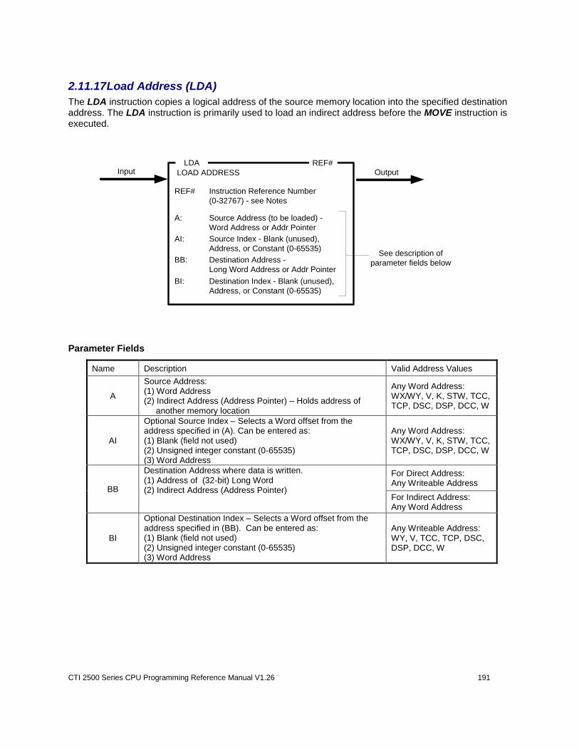
CTI 2500 Series CPU Programming Reference Manual V1.26 191
2.11.17 Load Address (LDA)
The LDA instruction copies a logical address of the source memory location into the specified destination address. The LDA instruction is primarily used to load an indirect address before the MOVE instruction is executed.
LDA
OutputInput
BB: Destination Address -
Long Word Address or Addr Pointer
REF#
A: Source Address (to be loaded) -
Word Address or Addr Pointer
REF# Instruction Reference Number
(0-32767) - see Notes
AI: Source Index - Blank (unused),
Address, or Constant (0-65535)
BI: Destination Index - Blank (unused),
Address, or Constant (0-65535)
See description of
parameter fields below
LOAD ADDRESS
Parameter Fields
Name Description Valid Address Values
A
Source Address: (1) Word Address (2) Indirect Address (Address Pointer) – Holds address of another memory location
Any Word Address: WX/WY, V, K, STW, TCC, TCP, DSC, DSP, DCC, W
AI
Optional Source Index – Selects a Word offset from the address specified in (A). Can be entered as: (1) Blank (field not used) (2) Unsigned integer constant (0-65535) (3) Word Address
Any Word Address: WX/WY, V, K, STW, TCC, TCP, DSC, DSP, DCC, W
BB
Destination Address where data is written. (1) Address of (32-bit) Long Word (2) Indirect Address (Address Pointer)
For Direct Address: Any Writeable Address
For Indirect Address: Any Word Address
BI
Optional Destination Index – Selects a Word offset from the address specified in (BB). Can be entered as: (1) Blank (field not used) (2) Unsigned integer constant (0-65535) (3) Word Address
Any Writeable Address: WY, V, TCC, TCP, DSC, DSP, DCC, W
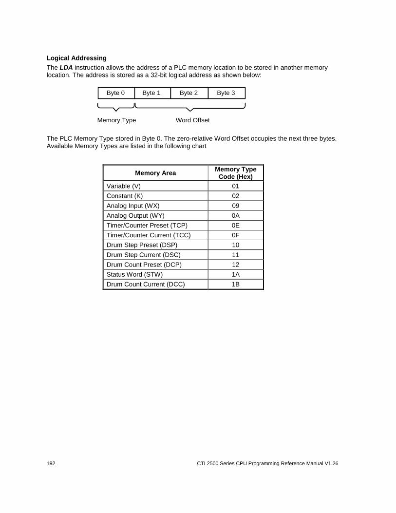
192 CTI 2500 Series CPU Programming Reference Manual V1.26
Logical Addressing
The LDA instruction allows the address of a PLC memory location to be stored in another memory location. The address is stored as a 32-bit logical address as shown below:
Byte 1Byte 0 Byte 2 Byte 3
Word OffsetMemory Type
The PLC Memory Type stored in Byte 0. The zero-relative Word Offset occupies the next three bytes. Available Memory Types are listed in the following chart
Memory Area Memory Type
Code (Hex)
Variable (V) 01
Constant (K) 02
Analog Input (WX) 09
Analog Output (WY) 0A
Timer/Counter Preset (TCP) 0E
Timer/Counter Current (TCC) 0F
Drum Step Preset (DSP) 10
Drum Step Current (DSC) 11
Drum Count Preset (DCP) 12
Status Word (STW) 1A
Drum Count Current (DCC) 1B
CTI 2500 Series CPU Programming Reference Manual V1.26 193
Entering Source Information
1. The Source Address (A) specifies the Word Address to be loaded into Destination (BB). The Source Address can be designated as one of the following types:
Word Address (any valid memory address) – Specifies the logical address to be loaded to the Destination Address.
Indirect Address (Address Pointer) – Specified Long Word Address holds the value of another memory location whose logical address is loaded into the Destination Address. An Address Pointer is a 32-bit value and is designated by inserting a “@” character as a prefix to the address, i.e., @V125 or @K20.
2. The Source Index (AI) field designates an index (or Word offset) from the Start Address (A) specified. When used, the actual starting location is Start Address (A) plus Index (AI). The Source Index can be used with either Direct or Indirect Addresses through one of the following values:
Blank – No indexing performed and no entry is required
Constant Index – Range: 0 to 65535 (value of 0 results in no index)
Variable Index – Value of the Word Address entered is interpreted as an Unsigned Integer (0 to 65535) and used as relative offset from (TS).
3. If Source Address (A) is specified as an Indirect Address with Source Index (AI), the actual address is determined by first calculating the Indirect Address location and then indexing from that point.
Entering Destination Information
1. The (BB) field specifies the Destination Address for the Data Elements by entering:
Word Address (any writeable memory address) – The logical address of the memory location specified in (A) is loaded as a 32-bit value into this Long Word Address.
Indirect Address (Address Pointer) – Specified Long Word Address holds the value of another memory location that is used as the Destination Address. An Address Pointer is a 32-bit value and is designated by inserting a “@” character as a prefix to the address, i.e., @V125 or @K20.
2. The Destination Index (BI) field designates an index (or relative offset) from the Destination Address (TD) specified. When used, the actual starting location is Destination Address (BB) plus Index (DI). The Destination Index can be used with either Direct or Indirect Addresses through one of the following values:
Blank – No indexing performed and no entry is required
Constant Index – Range: 0 to 65535 (value of 0 results in no index)
Variable Index – Value of the Word Address entered is interpreted as an Unsigned Integer (0 to 65535) and used as relative offset from (BB).
3. If Destination Address (BB) is specified as an Indirect Address with Destination Index (BI), the actual address is determined by first calculating the Indirect Address location and then indexing from that point.
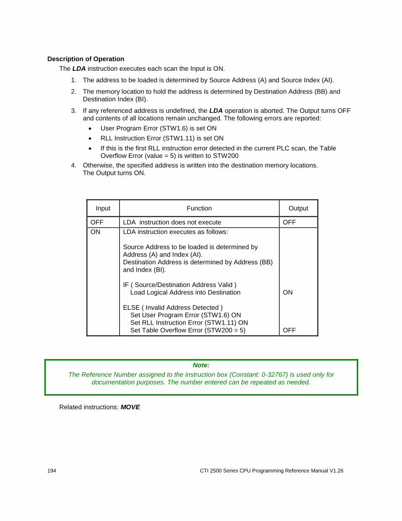
194 CTI 2500 Series CPU Programming Reference Manual V1.26
Description of Operation
The LDA instruction executes each scan the Input is ON.
1. The address to be loaded is determined by Source Address (A) and Source Index (AI).
2. The memory location to hold the address is determined by Destination Address (BB) and Destination Index (BI).
3. If any referenced address is undefined, the LDA operation is aborted. The Output turns OFF and contents of all locations remain unchanged. The following errors are reported:
User Program Error (STW1.6) is set ON
RLL Instruction Error (STW1.11) is set ON
If this is the first RLL instruction error detected in the current PLC scan, the Table Overflow Error (value = 5) is written to STW200
4. Otherwise, the specified address is written into the destination memory locations. The Output turns ON.
Input Function Output
OFF LDA instruction does not execute OFF
ON
LDA instruction executes as follows: Source Address to be loaded is determined by Address (A) and Index (AI). Destination Address is determined by Address (BB) and Index (BI). IF ( Source/Destination Address Valid ) Load Logical Address into Destination ELSE ( Invalid Address Detected ) Set User Program Error (STW1.6) ON Set RLL Instruction Error (STW1.11) ON Set Table Overflow Error (STW200 = 5)
ON OFF
Note:
The Reference Number assigned to the instruction box (Constant: 0-32767) is used only for documentation purposes. The number entered can be repeated as needed.
Related instructions: MOVE
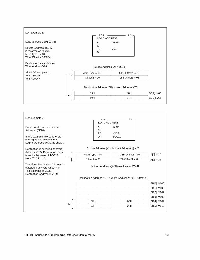
CTI 2500 Series CPU Programming Reference Manual V1.26 195
A: DSP5
22
LOAD ADDRESS
SI:
LDA
DI:
TD: V65
LDA Example 1:
Load address DSP5 to V65
Source Address (DSP5 )
is resolved as follows:
Mem Type = 10H
Word Offset = 000004H
Destination is specified as
Word Address V65.
After LDA completes,
V65 = 1000H
V66 = 0004H
BB[0]: V65
0 1 0 0 0 0 0 0 1000 0 1 0 1 BB[1]: V66
Destination Address (BB) = Word Address V65
00H
00H 04H
10H
0 1 0 0 0 0 0 0 1000 0 1 0 1
Source Address (A) = DSP5
MSB Offset1 = 00
Offset 2 = 00 LSB Offset3 = 04
Mem Type = 10H
Indirect Address @K20 resolves as WX41
A: @K20
23
LOAD ADDRESS
SI:
LDA
DI: TCC12
TD: V105
LDA Example 2:
Source Address is an Indirect
Address (@K20).
In this example, the Long Word
starting at K20 contains the
Logical Address WX41 as shown.
Destination is specified as Word
Address V105. Destination Index
is set by the value of TCC12.
Here, TCC12 = 4.
Therefore, Destination Address is
calculated as Word Offset 4 in
Table starting at V105.
Destination Address = V109
0 1 0 0 0 0 0 0 1000 0 1 0 1
Source Address (A) = Indirect Address @K20
MSB Offset1 = 00
Offset 2 = 00 LSB Offset3 = 28H
Mem Type = 09 A[0]: K20
A[1]: K21
BB[0]: V105
0 1 0 0 0 0 0 0 1000 0 1 0 1 BB[1]: V106
Destination Address (BB) = Word Address V105 + Offset 4
BB[2]: V107
0 1 0 0 0 0 0 0 1000 0 1 0 1 BB[3]: V108
BB[4]: V109
0 1 0 0 0 0 0 0 1000 0 1 0 1 BB[5]: V110
00H
00H 28H
09H
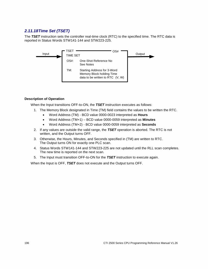
196 CTI 2500 Series CPU Programming Reference Manual V1.26
2.11.18 Time Set (TSET)
The TSET instruction sets the controller real-time clock (RTC) to the specified time. The RTC data is reported in Status Words STW141-144 and STW223-225.
TSETOutputInput
TM: Starting Address for 3-Word
Memory Block holding Time
data to be written to RTC (V, W)
OS#
TIME SET
OS#: One-Shot Reference No
See Notes
Description of Operation
When the Input transitions OFF-to-ON, the TSET instruction executes as follows:
1. The Memory Block designated in Time (TM) field contains the values to be written the RTC.
Word Address (TM) - BCD value 0000-0023 interpreted as Hours
Word Address (TM+1) – BCD value 0000-0059 interpreted as Minutes
Word Address (TM+2) - BCD value 0000-0059 interpreted as Seconds
2. If any values are outside the valid range, the TSET operation is aborted. The RTC is not written, and the Output turns OFF.
3. Otherwise, the Hours, Minutes, and Seconds specified in (TM) are written to RTC. The Output turns ON for exactly one PLC scan.
4. Status Words STW141-144 and STW223-225 are not updated until the RLL scan completes. The new time is reported on the next scan.
5. The Input must transition OFF-to-ON for the TSET instruction to execute again.
When the Input is OFF, TSET does not execute and the Output turns OFF.
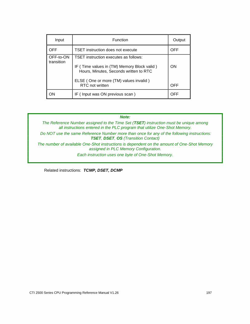
CTI 2500 Series CPU Programming Reference Manual V1.26 197
Input Function Output
OFF TSET instruction does not execute OFF
OFF-to-ON transition
TSET instruction executes as follows: IF ( Time values in (TM) Memory Block valid ) Hours, Minutes, Seconds written to RTC ELSE ( One or more (TM) values invalid ) RTC not written
ON OFF
ON IF ( Input was ON previous scan ) OFF
Note:
The Reference Number assigned to the Time Set (TSET) instruction must be unique among all instructions entered in the PLC program that utilize One-Shot Memory.
Do NOT use the same Reference Number more than once for any of the following instructions: TSET, DSET, OS (Transition Contact)
The number of available One-Shot instructions is dependent on the amount of One-Shot Memory assigned in PLC Memory Configuration.
Each instruction uses one byte of One-Shot Memory.
Related instructions: TCMP, DSET, DCMP
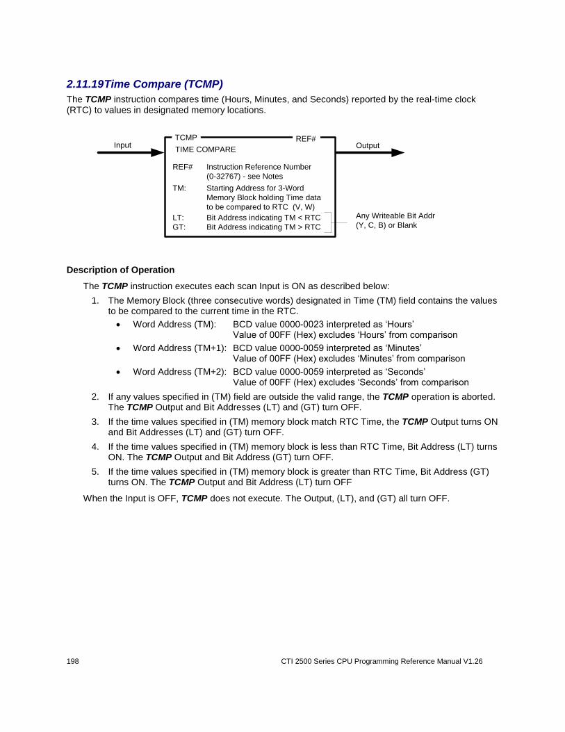
198 CTI 2500 Series CPU Programming Reference Manual V1.26
2.11.19 Time Compare (TCMP)
The TCMP instruction compares time (Hours, Minutes, and Seconds) reported by the real-time clock (RTC) to values in designated memory locations.
TCMPOutputInput
TM: Starting Address for 3-Word
Memory Block holding Time data
to be compared to RTC (V, W)
REF#
TIME COMPARE
REF# Instruction Reference Number
(0-32767) - see Notes
LT: Bit Address indicating TM < RTC
GT: Bit Address indicating TM > RTC
Any Writeable Bit Addr
(Y, C, B) or Blank
Description of Operation
The TCMP instruction executes each scan Input is ON as described below:
1. The Memory Block (three consecutive words) designated in Time (TM) field contains the values to be compared to the current time in the RTC.
Word Address (TM): BCD value 0000-0023 interpreted as ‘Hours’ Value of 00FF (Hex) excludes ‘Hours’ from comparison
Word Address (TM+1): BCD value 0000-0059 interpreted as ‘Minutes’ Value of 00FF (Hex) excludes ‘Minutes’ from comparison
Word Address (TM+2): BCD value 0000-0059 interpreted as ‘Seconds’ Value of 00FF (Hex) excludes ‘Seconds’ from comparison
2. If any values specified in (TM) field are outside the valid range, the TCMP operation is aborted. The TCMP Output and Bit Addresses (LT) and (GT) turn OFF.
3. If the time values specified in (TM) memory block match RTC Time, the TCMP Output turns ON and Bit Addresses (LT) and (GT) turn OFF.
4. If the time values specified in (TM) memory block is less than RTC Time, Bit Address (LT) turns ON. The TCMP Output and Bit Address (GT) turn OFF.
5. If the time values specified in (TM) memory block is greater than RTC Time, Bit Address (GT) turns ON. The TCMP Output and Bit Address (LT) turn OFF
When the Input is OFF, TCMP does not execute. The Output, (LT), and (GT) all turn OFF.
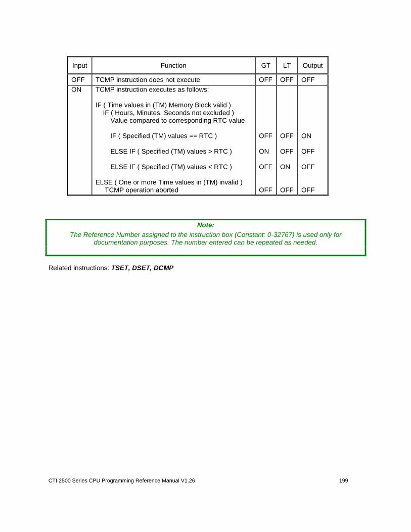
CTI 2500 Series CPU Programming Reference Manual V1.26 199
Input Function GT LT Output
OFF TCMP instruction does not execute OFF OFF OFF
ON
TCMP instruction executes as follows: IF ( Time values in (TM) Memory Block valid ) IF ( Hours, Minutes, Seconds not excluded ) Value compared to corresponding RTC value IF ( Specified (TM) values == RTC ) ELSE IF ( Specified (TM) values > RTC ) ELSE IF ( Specified (TM) values < RTC ) ELSE ( One or more Time values in (TM) invalid ) TCMP operation aborted
OFF ON OFF OFF
OFF OFF ON OFF
ON OFF OFF OFF
Note:
The Reference Number assigned to the instruction box (Constant: 0-32767) is used only for documentation purposes. The number entered can be repeated as needed.
Related instructions: TSET, DSET, DCMP
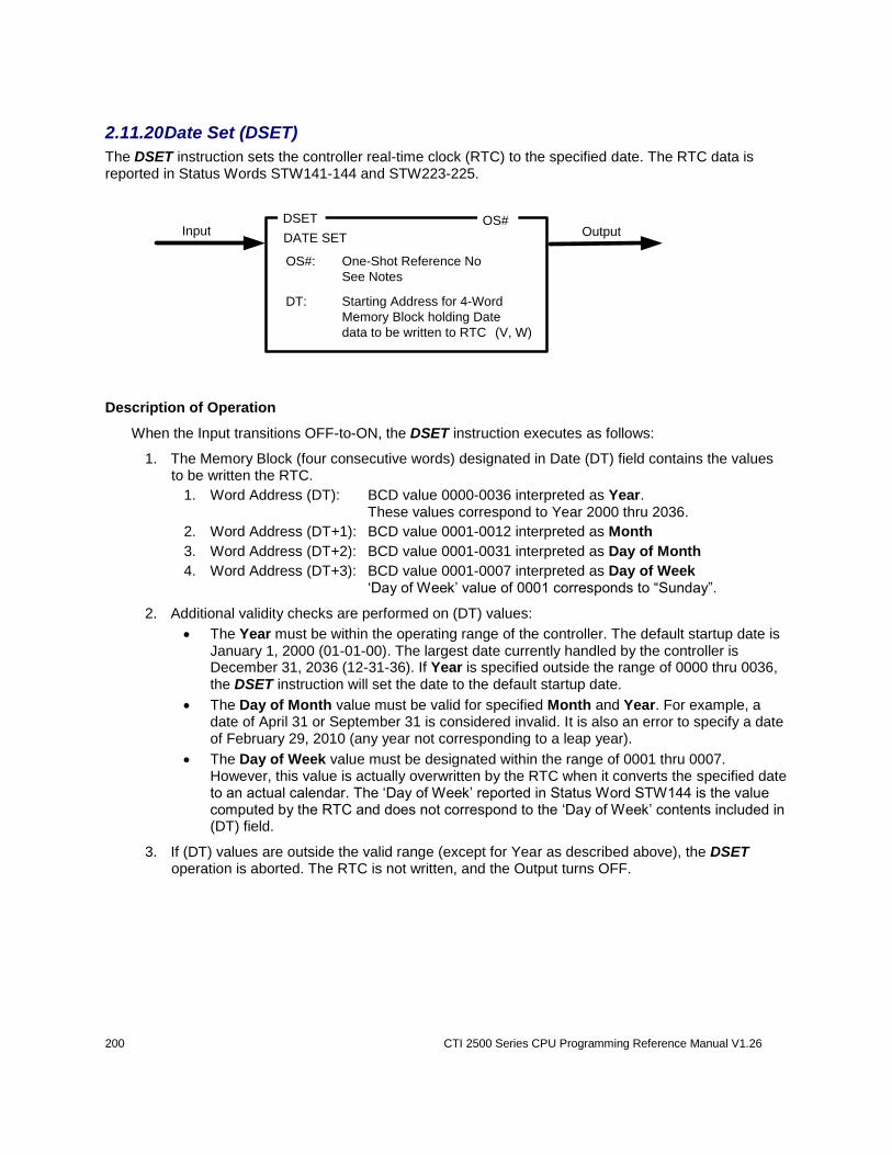
200 CTI 2500 Series CPU Programming Reference Manual V1.26
2.11.20 Date Set (DSET)
The DSET instruction sets the controller real-time clock (RTC) to the specified date. The RTC data is reported in Status Words STW141-144 and STW223-225.
DSETOutputInput
DT: Starting Address for 4-Word
Memory Block holding Date
data to be written to RTC (V, W)
OS#
DATE SET
OS#: One-Shot Reference No
See Notes
Description of Operation
When the Input transitions OFF-to-ON, the DSET instruction executes as follows:
1. The Memory Block (four consecutive words) designated in Date (DT) field contains the values to be written the RTC.
1. Word Address (DT): BCD value 0000-0036 interpreted as Year. These values correspond to Year 2000 thru 2036.
2. Word Address (DT+1): BCD value 0001-0012 interpreted as Month
3. Word Address (DT+2): BCD value 0001-0031 interpreted as Day of Month
4. Word Address (DT+3): BCD value 0001-0007 interpreted as Day of Week ‘Day of Week’ value of 0001 corresponds to “Sunday”.
2. Additional validity checks are performed on (DT) values:
The Year must be within the operating range of the controller. The default startup date is January 1, 2000 (01-01-00). The largest date currently handled by the controller is December 31, 2036 (12-31-36). If Year is specified outside the range of 0000 thru 0036, the DSET instruction will set the date to the default startup date.
The Day of Month value must be valid for specified Month and Year. For example, a date of April 31 or September 31 is considered invalid. It is also an error to specify a date of February 29, 2010 (any year not corresponding to a leap year).
The Day of Week value must be designated within the range of 0001 thru 0007. However, this value is actually overwritten by the RTC when it converts the specified date to an actual calendar. The ‘Day of Week’ reported in Status Word STW144 is the value computed by the RTC and does not correspond to the ‘Day of Week’ contents included in (DT) field.
3. If (DT) values are outside the valid range (except for Year as described above), the DSET operation is aborted. The RTC is not written, and the Output turns OFF.
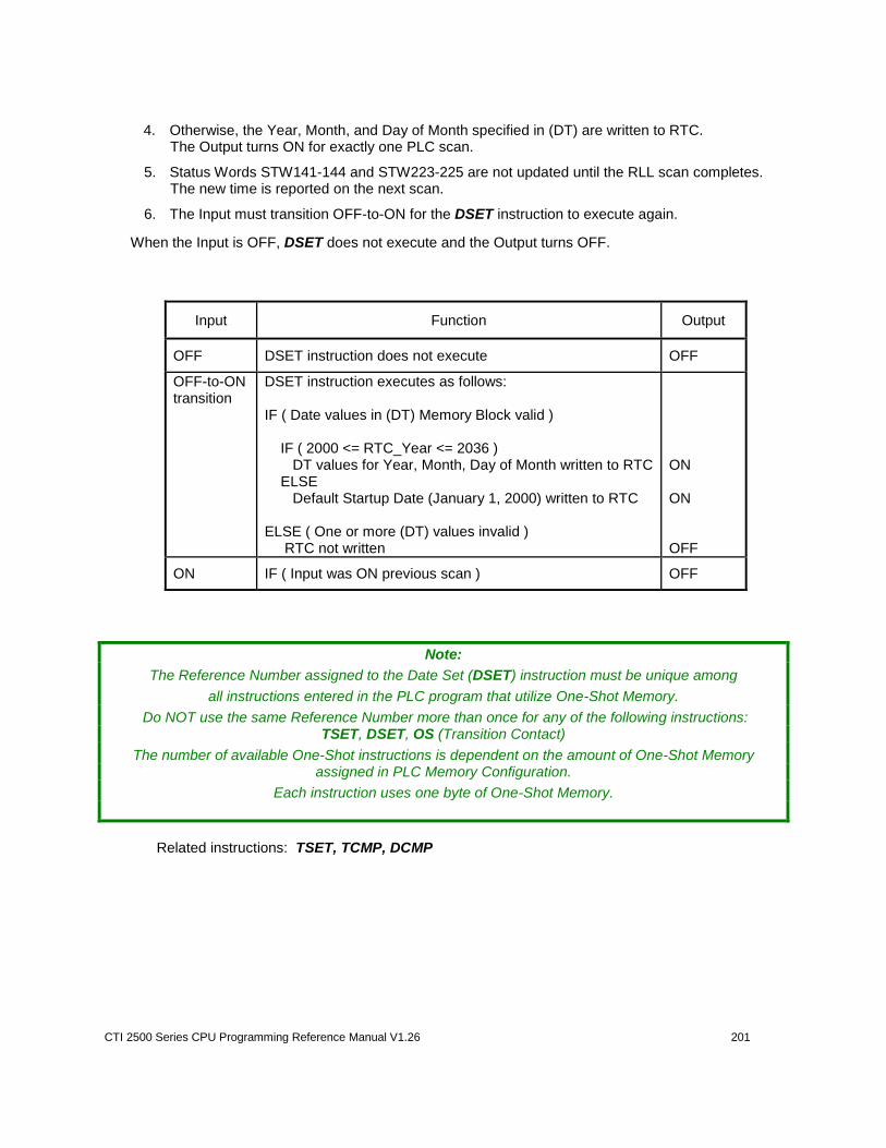
CTI 2500 Series CPU Programming Reference Manual V1.26 201
4. Otherwise, the Year, Month, and Day of Month specified in (DT) are written to RTC.
The Output turns ON for exactly one PLC scan.
5. Status Words STW141-144 and STW223-225 are not updated until the RLL scan completes. The new time is reported on the next scan.
6. The Input must transition OFF-to-ON for the DSET instruction to execute again.
When the Input is OFF, DSET does not execute and the Output turns OFF.
Input Function Output
OFF DSET instruction does not execute OFF
OFF-to-ON transition
DSET instruction executes as follows: IF ( Date values in (DT) Memory Block valid ) IF ( 2000 <= RTC_Year <= 2036 ) DT values for Year, Month, Day of Month written to RTC ELSE Default Startup Date (January 1, 2000) written to RTC ELSE ( One or more (DT) values invalid ) RTC not written
ON ON OFF
ON IF ( Input was ON previous scan ) OFF
Note:
The Reference Number assigned to the Date Set (DSET) instruction must be unique among
all instructions entered in the PLC program that utilize One-Shot Memory.
Do NOT use the same Reference Number more than once for any of the following instructions: TSET, DSET, OS (Transition Contact)
The number of available One-Shot instructions is dependent on the amount of One-Shot Memory assigned in PLC Memory Configuration.
Each instruction uses one byte of One-Shot Memory.
Related instructions: TSET, TCMP, DCMP
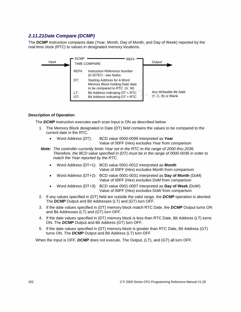
202 CTI 2500 Series CPU Programming Reference Manual V1.26
2.11.21 Date Compare (DCMP)
The DCMP instruction compares date (Year, Month, Day of Month, and Day of Week) reported by the real-time clock (RTC) to values in designated memory locations.
DCMPOutputInput
DT: Starting Address for 4-Word
Memory Block holding Date data
to be compared to RTC (V, W)
REF#
TIME COMPARE
REF# Instruction Reference Number
(0-32767) - see Notes
LT: Bit Address indicating DT < RTC
GT: Bit Address indicating DT > RTC
Any Writeable Bit Addr
(Y, C, B) or Blank
Description of Operation
The DCMP instruction executes each scan Input is ON as described below:
1. The Memory Block designated in Date (DT) field contains the values to be compared to the current date in the RTC.
Word Address (DT): BCD value 0000-0099 interpreted as Year Value of 00FF (Hex) excludes Year from comparison
Note: The controller currently limits Year set in the RTC to the range of 2000 thru 2036. Therefore, the BCD value specified in (DT) must be in the range of 0000-0036 in order to match the Year reported by the RTC.
Word Address (DT+1): BCD value 0001-0012 interpreted as Month Value of 00FF (Hex) excludes Month from comparison
Word Address (DT+2): BCD value 0001-0031 interpreted as Day of Month (DoM) Value of 00FF (Hex) excludes DoM from comparison
Word Address (DT+3): BCD value 0001-0007 interpreted as Day of Week (DoW) Value of 00FF (Hex) excludes DoW from comparison
2. If any values specified in (DT) field are outside the valid range, the DCMP operation is aborted. The DCMP Output and Bit Addresses (LT) and (GT) turn OFF.
3. If the date values specified in (DT) memory block match RTC Date, the DCMP Output turns ON and Bit Addresses (LT) and (GT) turn OFF.
4. If the date values specified in (DT) memory block is less than RTC Date, Bit Address (LT) turns ON. The DCMP Output and Bit Address (GT) turn OFF.
5. If the date values specified in (DT) memory block is greater than RTC Date, Bit Address (GT) turns ON. The DCMP Output and Bit Address (LT) turn OFF
When the Input is OFF, DCMP does not execute. The Output, (LT), and (GT) all turn OFF.
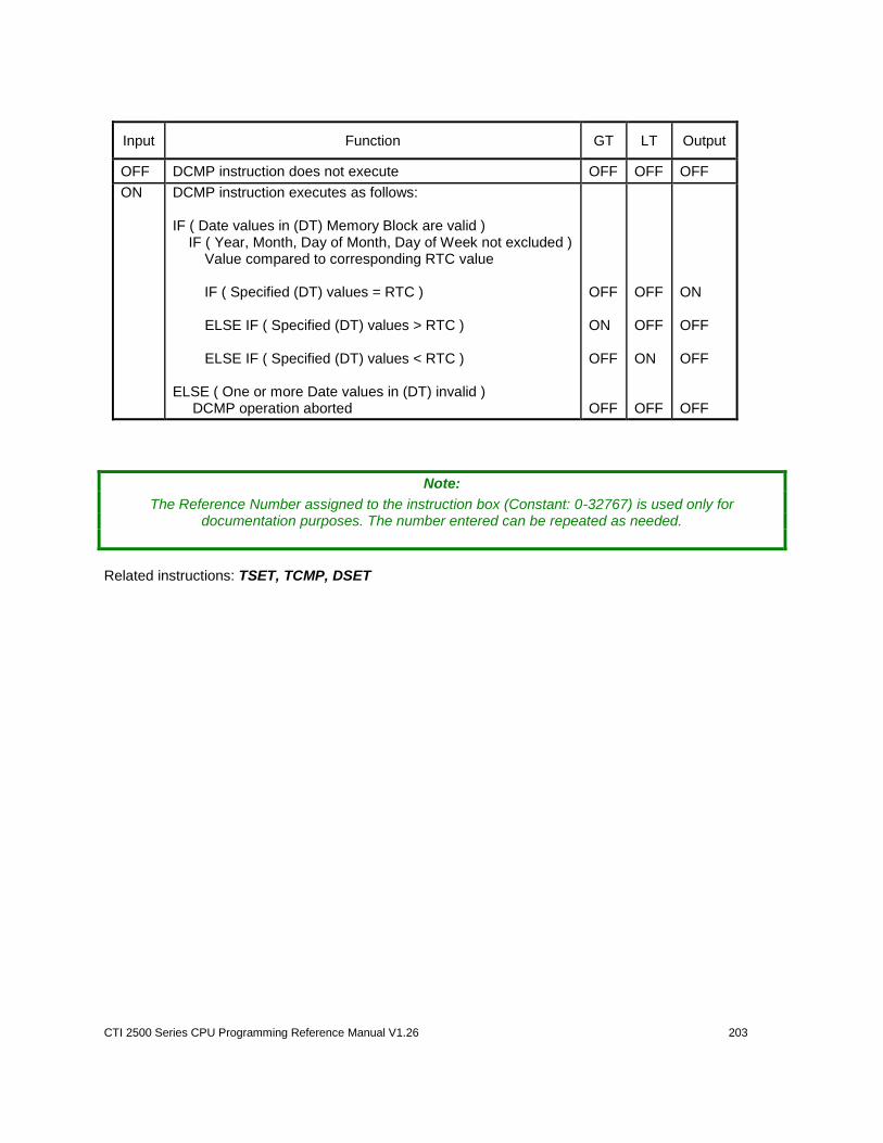
CTI 2500 Series CPU Programming Reference Manual V1.26 203
Input Function GT LT Output
OFF DCMP instruction does not execute OFF OFF OFF
ON
DCMP instruction executes as follows: IF ( Date values in (DT) Memory Block are valid ) IF ( Year, Month, Day of Month, Day of Week not excluded ) Value compared to corresponding RTC value IF ( Specified (DT) values = RTC ) ELSE IF ( Specified (DT) values > RTC ) ELSE IF ( Specified (DT) values < RTC ) ELSE ( One or more Date values in (DT) invalid ) DCMP operation aborted
OFF ON OFF OFF
OFF OFF ON OFF
ON OFF OFF OFF
Note:
The Reference Number assigned to the instruction box (Constant: 0-32767) is used only for documentation purposes. The number entered can be repeated as needed.
Related instructions: TSET, TCMP, DSET
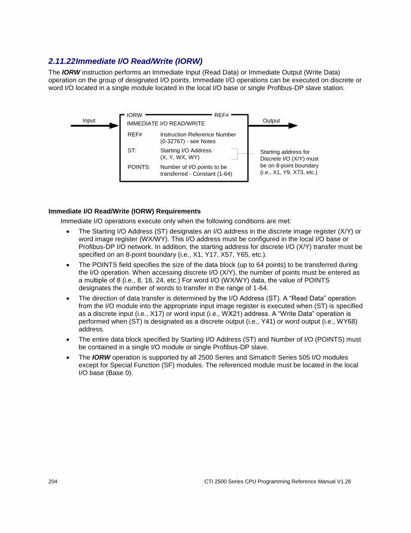
204 CTI 2500 Series CPU Programming Reference Manual V1.26
2.11.22 Immediate I/O Read/Write (IORW)
The IORW instruction performs an Immediate Input (Read Data) or Immediate Output (Write Data) operation on the group of designated I/O points. Immediate I/O operations can be executed on discrete or word I/O located in a single module located in the local I/O base or single Profibus-DP slave station.
IORWOutputInput
POINTS: Number of I/O points to be
transferred - Constant (1-64)
REF#
IMMEDIATE I/O READ/WRITE
ST: Starting I/O Address
(X, Y, WX, WY)
REF# Instruction Reference Number
(0-32767) - see Notes
Starting address for
Discrete I/O (X/Y) must
be on 8-point boundary
(i.e., X1, Y9, X73, etc.)
Immediate I/O Read/Write (IORW) Requirements
Immediate I/O operations execute only when the following conditions are met:
The Starting I/O Address (ST) designates an I/O address in the discrete image register (X/Y) or word image register (WX/WY). This I/O address must be configured in the local I/O base or Profibus-DP I/O network. In addition, the starting address for discrete I/O (X/Y) transfer must be specified on an 8-point boundary (i.e., X1, Y17, X57, Y65, etc.).
The POINTS field specifies the size of the data block (up to 64 points) to be transferred during the I/O operation. When accessing discrete I/O (X/Y), the number of points must be entered as a multiple of 8 (i.e., 8, 16, 24, etc.) For word I/O (WX/WY) data, the value of POINTS designates the number of words to transfer in the range of 1-64.
The direction of data transfer is determined by the I/O Address (ST). A “Read Data” operation from the I/O module into the appropriate input image register is executed when (ST) is specified as a discrete input (i.e., X17) or word input (i.e., WX21) address. A “Write Data” operation is performed when (ST) is designated as a discrete output (i.e., Y41) or word output (i.e., WY68) address.
The entire data block specified by Starting I/O Address (ST) and Number of I/O (POINTS) must be contained in a single I/O module or single Profibus-DP slave.
The IORW operation is supported by all 2500 Series and Simatic® Series 505 I/O modules except for Special Function (SF) modules. The referenced module must be located in the local I/O base (Base 0).
CTI 2500 Series CPU Programming Reference Manual V1.26 205
Description of Operation
The IORW instruction executes each scan the Input is ON.
1. The IORW operation interrupts the RLL scan to execute.
2. The Starting I/O Address (ST) determines the module location and direction of data transfer. Number of I/O points to transfer specified by value in POINTS field.
3. If the module is not present or designated I/O points are not contained within the I/O configuration for a module in the local base or Profibus-DP slave:
For Read operation, the specified points in the input image register are set to zero.
For Write operation, the operation aborts and points in the output image register are not copied to the module.
The Output turns OFF.
4. Otherwise, IORW transfers data to/from the I/O module.
When Input I/O Address (X or WX) is specified, the current state of the specified number of points (POINTS) is read from the module and copied into the corresponding input image register.
When Output I/O Address (Y or WY) is specified, the current state of the specified number of points is copied from the corresponding output image register and written to the module.
The Output turns ON.
WARNING:
Use caution when placing an IORW instruction within a MCR Zone of Control. When an Immediate I/O Write operation is specified for discrete outputs, the current state of the Y
points in the output image register are written to the module. The specified points are not zeroed by the MCR before the Immediate Write operation is executed.
This could result in damage to equipment and/or serious injury to personnel.
In order for the IORW discrete outputs to be controlled by the MCR, the designated points in the output image register must set by coils within the MCR Zone of Control.
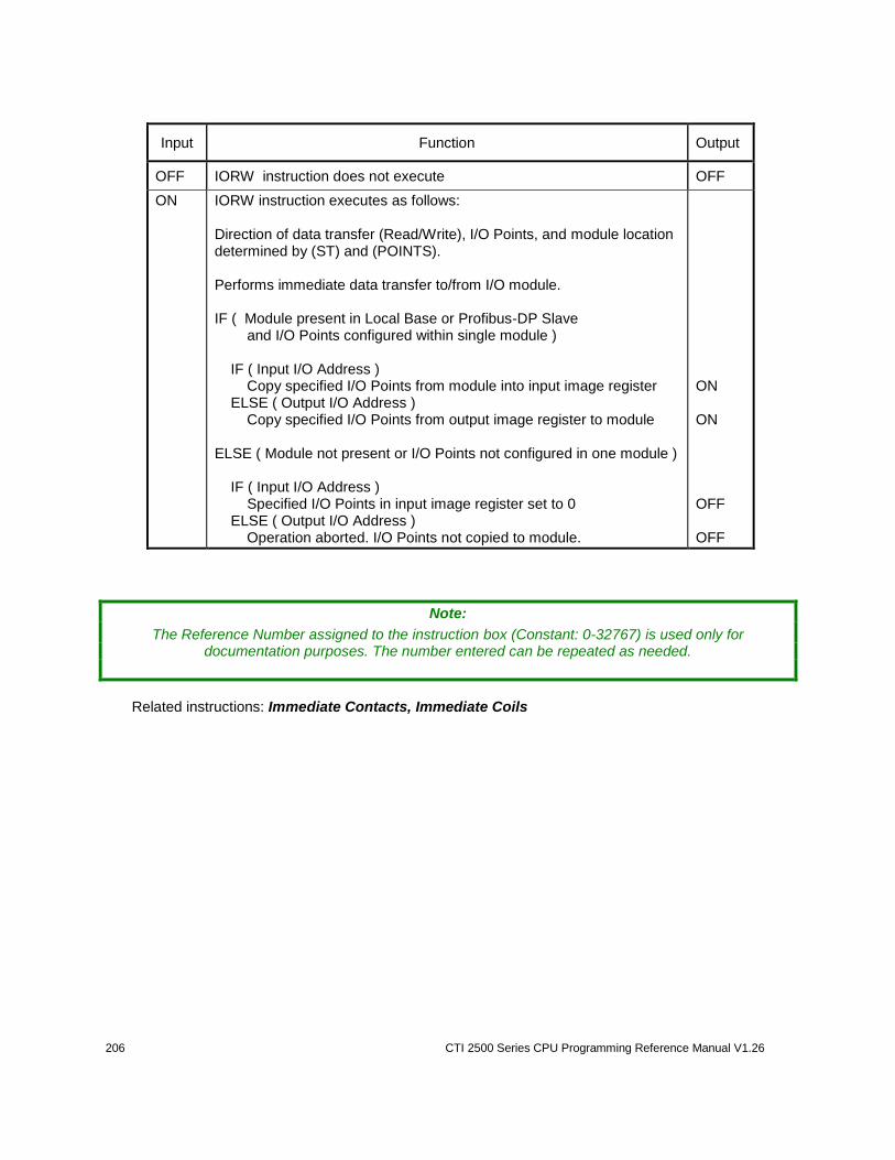
206 CTI 2500 Series CPU Programming Reference Manual V1.26
Input Function Output
OFF IORW instruction does not execute OFF
ON
IORW instruction executes as follows: Direction of data transfer (Read/Write), I/O Points, and module location determined by (ST) and (POINTS). Performs immediate data transfer to/from I/O module. IF ( Module present in Local Base or Profibus-DP Slave and I/O Points configured within single module ) IF ( Input I/O Address ) Copy specified I/O Points from module into input image register ELSE ( Output I/O Address ) Copy specified I/O Points from output image register to module ELSE ( Module not present or I/O Points not configured in one module ) IF ( Input I/O Address ) Specified I/O Points in input image register set to 0 ELSE ( Output I/O Address ) Operation aborted. I/O Points not copied to module.
ON ON OFF OFF
Note:
The Reference Number assigned to the instruction box (Constant: 0-32767) is used only for documentation purposes. The number entered can be repeated as needed.
Related instructions: Immediate Contacts, Immediate Coils
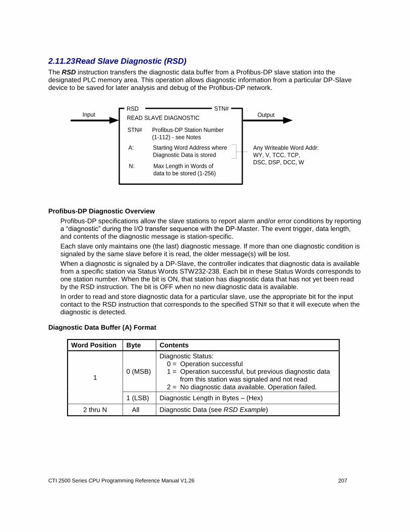
CTI 2500 Series CPU Programming Reference Manual V1.26 207
2.11.23 Read Slave Diagnostic (RSD)
The RSD instruction transfers the diagnostic data buffer from a Profibus-DP slave station into the designated PLC memory area. This operation allows diagnostic information from a particular DP-Slave device to be saved for later analysis and debug of the Profibus-DP network.
RSDOutputInput
N: Max Length in Words of
data to be stored (1-256)
STN#
READ SLAVE DIAGNOSTIC
A: Starting Word Address where
Diagnostic Data is stored
STN# Profibus-DP Station Number
(1-112) - see Notes
Any Writeable Word Addr:
WY, V, TCC, TCP,
DSC, DSP, DCC, W
Profibus-DP Diagnostic Overview
Profibus-DP specifications allow the slave stations to report alarm and/or error conditions by reporting a “diagnostic” during the I/O transfer sequence with the DP-Master. The event trigger, data length, and contents of the diagnostic message is station-specific.
Each slave only maintains one (the last) diagnostic message. If more than one diagnostic condition is signaled by the same slave before it is read, the older message(s) will be lost.
When a diagnostic is signaled by a DP-Slave, the controller indicates that diagnostic data is available from a specific station via Status Words STW232-238. Each bit in these Status Words corresponds to one station number. When the bit is ON, that station has diagnostic data that has not yet been read by the RSD instruction. The bit is OFF when no new diagnostic data is available.
In order to read and store diagnostic data for a particular slave, use the appropriate bit for the input contact to the RSD instruction that corresponds to the specified STN# so that it will execute when the diagnostic is detected.
Diagnostic Data Buffer (A) Format
Word Position Byte Contents
1 0 (MSB)
Diagnostic Status: 0 = Operation successful 1 = Operation successful, but previous diagnostic data from this station was signaled and not read 2 = No diagnostic data available. Operation failed.
1 (LSB) Diagnostic Length in Bytes – (Hex)
2 thru N All Diagnostic Data (see RSD Example)
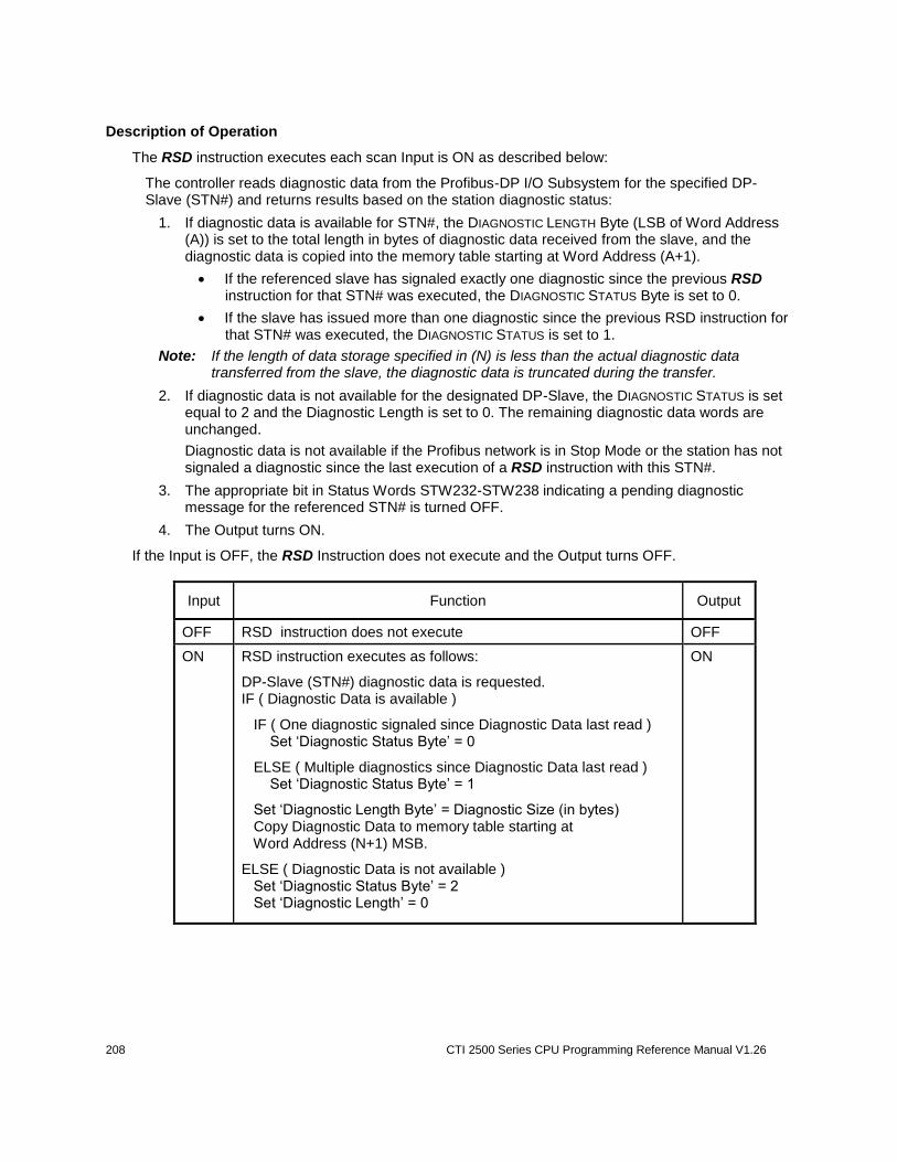
208 CTI 2500 Series CPU Programming Reference Manual V1.26
Description of Operation
The RSD instruction executes each scan Input is ON as described below:
The controller reads diagnostic data from the Profibus-DP I/O Subsystem for the specified DP-Slave (STN#) and returns results based on the station diagnostic status:
1. If diagnostic data is available for STN#, the DIAGNOSTIC LENGTH Byte (LSB of Word Address (A)) is set to the total length in bytes of diagnostic data received from the slave, and the diagnostic data is copied into the memory table starting at Word Address (A+1).
If the referenced slave has signaled exactly one diagnostic since the previous RSD instruction for that STN# was executed, the DIAGNOSTIC STATUS Byte is set to 0.
If the slave has issued more than one diagnostic since the previous RSD instruction for that STN# was executed, the DIAGNOSTIC STATUS is set to 1.
Note: If the length of data storage specified in (N) is less than the actual diagnostic data transferred from the slave, the diagnostic data is truncated during the transfer.
2. If diagnostic data is not available for the designated DP-Slave, the DIAGNOSTIC STATUS is set equal to 2 and the Diagnostic Length is set to 0. The remaining diagnostic data words are unchanged.
Diagnostic data is not available if the Profibus network is in Stop Mode or the station has not signaled a diagnostic since the last execution of a RSD instruction with this STN#.
3. The appropriate bit in Status Words STW232-STW238 indicating a pending diagnostic message for the referenced STN# is turned OFF.
4. The Output turns ON.
If the Input is OFF, the RSD Instruction does not execute and the Output turns OFF.
Input Function Output
OFF RSD instruction does not execute OFF
ON
RSD instruction executes as follows:
DP-Slave (STN#) diagnostic data is requested. IF ( Diagnostic Data is available )
IF ( One diagnostic signaled since Diagnostic Data last read ) Set ‘Diagnostic Status Byte’ = 0
ELSE ( Multiple diagnostics since Diagnostic Data last read ) Set ‘Diagnostic Status Byte’ = 1
Set ‘Diagnostic Length Byte’ = Diagnostic Size (in bytes) Copy Diagnostic Data to memory table starting at Word Address (N+1) MSB.
ELSE ( Diagnostic Data is not available ) Set ‘Diagnostic Status Byte’ = 2 Set ‘Diagnostic Length’ = 0
ON

CTI 2500 Series CPU Programming Reference Manual V1.26 209
3RSD
A: V90
N: 4
C11STW232.14
RSD Example:
When DP-Slave 3 signal diagnostic (indicated by STW232 Bit 14) = ON, the RSD instruction
runs and copies diagnostic data into memory table starting at V90. Maximum length of
diagnostic data saved is 6 bytes (3 words) starting at V91. The first word of the diagnostic
buffer (V90) is used for status information.
A[0]: V90
0 1 0 0 0 0 0 0 1000 0 1 0 1 A[1]: V91
Diag Length = 06H
Byte 1 = 02H Byte 2 = 04H
Diag Status = 00
A[2]: V92
0 1 0 0 0 0 0 0 1000 0 1 0 1 A[3]: V93
Byte 4 = 12H
Byte 5 = A7H Byte 6 = 03H
Byte 3 = 00H
Slave 3 Diagnostic Data (in Hex):
02 04 00 12 A7 03
Notes:
1) The Profibus-DP Station Number referenced by the RSD instruction box should be set to an address supported by the Profibus-DP I/O Subsystem (slave address: 1-112). A Station Number can be repeated in other RSD instruction boxes as needed.
2) The data length and content included in diagnostic data is proprietary for each DP-Slave device. Reference the product user manual for a description of the diagnostic data.
3) Each installed slave signals a diagnostic immediately after the DP-Master downloads its slave configuration. These diagnostic data messages are reported to the CPU. Therefore, it is normal for the Diagnostic Status bits (in STW232-STW238 ) corresponding to all configured slave stations to be set ON each time the Profibus Operation Mode is changed to RUN. This occurs automatically following a program download to the PLC.
The RSD instruction must be executed once for each STN# in order to clear the corresponding Diagnostic Status bit (in STW232-STW238) to zero.
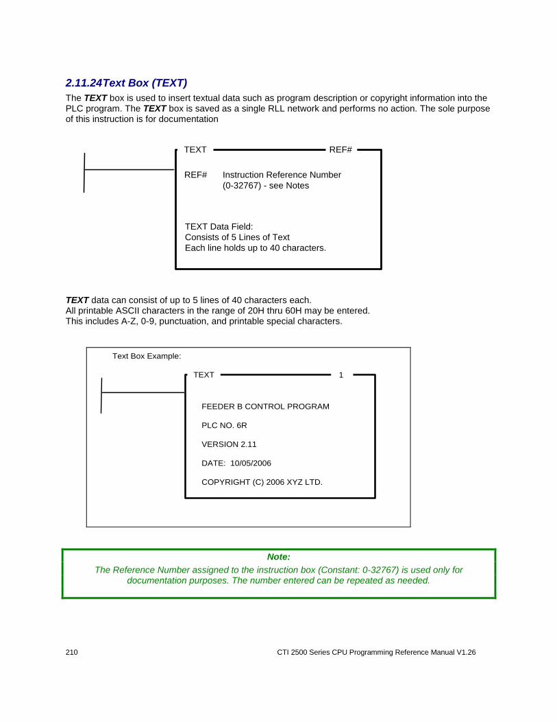
210 CTI 2500 Series CPU Programming Reference Manual V1.26
2.11.24 Text Box (TEXT)
The TEXT box is used to insert textual data such as program description or copyright information into the PLC program. The TEXT box is saved as a single RLL network and performs no action. The sole purpose of this instruction is for documentation
TEXT REF#
TEXT Data Field:
Consists of 5 Lines of Text
Each line holds up to 40 characters.
REF# Instruction Reference Number
(0-32767) - see Notes
TEXT data can consist of up to 5 lines of 40 characters each. All printable ASCII characters in the range of 20H thru 60H may be entered. This includes A-Z, 0-9, punctuation, and printable special characters.
TEXT 1
FEEDER B CONTROL PROGRAM
PLC NO. 6R
VERSION 2.11
DATE: 10/05/2006
COPYRIGHT (C) 2006 XYZ LTD.
Text Box Example:
Note:
The Reference Number assigned to the instruction box (Constant: 0-32767) is used only for documentation purposes. The number entered can be repeated as needed.
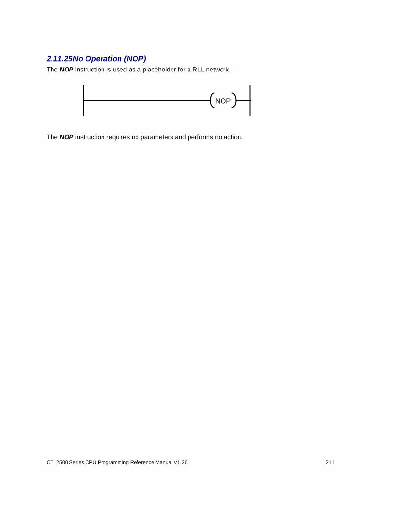
CTI 2500 Series CPU Programming Reference Manual V1.26 211
2.11.25 No Operation (NOP)
The NOP instruction is used as a placeholder for a RLL network.
NOP
The NOP instruction requires no parameters and performs no action.

212 CTI 2500 Series CPU Programming Reference Manual V1.26
CTI 2500 Series CPU Programming Reference Manual V1.26 213
CHAPTER 3 SF PROGRAMS AND SUBROUTINES
3.1 Overview
Special Function (SF) Programs and Subroutines provide a statement–oriented procedural programming language much like BASIC. Using SF Programs and Subroutines, you can develop process control applications that would be difficult or impossible to implement in RLL. This is particularly useful for performing complex mathematical calculations and IF-THEN-ELSE logic expressions.
SF Program execution can be initiated from the RLL program, Loops, or Analog Alarms. In addition, SF Subroutines can be called from an SF Program or another SF Subroutine.
Up to 1023 SF Programs and 1023 SF Subroutines can be defined. The actual number supported in the controller is dependent on the CPU model.
SF Programs and SF Subroutines are stored in S memory. The S memory size must be adjusted as required to accommodate your program storage requirement.
To maximize performance, all enabled SF Programs and Subroutines are compiled. Compiling takes place when the SF program or subroutine is downloaded or edited (if enabled) or when execution status is changed to enabled, if it has been modified.
3.2 SF Program/Subroutine Execution
3.2.1 SF Programs
When the SF Program is created, you designate how it is to be executed by selecting the ‘Program Type’ (NORMAL, PRIORITY, CYCLIC, or RESTRICTED).
All Series 2500™ Processors support In-Line execution of SF Programs. This feature allows all NORMAL and PRIORITY SF Programs to run as part of the RLL scan, and results are immediately available for use by other RLL instructions.
The temporary variable (T2) indicates how the SF Program was called.
3.2.1.1 Normal / Priority SF Programs
Normal and Priority program types are general-purpose SF Programs that can be called for execution from any source (RLL, Loops, or Alarms). These program types are identical except when run using the Deferred Execution method described later in this section.
When called from a Loop or Analog Alarm, Normal and Priority SF Programs execute exactly like Restricted SF Programs described in Section 3.2.2.3
Normal and Priority SF Programs may also be initiated from the RLL using the SFPGM instruction. The execution method then depends on whether the program is designated for In-Line Execution or Deferred Execution.
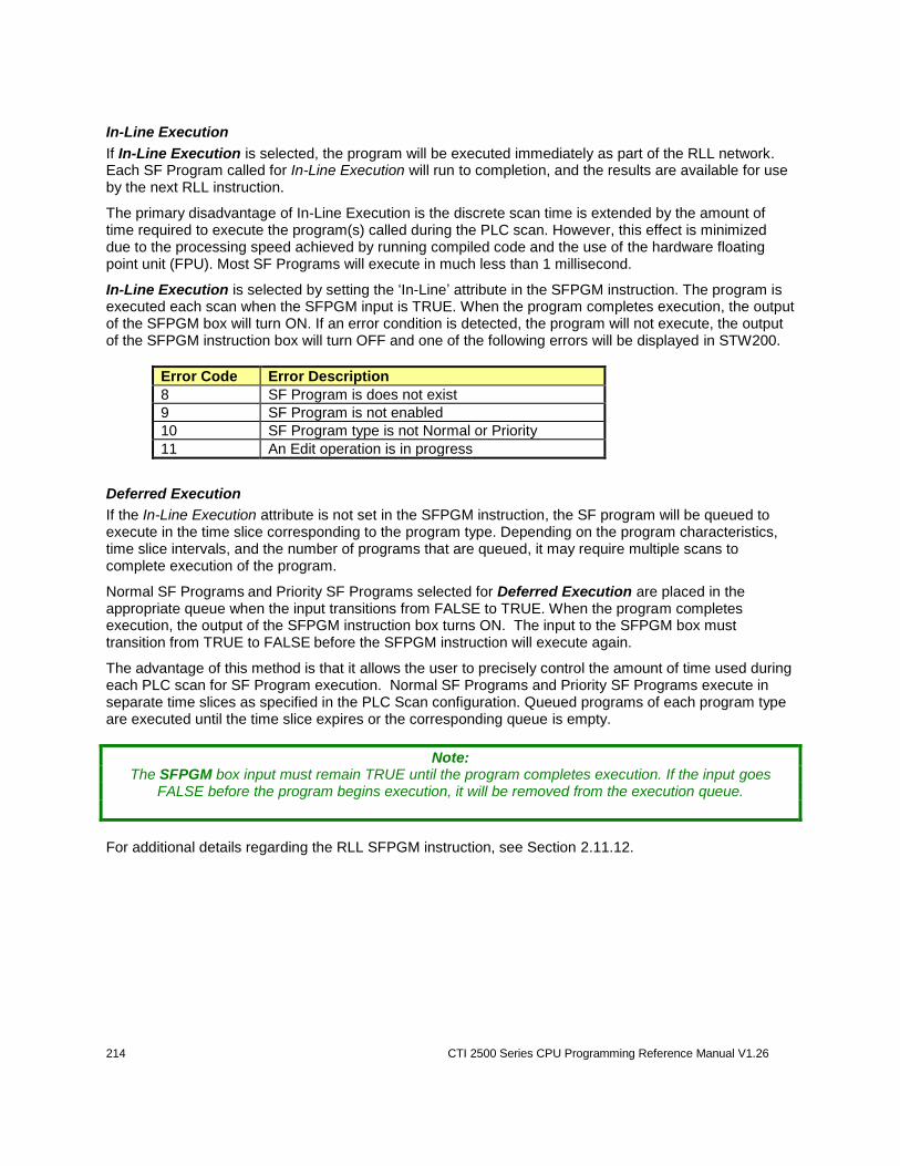
214 CTI 2500 Series CPU Programming Reference Manual V1.26
In-Line Execution
If In-Line Execution is selected, the program will be executed immediately as part of the RLL network. Each SF Program called for In-Line Execution will run to completion, and the results are available for use by the next RLL instruction.
The primary disadvantage of In-Line Execution is the discrete scan time is extended by the amount of time required to execute the program(s) called during the PLC scan. However, this effect is minimized due to the processing speed achieved by running compiled code and the use of the hardware floating point unit (FPU). Most SF Programs will execute in much less than 1 millisecond.
In-Line Execution is selected by setting the ‘In-Line’ attribute in the SFPGM instruction. The program is executed each scan when the SFPGM input is TRUE. When the program completes execution, the output of the SFPGM box will turn ON. If an error condition is detected, the program will not execute, the output of the SFPGM instruction box will turn OFF and one of the following errors will be displayed in STW200.
Error Code Error Description
8 SF Program is does not exist
9 SF Program is not enabled
10 SF Program type is not Normal or Priority
11 An Edit operation is in progress
Deferred Execution
If the In-Line Execution attribute is not set in the SFPGM instruction, the SF program will be queued to execute in the time slice corresponding to the program type. Depending on the program characteristics, time slice intervals, and the number of programs that are queued, it may require multiple scans to complete execution of the program.
Normal SF Programs and Priority SF Programs selected for Deferred Execution are placed in the appropriate queue when the input transitions from FALSE to TRUE. When the program completes execution, the output of the SFPGM instruction box turns ON. The input to the SFPGM box must transition from TRUE to FALSE before the SFPGM instruction will execute again.
The advantage of this method is that it allows the user to precisely control the amount of time used during each PLC scan for SF Program execution. Normal SF Programs and Priority SF Programs execute in separate time slices as specified in the PLC Scan configuration. Queued programs of each program type are executed until the time slice expires or the corresponding queue is empty.
Note: The SFPGM box input must remain TRUE until the program completes execution. If the input goes
FALSE before the program begins execution, it will be removed from the execution queue.
For additional details regarding the RLL SFPGM instruction, see Section 2.11.12.
CTI 2500 Series CPU Programming Reference Manual V1.26 215
3.2.1.2 Cyclic SF Programs
SF Programs designated as CYCLIC type run on the time interval specified in the program header. Cyclic SF Programs must be initiated from the RLL SFPGM instruction with the ‘In-Line’ attribute turned off.
Note:
Cyclic programs are queued for execution during the Cyclic SF Program time slice. An error is returned you attempt to execute them using the SFPGM instruction with the
In-Line attribute set.
Cyclic SF Programs are initially scheduled when the SFPGM box input transitions to TRUE. Thereafter, they are automatically re-scheduled for execution on the specified time interval as long as the input to the SFPGM instruction stays TRUE. The output of the SFPGM box turns ON after the first successful execution and remains ON as long as the input is TRUE. When the input goes FALSE, the Cyclic SF Program is removed from the queue.
Note:
The operation of Cyclic SF Programs in the CTI 2500 Series PLC differs slightly from the SIMATIC® 505 controller as described below:
CTI 2500 Series PLC: Cyclic SF Programs are removed from the execution queue
immediately when the SFPGM box input transitions from TRUE-to-FALSE.
SIMATIC® 505 controller: Cyclic SF Programs are removed from the queue immediately after the SF Program is executed if the SFPGM box input is FALSE. Therefore, if the input
transitions TRUE-to-FALSE during the wait period being execution cycles, the SFPGM will run one additional time before it is removed from the queue.
Cyclic SF Programs execute in a separate time slice as specified in the PLC Scan configuration. Each scan all scheduled Cyclic SF Programs are executed until the time slice expires or the queue is empty.
216 CTI 2500 Series CPU Programming Reference Manual V1.26
3.2.1.3 Restricted SF Programs
Loops and/or Alarms can be programmed to execute an SF Program in order to perform special processing on data variables. SF Programs assigned the program type of Restricted can only be executed when called by a Loop or Alarm.
Restricted SF Programs execute within the time slice of the calling Loop or Alarm. This capability allows you to customize the operation of the Loop or Alarm by performing calculations before certain parameters are used by the function. SF Programs called by Alarms
SF Programs called by Alarms are called at the Alarm Sample Rate. The program is executed after the Alarm Process Variable has been read but before it has been evaluated for an alarm condition. SF Local Variable T2=4 when called by Analog Alarm.
SF Programs called by a Loop execute at different times based on the SF Spec Calc setting (None, PV, SP, Output) specified in the Loop Configuration. Some settings provide multi-function operation as described below; SF Programs Called on Setpoint
This selection causes the designated SF Program to be executed only when the Loop is in Auto or Cascade mode. The SF Program is then called at the Loop Sample Rate with SF Local Variable T2=2. SF Programs Called on Process Variable
The designated SF Program is called in all Loop modes: Manual, Auto, or Cascade.
In Manual mode, the SF Program is called at the Loop Sample Rate for alarm monitoring purposes. In Auto (or Cascade) mode, the SF Program is called immediately before the Loop algorithm executes. In addition, the SF Program is also called for alarm monitoring at 2 second intervals as long as the time to the next scheduled Loop execution is greater than or equal to 2 seconds.
For instance, when the Loop Sample Rate is set to 3 seconds, the SF Program is called only when the Loop executes (because at the 2-second mark, the next Loop execution time is less than 2 seconds in the future). However, if the Loop Sample Rate is set to 6 seconds, the SF Program is called an additional 2 times during each Loop execution cycle – for alarm monitoring at 2-second and 4-second marks (because next Loop execution time is 2 seconds in the future).
The SF variable T2=2 when the SF Program runs immediately before the Loop algorithm executes. When SF Program is called for alarm monitoring purposes, this case is indicated by T2=3.
Note:
SF Programs called on Setpoint access or Process Variable access execute after the Setpoint (SP) and Process Variable (PV) have been read into the internal Loop variables.
This allows modification of either value before the Loop algorithm executes.
CTI 2500 Series CPU Programming Reference Manual V1.26 217
SF Programs Called on Loop Output
The designated SF Program is called in all Loop modes: Manual, Auto, or Cascade.
In Manual mode, the SF Program is called at the Loop Sample Rate for alarm monitoring purposes.
In Auto (or Cascade) mode, the SF Program is executed twice during each Loop algorithm calculation - immediately before and after the Loop algorithm executes. In addition, the SF Program is also called for alarm monitoring at 2 second intervals as long as the time to the next scheduled Loop execution is greater than or equal to 2 seconds.
For instance, when the Loop Sample Rate is set to 3 seconds, the SF Program is called only before/after the Loop algorithm calculation (because at the 2-second mark, the next Loop execution time is less than 2 seconds in the future). However, if the Loop Sample Rate is set to 6 seconds, the SF Program is called an additional 2 times during each Loop execution cycle – for alarm monitoring at 2-second and 4-second marks (because next Loop execution time is at least 2 seconds in the future).
The SF variable T2=2 when the SF Program runs immediately before the Loop algorithm executes, and T2=5 when the SF Program is called immediately after the Loop calculation.
When SF Program is called for alarm monitoring purposes, this case is indicated by T2=3.
Note:
A SF Program called on ‘Output’ is called twice each time the Loop calculation executes. The SFP is called the first time after Setpoint (SP) and Process Variable (PV) have been read into the internal Loop variables which allows modification of either value before the
Loop algorithm executes.
The SFP is then called again after the Loop calculation has completed and the Control Variable (Output) has been written into the internal Loop variable (LMNx).
This allows modification of Output value before data is written to the field Output channel.
218 CTI 2500 Series CPU Programming Reference Manual V1.26
3.2.2 SF Subroutines
SF Subroutines allow you to construct modular programs by creating re-useable sections of code using the BASIC-like SF instruction set. SF Subroutines can be called from RLL using the SFSUB box instruction, from an SF Program, or from another SF Subroutine (via the CALL instruction). When the SF Subroutine completes execution, it returns control to the program that called it.
3.2.2.1 SF Subroutines Called from RLL
SF Subroutines (1-1023) called from RLL execute in the following manner:
If the IN-LINE EXECUTION attribute is not set, the referenced SF Subroutine is queued for execution in the Ladder SFSUB time slice when the SFSUB instruction input transitions from FALSE to TRUE. The SFSUB box output will turn ON when the SFSUB successfully completes execution. The output remains ON until the input goes FALSE.
If IN-LINE EXECUTION is selected, the SF Subroutine is immediately executed each scan the input to the SFSUB instruction box is TRUE. If an Edit operation is in progress when the SFSUB instruction executes, the output is turned OFF and error code 11 is written to STW200. If the SF Subroutine does not exist or is disabled, an error is displayed in the SFSUB instruction’s ERROR
STATUS ADDRESS.
For additional details regarding the RLL SFSUB instruction, see Section 0.
3.2.2.2 SF Subroutines Called from SF Programs/Subroutines
SF Subroutines called by SF Programs or other SF Subroutines using the CALL instruction are executed as follows:
1. Control is transferred to the designated SF Subroutine, and it immediately begins to run. Upon completion, control returns to the calling SF Program/Subroutine and continues execution with the statement following the CALL instruction.
2. If the SF Subroutine does not exist or not enabled, an error code is written to the corresponding Error Status Address and the subroutine is not executed. Program action is based on ERROR
RESPONSE selected for the calling SF Program/Subroutine as described in Section 3.3.
A detailed description of the CALL instruction is provided in Section 3.5.5.
CTI 2500 Series CPU Programming Reference Manual V1.26 219
3.2.2.3 SF Subroutine Password Protection
Note:
This feature is available only when using 2500 Series CPU firmware V6.0 or later and 505 WorkShop V4.50 or later as PLC programming software.
The SF Subroutine password protection feature permits users and integrators to create programs that contain methods or calculations that are considered critical and/or private intellectual property without revealing the actual program instructions or allowing any edits to be performed.
The programmer has the option of setting password protection for each existing SF Subroutine. Once a password is entered for a particular SF Subroutine, it is designated as “protected” and can be viewed or modified only when the correct password is entered. Once a password has been successfully entered for a particular SF Subroutine, that program shall remain unprotected as long as the PLC Program (.FSS) file is open within 505 WorkShop. It is possible to “unprotect” multiple SF Subroutines at the same time.
Valid passwords can contain up to 16 characters including (A-Z, a-z, 0-9, and <space> character. There is no restriction on password usage so the same password may be used for all SF Subroutines if desired, or a different password may be established for each program.
There are two methods of importing password-protected SF Subroutines into new or existing WorkShop PLC Program files:
1. COPY / PASTE SF Subroutine(s) from one .FSS file to another.
2. Use EXPORT facility to create “Workshop Special Function” (.WSP) files that can then be brought into a different PLC Program using the IMPORT function.
Both of these techniques can be completed without knowing the password. However, all SF Subroutines produced in this manner will also be designated as “protected” and have the identical password in the new PLC Program file as in the original file.
220 CTI 2500 Series CPU Programming Reference Manual V1.26
3.2.3 Editing of SF Programs during Run Mode
The CTI 2500 Series PLC execute compiled language versions of all SF Programs and SF Subroutines. Because compiled languages are converted directly into machine code, they run significantly faster and more efficiently than interpreted languages used in the SIMATIC® 505 controllers.
However, the use of the compiled language requires that each SF Program be converted (or compiled) before it can be executed. The converter (or “compiler”) requires a very strict syntax to ensure the program is translated correctly. This syntax requirement can generate errors when converting existing SF Programs that ran successfully in interpretive mode on SIMATIC® 505 controllers.
When a PLC program is downloaded to the CTI 2500 Series PLC, all SF Programs are compiled as they are received. Compiler errors are reported as immediately during the download procedure. The affected SF Program is disabled and will not execute until the error is corrected. Most compiler errors are associated with mismatched pairs of “IF” and “ENDIF” statements.
The CTI 2500 Series PLC allows on-line editing of SF Programs while the PLC program is executed. However, this procedure must be done carefully to avoid “disabling” the SF Program and/or creating computational errors during the editing process. Because the entire SF Program is converted (or “recompiled”) after each SF statement is entered, it is easy to create invalid program segments and/or incomplete computations.
As a general rule, we recommend that the SF Program be manually disabled to editing. This allows the user to add, delete, modify, and verify all SF statements before they are executed. If the edit includes the addition or deletion of SF statements (or lines), it is highly recommended that the SF Program be disabled to prevent compiler and/or computational errors.
If the edit involves the addition and/or deletion of SF statements listed below, the SF Program must be disabled to prevent a compilation error:
IF / IIF / ELSE / ENDIF
WHILE / ENDWHILE
FOR / NEXT
SWITCH / ENDSWITCH
CASE / BREAK / DEFAULT (if not within an existing SWITCH / ENDSWITCH segment)
The SF Program is always disabled while it is being compiled, and the compilation always occurs during the “Normal Communication” time slice of the PLC scan. The time required to compile and store the SF Program depends on the program size and the total of amount of S-Memory used for storage of SF Programs It is certainly possible that the SF Program will be disabled for one or more PLC scans while the program is being compiled.
WARNING:
Take care when editing SF Programs or SF Subroutine via the Online Edit function. All SF Programs are compiled immediately after each statement is entered. Any compilation error will
result in setting the SF Program state to “disabled” and prevent execution until the error is corrected. Any edits that involve the addition of multi-statement computations must be done in a
manner to prevent an incomplete result from being used by the controller. This could cause damage to equipment and/or serious injury to personnel.
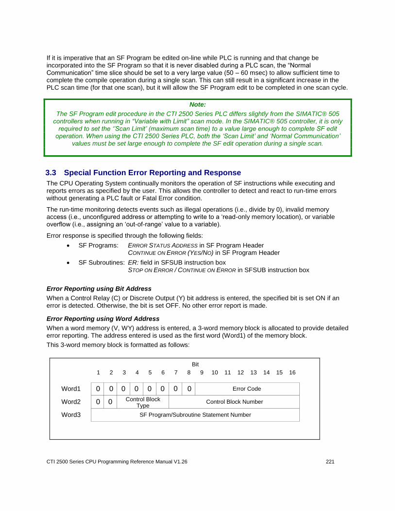
CTI 2500 Series CPU Programming Reference Manual V1.26 221
If it is imperative that an SF Program be edited on-line while PLC is running and that change be incorporated into the SF Program so that it is never disabled during a PLC scan, the “Normal Communication” time slice should be set to a very large value (50 – 60 msec) to allow sufficient time to complete the compile operation during a single scan. This can still result in a significant increase in the PLC scan time (for that one scan), but it will allow the SF Program edit to be completed in one scan cycle.
Note:
The SF Program edit procedure in the CTI 2500 Series PLC differs slightly from the SIMATIC® 505 controllers when running in “Variable with Limit” scan mode. In the SIMATIC® 505 controller, it is only
required to set the ‘’Scan Limit’ (maximum scan time) to a value large enough to complete SF edit operation. When using the CTI 2500 Series PLC, both the ‘Scan Limit’ and ‘Normal Communication’
values must be set large enough to complete the SF edit operation during a single scan.
3.3 Special Function Error Reporting and Response
The CPU Operating System continually monitors the operation of SF instructions while executing and reports errors as specified by the user. This allows the controller to detect and react to run-time errors without generating a PLC fault or Fatal Error condition.
The run-time monitoring detects events such as illegal operations (i.e., divide by 0), invalid memory access (i.e., unconfigured address or attempting to write to a ‘read-only memory location), or variable overflow (i.e., assigning an ‘out-of-range’ value to a variable).
Error response is specified through the following fields:
SF Programs: ERROR STATUS ADDRESS in SF Program Header CONTINUE ON ERROR (YES/NO) in SF Program Header
SF Subroutines: ER: field in SFSUB instruction box STOP ON ERROR / CONTINUE ON ERROR in SFSUB instruction box
Error Reporting using Bit Address
When a Control Relay (C) or Discrete Output (Y) bit address is entered, the specified bit is set ON if an error is detected. Otherwise, the bit is set OFF. No other error report is made.
Error Reporting using Word Address
When a word memory (V, WY) address is entered, a 3-word memory block is allocated to provide detailed error reporting. The address entered is used as the first word (Word1) of the memory block.
This 3-word memory block is formatted as follows:
0 00 0
0 0
Word1
Word2
Word3
1 2 3 4 5 6 7 8 9 10 11 12 13 14 15 16
Bit
Control BlockType
0 0 0 Error Code
Control Block Number
SF Program/Subroutine Statement Number
0
222 CTI 2500 Series CPU Programming Reference Manual V1.26
The reason for the error is provided in the Error Code written to the least significant byte of Word1. Section 3.7 contains a description of the possible Error Codes.
The Control Block ID for the task that declared the error is written to Word2.
1. Bits 3-6 indicate one of the following Control Block Types:
0000: PID Loop 0001: Analog Alarm 0002: SF Program 0003: SF Subroutine
2. Bits 7-16 hold the SF Program/Subroutine Number (1-1023)
Word3 indicates the Statement Number of the SF Program or SF Subroutine executing when the error was detected.
The Error Code value (in Word1) is reset to zero each time the control block starts execution. However, values in Words2-3 are left unchanged until manually cleared to allow debug of intermittent error conditions.
Error Reporting using SFEC Variable
The Special Function Error Code (SFEC) variable provides another means of accessing the Error Code associated with a SF Program/Subroutine. The SFEC variable contains the same information as Word1 of the Word Address Memory Block described above.
The SFEC variable may be read or written in a SF Program/Subroutine statement. This allows the user to programmatically detect and respond to errors or declare unique error codes when desired.
Note:
The programming software may require that a number be entered as part of the SFEC variable when used in a SF Program/Subroutine (i.e., SFEC1). However, the number entered has no
effect on the operation. All references to the SFEC variable made within an SF Program/Subroutine refer to the Error Code associated with that one program.
When the SF Program/Subroutine is called for execution, the SFEC value is cleared to zero. If the CPU operating system detects an error, the corresponding Error Code is written to the SFEC. Errors can also be detected programmatically and assigned to the SFEC using the MATH or IMATH instruction (i.e., SFEC1 := 127).
The action taken by the SF Program/Subroutine when a writing to the SFEC variable depends on the selection made in the CONTINUE ON ERROR (YES/NO) field (in SF Program Header) or STOP ON ERROR / CONTINUE ON ERROR (for RLL SFSUB instructions).
If STOP ON ERROR is selected, the SF Program/Subroutine terminates immediately when a non-zero value is written to the SFEC variable. If CONTINUE ON ERROR is chosen, the program continues to execute – allowing the SF Program/Subroutine to examine the SFEC value and take the necessary corrective action.
CAUTION:
Take care when selecting ‘CONTINUE ON ERROR’ for SF Programs//Subroutines. Operational errors (such as ‘Arithmetic Overflow’ or ‘Invalid Data’) often result in invalid values
being assigned to critical memory locations. This can cause unexpected results in program calculations and machine operation.
CTI 2500 Series CPU Programming Reference Manual V1.26 223
3.4 Special Function Memory Usage
This section describes PLC memory access by SF Programs/Subroutines that differs from the RLL program instructions.
3.4.1 SF Program Size
The PLC uses S-Memory to store the source code for each SF Program/ Subroutine. The amount of S-Memory available is determined by the PLC Memory Configuration for this memory type (see Section 6.2.4).
The maximum size for each SF Program / Subroutine is limited to 32767 bytes. This includes all operations (one byte each), parameters (one byte for Boolean, two bytes for 16-bit Integer/Word, and four bytes for Real/Long Integer/Double Word), and comments (each character is one byte).
Any program that exceeds this limit will generate a “Control Block Size Error” when attempting to download it to the PLC.
3.4.2 SF Local Memory
A block of memory (called temporary or T-memory) is allocated for duration of the program execution. T-Memory is analogous to “local variables” used in C program functions. This memory can be accessed only by the SF Program / Subroutine currently executing and is cleared when the program terminates.
Note:
The amount of T-memory available to SF programs has been extended to 64 words, and this memory block can be accessed as T1-T64. All addresses in this extended memory
SF Program/Subroutine starts executing.
This feature is available only when using 2500 Series CPU firmware V6.0 or later and 505 WorkShop V4.50 or later as the PLC programming software.
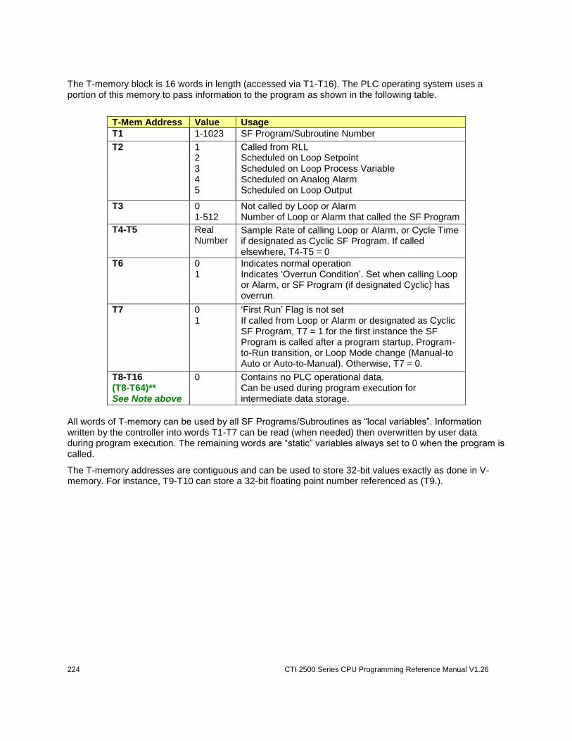
224 CTI 2500 Series CPU Programming Reference Manual V1.26
The T-memory block is 16 words in length (accessed via T1-T16). The PLC operating system uses a portion of this memory to pass information to the program as shown in the following table.
T-Mem Address Value Usage
T1 1-1023 SF Program/Subroutine Number
T2 1 Called from RLL 2 Scheduled on Loop Setpoint 3 Scheduled on Loop Process Variable 4 Scheduled on Analog Alarm
5 Scheduled on Loop Output
T3 0 1-512
Not called by Loop or Alarm Number of Loop or Alarm that called the SF Program
T4-T5 Real Number
Sample Rate of calling Loop or Alarm, or Cycle Time if designated as Cyclic SF Program. If called elsewhere, T4-T5 = 0
T6 0 1
Indicates normal operation Indicates ‘Overrun Condition’. Set when calling Loop or Alarm, or SF Program (if designated Cyclic) has overrun.
T7 0 1
‘First Run’ Flag is not set If called from Loop or Alarm or designated as Cyclic SF Program, T7 = 1 for the first instance the SF Program is called after a program startup, Program-to-Run transition, or Loop Mode change (Manual-to Auto or Auto-to-Manual). Otherwise, T7 = 0.
T8-T16 (T8-T64)** See Note above
0 Contains no PLC operational data. Can be used during program execution for intermediate data storage.
All words of T-memory can be used by all SF Programs/Subroutines as “local variables”. Information written by the controller into words T1-T7 can be read (when needed) then overwritten by user data during program execution. The remaining words are “static” variables always set to 0 when the program is called.
The T-memory addresses are contiguous and can be used to store 32-bit values exactly as done in V-memory. For instance, T9-T10 can store a 32-bit floating point number referenced as (T9.).
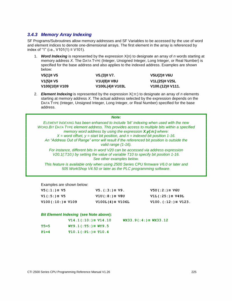
CTI 2500 Series CPU Programming Reference Manual V1.26 225
3.4.3 Memory Array Indexing
SF Programs/Subroutines allow memory addresses and SF Variables to be accessed by the use of word and element indices to denote one-dimensional arrays. The first element in the array is referenced by index of “1” (i.e., V101(1) ≡ V101).
1. Word Indexing is represented by the expression X(n) to designate an array of n words starting at memory address X. The DATA TYPE (Integer, Unsigned Integer, Long Integer, or Real Number) is specified for the base address and also applies to the indexed address. Examples are shown below:
V5(1)≡ V5 V5.(3)≡ V7. V5U(2)≡ V6U
V1(5)≡ V5 V1U(8)≡ V8U V1L(25)≡ V25L
V100(10)≡ V109 V100L(4)≡ V103L V100.(12)≡ V111.
2. Element Indexing is represented by the expression X(:n:) to designate an array of n elements starting at memory address X. The actual address selected by the expression depends on the DATA TYPE (Integer, Unsigned Integer, Long Integer, or Real Number) specified for the base address.
Note:
ELEMENT INDEXING has been enhanced to include ‘bit’ indexing when used with the new WORD.BIT DATA TYPE element address. This provides access to multiple bits within a specified
memory word address by using the expression X.y(:n:) where: X = word offset, y = start bit position, and n = indexed bit position 1-16.
An “Address Out of Range” error will result if the referenced bit position is outside the valid range (1-16).
For instance, different bits in word V20 can be accessed via address expression V20.1(:T10:) by setting the value of variable T10 to specify bit position 1-16.
See other examples below.
This feature is available only when using 2500 Series CPU firmware V6.0 or later and 505 WorkShop V4.50 or later as the PLC programming software.
Examples are shown below:
V5(:1:)≡ V5 V5.(:3:)≡ V9. V5U(:2:)≡ V6U
V1(:5:)≡ V5 V1U(:8:)≡ V8U V1L(:25:)≡ V49L
V100(:10:)≡ V109 V100L(4)≡ V106L V100.(:12:)≡ V123.
Bit Element Indexing (see Note above):
V14.1(:10:)≡ V14.10 WX33.9(:4:)≡ WX33.12
T5=5 WY9.1(:T5:)≡ WY9.5
P1=4 T10.1(:P1:)≡ T10.4
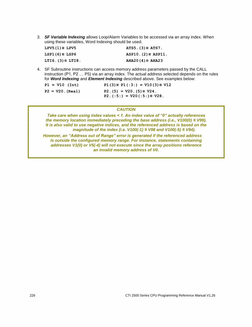
226 CTI 2500 Series CPU Programming Reference Manual V1.26
3. SF Variable Indexing allows Loop/Alarm Variables to be accessed via an array index. When
using these variables, Word Indexing should be used.
LPV5(1)≡ LPV5 ATS5.(3)≡ ATS7.
LSP1(6)≡ LSP6 ASP10.(2)≡ ASP11.
LTI6.(3)≡ LTI8. AHA20(4)≡ AHA23
4. SF Subroutine instructions can access memory address parameters passed by the CALL instruction (P1, P2 … P5) via an array index. The actual address selected depends on the rules for Word Indexing and Element Indexing described above. See examples below:
P1 = V10 (Int) P1(3)≡ P1(:3:) = V10(3)≡ V12
P2 = V20.(Real) P2.(5) = V20.(5)≡ V24.
P2.(:5:) = V20(:5:)≡ V28.
CAUTION
Take care when using index values < 1. An index value of “0” actually references the memory location immediately preceding the base address (i.e., V100(0) ≡ V99). It is also valid to use negative indices, and the referenced address is based on the
magnitude of the index (i.e. V100(-1) ≡ V98 and V100(-5) ≡ V94).
However, an “Address out of Range” error is generated if the referenced address Is outside the configured memory range. For instance, statements containing addresses V1(0) or V5(-4) will not execute since the array positions reference
an invalid memory address of V0.
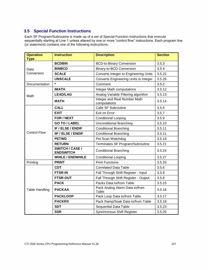
CTI 2500 Series CPU Programming Reference Manual V1.26 227
3.5 Special Function Instructions
Each SF Program/Subroutine is made up of a set of Special Function instructions that execute sequentially starting at Line 1 unless altered by one or more “control flow” instructions. Each program line (or statement) contains one of the following instructions:
Operation Type
Instruction Description Section
Data Conversion
BCDBIN BCD-to-Binary Conversion 3.5.3
BINBCD Binary-to-BCD Conversion 3.5.4
SCALE Converts Integer to Engineering Units 3.5.22
UNSCALE Converts Engineering Units to Integer 3.5.26
Documentation * Comment 3.5.2
Math
IMATH Integer Math computations 3.5.12
LEAD/LAG Analog Variable Filtering algorithm 3.5.13
MATH Integer and Real Number Math computations
3.5.14
Control Flow
CALL Calls SF Subroutine 3.5.5
EXIT Exit on Error 3.5.7
FOR / NEXT Conditional Looping 3.5.9
GO TO / LABEL Unconditional Branching 3.5.10
IF / ELSE / ENDIF Conditional Branching 3.5.11
IIF / ELSE / ENDIF Conditional Branching 3.5.11
PETWD Pet Scan Watchdog 3.5.19
RETURN Terminates SF Program/Subroutine 3.5.21
SWITCH / CASE / ENDSWITCH
Conditional Branching 3.5.24
WHILE / ENDWHILE Conditional Looping 3.5.27
Printing PRINT Print Functions 3.5.20
Table Handling
CDT Correlated Data Table 3.5.6
FTSR-IN Fall Through Shift Register - Input 3.5.8
FTSR-OUT Fall Through Shift Register - Output 3.5.8
PACK Packs Data to/from Table 3.5.15
PACKAA Pack Analog Alarm Data to/from Table
3.5.16
PACKLOOP Pack Loop Data to/from Table 3.5.17
PACKRS Pack Ramp/Soak Data to/from Table 3.5.18
SDT Sequential Data Table 3.5.23
SSR Synchronous Shift Register 3.5.25
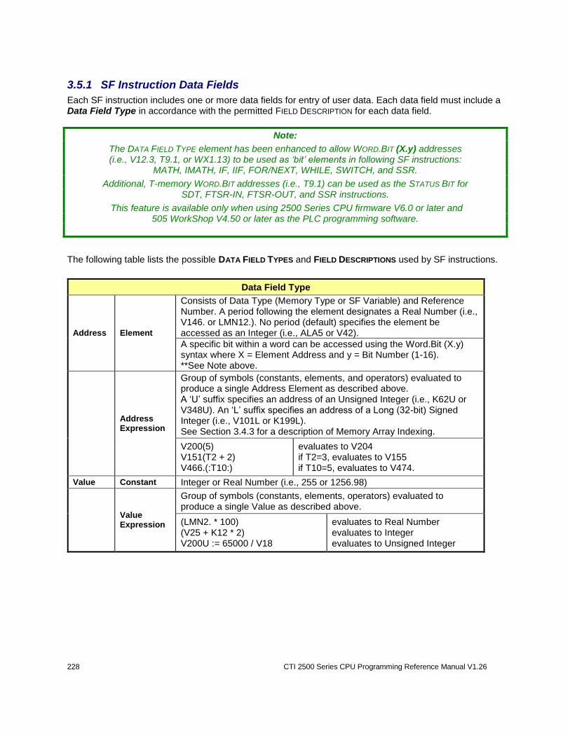
228 CTI 2500 Series CPU Programming Reference Manual V1.26
3.5.1 SF Instruction Data Fields
Each SF instruction includes one or more data fields for entry of user data. Each data field must include a Data Field Type in accordance with the permitted FIELD DESCRIPTION for each data field.
Note:
The DATA FIELD TYPE element has been enhanced to allow WORD.BIT (X.y) addresses (i.e., V12.3, T9.1, or WX1.13) to be used as ‘bit’ elements in following SF instructions:
MATH, IMATH, IF, IIF, FOR/NEXT, WHILE, SWITCH, and SSR.
Additional, T-memory WORD.BIT addresses (i.e., T9.1) can be used as the STATUS BIT for SDT, FTSR-IN, FTSR-OUT, and SSR instructions.
This feature is available only when using 2500 Series CPU firmware V6.0 or later and 505 WorkShop V4.50 or later as the PLC programming software.
The following table lists the possible DATA FIELD TYPES and FIELD DESCRIPTIONS used by SF instructions.
Data Field Type
Address Element
Consists of Data Type (Memory Type or SF Variable) and Reference Number. A period following the element designates a Real Number (i.e., V146. or LMN12.). No period (default) specifies the element be accessed as an Integer (i.e., ALA5 or V42).
A specific bit within a word can be accessed using the Word.Bit (X.y) syntax where X = Element Address and y = Bit Number (1-16). **See Note above.
Address Expression
Group of symbols (constants, elements, and operators) evaluated to produce a single Address Element as described above. A ‘U’ suffix specifies an address of an Unsigned Integer (i.e., K62U or V348U). An ‘L’ suffix specifies an address of a Long (32-bit) Signed Integer (i.e., V101L or K199L). See Section 3.4.3 for a description of Memory Array Indexing.
V200(5) V151(T2 + 2) V466.(:T10:)
evaluates to V204 if T2=3, evaluates to V155 if T10=5, evaluates to V474.
Value Constant Integer or Real Number (i.e., 255 or 1256.98)
Value Expression
Group of symbols (constants, elements, operators) evaluated to produce a single Value as described above.
(LMN2. * 100) (V25 + K12 * 2) V200U := 65000 / V18
evaluates to Real Number evaluates to Integer evaluates to Unsigned Integer
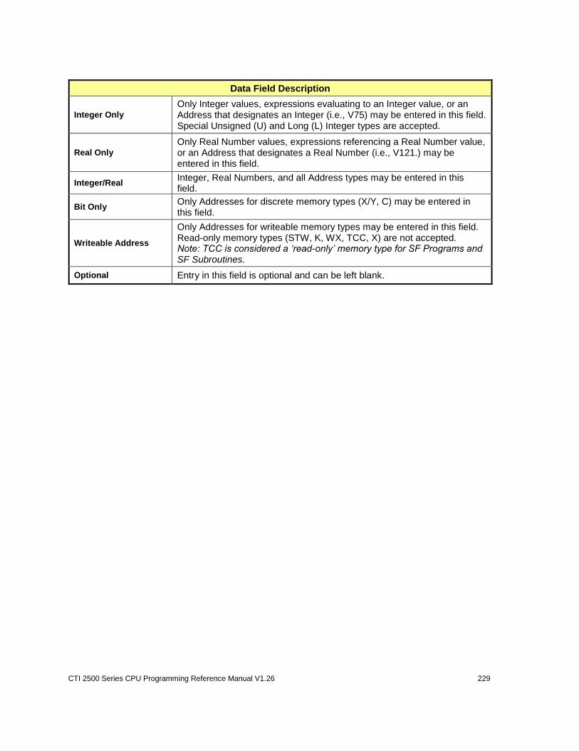
CTI 2500 Series CPU Programming Reference Manual V1.26 229
Data Field Description
Integer Only
Only Integer values, expressions evaluating to an Integer value, or an Address that designates an Integer (i.e., V75) may be entered in this field. Special Unsigned (U) and Long (L) Integer types are accepted.
Real Only
Only Real Number values, expressions referencing a Real Number value, or an Address that designates a Real Number (i.e., V121.) may be entered in this field.
Integer/Real Integer, Real Numbers, and all Address types may be entered in this field.
Bit Only Only Addresses for discrete memory types (X/Y, C) may be entered in this field.
Writeable Address
Only Addresses for writeable memory types may be entered in this field. Read-only memory types (STW, K, WX, TCC, X) are not accepted. Note: TCC is considered a ‘read-only’ memory type for SF Programs and SF Subroutines.
Optional Entry in this field is optional and can be left blank.
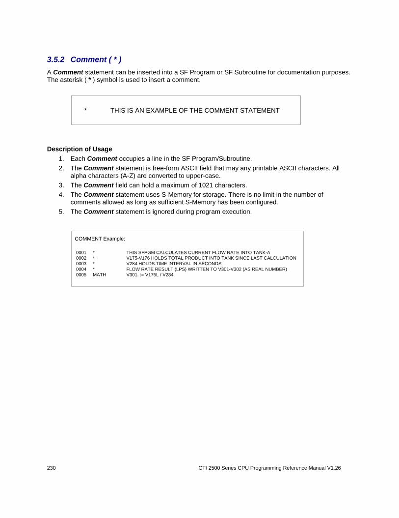
230 CTI 2500 Series CPU Programming Reference Manual V1.26
3.5.2 Comment ( * )
A Comment statement can be inserted into a SF Program or SF Subroutine for documentation purposes. The asterisk ( * ) symbol is used to insert a comment.
* THIS IS AN EXAMPLE OF THE COMMENT STATEMENT
Description of Usage
1. Each Comment occupies a line in the SF Program/Subroutine.
2. The Comment statement is free-form ASCII field that may any printable ASCII characters. All alpha characters (A-Z) are converted to upper-case.
3. The Comment field can hold a maximum of 1021 characters.
4. The Comment statement uses S-Memory for storage. There is no limit in the number of comments allowed as long as sufficient S-Memory has been configured.
5. The Comment statement is ignored during program execution.
0001 * THIS SFPGM CALCULATES CURRENT FLOW RATE INTO TANK-A
0002 * V175-V176 HOLDS TOTAL PRODUCT INTO TANK SINCE LAST CALCULATION
0003 * V284 HOLDS TIME INTERVAL IN SECONDS
0004 * FLOW RATE RESULT (LPS) WRITTEN TO V301-V302 (AS REAL NUMBER)
0005 MATH V301. := V175L / V284
COMMENT Example:
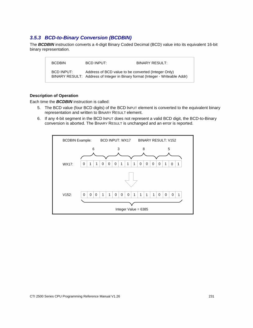
CTI 2500 Series CPU Programming Reference Manual V1.26 231
3.5.3 BCD-to-Binary Conversion (BCDBIN)
The BCDBIN instruction converts a 4-digit Binary Coded Decimal (BCD) value into its equivalent 16-bit binary representation.
BCDBIN BCD INPUT: BINARY RESULT:
BCD INPUT: Address of BCD value to be converted (Integer Only)
BINARY RESULT: Address of Integer in Binary format (Integer - Writeable Addr)
Description of Operation
Each time the BCDBIN instruction is called:
5. The BCD value (four BCD digits) of the BCD INPUT element is converted to the equivalent binary representation and written to BINARY RESULT element.
6. If any 4-bit segment in the BCD INPUT does not represent a valid BCD digit, the BCD-to-Binary conversion is aborted. The BINARY RESULT is unchanged and an error is reported.
WX17:
V152: 0 1 1 11 1 0 0 1
Integer Value = 6385
0 0 0 0 0 1 0
0 0 0 0 0 0 0 0 1
836 5
11 1 101 1
BCDBIN Example: BCD INPUT: WX17 BINARY RESULT: V152
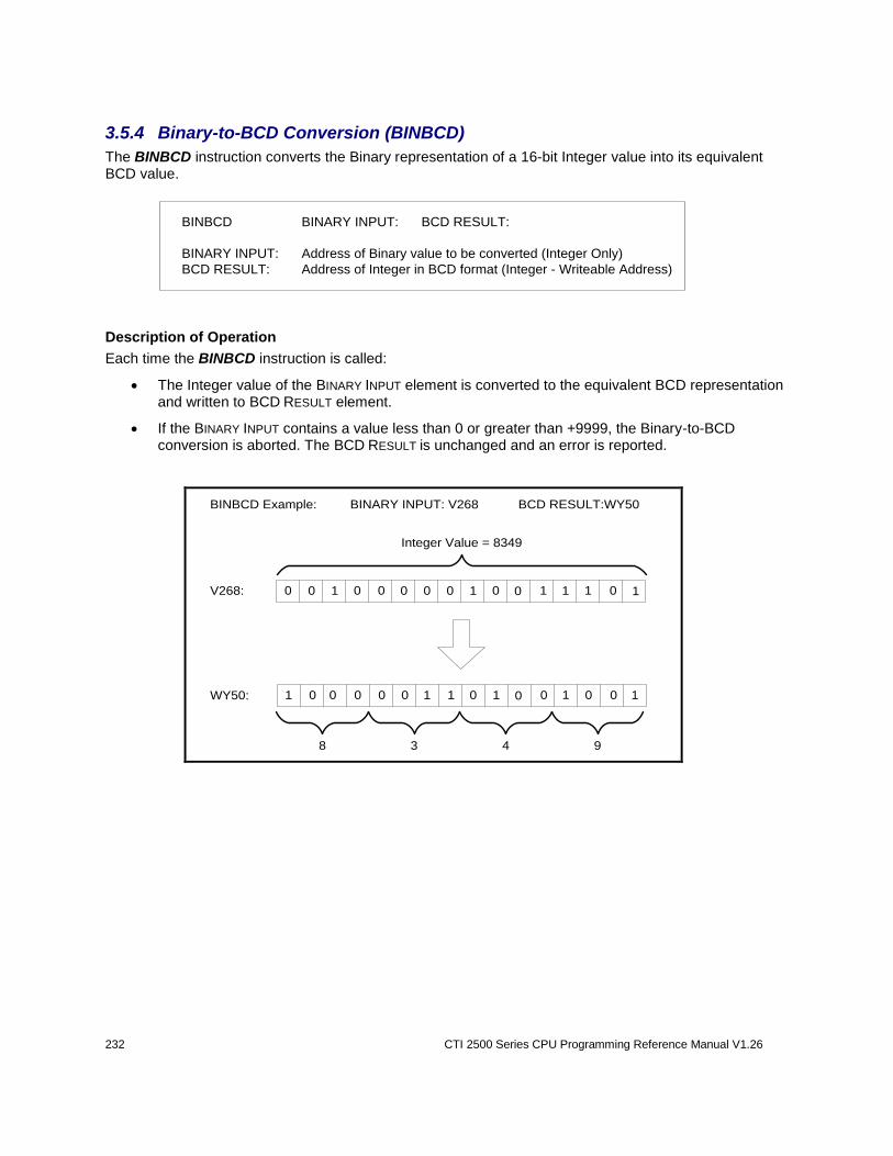
232 CTI 2500 Series CPU Programming Reference Manual V1.26
3.5.4 Binary-to-BCD Conversion (BINBCD)
The BINBCD instruction converts the Binary representation of a 16-bit Integer value into its equivalent BCD value.
BINBCD BINARY INPUT: BCD RESULT:
BINARY INPUT: Address of Binary value to be converted (Integer Only)
BCD RESULT: Address of Integer in BCD format (Integer - Writeable Address)
Description of Operation
Each time the BINBCD instruction is called:
The Integer value of the BINARY INPUT element is converted to the equivalent BCD representation and written to BCD RESULT element.
If the BINARY INPUT contains a value less than 0 or greater than +9999, the Binary-to-BCD conversion is aborted. The BCD RESULT is unchanged and an error is reported.
BINBCD Example: BINARY INPUT: V268 BCD RESULT:WY50
Integer Value = 8349
V268: 0 0 0 10 0 1 0 10 1 0 0 0 1 1
438 9
WY50: 1 0 0 01 0 0 00 0 0 1 1 0 1 1
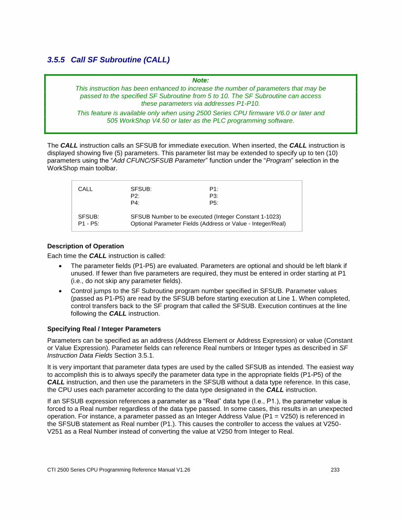
CTI 2500 Series CPU Programming Reference Manual V1.26 233
3.5.5 Call SF Subroutine (CALL)
Note:
This instruction has been enhanced to increase the number of parameters that may be passed to the specified SF Subroutine from 5 to 10. The SF Subroutine can access
these parameters via addresses P1-P10.
This feature is available only when using 2500 Series CPU firmware V6.0 or later and 505 WorkShop V4.50 or later as the PLC programming software.
The CALL instruction calls an SFSUB for immediate execution. When inserted, the CALL instruction is displayed showing five (5) parameters. This parameter list may be extended to specify up to ten (10) parameters using the “Add CFUNC/SFSUB Parameter” function under the “Program” selection in the WorkShop main toolbar.
CALL SFSUB: P1:
P2: P3:
P4: P5:
SFSUB: SFSUB Number to be executed (Integer Constant 1-1023)
P1 - P5: Optional Parameter Fields (Address or Value - Integer/Real)
Description of Operation
Each time the CALL instruction is called:
The parameter fields (P1-P5) are evaluated. Parameters are optional and should be left blank if unused. If fewer than five parameters are required, they must be entered in order starting at P1 (i.e., do not skip any parameter fields).
Control jumps to the SF Subroutine program number specified in SFSUB. Parameter values (passed as P1-P5) are read by the SFSUB before starting execution at Line 1. When completed, control transfers back to the SF program that called the SFSUB. Execution continues at the line following the CALL instruction.
Specifying Real / Integer Parameters
Parameters can be specified as an address (Address Element or Address Expression) or value (Constant or Value Expression). Parameter fields can reference Real numbers or Integer types as described in SF Instruction Data Fields Section 3.5.1.
It is very important that parameter data types are used by the called SFSUB as intended. The easiest way to accomplish this is to always specify the parameter data type in the appropriate fields (P1-P5) of the CALL instruction, and then use the parameters in the SFSUB without a data type reference. In this case, the CPU uses each parameter according to the data type designated in the CALL instruction.
If an SFSUB expression references a parameter as a “Real” data type (I.e., P1.), the parameter value is forced to a Real number regardless of the data type passed. In some cases, this results in an unexpected operation. For instance, a parameter passed as an Integer Address Value (P1 = V250) is referenced in the SFSUB statement as Real number (P1.). This causes the controller to access the values at V250-V251 as a Real Number instead of converting the value at V250 from Integer to Real.
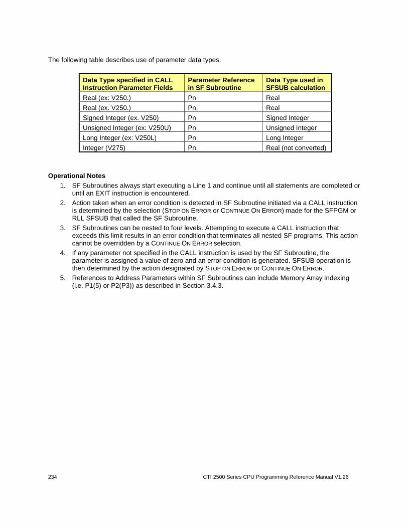
234 CTI 2500 Series CPU Programming Reference Manual V1.26
The following table describes use of parameter data types.
Data Type specified in CALL Instruction Parameter Fields
Parameter Reference in SF Subroutine
Data Type used in SFSUB calculation
Real (ex: V250.) Pn Real
Real (ex. V250.) Pn. Real
Signed Integer (ex. V250) Pn Signed Integer
Unsigned Integer (ex: V250U) Pn Unsigned Integer
Long Integer (ex: V250L) Pn Long Integer
Integer (V275) Pn. Real (not converted)
Operational Notes
1. SF Subroutines always start executing a Line 1 and continue until all statements are completed or until an EXIT instruction is encountered.
2. Action taken when an error condition is detected in SF Subroutine initiated via a CALL instruction is determined by the selection (STOP ON ERROR or CONTINUE ON ERROR) made for the SFPGM or RLL SFSUB that called the SF Subroutine.
3. SF Subroutines can be nested to four levels. Attempting to execute a CALL instruction that exceeds this limit results in an error condition that terminates all nested SF programs. This action cannot be overridden by a CONTINUE ON ERROR selection.
4. If any parameter not specified in the CALL instruction is used by the SF Subroutine, the parameter is assigned a value of zero and an error condition is generated. SFSUB operation is then determined by the action designated by STOP ON ERROR or CONTINUE ON ERROR.
5. References to Address Parameters within SF Subroutines can include Memory Array Indexing (i.e. P1(5) or P2(P3)) as described in Section 3.4.3.
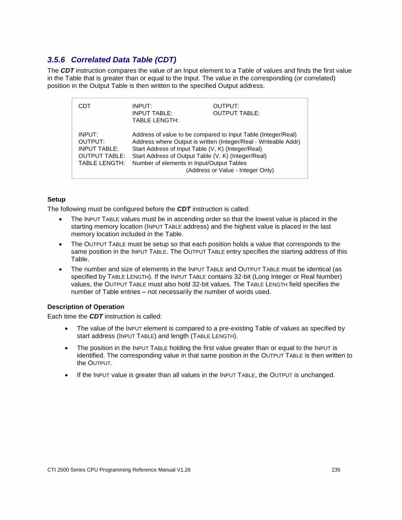
CTI 2500 Series CPU Programming Reference Manual V1.26 235
3.5.6 Correlated Data Table (CDT)
The CDT instruction compares the value of an Input element to a Table of values and finds the first value in the Table that is greater than or equal to the Input. The value in the corresponding (or correlated) position in the Output Table is then written to the specified Output address.
CDT INPUT: OUTPUT:
INPUT TABLE: OUTPUT TABLE:
TABLE LENGTH:
INPUT: Address of value to be compared to Input Table (Integer/Real)
OUTPUT: Address where Output is written (Integer/Real - Writeable Addr)
INPUT TABLE: Start Address of Input Table (V, K) (Integer/Real)
OUTPUT TABLE: Start Address of Output Table (V, K) (Integer/Real)
TABLE LENGTH: Number of elements in Input/Output Tables
(Address or Value - Integer Only)
Setup
The following must be configured before the CDT instruction is called:
The INPUT TABLE values must be in ascending order so that the lowest value is placed in the starting memory location (INPUT TABLE address) and the highest value is placed in the last memory location included in the Table.
The OUTPUT TABLE must be setup so that each position holds a value that corresponds to the same position in the INPUT TABLE. The OUTPUT TABLE entry specifies the starting address of this Table.
The number and size of elements in the INPUT TABLE and OUTPUT TABLE must be identical (as specified by TABLE LENGTH). If the INPUT TABLE contains 32-bit (Long Integer or Real Number) values, the OUTPUT TABLE must also hold 32-bit values. The TABLE LENGTH field specifies the number of Table entries – not necessarily the number of words used.
Description of Operation
Each time the CDT instruction is called:
The value of the INPUT element is compared to a pre-existing Table of values as specified by start address (INPUT TABLE) and length (TABLE LENGTH).
The position in the INPUT TABLE holding the first value greater than or equal to the INPUT is identified. The corresponding value in that same position in the OUTPUT TABLE is then written to the OUTPUT.
If the INPUT value is greater than all values in the INPUT TABLE, the OUTPUT is unchanged.
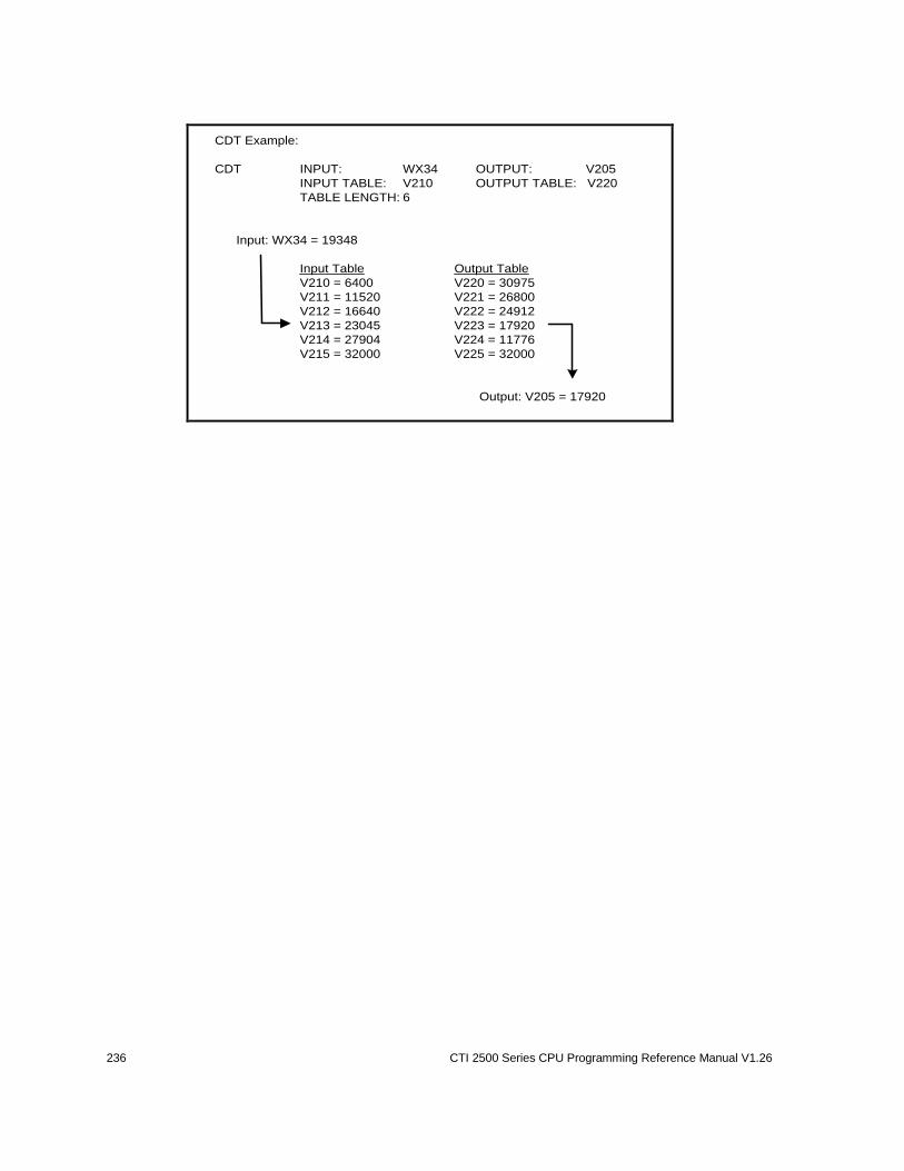
236 CTI 2500 Series CPU Programming Reference Manual V1.26
CDT Example:
CDT INPUT: WX34 OUTPUT: V205
INPUT TABLE: V210 OUTPUT TABLE: V220
TABLE LENGTH: 6
Input: WX34 = 19348
Input Table Output Table
V210 = 6400 V220 = 30975
V211 = 11520 V221 = 26800
V212 = 16640 V222 = 24912
V213 = 23045 V223 = 17920
V214 = 27904 V224 = 11776
V215 = 32000 V225 = 32000
Output: V205 = 17920

CTI 2500 Series CPU Programming Reference Manual V1.26 237
3.5.7 Exit on Error (EXIT)
The EXIT instruction forces termination of an SF Program or SF Subroutine and writes the user-specified Error Code to the ERROR STATUS ADDRESS.
EXIT ERRCODE:
ERRCODE: Value to be written to ERROR STATUS ADDRESS
(Integer Constant 0-255)
Description of Operation
Each time the EXIT instruction is encountered:
1. Program termination occurs as follows:
a. If an SF Program is being executed, it is immediately terminated.
b. If the SF Subroutine being executed was called from an RLL SFSUB box, that SF Subroutine is terminated.
c. If the SF Subroutine being executed was called via an SF CALL instruction, execution of that SF Subroutine and all “nested” SF Programs/Subroutines are terminated.
2. The ERRCODE value is written to the ERROR STATUS ADDRESS designated in the SF Program Header (for SF Program that called the SFSUB) or RLL SFSUB instruction ER field. The ERRCODE can be specified as an Integer in the range of 0-255. However, we recommend using values in the range of 100-255 since 0-99 are already used by the CPU to designate SF errors. See Section xx.
3. If a bit address is used for the ERROR STATUS ADDRESS, it turns ON.
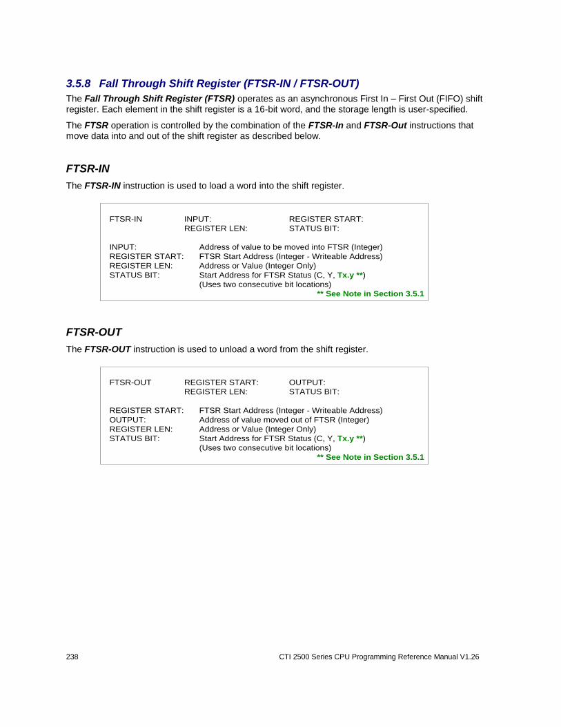
238 CTI 2500 Series CPU Programming Reference Manual V1.26
3.5.8 Fall Through Shift Register (FTSR-IN / FTSR-OUT)
The Fall Through Shift Register (FTSR) operates as an asynchronous First In – First Out (FIFO) shift register. Each element in the shift register is a 16-bit word, and the storage length is user-specified.
The FTSR operation is controlled by the combination of the FTSR-In and FTSR-Out instructions that move data into and out of the shift register as described below.
FTSR-IN
The FTSR-IN instruction is used to load a word into the shift register.
FTSR-IN INPUT: REGISTER START:
REGISTER LEN: STATUS BIT:
INPUT: Address of value to be moved into FTSR (Integer)
REGISTER START: FTSR Start Address (Integer - Writeable Address)
REGISTER LEN: Address or Value (Integer Only)
STATUS BIT: Start Address for FTSR Status (C, Y, Tx.y **)
(Uses two consecutive bit locations)
** See Note in Section 3.5.1
FTSR-OUT
The FTSR-OUT instruction is used to unload a word from the shift register.
FTSR-OUT REGISTER START: OUTPUT:
REGISTER LEN: STATUS BIT:
REGISTER START: FTSR Start Address (Integer - Writeable Address)
OUTPUT: Address of value moved out of FTSR (Integer)
REGISTER LEN: Address or Value (Integer Only)
STATUS BIT: Start Address for FTSR Status (C, Y, Tx.y **)
(Uses two consecutive bit locations)
** See Note in Section 3.5.1
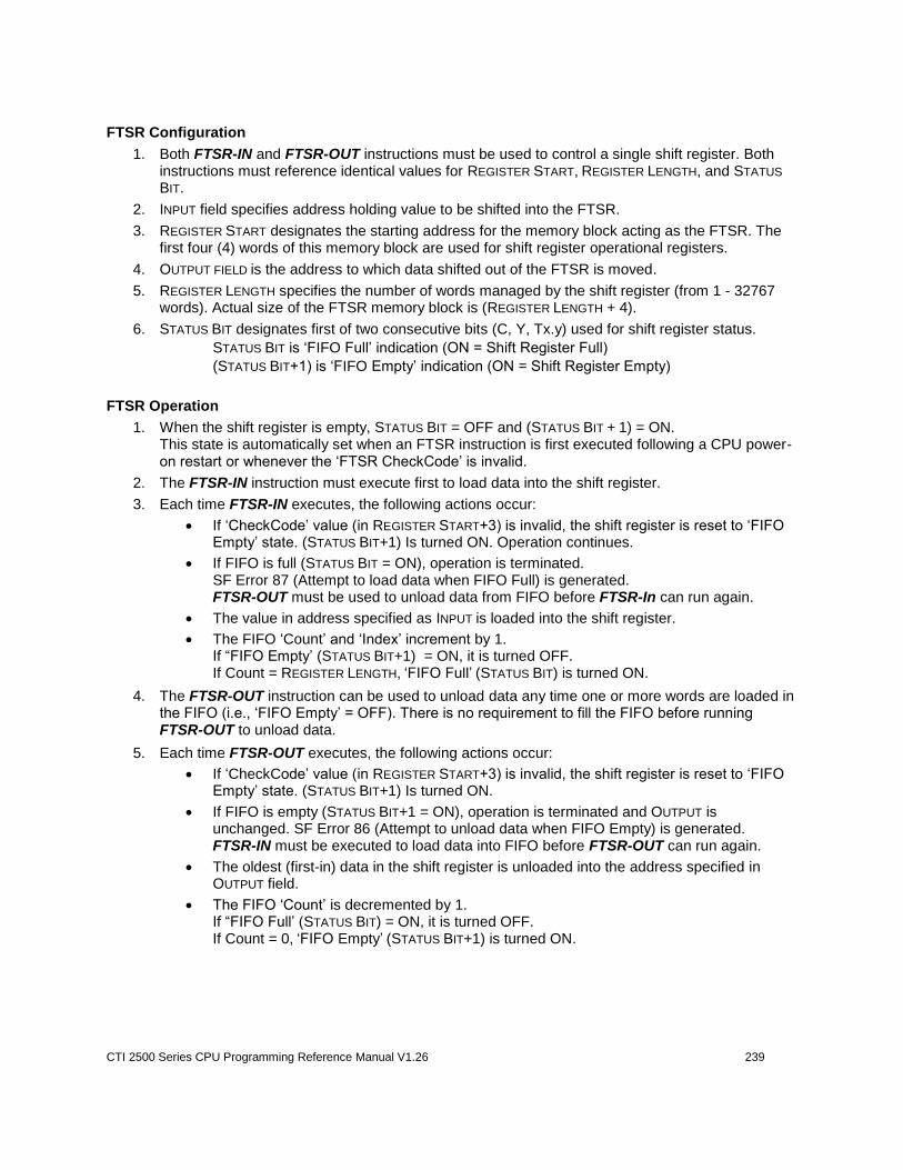
CTI 2500 Series CPU Programming Reference Manual V1.26 239
FTSR Configuration
1. Both FTSR-IN and FTSR-OUT instructions must be used to control a single shift register. Both instructions must reference identical values for REGISTER START, REGISTER LENGTH, and STATUS
BIT.
2. INPUT field specifies address holding value to be shifted into the FTSR.
3. REGISTER START designates the starting address for the memory block acting as the FTSR. The first four (4) words of this memory block are used for shift register operational registers.
4. OUTPUT FIELD is the address to which data shifted out of the FTSR is moved.
5. REGISTER LENGTH specifies the number of words managed by the shift register (from 1 - 32767 words). Actual size of the FTSR memory block is (REGISTER LENGTH + 4).
6. STATUS BIT designates first of two consecutive bits (C, Y, Tx.y) used for shift register status.
STATUS BIT is ‘FIFO Full’ indication (ON = Shift Register Full)
(STATUS BIT+1) is ‘FIFO Empty’ indication (ON = Shift Register Empty)
FTSR Operation
1. When the shift register is empty, STATUS BIT = OFF and (STATUS BIT + 1) = ON. This state is automatically set when an FTSR instruction is first executed following a CPU power-
on restart or whenever the ‘FTSR CheckCode’ is invalid.
2. The FTSR-IN instruction must execute first to load data into the shift register.
3. Each time FTSR-IN executes, the following actions occur:
If ‘CheckCode’ value (in REGISTER START+3) is invalid, the shift register is reset to ‘FIFO Empty’ state. (STATUS BIT+1) Is turned ON. Operation continues.
If FIFO is full (STATUS BIT = ON), operation is terminated. SF Error 87 (Attempt to load data when FIFO Full) is generated. FTSR-OUT must be used to unload data from FIFO before FTSR-In can run again.
The value in address specified as INPUT is loaded into the shift register.
The FIFO ‘Count’ and ‘Index’ increment by 1. If “FIFO Empty’ (STATUS BIT+1) = ON, it is turned OFF. If Count = REGISTER LENGTH, ‘FIFO Full’ (STATUS BIT) is turned ON.
4. The FTSR-OUT instruction can be used to unload data any time one or more words are loaded in the FIFO (i.e., ‘FIFO Empty’ = OFF). There is no requirement to fill the FIFO before running FTSR-OUT to unload data.
5. Each time FTSR-OUT executes, the following actions occur:
If ‘CheckCode’ value (in REGISTER START+3) is invalid, the shift register is reset to ‘FIFO Empty’ state. (STATUS BIT+1) Is turned ON.
If FIFO is empty (STATUS BIT+1 = ON), operation is terminated and OUTPUT is unchanged. SF Error 86 (Attempt to unload data when FIFO Empty) is generated.
FTSR-IN must be executed to load data into FIFO before FTSR-OUT can run again.
The oldest (first-in) data in the shift register is unloaded into the address specified in OUTPUT field.
The FIFO ‘Count’ is decremented by 1. If “FIFO Full’ (STATUS BIT) = ON, it is turned OFF. If Count = 0, ‘FIFO Empty’ (STATUS BIT+1) is turned ON.
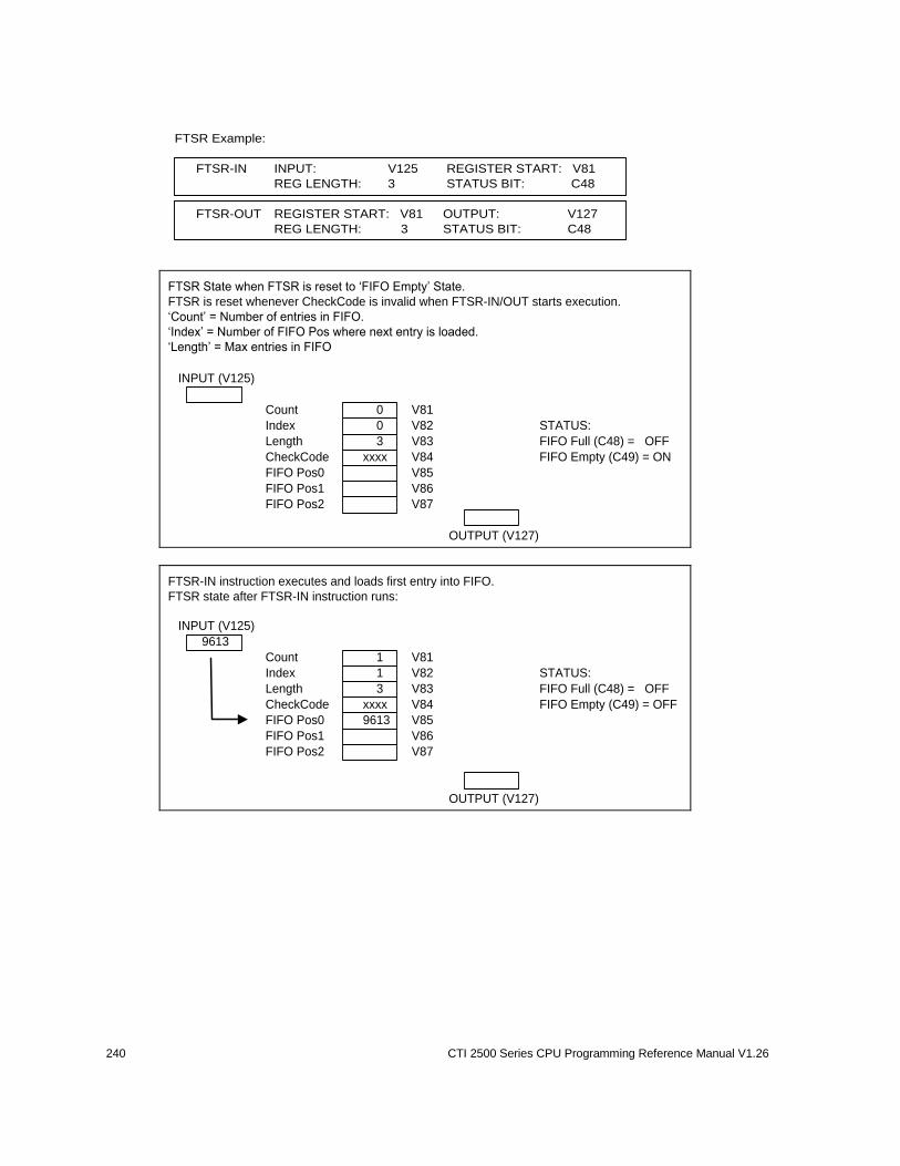
240 CTI 2500 Series CPU Programming Reference Manual V1.26
FTSR Example:
FTSR-IN INPUT: V125 REGISTER START: V81
REG LENGTH: 3 STATUS BIT: C48
FTSR-OUT REGISTER START: V81 OUTPUT: V127
REG LENGTH: 3 STATUS BIT: C48
INPUT (V125)
Count 0 V81
Index 0 V82 STATUS:
Length 3 V83 FIFO Full (C48) = OFF
CheckCode xxxx V84 FIFO Empty (C49) = ON
FIFO Pos0 V85
FIFO Pos1 V86
FIFO Pos2 V87
OUTPUT (V127)
FTSR State when FTSR is reset to ‘FIFO Empty’ State.
FTSR is reset whenever CheckCode is invalid when FTSR-IN/OUT starts execution.
‘Count’ = Number of entries in FIFO.
‘Index’ = Number of FIFO Pos where next entry is loaded.
‘Length’ = Max entries in FIFO
INPUT (V125)
9613
Count 1 V81
Index 1 V82 STATUS:
Length 3 V83 FIFO Full (C48) = OFF
CheckCode xxxx V84 FIFO Empty (C49) = OFF
FIFO Pos0 9613 V85
FIFO Pos1 V86
FIFO Pos2 V87
OUTPUT (V127)
FTSR-IN instruction executes and loads first entry into FIFO.
FTSR state after FTSR-IN instruction runs:
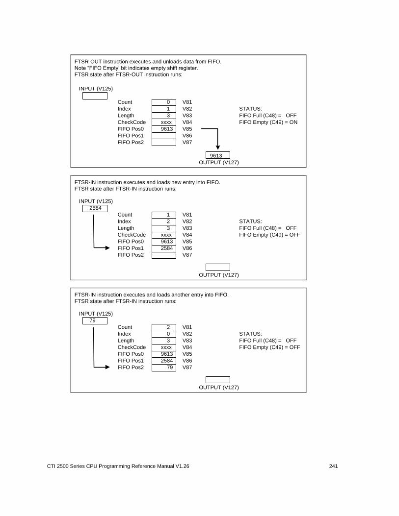
CTI 2500 Series CPU Programming Reference Manual V1.26 241
FTSR-OUT instruction executes and unloads data from FIFO.
Note “FIFO Empty’ bit indicates empty shift register.
FTSR state after FTSR-OUT instruction runs:
INPUT (V125)
Count 0 V81
Index 1 V82 STATUS:
Length 3 V83 FIFO Full (C48) = OFF
CheckCode xxxx V84 FIFO Empty (C49) = ON
FIFO Pos0 9613 V85
FIFO Pos1 V86
FIFO Pos2 V87
9613
OUTPUT (V127)
INPUT (V125)
2584
Count 1 V81
Index 2 V82 STATUS:
Length 3 V83 FIFO Full (C48) = OFF
CheckCode xxxx V84 FIFO Empty (C49) = OFF
FIFO Pos0 9613 V85
FIFO Pos1 2584 V86
FIFO Pos2 V87
OUTPUT (V127)
FTSR-IN instruction executes and loads new entry into FIFO.
FTSR state after FTSR-IN instruction runs:
INPUT (V125)
79
Count 2 V81
Index 0 V82 STATUS:
Length 3 V83 FIFO Full (C48) = OFF
CheckCode xxxx V84 FIFO Empty (C49) = OFF
FIFO Pos0 9613 V85
FIFO Pos1 2584 V86
FIFO Pos2 79 V87
OUTPUT (V127)
FTSR-IN instruction executes and loads another entry into FIFO.
FTSR state after FTSR-IN instruction runs:
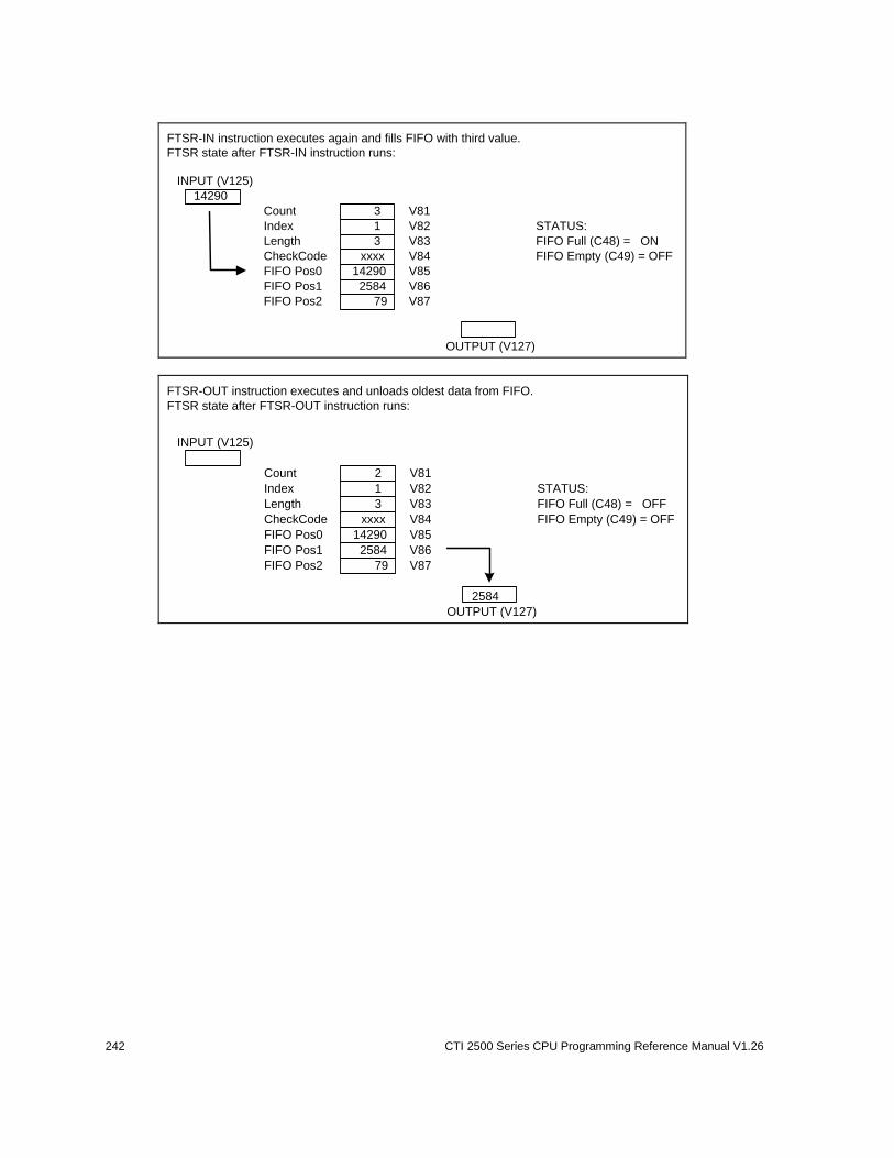
242 CTI 2500 Series CPU Programming Reference Manual V1.26
INPUT (V125)
14290
Count 3 V81
Index 1 V82 STATUS:
Length 3 V83 FIFO Full (C48) = ON
CheckCode xxxx V84 FIFO Empty (C49) = OFF
FIFO Pos0 14290 V85
FIFO Pos1 2584 V86
FIFO Pos2 79 V87
OUTPUT (V127)
FTSR-IN instruction executes again and fills FIFO with third value.
FTSR state after FTSR-IN instruction runs:
FTSR-OUT instruction executes and unloads oldest data from FIFO.
FTSR state after FTSR-OUT instruction runs:
INPUT (V125)
Count 2 V81
Index 1 V82 STATUS:
Length 3 V83 FIFO Full (C48) = OFF
CheckCode xxxx V84 FIFO Empty (C49) = OFF
FIFO Pos0 14290 V85
FIFO Pos1 2584 V86
FIFO Pos2 79 V87
2584
OUTPUT (V127)
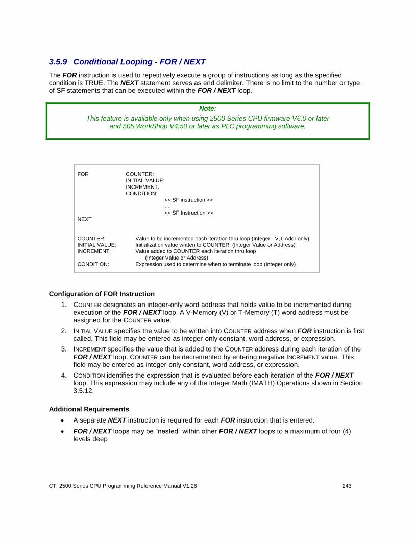
CTI 2500 Series CPU Programming Reference Manual V1.26 243
3.5.9 Conditional Looping - FOR / NEXT
The FOR instruction is used to repetitively execute a group of instructions as long as the specified condition is TRUE. The NEXT statement serves as end delimiter. There is no limit to the number or type of SF statements that can be executed within the FOR / NEXT loop.
Note:
This feature is available only when using 2500 Series CPU firmware V6.0 or later and 505 WorkShop V4.50 or later as PLC programming software.
FOR COUNTER:
INITIAL VALUE:
INCREMENT:
CONDITION:
<< SF instruction >>
…
<< SF Instruction >>
NEXT
COUNTER: Value to be incremented each iteration thru loop (Integer - V,T Addr only)
INITIAL VALUE: Initialization value written to COUNTER (Integer Value or Address)
INCREMENT: Value added to COUNTER each iteration thru loop
(Integer Value or Address)
CONDITION: Expression used to determine when to terminate loop (Integer only)
Configuration of FOR Instruction
1. COUNTER designates an integer-only word address that holds value to be incremented during execution of the FOR / NEXT loop. A V-Memory (V) or T-Memory (T) word address must be assigned for the COUNTER value.
2. INITIAL VALUE specifies the value to be written into COUNTER address when FOR instruction is first called. This field may be entered as integer-only constant, word address, or expression.
3. INCREMENT specifies the value that is added to the COUNTER address during each iteration of the FOR / NEXT loop. COUNTER can be decremented by entering negative INCREMENT value. This field may be entered as integer-only constant, word address, or expression.
4. CONDITION identifies the expression that is evaluated before each iteration of the FOR / NEXT loop. This expression may include any of the Integer Math (IMATH) Operations shown in Section 3.5.12.
Additional Requirements
A separate NEXT instruction is required for each FOR instruction that is entered.
FOR / NEXT loops may be “nested” within other FOR / NEXT loops to a maximum of four (4) levels deep
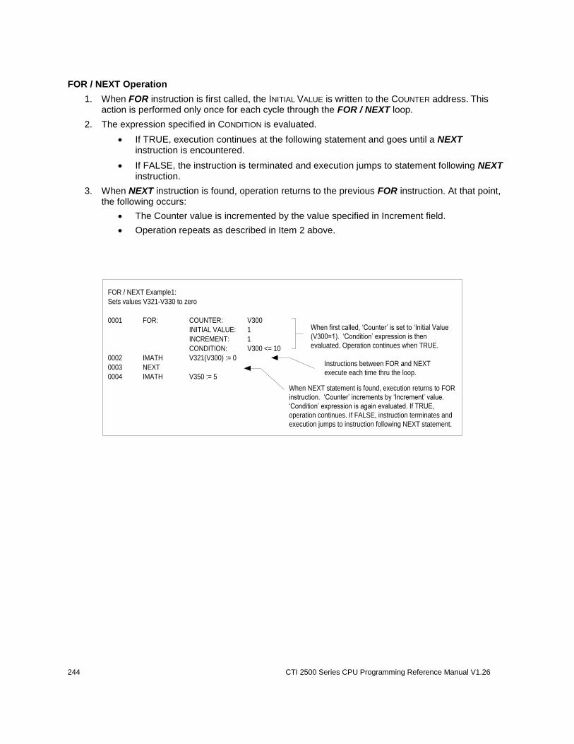
244 CTI 2500 Series CPU Programming Reference Manual V1.26
FOR / NEXT Operation
1. When FOR instruction is first called, the INITIAL VALUE is written to the COUNTER address. This action is performed only once for each cycle through the FOR / NEXT loop.
2. The expression specified in CONDITION is evaluated.
If TRUE, execution continues at the following statement and goes until a NEXT instruction is encountered.
If FALSE, the instruction is terminated and execution jumps to statement following NEXT instruction.
3. When NEXT instruction is found, operation returns to the previous FOR instruction. At that point, the following occurs:
The Counter value is incremented by the value specified in Increment field.
Operation repeats as described in Item 2 above.
When first called, ‘Counter’ is set to ‘Initial Value
(V300=1). ‘Condition’ expression is then
evaluated. Operation continues when TRUE.
When NEXT statement is found, execution returns to FOR
instruction. ‘Counter’ increments by ‘Increment’ value.
‘Condition’ expression is again evaluated. If TRUE,
operation continues. If FALSE, instruction terminates and
execution jumps to instruction following NEXT statement.
Instructions between FOR and NEXT
execute each time thru the loop.
FOR / NEXT Example1:
Sets values V321-V330 to zero
0001 FOR: COUNTER: V300
INITIAL VALUE: 1
INCREMENT: 1
CONDITION: V300 <= 10
0002 IMATH V321(V300) := 0
0003 NEXT
0004 IMATH V350 := 5
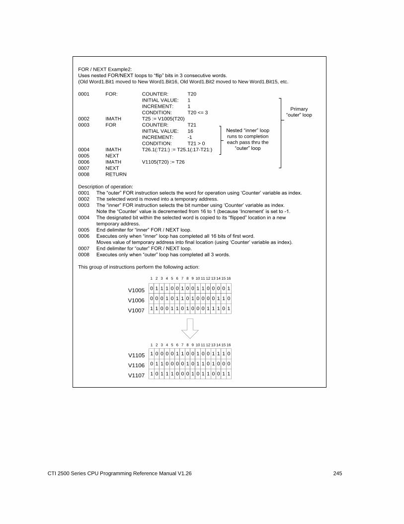
CTI 2500 Series CPU Programming Reference Manual V1.26 245
FOR / NEXT Example2:
Uses nested FOR/NEXT loops to “flip” bits in 3 consecutive words.
(Old Word1.Bit1 moved to New Word1.Bit16, Old Word1.Bit2 moved to New Word1.Bit15, etc.
0001 FOR: COUNTER: T20
INITIAL VALUE: 1
INCREMENT: 1
CONDITION: T20 <= 3
0002 IMATH T25 := V1005(T20)
0003 FOR COUNTER: T21
INITIAL VALUE: 16
INCREMENT: -1
CONDITION: T21 > 0
0004 IMATH T26.1(:T21:) := T25.1(:17-T21:)
0005 NEXT
0006 IMATH V1105(T20) := T26
0007 NEXT
0008 RETURN
Description of operation:
0001 The “outer” FOR instruction selects the word for operation using ‘Counter’ variable as index.
0002 The selected word is moved into a temporary address.
0003 The “inner” FOR instruction selects the bit number using ‘Counter’ variable as index.
Note the “Counter’ value is decremented from 16 to 1 (because ‘Increment’ is set to -1.
0004 The designated bit within the selected word is copied to its “flipped” location in a new
temporary address.
0005 End delimiter for “inner” FOR / NEXT loop.
0006 Executes only when “inner” loop has completed all 16 bits of first word.
Moves value of temporary address into final location (using ‘Counter’ variable as index).
0007 End delimiter for “outer” FOR / NEXT loop.
0008 Executes only when “outer” loop has completed all 3 words.
This group of instructions perform the following action:
01 0 0 0 1 1 0 0 1 0 0 1 1 1 0
10 1 0 0 0 0 1 0 1 1 0 1 0 0 0
11 0 1 1 0 0 0 1 0 1 1 0 0 1 1
1 2 4 5 6 7 8 9 103 11 12 13 14 15 16
V1106
V1107
V1105
10 1 1 0 0 1 0 0 1 1 0 0 0 0 1
00 0 1 0 1 1 0 1 0 0 0 0 1 1 0
01 1 0 1 1 0 1 0 0 0 1 1 1 0 1
V1006
V1007
V1005
1 2 4 5 6 7 8 9 103 11 12 13 14 15 16
Primary
“outer” loop
Nested “inner” loop
runs to completion
each pass thru the
“outer” loop
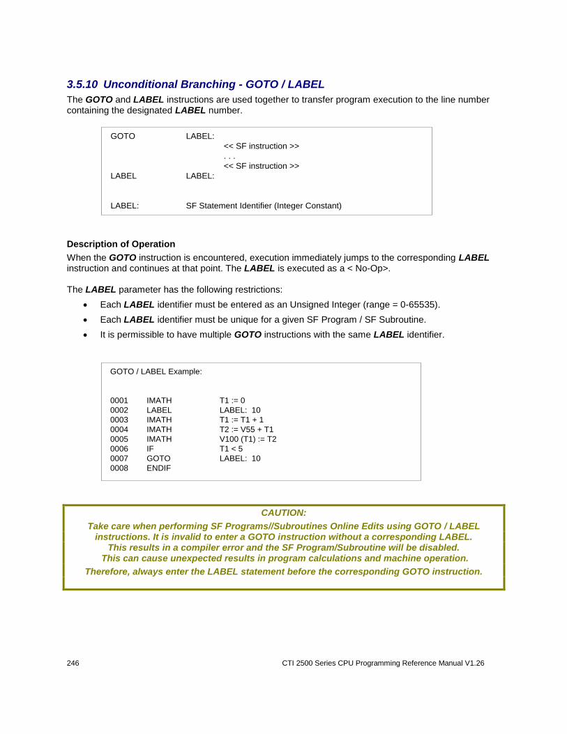
246 CTI 2500 Series CPU Programming Reference Manual V1.26
3.5.10 Unconditional Branching - GOTO / LABEL
The GOTO and LABEL instructions are used together to transfer program execution to the line number containing the designated LABEL number.
GOTO LABEL:
<< SF instruction >>
. . .
<< SF instruction >>
LABEL LABEL:
LABEL: SF Statement Identifier (Integer Constant)
Description of Operation
When the GOTO instruction is encountered, execution immediately jumps to the corresponding LABEL instruction and continues at that point. The LABEL is executed as a < No-Op>. The LABEL parameter has the following restrictions:
Each LABEL identifier must be entered as an Unsigned Integer (range = 0-65535).
Each LABEL identifier must be unique for a given SF Program / SF Subroutine.
It is permissible to have multiple GOTO instructions with the same LABEL identifier.
GOTO / LABEL Example:
0001 IMATH T1 := 0
0002 LABEL LABEL: 10
0003 IMATH T1 := T1 + 1
0004 IMATH T2 := V55 + T1
0005 IMATH V100 (T1) := T2
0006 IF T1 < 5
0007 GOTO LABEL: 10
0008 ENDIF
CAUTION:
Take care when performing SF Programs//Subroutines Online Edits using GOTO / LABEL instructions. It is invalid to enter a GOTO instruction without a corresponding LABEL.
This results in a compiler error and the SF Program/Subroutine will be disabled. This can cause unexpected results in program calculations and machine operation.
Therefore, always enter the LABEL statement before the corresponding GOTO instruction.
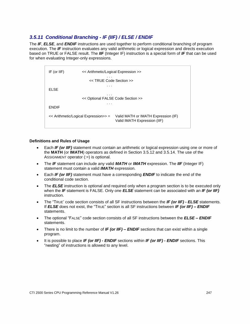
CTI 2500 Series CPU Programming Reference Manual V1.26 247
3.5.11 Conditional Branching - IF (IIF) / ELSE / ENDIF
The IF, ELSE, and ENDIF instructions are used together to perform conditional branching of program execution. The IF instruction evaluates any valid arithmetic or logical expression and directs execution based on TRUE or FALSE result. The IIF (Integer IF) instruction is a special form of IF that can be used for when evaluating Integer-only expressions.
IF (or IIF) << Arithmetic/Logical Expression >>
. . .
<< TRUE Code Section >>
. . .
ELSE
. . .
<< Optional FALSE Code Section >>
. . .
ENDIF
<< Arithmetic/Logical Expression>> = Valid MATH or IMATH Expression (IF)
Valid IMATH Expression (IIF)
Definitions and Rules of Usage
Each IF (or IIF) statement must contain an arithmetic or logical expression using one or more of the MATH (or IMATH) operators as defined in Section 3.5.12 and 3.5.14. The use of the ASSIGNMENT operator (:=) is optional.
The IF statement can include any valid MATH or IMATH expression. The IIF (Integer IF) statement must contain a valid IMATH expression.
Each IF (or IIF) statement must have a corresponding ENDIF to indicate the end of the conditional code section.
The ELSE instruction is optional and required only when a program section is to be executed only when the IF statement is FALSE. Only one ELSE statement can be associated with an IF (or IIF) instruction.
The “TRUE’ code section consists of all SF instructions between the IF (or IIF) - ELSE statements. If ELSE does not exist, the “TRUE” section is all SF instructions between IF (or IIF) – ENDIF statements.
The optional “FALSE” code section consists of all SF instructions between the ELSE – ENDIF statements.
There is no limit to the number of IF (or IIF) – ENDIF sections that can exist within a single program.
It is possible to place IF (or IIF) - ENDIF sections within IF (or IIF) - ENDIF sections. This “nesting” of instructions is allowed to any level.
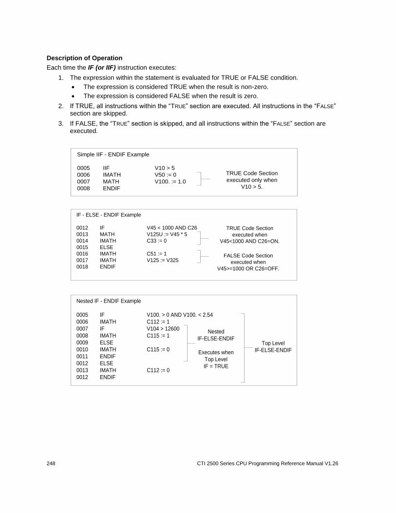
248 CTI 2500 Series CPU Programming Reference Manual V1.26
Description of Operation
Each time the IF (or IIF) instruction executes:
1. The expression within the statement is evaluated for TRUE or FALSE condition.
The expression is considered TRUE when the result is non-zero.
The expression is considered FALSE when the result is zero.
2. If TRUE, all instructions within the “TRUE” section are executed. All instructions in the “FALSE” section are skipped.
3. If FALSE, the “TRUE” section is skipped, and all instructions within the “FALSE” section are executed.
Simple IIF - ENDIF Example
0005 IIF V10 > 5
0006 IMATH V50 := 0
0007 MATH V100. := 1.0
0008 ENDIF
TRUE Code Section
executed only when
V10 > 5.
IF - ELSE - ENDIF Example
0012 IF V45 < 1000 AND C26
0013 MATH V125U := V45 * 5
0014 IMATH C33 := 0
0015 ELSE
0016 IMATH C51 := 1
0017 IMATH V125 := V325
0018 ENDIF
FALSE Code Section
executed when
V45>=1000 OR C26=OFF.
TRUE Code Section
executed when
V45<1000 AND C26=ON.
Nested IF - ENDIF Example
0005 IF V100. > 0 AND V100. < 2.54
0006 IMATH C112 := 1
0007 IF V104 > 12600
0008 IMATH C115 := 1
0009 ELSE
0010 IMATH C115 := 0
0011 ENDIF
0012 ELSE
0013 IMATH C112 := 0
0012 ENDIF
Nested
IF-ELSE-ENDIF
Executes when
Top Level
IF = TRUE
Top Level
IF-ELSE-ENDIF

CTI 2500 Series CPU Programming Reference Manual V1.26 249
3.5.12 Integer Math Operations (IMATH)
The IMATH (Integer Math) instruction executes integer-based arithmetic and logical operations.
IMATH Y := X
Y : Result (Writeable Address - Integer Only)
X: Address Element/Expression or Value Element/Expression
(Integer Only)
Description of Operation
Each time the IMATH instruction executes:
The operations on the right side of the ASSIGNMENT (:=) operator are performed, and the result is written into the memory address (Y) entered on the left side of the ASSIGNMENT operator.
All arithmetic operations are executed using integer math.
Rules of Execution
The IMATH instruction according to the following rules:
Only integers can be used in IMATH statements. Real numbers are not supported.
Different integer types can be designated as follows:
o 16-bit signed integer – default (i.e., V148)
o 16-bit unsigned integer - add “U” suffix (i.e., V352U)
o 32-bit signed integer – add “L” suffix (i.e., V2120L)
Different number formats can be used as follows:
o Decimal – default (i.e., 12)
o Hexadecimal – add “0H” prefix (i.e., 0H7FFE)
o Binary – add “0B” prefix (i.e., 0B11001001)
Each IMATH instruction must contain a single ASSIGNMENT operator.
The right side of the ASSIGNMENT operator can contain multiple mathematical expressions made up of arithmetic and/or logical operations supported by the IMATH instruction.
Expressions can include Memory Array Indexing as described in Section 3.4.3.
Computations are executed according the IMATH Order of Precedence as shown in the table in this section. Operations with the highest precedence are performed first. When functions are equivalent in precedence, calculations are made from left to right. For example, the expression (A / B * C) is calculated first as the quotient of (A / B), and then the result is multiplied by C.
Parentheses can also be used to force the order in which a computation is performed. Any expression enclosed by parentheses is executed before the surrounding operations. For example, the expression (A – B) / C is calculated first as the difference of (A – B), and then the result is divided by C.
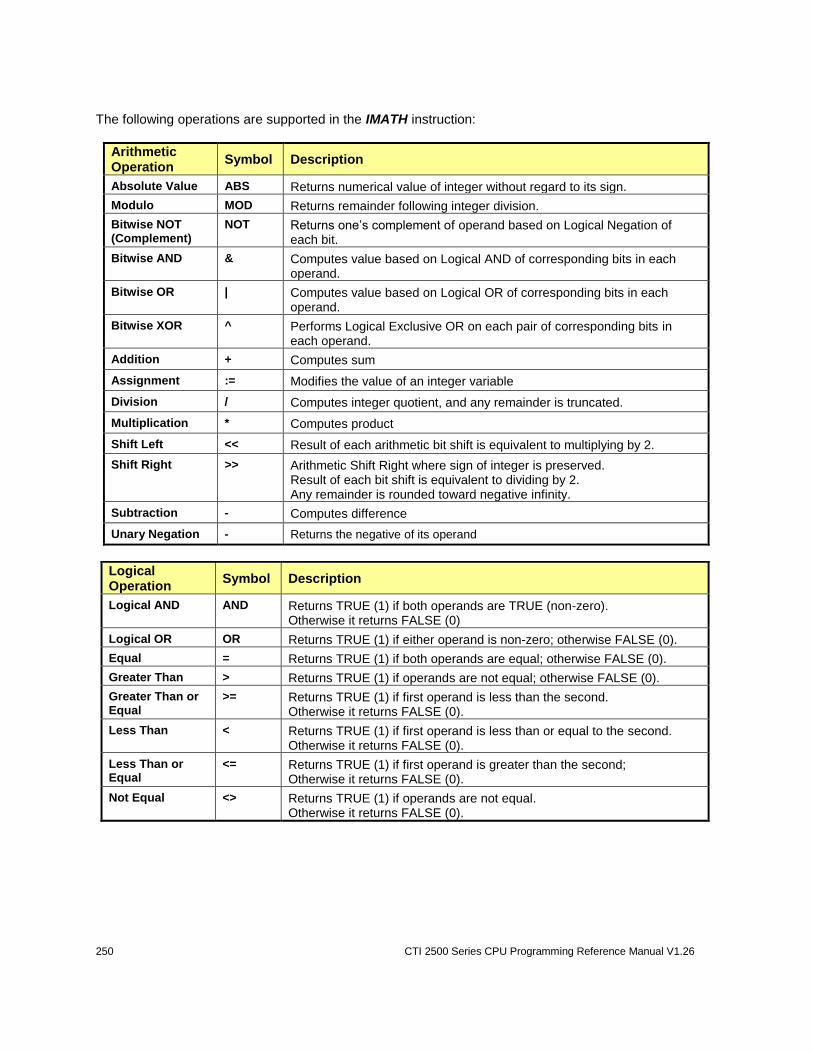
250 CTI 2500 Series CPU Programming Reference Manual V1.26
The following operations are supported in the IMATH instruction:
Arithmetic Operation
Symbol Description
Absolute Value ABS Returns numerical value of integer without regard to its sign.
Modulo MOD Returns remainder following integer division.
Bitwise NOT (Complement)
NOT Returns one’s complement of operand based on Logical Negation of each bit.
Bitwise AND & Computes value based on Logical AND of corresponding bits in each operand.
Bitwise OR | Computes value based on Logical OR of corresponding bits in each operand.
Bitwise XOR ^ Performs Logical Exclusive OR on each pair of corresponding bits in each operand.
Addition + Computes sum
Assignment := Modifies the value of an integer variable
Division / Computes integer quotient, and any remainder is truncated.
Multiplication * Computes product
Shift Left << Result of each arithmetic bit shift is equivalent to multiplying by 2.
Shift Right >> Arithmetic Shift Right where sign of integer is preserved. Result of each bit shift is equivalent to dividing by 2. Any remainder is rounded toward negative infinity.
Subtraction - Computes difference
Unary Negation - Returns the negative of its operand
Logical Operation
Symbol Description
Logical AND AND Returns TRUE (1) if both operands are TRUE (non-zero). Otherwise it returns FALSE (0)
Logical OR OR Returns TRUE (1) if either operand is non-zero; otherwise FALSE (0).
Equal = Returns TRUE (1) if both operands are equal; otherwise FALSE (0).
Greater Than > Returns TRUE (1) if operands are not equal; otherwise FALSE (0).
Greater Than or Equal
>= Returns TRUE (1) if first operand is less than the second. Otherwise it returns FALSE (0).
Less Than < Returns TRUE (1) if first operand is less than or equal to the second. Otherwise it returns FALSE (0).
Less Than or Equal
<= Returns TRUE (1) if first operand is greater than the second; Otherwise it returns FALSE (0).
Not Equal <> Returns TRUE (1) if operands are not equal. Otherwise it returns FALSE (0).

CTI 2500 Series CPU Programming Reference Manual V1.26 251
The Order of Precedence of IMATH operations is shown in the following table:
Operation Order of Precedence
Absolute Value, Bitwise NOT, Unary Negation 1 (Highest)
Multiplication, Division, Modulo 2
Addition, Subtraction 3
Shift Left, Shift Right 4
Relational Operations ( =, <>, <, <=, >, >= ) 5
Logical AND, Bitwise AND 6
Logical OR, Bitwise OR, Bitwise XOR 7
Assignment (:=) 8 (Lowest)
Note:
The NOT operator does not perform the same function in IMATH instruction and MATH instruction. The NOT operation is executed in IMATH as arithmetic Bitwise NOT (or Complement) while it is executed
in MATH as Logical NOT (inverting TRUE/FALSE result).
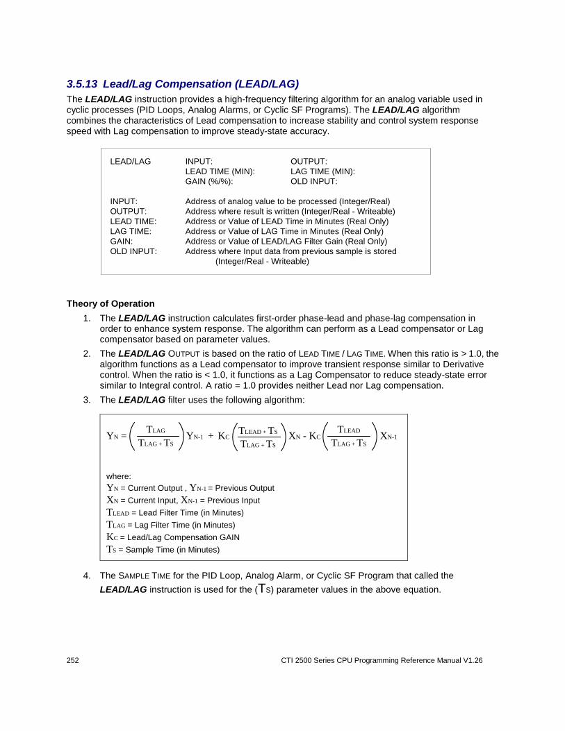
252 CTI 2500 Series CPU Programming Reference Manual V1.26
3.5.13 Lead/Lag Compensation (LEAD/LAG)
The LEAD/LAG instruction provides a high-frequency filtering algorithm for an analog variable used in cyclic processes (PID Loops, Analog Alarms, or Cyclic SF Programs). The LEAD/LAG algorithm combines the characteristics of Lead compensation to increase stability and control system response speed with Lag compensation to improve steady-state accuracy.
LEAD/LAG INPUT: OUTPUT:
LEAD TIME (MIN): LAG TIME (MIN):
GAIN (%/%): OLD INPUT:
INPUT: Address of analog value to be processed (Integer/Real)
OUTPUT: Address where result is written (Integer/Real - Writeable)
LEAD TIME: Address or Value of LEAD Time in Minutes (Real Only)
LAG TIME: Address or Value of LAG Time in Minutes (Real Only)
GAIN: Address or Value of LEAD/LAG Filter Gain (Real Only)
OLD INPUT: Address where Input data from previous sample is stored
(Integer/Real - Writeable)
Theory of Operation
1. The LEAD/LAG instruction calculates first-order phase-lead and phase-lag compensation in order to enhance system response. The algorithm can perform as a Lead compensator or Lag compensator based on parameter values.
2. The LEAD/LAG OUTPUT is based on the ratio of LEAD TIME / LAG TIME. When this ratio is > 1.0, the algorithm functions as a Lead compensator to improve transient response similar to Derivative control. When the ratio is < 1.0, it functions as a Lag Compensator to reduce steady-state error similar to Integral control. A ratio = 1.0 provides neither Lead nor Lag compensation.
3. The LEAD/LAG filter uses the following algorithm:
TLEAD + TS
TLAG + TS
TLAG
TLAG + TS
TLEAD
TLAG + TS
YN = YN-1 + KC XN - KC XN-1
where:
YN = Current Output , YN-1 = Previous Output
XN = Current Input, XN-1 = Previous Input
TLEAD = Lead Filter Time (in Minutes)
TLAG = Lag Filter Time (in Minutes)
KC = Lead/Lag Compensation GAIN
TS = Sample Time (in Minutes)
4. The SAMPLE TIME for the PID Loop, Analog Alarm, or Cyclic SF Program that called the
LEAD/LAG instruction is used for the (TS) parameter values in the above equation.
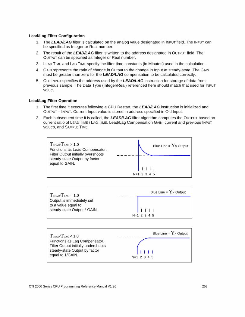
CTI 2500 Series CPU Programming Reference Manual V1.26 253
Lead/Lag Filter Configuration
1. The LEAD/LAG filter is calculated on the analog value designated in INPUT field. The INPUT can be specified as Integer or Real number.
2. The result of the LEAD/LAG filter is written to the address designated in OUTPUT field. The OUTPUT can be specified as Integer or Real number.
3. LEAD TIME and LAG TIME specify the filter time constants (in Minutes) used in the calculation.
4. GAIN represents the ratio of change in Output to the change in Input at steady-state. The GAIN must be greater than zero for the LEAD/LAG compensation to be calculated correctly.
5. OLD INPUT specifies the address used by the LEAD/LAG instruction for storage of data from previous sample. The Data Type (Integer/Real) referenced here should match that used for INPUT value.
Lead/Lag Filter Operation
1. The first time it executes following a CPU Restart, the LEAD/LAG instruction is initialized and OUTPUT = INPUT. Current Input value is stored in address specified in Old Input.
2. Each subsequent time it is called, the LEAD/LAG filter algorithm computes the OUTPUT based on current ratio of LEAD TIME / LAG TIME, Lead/Lag Compensation GAIN, current and previous INPUT values, and SAMPLE TIME.
TLEAD/TLAG > 1.0
Functions as Lead Compensator.
Filter Output initially overshoots
steady-state Output by factor
equal to GAIN.
N=1 2 3 4 5
Blue Line = YN Output
N=1 2 3 4 5
TLEAD/TLAG = 1.0
Output is immediately set
to a value equal to
steady-state Output * GAIN.
Blue Line = YN Output
N=1 2 3 4 5
TLEAD/TLAG < 1.0
Functions as Lag Compensator.
Filter Output initially undershoots
steady-state Output by factor
equal to 1/GAIN.
Blue Line = YN Output
254 CTI 2500 Series CPU Programming Reference Manual V1.26
3.5.14 Real Number Math Operations (MATH)
The MATH instruction executes arithmetic and logical operations using floating point numbers. Integer numbers may be included in the expression, but all integers are converted into the equivalent Real number before execution, and then (if required) the result is converted back into integer value before writing to the memory address entered on the left side of the ASSIGNMENT operator.
MATH Y := X
Y : Result (Writeable Address - Real or Integer)
X: Address Element/Expression or Value Element/Expression
(Real or Integer)
Description of Operation
Each time the MATH instruction executes:
All expressions on the right side of the ASSIGNMENT (:=) operator are executed. All arithmetic operations are executed using Real numbers. Any Integer values are converted into the Real number equivalent before the operation is performed.
The result is written into the memory address (Y) entered on the left side of the ASSIGNMENT
operator. If an Integer memory address is specified, the result is converted to integer value.
Rules of Execution
The MATH instruction according to the following rules:
Integers and/or Real numbers can be used in MATH statements.
Different integer types can be designated as follows:
o 16-bit signed integer – default (i.e., V148)
o 16-bit unsigned integer - add “U” suffix (i.e., V352U)
o 32-bit signed integer – add “L” suffix (i.e., V2120L)
Different number formats can be used as follows:
o Decimal – default (i.e., 12)
o Hexadecimal – add “0H” prefix (i.e., 0H7FFE)
o Binary – add “0B” prefix (i.e., 0B11001001)
Real number variable types are designated by a period following the memory address or variable (i.e., V650. or LSP1.).
Each MATH instruction must contain a single ASSIGNMENT operator.
The right side of the ASSIGNMENT operator can contain multiple mathematical expressions made up of arithmetic and/or logical operations supported by the MATH instruction.
Expressions can include Memory Array Indexing as described in Section 3.4.3.
Computations are executed according the MATH Order of Precedence as shown in the table later in this section. Operations with the highest precedence are performed first. When functions are equivalent in precedence, calculations are made from left to right. For example, the expression (A / B * C) is calculated first as the quotient of (A / B), and then the result is multiplied by C.
Parentheses can also be used to force the order in which a computation is performed. Any expression enclosed by parentheses is executed before the surrounding operations. For example, the expression (A – B) / C is calculated first as the difference of (A – B), and then the result is divided by C.
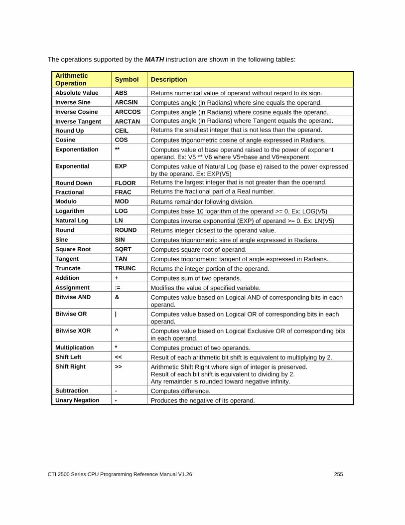
CTI 2500 Series CPU Programming Reference Manual V1.26 255
The operations supported by the MATH instruction are shown in the following tables:
Arithmetic Operation
Symbol Description
Absolute Value ABS Returns numerical value of operand without regard to its sign.
Inverse Sine ARCSIN Computes angle (in Radians) where sine equals the operand.
Inverse Cosine ARCCOS Computes angle (in Radians) where cosine equals the operand.
Inverse Tangent ARCTAN Computes angle (in Radians) where Tangent equals the operand.
Round Up CEIL Returns the smallest integer that is not less than the operand.
Cosine COS Computes trigonometric cosine of angle expressed in Radians.
Exponentiation ** Computes value of base operand raised to the power of exponent operand. Ex: V5 ** V6 where V5=base and V6=exponent
Exponential EXP Computes value of Natural Log (base e) raised to the power expressed by the operand. Ex: EXP(V5)
Round Down FLOOR Returns the largest integer that is not greater than the operand.
Fractional FRAC Returns the fractional part of a Real number.
Modulo MOD Returns remainder following division.
Logarithm LOG Computes base 10 logarithm of the operand >= 0. Ex: LOG(V5)
Natural Log LN Computes inverse exponential (EXP) of operand >= 0. Ex: LN(V5)
Round ROUND Returns integer closest to the operand value.
Sine SIN Computes trigonometric sine of angle expressed in Radians.
Square Root SQRT Computes square root of operand.
Tangent TAN Computes trigonometric tangent of angle expressed in Radians.
Truncate TRUNC Returns the integer portion of the operand.
Addition + Computes sum of two operands.
Assignment := Modifies the value of specified variable.
Bitwise AND & Computes value based on Logical AND of corresponding bits in each operand.
Bitwise OR | Computes value based on Logical OR of corresponding bits in each operand.
Bitwise XOR ^ Computes value based on Logical Exclusive OR of corresponding bits in each operand.
Multiplication * Computes product of two operands.
Shift Left << Result of each arithmetic bit shift is equivalent to multiplying by 2.
Shift Right >> Arithmetic Shift Right where sign of integer is preserved. Result of each bit shift is equivalent to dividing by 2. Any remainder is rounded toward negative infinity.
Subtraction - Computes difference.
Unary Negation - Produces the negative of its operand.
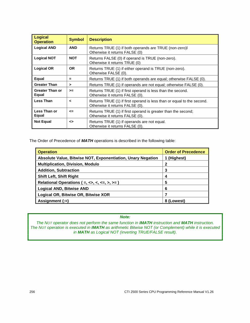
256 CTI 2500 Series CPU Programming Reference Manual V1.26
Logical Operation
Symbol Description
Logical AND AND Returns TRUE (1) if both operands are TRUE (non-zero)l Otherwise it returns FALSE (0)
Logical NOT NOT Returns FALSE (0) if operand is TRUE (non-zero). Otherwise it returns TRUE (0)
Logical OR OR Returns TRUE (1) if either operand is TRUE (non-zero). Otherwise FALSE (0).
Equal = Returns TRUE (1) if both operands are equal; otherwise FALSE (0).
Greater Than > Returns TRUE (1) if operands are not equal; otherwise FALSE (0).
Greater Than or Equal
>= Returns TRUE (1) if first operand is less than the second. Otherwise it returns FALSE (0).
Less Than < Returns TRUE (1) if first operand is less than or equal to the second. Otherwise it returns FALSE (0).
Less Than or Equal
<= Returns TRUE (1) if first operand is greater than the second; Otherwise it returns FALSE (0).
Not Equal <> Returns TRUE (1) if operands are not equal. Otherwise it returns FALSE (0).
The Order of Precedence of MATH operations is described in the following table:
Operation Order of Precedence
Absolute Value, Bitwise NOT, Exponentiation, Unary Negation 1 (Highest)
Multiplication, Division, Modulo 2
Addition, Subtraction 3
Shift Left, Shift Right 4
Relational Operations ( =, <>, <, <=, >, >= ) 5
Logical AND, Bitwise AND 6
Logical OR, Bitwise OR, Bitwise XOR 7
Assignment (:=) 8 (Lowest)
Note:
The NOT operator does not perform the same function in IMATH instruction and MATH instruction. The NOT operation is executed in IMATH as arithmetic Bitwise NOT (or Complement) while it is executed
in MATH as Logical NOT (inverting TRUE/FALSE result).
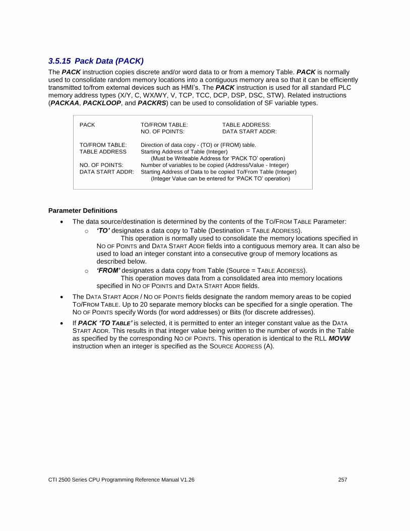
CTI 2500 Series CPU Programming Reference Manual V1.26 257
3.5.15 Pack Data (PACK)
The PACK instruction copies discrete and/or word data to or from a memory Table. PACK is normally used to consolidate random memory locations into a contiguous memory area so that it can be efficiently transmitted to/from external devices such as HMI’s. The PACK instruction is used for all standard PLC memory address types (X/Y, C, WX/WY, V, TCP, TCC, DCP, DSP, DSC, STW). Related instructions (PACKAA, PACKLOOP, and PACKRS) can be used to consolidation of SF variable types.
PACK TO/FROM TABLE: TABLE ADDRESS:
NO. OF POINTS: DATA START ADDR:
TO/FROM TABLE: Direction of data copy - (TO) or (FROM) table.
TABLE ADDRESS Starting Address of Table (Integer)
(Must be Writeable Address for ‘PACK TO’ operation)
NO. OF POINTS: Number of variables to be copied (Address/Value - Integer)
DATA START ADDR: Starting Address of Data to be copied To/From Table (Integer)
(Integer Value can be entered for ‘PACK TO’ operation)
Parameter Definitions
The data source/destination is determined by the contents of the TO/FROM TABLE Parameter:
o ‘TO’ designates a data copy to Table (Destination = TABLE ADDRESS). This operation is normally used to consolidate the memory locations specified in
NO OF POINTS and DATA START ADDR fields into a contiguous memory area. It can also be used to load an integer constant into a consecutive group of memory locations as described below.
o ‘FROM’ designates a data copy from Table (Source = TABLE ADDRESS). This operation moves data from a consolidated area into memory locations
specified in NO OF POINTS and DATA START ADDR fields.
The DATA START ADDR / NO OF POINTS fields designate the random memory areas to be copied TO/FROM TABLE. Up to 20 separate memory blocks can be specified for a single operation. The NO OF POINTS specify Words (for word addresses) or Bits (for discrete addresses).
If PACK ‘TO TABLE’ is selected, it is permitted to enter an integer constant value as the DATA
START ADDR. This results in that integer value being written to the number of words in the Table as specified by the corresponding NO OF POINTS. This operation is identical to the RLL MOVW instruction when an integer is specified as the SOURCE ADDRESS (A).
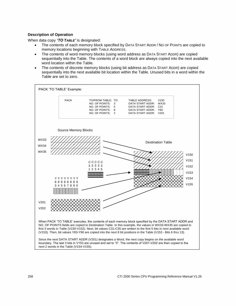
258 CTI 2500 Series CPU Programming Reference Manual V1.26
Description of Operation
When data copy ‘TO TABLE’ is designated:
The contents of each memory block specified by DATA START ADDR / NO OF POINTS are copied to memory locations beginning with TABLE ADDRESS.
The contents of word memory blocks (using word address as DATA START ADDR) are copied sequentially into the Table. The contents of a word block are always copied into the next available word location within the Table.
The contents of discrete memory blocks (using bit address as DATA START ADDR) are copied sequentially into the next available bit location within the Table. Unused bits in a word within the Table are set to zero.
PACK TO/FROM TABLE: TO TABLE ADDRESS: V150
NO. OF POINTS: 3 DATA START ADDR: WX33
NO. OF POINTS: 5 DATA START ADDR: C31
NO. OF POINTS: 8 DATA START ADDR: Y83
NO. OF POINTS: 2 DATA START ADDR: V201
Source Memory Blocks
WX33
WX34
WX35
V201
V202
C
3
1
C
3
2
C
3
3
C
3
4
C
3
5
Y
8
3
Y
8
4
Y
8
5
Y
8
6
Y
8
7
Y
8
8
Y
8
9
Y
9
0
Destination Table
V150
V151
V152
V153
V154
V155
PACK ‘TO TABLE’ Example:
When PACK ‘TO TABLE’ executes, the contents of each memory block specified by the DATA START ADDR and
NO. OF POINTS fields are copied to Destination Table. In this example, the values in WX33-WX35 are copied to
first 3 words in Table (V150-V152). Next, bit values C31-C35 are written to the first 5 bits in next available word
(V153). Then, bit values Y83-Y90 are copied into the next 8 bit positions in the Table (V153 - Bits 6 thru 13).
Since the next DATA START ADDR (V201) designates a Word, the next copy begins on the available word
boundary. The last 3 bits in V153 are unused and set to “0”. The contents of V201-V202 are then copied to the
next 2 words in the Table (V154-V155).

CTI 2500 Series CPU Programming Reference Manual V1.26 259
When data copy ‘FROM Table’ is designated::
The contents of the memory locations starting with TABLE ADDRESS.are sequentially copied into the memory block(s) specified by DATA START ADDR / NO OF POINTS fields. The data copy begins at the first memory block and continues until all memory blocks are completed.
Word values are copied to memory block areas that have a word address as DATA START ADDR. A word copy always begins on the next available word boundary within the Table.
Bit values are copied to discrete memory areas (specified by bit address as DATA START ADDR). Bit data is copied starting with the next available bit location within the Table.
PACK TO/FROM TABLE: FROM TABLE ADDRESS: V240
NO. OF POINTS: 6 DATA START ADDR: C65
NO. OF POINTS: 13 DATA START ADDR: C73
NO. OF POINTS: 2 DATA START ADDR: V88
NO. OF POINTS: 1 DATA START ADDR: V97
NO. OF POINTS: 4 DATA START ADDR: C97
PACK ‘FROM TABLE’ Example:
Destination Memory Blocks
Source Table
C
6
5
C
6
6
C
6
7
C
6
8
C
6
9
C
7
0
C
7
3
C
7
4
C
7
5
C
7
6
C
7
7
C
7
8
C
7
9
C
8
0
C
8
1
C
8
2
C
8
3
C
8
4
C
8
5
C
9
6
C
9
7
C
9
8
C
9
9
V240
V241
V242
V243
V244
V245
V88
V89
V97
When PACK ‘FROM TABLE’ executes, the contents of the Table memory are copied sequentially to the locations
specified by the DATA START ADDR and NO. OF POINTS fields. In this example, the first 6 bits in V240 (Table Start
Address) are copied to C65-C70, and the next 13 bits (spanning V240-V241) are copied to C73-C85.
Since the next DATA START ADDR (V88) is a Word, the next copy begins on the available word boundary. The
contents of V242-V243 are then copied to V88-V89. Next, the contents of V244 are written to V97. Finally, the next 4
bits (first four bits in V245) are copied to C96-C99.
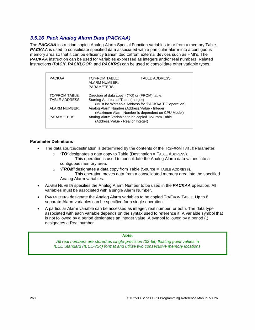
260 CTI 2500 Series CPU Programming Reference Manual V1.26
3.5.16 Pack Analog Alarm Data (PACKAA)
The PACKAA instruction copies Analog Alarm Special Function variables to or from a memory Table. PACKAA is used to consolidate specified data associated with a particular alarm into a contiguous memory area so that it can be efficiently transmitted to/from external devices such as HMI’s. The PACKAA instruction can be used for variables expressed as integers and/or real numbers. Related instructions (PACK, PACKLOOP, and PACKRS) can be used to consolidate other variable types.
PACKAA TO/FROM TABLE: TABLE ADDRESS:
ALARM NUMBER:
PARAMETERS:
TO/FROM TABLE: Direction of data copy - (TO) or (FROM) table.
TABLE ADDRESS Starting Address of Table (Integer)
(Must be Writeable Address for ‘PACKAA TO’ operation)
ALARM NUMBER: Analog Alarm Number (Address/Value - Integer)
(Maximum Alarm Number is dependent on CPU Model)
PARAMETERS: Analog Alarm Variables to be copied To/From Table
(Address/Value - Real or Integer)
Parameter Definitions
The data source/destination is determined by the contents of the TO/FROM TABLE Parameter:
o ‘TO’ designates a data copy to Table (Destination = TABLE ADDRESS). This operation is used to consolidate the Analog Alarm data values into a
contiguous memory area.
o ‘FROM’ designates a data copy from Table (Source = TABLE ADDRESS). This operation moves data from a consolidated memory area into the specified
Analog Alarm variables.
ALARM NUMBER specifies the Analog Alarm Number to be used in the PACKAA operation. All variables must be associated with a single Alarm Number.
PARAMETERS designate the Analog Alarm variables to be copied TO/FROM TABLE. Up to 8 separate Alarm variables can be specified for a single operation.
A particular Alarm variable can be accessed as integer, real number, or both. The data type associated with each variable depends on the syntax used to reference it. A variable symbol that is not followed by a period designates an integer value. A symbol followed by a period (.) designates a Real number.
Note:
All real numbers are stored as single-precision (32-bit) floating point values in IEEE Standard (IEEE-754) format and utilize two consecutive memory locations.
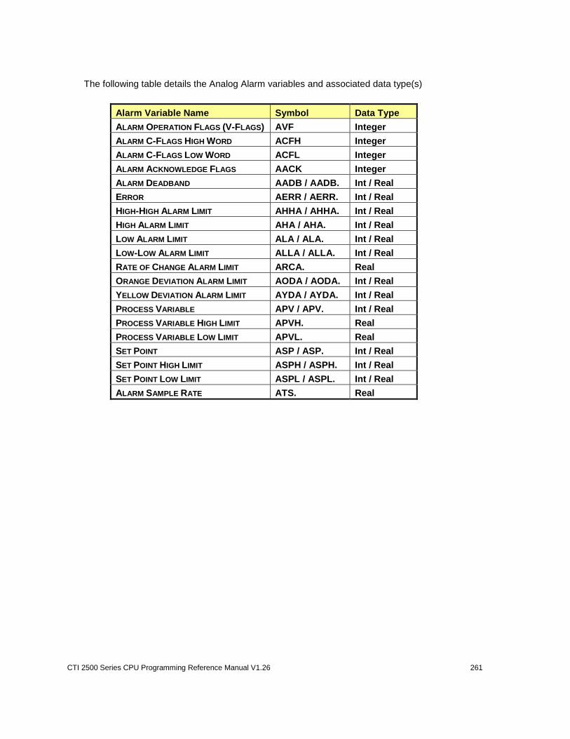
CTI 2500 Series CPU Programming Reference Manual V1.26 261
The following table details the Analog Alarm variables and associated data type(s)
Alarm Variable Name Symbol Data Type
ALARM OPERATION FLAGS (V-FLAGS) AVF Integer
ALARM C-FLAGS HIGH WORD ACFH Integer
ALARM C-FLAGS LOW WORD ACFL Integer
ALARM ACKNOWLEDGE FLAGS AACK Integer
ALARM DEADBAND AADB / AADB. Int / Real
ERROR AERR / AERR. Int / Real
HIGH-HIGH ALARM LIMIT AHHA / AHHA. Int / Real
HIGH ALARM LIMIT AHA / AHA. Int / Real
LOW ALARM LIMIT ALA / ALA. Int / Real
LOW-LOW ALARM LIMIT ALLA / ALLA. Int / Real
RATE OF CHANGE ALARM LIMIT ARCA. Real
ORANGE DEVIATION ALARM LIMIT AODA / AODA. Int / Real
YELLOW DEVIATION ALARM LIMIT AYDA / AYDA. Int / Real
PROCESS VARIABLE APV / APV. Int / Real
PROCESS VARIABLE HIGH LIMIT APVH. Real
PROCESS VARIABLE LOW LIMIT APVL. Real
SET POINT ASP / ASP. Int / Real
SET POINT HIGH LIMIT ASPH / ASPH. Int / Real
SET POINT LOW LIMIT ASPL / ASPL. Int / Real
ALARM SAMPLE RATE ATS. Real
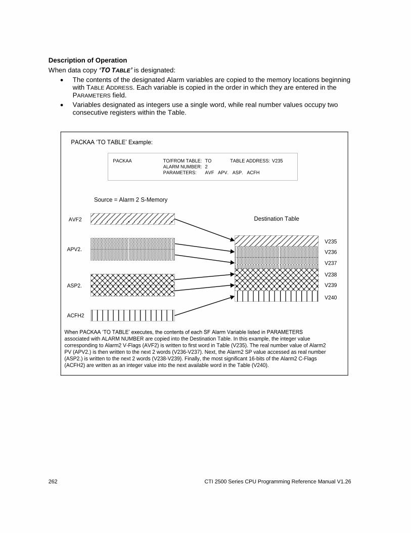
262 CTI 2500 Series CPU Programming Reference Manual V1.26
Description of Operation
When data copy ‘TO TABLE’ is designated:
The contents of the designated Alarm variables are copied to the memory locations beginning with TABLE ADDRESS. Each variable is copied in the order in which they are entered in the PARAMETERS field.
Variables designated as integers use a single word, while real number values occupy two consecutive registers within the Table.
When PACKAA ‘TO TABLE’ executes, the contents of each SF Alarm Variable listed in PARAMETERS
associated with ALARM NUMBER are copied into the Destination Table. In this example, the integer value
corresponding to Alarm2 V-Flags (AVF2) is written to first word in Table (V235). The real number value of Alarm2
PV (APV2.) is then written to the next 2 words (V236-V237). Next, the Alarm2 SP value accessed as real number
(ASP2.) is written to the next 2 words (V238-V239). Finally, the most significant 16-bits of the Alarm2 C-Flags
(ACFH2) are written as an integer value into the next available word in the Table (V240).
Destination Table
PACKAA ‘TO TABLE’ Example:
Source = Alarm 2 S-Memory
AVF2
APV2.
ASP2.
ACFH2
V235
V236
V237
V238
V239
V240
PACKAA TO/FROM TABLE: TO TABLE ADDRESS: V235
ALARM NUMBER: 2
PARAMETERS: AVF APV. ASP. ACFH

CTI 2500 Series CPU Programming Reference Manual V1.26 263
When data copy ‘FROM TABLE’ is designated:
The contents of the memory locations starting with TABLE ADDRESS are sequentially copied into the Alarm variables specified in PARAMETERS. The data copy begins at the first memory block and continues until all memory blocks are completed.
Variables designated as integers are loaded as a single word, while real number values are copied from two consecutive words within the Table.
The PACKAA ‘FROM TABLE’ operation copies the contents of the Table memory into the SF Alarm Variables
associated with ALARM NUMBER that are listed as PARAMETERS. In this example, the first word in the Table
(V235) is accessed as an integer value and copied to Alarm2 V-Flags variable (AVF2). The next 2 words (V236-
V237) are accessed as a real number and written to Alarm2 PV variable (APV2.). The next 2 words in the Table
(V238-V239) are accessed as a real number and copied to Alarm2 SP (ASP2.) . Finally, the contents of the last
word (V240) are copied to the most significant 16-bits of the Alarm2 C-Flags variable (ACFH2).
PACKAA ‘FROM TABLE’ Example:
PACKAA TO/FROM TABLE: FROM TABLE ADDRESS: V235
ALARM NUMBER: 2
PARAMETERS: AVF APV. ASP. ACFH
Source = Table
V235
V236
V237
V238
V239
V240
AVF2
APV2.
ASP2.
ACFH2
Dest = Alarm 2 S-Memory
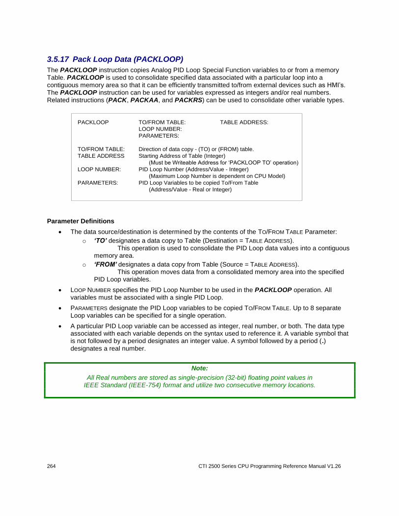
264 CTI 2500 Series CPU Programming Reference Manual V1.26
3.5.17 Pack Loop Data (PACKLOOP)
The PACKLOOP instruction copies Analog PID Loop Special Function variables to or from a memory Table. PACKLOOP is used to consolidate specified data associated with a particular loop into a contiguous memory area so that it can be efficiently transmitted to/from external devices such as HMI’s. The PACKLOOP instruction can be used for variables expressed as integers and/or real numbers. Related instructions (PACK, PACKAA, and PACKRS) can be used to consolidate other variable types.
PACKLOOP TO/FROM TABLE: TABLE ADDRESS:
LOOP NUMBER:
PARAMETERS:
TO/FROM TABLE: Direction of data copy - (TO) or (FROM) table.
TABLE ADDRESS Starting Address of Table (Integer)
(Must be Writeable Address for ‘PACKLOOP TO’ operation)
LOOP NUMBER: PID Loop Number (Address/Value - Integer)
(Maximum Loop Number is dependent on CPU Model)
PARAMETERS: PID Loop Variables to be copied To/From Table
(Address/Value - Real or Integer)
Parameter Definitions
The data source/destination is determined by the contents of the TO/FROM TABLE Parameter:
o ‘TO’ designates a data copy to Table (Destination = TABLE ADDRESS). This operation is used to consolidate the PID Loop data values into a contiguous
memory area.
o ‘FROM’ designates a data copy from Table (Source = TABLE ADDRESS). This operation moves data from a consolidated memory area into the specified
PID Loop variables.
LOOP NUMBER specifies the PID Loop Number to be used in the PACKLOOP operation. All variables must be associated with a single PID Loop.
PARAMETERS designate the PID Loop variables to be copied TO/FROM TABLE. Up to 8 separate Loop variables can be specified for a single operation.
A particular PID Loop variable can be accessed as integer, real number, or both. The data type associated with each variable depends on the syntax used to reference it. A variable symbol that is not followed by a period designates an integer value. A symbol followed by a period (.) designates a real number.
Note:
All Real numbers are stored as single-precision (32-bit) floating point values in IEEE Standard (IEEE-754) format and utilize two consecutive memory locations.
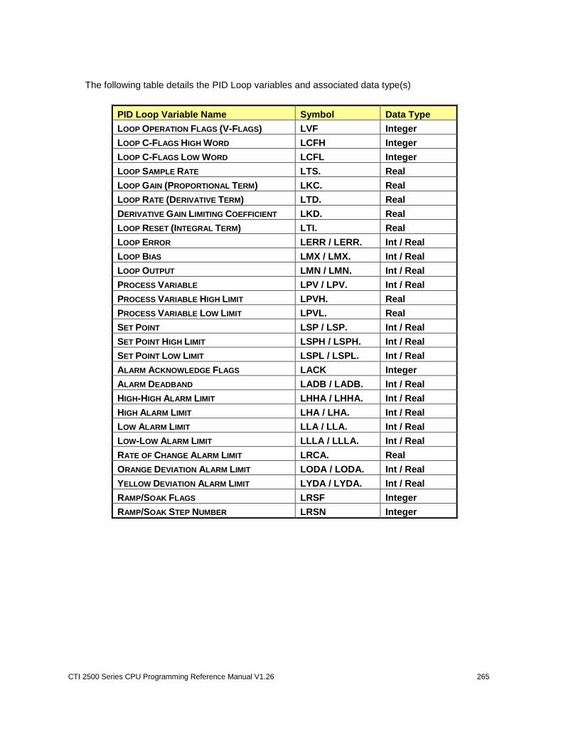
CTI 2500 Series CPU Programming Reference Manual V1.26 265
The following table details the PID Loop variables and associated data type(s)
PID Loop Variable Name Symbol Data Type
LOOP OPERATION FLAGS (V-FLAGS) LVF Integer
LOOP C-FLAGS HIGH WORD LCFH Integer
LOOP C-FLAGS LOW WORD LCFL Integer
LOOP SAMPLE RATE LTS. Real
LOOP GAIN (PROPORTIONAL TERM) LKC. Real
LOOP RATE (DERIVATIVE TERM) LTD. Real
DERIVATIVE GAIN LIMITING COEFFICIENT LKD. Real
LOOP RESET (INTEGRAL TERM) LTI. Real
LOOP ERROR LERR / LERR. Int / Real
LOOP BIAS LMX / LMX. Int / Real
LOOP OUTPUT LMN / LMN. Int / Real
PROCESS VARIABLE LPV / LPV. Int / Real
PROCESS VARIABLE HIGH LIMIT LPVH. Real
PROCESS VARIABLE LOW LIMIT LPVL. Real
SET POINT LSP / LSP. Int / Real
SET POINT HIGH LIMIT LSPH / LSPH. Int / Real
SET POINT LOW LIMIT LSPL / LSPL. Int / Real
ALARM ACKNOWLEDGE FLAGS LACK Integer
ALARM DEADBAND LADB / LADB. Int / Real
HIGH-HIGH ALARM LIMIT LHHA / LHHA. Int / Real
HIGH ALARM LIMIT LHA / LHA. Int / Real
LOW ALARM LIMIT LLA / LLA. Int / Real
LOW-LOW ALARM LIMIT LLLA / LLLA. Int / Real
RATE OF CHANGE ALARM LIMIT LRCA. Real
ORANGE DEVIATION ALARM LIMIT LODA / LODA. Int / Real
YELLOW DEVIATION ALARM LIMIT LYDA / LYDA. Int / Real
RAMP/SOAK FLAGS LRSF Integer
RAMP/SOAK STEP NUMBER LRSN Integer

266 CTI 2500 Series CPU Programming Reference Manual V1.26
Description of Operation
When data copy ‘TO TABLE’ is designated:
The contents of the designated Loop variables are copied to the memory locations beginning with TABLE ADDRESS. Each variable is copied in the order in which they are entered in the PARAMETERS field.
Variables designated as integers use a single word, while real number values occupy two consecutive registers within the Table.
When PACKLOOP ‘TO TABLE’ executes, the contents of each SF Loop Variable listed in PARAMETERS
associated with LOOP NUMBER are copied into the Destination Table. In this example, the integer value
corresponding to Loop6 V-Flags (LVF6) is written to first word in Table (V171). The Loop6 Gain (LKC6.) is
accessed as a real number and written to the next 2 words (V172-V173). Next, the Loop6 High Alarm Limit is
accessed as real number (LHA6.) and written to the next 2 words (V174-V175). Finally, the Loop6 Output integer
value (LMN6) is written into the next available word in the Table (V176).
Destination Table
PACKLOOP ‘TO TABLE’ Example:
Source = Loop 6 S-Memory
LVF6
LKC6.
LHA6.
LMN6
V171
V172
V173
V174
V175
V176
PACKLOOP TO/FROM TABLE: TO TABLE ADDRESS: V171
LOOP NUMBER: 6
PARAMETERS: LVF LKC. LHA. LMN
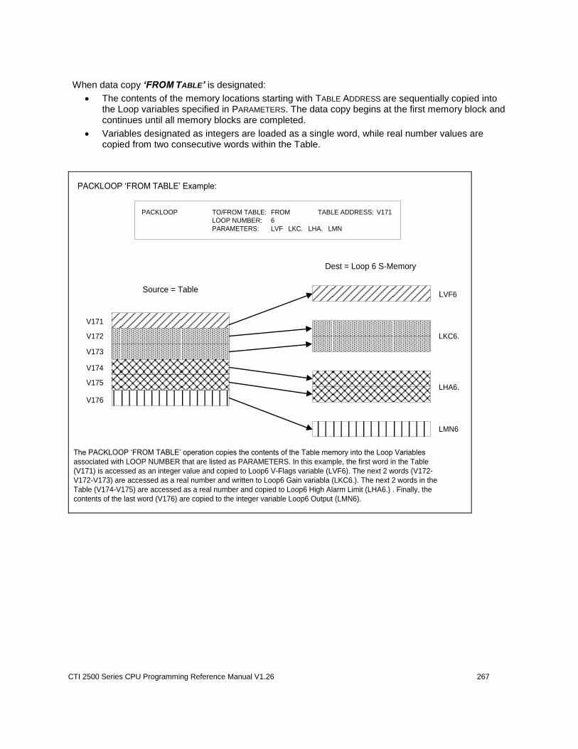
CTI 2500 Series CPU Programming Reference Manual V1.26 267
When data copy ‘FROM TABLE’ is designated:
The contents of the memory locations starting with TABLE ADDRESS are sequentially copied into the Loop variables specified in PARAMETERS. The data copy begins at the first memory block and continues until all memory blocks are completed.
Variables designated as integers are loaded as a single word, while real number values are copied from two consecutive words within the Table.
The PACKLOOP ‘FROM TABLE’ operation copies the contents of the Table memory into the Loop Variables
associated with LOOP NUMBER that are listed as PARAMETERS. In this example, the first word in the Table
(V171) is accessed as an integer value and copied to Loop6 V-Flags variable (LVF6). The next 2 words (V172-
V172-V173) are accessed as a real number and written to Loop6 Gain variabla (LKC6.). The next 2 words in the
Table (V174-V175) are accessed as a real number and copied to Loop6 High Alarm Limit (LHA6.) . Finally, the
contents of the last word (V176) are copied to the integer variable Loop6 Output (LMN6).
PACKLOOP ‘FROM TABLE’ Example:
PACKLOOP TO/FROM TABLE: FROM TABLE ADDRESS: V171
LOOP NUMBER: 6
PARAMETERS: LVF LKC. LHA. LMN
Source = Table
V171
V172
V173
V174
V175
V176
LVF6
LKC6.
LHA6.
LMN6
Dest = Loop 6 S-Memory
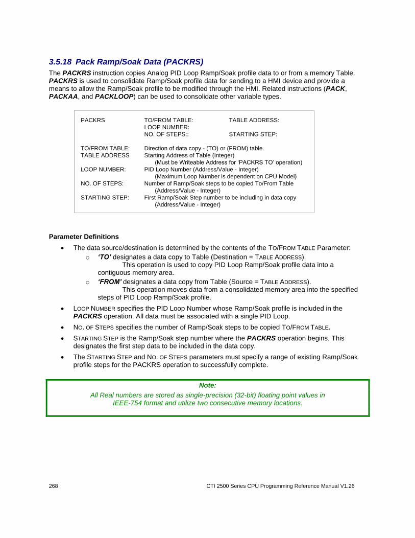
268 CTI 2500 Series CPU Programming Reference Manual V1.26
3.5.18 Pack Ramp/Soak Data (PACKRS)
The PACKRS instruction copies Analog PID Loop Ramp/Soak profile data to or from a memory Table. PACKRS is used to consolidate Ramp/Soak profile data for sending to a HMI device and provide a means to allow the Ramp/Soak profile to be modified through the HMI. Related instructions (PACK, PACKAA, and PACKLOOP) can be used to consolidate other variable types.
PACKRS TO/FROM TABLE: TABLE ADDRESS:
LOOP NUMBER:
NO. OF STEPS:: STARTING STEP:
TO/FROM TABLE: Direction of data copy - (TO) or (FROM) table.
TABLE ADDRESS Starting Address of Table (Integer)
(Must be Writeable Address for ‘PACKRS TO’ operation)
LOOP NUMBER: PID Loop Number (Address/Value - Integer)
(Maximum Loop Number is dependent on CPU Model)
NO. OF STEPS: Number of Ramp/Soak steps to be copied To/From Table
(Address/Value - Integer)
STARTING STEP: First Ramp/Soak Step number to be including in data copy
(Address/Value - Integer)
Parameter Definitions
The data source/destination is determined by the contents of the TO/FROM TABLE Parameter:
o ‘TO’ designates a data copy to Table (Destination = TABLE ADDRESS). This operation is used to copy PID Loop Ramp/Soak profile data into a
contiguous memory area.
o ‘FROM’ designates a data copy from Table (Source = TABLE ADDRESS). This operation moves data from a consolidated memory area into the specified
steps of PID Loop Ramp/Soak profile.
LOOP NUMBER specifies the PID Loop Number whose Ramp/Soak profile is included in the PACKRS operation. All data must be associated with a single PID Loop.
NO. OF STEPS specifies the number of Ramp/Soak steps to be copied TO/FROM TABLE.
STARTING STEP is the Ramp/Soak step number where the PACKRS operation begins. This designates the first step data to be included in the data copy.
The STARTING STEP and NO. OF STEPS parameters must specify a range of existing Ramp/Soak profile steps for the PACKRS operation to successfully complete.
Note:
All Real numbers are stored as single-precision (32-bit) floating point values in IEEE-754 format and utilize two consecutive memory locations.
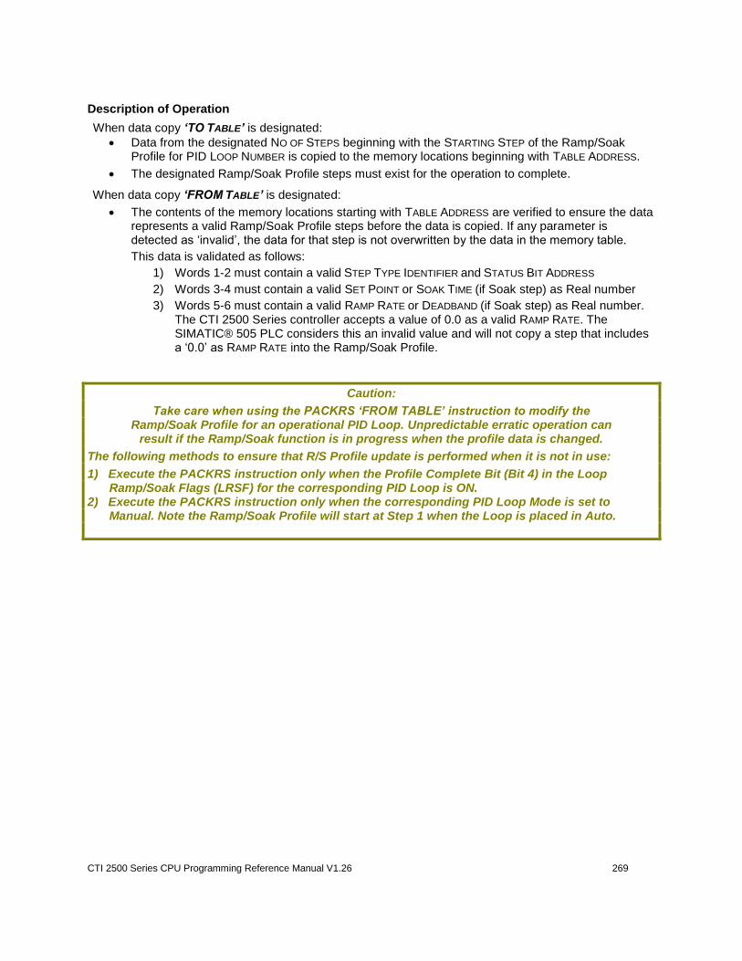
CTI 2500 Series CPU Programming Reference Manual V1.26 269
Description of Operation
When data copy ‘TO TABLE’ is designated:
Data from the designated NO OF STEPS beginning with the STARTING STEP of the Ramp/Soak Profile for PID LOOP NUMBER is copied to the memory locations beginning with TABLE ADDRESS.
The designated Ramp/Soak Profile steps must exist for the operation to complete.
When data copy ‘FROM TABLE’ is designated:
The contents of the memory locations starting with TABLE ADDRESS are verified to ensure the data represents a valid Ramp/Soak Profile steps before the data is copied. If any parameter is detected as ‘invalid’, the data for that step is not overwritten by the data in the memory table.
This data is validated as follows:
1) Words 1-2 must contain a valid STEP TYPE IDENTIFIER and STATUS BIT ADDRESS
2) Words 3-4 must contain a valid SET POINT or SOAK TIME (if Soak step) as Real number
3) Words 5-6 must contain a valid RAMP RATE or DEADBAND (if Soak step) as Real number. The CTI 2500 Series controller accepts a value of 0.0 as a valid RAMP RATE. The SIMATIC® 505 PLC considers this an invalid value and will not copy a step that includes a ‘0.0’ as RAMP RATE into the Ramp/Soak Profile.
Caution:
Take care when using the PACKRS ‘FROM TABLE’ instruction to modify the Ramp/Soak Profile for an operational PID Loop. Unpredictable erratic operation can
result if the Ramp/Soak function is in progress when the profile data is changed.
The following methods to ensure that R/S Profile update is performed when it is not in use:
1) Execute the PACKRS instruction only when the Profile Complete Bit (Bit 4) in the Loop Ramp/Soak Flags (LRSF) for the corresponding PID Loop is ON.
2) Execute the PACKRS instruction only when the corresponding PID Loop Mode is set to Manual. Note the Ramp/Soak Profile will start at Step 1 when the Loop is placed in Auto.
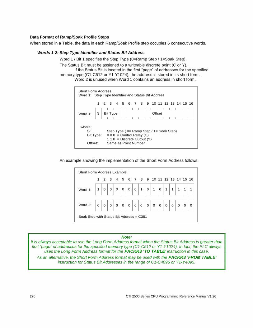
270 CTI 2500 Series CPU Programming Reference Manual V1.26
Data Format of Ramp/Soak Profile Steps
When stored in a Table, the data in each Ramp/Soak Profile step occupies 6 consecutive words. Words 1-2: Step Type Identifier and Status Bit Address
Word 1 / Bit 1 specifies the Step Type (0=Ramp Step / 1=Soak Step).
The Status Bit must be assigned to a writeable discrete point (C or Y). If the Status Bit is located in the first “page” of addresses for the specified
memory type (C1-C512 or Y1-Y1024), the address is stored in its short form. Word 2 is unused when Word 1 contains an address in short form.
Word 1:
Short Form Address
Word 1: Step Type Identifier and Status Bit Address
1 2 3 4 5 6 7 8 9 10 11 12 13 14 15 16
S Bit Type Offset
where:
S: Step Type ( 0= Ramp Step / 1= Soak Step)
Bit Type: 0 0 0 = Control Relay (C)
1 1 0 = Discrete Output (Y)
Offset: Same as Point Number
An example showing the implementation of the Short Form Address follows:
Short Form Address Example:
1 2 3 4 5 6 7 8 9 10 11 12 13 14 15 16
1 00 0 1000 0 1 0 1 1 1 1 1
0 00 0 0000 0 0 0 0 0 0 0 0
Word 1:
Word 2:
Soak Step with Status Bit Address = C351
Note: It is always acceptable to use the Long Form Address format when the Status Bit Address is greater than first “page” of addresses for the specified memory type (C1-C512 or Y1-Y1024). In fact, the PLC always
uses the Long Form Address format for the PACKRS ‘TO TABLE’ instruction in this case.
As an alternative, the Short Form Address format may be used with the PACKRS ‘FROM TABLE’ instruction for Status Bit Addresses in the range of C1-C4095 or Y1-Y4095.
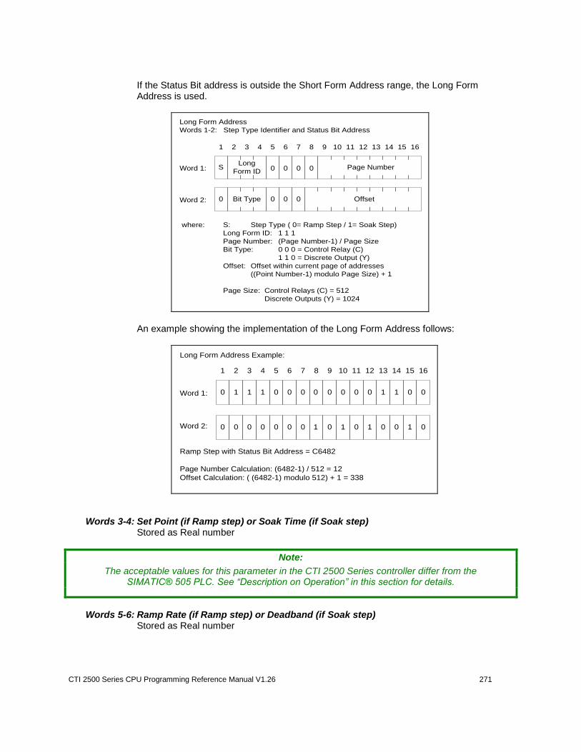
CTI 2500 Series CPU Programming Reference Manual V1.26 271
If the Status Bit address is outside the Short Form Address range, the Long Form
Address is used.
Long Form Address
Words 1-2: Step Type Identifier and Status Bit Address
where: S: Step Type ( 0= Ramp Step / 1= Soak Step)
Long Form ID: 1 1 1
Page Number: (Page Number-1) / Page Size
Bit Type: 0 0 0 = Control Relay (C)
1 1 0 = Discrete Output (Y)
Offset: Offset within current page of addresses
((Point Number-1) modulo Page Size) + 1
Page Size: Control Relays (C) = 512
Discrete Outputs (Y) = 1024
Word 1:
1 2 3 4 5 6 7 8 9 10 11 12 13 14 15 16
0 0 0 0SLong
Form IDPage Number
Word 2: 0 0 0 0 OffsetBit Type
An example showing the implementation of the Long Form Address follows:
Long Form Address Example:
1 2 3 4 5 6 7 8 9 10 11 12 13 14 15 16
0 11 1 0000 0 0 0 0 1 1 0 0
0 00 0 1000 0 1 0 1 0 0 1 0
Word 1:
Word 2:
Ramp Step with Status Bit Address = C6482
Page Number Calculation: (6482-1) / 512 = 12
Offset Calculation: ( (6482-1) modulo 512) + 1 = 338
Words 3-4: Set Point (if Ramp step) or Soak Time (if Soak step) Stored as Real number
Note:
The acceptable values for this parameter in the CTI 2500 Series controller differ from the SIMATIC® 505 PLC. See “Description on Operation” in this section for details.
Words 5-6: Ramp Rate (if Ramp step) or Deadband (if Soak step) Stored as Real number

272 CTI 2500 Series CPU Programming Reference Manual V1.26
PACKRS ‘TO TABLE’ Example:
PACKRS TO/FROM TABLE: TO TABLE ADDRESS: V40
LOOP NUMBER: 10
NO. OF STEPS: 3 STARTING STEP: 3
Step 3 Data
PID Loop 10
Step R/S Stat Bit SetPoint Ramp Rate Soak Time Deadband
1 Ramp C329 37.5 4.25
2 Soak C330 9.0 2.25
3 Ramp C493 46.5 3.65
4 Soak C494 12.5 1.14
5 Ramp C565 52.2 1.45
6 End
Source = Loop 10 R/S Table
Destination = Memory Table Hex
V46
V47
V48
V49
V50
V51
1 0 0 0 0 0 0 1 1 1 1 0 1 1 1 0
0 0 0 0 0 0 0 0 0 0 0 0 0 0 0 0
0 1 0 0 0 0 0 1 0 1 0 0 1 0 0 0
0 0 0 0 0 0 0 0 0 0 0 0 0 0 0 0
0 0 1 1 1 1 1 1 1 0 0 1 0 0 0 1
1 1 1 0 1 0 1 1 1 0 0 0 0 1 0 1
Soak step w/ Status Bit = C494
Soak Time = 12.5 (stored as Real)
Deadband = 1.14 (stored as Real)
81EE
0000
4148
0000
3F91
EB85
Ramp step w/ Status Bit = C565
SetPoint = 52.2 (stored as Real)
Ramp Rate = 1.45 (stored as Real)
7001
0035
4250
CCCD
3FB9
999A
V52
V53
V54
V55
V56
V57
10 1 1 0 0 0 0 0 0 0 0 0 0 0 1
0 1 0 0 0 0 1 0 0 1 0 1 0 0 0 0
1 1 0 0 1 1 0 0 1 1 0 0 1 1 0 1
10 0 1 1 1 1 1 1 0 1 1 1 0 0 1
1 0 0 1 1 0 0 1 1 0 0 1 1 0 1 0
0 0 0 0 0 0 0 0 0 0 1 1 0 1 0 1
V40
V41
V42
V43
V44
V45
0 0 0 0 0 0 0 1 1 1 1 0 1 1 0 1
0 0 0 0 0 0 0 0 0 0 0 0 0 0 0 0
0 1 0 0 0 0 1 0 0 0 1 1 1 0 1 0
0 0 0 0 0 0 0 0 0 0 0 0 0 0 0 0
0 1 0 0 0 0 0 0 0 1 1 0 1 0 0 1
1 0 0 1 1 0 0 1 1 0 0 1 1 0 1 0
Ramp step w/ Status Bit = C493
SetPoint = 46.5 (stored as Real)
Ramp Rate = 3.65 (stored as Real)
01ED
0000
423A
0000
4069
999A
Step 4 Data
Step 5 Data
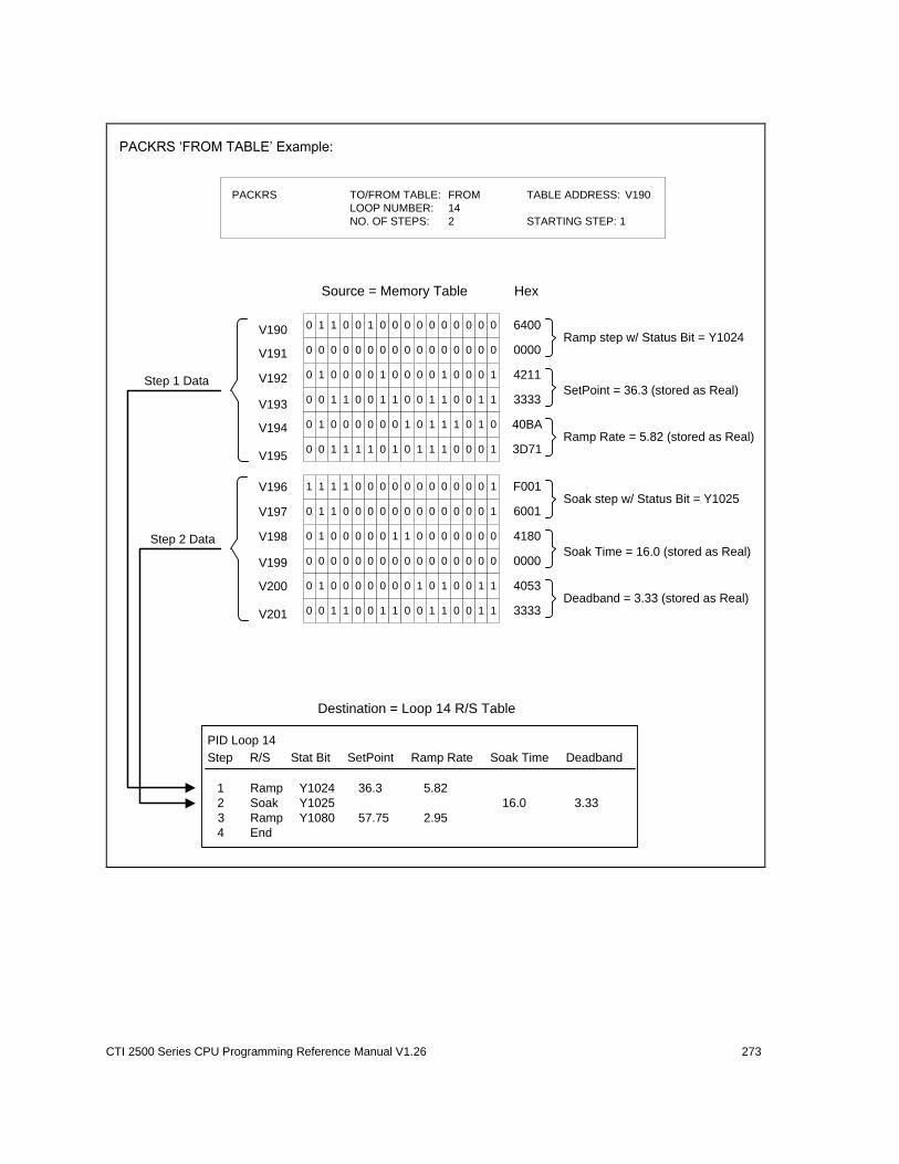
CTI 2500 Series CPU Programming Reference Manual V1.26 273
PACKRS ‘FROM TABLE’ Example:
PACKRS TO/FROM TABLE: FROM TABLE ADDRESS: V190
LOOP NUMBER: 14
NO. OF STEPS: 2 STARTING STEP: 1
Step 2 Data
Step 1 Data
Source = Memory Table Hex
V196
V197
V198
V199
V200
V201
1 1 1 1 0 0 0 0 0 0 0 0 0 0 0 1
0 1 1 0 0 0 0 0 0 0 0 0 0 0 0 1
0 1 0 0 0 0 0 1 1 0 0 0 0 0 0 0
0 0 0 0 0 0 0 0 0 0 0 0 0 0 0 0
0 1 0 0 0 0 0 0 0 1 0 1 0 0 1 1
0 0 1 1 0 0 1 1 0 0 1 1 0 0 1 1
Soak step w/ Status Bit = Y1025
Soak Time = 16.0 (stored as Real)
Deadband = 3.33 (stored as Real)
F001
6001
4180
0000
4053
3333
V190
V191
V192
V193
V194
V195
0 00 1 1 0 0 1 0 0 0 0 0 0 0 0
0 0 0 0 0 0 0 0 0 0 0 0 0 0 0 0
0 1 0 0 0 0 1 0 0 0 0 1 0 0 0 1
0 0 1 1 0 0 1 1 0 0 1 1 0 0 1 1
0 1 0 0 0 0 0 0 1 0 1 1 1 0 1 0
0 0 1 1 1 1 0 1 0 1 1 1 0 0 0 1
Ramp step w/ Status Bit = Y1024
SetPoint = 36.3 (stored as Real)
Ramp Rate = 5.82 (stored as Real)
6400
0000
4211
3333
40BA
3D71
PID Loop 14
Step R/S Stat Bit SetPoint Ramp Rate Soak Time Deadband
1 Ramp Y1024 36.3 5.82
2 Soak Y1025 16.0 3.33
3 Ramp Y1080 57.75 2.95
4 End
Destination = Loop 14 R/S Table
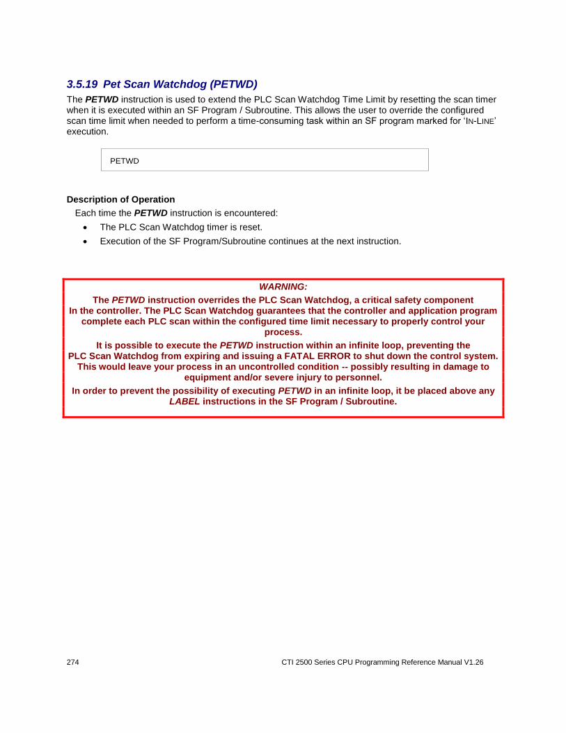
274 CTI 2500 Series CPU Programming Reference Manual V1.26
3.5.19 Pet Scan Watchdog (PETWD)
The PETWD instruction is used to extend the PLC Scan Watchdog Time Limit by resetting the scan timer when it is executed within an SF Program / Subroutine. This allows the user to override the configured scan time limit when needed to perform a time-consuming task within an SF program marked for ‘IN-LINE’ execution.
PETWD
Description of Operation
Each time the PETWD instruction is encountered:
The PLC Scan Watchdog timer is reset.
Execution of the SF Program/Subroutine continues at the next instruction.
WARNING:
The PETWD instruction overrides the PLC Scan Watchdog, a critical safety component In the controller. The PLC Scan Watchdog guarantees that the controller and application program
complete each PLC scan within the configured time limit necessary to properly control your process.
It is possible to execute the PETWD instruction within an infinite loop, preventing the PLC Scan Watchdog from expiring and issuing a FATAL ERROR to shut down the control system.
This would leave your process in an uncontrolled condition -- possibly resulting in damage to equipment and/or severe injury to personnel.
In order to prevent the possibility of executing PETWD in an infinite loop, it be placed above any LABEL instructions in the SF Program / Subroutine.
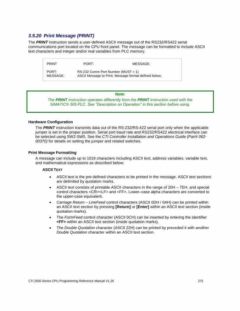
CTI 2500 Series CPU Programming Reference Manual V1.26 275
3.5.20 Print Message (PRINT)
The PRINT instruction sends a user-defined ASCII message out of the RS232/RS422 serial communications port located on the CPU front panel. The message can be formatted to include ASCII text characters and integer and/or real variables from PLC memory.
PRINT PORT: MESSAGE:
PORT: RS-232 Comm Port Number (MUST = 1)
MESSAGE: ASCII Message to Print. Message format defined below.
Note:
The PRINT instruction operates differently from the PRINT instruction used with the SIMATIC® 505 PLC. See “Description on Operation” in this section before using.
Hardware Configuration
The PRINT instruction transmits data out of the RS-232/RS-422 serial port only when the applicable jumper is set in the proper position. Serial port baud rate and RS232/RS422 electrical interface can be selected using SW2-SW5. See the CTI Controller Installation and Operations Guide (Part# 062-00370) for details on setting the jumper and related switches.
Print Message Formatting
A message can include up to 1019 characters including ASCII text, address variables, variable text, and mathematical expressions as described below:
ASCII TEXT
ASCII text is the pre-defined characters to be printed in the message. ASCII text sections are delimited by quotation marks.
ASCII text consists of printable ASCII characters in the range of 20H – 7EH, and special control characters <CR><LF> and <FF>. Lower–case alpha characters are converted to the upper-case equivalent.
Carriage Return – LineFeed control characters (ASCII 0DH / 0AH) can be printed within an ASCII text section by pressing [Return] or [Enter] within an ASCII text section (inside quotation marks).
The FormFeed control character (ASCII 0CH) can be inserted by entering the identifier <FF> within an ASCII text section (inside quotation marks).
The Double Quotation character (ASCII 22H) can be printed by preceded it with another Double Quotation character within an ASCII text section.
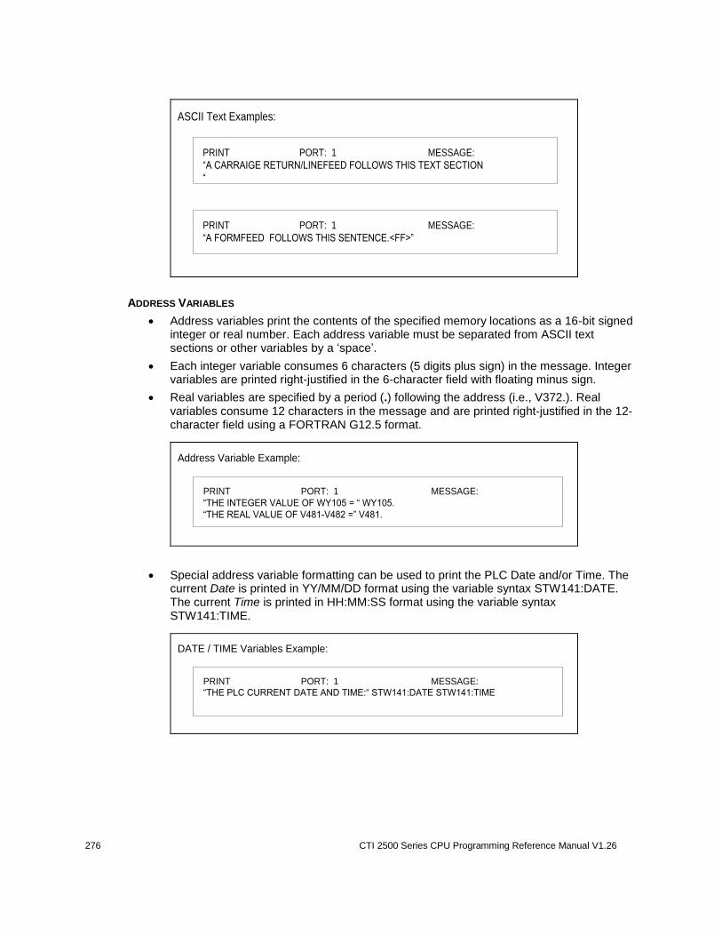
276 CTI 2500 Series CPU Programming Reference Manual V1.26
PRINT PORT: 1 MESSAGE:
“A CARRAIGE RETURN/LINEFEED FOLLOWS THIS TEXT SECTION
“
PRINT PORT: 1 MESSAGE:
“A FORMFEED FOLLOWS THIS SENTENCE.<FF>”
ASCII Text Examples:
ADDRESS VARIABLES
Address variables print the contents of the specified memory locations as a 16-bit signed integer or real number. Each address variable must be separated from ASCII text sections or other variables by a ‘space’.
Each integer variable consumes 6 characters (5 digits plus sign) in the message. Integer variables are printed right-justified in the 6-character field with floating minus sign.
Real variables are specified by a period (.) following the address (i.e., V372.). Real variables consume 12 characters in the message and are printed right-justified in the 12-character field using a FORTRAN G12.5 format.
PRINT PORT: 1 MESSAGE:
“THE INTEGER VALUE OF WY105 = “ WY105.
“THE REAL VALUE OF V481-V482 =” V481.
Address Variable Example:
Special address variable formatting can be used to print the PLC Date and/or Time. The current Date is printed in YY/MM/DD format using the variable syntax STW141:DATE. The current Time is printed in HH:MM:SS format using the variable syntax STW141:TIME.
PRINT PORT: 1 MESSAGE:
“THE PLC CURRENT DATE AND TIME:“ STW141:DATE STW141:TIME
DATE / TIME Variables Example:
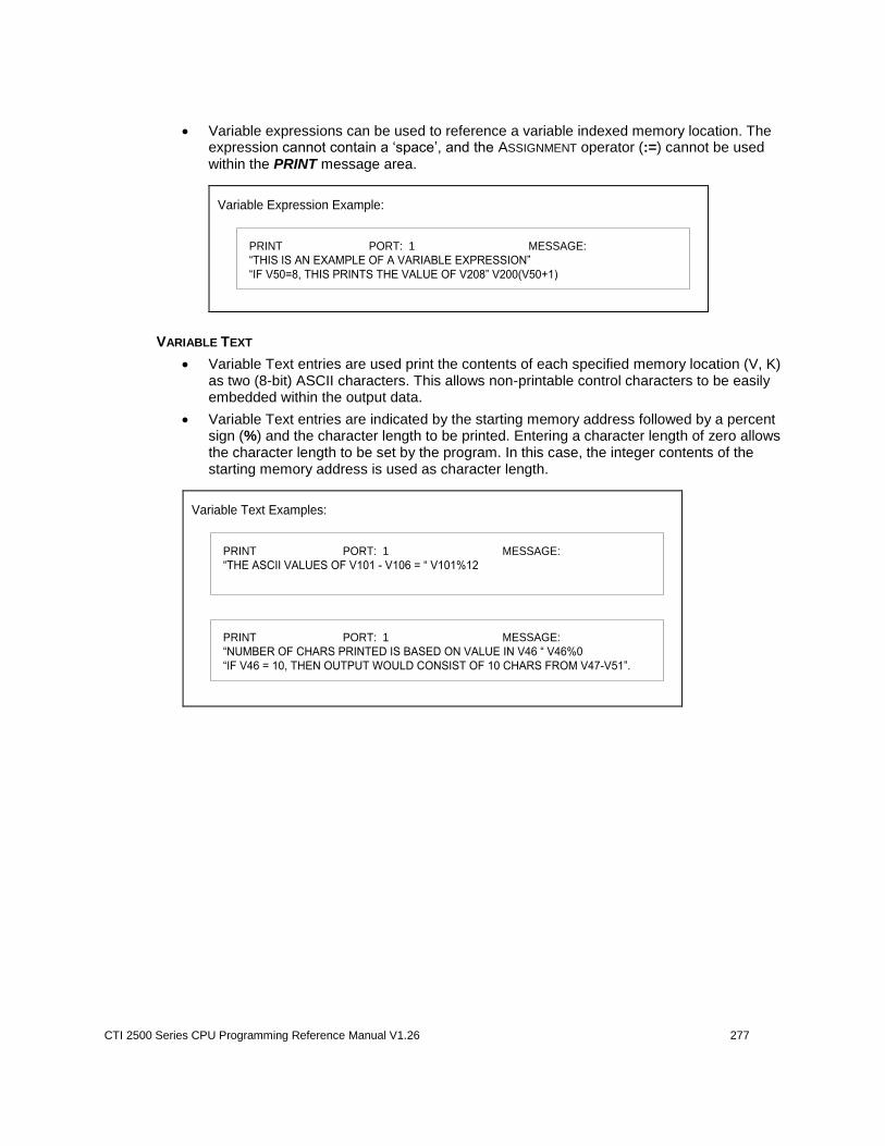
CTI 2500 Series CPU Programming Reference Manual V1.26 277
Variable expressions can be used to reference a variable indexed memory location. The
expression cannot contain a ‘space’, and the ASSIGNMENT operator (:=) cannot be used within the PRINT message area.
PRINT PORT: 1 MESSAGE:
“THIS IS AN EXAMPLE OF A VARIABLE EXPRESSION”
“IF V50=8, THIS PRINTS THE VALUE OF V208” V200(V50+1)
Variable Expression Example:
VARIABLE TEXT
Variable Text entries are used print the contents of each specified memory location (V, K) as two (8-bit) ASCII characters. This allows non-printable control characters to be easily embedded within the output data.
Variable Text entries are indicated by the starting memory address followed by a percent sign (%) and the character length to be printed. Entering a character length of zero allows the character length to be set by the program. In this case, the integer contents of the starting memory address is used as character length.
PRINT PORT: 1 MESSAGE:
“THE ASCII VALUES OF V101 - V106 = “ V101%12
Variable Text Examples:
PRINT PORT: 1 MESSAGE:
“NUMBER OF CHARS PRINTED IS BASED ON VALUE IN V46 “ V46%0
“IF V46 = 10, THEN OUTPUT WOULD CONSIST OF 10 CHARS FROM V47-V51”.
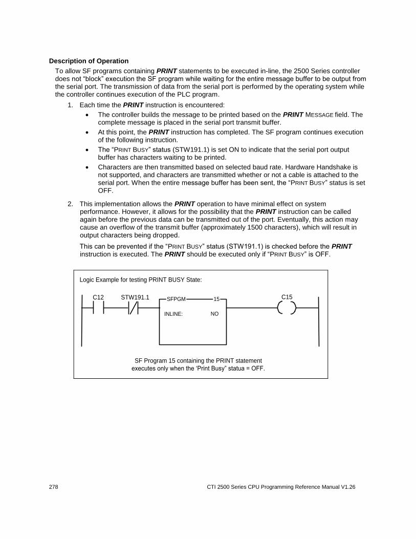
278 CTI 2500 Series CPU Programming Reference Manual V1.26
Description of Operation
To allow SF programs containing PRINT statements to be executed in-line, the 2500 Series controller does not “block” execution the SF program while waiting for the entire message buffer to be output from the serial port. The transmission of data from the serial port is performed by the operating system while the controller continues execution of the PLC program.
1. Each time the PRINT instruction is encountered:
The controller builds the message to be printed based on the PRINT MESSAGE field. The complete message is placed in the serial port transmit buffer.
At this point, the PRINT instruction has completed. The SF program continues execution of the following instruction.
The “PRINT BUSY” status (STW191.1) is set ON to indicate that the serial port output buffer has characters waiting to be printed.
Characters are then transmitted based on selected baud rate. Hardware Handshake is not supported, and characters are transmitted whether or not a cable is attached to the serial port. When the entire message buffer has been sent, the “PRINT BUSY” status is set OFF.
2. This implementation allows the PRINT operation to have minimal effect on system performance. However, it allows for the possibility that the PRINT instruction can be called again before the previous data can be transmitted out of the port. Eventually, this action may cause an overflow of the transmit buffer (approximately 1500 characters), which will result in output characters being dropped.
This can be prevented if the “PRINT BUSY” status (STW191.1) is checked before the PRINT instruction is executed. The PRINT should be executed only if “PRINT BUSY” is OFF.
Logic Example for testing PRINT BUSY State:
SF Program 15 containing the PRINT statement
executes only when the ‘Print Busy” statua = OFF.
STW191.1
INLINE: NO
C15C12 15SFPGM
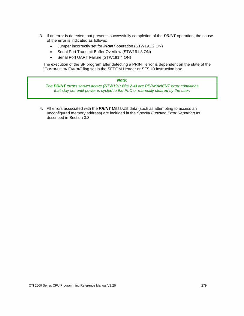
CTI 2500 Series CPU Programming Reference Manual V1.26 279
3. If an error is detected that prevents successfully completion of the PRINT operation, the cause
of the error is indicated as follows:
Jumper incorrectly set for PRINT operation (STW191.2 ON)
Serial Port Transmit Buffer Overflow (STW191.3 ON)
Serial Port UART Failure (STW191.4 ON)
The execution of the SF program after detecting a PRINT error is dependent on the state of the “CONTINUE ON ERROR” flag set in the SFPGM Header or SFSUB instruction box.
Note:
The PRINT errors shown above (STW191/ Bits 2-4) are PERMANENT error conditions that stay set until power is cycled to the PLC or manually cleared by the user.
4. All errors associated with the PRINT MESSAGE data (such as attempting to access an unconfigured memory address) are included in the Special Function Error Reporting as described in Section 3.3.
280 CTI 2500 Series CPU Programming Reference Manual V1.26
3.5.21 Return from SF Program / Subroutine (RETURN)
The RETURN instruction immediately terminates the executing SF Program or SF Subroutine and returns control to the entity that called it (RLL, PID Loop, Analog Alarm, SF Program, SF subroutine). It can be used for conditional program termination as needed. It is not required to insert RETURN at the end of an SF program as the program terminates after executing the last instruction.
RETURN
Description of Operation
If the RETURN instruction is encountered in an SF Program, the program terminates and control
If an SF Program is running, the program terminates and control returns to the task (RLL, PID Loop, or Analog Alarm) that called it.
If an SF Subroutine is running, the program terminates and execution continues at the instruction following the SF Subroutine CALL (RLL, SF Program, or SF Subroutine).
Conditional RETURN Example
0025 IF SFEC > 0
0026 RETURN
0027 ENDIF
CTI 2500 Series CPU Programming Reference Manual V1.26 281
3.5.22 Scale Analog Input to Engineering Units (SCALE)
The SCALE instruction converts an integer value within a standard analog range to engineering units scaled within the range of the specified Low / High Limits. The result can be designated to be an integer or real number. A complementary instruction (UNSCALE) can be used to convert a real number to a standard analog output.
SCALE BINARY INPUT: SCALED RESULT::
LOW LIMIT:: HIGH LIMIT::
20% OFFSET: BIPOLAR:
BINARY INPUT: Address of analog value to be scaled (Integer)
SCALED RESULT: Address where result is written (Integer/Real - Writeable)
LOW LIMIT: Low Limit of Result in Engr Units (integer/Real Constant)
HIGH LIMIT: High Limit of Result in Engr Units (Integer/Real Constant)
20% OFFSET Specifies 20% Offset for Input Range (YES / NO )
BIPOLAR: Specifies Bipolar Input Range (YES / NO)
Parameter Definitions
BINARY INPUT designates the memory address for integer value used as input.
SCALED RESULT designates the memory address where the SCALE result is written. The address can specify an integer or real number (when address is followed by a period (.) ).
LOW LIMIT is the low end (0%) of the range used for SCALE result..This value must be entered as an integer or real number constant value.
HIGH LIMIT is the high end (100%) of the range used for SCALE result. This value must be entered as an integer or real number constant value.
20% OFFSET indicates an analog range where the BINARY INPUT includes a 20% offset (such as 1-5V or 4-20mA analog range). Enter ‘YES’ to specify an input range with 20% offset.
BIPOLAR indicates an analog range where the Binary Input corresponds to a bipolar range (such as -5-to-+5V analog range). Enter ‘YES’ to specify a bipolar input range.
Note: It is not permitted to set both 20% OFFSET and BIPOLAR selections to ‘YES’ since that would
define an invalid analog range.
282 CTI 2500 Series CPU Programming Reference Manual V1.26
Description of Operation
Each time the SCALE instruction is called
1. The analog input range is determined based on SCALE parameters:
Input Range = 0-to-+32000 when both 20% OFFSET = ‘NO’ and BIPOLAR = ‘NO’
Input Range = +6400–to-+32000 when 20% OFFSET = ‘YES’
Input Range = -32000-to-+32000 when BIPOLAR = ‘YES’
2. The percentage of input (0-100%) is calculated based on the BINARY INPUT value within the analog range and converted to the equivalent percentage of the engineering units defined by LOW
/ HIGH LIMITS.
3. If the SCALED RESULT is an integer address, the result is rounded to the closest integer value.
4. If the SCALED RESULT is a real number, the result is written within the following ranges:
5.42101 E-20 to 9.22337 E+19 (SCALED RESULT = positive real number)
-9.22337 E+18 to -2.71051 E-20 (SCALED RESULT = negative real number)
Input: WX45 = 9138
Result: V341. = 82.8887
SCALE Calculation
Analog Range = +6400-to-+32000 (because 20% OFFSET = ‘YES’)
Percentage of Input = (9138 - 6400) / (32000 - 6400) = 10.6953125%
Scaled Result = (625.0 - (150.0) ) * .106953125 = 82.8887
SCALE Example:
SCALE BINARY INPUT: WX45 SCALED RESULT: V341.
LOW LIMIT:: -150 HIGH LIMIT:: 625
20% OFFSET: YES BIPOLAR: NO
CTI 2500 Series CPU Programming Reference Manual V1.26 283
3.5.23 Sequential Data Table (SDT)
The SDT instruction copies the value of a word within a table to a specified memory location. The next word position to be copied is specified by a Table Pointer that is automatically incremented each time the SDT instruction executes. This operation is very similar to the MWFT RLL instruction.
SDT INPUT TABLE: OUTPUT:
TABLE PTR: TABLE LENGTH:
RESTART BIT:
INPUT TABLE: Starting Address of Table (Integer)
OUTPUT: Word Address of Destination (Integer - Writeable)
TABLE PTR: Address of Index holding next table position to copy (Int)
TABLE LENGTH: Number of Words in Table (Address/Value - Integer)
RESTART BIT SDT Status Bit (Discrete - Writeable )
Parameter Definitions
INPUT TABLE designates the memory location that serves as starting Word address for the group of registers that make up the Data Table.
OUTPUT is the Word address of the Destination to which data is copied.
TABLE PTR is the address which holds the Word Index within the Table for the value to be copied when SDT instruction is next executed.
TABLE LENGTH is the number of Words in the Data Table. TABLE LENGTH can be specified as a constant or indirectly via a memory address.
RESTART BIT designates the discrete location used as the Data Table Status Bit.
Description of Operation
Each time the SDT instruction is called:
1. The TABLE PTR value is incremented by one, and the content of the corresponding memory location is copied to the OUTPUT. The RESTART BIT is turned ON.
2. If the TABLE PTR value is greater than or equal to the TABLE LENGTH, the TABLE PTR is reset to zero, the RESTART BIT is turned OFF, and all locations remain unchanged.
3. The values within the Data Table can be modified at any time. The TABLE PTR, OUTPUT, and RESTART BIT change only when the SDT instruction executes.
Note: The SDT instruction TABLE PTR is not automatically reset to zero on program startup.
Additional logic must be included to manually reset the Pointer and set the RESTART BIT = OFF when necessary.
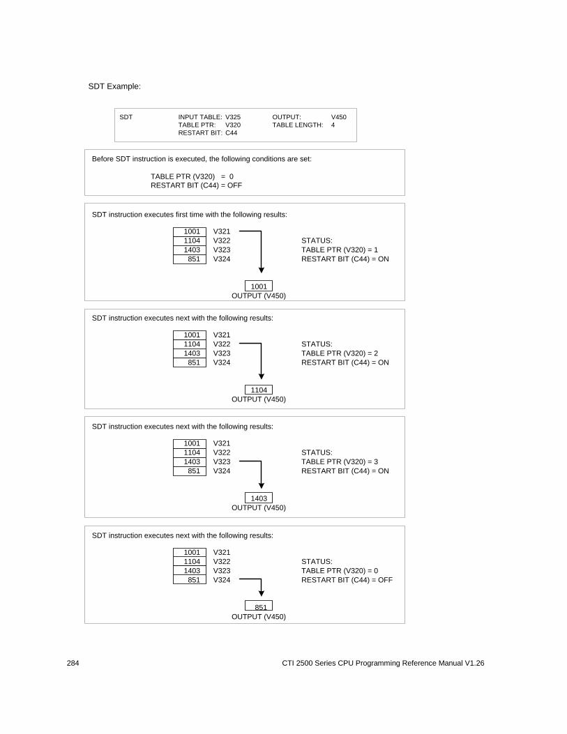
284 CTI 2500 Series CPU Programming Reference Manual V1.26
SDT INPUT TABLE: V325 OUTPUT: V450
TABLE PTR: V320 TABLE LENGTH: 4
RESTART BIT: C44
Before SDT instruction is executed, the following conditions are set:
TABLE PTR (V320) = 0
RESTART BIT (C44) = OFF
SDT instruction executes first time with the following results:
1001 V321
1104 V322 STATUS:
1403 V323 TABLE PTR (V320) = 1
851 V324 RESTART BIT (C44) = ON
1001
OUTPUT (V450)
SDT instruction executes next with the following results:
1001 V321
1104 V322 STATUS:
1403 V323 TABLE PTR (V320) = 2
851 V324 RESTART BIT (C44) = ON
1104
OUTPUT (V450)
SDT instruction executes next with the following results:
1001 V321
1104 V322 STATUS:
1403 V323 TABLE PTR (V320) = 3
851 V324 RESTART BIT (C44) = ON
1403
OUTPUT (V450)
SDT instruction executes next with the following results:
1001 V321
1104 V322 STATUS:
1403 V323 TABLE PTR (V320) = 0
851 V324 RESTART BIT (C44) = OFF
851
OUTPUT (V450)
SDT Example:
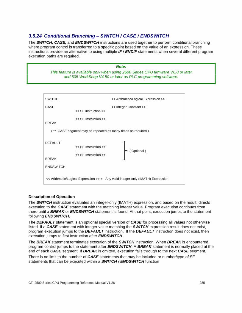
CTI 2500 Series CPU Programming Reference Manual V1.26 285
3.5.24 Conditional Branching – SWITCH / CASE / ENDSWITCH
The SWITCH, CASE, and ENDSWITCH instructions are used together to perform conditional branching where program control is transferred to a specific point based on the value of an expression. These instructions provide an alternative to using multiple IF / ENDIF statements when several different program execution paths are required.
Note:
This feature is available only when using 2500 Series CPU firmware V6.0 or later and 505 WorkShop V4.50 or later as PLC programming software.
SWITCH << Arithmetic/Logical Expression >>
CASE << Integer Constant >>
<< SF instruction >>
…
<< SF Instruction >>
BREAK
( ** CASE segment may be repeated as many times as required )
DEFAULT
<< SF Instruction >>
… ( Optional )
<< SF Instruction >>
BREAK
ENDSWITCH
<< Arithmetic/Logical Expression >> = Any valid integer-only (IMATH) Expression
Description of Operation
The SWITCH instruction evaluates an integer-only (IMATH) expression, and based on the result, directs execution to the CASE statement with the matching integer value. Program execution continues from there until a BREAK or ENDSWITCH statement is found. At that point, execution jumps to the statement following ENDSWITCH.
The DEFAULT statement is an optional special version of CASE for processing all values not otherwise listed. If a CASE statement with integer value matching the SWITCH expression result does not exist, program execution jumps to the DEFAULT instruction. If the DEFAULT instruction does not exist, then execution jumps to first instruction after ENDSWITCH.
The BREAK statement terminates execution of the SWITCH instruction. When BREAK is encountered, program control jumps to the statement after ENDSWITCH. A BREAK statement is normally placed at the end of each CASE segment. If BREAK is omitted, execution falls through to the next CASE segment.
There is no limit to the number of CASE statements that may be included or number/type of SF statements that can be executed within a SWITCH / ENDSWITCH function
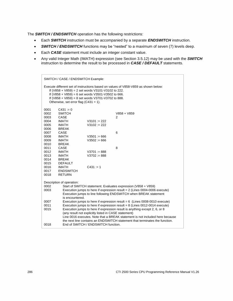
286 CTI 2500 Series CPU Programming Reference Manual V1.26
The SWITCH / ENDSWITCH operation has the following restrictions:
Each SWITCH instruction must be accompanied by a separate ENDSWITCH instruction.
SWITCH / ENDSWITCH functions may be “nested” to a maximum of seven (7) levels deep.
Each CASE statement must include an integer constant value.
Any valid Integer Math (IMATH) expression (see Section 3.5.12) may be used with the SWITCH instruction to determine the result to be processed in CASE / DEFAULT statements.
SWITCH / CASE / ENDSWITCH Example:
Execute different set of instructions based on values of V858-V859 as shown below:
If (V858 + V859) = 2 set words V3101-V3102 to 222.
If (V858 + V859) = 6 set words V3501-V3502 to 666.
If (V858 + V859) = 8 set words V3701-V3702 to 888.
Otherwise, set error flag (C431 = 1).
0001 C431 := 0
0002 SWITCH V858 + V859
0003 CASE 2
0004 IMATH V3101 := 222
0005 IMATH V3102 := 222
0006 BREAK
0007 CASE 6
0008 IMATH V3501 := 666
0009 IMATH V3502 := 666
0010 BREAK
0011 CASE 8
0012 IMATH V3701 := 888
0013 IMATH V3702 := 888
0014 BREAK
0015 DEFAULT
0016 IMATH C431 := 1
0017 ENDSWITCH
0018 RETURN
Description of operation:
0002 Start of SWITCH statement. Evaluates expression (V858 + V859)
0003 Execution jumps to here if expression result = 2 (Lines 0004-0006 execute)
Execution jumps to line following ENDSWITCH when BREAK statement
is encountered.
0007 Execution jumps to here if expression result = 6 (Lines 0008-0010 execute)
0011 Execution jumps to here if expression result = 8 (Lines 0012-0014 execute)
0015 Execution jumps to here if expression result is anything except 2, 6, or 8
(any result not explicitly listed in CASE statement)
Line 0016 executes. Note that a BREAK statement is not included here because
the next line contains an ENDSWITCH statement that terminates the function.
0018 End of SWITCH / ENDSWITCH function.
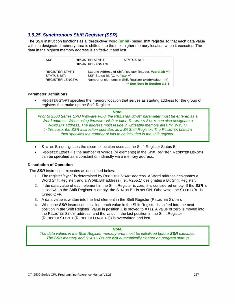
CTI 2500 Series CPU Programming Reference Manual V1.26 287
3.5.25 Synchronous Shift Register (SSR)
The SSR instruction functions as a ‘destructive’ word (or bit) based shift register so that each data value within a designated memory area is shifted into the next higher memory location when it executes. The data in the highest memory address is shifted-out and lost.
SSR REGISTER START: STATUS BIT:
REGISTER LENGTH:
REGISTER START: Starting Address of Shift Register (Integer, Word.Bit **)
STATUS BIT: SSR Status Bit (C, Y, Tx.y **)
REGISTER LENGTH: Number of elements in Shift Register (Addr/Value - Int)
** See Note in Section 3.5.1
Parameter Definitions
REGISTER START specifies the memory location that serves as starting address for the group of registers that make up the Shift Register.
Note: Prior to 2500 Series CPU firmware V6.0, the REGISTER START parameter must be entered as a
Word address. When using firmware V6.0 or later, REGISTER START can also designate a WORD.BIT address. The address must reside in writeable memory area (V, WY, T).
In this case, the SSR instruction operates as a Bit Shift Register. The REGISTER LENGTH then specifies the number of bits to be included in the shift register.
STATUS BIT designates the discrete location used as the Shift Register Status Bit.
REGISTER LENGTH is the number of Words (or elements) in the Shift Register. REGISTER LENGTH can be specified as a constant or indirectly via a memory address.
Description of Operation
The SSR instruction executes as described below:
1. The register “type” is determined by REGISTER START address. A Word address designates a Word Shift Register, and a WORD.BIT address (i.e., V255.1) designates a Bit Shift Register.
2. If the data value of each element in the Shift Register is zero, it is considered empty. If the SSR is called when the Shift Register is empty, the STATUS BIT is set ON. Otherwise, the STATUS BIT is turned OFF.
3. A data value is written into the first element in the Shift Register (REGISTER START).
4. When the SSR instruction is called, each value in the Shift Register is shifted into the next position in the Shift Register (value in position X is moved to X+1). A value of zero is moved into the REGISTER START address, and the value in the last position in the Shift Register (REGISTER START + (REGISTER LENGTH-1)) is overwritten and lost.
Note: The data values in the Shift Register memory area must be initialized before SSR executes.
The SSR memory and STATUS BIT are not automatically cleared on program startup.
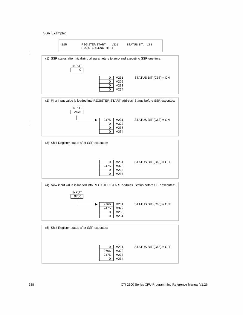
288 CTI 2500 Series CPU Programming Reference Manual V1.26
(1) SSR status after initializing all parameters to zero and executing SSR one time.
INPUT
0
0 V231 STATUS BIT (C68) = ON
0 V322
0 V233
0 V234
(2) First input value is loaded into REGISTER START address. Status before SSR executes:
INPUT
2475
2475 V231 STATUS BIT (C68) = ON
0 V322
0 V233
0 V234
(3) Shift Register status after SSR executes:
0 V231 STATUS BIT (C68) = OFF
2475 V322
0 V233
0 V234
(4) New input value is loaded into REGISTER START address. Status before SSR executes:
INPUT
9766
9766 V231 STATUS BIT (C68) = OFF
2475 V322
0 V233
0 V234
SSR REGISTER START: V231 STATUS BIT: C68
REGISTER LENGTH: 4
SSR Example:
(5) Shift Register status after SSR executes:
0 V231 STATUS BIT (C68) = OFF
9766 V322
2475 V233
0 V234
‘ ‘ ‘

CTI 2500 Series CPU Programming Reference Manual V1.26 289
(9) New input value is loaded into REGISTER START address.
Shift Register is full at this point. Status before SSR executes:
INPUT
3348
3348 V231 STATUS BIT (C68) = OFF
12859 V322
9766 V233
2475 V234
(10) Results after SSR executes again. All data values are shifted into next higher address..
Previous value in last Shift Register address (V234) is shifted out and lost.
INPUT
0
0 V231 STATUS BIT (C68) = OFF
3348 V322
12859 V233
9766 V234
(7) New Input value is loaded into REGISTER START address. Status before SSR excutes:
INPUT
12859
12859 V231 STATUS BIT (C68) = OFF
9766 V322
2475 V233
0 V234
(8) Shift Register status after SSR executes again:
0 V231 STATUS BIT (C68) = OFF
12859 V322
9766 V233
2475 V234
(6) Shift Register status after SSR executes again:
0 V231 STATUS BIT (C68) = OFF
9766 V322
2475 V233
0 V234
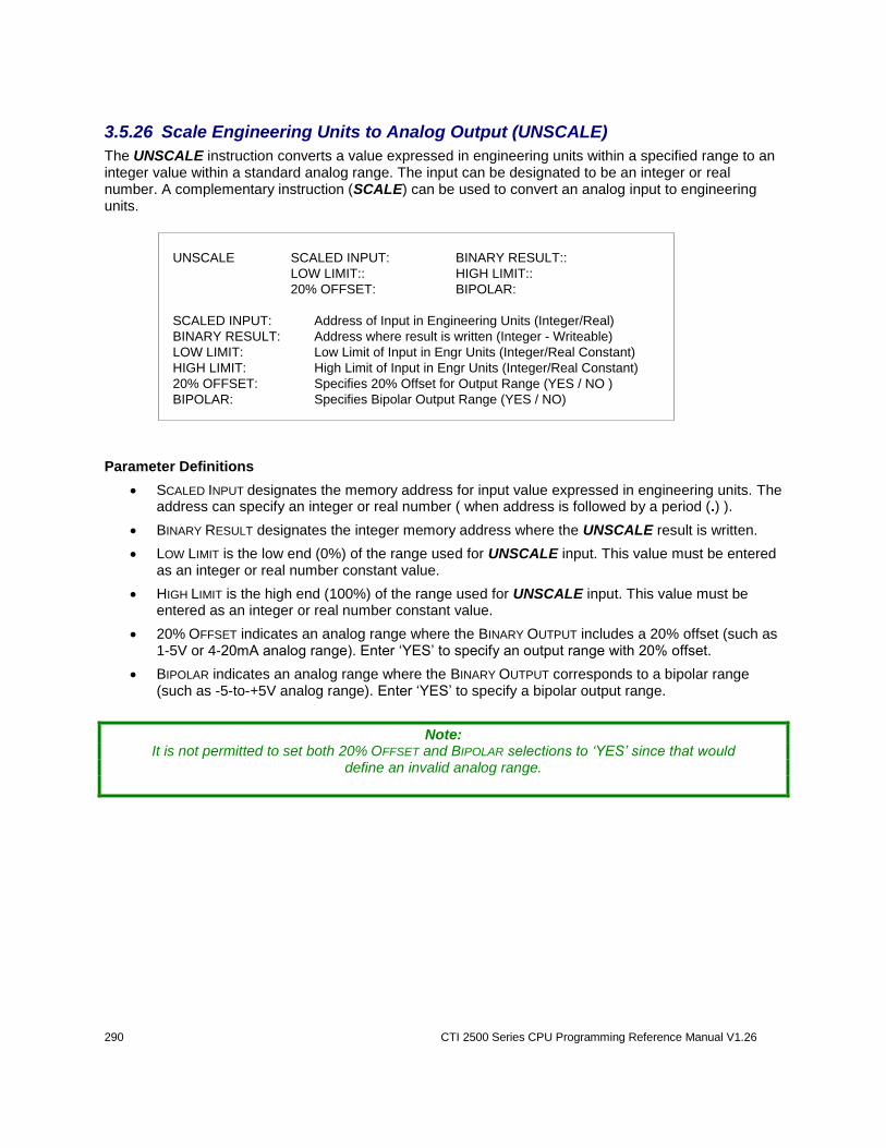
290 CTI 2500 Series CPU Programming Reference Manual V1.26
3.5.26 Scale Engineering Units to Analog Output (UNSCALE)
The UNSCALE instruction converts a value expressed in engineering units within a specified range to an integer value within a standard analog range. The input can be designated to be an integer or real number. A complementary instruction (SCALE) can be used to convert an analog input to engineering units.
UNSCALE SCALED INPUT: BINARY RESULT::
LOW LIMIT:: HIGH LIMIT::
20% OFFSET: BIPOLAR:
SCALED INPUT: Address of Input in Engineering Units (Integer/Real)
BINARY RESULT: Address where result is written (Integer - Writeable)
LOW LIMIT: Low Limit of Input in Engr Units (Integer/Real Constant)
HIGH LIMIT: High Limit of Input in Engr Units (Integer/Real Constant)
20% OFFSET: Specifies 20% Offset for Output Range (YES / NO )
BIPOLAR: Specifies Bipolar Output Range (YES / NO)
Parameter Definitions
SCALED INPUT designates the memory address for input value expressed in engineering units. The address can specify an integer or real number ( when address is followed by a period (.) ).
BINARY RESULT designates the integer memory address where the UNSCALE result is written.
LOW LIMIT is the low end (0%) of the range used for UNSCALE input. This value must be entered as an integer or real number constant value.
HIGH LIMIT is the high end (100%) of the range used for UNSCALE input. This value must be entered as an integer or real number constant value.
20% OFFSET indicates an analog range where the BINARY OUTPUT includes a 20% offset (such as 1-5V or 4-20mA analog range). Enter ‘YES’ to specify an output range with 20% offset.
BIPOLAR indicates an analog range where the BINARY OUTPUT corresponds to a bipolar range (such as -5-to-+5V analog range). Enter ‘YES’ to specify a bipolar output range.
Note: It is not permitted to set both 20% OFFSET and BIPOLAR selections to ‘YES’ since that would
define an invalid analog range.
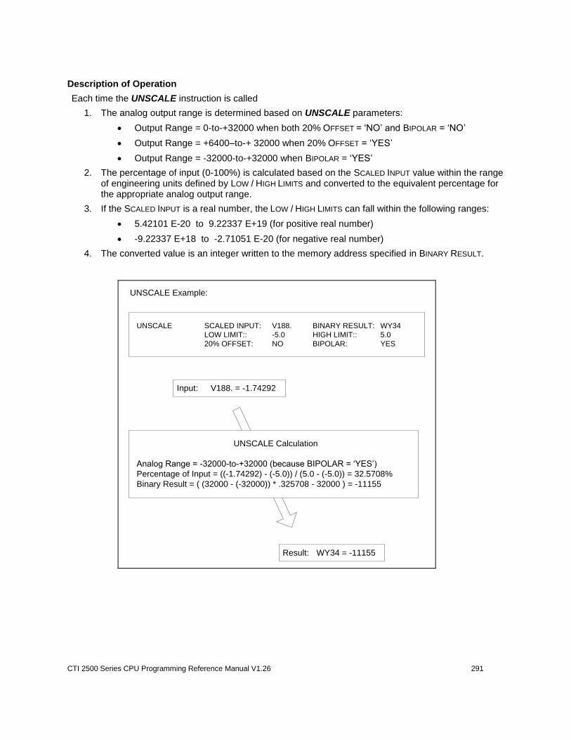
CTI 2500 Series CPU Programming Reference Manual V1.26 291
Description of Operation
Each time the UNSCALE instruction is called
1. The analog output range is determined based on UNSCALE parameters:
Output Range = 0-to-+32000 when both 20% OFFSET = ‘NO’ and BIPOLAR = ‘NO’
Output Range = +6400–to-+ 32000 when 20% OFFSET = ‘YES’
Output Range = -32000-to-+32000 when BIPOLAR = ‘YES’
2. The percentage of input (0-100%) is calculated based on the SCALED INPUT value within the range of engineering units defined by LOW / HIGH LIMITS and converted to the equivalent percentage for the appropriate analog output range.
3. If the SCALED INPUT is a real number, the LOW / HIGH LIMITS can fall within the following ranges:
5.42101 E-20 to 9.22337 E+19 (for positive real number)
-9.22337 E+18 to -2.71051 E-20 (for negative real number)
4. The converted value is an integer written to the memory address specified in BINARY RESULT.
Input: V188. = -1.74292
Result: WY34 = -11155
UNSCALE Calculation
Analog Range = -32000-to-+32000 (because BIPOLAR = ‘YES’)
Percentage of Input = ((-1.74292) - (-5.0)) / (5.0 - (-5.0)) = 32.5708%
Binary Result = ( (32000 - (-32000)) * .325708 - 32000 ) = -11155
UNSCALE Example:
UNSCALE SCALED INPUT: V188. BINARY RESULT: WY34
LOW LIMIT:: -5.0 HIGH LIMIT:: 5.0
20% OFFSET: NO BIPOLAR: YES

292 CTI 2500 Series CPU Programming Reference Manual V1.26
3.5.27 Conditional Looping - WHILE / ENDWHILE
The WHILE and ENDWHILE instructions are used together to repetitively execute a group of instructions until a specified event occurs.
Note:
This feature is available only when using 2500 Series CPU firmware V6.0 or later and 505 WorkShop V4.50 or later as PLC programming software.
WHILE << Arithmetic/Logical Expression >>
<< SF instruction >>
…
<< SF Instruction >>
ENDWHILE
<< Arithmetic/Logical Expression >> = Any valid integer-only (IMATH) Expression
Description of Operation
When the WHILE instruction is called, the associated IMATH expression is evaluated. If the result is zero (FALSE), then execution jumps to first instruction after ENDWHILE. If the result is non-zero (TRUE), then execution continues to next statement following the WHILE instruction. When ENDWHILE is found, execution jumps back to the last WHILE instruction and process repeats.
There is no limit to the number or type of SF statements that can be executed within the WHILE / ENDWHILE loop. The WHILE / ENDWHILE operation has the following requirements:
Each WHILE instruction must be accompanied by a separate ENDWHILE instruction.
WHILE / ENDWHILE loops may be “nested” within other WHILE / ENDWHILE loops to a maximum of four (4) levels deep.
Any valid Integer Math (IMATH) expression (see Section 3.5.12) may be used with the WHILE instruction as the condition to execute the embedded statements

CTI 2500 Series CPU Programming Reference Manual V1.26 293
WHILE / ENDWHILE Example:
Look thru a table of words of random length starting at V211.
Report ‘Table Position’ of first word that has a value = 0.
0001 IMATH T11 := 0
0002 IMATH T12 := 0
0003 WHILE T11 = 0 AND T12 < V339
0004 IMATH T12 := T12 + 1
0005 IF V211(T12) = 0
0006 IMATH T11 := 1
0007 ENDIF
0008 ENDWHILE
0009 IF T11 = 0
0010 IMATH T12 = 0
0011 ENDIF
Description of operation:
0001-0002 Initialize values for WHILE loop
0003 Start of WHILE loop.
V339 contains ‘Number of Words in Table’ to be searched.
0004 Increments ‘Table Position’ Pointer (T12)
0005-0007 Evaluate selected word in Table (using ‘Table Position’ as index)
Set Flag (T11) if word value = 0
0008 End of WHILE loop.
Program execution jumps to WHILE instruction and expression is re-evaluated.
If Flag set (word value = 0 found) or ‘Number of Words in Table’ has been
reached, WHILE loop is terminated and execution jumps to statement following
ENDWHILE (Line 0009). Otherwise, WHILE loop operation is repeated.
0009-0011 Table Position where value = 0 found is stored in V274.
If word value = 0 is not found in Table, V274 is set = 0.

294 CTI 2500 Series CPU Programming Reference Manual V1.26
3.6 SF Program/Subroutine Data Variables
Special Function Variables associated with the operation of Analog Alarms, PID Loops, and PLC operation can be accessed only within SF Programs and Subroutines and by HMIs connected to the PLC. The following table provides a list of all supported data types (eu = engineering units).
Mnemonic Description Units Real
Integer
Read Only
Notes
AACK Alarm Acknowledge Flags X O
AADB Analog Alarm Deadband eu X X A,B,H
ACFH Alarm C Flag High X A
ACFL Alarm C Flag Low X A
AERR Alarm Error eu X X X C
AHA Alarm High Limit eu X X A,B,H
AHHA Alarm High-High Limit eu X X A,B,H
ALA Alarm Low Limit eu X X A,B,H
ALLA Alarm Low-Low Limit eu X X A,B,H
AODA Alarm Orange Deviation Limit eu X X A,B,H
APV Alarm Process Variable eu X X B
APVH Alarm Process Variable High Limit eu X A, G
APVL Alarm Process Variable Low Limit eu X A, G
ARCA Alarm Rate of Change Alarm Limit eu/min X A, G
ASP Alarm Setpoint eu X X B, H
ASPH Alarm Setpoint High eu X X A,B,H
ASPL Alarm Setpoint Low eu X X A,B,H
ATS Alarm Sample Rate (seconds) sec X A
AVF Alarm V Flag X I
AYDA Alarm Yellow Deviation Limit eu X X A,B,H
APET Alarm Peak Elapsed Time ms X X P
LACK Loop Alarm Acknowledge Flags X O
LADB Loop Alarm Deadband eu X X A,B,H
LCFH Loop C Flag High X A
LCFL Loop C Flag Low X A
LERR Loop Error eu X X X C
LHA Loop High Alarm Limit eu X X A,B,H
LHHA Loop High-High Alarm Limit eu X X A,B,H
LKC Loop Gain % X
LKD Loop Derivative Gain Limiting Coefficient
X
LLA Loop Low Alarm Limit eu X X A,B,H
LLLA Loop Low-Low Alarm Limit eu X X A,B,H
LMN Loop Output % X X J
LMX Loop Bias % X X K
LODA Loop Orange Deviation Alarm Limit eu X X A,B,H
LPV Loop Process Variable eu X X B
LPVH Loop Process Variable High Limit eu X A,G
LPVL Loop Process Variable Low Limit eu X A,G
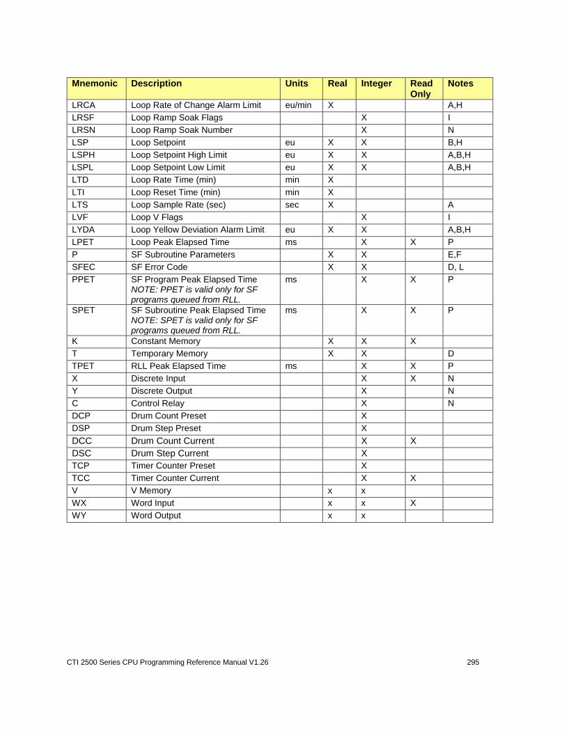
CTI 2500 Series CPU Programming Reference Manual V1.26 295
Mnemonic Description Units Real
Integer
Read Only
Notes
LRCA Loop Rate of Change Alarm Limit eu/min X A,H
LRSF Loop Ramp Soak Flags X I
LRSN Loop Ramp Soak Number X N
LSP Loop Setpoint eu X X B,H
LSPH Loop Setpoint High Limit eu X X A,B,H
LSPL Loop Setpoint Low Limit eu X X A,B,H
LTD Loop Rate Time (min) min X
LTI Loop Reset Time (min) min X
LTS Loop Sample Rate (sec) sec X A
LVF Loop V Flags X I
LYDA Loop Yellow Deviation Alarm Limit eu X X A,B,H
LPET Loop Peak Elapsed Time ms X X P
P SF Subroutine Parameters X X E,F
SFEC SF Error Code X X D, L
PPET SF Program Peak Elapsed Time NOTE: PPET is valid only for SF programs queued from RLL.
ms X X P
SPET SF Subroutine Peak Elapsed Time NOTE: SPET is valid only for SF programs queued from RLL.
ms X X P
K Constant Memory X X X
T Temporary Memory X X D
TPET RLL Peak Elapsed Time ms X X P
X Discrete Input X X N
Y Discrete Output X N
C Control Relay X N
DCP Drum Count Preset X
DSP Drum Step Preset X
DCC Drum Count Current X X
DSC Drum Step Current X
TCP Timer Counter Preset X
TCC Timer Counter Current X X
V V Memory x x
WX Word Input x x X
WY Word Output x x
296 CTI 2500 Series CPU Programming Reference Manual V1.26
NOTES:
A. This variable is read-only if Flash is selected as the program source.
B. When accessed as an integer, value returned is an integer between 0 and 32000. When accessed as a real, the value is returned in engineering units between the low limit and the high limit.
C. When accessed as an integer, value returned is a scaled integer between -32000 and 32000. When accessed as a real, the value is returned in engineering units between -span and + span.
D. This variable can be accessed only in an SF program or SF subroutine.
E. This variable can be accessed only in an SF subroutine.
F. The access restrictions depend on the type of variable passed to the subroutine.
G. If PVLn is changed to a value greater than PVHn, then PVHn is set to the new PVLn.
If PVHn is changed to a value less than PVLn, then PVLn is set to the new PVHn.
H. If PVLn or PVHn is modified and the current value of any of these variables is outside the new PV range, the value clamps to the nearest endpoint of the new PV range.
I. When written, only the control bits are actually modified. When read, only the status bits are returned, the control bits are returned as 0.
J. The value is dependent on the PID algorithm in use:
Position: The value is a percent between 0.0 and 1.0, if accessed as a real, or a number between 0 and 32000, if accessed as an integer.
Velocity: The value is a percent-of-change between -1.0 and 1.0 is accessed as a real, or -32000 and 32000 if accessed as an integer.
K. These values are invalid if the Velocity PID algorithm is being used.
L. The value written to SFEC must range from 0-255. Writing a non-zero value will cause the program to terminate, unless “Continue on Error” is selected in the SF program,
M. LRSN is valid only if the loop is in Auto and ramp/soak for that loop is enabled. Error 39 is returned if the step is not programmed. If the loop is programmed, the loop exits the current step and enters the specified step. Writing a value larger than the number of the last programmed ramp/soak step to LRSN completes the ramp/soak and sets the ramp/soak finish bit.
N. When reading a discrete point, a zero is returned if the bit is off and a 1 if the bit is on. When writing to a discrete point, a value of 0 turns off the bit and a value of 1 turns on the bit.
O. Bit format for AACK and LACK is shown in Appendix B.
P. APET, LPET, and SPET contain the time from which the process is scheduled until the process completes execution. TPET contains the peak elapsed time of an RLL task. TPET1 is the main RLL task; TPET2 is the cyclic RLL task. These variables can be read only by HMI devices connected to the controller.
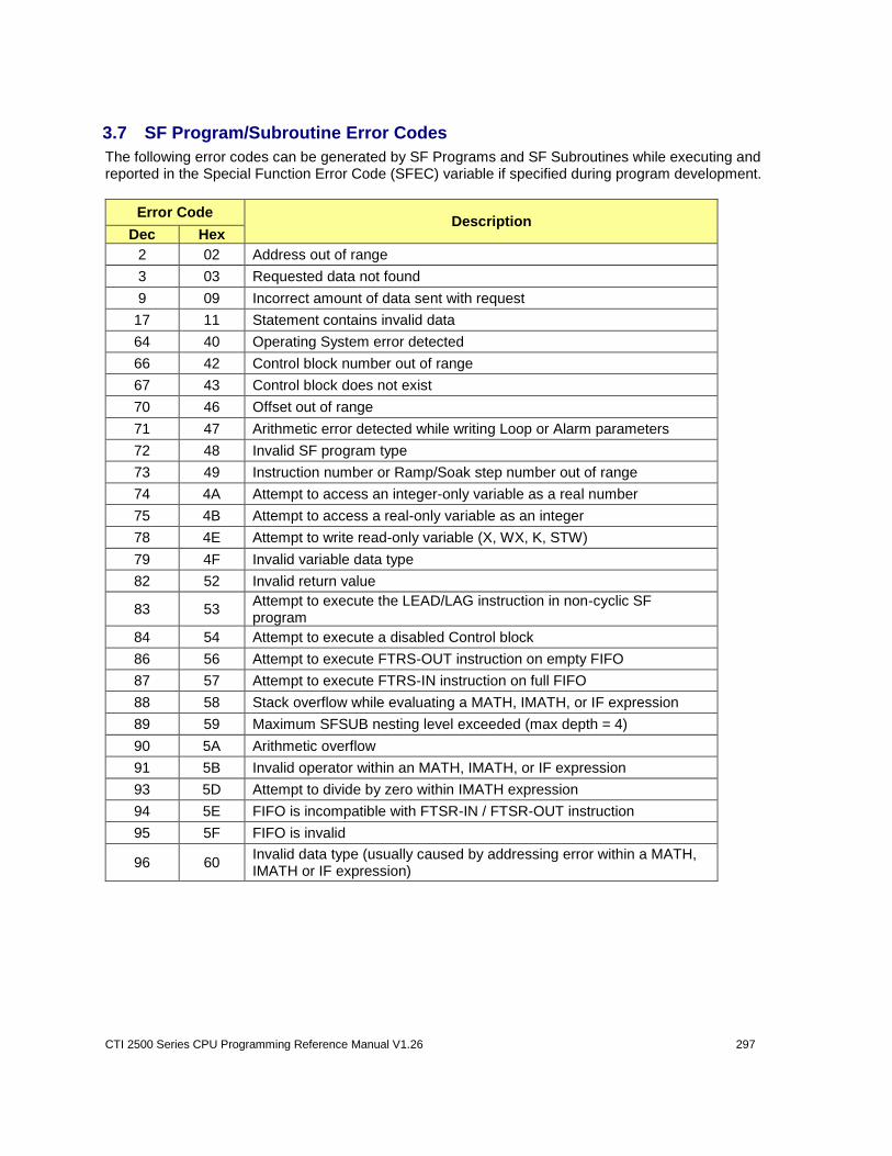
CTI 2500 Series CPU Programming Reference Manual V1.26 297
3.7 SF Program/Subroutine Error Codes
The following error codes can be generated by SF Programs and SF Subroutines while executing and reported in the Special Function Error Code (SFEC) variable if specified during program development.
Error Code Description
Dec Hex
2 02 Address out of range
3 03 Requested data not found
9 09 Incorrect amount of data sent with request
17 11 Statement contains invalid data
64 40 Operating System error detected
66 42 Control block number out of range
67 43 Control block does not exist
70 46 Offset out of range
71 47 Arithmetic error detected while writing Loop or Alarm parameters
72 48 Invalid SF program type
73 49 Instruction number or Ramp/Soak step number out of range
74 4A Attempt to access an integer-only variable as a real number
75 4B Attempt to access a real-only variable as an integer
78 4E Attempt to write read-only variable (X, WX, K, STW)
79 4F Invalid variable data type
82 52 Invalid return value
83 53 Attempt to execute the LEAD/LAG instruction in non-cyclic SF program
84 54 Attempt to execute a disabled Control block
86 56 Attempt to execute FTRS-OUT instruction on empty FIFO
87 57 Attempt to execute FTRS-IN instruction on full FIFO
88 58 Stack overflow while evaluating a MATH, IMATH, or IF expression
89 59 Maximum SFSUB nesting level exceeded (max depth = 4)
90 5A Arithmetic overflow
91 5B Invalid operator within an MATH, IMATH, or IF expression
93 5D Attempt to divide by zero within IMATH expression
94 5E FIFO is incompatible with FTSR-IN / FTSR-OUT instruction
95 5F FIFO is invalid
96 60 Invalid data type (usually caused by addressing error within a MATH, IMATH or IF expression)

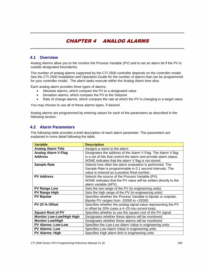
CTI 2500 Series CPU Programming Reference Manual V1.26 299
CHAPTER 4 ANALOG ALARMS
4.1 Overview
Analog Alarms allow you to the monitor the Process Variable (PV) and to set an alarm bit if the PV is outside designated boundaries.
The number of analog alarms supported by the CTI 2500 controller depends on the controller model. See the CTI 2500 Installation and Operation Guide for the number of alarms that can be programmed for your controller model. The alarm tasks execute within the Analog Alarm time slice.
Each analog alarm provides three types of alarms:
Absolute alarms, which compare the PV to a designated value
Deviation alarms, which compare the PV to the Setpoint
Rate of change alarms, which compare the rate at which the PV is changing to a target value.
You may choose to use all of these alarms types, if desired. Analog alarms are programmed by entering values for each of the parameters as described in the following section:
4.2 Alarm Parameters
The following table provides a brief description of each alarm parameter. The parameters are explained in more detail following the table.
Variable Description
Analog Alarm Title Assigns a name to the alarm
Analog Alarm V-Flag Address
Designates the address of the Alarm V Flag. The Alarm V flag is a set of bits that control the alarm and provide alarm status. NONE indicates that the alarm V flag is not stored.
Sample Rate Selects how often the alarm evaluation is performed. The Sample Rate is programmable in 0.1 second intervals. The value is entered as a positive Real number.
PV Address
Selects the source of the Process Variable (PV). NONE indicates that the PV value will be written directly to the alarm variable (APV).
PV Range Low Sets the low range of the PV (in engineering units)
PV Range High Sets the high range of the PV (in engineering units)
PV Bipolar Specifies whether the Process Variable is bipolar or unipolar. Bipolar PV ranges from -32000 to +32000.
PV 20 % Offset Specifies whether the analog signal value representing the PV is offset by 20% (uses a 4–20 ma current loop).
Square Root of PV Specifies whether to use the square root of the PV signal
Monitor Low-Low/High High Designates whether these alarms will be monitored
Monitor Low/High Designates whether these alarms will be monitored
PV Alarms: Low-Low Specifies the Low-Low Alarm Value in engineering units
PV Alarms: Low Specifies Low Alarm Value in engineering units
PV Alarms: High Specifies High alarm limit in engineering units
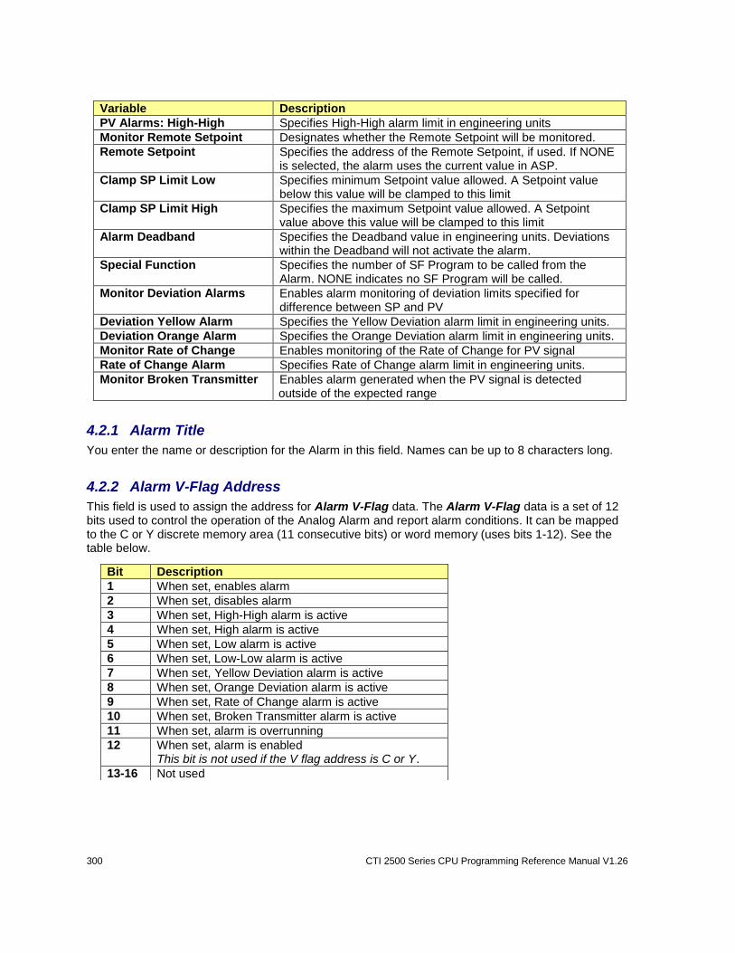
300 CTI 2500 Series CPU Programming Reference Manual V1.26
Variable Description
PV Alarms: High-High Specifies High-High alarm limit in engineering units
Monitor Remote Setpoint Designates whether the Remote Setpoint will be monitored.
Remote Setpoint Specifies the address of the Remote Setpoint, if used. If NONE is selected, the alarm uses the current value in ASP.
Clamp SP Limit Low Specifies minimum Setpoint value allowed. A Setpoint value below this value will be clamped to this limit
Clamp SP Limit High Specifies the maximum Setpoint value allowed. A Setpoint value above this value will be clamped to this limit
Alarm Deadband Specifies the Deadband value in engineering units. Deviations within the Deadband will not activate the alarm.
Special Function Specifies the number of SF Program to be called from the Alarm. NONE indicates no SF Program will be called.
Monitor Deviation Alarms Enables alarm monitoring of deviation limits specified for difference between SP and PV
Deviation Yellow Alarm Specifies the Yellow Deviation alarm limit in engineering units.
Deviation Orange Alarm Specifies the Orange Deviation alarm limit in engineering units.
Monitor Rate of Change Enables monitoring of the Rate of Change for PV signal
Rate of Change Alarm Specifies Rate of Change alarm limit in engineering units.
Monitor Broken Transmitter Enables alarm generated when the PV signal is detected outside of the expected range
4.2.1 Alarm Title
You enter the name or description for the Alarm in this field. Names can be up to 8 characters long.
4.2.2 Alarm V-Flag Address
This field is used to assign the address for Alarm V-Flag data. The Alarm V-Flag data is a set of 12 bits used to control the operation of the Analog Alarm and report alarm conditions. It can be mapped to the C or Y discrete memory area (11 consecutive bits) or word memory (uses bits 1-12). See the table below.
Bit Description
1 When set, enables alarm
2 When set, disables alarm
3 When set, High-High alarm is active
4 When set, High alarm is active
5 When set, Low alarm is active
6 When set, Low-Low alarm is active
7 When set, Yellow Deviation alarm is active
8 When set, Orange Deviation alarm is active
9 When set, Rate of Change alarm is active
10 When set, Broken Transmitter alarm is active
11 When set, alarm is overrunning
12 When set, alarm is enabled This bit is not used if the V flag address is C or Y.
13-16 Not used
CTI 2500 Series CPU Programming Reference Manual V1.26 301
4.2.3 Sample Rate
This parameter determines how often the alarm evaluation is performed. The minimum value is 0.1 seconds (100 ms), and Sample Rate can be entered in 0.1 second intervals.
Regardless of the Sample Rate entered, the alarms will be evaluated at least once every two seconds. Therefore, the Sample Rate is normally specified between 0.1 and 2.0 seconds.
4.2.4 Process Variable Address (V, WX, WY, None)
This parameter designates the memory address that contains the Process Variable feedback to the loop. It is usually a WX address associated with an analog input channel. The input range is expected to be between 0-32000 for a standard unipolar (i.e. 0-5V) signal. If NONE is specified, the Process Variable value must be written directly to the SF alarm variable (APV).
4.2.5 PV Range Low/High (in Engr Units)
The PROCESS VARIABLE can also be expressed as a Real number in engineering units. The PV Low Range represents the value when the analog input signal is at its minimum. The PV High Range represents the value when the input signal is at its maximum. The PV 20% OFFSET and PV BIPOLAR features are automatically integrated into the PV engineering units when selected.
4.2.6 PV is Bipolar (Yes/No)
This refers to the actual PROCESS VARIABLE input to the loop. If a Bipolar input signal (i.e., -5 to +5V) is used, answer YES. The input range is then set to -32000 to +32000.
4.2.7 20% Offset on PV (Yes/No)
Answer YES when the analog input has a 20% Offset for the “zero” range position, used with signals such as 1-5V or 4-20mA. When active, the range of the PV integer value is 6400–32000.
NOTE: It is invalid to select both Bipolar and 20% Offset for the same analog signal.
4.2.8 Square Root of PV (Yes/No)
Some devices provide a signal that is the square of the actual measurement. This calculation will compensate for this characteristic. Answer YES only if the actual PROCESS VARIABLE input represents the square of the measured input (i.e., differential pressure flow measurement).
4.2.9 Monitor Absolute Alarms (Yes/No)
The selection of Monitor Low-Low / High-High and Monitor Low / High enable alarms generated by comparing the PV to fixed values. Either pair of alarms may be used independently. Both pairs are used when one pair (High/Low) indicates a warning while the other pair (High-High/Low/Low signals a critical condition.
302 CTI 2500 Series CPU Programming Reference Manual V1.26
4.2.10 Absolute Alarm Limits (in Engr Units)
The values for the absolute alarm limits are entered when the corresponding alarm pair is selected. These values are specified in engineering units as follows:
The value for the High-High alarm must be less than or equal to the PV HIGH RANGE value.
The value for the High alarm must be less than or equal to the High-High alarm,
The value for the Low alarm must be less than or equal to the High alarm,
The value for the Low-Low alarm must be less than or equal to the Low alarm and greater than or equal to the PV LOW RANGE value.
4.2.11 Monitor Remote Setpoint (Yes/No)
When Monitor Remote SP is set to YES, the alarm will obtain the SETPOINT value from the address entered in the REMOTE SETPOINT field. A value of NONE indicates that there is no REMOTE SETPOINT used by the Alarm. In this case, the SETPOINT value (if needed) must be written by Special Function program or HMI using the ASP variable.
4.2.12 Remote Setpoint (V, K, WX, WY, None)
The Remote SP field is applicable only when Monitor Remote SP is selected. This field specifies the memory location containing the SETPOINT value. The integer value of Remote Setpoint is always scaled for the normal unipolar range of 0-32000. The SETPOINT value can also be accessed as Real number in engineering units according to the range specified by PV LOW and PV HIGH limits.
4.2.13 Clamp Setpoint Low/High (in Engr Units)
The Clamp SP Low and Clamp SP High fields designate the minimum and maximum limits for the SETPOINT value. The values entered are treated in engineering units and must be within limits specified for PV LOW and PV HIGH. An attempt to force the SETPOINT outside these limits will result in the SP value being clamped to nearest limit. For instance, with SP limits set to 10 and 90, a SP input of 5 is changed to a value of 10 and a SP input of 95 is changed to a value of 90.
The Clamp Setpoint function is disabled if both SP LOW and SP HIGH limits are set to the same value.
4.2.14 Alarm Deadband (in Engr Units)
The Alarm Deadband field allows the user to set an area around the alarm points to prevent nuisance alarms caused by PV value ‘chattering’ near an alarm limit. If specified, it provides a “neutral zone” for all alarms except for RATE OF CHANGE alarm. The Alarm Deadband delays the point at which an alarm condition is set and/or cleared. A typical Deadband normally ranges from 0.25% to 5% of span.
For example, assume a PV RANGE of 0-100, PV LOW LIMIT = 20, and a DEADBAND = 2. When PV drops from 21 to 20, PV LOW alarm is activated. The PV LOW alarm is not cleared until PV signal rises to 22.
CTI 2500 Series CPU Programming Reference Manual V1.26 303
4.2.15 Special Function
This field designates the number of the Special Function Program that will be called by the alarm function. The SF Program can be designated as NORMAL, PRIORITY, or RESTRICTED type.
The Special Function Program is called immediately each time before the alarm executes when the SAMPLE RATE is set to 2.0 seconds or less. When the SAMPLE RATE is greater than two seconds, the SF Program is called only at the SAMPLE RATE interval.
4.2.16 Deviation Alarms (Yes/No)
When Monitor Deviation is set to YES, alarm monitoring is enabled for Deviation limits on the difference between SETPOINT and PV. When enabled, both Yellow Deviation and Orange Deviation alarms are enabled.
The Yellow Deviation and Orange Deviation alarms compute the ERROR (SP – PV) and activate when that ERROR exceeds the specified limits. The Yellow Deviation is considered the first level alarm, and the Orange Deviation is considered the critical alarm. The values for both alarms are entered in Engineering Units as follows:
The Orange Deviation value must be less than the PV RANGE in Engineering Units (PV
RANGE HIGH – PV RANGE LOW) and greater than or equal to the Yellow Deviation alarm limit.
The Yellow Deviation value must be greater than or equal to zero and less than or equal to the Orange Deviation alarm limit.
4.2.17 Rate of Change Alarm Limit (in Engr Units per Minute)
When MONITOR CHANGE is set to YES, alarm monitoring is enabled for Rate of Change of the PROCESS VARIABLE input signal.
The Rate of Change Alarm is applicable only when Monitor Change is selected. The Rate of Change Alarm is set when the analog input value changes faster than the limit specified by the designated amount. The RATE OF CHANGE limit is entered in engineering units per minute. For example, for a PV Range = 0-100, an entry of 120 equates to a Rate of Change Alarm limit of 2 units
per second.
4.2.18 Broken Transmitter Alarm (Yes/No)
When Monitor Broken Xmit is set to YES, an alarm is generated when the integer value of the Process Variable signal is detected outside of the expected PV range as noted below:
NO OFFSET: 0 – 32000
20% OFFSEt: 6400 – 32000
BIPOLAR: -32000 to +32000
If an ALARM DEADBAND is specified, that value is added to the limits that activate this alarm. For instance, the Broken Transmitter Alarm occurs when a 20% OFFSET signal is read outside the range of 6400-32000 when no DEADBAND is used. However, a DEADBAND value of 5% expands the acceptable input range by 1280 counts on both end of the scale (5120-33280).
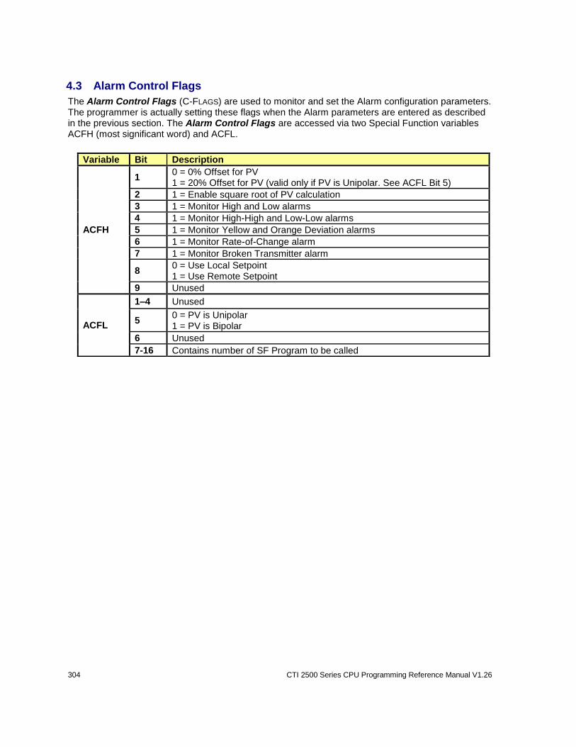
304 CTI 2500 Series CPU Programming Reference Manual V1.26
4.3 Alarm Control Flags
The Alarm Control Flags (C-FLAGS) are used to monitor and set the Alarm configuration parameters. The programmer is actually setting these flags when the Alarm parameters are entered as described in the previous section. The Alarm Control Flags are accessed via two Special Function variables ACFH (most significant word) and ACFL.
Variable Bit Description
ACFH
1 0 = 0% Offset for PV 1 = 20% Offset for PV (valid only if PV is Unipolar. See ACFL Bit 5)
2 1 = Enable square root of PV calculation
3 1 = Monitor High and Low alarms
4 1 = Monitor High-High and Low-Low alarms
5 1 = Monitor Yellow and Orange Deviation alarms
6 1 = Monitor Rate-of-Change alarm
7 1 = Monitor Broken Transmitter alarm
8 0 = Use Local Setpoint 1 = Use Remote Setpoint
9 Unused
ACFL
1–4 Unused
5 0 = PV is Unipolar 1 = PV is Bipolar
6 Unused
7-16 Contains number of SF Program to be called
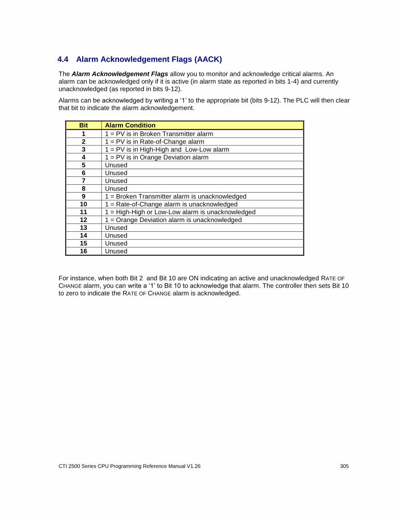
CTI 2500 Series CPU Programming Reference Manual V1.26 305
4.4 Alarm Acknowledgement Flags (AACK)
The Alarm Acknowledgement Flags allow you to monitor and acknowledge critical alarms. An alarm can be acknowledged only if it is active (in alarm state as reported in bits 1-4) and currently unacknowledged (as reported in bits 9-12).
Alarms can be acknowledged by writing a ‘1’ to the appropriate bit (bits 9-12). The PLC will then clear that bit to indicate the alarm acknowledgement.
For instance, when both Bit 2 and Bit 10 are ON indicating an active and unacknowledged RATE OF
CHANGE alarm, you can write a ‘1’ to Bit 10 to acknowledge that alarm. The controller then sets Bit 10 to zero to indicate the RATE OF CHANGE alarm is acknowledged.
Bit Alarm Condition
1 1 = PV is in Broken Transmitter alarm
2 1 = PV is in Rate-of-Change alarm
3 1 = PV is in High-High and Low-Low alarm
4 1 = PV is in Orange Deviation alarm
5 Unused
6 Unused
7 Unused
8 Unused
9 1 = Broken Transmitter alarm is unacknowledged
10 1 = Rate-of-Change alarm is unacknowledged
11 1 = High-High or Low-Low alarm is unacknowledged
12 1 = Orange Deviation alarm is unacknowledged
13 Unused
14 Unused
15 Unused
16 Unused


CTI 2500 Series CPU Programming Reference Manual V1.26 307
CHAPTER 5 ANALOG (PID) LOOPS
5.1 Overview
Analog Loops (also called PID loops) are used to control a process by measuring the PROCESS
VARIABLE (PV), comparing it to a SETPOINT (SP) , and computing a control OUTPUT intended to bring the difference (or ERROR) between the PV and SP to 0.
Loops 1–128 operate as cyclical (time scheduled) loops. These loops run in the Analog Lop time slice. Loops 129–512 must be called from RLL using the PID instruction. These loops, also called “Fast Loops”, execute during the RLL portion of the scan. All loops use the same PID algorithms and provide integrated analog alarms. The only limitation of “Fast Loops” is that Ramp/Soak feature is not available.
Analog loops are programmed by entering values for each of the loop parameters as described in the following section.
5.2 Loop Modes of Operation
PID Loops can operate in the following modes:
Manual The LOOP OUTPUT is controlled by the operator. While in MANUAL mode, the loop monitors all active alarms associated with PV (except the YELLOW / ORANGE
DEVIATION alarms).
Auto The controller calculates the LOOP OUTPUT based on the LOOP PARAMETER settings. The SETPOINT value may be controlled by an operator interface, an SF PROGRAM, or a RAMP/SOAK table. All active alarms are monitored.
Cascade CASCADE mode is a configuration where the OUTPUT of one (“outer”) loop is used as the SETPOINT for another (“inner”) loop. The controller computes the OUTPUT for the “inner” loop. The SETPOINT for the “inner” loop is obtained from the memory location specified for REMOTE SETPOINT address.
While in CASCADE mode, the loop operation is identical to AUTO mode with the addition of the mode management of the associated loops, if they exist. When the “inner” loop is switched out of CASCADE, then all associated outer loops are placed in MANUAL mode to prevent reset windup. A request to place an “outer” loop into AUTO or CASCADE mode is denied unless its inner loop is in CASCADE mode. The number of cascaded loops is unlimited.
The PLC requires that the loop be placed in CASCADE mode in order to use the REMOTE SETPOINT parameter. Therefore it is possible to setup a virtual CASCADE loop when this feature is desired.
Stopped In effect when the PLC ANALOG SCAN IS set to PROGRAM mode or disabled.

308 CTI 2500 Series CPU Programming Reference Manual V1.26
5.3 Loop Parameters
The following table provides a brief description of each loop parameter. The parameters are explained in more detail following the table.
Variable Description
Loop Title Assigns a name or description for the loop
PID Algorithm Selects PID algorithm used for Loop Output calculation
Loop V Flag Address Designates the address of the Alarm V-Flag data for control of loop operation and alarm status.
Sample Rate Selects how often the loop function executes.
PV Address Selects the source for the Process Variable.
PV Range High/Low Sets the High/Low range limits for PV in Engineering Units
PV is Bipolar Selects a bipolar range for the PV signal
20% Offset on PV Selects an analog range with 20% offset for PV (4–20mA signal).
Square Root of PV Calculates PV as the square root of the analog signal for PV
Loop Output Address Specifies the memory location where Loop Output will be written.
Output is Bipolar Specifies whether the Loop Output signal is bipolar
20% Offset in Output Specifies whether the analog signal representing the Loop Output is offset by 20% (i.e., a 4–20mA signal).
Ramp/Soak for SP Enables operation of the Ramp/Soak function according to the programmed steps when loop mode transitions to AUTO.
Remote SP Specifies source for the Loop Setpoint.
Monitor Low-Low/High-High Enables monitoring of Low-Low and High-High absolute alarms
Monitor Low/High Enables monitoring of Low and High absolute alarms
PV Alarms: Low-Low Specifies Low-Low alarm value in Engineering Units
PV Alarms: Low Specifies Low alarm value in Engineering Units
PV Alarms: High Specifies High alarm value in Engineering Units
PV Alarms: High-High Specifies High-High alarm value in Engineering Units
Remote SP Specifies the memory address used for loop Setpoint. NONE indicates the SP value must be written to loop variable LSP.
Clamp SP Limits Low: Clamp SP Limits High:
Designates minimum and maximum values (in Engineering Units) that are permitted for Loop Setpoint
Loop Gain Sets the Proportional Gain for the loop. This value also serves as overall Gain multiplier (Kc)
Loop Reset Specifies the Reset Time used to compute the Integral Gain (Ki) for the loop
Loop Rate Specifies the Rate Time used to compute the Derivative Gain (Kr) for the loop
Freeze Bias Determines method used to manage Loop Bias when the loop Output calculation is out of range
Derivative Gain Limiting Enables a filter to be used for the Derivative component of the loop Output calculation
Limiting Coefficient Designates Limiting Coefficient for Rate limiting filter
Alarm Deadband Specifies the Deadband value in Engineering Units. Deviations within the Deadband will not activate the alarm
Special Calculation On Determines scheduling of a Special Function Program called from the loop. NONE indicates that no SF Program will be called.
Special Function Specifies the number of Special Function Program to be called when loop is executed
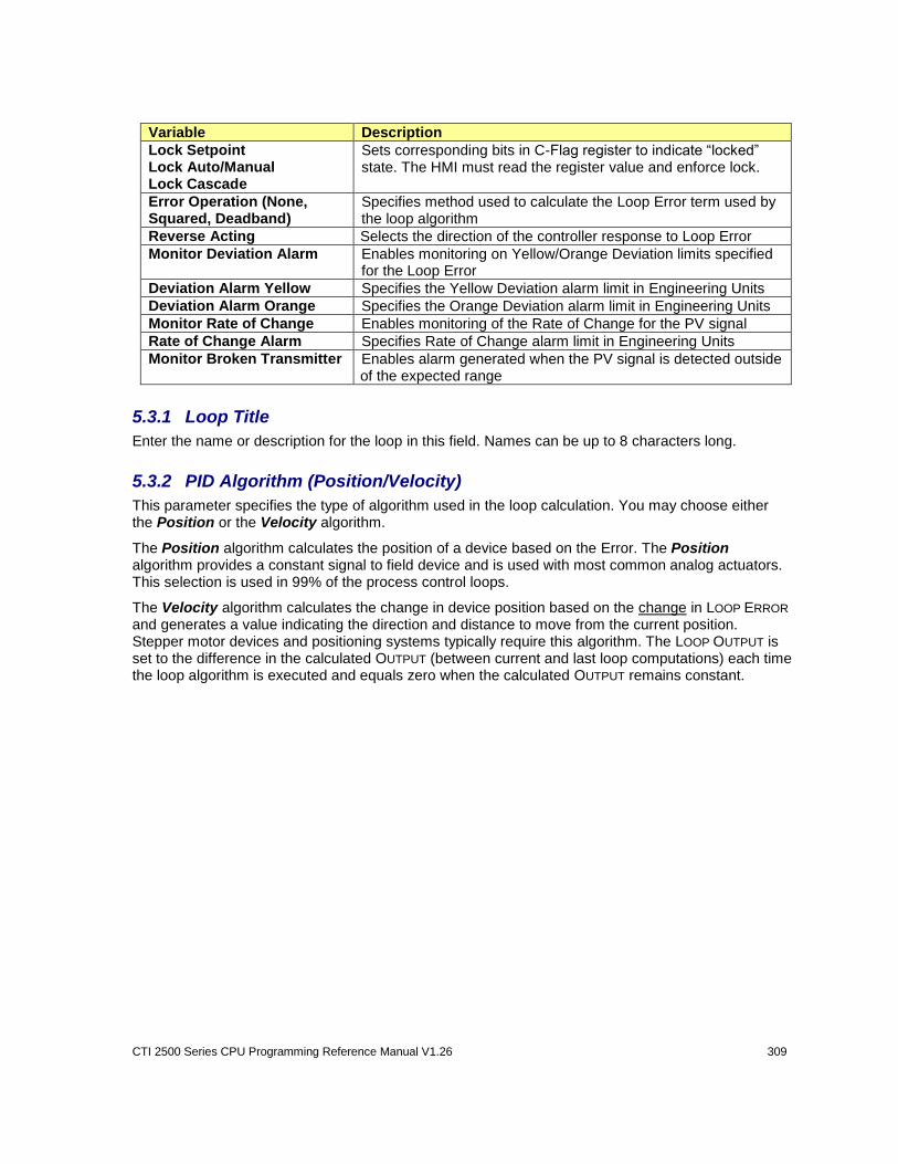
CTI 2500 Series CPU Programming Reference Manual V1.26 309
Variable Description
Lock Setpoint Lock Auto/Manual Lock Cascade
Sets corresponding bits in C-Flag register to indicate “locked” state. The HMI must read the register value and enforce lock.
Error Operation (None, Squared, Deadband)
Specifies method used to calculate the Loop Error term used by the loop algorithm
Reverse Acting Selects the direction of the controller response to Loop Error
Monitor Deviation Alarm Enables monitoring on Yellow/Orange Deviation limits specified for the Loop Error
Deviation Alarm Yellow Specifies the Yellow Deviation alarm limit in Engineering Units
Deviation Alarm Orange Specifies the Orange Deviation alarm limit in Engineering Units
Monitor Rate of Change Enables monitoring of the Rate of Change for the PV signal
Rate of Change Alarm Specifies Rate of Change alarm limit in Engineering Units
Monitor Broken Transmitter Enables alarm generated when the PV signal is detected outside of the expected range
5.3.1 Loop Title
Enter the name or description for the loop in this field. Names can be up to 8 characters long.
5.3.2 PID Algorithm (Position/Velocity)
This parameter specifies the type of algorithm used in the loop calculation. You may choose either the Position or the Velocity algorithm.
The Position algorithm calculates the position of a device based on the Error. The Position algorithm provides a constant signal to field device and is used with most common analog actuators. This selection is used in 99% of the process control loops.
The Velocity algorithm calculates the change in device position based on the change in LOOP ERROR and generates a value indicating the direction and distance to move from the current position. Stepper motor devices and positioning systems typically require this algorithm. The LOOP OUTPUT is set to the difference in the calculated OUTPUT (between current and last loop computations) each time the loop algorithm is executed and equals zero when the calculated OUTPUT remains constant.
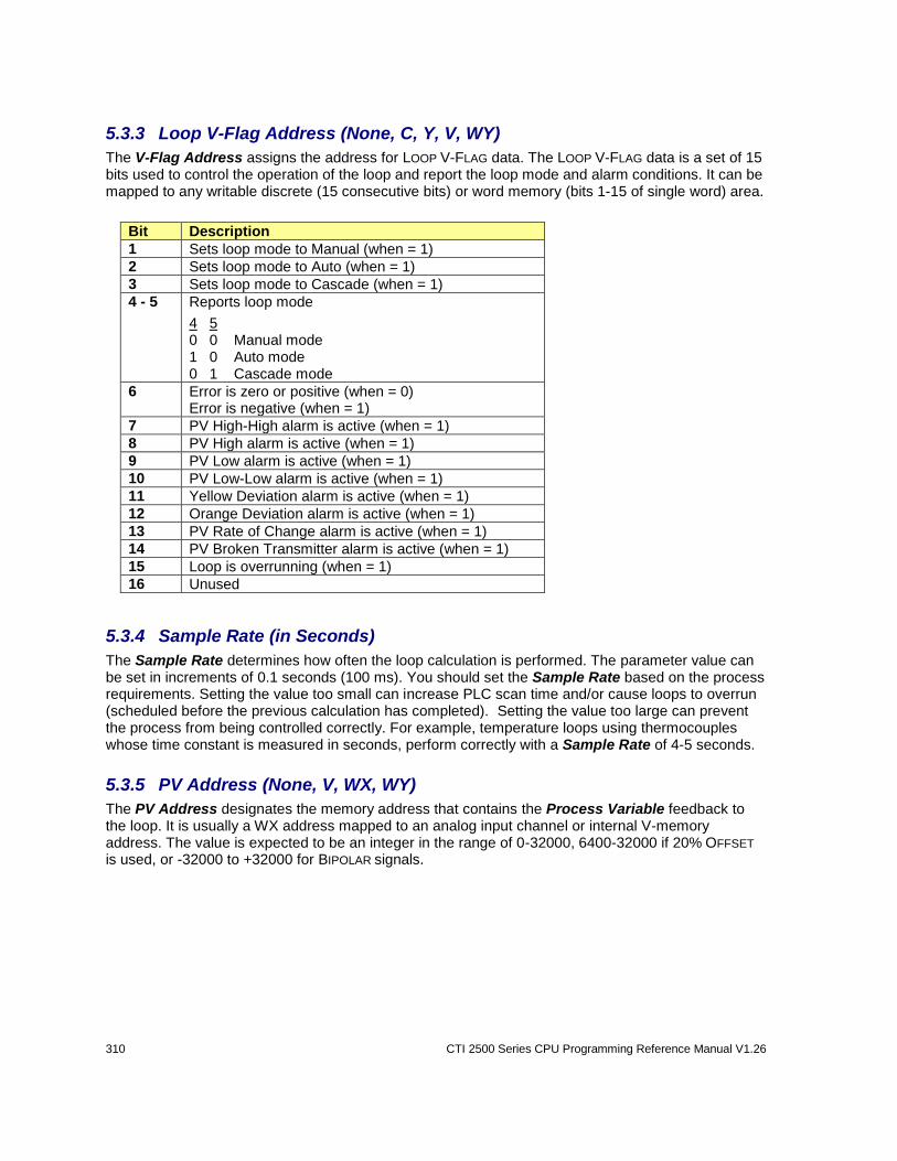
310 CTI 2500 Series CPU Programming Reference Manual V1.26
5.3.3 Loop V-Flag Address (None, C, Y, V, WY)
The V-Flag Address assigns the address for LOOP V-FLAG data. The LOOP V-FLAG data is a set of 15 bits used to control the operation of the loop and report the loop mode and alarm conditions. It can be mapped to any writable discrete (15 consecutive bits) or word memory (bits 1-15 of single word) area.
5.3.4 Sample Rate (in Seconds)
The Sample Rate determines how often the loop calculation is performed. The parameter value can be set in increments of 0.1 seconds (100 ms). You should set the Sample Rate based on the process requirements. Setting the value too small can increase PLC scan time and/or cause loops to overrun (scheduled before the previous calculation has completed). Setting the value too large can prevent the process from being controlled correctly. For example, temperature loops using thermocouples whose time constant is measured in seconds, perform correctly with a Sample Rate of 4-5 seconds.
5.3.5 PV Address (None, V, WX, WY)
The PV Address designates the memory address that contains the Process Variable feedback to the loop. It is usually a WX address mapped to an analog input channel or internal V-memory address. The value is expected to be an integer in the range of 0-32000, 6400-32000 if 20% OFFSET is used, or -32000 to +32000 for BIPOLAR signals.
Bit Description
1 Sets loop mode to Manual (when = 1)
2 Sets loop mode to Auto (when = 1)
3 Sets loop mode to Cascade (when = 1)
4 - 5 Reports loop mode
4 5 0 0 Manual mode 1 0 Auto mode 0 1 Cascade mode
6 Error is zero or positive (when = 0) Error is negative (when = 1)
7 PV High-High alarm is active (when = 1)
8 PV High alarm is active (when = 1)
9 PV Low alarm is active (when = 1)
10 PV Low-Low alarm is active (when = 1)
11 Yellow Deviation alarm is active (when = 1)
12 Orange Deviation alarm is active (when = 1)
13 PV Rate of Change alarm is active (when = 1)
14 PV Broken Transmitter alarm is active (when = 1)
15 Loop is overrunning (when = 1)
16 Unused

CTI 2500 Series CPU Programming Reference Manual V1.26 311
5.3.6 PV Range (Low/High)
The PROCESS VARIABLE can also be expressed as a Real number in engineering units. The PV Low Range represents the value when the input signal is at its minimum. The PV High Range represents the value when the input signal is at its maximum. The PV 20% OFFSET and PV BIPOLAR features are automatically integrated into the PV engineering units when selected.
Caution:
It is an invalid case to set the PV Low Range and PV High Range to the same values. WorkShop and TISOFT prohibit this setting during Loop configuration. However, it is possible to change these values via HMI to create invalid Loop parameter settings.
If PV Low Range is set equal to the PV High Range (LPVL = LPVH) during run-time, an error is detected in the associated PID calculation and the Loop Output is held at the previous calculated value. This will occur until a valid PV Range (LPVL < LPVH)
is entered when the Loop will resume normal operation.
5.3.7 PV Bipolar (Yes/No)
Select YES when the PROCESS VARIABLE is converted into a Bipolar analog signal, (-10 to +10V). When active, the range of the PROCESS VARIABLE integer value is -32000 to +32000.
5.3.8 20% Offset on PV (Yes/No)
Select YES when the PROCESS VARIABLE is an analog signal with a 20% Offset for the “zero” range position, (1-5V or 4-20mA). The range of the PROCESS VARIABLE is an integer value in the range of 6400–32000.
5.3.9 Square Root of PV (Yes/No)
The Square Root of PV feature is used with differential pressure flow measurement devices, such as an orifice or venturi tube, where the flow rate is proportional to the square root of the pressure drop across the device. In this case, the PV input value represents the measured differential pressure so flow must be derived through a square root calculation. Select YES only if the actual PV input signal represents the square of the measured input.
5.3.10 Loop Output Address (None, WY, V)
Specifies the memory address associated with the Loop Output. It is usually a WY address mapped to an analog output channel or internal V-Memory address. The value is expected to be an integer in the range of 0-32000, 6400-32000 (for 20% OFFSET) or -32000 to +32000 (for BIPOLAR signals)elect NONE if you do not want the LOOP OUTPUT to be written to a PLC memory address. In this case, the Loop Output value must be accessed via the SF variable LMN.
5.3.11 Output is Bipolar (Yes/No)
Select YES when the LOOP OUTPUT is converted into a Bipolar analog signal, (i.e., -10-to-+10V). When active, the range of the LOOP OUTPUT integer value is -32000 to +32000. It is invalid to set both Bipolar and 20% OFFSET flags for the same analog signal.
312 CTI 2500 Series CPU Programming Reference Manual V1.26
5.3.12 20% Offset on Output (Yes/No)
Select YES when the LOOP OUTPUT is converted into an analog signal with a 20% Offset for the “zero” range position, (1-5V or 4-20mA). When active, the range of the LOOP OUTPUT integer value is 6400–32000. It is invalid to set both 20% Offset and BIPOLAR flags for the same analog signal.
5.3.13 Ramp/Soak for SP (Yes/No)
When a Ramp/Soak profile has been programmed for this loop, setting this parameter to YES causes the loop to execute the Ramp/Soak steps when the loop transitions from MANUAL to AUTO mode. The configuration of a Ramp/Soak profile is described in Section 5.4.
5.3.14 Monitor Absolute Alarms (Yes/No)
The selection of Monitor Low-Low/High-High and Monitor Low/High enable alarms generated by comparing the PV to fixed values. Either pair of alarms may be used independently. Both pairs are used when one pair (High/Low) provides a warning indication while the other pair (High-High/ Low-Low signals a critical condition.
5.3.15 Absolute Alarm Limits (in Engr Units)
The values for the absolute alarm limits are entered when the corresponding alarm pair (Low/High) or (Low-Low/High-High) is selected. These values are specified in Engineering Units as follows:
The value for the High-High alarm must be less than or equal to the PV HIGH RANGE value.
The value for the High alarm must be less than or equal to the High-High alarm,
The value for the Low alarm must be less than or equal to the High alarm,
The value for the Low-Low alarm must be less than or equal to the Low alarm and greater than or equal to the PV LOW RANGE value.
5.3.16 Remote SP (None, V, K, WX, WY, LMN)
The Remote Setpoint field specifies the memory location used by the loop to obtain the SETPOINT
value. A value of NONE indicates that there is no Remote Setpoint and that the SETPOINT must be set via the Special Function variable LSP.
In order to use Remote Setpoint, the loop must be placed in CASCADE mode even if the loops are not actually cascaded together. True CASCADE mode involves multiple loops where the OUTPUT of one loop (LMN) is used as the SETPOINT for another. It is possible to simulate CASCADE mode by using any writeable word memory location as Remote Setpoint rather than an actual LOOP OUTPUT. This allows the SP to be controlled by RLL, SF programs, or manually via HMI. In this case, a loop in CASCADE mode operates exactly like AUTO mode without being influenced by the operation of another loop.
The integer value of Remote Setpoint is always scaled for the normal unipolar range of 0-32,000. The SETPOINT can also be accessed as Real number in engineering units according to the range specified by PV LOW and PV HIGH limits.
Note: An alternative to using Remote Setpoint in non-Cascade applications is to control
the Loop Setpoint via the SF Loop Setpoint variable (LSP).
CTI 2500 Series CPU Programming Reference Manual V1.26 313
5.3.17 Clamp Setpoint Limits Low/High (in Engr Units)
Designates minimum and maximum limits allowed for LOOP SETPOINT. The values entered are treated as engineering units and must be within limits specified for PV LOW and PV HIGH. An attempt to force the SETPOINT outside these limits will result in the SP value being clamped to nearest limit. For instance, with Setpoint Limits set to ‘10’ and ‘90’, a SP input of ‘5’ is changed to a value of ‘10’and a SP input of ‘95’ is changed to a value of ‘90’.
Setpoint Limits are enforced in MANUAL and AUTO modes but not in CASCADE mode. However, the controller sets SETPOINT equal to Process Variable (SP=PV) to ensure a bumpless transfer from MANUAL to AUTO mode even if PV is outside Setpoint Limits. The Setpoint Limits are then applied if the SETPOINT is ever changed from that value.
Setpoint Clamping is disabled if both SP Low and SP High limits are set to the same value.
5.3.18 Loop Gain
The Loop Gain parameter sets the PROPORTIONAL GAIN for the control loop and also acts as overall
GAIN multiplier (Kc). The Loop Gain entry may range from 0.0 to 100.0. An entry of 0 disables
PROPORTIONAL control.
A Loop Gain of 1.0 is Unity Gain where the PROPORTIONAL component of the LOOP OUTPUT is equal to amount the LOOP ERROR (SP-PV). A larger value for Loop Gain typically results in faster response since its PROPORTIONAL component increases as the ERROR increases, but it can lead to process instability if it is excessively large. The Loop Gain also serves as multiplier for DERIVATIVE GAIN and INTEGRAL GAIN as described in the following sections.
5.3.19 Loop Reset (Reset Time in Minutes)
This value determines the INTEGRAL portion of the PID algorithm. The Reset parameter is expressed
as Reset Time in minutes and used to calculate the INTEGRAL GAIN (Ki) as Sample Rate / Reset
Time. Therefore INTEGRAL GAIN is the reciprocal of Reset Time and decreases as Reset Time gets larger. Reset is used to improve response time and eliminate steady-state errors quicker. The trade-off is this usually causes larger overshoot during ERROR correction. The contribution of the INTEGRAL component is reflected in the BIAS term of the LOOP OUTPUT. Reset can be disabled by entering “0” or leaving the entry blank.
5.3.20 Rate (Derivative Time in Minutes)
Rate is the DERIVATIVE portion of the loop and is expressed as DERIVATIVE TIME in minutes.
DERIVATIVE GAIN (Kd) is calculated as DERIVATIVE TIME / SAMPLE RATE. The DERIVATIVE term slows the
rate of change of the LOOP OUTPUT and is most noticeable when the ERROR is small.. Rate is used to reduce the amount of overshoot produced by the INTEGRAL component. However, it slows down transient response and is highly sensitive to noise in PV and/or SP signals that can lead to process instability when DERIVATIVE GAIN is sufficiently large. Rate can be disabled by entering “0” or leaving the entry blank.
314 CTI 2500 Series CPU Programming Reference Manual V1.26
5.3.21 Freeze Bias (Yes/No)
In Adjust Bias mode (when Freeze Bias = NO), the controller adjusts LOOP BIAS by the amount that the calculated LOOP OUTPUT is out-of-range. Otherwise (Freeze Bias = YES), the controller holds BIAS at last value when OUTPUT calculation is out-of-range.
For example, the previous loop calculation had LOOP BIAS = 0.59 and LOOP OUTPUT = 0.99, and new loop calculation results in LOOP BIAS = 0.62 and LOOP OUTPUT = 1.08.
In Adjust Bias mode, the BIAS is adjusted by the overage amount
BIASNEW = 0.62 – 0.08 = 0.54
In Freeze Bias mode, the BIAS is held at previous value
BIASNEW = BIASOLD = 0.59
Freeze Bias is usually selected only in special circumstances where an external action can affect a process signal and generate an erroneous value over some time period. For example, the loop is controlling temperature in a furnace. If the temperature (PV) sensor were located near a furnace door, opening the door would produce a large ERROR and cause unwanted large change in the BIAS term.
5.3.22 Derivative Gain Limiting (Yes/No)
Derivative Gain Limiting enables a filter to be used in the calculation of DERIVATIVE component of the controller algorithm. This feature helps to reduce the sensitivity of the DERIVATIVE TERM to noise in process signals that can cause erratic behavior of the control system. This is typically used when the DERIVATIVE term exceeds 15-20 percent of the calculated LOOP OUTPUT.
5.3.23 Limiting Coefficient
Specifies the value used as Derivative Gain Limiting Coefficient in calculation of the DERIVATIVE
GAIN LIMITING filter. This filter effectively limits the rate of change of PROCESS VARIABLE according to the filter time constant as specified by the DERIVATIVE TIME (Td) and LIMITING COEFFICIENT (Kd) as shown below:
The Limiting Coefficient is used only when DERIVATIVE GAIN LIMITING = YES.
5.3.24 Alarm Deadband (in Engr Units)
Alarm Deadband sets the value used to prevent nuisance alarms caused by PV value ‘chattering’ near an alarm limit. If specified, it provides a “neutral zone” for all alarms except for RATE OF CHANGE alarm. The Alarm Deadband delays the point at which an alarm condition is set and/or cleared. It is normally set to a value in the range of 0.25% to 5% of span.
For example, PV RANGE of 0-100, PV LOW alarm = 20, and Deadband = 2. When PV drops from 21 to 20, PV LOW alarm is activated. The PV LOW alarm is not cleared until PV signal rises to 22.
YNEW = X (PVNEW – YPREV)
Sample Time (Ts)
Ts + (Td/Kd)
Derivative Term = Rate Gain (Kc*Td/Ts) X (YNEW – YPREV)
YPREV +
CTI 2500 Series CPU Programming Reference Manual V1.26 315
5.3.25 Special Calculation On (SP, PV, Output, None)
The controller can perform any custom calculations by calling a SPECIAL FUNCTION PROGRAM during the loop calculation. This field schedules the SF program to be called while the SP, PV, or Output values are accessed. No Special Function Program is called if “NONE” is entered in this field.
SP Used for manipulating SP and/or PV values Called in AUTO or CASCADE mode immediately before loop calculation (T2=2)
PV Used for alarm monitoring and setting/changing of any loop parameter value Called in all modes every 2 seconds or SAMPLE RATE whichever is less.
T2=3 when called for alarm monitoring (when SAMPLE RATE > 2 sec)
T2=2 when called immediately before loop calculation
Output Same as PV with additional call to set OUTPUT values after loop calculation Called in all modes every 2 seconds or SAMPLE RATE whichever is less.
T2=3 when called for alarm monitoring (when Sample Rate > 2 sec)
T2=2 when called immediately before loop calculation
T2=5 when called immediately after loop calculation
None No Special Function Program is called
5.3.26 Special Function
This field specifies the number of the Special Function Program that will be called from the loop.
5.3.27 Lock Setpoint, Lock Auto/Man, Lock Cascade
These values set the corresponding bits in the LOOP C-FLAGS. It is the responsibility of the operator interface or HMI program to check these flags before attempting to modify these parameters. The controller does not enforce the lock.
5.3.28 Error Operation (Error Squared, Error Deadband, None)
Specifies method used to calculate the LOOP ERROR term used in the control equation:
Error Squared Computes the square of the ERROR before using it in the loop algorithm. Since the ERROR is expressed as a percent, this makes the loop less responsive to a specific ERROR amount. For example, an ERROR of 50% would result in an ERROR TERM of 0.25 (0.5 X 0.5). Used primarily in PH control applications.
Error Deadband Used to implement fast response for large errors and ignore small errors. The controller does not respond to ERROR values within the YELLOW
DEVIATION limit
None Computes LOOP ERROR as ERR = SP – PV (Default)
316 CTI 2500 Series CPU Programming Reference Manual V1.26
5.3.29 Reverse Acting (Yes/No)
This parameter selects the direction of controller response to LOOP ERROR.
NO Selects Direct-Acting control. Direction of PV movement follows the LOOP
OUTPUT. Therefore, increasing the CONTROL OUTPUT causes the PV value to increase.
YES Selects Reverse-Acting control. Direction of PV movement is opposite of the LOOP
OUTPUT. Increasing the CONTROL OUTPUT causes the PV value to decrease.
5.3.30 Monitor Deviation (Yes/No)
Select YES to enable alarm monitoring on DEVIATION LIMITS on the ERROR value calculated as SP-PV. When selected both YELLOW DEVIATION and ORANGE DEVIATION alarms are enabled.
5.3.31 Deviation Alarm Limits (in Engr Units)
The Yellow Deviation and Orange Deviation alarms activate when the ERROR (SP – PV) exceeds the specified limits. The Yellow Deviation is considered the first level alarm, and the ORANGE
DEVIATION is considered the critical alarm. The values for both alarm limits are entered in Engineering Units as follows:
The value for the Orange Deviation alarm limit must be less than or equal to the PV RANGE
in Engineering Units ((PV HIGH RANGE – PV LOW RANGE.) and greater than or equal to the Yellow Deviation limit.
The value for the Yellow Deviation alarm limit must be greater than or equal to zero and less than or equal to the Orange Deviation limit.
5.3.32 Monitor Rate (Yes/No)
Select YES to enable alarm monitoring on PV RATE OF CHANGE.
5.3.33 Rate of Change Alarm Limit (in Engr Units per Minute)
The Rate of Change alarm is activated when the PV input changes faster than the designated alarm limit. The change in PV is calculated as the difference in two consecutive monitoring cycles. The Rate of Change limit is entered in Engineering Units per Minute. For example, for a PV RANGE = 0-100, an entry of 120 equates to an Rate of Change alarm limit of 2 units per second.
5.3.34 Monitor Broken Xmit (Yes/No)
Select YES to enable Broken Transmitter alarm that is activated when the integer value of the PV input signal is detected outside of the expected range as shown below:
NO OFFSET: 0 – 32000
20% OFFSET: 6400 – 32000
BIPOLAR: -32000 to +32000
If DEADBAND is specified, that value is added to the limits that activate this alarm. For instance, the Broken Transmitter alarm is set when a 20% OFFSET signal is read outside the range of 6400-32000 when no DEADBAND is used. However, a DEADBAND value of 5% expands the acceptable input range by 1280 counts on both end of the scale (5120-33280).
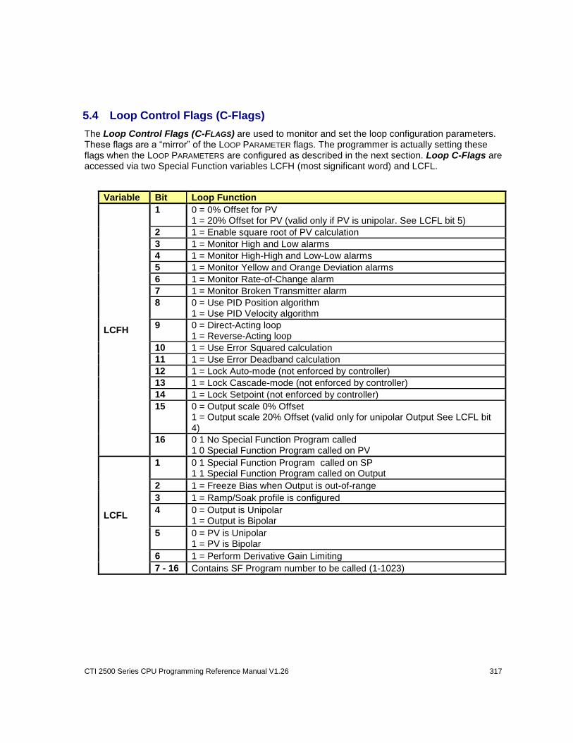
CTI 2500 Series CPU Programming Reference Manual V1.26 317
5.4 Loop Control Flags (C-Flags)
The Loop Control Flags (C-FLAGS) are used to monitor and set the loop configuration parameters. These flags are a “mirror” of the LOOP PARAMETER flags. The programmer is actually setting these flags when the LOOP PARAMETERS are configured as described in the next section. Loop C-Flags are accessed via two Special Function variables LCFH (most significant word) and LCFL.
Variable Bit Loop Function
LCFH
1 0 = 0% Offset for PV 1 = 20% Offset for PV (valid only if PV is unipolar. See LCFL bit 5)
2 1 = Enable square root of PV calculation
3 1 = Monitor High and Low alarms
4 1 = Monitor High-High and Low-Low alarms
5 1 = Monitor Yellow and Orange Deviation alarms
6 1 = Monitor Rate-of-Change alarm
7 1 = Monitor Broken Transmitter alarm
8 0 = Use PID Position algorithm 1 = Use PID Velocity algorithm
9 0 = Direct-Acting loop 1 = Reverse-Acting loop
10 1 = Use Error Squared calculation
11 1 = Use Error Deadband calculation
12 1 = Lock Auto-mode (not enforced by controller)
13 1 = Lock Cascade-mode (not enforced by controller)
14 1 = Lock Setpoint (not enforced by controller)
15 0 = Output scale 0% Offset 1 = Output scale 20% Offset (valid only for unipolar Output See LCFL bit 4)
16 0 1 No Special Function Program called 1 0 Special Function Program called on PV
LCFL
1 0 1 Special Function Program called on SP 1 1 Special Function Program called on Output
2 1 = Freeze Bias when Output is out-of-range
3 1 = Ramp/Soak profile is configured
4 0 = Output is Unipolar 1 = Output is Bipolar
5 0 = PV is Unipolar 1 = PV is Bipolar
6 1 = Perform Derivative Gain Limiting
7 - 16 Contains SF Program number to be called (1-1023)
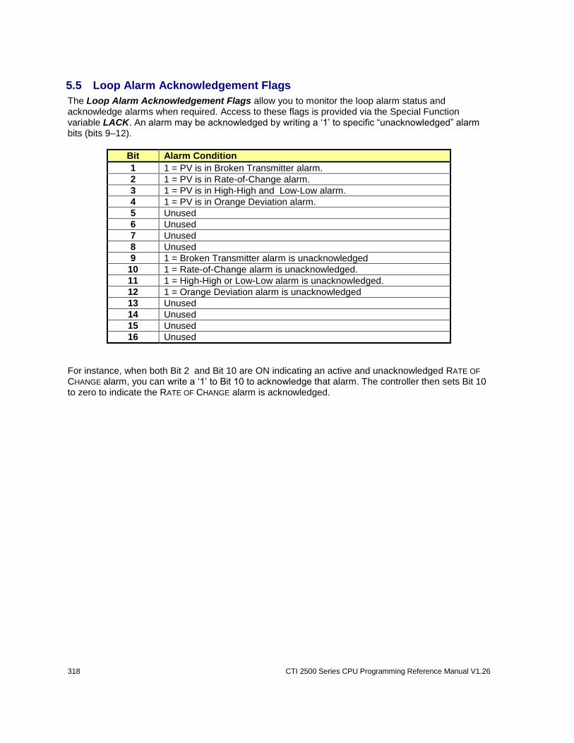
318 CTI 2500 Series CPU Programming Reference Manual V1.26
5.5 Loop Alarm Acknowledgement Flags
The Loop Alarm Acknowledgement Flags allow you to monitor the loop alarm status and acknowledge alarms when required. Access to these flags is provided via the Special Function variable LACK. An alarm may be acknowledged by writing a ‘1’ to specific “unacknowledged” alarm bits (bits 9–12). For instance, when both Bit 2 and Bit 10 are ON indicating an active and unacknowledged RATE OF
CHANGE alarm, you can write a ‘1’ to Bit 10 to acknowledge that alarm. The controller then sets Bit 10 to zero to indicate the RATE OF CHANGE alarm is acknowledged.
Bit Alarm Condition
1 1 = PV is in Broken Transmitter alarm.
2 1 = PV is in Rate-of-Change alarm.
3 1 = PV is in High-High and Low-Low alarm.
4 1 = PV is in Orange Deviation alarm.
5 Unused
6 Unused
7 Unused
8 Unused
9 1 = Broken Transmitter alarm is unacknowledged
10 1 = Rate-of-Change alarm is unacknowledged.
11 1 = High-High or Low-Low alarm is unacknowledged.
12 1 = Orange Deviation alarm is unacknowledged
13 Unused
14 Unused
15 Unused
16 Unused
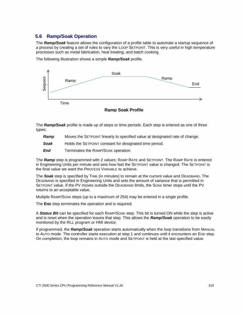
CTI 2500 Series CPU Programming Reference Manual V1.26 319
5.6 Ramp/Soak Operation
The Ramp/Soak feature allows the configuration of a profile table to automate a startup sequence of a process by creating a set of rules to vary the LOOP SETPOINT. This is very useful in high temperature processes such as metal fabrication, heat treating, and batch cooking.
The following illustration shows a simple Ramp/Soak profile.
The Ramp/Soak profile is made up of steps or time periods. Each step is entered as one of three types:
Ramp Moves the SETPOINT linearly to specified value at designated rate of change.
Soak Holds the SETPOINT constant for designated time period.
End Terminates the RAMP/SOAK operation
The Ramp step is programmed with 2 values; RAMP RATE and SETPOINT. The RAMP RATE is entered in Engineering Units per minute and sets how fast the SETPOINT value is changed. The SETPOINT is the final value we want the PROCESS VARIABLE to achieve.
The Soak step is specified by TIME (in minutes) to remain at the current value and DEADBAND. The DEADBAND is specified in Engineering Units and sets the amount of variance that is permitted in SETPOINT value. If the PV moves outside the DEADBAND limits, the SOAK timer stops until the PV returns to an acceptable value.
Multiple RAMP/SOAK steps (up to a maximum of 254) may be entered in a single profile.
The END step terminates the operation and is required.
A Status Bit can be specified for each RAMP/SOAK step. This bit is turned ON while the step is active and is reset when the operation leaves that step. This allows the Ramp/Soak operation to be easily monitored by the RLL program or HMI device.
If programmed, the Ramp/Soak operation starts automatically when the loop transitions from MANUAL to AUTO mode. The controller starts execution at step 1 and continues until it encounters an END step. On completion, the loop remains in AUTO mode and SETPOINT is held at the last specified value.
Time
Setp
oin
t
Ramp Soak Profile
Ramp
Soak
Ramp
End
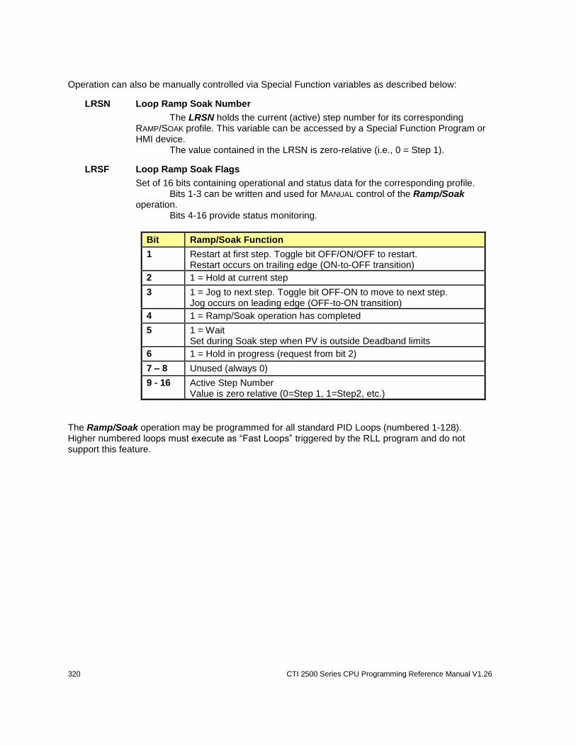
320 CTI 2500 Series CPU Programming Reference Manual V1.26
Operation can also be manually controlled via Special Function variables as described below:
LRSN Loop Ramp Soak Number
The LRSN holds the current (active) step number for its corresponding RAMP/SOAK profile. This variable can be accessed by a Special Function Program or HMI device.
The value contained in the LRSN is zero-relative (i.e., 0 = Step 1).
LRSF Loop Ramp Soak Flags
Set of 16 bits containing operational and status data for the corresponding profile. Bits 1-3 can be written and used for MANUAL control of the Ramp/Soak
operation. Bits 4-16 provide status monitoring.
Bit Ramp/Soak Function
1 Restart at first step. Toggle bit OFF/ON/OFF to restart. Restart occurs on trailing edge (ON-to-OFF transition)
2 1 = Hold at current step
3 1 = Jog to next step. Toggle bit OFF-ON to move to next step. Jog occurs on leading edge (OFF-to-ON transition)
4 1 = Ramp/Soak operation has completed
5 1 = Wait Set during Soak step when PV is outside Deadband limits
6 1 = Hold in progress (request from bit 2)
7 – 8 Unused (always 0)
9 - 16 Active Step Number Value is zero relative (0=Step 1, 1=Step2, etc.)
The Ramp/Soak operation may be programmed for all standard PID Loops (numbered 1-128). Higher numbered loops must execute as “Fast Loops” triggered by the RLL program and do not support this feature.
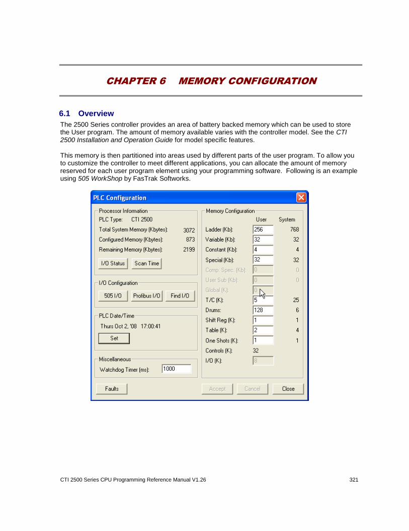
CTI 2500 Series CPU Programming Reference Manual V1.26 321
CHAPTER 6 MEMORY CONFIGURATION
6.1 Overview
The 2500 Series controller provides an area of battery backed memory which can be used to store the User program. The amount of memory available varies with the controller model. See the CTI 2500 Installation and Operation Guide for model specific features. This memory is then partitioned into areas used by different parts of the user program. To allow you to customize the controller to meet different applications, you can allocate the amount of memory reserved for each user program element using your programming software. Following is an example using 505 WorkShop by FasTrak Softworks.
322 CTI 2500 Series CPU Programming Reference Manual V1.26
6.2 Memory Configuration
This section describes the PLC memory types available for user configuration.
6.2.1 Ladder (L) Memory
Ladder Memory is used to hold the RLL program. Each ladder instruction consumes one or more 16 bit words of RLL memory. For each 1KB of RLL source memory configured, the controller allocates an additional 2KB for compiled run-time code.
6.2.2 Variable (V) Memory
Variable (V) Memory is an array of 16 bit words that used to store user defined data. One V-Memory location can contain an array of bits, an unsigned integer, or a signed integer. Two consecutive V memory locations can be used for long integers and/or floating point numbers. V-Memory is allocated in increments of 1KB. Each V-Memory location consumes 2 bytes.
6.2.3 Constant (K) Memory
Constant (K) Memory is similar to V memory, except that it cannot be written by the user program. K-Memory is typically used to hold initialization data and other data that is unchangeable. One K-Memory location can contain an array of bits, an unsigned integer, or a signed integer. Two consecutive K memory locations can be used for long integers and floating point numbers. K-Memory is allocated in increments of 1KB. Each K-Memory location consumes 2 bytes.
6.2.4 Special (S) Memory
Special (S) Memory is used to hold instructions for Special Function Programs and Subroutines, Analog Loop parameters, and Analog Alarm parameters. S-Memory is allocated in 1KB increments.
6.2.5 Timer/Counter (TC) Memory
Timer/Counter memory is used to hold the Timer/Counter Current (TCC) and Timer/Counter Preset (TCP) data. Each Timer and/or Counter instruction (TMR, TMRF, DCAT, MCAT, CTR, UDC) used in the program must have a unique instruction number. The user allocates the number of Timers and/or Counters available in 1K increments, and each group of 1K instructions consumes 5KB of System Memory.
6.2.6 Drum Memory (D) Memory
Drum Memory is used to store the Drum data including the Drum Step Preset (DSP), Drum Count Preset (DCP), Drum Step Current (DSC), and Drum Count Current (DCC) values. Each Drum instruction (DRUM, EDRUM, MDRMD, MDRMW) used in the program must have a unique instruction number. The user allocates the number of Drums available in increments of 64. Each allocated group of 64 Drums uses 3KB of System Memory.
6.2.7 Shift Register (SR) Memory
Shift Register Memory is used by the Shift Register instructions. Each Shift Register instruction (SHRB or SHRW) used in the program must have a unique instruction number. The user allocates the number of Shift Register available in 1K increments, and the system uses one byte for each allocated instruction to save the previous state of the instruction input.
CTI 2500 Series CPU Programming Reference Manual V1.26 323
6.2.8 Table (T) Memory
Table Memory is used by the Table Move instructions. Each Table Move instruction (MWTT or MWFT) used in the program must have a unique instruction number. The user allocates the number of Table Move instructions available in 1K increments, and 2 bytes of System Memory are used for each allocated instruction to maintain the count of move operations completed since the last instruction reset.
6.2.9 One Shot (OS) Memory
One Shot Memory is used by the group of One-Shot instructions for storage of the previous input state. Each One-Shot instruction (OS, DSET, TSET) used in the program must have a unique instruction number. The user allocates the number of One-Shot instructions available in 1K increments, and each allocated instruction uses 1 byte of System Memory.
Note:
Compiled Special (CS) Memory and User (U) Memory that were user-configurable memory types for the SIMATIC® 505 controllers are not used in the CTI 2500 Series CPU.
When using 505 WorkShop, the software automatically removes these memory types from the PLC Configuration when the ‘PLC Type’ is changed to a CTI 2500 Series PLC model. However,
these memory allocations must be manually removed from the PLC Memory Configuration before using TISOFT to download a program to a CTI 2500 Series PLC

324 CTI 2500 Series CPU Programming Reference Manual V1.26
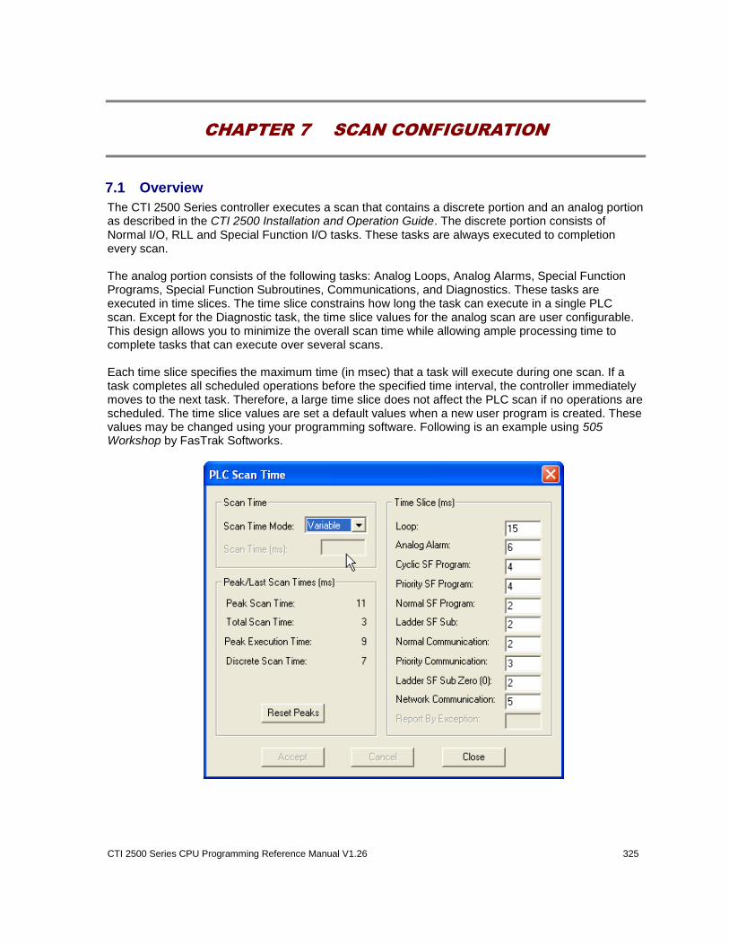
CTI 2500 Series CPU Programming Reference Manual V1.26 325
CHAPTER 7 SCAN CONFIGURATION
7.1 Overview
The CTI 2500 Series controller executes a scan that contains a discrete portion and an analog portion as described in the CTI 2500 Installation and Operation Guide. The discrete portion consists of Normal I/O, RLL and Special Function I/O tasks. These tasks are always executed to completion every scan. The analog portion consists of the following tasks: Analog Loops, Analog Alarms, Special Function Programs, Special Function Subroutines, Communications, and Diagnostics. These tasks are executed in time slices. The time slice constrains how long the task can execute in a single PLC scan. Except for the Diagnostic task, the time slice values for the analog scan are user configurable. This design allows you to minimize the overall scan time while allowing ample processing time to complete tasks that can execute over several scans. Each time slice specifies the maximum time (in msec) that a task will execute during one scan. If a task completes all scheduled operations before the specified time interval, the controller immediately moves to the next task. Therefore, a large time slice does not affect the PLC scan if no operations are scheduled. The time slice values are set a default values when a new user program is created. These values may be changed using your programming software. Following is an example using 505 Workshop by FasTrak Softworks.
326 CTI 2500 Series CPU Programming Reference Manual V1.26
7.2 Time Slice Configuration
You can configure the following time periods in the analog scan:
7.2.1 Analog Loop Time Slice
The Analog Loop task executes in this time slice. This time slice value represents the maximum amount of time that the task can run in a single scan. If you wish to minimize scan time, you can set the time slice slightly larger than the value that will cause the loops to begin overrunning.
7.2.2 Analog Alarm Time Slice
The Analog Alarm task executes in this time slice. This time slice value represents the maximum amount of time that the task can run in a single scan. If you wish to minimize scan time, you can set the time slice slightly larger than the value that will cause the alarms to begin overrunning.
7.2.3 Cyclic Special Function Program Time Slice
When you create a Special Function Program, you can designate that the program is executed on a cyclical basis and specify the cyclic time interval. This time slice value represents the maximum amount of time that Cyclic Special Function Programs can run in a single scan. If you wish to minimize scan time, you can set the time slice slightly larger than the value that will cause Cyclic Special Function Programs to begin overrunning.
7.2.4 Priority Special Function Program Time Slice
When you create a Special Function Program that is called from the RLL program, you can designate whether the program is executed in the Priority time slice or the Normal time slice. This time slice value represents the maximum amount of time that Special Function programs designated as Priority can run in a single scan.
7.2.5 Normal Special Function Program Time Slice
When you create a Special Function Program that is called from relay ladder logic, you can designate whether the program is executed in the Priority time slice or the Normal time slice. This time slice value represents the maximum amount of time that Special Function programs designated as Normal can run in a single scan.
7.2.6 Ladder Special Function Subroutine Time Slice
Special Function Subroutines called from relay ladder logic (RLL) execute in this time slice. This time slice value represents the maximum amount of time that Special Function Subroutines called from RLL can run in a single scan.
7.2.7 Normal Communications Time Slice
Requests that may require several scans to service, called DEFERRED REQUESTS, are executed in this time slice. In general, these requests consist of programming functions such as BLOCK MOVES and SEARCHES. When the controller is in RUN mode, this value represents the maximum amount of scan time that will be allocated to executing this request. If DEFERRED REQUESTS are serviced too slowly, you can speed them up by increasing this time slice (at the expense of impacting scan time). If the impact on scan time is more important than the execution time of these requests, you can reduce the time slice value.
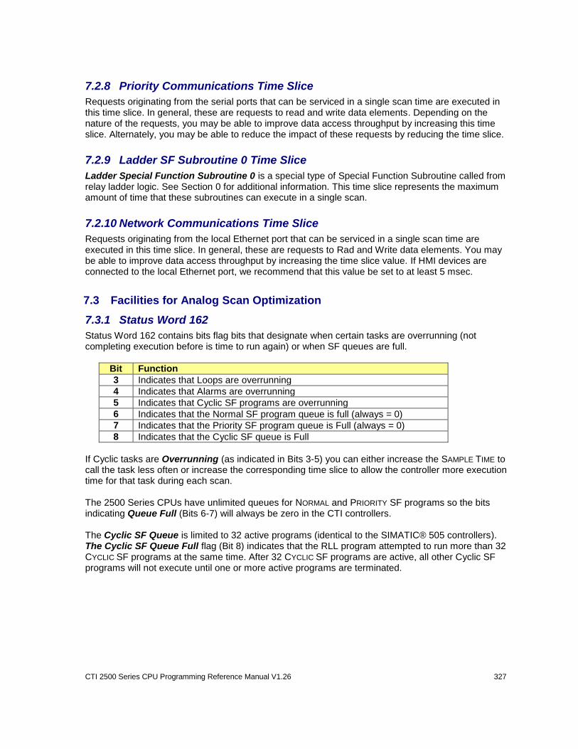
CTI 2500 Series CPU Programming Reference Manual V1.26 327
7.2.8 Priority Communications Time Slice
Requests originating from the serial ports that can be serviced in a single scan time are executed in this time slice. In general, these are requests to read and write data elements. Depending on the nature of the requests, you may be able to improve data access throughput by increasing this time slice. Alternately, you may be able to reduce the impact of these requests by reducing the time slice.
7.2.9 Ladder SF Subroutine 0 Time Slice
Ladder Special Function Subroutine 0 is a special type of Special Function Subroutine called from relay ladder logic. See Section 0 for additional information. This time slice represents the maximum amount of time that these subroutines can execute in a single scan.
7.2.10 Network Communications Time Slice
Requests originating from the local Ethernet port that can be serviced in a single scan time are executed in this time slice. In general, these are requests to Rad and Write data elements. You may be able to improve data access throughput by increasing the time slice value. If HMI devices are connected to the local Ethernet port, we recommend that this value be set to at least 5 msec.
7.3 Facilities for Analog Scan Optimization
7.3.1 Status Word 162
Status Word 162 contains bits flag bits that designate when certain tasks are overrunning (not completing execution before is time to run again) or when SF queues are full.
Bit Function
3 Indicates that Loops are overrunning
4 Indicates that Alarms are overrunning
5 Indicates that Cyclic SF programs are overrunning
6 Indicates that the Normal SF program queue is full (always = 0)
7 Indicates that the Priority SF program queue is Full (always = 0)
8 Indicates that the Cyclic SF queue is Full
If Cyclic tasks are Overrunning (as indicated in Bits 3-5) you can either increase the SAMPLE TIME to call the task less often or increase the corresponding time slice to allow the controller more execution time for that task during each scan. The 2500 Series CPUs have unlimited queues for NORMAL and PRIORITY SF programs so the bits indicating Queue Full (Bits 6-7) will always be zero in the CTI controllers. The Cyclic SF Queue is limited to 32 active programs (identical to the SIMATIC® 505 controllers). The Cyclic SF Queue Full flag (Bit 8) indicates that the RLL program attempted to run more than 32 CYCLIC SF programs at the same time. After 32 CYCLIC SF programs are active, all other Cyclic SF programs will not execute until one or more active programs are terminated.
328 CTI 2500 Series CPU Programming Reference Manual V1.26
7.3.2 Program Elapsed Times
For each analog loop, analog alarm, special function program, and special function subroutine, the controller maintains a peak elapsed time. This measures the time from which the program element is placed in the execution queue until it has completed execution. These statistics may be accessed via the following mnemonics.
LPET Contains the PEAK ELAPSED TIME for PID loops executed in the ANALOG LOOP time slice. LPET1 contains the time for Loop 1; LPET2 contains the time for Loop 2; etc. Note LPET times are not valid for loops executed using the RLL PID instruction, since these loops are executed in the RLL portion of the scan.
APET Contains the PEAK ELAPSED TIME for Analog Alarms. APET1 contains the time for
Alarm 1; APET2 contains the time for Alarm 2; etc.
PPET Contains the PEAK ELAPSED TIME for Special Function programs. PPET1 contains the time for SFPGM 1; PPET2 contains the time for SFPGM 2; etc. PPET times for SF programs executed IN-LINE with RLL are not available, since they are executed in the RLL portion of the scan. The PPET values for SF programs called only by LOOPS or ALARMS are set to 65535 to provide indication that the SFPGM has executed.
SPET Contains the PEAK ELAPSED TIME for Special Function Subroutines. SPET1 contains the
time for SFSUB 1; SPET2 contains the time for SFSUB 2; etc. Note that SPET times are valid only for SF Subroutines called by RLL that are not designated for IN-LINE execution.
The PEAK ELAPSED TIME shows the total time interval between when the task starts to execute until it is complete. If the task cannot finish before the time slice expires, the task is suspended until the next PLC Scan. The PEAK ELAPSED TIME includes the time required to complete the PLC Scan as well as the task itself. Using the PEAK ELAPSED TIME values, you can determine how long it is taking to execute a specific task on the controller. For Cyclic tasks, it shows how close the tasks are to overrunning (not completing execution before it is time to run again) and helps you to adjust the time slice values accordingly.
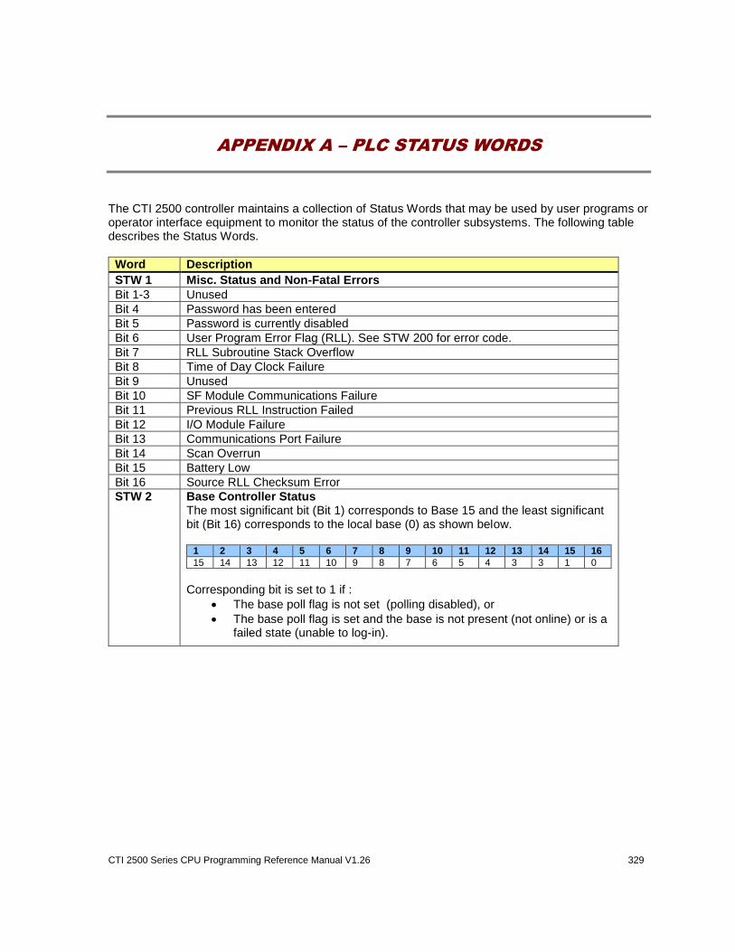
CTI 2500 Series CPU Programming Reference Manual V1.26 329
APPENDIX A – PLC STATUS WORDS
The CTI 2500 controller maintains a collection of Status Words that may be used by user programs or operator interface equipment to monitor the status of the controller subsystems. The following table describes the Status Words.
Word Description
STW 1 Misc. Status and Non-Fatal Errors
Bit 1-3 Unused
Bit 4 Password has been entered
Bit 5 Password is currently disabled
Bit 6 User Program Error Flag (RLL). See STW 200 for error code.
Bit 7 RLL Subroutine Stack Overflow
Bit 8 Time of Day Clock Failure
Bit 9 Unused
Bit 10 SF Module Communications Failure
Bit 11 Previous RLL Instruction Failed
Bit 12 I/O Module Failure
Bit 13 Communications Port Failure
Bit 14 Scan Overrun
Bit 15 Battery Low
Bit 16 Source RLL Checksum Error
STW 2 Base Controller Status The most significant bit (Bit 1) corresponds to Base 15 and the least significant bit (Bit 16) corresponds to the local base (0) as shown below.
1 2 3 4 5 6 7 8 9 10 11 12 13 14 15 16
15 14 13 12 11 10 9 8 7 6 5 4 3 3 1 0
Corresponding bit is set to 1 if :
The base poll flag is not set (polling disabled), or
The base poll flag is set and the base is not present (not online) or is a failed state (unable to log-in).
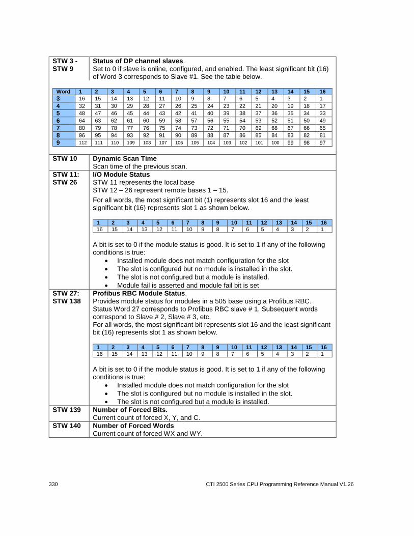
330 CTI 2500 Series CPU Programming Reference Manual V1.26
STW 3 - STW 9
Status of DP channel slaves. Set to 0 if slave is online, configured, and enabled. The least significant bit (16) of Word 3 corresponds to Slave #1. See the table below.
Word 1 2 3 4 5 6 7 8 9 10 11 12 13 14 15 16
3 16 15 14 13 12 11 10 9 8 7 6 5 4 3 2 1
4 32 31 30 29 28 27 26 25 24 23 22 21 20 19 18 17
5 48 47 46 45 44 43 42 41 40 39 38 37 36 35 34 33
6 64 63 62 61 60 59 58 57 56 55 54 53 52 51 50 49
7 80 79 78 77 76 75 74 73 72 71 70 69 68 67 66 65
8 96 95 94 93 92 91 90 89 88 87 86 85 84 83 82 81
9 112 111 110 109 108 107 106 105 104 103 102 101 100 99 98 97
STW 10 Dynamic Scan Time Scan time of the previous scan.
STW 11: STW 26
I/O Module Status STW 11 represents the local base STW 12 – 26 represent remote bases 1 – 15.
For all words, the most significant bit (1) represents slot 16 and the least significant bit (16) represents slot 1 as shown below.
1 2 3 4 5 6 7 8 9 10 11 12 13 14 15 16
16 15 14 13 12 11 10 9 8 7 6 5 4 3 2 1
A bit is set to 0 if the module status is good. It is set to 1 if any of the following conditions is true:
Installed module does not match configuration for the slot
The slot is configured but no module is installed in the slot.
The slot is not configured but a module is installed.
Module fail is asserted and module fail bit is set
STW 27: STW 138
Profibus RBC Module Status. Provides module status for modules in a 505 base using a Profibus RBC. Status Word 27 corresponds to Profibus RBC slave # 1. Subsequent words correspond to Slave # 2, Slave # 3, etc. For all words, the most significant bit represents slot 16 and the least significant bit (16) represents slot 1 as shown below.
1 2 3 4 5 6 7 8 9 10 11 12 13 14 15 16
16 15 14 13 12 11 10 9 8 7 6 5 4 3 2 1
A bit is set to 0 if the module status is good. It is set to 1 if any of the following conditions is true:
Installed module does not match configuration for the slot
The slot is configured but no module is installed in the slot.
The slot is not configured but a module is installed.
STW 139 Number of Forced Bits. Current count of forced X, Y, and C.
STW 140 Number of Forced Words Current count of forced WX and WY.
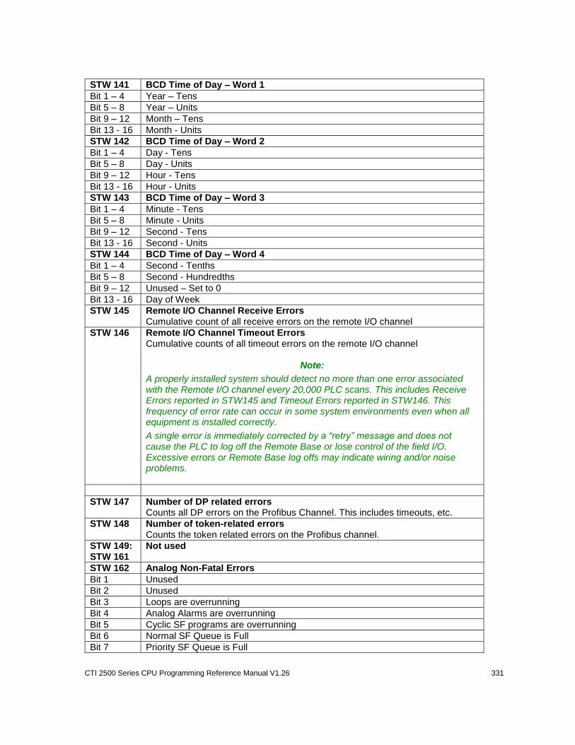
CTI 2500 Series CPU Programming Reference Manual V1.26 331
STW 141 BCD Time of Day – Word 1
Bit 1 – 4 Year – Tens
Bit 5 – 8 Year – Units
Bit 9 – 12 Month – Tens
Bit 13 - 16 Month - Units
STW 142 BCD Time of Day – Word 2
Bit 1 – 4 Day - Tens
Bit 5 – 8 Day - Units
Bit 9 – 12 Hour - Tens
Bit 13 - 16 Hour - Units
STW 143 BCD Time of Day – Word 3
Bit 1 – 4 Minute - Tens
Bit 5 – 8 Minute - Units
Bit 9 – 12 Second - Tens
Bit 13 - 16 Second - Units
STW 144 BCD Time of Day – Word 4
Bit 1 – 4 Second - Tenths
Bit 5 – 8 Second - Hundredths
Bit 9 – 12 Unused – Set to 0
Bit 13 - 16 Day of Week
STW 145 Remote I/O Channel Receive Errors Cumulative count of all receive errors on the remote I/O channel
STW 146 Remote I/O Channel Timeout Errors Cumulative counts of all timeout errors on the remote I/O channel
Note:
A properly installed system should detect no more than one error associated with the Remote I/O channel every 20,000 PLC scans. This includes Receive Errors reported in STW145 and Timeout Errors reported in STW146. This frequency of error rate can occur in some system environments even when all equipment is installed correctly.
A single error is immediately corrected by a “retry” message and does not cause the PLC to log off the Remote Base or lose control of the field I/O. Excessive errors or Remote Base log offs may indicate wiring and/or noise problems.
STW 147 Number of DP related errors Counts all DP errors on the Profibus Channel. This includes timeouts, etc.
STW 148 Number of token-related errors Counts the token related errors on the Profibus channel.
STW 149: STW 161
Not used
STW 162 Analog Non-Fatal Errors
Bit 1 Unused
Bit 2 Unused
Bit 3 Loops are overrunning
Bit 4 Analog Alarms are overrunning
Bit 5 Cyclic SF programs are overrunning
Bit 6 Normal SF Queue is Full
Bit 7 Priority SF Queue is Full
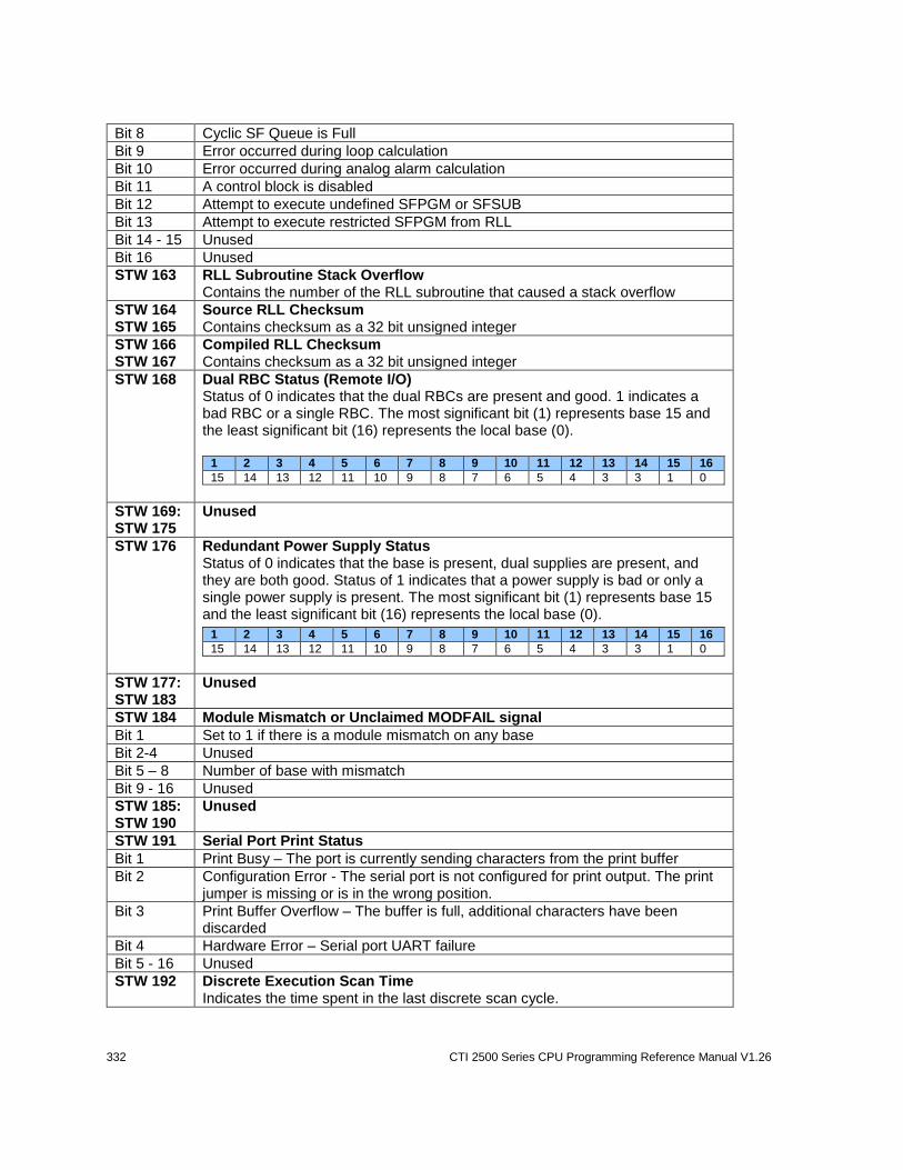
332 CTI 2500 Series CPU Programming Reference Manual V1.26
Bit 8 Cyclic SF Queue is Full
Bit 9 Error occurred during loop calculation
Bit 10 Error occurred during analog alarm calculation
Bit 11 A control block is disabled
Bit 12 Attempt to execute undefined SFPGM or SFSUB
Bit 13 Attempt to execute restricted SFPGM from RLL
Bit 14 - 15 Unused
Bit 16 Unused
STW 163 RLL Subroutine Stack Overflow Contains the number of the RLL subroutine that caused a stack overflow
STW 164 STW 165
Source RLL Checksum Contains checksum as a 32 bit unsigned integer
STW 166 STW 167
Compiled RLL Checksum Contains checksum as a 32 bit unsigned integer
STW 168 Dual RBC Status (Remote I/O) Status of 0 indicates that the dual RBCs are present and good. 1 indicates a bad RBC or a single RBC. The most significant bit (1) represents base 15 and the least significant bit (16) represents the local base (0).
1 2 3 4 5 6 7 8 9 10 11 12 13 14 15 16
15 14 13 12 11 10 9 8 7 6 5 4 3 3 1 0
STW 169: STW 175
Unused
STW 176 Redundant Power Supply Status Status of 0 indicates that the base is present, dual supplies are present, and they are both good. Status of 1 indicates that a power supply is bad or only a single power supply is present. The most significant bit (1) represents base 15 and the least significant bit (16) represents the local base (0).
1 2 3 4 5 6 7 8 9 10 11 12 13 14 15 16
15 14 13 12 11 10 9 8 7 6 5 4 3 3 1 0
STW 177: STW 183
Unused
STW 184 Module Mismatch or Unclaimed MODFAIL signal
Bit 1 Set to 1 if there is a module mismatch on any base
Bit 2-4 Unused
Bit 5 – 8 Number of base with mismatch
Bit 9 - 16 Unused
STW 185: STW 190
Unused
STW 191 Serial Port Print Status
Bit 1 Print Busy – The port is currently sending characters from the print buffer
Bit 2 Configuration Error - The serial port is not configured for print output. The print jumper is missing or is in the wrong position.
Bit 3 Print Buffer Overflow – The buffer is full, additional characters have been discarded
Bit 4 Hardware Error – Serial port UART failure
Bit 5 - 16 Unused
STW 192 Discrete Execution Scan Time Indicates the time spent in the last discrete scan cycle.
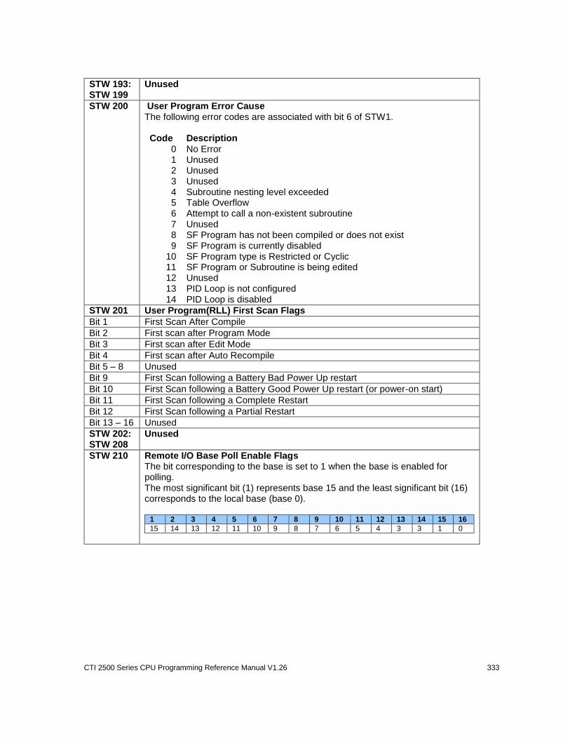
CTI 2500 Series CPU Programming Reference Manual V1.26 333
STW 193: STW 199
Unused
STW 200 User Program Error Cause The following error codes are associated with bit 6 of STW1. Code Description
0 No Error 1 Unused 2 Unused 3 Unused 4 Subroutine nesting level exceeded 5 Table Overflow 6 Attempt to call a non-existent subroutine 7 Unused 8 SF Program has not been compiled or does not exist 9 SF Program is currently disabled
10 SF Program type is Restricted or Cyclic 11 SF Program or Subroutine is being edited 12 Unused 13 PID Loop is not configured 14 PID Loop is disabled
STW 201 User Program(RLL) First Scan Flags
Bit 1 First Scan After Compile
Bit 2 First scan after Program Mode
Bit 3 First scan after Edit Mode
Bit 4 First scan after Auto Recompile
Bit 5 – 8 Unused
Bit 9 First Scan following a Battery Bad Power Up restart
Bit 10 First Scan following a Battery Good Power Up restart (or power-on start)
Bit 11 First Scan following a Complete Restart
Bit 12 First Scan following a Partial Restart
Bit 13 – 16 Unused
STW 202: STW 208
Unused
STW 210 Remote I/O Base Poll Enable Flags The bit corresponding to the base is set to 1 when the base is enabled for polling. The most significant bit (1) represents base 15 and the least significant bit (16) corresponds to the local base (base 0).
1 2 3 4 5 6 7 8 9 10 11 12 13 14 15 16
15 14 13 12 11 10 9 8 7 6 5 4 3 3 1 0
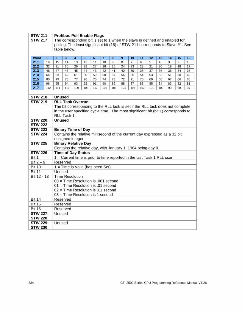
334 CTI 2500 Series CPU Programming Reference Manual V1.26
STW 211: STW 217
Profibus Poll Enable Flags The corresponding bit is set to 1 when the slave is defined and enabled for polling. The least significant bit (16) of STW 211 corresponds to Slave #1. See table below.
Word 1 2 3 4 5 6 7 8 9 10 11 12 13 14 15 16
211 16 15 14 13 12 11 10 9 8 7 6 5 4 3 2 1
212 32 31 30 29 28 27 26 25 24 23 22 21 20 19 18 17
213 48 47 46 45 44 43 42 41 40 39 38 37 36 35 34 33
214 64 63 62 61 60 59 58 57 56 55 54 53 52 51 50 49
215 80 79 78 77 76 75 74 73 72 71 70 69 68 67 66 65
216 96 95 94 93 92 91 90 89 88 87 86 85 84 83 82 81
217 112 111 110 109 108 107 106 105 104 103 102 101 100 99 98 97
STW 218 Unused
STW 219 RLL Task Overrun The bit corresponding to the RLL task is set if the RLL task does not complete in the user specified cycle time. The most significant bit (bit 1) corresponds to RLL Task 1.
STW 220: STW 222
Unused
STW 223 STW 224
Binary Time of Day Contains the relative millisecond of the current day expressed as a 32 bit unsigned integer.
STW 225 Binary Relative Day Contains the relative day, with January 1, 1984 being day 0.
STW 226 Time of Day Status
Bit 1 1 = Current time is prior to time reported in the last Task 1 RLL scan
Bit 2 – 9 Reserved
Bit 10 1 = Time is Valid (has been Set)
Bit 11 Unused
Bit 12 - 13 Time Resolution 00 = Time Resolution is .001 second 01 = Time Resolution is .01 second 02 = Time Resolution is 0.1 second 03 = Time Resolution is 1 second
Bit 14 Reserved
Bit 15 Reserved
Bit 16 Reserved
STW 227: STW 228
Unused
STW 229: STW 230
Unused
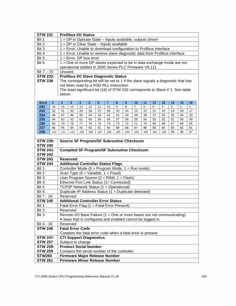
CTI 2500 Series CPU Programming Reference Manual V1.26 335
STW 231 Profibus I/O Status
Bit 1 1 = DP in Operate State – inputs available, outputs driven
Bit 2 1 = DP in Clear State – Inputs available
Bit 3 1 = Error; Unable to download configuration to Profibus interface
Bit 4 1 = Error: Unable to retrieve slave diagnostic data from Profibus interface
Bit 5 1 = Error: DP bus error
Bit 6 1 = One of more DP slaves expected to be in data exchange mode are not operational (added in 2500 Series PLC Firmware V6.11).
Bit 7 – 15 Unused.
STW 232: STW 238
Profibus I/O Slave Diagnostic Status The corresponding bit will be set to 1 if the slave signals a diagnostic that has not been read by a RSD RLL instruction. The least significant bit (16) of STW 232 corresponds to Slave #`1. See table below.
Word 1 2 3 4 5 6 7 8 9 10 11 12 13 14 15 16
232 16 15 14 13 12 11 10 9 8 7 6 5 4 3 2 1
233 32 31 30 29 28 27 26 25 24 23 22 21 20 19 18 17
234 48 47 46 45 44 43 42 41 40 39 38 37 36 35 34 33
235 64 63 62 61 60 59 58 57 56 55 54 53 52 51 50 49
236 80 79 78 77 76 75 74 73 72 71 70 69 68 67 66 65
237 96 95 94 93 92 91 90 89 88 87 86 85 84 83 82 81
238 112 111 110 109 108 107 106 105 104 103 102 101 100 99 98 97
STW 239: STW 240
Source SF Program/SF Subroutine Checksum
STW 241: STW 242
Compiled SF Program/SF Subroutine Checksum
STW 243 Reserved
STW 244 Additional Controller Status Flags
Bit 1 Controller Mode (0 = Program Mode, 1 = Run mode)
Bit 2 Scan Type (0 = Variable, 1 = Fixed)
Bit 3 User Program Source (0 = RAM, 1 = Flash)
Bit 4 Ethernet Port Link Status (1= Connected)
Bit 5 TCP/IP Network Status (1 = Operational)
Bit 6 Duplicate IP Address Status (1 = Duplicate detected)
Bit 7 - 16 Reserved
STW 245 Additional Controller Error Status
Bit 1 Fatal Error Flag (1 = Fatal Error Present).
Bit 2 Reserved
Bit 3 Remote I/O Base Failure (1 = One or more bases are not communicating) A base that is configured and enabled cannot be logged in.
Bit 4 - 16 Reserved
STW 246 Fatal Error Code Contains the fatal error code when a fatal error is present
STW 247- STW 257
CTI Support Diagnostics Subject to change
STW 259-STW 259
Product Serial Number Contains the serial number of the controller
STW260 Firmware Major Release Number
STW 261 Firmware Minor Release Number

336 CTI 2500 Series CPU Programming Reference Manual V1.26
STW 262-STW 298
CTI Support Diagnostics Subject to change
STW 299 Peak Scan Time 16 bit representation
STW 300- STW 454
CTI Support Statistics Subject to change
STW 455- STW 469
Remote Base Receive Errors Contains the number of times that the controller encountered an error reading the response message from the remote base. STW 455 corresponds to remote base 1. STW 456 – STW 469 correspond to remote bases 2 – 15.
STW 470 Unused
STW 471- STW 485
Abnormal Logoff Count – Remote Base 1 - 15 Contains the number of times that the controller stopped communicating with the remote base due to communications errors or response timeouts. STW 471 corresponds to remote base 1. STW 472 – STW 485 correspond to remote bases 2 – 15.
STW 486 Unused
STW 487- STW 501
Timeout Count – Remote Base 1 – 15 Contains the number of times that the base failed to respond to a request from the controller within the specified time. STW 487 corresponds to remote base 1. STW 488 – STW 501 correspond to remote bases 2 – 15.
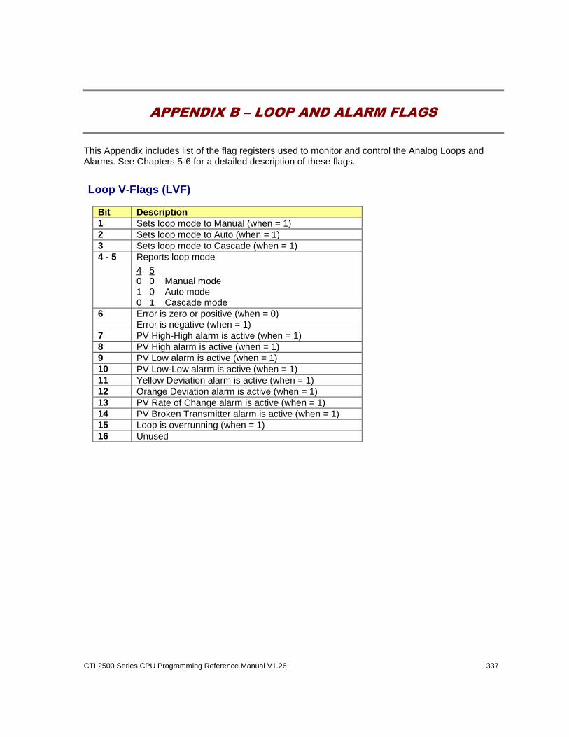
CTI 2500 Series CPU Programming Reference Manual V1.26 337
APPENDIX B – LOOP AND ALARM FLAGS
This Appendix includes list of the flag registers used to monitor and control the Analog Loops and Alarms. See Chapters 5-6 for a detailed description of these flags.
Loop V-Flags (LVF)
Bit Description
1 Sets loop mode to Manual (when = 1)
2 Sets loop mode to Auto (when = 1)
3 Sets loop mode to Cascade (when = 1)
4 - 5 Reports loop mode
4 5 0 0 Manual mode 1 0 Auto mode 0 1 Cascade mode
6 Error is zero or positive (when = 0) Error is negative (when = 1)
7 PV High-High alarm is active (when = 1)
8 PV High alarm is active (when = 1)
9 PV Low alarm is active (when = 1)
10 PV Low-Low alarm is active (when = 1)
11 Yellow Deviation alarm is active (when = 1)
12 Orange Deviation alarm is active (when = 1)
13 PV Rate of Change alarm is active (when = 1)
14 PV Broken Transmitter alarm is active (when = 1)
15 Loop is overrunning (when = 1)
16 Unused
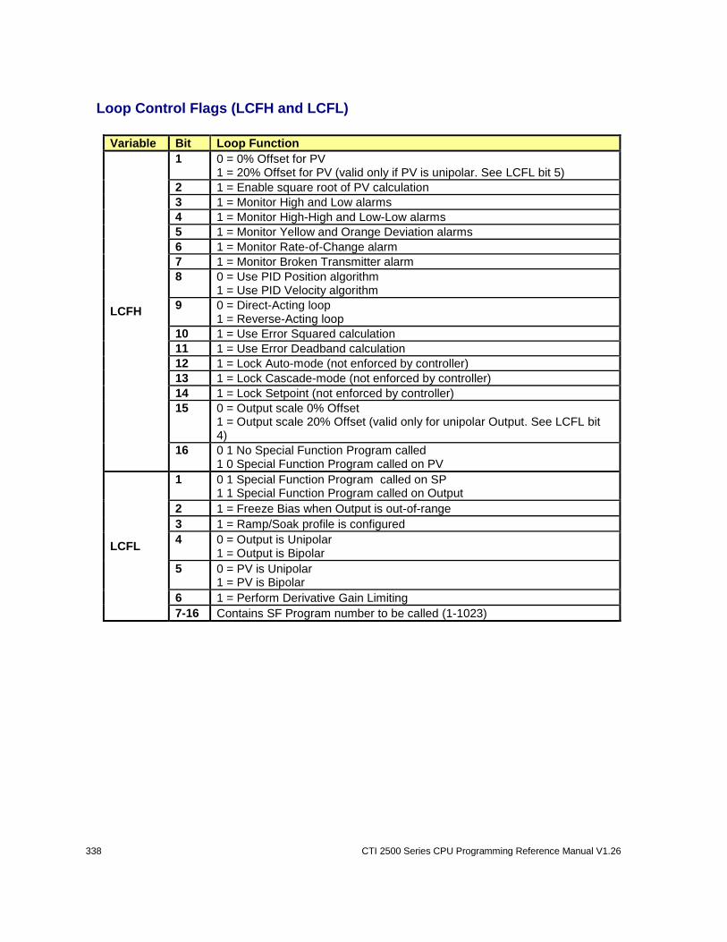
338 CTI 2500 Series CPU Programming Reference Manual V1.26
Loop Control Flags (LCFH and LCFL)
Variable Bit Loop Function
LCFH
1 0 = 0% Offset for PV 1 = 20% Offset for PV (valid only if PV is unipolar. See LCFL bit 5)
2 1 = Enable square root of PV calculation
3 1 = Monitor High and Low alarms
4 1 = Monitor High-High and Low-Low alarms
5 1 = Monitor Yellow and Orange Deviation alarms
6 1 = Monitor Rate-of-Change alarm
7 1 = Monitor Broken Transmitter alarm
8 0 = Use PID Position algorithm 1 = Use PID Velocity algorithm
9 0 = Direct-Acting loop 1 = Reverse-Acting loop
10 1 = Use Error Squared calculation
11 1 = Use Error Deadband calculation
12 1 = Lock Auto-mode (not enforced by controller)
13 1 = Lock Cascade-mode (not enforced by controller)
14 1 = Lock Setpoint (not enforced by controller)
15 0 = Output scale 0% Offset 1 = Output scale 20% Offset (valid only for unipolar Output. See LCFL bit 4)
16 0 1 No Special Function Program called 1 0 Special Function Program called on PV
LCFL
1 0 1 Special Function Program called on SP 1 1 Special Function Program called on Output
2 1 = Freeze Bias when Output is out-of-range
3 1 = Ramp/Soak profile is configured
4 0 = Output is Unipolar 1 = Output is Bipolar
5 0 = PV is Unipolar 1 = PV is Bipolar
6 1 = Perform Derivative Gain Limiting
7-16 Contains SF Program number to be called (1-1023)
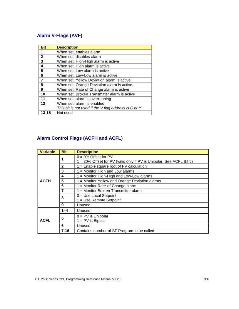
CTI 2500 Series CPU Programming Reference Manual V1.26 339
Alarm V-Flags (AVF)
Alarm Control Flags (ACFH and ACFL)
Bit Description
1 When set, enables alarm
2 When set, disables alarm
3 When set, High-High alarm is active
4 When set, High alarm is active
5 When set, Low alarm is active
6 When set, Low-Low alarm is active
7 When set, Yellow Deviation alarm is active
8 When set, Orange Deviation alarm is active
9 When set, Rate of Change alarm is active
10 When set, Broken Transmitter alarm is active
11 When set, alarm is overrunning
12 When set, alarm is enabled This bit is not used if the V flag address is C or Y.
13-16 Not used
Variable Bit Description
ACFH
1 0 = 0% Offset for PV 1 = 20% Offset for PV (valid only if PV is Unipolar. See ACFL Bit 5)
2 1 = Enable square root of PV calculation
3 1 = Monitor High and Low alarms
4 1 = Monitor High-High and Low-Low alarms
5 1 = Monitor Yellow and Orange Deviation alarms
6 1 = Monitor Rate-of-Change alarm
7 1 = Monitor Broken Transmitter alarm
8 0 = Use Local Setpoint 1 = Use Remote Setpoint
9 Unused
ACFL
1–4 Unused
5 0 = PV is Unipolar 1 = PV is Bipolar
6 Unused
7-16 Contains number of SF Program to be called
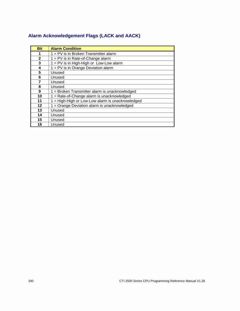
340 CTI 2500 Series CPU Programming Reference Manual V1.26
Alarm Acknowledgement Flags (LACK and AACK)
Bit Alarm Condition
1 1 = PV is in Broken Transmitter alarm
2 1 = PV is in Rate-of-Change alarm
3 1 = PV is in High-High or Low-Low alarm
4 1 = PV is in Orange Deviation alarm
5 Unused
6 Unused
7 Unused
8 Unused
9 1 = Broken Transmitter alarm is unacknowledged
10 1 = Rate-of-Change alarm is unacknowledged
11 1 = High-High or Low-Low alarm is unacknowledged
12 1 = Orange Deviation alarm is unacknowledged
13 Unused
14 Unused
15 Unused
16 Unused

CTI 2500 Series CPU Programming Reference Manual V1.26 341
LIMITED PRODUCT WARRANTY
1. Warranty. Control Technology Inc. ("CTI") warrants that this CTI Industrial Product (the "Product") shall be free from defects in material and workmanship for a period of one (1) year from the date of purchase from CTI or from an authorized CTI Industrial Distributor, as the case may be. Repaired or replacement CTI products provided under this warranty are similarly warranted for a period of 6 months from the date of shipment to the customer or the remainder of the original warranty term, whichever is longer. This Product and any repaired or replacement products will be manufactured from new and/or serviceable used parts which are equal to new in the Product. This warranty is limited to the initial purchaser of the Product from CTI or from an authorized CTI Industrial Distributor and may not be transferred or assigned.
2. Remedies. Remedies under this warranty shall be limited, at CTI's option, to the replacement or repair of this Product, or the parts thereof, only after shipment by the customer at the customer's expense to a designated CTI service location along with proof of purchase date and an associated serial number. Repair parts and replacement products furnished under this warranty will be on an exchange basis and all exchanged parts or products become the property of CTI. Should any product or part returned to CTI hereunder be found by CTI to be without defect, CTI will return such product or part to the customer. The foregoing will be the exclusive remedies for any breach of warranty or breach of contract arising therefrom.
3. General. This warranty is only available if (a) the customer provides CTI with written notice of a warranty claim within the warranty period set forth above in Section 1 and (b) CTI's examination of the Product or the parts thereof discloses that any alleged defect has not been caused by a failure to provide a suitable environment as specified in the CTI Standard Environmental Specification and applicable Product specifications, or damage caused by accident, disaster, acts of God, neglect, abuse, misuse, transportation, alterations, attachments, accessories, supplies, non-CTI parts, non-CTI repairs or activities, or to any damage whose proximate cause was utilities or utility-like services, or faulty installation or maintenance done by someone other than CTI.
4. Product Improvement. CTI reserves the right to make changes to the Product in order to improve reliability, function or design in the pursuit of providing the best possible products.
5. Exclusive Warranty. THE WARRANTIES SET FORTH HEREIN ARE CUSTOMER'S EXCLUSIVE WARRANTIES. CTI HEREBY DISCLAIMS ALL OTHER WARRANTIES, EXPRESS OR IMPLIED. WITHOUT LIMITING THE FOREGOING, CTI SPECIFICALLY DISCLAIMS THE IMPLIED WARRANTIES OF MERCHANTABILITY, FITNESS FOR A PARTICULAR PURPOSE, NON-INFRINGEMENT, COURSE OF DEALING AND USAGE OF TRADE.
6. Disclaimer and Limitation of Liability. TO THE FULLEST EXTENT PERMITTED BY APPLICABLE LAW, CTI WILL NOT BE LIABLE FOR ANY BUSINESS INTERRUPTION OR LOSS OF PROFIT, REVENUE, MATERIALS, ANTICIPATED SAVINGS, DATA, CONTRACT, GOODWILL OR THE LIKE (WHETHER DIRECT OR INDIRECT IN NATURE) OR FOR ANY OTHER FORM OF INCIDENTAL, INDIRECT OR CONSEQUENTIAL DAMAGES OF ANY KIND. CTI'S MAXIMUM CUMULATIVE LIABILITY RELATIVE TO ALL OTHER CLAIMS AND LIABILITIES, INCLUDING OBLIGATIONS UNDER ANY INDEMNITY, WHETHER OR NOT INSURED, WILL NOT EXCEED THE COST OF THE PRODUCT(S) GIVING RISE TO THE CLAIM OR LIABILITY. CTI DISCLAIMS ALL LIABILITY RELATIVE TO GRATUITOUS INFORMATION OR ASSISTANCE PROVIDED BY, BUT NOT REQUIRED OF CTI HEREUNDER. ANY ACTION AGAINST CTI MUST BE BROUGHT WITHIN
342 CTI 2500 Series CPU Programming Reference Manual V1.26
EIGHTEEN (18) MONTHS AFTER THE CAUSE OF ACTION ACCRUES. THESE DISCLAIMERS AND LIMITATIONS OF LIABILITY WILL APPLY REGARDLESS OF ANY OTHER CONTRARY PROVISION HEREOF AND REGARDLESS OF THE FORM OF ACTION, WHETHER IN CONTRACT, TORT (INCLUDING NEGLIGENCE AND STRICT LIABILITY) OR OTHERWISE, AND FURTHER WILL EXTEND TO THE BENEFIT OF CTI'S VENDORS, APPOINTED DISTRIBUTORS AND OTHER AUTHORIZED RESELLERS AS THIRD-PARTY BENEFICIARIES. EACH PROVISION HEREOF WHICH PROVIDES FOR A LIMITATION OF LIABILITY, DISCLAIMER OF WARRANTY OR CONDITION OR EXCLUSION OF DAMAGES IS SEVERABLE AND INDEPENDENT OF ANY OTHER PROVISION AND IS TO BE ENFORCED AS SUCH.
7. Adequate Remedy. The customer is limited to the remedies specified herein and shall have no others for a nonconformity in the Product. The customer agrees that these remedies provide the customer with a minimum adequate remedy and are its exclusive remedies, whether based on contract, warranty, tort (including negligence), strict liability, indemnity, or any other legal theory, and whether arising out of warranties, representations, instructions, installations, or non-conformities from any cause. The customer further acknowledges that the purchase price of the Product reflects these warranty terms and remedies.
8. Force Majeure. CTI will not be liable for any loss, damage or delay arising out of its failure (or that of its subcontractors) to perform hereunder due to causes beyond its reasonable control, including without limitation, acts of God, acts or omissions of the customer, acts of civil or military authority, fires, strikes, floods, epidemics, quarantine restrictions, war, riots, acts of terrorism, delays in transportation, or transportation embargoes. In the event of such delay, CTI's performance date(s) will be extended for such length of time as may be reasonably necessary to compensate for the delay.
9. Governing Law. The laws of the State of Tennessee shall govern the validity, interpretation and enforcement of this warranty, without regard to its conflicts of law principles. The application of the United Nations Convention on Contracts for the International Sale of Goods shall be excluded.
CTI 2500 Series CPU Programming Reference Manual V1.26 343
REPAIR POLICY
In the event that the Product should fail during or after the warranty period, a Return Material Authorization (RMA) number can be requested orally or in writing from CTI main offices. Whether or not this equipment is in warranty, providing a Purchase Order number to CTI when requesting the RMA number will aid in expediting the repair process. The RMA number that is issued and your Purchase Order number should be referenced on the returning equipment's shipping documentation. Additionally, if the product is under warranty, proof of purchase date and serial number must accompany the returned equipment. The current repair and/or exchange rates can be obtained by contacting CTI's main office at 1-800-537-8398. When returning any module to CTI, follow proper static control precautions. Keep the module away from polyethylene products, polystyrene products and all other static producing materials. Packing the module in its original conductive bag is the preferred way to control static problems during shipment. Failure to observe static control precautions may void the warranty. For additional information on static control precautions, contact CTI at 1-800-537-8398.