Embed Size (px)
Citation preview

1
Curriculum Vitae ofDr. G. N. Dash, Sambalpur University
1. Name: GANA NATH DASH
2. Date of birth: 04.11.1955
3. Address (office): P.G. Department of Physics,Sambalpur University, Jyoti Vihar,Sambalpur-768019 (ORISSA)Tel No: (663) 2431719E-mail: [email protected]
(Res.): EC 3/28, Executive Colony, Budharaja,Sambalpur-768004 (ORISSA)Tel. No: (663) 2541223Mobile: 9437104537
4. Educational Qualifications: M.Sc., M.Phil., Ph.D. (Details below)
Examination Board/University Year ofPassing Class/Division Percentage of
Marks
H.S.C.E.
P.U. Sc.
I Degree B.Sc.
B.Sc. (Hons)
M.Sc.
M.Phil.
Ph.D.
B.S.E., Orissa
Sambalpur University
-do-
-do-
-do-
-do-
-do-
1971
1972
1973
1975
1977
1983
1992
I Div.
I Div.
I Div.
I Class Hons withDistinction
I Class
Grade ‘A’
Awarded
72%
62%*
76%*
72% (Hons)**
73.5% (Total)
72.9%
Grade Point 4.5out of 5
Awarded
*Position among the best Ten, **First Position in order of Merit

2
5. Teaching experience: Post-graduate – 34 years (Details below)
Present Position – Professor of Physics, Sambalpur University
Institution From To Position Held UG/PG
G.M. College,Sambalpur 1.09.1978 29.11.1983 Lecture in Physics UG & PG
Rajendra College,Bolangir 30.11.1983 11.12. 1984 Lecture in Physics UG
SambalpurUniversity 12.12.1984 22.06.1993 Lecture in Physics PG
SambalpurUniversity 22.06.1993 22.06.2001 Reader in Physics PG
SambalpurUniversity 23.06.2001 Continuing Professor of
Physics PG
6. Research publications:
So far 160 papers/articles have been published (For details please see the list ofpublications below)
7. School/Conference/Seminar/Symposium etc. attended:
(i) SSP Symposium, BARC, Bombay (1987)
(ii) SERC School in Physics of Semiconductors at IIT Kharagpur (1988)
(iii) International Workshop on Physics of Semiconductor Devices (IWPSD-95) atNational Physical Laboratory, New Delhi ( Dec. 1995)
(iv) XVI Annual Convention of Orissa Physical Society and National Seminar onRecent Advances in Physics, Berhampur University, April 4-5, 1998
(v) XVIII Annual Convention of Orissa Physical Society And National Seminaron Recent Advances in Material Science and their Application with SpecialReference to Industries, REC, Rourkela, Feb. 19-20, 2000
(vi) Condensed Matter Days (CMDAYS) – 2K, G.G. University, Bilaspur (Aug,29-31, 2K)
(vii) XIX Annual Convention of Orissa Physical Society and UGC NationalSeminar on “Physics in the Millenium”, R.D. Women’s College,Bhubaneswar, Feb. 10-11, 2001
(viii) National Conference – Condensed Matter Days – 2001, Sambalpur University,Sambalpur (29-31 August, 2001)
(ix) International Workshop on Physics of Semiconductor Devices (IWPSD-2001), I.I.T., Delhi (Dec. 11-15, 2001)
(x) National Conference – Condensed Matter Days – 2003, Jadavpur University,Aug. 27-29, 2003

3
(xi) Dr. A.K.Pujari Symposium on IT and Education, Bhubaneswar, Dec 21, 2003
(xii) Sixth International Conference on IT (CIT03), Bhubaneswar, Dec 22-24,2003.
(xiii) Workshop on Parallel Computing and Bioinformatics, G.M. College(Autonomous), Sambalpur, March 22-23, 2004
(xiv) Dirac Centenary Seminar on Contemporary Trends in Physics, SambalpurUniversity, Sambalpur, Mar. 26-27, 2004.
(xv) A mini symposium in Condensed Matter Physics, IOP, Bhubaneswar, Apr. 27,2004.
(xvi) National Conference on Physics of Electronic Materials and Devices, Dept ofPhysics, Sambalpur University, Feb. 10-12, 2005.
(xvii) National Conference – Condensed Matter Days – 2005, Deptt of Physics,Berhampur University, Aug. 29-31, 2005
(xviii) International Workshop on Physics of Semiconductor Devices – (XIII IWPSD– 2005), National Physical Laboratory, New Delhi, Dec 13-17, 2005
(xix) National Seminar on Recent Advances in Physics, held at Department ofPhysics, Dalmia College, Rajgangpur, Orissa during Feb. 8-10, 2006
(xx) National Round Table Conference on e-Governance, organized by theDepartment of Computer Science and Application, Sambalpur University,March 26, 2006
(xxi) XXIV Convention of the Orissa Physical Society and National Seminar onPhysics Education and Research – Challenges Ahead, Ispat College, Rourkela,Feb. 10-11, 2007
(xxii) National Conference - Condensed Matter Days – 2007, N.I.T. Rourkela, Aug.29-31, 2007
(xxiii) Silver Jubilee convention of the Orissa Physical Society and NationalConference on Recent Developments and Prospects of Physics, StewartScience College, Cuttack, Feb 2-3, 2008
(xxiv) International Conference on Recent Advances in Microwave Theory andApplication – ‘Microwave-08’, University of Rajasthan, Jaipur, Nov 21-24,2008 (Chaired a Session)
(xxv) XXVI convention of Orissa Physical Society and National Seminar on Roleand Relevance of Physics in Engineering Education, NIST, Berhampur, Feb14 – 15, 2009
(xxvi) National Workshop on Microwave Communication Systems, PurushottamInstitute of Technology, Rourkela, March 7 – 8, 2009 (Delivered an InvitedTalk)
(xxvii) XXVII convention of Orissa Physical Society and National Seminar onGlobal Warming and Clean Energy, North Orissa University, Baripada Feb 13-14, 2010 (Delivered an Invited Talk – titled “The mystery of Memristor”)
(xxviii) National Seminar on Physics and Technology of Novel Materials – 2010Sambalpur University, Feb 25 -27, 2010, Organised as Director of the

4
Seminar and presented a paper titled “Physics and Technology of Memristicmaterials”
(xxix) National Conference on Recent trends in Communication TechnologyRTCT – 2011 KIST, Bhubaneswar, Date: Jan 22 – 23, 2011, InvitedSpeaker, Presented a Talk on Microwave Semiconductor Devices
(xxx) National Seminar on Non Conventional Energy NASENCE – 2011 andXXVIII convention of Orissa Physical Society, Sambalpur UniversityFeb 12 -13, 2011, Organised as Director of NASENCE – 2011
(xxxi) Workshop on Awareness Programme: Medical and Societal Applicationof Nuclear Physics, Sambalpur University, March 26, 2011, Took partin organization as HOD and member of Local Organizing Committee
(xxxii) National Seminar on Physics and Technology of Novel Materials – II(PTNM – II), Sambalpur University, March 2012
(xxxiii) Mini Colloquium of EDS chapter, April 2012, National Institute of Scienceand Technology, Brahmapur (Invited Speaker)
8. Research Projects:
3 Major Research Projects Investigated (Details below)
Funding Agency Title of theproject Duration Amount Capacity
DST, Govt. of India(New Delhi)
Noise and mm-wave propertiesof……superlatticeIMPATTs.
3 years
2000-2003Rs 6.2 lakhs
Project Director& PrincipalInvestigator
U.G.C.Computer aidedstudies on ………IMPATT devices.
3 years
1992-1995Rs 3.5 lakhs Principal
Co-Investigator
D.S.T. Govt. ofORISSA
Studies on………IMPATT andMITTAT devices.
2 years
1998-2000Rs 90, 000 /- Principal
Co-Investigator
9. Research Guidance:
M.Phil:
Guided 33 M.Phil level students for their dissertations.
Ph.D.:

5
Guided Seven Scholars for the award of Ph.D. Degree, Six are working, Pleasesee List below.
(A) Details of Ph. D Guidance.
Ph.D. Awarded
#Jointly with Dr. A. K. Panda , *Jointly with Prof. P.K. Meher
Ph.D. Ongoing
Sl.No. Title of Thesis Name of the Scholar Status of
Work
1
Studies on the effect of increase inBand gap of base semiconductor on theMillimeter wave properties ofAvalanche Transit Time Diodes
Sri Janmajay Pradhan Registered
2 Mixed mode analysis of AvalancheTransit Time Diodes Mrs. Pranati Panda Registered
Sl.No. Title of Thesis Name of the Awardees Year of
Award
1
Computer aided studies on someproperties of Mixed TunnelingAvalanche Transit Time (MITTAT)devices.
Dr. Jiten Kumar Mishra 1998
2 Computer Study of Double AvalancheRegion IMPATT Diodes Dr. Ishwar Prasad Mishra 2004
3
Computer simulation studies on the highfrequency properties of someheterojunction and superlatticeIMPATTs.
Dr. Satya Ranjan Pattanaik 2010
4 Some studies on the high frequencyproperties of IMPATT and Gun Diodes
Dr. Naresh ChandraAgrawala
2011#
5
Studies on Emerging Trends inMicrowave Semiconductor Devicesmarked by Avalanche Transit Timeeffect and Transfer electron effect
Dr. Rajanaikanta Parida 2012#
6 Development of a Digital SignalProcessing System for Bioinformatics Dr. Jayakishan Meher 2012*
7
Studies on characteristics of III-Vcompound Semiconductor basedHEMT/MODFET to use in analogVLSI circuits
Dr. Trupti Ranjan Lenka 2012#

6
3
Design and analysis of DARIMPATT diode with specialreference to mm-wave and Tera-hertz communication
Mr. Satyanarayan PadhiRegistered
4
Some studies on the digitalmodeling of the “Turi: a woodwindmusical instrument of Orissa”
Mr Krishna ChandraMohapatra
(Jointlywith ProfR. K.Mishra)
5
Wide Bandgap Semiconductor BasedIMPATT Diode for TerahertzApplications Santosh Kumar Swain
Jointly withDr. S.R.Pattanaik
6
Studies on some couplers betweenMetal-Dielectric-Metal Plasmonicwaveguides and Photonic Crystalwaveguides
Anjali DashJointly withProf. S.K.Tripathy
(B) Details of M. Phil. Students Guided.
1 Effect of heavy doping on the theory ofp-n junction Miss Puspalata Rath 1989
2 Quantum Well Heterostructure Lasers. Sri Ashok Kumar Mohanty 1991
3 Tunneling in MIS(Metal-Insulator-Semiconductor) Diode Miss Sunita Dash 1992
4 Current status of Photodiodes for Opticalfibre communication systems Sri Subrat Kumar Jena 1993
5Analytical Modeling for Noise andMicrowave Properties of READ typeMITTAT Diodes.
Sri Sarthak Kumar Nayak 1995
6 Novel Properties of compositionalsuperlattice structures. Sri Barun Kumar Parmanik 1995
7 A review of some interesting propertiesassociated with doping superlattices Miss Rashmi Mohanty 1995
8Harmonic extraction using artificialNeural Network Sri Asis Barik 1997
9 Adaptive Channel Equilisation usingFuzzy Logic. Miss Reeti Das 2000
10
Effect of Impurity Charge Bump on theNoise Characteristics of GaAs MixedTunneling Avalanche Transit TimeDiodes.
Sri S.C. Hatee 2000
11A comparative study of n- and p-typeSi/SiGe Heterojunction SDR IMPATTdiodes.
Sri Sanjeeb Kumar Hota 2001
12 Potentials of AlGaAs- GaAs Hetero-junction Impatt diode Sri Dillip Kumar Rath 2002

7
13Effect of GaInP hetero-layer on themicrowave and mm-wave behaviour ofGaAs IMPATT Diode
Sri Nilakanta Behera 2003
14Photon Assisted control of noise and mm-wave properties of GaInAsP Readavalanche Diode
Sri Santosh Kumar Swain 2004
15 Studies on Microwave Oscillation fromGaP Avalanche Diode Sri Manoj Kumar Jaiswal 2004
16 Effect of Biasing Current Density on theperformance of GaAs IMPATT Diodes
Sri Netaji Sangram KeshariSahoo
2004
17 Studies on carrier ionization rates inGaAs with reference to IMPATT diodes Sri Janmejaya Pradhan 2005
18 A brief Review on QuantumSemiconductor Structures Miss Suprava Mohanty 2006
19 Photonic Crystals: A Review on itsResearch and Development Sri Pravanjan Mishra 2006
20 Solid-State Microwave Sources: AReview Sri Antaryami Tandi 2006
21 Some studies on Mixed TunnelingAvalanche Transit Time Diodes Sri Naba Kumar Mishra 2007
22 Application of Carbon Nano-tubes in thefield of electronics Miss Padmaja Mishra 2007
23 Some studies on Quantum Computers Miss Gurpreet Kaur 2007
24 Single Electron Transistors Sri Ashish Pradhan 2007
25 Some studies on Fast Adders Miss Shradhanjali Sahoo 2007
26 Simulation study of MOSFET Miss Pushpanjali Tandi 2008
27 Synthesis and structural Investigation ofBaTiO3 nanoparticles Sri Manoranjan Sahoo 2008
28 Simulation study of Gunn diode Sri Sunil Kumar Jena 2008
29 Satellite Communication Mrs Sagarika Nath 200930 Review on Super insulator Miss Mukta behera 201031 Review on Memristor Miss Utkaika Naik 201032 Review on Graphene Miss Purnima Mishra 201133 Studies on MITATT Sri Deepak kumar Karan 2011
10. Collaborative Research:
(i) Centre for Advance Study in Radiophysics and Electronics, University ofCalcutta (Past)
(ii) Department of Electronics Sci., University of Calcutta (Past)
(iii) NIST, Berhampur

8
11. Major Area of Research:
(i) Semiconductor Physics,
(ii) Solid State Devices,
(iii) Semiconductor Materials,
(iv) Noise in Microwave Solid State Devices.
(v) Application of ANN and Fuzzy logic
(vi) IT in Education
12. Referee of Journal:
(i) IEEE Transaction on Electron Devices (USA)
(ii) International Journal of Electronics (U.K.)
(iii) Circuits, Systems and Signal Processing (Springer Journal)
(iv) Indian Journal of Physics
(v) Edited a Volume of IJP, Vol. 77A, No. 2, March 2003 as Guest Editor
(vi) Edited International Journal of Material Science (ISSN 0973-4589), Volume 5,Number 5, 2010 as Guest Editor
13. Special Contributions: (for different programmes of SambalpurUniversity)
(i) Programme Coordinator M.Sc. Electronics (1999-2001)
(ii) H.O.D., Physics (2000-2002)
(iii) Took steps for the University to enter in to MOU with IOP, Bhubaneswar
(iv) Member, Board of Studies and Board of Conducting Examiners in Physics,Electronics and Computer Science.
(v) Organized National Level Seminar, CMDAYS-2001 in the Department duringAug. 29-31, 2001 as Head of the Department and Convener.
(vi) Contributed significantly for introducing M.Sc. Electronics Programme inSambalpur University. (From 1995 to 2001)
(vii) Coordinator of P.G.D.C.A. (From Dec 2001 to Dec 2003)
(viii) Coordinator of M.Sc. Comp. Science (From Feb 2002 to Dec 2003)
(ix) Founder Coordinator of M.C.A. (From June 2002 to Dec 2003)
(x) Involved in opening of M.Sc. Computer Science in Sambalpur University. (2000– 2001)
(xi) Major contribution to prepare draft regulation and syllabus for M.Sc.Electronics.(1996-1997)

9
(xii) Mainly responsible for setting up of 8 Labs for M.Sc. ElectronicsProgramme.(1996 – 1998)
(xiii) Worked as member and Convener (Sub-group-II) of the Disaster ManagementPlan Group set up by the District Magistrate and Collector, Sambalpur.(2000-2002)
(xiv) Chairman, BOS of Computer Science, Electronics and BOS (SF Comp. Sc.)(2002 – 2003)
(xv) Member of Technical Expert Committee (X-plan period)
(xvi) Member of E-Governance Technical Committee (Continuing)
(xvii) Attended the meeting of the “Committee of Vice chancellors – under theChairmanship of Prof P.C. Tripathy, Vice chancellor, Sambalpur University”on 02-03-2007 at O.U.A.T., Bhubaneswar as member secretary to assist theChairman in the conduct of the meeting (Office Order Memo No.33/R Dated27.02.2007).
(xviii) Attended the Review Committee meeting convened by the Chief-Secretary,Government of Orissa in his Conference Hall in the Orissa Secretariat,Bhubaneswar on 05-04-2007 to assist the Vice chancellor for presentation ofvacancy position (teaching) in Sambalpur University (Office Order MemoNo.58/R Dated 03.04.2007).
(xix) Coordinator of the Department of Physics (2007-08)
(xx) Director, Nodal Center (E-Governence)
(xxi) Attended the Review meeting convened by the Chief-Secretary, Governmentof Orissa in his Conference Hall in the Orissa Secretariat, Bhubaneswar on24th June 2008 along with the Vice chancellor and Registrar for discussion ofnon-teaching vacancy position in Sambalpur University.
(xxii) Attended (as delegated nominee of the Vice chancellor) the Vice chancellors’meeting on e-connectivity convened by Vice chancellor, BPUT at OUAT,Bhubaneswar on 29th June 2008.
14. Awards and Recognition:
(i) FIET – Fellow IET (Institution of Engineering and Technology – UK)
(ii) SMIEEE - Senior Member IEEE (Institution of Electrical and ElectronicsEngineers - USA)
(iii) F.I.E.T.E. - Fellow (and Life Member) I.E.T.E. (Institution of Electronics andTelecommunication Engineers - New Delhi))
(iv) Life member of Orissa Information Technology Society
(v) Life member of Orissa Physical Society
(vi) Member IEEE Electron Devices (ED) Society (USA)
(vii) Member IEEE Communication Society (USA-2007)
(viii) Member IEEE Laser and Electro-optics Society (USA-2007 and 2008)

10
(ix) Member IEEE MTT society USA
(x) Bharat Jyoti Award - awarded by India International Friendship Society, NewDelhi
15. List of some important invited Technical Talks delivered:
Sl No Title of Talk Occasion and date Place No ofattendees(approx.)
1 Graphene, thewonder material
Mini Colloquium ofEDS chapter, April2012
National Institute ofScience andtechnology,Brahmapur
250
2 MicrowaveSemiconductorActive Devices
National Conferenceon recent Trends inCommunicationTechnology, Jan2011
Konark Institute ofScience andTechnology,Bhubaneswar
110
3 The 2D perfectlattice - graphene
Nobel Prize - 2010seminar,May 2011
SambalpurUniversity, JyotiVihar
120
4 The mystery ofMemristor
XXVII convention ofthe Orissa PhysicalSociety – March2010
North OrissaUniversity, Baripada 140
5 Gunn diodemicrowave oscillator
National Workshopon microwavecommunicationsystem – March 2009
Purusottam Instituteof Technology,Rourkela 90
6 GiantMagnetoresistanceand the Hard Disk
Nobel Prize – 2007Seminar, May 2008
SambalpurUniversity, JyotiVihar
120
7 Diamond, thewonder material forfuture devices
National Seminar onRecent Advances inPhysics – Feb. 2006
Dalmia College,Rajgangpur 90
8 Frequency CombTechnique withexceptionalaccuracy
Nobel Prize – 2005Seminar, April 2006
SambalpurUniversity, JyotiVihar 120
9 Effect of tunnellingcurrent on noise inIMPATT diode
Mini symposium onCondense MatterPhysics - 2004
Institute of Physics,Bhubaneswar 30
10 Trapping of atoms –the Laser coolingtechnique
Nobel Prize – 1997Seminar
SambalpurUniversity, JyotiVihar
120

11
LIST OF PUBLICATIONS OF DR. G.N. DASHDEPARTMENT OF PHYSICS, SAMBALPUR UNIVERSITY
IN JOURNALS OF INTERNATIONAL REPUTE
A1. Small signal computer simulation of IMPATT diodes including carrier diffusion,Semiconductor Sci. and Technol., (IOP Journal, UK), Vol.6, No.5, pp.348-355,May 1991 (G.N.Dash and S.P.Pati).
A2. Computer analysis of negative resistance profiles in silicon double drift diodesincluding the carrier diffusion effect, Physica Status Solidi (a), (Germany),Vol.127, No.2., pp.577-590, Oct.1991 (G.N.Dash and S.P.Pati).
A3. A generalized simulation method for MITATT mode operation and studies on theinfluence of tunnel current on IMPATT properties, Semicond. Sci. and Technol.,(IOP Journal, UK), Vol-7, No-2, pp 222-230, Feb.1992 (G.N.Dash and S.P.Pati).
A4. Calculation of phase distortion due to tunnel injection in heterojunctionIMPATT, Electronics Letters, (IEE Journal, UK), Vol-28, No-3, pp 241-243,Jan.1992 (G.N.Dash and S.P.Pati).
A5. Phase distortion assisted MITATT design for compensation of performancedeterioration due to tunnel current, Special issue of JIETE, Vol 39, No 6, pp. 375-377, 1993 (G.N.Dash, A.K. Panda, J.K.Mishra and S.P.Pati).
A6. Studies on the prospects of GaInAs and GaInAsP for double drift regionheterostructure IMPATTs, Applied Physics-A (Germany), Vol.58, No.2, pp.211-217, 1994 (G.N.Dash and S.P.Pati).
A7. Effect of diffusion impurity profile on microwave properties of Silicon p+nn+Impatt diodes - Semicond. Sci. and Technol., (IOP Journal, UK), 9, 241-248,1994 (A.K.Panda, G.N.Dash and S.P.Pati).
A8. Computer aided studies on the microwave characteristics of InP/GaInAs andGaAs/GaInAs heterostructure SDR IMPATTs, Journal of Physics D, (IOPJournal, UK), 27, 1719-26, 1994 (G.N.Dash and S.P.Pati).

12
A9. Computer-aided studies on the wide-Band Microwave Characteristics of SiliconDouble Avalanche Region (DAR) diode - Semicond. Sci. and Technol., (IOPJournal, UK), 10, 854-64, 1995 (A.K. Panda, G.N.Dash and S.P.Pati).
A10. A New Design Approach for MITATT and TUNNETT mode devices - Solid StateElectronics, (Elsevier Limited, UK), 38, 1381-85, 1995 (G.N.Dash).
A11. Influence of ionisation rates in a semiconductor on avalanche build-up time in p-njunctions-Indian Journal of Physics, 69A, 183-89, 1995 (S.P.Pati, S.Satpathy,A.K.Panda and G.N.Dash).
A12. Computer Aided optimization of Ion implantation impurity profiles for n+npp+DDR with three moment approach- Solid State Electronics, (Elsevier Limited,UK), 39, 759-762, 1996 (A.K. Panda, G.N.Dash and S.P.Pati).
A13. Computer aided realization of diffusion based Si n+npp+ double drift dopingprofiles and studies on their microwave properties- Physica Status Solidi (a),(Germany), 154, 657-667, 1996 (A.K.Panda, G.N.Dash and S.P.Pati),
A14. Noise in Mixed Tunneling Avalanche Transit Time (MITATT) Diodes- Solid-StateElectronics, (Elsevier Limited, UK), 39, 1473-1479, 1996 (G.N.Dash, J.K.Mishraand A.K.Panda).
A15. High power design consideration of mm-wave double Read IMPATT diodes- J. ofSemicond. Material and devices, 1, 97-102, 1989 (J. P. Banerjee, S. K. Roy, G. N.Dash and S. P. Pati).
A16. MM-wave characteristics of GaAs/GaInAs heterojunction in MITATT modeconsidering photon injection- SPIE, (U.S.A.), Vol 2401, pp 33-43, 1995 (S.P.Pati,S.Satpathy, A.K.Panda and G.N.Dash)
A17. Optical control of mm-wave performance of photo sensitive heterojunction DDRsin MITATT mode - SPIE, (U.S.A.), Vol 2997, pp 35-45, 1997 (S. P. Pati, S.Satapathy, G. N. Dash and A.K. Panda).
A18. An extremely low-noise heterojunction IMPATT - IEEE Trans on ElectronDevices, (U.S.A.), Vol. ED-44, No. 12, pp. 2143-2148, Dec. 1997 (J. K. Mishra,A. K. Panda and G. N. Dash).
A19. Effect of diffusion impurity profiles on the performance of Silicon SDRs - AsianJournal of Physics, Vol. 6, No. 3, pp. 439-446, 1997 (A. K. Panda, S. Satapathy,G.N.Dash and S.P.Pati).
A20. Studies on the microwave properties of limited source diffusion based siliconSDRs- Indian J. of Pure and Applied Physics, Vol. 35, No. 12, pp. 749-755, Dec.1997, (A. K. Panda, S. Satapathy, G. N. Dash and S. P. Pati).
13
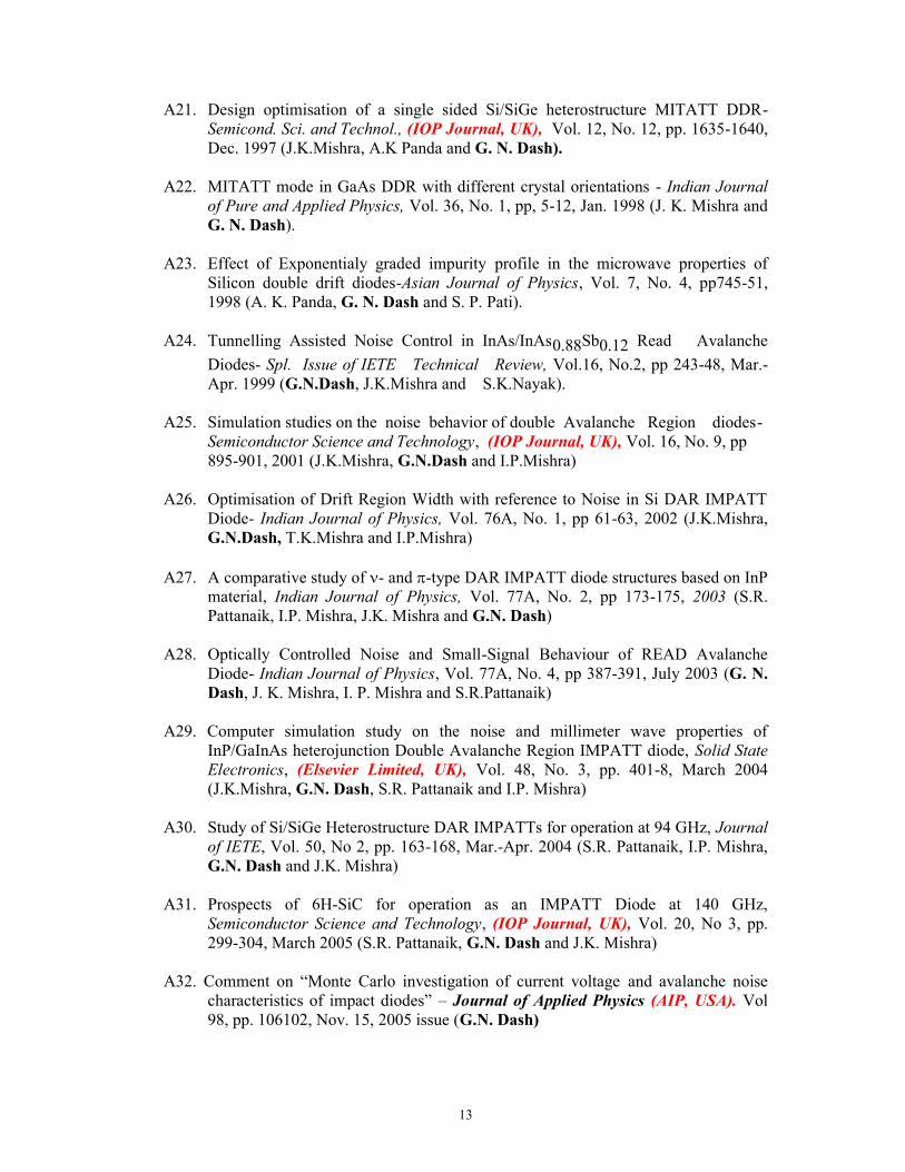
A21. Design optimisation of a single sided Si/SiGe heterostructure MITATT DDR-Semicond. Sci. and Technol., (IOP Journal, UK), Vol. 12, No. 12, pp. 1635-1640,Dec. 1997 (J.K.Mishra, A.K Panda and G. N. Dash).
A22. MITATT mode in GaAs DDR with different crystal orientations - Indian Journalof Pure and Applied Physics, Vol. 36, No. 1, pp, 5-12, Jan. 1998 (J. K. Mishra andG. N. Dash).
A23. Effect of Exponentialy graded impurity profile in the microwave properties ofSilicon double drift diodes-Asian Journal of Physics, Vol. 7, No. 4, pp745-51,1998 (A. K. Panda, G. N. Dash and S. P. Pati).
A24. Tunnelling Assisted Noise Control in InAs/InAs0.88Sb0.12 Read AvalancheDiodes- Spl. Issue of IETE Technical Review, Vol.16, No.2, pp 243-48, Mar.-Apr. 1999 (G.N.Dash, J.K.Mishra and S.K.Nayak).
A25. Simulation studies on the noise behavior of double Avalanche Region diodes-Semiconductor Science and Technology, (IOP Journal, UK), Vol. 16, No. 9, pp895-901, 2001 (J.K.Mishra, G.N.Dash and I.P.Mishra)
A26. Optimisation of Drift Region Width with reference to Noise in Si DAR IMPATTDiode- Indian Journal of Physics, Vol. 76A, No. 1, pp 61-63, 2002 (J.K.Mishra,G.N.Dash, T.K.Mishra and I.P.Mishra)
A27. A comparative study of - and -type DAR IMPATT diode structures based on InPmaterial, Indian Journal of Physics, Vol. 77A, No. 2, pp 173-175, 2003 (S.R.Pattanaik, I.P. Mishra, J.K. Mishra and G.N. Dash)
A28. Optically Controlled Noise and Small-Signal Behaviour of READ AvalancheDiode- Indian Journal of Physics, Vol. 77A, No. 4, pp 387-391, July 2003 (G. N.Dash, J. K. Mishra, I. P. Mishra and S.R.Pattanaik)
A29. Computer simulation study on the noise and millimeter wave properties ofInP/GaInAs heterojunction Double Avalanche Region IMPATT diode, Solid StateElectronics, (Elsevier Limited, UK), Vol. 48, No. 3, pp. 401-8, March 2004(J.K.Mishra, G.N. Dash, S.R. Pattanaik and I.P. Mishra)
A30. Study of Si/SiGe Heterostructure DAR IMPATTs for operation at 94 GHz, Journalof IETE, Vol. 50, No 2, pp. 163-168, Mar.-Apr. 2004 (S.R. Pattanaik, I.P. Mishra,G.N. Dash and J.K. Mishra)
A31. Prospects of 6H-SiC for operation as an IMPATT Diode at 140 GHz,Semiconductor Science and Technology, (IOP Journal, UK), Vol. 20, No 3, pp.299-304, March 2005 (S.R. Pattanaik, G.N. Dash and J.K. Mishra)
A32. Comment on “Monte Carlo investigation of current voltage and avalanche noisecharacteristics of impact diodes” – Journal of Applied Physics (AIP, USA). Vol98, pp. 106102, Nov. 15, 2005 issue (G.N. Dash)

14
A33. Optimised Ion-implantation profiles for the p-n junction using fourth momentapproach for application in high frequency VLSI circuits, ECTI Transaction onElectrical Engineering, Electronics and Communication, (ECTI Journal,Bangkok) Vol. 6, No. 2, pp. 44 - 49, August 2008 (N.C. Agrawalla, R.K. Parida,G.N. Dash and A.K. Panda)
A.34. A comparative study on the high band gap material (GaN and SiC)- basedIMPATTs –IET Microwave, Antenna and Propagation, Vol 2, No. 8, pp. 789 –793, 2008 (IET Journal, UK) (A K Panda, R K Parida, N C Agrawala and G NDash)
A35. Performance of 4H-SiC/6H-SiC Heterojunction IMPATT Diode at 94 GHzInternational Journal of Material Science (ISSN 0973-4589), Volume 5, Number 5,pp. 769—775, 2010 (S.R. Pattanaik, J.K. Mishra and G.N. Dash)
A36. The mystery of Memristor, Orissa Journal of Physics (ISSN 0974 – 8202),Vol 17, No 1, pp. 145 -152, Feb. 2010 (G. N. Dash)
A37. Millimeter-wave and Noise Characteristics of GaAs~AlGaAsheterojunction IMPATT Diode, Orissa Journal of Physics (ISSN 0974 –8202),Vol. 18, No 1, pp. 79 - 84, Feb 2011 (S. R. Pattanaik, J. K. Mishraand G. N. Dash)
A38. A new mm-wave GaAs~Ga0.52In0.48P Heterojunction IMPATT Diode, IETEJournal of Research, Vol. 57, No. 4, pp. 351 - 356, July-Aug. 2011 (S. R.Pattanaik, J. K. Mishra and G. N. Dash)
A39. Improved Comb Filter based Approach for Effective Prediction of Protein CodingRegions in DNA Sequences, Journal of Signal and Information Processing (JSIP),Scientific Research Publishing (USA), ISSN Print: 2159-4465, ISSN Online: 2159-4481, Vol. 2, No. 2, pp. 88 - 99, May-2011 (J. K. Meher, P. K. Meher and G. N.Dash)
A40. The Role of Combined OSR and SDF Method for Pre-Processing of MicroarrayData That Accounts for Effective Denoising and Quantification, Journal of Signaland Information Processing, Scientific Research Publishing (USA), ISSN Print:2159-4465, ISSN Online: 2159-4481,Vol. 2, pp. 190-195, 2011 (J. K. Meher, M.K. Raval, P.K. Meher and G. N. Dash)
A41. A Reduced Computational Load Protein Coding Predictor using Equivalent AminoAcid Sequence of DNA String with Period-3 based Time and Frequency DomainAnalysis, American Journal of Molecular Biology (AJMB), Scientific ResearchPublishing (USA), Vol. 1, pp. 79-86, 2011, (J. K. Meher, G. N. Dash and P. K.Meher, M. K. Raval,)
A42. Prediction of hydrophobic regions effectively in transmembrane proteins usingdigital filter, J. Biomedical Science and Engineering, Vol. 4, pp. 562-568, 2011(Jayakishan Meher, Mukesh Kumar Raval, Gananath Dash, Pramod Kumar Meher)

15
A43. A Comparative 2DEG Study of InxAl1-xN/ (In, Al, Ga)N/GaN-based HEMTs,Physics Procedia (Elsevier Publication, UK), Vol. 25, pp. 36 – 43, 2012 (T. R.Lenka, G. N. Dash, A. K. Panda)
A44. New encoded single-indicator sequences based on physico-chemical parameters forefficient exon identification, International Journal of Bioinformatics Research andApplications, Vol. 8, Nos. 1/2, pp. 126 – 140, 2012 (J.K. Meher, P.K. Meher, G.N.Dash and M.K. Raval)
A45. Wavelet Based Lossless DNA Sequence Compression for Faster Detection ofEukaryotic Protein Coding Regions, International Journal of Image, Graphics andSignal Processing, Vol. 7, pp. 47 – 53, 2012 (J.K. Meher, M.R. Panigrahi, G.N.Dash and P.K. Meher)
A46 Characteristics of a GaN-based Gunn diode for THz signal generation, Journal ofSemiconductors (IOP Publishing, UK), Vol. 33, No. 8, 084001-1 to 084001-7, 2012(R K Parida, N C Agrawala, G N Dash, and A K Panda)
A47. Cascaded Factor Analysis and Wavelet Transform Method for Tumor ClassificationUsing Gene Expression Data, International Journal of Information Technology andComputer Science, Vol. 9, pp. 73 – 79, 2012, (Jayakishan Meher, Ram ChandraBarik, Madhab Ranjan Panigrahi, Saroj Kumar Pradhan, Gananath Dash)
A48. Characterization of electrical properties of AlGaN/GaN interface using coupledSchrodinger and Poisson equation, Journal of Semiconductors (IOP Publishing,UK), Vol. 33, No. 11, pp. 113001-1 to 113001- 8, 2012 (S. Das, A. K. Panda, andG. N. Dash)
A49. Effect of Tunneling Current on the Noise Characteristics of a 4H-SiC ReadAvalanche Diode, Journal of Semiconductors (IOP Publishing, UK), Vol 34, No 1,pp. 014001-1 to 014001-5, 2013 (Deepak K. Karan, Pranati Panda and G. N. Dash)
A50. Study of Interface Sheet Charge Density of AlGaAs/InGaAs/GaAs-basedPseudomorphic HEMT, Asian Journal of Physics, Vol. 21, No. 2, pp. 187 - 192,2012 (T. R. Lenka, Sudhakar Das, Rasmita Ku Nayak, G. N. Dash and A. K.Panda)
A51. Competence of 4H-SiC IMPATT diode for terahertz application, Asian Journal ofPhysics, Vol. 21, No. 2, pp.175 - 178, 2012 (J Pradhan, S. K. Swain, G. N.Dash and S. R. Pattanaik)
A52. Identification of Electron and Hole Ionization Rates in GaAs with reference toIMPATT Diode, IOSR Journal of Applied Physics, (IOSR-JAP, ISSN: 2278-486).Volume 2, Issue 1, pp. 24 – 29, Sep-Oct. 2012 (J. Pradhan, S.K. Swain, S.R.Pattanaik and G.N. Dash)
16
IN PROCEEDINGS OF INTERNATIONAL SYMPOSIA, CONFERENCES ETC.(INCLUDING THOSE PUBLISHED IN BOOKS BY INTERNATIONAL PUBLISHERS)
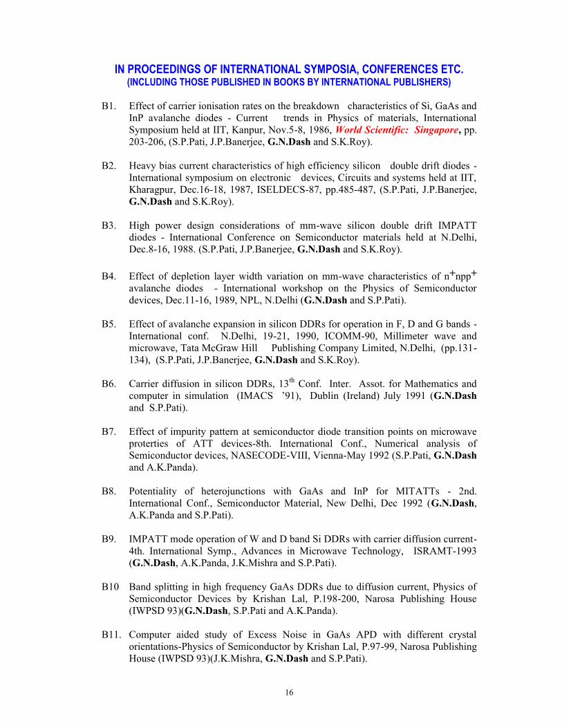
B1. Effect of carrier ionisation rates on the breakdown characteristics of Si, GaAs andInP avalanche diodes - Current trends in Physics of materials, InternationalSymposium held at IIT, Kanpur, Nov.5-8, 1986, World Scientific: Singapore, pp.203-206, (S.P.Pati, J.P.Banerjee, G.N.Dash and S.K.Roy).
B2. Heavy bias current characteristics of high efficiency silicon double drift diodes -International symposium on electronic devices, Circuits and systems held at IIT,Kharagpur, Dec.16-18, 1987, ISELDECS-87, pp.485-487, (S.P.Pati, J.P.Banerjee,G.N.Dash and S.K.Roy).
B3. High power design considerations of mm-wave silicon double drift IMPATTdiodes - International Conference on Semiconductor materials held at N.Delhi,Dec.8-16, 1988. (S.P.Pati, J.P.Banerjee, G.N.Dash and S.K.Roy).
B4. Effect of depletion layer width variation on mm-wave characteristics of n+npp+avalanche diodes - International workshop on the Physics of Semiconductordevices, Dec.11-16, 1989, NPL, N.Delhi (G.N.Dash and S.P.Pati).
B5. Effect of avalanche expansion in silicon DDRs for operation in F, D and G bands -International conf. N.Delhi, 19-21, 1990, ICOMM-90, Millimeter wave andmicrowave, Tata McGraw Hill Publishing Company Limited, N.Delhi, (pp.131-134), (S.P.Pati, J.P.Banerjee, G.N.Dash and S.K.Roy).
B6. Carrier diffusion in silicon DDRs, 13th Conf. Inter. Assot. for Mathematics andcomputer in simulation (IMACS ’91), Dublin (Ireland) July 1991 (G.N.Dashand S.P.Pati).
B7. Effect of impurity pattern at semiconductor diode transition points on microwaveproterties of ATT devices-8th. International Conf., Numerical analysis ofSemiconductor devices, NASECODE-VIII, Vienna-May 1992 (S.P.Pati, G.N.Dashand A.K.Panda).
B8. Potentiality of heterojunctions with GaAs and InP for MITATTs - 2nd.International Conf., Semiconductor Material, New Delhi, Dec 1992 (G.N.Dash,A.K.Panda and S.P.Pati).
B9. IMPATT mode operation of W and D band Si DDRs with carrier diffusion current-4th. International Symp., Advances in Microwave Technology, ISRAMT-1993(G.N.Dash, A.K.Panda, J.K.Mishra and S.P.Pati).
B10 Band splitting in high frequency GaAs DDRs due to diffusion current, Physics ofSemiconductor Devices by Krishan Lal, P.198-200, Narosa Publishing House(IWPSD 93)(G.N.Dash, S.P.Pati and A.K.Panda).
B11. Computer aided study of Excess Noise in GaAs APD with different crystalorientations-Physics of Semiconductor by Krishan Lal, P.97-99, Narosa PublishingHouse (IWPSD 93)(J.K.Mishra, G.N.Dash and S.P.Pati).
17
B12. Avalanche phase delay determination in different Impatt diode structures -NASECODE X Conference, Dublin (June 20-24, 1994) (S.P.Pati, A.K.Panda,G.N.Dash and S.K.Dash).
B13. Realistic Computer Aided Assessment of Avalanche noise generation along activezone of silicon DDRs - NASECODE X Conference, Dublin (June 20-24, 1994)(S.K.Dash, G.N.Dash, A.K.Panda and S.P.Pati).
B14. Effect of tunneling current on avalanche phase delay in MITATT devices -IWPSD-95, NPL, New Delhi (J.K.Mishra and G.N.Dash).
B15. Minimization of avalanche noise through modulation of location of clump chargein silicon low-high-low DDR - IWPSD-95, NPL, New Delhi (S.K.Dash, G.N.Dashand S.P.Pati).
B16. High frequency design optimisation of InP/GaInAs and InP/GaInAsPheterojunction DDRs, APMC’96 (J.K.Mishra, A.K.Panda and G.N.Dash).
B17. Effect of saturated current on mm-wave properties of GaInAsP and heteroInP/GaInAsP DDRs - ICSMT’96 (S.Satapathy, A.K.Panda, G.N.Dash andS.P.Pati).
B18. The potentiality of Si/SiGe heterostructure MITATT devices - ICSMT' 96(J.K.Mishra, A.K.Panda, S.K.Dash, S.Satapathy, G.N.Dash and S.P.Pati).
B19. Single Fundamental Band output from DAR IMPATT diode- (IWPSD-99) Physicsof Semiconductor Devices, Allied Publishers Ltd. New Delhi, pp 562-64, 1999(I.P.Mishra, J.K.Mishra and G.N.Dash)
B20. A high power and low noise GaAs DAR Impatt diode-(IWPSD-2001) Physics ofSemiconductor Devices, Allied Publishers Ltd. New Delhi, pp 898-901,2001(S.R.Pattanaik, I.P.Mishra, J.K.Mishra and G.N.Dash)
B21. The potential of InP/ GaInAs Double avalanche Region Impatt Diode- IWPSD-2001 Physics of Semiconductor Devices, Allied Publishers Ltd. New Delhi, pp902-905, 2001 (S.R.Pattanaik, I.P.Mishra, J.K.Mishra and G.N.Dash)
B22. Avalanche Noise Characteristics of GaAs/Al0.2 Ga0.8As Heterojunction IMPATTdiode, Physics of Semiconductor Devices (Proceeding of IWPSD 2003), AlliedPublishers Ltd. New Delhi, pp. 812-815, 2003 (S.R. Pattanaik, I.P. Mishra, J.K.Mishra and G.N. Dash)
B23. 4H-SiC Vs 6H-SiC for realization of impatt diode - Physics of SemiconductorDevices (Proceeding of IWPSD 2005), Allied Publishers Ltd. New Delhi, Vol 2,pp. 857-860, 2005 (S.R. Pattanaik, G.N. Dash and S.K. Swain)
B24. Comparison of 4H-SiC with wurtzite-GaN for Impatt application at 140 GHz –International Workshop IWPSD – 2007, I.I.T., Bombay, Dec 2007, IEEE 978-1-

18
4244-1727-8/07, pp. 391, 2007(S.R. Pattanaik, J. Pradhan, P.R. Tripathy and G.N.Dash)
B25. GaN based Gunn diode for high frequency signal generation, InternationalWorkshop IWPSD – 2007, I.I.T., Bombay, Dec 2007, IEEE 978-1-4244-1727-8/07, pp. 514-517, 2007 (A.K.Panda, N.C. Agrawal, R.K.Parida and G.N.Dash)
B26. A compararative study on the high band gap material (GaN and SiC) – basedIMPATTs - Proceedings of Asia Pacific Microwave Conference-2007, IEEE 1-4244-0748-6/07, pp. 1669-72, 2007 (A.K.Panda, , R.K.Parida, N.C. Agrawal andG.N.Dash)
B27. GaN based Gunn diode for THz Signal Generation, Asia Pacific MicrowaveConference Dec 7 – 10, 2009, Singapore - (A K Panda, G N Dash, N CAgrawala and R K Parida)
B28. THz Signal Generation using 3C-SiC, 4H-SiC and 6H-SiC based SDRMITATTs, International Workshop on Physics of Semiconductor Devices,JMI, New Delhi – Paper ID 32, Dec 15 -19, 2009 (R K Parida, N CAgrawala, G N Dash and A K Panda)
B29. High efficiency superlattice type Heterojunction Impatt, InternationalWorkshop on Physics of Semiconductor Devices, JMI, New Delhi – PaperID 479, Dec 15 -19, 2009 (S.R. Pattanaik and G.N. Dash)
B30. High power 4H SiC – 6H SiC heterojunction Impatt diode, InternationalWorkshop on Physics of Semiconductor Devices, JMI, New Delhi – PaperID 485, Dec 15 -19, 2009 (S.R. Pattanaik, J. Pradhan and G.N. Dash)
B31. Comb filter based approach for prediction of protein coding region,International Conference on Electronics Design and Signal Processing(ICEDSP-09), , MIT, Manipal, Paper ID-152, Dec.10 – 12, 2009 (J. K.Meher, P. K. Meher and G. N. Dash)
B32. Signal processing approach for prediction of kink in Transmembrane α-Hilices, International conference on Advances in Information Technologyand Mobile Communication, AIM 2011, Nagpur, April 21-22, 2011,Proceedings published by Springer Publication: Heidelberg (Germany),ISBN 978-3-642-20572-9, Edited by V.V. Das, G. Thomas, and F. LumbanGaol, pp. 170 - 177, (J. K .Meher, N. Mishra, P. K. Mohapatra, M. K. Raval., P.K. Meher, G. N. Dash)
B33. Wavelet transform for detection of conserved motifs in protein sequenceswith ten bit physico-chemical properties, International Conference onNetwork Communication and Computers (ICNCC – 2011), New Delhi,March 21 – 22, 2011, Proceedings published by IEEE (USA), ISBN 978-1-4244-9550-4, Edited by P.S. Sandhu and Zhao Yang. pp. 558 – 562 (J. K.Meher, P. K. Meher, M. K. Raval and G. N. Dash)
B34. Preprocessing of microarray by integrated OSR and SDF approach foreffective denoising and quantification, International conference onInformation and Network Technology, IPCSIT, 29 - 30 April 2011,

19
Chennai, India, Proceedings published by IACSIT press, Singapore, ISBN978-981-08-8632-5, Edited by Xu Lifeng, Vol. 4, pp. 158 – 163 (J. K.Meher, P. K. Meher and G. N. Dash)
B35. Influence of small variation in impact ionisation rate data on simulation of 4-HSiC IMPATT diode, Proceedings of XVI International Workshop on Physics ofSemiconductor Devices (IWPSD – 2011), IIT, Kanpur, Dec. 19 – 22, 2011 (S.R.Pattanaik, J. Pradhan, S.K. Swain and G.N. Dash)
B36. A comparative study of high frequency characteristics of SiC based SDRs,Proceedings of XVI International Workshop on Physics of Semiconductor Devices(IWPSD – 2011), IIT, Kanpur, Dec. 19 – 22, 2011 (R.K. Parida, A.K. Panda andG.N. Dash)
B37. Terahertz characteristics of 6H-SiC and 4-H SiC IMPATT diode, Proceedings ofXVI International Workshop on Physics of Semiconductor Devices (IWPSD –2011), IIT, Kanpur, Dec. 19 – 22, 2011 (S.K. Swain, J Pradhan, S.R. Pattanaik andG.N. Dash)
IN PROCEEDINGS OF NATIONAL SYMPOSIA/CONFERENCES ETC.(INCLUDING THOSE PUBLISHED IN BOOKS BY INTERNATIONAL PUBLISHERS)
C1. Calculation of noise voltage in IMPATT diodes through use of Laplace transform,14th CASAM -CU. National Research Symposium on Application of Mathematicsto Science, Technology and Society held at Calcutta University, Feb.12-13, 1987,(G.N.Dash, S.P.Pati and K.Mishra)
C2. Effect of crystal orientation on microwave characteristics of GaAs p+nn+avalanche diodes, SSP Symposium, BARC, Bombay, 1987 - Vol.30C, P.400,(S.P.Pati, J.P.Banerjee, G.N.Dash, A.Ganguly and S.K.Roy)
C3. Computer simulation of avalanche Noise in IMPATT devices, NationalSymposium on Physics of Electronic Communication held at University ofBurdwan, Dec.27-29, 1987. (G.N.Dash and S.P.Pati)
C4. Effect of carrier diffusion on avalanche breakdown condition of p-n junction - 75thsession of ISCA held at University of Pune. Jan. 7-12, 1988. (S.P.Pati,J.P.Banerjee, G.N.Dash and S.K.Roy)
C5. Effect of temperature on avalanche breakdown voltage of (100) oriented GaAs p-njunction - 76th session of ISCA, held at Madurai, Jan 1989. (G.N.Dash andS.P.Pati)
C6. Effect of temperature variation of ionisation rates on avalanche properties ofsilicon p-n junction, Vol.31C., P.380, SSP Symposium, Dec.23-28, 1988, Bhopal.(S.P.Pati, J.P.Banerjee, G.N.Dash and S.K.Roy)

20
C7. Study on the modification of microwave negative resistance profiles throughmodulation of drift zone in silicon p+nn+ IMPATT diode - Electronics circuits andSystems, Tata McGraw Hill: New Delhi, pp.489-491, (G.N.Dash and S.P.Pati)
C8. Tuning of doping concentration of V-band silicon DDR for compensatingperformance deterioration due to avalanche expansion, 79th session of ICSA,Baroda, 3-8, Jan. 1992. (S.P.Pati, G.N.Dash and A.K.Panda)
C9. Effect of carrier diffusion current on millimeter wave characteristics of InP SDRs,National Symp. on Antennas and Propagation, Cochin Univ., Dec 1992, pp.393-396, (G.N.Dash, A.K.Panda, K.Mishra and S.P.Pati)
C10. Estimation of tunnel current in Si, GaAs and InP DDRs - SSP symposium-Tirupati,Vol-35C, p 442, Dec 1992 (G.N.Dash, A.K.Panda, S.P.Pati and K.Mishra)
C11. Effect of carrier diffusion on high power Si flat DDRs - Advances in Microwaves,Asian Books Pvt. Ltd.: New Delhi, pp 109-114, Jan 1993 (G.N.Dash, A.K.Pandaand S.P.Pati)
C12. CAD for improvement of mm-wave characteristics of ATT devices in MITATTmode, Integrated Electronics, Allied Publishers Ltd.: New Delhi, pp.237, 1994(S.P.Pati, G.N.Dash and A.K.Panda)
C13. A study on effect of diffusion current on microwave properties of Si DDRs atdifferent temperatures, Proc. of the 81st session of the Indian Science Congress1994, Section of Engg. Sc, pp.14 (S.P.Pati, G.N.Dash, A.K.Panda, J.K.Mishra andS.K.Dash)
C14. Effect of low multiplication factor on the microwave properties of Si SD and DDIMPATT diodes, Electronic systems and applications, Allied Publishers Ltd.: NewDelhi, 1994, pp.16-20 (S.Satapathy, A.K.Panda, G.N.Dash, S.K.Dash andS.P.Pati)
C15. Generalised computer method for determination of avalanche noise in IMPATTdiodes, Electronic systems and applications, Allied Publishers Ltd.: New Delhi,1994, pp.78-81 (S.K.Dash, G.N.Dash, A.K.Panda and S.P.Pati)
C16. Excess Noise Study of Hi-Lo (111)-Oriented GaAs APD, Electronic systems andapplications, Allied Publishers Ltd.: New Delhi, 1994, pp.29-31 (J.K.Mishra andG.N.Dash)
C17. Influence of ionisation rates in a semiconductor on avalanche build up time in p-njunctions, Workshop on Current trends in condensed matter physics: SINP,Calcutta (S.P.Pati, S.Satapathy, A.K.Panda and G.N.Dash)
C18. Role of avalanche phase delay in the performance of GaAs DDRs with differentcrystal orientation- APSYM, CUSAT-94, Kochi (A.K.Panda, S.Satapathy,S.K.Dash, G.N.Dash and S.P.Pati)

21
C19. Multiple-Band Microwave Oscillations in 8-350 GHz Range From a SiliconDouble Avalanche Region Diode - APSYM, CUSAT-94, Kochi (A.K.Panda,G.N.Dash and S.P.Pati)
C20. A computer scheme to study the Impulse response and frequency response ofAvalanche Photodiodes - APSYM, CUSAT-94, Kochi (J.K.Mishra and G.N.Dash)
C21. Avalanche phase delay in Si, GaAs and InP p-n junctions - SSP symposium,Vol 37C, pp.525, 1994 (A.K.Panda, S.Satpathy, S.K.Dash, G.N.Dash and S.P.Pati)
C22. Minimisation of excess noise in a GaAs APD by modulating the diffusion dopingprofile- Proceedings of INCURSI-96, pp. IV-1 to IV-3 (J.K.Mishra, A.K.Panda andG.N.Dash)
C23. Computer studies on the microwave properties of ion-implanted p+pnn+ DDRswith three moment approach - National Symposium in recent advances inElectronics: Amritsar (A.K.Panda, S. Satapathy, G.N.Dash and S. P. Pati)
C24. Studies on Si/SiGe heterostructure MITATT DDR with one sided SiGe layer - SSPSymposium 96 (J.K.Mishra, A.K.Panda, G.N.Dash and S.P.Pati)
C25. Tunneling assisted enhancement of device properties in IMPATT diodes for aconstant frequency operation with different bias current - INCURSI 96 (J.K.Mishraand G.N.Dash)
C26. Noise and Microwave Properties of InAlAs/InGaAs Superlattice Read AvalancheDiode- National Seminar INCURSI-99 held at Burdwan University duringFebruary 22-24, 1999(G.N.Dash, J.K.Mishra)
C27. Photon Assisted control of Noise and millimeter wave properties of ReadAvalanche Diode- National Symposium for Advances in Microwave, Millimeterwave, Infrared Technology (SAMMIT) held at Calcutta University duringDecember 21-29, 1999(G.N.Dash, J.K.Mishra)
C28. Noise in Double Avalanche Region IMPATT Diode- National Seminar onCMDAYS-2K held at G.G. University, Bilaspur during Aug 29-31, 2000(J.K.Mishra, G.N.Dash, T.K.Mishra and I.P.Mishra)
C29. Performance Assessment of the two complimentary Si DAR IMPATT Diodes,National Conference on Material and Semiconductor Technologies in ElectronicResearch held at G.B. Pant University, Pantnagar during November 8-10, 2000(I.P.Mishra, J.K.Mishra and G.N.Dash)
C30. A comparative study of - and -type DAR IMPATT diode structures based on InPmaterial- National Seminar on CMDAYS-2001 held at Sambalpur University, Aug.29-31, 2001 (S.R.Pattanaik, I.P.Mishra, J.K.Mishra and G.N.Dash)
C31. Microwave Negative Resistivity Profiles of InP/GaInAs Heterojunction DoubleAvalanche Region (DAR) IMPATT diodes- National Seminar on CMDAYS-2001

22
held at Sambalpur University, Aug. 29-31, 2001 (J.K.Mishra, G.N.Dash,S.R.Pattanaik and I.P.Mishra)
C32. Study of Si/SiGe heterojunction DAR IMPATT diode, Proceedings of APSYM-2002, held at Department of Electronics, Cochin University of Science andTechnology, Cochin-682 022, pp 189-192, 2002. (S.R. Pattanaik, J.K. Mishra, I.P.Mishra and G.N. Dash)
C33. Optimisation of DC and Small Signal Properties of GaAs/Al0.3Ga0.7AsHeterojunction IMPATT diode, Proceedings of CMDAYS-2003, held at JadavpurUniversity, pp 107-108, 2003 (S.R. Pattanaik, J.K. Mishra and G.N. Dash).
C34. Effect of SiGe Nano layers on the performance of heterojunction IMPATT diode,Proceedings of CMDAYS-2003, held at Jadavpur University, pp 109-110, 2003(S.R. Pattanaik, J.K. Mishra and G.N. Dash)
C35. Prospects of GaAs/GaInP heterojunction for realization of millimeter wave,Proceedings CMDAYS-2004, organized by Department of Physics, NEHU,Shillong, Meghalaya, Aug. 25-27, 2004 (S.R. Pattanaik, G.N. Dash and J.K.Mishra)
C36. GaP: A promising new material for fabrication of IMPATT devices, ProceedingsPEMD-2005, held at Department of Physics, Sambalpur University during Feb. 10-12, 2005 (S.R. Pattanaik, G.N. Dash and M.K. Jaiswal)
C37. GaAs/AlGaAs Impatt Diode For High Power And Low Noise Operation,Proceedings PEMD-2005, held at Department of Physics, Sambalpur Universityduring Feb. 10-12, 2005 (S.R. Pattanaik, G.N. Dash and J.K. Mishra)
C38. Photon Assisted Control of Noise and MM wave properties of GaInAsP ReadDiode, Proceedings PEMD-2005, held at Department of Physics, SambalpurUniversity during Feb. 10-12, 2005 (S.R. Pattanaik, G.N. Dash and S.K. Swain)
C39. Prospects of superlattice structure for IMPATT operation - Proceedings CMDAYS-2005, organized by Department of Physics, Berhampur University, Aug. 29-31,2005 (S.R. Pattanaik, S.K. Swain and G.N. Dash)
C40. Realization of High Power IMPATT Diodes with 4H-SiC, Proceedings RecentAdvances in Physics, held at Department of Physics, Dalmia College, Rajgangpur,Orissa during Feb. 8-10, 2006 (S.R. Pattanaik, G.N. Dash, S.K. Swain and J.K.Mishra)
C41. Prospects GaAs/Ga0.52In0.48P Heterojunction IMPATT Diode for Low NoiseOperation at 94 GHz, Proceedings Recent Advances in Physics, held at Departmentof Physics, Dalmia College, Rajgangpur, Orissa during Feb. 8-10, 2006 (S.R.Pattanaik, G.N. Dash, S.K. Swain and J.K. Mishra)
C42. Diamond: The Wonder Material for Future Devices, Proceedings Recent Advancesin Physics, held at Department of Physics, Dalmia College, Rajgangpur, Orissaduring Feb. 8-10, 2006 (S.R. Pattanaik, G.N. Dash, invited speaker)
C43. A new model to eliminated digital divide for successful implementation of e-Governance, Proceedings of National Round Table Conference on e-Governance,
23
organized by the Department of Computer Science and Application, SambalpurUniversity, March 26, 2006 (G.N.Dash, invited speaker)
C44. Exploration of high power Impatt diodes with 4H-SiC for mm-wave application –Proceedings of APSYM-CUSAT 2006, Dec 14 – 16, 2006, Cochin University ofScience and Technology, pp. 279 – 282, (S.R Pattanaik, S.K. Swain, J. Pradhan andG.N. Dash)
C45. GaN: A promising base material for Impatt diode – Proceedinds of NationalSeminar CMDAYS – 07, Aug 29-31, 2007, NIT Rourkela, pp. 36 (S.R. Pattanaik,P.R. Tripathy, J. Pradhan and G.N. Dash)
C46. DNA Mcroarrary Image Analysis for Locating and Estimating Intensities of Spots,Proceedinds of National National seminar on Devices ,Circuits &Communication(NASDEC-08), Nov 06-07, 2008, B.I.T., Mesra, Ranchi, pp. 30(J.K.Meher, G.N.Dash, P.K.Meher , M.K.Raval )
C47. Quantification and Denoising of DNA Microarrary by Image Analysis, 38th ISTENational Convention-08, K.I.I.T University, Bhubaneswar, Dec 19-21, 2008, (J. K.Meher, P. K. Meher, G. N. Dash, M. K. Raval)
C48. Comb filter based approach for prediction of protein coding region,International Conference on Electronics Design and Signal Processing(ICEDSP-09), , MIT, Manipal, Paper ID-152, Dec.10 – 12, 2009 (J. K.Meher, P. K. Meher and G. N. Dash)
C49. Wavelet-based Denoising and Quantification of Microarrary Spot, NationalConference on Computational Biology (NCCB-09), SOA University,Bhubaneswar, Page 62, Dec. 28 – 29, 2009 (J. K. Meher, P. K. Meher andG. N. Dash)
C50. Millimeter-wave Communication Characteristics of GaAs~AlGaAsheterojunction IMPATT Diode, National Seminar on Communication –Present Trend and Future Prospects, GIET, Gunupur, Nov 18 – 19, 2009 (S.R. Pattanaik, J. K. Mishra and G. N. Dash)
C51. “Prediction of Protein Coding Region by Signal Processing Analysis ofEquivalent Amino Acid Sequence of DNA String”, Proceedings ofNational Conference on Electronics, Computers and Communications,(NCECC-2010) Madhav Institute of Technology and Science, Gwalior,March 06-07, 2010, (J. K. Meher, P. K. Meher and G. N. Dash, M. K.Rawal)
C52. “Integrated Frequency Domain Filter and Histogram Equalization Approachon Microarray Slide for Effective Quantification”, Proceedings of ThirdNational Conference on VLSI, Embedded Systems, Signal Processing andCommunication Technologies.(NC-VESCOM' 10), 02 – 03 April 2010,Aarupadai Veedu Institute of Technology, Chennai., Pages: 102-105 (J. K.Meher, P. K. Meher and G. N. Dash)

24
C53. Physics and Technology of Memristic Materials, Proceedings of NationalSeminar on Physics and Technology of Novel Materials -2010 (PTNM –2010), Sambalpur University, Feb 25 – 27, 2010, Abstract Volume, pp. 22,(G.N. Dash)
C54. Potentials of Superlattice Materials for Avalanche Devices, Proceedings ofNational Seminar on Physics and Technology of Novel Materials -2010(PTNM – 2010), Sambalpur University, Feb 25 – 27, 2010, AbstractVolume, pp.44, (S.R. Pattanaik, J.K. Mishra and G.N. Dash)
C55. Performance of 4H-SiC~6H-SiC heterojunction IMPATT diode at 94 GHz,Proceedings of National Seminar on Physics and Technology of NovelMaterials -2010 (PTNM – 2010), Sambalpur University, Feb 25 – 27, 2010,Abstract Volume, pp.45, (S.R. Pattanaik, J.K. Mishra and G.N. Dash)
C56 Studies of binary computing using magnetic Logic Gates, Proceedings ofNational Seminar on Physics and Technology of Novel Materials -2010(PTNM – 2010), Sambalpur University, Feb 25 – 27, 2010, AbstractVolume, pp.43, (S.K. Panda and G.N. Dash)
C57. Detection of Conserved Motifs in Protein Sequences using Fourier Transform:Light Harvesting Complexes: A Case Study, NCEC-10, National Conference onElectronics and Communication, 22-24 Dec 2010 MIT, Gwalior and IEEE IndianCouncil, Oral Presentation, 102 of Abstract Book (J.K. Meher, M.K. Raval, P.K.Meher, G.N. Dash)
C58. Study of Interface Sheet Charge Density of AlGaAs/InGaAs/GaAs-basedPseudomorphic HEMT, II National Seminar on Physics and Technology of NovelMaterials, PTNM – II, Sambalpur University, March 2012 (T. R. Lenka, SudhakarDas, Rasmita Ku Nayak, G. N. Dash and A. K. Panda)
C59. Competence of 4H-SiC IMPATT Diode for Terahertz Application, II NationalSeminar on Physics and Technology of Novel Materials, PTNM – II, SambalpurUniversity, March 2012 (S.R. Pattanaik, J. Pradhan, S.K. Swain and G.N. Dash)
IN BULLETIN/REPORT/SUJST (Local Journal)
D1. Millimeter wave properties of InP single drift IMPATT diodes - SambalpurUniversity Journal of Science and Technology - Silver Jubilee issue -1991, p.81,(S.P.Pati, A.K.Panda and G.N.Dash).
D2. Silicon IMPATT diode as a solid state device for microwave and millimeter wavecommunication systems - Bulletin of Orissa Physical Society, 1996 (S.P.Pati,G.N.Dash and A.K.Panda).
D3. Computer solution of doping profiles of ion-implanted p-n junctions and itsapplication to optimise microwave characteristics of IMPATT diodes - Bulletinof Orissa Physical Society, Vol V, pp.90-95, 1997 (S.P.Pati, G.N.Dash, S.K.Dash,J.K.Mishra, S.Satapathy and A.K.Panda).

25
D4. Studies on the noise electric field profile for InP/GaInAs heterostructure MITATTdiodes- Bulletin of Orissa Physical Society, Vol V, pp. 41-48, 1997 (J.K.Mishra,A.K.Panda and G.N.Dash).
D5. Computer studies on mm-wave InP Impatts- Bulletin of the Orissa PhysicalSociety, Vol VI, pp. 42-51, March 1998 (S.K.Dash, S.Satpathy, A.K.Panda,G.N.Dash and S.P.Pati)
D6. Heavy bias noise characteristics in double avalanche region Impatt diodes- OPSBulletin Vol IX, pp 79- 89, Feb. 2001- (J.K.Mishra, S.R.Pattanaik, I.P.Mishra andG.N.Dash)
D7. Quantum Semiconductor Structures, SOUVENIR of Dirac Centenary Seminar onCurrent Trend in Physics, Department of Physics, Sambalpur University, March26, 2004 (G.N.Dash).
D8. Trapping of Atoms, Bulletin of Nobel Prize Seminars 1997 and 1998, Published byDepartment of Chemistry, Sambalpur University (G.N.Dash, invited talk)
D9. Nobel Prize in Physics – 2005, Bulletin of Nobel Prize Seminar2005 and 2006Organised by the Department of Chemistry, Sambalpur University (G.N. Dash,invited talk)
D10. GMR and the Hard Disk, Bulletin of Orissa Physical Society, Vol. XV, pp. 203-209, 2008 (G.N.Dash)
D11. The Giant Magneto Resistance, Bulletin of Nobel Prize Seminar- 2007, Organisedby the Department of Chemistry, Sambalpur University (G.N. Dash, invited talk)
D12. Two Dimensional Dirac fermions in Graphene, Proceedings of 30th Convention ofOPS, pp 94 – 98, Feb. 2013
POPULAR ARTICLES OF GENERAL INTEREST
E1. “Odia ra barnantara”, an article in odia published in the daily News Paper – “TheSamaja”, Vol. 79, No. 290, p. 6, 24 October 2008 (G.N. Dash)
E2. “Nobel Puraskar (Padartha Bijnan) – 2009” alias Nobel Prize (Physics) –2009, An article in “o.DiA” published in the Annual Magazine –“Digbalaya” of the Orissa Physical Society, No 11, pp. 13 -17, Feb. 2010(G.N. Dash)
E3. “Nobel Puraskar (Padartha Bijnan) – 2010” alias Nobel Prize (Physics) –2010, An article in “o.DiA” published in the Annual Magazine –“Digbalaya” of the Orissa Physical Society, No 12, pp.12 - 13, Feb. 2011(G.N. Dash)