Embed Size (px)
DESCRIPTION
Service manual HUMAX
Citation preview
CONTENTS
I. Troubleshooting Guideline 3
II. Checkpoints in the Event of a Problem
1. Basic Inspection- Not Working When Powered On 4- Malfunction of Front Display or Keys 5- Malfunction of Remote Control Unit 6- Not Working When Powered On 7- Does Not Boot after Power On or System Reset 8
2. CPU/System Memory Inspection- Error Occurs During S/W Installation or Updating 9
System Stops During Initial Booting or Operation
3. Channel Inspection- Lack of Channel Locking even though No Problems with Power/CPU (1) 10- Lack of Channel Locking even though No Problems with Power/CPU (2) 11- Lack of Channel Locking even though No Problems with Power/CPU (3) 12
4. MPEG Inspection- No Problems Found during Basic and CPU/System Memory Inspections,
but MPEG Does Not Play 13
5. CI I/F Inspection- Tuner Locked but No Channel Search 14- CAM Not Detected 15- CAM Detected, but No MPEG Play on a Scrambled Channel 16
6. Smart Card Inspection (IRCI-8400P, NACI-8700P)- Card Not Detected or No MPEG Play on a Scrambled Channel 17
7. A/V Inspection- No Video Output 18- Not Audio Output 19- Cannot Change the Screen Ratio [4:3 <-> 16:9] 20- TV -> VCR Bypass Does Not Work 21- VCR -> TV Bypass Does Not Work 22- Cannot Switch between CVBS (S-VIDEO) <-> RGB 23- No SPDIF Output 24
8. HDD Inspection- Cannot Perform HDD-related Operations (tsr, recording) (1) 25- Cannot Perform HDD-related Operations (tsr, recording) (2) 26
III. PCB Layout 27 ~ 28
IV. Block Diagram ??
V. Circuit Diagram and Waveform Diagram ?? ~ ??
VI. BOM (Bill of Material) ?? ~ ??
VII. Apparatus Drawing and Assembly Diagram ??
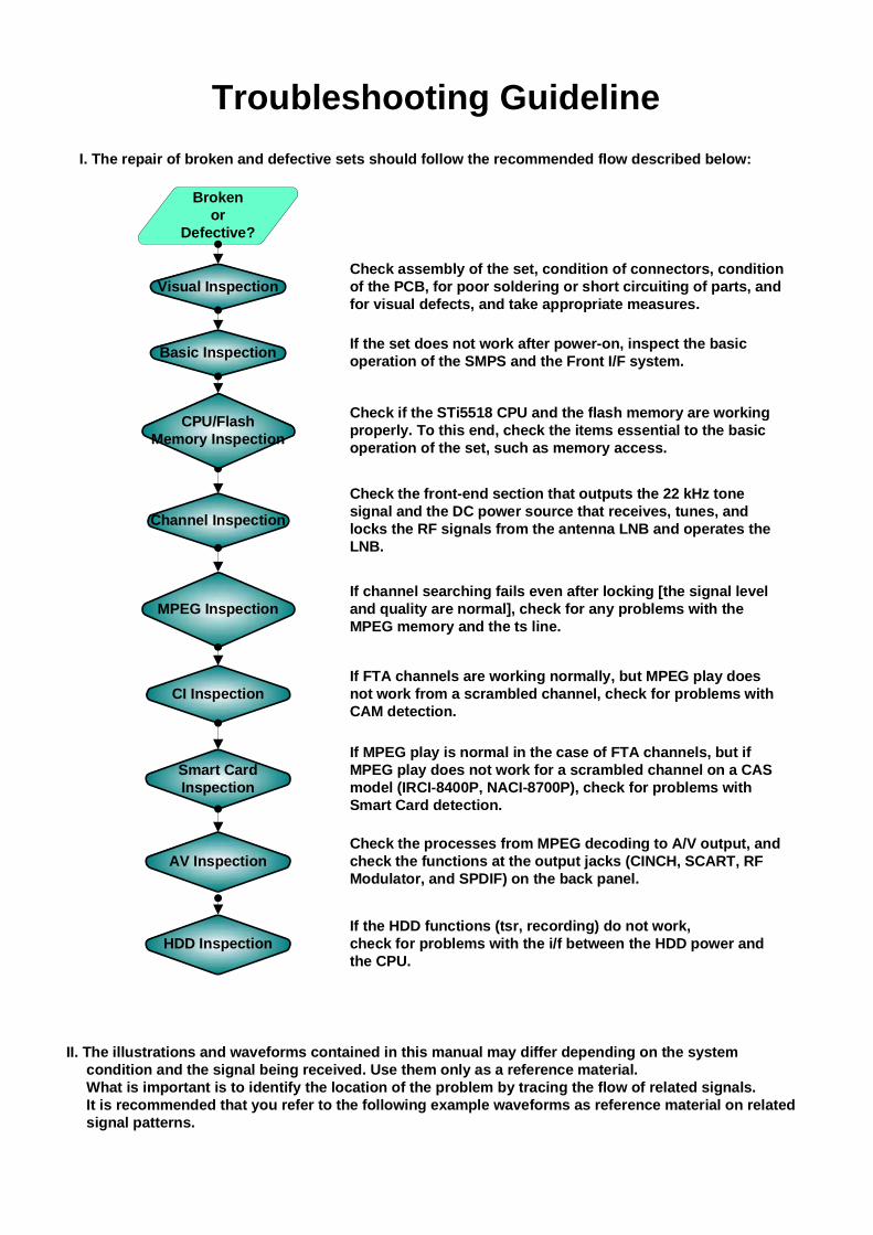
Troubleshooting GuidelineI. The repair of broken and defective sets should follow the recommended flow described below:
Visual Inspection
Brokenor
Defective?
Check assembly of the set, condition of connectors, conditionof the PCB, for poor soldering or short circuiting of parts, andfor visual defects, and take appropriate measures.
Basic Inspection If the set does not work after power-on, inspect the basicoperation of the SMPS and the Front I/F system.
Check if the STi5518 CPU and the flash memory are workingproperly. To this end, check the items essential to the basicoperation of the set, such as memory access.
Channel Inspection
If channel searching fails even after locking [the signal leveland quality are normal], check for any problems with theMPEG memory and the ts line.
MPEG Inspection
If MPEG play is normal in the case of FTA channels, but ifMPEG play does not work for a scrambled channel on a CASmodel (IRCI-8400P, NACI-8700P), check for problems withSmart Card detection.
CI Inspection
Check the front-end section that outputs the 22 kHz tonesignal and the DC power source that receives, tunes, andlocks the RF signals from the antenna LNB and operates theLNB.
II. The illustrations and waveforms contained in this manual may differ depending on the system condition and the signal being received. Use them only as a reference material. What is important is to identify the location of the problem by tracing the flow of related signals. It is recommended that you refer to the following example waveforms as reference material on related signal patterns.
Smart CardInspection
If the HDD functions (tsr, recording) do not work,check for problems with the i/f between the HDD power andthe CPU.
AV Inspection
HDD Inspection
If FTA channels are working normally, but MPEG play doesnot work from a scrambled channel, check for problems withCAM detection.
Check the processes from MPEG decoding to A/V output, andcheck the functions at the output jacks (CINCH, SCART, RFModulator, and SPDIF) on the back panel.
CPU/FlashMemory Inspection
Page 4
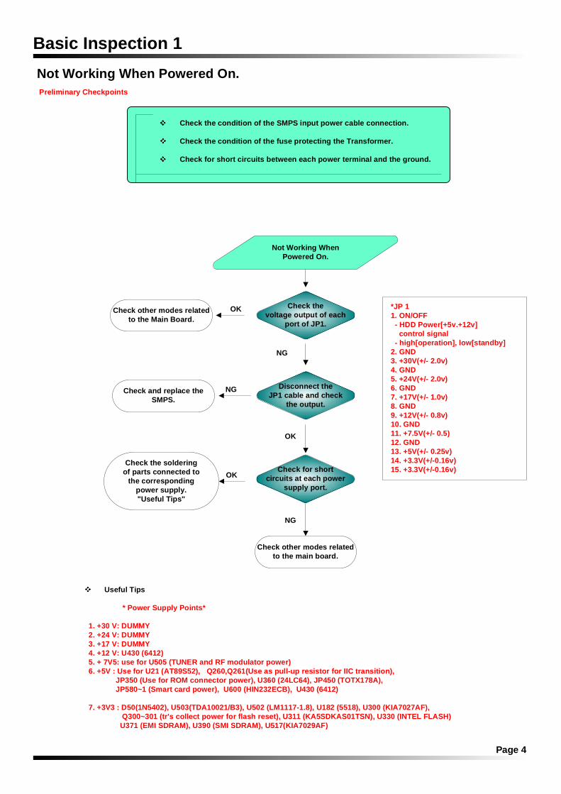
Basic Inspection 1Not Working When Powered On.
Check the condition of the SMPS input power cable connection.
Check the condition of the fuse protecting the Transformer.
Check for short circuits between each power terminal and the ground.
Not Working WhenPowered On.
Check thevoltage output of each
port of JP1.
OK
Disconnect theJP1 cable and check
the output.
Check and replace theSMPS.
Check for shortcircuits at each power
supply port.
NG
Check other modes relatedto the Main Board.
NG
OK
NG
OK
Check other modes relatedto the main board.
Check the solderingof parts connected to
the correspondingpower supply."Useful Tips"
*JP 1 1. ON/OFF - HDD Power[+5v.+12v] control signal - high[operation], low[standby] 2. GND 3. +30V(+/- 2.0v) 4. GND 5. +24V(+/- 2.0v) 6. GND 7. +17V(+/- 1.0v) 8. GND 9. +12V(+/- 0.8v) 10. GND 11. +7.5V(+/- 0.5) 12. GND 13. +5V(+/- 0.25v) 14. +3.3V(+/-0.16v) 15. +3.3V(+/-0.16v)
Useful Tips
* Power Supply Points*
1. +30 V: DUMMY 2. +24 V: DUMMY 3. +17 V: DUMMY 4. +12 V: U430 (6412) 5. + 7V5: use for U505 (TUNER and RF modulator power) 6. +5V : Use for U21 (AT89S52), Q260,Q261(Use as pull-up resistor for IIC transition), JP350 (Use for ROM connector power), U360 (24LC64), JP450 (TOTX178A), JP580~1 (Smart card power), U600 (HIN232ECB), U430 (6412)
7. +3V3 : D50(1N5402), U503(TDA10021/B3), U502 (LM1117-1.8), U182 (5518), U300 (KIA7027AF), Q300~301 (tr's collect power for flash reset), U311 (KA5SDKAS01TSN), U330 (INTEL FLASH) U371 (EMI SDRAM), U390 (SMI SDRAM), U517(KIA7029AF)
Preliminary Checkpoints
Page 5
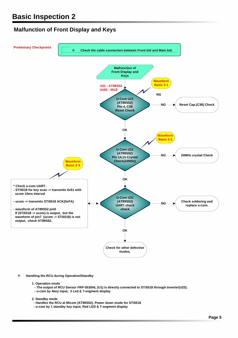
Basic Inspection 2Malfunction of Front Display and Keys
Check the cable connection between Front b/d and Main b/d.
Malfunction ofFront Display and
Keys
Check for other defectivemodes.
OK
U-Com U21(AT89S52)Pin 4, C38
Reset Check
Reset Cap.(C38) Check
OK
NG
U-Com U21(AT89S52)
Pin 14,15 CrystalCheck(24MHz)
24MHz crystal CheckNG
Handling the RCU during Operation/Standby
1. Operation mode - The output of RCU Sensor FRP-5530HL (U1) is directly connected to STi5518 through Inverter(U23). - u-com by 4key input, 3 Led & 7-segment display
2. Standby mode - Handles the RCU at Micom (AT89S52), Power down mode for STi5518 - u-com by 1 standby key input, Red LED & 7-segment display
U-Com U21(AT89S52)
UART checkcheck
OK
Check soldering andreplace u-com.NG
NG
WaveformBasic 2-1
WaveformBasic 2-2
WaveformBasic 2-3
* Check u-com UART. - STi5518 for key scan -> transmits 0x51 with ucom 10ms interval
- ucom -> transmits STi5518 ACK(0xFA)
- waveform of AT89S52 pin5 If (STi5518 -> ucom) is output, but the waveform of pin7 (ucom -> STi5518) is not output, check AT89S52.
U21 : AT89S52U182 : 5518
Preliminary Checkpoints
Page 6
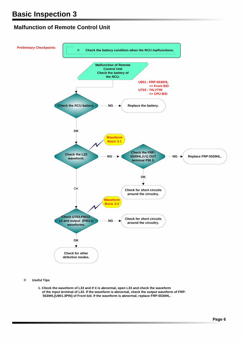
Basic Inspection 3Malfunction of Remote Control Unit
Check the battery condition when the RCU malfunctions.
Malfunction of RemoteControl Unit
Check the battery ofthe RCU.
Check the RCU battery. Replace the battery.NG
Useful Tips
1. Check the waveform of L33 and if it is abnormal, open L33 and check the waveform of the input terminal of L33. If the waveform is abnormal, check the output waveform of FRP-
5530HL[U901.3PIN] of Front b/d. If the waveform is abnormal, replace FRP-5530HL.
Check the L33waveform. NG
OK
Check U703.PIN12,13 and output (PIN11)
waveforms.
Check for short circuitsaround the circuitry.NG
OK
Check the FRP-5530HL(U1) OUTterminal PIN 3.
NG Replace FRP-5530HL.
OK
Check for short circuitsaround the circuitry.
WaveformBasic 3-2
WaveformBasic 3-1
Check for otherdefective modes.
OK
U901 : FRP-5530HL => Front B/DU703 : 74LVT00 => CPU B/D
Preliminary Checkpoints
Page 7
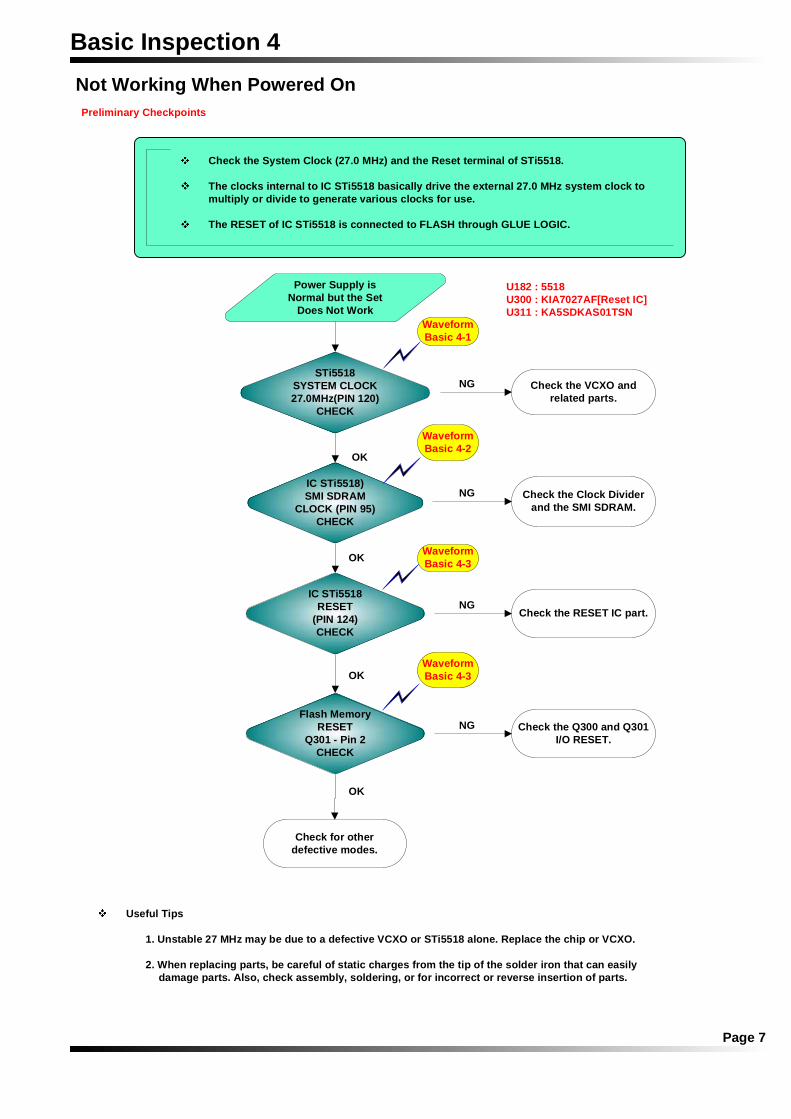
Basic Inspection 4Not Working When Powered On
Power Supply isNormal but the Set
Does Not Work
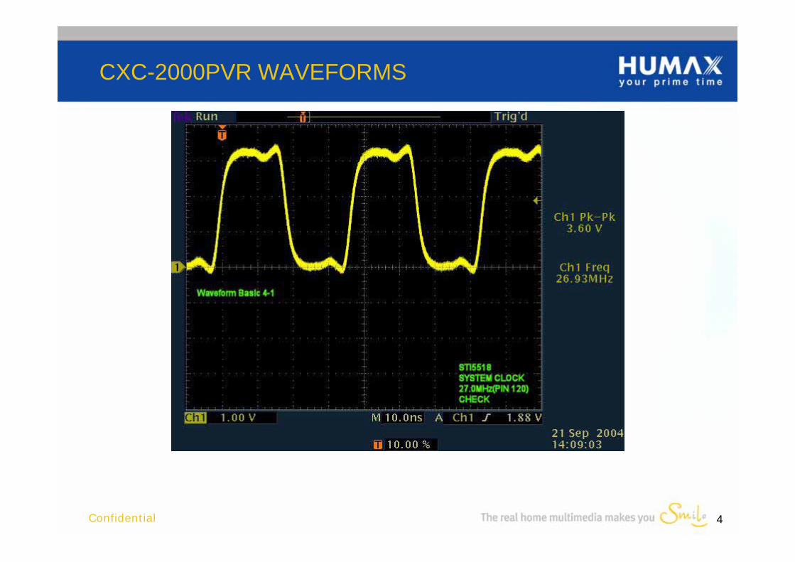
STi5518SYSTEM CLOCK27.0MHz(PIN 120)
CHECK
Check the VCXO andrelated parts.
NG
OK
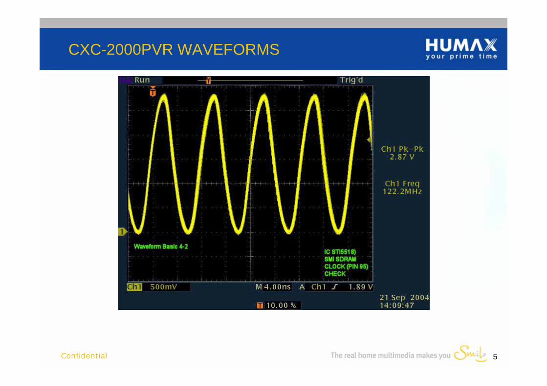
IC STi5518)SMI SDRAM
CLOCK (PIN 95)CHECK
OK
Check the Clock Dividerand the SMI SDRAM.
NG
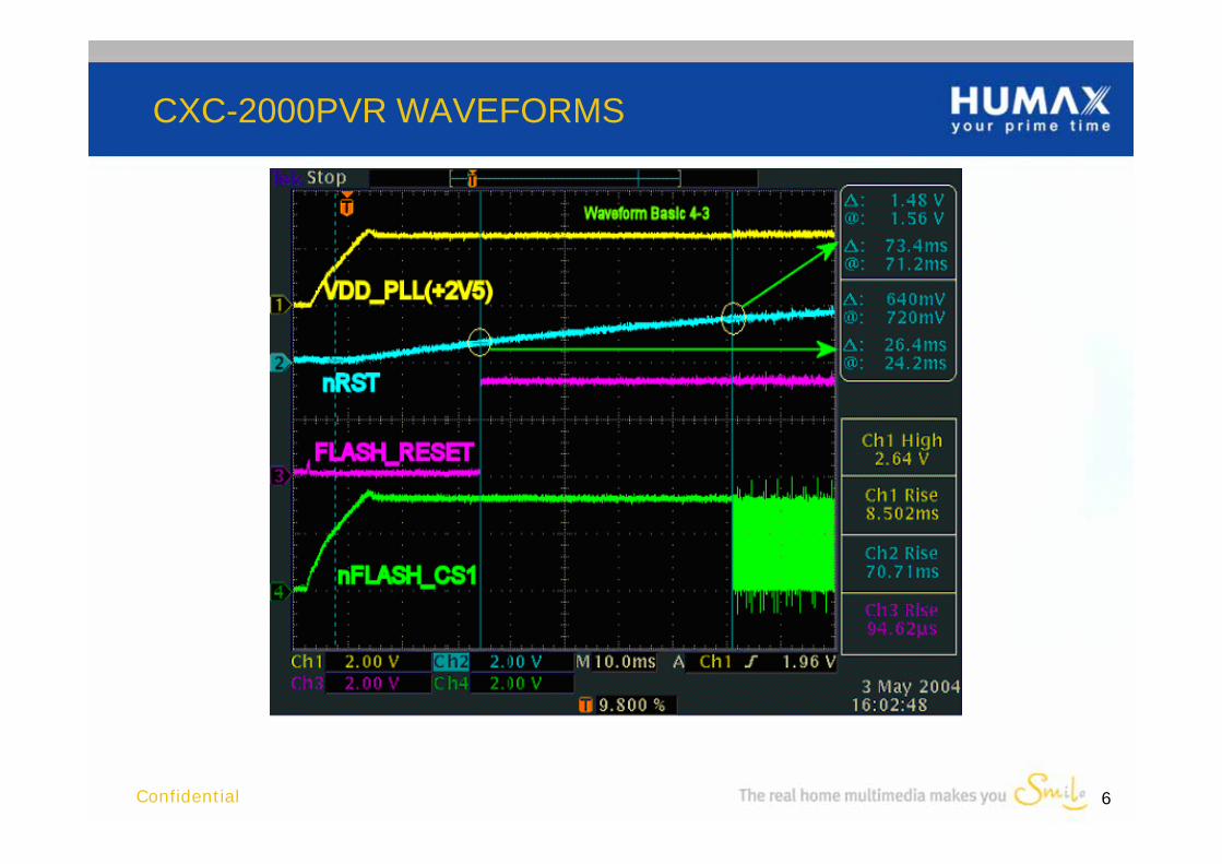
Flash MemoryRESET
Q301 - Pin 2CHECK
Check the Q300 and Q301I/O RESET.
NG
Check for otherdefective modes.
OK
WaveformBasic 4-1
Useful Tips
1. Unstable 27 MHz may be due to a defective VCXO or STi5518 alone. Replace the chip or VCXO.
2. When replacing parts, be careful of static charges from the tip of the solder iron that can easily damage parts. Also, check assembly, soldering, or for incorrect or reverse insertion of parts.
IC STi5518RESET
(PIN 124)CHECK
Check the RESET IC part.NG
OK
Check the System Clock (27.0 MHz) and the Reset terminal of STi5518.
The clocks internal to IC STi5518 basically drive the external 27.0 MHz system clock tomultiply or divide to generate various clocks for use.
The RESET of IC STi5518 is connected to FLASH through GLUE LOGIC.
WaveformBasic 4-2
WaveformBasic 4-3
WaveformBasic 4-3
U182 : 5518U300 : KIA7027AF[Reset IC]U311 : KA5SDKAS01TSN
Preliminary Checkpoints
Page 8
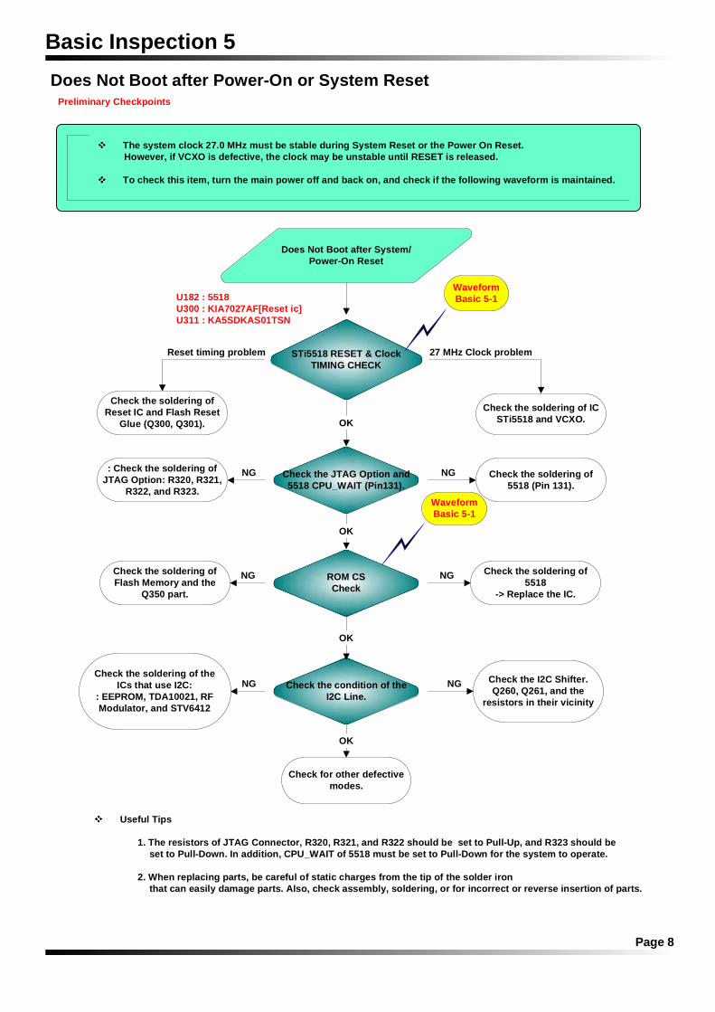
Basic Inspection 5Does Not Boot after Power-On or System Reset
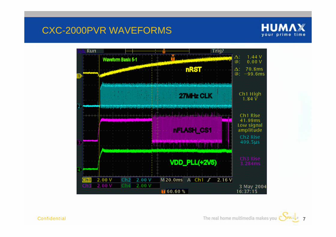
Does Not Boot after System/Power-On Reset
STi5518 RESET & ClockTIMING CHECK
Reset timing problem
Check the soldering of ICSTi5518 and VCXO.
27 MHz Clock problem
Check the JTAG Option and5518 CPU_WAIT (Pin131).
NG
WaveformBasic 5-1
: Check the soldering ofJTAG Option: R320, R321,
R322, and R323.
Check the soldering of5518 (Pin 131).
NG
ROM CSCheck
NGCheck the soldering ofFlash Memory and the
Q350 part.
Check the soldering of5518
-> Replace the IC.
NG
Check for other defectivemodes.
Check the condition of theI2C Line.
NG Check the I2C Shifter.Q260, Q261, and the
resistors in their vicinity
The system clock 27.0 MHz must be stable during System Reset or the Power On Reset. However, if VCXO is defective, the clock may be unstable until RESET is released.
To check this item, turn the main power off and back on, and check if the following waveform is maintained.
Useful Tips
1. The resistors of JTAG Connector, R320, R321, and R322 should be set to Pull-Up, and R323 should be set to Pull-Down. In addition, CPU_WAIT of 5518 must be set to Pull-Down for the system to operate.
2. When replacing parts, be careful of static charges from the tip of the solder iron that can easily damage parts. Also, check assembly, soldering, or for incorrect or reverse insertion of parts.
WaveformBasic 5-1
Preliminary Checkpoints
Check the soldering ofReset IC and Flash Reset
Glue (Q300, Q301). OK
OK
OK
OK
U182 : 5518U300 : KIA7027AF[Reset ic]U311 : KA5SDKAS01TSN
Check the soldering of theICs that use I2C:
: EEPROM, TDA10021, RFModulator, and STV6412
NG
Page 9
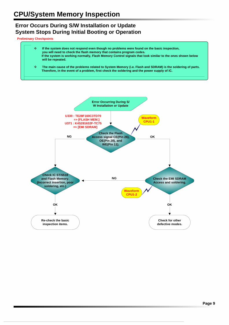
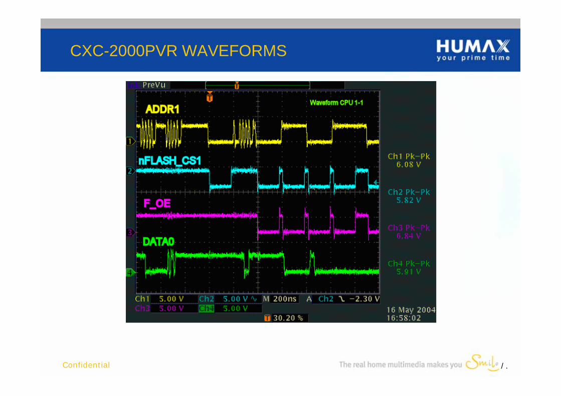
CPU/System Memory InspectionError Occurs During S/W Installation or UpdateSystem Stops During Initial Booting or Operation
Error Occurring During S/W Installation or Update
Check the FlashAccess signal CE(Pin 26),
OE(Pin 28), andWE(Pin 11).
NG OK
Re-check the basicinspection items.
Check for otherdefective modes.
NG
WaveformCPU1-2
WaveformCPU1-1
Check IC STi5518and Flash Memory.
(Incorrect insertion, poorsoldering, etc.)
Check the EMI SDRAMAccess and soldering.
If the system does not respond even though no problems were found on the basic inspection,you will need to check the flash memory that contains program codes.
If the system is working normally, Flash Memory Control signals that look similar to the ones shown belowwill be repeated.
The main cause of the problems related to System Memory (i.e. Flash and SDRAM) is the soldering of parts. Therefore, in the event of a problem, first check the soldering and the power supply of IC.
U330 : TE28F160C3TD70 => [FLASH MEM.]
U371 : K4S281632F-TC75 => [EMI SDRAM]
Preliminary Checkpoints
OK OK
Page 10
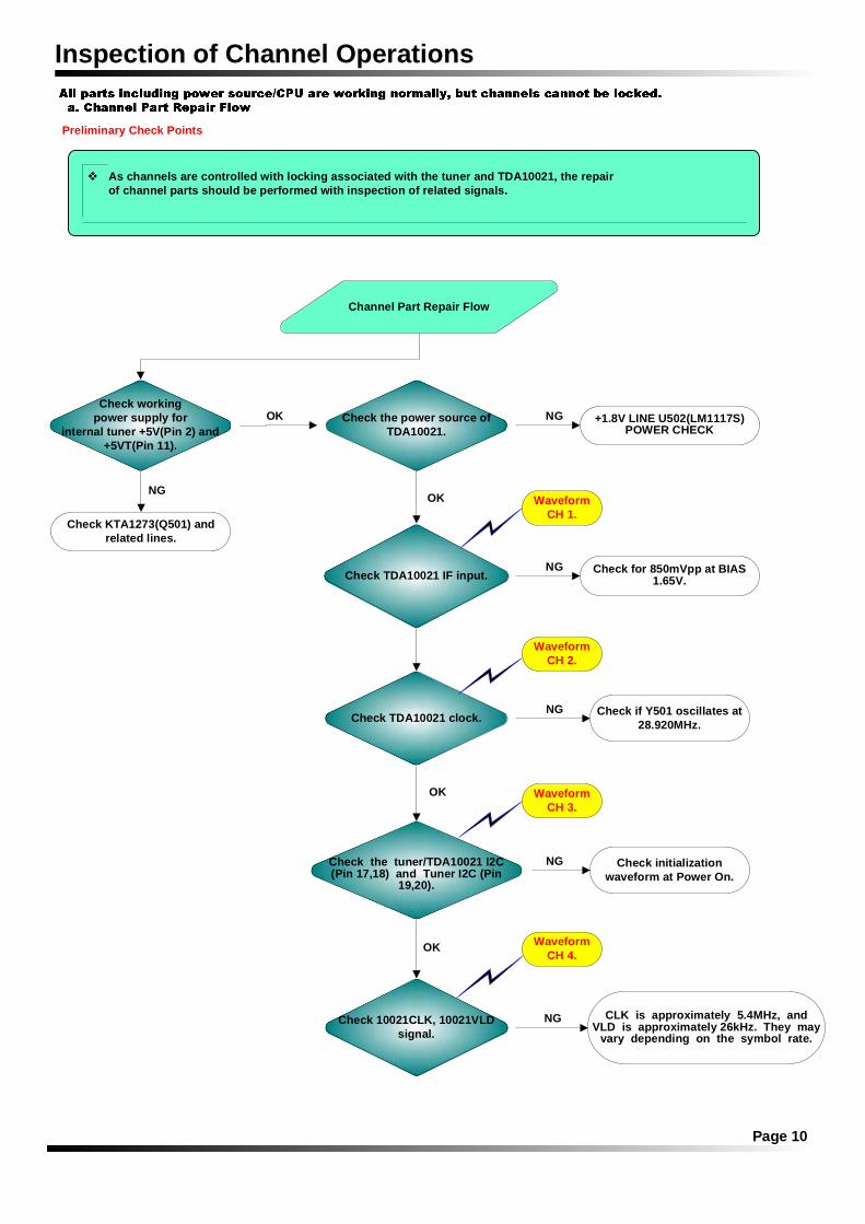
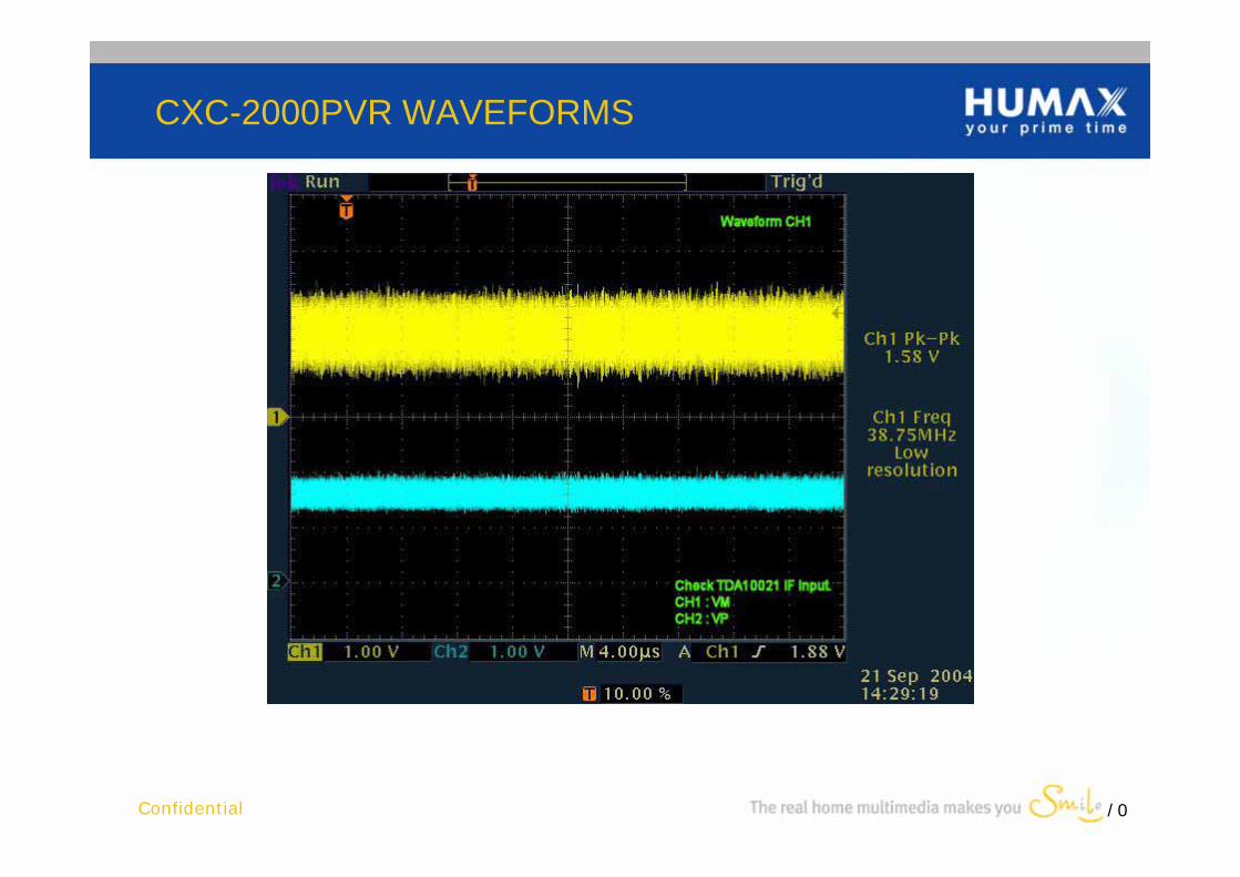
As channels are controlled with locking associated with the tuner and TDA10021, the repairof channel parts should be performed with inspection of related signals.
OK Check the power source ofTDA10021.
Check TDA10021 IF input.
Check TDA10021 clock.
Check the tuner/TDA10021 I2C(Pin 17,18) and Tuner I2C (Pin
19,20).
Check 10021CLK, 10021VLDsignal.
+1.8V LINE U502(LM1117S)POWER CHECK
Check for 850mVpp at BIAS1.65V.
Check initializationwaveform at Power On.
CLK is approximately 5.4MHz, andVLD is approximately 26kHz. They may
vary depending on the symbol rate.
OKNG
NG
NG
NG
NG
Preliminary Check Points
WaveformCH 1.
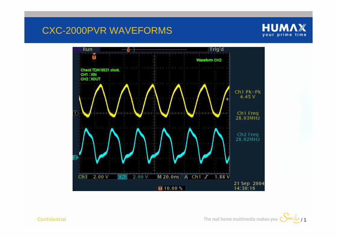
Check if Y501 oscillates at28.920MHz.
OK
OK
NG
Inspection of Channel Operations
Channel Part Repair Flow
Check workingpower supply for
internal tuner +5V(Pin 2) and+5VT(Pin 11).
Check KTA1273(Q501) andrelated lines.
WaveformCH 2.
WaveformCH 3.
WaveformCH 4.
Page 11
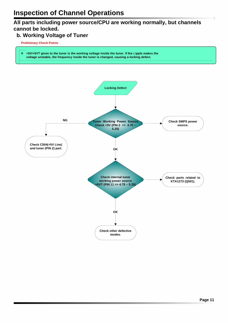
Inspection of Channel OperationsAll parts including power source/CPU are working normally, but channelscannot be locked. b. Working Voltage of Tuner
Locking Defect
+5V/+5VT given to the tuner is the working voltage inside the tuner. If the r.ipple makes thevoltage unstable, the frequency inside the tuner is changed, causing a locking defect.
Check C504(+5V Line)and tuner (PIN 2) part.
Tuner Working Power SourceCheck +5V (PIN 2 => 4.75 ~
5.25)
NG
Check other defectivemodes.
Preliminary Check Points
Check internal tunerworking power source
+5VT (PIN 11 => 4.75 ~ 5.25)
Check SMPS powersource.
Check parts related toKTA1273 (Q501).
OK
OK
Locking defect
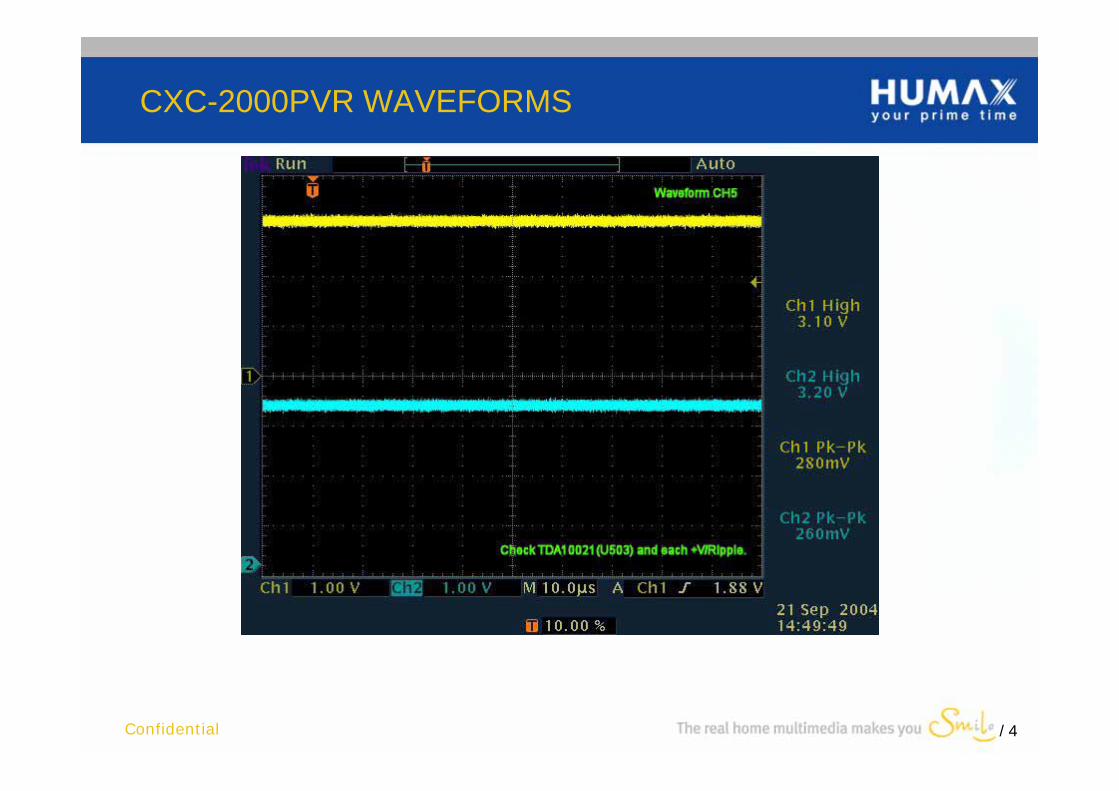
Check TDA10021(U503) andeach +V/Ripple.
Check other modes.
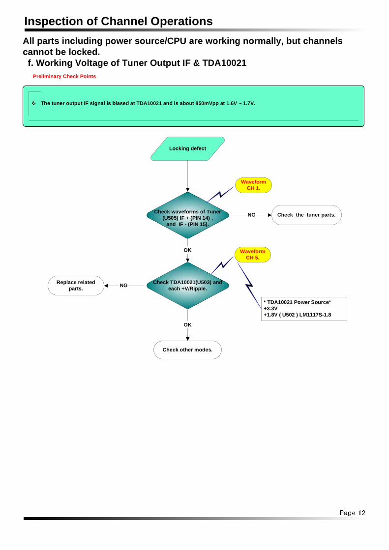
The tuner output IF signal is biased at TDA10021 and is about 850mVpp at 1.6V ~ 1.7V.
Check waveforms of Tuner(U505) IF + (PIN 14) ,
and IF - (PIN 15).
Check the tuner parts.
Replace relatedparts.
OK
OK
NG
NG
All parts including power source/CPU are working normally, but channelscannot be locked. f. Working Voltage of Tuner Output IF & TDA10021
Preliminary Check Points
Inspection of Channel Operations
* TDA10021 Power Source*+3.3V+1.8V ( U502 ) LM1117S-1.8
WaveformCH 1.
WaveformCH 5.
Page 13
Inspection of Channel Operations
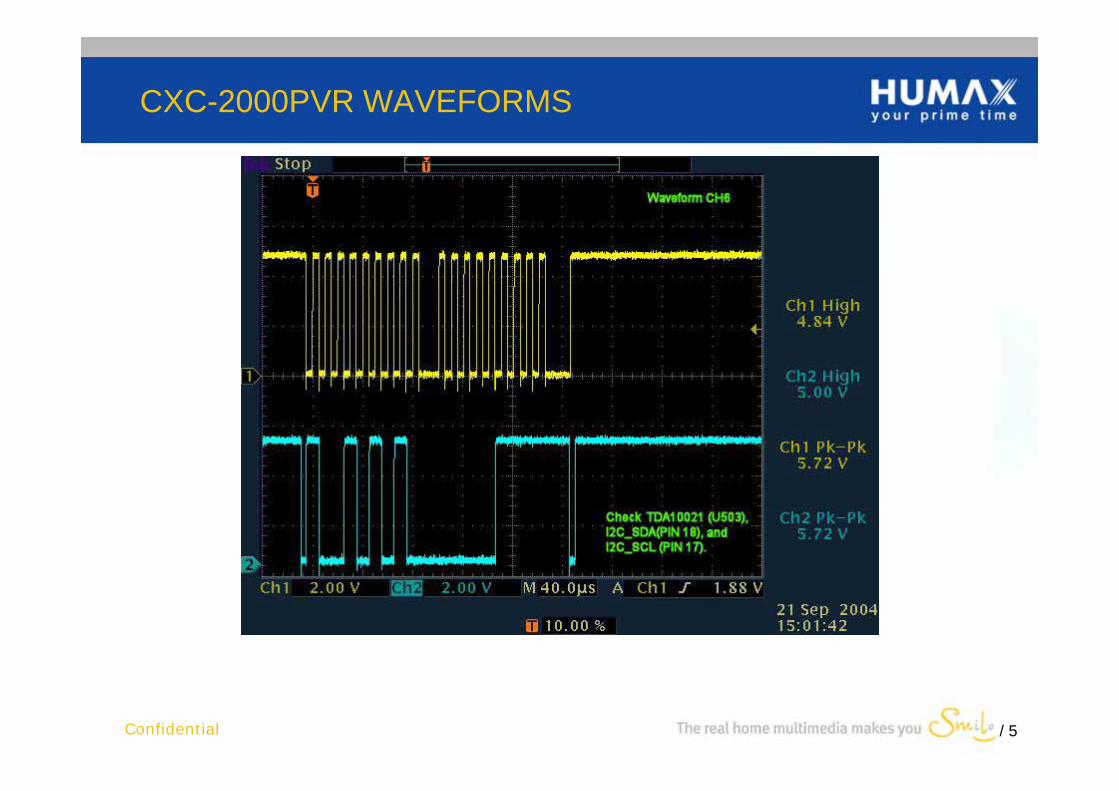
Locking defect
Check TDA10021 (U503),I2C_SDA(PIN 18), and
I2C_SCL (PIN 17).
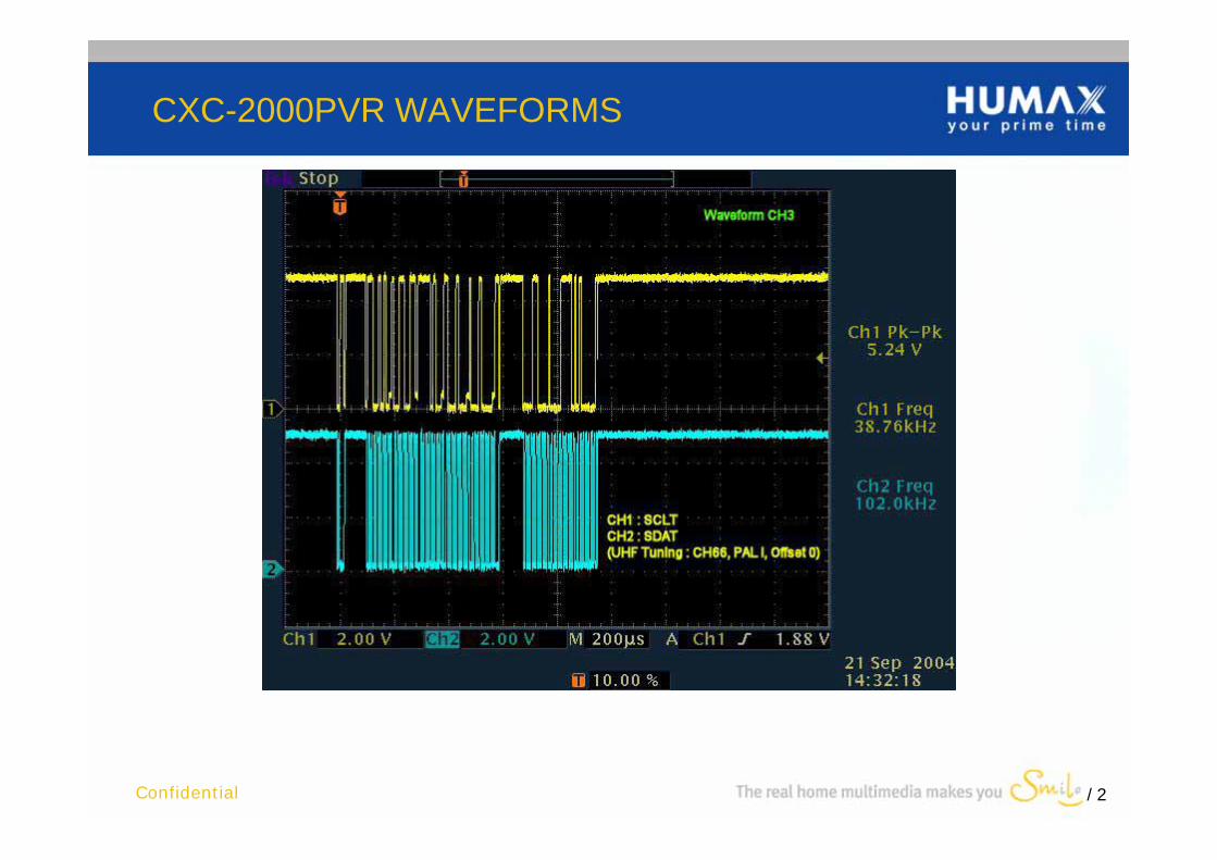
The TDA10021 CLOCK Y501 28.920MHz is converted to the A/D clock through the internal divider andused as the internal clock. Therefore, check if it produces the waveform generated by X-TAL.
The I2C BUS is generated from STi5518 for control of the tuner and TDA10021 and usedmostly for data setting necessary for channel locking and also for status reading.
Check TDA10021(U503)clock (C596, C597). Check related parts.
Replace related parts.
OK
OK
NG
NG
Check other modes.
Check TDA10021 (U503),SCLT (PIN 20), and
SDAT(PIN 19).
OK
NG
All parts including power source/CPU are working normally, but channelscannot be locked. h. TDA10021 28.920MHz Clock & I2C BUS
Preliminary Check Points
Replace related parts.
WaveformCH 2.
WaveformCH 6.
WaveformCH 3.
Page 14
Inspection of Channel Operations
Locking defect
Check TDA10021(U503)Reset (PIN 16).
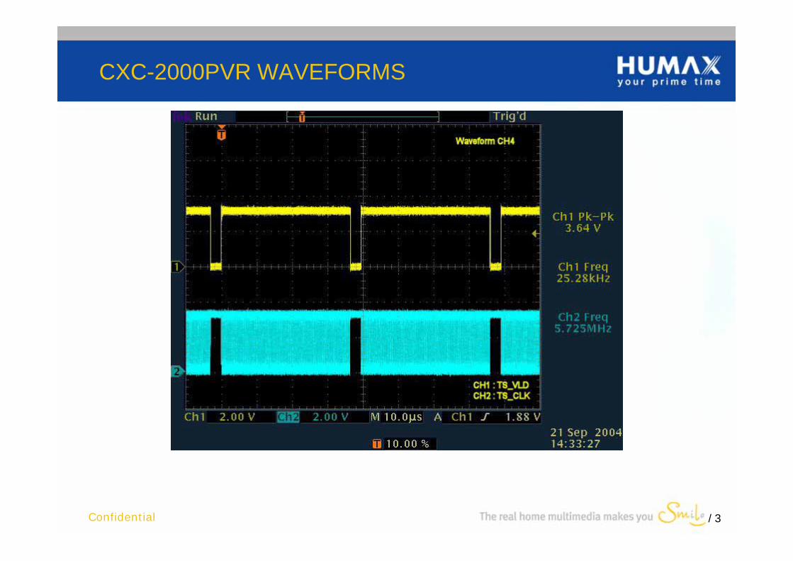
TDA10021 output is mainly divided into Bit Clock, Valid, and 8BIT Data and differs slightlydepending on the transmission parameters. Each signal is generated only when 10021 internallocking is completed.
OK
OK
NG
Check other modes.
Check TDA10021(U503)TS_VLD,TS_STR.
OK
Replace related parts. NG
All parts including power source/CPU are working normally, but channelscannot be locked. g. TDA10021 Input/Output Signal
Preliminary Check Points
Unlocked stateif not working
normally
Confirm STi5518.Replace related parts.
WaveformCH 7.
WaveformCH 8.
Page 15
MPEG Inspection
No Problems Found onBasic/Memory/Tuner LockInspections but MPEG Play
Does Not Work
Check the STi5518output SMI_CS0 &
SMI_CLKIN(Pin 74 / 82).
NG OK
Re-check basicinspection items.
Check ts path of CI2000/2(page 6, 7, and 8).
OKOK
NG
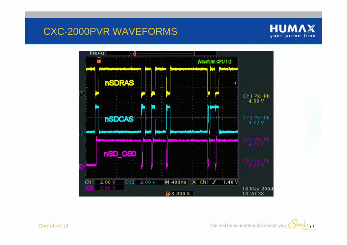
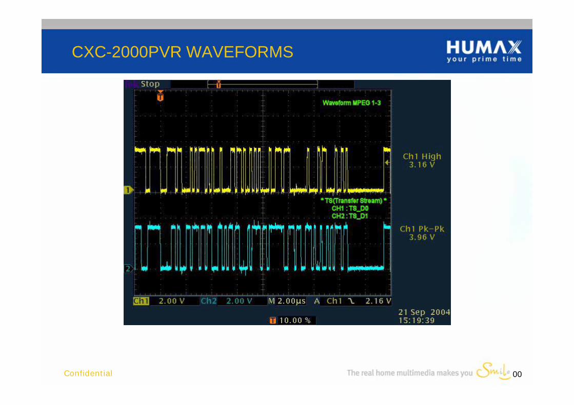
No Problems Found on Basic and CPU/System Memory Inspections, butMPEG Does Not Play- Check MPEG SDRAM Interface/Transfer Stream (TS).
WaveformMPEG1-1
Check soldering ofSMI SDRAM.
STi5518 & SDRAMInterface Signal
Check
If MPEG playback does not work even though no problems were found on the Basic inspection,CPU/Flash inspection, and Tuner Lock inspection, check the SMI SDRAM I/F of the MPEG memory sector.
SMI SDRAM of IC STi5518 is selected when the SMI_CS0 (Pin 74) signal of STi5518 is LOW.
The main cause of the problems related to System Memory (i.e. Flash and SDRAM) is the soldering of parts.Therefore, in the event of a problem, first check the condition of the soldering and the power supply of IC.
Transfer Stream (TS)Line CHECK
PR51,PR52,R511,R512,R513
OK
Useful Tips
1. The above checkpoints are listed in order. Because signals will pass through various paths between the above checkpoints, if any checkpoint
shows waveforms unlike the above, refer to the circuit diagram according to the above order to identify the location.
2. If the MPEG still does not play, check if a signal error is caused by poor soldering of the TS Data Line.
WaveformMPEG1-2
U182 : 5518U390 : SMI SDRAM
Check path between 10021and CI2000/2/STi5518.
(Incorrect insertion, poorsoldering, short circuits,
damage, etc.)
NG
WaveformMPEG1-3
Preliminary Checkpoints
Page 16
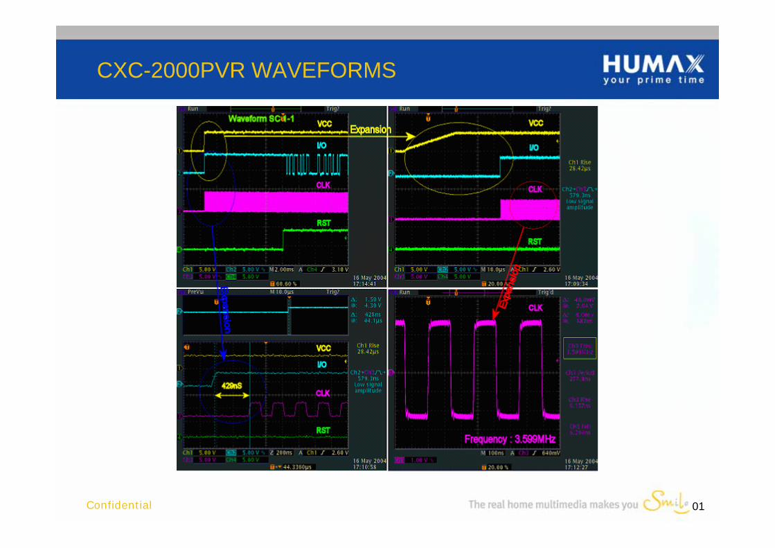
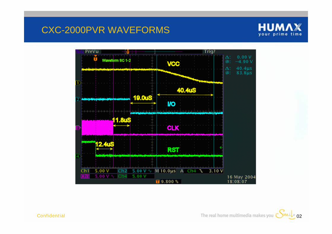
Smart Card (CAS) Inspection
Card Not Detected or Cannot Descramble
Card detectionfailure and
Descramble failure
If a problem has occurred with Smart Card operation, check the solderingaround TDA8004 and Card Reader. If no problem is found, check the condition of each signal.
It may be necessary to check whether the card has any problems by using a Smart Card B/D andSmart Card that work normally.
OK
Check U700 pin 23(/OFF)of CARD DETECT signal
S/C B/D
+3.3V POWER LINE +5V POWER LINE
CHECK
Check operatingpower (+3.3V) of SmartCard B/D and the Card
power (+5V).
Check related parts andreplace U701 Reader.
HIGH
NG
LOW
Check for otherdefective modes.
U700 pin 9(/PRES)CHECK
HIGH
LOW
Check related parts andreplace TDA8024T.
ACTIVATION &DEACTIVATION SEQUENCE
CHECK(ISO/IEC 7816 SPEC)
NG
Waveform SC1-1Waveform SC1-2
OK
Useful Tips
1. When accessing Smart Card, if Activation Sequence, Deactivation Sequence, or Emergency Deactivation Sequence (at Power-Off), which conform to ISO/IEC 7816 Spec, are not satisfied, the card may get damaged or result in descrambling.
Preliminary Checkpoints
Page 17
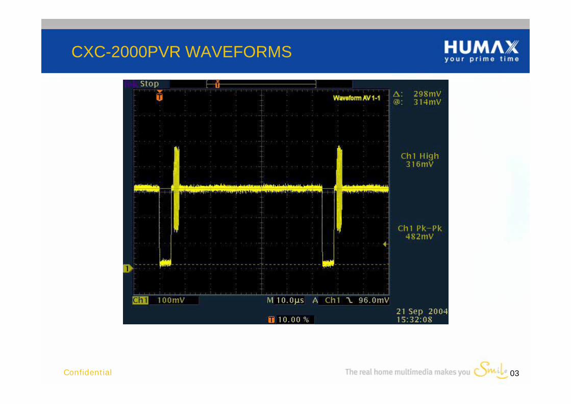
A/V Inspection 1
No Video Output
If no video is output through TV/VCR SCART or CINCH while the front display and key controls are normal,first check the 5518 video output terminal and the 6412 input voltage.
If no problems were found on the 5518 output terminal and the 6412 input voltage, check the output signalaround 6412 since the final video out is controlled by 6412.
Useful Tips
1. Because I2C BUS continues polling, to determine whether the devices using the I2C are working properly, check the waveforms and messages using s/w with monitor s/w or debug.
No Video Output
NG
OK
Check STi5518BVCVIDEO OUTPUT.
Check 6412 input voltage.
C437 : CVBSC438 : YC439 : CC440 : RC441 : GC442 : B
* TV_SCART PIN38 : BLUE PIN40 : GREEN PIN42 : RED/Chrom. PIN44 : CVBS * VCR SCART PIN46 : Chorm. PIN48 : CVBS * CINCH, RF PIN36 : CVBS
Check RF MODULATORVIDEO INPUT.
C446
Check for other defectivemodes.
Check path between 6412 andeach Output con.
(Incorrect insertion, poor soldering,short circuits, damage, etc.)
OK
OKCheck 6412 VIDEO OUTPUT.
NG
NG
NGCheck if there is no RF output.
* 5V PIN1,53,47,45,43,39,37 * 12V PIN31,63
After basic inspection (1), checkpath between SMPS and 6412.
(Incorrect insertion, poor soldering,short circuits, damage, etc.)
Check path between 5518 and 6412.(Incorrect insertion, poor soldering,
short circuits, damage, etc.)
Check path between 6412 and Rf.(Incorrect insertion, poor soldering,
short circuits, damage, etc.)
Check 6412, RF IIC DATA,and CLOCK.
* IIC CLOCK[PIN55] * IIC DATA[PIN56]
Check path between the devicesthat use 5518~IIC BUS [10021,
EEPROM ,RF, and 6412].(Incorrect insertion, poor soldering,
short circuits, damage, etc.)
OK
OK
NG
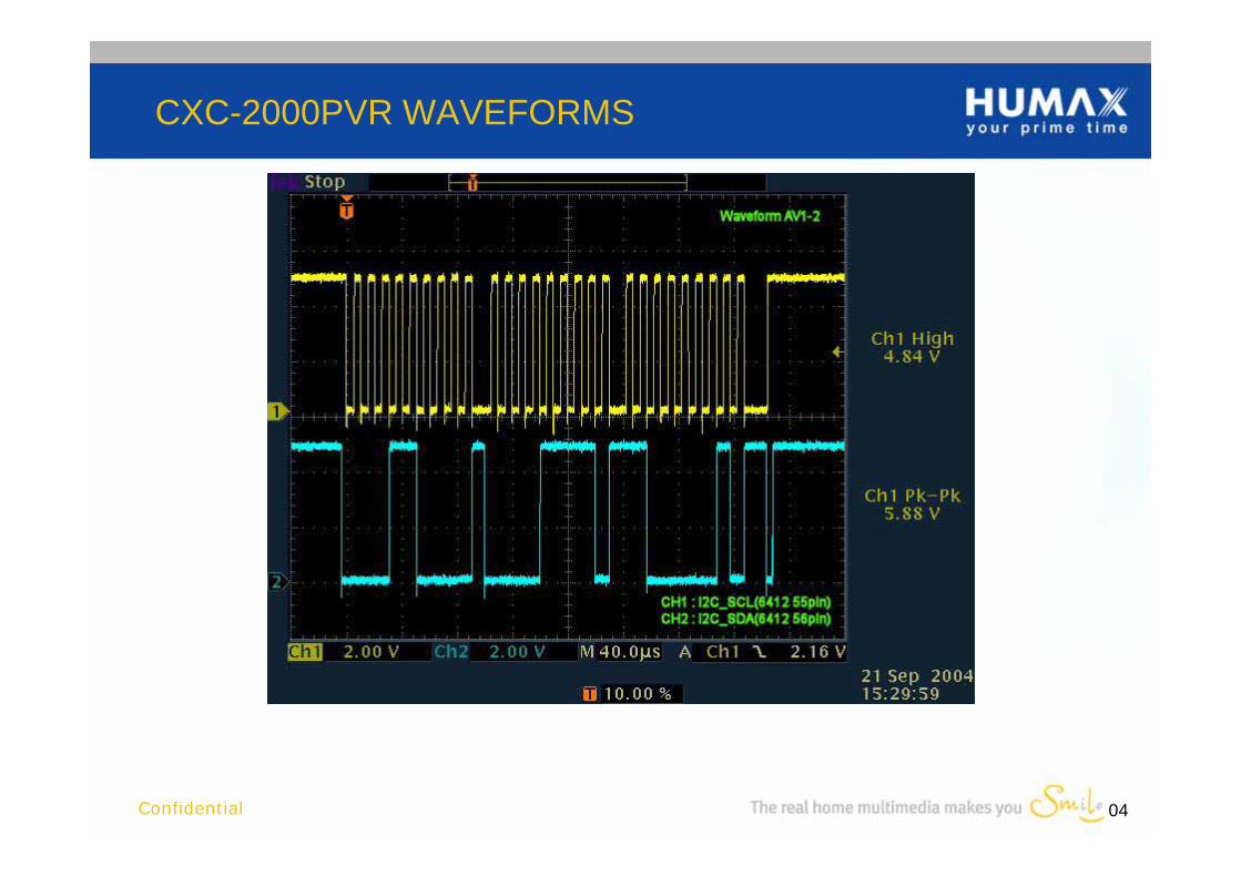
Waveform AV1-1
Waveform AV1-2
U430 : STV6412ADU505 : Tuner with RF
Preliminary Checkpoints
Page 18
A/V Inspection 2
No Audio Output
No Audio Output
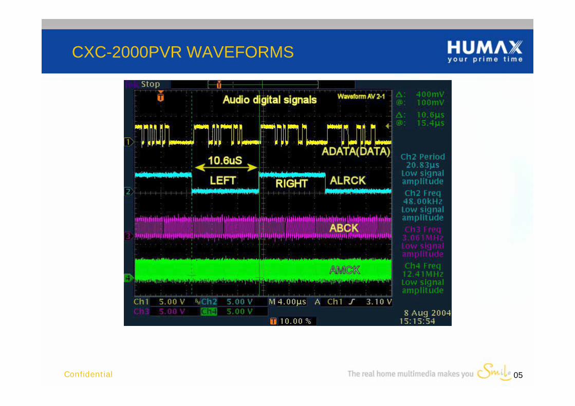
If no audio is output through CINCH while the system is normal, first check the 5518 AUDIO output [I2S interface].
If no problems were found, check the UDA1334 AUDIO OUT terminal and 6412 OUT to identify the problem path.
Useful Tips
1. Because I2C BUS continues polling, to determine whether the devices using the I2C are working properly, check the waveforms and messages using s/w with monitor s/w or debug.
OK
Check STi5518BVC I2Soutput.
Check UDA1334input voltage.
Check 6412 inputvoltage.
Check UDA1334AUDIO OUTPUT.
PIN 14,16
Check 6412 AUDIOOUTPUT.
Check RF MODULATORINPUT.C501
Check for other defectivemodes.
Check if there is RF output.
* TV_SCART PIN32 : Right PIN33 : Left * VCR SCART PIN29 : Right PIN30 : Left * CINCH PIN27 : Right PIN28 : Left * Rf PIN35 : MONO
* UDA1334BTS PIN1 : DA_CLK PIN6 : DA_FSCLK PIN2 : DA_WS PIN3 : DA_DATA
NG
NG
NG
NG
NG
OK
*UDA1334 Input Voltage 3.3V[PIN4,13] Vref(1.65V)[PIN12]
* 6412 Input Voltage 5V[PIN1,53,47,45,43,39,37] 12V[PIN31,63] Vref(4.3V)[PIN16]
Check path between 5518 and 1334.(Incorrect insertion, poor soldering,
short circuits, damage, etc.)
After basic inspection 1, check thepath between SMPS and 1334, 6412.(Incorrect insertion, poor soldering,
short circuits, damage, etc.)
Check path between 1334 and 6412.(Incorrect insertion, poor soldering,
short circuits, damage, etc.)
Check path between 6412 and Rf.(Incorrect insertion, poor soldering,
short circuits, damage, etc.)
Check path between 6412 andeach Output con.
(Incorrect insertion, poor soldering,short circuits, damage, etc.)
Check 6412, RF IIC DATA,and CLOCK.
* IIC CLOCK[PIN55] * IIC DATA[PIN56]
Check path between the devicesthat use 5518~IIC BUS [10021,
EEPROM ,RF, and 6412].(Incorrect insertion, poor soldering,
short circuits, damage, etc.)
NG
OK
OK
OK
OK
OK
WaveformAV2-1
Waveform AV1-2
Preliminary Checkpoints
U430 : STV6412ADU505 : Tuner with RF
Page 19
A/V Inspection 3
Cannot change theAspect Ratio
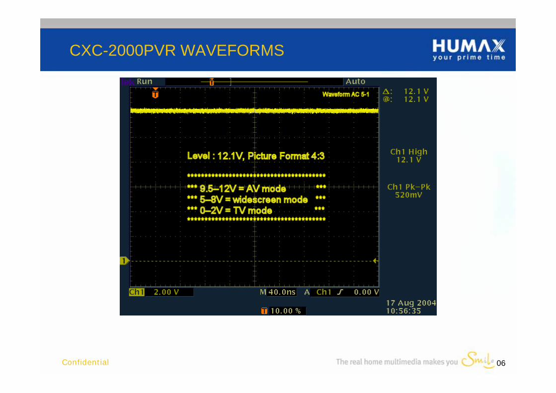
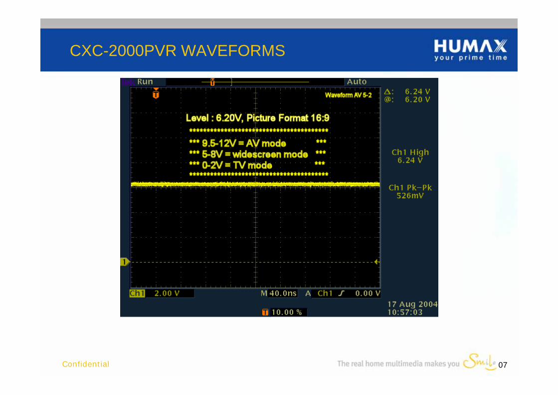
If the aspect ratio cannot be changed while the system is normal[including A/V Inspection (1, 2)], check the SCART function voltage of 6412.
NG
OKCheck output voltage
of 6412 SBO_TV.D562.Cathode
Cannot Change the Screen Ratio [4:3 <-> 16:9]
Check for otherdefective modes.
* 4:3 mode4.5~7V
* 16:9 mode9.5~12V
OK
Check path between 6412 andTV SCART.8pin
(Incorrect insertion, poor soldering,short circuits, damage, etc.)
U430 : STV6412AD
Preliminary Checkpoints
Page 20
A/V Inspection 4
Cannot change theAspect Ratio
If TV -> VCR Bypass does not work while the system is normal [including A/V Inspection(1, 2)], check the input and output of 6412.
NG
OK
Check output voltage of6412 SBO_TV.D562.Cathode
T-> VCR Bypass Does Not Work V
Check for otherdefective modes.
* TV -> VCR BYPASS:0~2V
Check 6412 A/V INPUT.
* VIDEO Input PIN21 :CVBS
* AUDIO Input PIN22 : Left PIN23 : Right
Check 6412 A/V OUTPUT.
* VIDEO Input PIN21: CVBS
* AUDIO Output PIN29: Right PIN30: Left
OK
NG
OK
Check path between 6412 and TVSCART.
(Incorrect insertion, poor soldering,short circuits, damage, etc.)
Check path between TV SCARTand 6412 input.
(Incorrect insertion, poor soldering,short circuits, damage, etc.)
Check path between 6412 andVCR SCART.
(Incorrect insertion, poor soldering,short circuits, damage, etc.)
NG
U430 : STV6412AD
Preliminary Checkpoints
Page 21
A/V Inspection 5
Cannot change theAspect Ratio
If VCR -> TV Bypass does not work while the system is normal [including A/V Inspection (1, 2)],check the input and output of 6412.
NG
OK
Check 6412 input voltage.PIN61(SBO_VCR)PIN50(FBIN_VCR)
VCR -> TV VCR -> TV Bypass Does Not Work.
* PIN61 -4:3 mode[4.5~7V] -16:9 mode[9.5~12V]
* PIN50 -RGB Input [1~3V] -CVBS/S-VIDEO Input [0~1V]
Check 6412 A/V INPUT.
* VIDEO PIN64: Blue PIN62: Green PIN60: Red/Chrom. PIN18: Cvbs
* AUDIO PIN19: Left PIN20: Right
Check outputvoltage of 6412.D549.CathodeD562.Cathode
* D549.Cathode -4:3 mode[4.5~7V] -16:9 mode[9.5~12V]
*D562.Cathode -RGB Output [1~3V] -CVBS/S-VIDEO Output [0~1V]
Check for otherdefective modes.
Check 6412 A/V OUTPUT.
* VIDEO Input PIN38: BLUE PIN40: GREEN PIN42: RED/Chrom. PIN44: CVBS
* AUDIO Output PIN32: Right PIN33: Left
OK
OK
OK
NG
NG
NG
Check path between 6412and VCR SCART.
(Incorrect insertion, poor soldering,short circuits, damage, etc.)
Check path between 6412and VCR SCART.
(Incorrect insertion, poor soldering,short circuits, damage, etc.)
Check path between 6412and TV SCART.
(Incorrect insertion, poor soldering,short circuits, damage, etc.)
Check path between6412 and TV SCART.
(Incorrect insertion, poor soldering,short circuits, damage, etc.)
U430 : STV6412AD
Preliminary Checkpoints
Waveform AV5-1,AV5-2, AV5-3, AV5-4
Page 22
A/V Inspection 6
Cannot changeVideo Mode
If CVBS (S-VIDEO) <-> RGB switching does not work while the system is normal[including A/V Inspection (1, 2)], check fast blanking of 6412.
NG
OKCheck output
voltage of 6412. D549.Cathode
Cannot Switch between CVBS (S-VIDEO) <-> RGB
Check for other defectivemodes.
-RGB MODE[1~3V]
-CVBS/S-VIDEO MODE [0~1V]
OK
Check path between 6412and TV SCART.
(Incorrect insertion, poor soldering,short circuits, damage, etc.)
U430 : STV6412AD
Preliminary Checkpoints
Page 23
A/V Inspection 7
No SPDIF Output
If the SPDIF output is not working while the system is normal (including MPEG Play and A/V Output),first check for any problems with the SPDIF output of 5518.If no problems were found, check for any problems with the input power of the SPDIF connector.
NG
OK
Check SPDIF output of 5518.
No SPDIF Output
*5518.PIN57
OK
Check path between 5518 andJP450 (TOTX178A).
(Incorrect insertion, poor soldering,short circuits, damage, etc.)
Check input power of JP450(TOTX178A).
After basic inspection (1), check thepath between SMPS and R450.
(Incorrect insertion, poor soldering,short circuits, damage, etc.)
NG
Check for otherdefective modes.
+5V : R450
OK
U182 : 5518JP450 : TOTX178A
Preliminary Checkpoints
Page 24
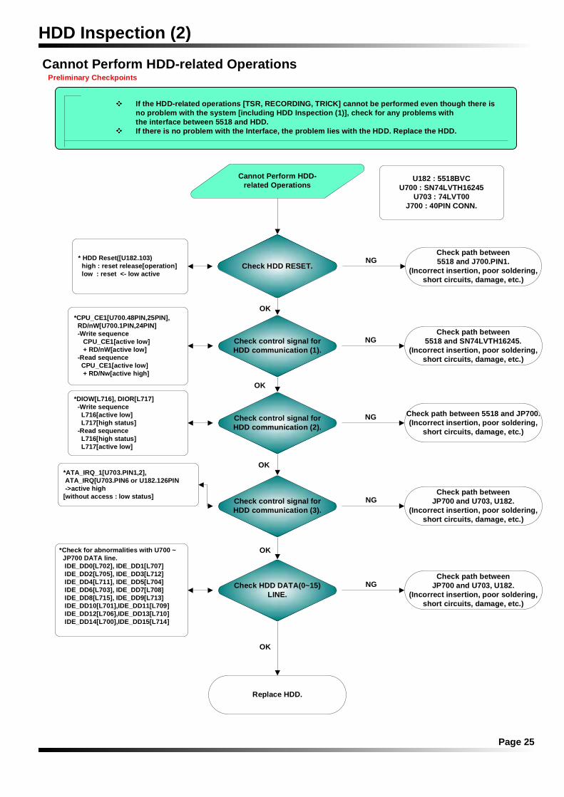
HDD Inspection (1)
Cannot Perform HDD-related Operations
If the HDD-related operations [TSR, RECORDING, TRICK] cannot be performed even though the system is normal,first check the HDD cable assembly condition and check for any problems with the HDD power supply.
Cannot Perform HDD-related Operations
NG
OK
Check insertion of theHDD power cable and JP700
40PIN cable.
Check HDD PWR[+5V,+12V]control signal.
HDD Inspection (2)
OK
* U21[TS80C52].PIN10 or U182[STi5518].125pin high : Operation mode low : standby mode
Check for incorrect insertion, poorsoldering, short circuits, damage,
etc.NG
After unplugging theHDD cable, re-check theHDD PWR control signal
from the CPU B/D.
Replace SMPS.
NG
Check HDD power supply.(+5V, +12V)
*SMPS BDÀÇ HDD2 PIN1.5V(+/-0.25V) PIN4.12V(+/-0.8V)
Replace SMPS.
OK
NG
Preliminary Checkpoints
Page 25
HDD Inspection (2)
Cannot Perform HDD-related Operations
Cannot Perform HDD-related Operations
If the HDD-related operations [TSR, RECORDING, TRICK] cannot be performed even though there isno problem with the system [including HDD Inspection (1)], check for any problems withthe interface between 5518 and HDD.If there is no problem with the Interface, the problem lies with the HDD. Replace the HDD.
Check HDD RESET.
Check control signal forHDD communication (1).
* HDD Reset([U182.103) high : reset release[operation] low : reset <- low active
U182 : 5518BVCU700 : SN74LVTH16245
U703 : 74LVT00J700 : 40PIN CONN.
NG
NG
NG
*CPU_CE1[U700.48PIN,25PIN], RD/nW[U700.1PIN,24PIN] -Write sequence CPU_CE1[active low] + RD/nW[active low] -Read sequence CPU_CE1[active low] + RD/Nw[active high]
Check path between5518 and J700.PIN1.
(Incorrect insertion, poor soldering,short circuits, damage, etc.)
Check path between5518 and SN74LVTH16245.
(Incorrect insertion, poor soldering,short circuits, damage, etc.)
Check path between 5518 and JP700.(Incorrect insertion, poor soldering,
short circuits, damage, etc.)
OK
OK
Check control signal forHDD communication (2).
*DIOW[L716], DIOR[L717] -Write sequence L716[active low] L717[high status] -Read sequence L716[high status] L717[active low]
Check control signal forHDD communication (3).
*ATA_IRQ_1[U703.PIN1,2], ATA_IRQ[U703.PIN6 or U182.126PIN ->active high [without access : low status]
Check HDD DATA(0~15)LINE.
Check path betweenJP700 and U703, U182.
(Incorrect insertion, poor soldering,short circuits, damage, etc.)
*Check for abnormalities with U700 ~ JP700 DATA line. IDE_DD0[L702], IDE_DD1[L707] IDE_DD2[L705], IDE_DD3[L712] IDE_DD4[L711], IDE_DD5[L704] IDE_DD6[L703], IDE_DD7[L708] IDE_DD8[L715], IDE_DD9[L713] IDE_DD10[L701],IDE_DD11[L709] IDE_DD12[L706],IDE_DD13[L710] IDE_DD14[L700],IDE_DD15[L714]
Check path betweenJP700 and U703, U182.
(Incorrect insertion, poor soldering,short circuits, damage, etc.)
Replace HDD.
NG
NG
OK
OK
OK
Preliminary Checkpoints
Page 26
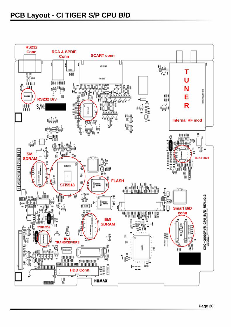
PCB Layout - CI TIGER S/P CPU B/D
RS232Conn RCA & SPDIF
Conn SCART conn
TUNER
Internal RF mod
HDD Conn
STi5518FLASH
EMISDRAM
SMISDRAM
Smart B/Dconn
RS232 Drv
TDA10021
TS80C52
BUSTRANSCEIVERS
Page 27
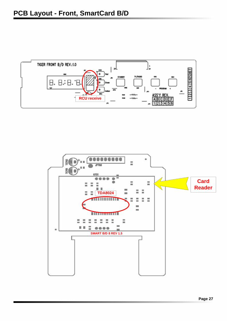
PCB Layout - Front, SmartCard B/D
TDA8024
CardReader
RCU receive
SMART B/D 8 REV 1.5
1Confidential
CXC-2000PVR WAVEFORMS
2Confidential
CXC-2000PVR WAVEFORMS
3Confidential
CXC-2000PVR WAVEFORMS
4Confidential
CXC-2000PVR WAVEFORMS
5Confidential
CXC-2000PVR WAVEFORMS
6Confidential
CXC-2000PVR WAVEFORMS
7Confidential
CXC-2000PVR WAVEFORMS
8Confidential
CXC-2000PVR WAVEFORMS
9Confidential
CXC-2000PVR WAVEFORMS
10Confidential
CXC-2000PVR WAVEFORMS
11Confidential
CXC-2000PVR WAVEFORMS
12Confidential
CXC-2000PVR WAVEFORMS
13Confidential
CXC-2000PVR WAVEFORMS
14Confidential
CXC-2000PVR WAVEFORMS
15Confidential
CXC-2000PVR WAVEFORMS
16Confidential
CXC-2000PVR WAVEFORMS
17Confidential
CXC-2000PVR WAVEFORMS
18Confidential
CXC-2000PVR WAVEFORMS
19Confidential
CXC-2000PVR WAVEFORMS
20Confidential
CXC-2000PVR WAVEFORMS
21Confidential
CXC-2000PVR WAVEFORMS
22Confidential
CXC-2000PVR WAVEFORMS
23Confidential
CXC-2000PVR WAVEFORMS
24Confidential
CXC-2000PVR WAVEFORMS
25Confidential
CXC-2000PVR WAVEFORMS
26Confidential
CXC-2000PVR WAVEFORMS
27Confidential
CXC-2000PVR WAVEFORMS
28Confidential
CXC-2000PVR WAVEFORMS
29Confidential
CXC-2000PVR WAVEFORMS
30Confidential
CXC-2000PVR WAVEFORMS
31Confidential
CXC-2000PVR WAVEFORMS
+17V
+12V
To TUNER
PW206i
DIGITAL SETTOP BOX
DECODER
(STi5518CVC)DIGITAL CABLE TUNER
(CDM1316L/IM MK2)
+3V3
+5V
+7V5
+12V
+17V
+24V
+30V
REGULATOR
(LP3965EMX-2.5)
+3V3
REGULATO
R
(KA7805)
REGULATOR
(LM1117
MPX-1.8)
FRONT-
uCOM
(AT89S52)
FRONT PCB
+5V
+7V5
+12V
+5V
+5V
+
5V
U
+3V
3
+3V
3D
+2V
5_1V
8
+2V
5_1V
8D
+5VT
QAM
DEMODULATOR
(TDA10021/B3)
VCC1V8_CH
+3V
3
VC
C1V
8_C
H
+5V
+5V
T
74LVC08
A
+3V
3
CI
CONTROLLE
R
(CI2000)
+3V
3
+5V
POWER
MOSFET
(IRF7303)
PCMCIA SLOT
+5V
+5V
S
1, S
2
+5V
74LVC
139A
FLASH
MEMORY
(M28W160CT9
0)FLASH
MEMORY
(M28W160CT9
0)
+3V
3
+3V
3
SMI SDRAM
(K4S641632H-
TC60)EMI SDRAM
(K4S641632H-
TC60)
+3V
3
+3V
3_0, +
3V
3_1
EEPROM
(24C64SN
)
+5V
RESET
(KIA
7027AF)
+3V
3
VCXO
&
VCXO
IC
+3V
3
AUDIO
DAC
(UDA133
4)
+3V
3
AV MATRIX IC
(STV6412AD)
+5V
S
+12V
S
SRDIF
(OPTIC)
+5V
RS-232
(HIN232)
+5V
SMART CARD
CONNECTORSMART CARD
CONNECTOR
+3V
3
+5V
IC_IRQ
(KIA7029V
F)
+3V
3
HDD
CONNECTOR
SN74LVTH16245
+3V
3
+3V
3
74LVT
00
+3V
3
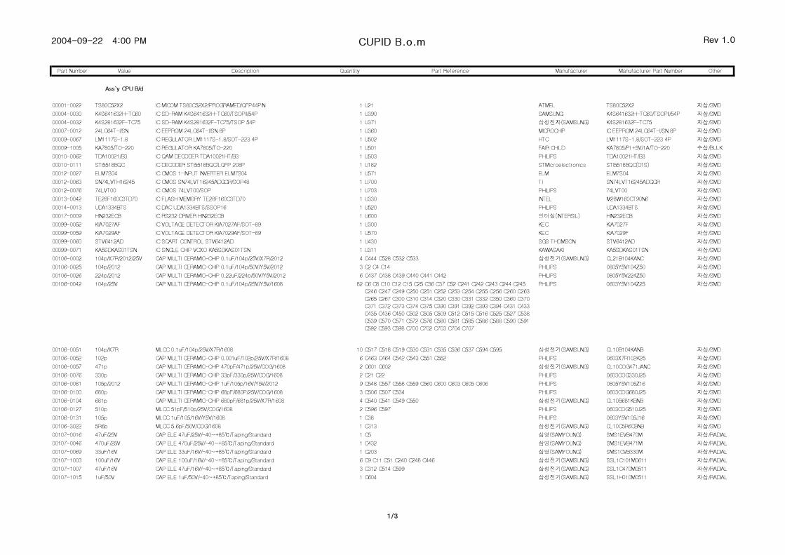
2004-09-22 4:00 PM CUPID B.o.m Rev 1.0
Part Number Value Description Quantity Part Reference Manufacturer Manufacturer Part Number Other
Ass`y CPU B/d
00001-0022 TS80C52X2 IC MICOM TS80C52X2/PROGRAMED/QFP44PIN 1 U21 ATMEL TS80C52X2 자삽/SMD
00004-0030 K4S641632H-TC60 IC SD-RAM K4S641632H-TC60/TSOPII/54P 1 U390 SAMSUNG K4S641632H-TC60/TSOPII/54P 자삽/SMD
00004-0032 K4S281632F-TC75 IC SD-RAM K4S281632F-TC75/TSOP 54P 1 U371 삼성전자(SAMSUNG) K4S281632F-TC75 자삽/SMD
00007-0012 24LC64T-I/SN IC EEPROM 24LC64T-I/SN 8P 1 U360 MICROCHIP IC EEPROM 24LC64T-I/SN 8P 자삽/SMD
00009-0067 LM1117S-1.8 IC REGULATOR LM1117S-1.8/SOT-223 4P 1 U502 HTC LM1117S-1.8/SOT-223 4P 자삽/SMD
00009-1005 KA7805/TO-220 IC REGULATOR KA7805/TO-220 1 U501 FAIR CHILD KA7805/PI +5V/1A/TO-220 수삽/BULK
00010-0062 TDA10021/B3 IC QAM DECODER TDA10021HT/B3 1 U503 PHILIPS TDA10021HT/B3 자삽/SMD
00010-0111 STI5518BQC IC DECODER STI5518BQC/LQFP 208P 1 U182 STMicroelectronics STI5518BQC(D1S) 자삽/SMD
00012-0027 ELM7S04 IC CMOS 1-INPUT INVERTER ELM7S04 1 U571 ELM ELM7S04 자삽/SMD
00012-0063 SN74LVTH16245 IC CMOS SN74LVT16245ADGGR/SOP48 1 U700 TI SN74LVT16245ADGGR 자삽/SMD
00012-0076 74LVT00 IC CMOS 74LVT00/SOP 1 U703 PHILIPS 74LVT00 자삽/SMD
00013-0042 TE28F160C3TD70 IC FLASH MEMORY TE28F160C3TD70 1 U330 INTEL M28W160CT90N6 자삽/SMD
00014-0013 UDA1334BTS IC DAC UDA1334BTS/SSOP16 1 U520 PHILIPS UDA1334BTS 자삽/SMD
00017-0009 HIN232ECB IC RS232 DRIVER HIN232ECB 1 U600 인터실(INTERSIL) HIN232ECB 자삽/SMD
00099-0052 KIA7027AF IC VOLTAGE DETECTOR KIA7027AF/SOT-89 1 U300 KEC KIA7027F 자삽/SMD
00099-0059 KIA7029AF IC VOLTAGE DETECTOR KIA7029AF/SOT-89 1 U570 KEC KIA7029F 자삽/SMD
00099-0060 STV6412AD IC SCART CONTROL STV6412AD 1 U430 SGS THOMSON STV6412AD 자삽/SMD
00099-0071 KA5SDKAS01TSN IC SINGLE CHIP VCXO KA5SDKAS01TSN 1 U311 KAWASAKI KA5SDKAS01TSN 자삽/SMD
00106-0002 104p/X7R/2012/25V CAP MULTI CERAMIC-CHIP 0.1uF/104p/25V/X7R/2012 4 C444 C528 C532 C533 삼성전기(SAMSUNG) CL21B104KANC 자삽/SMD
00106-0025 104p/2012 CAP MULTI CERAMIC-CHIP 0.1uF/104p/50V/Y5V/2012 3 C2 C4 C14 PHILIPS 0805Y5V104Z50 자삽/SMD
00106-0026 224p/2012 CAP MULTI CERAMIC-CHIP 0.22uF/224p/50V/Y5V/2012 6 C437 C438 C439 C440 C441 C442 PHILIPS 0805Y5V224Z50 자삽/SMD
00106-0042 104p/25V CAP MULTI CERAMIC-CHIP 0.1uF/104p/25V/Y5V/1608 82 C6 C8 C10 C12 C15 C25 C36 C37 C52 C241 C242 C243 C244 C245
C246 C247 C249 C250 C251 C252 C253 C254 C255 C256 C260 C263
C265 C267 C300 C310 C314 C320 C330 C331 C332 C350 C360 C370
C371 C372 C373 C374 C375 C390 C391 C392 C393 C394 C431 C433
C435 C436 C450 C502 C505 C509 C512 C515 C516 C525 C527 C538
C539 C570 C571 C572 C576 C580 C581 C585 C586 C588 C590 C591
C592 C593 C598 C700 C702 C703 C704 C707
PHILIPS 0603Y5V104Z25 자삽/SMD
00106-0051 104p/X7R MLCC 0.1uF/104p/25V/X7R/1608 10 C517 C518 C519 C530 C531 C535 C536 C537 C594 C595 삼성전기(SAMSUNG) CL10B104KANB 자삽/SMD
00106-0052 102p CAP MULTI CERAMIC-CHIP 0.001uF/102p/25V/X7R/1608 6 C463 C464 C542 C543 C551 C552 PHILIPS 0603X7R102K25 자삽/SMD
00106-0057 471p CAP MULTI CERAMIC-CHIP 470pF/471p/25V/COG/1608 2 C601 C602 삼성전기(SAMSUNG) CL10COG471JANC 자삽/SMD
00106-0076 330p CAP MULTI CERAMIC-CHIP 33pF/330p/25V/COG/1608 2 C21 C22 PHILIPS 0603COG330J25 자삽/SMD
00106-0081 105p/2012 CAP MULTI CERAMIC-CHIP 1uF/105p/16V/Y5V/2012 9 C548 C557 C558 C559 C560 C600 C603 C605 C606 PHILIPS 0805Y5V105Z16 자삽/SMD
00106-0100 680p CAP MULTI CERAMIC-CHIP 68pF/680P/25V/COG/1608 3 C506 C507 C534 PHILIPS 0603COG680J25 자삽/SMD
00106-0104 681p CAP MULTI CERAMIC-CHIP 680pF/681p/25V/X7R/1608 4 C540 C541 C549 C550 삼성전기(SAMSUNG) CL10B681KBNB 자삽/SMD
00106-0127 510p MLCC 51pF/510p/25V/COG/1608 2 C596 C597 PHILIPS 0603COG510J25 자삽/SMD
00106-0131 105p MLCC 1uF/105/16V/Y5V/1608 1 C38 PHILIPS 0603Y5V105J16 자삽/SMD
00106-3022 5R6p MLCC 5.6pF/50V/COG/1608 1 C313 삼성전기(SAMSUNG) CL10C5R6CBNB 자삽/SMD
00107-0016 47uF/25V CAP ELE 47uF/25V/-40~+85℃/Taping/Standard 1 C5 삼영(SAMYOUNG) SMS1EVB470M 자삽/RADIAL
00107-0046 470uF/25V CAP ELE 470uF/25V/-40~+85℃/Taping/Standard 1 C432 삼영(SAMYOUNG) SMS1EVB471M 자삽/RADIAL
00107-0069 33uF/16V CAP ELE 33uF/16V/-40~+85℃/Taping/Standard 1 C203 삼영(SAMYOUNG) SMS1CVB330M 자삽/RADIAL
00107-1003 100uF/16V CAP ELE 100uF/16V/-40~+85℃/Taping/Standard 6 C9 C11 C51 C240 C248 C446 삼성전기(SAMSUNG) SSL1C101M0611 자삽/RADIAL
00107-1007 47uF/16V CAP ELE 47uF/16V/-40~+85℃/Taping/Standard 3 C312 C514 C599 삼성전기(SAMSUNG) SSL1C470M0511 자삽/RADIAL
00107-1015 1uF/50V CAP ELE 1uF/50V/-40~+85℃/Taping/Standard 1 C604 삼성전기(SAMSUNG) SSL1H010M0511 자삽/RADIAL
1/3
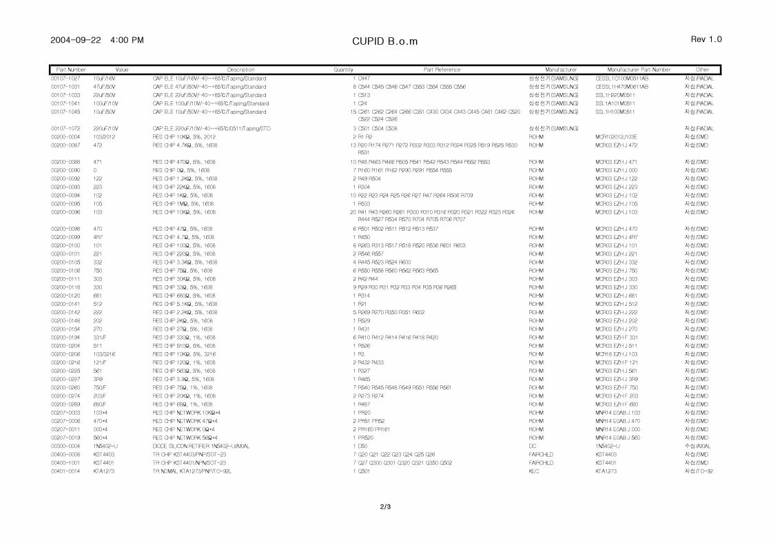
2004-09-22 4:00 PM CUPID B.o.m Rev 1.0
Part Number Value Description Quantity Part Reference Manufacturer Manufacturer Part Number Other
00107-1027 10uF/16V CAP ELE 10uF/16V/-40~+85℃/Taping/Standard 1 C447 삼성전기(SAMSUNG) CESSL1C100M0511AB 자삽/RADIAL
00107-1031 47uF/50V CAP ELE 47uF/50V/-40~+85℃/Taping/Standard 8 C544 C545 C546 C547 C553 C554 C555 C556 삼성전기(SAMSUNG) CESSL1H470M0611AB 자삽/RADIAL
00107-1033 22uF/50V CAP ELE 22uF/50V/-40~+85℃/Taping/Standard 1 C513 삼성전기(SAMSUNG) SSL1H220M0511 자삽/RADIAL
00107-1041 100uF/10V CAP ELE 100uF/10V/-40~+85℃/Taping/Standard 1 C24 삼성전기(SAMSUNG) SSL1A101M0511 자삽/RADIAL
00107-1045 10uF/50V CAP ELE 10uF/50V/-40~+85℃/Taping/Standard 15 C261 C262 C264 C266 C351 C430 C434 C443 C445 C461 C462 C520
C522 C524 C526
삼성전기(SAMSUNG) SSL1H100M0511 자삽/RADIAL
00107-1072 220uF/10V CAP ELE 220uF/10V/-40~+85℃/0511/Taping/STD 3 C501 C504 C508 삼성전기(SAMSUNG) 자삽/RADIAL
00200-0004 103/2012 RES CHIP 10KΩ, 5%, 2012 2 R1 R2 ROHM MCR102012J103E 자삽/SMD
00200-0087 472 RES CHIP 4.7KΩ, 5%, 1608 13 R20 R174 R271 R272 R302 R303 R312 R324 R325 R519 R525 R530
R531
ROHM MCR03 EZH J 472 자삽/SMD
00200-0088 471 RES CHIP 470Ω, 5%, 1608 10 R48 R463 R466 R505 R541 R542 R543 R544 R552 R553 ROHM MCR03 EZH J 471 자삽/SMD
00200-0090 0 RES CHIP 0Ω, 5%, 1608 7 R160 R161 R162 R290 R291 R554 R555 ROHM MCR03 EZH J 000 자삽/SMD
00200-0092 122 RES CHIP 1.2KΩ, 5%, 1608 2 R49 R504 ROHM MCR03 EZH J 122 자삽/SMD
00200-0093 223 RES CHIP 22KΩ, 5%, 1608 1 R304 ROHM MCR03 EZH J 223 자삽/SMD
00200-0094 102 RES CHIP 1KΩ, 5%, 1608 10 R22 R23 R24 R25 R26 R27 R47 R264 R506 R709 ROHM MCR03 EZH J 102 자삽/SMD
00200-0095 105 RES CHIP 1MΩ, 5%, 1608 1 R533 ROHM MCR03 EZH J 105 자삽/SMD
00200-0096 103 RES CHIP 10KΩ, 5%, 1608 20 R41 R43 R260 R261 R300 R310 R316 R320 R321 R322 R323 R326
R444 R527 R534 R570 R704 R705 R706 R707
ROHM MCR03 EZH J 103 자삽/SMD
00200-0098 470 RES CHIP 47Ω, 5%, 1608 6 R501 R502 R511 R512 R513 R537 ROHM MCR03 EZH J 470 자삽/SMD
00200-0099 4R7 RES CHIP 4.7Ω, 5%, 1608 1 R450 ROHM MCR03 EZH J 4R7 자삽/SMD
00200-0100 101 RES CHIP 100Ω, 5%, 1608 8 R263 R313 R517 R518 R520 R536 R601 R603 ROHM MCR03 EZH J 101 자삽/SMD
00200-0101 221 RES CHIP 220Ω, 5%, 1608 2 R546 R557 ROHM MCR03 EZH J 221 자삽/SMD
00200-0105 332 RES CHIP 3.3KΩ, 5%, 1608 4 R445 R523 R524 R600 ROHM MCR03 EZH J 332 자삽/SMD
00200-0106 750 RES CHIP 75Ω, 5%, 1608 6 R550 R558 R560 R562 R563 R565 ROHM MCR03 EZH J 750 자삽/SMD
00200-0111 303 RES CHIP 30KΩ, 5%, 1608 2 R42 R44 ROHM MCR03 EZH J 303 자삽/SMD
00200-0118 330 RES CHIP 33Ω, 5%, 1608 9 R29 R30 R31 R32 R33 R34 R35 R36 R265 ROHM MCR03 EZH J 330 자삽/SMD
00200-0120 681 RES CHIP 680Ω, 5%, 1608 1 R314 ROHM MCR03 EZH J 681 자삽/SMD
00200-0141 512 RES CHIP 5.1KΩ, 5%, 1608 1 R21 ROHM MCR03 EZH J 512 자삽/SMD
00200-0142 222 RES CHIP 2.2KΩ, 5%, 1608 5 R269 R270 R350 R351 R602 ROHM MCR03 EZH J 222 자삽/SMD
00200-0148 202 RES CHIP 2KΩ, 5%, 1608 1 R529 ROHM MCR03 EZH J 202 자삽/SMD
00200-0154 270 RES CHIP 27Ω, 5%, 1608 1 R431 ROHM MCR03 EZH J 270 자삽/SMD
00200-0194 331/F RES CHIP 330Ω, 1%, 1608 6 R410 R412 R414 R416 R418 R420 ROHM MCR03 EZH F 331 자삽/SMD
00200-0204 511 RES CHIP 510Ω, 5%, 1608 1 R526 ROHM MCR03 EZH J 511 자삽/SMD
00200-0206 103/3216 RES CHIP 10KΩ, 5%, 3216 1 R3 ROHM MCR18 EZH J 103 자삽/SMD
00200-0216 121/F RES CHIP 120Ω, 1%, 1608 2 R432 R433 ROHM MCR03 EZH F 121 자삽/SMD
00200-0225 561 RES CHIP 560Ω, 5%, 1608 1 R327 ROHM MCR03 EZH J 561 자삽/SMD
00200-0227 3R9 RES CHIP 3.9Ω, 5%, 1608 1 R465 ROHM MCR03 EZH J 3R9 자삽/SMD
00200-0260 750/F RES CHIP 75Ω, 1%, 1608 7 R540 R545 R548 R549 R551 R556 R561 ROHM MCR03 EZH F 750 자삽/SMD
00200-0274 203/F RES CHIP 20KΩ, 1%, 1608 2 R273 R274 ROHM MCR03 EZH F 203 자삽/SMD
00200-0289 680/F RES CHIP 68Ω, 1%, 1608 1 R487 ROHM MCR03 EZH F 680 자삽/SMD
00207-0003 103*4 RES CHIP NETWORK 10KΩ*4 1 PR20 ROHM MNR14 E0AB J 103 자삽/SMD
00207-0006 470*4 RES CHIP NETWORK 47Ω*4 2 PR51 PR52 ROHM MNR14 E0AB J 470 자삽/SMD
00207-0011 000*4 RES CHIP NETWORK 0Ω*4 2 PR160 PR161 ROHM MNR14 E0AB J 000 자삽/SMD
00207-0019 560*4 RES CHIP NETWORK 56Ω*4 1 PR520 ROHM MNR14 E0AB J 560 자삽/SMD
00300-0004 1N5402-U DIODE SILICON RETIFIER 1N5402-U/AXIAL 1 D50 DC 1N5402-U 수삽/AXIAL
00400-0008 KST4403 TR CHIP KST4403/PNP/SOT-23 7 Q20 Q21 Q22 Q23 Q24 Q25 Q26 FAIRCHILD KST4403 자삽/SMD
00400-1001 KST4401 TR CHIP KST4401/NPN/SOT-23 7 Q27 Q300 Q301 Q320 Q321 Q350 Q502 FAIRCHILD KST4401 자삽/SMD
00401-0014 KTA1273 TR NOMAL KTA1273/PNP/TO-92L 1 Q501 KEC KTA1273 자삽/TO-92
2/3
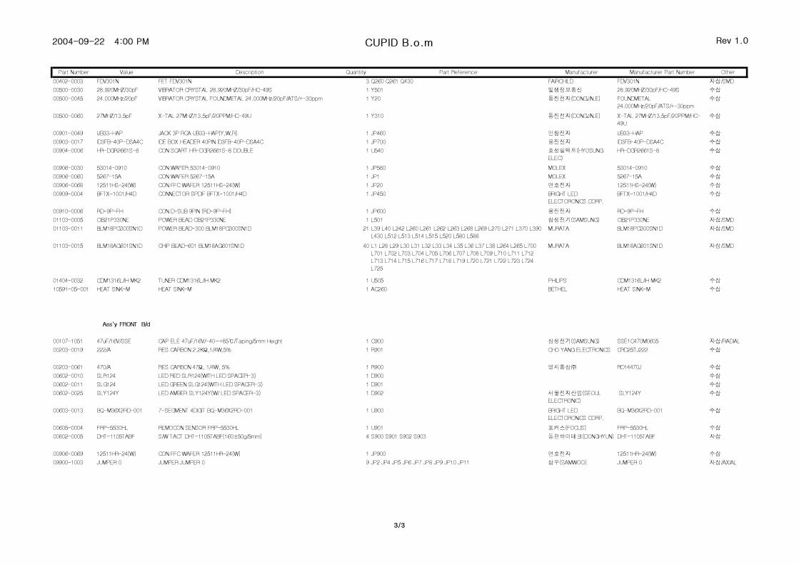
2004-09-22 4:00 PM CUPID B.o.m Rev 1.0
Part Number Value Description Quantity Part Reference Manufacturer Manufacturer Part Number Other
00402-0003 FDV301N FET FDV301N 3 Q260 Q261 Q430 FAIRCHILD FDV301N 자삽/SMD
00500-0030 28.920MHZ/30pF VIBRATOR CRYSTAL 28.920MHZ/30pF/HC-49S 1 Y501 빛샘정보통신 28.920MHZ/30pF/HC-49S 수삽
00500-0045 24.000MHz/20pF VIBRATOR CRYSTAL FOUNDMETAL 24.000MHz/20pF/ATS/+-30ppm 1 Y20 동진전자(DONGJIN.E) FOUNDMETAL
24.000MHz/20pF/ATS/+-30ppm
수삽
00500-0060 27MHZ/13.5pF X-TAL 27MHZ/13.5pF/20PPM/HC-49U 1 Y310 동진전자(DONGJIN.E) X-TAL 27MHZ/13.5pF/20PPM/HC-
49U
수삽
00901-0049 IJB33-HAP JACK 3P RCA IJB33-HAP(Y,W,R) 1 JP460 인창전자 IJB33-HAP 수삽
00903-0017 ID3FB-40P-DSA4C IDE BOX HEADER 40PIN ID3FB-40P-DSA4C 1 JP700 융진전자 ID3FB-40P-DSA4C 수삽
00904-0006 HR-DGR2661S-8 CON SCART HR-DGR2661S-8 DOUBLE 1 U540 효성일렉트(HYOSUNG
ELEC)
HR-DGR2661S-8 수삽
00906-0030 53014-0910 CON WAFER 53014-0910 1 JP580 MOLEX 53014-0910 수삽
00906-0060 5267-15A CON WAFER 5267-15A 1 JP1 MOLEX 5267-15A 수삽
00906-0068 12511HS-24(W) CON FFC WAFER 12511HS-24(W) 1 JP20 연호전자 12511HS-24(W) 수삽
00909-0004 BFTX-1001/H4D CONNECTOR SPDIF BFTX-1001/H4D 1 JP450 BRIGHT LED
ELECTORONICS CORP.
BFTX-1001/H4D 수삽
00910-0006 RD-9P-FH CON D-SUB 9PIN (RD-9P-FH) 1 JP600 융진전자 RD-9P-FH 수삽
01103-0005 CIB21P330NE POWER BEAD CIB21P330NE 1 L501 삼성전기(SAMSUNG) CIB21P330NE 자삽/SMD
01103-0011 BLM18PG300SN1D POWER BEAD-300 BLM18PG300SN1D 21 L39 L40 L242 L260 L261 L262 L263 L268 L269 L270 L271 L370 L390
L430 L512 L513 L514 L515 L520 L580 L588
MURATA BLM18PG300SN1D 자삽/SMD
01103-0015 BLM18AG601SN1D CHIP BEAD-601 BLM18AG601SN1D 40 L1 L28 L29 L30 L31 L32 L33 L34 L35 L36 L37 L38 L264 L265 L700
L701 L702 L703 L704 L705 L706 L707 L708 L709 L710 L711 L712
L713 L714 L715 L716 L717 L718 L719 L720 L721 L722 L723 L724
L725
MURATA BLM18AG601SN1D 자삽/SMD
01404-0032 CDM1316L/IH MK2 TUNER CDM1316L/IH MK2 1 U505 PHILIPS CDM1316L/IH MK2 수삽
10591-05-001 HEAT SINK-M HEAT SINK-M 1 AC260 BETHEL HEAT SINK-M 수삽
Ass`y FRONT B/d
00107-1051 47uF/16V/SSE CAP ELE 47uF/16V/-40~+85℃/Taping/5mm Height 1 C900 삼성전기(SAMSUNG) SSE1C470M0605 자삽/RADIAL
00203-0019 222/A RES CARBON 2.2KΩ,1/4W,5% 1 R901 CHO YANG ELECTRONICS CRD25TJ222 수삽
00203-0061 470/A RES CARBON 47Ω, 1/4W, 5% 1 R900 영지통상㈜ RD14470J 수삽
00602-0010 SLR124 LED RED SLR124(WITH LED SPACER-3) 1 D900 수삽
00602-0011 SLG124 LED GREEN SLG124(WITH LED SPACER-3) 1 D901 수삽
00602-0025 SLY124Y LED AMBER SLY124Y(W/ LED SPACER-3) 1 D902 서울전자산업(SEOUL
ELECTRONIC)
SLY124Y 수삽
00603-0013 BQ-M36X2RD-001 7-SEGMENT 4DIGIT BQ-M36X2RD-001 1 U900 BRIGHT LED
ELECTORONICS CORP.
BQ-M36X2RD-001 수삽
00605-0004 FRP-5530HL REMOCON SENSOR FRP-5530HL 1 U901 포커스(FOCUS) FRP-5530HL 수삽
00802-0005 DHT-1105TABF S/W TACT DHT-1105TABF(160±50g/5mm) 4 S900 S901 S902 S903 동현하이테크(DONGHYUN) DHT-1105TABF 자삽
00906-0069 12511HR-24(W) CON FFC WAFER 12511HR-24(W) 1 JP900 연호전자 12511HR-24(W) 수삽
09900-1003 JUMPER 0 JUMPER JUMPER 0 9 JP2 JP4 JP5 JP6 JP7 JP8 JP9 JP10 JP11 삼우(SAMWOO) JUMPER 0 자삽/AXIAL
3/3