Embed Size (px)
Citation preview
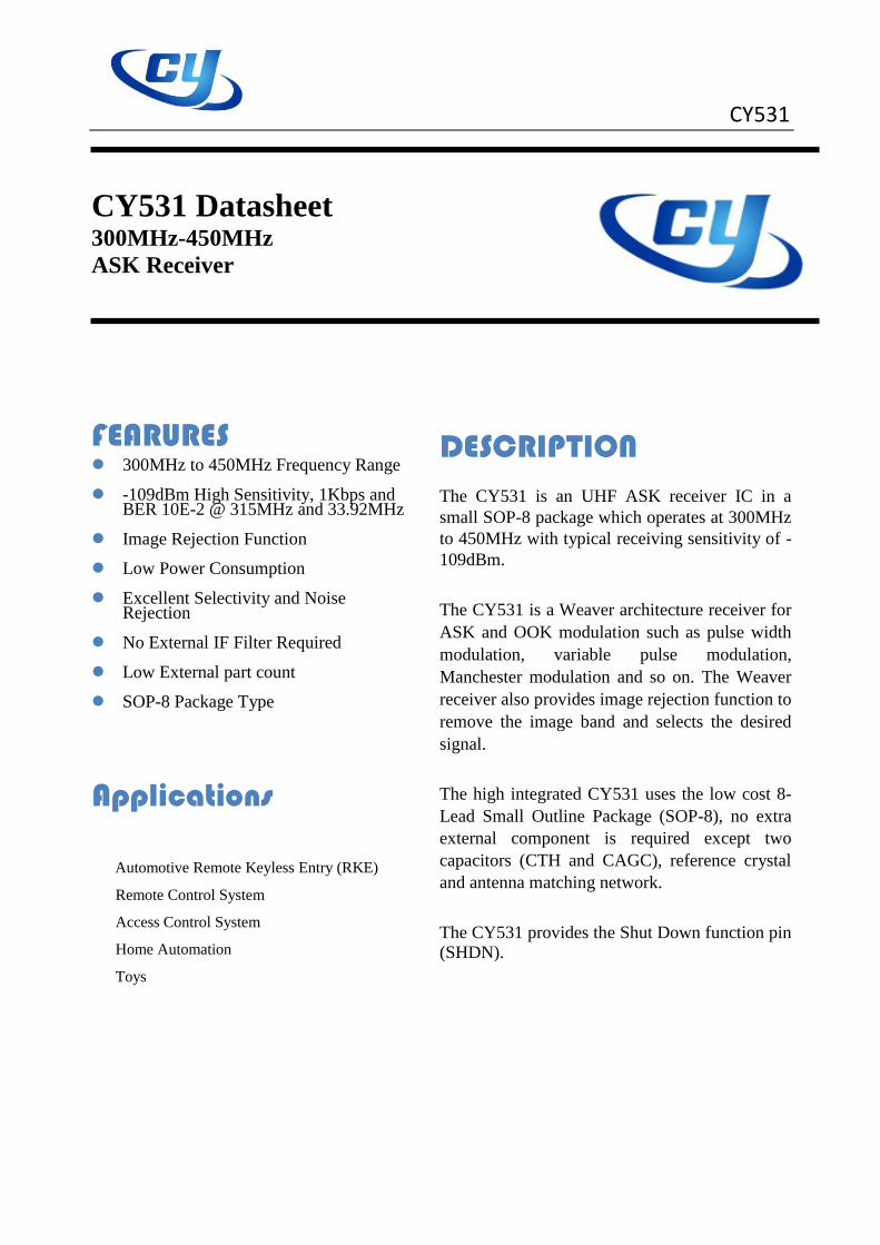
CY531
CY531 Datasheet 300MHz-450MHz
ASK Receiver
FEARURES 300MHz to 450MHz Frequency Range -109dBm High Sensitivity, 1Kbps and
BER 10E-2 @ 315MHz and 33.92MHz Image Rejection Function Low Power Consumption Excellent Selectivity and Noise
Rejection No External IF Filter Required Low External part count SOP-8 Package Type
Applications
Automotive Remote Keyless Entry (RKE)
Remote Control System
Access Control System
Home Automation
Toys
DESCRIPTION The CY531 is an UHF ASK receiver IC in a
small SOP-8 package which operates at 300MHz
to 450MHz with typical receiving sensitivity of -
109dBm.
The CY531 is a Weaver architecture receiver for
ASK and OOK modulation such as pulse width
modulation, variable pulse modulation,
Manchester modulation and so on. The Weaver
receiver also provides image rejection function to
remove the image band and selects the desired
signal.
The high integrated CY531 uses the low cost 8-
Lead Small Outline Package (SOP-8), no extra
external component is required except two
capacitors (CTH and CAGC), reference crystal
and antenna matching network.
The CY531 provides the Shut Down function pin (SHDN).
CY531
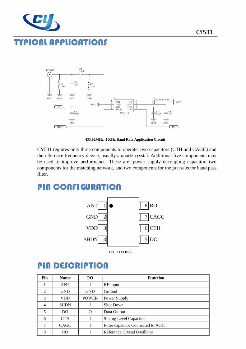
TYPICAL APPLICATIONS
433.92MHz, 1 KHz Baud Rate Application Circuit
CY531 requires only three components to operate: two capacitors (CTH and CAGC) and
the reference frequency device, usually a quartz crystal. Additional five components may
be used to improve performance. These are: power supply decoupling capacitor, two
components for the matching network, and two components for the pre-selector band pass
filter.
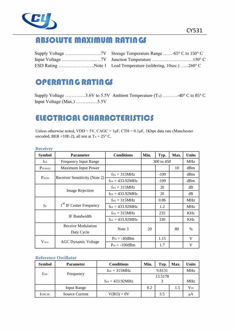
PIN CONFIGURATION
ANT 1 8 RO
GND 2 7 CAGC
VDD 3 6 CTH
SHDN 4 5 DO
CY531 SOP-8
PIN DESCRIPTION
Pin Name I/O Function
1 ANT I RF Input
2 GND GND Ground
3 VDD POWER Power Supply
4 SHDN I Shut Down
5 DO O Data Output
6 CTH I Slicing Level Capacitor
7 CAGC I Filter capacitor Connected to AGC
8 RO I Reference Crystal Oscillator
CY531
ABSOLUTE MAXIMUM RATINGS
Supply Voltage …………………..7V Storage Temperature Range ……-65° C to 150° C Input Voltage ……………….....…7V Junction Temperature ………………………150° C ESD Rating ……………….….Note 1 Lead Temperature (soldering, 10sec.) …...260° C
OPERATING RATINGS
Supply Voltage ……….…3.6V to 5.5V Ambient Temperature (TA) ……….-40° C to 85° C Input Voltage (Max.) ………..…5.5V
ELECTRICAL CHARACTERISTICS
Unless otherwise noted, VDD = 5V, CAGC = 1μF, CTH = 0.1μF, 1Kbps data rate (Manchester
encoded, BER =10E-2), all test at TA = 25° C.
Receiver
Symbol Parameter Conditions Min. Typ. Max. Units
fRX Frequency Input Range 300 to 450 MHz
PIN,MAX Maximum Input Power 10 dBm
PSENS Receiver Sensitivity (Note 2) fRX = 315MHz -109 dBm
fRX = 433.92MHz
-109
dBm
Image Rejection
fRX = 315MHz 20 dB
fRX = 433.92MHz
20
dB
fIF 1st
IF Center Frequency
fRX = 315MHz 0.86 MHz
fRX = 433.92MHz 1.2 MHz
IF Bandwidth
fRX = 315MHz 235 KHz
fRX = 433.92MHz
330
KHz
Receive Modulation Note 3 20
80 %
Duty Cycle
VAGC AGC Dynamic Voltage PIN = -40dBm 1.15 V
PIN = -100dBm
1.7
V
Reference Oscillator
Symbol Parameter Conditions Min. Typ. Max. Units
fOSC Frequency fRX = 315MHz 9.8131 MHz
fRX = 433.92MHz
13.5178
3
MHz
Input Range 0.2 1.5 VPP
IOSCSC Source Current V(RO) = 0V 3.5 μA
CY531
DO Drive
Symbol Parameter Conditions Min. Typ. Max. Units
DO pin Output Current
Source @ 0.8VDD 260 μA
Sink @ 0.2 VDD
600
μA
TRISE Output Rise and Fall CL = 15pF, pin DO, 2 μsec
Times 10-90%
TFALL 2 μsec
Power Supply
Symbol Parameter Conditions Min. Typ. Max. Units
ICC
Supply Current fRX = 315MHz 4.5 mA
@ VDD = 5V
fRX = 433.92MHz
7.0
mA
IOFF Shut Down Current SHDN = High 0.5 μA
Note 1: Device is ESD sensitive. Use appropriate ESD precautions. Exceeding the
absolute maximum rating may damage the device.
Note 2: Sensitivity is defined as the average signal level measured at the input
necessary to achieve 10-2 BER (bit error rate). The input signal is defined as a
return-to-zero (RZ) waveform with 50% average duty cycle (Manchester
encoded) at a data rate of 1kbps.
Note 3: When data burst does not contain preamble, duty cycle is defined as total duty
cycle, including any “quiet” time between data bursts. When data bursts contain
preamble sufficient to charge the slice level on capacitor CTH, then duty cycle is
the effective duty cycle of the burst alone.
[For example, 100msec burst with 50% duty cycle, and 100msec “quiet” time
between bursts. If burst includes preamble, duty cycle is TON/ (TON + TOFF) =
50%; without preamble, duty cycle is TON/ (TON + TOFF + TQUIET) = 50msec/
(200msec) = 25%. TON is the (Average number of 1’s/burst) × bit time, and TOFF
= TBURST–TON.]
CY531
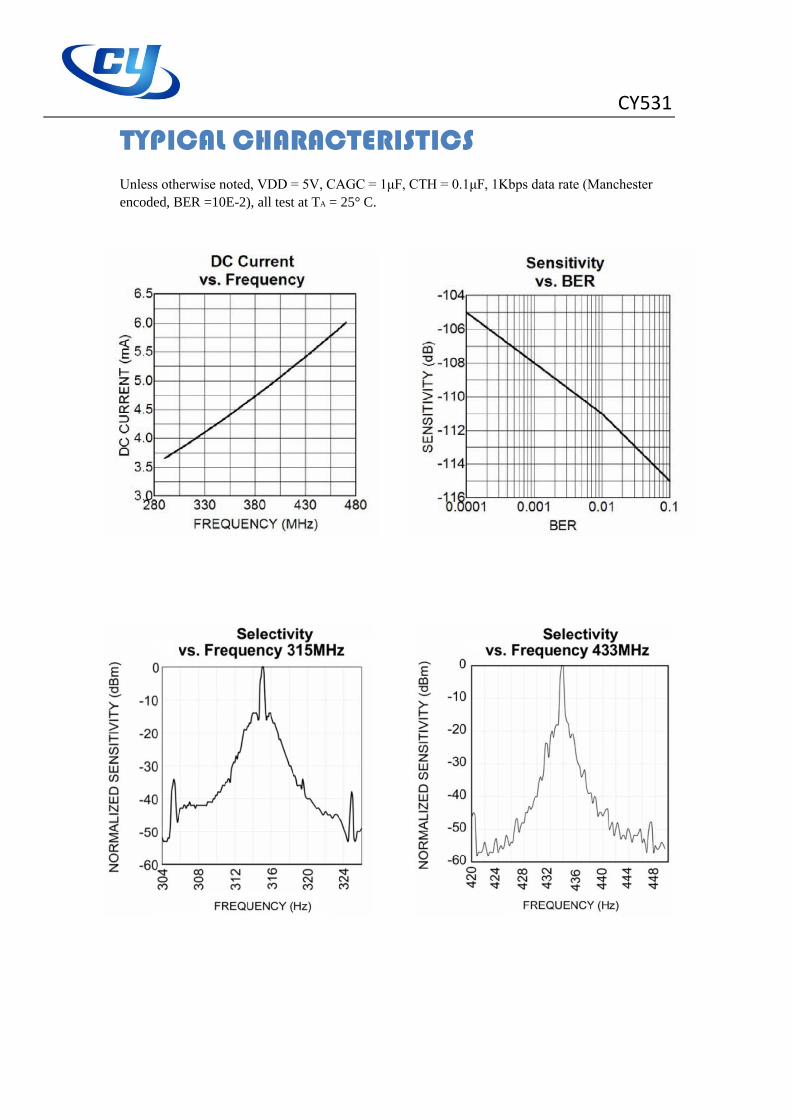
TYPICAL CHARACTERISTICS
Unless otherwise noted, VDD = 5V, CAGC = 1μF, CTH = 0.1μF, 1Kbps data rate (Manchester
encoded, BER =10E-2), all test at TA = 25° C.
CY531
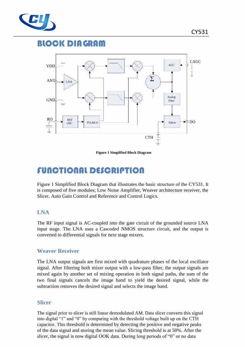
BLOCK DIAGRAM
CAGC VDD AGC
ANT LNA Σ
GND Analog
Filter
RO REF PLL&LO Silicer DO OSC
CTH
Figure 1 Simplified Block Diagram
FUNCTIONAL DESCRIPTION
Figure 1 Simplified Block Diagram that illustrates the basic structure of the CY531. It
is composed of five modules; Low Noise Amplifier, Weaver architecture receiver, the
Slicer, Auto Gain Control and Reference and Control Logics.
LNA
The RF input signal is AC-coupled into the gate circuit of the grounded source LNA
input stage. The LNA uses a Cascoded NMOS structure circuit, and the output is
converted to differential signals for next stage mixers.
Weaver Receiver
The LNA output signals are first mixed with quadrature phases of the local oscillator
signal. After filtering both mixer output with a low-pass filter, the output signals are
mixed again by another set of mixing operation in both signal paths, the sum of the
two final signals cancels the image band to yield the desired signal, while the
subtraction removes the desired signal and selects the image band.
Slicer
The signal prior to slicer is still linear demodulated AM. Data slicer converts this signal
into digital “1” and “0” by comparing with the threshold voltage built up on the CTH
capacitor. This threshold is determined by detecting the positive and negative peaks
of the data signal and storing the mean value. Slicing threshold is at 50%. After the
slicer, the signal is now digital OOK data. During long periods of “0” or no data
CY531
period, threshold voltage on the CTH capacitor may be very low. Large random
noise spikes during this time may cause erroneous “1” at DO pin.
AGC
The AGC comparator monitors the signal amplitude from the output of the Weaver
receiver. When the output signal is less than 750mV, the threshold 1.5μA current is
sourced into the external CAGC capacitor. When the output signal is greater than
750mV, a 15µ A current sink discharges the CAGC capacitor. The voltage developed
on the CAGC capacitor acts to adjust the gain of the mixers of Weaver receiver to
compensate for RF input signal level variation.
Reference Oscillator
The reference oscillator in the CY531 uses a basic Colpitts crystal oscillator
configuration with MOS transconductor to provide negative resistance. The RO pin
external capacitor is integrated inside CY531. User only needs to connect reference
oscillation crystal. Reference oscillator crystal frequency can be calculated: FOSC =
FRF/(32 + 1.198/12)
For 433.92 MHz, FOSC = 13.51783 MHz
CY531
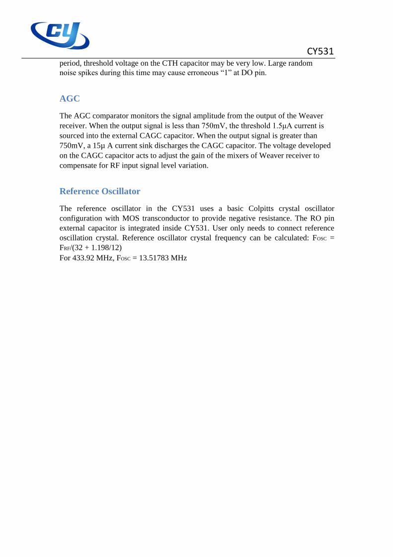
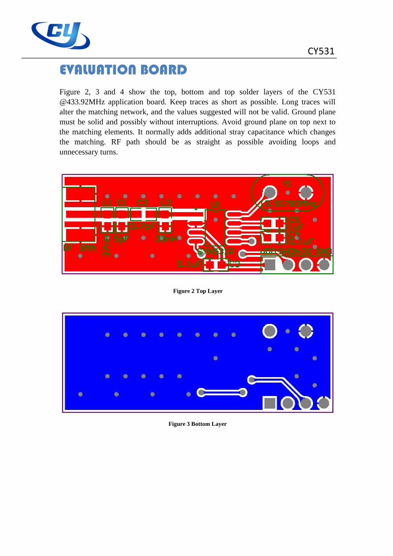
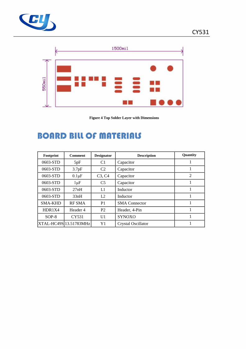
EVALUATION BOARD
Figure 2, 3 and 4 show the top, bottom and top solder layers of the CY531
@433.92MHz application board. Keep traces as short as possible. Long traces will
alter the matching network, and the values suggested will not be valid. Ground plane
must be solid and possibly without interruptions. Avoid ground plane on top next to
the matching elements. It normally adds additional stray capacitance which changes
the matching. RF path should be as straight as possible avoiding loops and
unnecessary turns.
Figure 2 Top Layer
Figure 3 Bottom Layer
CY531
Figure 4 Top Solder Layer with Dimensions
BOARD BILL OF MATERIALS
Footprint Comment Designator Description Quantity
0603-STD 5pF C1 Capacitor 1
0603-STD 3.7pF C2 Capacitor 1
0603-STD 0.1μF C3, C4 Capacitor 2
0603-STD 1μF C5 Capacitor 1
0603-STD 27nH L1 Inductor 1
0603-STD 33nH L2 Inductor 1
SMA-KHD RF SMA P1 SMA Connector 1
HDR1X4 Header 4 P2 Header, 4-Pin 1
SOP-8 CY531 U1 SYNOXO 1
XTAL-HC49S 13.51783MHz Y1 Crystal Oscillator 1
CY531
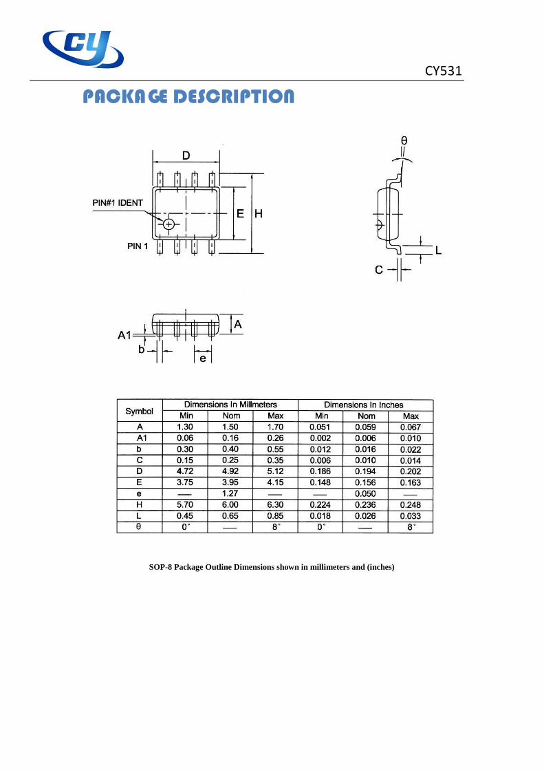
PACKAGE DESCRIPTION
SOP-8 Package Outline Dimensions shown in millimeters and (inches)