Embed Size (px)
Citation preview
PRELIMINARYCY8C20111, CY8C20121
CapSense Express™ - One Button andTwo Button Capacitive Controllers
Cypress Semiconductor Corporation • 198 Champion Court • San Jose, CA 95134-1709 • 408-943-2600Document Number: 001-53516 Rev. *A Revised December 16, 2009
1. Features■ Capacitive Button Input tied to a Configurable Output
❐ Robust sensing algorithm❐ High sensitivity, low noise❐ Immunity to RF and AC noise❐ Low radiated EMC noise❐ Supports wide range of input capacitance, sensor shapes,
and sizes
■ Target Applications❐ Printers❐ Cellular handsets❐ LCD monitors❐ Portable DVD players
■ Industry's Best Configurability❐ Custom sensor tuning❐ Output supports strong 20 mA sink current❐ Output state can be controlled through I2C or directly from
CapSense input state❐ Run time reconfigurable over I2C
■ Advanced Features ❐ Plug-and-play with factory defaults – tuned to support up to
1 mm overlay❐ Nonvolatile storage of custom settings ❐ Easy integration into existing products – configure output to
match system❐ No external components required❐ World class free configuration tool
■ Wide Range of Operating Voltages❐ 2.45V to 2.9V❐ 3.10V to 3.6V❐ 4.75V to 5.25V
■ I2C Communication❐ Supported from 1.8V❐ Internal pull up resistor support option❐ Data rate up to 400 kbps.❐ Configurable I2C addressing
■ Industrial Temperature Range: –40°C to +85°C
■ Available in 8-Pin SOIC Package
2. OverviewThe CapSense Express™ controllers support two capacitivesensing (CapSense) buttons and two general purpose outputs inCY8C20121 and one CapSense button and one generalpurpose output in CY8C20111. The device functionality isconfigured through the I2C port and can be stored in on-boardnonvolatile memory for automatic loading at power on. Thedigital outputs are controlled from CapSense inputs in factorydefault settings, but are user configurable for direct controlthrough I2C.The four key blocks that make up the CY8C20111 andCY8C20121 controllers are: a robust capacitive sensing corewith high immunity against radiated and conductive noise,control registers with nonvolatile storage, configurable outputs,and I2C communications. The user can configure registers withparameters needed to adjust the operation and sensitivity of theCapSense buttons and outputs and permanently store thesettings. The standard I2C serial communication interface allowsthe host to configure the device and read sensor information inreal time. I2C address is fully configurable without any externalhardware strapping.
[+] Feedback
PRELIMINARYCY8C20111, CY8C20121
Document Number: 001-53516 Rev. *A Page 2 of 35
3. ContentsFeatures ...............................................................................1Overview ..............................................................................1Contents ..............................................................................2Pinouts ................................................................................3Typical Circuits ...................................................................4
Circuit-1: One Button and One LED[1] ..........................4Circuit-2: One Button and One LED with I2C Interface ..........................................................4Circuit-3: Two Buttons and Two LEDs with I2C Interface ..........................................................5Circuit-4: Compatibility with 1.8V I2C Signaling[2] ........5Circuit-5: Powering Down CapSense Express Device for Low Power Requirements ............................6
Operating Modes ................................................................6Normal Mode .................................................................6Setup Mode ...................................................................6
I2C Interface ........................................................................6I2C Device Addressing ..................................................6I2C Clock Stretching ......................................................7Format for Register Write and Read .............................7
Registers .............................................................................7OUTPUT_STATUS .....................................................10OUTPUT_PORT ..........................................................10CS_ENABLE ...............................................................10DIG_ENABLE ..............................................................11SET_STRONG_DM ....................................................11OP_SEL_x ...................................................................13LOGICAL_OPR_INPUTx ............................................13CS_NOISE_TH ...........................................................14CS_BL_UPD_TH .........................................................14CS_SETL_TIME ..........................................................14CS_OTH_SET .............................................................15CS_HYSTERISIS ........................................................15CS_DEBOUNCE .........................................................16CS_NEG_NOISE_TH ..................................................16
CS_LOW_BL_RST ......................................................16CS_FILTERING ...........................................................17CS_SCAN_POS_x ......................................................17CS_FINGER_TH_x .....................................................18CS_IDAC_x .................................................................18I2C_ADDR_LOCK .......................................................18DEVICE_ID .................................................................19DEVICE_STATUS .......................................................19I2C_ADDR_DM ...........................................................20CS_READ_BUTTON ...................................................20CS_READ_BLx ...........................................................21CS_READ_DIFFx ........................................................21CS_READ_RAWx .......................................................21CS_READ_STATUS ...................................................22COMMAND_REG ........................................................22
Layout Guidelines and Best Practices ...........................24Example PCB Layout Design with Two CapSense Buttons and Two LEDs ......................26
Operating Voltages ...........................................................27CapSense Constraints .....................................................27Electrical Specifications ..................................................28
Absolute Maximum Ratings .........................................28Operating Temperature ...............................................28DC Electrical Characteristics .......................................29CapSense Electrical Characteristics ...........................30AC Electrical Specifications .........................................31
Examples of Frequently Used I2C Commands ..............32Ordering Information ........................................................33
Ordering Code Information ..........................................33Package Diagram ..............................................................34Document History Page ...................................................35Sales, Solutions, and Legal Information ........................35
Worldwide Sales and Design Support .........................35
[+] Feedback
PRELIMINARYCY8C20111, CY8C20121
Document Number: 001-53516 Rev. *A Page 3 of 35
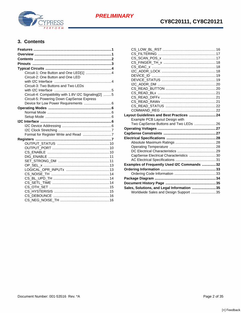
4. PinoutsFigure 1. CY8C20111 Pin Diagram - 8 SOIC - 1 Button
Table 1. Pin Definitions – 8 SOIC- 1 Button
Figure 2. CY8C20121 Pin Diagram – 8 SOIC- 2 Button
Table 2. Pin Definitions – 8 SOIC- 2 Button
Pin No Name Description1 VSS Ground
2 I2C SCL I2C Clock
3 I2C SDA I2C Data
4 CS0 CapSense Input
5 NC No Connect
6 DIG0 Digital Output
7 NC No Connect
8 VDD Supply Voltage
Pin No Name Description1 VSS Ground
2 I2C SCL I2C Clock
3 I2C SDA I2C Data
4 CS0 CapSense Input
5 CS1 CapSense Input
6 DIG0 Digital Output
7 DIG1 Digital Output
8 VDD Supply Voltage
[+] Feedback

PRELIMINARYCY8C20111, CY8C20121
Document Number: 001-53516 Rev. *A Page 4 of 35
5. Typical Circuits5.1 Circuit-1: One Button and One LED[1]
5.2 Circuit-2: One Button and One LED with I2C Interface
Note1. The sensors are factory tuned to work with 1 mm plastic or glass overlay.
[+] Feedback
PRELIMINARYCY8C20111, CY8C20121
Document Number: 001-53516 Rev. *A Page 5 of 35
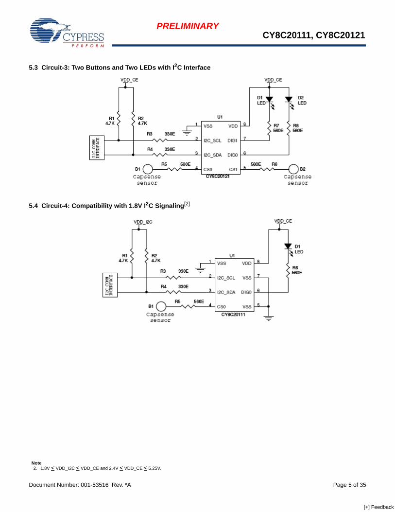
5.3 Circuit-3: Two Buttons and Two LEDs with I2C Interface
5.4 Circuit-4: Compatibility with 1.8V I2C Signaling[2]
Note2. 1.8V < VDD_I2C < VDD_CE and 2.4V < VDD_CE < 5.25V.
[+] Feedback
PRELIMINARYCY8C20111, CY8C20121
Document Number: 001-53516 Rev. *A Page 6 of 35
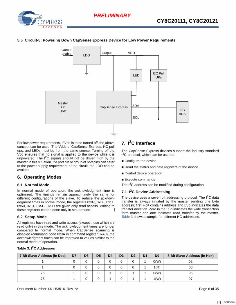
5.5 Circuit-5: Powering Down CapSense Express Device for Low Power Requirements
For low power requirements, if Vdd is to be turned off, the aboveconcept can be used. The Vdds of CapSense Express, I2C pullups, and LEDs must be from the same source. Turning off theVdd ensures that no signal is applied to the device while it isunpowered. The I2C signals should not be driven high by themaster in this situation. If a port pin or group of port pins can caterto the power supply requirement of the circuit, the LDO can beavoided.
6. Operating Modes6.1 Normal Mode In normal mode of operation, the acknowledgment time isoptimized. The timings remain approximately the same fordifferent configurations of the slave. To reduce the acknowl-edgment times in normal mode, the registers 0x07, 0x08, 0x11,0x50, 0x51, 0x5C, 0x5D are given only read access. Writing tothese registers can be done only in setup mode.
6.2 Setup Mode All registers have read and write access (except those which areread only) in this mode. The acknowledgment times are longercompared to normal mode. When CapSense scanning isdisabled (command code 0x0A in command register 0xA0), theacknowledgment times can be improved to values similar to thenormal mode of operation.
7. I2C InterfaceThe CapSense Express devices support the industry standardI2C protocol, which can be used to:
■ Configure the device
■ Read the status and data registers of the device
■ Control device operation
■ Execute commandsThe I2C address can be modified during configuration.
7.1 I2C Device AddressingThe device uses a seven bit addressing protocol. The I2C datatransfer is always initiated by the master sending one byteaddress; first 7-bit contains address and LSb indicates the datatransfer direction. Zero in the LSb indicates the write transactionform master and one indicates read transfer by the master.Table 3 shows example for different I2C addresses.
Master Or
Host
LDO
CapSense Express
I2C Pull UPsLED
I2CBUS
SDA
SCL
VDDOutputOutput enable
Table 3. I2C Addresses
7 Bit Slave Address (in Dec) D7 D6 D5 D4 D3 D2 D1 D0 8 Bit Slave Address (in Hex)1 0 0 0 0 0 0 1 0(W) 02
1 0 0 0 0 0 0 1 1(R) 03
75 1 0 0 1 0 1 1 0(W) 96
75 1 0 0 1 0 1 1 1(W) 97
[+] Feedback

PRELIMINARYCY8C20111, CY8C20121
Document Number: 001-53516 Rev. *A Page 7 of 35
7.2 I2C Clock Stretching “Clock stretching” or “bus stalling” in I2C communication protocolis a state in which the slave holds the SCL line low to indicatethat it is busy. In this condition, the master is expected to waituntil the SCL is released by the slave. When an I2C master communicates with the CapSense Expressdevice, the CapSense Express stalls the I2C bus after thereception of each byte (that is, just before the ACK/NAK bit) untilprocessing of the byte is complete and critical internal functionsare executed. Use a fully I2C compliant master to communicatewith the CapSense Express device.
An I2C master which does not support clock stretching (a bitbanged software I2C Master) must wait for a specific amount oftime specified (as shown in the section Format for Register Writeand Read) for each register write and read operation before thenext bit is transmitted. It is mandatory to check the SCL status (itshould be high) before I2C master initiates any data transfer withCapSense Express. If the master fails to do so and continues tocommunicate, the communication is erroneous. The following diagrams represent the ACK time delays shown inthe Register Map on page 7.
Figure 3. Write ACK Time Representation
Figure 4. Read ACK Time Representation
7.3 Format for Register Write and ReadRegister write format.
Register read format.
Legends:
8. RegistersTable 4. Register Conventions
Start Slave Addr + W A Reg Addr A Data A Data A . . . . . Data A Stop
Start Slave Addr + W A Reg Addr A Stop
Start Slave Addr + R A Data A Data A . . . . . Data N Stop
Master A - ACKSlave N- NAK
Convention DescriptionRW Register have both read and write access
R Register have only read access
WPR Write register with pass code
FD Factory defaults
[+] Feedback

PRELIMINARYCY8C20111, CY8C20121
Document Number: 001-53516 Rev. *A Page 8 of 35
Table 5. Register Map
NameRegisterAddress(in Hex)
AccessWritable Only in Setup
Mode[3]
Factory Default Values of Registers
(in Hex)I2C Max ACK
Time in NormalMode (ms)[5]
I2C Max ACK Time in
SetupMode (ms)[5]
Page No.
1 Button 2 Button
OUTPUT_PORT 04 W 01 03 0.10 10
CS_ENABLE 07 RW Yes 01 03 11 10
DIG_ENABLE 08 RW Yes 01 03 11 11
SET_STRONG_DM 11 RW Yes 01 03 11 11
OP_SEL_0 1C RW 82 82 0.12 11 13
LOGICAL_OPR_INPUT0 1E RW 01 01 0.12 11 13
OP_SEL_1[4] 21 RW 82 0.12 11 13
LOGICAL_OPR_INPUT1[4] 23 RW 02 0.12 11 13
CS_NOISE_TH 4E RW 28 28 0.11 11 14
CS_BL_UPD_TH 4F RW 64 64 0.11 11 14
CS_SETL_TIME 50 RW Yes A0 A0 35 14
CS_OTH_SET 51 RW Yes 00 00 35 15
CS_HYSTERISIS 52 RW 0A 0A 0.11 11 15
CS_DEBOUNCE 53 RW 03 03 0.11 11 16
CS_NEG_NOISE_TH 54 RW 14 14 0.11 11 16
CS_LOW_BL_RST 55 RW 14 14 0.11 11 16
CS_FILTERING 56 RW 20 20 0.11 11 17
CS_SCAN_POS_0 5C RW Yes 00 00 11 17
CS_SCAN_POS_1[4] 5D RW Yes 01 11 17
CS_FINGER_TH_0 66 RW 64 64 0.14 11 18
CS_FINGER_TH_1[4] 67 RW 64 0.14 11 18
CS_IDAC_0 70 RW 0A 0A 0.14 11 18
CS_IDAC_1[4] 71 RW 0A 0.14 11 18
I2C_ADDR_LOCK 79 RW 01 01 0.11 11 18
DEVICE_ID 7A R 11 21 0.11 11 19
DEVICE_STATUS 7B R 03 03 0.11 11 19
I2C_ADDR_DM 7C RW 80 80 0.11 11 20
CS_READ_BUTTON 81 RW 81 81 0.12 11 20
CS_READ_BLM 82 R NA NA 0.12 11 21
CS_READ_BLL 83 R NA NA 0.12 11 21
CS_READ_DIFFM 84 R NA NA 0.12 11 21
CS_READ_DIFFL 85 R NA NA 0.12 11 21
CS_READ_RAWM 86 R NA NA 0.12 11 21
CS_READ_RAWL 87 R NA NA 0.12 11 21
CS_READ_STATUS 88 R NA NA 0.12 11 22
COMMAND_REG A0 W 00 00 0.10 11 22
Notes3. These registers are writable only after entering into setup mode. All other registers are available for read and write in normal and setup mode.4. These registers are available only in CY8C20121 device.5. The Ack times specified are 1x I2C Ack times.
[+] Feedback

PRELIMINARYCY8C20111, CY8C20121
Document Number: 001-53516 Rev. *A Page 9 of 35
Table 6. CapSense Express Commands
Command [6] Description Executable Mode
Duration the Device is NOT Ac-cessible after ACK (in ms)[5]
W 00 A0 00 Get firmware revision Setup/Normal 0
W 00 A0 01 Store current configuration to NVM Setup/Normal 120
W 00 A0 02 Restore factory configuration Setup/Normal 120
W 00 A0 03 Write NVM POR defaults Setup/Normal 120
W 00 A0 04 Read NVM POR defaults Setup/Normal 5
W 00 A0 05 Read current configurations (RAM) Setup/Normal 5
W 00 A0 06 Reconfigure device (POR) Setup 5
W 00 A0 07 Set Normal mode of operation Setup/Normal 0
W 00 A0 08 Set Setup mode of operation Setup/Normal 0
W 00 A0 09 Start scan Setup/Normal 10
W 00 A0 0A Stop scan Setup/Normal 5
W 00 A0 0B Get CapSense scan status Setup/Normal 0
Note6. ‘W’ indicates the write transfer. The next byte of data represents the 7 bit I2C address.
[+] Feedback
PRELIMINARYCY8C20111, CY8C20121
Document Number: 001-53516 Rev. *A Page 10 of 35
8.1 OUTPUT_STATUSOutput Status Register
OUTPUT_STATUS: 00h
The Output Status register represents the actual logical levels on the output pins.
8.2 OUTPUT_PORTOutput Port Register
OUTPUT_PORT: 04h
This register is used to write data to DIG output port. Pins defined as output of combinational logic (in OP_SEL_x register) cannot bechanged using this register.
8.3 CS_ENABLESelect CapSense Input Register
CS_ENABLE: 07h (Writable only in Setup mode)
1 Button 7 6 5 4 3 2 1 0Access: FD R:01
Bit Name STS[0]
2 Button 7 6 5 4 3 2 1 0Access: FD R:03
Bit Name STS[1:0]
Bit Name Description1:0 STS [1:0] Used to represent the output status
0 Output low1 Output high
1 Button 7 6 5 4 3 2 1 0Access: FD W:01
Bit Name DIG[0]
2 Button 7 6 5 4 3 2 1 0Access: FD W:03
Bit Name DIG[1:0]
Bit Name Description1:0 DIG [1:0] A bit set in this register sets the logic level of the output.
0 Logic ‘0’1 Logic ‘1’
1 Button 7 6 5 4 3 2 1 0Access: FD RW:01
Bit Name CS[0]
2 Button 7 6 5 4 3 2 1 0Access: FD RW:03
Bit Name CS[1:0]
[+] Feedback

PRELIMINARYCY8C20111, CY8C20121
Document Number: 001-53516 Rev. *A Page 11 of 35
This register is used to enable CapSense inputs. This register should be set before setting finger threshold (0x66, 0x67) andIDAC setting (0x70, 0x71) registers.
8.4 DIG_ENABLESelect DIG Output Register
GPO_ENABLE: 08h (Writable only in Setup mode)
This register is used to enable DIG (Digital) outputs. If DIG output is enabled, the strong drive mode register (11h) should also be set.If DIG output is disabled the drive mode of these pins is High Z.
8.5 SET_STRONG_DMSets Strong Drive Mode for DIG Outputs.
SET_STRONG_DM: 11h (Writable only in Setup mode)
This register sets strong drive mode for DIG (Digital) outputs. To set strong drive mode the pin should be enabled as GP output.
Bit Name Description1:0 CS [1:0] These bits are used to enable CapSense inputs.
0 Disable CapSense input1 Enable CapSense input
1 Button 7 6 5 4 3 2 1 0Access: FD RW:01
Bit Name DIG[0]
2 Button 7 6 5 4 3 2 1 0Access: FD RW:03
Bit Name DIG [1:0]
Bit Name Description1:0 DIG [1:0] These bits are used to enable DIG outputs.
0 Disable DIG output1 Enable DIG output
1 Button 7 6 5 4 3 2 1 0Access: FD RW:01
Bit Name DM [0]
2 Button 7 6 5 4 3 2 1 0Access: FD RW:03
Bit Name DM [1:0]
Bit Name Description1:0 DM [1:0] These bits are used to set the strong drive mode to DIG outputs.
0 Strong drive mode not set1 Strong drive mode set
[+] Feedback
PRELIMINARYCY8C20111, CY8C20121
Document Number: 001-53516 Rev. *A Page 12 of 35
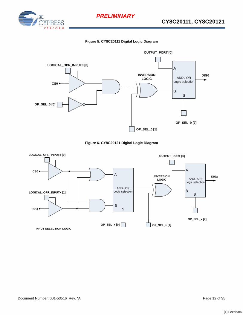
Figure 5. CY8C20111 Digital Logic Diagram
Figure 6. CY8C20121 Digital Logic Diagram
INVERSION LOGIC
DIG0
OP_SEL_0 [0]
OP_SEL_0 [1]
LOGICAL_OPR_INPUT0 [0]
OP_SEL_0 [7]
AND / OR Logic selection
A
BS
OUTPUT_PORT [0]
ENB
CS0
INVERSION LOGIC
DIGx
OP_SEL_x [0] OP_SEL_x [1]
AND / OR Logic selection
A
BS
LOGICAL_OPR_INPUTx [0]
LOGICAL_OPR_INPUTx [1]
INPUT SELECTION LOGIC
OP_SEL_x [7]
AND / OR Logic selection
A
BS
OUTPUT_PORT [x]
ENB
ENB
CS0
CS1
[+] Feedback

PRELIMINARYCY8C20111, CY8C20121
Document Number: 001-53516 Rev. *A Page 13 of 35
8.6 OP_SEL_xLogic Operation Selection Registers
This register is used to enable logic operation on GP outputs. OP_SEL_0 should be configured to get the logic operation output onDIG0 output and OP_SEL_1 for DIG1 output. Write to these registers during the disable state of respective DIG output pins does nothave any effect.The input to the logic operation can be selected in LOGIC_OPRX registers. The selected inputs can be ORed or ANDed. The outputof logic operation can also be inverted.
8.7 LOGICAL_OPR_INPUTxSelects Input for Logic Operation
LOGICAL_OPR_INPUT0: 1Eh LOGICAL_OPR_INPUT1: 23h (Not available for 1 button)LOGICAL_OPR_INPUT0
LOGICAL_OPR_INPUT1
These registers are used to give the input to logic operation block. The inputs can be only CapSense input status.
OP_SEL_0: 1Ch OP_SEL_1: 21h (Not available for 1 Button)
1/2Button 7 6 5 4 3 2 1 0Access: FD RW: 0 RW: 0 RW: 0
Bit Name Op_En InvOp Operator
Bit Name Description7 Op_En This bit enables or disables logic operation.
0 Disable logic operation1 Enable logic operation
1 InvOp This bit enables or disables logic operation output inversion.0 Logic operation output not inverted1 Logic operation output inverted
0 Operator This bit selects which operator should be used to compute logic operation.0 Logic operator OR is used on inputs1 Logic operator AND is used on inputs
1 Button 7 6 5 4 3 2 1 0Access: FD RW:01Bit Name CSL[0]
2 Button 7 6 5 4 3 2 1 0Access: FD RW:01Bit Name CSL [1:0]
2 Button 7 6 5 4 3 2 1 0Access: FD RW:02Bit Name CSL [1:0]
Bit Name Description1:0 CSL [1:0] These bits selects the input for logic operation block.
[+] Feedback

PRELIMINARYCY8C20111, CY8C20121
Document Number: 001-53516 Rev. *A Page 14 of 35
8.8 CS_NOISE_THNoise Threshold Register
CS_NOISE_TH: 4Eh
This register sets the noise threshold value. For individual sensors, count values above this threshold do not update the baseline.This count is relative to baseline. This parameter is common for all sensors.The range is 3 to 255 and it should satisfy the equation NT < Min (Finger Threshold – Hysteresis – 5). Recommended value is 40%of finger threshold.
8.9 CS_BL_UPD_THBaseline Update Threshold Register
CS_BL_UPD_TH: 4Fh
When the new raw count value is above the current baseline and the difference is below the noise threshold, the difference betweenthe current baseline and the raw count is accumulated into a “bucket.” When the bucket fills, the baseline increments and the bucketis emptied. This parameter sets the threshold that the bucket must reach for the baseline to increment. In other words, lower valueprovides faster baseline update rate and vice versa. This parameter is common for all sensors.The range is 0 to 255.
8.10 CS_SETL_TIMESettling Time Register
CS_SETL_TIME: 50h (Writable only in Setup mode)
The settling time parameter controls the duration of the capacitance-to-voltage conversion phase. The parameter setting controls asoftware delay that allows the voltage on the integrating capacitor to stabilize. This parameter is common for all sensors.This register should be set before setting finger threshold (0x66, 0x67) and IDAC setting (0x70, 0x71) registers.The range is 2 to 255.
1/2 Button 7 6 5 4 3 2 1 0Access: FD RW:28
Bit Name NT[7:0]
Bit Name Description7:0 NT [7:0] These bits are used to set the noise threshold value.
1/2 Button 7 6 5 4 3 2 1 0Access: FD RW:64
Bit Name BLUT[7:0]
Bit Name Description7:0 BLUT [7:0] These bits set the threshold that the bucket must reach for baseline to increment.
1/2 Button 7 6 5 4 3 2 1 0Access: FD RW:A0Bit Name STLNG_TM[7:0]
Bit Name Description7:0 STLNG_TM [7:0] These bits are used to set the settling time value.
[+] Feedback
PRELIMINARYCY8C20111, CY8C20121
Document Number: 001-53516 Rev. *A Page 15 of 35
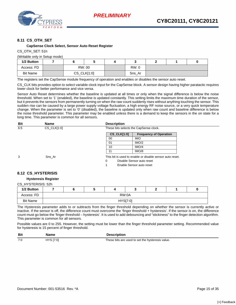
8.11 CS_OTH_SETCapSense Clock Select, Sensor Auto Reset Register
CS_OTH_SET: 51h (Writable only in Setup mode)
The registers set the CapSense module frequency of operation and enables or disables the sensor auto reset.CS_CLK bits provides option to select variable clock input for the CapSense block. A sensor design having higher paratactic requireslower clock for better performance and vice versa.Sensor Auto Reset determines whether the baseline is updated at all times or only when the signal difference is below the noisethreshold. When set to ‘1’ (enabled), the baseline is updated constantly. This setting limits the maximum time duration of the sensor,but it prevents the sensors from permanently turning on when the raw count suddenly rises without anything touching the sensor. Thissudden rise can be caused by a large power supply voltage fluctuation, a high energy RF noise source, or a very quick temperaturechange. When the parameter is set to ‘0’ (disabled), the baseline is updated only when raw count and baseline difference is belowthe noise threshold parameter. This parameter may be enabled unless there is a demand to keep the sensors in the on state for along time. This parameter is common for all sensors.
8.12 CS_HYSTERISISHysteresis Register
CS_HYSTERISIS: 52h
The Hysteresis parameter adds to or subtracts from the finger threshold depending on whether the sensor is currently active orinactive. If the sensor is off, the difference count must overcome the ‘finger threshold + hysteresis’. If the sensor is on, the differencecount must go below the ‘finger threshold – hysteresis’. It is used to add debouncing and “stickiness” to the finger detection algorithm.This parameter is common for all sensors.Possible values are 0 to 255. However, the setting must be lower than the finger threshold parameter setting. Recommended valuefor hysteresis is 15 percent of finger threshold.
1/2 Button 7 6 5 4 3 2 1 0Access: FD RW: 00 RW: 0
Bit Name CS_CLK[1:0] Sns_Ar
Bit Name Description6:5 CS_CLK[1:0] These bits selects the CapSense clock.
3 Sns_Ar This bit is used to enable or disable sensor auto reset.0 1
Disable Sensor auto resetEnable Sensor auto reset
CS_CLK[1:0] Frequency of Operation00 IMO01 IMO/210 IMO/411 IMO/8
1/2 Button 7 6 5 4 3 2 1 0Access: FD RW:0A
Bit Name HYS[7:0]
Bit Name Description7:0 HYS [7:0] These bits are used to set the hysteresis value.
[+] Feedback
PRELIMINARYCY8C20111, CY8C20121
Document Number: 001-53516 Rev. *A Page 16 of 35
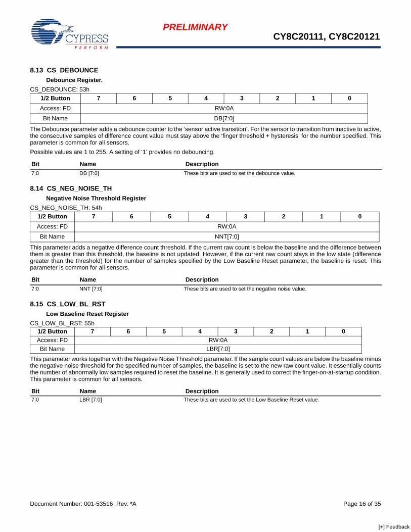
8.13 CS_DEBOUNCEDebounce Register.
CS_DEBOUNCE: 53h
The Debounce parameter adds a debounce counter to the ‘sensor active transition’. For the sensor to transition from inactive to active,the consecutive samples of difference count value must stay above the ‘finger threshold + hysteresis’ for the number specified. Thisparameter is common for all sensors.Possible values are 1 to 255. A setting of ‘1’ provides no debouncing.
8.14 CS_NEG_NOISE_THNegative Noise Threshold Register
CS_NEG_NOISE_TH: 54h
This parameter adds a negative difference count threshold. If the current raw count is below the baseline and the difference betweenthem is greater than this threshold, the baseline is not updated. However, if the current raw count stays in the low state (differencegreater than the threshold) for the number of samples specified by the Low Baseline Reset parameter, the baseline is reset. Thisparameter is common for all sensors.
8.15 CS_LOW_BL_RSTLow Baseline Reset Register
CS_LOW_BL_RST: 55h
This parameter works together with the Negative Noise Threshold parameter. If the sample count values are below the baseline minusthe negative noise threshold for the specified number of samples, the baseline is set to the new raw count value. It essentially countsthe number of abnormally low samples required to reset the baseline. It is generally used to correct the finger-on-at-startup condition.This parameter is common for all sensors.
1/2 Button 7 6 5 4 3 2 1 0Access: FD RW:0A
Bit Name DB[7:0]
Bit Name Description7:0 DB [7:0] These bits are used to set the debounce value.
1/2 Button 7 6 5 4 3 2 1 0Access: FD RW:0A
Bit Name NNT[7:0]
Bit Name Description7:0 NNT [7:0] These bits are used to set the negative noise value.
1/2 Button 7 6 5 4 3 2 1 0Access: FD RW:0ABit Name LBR[7:0]
Bit Name Description7:0 LBR [7:0] These bits are used to set the Low Baseline Reset value.
[+] Feedback

PRELIMINARYCY8C20111, CY8C20121
Document Number: 001-53516 Rev. *A Page 17 of 35
8.16 CS_FILTERINGCapSense Filtering Register
CS_FILTERING: 56h
This register provides an option for forced baseline reset and to enable and configure two different types of software filters.
8.17 CS_SCAN_POS_xScan Position Registers
CS_SCAN_POS_0: 5Ch(Writable only in Setup mode)
CS_SCAN_POS_1: 5Dh (Not available for 1 Button)(Writable only in Setup mode)
This register is used to set the position of the sensors in the switch table for proper scanning sequence because the CapSense sensorsare scanned in sequence.This register should be set after setting 0x07, 0x50, and 0x51 registers.
1/2 Button 7 6 5 4 3 2 1 0Access: FD RW: 0 RW: 1 RW: 0 RW: 00Bit Name RstBl I2C_DS Avg_En Avg_Order[1:0]
Bit Name Description7 RstBl This bit resets all the baselines and it is auto cleared to ‘0’.
0 All Baselines are not reset1 All baselines are reset
5 I2C_DS When this bit is set to ‘1’ the CapSense scan sample is dropped if I2C communicationwas active during scanning.0 Disable the I2C drop sample filer1 Enable the I2C drop sample filter
4 Avg_En This bit enables average filter on raw counts.0 Disable the average filter1 Enable the average filter
[1:0] Avg_Order[1:0] These bits are used to select the number of CapSense samples to average:
Avg_Order[1:0] in Hex Samples to Average00 201 410 811 16
1/2 Button 7 6 5 4 3 2 1 0Access: FD RW: 0
Bit Name Scan_Pstn
2 Button 7 6 5 4 3 2 1 0Access: FD RW: 1
Bit Name Scan_Pstn
Bit Name Description0 Scan_Pstn This bit sets the scan position.
[+] Feedback
PRELIMINARYCY8C20111, CY8C20121
Document Number: 001-53516 Rev. *A Page 18 of 35
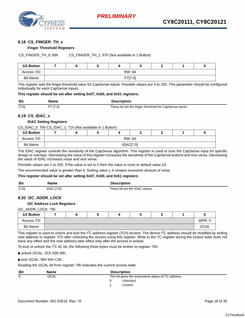
8.18 CS_FINGER_TH_xFinger Threshold Registers
This register sets the finger threshold value for CapSense inputs. Possible values are 3 to 255. This parameter should be configuredindividually for each CapSense inputs.This register should be set after setting 0x07, 0x50, and 0x51 registers.
8.19 CS_IDAC_xIDAC Setting Registers
CS_IDAC_0: 70h CS_IDAC_1: 71h (Not available in 1 Button)
The IDAC register controls the sensitivity of the CapSense algorithm. This register is used to tune the CapSense input for specificdesign or overlays. Decreasing the value of this register increases the sensitivity of the CapSense buttons and vice versa. Decreasingthe value of IDAC increases noise and vice versa.Possible values are 1 to 255. If the value is set to 0 then the value is reset to default value 10.The recommended value is greater than 4. Setting value < 4 creates excessive amount of noise.This register should be set after setting 0x07, 0x50, and 0x51 registers.
8.20 I2C_ADDR_LOCKI2C Address Lock Registers
I2C_ADDR_LOCK: 79h
This register is used to unlock and lock the I2C address register (7Ch) access. The device I2C address should be modified by writingnew address to register 7Ch after unlocking the access using this register. Write to the 7C register during the locked state does nothave any effect and the new address take effect only after the access is locked.To lock or unlock the I2C AL bit, the following three bytes must be written to register 79h:
■ unlock I2CAL: 3Ch A5h 69h
■ lock I2CAL: 96h 5Ah C3hReading the I2CAL bit from register 79h indicates the current access state.
CS_FINGER_TH_0: 66h CS_FINGER_TH_1: 67h (Not available in 1 Button)
1/2 Button 7 6 5 4 3 2 1 0Access: FD RW: 64
Bit Name FT[7:0]
Bit Name Description[7:0] FT [7:0] These bit set the finger threshold for CapSense inputs.
1/2 Button 7 6 5 4 3 2 1 0Access: FD RW: 0A
Bit Name IDAC[7:0]
Bit Name Description[7:0] IDAC [7:0] These bit set the IDAC values.
1/2 Button 7 6 5 4 3 2 1 0Access: FD WPR: 0
Bit Name I2CAL
Bit Name Description0 I2CAL This bit gives the lock/unlock status of I2C address.
0 Unlocked1 Locked
[+] Feedback

PRELIMINARYCY8C20111, CY8C20121
Document Number: 001-53516 Rev. *A Page 19 of 35
8.21 DEVICE_IDDevice ID Register
DEVICE_ID: 7Ah
This register contains the device and product ID. The device and product ID corresponds to “xx” in CY8C201xx.
8.22 DEVICE_STATUSDevice Status Register
DEVICE_STATUS: 7Bh
This register contains the device status.
1 Button 7 6 5 4 3 2 1 0Access: FD R: 11Bit Name DEV_ID[7:0]
2 Button 7 6 5 4 3 2 1 0Access: FD R: 21Bit Name DEV_ID[7:0]
Bit Name Description7:0 DEV_ID [7:0] These bits contain the device and product ID.
Part No Device/Product IDCY8C20111 11CY8C20121 21
1/2 Button 7 6 5 4 3 2 1 0Access: FD R : 00 R: 0 R : 0 R: 0 R: 0 R: 0Bit Name Ip_Volt[1:0] IRES Load_FD No_NVM_Wr CSE DIGE
Bit Name Description7:6 Ip_Volt [1:0] Supply voltage is automatically detected and these bits are set accordingly.
5 IRES When set to ‘1’, this bit indicates that an internal reset occurred.0 indicates the last system reset was not internal reset1 indicates the last system reset was internal reset
4 Load_FD This bit indicates whether factory defaults are loaded during power up.0 User default configuration is loaded during power up1 Factory default configuration is loaded during power up
3 No_NVM_Wr When set to ‘1’, this bit indicates that the supply voltage applied to the device Is toolow for a write to nonvolatile memory operation, and no write is performed. This bitmust be checked before any Store or Write POR command.
1 CSE This bit indicates whether CapSense function is enabled or disabled.0 Functionality of CapSense block is disabled1 Functionality of CapSense block is enabled
0 DIGE This bit indicates whether GP Output function is enabled or disabled.0 Functionality of Digital output block is disabled1 Functionality of Digital output block is enabled
Ip_Volt[1:0] Supply Voltage00 501 3.310 2.7 11 Reserved
[+] Feedback
PRELIMINARYCY8C20111, CY8C20121
Document Number: 001-53516 Rev. *A Page 20 of 35
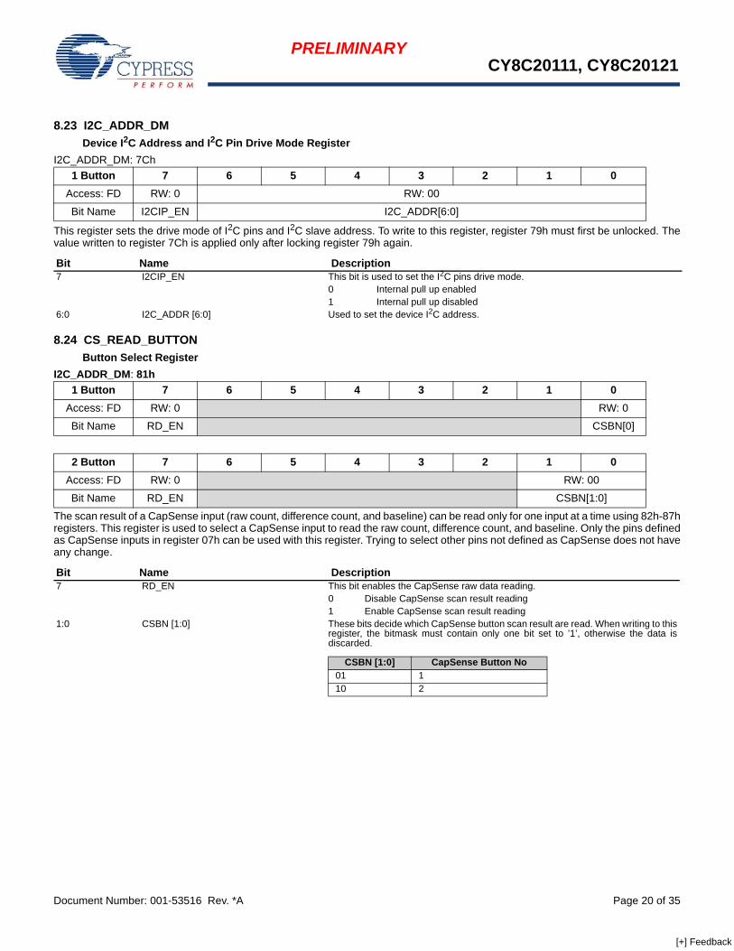
8.23 I2C_ADDR_DMDevice I2C Address and I2C Pin Drive Mode Register
I2C_ADDR_DM: 7Ch
This register sets the drive mode of I2C pins and I2C slave address. To write to this register, register 79h must first be unlocked. Thevalue written to register 7Ch is applied only after locking register 79h again.
8.24 CS_READ_BUTTONButton Select Register
I2C_ADDR_DM: 81h
The scan result of a CapSense input (raw count, difference count, and baseline) can be read only for one input at a time using 82h-87hregisters. This register is used to select a CapSense input to read the raw count, difference count, and baseline. Only the pins definedas CapSense inputs in register 07h can be used with this register. Trying to select other pins not defined as CapSense does not haveany change.
1 Button 7 6 5 4 3 2 1 0Access: FD RW: 0 RW: 00
Bit Name I2CIP_EN I2C_ADDR[6:0]
Bit Name Description7 I2CIP_EN This bit is used to set the I2C pins drive mode.
0 Internal pull up enabled1 Internal pull up disabled
6:0 I2C_ADDR [6:0] Used to set the device I2C address.
1 Button 7 6 5 4 3 2 1 0Access: FD RW: 0 RW: 0
Bit Name RD_EN CSBN[0]
2 Button 7 6 5 4 3 2 1 0Access: FD RW: 0 RW: 00
Bit Name RD_EN CSBN[1:0]
Bit Name Description7 RD_EN This bit enables the CapSense raw data reading.
0 Disable CapSense scan result reading1 Enable CapSense scan result reading
1:0 CSBN [1:0] These bits decide which CapSense button scan result are read. When writing to thisregister, the bitmask must contain only one bit set to ’1’, otherwise the data isdiscarded.
CSBN [1:0] CapSense Button No01 110 2
[+] Feedback
PRELIMINARYCY8C20111, CY8C20121
Document Number: 001-53516 Rev. *A Page 21 of 35
8.25 CS_READ_BLxBaseline Value MSB/LSB Registers
Reading from this register returns the 2-byte current baseline value for the selected CapSense input.
8.26 CS_READ_DIFFxDifference Count Value MSB/LSB Registers
Reading from this register returns the 2-byte current difference count for the selected CapSense input.
8.27 CS_READ_RAWxDifference Count Value MSB/LSB Registers
Reading from this register returns the 2-byte current raw count value for the selected CapSense input.
CS_READ_BLM: 82h CS_READ_BLL: 83h
1/2 Button 7 6 5 4 3 2 1 0Access: FD R: 00
Bit Name BL [7:0]
Bit Name Description7:0 BL [7:0] These bits represent the baseline value.
CS_READ_DIFFM: 82h CS_READ_DIFFL: 83h
1/2 Button 7 6 5 4 3 2 1 0Access: FD R: 00
Bit Name DIF [7:0]
Bit Name Description7:0 DIF [7:0] These bits represent the sensor difference count.
CS_READ_RAWM: 82h CS_READ_RAWL: 83h
1/2 Button 7 6 5 4 3 2 1 0Access: FD R: 00
Bit Name RC [7:0]
Bit Name Description7:0 RC [7:0] These bits represent the raw count value.
[+] Feedback

PRELIMINARYCY8C20111, CY8C20121
Document Number: 001-53516 Rev. *A Page 22 of 35
8.28 CS_READ_STATUSSensor On Status Register
CS_READ_STATUS: 88h
This register gives the sensor ON/OFF status. A bit ‘1’ indicates sensor is ON and ‘0’ indicates sensor is OFF.
8.29 COMMAND_REGCommand Register
COMMAND_REG: A0h
Commands are executed by writing the command code to the command register.
1 Button 7 6 5 4 3 2 1 0Access: FD R: 0
Bit Name BT_ST[0]
2 Button 7 6 5 4 3 2 1 0Access: FD R: 00
Bit Name BT_ST[1:0]
Bit Name Description1:0 BT_ST [1:0] These bits used to represent sensor status.
0 Sensor OFF1 Sensor ON
1/2 Button 7 6 5 4 3 2 1 0Access: FD W: 00
Bit Name Cmnd [7:0]
Bit Name Description7:0 Cmnd [7:0] Refer to the following table for command register opcodes.
Command Code Name Description
00h Get Firmware Revision The I2C buffer is loaded with the one byte firmware revision value. Reading one byte after writing this command returns the firmware revision. The upper nibble of the firmware revision byte is the major revision number and the lower nibble is the minor revision number.
01h Store Current Configu-ration to NVM
The current register settings are saved in nonvolatile memory (flash). This setting is automatically loaded after the next device reset/power up or if the Reconfigure Device (06h) command is issued.
02h Restore Factory Configuration
Replaces the saved user configuration with the factory default configuration. Current settings are unaffected by this command. New settings are loaded after the next device reset/power up or if the 06h command is issued.
03h Write POR Defaults Sends new power up defaults to the CapSense controller without changing current settings unless the 06h command is issued afterwards. This command is followed by 123 data bytes according to the POR Default Data Structure table. The CRC is calcu-lated as the XOR of the 122 data bytes (00h-79h). If the CRC check fails or an incomplete block is sent, the slave responds with an ACK and the data is NOT saved to flash.To define new POR defaults:
■ Write command 03h
■ Write 122 data bytes with new values of registers (use the _flash.iic file generated from s/w tool)
■ Write one CRC byte calculated as XOR of previous 122 data bytes
[+] Feedback
PRELIMINARYCY8C20111, CY8C20121
Document Number: 001-53516 Rev. *A Page 23 of 35
04h Read POR Defaults Reads the POR settings stored in the nonvolatile memory. To read POR defaults:
■ Write command 04h
■ Read 122 data bytes
■ Read one CRC byte05h Read Device Configu-
ration (RAM)Reads the current device configuration. Gives the user "flat-address-space" access to all device settings. To read device configuration:
■ Write command 05h
■ Read 122 data bytes
■ Read one CRC byte06h Reconfigure Device
(POR)Immediately reconfigures the device with actual POR defaults from flash. Has the same effect on the registers as a POR. This command can only be executed in setup operation mode (command code 08).
07h Set Normal Operation Mode
Sets the device in normal operation mode. In this mode, CapSense pin assignments cannot be modified; settling time, IDAC setting, external capacitor, and sensor auto-reset also cannot be modified.
08h Set Setup Operation Mode
Sets the device in setup operation mode. In this mode, CapSense pin assignments can be changed along with other parameters.
09h Start CapSense Scanning
Allows the user to start CSA scanning after it has been stopped using command 0x0A. Note that at POR, scanning is enabled and started by default if one or more sensors are enabled.
0Ah Stop CapSense Scanning
Allows the user to stop CSA scanning. A system host controller might initiate this command before powering down the device to make sure that during power down no CapSense touches are detected.When CSA scanning is stopped by the user and the device is still in the valid VCC operating range, the following behavior is supported:
■ Any change to configuration can still be done (as long as VCC is in operating range).
■ Command code 0x06 overrides the status of stop/scan by enabling and starting CSA scanning if one or more sensors are enabled.
■ CapSense read-back values return 0x00.0Bh Returns CapSense
Scanning StatusThe I2C buffer is loaded with the one-byte CSA scanning status value. After writing the value 0Bh to the A0h register, reading one byte returns the CSA scanning status. It returns the LVD_STOP_SCAN and STOP_SCAN bits.LVD_STOP_SCAN is bit 3 - Set when CSA is stopped because VCC is outside the valid operating range. STOP_SCAN is bit 2 - Set when CSA is stopped by the user by writing command 0x0A.
Command Code Name Description
[+] Feedback
PRELIMINARYCY8C20111, CY8C20121
Document Number: 001-53516 Rev. *A Page 24 of 35
9. Layout Guidelines and Best Practices
Sl. No. Category Min Max Recommendations/Remarks
1 Button Shape Solid round pattern, round with LED hole, rectangle with round corners
2 Button Size 5 mm 15 mm 10 mm
3 Button Button Spacing = Button Ground Clearance
8 mm
4 Button Ground Clearance 0.5 mm 2 mm Button ground clearance = Overlay Thickness
5 Ground Flood - Top Layer Hatched ground 7 mil trace and 45 mil grid (15% filling)
6 Ground Flood - Bottom Layer Hatched ground 7 mil trace and 70 mil grid (10% filling)
7 Trace Length from Sensor to PSoC - Buttons
200 mm < 100 mm.
8 Trace Width 0.17 mm 0.20 mm 0.17 mm (7 mil)
9 Trace Routing Traces should be routed on the non sensor side. If any non CapSense trace crosses CapSense trace, ensure that inter-section is orthogonal.
10 Via Position for the Sensors Via should be placed near the edge of the button/slider to reduce trace length thereby increasing sensitivity.
11 Via Hole Size for Sensor Traces
10 mil
12 No. of Via on Sensor Trace 1 2 1
13 CapSense Series Resistor Placement
10mm Place CapSense series resistors close to PSoC for noise suppression.CapSense resistors have highest priority place them first.
14 Distance between any CapSense Trace to Ground Flood
10 mil 20 mil 20 mil
15 Device Placement Mount the device on the layer opposite to sensor. The CapSense trace length between the device and sensors should be minimum
16 Placement of Components in 2 Layer PCB
Top layer-sensor pads and bottom layer-PSoC, other compo-nents and traces.
17 Placement of Components in 4 Layer PCB
Top layer-sensor pads, second layer – CapSense traces, third layer-hatched ground, bottom layer- PSoC, other components and non CapSense traces
18 Overlay Thickness - Buttons 0 mm 2 mm 1 mm
19 Overlay Material Should to be non conductive material. Glass, ABS Plastic, Formica
20 Overlay Adhesives Adhesive should be non conductive and dielectrically homog-enous. 467MP and 468MP adhesives made by 3M are recommended.
21 LED Back Lighting Cut a hole in the sensor pad and use rear mountable LEDs. Refer Example PCB Layout Design with Two CapSense Buttons and Two LEDs on page 26.
22 Board Thickness Standard board thickness for CapSense FR4 based designs is 1.6 mm.
[+] Feedback
PRELIMINARYCY8C20111, CY8C20121
Document Number: 001-53516 Rev. *A Page 25 of 35
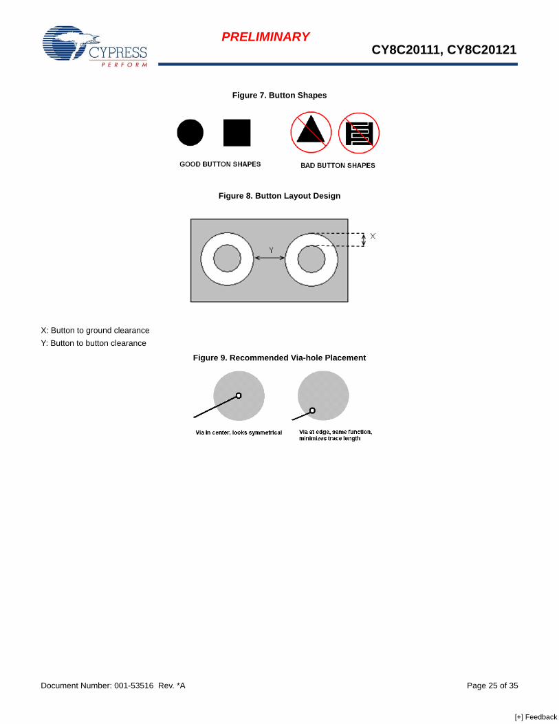
Figure 7. Button Shapes
Figure 8. Button Layout Design
X: Button to ground clearanceY: Button to button clearance
Figure 9. Recommended Via-hole Placement
[+] Feedback
PRELIMINARYCY8C20111, CY8C20121
Document Number: 001-53516 Rev. *A Page 26 of 35
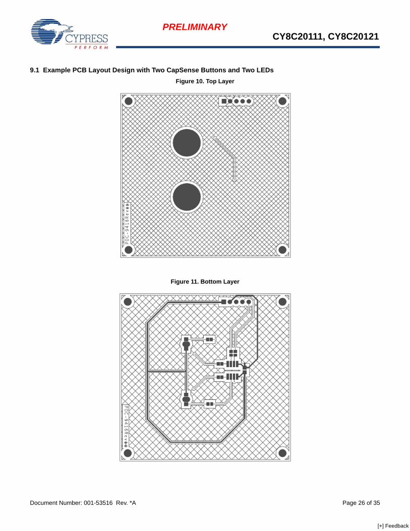
9.1 Example PCB Layout Design with Two CapSense Buttons and Two LEDsFigure 10. Top Layer
Figure 11. Bottom Layer
[+] Feedback
PRELIMINARYCY8C20111, CY8C20121
Document Number: 001-53516 Rev. *A Page 27 of 35
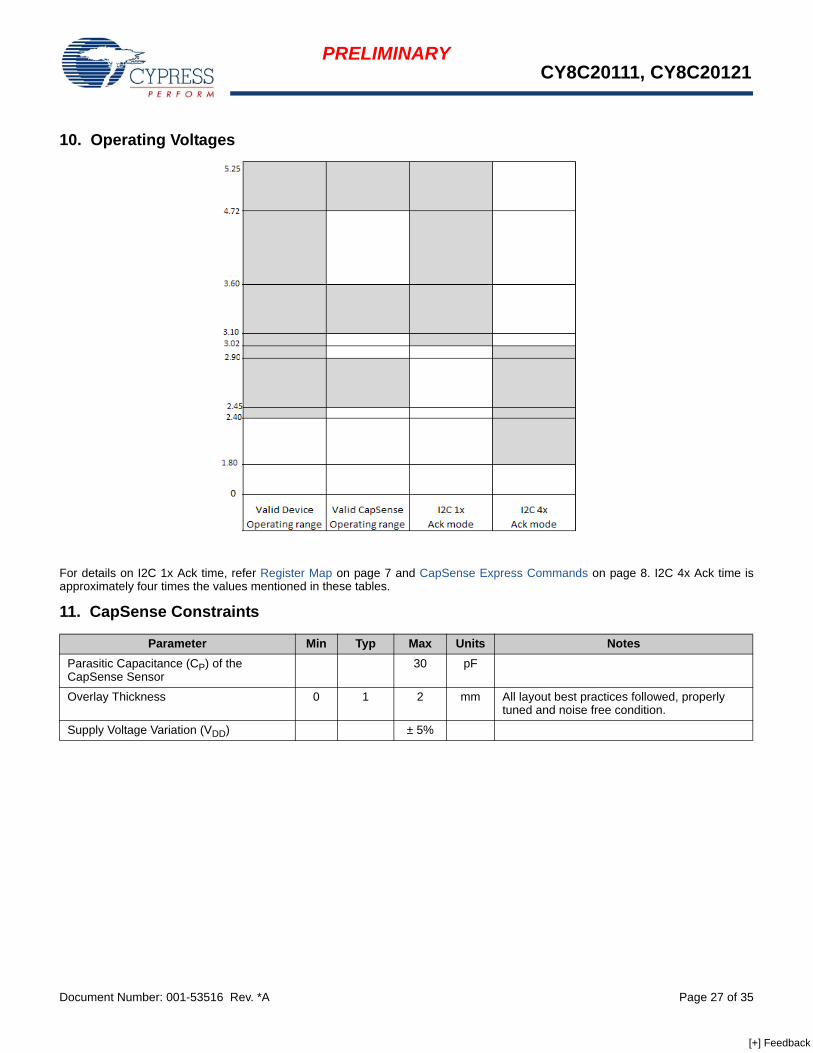
10. Operating Voltages
For details on I2C 1x Ack time, refer Register Map on page 7 and CapSense Express Commands on page 8. I2C 4x Ack time isapproximately four times the values mentioned in these tables.
11. CapSense Constraints
Parameter Min Typ Max Units NotesParasitic Capacitance (CP) of the CapSense Sensor
30 pF
Overlay Thickness 0 1 2 mm All layout best practices followed, properly tuned and noise free condition.
Supply Voltage Variation (VDD) ± 5%
[+] Feedback
PRELIMINARYCY8C20111, CY8C20121
Document Number: 001-53516 Rev. *A Page 28 of 35
12. Electrical Specifications12.1 Absolute Maximum Ratings
Parameter Description Min Typ Max Unit NotesTSTG Storage temperature –55 25 +100 °C Higher storage temperatures reduce data
retention time. Recommended storage temperature is +25°C ± 25°C (0°C to 50°C). Extended duration storage temperatures above 65°C degrade reliability
TA Ambient temperature with power applied
–40 – +85 °C
F32k u ILO frequency 15 32 64 kHz Calculations during sleep operations are done based on ILO frequency.
Tpowerup Power up time – 150 – ms VDD >= 3.1V
Tpowerup Power up time – 600 – ms 2.4V < VDD < 2.9V
VDD Supply voltage on VDD relative to VSS –0.5 – +6.0 V
VIO DC input voltage VSS – 0.5 – VDD + 0.5 V
VIOZ DC voltage applied to tri-state VSS – 0.5 – VDD + 0.5 V
IMIO Maximum current into any GPIO pin –25 – +50 mA
ESD Electro static discharge voltage 2000 – – V Human body model ESD
LU Latch up current – – 200 mA
12.2 Operating Temperature
Parameter Description Min Typ Max Unit NotesTA Ambient temperature –40 – +85 °C
TJ Junction temperature –40 – +100 °C
[+] Feedback
PRELIMINARYCY8C20111, CY8C20121
Document Number: 001-53516 Rev. *A Page 29 of 35
12.3 DC Electrical Characteristics12.3.1 DC Chip Level Specifications
Parameter Description Min Typ Max Unit NotesVDD Supply voltage 2.40 – 5.25 V
IDD Supply current – 1.5 2.5 mA Conditions are VDD = 3.10V, TA = 25°C
12.3.2 5V and 3.3V DC General Purpose I/O Specifications This table lists guaranteed maximum and minimum specifications for the voltage and temperature ranges: 4.75V to 5.25V and-40°C<TA<85°C, 3.10V to 3.6V -40°C<TA<85°C. Typical parameters apply to 5V and 3.3V at 25°C and are for design guidance only.
Parameter Description Min Typ Max Unit NotesVOH1 High output voltage VDD – 0.2 – – V IOH < 10 µA/pin, VDD > 3.10V
VOH2 High output voltage VDD – 0.9 – – V IOH = 1 mA/pin, VDD > 3.10V
VOL Low output voltage – – 0.75 V IOL = 20 mA/pin, VDD > 3.10V, maximum of 40 mA sink current
IOH High output current 0.01 – 1 mA VDD >= 3.1V
IOL1 Low output current on Port 0 pins – – 10 mA VDD >= 3.1V, maximum of 40 mA sink current
COUT Capacitive load on pins as output 0.5 1.7 5 pF Package and pin dependent. Temp = 25°C.
12.3.3 2.7 DC General Purpose I/O SpecificationsThis table lists guaranteed maximum and minimum specifications for the voltage and temperature ranges: 2.4V to 2.90V and-40°C<TA<85°C, respectively. Typical parameters apply to 2.7V at 25°C and are for design guidance only.
Parameter Description Min Typ Max Unit NotesVOH1 High output voltage VDD – 0.2 – – V IOH < 10 µA/pin
VOH2 High output voltage VDD – 0.5 – – V IOH = 0.2 mA/pin
VOL Low output voltage – – 0.75 V IOL = 10 mA/pin, maximum of 20 mA sink current
IOH High output current 0.01 – 0.2 mA VDD <= 2.9V
IOL1 Low output current on Port 0 pins – – 10 mA VDD <= 2.9V, maximum of 20 mA sink current
COUT Capacitive load on pins as output 0.5 1.7 5 pF Package and pin dependent. Temp = 25°C.
12.3.4 2.7V DC Spec for I2C Line with 1.8V External Pull-UpThis table lists guaranteed maximum and minimum specifications for the voltage and temperature ranges: 2.4V to 2.9V and 3.10V to3.60V, and -40°C<TA <85°C, respectively. Typical parameters apply to 2.7V at 25°C. The I2C lines drive mode must be set to opendrain and pulled up to 1.8V externally.
Parameter Description Min Typ Max Unit NotesVOLP Low output voltage – – 0.4 V IOL=5 mA/pin, maximum of 10 mA device
sink current 2.4<VDD <2.9V and 3.1<VDD <3.6V.
VIL Input low voltage – – 0.75 V VDD = 2.4 to 2.90V and 3.10V to 3.6V.
VIH Input high voltage 1.4 – – V VDD = 2.4 to 2.7V.
CI2C Capacitive load on I2C pins 0.5 1.7 5 pF Package and pin dependent. Temp = 25°C.
RPU Pull up resistor 4 5.6 8 kΩ
[+] Feedback

PRELIMINARYCY8C20111, CY8C20121
Document Number: 001-53516 Rev. *A Page 30 of 35
12.3.6 DC Flash Write SpecificationsThis table lists guaranteed maximum and minimum specifications for the voltage and temperature ranges: 4.75V to 5.25V and-40°C<TA<85°C, 3.10V to 3.6V and -40°C<TA<85°C or 2.4V to 2.90V and -40°C<TA<85°C, respectively. Typical parameters apply to5V, 3.3V, or 2.7V at 25°C. These are for design guidance only. Flash Endurance and Retention specifications are valid only within therange: 25°C±20°C during the flash write operation. It is at the user’s own risk to operate out of this temperature range. If flash writingis done out of this temperature range, the endurance and data retention reduces.
12.4 CapSense Electrical Characteristics
12.3.5 DC POR and LVD Specifications
Parameter Description Min Typ Max Unit Notes
VPPOR0VPPOR1
VDD Value for PPOR TripVDD= 2.7VVDD= 3.3V, 5V
––
2.362.60
2.402.65
VV
VDD must be greater than or equal to 2.5V during startup or reset from watchdog.
Symbol Description Min Typ Max Units NotesVddIWRITE Supply Voltage for Flash Write Operations[7] 2.7 – – VIDDP Supply Current for Flash Write Operations – 5 25 mAFlashENPB Flash Endurance 50,000 – – – Erase/write cyclesFlashDR Flash Data Retention 10 – – Years
Max (V) Typ (V) Min (V) Conditions for Supply Volt-age Result
3.6 3.3 3.1 <2.9 The device automatically reconfigures itself to work in 2.7V mode of operation.
>2.9 or <3.10 This range is not recommended for CapSense usage.
2.90 2.7 2.45 <2.45V The scanning for CapSense parameters shuts down until the voltage returns to over 2.45V.
>3.10 The device automatically reconfigures itself to work in 3.3V mode of operation.
<2.4V The device goes into reset.
5.25 5.0 4.75 <4.73V The scanning for CapSense parameters shuts down until the voltage returns to over 4.73V.
Note7. Commands involving flash writes (0x01, 0x02, 0x03) and flash read (0x04) must be executed only within the same VCC voltage range detected at POR (power on, or
command 0x06) and above 2.7V.
[+] Feedback

PRELIMINARYCY8C20111, CY8C20121
Document Number: 001-53516 Rev. *A Page 31 of 35
12.5 AC Electrical Specifications
12.5.1 5V and 3.3V AC General Purpose I/O Specifications
Figure 12. Definition of Timing for Fast/Standard Mode on the I2C Bus
Parameter Description Min Max Unit NotesTRise Rise time, strong mode,
Cload = 50 pF15 80 ns VDD = 3.10V to 3.6V and 4.75V to
5.25V, 10% - 90%
TFall Fall time, strong mode,Cload = 50 pF
10 50 ns VDD = 3.10V to 3.6V and 4.75V to 5.25V, 10% - 90%
12.5.2 2.7V AC General Purpose I/O Specifications
Parameter Description Min Max Unit NotesTRise Rise time, strong mode,
Cload = 50 pF15 100 ns VDD = 2.4V to 2.90V, 10% - 90%
TFall Fall time, strong mode,Cload = 50 pF
10 70 ns VDD = 2.4V to 2.90V, 10% - 90%
12.5.3 AC I2C Specifications
Parameter DescriptionStandard
Mode Fast ModeUnits Notes
Min Max Min MaxFSCLI2C SCL clock frequency 0 100 0 400 kbps Fast mode not supported for
VDD < 3.0V
THDSTAI2C Hold time (repeated) START condition. After this period, the first clock pulse is generated
4.0 – 0.6 – µs
TLOWI2C LOW period of the SCL clock 4.7 – 1.3 – µs
THIGHI2C HIGH period of the SCL clock 4.0 – 0.6 – µs
TSUSTAI2C Setup time for a repeated START condition 4.7 – 0.6 – µs
THDDATI2C Data hold time 0 – 0 – µs
TSUDATI2C Data setup time 250 – 100 – ns
TSUSTOI2C Setup time for STOP condition 4.0 – 0.6 – µs
TBUFI2C BUS free time between a STOP and START condition
4.7 – 1.3 – µs
TSPI2C Pulse width of spikes suppressed by the input filter
– – 0 50 ns
~ ~~ ~
S SrtSUSTOI2CtSUSTAI2CtHDSTAI2C tHIGHI2C
tLOWI2CtSUDATI2C
tHDDATI2C
tf
SDA
SCL
P S
tBUFI2Ctrtftr tSPI2CtHDSTAI2C
~ ~~ ~
~ ~ ~ ~
[+] Feedback
PRELIMINARYCY8C20111, CY8C20121
Document Number: 001-53516 Rev. *A Page 32 of 35
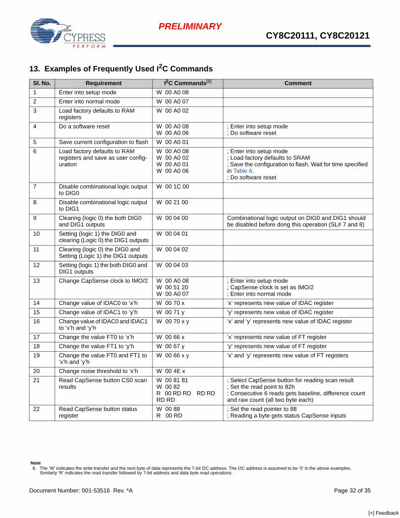
13. Examples of Frequently Used I2C Commands
Sl. No. Requirement I2C Commands[8] Comment1 Enter into setup mode W 00 A0 082 Enter into normal mode W 00 A0 073 Load factory defaults to RAM
registersW 00 A0 02
4 Do a software reset W 00 A0 08W 00 A0 06
; Enter into setup mode; Do software reset
5 Save current configuration to flash W 00 A0 016 Load factory defaults to RAM
registers and save as user config-uration
W 00 A0 08W 00 A0 02W 00 A0 01W 00 A0 06
; Enter into setup mode; Load factory defaults to SRAM; Save the configuration to flash. Wait for time specified in Table 6.; Do software reset
7 Disable combinational logic output to DIG0
W 00 1C 00
8 Disable combinational logic output to DIG1
W 00 21 00
9 Clearing (logic 0) the both DIG0 and DIG1 outputs
W 00 04 00 Combinational logic output on DIG0 and DIG1 should be disabled before dong this operation (SL# 7 and 8)
10 Setting (logic 1) the DIG0 and clearing (Logic 0) the DIG1 outputs
W 00 04 01
11 Clearing (logic 0) the DIG0 and Setting (Logic 1) the DIG1 outputs
W 00 04 02
12 Setting (logic 1) the both DIG0 and DIG1 outputs
W 00 04 03
13 Change CapSense clock to IMO/2 W 00 A0 08W 00 51 20W 00 A0 07
; Enter into setup mode; CapSense clock is set as IMO/2; Enter into normal mode
14 Change value of IDAC0 to ‘x’h W 00 70 x ‘x’ represents new value of IDAC register15 Change value of IDAC1 to ‘y’h W 00 71 y ‘y’ represents new value of IDAC register16 Change value of IDAC0 and IDAC1
to ‘x’h and ‘y’hW 00 70 x y ‘x’ and ‘y’ represents new value of IDAC register
17 Change the value FT0 to ‘x’h W 00 66 x ‘x’ represents new value of FT register18 Change the value FT1 to ‘y’h W 00 67 y ‘y’ represents new value of FT register19 Change the value FT0 and FT1 to
‘x’h and ‘y’hW 00 66 x y ‘x’ and ‘y’ represents new value of FT registers
20 Change noise threshold to ‘x’h W 00 4E x21 Read CapSense button CS0 scan
resultsW 00 81 81 W 00 82R 00 RD RD RD RD RD RD
; Select CapSense button for reading scan result; Set the read point to 82h; Consecutive 6 reads gets baseline, difference count and raw count (all two byte each)
22 Read CapSense button status register
W 00 88 R 00 RD
; Set the read pointer to 88; Reading a byte gets status CapSense inputs
Note8. The ‘W’ indicates the write transfer and the next byte of data represents the 7-bit I2C address. The I2C address is assumed to be ‘0’ in the above examples.
Similarly ‘R’ indicates the read transfer followed by 7-bit address and data byte read operations.
[+] Feedback
PRELIMINARYCY8C20111, CY8C20121
Document Number: 001-53516 Rev. *A Page 33 of 35
14. Ordering Information
Note For Die sales information, contact a local Cypress sales office or Field Applications Engineer (FAE).
14.1 Ordering Code Information
Ordering Code Package Diagram Package Type
Operating Tempera-
tureCapSense
BlocksCapSense
InputsDigital
OutputsXRES
Pin
CY8C20111-SX1I 51-85066 8 SOIC Industrial Yes 1 1 No
CY8C20111-SX1IT 51-85066 8 SOIC (Tape and Reel) Industrial Yes 1 1 No
CY8C20121-SX1I 51-85066 8 SOIC Industrial Yes 2 2 No
CY8C20121-SX1IT 51-85066 8 SOIC (Tape and Reel) Industrial Yes 2 2 No
CY
Marketing Code: 8 = Cypress Semiconductors
8 C 201 xx - SX 1 I T
Tape and ReelThermal Rating : Industrial
8 pin pinout
Package Type : SOIC Pb- Free
Part Number
Family Code
Technology Code: C = CMOS
Company ID: CY = Cypress
[+] Feedback

PRELIMINARYCY8C20111, CY8C20121
Document Number: 001-53516 Rev. *A Page 34 of 35
15. Package DiagramFigure 13. 8-Pin (150-Mil) SOIC (51-85066)
SEATING PLANE
PIN 1 ID
0.230[5.842]
0.244[6.197]
0.157[3.987]
0.150[3.810]
0.189[4.800]
0.196[4.978]
0.050[1.270]
BSC
0.061[1.549]
0.068[1.727]
0.004[0.102]
0.0098[0.249]
0.0138[0.350]
0.0192[0.487]
0.016[0.406]
0.035[0.889]
0.0075[0.190]
0.0098[0.249]
1. DIMENSIONS IN INCHES[MM] MIN.MAX.
0°~8°
0.016[0.406]
0.010[0.254]X 45°
2. PIN 1 ID IS OPTIONAL,ROUND ON SINGLE LEADFRAMERECTANGULAR ON MATRIX LEADFRAME
0.004[0.102]
8 Lead (150 Mil) SOIC - S08
14
5 8
3. REFERENCE JEDEC MS-012
PART #
S08.15 STANDARD PKG.
SZ08.15 LEAD FREE PKG.
4. PACKAGE WEIGHT 0.07gms
51-85066-*C
[+] Feedback
Document Number: 001-53516 Rev. *A Revised December 16, 2009 Page 35 of 35
CapSense Express™, PSoC Designer™, and Programmable System-on-Chip™ are trademarks and PSoC® is a registered trademark of Cypress Semiconductor Corp. All other trademarks or registeredtrademarks referenced herein are property of the respective corporations. Purchase of I2C components from Cypress or one of its sublicensed Associated Companies conveys a license under thePhilips I2C Patent Rights to use these components in an I2C system, provided that the system conforms to the I2C Standard Specification as defined by Philips. All products and company namesmentioned in this document may be the trademarks of their respective holders.
PRELIMINARYCY8C20111, CY8C20121
© Cypress Semiconductor Corporation, 2009. The information contained herein is subject to change without notice. Cypress Semiconductor Corporation assumes no responsibility for the use of anycircuitry other than circuitry embodied in a Cypress product. Nor does it convey or imply any license under patent or other rights. Cypress products are not warranted nor intended to be used for medical,life support, life saving, critical control or safety applications, unless pursuant to an express written agreement with Cypress. Furthermore, Cypress does not authorize its products for use as criticalcomponents in life-support systems where a malfunction or failure may reasonably be expected to result in significant injury to the user. The inclusion of Cypress products in life-support systemsapplication implies that the manufacturer assumes all risk of such use and in doing so indemnifies Cypress against all charges.
Any Source Code (software and/or firmware) is owned by Cypress Semiconductor Corporation (Cypress) and is protected by and subject to worldwide patent protection (United States and foreign),United States copyright laws and international treaty provisions. Cypress hereby grants to licensee a personal, non-exclusive, non-transferable license to copy, use, modify, create derivative works of,and compile the Cypress Source Code and derivative works for the sole purpose of creating custom software and or firmware in support of licensee product to be used only in conjunction with a Cypressintegrated circuit as specified in the applicable agreement. Any reproduction, modification, translation, compilation, or representation of this Source Code except as specified above is prohibited withoutthe express written permission of Cypress.
Disclaimer: CYPRESS MAKES NO WARRANTY OF ANY KIND, EXPRESS OR IMPLIED, WITH REGARD TO THIS MATERIAL, INCLUDING, BUT NOT LIMITED TO, THE IMPLIED WARRANTIESOF MERCHANTABILITY AND FITNESS FOR A PARTICULAR PURPOSE. Cypress reserves the right to make changes without further notice to the materials described herein. Cypress does notassume any liability arising out of the application or use of any product or circuit described herein. Cypress does not authorize its products for use as critical components in life-support systems wherea malfunction or failure may reasonably be expected to result in significant injury to the user. The inclusion of Cypress’ product in a life-support systems application implies that the manufacturerassumes all risk of such use and in doing so indemnifies Cypress against all charges.
Use may be limited by and subject to the applicable Cypress software license agreement.
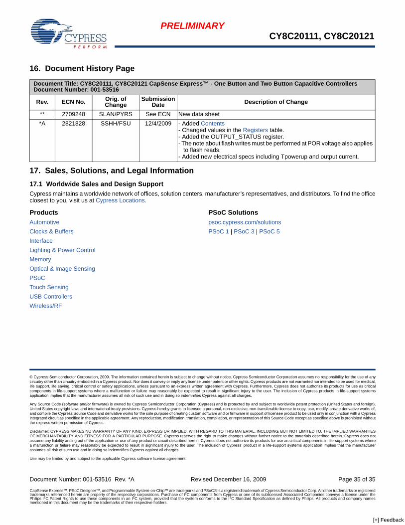
16. Document History Page
17. Sales, Solutions, and Legal Information 17.1 Worldwide Sales and Design SupportCypress maintains a worldwide network of offices, solution centers, manufacturer’s representatives, and distributors. To find the officeclosest to you, visit us at Cypress Locations.
ProductsAutomotiveClocks & BuffersInterfaceLighting & Power ControlMemoryOptical & Image Sensing PSoCTouch SensingUSB ControllersWireless/RF
PSoC Solutionspsoc.cypress.com/solutionsPSoC 1 | PSoC 3 | PSoC 5
Document Title: CY8C20111, CY8C20121 CapSense Express™ - One Button and Two Button Capacitive ControllersDocument Number: 001-53516
Rev. ECN No. Orig. of Change
Submission Date Description of Change
** 2709248 SLAN/PYRS See ECN New data sheet*A 2821828 SSHH/FSU 12/4/2009 - Added Contents
- Changed values in the Registers table.- Added the OUTPUT_STATUS register.- The note about flash writes must be performed at POR voltage also applies
to flash reads.- Added new electrical specs including Tpowerup and output current.
[+] Feedback