Embed Size (px)
Citation preview

CY8C24094/CY8C24794CY8C24894/CY8C24994
PSoC® Programmable System-on-Chip™
Cypress Semiconductor Corporation • 198 Champion Court • San Jose, CA 95134-1709 • 408-943-2600Document Number: 38-12018 Rev. AK Revised March 12, 2015
PSoC® Programmable System-on-Chip
1. Features
■ XRES pin to support in-system serial programming (ISSP) and external reset control in CY8C24894
■ Powerful Harvard-architecture processor❐ M8C processor speeds up to 24 MHz❐ Two 8 × 8 multiply, 32-bit accumulate❐ Low power at high speed❐ Operating voltage: 3 V to 5.25 V❐ Industrial temperature range: –40 °C to +85 °C❐ USB temperature range: –10 °C to +85 °C
■ Advanced peripherals (PSoC® Blocks)❐ Six rail-to-rail analog PSoC blocks provide:
• Up to 14-bit analog-to-digital converters (ADCs)• Up to 9-bit digital-to-analog converters (DACs)• Programmable gain amplifiers (PGAs)• Programmable filters and comparators
❐ Four digital PSoC blocks provide:• 8- to 32-bit timers, counters, and pulse width modulators
(PWMs)• Cyclical redundancy check (CRC) and pseudo random
sequence (PRS) modules• Full-duplex universal asynchronous receiver transmitter
(UART)• Multiple serial peripheral interface (SPI) masters or slaves• Connectable to all general-purpose I/O (GPIO) pins
❐ Complex peripherals by combining blocks❐ Capacitive sensing application (CSA) capability
■ Full speed USB (12 Mbps)❐ Four unidirectional endpoints❐ One bidirectional control endpoint❐ USB 2.0 compliant❐ Dedicated 256 byte buffer❐ No external crystal required
■ Flexible on-chip memory❐ 16 KB flash program storage 50,000 erase and write cycles❐ 1 KB static random access memory (SRAM) data storage❐ ISSP❐ Partial flash updates❐ Flexible protection modes❐ Electrically erasable programmable read-only memory
(EEPROM) emulation in flash
■ Programmable pin configurations❐ 25-mA sink, 10-mA source on all GPIOs❐ Pull-up, pull-down, high Z, strong, or open-drain drive modes
on all GPIOs
❐ Up to 48 analog inputs on GPIOs❐ Two 33 mA analog outputs on GPIOs❐ Configurable interrupt on all GPIOs
■ Precision, programmable clocking❐ Internal ±4% 24- / 48-MHz main oscillator❐ Internal oscillator for watchdog and sleep❐ 0.25% accuracy for USB with no external components
■ Additional system resources❐ I2C slave, master, and multi-master to 400 kHz❐ Watchdog and sleep timers❐ User-configurable low-voltage detection (LVD)
DIGITAL SYSTEM
SRAM1K
InterruptController
Sleep and Watchdog
Clock Sources(Includes IMO and ILO)
Global Digital InterconnectGlobal Analog Interconnect
PSoC CORE
CPU Core (M8C)
SROM Flash 16 KB
DigitalBlock Array
Digital Clocks
SYSTEM RESOURCES
ANALOG SYSTEM Analog
Ref.
Port 5 Port 4 Port 3 Port 2 Port 1 Port 0 Analog Drivers
Analog Block Array
Internal Voltage
Ref.
POR and LVDSystem Resets
2 MACs
Decimator Type 2
I 2C USB
Port 7
Sys
tem
Bus
Analog Input
Muxing
2. Logic Block Diagram
Errata: For information on silicon errata, see “Errata” on page 60. Details include trigger conditions, devices affected, and proposed workaround.
CY8C24094/CY8C24794CY8C24894/CY8C24994
Document Number: 38-12018 Rev. AK Page 2 of 67
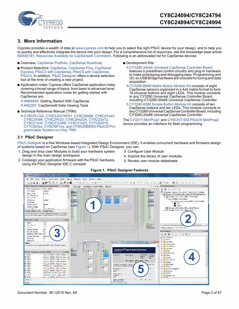
3. More Information
Cypress provides a wealth of data at www.cypress.com to help you to select the right PSoC device for your design, and to help youto quickly and effectively integrate the device into your design. For a comprehensive list of resources, see the knowledge base articleKBA92181, Resources Available for CapSense® Controllers. Following is an abbreviated list for CapSense devices:
■ Overview: CapSense Portfolio, CapSense Roadmap
■ Product Selectors: CapSense, CapSense Plus, CapSense Express, PSoC3 with CapSense, PSoC5 with CapSense, PSoC4. In addition, PSoC Designer offers a device selection tool at the time of creating a new project.
■ Application notes: Cypress offers CapSense application notes covering a broad range of topics, from basic to advanced level. Recommended application notes for getting started with CapSense are:❐ AN64846: Getting Started With CapSense❐ AN2397: CapSense® Data Viewing Tools
■ Technical Reference Manual (TRM):❐ CY8CPLC20, CY8CLED16P01, CY8C29x66, CY8C27x43,
CY8C24x94, CY8C24x23, CY8C24x23A, CY8C22x13, CY8C21x34, CY8C21x34B, CY8C21x23, CY7C64215, CY7C603xx, CY8CNP1xx, and CYWUSB6953 PSoC® Pro-grammable System-on-Chip TRM
■ Development Kits:❐ CY3280-24x94 Universal CapSense Controller Board
features a predefined control circuitry and plug-in hardware to make prototyping and debugging easy. Programming and I2C-to-USB Bridge hardware are included for tuning and data acquisition.
❐ CY3280-BMM Matrix Button Module Kit consists of eight CapSense sensors organized in a 4x4 matrix format to form 16 physical buttons and eight LEDs. This module connects to any CY3280 Universal CapSense Controller Board, including CY3280-20x66 Universal CapSense Controller.
❐ CY3280-BSM Simple Button Module Kit consists of ten CapSense buttons and ten LEDs. This module connects to any CY3280 Universal CapSense Controller Board, including CY3280-20x66 Universal CapSense Controller.
The CY3217-MiniProg1 and CY8CKIT-002 PSoC® MiniProg3 device provides an interface for flash programming.
3.1 PSoC Designer
PSoC Designer is a free Windows-based Integrated Design Environment (IDE). It enables concurrent hardware and firmware design of systems based on CapSense (see Figure 1). With PSoC Designer, you can:1. Drag and drop User Modules to build your hardware system
design in the main design workspace2. Codesign your application firmware with the PSoC hardware,
using the PSoC Designer IDE C compiler
3. Configure User Module4. Explore the library of user modules5. Review user module datasheets
Figure 1. PSoC Designer Features
12
3
54

CY8C24094/CY8C24794CY8C24894/CY8C24994
Document Number: 38-12018 Rev. AK Page 3 of 67
4. Contents
PSoC Functional Overview ................................................4The PSoC Core .............................................................4The Digital System ........................................................4The Analog System .......................................................5Additional System Resources .......................................6PSoC Device Characteristics ........................................6
Getting Started ....................................................................7Application Notes ..........................................................7Development Kits ..........................................................7Training .........................................................................7CYPros Consultants ......................................................7Solutions Library ............................................................7Technical Support .........................................................7
Development Tools ............................................................7PSoC Designer Software Subsystems ..........................7
Designing with PSoC Designer .........................................8Select User Modules .....................................................8Configure User Modules ................................................8Organize and Connect ..................................................8Generate, Verify, and Debug .........................................8
Pin Information ...................................................................956-Pin Part Pinout ........................................................956-Pin Part Pinout (with XRES) ..................................1068-Pin Part Pinout .......................................................1168-Pin Part Pinout (On-Chip Debug) ...........................12100-Ball VFBGA Part Pinout .......................................13100-Ball VFBGA Part Pinout (On-Chip Debug) ...........15100-Pin Part Pinout (On-Chip Debug) .........................17
Register Reference ...........................................................19Register Conventions ..................................................19Register Mapping Tables ............................................19Register Map Bank 0 Table: User Space ...................20Register Map Bank 1 Table: Configuration Space .....21
Electrical Specifications ..................................................22Absolute Maximum Ratings .........................................22Operating Temperature ...............................................23DC Electrical Characteristics .......................................23AC Electrical Characteristics .......................................37Thermal Impedance ....................................................45Solder Reflow Peak Specifications ..............................45
Development Tool Selection ...........................................46Software ......................................................................46Development Kits ........................................................46Evaluation Tools ..........................................................46Device Programmers ...................................................46Accessories (Emulation and Programming) ................47
Ordering Information ........................................................48Ordering Code Definitions ...........................................48
Packaging Dimensions ....................................................49Acronyms ..........................................................................54
Acronyms Used ...........................................................54Document Conventions ...................................................55
Units of Measure .........................................................55Numeric Conventions ..................................................55
Glossary ............................................................................55Errata .................................................................................60
Part Numbers Affected ................................................ 60CY8C24x94 Errata Summary ...................................... 60
Document History Page ...................................................64Sales, Solutions, and Legal Information ........................67
Worldwide Sales and Design Support ....................... 67Products .................................................................... 67PSoC® Solutions ...................................................... 67Cypress Developer Community ................................. 67Technical Support .......................................................67

CY8C24094/CY8C24794CY8C24894/CY8C24994
Document Number: 38-12018 Rev. AK Page 4 of 67
5. PSoC Functional Overview
The PSoC family consists of many devices with on-chip controllers. These devices are designed to replace multiple traditional MCU-based system components with one low-cost single-chip programmable component. A PSoC device includes configurable blocks of analog and digital logic, and programmable interconnect. This architecture makes it possible for you to create customized peripheral configurations, to match the requirements of each individual application. Additionally, a fast central processing unit (CPU), flash program memory, SRAM data memory, and configurable I/O are included in a range of convenient pinouts.
The PSoC architecture, shown in “Logic Block Diagram” on page 1, consists of four main areas: the core, the system resources, the digital system, and the analog system. Configurable global bus resources allow combining all of the device resources into a complete custom system. Each CY8C24x94 PSoC device includes four digital blocks and six analog blocks. Depending on the PSoC package, up to 56 GPIOs are also included. The GPIOs provide access to the global digital and analog interconnects.
5.1 The PSoC Core
The PSoC core is a powerful engine that supports a rich instruction set. It encompasses SRAM for data storage, an interrupt controller, sleep and watchdog timers, and internal main oscillator (IMO) and internal low-speed oscillator (ILO). The CPU core, called the M8C, is a powerful processor with speeds up to 24 MHz. The M8C is a four-million instructions per second (MIPS) 8-bit Harvard-architecture microprocessor.
System resources provide these additional capabilities:
■ Digital clocks for increased flexibility
■ I2C functionality to implement an I2C master and slave
■ An internal voltage reference, multi-master, that provides an absolute value of 1.3 V to a number of PSoC subsystems
■ A switch-mode pump (SMP) that generates normal operating voltages from a single battery cell
■ Various system resets supported by the M8C
The digital system consists of an array of digital PSoC blocks that may be configured into any number of digital peripherals. The digital blocks are connected to the GPIOs through a series of global buses. These buses can route any signal to any pin, freeing designs from the constraints of a fixed peripheral controller.
The analog system consists of six analog PSoC blocks, supporting comparators, and analog-to-digital conversion up to 10-bits of precision.
5.2 The Digital System
The digital system consists of four digital PSoC blocks. Each block is an 8-bit resource that is used alone or combined with other blocks to form 8-, 16-, 24-, and 32-bit peripherals, which are called user modules. Digital peripheral configurations include:
■ PWMs (8- to 32-bit)
■ PWMs with dead band (8- to 32-bit)
■ Counters (8- to 32-bit)
■ Timers (8- to 32-bit)
■ UART 8-bit with selectable parity
■ SPI master and slave
■ I2C slave and multi-master
■ CRC/generator (8-bit)
■ IrDA
■ PRS generators (8- to 32-bit)
The digital blocks are connected to any GPIO through a series of global buses that can route any signal to any pin. The buses also allow for signal multiplexing and for performing logic operations. This configurability frees your designs from the constraints of a fixed peripheral controller.
Digital blocks are provided in rows of four, where the number of blocks varies by PSoC device family. This allows the optimum choice of system resources for your application. Family resources are shown in Table 1 on page 6.
Figure 2. Digital System Block Diagram
DIGITAL SYSTEM
To System BusDigital Clocks From Core
Digital PSoC Block Array
To Analog System
8
Row
Inpu
t C
onfig
urat
ion R
ow O
utput
Config
uration
88
8 Row 0
DBB00 DBB01 DCB02 DCB03
4
4
GIE[7:0]
GIO[7:0]
GOE[7:0]
GOO[7:0]
Global Digital Interconnect
Port 1
Port 0
Port 3
Port 2
Port 5
Port 4
Port 7
CY8C24094/CY8C24794CY8C24894/CY8C24994
Document Number: 38-12018 Rev. AK Page 5 of 67
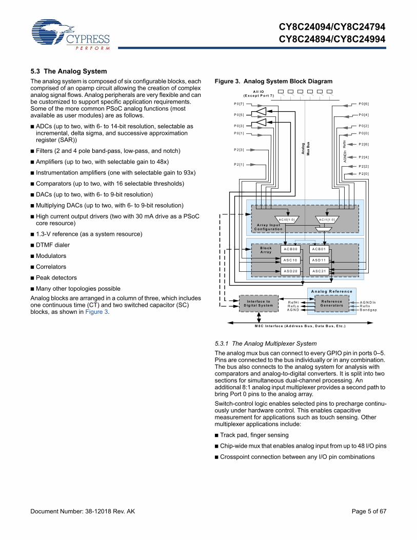
5.3 The Analog System
The analog system is composed of six configurable blocks, each comprised of an opamp circuit allowing the creation of complex analog signal flows. Analog peripherals are very flexible and can be customized to support specific application requirements. Some of the more common PSoC analog functions (most available as user modules) are as follows.
■ ADCs (up to two, with 6- to 14-bit resolution, selectable as incremental, delta sigma, and successive approximation register (SAR))
■ Filters (2 and 4 pole band-pass, low-pass, and notch)
■ Amplifiers (up to two, with selectable gain to 48x)
■ Instrumentation amplifiers (one with selectable gain to 93x)
■ Comparators (up to two, with 16 selectable thresholds)
■ DACs (up to two, with 6- to 9-bit resolution)
■ Multiplying DACs (up to two, with 6- to 9-bit resolution)
■ High current output drivers (two with 30 mA drive as a PSoC core resource)
■ 1.3-V reference (as a system resource)
■ DTMF dialer
■ Modulators
■ Correlators
■ Peak detectors
■ Many other topologies possible
Analog blocks are arranged in a column of three, which includes one continuous time (CT) and two switched capacitor (SC) blocks, as shown in Figure 3.
Figure 3. Analog System Block Diagram
5.3.1 The Analog Multiplexer System
The analog mux bus can connect to every GPIO pin in ports 0–5. Pins are connected to the bus individually or in any combination. The bus also connects to the analog system for analysis with comparators and analog-to-digital converters. It is split into two sections for simultaneous dual-channel processing. An additional 8:1 analog input multiplexer provides a second path to bring Port 0 pins to the analog array.
Switch-control logic enables selected pins to precharge continu-ously under hardware control. This enables capacitive measurement for applications such as touch sensing. Other multiplexer applications include:
■ Track pad, finger sensing
■ Chip-wide mux that enables analog input from up to 48 I/O pins
■ Crosspoint connection between any I/O pin combinations
A C B 0 0 A C B 0 1B lo c k A r ra y
A r ra y In p u tC o n fig u ra tio n
A C I1 [1 :0 ]
A S D 2 0
A C I0 [1 :0 ]
P 0 [6 ]
P 0 [4 ]
P 0 [2 ]
P 0 [0 ]
P 2 [2 ]
P 2 [0 ]
P 2 [6 ]
P 2 [4 ]
Re
fIn
AG
ND
In
P 0 [7 ]
P 0 [5 ]
P 0 [3 ]
P 0 [1 ]
P 2 [3 ]
P 2 [1 ]
R e fe re n c e G e n e ra to rs
A G N D InR e fInB a n d g a p
R e fH iR e fL oA G N D
A S D 1 1
A S C 2 1
A S C 1 0
In te r fa c e to D ig ita l S y s te m
M 8 C In te r fa c e (A d d re s s B u s , D a ta B u s , E tc .)
A n a lo g R e fe re n c e
A ll IO(E x c e p t P o r t 7 )
An
alo
g
Mu
x B
us

CY8C24094/CY8C24794CY8C24894/CY8C24994
Document Number: 38-12018 Rev. AK Page 6 of 67
5.4 Additional System Resources
System resources provide additional capability useful to complete systems. Additional resources include a multiplier, decimator, low-voltage detection, and power-on reset (POR). Brief statements describing the merits of each resource follow.
■ Full speed USB (12 Mbps) with five configurable endpoints and 256 bytes of RAM. No external components required except for two series resistors. Wider than commercial temperature USB operation (–10 °C to +85 °C).
■ Digital clock dividers provide three customizable clock frequencies for use in applications. The clocks can be routed to both the digital and analog systems. Additional clocks are generated using digital PSoC blocks as clock dividers.
■ Two multiply accumulates (MACs) provide fast 8-bit multipliers with 32-bit accumulate, to assist in both general math and digital filters.
■ Decimator provides a custom hardware filter for digital signal processing applications including creation of Delta Sigma ADCs.
■ The I2C module provides 100- and 400-kHz communication over two wires. Slave, master, multi-master are supported.
■ Low-voltage detection interrupts signal the application of falling voltage levels, while the advanced POR circuit eliminates the need for a system supervisor.
■ An internal 1.3-V reference provides an absolute reference for the analog system, including ADCs and DACs.
■ Versatile analog multiplexer system.
5.5 PSoC Device Characteristics
Depending on your PSoC device characteristics, the digital and analog systems can have 16, 8, or 4 digital blocks and 12, 6, or 4 analog blocks. The following table lists the resources available for specific PSoC device groups. The device covered by this datasheet is shown in the highlighted row of the table.
Table 1. PSoC Device Characteristics
PSoC PartNumber
Digital I/O
Digital Rows
Digital Blocks
Analog Inputs
Analog Outputs
Analog Columns
Analog Blocks
SRAMSize
Flash Size
CY8C29x66 up to 64 4 16 up to 12 4 4 12 2 K 32 K
CY8C28xxx up to 44 up to 3 up to 12 up to 44 up to 4 up to 6 up to 12 + 4[1]
1 K 16 K
CY8C27x43 up to 44 2 8 up to 12 4 4 12 256 16 K
CY8C24x94 up to 56 1 4 up to 48 2 2 6 1 K 16 K
CY8C24x23A up to 24 1 4 up to 12 2 2 6 256 4 K
CY8C23x33 up to 26 1 4 up to 12 2 2 4 256 8 K
CY8C22x45 up to 38 2 8 up to 38 0 4 6[1] 1 K 16 K
CY8C21x45 up to 24 1 4 up to 24 0 4 6[1] 512 8 K
CY8C21x34 up to 28 1 4 up to 28 0 2 4[1] 512 8 K
CY8C21x23 up to 16 1 4 up to 8 0 2 4[1] 256 4 K
CY8C20x34 up to 28 0 0 up to 28 0 0 3[1,2] 512 8 K
CY8C20xx6 up to 36 0 0 up to 36 0 0 3[1,2] up to 2 K
up to 32 K
Notes1. Limited analog functionality.2. Two analog blocks and one CapSense®.

CY8C24094/CY8C24794CY8C24894/CY8C24994
Document Number: 38-12018 Rev. AK Page 7 of 67
6. Getting Started
For in-depth information, along with detailed programming infor-mation, see the Technical Reference Manual for this PSoC device.
For up-to-date ordering, packaging, and electrical specification information, see the latest PSoC device datasheets on the web at http://www.cypress.com.
6.1 Application Notes
Cypress application notes are an excellent introduction to the wide variety of possible PSoC designs.
6.2 Development Kits
PSoC Development Kits are available online from and through a growing number of regional and global distributors, which include Arrow, Avnet, Digi-Key, Farnell, Future Electronics, and Newark.
6.3 Training
Free PSoC technical training (on demand, webinars, and workshops), which is available online via www.cypress.com,
covers a wide variety of topics and skill levels to assist you in your designs.
6.4 CYPros Consultants
Certified PSoC consultants offer everything from technical assis-tance to completed PSoC designs. To contact or become a PSoC consultant go to the CYPros Consultants web site.
6.5 Solutions Library
Visit our growing library of solution-focused designs. Here you can find various application designs that include firmware and hardware design files that enable you to complete your designs quickly.
6.6 Technical Support
Technical support – including a searchable Knowledge Base articles and technical forums – is also available online. If you cannot find an answer to your question, call our Technical Support hotline at 1-800-541-4736.
7. Development Tools
PSoC Designer™ is the revolutionary Integrated Design Environment (IDE) that you can use to customize PSoC to meet your specific application requirements. PSoC Designer software accelerates system design and time to market. Develop your applications using a library of precharacterized analog and digital peripherals (called user modules) in a drag-and-drop design environment. Then, customize your design by leveraging the dynamically generated application programming interface (API) libraries of code. Finally, debug and test your designs with the integrated debug environment, including in-circuit emulation and standard software debug features. PSoC Designer includes:
■ Application editor graphical user interface (GUI) for device and user module configuration and dynamic reconfiguration
■ Extensive user module catalog
■ Integrated source-code editor (C and assembly)
■ Free C compiler with no size restrictions or time limits
■ Built-in debugger
■ In-circuit emulation
■ Built-in support for communication interfaces:❐ Hardware and software I2C slaves and masters❐ Full speed USB 2.0❐ Up to four full-duplex universal asynchronous receiver/trans-
mitters (UARTs), SPI master and slave, and wireless
PSoC Designer supports the entire library of PSoC 1 devices and runs on Windows XP, Windows Vista, and Windows 7.
7.1 PSoC Designer Software Subsystems
7.1.1 Design Entry
In the chip-level view, choose a base device to work with. Then select different onboard analog and digital components that use
the PSoC blocks, which are called user modules. Examples of user modules are analog-to-digital converters (ADCs), digital-to-analog converters (DACs), amplifiers, and filters. Configure the user modules for your chosen application and connect them to each other and to the proper pins. Then generate your project. This prepopulates your project with APIs and libraries that you can use to program your application.
The tool also supports easy development of multiple configura-tions and dynamic reconfiguration. Dynamic reconfiguration makes it possible to change configurations at run time. In essence, this allows you to use more than 100 percent of PSoC's resources for an application.
7.1.2 Code Generation Tools
The code generation tools work seamlessly within the PSoC Designer interface and have been tested with a full range of debugging tools. You can develop your design in C, assembly, or a combination of the two.
Assemblers. The assemblers allow you to merge assembly code seamlessly with C code. Link libraries automatically use absolute addressing or are compiled in relative mode, and are linked with other software modules to get absolute addressing.
C Language Compilers. C language compilers are available that support the PSoC family of devices. The products allow you to create complete C programs for the PSoC family devices. The optimizing C compilers provide all of the features of C, tailored to the PSoC architecture. They come complete with embedded libraries providing port and bus operations, standard keypad and display support, and extended math functionality.
7.1.3 Debugger
PSoC Designer has a debug environment that provides hardware in-circuit emulation, allowing you to test the program in a physical system while providing an internal view of the PSoC device. Debugger commands allow you to read and program and

CY8C24094/CY8C24794CY8C24894/CY8C24994
Document Number: 38-12018 Rev. AK Page 8 of 67
read and write data memory, and read and write I/O registers. You can read and write CPU registers, set and clear breakpoints, and provide program run, halt, and step control. The debugger also allows you to create a trace buffer of registers and memory locations of interest.
7.1.4 Online Help System
The online help system displays online, context-sensitive help. Designed for procedural and quick reference, each functional subsystem has its own context-sensitive help. This system also provides tutorials and links to FAQs and an online support forum to aid the designer.
7.1.5 In-Circuit Emulator
A low-cost, high-functionality In-Circuit Emulator (ICE) is available for development support. This hardware can program single devices.
The emulator consists of a base unit that connects to the PC using a USB port. The base unit is universal and operates with all PSoC devices. Emulation pods for each device family are available separately. The emulation pod takes the place of the PSoC device in the target board and performs full speed (24-MHz) operation.
8. Designing with PSoC Designer
The development process for the PSoC® device differs from that of a traditional fixed function microprocessor. The configurable analog and digital hardware blocks give the PSoC architecture a unique flexibility that pays dividends in managing specification change during development and by lowering inventory costs. These configurable resources, called PSoC Blocks, have the ability to implement a wide variety of user-selectable functions. The PSoC development process is summarized in four steps:
1. Select User Modules
2. Configure User Modules
3. Organize and Connect
4. Generate, Verify, and Debug
8.1 Select User Modules
PSoC Designer provides a library of prebuilt, pretested hardware peripheral components called “user modules.” User modules make selecting and implementing peripheral devices, both analog and digital, simple.
8.2 Configure User Modules
Each user module that you select establishes the basic register settings that implement the selected function. They also provide parameters and properties that allow you to tailor their precise configuration to your particular application. For example, a PWM User Module configures one or more digital PSoC blocks, one for each 8 bits of resolution. The user module parameters permit you to establish the pulse width and duty cycle. Configure the parameters and properties to correspond to your chosen appli-cation. Enter values directly or by selecting values from drop-down menus. All the user modules are documented in datasheets that may be viewed directly in PSoC Designer or on the Cypress website. These user module datasheets explain the internal operation of the user module and provide performance specifications. Each datasheet describes the use of each user module parameter, and other information you may need to successfully implement your design.
8.3 Organize and Connect
You build signal chains at the chip level by interconnecting user modules to each other and the I/O pins. You perform the selection, configuration, and routing so that you have complete control over all on-chip resources.
8.4 Generate, Verify, and Debug
When you are ready to test the hardware configuration or move on to developing code for the project, you perform the “Generate Configuration Files” step. This causes PSoC Designer to generate source code that automatically configures the device to your specification and provides the software for the system. The generated code provides application programming interfaces (APIs) with high-level functions to control and respond to hardware events at run time and interrupt service routines that you can adapt as needed.
A complete code development environment allows you to develop and customize your applications in either C, assembly language, or both.
The last step in the development process takes place inside PSoC Designer’s debugger (access by clicking the Connect icon). PSoC Designer downloads the HEX image to the ICE where it runs at full speed. PSoC Designer debugging capabil-ities rival those of systems costing many times more. In addition to traditional single-step, run-to-breakpoint, and watch-variable features, the debug interface provides a large trace buffer and allows you to define complex breakpoint events. These include monitoring address and data bus values, memory locations and external signals.

CY8C24094/CY8C24794CY8C24894/CY8C24994
Document Number: 38-12018 Rev. AK Page 9 of 67
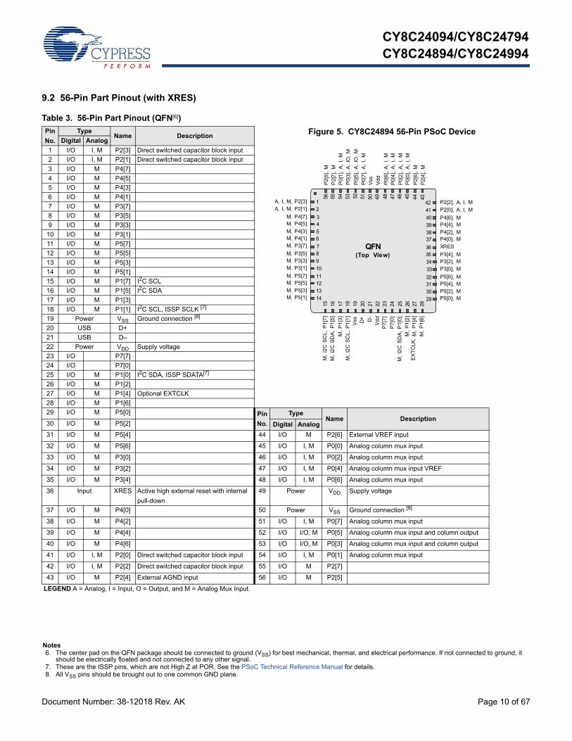
9. Pin Information
This section describes, lists, and illustrates the CY8C24x94 PSoC device family pins and pinout configuration.
The CY8C24x94 PSoC devices are available in the following packages, all of which are shown on the following pages. Every port pin (labeled with a “P”) is capable of Digital I/O. However, VSS, VDD, and XRES are not capable of Digital I/O.
9.1 56-Pin Part Pinout
Table 2. 56-Pin Part Pinout (QFN[6]) See LEGEND details and footnotes in Table 3 on page 10.
Pin
No.
TypeName Description
Figure 4. CY8C24794 56-Pin PSoC Device[3]
Digital Analog
1 I/O I, M P2[3] Direct switched capacitor block input
2 I/O I, M P2[1] Direct switched capacitor block input
3 I/O M P4[7]
4 I/O M P4[5]
5 I/O M P4[3]
6 I/O M P4[1]
7 I/O M P3[7]
8 I/O M P3[5]
9 I/O M P3[3]
10 I/O M P3[1]
11 I/O M P5[7]
12 I/O M P5[5]
13 I/O M P5[3]
14 I/O M P5[1]
15 I/O M P1[7] I2C serial clock (SCL)
16 I/O M P1[5] I2C serial data (SDA)
17 I/O M P1[3]
18 I/O M P1[1] I2C SCL, ISSP SCLK [4]
19 Power VSS Ground connection [5]
20 USB D+
21 USB D–
22 Power VDD Supply voltage
23 I/O P7[7]
24 I/O P7[0]
25 I/O M P1[0] I2C SDA, ISSP SDATA[4]
26 I/O M P1[2]
27 I/O M P1[4] Optional external clock input (EXTCLK)
28 I/O M P1[6]
29 I/O M P5[0] Pin
No.
TypeName Description
30 I/O M P5[2] Digital Analog
31 I/O M P5[4] 44 I/O M P2[6] External voltage reference (VREF) input
32 I/O M P5[6] 45 I/O I, M P0[0] Analog column mux input
33 I/O M P3[0] 46 I/O I, M P0[2] Analog column mux input
34 I/O M P3[2] 47 I/O I, M P0[4] Analog column mux input VREF
35 I/O M P3[4] 48 I/O I, M P0[6] Analog column mux input
36 I/O M P3[6] 49 Power VDD Supply voltage
37 I/O M P4[0] 50 Power VSS Ground connection [5]
38 I/O M P4[2] 51 I/O I, M P0[7] Analog column mux input
39 I/O M P4[4] 52 I/O I/O, M P0[5] Analog column mux input and column output
40 I/O M P4[6] 53 I/O I/O, M P0[3] Analog column mux input and column output
41 I/O I, M P2[0] Direct switched capacitor block input 54 I/O I, M P0[1] Analog column mux input
42 I/O I, M P2[2] Direct switched capacitor block input 55 I/O M P2[7]
43 I/O M P2[4] External analog ground (AGND) input 56 I/O M P2[5]
QFN(Top V iew )
A, I, M , P2[3]A, I, M , P2[1]
M , P4[7]M , P4[5]M , P4[3]M , P4[1]
M , P3[7]M , P3[5]M , P3[3]
M , P3[1]M , P5[7]M , P5[5]M , P5[3]M , P5[1]
12
3456
7891011121314
M, I
2C
SC
L, P
1[7
]
M, I
2C
SD
A, P
1[5
]
M, P
1[3
]
M, I
2C
SC
L, P
1[1
]
Vss D+ D-
Vdd
P7
[7]
P7
[0]
M, I
2C
SD
A, P
1[0
]M
, P1
[2]
M, P
1[4
]
M, P
1[6
]
15 16 17 18 19 20 21 22 23 24 25 26 27 28P
2[4
], M
P2
[6],
M
P0
[0],
A, I
, MP
0[2
], A
, I, M
P0
[4],
A, I
, M
P0
[6],
A, I
, M
Vdd
Vss
P0
[7],
A, I
, M
P0
[5],
A, I
O, M
P0
[3],
A, I
O, M
P0
[1],
A, I
, M
P2
[7],
M
P2
[5],
M
4344454647484950515253545556
P2[2], A, I, M
P2[0], A, I, M
P4[6], MP4[4], MP4[2], MP4[0], MP3[6], M
P3[4], MP3[2], MP3[0], MP5[6], MP5[4], MP5[2], MP5[0], M
42
41
4039
383736353433
32313029
EX
TC
LK
,
Notes3. This part cannot be programmed with Reset mode; use Power Cycle mode when programming.4. These are the ISSP pins, which are not High Z at POR. See the PSoC Technical Reference Manual for details.5. All VSS pins should be brought out to one common GND plane.
CY8C24094/CY8C24794CY8C24894/CY8C24994
Document Number: 38-12018 Rev. AK Page 10 of 67
9.2 56-Pin Part Pinout (with XRES)
Table 3. 56-Pin Part Pinout (QFN[6])
Pin
No.
TypeName Description
Figure 5. CY8C24894 56-Pin PSoC DeviceDigital Analog
1 I/O I, M P2[3] Direct switched capacitor block input
2 I/O I, M P2[1] Direct switched capacitor block input
3 I/O M P4[7]
4 I/O M P4[5]
5 I/O M P4[3]
6 I/O M P4[1]
7 I/O M P3[7]
8 I/O M P3[5]
9 I/O M P3[3]
10 I/O M P3[1]
11 I/O M P5[7]
12 I/O M P5[5]
13 I/O M P5[3]
14 I/O M P5[1]
15 I/O M P1[7] I2C SCL
16 I/O M P1[5] I2C SDA
17 I/O M P1[3]
18 I/O M P1[1] I2C SCL, ISSP SCLK [7]
19 Power VSS Ground connection [8]
20 USB D+
21 USB D–
22 Power VDD Supply voltage
23 I/O P7[7]
24 I/O P7[0]
25 I/O M P1[0] I2C SDA, ISSP SDATA[7]
26 I/O M P1[2]
27 I/O M P1[4] Optional EXTCLK
28 I/O M P1[6]
29 I/O M P5[0] Pin
No.
TypeName Description
30 I/O M P5[2] Digital Analog
31 I/O M P5[4] 44 I/O M P2[6] External VREF input
32 I/O M P5[6] 45 I/O I, M P0[0] Analog column mux input
33 I/O M P3[0] 46 I/O I, M P0[2] Analog column mux input
34 I/O M P3[2] 47 I/O I, M P0[4] Analog column mux input VREF
35 I/O M P3[4] 48 I/O I, M P0[6] Analog column mux input
36 Input XRES Active high external reset with internal
pull-down
49 Power VDD Supply voltage
37 I/O M P4[0] 50 Power VSS Ground connection [8]
38 I/O M P4[2] 51 I/O I, M P0[7] Analog column mux input
39 I/O M P4[4] 52 I/O I/O, M P0[5] Analog column mux input and column output
40 I/O M P4[6] 53 I/O I/O, M P0[3] Analog column mux input and column output
41 I/O I, M P2[0] Direct switched capacitor block input 54 I/O I, M P0[1] Analog column mux input
42 I/O I, M P2[2] Direct switched capacitor block input 55 I/O M P2[7]
43 I/O M P2[4] External AGND input 56 I/O M P2[5]
LEGEND A = Analog, I = Input, O = Output, and M = Analog Mux Input.
QFN(Top View)
A, I, M, P2[3]
A, I, M, P2[1]
M, P4[7]M, P4[5]
M, P4[3]M, P4[1]
M, P3[7]
M, P3[5]M, P3[3]
M, P3[1]
M, P5[7]M, P5[5]
M, P5[3]M, P5[1]
1
2
34
56
78
9
10
1112
13
14
M,
I2C
SC
L,
P1
[7]
M,
I2C
SD
A,
P1
[5]
M,
P1
[3]
M,
I2C
SC
L,
P1
[1]
Vss D+ D-
Vd
dP
7[7
]
P7
[0]
M,
I2C
SD
A,
P1
[0]
M,
P1
[2]
M,
P1
[4]
M,
P1
[6]
15 16 17 18 19 20 21 22 23 24 25 26 27 28P
2[4
], M
P2
[6],
M
P0
[0],
A,
I, M
P0
[2],
A,
I, M
P0
[4],
A,
I, M
P0
[6],
A,
I, M
Vd
d
Vss
P0
[7],
A,
I, M
P0
[5],
A,
IO,
M
P0
[3],
A,
IO,
M
P0
[1],
A,
I, M
P2
[7],
M
P2
[5],
M
4344454647484950515253545556
P2[2], A, I, M
P2[0], A, I, M
P4[6], MP4[4], M
P4[2], MP4[0], M
XRES
P3[4], MP3[2], M
P3[0], M
P5[6], MP5[4], M
P5[2], MP5[0], M
42
41
40
39
3837
3635
34
33
3231
30
29
EX
TC
LK,
Notes6. The center pad on the QFN package should be connected to ground (VSS) for best mechanical, thermal, and electrical performance. If not connected to ground, it
should be electrically floated and not connected to any other signal.7. These are the ISSP pins, which are not High Z at POR. See the PSoC Technical Reference Manual for details.8. All VSS pins should be brought out to one common GND plane.

CY8C24094/CY8C24794CY8C24894/CY8C24994
Document Number: 38-12018 Rev. AK Page 11 of 67
9.3 68-Pin Part Pinout
The following 68-pin QFN part table and drawing is for the CY8C24994 PSoC device.
Table 4. 68-Pin Part Pinout (QFN[9])
Pin
No.
TypeName Description
Figure 6. CY8C24994 68-Pin PSoC DeviceDigital Analog
1 I/O M P4[7]
2 I/O M P4[5]
3 I/O M P4[3]
4 I/O M P4[1]
5 NC No connection. Pin must be left floating
6 NC No connection. Pin must be left floating
7 Power VSS Ground connection [10]
8 I/O M P3[7]
9 I/O M P3[5]
10 I/O M P3[3]
11 I/O M P3[1]
12 I/O M P5[7]
13 I/O M P5[5]
14 I/O M P5[3]
15 I/O M P5[1]
16 I/O M P1[7] I2C SCL
17 I/O M P1[5] I2C SDA
18 I/O M P1[3]
19 I/O M P1[1] I2C SCL ISSP SCLK[11]
20 Power VSS Ground connection [10]
21 USB D+
22 USB D–
23 Power VDD Supply voltage
24 I/O P7[7]
25 I/O P7[6]
26 I/O P7[5]
27 I/O P7[4]
28 I/O P7[3]
29 I/O P7[2] Pin
No.
TypeName Description
30 I/O P7[1] Digital Analog
31 I/O P7[0] 50 I/O M P4[6]
32 I/O M P1[0] I2C SDA, ISSP SDATA[11] 51 I/O I, M P2[0] Direct switched capacitor block input
33 I/O M P1[2] 52 I/O I, M P2[2] Direct switched capacitor block input
34 I/O M P1[4] Optional EXTCLK 53 I/O M P2[4] External AGND input
35 I/O M P1[6] 54 I/O M P2[6] External VREF input
36 I/O M P5[0] 55 I/O I, M P0[0] Analog column mux input
37 I/O M P5[2] 56 I/O I, M P0[2] Analog column mux input and column output
38 I/O M P5[4] 57 I/O I, M P0[4] Analog column mux input and column output
39 I/O M P5[6] 58 I/O I, M P0[6] Analog column mux input
40 I/O M P3[0] 59 Power VDD Supply voltage
41 I/O M P3[2] 60 Power VSS Ground connection [10]
42 I/O M P3[4] 61 I/O I, M P0[7] Analog column mux input, integration input #1
43 I/O M P3[6] 62 I/O I/O, M P0[5] Analog column mux input and column output, integration
input #2
44 NC No connection. Pin must be left floating. 63 I/O I/O, M P0[3] Analog column mux input and column output
45 NC No connection. Pin must be left floating. 64 I/O I, M P0[1] Analog column mux input
46 Input XRES Active high pin reset with internal
pull-down.
65 I/O M P2[7]
47 I/O M P4[0] 66 I/O M P2[5]
48 I/O M P4[2] 67 I/O I, M P2[3] Direct switched capacitor block input
49 I/O M P4[4] 68 I/O I, M P2[1] Direct switched capacitor block input
LEGEND A = Analog, I = Input, O = Output, NC = No connection. Pin must be left floating, M = Analog Mux Input.
P2[
6],
M, E
xt.
VR
EF
P2[
4], M
, Ext
. AG
ND
M, P4[7]
M, P4[5]M, P4[3]
M, P4[1]
NCNC
VssM, P3[7]
M, P3[5]
M, P3[3]M, P3[1]M, P5[7]
M, P5[5]
M, P5[3]M, P5[1]
I2C SCL, M, P1[7]
I2C SDA, M, P1[5]
M, P
1[3]
P7
[5]
I2C
SD
A, M
, P1[
0]
I2C
SC
L, M
, P1[
1]
Vss D +
D -
Vdd
P7
[6]
P7
[4]
P7
[3]
P7
[2]
P7
[1]
P7
[0]
M, P
1[2]
P2[0], M, AI
P4[6], M
P4[4], M
P4[2], M
P4[0], MXRES
NCNCP3[6], MP3[4], M
P3[2], MP3[0], M
P5[6], M
P5[4], M
P5[2], MP5[0], M
P1[6], M
P2
[1],
M, A
I
P2
[3],
M, A
I
P2[
5],
MP
2[7
], M
P0
[1],
M, A
IP
0[3
], M
, AIO
P0
[5],
M, A
IO
P0
[7],
M, A
IV
ssV
dd
P0
[6],
M, A
IP
0[4
], M
, AI
P0
[2],
M, A
I
P0
[0],
M, A
I
P2
[2],
M, A
I
5150
494847
46
45
444342
41
4039
38
37
36
35
68 67 66 65 64 63 62 61 60 59 58 57 56 55 54 53 52
10
11
1213
14
15
16
17
12
3
4
56
789
18
19
20
21
22
23
24
25
26
27
28
29
30
31
32
33
34
QFN(Top View)
M, P
1[4]
EX
TC
LK
,
P7
[7]
Notes9. The center pad on the QFN package should be connected to ground (VSS) for best mechanical, thermal, and electrical performance. If not connected to ground, it
should be electrically floated and not connected to any other signal.10. All VSS pins should be brought out to one common GND plane.11. These are the ISSP pins, which are not High Z at POR. See the PSoC Technical Reference Manual for details.

CY8C24094/CY8C24794CY8C24894/CY8C24994
Document Number: 38-12018 Rev. AK Page 12 of 67
9.4 68-Pin Part Pinout (On-Chip Debug)
The following 68-pin QFN part table and drawing is for the CY8C24094 OCD PSoC device.
Note This part is only used for in-circuit debugging. It is NOT available for production.
Table 5. 68-Pin Part Pinout (QFN[12])
Pin
No.
TypeName Description
Figure 7. CY8C24094 68-Pin OCD PSoC DeviceDigital Analog
1 I/O M P4[7]
2 I/O M P4[5]
3 I/O M P4[3]
4 I/O M P4[1]
5 OCDE OCD even data I/O
6 OCDO OCD odd data output
7 Power VSS Ground connection [13]
8 I/O M P3[7]
9 I/O M P3[5]
10 I/O M P3[3]
11 I/O M P3[1]
12 I/O M P5[7]
13 I/O M P5[5]
14 I/O M P5[3]
15 I/O M P5[1]
16 I/O M P1[7] I2C SCL
17 I/O M P1[5] I2C SDA
18 I/O M P1[3]
19 I/O M P1[1] I2C SCL, ISSP SCLK [14]
20 Power VSS Ground connection [13]
21 USB D+
22 USB D–
23 Power VDD Supply voltage
24 I/O P7[7]
25 I/O P7[6]
26 I/O P7[5]
27 I/O P7[4]
28 I/O P7[3]
29 I/O P7[2] Pin
No.
TypeName Description
30 I/O P7[1] Digital Analog
31 I/O P7[0] 50 I/O M P4[6]
32 I/O M P1[0] I2C SDA, ISSP SDATA[14] 51 I/O I, M P2[0] Direct switched capacitor block input
33 I/O M P1[2] 52 I/O I, M P2[2] Direct switched capacitor block input
34 I/O M P1[4] Optional EXTCLK 53 I/O M P2[4] External AGND input
35 I/O M P1[6] 54 I/O M P2[6] External VREF input
36 I/O M P5[0] 55 I/O I, M P0[0] Analog column mux input
37 I/O M P5[2] 56 I/O I, M P0[2] Analog column mux input and column output
38 I/O M P5[4] 57 I/O I, M P0[4] Analog column mux input and column output
39 I/O M P5[6] 58 I/O I, M P0[6] Analog column mux input
40 I/O M P3[0] 59 Power VDD Supply voltage
41 I/O M P3[2] 60 Power VSS Ground connection [13]
42 I/O M P3[4] 61 I/O I, M P0[7] Analog column mux input, integration input #1
43 I/O M P3[6] 62 I/O I/O, M P0[5] Analog column mux input and column output, integration
input #2
44 HCLK OCD high speed clock output 63 I/O I/O, M P0[3] Analog column mux input and column output
45 CCLK OCD CPU clock output 64 I/O I, M P0[1] Analog column mux input
46 Input XRES Active high pin reset with internal pull-down 65 I/O M P2[7]
47 I/O M P4[0] 66 I/O M P2[5]
48 I/O M P4[2] 67 I/O I, M P2[3] Direct switched capacitor block input
49 I/O M P4[4] 68 I/O I, M P2[1] Direct switched capacitor block input
LEGEND A = Analog, I = Input, O = Output, M = Analog Mux Input, OCD = On-Chip Debugger.
M, P4[7]M, P4[5]M, P4[3]
M, P4[1]OCDEOCDO
VssM, P3[7]M, P3[5]
M, P3[3]M, P3[1]M, P5[7]M, P5[5]
M, P5[3]M, P5[1]
I2C SCL, M, P1[7]I2C SDA, M, P1[5]
M, P
1[3]
P7
[5]
I2C
SD
A, M
, P1
[0]
I2C
SC
L, M
, P1
[1]
Vss
D + D -
Vdd
P7
[7]
P7[
6]
P7
[4]
P7
[3]
P7
[2]
P7
[1]
P7[
0]
M,
P1
[2]
M,
P1
[4]
P2[0], M, AIP4[6], MP4[4], MP4[2], M
P4[0], MXRESCCLKHCLKP3[6], MP3[4], MP3[2], MP3[0], M
P5[6], MP5[4], M
P5[2], MP5[0], MP1[6], M
P2[
1], M
, AI
P2[
3], M
, AI
P2[
5], M
P2
[7],
M
P0[
1], M
, AI
P0[
3], M
, AIO
P0[
5], M
, AIO
P0[
7], M
, AI
Vss
Vdd
P0
[6],
M, A
IP
0[4
], M
, AI
P0[
2], M
, AI
P0
[0],
M, A
I
P2
[6],
M, E
xt.
VR
EF
P2[
4], M
, Ext
. AG
ND
P2
[2],
M, A
I
5150
494847
464544434241403938373635
68 67 66 65 64 63 62
61 60
59 58
57 56
55
54 53 52
1011121314151617
123456789
18 19 20 21 22
23 24 25
26 27
28
29
30
31 32
33 34
QFN(Top View)
EX
TC
LK
,
Notes12. The center pad on the QFN package should be connected to ground (VSS) for best mechanical, thermal, and electrical performance. If not connected to ground, it
should be electrically floated and not connected to any other signal.13. All VSS pins should be brought out to one common GND plane.14. These are the ISSP pins, which are not High Z at POR. See the PSoC Technical Reference Manual for details.
CY8C24094/CY8C24794CY8C24894/CY8C24994
Document Number: 38-12018 Rev. AK Page 13 of 67
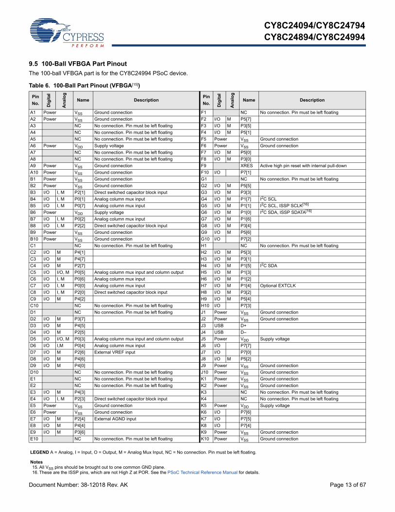
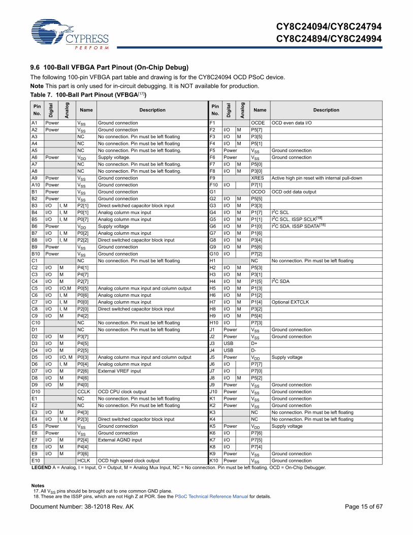
9.5 100-Ball VFBGA Part Pinout
The 100-ball VFBGA part is for the CY8C24994 PSoC device.
Table 6. 100-Ball Part Pinout (VFBGA[15])
Pin
No. Dig
ital
An
alo
g
Name DescriptionPin
No. Dig
ital
An
alo
g
Name Description
A1 Power VSS Ground connection F1 NC No connection. Pin must be left floating
A2 Power VSS Ground connection F2 I/O M P5[7]
A3 NC No connection. Pin must be left floating F3 I/O M P3[5]
A4 NC No connection. Pin must be left floating F4 I/O M P5[1]
A5 NC No connection. Pin must be left floating F5 Power VSS Ground connection
A6 Power VDD Supply voltage F6 Power VSS Ground connection
A7 NC No connection. Pin must be left floating F7 I/O M P5[0]
A8 NC No connection. Pin must be left floating F8 I/O M P3[0]
A9 Power VSS Ground connection F9 XRES Active high pin reset with internal pull-down
A10 Power VSS Ground connection F10 I/O P7[1]
B1 Power VSS Ground connection G1 NC No connection. Pin must be left floating
B2 Power VSS Ground connection G2 I/O M P5[5]
B3 I/O I, M P2[1] Direct switched capacitor block input G3 I/O M P3[3]
B4 I/O I, M P0[1] Analog column mux input G4 I/O M P1[7] I2C SCL
B5 I/O I, M P0[7] Analog column mux input G5 I/O M P1[1] I2C SCL, ISSP SCLK[16]
B6 Power VDD Supply voltage G6 I/O M P1[0] I2C SDA, ISSP SDATA[16]
B7 I/O I, M P0[2] Analog column mux input G7 I/O M P1[6]
B8 I/O I, M P2[2] Direct switched capacitor block input G8 I/O M P3[4]
B9 Power VSS Ground connection G9 I/O M P5[6]
B10 Power VSS Ground connection G10 I/O P7[2]
C1 NC No connection. Pin must be left floating H1 NC No connection. Pin must be left floating
C2 I/O M P4[1] H2 I/O M P5[3]
C3 I/O M P4[7] H3 I/O M P3[1]
C4 I/O M P2[7] H4 I/O M P1[5] I2C SDA
C5 I/O I/O, M P0[5] Analog column mux input and column output H5 I/O M P1[3]
C6 I/O I, M P0[6] Analog column mux input H6 I/O M P1[2]
C7 I/O I, M P0[0] Analog column mux input H7 I/O M P1[4] Optional EXTCLK
C8 I/O I, M P2[0] Direct switched capacitor block input H8 I/O M P3[2]
C9 I/O M P4[2] H9 I/O M P5[4]
C10 NC No connection. Pin must be left floating H10 I/O P7[3]
D1 NC No connection. Pin must be left floating J1 Power VSS Ground connection
D2 I/O M P3[7] J2 Power VSS Ground connection
D3 I/O M P4[5] J3 USB D+
D4 I/O M P2[5] J4 USB D–
D5 I/O I/O, M P0[3] Analog column mux input and column output J5 Power VDD Supply voltage
D6 I/O I,M P0[4] Analog column mux input J6 I/O P7[7]
D7 I/O M P2[6] External VREF input J7 I/O P7[0]
D8 I/O M P4[6] J8 I/O M P5[2]
D9 I/O M P4[0] J9 Power VSS Ground connection
D10 NC No connection. Pin must be left floating J10 Power VSS Ground connection
E1 NC No connection. Pin must be left floating K1 Power VSS Ground connection
E2 NC No connection. Pin must be left floating K2 Power VSS Ground connection
E3 I/O M P4[3] K3 NC No connection. Pin must be left floating
E4 I/O I, M P2[3] Direct switched capacitor block input K4 NC No connection. Pin must be left floating
E5 Power VSS Ground connection K5 Power VDD Supply voltage
E6 Power VSS Ground connection K6 I/O P7[6]
E7 I/O M P2[4] External AGND input K7 I/O P7[5]
E8 I/O M P4[4] K8 I/O P7[4]
E9 I/O M P3[6] K9 Power VSS Ground connection
E10 NC No connection. Pin must be left floating K10 Power VSS Ground connection
LEGEND A = Analog, I = Input, O = Output, M = Analog Mux Input, NC = No connection. Pin must be left floating.
Notes15. All VSS pins should be brought out to one common GND plane.16. These are the ISSP pins, which are not High Z at POR. See the PSoC Technical Reference Manual for details.
CY8C24094/CY8C24794CY8C24894/CY8C24994
Document Number: 38-12018 Rev. AK Page 14 of 67
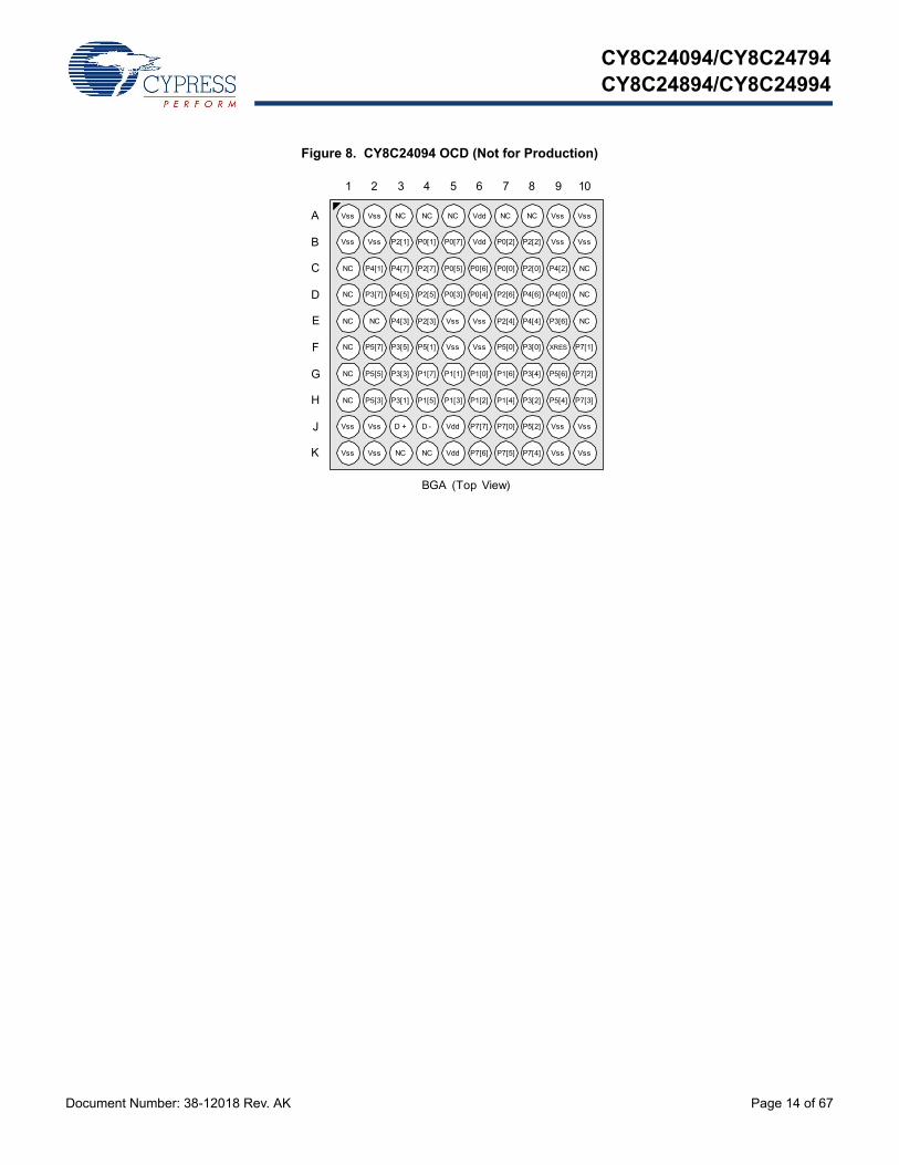
Figure 8. CY8C24094 OCD (Not for Production)
Vss Vss NC NC NC Vdd NC NC Vss Vss
Vss Vss P2[1] P0[1] P0[7] Vdd P0[2] P2[2] Vss Vss
NC P4[1] P4[7] P2[7] P0[5] P0[6] P0[0] P2[0] P4[2] NC
NC P3[7] P4[5] P2[5] P0[3] P0[4] P2[6] P4[6] P4[0] NC
NC NC P4[3] P2[3] Vss Vss P2[4] P4[4] P3[6] NC
NC P5[7] P3[5] P5[1] Vss Vss P5[0] P3[0] XRES P7[1]
NC P5[5] P3[3] P1[7] P1[1] P1[0] P1[6] P3[4] P5[6] P7[2]
NC P5[3] P3[1] P1[5] P1[3] P1[2] P1[4] P3[2] P5[4] P7[3]
Vss Vss D + D - Vdd P7[7] P7[0] P5[2] Vss Vss
Vss Vss NC NC Vdd P7[6] P7[5] P7[4] Vss Vss
1 2 3 4 5 6 7 8 9 10
A
B
C
D
E
F
G
H
J
K
BGA (Top View)
CY8C24094/CY8C24794CY8C24894/CY8C24994
Document Number: 38-12018 Rev. AK Page 15 of 67
9.6 100-Ball VFBGA Part Pinout (On-Chip Debug)
The following 100-pin VFBGA part table and drawing is for the CY8C24094 OCD PSoC device.
Note This part is only used for in-circuit debugging. It is NOT available for production.
Table 7. 100-Ball Part Pinout (VFBGA[17])
Pin
No. Dig
ita
l
An
alo
g
Name DescriptionPin
No. Dig
ita
l
An
alo
g
Name Description
A1 Power VSS Ground connection F1 OCDE OCD even data I/O
A2 Power VSS Ground connection F2 I/O M P5[7]
A3 NC No connection. Pin must be left floating F3 I/O M P3[5]
A4 NC No connection. Pin must be left floating F4 I/O M P5[1]
A5 NC No connection. Pin must be left floating. F5 Power VSS Ground connection
A6 Power VDD Supply voltage. F6 Power VSS Ground connection
A7 NC No connection. Pin must be left floating. F7 I/O M P5[0]
A8 NC No connection. Pin must be left floating. F8 I/O M P3[0]
A9 Power VSS Ground connection F9 XRES Active high pin reset with internal pull-down
A10 Power VSS Ground connection F10 I/O P7[1]
B1 Power VSS Ground connection G1 OCDO OCD odd data output
B2 Power VSS Ground connection G2 I/O M P5[5]
B3 I/O I, M P2[1] Direct switched capacitor block input G3 I/O M P3[3]
B4 I/O I, M P0[1] Analog column mux input G4 I/O M P1[7] I2C SCL
B5 I/O I, M P0[7] Analog column mux input G5 I/O M P1[1] I2C SCL, ISSP SCLK[18]
B6 Power VDD Supply voltage G6 I/O M P1[0] I2C SDA, ISSP SDATA[18]
B7 I/O I, M P0[2] Analog column mux input G7 I/O M P1[6]
B8 I/O I, M P2[2] Direct switched capacitor block input G8 I/O M P3[4]
B9 Power VSS Ground connection G9 I/O M P5[6]
B10 Power VSS Ground connection G10 I/O P7[2]
C1 NC No connection. Pin must be left floating H1 NC No connection. Pin must be left floating
C2 I/O M P4[1] H2 I/O M P5[3]
C3 I/O M P4[7] H3 I/O M P3[1]
C4 I/O M P2[7] H4 I/O M P1[5] I2C SDA
C5 I/O I/O,M P0[5] Analog column mux input and column output H5 I/O M P1[3]
C6 I/O I, M P0[6] Analog column mux input H6 I/O M P1[2]
C7 I/O I, M P0[0] Analog column mux input H7 I/O M P1[4] Optional EXTCLK
C8 I/O I, M P2[0] Direct switched capacitor block input H8 I/O M P3[2]
C9 I/O M P4[2] H9 I/O M P5[4]
C10 NC No connection. Pin must be left floating H10 I/O P7[3]
D1 NC No connection. Pin must be left floating J1 Power VSS Ground connection
D2 I/O M P3[7] J2 Power VSS Ground connection
D3 I/O M P4[5] J3 USB D+
D4 I/O M P2[5] J4 USB D-
D5 I/O I/O, M P0[3] Analog column mux input and column output J5 Power VDD Supply voltage
D6 I/O I, M P0[4] Analog column mux input J6 I/O P7[7]
D7 I/O M P2[6] External VREF input J7 I/O P7[0]
D8 I/O M P4[6] J8 I/O M P5[2]
D9 I/O M P4[0] J9 Power VSS Ground connection
D10 CCLK OCD CPU clock output J10 Power VSS Ground connection
E1 NC No connection. Pin must be left floating K1 Power VSS Ground connection
E2 NC No connection. Pin must be left floating K2 Power VSS Ground connection
E3 I/O M P4[3] K3 NC No connection. Pin must be left floating
E4 I/O I, M P2[3] Direct switched capacitor block input K4 NC No connection. Pin must be left floating
E5 Power VSS Ground connection K5 Power VDD Supply voltage
E6 Power VSS Ground connection K6 I/O P7[6]
E7 I/O M P2[4] External AGND input K7 I/O P7[5]
E8 I/O M P4[4] K8 I/O P7[4]
E9 I/O M P3[6] K9 Power VSS Ground connection
E10 HCLK OCD high speed clock output K10 Power VSS Ground connection
LEGEND A = Analog, I = Input, O = Output, M = Analog Mux Input, NC = No connection. Pin must be left floating, OCD = On-Chip Debugger.
Notes17. All VSS pins should be brought out to one common GND plane.18. These are the ISSP pins, which are not High Z at POR. See the PSoC Technical Reference Manual for details.

CY8C24094/CY8C24794CY8C24894/CY8C24994
Document Number: 38-12018 Rev. AK Page 16 of 67
Figure 9. CY8C24094 OCD (Not for Production)
Vss Vss NC NC NC Vdd NC NC Vss Vss
Vss Vss P2[1] P0[1] P0[7] Vdd P0[2] P2[2] Vss Vss
NC P4[1] P4[7] P2[7] P0[5] P0[6] P0[0] P2[0] P4[2] NC
NC P3[7] P4[5] P2[5] P0[3] P0[4] P2[6] P4[6] P4[0] CClk
NC NC P4[3] P2[3] Vss Vss P2[4] P4[4] P3[6] HClk
ocde P5[7] P3[5] P5[1] Vss Vss P5[0] P3[0] XRES P7[1]
ocdo P5[5] P3[3] P1[7] P1[1] P1[0] P1[6] P3[4] P5[6] P7[2]
NC P5[3] P3[1] P1[5] P1[3] P1[2] P1[4] P3[2] P5[4] P7[3]
Vss Vss D + D - Vdd P7[7] P7[0] P5[2] Vss Vss
Vss Vss NC NC Vdd P7[6] P7[5] P7[4] Vss Vss
1 2 3 4 5 6 7 8 9 10
A
B
C
D
E
F
G
H
J
K
BGA (Top View)

CY8C24094/CY8C24794CY8C24894/CY8C24994
Document Number: 38-12018 Rev. AK Page 17 of 67
9.7 100-Pin Part Pinout (On-Chip Debug)The 100-pin TQFP part is for the CY8C24094 OCD PSoC device.
Note This part is only used for in-circuit debugging. It is NOT available for production.
Table 8. 100-Pin Part Pinout (TQFP[19])
Pin
No. Dig
ita
l
An
alo
g
Name DescriptionPin
No. Dig
ita
l
An
alo
g
Name Description
1 NC No connection. Pin must be left floating 51 I/O M P1[6]
2 NC No connection. Pin must be left floating 52 I/O M P5[0]
3 I/O I, M P0[1] Analog column mux input 53 I/O M P5[2]
4 I/O M P2[7] 54 I/O M P5[4]
5 I/O M P2[5] 55 I/O M P5[6]
6 I/O I, M P2[3] Direct switched capacitor block input 56 I/O M P3[0]
7 I/O I, M P2[1] Direct switched capacitor block input 57 I/O M P3[2]
8 I/O M P4[7] 58 I/O M P3[4]
9 I/O M P4[5] 59 I/O M P3[6]
10 I/O M P4[3] 60 HCLK OCD high speed clock output
11 I/O M P4[1] 61 CCLK OCD CPU clock output
12 OCDE OCD even data I/O 62 Input XRES Active high pin reset with internal pull-down
13 OCDO OCD odd data output 63 I/O M P4[0]
14 NC No connection. Pin must be left floating 64 I/O M P4[2]
15 Power VSS Ground connection 65 Power VSS Ground connection
16 I/O M P3[7] 66 I/O M P4[4]
17 I/O M P3[5] 67 I/O M P4[6]
18 I/O M P3[3] 68 I/O I, M P2[0] Direct switched capacitor block input
19 I/O M P3[1] 69 I/O I, M P2[2] Direct switched capacitor block input
20 I/O M P5[7] 70 I/O P2[4] External AGND input
21 I/O M P5[5] 71 NC No connection. Pin must be left floating
22 I/O M P5[3] 72 I/O P2[6] External VREF input
23 I/O M P5[1] 73 NC No connection. Pin must be left floating
24 I/O M P1[7] I2C SCL 74 I/O I P0[0] Analog column mux input
25 NC No connection. Pin must be left floating 75 NC No connection. Pin must be left floating
26 NC No connection. Pin must be left floating 76 NC No connection. Pin must be left floating
27 NC No connection. Pin must be left floating 77 I/O I, M P0[2] Analog column mux input and column output
28 I/O P1[5] I2C SDA 78 NC No connection. Pin must be left floating
29 I/O P1[3] 79 I/O I, M P0[4] Analog column mux input and column output
30 I/O P1[1] Crystal (XTALin), I2C SCL, ISSP SCLK[20] 80 NC No connection. Pin must be left floating
31 NC No connection. Pin must be left floating 81 I/O I, M P0[6] Analog column mux input
32 Power VSS Ground connection 82 Power VDD Supply voltage
33 USB D+ 83 NC No connection. Pin must be left floating
34 USB D- 84 Power VSS Ground connection
35 Power VDD Supply voltage 85 NC No connection. Pin must be left floating
36 I/O P7[7] 86 NC No connection. Pin must be left floating
37 I/O P7[6] 87 NC No connection. Pin must be left floating
38 I/O P7[5] 88 NC No connection. Pin must be left floating
39 I/O P7[4] 89 NC No connection. Pin must be left floating
40 I/O P7[3] 90 NC No connection. Pin must be left floating
41 I/O P7[2] 91 NC No connection. Pin must be left floating
42 I/O P7[1] 92 NC No connection. Pin must be left floating
43 I/O P7[0] 93 NC No connection. Pin must be left floating
44 NC No connection. Pin must be left floating 94 NC No connection. Pin must be left floating
45 NC No connection. Pin must be left floating 95 I/O I, M P0[7] Analog column mux input
46 NC No connection. Pin must be left floating 96 NC No connection. Pin must be left floating
47 NC No connection. Pin must be left floating 97 I/O I/O, M P0[5] Analog column mux input and column output
48 I/O P1[0] Crystal (XTALout), I2C SDA, ISSP SDATA[20] 98 NC No connection. Pin must be left floating
49 I/O P1[2] 99 I/O I/O, M P0[3] Analog column mux input and column output
50 I/O P1[4] Optional EXTCLK 100 NC No connection. Pin must be left floating
LEGEND A = Analog, I = Input, O = Output, NC = No connection. Pin must be left floating, M = Analog Mux Input, OCD = On-Chip Debugger.
Notes19. All VSS pins should be brought out to one common GND plane.20. These are the ISSP pins, which are not High Z at POR. See the PSoC Technical Reference Manual for details.

CY8C24094/CY8C24794CY8C24894/CY8C24994
Document Number: 38-12018 Rev. AK Page 18 of 67
Figure 10. CY8C24094 OCD (Not for Production)
TQFP
NC
NCAI, M, P0[1]
M, P2[7]M, P2[5]
AI, M, P2[3]AI, M, P2[1]
M, P4[7]
M, P4[5]M, P4[3]M, P4[1]
OCDEOCDO
NCVss
M, P3[7]M, P3[5]
M, P3[3]M, P3[1]M, P5[7]
M, P5[5]M, P5[3]M, P5[1]
I2C SCL, P1[7]NC
NC D-
P7
[3]
NC
NC
I2C
SD
A, M
, P1
[5]
M, P
1[3
]
I2C
SC
L, M
, P1
[1]
NC
Vss D+
Vdd
P7
[7]
P7
[6]
P7
[5]
P7
[4]
P7
[2]
P7
[1]
P7
[0]
NC
NC
NC
I2C
SD
A, M
, P1
[0]
M, P
1[2
]M
, P1
[4]
NC
P0[0], M, AI
NCP2[6], M, External VREFNCP2[4], M, External AGNDP2[2], M, AIP2[0], M, AIP4[6], MP4[4], M
VssP4[2], M
P4[0], MXRES
CCLKHCLKP3[6], MP3[4], MP3[2], MP3[0], MP5[6], MP5[4], MP5[2], MP5[0], M
P1[6], M
NC
P0
[3],
M, A
I
NC
P0
[5],
M, A
I
NC
P0
[7],
M, A
IN
C
NC
NC
NC
NC
NC
NC
NC
NC
NC
Vss
NC
Vdd
P0
[6],
M, A
IN
CP
0[4
], M
, AI
NC
P0
[2],
M, A
IN
C
7574
73727170
69
686766656463
6261605958575655
54535251
100
99 98 97 96 95 94 93 92 91 90 89 88 87 86 85 84 83 82 81 80 79 78 77 76
10111213141516171819202122
232425
1234
56789
26 27 28 29 30 31 32 33 34 35 36 37 38 39 40 41 42 43 44 45 46 47 48 5049E
XT
CL
K,
CY8C24094/CY8C24794CY8C24894/CY8C24994
Document Number: 38-12018 Rev. AK Page 19 of 67
10. Register Reference
This section lists the registers of the CY8C24x94 PSoC device family. For detailed register information, see the PSoC Technical Reference Manual.
10.1 Register Conventions
The register conventions specific to this section are listed in the following table.
10.2 Register Mapping Tables
The PSoC device has a total register address space of 512 bytes. The register space is referred to as I/O space and is divided into two banks, Bank 0 and Bank 1. The XOI bit in the Flag register (CPU_F) determines which bank the user is currently in. When the XOI bit is set to 1, the user is in Bank 1.
Note In the following register mapping tables, blank fields are Reserved and should not be accessed.
Convention Description
R Read register or bit(s)
W Write register or bit(s)
L Logical register or bit(s)
C Clearable register or bit(s)
# Access is bit specific

CY8C24094/CY8C24794CY8C24894/CY8C24994
Document Number: 38-12018 Rev. AK Page 20 of 67
10.3 Register Map Bank 0 Table: User Space Name Addr (0, Hex) Access Name Addr (0, Hex) Access Name Addr (0, Hex) Access Name Addr (0, Hex) Access
PRT0DR 00 RW PMA0_DR 40 RW ASC10CR0 80 RW C0
PRT0IE 01 RW PMA1_DR 41 RW ASC10CR1 81 RW C1
PRT0GS 02 RW PMA2_DR 42 RW ASC10CR2 82 RW C2
PRT0DM2 03 RW PMA3_DR 43 RW ASC10CR3 83 RW C3
PRT1DR 04 RW PMA4_DR 44 RW ASD11CR0 84 RW C4
PRT1IE 05 RW PMA5_DR 45 RW ASD11CR1 85 RW C5
PRT1GS 06 RW PMA6_DR 46 RW ASD11CR2 86 RW C6
PRT1DM2 07 RW PMA7_DR 47 RW ASD11CR3 87 RW C7
PRT2DR 08 RW USB_SOF0 48 R 88 C8
PRT2IE 09 RW USB_SOF1 49 R 89 C9
PRT2GS 0A RW USB_CR0 4A RW 8A CA
PRT2DM2 0B RW USBI/O_CR0 4B # 8B CB
PRT3DR 0C RW USBI/O_CR1 4C RW 8C CC
PRT3IE 0D RW 4D 8D CD
PRT3GS 0E RW EP1_CNT1 4E # 8E CE
PRT3DM2 0F RW EP1_CNT 4F RW 8F CF
PRT4DR 10 RW EP2_CNT1 50 # ASD20CR0 90 RW CUR_PP D0 RW
PRT4IE 11 RW EP2_CNT 51 RW ASD20CR1 91 RW STK_PP D1 RW
PRT4GS 12 RW EP3_CNT1 52 # ASD20CR2 92 RW D2
PRT4DM2 13 RW EP3_CNT 53 RW ASD20CR3 93 RW IDX_PP D3 RW
PRT5DR 14 RW EP4_CNT1 54 # ASC21CR0 94 RW MVR_PP D4 RW
PRT5IE 15 RW EP4_CNT 55 RW ASC21CR1 95 RW MVW_PP D5 RW
PRT5GS 16 RW EP0_CR 56 # ASC21CR2 96 RW I2C_CFG D6 RW
PRT5DM2 17 RW EP0_CNT 57 # ASC21CR3 97 RW I2C_SCR D7 #
18 EP0_DR0 58 RW 98 I2C_DR D8 RW
19 EP0_DR1 59 RW 99 I2C_MSCR D9 #
1A EP0_DR2 5A RW 9A INT_CLR0 DA RW
1B EP0_DR3 5B RW 9B INT_CLR1 DB RW
PRT7DR 1C RW EP0_DR4 5C RW 9C INT_CLR2 DC RW
PRT7IE 1D RW EP0_DR5 5D RW 9D INT_CLR3 DD RW
PRT7GS 1E RW EP0_DR6 5E RW 9E INT_MSK3 DE RW
PRT7DM2 1F RW EP0_DR7 5F RW 9F INT_MSK2 DF RW
DBB00DR0 20 # AMX_IN 60 RW A0 INT_MSK0 E0 RW
DBB00DR1 21 W AMUXCFG 61 RW A1 INT_MSK1 E1 RW
DBB00DR2 22 RW 62 A2 INT_VC E2 RC
DBB00CR0 23 # ARF_CR 63 RW A3 RES_WDT E3 W
DBB01DR0 24 # CMP_CR0 64 # A4 DEC_DH E4 RC
DBB01DR1 25 W ASY_CR 65 # A5 DEC_DL E5 RC
DBB01DR2 26 RW CMP_CR1 66 RW A6 DEC_CR0 E6 RW
DBB01CR0 27 # 67 A7 DEC_CR1 E7 RW
DCB02DR0 28 # 68 MUL1_X A8 W MUL0_X E8 W
DCB02DR1 29 W 69 MUL1_Y A9 W MUL0_Y E9 W
DCB02DR2 2A RW 6A MUL1_DH AA R MUL0_DH EA R
DCB02CR0 2B # 6B MUL1_DL AB R MUL0_DL EB R
DCB03DR0 2C # TMP_DR0 6C RW ACC1_DR1 AC RW ACC0_DR1 EC RW
DCB03DR1 2D W TMP_DR1 6D RW ACC1_DR0 AD RW ACC0_DR0 ED RW
DCB03DR2 2E RW TMP_DR2 6E RW ACC1_DR3 AE RW ACC0_DR3 EE RW
DCB03CR0 2F # TMP_DR3 6F RW ACC1_DR2 AF RW ACC0_DR2 EF RW
30 ACB00CR3 70 RW RDI0RI B0 RW F0
31 ACB00CR0 71 RW RDI0SYN B1 RW F1
32 ACB00CR1 72 RW RDI0IS B2 RW F2
33 ACB00CR2 73 RW RDI0LT0 B3 RW F3
34 ACB01CR3 74 RW RDI0LT1 B4 RW F4
35 ACB01CR0 75 RW RDI0RO0 B5 RW F5
36 ACB01CR1 76 RW RDI0RO1 B6 RW F6
37 ACB01CR2 77 RW B7 CPU_F F7 RL
38 78 B8 F8
39 79 B9 F9
3A 7A BA FA
3B 7B BB FB
3C 7C BC FC
3D 7D BD DAC_D FD RW
3E 7E BE CPU_SCR1 FE #
3F 7F BF CPU_SCR0 FF #
Blank fields are reserved and should not be accessed. # Access is bit specific.

CY8C24094/CY8C24794CY8C24894/CY8C24994
Document Number: 38-12018 Rev. AK Page 21 of 67
10.4 Register Map Bank 1 Table: Configuration Space Name Addr (1, Hex) Access Name Addr (1, Hex) Access Name Addr (1, Hex) Access Name Addr (1, Hex) Access
PRT0DM0 00 RW PMA0_WA 40 RW ASC10CR0 80 RW USBI/O_CR2 C0 RW
PRT0DM1 01 RW PMA1_WA 41 RW ASC10CR1 81 RW USB_CR1 C1 #
PRT0IC0 02 RW PMA2_WA 42 RW ASC10CR2 82 RW
PRT0IC1 03 RW PMA3_WA 43 RW ASC10CR3 83 RW
PRT1DM0 04 RW PMA4_WA 44 RW ASD11CR0 84 RW EP1_CR0 C4 #
PRT1DM1 05 RW PMA5_WA 45 RW ASD11CR1 85 RW EP2_CR0 C5 #
PRT1IC0 06 RW PMA6_WA 46 RW ASD11CR2 86 RW EP3_CR0 C6 #
PRT1IC1 07 RW PMA7_WA 47 RW ASD11CR3 87 RW EP4_CR0 C7 #
PRT2DM0 08 RW 48 88 C8
PRT2DM1 09 RW 49 89 C9
PRT2IC0 0A RW 4A 8A CA
PRT2IC1 0B RW 4B 8B CB
PRT3DM0 0C RW 4C 8C CC
PRT3DM1 0D RW 4D 8D CD
PRT3IC0 0E RW 4E 8E CE
PRT3IC1 0F RW 4F 8F CF
PRT4DM0 10 RW PMA0_RA 50 RW 90 GDI_O_IN D0 RW
PRT4DM1 11 RW PMA1_RA 51 RW ASD20CR1 91 RW GDI_E_IN D1 RW
PRT4IC0 12 RW PMA2_RA 52 RW ASD20CR2 92 RW GDI_O_OU D2 RW
PRT4IC1 13 RW PMA3_RA 53 RW ASD20CR3 93 RW GDI_E_OU D3 RW
PRT5DM0 14 RW PMA4_RA 54 RW ASC21CR0 94 RW D4
PRT5DM1 15 RW PMA5_RA 55 RW ASC21CR1 95 RW D5
PRT5IC0 16 RW PMA6_RA 56 RW ASC21CR2 96 RW D6
PRT5IC1 17 RW PMA7_RA 57 RW ASC21CR3 97 RW D7
18 58 98 MUX_CR0 D8 RW
19 59 99 MUX_CR1 D9 RW
1A 5A 9A MUX_CR2 DA RW
1B 5B 9B MUX_CR3 DB RW
PRT7DM0 1C RW 5C 9C DC
PRT7DM1 1D RW 5D 9D OSC_GO_EN DD RW
PRT7IC0 1E RW 5E 9E OSC_CR4 DE RW
PRT7IC1 1F RW 5F 9F OSC_CR3 DF RW
DBB00FN 20 RW CLK_CR0 60 RW A0 OSC_CR0 E0 RW
DBB00IN 21 RW CLK_CR1 61 RW A1 OSC_CR1 E1 RW
DBB00OU 22 RW ABF_CR0 62 RW A2 OSC_CR2 E2 RW
23 AMD_CR0 63 RW A3 VLT_CR E3 RW
DBB01FN 24 RW CMP_GO_EN 64 RW A4 VLT_CMP E4 R
DBB01IN 25 RW 65 A5 E5
DBB01OU 26 RW AMD_CR1 66 RW A6 E6
27 ALT_CR0 67 RW A7 E7
DCB02FN 28 RW 68 A8 IMO_TR E8 W
DCB02IN 29 RW 69 A9 ILO_TR E9 W
DCB02OU 2A RW 6A AA BDG_TR EA RW
2B 6B AB ECO_TR EB W
DCB03FN 2C RW TMP_DR0 6C RW AC MUX_CR4 EC RW
DCB03IN 2D RW TMP_DR1 6D RW AD MUX_CR5 ED RW
DCB03OU 2E RW TMP_DR2 6E RW AE EE
2F TMP_DR3 6F RW AF EF
30 ACB00CR3 70 RW RDI0RI B0 RW F0
31 ACB00CR0 71 RW RDI0SYN B1 RW F1
32 ACB00CR1 72 RW RDI0IS B2 RW F2
33 ACB00CR2 73 RW RDI0LT0 B3 RW F3
34 ACB01CR3 74 RW RDI0LT1 B4 RW F4
35 ACB01CR0 75 RW RDI0RO0 B5 RW F5
36 ACB01CR1 76 RW RDI0RO1 B6 RW F6
37 ACB01CR2 77 RW B7 CPU_F F7 RL
38 78 B8 F8
39 79 B9 F9
3A 7A BA FA
3B 7B BB FB
3C 7C BC FC
3D 7D BD DAC_CR FD RW
3E 7E BE CPU_SCR1 FE #
3F 7F BF CPU_SCR0 FF #
Blank fields are reserved and should not be accessed. # Access is bit specific.

CY8C24094/CY8C24794CY8C24894/CY8C24994
Document Number: 38-12018 Rev. AK Page 22 of 67
11. Electrical Specifications
This section presents the DC and AC electrical specifications of the CY8C24x94 PSoC device family. For the most up-to-date electrical specifications, confirm that you have the most recent datasheet by visiting http://www.cypress.com.
Specifications are valid for –40 °C TA 85 °C and TJ 100 °C, except where noted. Specifications for devices running at greater than 12 MHz are valid for –40 °C TA 70 °C and TJ 82 °C.
Figure 11. Voltage Versus CPU Frequency
11.1 Absolute Maximum Ratings
5.25
4.75
3.00
93 kHz 12 MHz 24 MHz
CPU Frequency
Vd
d V
olt
age
Valid
Operating
Region
Table 9. Absolute Maximum Ratings
Symbol Description Min Typ Max Units Notes
TSTG Storage temperature –55 25 +100 °C Higher storage temperatures reduces data retention time. Recommended storage temper-ature is +25 °C ± 25 °C. Extended duration storage temperatures higher than 65 °C degrades reliability.
TBAKETEMP Bake temperature – 125 See package
label
°C
tBAKETIME Bake time See package
label
– 72 Hours
TA Ambient temperature with power applied –40 – +85 °C
VDD Supply voltage on VDD relative to VSS –0.5 – +6.0 V
VI/O DC input voltage VSS – 0.5 – VDD + 0.5 V
VI/O2 DC voltage applied to tristate VSS – 0.5 – VDD + 0.5 V
IMI/O Maximum current into any port pin –25 – +50 mA
IMAI/O Maximum current into any port pin configured as analog driver
–50 – +50 mA
ESD Electrostatic discharge voltage 2000 – – V Human body model ESD.
LU Latch-up current – – 200 mA

CY8C24094/CY8C24794CY8C24894/CY8C24994
Document Number: 38-12018 Rev. AK Page 23 of 67
11.2 Operating Temperature
11.3 DC Electrical Characteristics
11.3.1 DC Chip-Level Specifications
The following table lists guaranteed maximum and minimum specifications for the voltage and temperature ranges: 4.75 V to 5.25 V and –40 °C TA 85 °C, or 3.0 V to 3.6 V and –40 °C TA 85 °C, respectively. Typical parameters are measured at 5 V and 3.3 V at 25 °C and are for design guidance only.
Table 10. Operating Temperature
Symbol Description Min Typ Max Units Notes
TA Ambient temperature –40 – +85 °C
TAUSB Ambient temperature using USB –10 – +85 °C
TJ Junction temperature –40 – +100 °C The temperature rise from ambient to junction is package specific. See Thermal Impedance on page 45. The user must limit the power consumption to comply with this requirement.
Table 11. DC Chip-Level Specifications
Symbol Description Min Typ Max Units Notes
VDD Supply voltage 3.0 – 5.25 V See DC POR and LVD specifications, Table 22 on page 35.
IDD5 Supply current, IMO = 24 MHz (5 V) – 14 27 mA Conditions are VDD = 5.0 V, TA = 25 °C, CPU = 3 MHz, SYSCLK doubler disabled, VC1 = 1.5 MHz, VC2 = 93.75 kHz, VC3 = 93.75 kHz, analog power = off.
IDD3 Supply current, IMO = 24 MHz (3.3 V) – 8 14 mA Conditions are VDD = 3.3 V, TA = 25 °C, CPU = 3 MHz, SYSCLK doubler disabled, VC1 = 1.5 MHz, VC2 = 93.75 kHz, VC3 = 0.367 kHz, analog power = off.
ISB Sleep [21] (mode) current with POR, LVD, sleep timer, and WDT.[22]
– 3 6.5 µA Conditions are with internal slow speed oscillator, VDD = 3.3 V, –40 C TA 55 °C, analog power = off.
ISBH Sleep (mode) current with POR, LVD, Sleep Timer, and WDT at high temperature.[22]
– 4 25 µA Conditions are with internal slow speed oscillator, VDD = 3.3 V, 55 °C < TA 85 °C, analog power = off.
Notes21. Errata: When the device is operating at 4.75 V to 5.25 V and the 3.3 V regulator is enabled, a short low pulse may be created on the DP signal line during device
wake-up. The 15-20 μs low pulse of the DP line may be interpreted by the host computer as a deattach or the beginning of a wake-up. More details in “Errata” on page 60.22. Standby current includes all functions (POR, LVD, WDT, Sleep Time) needed for reliable system operation. This should be compared with devices that have similar
functions enabled.
CY8C24094/CY8C24794CY8C24894/CY8C24994
Document Number: 38-12018 Rev. AK Page 24 of 67
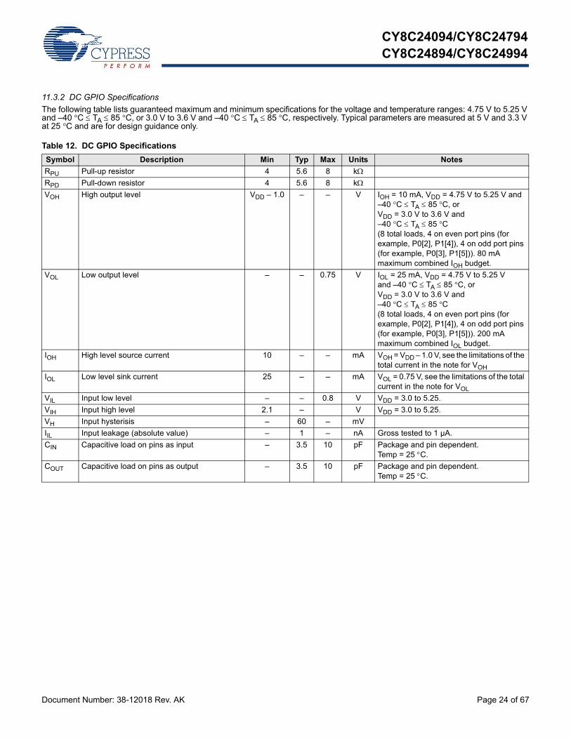
11.3.2 DC GPIO Specifications
The following table lists guaranteed maximum and minimum specifications for the voltage and temperature ranges: 4.75 V to 5.25 V and –40 °C TA 85 °C, or 3.0 V to 3.6 V and –40 °C TA 85 °C, respectively. Typical parameters are measured at 5 V and 3.3 V at 25 °C and are for design guidance only.
Table 12. DC GPIO Specifications
Symbol Description Min Typ Max Units Notes
RPU Pull-up resistor 4 5.6 8 kRPD Pull-down resistor 4 5.6 8 kVOH High output level VDD – 1.0 – – V IOH = 10 mA, VDD = 4.75 V to 5.25 V and
–40 °C TA 85 °C, orVDD = 3.0 V to 3.6 V and –40 °C TA 85 °C (8 total loads, 4 on even port pins (for example, P0[2], P1[4]), 4 on odd port pins (for example, P0[3], P1[5])). 80 mA maximum combined IOH budget.
VOL Low output level – – 0.75 V IOL = 25 mA, VDD = 4.75 V to 5.25 Vand –40 °C TA 85 °C, orVDD = 3.0 V to 3.6 V and –40 °C TA 85 °C (8 total loads, 4 on even port pins (for example, P0[2], P1[4]), 4 on odd port pins (for example, P0[3], P1[5])). 200 mA maximum combined IOL budget.
IOH High level source current 10 – – mA VOH = VDD – 1.0 V, see the limitations of the total current in the note for VOH
IOL Low level sink current 25 – – mA VOL = 0.75 V, see the limitations of the total current in the note for VOL
VIL Input low level – – 0.8 V VDD = 3.0 to 5.25.
VIH Input high level 2.1 – V VDD = 3.0 to 5.25.
VH Input hysterisis – 60 – mV
IIL Input leakage (absolute value) – 1 – nA Gross tested to 1 µA.
CIN Capacitive load on pins as input – 3.5 10 pF Package and pin dependent. Temp = 25 C.
COUT Capacitive load on pins as output – 3.5 10 pF Package and pin dependent. Temp = 25 C.

CY8C24094/CY8C24794CY8C24894/CY8C24994
Document Number: 38-12018 Rev. AK Page 25 of 67
11.3.3 DC Full Speed USB Specifications
The following table lists guaranteed maximum and minimum specifications for the voltage and temperature ranges: 4.75 V to 5.25 V and –10 C TA 85 °C, or 3.0 V to 3.6 V and –10 °C TA 85 °C, respectively. Typical parameters are measured at 5 V and 3.3 V at 25 °C and are for design guidance only.
Table 13. DC Full Speed (12 Mbps) USB Specifications
Symbol Description Min Typ Max Units Notes
USB Interface
VDI Differential input sensitivity 0.2 – – V | (D+) – (D–) |
VCM Differential input common mode range 0.8 – 2.5 V
VSE Single ended receiver threshold 0.8 – 2.0 V
CIN Transceiver capacitance – – 20 pF
II/O High Z state data line leakage –10 – 10 µA 0 V < VIN < 3.3 V.
REXT External USB series resistor 23 – 25 In series with each USB pin.
VUOH Static output high, driven 2.8 – 3.6 V 15 k ± 5% to ground. Internal pull-up enabled.
VUOHI Static output high, idle 2.7 – 3.6 V 15 k ± 5% to ground. Internal pull-up enabled.
VUOL Static output low – – 0.3 V 15 k ± 5% to ground. Internal pull-up enabled.
ZO USB driver output impedance 28 – 44 Including REXT resistor.
VCRS D+/D– crossover voltage 1.3 – 2.0 V
CY8C24094/CY8C24794CY8C24894/CY8C24994
Document Number: 38-12018 Rev. AK Page 26 of 67
11.3.4 DC Operational Amplifier Specifications
The following tables list guaranteed maximum and minimum specifications for the voltage and temperature ranges: 4.75 V to 5.25 V and –40 °C TA 85 °C, or 3.0 V to 3.6 V and –40 °C TA 85 °C, respectively. Typical parameters are measured at 5 V and 3.3 V at 25 °C and are for design guidance only.
The operational amplifier is a component of both the analog continuous time PSoC blocks and the analog switched capacitor PSoC blocks. The guaranteed specifications are measured in the analog continuous time PSoC block.
Table 14. 5-V DC Operational Amplifier Specifications
Symbol Description Min Typ Max Units Notes
VOSOA Input offset voltage (absolute value) Power = low, Opamp bias = highPower = medium, Opamp bias = highPower = high, Opamp bias = high
–––
1.6 1.3 1.2
10 8
7.5
mV mV mV
TCVOSOA Average input offset voltage drift – 7.0 35.0 µV/°C
IEBOA Input leakage current (Port 0 analog pins) – 20 – pA Gross tested to 1 µA.
CINOA Input capacitance (Port 0 analog pins) – 4.5 9.5 pF Package and pin dependent. Temp = 25 C.
VCMOA Common mode voltage rangeCommon mode voltage range (high power or high Opamp bias)
0.0 – VDDVDD – 0.5
VV
The common-mode input voltage range is measured through an analog output buffer. The specification includes the limitations imposed by the characteristics of the analog output buffer.
0.5 –
GOLOA Open loop gainPower = low, Opamp bias = highPower = medium, Opamp bias = highPower = high, Opamp bias = high
606080
–––
–––
dBdBdB
VOHIGHOA High output voltage swing (internal signals)Power = low, Opamp bias = highPower = medium, Opamp bias = highPower = high, Opamp bias = high
VDD – 0.2VDD – 0.2VDD – 0.5
–––
–––
VVV
VOLOWOA Low output voltage swing (internal signals)Power = low, Opamp bias = highPower = medium, Opamp bias = highPower = high, Opamp bias = high
–––
–––
0.20.20.5
VVV
ISOA Supply current (including associated AGND buffer)Power = low, Opamp bias = lowPower = low, Opamp bias = highPower = medium, Opamp bias = lowPower = medium, Opamp bias = highPower = high, Opamp bias = lowPower = high, Opamp bias = high
––––––
400500800120024004600
8009001000160032006400
µAµAµAµAµAµA
PSRROA Supply voltage rejection ratio 65 80 – dB VSS VIN (VDD – 2.25) or (VDD – 1.25 V) VIN VDD.

CY8C24094/CY8C24794CY8C24894/CY8C24994
Document Number: 38-12018 Rev. AK Page 27 of 67
11.3.5 DC Low Power Comparator Specifications
The following table lists guaranteed maximum and minimum specifications for the voltage and temperature ranges: 4.75 V to 5.25 V and –40 °C TA 85 °C or 3.0 V to 3.6 V and –40 °C TA 85 °C, respectively. Typical parameters are measured at 5 V at 25 °C and are for design guidance only.
Table 15. 3.3-V DC Operational Amplifier Specifications
Symbol Description Min Typ Max Units Notes
VOSOA Input offset voltage (absolute value) Power = low, Opamp bias = highPower = medium, Opamp bias = highPower = high, Opamp bias = high
–––
1.65 1.32
–
10 8 –
mV mVmV
Power = high, Opamp bias = high setting is not allowed for 3.3 V VDD operation
TCVOSOA Average input offset voltage drift – 7.0 35.0 µV/°C
IEBOA Input leakage current (port 0 analog pins) – 20 – pA Gross tested to 1 µA.
CINOA Input capacitance (port 0 analog pins) – 4.5 9.5 pF Package and pin dependent. Temp = 25 °C.
VCMOA Common mode voltage range 0.2 – VDD – 0.2 V The common-mode input voltage range is measured through an analog output buffer. The specifi-cation includes the limitations imposed by the characteristics of the analog output buffer.
GOLOA Open loop gainPower = low, Opamp bias = lowPower = medium, Opamp bias = lowPower = high, Opamp bias = low
606080
–––
–––
dBdBdB
Specification is applicable at Low opamp bias. For high opamp bias mode (except high power, High opamp bias), minimum is 60 dB.
VOHIGHOA High output voltage swing (internal signals)Power = low, Opamp bias = lowPower = medium, Opamp bias = lowPower = high, Opamp bias = low
VDD – 0.2VDD – 0.2VDD – 0.2
–––
–––
VVV
Power = high, Opamp bias = high setting is not allowed for 3.3 V VDD operation
VOLOWOA Low output voltage swing (internal signals)Power = low, Opamp bias = lowPower = medium, Opamp bias = lowPower = high, Opamp bias = low
–––
–––
0.20.20.2
VVV
Power = high, Opamp bias = high setting is not allowed for 3.3 V VDD operation
ISOA Supply current (including associated AGND buffer)Power = low, Opamp bias = lowPower = low, Opamp bias = highPower = medium, Opamp bias = lowPower = medium, Opamp bias = highPower = high, Opamp bias = lowPower = high, Opamp bias = high
––––––
40050080012002400
–
800900100016003200
–
µAµAµAµAµAµA
Power = high, Opamp bias = high setting is not allowed for 3.3 V VDD operation
PSRROA Supply voltage rejection ratio 65 80 – dB VSS VIN (VDD – 2.25) or (VDD – 1.25 V) VIN VDD
Table 16. DC Low Power Comparator Specifications
Symbol Description Min Typ Max Units Notes
VREFLPC Low power comparator (LPC) reference voltage range
0.2 – VDD – 1 V
ISLPC LPC supply current – 10 40 µA
VOSLPC LPC voltage offset – 2.5 30 mV

CY8C24094/CY8C24794CY8C24894/CY8C24994
Document Number: 38-12018 Rev. AK Page 28 of 67
11.3.6 DC Analog Output Buffer Specifications
The following tables list guaranteed maximum and minimum specifications for the voltage and temperature ranges: 4.75 V to 5.25 V and –40 °C TA 85 °C, or 3.0 V to 3.6 V and –40 °C TA 85 °C, respectively. Typical parameters are measured at 5 V and 3.3 V at 25 °C and are for design guidance only.
Table 17. 5-V DC Analog Output Buffer Specifications
Symbol Description Min Typ Max Units Notes
CL Load Capacitance – – 200 pF This specification applies to the external circuit that is being driven by the analog output buffer.
VOSOB Input offset voltage (absolute value) – 3 12 mV
TCVOSOB Average input offset voltage drift – +6 – µV/°C
VCMOB Common mode input voltage range 0.5 – VDD – 1.0 V
ROUTOB Output resistancePower = lowPower = high
––
0.60.6
––
VOHIGHOB High output voltage swing (Load = 32 ohms to VDD/2)Power = lowPower = high
0.5 × VDD + 1.10.5 × VDD + 1.1
––
––
VV
VOLOWOB Low output voltage swing (Load = 32 ohms to VDD/2)Power = lowPower = high
––
––
0.5 × VDD – 1.30.5 × VDD – 1.3
VV
ISOB Supply current including opamp bias cell (No Load)Power = lowPower = high
––
1.12.6
5.18.8
mAmA
PSRROB Supply voltage rejection ratio 53 64 – dB (0.5 × VDD – 1.3) VOUT (VDD – 2.3).

CY8C24094/CY8C24794CY8C24894/CY8C24994
Document Number: 38-12018 Rev. AK Page 29 of 67
Table 18. 3.3-V DC Analog Output Buffer Specifications
Symbol Description Min Typ Max Units Notes
CL Load Capacitance – – 200 pF This specification applies to the external circuit that is being driven by the analog output buffer.
VOSOB Input offset voltage (absolute value) – 3 12 mV
TCVOSOB Average input offset voltage drift – +6 – µV/°C
VCMOB Common mode input voltage range 0.5 – VDD – 1.0 V
ROUTOB Output resistancePower = lowPower = high
––
11
––
WW
VOHIGHOB High output voltage swing (Load = 1 K ohms to VDD/2)Power = lowPower = high
0.5 × VDD + 1.00.5 × VDD + 1.0
––
––
VV
VOLOWOB Low output voltage swing (Load = 1 K ohms to VDD/2)Power = lowPower = high
––
––
0.5 × VDD – 1.00.5 × VDD – 1.0
VV
ISOB Supply current including opamp bias cell (No load)Power = lowPower = high
––
0.82.0
2.04.3
mAmA
PSRROB Supply voltage rejection ratio 34 64 – dB (0.5 × VDD – 1.0) VOUT (0.5 × VDD + 0.9).

CY8C24094/CY8C24794CY8C24894/CY8C24994
Document Number: 38-12018 Rev. AK Page 30 of 67
11.3.7 DC Analog Reference Specifications
The following tables list guaranteed maximum and minimum specifications for the voltage and temperature ranges: 4.75 V to 5.25 Vand –40 °C TA 85 °C, or 3.0 V to 3.6 V and –40 °C TA 85 °C, respectively. Typical parameters apply to 5 V and 3.3 V at 25 °Cand are for design guidance only.
The guaranteed specifications for RefHI and RefLo are measured through the Analog Continuous Time PSoC blocks. The powerlevels for RefHi and RefLo refer to the Analog Reference Control register. AGND is measured at P2[4] in AGND bypass mode. EachAnalog Continuous Time PSoC block adds a maximum of 10mV additional offset error to guaranteed AGND specifications from thelocal AGND buffer. Reference control power can be set to medium or high unless otherwise noted.
Note Avoid using P2[4] for digital signaling when using an analog resource that depends on the Analog Reference. Some coupling of the digital signal may appear on the AGND.
Table 19. 5-V DC Analog Reference Specifications
Reference ARF_CR
[5:3]
Reference Power Settings
Symbol Reference Description Min Typ Max Units
0b000 RefPower = highOpamp bias = high
VREFHI Ref High VDD/2 + Bandgap VDD/2 + 1.229 VDD/2 + 1.290 VDD/2 + 1.346 V
VAGND AGND VDD/2 VDD/2 – 0.038 VDD/2 VDD/2 + 0.040 V
VREFLO Ref Low VDD/2 – Bandgap VDD/2 – 1.356 VDD/2 – 1.295 VDD/2 – 1.218 V
RefPower = highOpamp bias = low
VREFHI Ref High VDD/2 + Bandgap VDD/2 + 1.220 VDD/2 + 1.292 VDD/2 + 1.348 V
VAGND AGND VDD/2 VDD/2 – 0.036 VDD/2 VDD/2 + 0.036 V
VREFLO Ref Low VDD/2 – Bandgap VDD/2 – 1.357 VDD/2 – 1.297 VDD/2 – 1.225 V
RefPower = mediumOpamp bias = high
VREFHI Ref High VDD/2 + Bandgap VDD/2 + 1.221 VDD/2 + 1.293 VDD/2 + 1.351 V
VAGND AGND VDD/2 VDD/2 – 0.036 VDD/2 VDD/2 + 0.036 V
VREFLO Ref Low VDD/2 – Bandgap VDD/2 – 1.357 VDD/2 – 1.298 VDD/2 – 1.228 V
RefPower = mediumOpamp bias = low
VREFHI Ref High VDD/2 + Bandgap VDD/2 + 1.219 VDD/2 + 1.293 VDD/2 + 1.353 V
VAGND AGND VDD/2 VDD/2 – 0.037 VDD/2 – 0.001 VDD/2 + 0.036 V
VREFLO Ref Low VDD/2 – Bandgap VDD/2 – 1.359 VDD/2 – 1.299 VDD/2 – 1.229 V
0b001 RefPower = highOpamp bias = high
VREFHI Ref High P2[4]+P2[6] (P2[4] = VDD/2, P2[6] = 1.3 V)
P2[4] + P2[6] – 0.092
P2[4] + P2[6] – 0.011
P2[4] + P2[6] + 0.064
V
VAGND AGND P2[4] P2[4] P2[4] P2[4] –
VREFLO Ref Low P2[4]–P2[6] (P2[4] = VDD/2, P2[6] = 1.3 V)
P2[4] – P2[6] – 0.031
P2[4] – P2[6] + 0.007
P2[4] – P2[6] + 0.056
V
RefPower = highOpamp bias = low
VREFHI Ref High P2[4]+P2[6] (P2[4] = VDD/2, P2[6] = 1.3 V)
P2[4] + P2[6] – 0.078
P2[4] + P2[6] – 0.008
P2[4] + P2[6] + 0.063
V
VAGND AGND P2[4] P2[4] P2[4] P2[4] –
VREFLO Ref Low P2[4]–P2[6] (P2[4] = VDD/2, P2[6] = 1.3 V)
P2[4] – P2[6] – 0.031
P2[4] – P2[6] + 0.004
P2[4] – P2[6] + 0.043
V
RefPower = mediumOpamp bias = high
VREFHI Ref High P2[4]+P2[6] (P2[4] = VDD/2, P2[6] = 1.3 V)
P2[4] + P2[6] – 0.073
P2[4] + P2[6] – 0.006
P2[4] + P2[6] + 0.062
V
VAGND AGND P2[4] P2[4] P2[4] P2[4] –
VREFLO Ref Low P2[4]–P2[6] (P2[4] = VDD/2, P2[6] = 1.3 V)
P2[4] – P2[6] – 0.032
P2[4] – P2[6] + 0.003
P2[4] – P2[6] + 0.038
V
RefPower = mediumOpamp bias = low
VREFHI Ref High P2[4]+P2[6] (P2[4] = VDD/2, P2[6] = 1.3 V)
P2[4] + P2[6] – 0.073
P2[4] + P2[6] – 0.006
P2[4] + P2[6] + 0.062
V
VAGND AGND P2[4] P2[4] P2[4] P2[4] –
VREFLO Ref Low P2[4]–P2[6] (P2[4] = VDD/2, P2[6] = 1.3 V)
P2[4] – P2[6] – 0.034
P2[4] – P2[6] + 0.002
P2[4] – P2[6] + 0.037
V

CY8C24094/CY8C24794CY8C24894/CY8C24994
Document Number: 38-12018 Rev. AK Page 31 of 67
0b010 RefPower = highOpamp bias = high
VREFHI Ref High VDD VDD – 0.037 VDD – 0.007 VDD V
VAGND AGND VDD/2 VDD/2 – 0.036 VDD/2 – 0.001 VDD/2 + 0.036 V
VREFLO Ref Low VSS VSS VSS + 0.005 VSS + 0.029 V
RefPower = highOpamp bias = low
VREFHI Ref High VDD VDD – 0.034 VDD – 0.006 VDD V
VAGND AGND VDD/2 VDD/2 – 0.036 VDD/2 – 0.001 VDD/2 + 0.035 V
VREFLO Ref Low VSS VSS VSS + 0.004 VSS + 0.024 V
RefPower = mediumOpamp bias = high
VREFHI Ref High VDD VDD – 0.032 VDD – 0.005 VDD V
VAGND AGND VDD/2 VDD/2 – 0.036 VDD/2 – 0.001 VDD/2 + 0.035 V
VREFLO Ref Low VSS VSS VSS + 0.003 VSS + 0.022 V
RefPower = mediumOpamp bias = low
VREFHI Ref High VDD VDD – 0.031 VDD – 0.005 VDD V
VAGND AGND VDD/2 VDD/2 – 0.037 VDD/2 – 0.001 VDD/2 + 0.035 V
VREFLO Ref Low VSS VSS VSS + 0.003 VSS + 0.020 V
0b011 RefPower = highOpamp bias = high
VREFHI Ref High 3 × Bandgap 3.760 3.884 4.006 V
VAGND AGND 2 × Bandgap 2.522 2.593 2.669 V
VREFLO Ref Low Bandgap 1.252 1.299 1.342 V
RefPower = highOpamp bias = low
VREFHI Ref High 3 × Bandgap 3.766 3.887 4.010 V
VAGND AGND 2 × Bandgap 2.523 2.594 2.670 V
VREFLO Ref Low Bandgap 1.252 1.297 1.342 V
RefPower = mediumOpamp bias = high
VREFHI Ref High 3 × Bandgap 3.769 3.888 4.013 V
VAGND AGND 2 × Bandgap 2.523 2.594 2.671 V
VREFLO Ref Low Bandgap 1.251 1.296 1.343 V
RefPower = mediumOpamp bias = low
VREFHI Ref High 3 × Bandgap 3.769 3.889 4.015 V
VAGND AGND 2 × Bandgap 2.523 2.595 2.671 V
VREFLO Ref Low Bandgap 1.251 1.296 1.344 V
0b100 RefPower = highOpamp bias = high
VREFHI Ref High 2 × Bandgap + P2[6] (P2[6] = 1.3 V)
2.483 + P2[6] 2.582 + P2[6] 2.674 + P2[6] V
VAGND AGND 2 × Bandgap 2.522 2.593 2.669 V
VREFLO Ref Low 2 × Bandgap – P2[6] (P2[6] = 1.3 V)
2.524 – P2[6] 2.600 – P2[6] 2.676 – P2[6] V
RefPower = highOpamp bias = low
VREFHI Ref High 2 × Bandgap + P2[6] (P2[6] = 1.3 V)
2.490 + P2[6] 2.586 + P2[6] 2.679 + P2[6] V
VAGND AGND 2 × Bandgap 2.523 2.594 2.669 V
VREFLO Ref Low 2 × Bandgap – P2[6] (P2[6] = 1.3 V)
2.523 – P2[6] 2.598 – P2[6] 2.675 – P2[6] V
RefPower = mediumOpamp bias = high
VREFHI Ref High 2 × Bandgap + P2[6] (P2[6] = 1.3 V)
2.493 + P2[6] 2.588 + P2[6] 2.682 +P2[6] V
VAGND AGND 2 × Bandgap 2.523 2.594 2.670 V
VREFLO Ref Low 2 × Bandgap – P2[6] (P2[6] = 1.3 V)
2.523 – P2[6] 2.597 – P2[6] 2.675 – P2[6] V
RefPower = mediumOpamp bias = low
VREFHI Ref High 2 × Bandgap + P2[6] (P2[6] = 1.3 V)
2.494 + P2[6] 2.589 + P2[6] 2.685 + P2[6] V
VAGND AGND 2 × Bandgap 2.523 2.595 2.671 V
VREFLO Ref Low 2 × Bandgap – P2[6] (P2[6] = 1.3 V)
2.522 – P2[6] 2.596 – P2[6] 2.676 – P2[6] V
Table 19. 5-V DC Analog Reference Specifications (continued)
Reference ARF_CR
[5:3]
Reference Power Settings
Symbol Reference Description Min Typ Max Units

CY8C24094/CY8C24794CY8C24894/CY8C24994
Document Number: 38-12018 Rev. AK Page 32 of 67
0b101 RefPower = highOpamp bias = high
VREFHI Ref High P2[4] + Bandgap (P2[4] = VDD/2)
P2[4] + 1.218 P2[4] + 1.291 P2[4] + 1.354 V
VAGND AGND P2[4] P2[4] P2[4] P2[4] –
VREFLO Ref Low P2[4] – Bandgap (P2[4] = VDD/2)
P2[4] – 1.335 P2[4] – 1.294 P2[4] – 1.237 V
RefPower = highOpamp bias = low
VREFHI Ref High P2[4] + Bandgap (P2[4] = VDD/2)
P2[4] + 1.221 P2[4] + 1.293 P2[4] + 1.358 V
VAGND AGND P2[4] P2[4] P2[4] P2[4] –
VREFLO Ref Low P2[4] – Bandgap (P2[4] = VDD/2)
P2[4] – 1.337 P2[4] – 1.297 P2[4] – 1.243 V
RefPower = mediumOpamp bias = high
VREFHI Ref High P2[4] + Bandgap (P2[4] = VDD/2)
P2[4] + 1.222 P2[4] + 1.294 P2[4] + 1.360 V
VAGND AGND P2[4] P2[4] P2[4] P2[4] –
VREFLO Ref Low P2[4] – Bandgap (P2[4] = VDD/2)
P2[4] – 1.338 P2[4] – 1.298 P2[4] – 1.245 V
RefPower = mediumOpamp bias = low
VREFHI Ref High P2[4] + Bandgap (P2[4] = VDD/2)
P2[4] + 1.221 P2[4] + 1.294 P2[4] + 1.362 V
VAGND AGND P2[4] P2[4] P2[4] P2[4] –
VREFLO Ref Low P2[4] – Bandgap (P2[4] = VDD/2)
P2[4] – 1.340 P2[4] – 1.298 P2[4] – 1.245 V
0b110 RefPower = highOpamp bias = high
VREFHI Ref High 2 × Bandgap 2.513 2.593 2.672 V
VAGND AGND Bandgap 1.264 1.302 1.340 V
VREFLO Ref Low VSS VSS VSS + 0.008 VSS + 0.038 V
RefPower = highOpamp bias = low
VREFHI Ref High 2 × Bandgap 2.514 2.593 2.674 V
VAGND AGND Bandgap 1.264 1.301 1.340 V
VREFLO Ref Low VSS VSS VSS + 0.005 VSS + 0.028 V
RefPower = mediumOpamp bias = high
VREFHI Ref High 2 × Bandgap 2.514 2.593 2.676 V
VAGND AGND Bandgap 1.264 1.301 1.340 V
VREFLO Ref Low VSS VSS VSS + 0.004 VSS + 0.024 V
RefPower = mediumOpamp bias = low
VREFHI Ref High 2 × Bandgap 2.514 2.593 2.677 V
VAGND AGND Bandgap 1.264 1.300 1.340 V
VREFLO Ref Low VSS VSS VSS + 0.003 VSS + 0.021 V
0b111 RefPower = highOpamp bias = high
VREFHI Ref High 3.2 × Bandgap 4.028 4.144 4.242 V
VAGND AGND 1.6 × Bandgap 2.028 2.076 2.125 V
VREFLO Ref Low VSS VSS VSS + 0.008 VSS + 0.034 V
RefPower = highOpamp bias = low
VREFHI Ref High 3.2 × Bandgap 4.032 4.142 4.245 V
VAGND AGND 1.6 × Bandgap 2.029 2.076 2.126 V
VREFLO Ref Low VSS VSS VSS + 0.005 VSS + 0.025 V
RefPower = mediumOpamp bias = high
VREFHI Ref High 3.2 × Bandgap 4.034 4.143 4.247 V
VAGND AGND 1.6 × Bandgap 2.029 2.076 2.126 V
VREFLO Ref Low VSS VSS VSS + 0.004 VSS + 0.021 V
RefPower = mediumOpamp bias = low
VREFHI Ref High 3.2 × Bandgap 4.036 4.144 4.249 V
VAGND AGND 1.6 × Bandgap 2.029 2.076 2.126 V
VREFLO Ref Low VSS VSS VSS + 0.003 VSS + 0.019 V
Table 19. 5-V DC Analog Reference Specifications (continued)
Reference ARF_CR
[5:3]
Reference Power Settings
Symbol Reference Description Min Typ Max Units

CY8C24094/CY8C24794CY8C24894/CY8C24994
Document Number: 38-12018 Rev. AK Page 33 of 67
Table 20. 3.3-V DC Analog Reference Specifications
Reference ARF_CR
[5:3]
Reference Power Settings
Symbol Reference Description Min Typ Max Units
0b000 RefPower = highOpamp bias = high
VREFHI Ref High VDD/2 + Bandgap VDD/2 + 1.200 VDD/2 + 1.290 VDD/2 + 1.365 V
VAGND AGND VDD/2 VDD/2 – 0.030 VDD/2 VDD/2 + 0.034 V
VREFLO Ref Low VDD/2 – Bandgap VDD/2 – 1.346 VDD/2 – 1.292 VDD/2 – 1.208 V
RefPower = highOpamp bias = low
VREFHI Ref High VDD/2 + Bandgap VDD/2 + 1.196 VDD/2 + 1.292 VDD/2 + 1.374 V
VAGND AGND VDD/2 VDD/2 – 0.029 VDD/2 VDD/2 + 0.031 V
VREFLO Ref Low VDD/2 – Bandgap VDD/2 – 1.349 VDD/2 – 1.295 VDD/2 – 1.227 V
RefPower = mediumOpamp bias = high
VREFHI Ref High VDD/2 + Bandgap VDD/2 + 1.204 VDD/2 + 1.293 VDD/2 + 1.369 V
VAGND AGND VDD/2 VDD/2 – 0.030 VDD/2 VDD/2 + 0.030 V
VREFLO Ref Low VDD/2 – Bandgap VDD/2 – 1.351 VDD/2 – 1.297 VDD/2 – 1.229 V
RefPower = mediumOpamp bias = low
VREFHI Ref High VDD/2 + Bandgap VDD/2 + 1.189 VDD/2 + 1.294 VDD/2 + 1.384 V
VAGND AGND VDD/2 VDD/2 – 0.032 VDD/2 VDD/2 + 0.029 V
VREFLO Ref Low VDD/2 – Bandgap VDD/2 – 1.353 VDD/2 – 1.297 VDD/2 – 1.230 V
0b001 RefPower = highOpamp bias = high
VREFHI Ref High P2[4]+P2[6] (P2[4] = VDD/2, P2[6] = 0.5 V)
P2[4] + P2[6] – 0.105
P2[4] + P2[6] – 0.008
P2[4] + P2[6] + 0.095
V
VAGND AGND P2[4] P2[4] P2[4] P2[4] –
VREFLO Ref Low P2[4]–P2[6] (P2[4] = VDD/2, P2[6] = 0.5 V)
P2[4] – P2[6] – 0.035
P2[4] – P2[6] + 0.006
P2[4] – P2[6] + 0.053
V
RefPower = highOpamp bias = low
VREFHI Ref High P2[4]+P2[6] (P2[4] = VDD/2, P2[6] = 0.5 V)
P2[4] + P2[6] – 0.094
P2[4] + P2[6] – 0.005
P2[4] + P2[6] + 0.073
V
VAGND AGND P2[4] P2[4] P2[4] P2[4] –
VREFLO Ref Low P2[4]–P2[6] (P2[4] = VDD/2, P2[6] = 0.5 V)
P2[4] – P2[6] – 0.033
P2[4] – P2[6] + 0.002
P2[4] – P2[6] + 0.042
V
RefPower = mediumOpamp bias = high
VREFHI Ref High P2[4]+P2[6] (P2[4] = VDD/2, P2[6] = 0.5 V)
P2[4] + P2[6] – 0.094
P2[4] + P2[6] – 0.003
P2[4] + P2[6] + 0.075
V
VAGND AGND P2[4] P2[4] P2[4] P2[4] –
VREFLO Ref Low P2[4]–P2[6] (P2[4] = VDD/2, P2[6] = 0.5 V)
P2[4] – P2[6] – 0.035
P2[4] – P2[6] P2[4] – P2[6] + 0.038
V
RefPower = mediumOpamp bias = low
VREFHI Ref High P2[4]+P2[6] (P2[4] = VDD/2, P2[6] = 0.5 V)
P2[4] + P2[6] – 0.095
P2[4] + P2[6] – 0.003
P2[4] + P2[6] + 0.080
V
VAGND AGND P2[4] P2[4] P2[4] P2[4] –
VREFLO Ref Low P2[4]–P2[6] (P2[4] = VDD/2, P2[6] = 0.5 V)
P2[4] – P2[6] – 0.038
P2[4] – P2[6] P2[4] – P2[6] + 0.038
V
0b010 RefPower = highOpamp bias = high
VREFHI Ref High VDD VDD – 0.119 VDD – 0.005 VDD V
VAGND AGND VDD/2 VDD/2 – 0.028 VDD/2 VDD/2 + 0.029 V
VREFLO Ref Low VSS VSS VSS + 0.004 VSS + 0.022 V
RefPower = highOpamp bias = low
VREFHI Ref High VDD VDD – 0.131 VDD – 0.004 VDD V
VAGND AGND VDD/2 VDD/2 – 0.028 VDD/2 VDD/2 + 0.028 V
VREFLO Ref Low VSS VSS VSS + 0.003 VSS + 0.021 V
RefPower = mediumOpamp bias = high
VREFHI Ref High VDD VDD – 0.111 VDD – 0.003 VDD V
VAGND AGND VDD/2 VDD/2 – 0.029 VDD/2 VDD/2 + 0.028 V
VREFLO Ref Low VSS VSS VSS + 0.002 VSS + 0.017 V
RefPower = mediumOpamp bias = low
VREFHI Ref High VDD VDD – 0.128 VDD – 0.003 VDD V
VAGND AGND VDD/2 VDD/2 – 0.029 VDD/2 VDD/2 + 0.029 V
VREFLO Ref Low VSS VSS VSS + 0.002 VSS + 0.019 V
CY8C24094/CY8C24794CY8C24894/CY8C24994
Document Number: 38-12018 Rev. AK Page 34 of 67
0b011 All power settings. Not allowed for 3.3 V.
– – – – – – –
0b100 All power settings. Not allowed for 3.3 V.
– – – – – – –
0b101 RefPower = highOpamp bias = high
VREFHI Ref High P2[4] + Bandgap (P2[4] = VDD/2)
P2[4] + 1.214 P2[4] + 1.291 P2[4] + 1.359 V
VAGND AGND P2[4] P2[4] P2[4] P2[4] –
VREFLO Ref Low P2[4] – Bandgap (P2[4] = VDD/2)
P2[4] – 1.335 P2[4] – 1.292 P2[4] – 1.200 V
RefPower = highOpamp bias = low
VREFHI Ref High P2[4] + Bandgap (P2[4] = VDD/2)
P2[4] + 1.219 P2[4] + 1.293 P2[4] + 1.357 V
VAGND AGND P2[4] P2[4] P2[4] P2[4] –
VREFLO Ref Low P2[4] – Bandgap (P2[4] = VDD/2)
P2[4] – 1.335 P2[4] – 1.295 P2[4] – 1.243 V
RefPower = mediumOpamp bias = high
VREFHI Ref High P2[4] + Bandgap (P2[4] = VDD/2)
P2[4] + 1.222 P2[4] + 1.294 P2[4] + 1.356 V
VAGND AGND P2[4] P2[4] P2[4] P2[4] –
VREFLO Ref Low P2[4] – Bandgap (P2[4] = VDD/2)
P2[4] – 1.337 P2[4] – 1.296 P2[4] – 1.244 V
RefPower = mediumOpamp bias = low
VREFHI Ref High P2[4] + Bandgap (P2[4] = VDD/2)
P2[4] + 1.224 P2[4] + 1.295 P2[4] + 1.355 V
VAGND AGND P2[4] P2[4] P2[4] P2[4] –
VREFLO Ref Low P2[4] – Bandgap (P2[4] = VDD/2)
P2[4] – 1.339 P2[4] – 1.297 P2[4] – 1.244 V
0b110 RefPower = highOpamp bias = high
VREFHI Ref High 2 × Bandgap 2.510 2.595 2.655 V
VAGND AGND Bandgap 1.276 1.301 1.332 V
VREFLO Ref Low VSS VSS VSS + 0.006 VSS + 0.031 V
RefPower = highOpamp bias = low
VREFHI Ref High 2 × Bandgap 2.513 2.594 2.656 V
VAGND AGND Bandgap 1.275 1.301 1.331 V
VREFLO Ref Low VSS VSS VSS + 0.004 VSS + 0.021 V
RefPower = mediumOpamp bias = high
VREFHI Ref High 2 × Bandgap 2.516 2.595 2.657 V
VAGND AGND Bandgap 1.275 1.301 1.331 V
VREFLO Ref Low VSS VSS VSS + 0.003 VSS + 0.017 V
RefPower = mediumOpamp bias = low
VREFHI Ref High 2 × Bandgap 2.520 2.595 2.658 V
VAGND AGND Bandgap 1.275 1.300 1.331 V
VREFLO Ref Low VSS VSS VSS + 0.002 VSS + 0.015 V
0b111 All power settings. Not allowed for 3.3 V.
– – – – – – –
Table 20. 3.3-V DC Analog Reference Specifications (continued)
Reference ARF_CR
[5:3]
Reference Power Settings
Symbol Reference Description Min Typ Max Units

CY8C24094/CY8C24794CY8C24894/CY8C24994
Document Number: 38-12018 Rev. AK Page 35 of 67
11.3.8 DC Analog PSoC Block Specifications
The following table lists guaranteed maximum and minimum specifications for the voltage and temperature ranges: 4.75 V to 5.25 V and –40 °C TA 85 °C, or 3.0 V to 3.6 V and –40 °C TA 85 °C, respectively. Typical parameters are measured at 5 V and 3.3 V at 25 °C and are for design guidance only.
11.3.9 DC POR and LVD Specifications
The following table lists guaranteed maximum and minimum specifications for the voltage and temperature ranges: 4.75 V to 5.25 V and –40 °C TA 85 °C, or 3.0 V to 3.6 V and –40 °C TA 85 °C, respectively. Typical parameters are measured at 5 V or 3.3 V at 25 °C and are for design guidance only.
Note The bits PORLEV and VM in the following table refer to bits in the VLT_CR register. See the PSoC Technical Reference Manual for more information on the VLT_CR register.
Table 21. DC Analog PSoC Block Specifications
Symbol Description Min Typ Max Units Notes
RCT Resistor unit value (continuous time) – 12.2 – kCSC Capacitor unit value (switched capacitor) – 80 – fF
Table 22. DC POR and LVD Specifications
Symbol Description Min Typ Max Units Notes
VPPOR0R VPPOR1R VPPOR2R
VDD value for PPOR trip (positive ramp)PORLEV[1:0] = 00bPORLEV[1:0] = 01bPORLEV[1:0] = 10b
–2.914.394.55
–VVV
VPPOR0 [23]
VPPOR1 [23]
VPPOR2 [23]
VDD value for PPOR trip (negative ramp)PORLEV[1:0] = 00bPORLEV[1:0] = 01bPORLEV[1:0] = 10b
–2.824.394.55
–VVV
VPH0VPH1VPH2
PPOR hysteresisPORLEV[1:0] = 00bPORLEV[1:0] = 01bPORLEV[1:0] = 10b
–––
9200
–––
mVmVmV
VLVD0VLVD1VLVD2VLVD3VLVD4VLVD5VLVD6VLVD7
VDD value for LVD tripVM[2:0] = 000bVM[2:0] = 001bVM[2:0] = 010bVM[2:0] = 011bVM[2:0] = 100bVM[2:0] = 101bVM[2:0] = 110bVM[2:0] = 111b
2.862.963.073.924.394.554.634.72
2.923.023.134.004.484.644.734.81
2.98[24]
3.083.204.084.57
4.74[25]
4.824.91
VVVVVVVV
Notes23. Errata: When VDD of the device is pulled below ground just before power on, the first read from each 8K Flash page may be corrupted. This issue does not affect Flash
page 0 because it is the selected page upon reset. More details in “Errata” on page 60.24. Always greater than 50 mV above PPOR (PORLEV = 00) for falling supply.25. Always greater than 50 mV above PPOR (PORLEV = 10) for falling supply.

CY8C24094/CY8C24794CY8C24894/CY8C24994
Document Number: 38-12018 Rev. AK Page 36 of 67
11.3.10 DC Programming Specifications
The following table lists guaranteed maximum and minimum specifications for the voltage and temperature ranges: 4.75 V to 5.25 V and –40 °C TA 85 °C, or 3.0 V to 3.6 V and –40 °C TA 85 °C, respectively. Typical parameters are measured at 5 V and 3.3 V at 25 °C and are for design guidance only.
11.3.11 DC I2C Specifications
The following table lists guaranteed maximum and minimum specifications for the voltage and temperature ranges: 4.75 V to 5.25 V and –40 °C TA 85 °C, or 3.0 V to 3.6 V and –40 °C TA 85 °C, respectively. Typical parameters are measured at 5 V and 3.3 V at 25 °C and are for design guidance only.
Table 23. DC Programming Specifications
Symbol Description Min Typ Max Units Notes
VDDP VDD for programming and erase 4.5 5 5.5 V This specification applies to the functional requirements of external programmer tools
VDDLV Low VDD for verify 3 3.1 3.2 V This specification applies to the functional requirements of external programmer tools
VDDHV High VDD for verify 5.1 5.2 5.3 V This specification applies to the functional requirements of external programmer tools
VDDIWRITE Supply voltage for flash write operation 3 5.25 V This specification applies to this device when it is executing internal flash writes
IDDP Supply current during programming or verify – 15 30 mA
VILP Input low voltage during programming or verify – – 0.8 V
VIHP Input high voltage during programming or verify 2.1 – – V
IILP Input current when applying VILP to P1[0] or P1[1] during programming or verify
– – 0.2 mA Driving internal pull-down resistor.
IIHP Input current when applying VIHP to P1[0] or P1[1] during programming or verify
– – 1.5 mA Driving internal pull-down resistor.
VOLV Output low voltage during programming or verify – – VSS + 0.75 V
VOHV Output high voltage during programming or verify VDD – 1.0 – VDD V
FlashENPB Flash endurance (per block)[26] 50,000 – – – Erase/write cycles per block.
FlashENT Flash endurance (total)[27] 1,800,000 – – – Erase/write cycles.
FlashDR Flash data retention 10 – – Years
Table 24. DC I2C Specifications[28]
Symbol Description Min Typ Max Units Notes
VILI2C Input low level – – 0.3 × VDD V 3.0 V VDD 3.6 V
– – 0.25 × VDD V 4.75 V VDD 5.25 V
VIHI2C Input high level 0.7 × VDD – – V 3.0 V VDD 5.25 V
Notes26. The 50,000 cycle flash endurance per block is only guaranteed if the flash is operating within one voltage range. Voltage ranges are 3.0 V to 3.6 V and 4.75 V to 5.25 V.27. A maximum of 36 × 50,000 block endurance cycles is allowed. This may be balanced between operations on 36 × 1 blocks of 50,000 maximum cycles each,
36 × 2 blocks of 25,000 maximum cycles each, or 36 × 4 blocks of 12,500 maximum cycles each (to limit the total number of cycles to 36 × 50,000 and ensure that no single block ever sees more than 50,000 cycles). For the full industrial range, the user must employ a temperature sensor user module (FlashTemp) and feed the result to the temperature argument before writing. See the Flash APIs application note Design Aids – Reading and Writing PSoC® Flash – AN2015 for more information.
28. All GPIOs meet the DC GPIO VIL and VIH specifications found in the DC GPIO Specifications sections. The I2C GPIO pins also meet the mentioned specifications.
CY8C24094/CY8C24794CY8C24894/CY8C24994
Document Number: 38-12018 Rev. AK Page 37 of 67
11.4 AC Electrical Characteristics
11.4.1 AC Chip-Level Specifications
The following table lists guaranteed maximum and minimum specifications for the voltage and temperature ranges: 4.75 V to 5.25 V and –40 C TA 85 C, or 3.0 V to 3.6 V and –40 C TA 85 C, respectively. Typical parameters are measured at 5 V and 3.3 V at 25 C and are for design guidance only.
Table 25. AC Chip Level Specifications
Symbol Description Min Typ Max Units Notes
FIMO245V Internal main oscillator frequency for 24 MHz (5 V)
23.04 24 24.96[29] MHz Trimmed for 5 V operation using factory trim values.
FIMO243V Internal main oscillator frequency for 24 MHz (3.3 V)
22.08 24 25.92[30] MHz Trimmed for 3.3 V operation using factory trim values.
FIMOUSB5V Internal main oscillator frequency with USB (5 V)Frequency locking enabled and USB traffic present.
23.94 24 24.06 MHz –10 °C TA 85 °C4.35 VDD 5.15
FIMOUSB3V Internal main oscillator frequency with USB (3.3 V)Frequency locking enabled and USB traffic present.
23.94 24 24.06 MHz –0 °C TA 70 °C3.15 VDD 3.45
FCPU1 CPU frequency (5 V nominal) 0.093 24 24.96[29] MHz SLIMO Mode = 0.
FCPU2 CPU frequency (3.3 V nominal) 0.086 12 12.96[30] MHz SLIMO Mode = 0.
FBLK5 Digital PSoC block frequency (5 V nominal) 0 48 49.92[29,31] MHz Refer to the AC digital block Specifications.
FBLK3 Digital PSoC block frequency (3.3 V nominal) 0 24 25.92[31] MHz
F32K1 Internal low speed oscillator frequency 15 32 64 kHz
F32K_U Internal low speed oscillator untrimmed frequency
5 – 100 kHz After a reset and before the M8C starts to run, the ILO is not trimmed. See the System Resets section of the PSoC Technical Reference Manual for details on this timing
tXRST External reset pulse width 10 – – µs
DC24M 24 MHz duty cycle 40 50 60 %
DCILO Internal low speed oscillator duty cycle 20 50 80 %
Step24M 24 MHz trim step size – 50 – kHz
Fout48M 48 MHz output frequency 46.08 48.0 49.92[29,30] MHz Trimmed. Utilizing factory trim values.
FMAX Maximum frequency of signal on row input or row output.
– – 12.96 MHz
SRPOWER_UP Power supply slew rate – – 250 V/ms VDD slew rate during power-up.
tPOWERUP Time from end of POR to CPU executing code – 16 100 ms Power-up from 0 V. See the System Resets section of the PSoC Technical Reference Manual.
tjit_IMO[32] 24 MHz IMO cycle-to-cycle jitter (RMS) – 200 1200 ps
24 MHz IMO long term N cycle-to-cycle jitter (RMS)
– 900 6000 ps N=32
24 MHz IMO period jitter (RMS) – 200 900 ps
Notes29. 4.75 V < VDD < 5.25 V.30. 3.0 V < VDD < 3.6 V. See application note Adjusting PSoC® Trims for 3.3 V and 2.7 V Operation – AN2012 for information on trimming for operation at 3.3 V.31. See the individual user module datasheets for information on maximum frequencies for user modules.32. Refer to Cypress Jitter Specifications application note, Understanding Datasheet Jitter Specifications for Cypress Timing Products – AN5054 for more information.
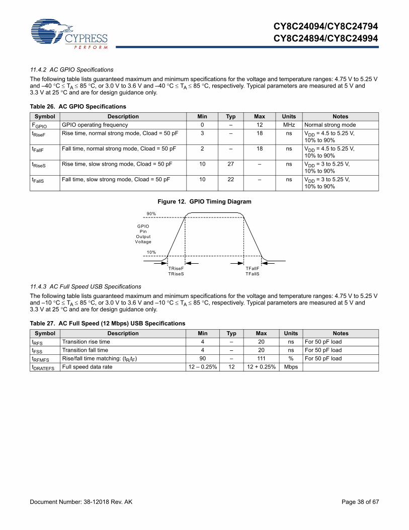
CY8C24094/CY8C24794CY8C24894/CY8C24994
Document Number: 38-12018 Rev. AK Page 38 of 67
11.4.2 AC GPIO Specifications
The following table lists guaranteed maximum and minimum specifications for the voltage and temperature ranges: 4.75 V to 5.25 V and –40 °C TA 85 °C, or 3.0 V to 3.6 V and –40 °C TA 85 °C, respectively. Typical parameters are measured at 5 V and 3.3 V at 25 °C and are for design guidance only.
Figure 12. GPIO Timing Diagram
11.4.3 AC Full Speed USB Specifications
The following table lists guaranteed maximum and minimum specifications for the voltage and temperature ranges: 4.75 V to 5.25 V and –10 °C TA 85 °C, or 3.0 V to 3.6 V and –10 °C TA 85 °C, respectively. Typical parameters are measured at 5 V and 3.3 V at 25 °C and are for design guidance only.
Table 26. AC GPIO Specifications
Symbol Description Min Typ Max Units Notes
FGPIO GPIO operating frequency 0 – 12 MHz Normal strong mode
tRiseF Rise time, normal strong mode, Cload = 50 pF 3 – 18 ns VDD = 4.5 to 5.25 V, 10% to 90%
tFallF Fall time, normal strong mode, Cload = 50 pF 2 – 18 ns VDD = 4.5 to 5.25 V, 10% to 90%
tRiseS Rise time, slow strong mode, Cload = 50 pF 10 27 – ns VDD = 3 to 5.25 V, 10% to 90%
tFallS Fall time, slow strong mode, Cload = 50 pF 10 22 – ns VDD = 3 to 5.25 V, 10% to 90%
TFallFTFallS
TRiseFTRiseS
90%
10%
GPIOPin
OutputVoltage
Table 27. AC Full Speed (12 Mbps) USB Specifications
Symbol Description Min Typ Max Units Notes
tRFS Transition rise time 4 – 20 ns For 50 pF load
tFSS Transition fall time 4 – 20 ns For 50 pF load
tRFMFS Rise/fall time matching: (tR/tF) 90 – 111 % For 50 pF load
tDRATEFS Full speed data rate 12 – 0.25% 12 12 + 0.25% Mbps

CY8C24094/CY8C24794CY8C24894/CY8C24994
Document Number: 38-12018 Rev. AK Page 39 of 67
11.4.4 AC Operational Amplifier Specifications
The following tables list guaranteed maximum and minimum specifications for the voltage and temperature ranges: 4.75 V to 5.25 V and –40 °C TA 85 °C, or 3.0 V to 3.6 V and –40 °C TA 85 °C, respectively. Typical parameters are measured at 5 V and 3.3 V at 25 °C and are for design guidance only.
Settling times, slew rates, and gain bandwidth are based on the analog continuous time PSoC block.
Power = high and Opamp bias = high is not supported at 3.3 V.
Table 28. 5-V AC Operational Amplifier Specifications
Symbol Description Min Typ Max Units
tROA Rising settling time from 80% of V to 0.1% of V (10 pF load, unity gain)Power = low, Opamp bias = lowPower = medium, Opamp bias = highPower = high, Opamp bias = high
–––
–––
3.90.720.62
µsµsµs
tSOA Falling settling time from 20% of V to 0.1% of V (10 pF load, unity gain)Power = low, Opamp bias = lowPower = medium, Opamp bias = highPower = high, Opamp bias = high
–––
–––
5.90.920.72
µsµsµs
SRROA Rising slew rate (20% to 80%)(10 pF load, unity gain)Power = low, Opamp bias = lowPower = medium, Opamp bias = highPower = high, Opamp bias = high
0.151.76.5
–––
–––
V/µsV/µsV/µs
SRFOA Falling slew rate (20% to 80%)(10 pF load, unity gain)Power = low, Opamp bias = lowPower = medium, Opamp bias = highPower = high, Opamp bias = high
0.010.54.0
–––
–––
V/µsV/µsV/µs
BWOA Gain bandwidth product Power = low, Opamp bias = lowPower = medium, Opamp bias = highPower = high, Opamp bias = high
0.753.15.4
–––
–––
MHzMHzMHz
ENOA Noise at 1 kHz (Power = medium, Opamp bias = high) – 100 – nV/rt-Hz
Table 29. 3.3-V AC Operational Amplifier Specifications
Symbol Description Min Typ Max Units
tROA Rising settling time from 80% of V to 0.1% of V (10 pF load, unity gain)Power = low, Opamp bias = lowPower = medium, Opamp bias = high
––
––
3.920.72
µsµs
tSOA Falling settling time from 20% of V to 0.1% of V (10 pF load, unity gain)Power = low, Opamp bias = lowPower = medium, Opamp bias = high
––
––
5.410.72
µsµs
SRROA Rising slew rate (20% to 80%)(10 pF load, unity gain)Power = low, Opamp bias = lowPower = medium, Opamp bias = high
0.312.7
––
––
V/µsV/µs
SRFOA Falling slew rate (20% to 80%)(10 pF load, Unity Gain)Power = low, Opamp bias = lowPower = medium, Opamp bias = high
0.241.8
––
––
V/µsV/µs
BWOA Gain bandwidth product Power = low, Opamp bias = lowPower = medium, Opamp bias = high
0.672.8
––
––
MHzMHz
ENOA Noise at 1 kHz (Power = medium, Opamp bias = high) – 100 – nV/rt-Hz

CY8C24094/CY8C24794CY8C24894/CY8C24994
Document Number: 38-12018 Rev. AK Page 40 of 67
When bypassed by a capacitor on P2[4], the noise of the analog ground signal distributed to each block is reduced by a factor of up to 5 (14 dB). This is at frequencies above the corner frequency defined by the on-chip 8.1 K resistance and the external capacitor.
Figure 13. Typical AGND Noise with P2[4] Bypass
At low frequencies, the opamp noise is proportional to 1/f, power independent, and determined by device geometry. At high frequencies, increased power level reduces the noise spectrum level.
Figure 14. Typical Opamp Noise
100
1000
10000
0.001 0.01 0.1 1 10 100Freq (kHz)
nV/rtHz
00.010.11.010
10
100
1000
10000
0.001 0.01 0.1 1 10 100Freq ( kHz)
nV/rtHz
PH_BHPH_BLPM_BLPL_BL

CY8C24094/CY8C24794CY8C24894/CY8C24994
Document Number: 38-12018 Rev. AK Page 41 of 67
11.4.5 AC Low Power Comparator Specifications
The following table lists guaranteed maximum and minimum specifications for the voltage and temperature ranges: 4.75 V to 5.25 V and –40 °C TA 85 °C or 3.0 V to 3.6 V and –40 °C TA 85 °C, respectively. Typical parameters are measured at 5 V at 25 °C and are for design guidance only.
11.4.6 AC Digital Block Specifications
The following table lists guaranteed maximum and minimum specifications for the voltage and temperature ranges: 4.75 V to 5.25 V and –40 °C TA 85 °C, or 3.0 V to 3.6 V and –40 °C TA 85 °C, respectively. Typical parameters apply to 5 V and 3.3 V at 25 °C and are for design guidance only.
Table 30. AC Low Power Comparator Specifications
Symbol Description Min Typ Max Units Notes
tRLPC LPC response time – – 50 µs 50 mV overdrive comparator reference set within VREFLPC.
Table 31. AC Digital Block Specifications
Function Description Min Typ Max Unit Notes
All functions Block input clock frequency
VDD 4.75 V – – 49.92 MHz
VDD < 4.75 V – – 25.92 MHz
Timer Input clock frequency
No capture, VDD 4.75 V – – 49.92 MHz
No capture, VDD < 4.75 V – – 25.92 MHz
With capture – – 25.92 MHz
Capture pulse width 50[33] – – ns
Counter Input clock frequency
No enable input, VDD 4.75 V – – 49.92 MHz
No enable input, VDD < 4.75 V – – 25.92 MHz
With enable input – – 25.92 MHz
Enable input pulse width 50[33] – – ns
Kill pulse width
Asynchronous restart mode 20 – – ns
Synchronous restart mode 50[33] – – ns
Disable mode 50[33] – – ns
Input clock frequency
VDD 4.75 V – – 49.92 MHz
VDD < 4.75 V – – 25.92 MHz
CRCPRS(PRS Mode)
Input clock frequency
VDD 4.75 V – – 49.92 MHz
VDD < 4.75 V – – 25.92 MHz
CRCPRS(CRC Mode)
Input clock frequency – – 24.6 MHz
SPIM Input clock frequency – – 8.2 MHz The SPI serial clock (SCLK) frequency is equal to the input clock frequency divided by 2.
SPIS Input clock (SCLK) frequency – – 4.1 MHz The input clock is the SPI SCLK in SPIS mode.
Width of SS_negated between transmissions
50[33] – – ns
Note33. 50 ns minimum input pulse width is based on the input synchronizers running at 24 MHz (42 ns nominal period).
CY8C24094/CY8C24794CY8C24894/CY8C24994
Document Number: 38-12018 Rev. AK Page 42 of 67
11.4.7 AC External Clock Specifications
The following tables list guaranteed maximum and minimum specifications for the voltage and temperature ranges: 4.75 V to 5.25 V and –40 °C TA 85 °C, or 3.0 V to 3.6 V and –40 °C TA 85 °C, respectively. Typical parameters are measured at 5 V and 3.3 V at 25 °C and are for design guidance only.
11.4.8 AC Analog Output Buffer Specifications
The following tables list guaranteed maximum and minimum specifications for the voltage and temperature ranges: 4.75 V to 5.25 V and –40 °C TA 85 °C, or 3.0 V to 3.6 V and –40 °C TA 85 °C, respectively. Typical parameters are measured at 5 V and 3.3 V at 25 °C and are for design guidance only.
Transmitter Input clock frequency The baud rate is equal to the input clock frequency divided by 8. VDD 4.75 V, 2 stop bits – – 49.92 MHz
VDD 4.75 V, 1 stop bit – – 24.6 MHz
VDD < 4.75 V – – 24.6 MHz
Receiver Input clock frequency The baud rate is equal to the input clock frequency divided by 8. VDD 4.75 V, 2 stop bits – – 49.92 MHz
VDD 4.75 V, 1 stop bit – – 24.6 MHz
VDD < 4.75 V – – 24.6 MHz
Table 31. AC Digital Block Specifications (continued)
Function Description Min Typ Max Unit Notes
Table 32. AC External Clock Specifications
Symbol Description Min Typ Max Units Notes
FOSCEXT Frequency for USB applications 23.94 24 24.06 MHz
– Duty cycle 47 50 53 %
– Power-up to IMO switch 150 – – µs
Table 33. 5-V AC Analog Output Buffer Specifications
Symbol Description Min Typ Max Units Notes
tROB Rising settling time to 0.1%, 1 V Step, 100 pF loadPower = lowPower = high
––
––
2.52.5
µsµs
tSOB Falling settling time to 0.1%, 1 V Step, 100 pF loadPower = low Power = high
––
––
2.22.2
µsµs
SRROB Rising slew rate (20% to 80%), 1 V Step, 100 pF loadPower = lowPower = high
0.650.65
––
––
V/µsV/µs
SRFOB Falling slew rate (80% to 20%), 1 V Step, 100 pF loadPower = lowPower = high
0.650.65
––
––
V/µsV/µs
BWOBSS Small signal bandwidth, 20 mVpp, 3 dB BW, 100 pF loadPower = lowPower = high
0.80.8
––
––
MHzMHz
BWOBLS Large signal bandwidth, 1 Vpp, 3 dB BW, 100 pF loadPower = lowPower = high
300300
––
––
kHzkHz

CY8C24094/CY8C24794CY8C24894/CY8C24994
Document Number: 38-12018 Rev. AK Page 43 of 67
11.4.9 AC Programming Specifications
The following table lists guaranteed maximum and minimum specifications for the voltage and temperature ranges: 4.75 V to 5.25 V and –40 °C TA 85 °C, or 3.0 V to 3.6 V and –40 °C TA 85 °C, respectively. Typical parameters are measured at to 5 V and 3.3 V at 25 °C and are for design guidance only.
Table 34. 3.3-V AC Analog Output Buffer Specifications
Symbol Description Min Typ Max Units Notes
tROB Rising settling time to 0.1%, 1 V Step, 100 pF load Power = low Power = high
––
––
3.83.8
µsµs
tSOB Falling settling time to 0.1%, 1 V Step, 100 pF load Power = low Power = high
––
––
2.62.6
µsµs
SRROB Rising slew rate (20% to 80%), 1 V Step, 100 pF load Power = low Power = high
0.50.5
––
––
V/µsV/µs
SRFOB Falling slew rate (80% to 20%), 1 V Step, 100 pF load Power = low Power = high
0.50.5
––
––
V/µsV/µs
BWOBSS Small signal bandwidth, 20 mVpp, 3dB BW, 100 pF load Power = low Power = high
0.70.7
––
––
MHzMHz
BWOBLS Large signal bandwidth, 1 Vpp, 3dB BW, 100 pF load Power = low Power = high
200200
––
––
kHzkHz
Table 35. AC Programming Specifications
Symbol Description Min Typ Max Units Notes
tRSCLK Rise time of SCLK 1 – 20 ns
tFSCLK Fall time of SCLK 1 – 20 ns
tSSCLK Data setup time to falling edge of SCLK 40 – – ns
tHSCLK Data hold time from falling edge of SCLK 40 – – ns
FSCLK Frequency of SCLK 0 – 8 MHz
tERASEB Flash erase time (block) – 10 – ms
tWRITE Flash block write time – 40 – ms
tDSCLK Data out delay from falling edge of SCLK – – 45 ns VDD 3.6
tDSCLK3 Data out delay from falling edge of SCLK – – 50 ns 3.0 VDD 3.6
tERASEALL Flash erase time (bulk) – 40 – ms Erase all blocks and protection fields at once
tPROGRAM_HOT Flash block erase + flash block write time – – 100[34] ms 0 °C Tj 100 C
tPROGRAM_COLD Flash block erase + flash block write time – – 200[34] ms –40 °C Tj 0 C
Note34. For the full industrial range, the user must employ a temperature sensor user module (FlashTemp) and feed the result to the temperature argument before writing.
See the Flash APIs application note Design Aids – Reading and Writing PSoC® Flash – AN2015 for more information.

CY8C24094/CY8C24794CY8C24894/CY8C24994
Document Number: 38-12018 Rev. AK Page 44 of 67
11.4.10 AC I2C Specifications
The following table lists guaranteed maximum and minimum specifications for the voltage and temperature ranges: 4.75 V to 5.25 V and –40 °C TA 85 °C, or 3.0 V to 3.6 V and –40 °C TA 85 °C, respectively. Typical parameters are measured at 5 V and 3.3 V at 25 °C and are for design guidance only.
Figure 15. Definition for Timing for Fast/Standard Mode on the I2C Bus
Table 36. AC Characteristics of the I2C SDA and SCL Pins for VDD
Symbol DescriptionStandard Mode Fast Mode
Units NotesMin Max Min Max
FSCLI2C SCL clock frequency 0 100 0 400 kHz
tHDSTAI2C Hold time (repeated) start condition. After this period, the first clock pulse is generated
4.0 – 0.6 – µs
tLOWI2C Low period of the SCL clock 4.7 – 1.3 – µs
tHIGHI2C High period of the SCL clock 4.0 – 0.6 – µs
tSUSTAI2C Setup time for a repeated start condition 4.7 – 0.6 – µs
tHDDATI2C Data hold time 0 – 0 – µs
tSUDATI2C Data setup time 250 – 100[35] – ns
tSUSTOI2C Setup time for stop condition 4.0 – 0.6 – µs
tBUFI2C Bus free time between a stop and start condition 4.7 – 1.3 – µs
tSPI2C Pulse width of spikes suppressed by the input filter
– – 0 50 ns
I2C_SDA
I2C_SCL
S Sr SP
TBUFI2C
TSPI2C
TSUSTOI2C
TSUSTAI2C
TLOWI2CTHIGHI2C
THDDATI2CTHDSTAI2C
TSUDATI2C
START Condition Repeated START Condition STOP Condition
Note35. A fast-mode I2C-bus device can be used in a standard-mode I2C-bus system, but the requirement tSU;DAT 250 ns it must meet. This automatically is the case if the
device does not stretch the LOW period of the SCL signal. If the device does stretch the LOW period of the SCL signal, it must output the next data bit to the SDA line trmax + tSU;DAT = 1000 + 250 = 1250 ns (according to the Standard-Mode I2C-bus specification) before the SCL line is released.

CY8C24094/CY8C24794CY8C24894/CY8C24994
Document Number: 38-12018 Rev. AK Page 45 of 67
11.5 Thermal Impedance
11.6 Solder Reflow Peak Specifications
Table 38 shows the solder reflow temperature limits that must not be exceeded.
Table 37. Thermal Impedances per Package
Package Typical JA [36]
56-Pin QFN[37] 12.93 °C/W
68-Pin QFN[37] 13.05 °C/W
100-Ball VFBGA 65 °C/W
100-Pin TQFP 51 °C/W
Table 38. Solder Reflow Specifications
Package Maximum PeakTemperature (TC)
Maximum Timeabove TC – 5 °C
56-Pin QFN 260 °C 30 seconds68-Pin QFN 260 °C 30 seconds100-Ball VFBGA 260 °C 30 seconds100-Pin TQFP 260 °C 30 seconds
Notes36. TJ = TA + POWER × JA. 37. To achieve the thermal impedance specified for the QFN package, see the Application Notes for Surface Mount Assembly of Amkor's MicroLeadFrame (MLF) Packages
available at http://www.amkor.com.

CY8C24094/CY8C24794CY8C24894/CY8C24994
Document Number: 38-12018 Rev. AK Page 46 of 67
12. Development Tool Selection
12.1 Software
12.1.1 PSoC Designer
At the core of the PSoC development software suite is PSoC Designer, used to generate PSoC firmware applications. PSoC Designer is available free of charge at http://www.cypress.com and includes a free C compiler.
12.1.2 PSoC Programmer
Flexible enough to be used on the bench in development, yet suitable for factory programming, PSoC Programmer works either as a standalone programming application or it can operate directly from PSoC Designer. PSoC Programmer software is compatible with both PSoC ICE-Cube in-circuit emulator and PSoC MiniProg. PSoC programmer is available free of charge at http://www.cypress.com.
12.2 Development Kits
All development kits can be purchased from the Cypress Online Store.
12.2.1 CY3215-DK Basic Development Kit
The CY3215-DK is for prototyping and development with PSoC Designer. This kit supports in-circuit emulation, and the software interface enables you to run, halt, and single step the processor, and view the content of specific memory locations. Advance emulation features are also supported through PSoC Designer. The kit includes:
■ PSoC Designer software CD
■ ICE-Cube in-circuit Emulator
■ ICE Flex-Pod for CY8C29x66 family
■ Cat-5 adapter
■ MiniEval programming board
■ 110 ~ 240 V power supply, Euro-Plug adapter
■ iMAGEcraft C compiler (registration required)
■ ISSP cable
■ USB 2.0 cable and Blue Cat-5 cable
■ Two CY8C29466-24PXI 28-PDIP chip samples
12.3 Evaluation Tools
All evaluation tools can be purchased from the Cypress Online Store.
12.3.1 CY3210-MiniProg1
The CY3210-MiniProg1 kit enables you to program PSoC devices via the MiniProg1 programming unit. The MiniProg is a small, compact prototyping programmer that connects to the PC via a provided USB 2.0 cable. The kit includes:
■ MiniProg programming unit
■ MiniEval socket programming and evaluation board
■ 28-Pin CY8C29466-24PXI PDIP PSoC device sample
■ 28-Pin CY8C27443-24PXI PDIP PSoC device sample
■ PSoC Designer software CD
■ Getting Started guide
■ USB 2.0 cable
12.3.2 CY3210-PSoCEval1
The CY3210-PSoCEval1 kit features an evaluation board and the MiniProg1 programming unit. The evaluation board includes an LCD module, potentiometer, LEDs, and plenty of bread-boarding space to meet all of your evaluation needs. The kit includes:
■ Evaluation board with LCD module
■ MiniProg programming unit
■ 28-Pin CY8C29466-24PXI PDIP PSoC device sample (2)
■ PSoC Designer software CD
■ Getting Started guide
■ USB 2.0 cable
12.3.3 CY3214-PSoCEvalUSB
The CY3214-PSoCEvalUSB evaluation kit features a devel-opment board for the CY8C24794-24LTXI PSoC device. The board supports both USB and capacitive sensing development and debugging support. This evaluation board also includes an LCD module, potentiometer, LEDs, an enunciator and plenty of breadboarding space to meet all of your evaluation needs. The kit includes:
■ PSoCEvalUSB board
■ LCD module
■ MIniProg programming unit
■ Mini USB cable
■ PSoC Designer and Example Projects CD
■ Getting Started guide
■ Wire pack
12.4 Device Programmers
All device programmers can be purchased from the Cypress Online Store.
12.4.1 CY3216 Modular Programmer
The CY3216 Modular Programmer kit features a modular programmer and the MiniProg1 programming unit. The modular programmer includes three programming module cards and supports multiple Cypress products. The kit includes:
■ Modular programmer base
■ Three programming module cards
■ MiniProg programming unit
■ PSoC Designer software CD

CY8C24094/CY8C24794CY8C24894/CY8C24994
Document Number: 38-12018 Rev. AK Page 47 of 67
■ Getting Started guide
■ USB 2.0 cable
12.4.2 CY3207ISSP In-System Serial Programmer (ISSP)
The CY3207ISSP is a production programmer. It includes protection circuitry and an industrial case that is more robust than the MiniProg in a production-programming environment.
Note: CY3207ISSP needs special software and is not compatible with PSoC Programmer. The kit includes:
■ CY3207 programmer unit
■ PSoC ISSP software CD
■ 110 ~ 240 V power supply, Euro-Plug adapter
■ USB 2.0 cable
12.5 Accessories (Emulation and Programming)
Table 39. Emulation and Programming Accessories
Part # Pin Package Flex-Pod Kit[38] Foot Kit[39] Adapter[40]
CY8C24794-24LQXI 56-pin QFN CY3250-24X94QFN None Adapters can be found at http://www.emulation.com.
Notes38. Flex-Pod kit includes a practice flex-pod and a practice PCB, in addition to two flex-pods.39. Foot kit includes surface mount feet that are soldered to the target PCB.40. Programming adapter converts non-DIP package to DIP footprint. Specific details and ordering information for each of the adapters are found at
http://www.emulation.com.

CY8C24094/CY8C24794CY8C24894/CY8C24994
Document Number: 38-12018 Rev. AK Page 48 of 67
13. Ordering Information
Note For die sales information, contact a local Cypress sales office or Field Applications Engineer (FAE).
13.1 Ordering Code Definitions
Table 40. CY8C24x94 PSoC Device’s Key Features and Ordering Information
Pa
cka
ge
Pa
cka
ge
dia
gra
m
Ord
erin
g
Co
de
Fla
sh
(B
ytes
)
SR
AM
(B
ytes
)
Tem
per
atu
re
Ran
ge
Dig
ital
Blo
cks
An
alo
g B
lock
s
Dig
ital
I/O
Pin
s
An
alo
g In
pu
ts
An
alo
g O
utp
uts
XR
ES
Pin
100-pin OCD TQFP[41] 51-85048 CY8C24094-24AXI 16 K 1 K –40 C to +85 C 4 6 56 48 2 Yes
56-pin (7 × 7 mm) QFN 001-58740 CY8C24794-24LQXI 16 K 1 K –40 °C to +85 °C 4 6 50 48 2 No
56-pin (7 × 7 mm) QFN (Tape and Reel)
CY8C24794-24LQXIT 16 K 1 K –40 °C to +85 °C 4 6 50 48 2 No
56-pin (8 × 8 mm) QFN (Sawn)
001-53450 CY8C24794-24LTXI 16 K 1 K –40 C to +85 C 4 6 50 48 2 No
56-pin (8 × 8 mm) QFN (Sawn) (Tape and Reel)
CY8C24794-24LTXIT 16 K 1 K –40 C to +85 C 4 6 50 48 2 No
56-pin (8 × 8 mm) QFN (Sawn)
001-53450 CY8C24894-24LTXI 16 K 1 K –40 C to +85 C 4 6 49 47 2 Yes
56-pin (8 × 8 mm) QFN (Sawn) (Tape and Reel)
CY8C24894-24LTXIT 16 K 1 K –40 C to +85 C 4 6 49 47 2 Yes
68-pin (8 × 8 mm) QFN (Sawn)
001-09618 CY8C24994-24LTXI 16 K 1 K –40 C to +85 C 4 6 56 48 2 Yes
68-pin QFN (8 × 8 mm) (Sawn) (Tape and Reel)
CY8C24994-24LTXIT 16 K 1 K –40 C to +85 C 4 6 56 48 2 Yes
CY
Package Type: T = Tape and Reel
PX = PDIP Pb-freeSX = SOIC Pb-freePVX = SSOP Pb-freeLFX = QFN (punched, 8 × 8 mm), Pb-freeLTX = QFN (sawn, 8 × 8 mm), Pb-freeLQX = QFN (sawn, 7 × 7 mm), Pb-freeAX = TQFP Pb-freeBVX = VFBGA Pb-free
Speed: 24 MHz
Part Number
Family Code
Technology Code: C = CMOSMarketing Code: 8 = PSoC
Company ID: CY = Cypress
8 C 24 XXX-SP XXT
Thermal Rating:
C = Commercial
I = Industrial
E = Extended
Note41. This part may be used for in-circuit debugging. It is NOT available for production.

CY8C24094/CY8C24794CY8C24894/CY8C24994
Document Number: 38-12018 Rev. AK Page 49 of 67
14. Packaging Dimensions
This section illustrates the package specification for the CY8C24x94 PSoC devices, along with the thermal impedance for the package and solder reflow peak temperatures.
Important Note Emulation tools may require a larger area on the target PCB than the chip's footprint. For a detailed description of the emulation tools' dimensions, refer to the emulator pod dimension drawings at http://www.cypress.com/design/MR10161.
Figure 16. 56-pin QFN (7 × 7 × 0.6 mm) LR56A/LQ56A 5.6 × 5.6 E-Pad (Sawn) Package Outline, 001-58740
001-58740 *B
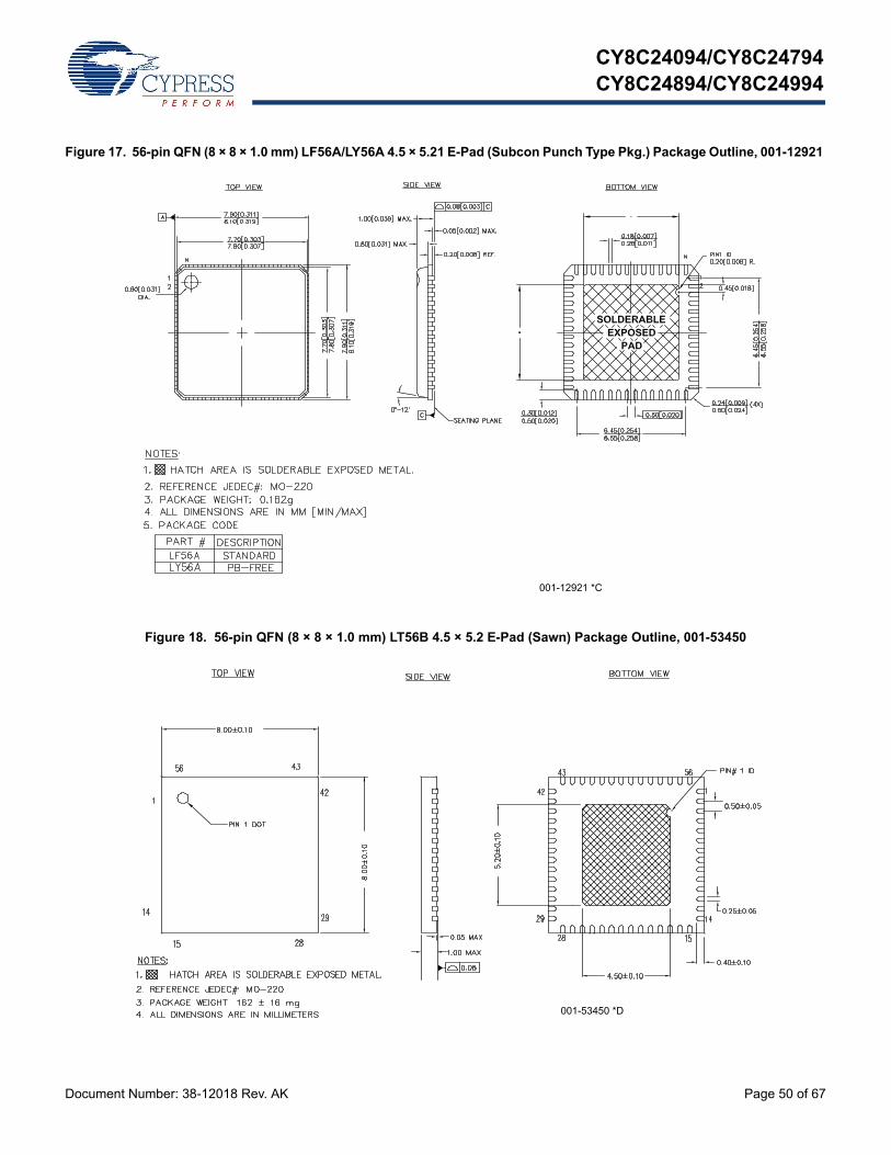
CY8C24094/CY8C24794CY8C24894/CY8C24994
Document Number: 38-12018 Rev. AK Page 50 of 67
Figure 17. 56-pin QFN (8 × 8 × 1.0 mm) LF56A/LY56A 4.5 × 5.21 E-Pad (Subcon Punch Type Pkg.) Package Outline, 001-12921
Figure 18. 56-pin QFN (8 × 8 × 1.0 mm) LT56B 4.5 × 5.2 E-Pad (Sawn) Package Outline, 001-53450
001-12921 *C
001-53450 *D

CY8C24094/CY8C24794CY8C24894/CY8C24994
Document Number: 38-12018 Rev. AK Page 51 of 67
Figure 19. 68-pin QFN (8 × 8 × 1.0 mm) LT68 5.7 × 5.7 E-Pad (Sawn Type) Package Outline, 001-09618
001-09618 *E

CY8C24094/CY8C24794CY8C24894/CY8C24994
Document Number: 38-12018 Rev. AK Page 52 of 67
Figure 20. 100-ball VFBGA (6 × 6 × 1.0 mm) BZ100 Package Outline, 51-85209
51-85209 *E

CY8C24094/CY8C24794CY8C24894/CY8C24994
Document Number: 38-12018 Rev. AK Page 53 of 67
Figure 21. 100-pin TQFP (14 × 14 × 1.4 mm) A100SA Package Outline, 51-85048
Important Note
■ For information on the preferred dimensions for mounting QFN packages, see the Application Note, Application Notes for Surface Mount Assembly of Amkor's MicroLeadFrame (MLF) Packages available at http://www.amkor.com.
■ Pinned vias for thermal conduction are not required for the low power PSoC device.
51-85048 *I

CY8C24094/CY8C24794CY8C24894/CY8C24994
Document Number: 38-12018 Rev. AK Page 54 of 67
15. Acronyms
15.1 Acronyms Used
The following table lists the acronyms that are used in this document.
Acronym Description Acronym Description
AC alternating current MIPS million instructions per second
ADC analog-to-digital converter OCD on-chip debug
API application programming interface PCB printed circuit board
CMOS complementary metal oxide semiconductor PDIP plastic dual-in-line package
CPU central processing unit PGA programmable gain amplifier
CRC cyclic redundancy check POR power-on reset
CT continuous time PPOR precision power-on reset
DAC digital-to-analog converter PRS pseudo-random sequence
DC direct current PSoC® Programmable System-on-Chip™
DTMF dual-tone multi-frequency PWM pulse-width modulator
EEPROM electrically erasable programmable read-only memory
QFN quad flat no leads
GPIO general purpose I/O SAR successive approximation register
ICE in-circuit emulator SC switched capacitor
IDE integrated development environment SLIMO slow IMO
ILO internal low-speed oscillator SOIC small-outline integrated circuit
IMO internal main oscillator SPI™ serial peripheral interface
I/O input/output SRAM static random-access memory
IrDA infrared data association SROM supervisory read-only memory
ISSP In-System Serial Programming TQFP thin quad flat pack
LCD liquid crystal display UART universal asynchronous receiver / transmitter
LED light-emitting diode USB universal serial bus
LPC low power comparator VFBGA very fine-pitch ball grid array
LVD low-voltage detect WDT watchdog timer
MAC multiply-accumulate XRES external reset
MCU microcontroller unit

CY8C24094/CY8C24794CY8C24894/CY8C24994
Document Number: 38-12018 Rev. AK Page 55 of 67
16. Document Conventions
16.1 Units of Measure
16.2 Numeric Conventions
Hexadecimal numbers are represented with all letters in uppercase with an appended lowercase ‘h’ (for example, ‘14h’ or ‘3Ah’). Hexadecimal numbers may also be represented by a ‘0x’ prefix, the C coding convention. Binary numbers have an appended lowercase ‘b’ (for example, ‘01010100b’ or ‘01000011b’). Numbers not indicated by an ‘h’ or ‘b’ are decimal.
Symbol Unit of Measure Symbol Unit of Measure
°C degree Celsius mV millivolt
dB decibels nA nanoampere
fF femtofarad ns nanosecond
kHz kilohertz nV nanovolt
k kilohms ohms
MHz megahertz pA picoampere
A microampere pF picofarad
s microsecond ps picosecond
V microvolt % percent
mA milliampere rt-Hz root hertz
mm millimeter V volt
ms millisecond W watt
17. Glossary
active high 6. A logic signal having its asserted state as the logic 1 state.
7. A logic signal having the logic 1 state as the higher voltage of the two states.
analog blocks The basic programmable opamp circuits. These are SC (switched capacitor) and CT (continuous time) blocks. These blocks can be interconnected to provide ADCs, DACs, multi-pole filters, gain stages, and much more.
analog-to-digital (ADC)
A device that changes an analog signal to a digital signal of corresponding magnitude. Typically, an ADC converts a voltage to a digital number. The digital-to-analog (DAC) converter performs the reverse operation.
API (Application Programming Interface)
A series of software routines that comprise an interface between a computer application and lower level services and functions (for example, user modules and libraries). APIs serve as building blocks for programmers that create software applications.
asynchronous A signal whose data is acknowledged or acted upon immediately, irrespective of any clock signal.
Bandgap reference
A stable voltage reference design that matches the positive temperature coefficient of VT with the negative temperature coefficient of VBE, to produce a zero temperature coefficient (ideally) reference.
bandwidth 1. The frequency range of a message or information processing system measured in hertz.
2. The width of the spectral region over which an amplifier (or absorber) has substantial gain (or loss); it is sometimes represented more specifically as, for example, full width at half maximum.
bias 1. A systematic deviation of a value from a reference value.
2. The amount by which the average of a set of values departs from a reference value.
3. The electrical, mechanical, magnetic, or other force (field) applied to a device to establish a reference level to operate the device.

CY8C24094/CY8C24794CY8C24894/CY8C24994
Document Number: 38-12018 Rev. AK Page 56 of 67
block 1. A functional unit that performs a single function, such as an oscillator.
2. A functional unit that may be configured to perform one of several functions, such as a digital PSoC block or an analog PSoC block.
buffer 1. A storage area for data that is used to compensate for a speed difference, when transferring data from one device to another. Usually refers to an area reserved for IO operations, into which data is read, or from which data is written.
2. A portion of memory set aside to store data, often before it is sent to an external device or as it is received from an external device.
3. An amplifier used to lower the output impedance of a system.
bus 1. A named connection of nets. Bundling nets together in a bus makes it easier to route nets with similar routing patterns.
2. A set of signals performing a common function and carrying similar data. Typically represented using vector notation; for example, address[7:0].
3. One or more conductors that serve as a common connection for a group of related devices.
clock The device that generates a periodic signal with a fixed frequency and duty cycle. A clock is sometimes used to synchronize different logic blocks.
comparator An electronic circuit that produces an output voltage or current whenever two input levels simultaneously satisfy predetermined amplitude requirements.
compiler A program that translates a high level language, such as C, into machine language.
configuration space
In PSoC devices, the register space accessed when the XIO bit, in the CPU_F register, is set to ‘1’.
crystal oscillator An oscillator in which the frequency is controlled by a piezoelectric crystal. Typically a piezoelectric crystal is less sensitive to ambient temperature than other circuit components.
cyclic redundancy check (CRC)
A calculation used to detect errors in data communications, typically performed using a linear feedback shift register. Similar calculations may be used for a variety of other purposes such as data compression.
data bus A bi-directional set of signals used by a computer to convey information from a memory location to the central processing unit and vice versa. More generally, a set of signals used to convey data between digital functions.
debugger A hardware and software system that allows the user to analyze the operation of the system under development. A debugger usually allows the developer to step through the firmware one step at a time, set break points, and analyze memory.
dead band A period of time when neither of two or more signals are in their active state or in transition.
digital blocks The 8-bit logic blocks that can act as a counter, timer, serial receiver, serial transmitter, CRC generator, pseudo-random number generator, or SPI.
digital-to-analog (DAC)
A device that changes a digital signal to an analog signal of corresponding magnitude. The analog-to-digital (ADC) converter performs the reverse operation.
duty cycle The relationship of a clock period high time to its low time, expressed as a percent.
emulator Duplicates (provides an emulation of) the functions of one system with a different system, so that the second system appears to behave like the first system.
17. Glossary (continued)

CY8C24094/CY8C24794CY8C24894/CY8C24994
Document Number: 38-12018 Rev. AK Page 57 of 67
external reset (XRES)
An active high signal that is driven into the PSoC device. It causes all operation of the CPU and blocks to stop and return to a pre-defined state.
flash An electrically programmable and erasable, non-volatile technology that provides users with the programmability and data storage of EPROMs, plus in-system erasability. Non-volatile means that the data is retained when power is off.
Flash block The smallest amount of Flash ROM space that may be programmed at one time and the smallest amount of Flash space that may be protected. A Flash block holds 64 bytes.
frequency The number of cycles or events per unit of time, for a periodic function.
gain The ratio of output current, voltage, or power to input current, voltage, or power, respectively. Gain is usually expressed in dB.
I2C A two-wire serial computer bus by Philips Semiconductors (now NXP Semiconductors). I2C is an Inter-Integrated Circuit. It is used to connect low-speed peripherals in an embedded system. The original system was created in the early 1980s as a battery control interface, but it was later used as a simple internal bus system for building control electronics. I2C uses only two bi-directional pins, clock and data, both running at +5V and pulled high with resistors. The bus operates at 100 kbits/second in standard mode and 400 kbits/second in fast mode.
ICE The in-circuit emulator that allows users to test the project in a hardware environment, while viewing the debugging device activity in a software environment (PSoC Designer).
input/output (I/O) A device that introduces data into or extracts data from a system.
interrupt A suspension of a process, such as the execution of a computer program, caused by an event external to that process, and performed in such a way that the process can be resumed.
interrupt service routine (ISR)
A block of code that normal code execution is diverted to when the M8C receives a hardware interrupt. Many interrupt sources may each exist with its own priority and individual ISR code block. Each ISR code block ends with the RETI instruction, returning the device to the point in the program where it left normal program execution.
jitter 1. A misplacement of the timing of a transition from its ideal position. A typical form of corruption that occurs on serial data streams.
2. The abrupt and unwanted variations of one or more signal characteristics, such as the interval between successive pulses, the amplitude of successive cycles, or the frequency or phase of successive cycles.
low-voltage detect (LVD)
A circuit that senses VDD and provides an interrupt to the system when VDD falls lower than a selected threshold.
M8C An 8-bit Harvard-architecture microprocessor. The microprocessor coordinates all activity inside a PSoC by interfacing to the Flash, SRAM, and register space.
master device A device that controls the timing for data exchanges between two devices. Or when devices are cascaded in width, the master device is the one that controls the timing for data exchanges between the cascaded devices and an external interface. The controlled device is called the slave device.
microcontroller An integrated circuit chip that is designed primarily for control systems and products. In addition to a CPU, a microcontroller typically includes memory, timing circuits, and IO circuitry. The reason for this is to permit the realization of a controller with a minimal quantity of chips, thus achieving maximal possible miniaturization. This in turn, reduces the volume and the cost of the controller. The microcontroller is normally not used for general-purpose computation as is a microprocessor.
mixed-signal The reference to a circuit containing both analog and digital techniques and components.
17. Glossary (continued)

CY8C24094/CY8C24794CY8C24894/CY8C24994
Document Number: 38-12018 Rev. AK Page 58 of 67
modulator A device that imposes a signal on a carrier.
noise 1. A disturbance that affects a signal and that may distort the information carried by the signal.
2. The random variations of one or more characteristics of any entity such as voltage, current, or data.
oscillator A circuit that may be crystal controlled and is used to generate a clock frequency.
parity A technique for testing transmitting data. Typically, a binary digit is added to the data to make the sum of all the digits of the binary data either always even (even parity) or always odd (odd parity).
phase-locked loop (PLL)
An electronic circuit that controls an oscillator so that it maintains a constant phase angle relative to a reference signal.
pinouts The pin number assignment: the relation between the logical inputs and outputs of the PSoC device and their physical counterparts in the printed circuit board (PCB) package. Pinouts involve pin numbers as a link between schematic and PCB design (both being computer generated files) and may also involve pin names.
port A group of pins, usually eight.
power on reset (POR)
A circuit that forces the PSoC device to reset when the voltage is lower than a pre-set level. This is one type of hardware reset.
PSoC® Cypress Semiconductor’s PSoC® is a registered trademark and Programmable System-on-Chip™ is a trademark of Cypress.
PSoC Designer™ The software for Cypress’ Programmable System-on-Chip technology.
pulse width modulator (PWM)
An output in the form of duty cycle which varies as a function of the applied measurand
RAM An acronym for random access memory. A data-storage device from which data can be read out and new data can be written in.
register A storage device with a specific capacity, such as a bit or byte.
reset A means of bringing a system back to a know state. See hardware reset and software reset.
ROM An acronym for read only memory. A data-storage device from which data can be read out, but new data cannot be written in.
serial 1. Pertaining to a process in which all events occur one after the other.
2. Pertaining to the sequential or consecutive occurrence of two or more related activities in a single device or channel.
settling time The time it takes for an output signal or value to stabilize after the input has changed from one value to another.
shift register A memory storage device that sequentially shifts a word either left or right to output a stream of serial data.
slave device A device that allows another device to control the timing for data exchanges between two devices. Or when devices are cascaded in width, the slave device is the one that allows another device to control the timing of data exchanges between the cascaded devices and an external interface. The controlling device is called the master device.
17. Glossary (continued)

CY8C24094/CY8C24794CY8C24894/CY8C24994
Document Number: 38-12018 Rev. AK Page 59 of 67
SRAM An acronym for static random access memory. A memory device allowing users to store and retrieve data at a high rate of speed. The term static is used because, after a value has been loaded into an SRAM cell, it remains unchanged until it is explicitly altered or until power is removed from the device.
SROM An acronym for supervisory read only memory. The SROM holds code that is used to boot the device, calibrate circuitry, and perform Flash operations. The functions of the SROM may be accessed in normal user code, operating from Flash.
stop bit A signal following a character or block that prepares the receiving device to receive the next character or block.
synchronous 1. A signal whose data is not acknowledged or acted upon until the next active edge of a clock signal.
2. A system whose operation is synchronized by a clock signal.
tristate A function whose output can adopt three states: 0, 1, and Z (high-impedance). The function does not drive any value in the Z state and, in many respects, may be considered to be disconnected from the rest of the circuit, allowing another output to drive the same net.
UART A UART or universal asynchronous receiver-transmitter translates between parallel bits of data and serial bits.
user modules Pre-build, pre-tested hardware/firmware peripheral functions that take care of managing and configuring the lower level Analog and Digital PSoC Blocks. User Modules also provide high level API (Application Programming Interface) for the peripheral function.
user space The bank 0 space of the register map. The registers in this bank are more likely to be modified during normal program execution and not just during initialization. Registers in bank 1 are most likely to be modified only during the initialization phase of the program.
VDD A name for a power net meaning "voltage drain." The most positive power supply signal. Usually 5 V or 3.3 V.
VSS A name for a power net meaning "voltage source." The most negative power supply signal.
watchdog timer A timer that must be serviced periodically. If it is not serviced, the CPU resets after a specified period of time.
17. Glossary (continued)

CY8C24094/CY8C24794CY8C24894/CY8C24994
Document Number: 38-12018 Rev. AK Page 60 of 67
18. Errata
This section describes the errata for the CY8C24x94 device. Details include errata trigger conditions, scope of impact, availableworkaround, and silicon revision applicability. Contact your local Cypress Sales Representative if you have questions.
Part Numbers Affected
CY8C24x94 Errata Summary
The following table defines the errata applicability to available devices.
1. The DP line of the USB interface may pulse low when the PSoC device wakes from sleep causing an unexpected wake-up of the host computer.
■ PROBLEM DEFINITION
When the device is operating at 4.75 V to 5.25 V and the 3.3 V regulator is enabled, a short low pulse may be created on the DPsignal line during device wake-up. The 15-20 µs low pulse of the DP line may be interpreted by the host computer as a deattachor the beginning of a wake-up.
■ TRIGGER CONDITION(S)
The bandgap reference voltage used by the 3.3 V regulator decreases during sleep due to leakage. Upon device wake up, thebandgap is reenabled and after a delay for settling, the 3.3 V regulator is enabled. On some devices the 3.3 V regulator that isused to generate the USB DP signal may be enabled before the bandgap is fully stabilized. This can cause a low pulse on theregulator output and DP signal line until the bandgap stabilizes. In applications where Vdd is 3.3 V, the regulator is not used andtherefore the DP low pulse is not generated.
■ WORKAROUND
To prevent the DP signal from pulsing low, keep the bandgap enabled during sleep. The most efficient method is to set the No Buzzbit in the OSC_CR0 register. The No Buzz bit keeps the bandgap powered and output stable during sleep. Setting the No Buzz bitresults in nominal 100 µA increase to sleep current. Leaving the analog reference block enabled during sleep also resolves thisissue because it forces the bandgap to remain enabled. An example for disabling the No Buzz bit is listed below.
AssemblyM8C_SetBank1or reg[OSC_CR0], 0x20M8C_SetBank0
COSC_CR0 |= 0x20;
Part Number
CY8C24x94
Items Part Number
1. The DP line of the USB interface may pulse low when the PSoC device wakes from sleep causing an unexpected wake-up of the host computer.
CY8C24x94
2. Invalid Flash reads may occur if Vdd is pulled to -0.5 V just before power on. CY8C24x94
3. PMA Index Register fails to auto-increment with CPU_Clock set to SysClk/1 (24 MHz). CY8C24x94
4. The Internal Main Oscillator (IMO) frequency parameter (FIMO245V) may increase over a period of time during usage in the field and exceed the maximum spec limit of 24.96 MHz.
CY8C24x94

CY8C24094/CY8C24794CY8C24894/CY8C24994
Document Number: 38-12018 Rev. AK Page 61 of 67
2. Invalid Flash reads may occur if Vdd is pulled to -0.5 V just before power on.
■ PROBLEM DEFINITION
When Vdd of the device is pulled below ground just before power on, the first read from each 8K Flash page may be corrupted.This issue does not affect Flash page 0 because it is the selected page upon reset.
■ TRIGGER CONDITION(S)
When Vdd is pulled below ground before power on, an internal Flash reference may deviate from its nominal voltage. The referencedeviation tends to result in the first Flash read from that page returning 0xFF. During the first read from each page, the referenceis reset resulting in all future reads returning the correct value. A short delay of 5 µs before the first real read provides time for thereference voltage to stabilize.
■ WORKAROUND
To prevent an invalid Flash read, a dummy read from each Flash page must occur before use of the pages. A delay of 5 µs mustoccur after the dummy read and before a real read. The dummy reads occurs as soon as possible and must be located in Flashpage 0 before a read from any other Flash page. An example for reading a byte of memory from each Flash page is listed below.Placed it in boot.tpl and boot.asm immediately after the ‘start:’ label.
// dummy read from each 8K Flash page// page 1mov A, 0x20 // MSBmov X, 0x00 // LSBromx// wait at least 5 µsmov X, 14loop1:dec Xjnz loop1

CY8C24094/CY8C24794CY8C24894/CY8C24994
Document Number: 38-12018 Rev. AK Page 62 of 67
3. PMA Index Register fails to auto-increment with CPU_Clock set to SysClk/1 (24 MHz).
■ PROBLEM DEFINITION
When the device is operating at 4.75 to 5.25 V and the CPU_Clock is set to SysClk/1 (24 MHz), the USB PMA Index Register mayfail to increment automatically when used in an OUT endpoint configuration at Full-Speed. When the application program attemptsto use the bReadOutEP() function the first byte in the PMA buffer is always returned.
■ TRIGGER CONDITION(S)
An internal flip-flop hold problem associated with Index Register increment function. All reads of the associated RAM originate fromthe first byte. The hold problem has no impact on other circuits or functions within the device.
■ WORKAROUND
To make certain that the index register properly increments, set the CPU_Clock to SysClk/2 (12 MHz) during the read of the PMAbuffer. An example for the clock adjustment method is listed below.
PSoC Designer™ 4.3 User Module workaround: PSoC Designer Release 4.3 and subsequent releases includes a revisedfull-speed USB User Module with the revised firmware work-around included (see example below).
;;;; 24 MHz read PMA workaround;;M8C_SetBank1mov A, reg[OSC_CR0]push Aand A, 0xf8 ;clear the clock bits (briefly chg the cpu_clk to 3 MHz)or A, 0x02 ;will set clk to 12Mhz
mov reg[OSC_CR0],A ;clk is now set at 12 MHzM8C_SetBank0.loop: mov A, reg[PMA0_DR] ; Get the data from the PMA space mov [X], A ; save it in data array inc X ; increment the pointer dec [USB_APITemp+1] ; decrement the counter jnz .loop ; wait for count to zero out;;;; 24MHz read PMA workaround (back to previous clock speed);;pop A ;recover previous reg[OSC_CR0] valueM8C_SetBank1mov reg[OSC_CR0],A ;clk is now set at previous valueM8C_SetBank0;;;; end 24Mhz read PMA workaround

CY8C24094/CY8C24794CY8C24894/CY8C24994
Document Number: 38-12018 Rev. AK Page 63 of 67
4. The Internal Main Oscillator (IMO) frequency parameter (FIMO245V) may increase over a period of time during usage in the field and exceed the maximum spec limit of 24.96 MHz.
■ PROBLEM DEFINITION
When the device has been operating at 4.75 V to 5.25 V for a cumulatively long duration in the field, the IMO Frequency may slowlyincrease over the duration of usage in the field and eventually exceed the maximum spec limit of 24.96 MHz. This may affectapplications that are sensitive to the max value of IMO frequency, such as those using UART communication and result in afunctional failure.
■ TRIGGER CONDITION(S)
Very long (cumulative) usage of the device in the operating voltage range of 4.75V to 5.25V, with the IMO clock runningcontinuously, could lead to the degradation. Higher power supply voltage and lower ambient temperature are worst-case conditionsfor the degradation.
■ WORKAROUND
Operating the device with the power supply voltage range of 3.0 V to 3.6 V, would avoid the degradation of IMO Frequency beyondthe max spec limit of 24.96 MHz.
■ FIX STATUS
A new revision of the silicon, with a fix for this issue, is expected to be available from August 1st 2015.

CY8C24094/CY8C24794CY8C24894/CY8C24994
Document Number: 38-12018 Rev. AK Page 64 of 67
19. Document History Page
Document Title: CY8C24094/CY8C24794/CY8C24894/CY8C24994, PSoC® Programmable System-on-Chip™Document Number: 38-12018
Revision ECNOrig. of Change
Submission Date
Description of Change
** 133189 NWJ 01/27/2004 New silicon and new document – Advance datasheet.
*A 251672 SFV See ECN First Preliminary datasheet. Changed title to encompass only the CY8C24794 because the CY8C24494 and CY8C24694 are not being offered by Cypress.
*B 289742 HMT See ECN Add standard DS items from SFV memo. Add Analog Input Mux on pinouts. 2 MACs. Change 512 bytes of SRAM to 1 K. Add dimension key to package. Remove HAPI. Update diagrams, registers and specs.
*C 335236 HMT See ECN Add CY logo. Update CY copyright. Update new CY.com URLs. Re-add ISSP programming pinout notation. Add Reflow Temp. table. Update features (MAC, Oscillator, and voltage range), registers (INT_CLR2/MSK2, second MAC), and specs. (Rext, IMO, analog output buffer...).
*D 344318 HMT See ECN Add new color and logo. Expand analog arch. diagram. Fix I/O #. Update Electrical Specifications.
*E 346774 HMT See ECN Add USB temperature specifications. Make datasheet Final.
*F 349566 HMT See ECN Remove USB logo. Add URL to preferred dimensions for mounting MLF packages.
*G 393164 HMT See ECN Add new device, CY8C24894 56-pin MLF with XRES pin. Add Fimousb3v char. to specs. Upgrade to CY Perform logo and update corporate address and copyright.
*H 469243 HMT See ECN Add ISSP note to pinout tables. Update typical and recommended Storage Temperature per industrial specs. Update Low Output Level maximum I/OL budget. Add FLS_PR1 to Register Map Bank 1 for users to specify which Flash bank should be used for SROM operations. Add two new devices for a 68-pin QFN and 100-ball VFBGA under RPNs: CY8C24094 and CY8C24994. Add two packages for 68-pin QFN. Add OCD non-production pinouts and package diagrams. Update CY branding and QFN convention. Add new Dev. Tool section. Update copyright and trademarks.
*I 561158 HMT See ECN Add Low Power Comparator (LPC) AC/DC electrical spec. tables. Add CY8C20x34 to PSoC Device Characteristics table. Add detailed dimensions to 56-pin QFN package diagram and update revision. Secure one package diagram/manufacturing per QFN. Update emulation pod/feet kit part numbers. Fix pinout type-o per TestTrack.
*J 728238 HMT See ECN Add CapSense SNR requirement reference. Update figure standards. Update Technical Training paragraphs. Add QFN package clarifications and dimen-sions. Update ECN-ed Amkor dimensioned QFN package diagram revisions. Reword SNR reference. Add new 56-pin QFN spec.
*K 2552459 AZIE / PYRS
08/14/08 Add footnote on AGND descriptions to avoid using P2[4] for digital signaling as it may add noise to AGND. Remove reference to CMP_GO_EN1 in Map Bank 1 Table on Address 65; this register has no functionality on 24xxx. Add footnote on die sales. Add description 'Optional External Clock Input’ on P1[4] to match description of P1[4].
*L 2616550 OGNE / PYRS
12/05/08 Updated Programmable Pin Configuration detail.Changed title from PSoC® Mixed-Signal Array to PSoC® Programmable System-on-Chip™
*M 2657956 DPT / PYRS
02/11/09 Added package diagram 001-09618 and updated Ordering Information table

CY8C24094/CY8C24794CY8C24894/CY8C24994
Document Number: 38-12018 Rev. AK Page 65 of 67
*N 2708135 BRW 05/18/2009 Added Note in the Pin Information section on page 8.Removed reference to Hi-Tech Lite Compiler in the section Development Tools Selection on page 42.
*O 2718162 DPT 06/11/2009 Added 56-Pin QFN (Sawn) package diagram and updated ordering information
*P 2762161 RLRM 09/10/2009 Updated the following parameters:DCILO, F32K_U, FIMO6, TPOWERUP, TERASE_ALL, TPROGRAM_HOT, and TPROGRAM_COLD. Added SRPOWER_UP parameter in AC specs table.
*Q 2768530 RLRM 09/24/09 Ordering Information table: Changed XRES Pin value for CY8C24894-24LTXI and CY8C24894-24LTXIT to ‘Yes’.
*R 2817938 KRIS 11/30/09 Ordering Information: Updated CY8C24894-24LTXI and CY8C24894-24LTXIT parts as Sawn and updated the Digital I/O and Analog Pin valuesAdded Contents page. Updated 68 QFN package diagram (51-85124)
*S 2846641 RLRM 1/12/10 Added package diagram 001-58740 and updated Development Tools section.
*T 2867363 ANUP 01/27/10 Modified Note 9 to remove voltage range 2.4 V to 3.0 V
*U 2901653 NJF 03/30/2010 Updated Cypress website linksAdded TXRST, DC24M, TBAKETEMP and TBAKETIME parametersRemoved reference to 2.4 VRemoved sections ‘Third Party Tools’ ‘Build a PSoC Emulator into your Board’Updated package diagramsRemoved inactive parts from ordering information table.
*V 2938528 VMAD 05/28/2010 Updated content to match current style guide and datasheet template. No technical updates
*W 3028596 NJF 09/20/10 Added PSoC Device Characteristics table.Added DC I2C Specifications table.Added F32K_U max limit.Added Tjit_IMO specification, removed existing jitter specifications.Updated Analog reference tables.Updated Units of Measure, Acronyms, Glossary, and References sections.Updated solder reflow specifications.No specific changes were made to AC Digital Block Specifications table and I2C Timing Diagram. They were updated for clearer understanding.Updated Figure 12 since the labelling for y-axis was incorrect.Template and styles update.
*X 3082244 NXZ 11/09/2010 Sunset review; no updates.
*Y 3111357 BTK / NJF / ARVM
12/15/10 Updated solder reflow specifications.Removed FIMO6 spec from AC chip-level specifications table.Removed the following pruned parts from the ordering information table and their references in the datasheet.1) CY8C24794-24LFXI2) CY8C24794-24LFXIT3) CY8C24894-24LFXI4) CY8C24894-24LFXIT
*Z 3126167 BTK / ANBA /
PKS
01/03/11 Updated ordering information.Removed the package diagram spec 51-85214 since there are no MPNs in the ordering information table that corresponds with this package.Updated ordering code definitions for clearer understanding.
AA 3367463 BTK / GIR 09/22/11 Updated VREFHI values for parameter ‘0b100’ under Table 19 on page 30.Updated text under Table 19 on page 30.The text “Pin must be left floating” is included under Description of NC pin in Table 4 on page 11, Table 6 on page 13, Table 7 on page 15, and Table 8 on page 17.Updated Table 38 on page 45 to give more clarity.
AB 3404970 MATT 10/13/11 Removed prune device CY8C24994-24BVXI from Ordering Information.
AC 3461872 CSAI 12/13/2011 Sunset review; no content update
19. Document History Page (continued)
Document Title: CY8C24094/CY8C24794/CY8C24894/CY8C24994, PSoC® Programmable System-on-Chip™Document Number: 38-12018

CY8C24094/CY8C24794CY8C24894/CY8C24994
Document Number: 38-12018 Rev. AK Page 66 of 67
AD 3503402 PMAD 01/20/2012 Updated VOH and VOL section in Table 12.
AE 3545509 PSAI 03/08/2012 Updated link to 'Technical reference Manual'.
AF 3862667 CSAI 01/09/2013 Updated Ordering Information (Updated part numbers).
Updated Packaging Dimensions:spec 001-53450 – Changed revision from *B to *C.spec 001-09618 – Changed revision from *D to *E.spec 51-85048 – Changed revision from *E to *G.
AG 3979302 CSAI 04/23/2013 Updated Packaging Dimensions:spec 001-58740 – Changed revision from ** to *A.Added Errata.
AH 4074544 CSAI 07/23/2013 Added Errata Footnotes (Note 21, 23)
Updated Electrical Specifications:Updated DC Electrical Characteristics:Updated DC Chip-Level Specifications:Added Note 21 and referred the same note in “Sleep Mode” in description of ISB parameter in Table 11.Updated DC POR and LVD Specifications:Added Note 23 and referred the same note in VPPOR0, VPPOR1, VPPOR2 parameters in Table 22.
Updated to new template.
AI 4596835 DIMA 12/15/2014 Updated Pin Information:Updated 56-Pin Part Pinout:Updated Table 2:Added Note 5 and referred the same note in description of pin 19 and pin 50.Updated 56-Pin Part Pinout (with XRES):Updated Table 3:Added Note 8 and referred the same note in description of pin 19 and pin 50.Updated 68-Pin Part Pinout:Updated Table 4:Added Note 10 and referred the same note in description of pin 7, pin 20 and pin 60.Updated 68-Pin Part Pinout (On-Chip Debug):Updated Table 5:Added Note 13 and referred the same note in description of pin 7, pin 20 and pin 60.Updated 100-Ball VFBGA Part Pinout:Updated Table 6:Added Note 15 and referred the same note in caption of Table 6.Updated 100-Ball VFBGA Part Pinout (On-Chip Debug):Updated Table 7:Added Note 17 and referred the same note in caption of Table 7.Updated 100-Pin Part Pinout (On-Chip Debug):Updated Table 8:Added Note 19 and referred the same note in caption of Table 8.
Updated Packaging Dimensions:spec 001-12921 – Changed revision from *B to *C.spec 001-53450 – Changed revision from *C to *D.spec 51-85209 – Changed revision from *D to *E.spec 51-85048 – Changed revision from *G to *I.
Completing Sunset Review.
AJ 4622083 SLAN 01/13/2015 Added More Information section.
AK 4684565 PSI 03/12/2015 Updated Packaging Dimensions:spec 001-58740 – Changed revision from *A to *B.Updated Errata.
19. Document History Page (continued)
Document Title: CY8C24094/CY8C24794/CY8C24894/CY8C24994, PSoC® Programmable System-on-Chip™Document Number: 38-12018
Document Number: 38-12018 Rev. AK Revised March 12, 2015 Page 67 of 67
PSoC Designer™ is a trademark and PSoC® is a registered trademark of Cypress Semiconductor Corp. All other trademarks or registered trademarks referenced herein are property of the respectivecorporations.
CY8C24094/CY8C24794CY8C24894/CY8C24994
© Cypress Semiconductor Corporation, 2004-2015. The information contained herein is subject to change without notice. Cypress Semiconductor Corporation assumes no responsibility for the use ofany circuitry other than circuitry embodied in a Cypress product. Nor does it convey or imply any license under patent or other rights. Cypress products are not warranted nor intended to be used formedical, life support, life saving, critical control or safety applications, unless pursuant to an express written agreement with Cypress. Furthermore, Cypress does not authorize its products for use ascritical components in life-support systems where a malfunction or failure may reasonably be expected to result in significant injury to the user. The inclusion of Cypress products in life-support systemsapplication implies that the manufacturer assumes all risk of such use and in doing so indemnifies Cypress against all charges.
Any Source Code (software and/or firmware) is owned by Cypress Semiconductor Corporation (Cypress) and is protected by and subject to worldwide patent protection (United States and foreign),United States copyright laws and international treaty provisions. Cypress hereby grants to licensee a personal, non-exclusive, non-transferable license to copy, use, modify, create derivative works of,and compile the Cypress Source Code and derivative works for the sole purpose of creating custom software and or firmware in support of licensee product to be used only in conjunction with a Cypressintegrated circuit as specified in the applicable agreement. Any reproduction, modification, translation, compilation, or representation of this Source Code except as specified above is prohibited withoutthe express written permission of Cypress.
Disclaimer: CYPRESS MAKES NO WARRANTY OF ANY KIND, EXPRESS OR IMPLIED, WITH REGARD TO THIS MATERIAL, INCLUDING, BUT NOT LIMITED TO, THE IMPLIED WARRANTIESOF MERCHANTABILITY AND FITNESS FOR A PARTICULAR PURPOSE. Cypress reserves the right to make changes without further notice to the materials described herein. Cypress does notassume any liability arising out of the application or use of any product or circuit described herein. Cypress does not authorize its products for use as critical components in life-support systems wherea malfunction or failure may reasonably be expected to result in significant injury to the user. The inclusion of Cypress’ product in a life-support systems application implies that the manufacturerassumes all risk of such use and in doing so indemnifies Cypress against all charges.
Use may be limited by and subject to the applicable Cypress software license agreement.
20. Sales, Solutions, and Legal Information
Worldwide Sales and Design Support
Cypress maintains a worldwide network of offices, solution centers, manufacturer’s representatives, and distributors. To find the office closest to you, visit us at Cypress Locations.
Products
Automotive cypress.com/go/automotive
Clocks & Buffers cypress.com/go/clocks
Interface cypress.com/go/interface
Lighting & Power Control cypress.com/go/powerpsoc
Memory cypress.com/go/memory
PSoC cypress.com/go/psoc
Touch Sensing cypress.com/go/touch
USB Controllers cypress.com/go/USB
Wireless/RF cypress.com/go/wireless
PSoC® Solutions
psoc.cypress.com/solutions
PSoC 1 | PSoC 3 | PSoC 4 | PSoC 5LP
Cypress Developer Community
Community | Forums | Blogs | Video | Training
Technical Support
cypress.com/go/support