Embed Size (px)
Citation preview
Cyclist: Accelerating Hardware DevelopmentJonathan Bachrach, Albert Magyar, Palmer Dabbelt, Patrick Li, Richard Lin, Krste Asanovic,
Department of Electrical Engineering and Computer Sciences, University of California, BerkeleyEmail: { jrb, magyar, palmer.dabbelt, psli, rlin, krste } @berkeley.edu
Abstract—The end of Dennard scaling has led to an increase in demandfor energy-efficient custom hardware accelerators, but current hardwaredesign is slow and laborious, partly because each iteration of the compile-run-debug cycle can take hours or even days with existing simulation andemulation platforms. Cyclist is a new emulation platform designed specif-ically to shorten the total compile-run-debug cycle. The Cyclist toolflowconverts a Chisel RTL design to a parallel dataflow graph, which is thenmapped to the Cyclist hardware architecture, consisting of a tiled arrayof custom parallel emulation engines. Cyclist provides cycle-accurate/bit-accurate RTL emulation at speeds approaching FPGA emulation, butwith compile time closer to software simulation. Cyclist provides fullvisibility and debuggability of the hardware design, including movingforwards and backwards in simulation time while searching for triggerevents. The snapshot facility used for debugging is also used to providea “pay-as-you-go” mapping strategy, which allows emulation to beginexecution with a low-effort placement, while higher-quality emulationplacements are optimized in the background and swapped in to a runningemulation. The Cyclist ASIC design requires 0.069mm2 per tile andruns at 2GHz in a 45nm CMOS process. Our evaluation demonstratethat Cyclist outperforms FPGA emulation, VCS, and C++ simulation oncombined compile and run time for up to a billion cycles for a set ofreal-world hardware benchmarks.
Index Terms—Simulation; RTL; Design; FPGA; Hardware; Modeling;Debugging
I. INTRODUCTION
The end of traditional Dennard scaling is driving demand forefficient specialized hardware accelerators in all scales of computingsystem from smartphones [1] to datacenters [2]. But designingefficient digital hardware is incredibly labor intensive compared tosequential software of similar functional complexity, as hardwaredesigners must not only verify highly concurrent implementationsbut also optimize performance and energy consumption. The typicaldesign loop contains many steps that take considerable wall-clocktime with existing hardware design tools. Each iteration of the designloop requires programming, compilation, testing, debugging, andevaluation steps. To accelerate development, we need to decrease thetotal time through the many required iterations of the design loop.
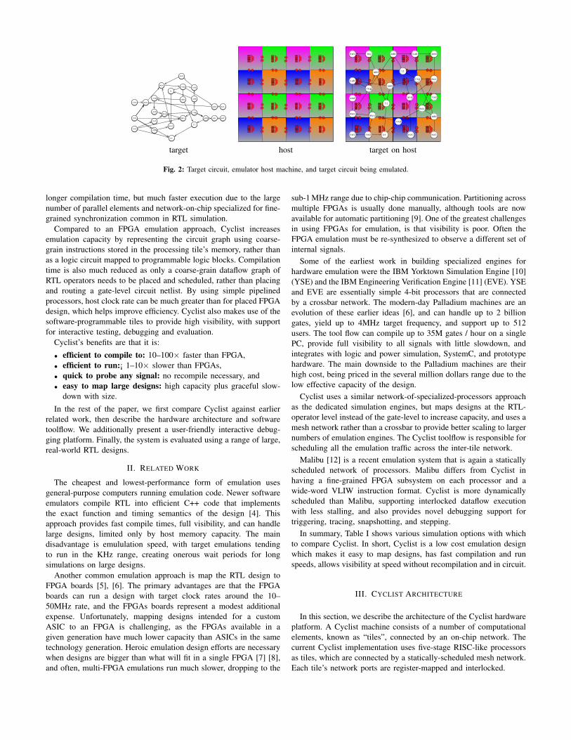
In general, reducing the latency of the steps of the loop where thedesigner is not productively developing (compilation and emulation)will speed the development process. To this end, hardware designerstypically use a variety of emulation techniques at different stages inthe design process, trading off cost, compilation speed, and emulationthroughput. Emulation techniques range from software emulation ongeneral-purpose servers to hardware emulation on specialized multi-million dollar hardware emulation engines. We use the term “target”to describe the design being emulated, and “host” to represent thesystem emulating the target design as shown in Figure 2. Althoughsoftware-based emulations are sometimes called simulations, in thispaper we use the term emulation for any cycle-accurate and bit-accurate model of a target, whether implemented in software or inhardware.
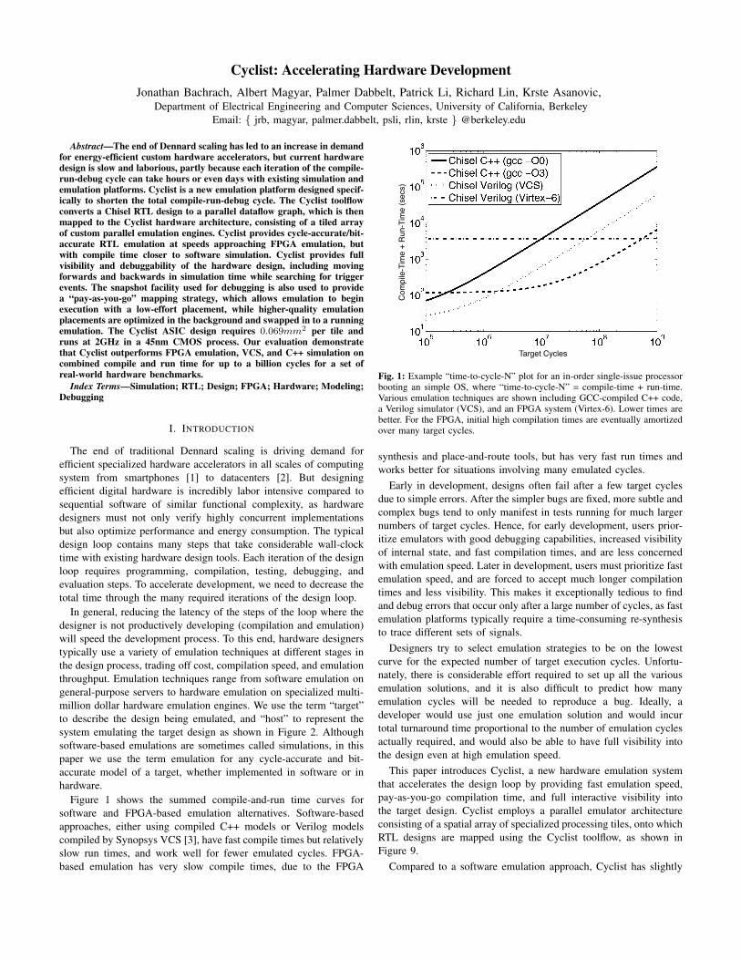
Figure 1 shows the summed compile-and-run time curves forsoftware and FPGA-based emulation alternatives. Software-basedapproaches, either using compiled C++ models or Verilog modelscompiled by Synopsys VCS [3], have fast compile times but relativelyslow run times, and work well for fewer emulated cycles. FPGA-based emulation has very slow compile times, due to the FPGA
Target Cycles
Com
pile
-Tim
e +
Run
-Tim
e (s
ecs)
Fig. 1: Example “time-to-cycle-N” plot for an in-order single-issue processorbooting an simple OS, where “time-to-cycle-N” = compile-time + run-time.Various emulation techniques are shown including GCC-compiled C++ code,a Verilog simulator (VCS), and an FPGA system (Virtex-6). Lower times arebetter. For the FPGA, initial high compilation times are eventually amortizedover many target cycles.
synthesis and place-and-route tools, but has very fast run times andworks better for situations involving many emulated cycles.
Early in development, designs often fail after a few target cyclesdue to simple errors. After the simpler bugs are fixed, more subtle andcomplex bugs tend to only manifest in tests running for much largernumbers of target cycles. Hence, for early development, users prior-itize emulators with good debugging capabilities, increased visibilityof internal state, and fast compilation times, and are less concernedwith emulation speed. Later in development, users must prioritize fastemulation speed, and are forced to accept much longer compilationtimes and less visibility. This makes it exceptionally tedious to findand debug errors that occur only after a large number of cycles, as fastemulation platforms typically require a time-consuming re-synthesisto trace different sets of signals.
Designers try to select emulation strategies to be on the lowestcurve for the expected number of target execution cycles. Unfortu-nately, there is considerable effort required to set up all the variousemulation solutions, and it is also difficult to predict how manyemulation cycles will be needed to reproduce a bug. Ideally, adeveloper would use just one emulation solution and would incurtotal turnaround time proportional to the number of emulation cyclesactually required, and would also be able to have full visibility intothe design even at high emulation speed.
This paper introduces Cyclist, a new hardware emulation systemthat accelerates the design loop by providing fast emulation speed,pay-as-you-go compilation time, and full interactive visibility intothe target design. Cyclist employs a parallel emulator architectureconsisting of a spatial array of specialized processing tiles, onto whichRTL designs are mapped using the Cyclist toolflow, as shown inFigure 9.
Compared to a software emulation approach, Cyclist has slightly
eat
sub
andmux
not
rnd
mux
or
rnd
not
ltand
add
reg
add eq
add
lt
sub
and
muxreg
rnd mux
add eat
eat
sub
and
mux
not rnd
mux
or
rnd
not
lt
and
addreg
add
eq add
lt
sub and
muxreg
rnd
mux
add
eat
target host target on host
Fig. 2: Target circuit, emulator host machine, and target circuit being emulated.
longer compilation time, but much faster execution due to the largenumber of parallel elements and network-on-chip specialized for fine-grained synchronization common in RTL simulation.
Compared to an FPGA emulation approach, Cyclist increasesemulation capacity by representing the circuit graph using coarse-grain instructions stored in the processing tile’s memory, rather thanas a logic circuit mapped to programmable logic blocks. Compilationtime is also much reduced as only a coarse-grain dataflow graph ofRTL operators needs to be placed and scheduled, rather than placingand routing a gate-level circuit netlist. By using simple pipelinedprocessors, host clock rate can be much greater than for placed FPGAdesign, which helps improve efficiency. Cyclist also makes use of thesoftware-programmable tiles to provide high visibility, with supportfor interactive testing, debugging and evaluation.
Cyclist’s benefits are that it is:
• efficient to compile to: 10–100× faster than FPGA,• efficient to run:¡ 1–10× slower than FPGAs,• quick to probe any signal: no recompile necessary, and• easy to map large designs: high capacity plus graceful slow-
down with size.
In the rest of the paper, we first compare Cyclist against earlierrelated work, then describe the hardware architecture and softwaretoolflow. We additionally present a user-friendly interactive debug-ging platform. Finally, the system is evaluated using a range of large,real-world RTL designs.
II. RELATED WORK
The cheapest and lowest-performance form of emulation usesgeneral-purpose computers running emulation code. Newer softwareemulators compile RTL into efficient C++ code that implementsthe exact function and timing semantics of the design [4]. Thisapproach provides fast compile times, full visibility, and can handlelarge designs, limited only by host memory capacity. The maindisadvantage is emululation speed, with target emulations tendingto run in the KHz range, creating onerous wait periods for longsimulations on large designs.
Another common emulation approach is map the RTL design toFPGA boards [5], [6]. The primary advantages are that the FPGAboards can run a design with target clock rates around the 10–50MHz rate, and the FPGAs boards represent a modest additionalexpense. Unfortunately, mapping designs intended for a customASIC to an FPGA is challenging, as the FPGAs available in agiven generation have much lower capacity than ASICs in the sametechnology generation. Heroic emulation design efforts are necessarywhen designs are bigger than what will fit in a single FPGA [7] [8],and often, multi-FPGA emulations run much slower, dropping to the
sub-1 MHz range due to chip-chip communication. Partitioning acrossmultiple FPGAs is usually done manually, although tools are nowavailable for automatic partitioning [9]. One of the greatest challengesin using FPGAs for emulation, is that visibility is poor. Often theFPGA emulation must be re-synthesized to observe a different set ofinternal signals.
Some of the earliest work in building specialized engines forhardware emulation were the IBM Yorktown Simulation Engine [10](YSE) and the IBM Engineering Verification Engine [11] (EVE). YSEand EVE are essentially simple 4-bit processors that are connectedby a crossbar network. The modern-day Palladium machines are anevolution of these earlier ideas [6], and can handle up to 2 billiongates, yield up to 4MHz target frequency, and support up to 512users. The tool flow can compile up to 35M gates / hour on a singlePC, provide full visibility to all signals with little slowdown, andintegrates with logic and power simulation, SystemC, and prototypehardware. The main downside to the Palladium machines are theirhigh cost, being priced in the several million dollars range due to thelow effective capacity of the design.
Cyclist uses a similar network-of-specialized-processors approachas the dedicated simulation engines, but maps designs at the RTL-operator level instead of the gate-level to increase capacity, and uses amesh network rather than a crossbar to provide better scaling to largernumbers of emulation engines. The Cyclist toolflow is responsible forscheduling all the emulation traffic across the inter-tile network.
Malibu [12] is a recent emulation system that is again a staticallyscheduled network of processors. Malibu differs from Cyclist inhaving a fine-grained FPGA subsystem on each processor and awide-word VLIW instruction format. Cyclist is more dynamicallyscheduled than Malibu, supporting interlocked dataflow executionwith less stalling, and also provides novel debugging support fortriggering, tracing, snapshotting, and stepping.
In summary, Table I shows various simulation options with whichto compare Cyclist. In short, Cyclist is a low cost emulation designwhich makes it easy to map designs, has fast compilation and runspeeds, allows visibility at speed without recompilation and in circuit.
III. CYCLIST ARCHITECTURE
In this section, we describe the architecture of the Cyclist hardwareplatform. A Cyclist machine consists of a number of computationalelements, known as “tiles”, connected by an on-chip network. Thecurrent Cyclist implementation uses five-stage RISC-like processorsas tiles, which are connected by a statically-scheduled mesh network.Each tile’s network ports are register-mapped and interlocked.
name ease of compiler run visibility visibility in costmapping speed speed speed recompile? circuit?
Verilog easy fast slow slow no no lowC++ easy fast med slow yes no free
FPGA hard slow fast fast yes yes medPalladium easy fast fast fast no yes high
Cyclist easy fast fast fast no yes med
TABLE I: Comparison of various simulation options according to a number of important simulation attributes.
op dst x iy y z in out5b 4b 5b 1b 5b 5b 2b 4b
TABLE II: Cyclist RISC-style instruction format including one destinationspecifier, three operand specifiers x, y, and z, and one network route specifiedby in and out. The y field holds an immediate when iy is one. For certaininstructions, z is an immediate specifying the number of mask bits with whichto mask the result.
I$ Decode RF D$
Net OutNet InPC
fetch decode reg/net read execute write-back
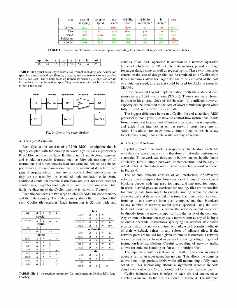
Fig. 3: Cyclist five stage pipeline.
A. The Cyclist Pipeline
Each Cyclist tile consists of a 32-bit RISC-like pipeline that istightly coupled with the on-chip network. Cyclist uses a proprietaryRISC ISA, as shown in Table II. There are 32 architectural registers,and emulation-specific features such as bitwidth masking of allinstructions and direct network read and write are included to enhanceperformance on common operations. In a significant departure fromgeneral-purpose chips, there are no control flow instructions, asthey are not used by the scheduled logic emulation code. Someadditional emulation-specific instructions are rst for reset, mux forconditionals, log2 for find highest bit, and cat for concatenate twofields. A diagram of the Cyclist pipeline is shown in Figure 3.
Each tile has access to two large on-chip SRAMs: the code memoryand the data memory. The code memory stores the instructions thateach Cyclist tile executes. Each instruction is 32 bits wide and
op d x y zspecial
nopinputs
rst dlit d val
logicalnot d x wand d x yor d x yxor d x yeq d x yneq d x ymux d c t elog2 d x w
bitslsh d x nrsh d x n wrsha d x n wcat d x y wy
arithmeticadd d x y wsub d x y wlt d x y wgte d x y wmul d x y w
stateld d a est a x a eldi d asti a x a
TABLE III: 24 instructions necessary for implementing Cyclist RTL func-tionality.
consists of an ALU operation in addition to a network operation(either of which can be NOPs). The data memory provides storagefor target design state as well as register spills. These two memoriesdetermine the size of design that can be emulated on a Cyclist chip:larger memories allow for larger designs to be emulated at the costof emulation speed, as area that could be used for ALUs is taken bySRAMs.
In the presented Cyclist implementation, both the code and datamemories are 1024 words long (32kbit). These sizes were chosenin order to hit a target clock of 1MHz when fully utilized; however,capacity can be increased at the cost of lower simulation speed whenfully utilized and a slower critical path.
The biggest difference between a Cyclist tile and a standard RISCprocessor is that Cyclist tiles have no control-flow instructions. Asidefrom the implicit loop around all instructions execution is sequential,and aside from interlocking on the network ports there are nostalls. This allows for an extremely simple pipeline, which is keyto achieving a high clock rate while keeping area small.
B. The Cyclist Network
Cyclist’s on-chip network is responsible for feeding each tilewith data for execution, and it is therefore a first-order performanceconstraint. Th network was designed to be low latency, handle fanoutefficiently, have a simple hardware implementation, and be easy toschedule for. A block diagram of Cyclist’s on-chip network is shownin Figure 4.
The on-chip network consists of an interlocked, NSEW-meshnetwork. Each compass direction consists of a pair of one elementblocking queues with one used for input and one used for output.In order to avoid physical overhead for routing, tiles are responsiblefor moving data from inputs to outputs; routing across the chip isdone statically at design compilation time. Each instruction can readfrom up to one network input port, compute, and then broadcastto any number of network output ports (specified using the outfield and shown in Table II), where the network output value canbe directly from the network input or from the result of the compute.Any arithmetic instruction may use a network port as any of its inputor output operands. Instructions specifying the network destinationregister utilize the network output bitmask, which permits multicastof their writeback values to any subset of adjacent tiles. If thenetwork ports are unused for a given arithmetic instruction, a networkoperation may be performed in parallel, allowing a higer degree ofinstruction-level parallelism. Careful scheduling of network trafficallows for efficient handling of fan-out to multiple tiles.
The pipeline is interlocked and will stall if space on an outputqueue is full or an input queue has no data. This allows the compilerto avoid emitting spurious NOPs while still maintaining a fully staticschedule. This interlocking affords a significant increase in codedensity without which Cyclist would not be a practical machine.
Cyclist includes a host interface on each tile and connected asa debug scanchain to the host as shown in Figure 4. The interface
data in
data out
debug out
debug in
imem dmem
imem dmem
imem dmem
imem
dmem
Fig. 4: Tiled emulation machine with statically scheduled mesh network(shown in red) and debug scanchain (shown in green).
supports peek and poke commands for reading and writing host/targetarchitectural state, and a step command for stepping the targetmachine n target cycles. Tiles can be individually addressed orbroadcast to. Every instruction includes a trace bit, that when set,sends out the instruction result out the debug scanchain.
C. ASIC and Performance Results
We have pushed our Cyclist design through Synopsis DC and ICC 1
Placed-and-routed results using models from a 45nm CMOS processproduced favorable results.
tile area = 0.069 mm2 / tilearray speed = 1.97GHz
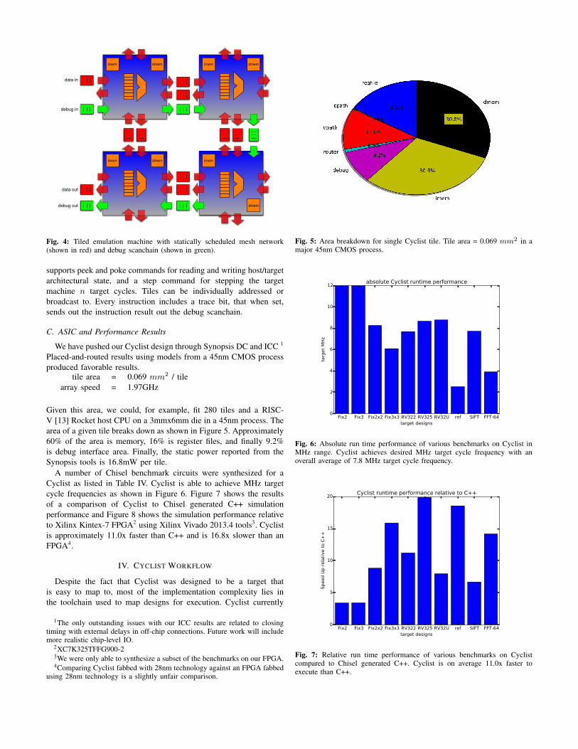
Given this area, we could, for example, fit 280 tiles and a RISC-V [13] Rocket host CPU on a 3mmx6mm die in a 45nm process. Thearea of a given tile breaks down as shown in Figure 5. Approximately60% of the area is memory, 16% is register files, and finally 9.2%is debug interface area. Finally, the static power reported from theSynopsis tools is 16.8mW per tile.
A number of Chisel benchmark circuits were synthesized for aCyclist as listed in Table IV. Cyclist is able to achieve MHz targetcycle frequencies as shown in Figure 6. Figure 7 shows the resultsof a comparison of Cyclist to Chisel generated C++ simulationperformance and Figure 8 shows the simulation performance relativeto Xilinx Kintex-7 FPGA2 using Xilinx Vivado 2013.4 tools3. Cyclistis approximately 11.0x faster than C++ and is 16.8x slower than anFPGA4.
IV. CYCLIST WORKFLOW
Despite the fact that Cyclist was designed to be a target thatis easy to map to, most of the implementation complexity lies inthe toolchain used to map designs for execution. Cyclist currently
1The only outstanding issues with our ICC results are related to closingtiming with external delays in off-chip connections. Future work will includemore realistic chip-level IO.
2XC7K325TFFG900-23We were only able to synthesize a subset of the benchmarks on our FPGA.4Comparing Cyclist fabbed with 28nm technology against an FPGA fabbed
using 28nm technology is a slightly unfair comparison.
Fig. 5: Area breakdown for single Cyclist tile. Tile area = 0.069 mm2 in amajor 45nm CMOS process.
Fix2 Fix3 Fix2x2 Fix3x3 RV322 RV325 RV32U ref SIFT FFT-64target designs
0
2
4
6
8
10
12
targ
et
MH
z
absolute Cyclist runtime performance
Fig. 6: Absolute run time performance of various benchmarks on Cyclist inMHz range. Cyclist achieves desired MHz target cycle frequency with anoverall average of 7.8 MHz target cycle frequency.
Fix2 Fix3 Fix2x2 Fix3x3 RV322 RV325 RV32U ref SIFT FFT-64target designs
0
5
10
15
20
Speed U
p r
ela
tive t
o C
++
Cyclist runtime performance relative to C++
Fig. 7: Relative run time performance of various benchmarks on Cyclistcompared to Chisel generated C++. Cyclist is on average 11.0x faster toexecute than C++.
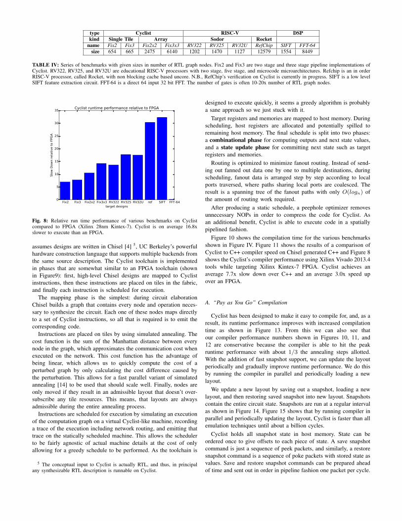
type Cyclist RISC-V DSPkind Single Tile Array Sodor Rocket
name Fix2 Fix3 Fix2x2 Fix3x3 RV322 RV325 RV32U RefChip SIFT FFT-64size 654 665 2475 6140 1202 1470 1127 12579 1554 8449
TABLE IV: Series of benchmarks with given sizes in number of RTL graph nodes. Fix2 and Fix3 are two stage and three stage pipeline implementations ofCyclist. RV322, RV325, and RV32U are educational RISC-V processors with two stage, five stage, and microcode microarchitectures. Refchip is an in orderRISC-V processor, called Rocket, with non blocking cache based uncore. N.B., RefChip’s verification on Cyclist is currently in progress. SIFT is a low levelSIFT feature extraction circuit. FFT-64 is a direct 64 input 32 bit FFT. The number of gates is often 10-20x number of RTL graph nodes.
Fix2 Fix3 Fix2x2 Fix3x3 RV322 RV325 RV32U ref SIFT FFT-64target designs
0
5
10
15
20
25
30
35
Slo
w D
ow
n r
ela
tive t
o F
PG
A
Cyclist runtime performance relative to FPGA
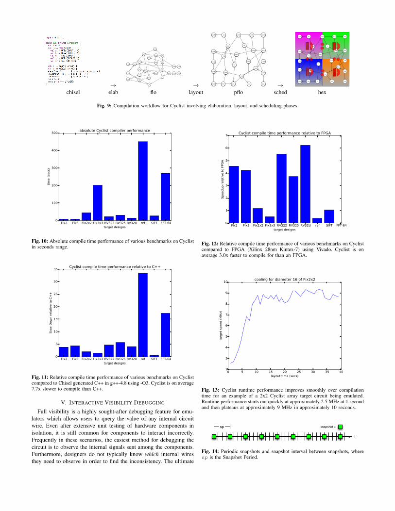
Fig. 8: Relative run time performance of various benchmarks on Cyclistcompared to FPGA (Xilinx 28nm Kintex-7). Cyclist is on average 16.8xslower to execute than an FPGA.
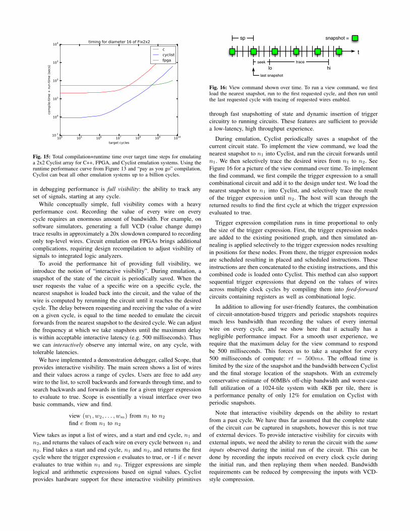
assumes designs are written in Chisel [4] 5, UC Berkeley’s powerfulhardware construction language that supports multiple backends fromthe same source description. The Cyclist toolchain is implementedin phases that are somewhat similar to an FPGA toolchain (shownin Figure9): first, high-level Chisel designs are mapped to Cyclistinstructions, then these instructions are placed on tiles in the fabric,and finally each instruction is scheduled for execution.
The mapping phase is the simplest: during circuit elaborationChisel builds a graph that contains every node and operation neces-sary to synthesize the circuit. Each one of these nodes maps directlyto a set of Cyclist instructions, so all that is required is to emit thecorresponding code.
Instructions are placed on tiles by using simulated annealing. Thecost function is the sum of the Manhattan distance between everynode in the graph, which approximates the communication cost whenexecuted on the network. This cost function has the advantage ofbeing linear, which allows us to quickly compute the cost of aperturbed graph by only calculating the cost difference caused bythe perturbation. This allows for a fast parallel variant of simulatedannealing [14] to be used that should scale well. Finally, nodes areonly moved if they result in an admissible layout that doesn’t over-subscribe any tile resources. This means, that layouts are alwaysadmissible during the entire annealing process.
Instructions are scheduled for execution by simulating an executionof the computation graph on a virtual Cyclist-like machine, recordinga trace of the execution including network routing, and emitting thattrace on the statically scheduled machine. This allows the schedulerto be fairly agnostic of actual machine details at the cost of onlyallowing for a greedy schedule to be performed. As the toolchain is
5 The conceptual input to Cyclist is actually RTL, and thus, in principalany synthesizable RTL description is runnable on Cyclist.
designed to execute quickly, it seems a greedy algorithm is probablya sane approach so we just stuck with it.
Target registers and memories are mapped to host memory. Duringscheduling, host registers are allocated and potentially spilled toremaining host memory. The final schedule is split into two phases:a combinational phase for computing outputs and next state values,and a state update phase for committing next state such as targetregisters and memories.
Routing is optimized to minimize fanout routing. Instead of send-ing out fanned out data one by one to multiple destinations, duringscheduling, fanout data is arranged step by step according to localports traversed, where paths sharing local ports are coalesced. Theresult is a spanning tree of the fanout paths with only O(logn) ofthe amount of routing work required.
After producing a static schedule, a peephole optimizer removesunnecessary NOPs in order to compress the code for Cyclist. Asan additional benefit, Cyclist is able to execute code in a spatiallypipelined fashion.
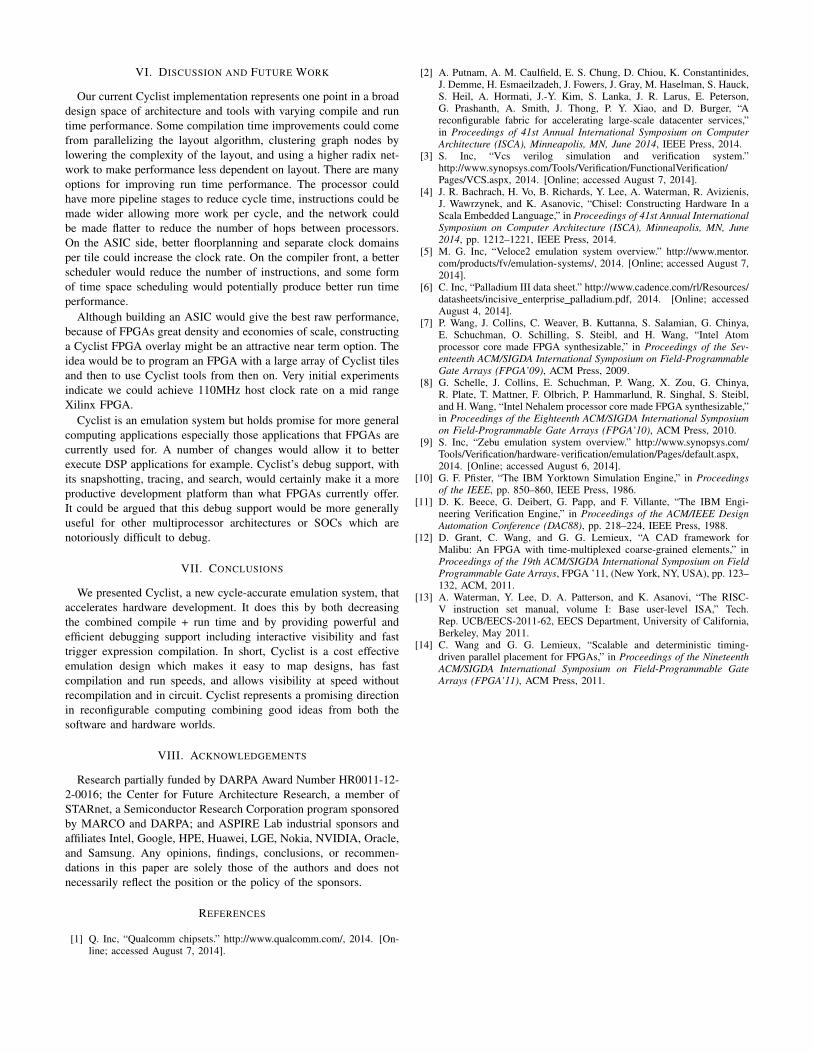
Figure 10 shows the compilation time for the various benchmarksshown in Figure IV. Figure 11 shows the results of a comparison ofCyclist to C++ compiler speed on Chisel generated C++ and Figure 8shows the Cyclist’s compiler performance using Xilinx Vivado 2013.4tools while targeting Xilinx Kintex-7 FPGA. Cyclist achieves anaverage 7.7x slow down over C++ and an average 3.0x speed upover an FPGA.
A. “Pay as You Go” Compilation
Cyclist has been designed to make it easy to compile for, and, as aresult, its runtime performance improves with increased compilationtime as shown in Figure 13. From this we can also see thatour compiler performance numbers shown in Figures 10, 11, and12 are conservative because the compiler is able to hit the peakruntime performance with about 1/3 the annealing steps allotted.With the addition of fast snapshot support, we can update the layoutperiodically and gradually improve runtime performance. We do thisby running the compiler in parallel and periodically loading a newlayout.
We update a new layout by saving out a snapshot, loading a newlayout, and then restoring saved snapshot into new layout. Snapshotscontain the entire circuit state. Snapshots are run at a regular intervalas shown in Figure 14. Figure 15 shows that by running compiler inparallel and periodically updating the layout, Cyclist is faster than allemulation techniques until about a billion cycles.
Cyclist holds all snapshot state in host memory. State can beordered once to give offsets to each piece of state. A save snapshotcommand is just a sequence of peek packets, and similarly, a restoresnapshot command is a sequence of poke packets with stored state asvalues. Save and restore snapshot commands can be prepared aheadof time and sent out in order in pipeline fashion one packet per cycle.
→
eat
sub
andmux
not
rnd
mux
or
rnd
not
ltand
add
reg
add eq
add
lt
sub
and
muxreg
rnd mux
add eat
→
eat
sub
and
mux
not rnd
mux
or
rnd
not
lt
and
addreg
add
eq add
lt
sub and
muxreg
rnd
mux
add
eat →
eat
sub
and
mux
not rnd
mux
or
rnd
not
lt
and
addreg
add
eq add
lt
sub and
muxreg
rnd
mux
add
eat
chisel elab flo layout pflo sched hex
Fig. 9: Compilation workflow for Cyclist involving elaboration, layout, and scheduling phases.
Fix2 Fix3 Fix2x2 Fix3x3 RV322 RV325 RV32U ref SIFT FFT-64target designs
0
100
200
300
400
500
tim
e (
secs
)
absolute Cyclist compiler performance
Fig. 10: Absolute compile time performance of various benchmarks on Cyclistin seconds range.
Fix2 Fix3 Fix2x2 Fix3x3 RV322 RV325 RV32U ref SIFT FFT-64target designs
0
5
10
15
20
25
30
35
Slo
w D
ow
n r
ela
tive t
o C
++
Cyclist compile time performance relative to C++
Fig. 11: Relative compile time performance of various benchmarks on Cyclistcompared to Chisel generated C++ in g++-4.8 using -O3. Cyclist is on average7.7x slower to compile than C++.
V. INTERACTIVE VISIBILITY DEBUGGING
Full visibility is a highly sought-after debugging feature for emu-lators which allows users to query the value of any internal circuitwire. Even after extensive unit testing of hardware components inisolation, it is still common for components to interact incorrectly.Frequently in these scenarios, the easiest method for debugging thecircuit is to observe the internal signals sent among the components.Furthermore, designers do not typically know which internal wiresthey need to observe in order to find the inconsistency. The ultimate
Fix2 Fix3 Fix2x2 Fix3x3 RV322 RV325 RV32U ref SIFT FFT-64target designs
0
1
2
3
4
5
6
7
Speedup r
ela
tive t
o F
PG
A
Cyclist compile time performance relative to FPGA
Fig. 12: Relative compile time performance of various benchmarks on Cyclistcompared to FPGA (Xilinx 28nm Kintex-7) using Vivado. Cyclist is onaverage 3.0x faster to compile for than an FPGA.
0 5 10 15 20 25 30 35 40layout time (secs)
2
3
4
5
6
7
8
9
10
targ
et
speed (
MH
z)
cooling for diameter 16 of Fix2x2
Fig. 13: Cyclist runtime performance improves smoothly over compilationtime for an example of a 2x2 Cyclist array target circuit being emulated.Runtime performance starts out quickly at approximately 2.5 MHz at 1 secondand then plateaus at approximately 9 MHz in approximately 10 seconds.
t
sp snapshot =
Fig. 14: Periodic snapshots and snapshot interval between snapshots, wheresp is the Snapshot Period.
104 105 106 107 108 109 1010
target cycles
10-1
100
101
102
103
104
com
pile
-tim
e +
run-t
ime (
secs
)
timing for diameter 16 of Fix2x2
ccyclistfpga
Fig. 15: Total compilation+runtime time over target time steps for emulatinga 2x2 Cyclist array for C++, FPGA, and Cyclist emulation systems. Using theruntime performance curve from Figure 13 and “pay as you go” compilation,Cyclist can beat all other emulation systems up to a billion cycles.
in debugging performance is full visibility: the ability to track anyset of signals, starting at any cycle.
While conceptually simple, full visibility comes with a heavyperformance cost. Recording the value of every wire on everycycle requires an enormous amount of bandwidth. For example, onsoftware simulators, generating a full VCD (value change dump)trace results in approximately a 20x slowdown compared to recordingonly top-level wires. Circuit emulation on FPGAs brings additionalcomplications, requiring design recompilation to adjust visibility ofsignals to integrated logic analyzers.
To avoid the performance hit of providing full visibility, weintroduce the notion of “interactive visibility”. During emulation, asnapshot of the state of the circuit is periodically saved. When theuser requests the value of a specific wire on a specific cycle, thenearest snapshot is loaded back into the circuit, and the value of thewire is computed by rerunning the circuit until it reaches the desiredcycle. The delay between requesting and receiving the value of a wireon a given cycle, is equal to the time needed to emulate the circuitforwards from the nearest snapshot to the desired cycle. We can adjustthe frequency at which we take snapshots until the maximum delayis within acceptable interactive latency (e.g. 500 milliseconds). Thuswe can interactively observe any internal wire, on any cycle, withtolerable latencies.
We have implemented a demonstration debugger, called Scope, thatprovides interactive visibility. The main screen shows a list of wiresand their values across a range of cycles. Users are free to add anywire to the list, to scroll backwards and forwards through time, and tosearch backwards and forwards in time for a given trigger expressionto evaluate to true. Scope is essentially a visual interface over twobasic commands, view and find.
view (w1, w2, . . . , wm) from n1 to n2
find e from n1 to n2
View takes as input a list of wires, and a start and end cycle, n1 andn2, and returns the values of each wire on every cycle between n1 andn2. Find takes a start and end cycle, n1 and n2, and returns the firstcycle where the trigger expression e evaluates to true, or -1 if e neverevaluates to true within n1 and n2. Trigger expressions are simplelogical and arithmetic expressions based on signal values. Cyclistprovides hardware support for these interactive visibility primitives
t
sp snapshot =
lo hitraceseek
last snapshot
Fig. 16: View command shown over time. To run a view command, we firstload the nearest snapshot, run to the first requested cycle, and then run untilthe last requested cycle with tracing of requested wires enabled.
through fast snapshotting of state and dynamic insertion of triggercircuitry to running circuits. These features are sufficient to providea low-latency, high throughput experience.
During emulation, Cyclist periodically saves a snapshot of thecurrent circuit state. To implement the view command, we load thenearest snapshot to n1 into Cyclist, and run the circuit forwards untiln1. We then selectively trace the desired wires from n1 to n2. SeeFigure 16 for a picture of the view command over time. To implementthe find command, we first compile the trigger expression to a smallcombinational circuit and add it to the design under test. We load thenearest snapshot to n1 into Cyclist, and selectively trace the resultof the trigger expression until n2. The host will scan through thereturned results to find the first cycle at which the trigger expressionevaluated to true.
Trigger expression compilation runs in time proportional to onlythe size of the trigger expression. First, the trigger expression nodesare added to the existing positioned graph, and then simulated an-nealing is applied selectively to the trigger expression nodes resultingin positions for these nodes. From there, the trigger expression nodesare scheduled resulting in placed and scheduled instructions. Theseinstructions are then concatenated to the existing instructions, and thiscombined code is loaded onto Cyclist. This method can also supportsequential trigger expressions that depend on the values of wiresacross multiple clock cycles by compiling them into feed-forwardcircuits containing registers as well as combinational logic.
In addition to allowing for user-friendly features, the combinationof circuit-annotation-based triggers and periodic snapshots requiresmuch less bandwidth than recording the values of every internalwire on every cycle, and we show here that it actually has anegligible performance impact. For a smooth user experience, werequire that the maximum delay for the view command to respondbe 500 milliseconds. This forces us to take a snapshot for every500 milliseconds of compute: rt = 500ms. The offload time islimited by the size of the snapshot and the bandwidth between Cyclistand the final storage location of the snapshots. With an extremelyconservative estimate of 60MB/s off-chip bandwidth and worst-casefull utilization of a 1024-tile system with 4KB per tile, there isa performance penalty of only 12% for emulation on Cyclist withperiodic snapshots.
Note that interactive visibility depends on the ability to restartfrom a past cycle. We have thus far assumed that the complete stateof the circuit can be captured in snapshots, however this is not trueof external devices. To provide interactive visibility for circuits withexternal inputs, we need the ability to rerun the circuit with the sameinputs observed during the initial run of the circuit. This can bedone by recording the inputs received on every clock cycle duringthe initial run, and then replaying them when needed. Bandwidthrequirements can be reduced by compressing the inputs with VCD-style compression.
VI. DISCUSSION AND FUTURE WORK
Our current Cyclist implementation represents one point in a broaddesign space of architecture and tools with varying compile and runtime performance. Some compilation time improvements could comefrom parallelizing the layout algorithm, clustering graph nodes bylowering the complexity of the layout, and using a higher radix net-work to make performance less dependent on layout. There are manyoptions for improving run time performance. The processor couldhave more pipeline stages to reduce cycle time, instructions could bemade wider allowing more work per cycle, and the network couldbe made flatter to reduce the number of hops between processors.On the ASIC side, better floorplanning and separate clock domainsper tile could increase the clock rate. On the compiler front, a betterscheduler would reduce the number of instructions, and some formof time space scheduling would potentially produce better run timeperformance.
Although building an ASIC would give the best raw performance,because of FPGAs great density and economies of scale, constructinga Cyclist FPGA overlay might be an attractive near term option. Theidea would be to program an FPGA with a large array of Cyclist tilesand then to use Cyclist tools from then on. Very initial experimentsindicate we could achieve 110MHz host clock rate on a mid rangeXilinx FPGA.
Cyclist is an emulation system but holds promise for more generalcomputing applications especially those applications that FPGAs arecurrently used for. A number of changes would allow it to betterexecute DSP applications for example. Cyclist’s debug support, withits snapshotting, tracing, and search, would certainly make it a moreproductive development platform than what FPGAs currently offer.It could be argued that this debug support would be more generallyuseful for other multiprocessor architectures or SOCs which arenotoriously difficult to debug.
VII. CONCLUSIONS
We presented Cyclist, a new cycle-accurate emulation system, thataccelerates hardware development. It does this by both decreasingthe combined compile + run time and by providing powerful andefficient debugging support including interactive visibility and fasttrigger expression compilation. In short, Cyclist is a cost effectiveemulation design which makes it easy to map designs, has fastcompilation and run speeds, and allows visibility at speed withoutrecompilation and in circuit. Cyclist represents a promising directionin reconfigurable computing combining good ideas from both thesoftware and hardware worlds.
VIII. ACKNOWLEDGEMENTS
Research partially funded by DARPA Award Number HR0011-12-2-0016; the Center for Future Architecture Research, a member ofSTARnet, a Semiconductor Research Corporation program sponsoredby MARCO and DARPA; and ASPIRE Lab industrial sponsors andaffiliates Intel, Google, HPE, Huawei, LGE, Nokia, NVIDIA, Oracle,and Samsung. Any opinions, findings, conclusions, or recommen-dations in this paper are solely those of the authors and does notnecessarily reflect the position or the policy of the sponsors.
REFERENCES
[1] Q. Inc, “Qualcomm chipsets.” http://www.qualcomm.com/, 2014. [On-line; accessed August 7, 2014].
[2] A. Putnam, A. M. Caulfield, E. S. Chung, D. Chiou, K. Constantinides,J. Demme, H. Esmaeilzadeh, J. Fowers, J. Gray, M. Haselman, S. Hauck,S. Heil, A. Hormati, J.-Y. Kim, S. Lanka, J. R. Larus, E. Peterson,G. Prashanth, A. Smith, J. Thong, P. Y. Xiao, and D. Burger, “Areconfigurable fabric for accelerating large-scale datacenter services,”in Proceedings of 41st Annual International Symposium on ComputerArchitecture (ISCA), Minneapolis, MN, June 2014, IEEE Press, 2014.
[3] S. Inc, “Vcs verilog simulation and verification system.”http://www.synopsys.com/Tools/Verification/FunctionalVerification/Pages/VCS.aspx, 2014. [Online; accessed August 7, 2014].
[4] J. R. Bachrach, H. Vo, B. Richards, Y. Lee, A. Waterman, R. Avizienis,J. Wawrzynek, and K. Asanovic, “Chisel: Constructing Hardware In aScala Embedded Language,” in Proceedings of 41st Annual InternationalSymposium on Computer Architecture (ISCA), Minneapolis, MN, June2014, pp. 1212–1221, IEEE Press, 2014.
[5] M. G. Inc, “Veloce2 emulation system overview.” http://www.mentor.com/products/fv/emulation-systems/, 2014. [Online; accessed August 7,2014].
[6] C. Inc, “Palladium III data sheet.” http://www.cadence.com/rl/Resources/datasheets/incisive enterprise palladium.pdf, 2014. [Online; accessedAugust 4, 2014].
[7] P. Wang, J. Collins, C. Weaver, B. Kuttanna, S. Salamian, G. Chinya,E. Schuchman, O. Schilling, S. Steibl, and H. Wang, “Intel Atomprocessor core made FPGA synthesizable,” in Proceedings of the Sev-enteenth ACM/SIGDA International Symposium on Field-ProgrammableGate Arrays (FPGA’09), ACM Press, 2009.
[8] G. Schelle, J. Collins, E. Schuchman, P. Wang, X. Zou, G. Chinya,R. Plate, T. Mattner, F. Olbrich, P. Hammarlund, R. Singhal, S. Steibl,and H. Wang, “Intel Nehalem processor core made FPGA synthesizable,”in Proceedings of the Eighteenth ACM/SIGDA International Symposiumon Field-Programmable Gate Arrays (FPGA’10), ACM Press, 2010.
[9] S. Inc, “Zebu emulation system overview.” http://www.synopsys.com/Tools/Verification/hardware-verification/emulation/Pages/default.aspx,2014. [Online; accessed August 6, 2014].
[10] G. F. Pfister, “The IBM Yorktown Simulation Engine,” in Proceedingsof the IEEE, pp. 850–860, IEEE Press, 1986.
[11] D. K. Beece, G. Deibert, G. Papp, and F. Villante, “The IBM Engi-neering Verification Engine,” in Proceedings of the ACM/IEEE DesignAutomation Conference (DAC88), pp. 218–224, IEEE Press, 1988.
[12] D. Grant, C. Wang, and G. G. Lemieux, “A CAD framework forMalibu: An FPGA with time-multiplexed coarse-grained elements,” inProceedings of the 19th ACM/SIGDA International Symposium on FieldProgrammable Gate Arrays, FPGA ’11, (New York, NY, USA), pp. 123–132, ACM, 2011.
[13] A. Waterman, Y. Lee, D. A. Patterson, and K. Asanovi, “The RISC-V instruction set manual, volume I: Base user-level ISA,” Tech.Rep. UCB/EECS-2011-62, EECS Department, University of California,Berkeley, May 2011.
[14] C. Wang and G. G. Lemieux, “Scalable and deterministic timing-driven parallel placement for FPGAs,” in Proceedings of the NineteenthACM/SIGDA International Symposium on Field-Programmable GateArrays (FPGA’11), ACM Press, 2011.