Embed Size (px)
Citation preview

CYIL2SM1300AA
LUPA-1300-2 High speed CMOSImage Sensor
Cypress Semiconductor Corporation • 198 Champion Court • San Jose, CA 95134-1709 • 408-943-2600Document Number: 001-24599 Rev. ** Revised September 10, 2007
Featuresn 1280 x 1024 active pixels (SXGA resolution).
n 14 µm2 square pixels [based on the high-fill factor active pixel sensor technology of FillFactory (US patent No. 6,225,670 and others))]
n On-chip 10-bit ADCs
n 12 LVDS serial outputs
n 500 fps frame rate
n Full snapshot shutter
n On-chip FPN correction
n Random programmable windowing
n 168-pin µPGA package
n Sub sampling
n Programmable read out direction (X and Y)
Functional OverviewThe Lupa1300-2 is a high speed CMOS image sensor with 1280by 1024 pixels. The pixels are 14µm x 14 µm in size and allconsist of high sensitivity 6T pipelined snapshot shuttercapability (exposure during read out is possible). The image sensor has twelve 10-bit Digital LVDS outputs (serial).The image sensor also integrates a programmable offset andgain amplifier for each channel. Each channel runs at 61 MHzpixel rate which results in 500 fps frame rate at full resolution.Higher frame rates can be achieved by windowed or subsampledread out modes which are all programmable over the SPIinterface. All internal exposure and read out timings are generated by anon-board sequencer. Extended optical dynamic range can be
achieved by setting multiple slopes. The sensor can also be readout non-destructively, that is, the pixel is reset and afterwardssampled and read out two or several times without additionalresets in between. The initial reset level and all intermediatesignals can be recorded. In this case, the reset level can simplybe subtracted from the single level after a given integrationperiod to perform Correlated Double Sampling (CDS) for verylow noise applications.The Lupa1300-2 sensor has 12 LVDS high speed outputs whichtransfer the image data over longer distances, thus simplifyingthe surrounding system. The LVDS interface can receive highspeed and wide bandwidth data signals when maintaining lownoise and distortion. A special training mode allows the receivingsystem to synchronize the coming data stream when switchingto master, slave, or triggered mode.
Table 1. Part Number
Name Package Monochrome/ColorCYIL2SM1300AA-GDCES 168-pin ceramic µPGA MonochromeCYIL2SC1300AA-GDCES 168-pin ceramic µPGA ColorNote1. The LUPA-1300-2 is also available in color or monochrome without the cover glass. Please contact Cypress for more information.

CYIL2SM1300AA
Document Number: 001-24599 Rev. ** Page 2 of 42
1. OverviewThis document describes the interfacing and the driving of theLUPA-1300-2 image sensor. This SXGA resolution CMOS activepixel sensor features synchronous shutter and a maximal framerate of 500 fps in full resolution. The read out speed can beboosted by means of sub sampling and windowed Region OfInterest (ROI) read out. High dynamic range scenes can becaptured using the double and multiple slope functionality. Userprogrammable row and column start and stop positions allowwindowing. Sub sampling reduces resolution while maintainingthe constant field of view and an increased frame rate. The Lupa1300-2 sensor has 12 LVDS high speed outputs whichtransfers the image data over longer distances thus simplifyingthe surrounding system. The LVDS interface can receive highspeed and wide bandwidth data signals and maintain low noiseand distortion. A special training mode allows the receivingsystem to synchronize the coming data stream when switchingto master, slave, or triggered mode. The image sensor alsointegrates a programmable offset and gain amplifier for eachchannel. A 10-bit ADC converts the analog data to a 10-bit digital wordstream. The sensor uses a 3-wire Serial-Parallel Interface (SPI).It requires only one master clock for operation up to 500 fps. It ishoused in a 168-pin ceramic µPGA package. The sensor is available in a Monochrome version or Bayer (RGB)patterned color filter array.
This data sheet allows the user to develop a camera systembased on the described timing and interfacing.
1.1 Applicationsn Machine vision
n Motion trackingTable 2. Specifications
2. Specifications2.1 General SpecificationsTable 3. General Specifications
2.2 Electro-optical Specifications
2.2.1 OverviewTable 4. Electro-optical Specifications
Parameter Typical ValueActive Pixels 1280 (H) x 1024 (V)Pixel Size 14µm x 14 µmPixel Type 6 Transistor PixelShutter Type Pipelined & Triggered Global ShutterMaster Clock 310 MHzFrame Rate 500fps @ 1.3MpxlRead out Windowed, flipped, mirrored, and
subsampled read out possibleADC resolution 10-bit, on-chipSensitivity 25 V/lux.sQE x FF 35% (average 400-720 nm)Full Well Charge 30.000 e-
Parameter Specifications Remarks
Pixel Architecture 6 transistor pixelPixel Size 14 µm x 14 µm The pixel size and resolution result in a 17.92 mm x 14.34 mm
optical active area. Resolution 1280 x 1024 pixelsPixel Rate 620 Mbps 12 serial LVDS outputsShutter Type Pipelined or Triggered snapshot
shutterIntegration during read out is possible
Frame Rate 500 fps Frame rate can be boosted by sub sampling and windowing.
Parameter Specifications Remarks
FPN 2% RMS Column FPN corrected on-chipPRNU 1% RMSConversion gain 34 uV/e- @ outputSaturation charge 30.000 e-Sensitivity 7639 V/(J/m2) @ 680nmPeak QE * FF 40%Dark current (@ 21 °C) 200 mV/s

CYIL2SM1300AA
Document Number: 001-24599 Rev. ** Page 3 of 42
2.2.2 Spectral Response Curve
Figure 1. Spectral response of lupa-1300-2
Noise electrons 37e-S/N ratio 57.81 dBParasitic sensitivity < 1/10000MTF 58%Power dissipation 1250 mW
Parameter Specifications Remarks

CYIL2SM1300AA
Document Number: 001-24599 Rev. ** Page 4 of 42
2.2.3 Photo-voltaic Response Curve
Figure 2. Photo-voltaic response of lupa-1300-2
2.3 Features and General SpecificationsTable 5. General Specifications
Feature DescriptionElectronic shutter type Full snapshot shutter (integration during read out is possible).Windowing (ROI) Randomly programmable ROI read out. Implemented as scanning of lines or columns
from an uploaded position.Sub-sampling Sub sampling is possible (X and Y direction)
Sub-sampling pattern: X0X0X0X0 (mono) or XX00XX00 (color)Read out direction Read out direction can be reversed in X and Y.Extended dynamic range Multiple slope (up to 90 dB optical dynamic range).Programmable gain range x1 to x4, in 6 steps using 3-bits programming.Programmable ADC offset 256 steps (8-bit)Digital output 12 On-chip 10-bit serial LVDS outputsSupply voltage VDD Nominal 2.5V (some supplies require 3.3V)Logic levels 2.5V.Operational temperature range -40°C to 70°C; with degradation of dark current.Interface Serial-to Parallel Interface (SPI). Package 168-pin µPGAPower dissipation 1250 mW

CYIL2SM1300AA
Document Number: 001-24599 Rev. ** Page 5 of 42
2.4 Electrical SpecificationsTable 6. Absoulte Maximum Ratings
Table 7. Recommended Operating Conditions
Symbol Parameter Value UnitVDD DC supply voltages -0.5 to 3.5 VVIN DC input voltage -0.5 to 3.5 VVOUT DC output voltage -0.5 to 3.5 VIIO DC current on any single pin +/- 50 mATL Lead temperature (5 seconds soldering) 350 ºCNote2. Absolute Ratings are those values beyond which damage to the device may occur.
Symbol Parameter Min Typ Max UnitVsamp Power supply of the sampling circuitry. 2.5 VVres Power supply reset drivers 3.5 VVres_ds Power supply of the dual slope 2.5 VVres_ts Power supply of the triple slope 1.8 VVmem_l Power supply of the pixels memory element (low level) 2.5 VVmem_h Power supply of the pixels memory element (high level) 3.3 VVadc Power supply of the on-chip ADCs 2.5 VVpix Power supply of the pixel array 2.5 VVprech Power supply of the precharge drivers 0.7 VVana Analog power supply 2.5 VVdig Digital power supply 2.5 VVbuf Power supply of the on-board buffers 2.5 VVresab Anti-blooming power supply 0.7 VTA Commercial operating temperature -40 30 70 °CNote3. All parameters are characterized for DC conditions after thermal equilibrium has been established.4. Unused inputs must always be tied to an appropriate logic level, for example, either VDD or GND. All cap_xxx pins must be connected to ground through a 100 nF
capcitor. 5. This device contains circuitry to protect the inputs against damage due to high static voltages or electric fields; however, it is recomended that normal precautions
be taken to avoid application of any voltages higher than the maximum rated voltages to this high impedance circuit.

CYIL2SM1300AA
Document Number: 001-24599 Rev. ** Page 6 of 42
3. Sensor ArchitectureThe floor plan of the architecture is shown in the following block diagram. The sensor consists of a pixel array, analog front end, datablock, and LVDS transmitters and receivers. Separate modules for the SPI, clock division, and sequencer are also integrated. Theimage sensor of 1280 x 1024 pixels is read out in progressive scan. The architecture allows programmable addressing in the x-direction in steps of 24 pixels, and in the y-direction in steps of 1 pixel. Thestarting point of the address is uploadable by means of the Serial Parallel Interface (SPI).The AFE prepares the signal for the digital datablock where the data is multiplexed and prepared for the LVDS interface.
Figure 3. Floor Plan of the Sensor
Image core1280 x 1024
24 analog channels 31 Msps
Analog front end
24x 10-bit digital channels 31 Msps
Data blockLocal register
12x 10-bit digital channels 62 Msps
LVDS TX and RX
12x LVDS outputs @ 620 Msps
Clock Divider
Clk o
Clk in
Sequencer &
Logic
SPI
31 MHz
310 MHz
62 MHz
Clk X & Clk Y

CYIL2SM1300AA
Document Number: 001-24599 Rev. ** Page 7 of 42
3.1 The 6-T PixelTo obtain the global shutter feature combined with a high sensi-tivity and good Parasitic Light Sensitivity (PLS), the pixel archi-tecture given in the following figure is implemented. This pixelarchitecture is designed in a 14 x 14 µm2 pixel pitch. The pixelis designed to meet the specifications as described in Table 1,Table 2, and Table 3. This architecture also allows the pipelinedor triggered mode which is explained in Figure 4.
Figure 4. 6T-pixel Architecture
3.2 Frame Rate and Windowing
3.2.1 Frame RateThe frame rate depends on the input clock, the frame OverheadTime (FOT), and the Row Overhead Time (ROT). The frameperiod can be calculated as follows: Frame period = FOT + Nr. Lines * (ROT + Nr. Pixels * clockperiod)Table 8. Frame Rate Parameters
Example: read out of the full resolution at nominal speed (744MHz pixel rate = 1.34 ns):
Frame period = 5µs + (1024 * (208ns + 1.34ns * 1280) = 1.97 ms=> 506 fpsThe real speed of the LUPA-1300-2 is reduced to 500 fps due tooverhead pixels being read out for black level calibration andother on-board features.
3.2.2 WindowingWindowing can easily be achieved by the SPI. The starting pointof the x- and y-address is uploadable, as well as the window size.The minimum step size in the x-direction is 24 pixels (onlymultiples of 24 can be chosen as start or stop addresses). Theminimum step size in the y-direction is 1 line (every line can beaddressed) in normal mode, and 2 lines in sub sampling mode. The sequencer section explains the use of the registers toachieve the desired ROI.Table 9. Typical frame rates for 620 MHz clock
3.3 Analog to Digital ConverterThe sensor has 24 10-bit pipelined ADCs on board. The ADCsnominally operate at 31 Msamples/s.Table 10. ADC Parameters
3.4 Programmable Gain AmplifiersThe PGAs amplify the signal before sending it to the ADCs.The amplification inside the PGA is controlled by one SPI setting:afemode [5:3].Six gain steps can be selected by means of the afemode<3:0>register. Table 9 gives the six gain settings. The unity gain selection of thePGA is done by the default afemode<5:3> setting. Table 11. Gain Settings
Parameter Comment ClarificationFOT Frame Overhead
TimeProgrammable: Default 310 granularity clock cycles (5 us @620 MHz)
ROT Row Overhead Time
Programmable: Default 13 granularity clock cycles (208 ns @620 MHz)
Nr. Lines Number of Lines read out each frame
Nr. Pixels Number of pixels read out each line.
clock period 1/62 MHz = 16.1 ns
Every channel works at 62 MHz 12 channels result in 744 MHz data rate
Vpix Vmem
Reset
Sample Select
Image resolu-tion (X * Y)
Frame rate (fps)
Frame read out time (µs) Comment
1280x1024 506 1970640 x 512 1816 550 sub sampling256 x 256 6846 146 windowing
Parameter SpecificationData rate 31 Msamples/sQuantization 10 bitDNL Typ. < 1 DNINL Typ. < 1 DN
afemode<5:3> Gain000 1001 1.5010 2011 2.25100 3101 4

CYIL2SM1300AA
Document Number: 001-24599 Rev. ** Page 8 of 42
3.5 Operation and Signaling
3.5.1 Power SuppliesEvery module, on-chip column amplifier, output stage, digital module, driver, ADC, LVD, and so on, has its own power supply andground. Off-chip the grounds can be combined, but not all power supplies may be combined. This results in several different powersupplies, but this is required to reduce electrical cross-talk and to improve shielding, dynamic range, and output swing.On chip, the ground lines of every module are kept separate to improve shielding and electrical cross-talk between them. An overview of the supplies is given in the following table.Table 12. Power Supplies
The maximum currents mentioned in Table 12 are peak currents. All power supplies must be able to deliver these maximum currents.It is important to notice that no power supply filtering on chip is implemented and that noise on these power supplies can contributeimmediately to the noise on the signal. The voltage supplies Vpix, Vana and Vadc are especially important to be noise free.
Name DC Current Peak Current Typ Description
Vsamp 2 mA 2.5V Power supply of the sampling circuitryVres 0 mA 3.5V Power supply reset driversVres_ds 0 mA 2.5V Power supply of the dual slopeVres_ts 0 mA 1.8V Power supply of the triple slopeVmem_l 0 mA 2.5V Power supply of the pixels memory element (low level)Vmem_h 0 mA 3.3V Power supply of the pixels memory element (high level)Vadc 185 mA 2.5V Power supply of the on-chip ADCsVpix 26 mA 2.5V Power supply of the pixel arrayVprech 0 mA 0.7V Power supply of the precharge driversVana 6 mA 2.5V Analog power supplyVdig 241 mA 2.5V Digital power supplyVbuf 40 mA 2.5V Power supply of the onboard buffersVresab 0 mA 0.7V Anti-blooming power supplyGNDlvds 0V Ground of the LVDS moduleGNDadc 0V Ground of the ADC moduleGNDdig 0V Ground of the digital modulesGNDana 0V Ground of the analog driversGNDpix 0V Ground of the pixel arrayGNDbuf 0V Ground of the analog buffers

CYIL2SM1300AA
Document Number: 001-24599 Rev. ** Page 9 of 42
3.5.2 Digital signalsDepending on the operation mode (master or slave), the pixel array of the image sensor requires different digital control signals. Thefunction of each signal is shown in the following table.Table 13. Overview of Digital Signals
3.6 Synchronous ShutterIn a synchronous (snapshot or global) shutter light integration takes place on all pixels in parallel, although subsequent read out issequential. Figure 5 shows the integration and read out sequence for the synchronous shutter. All pixels are light sensitive at the sameperiod of time. The whole pixel core is reset simultaneously, and after the integration time, all pixel values are sampled together onthe storage node inside each pixel. The pixel core is read out line by line after integration. Note that the integration and read out cyclecan occur in parallel or in sequential mode (pipelined or triggered). (See “Timing and Read out of the Image Sensor” on page 18.)
Figure 5. Synchronous Shutter Operation
Signal Name IO CommentsMONITOR_1 Output Output pin for integration timing, high during integrationMONITOR_2 Output Output pin for dual slope integration timing, high during integrationMONITOR_3 Output Output pin for triple slope integration timing, high during integrationINT_TIME_3 Input Integration pin triple slopeINT_TIME_2 Input Integration pin dual slopeINT_TIME_1 Input Integration pin first slopeRESET_N Input Sequencer reset. Active LOWCLK Input System clock (620 MHz)SPI_CS Input SPI chip selectSPI_CLK Input Clock of the SPISPI_IN Input Data line of the SPI. Serial inputSPI_OUT Output Data line of the SPI. Serial output
Time axis
Line number
Integration time Burst Readout time
CO
MM
ON
RES
ET
COM
MO
N S
AM
PLE&
HOLD
Flas
h co
uld
occu
r her
e

CYIL2SM1300AA
Document Number: 001-24599 Rev. ** Page 10 of 42
3.7 Non-destructive Read Out (NDR)Figure 6. Principle of Non-destructive Read Out
The sensor can also be read out in a nondestructive way. After a pixel is initially reset, it can be read multiple times, without resetting.The initial reset level and all intermediate signals can be recorded. High light levels saturate the pixels quickly, but a useful signal isobtained from the early samples. For low light levels, the later or latest samples must be used. Essentially, an active pixel array isread multiple times, and reset only once. The external system intelligence takes care of the interpretation of the data. The followingtable summarizes the advantages and disadvantages of nondestructive read out.Table 14. Advantages and Disadvantages of Nondestructive Read Out
Note that the amount of samples to be taken with one initial reset is programmable in the nr_of_ndr_steps register. If nr_of_ndr_stepsis 1, the sensor operates in the default way, namely one reset and one sample, that is. disable nondestructive read out mode.When nr_of_ndr_steps is 2, there is one reset and two samples, and so on. In case of Slave mode, nothing changes on the protocolof the signals int_time_*. The sequencer takes care of suppressing the internal reset signal to the pixel array.
3.8 SequencerThe sequencer generates the complete internal timing of the pixel array and the read out. The timing can be controlled by the userthrough the SPI register settings. The sequencer operates on the same clock as the data block. This is a division by 10 of the inputclock (internally divided).The following table shows a list of the internal registers with a short description. In the next section, the registers are explained morein detail.Table 15. Internal Registers
Advantages DisadvantagesLow noise – because it is true CDS. System memory required to record the reset level and the
intermediate samples.High sensitivity – as the conversion capacitance is kept rather low.
Requires multiples readings of each pixel, thus higher data throughput.
High dynamic range – because the results include signals for short and long integrations times.
Requires system level digital calculations.
time
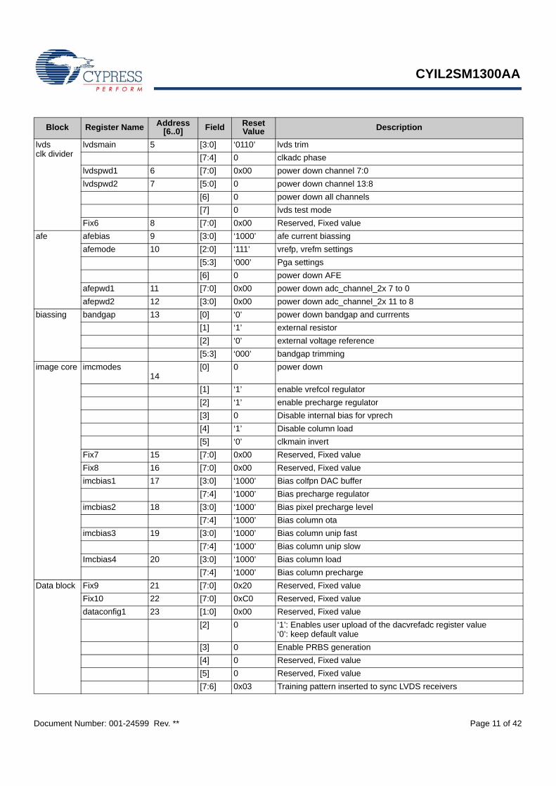
Block Register Name Address [6..0] Field Reset
Value Description
Mbs (reserved)
Fix1 0 [7:0] 0x00 Reserved, Fixed valueFix2 1 [7:0] 0xFF Reserved, Fixed valueFix3 2 [7:0] 0x00 Reserved, Fixed valueFix4 3 [7:0] 0x00 Reserved, Fixed valueFix5 4 [7:0] ‘0x08’ Reserved, Fixed value
CYIL2SM1300AA
Document Number: 001-24599 Rev. ** Page 11 of 42
lvdsclk divider
lvdsmain 5 [3:0] ‘0110’ lvds trim[7:4] 0 clkadc phase
lvdspwd1 6 [7:0] 0x00 power down channel 7:0lvdspwd2 7 [5:0] 0 power down channel 13:8
[6] 0 power down all channels[7] 0 lvds test mode
Fix6 8 [7:0] 0x00 Reserved, Fixed valueafe afebias 9 [3:0] ‘1000’ afe current biassing
afemode 10 [2:0] ‘111’ vrefp, vrefm settings[5:3] ‘000’ Pga settings[6] 0 power down AFE
afepwd1 11 [7:0] 0x00 power down adc_channel_2x 7 to 0afepwd2 12 [3:0] 0x00 power down adc_channel_2x 11 to 8
biassing bandgap 13 [0] ‘0’ power down bandgap and currrents[1] ‘1’ external resistor[2] ‘0’ external voltage reference[5:3] ‘000’ bandgap trimming
image core imcmodes 14
[0] 0 power down
[1] ‘1’ enable vrefcol regulator[2] ‘1’ enable precharge regulator[3] 0 Disable internal bias for vprech[4] ‘1’ Disable column load[5] ‘0’ clkmain invert
Fix7 15 [7:0] 0x00 Reserved, Fixed valueFix8 16 [7:0] 0x00 Reserved, Fixed valueimcbias1 17 [3:0] ‘1000’ Bias colfpn DAC buffer
[7:4] ‘1000’ Bias precharge regulatorimcbias2 18 [3:0] ‘1000’ Bias pixel precharge level
[7:4] ‘1000’ Bias column otaimcbias3 19 [3:0] ‘1000’ Bias column unip fast
[7:4] ‘1000’ Bias column unip slowImcbias4 20 [3:0] ‘1000’ Bias column load
[7:4] ‘1000’ Bias column prechargeData block Fix9 21 [7:0] 0x20 Reserved, Fixed value
Fix10 22 [7:0] 0xC0 Reserved, Fixed valuedataconfig1 23 [1:0] 0x00 Reserved, Fixed value
[2] 0 ‘1’: Enables user upload of the dacvrefadc register value‘0’: keep default value
[3] 0 Enable PRBS generation[4] 0 Reserved, Fixed value[5] 0 Reserved, Fixed value[7:6] 0x03 Training pattern inserted to sync LVDS receivers
Block Register Name Address [6..0] Field Reset
Value Description

CYIL2SM1300AA
Document Number: 001-24599 Rev. ** Page 12 of 42
dataconfig2 24 [7:0] 0x2A Training pattern inserted to sync LVDS receiversFix11 25 [7:0] 0 Reserved, Fixed valuedacvrefadc 26 [7:0] 0x80 Input to DAC to set the offset at the input of the ADC (black
calibration)Fix12 27 [7:0] 0x80 Reserved, Fixed valueFix13 28 [7:0] Reserved, Fixed value Fix14 29 [7:0] Reserved, Fixed valuedatachannel0_1 30 [0] 0 Bypass the data block
[1] 0 Enables the FPN correction[2] 0 Overwrite incoming ADC data by the data in the testpat register[3] 0 Reserved, Fixed value[5:4] 0x00 Pattern inserted to generate a test image
datachannel0_2 31 [7:0] 0x00 Pattern inserted to generate a test imagedatachannel1_1 32 [0] 0 Bypass the data block
[1] 0 Enables the FPN correction[2] 0 Overwrite incoming ADC data by the data in the testpat register[3] 0 Reserved, fixed value[5:4] 0x00 Pattern inserted to generate a test image
datachannel1_2 33 [7:0] 0x00 Pattern inserted to generate a test image… … … … …datachannel12_1
54 [0] 0 Bypass the data block
[1] 0 Enables the FPN correction[2] 0 Overwrite incoming ADC data by the data in the testpat register[3] 0 Reserved, Fixed value[5:4] 0x00 Pattern inserted to generate a test image
datachannel12_2
55 [7:0] 0x00 Pattern inserted to generate a test image
sequencer seqmode1 56 [0] 0 Enables image capture[1] 1 ‘1’: Master mode, Integration timing is generated on-chip
‘0’: Slave mode, integration timing is controlled off-chip through INT_TIME1, INT_TIME2 and INT_TIME3 pins
[2] 0 ‘0’: pipelined mode‘1’: triggered mode
[3] 0 Enables(‘1’)/Disables(‘0’) Subsampling[4] 0 ‘1’: color subsampling scheme: 1:1:0:0:1:1:0:0
‘0’: B&W subsampling scheme: 1:0:1:0:1[5] 0 Enable dual slope[6] 0 Enable Triple slope[7] 0 Enables continued row select (i.e. assert rowsel during pixel read
out)seqmode2 57 [4:0] ‘10000’ Reserved, write ‘10001’ to this register
Block Register Name Address [6..0] Field Reset
Value Description

CYIL2SM1300AA
Document Number: 001-24599 Rev. ** Page 13 of 42
[6:5] ‘00’ The number of active windows:“00”: 1 window“01”: 2 windows“10”: 3 windows“11”: 4 windows
seqmode3 58 [0] ‘1’ Enables the generation of the CRC10 on the data and sync channels
[1] ‘0’ Enable black level calibration[2] ‘0’ Enable column fpn calibration[5:3] “001” Number of frames in non destructive read out:
“000”: invalid“001”: one reset, one sample (default mode)“010”: one reset, two samples…
[6] 0 Controls the granularity of the timer settings (only for those that have ‘granularity selectable’ in the description):‘0’: expressed in number of lines‘1’: expressed in clock cycles (multiplied by 2**seqmode4 [3:0])
[7] 0 Allows syncing of events that happen outside of ROT to be delayed to the next ROT, to avoid image artefacts.
seqmode4 59 [3:0] 0x00 Multiplier factor (=2**seqmode4[3:0]) for the timers when working in clockcycle mode
[5:4] 0x0 Selects the source signals to put on the digital test pins:“00”: integration time settings“01”: EOS signals“10”: frame sync signals“11”: functional test mode
[6] ‘0’ reverse read out in X direction[7] ‘0’ reverse read out in Y direction
window1_1 60 [7:0] 0x00 Y start address for window 1window1_2 61 [1:0] 0x00 Y start address for window 1
[7:2] 0x00 X start address for window 1window1_3 62 [7:0] 0xFF Y end address for window 1window1_4 63 [1:0] 0x3 Y end address for window 1
[7:2] 0x36 X width for window 1window2_1 64 [7:0] 0x00 Y start address for window 2window2_2 65 [1:0] 0x00 Y start address for window 2
[7:2] 0x00 X start address for window 2window2_3 66 [7:0] 0xFF Y end address for window 2window2_4 67 [1:0] 0x3 Y end address for window 2
[7:2] 0x36 X width for window 2window3_1 68 [7:0] 0x00 Y start address for window 3window3_2 69 [1:0] 0x00 Y start address for window 3
[7:2] 0x00 X start address for window 3window3_3 70 [7:0] 0xFF Y end address for window 3window3_4 71 [1:0] 0x3 Y end address for window 3
[7:2] 0x36 X width for window 3window4_1 72 [7:0] 0x00 Y start address for window 4
Block Register Name Address [6..0] Field Reset
Value Description

CYIL2SM1300AA
Document Number: 001-24599 Rev. ** Page 14 of 42
3.8.1 Detailed Description of the Internal RegistersCypress advises that the registers should only be changed during Idle Mode, i.e. ehen seqmode1[0] is ‘0’. Uploaded registers havean immediate effect on the way the frame is read out. Parameters uploaded during read out may have an undesired effect on the datacoming out of the imagers.MBS blockThe register block contains registers for testing and debuggingof the sensor. All registers in this block must remain unchangedafter startup.
LVDS Clock divider blockThis block controls division of the input clock for the LVDS trans-mitters or receivers. This block also allows shutting down one orall LVDS channels. For normal operation, this register block mustremain untouched after startup.
window4_2 73 [1:0] 0x00 Y start address for window 4[7:2] 0x00 X start address for window 4
window4_3 74 [7:0] 0xFF Y end address for window 4window4_4 75 [1:0] 0x3 Y end address for window 4
[7:2] 0x36 X width for window 4res_length1 76 [7:0] 0x02 Length of pix_rst (granularity selectable)res_length2 77 [7:0] 0x00 Length of pix_rst (granularity selectable)res_dsts_length 78 [7:0] 0x01 Length of resetds and resetts (granularity selectable)tint_timer1 79 [7:0] 0xFF Length of integration time (granularity selectable)tint_timer2 80 [7:0] 0x03 Length of integration time (granularity selectable)tint_ds_timer1 81 [7:0] 0x40 Length of DS integration time (granularity selectable) tint_ds_timer2 82 [1:0] 0x00 length of DS integration time (granularity selectable)tint_ts_timer1 83 [7:0] 0x0C length of TS integration time (granularity selectable)tint_ts_timer2 84 [1:0] 0x00 length of TS integration time (granularity selectable)Fix15 85 [7:0] 0x06 Reserved, Fixed valueFix16 86 [7:0] 0x0D Reserved, Fixed value Fix17 87 [7:0] 0x36 Reserved, Fixed value Fix18 88 [1:0] 0x01 Reserved, Fixed valueFix19 89 [7:0] 0x7C Reserved, Fixed valueFix20 90 [1:0] 0x00 Reserved, Fixed valueFix21 91 [7:0] 0x03 Reserved, Fixed valueFix22 92 [7:0] 0x09 Reserved, Fixed valueFix23 93 [7:0] 0xF8 Reserved, Fixed value Fix24 94 [1:0] 0x00 Reserved, Fixed valueFix25 95 [7:0] 0x10 Reserved, Fixed valueFix26 96 [7:0] 0x01 Reserved, Fixed valueFix27 97 [7:0] 0 Reserved, Fixed value Fix28 98 [7:0] 0 Reserved, Fixed valueFix29 99 [7:0] 0 Reserved, Fixed valueFix30 100 [7:0] 0 Reserved, Fixed valueFix31 101 [7:0] 0 Reserved, Fixed valueFix32 102 [7:0] 0 Reserved, Fixed valueFix33 103 [7:0] 0 Reserved, Fixed valueFix34 104 [7:0] 0 Reserved, Fixed value, write 0x4 to it
Block Register Name Address [6..0] Field Reset
Value Description

CYIL2SM1300AA
Document Number: 001-24599 Rev. ** Page 15 of 42
AFE blockThis register block contains registers to shut down ADCchannels or the complete AFE block. This block also contains theregister for setting the PGA gain: ......... AFE_mode[5:3]. See “Electrical Specifications” on page 5 for more details on the PGAsettings.Biasing blockThis block contains several registers for setting biasing currentsfor the sensor. Default values after startup must remainunchanged for normal operation of the sensor.Image core blockThe registers in this block have an impact on the pixel array itself.Default settings after startup must remain unchanged for normaloperation of the image sensor.Datablock blockThe data block is positioned in between the analog front-end(output stage + ADCs) and the LVDS interface. It muxes theoutputs of 2 ADCs to one LVDS block and performs some minordata handling:
• CRC calculation and insertion• Training and test pattern generation
The most important registers in this block are:
DataconfigThe dataconfig1[7:6] and dataconfig2[7:0] registers inserts atraining pattern in the LVDS channels to sync the LVDSreceivers.
DatachannelsDatachannelX_1 and DatachannelX_2 (with X=0 to 12) areregisters which allow the user to enable or disable the FPNcorrection (DatachannelX_1[1]), and generate a test pattern ifnecessary (datachannelX_1[5:4] and datachannelX_2[7:0]).Sequencer blockThe sequencer block group registers allow enabling or disablingof image sensor features which are driven by the on-boardsequencer. This block consists of the following registers.
Seqmode1The seqmode1 registers have the following sub-registers:Seqmode1[0]: Enable image capture, must be '1' during imageacquisition.Seqmode1[1]: '1': In this default mode the integration timing is generatedon-chip.'0': In this slave mode, the integration timing has to be generatedthrough the int_time1, int_time2, and int_time3 pins.Seqmode1[2]: This bit allows pipelined (0) or triggered (1) mode.Seqmode1[3]: Enable (1) or disable (0) subsampling.
Seqmode1[4]: This bit sets the type of subsampling schemeused when subsampling is enabled.'1': color (1:1:0:0:1:1:0:0:1…)'0': B&W (1:0:1:0:1)Seqmode1[5]: This bit enables or disables the dual slopeintegration.Seqmode1[6]: This bit enables or disables the triple slopeintegration.
Seqmode2The seqmode2 register consists of only 2 sub-registers:Seqmode2[4:0]: Default value after startup is '10000' but thismust be overwritten with the new value '10001' immediately afterstartup.Seqmode3[6:5]: These two bits set the number of activewindows:'00': 1 window'01': 2 windows'10': 3 windows'11': 4 windows (max)
Seqmode3The seqmode3 register consists of the following sub-registers:Seqmode3[0]: This bit enables or disables the CRC10 gener-ation on the data and sync channelsSeqmode3[1]: Enable or disable black level calibrationSeqmode3[2]: Enable or disable column FPN correctionSeqmode3[5:3]: Enabling or disabling, and setting number offrames grabbed in nondestructive read out mode'000': Invalid'001': Default, 1 reset, 1 sample'010': 1reset, 2 samples'011': 1 reset, 3 samples…Seqmode3[6]: Controls the granularity of the timer settings (onlyfor those that have 'granularity selectable' in the description), sothat all timer settings can be set either in number of applied clockcycles, or in the number of 'read out lines'.'0': expressed in number of lines'1': expressed in clock cycles (multiplied by 2**seqmode4 [3:0])Seqmode3[7]: Allows syncing of events that happen outside ofROT (Row Overhead Time, the time between read out of tworows) to be Seqmode3[7]: Allows syncing of events that happenoutside of ROT (Row Overhead Time, the time between read outof two rows) to be delayed to the next ROT to avoid imageartefacts.

CYIL2SM1300AA
Document Number: 001-24599 Rev. ** Page 16 of 42
Seqmode4This register consists of 4 sub-registers:Seqmode4[3:0]: Multiplier factor (=2**seqmode4[3:0]) for thetimers when working in clockcycle mode.Seqmode4[5:4]: Selects which source signals to be put on thedigital test pins (monitor1, monitor2 and monitor3 pins)"00": integration time settings"01": EOS signals"10": frame sync signals"11": functional test modeSeqmode4[6]: Enable (1) and disable (0) reverse X read out. Seqmode4[7]: Enable (1) and disable (0) reverse Y read out.
Y1_start (60 and 61, 10 bit)These registers set the Y start address for window 1 (defaultwindow).
X1_start (61, 6bit)This register sets the X start address for window 1 (defaultwindow).
Y1_end (62 and 63, 10 bit)These registers set the Y end address for window 1 (defaultwindow).
X1_kernels (63, 6 bit)This register sets the number of kernels or X width to be read outfor window 1 (default window).
Y2_start (64 and 65, 10 bit)These registers set the Y start address for window 2 (if enabled).
X2_start (65, 6bit)This register sets the X start address for window 2 (if enabled).
Y2_end (66 and 67, 10 bit)These registers set the Y end address for window 2 (if enabled).
X2_kernels (67, 6 bit)This register sets the number of kernels or X width to be read outfor window 2 (if enabled).
Y3_start (68 and 69, 10 bit)These registers set the Y start address for window 3 (if enabled).
X3_start (69, 6bit)This register sets the X start address for window 3 (if enabled).
Y3_end (70 and 71, 10 bit)These registers set the Y end address for window 3 (if enabled)
X3_kernels (71, 6 bit)This register sets the number of kernels or X width to be read outfor window 3 (if enabled).
Y4_start (72 and 73, 10 bit)These registers set the Y start address for window 4 (if enabled).
X4_start (73, 6bit)This register sets the X start address for window 4 (if enabled).
Y4_end (74 and 75, 10 bit)These registers set the Y end address for window 4 (if enabled).
X4_kernels (75, 6 bit)This register sets the number of kernels or X width to be read outfor window 4 (if enabled).
Res_length (76 and 77)This register sets the length of the internal pixel array reset (howlong are all pixel reset simultaneously). This value can beexpressed in 'number of lines' or in clock cycles (depends onseqmode3[6], see page 15).
Res_dsts_lengthThis register sets the length of the internal dual and triple slopereset pulses when enabled. This value can be expressed in'number of lines' or in clock cycles (depends on seqmode3[6],see page 15).
Tint_timer (79 and 80)This register sets the length of the integration time. This valuecan be expressed in 'number of lines' or in clock cycles (dependson seqmode3[6], see page 15).
Tint_ds_timer (81 and 82)This register sets the length of the dual slope integration time.This value can be expressed in 'number of lines' or in clockcycles (depends on seqmode3[6], see page 15).
Tint_ts_timer (83 and 84)This register sets the length of the triple slope integration time.This value can be expressed in 'number of lines' or in clockcycles (depends on seqmode3[6], see page 15).
3.8.2 Data Interface (SPI) The serial 4-wire interface (or Serial to Parallel Interface) uses aserial input or output to shift the data in or out the register buffer.The chip's configuration registers are accessed from the outsideworld through the SPI protocol. A 4-wire bus runs over the chipand connects the SPI IOs with the internal register blocks. Theinterface consists of:
• cs_n: chip select, when LOW the chip is selected• clk: the spi clock• in: master out, slave in, the serial input of the register.• out: master in, slave out, the serial output of the register.

CYIL2SM1300AA
Document Number: 001-24599 Rev. ** Page 17 of 42
SPI protocolThe information on the data 'in' line is:
• a command bit C, indicating a write ('1') or a read ('0') access• a 7-bit address• a 8-bit data word (in case of a write access)
The data 'out' line is mostly in High Z mode, except when a read request is performed.Data is always written on the bus on the falling edge of the clock, and sampled on the rising edge as can be seen in the followingwaveforms. This is valid both for the 'in' and 'out' bus. The system clock should be active in order to keep the SPI uploads stored onthe chip. The SPI clock speed should be a factor 6 slower compared to the system clock.
Figure 7. Write Access (C='1')
The 'out' line is held to High Z. The data for the address A is transferred from the shift register to the active register bank (that is,sampled) on a rising edge of cs_n. Only the register block with address A can write its data on the 'out' bus. The data on 'in' is ignored.
Figure 8. Read Access (C='0')

CYIL2SM1300AA
Document Number: 001-24599 Rev. ** Page 18 of 42
4. Timing and Read out of the Image SensorThe timing of the sensor consists of two parts. The first part isrelated with the exposure time and the control of the pixel. Thesecond part is related with the read out of the image sensor.Integration and read out can be in parallel or triggered. In the firstcase, the integration time of frame I is ongoing during the readout of frame I-1. The following figure shows this parallel timingstructure.The read out of every frame starts with a Frame Overhead Time(FOT), during which the analog value on the pixel diode is trans-ferred to the pixel memory element. After this FOT, the sensor isread out line by line. The read out of every line starts with a Row
Overhead Time (ROT), during which the pixel value is put on thecolumn lines. Then the pixels are selected in groups of 24 (12 onrising edge, and 12 on the falling edge of the internal clock). Soin total, 54 kernels of 12 pixels are read out per line. The internaltiming is generated by the sequencer. The sequencer canoperate in two modes: master mode and slave mode. In mastermode all the internal timing is controlled by the sequencer, basedon the SPI settings. In slave mode the integration timing isdirectly controlled over three pins, and the read out timing is stillcontrolled by the sequencer. The selection between master andslave mode is done by the seqmode1[1] register of the SPI.
Figure 9. Global Read Out Timing (parallel)
4.1 Pipelined shutterIntegration and read out happen in parallel and are continuous. No interaction from the user is required except for starting and stoppingthe batch of image captures.Integration of frame N is always ongoing during read out of frame N-1. The read out of every frame starts with a Frame OverheadTime (FOT), during which the analog value on the pixel diode is transferred to the pixel memory element. After this FOT, the sensoris read out line per line. The read out of every line starts with a Row Overhead Time (ROT), during which the pixel value is put on thecolumn lines. Then the pixels are muxed in the correct ADCs and after undergoing some processing sent to the LVDS output block.
Figure 10. Integration and Read Out for Pipelined Shutte
In pipelined shutter mode, the user has the option to either program the reset and integration through the configuration interface andlet the sequencer handle integration time automatically. This mode is called Master mode. The other option is to drive the integrationtime through an external pin. In that case, the sequencer is in Slave mode.
Readout Lines
Integration frame I+1 Integration frame I+2
Readout frame I Readout frame I+1
FOT L1 L2 L480...
ROT K1 K2 K160...
Readout Pixels
Reset N Exposure Time N Reset N+1
Exposure Time
Readout N-1 Readout NFOT FOT
ROT
Line Readout
Int. Time Handling
Readout Handling

CYIL2SM1300AA
Document Number: 001-24599 Rev. ** Page 19 of 42
4.1.1 Programming the exposure timeIn Master mode, the exposure time can be configured in two verydistinct ways (controlled by register seqmode3[6]):#lines: Obvious, changing signals that control integration timeare always changed during ROT to avoid any image artefacts.#clock cycles: Needs to be multiplied by (2**seqmode4[3:0]).When the counter expires, changes are put into effect immedi-ately. Asserting the configuration signal (seqmode3[7]) forcesdelaying signal updates until the next ROT.Table 16 gives an overview of all user programmable timersettings and how they are interpreted by the hardware.
Table 16. User programmable timer settings
Note that the seqmode3[7] can also be used to sync the usersignals in Slave mode. The behavior is exactly the same.
4.1.2 Master ModeIn Master mode the reset and exposure time is written in registers.
Figure 11. Integration and Image Read Out in Master mode
Care has to be taken that the added value of the registers res_length and tint_timer always exceeds the number of lines that are readout, because the sequencer samples a new image after integration is finished, without looking whether image read out was finished.Enlarging res_length to accommodate for this has no impact on image capture.
Setting Granularityreg_res_length Lines/cyclesreg_tint_timer Lines/cyclesreg_tint_ds_timer Lines/cyclesreg_tint_ts_timer Lines/cyclesreg_rot_timer clock cyclesreg_fot_timer clock cyclesreg_sel_pre_timer clock cyclesreg_precharge_timer clock cyclesreg_sample_timer clock cyclesreg_vmem_timer clock cyclesreg_delayed_rdt_timer Lines/cycles

CYIL2SM1300AA
Document Number: 001-24599 Rev. ** Page 20 of 42
4.1.3 Slave ModeIn Slave mode the register values of res_length and tint_timer are ignored. The integration time is controlled by the int_time pin. Therelationship between the input pin and the integration time is illustrated in the following figure. As soon as the input pin int_time isasserted, the pixel array goes out of reset and exposure can start. When int_time goes low again, the desired exposure time is reached,the image is sampled and read out can start.
Figure 12. Integration and Image Read Out in Slave mode
Changing a pixel's reset level during line read out might result in image artefacts during a small transient period. Therefore, it is advisedto only change the value of int_time during ROT.
4.2 Triggered shutterThe two main differences with the pipelined shutter mode are:Upon every user action, 1 single image is read.Integration (and read out) is under control of the user through pinint_time.
This means that for every frame, manual intervention from theuser is required. The pixel array is kept in reset state until theuser asserts the int_time input. Just like the pipelined shuttermode, there is a master mode in which the sequencer has controlof the integration time or a slave mode in which the user candefine it.
Figure 13. Integration and Read Out for Triggered Shutter
The possible applications for this triggered shutter mode are:Synchronize external flash with exposureApply extremely long integration times (only in slave mode)
Reset Exposure Time N Reset Exposure Time NInt. Time Handling
Readout Handling Readout NFOT
ROT
Line Readout
int_time1
Read outN+1
N+1
FOT
Reset

CYIL2SM1300AA
Document Number: 001-24599 Rev. ** Page 21 of 42
4.2.1 Master ModeIn this mode, a rising edge on int_time1 pin is used to trigger thestart of integration and read out. The tint_timer defines theintegration time no matter how long the input pin int_time1 isasserted. Automatically after the integration time counter runsout, the FOT starts and image read out is done. During read out,the image array is kept in reset. A request for a new frame isstarted again when a new rising edge on int_time is detected.The time of the falling edge is of no importance in this mode.
4.2.2 Slave ModeIntegration time control is identical to the pipelined shutter slavemode. The int_time1 pin controls the start of integration. Themoment that int_time gets deasserted, the FOT starts (analogvalue on the pixel diode is transferred to the pixel memoryelement). Only at that time, image read out can start (similar asfor the pipelined read out). During read out the image array iskept in reset. A request for a new frame is started again whenint_time goes high again.
4.3 WindowingA fully configurable window can be selected for read out.
Figure 14. Window selected for Read Out
The parameters to configure this window are:x_start: The sensor reads out 24 pixels in one single clock cycle.The granularity of configuring the X start position is also 24.Every value written to the windowX_2 register must be multipliedby 24 to find the corresponding column in the pixel array. x_kernels: The amount of columns that is read out (x_kernels*24in full frame mode) In subsampling mode x_kernels*48 repre-sents the number of columns over which subsampling is done.The x_kernels value needs to be written to the windowX_4register.y_start: The starting line of the read out window, granularity of 1.Watch out: in subsample mode, the correct y_start position must
be uploaded (exact value depends on color or B/W subsamplingmode). This value needs to be written to the windowX_1 andwindowx_2 register.y_end: The end line of the read out window, granularity of 1. Inall cases (even in reverse scan) y_end shall be larger thany_start. Watch out: in subsample mode, the correct y_endposition must be uploaded (exact value depends on color or B/Wsubsampling mode) This value needs to be written to thewindowX_3 and windowX_4 register.In case of windowing, the effective read out time is smaller thanin full frame mode as only the relevant part of the image array isaccessed. Therefore, it is possible to achieve higher frame rates.
1024 pixels
1280 pixels
x start
x kernel
y end
y start

CYIL2SM1300AA
Document Number: 001-24599 Rev. ** Page 22 of 42
4.4 Reverse ScanReverse scanning is supported in the X&Y direction. Line 0 (first line on the output) is the top line in normal mode and the bottom linein reverse scanning as shown in the following figure. So line numbers are always incrementing. When reverse scanning in X, theoperation is analogous. To enable reverse read out in X and Y the seqmode4[6:7] bits need to be set. Also, the Y_start and X_startaddresses must be changed to the new starting address.
Figure 15. Normal and Reverse Scanning in Y
4.5 Multiple windowsThe sequencer supports the read out of four different windows, randomly positioned over the pixel array. The images are read outsequentially, that is, before starting reading out window 2, window 1 is entirely finished, even if both windows show some overlap.After that, windows 3 and 4 are read out. The user is capable of configuring how many windows are used in the application (1 up to4). The following figure shows an example on how two windows can be spread over the image array, and how they are configured.
Figure 16. Multiple Windows Read from the same Pixel Array

CYIL2SM1300AA
Document Number: 001-24599 Rev. ** Page 23 of 42
The following figure shows the sequence how the integration and read out is done for multiple windows. Handling of integration timeis identical to the single window mode (except in this case the maximal integration time is equal to the sum of the y_widths of the twowindows). read out starts with a FOT that is also similar to single window mode. After the FOT, first all lines of window 1 are read,followed by the lines of window 2.
Figure 17. Exposure and Read Out of Multiple Windows
If the X size of the windows are not identical, the integration timein function of the number of lines read presents multiple slopes(proportional to the X size of these windows). Because this cancause confusion when programming the integration time, it couldbe easier to configure all timer registers using the clock cycleconfiguration instead of the 'line' configuration.
4.6 Multiple slopesDynamic range can be extended by the multiple slope capabil-ities of the sensor. The four colored lines in Figure 18 representanalog signals of the photodiode of 4 pixels, which decrease asa result of exposure. The slope is determined by the amount oflight at each pixel (the more light, the steeper the slope). Whenthe pixels reach the saturation level, the analog does not changedespite further exposure. Without the multiple slope capabilities,
the pixels p3 and p4 are saturated before the end of the exposuretime, and no signal is received. However, when using multipleslopes, the analog signal is reset to a 2nd or 3th reset level (lowerthan the original one) before the end of the integration time. Theanalog signal starts decreasing with the same slope as before,and pixels that were saturated before could end up non saturatedat read out time. For pixels that never reach any of the resetlevels (for example, p1 and p2) there is absolutely no differencebetween single and multiple slope operation. By choosing the time stamps of the Double and Triple sloperesets wisely (typical at 90% and 99% of the integration, config-urable by the user), it is possible to have a non saturated pixelvalue even for pixels receiving a huge amount of light.
Figure 18. Multiple Slopes
Reset N Exposure Time N
Reset N+1 Exposure Time
Int. Time Handling
Readout Handling
Readout N
FOT
FOT
ROT
Line Readout Window 1
Line Readout Window 2
Readout N
Window 2
Readout N-1
Window 1
Readout N-1
Window 2

CYIL2SM1300AA
Document Number: 001-24599 Rev. ** Page 24 of 42
The Reset Levels are configurable either through the configuration interface (digital values going to a DAC, generating a voltagereference) or through external (power) pins.In Master mode, the time stamps of the double and triple slope resets are configured in a similar way as the exposure time. They areenabled through the registers seqmode1[5] and seqmode1[6] and their values are expressed in line or clock cycles in the registersreg_tint_ds_timer and reg_tint_ts_timer.
Figure 19. Triple Slope Timing in Master mode
In Slave mode, the values of res_length, tint_timer, tint_DS_timer, and tint_TS_timer in the configuration registers are ignored. Theuser has full control through the pins int_time, int_time_ds, and int_time_ts.
Figure 20. Triple Slope Timing in Slave Mode
It is the user's responsibility to configure the multiple slopeparameters for the application, and interpret the pixel dataaccordingly.
CYIL2SM1300AA
Document Number: 001-24599 Rev. ** Page 25 of 42
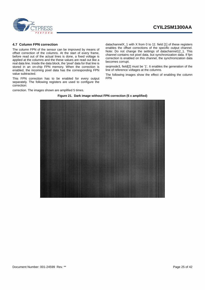
4.7 Column FPN correctionThe column FPN of the sensor can be improved by means ofoffset correction of the columns. At the start of every frame,before read out of the actual lines is done, a fixed voltage isapplied at the columns and the these values are read out like areal data line. Inside the data block, the 'pixel' data for that line isstored in an on-chip FPN memory. When the correction isenabled, the incoming pixel data has the corresponding FPNvalue subtracted. This FPN correction has to be enabled for every outputseparately. The following registers are used to configure thecorrection:
datachannelX_1 with X from 0 to 11: field [1] of these registersenables the offset corrections of the specific output channel.Note: Do not change the settings of datachannel12_1. Thischannel contains not pixel data, but synchronization data. If fpncorrection is enabled on this channel, the synchronization databecomes corrupt.seqmode3, field[2] must be '1'. It enables the generation of theline of reference voltages at the columns.The following images show the effect of enabling the columnFPN
correction. The images shown are amplified 5 times.
Figure 21. Dark image without FPN correction (5 x amplified)

CYIL2SM1300AA
Document Number: 001-24599 Rev. ** Page 26 of 42
Figure 22. Dark image with FPN correction enabled (5x amplified)

CYIL2SM1300AA
Document Number: 001-24599 Rev. ** Page 27 of 42
4.8 Image Format + Read Out ProtocolThe active area, as read out by the sequencer in full frame mode, looks like the following figure. Before starting the read out of theactual pixels, one dummy line is read to allow column FPN calibration. A reference voltage is applied to the columns and the entireline is read just as if real pixel values are put on the columns.Pixels are always read in multiples of 24 (one value to every channel in the AFE). The last time slot contains not only valid pixels, butalso 2 dummy columns, 6 grey columns, and 8 black columns.
Figure 23. Sensor Read Out Format

CYIL2SM1300AA
Document Number: 001-24599 Rev. ** Page 28 of 42
The following sections each list what the output looks like (data + synchronization codes) in several relevant configurations. Twelveof the output channels are connected to the 24 ADCs and take care of handling the data. One additional channel contains all thesynchronization codes for the receiver, indicating, for example, the start of a frame, the end of a frame, whether the data channelscontain data, CRC, a training pattern, and so on. The sequencer takes care of providing the synchronization channel with the correctsynchronization or protocol signals as shown in the following figure. The synchronization codes can be found in Table 17. Please notethat a FS serves as LS as well, just like a FE also serves as a LE.
Figure 24. Data + Sync Channel Overview
Table 17. Synchronization codesSync code Abbrev 10-bit code Input #
Frame Start FS 0x059 1Line Start LS 0x056 1Frame End FE 0x05A 1/2Line End LE 0x055 1/2Grey/Black Cols GBC 0x0A9 2CRC CRC 0x0A6 1FPN stored values FPN 0x13C 1+2Normal Data D 0x193 1/2Training Pattern T T 1/2

CYIL2SM1300AA
Document Number: 001-24599 Rev. ** Page 29 of 42
4.8.1 Full Frame ModeIn this operation mode, the entire sensor as shown in Figure 23 on page 27 is read out. Figure 25 shows the internal state of thesequencer, and the behavior of the data and sync channels (overview and detail of one line).
Figure 25. Full Frame mode Read Out
Data Channel
Sync Channel
Data channel
Sync Channel
Sequencer internal state
line 0 line 1 line
1022
line
1023
black
timeslot timeslot
timeslot
timeslot53
timeslot54
CRC timeslot
T
T FS
D D D D D D D LE
GBC
CRC
T
T
FOT ROT
ROT ROT
ROT
1 32

CYIL2SM1300AA
Document Number: 001-24599 Rev. ** Page 30 of 42
The following table gives a detailed overview of the remapping of one full row read out.Table 18. Remapping scheme for 1 rowtimeslot ch0 ch1 ch2 ch3 ch4 ch5 ch6 ch7 ch8 ch9 ch10 ch111a 0 2 4 6 8 10 12 14 16 18 20 221b 1 3 5 7 9 11 13 15 17 19 21 232a 47 45 43 41 39 37 35 33 31 29 27 252b 46 44 42 40 38 36 34 32 30 28 26 243a 48 50 52 54 56 58 60 62 64 66 68 703b 49 51 53 55 57 59 61 63 65 67 69 714a 95 93 91 89 87 85 83 81 79 77 75 734b 94 92 90 88 86 84 82 80 78 76 74 725a 96 98 100 102 104 106 108 110 112 114 116 1185b 97 99 101 103 105 107 109 111 113 115 117 1196a 143 141 139 137 135 133 131 129 127 125 123 1216b 142 140 138 136 134 132 130 128 126 124 122 1207a 144 146 148 150 152 154 156 158 160 162 164 1667b 145 147 149 151 153 155 157 159 161 163 165 1678a 191 189 187 185 183 181 179 177 175 173 171 1698b 190 188 186 184 182 180 178 176 174 172 170 1689a 192 194 196 198 200 202 204 206 208 210 212 2149b 193 195 197 199 201 203 205 207 209 211 213 21510a 239 237 235 233 231 229 227 225 223 221 219 21710b 238 236 234 232 230 228 226 224 222 220 218 21611a 240 242 244 246 248 250 252 254 256 258 260 26211b 241 243 245 247 249 251 253 255 257 259 261 26312a 287 285 283 281 279 277 275 273 271 269 267 26512b 286 284 282 280 278 276 274 272 270 268 266 264... ... ... ... ... ... ... ... ... ... ... ... ...... ... ... ... ... ... ... ... ... ... ... ... ...53a 1248 1250 1252 1254 1256 1258 1260 1262 1264 1266 1268 127053b 1249 1251 1253 1255 1257 1259 1261 1263 1265 1267 1269 127154a 1295 1293 1291 1289 1287 1285 1283 1281 1279 1277 1275 127354b 1294 1292 1290 1288 1286 1284 1282 1280 1278 1276 1274 1272CRC

CYIL2SM1300AA
Document Number: 001-24599 Rev. ** Page 31 of 42
4.8.2 Single Window Mode containing timeslot 54In this operation mode, only part of the sensor is read out, as shown by the shaded area in Figure 26. A clear distinction is made withthe single window mode not containing timeslot 54 as the output synchronization protocol is slightly different.
Figure 26. Single Window containing Timeslot 54
The following figure shows the internal state of the sequencer, and the behavior of the data and sync channels (overview and detailof one line) for this window mode.
Figure 27. Waveform for Single Window containing Timeslot 54
Data Channel Sync Channel
Sequencer internal state
line Ys LineYs+1
line Ye black
timeslotX
timeslotX+1 53 54
CRC
T LS
D FE
GBC
CRC
FOT
ROT
ROT
ROT
Data Channel
Sync Channel
timeslottimeslottimeslot
T
TT
DDD D
ROT

CYIL2SM1300AA
Document Number: 001-24599 Rev. ** Page 32 of 42
4.8.3 Single Window Mode NOT containing timeslot 54In this operation mode, only part of the sensor is read out, as shown in Figure 28. Although the window is defined as not containingany data from timeslot 54, it is read out to provide the information on grey and black columns to both the black level calibration algorithmand the user. This results in some minor differences between the waveforms from Figure 27 on page 31 and Figure 29 on page 32.
Figure 28. Single window NOT containing timeslot 54
Figure 29 shows the internal state of the sequencer, and the behavior of the data and sync channels (overview and detail of one line)for this window mode.
Figure 29. Waveform for single window NOT containing timeslot 54
Note that the dummy black line is read completely.Reading out multiple windows is in no way different from combining the windowed modes in Sections “Single Window Mode containingtimeslot 54” on page 31 and “Single Window Mode NOT containing timeslot 54” on page 32. The dummy black line again spans theentire width of the sensor and is processed only once, before all configured windows are read, and is independent of the window sizes.
Data Channel Sync Channel
Sequencer internal state
line Ys line Ys+1
line Ye black
timeslotXstart
timeslot timeslotXend
timeslot54
CRC timeslot
T
T LS
D D D D LE
T GBC
CRC
T
T
FOT ROT
ROT ROT
ROT
timeslotXend-1
D D

CYIL2SM1300AA
Document Number: 001-24599 Rev. ** Page 33 of 42
5. PinlistFigure 30. Pin Placement Layout (Top View)
1 2 3 4 5 6 7 8 9 10 11 12 13 14 15 16 17 18 19 20 21 22 23 24A 134 130 127 124 121 118 115 112 109 106 103 100 99 96 93 90 87 84 81 78 75 72 69 65B * 131 128 125 122 119 116 113 110 107 104 101 98 95 92 89 86 83 80 77 74 71 68 *C 133 132 129 126 123 120 117 114 111 108 105 102 97 94 91 88 85 82 79 76 73 70 67 66DEFGHJK TOP VIEWLMNPQRST 135 139 140 137 145 * 5 7 * 17 19 * * 31 29 * 43 41 * 54 62 60 59 64U 136 144 141 138 146 * 8 6 * 20 18 * * 30 32 * 42 44 * 53 61 55 58 63V 149 147 142 * 1 3 9 11 13 15 21 23 25 27 33 35 37 39 45 47 * 52 57 50 W 150 148 143 * 2 4 10 12 14 16 22 24 26 28 34 36 38 40 46 48 * 51 56 49

CYIL2SM1300AA
Document Number: 001-24599 Rev. ** Page 34 of 42
Table 19. Pin Listnr pin name Type Direction Description Position
1 clkoutp LVDS O p clk output channel V52 clkoutn LVDS O n clk output channel W53 chp[0] LVDS O p output channel [0] V64 chn[0] LVDS O n output channel [0] W65 gndlvds Supply IO LVDS ground T76 gndadc Supply IO ADC gound U87 vddadc Supply IO ADC power T88 vddlvds Supply IO LVDS power U79 chp[1] LVDS O p output channel [1] V710 chn[1] LVDS O n output channel [1] W711 chp[2] LVDS O p output channel [2] V812 chn[2] LVDS O n output channel [2] W813 chp[3] LVDS O p output channel [3] V914 chn[3] LVDS O n output channel [3] W915 chp[4] LVDS O p output channel [4] V1016 chn[4] LVDS O n output channel [4] W1017 gndlvds Supply IO LVDS ground T1018 gndadc Supply IO ADC gound U1119 vddadc Supply IO ADC power T1120 vddlvds Supply IO LVDS power U1021 chp[5] LVDS O p output channel [5] V1122 chn[5] LVDS O n output channel [5] W1123 chp[6] LVDS O p output channel [6] V1224 chn[6] LVDS O n output channel [6] W1225 chp[7] LVDS O p output channel [7] V1326 chn[7] LVDS O n output channel [7] W1327 chp[8] LVDS O p output channel [8] V1428 chn[8] LVDS O n output channel [8] W1429 gndlvds Supply IO LVDS ground T1530 gndadc Supply IO ADC gound U1431 vddadc Supply IO ADC power T1432 vddlvds Supply IO LVDS power U1533 chp[9] LVDS O p output channel [9] V1534 chn[9] LVDS O n output channel [9] W1535 chp[10] LVDS O p output channel [10] V1636 chn[10] LVDS O n output channel [10] W1637 chp[11] LVDS O p output channel [11] V1738 chn[11] LVDS O n output channel [11] W1739 n/a not assigned V1840 n/a not assigned W1841 gndlvds Supply IO LVDS ground T1842 gndadc Supply IO ADC gound U1743 vddadc Supply IO ADC power T17

CYIL2SM1300AA
Document Number: 001-24599 Rev. ** Page 35 of 42
44 vddlvds Supply IO LVDS power U1845 clkinp LVDS I LVDS input clock 310 Mhz p-node V1946 clkinn LVDS I LVDS input clock 310 Mhz n-node W1947 syncp LVDS O LVDS sync p output V2048 syncn LVDS O LVDS sync n output W2049 gnddig Supply IO digital ground W2450 vdddig Supply IO digital power supply V2451 cap_vrefm Analog O lower limit adc range decoupling W2252 cap_vrefp Analog O higher limit adc range decoupling V2253 gndadc Supply IO ADC ground U2054 vddadc Supply IO ADC power supply T2055 gnddig Supply IO digital ground U2256 gndbuf Supply IO column buffers ground W2357 vddbuf Supply IO column buffers supply V2358 gndana Supply IO column buffers ground U2359 vddana Supply IO column buffers supply T2360 vpix Supply IO pixel core supply T2261 gndpix Supply IO pixel core ground U2162 vsamp Supply IO image core select and sample supply T2163 gndadc Supply IO ADC ground U2464 vdddig Supply IO digital power supply T2465 nbias_colload Analog O column bias decouple A2466 test_ena CMOS I scan pin for sequencer C2467 int_time1 CMOS I integration pin first slope C2368 int_time2 CMOS I integration pin dual slope B2369 int_time3 CMOS I integration pin tripple slope A2370 monitor1 CMOS O output pin for integration timing, high during integration C2271 monitor2 CMOS O output pin for dual slope integration timing, high during
integrationB22
72 monitor3 CMOS O output pin for triple slope integration timing, high during integration
A22
73 cap_vrefadc Analog O ADC black reference decoupling C2174 vpix Supply IO pixel core supply B2175 cap_vrefcm Analog O adc common mode decoupling A21
76 reset_n CMOS IO chip reset (active low) C2077 scan_en CMOS I DFT scan enable B2078 scan_clk CMOS I DFT clock A2079 scan_clk_en CMOS I DFT clock enable C1980 gndpix Supply IO pixel core ground B1981 gnddig Supply IO digital ground A1982 vdddig Supply IO digital power supply C1883 vpix Supply IO pixel core supply B1884 pixdiode Analog O pixel diode current pin A18
nr pin name Type Direction Description Position

CYIL2SM1300AA
Document Number: 001-24599 Rev. ** Page 36 of 42
85 gndpix Supply IO pixel core ground C1786 vsamp Supply IO image core select and sample supply B1787 vresetab Supply IO anti blooming lower reset level A1788 vprech Supply IO pixel precharge level / decoupling pin C1689 vmemh Supply IO pixel memory reference high B1690 vmeml Supply IO pixel memory reference low A1691 vreset Supply IO pixel reset level C1592 vresetds Supply IO pixel dual slope reset level / decoupling pin B1593 vresetts Supply IO pixel tripple splope reset level / decoupling pin A1594 vresetab Supply IO anti blooming lower reset level C1495 gndpix Supply IO pixel core ground B1496 vresetts Supply IO pixel tripple splope reset level / decoupling pin A1497 vresetds Supply IO pixel dual slope reset level / decoupling pin C1398 vreset Supply IO pixel reset level B1399 vsamp Supply IO image core select and sample supply A13 100 vmeml Supply IO pixel memory reference low A12 101 vmemh Supply IO pixel memory reference high B12 102 vprech Supply IO pixel precharge level / decoupling pin C12 103 n/a not assigned A11 104 gndpix Supply IO pixel core ground B11 105 vresetab Supply IO anti blooming lower reset level C11 106 vresetts Supply IO pixel tripple splope reset level / decoupling pin A10 107 vresetds Supply IO pixel dual slope reset level / decoupling pin B10 108 vreset Supply IO pixel reset level C10 109 vmeml Supply IO pixel memory reference low A9 110 vmemh Supply IO pixel memory reference high B9 111 vprech Supply IO pixel precharge level / decoupling pin C9 112 vresetab Supply IO anti blooming lower reset level A8 113 vsamp Supply IO image core select and sample supply B8 114 gndpix Supply IO pixel core ground C8 115 ibiaspre Analog I extermal current bias for vprech (not connected by
default)A7
116 vpix Supply IO pixel core supply B7 117 vdddig Supply IO digital power supply C7 118 gnddig Supply IO digital ground A6 119 gndpix Supply IO pixel core ground B6 120 thermkathtop Analog O temperature sensor kathode bottom C6 121 thermanotop Analog I temperature sensor anode bottom A5 122 thermkathbot Analog O temperature sensor kathode bottom B5 123 thermanobot Analog I temperature sensor anode bottom C5 124 cap_vrefcm Analog O adc common mode decoupling A4 125 vpix Supply IO pixel core supply B4 126 cap_vrefadc Analog O ADC black reference decoupling C4 127 spics CMOS I SPI chip select A3
nr pin name Type Direction Description Position
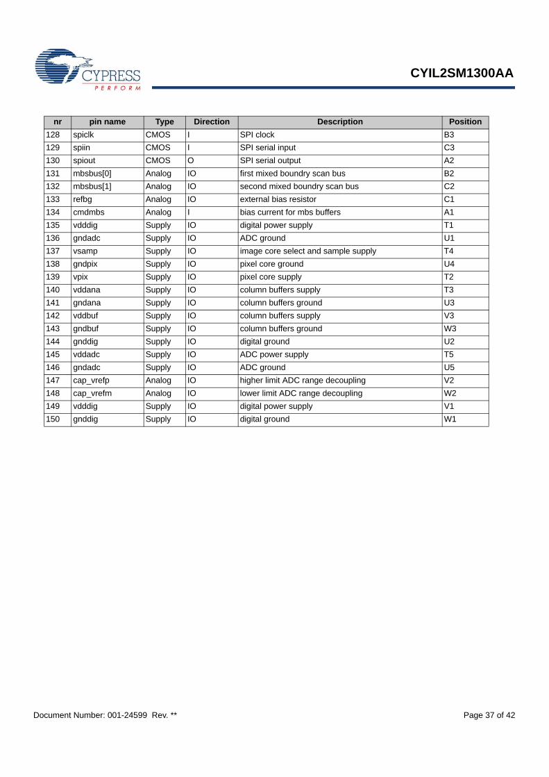
CYIL2SM1300AA
Document Number: 001-24599 Rev. ** Page 37 of 42
128 spiclk CMOS I SPI clock B3 129 spiin CMOS I SPI serial input C3 130 spiout CMOS O SPI serial output A2 131 mbsbus[0] Analog IO first mixed boundry scan bus B2 132 mbsbus[1] Analog IO second mixed boundry scan bus C2 133 refbg Analog IO external bias resistor C1 134 cmdmbs Analog I bias current for mbs buffers A1 135 vdddig Supply IO digital power supply T1 136 gndadc Supply IO ADC ground U1 137 vsamp Supply IO image core select and sample supply T4 138 gndpix Supply IO pixel core ground U4 139 vpix Supply IO pixel core supply T2 140 vddana Supply IO column buffers supply T3 141 gndana Supply IO column buffers ground U3 142 vddbuf Supply IO column buffers supply V3 143 gndbuf Supply IO column buffers ground W3 144 gnddig Supply IO digital ground U2 145 vddadc Supply IO ADC power supply T5 146 gndadc Supply IO ADC ground U5 147 cap_vrefp Analog IO higher limit ADC range decoupling V2 148 cap_vrefm Analog IO lower limit ADC range decoupling W2 149 vdddig Supply IO digital power supply V1 150 gnddig Supply IO digital ground W1
nr pin name Type Direction Description Position

CYIL2SM1300AA
Document Number: 001-24599 Rev. ** Page 38 of 42
6. Package drawingFigure 31. Package Drawing (A)

CYIL2SM1300AA
Document Number: 001-24599 Rev. ** Page 39 of 42
Figure 32. Package Drawing (B)

CYIL2SM1300AA
Document Number: 001-24599 Rev. ** Page 40 of 42
6.1 Package with Glass cross-sectionFigure 33. Package Cross-section
6.2 Die SpecificationsFigure 34. Die Specifications

CYIL2SM1300AA
Document Number: 001-24599 Rev. ** Page 41 of 42
7. Glass lidA D263 glass is used as protection glass lid on top of the LUPA-1300-2 monochrome and color sensors. The following figure showsthe transmission characteristics of the D263 glass.
Figure 35. Transmission characteristics of the D263 glass used as protective cover for the LUPA-1300-2 sensors
As can be seen in Figure 35, no infrared attenuating color filterglass is used. The user is required to provide this filter in theoptical path when color devices are used.
8. Color filterAn optional color filter can be processed as well. TheLUPA-1300-2 can also be processed with a Bayer RGB colorpattern.
9. Handling precautionsSpecial care must be given when soldering image sensors withcolor filter arrays (RGB color filters), onto a circuit board, sincecolor filters are sensitive to high temperatures. Prolongedheating at elevated temperatures may result in deterioration ofthe performance of the sensor. The following recommendationsare made to ensure that sensor performance is not compromisedduring end-users' assembly processes.Board Assembly:Device placement onto boards must be done in accordance withstrict ESD controls for Class 0, JESD22 Human Body Model, andClass A, JESD22 Machine Model devices. Assembly operatorsmust always wear all designated and approved grounding
equipment; grounded wrist straps at ESD protected workstationsare recommended, including the use of ionized blowers. All toolsmust be ESD protected.Manual Soldering:When a soldering iron is used the following conditions must beobserved:Use a soldering iron with temperature control at the tip.The soldering iron tip temperature must not exceed 350°C.The soldering period for each pin must be less than 5 seconds.Precautions and cleaning:Avoid spilling solder flux on the cover glass; bare glass andparticularly glass with antireflection filters may be adverselyaffected by the flux. Avoid mechanical or particulate damage tothe cover glass.It is recommended that isopropyl alcohol (IPA) be used as asolvent for cleaning the image sensor glass lid. When using othersolvents, it must be confirmed beforehand whether the solventdissolves the package or the glass lid or both.

Document Number: 001-24599 Rev. ** Revised September 10, 2007 Page 42 of 42
All products and company names mentioned in this document may be the trademarks of their respective holders.
CYIL2SM1300AA
© Cypress Semiconductor Corporation, 2007. The information contained herein is subject to change without notice. Cypress Semiconductor Corporation assumes no responsibility for the use of anycircuitry other than circuitry embodied in a Cypress product. Nor does it convey or imply any license under patent or other rights. Cypress products are not warranted nor intended to be used for medical,life support, life saving, critical control or safety applications, unless pursuant to an express written agreement with Cypress. Furthermore, Cypress does not authorize its products for use as criticalcomponents in life-support systems where a malfunction or failure may reasonably be expected to result in significant injury to the user. The inclusion of Cypress products in life-support systemsapplication implies that the manufacturer assumes all risk of such use and in doing so indemnifies Cypress against all charges.
Any Source Code (software and/or firmware) is owned by Cypress Semiconductor Corporation (Cypress) and is protected by and subject to worldwide patent protection (United States and foreign),United States copyright laws and international treaty provisions. Cypress hereby grants to licensee a personal, non-exclusive, non-transferable license to copy, use, modify, create derivative works of,and compile the Cypress Source Code and derivative works for the sole purpose of creating custom software and or firmware in support of licensee product to be used only in conjunction with a Cypressintegrated circuit as specified in the applicable agreement. Any reproduction, modification, translation, compilation, or representation of this Source Code except as specified above is prohibited withoutthe express written permission of Cypress.
Disclaimer: CYPRESS MAKES NO WARRANTY OF ANY KIND, EXPRESS OR IMPLIED, WITH REGARD TO THIS MATERIAL, INCLUDING, BUT NOT LIMITED TO, THE IMPLIED WARRANTIESOF MERCHANTABILITY AND FITNESS FOR A PARTICULAR PURPOSE. Cypress reserves the right to make changes without further notice to the materials described herein. Cypress does notassume any liability arising out of the application or use of any product or circuit described herein. Cypress does not authorize its products for use as critical components in life-support systems wherea malfunction or failure may reasonably be expected to result in significant injury to the user. The inclusion of Cypress’ product in a life-support systems application implies that the manufacturerassumes all risk of such use and in doing so indemnifies Cypress against all charges.
Use may be limited by and subject to the applicable Cypress software license agreement.
Document History Page
Document Title: CYIL2SM1300AA LUPA-1300-2 High speed CMOS Image SensorDocument Number: 001-24599
Revision ECN Orig. of Change Description of Change
** See ECN FPW Initial Cypress release

![IBIS5-B-1300 CYII5FM1300AB 1.3 MP CMOS Image Sensor Sheets/Cypress PDFs/IBIS5-B-130… · Packaging 84-pins LCC [+] Feedback . IBIS5-B-1300 CYII5FM1300AB ... Using M4 as a global](https://img.pdfslide.net/doc/110x75/5a9b39fb7f8b9adb5c8de135/ibis5-b-1300-cyii5fm1300ab-13-mp-cmos-image-sensor-sheetscypress-pdfsibis5-b-130packaging.jpg)


![LUPA 1300 2 Datasheet[1]](https://img.pdfslide.net/doc/110x75/577ce7321a28abf1039490e2/lupa-1300-2-datasheet1.jpg)