Embed Size (px)
Citation preview

Adv. Eng. Tec. Appl. 3, No. 1, 1-6 (2014) 1
Advanced Engineering Technology and ApplicationAn International Journal
http://dx.doi.org/10.12785/aeta/paper
D Flip Flop with Different Technologies
Amit Grover1,∗ and Sumer Singh2
1 Department of Electronics & Communication Engineering, S.B.S State Technical Campus Ferozepur, Punjab, India2 Department of Electronics & Communication Engineering, Government Polytechnic College, Ferozepur, Punjab, India
Received: 15 Oct. 2013, Revised: 19 Dec. 2013, Accepted: 22 Dec. 2013Published online: 1 Jan. 2014
Abstract: This article explains a new implementation of efficient D-Flip-Flop (DFF) using Gate-Diffusion-Input (GDI) technique,PowerPC, DSTC, and HLFF. This DFF design allows reducing power-delay product and area of the circuit, while maintaining lowcomplexity of logic design. Performance comparison with other DFF design techniques is presented, with respect to gate area, number ofdevices, delay and power dissipation, showing advantages and drawbacks of GDI DFF as compared to other methods. The performanceis carried out by HSPICE simulation with 180 nm & 90 nm CMOS technology.
Keywords: D flip-flop, low power, Gate-Diffusion-Input (GDI) technique, PowerPC, DSTC, and HLFF
1 Introduction
Binary logic has been widely used in the electronic fields.It is traditional and thus, more mature thanmultiple-valued logic. However, alongside the boomingof the information and electronic industry, thedeficiencies of binary circuits began to emerge. It hasbeen rather difficult for binary logic to satisfy demandsfrom chip area, switching speed, power dissipation, andother aspects all at the same time. Therefore, multiplevalued circuits are becoming increasingly important.Digital circuits in every high speed technology aretypically benchmarked by the performance of staticfrequency dividers which is recognized as a figure ofmerit for a digital integrated circuit process, because astatic frequency divider uses the same basic flip-flopelements found in more complex sequential circuits[1].High speed frequency dividers [2] are one of the keydevices in measurement equipments, microwave andsatellite communication systems. Therefore, manydifferent high speed static and dynamic frequencydividers [3] [4] based on various kinds of devicetechnology have been developed.
The fastest frequency dividers [5] to date are theAlInAs/GalnAs HBT static frequency divider operating at39.5GHz [6], the AlGaAs/GaAs HEMT and the T-gateA1GaAs/InGaAs MODFET dynamic frequency dividersat 34GHz [7] and 51GHz [8], respectively. In addition, a30GHz static frequency divider based on the Si-bipolar
technology has been reported in [9]. On the Other hand,building low power VLSI systems has emerged as highlyin demand because of the fast growing technologies inmobile communication and computation. The batterytechnology does not advance at the same rate as themicroelectronics technology [10]. There is a limitedamount of power available for the mobile systems. Sodesigners are faced with more constraints: high speed,high throughput, small silicon area, and at the same time,low power consumption. Therefore building low power,high performance circuits are of great interest [11].
Wide utilization of memory storage systems andsequential logic in modern electronics triggers a demandfor high-performance and low-area implementations ofbasic memory components. One of the most importantstate-holding elements is the D-Flip-Flop (DFF) [1].Various DFF circuits were researched and presented inthe literature, aiming to achieve an optimal design interms of delay, power and area. Some efficient techniqueswere developed and adopted by designers for a variety oftechnologies [1].
2 BASIC GDI FUNCTION
The GDI method is based on the use of a simple cell asshown in Fig. 1. At first glance, the basic cell reminds oneof the standard CMOS inverter, but there are someimportant differences.
∗ Corresponding author e-mail: amitgrover [email protected]⃝ 2014 NSP
Natural Sciences Publishing Cor.

2 A. Grover, S. Singh: D Flip Flop with Different Technologies
1) The GDI cell contains three inputs: (common gateinput of nMOS and pMOS), P (input to the source/drainof pMOS), and N (input to the source/drain of nMOS). 2)Bulks of both nMOS and pMOS are connected to N orP (respectively), so it can be arbitrarily biased at contrastwith a CMOS inverter.
Gate-Diffusion-Input (GDI) design technique that wasrecently developed and presented in [12], proposes anefficient alternative for logic design in standard CMOSand SOI technologies. The GDI method is based on thesimple cell shown in Fig. 1. A basic GDI cell containsfour terminals - G (the common gate input of the nMOSand pMOS transistors), P (the outer diffusion node of thepMOS transistor), N (the outer diffusion node of thenMOS transistor) and the D node (the common diffusionof both transistors). P, N and D may be used as eitherinput or output ports, depending on the circuit structure.Table 1 shows how various configuration changes of theinputs P, N and G in the basic GDI cell correspond todifferent Boolean functions at the output D. GDI enablessimpler gates, lower transistor count, and lower powerdissipation in many implementations, as compared withstandard CMOS and PTL design techniques [12].Multiple-input gates can be implemented by combiningseveral GDI cells. The buffering constraints, due topossible VTH drop, are described in detail in [12], as wellas technological compatibility with CMOS and SOI.
Fig. 1: GDI basic cell
It must be remarked that not all of the functions arepossible in standard p-well CMOS process but can besuccessfully implemented in twin-well CMOS or siliconon insulator (SOI) technologies.
Table 1: VARIOUS LOGIC FUNCTIONS OF GDI CELL FORDIFFERENT INPUT CONFIGURATIONS
3 Power Consumption in CMOS Circuits
There are three main components of power consumptionin digital CMOS VLSI circuits.
1.Switching Power: consumed in charging anddischarging of the circuit capacitances duringtransistor switching.
2.Short-Circuit Power: consumed due to short-circuitcurrent flowing from power supply to ground duringtransistor switching. This power more dominates inDeep Sub Micron (DSM) technology.
3.Static Power: consumed due to static and leakagecurrents flowing while the circuit is in a stable state.The first two components are referred to as dynamicpower, since power is consumed dynamically whilethe circuit is changing states. Dynamic poweraccounts for the majority of the total powerconsumption in digital CMOS VLSI circuits atmicron technology [7][13].
Pavg = Pswitching +Pshort−circuit +Pleakage (1)
Pavg = α0→1 ×Cl ×V 2dd ×Fclk + Isc ×V dd + Ileakage ×V dd
(2)
4 SIMULATION AND COMPARISON
Due to the topological differences among the existinglatches, some of them required a modified test bench, i.e.,a dual input and/or a single output. However, thesemodifications did not alter the principal of the analysisapproach based on the simulation conditions. The role of
c⃝ 2014 NSPNatural Sciences Publishing Cor.
Adv. Eng. Tec. Appl. 3, No. 1, 1-6 (2014) / www.naturalspublishing.com/Journals.asp 3
the test bench is to provide the realistic data and clocksignals, the fan out signal degradation from the previousand to the succeeding stage, and measurement of powerdissipated on switching of the clock and data inputs.Buffering inverters provide the realistic data and clocksignals, which themselves are fed from ideal voltagesources. Furthermore, capacitive load at the data inputsimulates the fan out signal degradation from previousstages. Capacitive loads at the outputs simulate the fanout signal degradation caused by the succeeding stages.
As mentioned in the section on power considerations,there are three kinds of power dissipation that weremeasured in order to get the real insight in the amount ofpower consumed in and around the latch due to itspresence.
1.Local data power dissipation presents the portion ofthe gray inverter’s power consumption dissipated onswitching the data input capacitance.
2.Local clock power dissipation presents the portion ofthe black inverter’s power consumption dissipated onswitching the clock input capacitance.
3.Internal power dissipation includes the intrinsic powerdissipated on switching the internal nodes of thecircuit and excludes the power dissipated onswitching the output load capacitances.
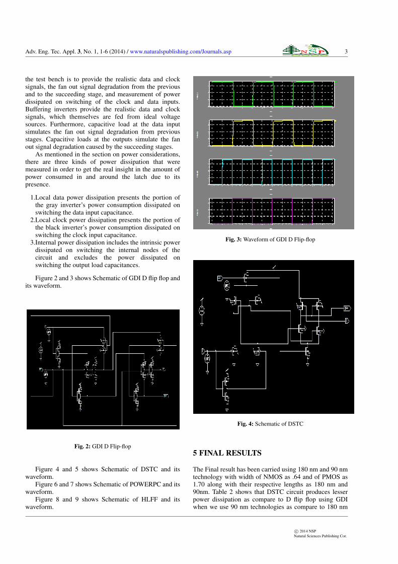
Figure 2 and 3 shows Schematic of GDI D flip flop andits waveform.
Fig. 2: GDI D Flip-flop
Figure 4 and 5 shows Schematic of DSTC and itswaveform.
Figure 6 and 7 shows Schematic of POWERPC and itswaveform.
Figure 8 and 9 shows Schematic of HLFF and itswaveform.
Fig. 3: Waveform of GDI D Flip-flop
Fig. 4: Schematic of DSTC
5 FINAL RESULTS
The Final result has been carried using 180 nm and 90 nmtechnology with width of NMOS as .64 and of PMOS as1.70 along with their respective lengths as 180 nm and90nm. Table 2 shows that DSTC circuit produces lesserpower dissipation as compare to D flip flop using GDIwhen we use 90 nm technologies as compare to 180 nm
c⃝ 2014 NSPNatural Sciences Publishing Cor.

4 A. Grover, S. Singh: D Flip Flop with Different Technologies
Fig. 5: Waveform of DSTC
Fig. 6: Schematic of POWERPC
technology. In DSTC circuit, we have used 12 transistorsbut in GDI number of transistors used are 18 to build Dflip flop, so in DSTC lesser be the area, lesser powerdissipation and lesser delay as compare to the GDI basedD Flip flop. PowerPC circuit is implemented with 18transistors so its power dissipation is more similar to thecircuit GDI. HLFF circuit is implemented with 20transistors so it dissipates more power as compare to allcircuits and more is its area. This article explains the
Fig. 7: Waveform of POWERPC
Fig. 8: Schematic of HLFF
performance comparison of four different circuits whichinclude Gate-Diffusion-Input (GDI) technique, PowerPC,DSTC, and HLFF used to build D flip-flop. Among allthese circuits DSTC uses lesser transistors, lesser area,lesser delay and lesser the power dissipation. The mainpoint of the optimization is the minimization of thepower-delay product, given the always-present tradeoffbetween power and speed.
6 CONCLUSIONS AND FUTURERESEARCH
A new implementation of high-performance D-Flip- Flopusing Gate-Diffusion-Input technique, PowerPC, DSTC,
c⃝ 2014 NSPNatural Sciences Publishing Cor.

Adv. Eng. Tec. Appl. 3, No. 1, 1-6 (2014) / www.naturalspublishing.com/Journals.asp 5
Fig. 9: Waveform of HLFF
Table 2: PERFORMANCE PARAMETERS OF D FLIP FLOP
and HLFF was presented. The proposed circuit has asimple structure, based on Master-Slave principle, andcontains 18 transistors. An optimization procedure wasdeveloped for GDI DFF, based on iterative transistorsizing, while targeting a minimal power-delay product.Performance comparison with other DFF designtechniques was shown, with respect to gate area, numberof devices, delay and power dissipation. A variety of
circuits have been implemented in 90 nm and 180 nmtechnologies to compare the proposed GDI structure witha set of representative flip-flops, commonly used for highperformance design. The future research activities mayinclude further higher bits of D- Flip using this GDItechnology, PowerPC, DSTC, and HLFF.[1]
References
[1] J. M. Rabaey, A. P. Chandrakasan, and B. Nikolic, Digitalintegrated circuits. Prentice hall Englewood Cliffs, 2002,vol. 2.
[2] M. Sokolich, C. Fields, B. Shi, Y. Brown, M. Montes,R. Martinez, A. Kramer, S. Thomas III, and M. Madhav, “Alow power 72.8 ghz static frequency divider implementedin alinas/ingaas hbt ic technology,” in GaAs IC Symposium,2000. 22nd Annual. IEEE, 2000, pp. 81–84.
[3] M. Hafizi, J. F. Jensen, R. A. Metzger, W. E. Stanchina, D. B.Rensch, and Y. K. Allen, “39.5-ghz static frequency dividerimplemented in alinas/gainas hbt technology,” ElectronDevice Letters, IEEE, vol. 13, no. 12, pp. 612–614, 1992.
[4] J. M. Wong, V. S. Cheung, and H. C. Luong, “A 1-v 2.5-mw 5.2-ghz frequency divider in a 0.35-µm cmos process,”Solid-State Circuits, IEEE Journal of, vol. 38, no. 10, pp.1643–1648, 2003.
[5] H. Wang, “A 1.8 v 3 mw 16.8 ghz frequency divider in0.25/spl mu/m cmos,” in Solid-State Circuits Conference,2000. Digest of Technical Papers. ISSCC. 2000 IEEEInternational. IEEE, 2000, pp. 196–197.
[6] V. Stojanovic and V. G. Oklobdzija, “Comparative analysisof master-slave latches and flip-flops for high-performanceand low-power systems,” Solid-State Circuits, IEEE Journalof, vol. 34, no. 4, pp. 536–548, 1999.
[7] G. Gerosa, S. Gary, C. Dietz, D. Pham, K. Hoover,J. Alvarez, H. Sanchez, P. Ippolito, T. Ngo, S. Litch et al., “A2.2 w, 80 mhz superscalar risc microprocessor,” Solid-StateCircuits, IEEE Journal of, vol. 29, no. 12, pp. 1440–1454,1994.
[8] H. Partovi, R. Burd, U. Salim, F. Weber, L. DiGregorio, andD. Draper, “Fa 8.5: Flow-through latch and edge-triggeredflip-flop hybrid elements,” ISSCC Dig. Tech. Papers, vol. 8,pp. 138–139, 1996.
[9] J. Yuan and C. Svensson, “New single-clock cmos latchesand flipflops with improved speed and power savings,”Solid-State Circuits, IEEE Journal of, vol. 32, no. 1, pp. 62–69, 1997.
[10] A. Morgenshtein, A. Fish, and I. A. Wagner, “Gate-diffusioninput (gdi)-a novel power efficient method for digitalcircuits: a design methodology,” in ASIC/SOC Conference,2001. Proceedings. 14th Annual IEEE International. IEEE,2001, pp. 39–43.
[11] A. Saberkari, S. B. Shokouhi, A. Kiani, andF. Poorahangaryan, “A novel low power static frequencydivider based on the gdi technique,” in Electrical andComputer Engineering, 2009. CCECE’09. CanadianConference on. IEEE, 2009, pp. 67–70.
[12] A. Morgenshtein, A. Fish, and I. A. Wagner, “Gate-diffusion input (gdi): a power-efficient method for digitalcombinatorial circuits,” Very Large Scale Integration (VLSI)
c⃝ 2014 NSPNatural Sciences Publishing Cor.

6 A. Grover, S. Singh: D Flip Flop with Different Technologies
Systems, IEEE Transactions on, vol. 10, no. 5, pp. 566–581,2002.
[13] T. Fuse, M. Tokumasu, S. Kawanaka, H. Fujii,A. Kameyama, M. Yoshimi, and S. Watanabe, “A 1.1v soi cmos frequency divider using body-inputting sclcircuit technology,” in SOI Conference, 2000 IEEEInternational. IEEE, 2000, pp. 106–107.
Amit Grover becamea Member (M) of AssociationISTE in 2006, a SeniorMember (SM) of societySELCOME in September2009, and a Project-In charge(PI) in august 2011 and inSeptember 2012. The authorplace of birth is Ferozepur,Punjab, India on 27th,
September 1980.The author received his M. Tech degreein Electronics and Communication Engineering fromPunjab Technical University, Kapurthla, Punjab, India in2008 and received his B. Tech degree in Electronics andCommunication Engineering from Punjab TechnicalUniversity, Kapurthala, Punjab, India in 2001. Currently,he is working as an Assistant Professor in ShaheedBhagat Singh State Technical Campus, Ferozepur,Punjab, India. The author is a Reviewer of many ReputedInternational Journals. His area of interest includessignal processing, MIMO systems, Wireless mobilecommunication; high speed digital communications, 4GWireless Communications and VLSI Design.
Sumer Singh the authorplace of birth is Ferozepur,Punjab, India on 15th, August1985. The author receivedhis M. Tech degree in Electronicsand Communication Engineeringfrom Punjab TechnicalUniversity, Kapurthla, Punjab,India in 2013 and received his
B. Tech degree in Electronics and CommunicationEngineering from Punjab Technical University,Kapurthala, Punjab, India in 2010. Currently, he isworking as a Lecturer in Department of Electronics &Communication Engineering, Government PolytechnicCollege, Ferozepur, Punjab India. His area of interestincludes Wireless Communication Network, Mobile AdHoc Network, Wireless Sensor Network and VLSIDesign.
c⃝ 2014 NSPNatural Sciences Publishing Cor.