Embed Size (px)
Citation preview

Rev. 1.2 8/16 Copyright © 2016 by Silicon Laboratories Si7015-A20
Si7015-A20
DIGITAL I2C HUMIDITY AND TEMPERATURE SENSOR
Features
Applications
Description
The Si7015 I2C Humidity and Temperature Sensor is a monolithic CMOSIC integrating humidity and temperature sensor elements, an analog-to-digital converter, signal processing, calibration data, and an I2C Interface.The patented use of industry-standard, low-K polymeric dielectrics forsensing humidity enables the construction of low-power, monolithicCMOS Sensor ICs with low drift and hysteresis and excellent long termstability.
Each unit is factory-calibrated, and the calibration data is stored in the on-chip non-volatile memory. This ensures that the sensors are fullyinterchangeable, with no recalibration or software changes required. TheSi7015 can be used as a drop-in upgrade for the Si7005 with only minorsoftware changes because the register sets are the same, and the4x4 mm QFN package is footprint-compatible with that of the Si7005.
The device is compatible with standard SMT assembly processes, suchas reflow. The optional factory-installed cover offers a low profile andconvenient means of protecting the sensor during assembly (e.g., reflowsoldering) and throughout the life of the product, excluding liquids(hydrophobic/oleophobic) and particulates.
The Si7015 offers an accurate, low-power, factory-calibrated digitalsolution ideal for measuring humidity, dew-point, and temperature inapplications ranging from HVAC/R and asset tracking to industrial andconsumer platforms.
Precision Relative Humidity Sensor± 4.5% RH (max), 0–80% RH
High-Accuracy Temperature Sensor±1 ºC (max), –10 to 85 °C
0 to 100% RH operating range
0 to +70 °C operating range (FM)
–40 to +85 °C operating range (GM)
Low Voltage Operation (1.9 to 3.6 V)
Low Power Consumption150 µA active current60 nA standby current
Drop-In Upgrade for Si7005
Factory-calibrated
I2C Interface
Integrated on-chip heater
4x4 mm QFN package
Excellent long term stability
Optional factory-installed coverLow-profileProtection during reflowExcludes liquids and
particulates
HVAC/R
Thermostats/humidistats
Instrumentation
White goods
Micro-environments/data centers
Industrial controls
Weather stations
Asset tracking and storage
Patent protected; patents pending
Ordering Information
See page 31.
Pin Assignments
1
6
5
4
3
2
18
13
14
15
16
17
24
19
20
21
22
23
127 8 9 10
11
GND
DNC
DNC
SDA
SCL
DNC
DNC
DNC
CS
DNC
DNC
DN
C
DN
C
GN
D
DN
C
VD
D
GN
D
DN
C
GN
D
DN
C
DN
C
DN
C
DN
C
DNC
Si7015-A20
2 Rev. 1.2
Functional Block Diagram
Si7015-A20
Rev. 1.2 3
TABLE OF CONTENTS
Section Page
1. Electrical Specifications . . . . . . . . . . . . . . . . . . . . . . . . . . . . . . . . . . . . . . . . . . . . . . . . . . .42. Typical Application Circuit . . . . . . . . . . . . . . . . . . . . . . . . . . . . . . . . . . . . . . . . . . . . . . . .103. Bill of Materials . . . . . . . . . . . . . . . . . . . . . . . . . . . . . . . . . . . . . . . . . . . . . . . . . . . . . . . . . .114. Functional Description . . . . . . . . . . . . . . . . . . . . . . . . . . . . . . . . . . . . . . . . . . . . . . . . . . .12
4.1. Overview . . . . . . . . . . . . . . . . . . . . . . . . . . . . . . . . . . . . . . . . . . . . . . . . . . . . . . . . . .124.2. Relative Humidity Sensor Accuracy . . . . . . . . . . . . . . . . . . . . . . . . . . . . . . . . . . . . .134.3. Temperature Compensation . . . . . . . . . . . . . . . . . . . . . . . . . . . . . . . . . . . . . . . . . . .144.4. Hysteresis . . . . . . . . . . . . . . . . . . . . . . . . . . . . . . . . . . . . . . . . . . . . . . . . . . . . . . . . .144.5. Prolonged Exposure to High Humidity . . . . . . . . . . . . . . . . . . . . . . . . . . . . . . . . . . .144.6. PCB Assembly . . . . . . . . . . . . . . . . . . . . . . . . . . . . . . . . . . . . . . . . . . . . . . . . . . . . .154.7. Protecting the Sensor . . . . . . . . . . . . . . . . . . . . . . . . . . . . . . . . . . . . . . . . . . . . . . . .174.8. Bake/Hydrate Procedure . . . . . . . . . . . . . . . . . . . . . . . . . . . . . . . . . . . . . . . . . . . . . .174.9. Long Term Drift/Aging . . . . . . . . . . . . . . . . . . . . . . . . . . . . . . . . . . . . . . . . . . . . . . . .17
5. Host Interface . . . . . . . . . . . . . . . . . . . . . . . . . . . . . . . . . . . . . . . . . . . . . . . . . . . . . . . . . . .185.1. I2C Interface . . . . . . . . . . . . . . . . . . . . . . . . . . . . . . . . . . . . . . . . . . . . . . . . . . . . . . .185.2. I2C Operation . . . . . . . . . . . . . . . . . . . . . . . . . . . . . . . . . . . . . . . . . . . . . . . . . . . . . .23
6. Control Registers . . . . . . . . . . . . . . . . . . . . . . . . . . . . . . . . . . . . . . . . . . . . . . . . . . . . . . . .266.1. Register Detail . . . . . . . . . . . . . . . . . . . . . . . . . . . . . . . . . . . . . . . . . . . . . . . . . . . . . .26
7. Pin Descriptions: Si7015 . . . . . . . . . . . . . . . . . . . . . . . . . . . . . . . . . . . . . . . . . . . . . . . . . .308. Ordering Guide . . . . . . . . . . . . . . . . . . . . . . . . . . . . . . . . . . . . . . . . . . . . . . . . . . . . . . . . . .319. Package Outline . . . . . . . . . . . . . . . . . . . . . . . . . . . . . . . . . . . . . . . . . . . . . . . . . . . . . . . . .32
9.1. 24-Pin QFN . . . . . . . . . . . . . . . . . . . . . . . . . . . . . . . . . . . . . . . . . . . . . . . . . . . . . . . .329.2. 24-Pin QFN with Protective Cover . . . . . . . . . . . . . . . . . . . . . . . . . . . . . . . . . . . . . .33
10. PCB Land Pattern and Solder Mask Design . . . . . . . . . . . . . . . . . . . . . . . . . . . . . . . . .3411. Top Marking . . . . . . . . . . . . . . . . . . . . . . . . . . . . . . . . . . . . . . . . . . . . . . . . . . . . . . . . . . .36
11.1. Si7015 Top Marking . . . . . . . . . . . . . . . . . . . . . . . . . . . . . . . . . . . . . . . . . . . . . . . .3611.2. Top Marking Explanation . . . . . . . . . . . . . . . . . . . . . . . . . . . . . . . . . . . . . . . . . . . .36
12. Additional Reference Resources . . . . . . . . . . . . . . . . . . . . . . . . . . . . . . . . . . . . . . . . . .37Contact Information . . . . . . . . . . . . . . . . . . . . . . . . . . . . . . . . . . . . . . . . . . . . . . . . . . . . . . . .38
Si7015-A20
4 Rev. 1.2
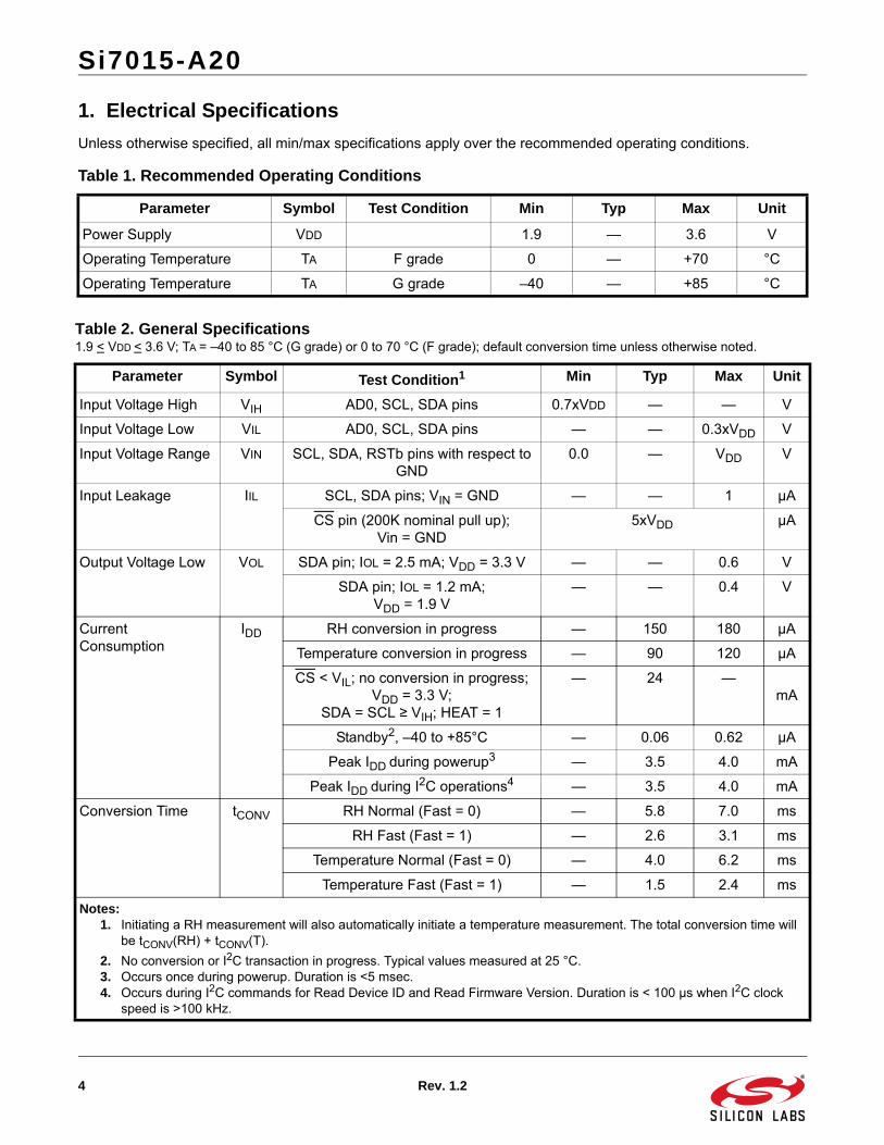
1. Electrical Specifications
Unless otherwise specified, all min/max specifications apply over the recommended operating conditions.
Table 1. Recommended Operating Conditions
Parameter Symbol Test Condition Min Typ Max Unit
Power Supply VDD 1.9 — 3.6 V
Operating Temperature TA F grade 0 — +70 °C
Operating Temperature TA G grade –40 — +85 °C
Table 2. General Specifications1.9 < VDD < 3.6 V; TA = –40 to 85 °C (G grade) or 0 to 70 °C (F grade); default conversion time unless otherwise noted.
Parameter Symbol Test Condition1 Min Typ Max Unit
Input Voltage High VIH AD0, SCL, SDA pins 0.7xVDD — — V
Input Voltage Low VIL AD0, SCL, SDA pins — — 0.3xVDD V
Input Voltage Range VIN SCL, SDA, RSTb pins with respect to GND
0.0 — VDD V
Input Leakage IIL SCL, SDA pins; VIN = GND — — 1 μA
CS pin (200K nominal pull up); Vin = GND
5xVDD μA
Output Voltage Low VOL SDA pin; IOL = 2.5 mA; VDD = 3.3 V — — 0.6 V
SDA pin; IOL = 1.2 mA; VDD = 1.9 V
— — 0.4 V
Current Consumption
IDD RH conversion in progress — 150 180 µA
Temperature conversion in progress — 90 120 µA
CS < VIL; no conversion in progress; VDD = 3.3 V;
SDA = SCL ≥ VIH; HEAT = 1
— 24 —mA
Standby2, –40 to +85°C — 0.06 0.62 µA
Peak IDD during powerup3 — 3.5 4.0 mA
Peak IDD during I2C operations4 — 3.5 4.0 mA
Conversion Time tCONV RH Normal (Fast = 0) — 5.8 7.0 ms
RH Fast (Fast = 1) — 2.6 3.1 ms
Temperature Normal (Fast = 0) — 4.0 6.2 ms
Temperature Fast (Fast = 1) — 1.5 2.4 ms
Notes:1. Initiating a RH measurement will also automatically initiate a temperature measurement. The total conversion time will
be tCONV(RH) + tCONV(T).
2. No conversion or I2C transaction in progress. Typical values measured at 25 °C.3. Occurs once during powerup. Duration is <5 msec.4. Occurs during I2C commands for Read Device ID and Read Firmware Version. Duration is < 100 µs when I2C clock
speed is >100 kHz.

Si7015-A20
Rev. 1.2 5
Wake Up Time tCS From CS < VIL to ready for a temp/RH conversion
— — 1 ms
Power Up Time tPU From VDD ≥ 1.9 V to ready for a temp/RH conversion, 25°C
— 18 25 ms
From VDD ≥ 1.9 V to ready for a temp/RH conversion, full temperature range
— — 80 ms
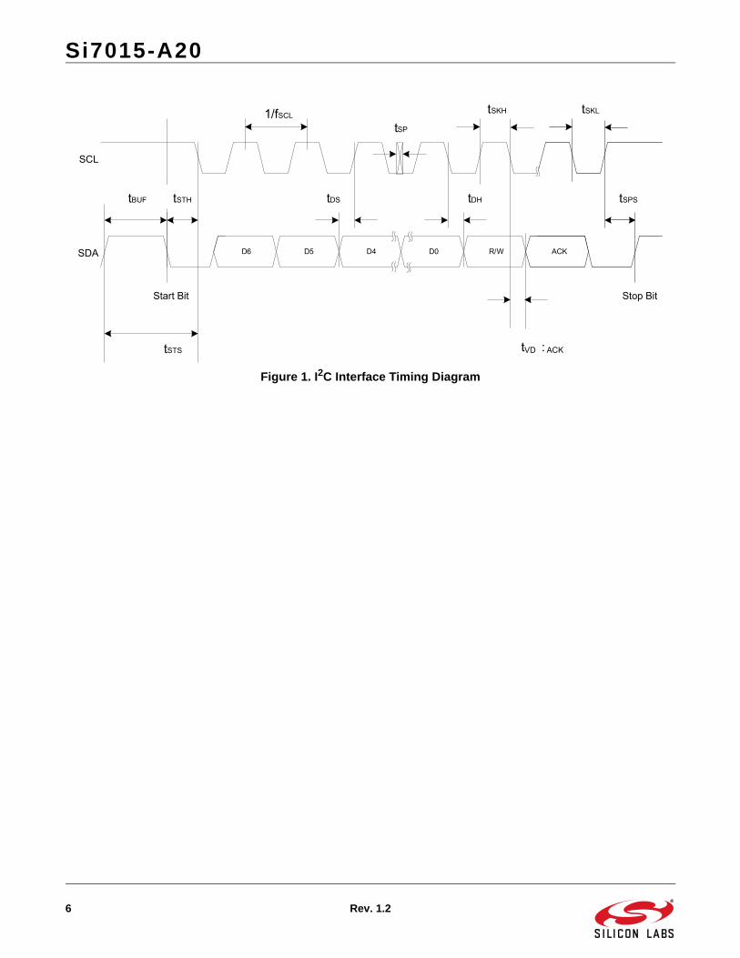
Table 3. I2C Interface Specifications1
1.9 VDD 3.6 V; TA = 0 to 70 °C (F grade) or –40 to +85 °C (G grade) unless otherwise noted.
Parameter Symbol Test Condition Min Typ Max Unit
Hysteresis VHYS High-to-low versus low-to-high transition
0.05 x VDD — — V
SCLK Frequency fSCL — — 400 kHz
SCL High Time tSKH 0.6 — — µs
SCL Low Time tSKL 1.3 — — µs
Start Hold Time tSTH 0.6 — — µs
Start Setup Time tSTS 0.6 — — µs
Stop Setup Time tSPS 0.6 — — µs
Bus Free Time tBUF Between Stop and Start 1.3 — — µs
SDA Setup Time tDS 100 — — ns
SDA Hold Time tDH 100 — — ns
SDA Valid Time tVD;DAT From SCL low to data valid — — 0.9 µs
SDA Acknowledge Valid Time tVD;ACK From SCL low to data valid — — 0.9 µs
Suppressed Pulse Width2 tSP 50 — — ns
Notes:1. All values are referenced to VIL and/or VIH.2. Pulses up to and including 50ns will be suppressed.
Table 2. General Specifications (Continued)1.9 < VDD < 3.6 V; TA = –40 to 85 °C (G grade) or 0 to 70 °C (F grade); default conversion time unless otherwise noted.
Parameter Symbol Test Condition1 Min Typ Max Unit
Notes:1. Initiating a RH measurement will also automatically initiate a temperature measurement. The total conversion time will
be tCONV(RH) + tCONV(T).
2. No conversion or I2C transaction in progress. Typical values measured at 25 °C.3. Occurs once during powerup. Duration is <5 msec.4. Occurs during I2C commands for Read Device ID and Read Firmware Version. Duration is < 100 µs when I2C clock
speed is >100 kHz.
Si7015-A20
6 Rev. 1.2
Figure 1. I2C Interface Timing Diagram
SCL
D6
1/fSCLtSKH
SDA
tSKL
tSTH
D5 D4 D0 R/W ACK
tDS tDH
Start Bit Stop Bit
tBUF
tSTS tVD : ACK
tSPS
tSP

Si7015-A20
Rev. 1.2 7
Figure 2. RH Accuracy at 30 °C
Table 4. Humidity Sensor1.9 ≤ VDD ≤ 3.6 V; TA = 30 °C; default conversion time unless otherwise noted.
Parameter Symbol Test Condition Min Typ Max Unit
Operating Range1 Non-condensing 0 — 100 %RH
Accuracy2, 3 0 – 80% RH — ±3.0 ±4.5 %RH
80 – 100% RH See Figure 2. %RH
Repeatability/Noise Normal Mode — 0.05 — %RH RMS
Fast Mode — 0.2 — %RH RMS
Response Time4 τ63%1 m/s airflow, with cover — 18 —
S1 m/s airflow, without cover — 17 —
Drift vs. Temperature — 0.05 — %RH/°C
Hysteresis — ±1 — %RH
Long Term Stability3 — < 0.25 — %RH/yr
Notes:1. Recommended humidity operating range is 20% to 80% RH (non-condensing) over –10 °C to 60 °C.
Prolonged operation beyond these ranges may result in a shift of sensor reading with slow recovery time.2. Excludes hysteresis, long term drift, and certain other factors and is applicable to non-condensing environments only.
See Section “4.2. Relative Humidity Sensor Accuracy” for more details.3. Drift due to aging effects at typical room conditions of 30C and 30% to 50%. May be impacted by dust, vaporized
solvents or other contaminants, e.g., out-gassing tapes, adhesives, packaging materials, etc. See Section “4.9. Long Term Drift/Aging”.
4. Response time to a step change in RH. Time for the RH output to change by 63% of the total RH change.
0
1
2
3
4
5
6
7
8
9
10
0 5 10 15 20 25 30 35 40 45 50 55 60 65 70 75 80 85 90 95 100
RHMeasuremen
tError
(±%)
Relative Humidity (%)
RH AccuracyMax. RH Error (±%) Typ. RH Error (±%)
Si7015-A20
8 Rev. 1.2
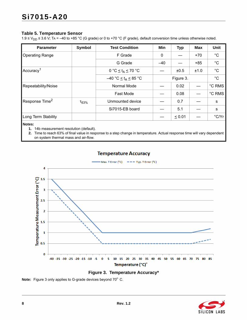
Figure 3. Temperature Accuracy*
Note: Figure 3 only applies to G-grade devices beyond 70C.
Table 5. Temperature Sensor1.9 ≤ VDD ≤ 3.6 V; TA = –40 to +85 °C (G grade) or 0 to +70 °C (F grade), default conversion time unless otherwise noted.
Parameter Symbol Test Condition Min Typ Max Unit
Operating Range F Grade 0 — +70 °C
G Grade –40 — +85 °C
Accuracy1 0 °C < tA < 70 °C — ±0.5 ±1.0 °C
–40 °C < tA < 85 °C Figure 3. °C
Repeatability/Noise Normal Mode — 0.02 — °C RMS
Fast Mode — 0.08 — °C RMS
Response Time2 τ63% Unmounted device — 0.7 — s
Si7015-EB board — 5.1 — s
Long Term Stability — < 0.01 — °C/Yr
Notes:1. 14b measurement resolution (default).2. Time to reach 63% of final value in response to a step change in temperature. Actual response time will vary dependent
on system thermal mass and air-flow.

Si7015-A20
Rev. 1.2 9
Table 6. Thermal Characteristics
Parameter Symbol Test Condition QFN-24 Unit
Junction-to-Air Thermal Resistance JA JEDEC 4-layer board 55 °C/W
Junction-to-Air Thermal Resistance JA 2-layer evaluation PCB with minimal thermal pad
110 °C/W
Table 7. Absolute Maximum Ratings1,2
Parameter Symbol Test Condition
Min Typ Max Unit
Ambient Temperature under Bias –55 — 125 °C
Storage Temperature –65 — 150 °C
Voltage on SDA or SCL Pin with Respect to GND
–0.3 — VDD+ 0.3 V
Voltage on CS pin with Respect to GND –0.3 — VDD + 0.3 V
Voltage on VDD with Respect to GND –0.3 — 4.2 V
ESD Tolerance HBM — — 2 kV
CDM — — 1.25 kV
MM — — 250 V
Notes:1. Absolute maximum ratings are stress ratings only; operation at or beyond these conditions is not implied and may
shorten the life of the device or alter its performance.2. Special handling considerations apply; see “AN607: Si70xx Humidity Sensor Designer’s Guide” for details.
Si7015-A20
10 Rev. 1.2
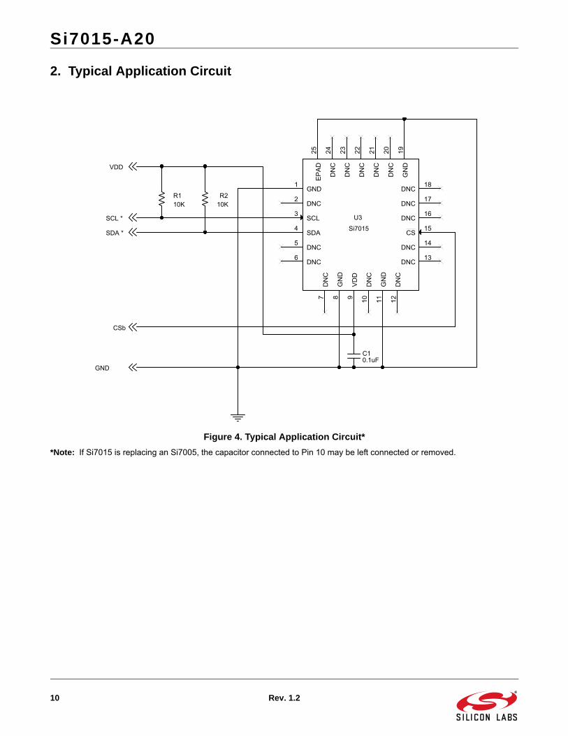
2. Typical Application Circuit
Figure 4. Typical Application Circuit*
*Note: If Si7015 is replacing an Si7005, the capacitor connected to Pin 10 may be left connected or removed.
SDA *
SCL *
VDD
CSb
GND
U3
Si7015
DNC13
DNC14
SDA4
DNC6
SCL3
DNC5
DNC2
GND1
CS15
DNC16
DNC17
DNC18
DN
C12
GN
D11
DN
C10
GN
D8
VD
D9
GN
D19
DN
C24
DN
C20
DN
C23
DN
C22
DN
C21
DN
C7
EP
AD
25
R110K
C10.1uF
R210K
Si7015-A20
Rev. 1.2 11
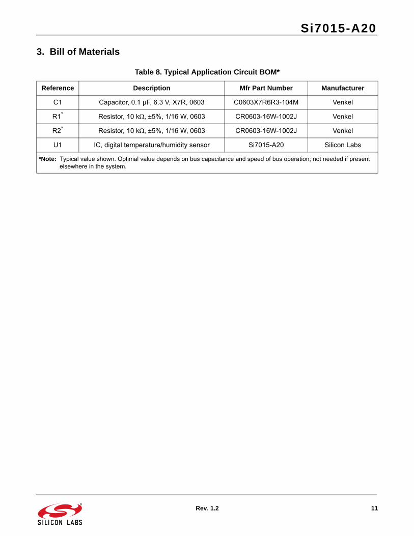
3. Bill of Materials
Table 8. Typical Application Circuit BOM*
Reference Description Mfr Part Number Manufacturer
C1 Capacitor, 0.1 µF, 6.3 V, X7R, 0603 C0603X7R6R3-104M Venkel
R1* Resistor, 10 k, ±5%, 1/16 W, 0603 CR0603-16W-1002J Venkel
R2* Resistor, 10 k, ±5%, 1/16 W, 0603 CR0603-16W-1002J Venkel
U1 IC, digital temperature/humidity sensor Si7015-A20 Silicon Labs
*Note: Typical value shown. Optimal value depends on bus capacitance and speed of bus operation; not needed if present elsewhere in the system.

Si7015-A20
12 Rev. 1.2
4. Functional Description
Figure 5. Si7015 Functional Block Diagram
4.1. OverviewThe Si7015 is a digital relative humidity and temperature sensor. This monolithic CMOS IC integrates temperatureand humidity sensor elements, an analog-to-digital converter, signal processing, calibration data, and an I2C hostinterface. Both the temperature and humidity sensors on each unit are factory-calibrated and the calibration data isstored in the on-chip non-volatile memory. This ensures that the sensors are fully interchangeable, with norecalibration or software changes required.
While the Si7015 is largely a conventional mixed-signal CMOS integrated circuit, relative humidity sensors ingeneral and those based on capacitive sensing using polymeric dielectric have unique application and userequirements that are not common to conventional (non-sensor) ICs. Chief among those are:
The need to protect the sensor during board assembly, i.e., solder reflow, and the need to subsequently rehydrate the sensor.
The need to apply temperature correction to the humidity readings.
The need to protect the sensor from damage or contamination during the product life-cycle.
The impact of prolonged exposure to extremes of temperature and/or humidity and their potential effect on sensor accuracy.
The effects of humidity sensor “memory”.
Each of these items is discussed in more detail in the following sections.

Si7015-A20
Rev. 1.2 13
4.2. Relative Humidity Sensor AccuracyTo determine the accuracy of a relative humidity sensor, it is placed in a temperature and humidity controlledchamber. The temperature is set to a convenient fixed value (typically 30 °C) and the relative humidity is sweptfrom 20 to 80% and back to 20% in the following steps: 20% – 40% – 60% – 80% – 80% – 60% – 40% – 20%. Ateach set-point, the chamber is allowed to settle for a period of 60 minutes before a reading is taken from thesensor. Prior to the sweep, the device is allowed to stabilize to 50%RH. The solid top and bottom trace in Figure 6,“Measuring Sensor Accuracy Including Hysteresis,” shows the result of a typical sweep after non-linearitycompensation.
Figure 6. Measuring Sensor Accuracy Including Hysteresis
The RH accuracy is defined as the center (dashed) line shown in Figure 6, which is the average of the two datapoints at each relative humidity set-point. In this case, the sensor shows an accuracy of 0.25%RH. The Si7015accuracy specification (Table 4) includes the following:
Unit-to-unit and lot-to-lot variation in non-linearity compensation
Accuracy of factory calibration
Margin for shifts that can occur during solder reflow.
The accuracy specification does not include the following:
Hysteresis (typically ±1%)
Effects from long term exposure to very humid conditions
Contamination of the sensor by particulates, chemicals, etc.
Other aging related shifts (“Long-term stability”)
Variations due to temperature
5
4
3
2
1
0
1
2
3
4
5
10 20 30 40 50 60 70 80 90
%RH
Accuracy
%RH Set point
RH Accuracy vs. RH Set Point
Hysteresis
Si7015-A20
14 Rev. 1.2
4.3. Temperature CompensationThe Si7015 relative humidity sensor is calibrated at a temperature of 30 °C; it is at this temperature that the sensorwill give the most accurate relative humidity readings. For relative humidity measurements at other temperatures,the RH reading from the Si7015 must be compensated for the change in temperature relative to 30 °C.Temperature-compensated relative humidity readings can be calculated as follows:
Where:
RHTempCompensated is the temperature compensated relative humidity value in %RH.
RHLinear is the linear corrected relative humidity value in %RH.
Temperature is the ambient temperature in °C as measured by the Si7015 on chip temperature sensor.
Q1 and Q0 are unit-less correction coefficients derived through characterization of Si7015s by Silicon Laboratories.
This temperature compensation is most accurate in the range of 15–50 °C. The values for the correctioncoefficients are shown in Table 9.
4.4. HysteresisThe moisture absorbent film (polymeric dielectric) of the humidity sensor will carry a memory of its exposurehistory, particularly its recent or extreme exposure history. A sensor exposed to relatively low humidity will carry anegative offset relative to the factory calibration, and a sensor exposed to relatively high humidity will carry apositive offset relative to the factory calibration. This factor causes a hysteresis effect illustrated by the solid topand bottom traces in Figure 6. The hysteresis value is the difference in %RH between the maximum absolute erroron the decreasing humidity ramp and the maximum absolute error on the increasing humidity ramp at a singlerelative humidity Setpoint and is expressed as a bipolar quantity relative to the average, the center dashed trace inFigure 6. In the case of Figure 6, the measurement uncertainty due to the hysteresis effect is ±1.05%RH.
4.5. Prolonged Exposure to High HumidityProlonged exposure to high humidity will result in a gradual upward drift of the RH reading. The shift in sensorreading resulting from this drift will generally disappear slowly under normal ambient conditions. The amount ofshift is proportional to the magnitude of relative humidity and the length of exposure. In the case of lengthyexposure to high humidity, some of the resulting shift may persist indefinitely under typical conditions. It is generallypossible to substantially reverse this affect by baking the device (see Section “4.8. Bake/Hydrate Procedure”).
Table 9. Linearization Coefficients
Coefficient Value
Q0 0.060162
Q1 0.000508
RHTempCompensated RHLinear Temperature 30– RHLinear Q1 Q0+ +=
Si7015-A20
Rev. 1.2 15
4.6. PCB Assembly4.6.1. Soldering
Like most ICs, Si7015 devices are shipped from the factory vacuum-packed with an enclosed desiccant to avoidany drift during storage and to prevent any moisture-related issues during solder reflow. The following guidelinesshould be observed during PCB assembly:
Si7015 devices are compatible with standard board assembly processes. Devices should be soldered using reflow per the recommended card reflow profile. See Section “10. PCB Land Pattern and Solder Mask Design” for the recommended card reflow profile.
A “no clean” solder process is recommended to minimize the need for water or solvent rinses after soldering. Cleaning after soldering is possible, but must be done carefully to avoid impacting the performance of the sensor. See application note, “AN607: Si70xx Humidity Sensor Designer’s Guide” for more information on cleaning.
It is essential that the exposed polymer sensing film be kept clean and undamaged. This can be accomplished by careful handling and a clean, well-controlled assembly process. When in doubt or for
extra protection, a heat-resistant, protective cover such as Kapton® KPPD-1/8 can be installed during PCB assembly.
Si7015s may be ordered with a factory-fitted, solder-resistant protective cover. This cover provides protectionduring PCB assembly or rework but without the time and effort required to install and remove the Kapton® tape. Itcan be left in place for the lifetime of the product, preventing liquids, dust, or other contaminants from coming intocontact with the polymer sensor film. See Section “8. Ordering Guide” for a list of ordering part numbers thatinclude the cover.
4.6.2. Rehydration
The measured humidity value will generally shift slightly after solder reflow. A portion of this shift is permanent andis accounted for in the accuracy specifications in Table 4. After soldering, an Si7015 should be allowed toequilibrate under controlled RH conditions (room temperature, 45-55%RH) for at least 48 hours to eliminate theremainder of the shift and return the device to its specified accuracy performance.

Si7015-A20
16 Rev. 1.2
4.6.3. Rework
To maintain the specified sensor performance, care must be taken during rework to minimize the exposure of thedevice to excessive heat and to avoid damage/contamination or a shift in the sensor reading due to liquids, solderflux, etc. Manual touch-up using a soldering iron is permissible under the following guidelines:
The exposed polymer sensing film must be kept clean and undamaged. A protective cover is
recommended during any rework operation (Kapton® tape or the factory-installed cover).
Flux must not be allowed to contaminate the sensor; liquid flux is not recommended even with a cover in place. Conventional lead-free solder with rosin core is acceptable for touch-up as long as a cover is in place during the rework.
If possible, avoid water or solvent rinses after touch-up. Cleaning after soldering is possible, but must be done carefully to avoid impacting the performance of the sensor. See application note, “AN607: Si70xx Humidity Sensor Designer’s Guide” for more information on cleaning.
Minimize the heating of the device. Soldering iron temperature should not exceed 350 °C and the contact time per pin should not exceed five seconds.
Hot air rework is not recommended. If a device must be replaced, remove the device by hot air and solder a new part in its place by reflow following the guidelines above.
*Note: All trademarks are the property of their respective owners.
Figure 7. Si7015 with Factory-Installed Protective Cover
Si7015-A20
Rev. 1.2 17
4.7. Protecting the SensorBecause the sensor operates on the principal of measuring a change in capacitance, any changes to the dielectricconstant of the polymer film will be detected as a change in relative humidity. Therefore, it is important to minimizethe probability of contaminants coming into contact with the sensor. Dust and other particles as well as liquids canaffect the RH reading. It is recommended that a cover is employed in the end system that blocks contaminants butallows water vapor to pass through. Depending on the needs of the application, this can be as simple as plastic ormetallic gauze for basic protection against particulates or something more sophisticated such as a hydrophobicmembrane providing up to IP67 compliant protection.
The Si7015 may be ordered with a factory-fitted, solder-resistant cover that can be left in place for the lifetime ofthe product. It is very low-profile, hydrophobic and oleophobic. See Section “8. Ordering Guide” for a list of orderingpart numbers that include the cover. A dimensioned drawing of the IC with the cover is included in Section “9.Package Outline”. Other characteristics of the cover are listed in Table 10.
4.8. Bake/Hydrate ProcedureAfter exposure to extremes of temperature and/or humidity for prolonged periods, the polymer sensor film canbecome either very dry or very wet; in each case the result is either high or low relative humidity readings. Undernormal operating conditions, the induced error will diminish over time. From a very dry condition, such as aftershipment and soldering, the error will diminish over a few days at typical controlled ambient conditions, e.g.,48 hours of 45 ≤ %RH ≤ 55. However, from a very wet condition, recovery may take significantly longer. Toaccelerate recovery from a wet condition, a bake and hydrate cycle can be implemented. This operation consists ofthe following steps:
Baking the sensor at 125 °C for ≥ 12 hours
Hydration at 30 °C in 75 %RH for ≥ 10 hours
Following this cycle, the sensor will return to normal operation in typical ambient conditions after a few days.
4.9. Long Term Drift/AgingOver long periods of time, the sensor readings may drift due to aging of the device. Standard accelerated lifetesting of the Si7015 has resulted in the specifications for long-term drift shown in Table 4 and Table 5. Thiscontribution to the overall sensor accuracy accounts only for the long-term aging of the device in an otherwisebenign operating environment and does not include the affects of damage, contamination, or exposure to extremeenvironmental conditions.
Table 10. Specifications of Protective Cover
Parameter Value
Material PTFE
Operating Temperature –40 to +125 °C
Maximum Reflow Temperature 260 °C
IP Rating (per IEC 529) IP67
Si7015-A20
18 Rev. 1.2
5. Host Interface
5.1. I2C InterfaceThe Si7015 has an I2C serial interface with a 7-bit address of 0x40. The Si7015 is a slave device supporting datatransfer rates up to 400 kHz. Table 20 shows the register summary of the Si7015.
5.1.1. Performing a Relative Humidity Measurement
The following steps should be performed in sequence to take a relative humidity measurement:
1. Set START (D0) in CONFIG to begin a new conversion.
2. Poll RDY (D0) in STATUS (register 0) until it is low (= 0). (This must be done at least once prior to reading results even if the host waits longer than tCONV.)
3. Read the upper and lower bytes of the RH value from DATAh and DATAl (registers 0x01 and 0x02), respectively. Table 11 shows the format of the 12-bit relative humidity result.
4. Convert the RH value to %RH using the following equation:
where RH is the measured value returned in DATAh:DATAI.
5. Apply temperature compensation as discussed elsewhere in this data sheet.
Due to normal variations in RH accuracy of the device as described in Table 4, it is possible for the measured valueof %RH to be slightly less than 0 when the actual RH level is close to or equal to 0. Similarly, the measured valueof %RH may be slightly greater than 100 when the actual RH level is close to or equal to 100. This is expectedbehavior, and it is acceptable to limit the range of RH results to 0 to 100%RH in the host software by truncatingvalues that are slightly outside of this range.
Table 12 shows the 12-bit values that correspond to various measured RH levels.
Table 11. 12-Bit Relative Humidity Result Available in Registers 1 and 2
DATAh DATAI
D7 D6 D5 D4 D3 D2 D1 D0 D7 D6 D5 D4 D3 D2 D1 D0
12-Bit Relative Humidity Code
%RHRH16--------- 24–=

Si7015-A20
Rev. 1.2 19
The above sequence assumes normal mode, i.e., tCONV = 5.8 ms (typical). Conversions may be performed in fastmode. See Section “5.1.4. Fast Conversion Mode”.
Table 12. Typical %RH Measurement Codes for 0 to 100% RH Range
%RH 12 Bit Code
Dec Hex
0 384 180
10 544 220
20 704 2C0
30 864 360
40 1024 400
50 1184 4A0
60 1344 540
70 1504 5E0
80 1664 680
90 1824 720
100 1984 7C0
Si7015-A20
20 Rev. 1.2
5.1.2. Performing a Temperature Measurement
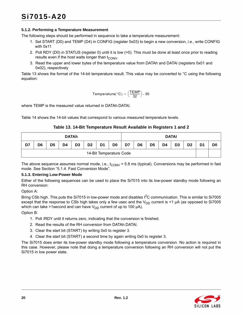
The following steps should be performed in sequence to take a temperature measurement:
1. Set START (D0) and TEMP (D4) in CONFIG (register 0x03) to begin a new conversion, i.e., write CONFIG with 0x11
2. Poll RDY (D0) in STATUS (register 0) until it is low (=0). This must be done at least once prior to reading results even if the host waits longer than tCONV.
3. Read the upper and lower bytes of the temperature value from DATAh and DATAl (registers 0x01 and 0x02), respectively
Table 13 shows the format of the 14-bit temperature result. This value may be converted to °C using the followingequation:
where TEMP is the measured value returned in DATAh:DATAI.
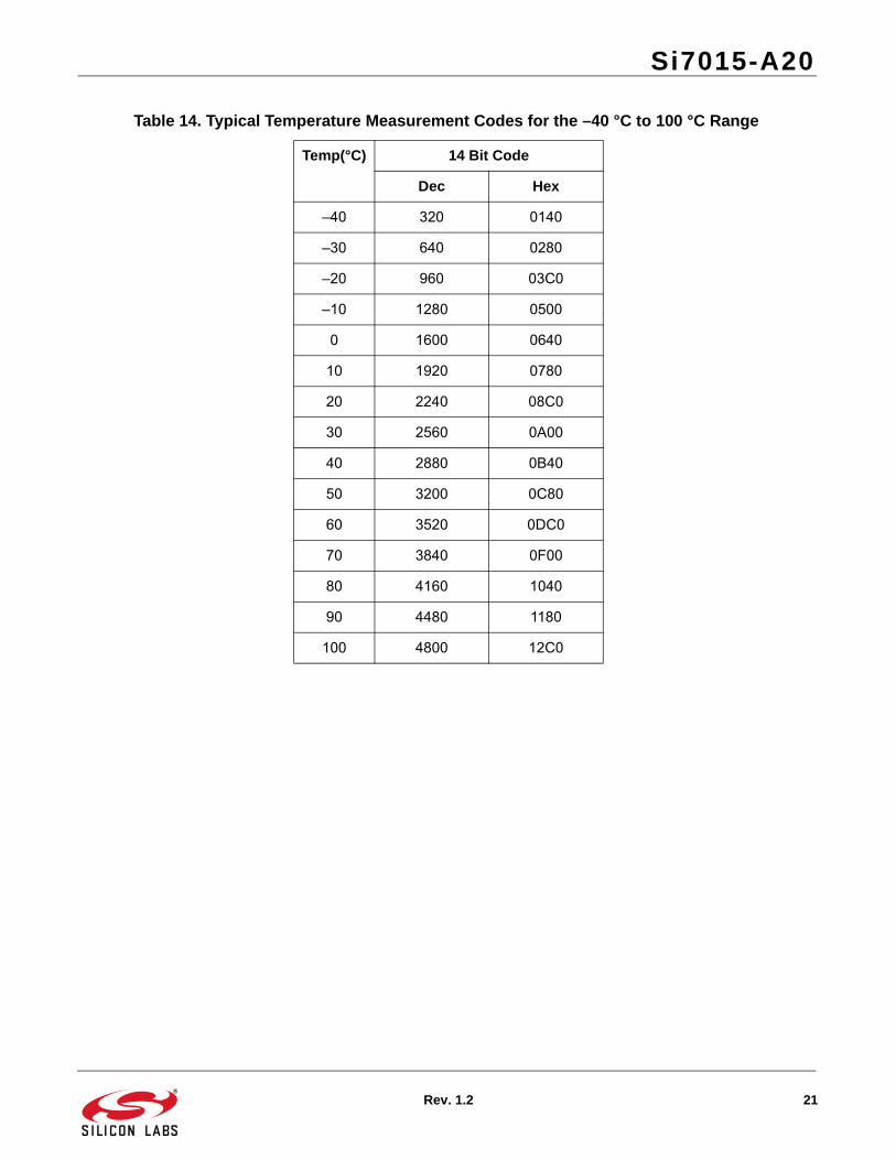
Table 14 shows the 14-bit values that correspond to various measured temperature levels.
The above sequence assumes normal mode, i.e., tCONV = 5.8 ms (typical). Conversions may be performed in fastmode. See Section “5.1.4. Fast Conversion Mode”.
5.1.3. Entering Low-Power Mode
Either of the following sequences can be used to place the Si7015 into its low-power standby mode following anRH conversion:
Option A:
Bring CSb high. This puts the Si7015 in low-power mode and disables I2C communication. This is similar to Si7005except that the response to CSb high takes only a few usec and the VDD current is <1 µA (as opposed to Si7005which can take >1second and can have VDD current of up to 100 µA).
Option B:
1. Poll /RDY until it returns zero, indicating that the conversion is finished.
2. Read the results of the RH conversion from DATAh:DATAl.
3. Clear the start bit (START) by writing 0x0 to register 3.
4. Clear the start bit (START) a second time by again writing 0x0 to register 3.
The Si7015 does enter its low-power standby mode following a temperature conversion. No action is required inthis case. However, please note that doing a temperature conversion following an RH conversion will not put theSi7015 in low power state.
Table 13. 14-Bit Temperature Result Available in Registers 1 and 2
DATAh DATAI
D7 D6 D5 D4 D3 D2 D1 D0 D7 D6 D5 D4 D3 D2 D1 D0
14-Bit Temperature Code
Temperature C TEMP32
----------------- 50–=
Si7015-A20
Rev. 1.2 21
Table 14. Typical Temperature Measurement Codes for the –40 °C to 100 °C Range
Temp(°C) 14 Bit Code
Dec Hex
–40 320 0140
–30 640 0280
–20 960 03C0
–10 1280 0500
0 1600 0640
10 1920 0780
20 2240 08C0
30 2560 0A00
40 2880 0B40
50 3200 0C80
60 3520 0DC0
70 3840 0F00
80 4160 1040
90 4480 1180
100 4800 12C0
Si7015-A20
22 Rev. 1.2
5.1.4. Fast Conversion Mode
The time needed to perform a temperature or RH measurement can be reduced from 5.8 ms (typical) to 2.6 ms(typical) by setting FAST (D5) in CONFIG (register 0x03). Fast mode reduces the total power consumed during aconversion or the average power consumed by the Si7015 when making periodic conversions. It also reduces theresolution of the measurements.
5.1.5. Heater
The Si7015 relative humidity sensor contains an integrated, resistive heating element that may be used to raise thetemperature of the humidity sensor. This element can be used to drive off condensation or to implement dew-pointmeasurement when the Si7015 is used in conjunction with a separate temperature sensor such as another Si7015.
The heater can be activated by setting HEAT (D1) in CONFIG (register 0x03). Turning on the heater will reduce thetendency of the humidity sensor to accumulate an offset due to “memory” of sustained high humidity conditions.When the heater is enabled, the reading of the on-chip temperature sensor will be affected (increased).
5.1.6. Device Identification
The Si7015 device and its revision level can be determined by reading ID (register 0x11). Table 15 lists the valuesfor the various device revisions and may include revisions not yet in existence.
Table 15. Device ID Revision Values
Device ID Value Device Type
Revision Level
D[7:4] D[3:0]
1111 0000 Si7015 A
Si7015-A20
Rev. 1.2 23
5.2. I2C OperationThe format of the address byte is shown in Table 16.
5.2.1. I2C Write Operation
To write to a register on the Si7015, the master should issue a start command (S) followed by the slave address,0x40. The slave address is followed by a 0 to indicate that the operation is a write. Upon recognizing its slaveaddress, the Si7015 issues an acknowledge (A) by pulling the SDA line low for the high duration of the ninth SCLcycle. The next byte the master places on the bus is the register address pointer, selecting the register on theSi7015 to which the data should be transferred. After the Si7015 acknowledges this byte, the master places a databyte on the bus. This byte will be written to the register selected by the address pointer. The Si7015 willacknowledge the data byte, after which the master issues a Stop command (P). See Table 17.
Table 16. I2C Slave Address Byte
A6 A5 A4 A3 A2 A1 A0 R/W
1 0 0 0 0 0 0 1/0
Master Slave
Table 17. I2C Write Sequence
Sequence to Write to a Register
S Slave Address W A Address Pointer A Register Data A P
Sequence to Start a Relative Humidity Conversion
S 0x40 0 A 0x03 A 0x01 A P
Sequence to Start a Temperature Conversion
S 0x40 0 A 0x03 A 0x11 A P
Si7015-A20
24 Rev. 1.2
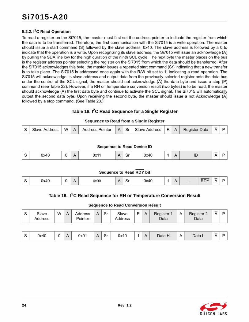
5.2.2. I2C Read Operation
To read a register on the Si7015, the master must first set the address pointer to indicate the register from whichthe data is to be transferred. Therefore, the first communication with the Si7015 is a write operation. The mastershould issue a start command (S) followed by the slave address, 0x40. The slave address is followed by a 0 toindicate that the operation is a write. Upon recognizing its slave address, the Si7015 will issue an acknowledge (A)by pulling the SDA line low for the high duration of the ninth SCL cycle. The next byte the master places on the busis the register address pointer selecting the register on the Si7015 from which the data should be transferred. Afterthe Si7015 acknowledges this byte, the master issues a repeated start command (Sr) indicating that a new transferis to take place. The Si7015 is addressed once again with the R/W bit set to 1, indicating a read operation. TheSi7015 will acknowledge its slave address and output data from the previously-selected register onto the data busunder the control of the SCL signal, the master should not acknowledge (A) the data byte and issue a stop (P)command (see Table 22). However, if a RH or Temperature conversion result (two bytes) is to be read, the mastershould acknowledge (A) the first data byte and continue to activate the SCL signal. The Si7015 will automaticallyoutput the second data byte. Upon receiving the second byte, the master should issue a not Acknowledge (A)followed by a stop command. (See Table 23.)
Table 18. I2C Read Sequence for a Single Register
Sequence to Read from a Single Register
S Slave Address W A Address Pointer A Sr Slave Address R A Register Data A P
Sequence to Read Device ID
S 0x40 0 A 0x11 A Sr 0x40 1 A ID A P
Sequence to Read RDY bit
S 0x40 0 A 0x00 A Sr 0x40 1 A — RDY A P
Table 19. I2C Read Sequence for RH or Temperature Conversion Result
Sequence to Read Conversion Result
S Slave Address
W A Address Pointer
A Sr Slave Address
R A Register 1 Data
A Register 2 Data
A P
S 0x40 0 A 0x01 A Sr 0x40 1 A Data H A Data L A P
Si7015-A20
Rev. 1.2 25
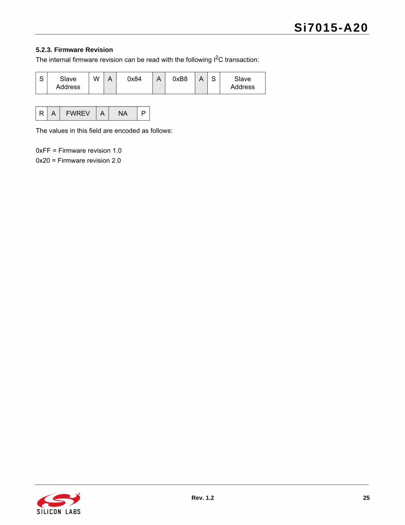
5.2.3. Firmware Revision
The internal firmware revision can be read with the following I2C transaction:
The values in this field are encoded as follows:
0xFF = Firmware revision 1.0
0x20 = Firmware revision 2.0
S Slave Address
W A 0x84 A 0xB8 A S Slave Address
R A FWREV A NA P

Si7015-A20
26 Rev. 1.2
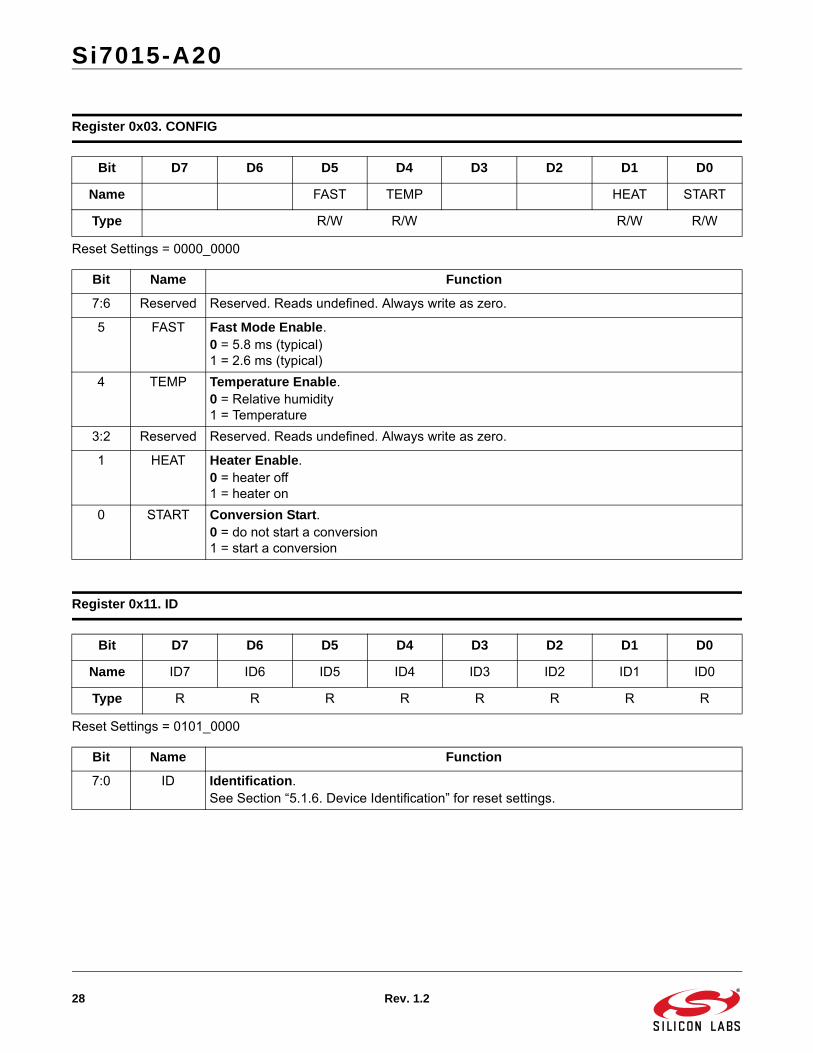
6. Control Registers
Table 20 contains a summary of the Si7015 register set. Each register is described in more detail below.
6.1. Register Detail
Reset Settings = 0000_0001
Table 20. Si7015 Register Summary
Register Name Bit 7 Bit 6 Bit 5 Bit 4 Bit 3 Bit 2 Bit 1 Bit 0
I2C Register Summary
0x00 STATUS RSVD RSVD RSVD RSVD RSVD RSVD RSVD /RDY
0x01 DATAh Relative Humidity or Temperature, High Byte
0x02 DATAl Relative Humidity or Temperature, Low Byte
0x03 CONFIG RSVD RSVD FAST TEMP RSVD RSVD HEAT START
0x11 ID ID3 ID2 ID1 ID0 0 0 0 0
0x84 0xB8 FWREV MAJREV MINREV
Notes:1. Any register address not listed here is reserved and must not be written. 2. Reserved register bits (RSVD) must always be written as zero; the result of a read operation on these bits is undefined.
Register 0. STATUS
Bit D7 D6 D5 D4 D3 D2 D1 D0
Name /RDY
Type R
Bit Name Function
7:1 Reserved Reserved. Reads undefined.
0 /RDY Ready.0 = conversion complete; results available in DATAh:DATAl.1 = conversion in progress.

Si7015-A20
Rev. 1.2 27
Reset Settings = 0000_0000
Reset Settings = 0000_0000
Register 0x01. DATAh
Bit D7 D6 D5 D4 D3 D2 D1 D0
Name Relative Humidity or Temperature, High Byte
Type R
Bit Name Function
7:0 DATAh Data, High Byte.Eight most significant bits of a temperature or humidity measurement. See Table 11 or Table 13 for the measurement format.
Register 0x02. DATAI
Bit D7 D6 D5 D4 D3 D2 D1 D0
Name Relative Humidity or Temperature, Low Byte
Type Read
Bit Name Function
7:0 DATAl Data, Low Byte.Eight least significant bits of a temperature or humidity measurement. See Table 11 or Table 13 for the measurement format.
Si7015-A20
28 Rev. 1.2
Reset Settings = 0000_0000
Reset Settings = 0101_0000
Register 0x03. CONFIG
Bit D7 D6 D5 D4 D3 D2 D1 D0
Name FAST TEMP HEAT START
Type R/W R/W R/W R/W
Bit Name Function
7:6 Reserved Reserved. Reads undefined. Always write as zero.
5 FAST Fast Mode Enable.0 = 5.8 ms (typical)1 = 2.6 ms (typical)
4 TEMP Temperature Enable.0 = Relative humidity1 = Temperature
3:2 Reserved Reserved. Reads undefined. Always write as zero.
1 HEAT Heater Enable.0 = heater off1 = heater on
0 START Conversion Start.0 = do not start a conversion1 = start a conversion
Register 0x11. ID
Bit D7 D6 D5 D4 D3 D2 D1 D0
Name ID7 ID6 ID5 ID4 ID3 ID2 ID1 ID0
Type R R R R R R R R
Bit Name Function
7:0 ID Identification.See Section “5.1.6. Device Identification” for reset settings.

Si7015-A20
Rev. 1.2 29
Register 0x84 0xB8. FWREV
Bit D7 D6 D5 D4 D3 D2 D1 D0
Name MAJREV MINREV
Type R R
Bit Name Function
7:4 MAJREV Major firmware revision number
3:0 MINREV Minor firmware revision number
Si7015-A20
30 Rev. 1.2
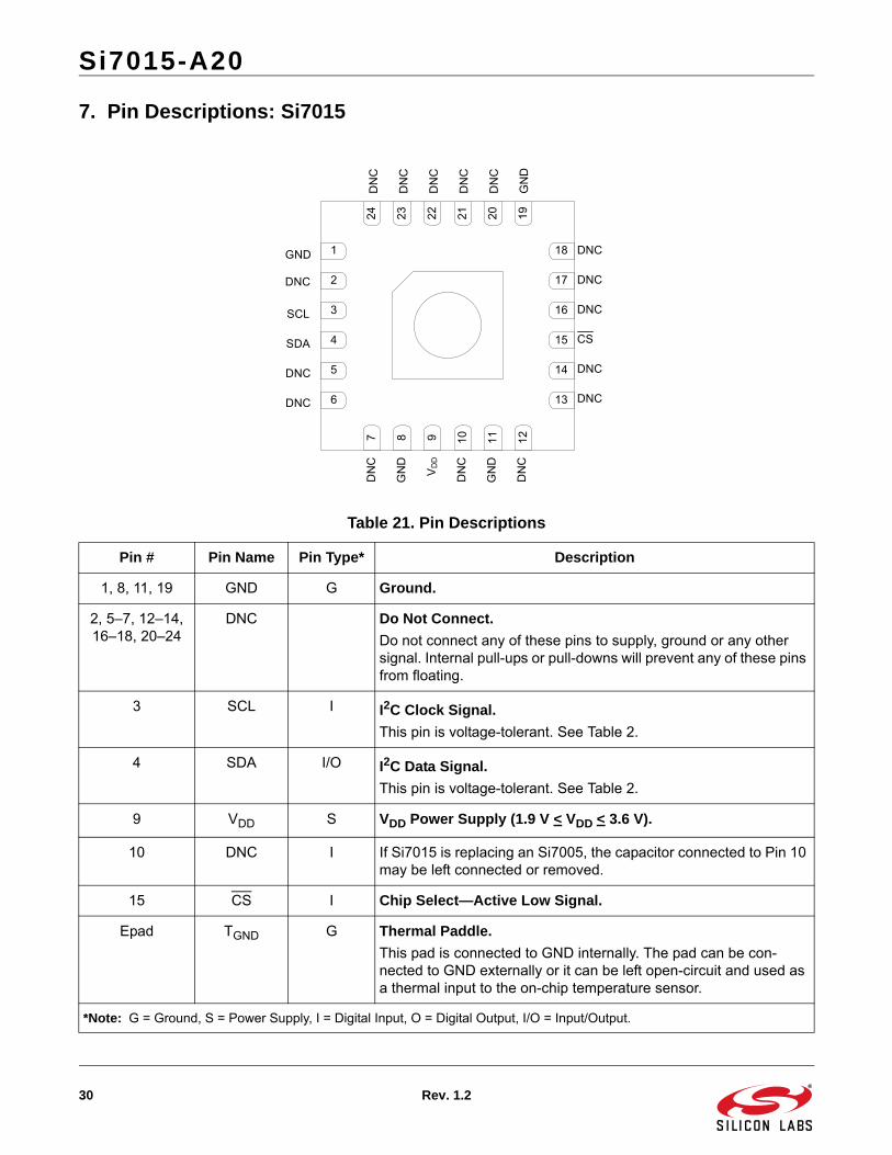
7. Pin Descriptions: Si7015
Table 21. Pin Descriptions
Pin # Pin Name Pin Type* Description
1, 8, 11, 19 GND G Ground.
2, 5–7, 12–14, 16–18, 20–24
DNC Do Not Connect.
Do not connect any of these pins to supply, ground or any other signal. Internal pull-ups or pull-downs will prevent any of these pins from floating.
3 SCL I I2C Clock Signal.
This pin is voltage-tolerant. See Table 2.
4 SDA I/O I2C Data Signal.
This pin is voltage-tolerant. See Table 2.
9 VDD S VDD Power Supply (1.9 V < VDD < 3.6 V).
10 DNC I If Si7015 is replacing an Si7005, the capacitor connected to Pin 10 may be left connected or removed.
15 CS I Chip Select—Active Low Signal.
Epad TGND G Thermal Paddle.
This pad is connected to GND internally. The pad can be con-nected to GND externally or it can be left open-circuit and used as a thermal input to the on-chip temperature sensor.
*Note: G = Ground, S = Power Supply, I = Digital Input, O = Digital Output, I/O = Input/Output.
1
6
5
4
3
2
18
13
14
15
16
17
24
19
20
21
22
23
127 8 9 10
11
GND
DNC
DNC
SDA
SCL
DNC
DNC
DNC
CS
DNC
DNC
DN
C
DN
C
GN
D
DN
C
VD
D
GN
D
DN
C
GN
D
DN
C
DN
C
DN
C
DN
C
DNC
Si7015-A20
Rev. 1.2 31
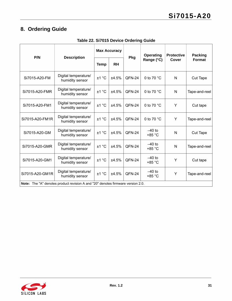
8. Ordering Guide
Table 22. Si7015 Device Ordering Guide
P/N Description
Max Accuracy
PkgOperating Range (°C)
Protective Cover
Packing Format
Temp RH
Si7015-A20-FMDigital temperature/
humidity sensor±1 °C ±4.5% QFN-24 0 to 70 °C N Cut Tape
Si7015-A20-FMRDigital temperature/
humidity sensor±1 °C ±4.5% QFN-24 0 to 70 °C N Tape-and-reel
Si7015-A20-FM1Digital temperature/
humidity sensor±1 °C ±4.5% QFN-24 0 to 70 °C Y Cut tape
Si7015-A20-FM1RDigital temperature/
humidity sensor±1 °C ±4.5% QFN-24 0 to 70 °C Y Tape-and-reel
Si7015-A20-GMDigital temperature/
humidity sensor±1 °C ±4.5% QFN-24
–40 to +85 °C
N Cut Tape
Si7015-A20-GMRDigital temperature/
humidity sensor±1 °C ±4.5% QFN-24
–40 to +85 °C
N Tape-and-reel
Si7015-A20-GM1Digital temperature/
humidity sensor±1 °C ±4.5% QFN-24
–40 to +85 °C
Y Cut tape
Si7015-A20-GM1RDigital temperature/
humidity sensor±1 °C ±4.5% QFN-24
–40 to +85 °C
Y Tape-and-reel
Note: The "A" denotes product revision A and "20" denotes firmware version 2.0.
Si7015-A20
32 Rev. 1.2
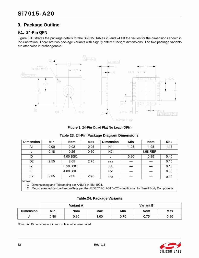
9. Package Outline
9.1. 24-Pin QFNFigure 8 illustrates the package details for the Si7015. Tables 23 and 24 list the values for the dimensions shown inthe illustration. There are two package variants with slightly different height dimensions. The two package variantsare otherwise interchangeable.
Figure 8. 24-Pin Quad Flat No Lead (QFN)
Note: All Dimensions are in mm unless otherwise noted.
Table 23. 24-Pin Package Diagram Dimensions
Dimension Min Nom Max Dimension Min Nom Max
A1 0.00 0.02 0.05 H1 1.03 1.08 1.13
b 0.18 0.25 0.30 H2 1.68 REF
D 4.00 BSC. L 0.30 0.35 0.40
D2 2.55 2.65 2.75 aaa — — 0.15
e 0.50 BSC. bbb — — 0.15
E 4.00 BSC. ccc — — 0.08
E2 2.55 2.65 2.75 ddd — — 0.10Notes:
1. Dimensioning and Tolerancing per ANSI Y14.5M-1994.2. Recommended card reflow profile is per the JEDEC/IPC J-STD-020 specification for Small Body Components.
Table 24. Package Variants
Variant A Variant B
Dimension Min Nom Max Min Nom Max
A 0.80 0.90 1.00 0.70 0.75 0.80
Si7015-A20
Rev. 1.2 33
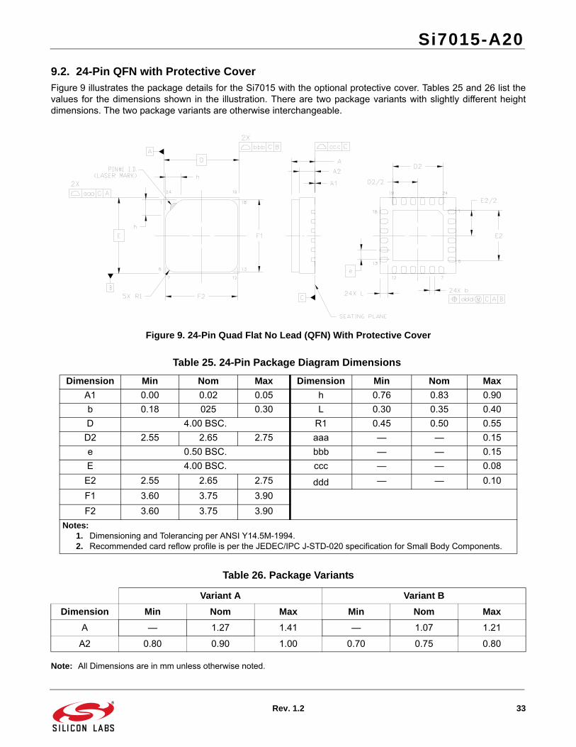
9.2. 24-Pin QFN with Protective CoverFigure 9 illustrates the package details for the Si7015 with the optional protective cover. Tables 25 and 26 list thevalues for the dimensions shown in the illustration. There are two package variants with slightly different heightdimensions. The two package variants are otherwise interchangeable.
Figure 9. 24-Pin Quad Flat No Lead (QFN) With Protective Cover
Note: All Dimensions are in mm unless otherwise noted.
Table 25. 24-Pin Package Diagram Dimensions
Dimension Min Nom Max Dimension Min Nom Max
A1 0.00 0.02 0.05 h 0.76 0.83 0.90
b 0.18 025 0.30 L 0.30 0.35 0.40
D 4.00 BSC. R1 0.45 0.50 0.55
D2 2.55 2.65 2.75 aaa — — 0.15
e 0.50 BSC. bbb — — 0.15
E 4.00 BSC. ccc — — 0.08
E2 2.55 2.65 2.75 ddd — — 0.10
F1 3.60 3.75 3.90
F2 3.60 3.75 3.90
Notes:1. Dimensioning and Tolerancing per ANSI Y14.5M-1994.2. Recommended card reflow profile is per the JEDEC/IPC J-STD-020 specification for Small Body Components.
Table 26. Package Variants
Variant A Variant B
Dimension Min Nom Max Min Nom Max
A — 1.27 1.41 — 1.07 1.21
A2 0.80 0.90 1.00 0.70 0.75 0.80
Si7015-A20
34 Rev. 1.2
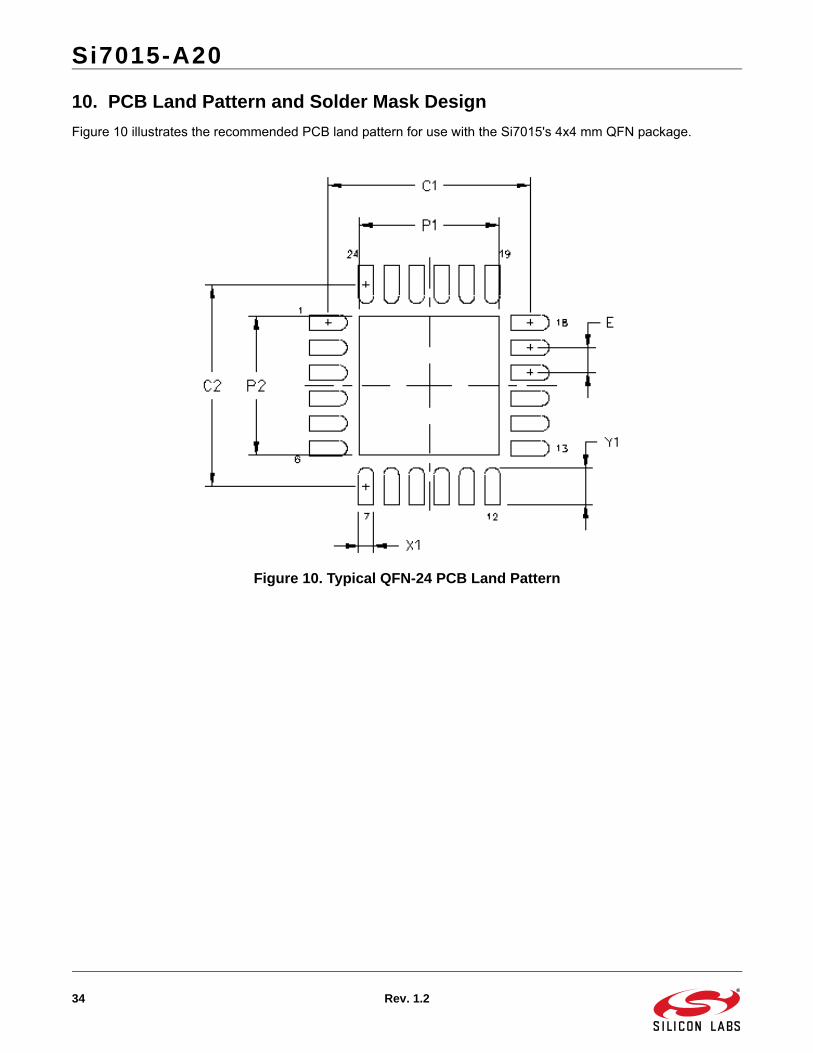
10. PCB Land Pattern and Solder Mask Design
Figure 10 illustrates the recommended PCB land pattern for use with the Si7015's 4x4 mm QFN package.
Figure 10. Typical QFN-24 PCB Land Pattern

Si7015-A20
Rev. 1.2 35
Table 27. PCB Land Pattern Dimensions
Symbol mm
C1 4.00
C2 4.00
E 0.50
P1 2.75
P2 2.75
X1 0.30
Y1 0.75
Notes:General
1. All dimensions shown are at Maximum Material Condition (MMC). Least Material Condition (LMC) is calculated based on a Fabrication Allowance of 0.05 mm.
2. This Land Pattern Design is based on the IPC-7351 guidelines.Solder Mask Design
3. All metal pads are to be non-solder mask defined (NSMD). Clearance between the solder mask and the metal pad is to be 60 µm minimum, all the way around the pad.
Stencil Design
4. A stainless steel, laser-cut and electro-polished stencil with trapezoidal walls should be used to assure good solder paste release.
5. The stencil thickness should be 0.125 mm (5 mils).6. The ratio of stencil aperture to land pad size should be 1:1 for all perimeter
pins.7. A 2x2 array of 0.95 mm square openings on 1.35 mm pitch should be used
for the center ground pad.Card Assembly
8. A No-Clean, Type-3 solder paste is recommended. 9. The recommended card reflow profile is per the JEDEC/IPC J-STD-020
specification for Small Body Components.
Si7015-A20
36 Rev. 1.2
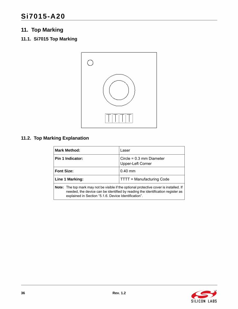
11. Top Marking
11.1. Si7015 Top Marking
11.2. Top Marking Explanation
Mark Method: Laser
Pin 1 Indicator: Circle = 0.3 mm DiameterUpper-Left Corner
Font Size: 0.40 mm
Line 1 Marking: TTTT = Manufacturing Code
Note: The top mark may not be visible if the optional protective cover is installed. If needed, the device can be identified by reading the identification register as explained in Section “5.1.6. Device Identification”.

Si7015-A20
Rev. 1.2 37
12. Additional Reference Resources
AN607: Si70xx Humidity Sensor Designer’s Guide
AN764: Upgrading from the Si7005 to the Si7015

Si7015-A20
38 Rev. 1.2
DOCUMENT CHANGE LIST
Revision 0.9 to Revision 1.0 Updated document revision to 1.0.
Revision 1.0 to Revision 1.1 Minor modification to description and dimensions of protective cover due to the addition of a second cover supplier.
Revision 1.1 to Revision 1.2 Changed packing format from tube to cut tape for all non-tape & reel part numbers without protective filter covers.

DisclaimerSilicon Laboratories intends to provide customers with the latest, accurate, and in-depth documentation of all peripherals and modules available for system and software implementers using or intending to use the Silicon Laboratories products. Characterization data, available modules and peripherals, memory sizes and memory addresses refer to each specific device, and "Typical" parameters provided can and do vary in different applications. Application examples described herein are for illustrative purposes only. Silicon Laboratories reserves the right to make changes without further notice and limitation to product information, specifications, and descriptions herein, and does not give warranties as to the accuracy or completeness of the included information. Silicon Laboratories shall have no liability for the consequences of use of the information supplied herein. This document does not imply or express copyright licenses granted hereunder to design or fabricate any integrated circuits. The products must not be used within any Life Support System without the specific written consent of Silicon Laboratories. A "Life Support System" is any product or system intended to support or sustain life and/or health, which, if it fails, can be reasonably expected to result in significant personal injury or death. Silicon Laboratories products are generally not intended for military applications. Silicon Laboratories products shall under no circumstances be used in weapons of mass destruction including (but not limited to) nuclear, biological or chemical weapons, or missiles capable of delivering such weapons.
Trademark InformationSilicon Laboratories Inc., Silicon Laboratories, Silicon Labs, SiLabs and the Silicon Labs logo, CMEMS®, EFM, EFM32, EFR, Energy Micro, Energy Micro logo and combinations thereof, "the world’s most energy friendly microcontrollers", Ember®, EZLink®, EZMac®, EZRadio®, EZRadioPRO®, DSPLL®, ISOmodem ®, Precision32®, ProSLIC®, SiPHY®, USBXpress® and others are trademarks or registered trademarks of Silicon Laboratories Inc. ARM, CORTEX, Cortex-M3 and THUMB are trademarks or registered trademarks of ARM Holdings. Keil is a registered trademark of ARM Limited. All other products or brand names mentioned herein are trademarks of their respective holders.
http://www.silabs.com
Silicon Laboratories Inc.400 West Cesar ChavezAustin, TX 78701USA
Smart.Connected.Energy-Friendly
Productswww.silabs.com/products
Qualitywww.silabs.com/quality
Support and Communitycommunity.silabs.com