Embed Size (px)
Citation preview
ARTICLE IN PRESS
0168-9002/$ - se
doi:10.1016/j.ni
E-mail addr
Nuclear Instruments and Methods in Physics Research A 566 (2006) 104–109
www.elsevier.com/locate/nima
D0 tracking experience—From the inside looking out
Ronald Lipton
Fermilab, P.O. Box 500, Batavia 60510, USA
Available online 4 August 2006
Abstract
We describe the design, construction, and operation of the D0 detector and its upgrades at the Fermilab Tevatron Collider.
Published by Elsevier B.V.
1. Origins
Let’s go back to 1990; CDF had completed the first p,p̄running at Fermilab and the D0 detector [1] was nearingcompletion. At the same time plans were underway toupgrade the collider complex for higher luminosityconditions in what would eventually be called ‘Run II’.In Run II the main ring would be replaced by anotheraccelerator, the Main Injector, in a separate tunnel, thecrossing interval would be reduced to either 396 or132 ns from 3.2 ms, and the luminosity would increaseto 2� 1032 cm�2 s�1 [2]. Both experiments began to planupgrades to address the changes in operating environmentand take advantage of the physics opportunities.
During the initial planning of the upgrades it wasexpected that the LHC/SSC would turn on in �1997 andsoon thereafter dominate high pT physics. The top quarkhad not yet been discovered and the prospect of thatdiscovery was the clear driving force behind the physicsdesign. CDF had shown that significant B physics could bedone in a hadron collider and B factories were not yet aprospect. The result was a physics design that was intendedprimarily for high pT physics with B physics as a significantfeature.
D0 was significantly redesigned for Run II [3], the mostobvious change being the addition of a 2T superconduct-ing solenoid magnet and a new tracking and vertex detectorto take advantage of the field. In addition, the muonsystem was substantially improved based on the experienceacquired during Run I.
e front matter Published by Elsevier B.V.
ma.2006.05.129
ess: [email protected].
2. Run II design
The Run I non-magnetic detector emphasized calorime-try and muon detection over an Z range of 73. Experiencegained in Run I led us to several conclusions:
�
The small-angle muon chambers had unacceptably highoccupancy. We performed a series of detailed shieldingstudies using MARS and GEANT as well as insitumeasurements. The result was an understanding thatneutrons and slow tracks were a significant problem.This in turn led to a complex passive shield design andthe addition of several layers of fast trigger counters. � The D0 tracker performed poorly in r–z. The Run Ichambers used charge division and delay lines for z
information which presented ambiguity problems inhigh multiplicity events and high-luminosity conditions.The Run II tracker makes use of small-angle stereo andmultiple z sections in the silicon.
� CDF had much better J/c-mm yields than D0 due totheir thinner iron which resulted in lower pT thresholds.In Run II an inner ‘A’ layer of scintillation counters wasadded between the calorimeter and the inner muonabsorber to reduce the muon momentum threshold.
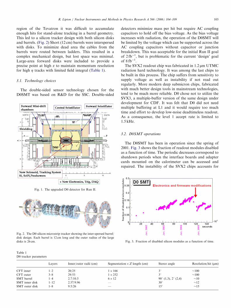
The result of these upgrades is a more robust detector(Fig. 1) with substantially improved tracking and muondetection.
3. D0 silicon microstrip tracker (D0SMT)
We also wanted to preserve good tracking and vertexingat reasonably high Z. Given the 25 cm–long luminous
ARTICLE IN PRESSR. Lipton / Nuclear Instruments and Methods in Physics Research A 566 (2006) 104–109 105
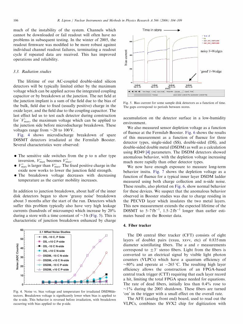
region of the Tevatron it was difficult to accumulateenough hits for stand-alone tracking in a barrel geometry.This led to a silicon tracker design with both silicon disksand barrels. (Fig. 2) Short (12 cm) barrels were interspersedwith disks. To minimize dead area the cables from thebarrels were routed between ladders. This resulted in acomplex mechanical design, but lost space was minimal.Large-area forward disks were included to provide aprecise point at high z to maintain momentum resolutionfor high Z tracks with limited field integral (Table 1).
3.1. Technology choices
The double-sided sensor technology chosen for theD0SMT was based on R&D for the SSC. Double-sided
Fig. 1. The upgraded D0 detector for Run II.
Fig. 2. The D0 silicon microstrip tracker showing the inter-spersed barrel/
disk design. Each barrel is 12 cm long and the outer radius of the large
disks is 26 cm.
Table 1
D0 tracker parameters
Layers Inner/outer radii (cm) Segmenta
CFT inner 1–2 20/25 1� 166
CFT outer 3–8 29/53 1� 252
SMT barrel 1–4 2.7/10.5 6� 12
SMT inner disk 1–12 2.57/9.96 —
SMT outer disk 1–8 9.5/26 —
detectors minimize mass per hit but require AC couplingcapacitors to hold off the bias voltage. As the bias voltageincreases with radiation, the operation of the D0SMT willbe limited by the voltage which can be supported across theAC coupling capacitors without capacitor or junctionbreakdown. This was acceptable for the initial Run II goalof 2 fb�1, but is problematic for the current ‘design’ goalof 8 fb�1.The SVX2 readout chip was fabricated in 1.2 mm UTMC
radiation hard technology. It was among the last chips tobe built in this process. The chip suffers from sensitivity tosupply voltage as well as instability if not read outregularly. More modern deep submicron chips, fabricatedwith much better design tools in mainstream technologies,tend to be much more reliable. D0 chose not to utilize theSVX3, a multiple-buffer version of the same design underdevelopment for CDF. It was felt that D0 did not needmultiple buffering at L1 and it would require too muchtime and effort to develop low-noise deadtimeless readout.As a consequence, the level 1 accept rate is limited to1.5 kHz.
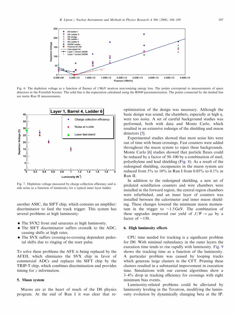
3.2. D0SMT operations
The D0SMT has been in operation since the spring of2001. Fig. 3 shows the fraction of readout modules disabledas a function of time. The periodic decreases correspond toshutdown periods when the interface boards and adaptercards mounted on the calorimeter can be accessed andrepaired. The instability of the SVX2 chips accounts for
tion�Z length (cm) Stereo angle Resolution/hit (mm)
31 �100
31 �100
901 (1,3), 21 (2,4) �10
301 �12
151 �15
Fig. 3. Fraction of disabled silicon modules as a function of time.
ARTICLE IN PRESSR. Lipton / Nuclear Instruments and Methods in Physics Research A 566 (2006) 104–109106
much of the instability of the system. Channels whichcannot be downloaded or fail readout will often have noproblems in subsequent testing. In the winter of 2005, thereadout firmware was modified to be more robust againstindividual channel readout failures, terminating a readoutcycle if repeated data are received. This has improvedoperations and reliability.
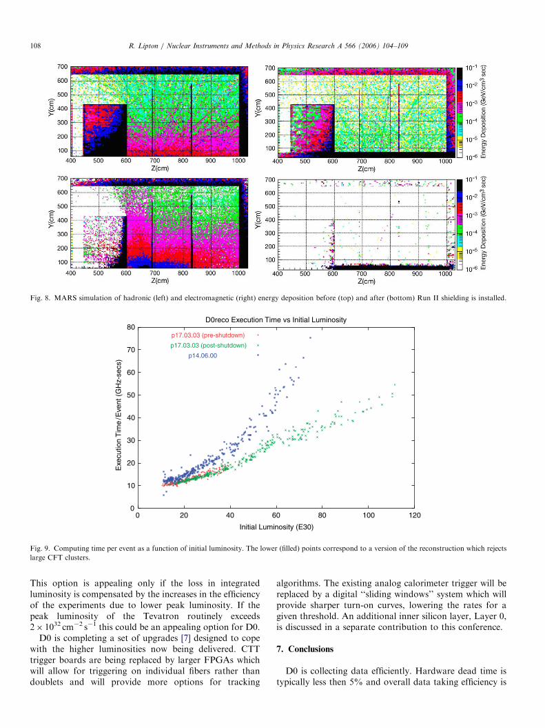
Fig. 5. Bias current for some sample disk detectors as a function of time.
The gaps correspond to periods between stores.
3.3. Radiation studies
The lifetime of our AC-coupled double-sided silicondetectors will be typically limited either by the maximumvoltage which can be applied across the integrated couplingcapacitor or by breakdown at the junction. The net field atthe junction implant is a sum of the field due to the bias ofthe bulk, field due to fixed (usually positive) charge in theoxide layer, and the field due to the coupling capacitor. Thelast effect led us to test each detector during constructionfor ‘V�max
’ , the maximum voltage which can be applied tothe junction side before microdischarge breakdown. Thesevoltages range from �20 to 100V.
Fig. 4 shows microdischarge breakdown of spareD0SMT detectors irradiated at the Fermilab Booster.Several characteristics were observed:
�
Fig
tec
the
occ
The sensitive side switches from the p to n after typeinversion, V�max becomes V+
max.
� V+max is larger than V�max. The fixed positive charge in theoxide now works to lower the junction field strength.
� The breakdown voltage decreases with decreasingtemperature as the carrier mobility increases.
In addition to junction breakdown, about half of the innerdisk detectors began to show ‘grassy noise’ breakdownabout 3 months after the start of the run. Detectors whichsuffer this problem typically also have very high leakagecurrents (hundreds of microamps) which increase by 20%during a store with a time constant of �3 h (Fig. 5). This ischaracteristic of junction breakdown enhanced by charge
2.1 MRad Noise Studies
0
10
20
30
40
50
60
No
ise
(AD
C C
ou
nts
)
DS, -10 C, P Side
DS, +10 C P-side
DS, -10 C N-side
DS, +10 C N-side
DSDM, -10 C N-side
DSDM, +10 C N-side
DSDM, -10 C P-side
DSDM, +10 C P-side
. 4. Noise vs. bias voltage and temperature for irradiated DSDMde-
tors. Breakdown voltage is significantly lower when bias is applied to
n-side. This behavior is reversed before irradiation, with breakdown
urring with bias applied to the p-side.
accumulation on the detector surface in a low-humidityenvironment.We also measured sensor depletion voltage as a function
of fluence at the Fermilab Booster. Fig. 6 shows the resultsof this measurement as a function of fluence for threedetector types, single-sided (SS), double-sided (DS), anddouble-sided double metal (DSDM) as well as a calculationusing RD49 [4] parameters. The DSDM detectors showedanomalous behavior, with the depletion voltage increasingmuch more rapidly than other detector types.We now have enough exposure to measure long-term
behavior insitu. Fig. 7 shows the depletion voltage as afunction of fluence for a typical inner layer DSDM laddermeasured using both charge collection and n-side noise.These results, also plotted on Fig. 6, show normal behaviorfor these devices. We suspect that the anomalous behaviorobserved in Booster studies was due to charge residing inthe PECVD layer which insulates the two metal layers.This new measurement extends the expected lifetime of theD0SMT to 5–7 fb�1, 1.5–2 fb�1 longer than earlier esti-mates based on the Booster data.
4. Fiber tracker
The D0 central fiber tracker (CFT) consists of eightlayers of doublet pairs (xxuu, xxvv, etc) of 0.835mmdiameter scintillating fibers. The u and v measurementscorrespond to 731 stereo fibers. Light from the fibers isconverted to an electrical signal by visible light photoncounters (VLPCs) which have a quantum efficiency of�80% and operate at �265 1C. The resulting high layerefficiency allows the construction of an FPGA-basedcentral track trigger (CTT) requiring that each layer recorda hit, limiting the total FPGA space needed for equations.The rate of dead fibers, initially less than 0.4% rose to�1% during the 2003 shutdown. These fibers are turned‘on’ in the trigger with a small effect on the overall rate.The AFE (analog front end) board, used to read out the
VLPCs, combines the SVX2 chip for digitization with
ARTICLE IN PRESS
0
250
200
150
100
50
1 fb-1
Dep
leti
on
Vo
ltag
e
0.00E+00 5.00E+12 1.00E+13 1.50E+13 2.00E+13 2.50E+13 3.00E+13 3.50E+13 4.00E+13Fluence (1MeVn)
DS ladder IDS Ladder IIDS wedgeSS Ladder ISS Ladder IIDSDM LadderFluence 8 /1/05Calculated VdLayer 1 (inner) DSDMLayer 1 (outer) DSDM
Fig. 6. The depletion voltage as a function of fluence of 1MeV neutron non-ionizing energy loss. The points correspond to measurements of spare
detectors in the Fermilab booster. The solid line is the expectation calculated using the RD49 parameterization. The points connected by the dashed line
are insitu Run II measurements.
Fig. 7. Depletion voltage measured by charge collection efficiency and n-
side noise as a function of luminosity for a typical inner layer ladder.
R. Lipton / Nuclear Instruments and Methods in Physics Research A 566 (2006) 104–109 107
another ASIC, the SIFT chip, which contains an amplifier/discriminator to feed the track trigger. This system hasseveral problems at high luminosity:
�
The SVX2 front end saturates at high luminosity. � The SIFT discriminator suffers crostalk to the ADC,causing shifts at high rates.
� The SVX suffers crossing-to-crossing dependent pedes-tal shifts due to ringing of the reset pulse.
To solve these problems the AFE is being replaced by theAFEII, which eliminates the SVX chip in favor ofcommercial ADCs and replaces the SIFT chip by theTRIP-T chip, which combines discrimination and providestiming for z information.
5. Muon system
Muons are at the heart of much of the D0 physicsprogram. At the end of Run I it was clear that re-
optimization of the design was necessary. Although thebasic design was sound, the chambers, especially at high Z,were too noisy. A set of careful background studies wasperformed, both with data and Monte Carlo, whichresulted in an extensive redesign of the shielding and muondetectors [5].Experimental studies showed that most noise hits were
out of time with beam crossings. Fast counters were addedthroughout the muon system to reject these backgrounds.Monte Carlo [6] studies showed that particle fluxes couldbe reduced by a factor of 50–100 by a combination of steel,polyethylene and lead shielding (Fig. 8). As a result of theredesigned shielding, occupancies in the muon system arereduced from 5% to 10% in Run I from 0.05% to 0.1% inRun II.In addition to the redesigned shielding, a new set of
pixilated scintillation counters and wire chambers wereinstalled in the forward region, the central region chamberswere refurbished, and an inner layer of counters wasinstalled between the calorimeter and inner muon shield-ing. These changes lowered the minimum muon momen-tum in the trigger to �1.5GeV. The combination ofthese upgrades improved our yield of J=C! mm by afactor of �150.
6. High luminosity effects
CPU time needed for tracking is a significant problemfor D0. With minimal redundancy in the outer layers theexecution time tends to rise rapidly with luminosity. Fig. 9shows the tracking time as a function of the luminosity.A particular problem was caused by looping trackswhich generate large clusters in the CFT. Pruning theseclusters resulted in a substantial improvement in executiontime. Simulations with our current algorithms show a3–4% drop in tracking efficiency for crossings with eightminimum bias events.Luminosity-related problems could be alleviated by
luminosity leveling in the Tevatron, modifying the lumin-osity evolution by dynamically changing beta at the IP.
ARTICLE IN PRESS
Fig. 8. MARS simulation of hadronic (left) and electromagnetic (right) energy deposition before (top) and after (bottom) Run II shielding is installed.
0
10
20
30
40
50
60
70
80
0 20 40 60 80 100 120
Exe
cutio
n T
ime
/Eve
nt (
GH
z-se
cs)
Initial Luminosity (E30)
D0reco Execution Time vs Initial Luminosity
p17.03.03 (pre-shutdown)
p17.03.03 (post-shutdown)
p14.06.00
Fig. 9. Computing time per event as a function of initial luminosity. The lower (filled) points correspond to a version of the reconstruction which rejects
large CFT clusters.
R. Lipton / Nuclear Instruments and Methods in Physics Research A 566 (2006) 104–109108
This option is appealing only if the loss in integratedluminosity is compensated by the increases in the efficiencyof the experiments due to lower peak luminosity. If thepeak luminosity of the Tevatron routinely exceeds2� 1032 cm�2 s�1 this could be an appealing option for D0.
D0 is completing a set of upgrades [7] designed to copewith the higher luminosities now being delivered. CTTtrigger boards are being replaced by larger FPGAs whichwill allow for triggering on individual fibers rather thandoublets and will provide more options for tracking
algorithms. The existing analog calorimeter trigger will bereplaced by a digital ‘‘sliding windows’’ system which willprovide sharper turn-on curves, lowering the rates for agiven threshold. An additional inner silicon layer, Layer 0,is discussed in a separate contribution to this conference.
7. Conclusions
D0 is collecting data efficiently. Hardware dead time istypically less then 5% and overall data taking efficiency is
ARTICLE IN PRESSR. Lipton / Nuclear Instruments and Methods in Physics Research A 566 (2006) 104–109 109
�85%. The muon and calorimeter systems typicallyoperate with 99.8% and 99.9% operational channels, theCFT is at �98% and the SMT is at �87%. Although thedetector is operating well, the experiment is just beginningto cope with the challenges of high luminosity. As Tevatronluminosity climbs, additional work will be needed to refinetracking algorithms, monitor detector aging, and tune thetrigger and data acquisition systems. Imminent upgrades ofthe trigger, tracking, and DAQ should allow D0 maximaluse of the Tevatron in the pre-LHC era.
Acknowledgments
I would like to thank the D0 operations group, runcoordinators and detector group leaders, whose continual
efforts to improve the quality and efficiency of the D0detector have been crucial to the success of the experiment.
References
[1] S. Abachi, et al., Nucl. Instr.and Meth. A 338 (1994) 185.
[2] Tevatron Run II Handbook. www-bd.fnal.gov/lug/.
[3] The Upgraded D0 Detector. Physics/0507191; Fermilab-Pub-05/341-
E, Nucl. Instr. and Meth., submitted for publication.
[4] M. Moll, Radiation Damage in silicon particle detectors microscopic
defects and macroscopic properties, Ph.D. Thesis, University of
Hamburg, DESY-THESIS-1999-040, ISSN 1435-8085, 1999.
[5] V.M. Abazov, et al., Nucl. Instr. and Meth. A 552 (2005) 372.
[6] N. Mokhov, Fermilab-Conf-03/053 (2003). www-ap.fnal.gov/MARS.
[7] R. Lipton, Tevatron Detector Upgrades, in: Proceedings of East
Lansing 2004, Hadron Collider Physics, 753:2005, vol. pp. 419–425.