Embed Size (px)
Citation preview
FN6783Rev.1.00
May 5, 2016
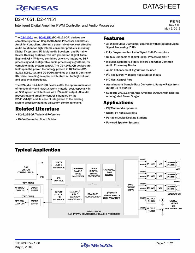
D2-41051, D2-41151Intelligent Digital Amplifier PWM Controller and Audio Processor
DATASHEET
The D2-41051 and D2-41151 (D2-41x51-QR) devices are complete System-on-Chip (SoC) Audio Processor and Class-D Amplifier Controllers, offering a powerful yet very cost effective audio solution for high volume consumer products, including Digital TV systems, PC Multimedia Speakers, and Portable Device Docking Stations. This 4th generation Digital Audio Engine (DAE-4)™ device combines extensive integrated DSP processing and configurable audio processing algorithms, for complete audio system control. The D2-41x51-QR devices are built upon the proven technology present in D2Audio's D2-814xx, D2-914xx, and D2-926xx families of Class-D Controller ICs, while providing an optimized feature set for high volume and cost-critical products.
The D2Audio D2-41x51-QR devices offer the optimum balance of functionality and lowest system material cost, especially in an SoC system architectures with I2S audio output. All audio processing and amplifier control is handled by the D2-41x51-QR, and its ease of integration to the existing system processor handles all system control functions.
Related Literature• D2-41x51-QR Technical Reference
• DAE-4 Evaluation Board Guides
Features• All Digital Class-D Amplifier Controller with Integrated Digital
Signal Processing (DSP)
• Fully Programmable Audio Signal Path Parameters
• Up to 5 Channels of Digital Signal Processing (DSP)
• Includes Equalizers, Filters, Mixers and Other Common Audio Processing Blocks
• Audio Enhancement Algorithms Included
• I2S and S/PDIF™ Digital Audio Stereo Inputs
• I2C Host Control Port
• Asynchronous Sample Rate Converters, Sample Rates from 32kHz up to 192kHz
• Supports 2.0, 2.1 or Bi-Amp Amplifier Outputs with Discrete or Integrated Power Stages
Applications• PC/Multimedia Speakers
• Digital TV Audio Systems
• Portable Device Docking Stations
• Powered Speaker Systems
Typical Application
DRIVER
D2-41x51-QRDAE-4™ PWM CONTROLLER AND AUDIO PROCESSOR
PWMOUTPUTDRIVE
FETs OUTPUTFILTER
PWM0
PWM1
DRIVER FETs OUTPUTFILTER
PWM2
PWM3
OUTPUTFILTER
PWM6
OUTPUTFILTER
PWM7
STEREOLINE OUT
ORHEADPHONE OUT
5 CHANNEL PWM
ENGINE
24 BIT DIGITAL SIGNAL
PROCESSOR
2 CHANNEL SAMPLE RATE
CONVERTER
DIGITAL AUDIO
INTERFACE
S/PDIF DIGITAL
I/O INTERFACE
SoCSYSTEM
CONTROLLER(S)
I2S
I2CCONTROL
I2C
S/PDIF BUFFER
S/PDIF BUFFER
OPTICAL/COAX IN
OPTICAL/COAX OUT
(OPTIONAL)
(OPTIONAL)D2AUDIO®
SOUNDSUITE™
3RD PARTYENHANCEMENTS(SRS WOW/HD®)
D2AUDIO®
AUDIO CANVAS™
PROCESSING
DRIVER FETs OUTPUTFILTERPWM5
PWM4
LEFT
RIGHT
SUBWOOFER
FN6783 Rev.1.00 Page 1 of 21May 5, 2016
D2-41051, D2-41151
Ordering InformationPART
NUMBER(Notes 3, 4)
AUDIO PROCESSING FEATURE SET SUPPORT
(Note 2)PART
MARKINGTEMP RANGE
(°C)TAPE AND REEL
(UNITS)PACKAGE
(RoHS Compliant)PKG.
DWG. #
D2-41051-QR D2Audio™ SoundSuite™ D2-41051-QR -10 to +85 - 48 Ld QFN L48.7x7
D2-41051-QR-TK(Note 1)
D2Audio™ SoundSuite™ D2-41051-QR -10 to +85 1k 48 Ld QFN L48.7x7
D2-41151-QR D2Audio™ SoundSuite™DTS®(SRS) WOW/HD™
D2-41151-QR -10 to +85 - 48 Ld QFN L48.7x7
D2-41151-QR-TK(Note 1)
D2Audio™ SoundSuite™DTS®(SRS) WOW/HD™
D2-41151-QR -10 to +85 1k 48 Ld QFN L48.7x7
NOTES:
1. Please refer to TB347 for details on reel specifications.
2. The D2-41x51 family supports audio processing algorithms for the D2Audio SoundSuite™, and DTS®(SRS) WOW/HD® audio enhancement features. Algorithm support of these enhancements is device-dependent. Refer to specific part number for desired feature support.
3. These Intersil Pb-free plastic packaged products employ special Pb-free material sets, molding compounds/die attach materials, and 100% matte tin plate plus anneal (e3 termination finish, which is RoHS compliant and compatible with both SnPb and Pb-free soldering operations). Intersil Pb-free products are MSL classified at Pb-free peak reflow temperatures that meet or exceed the Pb-free requirements of IPC/JEDEC J STD-020.
4. For Moisture Sensitivity Level (MSL), please see device information page for D2-41051 and D2-41151. For more information on MSL please see techbrief TB363.
FN6783 Rev.1.00 Page 2 of 21May 5, 2016
D2-41051, D2-41151
Table of ContentsTypical Application . . . . . . . . . . . . . . . . . . . . . . . . . . . . . . . . . . . . . . . . . . . . . . . . . . . . . . . . . . . . . . . . . . . . . . . . . . . . . . . . . . . . . . . . . . 1
Ordering Information . . . . . . . . . . . . . . . . . . . . . . . . . . . . . . . . . . . . . . . . . . . . . . . . . . . . . . . . . . . . . . . . . . . . . . . . . . . . . . . . . . . . . . . . 2
Absolute Maximum Ratings . . . . . . . . . . . . . . . . . . . . . . . . . . . . . . . . . . . . . . . . . . . . . . . . . . . . . . . . . . . . . . . . . . . . . . . . . . . . . . . . . . . 4
Thermal Information . . . . . . . . . . . . . . . . . . . . . . . . . . . . . . . . . . . . . . . . . . . . . . . . . . . . . . . . . . . . . . . . . . . . . . . . . . . . . . . . . . . . . . . . . 4
Recommended Operating Conditions . . . . . . . . . . . . . . . . . . . . . . . . . . . . . . . . . . . . . . . . . . . . . . . . . . . . . . . . . . . . . . . . . . . . . . . . . . 4
Electrical Specifications . . . . . . . . . . . . . . . . . . . . . . . . . . . . . . . . . . . . . . . . . . . . . . . . . . . . . . . . . . . . . . . . . . . . . . . . . . . . . . . . . . . . . 4
Serial Audio Interface Port Timing . . . . . . . . . . . . . . . . . . . . . . . . . . . . . . . . . . . . . . . . . . . . . . . . . . . . . . . . . . . . . . . . . . . . . . . . . . . . . 6
Two-Wire (I2C) Interface Port Timing. . . . . . . . . . . . . . . . . . . . . . . . . . . . . . . . . . . . . . . . . . . . . . . . . . . . . . . . . . . . . . . . . . . . . . . . . . . . 7
SPI™ Master Mode Interface Port Timing . . . . . . . . . . . . . . . . . . . . . . . . . . . . . . . . . . . . . . . . . . . . . . . . . . . . . . . . . . . . . . . . . . . . . . . 8
SPI™ Slave Mode Interface Port Timing. . . . . . . . . . . . . . . . . . . . . . . . . . . . . . . . . . . . . . . . . . . . . . . . . . . . . . . . . . . . . . . . . . . . . . . . . 8
Pin Configuration. . . . . . . . . . . . . . . . . . . . . . . . . . . . . . . . . . . . . . . . . . . . . . . . . . . . . . . . . . . . . . . . . . . . . . . . . . . . . . . . . . . . . . . . . . . . 9
D2-41051, D2-41151 Pin Descriptions . . . . . . . . . . . . . . . . . . . . . . . . . . . . . . . . . . . . . . . . . . . . . . . . . . . . . . . . . . . . . . . . . . . . . . . . . 10
Overview . . . . . . . . . . . . . . . . . . . . . . . . . . . . . . . . . . . . . . . . . . . . . . . . . . . . . . . . . . . . . . . . . . . . . . . . . . . . . . . . . . . . . . . . . . . . . . . . . . 12Output Configurations . . . . . . . . . . . . . . . . . . . . . . . . . . . . . . . . . . . . . . . . . . . . . . . . . . . . . . . . . . . . . . . . . . . . . . . . . . . . . . . . . . . . . . . . . . . . 12Programmable Audio Processing . . . . . . . . . . . . . . . . . . . . . . . . . . . . . . . . . . . . . . . . . . . . . . . . . . . . . . . . . . . . . . . . . . . . . . . . . . . . . . . . . . 12Typical Performance . . . . . . . . . . . . . . . . . . . . . . . . . . . . . . . . . . . . . . . . . . . . . . . . . . . . . . . . . . . . . . . . . . . . . . . . . . . . . . . . . . . . . . . . . . . . . 12Audio Enhancement Processing . . . . . . . . . . . . . . . . . . . . . . . . . . . . . . . . . . . . . . . . . . . . . . . . . . . . . . . . . . . . . . . . . . . . . . . . . . . . . . . . . . . 12
Functional Description . . . . . . . . . . . . . . . . . . . . . . . . . . . . . . . . . . . . . . . . . . . . . . . . . . . . . . . . . . . . . . . . . . . . . . . . . . . . . . . . . . . . . . 12Serial Audio Digital Input . . . . . . . . . . . . . . . . . . . . . . . . . . . . . . . . . . . . . . . . . . . . . . . . . . . . . . . . . . . . . . . . . . . . . . . . . . . . . . . . . . . . . . . . . 13S/PDIF Digital Audio I/O. . . . . . . . . . . . . . . . . . . . . . . . . . . . . . . . . . . . . . . . . . . . . . . . . . . . . . . . . . . . . . . . . . . . . . . . . . . . . . . . . . . . . . . . . . 13Sample Rate Converter. . . . . . . . . . . . . . . . . . . . . . . . . . . . . . . . . . . . . . . . . . . . . . . . . . . . . . . . . . . . . . . . . . . . . . . . . . . . . . . . . . . . . . . . . . . 13DSP . . . . . . . . . . . . . . . . . . . . . . . . . . . . . . . . . . . . . . . . . . . . . . . . . . . . . . . . . . . . . . . . . . . . . . . . . . . . . . . . . . . . . . . . . . . . . . . . . . . . . . . . . . . 13Audio Processing And Signal Flow . . . . . . . . . . . . . . . . . . . . . . . . . . . . . . . . . . . . . . . . . . . . . . . . . . . . . . . . . . . . . . . . . . . . . . . . . . . . . . . . . 13Audio Enhancement Feature Processing . . . . . . . . . . . . . . . . . . . . . . . . . . . . . . . . . . . . . . . . . . . . . . . . . . . . . . . . . . . . . . . . . . . . . . . . . . . . 15PWM Audio Outputs . . . . . . . . . . . . . . . . . . . . . . . . . . . . . . . . . . . . . . . . . . . . . . . . . . . . . . . . . . . . . . . . . . . . . . . . . . . . . . . . . . . . . . . . . . . . . 15I/O Control Pins . . . . . . . . . . . . . . . . . . . . . . . . . . . . . . . . . . . . . . . . . . . . . . . . . . . . . . . . . . . . . . . . . . . . . . . . . . . . . . . . . . . . . . . . . . . . . . . . . 15Timers . . . . . . . . . . . . . . . . . . . . . . . . . . . . . . . . . . . . . . . . . . . . . . . . . . . . . . . . . . . . . . . . . . . . . . . . . . . . . . . . . . . . . . . . . . . . . . . . . . . . . . . . . 15I2C 2-Wire Control Interface . . . . . . . . . . . . . . . . . . . . . . . . . . . . . . . . . . . . . . . . . . . . . . . . . . . . . . . . . . . . . . . . . . . . . . . . . . . . . . . . . . . . . . . 15Serial Peripheral Interface (SPI) . . . . . . . . . . . . . . . . . . . . . . . . . . . . . . . . . . . . . . . . . . . . . . . . . . . . . . . . . . . . . . . . . . . . . . . . . . . . . . . . . . . 15Control Register Summary . . . . . . . . . . . . . . . . . . . . . . . . . . . . . . . . . . . . . . . . . . . . . . . . . . . . . . . . . . . . . . . . . . . . . . . . . . . . . . . . . . . . . . . . 15Temperature Sensing . . . . . . . . . . . . . . . . . . . . . . . . . . . . . . . . . . . . . . . . . . . . . . . . . . . . . . . . . . . . . . . . . . . . . . . . . . . . . . . . . . . . . . . . . . . . 17Overcurrent Sensing . . . . . . . . . . . . . . . . . . . . . . . . . . . . . . . . . . . . . . . . . . . . . . . . . . . . . . . . . . . . . . . . . . . . . . . . . . . . . . . . . . . . . . . . . . . . . 17Power Supply Synchronization. . . . . . . . . . . . . . . . . . . . . . . . . . . . . . . . . . . . . . . . . . . . . . . . . . . . . . . . . . . . . . . . . . . . . . . . . . . . . . . . . . . . . 17Error Reporting. . . . . . . . . . . . . . . . . . . . . . . . . . . . . . . . . . . . . . . . . . . . . . . . . . . . . . . . . . . . . . . . . . . . . . . . . . . . . . . . . . . . . . . . . . . . . . . . . . 17Power Sequencing. . . . . . . . . . . . . . . . . . . . . . . . . . . . . . . . . . . . . . . . . . . . . . . . . . . . . . . . . . . . . . . . . . . . . . . . . . . . . . . . . . . . . . . . . . . . . . . 17Clock and PLL. . . . . . . . . . . . . . . . . . . . . . . . . . . . . . . . . . . . . . . . . . . . . . . . . . . . . . . . . . . . . . . . . . . . . . . . . . . . . . . . . . . . . . . . . . . . . . . . . . . 17Reset and Device Initialization. . . . . . . . . . . . . . . . . . . . . . . . . . . . . . . . . . . . . . . . . . . . . . . . . . . . . . . . . . . . . . . . . . . . . . . . . . . . . . . . . . . . . 17Boot Modes. . . . . . . . . . . . . . . . . . . . . . . . . . . . . . . . . . . . . . . . . . . . . . . . . . . . . . . . . . . . . . . . . . . . . . . . . . . . . . . . . . . . . . . . . . . . . . . . . . . . . 18Output Mode Configurations . . . . . . . . . . . . . . . . . . . . . . . . . . . . . . . . . . . . . . . . . . . . . . . . . . . . . . . . . . . . . . . . . . . . . . . . . . . . . . . . . . . . . . 18Configuration Modes Assignment . . . . . . . . . . . . . . . . . . . . . . . . . . . . . . . . . . . . . . . . . . . . . . . . . . . . . . . . . . . . . . . . . . . . . . . . . . . . . . . . . . 18
Revision History. . . . . . . . . . . . . . . . . . . . . . . . . . . . . . . . . . . . . . . . . . . . . . . . . . . . . . . . . . . . . . . . . . . . . . . . . . . . . . . . . . . . . . . . . . . . 20
About Intersil . . . . . . . . . . . . . . . . . . . . . . . . . . . . . . . . . . . . . . . . . . . . . . . . . . . . . . . . . . . . . . . . . . . . . . . . . . . . . . . . . . . . . . . . . . . . . . 20
Trademarks . . . . . . . . . . . . . . . . . . . . . . . . . . . . . . . . . . . . . . . . . . . . . . . . . . . . . . . . . . . . . . . . . . . . . . . . . . . . . . . . . . . . . . . . . . . . . . . . 20
Disclaimer for DTS®(SRS) Technology License Required Notice: . . . . . . . . . . . . . . . . . . . . . . . . . . . . . . . . . . . . . . . . . . . . . . . . . . 20
Package Outline Drawing . . . . . . . . . . . . . . . . . . . . . . . . . . . . . . . . . . . . . . . . . . . . . . . . . . . . . . . . . . . . . . . . . . . . . . . . . . . . . . . . . . . . 21
FN6783 Rev.1.00 Page 3 of 21May 5, 2016
D2-41051, D2-41151
Specifications
Absolute Maximum Ratings (Note 7) Thermal InformationSupply Voltage
RVDD, PWMVDD . . . . . . . . . . . . . . . . . . . . . . . . . . . . . . . . . . . -0.3V to 4.0VCVDD, PLLVDD . . . . . . . . . . . . . . . . . . . . . . . . . . . . . . . . . . . . -0.3V to 2.4V
Input VoltageAny Input but XTALI . . . . . . . . . . . . . . . . . . . . . . . . . -0.3V to RVDD + 0.3VXTALI . . . . . . . . . . . . . . . . . . . . . . . . . . . . . . . . . . . -0.3V to PLLVDD + 0.3V
Input Current, any Pin but Supplies . . . . . . . . . . . . . . . . . . . . . . . . . . ±10mA
Thermal Resistance (Typical) JA (°C/W) JC (°C/W)48 Ld QFN (Notes 5, 6) . . . . . . . . . . . . . . . . 27 2
Temperature Range (Operating) . . . . . . . . . . . . . . . . . . . . . . . 0°C to +70°CMaximum Storage Temperature. . . . . . . . . . . . . . . . . . . . -55°C to +150°CPb-Free Reflow Profile . . . . . . . . . . . . . . . . . . . . . . . . . . . . . . . . . . see TB493
CAUTION: Do not operate at or near the maximum ratings listed for extended periods of time. Exposure to such conditions may adversely impact productreliability and result in failures not covered by warranty.
NOTES:
5. JA is measured in free air with the component mounted on a high effective thermal conductivity test board with “direct attach” features. See Tech Brief TB379.
6. For JC, the “case temp” location is the center of the exposed metal pad on the package underside.
7. Absolute Maximum parameters are not tested in production.
Recommended Operating Conditions TA = +25°C, CVDD = PLLVDD = 1.8V ±5%, RVDD = PWMVDD = 3.3V ±10%. All grounds at 0.0V. All voltages referenced to ground. PLL at 294.912MHz, OSC at 24.576MHz, core running at 147.456MHz with typical audio data traffic.
SYMBOL PARAMETER MIN TYP MAX UNIT
CVDD Core Supply Pins 1.7 1.8 1.9 V
Active Current - 300 - mA
Power-Down Current (Note 8) - 6 - mA
RVDD and PWMVDD Digital I/O and PWM Pad Ring Supply Pins 3.0 3.3 3.6 V
Active Current - 10 - mA
Power-Down Current (Note 8) - 0.01 - mA
PLLVDD Analog Supply Pins (PLL) 1.7 1.8 1.9 V
Active Current - 10 - mA
Power-Down Current (Note 8) - 5 - mA
NOTE:8. Power Down is with device in reset and clocks stopped
Electrical Specifications TA = +25°C, CVDD = PLLVDD = 1.8V ±5%, RVDD = PWMVDD = 3.3V ±10%. All grounds at 0.0V. All voltages referenced to ground. PLL at 294.912MHz, OSC at 24.576MHz, core running at 147.456MHz with typical audio data traffic.
SYMBOL PARAMETER MIN TYP MAX UNIT
VIH Digital Input High Logic Level (Note 9) 2 - - V
VIL Digital Input Low Logic Level (Note 9) - - 0.8 V
VOH High Level Output Drive Voltage (Note 10) (IOUT = -Pad Drive) RVDD - 0.4 - - V
VOL Low Level Output Drive Voltage (Note 10) (IOUT = +Pad Drive) - - 0.4 V
VIHX High Level Input Drive Voltage XTALI Pin 0.7 - PLLVDD V
VILX Low Level Input Drive Voltage XTALI Pin - - 0.3 V
IIN Input Leakage Current (Note 11) - - ±10 µA
CIN Input Capacitance - 9 - pF
COUT Output Capacitance - 9 - pF
Trst nRESET Pulse Width - 10 - ns
FN6783 Rev.1.00 Page 4 of 21May 5, 2016
D2-41051, D2-41151
CRYSTAL OSCILLATOR
Xo Crystal Frequency (Fundamental Mode Crystal) 20 24.576 25 MHz
Dt Duty Cycle 40 - 60 %
Tstart Start-Up Time (Start-Up Time is Oscillator enabled (with Valid Supply) to Stable Oscillation) - 5 20 ms
PLL
Fvco VCO Frequency 240 294.912 300 MHz
PLL Lock Time from any Input Change - 3 - ms
1.8V POWER ON RESET
Ven Reset Enabled Voltage Level 0.95 1.10 1.30 V
Tdis POR Minimum Output Pulse Width - 5 - µs
1.8V BROWNOUT DETECTION
Detect Level 1.4 1.5 1.7 V
Tbod1 Pulse Width Rejection - 100 - ns
To1 Minimum Output Pulse Width - 20 - ns
3.3V (CVDD) BROWNOUT DETECTION
Detect Level 2.4 2.7 2.9 V
Tbod3 Pulse Width Rejection - 100 - ns
To3 Minimum Output Pulse Width - 20 - ns
NOTES:
9. All input pins except XTALI
10. All digital output pins. Drive strength for each digital pin is in the “D2-41051, D2-41151 Pin Descriptions” on page 10.
11. Input leakage applies to all pins except XTALO
Electrical Specifications TA = +25°C, CVDD = PLLVDD = 1.8V ±5%, RVDD = PWMVDD = 3.3V ±10%. All grounds at 0.0V. All voltages referenced to ground. PLL at 294.912MHz, OSC at 24.576MHz, core running at 147.456MHz with typical audio data traffic. (Continued)
SYMBOL PARAMETER MIN TYP MAX UNIT
FN6783 Rev.1.00 Page 5 of 21May 5, 2016
D2-41051, D2-41151
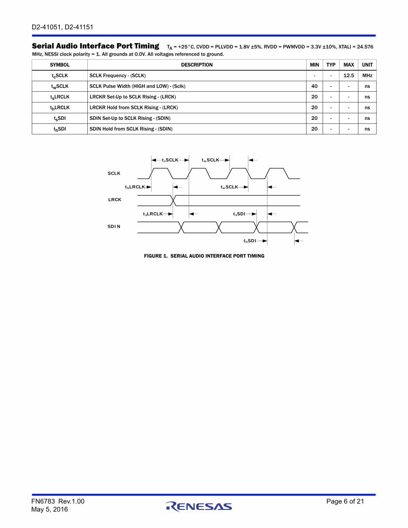
Serial Audio Interface Port Timing TA = +25°C, CVDD = PLLVDD = 1.8V ±5%, RVDD = PWMVDD = 3.3V ±10%, XTALI = 24.576 MHz, NESSI clock polarity = 1. All grounds at 0.0V. All voltages referenced to ground.
SYMBOL DESCRIPTION MIN TYP MAX UNIT
tcSCLK SCLK Frequency - (SCLK) - - 12.5 MHz
twSCLK SCLK Pulse Width (HIGH and LOW) - (Sclk) 40 - - ns
tsLRCLK LRCKR Set-Up to SCLK Rising - (LRCK) 20 - - ns
thLRCLK LRCKR Hold from SCLK Rising - (LRCK) 20 - - ns
tsSDI SDIN Set-Up to SCLK Rising - (SDIN) 20 - - ns
thSDI SDIN Hold from SCLK Rising - (SDIN) 20 - - ns
tcSCLK
LRCK
SCLK
SDIN
thLRCLK
tsLRCLK tsSDI
thSDI
twSCLK
twSCLK
FIGURE 1. SERIAL AUDIO INTERFACE PORT TIMING
FN6783 Rev.1.00 Page 6 of 21May 5, 2016
D2-41051, D2-41151
Two-Wire (I2C) Interface Port Timing TA = +25°C, CVDD = PLLVDD = 1.8V ±5%, RVDD = PWMVDD = 3.3V ±10%. All grounds at 0.0V. All voltages referenced to ground.
SYMBOL DESCRIPTION MIN TYP MAX UNIT
fSCL SCL Frequency - - 100 kHz
tbuf Bus Free Time Between Transmissions 4.7 - - µs
twlowSCLx SCL Clock Low 4.7 - - µs
twhighSCLx SCL Clock High 4.0 - - µs
tsSTA Set-Up Time for a (Repeated) Start 4.7 - - µs
thSTA Start Condition Hold Time 4.0 - - µs
thSDAx SDA Hold from SCL Falling (See Note 12) - 1 - sys clk
tsSDAx SDA Set-Up Time to SCL Rising 250 - - ns
tdSDAx SDA Output Delay Time from SCL Falling - - 3.5 µs
tr Rise Time of Both SDA and SCL (See Note 13) - - 1 µs
tf Fall Time of Both SDA and SCL (See Note 13) - - 300 ns
tsSTO Set-Up Time for a Stop Condition 4.7 - - µs
NOTES:
12. Data is clocked in as valid on next XTALI rising edge after SCL goes low.
13. Limits established by characterization and not production tested.
twlowSCLx
SCLx
SDAx (INPUT)
tsSTA
thSTAx
tr tf
tsSDAx
thSDAx tsSTO
tbuf
SDAx (OUTPUT)
tdSDAx
twhighSCLx
FIGURE 2. I2C INTERFACE TIMING
FN6783 Rev.1.00 Page 7 of 21May 5, 2016
D2-41051, D2-41151
SPI™ Master Mode Interface Port Timing TA = +25°C, CVDD = PLLVDD = 1.8V ±5%, RVDD = PWMVDD = 3.3V ±10%. All grounds at 0.0V. All voltages referenced to ground.
SYMBOL DESCRIPTION MIN MAX UNIT
tV MOSI Valid from Clock Edge - 8 ns
tS MISO Set-Up to Clock Edge 10 - ns
tH MISO Hold from Clock Edge 1 system clock + 2ns
tWI nSS Minimum Width 3 system clocks + 2ns
SPI™ Slave Mode Interface Port Timing TA = +25°C, CVDD = PLLVDD = 1.8V ±5%, RVDD = PWMVDD = 3.3V ±10%. All grounds at 0.0V. All voltages referenced to ground.
SYMBOL DESCRIPTION MIN MAX UNIT
tV MISO Valid from Clock Edge 3 system clocks + 2ns
tS MOSI Set-Up to Clock Edge 10 - ns
tH MOSI Hold from Clock Edge 1 system clock + 2ns
tWI nSS Minimum Width 3 system clocks + 2ns
SCK(CPHA = 1, CPOL = 0)
MOSI
nSS
SCK(CPHA = 0, CPOL = 0)
MISO(CPHA = 0)
tV tV
tHtS
tWI
FIGURE 3. SPI TIMING
FN6783 Rev.1.00 Page 8 of 21May 5, 2016
D2-41051, D2-41151
Pin ConfigurationD2-41051, D2-41151
(48 LD QFN)TOP VIEW
1
2
3
4
5
6
7
8
9
10
11
12
36
35
34
33
32
31
30
29
28
27
26
25
SCLK
SDIN
LRCK
MCLK
CVDD
CGND
RGND
RVDD
TEMPREF/SCK
nMUTE/TIO1
VOL1/MISO
TEMP1/MOSI
PWMVDD
PWM0
PWM1
PWM2
PWM3
PWMGND
PWMVDD
PWM4
PWM5
PWM6
PWM7
PWMGND
48 47 46 45 44 43 42 41 40 39 38 37
SCL
SDA
TEMPCOM/TIO0
nRESET
nRSTOUT
CVDD
CGND
VOL0/nSS
PLLAVDD
XTALO
XTALI
PLLAGND
FN6783 Rev.1.00 Page 9 of 21May 5, 2016
D2-41051, D2-41151
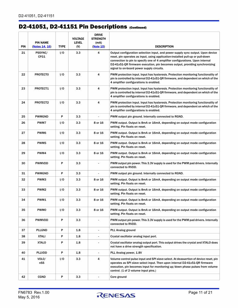
D2-41051, D2-41151 Pin Descriptions
PIN PIN NAME
(Notes 14, 16) TYPE
VOLTAGE LEVEL
(V)
DRIVESTRENGTH
(mA)(Note 15) DESCRIPTION
1 SCLK I 3.3 - I2S Serial Audio Bit Clock (SCLK) Input. Input has hysteresis.
2 SDIN I 3.3 - I2S Serial Audio Data (SDIN) Input. Input has hysteresis.
3 LRCK I 3.3 - I2S Serial Audio Left/Right (LRCK) Input. Input has hysteresis.
4 MCLK O 3.3 16 I2S Serial Audio Master Clock output for external ADC/DAC components, drives low on reset. Output is an 8mA driver.
5 CVDD P 3.3 - Core power, +1.8VDC. Used in the chip internal DSP, logic and interfaces.
6 CGND P 3.3 - Core ground
7 RGND P 3.3 - Digital pad ring ground. Internally connected to PWMGND.
8 RVDD P 3.3 - Digital pad ring power, 3.3V. This 3.3V supply is used for all the digital I/O pad drivers and receivers, except for the analog pads. There are 2 of these pins and both are required to be connected. Internally connected to PWMVDD.
9 TEMPREF/SCK
I/O 3.3 4 Reference pin for temperature monitor and SPI clock. At deassertion of device reset, pin operates as SPI clock. Upon internal D2-41x51-QR firmware execution, pin becomes temperature monitor reference.
10 nMUTE/TIO1
O 3.3 16 Mute signal output. Low active: mute condition drives pin low. Output is a 16mA driver. Initializes as input on reset, then becomes output upon internal firmware execution.
11 VOL1/MISO
I/O 3.3 4 Volume control pulse input and SPI master- input/slave-output data signal. At deassertion of device reset, pin operates as SPI master input or slave output. Then upon internal D2-41x51-QR firmware execution, pin becomes input for monitoring up/down phase pulses from volume control. (1 of 2 volume input pins.)
12 TEMP1/MOSI
I/O 3.3 4 Temperature monitor pin and SPI master-output/slave-input data signal. At deassertion of device reset, pin operates as SPI master output or slave input. Then upon internal D2-41x51-QR firmware execution, pin becomes input for monitoring temperature.
13 SPDIFRX I 3.3 - S/PDIF digital audio data input
14 SPDIFTX O 3.3 8 S/PDIF digital audio data output This pin is the S/PDIF audio output and drives an 8mA, 3.3V stereo output up to 192kHz. Pin floats on reset.
15 TEST I 3.3 - Hardware test mode control. For factory use only. Must be tied low.
16 IRQA I 3.3 - Interrupt request port A. One of 2 IRQ pins, tied to logic (3.3V) high or to ground. High/low logic status establishes boot mode selection upon deassertion of reset (nRESET) cycle.
17 IRQB I 3.3 - Interrupt request port B. One of 2 IRQ pins, tied to logic (3.3V) high or to ground. High/low logic status establishes boot mode selection upon deassertion of reset (nRESET) cycle.
18 RGND P 3.3 - Digital pad ring ground. Internally connected to PWMGND.
19 RVDD P 3.3 - Digital pad ring power, 3.3V. This 3.3V supply is used for all the digital I/O pad drivers and receivers, except for the analog pads. There are 2 of these pins and both are required to be connected. Internally connected to PWMVDD.
20 nERROR/CFG0
I/O 3.3 4 Output configuration selection input, and nERROR output. Upon device reset, pin operates as input, using application-installed pull-up or pull-down connection to pin to specify one of 4 amplifier configurations. Upon internal D2-41x51-QR firmware execution, pin becomes output, providing active-low output drive when amplifier protection monitoring detects an error condition.
FN6783 Rev.1.00 Page 10 of 21May 5, 2016
D2-41051, D2-41151
21 PSSYNC/CFG1
I/O 3.3 4 Output configuration selection input, and power supply sync output. Upon device reset, pin operates as input, using application-installed pull-up or pull-down connection to pin to specify one of 4 amplifier configurations. Upon internal D2-41x51-QR firmware execution, pin becomes output, providing synchronizing signal to on-board power supply circuits.
22 PROTECT0 I/O 3.3 4 PWM protection input. Input has hysteresis. Protection monitoring functionality of pin is controlled by internal D2-41x51-QR firmware, and dependent on which of the 4 amplifier configurations is enabled.
23 PROTECT1 I/O 3.3 4 PWM protection input. Input has hysteresis. Protection monitoring functionality of pin is controlled by internal D2-41x51-QR firmware, and dependent on which of the 4 amplifier configurations is enabled.
24 PROTECT2 I/O 3.3 4 PWM protection input. Input has hysteresis. Protection monitoring functionality of pin is controlled by internal D2-41x51-QR firmware, and dependent on which of the 4 amplifier configurations is enabled.
25 PWMGND P 3.3 - PWM output pin ground. Internally connected to RGND.
26 PWM7 I/O 3.3 8 or 16 PWM output. Output is 8mA or 16mA, depending on output mode configuration setting. Pin floats on reset.
27 PWM6 I/O 3.3 8 or 16 PWM output. Output is 8mA or 16mA, depending on output mode configuration setting. Pin floats on reset.
28 PWM5 I/O 3.3 8 or 16 PWM output. Output is 8mA or 16mA, depending on output mode configuration setting. Pin floats on reset.
29 PWM4 I/O 3.3 8 or 16 PWM output. Output is 8mA or 16mA, depending on output mode configuration setting. Pin floats on reset.
30 PWMVDD P 3.3 - PWM output pin power. This 3.3V supply is used for the PWM pad drivers. Internally connected to RVDD.
31 PWMGND P 3.3 - PWM output pin ground. Internally connected to RGND.
32 PWM3 I/O 3.3 8 or 16 PWM output. Output is 8mA or 16mA, depending on output mode configuration setting. Pin floats on reset.
33 PWM2 I/O 3.3 8 or 16 PWM output. Output is 8mA or 16mA, depending on output mode configuration setting. Pin floats on reset.
34 PWM1 I/O 3.3 8 or 16 PWM output. Output is 8mA or 16mA, depending on output mode configuration setting. Pin floats on reset.
35 PWM0 I/O 3.3 8 or 16 PWM output. Output is 8mA or 16mA, depending on output mode configuration setting. Pin floats on reset.
36 PWMVDD P 3.3 - PWM output pin power. This 3.3V supply is used for the PWM pad drivers. Internally connected to RVDD.
37 PLLGND P 1.8 - PLL Analog ground
38 XTALI P 1.8 - Crystal oscillator analog input port.
39 XTALO P 1.8 - Crystal oscillator analog output port. This output drives the crystal and XTALO does not have a drive strength specification.
40 PLLVDD P 1.8 - PLL Analog power, 1.8V
41 VOL0/nSS
I/O 3.3 4 Volume control pulse input and SPI slave select. At deassertion of device reset, pin operates as SPI slave select input. Then upon internal D2-41x51-QR firmware execution, pin becomes input for monitoring up/down phase pulses from volume control. (1 of 2 volume input pins.)
42 CGND P 3.3 - Core ground
D2-41051, D2-41151 Pin Descriptions (Continued)
PIN PIN NAME
(Notes 14, 16) TYPE
VOLTAGE LEVEL
(V)
DRIVESTRENGTH
(mA)(Note 15) DESCRIPTION
FN6783 Rev.1.00 Page 11 of 21May 5, 2016
D2-41051, D2-41151
OverviewThe D2-41x51-QR devices are integrated System-on-Chip (SoC) audio processor and Class D amplifier PWM controller. They include complete digital audio input selection, signal routing, complete audio processing, and selectable PWM output options for driving multiple output power stage configurations. Stereo I2S and stereo S/PDIF digital input support, plus I2C and 2-wire SPI control interfaces enable integration compatibility with existing system architectures and solutions. The audio path includes a stereo Sample Rate Converter (SRC) plus device-specific audio enhancement processing algorithms.
Output ConfigurationsA 5-channel PWM engine with application-selected configuration settings provides output paths for combinations of output channels. Application dependent configuration selection includes PWM controller outputs for driving Stereo Speaker, 2.1 Speaker, and Stereo Bi-Amp Speaker solutions, as well as Stereo Line, Headphone Outputs, or Subwoofer Line Outputs. Depending on configuration settings, Full-Bridge, Half-Bridge and Bridge-Tied-Load (BTL) output stage topologies, with either discrete or integrated output stages are supported.
Programmable Audio ProcessingProgrammable parameter settings for audio processing include volume control, path routing and mixing, high/low pass filtering, multi-band equalizers, compressors, and loudness. These parameters can be adjusted using the D2Audio™ Canvas II™ software during design and development, or can be set through
the device’s control interface within production amplifier products.
Typical PerformanceFinal system performance is largely determined by the amplifier configuration, its choice of output power stages and components, and overall system design. Typical performance capability of amplifier power outputs varies from less than 10 Watts to systems over 150 Watts. System audio performance includes 20Hz to 20kHz frequency response, SNR of greater than 100dB, and THD+N performance typically below 0.1%.
Audio Enhancement ProcessingThe D2-41x51-QR devices include D2Audio™ SoundSuite™ (within the D2-41051 device) and DTS®(SRS) WOW/HD™ (within the D2-41151 device) audio enhancement algorithms. These functions are integrated within the firmware of each device, and are part of the standard audio signal flow.
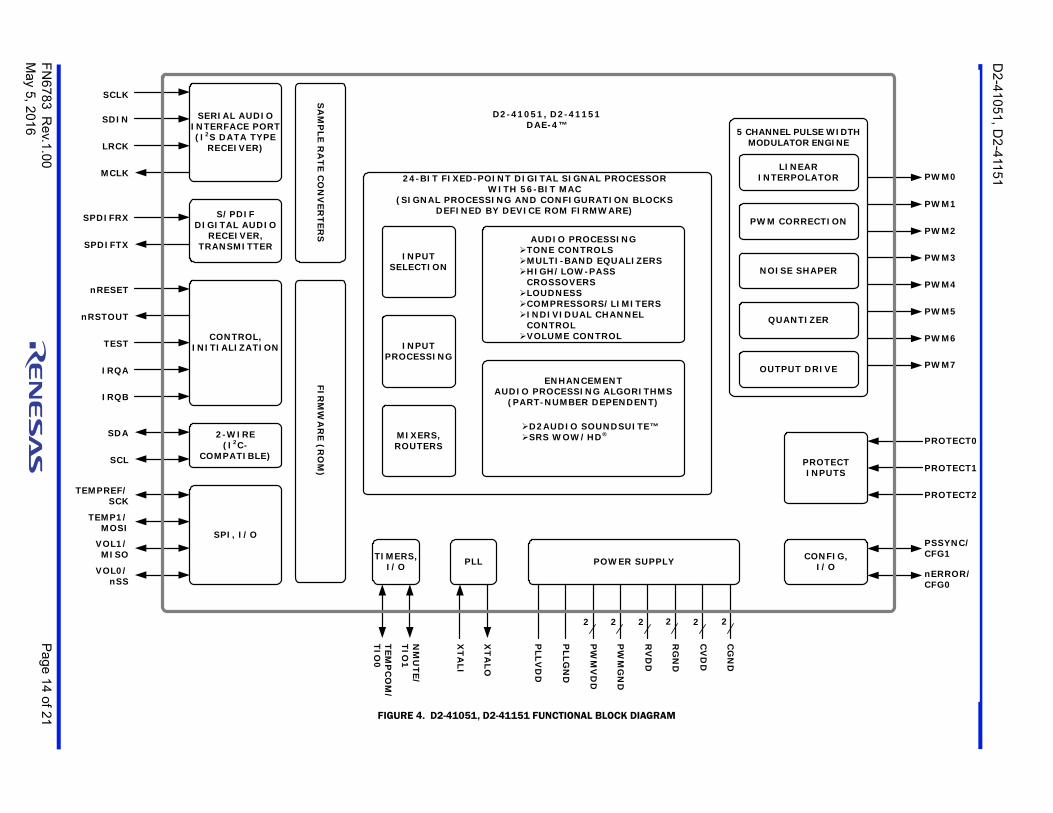
Functional DescriptionFigure 4 shows a block diagram of the D2-41x51-QR devices, and serves as a reference for many of the items in the following descriptions. Additional information, including detailed programming and parameter data, communication detail, and amplifier design implementation is described in the D2-41x51-QR Technical Reference document, available from Intersil Corporation.
43 CVDD P 3.3 - Core power, +1.8VDC. Used in the chip internal DSP, logic and interfaces.
44 nRSTOUT O 3.3 16 - OD Active low output. Pin drives low from 3.3V brownout detector or 1.8V brownout detector going active. This output should be used to initiate a system reset to the nRESET pin upon brownout event detection.
45 nRESET I 3.3 - Active low reset input with hysteresis. Low level activates system level reset, initializing all internal logic and program operations. System latches boot mode selection on the IRQ input pins on the rising edge.
46 TEMPCOM/TIO0
I/O 3.3 16 Temperature monitor common I/O pin.
47 SDA I/O 3.3 8 - OD Two-Wire Serial data port, open drain driver with 8mA drive strength. Bidirectional signal used by both the master and slave controllers for data transport. Pin floats on reset.
48 SCL I/O 3.3 8 - OD Two-Wire Serial clock port, open drain driver with 8mA drive strength. Bidirectional signal is used by both the master and slave controllers for clock signaling. Pin floats on reset.
NOTES:
14. Unless otherwise specified, all pin names are active high. Those that are active low have an “n” prefix, such as nRESET.
15. OD means pad has open drain driver.
16. All power and ground pins of same names are to be tied together to all other pins of their same name. (i.e., RVDD pins to be tied together, RGND pins tied together, CVDD pins tied together, CGND pins to be tied together, PWMVDD pins tied together, PWMGND pins tied together, etc.)
D2-41051, D2-41151 Pin Descriptions (Continued)
PIN PIN NAME
(Notes 14, 16) TYPE
VOLTAGE LEVEL
(V)
DRIVESTRENGTH
(mA)(Note 15) DESCRIPTION
FN6783 Rev.1.00 Page 12 of 21May 5, 2016
D2-41051, D2-41151
Serial Audio Digital InputThe D2-41x51-QR devices include one Serial Audio Interface (SAI) port accommodating two channels of digital audio input. This SAI port supports the I2S digital audio industry standard, and can carry up to 24-bit Linear PCM audio words. The SAI input port operates in slave mode only. The digital audio input from the SAI input port routes directly through the Sample Rate Converters (SRC). Either this I2S digital input or the S/PDIF digital input may be selected as the audio path source.
S/PDIF Digital Audio I/OThe D2-41x51-QR contains one IEC60958 compliant S/PDIF Digital receiver input and one IEC60958 compatible S/PDIF Digital transmitter.
The S/PDIF receiver input includes an input transition detector, digital PLL clock recovery, and a decoder to separate the audio data. The receiver meets the jitter tolerance specified in IEC60958-4.
The S/PDIF transmitter complies with the consumer applications defined in IEC60958-3. The transmitter supports 24-bit audio data, but does not support user data and channel status.
Compressed digital formats are not decoded within the D2-41x51-QR devices. But a bit-exact pass-through mode from the SPDIFRX input to the SPDIFTX output is supported, allowing for designs that require that the IEC61937-compliant original compressed audio input bitstream be made available at the product’s S/PDIF output.
Sample Rate ConverterThe D2-41x51-QR devices include a 2-channel asynchronous sample rate converter (SRC). This SRC is used to convert audio data input sampled at one input sample rate, to a fixed 48kHz output sample rate, aligning asynchronous input audio streams to a single rate for system processing. Audio data presented to the SRC can be from either the SAI or S/PDIF input sources, with an input sample rate from 16kHz to 192kHz.
In addition to converting the input sample rate to the output sample rate, input clock jitter and sampling jitter are attenuated by the SRC.
DSPA 24-bit fixed-point Digital Signal Processor (DSP) controls the majority of audio processing and system control functions within the D2-41x51-QR devices.
Audio path signal routing, programmable-parameter processing blocks, and control logic are defined within the device’s internal firmware. Signal flows through the device are buffered and processed through hardware specific-function blocks, such as the Sample Rate Converter.
Audio Processing And Signal FlowThe audio processing within the D2-41x51-QR devices is defined by the internal ROM firmware, and executed by the DSP. This firmware defines the audio flow architecture and the processing blocks used in that definition. Figure 5 on page 16 shows the signal flow for the D2-41x51-QR devices. General audio processing functions within this architecture include:
• Matrix Mixers
• Routers
• Compressors and Limiters
• Tone Controls
• Multi-Band Equalizers (fully parametric and shelving)
• High-Pass and Low-Pass Crossover Filters
• Volume and Level Controls
• Loudness Compensation
• Input Signal Selection
Signal flow and total system definition is defined by the internal device firmware, but each of these blocks are programmable, allowing for adjustment of all of their parameters.
Signal flow and details of each of these audio processing blocks are shown in Figure 5. Programming details, register identification, and parameter calculations are included in the D2-41x51-QR Technical Reference document.
FN6783 Rev.1.00 Page 13 of 21May 5, 2016
FN
678
3R
ev.1.00
Pa
ge 1
4 of 21
May 5, 2
016
D2-41
051
, D2-4115
1
LINEAR NTERPOLATOR
M CORRECTION
OISE SHAPER
QUANTIZER
UTPUT DRIVE
PROTECTINPUTS
PROTECT0
PROTECT1
PROTECT2
CONFIG,I/O
PSSYNC/CFG1
nERROR/CFG0
PWM0
PWM1
PWM2
PWM3
PWM4
PWM5
PWM6
PWM7
NNEL PULSE WIDTH DULATOR ENGINE
I
PW
N
O
SPDIFRX
SPDIFTX
SERIAL AUDIO INTERFACE PORT(I2S DATA TYPE
RECEIVER)
SPI, I/O
PLL
SA
MP
LE RA
TE CO
NV
ERTER
S
INPUT SELECTION
MIXERS, ROUTERS
INPUT PROCESSING
CONTROL, INITIALIZATION
D2-41051, D2-41151DAE-4™
TONE CONTROLSMULTI-BAND EQUALIZERSHIGH/LOW-PASS
CROSSOVERSLOUDNESSCOMPRESSORS/LIMITERSINDIVIDUAL CHANNEL
CONTROLVOLUME CONTROL
ENHANCEMENTAUDIO PROCESSING ALGORITHMS
(PART-NUMBER DEPENDENT)
24-BIT FIXED-POINT DIGITAL SIGNAL PROCESSOR WITH 56-BIT MAC
(SIGNAL PROCESSING AND CONFIGURATION BLOCKSDEFINED BY DEVICE ROM FIRMWARE)S/PDIF
DIGITAL AUDIO RECEIVER,
TRANSMITTER
SCLK
SDIN
LRCK
MCLK
nRESET
nRSTOUT
TEST
IRQA
IRQB
XTA
LI
XTA
LO
2-WIRE(I2C-
COMPATIBLE)
SDA
SCL
TIMERS,I/O
TEMPREF/SCK
TEMP1/MOSI
VOL1/MISO
VOL0/nSS
TEMP
CO
M/
TIO0
NM
UTE/
TIO1
PLLV
DD
PLLG
ND
PW
MV
DD
PW
MG
ND
RV
DD
RG
ND
CV
DD
CG
ND
222222
POWER SUPPLY
5 CHAMO
D2AUDIO SOUNDSUITE™SRS WOW/HD®
AUDIO PROCESSING
FIRM
WA
RE (R
OM
)
FIGURE 4. D2-41051, D2-41151 FUNCTIONAL BLOCK DIAGRAM
D2-41051, D2-41151
Audio Enhancement Feature ProcessingAdditional enhancement audio processing algorithms are included within specific part number options of the D2-41x51-QR devices. These specific enhancements are:
• D2Audio™ SoundSuite™ (WideSound™, DeepBass™, Audio Align™, and ClearVoice™) Audio Processing(with the D2-41051 device)
• DTS®SRS WOW/HD™(with the D2-41151 device)
Each of these enhancements are unique only to the particular part number, and each enhancement has its own set of programmable parameters to control operation. The location of these enhancements within the signal flow is shown in Figure 5 on page 16.
PWM Audio OutputsThe D2-41x51-QR devices incorporate five PWM output channels that are mapped to eight PWM output pins. Each of the PWM channels and their pins are used for driving output power stages, and/or for line level outputs, depending on the selected configuration mode.
The outputs support multiple PWM amplifier output topologies. These supported topologies include half-bridge N+N or N+P, and full-bridge N+N or N+P using 2-level modulation with 2 or 4-quadrant control. The channel and function assignment of the eight output pins as well as the associated output topology is established by the output mode configuration settings. Refer to “Output Mode Configurations” on page 18 for description and selection of these output configurations, and their associated mapping of the PWM output pins. Also refer to the D2-41x51-QR Technical Reference document for additional operation of the outputs.
Using a simple passive filter, the PWM outputs will drive line-level outputs at a nominal 1Vrms. Headphone outputs or line-level outputs that require a 2Vrms or higher output level are implemented using an active filter.
I/O Control PinsSeveral device pins are used as specific-function inputs and outputs and are used to control amplifier and device operation. Some pins are multiple-purpose, where their functions are different depending on the device operating state. Functions of these pins are defined in the pin definition list, and additional descriptions are included within the functional block descriptions elsewhere in this document. These pins are implemented within the device hardware as general purpose inputs/outputs. However, their operation is not programmable, and their specific function is defined by the D2-41x51-QR internal firmware.
TimersThere are two independent timers used for device and system control. One timer is used for internal references, and the other is used for the temperature sensing control. There are two I/O pins associated with the timers, and these pin functions are defined by the device firmware. Timer 0 is used for the timing-related executions of the temperature monitoring algorithm. Its pin (TIO0) is used as an input and output for that temperature monitoring operation. Timer 1 is used for internal functions of the device. Its pin (TIO1) is not used for this timing operation, and is defined by device firmware as the nMUTE I/O pin. Timer operation is established internally by firmware and not programmable.
I2C 2-Wire Control InterfaceThe D2-41x51-QR devices include a 2-Wire I2C compatible interface for communicating with an external controller.
This interface is usable with either an external microcontroller interface, or for communication to EEPROMs, or other compatible peripheral chips. The I2C interface is multi-master capable, operates as independent master and slave, and supports normal and fast mode operation.
Serial Peripheral Interface (SPI)The Serial Peripheral Interface (SPI) is an alternate serial input port that provides an interface for loading parameter data from an optional EEPROM or Flash device during boot-up operation.
The four SPI interface pins are all shared. This interface functions only as an input port for external boot operation and does not operate as an interactive control port. During a reset condition, initiating the boot-up process, the four pins (TEMPREF/SCK, TEMP1/MOSI, VOL1/MISO, VOL0/nSS) operate as the SPI port. As soon as the boot-up process is completed and the device begins executing its firmware program, these pins are no longer used for SPI functions, and operate as assigned by the firmware.
Control Register SummaryThe control register interface is used for an external controller to adjust the amplifier’s programmable settings and adjustments within its signal flow. These parameters for each of the signal processing blocks are accessed through a register programming interface, and each parameters is defined with its specific register address. Audio input selection (I2S input or S/PDIF receiver input) and output elements (PWM amplifier and line outputs, and S/PDIF transmitter) are controlled through their register parameters.
All of these control register functions are defined in the Application Programming Interface (API) specification within the D2-41x51-QR Technical Reference document.
FN6783 Rev.1.00 Page 15 of 21May 5, 2016

FN
678
3R
ev.1.00
Pa
ge 1
6 of 21
May 5, 2
016
D2-41
051
, D2-4115
1
PWM PIN OUTPUTS
CHANNEL 0
CHANNEL 1
CHANNEL 2
CHANNEL 3
2X1MIXER
SPEAKER EQ 1
4X4ROUTER
CHANNEL 4
SPEAKER EQ 2
5
4
3
2
1
ICE
PWM CHANNEL
PINMAPPING
ANDDRIVE
PWM PIN 0
PWM PIN 1
PWM PIN 2
PWM PIN 3
PWM PIN 4
PWM PIN 5
PWM PIN 6
PWM PIN 7
2X2MIXER
TONE 1 5 BAND EQ 1COMPRESSOR 1
PWM
PWM
PWM
PWM
DIGITAL
INPUT SELECT
S/PDIFDIGITAL INPUT
LICENSEDAUDIO
PROCESSINGALGORITHM*(SEE NOTE)
S/PDIF
PWM
2SRC
I2SDIGITAL INPUT
COMPRESSOR 2 TONE 2 5 BAND EQ 2
HP 1 LP 1
HP 2 LP 2
HP 3 LP 3
HP 4 LP 4
HP 5 LP 5
3 BAND EQ 1
3 BAND EQ 1
3 BAND EQ 1
3 BAND EQ 1
MASTERVOLUME
CONTROL
LOUDNESS 1
LOUDNESS 2
LOUDNESS 3
LOUDNESS 4
LOUDNESS 5
LIMITER 1
LIMITER 2
LIMITER 3
LIMITER 4
LIMITER 5
VOLUME 1
VOLUME 2
VOLUME 3
VOLUME 4
VOLUME 5
CROSSOVERS
5
4
3
2
1
* NOTE: DEVICE-DEPENDENT LICENSED AUDIO PROCESSING ALGORITHM SUPPORTING D2AUDIO SOUNDSUITE™, OR SRS WOW/HD®. REFER TO DEVORDERING INFORMATION FOR PART NUMBER SPECIFYING EACH ALGORITHM.
FIGURE 5. D2-41051, D2-41151 AUDIO SIGNAL FLOW
D2-41051, D2-41151
Temperature SensingThe temperature sensing algorithm utilizes external hardware on the amplifier’s design to monitor system temperature. This external hardware includes a negative temperature coefficient (NTC) resistor located physically on the design in an areas that require monitoring.
This operation uses three of the I/O pins (TEMPREF/SCK, TEMP1/MOSI, and TEMPCOM/TIO1). These pins have shared functions. During device initialization, these pins operate as part of the SPI interface, but after the firmware is executing, the SPI functionality turns off and these pins are dedicated to the temperature monitoring function.
Overcurrent SensingOvercurrent sensing is accomplished with current threshold detectors connected in the power supply used at each power stage output of the amplifier design.
Design of these detectors is described in the D2-41x51-QR Technical Reference document, but their purpose is to generate a pulse or logic level upon detection of high current, where this logic level is connected to one of the three protection input (PROTECT[0:2]) pins.
These protection input pins are primarily intended for protecting the PWM powered output stages. They are activated by either a pulse or level driven into the pin. Firmware within the D2-41x51-QR devices monitors the internal hardware connected to these pins, and adjusts or disables the PWM output drive, depending on the conditions monitored on these protection input pins.
The number of powered outputs in a design depends on which one of the four configurations is defined. The configuration settings, established upon device reset through the configuration pins, also determines which of the protection inputs are used.
Power Supply SynchronizationThe PSSYNC/CFG1 pin provides a power supply synchronization signal for switching power supplies. Firmware configures this pin to the frequency and duty cycle needed by the system switching regulator. This synchronization allows switching supplies used with the device to operate without generating in-band audio interference signals that could be possible if the switching power supply is not locked to the amplifier switching.
This PSSYNC/CFG1 pin is a shared pin. During device reset and initialization, it operates as one of two configuration input pins, where its high or low logic state is used to set the amplifier configuration mode. After completion of reset and when the device firmware begins operating, this pin becomes the PSSYNC output.
Error ReportingInternal monitoring of system and device operation uses an I/O pin (nERROR/CFG1) as an output to signal an external system controller of a channel shutdown error condition. This output may be used to turn on a simple indicator.
The error output is also used to signal an external microcontroller that the I2C bus may be busy. When the error output is low during system initialization, the I2C bus is busy as a master device.
This error output is active low and only becomes used as an output after the device firmware has initialized and began running. This same pin is shared as an input. During a reset condition, this pin operates as an input, and is one of two input pins that are used to define the configuration mode. A resistor pull-up or pull-down on this pin establishes this mode input configuration state. After completion of the initialization sequence, these resistors do not affect the error output operation.
Power SequencingThe CVDD and RVDD (including PWMVDD) power supplies should be brought up together to avoid high current transients that could fold back a power supply regulator. The PLLVDD may be brought up separately. Best practice would be for all supplies to feed from regulators with a common power source. Typically this can be achieved by using a single 5V power source and regulating the 3.3V and 1.8V supplies from that 5V source. As noted in the pin specifications of this document, all voltages of the same names must be tied together at the board level.
Clock and PLLClock is generated on-chip, using a fundamental-mode crystal connected across the XTALI and XTALO pins. XTALO is an output, but is designed only to drive the crystal, and not connect to any other circuit. XTALI is an input, connecting to the other side of the crystal.
The clock generation contains a low jitter PLL critical for low noise PWM output and a precise master clock source for sample rate conversion and the audio processing data paths. The clock system is used throughout the device, and provides clock generators for brown-out detection, system and power-on reset, DSP, S/PDIF transmitter, and the PWM engine.
Clock and PLL hardware functions are controlled by internal device firmware. They are not programmable and are optimized for device and system operation.
Reset and Device InitializationThe D2-41x51-QR devices must be reset to initialize and begin proper operation. A system reset is initiated by applying a low level to the nRESET input pin. External hardware circuitry or a controller within the amplifier system design must provide this reset signal and connect to the nRESET input to initiate the reset process. Device initialization then begins after the nRESET pin is released from its low-active state.
The chip contains power rail sensors and brownout detectors on the 3.3V and 1.8V power supplies. A loss or droop of power from either of these supplies will trigger their brownout detectors which will assert the nRSTOUT pin, driving it low. This pin should connect to the nRESET input through hardware on the amplifier design, to ensure a proper reset occurs if the power supply voltages drop below their design specifications. Refer to the D2-41x51-QR Technical Reference document for connection recommendations.
At the deassertion of nRESET, the chip will read the status of the boot mode selection pins (IRQA and IRQB) and begin the boot process, determined by the boot mode that is defined by these pins’ logic state. These device pins are strapped either high or low on the system’s design (PCB), and it is the state of these pins
FN6783 Rev.1.00 Page 17 of 21May 5, 2016
D2-41051, D2-41151
that is latched into, and defines boot mode operation. Refer to the Boot Modes section in this document for related descriptions. Refer to the D2-41x51-QR Technical Reference document for details of connection and operation of initialization and strapping options.
Boot ModesThe D2-41x51-QR devices contain internal firmware to operate the part and run the amplifier system. Parameter information that is used by the programmable settings can be written to the device after it is operational and running, and parameter data can also be read at boot time, allowing saved parameter settings to be used in processing. The device is designed to boot in one of four possible modes, allowing control and data to be provided from these boot sources:
• I2C Slave (to external Microcontroller)
• I2C EEPROM
• Internal Device ROM Only
• SPI Slave
The specific boot mode is selected based on the state of the IRQB and IRQA input pins at the time of reset de-assertion. Boot modes are shown in Table 1.
The device initializes as defined by its boot mode. But it gets its configuration and parameter data from the host device. This host device can be either an external controller, or from an EEPROM. If a system uses both an external controller and an EEPROM, the EEPROM will load first, and during this time, the controller must remain off the I2C bus.
Output Mode ConfigurationsThe D2-41x51-QR devices support four amplifier output configuration modes of powered output and line output combinations. These four modes are shown in Table 2.
These configuration modes utilize different combinations of the five PWM output channels, and each mode maps the eight PWM pins to their appropriate PWM channel path. This channel content and mapping of the pins is shown in Table 3 on page 19. Of the total eight PWM pins, not all pins are used with every configuration mode. Timing and drive characteristics of each PWM pin output are automatically programmed for correct operation when those pins are connected to their designated output stages.
In modes 2 and 3, the filtering for high and low pass crossovers is applied to the audio signal flow path, enabling the appropriate high or low pass content to be properly filtered for the PWM output channels.
The protect pin inputs are mapped to the PWM channels that are used for the powered outputs. This protect pin mapping assignment is shown in Table 3 for the different configurations.
Configuration Modes AssignmentThe configuration mode is assigned when the D2-41x51-QR device exits its reset state, when at that time, the logic status of the PSSYNC/CFG1 and nERROR/CFG0 pins are latched into internal device registers. During this initialization time, these pins operate as logic inputs. After completion of the initialization and the internal firmware begins executing, these pins are re-assigned as outputs for their shared functions, and the internal latched logic state that defines the configuration mode remains until the device is powered down or reset again. Each mode requires specific amplifier design hardware connection, and the configuration pin logic levels are defined through pull-up or pull-down resistors installed on that design’s board. These modes are not programmable and are not intended to be changed for each hardware design.
TABLE 1. BOOT MODE SETTINGS
BOOTMODE
IRQB PIN
IRQA PIN
MASTER/SLAVE DESCRIPTION
0 0 0 I2C Slave Operates as I2C slave, boot at address 0x88. An external 2-wire I2C master provides the boot code.
1 0 1 I2C Master Operates as 2-wire master; loads boot code from ROM on I2C port.
2 1 0 - Internal ROM Boot/Operation
3 1 1 SPI Slave SPI slave. External SPI master provides boot code.
TABLE 2. D2-41x51-QR OUTPUT CONFIGURATION MODES
CONFIGMODE NAME FUNCTION
0 2.0 L/R4-Quadrant
• Powered Left and Right Outputs With 4-Quadrant, Full Bridge Drivers.
• No Line-Level Outputs
1 2.0 L/R+
L/R/SubLine
• Powered Left and Right Outputs With 2-Quadrant, Full Bridge Drivers.
• Single-Ended Stereo Left + Right Line-Level Outputs.
• Dual-Ended Subwoofer Line-Level Output
2 2.1L/R/Sub
+L/R Line
• Powered Left and Right Outputs With 2-Quadrant Half Bridge Drivers.
• Powered Subwoofer Output With 2-Quadrant, Full Bridge Driver.
• Single-Ended Stereo Left + Right Line-Level Outputs.
• Crossover Filtering Added To Signal Flow.
3 2.2Bi-Amp
• Powered Left and Right Bi-Amp Outputs With 2-Quadrant Drivers.
• Crossover Filtering Added To Signal Flow.
FN6783 Rev.1.00 Page 18 of 21May 5, 2016
D2-41051, D2-41151
TABLE 3. PWM CHANNEL ASSIGNMENT AND CONFIGURATION DETAILS
CONFIGMODE
CONFIGNAME
PSSYNC/CFG1 PIN
LOGIC LEVEL
nERROR/CFG0 PIN
LOGIC LEVEL
PWMCHANNELNUMBER
PWMCHANNELCONTENT
PWMPINS
PROTECTPIN
ASSIGNMENT
SUPPORTEDOUTPUT
TOPOLOGYAUDIO
FUNCTION
0 2.0 L/R4-Quadrant
0 0 0 L-Spkr 0-3 0 4-Quadrant, Full Bridge
Powered Left
1 R-Spkr 4-7 1 4-Quadrant,Full Bridge
Powered Right
2 - - - - -
3 - - - - -
4 - - - - -
1 2.0 L/R+
L/R/SubLine
0 1 0 L-Spkr 0, 1 0 2-Quadrant, Full Bridge
Powered Left
1 R-Spkr 2, 3 1 2-Quadrant, Full Bridge
Powered Right
2 L-Line 6 - Line Level Line/Headphone Left
3 R-Line 7 - Line Level Line/Headphone Right
4 Sub 4, 5 - Line Level Line Level Sub
2 2.1L/R/Sub
+L/R Line
1 0 0 L Spkr 0, 1 0 Half Bridge Powered Left
1 R Spkr 2, 3 1 Half Bridge Powered Right
2 L Line 6 - Line Level Line/Headphone Left
3 R Line 7 - Line Level Line/Headphone Right
4 Sub 4, 5 2 2-Quadrant, Full Bridge
Powered Sub
3 2.2Bi-Amp
1 1 0 L Hi-Freq 0, 1 0,1 Half Bridge Powered Left HF
1 L Lo-Freq 2, 3 1,0 Half Bridge Powered Left LF
2 R Hi-Freq 4, 5 2 Half Bridge Powered Right HF
3 R Lo-Freq 6, 7 2 Half Bridge Powered Right LF
4 - - - - -
FN6783 Rev.1.00 Page 19 of 21May 5, 2016
D2-41051, D2-41151
Intersil products are manufactured, assembled and tested utilizing ISO9001 quality systems as notedin the quality certifications found at www.intersil.com/en/support/qualandreliability.html
Intersil products are sold by description only. Intersil may modify the circuit design and/or specifications of products at any time without notice, provided that such modification does not, in Intersil's sole judgment, affect the form, fit or function of the product. Accordingly, the reader is cautioned to verify that datasheets are current before placing orders. Information furnished by Intersil is believed to be accurate and reliable. However, no responsibility is assumed by Intersil or its subsidiaries for its use; nor for any infringements of patents or other rights of third parties which may result from its use. No license is granted by implication or otherwise under any patent or patent rights of Intersil or its subsidiaries.
For information regarding Intersil Corporation and its products, see www.intersil.com
For additional products, see www.intersil.com/en/products.html
© Copyright Intersil Americas LLC 2009-2016. All Rights Reserved.All trademarks and registered trademarks are the property of their respective owners.
About IntersilIntersil Corporation is a leading provider of innovative power management and precision analog solutions. The company's products address some of the largest markets within the industrial and infrastructure, mobile computing and high-end consumer markets.
For the most updated datasheet, application notes, related documentation and related parts, please see the respective product information page found at www.intersil.com.
You may report errors or suggestions for improving this datasheet by visiting www.intersil.com/ask.
Reliability reports are also available from our website at www.intersil.com/support.
TrademarksDAE-4™, Intelligent Digital Amplifier™ and D2Audio CanvasII™, and D2Audio SoundSuite™ are trademarks, and D2™, D2A™, D2Audio™ are registered trademarks of Intersil Corporation. DTS®(SRS) and DTS®(SRS) WOW/HD™ are registered trademarks of DTS®(SRS) Corporation. Windows™ is a registered trademark of Microsoft Corporation. Other product names are for identification purposes and may be trademarks and/or registered trademarks of their respective companies.
Disclaimer for DTS®(SRS) Technology License Required Notice:NOTICE OF LICENSE REQUIREMENT: Supply of this implementation of DTS technology to DTS Product Licensees directly or through a distributor does not incur a royalty payment or convey a license, exhaust DTS’ rights in the implementation, or imply a right under any patent or any other industrial or intellectual property right of DTS to use, offer for sale, sell, or import such implementation in any finished end-user or ready-to-use final product. A license from and royalty payment to DTS is required prior to and for such use.
Revision History The revision history provided is for informational purposes only and is believed to be accurate, but not warranted. Please go to the web to make sure that you have the latest revision.
DATE REVISION CHANGE
May 5, 2016 FN6783.1 Updated entire datasheet applying Intersil’s new standards.Updated the Ordering Information table on page 2.Updated Note 5 on page 4. Added the Disclaimer for DTS®(SRS) Technology License Required Notice.Added Revision History section.Replaced Products verbiage to About Intersil verbiage.Updated POD to the latest revision changes are as follows:
-Corrected Note 4 from: “Dimension b applies to...” to: “Dimension applies to...” 'b' leftover from when dimensions were in table format.
-Enclosed Notes #'s 4, 5 and 6 in a triangle.
FN6783 Rev.1.00 Page 20 of 21May 5, 2016
D2-41051, D2-41151
FN6783 Rev.1.00 Page 21 of 21May 5, 2016
Package Outline DrawingL48.7x748 LEAD QUAD FLAT NO-LEAD PLASTIC PACKAGE
Rev 5, 4/10
located within the zone indicated. The pin #1 indentifier may be
Unless otherwise specified, tolerance : Decimal ± 0.05
Tiebar shown (if present) is a non-functional feature.
The configuration of the pin #1 identifier is optional, but must be
between 0.15mm and 0.30mm from the terminal tip.Dimension applies to the metallized terminal and is measured
Dimensions in ( ) for Reference Only.
Dimensioning and tolerancing conform to AMSE Y14.5m-1994.
6.
either a mold or mark feature.
3.
5.
4.
2.
Dimensions are in millimeters.1.
NOTES:
7.00
BA
7.00
(4X) 0.15
INDEX AREAPIN 1
TOP VIEW
PIN #1 INDEX AREA44X 0.50
4X 5.5
4837
4. 30 ± 0 . 15
136
25
48X 0 . 40± 0 . 14
M0.10 C A B1324
BOTTOM VIEW
12
50 . 2 REF
0 . 00 MIN.0 . 05 MAX.
DETAIL "X"
C
0 . 90 ± 0 . 1 BASE PLANE
SEE DETAIL "X"
C
C0.08SEATING PLANE
C0.10
SIDE VIEW
TYPICAL RECOMMENDED LAND PATTERN
6
6
( 6 . 80 TYP )
( 4 . 30 )
( 48X 0 . 60 )
( 44X 0 . 5 )
( 48X 0 . 23 )
0.23 +0.07 / -0.05