Embed Size (px)
Citation preview

NuDAQ DAQ-2500/PXI-2500 Series
High Performance
Analog Output Multi-function Cards
User's Guide
Recycled Paper


Copyright 2002~2003 ADLINK Technology Inc.
All Rights Reserved.
Manual Rev. 1.00: May 16, 2002
Part No : 50-12265-100
The information in this document is subject to change without prior notice in order to improve reliability, design and function and does not represent a commitment on the part of the manufacturer.
In no event will the manufacturer be liable for direct, indirect, special, in-cidental, or consequential damages arising out of the use or inability to use the product or documentation, even if advised of the possibility of such damages.
This document contains proprietary information protected by copyright. All rights are reserved. No part of this manual may be reproduced by any mechanical, electronic, or other means in any form without prior written permission of the manufacturer.
Trademarks
NuDAQ, NuIPC, NuDAM, NuPRO are registered trademarks of ADLINK Technology Inc. Other product names mentioned herein are used for identification purposes only and may be trademarks and/or registered trademarks of their respective companies.

Getting service from ADLINK • Customer Satisfaction is the most important priority for ADLINK Tech Inc.
If you need any help or service, please contact us.
ADLINK Technology Inc.
Web Site http://www.adlinktech.com
Sales & Service [email protected] NuDAQ + USBDAQ [email protected] NuDAM [email protected] NuIPC [email protected]
Technical Support
NuPRO/EBC [email protected] TEL +886-2-82265877 FAX +886-2-82265717 Address 9F, No. 166, Jian Yi Road, Chungho City, Taipei, 235 Taiwan.
• Please inform or FAX us of your detailed information for a prompt, satis-factory and constant service.
Detailed Company Information Company/Organization Contact Person E-mail Address Address Country TEL FAX Web Site
Questions Product Model
OS: Computer Brand:
Environment to Use M/B: CPU: Chipset: BIOS: Video Card: Network Interface Card: Other:
Detail Description
Suggestions for ADLINK
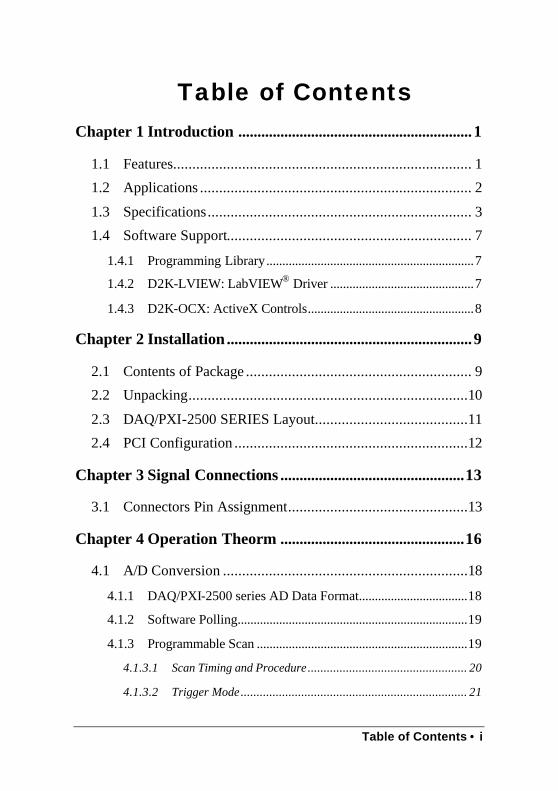
Table of Contents • i
Table of Contents
Chapter 1 Introduction .............................................................1
1.1 Features.............................................................................. 1 1.2 Applications ....................................................................... 2 1.3 Specifications..................................................................... 3 1.4 Software Support................................................................ 7
1.4.1 Programming Library.................................................................7 1.4.2 D2K-LVIEW: LabVIEW® Driver .............................................7
1.4.3 D2K-OCX: ActiveX Controls....................................................8
Chapter 2 Installation ................................................................9
2.1 Contents of Package ........................................................... 9 2.2 Unpacking.........................................................................10 2.3 DAQ/PXI-2500 SERIES Layout........................................11 2.4 PCI Configuration .............................................................12
Chapter 3 Signal Connections ................................................13
3.1 Connectors Pin Assignment...............................................13
Chapter 4 Operation Theorm ................................................16
4.1 A/D Conversion ................................................................18
4.1.1 DAQ/PXI-2500 series AD Data Format..................................18 4.1.2 Software Polling........................................................................19 4.1.3 Programmable Scan ..................................................................19
4.1.3.1 Scan Timing and Procedure.................................................. 20 4.1.3.2 Trigger Mode....................................................................... 21

ii • Table of Contents
4.1.4.4 Bus-mastering DMA Data Transfer ....................................... 23 4.2 D/A Conversion ................................................................25
4.2.1 Software Update........................................................................28 4.2.2 Waveform Generation ..............................................................28
4.2.2.1 Waveform Generation Timing ............................................... 29 4.2.2.2 Trigger Modes.......................................................................... 30 4.2.2.3 Iterative Waveform Generation ............................................. 32 4.2.2.4 Stop Modes........................................................................... 34
4.3 General Purpose Digital I/O...............................................36 4.4 General Purpose Timer/Counter Operation ........................37
4.4.1 Timer/Counter functions basics ...............................................37 4.4.2 General Purpose Timer/Counter modes ..................................37
4.4.2.1 Mode1: Simple Gated-Event Counting................................... 38 4.4.2.2 Mode2: Single Period Measurement...................................... 38 4.4.2.3 Mode3: Single Pulse-width Measurement.............................. 39
4.4.2.4 Mode4: Single Gated Pulse Generation................................. 39 4.4.2.5 Mode5: Single Triggered Pulse Generation........................... 40
4.4.2.6 Mode6: Re-triggered Single Pulse Generation....................... 40 4.4.2.7 Mode7: Single Triggered Continuous Pulse Generation......... 41
4.4.2.8 Mode8: Continuous Gated Pulse Generation......................... 41 4.5 Trigger Sources.................................................................42
4.5.1 Software-Trigger.......................................................................42 4.5.2 External Analog Trigger...........................................................42
4.5.2.1 Below-Low analog trigger condition ..................................... 43 4.5.2.2 Above-High analog trigger condition .................................... 44
4.5.2.3 Inside-Region analog trigger condition ................................. 44

Table of Contents • iii
4.5.2.4 High-Hysteresis analog trigger condition.............................. 45 4.5.2.5 Low-Hysteresis analog trigger condition ............................... 45
4.6 Timing Signals ..................................................................46
4.6.1 System Synchronization Interface ...........................................47
Chapter 5 Calibration .............................................................48
5.1 Auto-calibration ................................................................49 5.2 Saving Calibration Constants.............................................49 5.3 Loading Calibration Constants...........................................49
Chapter 6 Appendix A.............................................................50
6.1 Waveform Generation Demonstration................................50
Warranty Policy .......................................................................53

iv • How to Use This Guide
How to Use This Guide
This manual is designed to help you use/understand the DAQ/PXI-2500 SERIES high performance analog output multi-function cards. The manual describes the functions and the operation theory of the DAQ/PXI-2500 SERIES. It is divided into five chapters:
Chapter 1, Introduction gives an overview of the product features, ap-plications, and specifications.
Chapter 2, Installation describes how to install the DAQ/PXI-2500 SERIES cards. The layout and positions of all the connectors on the DAQ/PXI-2500 SERIES are also shown.
Chapter 3, Signal Connections describes the connector’s pin assign-ment and how to connect external signals to the DAQ/PXI-2500 SERIES.
Chapter 4, Operation Theory describes how DAQ/PXI-2500 SERIES operates. The A/D, D/A, GPIO, timer/counter, trigger and timing signal routing are introduced.
Chapter 5, Calibration describes how to calibrate the DAQ/PXI-2500 SERIES for accurate measurements.

Introduction • 1
1
Introduction
DAQ/PXI-2500 SERIES is an advanced analog output card based on the 32-bit PCI/PXI architecture. High performance designs and state-of-the-art technology make this card ideal for waveform generation, industrial proc-ess control, and signal analysis applications in medical, process control, etc.
1.1 Features
DAQ/PXI-2500 SERIES advanced analog output cards provide the following advanced features:
• 32-bit PCI/PXI-Bus, plug and play
• Up to 1MS/s analog output rate
• Up to 400KS/s analog input rate
• Up to 8 analog output channels for DAQ/PXI-2502, and 4 analog output channels for DAQ/PXI-2501
• Up to 4 analog input channels for DAQ/PXI-2502, and 8 analog input channels for DAQ/PXI-2501
• Programmable bipolar/unipolar range for analog input channels and individual analog output channels
• Programmable internal/external reference for individual analog output channels

2 • Introduction
• D/A FIFO size: 8K samples for DAQ/PXI-2501, and 16K samples for DAQ/PXI-2502
• A/D FIFO size: 2K samples
• Versatile trigger sources: software trigger, external digital trigger, ana-log trigger and trigger from System Synchronization Interface (SSI)
• A/D Data transfer: software polling & bus-mastering DMA with Scat-ter/Gather
• D/A Data transfer: software update and bus-mastering DMA with Scatter/Gather
• A/D trigger modes: post-trigger, delay-trigger with re-trigger functionality
• D/A outputs with waveform generation capability
• System Synchronization Interface (SSI)
• A/D and D/A fully auto-calibration
• Build-in programmable D/A external reference voltage compensator
• Completely jumper-less and software configurable
1.2 Applications
• Automotive Testing
• Arbitrary Waveform Generator
• Transient Signal Measurement
• ATE
• Laboratory Automation
• Biotech measurement
Introduction • 3
1.3 Specifications
Analog Output (AO)
• Number of channels: 4-CH for DAQ/PXI-2501, 8-CH for DAQ/PXI-2502
• DA converter: AD7945
• Max update rate: 1MS/s
• Resolution: 12 bits
• FIFO buffer size: 8K for DAQ/PXI-2501, 16K for DAQ/PXI-2502
• Data transfer: Programmed I/O, and bus-mastering DMA with scat-ter/gather
• Voltage reference: internal 10V or external up to ±10V
• Output range:
Bipolar: ±10V or ± external reference
Unipolar: 0~10V or 0~ external reference
• Settling time for –10~+10V step: 2µs
• Slew rate: 20V/µs
• Output coupling: DC
• Protection: Short-circuit to ground
• Output impedance: 0.1Ω. max.
• Output current: ±5mA max.
• Power-on state: 0V steady-state
• Power-on glitch: ±600mV/500µs
• Offset error:
Before calibration: ±80mV max
After calibration: ±2mV max
• Gain error:
Before calibration: ±0.8% of output max
After calibration: ±0.02% of output max

4 • Introduction
Analog Input (AI)
• Number of channels: 4 single-ended for DAQ/PXI-2502, 8 single-ended for DAQ/PXI-2501
• AD converter: LTC1416
• Max sampling rate: 400KS/s
• Resolution: 14 bits
• FIFO buffer size: 2K samples
• Input range: Bipolar: ±10V, unipolar: 0~10V
• Over voltage protection: Continuous ± 35V maximum
• Input impedance: 1GΩ | 6pF
• Trigger mode: Pre-trigger, post-trigger, middle-trigger, and delay trigger
• Data transfers: Programmed I/O, and bus-mastering DMA with scat-ter/gather
• Input coupling: DC
• Offset error:
Before calibration: ±40mV max
After calibration: ±1mV max
• Gain error:
Before calibration: ±0.4 % of output max
After calibration: ±1mV of output max
General Purpose Digital I/O (G.P. DIO)
• Number of channels: 24 programmable Input/Output
• Compatibility: TTL/CMOS
• Input voltage:
Logic Low: VIL=0.8V max.; IIL=0.2mA max.
High: VIH=2.0V max.; IIH=0.02mA max
• Output voltage:
Low: VOL=0.5 V max.; IOL=8mA max.
High: VOH=2.7V min; IOH=400µA

Introduction • 5
General Purpose Timer/ Counter (GPTC)
• Number of channel: 2 Up/Down Timer/Counters
• Resolution: 16 bits
• Compatibility: TTL/CMOS
• Clock source: Internal or external
• Max source frequency: 10MHz
Analog Trigger (A.Trig)
• Source: external analog trigger (EXTATRIG)
• Level: ±10V external
• Resolution: 8 bits
• Slope: Positive or negative (software selectable)
• Hysteresis: Programmable
• Bandwidth: 400khz
• External Analog Trigger Input (EXTATRIG)
• Impedance: 40KΩ
• Coupling: DC
• Protection: Continuous ± 35V maximum
System Synchronous Interface (SSI)
• Trigger lines: 7
Calibration
• Recommended warm-up time: 15 minutes
• On-board reference: 5.0V
• Temperature coefficient: ±2ppm/°C
• Long-term stability: 6ppm/1000Hr
Physical
• Dimension: 175mm by 107mm
• I/O connector: 68-pin female mini-SCSI type

6 • Introduction
• Power Requirement: +5VDC; 1.6A typical
Operating Environment
• Ambient temperature: 0 to 55°C
• Relative humidity: 10% to 90% non-condensing
Storage Environment
• Ambient temperature: -20 to 70°C
• Relative humidity: 5% to 95% non-condensing

Introduction • 7
1.4 Software Support
ADLINK provides versatile software drivers and packages for users’ dif-ferent approach to building up a system. ADLINK not only provides pro-gramming libraries such as DLL for most Windows based systems, but also provide drivers for other software packages such as LabVIEW®.
All software options are included in the ADLINK CD. Non-free software drivers are protected with licensing codes. Without the software code , you can install and run the demo version for two hours for trial/demonstration purposes. Please contact ADLINK dealers to purchase the formal license.
1.4.1 Programming Library
For customers who are writing their own programs, we provide function libraries for many different operating systems, including:
D2K-DASK: Include device drivers and DLL for Windows 98, Windows NT and Windows 2000. DLL is binary compatible across Windows 98, Windows NT and Windows 2000/XP. This means all applications developed with D2K-DASK are compatible across Windows 98, Windows NT and Windows 2000/XP. The developing environment can be VB, VC++, Delphi, BC5, or any Windows pro-gramming language that allows calls to a DLL. The user’s guide and function reference manual of D2K-DASK are in the CD. (\\Manual_PDF\Software\D2K-DASK)
D2K-DASK/X : Include device drivers and shared library for Linux. The developing environment can be Gnu C/C++ or any program-ming language that allows linking to a shared library. The user's guide and function reference manual of D2K-DASK/X are in the CD. (\Manual_PDF\Software\D2K-DASK-X.)
1.4.2 D2K-LVIEW: LabVIEW® Driver
D2K-LVIEW contains the VIs, which are used to interface with NI’s Lab-VIEW® software package. The D2K-LVIEW supports Windows 98/NT/2000/XP. The LabVIEW® driver is shipped free with the board. You can install and use them without a license. For detailed information about D2K-LVIEW, please refer to the user’s guide in the CD.
(\\Manual_PDF\Software\D2K-LVIEW)

8 • Introduction
1.4.3 D2K-OCX: ActiveX Controls
We suggest customers who are familiar with ActiveX controls and VB/VC++ programming use PCIS-OCX ActiveX control component librar-ies for developing applications. PCIS-OCX is designed for Windows 98/NT/2000/XP. For more detailed information about PCIS-OCX, please refer to the user's guide in the CD.
(\Manual_PDF\Software\D2K-OCX\D2K-OCX.PDF)
The above software drivers are shipped with the board. Please refer to the “Software Installation Guide” in the package to install these drivers.
In addition, ADLINK supplies an ActiveX control software DAQBench. DAQBench is a collection of ActiveX controls for measurement or auto-mation applications. With DAQBench, you can easily develop custom user interfaces to display your data, analyze data you acquired or received from other sources, or integrate with popular applications or other data sources. For more detailed information about DAQBench, please refer to the user's guide in the CD.
(\Manual_PDF\Software\DAQBench\DAQBenchManual.PDF)
You can also get a free 4-hour evaluation version of DAQBench from the CD. DAQBench is not free. Please contact ADLINK dealer or ADLINK to pur-chase the software license.
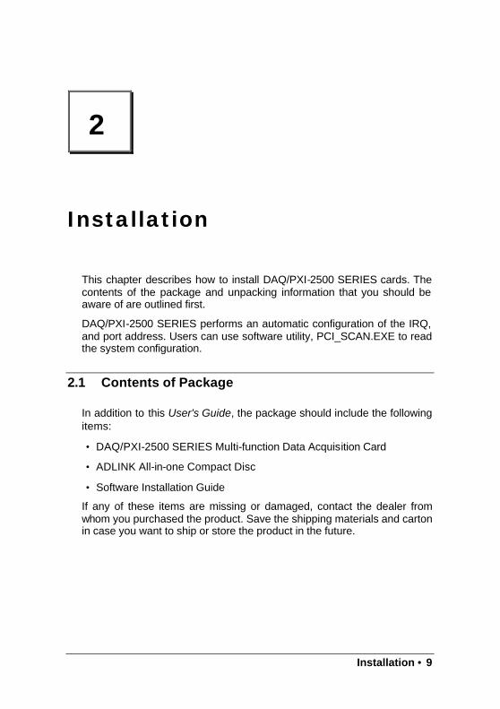
Installation • 9
2
Installation
This chapter describes how to install DAQ/PXI-2500 SERIES cards. The contents of the package and unpacking information that you should be aware of are outlined first.
DAQ/PXI-2500 SERIES performs an automatic configuration of the IRQ, and port address. Users can use software utility, PCI_SCAN.EXE to read the system configuration.
2.1 Contents of Package
In addition to this User's Guide, the package should include the following items:
• DAQ/PXI-2500 SERIES Multi-function Data Acquisition Card
• ADLINK All-in-one Compact Disc
• Software Installation Guide
If any of these items are missing or damaged, contact the dealer from whom you purchased the product. Save the shipping materials and carton in case you want to ship or store the product in the future.
10 • Installation
2.2 Unpacking
Your DAQ/PXI-2500 SERIES card contains electro-static sensitive com-ponents that can be easily be damaged by static electricity.
Therefore, the card should be handled on a grounded anti-static mat. The operator should be wearing an anti-static wristband, grounded at the same point as the anti-static mat.
Inspect the card module carton for obvious damages. Shipping and han-dling may cause damage to your module. Be sure there are no shipping and handling damages on the modules carton before continuing.
After opening the card module carton, extract the system module and place it only on a grounded anti-static surface with component side up.
Again, inspect the module for damages. Press down on all the socketed IC's to make sure that they are properly seated. Do this only with the module place on a firm flat surface.
Note: DO NOT APPLY POWER TO THE CARD IF IT HAS BEEN DAMAGED.
You are now ready to install your DAQ/PXI-2500 SERIES.

Installation • 11
2.3 DAQ/PXI-2500 SERIES Layout
Figure 2.2 PCB Layout of DAQ-2502/2501
Figure 2.3 PCB Layout of PXI-2502/2501

12 • Installation
2.4 PCI Configuration
1. Plug and Play:
As a plug and play component, the board requests an interrupt number via its PCI controller. The system BIOS responds with an interrupt assignment based on the board information and system parameters. These system parameters are determined by the installed drivers and the hardware load seen by the system.
2. Configuration:
The board configuration is done on a board-by-board basis for all PCI boards on your system. Because configuration is controlled by the system and software, there is no jumper setting required for base-address, DMA, and interrupt IRQ.
The configuration is subject to change with every boot of the system as new boards are added or removed.
3. Trouble shooting:
If your system doesn’t boot or if you experience erratic operation with your PCI board in place, it’s likely caused by an interrupt conflict (perhaps the BIOS Setup is incorrectly configured). In general, the solution, once you determine it is not a simple oversight, is to consult the BIOS documentation that comes with your system.

Signal Connections • 13
3
Signal Connections
This chapter describes the connectors of DAQ/PXI-2500 SERIES, and the signal connection between DAQ/PXI-2500 SERIES and external devices.
3.1 Connectors Pin Assignment
DAQ/PXI-2500 SERIES is equipped with two 68-pin VHDCI-type con-nectors (AMP-787254-1). It is used for digital input / output, analog input / output, and timer/counter signals, etc. The pin assignments of the con-nectors are defined in Figure 3.1.1 and Figure 3.1.2.

14 • Signal Connections
AO_0 1 35 AGND AO_1 2 36 AGND AO_2 3 37 AGND AO_3 4 38 AGND
AOEXTREF_A/AI_0 5 39 AGND AI_1 6 40 AGND
EXTATRIG/AI_2 7 41 AGND AOEXTREF_B/AI_3 8 42 AGND
AO_4/AI_4 9 43 AGND AO_5/AI_5 10 44 AGND AO_6/AI_6 11 45 AGND AO_7/AI_7 12 46 AGND
AO_TRIG_OUTA 13 47 EXTWFTRG_A AO_TRIG_OUTB 14 48 EXTWFTRG_B
GPTC1_SRC 15 49 VCC GPTC0_SRC 16 50 DGND
GPTC0_GATE 17 51 GPTC1_GATE GPTC0_OUT 18 52 GPTC1_OUT
GPTC0_UPDOWN 19 53 GPTC1_UPDOWN RESERVED 20 54 DGND
AFI1 21 55 AFI0 PB7 22 56 PB6 PB5 23 57 PB4 PB3 24 58 PB2 PB1 25 59 PB0 PC7 26 60 PC6 PC5 27 61 PC4
DGND 28 62 DGND PC3 29 63 PC2 PC1 30 64 PC0 PA7 31 65 PA6 PA5 32 66 PA4 PA3 33 67 PA2 PA1 34 68 PA0
Figure 3.1.1 Connector CN1 pin assignment

Signal Connections • 15
Legend :
Pin # Signal Name Refer-ence
Direction Description
1~4 AO_<0..3> AGND Output Voltage output of DA channel <0..3>
5 AOEXTREF_A/ AI_0
AGND Input External reference for AO channel <0..3> / AI input 2
6 AI_1 AGND Input AI input 0 7 EXTATRIG/
AI_2 AGND Input External analog trigger / AI
input 1 8 AOEXTREF_B/
AI_3 AGND Input External reference for AO
channel <4..7> / AI input 3 9~12 AO_<4..7>/
AI_<4..7> AGND Output
/Input Voltage output of DA channel <4..7> / AI channel <4..7> (only for DAQ-2501)
13,14 AO_TRIG_OUT_ <A,B>
DGND Output AO trigger signal for channel <0..3> <4..7>
15,16 GPTC<0,1>_SRC DGND Input Source of GPTC<0,1> 17,51 GPTC<0,1>_GATE DGND Input Gate of GPTC<0,1> 18,52 GPTC<0,1>_OUT DGND Input Output of GPTC<0,1> 19,53 GPTC<0,1>_
UPDOWN DGND Input Up/Down of GPTC<0,1>
20 RESERVED -------- -------- Reserved Pin 21,55 AFI<1,0> DGND Input Auxiliary Function Input 22,56,23,57, 24,58,25,59
PB<7,0> DGND PIO Programmable DIO of 8255 Port B
26,60,27,61, 29,63,30,64
PC<7,0> DGND PIO Programmable DIO of 8255 Port C
31,65,32,66, 33,67,34,68
PA<7,0> DGND PIO Programmable DIO of 8255 Port A
35~46 AGND -------- -------- Analog ground 47,48 EXTWFTRIG_<A,B
> DGND Input External waveform trigger
for AO channel <0..3> <4..7>
49 VCC DGND Power (Output)
+5V Power Source
28,50,54,62 DGND -------- -------- Digital ground
*PIO means Programmable Input/Output
Figure 3.1.2 Connector CN2 pin assignment

16 • Operation Theoreym
4
Operation Theorm
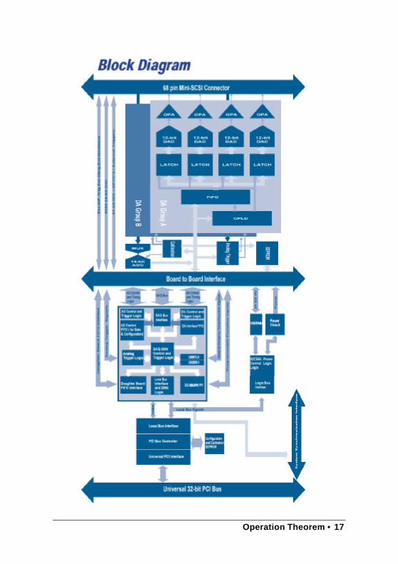
The operation theories of the DAQ/PXI-2500 series are described in this chapter. The functions include A/D conversion, D/A conversion, Digital I/O, and General Purpose Counter / Timer. This operation theory will help you understand how to configure and program the DAQ/PXI-2500 series.
Operation Theorem • 17
18 • Operation Theoreym
4.1 A/D Conversion
When using an A/D converter, users should know the properties of the signal to be measured. In addition, users should setup the A/D configura-tions, including scan channels, input range, and polarities.
The A/D acquisition is initiated by a trigger signal. The data acquisition will start once the trigger signal matches the trigger conditions. Converted data are queued into the FIFO buffer, and then transferred to the host PC's memory for further processing.
Two acquisition modes: Software Polling and Programmable Scan are described in the following sections, including the timing, trigger modes, trigger sources, and transfer methods.
4.1.1 DAQ/PXI-2500 series AD Data Format
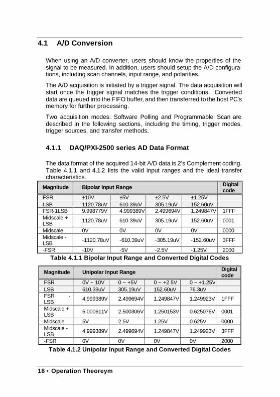
The data format of the acquired 14-bit A/D data is 2’s Complement coding. Table 4.1.1 and 4.1.2 lists the valid input ranges and the ideal transfer characteristics.
Magnitude Bipolar Input Range Digital code
FSR ±10V ±5V ±2.5V ±1.25V LSB 1120.78uV 610.39uV 305.19uV 152.60uV FSR-1LSB 9.998779V 4.999389V 2.499694V 1.249847V 1FFF Midscale + LSB 1120.78uV 610.39uV 305.19uV 152.60uV 0001
Midscale 0V 0V 0V 0V 0000 Midscale - LSB -1120.78uV -610.39uV -305.19uV -152.60uV 3FFF
-FSR -10V -5V -2.5V -1.25V 2000 Table 4.1.1 Bipolar Input Range and Converted Digital Codes
Magnitude Unipolar Input Range Digital code
FSR 0V ~ 10V 0 ~ +5V 0 ~ +2.5V 0 ~ +1.25V LSB 610.39uV 305.19uV 152.60uV 76.3uV FSR - LSB 4.999389V 2.499694V 1.249847V 1.249923V 1FFF
Midscale + LSB 5.000611V 2.500306V 1.250153V 0.625076V 0001
Midscale 5V 2.5V 1.25V 0.625V 0000 Midscale - LSB 4.999389V 2.499694V 1.249847V 1.249923V 3FFF
-FSR 0V 0V 0V 0V 2000
Table 4.1.2 Unipolar Input Range and Converted Digital Codes

Operation Theorem • 19
4.1.2 Software Polling
This is the easiest way to acquire a single A/D data. The A/D converter performs one conversion whenever the dedicated software command is executed. The software would poll the conversion status and read the A/D data back when it is available.
This method is suitable for applications that need to acquire A/D data in real time. In this mode, the timing of the A/D conversion is fully controlled by software. However, it would be difficult to maintain a fixed A/D sampling rate.
4.1.3 Programmable Scan
This method is suitable for applications that need to acquire A/D data at a precise and fixed rate. A scan is a group of multiple channel samples and the scan interval is defined by the SI_counter. Likewise, the sample in-terval of the multiple channels is defined by the SI2_counter. Please refer to Table 4.1.4 for more information.
DAQ/PXI-2500 series can sample multiple channels in continu-ous/discontinuous ascending sequence. For example, users may program DAQ/PXI-2500 series to perform a scan in the channel sequence of 1-2-4-1-2-4…
There are 3 Trigger Modes available in Programmable Scan. They are Post-Trigger, Delay-Trigger, Post/Delay-Trigger with Retrigger. Please refer to Table 4.1.3 for a brief summary on Trigger Modes and their Trigger Sources.
Trigger Mode Description Trigger Sources
Post-Trigger Perform a scan right after the trigger occurs.
Delay-Trigger Scan delayed by the amount of time programmed after the trigger
Post/Delay-Trigger with Retrigger
Perform repeated scan while trigger occurs and it could be under Post-Trigger or De-lay-Trigger mode.
Software Trigger
Digital Trigger
Analog Trigger
SSI AD Trigger
Table 4.1.3 Trigger Modes and Corresponding Trigger Sources

20 • Operation Theoreym
4.1.3.1 Scan Timing and Procedure
There are 4 counters that need to be specified prior to programmable scans:
Counter Name Width Description Notes
SI_counter 24-bit Scan Interval, which defines the interval between each scan.
Scan Interval =
SI_counter / Time-base*
SI2_counter 24-bit
Sampling Interval, which defines the interval between each sampled channel.
Sampling Interval =
SI2_counter / Timebase*
PSC_counter 24-bit
Post Scan Counts, which defines how many scans to be performed with re-spect to each trig-ger.
Delay_counter 16-bit Define the delay time for scan after trigger.
Delay Time =
(Delay_counter / Timebase*),
Timebase*=40M for DAQ/PXI-2500 Series
Table 4.1.4 Summary of Counters for Programmable Scan
The relationship between counters and acquisition timing is illustrated in Figure 4.1.1.

Operation Theorem • 21
Acquisition_in_progress
Scan_start
AD_conversion
Scan_in_progress
3 Scans, 4 Samples per scan (PSC_Counter=3)
Sampling Interval t= SI2_COUNTER/TimeBase
Scan Interval T= SI_COUNTER/TimeBase
Ch0 Ch1
C h2 Ch3
Ch0C h1
Ch2 Ch3
C h0 Ch1
C h2 C h3
(Scan acquisition is performed in ascending sequence for enabled channels)
Trigger
Figure 4.1.1 Timing for Scan
NOTE: 1. The maximum A/D sampling rate is 400KHz for DAQ/PXI-2500 series
therefore the minimum setting of SI2_counter is 100. 2. The Scan Interval can not be smaller than the interval of data Sampling
Interval multiple by the Number of channels per Scan, i.e.: SI_counter >= SI2_counter * NumChan_Counter
4.1.3.2 Trigger Mode
Post-Trigger Acquisition
Use post-trigger acquisition when users want to perform scans right after a trigger signal. The number of scans to be performed after the trigger signal is specified by the PSC_counter, as illustrated in Figure 4.1.2. The total acquired data length = (number_of_channels_enabled_for _scan_acquisition) * PSC_counter.
Delay Trigger Acquisition
Use delay trigger when users want to delay the scan after a trigger signal. The delay time is determined by the Delay_counter, as shown in Figure 4.1.3.
The counter counts down on the rising edges of Delay_counter clock source after the trigger signal. When the count reaches 0, DAQ/PXI-2500 SERIES starts to perform the scan. The acquired data length = (num-ber_of_channels_enabled_for_scan_acquisition) * PSC_counter. The Delay_counter clock source can be software selected from Internal 40MHz

22 • Operation Theoreym
Timebase, external input (AFI-1), or General Purpose Timer/Counter Output 0/1.
Post-Trigger or Delay-trigger Acquisition with retrigger
Use post-trigger or delay-trigger acquisition with retrigger when users want to perform repeated scans with respect to the repeated triggers. Figure 4.1.4 illustrates an example. Two scans are performed after the first trigger signal, and then wait for the next trigger signal. When the trigger signal occurs, it performs 2 more scans.
When re-trigger function is disabled, only one trigger signal would be ac-cepted after retrigger
NOTE: Retrigger signals asserted during scan process will be ignored.
(NumChan_Counter=4, PSC_Counter=3)
Acquisition_in_progress
Scan_start
AD_conversion
Scan_in_progress
Acquired & stored data (3 scans)
Operation start
Trigger
Figure 4.1.2 Post trigger

Operation Theorem • 23
(NumChan _Counter=4, PSC_Counter=3)
Acquisition_in_progress
Scan_start
AD_conversion
Scan_in_progress
Acquired & stored data (3 scans)
Operation start
Trigger
Delay until Delay_Counter reaches 0
Figure 4.1.3 Delay trigger
(NumChan _Counter=4, SC_Counter=2, retrig_no=3)
Acquisition_in_progress
Scan_start
AD_conversion
Scan_in_progress
Acquired & stored data (6 scans)
Operation start
Trigger
Figure 4.1.4 Post trigger with retrigger
4.1.4.4 Bus-mastering DMA Data Transfer
Bus Mastering DMA Mode
In order to utilize the maximum PCI bandwidth, PCI bus-mastering DMA is used for high speed DAQ boards. The bus-mastering capability of the PLX PCI controller, takes over the PCI bus when it becomes the master. Bus mastering reduces the required size of on-board memory as well as CPU loading since data is directly transferred to the host PC’s memory without CPU intervention.

24 • Operation Theoreym
The hardware temporarily stores the acquired data in the onboard Data FIFO buffer, then transfers the data to the user-defined DMA buffer in the host PC’s memory. Bus-mastering DMA utilizes the fastest available transfer rate of PCI-bus. Once the analog acquisition operation starts, control returns to your program.
The DMA transfer mode is very complex to program. We recommend using a high-level program library to configure this card. If users would like to program the software that can handle DMA data transfer, please refer to http://www.plxtech.com for more information on PCI controllers.
DMA with Scatter Gathering Capability
In multi-user or multi-tasking OS such as Microsoft Windows, Linux, etc., it would be difficult to allocate a large continuous memory block due to memory fragmentation. PLX PCI controller provides scatter /gather or chaining mode to link non-continuous memory blocks into a linked list, so that users can transfer large amounts of data without being limited by the fragment of memory blocks. Users can configure the linked list for the input DMA channel and the output DMA channel, individually.
Figure 4.1.5 shows the linked list that is constructed by three DMA de-scriptors. Each descriptor contains a PCI address, a local address, a transfer size, and the pointer to the next descriptor. Users can thus collect fragmented memory blocks and chain their associative DMA descriptors altogether. DAQ/PXI-2500 SERIES software driver provides users easy ways to setup scatter/gather functions. Sample programs are also sup-plied in the all-in-one CD.
Figure 4.1.5 Scatter/Gather DMA for data transfer
In non-chaining mode, the maximum DMA data transfer size would be 2M double words (8M bytes). By using chaining mode, scatter/gather, there is no limitation on DMA data transfer size. Users can also link the descriptor nodes circularly to achieve a multi-buffered DMA.

Operation Theorem • 25
4.2 D/A Conversion
DAQ/PXI-2500 series offers flexible and versatile analog output scheme to fit users’ complex field applications. In order to take full advantages of DAQ/PXI-2500 series, we suggest users carefully read the following con-tents.
Architecture
There are up to 8-channel of 12-bit Digital-to-Analog Converter (DAC) available in the DAQ/PXI-2502. Four D/A channels are packed into one D/A group, i.e., DAQ/PXI-2502 contains two D/A groups, and DAQ/PXI-2501 has only one D/A group.
Figure 4.2.1 Block Diagram of D/A Group (Group B of DAQ/PXI-2502 is identical to Group A shown above)
Figure 4.2.1 shows the D/A block diagram. DAC are controlled implicitly by CPLD and have their outputs updated only when digital codes for all en-abled DA channels are ready and latched. This ensures D/A conversions to be synchronized for each channel in the same D/A group. Users can utilize this property to perform multi-channel waveform generation without any phase-lag.
26 • Operation Theoreym
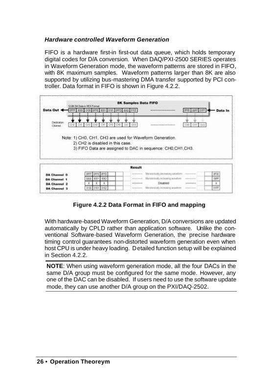
Hardware controlled Waveform Generation
FIFO is a hardware first-in first-out data queue, which holds temporary digital codes for D/A conversion. When DAQ/PXI-2500 SERIES operates in Waveform Generation mode, the waveform patterns are stored in FIFO, with 8K maximum samples. Waveform patterns larger than 8K are also supported by utilizing bus-mastering DMA transfer supported by PCI con-troller. Data format in FIFO is shown in Figure 4.2.2.
Figure 4.2.2 Data Format in FIFO and mapping
With hardware-based Waveform Generation, D/A conversions are updated automatically by CPLD rather than application software. Unlike the con-ventional Software-based Waveform Generation, the precise hardware timing control guarantees non-distorted waveform generation even when host CPU is under heavy loading. Detailed function setup will be explained in Section 4.2.2.
NOTE: When using waveform generation mode, all the four DACs in the same D/A group must be configured for the same mode. However, any one of the DAC can be disabled. If users need to use the software update mode, they can use another D/A group on the PXI/DAQ-2502.

Operation Theorem • 27
Setting up the DACs
Before using the DACs, users should setup the reference source and its polarity. Each DAC has its own reference and polarity settings. For ex-ample; the internal voltage reference of D/A Group A is tied to internal +10V, however, users can still connect external reference thru AOEXTREF (pin 5 on CN2), for example to a +3.3V voltage source. Therefore, each DAC in D/A Group A has two reference options: 10V or 3.3V. However, DA update timing, trigger Source, and trigger/stop mode are all the same throughout that D/A Group.
DAQ/PXI-2500 SERIES provides the capability to fine tune the voltage reference from the external source. The external reference is fed thru an on board calibrated circuit, with programmable offset. Users can utilize this capability to generate precise D/A outputs.
CAUTION: The range of external voltage reference should be within ア10V.
Utilizing Multiplying Characteristic of DACs
The D/A reference selection let users fully utilize the multiplying charac-teristics of the DACs. Digital codes sent to the D/A converters will be multiplied by the reference to generate output.
Bipolar Unipolar Magnitude
Output Output Digital Code
FSR – LSB +Vref * (2046 / 2048)
Vref * (4095 / 4096) 0FFF
Midscale + LSB +Vref * (1 / 2048) Vref * (2049 4096) 0801
Midscale 0 Vref * (2048 / 4096) 0800 Midscale – LSB -Vref * ( 1 / 2048) Vref * (2047 / 4096) 07FF
-FSR + LSB -Vref * (2046 / 2048)
Vref * ( 1 / 4096) 0001
-FSR -Vref 0 0000
Table 4.2.1 D/A Output Versus Digital Codes

28 • Operation Theoreym
DAQ/PXI-2500 SERIES can generate standard and arbitrary functions, continuously or piece-wisely. Appendix A demonstrates possible wave-form patterns generated by DAQ/PXI-2500 SERIES in combination with various counters, clock sources, and voltage references.
4.2.1 Software Update
This method is suitable for applications that need to generate D/A output controlled by user programs. In this mode, the D/A converter generates one output once the software command is issued. However, it would be difficult to determine the software update rate under a multi-task OS like Windows.
4.2.2 Waveform Generation
This method is suitable for applications that need to generate waveforms at a precise and fixed rate. Various programmable counters will facilitate users to generate complex waveforms with great flexibility.
There are three event signals involved in Waveform Generation: Start, DAWR (DA WRite), and Stop. Please refer to Table 4.2.2 for a brief summary on Waveform Generation Events and their corresponding Trig-ger Sources.
For more information on Trigger Mode, Stop Mode, Time-base, and Trig-ger Sources, please refer to section 4.2.2.2, 4.2.2.4, 4.1.4.2, and 4.5, re-spectively.
Signal Descriptions Valid Sources
Start Start Waveform Generation process.
Software Trigger Ext. Digital Trigger Analog Trigger SSI Trigger
DAWR Write data to the DAC on the fal-ling edges of DAWR.
Internal Update External Update SSI Update
Stop Stop Waveform Generation Software Trigger Ext. Digital Trigger Analog Trigger
Table 4.2.2 Trigger Signals and Corresponding Signal Sources

Operation Theorem • 29
4.2.2.1 Waveform Generation Timing
Six counters interact with the waveform to generate different DAWR timing, thus forming different waveforms. They are described in Table 4.2.3.
Counter Name Width Description Note
UI_counter 24-bit
Update Interval, which defines the update interval be-tween each data output.
Update Interval = UI_counter / Time-base*.
UC_counter 24-bit
Update Counts, which defines the number of data in a waveform.
When value in UC_counter is smaller than the size of waveform pat-terns, the waveform is generated piece-wisely.
IC_counter 16-bit
Iteration Counts, which defines how many times the waveform is gener-ated.
DLY1_counter 16-bit
Define the delay time for waveform gen-eration after the trigger signal.
Delay Time = (DLY1_counter / Clock Timebase)
DLY2_counter 16-bit
Define the delay time to separate con-secutive waveform generation. Effec-tive only in Iterative Waveform Genera-tion mode.
Delay Time = (DLY2_counter / Clock Timebase)
Trig_counter 16-bit
Define the accept-able start trigger count when re-trigger function is enabled
Timebase*=40M for DAQ/PXI-2500 Series
Table 4.2.3 Summary of Counters for Waveform Generation
30 • Operation Theoreym
NOTE: The maximum D/A update rate is 1MHz. Therefore the minimum setting of UI_counter is 40.
(UC _Counter=4, IC_Counter=3)
4 update counts, 3 iterations
DAWR
WFG_in_progress
DA update_interval t= UI_Counter/Timebase
Operation start
Trigger
Delay until DLY1_Counter reaches 0
Delay until DLY2_Counter reaches 0
Output Waveform
Delay until DLY2_Counter reaches 0
0 2
4
-4
A single waveform
UC_Counter=4
IC_Counter = 3
Figure 4.2.3 Typical D/A timing of waveform generation (Assuming the data in the data buffer are 2V, 4V, -4V, 0V)
4.2.2.2 Trigger Modes
Post-Trigger Generation
Use post-trigger generation when users want to generate waveform right after a trigger signal. The number of patterns to be updated after the trigger signal is specified by UC_counter* IC_counter, as illustrated in Figure 4.2.4.

Operation Theorem • 31
Delay-Trigger Generation
Use delay-trigger when users want to delay the waveform generation after the trigger signal. The delay time is determined by DLY1_counter, as shown in Figure 4.2.5.
The counter counts down on the rising edges of DLY1_counter clock source after the start trigger signal. When the count reaches zero, DAQ/PXI-2500 series starts to generate the waveform. The DLY1_counter clock source can be software selected from the Internal 40MHz Timebase, external clock input (AFI-0), or GPTC output 0/1.
Post-Trigger or Delay-Trigger with Retrigger
Use post-trigger or delay-trigger with retrigger when users want to gener-ate multiple waveforms with respect to multiple incoming trigger signals. Users can set Trig_counter to specify the number of acceptable trigger signals.
Figure 4.2.6 illustrates an example. Two waveforms are generated after the first trigger signal (Iterative Waveform Generation is used in this example, please refer to Section 4.2.2.3 for details). The board then waits for another trigger signal. When the next trigger signal is asserted, the board generates two more waveforms. After three trigger signals, as specified in Trig_Counter, no more triggers signals will be accepted unless software trigger reset command is executed.
NOTE: Start Trigger signals asserted during waveform generation process will be ignored.
(UC _Counter=8, IC_Counter=1)
8 update counts, 1 iteration
DAWR
WFG_in_progress
Operation start
Trigger
Output Waveform 0
2 4
6 3
-4 -2
4
Figure 4.2.4 Post-Trigger Generation

32 • Operation Theoreym
(UC _Counter=8, IC_Counter=1)
8 update counts, 1 iteration
DAWR
WFG_in_progress
Operation start
Trigger
Output Waveform
Delay until DLY1_counter reaches 0
Figure 4.2.5 Delay-Trigger Generation
(UC _Counter=4, IC_Counter=2, Trig_Counter=3, DLY2_Counter disabled, DLY2_Counter disabled)
4 update counts, 2 iterations
Ignored
DAWR
WFG_in_progress
Operation start
Trigger
Output Waveform
0
2 4
a single waveform
Figure 4.2.6 Post-Trigger with Retrigger Generation
4.2.2.3 Iterative Waveform Generation
Users can set IC_counter to generate iterative waveforms, no matter which Trigger Mode is used. The IC_counter stores the iteration number. Ex-amples are shown in Figure 4.2.7 and 4.2.8.
When IC_counter is disabled, the waveform generation will not stop until a stop trigger is asserted. For Stop Mode, please refer to Section 4.2.2.4 for details.
An on-board data FIFO is used to buffer the waveform patterns for wave-form generation. If the size of a single waveform is smaller than that of the FIFO, after initially loading the data from the host PC’s memory, the data in FIFO will be re-used when a single waveform generation is completed. In other words, it won’t occupy the PCI bandwidth afterwards. However, if the

Operation Theorem • 33
size of a single waveform were larger than that of the FIFO, it needs to be intermittently loaded from the host PC’s memory via DMA, thus PCI bandwidth would be occupied.
If the value specified in UC_counter is smaller than the sample size of the waveform patterns, the waveform will be generated piece-wisely. For example, if users defined a 16-sample sine wave and set the UC_counter to 2, the generated waveform will be a 1/8-cycle sine wave for every waveform period. In other words, a complete sine wave will be generated for every 8-iterations. If value specified in UC_counter is larger than the sample size of waveform LUT, say, 32; the generated waveform will be a 2-cycle sine wave for every waveform period.
In conjunction with different trigger modes and counter setups, users can manipulate a single waveform to generate different, more complex wave-forms. For more information, please refer to Appendix A.
(UC _Counter=4, IC_Counter=3, DLY2_Counter=0)
4 update counts, 3 iterations
DAWR
WFG_in_progress
Operation start
Trigger
Output Waveform 0
2 4
A single waveform
Figure 4.2.7 Finite iterative waveform generation with Post-trigger (Assuming the digital codes in the FIFO are 2V, 4V, 2V, 0V)
(UC _Counter=4, IC_Counter=disabled, DLY2_Counter=disabled)
4 update counts, infinite iterations
DAWR
WFG_in_progress
Operation start
Trigger
Output Waveform
waveform generation won’t stop until a stop trigger is asserted
0
2 4
Figure 4.2.8 Infinite iterative waveform generation with Post-trigger (Assuming the digital codes in the FIFO are 2V, 4V, 2V, 0V)

34 • Operation Theoreym
DLY2_Counter in iterative Waveform Generation
To expand the flexibility of Iterative Waveform Generation, DLY2_counter was implemented to separate consecutive waveform generations.
The DLY2_counter starts counting down right after a single waveform generation is completed. When it reaches zero, the next iteration of waveform generation will start as shown in Figure 4.2.3. If users are generating waveform piece-wisely, the next piece of waveform will be generated. The DLY2_counter clock source can be software selected from Internal 40MHz Timebase, external clock input (AFI-0), or GPTC output 0/1.
4.2.2.4 Stop Modes
Users can stop waveform generation while it is still in progress, either by hardware or software trigger. The stop trigger sources can be software selected from Internal software trigger, external digital trigger (AFI-0/1), or analog trigger. Three stop modes are provided to stop finite or infinite waveform generation.
Stop Mode I
After a mode I stop trigger is asserted, the waveform generation stops immediately. Figure 4.2.9 illustrates an example.
Stop Mode II
After a mode II stop trigger is asserted, the waveform generation continues to generate a complete waveform then stops the operation. Take Figure 4.2.10 as an example. Since UC_counter is set to 4, the total generated data points must be a multiple of 4.
Users can check WFG_in_progress (waveform generation in progress) status by software read-back to confirm the stop of a waveform generation.
Stop Mode III
After a mode III stop trigger is asserted, the waveform generation contin-ues until the iterative number of waveforms specified in IC_Counter is completed. Take Figure 4.2.11 for example. Since IC_Counter is set to 3, the total generated waveforms must be a multiple of 3.
Users can check WFG_in_progress (waveform generation in progress) status by software read-back to confirm the stop of a waveform generation.

Operation Theorem • 35
(UC _Counter=4, IC_Counter disabled)
4 update counts, infinite iterations
DAWR
WFG_in_progress
Operation start
Trigger
Output Waveform
0
2 4
stop trigger
Figure 4.2.9 Stop mode I (Assuming the data in the data buffer are 2V, 4V, 2V, 0V)
(UC _Counter=4, IC_Counter disabled)
4 update counts, infinite iterations
DAWR
WFG_in_progress
Operation start
Trigger
Output Waveform
0
2 4
stop trigger
Figure 4.2.10 Stop mode II
(UC _Counter=4, IC_Counter=3, Trig_Counter>1)
4 update counts, finite iterations
DAWR
WFG_in_progress
Operation start
Trigger
Output Waveform
0
2 4
stop trigger
Figure 4.2.11 Stop mode III

36 • Operation Theoreym
4.3 General Purpose Digital I/O
DAQ/PXI-2500 SERIES provides 24-line general-purpose digital I/O (GPIO) through a 82C55A chip.
The 24-line GPIO are separated into three ports: Port A, Port B and Port C. High nibble (bit[7…4]), and low nibble (bit[3…0]) of each port can be indi-vidually programmed to be either inputs or outputs. Upon system startup or reset, all the GPIO pins are reset to high impedance inputs.
For more information on programmable I/O chip 82C55A, please refer to http://www.intel.com.

Operation Theorem • 37
4.4 General Purpose Timer/Counter Operation
Two independent 16-bit up/down timer/counter are embedded in FPGA firmware for users applications. They have the following features:
• Direction of counting can be controlled via hardware or software. • Selectable c ounter clock source from either internal or external clock up
to 10MHz. • Programmable gate selection. • Programmable input and output signal polarities, either active-high or
active-low. • Initial Count can be loaded via software • Current count value can be read-back by software without affecting
circuit operation
4.4.1 Timer/Counter functions basics
Each timer/counter has three inputs that can be controlled via hardware or software. They are clock input (GPTC_CLK), gate input (GPTC_GATE), and up/down control input (GPTC_UPDOWN).
The GPTC_CLK input acts as a clock source to the timer/counter. Active edges on the GPTC_CLK input increment or decrement the counter. The GPTC_UPDOWN input determines whether the counter’s counting-up or counting-down. The GPTC_GATE input is a control line, which acts as a counter enable or a counter trigger signal in different modes.
The output of timer/counter is GPTC_OUT. After power-up, GPTC_OUT is pulled high by a 10K resistor. GPTC_OUT goes low after the DAQ board is initialized.
All the polarities of input/output signals can be programmed via software. In this chapter, all timing figures assume that GPTC_CLK, GPTC_GATE, and GPTC_OUT are set to be positive-logic. (i.e. they’re triggered on the rising-edge)
4.4.2 General Purpose Timer/Counter modes
Eight programmable timer/counter modes are provided. All modes start operations following the software start command. The GPTC software reset command initializes the status of the counter and re-loads the initial value to the counter.

38 • Operation Theoreym
4.4.2.1 Mode1: Simple Gated-Event Counting
In this mode, the counter counts the number of pulses on the GPTC_CLK after the software start. Initial count value can be loaded via software. Current count value can be read-back by software at any time. GPTC_GATE is used to enable/disable counting. When GPTC_GATE is inactive, the counter halts the current count value. Figure 4.4.1 illustrates the operation with initial count = 5 in down-counting mode.
5 5 4 3 2 1 1 0 ffff
Gate
CLK
Count value
Software start
Figure 4.4.1 Mode 1 Operation
4.4.2.2 Mode2: Single Period Measurement
In this mode, the counter counts the period of the signal on GPTC_GATE in terms of GPTC_CLK. Initial count can be loaded via software. After the software start, the counter counts the number of active edges on GPTC_CLK between two active edges of GPTC_GATE. After the com-pletion of the period measurement, GPTC_OUT outputs high and current count value can be read-back by software. Figure 4.4.2 illustrates the operation where initial count = 0, up-counting mode.
0 0 1 2 3 4 5 5 5
Gate
CLK
Count value
Software start
Figure 4.4.2 Mode 2 Operation

Operation Theorem • 39
4.4.2.3 Mode3: Single Pulse-width Measurement
In this mode, the counter counts the pulse-width of the signal on GPTC_GATE in terms of GPTC_CLK. Initial count can be loaded via software. After the software start, the counter counts the number of active edges on GPTC_CLK when GPTC_GATE is active. GPTC_OUT outputs high, and current count value can be read-back via software after the completion of the pulse-width measurement. Figure 4.4.3 illustrates the operation where initial count = 0 in up-counting mode.
0 0 1 2 3 4 5 5 5
Gate
CLK
Count value
Software start
Figure 4.4.3 Mode 3 Operation
4.4.2.4 Mode4: Single Gated Pulse Generation
This mode generates a single pulse with programmable delay and pro-grammable pulse-width following the software start. These software programmable parameters could be specified in terms of periods of the GPTC_CLK. GPTC_GATE is used to enable/disable counting. When GPTC_GATE is inactive, the counter halts the counting. Figure 4.4.4 il-lustrates the generation of a single pulse with pulse-delay of two and pulse-width of four.
2 2 1 0 3 2 2 1 0
Gate
CLK
Count value
OUT
Software start
Figure 4.4.4 Mode 4 Operation

40 • Operation Theoreym
4.4.2.5 Mode5: Single Triggered Pulse Generation
This function generates a single pulse with programmable delay and pro-grammable pulse-width following an active GPTC_GATE edge. These software programmable parameters can be specified in terms of periods of the GPTC_CLK input. Once the first GPTC_GATE edge triggers the single pulse, GPTC_GATE takes no effect until the software start is re-executed. Figure 4.4.5 illustrates the generation of a single pulse with pulse delay of two and pulse-width of four.
2 2 1 0 3 2 1 0
Gate
CLK
Count value
OUT
Software start
Figure 4.4.5 Mode 5 Operation
4.4.2.6 Mode6: Re-triggered Single Pulse Generation
This mode is similar to mode 5 except that the counter generates a pulse following every active edge on GPTC_GATE. After the software start, every active GPTC_GATE edge triggers a single pulse with programmable delay and pulse-width. Any GPTC_GATE trigger that occurs during the pulse generation would be ignored. Figure 4.4.6 illustrates the generation of two pulses with pulse delay of two and pulse-width of four.
2 2 1 0 3 2 1 0 2 2 1 0 3 2 1 0 2 2
G a t e
C L K
C o u n t v a l u e
O U T
S o f t w a r e s t a r t I g n o r e d
Figure 4.4.6 Mode 6 Operation

Operation Theorem • 41
4.4.2.7 Mode7: Single Triggered Continuous Pulse Generation
This mode is similar to mode 5, except that the counter generates con-tinuous periodic pulses with programmable pulse interval and pulse-width following the first active edge of GPTC_GATE. Once the first GPTC_GATE edge triggers the counter, GPTC_GATE takes no effect until the software start is re-executed. Figure 4.4.7 illustrates the generation of two pulses with pulse delay of four and pulse-width of three.
4 4 4 3 2 1 0 2 1
S o f t w a r e s t a r t
0 3 2 1 0 2 1 0 3 2
G a t e
C L K
C o u n t v a l u e
O U T
Figure 4.4.7 Mode 7 Operation
4.4.2.8 Mode8: Continuous Gated Pulse Generation
This mode generates periodic pulses with programmable pulse interval and pulse-width following the software start. GPTC_GATE is used to enable/disable counting. When GPTC_GATE is inactive, the counter halts the current count value. Figure 4.4.8 illustrates the generation of two pulses with pulse delay of four and pulse-width of three.
4 4 3 3 2 1 0 2 1
S o f t w a r e s t a r t
0 3 2 1 0 2 1 1 0 3
G a t e
C L K
C o u n t v a l u e
O U T
Figure 4.4.8 Mode 8 Operation
42 • Operation Theoreym
4.5 Trigger Sources
We provide flexible trigger selections in DAQ/PXI-2500 SERIES. In addi-tion to software trigger, DAQ/PXI-2500 SERIES also supports external analog and digital triggers. Users can configure the trigger source for A/D and D/A processes individually via software.
NOTE: A/D and D/A conversion share the same analog trigger.
4.5.1 Software-Trigger
This trigger mode does not need any external trigger source. The trigger asserts right after users execute the specified function call. A/D and D/A processes can receive an individual software trigger.
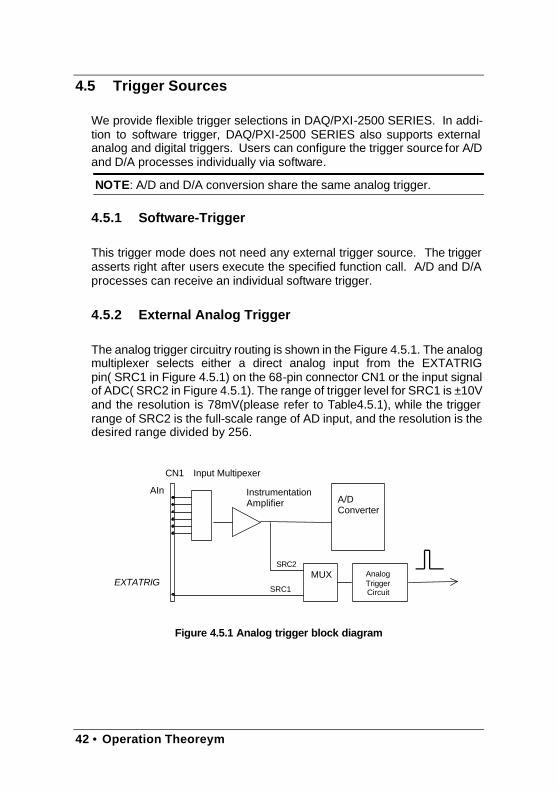
4.5.2 External Analog Trigger
The analog trigger circuitry routing is shown in the Figure 4.5.1. The analog multiplexer selects either a direct analog input from the EXTATRIG pin( SRC1 in Figure 4.5.1) on the 68-pin connector CN1 or the input signal of ADC( SRC2 in Figure 4.5.1). The range of trigger level for SRC1 is ±10V and the resolution is 78mV(please refer to Table4.5.1), while the trigger range of SRC2 is the full-scale range of AD input, and the resolution is the desired range divided by 256.
AIn Instrumentation Amplifier A/D
Converter
Input Multipexer CN1
MUX Analog Trigger Circuit
EXTATRIG SRC1
SRC2
Figure 4.5.1 Analog trigger block diagram

Operation Theorem • 43
Trigger Level digital setting Trigger voltage
0xFF 9.92V 0xFE 9.84V
--- --- 0x81 0.08V 0x80 0 0x7F -0.08V --- ---
0x01 -9.92V 0x00 -10V
Table 4.5.1 Analog trigger SRC1(EXTATRIG) ideal transfer characteristic
The trigger signal asserts when an analog trigger condition is meet. There are five analog trigger conditions in DAQ/PXI-2500 SERIES. DAQ/PXI-2500 SERIES uses 2 threshold voltages: Low_Threshold and High_Threshold to compose 5 different trigger conditions. Users can con-figure the trigger conditions easily via software.
4.5.2.1 Below-Low analog trigger condition
Figure 4.5.2 shows the below-low analog trigger condition, the trigger signal asserts when the input analog signal is lower than the Low_Threshold voltage. High_Threshold setting is not used in this trigger condition.
Figure 4.5.2 Below-Low analog trigger condition

44 • Operation Theoreym
4.5.2.2 Above-High analog trigger condition
Figure 4.5.3 shows the above-high analog trigger condition, the trigger signal asserts when the input analog signal is higher than the High_Threshold voltage. The Low_Threshold setting is not used in this trigger condition.
Figure 4.5.3 Above-High analog trigger condition
4.5.2.3 Inside-Region analog trigger condition
Figure 4.5.4 shows the inside-region analog trigger condition, the trigger signal asserts when the input analog signal level falls in the range between the High_Threshold and the Low_Threshold voltages.
Figure 4.5.4 Inside-Region analog trigger condition
Operation Theorem • 45
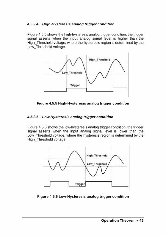
4.5.2.4 High-Hysteresis analog trigger condition
Figure 4.5.5 shows the high-hysteresis analog trigger condition, the trigger signal asserts when the input analog signal level is higher than the High_Threshold voltage, where the hysteresis region is determined by the Low_Threshold voltage.
Figure 4.5.5 High-Hysteresis analog trigger condition
4.5.2.5 Low-Hysteresis analog trigger condition
Figure 4.5.6 shows the low-hysteresis analog trigger condition, the trigger signal asserts when the input analog signal level is lower than the Low_Threshold voltage, where the hysteresis region is determined by the High_Threshold voltage.
Figure 4.5.6 Low-Hysteresis analog trigger condition

46 • Operation Theoreym
4.6 Timing Signals
In order to meet the requirements for user-specific timing or synchronizing multiple boards, DAQ/PXI-2500 SERIES provides a flexible interface for connecting timing signals with external circuitry or other boards. The DAQ timing of the DAQ/PXI-2500 SERIES is composed of a bunch of counters and trigger signals in the FPGA on board.
There are 7 timing signals related to the DAQ timing, which in turn influ-ence the A/D, D/A process, and GPTC operation. These signals are fed through the Auxiliary Function Inputs pins (AFI) or the System Synchro-nization Interface bus (SSI). We implemented a multiplexer in the FPGA to select the desired timing signal from these inputs, as shown in the Figure 4.6.1.
Users can use the SSI to achieve synchronization between multiple boards, or use the AFI to derive timing signals from an external timing circuit.
Internal timing
signals
SSI timing signals
AFI timing signals
DAQ timing signals
Figure 4.6.1 DAQ signals routing
Operation Theorem • 47
4.6.1 System Synchronization Interface
SSI uses bi-directional I/O to provide flexible connections between boards. You can choose each of the 7 timing signals and which board to be the SSI master. The SSI master can drive the timing signals of the slaves. Users can thus achieve better synchronization between boards.
Note that when power-up or reset, the DAQ board is reset to using its in-ternal timing signals.

48 • Calibration
5
Calibration
This chapter introduces the calibration process to minimize AD meas-urement errors and DA output errors.
DAQ/PXI-2500 SERIES is factory calibrated before shipment. The on-board high precision band-gap voltage reference together with TrimDAC compensates for unwanted offsets and gain errors, caused by environment variation or component aging.

Calibration • 49
5.1 Auto-calibration
The auto-calibration feature of DAQ/PXI-2500 SERIES facilitates users completing a calibration process, without the necessities for any external voltage references or measurement devices.
The on-board auto-calibration circuitry is composed of a precision band-gap voltage reference, an ADC and a TrimDAC. TrimDAC is a multi-channel DAC that generates DC offsets that counteract the offsets from the main DACs. Digital codes for the TrimDAC, as well as the tem-perature and the date of the calibration, are stored in the onboard EEPROM. We do not recommend end-users to adjust the onboard band-gap voltage reference in anyway, unless an ultra-precision calibrator is available.
Due to temperature, humidity variations, and component aging, the preci-sion of DAQ board may degrade over time. It is suggested that users pe-riodically calibrate the DAQ board. The user calibration constants can also be stored in the on-board EEPROM.
NOTE: 1. Before auto-calibration procedure starts, it is recommended to warn up
the board for at least 15 minutes. 2. Please remove the cable before auto-calibration, because the D/A
outputs would be changed in the process.
5.2 Saving Calibration Constants
An on-board EEPROM is used to store calibration constants. In addition to a default bank that stores factory calibration constants, there are three user banks. Users can save the subsequently performed calibration constants in anyone of these user banks. ADLink provides software for users to save calibration constants in an easy manner.
5.3 Loading Calibration Constants
Users can calibrate DAQ board in three sites and store the calibration constants into different user banks. When moving DAQ board from one site to another, users can load the calibration constants without re-calibration. ADLINK provides software for users to load calibration constants in an easy manner.

50 • Appendix A
6
Appendix A
6.1 Waveform Generation Demonstration
Combined with 6 counters, selectable trigger sources, external reference sources, and time base, DAQ/PXI-2500 SERIES provides the capabilities to generate complex waveforms. Various modes shown below can be mixed together to generate waveforms that are even more complex.
Although users can always load a new waveform to generate any desired waveform, we suggest using hardware capabilities to maximize both effi-ciency and flexibility.
Standard Function
Waveforms including sine wave, trian-gular wave, saw wave, ramp, etc., can be converted to Waveform LUT. Using larger waveform means trading maxi-mum output rate for lower harmonic distortion.
Arbitrary Function
User defined arbitrary function without size limit can be generated. Users can also concatenate various standard functions of same length into one arbitrary function and setup piece-wise generation, so each stan-dard function can be generated in se-quence, with a user definable interme-diate space.

Appendix A • 51
Standard Function w. Frequency Variant
Users can alter the frequency of gener-ated waveforms by driving DAWR from external signal via AF0/AF1/SSI. The resultant updating rate should be kept within 1MHz. In this demo, iterative generation is used.
Iterative Generation w. Intermediate Space
Utilize DLY2_counter to separate con-secutive waveform generations in itera-tive generation mode. In this demo, the original standard sine wave is repeated several times as specified in IC_counter, with intermedi-ate space determined by DLY2_counter.
Piece-wise Generation
When the value specified in UC_counter is smaller than the sample size of waveform, the waveform is generated piece-wisely. The intermediate space between each piece is determined by DLY2_counter. In this demo, the UC_counter is set to 1/8 of the sample size of waveform.
Amplitude Modulated
When external D/A reference is used, applying sinusoidal voltage reference will result in an amplitude modulated (AM) waveform generation. Users can use one D/A channel to generate sine wave, loop it back to AOEXTREF_A/B pin, and generate AM waveform by another D/A channel using external reference. All can be done in a single D/A group.
Frequency Modulated

52 • Appendix A
By feeding AFI0/AFI1 with PWM source, pulse train from VCO, or any time-varying digital signal, DAQ/PXI-2500 SERIES is capable of generating frequency modulated (FM) waveform. Since all four channels are synchronized in a D/A group, precise quadrature waveform generation is guarantied, provided the waveform are shifted 90-degree for the other channel. Phase difference of any degree can also be setup. Combined with external High-speed programmable Digital I/O card, Phase-Shift-Keying or Phase-Reversal-Keying can also be achieved.

Warranty Policy • 53
Warranty Policy
Thank you for choosing ADLINK. To understand your rights and enjoy all the after-sales services we offer, please read the following carefully.
1. Before using ADLINK’s products, please read the user manual and follow the instructions exactly. When sending in damaged products for repair, please attach an RMA application form.
2. All ADLINK products come with a two-year guarantee,free of repair charge.
• The warranty period starts from the product’s shipment date from ADLINK’s factory
• Peripherals and third-party products not manufactured by ADLINK will be covered by the original manufacturers’ warranty
• End users requiring maintenance services should contact their local dealers. Local warranty conditions will depend on the local dealers
3. Our repair service does not cover two-year guarantee while dam-ages are caused by the following:
a. Damage caused by not following instructions on user menus.
b. Damage caused by carelessness on the users’ part during product transportation.
c. Damage caused by fire, earthquakes, floods, lightening, pollu-tion and incorrect usage of voltage transformers.
d. Damage caused by unsuitable storage environments with high temperatures, high humidity or volatile chemicals.
e. Damage caused by leakage of battery fluid when changing batteries.
f. Damages from improper repair by unauthorized technicians.
g. Products with altered and damaged serial numbers are not en-titled to our service.
h. Other categories not protected under our guarantees.
4. Customers are responsible for the fees regarding transportation of damaged products to our company or to the sales office.
54 • Warranty Policy
5. To ensure the speed and quality of product repair, please download an RMA application form from our company website www.adlinktech.com. Damaged products with RMA forms at-tached receive priority.
For further questions, please contact our FAE staff.
ADLINK: [email protected]
Test & Measurement Product Segment: [email protected]
Automation Product Segment: [email protected]
Computer & Communication Product Segment: [email protected] ; [email protected]