Embed Size (px)
Citation preview

04/24/05UNCLASSIFIED 1
DarkHorsea Proposed Peta(FL)OPS
Architecture
Steve PooleLos Alamos National Laboratory
Salishan Conference on High Speed ComputingApril 18-22, 2005LA-UR-05-2745

04/24/05UNCLASSIFIED 2
Advanced Architecture Team
• LANLDave DuBoisAndy DuBoisSteve PooleChris Kemper

04/24/05UNCLASSIFIED 3
Some History
• First basic ideas in 1997/1998• HMM/GA Application (Kestrel, Sequence Alignment Modeling)• Switch Application (SanNetworks, memory technology)• 3D FPGA• Potential Seismic Application (FD,RTM, A/E Modeling,XON)• Specialized Search/Sort Problem (DB Problem)• Started @ LANL 2001
3D FPGA 3D CAM
• Early processor disclosures in 2002

04/24/05UNCLASSIFIED 4
Dark HorseApplications &Algorithms
Computer industrycollaborationsUnderstand andinfluence productroadmaps
Semiconductor industrycollaborations3D semiconductorstacking
Co-processor technologiesFPGA acceleratorsGraphics/Networkprocessoraccelerators
Determine the feasibility ofdeveloping a PF system inthe ~FY08 time frame that is:
based potentially on avariety ofmicroprocessors,computationallyefficient for LANLalgorithms, andstraightforward toprogram.BalancedFirst Principle
Minimizing time to solution for LANLcomputational workloads
Adapt algorithms to differentarchitecturesDevelop new algorithmsthat take maximumadvantage of computerarchitecturesProgramming model(s)
Processor & MemorySubsystems
Advanced ArchitecturesProject

04/24/05UNCLASSIFIED 5
Elements of an ASC Simulation Code
Hydrodynamics
NuclearPhysics
Material Models AtomicPhysics
Isotopics
Transport
Constitutive ModelsHigh
Explosives
WeaponPhysics
Time evolving coupled multi-physics simulations.

04/24/05UNCLASSIFIED 6
Some Unclassified Testbed Codes
Code Association/Support(S/R)AGE Crestone Project
MCNP Eolus Project
PARTISN Sn Transport
SWEEP3D Sn sweep strategy
TRUCHAS & TELLURIDE Telluride Project
They are:Representative of computer science issuesNOT parts of our classified codesused for unclassified applicationsused for methods & CS testing and R&Doften export controlled

04/24/05UNCLASSIFIED 7

04/24/05UNCLASSIFIED 8
One Processor’s attributes
• SMP on a chip• 1 PowerPC• L1 (32kB+32kB)• L2 (512kB)• Coherent load/store
• 8 SPUs• 256 GFlops (SPtotal)• 256 kB Local Store• Coherent DMA
• High-B/W Memory• 25.6 GB/s (data)
• Configurable I/O interface• Up to 35GB/s out• Up to 25GB/s in• Coherent interface or I/O
PowerPC(PU)
L2 Cache
Hardware Managed Coherency (MFC)
SPE
MFC
Local Store
SPU
N
AUC
MFC
Local Store
SPU
N
AUC
MFC
Local Store
SPU
N
AUC
MFC
Local Store
SPU
N
AUC
Memory I/F I/O I/F
o
MFC
Local Store
SPU
N
AUCo
MFC
Local Store
SPU
N
AUC
MFC
Local Store
SPU
N
AUC
MFC
Local Store
SPU
N
AUC
IBM Cell Processor
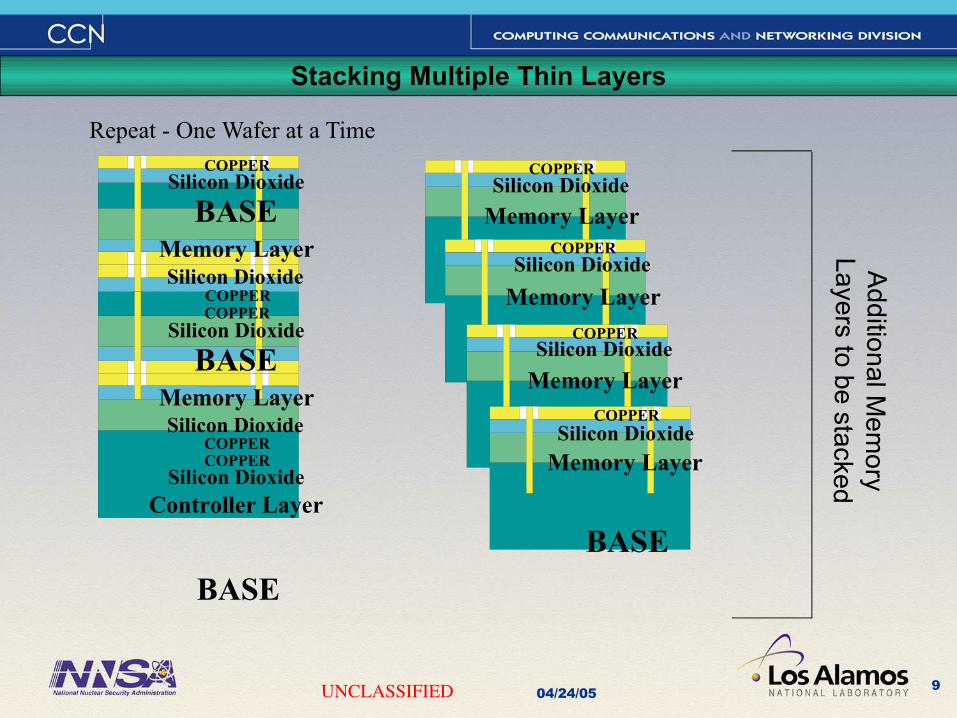
04/24/05UNCLASSIFIED 9
AdditionalM
emory
Layerstobestacked
Repeat - One Wafer at a Time
Stacking Multiple Thin Layers
BASE
Silicon Dioxide
Silicon Dioxide
COPPERCOPPER
Memory Layer
BASE
Controller Layer
Silicon Dioxide
Silicon Dioxide
COPPERCOPPER
Memory Layer
BASESilicon Dioxide
COPPER
Memory LayerSilicon Dioxide
COPPER
Memory LayerSilicon Dioxide
COPPER
Memory LayerSilicon Dioxide
COPPER
Memory Layer
BASE
Silicon DioxideCOPPER

04/24/05UNCLASSIFIED 10
Stacking Process
< Optical MicrographOptical Micrograph > < Scanning Electron MicrographScanning Electron Micrograph >
“Super Via” 4um in diameter and 12um in height
3rd Si thinned to 5.5um
2nd Si thinned to 5.5um
1st Si bottom supporting wafer
SiO2
Three wafers successfully aligned and stacked

04/24/05UNCLASSIFIED 11
Chip Stacking

04/24/05UNCLASSIFIED 12
Bufferless Crossbar Design:Implemented via Broadcast and Select Architecture
EDFAs 40 Gb/s PacketreceiversMux’s
Fast SOAColor-Selector
Gates
Fast SOAFiber-Selector
GatesStar
Couplers1x128
#0a,b
.
.
.
#63a,b
Laser-IntegratedModulators
8x1Combine
High Capacity TX:Low Latency High Power Optical Gain
High Efficiency SemiconductorOptical Amplifier Gates
High Sensitivity Cyclic RX
S: Multiple fibers (8 scaling to 40+)
: Multiple colors per fiber (8 scaling to 100+)
T: Switching time (~2 ns scaling to <0.1ns)High bit rates (40G scaling to 100G+)

04/24/05UNCLASSIFIED 13
Bufferless Optical Crossbar
Compact, Integrated
Low Optical Impairment
Scaleable in Bit Rate and Port CountAll optical data path
control
control
control
CentralScheduler
control
control
control
Datalinks
ingress nodes egress nodes
Electricallymediated
control links
Switch State
BufferlessOpticalCrossbarSwitch
5 ns/div
Switched 40GOptical Packets
Large Signal 231-1 PRSwitching Sequence
Optically SwitchedSOA@ 80GHz

04/24/05UNCLASSIFIED 14
OSMOSIS will integrate to be cost competitive with conventional OEO
Today ~$50K/port→~$1.5k/port for commercial
Modular chassisOctal switch port blade
Integration achieves200:1 Parts count reduction10X Power reduction
Provisioning in 16 port increments
TransmitterIntegration
SwitchIntegration
ReceiverIntegration
Gain+SplitIntegration
10x 4x 200x 10x
10 Terabit/sec form factor
7U
•1.28 Gigapackets/sec in 64 port switchmodule•Cell-oriented error correction supports10-21 BER•Goal: 10 Tbit/sec in a single stagemodule @ first commercial release

04/24/05UNCLASSIFIED 15
Development Switch
As of this month (Test Vehicle/Prototype)

04/24/05UNCLASSIFIED 16
InfiniBand Roadmap
Distance from CPU
0.25
1.0
MemoryBandwidth
Local I/OChannel
ClusterNetwork
PCI-Express 4XHT 1.0 or PCI-X DDR
4X InfiniBand2.0 GB/s
2002-2005
PCI-Express 32XHT 2.0
12X DDR InfiniBand12.0 GB/s
FutureProcessors 2005
2.0
6.0
12.0
24.0
PCI-Express 16XHT 2.0
12X InfiniBand6.0 GB/s
Itanium 2(6.4 GB/s) 2005
PCI-Express 2.0HT 3.0 12X QDR InfiniBand
24.0 GB/sFutureProcessors 2006
Myrinet 2K PCI-X2 x 0.25 GB/sQuadrics Elan3
0.4 GB/s
PCI-X(1.1 GB/s)
2000-2001Myrinet 2K0.25 GB/s
Opteron(5.2 GB/s)Pentium 4(3.2 GB/s)
PCI(0.5 GB/s)
Pentium III(1.0GB/s)
Bandwidth(GB/s)
Quadrics Elan40.8 – 0.9 GB/s
4X DDR/8XInfiniBand4.0 GB/s
24X QDR InfiniBand48.0 GB/s
PCI-Express 2.0/3.0HT 3.0
Adv. SwitchingFuture
Memories2007-2008

04/24/05UNCLASSIFIED 17
Conclusions
• DarkHorse pushed many design envelopes It is the I/O, NOT FLOPS 3D Memories
Self Healing 3D Stacking (S/MOC) 3D FPGA/CAM Designs Optical Interconnects
Networking (OSMOSIS) Chip-to-Chip (ZRL)
Interconnects 12X-QDR Infiniband 32X-ODR Infiniband (Future)

04/24/05UNCLASSIFIED 18
Conclusions (cont)
• 3D Memories will improve Power/Performance Non-DRAM
• Currently modeling codes against DH design Some new algorithms (Sparse) Potentially new language approaches Future HW/SW designs
• The design is feasible Most of the sub-components exist
• We have started the design of the follow-on

04/24/05UNCLASSIFIED 19
•LANLGary GriderKarl-Heinz WinklerJohn MorrisonJames PeeryKen KochRich GrahamMike Boorman
•SNLBill CampJim TompkinsMatt Leininger
•Mellanox•IBM
(ZRL,POK,TJW,ARL,STIDC)
•Corning•Many others…
Special Thanks (DH)

04/24/05UNCLASSIFIED 20
Backup (Movie)

04/24/05UNCLASSIFIED 21
Data packet bit streams/eye diagrams
40 Gb/s data packet
Closer look at bit stream
Packet 1 Packet 2
DataPost-amble
Preamble DataInter-packetgap
5 ns/div
10 ps/div
500 ps/div

04/24/05UNCLASSIFIED 22
Fast integrated optical fiber and color selector
SOA Waveguide
Fast SOAColor Select
Integrated Hybrid
InP 8x1Combiner
MonolithicSOAArray
MonolithicOptical Interface
Cost reduction:•planar integration•parts reduction•wide fabricationtolerances→ highoptical margins