Embed Size (px)
Citation preview

AG1280 - Low power and low cost CPLD Rev1.0
Page 1 of 14
DATA SHEET
Revision: 1.0
Release date: 10/10/2016
AG1280
Low power and low cost CPLD
AG1280 - Low power and low cost CPLD Rev1.0
Page 2 of 14
General Description
AG1280 family provides low cost, ultra-low power CPLDs, with density is 1280 Look-Up Tables(LUTs).
The devices feature Embedded Block Memory (EBR), Distributed RAM, and Phase Locked Loops (PLLs).
The devices are designed for ultra low power and cost while providing programmable solutions for a wide
range of applications, especially in consumer and mobile device products.
Features
Low power and low cost CPLD.
Flexible logic architecture based on LUT.
Ultra-low power, as low as 60μA standby typical Icc (1.2V Vcc).
Small footprint package for consumer and mobile application.
Provides PLL per device provide clock multiplication and phase shifting
3.3-V, 2.5-V, 1.8-V, 1.5-V LVCMOS and LVTTL standards
Flexible device configuration through JTAG interface.
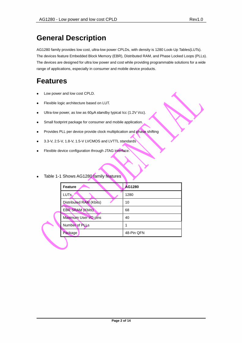
Table 1-1 Shows AG1280 family features
Feature AG1280
LUTs 1280
Distributed RAM (Kbits) 10
EBR SRAM (Kbits) 68
Maximum User I/O pins 40
Number of PLLs 1
Package 48-Pin QFN

AG1280 - Low power and low cost CPLD Rev1.0
Page 3 of 14
Content
General Description ....................................................................................................................... 2
Features ........................................................................................................................................... 2
Content ........................................................................................................................................... 3
1. AG1280 Architecture Overview ............................................................................................ 4
1.1. Functional Description ............................................................................................... 4
1.2. Logic Array Blocks ...................................................................................................... 4
1.3. Logic Element ............................................................................................................. 4
1.4. FlexTrack Interconnect .............................................................................................. 5
1.5. Global Signals ............................................................................................................. 5
1.6. Phase Locked Loops (PLLs) ..................................................................................... 6
1.7. Embedded Block RAM ............................................................................................... 7
1.8. I/O Pin .......................................................................................................................... 8
2. Device Configuration .............................................................................................................. 8
3. Power-On Reset Circuitry ..................................................................................................... 8
4. DC Electrical Characteristics ................................................................................................ 8
5. Timing Characteristics ......................................................................................................... 10
6. Pin-Outs ................................................................................................................................. 10
7. Reference and Ordering Information ................................................................................. 11
7.1. Software ..................................................................................................................... 11
7.2. Ordering Information ................................................................................................ 11
8. Recommended Reflow Profile ............................................................................................ 12
9. RoHS Compliant ................................................................................................................... 13
10. ESD Precautions .................................................................................................................. 13

AG1280 - Low power and low cost CPLD Rev1.0
Page 4 of 14
1. AG1280 Architecture Overview
1.1. Functional Description
The AG1280 devices contain an industrial state-of-the art two-dimensional row- and column-based
architecture to implement custom logic. Column and row interconnects of varies speeds provide signal
interconnects between logic blocks (LBs) and IOs.
The logic array consists of LBs, with 16 logic slices (LS) in each LB. A slice is a small unit of logic
providing efficient implementation of user logic functions. LBs are grouped into rows and columns across
the device. The AG1280 devices’ density is ranging from 640 to 1280 slices.
The device global clock network consists of up to 8 global clock lines that drive through the entire device.
The global clock network can provide clocks for all resources within the device, such as input/output
elements (IOEs), slices. The global clock lines can also be used for other high fan-out signals.
Each device I/O pin is fed by an IOE located at the ends of LB rows and columns around the periphery of
the device. I/O pins support various single-ended standards. Each IOE contains a bidirectional I/O buffer.
1.2. Logic Array Blocks
Each Logic Block consists of 16 slices, SLICE carry chains, SLICE control signals, a local interconnect, a
look-up table (LUT) chain, and register chain connection lines. There are 32 possible unique inputs into
an SLICE. Register chain connections transfer the output of one SLICE’s register to the adjacent SLICE’s
register within a block. The AG1280 software places associated logic within an SLICE or adjacent
SLICES, allowing the use of local, LUT chain, and register chain connections for performance and area
efficiency.
1.3. Logic Element
The smallest unit of logic in AG1280 architecture, the slice, is compact and provides advanced and
flexible features with efficient logic utilization. Each slice features:
Industrial standard four-input look-up table (LUT4), which is a function generator that can implement
any combinatorial logic function of four inputs.
A programmable register
A carry chain connection
A register chain connection
The ability to drive all types of interconnects: local, row, column, register chain, and inter-tile
connections
Support for efficient packing of LUT and register
Support for register feedback

AG1280 - Low power and low cost CPLD Rev1.0
Page 5 of 14
Figure 1-1 AG1280 Logic SLICE
Each slice’s register has data, clock, clock enable, and clear inputs. Signals that from global clock
network, general-purpose I/O pins, or any internal logic outputs can drive the register’s clock and clear
control signals. Either general-purpose I/O pins or internal logic can drive the clock enable. For
combinational functions, the LUT output bypasses the register and drives directly to the slice outputs
resources. The slice is architected so that LUT and register can drive to separate outputs.
1.4. FlexTrack Interconnect
In AG1280 device architecture, FlexTrack interconnect consists of continuous, performance-optimized
routing lines used for inter- and intra- design block connectivity. The FlexTrack connects to LEs, and IO
pins with row and column connection that span fixed distances.
1.5. Global Signals
Each device has eight dual-purpose dedicated clock pins. The eight global clock lines drive throughout
the entire device. The global clock network can provide clocks for all resources within the device
including LEs, local interconnect. The global lines can be used for global signals distribution.
Shift Register
Input
ClkEnable
Carry Out
>
Data
Inputs
Clk
Synchronous
Reset
Enabl
e
Q
Lut
Output
Shift Register
Output
Reset
Asynchronous
Reset
Clk
Carry In
Synchronous &
Shift Control D
LUT4 &
Carry Chain
AG1280 - Low power and low cost CPLD Rev1.0
Page 6 of 14
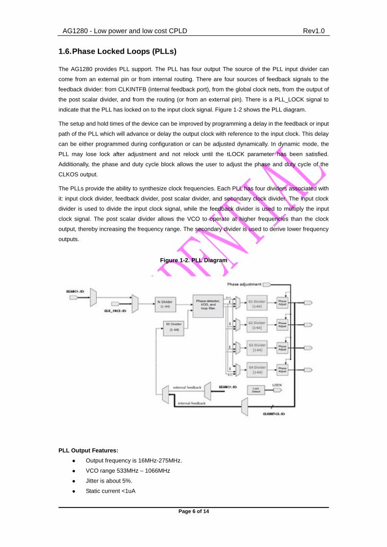
1.6. Phase Locked Loops (PLLs)
The AG1280 provides PLL support. The PLL has four output The source of the PLL input divider can
come from an external pin or from internal routing. There are four sources of feedback signals to the
feedback divider: from CLKINTFB (internal feedback port), from the global clock nets, from the output of
the post scalar divider, and from the routing (or from an external pin). There is a PLL_LOCK signal to
indicate that the PLL has locked on to the input clock signal. Figure 1-2 shows the PLL diagram.
The setup and hold times of the device can be improved by programming a delay in the feedback or input
path of the PLL which will advance or delay the output clock with reference to the input clock. This delay
can be either programmed during configuration or can be adjusted dynamically. In dynamic mode, the
PLL may lose lock after adjustment and not relock until the tLOCK parameter has been satisfied.
Additionally, the phase and duty cycle block allows the user to adjust the phase and duty cycle of the
CLKOS output.
The PLLs provide the ability to synthesize clock frequencies. Each PLL has four dividers associated with
it: input clock divider, feedback divider, post scalar divider, and secondary clock divider. The input clock
divider is used to divide the input clock signal, while the feedback divider is used to multiply the input
clock signal. The post scalar divider allows the VCO to operate at higher frequencies than the clock
output, thereby increasing the frequency range. The secondary divider is used to derive lower frequency
outputs.
Figure 1-2. PLL Diagram
PLL Output Features:
Output frequency is 16MHz-275MHz.
VCO range 533MHz – 1066MHz
Jitter is about 5%.
Static current <1uA

AG1280 - Low power and low cost CPLD Rev1.0
Page 7 of 14
Operating Temperature Range:- 25℃ ~ 125℃
Operation Voltage: 1.2V ± 5%
PLL Input Features:
10MHz-133MHz.
Power down PLL.
A reset input.
1.7. Embedded Block RAM
AG1280 contains 14 Embedded Block RAMs (EBRs). The EBR consists of a 4.5Kbit RAM, with
dedicated input and output registers. This memory can be used for a wide variety of purposes including
data buffering and FIFO. The EBR block can implement single port, dual port, simple dual port, or FIFO
memories. Each block can be used in a variety of depths and widths as shown in Table 1-1.
Memory Mode Configurations
Single Port 4096 x 1
2048 x 2
1024 x 4
512 x 9
256 x 18
128 x 36
True Dual Port 4096 x 1
2048 x 2
1024 x 4
512 x 9
256 x 18
Pseudo Dual Port 4096 x 1
2048 x 2
1024 x 4
512 x 9
256 x 18
128 x 36
FIFO 4096 x 1
2048 x 2
1024 x 4
512 x 9
256 x 18
128 x 36
If desired, the contents of the RAM can be pre-loaded during device configuration.
By preloading the RAM block during the chip configuration cycle and disabling the write controls, the
EBR block can also be utilized as a ROM.
Larger and deeper blocks of RAM can be created using EBR Blocks.

AG1280 - Low power and low cost CPLD Rev1.0
Page 8 of 14
In all the RAM modes, the input data and addresses for the ports are registered at the input of the
memory array. The output data of the memory is optionally registered at the memory array output.
The EBR memory supports three forms of write behavior for single or dual port operation:
1. Normal: Data on the output appears only during the read cycle.
2. Write Through: A copy of the input data appears at the output of the same port.
3. Read-Before-Write: When new data in being written, the old data of the address appears at the
output.
1.8. I/O Pin
I/O supported features:
Supports 3.3-V, 2.5-V, 1.8-V, and 1.5-V logic levels
Programmable drive strength, bus-hold, pull-up resistors, open-drain output
3.3-V , 2.5-V, 1.8-V, 1.5-V LVCMOS and LVTTL standards
2. Device Configuration
AG1280 device supports JTAG mode configuration. Internal Flash provides a non-volatile storage for the
configuration data.
3. Power-On Reset Circuitry
When power is applied to AG1280 devices, the POR circuit monitors VCC and begins SRAM download at
an approximate voltage of 1.2V AG1280 devices.
Entry into user mode is gated by whether VCCIO bank2 are powered with sufficient operating voltage. If VCC
and VCCIO are powered simultaneously, the device enters user mode.
For AG1280 when in user mode, the POR circuitry continues to monitor the VCC(but not VCCIO) voltage level
to detect a brown-out condition. If there is a VCC voltage sag at during user mode, the POR circuit resets
the SRAM and tri-states the I/O pins. Once VCC rises back to approximately 1.2V, the SRAM download
restarts and the device begins to operate.
4. DC Electrical Characteristics
Table 4-1 Recommended Operating Conditions
Symbol Parameter Min. Max. Units
VCC Core Supply Voltage 1.14 1.26 V
VCCPLL PLL Supply Voltage 1.14 1.26 V
VCCIO I/O Driver Supply VCCIO0,2 1.71 3.46 V

AG1280 - Low power and low cost CPLD Rev1.0
Page 9 of 14
Voltage VCC_SPI 1.71 3.46 V
Table 4-2 Recommended Operating Conditions
Symbol Parameter Typ. Units
IIL, IIH Input or I/O Leakage +/-1 μA
C1 I/O Capacitance 6 pF
C2 Global Input Buffer Capacitance 6 pF
VHYST Input Hysteresis 200 mV
IPU Internal PIO Pull-up Current -35 (VCCIO = 1.8V) μA
-49 (VCCIO = 2.5V) μA
-65 (VCCIO = 3.3V) μA
ICC Core Power Supply 50 μA
ICCPLL PLL Power Supply 1 μA
Table 4-3 Peak Startup Supply Current
Symbol Parameter Max. Units
ICCPEAK Core Power Supply 6.5 mA
ICCPLLPEAK PLL Power Supply 1.5 mA
ICCIOPEAK,
ICC_SPIPEAK
Bank Power Supply 3.4 mA
Table 4-4 IO Single-Ended DC Electrical Characteristics
Input/
Output
Standard
VIL VIH VOL
Max.
(V)
VOH
Min. (V)
IOL
Max.
(mA)
IOH Max.
(mA) Min. (V) Max.
(V)
Min. (V) Max. (V)
LVCMOS
3.3
-0.3 0.8 2.0 VCCIO
+0.2V
0.4 VCCIO
-0.5
8,16,24 -8,-16,-24
LVCMOS
2.5
-0.3 0.7 1.7 VCCIO
+0.2V
0.4 VCCIO
-0.5
6,12,18 -6,-12,-18
LVCMOS
1.8
-0.3 0.35
VCCIO
0.65
VCCIO
VCCIO
+0.2V
0.4 VCCIO
-0.4
4, 8,12 -4, -8,-12
Table 4-5 Power-On-Reset Voltage Levels
Symbol Parameter Min. Max Units
VPORUP Power-On-Reset
ramp-up trip point
(band gap based
circuit monitoring
VCC, VCCIO_2,
VCC_SPI)
VCC 0.55 0.8 V
VCCIO_2 0.9 1.1 V
VCC_SPI 0.9 1.1 V

AG1280 - Low power and low cost CPLD Rev1.0
Page 10 of 14
5. Timing Characteristics
Table 5-1 Typical Building Block Function Performance
Register-to-Register Performance
Function Timing Units
16-bit counter 250 MHz
64-bit counter 100 MHz
Table 5-2 External Switching Characteristics
Parameter Description Min. Max. Units
Global Clocks
fMAX_GBUF Frequency for Global Buffer Clock network - 300 MHz
fMAX_GBUF Frequency for Global Buffer Clock network - 200 ps
Pin-LUT-Pin Propagation Delay
tPD Best case propagation delay through one LUT-4 - 6.5 ns
General I/O Pin Parameters (Using Global Buffer Clock without PLL)
tCO Clock to Output - PIO Output Register - 6.5 ns
tSU Clock to Data Setup - PIO Input Register -0.3 - ns
tH Clock to Data Hold - PIO Input Register 1.9 - ns
Table 5-3 Maximum sysIO Buffer Performance
I/O Standard Max. Speed Units
Inputs
LVCMOS33 250 MHz
LVCMOS25 250 MHz
LVCMOS18 250 MHz
Outputs
LVCMOS33 250 MHz
LVCMOS25 250 MHz
LVCMOS18 155 MHz
6. Pin-Outs
Refer to Pin-Outs printouts for AG1280 device family.

AG1280 - Low power and low cost CPLD Rev1.0
Page 11 of 14
7. Reference and Ordering Information
7.1. Software
AG1280 Software tools support from RTL to bit stream configuration implementation and programming.
Supported operating system platforms include Microsoft Windows and Linux.
7.2. Ordering Information
Table 7-1 Device Part Number Description
AG XXXX X XX
Package Type
C = ucBGA (0.4mm Pitch)
Logic Capacity (LUTs)
1280
Pin Count 16, 36, 48, 49
W = WLCSP
Q = QFN
AG1280 - Low power and low cost CPLD Rev1.0
Page 12 of 14
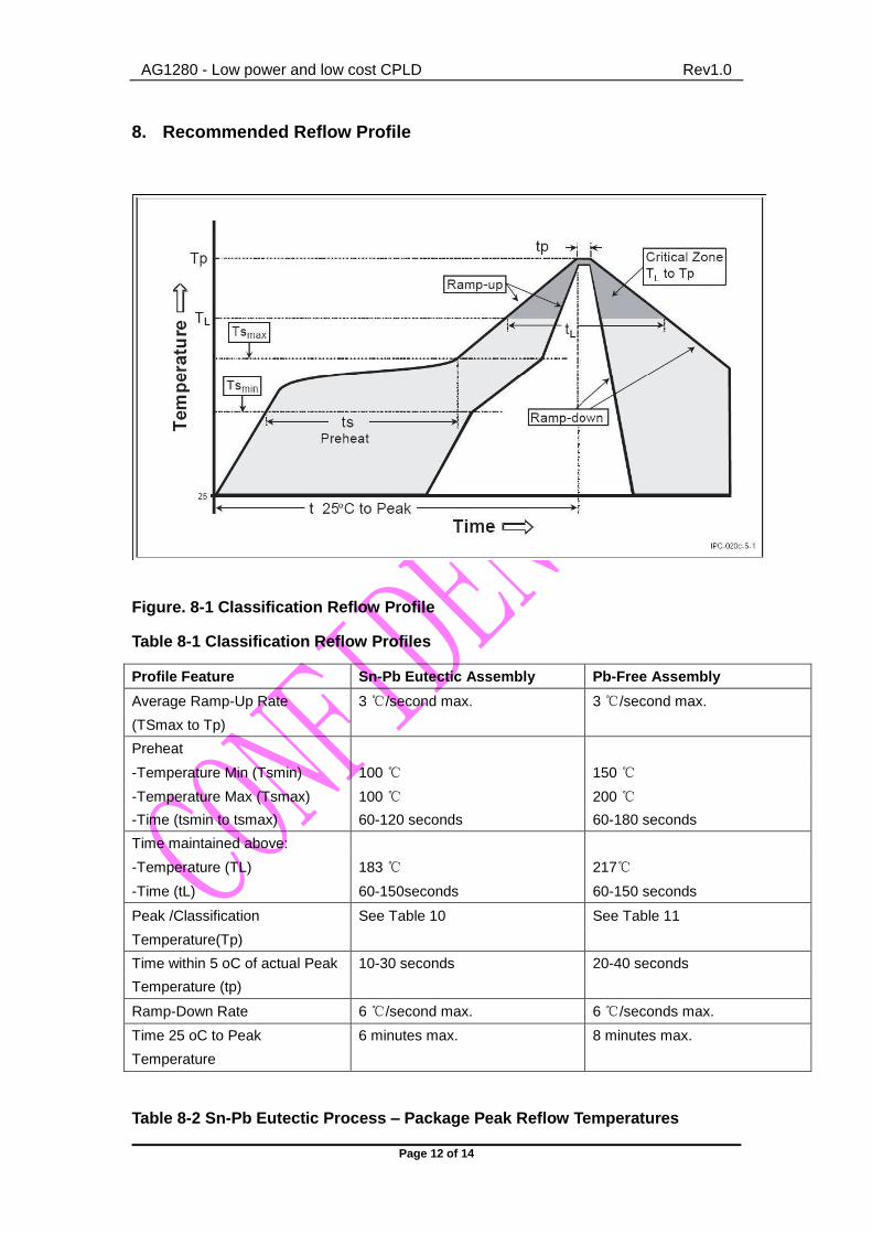
8. Recommended Reflow Profile
Figure. 8-1 Classification Reflow Profile
Table 8-1 Classification Reflow Profiles
Profile Feature Sn-Pb Eutectic Assembly Pb-Free Assembly
Average Ramp-Up Rate 3 ℃/second max. 3 ℃/second max.
(TSmax to Tp)
Preheat
-Temperature Min (Tsmin) 100 ℃ 150 ℃
-Temperature Max (Tsmax) 100 ℃ 200 ℃
-Time (tsmin to tsmax) 60-120 seconds 60-180 seconds
Time maintained above:
-Temperature (TL) 183 ℃ 217℃
-Time (tL) 60-150seconds 60-150 seconds
Peak /Classification See Table 10 See Table 11
Temperature(Tp)
Time within 5 oC of actual Peak 10-30 seconds 20-40 seconds
Temperature (tp)
Ramp-Down Rate 6 ℃/second max. 6 ℃/seconds max.
Time 25 oC to Peak 6 minutes max. 8 minutes max.
Temperature
Table 8-2 Sn-Pb Eutectic Process – Package Peak Reflow Temperatures
AG1280 - Low power and low cost CPLD Rev1.0
Page 13 of 14
Package Thickness Volume mm3 Volume mm3
<350 ≥350
<2.5mm 240 + 0/-5 ℃ 225 + 0/-5 ℃
≥2.5mm 225 + 0/-5 ℃ 225 + 0/-5 ℃
Table 8-3 Pb-free Process – Package Classification Reflow Temperatures
Package Thickness Volume mm3 <350 Volume mm3 350-2000 Volume mm3 >2000
<1.6mm 260 + 0 ℃ * 260 + 0 ℃ * 260 + 0 ℃ *
1.6mm – 2.5mm 260 + 0 ℃ * 250 + 0 ℃ * 245 + 0 ℃ *
≥2.5mm 250 + 0 ℃ * 245 + 0 ℃ * 245 + 0 ℃ *
*Tolerance : The device manufacturer/supplier shall assure process compatibility up to and including the
stated classification temperature(this mean Peak reflow temperature + 0 ℃. For example 260+ 0 ℃ ) at
the rated MSL Level.
Note 1: All temperature refer topside of the package. Measured on the package body
surface.
Note 2: The profiling tolerance is + 0 ℃, - X ℃ (based on machine variation
capability)whatever is required to control the profile process but at no time will it
exceed – 5 ℃. The producer assures process compatibility at the peak reflow profile
temperatures defined in Table 9-3.
Note 3: Package volume excludes external terminals(balls, bumps, lands, leads) and/or non
integral heat sinks.
Note 4: The maximum component temperature reached during reflow depends on package
the thickness and volume. The use of convection reflow processes reduces the
thermal gradients between packages. However, thermal gradients due to differences
in thermal mass of SMD package may sill exist.
Note 5: Components intended for use in a “lead-free” assembly process shall be evaluated
using the “lead free” classification temperatures and profiles defined in Table8-1, 8-2,
8-3 whether or not lead free.
9. RoHS Compliant
The product does not contain lead, mercury, cadmium, hexavalent chromium,
polybrominated biphenyls (PBB) or polybrominated diphenyl ethers (PBDE), and are
therefore considered RoHS compliant.
10. ESD Precautions
ESD protection circuitry is contended in this device, but special handling
precautions are required.

AG1280 - Low power and low cost CPLD Rev1.0
Page 14 of 14
11. Package Diagram(QFN 48)