Embed Size (px)
Citation preview
DATA SHEET
Product specificationFile under Integrated Circuits, IC01
July 1994
INTEGRATED CIRCUITS
TDA1552Q2 x 22 W BTL stereo car radiopower amplifier
July 1994 2
Philips Semiconductors Product specification
2 x 22 W BTL stereo car radio poweramplifier
TDA1552Q
GENERAL DESCRIPTION
The TDA1552Q is an integrated class-B output amplifier in a 13-lead single-in-line (SIL) plastic power package.The circuit contains 2 x 22 W amplifiers in Bridge Tied Load (BTL) configuration. The device is primarily developed forcar radio applications.
Features
• Requires very few external components
• High output power
• Low offset voltage at outputs
• Fixed gain
• Good ripple rejection
• Mute/stand-by switch
• Load dump protection
• AC and DC short-circuit-safe to ground and VP
• Thermally protected
• Reverse polarity safe
• Capability to handle high energy on outputs (VP = 0 V)
• Protected against electrostatic discharge
• No switch-on/switch-off plop
• Low thermal resistance
• Flexible leads.
QUICK REFERENCE DATA
PACKAGE OUTLINE
13-lead SIL-bent-to-DIL; plastic power (SOT141R); SOT 141-6; 1996 July 23.
PARAMETER CONDITIONS SYMBOL MIN. TYP. MAX. UNIT
Supply voltage range
operating VP 6.0 14.4 18.0 V
non-operating VP − − 30 V
load dump protected VP − − 45 V
Repetitive peak output
current IORM − − 4 A
Total quiescent current Itot − 80 160 mA
Stand-by current Isb − 0.1 100 µA
Switch-on current Isw − − 60 µA
Input impedance |ZI| 50 60 75 kΩJunction temperature Tj − − 150 °C
Stereo application
Output power RL = 4 Ω; THD = 10% Po 20 22 − W
Supply voltage ripple
rejection RS = 0 Ωf = 100 Hz to 10 kHz RR 48 − − dB
DC output offset voltage |∆VO| − − 150 mV
Channel separation α 40 − − dB
Channel unbalance |∆Gv| − − 1 dB
July 1994 3
Philips Semiconductors Product specification
2 x 22 W BTL stereo car radio poweramplifier
TDA1552Q
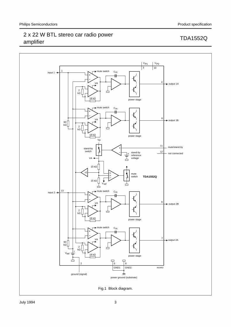
Fig.1 Block diagram.
handbook, full pagewidth
mute/stand-by
MLB952
output 1A
Vref
x1
VA
stand-byswitch
VP
muteswitch
stand-byreferencevoltage
3 10
VP1 VP2
18 kΩ
2kΩ
18 kΩ
15 kΩ
15 kΩ
2kΩ
18 kΩ
2kΩ
18 kΩ
2kΩ
60kΩ
60kΩ
mute switch
VA
Cm
power stage
mute switch
VA
Cm
power stage
4
6
11
12
mute switch
VA
Cm
power stage
mute switch
VA
Cm
power stage
9
7
Vref
2 5 8
ground (signal)
GND1 GND2
power ground (substrate)
output 2B
output 2A
not connected
output 1B
input 1
input 213
1
TDA1552Q
July 1994 4
Philips Semiconductors Product specification
2 x 22 W BTL stereo car radio poweramplifier
TDA1552Q
PINNING
FUNCTIONAL DESCRIPTION
The TDA1552Q contains two identical amplifiers with differential input stages and can be used for bridge applications.The gain of each amplifier is fixed at 26 dB. A special feature of this device is:
Mute/stand-by switch
• low stand-by current (< 100 µA)
• low mute/stand-by switching current (low cost supply switch)
• mute facility.
RATINGSLimiting values in accordance with the Absolute Maximum System (IEC 134)
1 IP1 input 1 8 GND2 power ground 2 (substrate)
2 GND ground (signal) 9 OUT2B output 2B
3 VP1 positive supply voltage 1 10 VP2 positive supply voltage 2
4 OUT1A output 1A 11 M/SS mute/stand-by switch
5 GND1 power ground 1 (substrate) 12 n.c. not connected
6 OUT1B output 1B 13 IP2 input 2
7 OUT2A output 2A
PARAMETER CONDITIONS SYMBOL MIN. MAX. UNIT
Supply voltage
operating VP − 18 V
non-operating VP − 30 V
load dump protected during 50 ms;
tr ≥ 2.5 ms VP − 45 V
Non-repetitive peak output current IOSM − 6 A
Repetitive peak output current IORM − 4 A
Storage temperature range Tstg −55 +150 °CJunction temperature Tj − 150 °CAC and DC short-circuit-safe voltage VPSC − 18 V
Energy handling capability at outputs VP = 0 V − 200 mJ
Reverse polarity VPR − 6 V
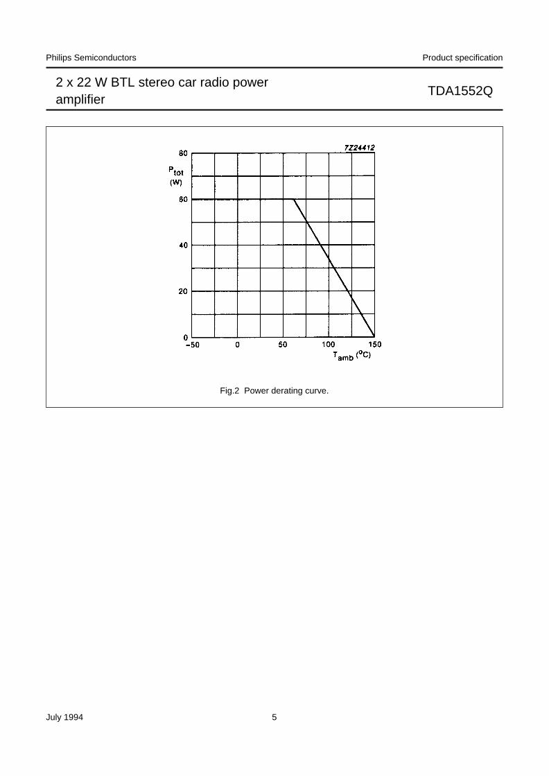
Total power dissipation see Fig.2 Ptot − 60 W
July 1994 5
Philips Semiconductors Product specification
2 x 22 W BTL stereo car radio poweramplifier
TDA1552Q
Fig.2 Power derating curve.
July 1994 6
Philips Semiconductors Product specification
2 x 22 W BTL stereo car radio poweramplifier
TDA1552Q
DC CHARACTERISTICSVP = 14.4 V; Tamb = 25 °C; measurements taken using Fig.3; unless otherwise specified
PARAMETER CONDITIONS SYMBOL MIN. TYP. MAX. UNIT
Supply
Supply voltage range note 1 VP 6.0 14.4 18.0 V
Total quiescent current Itot − 80 160 mA
DC output voltage note 2 VO − 6.9 − V
DC output offset voltage |∆VO| − − 150 mV
Mute/stand-by switch
Switch-on voltage level VON 8.5 − − V
Mute condition Vmute 3.3 − 6.4 V
Output signal in mute VI = 1 V (max);
position f = 1 kHz VO − − 2 mV
DC output offset voltage
(between pins 4 to 6 and 7 to 9) |∆VO| − − 150 mV
Stand-by condition Vsb 0 − 2 V
DC current in VII < 0.5 V Isb − − 100 µA
stand-by condition 0.5 V ≤ VII < 2 V Isb − − 500 µA
Switch-on current Isw − 25 60 µA
Supply current short-circuit
to GND
note 3 IP − 5.5 − mA
July 1994 7
Philips Semiconductors Product specification
2 x 22 W BTL stereo car radio poweramplifier
TDA1552Q
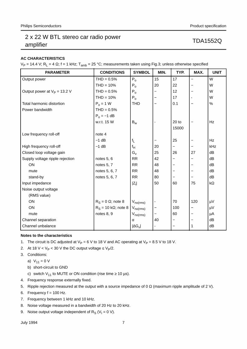
AC CHARACTERISTICSVP = 14.4 V; RL = 4 Ω; f = 1 kHz; Tamb = 25 °C; measurements taken using Fig.3; unless otherwise specified
Notes to the characteristics
1. The circuit is DC adjusted at VP = 6 V to 18 V and AC operating at VP = 8.5 V to 18 V.
2. At 18 V < VP < 30 V the DC output voltage ≤ VP/2.
3. Conditions:
a) V11 = 0 V
b) short-circuit to GND
c) switch V11 to MUTE or ON condition (rise time ≥ 10 µs).
4. Frequency response externally fixed.
5. Ripple rejection measured at the output with a source impedance of 0 Ω (maximum ripple amplitude of 2 V).
6. Frequency f = 100 Hz.
7. Frequency between 1 kHz and 10 kHz.
8. Noise voltage measured in a bandwidth of 20 Hz to 20 kHz.
9. Noise output voltage independent of RS (VI = 0 V).
PARAMETER CONDITIONS SYMBOL MIN. TYP. MAX. UNIT
Output power THD = 0.5% Po 15 17 − W
THD = 10% Po 20 22 − W
Output power at VP = 13.2 V THD = 0.5% Po − 12 − W
THD = 10% Po − 17 - W
Total harmonic distortion Po = 1 W THD − 0.1 − %
Power bandwidth THD = 0.5%
Po = −1 dB
w.r.t. 15 W Bw - 20 to − Hz
15000
Low frequency roll-off note 4
−1 dB fL − 25 − Hz
High frequency roll-off −1 dB fH 20 − − kHz
Closed loop voltage gain Gv 25 26 27 dB
Supply voltage ripple rejection notes 5, 6 RR 42 − − dB
ON notes 5, 7 RR 48 − − dB
mute notes 5, 6, 7 RR 48 − − dB
stand-by notes 5, 6, 7 RR 80 − − dB
Input impedance |Zi| 50 60 75 kΩNoise output voltage
(RMS value)
ON RS = 0 Ω; note 8 Vno(rms) - 70 120 µV
ON RS = 10 kΩ; note 8 Vno(rms) − 100 − µV
mute notes 8, 9 Vno(rms) − 60 − µA
Channel separation α 40 − − dB
Channel unbalance |∆Gv| - − 1 dB
July 1994 8
Philips Semiconductors Product specification
2 x 22 W BTL stereo car radio poweramplifier
TDA1552Q
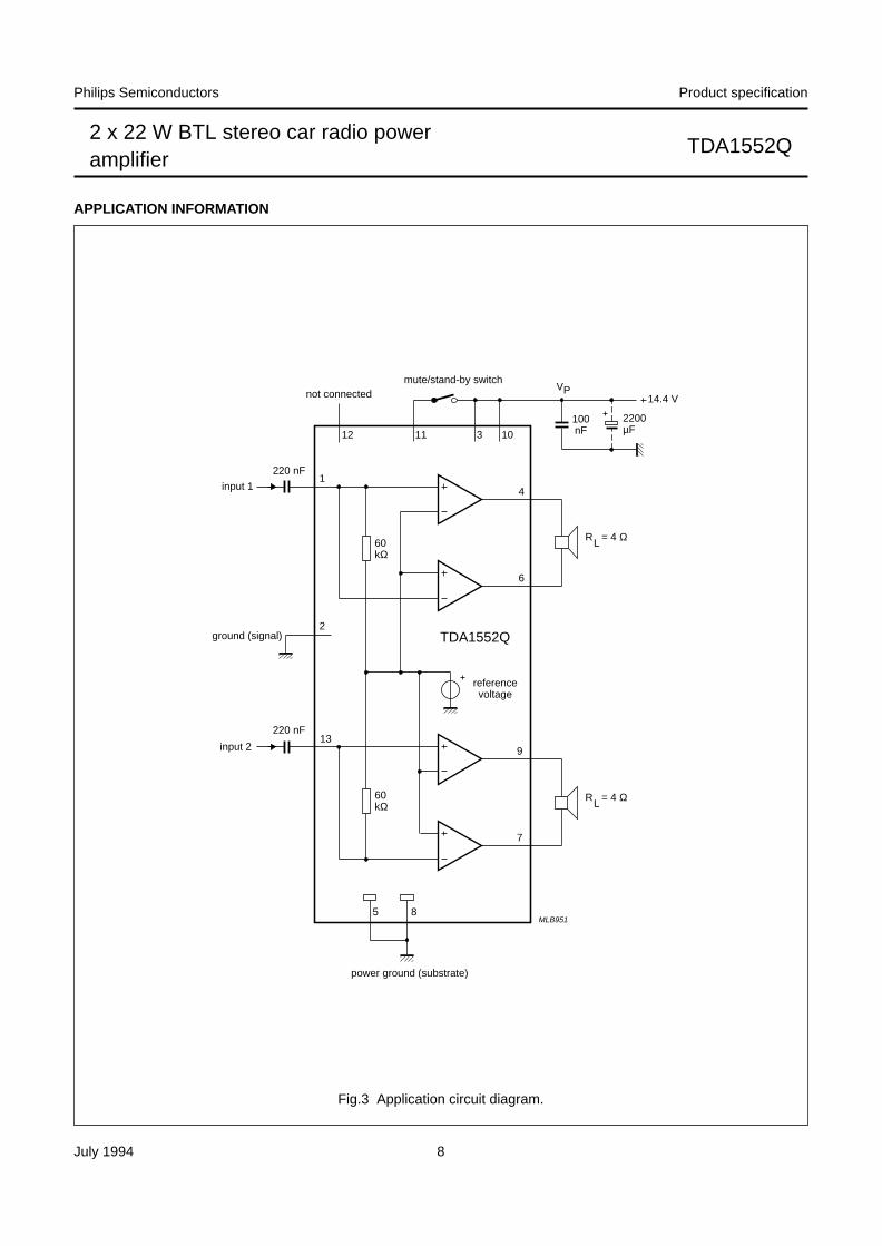
APPLICATION INFORMATION
Fig.3 Application circuit diagram.
handbook, full pagewidth
MLB951
100nF
mute/stand-by switch
12 11 3 10
220 nF1
4
6
220 nF13
9
7
5 8
VP
TDA1552Q
2200µF
14.4 Vnot connected
R = 4 Ω L
R = 4 Ω L
60kΩ
60kΩ
referencevoltage
2ground (signal)
input 2
input 1
power ground (substrate)
July 1994 9
Philips Semiconductors Product specification
2 x 22 W BTL stereo car radio poweramplifier
TDA1552Q
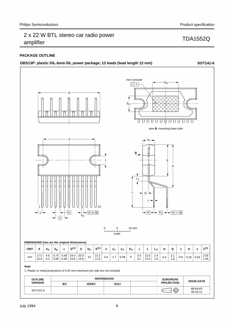
PACKAGE OUTLINE
UNIT A e 1A2 bp c D(1) E(1) Z(1)d eDh L L3 m
REFERENCESOUTLINEVERSION
EUROPEANPROJECTION ISSUE DATE
IEC JEDEC EIAJ
mm 17.015.5
4.64.2
0.750.60
0.480.38
24.023.6
20.019.6
10 3.4
v
0.812.211.8
1.7
e 2
5.08 2.41.6
Eh
6 2.001.45
2.11.8
3.43.1 4.3
DIMENSIONS (mm are the original dimensions)
Note
1. Plastic or metal protrusions of 0.25 mm maximum per side are not included.
12.411.0
SOT141-6
0 5 10 mm
scale
Qj
0.25
w
0.03
x
D
L
E
A
c
A2
m
L3
Q
w Mbp
1
d
D
Z e 2e
e
x h
1 13
j
Eh
non-concave
view B: mounting base side
92-11-1795-03-11
DBS13P: plastic DIL-bent-SIL power package; 13 leads (lead length 12 mm) SOT141-6
v M
B
July 1994 10
Philips Semiconductors Product specification
2 x 22 W BTL stereo car radio poweramplifier
TDA1552Q
SOLDERING
Introduction
There is no soldering method that is ideal for all ICpackages. Wave soldering is often preferred whenthrough-hole and surface mounted components are mixedon one printed-circuit board. However, wave soldering isnot always suitable for surface mounted ICs, or forprinted-circuits with high population densities. In thesesituations reflow soldering is often used.
This text gives a very brief insight to a complex technology.A more in-depth account of soldering ICs can be found inour “IC Package Databook” (order code 9398 652 90011).
Soldering by dipping or by wave
The maximum permissible temperature of the solder is260 °C; solder at this temperature must not be in contactwith the joint for more than 5 seconds. The total contacttime of successive solder waves must not exceed5 seconds.
The device may be mounted up to the seating plane, butthe temperature of the plastic body must not exceed thespecified maximum storage temperature (Tstg max). If theprinted-circuit board has been pre-heated, forced coolingmay be necessary immediately after soldering to keep thetemperature within the permissible limit.
Repairing soldered joints
Apply a low voltage soldering iron (less than 24 V) to thelead(s) of the package, below the seating plane or notmore than 2 mm above it. If the temperature of thesoldering iron bit is less than 300 °C it may remain incontact for up to 10 seconds. If the bit temperature isbetween 300 and 400 °C, contact may be up to 5 seconds.
DEFINITIONS
LIFE SUPPORT APPLICATIONS
These products are not designed for use in life support appliances, devices, or systems where malfunction of theseproducts can reasonably be expected to result in personal injury. Philips customers using or selling these products foruse in such applications do so at their own risk and agree to fully indemnify Philips for any damages resulting from suchimproper use or sale.
Data sheet status
Objective specification This data sheet contains target or goal specifications for product development.
Preliminary specification This data sheet contains preliminary data; supplementary data may be published later.
Product specification This data sheet contains final product specifications.
Limiting values
Limiting values given are in accordance with the Absolute Maximum Rating System (IEC 134). Stress above one ormore of the limiting values may cause permanent damage to the device. These are stress ratings only and operationof the device at these or at any other conditions above those given in the Characteristics sections of the specificationis not implied. Exposure to limiting values for extended periods may affect device reliability.
Application information
Where application information is given, it is advisory and does not form part of the specification.