Embed Size (px)
Citation preview
B
L
K
H
J
A
1
2
C
α
SCHOTTKY DIODE 0.5 Amp
MBR0520
Preliminary Data Sheet PD-20226 01/02
Major Ratings and Characteristics
IF(AV) DC 0.5 A
VRRM 20 V
IFSM @ tp= 10 ms sine 6.5 A
VF @ 0.5Apk, TJ= 100°C 0.36 V
TJ range - 65 to 150 °C
Characteristics Value Units
SOD123
This Schottky diode is ideally suited for low voltage, highfrequency operation, as freewheeling and polarity protection.Small size of the package allows proper use in applicationwhere compact size is critical, fitting also the GSM andPCMCIA requirement.
Surface mountableVery low forward voltage dropExtremely fast switchingNegligible switching lossesGuard ring for enhanced ruggedness and long termreliability
Description/ Features
1
Case Styles
Outline SOD123
Device Marking: IR520
21
SOLDERING PAD
DIM Millimeters InchesMin Max Min Max
A 0.55 0.70 0.022 0.028B 1.40 1.70 0.055 0.067C 3.55 3.85 0.140 0.152H 2.55 2.85 0.100 0.112J - 0.10 - 0.004K 0.95 1.35 0.037 0.053L - 1.35 - 0.053M - 0.15 - 0.006α 8° 8°C
4.19 mm0.165"
2.36 mm0.093"
1.22 mm0.048"
0.91 mm0.036"
MBR0520Preliminary Data Sheet PD-20226 01/02
2
Part number ValueVR Max. DC Reverse Voltage (V)
VRWM Max. Working Peak Reverse Voltage (V)20
Voltage Ratings
IF Max. Average Forward Current 0.5 A DC, TL = 129°C
IFSM Max. Peak One Cycle Non-Repetitive 55 A 5µs Sine or 3µs Rect. pulse
Surge Current, @ 25°C 6.5 A 10ms Sine or 6ms Rect. pulse
Parameters Value Units Conditions
Absolute Maximum Ratings
Following any ratedload condition andwith rated VRRM applied
TJ Max. Junction Temperature Range (*) - 65 to 150 °C
Tstg Max. Storage Temperature Range - 65 to 150 °C
RthJL Max. Thermal Resistance Junction 150 °C/W Mounted on PC board FR4 with minimum pad sizeto Lead
RthJA Max. Thermal Resistance Junction 200 °C/W 1 inch square pad size (1 x 0.5 inch for each lead) onto Ambient FR4 board
Wt Approximate Weight 0.012 g rCase Style SOD123Device Marking IR520
Thermal-Mechanical SpecificationsParameters Value Units Conditions
VFM Max. Forward Voltage Drop (1) 0.375 V @ 0.1A TJ = 25°C
0.440 V @ 0.5A
VFM Max. Forward Voltage Drop (1) 0.260 V @ 0.1A TJ = 100°C0.360 V @ 0.5A
IRM Max. Reverse Leakage (1) 40 µA TJ = 25°C VR = 10V
Current 3 mA TJ = 100°C
150 µA TJ = 25°C VR = 20V
7 mA TJ = 100°CCT Max. Junction Capacitance 110 pF VR = 5VDC (test signal range 100KHz to 1Mhz), TJ = 25°C
dv/dt Max. Voltage Rate of Change 10000 V/µs(Rated VR)
Electrical SpecificationsParameters Value Units Conditions
(1) Pulse Width < 300µs, Duty Cycle < 2%
(*)dPtot 1dTj Rth( j-a)
< thermal runaway condition for a diode on its own heatsink
MBR0520Preliminary Data Sheet PD-20226 01/02
3
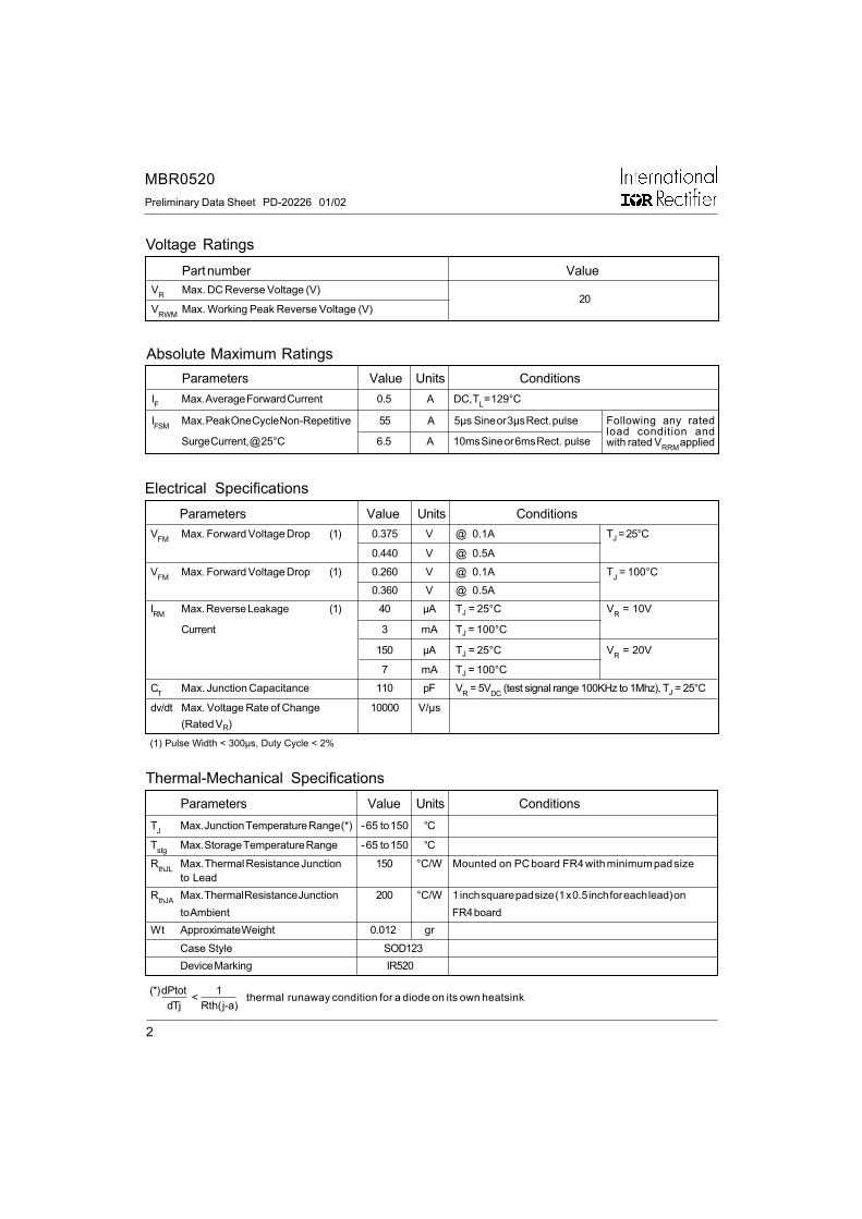
Fig. 2 - Typical Values of Reverse CurrentVs. Reverse Voltage
Fig. 3 - Typical Junction CapacitanceVs. Reverse Voltage
Fig. 1 - Maximum Forward Voltage Drop Characteristics
Inst
anta
neou
s Fo
rwar
d C
urre
nt -
I F (A
)
Forward Voltage Drop - V FM (V)
Reverse Voltage - V R (V)
Rev
erse
Cur
rent
- I R
(mA)
Reverse Voltage - V R (V)
Junc
tion C
apac
itanc
e - C
T (p
F)
0.01
0.1
1
10
0 0.1 0.2 0.3 0.4 0.5 0.6 0.7
Tj = 150˚C
Tj = 100˚C
Tj = 25˚C
10
100
1000
0 5 10 15 20 25
T = 25˚CJ
0.0001
0.001
0.01
0.1
1
10
100
0 5 10 15 20 25
125˚C
100˚C
75˚C
50˚C
25˚C
Tj = 150˚C
MBR0520Preliminary Data Sheet PD-20226 01/02
4
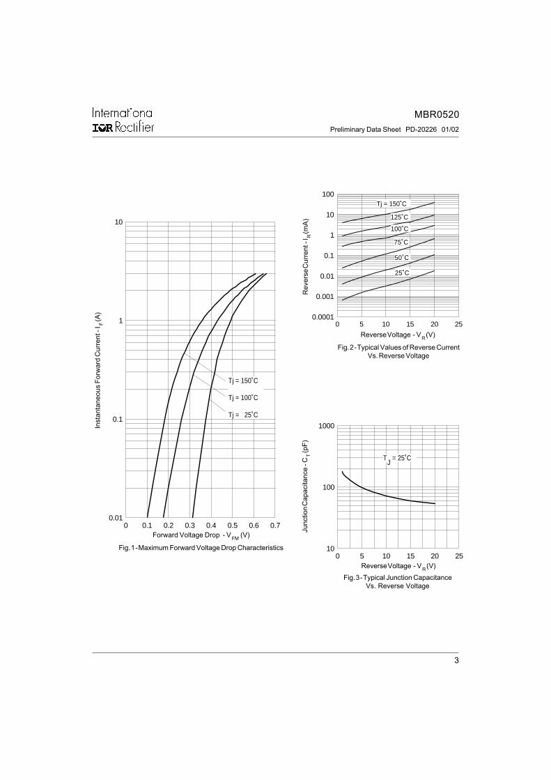
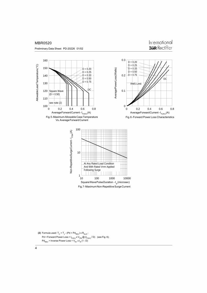
Fig. 5 - Maximum Allowable Case TemperatureVs. Average Forward Current
Fig. 6 - Forward Power Loss Characteristics
Fig. 7 - Maximum Non-Repetitive Surge Current
Allo
wab
le Le
ad T
empe
ratu
re (°
C)
Average Forward Current - I F(AV) (A) Average Forward Current - I F(AV) (A)Av
erag
e Pow
er Lo
ss (W
atts
)
Square Wave Pulse Duration - t p (microsec)
Non
-Rep
etiti
ve S
urge
Cur
rent
- I FS
M (A
)
100
110
120
130
140
150
160
0 0.2 0.4 0.6 0.8
DC
D = 0.20D = 0.25D = 0.33D = 0.50D = 0.75
Square Wave(D = 0.50)
see note (2)
1
10
100
10 100 1000 10000
At Any Rated Load ConditionAnd With Rated Vrrm AppliedFollowing Surge
0
0.1
0.2
0.3
0 0.2 0.4 0.6 0.8
DC
RMS Limit
D = 0.20D = 0.25D = 0.33D = 0.50D = 0.75
(2) Formula used: TC = TJ - (Pd + PdREV) x RthJC ;
Pd = Forward Power Loss = IF(AV) x VFM @ (IF(AV) / D) (see Fig. 6);PdREV = Inverse Power Loss = VR1 x IR (1 - D)
MBR0520Preliminary Data Sheet PD-20226 01/02
5
IR WORLD HEADQUARTERS: 233 Kansas St., El Segundo, California 90245, USA Tel: (310) 252-7105TAC Fax: (310) 252-7309
Visit us at www.irf.com for sales contact information. 01/02
Data and specifications subject to change without notice.This product has been designed for Industrial Level.
Qualification Standards can be found on IR's Web site.
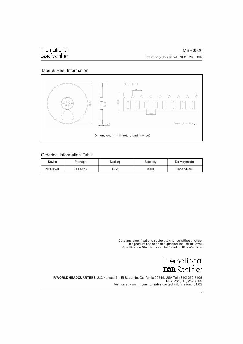
Tape & Reel Information
Dimensions in millimeters and (inches)
Ordering Information TableDevice Package Marking Base qty Delivery mode
MBR0520 SOD-123 IR520 3000 Tape & Reel

This datasheet has been download from:
www.datasheetcatalog.com
Datasheets for electronics components.