Embed Size (px)
Citation preview
2004 Microchip Technology Inc. Advance Information DS70083E
dsPIC30F Data Sheet
General Purpose and Sensor Families
High Performance
Digital Signal Controllers
Note the following details of the code protection feature on Microchip devices:
• Microchip products meet the specification contained in their particular Microchip Data Sheet.
• Microchip believes that its family of products is one of the most secure families of its kind on the market today, when used in the
intended manner and under normal conditions.
• There are dishonest and possibly illegal methods used to breach the code protection feature. All of these methods, to our
knowledge, require using the Microchip products in a manner outside the operating specifications contained in Microchip's Data
Sheets. Most likely, the person doing so is engaged in theft of intellectual property.
• Microchip is willing to work with the customer who is concerned about the integrity of their code.
• Neither Microchip nor any other semiconductor manufacturer can guarantee the security of their code. Code protection does not
mean that we are guaranteeing the product as “unbreakable.”
Code protection is constantly evolving. We at Microchip are committed to continuously improving the code protection features of our
products. Attempts to break microchip’s code protection feature may be a violation of the Digital Millennium Copyright Act. If such acts
allow unauthorized access to your software or other copyrighted work, you may have a right to sue for relief under that Act.
Information contained in this publication regarding device
applications and the like is intended through suggestion only
and may be superseded by updates. It is your responsibility to
ensure that your application meets with your specifications.
No representation or warranty is given and no liability is
assumed by Microchip Technology Incorporated with respect
to the accuracy or use of such information, or infringement of
patents or other intellectual property rights arising from such
use or otherwise. Use of Microchip’s products as critical
components in life support systems is not authorized except
with express written approval by Microchip. No licenses are
conveyed, implicitly or otherwise, under any intellectual
property rights.
DS70083E-page ii Advance Info
Trademarks
The Microchip name and logo, the Microchip logo, Accuron,
dsPIC, KEELOQ, MPLAB, PIC, PICmicro, PICSTART,
PRO MATE, PowerSmart and rfPIC are registered
trademarks of Microchip Technology Incorporated in the
U.S.A. and other countries.
AmpLab, FilterLab, microID, MXDEV, MXLAB, PICMASTER,
SEEVAL, SmartShunt and The Embedded Control Solutions
Company are registered trademarks of Microchip Technology
Incorporated in the U.S.A.
Application Maestro, dsPICDEM, dsPICDEM.net,
dsPICworks, ECAN, ECONOMONITOR, FanSense,
FlexROM, fuzzyLAB, In-Circuit Serial Programming, ICSP,
ICEPIC, Migratable Memory, MPASM, MPLIB, MPLINK,
MPSIM, PICkit, PICDEM, PICDEM.net, PICtail, PowerCal,
PowerInfo, PowerMate, PowerTool, rfLAB, Select Mode,
SmartSensor, SmartTel and Total Endurance are trademarks
of Microchip Technology Incorporated in the U.S.A. and other
countries.
Serialized Quick Turn Programming (SQTP) is a service mark
of Microchip Technology Incorporated in the U.S.A.
All other trademarks mentioned herein are property of their
respective companies.
© 2004, Microchip Technology Incorporated, Printed in the
U.S.A., All Rights Reserved.
Printed on recycled paper.
rmation 2004 Microchip Technology Inc.
Microchip received ISO/TS-16949:2002 quality system certification for its worldwide headquarters, design and wafer fabrication facilities in Chandler and Tempe, Arizona and Mountain View, California in October 2003. The Company’s quality system processes and procedures are for its PICmicro® 8-bit MCUs, KEELOQ® code hopping devices, Serial EEPROMs, microperipherals, non-volatile memory and analog products. In addition, Microchip’s quality system for the design and manufacture of development systems is ISO 9001:2000 certified.
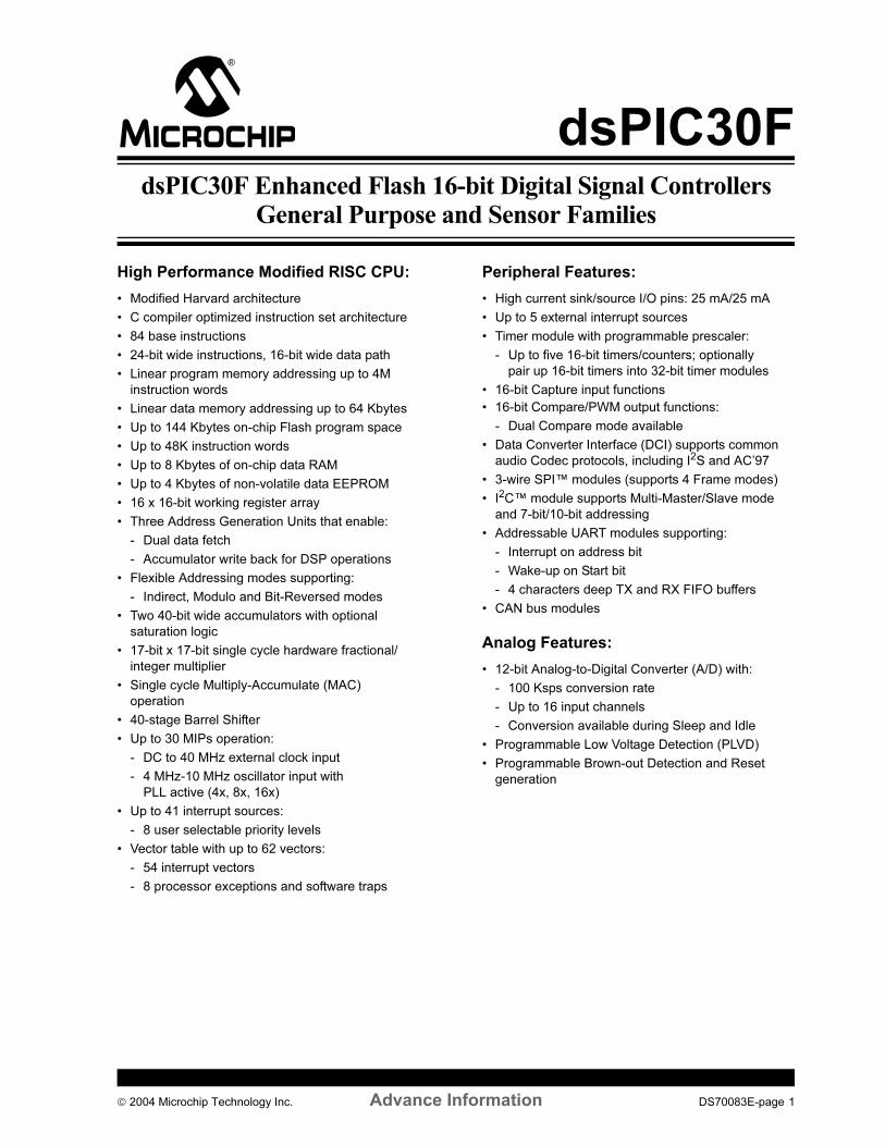
dsPIC30F
dsPIC30F Enhanced Flash 16-bit Digital Signal Controllers General Purpose and Sensor Families
High Performance Modified RISC CPU:
• Modified Harvard architecture
• C compiler optimized instruction set architecture
• 84 base instructions
• 24-bit wide instructions, 16-bit wide data path
• Linear program memory addressing up to 4M
instruction words
• Linear data memory addressing up to 64 Kbytes
• Up to 144 Kbytes on-chip Flash program space
• Up to 48K instruction words
• Up to 8 Kbytes of on-chip data RAM
• Up to 4 Kbytes of non-volatile data EEPROM
• 16 x 16-bit working register array
• Three Address Generation Units that enable:
- Dual data fetch
- Accumulator write back for DSP operations
• Flexible Addressing modes supporting:
- Indirect, Modulo and Bit-Reversed modes
• Two 40-bit wide accumulators with optional
saturation logic
• 17-bit x 17-bit single cycle hardware fractional/
integer multiplier
• Single cycle Multiply-Accumulate (MAC)
operation
• 40-stage Barrel Shifter
• Up to 30 MIPs operation:
- DC to 40 MHz external clock input
- 4 MHz-10 MHz oscillator input with
PLL active (4x, 8x, 16x)
• Up to 41 interrupt sources:
- 8 user selectable priority levels
• Vector table with up to 62 vectors:
- 54 interrupt vectors
- 8 processor exceptions and software traps
Peripheral Features:
• High current sink/source I/O pins: 25 mA/25 mA
• Up to 5 external interrupt sources
• Timer module with programmable prescaler:
- Up to five 16-bit timers/counters; optionally
pair up 16-bit timers into 32-bit timer modules
• 16-bit Capture input functions
• 16-bit Compare/PWM output functions:
- Dual Compare mode available
• Data Converter Interface (DCI) supports common
audio Codec protocols, including I2S and AC’97
• 3-wire SPI™ modules (supports 4 Frame modes)
• I2C™ module supports Multi-Master/Slave mode
and 7-bit/10-bit addressing
• Addressable UART modules supporting:
- Interrupt on address bit
- Wake-up on Start bit
- 4 characters deep TX and RX FIFO buffers
• CAN bus modules
Analog Features:
• 12-bit Analog-to-Digital Converter (A/D) with:
- 100 Ksps conversion rate
- Up to 16 input channels
- Conversion available during Sleep and Idle
• Programmable Low Voltage Detection (PLVD)
• Programmable Brown-out Detection and Reset
generation
2004 Microchip Technology Inc. Advance Information DS70083E-page 1
dsPIC30F
Special Microcontroller Features:
• Enhanced Flash program memory:
- 10,000 erase/write cycle (min.) for
industrial temperature range, 100K (typical)
• Data EEPROM memory:
- 100,000 erase/write cycle (min.) for
industrial temperature range, 1M (typical)
• Self-reprogrammable under software control
• Power-on Reset (POR), Power-up Timer (PWRT)
and Oscillator Start-up Timer (OST)
• Flexible Watchdog Timer (WDT) with on-chip low
power RC oscillator for reliable operation
• Fail-Safe Clock Monitor operation:
- Detects clock failure and switches to on-chip
low power RC oscillator
• Programmable code protection
• In-Circuit Serial Programming™ (ICSP™) via
3 pins and power/ground
• Selectable Power Management modes:
- Sleep, Idle and Alternate Clock modes
CMOS Technology:
• Low power, high speed Flash technology
• Wide operating voltage range (2.5V to 5.5V)
• Industrial and Extended temperature ranges
• Low power consumption
DS70083E-page 2 Advance Information 2004 Microchip Technology Inc.
dsPIC30F
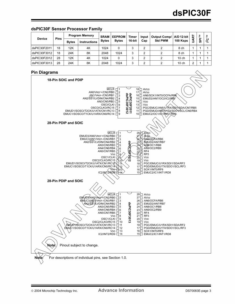
dsPIC30F Sensor Processor Family
Pin Diagrams
Note: For descriptions of individual pins, see Section 1.0.
Device PinsProgram Memory SRAM
Bytes
EEPROM
Bytes
Timer
16-bit
Input
Cap
Output Comp/
Std PWM
A/D 12-bit
100 Ksps
UART
SPI ™
I2C™
Bytes Instructions
dsPIC30F2011 18 12K 4K 1024 0 3 2 2 8 ch 1 1 1
dsPIC30F3012 18 24K 8K 2048 1024 3 2 2 8 ch 1 1 1
dsPIC30F2012 28 12K 4K 1024 0 3 2 2 10 ch 1 1 1
dsPIC30F3013 28 24K 8K 2048 1024 3 2 2 10 ch 2 1 1
ds
PIC
30
F2
011
1
2
3
4
5
6
7
8
9
18
17
16
15
14
13
12
11
10
18-Pin SOIC and PDIP
ds
PIC
30
F3
01
2
MCLR
VSS
VDD
EMUD3/AN0/VREF+/CN2/RB0
EMUC3/AN1/VREF-/CN3/RB1
AVDD
AVSS
AN2/SS1/LVDIN/CN4/RB2
IC2/INT2/RD9 EMUC2/IC1/INT1/RD8
EMUC1/SOSCO/T1CK/U1ARX/CN0/RC14
EMUD1/SOSCI/T2CK/U1ATX/CN1/RC13
VSSOSC2/CLKO/RC15
OSC1/CLKI VDD
SCK1/INT0/RF6
PGC/EMUC/U1RX/SDI1/SDA/RF2
PGD/EMUD/U1TX/SDO1/SCL/RF3
AN5/CN7/RB5
AN4/CN6/RB4
AN3/CN5/RB3
1
2
3
4
5
6
7
8
9
10
11
12
13
14
28
27
26
25
24
23
22
21
20
19
18
17
16
15
AN6/OCFA/RB6
EMUD2/AN7/RB7
AN8/OC1/RB8
AN9/OC2/RB9
RF4
RF5
28-Pin PDIP and SOIC
ds
PIC
30
F2
01
2
Note: Pinout subject to change.
1
2
3
4
5
6
7
8
9
10
11
12
13
14
28
27
26
25
24
23
22
21
20
19
18
17
16
15
28-Pin PDIP and SOIC
ds
PIC
30
F3
01
3
AVDD
AVSS
EMUC2/IC1/INT1/RD8
VSS
VDD
SCK1/INT0/RF6
PGC/EMUC/U1RX/SDI1/SDA/RF2
PGD/EMUD/U1TX/SDO1/SCL/RF3
AN6/OCFA/RB6
EMUD2/AN7/RB7
AN8/OC1/RB8
AN9/OC2/RB9
RF4
RF5
MCLR
VSS
VDD
EMUD3/AN0/VREF+/CN2/RB0
EMUC3/AN1/VREF-/CN3/RB1
AN2/SS1/LVDIN/CN4/RB2
IC2/INT2/RD9
EMUC1/SOSCO/T1CK/U1ARX/CN0/RC14
EMUD1/SOSCI/T2CK/U1ATX/CN1/RC13
OSC2/CLKO/RC15
OSC1/CLKI
AN5/CN7/RB5
AN4/CN6/RB4
AN3/CN5/RB3
AVDD
AVSS
EMUC2/OC1/IC1/INT1/RD0
VSS
VDD
PGC/EMUC/AN5/U1RX/SDI1/SDA/CN7/RB5
PGD/EMUD/AN4/U1TX/SDO1/SCL/CN6/RB4
AN6/SCK1/INT0/OCFA/RB6
EMUD2/AN7/OC2/IC2/RB7
MCLR
AN0/VREF+/CN2/RB0
AN1/VREF-/CN3/RB1
AN2/SS1/LVDIN/CN4/RB2
EMUC1/SOSCO/T1CK/U1ARX/CN0/RC14
EMUD1/SOSCI/T2CK/U1ATX/CN1/RC13
OSCO/CLKO/RC15
OSCI/CLKI
AN3/CN5/RB3
2004 Microchip Technology Inc. Advance Information DS70083E-page 3
dsPIC30F
dsPIC30F General Purpose Controller Family
Pin Diagrams
Note: For descriptions of individual pins, see Section 1.0.
Device Pins
Program MemorySRAM
Bytes
EEPROM
Bytes
Timer
16-bit
Input
Cap
Output
Comp/Std
PWM
Codec
Interface
A/D 12-bit
100 Ksps
UART
SPI ™
I2C™
CAN
Bytes Instructions
dsPIC30F3014 40/44 24K 8K 2048 1024 3 2 2 — 13 ch 2 1 1 -
dsPIC30F4013 40/44 48K 16K 2048 1024 5 4 4 AC’97, I2S 13 ch 2 1 1 1
dsPIC30F5011 64 66K 22K 4096 1024 5 8 8 AC’97, I2S 16 ch 2 2 1 2
dsPIC30F6011 64 132K 44K 6144 2048 5 8 8 — 16 ch 2 2 1 2
dsPIC30F6012 64 144K 48K 8192 4096 5 8 8 AC’97, I2S 16 ch 2 2 1 2
dsPIC30F5013 80 66K 22K 4096 1024 5 8 8 AC’97, I2S 16 ch 2 2 1 2
dsPIC30F6013 80 132K 44K 6144 2048 5 8 8 — 16 ch 2 2 1 2
dsPIC30F6014 80 144K 48K 8192 4096 5 8 8 AC’97, I2S 16 ch 2 2 1 2
PGD/EMUD/AN7/RB7
PGC/EMUC/AN6/OCFA/RB6
C1RX/RF0
C1TX/RF1
IC1/INT1/RD8
OC3/RD2
AN8/RB8
1
2
3
4
5
6
7
8
9
10
11
12
13
14
15
16
17
18
19
20
40
39
38
37
36
35
34
33
32
31
30
29
28
27
26
25
24
23
22
21
ds
PIC
30
F4
01
3
MCLR
VDD
VSS
AN0/VREF+/CN2/RB0
AN1/VREF-/CN3/RB1
AN2/SS1/LVDIN/CN4/RB2
OC4/RD3
EMUC1/SOSCO/T1CK/U1ARX/CN0/RC14
EMUD1/SOSCI/T2CK/U1ATX/CN1/RC13
OSC2/CLKO/RC15
OSC1/CLKI
AN5/IC8/CN7/RB5
AN4/IC7/CN6/RB4
AN3/CN5/RB3
AVDD
AVSS
IC2/INT2/RD9
VSS
VDD
EMUC3/SCK1/RF6
U1RX/SDI1/SDA/RF2
EMUD3/U1TX/SDO1/SCL/RF3
VSS VDD
U2RX/RF4
U2TX/RF5
AN12/COFS/RB12
AN10/CSDI/RB10
AN11/CSDO/RB11
AN9/CSCK/RB9
EMUC2/OC1/RD0
EMUD2/OC2/RD1
INT0/RA11
40-Pin PDIP
PGD/EMUD/AN7/RB7
PGC/EMUC/AN6/OCFA/RB6
RF0
RF1
IC1/INT1/RD8
RD2
AN8/RB8
1
2
3
4
5
6
7
8
9
10
11
12
13
14
15
16
17
18
19
20
40
39
38
37
36
35
34
33
32
31
30
29
28
27
26
25
24
23
22
21
ds
PIC
30
F3
01
4MCLR
VDD
VSS
AN0/VREF+/CN2/RB0
AN1/VREF-/CN3/RB1
AN2/SS1/LVDIN/CN4/RB2
RD3
EMUC1/SOSCO/T1CK/U1ARX/CN0/RC14
EMUD1/SOSCI/T2CK/U1ATX/CN1/RC13
OSC2/CLKO/RC15
OSC1/CLKI
AN5/CN7/RB5
AN4/CN6/RB4
AN3/CN5/RB3
AVDD
AVSS
IC2/INT2/RD9
VSS
VDD
EMUC3/SCK1/RF6
U1RX/SDI1/SDA/RF2
EMUD3/U1TX/SDO1/SCL/RF3
VSS VDD
U2RX/RF4
U2TX/RF5
AN12/RB12
AN10/RB10
AN11/RB11
AN9/RB9
EMUC2/OC1/RD0
EMUD2/OC2/RD1
INT0/RA11
40-Pin PDIP
Note: Pinout subject to change.
DS70083E-page 4 Advance Information 2004 Microchip Technology Inc.
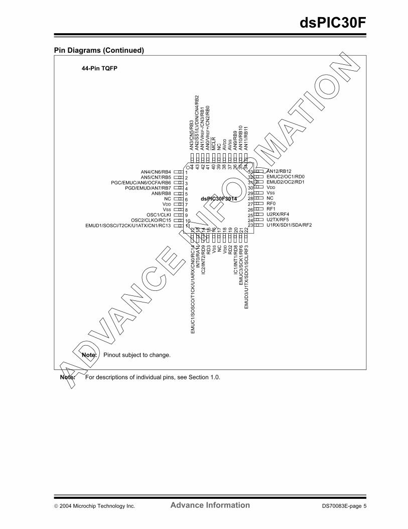
dsPIC30F
Pin Diagrams (Continued)
Note: For descriptions of individual pins, see Section 1.0.
10
11
2
3
4
5
6
1
18
19
20
21
22
12
13
14
15
38
8
7
44
43
42
41
40
39
16
17
29
30
31
32
33
23
24
25
26
27
28
36
34
35
9
37
EMUD3/U1TX/SDO1/SCL/RF3
EMUC3/SCK1/RF6
IC1/INT1/RD8
RD2
VDD
EMUC1/SOSCO/T1CK/U1ARX/CN0/RC14
NC
VSS
RD3
IC2/INT2/RD9
INT0/RA11
AN3/CN5/RB3
AN2/SS1/LVDIN/CN4/RB2
AN1/V
REF-/CN3/RB1
AN0/V
REF+/CN2/RB0
MCLR
NC
AVDD
AVSS
AN9/RB9
AN10/R
B10
AN11/RB11
AN12/RB12
EMUC2/OC1/RD0
EMUD2/OC2/RD1
VDD
VSS
NC
RF0
RF1
U2RX/RF4
U2TX/RF5
U1RX/SDI1/SDA/RF2
AN4/CN6/RB4
AN5/CN7/RB5
PGC/EMUC/AN6/OCFA/RB6
PGD/EMUD/AN7/RB7
AN8/RB8
NC
VDD
VSS
OSC1/CLKI
OSC2/CLKO/RC15
EMUD1/SOSCI/T2CK/U1ATX/CN1/RC13
dsPIC30F3014
44-Pin TQFP
Note: Pinout subject to change.
2004 Microchip Technology Inc. Advance Information DS70083E-page 5
dsPIC30F
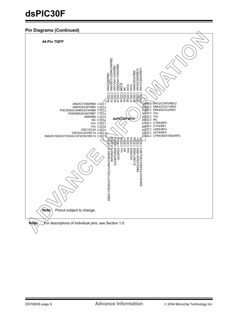
Pin Diagrams (Continued)
Note: For descriptions of individual pins, see Section 1.0.
10
11
2
3
4
5
6
1
18
19
20
21
22
12
13
14
15
38
8
7
44
43
42
41
40
39
16
17
29
30
31
32
33
23
24
25
26
27
28
36
34
35
937
EMUD3/U1TX/SDO1/SCL/RF3
EMUC3/SCK1/RF6
IC1/INT1/RD8
OC3/RD2
VDD
EMUC1/SOSCO/T1CK/U1ARX/CN0/RC14
NC
VSS
OC4/RD3
IC2/INT2/RD9
INT0/RA11
AN3/CN5/RB3
AN2/SS1/LVDIN/CN4/RB2
AN1/V
REF-/CN3/RB1
AN0/V
REF+/CN2/RB0
MCLR
NC
AVDD
AVSS
AN9/CSCK/RB9
AN10/CSDI/RB10
AN11/C
SDO/RB11
AN12/COFS/RB12
EMUC2/OC1/RD0
EMUD2/OC2/RD1
VDD
VSS
NC
C1RX/RF0
C1TX/RF1
U2RX/RF4
U2TX/RF5
U1RX/SDI1/SDA/RF2
AN4/IC7/CN6/RB4
AN5/IC8/CN7/RB5
PGC/EMUC/AN6/OCFA/RB6
PGD/EMUD/AN7/RB7
AN8/RB8
NC
VDD
VSS
OSC1/CLKI
OSC2/CLKO/RC15
EMUD1/SOSCI/T2CK/U1ATX/CN1/RC13
44-Pin TQFP
dsPIC30F4013
Note: Pinout subject to change.
DS70083E-page 6 Advance Information 2004 Microchip Technology Inc.
dsPIC30F
Pin Diagrams (Continued)
Note: For descriptions of individual pins, see Section 1.0.
1
2
3
4
5
6
7
8
9
10
11
12
13 36
35
34
3332
31
30
29
28
27
26
64
63
62
61
60
59
58
57
56
14
15
16
17
18
19
20
21
22
23
24
25
EMUC1/SOSCO/T1CK/CN0/RC14
EMUD1/SOSCI/T4CK/CN1/RC13
EMUC2/OC1/RD0
IC4/INT4/RD11
IC2/INT2/RD9
IC1/INT1/RD8
VSS
OSC2/CLKO/RC15
OSC1/CLKI
VDD
SCL/RG2
EMUC3/SCK1/INT0/RF6
U1RX/SDI1/RF2
EMUD3/U1TX/SDO1/RF3
COFS/RG15
T2CK/RC1
T3CK/RC2
SCK2/CN8/RG6
SDI2/CN9/RG7
SDO2/CN10/RG8
MCLR
VSS
VDD
AN3/CN5/RB3
AN2/SS1/LVDIN/CN4/RB2
AN1/VREF-/CN3/RB1
AN0/VREF+/CN2/RB0
OC8/CN16/RD7
CSDO/RG13
CSDI/RG12
CSCK/RG14
VSS
C2TX/RG1
C1TX/RF1
C2RX/RG0
EMUD2/O
C2/RD1
OC3/RD2
PGC/EMUC/AN6/O
CFA/RB6
PGD/EMUD/AN7/RB7
AVDD
AVSS
AN8/RB8
AN9/RB9
AN10/RB10
AN11/RB11
VSS
VDD
AN12/RB12
AN13/RB13
AN14/RB14
AN15/O
CFB/CN12/RB15
U2TX/CN18/RF5
U2RX/CN17/RF4
SDA/RG3
43
42
41
40
39
38
37
44
48
47
46
50
49
51
54
53
52
55
45
SS2/CN11/RG9
AN5/IC8/CN7/RB5
AN4/IC7/CN6/RB4
IC3/INT3/RD10
VDD
C1RX/RF0
OC4/RD3
OC7/CN15/RD6
OC6/IC6/CN14/RD5
OC5/IC5/CN13/RD4
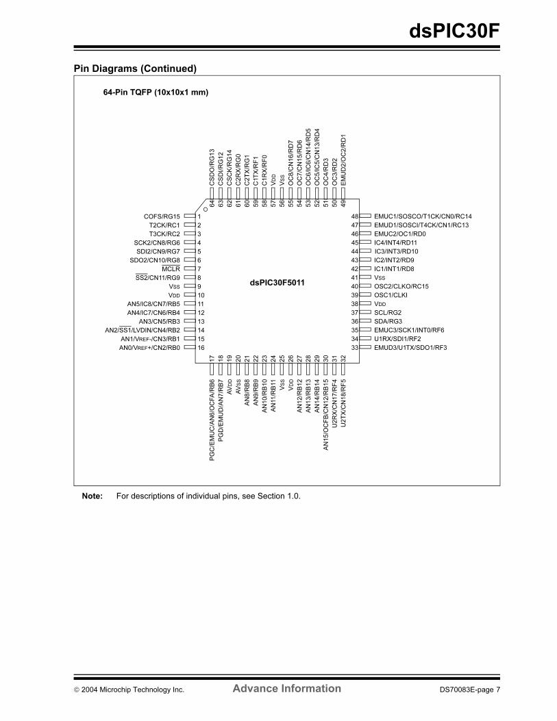
64-Pin TQFP (10x10x1 mm)
dsPIC30F5011
2004 Microchip Technology Inc. Advance Information DS70083E-page 7
dsPIC30F
Pin Diagrams (Continued)
Note: For descriptions of individual pins, see Section 1.0.
1
2
3
4
5
6
7
8
9
10
11
12
13 36
35
34
33
32
31
30
29
28
27
26
64
63
62
61
60
59
58
57
56
14
15
16
17
18
19
20
21
22
23
24
25
EMUC1/SOSCO/T1CK/CN0/RC14
EMUD1/SOSCI/T4CK/CN1/RC13
EMUC2/OC1/RD0
IC4/INT4/RD11
IC2/INT2/RD9
IC1/INT1/RD8
VSS
OSC2/CLKO/RC15
OSC1/CLKI
VDD
SCL/RG2
EMUC3/SCK1/INT0/RF6
U1RX/SDI1/RF2
EMUD3/U1TX/SDO1/RF3
RG15
T2CK/RC1
T3CK/RC2
SCK2/CN8/RG6
SDI2/CN9/RG7
SDO2/CN10/RG8
MCLR
VSS
VDD
AN3/CN5/RB3
AN2/SS1/LVDIN/CN4/RB2
PGC/EMUC/AN1/VREF-/CN3/RB1
PGD/EMUD/AN0/VREF+/CN2/RB0
OC8/CN16/RD7
RG13
RG12
RG14
VSS
C2TX/RG1
C1TX/RF1
C2RX/RG0
EMUD2/O
C2/RD1
OC3/RD2
AN6/O
CFA/RB6
AN7/RB7
AVDD
AVSS
AN8/RB8
AN9/RB9
AN10/RB10
AN11/RB11
VSS
VDD
AN12/RB12
AN13/RB13
AN14/RB14
AN15/O
CFB/CN12/RB15
U2TX/CN18/RF5
U2RX/CN17/RF4
SDA/RG3
43
42
41
40
39
38
37
44
48
47
46
50
49
51
54
53
52
55
45
SS2/CN11/RG9
AN5/IC8/CN7/RB5
AN4/IC7/CN6/RB4
IC3/INT3/RD10
VDD
C1RX/RF0
OC4/RD3
OC7/CN15/RD6
OC6/IC6/CN14/RD5
OC5/IC5/CN13/RD4
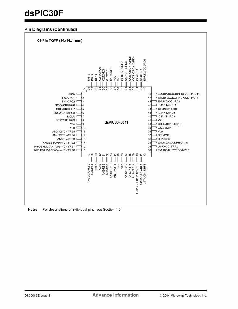
64-Pin TQFP (14x14x1 mm)
dsPIC30F6011
DS70083E-page 8 Advance Information 2004 Microchip Technology Inc.
dsPIC30F
Pin Diagrams (Continued)
Note: For descriptions of individual pins, see Section 1.0.
1
2
3
4
5
6
7
8
9
10
11
12
13 36
35
34
3332
31
30
29
28
27
26
64
63
62
61
60
59
58
57
56
14
15
16
17
18
19
20
21
22
23
24
25
EMUC1/SOSCO/T1CK/CN0/RC14
EMUD1/SOSCI/T4CK/CN1/RC13
EMUC2/OC1/RD0
IC4/INT4/RD11
IC2/INT2/RD9
IC1/INT1/RD8
VSS
OSC2/CLKO/RC15
OSC1/CLKI
VDD
SCL/RG2
EMUC3/SCK1/INT0/RF6
U1RX/SDI1/RF2
EMUD3/U1TX/SDO1/RF3
COFS/RG15
T2CK/RC1
T3CK/RC2
SCK2/CN8/RG6
SDI2/CN9/RG7
SDO2/CN10/RG8
MCLR
VSS
VDD
AN3/CN5/RB3
AN2/SS1/LVDIN/CN4/RB2
PGC/EMUC/AN1/VREF-/CN3/RB1
PGD/EMUD/AN0/VREF+/CN2/RB0
OC8/CN16/RD7
CSDO/RG13
CSDI/RG12
CSCK/RG14
VSS
C2TX/RG1
C1TX/RF1
C2RX/RG0
EMUD2/O
C2/RD1
OC3/RD2
AN6/O
CFA/RB6
AN7/RB7
AVDD
AVSS
AN8/RB8
AN9/RB9
AN10/RB10
AN11/RB11
VSS
VDD
AN12/RB12
AN13/RB13
AN14/RB14
AN15/O
CFB/CN12/RB15
U2TX/CN18/RF5
U2RX/CN17/RF4
SDA/RG3
43
42
41
40
39
38
37
44
48
47
46
50
49
51
54
53
52
55
45
SS2/CN11/RG9
AN5/IC8/CN7/RB5
AN4/IC7/CN6/RB4
IC3/INT3/RD10
VDD
C1RX/RF0
OC4/RD3
OC7/CN15/RD6
OC6/IC6/CN14/RD5
OC5/IC5/CN13/RD4
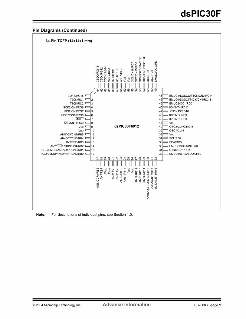
64-Pin TQFP (14x14x1 mm)
dsPIC30F6012
2004 Microchip Technology Inc. Advance Information DS70083E-page 9

dsPIC30F
Pin Diagrams (Continued)
Note: For descriptions of individual pins, see Section 1.0.
72
74
73
71
70
69
68
67
66
65
64
63
62
61
20
2
3
4
5
6
7
8
9
10
11
12
13
14
15
16
50
49
48
47
46
45
44
21
41
40
39
38
37
36
35
34
23
24
25
26
27
28
29
30
31
32
33
dsPIC30F5013
17
18
19
75
1
57
56
55
54
53
52
51
60
59
58
43
42
76
78
77
79
22
80
IC5/RD12
OC4/RD3
OC3/RD2
EMUD2/O
C2/RD1
CSCK/RG14
RA7/CN23
RA6/CN22
C2RX/RG0
C2TX/R
G1
C1TX/R
F1
C1RX/RF0
CSDO/RG13
CSDI/RG12
OC8/CN16/RD7
OC6/CN14/RD5
EMUC2/OC1/RD0
IC4/RD11
IC2/RD9
IC1/RD8
INT4/RA15
IC3/RD10
INT3/RA14
VSS
OSC1/CLKI
VDD
SCL/RG2
U1RX/RF2
U1TX/RF3
EMUC1/SOSCO/T1CK/CN0/RC14
EMUD1/SOSCI/CN1/RC13
VREF+/RA10
VREF-/RA9
AVDD
AVSS
AN8/RB8
AN9/RB9
AN10/RB10
AN11/RB11
VDD
U2RX/CN17/RF4
IC8/CN21/RD15
U2TX/CN18/RF5
AN6/O
CFA/RB6
AN7/RB7
T3CK/RC2
T4CK/RC3
T5CK/RC4
SCK2/CN8/RG6
SDI2/CN9/RG7
SDO2/CN10/RG8
MCLR
SS2/CN11/RG9
AN4/CN6/RB4
AN3/CN5/RB3
AN2/SS1/LVDIN/CN4/RB2
PGC/EMUC/AN1/CN3/RB1
PGD/EMUD/AN0/CN2/RB0
VSS
VDD
COFS/RG15
T2CK/RC1
INT2/RA13
INT1/RA12
AN12/RB12
AN13/RB13
AN14/RB14
AN15/O
CFB/CN12/RB15
VDD
VSS
OC5/CN13/RD4
IC6/CN19/RD13
SDA/RG3
SDI1/RF7
EMUD3/SDO1/RF8
AN5/CN7/RB5
VSS
OSC2/CLKO/RC15
OC7/CN15/RD6
EMUC3/SCK1/INT0/RF6
IC7/CN20/RD14
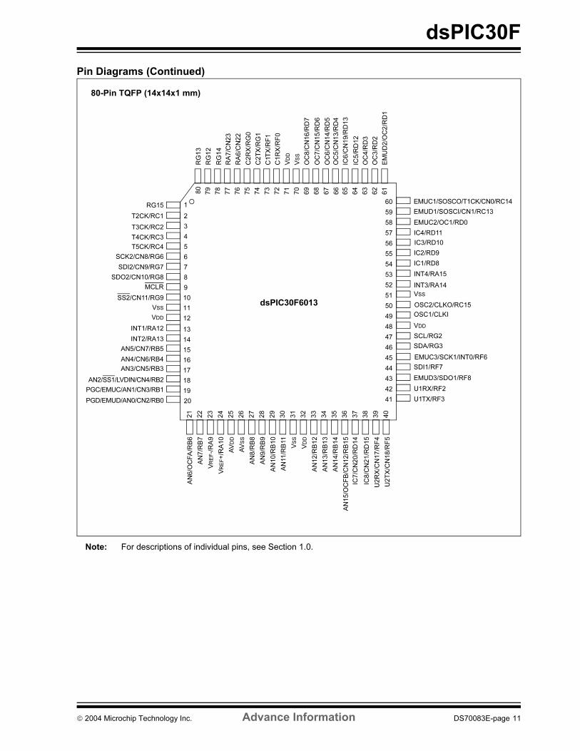
80-Pin TQFP (12x12x1 mm)
DS70083E-page 10 Advance Information 2004 Microchip Technology Inc.
dsPIC30F
Pin Diagrams (Continued)
Note: For descriptions of individual pins, see Section 1.0.
72
74
73
71
70
69
68
67
66
65
64
63
62
61
20
2
3
4
5
6
7
8
9
10
11
12
13
14
15
16
50
49
48
47
46
45
44
21
41
40
39
38
37
36
35
34
23
24
25
26
27
28
29
30
31
32
33
17
18
19
75
1
57
56
55
54
53
52
51
60
59
58
43
42
76
78
77
79
22
80
IC5/RD12
OC4/RD3
OC3/RD2
EMUD2/O
C2/RD1
RG14
RA7/CN23
RA6/CN22
C2RX/RG0
C2TX/RG1
C1TX/R
F1
C1RX/RF0
RG13
RG12
OC8/CN16/RD7
OC6/CN14/RD5
EMUC2/OC1/RD0
IC4/RD11
IC2/RD9
IC1/RD8
INT4/RA15
IC3/RD10
INT3/RA14
VSS
OSC1/CLKI
VDD
SCL/RG2
U1RX/RF2
U1TX/RF3
EMUC1/SOSCO/T1CK/CN0/RC14
EMUD1/SOSCI/CN1/RC13
VREF+/RA10
VREF-/RA9
AVDD
AVSS
AN8/RB8
AN9/RB9
AN10/RB10
AN11/RB11
VDD
U2RX/CN17/RF4
IC8/CN21/RD15
U2TX/CN18/RF5
AN6/O
CFA/RB6
AN7/RB7
T3CK/RC2
T4CK/RC3
T5CK/RC4
SCK2/CN8/RG6
SDI2/CN9/RG7
SDO2/CN10/RG8
MCLR
SS2/CN11/RG9
AN4/CN6/RB4
AN3/CN5/RB3
AN2/SS1/LVDIN/CN4/RB2
PGC/EMUC/AN1/CN3/RB1
PGD/EMUD/AN0/CN2/RB0
VSS
VDD
RG15
T2CK/RC1
INT2/RA13
INT1/RA12
AN12/RB12
AN13/RB13
AN14/RB14
AN15/O
CFB/CN12/RB15
VDD
VSS
OC5/CN13/RD4
IC6/CN19/RD13
SDA/RG3
SDI1/RF7
EMUD3/SDO1/RF8
AN5/CN7/RB5
VSS
OSC2/CLKO/RC15
OC7/CN15/RD6
EMUC3/SCK1/INT0/RF6IC7/CN20/RD14
80-Pin TQFP (14x14x1 mm)
dsPIC30F6013
2004 Microchip Technology Inc. Advance Information DS70083E-page 11
dsPIC30F
Pin Diagrams (Continued)
Note: For descriptions of individual pins, see Section 1.0.
72
74
73
71
70
69
68
67
66
65
64
63
62
61
20
2
3
4
5
6
7
8
9
10
11
12
13
14
15
16
50
49
48
47
46
45
44
21
41
40
39
38
37
36
35
34
23
24
25
26
27
28
29
30
31
32
33
17
18
19
75
1
57
56
55
54
53
52
51
60
59
58
43
42
76
78
77
79
22
80
IC5/RD12
OC4/RD3
OC3/RD2
EMUD2/O
C2/RD1
CSCK/RG14
RA7/CN23
RA6/CN22
C2RX/RG0
C2TX/R
G1
C1TX/R
F1
C1RX/RF0
CSDO/RG13
CSDI/RG12
OC8/CN16/RD7
OC6/CN14/RD5
EMUC2/OC1/RD0
IC4/RD11
IC2/RD9
IC1/RD8
INT4/RA15
IC3/RD10
INT3/RA14
VSS
OSC1/CLKI
VDD
SCL/RG2
U1RX/RF2
U1TX/RF3
EMUC1/SOSCO/T1CK/CN0/RC14
EMUD1/SOSCI/CN1/RC13
VREF+/RA10
VREF-/RA9
AVDD
AVSS
AN8/RB8
AN9/RB9
AN10/RB10
AN11/RB11
VDD
U2RX/CN17/RF4
IC8/CN21/RD15
U2TX/CN18/RF5
AN6/O
CFA/RB6
AN7/RB7
T3CK/RC2
T4CK/RC3
T5CK/RC4
SCK2/CN8/RG6
SDI2/CN9/RG7
SDO2/CN10/RG8
MCLR
SS2/CN11/RG9
AN4/CN6/RB4
AN3/CN5/RB3
AN2/SS1/LVDIN/CN4/RB2
PGC/EMUC/AN1/CN3/RB1
PGD/EMUD/AN0/CN2/RB0
VSS
VDD
COFS/RG15
T2CK/RC1
INT2/RA13
INT1/RA12
AN12/RB12
AN13/RB13
AN14/RB14
AN15/O
CFB/CN12/RB15
VDD
VSS
OC5/CN13/RD4
IC6/CN19/RD13
SDA/RG3
SDI1/RF7
EMUD3/SDO1/RF8
AN5/CN7/RB5
VSS
OSC2/CLKO/RC15
OC7/CN15/RD6
EMUC3/SCK1/INT0/RF6
IC7/CN20/RD14
80-Pin TQFP (14x14x1 mm)
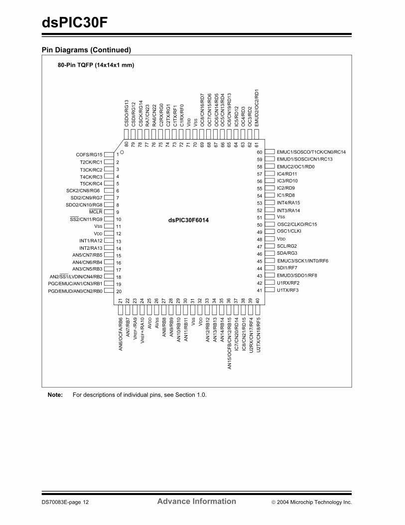
dsPIC30F6014
DS70083E-page 12 Advance Information 2004 Microchip Technology Inc.
dsPIC30F
Table of Contents
1.0 Device Overview ........................................................................................................................................................................ 15
2.0 CPU Architecture Overview........................................................................................................................................................ 19
3.0 Memory Organization ................................................................................................................................................................. 33
4.0 Address Generator Units............................................................................................................................................................ 45
5.0 Interrupts .................................................................................................................................................................................... 53
6.0 Flash Program Memory.............................................................................................................................................................. 61
7.0 Data EEPROM Memory ............................................................................................................................................................. 67
8.0 I/O Ports ..................................................................................................................................................................................... 73
9.0 Timer1 Module ........................................................................................................................................................................... 79
10.0 Timer2/3 Module ........................................................................................................................................................................ 83
11.0 Timer4/5 Module ........................................................................................................................................................................ 89
12.0 Input Capture Module................................................................................................................................................................. 93
13.0 Output Compare Module ............................................................................................................................................................ 97
14.0 SPI Module............................................................................................................................................................................... 101
15.0 I2C Module ............................................................................................................................................................................... 105
16.0 Universal Asynchronous Receiver Transmitter (UART) Module .............................................................................................. 113
17.0 CAN Module ............................................................................................................................................................................. 121
18.0 Data Converter Interface (DCI) Module.................................................................................................................................... 133
19.0 12-bit Analog-to-Digital Converter (A/D) Module...................................................................................................................... 143
20.0 System Integration ................................................................................................................................................................... 151
21.0 Instruction Set Summary .......................................................................................................................................................... 167
22.0 Development Support............................................................................................................................................................... 175
23.0 Electrical Characteristics .......................................................................................................................................................... 181
24.0 Packaging Information.............................................................................................................................................................. 223
Index .................................................................................................................................................................................................. 237
On-Line Support................................................................................................................................................................................. 243
Systems Information and Upgrade Hot Line ...................................................................................................................................... 243
Reader Response .............................................................................................................................................................................. 244
Product Identification System ............................................................................................................................................................ 245
TO OUR VALUED CUSTOMERS
It is our intention to provide our valued customers with the best documentation possible to ensure successful use of your Microchip
products. To this end, we will continue to improve our publications to better suit your needs. Our publications will be refined and
enhanced as new volumes and updates are introduced.
If you have any questions or comments regarding this publication, please contact the Marketing Communications Department via
E-mail at [email protected] or fax the Reader Response Form in the back of this data sheet to (480) 792-4150.
We welcome your feedback.
Most Current Data Sheet
To obtain the most up-to-date version of this data sheet, please register at our Worldwide Web site at:
http://www.microchip.com
You can determine the version of a data sheet by examining its literature number found on the bottom outside corner of any page.The last character of the literature number is the version number, (e.g., DS30000A is version A of document DS30000).
Errata
An errata sheet, describing minor operational differences from the data sheet and recommended workarounds, may exist for currentdevices. As device/documentation issues become known to us, we will publish an errata sheet. The errata will specify the revisionof silicon and revision of document to which it applies.
To determine if an errata sheet exists for a particular device, please check with one of the following:
• Microchip’s Worldwide Web site; http://www.microchip.com
• Your local Microchip sales office (see last page)
• The Microchip Corporate Literature Center; U.S. FAX: (480) 792-7277
When contacting a sales office or the literature center, please specify which device, revision of silicon and data sheet (includeliterature number) you are using.
Customer Notification System
Register on our web site at www.microchip.com/cn to receive the most current information on all of our products.
2004 Microchip Technology Inc. Advance Information DS70083E-page 13

dsPIC30F
NOTES:
DS70083E-page 14 Advance Information 2004 Microchip Technology Inc.
dsPIC30F
1.0 DEVICE OVERVIEW
This document contains device family specific
information for the dsPIC30F family of Digital Signal
Controller (DSC) devices. The dsPIC30F devices
contain extensive Digital Signal Processor (DSP)
functionality within a high performance 16-bit
microcontroller (MCU) architecture.
Figure 1-1 shows a sample device block diagram.
Note: The device(s) depicted in this block
diagram are representative of the
corresponding device family. Other
devices of the same family may vary in
terms of number of pins and multiplexing
of pin functions. Typically, smaller devices
in the family contain a subset of the
peripherals present in the device(s) shown
in this diagram.
2004 Microchip Technology Inc. Advance Information DS70083E-page 15
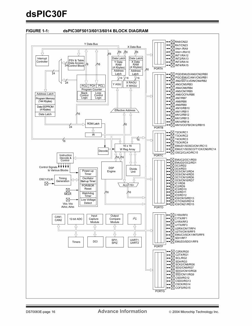
dsPIC30F
FIGURE 1-1: dsPIC30F5013/6013/6014 BLOCK DIAGRAM
AN8/RB8
AN9/RB9
AN10/RB10
AN11/RB11
Power-upTimer
OscillatorStart-up Timer
POR/BORReset
WatchdogTimer
InstructionDecode &Control
OSC1/CLKI
MCLR
VDD, VSS
AN4/CN6/RB4
AN12/RB12
AN13/RB13
AN14/RB14
AN15/OCFB/CN12/RB15
Low Voltage
Detect
UART1,
INT4/RA15
INT3/RA14
VREF+/RA10
VREF-/RA9
CAN2
TimingGeneration
CAN1,
AN5/CN7/RB5
16
PCH PCL
16
Program Counter
ALU<16>
16
24
24
24
24
X Data Bus
IR
I2C
DCI
AN6/OCFA/RB6
AN7/RB7
PCU
12-bit ADC
Timers
SCK2/CN8/RG6SDI2/CN9/RG7
SDO2/CN10/RG8
SS2/CN11/RG9
U2TX/CN18/RF5EMUC3/SCK1/INT0/RF6
SDI1/RF7
EMUD3/SDO1/RF8
Input Capture Module
OutputCompareModule
EMUC1/SOSCO/T1CK/CN0/RC14
EMUD1/SOSCI/CN1/RC13
T4CK/RC3
T2CK/RC1
PORTB
C1RX/RF0
C1TX/RF1
U1RX/RF2
U1TX/RF3
C2RX/RG0C2TX/RG1
SCL/RG2
SDA/RG3
PORTG
PORTD
16
16 16
16 x 16
W Reg Array
Divide Unit Engine
DSP
Decode
ROM Latch
16
Y Data Bus
Effective Address
X RAGU
X WAGU Y AGU
PGD/EMUD/AN0/CN2/RB0
PGC/EMUC/AN1/CN3/RB1
AN2/SS1/LVDIN/CN4/RB2
AN3/CN5/RB3
OSC2/CLKO/RC15
U2RX/CN17/RF4
AVDD, AVSS
UART2SPI2
16
16
16
16
16 PORTA
PORTC
PORTF
16
16
16
16
8
InterruptController PSV & Table
Data AccessControl Block
StackControl Logic
LoopControlLogic
Data LatchData Latch
Y Data
(4 Kbytes)RAM
X Data
(4 Kbytes)RAM
AddressLatch
AddressLatch
Control Signals to Various Blocks
EMUC2/OC1/RD0EMUD2/OC2/RD1OC3/RD2OC4/RD3OC5/CN13/RD4OC6/CN14/RD5OC7/CN15/RD6OC8/CN16/RD7IC1/RD8IC2/RD9IC3/RD10IC4/RD11IC5/RD12IC6/CN19/RD13IC7/CN20/RD14IC8/CN21/RD15
16
CSDI/RG12CSDO/RG13
CSCK/RG14
COFS/RG15
T3CK/RC2
SPI1,
INT1/RA12INT2/RA13
RA7/CN23
RA6/CN22
T5CK/RC4
Address Latch
Program Memory(144 Kbytes)
Data Latch
Data EEPROM(4 Kbytes)
DS70083E-page 16 Advance Information 2004 Microchip Technology Inc.
dsPIC30F
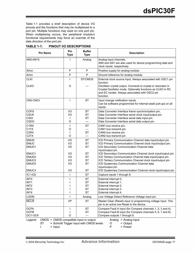
Table 1-1 provides a brief description of device I/O
pinouts and the functions that may be multiplexed to a
port pin. Multiple functions may exist on one port pin.
When multiplexing occurs, the peripheral module’s
functional requirements may force an override of the
data direction of the port pin.
TABLE 1-1: PINOUT I/O DESCRIPTIONS
Pin NamePin
Type
Buffer
TypeDescription
AN0-AN15 I Analog Analog input channels.
AN0 and AN1 are also used for device programming data and
clock inputs, respectively.
AVDD P P Positive supply for analog module.
AVSS P P Ground reference for analog module.
CLKI
CLKO
I
O
ST/CMOS
—
External clock source input. Always associated with OSC1 pin
function.
Oscillator crystal output. Connects to crystal or resonator in
Crystal Oscillator mode. Optionally functions as CLKO in RC
and EC modes. Always associated with OSC2 pin
function.
CN0-CN23 I ST Input change notification inputs.
Can be software programmed for internal weak pull-ups on all
inputs.
COFS
CSCK
CSDI
CSDO
I/O
I/O
I
O
ST
ST
ST
—
Data Converter Interface frame synchronization pin.
Data Converter Interface serial clock input/output pin.
Data Converter Interface serial data input pin.
Data Converter Interface serial data output pin.
C1RX
C1TX
C2RX
C2TX
I
O
I
O
ST
—
ST
—
CAN1 bus receive pin.
CAN1 bus transmit pin.
CAN2 bus receive pin.
CAN2 bus transmit pin
EMUD
EMUC
EMUD1
EMUC1
EMUD2
EMUC2
EMUD3
EMUC3
I/O
I/O
I/O
I/O
I/O
I/O
I/O
I/O
ST
ST
ST
ST
ST
ST
ST
ST
ICD Primary Communication Channel data input/output pin.
ICD Primary Communication Channel clock input/output pin.
ICD Secondary Communication Channel data
input/output pin.
ICD Secondary Communication Channel clock input/output pin.
ICD Tertiary Communication Channel data input/output pin.
ICD Tertiary Communication Channel clock input/output pin.
ICD Quaternary Communication Channel data
input/output pin.
ICD Quaternary Communication Channel clock input/output pin.
IC1-IC8 I ST Capture inputs 1 through 8.
INT0
INT1
INT2
INT3
INT4
I
I
I
I
I
ST
ST
ST
ST
ST
External interrupt 0.
External interrupt 1.
External interrupt 2.
External interrupt 3.
External interrupt 4.
LVDIN I Analog Low Voltage Detect Reference Voltage input pin.
MCLR I/P ST Master Clear (Reset) input or programming voltage input. This
pin is an active low Reset to the device.
OCFA
OCFB
OC1-OC8
I
I
O
ST
ST
—
Compare Fault A input (for Compare channels 1, 2, 3 and 4).
Compare Fault B input (for Compare channels 5, 6, 7 and 8).
Compare outputs 1 through 8.
Legend: CMOS = CMOS compatible input or output Analog = Analog input
ST = Schmitt Trigger input with CMOS levels O = Output
I = Input P = Power
2004 Microchip Technology Inc. Advance Information DS70083E-page 17
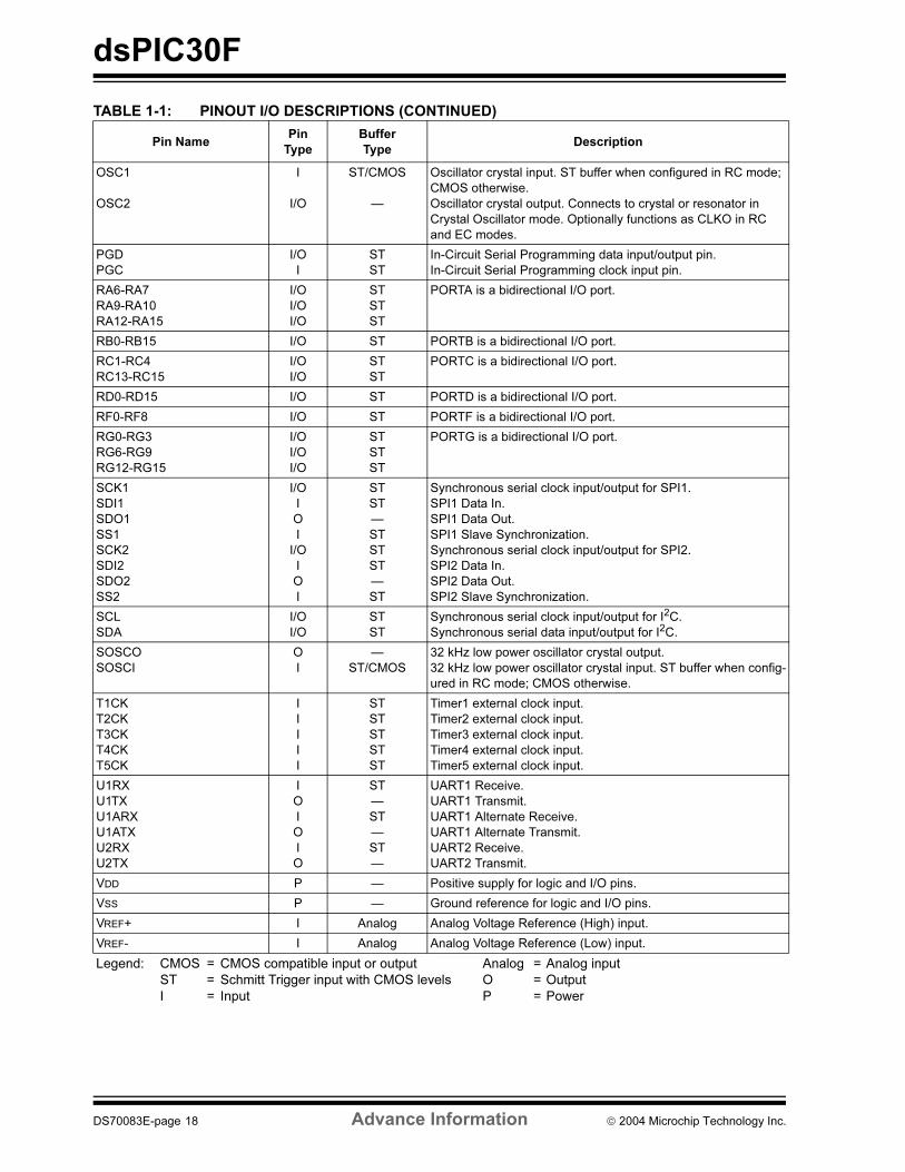
dsPIC30F
OSC1
OSC2
I
I/O
ST/CMOS
—
Oscillator crystal input. ST buffer when configured in RC mode;
CMOS otherwise.
Oscillator crystal output. Connects to crystal or resonator in
Crystal Oscillator mode. Optionally functions as CLKO in RC
and EC modes.
PGD
PGC
I/O
I
ST
ST
In-Circuit Serial Programming data input/output pin.
In-Circuit Serial Programming clock input pin.
RA6-RA7
RA9-RA10
RA12-RA15
I/O
I/O
I/O
ST
ST
ST
PORTA is a bidirectional I/O port.
RB0-RB15 I/O ST PORTB is a bidirectional I/O port.
RC1-RC4
RC13-RC15
I/O
I/O
ST
ST
PORTC is a bidirectional I/O port.
RD0-RD15 I/O ST PORTD is a bidirectional I/O port.
RF0-RF8 I/O ST PORTF is a bidirectional I/O port.
RG0-RG3
RG6-RG9
RG12-RG15
I/O
I/O
I/O
ST
ST
ST
PORTG is a bidirectional I/O port.
SCK1
SDI1
SDO1
SS1
SCK2
SDI2
SDO2
SS2
I/O
I
O
I
I/O
I
O
I
ST
ST
—
ST
ST
ST
—
ST
Synchronous serial clock input/output for SPI1.
SPI1 Data In.
SPI1 Data Out.
SPI1 Slave Synchronization.
Synchronous serial clock input/output for SPI2.
SPI2 Data In.
SPI2 Data Out.
SPI2 Slave Synchronization.
SCL
SDA
I/O
I/O
ST
ST
Synchronous serial clock input/output for I2C.
Synchronous serial data input/output for I2C.
SOSCO
SOSCI
O
I
—
ST/CMOS
32 kHz low power oscillator crystal output.
32 kHz low power oscillator crystal input. ST buffer when config-
ured in RC mode; CMOS otherwise.
T1CK
T2CK
T3CK
T4CK
T5CK
I
I
I
I
I
ST
ST
ST
ST
ST
Timer1 external clock input.
Timer2 external clock input.
Timer3 external clock input.
Timer4 external clock input.
Timer5 external clock input.
U1RX
U1TX
U1ARX
U1ATX
U2RX
U2TX
I
O
I
O
I
O
ST
—
ST
—
ST
—
UART1 Receive.
UART1 Transmit.
UART1 Alternate Receive.
UART1 Alternate Transmit.
UART2 Receive.
UART2 Transmit.
VDD P — Positive supply for logic and I/O pins.
VSS P — Ground reference for logic and I/O pins.
VREF+ I Analog Analog Voltage Reference (High) input.
VREF- I Analog Analog Voltage Reference (Low) input.
TABLE 1-1: PINOUT I/O DESCRIPTIONS (CONTINUED)
Pin NamePin
Type
Buffer
TypeDescription
Legend: CMOS = CMOS compatible input or output Analog = Analog input
ST = Schmitt Trigger input with CMOS levels O = Output
I = Input P = Power
DS70083E-page 18 Advance Information 2004 Microchip Technology Inc.
dsPIC30F
2.0 CPU ARCHITECTURE
OVERVIEW
2.1 Core Overview
The core has a 24-bit instruction word. The Program
Counter (PC) is 23-bits wide with the Least Significant
(LS) bit always clear (refer to Section 3.1), and the
Most Significant (MS) bit is ignored during normal pro-
gram execution, except for certain specialized instruc-
tions. Thus, the PC can address up to 4M instruction
words of user program space. An instruction pre-fetch
mechanism is used to help maintain throughput. Pro-
gram loop constructs, free from loop count manage-
ment overhead, are supported using the DO and
REPEAT instructions, both of which are interruptible at
any point.
The working register array consists of 16 x 16-bit regis-
ters, each of which can act as data, address or offset
registers. One working register (W15) operates as a
software stack pointer for interrupts and calls.
The data space is 64 Kbytes (32K words) and is split
into two blocks, referred to as X and Y data memory.
Each block has its own independent Address Genera-
tion Unit (AGU). Most instructions operate solely
through the X memory, AGU, which provides the
appearance of a single unified data space. The
Multiply-Accumulate (MAC) class of dual source DSP
instructions operate through both the X and Y AGUs,
splitting the data address space into two parts (see
Section 3.2). The X and Y data space boundary is
device specific and cannot be altered by the user. Each
data word consists of 2 bytes, and most instructions
can address data either as words or bytes.
There are two methods of accessing data stored in
program memory:
• The upper 32 Kbytes of data space memory can
be mapped into the lower half (user space) of pro-
gram space at any 16K program word boundary,
defined by the 8-bit Program Space Visibility Page
(PSVPAG) register. This lets any instruction
access program space as if it were data space,
with a limitation that the access requires an addi-
tional cycle. Moreover, only the lower 16 bits of
each instruction word can be accessed using this
method.
• Linear indirect access of 32K word pages within
program space is also possible using any working
register, via table read and write instructions.
Table read and write instructions can be used to
access all 24 bits of an instruction word.
Overhead-free circular buffers (modulo addressing) are
supported in both X and Y address spaces. This is pri-
marily intended to remove the loop overhead for DSP
algorithms.
The X AGU also supports bit-reversed addressing on
destination effective addresses to greatly simplify input
or output data reordering for radix-2 FFT algorithms.
Refer to Section 4.0 for details on modulo and
bit-reversed addressing.
The core supports Inherent (no operand), Relative,
Literal, Memory Direct, Register Direct, Register
Indirect, Register Offset and Literal Offset Addressing
modes. Instructions are associated with predefined
Addressing modes, depending upon their functional
requirements.
For most instructions, the core is capable of executing
a data (or program data) memory read, a working reg-
ister (data) read, a data memory write and a program
(instruction) memory read per instruction cycle. As a
result, 3-operand instructions are supported, allowing
C = A+B operations to be executed in a single cycle.
A DSP engine has been included to significantly
enhance the core arithmetic capability and throughput.
It features a high speed 17-bit by 17-bit multiplier, a
40-bit ALU, two 40-bit saturating accumulators and a
40-bit bidirectional barrel shifter. Data in the accumula-
tor or any working register can be shifted up to 15 bits
right, or 16 bits left in a single cycle. The DSP instruc-
tions operate seamlessly with all other instructions and
have been designed for optimal real-time performance.
The MAC class of instructions can concurrently fetch
two data operands from memory while multiplying two
W registers. To enable this concurrent fetching of data
operands, the data space has been split for these
instructions and linear for all others. This has been
achieved in a transparent and flexible manner, by ded-
icating certain working registers to each address space
for the MAC class of instructions.
The core does not support a multi-stage instruction
pipeline. However, a single stage instruction pre-fetch
mechanism is used, which accesses and partially
decodes instructions a cycle ahead of execution, in
order to maximize available execution time. Most
instructions execute in a single cycle with certain
exceptions, as outlined in Section 2.3.
The core features a vectored exception processing
structure for traps and interrupts, with 62 independent
vectors. The exceptions consist of up to 8 traps (of
which 4 are reserved) and 54 interrupts. Each interrupt
is prioritized based on a user assigned priority between
1 and 7 (1 being the lowest priority and 7 being the
highest), in conjunction with a predetermined ‘natural
order’. Traps have fixed priorities ranging from 8 to 15.
2004 Microchip Technology Inc. Advance Information DS70083E-page 19
dsPIC30F
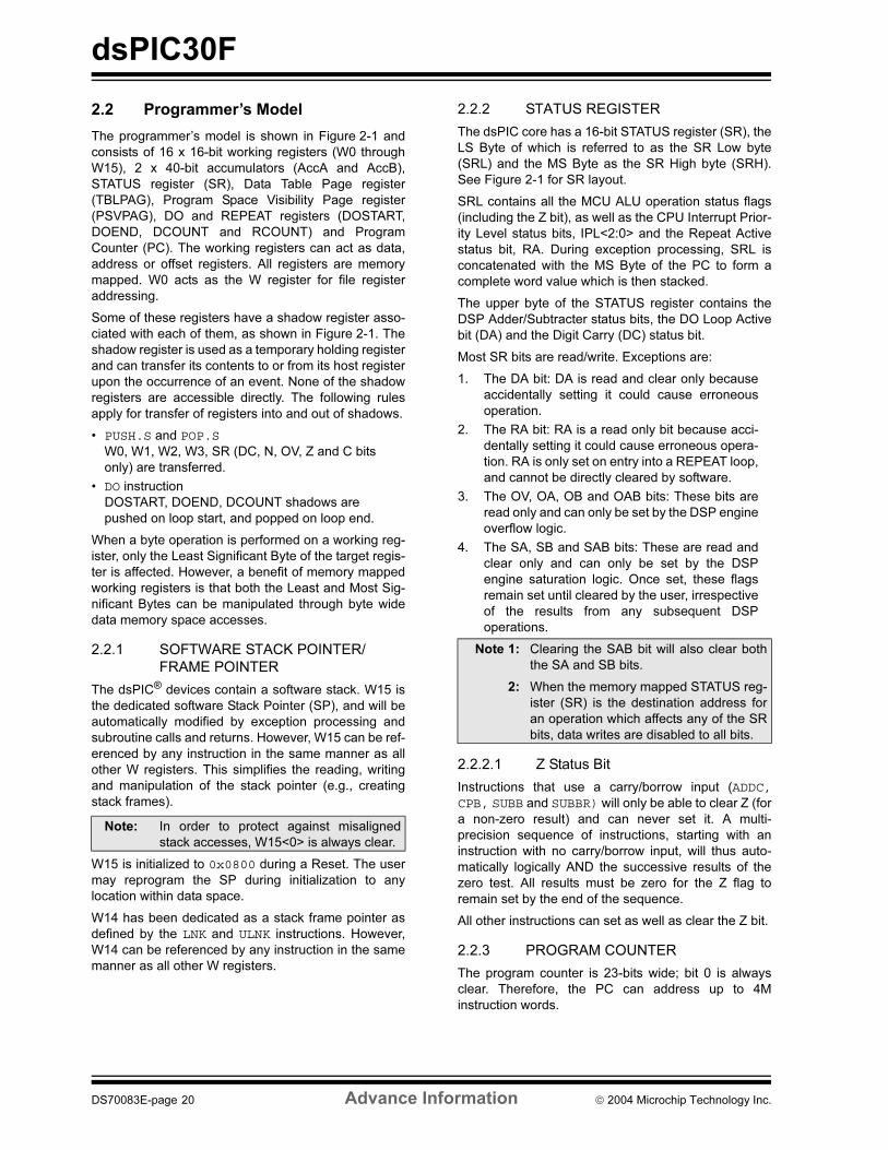
2.2 Programmer’s Model
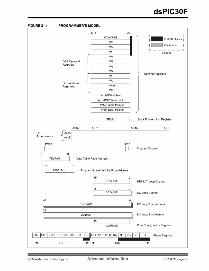
The programmer’s model is shown in Figure 2-1 and
consists of 16 x 16-bit working registers (W0 through
W15), 2 x 40-bit accumulators (AccA and AccB),
STATUS register (SR), Data Table Page register
(TBLPAG), Program Space Visibility Page register
(PSVPAG), DO and REPEAT registers (DOSTART,
DOEND, DCOUNT and RCOUNT) and Program
Counter (PC). The working registers can act as data,
address or offset registers. All registers are memory
mapped. W0 acts as the W register for file register
addressing.
Some of these registers have a shadow register asso-
ciated with each of them, as shown in Figure 2-1. The
shadow register is used as a temporary holding register
and can transfer its contents to or from its host register
upon the occurrence of an event. None of the shadow
registers are accessible directly. The following rules
apply for transfer of registers into and out of shadows.
• PUSH.S and POP.S
W0, W1, W2, W3, SR (DC, N, OV, Z and C bits
only) are transferred.
• DO instruction
DOSTART, DOEND, DCOUNT shadows are
pushed on loop start, and popped on loop end.
When a byte operation is performed on a working reg-
ister, only the Least Significant Byte of the target regis-
ter is affected. However, a benefit of memory mapped
working registers is that both the Least and Most Sig-
nificant Bytes can be manipulated through byte wide
data memory space accesses.
2.2.1 SOFTWARE STACK POINTER/
FRAME POINTER
The dsPIC® devices contain a software stack. W15 is
the dedicated software Stack Pointer (SP), and will be
automatically modified by exception processing and
subroutine calls and returns. However, W15 can be ref-
erenced by any instruction in the same manner as all
other W registers. This simplifies the reading, writing
and manipulation of the stack pointer (e.g., creating
stack frames).
W15 is initialized to 0x0800 during a Reset. The user
may reprogram the SP during initialization to any
location within data space.
W14 has been dedicated as a stack frame pointer as
defined by the LNK and ULNK instructions. However,
W14 can be referenced by any instruction in the same
manner as all other W registers.
2.2.2 STATUS REGISTER
The dsPIC core has a 16-bit STATUS register (SR), the
LS Byte of which is referred to as the SR Low byte
(SRL) and the MS Byte as the SR High byte (SRH).
See Figure 2-1 for SR layout.
SRL contains all the MCU ALU operation status flags
(including the Z bit), as well as the CPU Interrupt Prior-
ity Level status bits, IPL<2:0> and the Repeat Active
status bit, RA. During exception processing, SRL is
concatenated with the MS Byte of the PC to form a
complete word value which is then stacked.
The upper byte of the STATUS register contains the
DSP Adder/Subtracter status bits, the DO Loop Active
bit (DA) and the Digit Carry (DC) status bit.
Most SR bits are read/write. Exceptions are:
1. The DA bit: DA is read and clear only because
accidentally setting it could cause erroneous
operation.
2. The RA bit: RA is a read only bit because acci-
dentally setting it could cause erroneous opera-
tion. RA is only set on entry into a REPEAT loop,
and cannot be directly cleared by software.
3. The OV, OA, OB and OAB bits: These bits are
read only and can only be set by the DSP engine
overflow logic.
4. The SA, SB and SAB bits: These are read and
clear only and can only be set by the DSP
engine saturation logic. Once set, these flags
remain set until cleared by the user, irrespective
of the results from any subsequent DSP
operations.
2.2.2.1 Z Status Bit
Instructions that use a carry/borrow input (ADDC,CPB, SUBB and SUBBR) will only be able to clear Z (for
a non-zero result) and can never set it. A multi-
precision sequence of instructions, starting with an
instruction with no carry/borrow input, will thus auto-
matically logically AND the successive results of the
zero test. All results must be zero for the Z flag to
remain set by the end of the sequence.
All other instructions can set as well as clear the Z bit.
2.2.3 PROGRAM COUNTER
The program counter is 23-bits wide; bit 0 is always
clear. Therefore, the PC can address up to 4M
instruction words.
Note: In order to protect against misaligned
stack accesses, W15<0> is always clear.
Note 1: Clearing the SAB bit will also clear both
the SA and SB bits.
2: When the memory mapped STATUS reg-
ister (SR) is the destination address for
an operation which affects any of the SR
bits, data writes are disabled to all bits.
DS70083E-page 20 Advance Information 2004 Microchip Technology Inc.
dsPIC30F
FIGURE 2-1: PROGRAMMER’S MODEL
TABPAG
PC22 PC0
7 0
D0D15
Program Counter
Data Table Page Address
Status Register
Working Registers
DSP Operand
Registers
W1
W2
W3
W4
W5
W6
W7
W8
W9
W10
W11
W12/DSP Offset
W13/DSP Write Back
W14/Frame Pointer
W15/Stack Pointer
DSP Address
Registers
AD39 AD0AD31
DSP
Accumulators
AccA
AccB
PSVPAG
7 0
Program Space Visibility Page Address
Z
0
OA OB SA SB
RCOUNT
15 0
REPEAT Loop Counter
DCOUNT
15 0
DO Loop Counter
DOSTART
22 0
DO Loop Start Address
IPL2 IPL1
SPLIM Stack Pointer Limit Register
AD15
SRL
PUSH.S Shadow
DO Shadow
OAB SAB
15 0
Core Configuration Register
Legend
CORCON
DA DC RA N
TBLPAG
PSVPAG
IPL0 OV
W0/WREG
SRH
DO Loop End AddressDOEND
22
C
2004 Microchip Technology Inc. Advance Information DS70083E-page 21
dsPIC30F
2.3 Instruction Flow
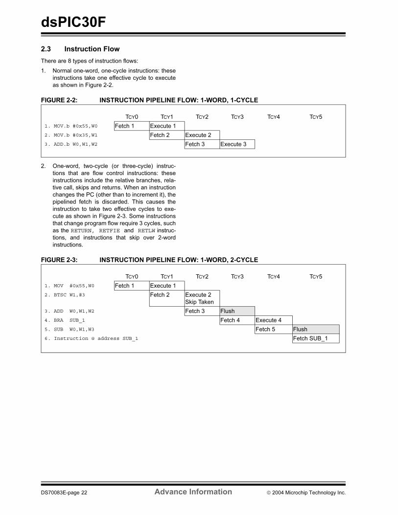
There are 8 types of instruction flows:
1. Normal one-word, one-cycle instructions: these
instructions take one effective cycle to execute
as shown in Figure 2-2.
FIGURE 2-2: INSTRUCTION PIPELINE FLOW: 1-WORD, 1-CYCLE
2. One-word, two-cycle (or three-cycle) instruc-
tions that are flow control instructions: these
instructions include the relative branches, rela-
tive call, skips and returns. When an instruction
changes the PC (other than to increment it), the
pipelined fetch is discarded. This causes the
instruction to take two effective cycles to exe-
cute as shown in Figure 2-3. Some instructions
that change program flow require 3 cycles, such
as the RETURN, RETFIE and RETLW instruc-
tions, and instructions that skip over 2-word
instructions.
FIGURE 2-3: INSTRUCTION PIPELINE FLOW: 1-WORD, 2-CYCLE
TCY0 TCY1 TCY2 TCY3 TCY4 TCY5
1. MOV.b #0x55,W0 Fetch 1 Execute 1
2. MOV.b #0x35,W1 Fetch 2 Execute 2
3. ADD.b W0,W1,W2 Fetch 3 Execute 3
TCY0 TCY1 TCY2 TCY3 TCY4 TCY5
1. MOV #0x55,W0 Fetch 1 Execute 1
2. BTSC W1,#3 Fetch 2 Execute 2
Skip Taken
3. ADD W0,W1,W2 Fetch 3 Flush
4. BRA SUB_1 Fetch 4 Execute 4
5. SUB W0,W1,W3 Fetch 5 Flush
6. Instruction @ address SUB_1 Fetch SUB_1
DS70083E-page 22 Advance Information 2004 Microchip Technology Inc.
dsPIC30F
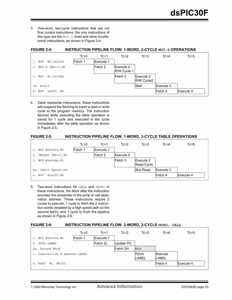
3. One-word, two-cycle instructions that are not
flow control instructions: the only instructions of
this type are the MOV.D (load and store double-
word) instructions, as shown in Figure 2-4.
FIGURE 2-4: INSTRUCTION PIPELINE FLOW: 1-WORD, 2-CYCLE MOV.D OPERATIONS
4. Table read/write instructions: these instructions
will suspend the fetching to insert a read or write
cycle to the program memory. The instruction
fetched while executing the table operation is
saved for 1 cycle and executed in the cycle
immediately after the table operation as shown
in Figure 2-5.
FIGURE 2-5: INSTRUCTION PIPELINE FLOW: 1-WORD, 2-CYCLE TABLE OPERATIONS
5. Two-word instructions for CALL and GOTO: in
these instructions, the fetch after the instruction
provides the remainder of the jump or call desti-
nation address. These instructions require 2
cycles to execute, 1 cycle to fetch the 2 instruc-
tion words (enabled by a high speed path on the
second fetch), and 1 cycle to flush the pipeline
as shown in Figure 2-6.
FIGURE 2-6: INSTRUCTION PIPELINE FLOW: 2-WORD, 2-CYCLE GOTO, CALL
TCY0 TCY1 TCY2 TCY3 TCY4 TCY5
1. MOV W0,0x1234 Fetch 1 Execute 1
2. MOV.D [W0++],W1 Fetch 2 Execute 2
R/W Cycle 1
3. MOV W1,0x00AA Fetch 3 Execute 2
R/W Cycle2
3a. Stall Stall Execute 3
4. MOV 0x0CC, W0 Fetch 4 Execute 4
TCY0 TCY1 TCY2 TCY3 TCY4 TCY5
1. MOV #0x1234,W0 Fetch 1 Execute 1
2. TBLRDL [W0++],W1 Fetch 2 Execute 2
3. MOV #0x00AA,W1 Fetch 3 Execute 2
Read Cycle
3a. Table Operation Bus Read Execute 3
4. MOV #0x0CC,W0 Fetch 4 Execute 4
TCY0 TCY1 TCY2 TCY3 TCY4 TCY5
1. MOV #0x1234,W0 Fetch 1 Execute 1
2. GOTO LABEL Fetch 2L Update PC
2a. Second Word Fetch 2H NOP
3. Instruction @ address LABEL Fetch
LABEL
Execute
LABEL
4. BSET W1, #BIT3 Fetch 4 Execute 4
2004 Microchip Technology Inc. Advance Information DS70083E-page 23
dsPIC30F
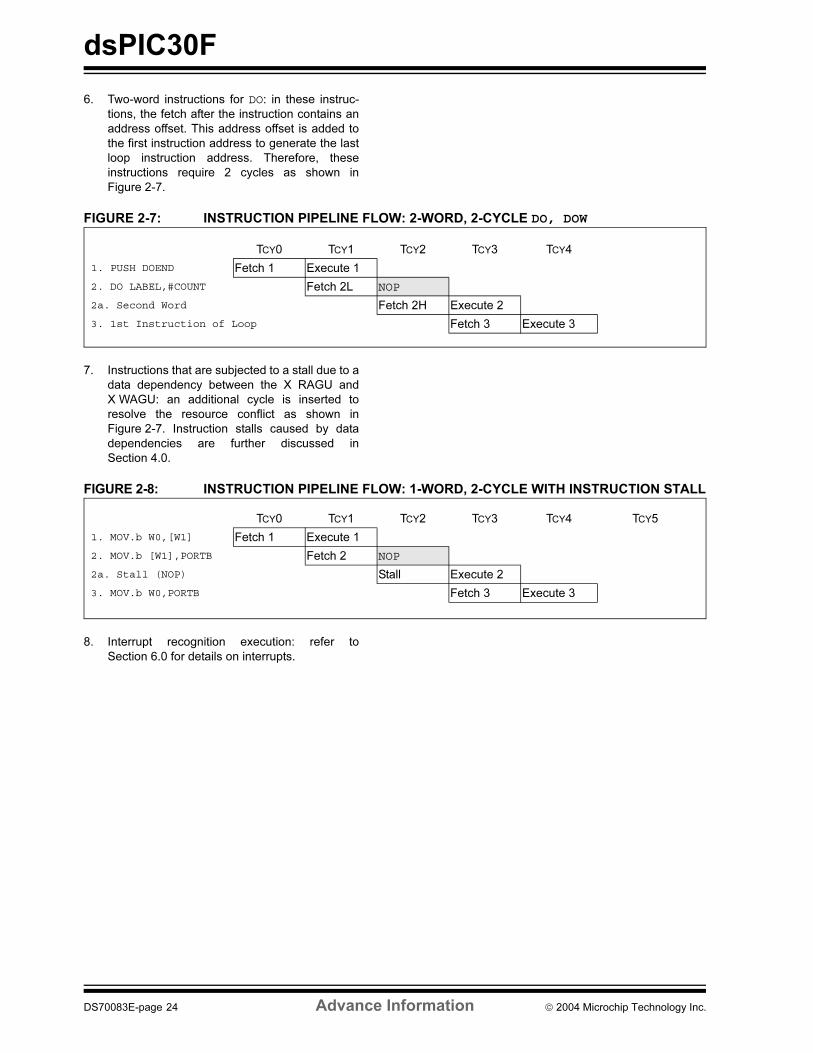
6. Two-word instructions for DO: in these instruc-
tions, the fetch after the instruction contains an
address offset. This address offset is added to
the first instruction address to generate the last
loop instruction address. Therefore, these
instructions require 2 cycles as shown in
Figure 2-7.
FIGURE 2-7: INSTRUCTION PIPELINE FLOW: 2-WORD, 2-CYCLE DO, DOW
7. Instructions that are subjected to a stall due to a
data dependency between the X RAGU and
X WAGU: an additional cycle is inserted to
resolve the resource conflict as shown in
Figure 2-7. Instruction stalls caused by data
dependencies are further discussed in
Section 4.0.
FIGURE 2-8: INSTRUCTION PIPELINE FLOW: 1-WORD, 2-CYCLE WITH INSTRUCTION STALL
8. Interrupt recognition execution: refer to
Section 6.0 for details on interrupts.
TCY0 TCY1 TCY2 TCY3 TCY4
1. PUSH DOEND Fetch 1 Execute 1
2. DO LABEL,#COUNT Fetch 2L NOP
2a. Second Word Fetch 2H Execute 2
3. 1st Instruction of Loop Fetch 3 Execute 3
TCY0 TCY1 TCY2 TCY3 TCY4 TCY5
1. MOV.b W0,[W1] Fetch 1 Execute 1
2. MOV.b [W1],PORTB Fetch 2 NOP
2a. Stall (NOP) Stall Execute 2
3. MOV.b W0,PORTB Fetch 3 Execute 3
DS70083E-page 24 Advance Information 2004 Microchip Technology Inc.
dsPIC30F
2.4 Divide Support
The dsPIC devices feature a 16/16-bit signed fractional
divide operation, as well as 32/16-bit and 16/16-bit
signed and unsigned integer divide operations, in the
form of single instruction iterative divides. The following
instructions and data sizes are supported:
1. DIVF - 16/16 signed fractional divide
2. DIV.sd - 32/16 signed divide
3. DIV.ud - 32/16 unsigned divide
4. DIV.sw - 16/16 signed divide
5. DIV.uw - 16/16 unsigned divide
The 16/16 divides are similar to the 32/16 (same number
of iterations), but the dividend is either zero-extended or
sign-extended during the first iteration.
The quotient for all divide instructions is stored in W0,
and the remainder in W1. DIV and DIVF can specify
any W register for both the 16-bit dividend and divisor.
All other divides can specify any W register for the
16-bit divisor, but the 32-bit dividend must be in an
aligned W register pair, such as W1:W0, W3:W2, etc.
The non-restoring divide algorithm requires one cycle
for an initial dividend shift (for integer divides only), one
cycle per divisor bit, and a remainder/quotient correc-
tion cycle. The correction cycle is the last cycle of the
iteration loop but must be performed (even if the
remainder is not required) because it may also adjust
the quotient. A consequence of this is that DIVF will
also produce a valid remainder (though it is of little use
in fractional arithmetic).
The divide instructions must be executed within a
REPEAT loop. Any other form of execution (e.g., a
series of discrete divide instructions) will not function
correctly because the instruction flow depends on
RCOUNT. The divide instruction does not automatically
set up the RCOUNT value and it must, therefore, be
explicitly and correctly specified in the REPEAT instruc-
tion as shown in Table 2-1 (REPEAT will execute the tar-
get instruction operand value+1 times). The REPEAT
loop count must be setup for 18 iterations of the DIV/DIVF instruction. Thus, a complete divide operation
requires 19 cycles.
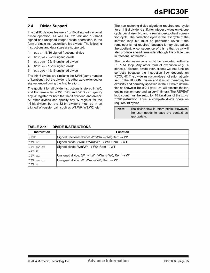
TABLE 2-1: DIVIDE INSTRUCTIONS
Note: The divide flow is interruptible. However,
the user needs to save the context as
appropriate.
Instruction Function
DIVF Signed fractional divide: Wm/Wn → W0; Rem → W1
DIV.sd Signed divide: (Wm+1:Wm)/Wn → W0; Rem → W1
DIV.sw or DIV.s
Signed divide: Wm/Wn → W0; Rem → W1
DIV.ud Unsigned divide: (Wm+1:Wm)/Wn → W0; Rem → W1
DIV.uw or DIV.u
Unsigned divide: Wm/Wn → W0; Rem → W1
2004 Microchip Technology Inc. Advance Information DS70083E-page 25
dsPIC30F
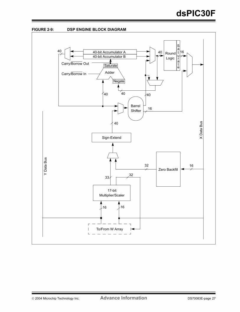
2.5 DSP Engine
Concurrent operation of the DSP engine with MCU
instruction flow is not possible, though both the MCU
ALU and DSP engine resources may be used concur-
rently by the same instruction (e.g., ED and EDACinstructions).
The DSP engine consists of a high speed 17-bit x
17-bit multiplier, a barrel shifter and a 40-bit adder/
subtracter (with two target accumulators, round and
saturation logic).
Data input to the DSP engine is derived from one of the
following:
1. Directly from the W array (registers W4, W5, W6
or W7) via the X and Y data buses for the MACclass of instructions (MAC, MSC, MPY,MPY.N, ED, EDAC, CLR and MOVSAC).
2. From the X bus for all other DSP instructions.
3. From the X bus for all MCU instructions which
use the barrel shifter.
Data output from the DSP engine is written to one of the
following:
1. The target accumulator, as defined by the DSP
instruction being executed.
2. The X bus for MAC, MSC, CLR and MOVSACaccumulator writes, where the EA is derived
from W13 only. (MPY, MPY.N, ED and EDACdo not offer an accumulator write option.)
3. The X bus for all MCU instructions which use the
barrel shifter.
The DSP engine also has the capability to perform
inherent accumulator-to-accumulator operations,
which require no additional data. These instructions are
ADD, SUB and NEG.
The DSP engine has various options selected through
various bits in the CPU Core Configuration register
(CORCON), as listed below:
1. Fractional or integer DSP multiply (IF).
2. Signed or unsigned DSP multiply (US).
3. Conventional or convergent rounding (RND).
4. Automatic saturation on/off for AccA (SATA).
5. Automatic saturation on/off for AccB (SATB).
6. Automatic saturation on/off for writes to data
memory (SATDW).
7. Accumulator Saturation mode selection
(ACCSAT).
A block diagram of the DSP engine is shown in
Figure 2-9.
Note: For CORCON layout, see Table 4-3.
DS70083E-page 26 Advance Information 2004 Microchip Technology Inc.
dsPIC30F
FIGURE 2-9: DSP ENGINE BLOCK DIAGRAM
Zero Backfill
Sign-Extend
Barrel
Shifter
40-bit Accumulator A
40-bit Accumulator BRound
Logic
X D
ata
Bus
To/From W Array
Adder
Saturate
Negate
32
3233
16
16 16
16
40 40
40 40
Saturate
Y D
ata
Bus
40
Carry/Borrow Out
Carry/Borrow In
16
40
Multiplier/Scaler
17-bit
2004 Microchip Technology Inc. Advance Information DS70083E-page 27
dsPIC30F
2.5.1 MULTIPLIER
The 17 x 17-bit multiplier is capable of signed or
unsigned operation and can multiplex its output using a
scaler to support either 1.31 fractional (Q31) or 32-bit
integer results. The respective number representation
formats are shown in Figure 2-10. Unsigned operands
are zero-extended into the 17th bit of the multiplier
input value. Signed operands are sign-extended into
the 17th bit of the multiplier input value. The output of
the 17 x 17-bit multiplier/scaler is a 33-bit value which
is sign-extended to 40 bits. Integer data is inherently
represented as a signed two’s complement value,
where the MSB is defined as a sign bit. Generally
speaking, the range of an N-bit two’s complement inte-
ger is -2N-1 to 2N-1 – 1. For a 16-bit integer, the data
range is -32768 (0x8000) to 32767 (0x7FFF) including
‘0’ (see Figure 2-10). For a 32-bit integer, the data
range is -2,147,483,648 (0x8000 0000) to
2,147,483,645 (0x7FFF FFFF).
When the multiplier is configured for fractional multipli-
cation, the data is represented as a two’s complement
fraction, where the MSB is defined as a sign bit and the
radix point is implied to lie just after the sign bit (QX
format). The range of an N-bit two’s complement frac-
tion with this implied radix point is -1.0 to (1 – 21-N). For
a 16-bit fraction, the Q15 data range is -1.0 (0x8000)
to 0.999969482 (0x7FFF) including ‘0’ and has a
precision of 3.01518x10⁻⁵. In Fractional mode, the
16x16 multiply operation generates a 1.31 product
which has a precision of 4.65661 x 10⁻¹⁰.
FIGURE 2-10: 16-BIT INTEGER AND FRACTIONAL MODES
Certain multiply operations always operate on signed
data. These include the MAC/MSC, MPY[.N] and
ED[AC] instructions. The 40-bit adder/subtracter may
also optionally negate one of its operand inputs to
change the result sign (without changing the oper-
ands). This is used to create a multiply and subtract
(MSC), or multiply and negate (MPY.N) operation.
In the special case when both input operands are 1.15
fractions and equal to 0x8000 (-110), the result of the
multiplication is corrected to 0x7FFFFFFF (as the
closest approximation to +1) by hardware before it is
used.
It should be noted that with the exception of DSP mul-
tiplies, the dsPIC30F ALU operates identically on inte-
ger and fractional data. Namely, an addition of two
integers will yield the same result (binary number) as
the addition of two fractional numbers. The only differ-
ence is how the result is interpreted by the user. How-
ever, multiplies performed by DSP operations are
different. In these instructions, data format selection is
made with the IF bit (CORCON<0>) and US bits
(CORCON<12>), and it must be set accordingly (‘0’ for
Fractional mode, ‘1’ for Integer mode in the case of the
IF bit, and ‘0’ for Signed mode, ‘1’ for Unsigned mode
in the case of the US bit). This is required because of
the implied radix point used by dsPIC30F fractions. In
Integer mode, multiplying two 16-bit integers produces
a 32-bit integer result. However, multiplying two 1.15
values generates a 2.30 result. Since the dsPIC30F
uses 1.31 format for the accumulators, a DSP multiply
in Fractional mode also includes a left shift by one bit to
keep the radix point properly aligned. This feature
reduces the resolution of the DSP multiplier to 2-30, but
has no other effect on the computation.
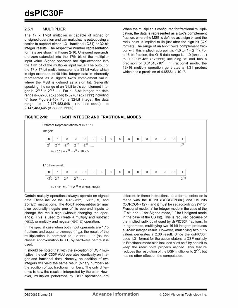
Different Representations of 0x4001
Integer:
214 213 212 211 .... 20
0x4001 = 214 + 20 = 16385
1.15 Fractional:
2-15
0x4001 = 2-1 + 2-15 = 0.500030518
0 1 0 0 0 0 0 0 0 0 0 0 0 0 0 1
. 2-1 2-2 2-3 . . . -20
0 1 0 0 0 0 0 0 0 0 0 0 0 0 0 1
20
DS70083E-page 28 Advance Information 2004 Microchip Technology Inc.
dsPIC30F
The same multiplier is used to support the MCU multi-
ply instructions which include integer 16-bit signed,
unsigned and mixed sign multiplies. Additional data
paths are provided to allow these instructions to write
the result back into the W array and X data bus (via the
W array). These paths are placed prior to the data
scaler. The IF bit in the CORCON register, therefore,
only affects the result of the MAC class of DSP instruc-
tions. All other multiply operations are assumed to be
integer operations. If the user executes a MAC instruc-
tion on fractional data without clearing the IF bit, the
result must be explicitly shifted left by the user program
after multiplication in order to obtain the correct result.
The MUL instruction may be directed to use byte or
word sized operands. Byte operands will direct a 16-bit
result, and word operands will direct a 32-bit result to
the specified register(s) in the W array.
2.5.2 DATA ACCUMULATORS AND
ADDER/SUBTRACTER
The data accumulator consists of a 40-bit adder/
subtracter with automatic sign extension logic. It can
select one of two accumulators (A or B) as its pre-
accumulation source and post-accumulation destina-
tion. For the ADD and LAC instructions, the data to be
accumulated or loaded can be optionally scaled via the
barrel shifter, prior to accumulation.
2.5.2.1 Adder/Subtracter, Overflow and
Saturation
The adder/subtracter is a 40-bit adder with an optional
zero input into one side and either true, or complement
data into the other input. In the case of addition, the
carry/borrow input is active high and the other input is
true data (not complemented), whereas in the case of
subtraction, the carry/borrow input is active low and the
other input is complemented. The adder/subtracter
generates overflow status bits SA/SB and OA/OB,
which are latched and reflected in the STATUS register:
• Overflow from bit 39: this is a catastrophic
overflow in which the sign of the accumulator is
destroyed.
• Overflow into guard bits 32 through 39: this is a
recoverable overflow. This bit is set whenever all
the guard bits bits are not identical to each other.
The adder has an additional saturation block which
controls accumulator data saturation, if selected. It
uses the result of the adder, the overflow status bits
described above, and the SATA/B (CORCON<7:6>)
and ACCSAT (CORCON<4>) mode control bits to
determine when and to what value to saturate.
Six STATUS register bits have been provided to
support saturation and overflow; they are:
1. OA:
AccA overflowed into guard bits
2. OB:
AccB overflowed into guard bits
3. SA:
AccA saturated (bit 31 overflow and saturation)
or
AccA overflowed into guard bits and saturated
(bit 39 overflow and saturation)
4. SB:
AccB saturated (bit 31 overflow and saturation)
or
AccB overflowed into guard bits and saturated
(bit 39 overflow and saturation)
5. OAB:
Logical OR of OA and OB
6. SAB:
Logical OR of SA and SB
The OA and OB bits are modified each time data
passes through the adder/subtracter. When set, they
indicate that the most recent operation has overflowed
into the accumulator guard bits (bits 32 through 39).
The OA and OB bits can also optionally generate an
arithmetic warning trap when set and the correspond-
ing overflow trap flag enable bit (OVATEN, OVBTEN) in
the INTCON1 register (refer to Section 5.0) is set. This
allows the user to take immediate action, for example,
to correct system gain.
The SA and SB bits are modified each time data
passes through the adder/subtracter but can only be
cleared by the user. When set, they indicate that the
accumulator has overflowed its maximum range (bit 31
for 32-bit saturation, or bit 39 for 40-bit saturation) and
will be saturated (if saturation is enabled). When satu-
ration is not enabled, SA and SB default to bit 39 over-
flow and thus indicate that a catastrophic overflow has
occurred. If the COVTE bit in the INTCON1 register is
set, SA and SB bits will generate an arithmetic warning
trap when saturation is disabled.
The overflow and saturation status bits can optionally
be viewed in the STATUS register (SR) as the logical
OR of OA and OB (in bit OAB) and the logical OR of SA
and SB (in bit SAB). This allows programmers to check
one bit in the STATUS register to determine if either
accumulator has overflowed, or one bit to determine if
either accumulator has saturated. This would be useful
for complex number arithmetic which typically uses
both the accumulators.
2004 Microchip Technology Inc. Advance Information DS70083E-page 29
dsPIC30F
The device supports three saturation and overflow
modes:
1. Bit 39 Overflow and Saturation:
When bit 39 overflow and saturation occurs, the
saturation logic loads the maximally positive 9.31
(0x7FFFFFFFFF), or maximally negative 9.31
value (0x8000000000) into the target accumula-
tor. The SA or SB bit is set and remains set until
cleared by the user. This is referred to as ‘super
saturation’ and provides protection against erro-
neous data, or unexpected algorithm problems
(e.g., gain calculations).
2. Bit 31 Overflow and Saturation:
When bit 31 overflow and saturation occurs, the
saturation logic then loads the maximally posi-
tive 1.31 value (0x007FFFFFFF), or maximally
negative 1.31 value (0x0080000000) into the
target accumulator. The SA or SB bit is set and
remains set until cleared by the user. When this
Saturation mode is in effect, the guard bits are
not used (so the OA, OB or OAB bits are never
set).
3. Bit 39 Catastrophic Overflow:
The bit 39 overflow status bit from the adder is
used to set the SA or SB bit which remain set
until cleared by the user. No saturation operation
is performed and the accumulator is allowed to
overflow (destroying its sign). If the COVTE bit in
the INTCON1 register is set, a catastrophic
overflow can initiate a trap exception.
2.5.2.2 Accumulator ‘Write Back’
The MAC class of instructions (with the exception of
MPY, MPY.N, ED and EDAC) can optionally write a
rounded version of the high word (bits 31 through 16)
of the accumulator that is not targeted by the instruction
into data space memory. The write is performed across
the X bus into combined X and Y address space. The
following Addressing modes are supported:
1. W13, Register Direct:
The rounded contents of the non-target
accumulator are written into W13 as a 1.15
fraction.
2. [W13]+=2, Register Indirect with Post-Increment:
The rounded contents of the non-target accumu-
lator are written into the address pointed to by
W13 as a 1.15 fraction. W13 is then
incremented by 2 (for a word write).
2.5.2.3 Round Logic
The round logic is a combinational block which per-
forms a conventional (biased) or convergent (unbi-
ased) round function during an accumulator write
(store). The Round mode is determined by the state of
the RND bit in the CORCON register. It generates a 16-
bit, 1.15 data value which is passed to the data space
write saturation logic. If rounding is not indicated by the
instruction, a truncated 1.15 data value is stored and
the LS Word is simply discarded.
The two Rounding modes are shown in Figure 2-10.
Conventional rounding takes bit 15 of the accumulator,
zero-extends it and adds it to the ACCxH word (bits 16
through 31 of the accumulator). If the ACCxL word
(bits 0 through 15 of the accumulator) is between
0x8000 and 0xFFFF (0x8000 included), ACCxH is
incremented. If ACCxL is between 0x0000 and
0x7FFF, ACCxH is left unchanged. A consequence of
this algorithm is that over a succession of random
rounding operations, the value will tend to be biased
slightly positive.
Convergent (or unbiased) rounding operates in the
same manner as conventional rounding, except when
ACCxL equals 0x8000. If this is the case, the LS bit
(bit 16 of the accumulator) of ACCxH is examined. If it
is ‘1’, ACCxH is incremented. If it is ‘0’, ACCxH is not
modified. Assuming that bit 16 is effectively random in
nature, this scheme will remove any rounding bias that
may accumulate.
The SAC and SAC.R instructions store either a trun-
cated (SAC) or rounded (SAC.R) version of the contents
of the target accumulator to data memory via the X bus
(subject to data saturation, see Section 2.5.2.4). Note
that for the MAC class of instructions, the accumulator
write back operation will function in the same manner,
addressing combined MCU (X and Y) data space
though the X bus. For this class of instructions, the data
is always subject to rounding.
DS70083E-page 30 Advance Information 2004 Microchip Technology Inc.
dsPIC30F
2.5.2.4 Data Space Write Saturation
In addition to adder/subtracter saturation, writes to data
space may also be saturated but without affecting the
contents of the source accumulator. The data space
write saturation logic block accepts a 16-bit, 1.15 frac-
tional value from the round logic block as its input,
together with overflow status from the original source
(accumulator) and the 16-bit round adder. These are
combined and used to select the appropriate 1.15
fractional value as output to write to data space
memory.
If the SATDW bit in the CORCON register is set, data
(after rounding or truncation) is tested for overflow and
adjusted accordingly, For input data greater than
0x007FFF, data written to memory is forced to the
maximum positive 1.15 value, 0x7FFF. For input data
less than 0xFF8000, data written to memory is forced
to the maximum negative 1.15 value, 0x8000. The MS
bit of the source (bit 39) is used to determine the sign
of the operand being tested.
If the SATDW bit in the CORCON register is not set, the
input data is always passed through unmodified under
all conditions.
2.5.3 BARREL SHIFTER
The barrel shifter is capable of performing up to 15-bit
arithmetic or logic right shifts, or up to 16-bit left shifts
in a single cycle. The source can be either of the two
DSP accumulators, or the X bus (to support multi-bit
shifts of register or memory data).
The shifter requires a signed binary value to determine
both the magnitude (number of bits) and direction of the
shift operation. A positive value will shift the operand
right. A negative value will shift the operand left. A
value of ‘0’ will not modify the operand.
The barrel shifter is 40-bits wide, thereby obtaining a
40-bit result for DSP shift operations and a 16-bit result
for MCU shift operations. Data from the X bus is pre-
sented to the barrel shifter between bit positions 16 to
31 for right shifts, and bit positions 0 to 15 for left shifts.
2004 Microchip Technology Inc. Advance Information DS70083E-page 31
dsPIC30F
NOTES:
DS70083E-page 32 Advance Information 2004 Microchip Technology Inc.
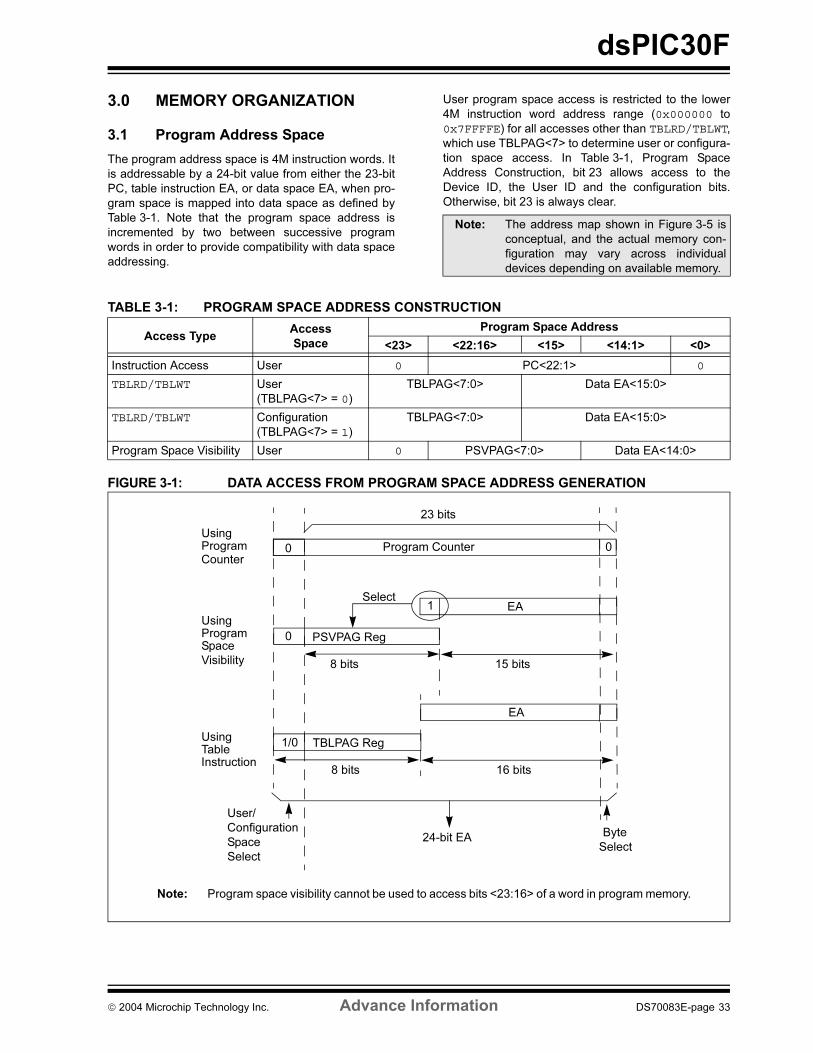
dsPIC30F
3.0 MEMORY ORGANIZATION
3.1 Program Address Space
The program address space is 4M instruction words. It
is addressable by a 24-bit value from either the 23-bit
PC, table instruction EA, or data space EA, when pro-
gram space is mapped into data space as defined by
Table 3-1. Note that the program space address is
incremented by two between successive program
words in order to provide compatibility with data space
addressing.
User program space access is restricted to the lower
4M instruction word address range (0x000000 to
0x7FFFFE) for all accesses other than TBLRD/TBLWT,which use TBLPAG<7> to determine user or configura-
tion space access. In Table 3-1, Program Space
Address Construction, bit 23 allows access to the
Device ID, the User ID and the configuration bits.
Otherwise, bit 23 is always clear.
TABLE 3-1: PROGRAM SPACE ADDRESS CONSTRUCTION
FIGURE 3-1: DATA ACCESS FROM PROGRAM SPACE ADDRESS GENERATION
Note: The address map shown in Figure 3-5 is
conceptual, and the actual memory con-
figuration may vary across individual
devices depending on available memory.
Access TypeAccess
Space
Program Space Address
<23> <22:16> <15> <14:1> <0>
Instruction Access User 0 PC<22:1> 0
TBLRD/TBLWT User
(TBLPAG<7> = 0)
TBLPAG<7:0> Data EA<15:0>
TBLRD/TBLWT Configuration
(TBLPAG<7> = 1)
TBLPAG<7:0> Data EA<15:0>
Program Space Visibility User 0 PSVPAG<7:0> Data EA<14:0>
0Program Counter
23 bits
1
PSVPAG Reg
8 bits
EA
15 bits
Program
Using
Select
TBLPAG Reg
8 bits
EA
16 bits
Using
Byte24-bit EA
0
0
1/0
Select
User/
Configuration
TableInstruction
ProgramSpace
Counter
Using
Space
Select
Visibility
Note: Program space visibility cannot be used to access bits <23:16> of a word in program memory.
2004 Microchip Technology Inc. Advance Information DS70083E-page 33
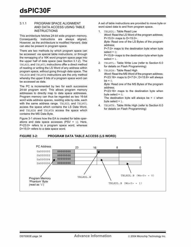
dsPIC30F
3.1.1 PROGRAM SPACE ALIGNMENT
AND DATA ACCESS USING TABLE
INSTRUCTIONS
This architecture fetches 24-bit wide program memory.
Consequently, instructions are always aligned.
However, as the architecture is modified Harvard, data
can also be present in program space.
There are two methods by which program space can
be accessed: via special table instructions, or through
the remapping of a 16K word program space page into
the upper half of data space (see Section 3.1.2). The
TBLRDL and TBLWTL instructions offer a direct method
of reading or writing the LS Word of any address within
program space, without going through data space. The
TBLRDH and TBLWTH instructions are the only method
whereby the upper 8 bits of a program space word can
be accessed as data.
The PC is incremented by two for each successive
24-bit program word. This allows program memory
addresses to directly map to data space addresses.
Program memory can thus be regarded as two 16-bit
word wide address spaces, residing side by side, each
with the same address range. TBLRDL and TBLWTLaccess the space which contains the LS Data Word,
and TBLRDH and TBLWTH access the space which
contains the MS Data Byte.
Figure 3-1 shows how the EA is created for table oper-
ations and data space accesses (PSV = 1). Here,
P<23:0> refers to a program space word, whereas
D<15:0> refers to a data space word.
A set of table instructions are provided to move byte or
word sized data to and from program space.
1. TBLRDL: Table Read Low
Word: Read the LS Word of the program address;
P<15:0> maps to D<15:0>.
Byte: Read one of the LS Bytes of the program
address;
P<7:0> maps to the destination byte when byte
select = 0;
P<15:8> maps to the destination byte when byte
select = 1.
2. TBLWTL: Table Write Low (refer to Section 6.0
for details on Flash Programming)
3. TBLRDH: Table Read High
Word: Read the MS Word of the program address;
P<23:16> maps to D<7:0>; D<15:8> will always
be = 0.
Byte: Read one of the MS Bytes of the program
address;
P<23:16> maps to the destination byte when
byte select = 0;
The destination byte will always be = 0 when
byte select = 1.
4. TBLWTH: Table Write High (refer to Section 6.0
for details on Flash Programming)
FIGURE 3-2: PROGRAM DATA TABLE ACCESS (LS WORD)
0816PC Address
0x000000
0x000002
0x000004
0x000006
23
00000000
00000000
00000000
00000000
Program Memory‘Phantom’ Byte(read as ‘0’)
TBLRDL.W
TBLRDL.B (Wn<0> = 1)
TBLRDL.B (Wn<0> = 0)
DS70083E-page 34 Advance Information 2004 Microchip Technology Inc.
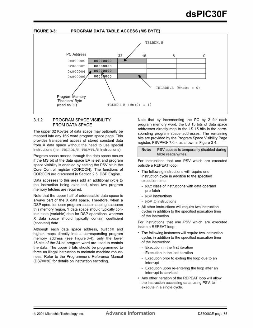
dsPIC30F
FIGURE 3-3: PROGRAM DATA TABLE ACCESS (MS BYTE)
3.1.2 PROGRAM SPACE VISIBILITY
FROM DATA SPACE
The upper 32 Kbytes of data space may optionally be
mapped into any 16K word program space page. This
provides transparent access of stored constant data
from X data space without the need to use special
instructions (i.e., TBLRDL/H, TBLWTL/H instructions).
Program space access through the data space occurs
if the MS bit of the data space EA is set and program
space visibility is enabled by setting the PSV bit in the
Core Control register (CORCON). The functions of
CORCON are discussed in Section 2.5, DSP Engine.
Data accesses to this area add an additional cycle to
the instruction being executed, since two program
memory fetches are required.
Note that the upper half of addressable data space is
always part of the X data space. Therefore, when a
DSP operation uses program space mapping to access
this memory region, Y data space should typically con-
tain state (variable) data for DSP operations, whereas
X data space should typically contain coefficient
(constant) data.
Although each data space address, 0x8000 and
higher, maps directly into a corresponding program
memory address (see Figure 3-4), only the lower
16 bits of the 24-bit program word are used to contain
the data. The upper 8 bits should be programmed to
force an illegal instruction to maintain machine robust-
ness. Refer to the Programmer’s Reference Manual
(DS70030) for details on instruction encoding.
Note that by incrementing the PC by 2 for each
program memory word, the LS 15 bits of data space
addresses directly map to the LS 15 bits in the corre-
sponding program space addresses. The remaining
bits are provided by the Program Space Visibility Page
register, PSVPAG<7:0>, as shown in Figure 3-4.
For instructions that use PSV which are executed
outside a REPEAT loop:
• The following instructions will require one
instruction cycle in addition to the specified
execution time:
- MAC class of instructions with data operand
pre-fetch
- MOV instructions
- MOV.D instructions
• All other instructions will require two instruction
cycles in addition to the specified execution time
of the instruction.
For instructions that use PSV which are executed
inside a REPEAT loop:
• The following instances will require two instruction
cycles in addition to the specified execution time
of the instruction:
- Execution in the first iteration
- Execution in the last iteration
- Execution prior to exiting the loop due to an
interrupt
- Execution upon re-entering the loop after an
interrupt is serviced
• Any other iteration of the REPEAT loop will allow
the instruction accessing data, using PSV, to
execute in a single cycle.
0816PC Address
0x000000
0x000002
0x000004
0x000006
23
00000000
00000000
00000000
00000000
Program Memory‘Phantom’ Byte(read as ‘0’)
TBLRDH.W
TBLRDH.B (Wn<0> = 1)
TBLRDH.B (Wn<0> = 0)
Note: PSV access is temporarily disabled during
table reads/writes.
2004 Microchip Technology Inc. Advance Information DS70083E-page 35
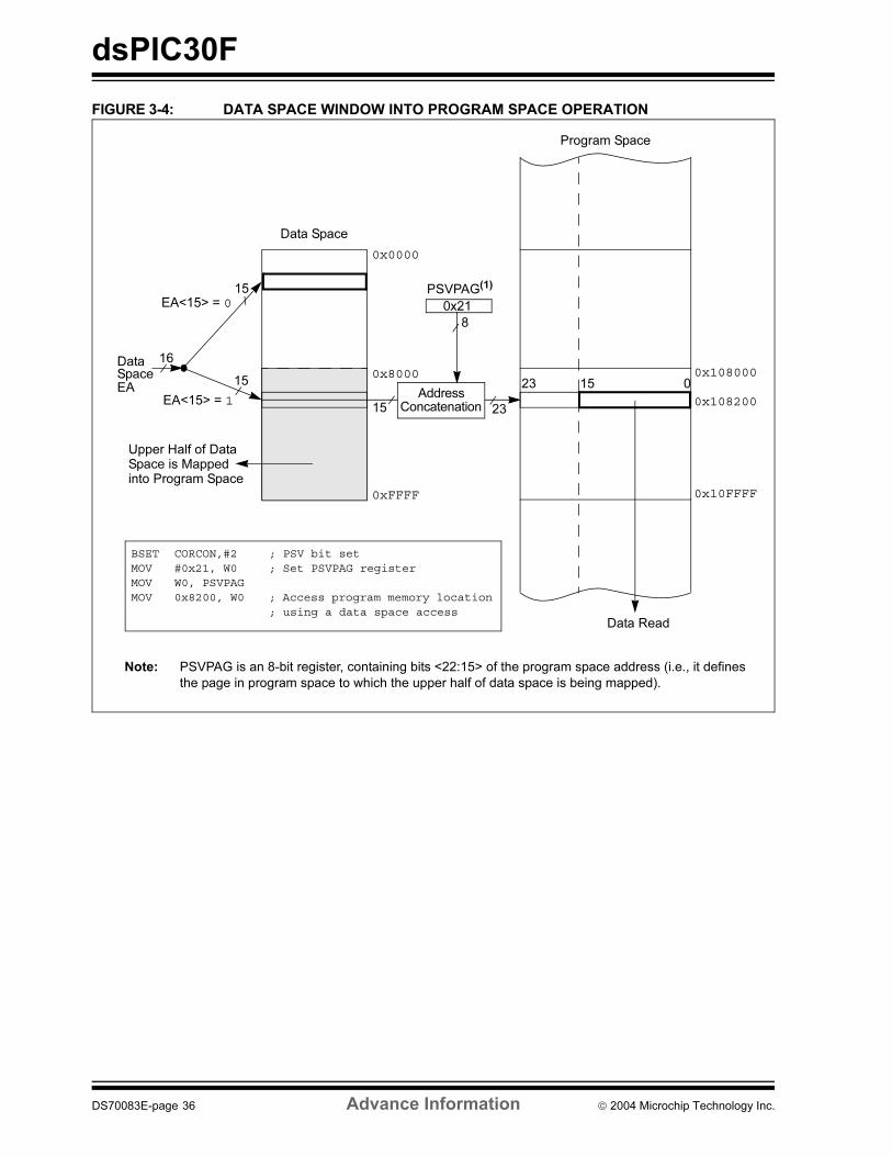
dsPIC30F
FIGURE 3-4: DATA SPACE WINDOW INTO PROGRAM SPACE OPERATION
23 15 0
PSVPAG(1)15
15
EA<15> = 0
EA<15> = 1
16DataSpaceEA
Data Space
Program Space
8
15 23
0x0000
0x8000
0xFFFF
0x21
0x108000
0x10FFFF
Data Read
Upper Half of Data Space is Mapped into Program Space
0x108200Address
Concatenation
BSET CORCON,#2 ; PSV bit setMOV #0x21, W0 ; Set PSVPAG registerMOV W0, PSVPAGMOV 0x8200, W0 ; Access program memory location
; using a data space access
Note: PSVPAG is an 8-bit register, containing bits <22:15> of the program space address (i.e., it defines
the page in program space to which the upper half of data space is being mapped).
DS70083E-page 36 Advance Information 2004 Microchip Technology Inc.
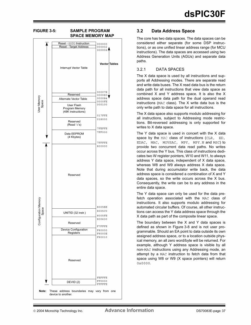
dsPIC30F
FIGURE 3-5: SAMPLE PROGRAM
SPACE MEMORY MAP 3.2 Data Address Space
The core has two data spaces. The data spaces can be
considered either separate (for some DSP instruc-
tions), or as one unified linear address range (for MCU
instructions). The data spaces are accessed using two
Address Generation Units (AGUs) and separate data
paths.
3.2.1 DATA SPACES
The X data space is used by all instructions and sup-
ports all Addressing modes. There are separate read
and write data buses. The X read data bus is the return
data path for all instructions that view data space as
combined X and Y address space. It is also the X
address space data path for the dual operand read
instructions (MAC class). The X write data bus is the
only write path to data space for all instructions.
The X data space also supports modulo addressing for
all instructions, subject to Addressing mode restric-
tions. Bit-reversed addressing is only supported for
writes to X data space.
The Y data space is used in concert with the X data
space by the MAC class of instructions (CLR, ED,EDAC, MAC, MOVSAC, MPY, MPY.N and MSC) to
provide two concurrent data read paths. No writes
occur across the Y bus. This class of instructions dedi-
cates two W register pointers, W10 and W11, to always
address Y data space, independent of X data space,
whereas W8 and W9 always address X data space.
Note that during accumulator write back, the data
address space is considered a combination of X and Y
data spaces, so the write occurs across the X bus.
Consequently, the write can be to any address in the
entire data space.
The Y data space can only be used for the data pre-
fetch operation associated with the MAC class of
instructions. It also supports modulo addressing for
automated circular buffers. Of course, all other instruc-
tions can access the Y data address space through the
X data path as part of the composite linear space.
The boundary between the X and Y data spaces is
defined as shown in Figure 3-8 and is not user pro-
grammable. Should an EA point to data outside its own
assigned address space, or to a location outside phys-
ical memory, an all zero word/byte will be returned. For
example, although Y address space is visible by all
non-MAC instructions using any Addressing mode, an
attempt by a MAC instruction to fetch data from that
space using W8 or W9 (X space pointers) will return
0x0000.
Reset - Target Address
User
Mem
ory
Space
000000
00007E
000002
000080
Device Configuration
User FlashProgram Memory
018000017FFE
Configura
tion M
em
ory
Space
Data EEPROM
(48K instructions)
(4 Kbytes)
800000
F80000Registers F8000E
F80010
DEVID (2)
FEFFFEFF0000FFFFFE
ReservedF7FFFE
Reserved
7FF0007FEFFE
(Read ‘0’s)
8005FE800600
UNITID (32 instr.)
Vector Tables
8005BE
8005C0
Reset - GOTO Instruction
000004
Reserved
7FFFFE
Reserved
0001000000FE000084Alternate Vector Table
Reserved
Interrupt Vector Table
Note: These address boundaries may vary from onedevice to another.
2004 Microchip Technology Inc. Advance Information DS70083E-page 37
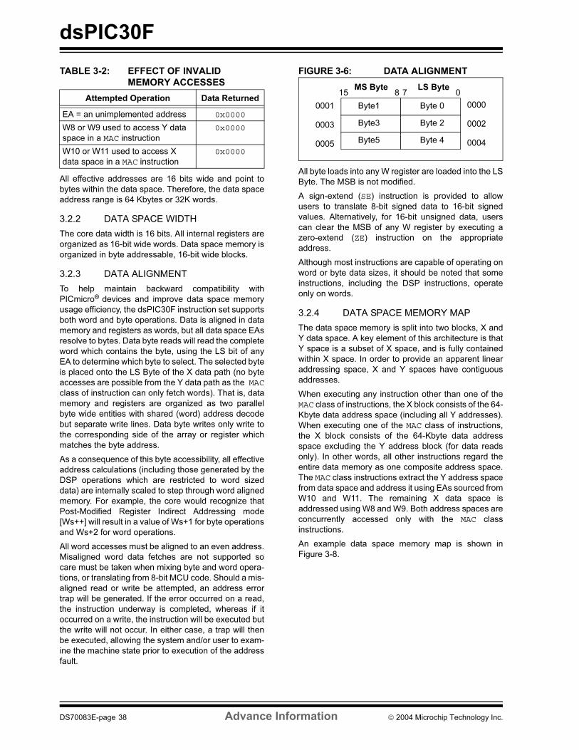
dsPIC30F
TABLE 3-2: EFFECT OF INVALID
MEMORY ACCESSES
All effective addresses are 16 bits wide and point to
bytes within the data space. Therefore, the data space
address range is 64 Kbytes or 32K words.
3.2.2 DATA SPACE WIDTH
The core data width is 16 bits. All internal registers are
organized as 16-bit wide words. Data space memory is
organized in byte addressable, 16-bit wide blocks.
3.2.3 DATA ALIGNMENT
To help maintain backward compatibility with
PICmicro® devices and improve data space memory
usage efficiency, the dsPIC30F instruction set supports
both word and byte operations. Data is aligned in data
memory and registers as words, but all data space EAs
resolve to bytes. Data byte reads will read the complete
word which contains the byte, using the LS bit of any
EA to determine which byte to select. The selected byte
is placed onto the LS Byte of the X data path (no byte
accesses are possible from the Y data path as the MACclass of instruction can only fetch words). That is, data
memory and registers are organized as two parallel
byte wide entities with shared (word) address decode
but separate write lines. Data byte writes only write to
the corresponding side of the array or register which
matches the byte address.
As a consequence of this byte accessibility, all effective
address calculations (including those generated by the
DSP operations which are restricted to word sized
data) are internally scaled to step through word aligned
memory. For example, the core would recognize that
Post-Modified Register Indirect Addressing mode
[Ws++] will result in a value of Ws+1 for byte operations
and Ws+2 for word operations.
All word accesses must be aligned to an even address.
Misaligned word data fetches are not supported so
care must be taken when mixing byte and word opera-
tions, or translating from 8-bit MCU code. Should a mis-
aligned read or write be attempted, an address error
trap will be generated. If the error occurred on a read,
the instruction underway is completed, whereas if it
occurred on a write, the instruction will be executed but
the write will not occur. In either case, a trap will then
be executed, allowing the system and/or user to exam-
ine the machine state prior to execution of the address
fault.
FIGURE 3-6: DATA ALIGNMENT
All byte loads into any W register are loaded into the LS
Byte. The MSB is not modified.
A sign-extend (SE) instruction is provided to allow
users to translate 8-bit signed data to 16-bit signed
values. Alternatively, for 16-bit unsigned data, users
can clear the MSB of any W register by executing a
zero-extend (ZE) instruction on the appropriate
address.
Although most instructions are capable of operating on
word or byte data sizes, it should be noted that some
instructions, including the DSP instructions, operate
only on words.
3.2.4 DATA SPACE MEMORY MAP
The data space memory is split into two blocks, X and
Y data space. A key element of this architecture is that
Y space is a subset of X space, and is fully contained
within X space. In order to provide an apparent linear
addressing space, X and Y spaces have contiguous
addresses.
When executing any instruction other than one of the
MAC class of instructions, the X block consists of the 64-
Kbyte data address space (including all Y addresses).
When executing one of the MAC class of instructions,
the X block consists of the 64-Kbyte data address
space excluding the Y address block (for data reads
only). In other words, all other instructions regard the
entire data memory as one composite address space.
The MAC class instructions extract the Y address space
from data space and address it using EAs sourced from
W10 and W11. The remaining X data space is
addressed using W8 and W9. Both address spaces are
concurrently accessed only with the MAC class
instructions.
An example data space memory map is shown in
Figure 3-8.
Attempted Operation Data Returned
EA = an unimplemented address 0x0000
W8 or W9 used to access Y data
space in a MAC instruction
0x0000
W10 or W11 used to access X
data space in a MAC instruction
0x0000
15 8 7 0
0001
0003
0005
0000
0002
0004
Byte1 Byte 0
Byte3 Byte 2
Byte5 Byte 4
LS ByteMS Byte
DS70083E-page 38 Advance Information 2004 Microchip Technology Inc.
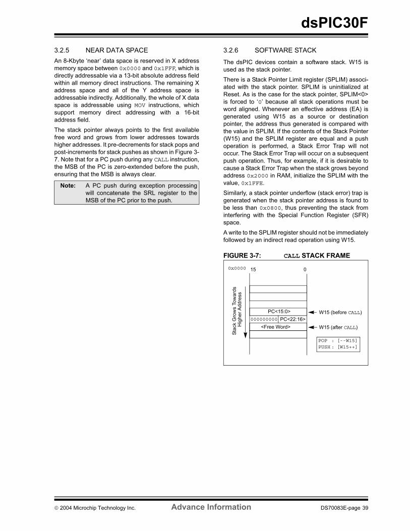
dsPIC30F
3.2.5 NEAR DATA SPACE
An 8-Kbyte ‘near’ data space is reserved in X address
memory space between 0x0000 and 0x1FFF, which is
directly addressable via a 13-bit absolute address field
within all memory direct instructions. The remaining X
address space and all of the Y address space is
addressable indirectly. Additionally, the whole of X data
space is addressable using MOV instructions, which
support memory direct addressing with a 16-bit
address field.
The stack pointer always points to the first available
free word and grows from lower addresses towards
higher addresses. It pre-decrements for stack pops and
post-increments for stack pushes as shown in Figure 3-
7. Note that for a PC push during any CALL instruction,
the MSB of the PC is zero-extended before the push,
ensuring that the MSB is always clear.
3.2.6 SOFTWARE STACK
The dsPIC devices contain a software stack. W15 is
used as the stack pointer.
There is a Stack Pointer Limit register (SPLIM) associ-
ated with the stack pointer. SPLIM is uninitialized at
Reset. As is the case for the stack pointer, SPLIM<0>
is forced to ‘0’ because all stack operations must be
word aligned. Whenever an effective address (EA) is
generated using W15 as a source or destination
pointer, the address thus generated is compared with
the value in SPLIM. If the contents of the Stack Pointer
(W15) and the SPLIM register are equal and a push
operation is performed, a Stack Error Trap will not
occur. The Stack Error Trap will occur on a subsequent
push operation. Thus, for example, if it is desirable to
cause a Stack Error Trap when the stack grows beyond
address 0x2000 in RAM, initialize the SPLIM with the
value, 0x1FFE.
Similarly, a stack pointer underflow (stack error) trap is
generated when the stack pointer address is found to
be less than 0x0800, thus preventing the stack from
interfering with the Special Function Register (SFR)
space.
A write to the SPLIM register should not be immediately
followed by an indirect read operation using W15.
FIGURE 3-7: CALL STACK FRAME
Note: A PC push during exception processing
will concatenate the SRL register to the
MSB of the PC prior to the push.
<Free Word>
PC<15:0>
000000000
015
W15 (before CALL)
W15 (after CALL)
Sta
ck G
row
s T
ow
ard
sH
igh
er
Ad
dre
ss
0x0000
PC<22:16>
POP : [--W15]PUSH : [W15++]
2004 Microchip Technology Inc. Advance Information DS70083E-page 39
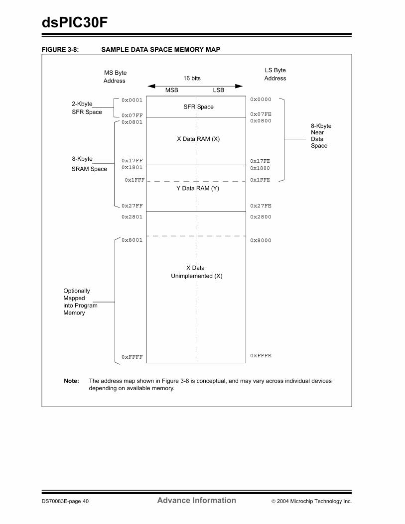
dsPIC30F
FIGURE 3-8: SAMPLE DATA SPACE MEMORY MAP
0x0000
0x07FESFR Space
0x17FE
0xFFFE
X Data RAM (X)
LS Byte
Address16 bits
LSBMSB
MS Byte
Address
0x0001
0x07FF
0x17FF
0xFFFF
X Data
0x8001 0x8000
Optionally
Mapped
into Program
Memory
Unimplemented (X)
0x27FF 0x27FE
0x28000x2801
0x0801 0x0800
0x1801 0x1800
NearData
0x1FFE 0x1FFF
Y Data RAM (Y)
2-Kbyte
SFR Space
8-Kbyte
SRAM Space
8-Kbyte
Note: The address map shown in Figure 3-8 is conceptual, and may vary across individual devices
depending on available memory.
Space
DS70083E-page 40 Advance Information 2004 Microchip Technology Inc.
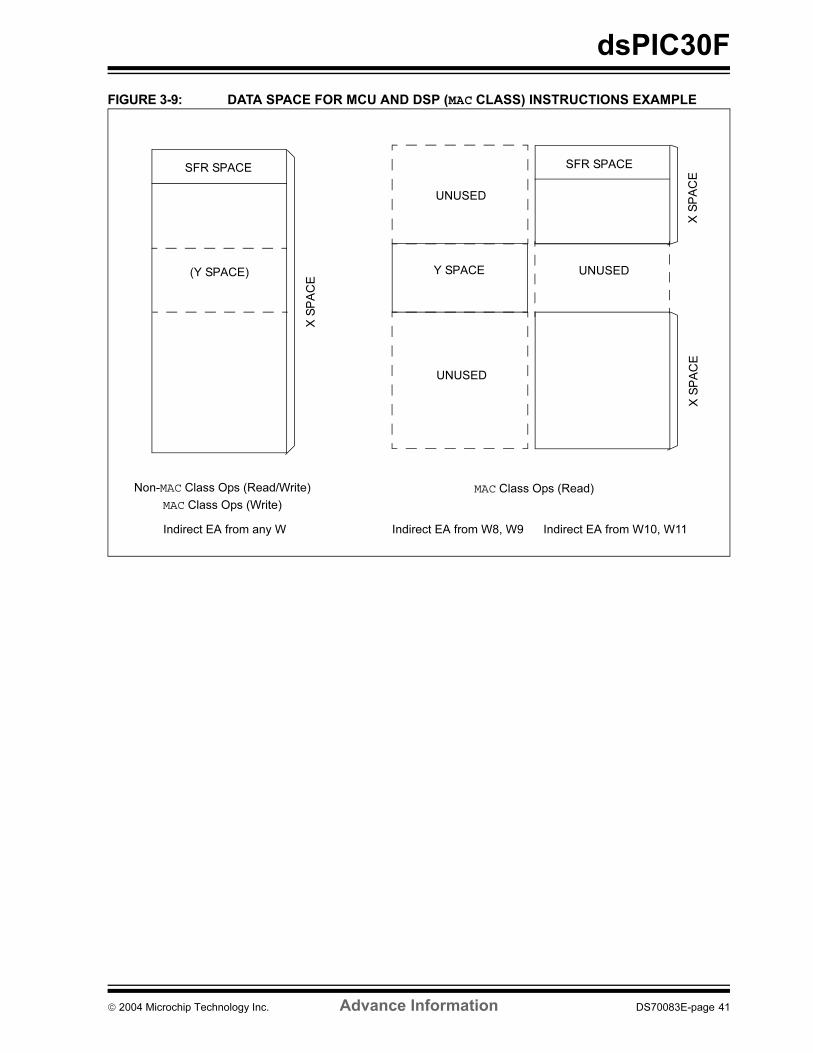
dsPIC30F
FIGURE 3-9: DATA SPACE FOR MCU AND DSP (MAC CLASS) INSTRUCTIONS EXAMPLE
SFR SPACE
(Y SPACE)
X S
PA
CE
SFR SPACE
UNUSED
X S
PA
CE
X S
PA
CE
Y SPACE
UNUSED
UNUSED
MAC Class Ops (Read)
Indirect EA from any W Indirect EA from W8, W9 Indirect EA from W10, W11
Non-MAC Class Ops (Read/Write)
MAC Class Ops (Write)
2004 Microchip Technology Inc. Advance Information DS70083E-page 41
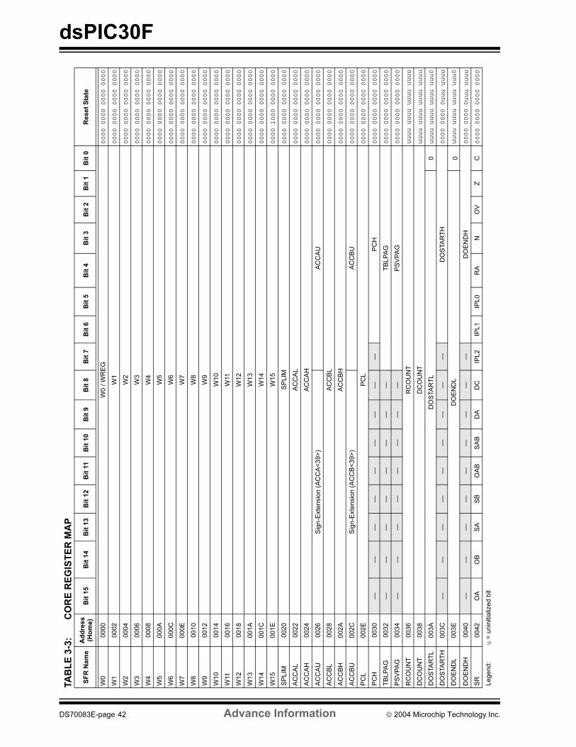
dsPIC30F
TA
BL
E 3
-3:
CO
RE
RE
GIS
TE
R M
AP
SF
R N
am
eA
dd
ress
(Ho
me)
Bit
15
Bit
14
Bit
13
Bit
12
Bit
11
Bit
10
Bit
9B
it 8
Bit
7B
it 6
Bit
5B
it 4
Bit
3B
it 2
Bit
1B
it 0
Reset
Sta
te
W0
0000
W0 / W
RE
G0000 0000 0000 0000
W1
0002
W1
0000 0000 0000 0000
W2
0004
W2
0000 0000 0000 0000
W3
0006
W3
0000 0000 0000 0000
W4
0008
W4
0000 0000 0000 0000
W5
000A
W5
0000 0000 0000 0000
W6
000C
W6
0000 0000 0000 0000
W7
000E
W7
0000 0000 0000 0000
W8
0010
W8
0000 0000 0000 0000
W9
0012
W9
0000 0000 0000 0000
W10
0014
W10
0000 0000 0000 0000
W11
0016
W11
0000 0000 0000 0000
W12
0018
W12
0000 0000 0000 0000
W13
001A
W13
0000 0000 0000 0000
W14
001C
W14
0000 0000 0000 0000
W15
001E
W15
0000 1000 0000 0000
SP
LIM
0020
SP
LIM
0000 0000 0000 0000
AC
CA
L0022
AC
CA
L0000 0000 0000 0000
AC
CA
H0024
AC
CA
H0000 0000 0000 0000
AC
CA
U0026
Sig
n-E
xte
nsio
n (
AC
CA
<39>
)A
CC
AU
0000 0000 0000 0000
AC
CB
L0028
AC
CB
L0000 0000 0000 0000
AC
CB
H002A
AC
CB
H0000 0000 0000 0000
AC
CB
U002C
Sig
n-E
xte
nsio
n (
AC
CB
<39>
)A
CC
BU
0000 0000 0000 0000
PC
L002E
PC
L0000 0000 0000 0000
PC
H0030
——
——
——
——
—P
CH
0000 0000 0000 0000
TB
LP
AG
0032
——
——
——
——
TB
LP
AG
0000 0000 0000 0000
PS
VP
AG
003
4—
——
——
——
—P
SV
PA
G0000 0000 0000 0000
RC
OU
NT
0036
RC
OU
NT
uuuu uuuu uuuu uuuu
DC
OU
NT
0038
DC
OU
NT
uuuu uuuu uuuu uuuu
DO
STA
RT
L003A
DO
STA
RT
L0
uuuu uuuu uuuu uuu0
DO
STA
RT
H003C
——
——
——
——
—D
OS
TA
RT
H0000 0000 0uuu uuuu
DO
EN
DL
003E
DO
EN
DL
0uuuu uuuu uuuu uuu0
DO
EN
DH
0040
——
——
——
——
—D
OE
ND
H0000 0000 0uuu uuuu
SR
0042
OA
OB
SA
SB
OA
BS
AB
DA
DC
IPL2
IPL1
IPL0
RA
NO
VZ
C0000 0000 0000 0000
Legend:
u =
unin
itia
lized b
it
DS70083E-page 42 Advance Information 2004 Microchip Technology Inc.
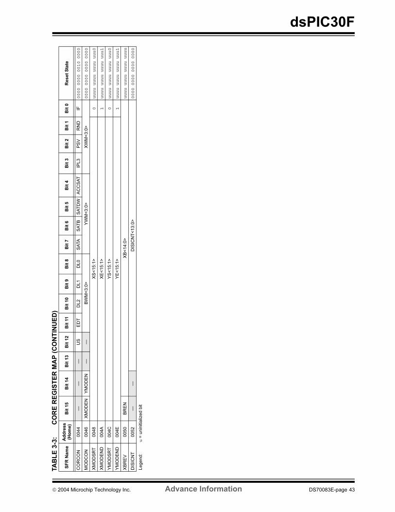
dsPIC30F
CO
RC
ON
0044
——
—U
SE
DT
DL2
DL1
DL0
SA
TA
SA
TB
SA
TD
WA
CC
SA
TIP
L3
PS
VR
ND
IF0000 0000 0010 0000
MO
DC
ON
0046
XM
OD
EN
YM
OD
EN
——
BW
M<
3:0
>Y
WM
<3:0
>X
WM
<3:0
>0000 0000 0000 0000
XM
OD
SR
T0048
XS
<15:1
>0
uuuu uuuu uuuu uuu0
XM
OD
EN
D004A
XE
<15:1
>1
uuuu uuuu uuuu uuu1
YM
OD
SR
T004C
YS
<15:1
>0
uuuu uuuu uuuu uuu0
YM
OD
EN
D004E
YE
<15:1
>1
uuuu uuuu uuuu uuu1
XB
RE
V0050
BR
EN
XB
<14:0
>uuuu uuuu uuuu uuuu
DIS
ICN
T0052
——
DIS
ICN
T<
13:0
>0000 0000 0000 0000
TA
BL
E 3
-3:
CO
RE
RE
GIS
TE
R M
AP
(C
ON
TIN
UE
D)
SF
R N
am
eA
dd
ress
(Ho
me)
Bit
15
Bit
14
Bit
13
Bit
12
Bit
11
Bit
10
Bit
9B
it 8
Bit
7B
it 6
Bit
5B
it 4
Bit
3B
it 2
Bit
1B
it 0
Reset
Sta
te
Legend:
u =
unin
itia
lized b
it
2004 Microchip Technology Inc. Advance Information DS70083E-page 43
dsPIC30F
NOTES:
DS70083E-page 44 Advance Information 2004 Microchip Technology Inc.
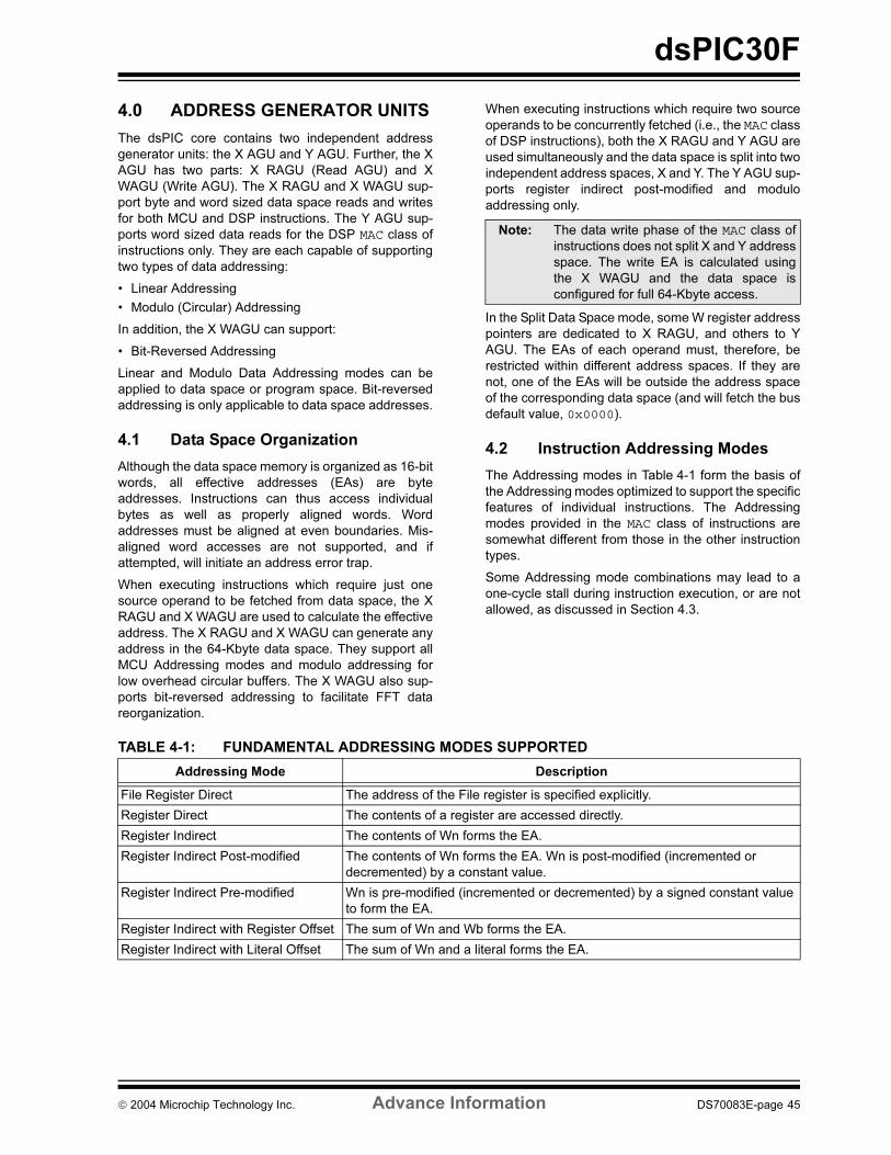
dsPIC30F
4.0 ADDRESS GENERATOR UNITS
The dsPIC core contains two independent address
generator units: the X AGU and Y AGU. Further, the X
AGU has two parts: X RAGU (Read AGU) and X
WAGU (Write AGU). The X RAGU and X WAGU sup-
port byte and word sized data space reads and writes
for both MCU and DSP instructions. The Y AGU sup-
ports word sized data reads for the DSP MAC class of
instructions only. They are each capable of supporting
two types of data addressing:
• Linear Addressing
• Modulo (Circular) Addressing
In addition, the X WAGU can support:
• Bit-Reversed Addressing
Linear and Modulo Data Addressing modes can be
applied to data space or program space. Bit-reversed
addressing is only applicable to data space addresses.
4.1 Data Space Organization
Although the data space memory is organized as 16-bit
words, all effective addresses (EAs) are byte
addresses. Instructions can thus access individual
bytes as well as properly aligned words. Word
addresses must be aligned at even boundaries. Mis-
aligned word accesses are not supported, and if
attempted, will initiate an address error trap.
When executing instructions which require just one
source operand to be fetched from data space, the X
RAGU and X WAGU are used to calculate the effective
address. The X RAGU and X WAGU can generate any
address in the 64-Kbyte data space. They support all
MCU Addressing modes and modulo addressing for
low overhead circular buffers. The X WAGU also sup-
ports bit-reversed addressing to facilitate FFT data
reorganization.
When executing instructions which require two source
operands to be concurrently fetched (i.e., the MAC class
of DSP instructions), both the X RAGU and Y AGU are
used simultaneously and the data space is split into two
independent address spaces, X and Y. The Y AGU sup-
ports register indirect post-modified and modulo
addressing only.
In the Split Data Space mode, some W register address
pointers are dedicated to X RAGU, and others to Y
AGU. The EAs of each operand must, therefore, be
restricted within different address spaces. If they are
not, one of the EAs will be outside the address space
of the corresponding data space (and will fetch the bus
default value, 0x0000).
4.2 Instruction Addressing Modes
The Addressing modes in Table 4-1 form the basis of
the Addressing modes optimized to support the specific
features of individual instructions. The Addressing
modes provided in the MAC class of instructions are
somewhat different from those in the other instruction
types.
Some Addressing mode combinations may lead to a
one-cycle stall during instruction execution, or are not
allowed, as discussed in Section 4.3.
TABLE 4-1: FUNDAMENTAL ADDRESSING MODES SUPPORTED
Note: The data write phase of the MAC class of
instructions does not split X and Y address
space. The write EA is calculated using
the X WAGU and the data space is
configured for full 64-Kbyte access.
Addressing Mode Description
File Register Direct The address of the File register is specified explicitly.
Register Direct The contents of a register are accessed directly.
Register Indirect The contents of Wn forms the EA.
Register Indirect Post-modified The contents of Wn forms the EA. Wn is post-modified (incremented or
decremented) by a constant value.
Register Indirect Pre-modified Wn is pre-modified (incremented or decremented) by a signed constant value
to form the EA.
Register Indirect with Register Offset The sum of Wn and Wb forms the EA.
Register Indirect with Literal Offset The sum of Wn and a literal forms the EA.
2004 Microchip Technology Inc. Advance Information DS70083E-page 45
dsPIC30F
4.2.1 FILE REGISTER INSTRUCTIONS
Most File register instructions use a 13-bit address field
(f) to directly address data present in the first 8192
bytes of data memory. These memory locations are
known as File registers. Most File register instructions
employ a working register, W0, which is denoted as
WREG in these instructions. The destination is typically
either the same File register or WREG (with the excep-
tion of the MUL instruction), which writes the result to a
register or register pair. The MOV instruction can use a
16-bit address field.
4.2.2 MCU INSTRUCTIONS
The three-operand MCU instructions are of the form:
Operand 3 = Operand 1 <function> Operand 2
where Operand 1 is always a working register (i.e., the
Addressing mode can only be register direct) which is
referred to as Wb. Operand 2 can be the W register
fetched from data memory or 5-bit literal. In two-
operand instructions, the result location is the same as
that of one of the operands. Certain MCU instructions
are one-operand operations. The following addressing
modes are supported by MCU instructions:
• Register Direct
• Register Indirect
• Register Indirect Post-modified
• Register Indirect Pre-modified
• 5-bit or 10-bit Literal
4.2.3 MOVE AND ACCUMULATOR
INSTRUCTIONS
Move instructions and the DSP accumulator class of
instructions provide a greater degree of addressing
flexibility than other instructions. In addition to the
Addressing modes supported by most MCU instruc-
tions, move and accumulator instructions also support
Register Indirect with Register Offset Addressing
mode, also referred to as Register Indexed mode.
In summary, the following Addressing modes are
supported by move and accumulator instructions:
• Register Direct
• Register Indirect
• Register Indirect Post-modified
• Register Indirect Pre-modified
• Register Indirect with Register Offset (Indexed)
• Register Indirect with Literal Offset
• 8-bit Literal
• 16-bit Literal
4.2.4 MAC INSTRUCTIONS
The dual source operand DSP instructions (CLR, ED,EDAC, MAC, MPY, MPY.N, MOVSAC and MSC), also
referred to as MAC instructions, utilize a simplified set of
Addressing modes to allow the user to effectively
manipulate the data pointers through register indirect
tables.
The 2 source operand pre-fetch registers must be a
member of the set W8, W9, W10, W11. For data
reads, W8 and W9 will always be directed to the X
RAGU and W10 and W11 will always be directed to the
Y AGU. The effective addresses generated (before and
after modification) must, therefore, be valid addresses
within X data space for W8 and W9 and Y data space
for W10 and W11.
In summary, the following Addressing modes are
supported by the MAC class of instructions:
• Register Indirect
• Register Indirect Post-modified by 2
• Register Indirect Post-modified by 4
• Register Indirect Post-modified by 6
• Register Indirect with Register Offset (Indexed)
4.2.5 OTHER INSTRUCTIONS
Besides the various Addressing modes outlined above,
some instructions use literal constants of various sizes.
For example, BRA (branch) instructions use 16-bit
signed literals to specify the branch destination directly,
whereas the DISI instruction uses a 14-bit unsigned
literal field. In some instructions, such as ADD Acc, the
source of an operand or result is implied by the opcode
itself. Certain operations, such as NOP, do not have any
operands.
Note: Not all instructions support all the
Addressing modes given above. Individual
instructions may support different subsets
of these Addressing modes.
Note: For the MOV instructions, the Addressing
mode specified in the instruction can differ
for the source and destination EA.
However, the 4-bit Wb (register offset)
field is shared between both source and
destination (but typically only used by
one).
Note: Not all instructions support all the
Addressing modes given above. Individual
instructions may support different subsets
of these Addressing modes.
Note: Register indirect with register offset
addressing is only available for W9 (in X
space) and W11 (in Y space).
DS70083E-page 46 Advance Information 2004 Microchip Technology Inc.
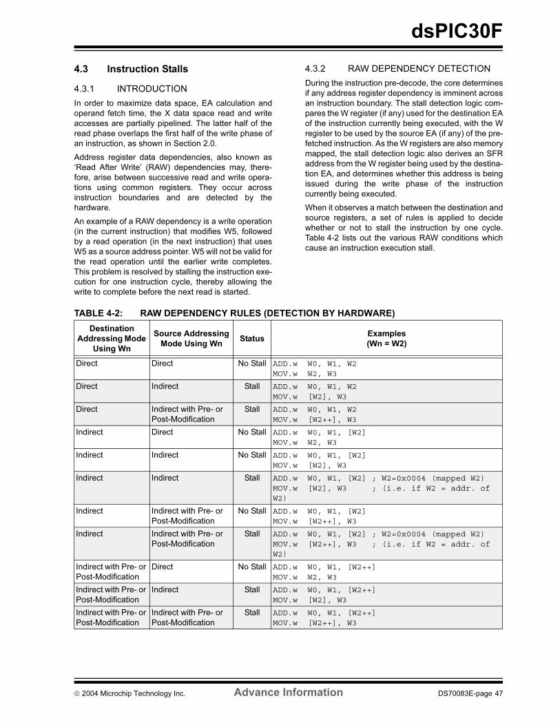
dsPIC30F
4.3 Instruction Stalls
4.3.1 INTRODUCTION
In order to maximize data space, EA calculation and
operand fetch time, the X data space read and write
accesses are partially pipelined. The latter half of the
read phase overlaps the first half of the write phase of
an instruction, as shown in Section 2.0.
Address register data dependencies, also known as
‘Read After Write’ (RAW) dependencies may, there-
fore, arise between successive read and write opera-
tions using common registers. They occur across
instruction boundaries and are detected by the
hardware.
An example of a RAW dependency is a write operation
(in the current instruction) that modifies W5, followed
by a read operation (in the next instruction) that uses
W5 as a source address pointer. W5 will not be valid for
the read operation until the earlier write completes.
This problem is resolved by stalling the instruction exe-
cution for one instruction cycle, thereby allowing the
write to complete before the next read is started.
4.3.2 RAW DEPENDENCY DETECTION
During the instruction pre-decode, the core determines
if any address register dependency is imminent across
an instruction boundary. The stall detection logic com-
pares the W register (if any) used for the destination EA
of the instruction currently being executed, with the W
register to be used by the source EA (if any) of the pre-
fetched instruction. As the W registers are also memory
mapped, the stall detection logic also derives an SFR
address from the W register being used by the destina-
tion EA, and determines whether this address is being
issued during the write phase of the instruction
currently being executed.
When it observes a match between the destination and
source registers, a set of rules is applied to decide
whether or not to stall the instruction by one cycle.
Table 4-2 lists out the various RAW conditions which
cause an instruction execution stall.
TABLE 4-2: RAW DEPENDENCY RULES (DETECTION BY HARDWARE)
Destination
Addressing Mode
Using Wn
Source Addressing
Mode Using WnStatus
Examples
(Wn = W2)
Direct Direct No Stall ADD.w W0, W1, W2MOV.w W2, W3
Direct Indirect Stall ADD.w W0, W1, W2MOV.w [W2], W3
Direct Indirect with Pre- or
Post-Modification
Stall ADD.w W0, W1, W2MOV.w [W2++], W3
Indirect Direct No Stall ADD.w W0, W1, [W2]MOV.w W2, W3
Indirect Indirect No Stall ADD.w W0, W1, [W2]MOV.w [W2], W3
Indirect Indirect Stall ADD.w W0, W1, [W2] ; W2=0x0004 (mapped W2)MOV.w [W2], W3 ; (i.e. if W2 = addr. of W2)
Indirect Indirect with Pre- or
Post-Modification
No Stall ADD.w W0, W1, [W2]MOV.w [W2++], W3
Indirect Indirect with Pre- or
Post-Modification
Stall ADD.w W0, W1, [W2] ; W2=0x0004 (mapped W2)MOV.w [W2++], W3 ; (i.e. if W2 = addr. of W2)
Indirect with Pre- or
Post-Modification
Direct No Stall ADD.w W0, W1, [W2++]MOV.w W2, W3
Indirect with Pre- or
Post-Modification
Indirect Stall ADD.w W0, W1, [W2++]MOV.w [W2], W3
Indirect with Pre- or
Post-Modification
Indirect with Pre- or
Post-Modification
Stall ADD.w W0, W1, [W2++]MOV.w [W2++], W3
2004 Microchip Technology Inc. Advance Information DS70083E-page 47
dsPIC30F
4.4 Modulo Addressing
Modulo addressing is a method of providing an auto-
mated means to support circular data buffers using
hardware. The objective is to remove the need for soft-
ware to perform data address boundary checks when
executing tightly looped code, as is typical in many
DSP algorithms.
Modulo addressing can operate in either data or pro-
gram space (since the data pointer mechanism is
essentially the same for both). One circular buffer can
be supported in each of the X (which also provides the
pointers into program space) and Y data spaces. Mod-
ulo addressing can operate on any W register pointer.
However, it is not advisable to use W14 or W15 for mod-
ulo addressing since these two registers are used as
the stack frame pointer and stack pointer, respectively.
In general, any particular circular buffer can only be
configured to operate in one direction, as there are cer-
tain restrictions on the buffer start address (for incre-
menting buffers), or end address (for decrementing
buffers) based upon the direction of the buffer.
The only exception to the usage restrictions is for buff-
ers which have a power-of-2 length. As these buffers
satisfy the start and end address criteria, they may
operate in a Bidirectional mode (i.e., address boundary
checks will be performed on both the lower and upper
address boundaries).
4.4.1 START AND END ADDRESS
The modulo addressing scheme requires that a starting
and an ending address be specified and loaded into the
16-bit Modulo Buffer Address registers: XMODSRT,
XMODEND, YMODSRT, YMODEND (see Table 3-3).
If the length of an incrementing buffer is greater than
M = 2N-1, but not greater than M = 2N bytes, then the
last ‘N’ bits of the data buffer start address must be
zeros. There are no such restrictions on the end
address of an incrementing buffer. For example, if the
buffer size (modulus value) is chosen to be 100 bytes
(0x64), then the buffer start address for an increment-
ing buffer must contain 7 Least Significant zeros. Valid
start addresses may, therefore, be 0xXX00 and
0xXX80, where ‘X’ is any hexadecimal value. Adding
the buffer length to this value and subtracting ‘1’ will
give the end address to be written into X/YMODEND.
For example, if the start address was chosen to be
0x2000, then the X/YMODEND would be set to
(0x2000 + 0x0064 – 1) = 0x2063.
In the case of a decrementing buffer, the last ‘N’ bits of
the data buffer end address must be ones. There are
no such restrictions on the start address of a decre-
menting buffer. For example, if the buffer size (modulus
value) is chosen to be 100 bytes (0x64), then the buffer
end address for a decrementing buffer must contain
7 Least Significant ones. Valid end addresses may,
therefore, be 0xXXFF and 0xXX7F, where ‘X’ is any
hexadecimal value. Subtracting the buffer length from
this value and adding 1 will give the start address to be
written into X/YMODSRT. For example, if the end
address was chosen to be 0x207F, then the start
address would be (0x207F – 0x0064 + 1) = 0x201C,
which is the first physical address of the buffer.
The length of a circular buffer is not directly specified. It
is determined by the difference between the corre-
sponding start and end addresses. The maximum pos-
sible length of the circular buffer is 32K words
(64 Kbytes).
A write operation to the MODCON register should not
be immediately followed by an indirect read operation
using any W register.
Note: The start and end addresses are the first
and last byte addresses of the buffer (irre-
spective of whether it is a word or byte
buffer, or an increasing or decreasing
buffer). Moreover, the start address must
be even and the end address must be odd
(for both word and byte buffers).
Note: ‘Start address’ refers to the smallest
address boundary of the circular buffer.
The first access of the buffer may be at
any address within the modulus range
(see Section 4.4.4).
Note: Y space modulo addressing EA calcula-
tions assume word sized data (LS bit of
every EA is always clear).
Note 1: Using a POP instruction to pop the con-
tents of the top-of-stack (TOS) location
into MODCON also constitutes a write to
MODCON. Therefore, the instruction
immediately following such a POP cannot
be any instruction performing an indirect
read operation.
2: It should be noted that some instructions
perform an indirect read operation
implicitly. These are: POP, RETURN,RETFIE, RETLW and ULNK.
DS70083E-page 48 Advance Information 2004 Microchip Technology Inc.
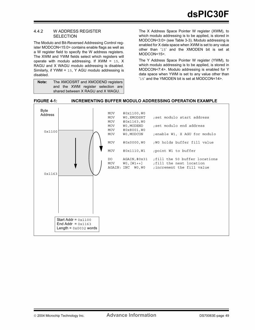
dsPIC30F
4.4.2 W ADDRESS REGISTER
SELECTION
The Modulo and Bit-Reversed Addressing Control reg-
ister MODCON<15:0> contains enable flags as well as
a W register field to specify the W address registers.
The XWM and YWM fields select which registers will
operate with modulo addressing. If XWM = 15, X
RAGU and X WAGU modulo addressing is disabled.
Similarly, if YWM = 15, Y AGU modulo addressing is
disabled.
The X Address Space Pointer W register (XWM), to
which modulo addressing is to be applied, is stored in
MODCON<3:0> (see Table 3-3). Modulo addressing is
enabled for X data space when XWM is set to any value
other than ‘15’ and the XMODEN bit is set at
MODCON<15>.
The Y Address Space Pointer W register (YWM), to
which modulo addressing is to be applied, is stored in
MODCON<7:4>. Modulo addressing is enabled for Y
data space when YWM is set to any value other than
‘15’ and the YMODEN bit is set at MODCON<14>.
FIGURE 4-1: INCREMENTING BUFFER MODULO ADDRESSING OPERATION EXAMPLE
Note: The XMODSRT and XMODEND registers
and the XWM register selection are
shared between X RAGU and X WAGU.
0x1100
0x1163
Start Addr = 0x1100End Addr = 0x1163Length = 0x0032 words
ByteAddress MOV #0x1100,W0
MOV W0,XMODSRT ;set modulo start addressMOV #0x1163,W0MOV W0,MODEND ;set modulo end addressMOV #0x8001,W0MOV W0,MODCON ;enable W1, X AGU for modulo
MOV #0x0000,W0 ;W0 holds buffer fill value
MOV #0x1110,W1 ;point W1 to buffer
DO AGAIN,#0x31 ;fill the 50 buffer locationsMOV W0,[W1++] ;fill the next locationAGAIN: INC W0,W0 ;increment the fill value
2004 Microchip Technology Inc. Advance Information DS70083E-page 49
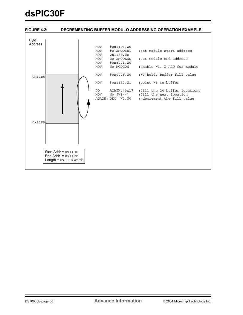
dsPIC30F
FIGURE 4-2: DECREMENTING BUFFER MODULO ADDRESSING OPERATION EXAMPLE
0x11D0
0x11FF
Start Addr = 0x11D0End Addr = 0x11FFLength = 0x0018 words
ByteAddress
MOV #0x11D0,W0MOV #0,XMODSRT ;set modulo start addressMOV 0x11FF,W0MOV W0,XMODEND ;set modulo end addressMOV #0x8001,W0MOV W0,MODCON ;enable W1, X AGU for modulo
MOV #0x000F,W0 ;W0 holds buffer fill value
MOV #0x11E0,W1 ;point W1 to buffer
DO AGAIN,#0x17 ;fill the 24 buffer locationsMOV W0,[W1--] ;fill the next locationAGAIN: DEC W0,W0 ; decrement the fill value
DS70083E-page 50 Advance Information 2004 Microchip Technology Inc.
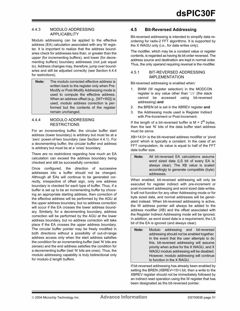
dsPIC30F
4.4.3 MODULO ADDRESSING
APPLICABILITY
Modulo addressing can be applied to the effective
address (EA) calculation associated with any W regis-
ter. It is important to realize that the address bound-
aries check for addresses less than, or greater than the
upper (for incrementing buffers), and lower (for decre-
menting buffers) boundary addresses (not just equal
to). Address changes may, therefore, jump over bound-
aries and still be adjusted correctly (see Section 4.4.4
for restrictions).
4.4.4 MODULO ADDRESSING
RESTRICTIONS
For an incrementing buffer, the circular buffer start
address (lower boundary) is arbitrary but must be at a
‘zero’ power-of-two boundary (see Section 4.4.1). For
a decrementing buffer, the circular buffer end address
is arbitrary but must be at a ‘ones’ boundary.
There are no restrictions regarding how much an EA
calculation can exceed the address boundary being
checked and still be successfully corrected.
Once configured, the direction of successive
addresses into a buffer should not be changed.
Although all EAs will continue to be generated cor-
rectly, irrespective of offset sign, only one address
boundary is checked for each type of buffer. Thus, if a
buffer is set up to be an incrementing buffer by choos-
ing an appropriate starting address, then correction of
the effective address will be performed by the AGU at
the upper address boundary, but no address correction
will occur if the EA crosses the lower address bound-
ary. Similarly, for a decrementing boundary, address
correction will be performed by the AGU at the lower
address boundary, but no address correction will take
place if the EA crosses the upper address boundary.
The circular buffer pointer may be freely modified in
both directions without a possibility of out-of-range
address access only when the start address satisfies
the condition for an incrementing buffer (last ‘N’ bits are
zeroes) and the end address satisfies the condition for
a decrementing buffer (last ‘N’ bits are ones). Thus, the
modulo addressing capability is truly bidirectional only
for modulo-2 length buffers.
4.5 Bit-Reversed Addressing
Bit-reversed addressing is intended to simplify data re-
ordering for radix-2 FFT algorithms. It is supported by
the X WAGU only (i.e., for data writes only).
The modifier, which may be a constant value or register
contents, is regarded as having its bit order reversed. The
address source and destination are kept in normal order.
Thus, the only operand requiring reversal is the modifier.
4.5.1 BIT-REVERSED ADDRESSING
IMPLEMENTATION
Bit-reversed addressing is enabled when:
1. BWM (W register selection) in the MODCON
register is any value other than ‘15’ (the stack
cannot be accessed using bit-reversed
addressing) and
2. the BREN bit is set in the XBREV register and
3. the Addressing mode used is Register Indirect
with Pre-Increment or Post-Increment.
If the length of a bit-reversed buffer is M = 2N bytes,
then the last ‘N’ bits of the data buffer start address
must be zeros.
XB<14:0> is the bit-reversed address modifier or ‘pivot
point’ which is typically a constant. In the case of an
FFT computation, its value is equal to half of the FFT
data buffer size.
When enabled, bit-reversed addressing will only be
executed for register indirect with pre-increment or
post-increment addressing and word sized data writes.
It will not function for any other Addressing mode or for
byte sized data, and normal addresses will be gener-
ated instead. When bit-reversed addressing is active,
the W address pointer will always be added to the
address modifier (XB) and the offset associated with
the Register Indirect Addressing mode will be ignored.
In addition, as word sized data is a requirement, the LS
bit of the EA is ignored (and always clear).
If bit-reversed addressing has already been enabled by
setting the BREN (XBREV<15>) bit, then a write to the
XBREV register should not be immediately followed by
an indirect read operation using the W register that has
been designated as the bit-reversed pointer.
Note: The modulo corrected effective address is
written back to the register only when Pre-
Modify or Post-Modify Addressing mode is
used to compute the effective address.
When an address offset (e.g., [W7+W2]) is
used, modulo address correction is per-
formed but the contents of the register
remain unchanged.
Note: All bit-reversed EA calculations assume
word sized data (LS bit of every EA is
always clear). The XB value is scaled
accordingly to generate compatible (byte)
addresses.
Note: Modulo addressing and bit-reversed
addressing should not be enabled together.
In the event that the user attempts to do
this, bit-reversed addressing will assume
priority when active for the X WAGU, and X
WAGU modulo addressing will be disabled.
However, modulo addressing will continue
to function in the X RAGU.
2004 Microchip Technology Inc. Advance Information DS70083E-page 51
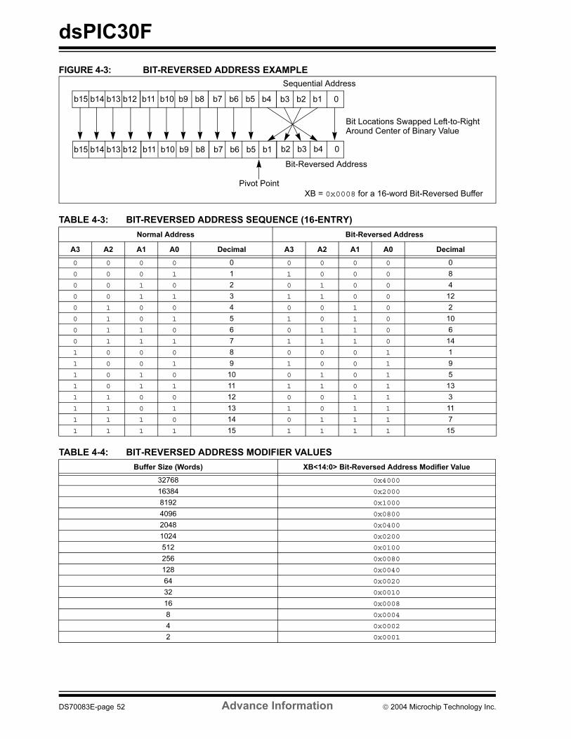
dsPIC30F
FIGURE 4-3: BIT-REVERSED ADDRESS EXAMPLE
TABLE 4-3: BIT-REVERSED ADDRESS SEQUENCE (16-ENTRY)
TABLE 4-4: BIT-REVERSED ADDRESS MODIFIER VALUES
Normal Address Bit-Reversed Address
A3 A2 A1 A0 Decimal A3 A2 A1 A0 Decimal
0 0 0 0 0 0 0 0 0 0
0 0 0 1 1 1 0 0 0 8
0 0 1 0 2 0 1 0 0 4
0 0 1 1 3 1 1 0 0 12
0 1 0 0 4 0 0 1 0 2
0 1 0 1 5 1 0 1 0 10
0 1 1 0 6 0 1 1 0 6
0 1 1 1 7 1 1 1 0 14
1 0 0 0 8 0 0 0 1 1
1 0 0 1 9 1 0 0 1 9
1 0 1 0 10 0 1 0 1 5
1 0 1 1 11 1 1 0 1 13
1 1 0 0 12 0 0 1 1 3
1 1 0 1 13 1 0 1 1 11
1 1 1 0 14 0 1 1 1 7
1 1 1 1 15 1 1 1 1 15
Buffer Size (Words) XB<14:0> Bit-Reversed Address Modifier Value
32768 0x4000
16384 0x2000
8192 0x1000
4096 0x0800
2048 0x0400
1024 0x0200
512 0x0100
256 0x0080
128 0x0040
64 0x0020
32 0x0010
16 0x0008
8 0x0004
4 0x0002
2 0x0001
b3 b2 b1 0
b2 b3 b4 0
Bit Locations Swapped Left-to-RightAround Center of Binary Value
Bit-Reversed Address
XB = 0x0008 for a 16-word Bit-Reversed Buffer
b7 b6 b5 b1
b7 b6 b5 b4b11 b10 b9 b8
b11 b10 b9 b8
b15 b14 b13 b12
b15 b14 b13 b12
Sequential Address
Pivot Point
DS70083E-page 52 Advance Information 2004 Microchip Technology Inc.
dsPIC30F
5.0 INTERRUPTS
The dsPIC30F Sensor and General Purpose Family
has up to 41 interrupt sources and 4 processor excep-
tions (traps) which must be arbitrated based on a
priority scheme.
The CPU is responsible for reading the Interrupt Vector
Table (IVT) and transferring the address contained in
the interrupt vector to the program counter. The inter-
rupt vector is transferred from the program data bus
into the program counter via a 24-bit wide multiplexer
on the input of the program counter.
The Interrupt Vector Table (IVT) and Alternate Interrupt
Vector Table (AIVT) are placed near the beginning of
program memory (0x000004). The IVT and AIVT are
shown in Table 5-2.
The interrupt controller is responsible for pre-
processing the interrupts and processor exceptions
prior to them being presented to the processor core.
The peripheral interrupts and traps are enabled, priori-
tized and controlled using centralized Special Function
Registers:
• IFS0<15:0>, IFS1<15:0>, IFS2<15:0>
All interrupt request flags are maintained in these
three registers. The flags are set by their respec-
tive peripherals or external signals, and they are
cleared via software.
• IEC0<15:0>, IEC1<15:0>, IEC2<15:0>
All interrupt enable control bits are maintained in
these three registers. These control bits are used
to individually enable interrupts from the
peripherals or external signals.
• IPC0<15:0>... IPC10<7:0>
The user assignable priority level associated with
each of these 41 interrupts is held centrally in
these twelve registers.
• IPL<3:0>
The current CPU priority level is explicitly stored
in the IPL bits. IPL<3> is present in the CORCON
register, whereas IPL<2:0> are present in the
STATUS register (SR) in the processor core.
• INTCON1<15:0>, INTCON2<15:0>
Global interrupt control functions are derived from
these two registers. INTCON1 contains the con-
trol and status flags for the processor exceptions.
The INTCON2 register controls the external
interrupt request signal behavior and the use of
the alternate vector table.
All interrupt sources can be user assigned to one of 7
priority levels, 1 through 7, via the IPCx registers. Each
interrupt source is associated with an interrupt vector,
as shown in Table 5-2. Levels 7 and 1 represent the
highest and lowest maskable priorities, respectively.
If the NSTDIS bit (INTCON1<15>) is set, nesting of
interrupts is prevented. Thus, if an interrupt is currently
being serviced, processing of a new interrupt is pre-
vented even if the new interrupt is of higher priority than
the one currently being serviced.
Certain interrupts have specialized control bits for fea-
tures like edge or level triggered interrupts, interrupt-
on-change, etc. Control of these features remains
within the peripheral module which generates the
interrupt.
The DISI instruction can be used to disable the pro-
cessing of interrupts of priorities 6 and lower for a cer-
tain number of instructions, during which the DISI bit
(INTCON2<14>) remains set.
When an interrupt is serviced, the PC is loaded with the
address stored in the vector location in program mem-
ory that corresponds to the interrupt. There are 63 dif-
ferent vectors within the IVT (refer to Table 5-2). These
vectors are contained in locations 0x000004 through
0x0000FE of program memory (refer to Table 5-2).
These locations contain 24-bit addresses and in order
to preserve robustness, an address error trap will take
place should the PC attempt to fetch any of these
words during normal execution. This prevents execu-
tion of random data as a result of accidentally decre-
menting a PC into vector space, accidentally mapping
a data space address into vector space, or the PC roll-
ing over to 0x000000 after reaching the end of imple-
mented program memory space. Execution of a GOTOinstruction to this vector space will also generate an
address error trap.
Note: Interrupt flag bits get set when an interrupt
condition occurs, regardless of the state of
its corresponding enable bit. User soft-
ware should ensure the appropriate inter-
rupt flag bits are clear prior to enabling an
interrupt.
Note: Assigning a priority level of ‘0’ to an inter-
rupt source is equivalent to disabling that
interrupt.
Note: The IPL bits become read only whenever
the NSTDIS bit has been set to ‘1’.
2004 Microchip Technology Inc. Advance Information DS70083E-page 53
dsPIC30F
5.1 Interrupt Priority
The user assignable interrupt priority (IP<2:0>) bits for
each individual interrupt source are located in the LS
3 bits of each nibble within the IPCx register(s). Bit 3 of
each nibble is not used and is read as a ‘0’. These bits
define the priority level assigned to a particular interrupt
by the user.
Since more than one interrupt request source may be
assigned to a specific user specified priority level, a
means is provided to assign priority within a given level.
This method is called “Natural Order Priority”.
Table 5-1 lists the interrupt numbers and interrupt
sources for the dsPIC device and their associated
vector numbers.
The ability for the user to assign every interrupt to one
of seven priority levels implies that the user can assign
a very high overall priority level to an interrupt with a
low natural order priority. For example, the PLVD (Low
Voltage Detect) can be given a priority of 7. The INT0
(External Interrupt 0) may be assigned to priority level
1, thus giving it a very low effective priority.
TABLE 5-1: NATURAL ORDER PRIORITY
Note: The user selectable priority levels start at
0 as the lowest priority and level 7 as the
highest priority.
Note 1: The natural order priority scheme has 0
as the highest priority and 53 as the
lowest priority.
2: The natural order priority number is the
same as the INT number.
INT
Number
Vector
NumberInterrupt Source
Highest Natural Order Priority
0 8 INT0 - External Interrupt 0
1 9 IC1 - Input Capture 1
2 10 OC1 - Output Compare 1
3 11 T1 - Timer 1
4 12 IC2 - Input Capture 2
5 13 OC2 - Output Compare 2
6 14 T2 - Timer 2
7 15 T3 - Timer 3
8 16 SPI1
9 17 U1RX - UART1 Receiver
10 18 U1TX - UART1 Transmitter
11 19 ADC - ADC Convert Done
12 20 NVM - NVM Write Complete
13 21 SI2C - I2C Slave Interrupt
14 22 MI2C - I2C Master Interrupt
15 23 Input Change Interrupt
16 24 INT1 - External Interrupt 1
17 25 IC7 - Input Capture 7
18 26 IC8 - Input Capture 8
19 27 OC3 - Output Compare 3
20 28 OC4 - Output Compare 4
21 29 T4 - Timer 4
22 30 T5 - Timer 5
23 31 INT2 - External Interrupt 2
24 32 U2RX - UART2 Receiver
25 33 U2TX - UART2 Transmitter
26 34 SPI2
27 35 C1 - Combined IRQ for CAN1
28 36 IC3 - Input Capture 3
29 37 IC4 - Input Capture 4
30 38 IC5 - Input Capture 5
31 39 IC6 - Input Capture 6
32 40 OC5 - Output Compare 5
33 41 OC6 - Output Compare 6
34 42 OC7 - Output Compare 7
35 43 OC8 - Output Compare 8
36 44 INT3 - External Interrupt 3
37 45 INT4 - External Interrupt 4
38 46 C2 - Combined IRQ for CAN2
39-40 47-48 Reserved
41 49 DCI - Codec Transfer Done
42 50 LVD - Low Voltage Detect
43-53 51-61 Reserved
Lowest Natural Order Priority
DS70083E-page 54 Advance Information 2004 Microchip Technology Inc.
dsPIC30F
5.2 Reset Sequence
A Reset is not a true exception, because the interrupt
controller is not involved in the Reset process. The pro-
cessor initializes its registers in response to a Reset
which forces the PC to zero. The processor then begins
program execution at location 0x000000. A GOTOinstruction is stored in the first program memory loca-
tion immediately followed by the address target for the
GOTO instruction. The processor executes the GOTO to
the specified address and then begins operation at the
specified target (start) address.
5.2.1 RESET SOURCES
In addition to external Reset and Power-on Reset
(POR), there are 6 sources of error conditions which
‘trap’ to the Reset vector.
• Watchdog Time-out:
The watchdog has timed out, indicating that the
processor is no longer executing the correct flow
of code.
• Uninitialized W Register Trap:
An attempt to use an uninitialized W register as
an address pointer will cause a Reset.
• Illegal Instruction Trap:
Attempted execution of any unused opcodes will
result in an illegal instruction trap. Note that a
fetch of an illegal instruction does not result in an
illegal instruction trap if that instruction is flushed
prior to execution due to a flow change.
• Brown-out Reset (BOR):
A momentary dip in the power supply to the
device has been detected which may result in
malfunction.
• Trap Lockout:
Occurrence of multiple trap conditions
simultaneously will cause a Reset.
5.3 Traps
Traps can be considered as non-maskable, non-stable
interrupts, which adhere to a predefined priority, as
shown in Table 5-2. They are intended to provide the
user a means to correct erroneous operation during
debug and when operating within the application.
Note that many of these trap conditions can only be
detected when they occur. Consequently, the question-
able instruction is allowed to complete prior to trap
exception processing. If the user chooses to recover
from the error, the result of the erroneous action that
caused the trap may have to be corrected.
There are 8 fixed priority levels for traps: level 8 through
level 15, which implies that the IPL3 is always set
during processing of a trap.
If the user is not currently executing a trap, and he sets
the IPL<3:0> bits to a value of ‘0111’ (level 7), then all
interrupts are disabled but traps can still be processed.
5.3.1 TRAP SOURCES
The following traps are provided with increasing prior-
ity. However, since all traps can be nested, priority has
little effect.
• Math Error Trap:
The math error trap executes under the following
four circumstances:
1. Should an attempt be made to divide by
zero, the divide operation will be aborted on
a cycle boundary and the trap taken.
2. If enabled, a math error trap will be taken
when an arithmetic operation on either
accumulator A or B causes an overflow
from bit 31 and the accumulator guard bits
are not utilized.
3. If enabled, a math error trap will be taken
when an arithmetic operation on either
accumulator A or B causes a catastrophic
overflow from bit 39 and all saturation is
disabled.
4. If the shift amount specified in a shift
instruction is greater than the maximum
allowed shift amount, a trap will occur.
Note: If the user does not intend to take correc-
tive action in the event of a trap error con-
dition, these vectors must be loaded with
the address of a default handler that sim-
ply contains the RESET instruction. If, on
the other hand, one of the vectors contain-
ing an invalid address is called, an
address error trap is generated.
2004 Microchip Technology Inc. Advance Information DS70083E-page 55
dsPIC30F
• Address Error Trap:
This trap is initiated when any of the following
circumstances occurs:
1. A misaligned data word access is
attempted.
2. A data fetch from and unimplemented data
memory location is attempted.
3. A data fetch from an unimplemented pro-
gram memory location is attempted.
4. An instruction fetch from vector space is
attempted.
5. Execution of a “BRA #literal” instruction or a
“GOTO #literal” instruction, where literalis an unimplemented program memory address.
6. Executing instructions after modifying the PC to
point to unimplemented program memory
addresses. The PC may be modified by loading
a value into the stack and executing a RETURNinstruction.
• Stack Error Trap:
This trap is initiated under the following
conditions:
1. The stack pointer is loaded with a value
which is greater than the (user program-
mable) limit value written into the SPLIM
register (stack overflow).
2. The stack pointer is loaded with a value
which is less than 0x0800 (simple stack
underflow).
• Oscillator Fail Trap:
This trap is initiated if the external oscillator fails
and operation becomes reliant on an internal RC
backup.
5.3.2 HARD AND SOFT TRAPS
It is possible that multiple traps can become active
within the same cycle (e.g., a misaligned word stack
write to an overflowed address). In such a case, the
fixed priority shown in Figure 5-2 is implemented,
which may require the user to check if other traps are
pending in order to completely correct the fault.
‘Soft’ traps include exceptions of priority level 8 through
level 11, inclusive. The arithmetic error trap (level 11)
falls into this category of traps. Soft traps can be treated
like non-maskable sources of interrupt that adhere to
the priority assigned by their position in the IVT. Soft
traps are processed like interrupts and require 2 cycles
to be sampled and Acknowledged prior to exception
processing. Therefore, additional instructions may be
executed before a soft trap is Acknowledged.
‘Hard’ traps include exceptions of priority level 12
through level 15, inclusive. The address error (level
12), stack error (level 13) and oscillator error (level 14)
traps fall into this category.
Like soft traps, hard traps can also be viewed as non-
maskable sources of interrupt. The difference between
hard traps and soft traps is that hard traps force the
CPU to stop code execution after the instruction caus-
ing the trap has completed. Normal program execution
flow will not resume until after the trap has been
Acknowledged and processed.
If a higher priority trap occurs while any lower priority
trap is in progress, processing of the lower priority trap
will be suspended and the higher priority trap will be
Acknowledged and processed. The lower priority trap
will remain pending until processing of the higher
priority trap completes.
Each hard trap that occurs must be Acknowledged
before code execution of any type may continue. If a
lower priority hard trap occurs while a higher priority
trap is pending, Acknowledged, or is being processed,
a hard trap conflict will occur. The conflict occurs
because the lower priority trap cannot be Acknowl-
edged until processing for the higher priority trap
completes.
The device is automatically reset in a hard trap conflict
condition. The TRAPR status bit (RCON<15>) is set
when the Reset occurs so that the condition may be
detected in software.
In the case of a math error trap or oscillator failure trap,
the condition that causes the trap to occur must be
removed before the respective trap flag bit in the
INTCON1 register may be cleared.
Note: In the MAC class of instructions, wherein
the data space is split into X and Y data
space, unimplemented X space includes
all of Y space, and unimplemented Y
space includes all of X space.
DS70083E-page 56 Advance Information 2004 Microchip Technology Inc.
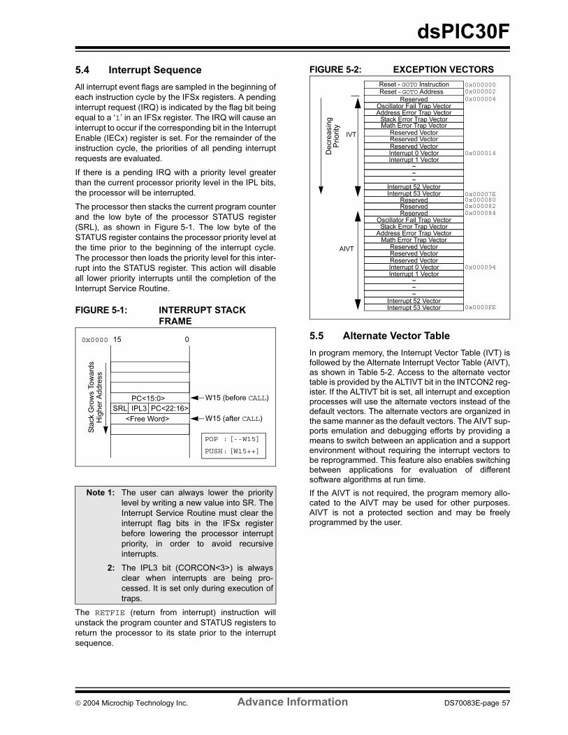
dsPIC30F
5.4 Interrupt Sequence
All interrupt event flags are sampled in the beginning of
each instruction cycle by the IFSx registers. A pending
interrupt request (IRQ) is indicated by the flag bit being
equal to a ‘1’ in an IFSx register. The IRQ will cause an
interrupt to occur if the corresponding bit in the Interrupt
Enable (IECx) register is set. For the remainder of the
instruction cycle, the priorities of all pending interrupt
requests are evaluated.
If there is a pending IRQ with a priority level greater
than the current processor priority level in the IPL bits,
the processor will be interrupted.
The processor then stacks the current program counter
and the low byte of the processor STATUS register
(SRL), as shown in Figure 5-1. The low byte of the
STATUS register contains the processor priority level at
the time prior to the beginning of the interrupt cycle.
The processor then loads the priority level for this inter-
rupt into the STATUS register. This action will disable
all lower priority interrupts until the completion of the
Interrupt Service Routine.
FIGURE 5-1: INTERRUPT STACK
FRAME
The RETFIE (return from interrupt) instruction will
unstack the program counter and STATUS registers to
return the processor to its state prior to the interrupt
sequence.
FIGURE 5-2: EXCEPTION VECTORS
5.5 Alternate Vector Table
In program memory, the Interrupt Vector Table (IVT) isfollowed by the Alternate Interrupt Vector Table (AIVT),as shown in Table 5-2. Access to the alternate vectortable is provided by the ALTIVT bit in the INTCON2 reg-ister. If the ALTIVT bit is set, all interrupt and exceptionprocesses will use the alternate vectors instead of thedefault vectors. The alternate vectors are organized inthe same manner as the default vectors. The AIVT sup-ports emulation and debugging efforts by providing ameans to switch between an application and a supportenvironment without requiring the interrupt vectors tobe reprogrammed. This feature also enables switchingbetween applications for evaluation of differentsoftware algorithms at run time.
If the AIVT is not required, the program memory allo-cated to the AIVT may be used for other purposes.AIVT is not a protected section and may be freelyprogrammed by the user.
Note 1: The user can always lower the priority
level by writing a new value into SR. The
Interrupt Service Routine must clear the
interrupt flag bits in the IFSx register
before lowering the processor interrupt
priority, in order to avoid recursive
interrupts.
2: The IPL3 bit (CORCON<3>) is always
clear when interrupts are being pro-
cessed. It is set only during execution of
traps.
<Free Word>
015
W15 (before CALL)
W15 (after CALL)
Sta
ck G
row
s T
ow
ard
sH
igh
er
Ad
dre
ss
0x0000
PC<15:0>
SRL IPL3 PC<22:16>
POP : [--W15]
PUSH: [W15++]
Address Error Trap Vector
Oscillator Fail Trap VectorStack Error Trap Vector
Reserved VectorMath Error Trap Vector
Reserved
Oscillator Fail Trap VectorAddress Error Trap Vector
Reserved VectorReserved VectorInterrupt 0 VectorInterrupt 1 Vector
~~~
Interrupt 52 VectorInterrupt 53 Vector
Math Error Trap Vector
De
cre
asin
gP
rio
rity
0x000000
0x000014
Reserved
Stack Error Trap Vector
Reserved VectorReserved VectorInterrupt 0 VectorInterrupt 1 Vector
~~~
Interrupt 52 VectorInterrupt 53 Vector
IVT
AIVT
0x000080
0x00007E
0x0000FE
Reserved
0x000094
Reset - GOTO InstructionReset - GOTO Address 0x000002
Reserved0x000082
0x000084
0x000004
Reserved Vector
2004 Microchip Technology Inc. Advance Information DS70083E-page 57
dsPIC30F
5.6 Fast Context Saving
A context saving option is available using shadow reg-isters. Shadow registers are provided for the DC, N,OV, Z and C bits in SR, and the registers W0 throughW3. The shadows are only one level deep. The shadowregisters are accessible using the PUSH.S and POP.Sinstructions only.
When the processor vectors to an interrupt, thePUSH.S instruction can be used to store the currentvalue of the aforementioned registers into theirrespective shadow registers.
If an ISR of a certain priority uses the PUSH.S andPOP.S instructions for fast context saving, then ahigher priority ISR should not include the same instruc-tions. Users must save the key registers in softwareduring a lower priority interrupt if the higher priority ISRuses fast context saving.
5.7 External Interrupt Requests
The interrupt controller supports up to five externalinterrupt request signals, INT0-INT4. These inputs areedge sensitive; they require a low-to-high or a high-to-low transition to generate an interrupt request. TheINTCON2 register has five bits, INT0EP-INT4EP, thatselect the polarity of the edge detection circuitry.
5.8 Wake-up from Sleep and Idle
The interrupt controller may be used to wake-up theprocessor from either Sleep or Idle modes, if Sleep orIdle mode is active when the interrupt is generated.
If an enabled interrupt request of sufficient priority isreceived by the interrupt controller, then the standardinterrupt request is presented to the processor. At thesame time, the processor will wake-up from Sleep orIdle and begin execution of the Interrupt ServiceRoutine (ISR) needed to process the interrupt request.
DS70083E-page 58 Advance Information 2004 Microchip Technology Inc.
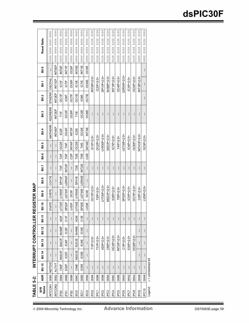
dsPIC30F
TA
BL
E 5
-2:
INT
ER
RU
PT
CO
NT
RO
LL
ER
RE
GIS
TE
R M
AP
SF
R
Nam
eA
DR
Bit
15
Bit
14
Bit
13
Bit
12
Bit
11
Bit
10
Bit
9B
it 8
Bit
7B
it 6
Bit
5B
it 4
Bit
3B
it 2
Bit
1B
it 0
Reset
Sta
te
INT
CO
N1
0080
NS
TD
IS—
——
—O
VA
TE
OV
BT
EC
OV
TE
——
—M
AT
HE
RR
AD
DR
ER
RS
TK
ER
RO
SC
FA
IL—
0000 0000 0000 0000
INT
CO
N2
0082
ALT
IVT
——
——
——
——
——
INT
4E
PIN
T3E
PIN
T2E
PIN
T1E
PIN
T0E
P0000 0000 0000 0000
IFS
00084
CN
IFM
I2C
IF S
I2C
IFN
VM
IFA
DIF
U1T
XIF
U1R
XIF
SP
I1IF
T3IF
T2IF
OC
2IF
IC2IF
T1IF
OC
1IF
IC1IF
INT
0IF
0000 0000 0000 0000
IFS
10086
IC6IF
IC5IF
IC4IF
IC3IF
C1IF
SP
I2IF
U2T
XIF
U2
RX
IFIN
T2IF
T5IF
T4IF
OC
4IF
OC
3IF
IC8IF
IC7IF
INT
1IF
0000 0000 0000 0000
IFS
20088
——
——
—LV
DIF
DC
IIF
——
C2IF
INT
4IF
INT
3IF
OC
8IF
OC
7IF
OC
6IF
OC
5IF
0000 0000 0000 0000
IEC
0008C
CN
IEM
I2C
IES
I2C
IEN
VM
IEA
DIE
U1T
XIE
U1R
XIE
SP
I1IE
T3IE
T2IE
OC
2IE
IC2IE
T1IE
OC
1IE
IC1IE
INT
0IE
0000 0000 0000 0000
IEC
1008E
IC6IE
IC5IE
IC4IE
IC3IE
C1IE
SP
I2IE
U2T
XIE
U2
RX
IEIN
T2IE
T5IE
T4IE
OC
4IE
OC
3IE
IC8IE
IC7IE
INT
1IE
0000 0000 0000 0000
IEC
20090
——
——
—LV
DIE
DC
IIE
——
C2IE
INT
4IE
INT
3IE
OC
8IE
OC
7IE
OC
6IE
OC
5IE
0000 0000 0000 0000
IPC
00094
—T
1IP
<2:0
>—
OC
1IP
<2:0
>—
IC1IP
<2:0
>—
INT
0IP
<2:0
>0100 0100 0100 0100
IPC
10096
—T
31P
<2:0
>—
T2IP
<2:0
>—
OC
2IP
<2:0
>—
IC2IP
<2:0
>0100 0100 0100 0100
IPC
20098
—A
DIP
<2:0
>—
U1T
XIP
<2:0
>—
U1R
XIP
<2:0
>—
SP
I1IP
<2:0
>0100 0100 0100 0100
IPC
3009A
—C
NIP
<2:0
>—
MI2
CIP
<2:0
>—
SI2
CIP
<2:0
>—
NV
MIP
<2:0
>0100 0100 0100 0100
IPC
4009C
—O
C3IP
<2:0
>—
IC8IP
<2:0
>—
IC7IP
<2:0
>—
INT
1IP
<2:0
>0100 0100 0100 0100
IPC
5009E
—IN
T2IP
<2:0
>—
T5IP
<2:0
>—
T4IP
<2:0
>—
OC
4IP
<2:0
>0100 0100 0100 0100
IPC
600A
0—
C1IP
<2:0
>—
SP
I2IP
<2:0
>—
U2T
XIP
<2:0
>—
U2R
XIP
<2:0
>0100 0100 0100 0100
IPC
700A
2—
IC6IP
<2:0
>—
IC5IP
<2:0
>—
IC4IP
<2:0
>—
IC3IP
<2:0
>0100 0100 0100 0100
IPC
800A
4—
OC
8IP
<2:0
>—
OC
7IP
<2:0
>—
OC
6IP
<2:0
>—
OC
5IP
<2:0
>0100 0100 0100 0100
IPC
900A
6—
——
——
C2IP
<2:0
>—
INT
41IP
<2:0
>—
INT
3IP
<2:0
>0000 0100 0100 0100
IPC
10
00A
8—
——
——
LV
DIP
<2:0
>—
DC
IIP
<2:0
>—
——
—0000 0100 0100 0000
Legend:
u =
unin
itia
lized b
it
2004 Microchip Technology Inc. Advance Information DS70083E-page 59

dsPIC30F
NOTES:
DS70083E-page 60 Advance Information 2004 Microchip Technology Inc.
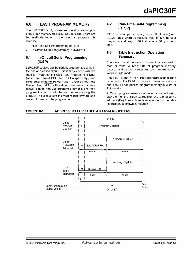
dsPIC30F
6.0 FLASH PROGRAM MEMORY
The dsPIC30F family of devices contains internal pro-
gram Flash memory for executing user code. There are
two methods by which the user can program this
memory:
1. Run-Time Self-Programming (RTSP)
2. In-Circuit Serial Programming™ (ICSP™)
6.1 In-Circuit Serial Programming
(ICSP)
dsPIC30F devices can be serially programmed while in
the end application circuit. This is simply done with two
lines for Programming Clock and Programming Data
(which are named PGC and PGD respectively), and
three other lines for Power (VDD), Ground (VSS) and
Master Clear (MCLR). this allows customers to manu-
facture boards with unprogrammed devices, and then
program the microcontroller just before shipping the
product. This also allows the most recent firmware or a
custom firmware to be programmed.
6.2 Run-Time Self-Programming
(RTSP)
RTSP is accomplished using TBLRD (table read) and
TBLWT (table write) instructions. With RTSP, the user
may erase and program 32 instructions (96 bytes) at a
time.
6.3 Table Instruction Operation
Summary
The TBLRDL and the TBLWTL instructions are used to
read or write to bits<15:0> of program memory.
TBLRDL and TBLWTL can access program memory in
Word or Byte mode.
The TBLRDH and TBLWTH instructions are used to read
or write to bits<23:16> of program memory. TBLRDHand TBLWTH can access program memory in Word or
Byte mode.
A 24-bit program memory address is formed using
bits<7:0> of the TBLPAG register and the effective
address (EA) from a W register specified in the table
instruction, as shown in Figure 6-1.
FIGURE 6-1: ADDRESSING FOR TABLE AND NVM REGISTERS
0Program Counter
24 bits
NVMADRU Reg
8 bits 16 bits
Program
Using
TBLPAG Reg
8 bits
Working Reg EA
16 bits
Using
Byte
24-bit EA
1/0
0
1/0
Select
Table
Instruction
NVMADR
Addressing
Counter
Using
NVMADR Reg EA
User/ConfigurationSpace Select
2004 Microchip Technology Inc. Advance Information DS70083E-page 61
dsPIC30F
6.4 RTSP Operation
The dsPIC30F Flash program memory is organized
into rows and panels. Each row consists of 32 instruc-
tions or 96 bytes. Each panel consists of 128 rows or
4K x 24 instructions. RTSP allows the user to erase and
program one row (32 instructions) at a time. RTSP may
be used to program multiple program memory panels,
but the table pointer must be changed at each panel
boundary.
Each panel of program memory contains write latches
that hold 32 instructions of programming data. Prior to
the actual programming operation, the write data must
be loaded into the panel write latches. The data to be
programmed into the panel is loaded in sequential
order into the write latches: instruction 0, instruction 1,
etc. The instruction words loaded must always be from
a group of 32 boundary.
The basic sequence for RTSP programming is to set up
a table pointer, then do a series of TBLWT instructions
to load the write latches. Programming is performed by
setting the special bits in the NVMCON register. Four
TBLWTL and four TBLWTH instructions are required to
load the four instructions. To fully program a row of
program memory, eight cycles of four TBLWTL and four
TBLWTH are required. If multiple panel programming
is required, the table pointer needs to be changed and
the next set of multiple write latches written.
All of the table write operations are single word writes
(2 instruction cycles) because only the table latches are
written. A total of 32 programming passes, each writing
4 instruction words, are required per row.
The Flash program memory is readable, writable, and
erasable during normal operation over the entire VDD
range.
6.5 Control Registers
The four SFRs used to read and write the program
Flash memory are:
• NVMCON
• NVMADR
• NVMADRU
• NVMKEY
6.5.1 NVMCON REGISTER
The NVMCON register controls which blocks are to be
erased, which memory type is to be programmed and
start of the programming cycle.
6.5.2 NVMADR REGISTER
The NVMADR register is used to hold the lower two
bytes of the effective address. The NVMADR register
captures the EA<15:0> of the last table instruction that
has been executed and selects the row to write.
6.5.3 NVMADRU REGISTER
The NVMADRU register is used to hold the upper byte
of the effective address. The NVMADRU register cap-
tures the EA<23:16> of the last table instruction that
has been executed.
6.5.4 NVMKEY REGISTER
NVMKEY is a write only register that is used for write
protection. To start a programming or an erase
sequence, the user must consecutively write 0x55 and
0xAA to the NVMKEY register. Refer to Section 6.6 for
further details.
DS70083E-page 62 Advance Information 2004 Microchip Technology Inc.
dsPIC30F
6.6 Programming Operations
A complete programming sequence is necessary for
programming or erasing the internal Flash in RTSP
mode. A programming operation is nominally 2 msec in
duration and the processor stalls (waits) until the oper-
ation is finished. Setting the WR bit (NVMCON<15>)
starts the operation, and the WR bit is automatically
cleared when the operation is finished.
6.6.1 PROGRAMMING ALGORITHM FOR
PROGRAM FLASH
The user can erase one row of program Flash memory
at a time. The user can program one block
(4 instruction words) of Flash memory at a time. The
general process is:
1. Read one row of program Flash (32 instruction
words) and store into data RAM as a data
“image”.
2. Update the data image with the desired new
data.
3. Erase program Flash row.
a) Setup NVMCON register for multi-word,
program Flash, erase, and set WREN bit.
b) Write address of row to be erased into
NVMADRU/NVMADR.
c) Write ‘55’ to NVMKEY.
d) Write ‘AA’ to NVMKEY.
e) Set the WR bit. This will begin erase cycle.
f) CPU will stall for the duration of the erase
cycle.
g) The WR bit is cleared when erase cycle
ends.
4. Write 32 instruction words of data from data
RAM into the program Flash write latches.
5. Program 32 instruction words into program
Flash.
a) Setup NVMCON register for multi-word,
program Flash, program, and set WREN
bit.
b) Write ‘55’ to NVMKEY.
c) Write ‘AA’ to NVMKEY.
d) Set the WR bit. This will begin program
cycle.
e) CPU will stall for duration of the program
cycle.
f) The WR bit is cleared by the hardware
when program cycle ends.
6. Repeat steps 1 through 5 as needed to program
desired amount of program Flash memory.
6.6.2 ERASING A ROW OF PROGRAM
MEMORY
Example 6-1 shows a code sequence that can be used
to erase a row (32 instructions) of program memory.
EXAMPLE 6-1: ERASING A ROW OF PROGRAM MEMORY
; Setup NVMCON for erase operation, multi word write; program memory selected, and writes enabled
MOV #0x4041,W0 ;MOV W0,NVMCON ; Init NVMCON SFR
; Init pointer to row to be ERASEDMOV #tblpage(PROG_ADDR),W0 ; MOV W0,NVMADRU ; Initialize PM Page Boundary SFRMOV #tbloffset(PROG_ADDR),W0 ; Intialize in-page EA[15:0] pointerMOV W0, NVMADR ; Initialize NVMADR SFRDISI #5 ; Block all interrupts with priority <7 for
; next 5 instructionsMOV #0x55,W0MOV W0,NVMKEY ; Write the 0x55 key MOV #0xAA,W1 ;MOV W1,NVMKEY ; Write the 0xAA keyBSET NVMCON,#WR ; Start the erase sequence NOP ; Insert two NOPs after the eraseNOP ; command is asserted
2004 Microchip Technology Inc. Advance Information DS70083E-page 63
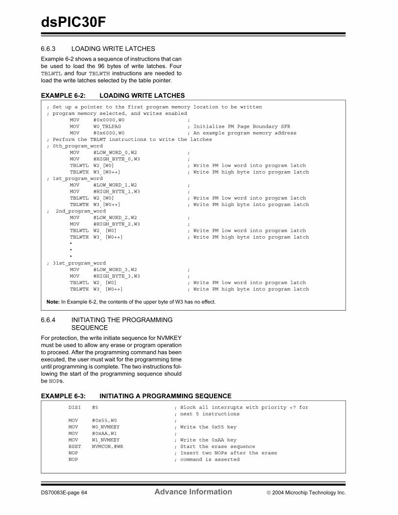
dsPIC30F
6.6.3 LOADING WRITE LATCHES
Example 6-2 shows a sequence of instructions that can
be used to load the 96 bytes of write latches. Four
TBLWTL and four TBLWTH instructions are needed to
load the write latches selected by the table pointer.
EXAMPLE 6-2: LOADING WRITE LATCHES
6.6.4 INITIATING THE PROGRAMMING
SEQUENCE
For protection, the write initiate sequence for NVMKEY
must be used to allow any erase or program operation
to proceed. After the programming command has been
executed, the user must wait for the programming time
until programming is complete. The two instructions fol-
lowing the start of the programming sequence should
be NOPs.
EXAMPLE 6-3: INITIATING A PROGRAMMING SEQUENCE
; Set up a pointer to the first program memory location to be written; program memory selected, and writes enabled
MOV #0x0000,W0 ; MOV W0,TBLPAG ; Initialize PM Page Boundary SFRMOV #0x6000,W0 ; An example program memory address
; Perform the TBLWT instructions to write the latches; 0th_program_word
MOV #LOW_WORD_0,W2 ; MOV #HIGH_BYTE_0,W3 ; TBLWTL W2,[W0] ; Write PM low word into program latchTBLWTH W3,[W0++] ; Write PM high byte into program latch
; 1st_program_wordMOV #LOW_WORD_1,W2 ; MOV #HIGH_BYTE_1,W3 ; TBLWTL W2,[W0] ; Write PM low word into program latchTBLWTH W3,[W0++] ; Write PM high byte into program latch
; 2nd_program_wordMOV #LOW_WORD_2,W2 ; MOV #HIGH_BYTE_2,W3 ; TBLWTL W2, [W0] ; Write PM low word into program latchTBLWTH W3, [W0++] ; Write PM high byte into program latch•
•
•
; 31st_program_wordMOV #LOW_WORD_3,W2 ; MOV #HIGH_BYTE_3,W3 ; TBLWTL W2, [W0] ; Write PM low word into program latchTBLWTH W3, [W0++] ; Write PM high byte into program latch
Note: In Example 6-2, the contents of the upper byte of W3 has no effect.
DISI #5 ; Block all interrupts with priority <7 for; next 5 instructions
MOV #0x55,W0 ; MOV W0,NVMKEY ; Write the 0x55 keyMOV #0xAA,W1 ;MOV W1,NVMKEY ; Write the 0xAA keyBSET NVMCON,#WR ; Start the erase sequence NOP ; Insert two NOPs after the eraseNOP ; command is asserted
DS70083E-page 64 Advance Information 2004 Microchip Technology Inc.
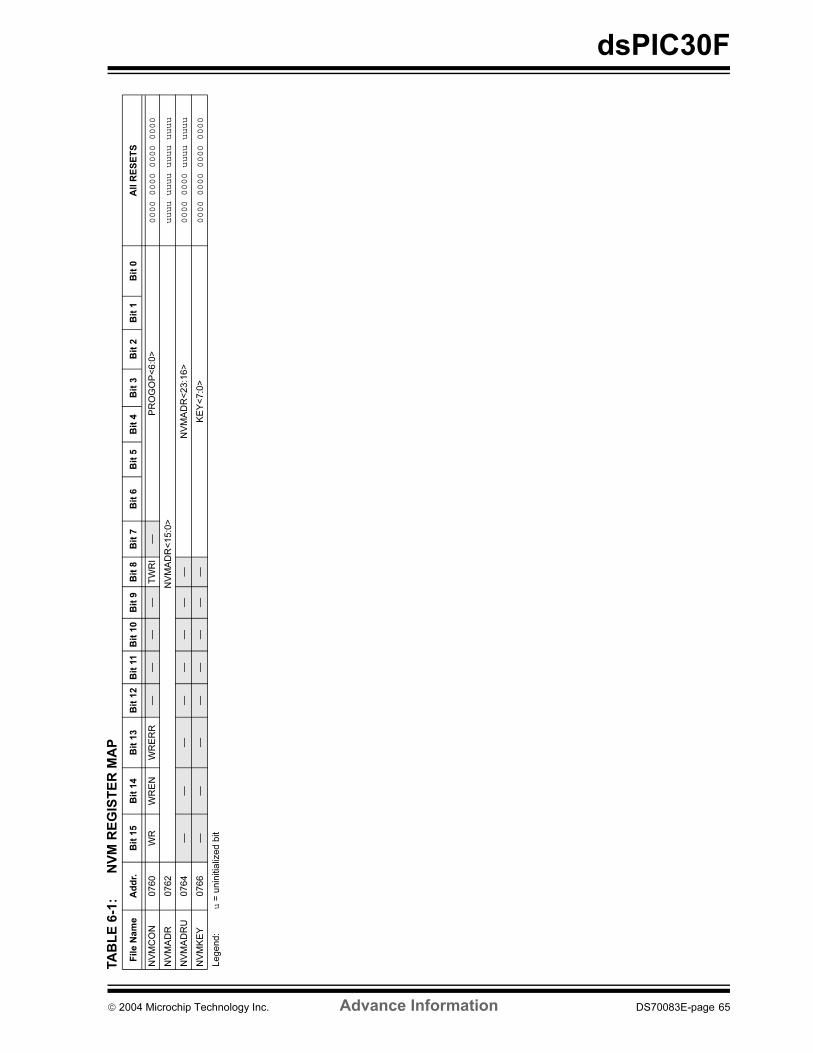
dsPIC30F
TA
BL
E 6
-1:
NV
M R
EG
IST
ER
MA
P
File N
am
eA
dd
r.B
it 1
5B
it 1
4B
it 1
3B
it 1
2B
it 1
1B
it 1
0B
it 9
Bit
8B
it 7
Bit
6B
it 5
Bit
4B
it 3
Bit
2B
it 1
Bit
0A
ll R
ES
ET
S
NV
MC
ON
0760
WR
WR
EN
WR
ER
R—
——
—T
WR
I—
PR
OG
OP
<6:0
>0000 0000 0000 0000
NV
MA
DR
0762
NV
MA
DR
<15:0
>uuuu uuuu uuuu uuuu
NV
MA
DR
U0764
——
——
——
——
NV
MA
DR
<23:1
6>
0000 0000 uuuu uuuu
NV
MK
EY
0766
——
——
——
——
KE
Y<
7:0
>0000 0000 0000 0000
Legend:
u =
unin
itia
lized b
it
2004 Microchip Technology Inc. Advance Information DS70083E-page 65

dsPIC30F
NOTES:
DS70083E-page 66 Advance Information 2004 Microchip Technology Inc.
dsPIC30F
7.0 DATA EEPROM MEMORY
The Data EEPROM Memory is readable and writable
during normal operation over the entire VDD range. The
data EEPROM memory is directly mapped in the
program memory address space.
The four SFRs used to read and write the program
Flash memory are used to access data EEPROM
memory, as well. As described in Section 6.5, these
registers are:
• NVMCON
• NVMADR
• NVMADRU
• NVMKEY
The EEPROM data memory allows read and write of
single words and 16-word blocks. When interfacing to
data memory, NVMADR in conjunction with the
NVMADRU register are used to address the EEPROM
location being accessed. TBLRDL and TBLWTLinstructions are used to read and write data EEPROM.
The dsPIC30F devices have up to 8 Kbytes (4K
words) of data EEPROM with an address range from
0x7FF000 to 0x7FFFFE.
A word write operation should be preceded by an erase
of the corresponding memory location(s). The write typ-
ically requires 2 ms to complete but the write time will
vary with voltage and temperature.
A program or erase operation on the data EEPROM
does not stop the instruction flow. The user is respon-
sible for waiting for the appropriate duration of time
before initiating another data EEPROM write/erase
operation. Attempting to read the data EEPROM while
a programming or erase operation is in progress results
in unspecified data.
Control bit WR initiates write operations similar to pro-
gram Flash writes. This bit cannot be cleared, only set,
in software. They are cleared in hardware at the com-
pletion of the write operation. The inability to clear the
WR bit in software prevents the accidental or
premature termination of a write operation.
The WREN bit, when set, will allow a write operation.
On power-up, the WREN bit is clear. The WRERR bit is
set when a write operation is interrupted by a MCLR
Reset or a WDT Time-out Reset during normal opera-
tion. In these situations, following Reset, the user can
check the WRERR bit and rewrite the location. The
address register NVMADR remains unchanged.
7.1 Reading the Data EEPROM
A TBLRD instruction reads a word at the current pro-
gram word address. This example uses W0 as a
pointer to data EEPROM. The result is placed in
register W4 as shown in Example 7-1.
EXAMPLE 7-1: DATA EEPROM READ
Note: Interrupt flag bit NVMIF in the IFS0 regis-
ter is set when write is complete. It must be
cleared in software.
MOV #LOW_ADDR_WORD,W0 ; Init Pointer
MOV #HIGH_ADDR_WORD,W1
MOV W1,TBLPAG
TBLRDL [ W0 ], W4 ; read data EEPROM
2004 Microchip Technology Inc. Advance Information DS70083E-page 67
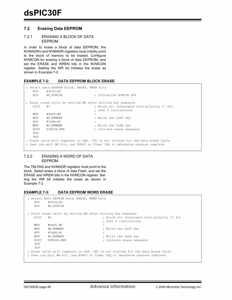
dsPIC30F
7.2 Erasing Data EEPROM
7.2.1 ERASING A BLOCK OF DATA
EEPROM
In order to erase a block of data EEPROM, the
NVMADRU and NVMADR registers must initially point
to the block of memory to be erased. Configure
NVMCON for erasing a block of data EEPROM, and
set the ERASE and WREN bits in the NVMCON
register. Setting the WR bit initiates the erase as
shown in Example 7-2.
EXAMPLE 7-2: DATA EEPROM BLOCK ERASE
7.2.2 ERASING A WORD OF DATA
EEPROM
The TBLPAG and NVMADR registers must point to the
block. Select erase a block of data Flash, and set the
ERASE and WREN bits in the NVMCON register. Set-
ting the WR bit initiates the erase as shown in
Example 7-3.
EXAMPLE 7-3: DATA EEPROM WORD ERASE
; Select data EEPROM block, ERASE, WREN bits
MOV #4045,W0
MOV W0,NVMCON ; Initialize NVMCON SFR
; Start erase cycle by setting WR after writing key sequence
DISI #5 ; Block all interrupts with priority <7 for
; next 5 instructions
MOV #0x55,W0 ;
MOV W0,NVMKEY ; Write the 0x55 key
MOV #0xAA,W1 ;
MOV W1,NVMKEY ; Write the 0xAA key
BSET NVMCON,#WR ; Initiate erase sequence
NOP
NOP
; Erase cycle will complete in 2mS. CPU is not stalled for the Data Erase Cycle
; User can poll WR bit, use NVMIF or Timer IRQ to determine erasure complete
; Select data EEPROM word, ERASE, WREN bits
MOV #4044,W0
MOV W0,NVMCON
; Start erase cycle by setting WR after writing key sequence
DISI #5 ; Block all interrupts with priority <7 for
; next 5 instructions
MOV #0x55,W0 ;
MOV W0,NVMKEY ; Write the 0x55 key
MOV #0xAA,W1 ;
MOV W1,NVMKEY ; Write the 0xAA key
BSET NVMCON,#WR ; Initiate erase sequence
NOP
NOP
; Erase cycle will complete in 2mS. CPU is not stalled for the Data Erase Cycle
; User can poll WR bit, use NVMIF or Timer IRQ to determine erasure complete
DS70083E-page 68 Advance Information 2004 Microchip Technology Inc.
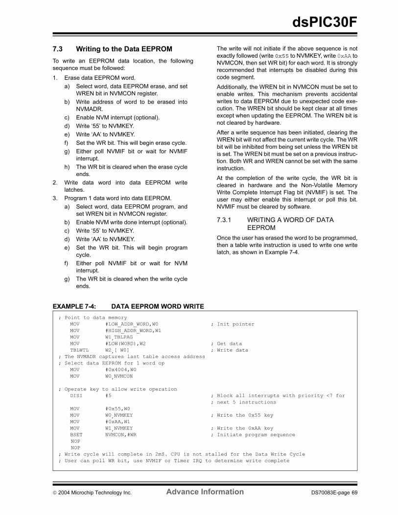
dsPIC30F
7.3 Writing to the Data EEPROM
To write an EEPROM data location, the following
sequence must be followed:
1. Erase data EEPROM word.
a) Select word, data EEPROM erase, and set
WREN bit in NVMCON register.
b) Write address of word to be erased into
NVMADR.
c) Enable NVM interrupt (optional).
d) Write ‘55’ to NVMKEY.
e) Write ‘AA’ to NVMKEY.
f) Set the WR bit. This will begin erase cycle.
g) Either poll NVMIF bit or wait for NVMIF
interrupt.
h) The WR bit is cleared when the erase cycle
ends.
2. Write data word into data EEPROM write
latches.
3. Program 1 data word into data EEPROM.
a) Select word, data EEPROM program, and
set WREN bit in NVMCON register.
b) Enable NVM write done interrupt (optional).
c) Write ‘55’ to NVMKEY.
d) Write ‘AA’ to NVMKEY.
e) Set the WR bit. This will begin program
cycle.
f) Either poll NVMIF bit or wait for NVM
interrupt.
g) The WR bit is cleared when the write cycle
ends.
The write will not initiate if the above sequence is not
exactly followed (write 0x55 to NVMKEY, write 0xAA to
NVMCON, then set WR bit) for each word. It is strongly
recommended that interrupts be disabled during this
code segment.
Additionally, the WREN bit in NVMCON must be set to
enable writes. This mechanism prevents accidental
writes to data EEPROM due to unexpected code exe-
cution. The WREN bit should be kept clear at all times
except when updating the EEPROM. The WREN bit is
not cleared by hardware.
After a write sequence has been initiated, clearing the
WREN bit will not affect the current write cycle. The WR
bit will be inhibited from being set unless the WREN bit
is set. The WREN bit must be set on a previous instruc-
tion. Both WR and WREN cannot be set with the same
instruction.
At the completion of the write cycle, the WR bit is
cleared in hardware and the Non-Volatile Memory
Write Complete Interrupt Flag bit (NVMIF) is set. The
user may either enable this interrupt or poll this bit.
NVMIF must be cleared by software.
7.3.1 WRITING A WORD OF DATA
EEPROM
Once the user has erased the word to be programmed,
then a table write instruction is used to write one write
latch, as shown in Example 7-4.
EXAMPLE 7-4: DATA EEPROM WORD WRITE
; Point to data memory
MOV #LOW_ADDR_WORD,W0 ; Init pointer
MOV #HIGH_ADDR_WORD,W1
MOV W1,TBLPAG
MOV #LOW(WORD),W2 ; Get data
TBLWTL W2,[ W0] ; Write data
; The NVMADR captures last table access address
; Select data EEPROM for 1 word op
MOV #0x4004,W0
MOV W0,NVMCON
; Operate key to allow write operation
DISI #5 ; Block all interrupts with priority <7 for
; next 5 instructions
MOV #0x55,W0
MOV W0,NVMKEY ; Write the 0x55 key
MOV #0xAA,W1
MOV W1,NVMKEY ; Write the 0xAA key
BSET NVMCON,#WR ; Initiate program sequence
NOP
NOP
; Write cycle will complete in 2mS. CPU is not stalled for the Data Write Cycle
; User can poll WR bit, use NVMIF or Timer IRQ to determine write complete
2004 Microchip Technology Inc. Advance Information DS70083E-page 69
dsPIC30F
7.3.2 WRITING A BLOCK OF DATA
EEPROM
To write a block of data EEPROM, write to all sixteen
latches first, then set the NVMCON register and
program the block.
EXAMPLE 7-5: DATA EEPROM BLOCK WRITE
MOV #LOW_ADDR_WORD,W0 ; Init pointer
MOV #HIGH_ADDR_WORD,W1
MOV W1,TBLPAG
MOV #data1,W2 ; Get 1st data
TBLWTL W2,[ W0]++ ; write data
MOV #data2,W2 ; Get 2nd data
TBLWTL W2,[ W0]++ ; write data
MOV #data3,W2 ; Get 3rd data
TBLWTL W2,[ W0]++ ; write data
MOV #data4,W2 ; Get 4th data
TBLWTL W2,[ W0]++ ; write data
MOV #data5,W2 ; Get 5th data
TBLWTL W2,[ W0]++ ; write data
MOV #data6,W2 ; Get 6th data
TBLWTL W2,[ W0]++ ; write data
MOV #data7,W2 ; Get 7th data
TBLWTL W2,[ W0]++ ; write data
MOV #data8,W2 ; Get 8th data
TBLWTL W2,[ W0]++ ; write data
MOV #data9,W2 ; Get 9th data
TBLWTL W2,[ W0]++ ; write data
MOV #data10,W2 ; Get 10th data
TBLWTL W2,[ W0]++ ; write data
MOV #data11,W2 ; Get 11th data
TBLWTL W2,[ W0]++ ; write data
MOV #data12,W2 ; Get 12th data
TBLWTL W2,[ W0]++ ; write data
MOV #data13,W2 ; Get 13th data
TBLWTL W2,[ W0]++ ; write data
MOV #data14,W2 ; Get 14th data
TBLWTL W2,[ W0]++ ; write data
MOV #data15,W2 ; Get 15th data
TBLWTL W2,[ W0]++ ; write data
MOV #data16,W2 ; Get 16th data
TBLWTL W2,[ W0]++ ; write data. The NVMADR captures last table access address.
MOV #0x400A,W0 ; Select data EEPROM for multi word op
MOV W0,NVMCON ; Operate Key to allow program operation
DISI #5 ; Block all interrupts with priority <7 for
; next 5 instructions
MOV #0x55,W0
MOV W0,NVMKEY ; Write the 0x55 key
MOV #0xAA,W1
MOV W1,NVMKEY ; Write the 0xAA key
BSET NVMCON,#WR ; Start write cycle
NOP
NOP
DS70083E-page 70 Advance Information 2004 Microchip Technology Inc.
dsPIC30F
7.4 Write Verify
Depending on the application, good programming
practice may dictate that the value written to the mem-
ory should be verified against the original value. This
should be used in applications where excessive writes
can stress bits near the specification limit.
7.5 Protection Against Spurious Write
There are conditions when the device may not want to
write to the data EEPROM memory. To protect against
spurious EEPROM writes, various mechanisms have
been built-in. On power-up, the WREN bit is cleared;
also, the Power-up Timer prevents EEPROM write.
The write initiate sequence and the WREN bit together
help prevent an accidental write during brown-out,
power glitch, or software malfunction.
2004 Microchip Technology Inc. Advance Information DS70083E-page 71

dsPIC30F
NOTES:
DS70083E-page 72 Advance Information 2004 Microchip Technology Inc.
dsPIC30F
8.0 I/O PORTS
All of the device pins (except VDD, VSS, MCLR, and
OSC1/CLKI) are shared between the peripherals and
the parallel I/O ports.
All I/O input ports feature Schmitt Trigger inputs for
improved noise immunity.
8.1 Parallel I/O (PIO) Ports
When a peripheral is enabled and the peripheral is
actively driving an associated pin, the use of the pin as
a general purpose output pin is disabled. The I/O pin
may be read but the output driver for the parallel port bit
will be disabled. If a peripheral is enabled but the
peripheral is not actively driving a pin, that pin may be
driven by a port.
All port pins have three registers directly associated
with the operation of the port pin. The Data Direction
register (TRISx) determines whether the pin is an input
or an output. If the data direction bit is a ‘1’, then the pin
is an input. All port pins are defined as inputs after a
Reset. Reads from the latch (LATx), read the latch.
Writes to the latch, write the latch (LATx). Reads from
the port (PORTx), read the port pins and writes to the
port pins, write the latch (LATx).
Any bit and its associated data and control registers
that are not valid for a particular device will be dis-
abled. That means the corresponding LATx and TRISx
registers and the port pin will read as zeros.
When a pin is shared with another peripheral or func-
tion that is defined as an input only, it is nevertheless
regarded as a dedicated port because there is no
other competing source of outputs. An example is the
INT4 pin.
The format of the registers for PORTA are shown in
Table 8-1.
The TRISA (Data Direction Control) register controls
the direction of the RA<7:0> pins, as well as the INTx
pins and the VREF pins. The LATA register supplies
data to the outputs and is readable/writable. Reading
the PORTA register yields the state of the input pins,
while writing the PORTA register modifies the contents
of the LATA register.
FIGURE 8-1: BLOCK DIAGRAM OF A DEDICATED PORT STRUCTURE
QD
CK
WR LAT +
TRIS Latch
I/O Pad
WR Port
Data Bus
QD
CK
Data Latch
Read LAT
Read Port
Read TRIS
WR TRIS
I/O Cell
Dedicated Port Module
2004 Microchip Technology Inc. Advance Information DS70083E-page 73
dsPIC30F
A parallel I/O (PIO) port that shares a pin with a periph-
eral is, in general, subservient to the peripheral. The
peripheral’s output buffer data and control signals are
provided to a pair of multiplexers. The multiplexers
select whether the peripheral or the associated port
has ownership of the output data and control signals of
the I/O pad cell. Figure 8-2 shows how ports are shared
with other peripherals and the associated I/O cell (pad)
to which they are connected. Table 8-2 through
Table 8-6 show the formats of the registers for the
shared ports, PORTB through PORTG.
FIGURE 8-2: BLOCK DIAGRAM OF A SHARED PORT STRUCTURE
8.2 Configuring Analog Port Pins
The use of the ADPCFG and TRIS registers control the
operation of the A/D port pins. The port pins that are
desired as analog inputs must have their correspond-
ing TRIS bit set (input). If the TRIS bit is cleared
(output), the digital output level (VOH or VOL) will be
converted.
When reading the Port register, all pins configured as
analog input channels will read as cleared (a low level).
Pins configured as digital inputs will not convert an
analog input. Analog levels on any pin that is defined as
a digital input (including the ANx pins) may cause the
input buffer to consume current that exceeds the
device specifications.
Note: The actual bits in use vary between
devices.
QD
CK
WR LAT +
TRIS Latch
I/O Pad
WR Port
Data Bus
QD
CK
Data Latch
Read LAT
Read Port
Read TRIS
1
0
1
0
WR TRIS
Peripheral Output DataOutput Enable
Peripheral Input Data
I/O Cell
Peripheral Module
Peripheral Output Enable
PIO Module
Output Multiplexers
Output Data
Input Data
Peripheral Module Enable
DS70083E-page 74 Advance Information 2004 Microchip Technology Inc.
dsPIC30F
TA
BL
E 8
-1:
PO
RTA
RE
GIS
TE
R M
AP
TA
BL
E 8
-2:
PO
RT
B R
EG
IST
ER
MA
P
TA
BL
E 8
-3:
PO
RT
C R
EG
IST
ER
MA
P
TA
BL
E 8
-4:
PO
RT
D R
EG
IST
ER
MA
P
SF
R
Nam
eA
dd
r.B
it 1
5B
it 1
4B
it 1
3B
it 1
2B
it 1
1B
it 1
0B
it 9
Bit
8B
it 7
Bit
6B
it 5
Bit
4B
it 3
Bit
2B
it 1
Bit
0R
eset
Sta
te
TR
ISA
02C
0T
RIS
A15
TR
ISA
14
TR
ISA
13
TR
ISA
12
—T
RIS
A10
TR
ISA
9—
TR
ISA
7T
RIS
A6
——
——
——
1111 0110 1100 0000
PO
RTA
02C
2R
A15
RA
14
RA
13
RA
12
—R
A10
RA
9—
RA
7R
A6
——
——
——
0000 0000 0000 0000
LA
TA
02C
4LA
TA
15
LA
TA
14
LA
TA
13
LA
TA
12
—LA
TA
10
LA
TA
9—
LA
TA
7LA
TA
6—
——
——
—0000 0000 0000 0000
Legend:
u =
unin
itia
lized b
it
SF
R
Nam
eA
dd
r.B
it 1
5B
it 1
4B
it 1
3B
it 1
2B
it 1
1B
it 1
0B
it 9
Bit
8B
it 7
Bit
6B
it 5
Bit
4B
it 3
Bit
2B
it 1
Bit
0R
eset
Sta
te
TR
ISB
02C
6T
RIS
B15
TR
ISB
14
TR
ISB
13
TR
ISB
12
TR
ISB
11
TR
ISB
10
TR
ISB
9T
RIS
B8
TR
ISB
7T
RIS
B6
TR
ISB
5T
RIS
B4
TR
ISB
3T
RIS
B2
TR
ISB
1T
RIS
B0
1111 1111 1111 1111
PO
RT
B0
2C
8R
B15
RB
14
RB
13
RB
12
RB
11
RB
10
RB
9R
B8
RB
7R
B6
RB
5R
B4
RB
3R
B2
RB
1R
B0
0000 0000 0000 0000
LA
TB
02C
BLA
TB
15
LA
TB
14
LA
TB
13
LA
TB
12
LA
TB
11
LA
TB
10
LA
TB
9LA
TB
8LA
TB
7LA
TB
6LA
TB
5LA
TB
4LA
TB
3LA
TB
2LA
TB
1LA
TB
00000 0000 0000 0000
Legend:
u =
unin
itia
lized b
it
SF
R
Nam
eA
dd
r.B
it 1
5B
it 1
4B
it 1
3B
it 1
2B
it 1
1B
it 1
0B
it 9
Bit
8B
it 7
Bit
6B
it 5
Bit
4B
it 3
Bit
2B
it 1
Bit
0R
eset
Sta
te
TR
ISC
02C
CT
RIS
C15
TR
ISC
14
TR
ISC
13
——
——
——
——
TR
ISC
4T
RIS
C3
TR
ISC
2T
RIS
C1
—1110 0000 0001 1110
PO
RT
C02C
ER
C15
RC
14
RC
13
——
——
——
——
RC
4R
C3
RC
2R
C1
—0000 0000 0000 0000
LA
TC
02D
0LA
TC
15
LA
TC
14
LA
TC
13
——
——
——
——
LA
TC
4LA
TC
3LA
TC
2LA
TC
1—
0000 0000 0000 0000
Legend:
u =
unin
itia
lized b
it
SF
R
Nam
eA
dd
r.B
it 1
5B
it 1
4B
it 1
3B
it 1
2B
it 1
1B
it 1
0B
it 9
Bit
8B
it 7
Bit
6B
it 5
Bit
4B
it 3
Bit
2B
it 1
Bit
0R
eset
Sta
te
TR
ISD
02D
2T
RIS
D15
TR
ISD
14
TR
ISD
13
TR
ISD
12
TR
ISD
11
TR
ISD
10
TR
ISD
9T
RIS
D8
TR
ISD
7T
RIS
D6
TR
ISD
5T
RIS
D4
TR
ISD
3T
RIS
D2
TR
ISD
1T
RIS
D0
1111 1111 1111 1111
PO
RT
D02D
4R
D15
RD
14
RD
13
RD
12
RD
11
RD
10
RD
9R
D8
RD
7R
D6
RD
5R
D4
RD
3R
D2
RD
1R
D0
0000 0000 0000 0000
LA
TD
02D
6LA
TD
15
LA
TD
14
LA
TD
13
LA
TD
12
LA
TD
11
LA
TD
10
LA
TD
9LA
TD
8LA
TD
7LA
TD
6LA
TD
5LA
TD
4LA
TD
3LA
TD
2LA
TD
1LA
TD
00000 0000 0000 0000
Legend:
u =
unin
itia
lized b
it
2004 Microchip Technology Inc. Advance Information DS70083E-page 75
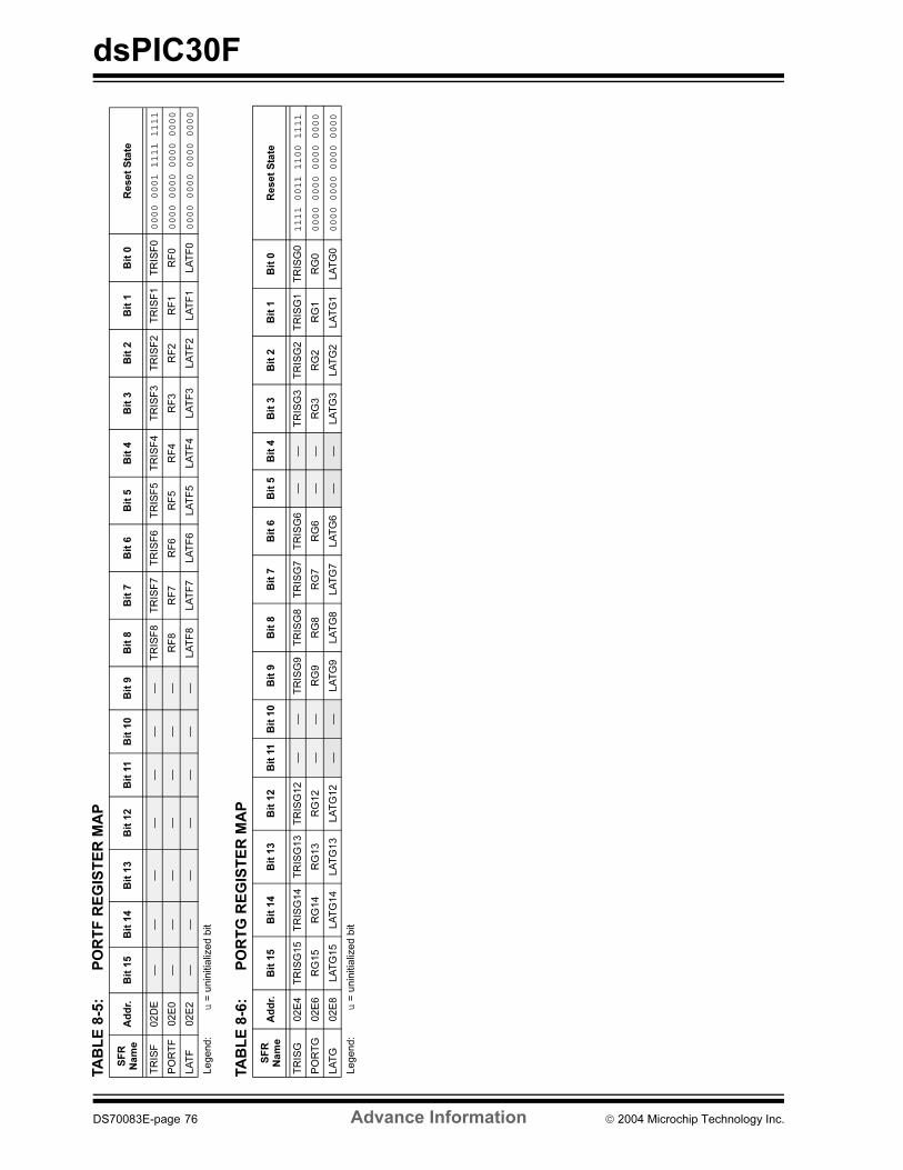
dsPIC30F
TA
BL
E 8
-5:
PO
RT
F R
EG
IST
ER
MA
P
TA
BL
E 8
-6:
PO
RT
G R
EG
IST
ER
MA
P
SF
R
Nam
eA
dd
r.B
it 1
5B
it 1
4B
it 1
3B
it 1
2B
it 1
1B
it 1
0B
it 9
Bit
8B
it 7
Bit
6B
it 5
Bit
4B
it 3
Bit
2B
it 1
Bit
0R
eset
Sta
te
TR
ISF
02D
E—
——
——
——
TR
ISF
8T
RIS
F7
TR
ISF
6T
RIS
F5
TR
ISF
4T
RIS
F3
TR
ISF
2T
RIS
F1
TR
ISF
00000 0001 1111 1111
PO
RT
F02E
0—
——
——
——
RF
8R
F7
RF
6R
F5
RF
4R
F3
RF
2R
F1
RF
00000 0000 0000 0000
LA
TF
02E
2—
——
——
——
LA
TF
8LA
TF
7LA
TF
6LA
TF
5LA
TF
4LA
TF
3LA
TF
2LA
TF
1LA
TF
00000 0000 0000 0000
Legend:
u =
unin
itia
lized b
it
SF
R
Nam
eA
dd
r.B
it 1
5B
it 1
4B
it 1
3B
it 1
2B
it 1
1B
it 1
0B
it 9
Bit
8B
it 7
Bit
6B
it 5
Bit
4B
it 3
Bit
2B
it 1
Bit
0R
eset
Sta
te
TR
ISG
02E
4T
RIS
G15
TR
ISG
14
TR
ISG
13
TR
ISG
12
——
TR
ISG
9T
RIS
G8
TR
ISG
7T
RIS
G6
——
TR
ISG
3T
RIS
G2
TR
ISG
1T
RIS
G0
1111 0011 1100 1111
PO
RT
G02E
6R
G15
RG
14
RG
13
RG
12
——
RG
9R
G8
RG
7R
G6
——
RG
3R
G2
RG
1R
G0
0000 0000 0000 0000
LA
TG
02E
8LA
TG
15
LA
TG
14
LA
TG
13
LA
TG
12
——
LA
TG
9LA
TG
8L
AT
G7
LA
TG
6—
—LA
TG
3LA
TG
2LA
TG
1LA
TG
00000 0000 0000 0000
Legend:
u =
unin
itia
lized b
it
DS70083E-page 76 Advance Information 2004 Microchip Technology Inc.
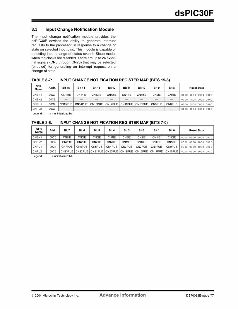
dsPIC30F
8.3 Input Change Notification Module
The input change notification module provides the
dsPIC30F devices the ability to generate interrupt
requests to the processor, in response to a change of
state on selected input pins. This module is capable of
detecting input change of states even in Sleep mode,
when the clocks are disabled. There are up to 24 exter-
nal signals (CN0 through CN23) that may be selected
(enabled) for generating an interrupt request on a
change of state.
TABLE 8-7: INPUT CHANGE NOTIFICATION REGISTER MAP (BITS 15-8)
TABLE 8-8: INPUT CHANGE NOTIFICATION REGISTER MAP (BITS 7-0)
SFR
NameAddr. Bit 15 Bit 14 Bit 13 Bit 12 Bit 11 Bit 10 Bit 9 Bit 8 Reset State
CNEN1 00C0 CN15IE CN14IE CN13IE CN12IE CN11IE CN10IE CN9IE CN8IE 0000 0000 0000 0000
CNEN2 00C2 — — — — — — — — 0000 0000 0000 0000
CNPU1 00C4 CN15PUE CN14PUE CN13PUE CN12PUE CN11PUE CN10PUE CN9PUE CN8PUE 0000 0000 0000 0000
CNPU2 00C6 — — — — — — — — 0000 0000 0000 0000
Legend: u = uninitialized bit
SFR
NameAddr. Bit 7 Bit 6 Bit 5 Bit 4 Bit 3 Bit 2 Bit 1 Bit 0 Reset State
CNEN1 00C0 CN7IE CN6IE CN5IE CN4IE CN3IE CN2IE CN1IE CN0IE 0000 0000 0000 0000
CNEN2 00C2 CN23IE CN22IE CN21IE CN20IE CN19IE CN18IE CN17IE CN16IE 0000 0000 0000 0000
CNPU1 00C4 CN7PUE CN6PUE CN5PUE CN4PUE CN3PUE CN2PUE CN1PUE CN0PUE 0000 0000 0000 0000
CNPU2 00C6 CN23PUE CN22PUE CN21PUE CN20PUE CN19PUE CN18PUE CN17PUE CN16PUE 0000 0000 0000 0000
Legend: u = uninitialized bit
2004 Microchip Technology Inc. Advance Information DS70083E-page 77

dsPIC30F
NOTES:
DS70083E-page 78 Advance Information 2004 Microchip Technology Inc.
dsPIC30F
9.0 TIMER1 MODULE
This section describes the 16-bit General Purpose
(GP) Timer1 module and associated Operational
modes. Figure 9-1 depicts the simplified block diagram
of the 16-bit Timer1 module.
The following sections provide a detailed description
including setup and control registers, along with asso-
ciated block diagrams for the Operational modes of the
timers.
The Timer1 module is a 16-bit timer which can serve as
the time counter for the real-time clock, or operate as a
free-running interval timer/counter. The 16-bit timer has
the following modes:
• 16-bit Timer
• 16-bit Synchronous Counter
• 16-bit Asynchronous Counter
Further, the following operational characteristics are
supported:
• Timer gate operation
• Selectable prescaler settings
• Timer operation during CPU Idle and Sleep
modes
• Interrupt on 16-bit Period register match or falling
edge of external gate signal
These Operating modes are determined by setting the
appropriate bit(s) in the 16-bit SFR, T1CON. Figure 9-1
presents a block diagram of the 16-bit timer module.
16-bit Timer Mode: In the 16-bit Timer mode, the timer
increments on every instruction cycle up to a match
value preloaded into the Period register PR1, then
resets to ‘0’ and continues to count.
When the CPU goes into the Idle mode, the timer will
stop incrementing unless the TSIDL (T1CON<13>)
bit = 0. If TSIDL = 1, the timer module logic will resume
the incrementing sequence upon termination of the
CPU Idle mode.
16-bit Synchronous Counter Mode: In the 16-bit
Synchronous Counter mode, the timer increments on
the rising edge of the applied external clock signal
which is synchronized with the internal phase clocks.
The timer counts up to a match value preloaded in PR1,
then resets to ‘0’ and continues.
When the CPU goes into the Idle mode, the timer will
stop incrementing unless the respective TSIDL bit = 0.
If TSIDL = 1, the timer module logic will resume the
incrementing sequence upon termination of the CPU
Idle mode.
16-bit Asynchronous Counter Mode: In the 16-bit
Asynchronous Counter mode, the timer increments on
every rising edge of the applied external clock signal.
The timer counts up to a match value preloaded in PR1,
then resets to ‘0’ and continues.
When the timer is configured for the Asynchronous
mode of operation and the CPU goes into the Idle
mode, the timer will stop incrementing if TSIDL = 1.
FIGURE 9-1: 16-BIT TIMER1 MODULE BLOCK DIAGRAM
TON
Sync
SOSCI
SOSCO/
PR1
T1IF
EqualComparator x 16
TMR1Reset
LPOSCEN
Event Flag
1
0
TSYNC
Q
Q D
CK
TGATE
TCKPS<1:0>
Prescaler1, 8, 64, 256
2
TGATE
TCY
1
0
T1CK
TCS
1 x
0 1
TGATE
0 0
GateSync
2004 Microchip Technology Inc. Advance Information DS70083E-page 79
dsPIC30F
9.1 Timer Gate Operation
The 16-bit timer can be placed in the Gated Time Accu-
mulation mode. This mode allows the internal TCY to
increment the respective timer when the gate input sig-
nal (T1CK pin) is asserted high. Control bit TGATE
(T1CON<6>) must be set to enable this mode. The
timer must be enabled (TON = 1) and the timer clock
source set to internal (TCS = 0).
When the CPU goes into the Idle mode, the timer will
stop incrementing unless TSIDL = 0. If TSIDL = 1, the
timer will resume the incrementing sequence upon
termination of the CPU Idle mode.
9.2 Timer Prescaler
The input clock (FOSC/4 or external clock) to the 16-bit
Timer has a prescale option of 1:1, 1:8, 1:64 and 1:256,
selected by control bits TCKPS<1:0> (T1CON<5:4>).
The prescaler counter is cleared when any of the
following occurs:
• a write to the TMR1 register
• clearing of the TON bit (T1CON<15>)
• device Reset, such as POR and BOR
However, if the timer is disabled (TON = 0), then the
timer prescaler cannot be reset since the prescaler
clock is halted.
TMR1 is not cleared when T1CON is written. It is
cleared by writing to the TMR1 register.
9.3 Timer Operation During Sleep
Mode
During CPU Sleep mode, the timer will operate if:
• The timer module is enabled (TON = 1) and
• The timer clock source is selected as external
(TCS = 1) and
• The TSYNC bit (T1CON<2>) is asserted to a logic
‘0’ which defines the external clock source as
asynchronous.
When all three conditions are true, the timer will con-
tinue to count up to the Period register and be reset to
0x0000.
When a match between the timer and the Period regis-
ter occurs, an interrupt can be generated if the
respective timer interrupt enable bit is asserted.
9.4 Timer Interrupt
The 16-bit timer has the ability to generate an interrupt on
period match. When the timer count matches the Period
register, the T1IF bit is asserted and an interrupt will be
generated if enabled. The T1IF bit must be cleared in
software. The timer interrupt flag, T1IF, is located in the
IFS0 Control register in the interrupt controller.
When the Gated Time Accumulation mode is enabled,
an interrupt will also be generated on the falling edge of
the gate signal (at the end of the accumulation cycle).
Enabling an interrupt is accomplished via the respec-
tive timer interrupt enable bit, T1IE. The timer interrupt
enable bit is located in the IEC0 Control register in the
interrupt controller.
9.5 Real-Time Clock
Timer1, when operating in Real-Time Clock (RTC)
mode, provides time of day and event time-stamping
capabilities. Key operational features of the RTC are:
• Operation from 32 kHz LP oscillator
• 8-bit prescaler
• Low power
• Real-Time Clock interrupts
These Operating modes are determined by setting the
appropriate bit(s) in the T1CON Control register.
FIGURE 9-2: RECOMMENDED
COMPONENTS FOR
TIMER1 LP OSCILLATOR
RTC
SOSCI
SOSCO
R
C1
C2
dsPIC30FXXXX32.768 kHz
XTAL
C1 = C2 = 18 pF; R = 100K
DS70083E-page 80 Advance Information 2004 Microchip Technology Inc.
dsPIC30F
9.5.1 RTC OSCILLATOR OPERATION
When the TON = 1, TCS = 1 and TGATE = 0, the timer
increments on the rising edge of the 32 kHz LP oscilla-
tor output signal, up to the value specified in the Period
register and is then reset to ‘0’.
The TSYNC bit must be asserted to a logic ‘0’
(Asynchronous mode) for correct operation.
Enabling LPOSCEN (OSCCON<1>) will disable the
normal Timer and Counter modes and enable a timer
carry-out wake-up event.
When the CPU enters Sleep mode, the RTC will con-
tinue to operate provided the 32 kHz external crystal
oscillator is active and the control bits have not been
changed. The TSIDL bit should be cleared to ‘0’ in
order for RTC to continue operation in Idle mode.
9.5.2 RTC INTERRUPTS
When an interrupt event occurs, the respective interrupt
flag, T1IF, is asserted and an interrupt will be generated
if enabled. The T1IF bit must be cleared in software. The
respective Timer interrupt flag, T1IF, is located in the
IFS0 Status register in the interrupt controller.
Enabling an interrupt is accomplished via the respec-
tive timer interrupt enable bit, T1IE. The timer interrupt
enable bit is located in the IEC0 Control register in the
interrupt controller.
2004 Microchip Technology Inc. Advance Information DS70083E-page 81
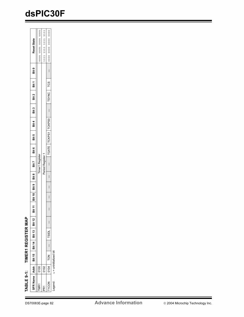
dsPIC30F
TA
BL
E 9
-1:
TIM
ER
1 R
EG
IST
ER
MA
P
SF
R N
am
eA
dd
r.B
it 1
5B
it 1
4B
it 1
3B
it 1
2B
it 1
1B
it 1
0B
it 9
Bit
8B
it 7
Bit
6B
it 5
Bit
4B
it 3
Bit
2B
it 1
Bit
0R
eset
Sta
te
TM
R1
0100
Tim
er1
Regis
ter
uuuu uuuu uuuu uuuu
PR
10102
Period R
egis
ter
11111 1111 1111 1111
T1C
ON
0104
TO
N—
TS
IDL
——
——
——
TG
AT
ET
CK
PS
1T
CK
PS
0—
TS
YN
CT
CS
—0000 0000 0000 0000
Legend:
u =
unin
itia
lized b
it
DS70083E-page 82 Advance Information 2004 Microchip Technology Inc.
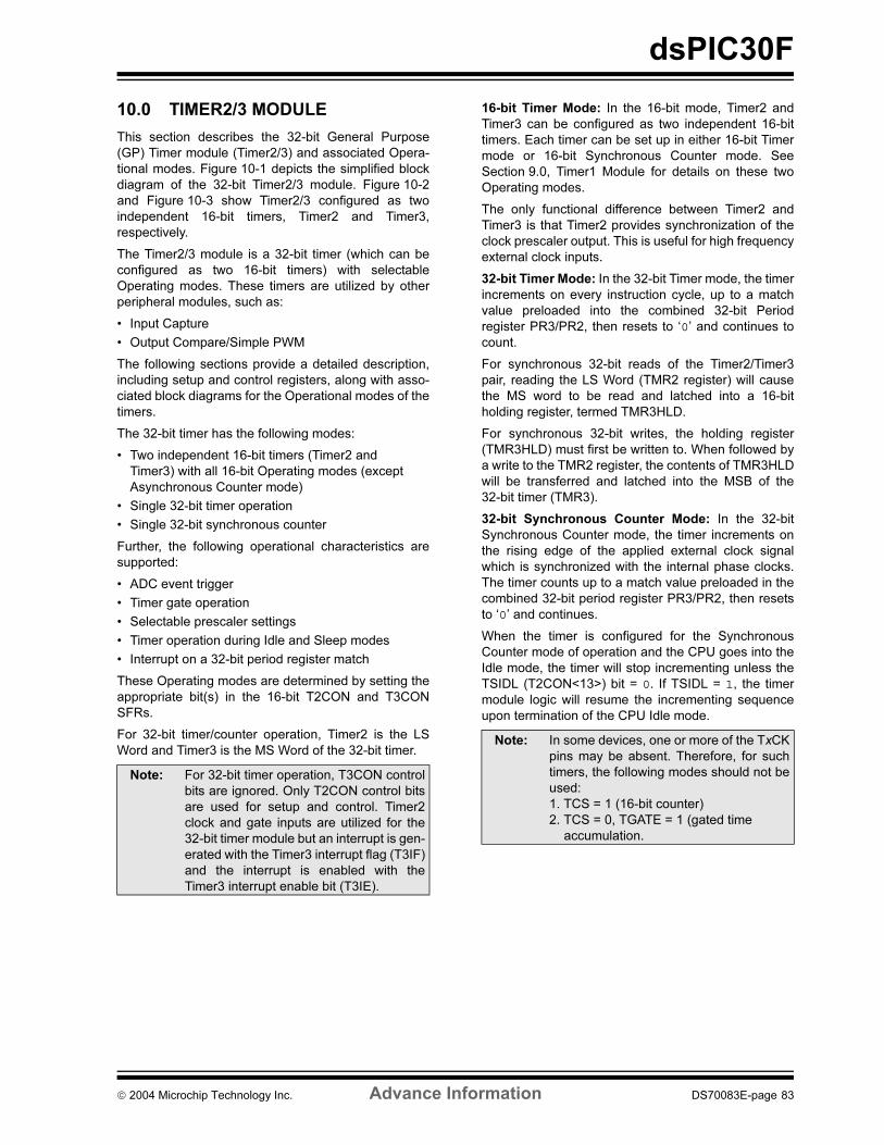
dsPIC30F
10.0 TIMER2/3 MODULE
This section describes the 32-bit General Purpose
(GP) Timer module (Timer2/3) and associated Opera-
tional modes. Figure 10-1 depicts the simplified block
diagram of the 32-bit Timer2/3 module. Figure 10-2
and Figure 10-3 show Timer2/3 configured as two
independent 16-bit timers, Timer2 and Timer3,
respectively.
The Timer2/3 module is a 32-bit timer (which can be
configured as two 16-bit timers) with selectable
Operating modes. These timers are utilized by other
peripheral modules, such as:
• Input Capture
• Output Compare/Simple PWM
The following sections provide a detailed description,
including setup and control registers, along with asso-
ciated block diagrams for the Operational modes of the
timers.
The 32-bit timer has the following modes:
• Two independent 16-bit timers (Timer2 and
Timer3) with all 16-bit Operating modes (except
Asynchronous Counter mode)
• Single 32-bit timer operation
• Single 32-bit synchronous counter
Further, the following operational characteristics are
supported:
• ADC event trigger
• Timer gate operation
• Selectable prescaler settings
• Timer operation during Idle and Sleep modes
• Interrupt on a 32-bit period register match
These Operating modes are determined by setting the
appropriate bit(s) in the 16-bit T2CON and T3CON
SFRs.
For 32-bit timer/counter operation, Timer2 is the LS
Word and Timer3 is the MS Word of the 32-bit timer.
16-bit Timer Mode: In the 16-bit mode, Timer2 and
Timer3 can be configured as two independent 16-bit
timers. Each timer can be set up in either 16-bit Timer
mode or 16-bit Synchronous Counter mode. See
Section 9.0, Timer1 Module for details on these two
Operating modes.
The only functional difference between Timer2 and
Timer3 is that Timer2 provides synchronization of the
clock prescaler output. This is useful for high frequency
external clock inputs.
32-bit Timer Mode: In the 32-bit Timer mode, the timer
increments on every instruction cycle, up to a match
value preloaded into the combined 32-bit Period
register PR3/PR2, then resets to ‘0’ and continues to
count.
For synchronous 32-bit reads of the Timer2/Timer3
pair, reading the LS Word (TMR2 register) will cause
the MS word to be read and latched into a 16-bit
holding register, termed TMR3HLD.
For synchronous 32-bit writes, the holding register
(TMR3HLD) must first be written to. When followed by
a write to the TMR2 register, the contents of TMR3HLD
will be transferred and latched into the MSB of the
32-bit timer (TMR3).
32-bit Synchronous Counter Mode: In the 32-bit
Synchronous Counter mode, the timer increments on
the rising edge of the applied external clock signal
which is synchronized with the internal phase clocks.
The timer counts up to a match value preloaded in the
combined 32-bit period register PR3/PR2, then resets
to ‘0’ and continues.
When the timer is configured for the Synchronous
Counter mode of operation and the CPU goes into the
Idle mode, the timer will stop incrementing unless the
TSIDL (T2CON<13>) bit = 0. If TSIDL = 1, the timer
module logic will resume the incrementing sequence
upon termination of the CPU Idle mode.
Note: For 32-bit timer operation, T3CON control
bits are ignored. Only T2CON control bits
are used for setup and control. Timer2
clock and gate inputs are utilized for the
32-bit timer module but an interrupt is gen-
erated with the Timer3 interrupt flag (T3IF)
and the interrupt is enabled with the
Timer3 interrupt enable bit (T3IE).
Note: In some devices, one or more of the TxCK
pins may be absent. Therefore, for such
timers, the following modes should not be
used:
1. TCS = 1 (16-bit counter)
2. TCS = 0, TGATE = 1 (gated time
accumulation.
2004 Microchip Technology Inc. Advance Information DS70083E-page 83
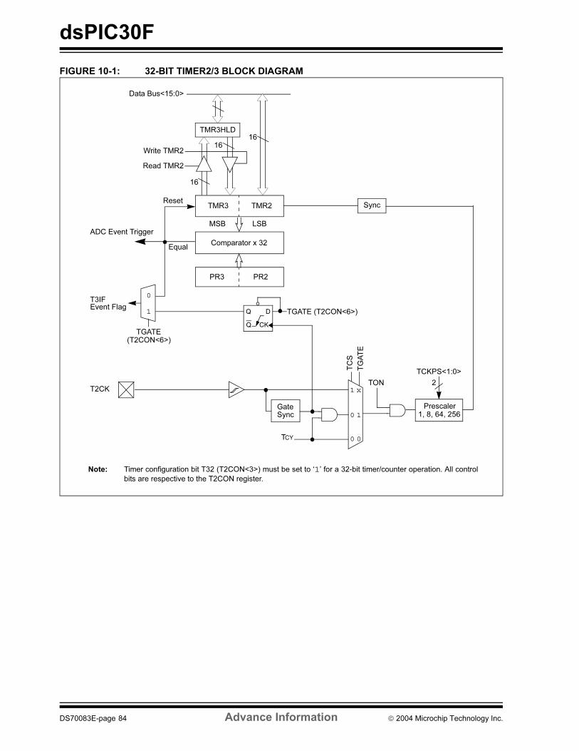
dsPIC30F
FIGURE 10-1: 32-BIT TIMER2/3 BLOCK DIAGRAM
TMR3 TMR2
T3IF
EqualComparator x 32
PR3 PR2
Reset
LSB MSB
Event Flag
Note: Timer configuration bit T32 (T2CON<3>) must be set to ‘1’ for a 32-bit timer/counter operation. All control
bits are respective to the T2CON register.
Data Bus<15:0>
Read TMR2
Write TMR216
16
16
Q
Q D
CK
TGATE (T2CON<6>)
(T2CON<6>)TGATE
0
1
TON
TCKPS<1:0>
2
TCY
TCS
1 x
0 1
TGATE
0 0
Gate
T2CK
Sync
ADC Event Trigger
Sync
TMR3HLD
Prescaler1, 8, 64, 256
DS70083E-page 84 Advance Information 2004 Microchip Technology Inc.
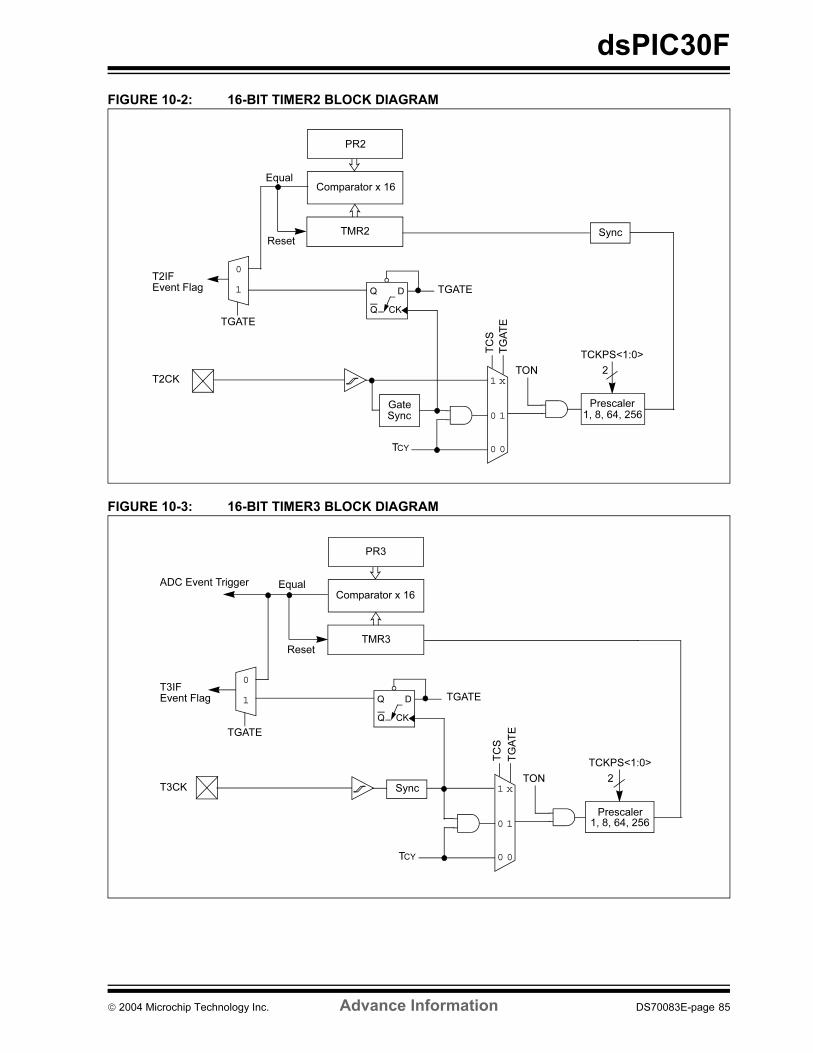
dsPIC30F
FIGURE 10-2: 16-BIT TIMER2 BLOCK DIAGRAM
FIGURE 10-3: 16-BIT TIMER3 BLOCK DIAGRAM
TON
Sync
PR2
T2IF
EqualComparator x 16
TMR2Reset
Event Flag TGATE
TCKPS<1:0>
2
TGATE
TCY
1
0
TCS
1 x
0 1
TGATE
0 0
Gate
T2CK
SyncPrescaler
1, 8, 64, 256
Q
Q D
CK
TON
PR3
T3IF
EqualComparator x 16
TMR3Reset
Event Flag TGATE
TCKPS<1:0>
2
TGATE
TCY
1
0
TCS
1 x
0 1
TGATE
0 0
T3CK
ADC Event Trigger
Sync
Q
Q D
CK
Prescaler1, 8, 64, 256
2004 Microchip Technology Inc. Advance Information DS70083E-page 85
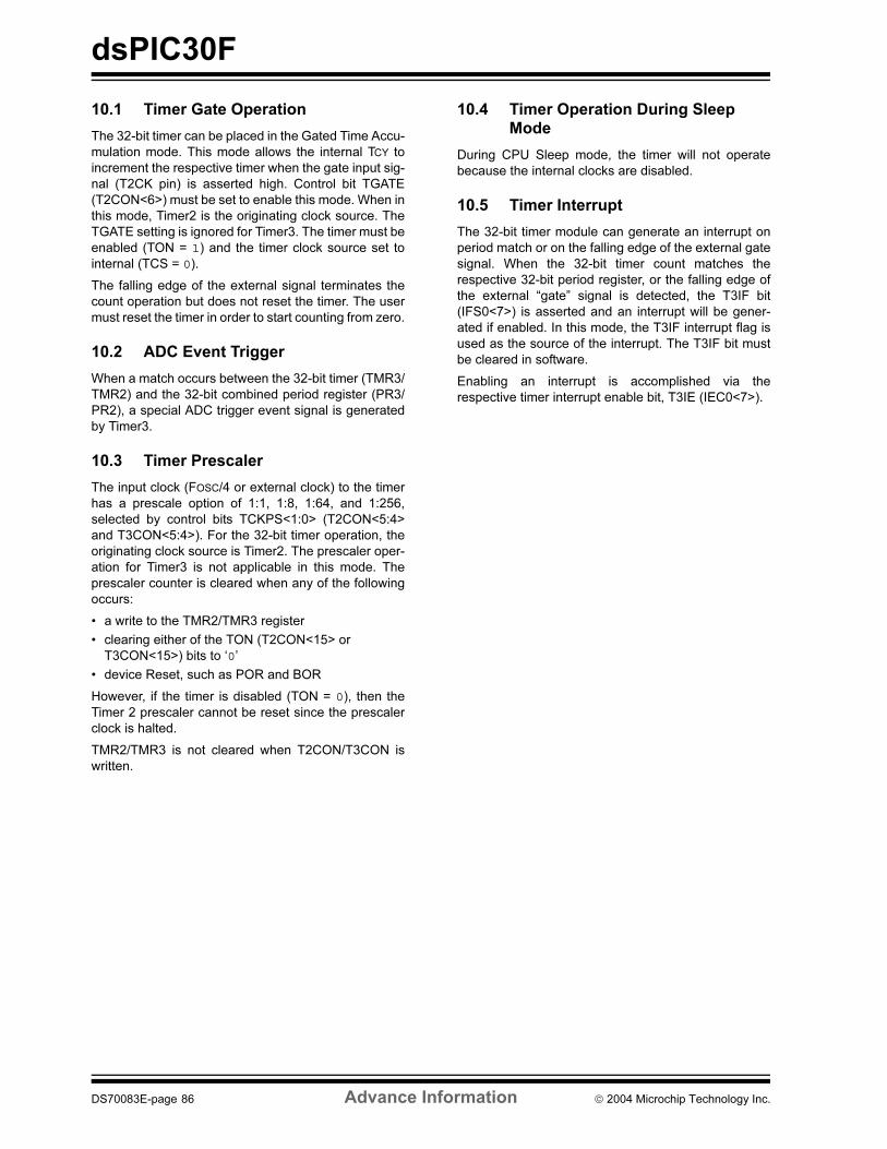
dsPIC30F
10.1 Timer Gate Operation
The 32-bit timer can be placed in the Gated Time Accu-
mulation mode. This mode allows the internal TCY to
increment the respective timer when the gate input sig-
nal (T2CK pin) is asserted high. Control bit TGATE
(T2CON<6>) must be set to enable this mode. When in
this mode, Timer2 is the originating clock source. The
TGATE setting is ignored for Timer3. The timer must be
enabled (TON = 1) and the timer clock source set to
internal (TCS = 0).
The falling edge of the external signal terminates the
count operation but does not reset the timer. The user
must reset the timer in order to start counting from zero.
10.2 ADC Event Trigger
When a match occurs between the 32-bit timer (TMR3/
TMR2) and the 32-bit combined period register (PR3/
PR2), a special ADC trigger event signal is generated
by Timer3.
10.3 Timer Prescaler
The input clock (FOSC/4 or external clock) to the timer
has a prescale option of 1:1, 1:8, 1:64, and 1:256,
selected by control bits TCKPS<1:0> (T2CON<5:4>
and T3CON<5:4>). For the 32-bit timer operation, the
originating clock source is Timer2. The prescaler oper-
ation for Timer3 is not applicable in this mode. The
prescaler counter is cleared when any of the following
occurs:
• a write to the TMR2/TMR3 register
• clearing either of the TON (T2CON<15> or
T3CON<15>) bits to ‘0’
• device Reset, such as POR and BOR
However, if the timer is disabled (TON = 0), then the
Timer 2 prescaler cannot be reset since the prescaler
clock is halted.
TMR2/TMR3 is not cleared when T2CON/T3CON is
written.
10.4 Timer Operation During Sleep
Mode
During CPU Sleep mode, the timer will not operate
because the internal clocks are disabled.
10.5 Timer Interrupt
The 32-bit timer module can generate an interrupt on
period match or on the falling edge of the external gate
signal. When the 32-bit timer count matches the
respective 32-bit period register, or the falling edge of
the external “gate” signal is detected, the T3IF bit
(IFS0<7>) is asserted and an interrupt will be gener-
ated if enabled. In this mode, the T3IF interrupt flag is
used as the source of the interrupt. The T3IF bit must
be cleared in software.
Enabling an interrupt is accomplished via the
respective timer interrupt enable bit, T3IE (IEC0<7>).
DS70083E-page 86 Advance Information 2004 Microchip Technology Inc.
dsPIC30F
TA
BL
E 1
0-1
:T
IME
R2
/3 R
EG
IST
ER
MA
P
SF
R N
am
eA
dd
r.B
it 1
5B
it 1
4B
it 1
3B
it 1
2B
it 1
1B
it 1
0B
it 9
Bit
8B
it 7
Bit
6B
it 5
Bit
4B
it 3
Bit
2B
it 1
Bit
0R
eset
Sta
te
TM
R2
0106
Tim
er2
Regis
ter
uuuu uuuu uuuu uuuu
TM
R3H
LD
0108
Tim
er3
Hold
ing R
egis
ter
(for
32-b
it tim
er
opera
tions o
nly
)uuuu uuuu uuuu uuuu
TM
R3
010A
Tim
er3
Regis
ter
uuuu uuuu uuuu uuuu
PR
2010C
Period R
egis
ter
21111 1111 1111 1111
PR
301
0E
Period R
egis
ter
31111 1111 1111 1111
T2
CO
N0110
TO
N—
TS
IDL
——
——
——
TG
AT
ET
CK
PS
1T
CK
PS
0T
32
—T
CS
—0000 0000 0000 0000
T3
CO
N0112
TO
N—
TS
IDL
——
——
——
TG
AT
ET
CK
PS
1T
CK
PS
0—
—T
CS
—0000 0000 0000 0000
Legend:
u =
unin
itia
lized b
it
2004 Microchip Technology Inc. Advance Information DS70083E-page 87

dsPIC30F
NOTES:
DS70083E-page 88 Advance Information 2004 Microchip Technology Inc.
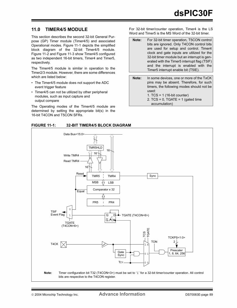
dsPIC30F
11.0 TIMER4/5 MODULE
This section describes the second 32-bit General Pur-
pose (GP) Timer module (Timer4/5) and associated
Operational modes. Figure 11-1 depicts the simplified
block diagram of the 32-bit Timer4/5 module.
Figure 11-2 and Figure 11-3 show Timer4/5 configured
as two independent 16-bit timers, Timer4 and Timer5,
respectively.
The Timer4/5 module is similar in operation to the
Timer2/3 module. However, there are some differences
which are listed below:
• The Timer4/5 module does not support the ADC
event trigger feature
• Timer4/5 can not be utilized by other peripheral
modules, such as input capture and
output compare
The Operating modes of the Timer4/5 module are
determined by setting the appropriate bit(s) in the
16-bit T4CON and T5CON SFRs.
For 32-bit timer/counter operation, Timer4 is the LS
Word and Timer5 is the MS Word of the 32-bit timer.
FIGURE 11-1: 32-BIT TIMER4/5 BLOCK DIAGRAM
Note: For 32-bit timer operation, T5CON control
bits are ignored. Only T4CON control bits
are used for setup and control. Timer4
clock and gate inputs are utilized for the
32-bit timer module but an interrupt is gen-
erated with the Timer5 interrupt flag (T5IF)
and the interrupt is enabled with the
Timer5 interrupt enable bit (T5IE).
Note: In some devices, one or more of the TxCK
pins may be absent. Therefore, for such
timers, the following modes should not be
used:
1. TCS = 1 (16-bit counter)
2. TCS = 0, TGATE = 1 (gated time
accumulation)
TMR5 TMR4
T5IF
EqualComparator x 32
PR5 PR4
Reset
LSB MSB
Event Flag
Note: Timer configuration bit T32 (T4CON<3>) must be set to ‘1’ for a 32-bit timer/counter operation. All control
bits are respective to the T4CON register.
Data Bus<15:0>
TMR5HLD
Read TMR4
Write TMR416
16
16
Q
Q D
CK
TGATE (T4CON<6>)
(T4CON<6>)TGATE
0
1
TON
TCKPS<1:0>
Prescaler1, 8, 64, 256
2
TCY
TCS
1 x
0 1
TGATE
0 0
Gate
T4CK
Sync
Sync
2004 Microchip Technology Inc. Advance Information DS70083E-page 89
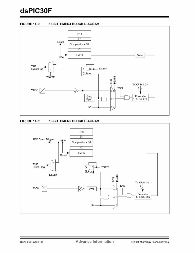
dsPIC30F
FIGURE 11-2: 16-BIT TIMER4 BLOCK DIAGRAM
FIGURE 11-3: 16-BIT TIMER5 BLOCK DIAGRAM
TON
Sync
PR4
T4IF
EqualComparator x 16
TMR4Reset
Event Flag TGATE
TCKPS<1:0>
Prescaler1, 8, 64, 256
2
TGATE
TCY
1
0
TCS
1 x
0 1
TGATE
0 0
Gate
T4CK
Sync
Q
Q D
CK
TON
PR5
T5IF
EqualComparator x 16
TMR5Reset
Event Flag TGATE
TCKPS<1:0>
Prescaler1, 8, 64, 256
2
TGATE
TCY
1
0
TCS
1 x
0 1
TGATE
0 0
T5CK
ADC Event Trigger
Sync
Q
Q D
CK
DS70083E-page 90 Advance Information 2004 Microchip Technology Inc.
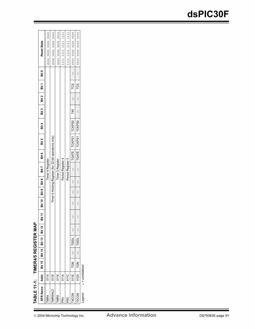
dsPIC30F
TA
BL
E 1
1-1
:T
IME
R4
/5 R
EG
IST
ER
MA
P
SF
R N
am
eA
dd
r.B
it 1
5B
it 1
4B
it 1
3B
it 1
2B
it 1
1B
it 1
0B
it 9
Bit
8B
it 7
Bit
6B
it 5
Bit
4B
it 3
Bit
2B
it 1
Bit
0R
eset
Sta
te
TM
R4
0114
Tim
er
4 R
egis
ter
uuuu uuuu uuuu uuuu
TM
R5H
LD
0116
Tim
er
5 H
old
ing R
egis
ter
(for
32-b
it o
pera
tions o
nly
)uuuu uuuu uuuu uuuu
TM
R5
0118
Tim
er
5 R
egis
ter
uuuu uuuu uuuu uuuu
PR
4011A
Period R
egis
ter
41111 1111 1111 1111
PR
5011C
Period R
egis
ter
51111 1111 1111 1111
T4
CO
N011E
TO
N—
TS
IDL
——
——
——
TG
AT
ET
CK
PS
1T
CK
PS
0T
45
—T
CS
—0000 0000 0000 0000
T5C
ON
0120
TO
N—
TS
IDL
——
——
——
TG
AT
ET
CK
PS
1T
CK
PS
0—
—T
CS
—0000 0000 0000 0000
Legend:
u =
unin
itia
lized
2004 Microchip Technology Inc. Advance Information DS70083E-page 91

dsPIC30F
NOTES:
DS70083E-page 92 Advance Information 2004 Microchip Technology Inc.
dsPIC30F
12.0 INPUT CAPTURE MODULE
This section describes the input capture module and
associated Operational modes. The features provided
by this module are useful in applications requiring fre-
quency (period) and pulse measurement. Figure 12-1
depicts a block diagram of the input capture module.
Input capture is useful for such modes as:
• Frequency/Period/Pulse Measurements
• Additional Sources of External Interrupts
The key operational features of the input capture
module are:
• Simple Capture Event mode
• Timer2 and Timer3 mode selection
• Interrupt on input capture event
These Operating modes are determined by setting the
appropriate bits in the ICxCON register (where
x = 1,2,...,N). The dsPIC devices contain up to 8
capture channels (i.e., the maximum value of N is 8).
FIGURE 12-1: INPUT CAPTURE MODE BLOCK DIAGRAM
12.1 Simple Capture Event Mode
The simple capture events in the dsPIC30F product
family are:
• Capture every falling edge
• Capture every rising edge
• Capture every 4th rising edge
• Capture every 16th rising edge
• Capture every rising and falling edge
These simple Input Capture modes are configured by
setting the appropriate bits ICM<2:0> (ICxCON<2:0>).
12.1.1 CAPTURE PRESCALER
There are four input capture prescaler settings speci-
fied by bits ICM<2:0> (ICxCON<2:0>). Whenever the
capture channel is turned off, the prescaler counter will
be cleared. In addition, any Reset will clear the
prescaler counter.
ICxBUF
Prescaler
ICx pin
ICM<2:0>Mode Select
3
Note: Where ‘x’ is shown, reference is made to the registers or bits associated to the respective input capture
channels 1 through N.
1 0
Set Flag ICxIF
ICTMR
T2_CNT T3_CNT
EdgeDetection
Logic
ClockSynchronizer1, 4, 16
From GP Timer Module
16 16
FIFOR/WLogic
ICI<1:0>
ICBNE, ICOV
ICxCONInterrupt
Logic
Set Flag ICxIF
Data Bus
2004 Microchip Technology Inc. Advance Information DS70083E-page 93
dsPIC30F
12.1.2 CAPTURE BUFFER OPERATION
Each capture channel has an associated FIFO buffer
which is four 16-bit words deep. There are two status
flags which provide status on the FIFO buffer:
• ICBFNE - Input Capture Buffer Not Empty
• ICOV - Input Capture Overflow
The ICBFNE will be set on the first input capture event
and remain set until all capture events have been read
from the FIFO. As each word is read from the FIFO, the
remaining words are advanced by one position within
the buffer.
In the event that the FIFO is full with four capture
events and a fifth capture event occurs prior to a read
of the FIFO, an overflow condition will occur and the
ICOV bit will be set to a logic ‘1’. The fifth capture event
is lost and is not stored in the FIFO. No additional
events will be captured until all four events have been
read from the buffer.
If a FIFO read is performed after the last read and no
new capture event has been received, the read will
yield indeterminate results.
12.1.3 TIMER2 AND TIMER3 SELECTION
MODE
The input capture module consists of up to 8 input cap-
ture channels. Each channel can select between one of
two timers for the time base, Timer2 or Timer3.
Selection of the timer resource is accomplished
through SFR bit, ICTMR (ICxCON<7>). Timer3 is the
default timer resource available for the input capture
module.
12.1.4 HALL SENSOR MODE
When the input capture module is set for capture on
every edge, rising and falling, ICM<2:0> = 001, the fol-
lowing operations are performed by the input capture
logic:
• The input capture interrupt flag is set on every
edge, rising and falling.
• The interrupt on Capture mode setting bits,
ICI<1:0>, is ignored since every capture
generates an interrupt.
• A capture overflow condition is not generated in
this mode.
12.2 Input Capture Operation During
Sleep and Idle Modes
An input capture event will generate a device wake-up
or interrupt, if enabled, if the device is in CPU Idle or
Sleep mode.
Independent of the timer being enabled, the input cap-
ture module will wake-up from the CPU Sleep or Idle
mode when a capture event occurs if ICM<2:0> = 111and the interrupt enable bit is asserted. The same wake-
up can generate an interrupt if the conditions for pro-
cessing the interrupt have been satisfied. The wake-up
feature is useful as a method of adding extra external pin
interrupts.
12.2.1 INPUT CAPTURE IN CPU SLEEP
MODE
CPU Sleep mode allows input capture module opera-
tion with reduced functionality. In the CPU Sleep mode,
the ICI<1:0> bits are not applicable and the input cap-
ture module can only function as an external interrupt
source.
The capture module must be configured for interrupt
only on rising edge (ICM<2:0> = 111) in order for the
input capture module to be used while the device is in
Sleep mode. The prescale settings of 4:1 or 16:1 are
not applicable in this mode.
12.2.2 INPUT CAPTURE IN CPU IDLE
MODE
CPU Idle mode allows input capture module operation
with full functionality. In the CPU Idle mode, the Inter-
rupt mode selected by the ICI<1:0> bits is applicable,
as well as the 4:1 and 16:1 capture prescale settings
which are defined by control bits ICM<2:0>. This mode
requires the selected timer to be enabled. Moreover,
the ICSIDL bit must be asserted to a logic ‘0’.
If the input capture module is defined as
ICM<2:0> = 111 in CPU Idle mode, the input capture
pin will serve only as an external interrupt pin.
12.3 Input Capture Interrupts
The input capture channels have the ability to generate
an interrupt based upon the selected number of cap-
ture events. The selection number is set by control bits
ICI<1:0> (ICxCON<6:5>).
Each channel provides an interrupt flag (ICxIF) bit. The
respective capture channel interrupt flag is located in
the corresponding IFSx Status register.
Enabling an interrupt is accomplished via the respec-
tive capture channel interrupt enable (ICxIE) bit. The
capture interrupt enable bit is located in the
corresponding IEC Control register.
DS70083E-page 94 Advance Information 2004 Microchip Technology Inc.
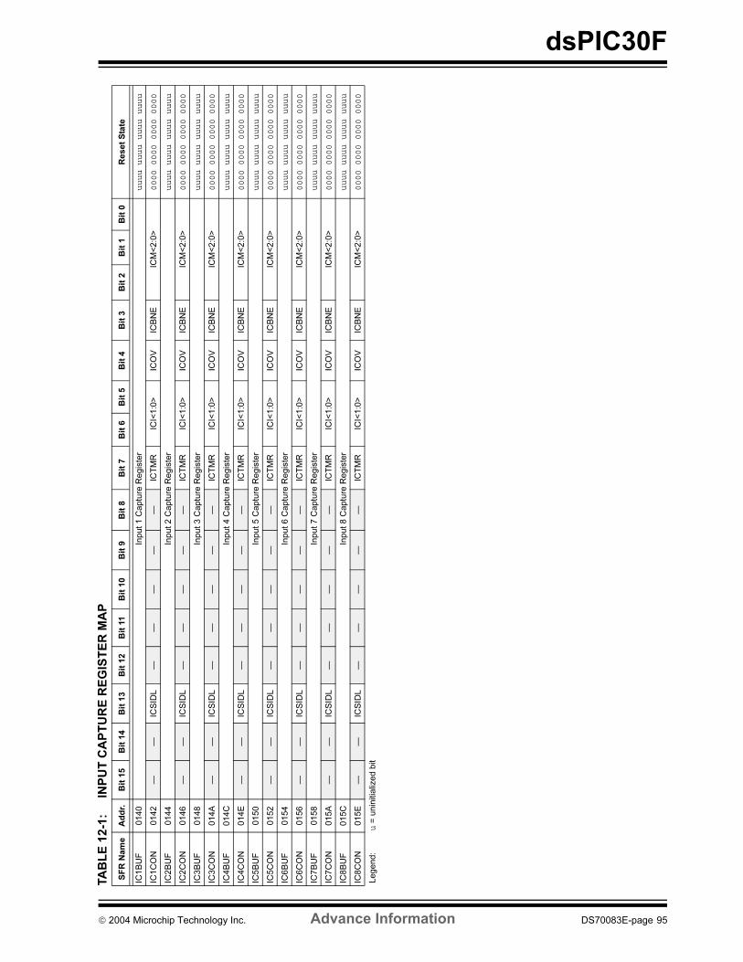
dsPIC30F
TA
BL
E 1
2-1
:IN
PU
T C
AP
TU
RE
RE
GIS
TE
R M
AP
SF
R N
am
eA
dd
r.B
it 1
5B
it 1
4B
it 1
3B
it 1
2B
it 1
1B
it 1
0B
it 9
Bit
8B
it 7
Bit
6B
it 5
Bit
4B
it 3
Bit
2B
it 1
Bit
0R
eset
Sta
te
IC1B
UF
0140
Input 1 C
aptu
re R
egis
ter
uuuu uuuu uuuu uuuu
IC1C
ON
0142
——
ICS
IDL
——
——
—IC
TM
RIC
I<1:0
>IC
OV
ICB
NE
ICM
<2:0
>0000 0000 0000 0000
IC2B
UF
0144
Input 2 C
aptu
re R
egis
ter
uuuu uuuu uuuu uuuu
IC2C
ON
0146
——
ICS
IDL
——
——
—IC
TM
RIC
I<1:0
>IC
OV
ICB
NE
ICM
<2:0
>0000 0000 0000 0000
IC3B
UF
0148
Input 3 C
aptu
re R
egis
ter
uuuu uuuu uuuu uuuu
IC3C
ON
014A
——
ICS
IDL
——
——
—IC
TM
RIC
I<1:0
>IC
OV
ICB
NE
ICM
<2:0
>0000 0000 0000 0000
IC4B
UF
014C
Input 4 C
aptu
re R
egis
ter
uuuu uuuu uuuu uuuu
IC4C
ON
014E
——
ICS
IDL
——
——
—IC
TM
RIC
I<1:0
>IC
OV
ICB
NE
ICM
<2:0
>0000 0000 0000 0000
IC5B
UF
0150
Input 5 C
aptu
re R
egis
ter
uuuu uuuu uuuu uuuu
IC5C
ON
0152
——
ICS
IDL
——
——
—IC
TM
RIC
I<1:0
>IC
OV
ICB
NE
ICM
<2:0
>0000 0000 0000 0000
IC6B
UF
0154
Input 6 C
aptu
re R
egis
ter
uuuu uuuu uuuu uuuu
IC6C
ON
0156
——
ICS
IDL
——
——
—IC
TM
RIC
I<1:0
>IC
OV
ICB
NE
ICM
<2:0
>0000 0000 0000 0000
IC7B
UF
0158
Input 7 C
aptu
re R
egis
ter
uuuu uuuu uuuu uuuu
IC7C
ON
015A
——
ICS
IDL
——
——
—IC
TM
RIC
I<1:0
>IC
OV
ICB
NE
ICM
<2:0
>0000 0000 0000 0000
IC8B
UF
015C
Input 8 C
aptu
re R
egis
ter
uuuu uuuu uuuu uuuu
IC8C
ON
015E
——
ICS
IDL
——
——
—IC
TM
RIC
I<1:0
>IC
OV
ICB
NE
ICM
<2:0
>0000 0000 0000 0000
Legend:
u =
unin
itia
lized b
it
2004 Microchip Technology Inc. Advance Information DS70083E-page 95

dsPIC30F
NOTES:
DS70083E-page 96 Advance Information 2004 Microchip Technology Inc.
dsPIC30F
13.0 OUTPUT COMPARE MODULE
This section describes the output compare module and
associated Operational modes. The features provided
by this module are useful in applications requiring
Operational modes, such as:
• Generation of Variable Width Output Pulses
• Power Factor Correction
Figure 13-1 depicts a block diagram of the output
compare module.
The key operational features of the output compare
module include:
• Timer2 and Timer3 Selection mode
• Simple Output Compare Match mode
• Dual Output Compare Match mode
• Simple PWM mode
• Output Compare During Sleep and Idle modes
• Interrupt on Output Compare/PWM Event
These Operating modes are determined by setting the
appropriate bits in the 16-bit OCxCON SFR (where
x = 1,2,3,...,N). The dsPIC devices contain up to 8
compare channels (i.e., the maximum value of N is 8).
OCxRS and OCxR in Figure 13-1 represent the Dual
Compare registers. In the Dual Compare mode, the
OCxR register is used for the first compare and OCxRS
is used for the second compare.
FIGURE 13-1: OUTPUT COMPARE MODE BLOCK DIAGRAM
OCxR
Comparator
OutputLogic
QSR
OCM<2:0>
OutputOCx
Set Flag bitOCxIF
OCxRS
Mode Select
3
Note: Where ‘x’ is shown, reference is made to the registers associated with the respective output compare
channels 1 through N.
OCFA
OCTSEL0 1
T2P2_MATCHTMR2<15:0 TMR3<15:0> T3P3_MATCH
From GP
(for x = 1, 2, 3 or 4)
or OCFB
(for x = 5, 6, 7 or 8)
0 1
Timer Module
Enable
2004 Microchip Technology Inc. Advance Information DS70083E-page 97
dsPIC30F
13.1 Timer2 and Timer3 Selection Mode
Each output compare channel can select between one
of two 16-bit timers, Timer2 or Timer3.
The selection of the timers is controlled by the OCTSEL
bit (OCxCON<3>). Timer2 is the default timer resource
for the output compare module.
13.2 Simple Output Compare Match
Mode
When control bits OCM<2:0> (OCxCON<2:0>) = 001,
010 or 011, the selected output compare channel is
configured for one of three simple Output Compare
Match modes:
• Compare forces I/O pin low
• Compare forces I/O pin high
• Compare toggles I/O pin
The OCxR register is used in these modes. The OCxR
register is loaded with a value and is compared to the
selected incrementing timer count. When a compare
occurs, one of these Compare Match modes occurs. If
the counter resets to zero before reaching the value in
OCxR, the state of the OCx pin remains unchanged.
13.3 Dual Output Compare Match Mode
When control bits OCM<2:0> (OCxCON<2:0>) = 100or 101, the selected output compare channel is config-
ured for one of two Dual Output Compare modes,
which are:
• Single Output Pulse mode
• Continuous Output Pulse mode
13.3.1 SINGLE PULSE MODE
For the user to configure the module for the generation
of a single output pulse, the following steps are
required (assuming timer is off):
• Determine instruction cycle time TCY.
• Calculate desired pulse width value based on TCY.
• Calculate time to start pulse from timer start value
of 0x0000.
• Write pulse width start and stop times into OCxR
and OCxRS Compare registers (x denotes
channel 1, 2, ...,N).
• Set Timer Period register to value equal to, or
greater than value in OCxRS Compare register.
• Set OCM<2:0> = 100.
• Enable timer, TON (TxCON<15>) = 1.
To initiate another single pulse, issue another write to
set OCM<2:0> = 100.
13.3.2 CONTINUOUS PULSE MODE
For the user to configure the module for the generation
of a continuous stream of output pulses, the following
steps are required:
• Determine instruction cycle time TCY.
• Calculate desired pulse value based on TCY.
• Calculate timer to start pulse width from timer start
value of 0x0000.
• Write pulse width start and stop times into OCxR
and OCxRS (x denotes channel 1, 2, ...,N)
Compare registers, respectively.
• Set Timer Period register to value equal to, or
greater than value in OCxRS Compare register.
• Set OCM<2:0> = 101.
• Enable timer, TON (TxCON<15>) = 1.
13.4 Simple PWM Mode
When control bits OCM<2:0> (OCxCON<2:0>) = 110or 111, the selected output compare channel is config-
ured for the PWM mode of operation. When configured
for the PWM mode of operation, OCxR is the main latch
(read only) and OCxRS is the secondary latch. This
enables glitchless PWM transitions.
The user must perform the following steps in order to
configure the output compare module for PWM
operation:
1. Set the PWM period by writing to the appropriate
period register.
2. Set the PWM duty cycle by writing to the OCxRS
register.
3. Configure the output compare module for PWM
operation.
4. Set the TMRx prescale value and enable the
Timer, TON (TxCON<15>) = 1.
13.4.1 INPUT PIN FAULT PROTECTION
FOR PWM
When control bits OCM<2:0> (OCxCON<2:0>) = 111,
the selected output compare channel is again config-
ured for the PWM mode of operation with the additional
feature of input FAULT protection. While in this mode,
if a logic ‘0’ is detected on the OCFA/B pin, the respec-
tive PWM output pin is placed in the high impedance
input state. The OCFLT bit (OCxCON<4>) indicates
whether a FAULT condition has occurred. This state will
be maintained until both of the following events have
occurred:
• The external FAULT condition has been removed.
• The PWM mode has been re-enabled by writing
to the appropriate control bits.
DS70083E-page 98 Advance Information 2004 Microchip Technology Inc.
dsPIC30F
13.4.2 PWM PERIOD
The PWM period is specified by writing to the PRx
register. The PWM period can be calculated using
Equation 13-1.
EQUATION 13-1:
PWM frequency is defined as 1 / [PWM period].
When the selected TMRx is equal to its respective
period register, PRx, the following four events occur on
the next increment cycle:
• TMRx is cleared.
• The OCx pin is set.
- Exception 1: If PWM duty cycle is 0x0000,
the OCx pin will remain low.
- Exception 2: If duty cycle is greater than PRx,
the pin will remain high.
• The PWM duty cycle is latched from OCxRS into
OCxR.
• The corresponding timer interrupt flag is set.
See Figure 13-2 for key PWM period comparisons.
Timer3 is referred to in Figure 13-2 for clarity.
FIGURE 13-2: PWM OUTPUT TIMING
13.5 Output Compare Operation During
CPU Sleep Mode
When the CPU enters Sleep mode, all internal clocks
are stopped. Therefore, when the CPU enters the
Sleep state, the output compare channel will drive the
pin to the active state that was observed prior to
entering the CPU Sleep state.
For example, if the pin was high when the CPU entered
the Sleep state, the pin will remain high. Likewise, if the
pin was low when the CPU entered the Sleep state, the
pin will remain low. In either case, the output compare
module will resume operation when the device wakes
up.
13.6 Output Compare Operation During
CPU Idle Mode
When the CPU enters the Idle mode, the output
compare module can operate with full functionality.
The output compare channel will operate during the
CPU Idle mode if the OCSIDL bit (OCxCON<13>) is at
logic ‘0’ and the selected time base (Timer2 or Timer3)
is enabled and the TSIDL bit of the selected timer is set
to logic ‘0’.
13.7 Output Compare Interrupts
The output compare channels have the ability to gener-
ate an interrupt on a compare match, for whichever
Match mode has been selected.
For all modes except the PWM mode, when a compare
event occurs, the respective interrupt flag (OCxIF) is
asserted and an interrupt will be generated if enabled.
The OCxIF bit is located in the corresponding IFS
Status register and must be cleared in software. The
interrupt is enabled via the respective compare inter-
rupt enable (OCxIE) bit located in the corresponding
IEC Control register.
For the PWM mode, when an event occurs, the respec-
tive timer interrupt flag (T2IF or T3IF) is asserted and
an interrupt will be generated if enabled. The IF bit is
located in the IFS0 Status register and must be cleared
in software. The interrupt is enabled via the respective
timer interrupt enable bit (T2IE or T3IE) located in the
IEC0 Control register. The output compare interrupt
flag is never set during the PWM mode of operation.
PWM period = [(PRx) + 1] • 4 • TOSC •
(TMRx prescale value)
Period
Duty Cycle
TMR3 = Duty Cycle TMR3 = Duty Cycle
TMR3 = PR3T3IF = 1
(Interrupt Flag)
OCxR = OCxRS
TMR3 = PR3
(Interrupt Flag)
OCxR = OCxRS
T3IF = 1
(OCxR) (OCxR)
2004 Microchip Technology Inc. Advance Information DS70083E-page 99
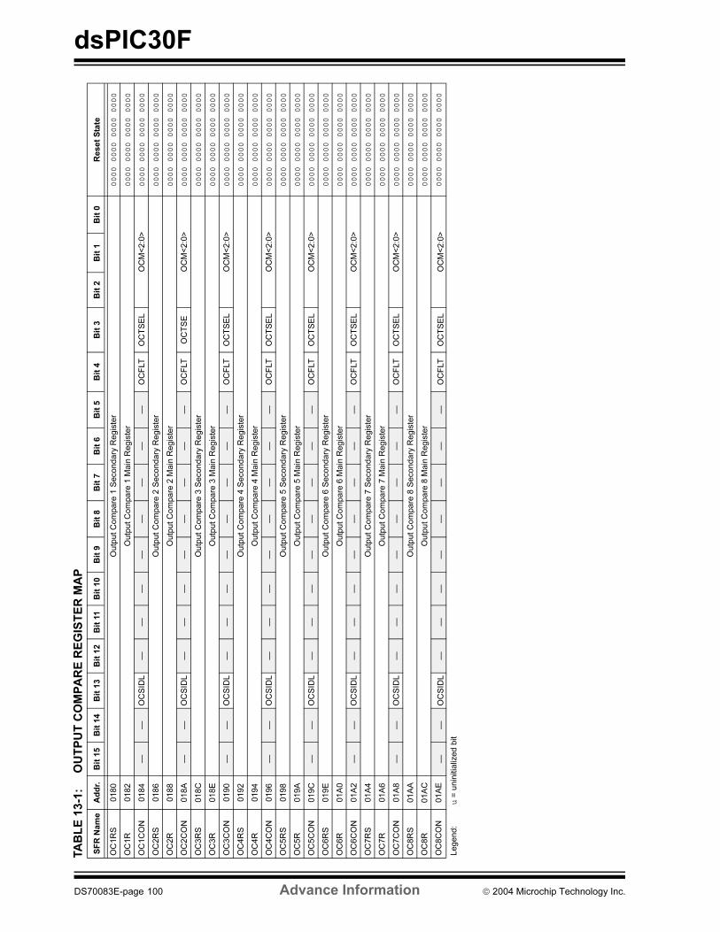
dsPIC30F
TA
BL
E 1
3-1
:O
UT
PU
T C
OM
PA
RE
RE
GIS
TE
R M
AP
SF
R N
am
eA
dd
r.B
it 1
5B
it 1
4B
it 1
3B
it 1
2B
it 1
1B
it 1
0B
it 9
Bit
8B
it 7
Bit
6B
it 5
Bit
4B
it 3
Bit
2B
it 1
Bit
0R
eset
Sta
te
OC
1R
S0180
Outp
ut C
om
pare
1 S
econdary
Regis
ter
0000 0000 0000 0000
OC
1R
0182
Outp
ut C
om
pare
1 M
ain
Regis
ter
0000 0000 0000 0000
OC
1C
ON
0184
——
OC
SID
L—
——
——
——
—O
CF
LT
OC
TS
EL
OC
M<
2:0
>0000 0000 0000 0000
OC
2R
S0186
Outp
ut C
om
pare
2 S
econdary
Regis
ter
0000 0000 0000 0000
OC
2R
0188
Outp
ut C
om
pare
2 M
ain
Regis
ter
0000 0000 0000 0000
OC
2C
ON
018A
——
OC
SID
L—
——
——
——
—O
CF
LT
OC
TS
EO
CM
<2:0
>0000 0000 0000 0000
OC
3R
S018C
Outp
ut C
om
pare
3 S
econdary
Regis
ter
0000 0000 0000 0000
OC
3R
018E
Outp
ut C
om
pare
3 M
ain
Regis
ter
0000 0000 0000 0000
OC
3C
ON
0190
——
OC
SID
L—
——
——
——
—O
CF
LT
OC
TS
EL
OC
M<
2:0
>0000 0000 0000 0000
OC
4R
S0192
Outp
ut C
om
pare
4 S
econdary
Regis
ter
0000 0000 0000 0000
OC
4R
0194
Outp
ut C
om
pare
4 M
ain
Regis
ter
0000 0000 0000 0000
OC
4C
ON
0196
——
OC
SID
L—
——
——
——
—O
CF
LT
OC
TS
EL
OC
M<
2:0
>0000 0000 0000 0000
OC
5R
S0198
Outp
ut C
om
pare
5 S
econdary
Regis
ter
0000 0000 0000 0000
OC
5R
019A
Outp
ut C
om
pare
5 M
ain
Regis
ter
0000 0000 0000 0000
OC
5C
ON
019C
——
OC
SID
L—
——
——
——
—O
CF
LT
OC
TS
EL
OC
M<
2:0
>0000 0000 0000 0000
OC
6R
S019E
Outp
ut C
om
pare
6 S
econdary
Regis
ter
0000 0000 0000 0000
OC
6R
01A
0O
utp
ut C
om
pare
6 M
ain
Regis
ter
0000 0000 0000 0000
OC
6C
ON
01A
2—
—O
CS
IDL
——
——
——
——
OC
FLT
OC
TS
EL
OC
M<
2:0
>0000 0000 0000 0000
OC
7R
S01A
4O
utp
ut C
om
pare
7 S
econdary
Regis
ter
0000 0000 0000 0000
OC
7R
01A
6O
utp
ut C
om
pare
7 M
ain
Regis
ter
0000 0000 0000 0000
OC
7C
ON
01A
8—
—O
CS
IDL
——
——
——
——
OC
FLT
OC
TS
EL
OC
M<
2:0
>0000 0000 0000 0000
OC
8R
S01A
AO
utp
ut C
om
pare
8 S
econdary
Regis
ter
0000 0000 0000 0000
OC
8R
01A
CO
utp
ut C
om
pare
8 M
ain
Regis
ter
0000 0000 0000 0000
OC
8C
ON
01A
E—
—O
CS
IDL
——
——
——
——
OC
FLT
OC
TS
EL
OC
M<
2:0
>0000 0000 0000 0000
Legend:
u =
unin
itia
lized b
it
DS70083E-page 100 Advance Information 2004 Microchip Technology Inc.
dsPIC30F
14.0 SPI MODULE
The Serial Peripheral Interface (SPI) module is a syn-
chronous serial interface. It is useful for communicating
with other peripheral devices, such as EEPROMs, shift
registers, display drivers and A/D converters, or other
microcontrollers. It is compatible with Motorola's SPI™
and SIOP interfaces.
14.1 Operating Function Description
Each SPI module consists of a 16-bit shift register,
SPIxSR (where x = 1 or 2), used for shifting data in and
out, and a buffer register, SPIxBUF. A control register,
SPIxCON, configures the module. Additionally, a status
register, SPIxSTAT, indicates various status conditions.
The serial interface consists of 4 pins: SDIx (serial data
input), SDOx (serial data output), SCKx (shift clock
input or output), and SSx (active low slave select).
In Master mode operation, SCK is a clock output but in
Slave mode, it is a clock input.
A series of eight (8) or sixteen (16) clock pulses shift
out bits from the SPIxSR to SDOx pin and simulta-
neously shift in data from SDIx pin. An interrupt is gen-
erated when the transfer is complete and the
corresponding interrupt flag bit (SPI1IF or SPI2IF) is
set. This interrupt can be disabled through an interrupt
enable bit (SPI1IE or SPI2IE).
The receive operation is double-buffered. When a com-
plete byte is received, it is transferred from SPIxSR to
SPIxBUF.
If the receive buffer is full when new data is being trans-
ferred from SPIxSR to SPIxBUF, the module will set the
SPIROV bit indicating an overflow condition. The trans-
fer of the data from SPIxSR to SPIxBUF will not be
completed and the new data will be lost. The module
will not respond to SCL transitions while SPIROV is ‘1’,
effectively disabling the module until SPIxBUF is read
by user software.
Transmit writes are also double-buffered. The user
writes to SPIxBUF. When the master or slave transfer
is completed, the contents of the shift register (SPIxSR)
are moved to the receive buffer. If any transmit data has
been written to the buffer register, the contents of the
transmit buffer are moved to SPIxSR. The received
data is thus placed in SPIxBUF and the transmit data in
SPIxSR is ready for the next transfer.
In Master mode, the clock is generated by prescaling
the system clock. Data is transmitted as soon as a
value is written to SPIxBUF. The interrupt is generated
at the middle of the transfer of the last bit.
In Slave mode, data is transmitted and received as
external clock pulses appear on SCK. Again, the inter-
rupt is generated when the last bit is latched. If SSx
control is enabled, then transmission and reception are
enabled only when SSx = low. The SDOx output will be
disabled in SSx mode with SSx high.
The clock provided to the module is (FOSC/4). This
clock is then prescaled by the primary (PPRE<1:0>)
and the secondary (SPRE<2:0>) prescale factors. The
CKE bit determines whether transmit occurs on transi-
tion from active clock state to Idle clock state, or vice
versa. The CKP bit selects the Idle state (high or low)
for the clock.
14.1.1 WORD AND BYTE
COMMUNICATION
A control bit, MODE16 (SPIxCON<10>), allows the
module to communicate in either 16-bit or 8-bit mode.
16-bit operation is identical to 8-bit operation except
that the number of bits transmitted is 16 instead of 8.
The user software must disable the module prior to
changing the MODE16 bit. The SPI module is reset
when the MODE16 bit is changed by the user.
A basic difference between 8-bit and 16-bit operation is
that the data is transmitted out of bit 7 of the SPIxSR for
8-bit operation, and data is transmitted out of bit15 of
the SPIxSR for 16-bit operation. In both modes, data is
shifted into bit 0 of the SPIxSR.
14.1.2 SDOx DISABLE
A control bit, DISSDO, is provided to the SPIxCON reg-
ister to allow the SDOx output to be disabled. This will
allow the SPI module to be connected in an input only
configuration. SDO can also be used for general
purpose I/O.
14.2 Framed SPI Support
The module supports a basic framed SPI protocol in
Master or Slave mode. The control bit FRMEN enables
framed SPI support and causes the SSx pin to perform
the frame synchronization pulse (FSYNC) function.
The control bit SPIFSD determines whether the SSx
pin is an input or an output (i.e., whether the module
receives or generates the frame synchronization
pulse). The frame pulse is an active high pulse for a
single SPI clock cycle. When frame synchronization is
enabled, the data transmission starts only on the
subsequent transmit edge of the SPI clock.Note: Both the transmit buffer (SPIxTXB) and
the receive buffer (SPIxRXB) are mapped
to the same register address, SPIxBUF.
2004 Microchip Technology Inc. Advance Information DS70083E-page 101
dsPIC30F
FIGURE 14-1: SPI BLOCK DIAGRAM
FIGURE 14-2: SPI MASTER/SLAVE CONNECTION
Note: x = 1 or 2.
Read Write
InternalData Bus
SDIx
SDOx
SSx
SCKx
SPIxSR
SPIxBUF
bit 0
ShiftClock
EdgeSelect
FCY
Primary
1, 4, 16, 64
Enable Master Clock
PrescalerSecondaryPrescaler1,2,4,6,8
SS and FSYNC
Control
ClockControl
Transmit
SPIxBUF
Receive
Serial Input Buffer(SPIxBUF)
Shift Register(SPIxSR)
MSb LSb
SDOx
SDIx
PROCESSOR 1
SCKx
SPI Master
Serial Input Buffer(SPIyBUF)
Shift Register(SPIySR)
LSbMSb
SDIy
SDOy
PROCESSOR 2
SCKy
SPI Slave
Serial Clock
Note: x = 1 or 2, y = 1 or 2.
DS70083E-page 102 Advance Information 2004 Microchip Technology Inc.
dsPIC30F
14.3 Slave Select Synchronization
The SSx pin allows a Synchronous Slave mode. The
SPI must be configured in SPI Slave mode with SSx pin
control enabled (SSEN = 1). When the SSx pin is low,
transmission and reception are enabled and the SDOx
pin is driven. When SSx pin goes high, the SDOx pin is
no longer driven. Also, the SPI module is re-
synchronized, and all counters/control circuitry are
reset. Therefore, when the SSx pin is asserted low
again, transmission/reception will begin at the MS bit
even if SSx had been de-asserted in the middle of a
transmit/receive.
14.4 SPI Operation During CPU Sleep
Mode
During Sleep mode, the SPI module is shutdown. If the
CPU enters Sleep mode while an SPI transaction is in
progress, then the transmission and reception is
aborted.
The transmitter and receiver will stop in Sleep mode.
However, register contents are not affected by entering
or exiting Sleep mode.
14.5 SPI Operation During CPU Idle
Mode
When the device enters Idle mode, all clock sources
remain functional. The SPISIDL bit (SPIxSTAT<13>)
selects if the SPI module will stop or continue on Idle. If
SPISIDL = 0, the module will continue to operate when
the CPU enters Idle mode. If SPISIDL = 1, the module
will stop when the CPU enters Idle mode.
2004 Microchip Technology Inc. Advance Information DS70083E-page 103
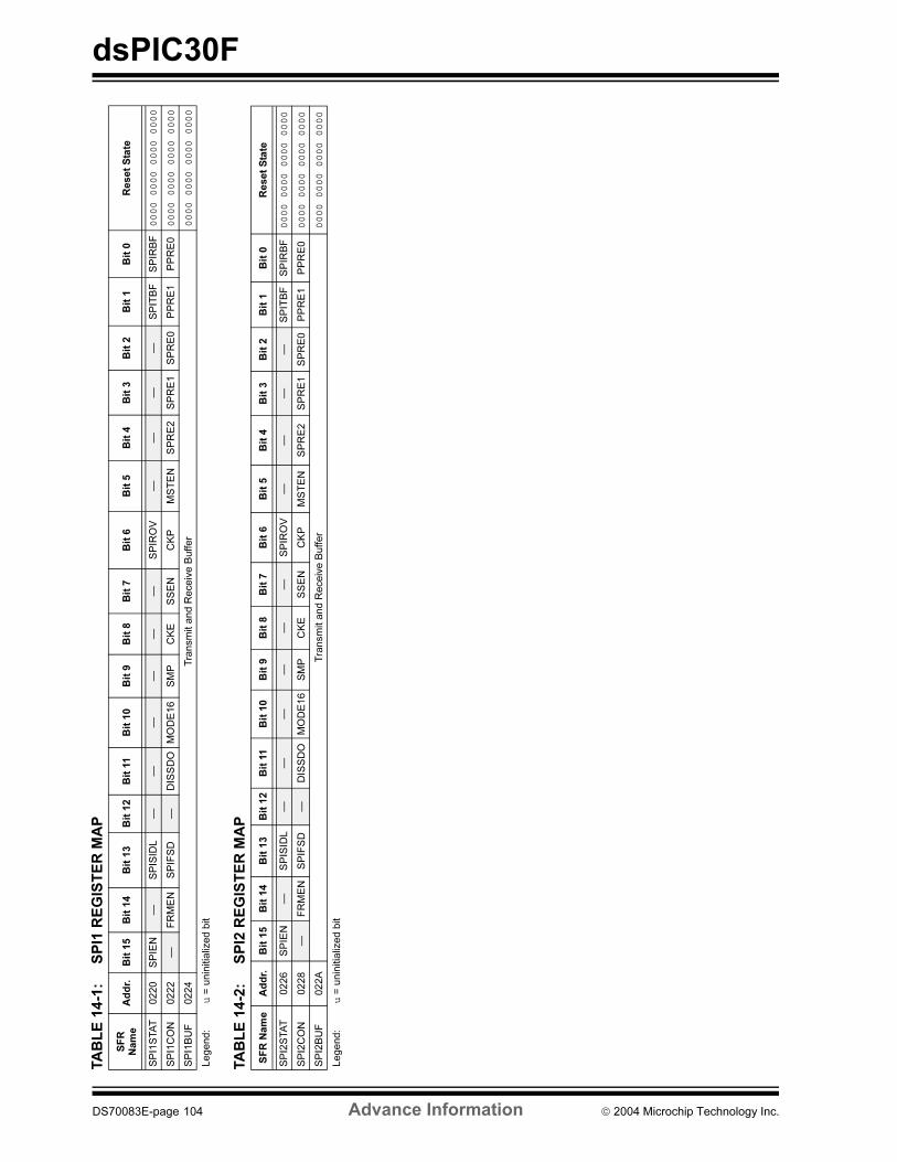
dsPIC30F
TA
BL
E 1
4-1
:S
PI1
RE
GIS
TE
R M
AP
TA
BL
E 1
4-2
:S
PI2
RE
GIS
TE
R M
AP
SF
R
Nam
eA
dd
r.B
it 1
5B
it 1
4B
it 1
3B
it 1
2B
it 1
1B
it 1
0B
it 9
Bit
8B
it 7
Bit
6B
it 5
Bit
4B
it 3
Bit
2B
it 1
Bit
0R
eset
Sta
te
SP
I1S
TA
T0220
SP
IEN
—S
PIS
IDL
——
——
——
SP
IRO
V—
——
—S
PIT
BF
SP
IRB
F0000 0000 0000 0000
SP
I1C
ON
0222
—F
RM
EN
SP
IFS
D—
DIS
SD
OM
OD
E16
SM
PC
KE
SS
EN
CK
PM
ST
EN
SP
RE
2S
PR
E1
SP
RE
0P
PR
E1
PP
RE
00000 0000 0000 0000
SP
I1B
UF
0224
Tra
nsm
it a
nd R
eceiv
e B
uffer
0000 0000 0000 0000
Legend:
u =
unin
itia
lized b
it
SF
R N
am
eA
dd
r.B
it 1
5B
it 1
4B
it 1
3B
it 1
2B
it 1
1B
it 1
0B
it 9
Bit
8B
it 7
Bit
6B
it 5
Bit
4B
it 3
Bit
2B
it 1
Bit
0R
eset
Sta
te
SP
I2S
TA
T0226
SP
IEN
—S
PIS
IDL
——
——
——
SP
IRO
V—
——
—S
PIT
BF
SP
IRB
F0000 0000 0000 0000
SP
I2C
ON
0228
—F
RM
EN
SP
IFS
D—
DIS
SD
OM
OD
E16
SM
PC
KE
SS
EN
CK
PM
ST
EN
SP
RE
2S
PR
E1
SP
RE
0P
PR
E1
PP
RE
00000 0000 0000 0000
SP
I2B
UF
022A
Tra
nsm
it a
nd R
eceiv
e B
uffer
0000 0000 0000 0000
Legend:
u =
unin
itia
lized b
it
DS70083E-page 104 Advance Information 2004 Microchip Technology Inc.
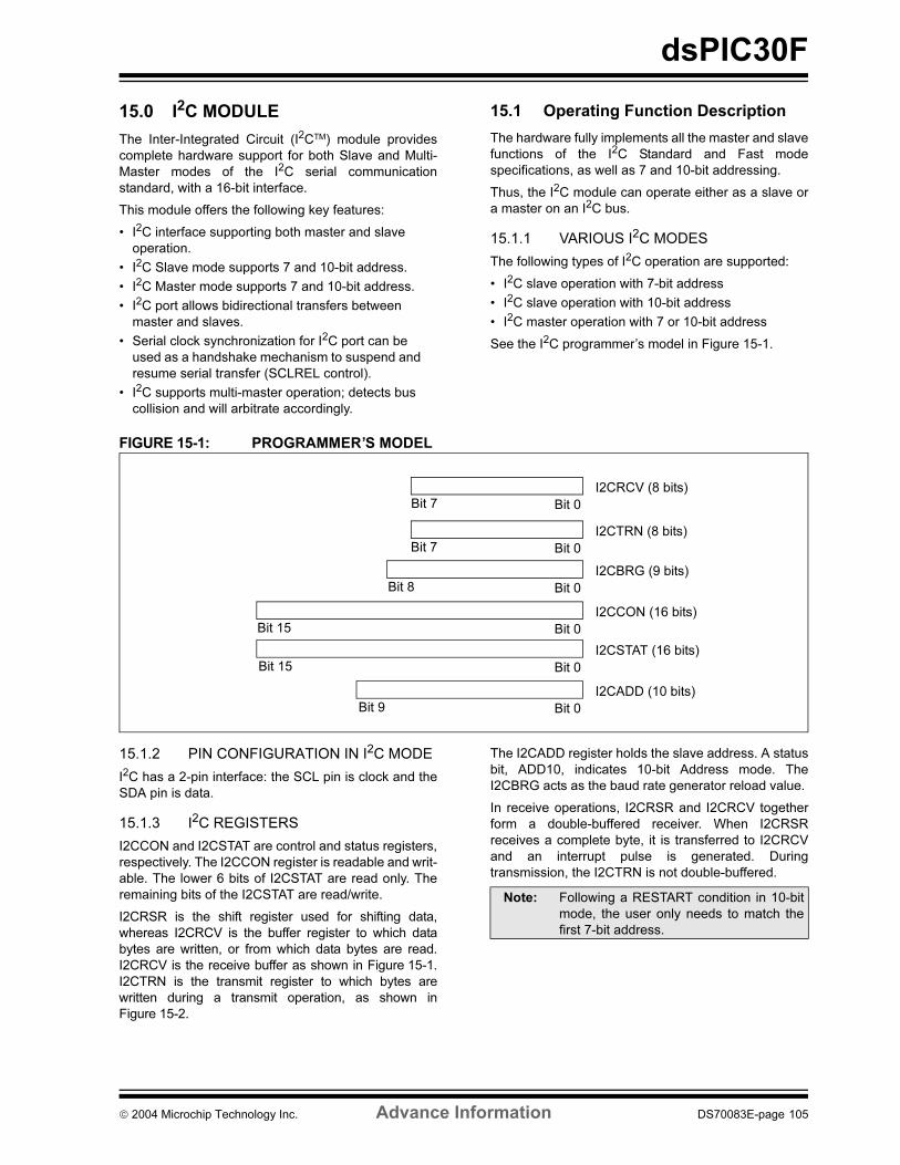
dsPIC30F
15.0 I2C MODULE
The Inter-Integrated Circuit (I2CTM) module provides
complete hardware support for both Slave and Multi-
Master modes of the I2C serial communication
standard, with a 16-bit interface.
This module offers the following key features:
• I2C interface supporting both master and slave
operation.
• I2C Slave mode supports 7 and 10-bit address.
• I2C Master mode supports 7 and 10-bit address.
• I2C port allows bidirectional transfers between
master and slaves.
• Serial clock synchronization for I2C port can be
used as a handshake mechanism to suspend and
resume serial transfer (SCLREL control).
• I2C supports multi-master operation; detects bus
collision and will arbitrate accordingly.
15.1 Operating Function Description
The hardware fully implements all the master and slave
functions of the I2C Standard and Fast mode
specifications, as well as 7 and 10-bit addressing.
Thus, the I2C module can operate either as a slave or
a master on an I2C bus.
15.1.1 VARIOUS I2C MODES
The following types of I2C operation are supported:
• I2C slave operation with 7-bit address
• I2C slave operation with 10-bit address
• I2C master operation with 7 or 10-bit address
See the I2C programmer’s model in Figure 15-1.
FIGURE 15-1: PROGRAMMER’S MODEL
15.1.2 PIN CONFIGURATION IN I2C MODE
I2C has a 2-pin interface: the SCL pin is clock and the
SDA pin is data.
15.1.3 I2C REGISTERS
I2CCON and I2CSTAT are control and status registers,
respectively. The I2CCON register is readable and writ-
able. The lower 6 bits of I2CSTAT are read only. The
remaining bits of the I2CSTAT are read/write.
I2CRSR is the shift register used for shifting data,
whereas I2CRCV is the buffer register to which data
bytes are written, or from which data bytes are read.
I2CRCV is the receive buffer as shown in Figure 15-1.
I2CTRN is the transmit register to which bytes are
written during a transmit operation, as shown in
Figure 15-2.
The I2CADD register holds the slave address. A status
bit, ADD10, indicates 10-bit Address mode. The
I2CBRG acts as the baud rate generator reload value.
In receive operations, I2CRSR and I2CRCV together
form a double-buffered receiver. When I2CRSR
receives a complete byte, it is transferred to I2CRCV
and an interrupt pulse is generated. During
transmission, the I2CTRN is not double-buffered.
Bit 7 Bit 0
I2CRCV (8 bits)
Bit 7 Bit 0
I2CTRN (8 bits)
Bit 8 Bit 0
I2CBRG (9 bits)
Bit 15 Bit 0
I2CCON (16 bits)
Bit 15 Bit 0
I2CSTAT (16 bits)
Bit 9 Bit 0
I2CADD (10 bits)
Note: Following a RESTART condition in 10-bit
mode, the user only needs to match the
first 7-bit address.
2004 Microchip Technology Inc. Advance Information DS70083E-page 105
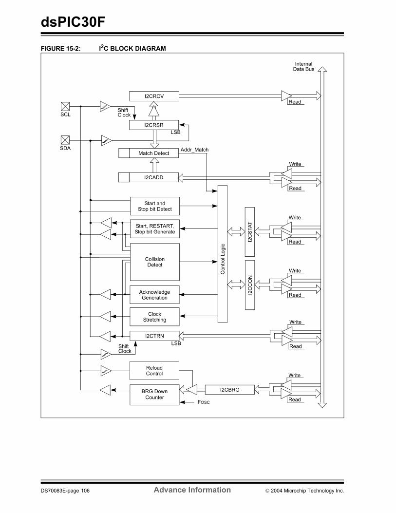
dsPIC30F
FIGURE 15-2: I2C BLOCK DIAGRAM
I2CRSR
I2CRCV
InternalData Bus
SCL
SDA
Shift
Match Detect
I2CADD
Start andStop bit Detect
Clock
Addr_Match
ClockStretching
I2CTRN
LSBShiftClock
Write
Read
BRG Down I2CBRG
ReloadControl
FOSC
Start, RESTART,Stop bit Generate
Write
Read
AcknowledgeGeneration
CollisionDetect
Write
Read
Write
ReadI2C
CO
N
Write
ReadI2C
STA
T
Co
ntr
ol L
og
ic
Read
LSB
Counter
DS70083E-page 106 Advance Information 2004 Microchip Technology Inc.
dsPIC30F
15.2 I2C Module Addresses
The I2CADD register contains the Slave mode
addresses. The register is a 10-bit register.
If the A10M bit (I2CCON<10>) is ‘0’, the address is
interpreted by the module as a 7-bit address. When an
address is received, it is compared to the 7 LS bits of
the I2CADD register.
If the A10M bit is ‘1’, the address is assumed to be a
10-bit address. When an address is received, it will be
compared with the binary value ‘11110 A9 A8’ (where
A9 and A8 are two Most Significant bits of I2CADD). If
that value matches, the next address will be compared
with the Least Significant 8 bits of I2CADD, as specified
in the 10-bit addressing protocol.
15.3 I2C 7-bit Slave Mode Operation
Once enabled (I2CEN = 1), the slave module will wait
for a Start bit to occur (i.e., the I2C module is ‘Idle’). Fol-
lowing the detection of a Start bit, 8 bits are shifted into
I2CRSR and the address is compared against
I2CADD. In 7-bit mode (A10M = 0), bits I2CADD<6:0>
are compared against I2CRSR<7:1> and I2CRSR<0>
is the R_W bit. All incoming bits are sampled on the ris-
ing edge of SCL.
If an address match occurs, an Acknowledgement will
be sent, and the slave event interrupt flag (SI2CIF) is
set on the falling edge of the ninth (ACK) bit. The
address match does not affect the contents of the
I2CRCV buffer or the RBF bit.
15.3.1 SLAVE TRANSMISSION
If the R_W bit received is a ‘1’, then the serial port will
go into Transmit mode. It will send ACK on the ninth bit
and then hold SCL to ‘0’ until the CPU responds by writ-
ing to I2CTRN. SCL is released by setting the SCLREL
bit, and 8 bits of data are shifted out. Data bits are
shifted out on the falling edge of SCL, such that SDA is
valid during SCL high. The interrupt pulse is sent on the
falling edge of the ninth clock pulse, regardless of the
status of the ACK received from the master.
15.3.2 SLAVE RECEPTION
If the R_W bit received is a ‘0’ during an address
match, then Receive mode is initiated. Incoming bits
are sampled on the rising edge of SCL. After 8 bits are
received, if I2CRCV is not full or I2COV is not set,
I2CRSR is transferred to I2CRCV. ACK is sent on the
ninth clock.
If the RBF flag is set, indicating that I2CRCV is still
holding data from a previous operation (RBF = 1), then
ACK is not sent; however, the interrupt pulse is gener-
ated. In the case of an overflow, the contents of the
I2CRSR are not loaded into the I2CRCV.
15.4 I2C 10-bit Slave Mode Operation
In 10-bit mode, the basic receive and transmit opera-
tions are the same as in the 7-bit mode. However, the
criteria for address match is more complex.
The I2C specification dictates that a slave must be
addressed for a write operation with two address bytes
following a Start bit.
The A10M bit is a control bit that signifies that the
address in I2CADD is a 10-bit address rather than a 7-bit
address. The address detection protocol for the first byte
of a message address is identical for 7-bit and 10-bit
messages, but the bits being compared are different.
I2CADD holds the entire 10-bit address. Upon receiv-
ing an address following a Start bit, I2CRSR <7:3> is
compared against a literal ‘11110’ (the default 10-bit
address) and I2CRSR<2:1> are compared against
I2CADD<9:8>. If a match occurs and if R_W = 0, the
interrupt pulse is sent. The ADD10 bit will be cleared to
indicate a partial address match. If a match fails or
R_W = 1, the ADD10 bit is cleared and the module
returns to the Idle state.
The low byte of the address is then received and com-
pared with I2CADD<7:0>. If an address match occurs,
the interrupt pulse is generated and the ADD10 bit is
set, indicating a complete 10-bit address match. If an
address match did not occur, the ADD10 bit is cleared
and the module returns to the Idle state.
15.4.1 10-BIT MODE SLAVE
TRANSMISSION
Once a slave is addressed in this fashion with the full
10-bit address (we will refer to this state as
“PRIOR_ADDR_MATCH”), the master can begin
sending data bytes for a slave reception operation.
15.4.2 10-BIT MODE SLAVE RECEPTION
Once addressed, the master can generate a Repeated
Start, reset the high byte of the address and set the
R_W bit without generating a Stop bit, thus initiating a
slave transmit operation.
Note: The I2CRCV will be loaded if the I2COV
bit = 1 and the RBF flag = 0. In this case,
a read of the I2CRCV was performed but
the user did not clear the state of the
I2COV bit before the next receive
occurred. The Acknowledgement is not
sent (ACK = 1) and the I2CRCV is
updated.
2004 Microchip Technology Inc. Advance Information DS70083E-page 107
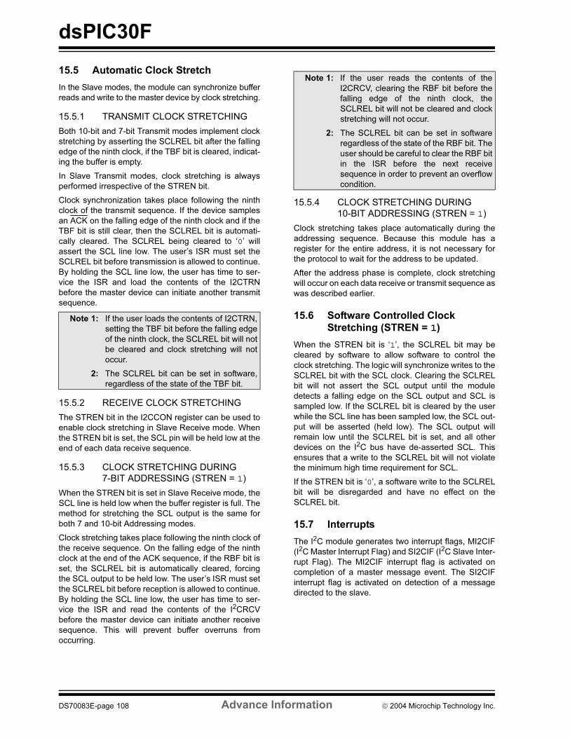
dsPIC30F
15.5 Automatic Clock Stretch
In the Slave modes, the module can synchronize buffer
reads and write to the master device by clock stretching.
15.5.1 TRANSMIT CLOCK STRETCHING
Both 10-bit and 7-bit Transmit modes implement clock
stretching by asserting the SCLREL bit after the falling
edge of the ninth clock, if the TBF bit is cleared, indicat-
ing the buffer is empty.
In Slave Transmit modes, clock stretching is always
performed irrespective of the STREN bit.
Clock synchronization takes place following the ninth
clock of the transmit sequence. If the device samples
an ACK on the falling edge of the ninth clock and if the
TBF bit is still clear, then the SCLREL bit is automati-
cally cleared. The SCLREL being cleared to ‘0’ will
assert the SCL line low. The user’s ISR must set the
SCLREL bit before transmission is allowed to continue.
By holding the SCL line low, the user has time to ser-
vice the ISR and load the contents of the I2CTRN
before the master device can initiate another transmit
sequence.
15.5.2 RECEIVE CLOCK STRETCHING
The STREN bit in the I2CCON register can be used to
enable clock stretching in Slave Receive mode. When
the STREN bit is set, the SCL pin will be held low at the
end of each data receive sequence.
15.5.3 CLOCK STRETCHING DURING
7-BIT ADDRESSING (STREN = 1)
When the STREN bit is set in Slave Receive mode, the
SCL line is held low when the buffer register is full. The
method for stretching the SCL output is the same for
both 7 and 10-bit Addressing modes.
Clock stretching takes place following the ninth clock of
the receive sequence. On the falling edge of the ninth
clock at the end of the ACK sequence, if the RBF bit is
set, the SCLREL bit is automatically cleared, forcing
the SCL output to be held low. The user’s ISR must set
the SCLREL bit before reception is allowed to continue.
By holding the SCL line low, the user has time to ser-
vice the ISR and read the contents of the I2CRCV
before the master device can initiate another receive
sequence. This will prevent buffer overruns from
occurring.
15.5.4 CLOCK STRETCHING DURING
10-BIT ADDRESSING (STREN = 1)
Clock stretching takes place automatically during the
addressing sequence. Because this module has a
register for the entire address, it is not necessary for
the protocol to wait for the address to be updated.
After the address phase is complete, clock stretching
will occur on each data receive or transmit sequence as
was described earlier.
15.6 Software Controlled Clock
Stretching (STREN = 1)
When the STREN bit is ‘1’, the SCLREL bit may be
cleared by software to allow software to control the
clock stretching. The logic will synchronize writes to the
SCLREL bit with the SCL clock. Clearing the SCLREL
bit will not assert the SCL output until the module
detects a falling edge on the SCL output and SCL is
sampled low. If the SCLREL bit is cleared by the user
while the SCL line has been sampled low, the SCL out-
put will be asserted (held low). The SCL output will
remain low until the SCLREL bit is set, and all other
devices on the I2C bus have de-asserted SCL. This
ensures that a write to the SCLREL bit will not violate
the minimum high time requirement for SCL.
If the STREN bit is ‘0’, a software write to the SCLREL
bit will be disregarded and have no effect on the
SCLREL bit.
15.7 Interrupts
The I2C module generates two interrupt flags, MI2CIF
(I2C Master Interrupt Flag) and SI2CIF (I2C Slave Inter-
rupt Flag). The MI2CIF interrupt flag is activated on
completion of a master message event. The SI2CIF
interrupt flag is activated on detection of a message
directed to the slave.
Note 1: If the user loads the contents of I2CTRN,
setting the TBF bit before the falling edge
of the ninth clock, the SCLREL bit will not
be cleared and clock stretching will not
occur.
2: The SCLREL bit can be set in software,
regardless of the state of the TBF bit.
Note 1: If the user reads the contents of the
I2CRCV, clearing the RBF bit before the
falling edge of the ninth clock, the
SCLREL bit will not be cleared and clock
stretching will not occur.
2: The SCLREL bit can be set in software
regardless of the state of the RBF bit. The
user should be careful to clear the RBF bit
in the ISR before the next receive
sequence in order to prevent an overflow
condition.
DS70083E-page 108 Advance Information 2004 Microchip Technology Inc.
dsPIC30F
15.8 Slope Control
The I2C standard requires slope control on the SDA
and SCL signals for Fast mode (400 kHz). The control
bit, DISSLW, enables the user to disable slew rate con-
trol if desired. It is necessary to disable the slew rate
control for 1 MHz mode.
15.9 IPMI Support
The control bit, IPMIEN, enables the module to support
Intelligent Peripheral Management Interface (IPMI).
When this bit is set, the module accepts and acts upon
all addresses.
15.10 General Call Address Support
The general call address can address all devices.
When this address is used, all devices should, in
theory, respond with an Acknowledgement.
The general call address is one of eight addresses
reserved for specific purposes by the I2C protocol. It
consists of all ‘0’s with R_W = 0.
The general call address is recognized when the Gen-
eral Call Enable (GCEN) bit is set (I2CCON<15> = 1).
Following a Start bit detection, 8 bits are shifted into
I2CRSR and the address is compared with I2CADD,
and is also compared with the general call address
which is fixed in hardware.
If a general call address match occurs, the I2CRSR is
transferred to the I2CRCV after the eighth clock, the
RBF flag is set and on the falling edge of the ninth bit
(ACK bit), the master event interrupt flag (MI2CIF) is
set.
When the interrupt is serviced, the source for the inter-
rupt can be checked by reading the contents of the
I2CRCV to determine if the address was device
specific or a general call address.
15.11 I2C Master Support
As a master device, six operations are supported:
• Assert a Start condition on SDA and SCL.
• Assert a RESTART condition on SDA and SCL.
• Write to the I2CTRN register initiating
transmission of data/address.
• Generate a Stop condition on SDA and SCL.
• Configure the I2C port to receive data.
• Generate an ACK condition at the end of a
received byte of data.
15.12 I2C Master Operation
The master device generates all of the serial clock
pulses and the Start and Stop conditions. A transfer is
ended with a Stop condition or with a Repeated Start
condition. Since the Repeated Start condition is also
the beginning of the next serial transfer, the I2C bus will
not be released.
In Master Transmitter mode, serial data is output
through SDA, while SCL outputs the serial clock. The
first byte transmitted contains the slave address of the
receiving device (7 bits) and the data direction bit. In
this case, the data direction bit (R_W) is logic ‘0’. Serial
data is transmitted 8 bits at a time. After each byte is
transmitted, an ACK bit is received. Start and Stop con-
ditions are output to indicate the beginning and the end
of a serial transfer.
In Master Receive mode, the first byte transmitted con-
tains the slave address of the transmitting device
(7 bits) and the data direction bit. In this case, the data
direction bit (R_W) is logic ‘1’. Thus, the first byte trans-
mitted is a 7-bit slave address, followed by a ‘1’ to indi-
cate receive bit. Serial data is received via SDA while
SCL outputs the serial clock. Serial data is received
8 bits at a time. After each byte is received, an ACK bit
is transmitted. Start and Stop conditions indicate the
beginning and end of transmission.
15.12.1 I2C MASTER TRANSMISSION
Transmission of a data byte, a 7-bit address, or the sec-
ond half of a 10-bit address is accomplished by simply
writing a value to I2CTRN register. The user should
only write to I2CTRN when the module is in a WAIT
state. This action will set the Buffer Full Flag (TBF) and
allow the baud rate generator to begin counting and
start the next transmission. Each bit of address/data
will be shifted out onto the SDA pin after the falling
edge of SCL is asserted. The Transmit Status Flag,
TRSTAT (I2CSTAT<14>), indicates that a master
transmit is in progress.
15.12.2 I2C MASTER RECEPTION
Master mode reception is enabled by programming the
Receive Enable bit, RCEN (I2CCON<11>). The I2C
module must be Idle before the RCEN bit is set, other-
wise the RCEN bit will be disregarded. The baud rate
generator begins counting and on each rollover, the
state of the SCL pin ACK and data are shifted into the
I2CRSR on the rising edge of each clock.
2004 Microchip Technology Inc. Advance Information DS70083E-page 109
dsPIC30F
15.12.3 BAUD RATE GENERATOR
In I2C Master mode, the reload value for the BRG is
located in the I2CBRG register. When the BRG is
loaded with this value, the BRG counts down to ‘0’ and
stops until another reload has taken place. If clock arbi-
tration is taking place, for instance, the BRG is reloaded
when the SCL pin is sampled high.
As per the I2C standard, FSCK may be 100 kHz or
400 kHz. However, the user can specify any baud rate
up to 1 MHz. I2CBRG values of ‘0’ or ‘1’ are illegal.
EQUATION 15-1: SERIAL CLOCK RATE
15.12.4 CLOCK ARBITRATION
Clock arbitration occurs when the master de-asserts
the SCL pin (SCL allowed to float high) during any
receive, transmit, or RESTART/Stop condition. When
the SCL pin is allowed to float high, the baud rate gen-
erator (BRG) is suspended from counting until the SCL
pin is actually sampled high. When the SCL pin is sam-
pled high, the baud rate generator is reloaded with the
contents of I2CBRG and begins counting. This ensures
that the SCL high time will always be at least one BRG
rollover count in the event that the clock is held low by
an external device.
15.12.5 MULTI-MASTER COMMUNICATION,
BUS COLLISION, AND BUS
ARBITRATION
Multi-master operation support is achieved by bus arbi-
tration. When the master outputs address/data bits
onto the SDA pin, arbitration takes place when the
master outputs a ‘1’ on SDA by letting SDA float high
while another master asserts a ‘0’. When the SCL pin
floats high, data should be stable. If the expected data
on SDA is a ‘1’ and the data sampled on the SDA
pin = 0, then a bus collision has taken place. The
master will set the MI2CIF pulse and reset the master
portion of the I2C port to its Idle state.
If a transmit was in progress when the bus collision
occurred, the transmission is halted, the TBF flag is
cleared, the SDA and SCL lines are de-asserted and a
value can now be written to I2CTRN. When the user
services the I2C master event Interrupt Service Rou-
tine, if the I2C bus is free (i.e., the P bit is set), the user
can resume communication by asserting a Start
condition.
If a Start, RESTART, Stop or Acknowledge condition
was in progress when the bus collision occurred, the
condition is aborted, the SDA and SCL lines are de-
asserted, and the respective control bits in the I2CCON
register are cleared to ‘0’. When the user services the
bus collision Interrupt Service Routine, and if the I2C
bus is free, the user can resume communication by
asserting a Start condition.
The master will continue to monitor the SDA and SCL
pins, and if a Stop condition occurs, the MI2CIF bit will
be set.
A write to the I2CTRN will start the transmission of data
at the first data bit regardless of where the transmitter
left off when bus collision occurred.
In a multi-master environment, the interrupt generation
on the detection of Start and Stop conditions allows the
determination of when the bus is free. Control of the I2C
bus can be taken when the P bit is set in the I2CSTAT
register, or the bus is Idle and the S and P bits are
cleared.
15.13 I2C Module Operation During CPU
Sleep and Idle Modes
15.13.1 I2C OPERATION DURING CPU
SLEEP MODE
When the device enters Sleep mode, all clock sources
to the module are shutdown and stay at logic ‘0’. If
Sleep occurs in the middle of a transmission and the
state machine is partially into a transmission as the
clocks stop, then the transmission is aborted. Similarly,
if Sleep occurs in the middle of a reception, then the
reception is aborted.
15.13.2 I2C OPERATION DURING CPU IDLE
MODE
For the I2C, the I2CSIDL bit selects if the module will
stop on Idle or continue on Idle. If I2CSIDL = 0, the
module will continue operation on assertion of the Idle
mode. If I2CSIDL = 1, the module will stop on Idle.
FSCK = FCY / I2CBRG
DS70083E-page 110 Advance Information 2004 Microchip Technology Inc.
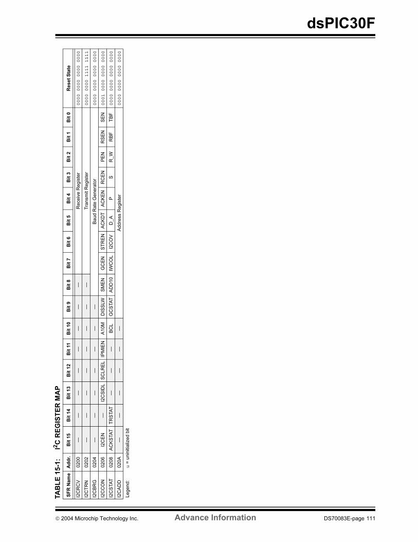
dsPIC30F
TA
BL
E 1
5-1
:I2
C R
EG
IST
ER
MA
P
SF
R N
am
eA
dd
r.B
it 1
5B
it 1
4B
it 1
3B
it 1
2B
it 1
1B
it 1
0B
it 9
Bit
8B
it 7
Bit
6B
it 5
Bit
4B
it 3
Bit
2B
it 1
Bit
0R
eset
Sta
te
I2C
RC
V0200
——
——
——
——
Receiv
e R
egis
ter
0000 0000 0000 0000
I2C
TR
N0202
——
——
——
——
Tra
nsm
it R
egis
ter
0000 0000 1111 1111
I2C
BR
G0204
——
——
——
—B
aud R
ate
Genera
tor
0000 0000 0000 0000
I2C
CO
N0206
I2C
EN
—I2
CS
IDL
SC
LR
EL
IPM
IEN
A10M
DIS
SLW
SM
EN
GC
EN
ST
RE
NA
CK
DT
AC
KE
NR
CE
NP
EN
RS
EN
SE
N0001 0000 0000 0000
I2C
STA
T0208
AC
KS
TA
TT
RS
TA
T—
——
BC
LG
CS
TA
TA
DD
10
IWC
OL
I2C
OV
D_A
PS
R_W
RB
FT
BF
0000 0000 0000 0000
I2C
AD
D020A
——
——
——
Addre
ss R
egis
ter
0000 0000 0000 0000
Legend:
u =
unin
itia
lized b
it
2004 Microchip Technology Inc. Advance Information DS70083E-page 111

dsPIC30F
NOTES:
DS70083E-page 112 Advance Information 2004 Microchip Technology Inc.
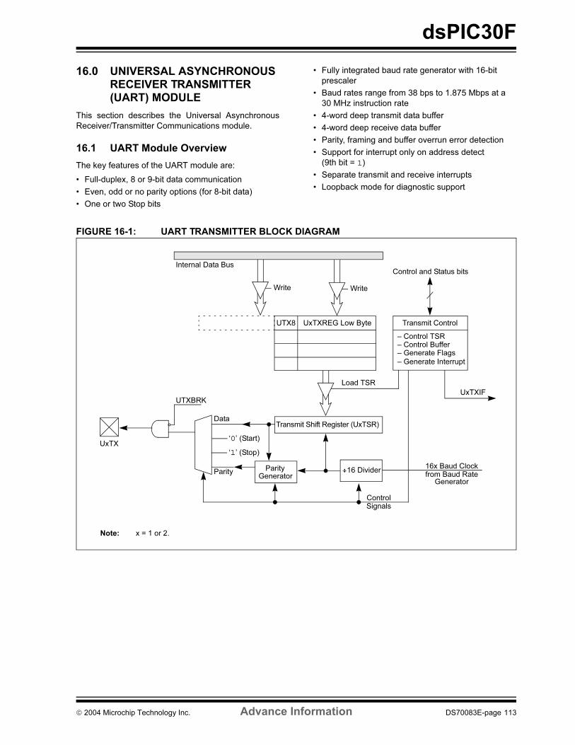
dsPIC30F
16.0 UNIVERSAL ASYNCHRONOUS RECEIVER TRANSMITTER (UART) MODULE
This section describes the Universal Asynchronous
Receiver/Transmitter Communications module.
16.1 UART Module Overview
The key features of the UART module are:
• Full-duplex, 8 or 9-bit data communication
• Even, odd or no parity options (for 8-bit data)
• One or two Stop bits
• Fully integrated baud rate generator with 16-bit
prescaler
• Baud rates range from 38 bps to 1.875 Mbps at a
30 MHz instruction rate
• 4-word deep transmit data buffer
• 4-word deep receive data buffer
• Parity, framing and buffer overrun error detection
• Support for interrupt only on address detect
(9th bit = 1)
• Separate transmit and receive interrupts
• Loopback mode for diagnostic support
FIGURE 16-1: UART TRANSMITTER BLOCK DIAGRAM
Write Write
UTX8 UxTXREG Low Byte
Load TSR
Transmit Control
– Control TSR– Control Buffer– Generate Flags– Generate Interrupt
Control and Status bits
UxTXIF
Data
‘0’ (Start)
‘1’ (Stop)
Parity ParityGenerator
Transmit Shift Register (UxTSR)
16 Divider
ControlSignals
16x Baud Clockfrom Baud Rate
Generator
Internal Data Bus
UTXBRK
UxTX
Note: x = 1 or 2.
2004 Microchip Technology Inc. Advance Information DS70083E-page 113
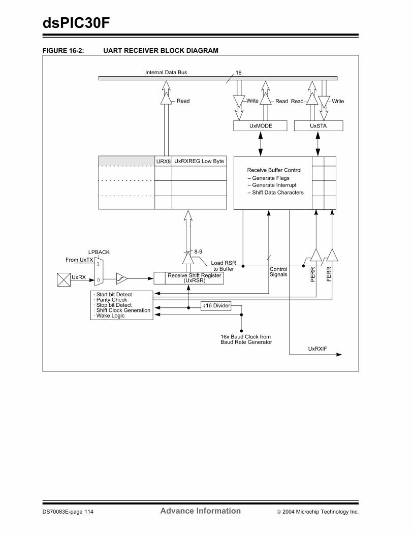
dsPIC30F
FIGURE 16-2: UART RECEIVER BLOCK DIAGRAM
Read
URX8 UxRXREG Low Byte
Load RSR
UxMODE
Receive Buffer Control
– Generate Flags
– Generate Interrupt
UxRXIF
UxRX
· Start bit Detect
Receive Shift Register
16 Divider
ControlSignals
UxSTA
– Shift Data Characters
Read ReadWrite Write
to Buffer
8-9
(UxRSR) PERR
FERR
· Parity Check· Stop bit Detect· Shift Clock Generation· Wake Logic
16Internal Data Bus
1
0
LPBACK
From UxTX
16x Baud Clock fromBaud Rate Generator
DS70083E-page 114 Advance Information 2004 Microchip Technology Inc.
dsPIC30F
16.2 Enabling and Setting Up UART
16.2.1 ENABLING THE UART
The UART module is enabled by setting the UARTEN
bit in the UxMODE register (where x = 1 or 2). Once
enabled, the UxTX and UxRX pins are configured as an
output and an input respectively, overriding the TRIS
and LATCH register bit settings for the corresponding
I/O port pins. The UxTX pin is at logic ‘1’ when no
transmission is taking place.
16.2.2 DISABLING THE UART
The UART module is disabled by clearing the UARTEN
bit in the UxMODE register. This is the default state
after any Reset. If the UART is disabled, all I/O pins
operate as port pins under the control of the latch and
TRIS bits of the corresponding port pins.
Disabling the UART module resets the buffers to empty
states. Any data characters in the buffers are lost and
the baud rate counter is reset.
All error and status flags associated with the UART
module are reset when the module is disabled. The
URXDA, OERR, FERR, PERR, UTXEN, UTXBRK and
UTXBF bits are cleared, whereas RIDLE and TRMT
are set. Other control bits, including ADDEN,
URXISEL<1:0>, UTXISEL, as well as the UxMODE
and UxBRG registers, are not affected.
Clearing the UARTEN bit while the UART is active will
abort all pending transmissions and receptions and
reset the module as defined above. Re-enabling the
UART will restart the UART in the same configuration.
16.2.3 ALTERNATE I/O
The alternate I/O function is enabled by setting the
ALTIO bit (UxMODE<10>). If ALTIO = 1, the UxATX
and UxARX pins (alternate transmit and alternate
receive pins, respectively) are used by the UART mod-
ule instead of the UxTX and UxRX pins. If ALTIO = 0,
the UxTX and UxRX pins are used by the UART
module.
16.2.4 SETTING UP DATA, PARITY AND
STOP BIT SELECTIONS
Control bits PDSEL<1:0> in the UxMODE register are
used to select the data length and parity used in the
transmission. The data length may either be 8 bits with
even, odd or no parity, or 9 bits with no parity.
The STSEL bit determines whether one or two Stop bits
will be used during data transmission.
The default (power-on) setting of the UART is 8 bits, no
parity and 1 Stop bit (typically represented as 8, N, 1).
16.3 Transmitting Data
16.3.1 TRANSMITTING IN 8-BIT DATA
MODE
The following steps must be performed in order to
transmit 8-bit data:
1. Set up the UART:
First, the data length, parity and number of Stop
bits must be selected. Then, the transmit and
receive interrupt enable and priority bits are
setup in the UxMODE and UxSTA registers.
Also, the appropriate baud rate value must be
written to the UxBRG register.
2. Enable the UART by setting the UARTEN bit
(UxMODE<15>).
3. Set the UTXEN bit (UxSTA<10>), thereby
enabling a transmission.
4. Write the byte to be transmitted to the lower byte
of UxTXREG. The value will be transferred to the
Transmit Shift register (UxTSR) immediately
and the serial bit stream will start shifting out
during the next rising edge of the baud clock.
Alternatively, the data byte may be written while
UTXEN = 0, following which, the user may set
UTXEN. This will cause the serial bit stream to
begin immediately because the baud clock will
start from a cleared state.
5. A transmit interrupt will be generated, depend-
ing on the value of the interrupt control bit
UTXISEL (UxSTA<15>).
16.3.2 TRANSMITTING IN 9-BIT DATA
MODE
The sequence of steps involved in the transmission of
9-bit data is similar to 8-bit transmission, except that a
16-bit data word (of which the upper 7 bits are always
clear) must be written to the UxTXREG register.
16.3.3 TRANSMIT BUFFER (UXTXB)
The transmit buffer is 9 bits wide and 4 characters
deep. Including the Transmit Shift register (UxTSR),
the user effectively has a 5-deep FIFO (First-In, First-
Out) buffer. The UTXBF status bit (UxSTA<9>)
indicates whether the transmit buffer is full.
If a user attempts to write to a full buffer, the new data
will not be accepted into the FIFO, and no data shift will
occur within the buffer. This enables recovery from a
buffer overrun condition.
The FIFO is reset during any device Reset but is not
affected when the device enters or wakes up from a
Power Saving mode.
2004 Microchip Technology Inc. Advance Information DS70083E-page 115
dsPIC30F
16.3.4 TRANSMIT INTERRUPT
The transmit interrupt flag (U1TXIF or U2TXIF) is
located in the corresponding interrupt flag register.
The transmitter generates an edge to set the UxTXIF
bit. The condition for generating the interrupt depends
on the UTXISEL control bit:
a) If UTXISEL = 0, an interrupt is generated when
a word is transferred from the transmit buffer to
the Transmit Shift register (UxTSR). This implies
that the transmit buffer has at least one empty
word.
b) If UTXISEL = 1, an interrupt is generated when
a word is transferred from the transmit buffer to
the Transmit Shift register (UxTSR) and the
transmit buffer is empty.
Switching between the two Interrupt modes during
operation is possible and sometimes offers more
flexibility.
16.3.5 TRANSMIT BREAK
Setting the UTXBRK bit (UxSTA<11>) will cause the
UxTX line to be driven to logic ‘0’. The UTXBRK bit
overrides all transmission activity. Therefore, the user
should generally wait for the transmitter to be Idle
before setting UTXBRK.
To send a break character, the UTXBRK bit must be set
by software and must remain set for a minimum of 13
baud clock cycles. The UTXBRK bit is then cleared by
software to generate Stop bits. The user must wait for
a duration of at least one or two baud clock cycles in
order to ensure a valid Stop bit(s) before reloading the
UxTXB, or starting other transmitter activity. Transmis-
sion of a break character does not generate a transmit
interrupt.
16.4 Receiving Data
16.4.1 RECEIVING IN 8-BIT OR 9-BIT
DATA MODE
The following steps must be performed while receiving
8-bit or 9-bit data:
1. Set up the UART (see Section 16.3.1).
2. Enable the UART (see Section 16.3.1).
3. A receive interrupt will be generated when one
or more data words have been received,
depending on the receive interrupt settings
specified by the URXISEL bits (UxSTA<7:6>).
4. Read the OERR bit to determine if an overrun
error has occurred. The OERR bit must be reset
in software.
5. Read the received data from UxRXREG. The act
of reading UxRXREG will move the next word to
the top of the receive FIFO, and the PERR and
FERR values will be updated.
16.4.2 RECEIVE BUFFER (UXRXB)
The receive buffer is 4 words deep. Including the
Receive Shift register (UxRSR), the user effectively
has a 5-word deep FIFO buffer.
URXDA (UxSTA<0>) = 1 indicates that the receive
buffer has data available. URXDA = 0 implies that the
buffer is empty. If a user attempts to read an empty
buffer, the old values in the buffer will be read and no
data shift will occur within the FIFO.
The FIFO is reset during any device Reset. It is not
affected when the device enters or wakes up from a
Power Saving mode.
16.4.3 RECEIVE INTERRUPT
The receive interrupt flag (U1RXIF or U2RXIF) can be
read from the corresponding interrupt flag register. The
interrupt flag is set by an edge generated by the
receiver. The condition for setting the receive interrupt
flag depends on the settings specified by the
URXISEL<1:0> (UxSTA<7:6>) control bits.
a) If URXISEL<1:0> = 00 or 01, an interrupt is gen-
erated every time a data word is transferred
from the Receive Shift register (UxRSR) to the
receive buffer. There may be one or more
characters in the receive buffer.
b) If URXISEL<1:0> = 10, an interrupt is generated
when a word is transferred from the Receive Shift
register (UxRSR) to the receive buffer, which as a
result of the transfer, contains 3 characters.
c) If URXISEL<1:0> = 11, an interrupt is set when
a word is transferred from the Receive Shift reg-
ister (UxRSR) to the receive buffer, which as a
result of the transfer, contains 4 characters (i.e.,
becomes full).
Switching between the Interrupt modes during opera-
tion is possible, though generally not advisable during
normal operation.
16.5 Reception Error Handling
16.5.1 RECEIVE BUFFER OVERRUN
ERROR (OERR BIT)
The OERR bit (UxSTA<1>) is set if all of the following
conditions occur:
a) The receive buffer is full.
b) The Receive Shift register is full, but unable to
transfer the character to the receive buffer.
c) The Stop bit of the character in the UxRSR is
detected, indicating that the UxRSR needs to
transfer the character to the buffer.
Once OERR is set, no further data is shifted in UxRSR
(until the OERR bit is cleared in software or a Reset
occurs). The data held in UxRSR and UxRXREG
remains valid.
DS70083E-page 116 Advance Information 2004 Microchip Technology Inc.
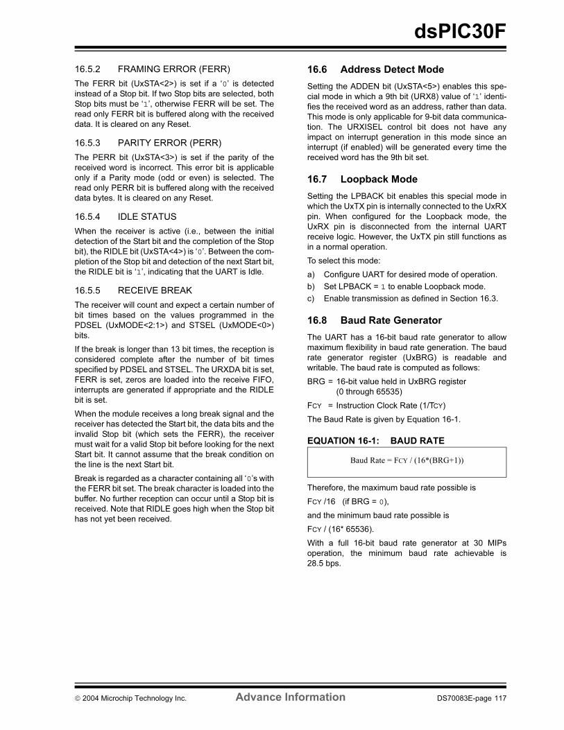
dsPIC30F
16.5.2 FRAMING ERROR (FERR)
The FERR bit (UxSTA<2>) is set if a ‘0’ is detected
instead of a Stop bit. If two Stop bits are selected, both
Stop bits must be ‘1’, otherwise FERR will be set. The
read only FERR bit is buffered along with the received
data. It is cleared on any Reset.
16.5.3 PARITY ERROR (PERR)
The PERR bit (UxSTA<3>) is set if the parity of the
received word is incorrect. This error bit is applicable
only if a Parity mode (odd or even) is selected. The
read only PERR bit is buffered along with the received
data bytes. It is cleared on any Reset.
16.5.4 IDLE STATUS
When the receiver is active (i.e., between the initial
detection of the Start bit and the completion of the Stop
bit), the RIDLE bit (UxSTA<4>) is ‘0’. Between the com-
pletion of the Stop bit and detection of the next Start bit,
the RIDLE bit is ‘1’, indicating that the UART is Idle.
16.5.5 RECEIVE BREAK
The receiver will count and expect a certain number of
bit times based on the values programmed in the
PDSEL (UxMODE<2:1>) and STSEL (UxMODE<0>)
bits.
If the break is longer than 13 bit times, the reception is
considered complete after the number of bit times
specified by PDSEL and STSEL. The URXDA bit is set,
FERR is set, zeros are loaded into the receive FIFO,
interrupts are generated if appropriate and the RIDLE
bit is set.
When the module receives a long break signal and the
receiver has detected the Start bit, the data bits and the
invalid Stop bit (which sets the FERR), the receiver
must wait for a valid Stop bit before looking for the next
Start bit. It cannot assume that the break condition on
the line is the next Start bit.
Break is regarded as a character containing all ‘0’s with
the FERR bit set. The break character is loaded into the
buffer. No further reception can occur until a Stop bit is
received. Note that RIDLE goes high when the Stop bit
has not yet been received.
16.6 Address Detect Mode
Setting the ADDEN bit (UxSTA<5>) enables this spe-
cial mode in which a 9th bit (URX8) value of ‘1’ identi-
fies the received word as an address, rather than data.
This mode is only applicable for 9-bit data communica-
tion. The URXISEL control bit does not have any
impact on interrupt generation in this mode since an
interrupt (if enabled) will be generated every time the
received word has the 9th bit set.
16.7 Loopback Mode
Setting the LPBACK bit enables this special mode in
which the UxTX pin is internally connected to the UxRX
pin. When configured for the Loopback mode, the
UxRX pin is disconnected from the internal UART
receive logic. However, the UxTX pin still functions as
in a normal operation.
To select this mode:
a) Configure UART for desired mode of operation.
b) Set LPBACK = 1 to enable Loopback mode.
c) Enable transmission as defined in Section 16.3.
16.8 Baud Rate Generator
The UART has a 16-bit baud rate generator to allow
maximum flexibility in baud rate generation. The baud
rate generator register (UxBRG) is readable and
writable. The baud rate is computed as follows:
BRG = 16-bit value held in UxBRG register
(0 through 65535)
FCY = Instruction Clock Rate (1/TCY)
The Baud Rate is given by Equation 16-1.
EQUATION 16-1: BAUD RATE
Therefore, the maximum baud rate possible is
FCY /16 (if BRG = 0),
and the minimum baud rate possible is
FCY / (16* 65536).
With a full 16-bit baud rate generator at 30 MIPs
operation, the minimum baud rate achievable is
28.5 bps.
Baud Rate = FCY / (16*(BRG+1))
2004 Microchip Technology Inc. Advance Information DS70083E-page 117
dsPIC30F
16.9 Auto Baud Support
To allow the system to determine baud rates of
received characters, the input can be optionally linked
to a selected capture input. To enable this mode, the
user must program the input capture module to detect
the falling and rising edges of the Start bit.
16.10 UART Operation During CPU
Sleep and Idle Modes
16.10.1 UART OPERATION DURING CPU
SLEEP MODE
When the device enters Sleep mode, all clock sources
to the module are shutdown and stay at logic ‘0’. If entry
into Sleep mode occurs while a transmission is in
progress, then the transmission is aborted. The UxTX
pin is driven to logic ‘1’. Similarly, if entry into Sleep
mode occurs while a reception is in progress, then the
reception is aborted. The UxSTA, UxMODE, transmit
and receive registers and buffers, and the UxBRG
register are not affected by Sleep mode.
If the WAKE bit (UxSTA<7>) is set before the device
enters Sleep mode, then a falling edge on the UxRX pin
will generate a receive interrupt. The Receive Interrupt
Select mode bit (URXISEL) has no effect for this func-
tion. If the receive interrupt is enabled, then this will
wake-up the device from Sleep. The UARTEN bit must
be set in order to generate a wake-up interrupt.
16.10.2 UART OPERATION DURING CPU
IDLE MODE
For the UART, the USIDL bit selects if the module will
stop operation when the device enters Idle mode or
whether the module will continue on Idle. If USIDL = 0,
the module will continue operation during Idle mode. If
USIDL = 1, the module will stop on Idle.
DS70083E-page 118 Advance Information 2004 Microchip Technology Inc.
dsPIC30F
TA
BL
E 1
6-1
:U
AR
T1
RE
GIS
TE
R M
AP
TA
BL
E 1
6-2
:U
AR
T2
RE
GIS
TE
R M
AP
SF
R N
am
eA
dd
r.B
it 1
5B
it 1
4B
it 1
3B
it 1
2B
it 1
1B
it 1
0B
it 9
Bit
8B
it 7
Bit
6B
it 5
Bit
4B
it 3
Bit
2B
it 1
Bit
0R
eset
Sta
te
U1M
OD
E020C
UA
RT
EN
—U
SID
L—
—A
LT
IO—
—W
AK
ELP
BA
CK
AB
AU
D—
—P
DS
EL
1P
DS
EL0
ST
SE
L0000 0000 0000 0000
U1S
TA
020E
UT
XIS
EL
——
—U
TX
BR
KU
TX
EN
UT
XB
FT
RM
TU
RX
ISE
L1
UR
XIS
EL0
AD
DE
NR
IDLE
PE
RR
FE
RR
OE
RR
UR
XD
A0000 0001 0001 0000
U1T
XR
EG
0210
——
——
——
—U
TX
8T
ransm
it R
egis
ter
0000 000u uuuu uuuu
U1R
XR
EG
0212
——
——
——
—U
RX
8R
eceiv
e R
egis
ter
0000 0000 0000 0000
U1B
RG
0214
Baud R
ate
Genera
tor
Pre
scale
r0000 0000 0000 0000
Legend:
u =
unin
itia
lized b
it
SF
R
Nam
eA
dd
r.B
it 1
5B
it 1
4B
it 1
3B
it 1
2B
it 1
1B
it 1
0B
it 9
Bit
8B
it 7
Bit
6B
it 5
Bit
4B
it 3
Bit
2B
it 1
Bit
0R
eset
Sta
te
U2M
OD
E0216
UA
RT
EN
—U
SID
L—
——
——
WA
KE
LP
BA
CK
AB
AU
D—
—P
DS
EL1
PD
SE
L0
ST
SE
L0000 0000 0000 0000
U2S
TA
0218
UT
XIS
EL
——
—U
TX
BR
KU
TX
EN
UT
XB
FT
RM
TU
RX
ISE
L1
UR
XIS
EL0
AD
DE
NR
IDLE
PE
RR
FE
RR
OE
RR
UR
XD
A0000 0001 0001 0000
U2T
XR
EG
021A
——
——
——
—U
TX
8T
ransm
it R
egis
ter
0000 000u uuuu uuuu
U2R
XR
EG
021C
——
——
——
—U
RX
8R
eceiv
e R
egis
ter
0000 0000 0000 0000
U2B
RG
021E
Baud R
ate
Genera
tor
Pre
scale
r0000 0000 0000 0000
Legend:
u =
unin
itia
lized b
it
2004 Microchip Technology Inc. Advance Information DS70083E-page 119

dsPIC30F
NOTES:
DS70083E-page 120 Advance Information 2004 Microchip Technology Inc.
dsPIC30F
17.0 CAN MODULE
17.1 Overview
The Controller Area Network (CAN) module is a serial
interface, useful for communicating with other CAN
modules or microcontroller devices. This interface/
protocol was designed to allow communications within
noisy environments.
The CAN module is a communication controller imple-
menting the CAN 2.0 A/B protocol, as defined in the
BOSCH specification. The module will support
CAN 1.2, CAN 2.0A, CAN 2.0B Passive, and CAN 2.0B
Active versions of the protocol. The module implemen-
tation is a full CAN system. The CAN specification is
not covered within this data sheet. The reader may
refer to the BOSCH CAN specification for further
details.
The module features are as follows:
• Implementation of the CAN protocol CAN 1.2,
CAN 2.0A and CAN 2.0B
• Standard and extended data frames
• 0-8 bytes data length
• Programmable bit rate up to 1 Mbit/sec
• Support for remote frames
• Double-buffered receiver with two prioritized
received message storage buffers (each buffer
may contain up to 8 bytes of data)
• 6 full (standard/extended identifier) acceptance
filters, 2 associated with the high priority receive
buffer and 4 associated with the low priority
receive buffer
• 2 full acceptance filter masks, one each
associated with the high and low priority receive
buffers
• Three transmit buffers with application specified
prioritization and abort capability (each buffer may
contain up to 8 bytes of data)
• Programmable wake-up functionality with
integrated low-pass filter
• Programmable Loopback mode supports self-test
operation
• Signaling via interrupt capabilities for all CAN
receiver and transmitter error states
• Programmable clock source
• Programmable link to timer module for
time-stamping and network synchronization
• Low power Sleep and Idle mode
The CAN bus module consists of a protocol engine and
message buffering/control. The CAN protocol engine
handles all functions for receiving and transmitting
messages on the CAN bus. Messages are transmitted
by first loading the appropriate data registers. Status
and errors can be checked by reading the appropriate
registers. Any message detected on the CAN bus is
checked for errors and then matched against filters to
see if it should be received and stored in one of the
receive registers.
17.2 Frame Types
The CAN module transmits various types of frames
which include data messages or remote transmission
requests initiated by the user, as other frames that are
automatically generated for control purposes. The
following frame types are supported:
• Standard Data Frame:
A standard data frame is generated by a node
when the node wishes to transmit data. It includes
an 11-bit standard identifier (SID) but not an 18-bit
extended identifier (EID).
• Extended Data Frame:
An extended data frame is similar to a standard
data frame but includes an extended identifier as
well.
• Remote Frame:
It is possible for a destination node to request the
data from the source. For this purpose, the desti-
nation node sends a remote frame with an identi-
fier that matches the identifier of the required data
frame. The appropriate data source node will then
send a data frame as a response to this remote
request.
• Error Frame:
An error frame is generated by any node that
detects a bus error. An error frame consists of 2
fields: an error flag field and an error delimiter
field.
• Overload Frame:
An overload frame can be generated by a node as
a result of 2 conditions. First, the node detects a
dominant bit during interframe space which is an
illegal condition. Second, due to internal condi-
tions, the node is not yet able to start reception of
the next message. A node may generate a maxi-
mum of 2 sequential overload frames to delay the
start of the next message.
• Interframe Space:
Interframe space separates a proceeding frame
(of whatever type) from a following data or remote
frame.
2004 Microchip Technology Inc. Advance Information DS70083E-page 121
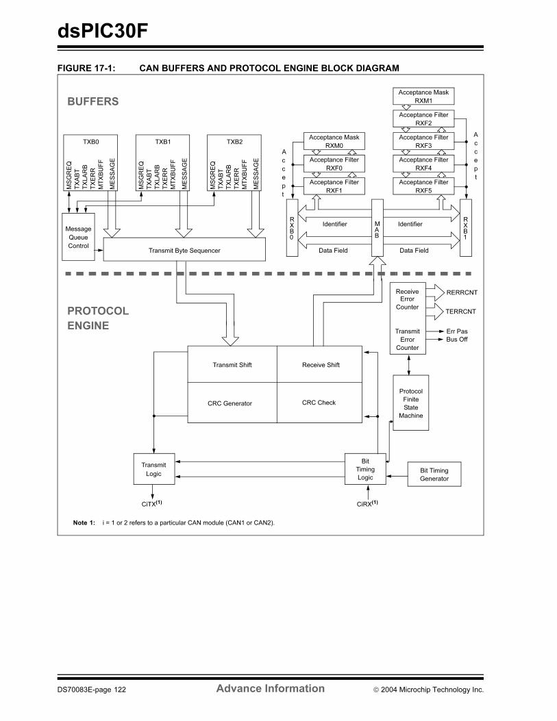
dsPIC30F
FIGURE 17-1: CAN BUFFERS AND PROTOCOL ENGINE BLOCK DIAGRAM
Acceptance Filter
RXF2
RXB1
A
c
c
e
p
t
A
c
c
e
p
t
Identifier
Data Field Data Field
Identifier
Acceptance Mask
RXM1
Acceptance Filter
RXF3
Acceptance Filter
RXF4
Acceptance Filter
RXF5
MAB
Acceptance Mask
RXM0
Acceptance Filter
RXF0
Acceptance Filter
RXF1
RXB0
MSGREQ
TXB2
TXABT
TXLARB
TXERR
MTXBUFF
MESSAGE
Message
Queue
ControlTransmit Byte Sequencer
MSGREQ
TXB1TXABT
TXLARB
TXERR
MTXBUFF
MESSAGE
MSGREQ
TXB0
TXABT
TXLARB
TXERR
MTXBUFF
MESSAGE
Receive ShiftTransmit Shift
ReceiveError
Transmit
Error
Protocol
RERRCNT
TERRCNT
Err Pas
Bus Off
Finite
State
Machine
Counter
Counter
Transmit
Logic
Bit
Timing
Logic
CiTX(1) CiRX(1)
Bit Timing
Generator
PROTOCOL
ENGINE
BUFFERS
CRC CheckCRC Generator
Note 1: i = 1 or 2 refers to a particular CAN module (CAN1 or CAN2).
DS70083E-page 122 Advance Information 2004 Microchip Technology Inc.
dsPIC30F
17.3 Modes of Operation
The CAN module can operate in one of several Operation
modes selected by the user. These modes include:
• Initialization Mode
• Disable Mode
• Normal Operation Mode
• Listen Only Mode
• Loopback Mode
• Error Recognition Mode
Modes are requested by setting the REQOP<2:0> bits
(CiCTRL<10:8>), except the Error Recognition mode
which is requested through the RXM<1:0> bits
(CiRXnCON<6:5>, where n = 0 or 1 represents a par-
ticular receive buffer). Entry into a mode is Acknowl-
edged by monitoring the OPMODE<2:0> bits
(CiCTRL<7:5>). The module will not change the mode
and the OPMODE bits until a change in mode is
acceptable, generally during bus Idle time which is
defined as at least 11 consecutive recessive bits.
17.3.1 INITIALIZATION MODE
In the Initialization mode, the module will not transmit or
receive. The error counters are cleared and the inter-
rupt flags remain unchanged. The programmer will
have access to configuration registers that are access
restricted in other modes. The module will protect the
user from accidentally violating the CAN protocol
through programming errors. All registers which control
the configuration of the module can not be modified
while the module is on-line. The CAN module will not
be allowed to enter the Configuration mode while a
transmission is taking place. The Configuration mode
serves as a lock to protect the following registers.
• All Module Control Registers
• Baud Rate and Interrupt Configuration Registers
• Bus Timing Registers
• Identifier Acceptance Filter Registers
• Identifier Acceptance Mask Registers
17.3.2 DISABLE MODE
In Disable mode, the module will not transmit or
receive. The module has the ability to set the WAKIF bit
due to bus activity, however, any pending interrupts will
remain and the error counters will retain their value.
If the REQOP<2:0> bits (CiCTRL<10:8>) = 001, the
module will enter the Module Disable mode. If the module
is active, the module will wait for 11 recessive bits on the
CAN bus, detect that condition as an Idle bus, then
accept the module disable command. When the
OPMODE<2:0> bits (CiCTRL<7:5>) = 001, that indi-
cates whether the module successfully went into Module
Disable mode. The I/O pins will revert to normal I/O
function when the module is in the Module Disable mode.
The module can be programmed to apply a low-pass
filter function to the CiRX input line while the module or
the CPU is in Sleep mode. The WAKFIL bit
(CiCFG2<14>) enables or disables the filter.
17.3.3 NORMAL OPERATION MODE
Normal Operating mode is selected when
REQOP<2:0> = 000. In this mode, the module is acti-
vated and the I/O pins will assume the CAN bus func-
tions. The module will transmit and receive CAN bus
messages via the CxTX and CxRX pins.
17.3.4 LISTEN ONLY MODE
If the Listen Only mode is activated, the module on the
CAN bus is passive. The transmitter buffers revert to
the port I/O function. The receive pins remain inputs.
For the receiver, no error flags or Acknowledge signals
are sent. The error counters are deactivated in this
state. The Listen Only mode can be used for detecting
the baud rate on the CAN bus. To use this, it is neces-
sary that there are at least two further nodes that
communicate with each other.
17.3.5 LISTEN ALL MESSAGES MODE
The module can be set to ignore all errors and receive
any message. The Error Recognition mode is activated
by setting REQOP<2:0> = 111. In this mode, the data
which is in the message assembly buffer until the time
an error occurred, is copied in the receive buffer and
can be read via the CPU interface.
17.3.6 LOOPBACK MODE
If the Loopback mode is activated, the module will con-
nect the internal transmit signal to the internal receive
signal at the module boundary. The transmit and
receive pins revert to their port I/O function.
Note: Typically, if the CAN module is allowed to
transmit in a particular mode of operation
and a transmission is requested immedi-
ately after the CAN module has been
placed in that mode of operation, the mod-
ule waits for 11 consecutive recessive bits
on the bus before starting transmission. If
the user switches to Disable Mode within
this 11-bit period, then this transmission is
aborted and the corresponding TXABT bit
is set and TXREQ bit is cleared.
2004 Microchip Technology Inc. Advance Information DS70083E-page 123
dsPIC30F
17.4 Message Reception
17.4.1 RECEIVE BUFFERS
The CAN bus module has 3 receive buffers. However,
one of the receive buffers is always committed to mon-
itoring the bus for incoming messages. This buffer is
called the Message Assembly Buffer (MAB). So there
are 2 receive buffers visible, RXB0 and RXB1, that can
essentially instantaneously receive a complete
message from the protocol engine.
All messages are assembled by the MAB and are trans-
ferred to the RXBn buffers only if the acceptance filter
criterion are met. When a message is received, the
RXnIF flag (CiINTF<0> or CiINRF<1>) will be set. This
bit can only be set by the module when a message is
received. The bit is cleared by the CPU when it has com-
pleted processing the message in the buffer. If the
RXnIE bit (CiINTE<0> or CiINTE<1>) is set, an interrupt
will be generated when a message is received.
RXF0 and RXF1 filters with RXM0 mask are associated
with RXB0. The filters RXF2, RXF3, RXF4, and RXF5
and the mask RXM1 are associated with RXB1.
17.4.2 MESSAGE ACCEPTANCE FILTERS
The message acceptance filters and masks are used to
determine if a message in the message assembly
buffer should be loaded into either of the receive buff-
ers. Once a valid message has been received into the
Message Assembly Buffer (MAB), the identifier fields of
the message are compared to the filter values. If there
is a match, that message will be loaded into the
appropriate receive buffer.
The acceptance filter looks at incoming messages for
the RXIDE bit (CiRXnSID<0>) to determine how to
compare the identifiers. If the RXIDE bit is clear, the
message is a standard frame and only filters with the
EXIDE bit (CiRXFnSID<0>) clear are compared. If the
RXIDE bit is set, the message is an extended frame,
and only filters with the EXIDE bit set are compared.
Configuring the RXM<1:0> bits to ‘01’ or ‘10’ can
override the EXIDE bit.
17.4.3 MESSAGE ACCEPTANCE FILTER
MASKS
The mask bits essentially determine which bits to apply
the filter to. If any mask bit is set to a zero, then that bit
will automatically be accepted regardless of the filter
bit. There are 2 programmable acceptance filter masks
associated with the receive buffers, one for each buffer.
17.4.4 RECEIVE OVERRUN
An overrun condition occurs when the Message
Assembly Buffer (MAB) has assembled a valid
received message, the message is accepted through
the acceptance filters, and when the receive buffer
associated with the filter has not been designated as
clear of the previous message.
The overrun error flag, RXnOVR (CiINTF<15> or
CiINTF<14>), and the ERRIF bit (CiINTF<5>) will be
set and the message in the MAB will be discarded.
If the DBEN bit is clear, RXB1 and RXB0 operate inde-
pendently. When this is the case, a message intended
for RXB0 will not be diverted into RXB1 if RXB0 con-
tains an unread message and the RX0OVR bit will be
set.
If the DBEN bit is set, the overrun for RXB0 is handled
differently. If a valid message is received for RXB0 and
RXFUL = 1 indicates that RXB0 is full and RXFUL = 0indicates that RXB1 is empty, the message for RXB0
will be loaded into RXB1. An overrun error will not be
generated for RXB0. If a valid message is received for
RXB0 and RXFUL = 1, indicating that both RXB0 and
RXB1 are full, the message will be lost and an overrun
will be indicated for RXB1.
17.4.5 RECEIVE ERRORS
The CAN module will detect the following receive
errors:
• Cyclic Redundancy Check (CRC) Error
• Bit Stuffing Error
• Invalid Message Receive Error
These receive errors do not generate an interrupt.
However, the receive error counter is incremented by
one in case one of these errors occur. The RXWAR bit
(CiINTF<9>) indicates that the receive error counter
has reached the CPU warning limit of 96 and an
interrupt is generated.
17.4.6 RECEIVE INTERRUPTS
Receive interrupts can be divided into 3 major groups,
each including various conditions that generate
interrupts:
• Receive Interrupt:
A message has been successfully received and
loaded into one of the receive buffers. This inter-
rupt is activated immediately after receiving the
End of Frame (EOF) field. Reading the RXnIF flag
will indicate which receive buffer caused the
interrupt.
• Wake-up Interrupt:
The CAN module has woken up from Disable
mode or the device has woken up from Sleep
mode.
DS70083E-page 124 Advance Information 2004 Microchip Technology Inc.
dsPIC30F
• Receive Error Interrupts:
A receive error interrupt will be indicated by the
ERRIF bit. This bit shows that an error condition
occurred. The source of the error can be deter-
mined by checking the bits in the CAN Interrupt
Status register, CiINTF.
- Invalid Message Received:
If any type of error occurred during reception of
the last message, an error will be indicated by
the IVRIF bit.
- Receiver Overrun:
The RXnOVR bit indicates that an overrun
condition occurred.
- Receiver Warning:
The RXWAR bit indicates that the receive error
counter (RERRCNT<7:0>) has reached the
warning limit of 96.
- Receiver Error Passive:
The RXEP bit indicates that the receive error
counter has exceeded the error passive limit of
127 and the module has gone into error passive
state.
17.5 Message Transmission
17.5.1 TRANSMIT BUFFERS
The CAN module has three transmit buffers. Each of
the three buffers occupies 14 bytes of data. Eight of the
bytes are the maximum 8 bytes of the transmitted mes-
sage. Five bytes hold the standard and extended
identifiers and other message arbitration information.
17.5.2 TRANSMIT MESSAGE PRIORITY
Transmit priority is a prioritization within each node of
the pending transmittable messages. There are
4 levels of transmit priority. If TXPRI<1:0>
(CiTXnCON<1:0>, where n = 0, 1 or 2 represents a par-
ticular transmit buffer) for a particular message buffer is
set to ‘11’, that buffer has the highest priority. If
TXPRI<1:0> for a particular message buffer is set to
‘10’ or ‘01’, that buffer has an intermediate priority. If
TXPRI<1:0> for a particular message buffer is ‘00’, that
buffer has the lowest priority.
17.5.3 TRANSMISSION SEQUENCE
To initiate transmission of the message, the TXREQ bit
(CiTXnCON<3>) must be set. The CAN bus module
resolves any timing conflicts between setting of the
TXREQ bit and the Start of Frame (SOF), ensuring that if
the priority was changed, it is resolved correctly before the
SOF occurs. When TXREQ is set, the TXABT
(CiTXnCON<6>), TXLARB (CiTXnCON<5>) and TXERR
(CiTXnCON<4>) flag bits are automatically cleared.
Setting TXREQ bit simply flags a message buffer as
enqueued for transmission. When the module detects
an available bus, it begins transmitting the message
which has been determined to have the highest priority.
If the transmission completes successfully on the first
attempt, the TXREQ bit is cleared automatically, and an
interrupt is generated if TXIE was set.
If the message transmission fails, one of the error con-
dition flags will be set, and the TXREQ bit will remain
set indicating that the message is still pending for trans-
mission. If the message encountered an error condition
during the transmission attempt, the TXERR bit will be
set, and the error condition may cause an interrupt. If
the message loses arbitration during the transmission
attempt, the TXLARB bit is set. No interrupt is
generated to signal the loss of arbitration.
17.5.4 ABORTING MESSAGE
TRANSMISSION
The system can also abort a message by clearing the
TXREQ bit associated with each message buffer. Set-
ting the ABAT bit (CiCTRL<12>) will request an abort of
all pending messages. If the message has not yet
started transmission, or if the message started but is
interrupted by loss of arbitration or an error, the abort
will be processed. The abort is indicated when the
module sets the TXABT bit and the TXnIF flag is not
automatically set.
17.5.5 TRANSMISSION ERRORS
The CAN module will detect the following transmission
errors:
• Acknowledge Error
• Form Error
• Bit Error
These transmission errors will not necessarily generate
an interrupt but are indicated by the transmission error
counter. However, each of these errors will cause the
transmission error counter to be incremented by one.
Once the value of the error counter exceeds the value
of 96, the ERRIF (CiINTF<5>) and the TXWAR bit
(CiINTF<10>) are set. Once the value of the error
counter exceeds the value of 96, an interrupt is
generated and the TXWAR bit in the Error Flag register
is set.
2004 Microchip Technology Inc. Advance Information DS70083E-page 125
dsPIC30F
17.5.6 TRANSMIT INTERRUPTS
Transmit interrupts can be divided into 2 major groups,
each including various conditions that generate
interrupts:
• Transmit Interrupt:
At least one of the three transmit buffers is empty
(not scheduled) and can be loaded to schedule a
message for transmission. Reading the TXnIF
flags will indicate which transmit buffer is available
and caused the interrupt.
• Transmit Error Interrupts:
A transmission error interrupt will be indicated by
the ERRIF flag. This flag shows that an error con-
dition occurred. The source of the error can be
determined by checking the error flags in the CAN
Interrupt Status register, CiINTF. The flags in this
register are related to receive and transmit errors.
- Transmitter Warning Interrupt:
The TXWAR bit indicates that the transmit error
counter has reached the CPU warning limit of
96.
- Transmitter Error Passive:
The TXEP bit (CiINTF<12>) indicates that the
transmit error counter has exceeded the error
passive limit of 127 and the module has gone to
error passive state.
- Bus Off:
The TXBO bit (CiINTF<13>) indicates that the
transmit error counter has exceeded 255 and
the module has gone to the bus off state.
17.6 Baud Rate Setting
All nodes on any particular CAN bus must have the
same nominal bit rate. In order to set the baud rate, the
following parameters have to be initialized:
• Synchronization Jump Width
• Baud Rate Prescaler
• Phase Segments
• Length determination of Phase Segment 2
• Sample Point
• Propagation Segment bits
17.6.1 BIT TIMING
All controllers on the CAN bus must have the same
baud rate and bit length. However, different controllers
are not required to have the same master oscillator
clock. At different clock frequencies of the individual
controllers, the baud rate has to be adjusted by
adjusting the number of time quanta in each segment.
The nominal bit time can be thought of as being divided
into separate non-overlapping time segments. These
segments are shown in Figure 17-2.
• Synchronization Segment (Sync Seg)
• Propagation Time Segment (Prop Seg)
• Phase Segment 1 (Phase1 Seg)
• Phase Segment 2 (Phase2 Seg)
The time segments and also the nominal bit time are
made up of integer units of time called time quanta or
TQ. By definition, the nominal bit time has a minimum
of 8 TQ and a maximum of 25 TQ. Also, by definition,
the minimum nominal bit time is 1 µsec corresponding
to a maximum bit rate of 1 MHz.
FIGURE 17-2: CAN BIT TIMING
Input Signal
SyncProp
Segment
Phase
Segment 1
Phase
Segment 2 Sync
Sample Point
TQ
DS70083E-page 126 Advance Information 2004 Microchip Technology Inc.
dsPIC30F
17.6.2 PRESCALER SETTING
There is a programmable prescaler with integral values
ranging from 1 to 64, in addition to a fixed divide-by-2
for clock generation. The time quantum (TQ) is a fixed
unit of time derived from the oscillator period, and is
given by Equation 17-1.
EQUATION 17-1: TIME QUANTUM FOR
CLOCK GENERATION
17.6.3 PROPAGATION SEGMENT
This part of the bit time is used to compensate physical
delay times within the network. These delay times con-
sist of the signal propagation time on the bus line and
the internal delay time of the nodes. The Prop Seg can
be programmed from 1 TQ to 8 TQ by setting the
PRSEG<2:0> bits (CiCFG2<2:0>).
17.6.4 PHASE SEGMENTS
The phase segments are used to optimally locate the
sampling of the received bit within the transmitted bit
time. The sampling point is between Phase1 Seg and
Phase2 Seg. These segments are lengthened or short-
ened by resynchronization. The end of the Phase1 Seg
determines the sampling point within a bit period. The
segment is programmable from 1 TQ to 8 TQ. Phase2
Seg provides delay to the next transmitted data transi-
tion. The segment is programmable from 1 TQ to 8 TQ,
or it may be defined to be equal to the greater of
Phase1 Seg or the information processing time (2 TQ).
The Phase1 Seg is initialized by setting bits
SEG1PH<2:0> (CiCFG2<5:3>), and Phase2 Seg is
initialized by setting SEG2PH<2:0> (CiCFG2<10:8>).
The following requirement must be fulfilled while setting
the lengths of the phase segments:
Prop Seg + Phase1 Seg > = Phase2 Seg
17.6.5 SAMPLE POINT
The sample point is the point of time at which the bus
level is read and interpreted as the value of that respec-
tive bit. The location is at the end of Phase1 Seg. If the
bit timing is slow and contains many TQ, it is possible to
specify multiple sampling of the bus line at the sample
point. The level determined by the CAN bus then corre-
sponds to the result from the majority decision of three
values. The majority samples are taken at the sample
point and twice before with a distance of TQ/2. The
CAN module allows the user to choose between sam-
pling three times at the same point or once at the same
point, by setting or clearing the SAM bit (CiCFG2<6>).
Typically, the sampling of the bit should take place at
about 60 - 70% through the bit time, depending on the
system parameters.
17.6.6 SYNCHRONIZATION
To compensate for phase shifts between the oscillator
frequencies of the different bus stations, each CAN
controller must be able to synchronize to the relevant
signal edge of the incoming signal. When an edge in
the transmitted data is detected, the logic will compare
the location of the edge to the expected time (Synchro-
nous Segment). The circuit will then adjust the values
of Phase1 Seg and Phase2 Seg. There are 2
mechanisms used to synchronize.
17.6.6.1 Hard Synchronization
Hard synchronization is only done whenever there is a
‘recessive’ to ‘dominant’ edge during bus Idle indicating
the start of a message. After hard synchronization, the
bit time counters are restarted with the Sync Seg. Hard
synchronization forces the edge which has caused the
hard synchronization to lie within the synchronization
segment of the restarted bit time. If a hard synchroniza-
tion is done, there will not be a resynchronization within
that bit time.
17.6.6.2 Resynchronization
As a result of resynchronization, Phase1 Seg may be
lengthened or Phase2 Seg may be shortened. The
amount of lengthening or shortening of the phase
buffer segment has an upper bound known as the syn-
chronization jump width, and is specified by the
SJW<1:0> bits (CiCFG1<7:6>). The value of the syn-
chronization jump width will be added to Phase1 Seg or
subtracted from Phase2 Seg. The resynchronization
jump width is programmable between 1 TQ and 4 TQ.
The following requirement must be fulfilled while setting
the SJW<1:0> bits:
Phase2 Seg > Synchronization Jump Width
TQ = 2 (BRP<5:0> + 1) / FCAN
2004 Microchip Technology Inc. Advance Information DS70083E-page 127
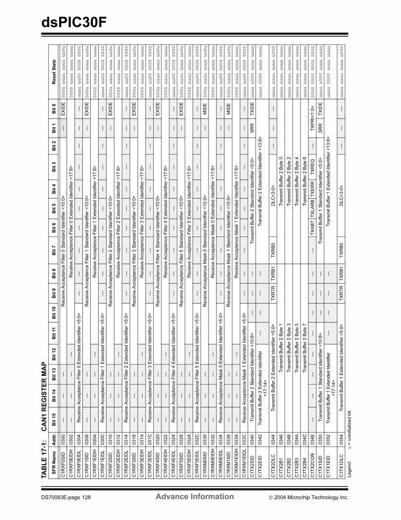
dsPIC30F
TA
BL
E 1
7-1
:C
AN
1 R
EG
IST
ER
MA
P
SF
R N
am
eA
dd
r.B
it 1
5B
it 1
4B
it 1
3B
it 1
2B
it 1
1B
it 1
0B
it 9
Bit
8B
it 7
Bit
6B
it 5
Bit
4B
it 3
Bit
2B
it 1
Bit
0R
eset
Sta
te
C1R
XF
0S
ID0
300
——
—R
eceiv
e A
ccepta
nce F
ilter
0 S
tandard
Identifier
<10:0
>—
EX
IDE
000u uuuu uuuu uu0u
C1R
XF
0E
IDH
0302
——
——
Receiv
e A
ccepta
nce F
ilter
0 E
xte
nded Identifier
<17:6
>0000 uuuu uuuu uuuu
C1R
XF
0E
IDL
0304
Receiv
e A
ccepta
nce F
ilter
0 E
xte
nded Identifier
<5:0
>—
——
——
——
——
—uuuu uu00 0000 0000
C1R
XF
1S
ID0
308
——
—R
eceiv
e A
ccepta
nce F
ilter
1 S
tandard
Identifier
<10:0
>—
EX
IDE
000u uuuu uuuu uu0u
C1R
XF
1E
IDH
030A
——
——
Receiv
e A
ccepta
nce F
ilter
1 E
xte
nded Identifier
<17:6
>0000 uuuu uuuu uuuu
C1R
XF
1E
IDL
030C
Receiv
e A
ccepta
nce F
ilter
1 E
xte
nded Identifier
<5:0
>—
——
——
——
——
—uuuu uu00 0000 0000
C1R
XF
2S
ID0
310
——
—R
eceiv
e A
ccepta
nce F
ilter
2 S
tandard
Identifier
<10:0
>—
EX
IDE
000u uuuu uuuu uu0u
C1R
XF
2E
IDH
0312
——
——
Receiv
e A
ccepta
nce F
ilter
2 E
xte
nded Identifier
<17:6
>0000 uuuu uuuu uuuu
C1R
XF
2E
IDL
0314
Receiv
e A
ccepta
nce F
ilter
2 E
xte
nded Identifier
<5:0
>—
——
——
——
——
—uuuu uu00 0000 0000
C1R
XF
3S
ID0
318
——
—R
eceiv
e A
ccepta
nce F
ilter
3 S
tandard
Identifier
<10:0
>—
EX
IDE
000u uuuu uuuu uu0u
C1R
XF
3E
IDH
031A
——
——
Receiv
e A
ccepta
nce F
ilter
3 E
xte
nded Identifier
<17:6
>0000 uuuu uuuu uuuu
C1R
XF
3E
IDL
031C
Receiv
e A
ccepta
nce F
ilter
3 E
xte
nded Identifier
<5:0
>—
——
——
——
——
—uuuu uu00 0000 0000
C1R
XF
4S
ID0
320
——
—R
eceiv
e A
ccepta
nce F
ilter
4 S
tandard
Identifier
<10:0
>—
EX
IDE
000u uuuu uuuu uu0u
C1R
XF
4E
IDH
0322
——
——
Receiv
e A
ccepta
nce F
ilter
4 E
xte
nded Identifier
<17:6
>0000 uuuu uuuu uuuu
C1R
XF
4E
IDL
0324
Receiv
e A
ccepta
nce F
ilter
4 E
xte
nded Identifier
<5:0
>—
——
——
——
——
—uuuu uu00 0000 0000
C1R
XF
5S
ID0
328
——
—R
eceiv
e A
ccepta
nce F
ilter
5 S
tandard
Identifier
<10:0
>—
EX
IDE
000u uuuu uuuu uu0u
C1R
XF
5E
IDH
032A
——
——
Receiv
e A
ccepta
nce F
ilter
5 E
xte
nded Identifier
<17:6
>0000 uuuu uuuu uuuu
C1R
XF
5E
IDL
032C
Receiv
e A
ccepta
nce F
ilter
5 E
xte
nded Identifier
<5:0
>—
——
——
——
——
—uuuu uu00 0000 0000
C1R
XM
0S
ID0
330
——
—R
eceiv
e A
ccepta
nce M
ask 0
Sta
ndard
Identifier
<10:0
>—
MID
E000u uuuu uuuu uu0u
C1R
XM
0E
IDH
0332
——
——
Receiv
e A
ccepta
nce M
ask 0
Exte
nded Identifier
<17:6
>0000 uuuu uuuu uuuu
C1R
XM
0E
IDL
0334
Re
ceiv
e A
ccepta
nce M
ask 0
Exte
nded Identifier
<5:0
>—
——
——
——
——
—uuuu uu00 0000 0000
C1R
XM
1S
ID0
338
——
—R
eceiv
e A
ccepta
nce M
ask 1
Sta
ndard
Identifier
<10:0
>—
MID
E000u uuuu uuuu uu0u
C1R
XM
1E
IDH
033A
——
——
Receiv
e A
ccepta
nce M
ask 1
Exte
nded Identifier
<17:6
>0000 uuuu uuuu uuuu
C1R
XM
1E
IDL
033C
Receiv
e A
ccepta
nce M
ask 1
Exte
nded Identifier
<5:0
>—
——
——
——
——
—uuuu uu00 0000 0000
C1T
X2S
ID0340
Tra
nsm
it B
uffer
2 S
tandard
Identifier
<10:6
>—
——
Tra
nsm
it B
uffer
2 S
tandard
Identifier
<5:0
>S
RR
TX
IDE
uuuu u000 uuuu uuuu
C1T
X2E
ID0342
Tra
nsm
it B
uffer
2 E
xte
nded Identifier
<17:1
4>
——
——
Tra
nsm
it B
uffer
2 E
xte
nded Identifier
<13:6
>uuuu 0000 uuuu uuuu
C1T
X2D
LC
0344
Tra
nsm
it B
uffer
2 E
xte
nded Identifier
<5:0
>T
XR
TR
TX
RB
1T
XR
B0
DLC
<3:0
>—
——
uuuu uuuu uuuu u000
C1T
X2B
10
346
Tra
nsm
it B
uffer
2 B
yte
1T
ransm
it B
uffer
2 B
yte
0uuuu uuuu uuuu uuuu
C1T
X2B
20
348
Tra
nsm
it B
uffer
2 B
yte
3T
ransm
it B
uffer
2 B
yte
2uuuu uuuu uuuu uuuu
C1T
X2B
3034A
Tra
nsm
it B
uffer
2 B
yte
5T
ransm
it B
uffer
2 B
yte
4uuuu uuuu uuuu uuuu
C1T
X2B
4034C
Tra
nsm
it B
uffer
2 B
yte
7T
ransm
it B
uffer
2 B
yte
6uuuu uuuu uuuu uuuu
C1T
X2C
ON
034E
——
——
——
——
—T
XA
BT
TX
LA
RB
TX
ER
RT
XR
EQ
—T
XP
RI<
1:0
>0000 0000 0000 0000
C1T
X1S
ID0350
Tra
nsm
it B
uffer
1 S
tandard
Identifier
<10:6
>—
——
Tra
nsm
it B
uffer
1 S
tandard
Identifier
<5:0
>S
RR
TX
IDE
uuuu u000 uuuu uuuu
C1T
X1E
ID0
352
Tra
nsm
it B
uffer
1 E
xte
nded Identif
ier
<17:1
4>
——
——
Tra
nsm
it B
uffer
1 E
xte
nded Identifier
<13:6
>uuuu 0000 uuuu uuuu
C1T
X1D
LC
0354
Tra
nsm
it B
uffer
1 E
xte
nded Identifier
<5:0
>T
XR
TR
TX
RB
1T
XR
B0
DLC
<3:0
>—
——
uuuu uuuu uuuu u000
Legend:
u =
unin
itia
lized b
it
DS70083E-page 128 Advance Information 2004 Microchip Technology Inc.
dsPIC30F
C1T
X1B
10
356
Tra
nsm
it B
uffer
1 B
yte
1T
ransm
it B
uffer
1 B
yte
0uuuu uuuu uuuu uuuu
C1T
X1B
20
358
Tra
nsm
it B
uffer
1 B
yte
3T
ransm
it B
uffer
1 B
yte
2uuuu uuuu uuuu uuuu
C1T
X1B
3035A
Tra
nsm
it B
uffer
1 B
yte
5T
ransm
it B
uffer
1 B
yte
4uuuu uuuu uuuu uuuu
C1T
X1B
4035C
Tra
nsm
it B
uffer
1 B
yte
7T
ransm
it B
uffer
1 B
yte
6uuuu uuuu uuuu uuuu
C1T
X1C
ON
035E
——
——
——
——
—T
XA
BT
TX
LA
RB
TX
ER
RT
XR
EQ
—T
XP
RI<
1:0
>0000 0000 0000 0000
C1T
X0S
ID0360
Tra
nsm
it B
uffer
0 S
tandard
Identifier
<10:6
>—
——
Tra
nsm
it B
uffer
0 S
tandard
Identifier
<5:0
>S
RR
TX
IDE
uuuu u000 uuuu uuuu
C1T
X0E
ID0362
Tra
nsm
it B
uffer
0 E
xte
nded Identifier
<17:1
4>
——
——
Tra
nsm
it B
uffer
0 E
xte
nded Identifier
<13:6
>uuuu 0000 uuuu uuuu
C1T
X0D
LC
0364
Tra
nsm
it B
uffer
0 E
xte
nded Identifier
<5:0
>T
XR
TR
TX
RB
1T
XR
B0
DLC
<3:0
>—
——
uuuu uuuu uuuu u000
C1T
X0B
10
366
Tra
nsm
it B
uffer
0 B
yte
1T
ransm
it B
uffer
0 B
yte
0uuuu uuuu uuuu uuuu
C1T
X0B
20
368
Tra
nsm
it B
uffer
0 B
yte
3T
ransm
it B
uffer
0 B
yte
2uuuu uuuu uuuu uuuu
C1T
X0B
3036A
Tra
nsm
it B
uffer
0 B
yte
5T
ransm
it B
uffer
0 B
yte
4uuuu uuuu uuuu uuuu
C1T
X0B
4036C
Tra
nsm
it B
uffer
0 B
yte
7T
ransm
it B
uffer
0 B
yte
6uuuu uuuu uuuu uuuu
C1T
X0C
ON
036E
——
——
——
——
—T
XA
BT
TX
LA
RB
TX
ER
RT
XR
EQ
—T
XP
RI<
1:0
>0000 0000 0000 0000
C1R
X1S
ID0370
——
—R
eceiv
e B
uffer
1 S
tanda
rd Identifier
<10:0
>S
RR
RX
IDE
000u uuuu uuuu uuuu
C1R
X1E
ID0372
——
——
Receiv
e B
uffer
1 E
xte
nded Identifier
<17:6
>0000 uuuu uuuu uuuu
C1R
X1D
LC
0374
Receiv
e B
uffer
1 E
xte
nded Identifier
<5:0
>R
XR
TR
RX
RB
1—
——
RX
RB
0D
LC
<3:0
>uuuu uuuu 000u uuuu
C1R
X1B
10
376
Receiv
e B
uffer
1 B
yte
1R
eceiv
e B
uffer
1 B
yte
0uuuu uuuu uuuu uuuu
C1R
X1B
20
378
Receiv
e B
uffer
1 B
yte
3R
eceiv
e B
uffer
1 B
yte
2uuuu uuuu uuuu uuuu
C1R
X1B
3037A
Receiv
e B
uffer
1 B
yte
5R
eceiv
e B
uffer
1 B
yte
4uuuu uuuu uuuu uuuu
C1R
X1B
4037C
Receiv
e B
uffer
1 B
yte
7R
eceiv
e B
uffer
1 B
yte
6uuuu uuuu uuuu uuuu
C1R
X1C
ON
037E
——
——
——
——
RX
FU
L—
——
RX
RT
RR
OF
ILH
IT<
2:0
>0000 0000 0000 0000
C1R
X0S
ID0380
——
—R
eceiv
e B
uffer
0 S
tanda
rd Identifier
<10:0
>S
RR
RX
IDE
000u uuuu uuuu uuuu
C1R
X0E
ID0382
——
——
Receiv
e B
uffer
0 E
xte
nded Identifier
<17:6
>0000 uuuu uuuu uuuu
C1R
X0D
LC
0384
Receiv
e B
uffer
0 E
xte
nded Identifier
<5:0
>R
XR
TR
RX
RB
1—
——
RX
RB
0D
LC
<3:0
>uuuu uuuu 000u uuuu
C1R
X0B
10
386
Receiv
e B
uffer
0 B
yte
1R
eceiv
e B
uffer
0 B
yte
0uuuu uuuu uuuu uuuu
C1R
X0B
20
388
Receiv
e B
uffer
0 B
yte
3R
eceiv
e B
uffer
0 B
yte
2uuuu uuuu uuuu uuuu
C1R
X0B
3038A
Receiv
e B
uffer
0 B
yte
5R
eceiv
e B
uffer
0 B
yte
4uuuu uuuu uuuu uuuu
C1R
X0B
4038C
Receiv
e B
uffer
0 B
yte
7R
eceiv
e B
uffer
0 B
yte
6uuuu uuuu uuuu uuuu
C1R
X0C
ON
038E
——
——
——
——
RX
FU
L—
——
RX
RT
RR
OD
BE
NJT
OF
FF
ILH
IT00000 0000 0000 0000
C1C
TR
L0390
CA
NC
AP
—C
SID
LE
AB
AT
CA
NC
KS
RE
QO
P<
2:0
>O
PM
OD
E<
2:0
>—
ICO
DE
<2:0
>—
0000 0100 1000 0000
C1C
FG
10392
——
——
——
——
SJW
<1:0
>B
RP
<5:0
>0000 0000 0000 0000
C1C
FG
20394
—W
AK
FIL
——
—S
EG
2P
H<
2:0
>S
EG
2P
HT
SS
AM
SE
G1P
H<
2:0
>P
RS
EG
<2:0
>0u00 0uuu uuuu uuuu
C1IN
TF
0396
RX
0O
VR
RX
1O
VR
TX
BO
TX
EP
RX
EP
TX
WA
RR
XW
AR
EW
AR
NIV
RIF
WA
KIF
ER
RIF
TX
2IF
TX
1IF
TX
0IF
RX
1IF
RX
0IF
0000 0000 0000 0000
C1IN
TE
0398
——
——
——
——
IVR
IEW
AK
IEE
RR
IET
X2IE
TX
1IE
TX
0IE
RX
1E
RX
0IE
0000 0000 0000 0000
C1E
C039A
Tra
nsm
it E
rror
Count R
egis
ter
Receiv
e E
rror
Count R
egis
ter
0000 0000 0000 0000
TA
BL
E 1
7-1
:C
AN
1 R
EG
IST
ER
MA
P (
CO
NT
INU
ED
)
SF
R N
am
eA
dd
r.B
it 1
5B
it 1
4B
it 1
3B
it 1
2B
it 1
1B
it 1
0B
it 9
Bit
8B
it 7
Bit
6B
it 5
Bit
4B
it 3
Bit
2B
it 1
Bit
0R
eset
Sta
te
Legend:
u =
unin
itia
lized b
it
2004 Microchip Technology Inc. Advance Information DS70083E-page 129
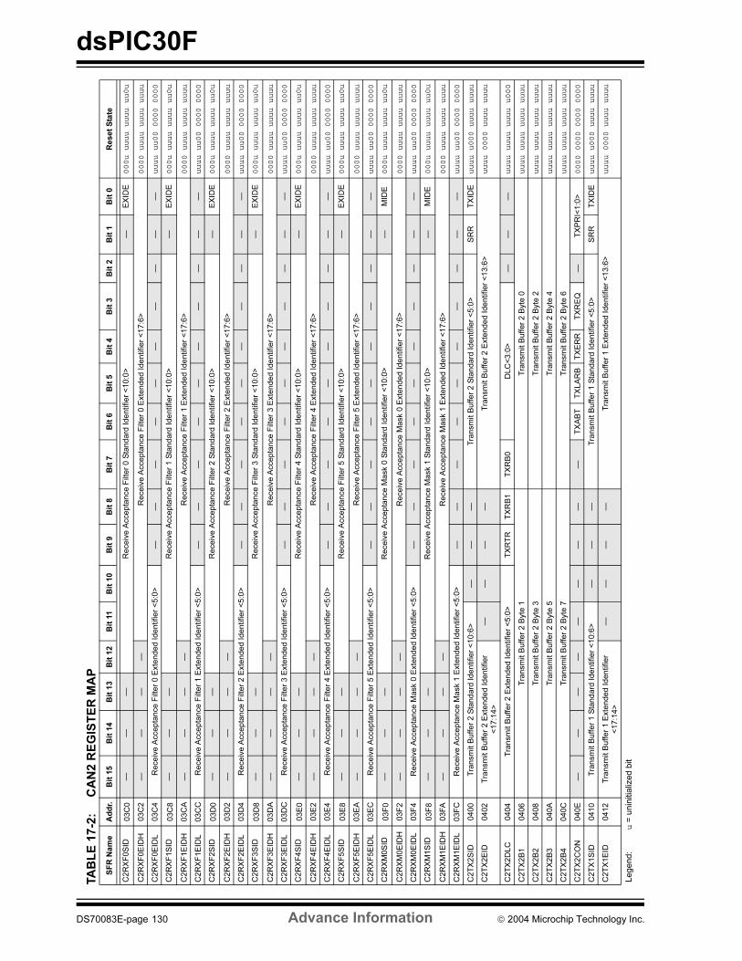
dsPIC30F
TA
BL
E 1
7-2
:C
AN
2 R
EG
IST
ER
MA
P
SF
R N
am
eA
dd
r.B
it 1
5B
it 1
4B
it 1
3B
it 1
2B
it 1
1B
it 1
0B
it 9
Bit
8B
it 7
Bit
6B
it 5
Bit
4B
it 3
Bit
2B
it 1
Bit
0R
eset
Sta
te
C2R
XF
0S
ID03C
0—
——
Receiv
e A
ccepta
nce F
ilter
0 S
tandard
Identifier
<10:0
>—
EX
IDE
000u uuuu uuuu uu0u
C2R
XF
0E
IDH
03C
2—
——
—R
eceiv
e A
ccepta
nce F
ilter
0 E
xte
nded Identifier
<17:6
>0000 uuuu uuuu uuuu
C2R
XF
0E
IDL
03C
4R
eceiv
e A
ccepta
nce F
ilter
0 E
xte
nded Identifier
<5:0
>—
——
——
——
——
—uuuu uu00 0000 0000
C2R
XF
1S
ID03C
8—
——
Receiv
e A
ccepta
nce F
ilter
1 S
tandard
Identifier
<10:0
>—
EX
IDE
000u uuuu uuuu uu0u
C2R
XF
1E
IDH
03C
A—
——
—R
eceiv
e A
ccepta
nce F
ilter
1 E
xte
nded Identifier
<17:6
>0000 uuuu uuuu uuuu
C2R
XF
1E
IDL
03C
CR
eceiv
e A
ccepta
nce F
ilter
1 E
xte
nded Identifier
<5:0
>—
——
——
——
——
—uuuu uu00 0000 0000
C2R
XF
2S
ID03D
0—
——
Receiv
e A
ccepta
nce F
ilter
2 S
tandard
Identifier
<10:0
>—
EX
IDE
000u uuuu uuuu uu0u
C2R
XF
2E
IDH
03D
2—
——
—R
eceiv
e A
ccepta
nce F
ilter
2 E
xte
nded Identifier
<17:6
>0000 uuuu uuuu uuuu
C2R
XF
2E
IDL
03D
4R
eceiv
e A
ccepta
nce F
ilter
2 E
xte
nded Identifier
<5:0
>—
——
——
——
——
—uuuu uu00 0000 0000
C2R
XF
3S
ID03D
8—
——
Receiv
e A
ccepta
nce F
ilter
3 S
tandard
Identifier
<10:0
>—
EX
IDE
000u uuuu uuuu uu0u
C2R
XF
3E
IDH
03D
A—
——
—R
eceiv
e A
ccepta
nce F
ilter
3 E
xte
nded Identifier
<17:6
>0000 uuuu uuuu uuuu
C2R
XF
3E
IDL
03D
CR
eceiv
e A
ccepta
nce F
ilter
3 E
xte
nded Identifier
<5:0
>—
——
——
——
——
—uuuu uu00 0000 0000
C2R
XF
4S
ID03E
0—
——
Receiv
e A
ccepta
nce F
ilter
4 S
tandard
Identifier
<10:0
>—
EX
IDE
000u uuuu uuuu uu0u
C2R
XF
4E
IDH
03E
2—
——
—R
eceiv
e A
ccepta
nce F
ilter
4 E
xte
nded Identifier
<17:6
>0000 uuuu uuuu uuuu
C2R
XF
4E
IDL
03E
4R
eceiv
e A
ccepta
nce F
ilter
4 E
xte
nded Identifier
<5:0
>—
——
——
——
——
—uuuu uu00 0000 0000
C2R
XF
5S
ID03E
8—
——
Receiv
e A
ccepta
nce F
ilter
5 S
tandard
Identifier
<10:0
>—
EX
IDE
000u uuuu uuuu uu0u
C2R
XF
5E
IDH
03E
A—
——
—R
eceiv
e A
ccepta
nce F
ilter
5 E
xte
nded Identifier
<17:6
>0000 uuuu uuuu uuuu
C2R
XF
5E
IDL
03E
CR
eceiv
e A
ccepta
nce F
ilter
5 E
xte
nded Identifier
<5:0
>—
——
——
——
——
—uuuu uu00 0000 0000
C2R
XM
0S
ID03F
0—
——
Receiv
e A
ccepta
nce M
ask 0
Sta
ndard
Identifier
<10:0
>—
MID
E000u uuuu uuuu uu0u
C2R
XM
0E
IDH
03F
2—
——
—R
eceiv
e A
ccepta
nce M
ask 0
Exte
nded Identifier
<17:6
>0000 uuuu uuuu uuuu
C2R
XM
0E
IDL
03F
4R
eceiv
e A
ccepta
nce M
ask 0
Exte
nded Identifier
<5:0
>—
——
——
——
——
—uuuu uu00 0000 0000
C2R
XM
1S
ID03F
8—
——
Receiv
e A
ccepta
nce M
ask 1
Sta
ndard
Identifier
<10:0
>—
MID
E000u uuuu uuuu uu0u
C2R
XM
1E
IDH
03F
A—
——
—R
eceiv
e A
ccepta
nce M
ask 1
Exte
nded Identifier
<17:6
>0000 uuuu uuuu uuuu
C2R
XM
1E
IDL
03F
CR
eceiv
e A
ccepta
nce M
ask 1
Exte
nded Identifier
<5:0
>—
——
——
——
——
—uuuu uu00 0000 0000
C2T
X2S
ID0400
Tra
nsm
it B
uffer
2 S
tandard
Identifier
<10:6
>—
——
Tra
nsm
it B
uffer
2 S
tandard
Identifier
<5:0
>S
RR
TX
IDE
uuuu u000 uuuu uuuu
C2T
X2E
ID0402
Tra
nsm
it B
uffer
2 E
xte
nded Identifier
<1
7:1
4>
——
——
Tra
nsm
it B
uffer
2 E
xte
nded Identifier
<13:6
>uuuu 0000 uuuu uuuu
C2T
X2D
LC
0404
Tra
nsm
it B
uffer
2 E
xte
nded Identifier
<5:0
>T
XR
TR
TX
RB
1T
XR
B0
DLC
<3:0
>—
——
uuuu uuuu uuuu u000
C2T
X2B
10406
Tra
nsm
it B
uffer
2 B
yte
1T
ransm
it B
uffer
2 B
yte
0uuuu uuuu uuuu uuuu
C2T
X2B
20408
Tra
nsm
it B
uffer
2 B
yte
3T
ransm
it B
uffer
2 B
yte
2uuuu uuuu uuuu uuuu
C2T
X2B
3040A
Tra
nsm
it B
uffer
2 B
yte
5T
ransm
it B
uffer
2 B
yte
4uuuu uuuu uuuu uuuu
C2T
X2B
4040C
Tra
nsm
it B
uffer
2 B
yte
7T
ransm
it B
uffer
2 B
yte
6uuuu uuuu uuuu uuuu
C2T
X2C
ON
040E
——
——
——
——
—T
XA
BT
TX
LA
RB
TX
ER
RT
XR
EQ
—T
XP
RI<
1:0
>0000 0000 0000 0000
C2T
X1S
ID0410
Tra
nsm
it B
uffer
1 S
tandard
Identifier
<10:6
>—
——
Tra
nsm
it B
uffer
1 S
tandard
Identifier
<5:0
>S
RR
TX
IDE
uuuu u000 uuuu uuuu
C2T
X1E
ID0412
Tra
nsm
it B
uffer
1 E
xte
nded Identifier
<1
7:1
4>
——
——
Tra
nsm
it B
uffer
1 E
xte
nded Identifier
<13:6
>uuuu 0000 uuuu uuuu
Legend:
u =
unin
itia
lized b
it
DS70083E-page 130 Advance Information 2004 Microchip Technology Inc.
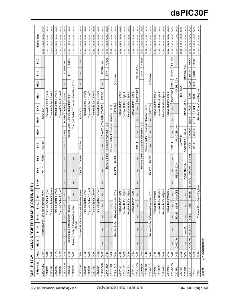
dsPIC30F
C2T
X1D
LC
0414
Tra
nsm
it B
uffer
1 E
xte
nded Identifier
<5:0
>T
XR
TR
TX
RB
1T
XR
B0
DLC
<3:0
>—
——
uuuu uuuu uuuu u000
C2T
X1B
10416
Tra
nsm
it B
uffer
1 B
yte
1T
ransm
it B
uffer
1 B
yte
0uuuu uuuu uuuu uuuu
C2T
X1B
20418
Tra
nsm
it B
uffer
1 B
yte
3T
ransm
it B
uffer
1 B
yte
2uuuu uuuu uuuu uuuu
C2T
X1B
3041A
Tra
nsm
it B
uffer
1 B
yte
5T
ransm
it B
uffer
1 B
yte
4uuuu uuuu uuuu uuuu
C2T
X1B
4041C
Tra
nsm
it B
uffer
1 B
yte
7T
ransm
it B
uffer
1 B
yte
6uuuu uuuu uuuu uuuu
C2T
X1C
ON
041E
——
——
——
——
—T
XA
BT
TX
LA
RB
TX
ER
RT
XR
EQ
—T
XP
RI<
1:0
>0000 0000 0000 0000
C2T
X0S
ID0420
Tra
nsm
it B
uffer
0 S
tandard
Identifier
<10:6
>—
——
Tra
nsm
it B
uffer
0 S
tandard
Identifier
<5:0
>S
RR
TX
IDE
uuuu u000 uuuu uuuu
C2T
X0E
ID0422
Tra
nsm
it B
uffer
0 E
xte
nded Identifier
<1
7:1
4>
——
——
Tra
nsm
it B
uffer
0 E
xte
nded Identifier
<13:6
>uuuu 0000 uuuu uuuu
C2T
X0D
LC
0424
Tra
nsm
it B
uffer
0 E
xte
nded Identifier
<5:0
>T
XR
TR
TX
RB
1T
XR
B0
DLC
<3:0
>—
——
uuuu uuuu uuuu u000
C2T
X0B
10426
Tra
nsm
it B
uffer
0 B
yte
1T
ransm
it B
uffer
0 B
yte
0uuuu uuuu uuuu uuuu
C2T
X0B
20428
Tra
nsm
it B
uffer
0 B
yte
3T
ransm
it B
uffer
0 B
yte
2uuuu uuuu uuuu uuuu
C2T
X0B
3042A
Tra
nsm
it B
uffer
0 B
yte
5T
ransm
it B
uffer
0 B
yte
4uuuu uuuu uuuu uuuu
C2T
X0B
4042C
Tra
nsm
it B
uffer
0 B
yte
7T
ransm
it B
uffer
0 B
yte
6uuuu uuuu uuuu uuuu
C2T
X0C
ON
042E
——
——
——
——
—T
XA
BT
TX
LA
RB
TX
ER
RT
XR
EQ
—T
XP
RI<
1:0
>0000 0000 0000 0000
C2R
X1S
ID0430
——
—R
eceiv
e B
uffer
1 S
tandard
Identifier
<10:0
>S
RR
RX
IDE
000u uuuu uuuu uuuu
C2R
X1E
ID0432
——
——
Receiv
e B
uffer
1 E
xte
nded Identifier
<17:6
>0000 uuuu uuuu uuuu
C2R
X1D
LC
0434
Receiv
e B
uffer
1 E
xte
nded Identifier
<5:0
>R
XR
TR
RX
RB
1—
——
RX
RB
0D
LC
<3:0
>uuuu uuuu 000u uuuu
C2R
X1B
10436
Receiv
e B
uffer
1 B
yte
1R
eceiv
e B
uffer
1 B
yte
0uuuu uuuu uuuu uuuu
C2R
X1B
20438
Receiv
e B
uffer
1 B
yte
3R
eceiv
e B
uffer
1 B
yte
2uuuu uuuu uuuu uuuu
C2R
X1B
3043A
Receiv
e B
uffer
1 B
yte
5R
eceiv
e B
uffer
1 B
yte
4uuuu uuuu uuuu uuuu
C2R
X1B
4043C
Receiv
e B
uffer
1 B
yte
7R
eceiv
e B
uffer
1 B
yte
6uuuu uuuu uuuu uuuu
C2R
X1C
ON
043E
——
——
——
——
RX
FU
L—
——
RX
RT
RR
OF
ILH
IT<
2:0
>0000 0000 0000 0000
C2R
X0S
ID0440
——
—R
eceiv
e B
uffer
0 S
tandard
Identifier
<10:0
>S
RR
RX
IDE
000u uuuu uuuu uuuu
C2R
X0E
ID0442
——
——
Receiv
e B
uffer
0 E
xte
nded Identifier
<17:6
>0000 uuuu uuuu uuuu
C2R
X0D
LC
0444
Receiv
e B
uffer
0 E
xte
nded Identifier
<5:0
>R
XR
TR
RX
RB
1—
——
RX
RB
0D
LC
<3:0
>uuuu uuuu 000u uuuu
C2R
X0B
10446
Receiv
e B
uffer
0 B
yte
1R
eceiv
e B
uffer
0 B
yte
0uuuu uuuu uuuu uuuu
C2R
X0B
20448
Receiv
e B
uffer
0 B
yte
3R
eceiv
e B
uffer
0 B
yte
2uuuu uuuu uuuu uuuu
C2R
X0B
3044A
Receiv
e B
uffer
0 B
yte
5R
eceiv
e B
uffer
0 B
yte
4uuuu uuuu uuuu uuuu
C2R
X0B
4044C
Receiv
e B
uffer
0 B
yte
7R
eceiv
e B
uffer
0 B
yte
6uuuu uuuu uuuu uuuu
C2R
X0C
ON
044E
——
——
——
——
RX
FU
L—
——
RX
RT
RR
OD
BE
NJT
OF
FF
ILH
IT0
0000 0000 0000 0000
C2C
TR
L0450
CA
NC
AP
—C
SID
LE
AB
AT
CA
NC
KS
RE
QO
P<
2:0
>O
PM
OD
E<
2:0
>—
ICO
DE
<2:0
>—
0000 0100 1000 0000
C2C
FG
10452
——
——
——
——
SJW
<1:0
>B
RP
<5:0
>0000 0000 0000 0000
C2C
FG
20454
—W
AK
FIL
——
—S
EG
2P
H<
2:0
>S
EG
2P
HT
SS
AM
SE
G1P
H<
2:0
>P
RS
EG
<2:0
>0u00 0uuu uuuu uuuu
C2IN
TF
0456
RX
0O
VR
RX
1O
VR
TX
BO
TX
EP
RX
EP
TX
WA
RR
XW
AR
EW
AR
NIV
RIF
WA
KIF
ER
RIF
TX
2IF
TX
1IF
TX
0IF
RX
1IF
RX
0IF
0000 0000 0000 0000
C2IN
TE
0458
——
——
——
——
IVR
IEW
AK
IEE
RR
IET
X2IE
TX
1IE
TX
0IE
RX
1E
RX
0IE
0000 0000 0000 0000
C2E
C045A
Tra
nsm
it E
rror
Count R
egis
ter
Receiv
e E
rror
Count R
egis
ter
0000 0000 0000 0000
TA
BL
E 1
7-2
:C
AN
2 R
EG
IST
ER
MA
P (
CO
NT
INU
ED
)
SF
R N
am
eA
dd
r.B
it 1
5B
it 1
4B
it 1
3B
it 1
2B
it 1
1B
it 1
0B
it 9
Bit
8B
it 7
Bit
6B
it 5
Bit
4B
it 3
Bit
2B
it 1
Bit
0R
eset
Sta
te
Legend:
u =
unin
itia
lized b
it
2004 Microchip Technology Inc. Advance Information DS70083E-page 131

dsPIC30F
NOTES:
DS70083E-page 132 Advance Information 2004 Microchip Technology Inc.
dsPIC30F
18.0 DATA CONVERTER INTERFACE (DCI) MODULE
18.1 Module Introduction
The dsPIC30F Data Converter Interface (DCI) module
allows simple interfacing of devices, such as audio
coder/decoders (Codecs), A/D converters and D/A
converters. The following interfaces are supported:
• Framed Synchronous Serial Transfer (Single or
Multi-Channel)
• Inter-IC Sound (I2S) Interface
• AC-Link Compliant mode
The DCI module provides the following general
features:
• Programmable word size up to 16 bits
• Support for up to 16 time slots, for a maximum
frame size of 256 bits
• Data buffering for up to 4 samples without CPU
overhead
18.2 Module I/O Pins
There are four I/O pins associated with the module.
When enabled, the module controls the data direction
of each of the four pins.
18.2.1 CSCK PIN
The CSCK pin provides the serial clock for the DCI
module. The CSCK pin may be configured as an input
or output using the CSCKD control bit in the DCICON2
SFR. When configured as an output, the serial clock is
provided by the dsPIC30F. When configured as an
input, the serial clock must be provided by an external
device.
18.2.2 CSDO PIN
The serial data output (CSDO) pin is configured as an
output only pin when the module is enabled. The
CSDO pin drives the serial bus whenever data is to be
transmitted. The CSDO pin is tri-stated or driven to ‘0’
during CSCK periods when data is not transmitted,
depending on the state of the CSDOM control bit. This
allows other devices to place data on the serial bus
during transmission periods not used by the DCI
module.
18.2.3 CSDI PIN
The serial data input (CSDI) pin is configured as an
input only pin when the module is enabled.
18.2.3.1 COFS PIN
The Codec frame synchronization (COFS) pin is used
to synchronize data transfers that occur on the CSDO
and CSDI pins. The COFS pin may be configured as an
input or an output. The data direction for the COFS pin
is determined by the COFSD control bit in the
DCICON1 register.
The DCI module accesses the shadow registers while
the CPU is in the process of accessing the memory
mapped buffer registers.
18.2.4 BUFFER DATA ALIGNMENT
Data values are always stored left justified in the buff-
ers since most Codec data is represented as a signed
2’s complement fractional number. If the received word
length is less than 16 bits, the unused LS bits in the
receive buffer registers are set to ‘0’ by the module. If
the transmitted word length is less than 16 bits, the
unused LS bits in the transmit buffer register are
ignored by the module. The word length setup is
described in subsequent sections of this document.
18.2.5 TRANSMIT/RECEIVE SHIFT
REGISTER
The DCI module has a 16-bit shift register for shifting
serial data in and out of the module. Data is shifted in/
out of the shift register MS bit first, since audio PCM
data is transmitted in signed 2’s complement format.
18.2.6 DCI BUFFER CONTROL
The DCI module contains a buffer control unit for trans-
ferring data between the shadow buffer memory and
the serial shift register. The buffer control unit is a sim-
ple 2-bit address counter that points to word locations
in the shadow buffer memory. For the receive memory
space (high address portion of DCI buffer memory), the
address counter is concatenated with a ‘0’ in the MSb
location to form a 3-bit address. For the transmit mem-
ory space (high portion of DCI buffer memory), the
address counter is concatenated with a ‘1’ in the MSb
location.
Note: The DCI buffer control unit always
accesses the same relative location in the
transmit and receive buffers, so only one
address counter is provided.
2004 Microchip Technology Inc. Advance Information DS70083E-page 133
dsPIC30F
FIGURE 18-1: DCI MODULE BLOCK DIAGRAM
BCG Control bits
16
-bit D
ata
Bu
s
Sample Rate
Generator
SCKD
FSD
DCI Buffer
Frame
Synchronization
Generator
Control Unit
DCI Shift Register
Receive Buffer
Registers w/Shadow
FOSC/4
Word Size Selection bits
Frame Length Selection bits
DCI Mode Selection bits
CSCK
COFS
CSDI
CSDO
15 0
Transmit Buffer
Registers w/Shadow
DS70083E-page 134 Advance Information 2004 Microchip Technology Inc.
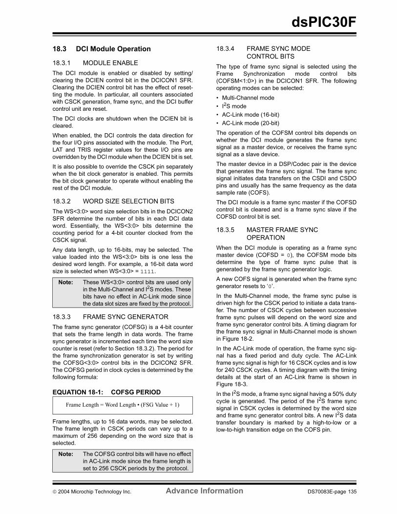
dsPIC30F
18.3 DCI Module Operation
18.3.1 MODULE ENABLE
The DCI module is enabled or disabled by setting/
clearing the DCIEN control bit in the DCICON1 SFR.
Clearing the DCIEN control bit has the effect of reset-
ting the module. In particular, all counters associated
with CSCK generation, frame sync, and the DCI buffer
control unit are reset.
The DCI clocks are shutdown when the DCIEN bit is
cleared.
When enabled, the DCI controls the data direction for
the four I/O pins associated with the module. The Port,
LAT and TRIS register values for these I/O pins are
overridden by the DCI module when the DCIEN bit is set.
It is also possible to override the CSCK pin separately
when the bit clock generator is enabled. This permits
the bit clock generator to operate without enabling the
rest of the DCI module.
18.3.2 WORD SIZE SELECTION BITS
The WS<3:0> word size selection bits in the DCICON2
SFR determine the number of bits in each DCI data
word. Essentially, the WS<3:0> bits determine the
counting period for a 4-bit counter clocked from the
CSCK signal.
Any data length, up to 16-bits, may be selected. The
value loaded into the WS<3:0> bits is one less the
desired word length. For example, a 16-bit data word
size is selected when WS<3:0> = 1111.
18.3.3 FRAME SYNC GENERATOR
The frame sync generator (COFSG) is a 4-bit counter
that sets the frame length in data words. The frame
sync generator is incremented each time the word size
counter is reset (refer to Section 18.3.2). The period for
the frame synchronization generator is set by writing
the COFSG<3:0> control bits in the DCICON2 SFR.
The COFSG period in clock cycles is determined by the
following formula:
EQUATION 18-1: COFSG PERIOD
Frame lengths, up to 16 data words, may be selected.
The frame length in CSCK periods can vary up to a
maximum of 256 depending on the word size that is
selected.
18.3.4 FRAME SYNC MODE
CONTROL BITS
The type of frame sync signal is selected using the
Frame Synchronization mode control bits
(COFSM<1:0>) in the DCICON1 SFR. The following
operating modes can be selected:
• Multi-Channel mode
• I2S mode
• AC-Link mode (16-bit)
• AC-Link mode (20-bit)
The operation of the COFSM control bits depends on
whether the DCI module generates the frame sync
signal as a master device, or receives the frame sync
signal as a slave device.
The master device in a DSP/Codec pair is the device
that generates the frame sync signal. The frame sync
signal initiates data transfers on the CSDI and CSDO
pins and usually has the same frequency as the data
sample rate (COFS).
The DCI module is a frame sync master if the COFSD
control bit is cleared and is a frame sync slave if the
COFSD control bit is set.
18.3.5 MASTER FRAME SYNC
OPERATION
When the DCI module is operating as a frame sync
master device (COFSD = 0), the COFSM mode bits
determine the type of frame sync pulse that is
generated by the frame sync generator logic.
A new COFS signal is generated when the frame sync
generator resets to ‘0’.
In the Multi-Channel mode, the frame sync pulse is
driven high for the CSCK period to initiate a data trans-
fer. The number of CSCK cycles between successive
frame sync pulses will depend on the word size and
frame sync generator control bits. A timing diagram for
the frame sync signal in Multi-Channel mode is shown
in Figure 18-2.
In the AC-Link mode of operation, the frame sync sig-
nal has a fixed period and duty cycle. The AC-Link
frame sync signal is high for 16 CSCK cycles and is low
for 240 CSCK cycles. A timing diagram with the timing
details at the start of an AC-Link frame is shown in
Figure 18-3.
In the I2S mode, a frame sync signal having a 50% duty
cycle is generated. The period of the I2S frame sync
signal in CSCK cycles is determined by the word size
and frame sync generator control bits. A new I2S data
transfer boundary is marked by a high-to-low or a
low-to-high transition edge on the COFS pin.
Note: These WS<3:0> control bits are used only
in the Multi-Channel and I2S modes. These
bits have no effect in AC-Link mode since
the data slot sizes are fixed by the protocol.
Note: The COFSG control bits will have no effect
in AC-Link mode since the frame length is
set to 256 CSCK periods by the protocol.
Frame Length = Word Length • (FSG Value + 1)
2004 Microchip Technology Inc. Advance Information DS70083E-page 135
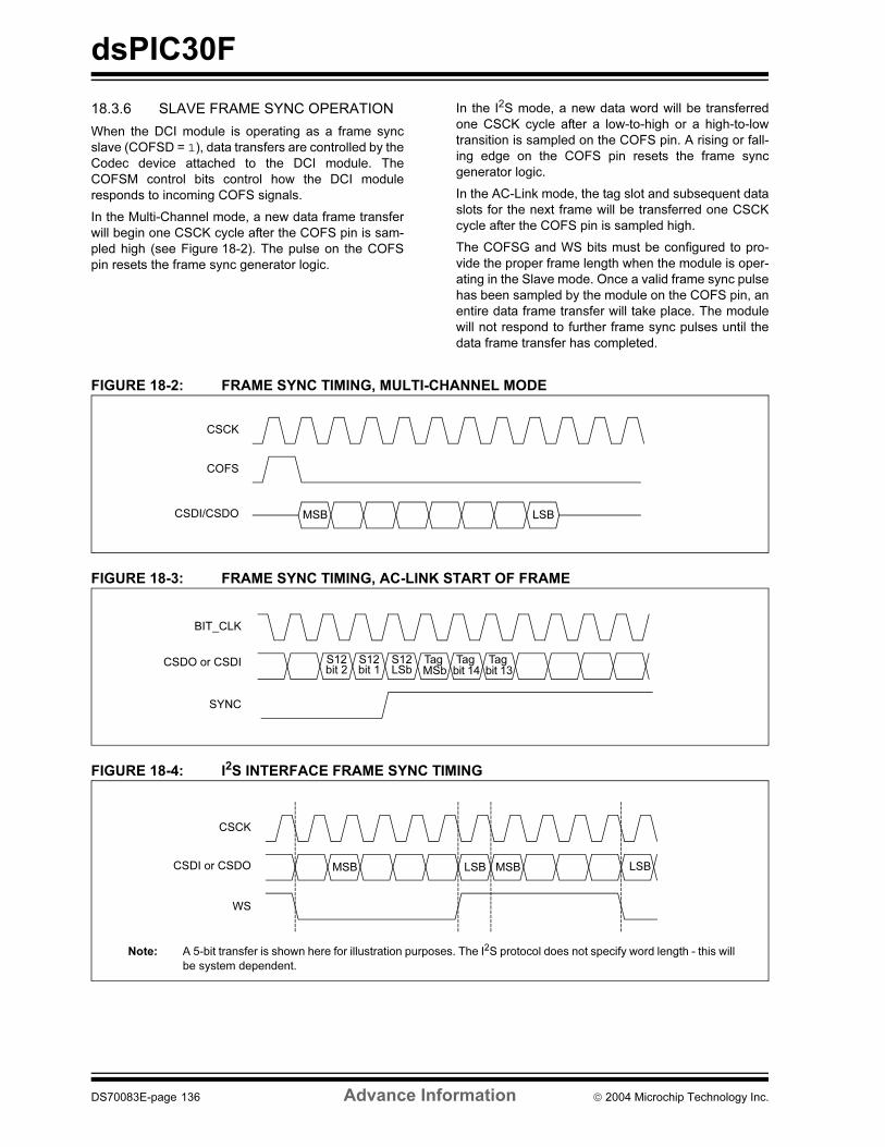
dsPIC30F
18.3.6 SLAVE FRAME SYNC OPERATION
When the DCI module is operating as a frame sync
slave (COFSD = 1), data transfers are controlled by the
Codec device attached to the DCI module. The
COFSM control bits control how the DCI module
responds to incoming COFS signals.
In the Multi-Channel mode, a new data frame transfer
will begin one CSCK cycle after the COFS pin is sam-
pled high (see Figure 18-2). The pulse on the COFS
pin resets the frame sync generator logic.
In the I2S mode, a new data word will be transferred
one CSCK cycle after a low-to-high or a high-to-low
transition is sampled on the COFS pin. A rising or fall-
ing edge on the COFS pin resets the frame sync
generator logic.
In the AC-Link mode, the tag slot and subsequent data
slots for the next frame will be transferred one CSCK
cycle after the COFS pin is sampled high.
The COFSG and WS bits must be configured to pro-
vide the proper frame length when the module is oper-
ating in the Slave mode. Once a valid frame sync pulse
has been sampled by the module on the COFS pin, an
entire data frame transfer will take place. The module
will not respond to further frame sync pulses until the
data frame transfer has completed.
FIGURE 18-2: FRAME SYNC TIMING, MULTI-CHANNEL MODE
FIGURE 18-3: FRAME SYNC TIMING, AC-LINK START OF FRAME
FIGURE 18-4: I2S INTERFACE FRAME SYNC TIMING
CSCK
CSDI/CSDO
COFS
MSB LSB
TagMSb
BIT_CLK
CSDO or CSDI
SYNC
Tagbit 14
S12LSb
S12bit 1
S12bit 2
Tagbit 13
MSB LSB MSB LSB
CSCK
CSDI or CSDO
WS
Note: A 5-bit transfer is shown here for illustration purposes. The I2S protocol does not specify word length - this will
be system dependent.
DS70083E-page 136 Advance Information 2004 Microchip Technology Inc.
dsPIC30F
18.3.7 BIT CLOCK GENERATOR
The DCI module has a dedicated 12-bit time base that
produces the bit clock. The bit clock rate (period) is set
by writing a non-zero 12-bit value to the BCG<11:0>
control bits in the DCICON1 SFR.
When the BCG<11:0> bits are set to zero, the bit clock
will be disabled. If the BCG<11:0> bits are set to a non-
zero value, the bit clock generator is enabled. These
bits should be set to ‘0’ and the CSCKD bit set to ‘1’ if
the serial clock for the DCI is received from an external
device.
The formula for the bit clock frequency is given in
Equation 18-2.
EQUATION 18-2: BIT CLOCK FREQUENCY
The required bit clock frequency will be determined by
the system sampling rate and frame size. Typical bit
clock frequencies range from 16x to 512x the converter
sample rate depending on the data converter and the
communication protocol that is used.
To achieve bit clock frequencies associated with com-
mon audio sampling rates, the user will need to select
a crystal frequency that has an ‘even’ binary value.
Examples of such crystal frequencies are listed in
Table 18-1.
TABLE 18-1: DEVICE FREQUENCIES FOR
COMMON CODEC CSCK
FREQUENCIES
18.3.8 SAMPLE CLOCK EDGE
CONTROL BIT
The sample clock edge (CSCKE) control bit determines
the sampling edge for the CSCK signal. If the CSCK bit
is cleared (default), data will be sampled on the falling
edge of the CSCK signal. The AC-Link protocols and
most Multi-Channel formats require that data be sam-
pled on the falling edge of the CSCK signal. If the
CSCK bit is set, data will be sampled on the rising edge
of CSCK. The I2S protocol requires that data be
sampled on the rising edge of the CSCK signal.
18.3.9 DATA JUSTIFICATION
CONTROL BIT
In most applications, the data transfer begins one
CSCK cycle after the COFS signal is sampled active.
This is the default configuration of the DCI module. An
alternate data alignment can be selected by setting the
DJST control bit in the DCICON2 SFR. When DJST = 1,
data transfers will begin during the same CSCK cycle
when the COFS signal is sampled active.
18.3.10 TRANSMIT SLOT ENABLE BITS
The TSCON SFR has control bits that are used to
enable up to 16 time slots for transmission. These con-
trol bits are the TSE<15:0> bits. The size of each time
slot is determined by the WS<3:0> word size selection
bits and can vary up to 16 bits.
If a transmit time slot is enabled via one of the TSE bits
(TSEx = 1), the contents of the current transmit shadow
buffer location will be loaded into the CSDO Shift regis-
ter and the DCI buffer control unit is incremented to
point to the next location.
During an unused transmit time slot, the CSDO pin will
drive ‘0’s or will be tri-stated during all disabled time
slots depending on the state of the CSDOM bit in the
DCICON1 SFR.
The data frame size in bits is determined by the chosen
data word size and the number of data word elements
in the frame. If the chosen frame size has less than 16
elements, the additional slot enable bits will have no
effect.
Each transmit data word is written to the 16-bit transmit
buffer as left justified data. If the selected word size is
less than 16 bits, then the LS bits of the transmit buffer
memory will have no effect on the transmitted data. The
user should write ‘0’s to the unused LS bits of each
transmit buffer location.
FOSC PLL FCYC
2.048 MHz 16x 32.768 MIPs
4.096 MHz 8x 32.768 MIPs
4.800 MHz 8x 38.4 MIPs
9.600 MHz 4x 38.4 MIPs
Note 1: When the CSCK signal is applied exter-
nally (CSCKD = 1), the BCG<11:0> bits
have no effect on the operation of the DCI
module.
2: When the CSCK signal is applied exter-
nally (CSCKD = 1), the external clock
high and low times must meet the device
timing requirements.
FBCK =FCY
2 (BCG + 1)•
2004 Microchip Technology Inc. Advance Information DS70083E-page 137
dsPIC30F
18.3.11 RECEIVE SLOT ENABLE BITS
The RSCON SFR contains control bits that are used to
enable up to 16 time slots for reception. These control
bits are the RSE<15:0> bits. The size of each receive
time slot is determined by the WS<3:0> word size
selection bits and can vary from 1 to 16 bits.
If a receive time slot is enabled via one of the RSE bits
(RSEx = 1), the shift register contents will be written to
the current DCI receive shadow buffer location and the
buffer control unit will be incremented to point to the
next buffer location.
Data is not packed in the receive memory buffer loca-
tions if the selected word size is less than 16 bits. Each
received slot data word is stored in a separate 16-bit
buffer location. Data is always stored in a left justified
format in the receive memory buffer.
18.3.12 SLOT ENABLE BITS OPERATION
WITH FRAME SYNC
The TSE and RSE control bits operate in concert with
the DCI frame sync generator. In the Master mode, a
COFS signal is generated whenever the frame sync
generator is reset. In the Slave mode, the frame sync
generator is reset whenever a COFS pulse is received.
The TSE and RSE control bits allow up to 16 consecu-
tive time slots to be enabled for transmit or receive.
After the last enabled time slot has been transmitted/
received, the DCI will stop buffering data until the next
occurring COFS pulse.
18.3.13 SYNCHRONOUS DATA
TRANSFERS
The DCI buffer control unit will be incremented by one
word location whenever a given time slot has been
enabled for transmission or reception. In most cases,
data input and output transfers will be synchronized,
which means that a data sample is received for a given
channel at the same time a data sample is transmitted.
Therefore, the transmit and receive buffers will be filled
with equal amounts of data when a DCI interrupt is
generated.
In some cases, the amount of data transmitted and
received during a data frame may not be equal. As an
example, assume a two-word data frame is used. Fur-
thermore, assume that data is only received during
slot #0 but is transmitted during slot #0 and slot #1. In
this case, the buffer control unit counter would be incre-
mented twice during a data frame but only one receive
register location would be filled with data.
18.3.14 BUFFER LENGTH CONTROL
The amount of data that is buffered between interrupts
is determined by the buffer length (BLEN<1:0>) control
bits in the DCISTAT SFR. The size of the transmit and
receive buffers may be varied from 1 to 4 data words
using the BLEN control bits. The BLEN control bits are
compared to the current value of the DCI buffer control
unit address counter. When the 2 LS bits of the DCI
address counter match the BLEN<1:0> value, the
buffer control unit will be reset to ‘0’. In addition, the
contents of the receive shadow registers are trans-
ferred to the receive buffer registers and the contents
of the transmit buffer registers are transferred to the
transmit shadow registers.
18.3.15 BUFFER ALIGNMENT WITH DATA
FRAMES
There is no direct coupling between the position of the
AGU address pointer and the data frame boundaries.
This means that there will be an implied assignment of
each transmit and receive buffer that is a function of the
BLEN control bits and the number of enabled data slots
via the TSE and RSE control bits.
As an example, assume that a 4-word data frame is
chosen and that we want to transmit on all four time
slots in the frame. This configuration would be estab-
lished by setting the TSE0, TSE1, TSE2, and TSE3
control bits in the TSCON SFR. With this module setup,
the TXBUF0 register would be naturally assigned to
slot #0, the TXBUF1 register would be naturally
assigned to slot #1, and so on.
Note: When more than four time slots are active
within a data frame, the user code must
keep track of which time slots are to be
read/written at each interrupt. In some
cases, the alignment between transmit/
receive buffers and their respective slot
assignments could be lost. Examples of
such cases include an emulation break-
point or a hardware trap. In these situa-
tions, the user should poll the SLOT status
bits to determine what data should be
loaded into the buffer registers to
resynchronize the software with the DCI
module.
DS70083E-page 138 Advance Information 2004 Microchip Technology Inc.
dsPIC30F
18.3.16 TRANSMIT STATUS BITS
There are two transmit status bits in the DCISTAT SFR.
The TMPTY bit is set when the contents of the transmit
buffer registers are transferred to the transmit shadow
registers. The TMPTY bit may be polled in software to
determine when the transmit buffer registers may be
written. The TMPTY bit is cleared automatically by the
hardware when a write to one of the four transmit
buffers occurs.
The TUNF bit is read only and indicates that a transmit
underflow has occurred for at least one of the transmit
buffer registers that is in use. The TUNF bit is set at the
time the transmit buffer registers are transferred to the
transmit shadow registers. The TUNF status bit is
cleared automatically when the buffer register that
underflowed is written by the CPU.
18.3.17 RECEIVE STATUS BITS
There are two receive status bits in the DCISTAT SFR.
The RFUL status bit is read only and indicates that new
data is available in the receive buffers. The RFUL bit is
cleared automatically when all receive buffers in use
have been read by the CPU.
The ROV status bit is read only and indicates that a
receive overflow has occurred for at least one of the
receive buffer locations. A receive overflow occurs
when the buffer location is not read by the CPU before
new data is transferred from the shadow registers. The
ROV status bit is cleared automatically when the buffer
register that caused the overflow is read by the CPU.
When a receive overflow occurs for a specific buffer
location, the old contents of the buffer are overwritten.
18.3.18 SLOT STATUS BITS
The SLOT<3:0> status bits in the DCISTAT SFR indi-
cate the current active time slot. These bits will corre-
spond to the value of the frame sync generator counter.
The user may poll these status bits in software when a
DCI interrupt occurs to determine what time slot data
was last received and which time slot data should be
loaded into the TXBUF registers.
18.3.19 CSDO MODE BIT
The CSDOM control bit controls the behavior of the
CSDO pin during unused transmit slots. A given trans-
mit time slot is unused if it’s corresponding TSEx bit in
the TSCON SFR is cleared.
If the CSDOM bit is cleared (default), the CSDO pin will
be low during unused time slot periods. This mode will
be used when there are only two devices attached to
the serial bus.
If the CSDOM bit is set, the CSDO pin will be tri-stated
during unused time slot periods. This mode allows mul-
tiple devices to share the same CSDO line in a multi-
channel application. Each device on the CSDO line is
configured so that it will only transmit data during
specific time slots. No two devices will transmit data
during the same time slot.
18.3.20 DIGITAL LOOPBACK MODE
Digital Loopback mode is enabled by setting the
DLOOP control bit in the DCISTAT SFR. When the
DLOOP bit is set, the module internally connects the
CSDO signal to CSDI. The actual data input on the
CSDI I/O pin will be ignored in Digital Loopback mode.
18.3.21 UNDERFLOW MODE CONTROL BIT
When an underflow occurs, one of two actions may
occur depending on the state of the Underflow mode
(UNFM) control bit in the DCICON2 SFR. If the UNFM
bit is cleared (default), the module will transmit ‘0’s on
the CSDO pin during the active time slot for the buffer
location. In this Operating mode, the Codec device
attached to the DCI module will simply be fed digital
‘silence’. If the UNFM control bit is set, the module will
transmit the last data written to the buffer location. This
Operating mode permits the user to send continuous
data to the Codec device without consuming CPU
overhead.
18.4 DCI Module Interrupts
The frequency of DCI module interrupts is dependent
on the BLEN<1:0> control bits in the DCICON2 SFR.
An interrupt to the CPU is generated each time the set
buffer length has been reached and a shadow register
transfer takes place. A shadow register transfer is
defined as the time when the previously written TXBUF
values are transferred to the transmit shadow registers
and new received values in the receive shadow
registers are transferred into the RXBUF registers.
Note: The transmit status bits only indicate sta-
tus for buffer locations that are used by the
module. If the buffer length is set to less
than four words, for example, the unused
buffer locations will not affect the transmit
status bits.
Note: The receive status bits only indicate status
for buffer locations that are used by the
module. If the buffer length is set to less
than four words, for example, the unused
buffer locations will not affect the transmit
status bits.
2004 Microchip Technology Inc. Advance Information DS70083E-page 139
dsPIC30F
18.5 DCI Module Operation During CPU
Sleep and Idle Modes
18.5.1 DCI MODULE OPERATION DURING
CPU SLEEP MODE
The DCI module has the ability to operate while in
Sleep mode and wake the CPU when the CSCK signal
is supplied by an external device (CSCKD = 1). The
DCI module will generate an asynchronous interrupt
when a DCI buffer transfer has completed and the CPU
is in Sleep mode.
18.5.2 DCI MODULE OPERATION DURING
CPU IDLE MODE
If the DCISIDL control bit is cleared (default), the mod-
ule will continue to operate normally even in Idle mode.
If the DCISIDL bit is set, the module will halt when Idle
mode is asserted.
18.6 AC-Link Mode Operation
The AC-Link protocol is a 256-bit frame with one 16-bit
data slot, followed by twelve 20-bit data slots. The DCI
module has two Operating modes for the AC-Link pro-
tocol. These Operating modes are selected by the
COFSM<1:0> control bits in the DCICON1 SFR. The
first AC-Link mode is called ‘16-bit AC-Link mode’ and
is selected by setting COFSM<1:0> = 10. The second
AC-Link mode is called ‘20-bit AC-Link mode’ and is
selected by setting COFSM<1:0> = 11.
18.6.1 16-BIT AC-LINK MODE
In the 16-bit AC-Link mode, data word lengths are
restricted to 16 bits. Note that this restriction only
affects the 20-bit data time slots of the AC-Link proto-
col. For received time slots, the incoming data is simply
truncated to 16 bits. For outgoing time slots, the 4 LS
bits of the data word are set to ‘0’ by the module. This
truncation of the time slots limits the A/D and DAC data
to 16 bits but permits proper data alignment in the
TXBUF and RXBUF registers. Each RXBUF and
TXBUF register will contain one data time slot value.
18.6.2 20-BIT AC-LINK MODE
The 20-bit AC-Link mode allows all bits in the data time
slots to be transmitted and received but does not main-
tain data alignment in the TXBUF and RXBUF
registers.
The 20-bit AC-Link mode functions similar to the Multi-
Channel mode of the DCI module, except for the duty
cycle of the frame synchronization signal. The AC-Link
frame synchronization signal should remain high for 16
CSCK cycles and should be low for the following
240 cycles.
The 20-bit mode treats each 256-bit AC-Link frame as
sixteen, 16-bit time slots. In the 20-bit AC-Link mode,
the module operates as if COFSG<3:0> = 1111 and
WS<3:0> = 1111. The data alignment for 20-bit data
slots is ignored. For example, an entire AC-Link data
frame can be transmitted and received in a packed
fashion by setting all bits in the TSCON and RSCON
SFRs. Since the total available buffer length is 64 bits,
it would take 4 consecutive interrupts to transfer the
AC-Link frame. The application software must keep
track of the current AC-Link frame segment.
18.7 I2S Mode Operation
The DCI module is configured for I2S mode by writing
a value of ‘01’ to the COFSM<1:0> control bits in the
DCICON1 SFR. When operating in the I2S mode, the
DCI module will generate frame synchronization sig-
nals with a 50% duty cycle. Each edge of the frame
synchronization signal marks the boundary of a new
data word transfer.
The user must also select the frame length and data
word size using the COFSG and WS control bits in the
DCICON2 SFR.
18.7.1 I2S FRAME AND DATA WORD
LENGTH SELECTION
The WS and COFSG control bits are set to produce the
period for one half of an I2S data frame. That is, the
frame length is the total number of CSCK cycles
required for a left or a right data word transfer.
The BLEN bits must be set for the desired buffer length.
Setting BLEN<1:0> = 01 will produce a CPU interrupt,
once per I2S frame.
18.7.2 I2S DATA JUSTIFICATION
As per the I2S specification, a data word transfer will, by
default, begin one CSCK cycle after a transition of the
WS signal. A ‘MS bit left justified’ option can be
selected using the DJST control bit in the DCICON2
SFR.
If DJST = 1, the I2S data transfers will be MS bit left jus-
tified. The MS bit of the data word will be presented on
the CSDO pin during the same CSCK cycle as the ris-
ing or falling edge of the COFS signal. The CSDO pin
is tri-stated after the data word has been sent.
DS70083E-page 140 Advance Information 2004 Microchip Technology Inc.
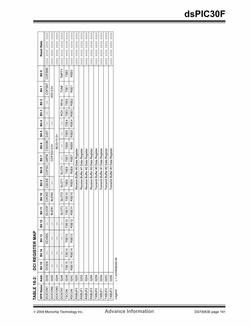
dsPIC30F
TA
BL
E 1
8-2
:D
CI
RE
GIS
TE
R M
AP
SF
R N
am
eA
dd
r.B
it 1
5B
it 1
4B
it 1
3B
it 1
2B
it 1
1B
it 1
0B
it 9
Bit
8B
it 7
Bit
6B
it 5
Bit
4B
it 3
Bit
2B
it 1
Bit
0R
eset
Sta
te
DC
ICO
N1
0240
DC
IEN
—D
CIS
IDL
—D
LO
OP
CS
CK
DC
SC
KE
CO
FS
DU
NF
MC
SD
OM
DJS
T—
——
CO
FS
M1
CO
FS
M0
0000 0000 0000 0000
DC
ICO
N2
0242
——
——
BLE
N1
BLE
N0
—C
OF
SG
<3:0
>—
WS
<3:0
>0000 0000 0000 0000
DC
ICO
N3
0244
——
——
BC
G<
11:0
>0000 0000 0000 0000
DC
ISTA
T0246
——
——
SLO
T3
SLO
T2
SLO
T1
SLO
T0
——
——
RO
VR
FU
LT
UN
FT
MP
TY
0000 0000 0000 0000
TS
CO
N0248
TS
E15
TS
E14
TS
E13
TS
E12
TS
E11
TS
E10
TS
E9
TS
E8
TS
E7
TS
E6
TS
E5
TS
E4
TS
E3
TS
E2
TS
E1
TS
E0
0000 0000 0000 0000
RS
CO
N024C
RS
E15
RS
E14
RS
E13
RS
E12
RS
E11
RS
E10
RS
E9
RS
E8
RS
E7
RS
E6
RS
E5
RS
E4
RS
E3
RS
E2
RS
E1
RS
E0
0000 0000 0000 0000
RX
BU
F0
0250
Receiv
e B
uffer
#0 D
ata
Regis
ter
0000 0000 0000 0000
RX
BU
F1
0252
Receiv
e B
uffer
#1 D
ata
Regis
ter
0000 0000 0000 0000
RX
BU
F2
0254
Receiv
e B
uffer
#2 D
ata
Regis
ter
0000 0000 0000 0000
RX
BU
F3
0256
Receiv
e B
uffer
#3 D
ata
Regis
ter
0000 0000 0000 0000
TX
BU
F0
0258
Tra
nsm
it B
uffer
#0 D
ata
Regis
ter
0000 0000 0000 0000
TX
BU
F1
025A
Tra
nsm
it B
uffer
#1 D
ata
Regis
ter
0000 0000 0000 0000
TX
BU
F2
025C
Tra
nsm
it B
uffer
#2 D
ata
Regis
ter
0000 0000 0000 0000
TX
BU
F3
025E
Tra
nsm
it B
uffer
#3 D
ata
Regis
ter
0000 0000 0000 0000
Legend:
u =
unin
itia
lized b
it
2004 Microchip Technology Inc. Advance Information DS70083E-page 141

dsPIC30F
NOTES:
DS70083E-page 142 Advance Information 2004 Microchip Technology Inc.
dsPIC30F
19.0 12-BIT ANALOG-TO-DIGITAL CONVERTER (A/D) MODULE
The 12-bit Analog-to-Digital converter (A/D) allows
conversion of an analog input signal to a 12-bit digital
number. This module is based on a Successive
Approximation Register (SAR) architecture and pro-
vides a maximum sampling rate of 100 ksps. The A/D
module has up to 16 analog inputs which are multi-
plexed into a sample and hold amplifier. The output of
the sample and hold is the input into the converter
which generates the result. The analog reference volt-
age is software selectable to either the device supply
voltage (AVDD/AVSS) or the voltage level on the
(VREF+/VREF-) pin. The A/D converter has a unique
feature of being able to operate while the device is in
Sleep mode with RC oscillator selection.
The A/D module has six 16-bit registers:
• A/D Control Register 1 (ADCON1)
• A/D Control Register 2 (ADCON2)
• A/D Control Register 3 (ADCON3)
• A/D Input Select Register (ADCHS)
• A/D Port Configuration Register (ADPCFG)
• A/D Input Scan Selection Register (ADCSSL)
The ADCON1, ADCON2 and ADCON3 registers con-
trol the operation of the A/D module. The ADCHS reg-
ister selects the input channels to be converted. The
ADPCFG register configures the port pins as analog
inputs or as digital I/O. The ADCSSL register selects
inputs for scanning.
The block diagram of the 12-bit A/D module is shown in
Figure 19-1.
FIGURE 19-1: 12-BIT A/D FUNCTIONAL BLOCK DIAGRAM
Note: The SSRC<2:0>, ASAM, SMPI<3:0>,
BUFM and ALTS bits, as well as the
ADCON3 and ADCSSL registers, must
not be written to while ADON = 1. This
would lead to indeterminate results.
Comparator
12-bit SAR Conversion Logic
VREF+AVSSAVDD
DAC
Data
Form
at
16-word, 12-bitDual Port
Buffer
Bus Inte
rface
AN12
0000
0101
0111
1001
1101
1110
1111
1100
0001
0010
0011
0100
0110
1000
1010
1011
AN13
AN14
AN15
AN8
AN9
AN10
AN11
AN4
AN5
AN6
AN7
AN0
AN1
AN2
AN3
CH0
CH0R
CH0G
VREF-
Sample/SequenceControlSample
Input MuxControl
InputSwitches
S/H
2004 Microchip Technology Inc. Advance Information DS70083E-page 143
dsPIC30F
19.1 A/D Result Buffer
The module contains a 16-word dual port read only
buffer, called ADCBUF0...ADCBUFF, to buffer the A/D
results. The RAM is 12 bits wide but the data obtained
is represented in one of four different 16-bit data for-
mats. The contents of the sixteen A/D Conversion
Result Buffer registers, ADCBUF0 through ADCBUFF,
cannot be written by user software.
19.2 Conversion Operation
After the A/D module has been configured, the sample
acquisition is started by setting the SAMP bit. Various
sources, such as a programmable bit, timer time-outs
and external events, will terminate acquisition and start
a conversion. When the A/D conversion is complete,
the result is loaded into ADCBUF0...ADCBUFF, and
the DONE bit and the A/D interrupt flag ADIF are set after
the number of samples specified by the SMPI bit. The
ADC module can be configured for different interrupt
rates as described in Section 19.3.
The following steps should be followed for doing an
A/D conversion:
1. Configure the A/D module:
• Configure analog pins, voltage reference and
digital I/O
• Select A/D input channels
• Select A/D conversion clock
• Select A/D conversion trigger
• Turn on A/D module
2. Configure A/D interrupt (if required):
• Clear ADIF bit
• Select A/D interrupt priority
3. Start sampling.
4. Wait the required acquisition time.
5. Trigger acquisition end, start conversion:
6. Wait for A/D conversion to complete, by either:
• Waiting for the A/D interrupt
7. Read A/D result buffer, clear ADIF if required.
19.3 Selecting the Conversion
Sequence
Several groups of control bits select the sequence in
which the A/D connects inputs to the sample/hold
channel, converts a channel, writes the buffer memory
and generates interrupts.
The sequence is controlled by the sampling clocks.
The SMPI bits select the number of acquisition/
conversion sequences that would be performed before
an interrupt occurs. This can vary from 1 sample per
interrupt to 16 samples per interrupt.
The BUFM bit will split the 16-word results buffer into
two 8-word groups. Writing to the 8-word buffers will be
alternated on each interrupt event.
Use of the BUFM bit will depend on how much time is
available for the moving of the buffers after the
interrupt.
If the processor can quickly unload a full buffer within
the time it takes to acquire and convert one channel,
the BUFM bit can be ‘0’ and up to 16 conversions (cor-
responding to the 16 input channels) may be done per
interrupt. The processor will have one acquisition and
conversion time to move the sixteen conversions.
If the processor cannot unload the buffer within the
acquisition and conversion time, the BUFM bit should be
‘1’. For example, if SMPI<3:0> (ADCON2<5:2>) = 0111,
then eight conversions will be loaded into 1/2 of the
buffer, following which an interrupt occurs. The next
eight conversions will be loaded into the other 1/2 of the
buffer. The processor will have the entire time between
interrupts to move the eight conversions.
The ALTS bit can be used to alternate the inputs
selected during the sampling sequence. The input
multiplexer has two sets of sample inputs: MUX A and
MUX B. If the ALTS bit is ‘0’, only the MUX A inputs are
selected for sampling. If the ALTS bit is ‘1’ and
SMPI<3:0> = 0000 on the first sample/convert
sequence, the MUX A inputs are selected and on the
next acquire/convert sequence, the MUX B inputs are
selected.
The CSCNA bit (ADCON2<10>) will allow the multi-
plexer input to be alternately scanned across a
selected number of analog inputs for the MUX A group.
The inputs are selected by the ADCSSL register. If a
particular bit in the ADCSSL register is ‘1’, the corre-
sponding input is selected. The inputs are always
scanned from lower to higher numbered inputs, starting
after each interrupt. If the number of inputs selected is
greater than the number of samples taken per interrupt,
the higher numbered inputs are unused.
DS70083E-page 144 Advance Information 2004 Microchip Technology Inc.
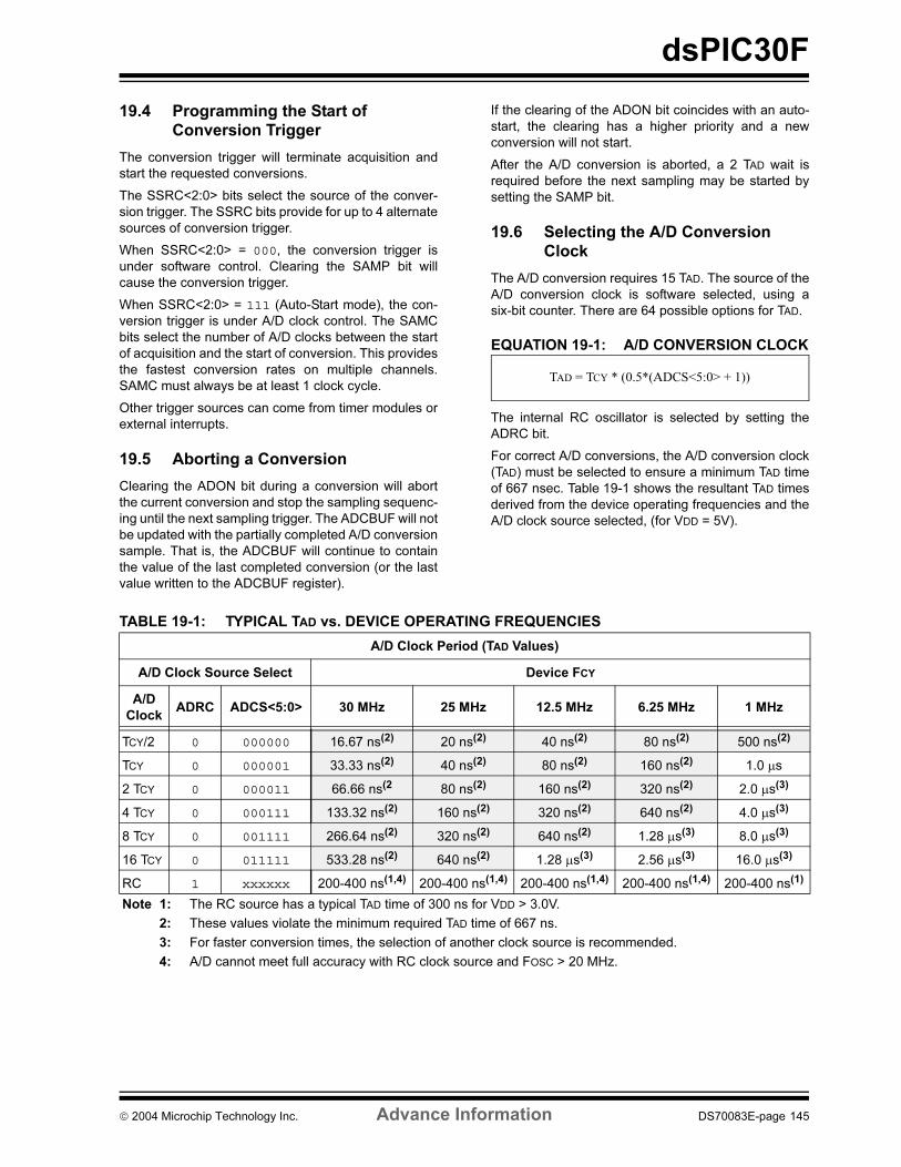
dsPIC30F
19.4 Programming the Start of
Conversion Trigger
The conversion trigger will terminate acquisition and
start the requested conversions.
The SSRC<2:0> bits select the source of the conver-
sion trigger. The SSRC bits provide for up to 4 alternate
sources of conversion trigger.
When SSRC<2:0> = 000, the conversion trigger is
under software control. Clearing the SAMP bit will
cause the conversion trigger.
When SSRC<2:0> = 111 (Auto-Start mode), the con-
version trigger is under A/D clock control. The SAMC
bits select the number of A/D clocks between the start
of acquisition and the start of conversion. This provides
the fastest conversion rates on multiple channels.
SAMC must always be at least 1 clock cycle.
Other trigger sources can come from timer modules or
external interrupts.
19.5 Aborting a Conversion
Clearing the ADON bit during a conversion will abort
the current conversion and stop the sampling sequenc-
ing until the next sampling trigger. The ADCBUF will not
be updated with the partially completed A/D conversion
sample. That is, the ADCBUF will continue to contain
the value of the last completed conversion (or the last
value written to the ADCBUF register).
If the clearing of the ADON bit coincides with an auto-
start, the clearing has a higher priority and a new
conversion will not start.
After the A/D conversion is aborted, a 2 TAD wait is
required before the next sampling may be started by
setting the SAMP bit.
19.6 Selecting the A/D Conversion
Clock
The A/D conversion requires 15 TAD. The source of the
A/D conversion clock is software selected, using a
six-bit counter. There are 64 possible options for TAD.
EQUATION 19-1: A/D CONVERSION CLOCK
The internal RC oscillator is selected by setting the
ADRC bit.
For correct A/D conversions, the A/D conversion clock
(TAD) must be selected to ensure a minimum TAD time
of 667 nsec. Table 19-1 shows the resultant TAD times
derived from the device operating frequencies and the
A/D clock source selected, (for VDD = 5V).
TABLE 19-1: TYPICAL TAD vs. DEVICE OPERATING FREQUENCIES
TAD = TCY * (0.5*(ADCS<5:0> + 1))
A/D Clock Period (TAD Values)
A/D Clock Source Select Device FCY
A/D
ClockADRC ADCS<5:0> 30 MHz 25 MHz 12.5 MHz 6.25 MHz 1 MHz
TCY/2 0 000000 16.67 ns(2) 20 ns(2) 40 ns(2) 80 ns(2) 500 ns(2)
TCY 0 000001 33.33 ns(2) 40 ns(2) 80 ns(2) 160 ns(2) 1.0 µs
2 TCY 0 000011 66.66 ns(2 80 ns(2) 160 ns(2) 320 ns(2) 2.0 µs(3)
4 TCY 0 000111 133.32 ns(2) 160 ns(2) 320 ns(2) 640 ns(2) 4.0 µs(3)
8 TCY 0 001111 266.64 ns(2) 320 ns(2) 640 ns(2) 1.28 µs(3) 8.0 µs(3)
16 TCY 0 011111 533.28 ns(2) 640 ns(2) 1.28 µs(3) 2.56 µs(3) 16.0 µs(3)
RC 1 xxxxxx 200-400 ns(1,4) 200-400 ns(1,4) 200-400 ns(1,4) 200-400 ns(1,4) 200-400 ns(1)
Note 1: The RC source has a typical TAD time of 300 ns for VDD > 3.0V.
2: These values violate the minimum required TAD time of 667 ns.
3: For faster conversion times, the selection of another clock source is recommended.
4: A/D cannot meet full accuracy with RC clock source and FOSC > 20 MHz.
2004 Microchip Technology Inc. Advance Information DS70083E-page 145
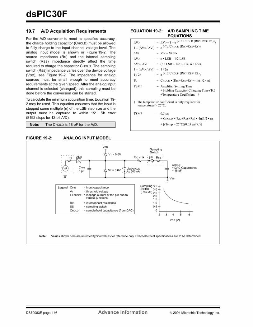
dsPIC30F
19.7 A/D Acquisition Requirements
For the A/D converter to meet its specified accuracy,
the charge holding capacitor (CHOLD) must be allowed
to fully charge to the input channel voltage level. The
analog input model is shown in Figure 19-2. The
source impedance (RS) and the internal sampling
switch (RSS) impedance directly affect the time
required to charge the capacitor CHOLD. The sampling
switch (RSS) impedance varies over the device voltage
(VDD), see Figure 19-2. The impedance for analog
sources must be small enough to meet accuracy
requirements at the given speed. After the analog input
channel is selected (changed), this sampling must be
done before the conversion can be started.
To calculate the minimum acquisition time, Equation 19-
2 may be used. This equation assumes that the input is
stepped some multiple (n) of the LSB step size and the
output must be captured to within 1/2 LSb error
(8192 steps for 12-bit A/D).
EQUATION 19-2: A/D SAMPLING TIME
EQUATIONS
FIGURE 19-2: ANALOG INPUT MODEL
Note: The CHOLD is 18 pF for the A/D.
∆VO = ∆VI • (1 – e (-TC/CHOLD (RIC+RSS+RS)))
1 – (∆VO / ∆VI) = e (-TC/CHOLD (RIC+RSS+RS))
∆VI = VIN – VREF-
∆VO = n • LSB – 1/2 LSB
∆VO / ∆VI = (n • LSB – 1/2 LSB) / n • LSB
1 – (∆VO / ∆VI) = 1 / 2n
1 / 2n = e (-TC/CHOLD (RIC+RSS+RS))
TC = CHOLD • (RIC+RSS+RS) • -In(1/2 • n)
TSMP = Amplifier Settling Time
+ Holding Capacitor Charging Time (TC)
+Temperature Coefficient †
† The temperature coefficient is only required for temperatures > 25°C.
TSMP = 0.5 µs
+ CHOLD • (RIC+RSS+RS) • -In(1/2 • n)
+ [(Temp – 25°C)(0.05 µs/°C)]
CPINVA
Rs ANx
5 pF
VDD (V)
VT = 0.6V
VT = 0.6VILEAKAGE
RIC ≤ 1k
SamplingSwitch
SS RSS
CHOLD
= DAC Capacitance
VSS
3.5
2.52.01.5
1.0
2 3 4 5
(RSS kΩ)
VDD
= 18 pF± 500 nA
Legend: CPIN
VT
ILEAKAGE
RIC
SS
CHOLD
= input capacitance
= threshold voltage
= leakage current at the pin due to
= interconnect resistance
= sampling switch
= sample/hold capacitance (from DAC)
various junctions
Sampling
3.0
0.5
0
6
Switch
Note: Values shown here are untested typical values for reference only. Exact electrical specifications are to be determined.
DS70083E-page 146 Advance Information 2004 Microchip Technology Inc.
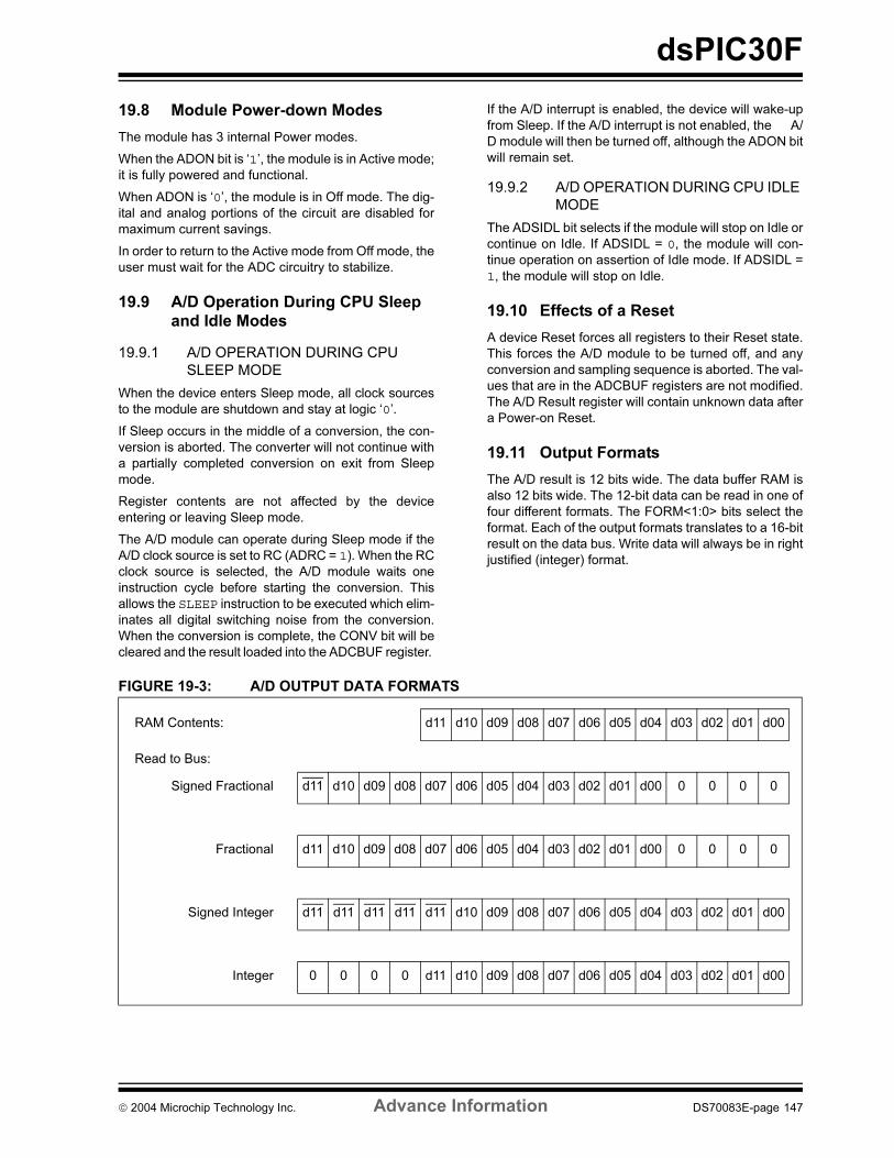
dsPIC30F
19.8 Module Power-down Modes
The module has 3 internal Power modes.
When the ADON bit is ‘1’, the module is in Active mode;
it is fully powered and functional.
When ADON is ‘0’, the module is in Off mode. The dig-
ital and analog portions of the circuit are disabled for
maximum current savings.
In order to return to the Active mode from Off mode, the
user must wait for the ADC circuitry to stabilize.
19.9 A/D Operation During CPU Sleep
and Idle Modes
19.9.1 A/D OPERATION DURING CPU
SLEEP MODE
When the device enters Sleep mode, all clock sources
to the module are shutdown and stay at logic ‘0’.
If Sleep occurs in the middle of a conversion, the con-
version is aborted. The converter will not continue with
a partially completed conversion on exit from Sleep
mode.
Register contents are not affected by the device
entering or leaving Sleep mode.
The A/D module can operate during Sleep mode if the
A/D clock source is set to RC (ADRC = 1). When the RC
clock source is selected, the A/D module waits one
instruction cycle before starting the conversion. This
allows the SLEEP instruction to be executed which elim-
inates all digital switching noise from the conversion.
When the conversion is complete, the CONV bit will be
cleared and the result loaded into the ADCBUF register.
If the A/D interrupt is enabled, the device will wake-up
from Sleep. If the A/D interrupt is not enabled, the A/
D module will then be turned off, although the ADON bit
will remain set.
19.9.2 A/D OPERATION DURING CPU IDLE
MODE
The ADSIDL bit selects if the module will stop on Idle or
continue on Idle. If ADSIDL = 0, the module will con-
tinue operation on assertion of Idle mode. If ADSIDL =
1, the module will stop on Idle.
19.10 Effects of a Reset
A device Reset forces all registers to their Reset state.
This forces the A/D module to be turned off, and any
conversion and sampling sequence is aborted. The val-
ues that are in the ADCBUF registers are not modified.
The A/D Result register will contain unknown data after
a Power-on Reset.
19.11 Output Formats
The A/D result is 12 bits wide. The data buffer RAM is
also 12 bits wide. The 12-bit data can be read in one of
four different formats. The FORM<1:0> bits select the
format. Each of the output formats translates to a 16-bit
result on the data bus. Write data will always be in right
justified (integer) format.
FIGURE 19-3: A/D OUTPUT DATA FORMATS
RAM Contents: d11 d10 d09 d08 d07 d06 d05 d04 d03 d02 d01 d00
Read to Bus:
Signed Fractional d11 d10 d09 d08 d07 d06 d05 d04 d03 d02 d01 d00 0 0 0 0
Fractional d11 d10 d09 d08 d07 d06 d05 d04 d03 d02 d01 d00 0 0 0 0
Signed Integer d11 d11 d11 d11 d11 d10 d09 d08 d07 d06 d05 d04 d03 d02 d01 d00
Integer 0 0 0 0 d11 d10 d09 d08 d07 d06 d05 d04 d03 d02 d01 d00
2004 Microchip Technology Inc. Advance Information DS70083E-page 147
dsPIC30F
19.12 Configuring Analog Port Pins
The use of the ADPCFG and TRIS registers control the
operation of the A/D port pins. The port pins that are
desired as analog inputs must have their correspond-
ing TRIS bit set (input). If the TRIS bit is cleared (out-
put), the digital output level (VOH or VOL) will be
converted.
The A/D operation is independent of the state of the
CH0SA<3:0>/CH0SB<3:0> bits and the TRIS bits.
When reading the Port register, all pins configured as
analog input channels will read as cleared.
Pins configured as digital inputs will not convert an ana-
log input. Analog levels on any pin that is defined as a
digital input (including the ANx pins) may cause the
input buffer to consume current that exceeds the
device specifications.
19.13 Connection Considerations
The analog inputs have diodes to VDD and VSS as ESD
protection. This requires that the analog input be
between VDD and VSS. If the input voltage exceeds this
range by greater than 0.3V (either direction), one of the
diodes becomes forward biased and it may damage the
device if the input current specification is exceeded.
An external RC filter is sometimes added for anti-
aliasing of the input signal. The R component should be
selected to ensure that the sampling time requirements
are satisfied. Any external components connected (via
high impedance) to an analog input pin (capacitor,
zener diode, etc.) should have very little leakage
current at the pin.
DS70083E-page 148 Advance Information 2004 Microchip Technology Inc.
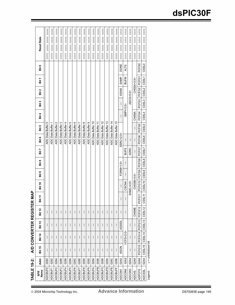
dsPIC30F
TA
BL
E 1
9-2
:A
/D C
ON
VE
RT
ER
RE
GIS
TE
R M
AP
SF
R
Nam
eA
dd
r.B
it 1
5B
it 1
4B
it 1
3B
it 1
2B
it 1
1B
it 1
0B
it 9
Bit
8B
it 7
Bit
6B
it 5
Bit
4B
it 3
Bit
2B
it 1
Bit
0R
eset
Sta
te
AD
CB
UF
00280
——
——
AD
C D
ata
Buffer
00000 uuuu uuuu uuuu
AD
CB
UF
10282
——
——
AD
C D
ata
Buffer
10000 uuuu uuuu uuuu
AD
CB
UF
20284
——
——
AD
C D
ata
Buffer
20000 uuuu uuuu uuuu
AD
CB
UF
30286
——
——
AD
C D
ata
Buffer
30000 uuuu uuuu uuuu
AD
CB
UF
40288
——
——
AD
C D
ata
Buffer
40000 uuuu uuuu uuuu
AD
CB
UF
5028A
——
——
AD
C D
ata
Buffer
50000 uuuu uuuu uuuu
AD
CB
UF
6028C
——
——
AD
C D
ata
Buffer
60000 uuuu uuuu uuuu
AD
CB
UF
7028E
——
——
AD
C D
ata
Buffer
70000 uuuu uuuu uuuu
AD
CB
UF
80290
——
——
AD
C D
ata
Buffer
80000 uuuu uuuu uuuu
AD
CB
UF
90292
——
——
AD
C D
ata
Buffer
90000 uuuu uuuu uuuu
AD
CB
UFA
0294
——
——
AD
C D
ata
Buffer
10
0000 uuuu uuuu uuuu
AD
CB
UF
B0296
——
——
AD
C D
ata
Buffer
11
0000 uuuu uuuu uuuu
AD
CB
UF
C0298
——
——
AD
C D
ata
Buffer
12
0000 uuuu uuuu uuuu
AD
CB
UF
D029A
——
——
AD
C D
ata
Buffer
13
0000 uuuu uuuu uuuu
AD
CB
UF
E029C
——
——
AD
C D
ata
Buffer
14
0000 uuuu uuuu uuuu
AD
CB
UF
F029E
——
——
AD
C D
ata
Buffer
15
0000 uuuu uuuu uuuu
AD
CO
N1
02A
0A
DO
N—
AD
SID
L—
——
FO
RM
<1:0
>S
SR
C<
2:0
>—
—A
SA
MS
AM
PD
ON
E0000 0000 0000 0000
AD
CO
N2
02A
2V
CF
G<
2:0
>—
—C
SC
NA
——
BU
FS
—S
MP
I<3:0
>B
UF
MA
LT
S0000 0000 0000 0000
AD
CO
N3
02A
4—
——
SA
MC
<4:0
>A
DR
C—
AD
CS
<5:0
>0000 0000 0000 0000
AD
CH
S02A
6—
——
CH
0N
BC
H0S
B<
3:0
>—
——
CH
0N
AC
H0S
A<
3:0
>0000 0000 0000 0000
AD
PC
FG
02A
8P
CF
G15
PC
FG
14
PC
FG
13
PC
FG
12
PC
FG
11
PC
FG
10
PC
FG
9P
CF
G8
PC
FG
7P
CF
G6
PC
FG
5P
CF
G4
PC
FG
3P
CF
G2
PC
FG
1P
CF
G0
0000 0000 0000 0000
AD
CS
SL
02A
AC
SS
L15
CS
SL14
CS
SL13
CS
SL12
CS
SL11
CS
SL10
CS
SL9
CS
SL8
CS
SL7
CS
SL6
CS
SL5
CS
SL4
CS
SL3
CS
SL2
CS
SL1
CS
SL0
0000 0000 0000 0000
Legend:
u =
unin
itia
lized b
it
2004 Microchip Technology Inc. Advance Information DS70083E-page 149

dsPIC30F
NOTES:
DS70083E-page 150 Advance Information 2004 Microchip Technology Inc.
dsPIC30F
20.0 SYSTEM INTEGRATION
There are several features intended to maximize sys-
tem reliability, minimize cost through elimination of
external components, provide Power Saving Operating
modes and offer code protection:
• Oscillator Selection
• Reset
- Power-on Reset (POR)
- Power-up Timer (PWRT)
- Oscillator Start-up Timer (OST)
- Programmable Brown-out Reset (BOR)
• Watchdog Timer (WDT)
• Power Saving Modes (Sleep and Idle)
• Code Protection
• Unit ID Locations
• In-Circuit Serial Programming (ICSP)
dsPIC30F devices have a Watchdog Timer which is
permanently enabled via the configuration bits or can
be software controlled. It runs off its own RC oscillator
for added reliability. There are two timers that offer
necessary delays on power-up. One is the Oscillator
Start-up Timer (OST), intended to keep the chip in
Reset until the crystal oscillator is stable. The other is
the Power-up Timer (PWRT) which provides a delay on
power-up only, designed to keep the part in Reset while
the power supply stabilizes. With these two timers on-
chip, most applications need no external Reset
circuitry.
Sleep mode is designed to offer a very low current
Power-down mode. The user can wake-up from Sleep
through external Reset, Watchdog Timer Wake-up, or
through an interrupt. Several oscillator options are also
made available to allow the part to fit a wide variety of
applications. In the Idle mode, the clock sources are
still active but the CPU is shut-off. The RC oscillator
option saves system cost while the LP crystal option
saves power.
20.1 Oscillator System Overview
The dsPIC30F oscillator system has the following
modules and features:
• Various external and internal oscillator options as
clock sources
• An on-chip PLL to boost internal operating
frequency
• A clock switching mechanism between various
clock sources
• Programmable clock postscaler for system power
savings
• A Fail-Safe Clock Monitor (FSCM) that detects
clock failure and takes fail-safe measures
• Clock Control register (OSCCON)
• Configuration bits for main oscillator selection
Configuration bits determine the clock source upon
Power-on Reset (POR) and Brown-out Reset (BOR).
Thereafter, the clock source can be changed between
permissible clock sources. The OSCCON register
controls the clock switching and reflects system clock
related status bits.
Table 20-1 provides a summary of the dsPIC30F Oscil-
lator Operating modes. A simplified diagram of the
oscillator system is shown in Figure 20-1.
2004 Microchip Technology Inc. Advance Information DS70083E-page 151
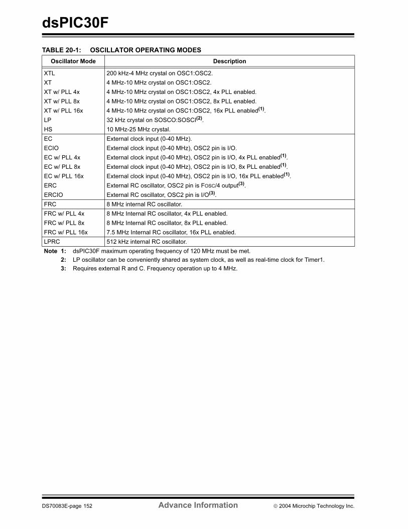
dsPIC30F
TABLE 20-1: OSCILLATOR OPERATING MODES
Oscillator Mode Description
XTL 200 kHz-4 MHz crystal on OSC1:OSC2.
XT 4 MHz-10 MHz crystal on OSC1:OSC2.
XT w/ PLL 4x 4 MHz-10 MHz crystal on OSC1:OSC2, 4x PLL enabled.
XT w/ PLL 8x 4 MHz-10 MHz crystal on OSC1:OSC2, 8x PLL enabled.
XT w/ PLL 16x 4 MHz-10 MHz crystal on OSC1:OSC2, 16x PLL enabled(1).
LP 32 kHz crystal on SOSCO:SOSCI(2).
HS 10 MHz-25 MHz crystal.
EC External clock input (0-40 MHz).
ECIO External clock input (0-40 MHz), OSC2 pin is I/O.
EC w/ PLL 4x External clock input (0-40 MHz), OSC2 pin is I/O, 4x PLL enabled(1).
EC w/ PLL 8x External clock input (0-40 MHz), OSC2 pin is I/O, 8x PLL enabled(1).
EC w/ PLL 16x External clock input (0-40 MHz), OSC2 pin is I/O, 16x PLL enabled(1).
ERC External RC oscillator, OSC2 pin is FOSC/4 output(3).
ERCIO External RC oscillator, OSC2 pin is I/O(3).
FRC 8 MHz internal RC oscillator.
FRC w/ PLL 4x 8 MHz Internal RC oscillator, 4x PLL enabled.
FRC w/ PLL 8x 8 MHz Internal RC oscillator, 8x PLL enabled.
FRC w/ PLL 16x 7.5 MHz Internal RC oscillator, 16x PLL enabled.
LPRC 512 kHz internal RC oscillator.
Note 1: dsPIC30F maximum operating frequency of 120 MHz must be met.
2: LP oscillator can be conveniently shared as system clock, as well as real-time clock for Timer1.
3: Requires external R and C. Frequency operation up to 4 MHz.
DS70083E-page 152 Advance Information 2004 Microchip Technology Inc.
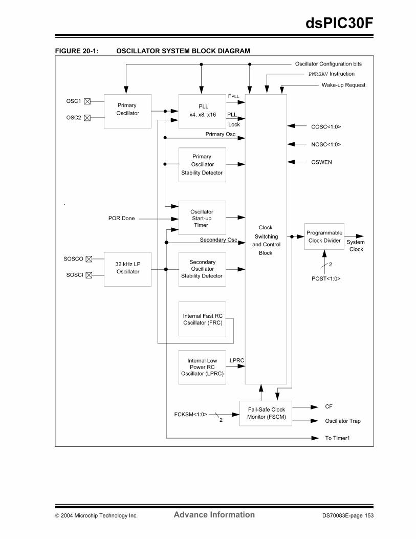
dsPIC30F
FIGURE 20-1: OSCILLATOR SYSTEM BLOCK DIAGRAM
Primary OSC1
OSC2
SOSCO
SOSCI
Oscillator
32 kHz LP
Clock
and Control
Block
Switching
Oscillator
x4, x8, x16
PLL
Primary
Oscillator
Stability Detector
Stability Detector
Secondary
Oscillator
Programmable
Clock Divider
Oscillator
Start-up
Timer
Fail-Safe Clock
Monitor (FSCM)
Internal Fast RC
Oscillator (FRC)
Internal Low
Power RC
Oscillator (LPRC)
PWRSAV Instruction
Wake-up Request
Oscillator Configuration bits
System
Clock
Oscillator Trap
To Timer1
LPRC
Secondary Osc
POR Done
Primary Osc
FPLL
POST<1:0>
2
FCKSM<1:0>2
PLL
Lock COSC<1:0>
NOSC<1:0>
OSWEN
CF
2004 Microchip Technology Inc. Advance Information DS70083E-page 153
dsPIC30F
20.2 Oscillator Configurations
20.2.1 INITIAL CLOCK SOURCE
SELECTION
While coming out of Power-on Reset or Brown-out
Reset, the device selects its clock source based on:
a) FOS<1:0> configuration bits that select one of
four oscillator groups,
b) and FPR<3:0> configuration bits that select one
of 13 oscillator choices within the primary group.
The selection is as shown in Table 20-2.
TABLE 20-2: CONFIGURATION BIT VALUES FOR CLOCK SELECTION
20.2.2 OSCILLATOR START-UP TIMER
(OST)
In order to ensure that a crystal oscillator (or ceramic
resonator) has started and stabilized, an Oscillator
Start-up Timer is included. It is a simple 10-bit counter
that counts 1024 TOSC cycles before releasing the
oscillator clock to the rest of the system. The time-out
period is designated as TOST. The TOST time is involved
every time the oscillator has to restart (i.e., on POR,
BOR and wake-up from Sleep). The Oscillator Start-up
Timer is applied to the LP oscillator, XT, XTL, and HS
modes (upon wake-up from Sleep, POR and BOR) for
the primary oscillator.
20.2.3 LP OSCILLATOR CONTROL
Enabling the LP oscillator is controlled with two
elements:
1. The current oscillator group bits COSC<1:0>.
2. The LPOSCEN bit (OSCON register).
The LP oscillator is on (even during Sleep mode) if
LPOSCEN = 1. The LP oscillator is the device clock if:
• COSC<1:0> = 00 (LP selected as main oscillator)
and
• LPOSCEN = 1
Keeping the LP oscillator on at all times allows for a fast
switch to the 32 kHz system clock for lower power oper-
ation. Returning to the faster main oscillator will still
require a start-up time
Note: Some devices support FRC with PLL 4x,
8x and 16x modes. Refer to individual
device data sheets for details.
Oscillator ModeOscillator
SourceFOS1 FOS0 FPR3 FPR2 FPR1 FPR0
OSC2
Function
EC Primary 1 1 1 0 1 1 CLKO
ECIO Primary 1 1 1 1 0 0 I/O
EC w/ PLL 4x Primary 1 1 1 1 0 1 I/O
EC w/ PLL 8x Primary 1 1 1 1 1 0 I/O
EC w/ PLL 16x Primary 1 1 1 1 1 1 I/O
ERC Primary 1 1 1 0 0 1 CLKO
ERCIO Primary 1 1 1 0 0 0 I/O
XT Primary 1 1 0 1 0 0 OSC2
XT w/ PLL 4x Primary 1 1 0 1 0 1 OSC2
XT w/ PLL 8x Primary 1 1 0 1 1 0 OSC2
XT w/ PLL 16x Primary 1 1 0 1 1 1 OSC2
XTL Primary 1 1 0 0 0 X OSC2
HS Primary 1 1 0 0 1 X OSC2
LP Secondary 0 0 — — — — (Notes 1, 2)
FRC Internal FRC 0 1 — — — — (Notes 1, 2)
LPRC Internal LPRC 1 0 — — — — (Notes 1, 2)
Note 1: OSC2 pin function is determined by the Primary Oscillator mode selection (FPR<3:0>).
2: OSC1 pin cannot be used as an I/O pin even if the secondary oscillator or an internal clock source is
selected at all times.
DS70083E-page 154 Advance Information 2004 Microchip Technology Inc.
dsPIC30F
20.2.4 PHASE LOCKED LOOP (PLL)
The PLL multiplies the clock which is generated by the
primary oscillator. The PLL is selectable to have either
gains of x4, x8, and x16. Input and output frequency
ranges are summarized in Table 20-3.
TABLE 20-3: PLL FREQUENCY RANGE
The PLL features a lock output which is asserted when
the PLL enters a phase locked state. Should the loop
fall out of lock (e.g., due to noise), the lock signal will be
rescinded. The state of this signal is reflected in the
read only LOCK bit in the OSCCON register.
20.2.5 FAST RC OSCILLATOR (FRC)
The FRC oscillator is a fast (8 MHz nominal) internal
RC oscillator. This oscillator is intended to provide
reasonable device operating speeds without the use of
an external crystal, ceramic resonator, or RC network.
The FRC oscillator can be used with the PLL to obtain
higher clock frequencies.
The dsPIC30F operates from the FRC oscillator when-
ever the current oscillator selection control bits in the
OSCCON register (OSCCON<13:12>) are set to ‘01’.
The four bit field specified by TUN<3:0> (OSCON
<15:14> and OSCON<11:10>) allows the user to tune
the internal fast RC oscillator (nominal 8.0 MHz). The
user can tune the FRC oscillator within a range of
+10.5% (840 kHz) and -12% (960 kHz) in steps of
1.50% around the factory-calibrated setting, see
Table 20-4.
If OSCCON<13:12> are set to ‘11’ and FPR<3:0> are
set to ‘0001’, ‘1010’ or ‘0011’, then a PLL multiplier of 4,
8 or 16 (respectively) is applied.
TABLE 20-4: FRC TUNING
20.2.6 LOW POWER RC OSCILLATOR
(LPRC)
The LPRC oscillator is a component of the Watchdog
Timer (WDT) and oscillates at a nominal frequency of
512 kHz. The LPRC oscillator is the clock source for
the Power-up Timer (PWRT) circuit, WDT, and clock
monitor circuits. It may also be used to provide a low
frequency clock source option for applications where
power consumption is critical and timing accuracy is
not required
The LPRC oscillator is always enabled at a Power-on
Reset because it is the clock source for the PWRT.
After the PWRT expires, the LPRC oscillator will remain
on if one of the following is TRUE:
• The Fail-Safe Clock Monitor is enabled
• The WDT is enabled
• The LPRC oscillator is selected as the system
clock via the COSC<1:0> control bits in the
OSCCON register
If one of the above conditions is not true, the LPRC will
shut-off after the PWRT expires.
FINPLL
MultiplierFOUT
4 MHz-10 MHz x4 16 MHz-40 MHz
4 MHz-10 MHz x8 32 MHz-80 MHz
4 MHz-7.5 MHz x16 64 MHz-160 MHz
Note: When a 16x PLL is used, the FRC fre-
quency must not be tuned to a frequency
greater than 7.5 MHz.
TUN<3:0>
BitsFRC Frequency
0111 + 10.5%
0110 + 9.0%
0101 + 7.5%
0100 + 6.0%
0011 + 4.5%
0010 + 3.0%
0001 + 1.5%
0000 Center Frequency (oscillator is
running at calibrated frequency)
1111 - 1.5%
1110 - 3.0%
1101 - 4.5%
1100 - 6.0%
1011 - 7.5%
1010 - 9.0%
1001 - 10.5%
1000 - 12.0%
Note 1: OSC2 pin function is determined by the
Primary Oscillator mode selection
(FPR<3:0>).
2: OSC1 pin cannot be used as an I/O pin
even if the secondary oscillator or an
internal clock source is selected at all
times.
2004 Microchip Technology Inc. Advance Information DS70083E-page 155
dsPIC30F
20.2.7 FAIL-SAFE CLOCK MONITOR
The Fail-Safe Clock Monitor (FSCM) allows the device
to continue to operate even in the event of an oscillator
failure. The FSCM function is enabled by appropriately
programming the FCKSM configuration bits (clock
switch and monitor selection bits) in the FOSC Device
Configuration register. If the FSCM function is enabled,
the LPRC internal oscillator will run at all times (except
during Sleep mode) and will not be subject to control by
the SWDTEN bit.
In the event of an oscillator failure, the FSCM will gen-
erate a clock failure trap event and will switch the sys-
tem clock over to the FRC oscillator. The user will then
have the option to either attempt to restart the oscillator
or execute a controlled shutdown. The user may decide
to treat the trap as a warm Reset by simply loading the
Reset address into the oscillator fail trap vector. In this
event, the CF (Clock Fail) status bit (OSCCON<3>) is
also set whenever a clock failure is recognized.
In the event of a clock failure, the WDT is unaffected
and continues to run on the LPRC clock.
If the oscillator has a very slow start-up time coming out
of POR, BOR or Sleep, it is possible that the PWRT
timer will expire before the oscillator has started. In
such cases, the FSCM will be activated and the FSCM
will initiate a clock failure trap, and the COSC<1:0> bits
are loaded with FRC oscillator selection. This will effec-
tively shut-off the original oscillator that was trying to
start.
The user may detect this situation and restart the
oscillator in the clock fail trap ISR.
Upon a clock failure detection, the FSCM module will
initiate a clock switch to the FRC oscillator as follows:
1. The COSC bits (OSCCON<13:12>) are loaded
with the FRC oscillator selection value.
2. CF bit is set (OSCCON<3>).
3. OSWEN control bit (OSCCON<0>) is cleared.
For the purpose of clock switching, the clock sources
are sectioned into four groups:
1. Primary
2. Secondary
3. Internal FRC
4. Internal LPRC
The user can switch between these functional groups
but cannot switch between options within a group. If the
primary group is selected, then the choice within the
group is always determined by the FPR<3:0>
configuration bits.
The OSCCON register holds the control and status bits
related to clock switching.
• COSC<1:0>: Read only status bits always reflect
the current oscillator group in effect.
• NOSC<1:0>: Control bits which are written to
indicate the new oscillator group of choice.
- On POR and BOR, COSC<1:0> and
NOSC<1:0> are both loaded with the
configuration bit values FOS<1:0>.
• LOCK: The LOCK status bit indicates a PLL lock.
• CF: Read only status bit indicating if a clock fail
detect has occurred.
• OSWEN: Control bit changes from a ‘0’ to a ‘1’
when a clock transition sequence is initiated.
Clearing the OSWEN control bit will abort a clock
transition in progress (used for hang-up
situations).
If configuration bits FCKSM<1:0> = 1x, then the clock
switching and Fail-Safe Clock monitoring functions are
disabled. This is the default configuration bit setting.
If clock switching is disabled, then the FOS<1:0> and
FPR<3:0> bits directly control the oscillator selection
and the COSC<1:0> bits do not control the clock selec-
tion. However, these bits will reflect the clock source
selection.
20.2.8 PROTECTION AGAINST
ACCIDENTAL WRITES TO OSCCON
A write to the OSCCON register is intentionally made
difficult because it controls clock switching and clock
scaling.
To write to the OSCCON low byte, the following code
sequence must be executed without any other
instructions in between:
Byte write is allowed for one instruction cycle. Write the
desired value or use bit manipulation instruction.
To write to the OSCCON high byte, the following
instructions must be executed without any other
instructions in between:
Byte write is allowed for one instruction cycle. Write the
desired value or use bit manipulation instruction.
Note: The application should not attempt to
switch to a clock of frequency lower than
100 KHz when the fail-safe clock monitor is
enabled. If such clock switching is
performed, the device may generate an
oscillator fail trap and switch to the Fast RC
oscillator.
Byte Write “0x46” to OSCCON lowByte Write “0x57” to OSCCON low
Byte Write “0x78” to OSCCON highByte Write “0x9A” to OSCCON high
DS70083E-page 156 Advance Information 2004 Microchip Technology Inc.
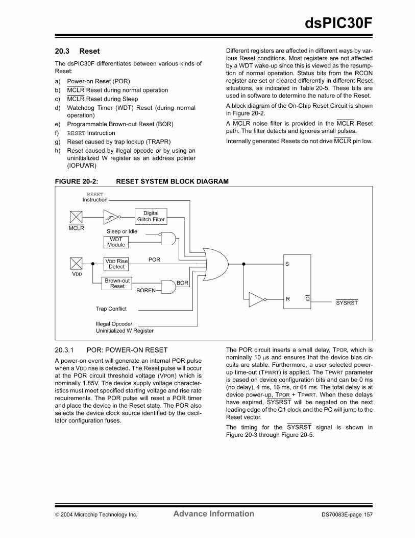
dsPIC30F
20.3 Reset
The dsPIC30F differentiates between various kinds of
Reset:
a) Power-on Reset (POR)
b) MCLR Reset during normal operation
c) MCLR Reset during Sleep
d) Watchdog Timer (WDT) Reset (during normal
operation)
e) Programmable Brown-out Reset (BOR)
f) RESET Instruction
g) Reset caused by trap lockup (TRAPR)
h) Reset caused by illegal opcode or by using an
uninitialized W register as an address pointer
(IOPUWR)
Different registers are affected in different ways by var-
ious Reset conditions. Most registers are not affected
by a WDT wake-up since this is viewed as the resump-
tion of normal operation. Status bits from the RCON
register are set or cleared differently in different Reset
situations, as indicated in Table 20-5. These bits are
used in software to determine the nature of the Reset.
A block diagram of the On-Chip Reset Circuit is shown
in Figure 20-2.
A MCLR noise filter is provided in the MCLR Reset
path. The filter detects and ignores small pulses.
Internally generated Resets do not drive MCLR pin low.
FIGURE 20-2: RESET SYSTEM BLOCK DIAGRAM
20.3.1 POR: POWER-ON RESET
A power-on event will generate an internal POR pulse
when a VDD rise is detected. The Reset pulse will occur
at the POR circuit threshold voltage (VPOR) which is
nominally 1.85V. The device supply voltage character-
istics must meet specified starting voltage and rise rate
requirements. The POR pulse will reset a POR timer
and place the device in the Reset state. The POR also
selects the device clock source identified by the oscil-
lator configuration fuses.
The POR circuit inserts a small delay, TPOR, which is
nominally 10 µs and ensures that the device bias cir-
cuits are stable. Furthermore, a user selected power-
up time-out (TPWRT) is applied. The TPWRT parameter
is based on device configuration bits and can be 0 ms
(no delay), 4 ms, 16 ms, or 64 ms. The total delay is at
device power-up, TPOR + TPWRT. When these delays
have expired, SYSRST will be negated on the next
leading edge of the Q1 clock and the PC will jump to the
Reset vector.
The timing for the SYSRST signal is shown in
Figure 20-3 through Figure 20-5.
S
R Q
MCLR
VDD
VDD RiseDetect
POR
SYSRST
Sleep or Idle
Brown-outReset
BOREN
RESETInstruction
WDTModule
DigitalGlitch Filter
BOR
Trap Conflict
Illegal Opcode/
Uninitialized W Register
2004 Microchip Technology Inc. Advance Information DS70083E-page 157
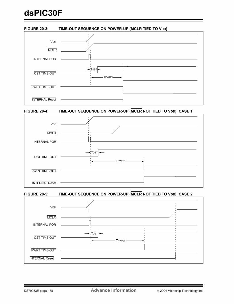
dsPIC30F
FIGURE 20-3: TIME-OUT SEQUENCE ON POWER-UP (MCLR TIED TO VDD)
FIGURE 20-4: TIME-OUT SEQUENCE ON POWER-UP (MCLR NOT TIED TO VDD): CASE 1
FIGURE 20-5: TIME-OUT SEQUENCE ON POWER-UP (MCLR NOT TIED TO VDD): CASE 2
TPWRT
TOST
VDD
INTERNAL POR
PWRT TIME-OUT
OST TIME-OUT
INTERNAL Reset
MCLR
TPWRT
TOST
VDD
INTERNAL POR
PWRT TIME-OUT
OST TIME-OUT
INTERNAL Reset
MCLR
VDD
MCLR
INTERNAL POR
PWRT TIME-OUT
OST TIME-OUT
INTERNAL Reset
TPWRT
TOST
DS70083E-page 158 Advance Information 2004 Microchip Technology Inc.
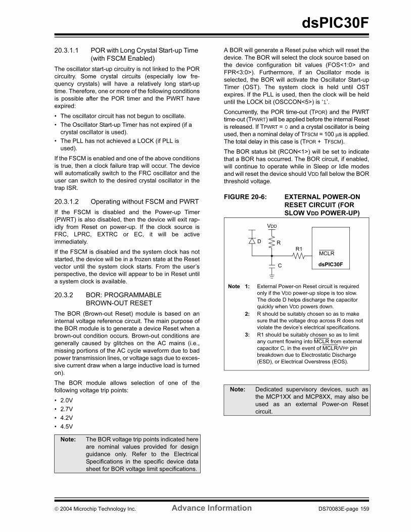
dsPIC30F
20.3.1.1 POR with Long Crystal Start-up Time
(with FSCM Enabled)
The oscillator start-up circuitry is not linked to the POR
circuitry. Some crystal circuits (especially low fre-
quency crystals) will have a relatively long start-up
time. Therefore, one or more of the following conditions
is possible after the POR timer and the PWRT have
expired:
• The oscillator circuit has not begun to oscillate.
• The Oscillator Start-up Timer has not expired (if a
crystal oscillator is used).
• The PLL has not achieved a LOCK (if PLL is
used).
If the FSCM is enabled and one of the above conditions
is true, then a clock failure trap will occur. The device
will automatically switch to the FRC oscillator and the
user can switch to the desired crystal oscillator in the
trap ISR.
20.3.1.2 Operating without FSCM and PWRT
If the FSCM is disabled and the Power-up Timer
(PWRT) is also disabled, then the device will exit rap-
idly from Reset on power-up. If the clock source is
FRC, LPRC, EXTRC or EC, it will be active
immediately.
If the FSCM is disabled and the system clock has not
started, the device will be in a frozen state at the Reset
vector until the system clock starts. From the user’s
perspective, the device will appear to be in Reset until
a system clock is available.
20.3.2 BOR: PROGRAMMABLE
BROWN-OUT RESET
The BOR (Brown-out Reset) module is based on an
internal voltage reference circuit. The main purpose of
the BOR module is to generate a device Reset when a
brown-out condition occurs. Brown-out conditions are
generally caused by glitches on the AC mains (i.e.,
missing portions of the AC cycle waveform due to bad
power transmission lines, or voltage sags due to exces-
sive current draw when a large inductive load is turned
on).
The BOR module allows selection of one of the
following voltage trip points:
• 2.0V
• 2.7V
• 4.2V
• 4.5V
A BOR will generate a Reset pulse which will reset the
device. The BOR will select the clock source based on
the device configuration bit values (FOS<1:0> and
FPR<3:0>). Furthermore, if an Oscillator mode is
selected, the BOR will activate the Oscillator Start-up
Timer (OST). The system clock is held until OST
expires. If the PLL is used, then the clock will be held
until the LOCK bit (OSCCON<5>) is ‘1’.
Concurrently, the POR time-out (TPOR) and the PWRT
time-out (TPWRT) will be applied before the internal Reset
is released. If TPWRT = 0 and a crystal oscillator is being
used, then a nominal delay of TFSCM = 100 µs is applied.
The total delay in this case is (TPOR + TFSCM).
The BOR status bit (RCON<1>) will be set to indicate
that a BOR has occurred. The BOR circuit, if enabled,
will continue to operate while in Sleep or Idle modes
and will reset the device should VDD fall below the BOR
threshold voltage.
FIGURE 20-6: EXTERNAL POWER-ON
RESET CIRCUIT (FOR
SLOW VDD POWER-UP)
Note: The BOR voltage trip points indicated here
are nominal values provided for design
guidance only. Refer to the Electrical
Specifications in the specific device data
sheet for BOR voltage limit specifications.
Note: Dedicated supervisory devices, such as
the MCP1XX and MCP8XX, may also be
used as an external Power-on Reset
circuit.
Note 1: External Power-on Reset circuit is required
only if the VDD power-up slope is too slow.
The diode D helps discharge the capacitor
quickly when VDD powers down.
2: R should be suitably chosen so as to make
sure that the voltage drop across R does not
violate the device’s electrical specifications.
3: R1 should be suitably chosen so as to limit
any current flowing into MCLR from external
capacitor C, in the event of MCLR/VPP pin
breakdown due to Electrostatic Discharge
(ESD), or Electrical Overstress (EOS).
C
R1RD
VDD
dsPIC30F
MCLR
2004 Microchip Technology Inc. Advance Information DS70083E-page 159
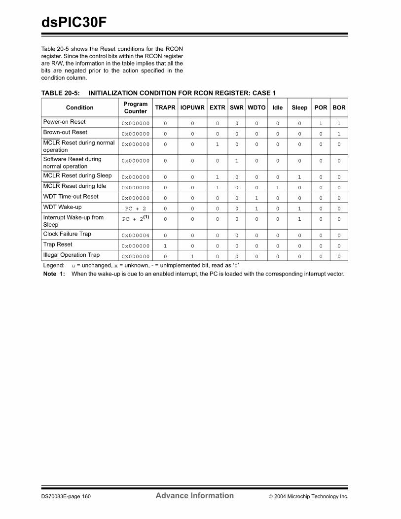
dsPIC30F
Table 20-5 shows the Reset conditions for the RCON
register. Since the control bits within the RCON register
are R/W, the information in the table implies that all the
bits are negated prior to the action specified in the
condition column.
TABLE 20-5: INITIALIZATION CONDITION FOR RCON REGISTER: CASE 1
ConditionProgram
CounterTRAPR IOPUWR EXTR SWR WDTO Idle Sleep POR BOR
Power-on Reset 0x000000 0 0 0 0 0 0 0 1 1
Brown-out Reset 0x000000 0 0 0 0 0 0 0 0 1
MCLR Reset during normal
operation0x000000 0 0 1 0 0 0 0 0 0
Software Reset during
normal operation0x000000 0 0 0 1 0 0 0 0 0
MCLR Reset during Sleep 0x000000 0 0 1 0 0 0 1 0 0
MCLR Reset during Idle 0x000000 0 0 1 0 0 1 0 0 0
WDT Time-out Reset 0x000000 0 0 0 0 1 0 0 0 0
WDT Wake-up PC + 2 0 0 0 0 1 0 1 0 0
Interrupt Wake-up from
SleepPC + 2(1) 0 0 0 0 0 0 1 0 0
Clock Failure Trap 0x000004 0 0 0 0 0 0 0 0 0
Trap Reset 0x000000 1 0 0 0 0 0 0 0 0
Illegal Operation Trap 0x000000 0 1 0 0 0 0 0 0 0
Legend: u = unchanged, x = unknown, - = unimplemented bit, read as ‘0’
Note 1: When the wake-up is due to an enabled interrupt, the PC is loaded with the corresponding interrupt vector.
DS70083E-page 160 Advance Information 2004 Microchip Technology Inc.
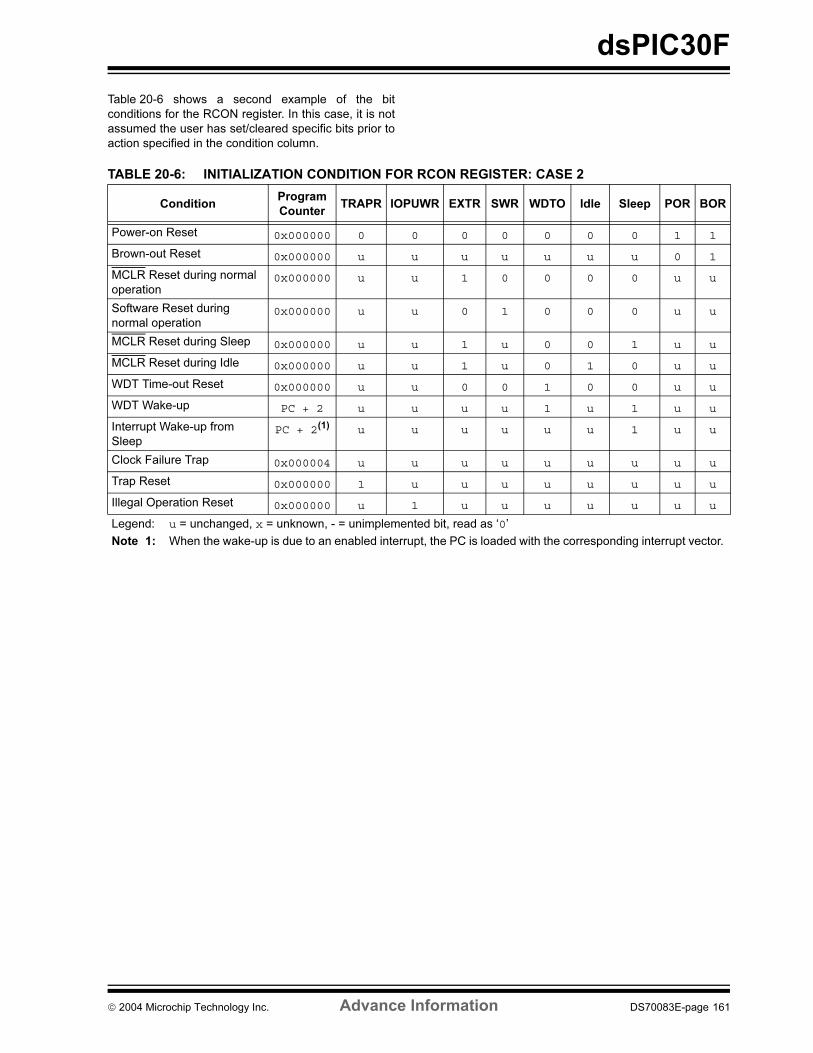
dsPIC30F
Table 20-6 shows a second example of the bit
conditions for the RCON register. In this case, it is not
assumed the user has set/cleared specific bits prior to
action specified in the condition column.
TABLE 20-6: INITIALIZATION CONDITION FOR RCON REGISTER: CASE 2
ConditionProgram
CounterTRAPR IOPUWR EXTR SWR WDTO Idle Sleep POR BOR
Power-on Reset 0x000000 0 0 0 0 0 0 0 1 1
Brown-out Reset 0x000000 u u u u u u u 0 1
MCLR Reset during normal
operation0x000000 u u 1 0 0 0 0 u u
Software Reset during
normal operation0x000000 u u 0 1 0 0 0 u u
MCLR Reset during Sleep 0x000000 u u 1 u 0 0 1 u u
MCLR Reset during Idle 0x000000 u u 1 u 0 1 0 u u
WDT Time-out Reset 0x000000 u u 0 0 1 0 0 u u
WDT Wake-up PC + 2 u u u u 1 u 1 u u
Interrupt Wake-up from
SleepPC + 2(1) u u u u u u 1 u u
Clock Failure Trap 0x000004 u u u u u u u u u
Trap Reset 0x000000 1 u u u u u u u u
Illegal Operation Reset 0x000000 u 1 u u u u u u u
Legend: u = unchanged, x = unknown, - = unimplemented bit, read as ‘0’
Note 1: When the wake-up is due to an enabled interrupt, the PC is loaded with the corresponding interrupt vector.
2004 Microchip Technology Inc. Advance Information DS70083E-page 161
dsPIC30F
20.4 Watchdog Timer (WDT)
20.4.1 WATCHDOG TIMER OPERATION
The primary function of the Watchdog Timer (WDT) is
to reset the processor in the event of a software mal-
function. The WDT is a free-running timer which runs
off an on-chip RC oscillator, requiring no external com-
ponent. Therefore, the WDT timer will continue to oper-
ate even if the main processor clock (e.g., the crystal
oscillator) fails.
20.4.2 ENABLING AND DISABLING
THE WDT
The Watchdog Timer can be “Enabled” or “Disabled”
only through a configuration bit (FWDTEN) in the
Configuration register, FWDT.
Setting FWDTEN = 1 enables the Watchdog Timer. The
enabling is done when programming the device. By
default, after chip erase, FWDTEN bit = 1. Any device
programmer capable of programming dsPIC30F
devices allows programming of this and other
configuration bits.
If enabled, the WDT will increment until it overflows or
“times out”. A WDT time-out will force a device Reset
(except during Sleep). To prevent a WDT time-out, the
user must clear the Watchdog Timer using a CLRWDTinstruction.
If a WDT times out during Sleep, the device will wake-
up. The WDTO bit in the RCON register will be cleared
to indicate a wake-up resulting from a WDT time-out.
Setting FWDTEN = 0 allows user software to enable/
disable the Watchdog Timer via the SWDTEN
(RCON<5>) control bit.
20.5 Low Voltage Detect
The Low Voltage Detect (LVD) module is used to detect
when the VDD of the device drops below a threshold
value, VLVD, which is determined by the LVDL<3:0>
bits (RCON<11:8>) and is thus user programmable.
The internal voltage reference circuitry requires a nom-
inal amount of time to stabilize, and the BGST bit
(RCON<13>) indicates when the voltage reference has
stabilized.
In some devices, the LVD threshold voltage may be
applied externally on the LVDIN pin.
The LVD module is enabled by setting the LVDEN bit
(RCON<12>).
20.6 Power Saving Modes
There are two power saving states that can be entered
through the execution of a special instruction, PWRSAV;
these are Sleep and Idle.
The format of the PWRSAV instruction is as follows:
PWRSAV <parameter>, where ‘parameter’ defines
Idle or Sleep mode.
20.6.1 SLEEP MODE
In Sleep mode, the clock to the CPU and peripherals is
shutdown. If an on-chip oscillator is being used, it is
shutdown.
The Fail-Safe Clock Monitor is not functional during
Sleep since there is no clock to monitor. However,
LPRC clock remains active if WDT is operational during
Sleep.
The brown-out protection circuit and the Low Voltage
Detect circuit, if enabled, will remain functional during
Sleep.
The processor wakes up from Sleep if at least one of
the following conditions has occurred:
• any interrupt that is individually enabled and
meets the required priority level
• any Reset (POR, BOR and MCLR)
• WDT time-out
On waking up from Sleep mode, the processor will
restart the same clock that was active prior to entry into
Sleep mode. When clock switching is enabled, bits
COSC<1:0> will determine the oscillator source that
will be used on wake-up. If clock switch is disabled,
then there is only one system clock.
If the clock source is an oscillator, the clock to the
device will be held off until OST times out (indicating a
stable oscillator). If PLL is used, the system clock is
held off until LOCK = 1 (indicating that the PLL is
stable). In either case, TPOR, TLOCK and TPWRT delays
are applied.
If EC, FRC, LPRC or EXTRC oscillators are used, then
a delay of TPOR (~ 10 µs) is applied. This is the smallest
delay possible on wake-up from Sleep.
Moreover, if LP oscillator was active during Sleep and
LP is the oscillator used on wake-up, then the start-up
delay will be equal to TPOR. PWRT delay and OST
timer delay are not applied. In order to have -the small-
est possible start-up delay when waking up from Sleep,
one of these faster wake-up options should be selected
before entering Sleep.
Note: If a POR or BOR occurred, the selection of
the oscillator is based on the FOS<1:0>
and FPR<3:0> configuration bits.
DS70083E-page 162 Advance Information 2004 Microchip Technology Inc.
dsPIC30F
Any interrupt that is individually enabled (using the cor-
responding IE bit) and meets the prevailing priority level
will be able to wake-up the processor. The processor will
process the interrupt and branch to the ISR. The Sleep
status bit in the RCON register is set upon wake-up.
All Resets will wake-up the processor from Sleep
mode. Any Reset, other than POR, will set the Sleep
status bit. In a POR, the Sleep bit is cleared.
If the Watchdog Timer is enabled, then the processor
will wake-up from Sleep mode upon WDT time-out. The
Sleep and WDTO status bits are both set.
20.6.2 IDLE MODE
In Idle mode, the clock to the CPU is shutdown while
peripherals keep running. Unlike Sleep mode, the clock
source remains active.
Several peripherals have a control bit in each module
that allows them to operate during Idle.
LPRC Fail-Safe Clock remains active if clock failure
detect is enabled.
The processor wakes up from Idle if at least one of the
following conditions has occurred:
• any interrupt that is individually enabled (IE bit is
‘1’) and meets the required priority level
• any Reset (POR, BOR, MCLR)
• WDT time-out
Upon wake-up from Idle mode, the clock is re-applied
to the CPU and instruction execution begins immedi-
ately, starting with the instruction following the PWRSAVinstruction.
Any interrupt that is individually enabled (using IE bit)
and meets the prevailing priority level will be able to
wake-up the processor. The processor will process the
interrupt and branch to the ISR. The Idle status bit in
the RCON register is set upon wake-up.
Any Reset other than POR will set the Idle status bit.
On a POR, the Idle bit is cleared.
If Watchdog Timer is enabled, then the processor will
wake-up from Idle mode upon WDT time-out. The Idle
and WDTO status bits are both set.
Unlike wake-up from Sleep, there are no time delays
involved in wake-up from Idle.
20.7 Device Configuration Registers
The configuration bits in each device configuration reg-
ister specify some of the Device modes and are
programmed by a device programmer, or by using the
In-Circuit Serial Programming™ (ICSP™) feature of
the device. Each device configuration register is a
24-bit register, but only the lower 16 bits of each regis-
ter are used to hold configuration data. There are four
device configuration registers available to the user:
1. FOSC (0xF80000): Oscillator Configuration
Register
2. FWDT (0xF80002): Watchdog Timer
Configuration Register
3. FBORPOR (0xF80004): BOR and POR
Configuration Register
4. FGS (0xF8000A): General Code Segment
Configuration Register
The placement of the configuration bits is automatically
handled when you select the device in your device pro-
grammer. The desired state of the configuration bits
may be specified in the source code (dependent on the
language tool used), or through the programming inter-
face. After the device has been programmed, the appli-
cation software may read the configuration bit values
through the table read instructions. For additional infor-
mation, please refer to the Programming Specifications
of the device.
Note: In spite of various delays applied (TPOR,
TLOCK and TPWRT), the crystal oscillator
(and PLL) may not be active at the end of
the time-out (e.g., for low frequency crys-
tals). In such cases, if FSCM is enabled,
then the device will detect this as a clock
failure and process the clock failure trap, the
FRC oscillator will be enabled and the user
will have to re-enable the crystal oscillator. If
FSCM is not enabled, then the device will
simply suspend execution of code until the
clock is stable and will remain in Sleep until
the oscillator clock has started.
Note: If the code protection configuration fuse
bits (FGS<GCP> and FGS<GWRP>)
have been programmed, an erase of the
entire code-protected device is only
possible at voltages VDD ≥ 4.5V.
2004 Microchip Technology Inc. Advance Information DS70083E-page 163
dsPIC30F
20.8 Peripheral Module Disable (PMD)
Registers
The Peripheral Module Disable (PMD) registers pro-
vide a method to disable a peripheral module by stop-
ping all clock sources supplied to that module. When a
peripheral is disabled via the appropriate PMD control
bit, the peripheral is in a minimum power consumption
state. The control and status registers associated with
the peripheral will also be disabled so writes to those
registers will have no effect and read values will be
invalid.
A peripheral module will only be enabled if both the
associated bit in the the PMD register is cleared and
the peripheral is supported by the specific dsPIC vari-
ant. If the peripheral is present in the device, it is
enabled in the PMD register by default.
20.9 In-Circuit Debugger
When MPLAB ICD2 is selected as a Debugger, the In-
Circuit Debugging functionality is enabled. This func-
tion allows simple debugging functions when used with
MPLAB IDE. When the device has this feature enabled,
some of the resources are not available for general
use. These resources include the first 80 bytes of Data
RAM and two I/O pins.
One of four pairs of Debug I/O pins may be selected by
the user using configuration options in MPLAB IDE.
These pin pairs are named EMUD/EMUC, EMUD1/
EMUC1, EMUD2/EMUC2 and MUD3/EMUC3.
In each case, the selected EMUD pin is the Emulation/
Debug Data line, and the EMUC pin is the Emulation/
Debug Clock line. These pins will interface to the
MPLAB ICD 2 module available from Microchip. The
selected pair of Debug I/O pins is used by MPLAB
ICD 2 to send commands and receive responses, as
well as to send and receive data. To use the In-Circuit
Debugger function of the device, the design must
implement ICSP connections to MCLR, VDD, VSS,
PGC, PGD, and the selected EMUDx/EMUCx pin pair.
This gives rise to two possibilities:
1. If EMUD/EMUC is selected as the Debug I/O pin
pair, then only a 5-pin interface is required, as
the EMUD and EMUC pin functions are multi-
plexed with the PGD and PGC pin functions in
all dsPIC30F devices.
2. If EMUD1/EMUC1, EMUD2/EMUC2 or EMUD3/
EMUC3 is selected as the Debug I/O pin pair,
then a 7-pin interface is required, as the
EMUDx/EMUCx pin functions (x = 1, 2 or 3) are
not multiplexed with the PGD and PGC pin
functions.
Note: If a PMD bit is set, the corresponding mod-
ule is disabled after a delay of 1 instruction
cycle. Similarly, if a PMD bit is cleared, the
corresponding module is enabled after a
delay of 1 instruction cycle (assuming the
module control registers are already
configured to enable module operation).
DS70083E-page 164 Advance Information 2004 Microchip Technology Inc.
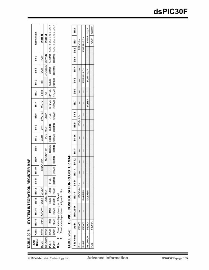
dsPIC30F
TA
BL
E 2
0-7
:S
YS
TE
M I
NT
EG
RA
TIO
N R
EG
IST
ER
MA
P
TA
BL
E 2
0-8
:D
EV
ICE
CO
NF
IGU
RA
TIO
N R
EG
IST
ER
MA
P
SF
R
Nam
eA
dd
r.B
it 1
5B
it 1
4B
it 1
3B
it 1
2B
it 1
1B
it 1
0B
it 9
Bit
8B
it 7
Bit
6B
it 5
Bit
4B
it 3
Bit
2B
it 1
Bit
0R
eset
Sta
te
RC
ON
0740
TR
AP
RIO
PU
WR
BG
ST
LV
DE
NLV
DL<
3:0
>E
XT
RS
WR
SW
DT
EN
WD
TO
Sle
ep
Idle
BO
RP
OR
(No
te 1
)
OS
CC
ON
0742
——
CO
SC
<1:0
>—
—N
OS
C<
1:0
>P
OS
T<
1:0
>LO
CK
—C
F—
LP
OS
CE
NO
SW
EN
(No
te 2
)
PM
D1
0770
T5M
DT
4M
DT
3M
DT
2M
DT
1M
D—
—D
CIM
DI2
CM
DU
2M
DU
1M
DS
PI2
MD
SP
I1M
DC
2M
DC
1M
DA
DC
MD
0000 0000 0000 0000
PM
D2
0772
IC8M
DIC
7M
DIC
6M
DIC
5M
DIC
4M
DIC
3M
DIC
2M
DIC
1M
DO
C8M
DO
C7M
DO
C6M
DO
C5M
DO
C4M
DO
C3M
DO
C2M
DO
C1M
D0000 0000 0000 0000
No
te1:
Reset sta
te d
epends o
n type o
f R
eset.
2:
Reset sta
te d
epends o
n c
onfigura
tion b
its.
Fil
e N
am
eA
dd
r.B
its 2
3-1
6B
it 1
5B
it 1
4B
it 1
3B
it 1
2B
it 1
1B
it 1
0B
it 9
Bit
8B
it 7
Bit
6B
it 5
Bit
4B
it 3
Bit
2B
it 1
Bit
0
FOSC
F80000
—F
SC
KM
<1:0
>—
——
—F
OS
<1:0
>—
——
—F
PR
<3:0
>
FW
DT
F80002
—F
WD
TE
N—
——
——
——
——
FW
PS
A<
1:0
>F
WP
SB
<3:0
>
FB
OR
PO
RF
80004
—M
CLR
EN
——
——
——
—B
OR
EN
—B
OR
V<
1:0
>—
—F
PW
RT
<1:0
>
FG
SF
8000A
——
——
——
——
——
——
——
—G
CP
GW
RP
2004 Microchip Technology Inc. Advance Information DS70083E-page 165

dsPIC30F
NOTES:
DS70083E-page 166 Advance Information 2004 Microchip Technology Inc.
dsPIC30F
21.0 INSTRUCTION SET SUMMARY
The dsPIC30F instruction set adds many
enhancements to the previous PICmicro® instruction
sets, while maintaining an easy migration from
PICmicro instruction sets.
Most instructions are a single program memory word
(24 bits). Only three instructions require two program
memory locations.
Each single word instruction is a 24-bit word divided
into an 8-bit opcode which specifies the instruction
type, and one or more operands which further specify
the operation of the instruction.
The instruction set is highly orthogonal and is grouped
into five basic categories:
• Word or byte-oriented operations
• Bit-oriented operations
• Literal operations
• DSP operations
• Control operations
Table 21-1 shows the general symbols used in
describing the instructions.
The dsPIC30F instruction set summary in Table 21-2
lists all the instructions, along with the status flags
affected by each instruction.
Most word or byte-oriented W register instructions
(including barrel shift instructions) have three
operands:
• The first source operand which is typically a
register ‘Wb’ without any address modifier
• The second source operand which is typically a
register ‘Ws’ with or without an address modifier
• The destination of the result which is typically a
register ‘Wd’ with or without an address modifier
However, word or byte-oriented file register instructions
have two operands:
• The file register specified by the value ‘f’
• The destination, which could either be the file
register ‘f’ or the W0 register, which is denoted as
‘WREG’
Most bit-oriented instructions (including simple rotate/
shift instructions) have two operands:
• The W register (with or without an address
modifier) or file register (specified by the value of
‘Ws’ or ‘f’)
• The bit in the W register or file register
(specified by a literal value or indirectly by the
contents of register ‘Wb’)
The literal instructions that involve data movement may
use some of the following operands:
• A literal value to be loaded into a W register or file
register (specified by the value of ‘k’)
• The W register or file register where the literal
value is to be loaded (specified by ‘Wb’ or ‘f’)
However, literal instructions that involve arithmetic or
logical operations use some of the following operands:
• The first source operand which is a register ‘Wb’
without any address modifier
• The second source operand which is a literal
value
• The destination of the result (only if not the same
as the first source operand) which is typically a
register ‘Wd’ with or without an address modifier
The MAC class of DSP instructions may use some of the
following operands:
• The accumulator (A or B) to be used (required
operand)
• The W registers to be used as the two operands
• The X and Y address space pre-fetch operations
• The X and Y address space pre-fetch destinations
• The accumulator write back destination
The other DSP instructions do not involve any
multiplication, and may include:
• The accumulator to be used (required)
• The source or destination operand (designated as
Wso or Wdo, respectively) with or without an
address modifier
• The amount of shift specified by a W register ‘Wn’
or a literal value
The control instructions may use some of the following
operands:
• A program memory address
• The mode of the table read and table write
instructions
2004 Microchip Technology Inc. Advance Information DS70083E-page 167
dsPIC30F
All instructions are a single word, except for certain
double-word instructions, which were made double-
word instructions so that all the required information is
available in these 48 bits. In the second word, the
8 MSbs are ‘0’s. If this second word is executed as an
instruction (by itself), it will execute as a NOP.
Most single word instructions are executed in a single
instruction cycle, unless a conditional test is true or the
program counter is changed as a result of the instruc-
tion. In these cases, the execution takes two instruction
cycles with the additional instruction cycle(s) executed
as a NOP. Notable exceptions are the BRA (uncondi-
tional/computed branch), indirect CALL/GOTO, all table
reads and writes, and RETURN/RETFIE instructions,
which are single word instructions but take two or three
cycles. Certain instructions that involve skipping over
the subsequent instruction require either two or three
cycles if the skip is performed, depending on whether
the instruction being skipped is a single word or two-
word instruction. Moreover, double-word moves
require two cycles. The double-word instructions
execute in two instruction cycles.
Note: For more details on the instruction set,
refer to the Programmer’s Reference
Manual.
TABLE 21-1: SYMBOLS USED IN OPCODE DESCRIPTIONS
Field Description
#text Means literal defined by “text”
(text) Means “content of text”
[text] Means “the location addressed by text”
Optional field or operation
<n:m> Register bit field
.b Byte mode selection
.d Double-Word mode selection
.S Shadow register select
.w Word mode selection (default)
Acc One of two accumulators A, B
AWB Accumulator write back destination address register ∈ W13, [W13]+=2
bit4 4-bit bit selection field (used in word addressed instructions) ∈ 0...15
C, DC, N, OV, Z MCU status bits: Carry, Digit Carry, Negative, Overflow, Sticky Zero
Expr Absolute address, label or expression (resolved by the linker)
f File register address ∈ 0x0000...0x1FFF
lit1 1-bit unsigned literal ∈ 0,1
lit4 4-bit unsigned literal ∈ 0...15
lit5 5-bit unsigned literal ∈ 0...31
lit8 8-bit unsigned literal ∈ 0...255
lit10 10-bit unsigned literal ∈ 0...255 for Byte mode, 0:1023 for Word mode
lit14 14-bit unsigned literal ∈ 0...16384
lit16 16-bit unsigned literal ∈ 0...65535
lit23 23-bit unsigned literal ∈ 0...8388608; LSB must be 0
None Field does not require an entry, may be blank
OA, OB, SA, SB DSP status bits: AccA Overflow, AccB Overflow, AccA Saturate, AccB Saturate
PC Program Counter
Slit10 10-bit signed literal ∈ -512...511
Slit16 16-bit signed literal ∈ -32768...32767
Slit6 6-bit signed literal ∈ -16...16
DS70083E-page 168 Advance Information 2004 Microchip Technology Inc.
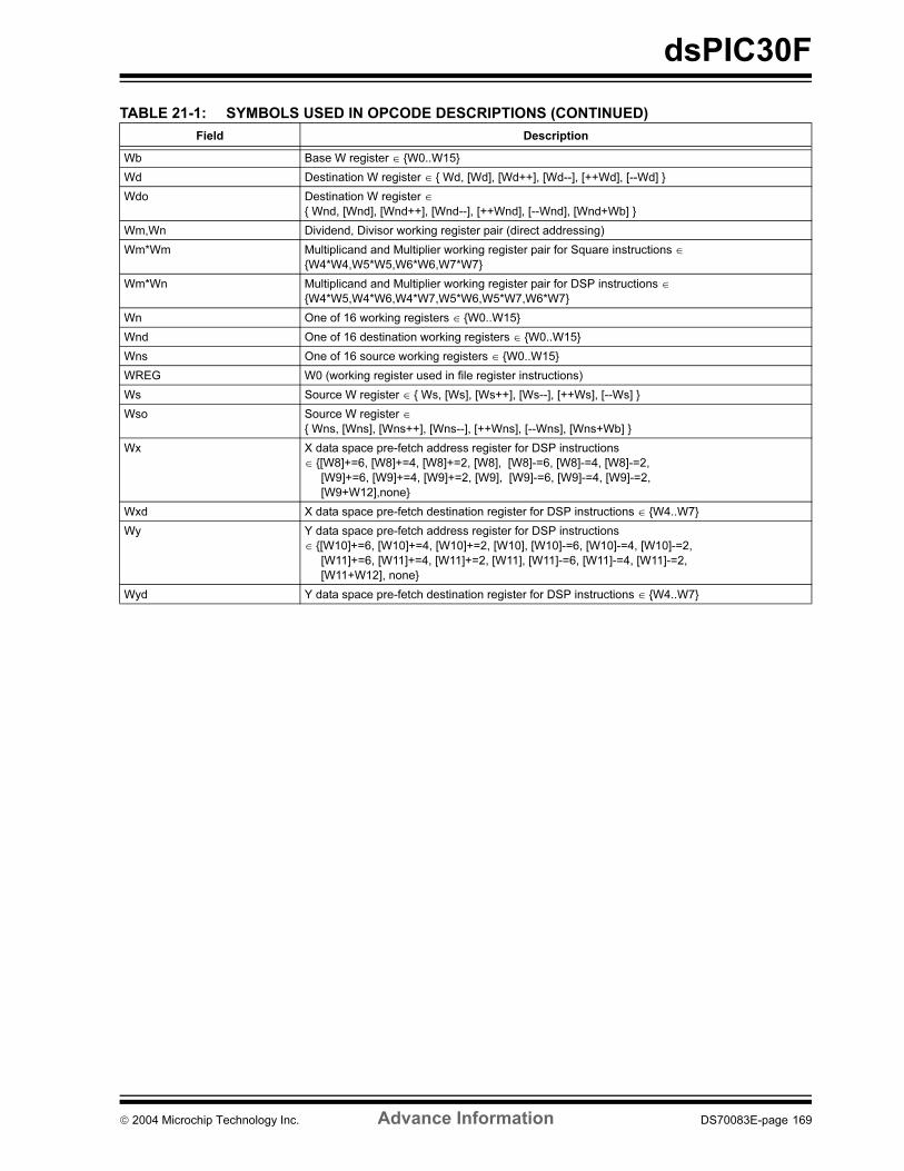
dsPIC30F
Wb Base W register ∈ W0..W15
Wd Destination W register ∈ Wd, [Wd], [Wd++], [Wd--], [++Wd], [--Wd]
Wdo Destination W register ∈
Wnd, [Wnd], [Wnd++], [Wnd--], [++Wnd], [--Wnd], [Wnd+Wb]
Wm,Wn Dividend, Divisor working register pair (direct addressing)
Wm*Wm Multiplicand and Multiplier working register pair for Square instructions ∈
W4*W4,W5*W5,W6*W6,W7*W7
Wm*Wn Multiplicand and Multiplier working register pair for DSP instructions ∈
W4*W5,W4*W6,W4*W7,W5*W6,W5*W7,W6*W7
Wn One of 16 working registers ∈ W0..W15
Wnd One of 16 destination working registers ∈ W0..W15
Wns One of 16 source working registers ∈ W0..W15
WREG W0 (working register used in file register instructions)
Ws Source W register ∈ Ws, [Ws], [Ws++], [Ws--], [++Ws], [--Ws]
Wso Source W register ∈
Wns, [Wns], [Wns++], [Wns--], [++Wns], [--Wns], [Wns+Wb]
Wx X data space pre-fetch address register for DSP instructions
∈ [W8]+=6, [W8]+=4, [W8]+=2, [W8], [W8]-=6, [W8]-=4, [W8]-=2,
[W9]+=6, [W9]+=4, [W9]+=2, [W9], [W9]-=6, [W9]-=4, [W9]-=2,
[W9+W12],none
Wxd X data space pre-fetch destination register for DSP instructions ∈ W4..W7
Wy Y data space pre-fetch address register for DSP instructions
∈ [W10]+=6, [W10]+=4, [W10]+=2, [W10], [W10]-=6, [W10]-=4, [W10]-=2,
[W11]+=6, [W11]+=4, [W11]+=2, [W11], [W11]-=6, [W11]-=4, [W11]-=2,
[W11+W12], none
Wyd Y data space pre-fetch destination register for DSP instructions ∈ W4..W7
TABLE 21-1: SYMBOLS USED IN OPCODE DESCRIPTIONS (CONTINUED)
Field Description
2004 Microchip Technology Inc. Advance Information DS70083E-page 169
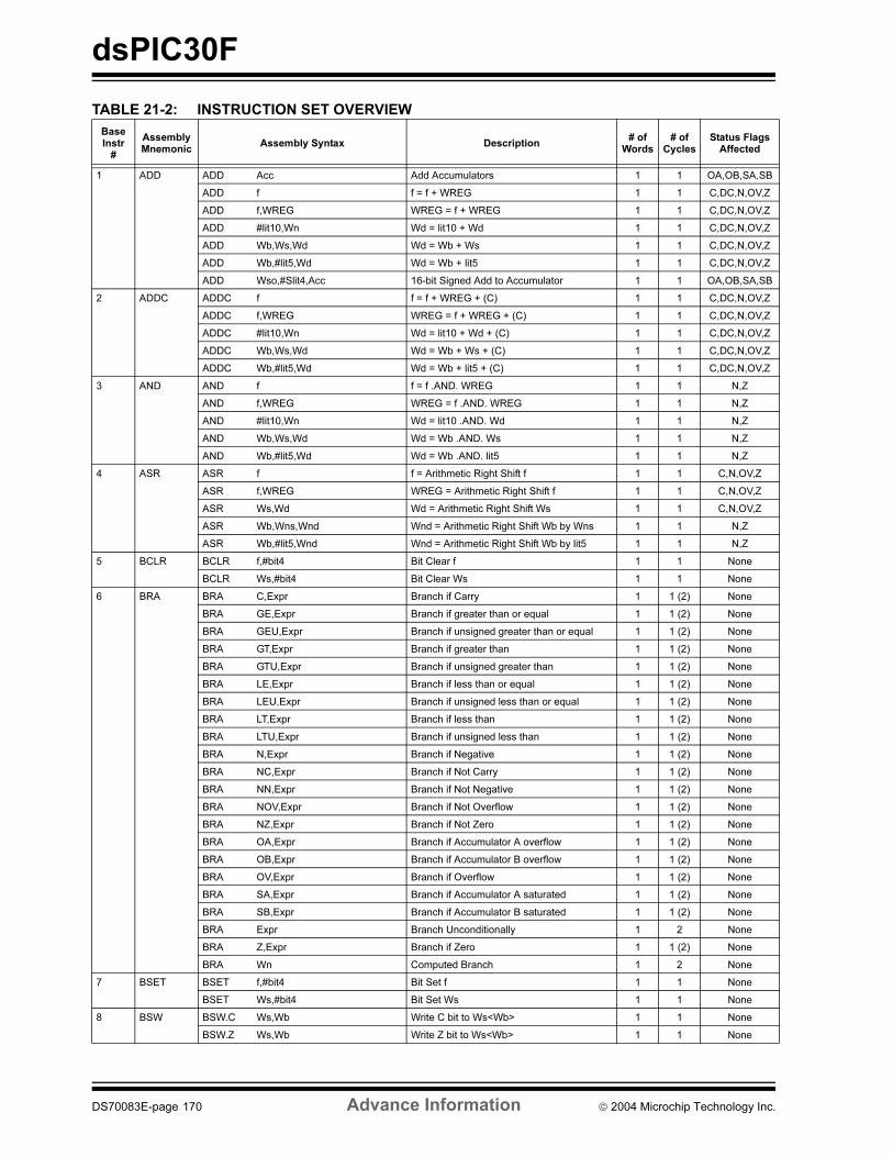
dsPIC30F
TABLE 21-2: INSTRUCTION SET OVERVIEW
BaseInstr
#
AssemblyMnemonic
Assembly Syntax Description# of
Words# of
CyclesStatus Flags
Affected
1 ADD ADD Acc Add Accumulators 1 1 OA,OB,SA,SB
ADD f f = f + WREG 1 1 C,DC,N,OV,Z
ADD f,WREG WREG = f + WREG 1 1 C,DC,N,OV,Z
ADD #lit10,Wn Wd = lit10 + Wd 1 1 C,DC,N,OV,Z
ADD Wb,Ws,Wd Wd = Wb + Ws 1 1 C,DC,N,OV,Z
ADD Wb,#lit5,Wd Wd = Wb + lit5 1 1 C,DC,N,OV,Z
ADD Wso,#Slit4,Acc 16-bit Signed Add to Accumulator 1 1 OA,OB,SA,SB
2 ADDC ADDC f f = f + WREG + (C) 1 1 C,DC,N,OV,Z
ADDC f,WREG WREG = f + WREG + (C) 1 1 C,DC,N,OV,Z
ADDC #lit10,Wn Wd = lit10 + Wd + (C) 1 1 C,DC,N,OV,Z
ADDC Wb,Ws,Wd Wd = Wb + Ws + (C) 1 1 C,DC,N,OV,Z
ADDC Wb,#lit5,Wd Wd = Wb + lit5 + (C) 1 1 C,DC,N,OV,Z
3 AND AND f f = f .AND. WREG 1 1 N,Z
AND f,WREG WREG = f .AND. WREG 1 1 N,Z
AND #lit10,Wn Wd = lit10 .AND. Wd 1 1 N,Z
AND Wb,Ws,Wd Wd = Wb .AND. Ws 1 1 N,Z
AND Wb,#lit5,Wd Wd = Wb .AND. lit5 1 1 N,Z
4 ASR ASR f f = Arithmetic Right Shift f 1 1 C,N,OV,Z
ASR f,WREG WREG = Arithmetic Right Shift f 1 1 C,N,OV,Z
ASR Ws,Wd Wd = Arithmetic Right Shift Ws 1 1 C,N,OV,Z
ASR Wb,Wns,Wnd Wnd = Arithmetic Right Shift Wb by Wns 1 1 N,Z
ASR Wb,#lit5,Wnd Wnd = Arithmetic Right Shift Wb by lit5 1 1 N,Z
5 BCLR BCLR f,#bit4 Bit Clear f 1 1 None
BCLR Ws,#bit4 Bit Clear Ws 1 1 None
6 BRA BRA C,Expr Branch if Carry 1 1 (2) None
BRA GE,Expr Branch if greater than or equal 1 1 (2) None
BRA GEU,Expr Branch if unsigned greater than or equal 1 1 (2) None
BRA GT,Expr Branch if greater than 1 1 (2) None
BRA GTU,Expr Branch if unsigned greater than 1 1 (2) None
BRA LE,Expr Branch if less than or equal 1 1 (2) None
BRA LEU,Expr Branch if unsigned less than or equal 1 1 (2) None
BRA LT,Expr Branch if less than 1 1 (2) None
BRA LTU,Expr Branch if unsigned less than 1 1 (2) None
BRA N,Expr Branch if Negative 1 1 (2) None
BRA NC,Expr Branch if Not Carry 1 1 (2) None
BRA NN,Expr Branch if Not Negative 1 1 (2) None
BRA NOV,Expr Branch if Not Overflow 1 1 (2) None
BRA NZ,Expr Branch if Not Zero 1 1 (2) None
BRA OA,Expr Branch if Accumulator A overflow 1 1 (2) None
BRA OB,Expr Branch if Accumulator B overflow 1 1 (2) None
BRA OV,Expr Branch if Overflow 1 1 (2) None
BRA SA,Expr Branch if Accumulator A saturated 1 1 (2) None
BRA SB,Expr Branch if Accumulator B saturated 1 1 (2) None
BRA Expr Branch Unconditionally 1 2 None
BRA Z,Expr Branch if Zero 1 1 (2) None
BRA Wn Computed Branch 1 2 None
7 BSET BSET f,#bit4 Bit Set f 1 1 None
BSET Ws,#bit4 Bit Set Ws 1 1 None
8 BSW BSW.C Ws,Wb Write C bit to Ws<Wb> 1 1 None
BSW.Z Ws,Wb Write Z bit to Ws<Wb> 1 1 None
DS70083E-page 170 Advance Information 2004 Microchip Technology Inc.
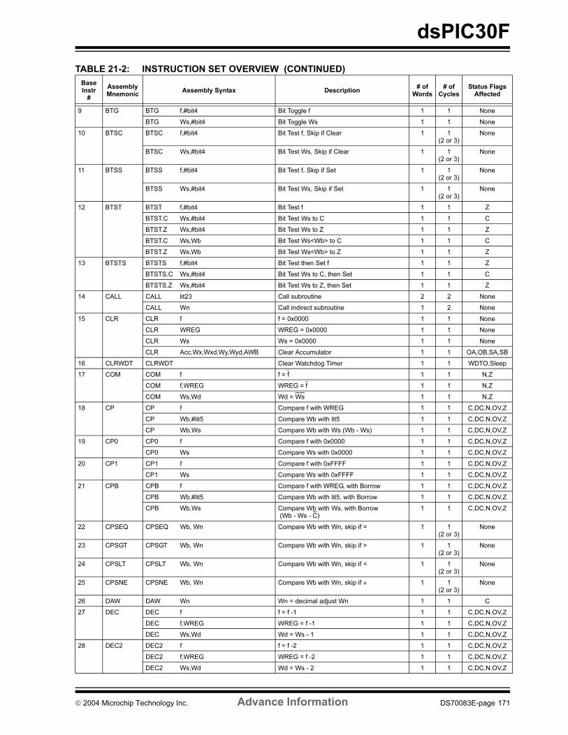
dsPIC30F
9 BTG BTG f,#bit4 Bit Toggle f 1 1 None
BTG Ws,#bit4 Bit Toggle Ws 1 1 None
10 BTSC BTSC f,#bit4 Bit Test f, Skip if Clear 1 1 (2 or 3)
None
BTSC Ws,#bit4 Bit Test Ws, Skip if Clear 1 1 (2 or 3)
None
11 BTSS BTSS f,#bit4 Bit Test f, Skip if Set 1 1 (2 or 3)
None
BTSS Ws,#bit4 Bit Test Ws, Skip if Set 1 1 (2 or 3)
None
12 BTST BTST f,#bit4 Bit Test f 1 1 Z
BTST.C Ws,#bit4 Bit Test Ws to C 1 1 C
BTST.Z Ws,#bit4 Bit Test Ws to Z 1 1 Z
BTST.C Ws,Wb Bit Test Ws<Wb> to C 1 1 C
BTST.Z Ws,Wb Bit Test Ws<Wb> to Z 1 1 Z
13 BTSTS BTSTS f,#bit4 Bit Test then Set f 1 1 Z
BTSTS.C Ws,#bit4 Bit Test Ws to C, then Set 1 1 C
BTSTS.Z Ws,#bit4 Bit Test Ws to Z, then Set 1 1 Z
14 CALL CALL lit23 Call subroutine 2 2 None
CALL Wn Call indirect subroutine 1 2 None
15 CLR CLR f f = 0x0000 1 1 None
CLR WREG WREG = 0x0000 1 1 None
CLR Ws Ws = 0x0000 1 1 None
CLR Acc,Wx,Wxd,Wy,Wyd,AWB Clear Accumulator 1 1 OA,OB,SA,SB
16 CLRWDT CLRWDT Clear Watchdog Timer 1 1 WDTO,Sleep
17 COM COM f f = f 1 1 N,Z
COM f,WREG WREG = f 1 1 N,Z
COM Ws,Wd Wd = Ws 1 1 N,Z
18 CP CP f Compare f with WREG 1 1 C,DC,N,OV,Z
CP Wb,#lit5 Compare Wb with lit5 1 1 C,DC,N,OV,Z
CP Wb,Ws Compare Wb with Ws (Wb - Ws) 1 1 C,DC,N,OV,Z
19 CP0 CP0 f Compare f with 0x0000 1 1 C,DC,N,OV,Z
CP0 Ws Compare Ws with 0x0000 1 1 C,DC,N,OV,Z
20 CP1 CP1 f Compare f with 0xFFFF 1 1 C,DC,N,OV,Z
CP1 Ws Compare Ws with 0xFFFF 1 1 C,DC,N,OV,Z
21 CPB CPB f Compare f with WREG, with Borrow 1 1 C,DC,N,OV,Z
CPB Wb,#lit5 Compare Wb with lit5, with Borrow 1 1 C,DC,N,OV,Z
CPB Wb,Ws Compare Wb with Ws, with Borrow (Wb - Ws - C)
1 1 C,DC,N,OV,Z
22 CPSEQ CPSEQ Wb, Wn Compare Wb with Wn, skip if = 1 1 (2 or 3)
None
23 CPSGT CPSGT Wb, Wn Compare Wb with Wn, skip if > 1 1 (2 or 3)
None
24 CPSLT CPSLT Wb, Wn Compare Wb with Wn, skip if < 1 1 (2 or 3)
None
25 CPSNE CPSNE Wb, Wn Compare Wb with Wn, skip if ≠ 1 1 (2 or 3)
None
26 DAW DAW Wn Wn = decimal adjust Wn 1 1 C
27 DEC DEC f f = f -1 1 1 C,DC,N,OV,Z
DEC f,WREG WREG = f -1 1 1 C,DC,N,OV,Z
DEC Ws,Wd Wd = Ws - 1 1 1 C,DC,N,OV,Z
28 DEC2 DEC2 f f = f -2 1 1 C,DC,N,OV,Z
DEC2 f,WREG WREG = f -2 1 1 C,DC,N,OV,Z
DEC2 Ws,Wd Wd = Ws - 2 1 1 C,DC,N,OV,Z
TABLE 21-2: INSTRUCTION SET OVERVIEW (CONTINUED)
BaseInstr
#
AssemblyMnemonic
Assembly Syntax Description# of
Words# of
CyclesStatus Flags
Affected
2004 Microchip Technology Inc. Advance Information DS70083E-page 171
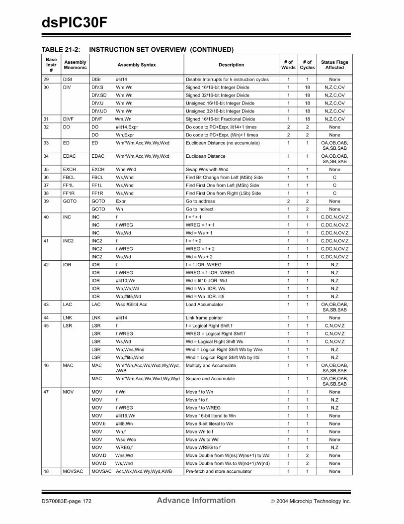
dsPIC30F
29 DISI DISI #lit14 Disable Interrupts for k instruction cycles 1 1 None
30 DIV DIV.S Wm,Wn Signed 16/16-bit Integer Divide 1 18 N,Z,C,OV
DIV.SD Wm,Wn Signed 32/16-bit Integer Divide 1 18 N,Z,C,OV
DIV.U Wm,Wn Unsigned 16/16-bit Integer Divide 1 18 N,Z,C,OV
DIV.UD Wm,Wn Unsigned 32/16-bit Integer Divide 1 18 N,Z,C,OV
31 DIVF DIVF Wm,Wn Signed 16/16-bit Fractional Divide 1 18 N,Z,C,OV
32 DO DO #lit14,Expr Do code to PC+Expr, lit14+1 times 2 2 None
DO Wn,Expr Do code to PC+Expr, (Wn)+1 times 2 2 None
33 ED ED Wm*Wm,Acc,Wx,Wy,Wxd Euclidean Distance (no accumulate) 1 1 OA,OB,OAB,SA,SB,SAB
34 EDAC EDAC Wm*Wm,Acc,Wx,Wy,Wxd Euclidean Distance 1 1 OA,OB,OAB,SA,SB,SAB
35 EXCH EXCH Wns,Wnd Swap Wns with Wnd 1 1 None
36 FBCL FBCL Ws,Wnd Find Bit Change from Left (MSb) Side 1 1 C
37 FF1L FF1L Ws,Wnd Find First One from Left (MSb) Side 1 1 C
38 FF1R FF1R Ws,Wnd Find First One from Right (LSb) Side 1 1 C
39 GOTO GOTO Expr Go to address 2 2 None
GOTO Wn Go to indirect 1 2 None
40 INC INC f f = f + 1 1 1 C,DC,N,OV,Z
INC f,WREG WREG = f + 1 1 1 C,DC,N,OV,Z
INC Ws,Wd Wd = Ws + 1 1 1 C,DC,N,OV,Z
41 INC2 INC2 f f = f + 2 1 1 C,DC,N,OV,Z
INC2 f,WREG WREG = f + 2 1 1 C,DC,N,OV,Z
INC2 Ws,Wd Wd = Ws + 2 1 1 C,DC,N,OV,Z
42 IOR IOR f f = f .IOR. WREG 1 1 N,Z
IOR f,WREG WREG = f .IOR. WREG 1 1 N,Z
IOR #lit10,Wn Wd = lit10 .IOR. Wd 1 1 N,Z
IOR Wb,Ws,Wd Wd = Wb .IOR. Ws 1 1 N,Z
IOR Wb,#lit5,Wd Wd = Wb .IOR. lit5 1 1 N,Z
43 LAC LAC Wso,#Slit4,Acc Load Accumulator 1 1 OA,OB,OAB,SA,SB,SAB
44 LNK LNK #lit14 Link frame pointer 1 1 None
45 LSR LSR f f = Logical Right Shift f 1 1 C,N,OV,Z
LSR f,WREG WREG = Logical Right Shift f 1 1 C,N,OV,Z
LSR Ws,Wd Wd = Logical Right Shift Ws 1 1 C,N,OV,Z
LSR Wb,Wns,Wnd Wnd = Logical Right Shift Wb by Wns 1 1 N,Z
LSR Wb,#lit5,Wnd Wnd = Logical Right Shift Wb by lit5 1 1 N,Z
46 MAC MAC Wm*Wn,Acc,Wx,Wxd,Wy,Wyd,AWB
Multiply and Accumulate 1 1 OA,OB,OAB,SA,SB,SAB
MAC Wm*Wm,Acc,Wx,Wxd,Wy,Wyd Square and Accumulate 1 1 OA,OB,OAB,SA,SB,SAB
47 MOV MOV f,Wn Move f to Wn 1 1 None
MOV f Move f to f 1 1 N,Z
MOV f,WREG Move f to WREG 1 1 N,Z
MOV #lit16,Wn Move 16-bit literal to Wn 1 1 None
MOV.b #lit8,Wn Move 8-bit literal to Wn 1 1 None
MOV Wn,f Move Wn to f 1 1 None
MOV Wso,Wdo Move Ws to Wd 1 1 None
MOV WREG,f Move WREG to f 1 1 N,Z
MOV.D Wns,Wd Move Double from W(ns):W(ns+1) to Wd 1 2 None
MOV.D Ws,Wnd Move Double from Ws to W(nd+1):W(nd) 1 2 None
48 MOVSAC MOVSAC Acc,Wx,Wxd,Wy,Wyd,AWB Pre-fetch and store accumulator 1 1 None
TABLE 21-2: INSTRUCTION SET OVERVIEW (CONTINUED)
BaseInstr
#
AssemblyMnemonic
Assembly Syntax Description# of
Words# of
CyclesStatus Flags
Affected
DS70083E-page 172 Advance Information 2004 Microchip Technology Inc.
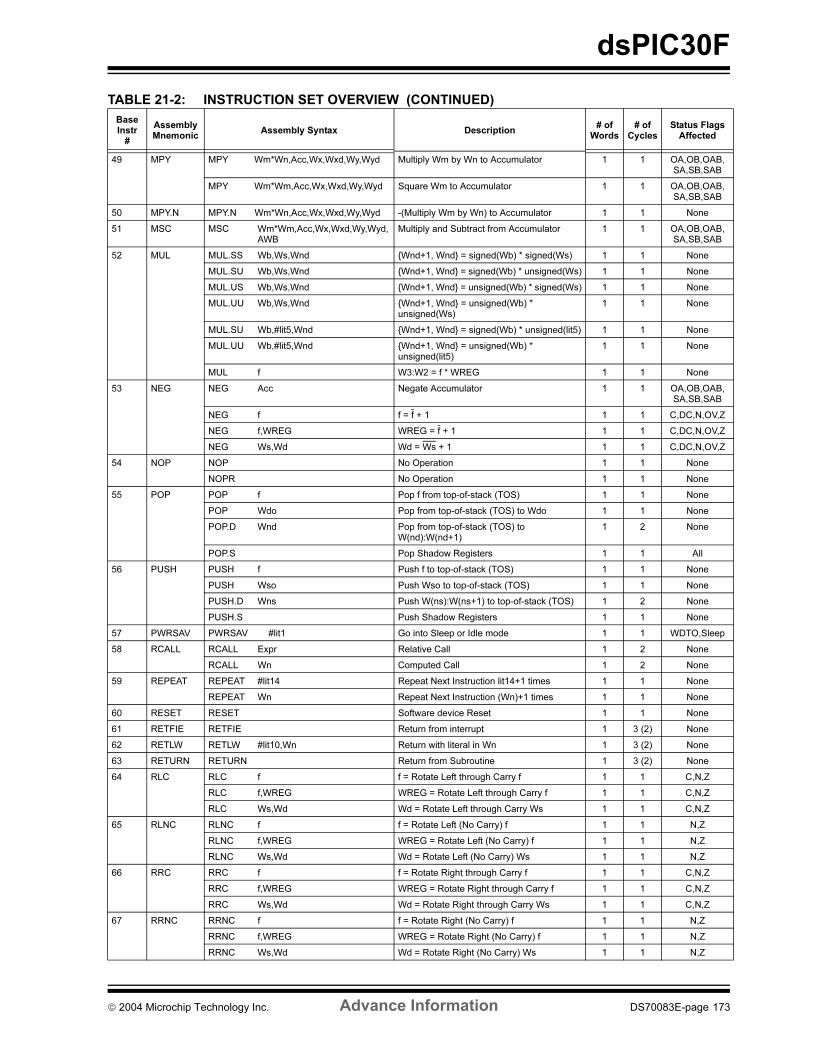
dsPIC30F
49 MPY MPY Wm*Wn,Acc,Wx,Wxd,Wy,Wyd Multiply Wm by Wn to Accumulator 1 1 OA,OB,OAB,SA,SB,SAB
MPY Wm*Wm,Acc,Wx,Wxd,Wy,Wyd Square Wm to Accumulator 1 1 OA,OB,OAB,SA,SB,SAB
50 MPY.N MPY.N Wm*Wn,Acc,Wx,Wxd,Wy,Wyd -(Multiply Wm by Wn) to Accumulator 1 1 None
51 MSC MSC Wm*Wm,Acc,Wx,Wxd,Wy,Wyd,AWB
Multiply and Subtract from Accumulator 1 1 OA,OB,OAB,SA,SB,SAB
52 MUL MUL.SS Wb,Ws,Wnd Wnd+1, Wnd = signed(Wb) * signed(Ws) 1 1 None
MUL.SU Wb,Ws,Wnd Wnd+1, Wnd = signed(Wb) * unsigned(Ws) 1 1 None
MUL.US Wb,Ws,Wnd Wnd+1, Wnd = unsigned(Wb) * signed(Ws) 1 1 None
MUL.UU Wb,Ws,Wnd Wnd+1, Wnd = unsigned(Wb) * unsigned(Ws)
1 1 None
MUL.SU Wb,#lit5,Wnd Wnd+1, Wnd = signed(Wb) * unsigned(lit5) 1 1 None
MUL.UU Wb,#lit5,Wnd Wnd+1, Wnd = unsigned(Wb) * unsigned(lit5)
1 1 None
MUL f W3:W2 = f * WREG 1 1 None
53 NEG NEG Acc Negate Accumulator 1 1 OA,OB,OAB,SA,SB,SAB
NEG f f = f + 1 1 1 C,DC,N,OV,Z
NEG f,WREG WREG = f + 1 1 1 C,DC,N,OV,Z
NEG Ws,Wd Wd = Ws + 1 1 1 C,DC,N,OV,Z
54 NOP NOP No Operation 1 1 None
NOPR No Operation 1 1 None
55 POP POP f Pop f from top-of-stack (TOS) 1 1 None
POP Wdo Pop from top-of-stack (TOS) to Wdo 1 1 None
POP.D Wnd Pop from top-of-stack (TOS) to W(nd):W(nd+1)
1 2 None
POP.S Pop Shadow Registers 1 1 All
56 PUSH PUSH f Push f to top-of-stack (TOS) 1 1 None
PUSH Wso Push Wso to top-of-stack (TOS) 1 1 None
PUSH.D Wns Push W(ns):W(ns+1) to top-of-stack (TOS) 1 2 None
PUSH.S Push Shadow Registers 1 1 None
57 PWRSAV PWRSAV #lit1 Go into Sleep or Idle mode 1 1 WDTO,Sleep
58 RCALL RCALL Expr Relative Call 1 2 None
RCALL Wn Computed Call 1 2 None
59 REPEAT REPEAT #lit14 Repeat Next Instruction lit14+1 times 1 1 None
REPEAT Wn Repeat Next Instruction (Wn)+1 times 1 1 None
60 RESET RESET Software device Reset 1 1 None
61 RETFIE RETFIE Return from interrupt 1 3 (2) None
62 RETLW RETLW #lit10,Wn Return with literal in Wn 1 3 (2) None
63 RETURN RETURN Return from Subroutine 1 3 (2) None
64 RLC RLC f f = Rotate Left through Carry f 1 1 C,N,Z
RLC f,WREG WREG = Rotate Left through Carry f 1 1 C,N,Z
RLC Ws,Wd Wd = Rotate Left through Carry Ws 1 1 C,N,Z
65 RLNC RLNC f f = Rotate Left (No Carry) f 1 1 N,Z
RLNC f,WREG WREG = Rotate Left (No Carry) f 1 1 N,Z
RLNC Ws,Wd Wd = Rotate Left (No Carry) Ws 1 1 N,Z
66 RRC RRC f f = Rotate Right through Carry f 1 1 C,N,Z
RRC f,WREG WREG = Rotate Right through Carry f 1 1 C,N,Z
RRC Ws,Wd Wd = Rotate Right through Carry Ws 1 1 C,N,Z
67 RRNC RRNC f f = Rotate Right (No Carry) f 1 1 N,Z
RRNC f,WREG WREG = Rotate Right (No Carry) f 1 1 N,Z
RRNC Ws,Wd Wd = Rotate Right (No Carry) Ws 1 1 N,Z
TABLE 21-2: INSTRUCTION SET OVERVIEW (CONTINUED)
BaseInstr
#
AssemblyMnemonic
Assembly Syntax Description# of
Words# of
CyclesStatus Flags
Affected
2004 Microchip Technology Inc. Advance Information DS70083E-page 173
dsPIC30F
68 SAC SAC Acc,#Slit4,Wdo Store Accumulator 1 1 None
SAC.R Acc,#Slit4,Wdo Store Rounded Accumulator 1 1 None
69 SE SE Ws,Wnd Wnd = sign-extended Ws 1 1 C,N,Z
70 SETM SETM f f = 0xFFFF 1 1 None
SETM WREG WREG = 0xFFFF 1 1 None
SETM Ws Ws = 0xFFFF 1 1 None
71 SFTAC SFTAC Acc,Wn Arithmetic Shift Accumulator by (Wn) 1 1 OA,OB,OAB,SA,SB,SAB
SFTAC Acc,#Slit6 Arithmetic Shift Accumulator by Slit6 1 1 OA,OB,OAB,SA,SB,SAB
72 SL SL f f = Left Shift f 1 1 C,N,OV,Z
SL f,WREG WREG = Left Shift f 1 1 C,N,OV,Z
SL Ws,Wd Wd = Left Shift Ws 1 1 C,N,OV,Z
SL Wb,Wns,Wnd Wnd = Left Shift Wb by Wns 1 1 N,Z
SL Wb,#lit5,Wnd Wnd = Left Shift Wb by lit5 1 1 N,Z
73 SUB SUB Acc Subtract Accumulators 1 1 OA,OB,OAB,SA,SB,SAB
SUB f f = f - WREG 1 1 C,DC,N,OV,Z
SUB f,WREG WREG = f - WREG 1 1 C,DC,N,OV,Z
SUB #lit10,Wn Wn = Wn - lit10 1 1 C,DC,N,OV,Z
SUB Wb,Ws,Wd Wd = Wb - Ws 1 1 C,DC,N,OV,Z
SUB Wb,#lit5,Wd Wd = Wb - lit5 1 1 C,DC,N,OV,Z
74 SUBB SUBB f f = f - WREG - (C) 1 1 C,DC,N,OV,Z
SUBB f,WREG WREG = f - WREG - (C) 1 1 C,DC,N,OV,Z
SUBB #lit10,Wn Wn = Wn - lit10 - (C) 1 1 C,DC,N,OV,Z
SUBB Wb,Ws,Wd Wd = Wb - Ws - (C) 1 1 C,DC,N,OV,Z
SUBB Wb,#lit5,Wd Wd = Wb - lit5 - (C) 1 1 C,DC,N,OV,Z
75 SUBR SUBR f f = WREG - f 1 1 C,DC,N,OV,Z
SUBR f,WREG WREG = WREG - f 1 1 C,DC,N,OV,Z
SUBR Wb,Ws,Wd Wd = Ws - Wb 1 1 C,DC,N,OV,Z
SUBR Wb,#lit5,Wd Wd = lit5 - Wb 1 1 C,DC,N,OV,Z
76 SUBBR SUBBR f f = WREG - f - (C) 1 1 C,DC,N,OV,Z
SUBBR f,WREG WREG = WREG -f - (C) 1 1 C,DC,N,OV,Z
SUBBR Wb,Ws,Wd Wd = Ws - Wb - (C) 1 1 C,DC,N,OV,Z
SUBBR Wb,#lit5,Wd Wd = lit5 - Wb - (C) 1 1 C,DC,N,OV,Z
77 SWAP SWAP.b Wn Wn = nibble swap Wn 1 1 None
SWAP Wn Wn = byte swap Wn 1 1 None
78 TBLRDH TBLRDH Ws,Wd Read Prog<23:16> to Wd<7:0> 1 2 None
79 TBLRDL TBLRDL Ws,Wd Read Prog<15:0> to Wd 1 2 None
80 TBLWTH TBLWTH Ws,Wd Write Ws<7:0> to Prog<23:16> 1 2 None
81 TBLWTL TBLWTL Ws,Wd Write Ws to Prog<15:0> 1 2 None
82 ULNK ULNK Unlink frame pointer 1 1 None
83 XOR XOR f f = f .XOR. WREG 1 1 N,Z
XOR f,WREG WREG = f .XOR. WREG 1 1 N,Z
XOR #lit10,Wn Wd = lit10 .XOR. Wd 1 1 N,Z
XOR Wb,Ws,Wd Wd = Wb .XOR. Ws 1 1 N,Z
XOR Wb,#lit5,Wd Wd = Wb .XOR. lit5 1 1 N,Z
84 ZE ZE Ws,Wnd Wnd = Zero-extend Ws 1 1 C,Z,N
TABLE 21-2: INSTRUCTION SET OVERVIEW (CONTINUED)
BaseInstr
#
AssemblyMnemonic
Assembly Syntax Description# of
Words# of
CyclesStatus Flags
Affected
DS70083E-page 174 Advance Information 2004 Microchip Technology Inc.
dsPIC30F
22.0 DEVELOPMENT SUPPORT
The PICmicro® microcontrollers are supported with a
full range of hardware and software development tools:
• Integrated Development Environment
- MPLAB® IDE Software
• Assemblers/Compilers/Linkers
- MPASM™ Assembler
- MPLAB C17 and MPLAB C18 C Compilers
- MPLINK™ Object Linker/
MPLIB™ Object Librarian
- MPLAB C30 C Compiler
- MPLAB ASM30 Assembler/Linker/Library
• Simulators
- MPLAB SIM Software Simulator
- MPLAB dsPIC30 Software Simulator
• Emulators
- MPLAB ICE 2000 In-Circuit Emulator
- MPLAB ICE 4000 In-Circuit Emulator
• In-Circuit Debugger
- MPLAB ICD 2
• Device Programmers
- PRO MATE® II Universal Device Programmer
- PICSTART® Plus Development Programmer
• Low Cost Demonstration Boards
- PICDEM™ 1 Demonstration Board
- PICDEM.net™ Demonstration Board
- PICDEM 2 Plus Demonstration Board
- PICDEM 3 Demonstration Board
- PICDEM 4 Demonstration Board
- PICDEM 17 Demonstration Board
- PICDEM 18R Demonstration Board
- PICDEM LIN Demonstration Board
- PICDEM USB Demonstration Board
• Evaluation Kits
- KEELOQ®
- PICDEM MSC
- microID®
- CAN
- PowerSmart®
- Analog
22.1 MPLAB Integrated Development
Environment Software
The MPLAB IDE software brings an ease of software
development previously unseen in the 8/16-bit micro-
controller market. The MPLAB IDE is a Windows®
based application that contains:
• An interface to debugging tools
- simulator
- programmer (sold separately)
- emulator (sold separately)
- in-circuit debugger (sold separately)
• A full-featured editor with color coded context
• A multiple project manager
• Customizable data windows with direct edit of
contents
• High level source code debugging
• Mouse over variable inspection
• Extensive on-line help
The MPLAB IDE allows you to:
• Edit your source files (either assembly or C)
• One touch assemble (or compile) and download
to PICmicro emulator and simulator tools
(automatically updates all project information)
• Debug using:
- source files (assembly or C)
- absolute listing file (mixed assembly and C)
- machine code
MPLAB IDE supports multiple debugging tools in a
single development paradigm, from the cost effective
simulators, through low cost in-circuit debuggers, to
full-featured emulators. This eliminates the learning
curve when upgrading to tools with increasing flexibility
and power.
22.2 MPASM Assembler
The MPASM assembler is a full-featured, universal
macro assembler for all PICmicro MCUs.
The MPASM assembler generates relocatable object
files for the MPLINK object linker, Intel® standard HEX
files, MAP files to detail memory usage and symbol ref-
erence, absolute LST files that contain source lines and
generated machine code and COFF files for
debugging.
The MPASM assembler features include:
• Integration into MPLAB IDE projects
• User defined macros to streamline assembly code
• Conditional assembly for multi-purpose source
files
• Directives that allow complete control over the
assembly process
2004 Microchip Technology Inc. Advance Information DS70083E-page 175
dsPIC30F
22.3 MPLAB C17 and MPLAB C18
C Compilers
The MPLAB C17 and MPLAB C18 Code Development
Systems are complete ANSI C compilers for
Microchip’s PIC17CXXX and PIC18CXXX family of
microcontrollers. These compilers provide powerful
integration capabilities, superior code optimization and
ease of use not found with other compilers.
For easy source level debugging, the compilers provide
symbol information that is optimized to the MPLAB IDE
debugger.
22.4 MPLINK Object Linker/
MPLIB Object Librarian
The MPLINK object linker combines relocatable
objects created by the MPASM assembler and the
MPLAB C17 and MPLAB C18 C compilers. It can link
relocatable objects from pre-compiled libraries, using
directives from a linker script.
The MPLIB object librarian manages the creation and
modification of library files of pre-compiled code. When
a routine from a library is called from a source file, only
the modules that contain that routine will be linked in
with the application. This allows large libraries to be
used efficiently in many different applications.
The object linker/library features include:
• Efficient linking of single libraries instead of many
smaller files
• Enhanced code maintainability by grouping
related modules together
• Flexible creation of libraries with easy module
listing, replacement, deletion and extraction
22.5 MPLAB C30 C Compiler
The MPLAB C30 C compiler is a full-featured, ANSI
compliant, optimizing compiler that translates standard
ANSI C programs into dsPIC30F assembly language
source. The compiler also supports many command-
line options and language extensions to take full
advantage of the dsPIC30F device hardware capabili-
ties, and afford fine control of the compiler code
generator.
MPLAB C30 is distributed with a complete ANSI C
standard library. All library functions have been vali-
dated and conform to the ANSI C library standard. The
library includes functions for string manipulation,
dynamic memory allocation, data conversion, time-
keeping, and math functions (trigonometric, exponen-
tial and hyperbolic). The compiler provides symbolic
information for high level source debugging with the
MPLAB IDE.
22.6 MPLAB ASM30 Assembler, Linker,
and Librarian
MPLAB ASM30 assembler produces relocatable
machine code from symbolic assembly language for
dsPIC30F devices. MPLAB C30 compiler uses the
assembler to produce it’s object file. The assembler
generates relocatable object files that can then be
archived or linked with other relocatable object files and
archives to create an executable file. Notable features
of the assembler include:
• Support for the entire dsPIC30F instruction set
• Support for fixed-point and floating-point data
• Command line interface
• Rich directive set
• Flexible macro language
• MPLAB IDE compatibility
22.7 MPLAB SIM Software Simulator
The MPLAB SIM software simulator allows code devel-
opment in a PC hosted environment by simulating the
PICmicro series microcontrollers on an instruction
level. On any given instruction, the data areas can be
examined or modified and stimuli can be applied from
a file, or user defined key press, to any pin. The execu-
tion can be performed in Single-Step, Execute Until
Break, or Trace mode.
The MPLAB SIM simulator fully supports symbolic
debugging using the MPLAB C17 and MPLAB C18
C Compilers, as well as the MPASM assembler. The
software simulator offers the flexibility to develop and
debug code outside of the laboratory environment,
making it an excellent, economical software
development tool.
22.8 MPLAB SIM30 Software Simulator
The MPLAB SIM30 software simulator allows code
development in a PC hosted environment by simulating
the dsPIC30F series microcontrollers on an instruction
level. On any given instruction, the data areas can be
examined or modified and stimuli can be applied from
a file, or user defined key press, to any of the pins.
The MPLAB SIM30 simulator fully supports symbolic
debugging using the MPLAB C30 C Compiler and
MPLAB ASM30 assembler. The simulator runs in either
a Command Line mode for automated tasks, or from
MPLAB IDE. This high speed simulator is designed to
debug, analyze and optimize time intensive DSP
routines.
DS70083E-page 176 Advance Information 2004 Microchip Technology Inc.
dsPIC30F
22.9 MPLAB ICE 2000
High Performance Universal
In-Circuit Emulator
The MPLAB ICE 2000 universal in-circuit emulator is
intended to provide the product development engineer
with a complete microcontroller design tool set for
PICmicro microcontrollers. Software control of the
MPLAB ICE 2000 in-circuit emulator is advanced by
the MPLAB Integrated Development Environment,
which allows editing, building, downloading and source
debugging from a single environment.
The MPLAB ICE 2000 is a full-featured emulator sys-
tem with enhanced trace, trigger and data monitoring
features. Interchangeable processor modules allow the
system to be easily reconfigured for emulation of differ-
ent processors. The universal architecture of the
MPLAB ICE in-circuit emulator allows expansion to
support new PICmicro microcontrollers.
The MPLAB ICE 2000 in-circuit emulator system has
been designed as a real-time emulation system with
advanced features that are typically found on more
expensive development tools. The PC platform and
Microsoft® Windows 32-bit operating system were
chosen to best make these features available in a
simple, unified application.
22.10 MPLAB ICE 4000
High Performance Universal
In-Circuit Emulator
The MPLAB ICE 4000 universal in-circuit emulator is
intended to provide the product development engineer
with a complete microcontroller design tool set for high-
end PICmicro microcontrollers. Software control of the
MPLAB ICE in-circuit emulator is provided by the
MPLAB Integrated Development Environment, which
allows editing, building, downloading and source
debugging from a single environment.
The MPLAB ICD 4000 is a premium emulator system,
providing the features of MPLAB ICE 2000, but with
increased emulation memory and high speed perfor-
mance for dsPIC30F and PIC18XXXX devices. Its
advanced emulator features include complex triggering
and timing, up to 2 Mb of emulation memory, and the
ability to view variables in real-time.
The MPLAB ICE 4000 in-circuit emulator system has
been designed as a real-time emulation system with
advanced features that are typically found on more
expensive development tools. The PC platform and
Microsoft Windows 32-bit operating system were cho-
sen to best make these features available in a simple,
unified application.
22.11 MPLAB ICD 2 In-Circuit Debugger
Microchip’s In-Circuit Debugger, MPLAB ICD 2, is a
powerful, low cost, run-time development tool,
connecting to the host PC via an RS-232 or high speed
USB interface. This tool is based on the Flash
PICmicro MCUs and can be used to develop for these
and other PICmicro microcontrollers. The MPLAB
ICD 2 utilizes the in-circuit debugging capability built
into the Flash devices. This feature, along with
Microchip’s In-Circuit Serial Programming™ (ICSPTM)
protocol, offers cost effective in-circuit Flash debugging
from the graphical user interface of the MPLAB Inte-
grated Development Environment. This enables a
designer to develop and debug source code by setting
breakpoints, single-stepping and watching variables,
CPU status and peripheral registers. Running at full
speed enables testing hardware and applications in
real-time. MPLAB ICD 2 also serves as a development
programmer for selected PICmicro devices.
22.12 PRO MATE II Universal Device
Programmer
The PRO MATE II is a universal, CE compliant device
programmer with programmable voltage verification at
VDDMIN and VDDMAX for maximum reliability. It features
an LCD display for instructions and error messages
and a modular detachable socket assembly to support
various package types. In Stand-Alone mode, the
PRO MATE II device programmer can read, verify, and
program PICmicro devices without a PC connection. It
can also set code protection in this mode.
22.13 PICSTART Plus Development
Programmer
The PICSTART Plus development programmer is an
easy-to-use, low cost, prototype programmer. It con-
nects to the PC via a COM (RS-232) port. MPLAB
Integrated Development Environment software makes
using the programmer simple and efficient. The
PICSTART Plus development programmer supports
most PICmicro devices up to 40 pins. Larger pin count
devices, such as the PIC16C92X and PIC17C76X,
may be supported with an adapter socket. The
PICSTART Plus development programmer is CE
compliant.
2004 Microchip Technology Inc. Advance Information DS70083E-page 177
dsPIC30F
22.14 PICDEM 1 PICmicro
Demonstration Board
The PICDEM 1 demonstration board demonstrates the
capabilities of the PIC16C5X (PIC16C54 to
PIC16C58A), PIC16C61, PIC16C62X, PIC16C71,
PIC16C8X, PIC17C42, PIC17C43 and PIC17C44. All
necessary hardware and software is included to run
basic demo programs. The sample microcontrollers
provided with the PICDEM 1 demonstration board can
be programmed with a PRO MATE II device program-
mer, or a PICSTART Plus development programmer.
The PICDEM 1 demonstration board can be connected
to the MPLAB ICE in-circuit emulator for testing. A pro-
totype area extends the circuitry for additional applica-
tion components. Features include an RS-232
interface, a potentiometer for simulated analog input,
push button switches and eight LEDs.
22.15 PICDEM.net Internet/Ethernet
Demonstration Board
The PICDEM.net demonstration board is an Internet/
Ethernet demonstration board using the PIC18F452
microcontroller and TCP/IP firmware. The board
supports any 40-pin DIP device that conforms to the
standard pinout used by the PIC16F877 or
PIC18C452. This kit features a user friendly TCP/IP
stack, web server with HTML, a 24L256 Serial
EEPROM for Xmodem download to web pages into
Serial EEPROM, ICSP/MPLAB ICD 2 interface con-
nector, an Ethernet interface, RS-232 interface, and a
16 x 2 LCD display. Also included is the book and
CD-ROM “TCP/IP Lean, Web Servers for Embedded
Systems,” by Jeremy Bentham
22.16 PICDEM 2 Plus
Demonstration Board
The PICDEM 2 Plus demonstration board supports
many 18-, 28-, and 40-pin microcontrollers, including
PIC16F87X and PIC18FXX2 devices. All the neces-
sary hardware and software is included to run the dem-
onstration programs. The sample microcontrollers
provided with the PICDEM 2 demonstration board can
be programmed with a PRO MATE II device program-
mer, PICSTART Plus development programmer, or
MPLAB ICD 2 with a Universal Programmer Adapter.
The MPLAB ICD 2 and MPLAB ICE in-circuit emulators
may also be used with the PICDEM 2 demonstration
board to test firmware. A prototype area extends the
circuitry for additional application components. Some
of the features include an RS-232 interface, a 2 x 16
LCD display, a piezo speaker, an on-board temperature
sensor, four LEDs, and sample PIC18F452 and
PIC16F877 Flash microcontrollers.
22.17 PICDEM 3 PIC16C92X
Demonstration Board
The PICDEM 3 demonstration board supports the
PIC16C923 and PIC16C924 in the PLCC package. All
the necessary hardware and software is included to run
the demonstration programs.
22.18 PICDEM 4 8/14/18-Pin
Demonstration Board
The PICDEM 4 can be used to demonstrate the capa-
bilities of the 8-, 14-, and 18-pin PIC16XXXX and
PIC18XXXX MCUs, including the PIC16F818/819,
PIC16F87/88, PIC16F62XA and the PIC18F1320 fam-
ily of microcontrollers. PICDEM 4 is intended to show-
case the many features of these low pin count parts,
including LIN and Motor Control using ECCP. Special
provisions are made for low power operation with the
super capacitor circuit, and jumpers allow on-board
hardware to be disabled to eliminate current draw in
this mode. Included on the demo board are provisions
for Crystal, RC or Canned Oscillator modes, a five volt
regulator for use with a nine volt wall adapter or battery,
DB-9 RS-232 interface, ICD connector for program-
ming via ICSP and development with MPLAB ICD 2,
2x16 liquid crystal display, PCB footprints for H-Bridge
motor driver, LIN transceiver and EEPROM. Also
included are: header for expansion, eight LEDs, four
potentiometers, three push buttons and a prototyping
area. Included with the kit is a PIC16F627A and a
PIC18F1320. Tutorial firmware is included along with
the User’s Guide.
22.19 PICDEM 17 Demonstration Board
The PICDEM 17 demonstration board is an evaluation
board that demonstrates the capabilities of several
Microchip microcontrollers, including PIC17C752,
PIC17C756A, PIC17C762 and PIC17C766. A pro-
grammed sample is included. The PRO MATE II device
programmer, or the PICSTART Plus development pro-
grammer, can be used to reprogram the device for user
tailored application development. The PICDEM 17
demonstration board supports program download and
execution from external on-board Flash memory. A
generous prototype area is available for user hardware
expansion.
DS70083E-page 178 Advance Information 2004 Microchip Technology Inc.
dsPIC30F
22.20 PICDEM 18R PIC18C601/801
Demonstration Board
The PICDEM 18R demonstration board serves to assist
development of the PIC18C601/801 family of Microchip
microcontrollers. It provides hardware implementation
of both 8-bit Multiplexed/De-multiplexed and 16-bit
Memory modes. The board includes 2 Mb external
Flash memory and 128 Kb SRAM memory, as well as
serial EEPROM, allowing access to the wide range of
memory types supported by the PIC18C601/801.
22.21 PICDEM LIN PIC16C43X
Demonstration Board
The powerful LIN hardware and software kit includes a
series of boards and three PICmicro microcontrollers.
The small footprint PIC16C432 and PIC16C433 are
used as slaves in the LIN communication and feature
on-board LIN transceivers. A PIC16F874 Flash micro-
controller serves as the master. All three microcontrol-
lers are programmed with firmware to provide LIN bus
communication.
22.22 PICkit™ 1 Flash Starter Kit
A complete "development system in a box", the PICkit
Flash Starter Kit includes a convenient multi-section
board for programming, evaluation, and development
of 8/14-pin Flash PIC® microcontrollers. Powered via
USB, the board operates under a simple Windows GUI.
The PICkit 1 Starter Kit includes the user's guide (on
CD ROM), PICkit 1 tutorial software and code for vari-
ous applications. Also included are MPLAB® IDE (Inte-
grated Development Environment) software, software
and hardware "Tips 'n Tricks for 8-pin Flash PIC®
Microcontrollers" Handbook and a USB Interface
Cable. Supports all current 8/14-pin Flash PIC
microcontrollers, as well as many future planned
devices.
22.23 PICDEM USB PIC16C7X5
Demonstration Board
The PICDEM USB Demonstration Board shows off the
capabilities of the PIC16C745 and PIC16C765 USB
microcontrollers. This board provides the basis for
future USB products.
22.24 Evaluation and
Programming Tools
In addition to the PICDEM series of circuits, Microchip
has a line of evaluation kits and demonstration software
for these products.
• KEELOQ evaluation and programming tools for
Microchip’s HCS Secure Data Products
• CAN developers kit for automotive network
applications
• Analog design boards and filter design software
• PowerSmart battery charging evaluation/
calibration kits
• IrDA® development kit
• microID development and rfLab™ development
software
• SEEVAL® designer kit for memory evaluation and
endurance calculations
• PICDEM MSC demo boards for Switching mode
power supply, high power IR driver, delta sigma
ADC, and flow rate sensor
Check the Microchip web page and the latest Product
Line Card for the complete list of demonstration and
evaluation kits.
2004 Microchip Technology Inc. Advance Information DS70083E-page 179

dsPIC30F
NOTES:
DS70083E-page 180 Advance Information 2004 Microchip Technology Inc.
dsPIC30F
23.0 ELECTRICAL CHARACTERISTICS
This section provides an overview of dsPIC30F electrical characteristics. Additional information will be provided in future
revisions of this document as it becomes available.
For detailed information about the dsPIC30F architecture and core, refer to dsPIC30F Family Reference Manual
(DS70046).
Absolute maximum ratings for the dsPIC30F family are listed below. Exposure to these maximum rating conditions for
extended periods may affect device reliability. Functional operation of the device at these or any other conditions above
the parameters indicated in the operation listings of this specification is not implied.
Absolute Maximum Ratings(†)
Ambient temperature under bias............................................................................................................ .-40°C to +125°C
Storage temperature .............................................................................................................................. -65°C to +150°C
Voltage on any pin with respect to VSS (except VDD and MCLR) ................................................... -0.3V to (VDD + 0.3V)
Voltage on VDD with respect to VSS ......................................................................................................... -0.3V to +5.5V
Voltage on MCLR with respect to VSS (Note 1) ......................................................................................... 0V to +13.25V
Total power dissipation (Note 2) ...............................................................................................................................1.0W
Maximum current out of VSS pin ...........................................................................................................................300 mA
Maximum current into VDD pin ..............................................................................................................................250 mA
Input clamp current, IIK (VI < 0 or VI > VDD) ..........................................................................................................±20 mA
Output clamp current, IOK (VO < 0 or VO > VDD) ...................................................................................................±20 mA
Maximum output current sunk by any I/O pin..........................................................................................................25 mA
Maximum output current sourced by any I/O pin ....................................................................................................25 mA
Maximum current sunk by all ports .......................................................................................................................200 mA
Maximum current sourced by all ports ..................................................................................................................200 mA
Note 1: Power dissipation is calculated as follows:
Pdis = VDD x IDD - ∑ IOH + ∑ (VDD - VOH) x IOH + ∑(VOl x IOL)
2: Voltage spikes below VSS at the MCLR/VPP pin, inducing currents greater than 80 mA, may cause latchup.
Thus, a series resistor of 50-100Ω should be used when applying a “low” level to the MCLR/VPP pin, rather
than pulling this pin directly to VSS.
†NOTICE: Stresses above those listed under “Absolute Maximum Ratings” may cause permanent damage to the
device. This is a stress rating only and functional operation of the device at those or any other conditions above those
indicated in the operation listings of this specification is not implied. Exposure to maximum rating conditions for
extended periods may affect device reliability.
Note: All peripheral electrical characteristics are specified. For exact peripherals available on specific
devices, please refer the the Family Cross Reference Table.
2004 Microchip Technology Inc. Advance Information DS70083E-page 181
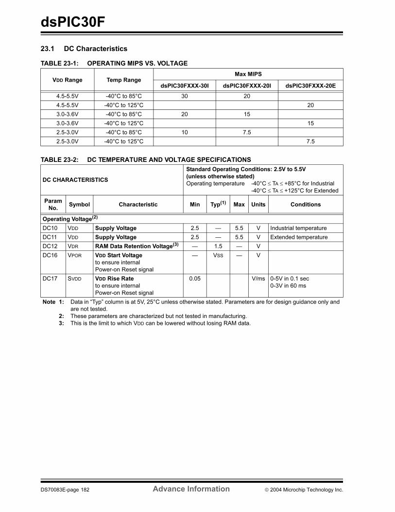
dsPIC30F
23.1 DC Characteristics
TABLE 23-1: OPERATING MIPS VS. VOLTAGE
VDD Range Temp RangeMax MIPS
dsPIC30FXXX-30I dsPIC30FXXX-20I dsPIC30FXXX-20E
4.5-5.5V -40°C to 85°C 30 20
4.5-5.5V -40°C to 125°C 20
3.0-3.6V -40°C to 85°C 20 15
3.0-3.6V -40°C to 125°C 15
2.5-3.0V -40°C to 85°C 10 7.5
2.5-3.0V -40°C to 125°C 7.5
TABLE 23-2: DC TEMPERATURE AND VOLTAGE SPECIFICATIONS
DC CHARACTERISTICS
Standard Operating Conditions: 2.5V to 5.5V
(unless otherwise stated)
Operating temperature -40°C ≤ TA ≤ +85°C for Industrial
-40°C ≤ TA ≤ +125°C for Extended
Param
No. Symbol Characteristic Min Typ(1) Max Units Conditions
Operating Voltage(2)
DC10 VDD Supply Voltage 2.5 — 5.5 V Industrial temperature
DC11 VDD Supply Voltage 2.5 — 5.5 V Extended temperature
DC12 VDR RAM Data Retention Voltage(3) — 1.5 — V
DC16 VPOR VDD Start Voltage
to ensure internal
Power-on Reset signal
— VSS — V
DC17 SVDD VDD Rise Rate
to ensure internal
Power-on Reset signal
0.05 V/ms 0-5V in 0.1 sec
0-3V in 60 ms
Note 1: Data in “Typ” column is at 5V, 25°C unless otherwise stated. Parameters are for design guidance only and
are not tested.
2: These parameters are characterized but not tested in manufacturing.
3: This is the limit to which VDD can be lowered without losing RAM data.
DS70083E-page 182 Advance Information 2004 Microchip Technology Inc.
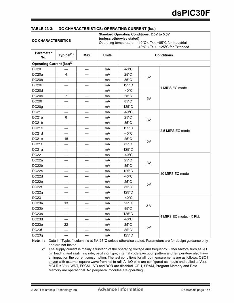
dsPIC30F
TABLE 23-3: DC CHARACTERISTICS: OPERATING CURRENT (IDD)
DC CHARACTERISTICS
Standard Operating Conditions: 2.5V to 5.5V
(unless otherwise stated)
Operating temperature -40°C ≤ TA ≤ +85°C for Industrial
-40°C ≤ TA ≤ +125°C for Extended
Parameter
No.Typical(1) Max Units Conditions
Operating Current (IDD)(2)
DC20 — — mA -40°C
3V
1 MIPS EC mode
DC20a 4 — mA 25°C
DC20b — — mA 85°C
DC20c — — mA 125°C
DC20d — — mA -40°C
5VDC20e 7 — mA 25°C
DC20f — — mA 85°C
DC20g — — mA 125°C
DC21 — — mA -40°C
3V
2.5 MIPS EC mode
DC21a 8 — mA 25°C
DC21b — — mA 85°C
DC21c — — mA 125°C
DC21d — — mA -40°C
5VDC21e 15 — mA 25°C
DC21f — — mA 85°C
DC21g — — mA 125°C
DC22 — — mA -40°C
3V
10 MIPS EC mode
DC22a — — mA 25°C
DC22b — — mA 85°C
DC22c — — mA 125°C
DC22d — — mA -40°C
5VDC22e — — mA 25°C
DC22f — — mA 85°C
DC22g — — mA 125°C
DC23 — — mA -40°C
3 V
4 MIPS EC mode, 4X PLL
DC23a 13 — mA 25°C
DC23b — — mA 85°C
DC23c — — mA 125°C
DC23d — — mA -40°C
5VDC23e 22 — mA 25°C
DC23f — — mA 85°C
DC23g — — mA 125°C
Note 1: Data in “Typical” column is at 5V, 25°C unless otherwise stated. Parameters are for design guidance only
and are not tested.
2: The supply current is mainly a function of the operating voltage and frequency. Other factors such as I/O
pin loading and switching rate, oscillator type, internal code execution pattern and temperature also have
an impact on the current consumption. The test conditions for all IDD measurements are as follows: OSC1
driven with external square wave from rail to rail. All I/O pins are configured as Inputs and pulled to VDD.
MCLR = VDD, WDT, FSCM, LVD and BOR are disabled. CPU, SRAM, Program Memory and Data
Memory are operational. No peripheral modules are operating.
2004 Microchip Technology Inc. Advance Information DS70083E-page 183
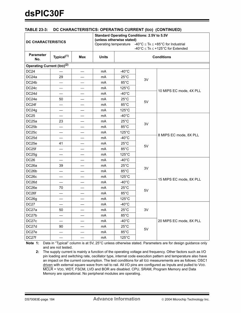
dsPIC30F
DC24 — — mA -40°C
3V
10 MIPS EC mode, 4X PLL
DC24a 29 — mA 25°C
DC24b — — mA 85°C
DC24c — — mA 125°C
DC24d — — mA -40°C
5VDC24e 50 — mA 25°C
DC24f — — mA 85°C
DC24g — — mA 125°C
DC25 — — mA -40°C
3V
8 MIPS EC mode, 8X PLL
DC25a 23 — mA 25°C
DC25b — — mA 85°C
DC25c — — mA 125°C
DC25d — — mA -40°C
5VDC25e 41 — mA 25°C
DC25f — — mA 85°C
DC25g — — mA 125°C
DC26 — — mA -40°C
3V
15 MIPS EC mode, 8X PLL
DC26a 39 — mA 25°C
DC26b — — mA 85°C
DC26c — — mA 125°C
DC26d — — mA -40°C
5VDC26e 70 — mA 25°C
DC26f — — mA 85°C
DC26g — — mA 125°C
DC27 — — mA -40°C
3V
20 MIPS EC mode, 8X PLL
DC27a 50 — mA 25°C
DC27b — — mA 85°C
DC27c — — mA -40°C
5VDC27d 90 — mA 25°C
DC27e — — mA 85°C
DC27f — — mA 125°C
TABLE 23-3: DC CHARACTERISTICS: OPERATING CURRENT (IDD) (CONTINUED)
DC CHARACTERISTICS
Standard Operating Conditions: 2.5V to 5.5V
(unless otherwise stated)
Operating temperature -40°C ≤ TA ≤ +85°C for Industrial
-40°C ≤ TA ≤ +125°C for Extended
Parameter
No.Typical(1) Max Units Conditions
Operating Current (IDD)(2)
Note 1: Data in “Typical” column is at 5V, 25°C unless otherwise stated. Parameters are for design guidance only
and are not tested.
2: The supply current is mainly a function of the operating voltage and frequency. Other factors such as I/O
pin loading and switching rate, oscillator type, internal code execution pattern and temperature also have
an impact on the current consumption. The test conditions for all IDD measurements are as follows: OSC1
driven with external square wave from rail to rail. All I/O pins are configured as Inputs and pulled to VDD.
MCLR = VDD, WDT, FSCM, LVD and BOR are disabled. CPU, SRAM, Program Memory and Data
Memory are operational. No peripheral modules are operating.
DS70083E-page 184 Advance Information 2004 Microchip Technology Inc.
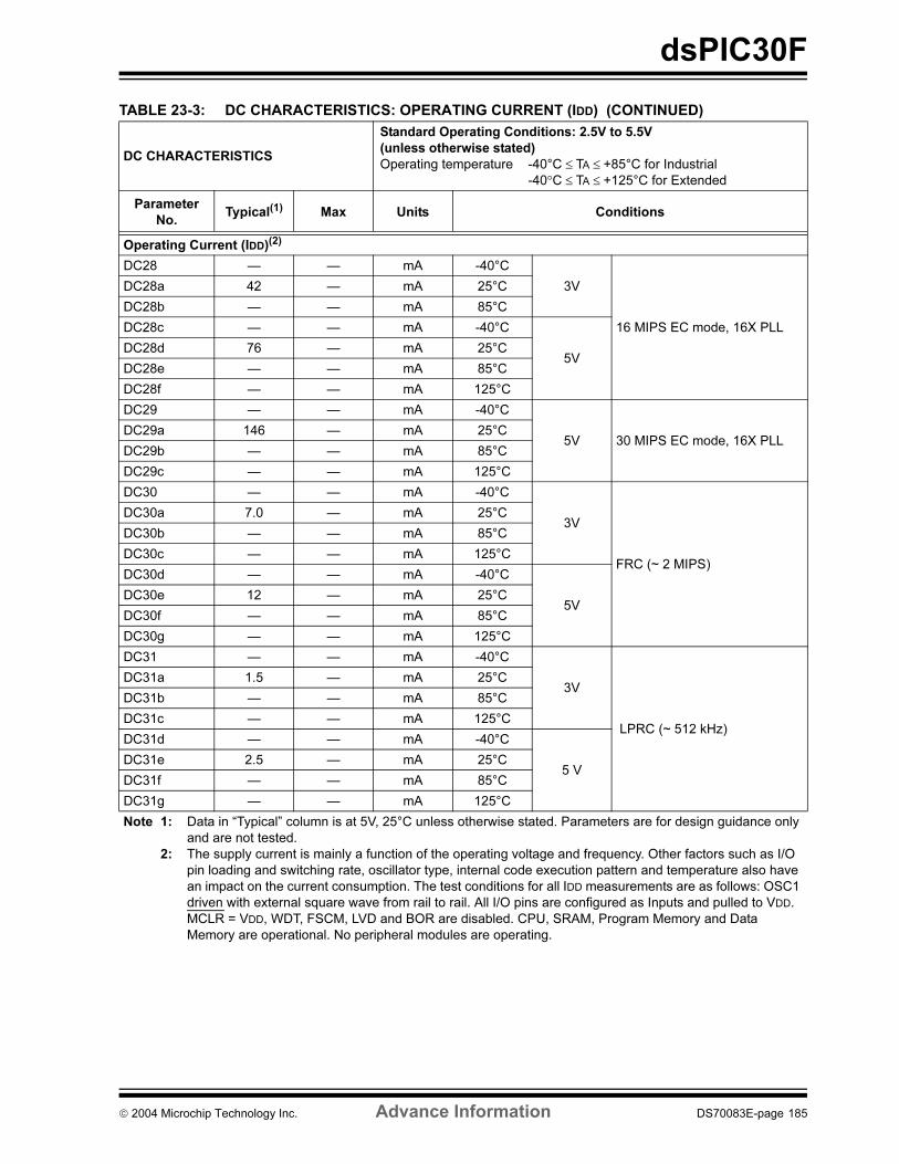
dsPIC30F
DC28 — — mA -40°C
3V
16 MIPS EC mode, 16X PLL
DC28a 42 — mA 25°C
DC28b — — mA 85°C
DC28c — — mA -40°C
5VDC28d 76 — mA 25°C
DC28e — — mA 85°C
DC28f — — mA 125°C
DC29 — — mA -40°C
5V 30 MIPS EC mode, 16X PLLDC29a 146 — mA 25°C
DC29b — — mA 85°C
DC29c — — mA 125°C
DC30 — — mA -40°C
3V
FRC (~ 2 MIPS)
DC30a 7.0 — mA 25°C
DC30b — — mA 85°C
DC30c — — mA 125°C
DC30d — — mA -40°C
5VDC30e 12 — mA 25°C
DC30f — — mA 85°C
DC30g — — mA 125°C
DC31 — — mA -40°C
3V
LPRC (~ 512 kHz)
DC31a 1.5 — mA 25°C
DC31b — — mA 85°C
DC31c — — mA 125°C
DC31d — — mA -40°C
5 VDC31e 2.5 — mA 25°C
DC31f — — mA 85°C
DC31g — — mA 125°C
TABLE 23-3: DC CHARACTERISTICS: OPERATING CURRENT (IDD) (CONTINUED)
DC CHARACTERISTICS
Standard Operating Conditions: 2.5V to 5.5V
(unless otherwise stated)
Operating temperature -40°C ≤ TA ≤ +85°C for Industrial
-40°C ≤ TA ≤ +125°C for Extended
Parameter
No.Typical(1) Max Units Conditions
Operating Current (IDD)(2)
Note 1: Data in “Typical” column is at 5V, 25°C unless otherwise stated. Parameters are for design guidance only
and are not tested.
2: The supply current is mainly a function of the operating voltage and frequency. Other factors such as I/O
pin loading and switching rate, oscillator type, internal code execution pattern and temperature also have
an impact on the current consumption. The test conditions for all IDD measurements are as follows: OSC1
driven with external square wave from rail to rail. All I/O pins are configured as Inputs and pulled to VDD.
MCLR = VDD, WDT, FSCM, LVD and BOR are disabled. CPU, SRAM, Program Memory and Data
Memory are operational. No peripheral modules are operating.
2004 Microchip Technology Inc. Advance Information DS70083E-page 185
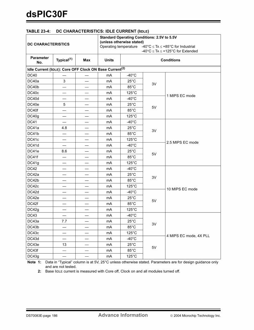
dsPIC30F
TABLE 23-4: DC CHARACTERISTICS: IDLE CURRENT (IIDLE)
DC CHARACTERISTICS
Standard Operating Conditions: 2.5V to 5.5V
(unless otherwise stated)
Operating temperature -40°C ≤ TA ≤ +85°C for Industrial
-40°C ≤ TA ≤ +125°C for Extended
Parameter
No.Typical(1) Max Units Conditions
Idle Current (IIDLE): Core OFF Clock ON Base Current(2)
DC40 — — mA -40°C
3V
1 MIPS EC mode
DC40a 3 — mA 25°C
DC40b — — mA 85°C
DC40c — — mA 125°C
DC40d — — mA -40°C
5VDC40e 5 — mA 25°C
DC40f — — mA 85°C
DC40g — — mA 125°C
DC41 — — mA -40°C
3V
2.5 MIPS EC mode
DC41a 4.8 — mA 25°C
DC41b — — mA 85°C
DC41c — — mA 125°C
DC41d — — mA -40°C
5VDC41e 8.6 — mA 25°C
DC41f — — mA 85°C
DC41g — — mA 125°C
DC42 — — mA -40°C
3V
10 MIPS EC mode
DC42a — — mA 25°C
DC42b — — mA 85°C
DC42c — — mA 125°C
DC42d — — mA -40°C
5VDC42e — — mA 25°C
DC42f — — mA 85°C
DC42g — — mA 125°C
DC43 — — mA -40°C
3V
4 MIPS EC mode, 4X PLL
DC43a 7.7 — mA 25°C
DC43b — — mA 85°C
DC43c — — mA 125°C
DC43d — — mA -40°C
5VDC43e 13 — mA 25°C
DC43f — — mA 85°C
DC43g — — mA 125°C
Note 1: Data in “Typical” column is at 5V, 25°C unless otherwise stated. Parameters are for design guidance only
and are not tested.
2: Base IIDLE current is measured with Core off, Clock on and all modules turned off.
DS70083E-page 186 Advance Information 2004 Microchip Technology Inc.
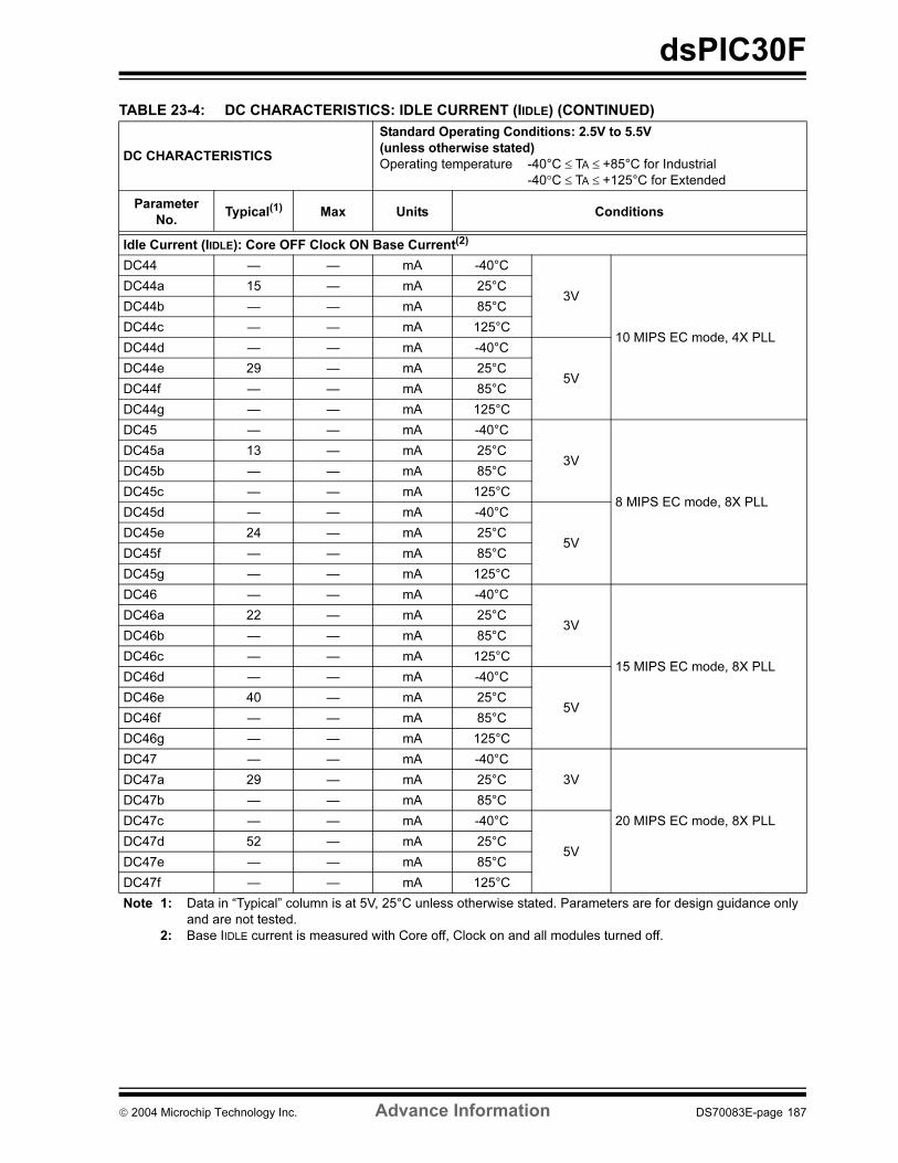
dsPIC30F
DC44 — — mA -40°C
3V
10 MIPS EC mode, 4X PLL
DC44a 15 — mA 25°C
DC44b — — mA 85°C
DC44c — — mA 125°C
DC44d — — mA -40°C
5VDC44e 29 — mA 25°C
DC44f — — mA 85°C
DC44g — — mA 125°C
DC45 — — mA -40°C
3V
8 MIPS EC mode, 8X PLL
DC45a 13 — mA 25°C
DC45b — — mA 85°C
DC45c — — mA 125°C
DC45d — — mA -40°C
5VDC45e 24 — mA 25°C
DC45f — — mA 85°C
DC45g — — mA 125°C
DC46 — — mA -40°C
3V
15 MIPS EC mode, 8X PLL
DC46a 22 — mA 25°C
DC46b — — mA 85°C
DC46c — — mA 125°C
DC46d — — mA -40°C
5VDC46e 40 — mA 25°C
DC46f — — mA 85°C
DC46g — — mA 125°C
DC47 — — mA -40°C
3V
20 MIPS EC mode, 8X PLL
DC47a 29 — mA 25°C
DC47b — — mA 85°C
DC47c — — mA -40°C
5VDC47d 52 — mA 25°C
DC47e — — mA 85°C
DC47f — — mA 125°C
TABLE 23-4: DC CHARACTERISTICS: IDLE CURRENT (IIDLE) (CONTINUED)
DC CHARACTERISTICS
Standard Operating Conditions: 2.5V to 5.5V
(unless otherwise stated)
Operating temperature -40°C ≤ TA ≤ +85°C for Industrial
-40°C ≤ TA ≤ +125°C for Extended
Parameter
No.Typical(1) Max Units Conditions
Idle Current (IIDLE): Core OFF Clock ON Base Current(2)
Note 1: Data in “Typical” column is at 5V, 25°C unless otherwise stated. Parameters are for design guidance only
and are not tested.
2: Base IIDLE current is measured with Core off, Clock on and all modules turned off.
2004 Microchip Technology Inc. Advance Information DS70083E-page 187
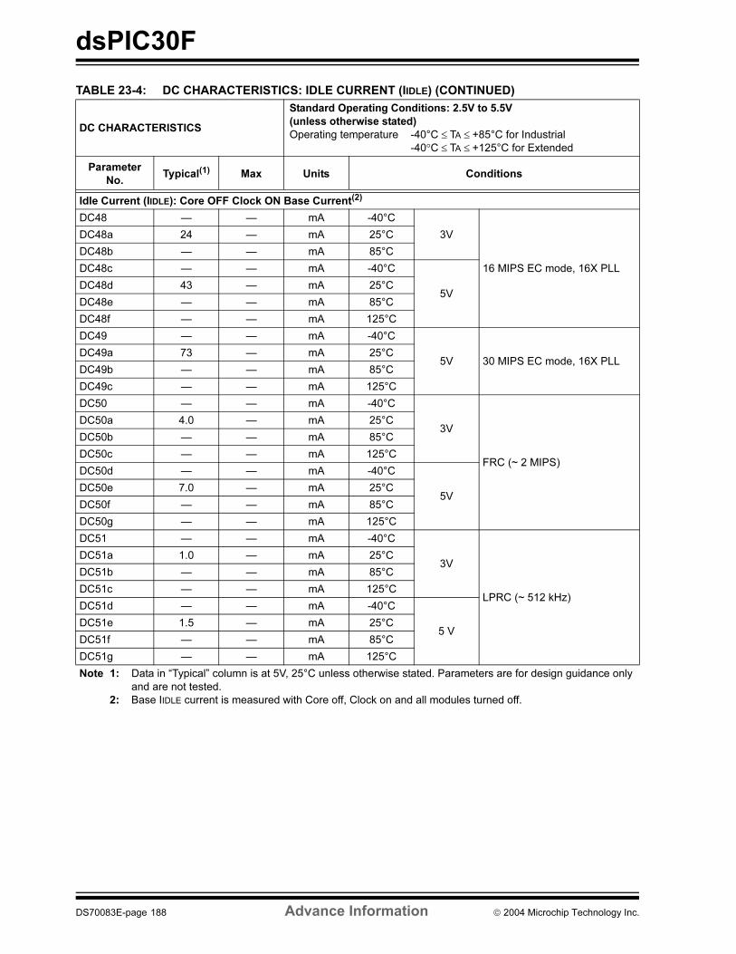
dsPIC30F
DC48 — — mA -40°C
3V
16 MIPS EC mode, 16X PLL
DC48a 24 — mA 25°C
DC48b — — mA 85°C
DC48c — — mA -40°C
5VDC48d 43 — mA 25°C
DC48e — — mA 85°C
DC48f — — mA 125°C
DC49 — — mA -40°C
5V 30 MIPS EC mode, 16X PLLDC49a 73 — mA 25°C
DC49b — — mA 85°C
DC49c — — mA 125°C
DC50 — — mA -40°C
3V
FRC (~ 2 MIPS)
DC50a 4.0 — mA 25°C
DC50b — — mA 85°C
DC50c — — mA 125°C
DC50d — — mA -40°C
5VDC50e 7.0 — mA 25°C
DC50f — — mA 85°C
DC50g — — mA 125°C
DC51 — — mA -40°C
3V
LPRC (~ 512 kHz)
DC51a 1.0 — mA 25°C
DC51b — — mA 85°C
DC51c — — mA 125°C
DC51d — — mA -40°C
5 VDC51e 1.5 — mA 25°C
DC51f — — mA 85°C
DC51g — — mA 125°C
TABLE 23-4: DC CHARACTERISTICS: IDLE CURRENT (IIDLE) (CONTINUED)
DC CHARACTERISTICS
Standard Operating Conditions: 2.5V to 5.5V
(unless otherwise stated)
Operating temperature -40°C ≤ TA ≤ +85°C for Industrial
-40°C ≤ TA ≤ +125°C for Extended
Parameter
No.Typical(1) Max Units Conditions
Idle Current (IIDLE): Core OFF Clock ON Base Current(2)
Note 1: Data in “Typical” column is at 5V, 25°C unless otherwise stated. Parameters are for design guidance only
and are not tested.
2: Base IIDLE current is measured with Core off, Clock on and all modules turned off.
DS70083E-page 188 Advance Information 2004 Microchip Technology Inc.
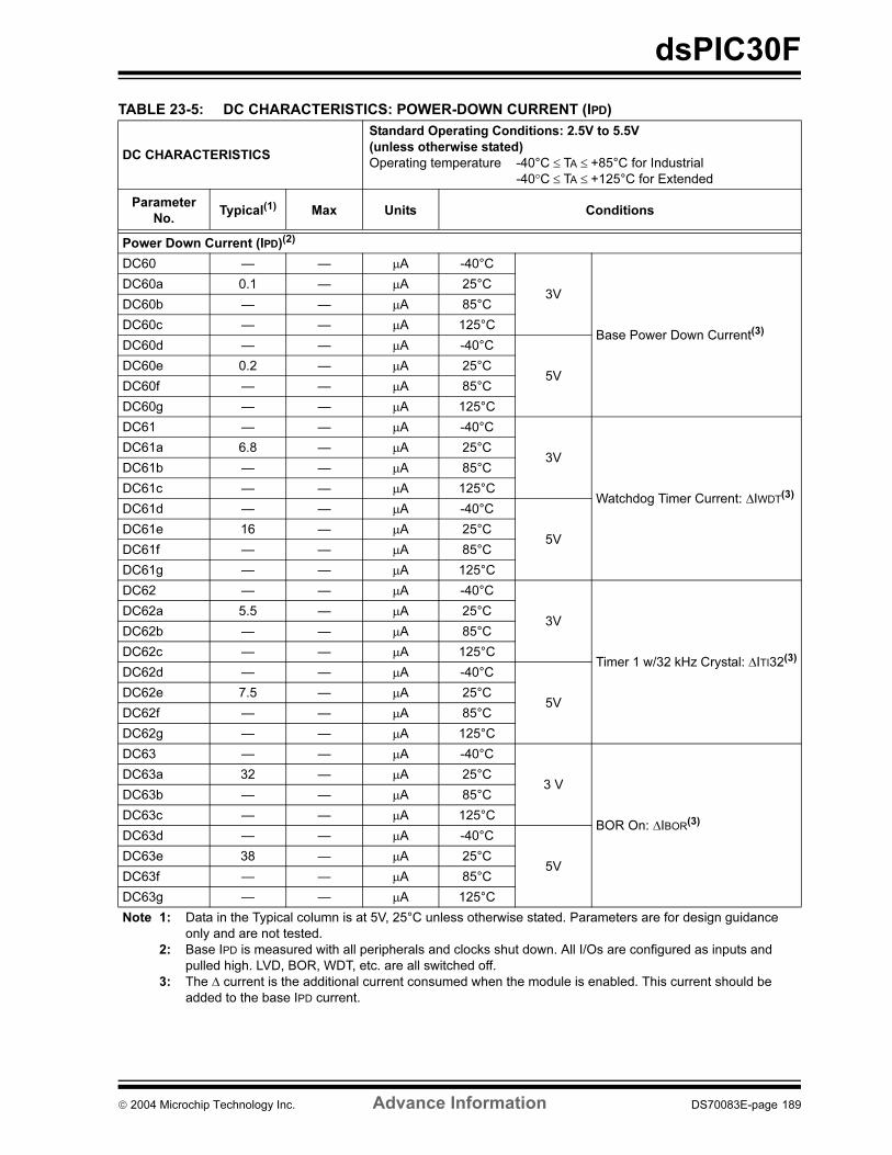
dsPIC30F
TABLE 23-5: DC CHARACTERISTICS: POWER-DOWN CURRENT (IPD)
DC CHARACTERISTICS
Standard Operating Conditions: 2.5V to 5.5V
(unless otherwise stated)
Operating temperature -40°C ≤ TA ≤ +85°C for Industrial
-40°C ≤ TA ≤ +125°C for Extended
Parameter
No.Typical(1) Max Units Conditions
Power Down Current (IPD)(2)
DC60 — — µA -40°C
3V
Base Power Down Current(3)
DC60a 0.1 — µA 25°C
DC60b — — µA 85°C
DC60c — — µA 125°C
DC60d — — µA -40°C
5VDC60e 0.2 — µA 25°C
DC60f — — µA 85°C
DC60g — — µA 125°C
DC61 — — µA -40°C
3V
Watchdog Timer Current: ∆IWDT(3)
DC61a 6.8 — µA 25°C
DC61b — — µA 85°C
DC61c — — µA 125°C
DC61d — — µA -40°C
5VDC61e 16 — µA 25°C
DC61f — — µA 85°C
DC61g — — µA 125°C
DC62 — — µA -40°C
3V
Timer 1 w/32 kHz Crystal: ∆ITI32(3)
DC62a 5.5 — µA 25°C
DC62b — — µA 85°C
DC62c — — µA 125°C
DC62d — — µA -40°C
5VDC62e 7.5 — µA 25°C
DC62f — — µA 85°C
DC62g — — µA 125°C
DC63 — — µA -40°C
3 V
BOR On: ∆IBOR(3)
DC63a 32 — µA 25°C
DC63b — — µA 85°C
DC63c — — µA 125°C
DC63d — — µA -40°C
5VDC63e 38 — µA 25°C
DC63f — — µA 85°C
DC63g — — µA 125°C
Note 1: Data in the Typical column is at 5V, 25°C unless otherwise stated. Parameters are for design guidance
only and are not tested.
2: Base IPD is measured with all peripherals and clocks shut down. All I/Os are configured as inputs and
pulled high. LVD, BOR, WDT, etc. are all switched off.
3: The ∆ current is the additional current consumed when the module is enabled. This current should be
added to the base IPD current.
2004 Microchip Technology Inc. Advance Information DS70083E-page 189
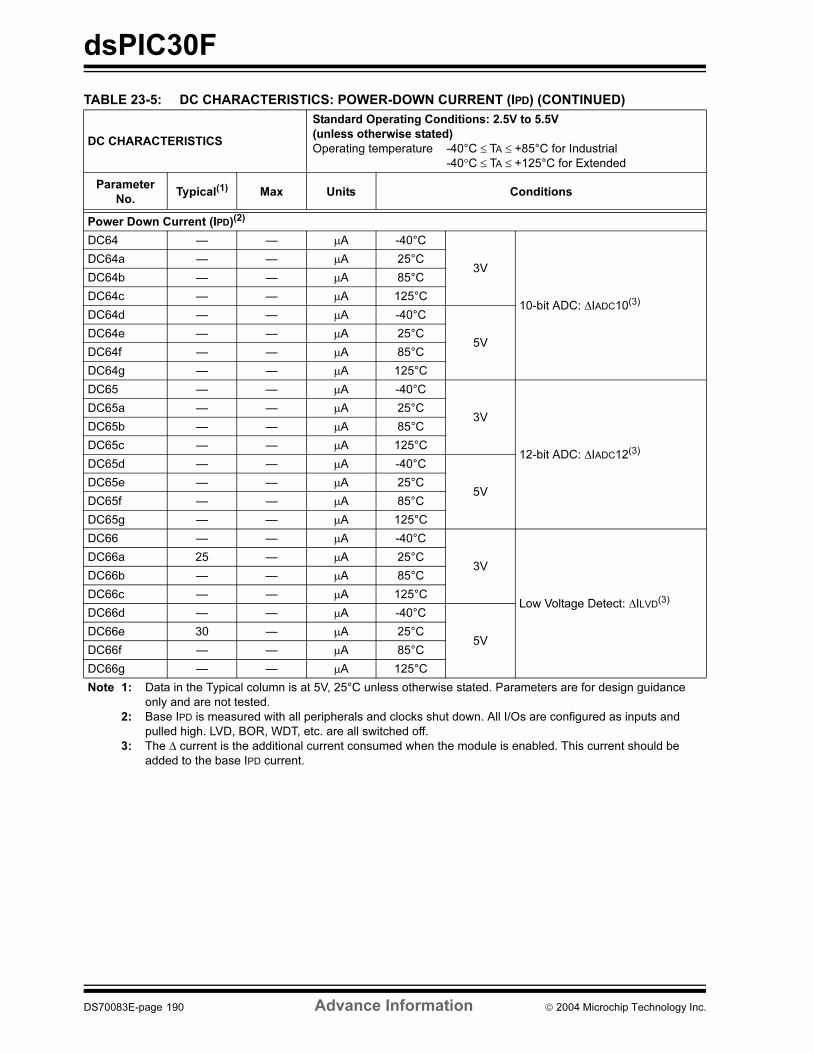
dsPIC30F
DC64 — — µA -40°C
3V
10-bit ADC: ∆IADC10(3)
DC64a — — µA 25°C
DC64b — — µA 85°C
DC64c — — µA 125°C
DC64d — — µA -40°C
5VDC64e — — µA 25°C
DC64f — — µA 85°C
DC64g — — µA 125°C
DC65 — — µA -40°C
3V
12-bit ADC: ∆IADC12(3)
DC65a — — µA 25°C
DC65b — — µA 85°C
DC65c — — µA 125°C
DC65d — — µA -40°C
5VDC65e — — µA 25°C
DC65f — — µA 85°C
DC65g — — µA 125°C
DC66 — — µA -40°C
3V
Low Voltage Detect: ∆ILVD(3)
DC66a 25 — µA 25°C
DC66b — — µA 85°C
DC66c — — µA 125°C
DC66d — — µA -40°C
5VDC66e 30 — µA 25°C
DC66f — — µA 85°C
DC66g — — µA 125°C
TABLE 23-5: DC CHARACTERISTICS: POWER-DOWN CURRENT (IPD) (CONTINUED)
DC CHARACTERISTICS
Standard Operating Conditions: 2.5V to 5.5V
(unless otherwise stated)
Operating temperature -40°C ≤ TA ≤ +85°C for Industrial
-40°C ≤ TA ≤ +125°C for Extended
Parameter
No.Typical(1) Max Units Conditions
Power Down Current (IPD)(2)
Note 1: Data in the Typical column is at 5V, 25°C unless otherwise stated. Parameters are for design guidance
only and are not tested.
2: Base IPD is measured with all peripherals and clocks shut down. All I/Os are configured as inputs and
pulled high. LVD, BOR, WDT, etc. are all switched off.
3: The ∆ current is the additional current consumed when the module is enabled. This current should be
added to the base IPD current.
DS70083E-page 190 Advance Information 2004 Microchip Technology Inc.
dsPIC30F
TABLE 23-6: DC CHARACTERISTICS: I/O PIN INPUT SPECIFICATIONS
DC CHARACTERISTICS
Standard Operating Conditions: 2.5V to 5.5V
(unless otherwise stated)
Operating temperature -40°C ≤ TA ≤ +85°C for Industrial
-40°C ≤ TA ≤ +125°C for Extended
Param
No.Symbol Characteristic Min Typ(1) Max Units Conditions
VIL Input Low Voltage(2)
DI10 I/O pins:
with Schmitt Trigger buffer VSS — 0.2 VDD V
DI15 MCLR VSS — 0.2 VDD V
DI16 OSC1 (in XT, HS and LP modes) VSS — 0.2 VDD V
DI17 OSC1 (in RC mode)(3) VSS — 0.3 VDD V
DI18 SDA, SCL TBD — TBD V SM bus disabled
DI19 SDA, SCL TBD — TBD V SM bus enabled
VIH Input High Voltage(2)
DI20 I/O pins:
with Schmitt Trigger buffer 0.8 VDD — VDD V
DI25 MCLR 0.8 VDD — VDD V
DI26 OSC1 (in XT, HS and LP modes) 0.7 VDD — VDD V
DI27 OSC1 (in RC mode)(3) 0.9 VDD — VDD V
DI28 SDA, SCL TBD — TBD V SM bus disabled
DI29 SDA, SCL TBD — TBD V SM bus enabled
ICNPU CNXX Pull-up Current(2)
DI30 50 250 400 µA VDD = 5V, VPIN = VSS
DI31 TBD TBD TBD µA VDD = 3V, VPIN = VSS
IIL Input Leakage Current(2)(4)(5)
DI50 I/O ports — 0.01 ±1 µA VSS ≤ VPIN ≤ VDD,
Pin at hi-impedance
DI55 MCLR — 0.05 ±5 µA VSS ≤ VPIN ≤ VDD
DI56 OSC1 — 0.05 ±5 µA VSS ≤ VPIN ≤ VDD, XT, HS
and LP Osc mode
Note 1: Data in “Typ” column is at 5V, 25°C unless otherwise stated. Parameters are for design guidance only and
are not tested.
2: These parameters are characterized but not tested in manufacturing.
3: In RC oscillator configuration, the OSC1/CLKl pin is a Schmitt Trigger input. It is not recommended that
the dsPIC30F device be driven with an external clock while in RC mode.
4: The leakage current on the MCLR pin is strongly dependent on the applied voltage level. The specified
levels represent normal operating conditions. Higher leakage current may be measured at different input
voltages.
5: Negative current is defined as current sourced by the pin.
2004 Microchip Technology Inc. Advance Information DS70083E-page 191
dsPIC30F
FIGURE 23-1: LOW-VOLTAGE DETECT CHARACTERISTICS
TABLE 23-7: DC CHARACTERISTICS: I/O PIN OUTPUT SPECIFICATIONS
DC CHARACTERISTICS
Standard Operating Conditions: 2.5V to 5.5V
(unless otherwise stated)
Operating temperature -40°C ≤ TA ≤ +85°C for Industrial
-40°C ≤ TA ≤ +125°C for Extended
Param
No.Symbol Characteristic Min Typ(1) Max Units Conditions
VOL Output Low Voltage(2)
DO10 I/O ports — — 0.6 V IOL = 8.5 mA, VDD = 5V
— — TBD V IOL = 2.0 mA, VDD = 3V
DO16 OSC2/CLKOUT — — 0.6 V IOL = 1.6 mA, VDD = 5V
(RC or EC Osc mode) — — TBD V IOL = 2.0 mA, VDD = 3V
VOH Output High Voltage(2)
DO20 I/O ports VDD – 0.7 — — V IOH = -3.0 mA, VDD = 5V
TBD — — V IOH = -2.0 mA, VDD = 3V
DO26 OSC2/CLKOUT VDD – 0.7 — — V IOH = -1.3 mA, VDD = 5V
(RC or EC Osc mode) TBD — — V IOH = -2.0 mA, VDD = 3V
Capacitive Loading Specs
on Output Pins(2)
DO50 COSC2 OSC2/SOSC2 pin — — 15 pF In XTL, XT, HS and LP modes
when external clock is used to
drive OSC1.
DO56 CIO All I/O pins and OSC2 — — 50 pF RC or EC Osc mode
DO58 CB SCL, SDA — — 400 pF In I2C mode
Note 1: Data in “Typ” column is at 5V, 25°C unless otherwise stated. Parameters are for design guidance only and
are not tested.
2: These parameters are characterized but not tested in manufacturing.
LV10
LVDIF
VDD
(LVDIF set by hardware)
DS70083E-page 192 Advance Information 2004 Microchip Technology Inc.
dsPIC30F
TABLE 23-8: ELECTRICAL CHARACTERISTICS: LVDL
FIGURE 23-2: BROWN-OUT RESET CHARACTERISTICS
DC CHARACTERISTICS
Standard Operating Conditions: 2.5V to 5.5V
(unless otherwise stated)
Operating temperature -40°C ≤ TA ≤ +85°C for Industrial
-40°C ≤ TA ≤ +125°C for Extended
Param
No.Symbol Characteristic(1) Min Typ Max Units Conditions
LV10 VPLVD LVDL Voltage on VDD transition
high to low
LVDL = 0000(2) — — — V
LVDL = 0001(2) — — — V
LVDL = 0010(2) — — — V
LVDL = 0011(2) — — — V
LVDL = 0100 2.50 — 2.65 V
LVDL = 0101 2.70 — 2.86 V
LVDL = 0110 2.80 — 2.97 V
LVDL = 0111 3.00 — 3.18 V
LVDL = 1000 3.30 — 3.50 V
LVDL = 1001 3.50 — 3.71 V
LVDL = 1010 3.60 — 3.82 V
LVDL = 1011 3.80 — 4.03 V
LVDL = 1100 4.00 — 4.24 V
LVDL = 1101 4.20 — 4.45 V
LVDL = 1110 4.50 — 4.77 V
LV15 VLVDIN External LVD input pin
threshold voltage
LVDL = 1111 — — — V
Note 1: These parameters are characterized but not tested in manufacturing.
2: These values not in usable operating range.
BO10
RESET (due to BOR)
VDD
(Device in Brown-out Reset)
(Device not in Brown-out Reset)
Power Up Time-out
BO15
2004 Microchip Technology Inc. Advance Information DS70083E-page 193
dsPIC30F
TABLE 23-9: ELECTRICAL CHARACTERISTICS: BOR
TABLE 23-10: DC CHARACTERISTICS: PROGRAM AND EEPROM
DC CHARACTERISTICS
Standard Operating Conditions: 2.5V to 5.5V
(unless otherwise stated)
Operating temperature -40°C ≤ TA ≤ +85°C for Industrial
-40°C ≤ TA ≤ +125°C for Extended
Param
No.Symbol Characteristic Min Typ(1) Max Units Conditions
BO10 VBOR BOR Voltage(2) on
VDD transition high to
low
BORV = 00(3) — — — V Not in operating
range
BORV = 01 2.7 — 2.86 V
BORV = 10 4.2 — 4.46 V
BORV = 11 4.5 — 4.78 V
BO15 VBHYS — 5 — mV
Note 1: Data in “Typ” column is at 5V, 25°C unless otherwise stated. Parameters are for design guidance only and
are not tested.
2: These parameters are characterized but not tested in manufacturing.
3: 00 values not in usable operating range.
DC CHARACTERISTICS
Standard Operating Conditions: 2.5V to 5.5V
(unless otherwise stated)
Operating temperature -40°C ≤ TA ≤ +85°C for Industrial
-40°C ≤ TA ≤ +125°C for Extended
Param
No.Symbol Characteristic Min Typ(1) Max Units Conditions
Data EEPROM Memory(2)
D120 ED Byte Endurance 100K 1M — E/W -40°C ≤ TA ≤ +85°C
D121 VDRW VDD for Read/Write VMIN — 5.5 V Using EECON to read/write
VMIN = Minimum operating
voltage
D122 TDEW Erase/Write Cycle Time — 2 — ms
D123 TRETD Characteristic Retention 40 100 — Year Provided no other specifications
are violated
Program FLASH Memory(2)
D130 EP Cell Endurance 10K 100K — E/W -40°C ≤ TA ≤ +85°C
D131 VPR VDD for Read VMIN — 5.5 V VMIN = Minimum operating
voltage
D132 VEB VDD for Block Erase 3.0 — 5.5 V
D133 VPEW VDD for Erase/Write 3.0 — 5.5 V
D134 TPEW Erase/Write Cycle Time — 2 — ms
D135 TRETD Characteristic Retention 40 100 — Year Provided no other specifications
are violated
D136 TEB ICSP Block Erase Time — 4 — ms
Note 1: Data in “Typ” column is at 5V, 25°C unless otherwise stated.
2: These parameters are characterized but not tested in manufacturing.
DS70083E-page 194 Advance Information 2004 Microchip Technology Inc.
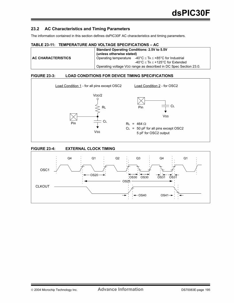
dsPIC30F
23.2 AC Characteristics and Timing Parameters
The information contained in this section defines dsPIC30F AC characteristics and timing parameters.
TABLE 23-11: TEMPERATURE AND VOLTAGE SPECIFICATIONS – AC
FIGURE 23-3: LOAD CONDITIONS FOR DEVICE TIMING SPECIFICATIONS
FIGURE 23-4: EXTERNAL CLOCK TIMING
AC CHARACTERISTICS
Standard Operating Conditions: 2.5V to 5.5V
(unless otherwise stated)
Operating temperature -40°C ≤ TA ≤ +85°C for Industrial
-40°C ≤ TA ≤ +125°C for Extended
Operating voltage VDD range as described in DC Spec Section 23.0.
VDD/2
CL
RL
Pin
Pin
VSS
VSS
CL
RL = 464 ΩCL = 50 pF for all pins except OSC2
5 pF for OSC2 output
Load Condition 1 - for all pins except OSC2 Load Condition 2 - for OSC2
OSC1
CLKOUT
Q4 Q1 Q2 Q3 Q4 Q1
OS20
OS25
OS30 OS30
OS40 OS41
OS31 OS31
2004 Microchip Technology Inc. Advance Information DS70083E-page 195
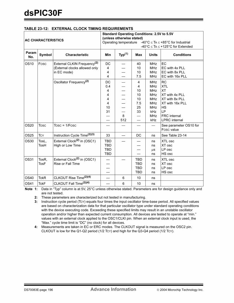
dsPIC30F
TABLE 23-12: EXTERNAL CLOCK TIMING REQUIREMENTS
AC CHARACTERISTICS
Standard Operating Conditions: 2.5V to 5.5V
(unless otherwise stated)
Operating temperature -40°C ≤ TA ≤ +85°C for Industrial
-40°C ≤ TA ≤ +125°C for Extended
Param
No.Symbol Characteristic Min Typ(1) Max Units Conditions
OS10 FOSC External CLKIN Frequency(2)
(External clocks allowed only
in EC mode)
DC
4
4
4
—
—
—
—
40
10
10
7.5
MHz
MHz
MHz
MHz
EC
EC with 4x PLL
EC with 8x PLL
EC with 16x PLL
Oscillator Frequency(2) DC
0.4
4
4
4
4
10
31
—
—
—
—
—
—
—
—
—
—
8
512
4
4
10
10
10
7.5
25
33
—
—
MHz
MHz
MHz
MHz
MHz
MHz
MHz
kHz
MHz
kHz
RC
XTL
XT
XT with 4x PLL
XT with 8x PLL
XT with 16x PLL
HS
LP
FRC internal
LPRC internal
OS20 TOSC TOSC = 1/FOSC — — — — See parameter OS10 for
FOSC value
OS25 TCY Instruction Cycle Time(2)(3) 33 — DC ns See Table 23-14
OS30 TosL,
TosH
External Clock(2) in (OSC1)
High or Low Time
TBD
TBD
TBD
TBD
— —
—
—
—
ns
ns
µs
ns
XTL osc
XT osc
LP osc
HS osc
OS31 TosR,
TosF
External Clock(2) in (OSC1)
Rise or Fall Time
—
—
—
—
— TBD
TBD
TBD
TBD
ns
ns
ns
ns
XTL osc
XT osc
LP osc
HS osc
OS40 TckR CLKOUT Rise Time(2)(4) — 6 10 ns
OS41 TckF CLKOUT Fall Time(2)(4) — 6 10 ns
Note 1: Data in “Typ” column is at 5V, 25°C unless otherwise stated. Parameters are for design guidance only and
are not tested.
2: These parameters are characterized but not tested in manufacturing.
3: Instruction cycle period (TCY) equals four times the input oscillator time-base period. All specified values
are based on characterization data for that particular oscillator type under standard operating conditions
with the device executing code. Exceeding these specified limits may result in an unstable oscillator
operation and/or higher than expected current consumption. All devices are tested to operate at “min.”
values with an external clock applied to the OSC1/CLKI pin. When an external clock input is used, the
“Max.” cycle time limit is “DC” (no clock) for all devices.
4: Measurements are taken in EC or ERC modes. The CLKOUT signal is measured on the OSC2 pin.
CLKOUT is low for the Q1-Q2 period (1/2 TCY) and high for the Q3-Q4 period (1/2 TCY).
DS70083E-page 196 Advance Information 2004 Microchip Technology Inc.
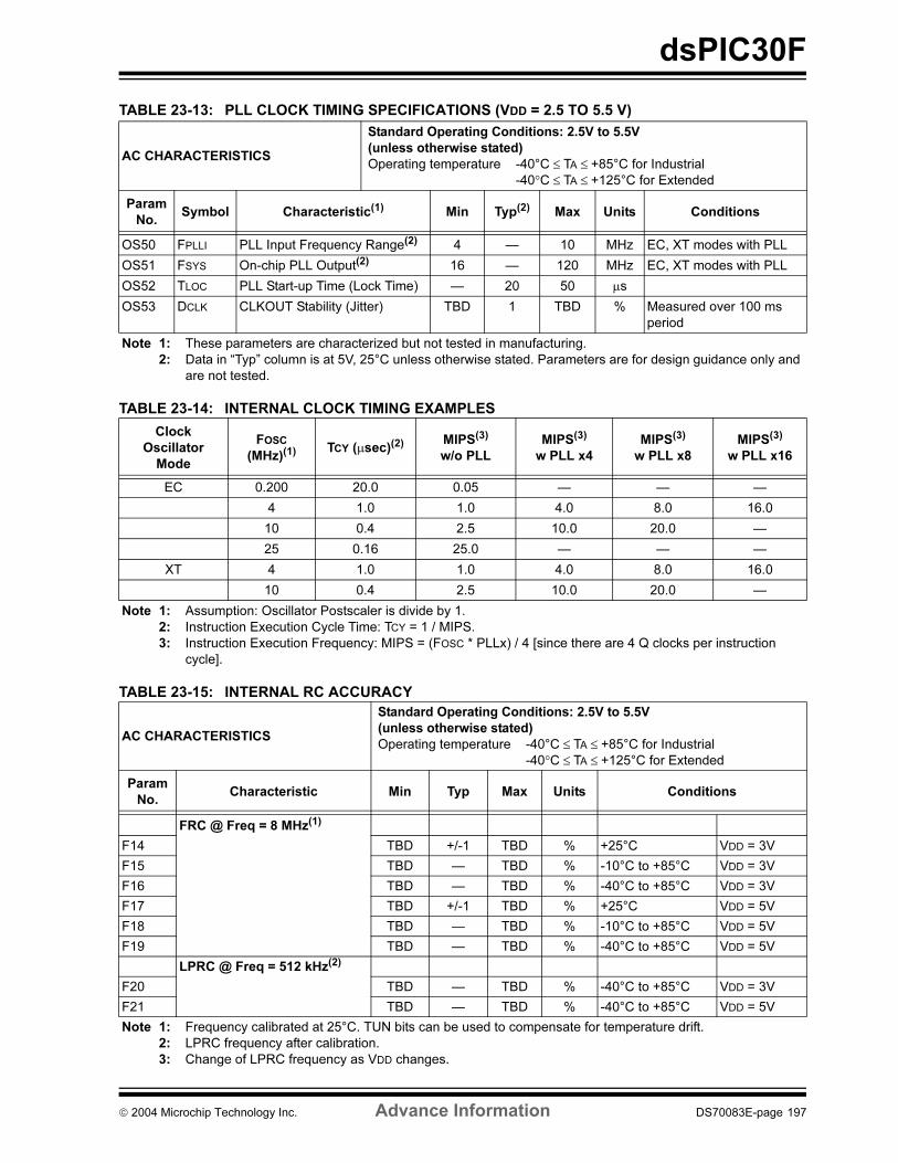
dsPIC30F
TABLE 23-14: INTERNAL CLOCK TIMING EXAMPLES
TABLE 23-13: PLL CLOCK TIMING SPECIFICATIONS (VDD = 2.5 TO 5.5 V)
AC CHARACTERISTICS
Standard Operating Conditions: 2.5V to 5.5V
(unless otherwise stated)
Operating temperature -40°C ≤ TA ≤ +85°C for Industrial
-40°C ≤ TA ≤ +125°C for Extended
Param
No.Symbol Characteristic(1) Min Typ(2) Max Units Conditions
OS50 FPLLI PLL Input Frequency Range(2) 4 — 10 MHz EC, XT modes with PLL
OS51 FSYS On-chip PLL Output(2) 16 — 120 MHz EC, XT modes with PLL
OS52 TLOC PLL Start-up Time (Lock Time) — 20 50 µs
OS53 DCLK CLKOUT Stability (Jitter) TBD 1 TBD % Measured over 100 ms
period
Note 1: These parameters are characterized but not tested in manufacturing.
2: Data in “Typ” column is at 5V, 25°C unless otherwise stated. Parameters are for design guidance only and
are not tested.
Clock
Oscillator
Mode
FOSC
(MHz)(1)TCY (µsec)(2)
MIPS(3)
w/o PLL
MIPS(3)
w PLL x4
MIPS(3)
w PLL x8
MIPS(3)
w PLL x16
EC 0.200 20.0 0.05 — — —
4 1.0 1.0 4.0 8.0 16.0
10 0.4 2.5 10.0 20.0 —
25 0.16 25.0 — — —
XT 4 1.0 1.0 4.0 8.0 16.0
10 0.4 2.5 10.0 20.0 —
Note 1: Assumption: Oscillator Postscaler is divide by 1.
2: Instruction Execution Cycle Time: TCY = 1 / MIPS.
3: Instruction Execution Frequency: MIPS = (FOSC * PLLx) / 4 [since there are 4 Q clocks per instruction
cycle].
TABLE 23-15: INTERNAL RC ACCURACY
AC CHARACTERISTICS
Standard Operating Conditions: 2.5V to 5.5V
(unless otherwise stated)
Operating temperature -40°C ≤ TA ≤ +85°C for Industrial
-40°C ≤ TA ≤ +125°C for Extended
Param
No.Characteristic Min Typ Max Units Conditions
FRC @ Freq = 8 MHz(1)
F14 TBD +/-1 TBD % +25°C VDD = 3V
F15 TBD — TBD % -10°C to +85°C VDD = 3V
F16 TBD — TBD % -40°C to +85°C VDD = 3V
F17 TBD +/-1 TBD % +25°C VDD = 5V
F18 TBD — TBD % -10°C to +85°C VDD = 5V
F19 TBD — TBD % -40°C to +85°C VDD = 5V
LPRC @ Freq = 512 kHz(2)
F20 TBD — TBD % -40°C to +85°C VDD = 3V
F21 TBD — TBD % -40°C to +85°C VDD = 5V
Note 1: Frequency calibrated at 25°C. TUN bits can be used to compensate for temperature drift.
2: LPRC frequency after calibration.
3: Change of LPRC frequency as VDD changes.
2004 Microchip Technology Inc. Advance Information DS70083E-page 197
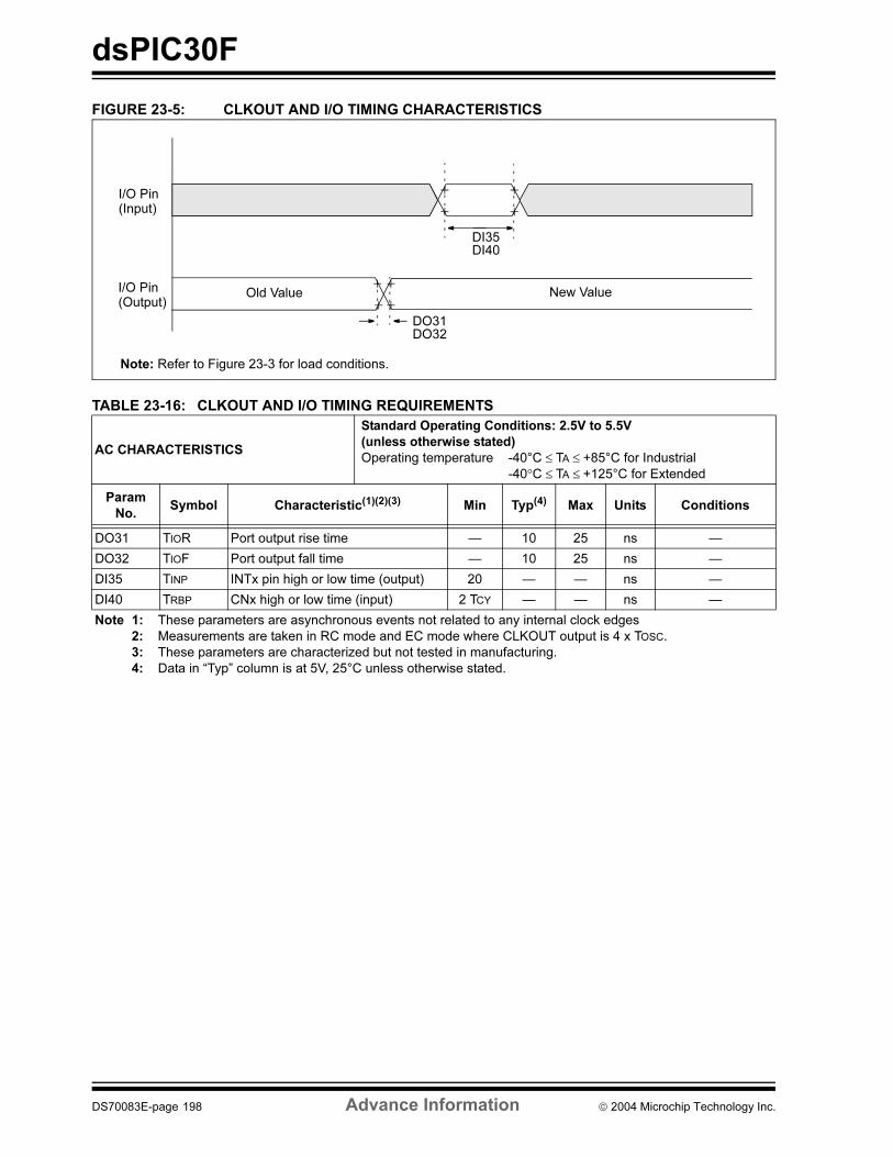
dsPIC30F
FIGURE 23-5: CLKOUT AND I/O TIMING CHARACTERISTICS
TABLE 23-16: CLKOUT AND I/O TIMING REQUIREMENTS
AC CHARACTERISTICS
Standard Operating Conditions: 2.5V to 5.5V
(unless otherwise stated)
Operating temperature -40°C ≤ TA ≤ +85°C for Industrial
-40°C ≤ TA ≤ +125°C for Extended
Param
No.Symbol Characteristic(1)(2)(3) Min Typ(4) Max Units Conditions
DO31 TIOR Port output rise time — 10 25 ns —
DO32 TIOF Port output fall time — 10 25 ns —
DI35 TINP INTx pin high or low time (output) 20 — — ns —
DI40 TRBP CNx high or low time (input) 2 TCY — — ns —
Note 1: These parameters are asynchronous events not related to any internal clock edges
2: Measurements are taken in RC mode and EC mode where CLKOUT output is 4 x TOSC.
3: These parameters are characterized but not tested in manufacturing.
4: Data in “Typ” column is at 5V, 25°C unless otherwise stated.
Note: Refer to Figure 23-3 for load conditions.
I/O Pin(Input)
I/O Pin(Output)
DI35
Old Value New Value
DI40
DO31DO32
DS70083E-page 198 Advance Information 2004 Microchip Technology Inc.
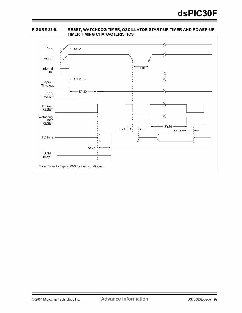
dsPIC30F
FIGURE 23-6: RESET, WATCHDOG TIMER, OSCILLATOR START-UP TIMER AND POWER-UP
TIMER TIMING CHARACTERISTICS
VDD
MCLR
InternalPOR
PWRTTime-out
OSCTime-out
InternalRESET
WatchdogTimer
RESET
SY11
SY10
SY20SY13
I/O Pins
SY13
Note: Refer to Figure 23-3 for load conditions.
FSCM Delay
SY35
SY30
SY12
2004 Microchip Technology Inc. Advance Information DS70083E-page 199
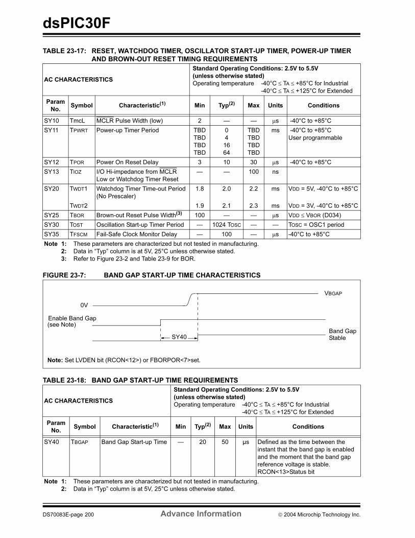
dsPIC30F
TABLE 23-17: RESET, WATCHDOG TIMER, OSCILLATOR START-UP TIMER, POWER-UP TIMER
AND BROWN-OUT RESET TIMING REQUIREMENTS
FIGURE 23-7: BAND GAP START-UP TIME CHARACTERISTICS
TABLE 23-18: BAND GAP START-UP TIME REQUIREMENTS
AC CHARACTERISTICS
Standard Operating Conditions: 2.5V to 5.5V
(unless otherwise stated)
Operating temperature -40°C ≤ TA ≤ +85°C for Industrial
-40°C ≤ TA ≤ +125°C for Extended
Param
No.Symbol Characteristic(1) Min Typ(2) Max Units Conditions
SY10 TmcL MCLR Pulse Width (low) 2 — — µs -40°C to +85°C
SY11 TPWRT Power-up Timer Period TBD
TBD
TBD
TBD
0
4
16
64
TBD
TBD
TBD
TBD
ms -40°C to +85°C
User programmable
SY12 TPOR Power On Reset Delay 3 10 30 µs -40°C to +85°C
SY13 TIOZ I/O Hi-impedance from MCLR
Low or Watchdog Timer Reset
— — 100 ns
SY20 TWDT1 Watchdog Timer Time-out Period
(No Prescaler)
1.8 2.0 2.2 ms VDD = 5V, -40°C to +85°C
TWDT2 1.9 2.1 2.3 ms VDD = 3V, -40°C to +85°C
SY25 TBOR Brown-out Reset Pulse Width(3) 100 — — µs VDD ≤ VBOR (D034)
SY30 TOST Oscillation Start-up Timer Period — 1024 TOSC — — TOSC = OSC1 period
SY35 TFSCM Fail-Safe Clock Monitor Delay — 100 — µs -40°C to +85°C
Note 1: These parameters are characterized but not tested in manufacturing.
2: Data in “Typ” column is at 5V, 25°C unless otherwise stated.
3: Refer to Figure 23-2 and Table 23-9 for BOR.
AC CHARACTERISTICS
Standard Operating Conditions: 2.5V to 5.5V
(unless otherwise stated)
Operating temperature -40°C ≤ TA ≤ +85°C for Industrial
-40°C ≤ TA ≤ +125°C for Extended
Param
No.Symbol Characteristic(1) Min Typ(2) Max Units Conditions
SY40 TBGAP Band Gap Start-up Time — 20 50 µs Defined as the time between the
instant that the band gap is enabled
and the moment that the band gap
reference voltage is stable.
RCON<13>Status bit
Note 1: These parameters are characterized but not tested in manufacturing.
2: Data in “Typ” column is at 5V, 25°C unless otherwise stated.
VBGAP
Enable Band Gap
Band Gap
0V
(see Note)
Stable
Note: Set LVDEN bit (RCON<12>) or FBORPOR<7>set.
SY40
DS70083E-page 200 Advance Information 2004 Microchip Technology Inc.
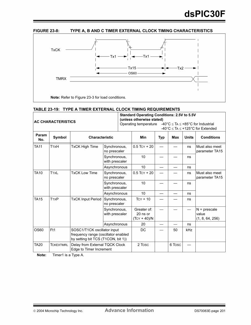
dsPIC30F
FIGURE 23-8: TYPE A, B AND C TIMER EXTERNAL CLOCK TIMING CHARACTERISTICS
TABLE 23-19: TYPE A TIMER EXTERNAL CLOCK TIMING REQUIREMENTS
AC CHARACTERISTICS
Standard Operating Conditions: 2.5V to 5.5V
(unless otherwise stated)
Operating temperature -40°C ≤ TA ≤ +85°C for Industrial
-40°C ≤ TA ≤ +125°C for Extended
Param
No.Symbol Characteristic Min Typ Max Units Conditions
TA11 TTXH TxCK High Time Synchronous,
no prescaler
0.5 TCY + 20 — — ns Must also meet
parameter TA15
Synchronous,
with prescaler
10 — — ns
Asynchronous 10 — — ns
TA10 TTXL TxCK Low Time Synchronous,
no prescaler
0.5 TCY + 20 — — ns Must also meet
parameter TA15
Synchronous,
with prescaler
10 — — ns
Asynchronous 10 — — ns
TA15 TTXP TxCK Input Period Synchronous,
no prescaler
TCY + 10 — — ns
Synchronous,
with prescaler
Greater of:
20 ns or
(TCY + 40)/N
— — — N = prescale
value
(1, 8, 64, 256)
Asynchronous 20 — — ns
OS60 Ft1 SOSC1/T1CK oscillator input
frequency range (oscillator enabled
by setting bit TCS (T1CON, bit 1))
DC — 50 kHz
TA20 TCKEXTMRL Delay from External TQCK Clock
Edge to Timer Increment
2 TOSC 6 TOSC —
Note: Timer1 is a Type A.
Note: Refer to Figure 23-3 for load conditions.
Tx1
Tx15
Tx1
Tx2
TMRX
OS60
TxCK
2004 Microchip Technology Inc. Advance Information DS70083E-page 201
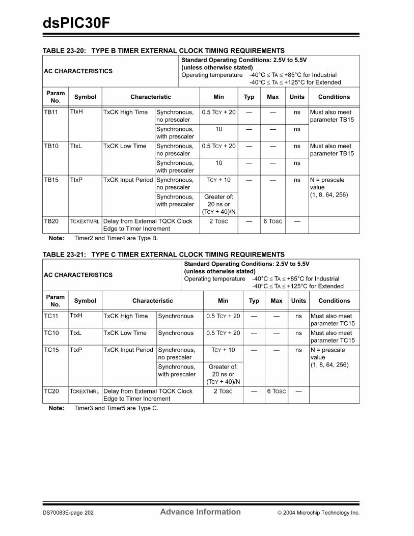
dsPIC30F
TABLE 23-20: TYPE B TIMER EXTERNAL CLOCK TIMING REQUIREMENTS
TABLE 23-21: TYPE C TIMER EXTERNAL CLOCK TIMING REQUIREMENTS
AC CHARACTERISTICS
Standard Operating Conditions: 2.5V to 5.5V
(unless otherwise stated)
Operating temperature -40°C ≤ TA ≤ +85°C for Industrial
-40°C ≤ TA ≤ +125°C for Extended
Param
No.Symbol Characteristic Min Typ Max Units Conditions
TB11 TtxH TxCK High Time Synchronous,
no prescaler
0.5 TCY + 20 — — ns Must also meet
parameter TB15
Synchronous,
with prescaler
10 — — ns
TB10 TtxL TxCK Low Time Synchronous,
no prescaler
0.5 TCY + 20 — — ns Must also meet
parameter TB15
Synchronous,
with prescaler
10 — — ns
TB15 TtxP TxCK Input Period Synchronous,
no prescaler
TCY + 10 — — ns N = prescale
value
(1, 8, 64, 256)Synchronous,
with prescaler
Greater of:
20 ns or
(TCY + 40)/N
TB20 TCKEXTMRL Delay from External TQCK Clock
Edge to Timer Increment
2 TOSC — 6 TOSC —
Note: Timer2 and Timer4 are Type B.
AC CHARACTERISTICS
Standard Operating Conditions: 2.5V to 5.5V
(unless otherwise stated)
Operating temperature -40°C ≤ TA ≤ +85°C for Industrial
-40°C ≤ TA ≤ +125°C for Extended
Param
No.Symbol Characteristic Min Typ Max Units Conditions
TC11 TtxH TxCK High Time Synchronous 0.5 TCY + 20 — — ns Must also meet
parameter TC15
TC10 TtxL TxCK Low Time Synchronous 0.5 TCY + 20 — — ns Must also meet
parameter TC15
TC15 TtxP TxCK Input Period Synchronous,
no prescaler
TCY + 10 — — ns N = prescale
value
(1, 8, 64, 256)Synchronous,
with prescaler
Greater of:
20 ns or
(TCY + 40)/N
TC20 TCKEXTMRL Delay from External TQCK Clock
Edge to Timer Increment
2 TOSC — 6 TOSC —
Note: Timer3 and Timer5 are Type C.
DS70083E-page 202 Advance Information 2004 Microchip Technology Inc.
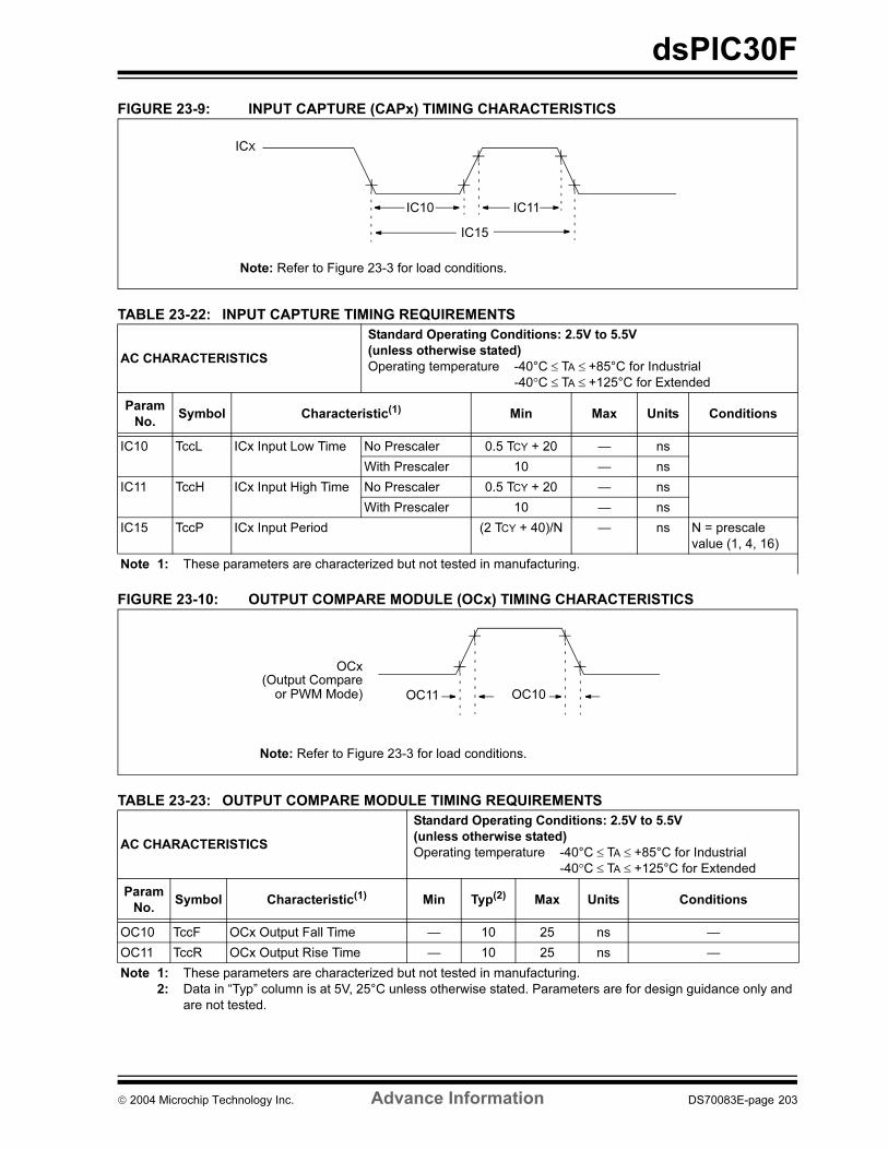
dsPIC30F
FIGURE 23-9: INPUT CAPTURE (CAPx) TIMING CHARACTERISTICS
TABLE 23-22: INPUT CAPTURE TIMING REQUIREMENTS
FIGURE 23-10: OUTPUT COMPARE MODULE (OCx) TIMING CHARACTERISTICS
TABLE 23-23: OUTPUT COMPARE MODULE TIMING REQUIREMENTS
AC CHARACTERISTICS
Standard Operating Conditions: 2.5V to 5.5V
(unless otherwise stated)
Operating temperature -40°C ≤ TA ≤ +85°C for Industrial
-40°C ≤ TA ≤ +125°C for Extended
Param
No.Symbol Characteristic(1) Min Max Units Conditions
IC10 TccL ICx Input Low Time No Prescaler 0.5 TCY + 20 — ns
With Prescaler 10 — ns
IC11 TccH ICx Input High Time No Prescaler 0.5 TCY + 20 — ns
With Prescaler 10 — ns
IC15 TccP ICx Input Period (2 TCY + 40)/N — ns N = prescale
value (1, 4, 16)
Note 1: These parameters are characterized but not tested in manufacturing.
AC CHARACTERISTICS
Standard Operating Conditions: 2.5V to 5.5V
(unless otherwise stated)
Operating temperature -40°C ≤ TA ≤ +85°C for Industrial
-40°C ≤ TA ≤ +125°C for Extended
Param
No.Symbol Characteristic(1) Min Typ(2) Max Units Conditions
OC10 TccF OCx Output Fall Time — 10 25 ns —
OC11 TccR OCx Output Rise Time — 10 25 ns —
Note 1: These parameters are characterized but not tested in manufacturing.
2: Data in “Typ” column is at 5V, 25°C unless otherwise stated. Parameters are for design guidance only and
are not tested.
ICX
IC10 IC11
IC15
Note: Refer to Figure 23-3 for load conditions.
OCx
OC11 OC10(Output Compare
Note: Refer to Figure 23-3 for load conditions.
or PWM Mode)
2004 Microchip Technology Inc. Advance Information DS70083E-page 203
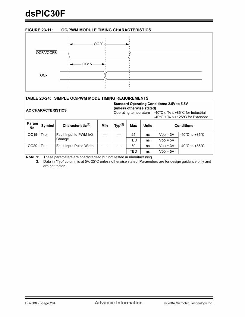
dsPIC30F
FIGURE 23-11: OC/PWM MODULE TIMING CHARACTERISTICS
TABLE 23-24: SIMPLE OC/PWM MODE TIMING REQUIREMENTS
AC CHARACTERISTICS
Standard Operating Conditions: 2.5V to 5.5V
(unless otherwise stated)
Operating temperature -40°C ≤ TA ≤ +85°C for Industrial
-40°C ≤ TA ≤ +125°C for Extended
Param
No.Symbol Characteristic(1) Min Typ(2) Max Units Conditions
OC15 TFD Fault Input to PWM I/O
Change
— — 25 ns VDD = 3V -40°C to +85°C
TBD ns VDD = 5V
OC20 TFLT Fault Input Pulse Width — — 50 ns VDD = 3V -40°C to +85°C
TBD ns VDD = 5V
Note 1: These parameters are characterized but not tested in manufacturing.
2: Data in “Typ” column is at 5V, 25°C unless otherwise stated. Parameters are for design guidance only and
are not tested.
OCFA/OCFB
OCx
OC20
OC15
DS70083E-page 204 Advance Information 2004 Microchip Technology Inc.
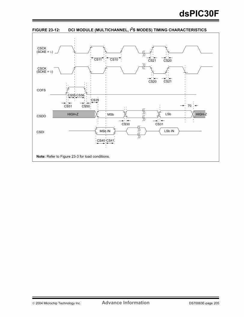
dsPIC30F
FIGURE 23-12: DCI MODULE (MULTICHANNEL, I2S MODES) TIMING CHARACTERISTICS
COFS
CSCK(SCKE = 1)
CSCK(SCKE = 0)
CSDO
CSDI
CS11 CS10
CS40 CS41
CS21CS20
CS35
CS21
MSb LSb
MSb IN LSb IN
CS31
HIGH-Z HIGH-Z
70
CS30
CS51 CS50
CS55
Note: Refer to Figure 23-3 for load conditions.
CS20
CS56
2004 Microchip Technology Inc. Advance Information DS70083E-page 205
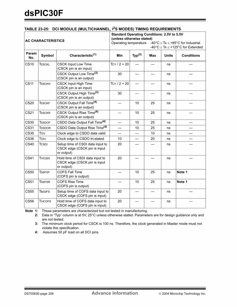
dsPIC30F
TABLE 23-25: DCI MODULE (MULTICHANNEL, I2S MODES) TIMING REQUIREMENTS
AC CHARACTERISTICS
Standard Operating Conditions: 2.5V to 5.5V
(unless otherwise stated)
Operating temperature -40°C ≤ TA ≤ +85°C for Industrial
-40°C ≤ TA ≤ +125°C for Extended
Param
No.Symbol Characteristic(1) Min Typ(2) Max Units Conditions
CS10 TcSCKL CSCK Input Low Time
(CSCK pin is an input)
TCY / 2 + 20 — — ns —
CSCK Output Low Time(3)
(CSCK pin is an output)
30 — — ns —
CS11 TcSCKH CSCK Input High Time
(CSCK pin is an input)
TCY / 2 + 20 — — ns —
CSCK Output High Time(3)
(CSCK pin is an output)
30 — — ns —
CS20 TcSCKF CSCK Output Fall Time(4)
(CSCK pin is an output)
— 10 25 ns —
CS21 TcSCKR CSCK Output Rise Time(4)
(CSCK pin is an output)
— 10 25 ns —
CS30 TcSDOF CSDO Data Output Fall Time(4) — 10 25 ns —
CS31 TcSDOR CSDO Data Output Rise Time(4) — 10 25 ns —
CS35 TDV Clock edge to CSDO data valid — — 10 ns —
CS36 TDIV Clock edge to CSDO tri-stated 10 — 20 ns —
CS40 TCSDI Setup time of CSDI data input to
CSCK edge (CSCK pin is input
or output)
20 — — ns —
CS41 THCSDI Hold time of CSDI data input to
CSCK edge (CSCK pin is input
or output)
20 — — ns —
CS50 TcoFSF COFS Fall Time
(COFS pin is output)
— 10 25 ns Note 1
CS51 TcoFSR COFS Rise Time
(COFS pin is output)
— 10 25 ns Note 1
CS55 TscoFS Setup time of COFS data input to
CSCK edge (COFS pin is input)
20 — — ns —
CS56 THCOFS Hold time of COFS data input to
CSCK edge (COFS pin is input)
20 — — ns —
Note 1: These parameters are characterized but not tested in manufacturing.
2: Data in “Typ” column is at 5V, 25°C unless otherwise stated. Parameters are for design guidance only and
are not tested.
3: The minimum clock period for CSCK is 100 ns. Therefore, the clock generated in Master mode must not
violate this specification.
4: Assumes 50 pF load on all DCI pins.
DS70083E-page 206 Advance Information 2004 Microchip Technology Inc.
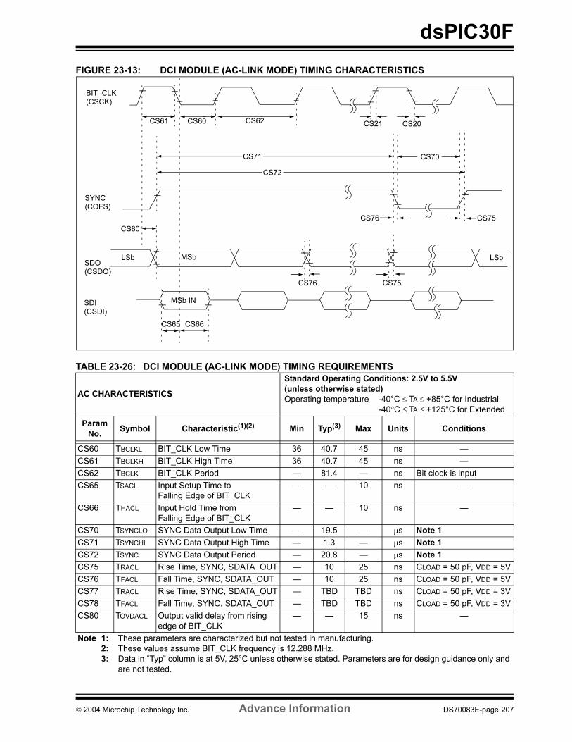
dsPIC30F
FIGURE 23-13: DCI MODULE (AC-LINK MODE) TIMING CHARACTERISTICS
TABLE 23-26: DCI MODULE (AC-LINK MODE) TIMING REQUIREMENTS
AC CHARACTERISTICS
Standard Operating Conditions: 2.5V to 5.5V
(unless otherwise stated)
Operating temperature -40°C ≤ TA ≤ +85°C for Industrial
-40°C ≤ TA ≤ +125°C for Extended
Param
No.Symbol Characteristic(1)(2) Min Typ(3) Max Units Conditions
CS60 TBCLKL BIT_CLK Low Time 36 40.7 45 ns —
CS61 TBCLKH BIT_CLK High Time 36 40.7 45 ns —
CS62 TBCLK BIT_CLK Period — 81.4 — ns Bit clock is input
CS65 TSACL Input Setup Time to
Falling Edge of BIT_CLK
— — 10 ns —
CS66 THACL Input Hold Time from
Falling Edge of BIT_CLK
— — 10 ns —
CS70 TSYNCLO SYNC Data Output Low Time — 19.5 — µs Note 1
CS71 TSYNCHI SYNC Data Output High Time — 1.3 — µs Note 1
CS72 TSYNC SYNC Data Output Period — 20.8 — µs Note 1
CS75 TRACL Rise Time, SYNC, SDATA_OUT — 10 25 ns CLOAD = 50 pF, VDD = 5V
CS76 TFACL Fall Time, SYNC, SDATA_OUT — 10 25 ns CLOAD = 50 pF, VDD = 5V
CS77 TRACL Rise Time, SYNC, SDATA_OUT — TBD TBD ns CLOAD = 50 pF, VDD = 3V
CS78 TFACL Fall Time, SYNC, SDATA_OUT — TBD TBD ns CLOAD = 50 pF, VDD = 3V
CS80 TOVDACL Output valid delay from rising
edge of BIT_CLK
— — 15 ns —
Note 1: These parameters are characterized but not tested in manufacturing.
2: These values assume BIT_CLK frequency is 12.288 MHz.
3: Data in “Typ” column is at 5V, 25°C unless otherwise stated. Parameters are for design guidance only and
are not tested.
SYNC
BIT_CLK
SDO
SDI
CS61 CS60
CS65 CS66
CS80
CS21
MSb IN
CS75
LSb
CS76
(COFS)
(CSCK)
LSbMSb
CS72
CS71 CS70
CS76 CS75
(CSDO)
(CSDI)
CS62 CS20
2004 Microchip Technology Inc. Advance Information DS70083E-page 207
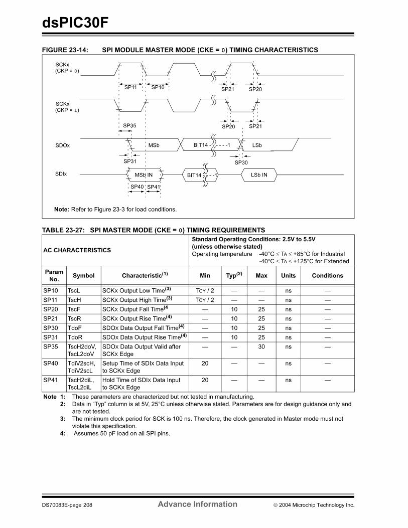
dsPIC30F
FIGURE 23-14: SPI MODULE MASTER MODE (CKE = 0) TIMING CHARACTERISTICS
TABLE 23-27: SPI MASTER MODE (CKE = 0) TIMING REQUIREMENTS
AC CHARACTERISTICS
Standard Operating Conditions: 2.5V to 5.5V
(unless otherwise stated)
Operating temperature -40°C ≤ TA ≤ +85°C for Industrial
-40°C ≤ TA ≤ +125°C for Extended
Param
No.Symbol Characteristic(1) Min Typ(2) Max Units Conditions
SP10 TscL SCKX Output Low Time(3) TCY / 2 — — ns —
SP11 TscH SCKX Output High Time(3) TCY / 2 — — ns —
SP20 TscF SCKX Output Fall Time(4 — 10 25 ns —
SP21 TscR SCKX Output Rise Time(4) — 10 25 ns —
SP30 TdoF SDOX Data Output Fall Time(4) — 10 25 ns —
SP31 TdoR SDOX Data Output Rise Time(4) — 10 25 ns —
SP35 TscH2doV,
TscL2doV
SDOX Data Output Valid after
SCKX Edge
— — 30 ns —
SP40 TdiV2scH,
TdiV2scL
Setup Time of SDIX Data Input
to SCKX Edge
20 — — ns —
SP41 TscH2diL,
TscL2diL
Hold Time of SDIX Data Input
to SCKX Edge
20 — — ns —
Note 1: These parameters are characterized but not tested in manufacturing.
2: Data in “Typ” column is at 5V, 25°C unless otherwise stated. Parameters are for design guidance only and
are not tested.
3: The minimum clock period for SCK is 100 ns. Therefore, the clock generated in Master mode must not
violate this specification.
4: Assumes 50 pF load on all SPI pins.
SCKx(CKP = 0)
SCKx(CKP = 1)
SDOx
SDIx
SP11 SP10
SP40 SP41
SP21SP20SP35
SP20SP21
MSb LSbBIT14 - - - - - -1
MSb IN LSb INBIT14 - - - -1
SP30SP31
Note: Refer to Figure 23-3 for load conditions.
DS70083E-page 208 Advance Information 2004 Microchip Technology Inc.
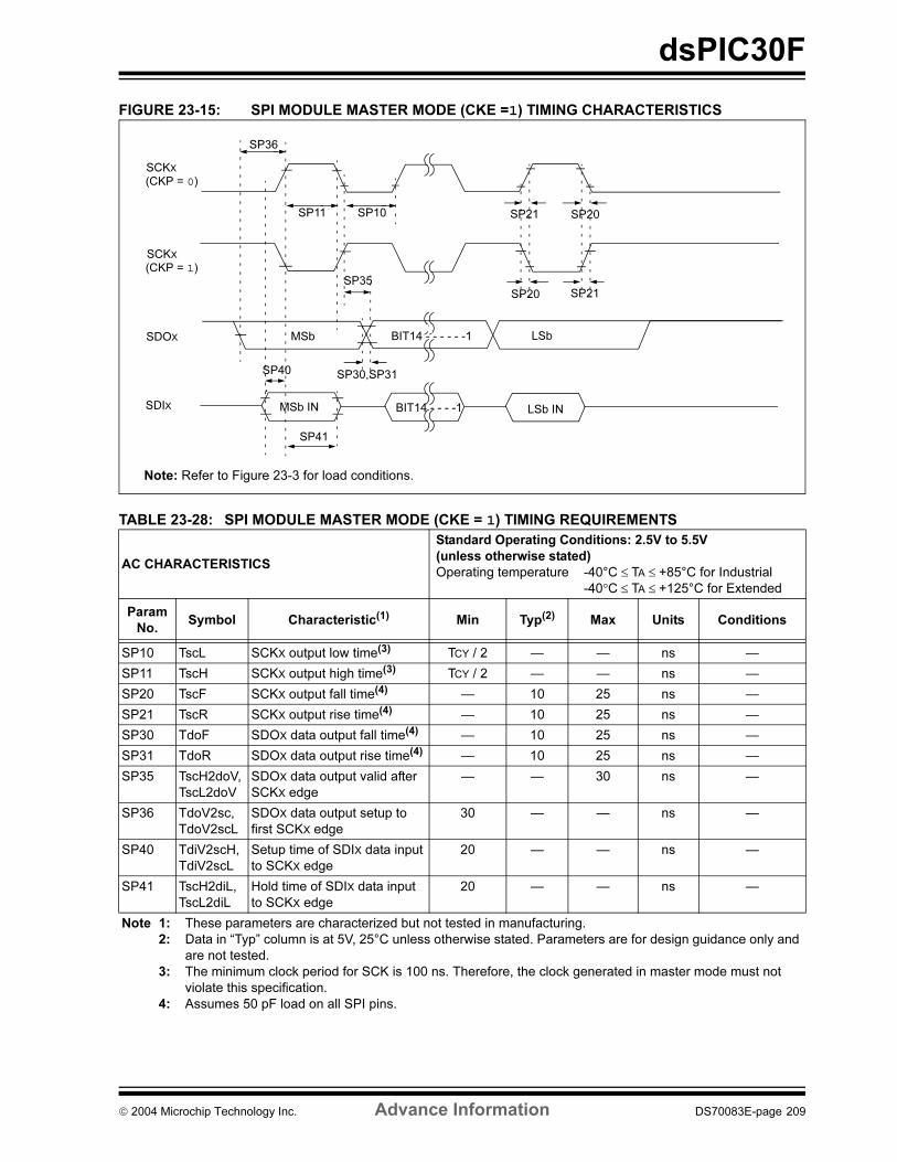
dsPIC30F
FIGURE 23-15: SPI MODULE MASTER MODE (CKE =1) TIMING CHARACTERISTICS
TABLE 23-28: SPI MODULE MASTER MODE (CKE = 1) TIMING REQUIREMENTS
AC CHARACTERISTICS
Standard Operating Conditions: 2.5V to 5.5V
(unless otherwise stated)
Operating temperature -40°C ≤ TA ≤ +85°C for Industrial
-40°C ≤ TA ≤ +125°C for Extended
Param
No.Symbol Characteristic(1) Min Typ(2) Max Units Conditions
SP10 TscL SCKX output low time(3) TCY / 2 — — ns —
SP11 TscH SCKX output high time(3) TCY / 2 — — ns —
SP20 TscF SCKX output fall time(4) — 10 25 ns —
SP21 TscR SCKX output rise time(4) — 10 25 ns —
SP30 TdoF SDOX data output fall time(4) — 10 25 ns —
SP31 TdoR SDOX data output rise time(4) — 10 25 ns —
SP35 TscH2doV,
TscL2doV
SDOX data output valid after
SCKX edge
— — 30 ns —
SP36 TdoV2sc,
TdoV2scL
SDOX data output setup to
first SCKX edge
30 — — ns —
SP40 TdiV2scH,
TdiV2scL
Setup time of SDIX data input
to SCKX edge
20 — — ns —
SP41 TscH2diL,
TscL2diL
Hold time of SDIX data input
to SCKX edge
20 — — ns —
Note 1: These parameters are characterized but not tested in manufacturing.
2: Data in “Typ” column is at 5V, 25°C unless otherwise stated. Parameters are for design guidance only and
are not tested.
3: The minimum clock period for SCK is 100 ns. Therefore, the clock generated in master mode must not
violate this specification.
4: Assumes 50 pF load on all SPI pins.
SCKX
(CKP = 0)
SCKX
(CKP = 1)
SDOX
SDIX
SP36
SP30,SP31
SP35
MSb
MSb IN
BIT14 - - - - - -1
LSb INBIT14 - - - -1
LSb
Note: Refer to Figure 23-3 for load conditions.
SP11 SP10 SP20SP21
SP21SP20
SP40
SP41
2004 Microchip Technology Inc. Advance Information DS70083E-page 209
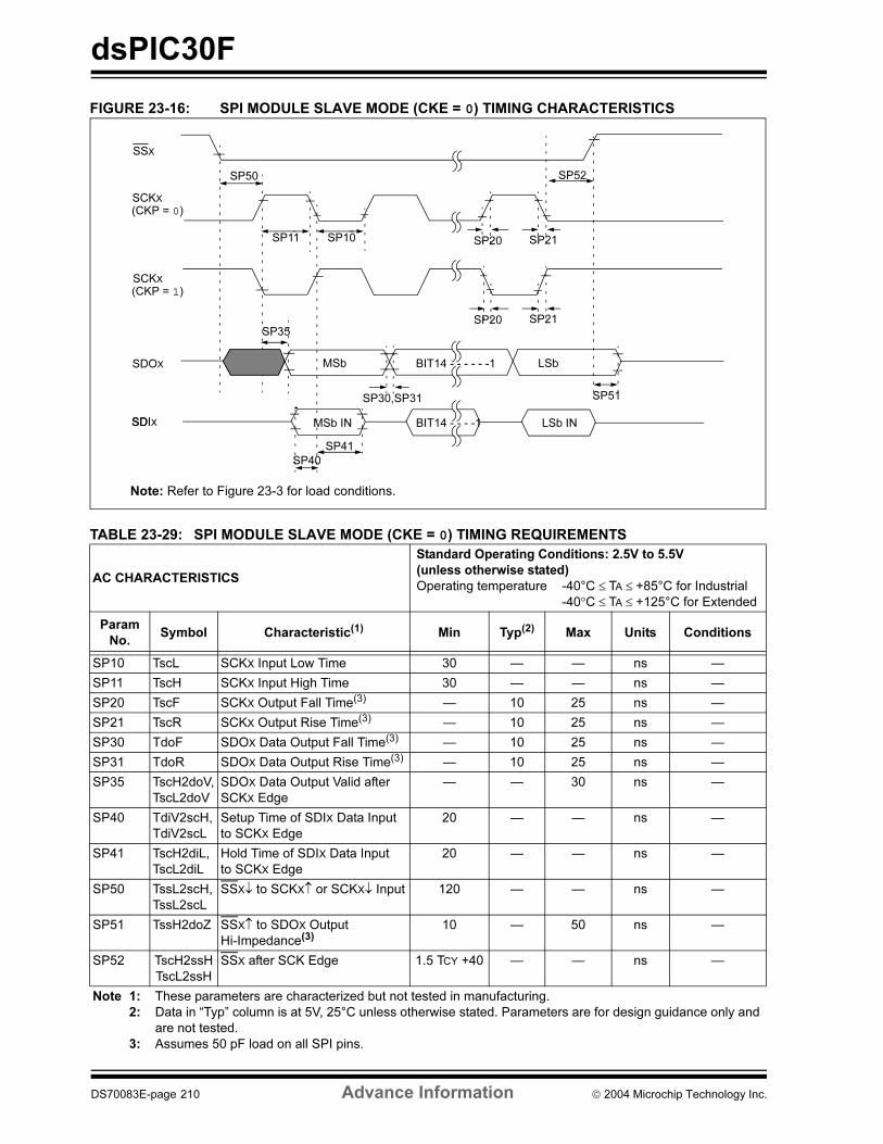
dsPIC30F
FIGURE 23-16: SPI MODULE SLAVE MODE (CKE = 0) TIMING CHARACTERISTICS
TABLE 23-29: SPI MODULE SLAVE MODE (CKE = 0) TIMING REQUIREMENTS
AC CHARACTERISTICS
Standard Operating Conditions: 2.5V to 5.5V
(unless otherwise stated)
Operating temperature -40°C ≤ TA ≤ +85°C for Industrial
-40°C ≤ TA ≤ +125°C for Extended
Param
No.Symbol Characteristic(1) Min Typ(2) Max Units Conditions
SP10 TscL SCKX Input Low Time 30 — — ns —
SP11 TscH SCKX Input High Time 30 — — ns —
SP20 TscF SCKX Output Fall Time(3) — 10 25 ns —
SP21 TscR SCKX Output Rise Time(3) — 10 25 ns —
SP30 TdoF SDOX Data Output Fall Time(3) — 10 25 ns —
SP31 TdoR SDOX Data Output Rise Time(3) — 10 25 ns —
SP35 TscH2doV,
TscL2doV
SDOX Data Output Valid after
SCKX Edge
— — 30 ns —
SP40 TdiV2scH,
TdiV2scL
Setup Time of SDIX Data Input
to SCKX Edge
20 — — ns —
SP41 TscH2diL,
TscL2diL
Hold Time of SDIX Data Input
to SCKX Edge
20 — — ns —
SP50 TssL2scH,
TssL2scL
SSX↓ to SCKX↑ or SCKX↓ Input 120 — — ns —
SP51 TssH2doZ SSX↑ to SDOX Output
Hi-Impedance(3)10 — 50 ns —
SP52 TscH2ssH
TscL2ssH
SSX after SCK Edge 1.5 TCY +40 — — ns —
Note 1: These parameters are characterized but not tested in manufacturing.
2: Data in “Typ” column is at 5V, 25°C unless otherwise stated. Parameters are for design guidance only and
are not tested.
3: Assumes 50 pF load on all SPI pins.
SSX
SCKX
(CKP = 0)
SCKX
(CKP = 1)
SDOX
SDI
SP50
SP40
SP41
SP30,SP31 SP51
SP35
SDIX
MSb LSbBIT14 - - - - - -1
MSb IN BIT14 - - - -1 LSb IN
SP52
SP21SP20
SP21SP20SP11 SP10
Note: Refer to Figure 23-3 for load conditions.
DS70083E-page 210 Advance Information 2004 Microchip Technology Inc.
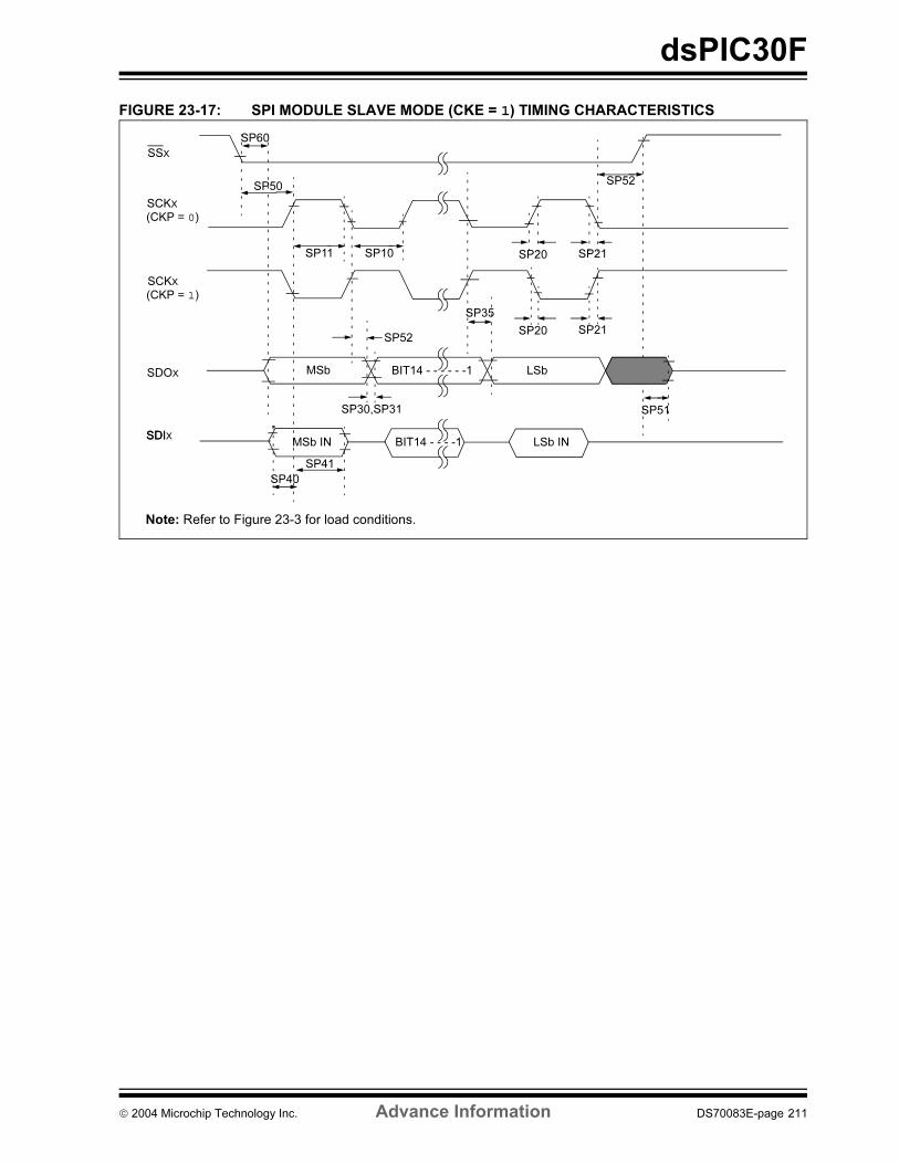
dsPIC30F
FIGURE 23-17: SPI MODULE SLAVE MODE (CKE = 1) TIMING CHARACTERISTICS
SSX
SCKX
(CKP = 0)
SCKX
(CKP = 1)
SDOX
SDI
SP50
SP60
SDIX
SP30,SP31
MSb BIT14 - - - - - -1 LSb
SP51
MSb IN BIT14 - - - -1 LSb IN
SP35
SP52
SP52
SP21SP20
SP21SP20SP11 SP10
SP40
SP41
Note: Refer to Figure 23-3 for load conditions.
2004 Microchip Technology Inc. Advance Information DS70083E-page 211
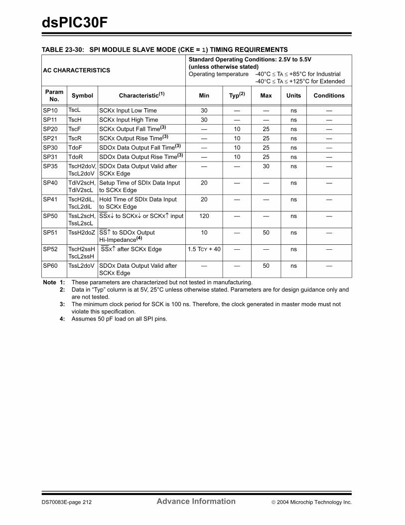
dsPIC30F
TABLE 23-30: SPI MODULE SLAVE MODE (CKE = 1) TIMING REQUIREMENTS
AC CHARACTERISTICS
Standard Operating Conditions: 2.5V to 5.5V
(unless otherwise stated)
Operating temperature -40°C ≤ TA ≤ +85°C for Industrial
-40°C ≤ TA ≤ +125°C for Extended
Param
No.Symbol Characteristic(1) Min Typ(2) Max Units Conditions
SP10 TscL SCKX Input Low Time 30 — — ns —
SP11 TscH SCKX Input High Time 30 — — ns —
SP20 TscF SCKX Output Fall Time(3) — 10 25 ns —
SP21 TscR SCKX Output Rise Time(3) — 10 25 ns —
SP30 TdoF SDOX Data Output Fall Time(3) — 10 25 ns —
SP31 TdoR SDOX Data Output Rise Time(3) — 10 25 ns —
SP35 TscH2doV,
TscL2doV
SDOX Data Output Valid after
SCKX Edge
— — 30 ns —
SP40 TdiV2scH,
TdiV2scL
Setup Time of SDIX Data Input
to SCKX Edge
20 — — ns —
SP41 TscH2diL,
TscL2diL
Hold Time of SDIX Data Input
to SCKX Edge
20 — — ns —
SP50 TssL2scH,
TssL2scL
SSX↓ to SCKX↓ or SCKX↑ input 120 — — ns —
SP51 TssH2doZ SS↑ to SDOX Output
Hi-Impedance(4)10 — 50 ns —
SP52 TscH2ssH
TscL2ssH
SSX↑ after SCKX Edge 1.5 TCY + 40 — — ns —
SP60 TssL2doV SDOX Data Output Valid after
SCKX Edge
— — 50 ns —
Note 1: These parameters are characterized but not tested in manufacturing.
2: Data in “Typ” column is at 5V, 25°C unless otherwise stated. Parameters are for design guidance only and
are not tested.
3: The minimum clock period for SCK is 100 ns. Therefore, the clock generated in master mode must not
violate this specification.
4: Assumes 50 pF load on all SPI pins.
DS70083E-page 212 Advance Information 2004 Microchip Technology Inc.
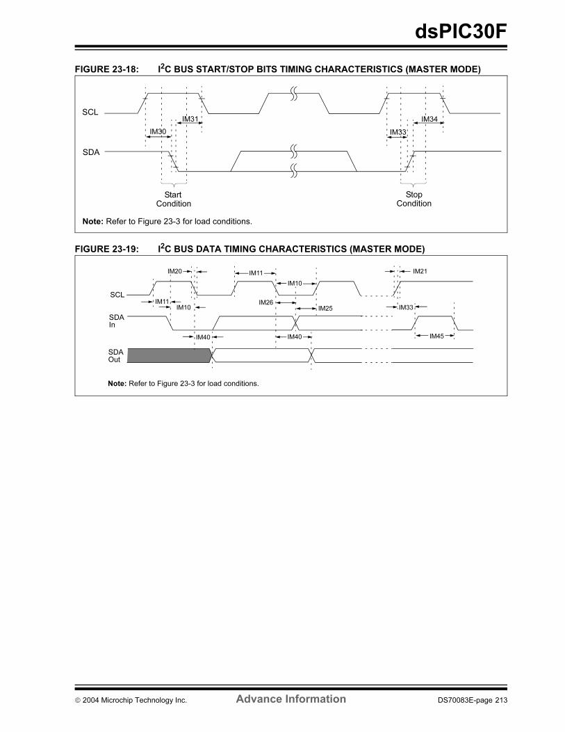
dsPIC30F
FIGURE 23-18: I2C BUS START/STOP BITS TIMING CHARACTERISTICS (MASTER MODE)
FIGURE 23-19: I2C BUS DATA TIMING CHARACTERISTICS (MASTER MODE)
IM31 IM34SCL
SDA
StartCondition
StopCondition
IM30 IM33
Note: Refer to Figure 23-3 for load conditions.
IM11IM10 IM33
IM11
IM10
IM20
IM26IM25
IM40 IM40 IM45
IM21
SCL
SDAIn
SDAOut
Note: Refer to Figure 23-3 for load conditions.
2004 Microchip Technology Inc. Advance Information DS70083E-page 213
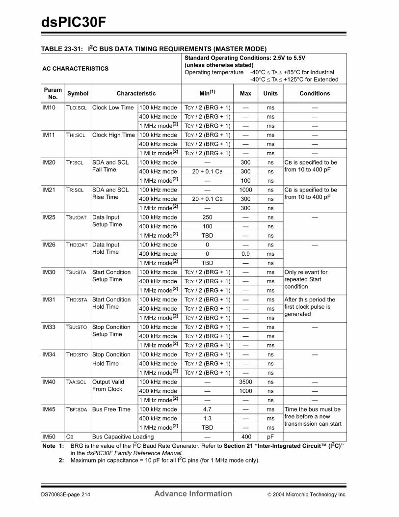
dsPIC30F
TABLE 23-31: I2C BUS DATA TIMING REQUIREMENTS (MASTER MODE)
AC CHARACTERISTICS
Standard Operating Conditions: 2.5V to 5.5V
(unless otherwise stated)
Operating temperature -40°C ≤ TA ≤ +85°C for Industrial
-40°C ≤ TA ≤ +125°C for Extended
Param
No.Symbol Characteristic Min(1) Max Units Conditions
IM10 TLO:SCL Clock Low Time 100 kHz mode TCY / 2 (BRG + 1) — ms —
400 kHz mode TCY / 2 (BRG + 1) — ms —
1 MHz mode(2) TCY / 2 (BRG + 1) — ms —
IM11 THI:SCL Clock High Time 100 kHz mode TCY / 2 (BRG + 1) — ms —
400 kHz mode TCY / 2 (BRG + 1) — ms —
1 MHz mode(2) TCY / 2 (BRG + 1) — ms —
IM20 TF:SCL SDA and SCL
Fall Time
100 kHz mode — 300 ns CB is specified to be
from 10 to 400 pF400 kHz mode 20 + 0.1 CB 300 ns
1 MHz mode(2) — 100 ns
IM21 TR:SCL SDA and SCL
Rise Time
100 kHz mode — 1000 ns CB is specified to be
from 10 to 400 pF400 kHz mode 20 + 0.1 CB 300 ns
1 MHz mode(2) — 300 ns
IM25 TSU:DAT Data Input
Setup Time
100 kHz mode 250 — ns —
400 kHz mode 100 — ns
1 MHz mode(2) TBD — ns
IM26 THD:DAT Data Input
Hold Time
100 kHz mode 0 — ns —
400 kHz mode 0 0.9 ms
1 MHz mode(2) TBD — ns
IM30 TSU:STA Start Condition
Setup Time
100 kHz mode TCY / 2 (BRG + 1) — ms Only relevant for
repeated Start
condition400 kHz mode TCY / 2 (BRG + 1) — ms
1 MHz mode(2) TCY / 2 (BRG + 1) — ms
IM31 THD:STA Start Condition
Hold Time
100 kHz mode TCY / 2 (BRG + 1) — ms After this period the
first clock pulse is
generated400 kHz mode TCY / 2 (BRG + 1) — ms
1 MHz mode(2) TCY / 2 (BRG + 1) — ms
IM33 TSU:STO Stop Condition
Setup Time
100 kHz mode TCY / 2 (BRG + 1) — ms —
400 kHz mode TCY / 2 (BRG + 1) — ms
1 MHz mode(2) TCY / 2 (BRG + 1) — ms
IM34 THD:STO Stop Condition 100 kHz mode TCY / 2 (BRG + 1) — ns —
Hold Time 400 kHz mode TCY / 2 (BRG + 1) — ns
1 MHz mode(2) TCY / 2 (BRG + 1) — ns
IM40 TAA:SCL Output Valid
From Clock
100 kHz mode — 3500 ns —
400 kHz mode — 1000 ns —
1 MHz mode(2) — — ns —
IM45 TBF:SDA Bus Free Time 100 kHz mode 4.7 — ms Time the bus must be
free before a new
transmission can start400 kHz mode 1.3 — ms
1 MHz mode(2) TBD — ms
IM50 CB Bus Capacitive Loading — 400 pF
Note 1: BRG is the value of the I2C Baud Rate Generator. Refer to Section 21 “Inter-Integrated Circuit™ (I2C)”
in the dsPIC30F Family Reference Manual.
2: Maximum pin capacitance = 10 pF for all I2C pins (for 1 MHz mode only).
DS70083E-page 214 Advance Information 2004 Microchip Technology Inc.
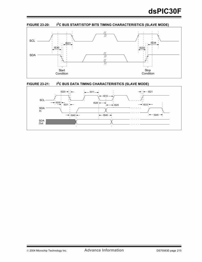
dsPIC30F
FIGURE 23-20: I2C BUS START/STOP BITS TIMING CHARACTERISTICS (SLAVE MODE)
FIGURE 23-21: I2C BUS DATA TIMING CHARACTERISTICS (SLAVE MODE)
IS31 IS34SCL
SDA
StartCondition
StopCondition
IS30 IS33
IS30IS31 IS33
IS11
IS10
IS20
IS26IS25
IS40 IS40 IS45
IS21
SCL
SDAIn
SDAOut
2004 Microchip Technology Inc. Advance Information DS70083E-page 215
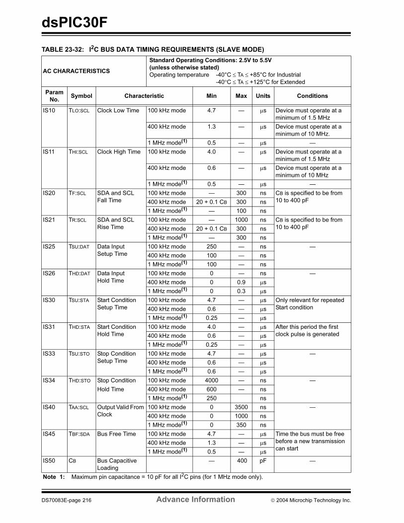
dsPIC30F
TABLE 23-32: I2C BUS DATA TIMING REQUIREMENTS (SLAVE MODE)
AC CHARACTERISTICS
Standard Operating Conditions: 2.5V to 5.5V
(unless otherwise stated)
Operating temperature -40°C ≤ TA ≤ +85°C for Industrial
-40°C ≤ TA ≤ +125°C for Extended
Param
No.Symbol Characteristic Min Max Units Conditions
IS10 TLO:SCL Clock Low Time 100 kHz mode 4.7 — µs Device must operate at a
minimum of 1.5 MHz
400 kHz mode 1.3 — µs Device must operate at a
minimum of 10 MHz.
1 MHz mode(1) 0.5 — µs —
IS11 THI:SCL Clock High Time 100 kHz mode 4.0 — µs Device must operate at a
minimum of 1.5 MHz
400 kHz mode 0.6 — µs Device must operate at a
minimum of 10 MHz
1 MHz mode(1) 0.5 — µs —
IS20 TF:SCL SDA and SCL
Fall Time
100 kHz mode — 300 ns CB is specified to be from
10 to 400 pF400 kHz mode 20 + 0.1 CB 300 ns
1 MHz mode(1) — 100 ns
IS21 TR:SCL SDA and SCL
Rise Time
100 kHz mode — 1000 ns CB is specified to be from
10 to 400 pF400 kHz mode 20 + 0.1 CB 300 ns
1 MHz mode(1) — 300 ns
IS25 TSU:DAT Data Input
Setup Time
100 kHz mode 250 — ns —
400 kHz mode 100 — ns
1 MHz mode(1) 100 — ns
IS26 THD:DAT Data Input
Hold Time
100 kHz mode 0 — ns —
400 kHz mode 0 0.9 µs
1 MHz mode(1) 0 0.3 µs
IS30 TSU:STA Start Condition
Setup Time
100 kHz mode 4.7 — µs Only relevant for repeated
Start condition400 kHz mode 0.6 — µs
1 MHz mode(1) 0.25 — µs
IS31 THD:STA Start Condition
Hold Time
100 kHz mode 4.0 — µs After this period the first
clock pulse is generated400 kHz mode 0.6 — µs
1 MHz mode(1) 0.25 — µs
IS33 TSU:STO Stop Condition
Setup Time
100 kHz mode 4.7 — µs —
400 kHz mode 0.6 — µs
1 MHz mode(1) 0.6 — µs
IS34 THD:STO Stop Condition 100 kHz mode 4000 — ns —
Hold Time 400 kHz mode 600 — ns
1 MHz mode(1) 250 ns
IS40 TAA:SCL Output Valid From
Clock
100 kHz mode 0 3500 ns —
400 kHz mode 0 1000 ns
1 MHz mode(1) 0 350 ns
IS45 TBF:SDA Bus Free Time 100 kHz mode 4.7 — µs Time the bus must be free
before a new transmission
can start400 kHz mode 1.3 — µs
1 MHz mode(1) 0.5 — µs
IS50 CB Bus Capacitive
Loading
— 400 pF —
Note 1: Maximum pin capacitance = 10 pF for all I2C pins (for 1 MHz mode only).
DS70083E-page 216 Advance Information 2004 Microchip Technology Inc.
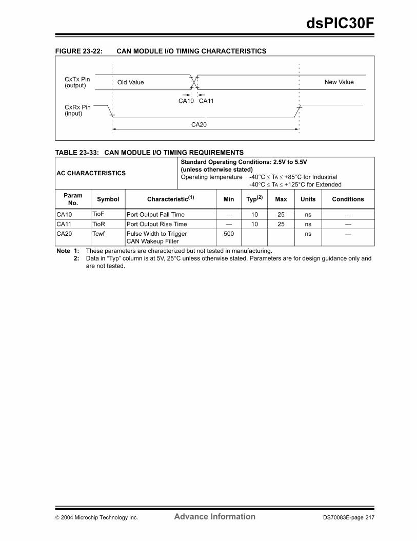
dsPIC30F
FIGURE 23-22: CAN MODULE I/O TIMING CHARACTERISTICS
TABLE 23-33: CAN MODULE I/O TIMING REQUIREMENTS
AC CHARACTERISTICS
Standard Operating Conditions: 2.5V to 5.5V
(unless otherwise stated)
Operating temperature -40°C ≤ TA ≤ +85°C for Industrial
-40°C ≤ TA ≤ +125°C for Extended
Param
No.Symbol Characteristic(1) Min Typ(2) Max Units Conditions
CA10 TioF Port Output Fall Time — 10 25 ns —
CA11 TioR Port Output Rise Time — 10 25 ns —
CA20 Tcwf Pulse Width to Trigger
CAN Wakeup Filter
500 ns —
Note 1: These parameters are characterized but not tested in manufacturing.
2: Data in “Typ” column is at 5V, 25°C unless otherwise stated. Parameters are for design guidance only and
are not tested.
CXTX Pin(output)
CA10 CA11
Old Value New Value
CA20
CXRX Pin(input)
2004 Microchip Technology Inc. Advance Information DS70083E-page 217
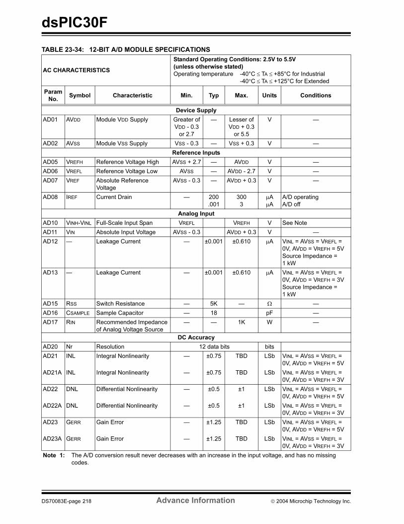
dsPIC30F
TABLE 23-34: 12-BIT A/D MODULE SPECIFICATIONS
AC CHARACTERISTICS
Standard Operating Conditions: 2.5V to 5.5V
(unless otherwise stated)
Operating temperature -40°C ≤ TA ≤ +85°C for Industrial
-40°C ≤ TA ≤ +125°C for Extended
Param
No.Symbol Characteristic Min. Typ Max. Units Conditions
Device Supply
AD01 AVDD Module VDD Supply Greater of
VDD - 0.3
or 2.7
— Lesser of
VDD + 0.3
or 5.5
V —
AD02 AVSS Module VSS Supply VSS - 0.3 — VSS + 0.3 V —
Reference Inputs
AD05 VREFH Reference Voltage High AVSS + 2.7 — AVDD V —
AD06 VREFL Reference Voltage Low AVSS — AVDD - 2.7 V —
AD07 VREF Absolute Reference
Voltage
AVSS - 0.3 — AVDD + 0.3 V —
AD08 IREF Current Drain — 200
.001
300
3
µA
µA
A/D operating
A/D off
Analog Input
AD10 VINH-VINL Full-Scale Input Span VREFL VREFH V See Note
AD11 VIN Absolute Input Voltage AVSS - 0.3 AVDD + 0.3 V —
AD12 — Leakage Current — ±0.001 ±0.610 µA VINL = AVSS = VREFL =
0V, AVDD = VREFH = 5V
Source Impedance =
1 kW
AD13 — Leakage Current — ±0.001 ±0.610 µA VINL = AVSS = VREFL =
0V, AVDD = VREFH = 3V
Source Impedance =
1 kW
AD15 RSS Switch Resistance — 5K — Ω —
AD16 CSAMPLE Sample Capacitor — 18 pF —
AD17 RIN Recommended Impedance
of Analog Voltage Source
— — 1K W —
DC Accuracy
AD20 Nr Resolution 12 data bits bits
AD21 INL Integral Nonlinearity — ±0.75 TBD LSb VINL = AVSS = VREFL =
0V, AVDD = VREFH = 5V
AD21A INL Integral Nonlinearity — ±0.75 TBD LSb VINL = AVSS = VREFL =
0V, AVDD = VREFH = 3V
AD22 DNL Differential Nonlinearity — ±0.5 ±1 LSb VINL = AVSS = VREFL =
0V, AVDD = VREFH = 5V
AD22A DNL Differential Nonlinearity — ±0.5 ±1 LSb VINL = AVSS = VREFL =
0V, AVDD = VREFH = 3V
AD23 GERR Gain Error — ±1.25 TBD LSb VINL = AVSS = VREFL =
0V, AVDD = VREFH = 5V
AD23A GERR Gain Error — ±1.25 TBD LSb VINL = AVSS = VREFL =
0V, AVDD = VREFH = 3V
Note 1: The A/D conversion result never decreases with an increase in the input voltage, and has no missing
codes.
DS70083E-page 218 Advance Information 2004 Microchip Technology Inc.
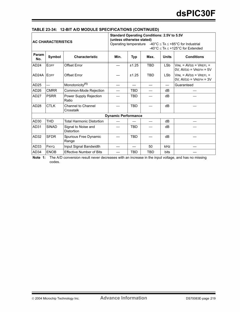
dsPIC30F
AD24 EOFF Offset Error — ±1.25 TBD LSb VINL = AVSS = VREFL =
0V, AVDD = VREFH = 5V
AD24A EOFF Offset Error — ±1.25 TBD LSb VINL = AVSS = VREFL =
0V, AVDD = VREFH = 3V
AD25 — Monotonicity(1) — — — — Guaranteed
AD26 CMRR Common-Mode Rejection — TBD — dB —
AD27 PSRR Power Supply Rejection
Ratio
— TBD — dB —
AD28 CTLK Channel to Channel
Crosstalk
— TBD — dB —
Dynamic Performance
AD30 THD Total Harmonic Distortion — — — dB —
AD31 SINAD Signal to Noise and
Distortion
— TBD — dB —
AD32 SFDR Spurious Free Dynamic
Range
— TBD — dB —
AD33 FNYQ Input Signal Bandwidth — — 50 kHz —
AD34 ENOB Effective Number of Bits — TBD TBD bits —
TABLE 23-34: 12-BIT A/D MODULE SPECIFICATIONS (CONTINUED)
AC CHARACTERISTICS
Standard Operating Conditions: 2.5V to 5.5V
(unless otherwise stated)
Operating temperature -40°C ≤ TA ≤ +85°C for Industrial
-40°C ≤ TA ≤ +125°C for Extended
Param
No.Symbol Characteristic Min. Typ Max. Units Conditions
Note 1: The A/D conversion result never decreases with an increase in the input voltage, and has no missing
codes.
2004 Microchip Technology Inc. Advance Information DS70083E-page 219
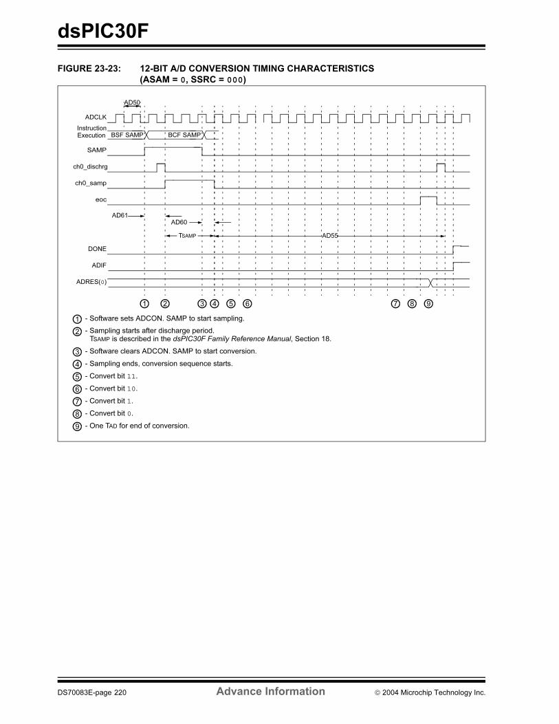
dsPIC30F
FIGURE 23-23: 12-BIT A/D CONVERSION TIMING CHARACTERISTICS
(ASAM = 0, SSRC = 000)
AD55TSAMP
BCF SAMPBSF SAMP
AD61
ADCLK
Instruction
SAMP
ch0_dischrg
ch0_samp
AD60
DONE
ADIF
ADRES(0)
1 2 3 4 5 6 87
1 - Software sets ADCON. SAMP to start sampling.
2 - Sampling starts after discharge period.
3 - Software clears ADCON. SAMP to start conversion.
4 - Sampling ends, conversion sequence starts.
5 - Convert bit 11.
9 - One TAD for end of conversion.
AD50
eoc
9
6 - Convert bit 10.
7 - Convert bit 1.
8 - Convert bit 0.
Execution
TSAMP is described in the dsPIC30F Family Reference Manual, Section 18.
DS70083E-page 220 Advance Information 2004 Microchip Technology Inc.
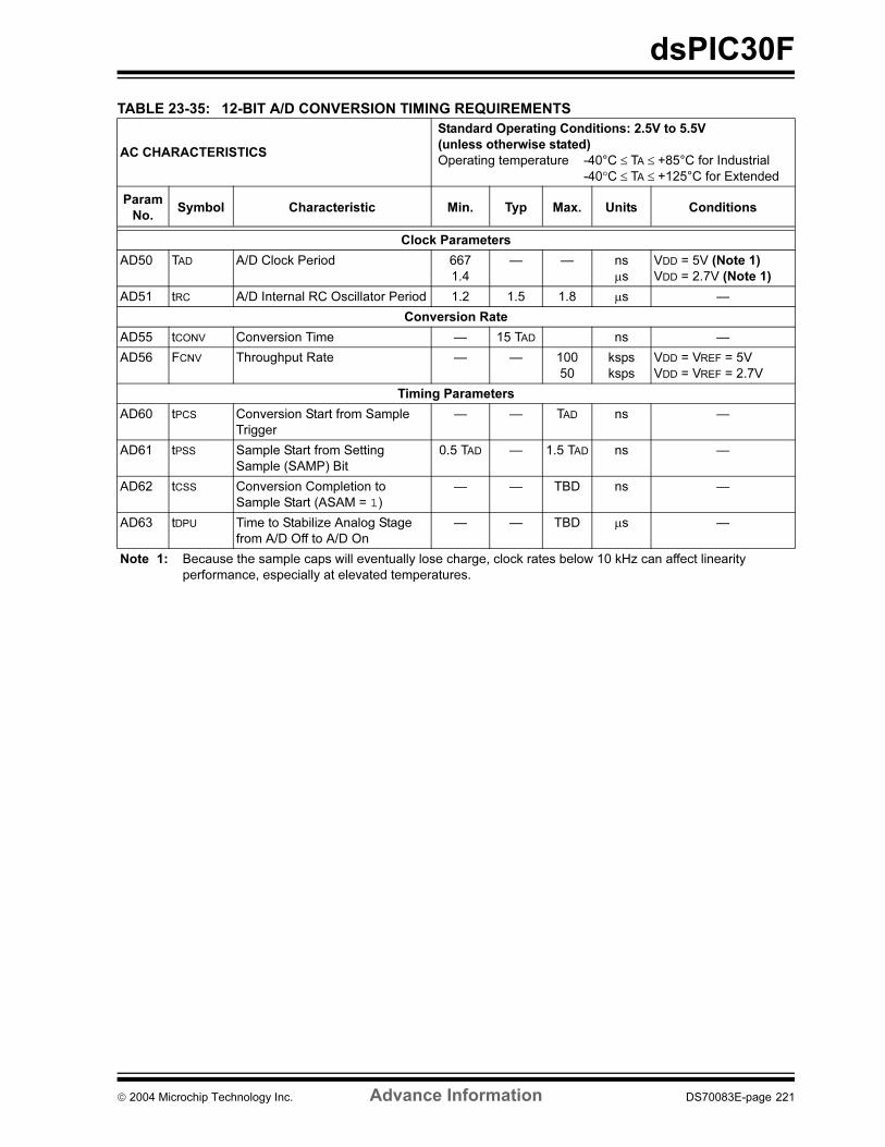
dsPIC30F
TABLE 23-35: 12-BIT A/D CONVERSION TIMING REQUIREMENTS
AC CHARACTERISTICS
Standard Operating Conditions: 2.5V to 5.5V
(unless otherwise stated)
Operating temperature -40°C ≤ TA ≤ +85°C for Industrial
-40°C ≤ TA ≤ +125°C for Extended
Param
No.Symbol Characteristic Min. Typ Max. Units Conditions
Clock Parameters
AD50 TAD A/D Clock Period 667
1.4
— — ns
µs
VDD = 5V (Note 1)
VDD = 2.7V (Note 1)
AD51 tRC A/D Internal RC Oscillator Period 1.2 1.5 1.8 µs —
Conversion Rate
AD55 tCONV Conversion Time — 15 TAD ns —
AD56 FCNV Throughput Rate — — 100
50
ksps
ksps
VDD = VREF = 5V
VDD = VREF = 2.7V
Timing Parameters
AD60 tPCS Conversion Start from Sample
Trigger
— — TAD ns —
AD61 tPSS Sample Start from Setting
Sample (SAMP) Bit
0.5 TAD — 1.5 TAD ns —
AD62 tCSS Conversion Completion to
Sample Start (ASAM = 1)
— — TBD ns —
AD63 tDPU Time to Stabilize Analog Stage
from A/D Off to A/D On
— — TBD µs —
Note 1: Because the sample caps will eventually lose charge, clock rates below 10 kHz can affect linearity
performance, especially at elevated temperatures.
2004 Microchip Technology Inc. Advance Information DS70083E-page 221
dsPIC30F
NOTES:
DS70083E-page 222 Advance Information 2004 Microchip Technology Inc.
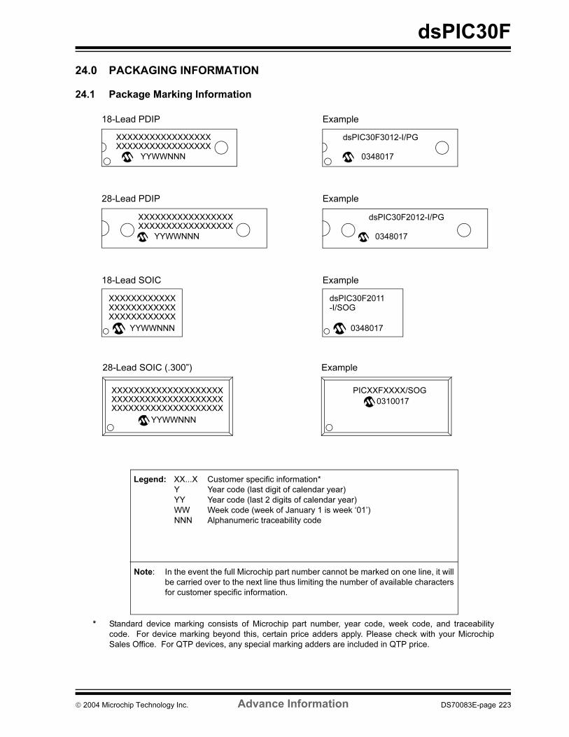
dsPIC30F
24.0 PACKAGING INFORMATION
24.1 Package Marking Information
XXXXXXXXXXXXXXXXX
YYWWNNN
28-Lead PDIP Example
XXXXXXXXXXXXXXXXX
18-Lead PDIP Example
18-Lead SOIC Example
0348017
dsPIC30F2012-I/PG
XXXXXXXXXXXXXXXXXXXXXXXXXXXXXXXXXX
YYWWNNN
dsPIC30F3012-I/PG
0348017
YYWWNNN
XXXXXXXXXXXXXXXXXXXXXXXXXXXXXXXXXXXX
0348017
-I/SOGdsPIC30F2011
Legend: XX...X Customer specific information*
Y Year code (last digit of calendar year)
YY Year code (last 2 digits of calendar year)
WW Week code (week of January 1 is week ‘01’)
NNN Alphanumeric traceability code
Note: In the event the full Microchip part number cannot be marked on one line, it will
be carried over to the next line thus limiting the number of available characters
for customer specific information.
* Standard device marking consists of Microchip part number, year code, week code, and traceability
code. For device marking beyond this, certain price adders apply. Please check with your Microchip
Sales Office. For QTP devices, any special marking adders are included in QTP price.
28-Lead SOIC (.300”)
XXXXXXXXXXXXXXXXXXXXXXXXXXXXXXXXXXXXXXXXXXXXXXXXXXXXXXXXXXXX
YYWWNNN
Example
PICXXFXXXX/SOG
0310017
2004 Microchip Technology Inc. Advance Information DS70083E-page 223
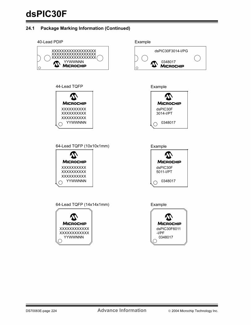
dsPIC30F
24.1 Package Marking Information (Continued)
44-Lead TQFP Example
XXXXXXXXXXXXXXXXXXXX
XXXXXXXXXX
YYWWNNN
dsPIC30F3014-I/PT
0348017
64-Lead TQFP (10x10x1mm) Example
XXXXXXXXXXXXXXXXXXXX
XXXXXXXXXX
YYWWNNN
dsPIC30F5011-I/PT
0348017
XXXXXXXXXXXXXXXXXXXXXXXX
YYWWNNN
64-Lead TQFP (14x14x1mm)
dsPIC30F6011-I/PF
0348017
Example
XXXXXXXXXXXXXXXXXX
YYWWNNN
40-Lead PDIP Example
XXXXXXXXXXXXXXXXXXXXXXXXXXXXXXXXXXXX
dsPIC30F3014-I/PG
0348017
DS70083E-page 224 Advance Information 2004 Microchip Technology Inc.
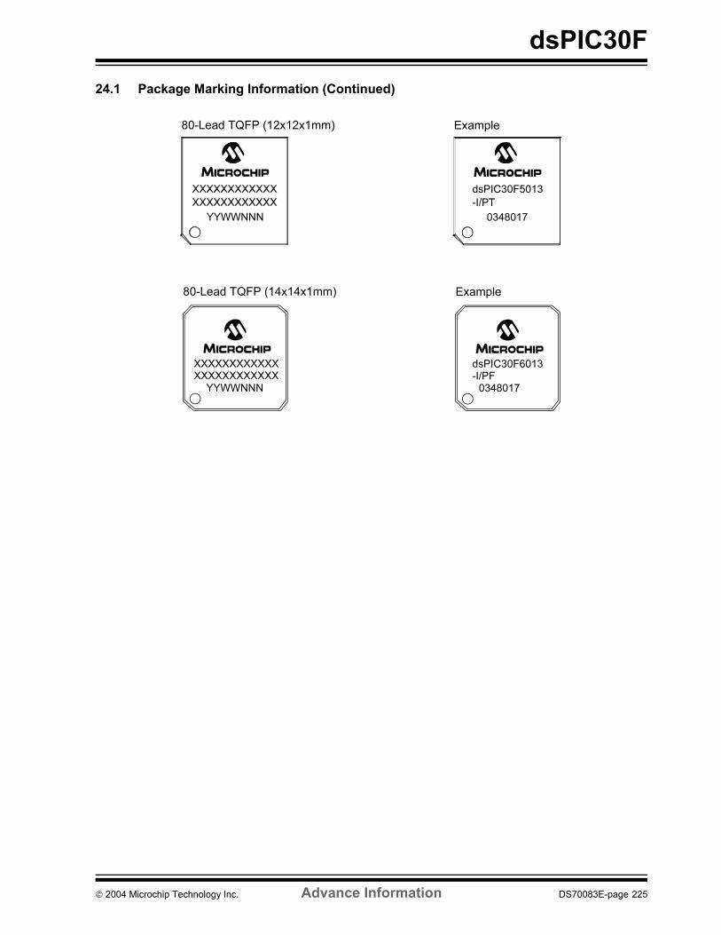
dsPIC30F
24.1 Package Marking Information (Continued)
XXXXXXXXXXXXXXXXXXXXXXXX
YYWWNNN
80-Lead TQFP (14x14x1mm)
dsPIC30F6013-I/PF
0348017
Example
80-Lead TQFP (12x12x1mm)
XXXXXXXXXXXX
YYWWNNN
XXXXXXXXXXXX
Example
dsPIC30F5013
0348017
-I/PT
2004 Microchip Technology Inc. Advance Information DS70083E-page 225
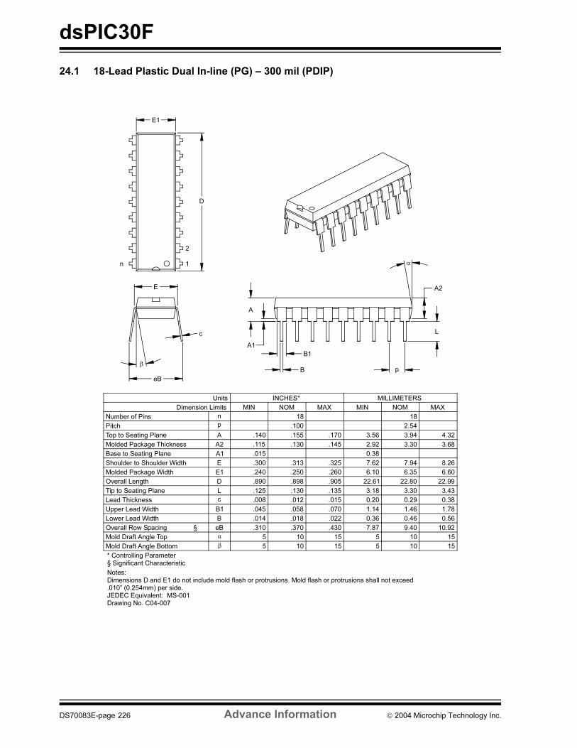
dsPIC30F
24.1 18-Lead Plastic Dual In-line (PG) – 300 mil (PDIP)
1510515105βMold Draft Angle Bottom
1510515105αMold Draft Angle Top
10.929.407.87.430.370.310eBOverall Row Spacing §
0.560.460.36.022.018.014BLower Lead Width
1.781.461.14.070.058.045B1Upper Lead Width
0.380.290.20.015.012.008cLead Thickness
3.433.303.18.135.130.125LTip to Seating Plane
22.9922.8022.61.905.898.890DOverall Length
6.606.356.10.260.250.240E1Molded Package Width
8.267.947.62.325.313.300EShoulder to Shoulder Width
0.38.015A1Base to Seating Plane
3.683.302.92.145.130.115A2Molded Package Thickness
4.323.943.56.170.155.140ATop to Seating Plane
2.54.100pPitch
1818nNumber of Pins
MAXNOMMINMAXNOMMINDimension Limits
MILLIMETERSINCHES*Units
1
2
D
n
E1
c
eB
β
E
α
p
A2
L
B1
B
A
A1
* Controlling Parameter
Notes:Dimensions D and E1 do not include mold flash or protrusions. Mold flash or protrusions shall not exceed .010” (0.254mm) per side.JEDEC Equivalent: MS-001Drawing No. C04-007
§ Significant Characteristic
DS70083E-page 226 Advance Information 2004 Microchip Technology Inc.
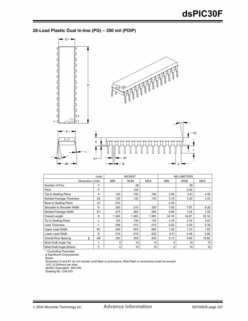
dsPIC30F
28-Lead Plastic Dual In-line (PG) – 300 mil (PDIP)
1510515105βMold Draft Angle Bottom
1510515105αMold Draft Angle Top
10.928.898.13.430.350.320eBOverall Row Spacing §
0.560.480.41.022.019.016BLower Lead Width
1.651.331.02.065.053.040B1Upper Lead Width
0.380.290.20.015.012.008cLead Thickness
3.433.303.18.135.130.125LTip to Seating Plane
35.1834.6734.161.3851.3651.345DOverall Length
7.497.246.99.295.285.275E1Molded Package Width
8.267.877.62.325.310.300EShoulder to Shoulder Width
0.38.015A1Base to Seating Plane
3.433.303.18.135.130.125A2Molded Package Thickness
4.063.813.56.160.150.140ATop to Seating Plane
2.54.100pPitch
2828nNumber of Pins
MAXNOMMINMAXNOMMINDimension Limits
MILLIMETERSINCHES*Units
2
1
D
n
E1
c
eB
β
E
α
p
L
A2
B
B1
A
A1
Notes:
JEDEC Equivalent: MO-095
Drawing No. C04-070
* Controlling Parameter
Dimension D and E1 do not include mold flash or protrusions. Mold flash or protrusions shall not exceed .010” (0.254mm) per side.
§ Significant Characteristic
2004 Microchip Technology Inc. Advance Information DS70083E-page 227
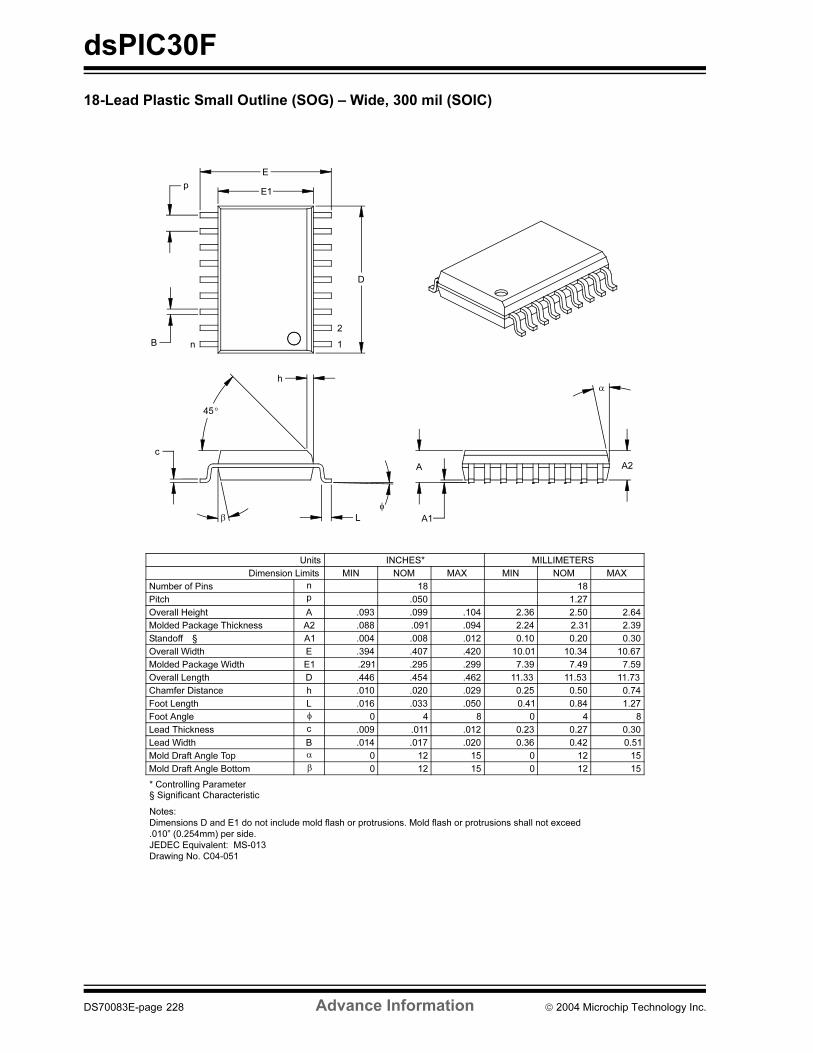
dsPIC30F
18-Lead Plastic Small Outline (SOG) – Wide, 300 mil (SOIC)
Foot Angle φ 0 4 8 0 4 8
1512015120βMold Draft Angle Bottom
1512015120αMold Draft Angle Top
0.510.420.36.020.017.014BLead Width
0.300.270.23.012.011.009cLead Thickness
1.270.840.41.050.033.016LFoot Length
0.740.500.25.029.020.010hChamfer Distance
11.7311.5311.33.462.454.446DOverall Length
7.597.497.39.299.295.291E1Molded Package Width
10.6710.3410.01.420.407.394EOverall Width
0.300.200.10.012.008.004A1Standoff §
2.392.312.24.094.091.088A2Molded Package Thickness
2.642.502.36.104.099.093AOverall Height
1.27.050pPitch
1818nNumber of Pins
MAXNOMMINMAXNOMMINDimension Limits
MILLIMETERSINCHES*Units
Lβ
c
φ
h
45°
1
2
D
p
nB
E1
E
α
A2
A1
A
* Controlling Parameter
Notes:
Dimensions D and E1 do not include mold flash or protrusions. Mold flash or protrusions shall not exceed
.010” (0.254mm) per side.
JEDEC Equivalent: MS-013
Drawing No. C04-051
§ Significant Characteristic
DS70083E-page 228 Advance Information 2004 Microchip Technology Inc.
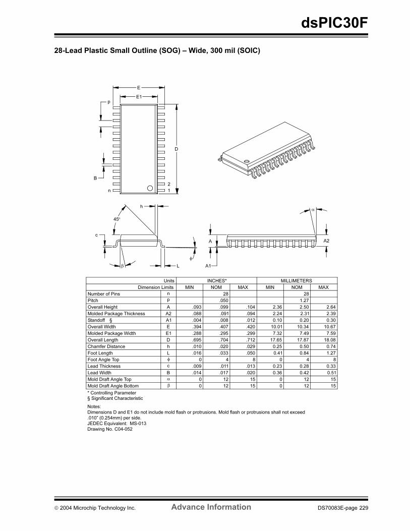
dsPIC30F
28-Lead Plastic Small Outline (SOG) – Wide, 300 mil (SOIC)
Foot Angle Top φ 0 4 8 0 4 8
1512015120βMold Draft Angle Bottom
1512015120αMold Draft Angle Top
0.510.420.36.020.017.014BLead Width
0.330.280.23.013.011.009cLead Thickness
1.270.840.41.050.033.016LFoot Length
0.740.500.25.029.020.010hChamfer Distance
18.0817.8717.65.712.704.695DOverall Length
7.597.497.32.299.295.288E1Molded Package Width
10.6710.3410.01.420.407.394EOverall Width
0.300.200.10.012.008.004A1Standoff §
2.392.312.24.094.091.088A2Molded Package Thickness
2.642.502.36.104.099.093AOverall Height
1.27.050pPitch
2828nNumber of Pins
MAXNOMMINMAXNOMMINDimension Limits
MILLIMETERSINCHES*Units
2
1
D
p
n
B
E
E1
L
c
β
45°
h
φ
A2
α
A
A1
* Controlling Parameter
Notes:
Dimensions D and E1 do not include mold flash or protrusions. Mold flash or protrusions shall not exceed
.010” (0.254mm) per side.
JEDEC Equivalent: MS-013
Drawing No. C04-052
§ Significant Characteristic
2004 Microchip Technology Inc. Advance Information DS70083E-page 229
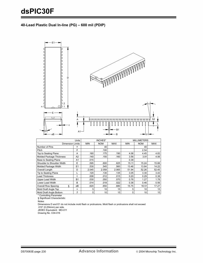
dsPIC30F
40-Lead Plastic Dual In-line (PG) – 600 mil (PDIP)
1510515105βMold Draft Angle Bottom
1510515105αMold Draft Angle Top
17.2716.5115.75.680.650.620eBOverall Row Spacing §
0.560.460.36.022.018.014BLower Lead Width
1.781.270.76.070.050.030B1Upper Lead Width
0.380.290.20.015.012.008cLead Thickness
3.433.303.05.135.130.120LTip to Seating Plane
52.4552.2651.942.0652.0582.045DOverall Length
14.2213.8413.46.560.545.530E1Molded Package Width
15.8815.2415.11.625.600.595EShoulder to Shoulder Width
0.38.015A1Base to Seating Plane
4.063.813.56.160.150.140A2Molded Package Thickness
4.834.454.06.190.175.160ATop to Seating Plane
2.54.100pPitch
4040nNumber of Pins
MAXNOMMINMAXNOMMINDimension Limits
MILLIMETERSINCHES*Units
A2
1
2
D
n
E1
c
β
eB
E
α
p
L
B
B1
A
A1
* Controlling Parameter
Notes:
Dimensions D and E1 do not include mold flash or protrusions. Mold flash or protrusions shall not exceed
.010” (0.254mm) per side.
JEDEC Equivalent: MO-011
Drawing No. C04-016
§ Significant Characteristic
DS70083E-page 230 Advance Information 2004 Microchip Technology Inc.
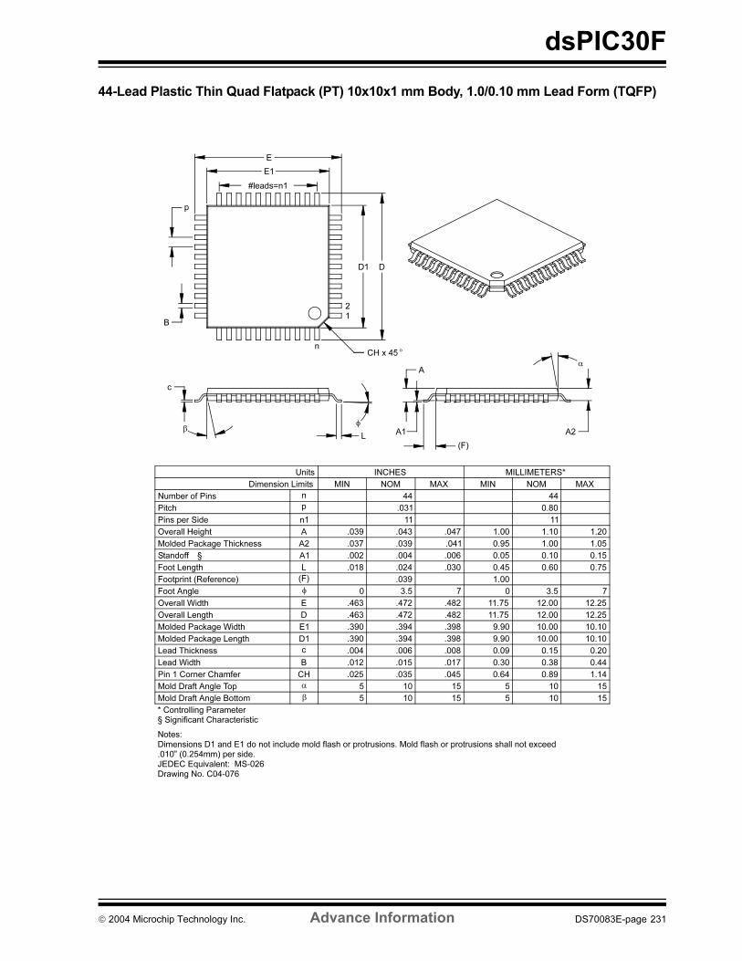
dsPIC30F
44-Lead Plastic Thin Quad Flatpack (PT) 10x10x1 mm Body, 1.0/0.10 mm Lead Form (TQFP)
* Controlling Parameter
Notes:Dimensions D1 and E1 do not include mold flash or protrusions. Mold flash or protrusions shall not exceed .010” (0.254mm) per side.JEDEC Equivalent: MS-026Drawing No. C04-076
1.140.890.64.045.035.025CHPin 1 Corner Chamfer
1.00.039(F)Footprint (Reference)
(F)
A
A1 A2
α
E
E1
#leads=n1
p
B
D1 D
n
12
φ
c
βL
Units INCHES MILLIMETERS*
Dimension Limits MIN NOM MAX MIN NOM MAX
Number of Pins n 44 44
Pitch p .031 0.80
Overall Height A .039 .043 .047 1.00 1.10 1.20
Molded Package Thickness A2 .037 .039 .041 0.95 1.00 1.05
Standoff § A1 .002 .004 .006 0.05 0.10 0.15
Foot Length L .018 .024 .030 0.45 0.60 0.75
Foot Angle φ 0 3.5 7 0 3.5 7
Overall Width E .463 .472 .482 11.75 12.00 12.25
Overall Length D .463 .472 .482 11.75 12.00 12.25
Molded Package Width E1 .390 .394 .398 9.90 10.00 10.10
Molded Package Length D1 .390 .394 .398 9.90 10.00 10.10
Pins per Side n1 11 11
Lead Thickness c .004 .006 .008 0.09 0.15 0.20
Lead Width B .012 .015 .017 0.30 0.38 0.44
Mold Draft Angle Top α 5 10 15 5 10 15
Mold Draft Angle Bottom β 5 10 15 5 10 15
CH x 45 °
§ Significant Characteristic
2004 Microchip Technology Inc. Advance Information DS70083E-page 231
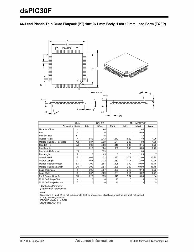
dsPIC30F
64-Lead Plastic Thin Quad Flatpack (PT) 10x10x1 mm Body, 1.0/0.10 mm Lead Form (TQFP)
* Controlling Parameter
Notes:Dimensions D1 and E1 do not include mold flash or protrusions. Mold flash or protrusions shall not exceed.010” (0.254mm) per side.JEDEC Equivalent: MS-026Drawing No. C04-085
1510515105βMold Draft Angle Bottom
1510515105αMold Draft Angle Top
0.270.220.17.011.009.007BLead Width
0.230.180.13.009.007.005cLead Thickness
1616n1Pins per Side
10.1010.009.90.398.394.390D1Molded Package Length
10.1010.009.90.398.394.390E1Molded Package Width
12.2512.0011.75.482.472.463DOverall Length
12.2512.0011.75.482.472.463EOverall Width
73.5073.50φFoot Angle
0.750.600.45.030.024.018LFoot Length
0.250.150.05.010.006.002A1Standoff §
1.051.000.95.041.039.037A2Molded Package Thickness
1.201.101.00.047.043.039AOverall Height
0.50.020pPitch
6464nNumber of Pins
MAXNOMMINMAXNOMMINDimension Limits
MILLIMETERS*INCHESUnits
c
21
n
DD1
B
p
#leads=n1
E1
E
A2
A1
A
L
CH x 45°
βφ
α
(F)
Footprint (Reference) (F) .039 1.00
Pin 1 Corner Chamfer CH .025 .035 .045 0.64 0.89 1.14
§ Significant Characteristic
DS70083E-page 232 Advance Information 2004 Microchip Technology Inc.
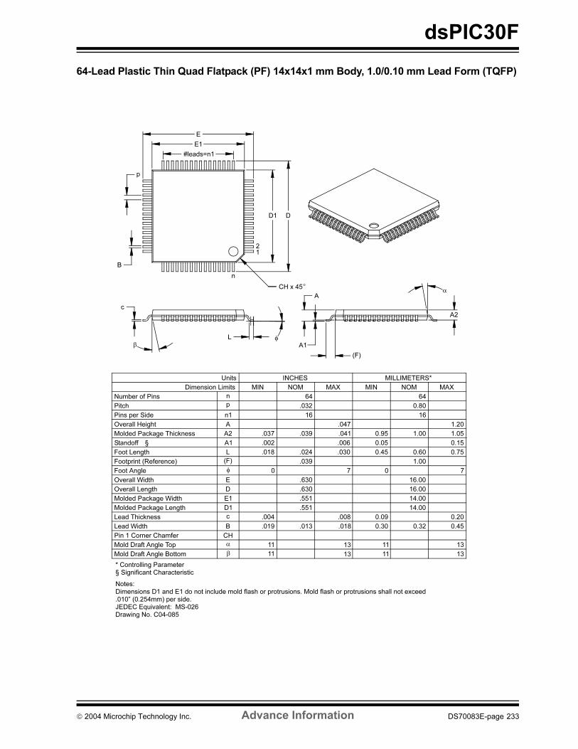
dsPIC30F
64-Lead Plastic Thin Quad Flatpack (PF) 14x14x1 mm Body, 1.0/0.10 mm Lead Form (TQFP)
* Controlling Parameter
Notes:Dimensions D1 and E1 do not include mold flash or protrusions. Mold flash or protrusions shall not exceed.010” (0.254mm) per side.JEDEC Equivalent: MS-026Drawing No. C04-085
13 11 βMold Draft Angle Bottom
1311 11 αMold Draft Angle Top
0.450.320.30.018.013.019BLead Width
0.20 0.09 .008 .004cLead Thickness
1616n1Pins per Side
14.00 .551 D1Molded Package Length
14.00 .551 E1Molded Package Width
16.00 .630 DOverall Length
16.00 .630 EOverall Width
7 07 0φFoot Angle
0.750.600.45.030.024.018LFoot Length
0.15 0.05.006 .002A1Standoff §
1.051.000.95.041.039.037A2Molded Package Thickness
1.20.047 AOverall Height
0.80.032pPitch
6464nNumber of Pins
MAXNOMMINMAXNOMMINDimension Limits
MILLIMETERS*INCHESUnits
c
21
n
DD1
B
p
#leads=n1
E1
E
A2
A1
A
L
CH x 45°
βφ
α
(F)
Footprint (Reference) (F) .039 1.00
Pin 1 Corner Chamfer CH
§ Significant Characteristic
11 13
13
2004 Microchip Technology Inc. Advance Information DS70083E-page 233
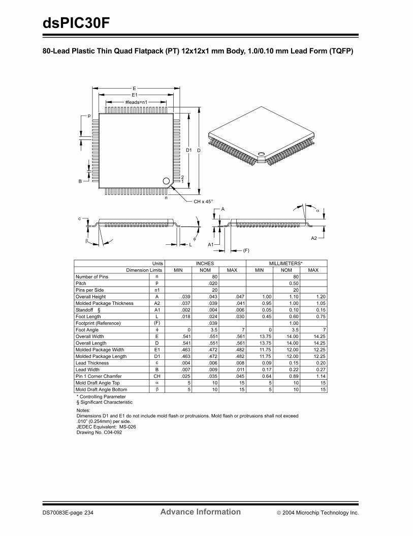
dsPIC30F
80-Lead Plastic Thin Quad Flatpack (PT) 12x12x1 mm Body, 1.0/0.10 mm Lead Form (TQFP)
* Controlling Parameter
Notes:Dimensions D1 and E1 do not include mold flash or protrusions. Mold flash or protrusions shall not exceed .010” (0.254mm) per side.JEDEC Equivalent: MS-026Drawing No. C04-092
1.101.00.043.039
1.140.890.64.045.035.025CHPin 1 Corner Chamfer
1.00.039(F)Footprint (Reference)
(F)
E
E1
#leads=n1
p
B
D1 D
n
12
φ
c
βL
A
A1
A2
α
Units INCHES MILLIMETERS*
Dimension Limits MIN NOM MAX MIN NOM MAX
Number of Pins n 80 80
Pitch p .020 0.50
Overall Height A .047 1.20
Molded Package Thickness A2 .037 .039 .041 0.95 1.00 1.05
Standoff § A1 .002 .004 .006 0.05 0.10 0.15
Foot Length L .018 .024 .030 0.45 0.60 0.75
Foot Angle φ 0 3.5 7 0 3.5 7
Overall Width E .541 .551 .561 13.75 14.00 14.25
Overall Length D .541 .551 .561 13.75 14.00 14.25
Molded Package Width E1 .463 .472 .482 11.75 12.00 12.25
Molded Package Length D1 .463 .472 .482 11.75 12.00 12.25
Pins per Side n1 20 20
Lead Thickness c .004 .006 .008 0.09 0.15 0.20
Lead Width B .007 .009 .011 0.17 0.22 0.27
Mold Draft Angle Top α 5 10 15 5 10 15
Mold Draft Angle Bottom β 5 10 15 5 10 15
CH x 45°
§ Significant Characteristic
DS70083E-page 234 Advance Information 2004 Microchip Technology Inc.
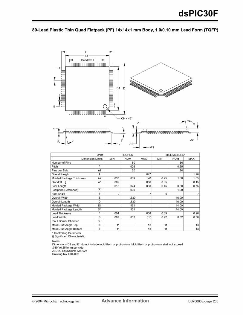
dsPIC30F
80-Lead Plastic Thin Quad Flatpack (PF) 14x14x1 mm Body, 1.0/0.10 mm Lead Form (TQFP)
* Controlling Parameter
Notes:Dimensions D1 and E1 do not include mold flash or protrusions. Mold flash or protrusions shall not exceed .010” (0.254mm) per side.JEDEC Equivalent: MS-026Drawing No. C04-092
CHPin 1 Corner Chamfer
1.00.039(F)Footprint (Reference)
(F)
E
E1
#leads=n1
p
B
D1 D
n
12
φ
c
βL
A
A1
A2
α
Units INCHES MILLIMETERS*
Dimension Limits MIN NOM MAX MIN NOM MAX
Number of Pins n 80 80
Pitch p .026 0.65
Overall Height A .047 1.20
Molded Package Thickness A2 .037 .039 .041 0.95 1.00 1.05
Standoff § A1 .002 .006 0.05 0.15
Foot Length L .018 .024 .030 0.45 0.60 0.75
Foot Angle φ 0 7 0 7
Overall Width E .630 16.00
Overall Length D .630 16.00
Molded Package Width E1 .551 14.00
Molded Package Length D1 . .551 14.00
Pins per Side n1 20 20
Lead Thickness c .004 .008 0.09 0.20
Lead Width B .009 .013 .015 0.22 0.32 0.38
Mold Draft Angle Top α 11 13 11 13
Mold Draft Angle Bottom β 11 13 11 13
CH x 45°
§ Significant Characteristic
2004 Microchip Technology Inc. Advance Information DS70083E-page 235

dsPIC30F
NOTES:
DS70083E-page 236 Advance Information 2004 Microchip Technology Inc.
dsPIC30F
INDEX
Numerics
12-bit Analog-to-Digital Converter (A/D) Module .............. 143
A
A/D .................................................................................... 143
Aborting a Conversion .............................................. 145
ADCHS Register ....................................................... 143
ADCON1 Register..................................................... 143
ADCON2 Register..................................................... 143
ADCON3 Register..................................................... 143
ADCSSL Register ..................................................... 143
ADPCFG Register..................................................... 143
Configuring Analog Port Pins.............................. 74, 148
Connection Considerations....................................... 148
Conversion Operation ............................................... 144
Effects of a Reset...................................................... 147
Operation During CPU Idle Mode ............................. 147
Operation During CPU Sleep Mode.......................... 147
Output Formats ......................................................... 147
Power-down Modes .................................................. 147
Programming the Sample Trigger............................. 145
Register Map............................................................. 149
Result Buffer ............................................................. 144
Sampling Requirements............................................ 146
Selecting the Conversion Clock ................................ 145
Selecting the Conversion Sequence......................... 144
TAD vs. Device Operating Frequencies..................... 145
AC Characteristics ............................................................ 195
Load Conditions ........................................................ 195
AC Temperature and Voltage Specifications .................... 195
AC-Link Mode Operation .................................................. 140
16-bit Mode ............................................................... 140
20-bit Mode ............................................................... 140
Address Generator Units .................................................... 45
Alternate Vector Table ........................................................ 57
Analog-to-Digital Converter. See A/D.
Assembler
MPASM Assembler................................................... 175
Automatic Clock Stretch.................................................... 108
During 10-bit Addressing (STREN = 1)..................... 108
During 7-bit Addressing (STREN = 1)....................... 108
Receive Mode ........................................................... 108
Transmit Mode .......................................................... 108
B
Bandgap Start-up Time
Requirements............................................................ 200
Timing Characteristics .............................................. 200
Barrel Shifter ....................................................................... 31
Bit Reversed Addressing
Example ...................................................................... 52
Implementation ........................................................... 51
Bit-Reversed Addressing .................................................... 51
Modifier Values Table ................................................. 52
Sequence Table (16-Entry)......................................... 52
Block Diagrams
12-bit A/D Functional ................................................ 143
16-bit Timer1 Module .................................................. 79
16-bit Timer2............................................................... 85
16-bit Timer3............................................................... 85
16-bit Timer4............................................................... 90
16-bit Timer5............................................................... 90
32-bit Timer2/3 ........................................................... 84
32-bit Timer4/5 ........................................................... 89
Analog Input Model................................................... 146
CAN Buffers and Protocol Engine ............................ 122
DCI Module............................................................... 134
Dedicated Port Structure ............................................ 73
DSP Engine ................................................................ 27
dsPIC30F5013/6013/6014.......................................... 16
External Power-on Reset Circuit .............................. 159
I2C ............................................................................ 106
Input Capture Mode.................................................... 93
Oscillator System...................................................... 153
Output Compare Mode ............................................... 97
Reset System ........................................................... 157
Shared Port Structure................................................. 74
SPI............................................................................ 102
SPI Master/Slave Connection................................... 102
UART Receiver......................................................... 114
UART Transmitter..................................................... 113
BOR Characteristics ......................................................... 194
BOR. See Brown-out Reset.
Brown-out Reset
Characteristics.......................................................... 193
Timing Requirements ............................................... 200
C
C Compilers
MPLAB C17.............................................................. 176
MPLAB C18.............................................................. 176
MPLAB C30.............................................................. 176
CAN Module ..................................................................... 121
Baud Rate Setting .................................................... 126
CAN1 Register Map.................................................. 128
CAN2 Register Map.................................................. 130
Frame Types ............................................................ 121
I/O Timing Characteristics ........................................ 217
Message Reception.................................................. 124
Message Transmission............................................. 125
Modes of Operation .................................................. 123
Overview................................................................... 121
CLKOUT and I/O Timing
Characteristics.......................................................... 198
Requirements ........................................................... 198
Code Examples
Data EEPROM Block Erase ....................................... 68
Data EEPROM Block Write ........................................ 70
Data EEPROM Read.................................................. 67
Data EEPROM Word Erase ....................................... 68
Data EEPROM Word Write ........................................ 69
Erasing a Row of Program Memory ........................... 63
Initiating a Programming Sequence ........................... 64
Loading Write Latches................................................ 64
Code Protection................................................................ 151
Core Architecture................................................................ 19
Overview..................................................................... 19
D
Data Accumulators and Adder/Subtractor .......................... 29
Data Space Write Saturation ...................................... 31
Overflow and Saturation ............................................. 29
Round Logic ............................................................... 30
Write Back .................................................................. 30
Data Address Space........................................................... 37
Alignment.................................................................... 38
Alignment (Figure) ...................................................... 38
2004 Microchip Technology Inc. Advance Information DS70083E-page 237
dsPIC30F
Effect of Invalid Memory Accesses (Table)................. 38
MCU and DSP (MAC Class) Instructions Example..... 41
Memory Map ............................................................... 38
Near Data Space ........................................................ 39
Sample Memory Map.................................................. 40
Software Stack............................................................ 39
Spaces ........................................................................ 37
Width........................................................................... 38
Data Converter Interface (DCI) Module ............................ 133
Data EEPROM Memory ...................................................... 67
Erasing........................................................................ 68
Erasing, Block ............................................................. 68
Erasing, Word ............................................................. 68
Protection Against Spurious Write .............................. 71
Reading....................................................................... 67
Write Verify ................................................................. 71
Writing......................................................................... 69
Writing, Block .............................................................. 70
Writing, Word .............................................................. 69
Data Space Organization .................................................... 45
DC Characteristics ............................................................ 182
BOR .......................................................................... 194
Brown-out Reset ....................................................... 193
I/O Pin Input Specifications....................................... 191
I/O Pin Output Specifications .................................... 192
Idle Current (IIDLE) .................................................... 186
Low-Voltage Detect................................................... 192
LVDL ......................................................................... 193
Operating Current (IDD)............................................. 183
Power-Down Current (IPD) ........................................ 189
Program and EEPROM............................................. 194
Temperature and Voltage Specifications .................. 182
DCI Module
Bit Clock Generator................................................... 137
Buffer Alignment with Data Frames .......................... 138
Buffer Control ............................................................ 133
Buffer Data Alignment ............................................... 133
Buffer Length Control ................................................ 138
COFS Pin.................................................................. 133
CSCK Pin.................................................................. 133
CSDI Pin ................................................................... 133
CSDO Mode Bit ........................................................ 139
CSDO Pin ................................................................. 133
Data Justification Control Bit ..................................... 137
Device Frequencies for Common Codec
CSCK Frequencies (Table)............................... 137
Digital Loopback Mode ............................................. 139
Enable....................................................................... 135
Frame Sync Generator ............................................. 135
Frame Sync Mode Control Bits ................................. 135
I/O Pins ..................................................................... 133
Interrupts................................................................... 139
Introduction ............................................................... 133
Master Frame Sync Operation.................................. 135
Operation .................................................................. 135
Operation During CPU Idle Mode ............................. 140
Operation During CPU Sleep Mode.......................... 140
Receive Slot Enable Bits........................................... 138
Receive Status Bits................................................... 139
Register Map............................................................. 141
Sample Clock Edge Control Bit................................. 137
Slave Frame Sync Operation.................................... 136
Slot Enable Bits Operation with Frame Sync ............ 138
Slot Status Bits.......................................................... 139
Synchronous Data Transfers .................................... 138
Timing Characteristics
AC-Link Mode................................................... 207
Multichannel, I2S Modes................................... 205
Timing Requirements
AC-Link Mode................................................... 207
Multichannel, I2S Modes................................... 206
Transmit Slot Enable Bits ......................................... 137
Transmit Status Bits.................................................. 139
Transmit/Receive Shift Register ............................... 133
Underflow Mode Control Bit...................................... 139
Word Size Selection Bits .......................................... 135
Demonstration Boards
PICDEM 1................................................................. 178
PICDEM 17............................................................... 178
PICDEM 18R PIC18C601/801.................................. 179
PICDEM 2 Plus......................................................... 178
PICDEM 3 PIC16C92X............................................. 178
PICDEM 4................................................................. 178
PICDEM LIN PIC16C43X ......................................... 179
PICDEM USB PIC16C7X5 ....................................... 179
PICDEM.net Internet/Ethernet .................................. 178
Development Support ....................................................... 175
Device Configuration
Register Map ............................................................ 165
Device Configuration Registers
FBORPOR................................................................ 163
FGS .......................................................................... 163
FOSC........................................................................ 163
FWDT ....................................................................... 163
Device Overview................................................................. 15
Disabling the UART .......................................................... 115
Divide Support .................................................................... 25
Instructions (Table) ..................................................... 25
DSP Engine ........................................................................ 26
Multiplier ..................................................................... 28
Dual Output Compare Match Mode .................................... 98
Continuous Pulse Mode.............................................. 98
Single Pulse Mode...................................................... 98
E
Electrical Characteristics .................................................. 181
AC............................................................................. 195
DC ............................................................................ 182
Enabling and Setting Up UART
Alternate I/O ............................................................. 115
Setting Up Data, Parity and Stop Bit Selections....... 115
Enabling the UART ........................................................... 115
Equations
A/D Conversion Clock............................................... 145
A/D Sampling Time................................................... 146
Baud Rate................................................................. 117
Bit Clock Frequency.................................................. 137
COFSG Period.......................................................... 135
Serial Clock Rate...................................................... 110
Time Quantum for Clock Generation........................ 127
Errata .................................................................................. 13
Evaluation and Programming Tools.................................. 179
Exception Processing ......................................................... 53
External Clock Timing Characteristics
Type A, B and C Timer ............................................. 201
External Clock Timing Requirements ............................... 196
Type A Timer ............................................................ 201
Type B Timer ............................................................ 202
Type C Timer............................................................ 202
External Interrupt Requests ................................................ 58
DS70083E-page 238 Advance Information 2004 Microchip Technology Inc.
dsPIC30F
F
Fast Context Saving............................................................ 58
Flash Program Memory ...................................................... 61
Control Registers ........................................................ 62
NVMADR ............................................................ 62
NVMADRU.......................................................... 62
NVMCON............................................................ 62
NVMKEY............................................................. 62
I
I/O Pin Specifications
Input .......................................................................... 191
Output ....................................................................... 192
I/O Ports.............................................................................. 73
Parallel (PIO) .............................................................. 73
I2C..................................................................................... 105
I2C 10-bit Slave Mode Operation ...................................... 107
Reception.................................................................. 107
Transmission............................................................. 107
I2C 7-bit Slave Mode Operation ........................................ 107
Reception.................................................................. 107
Transmission............................................................. 107
I2C Master Mode Operation .............................................. 109
Baud Rate Generator................................................ 110
Clock Arbitration........................................................ 110
Multi-Master Communication, Bus Collision
and Bus Arbitration ........................................... 110
Reception.................................................................. 109
Transmission............................................................. 109
I2C Master Mode Support ................................................. 109
I2C Module ........................................................................ 105
Addresses ................................................................. 107
Bus Data Timing Characteristics
Master Mode..................................................... 213
Slave Mode....................................................... 215
Bus Data Timing Requirements
Master Mode..................................................... 214
Slave Mode....................................................... 216
Bus Start/Stop Bits Timing Characteristics
Master Mode..................................................... 213
Slave Mode....................................................... 215
General Call Address Support .................................. 109
Interrupts................................................................... 108
IPMI Support ............................................................. 109
Operating Function Description ................................ 105
Operation During CPU Sleep and Idle Modes .......... 110
Pin Configuration ...................................................... 105
Programmer’s Model................................................. 105
Register Map............................................................. 111
Registers................................................................... 105
Slope Control ............................................................ 109
Software Controlled Clock Stretching (STREN = 1).. 108
Various Modes .......................................................... 105
I2S Mode Operation .......................................................... 140
Data Justification....................................................... 140
Frame and Data Word Length Selection................... 140
Idle Current (IIDLE) ............................................................ 186
In-Circuit Serial Programming (ICSP) ......................... 61, 151
Input Capture (CAPX) Timing Characteristics .................. 203
Input Capture Module ......................................................... 93
Interrupts..................................................................... 94
Register Map............................................................... 95
Input Capture Operation During Sleep and Idle Modes ...... 94
CPU Idle Mode............................................................ 94
CPU Sleep Mode ........................................................ 94
Input Capture Timing Requirements................................. 203
Input Change Notification Module....................................... 77
Register Map (Bits 15-8)............................................. 77
Register Map (Bits 7-0)............................................... 77
Instruction Addressing Modes ............................................ 45
File Register Instructions ............................................ 46
Fundamental Modes Supported ................................. 45
MAC Instructions ........................................................ 46
MCU Instructions ........................................................ 46
Move and Accumulator Instructions ........................... 46
Other Instructions ....................................................... 46
Instruction Flow................................................................... 22
Pipeline
1-Word, 1-Cycle (Figure) .................................... 22
1-Word, 2-Cycle (Figure) .................................... 22
1-Word, 2-Cycle MOV.D Operations (Figure)..... 23
1-Word, 2-Cycle Table Operations (Figure) ....... 23
1-Word, 2-Cycle with Instruction Stall (Figure) ... 24
2-Word, 2-Cycle DO, DOW (Figure)................... 24
2-Word, 2-Cycle GOTO, CALL (Figure) ............. 23
Instruction Set
Overview................................................................... 170
Summary .................................................................. 167
Instruction Stalls ................................................................. 47
Introduction................................................................. 47
Raw Dependency Detection ....................................... 47
Inter-Integrated Circuit. See I2C.
Internal Clock Timing Examples ....................................... 197
Interrupt Controller
Register Map .............................................................. 59
Interrupt Priority .................................................................. 54
Interrupt Sequence ............................................................. 57
Interrupt Stack Frame................................................. 57
Interrupts ............................................................................ 53
L
Load Conditions................................................................ 195
Low Voltage Detect (LVD) ................................................ 162
Low-Voltage Detect Characteristics.................................. 192
LVDL Characteristics ........................................................ 193
M
Memory Organization ......................................................... 33
Core Register Map ..................................................... 42
Modes of Operation
Disable...................................................................... 123
Initialization............................................................... 123
Listen All Messages.................................................. 123
Listen Only................................................................ 123
Loopback .................................................................. 123
Normal Operation ..................................................... 123
Modulo Addressing............................................................. 48
Applicability................................................................. 51
Decrementing Buffer Operation Example................... 50
Incrementing Buffer Operation Example .................... 49
Restrictions................................................................. 51
Start and End Address ............................................... 48
W Address Register Selection.................................... 49
MPLAB ASM30 Assembler, Linker, Librarian ................... 176
MPLAB ICD 2 In-Circuit Debugger ................................... 177
MPLAB ICE 2000 High Performance
Universal In-Circuit Emulator.................................... 177
MPLAB ICE 4000 High Performance
Universal In-Circuit Emulator.................................... 177
MPLAB Integrated Development Environment
Software ................................................................... 175
2004 Microchip Technology Inc. Advance Information DS70083E-page 239
dsPIC30F
MPLINK Object Linker/MPLIB Object Librarian ................ 176
Multiplier
16-bit Integer and Fractional Modes Example ............ 28
N
NVM
Register Map............................................................... 65
O
OC/PWM Module Timing Characteristics.......................... 204
Operating Current (IDD)..................................................... 183
Operating Frequency vs Voltage
dsPIC30FXXXX-20 (Extended)................................. 182
Oscillator
Configurations........................................................... 154
Fail-Safe Clock Monitor..................................... 156
Fast RC (FRC) .................................................. 155
Initial Clock Source Selection ........................... 154
Low Power RC (LPRC) ..................................... 155
LP Oscillator Control ......................................... 154
Phase Locked Loop (PLL) ................................ 155
Start-up Timer (OST) ........................................ 154
Operating Modes (Table) .......................................... 152
System Overview ...................................................... 151
Oscillator Selection ........................................................... 151
Oscillator Start-up Timer
Timing Characteristics .............................................. 199
Timing Requirements................................................ 200
Output Compare Interrupts ................................................. 99
Output Compare Module..................................................... 97
Register Map............................................................. 100
Timing Characteristics .............................................. 203
Timing Requirements................................................ 203
Output Compare Operation During CPU Idle Mode............ 99
Output Compare Sleep Mode Operation............................. 99
P
Packaging Information ...................................................... 223
Marking ..................................................................... 223
Peripheral Module Disable (PMD) Registers .................... 164
PICkit 1 Flash Starter Kit................................................... 179
PICSTART Plus Development Programmer ..................... 177
Pinout Descriptions ............................................................. 17
PLL Clock Timing Specifications....................................... 197
POR. See Power-on Reset.
PORTA Register Map ......................................................... 75
PORTB Register Map ......................................................... 75
PORTC Register Map ......................................................... 75
PORTD Register Map ......................................................... 75
PORTF Register Map.......................................................... 76
PORTG Register Map ......................................................... 76
Power Saving Modes ........................................................ 162
Idle ............................................................................ 163
Sleep......................................................................... 162
Sleep and Idle ........................................................... 151
Power-Down Current (IPD) ................................................ 189
Power-up Timer
Timing Characteristics .............................................. 199
Timing Requirements................................................ 200
PRO MATE II Universal Device Programmer ................... 177
Program Address Space ..................................................... 33
Alignment and Data Access Using
Table Instructions................................................ 34
Construction................................................................ 33
Data Access from, Address Generation...................... 33
Data Space Window into Operation............................ 36
Data Table Access (LS Word) .................................... 34
Data Table Access (MS Byte)..................................... 35
Memory Map............................................................... 37
Table Instructions
TBLRDH ............................................................. 34
TBLRDL.............................................................. 34
TBLWTH............................................................. 34
TBLWTL ............................................................. 34
Visibility from Data Space........................................... 35
Program and EEPROM Characteristics............................ 194
Program Counter ................................................................ 20
Programmable .................................................................. 151
Programmer’s Model .......................................................... 20
Diagram ...................................................................... 21
Programming Operations.................................................... 63
Algorithm for Program Flash....................................... 63
Erasing a Row of Program Memory............................ 63
Initiating the Programming Sequence......................... 64
Loading Write Latches................................................ 64
Protection Against Accidental Writes to OSCCON ........... 156
R
Reset ........................................................................ 151, 157
BOR, Programmable ................................................ 159
Brown-out Reset (BOR)............................................ 151
Oscillator Start-up Timer (OST) ................................ 151
POR
Operating without FSCM and PWRT................ 159
With Long Crystal Start-up Time ...................... 159
POR (Power-on Reset)............................................. 157
Power-on Reset (POR)............................................. 151
Power-up Timer (PWRT) .......................................... 151
Reset Sequence ................................................................. 55
Reset Sources ............................................................ 55
Reset Sources
Brown-out Reset (BOR).............................................. 55
Illegal Instruction Trap ................................................ 55
Trap Lockout............................................................... 55
Uninitialized W Register Trap ..................................... 55
Watchdog Time-out .................................................... 55
Reset Timing Characteristics............................................ 199
Reset Timing Requirements ............................................. 200
RTSP Operation ................................................................. 62
Run-Time Self-Programming (RTSP) ................................. 61
S
Serial Peripheral Interface. See SPI.
Simple Capture Event Mode............................................... 93
Buffer Operation ......................................................... 94
Hall Sensor Mode ....................................................... 94
Prescaler .................................................................... 93
Timer2 and Timer3 Selection Mode............................ 94
Simple OC/PWM Mode Timing Requirements ................. 204
Simple Output Compare Match Mode ................................ 98
Simple PWM Mode ............................................................. 98
Input Pin Fault Protection ........................................... 98
Period ......................................................................... 99
Software Simulator (MPLAB SIM) .................................... 176
Software Simulator (MPLAB SIM30) ................................ 176
Software Stack Pointer, Frame Pointer .............................. 20
CALL Stack Frame ..................................................... 39
SPI .................................................................................... 101
SPI Module ....................................................................... 101
Framed SPI Support ................................................. 101
Operating Function Description ................................ 101
Operation During CPU Idle Mode............................. 103
DS70083E-page 240 Advance Information 2004 Microchip Technology Inc.
dsPIC30F
Operation During CPU Sleep Mode.......................... 103
SDOx Disable ........................................................... 101
Slave Select Synchronization ................................... 103
SPI1 Register Map.................................................... 104
SPI2 Register Map.................................................... 104
Timing Characteristics
Master Mode (CKE = 0) .................................... 208
Master Mode (CKE = 1) .................................... 209
Slave Mode (CKE = 1) .............................. 210, 211
Timing Requirements
Master Mode (CKE = 0) .................................... 208
Master Mode (CKE = 1) .................................... 209
Slave Mode (CKE = 0) ...................................... 210
Slave Mode (CKE = 1) ...................................... 212
Word and Byte Communication ................................ 101
Status Bits, Their Significance and the Initialization
Condition for RCON Register, Case 1 ...................... 160
Status Bits, Their Significance and the Initialization
Condition for RCON Register, Case 2 ...................... 161
Status Register ................................................................... 20
Z Status Bit ................................................................. 20
Symbols Used in Opcode Descriptions............................. 168
System Integration ............................................................ 151
Register Map............................................................. 165
T
Table Instruction Operation Summary ................................ 61
Temperature and Voltage Specifications
AC............................................................................. 195
DC............................................................................. 182
Timer1 Module .................................................................... 79
16-bit Asynchronous Counter Mode ........................... 79
16-bit Synchronous Counter Mode ............................. 79
16-bit Timer Mode....................................................... 79
Gate Operation ........................................................... 80
Interrupt....................................................................... 80
Operation During Sleep Mode .................................... 80
Prescaler..................................................................... 80
Real-Time Clock ......................................................... 80
Interrupts............................................................. 81
Oscillator Operation ............................................ 81
Register Map............................................................... 82
Timer2 and Timer3 Selection Mode.................................... 98
Timer2/3 Module ................................................................. 83
16-bit Timer Mode....................................................... 83
32-bit Synchronous Counter Mode ............................. 83
32-bit Timer Mode....................................................... 83
ADC Event Trigger...................................................... 86
Gate Operation ........................................................... 86
Interrupt....................................................................... 86
Operation During Sleep Mode .................................... 86
Register Map............................................................... 87
Timer Prescaler........................................................... 86
Timer4/5 Module ................................................................. 89
Register Map............................................................... 91
Timing Characteristics
A/D Conversion
10-Bit (ASAM = 0, SSRC = 000)....................... 220
Bandgap Start-up Time............................................. 200
CAN Module I/O........................................................ 217
CLKOUT and I/O....................................................... 198
DCI Module
AC-Link Mode ................................................... 207
Multichannel, I2S Modes................................... 205
External Clock .......................................................... 195
I2C Bus Data
Master Mode..................................................... 213
Slave Mode ...................................................... 215
I2C Bus Start/Stop Bits
Master Mode..................................................... 213
Slave Mode ...................................................... 215
Input Capture (CAPX)............................................... 203
OC/PWM Module...................................................... 204
Oscillator Start-up Timer........................................... 199
Output Compare Module .......................................... 203
Power-up Timer ........................................................ 199
Reset ........................................................................ 199
SPI Module
Master Mode (CKE = 0).................................... 208
Master Mode (CKE = 1).................................... 209
Slave Mode (CKE = 0)...................................... 210
Slave Mode (CKE = 1)...................................... 211
Type A, B and C Timer External Clock..................... 201
Watchdog Timer ....................................................... 199
Timing Diagrams
CAN Bit..................................................................... 126
Frame Sync, AC-Link Start of Frame ....................... 136
Frame Sync, Multi-Channel Mode ............................ 136
I2S Interface Frame Sync ......................................... 136
PWM Output ............................................................... 99
Time-out Sequence on Power-up
(MCLR Not Tied to VDD), Case 1 ..................... 158
Time-out Sequence on Power-up
(MCLR Not Tied to VDD), Case 2 ..................... 158
Time-out Sequence on Power-up
(MCLR Tied to VDD) ......................................... 158
Timing Diagrams and Specifications
DC Characteristics - Internal RC Accuracy .............. 197
Timing Diagrams.See Timing Characteristics
Timing Requirements
A/D Conversion
10-Bit ................................................................ 221
Bandgap Start-up Time ............................................ 200
Brown-out Reset....................................................... 200
CLKOUT and I/O ...................................................... 198
DCI Module
AC-Link Mode................................................... 207
Multichannel, I2S Modes................................... 206
External Clock .......................................................... 196
I2C Bus Data (Master Mode) .................................... 214
I2C Bus Data (Slave Mode) ...................................... 216
Input Capture............................................................ 203
Oscillator Start-up Timer........................................... 200
Output Compare Module .......................................... 203
Power-up Timer ........................................................ 200
Reset ........................................................................ 200
Simple OC/PWM Mode ............................................ 204
SPI Module
Master Mode (CKE = 0).................................... 208
Master Mode (CKE = 1).................................... 209
Slave Mode (CKE = 0)...................................... 210
Slave Mode (CKE = 1)...................................... 212
Type A Timer External Clock.................................... 201
Type B Timer External Clock.................................... 202
Type C Timer External Clock.................................... 202
Watchdog Timer ....................................................... 200
Timing Specifications
PLL Clock ................................................................. 197
2004 Microchip Technology Inc. Advance Information DS70083E-page 241
dsPIC30F
Traps ................................................................................... 55
Hard and Soft .............................................................. 56
Sources....................................................................... 55
Address Error Trap ............................................. 56
Math Error Trap................................................... 55
Oscillator Fail Trap.............................................. 56
Stack Error Trap.................................................. 56
U
UART Module
Address Detect Mode ............................................... 117
Auto Baud Support.................................................... 118
Baud Rate Generator ................................................ 117
Enabling and Setting Up ........................................... 115
Framing Error (FERR)............................................... 117
Idle Status ................................................................. 117
Loopback Mode ........................................................ 117
Operation During CPU Sleep and Idle Modes .......... 118
Overview ................................................................... 113
Parity Error (PERR) .................................................. 117
Receive Break........................................................... 117
Receive Buffer (UxRXB) ........................................... 116
Receive Buffer Overrun Error (OERR Bit) ................ 116
Receive Interrupt....................................................... 116
Receiving Data.......................................................... 116
Receiving in 8-bit or 9-bit Data Mode ....................... 116
Reception Error Handling ......................................... 116
Transmit Break ......................................................... 116
Transmit Buffer (UxTXB) .......................................... 115
Transmit Interrupt ..................................................... 116
Transmitting Data ..................................................... 115
Transmitting in 8-bit Data Mode................................ 115
Transmitting in 9-bit Data Mode................................ 115
UART1 Register Map................................................ 119
UART2 Register Map................................................ 119
UART Operation
Idle Mode.................................................................. 118
Sleep Mode .............................................................. 118
Unit ID Locations .............................................................. 151
Universal Asynchronous Receiver Transmitter. See UART.
W
Wake-up from Sleep ......................................................... 151
Wake-up from Sleep and Idle ............................................. 58
Watchdog Timer
Timing Characteristics .............................................. 199
Timing Requirements................................................ 200
Watchdog Timer (WDT)............................................ 151, 162
Enabling and Disabling............................................. 162
Operation.................................................................. 162
WWW, On-Line Support ..................................................... 13
DS70083E-page 242 Advance Information 2004 Microchip Technology Inc.
dsPIC30F
ON-LINE SUPPORT
Microchip provides on-line support on the Microchip
World Wide Web site.
The web site is used by Microchip as a means to make
files and information easily available to customers. To
view the site, the user must have access to the Internet
and a web browser, such as Netscape® or Microsoft®
Internet Explorer. Files are also available for FTP
download from our FTP site.
Connecting to the Microchip Internet
Web Site
The Microchip web site is available at the following
URL:
www.microchip.com
The file transfer site is available by using an FTP ser-
vice to connect to:
ftp://ftp.microchip.com
The web site and file transfer site provide a variety of
services. Users may download files for the latest
Development Tools, Data Sheets, Application Notes,
User's Guides, Articles and Sample Programs. A vari-
ety of Microchip specific business information is also
available, including listings of Microchip sales offices,
distributors and factory representatives. Other data
available for consideration is:
• Latest Microchip Press Releases
• Technical Support Section with Frequently Asked
Questions
• Design Tips
• Device Errata
• Job Postings
• Microchip Consultant Program Member Listing
• Links to other useful web sites related to
Microchip Products
• Conferences for products, Development Systems,
technical information and more
• Listing of seminars and events
SYSTEMS INFORMATION AND
UPGRADE HOT LINE
The Systems Information and Upgrade Line provides
system users a listing of the latest versions of all of
Microchip's development systems software products.
Plus, this line provides information on how customers
can receive the most current upgrade kits.The Hot Line
Numbers are:
1-800-755-2345 for U.S. and most of Canada, and
1-480-792-7302 for the rest of the world.
042003
2004 Microchip Technology Inc. Advance Information DS70083E-page 243

dsPIC30F
READER RESPONSE
It is our intention to provide you with the best documentation possible to ensure successful use of your Microchip prod-
uct. If you wish to provide your comments on organization, clarity, subject matter, and ways in which our documentation
can better serve you, please FAX your comments to the Technical Publications Manager at (480) 792-4150.
Please list the following information, and use this outline to provide us with your comments about this document.
To: Technical Publications Manager
RE: Reader Response
Total Pages Sent ________
From: Name
Company
Address
City / State / ZIP / Country
Telephone: (_______) _________ - _________
Application (optional):
Would you like a reply? Y N
Device: Literature Number:
Questions:
FAX: (______) _________ - _________
DS70083EdsPIC30F
1. What are the best features of this document?
2. How does this document meet your hardware and software development needs?
3. Do you find the organization of this document easy to follow? If not, why?
4. What additions to the document do you think would enhance the structure and subject?
5. What deletions from the document could be made without affecting the overall usefulness?
6. Is there any incorrect or misleading information (what and where)?
7. How would you improve this document?
DS70083E-page 244 Advance Information 2004 Microchip Technology Inc.
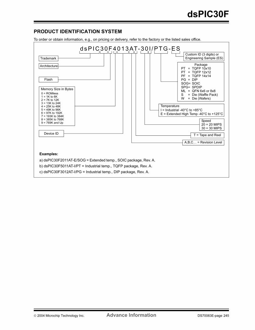
2004 Microchip Technology Inc. Advance Information DS70083E-page 245
dsPIC30F
PRODUCT IDENTIFICATION SYSTEM
To order or obtain information, e.g., on pricing or delivery, refer to the factory or the listed sales office.
Examples:
a) dsPIC30F2011AT-E/SOG = Extended temp., SOIC package, Rev. A.
b) dsPIC30F5011AT-I/PT = Industrial temp., TQFP package, Rev. A.
c) dsPIC30F3012AT-I/PG = Industrial temp., DIP package, Rev. A.
dsP IC30F4013AT-30 I /PTG-ES
Trademark
Architecture
Flash
E = Extended High Temp -40°C to +125°CI = Industrial -40°C to +85°C
Temperature
Device ID
PackagePT = TQFP 10x10PT = TQFP 12x12PF = TQFP 14x14PG = DIPSOG= SOICSPG= SPDIPML = QFN 6x6 or 8x8S = Die (Waffle Pack)W = Die (Wafers)
Memory Size in Bytes
0 = ROMless1 = 1K to 6K2 = 7K to 12K3 = 13K to 24K4 = 25K to 48K5 = 49K to 96K6 = 97K to 192K7 = 193K to 384K8 = 385K to 768K9 = 769K and Up
Custom ID (3 digits) or
T = Tape and Reel
A,B,C… = Revision Level
Engineering Sample (ES)
Speed20 = 20 MIPS30 = 30 MIPS

DS70083E-page 246 Advance Information 2004 Microchip Technology Inc.
AMERICAS
Corporate Office2355 West Chandler Blvd.Chandler, AZ 85224-6199Tel: 480-792-7200 Fax: 480-792-7277Technical Support: 480-792-7627Web Address: http://www.microchip.com
Atlanta3780 Mansell Road, Suite 130Alpharetta, GA 30022Tel: 770-640-0034 Fax: 770-640-0307
Boston2 Lan Drive, Suite 120Westford, MA 01886Tel: 978-692-3848 Fax: 978-692-3821
Chicago333 Pierce Road, Suite 180Itasca, IL 60143Tel: 630-285-0071 Fax: 630-285-0075
Dallas4570 Westgrove Drive, Suite 160Addison, TX 75001Tel: 972-818-7423 Fax: 972-818-2924
DetroitTri-Atria Office Building 32255 Northwestern Highway, Suite 190Farmington Hills, MI 48334Tel: 248-538-2250Fax: 248-538-2260
Kokomo2767 S. Albright Road Kokomo, IN 46902Tel: 765-864-8360Fax: 765-864-8387
Los Angeles18201 Von Karman, Suite 1090Irvine, CA 92612Tel: 949-263-1888 Fax: 949-263-1338
San Jose1300 Terra Bella AvenueMountain View, CA 94043Tel: 650-215-1444Fax: 650-961-0286
Toronto6285 Northam Drive, Suite 108Mississauga, Ontario L4V 1X5, CanadaTel: 905-673-0699 Fax: 905-673-6509
ASIA/PACIFIC
AustraliaSuite 22, 41 Rawson StreetEpping 2121, NSWAustraliaTel: 61-2-9868-6733 Fax: 61-2-9868-6755
China - BeijingUnit 706BWan Tai Bei Hai Bldg.No. 6 Chaoyangmen Bei Str. Beijing, 100027, ChinaTel: 86-10-85282100 Fax: 86-10-85282104
China - ChengduRm. 2401-2402, 24th Floor, Ming Xing Financial TowerNo. 88 TIDU StreetChengdu 610016, ChinaTel: 86-28-86766200 Fax: 86-28-86766599
China - FuzhouUnit 28F, World Trade PlazaNo. 71 Wusi RoadFuzhou 350001, ChinaTel: 86-591-7503506 Fax: 86-591-7503521
China - Hong Kong SARUnit 901-6, Tower 2, Metroplaza223 Hing Fong RoadKwai Fong, N.T., Hong KongTel: 852-2401-1200 Fax: 852-2401-3431
China - ShanghaiRoom 701, Bldg. BFar East International PlazaNo. 317 Xian Xia RoadShanghai, 200051Tel: 86-21-6275-5700 Fax: 86-21-6275-5060
China - ShenzhenRm. 1812, 18/F, Building A, United PlazaNo. 5022 Binhe Road, Futian DistrictShenzhen 518033, ChinaTel: 86-755-82901380 Fax: 86-755-8295-1393
China - ShundeRoom 401, Hongjian Building, No. 2 Fengxiangnan Road, Ronggui Town, ShundeDistrict, Foshan City, Guangdong 528303, ChinaTel: 86-757-28395507 Fax: 86-757-28395571
China - QingdaoRm. B505A, Fullhope Plaza,No. 12 Hong Kong Central Rd.Qingdao 266071, ChinaTel: 86-532-5027355 Fax: 86-532-5027205
IndiaDivyasree Chambers1 Floor, Wing A (A3/A4)No. 11, O’Shaugnessey RoadBangalore, 560 025, IndiaTel: 91-80-22290061 Fax: 91-80-22290062
JapanBenex S-1 6F3-18-20, ShinyokohamaKohoku-Ku, Yokohama-shiKanagawa, 222-0033, JapanTel: 81-45-471- 6166 Fax: 81-45-471-6122
Korea168-1, Youngbo Bldg. 3 FloorSamsung-Dong, Kangnam-KuSeoul, Korea 135-882Tel: 82-2-554-7200 Fax: 82-2-558-5932 or 82-2-558-5934
Singapore200 Middle Road#07-02 Prime CentreSingapore, 188980Tel: 65-6334-8870 Fax: 65-6334-8850
TaiwanKaohsiung Branch30F - 1 No. 8Min Chuan 2nd RoadKaohsiung 806, TaiwanTel: 886-7-536-4818Fax: 886-7-536-4803
TaiwanTaiwan Branch11F-3, No. 207Tung Hua North RoadTaipei, 105, TaiwanTel: 886-2-2717-7175 Fax: 886-2-2545-0139
EUROPEAustriaDurisolstrasse 2A-4600 WelsAustriaTel: 43-7242-2244-399Fax: 43-7242-2244-393
DenmarkRegus Business CentreLautrup hoj 1-3Ballerup DK-2750 DenmarkTel: 45-4420-9895 Fax: 45-4420-9910
FranceParc d’Activite du Moulin de Massy43 Rue du Saule TrapuBatiment A - ler Etage91300 Massy, FranceTel: 33-1-69-53-63-20 Fax: 33-1-69-30-90-79
GermanySteinheilstrasse 10D-85737 Ismaning, GermanyTel: 49-89-627-144-0 Fax: 49-89-627-144-44
ItalyVia Quasimodo, 1220025 Legnano (MI)Milan, Italy Tel: 39-0331-742611 Fax: 39-0331-466781
NetherlandsP. A. De Biesbosch 14NL-5152 SC Drunen, NetherlandsTel: 31-416-690399 Fax: 31-416-690340
United Kingdom505 Eskdale RoadWinnersh TriangleWokingham Berkshire, England RG41 5TUTel: 44-118-921-5869Fax: 44-118-921-5820
02/17/04
WORLDWIDE SALES AND SERVICE