Embed Size (px)
Citation preview
----------------------------------------------------------------------------------------------------------------------------- --------------------- Copyright © JORJIN TECHNOLOGIES INC. 2017
http://WWW.JORJIN.COM.TW
a module solution provider
WS2118-00
Ultralow Power Sub-1GHz and BLE Wireless MCU Module
STM S2-LP & BlueNRG-1 Solution
Datasheet
Draft 0.1
Prepared By Reviewed By Approved By
DOC No: WS2118-00A-DTS-D01
____________________________________________________________________________________
Copyright © JORJIN TECHNOLOGIES INC. 2017 1
http://WWW.JORJIN.COM.TW
Index
1. OVERVIEW ....................................................................................................................................... 3
1.1. GENERAL FEATURES ........................................................................................................................ 3
2. FUNCTIONAL FEATURES .................................................................................................................. 4
2.1. MODULE BLOCK DIAGRAM ............................................................................................................... 4
2.2. BLOCK FUNCTIONAL FEATURE ........................................................................................................... 5
BlueNRG-1 : Bluetooth low energy wireless SOC ....................................................................... 5
S2-LP Sub-1Ghz transceiver ......................................................................................................... 5
STSAFE-A1SX : Secure Element .................................................................................................... 6
3. MODULE OUTLINE ........................................................................................................................... 7
3.1. SIGNAL LAYOUT (TOP VIEW) ............................................................................................................. 7
3.2. PIN DESCRIPTION ........................................................................................................................... 8
4. MODULE SPECIFICATIONS ............................................................................................................. 10
4.1. ABSOLUTE MAXIMUM RATINGS ...................................................................................................... 10
4.2. ESD RATINGS .............................................................................................................................. 10
4.3. RECOMMENDED OPERATING CONDITIONS ......................................................................................... 10
4.4. POWER CONSUMPTION SUMMARY .................................................................................................. 11
4.5. 2.4GHZ GFSK (BLUETOOTH LOW ENERGY) RF CHARACTERISTICS ......................................................... 12
4.6. SUB-1GHZ RF CHARACTERISTICS .................................................................................................... 12
4.7. INTERNAL 16-MHZ CRYSTAL OSCILLATOR ( FOR BLUENRG-1 ) ............................................................. 13
4.8. INTERNAL 32.768-KHZ CRYSTAL OSCILLATOR ( FOR BLUENRG-1 ) ........................................................ 13
4.9. INTERNAL 50MHZ CRYSTAL OSCILLATOR ( FOR S2-LP ) ....................................................................... 14
4.10. BLUENRG-1 DIGITAL I/O SPECIFICATIONS ....................................................................................... 14
4.11. S2-LP DIGITAL INTERFACE SPECIFICATION ........................................................................................ 15
4.12. MORE CHARACTERISTICS.............................................................................................................. 15
5. DESIGN RECOMMENDATIONS ....................................................................................................... 16
5.1. GPIO USAGE OF BLUENRG-1 ........................................................................................................ 16
5.2. DEBUG PORT ............................................................................................................................... 16
5.3. DEBUGGING TIPS .......................................................................................................................... 17
5.4. PRE-PROGRAMMED BOOTLOADER ............................................................................................ 17
5.5. ANTENNA SELECTION GUIDE ........................................................................................................... 17
5.6. REFERENCE SCHEMATIC ................................................................................................................. 18
5.7. MODULE LAYOUT RECOMMENDATIONS ............................................................................................ 18
DOC No: WS2118-00A-DTS-D01
____________________________________________________________________________________
Copyright © JORJIN TECHNOLOGIES INC. 2017 2
http://WWW.JORJIN.COM.TW
6. PACKAGE INFORMATION ............................................................................................................... 19
6.1. MODULE MECHANICAL OUTLINE ..................................................................................................... 19
7. SMT AND BAKING RECOMMENDATION ....................................................................................... 21
7.1. BAKING RECOMMENDATION ........................................................................................................... 21
7.2. SMT RECOMMENDATION .............................................................................................................. 21
8. HISTORY CHANGE .......................................................................................................................... 23
DOC No: WS2118-00A-DTS-D01
____________________________________________________________________________________
Copyright © JORJIN TECHNOLOGIES INC. 2017 3
http://WWW.JORJIN.COM.TW
1. OVERVIEW
The WS2118-00 is a sub-1GHz and Bluetooth® low energy ultralow power wireless MCU module.
This module is built-in STM S2-LP and BlueNRG-1 chip.
The module is a cost-effective, high performance, ultra-low power, sub-1GHz and Bluetooth® low
energy RF devices. Very low active RF and MCU current and low-power mode current consumption
provide excellent battery lifetime and allow for operation on small coin cell batteries and in
energy-harvesting applications.
1.1. General Features
STM BlueNRG-1, S2-LP, 16MHz, 50MHz & 32.768KHz crystals, DC2DC, and U.FL connector on a
single module.
Stamp-hole 38pins package.
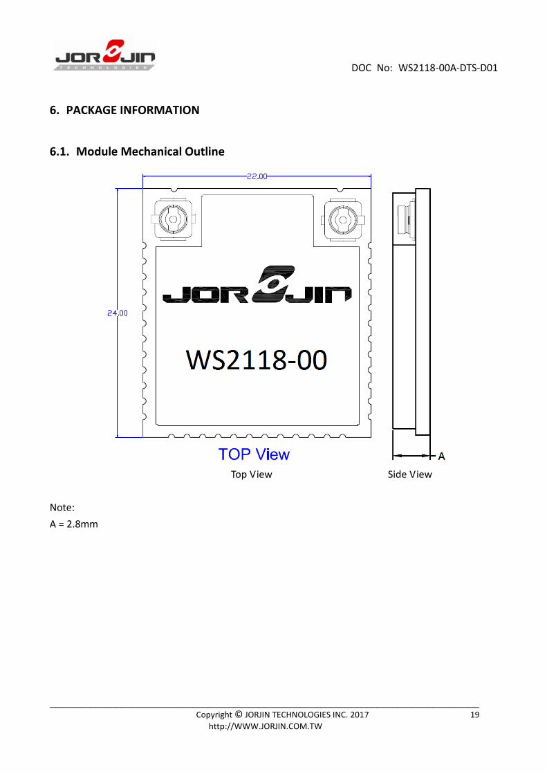
Dimension 22mm(L) x 24mm(W) x 2.8mm(H)
High performance, ultra-low power Cortex-M0 32-bit Microcontroller
Programmable 160 KB Flash
24 KB RAM with retention (two 12 KB banks)
Up to +8dBm BLE RF output power, up to +16dBm sub-1GHz RF output power
Excellent performance of receiver sensitivity. Up to -88dBm (BLE) and -130dBm (Sub-1GHz).
Low Power and Wide I/O Voltage Range: 1.8 to 3.6V
- Internal DC-DC converter built-in
Operating temperature range: -40 °C to +85 °C
DOC No: WS2118-00A-DTS-D01
____________________________________________________________________________________
Copyright © JORJIN TECHNOLOGIES INC. 2017 4
http://WWW.JORJIN.COM.TW
2. FUNCTIONAL FEATURES
2.1. Module Block Diagram
WS2118-00
DIO
pins
DOC No: WS2118-00A-DTS-D01
____________________________________________________________________________________
Copyright © JORJIN TECHNOLOGIES INC. 2017 5
http://WWW.JORJIN.COM.TW
2.2. Block Functional Feature
BlueNRG-1 : Bluetooth low energy wireless SOC
Bluetooth specification compliant master, slave and multiple roles simultaneously,
single-mode Bluetooth low energy SOC
Integrated linear regulator and DC-DC step-down converter
High performance, ultra-low power Cortex-M0 32-bit based architecture core
Programmable 160 KB Flash
24 KB RAM with retention (two 12 KB banks)
1 x UART interface
1 x SPI interface
1 x I2C interface
15 GPIO
2 x multifunction timer
10-bit ADC
Watchdog & RTC
DMA controller
PDM stream processor
16 MHz crystal oscillator built-in.
32 kHz crystal oscillator built-in.
Battery voltage monitor and temperature sensor
Up to +8 dBm available output power (at antenna connector)
Excellent RF link budget (up to 96 dB)
BALF-NRG-01D3 BALUN built-in.
Accurate RSSI to allow power control
S2-LP Sub-1Ghz transceiver
Narrow band ultra-low power Sub-1GHz transceiver tuned for 860-943 MHz frequency
bands.
Suitable for SigFox applications
Modulation schemes: 2-FSK, 2-GFSK, 4-FSK, 4-GFSK, OOK, and ASK
Air data rate from 0.3 to 500 kbps
Programmable RF output power up to +16 dBm
DOC No: WS2118-00A-DTS-D01
____________________________________________________________________________________
Copyright © JORJIN TECHNOLOGIES INC. 2017 6
http://WWW.JORJIN.COM.TW
Excellent performance of receiver sensitivity: down to -130 dBm
Programmable RX digital filter
Programmable channel spacing
Low duty cycle RX/TX operation mode
Integrated linear regulator and DC-DC step-down converter
STSAFE-A1SX : Secure Element
Data integrity over the Sigfox network:
- Signature of payloads before uplink
- Signature of payloads before uplink
Optional data confidentiality over the Sigfox network:
- Encryption of payloads before uplink
- Decryption of downlink payloads
Advanced symmetric cryptography : AES-128
DOC No: WS2118-00A-DTS-D01
____________________________________________________________________________________
Copyright © JORJIN TECHNOLOGIES INC. 2017 7
http://WWW.JORJIN.COM.TW
3. MODULE OUTLINE
3.1. Signal Layout (Top View)
DOC No: WS2118-00A-DTS-D01
____________________________________________________________________________________
Copyright © JORJIN TECHNOLOGIES INC. 2017 8
http://WWW.JORJIN.COM.TW
3.2. Pin Description
Table 3-1. Pin Description
Pin
No. Pin Name Type Description
1 GND GND GND
2 RESETN Digital Input System reset
3 DIO13 Digital I/O General purpose digital I/O of BlueNRG-1
Connected internally to GPIO3 of S2-LP for interrupt.
4 DIO12 Digital I/O General purpose digital I/O of BlueNRG-1
5 TEST Digital Input Test pin put to GND
6 DIO11 Digital I/O General purpose digital I/O of BlueNRG-1
7 DIO10 Digital I/O General purpose digital I/O of BlueNRG-1
8 DIO9 Digital I/O General purpose digital I/O of BlueNRG-1
9 DIO8 Digital I/O General purpose digital I/O of BlueNRG-1
10 GND GND GND
11 VBAT POWER Power for BlueNRG-1
12 GND GND GND
13 DIO7/BOOT (1)
Digital I/O Bootloader pin/
General purpose digital I/O of BlueNRG-1
14 DIO6 Digital I/O General purpose digital I/O of BlueNRG-1
Connected internally to RESET pin of STSAFE-A1SX
15 DIO5 Digital I/O General purpose digital I/O of BlueNRG-1
Connected internally to SDA pin of STSAFE-A1SX
16 DIO4 Digital I/O General purpose digital I/O of BlueNRG-1
Connected internally to SCL pin of STSAFE-A1SX
17 DIO3 Digital I/O General purpose digital I/O of BlueNRG-1 / SPI master
input pin connected internally to SDO pin of S2-LP
18 DIO2 Digital I/O General purpose digital I/O of BlueNRG-1 / SPI master
output pin connected internally to SDI pin of S2-LP
19 DIO1 Digital I/O
General purpose digital I/O of BlueNRG-1 / SPI master
CS pin connected internally to CS pin of S2-LP
Built-in pull-up 10K ohm resistor.
20 DIO0 Digital I/O General purpose digital I/O of BlueNRG-1 / SPI master
CLK pin connected internally to SCLK pin of S2-LP
DOC No: WS2118-00A-DTS-D01
____________________________________________________________________________________
Copyright © JORJIN TECHNOLOGIES INC. 2017 9
http://WWW.JORJIN.COM.TW
21 DIO14 Digital I/O
General purpose digital I/O of BlueNRG-1 /
Connected internally to SDN pin of S2-LP
Built-in pull-down 10K ohm resistor.
22 ANATEST1 Analog Output Analog output
23 ADC1 Analog Input ADC input1
24 GND GND GND
25 ADC2 Analog Input ADC input2
26 GND GND GND
27 VCC_S2LP POWER Power for S2-LP
28 GND GND GND
29 GPIO3 Digital I/O General purpose I/O of S2-LP. Connected internally to
DIO13 pin of BlueNRG-1 for interrupt.
30 GPIO2 Digital I/O General purpose I/O of S2-LP.
31 GPIO1 Digital I/O General purpose I/O of S2-LP.
32 GPIO0 Digital I/O General purpose I/O of S2-LP.
33 NC - No connection
34 NC - No connection
35 NC - No connection
36 GND GND GND
ANT1 ANT1 RF I/O 2.4 GHz BLE antenna connector
ANT2 ANT2 RF I/O Sub-1GHz antenna connector
(1) The pin DIO7/BOOT is monitored by bootloader after power up or hardware Reset and it should be low to prevent
unwanted bootloader activation.
DOC No: WS2118-00A-DTS-D01
____________________________________________________________________________________
Copyright © JORJIN TECHNOLOGIES INC. 2017 10
http://WWW.JORJIN.COM.TW
4. MODULE SPECIFICATIONS
4.1. Absolute Maximum Ratings
over operating free-air temperature range (unless otherwise noted)
4.2. ESD Ratings
4.3. Recommended Operating Conditions
Pin Parameter MIN MAX Unit
11, 27 Power for BlueNRG-1 and S2-LP -0.3 +3.9 V
3, 4, 5, 6, 7, 8, 9, 13, 14, 15, 16, 17,
18, 19, 20, 21, 29,
DC voltage on digital input/output
pins
-0.3 +3.9 V
22, 23, 25, DC voltage on analog pins -0.3 +3.9 V
30, 31, 32 DC voltage on digital control pins of
PA.
0 +3.6 V
ANT1 Input RF level +11 dBm
ANT2 Input RF level +5 dBm
Storage temperature range -40 +85 °C
Parameter Value Unit
Electrostatic
discharge
performance
VESD+HBM BlueNRG-1 pins ±2000 V
VESD+HBM S2-LP pins ±500 V
VESD+HBM RF pins ±500 V
Parameter Conditions MIN MAX Unit
Ambient temperature range -40 85 °C
VBAT For BlueNRG-1 +1.7 +3.6 V
VCC_S2LP For S2-LP +1.8 +3.6 V
DOC No: WS2118-00A-DTS-D01
____________________________________________________________________________________
Copyright © JORJIN TECHNOLOGIES INC. 2017 11
http://WWW.JORJIN.COM.TW
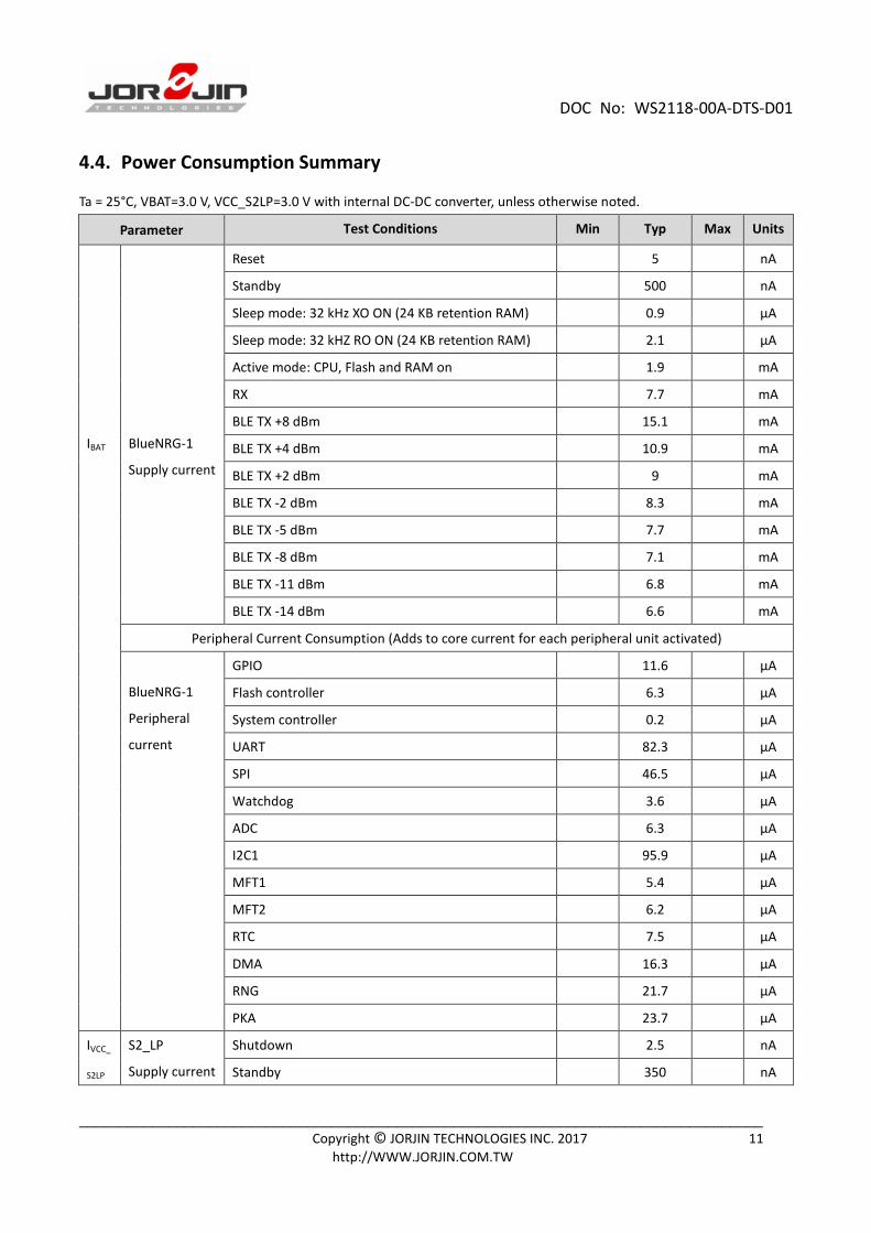
4.4. Power Consumption Summary
Ta = 25°C, VBAT=3.0 V, VCC_S2LP=3.0 V with internal DC-DC converter, unless otherwise noted.
Parameter Test Conditions Min Typ Max Units
IBAT
BlueNRG-1
Supply current
Reset 5 nA
Standby 500 nA
Sleep mode: 32 kHz XO ON (24 KB retention RAM) 0.9 μA
Sleep mode: 32 kHZ RO ON (24 KB retention RAM) 2.1 μA
Active mode: CPU, Flash and RAM on 1.9 mA
RX 7.7 mA
BLE TX +8 dBm 15.1 mA
BLE TX +4 dBm 10.9 mA
BLE TX +2 dBm 9 mA
BLE TX -2 dBm 8.3 mA
BLE TX -5 dBm 7.7 mA
BLE TX -8 dBm 7.1 mA
BLE TX -11 dBm 6.8 mA
BLE TX -14 dBm 6.6 mA
Peripheral Current Consumption (Adds to core current for each peripheral unit activated)
BlueNRG-1
Peripheral
current
GPIO 11.6 μA
Flash controller 6.3 μA
System controller 0.2 μA
UART 82.3 μA
SPI 46.5 μA
Watchdog 3.6 μA
ADC 6.3 μA
I2C1 95.9 μA
MFT1 5.4 μA
MFT2 6.2 μA
RTC 7.5 μA
DMA 16.3 μA
RNG 21.7 μA
PKA 23.7 μA
IVCC_
S2LP
S2_LP
Supply current
Shutdown 2.5 nA
Standby 350 nA
DOC No: WS2118-00A-DTS-D01
____________________________________________________________________________________
Copyright © JORJIN TECHNOLOGIES INC. 2017 12
http://WWW.JORJIN.COM.TW
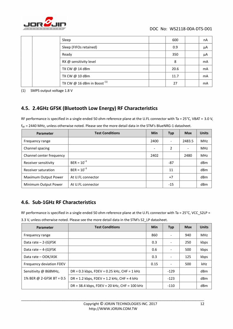
Sleep 600 nA
Sleep (FIFOs retained) 0.9 μA
Ready 350 μA
RX @ sensitivity level 8 mA
TX CW @ 14 dBm 20.6 mA
TX CW @ 10 dBm 11.7 mA
TX CW @ 16 dBm in Boost (1)
27 mA
(1) SMPS output voltage 1.8 V
4.5. 2.4GHz GFSK (Bluetooth Low Energy) RF Characteristics
RF performance is specified in a single ended 50 ohm reference plane at the U.FL connector with Ta = 25°C, VBAT = 3.0 V,
fRF = 2440 MHz, unless otherwise noted. Please see the more detail data in the STM’s BlueNRG-1 datasheet.
Parameter Test Conditions Min Typ Max Units
Frequency range 2400 - 2483.5 MHz
Channel spacing - 2 - MHz
Channel center frequency 2402 2480 MHz
Receiver sensitivity BER = 10–3
-87 dBm
Receiver saturation BER = 10–3
11 dBm
Maximum Output Power At U.FL connector +7 dBm
Minimum Output Power At U.FL connector -15 dBm
4.6. Sub-1GHz RF Characteristics
RF performance is specified in a single ended 50 ohm reference plane at the U.FL connector with Ta = 25°C, VCC_S2LP =
3.3 V, unless otherwise noted. Please see the more detail data in the STM’s S2_LP datasheet.
Parameter Test Conditions Min Typ Max Units
Frequency range 860 - 940 MHz
Data rate – 2-(G)FSK 0.3 - 250 kbps
Data rate – 4-(G)FSK 0.6 - 500 kbps
Data rate – OOK/ASK 0.3 - 125 kbps
Frequency deviation FDEV 0.15 - 500 kHz
Sensitivity @ 868MHz,
1% BER @ 2-GFSK BT = 0.5
DR = 0.3 kbps, FDEV = 0.25 kHz, CHF = 1 kHz -129 dBm
DR = 1.2 kbps, FDEV = 1.2 kHz, CHF = 4 kHz -123 dBm
DR = 38.4 kbps, FDEV = 20 kHz, CHF = 100 kHz -110 dBm
DOC No: WS2118-00A-DTS-D01
____________________________________________________________________________________
Copyright © JORJIN TECHNOLOGIES INC. 2017 13
http://WWW.JORJIN.COM.TW
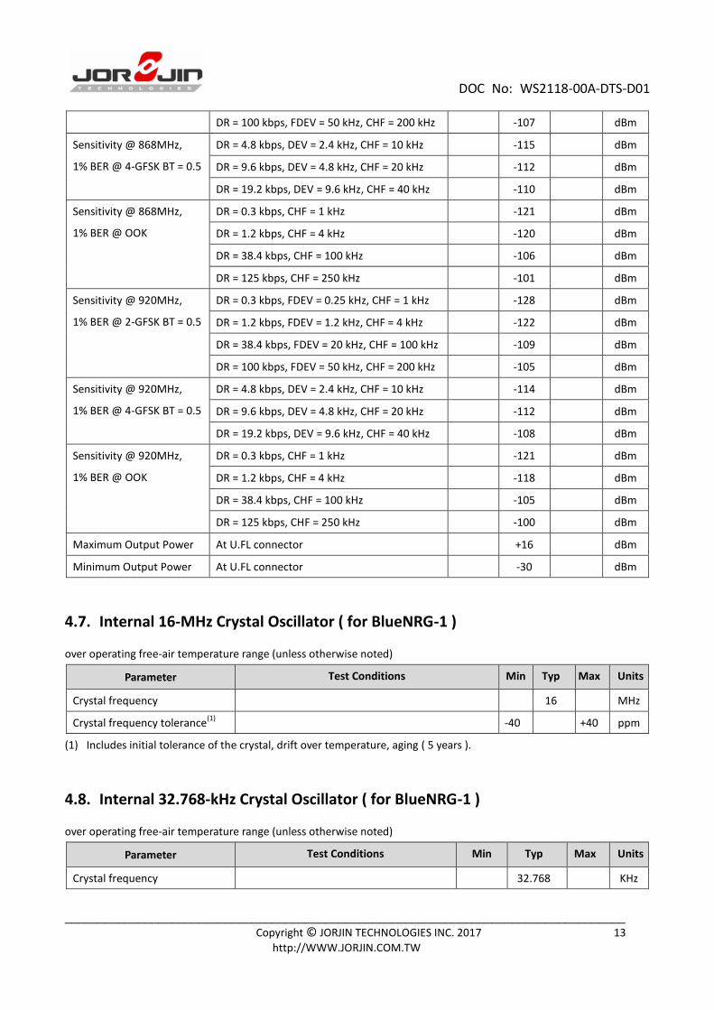
DR = 100 kbps, FDEV = 50 kHz, CHF = 200 kHz -107 dBm
Sensitivity @ 868MHz,
1% BER @ 4-GFSK BT = 0.5
DR = 4.8 kbps, DEV = 2.4 kHz, CHF = 10 kHz -115 dBm
DR = 9.6 kbps, DEV = 4.8 kHz, CHF = 20 kHz -112 dBm
DR = 19.2 kbps, DEV = 9.6 kHz, CHF = 40 kHz -110 dBm
Sensitivity @ 868MHz,
1% BER @ OOK
DR = 0.3 kbps, CHF = 1 kHz -121 dBm
DR = 1.2 kbps, CHF = 4 kHz -120 dBm
DR = 38.4 kbps, CHF = 100 kHz -106 dBm
DR = 125 kbps, CHF = 250 kHz -101 dBm
Sensitivity @ 920MHz,
1% BER @ 2-GFSK BT = 0.5
DR = 0.3 kbps, FDEV = 0.25 kHz, CHF = 1 kHz -128 dBm
DR = 1.2 kbps, FDEV = 1.2 kHz, CHF = 4 kHz -122 dBm
DR = 38.4 kbps, FDEV = 20 kHz, CHF = 100 kHz -109 dBm
DR = 100 kbps, FDEV = 50 kHz, CHF = 200 kHz -105 dBm
Sensitivity @ 920MHz,
1% BER @ 4-GFSK BT = 0.5
DR = 4.8 kbps, DEV = 2.4 kHz, CHF = 10 kHz -114 dBm
DR = 9.6 kbps, DEV = 4.8 kHz, CHF = 20 kHz -112 dBm
DR = 19.2 kbps, DEV = 9.6 kHz, CHF = 40 kHz -108 dBm
Sensitivity @ 920MHz,
1% BER @ OOK
DR = 0.3 kbps, CHF = 1 kHz -121 dBm
DR = 1.2 kbps, CHF = 4 kHz -118 dBm
DR = 38.4 kbps, CHF = 100 kHz -105 dBm
DR = 125 kbps, CHF = 250 kHz -100 dBm
Maximum Output Power At U.FL connector +16 dBm
Minimum Output Power At U.FL connector -30 dBm
4.7. Internal 16-MHz Crystal Oscillator ( for BlueNRG-1 )
over operating free-air temperature range (unless otherwise noted)
Parameter Test Conditions Min Typ Max Units
Crystal frequency 16 MHz
Crystal frequency tolerance(1)
-40 +40 ppm
(1) Includes initial tolerance of the crystal, drift over temperature, aging ( 5 years ).
4.8. Internal 32.768-kHz Crystal Oscillator ( for BlueNRG-1 )
over operating free-air temperature range (unless otherwise noted)
Parameter Test Conditions Min Typ Max Units
Crystal frequency 32.768 KHz
DOC No: WS2118-00A-DTS-D01
____________________________________________________________________________________
Copyright © JORJIN TECHNOLOGIES INC. 2017 14
http://WWW.JORJIN.COM.TW
Crystal frequency tolerance(1)
-40 40 ppm
(1) Includes initial tolerance of the crystal, drift over temperature, aging ( 5 years ).
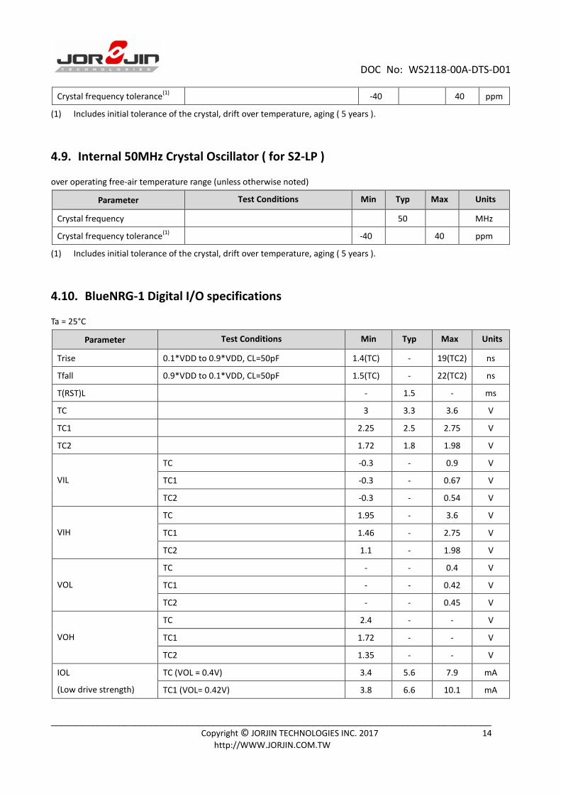
4.9. Internal 50MHz Crystal Oscillator ( for S2-LP )
over operating free-air temperature range (unless otherwise noted)
Parameter Test Conditions Min Typ Max Units
Crystal frequency 50 MHz
Crystal frequency tolerance(1)
-40 40 ppm
(1) Includes initial tolerance of the crystal, drift over temperature, aging ( 5 years ).
4.10. BlueNRG-1 Digital I/O specifications
Ta = 25°C
Parameter Test Conditions Min Typ Max Units
Trise 0.1*VDD to 0.9*VDD, CL=50pF 1.4(TC) - 19(TC2) ns
Tfall 0.9*VDD to 0.1*VDD, CL=50pF 1.5(TC) - 22(TC2) ns
T(RST)L - 1.5 - ms
TC 3 3.3 3.6 V
TC1 2.25 2.5 2.75 V
TC2 1.72 1.8 1.98 V
VIL
TC -0.3 - 0.9 V
TC1 -0.3 - 0.67 V
TC2 -0.3 - 0.54 V
VIH
TC 1.95 - 3.6 V
TC1 1.46 - 2.75 V
TC2 1.1 - 1.98 V
VOL
TC - - 0.4 V
TC1 - - 0.42 V
TC2 - - 0.45 V
VOH
TC 2.4 - - V
TC1 1.72 - - V
TC2 1.35 - - V
IOL
(Low drive strength)
TC (VOL = 0.4V) 3.4 5.6 7.9 mA
TC1 (VOL= 0.42V) 3.8 6.6 10.1 mA
DOC No: WS2118-00A-DTS-D01
____________________________________________________________________________________
Copyright © JORJIN TECHNOLOGIES INC. 2017 15
http://WWW.JORJIN.COM.TW
TC2 (VOL =0.45V) 1.6 3 5 mA
IOL
(High drive strength)
TC (VOL = 0.4V) 6.8 11.2 15.8 mA
TC1 (VOL= 0.42V) 7.6 13.2 20.1 mA
TC2 (VOL =0.45V) 3.3 6 9.9 mA
IOH
(Low drive strength)
TC (VOH = 2.4V) 5.5 10.6 17.6 mA
TC1 (VOH= 1.72V) 3.7 7.2 12 mA
TC2 (VOH =1.35V) 1.4 3 5.6 mA
IOH
(High drive strength)
TC (VOH = 2.4V) 9.9 19.2 31.7 mA
TC1 (VOH= 1.72V) 6.7 12.9 21.6 mA
TC2 (VOH =1.35V) 2.4 5.5 10.1 mA
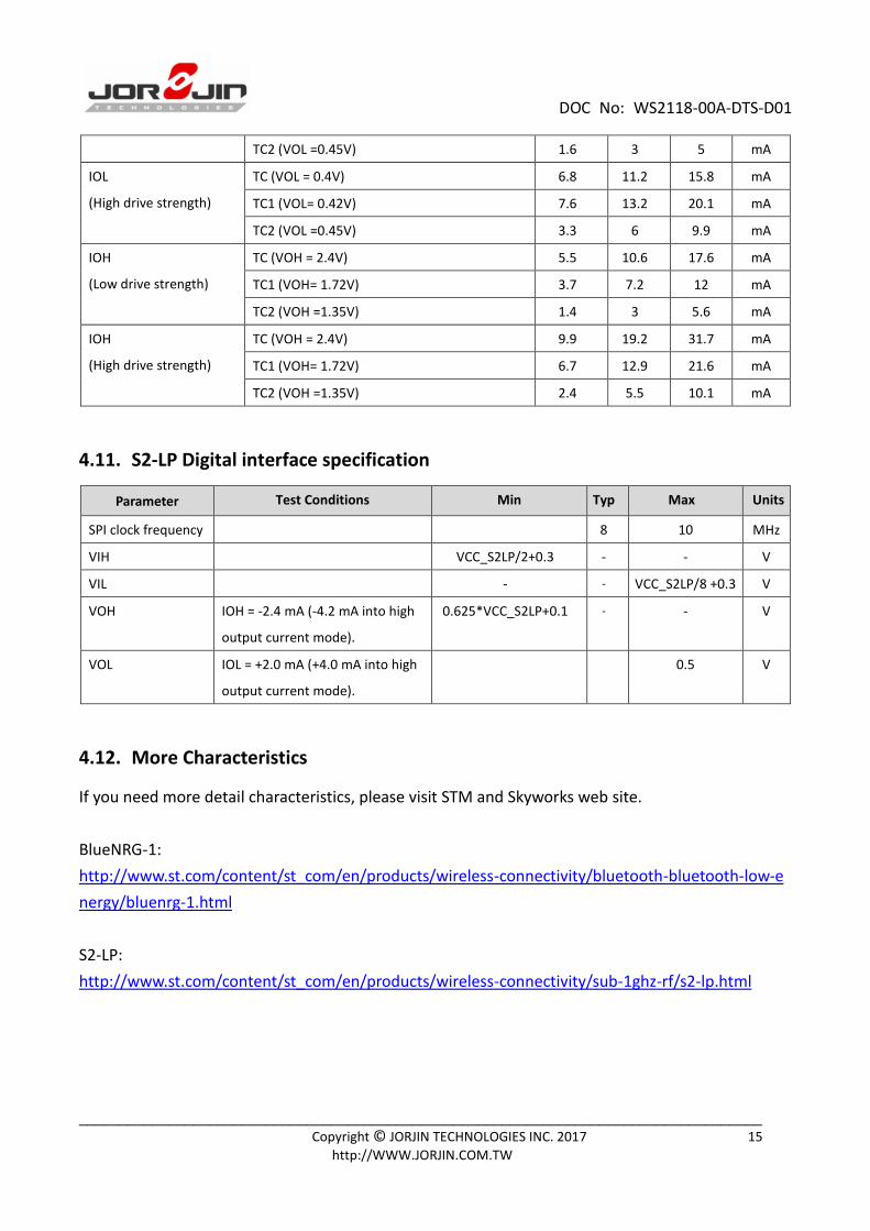
4.11. S2-LP Digital interface specification
Parameter Test Conditions Min Typ Max Units
SPI clock frequency 8 10 MHz
VIH VCC_S2LP/2+0.3 - - V
VIL - - VCC_S2LP/8 +0.3 V
VOH IOH = -2.4 mA (-4.2 mA into high
output current mode).
0.625*VCC_S2LP+0.1 - - V
VOL IOL = +2.0 mA (+4.0 mA into high
output current mode).
0.5 V
4.12. More Characteristics
If you need more detail characteristics, please visit STM and Skyworks web site.
BlueNRG-1:
http://www.st.com/content/st_com/en/products/wireless-connectivity/bluetooth-bluetooth-low-e
nergy/bluenrg-1.html
S2-LP:
http://www.st.com/content/st_com/en/products/wireless-connectivity/sub-1ghz-rf/s2-lp.html
DOC No: WS2118-00A-DTS-D01
____________________________________________________________________________________
Copyright © JORJIN TECHNOLOGIES INC. 2017 16
http://WWW.JORJIN.COM.TW
5. DESIGN RECOMMENDATIONS
5.1. GPIO Usage of BlueNRG-1
Because the function of some pins has been used in the module internally, the other functions of
these pins can not be defined. Please refer the below table.
Pin
Name
Mode “000” Mode “001” Mode “100” Mode “101” Note
Type Signal Type Signal Type Signal Type Signal
DIO0 I/O GPIO 0 I UART_CTS I/O SPI_CLK - - To SCLK pin of S2-LP
DIO1 I/O GPIO 1 O UART_RTS I/O SPI_CS1 I PDM_DAT To CS pin of S2-LP
DIO2 I/O GPIO 2 O PWM0 O SPI_OUT O PDM_CLK To SDI pin of S2-LP
DIO3 I/O GPIO 3 O PWM1 I SPI_IN O - To SDO pin of S2-LP
DIO4 I/O GPIO 4 I UART_RXD I/O I2C2_CLK O PWM0 To SCL pin of STSAFE-A1SX
DIO5 I/O GPIO 5 O UART_TXD I/O I2C2_DAT O PWM1 To SDA pin of STSAFE-A1SX
DIO6 I/O GPIO 6 O UART_RTS I/O I2C2_CLK I PDM_DAT To reset pin of STSAFE-A1SX
DIO7 I/O GPIO 7 I UART_CTS I/O I2C2_DAT O PDM_CLK
DIO8 I/O GPIO 8 O UART_TXD I/O SPI_CLK I PDM_DAT
DIO9 I/O GPIO 9 I SWCLK I SPI_IN - -
DIO10 I/O GPIO 10 I SWDIO O SPI_OUT - -
DIO11 I/O GPIO 11 I UART_RXD I/O SPI_CS1 - -
DIO12 OD GPIO 12 I - I/O I2C1_CLK - -
DIO13 OD GPIO 13 I UART_CTS I/O I2C1_DAT - - To GPIO3 pin of S2-LP
DIO14 I/O GPIO 14 I/O I2C1_CLK I/O SPI_CLK O - To SDN pin of S2-LP
5.2. Debug Port
The BlueNRG-1 embeds the ARM serial wire debug (SWD) port. It is two pins (clock and single
bi-directional data) debug interface, providing all the debug functionality plus realtime access to
system memory without halting the processor or requiring any target resident code.
Pin functionality Pin Name Pin description
SWCLK DIO9 SWD clock signal
SWDIO DIO10 SWD data signal
The Cortex-M0 subsystem of the BlueNRG-1 embeds two breakpoints and one watchpoint.
DOC No: WS2118-00A-DTS-D01
____________________________________________________________________________________
Copyright © JORJIN TECHNOLOGIES INC. 2017 17
http://WWW.JORJIN.COM.TW
5.3. Debugging Tips
There are certain situations where debug access is disabled and the chip cannot be accessed,
including:
application that disables debug pins
application that set the device in sleep or standby state, in which the debug port is not
powered.
These cases are common during application development and device can end up in a state where
debug access is no longer possible. To recover this situation, it is recommended to force DIO7 pin
high and hardware reset the device in order to force execution of the updater code. The user can
then connect with SWD interface and erase the device Flash memory.
5.4. Pre-programmed bootloader
BlueNRG-1 device has a pre-programmed bootloader supporting UART protocol with automatic
baudrate detection. Main features of the embedded bootloader are:
Auto baudrate detection up to 460 kbps
Flash mass erase, section erase
Flash programming
Flash readout protection enable/disable
The pre-programmed bootloader is an application which is stored on the BlueNRG-1 internal ROM
at manufacturing time by STMicroelectronics. This application allows upgrading the device Flash
with a user application using a serial communication channel (UART).
Bootloader is activated by hardware by forcing IO7 high during power-up or hardware Reset,
otherwise, application residing in Flash will be launched.
The customer application must ensure that IO7 is forced low during power up.
5.5. Antenna Selection Guide
There are two U.FL connectors to connect one 2.4GHz antenna and one Sub-1GHz antenna. There is
an antenna selection guide from STM. You can download it from the below link.
DOC No: WS2118-00A-DTS-D01
____________________________________________________________________________________
Copyright © JORJIN TECHNOLOGIES INC. 2017 18
http://WWW.JORJIN.COM.TW
http://www.st.com/content/ccc/resource/technical/document/application_note/82/38/3f/9f/fd/4d/4f
/ab/DM00068254.pdf/files/DM00068254.pdf/jcr:content/translations/en.DM00068254.pdf
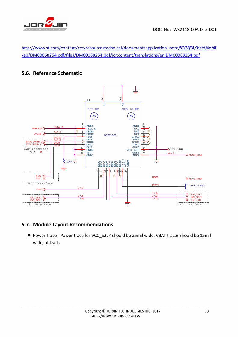
5.6. Reference Schematic
RESETNRESETN
TXD
DIO2DIO3
ADC1_Input
ADC2_Input
SPI_CLKSPI_SDO
SPI_SDII2C_SCLI2C_SDA
I2C Interface SPI Interface
DIO8
UART Interface
JTCK-SWTCKJTMS-SWTDIO
SWD Interface
RXD
DIO9DIO10DIO11
DIO12
DIO4DIO5
DIO7TEST1
ADC1
ADC2
DIO0
DIO12
BLE RF SUB-1G RF
U1
WS2118-00
GND11
RESETN2
DIO133
DIO124
TEST5
DIO116
GND210
VBAT11
GND312
DIO107
DIO98
DIO89
DIO
713
DIO
614
DIO
515
DIO
416
DIO
317
DIO
218
DIO
119
DIO
020
DIO
14
21
TE
ST
122
AD
C1
23
GN
D4
24
ADC225GND526VCC_S2LP27GND628GPIO329GPIO230GPIO131GPIO032NC133NC234NC335GND736
A1
A1
A2
A2
TEST POINT1
VCC_S2LPVBAT
DIO7
100K
5.7. Module Layout Recommendations
Power Trace - Power trace for VCC_S2LP should be 25mil wide. VBAT traces should be 15mil
wide, at least.
DOC No: WS2118-00A-DTS-D01
____________________________________________________________________________________
Copyright © JORJIN TECHNOLOGIES INC. 2017 19
http://WWW.JORJIN.COM.TW
6. PACKAGE INFORMATION
6.1. Module Mechanical Outline
Top View Side View
Note:
A = 2.8mm
DOC No: WS2118-00A-DTS-D01
____________________________________________________________________________________
Copyright © JORJIN TECHNOLOGIES INC. 2017 20
http://WWW.JORJIN.COM.TW
Bottom View
DOC No: WS2118-00A-DTS-D01
____________________________________________________________________________________
Copyright © JORJIN TECHNOLOGIES INC. 2017 21
http://WWW.JORJIN.COM.TW
7. SMT AND BAKING RECOMMENDATION
7.1. Baking Recommendation
Baking condition:
- Follow MSL Level 4 to do baking process.
- After bag is opened, devices that will be subjected to reflow solder or other high
temperature process must be
a) Mounted within 72 hours of factory conditions <30°C/60% RH, or
b) Stored at <10% RH.
- Devices require bake, before mounting, if Humidity Indicator Card reads >10%
If baking is required, Devices may be baked for 8 hrs. at 125 °C.
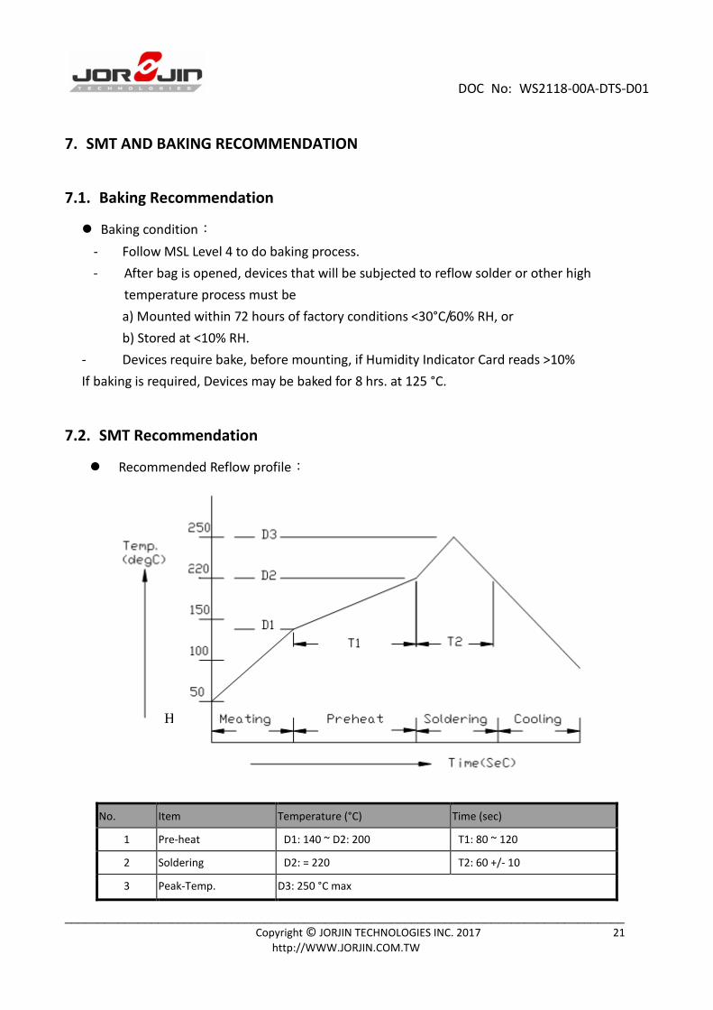
7.2. SMT Recommendation
Recommended Reflow profile:
No. Item Temperature (°C) Time (sec)
1 Pre-heat D1: 140 ~ D2: 200 T1: 80 ~ 120
2 Soldering D2: = 220 T2: 60 +/- 10
3 Peak-Temp. D3: 250 °C max
H
DOC No: WS2118-00A-DTS-D01
____________________________________________________________________________________
Copyright © JORJIN TECHNOLOGIES INC. 2017 22
http://WWW.JORJIN.COM.TW
Note: (1) Reflow soldering is recommended two times maximum.
(2) Add Nitrogen while Reflow process: SMT solder ability will be better.
Stencil thickness: 0.1~ 0.13 mm (Recommended)
Soldering paste (without Pb): Recommended SENJU N705-GRN3360-K2-V can get better
soldering effects.
DOC No: WS2118-00A-DTS-D01
____________________________________________________________________________________
Copyright © JORJIN TECHNOLOGIES INC. 2017 23
http://WWW.JORJIN.COM.TW
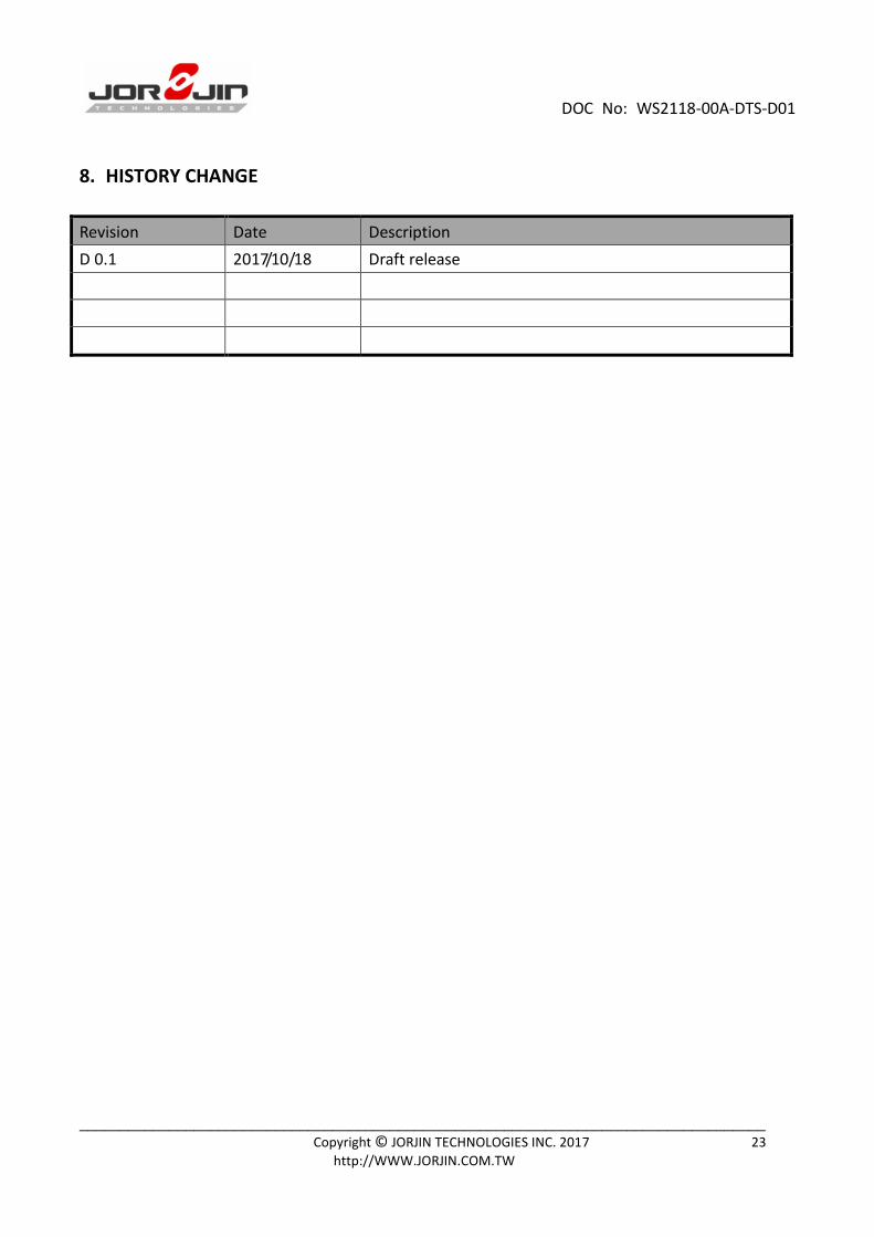
8. HISTORY CHANGE
Revision Date Description
D 0.1 2017/10/18 Draft release


![Very Low Noise, 24-Bit Analog-to-Digital Converter datasheet ...SDCS[1:0] = 01 0.5 μA Sensor detect current sources SDCS[1:0] = 10 2 μA SDCS[1:0] = 11 10 μA System Performance Resolution](https://img.pdfslide.net/doc/110x75/6100382d24f9d517681b0bc7/very-low-noise-24-bit-analog-to-digital-converter-datasheet-sdcs10-01.jpg)