Embed Size (px)
Citation preview

This is information on a product in full production.
April 2018 DS10889 Rev 3 1/39
M95040-DRE
4-Kbit serial SPI bus EEPROM - 105 °C Operation
Datasheet - production data
Features
• Compatible with the Serial Peripheral Interface (SPI) bus
• Memory array
– 4 Kbit (512 bytes) of EEPROM
– Page size: 16 bytes
– Write protection by block: 1/4, 1/2 or whole memory
– Additional Write lockable Page (Identification page)
• Extended temperature and voltage range
– Up to 105 °C (VCC from 1.7 V to 5.5 V)
• High speed clock frequency
– 20 MHz for VCC ≥ 4.5 V – 10 MHz for VCC ≥ 2.5 V
– 5 MHz for VCC ≥ 1.7 V
• Schmitt trigger inputs for noise filtering
• Short Write cycle time
– Byte Write within 4 ms
– Page Write within 4 ms
• Write cycle endurance
– 4 million Write cycles at 25 °C
– 1.2 million Write cycles at 85 °C
– 900 k Write cycles at 105 °C
• Data retention
– more than 50 years at 105 °C
– 200 years at 55 °C
• ESD Protection (Human Body Model)
– 4000 V
• Packages
– RoHS-compliant and halogen-free (ECOPACK2®)
WFDFPN8 (MF)DFN8 - 2 x 3 mm
SO8 (MN)150 mil width
TSSOP8 (DW)169 mil width
www.st.com

Contents M95040-DRE
2/39 DS10889 Rev 3
Contents
1 Description . . . . . . . . . . . . . . . . . . . . . . . . . . . . . . . . . . . . . . . . . . . . . . . . . 6
2 Signal description . . . . . . . . . . . . . . . . . . . . . . . . . . . . . . . . . . . . . . . . . . . 8
2.1 Serial Data output (Q) . . . . . . . . . . . . . . . . . . . . . . . . . . . . . . . . . . . . . . . . 8
2.2 Serial Data input (D) . . . . . . . . . . . . . . . . . . . . . . . . . . . . . . . . . . . . . . . . . . 8
2.3 Serial Clock (C) . . . . . . . . . . . . . . . . . . . . . . . . . . . . . . . . . . . . . . . . . . . . . 8
2.4 Chip Select (S) . . . . . . . . . . . . . . . . . . . . . . . . . . . . . . . . . . . . . . . . . . . . . . 8
2.5 Hold (HOLD) . . . . . . . . . . . . . . . . . . . . . . . . . . . . . . . . . . . . . . . . . . . . . . . . 8
2.6 Write Protect (W) . . . . . . . . . . . . . . . . . . . . . . . . . . . . . . . . . . . . . . . . . . . . 8
2.7 VSS ground . . . . . . . . . . . . . . . . . . . . . . . . . . . . . . . . . . . . . . . . . . . . . . . . . 8
2.8 VCC supply voltage . . . . . . . . . . . . . . . . . . . . . . . . . . . . . . . . . . . . . . . . . . . 9
3 Operating features . . . . . . . . . . . . . . . . . . . . . . . . . . . . . . . . . . . . . . . . . 10
3.1 Active power and Standby power modes . . . . . . . . . . . . . . . . . . . . . . . . . 10
3.2 SPI modes . . . . . . . . . . . . . . . . . . . . . . . . . . . . . . . . . . . . . . . . . . . . . . . . 10
3.3 Hold mode . . . . . . . . . . . . . . . . . . . . . . . . . . . . . . . . . . . . . . . . . . . . . . . . .11
3.4 Protocol control and data protection . . . . . . . . . . . . . . . . . . . . . . . . . . . . . .11
3.4.1 Protocol control . . . . . . . . . . . . . . . . . . . . . . . . . . . . . . . . . . . . . . . . . . . 11
3.4.2 Status Register and data protection . . . . . . . . . . . . . . . . . . . . . . . . . . . . 12
3.5 Identification page . . . . . . . . . . . . . . . . . . . . . . . . . . . . . . . . . . . . . . . . . . 13
4 Instructions . . . . . . . . . . . . . . . . . . . . . . . . . . . . . . . . . . . . . . . . . . . . . . . 14
4.1 Write Enable (WREN) . . . . . . . . . . . . . . . . . . . . . . . . . . . . . . . . . . . . . . . 15
4.2 Write Disable (WRDI) . . . . . . . . . . . . . . . . . . . . . . . . . . . . . . . . . . . . . . . . 15
4.3 Read Status Register (RDSR) . . . . . . . . . . . . . . . . . . . . . . . . . . . . . . . . . 16
4.4 Write Status Register (WRSR) . . . . . . . . . . . . . . . . . . . . . . . . . . . . . . . . . 17
4.5 Read from Memory Array (READ) . . . . . . . . . . . . . . . . . . . . . . . . . . . . . . 18
4.6 Write to Memory Array (WRITE) . . . . . . . . . . . . . . . . . . . . . . . . . . . . . . . 19
4.7 Read Identification Page (RDID) . . . . . . . . . . . . . . . . . . . . . . . . . . . . . . . 21
4.8 Write Identification Page (WRID) . . . . . . . . . . . . . . . . . . . . . . . . . . . . . . . 22
4.9 Read Lock Status (RDLS) . . . . . . . . . . . . . . . . . . . . . . . . . . . . . . . . . . . . 22
4.10 Lock Identification Page (LID) . . . . . . . . . . . . . . . . . . . . . . . . . . . . . . . . . 23
DS10889 Rev 3 3/39
M95040-DRE Contents
3
5 Application design recommendations . . . . . . . . . . . . . . . . . . . . . . . . . 25
5.1 Supply voltage (VCC) . . . . . . . . . . . . . . . . . . . . . . . . . . . . . . . . . . . . . . . . 25
5.1.1 Operating supply voltage (VCC) . . . . . . . . . . . . . . . . . . . . . . . . . . . . . . . 25
5.1.2 Power-up conditions . . . . . . . . . . . . . . . . . . . . . . . . . . . . . . . . . . . . . . . 25
5.1.3 Power-down . . . . . . . . . . . . . . . . . . . . . . . . . . . . . . . . . . . . . . . . . . . . . . 26
5.2 Implementing devices on SPI bus . . . . . . . . . . . . . . . . . . . . . . . . . . . . . . 26
5.3 Error Correction Code (ECC x 1) . . . . . . . . . . . . . . . . . . . . . . . . . . . . . . . 26
6 Delivery state . . . . . . . . . . . . . . . . . . . . . . . . . . . . . . . . . . . . . . . . . . . . . . 27
7 Absolute maximum ratings . . . . . . . . . . . . . . . . . . . . . . . . . . . . . . . . . . 27
8 DC and AC parameters . . . . . . . . . . . . . . . . . . . . . . . . . . . . . . . . . . . . . . 28
9 Package information . . . . . . . . . . . . . . . . . . . . . . . . . . . . . . . . . . . . . . . . 33
9.1 SO8N package information . . . . . . . . . . . . . . . . . . . . . . . . . . . . . . . . . . . 33
9.2 TSSOP8 package information . . . . . . . . . . . . . . . . . . . . . . . . . . . . . . . . . 34
9.3 WFDFPN8 (DFN8) package information . . . . . . . . . . . . . . . . . . . . . . . . . 35
10 Ordering information . . . . . . . . . . . . . . . . . . . . . . . . . . . . . . . . . . . . . . . 37
11 Revision history . . . . . . . . . . . . . . . . . . . . . . . . . . . . . . . . . . . . . . . . . . . 38

List of tables M95040-DRE
4/39 DS10889 Rev 3
List of tables
Table 1. Signal names . . . . . . . . . . . . . . . . . . . . . . . . . . . . . . . . . . . . . . . . . . . . . . . . . . . . . . . . . . . . 7Table 2. Status Register format . . . . . . . . . . . . . . . . . . . . . . . . . . . . . . . . . . . . . . . . . . . . . . . . . . . . 12Table 3. Write-protected block size . . . . . . . . . . . . . . . . . . . . . . . . . . . . . . . . . . . . . . . . . . . . . . . . . 13Table 4. Device identification bytes . . . . . . . . . . . . . . . . . . . . . . . . . . . . . . . . . . . . . . . . . . . . . . . . . 13Table 5. Instruction set . . . . . . . . . . . . . . . . . . . . . . . . . . . . . . . . . . . . . . . . . . . . . . . . . . . . . . . . . . . 14Table 6. Significant bits within the address byte . . . . . . . . . . . . . . . . . . . . . . . . . . . . . . . . . . . . . . . . 14Table 7. Absolute maximum ratings . . . . . . . . . . . . . . . . . . . . . . . . . . . . . . . . . . . . . . . . . . . . . . . . . 27Table 8. Cycling performance by byte . . . . . . . . . . . . . . . . . . . . . . . . . . . . . . . . . . . . . . . . . . . . . . . 28Table 9. Operating conditions (voltage range R, temperature range 8) . . . . . . . . . . . . . . . . . . . . . . 28Table 10. Operating conditions (voltage range R, temperature range 8)
for high-speed communications . . . . . . . . . . . . . . . . . . . . . . . . . . . . . . . . . . . . . . . . . . . . . 28Table 11. DC characteristics (voltage range R, temperature range 8) . . . . . . . . . . . . . . . . . . . . . . . . 29Table 12. AC characteristics. . . . . . . . . . . . . . . . . . . . . . . . . . . . . . . . . . . . . . . . . . . . . . . . . . . . . . . . 30Table 13. SO8N – 8-lead plastic small outline, 150 mils body width, package mechanical data . . . . 33Table 14. TSSOP8 – 8-lead thin shrink small outline, 3 x 6.4 mm, 0.65 mm pitch,
package mechanical data . . . . . . . . . . . . . . . . . . . . . . . . . . . . . . . . . . . . . . . . . . . . . . . . . . 34Table 15. WFDFPN8 – 8-lead very thin fine pitch dual flat package no lead
2 x 3 mm, 0.5 mm pitch, mechanical data . . . . . . . . . . . . . . . . . . . . . . . . . . . . . . . . . . . . . 36Table 16. Ordering information scheme . . . . . . . . . . . . . . . . . . . . . . . . . . . . . . . . . . . . . . . . . . . . . . . 37Table 17. Document revision history . . . . . . . . . . . . . . . . . . . . . . . . . . . . . . . . . . . . . . . . . . . . . . . . . 38

DS10889 Rev 3 5/39
M95040-DRE List of figures
5
List of figures
Figure 1. Logic diagram . . . . . . . . . . . . . . . . . . . . . . . . . . . . . . . . . . . . . . . . . . . . . . . . . . . . . . . . . . . . 6Figure 2. 8-pin package connections . . . . . . . . . . . . . . . . . . . . . . . . . . . . . . . . . . . . . . . . . . . . . . . . . . 7Figure 3. SPI modes supported . . . . . . . . . . . . . . . . . . . . . . . . . . . . . . . . . . . . . . . . . . . . . . . . . . . . . 10Figure 4. Hold mode activation . . . . . . . . . . . . . . . . . . . . . . . . . . . . . . . . . . . . . . . . . . . . . . . . . . . . . 11Figure 5. Write Enable (WREN) sequence . . . . . . . . . . . . . . . . . . . . . . . . . . . . . . . . . . . . . . . . . . . . 15Figure 6. Write Disable (WRDI) sequence. . . . . . . . . . . . . . . . . . . . . . . . . . . . . . . . . . . . . . . . . . . . . 16Figure 7. Read Status Register (RDSR) sequence . . . . . . . . . . . . . . . . . . . . . . . . . . . . . . . . . . . . . . 16Figure 8. Write Status Register (WRSR) sequence. . . . . . . . . . . . . . . . . . . . . . . . . . . . . . . . . . . . . . 17Figure 9. Read from Memory Array (READ) sequence . . . . . . . . . . . . . . . . . . . . . . . . . . . . . . . . . . . 18Figure 10. Byte Write (WRITE) sequence . . . . . . . . . . . . . . . . . . . . . . . . . . . . . . . . . . . . . . . . . . . . . . 19Figure 11. Page Write (WRITE) sequence . . . . . . . . . . . . . . . . . . . . . . . . . . . . . . . . . . . . . . . . . . . . . 20Figure 12. Read Identification Page sequence . . . . . . . . . . . . . . . . . . . . . . . . . . . . . . . . . . . . . . . . . . 21Figure 13. Write Identification Page sequence . . . . . . . . . . . . . . . . . . . . . . . . . . . . . . . . . . . . . . . . . . 22Figure 14. Read Lock Status sequence. . . . . . . . . . . . . . . . . . . . . . . . . . . . . . . . . . . . . . . . . . . . . . . . 23Figure 15. Lock ID sequence . . . . . . . . . . . . . . . . . . . . . . . . . . . . . . . . . . . . . . . . . . . . . . . . . . . . . . . . 23Figure 16. Bus master and memory devices on the SPI bus. . . . . . . . . . . . . . . . . . . . . . . . . . . . . . . . 26Figure 17. AC measurement I/O waveform . . . . . . . . . . . . . . . . . . . . . . . . . . . . . . . . . . . . . . . . . . . . . 31Figure 18. Serial input timing . . . . . . . . . . . . . . . . . . . . . . . . . . . . . . . . . . . . . . . . . . . . . . . . . . . . . . . . 31Figure 19. Hold timing . . . . . . . . . . . . . . . . . . . . . . . . . . . . . . . . . . . . . . . . . . . . . . . . . . . . . . . . . . . . . 31Figure 20. Serial output timing . . . . . . . . . . . . . . . . . . . . . . . . . . . . . . . . . . . . . . . . . . . . . . . . . . . . . . . 32Figure 21. SO8N – 8-lead plastic small outline, 150 mils body width, package outline . . . . . . . . . . . . 33Figure 22. TSSOP8 – 8-lead thin shrink small outline, 3 x 6.4 mm, 0.65 mm pitch,
package outline. . . . . . . . . . . . . . . . . . . . . . . . . . . . . . . . . . . . . . . . . . . . . . . . . . . . . . . . . . 34Figure 23. WFDFPN8 – 8-lead very thin fine pitch dual flat package no lead
2 x 3 mm, 0.5 mm, package outline . . . . . . . . . . . . . . . . . . . . . . . . . . . . . . . . . . . . . . . . . . 35

Description M95040-DRE
6/39 DS10889 Rev 3
1 Description
The M95040-DRE is a 4-Kbit serial EEPROM device operating up to 105 °C. The M95040-DRE is compliant with the level of reliability defined by the AEC-Q100 grade 2.
The device is accessed by a simple serial SPI compatible interface running up to 20 MHz.
The memory array is based on advanced true EEPROM technology (Electrically Erasable PROgrammable Memory). The M95040-DRE is a byte-alterable memory (512 × 8 bits) organized as 32 pages of 16 bytes in which the data integrity is significantly improved with an embedded Error Correction Code logic.
The M95040-DRE offers an additional Identification Page (16 bytes) in which the ST device identification can be read. This page can also be used to store sensitive application parameters which can be later permanently locked in read-only mode.
Figure 1. Logic diagram

DS10889 Rev 3 7/39
M95040-DRE Description
38
Figure 2. 8-pin package connections
1. See Package information section for package dimensions and how to identify pin-1.
Table 1. Signal names
Signal name Description
C Serial Clock
D Serial data input
Q Serial data output
S Chip Select
W Write Protect
HOLD Hold
VCC Supply voltage
VSS Ground

Signal description M95040-DRE
8/39 DS10889 Rev 3
2 Signal description
All input signals must be held high or low (according to voltages of VIH or VIL, as specified in Table 11). These signals are described below.
2.1 Serial Data output (Q)
This output signal is used to transfer data serially out of the device during a Read operation. Data is shifted out on the falling edge of Serial Clock (C), most significant bit (MSB) first. In all other cases, the Serial Data output is in high impedance.
2.2 Serial Data input (D)
This input signal is used to transfer data serially into the device. D input receives instructions, addresses, and the data to be written. Values are latched on the rising edge of Serial Clock (C), most significant bit (MSB) first.
2.3 Serial Clock (C)
This input signal allows to synchronize the timing of the serial interface. Instructions, addresses, or data present at Serial Data Input (D) are latched on the rising edge of Serial Clock (C). Data on Serial Data Output (Q) changes after the falling edge of Serial Clock (C).
2.4 Chip Select (S)
Driving Chip Select (S) low selects the device in order to start communication. Driving Chip Select (S) high deselects the device and Serial Data output (Q) enters the high impedance state.
2.5 Hold (HOLD)
The Hold (HOLD) signal is used to pause any serial communications with the device without deselecting the device. During the Hold condition, the Serial Data Output (Q) is high impedance, and the Serial Data Input (D) and Serial Clock (C) are Don’t Care. To start the Hold condition, the device must be selected, with Chip Select (S) driven low.
2.6 Write Protect (W)
This pin is used to write-protect the Status Register.
2.7 VSS ground
VSS is the reference for all signals, including the VCC supply voltage.

DS10889 Rev 3 9/39
M95040-DRE Signal description
38
2.8 VCC supply voltage
VCC is the supply voltage pin. Refer to Section 3.1: Active power and Standby power modes and to Section 5.1: Supply voltage (VCC).

Operating features M95040-DRE
10/39 DS10889 Rev 3
3 Operating features
3.1 Active power and Standby power modes
When Chip Select (S) is low, the device is selected and in the Active power mode.
When Chip Select (S) is high, the device is deselected. If a Write cycle is not currently in progress, the device then goes in to the Standby power mode, and the device consumption drops to ICC1, as specified in Table 11.
3.2 SPI modes
The device can be driven by a microcontroller with its SPI peripheral running in either of the two following modes:
• CPOL=0, CPHA=0
• CPOL=1, CPHA=1
For these two modes, input data is latched in on the rising edge of Serial Clock (C), and output data is available from the falling edge of Serial Clock (C).
The difference between the two modes, as shown in Figure 3, is the clock polarity when the bus master is in Stand-by mode and not transferring data:
• C remains at 0 for (CPOL=0, CPHA=0)
• C remains at 1 for (CPOL=1, CPHA=1)
Figure 3. SPI modes supported
DS10889 Rev 3 11/39
M95040-DRE Operating features
38
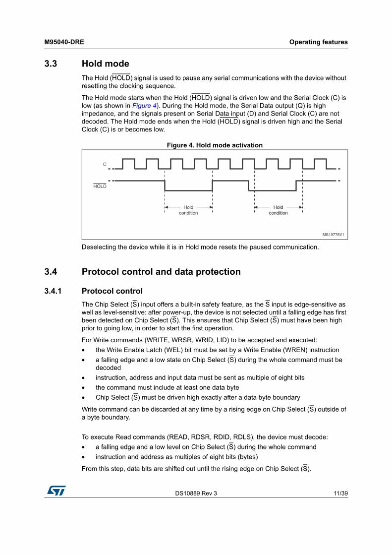
3.3 Hold mode
The Hold (HOLD) signal is used to pause any serial communications with the device without resetting the clocking sequence.
The Hold mode starts when the Hold (HOLD) signal is driven low and the Serial Clock (C) is low (as shown in Figure 4). During the Hold mode, the Serial Data output (Q) is high impedance, and the signals present on Serial Data input (D) and Serial Clock (C) are not decoded. The Hold mode ends when the Hold (HOLD) signal is driven high and the Serial Clock (C) is or becomes low.
Figure 4. Hold mode activation
Deselecting the device while it is in Hold mode resets the paused communication.
3.4 Protocol control and data protection
3.4.1 Protocol control
The Chip Select (S) input offers a built-in safety feature, as the S input is edge-sensitive as well as level-sensitive: after power-up, the device is not selected until a falling edge has first been detected on Chip Select (S). This ensures that Chip Select (S) must have been high prior to going low, in order to start the first operation.
For Write commands (WRITE, WRSR, WRID, LID) to be accepted and executed:
• the Write Enable Latch (WEL) bit must be set by a Write Enable (WREN) instruction
• a falling edge and a low state on Chip Select (S) during the whole command must be decoded
• instruction, address and input data must be sent as multiple of eight bits
• the command must include at least one data byte
• Chip Select (S) must be driven high exactly after a data byte boundary
Write command can be discarded at any time by a rising edge on Chip Select (S) outside of a byte boundary.
To execute Read commands (READ, RDSR, RDID, RDLS), the device must decode:
• a falling edge and a low level on Chip Select (S) during the whole command
• instruction and address as multiples of eight bits (bytes)
From this step, data bits are shifted out until the rising edge on Chip Select (S).

Operating features M95040-DRE
12/39 DS10889 Rev 3
3.4.2 Status Register and data protection
The Status Register format is shown in Table 2 and the status and control bits of the Status Register are as follows:
Note: Bits b7, b6, b5 and b4 are always read as 1.
WIP bit
The WIP bit (Write In Progress) is a read-only flag that indicates the Ready/Busy state of the device. When a Write command (WRITE, WRSR, WRID, LID) has been decoded and a Write cycle (tW) is in progress, the device is busy and the WIP bit is set to 1. When WIP=0, the device is ready to decode a new command.
During a Write cycle, reading continuously the WIP bit allows to detect when the device becomes ready (WIP=0) to decode a new command.
WEL bit
The WEL bit (Write Enable Latch) bit is a flag that indicates the status of the internal Write Enable Latch. When WEL is set to 1, the Write instructions (WRITE, WRSR, WRID, LID) are executed; when WEL is set to 0, any decoded Write instruction is not executed.
The WEL bit is set to 1 with the WREN instruction. The WEL bit is reset to 0 after the following events:
• Write Disable (WRDI) instruction completion
• Write instructions (WRITE, WRSR, WRID, LID) completion including the write cycle time tW
• Power-up
BP1, BP0 bits
The Block Protect bits (BP1, BP0) are non-volatile. BP1,BP0 bits define the size of the memory block to be protected against write instructions, as defined in Table 2. These bits are written with the Write Status Register (WRSR) instruction.
Table 2. Status Register format
b7 b6 b5 b4 b3 b2 b1 b0
1 1 1 1 BP1 BP0 WEL WIP
Block Protect bits
Write Enable Latch bit
Write In Progress bit

DS10889 Rev 3 13/39
M95040-DRE Operating features
38
3.5 Identification page
The M95040-DRE offers an Identification page (16 bytes) in addition to the 4 Kbit memory. The Identification page contains two fields:
• Device identification: the three first bytes are programmed by STMicroelectronics with the Device identification code, as shown in Table 4.
• Application parameters: the bytes after the Device identification code are available for application specific data.
Note: If the end application does not need to read the Device identification code, this field can be overwritten and used to store application-specific data. Once the application-specific data are written in the Identification page, the whole Identification page should be permanently locked in Read-only mode.
The Read, Write, Lock Identification Page instructions are detailed in Section 4: Instructions.
Table 3. Write-protected block size
Status Register bitsProtected block Protected array addresses
BP1 BP0
0 0 None None
0 1 Upper quarter 180h-1FFh
1 0 Upper half 100h - 1FFh
1 1 Whole memory 000h - 1FFh plus Identification page
Table 4. Device identification bytes
Address inIdentification page
Content Value
00h ST Manufacturer code 20h
01h SPI Family code 00h
02h Memory Density code 09h (4 Kbit)
Instructions M95040-DRE
14/39 DS10889 Rev 3
4 Instructions
Each command is composed of bytes (MSBit transmitted first), initiated with the instruction byte, as summarized in Table 5.
If an invalid instruction is sent (one not contained in Table 5), the device automatically enters a Wait state until deselected.
For read and write commands to memory array and Identification Page, the address is defined by one byte and the bit b3 of the instruction byte as explained in Table 6.
Table 5. Instruction set
Instruction DescriptionInstruction
format
WREN Write Enable 0000 X110(1)
1. X = Don’t Care.
WRDI Write Disable 0000 X100(1)
RDSR Read Status Register 0000 X101(1)
WRSR Write Status Register 0000 X001(1)
READ Read from Memory Array 0000 A8011(2)
2. A8 = 1 for the upper half of the memory array, and 0 for the lower half.
WRITE Write to Memory Array 0000 A8010(2)
RDID Read Identification Page 1000 0011
WRID Write Identification Page 1000 0010
RDLS Reads the Identification Page lock status. 1000 0011
LID Locks the Identification page in read-only mode. 1000 0010
Table 6. Significant bits within the address byte(1)(2)
InstructionsBit b3 of the instruction byte LSB Address byte
b7 b6 b5 b4 b3 b2 b1 b0
READ or WRITE
x x x x x x x A8 A7 A6 A5 A4 A3 A2 A1 A0
RDID or WRID
0 0 0 0 0 0 0 0 0 0 0 A4 A3 A2 A1 A0
RDLS or LID
0 0 0 0 0 0 0 0 1 0 0 0 0 0 0 0
1. A: Significant address bit.
2. x: bit is Don’t Care.
DS10889 Rev 3 15/39
M95040-DRE Instructions
38
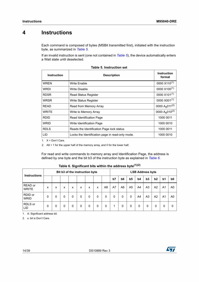
4.1 Write Enable (WREN)
The WREN instruction must be decoded by the device before a write instruction (WRITE, WRSR, WRID or LID).
As shown in Figure 5, to send this instruction to the device, Chip Select (S) is driven low, the bits of the instruction byte are shifted in (MSB first) on Serial Data Input (D) after what the Chip Select (S) input is driven high and the WEL bit is set (Status Register bit).
Figure 5. Write Enable (WREN) sequence
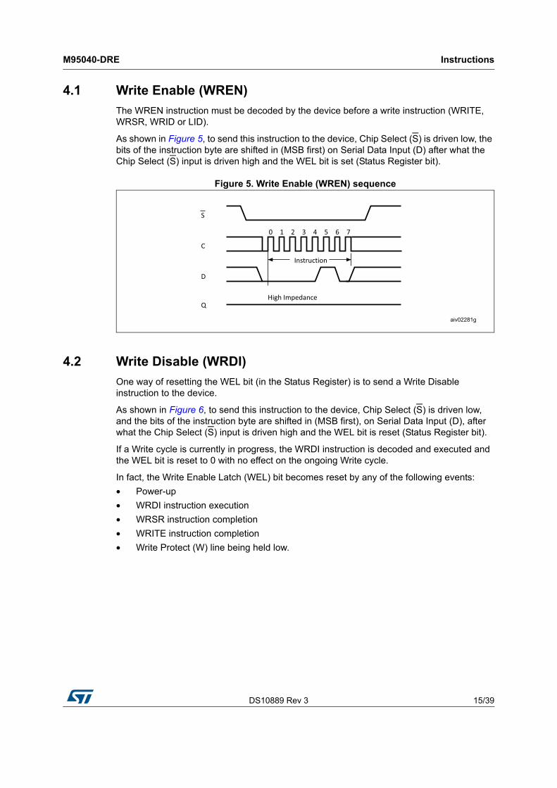
4.2 Write Disable (WRDI)
One way of resetting the WEL bit (in the Status Register) is to send a Write Disable instruction to the device.
As shown in Figure 6, to send this instruction to the device, Chip Select (S) is driven low, and the bits of the instruction byte are shifted in (MSB first), on Serial Data Input (D), after what the Chip Select (S) input is driven high and the WEL bit is reset (Status Register bit).
If a Write cycle is currently in progress, the WRDI instruction is decoded and executed and the WEL bit is reset to 0 with no effect on the ongoing Write cycle.
In fact, the Write Enable Latch (WEL) bit becomes reset by any of the following events:
• Power-up
• WRDI instruction execution
• WRSR instruction completion
• WRITE instruction completion
• Write Protect (W) line being held low.
Instructions M95040-DRE
16/39 DS10889 Rev 3
Figure 6. Write Disable (WRDI) sequence
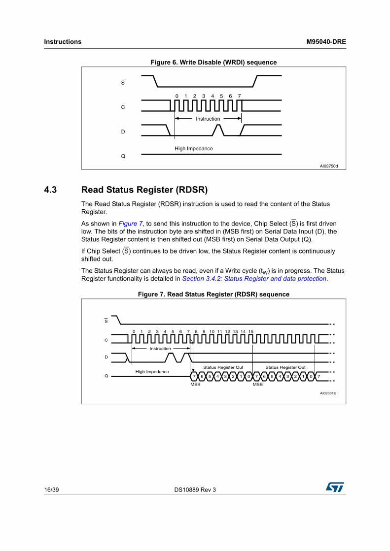
4.3 Read Status Register (RDSR)
The Read Status Register (RDSR) instruction is used to read the content of the Status Register.
As shown in Figure 7, to send this instruction to the device, Chip Select (S) is first driven low. The bits of the instruction byte are shifted in (MSB first) on Serial Data Input (D), the Status Register content is then shifted out (MSB first) on Serial Data Output (Q).
If Chip Select (S) continues to be driven low, the Status Register content is continuously shifted out.
The Status Register can always be read, even if a Write cycle (tW) is in progress. The Status Register functionality is detailed in Section 3.4.2: Status Register and data protection.
Figure 7. Read Status Register (RDSR) sequence
DS10889 Rev 3 17/39
M95040-DRE Instructions
38
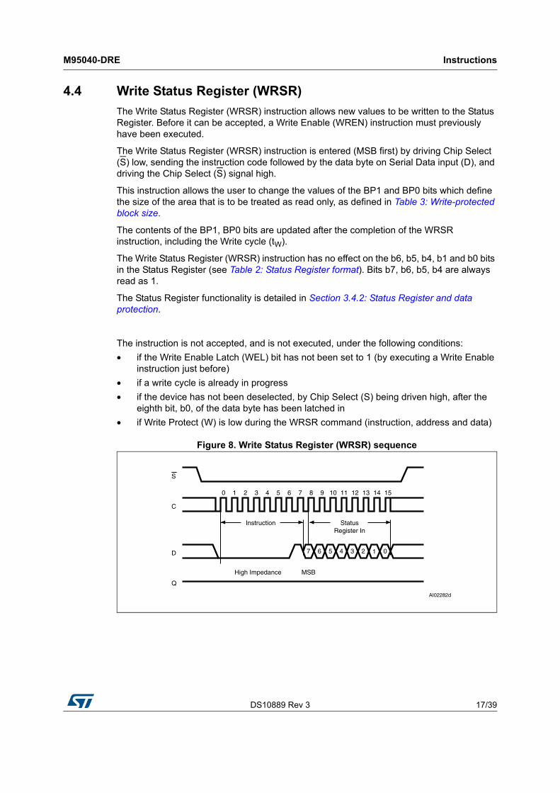
4.4 Write Status Register (WRSR)
The Write Status Register (WRSR) instruction allows new values to be written to the Status Register. Before it can be accepted, a Write Enable (WREN) instruction must previously have been executed.
The Write Status Register (WRSR) instruction is entered (MSB first) by driving Chip Select (S) low, sending the instruction code followed by the data byte on Serial Data input (D), and driving the Chip Select (S) signal high.
This instruction allows the user to change the values of the BP1 and BP0 bits which define the size of the area that is to be treated as read only, as defined in Table 3: Write-protected block size.
The contents of the BP1, BP0 bits are updated after the completion of the WRSR instruction, including the Write cycle (tW).
The Write Status Register (WRSR) instruction has no effect on the b6, b5, b4, b1 and b0 bits in the Status Register (see Table 2: Status Register format). Bits b7, b6, b5, b4 are always read as 1.
The Status Register functionality is detailed in Section 3.4.2: Status Register and data protection.
The instruction is not accepted, and is not executed, under the following conditions:
• if the Write Enable Latch (WEL) bit has not been set to 1 (by executing a Write Enable instruction just before)
• if a write cycle is already in progress
• if the device has not been deselected, by Chip Select (S) being driven high, after the eighth bit, b0, of the data byte has been latched in
• if Write Protect (W) is low during the WRSR command (instruction, address and data)
Figure 8. Write Status Register (WRSR) sequence

Instructions M95040-DRE
18/39 DS10889 Rev 3
4.5 Read from Memory Array (READ)
The READ instruction is used to read the content of the memory.
As shown in Figure 9, to send this instruction to the device, Chip Select (S) is first driven low.
The bits of the instruction byte and address byte are then shifted in, on Serial Data Input (D). The most significant address bit, A8, is incorporated as bit b3 of the instruction byte, as shown in Table 5: Instruction set. The address is loaded into an internal address register, and the byte of data at that address is shifted out, on Serial Data Output (Q).
If Chip Select (S) continues to be driven low, the internal address register is automatically incremented, and the next byte of data is shifted out. The whole memory can therefore be read with a single READ instruction.
When the highest address is reached, the address counter rolls over to zero, allowing the Read cycle to be continued indefinitely.
The Read cycle is terminated by driving Chip Select (S) high at any time when the data bits are shifted out on Serial Data Output (Q).
The instruction is not accepted, and is not executed, if a Write cycle is currently in progress.
Figure 9. Read from Memory Array (READ) sequence
1. Depending on the memory size, as shown in Table 6, the most significant address bits are Don’t Care.
DS10889 Rev 3 19/39
M95040-DRE Instructions
38
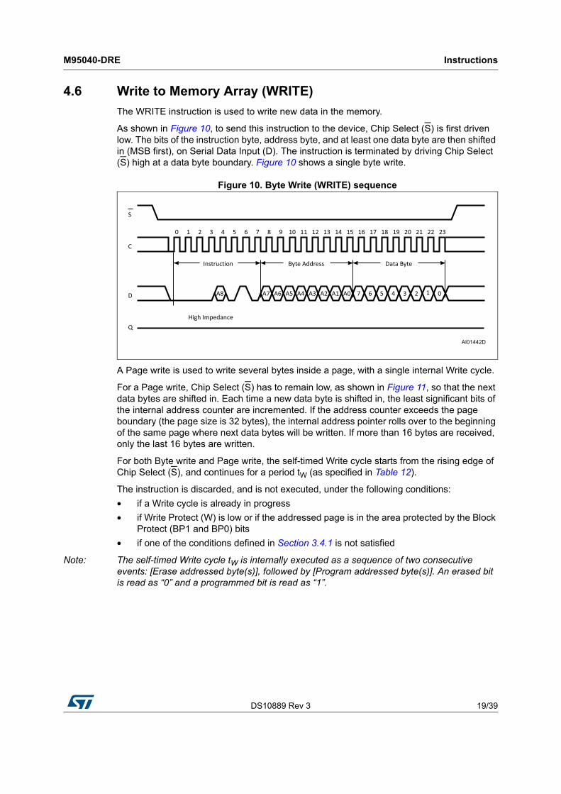
4.6 Write to Memory Array (WRITE)
The WRITE instruction is used to write new data in the memory.
As shown in Figure 10, to send this instruction to the device, Chip Select (S) is first driven low. The bits of the instruction byte, address byte, and at least one data byte are then shifted in (MSB first), on Serial Data Input (D). The instruction is terminated by driving Chip Select (S) high at a data byte boundary. Figure 10 shows a single byte write.
Figure 10. Byte Write (WRITE) sequence
A Page write is used to write several bytes inside a page, with a single internal Write cycle.
For a Page write, Chip Select (S) has to remain low, as shown in Figure 11, so that the next data bytes are shifted in. Each time a new data byte is shifted in, the least significant bits of the internal address counter are incremented. If the address counter exceeds the page boundary (the page size is 32 bytes), the internal address pointer rolls over to the beginning of the same page where next data bytes will be written. If more than 16 bytes are received, only the last 16 bytes are written.
For both Byte write and Page write, the self-timed Write cycle starts from the rising edge of Chip Select (S), and continues for a period tW (as specified in Table 12).
The instruction is discarded, and is not executed, under the following conditions:
• if a Write cycle is already in progress
• if Write Protect (W) is low or if the addressed page is in the area protected by the Block Protect (BP1 and BP0) bits
• if one of the conditions defined in Section 3.4.1 is not satisfied
Note: The self-timed Write cycle tW is internally executed as a sequence of two consecutive events: [Erase addressed byte(s)], followed by [Program addressed byte(s)]. An erased bit is read as “0” and a programmed bit is read as “1”.

Instructions M95040-DRE
20/39 DS10889 Rev 3
Figure 11. Page Write (WRITE) sequence

DS10889 Rev 3 21/39
M95040-DRE Instructions
38
4.7 Read Identification Page (RDID)
The Read Identification Page instruction is used to read the Identification Page (additional page of 16 bytes which can be written and later permanently locked in Read-only mode).
The Chip Select (S) signal is first driven low, the bits of the instruction byte and address bytes are then shifted in (MSB first) on Serial Data input (D). Address bit A8 must be 0 and the other upper address bits are Don't Care (it might be easier to define these bits as 0, as shown in Table 6). The data byte pointed to by the lower address bits [A4:A0] is shifted out (MSB first) on Serial Data output (Q).
The first byte addressed can be any byte within the identification page.
If Chip Select (S) continues to be driven low, the internal address register is automatically incremented and the byte of data at the new address is shifted out.
Note that there is no roll over feature in the Identification Page. The address of bytes to read must not exceed the page boundary.
The read cycle is terminated by driving Chip Select (S) high. The rising edge of the Chip Select (S) signal can occur at any time when the data bits are shifted out.
The instruction is not accepted, and is not executed, if a Write cycle is currently in progress.
Figure 12. Read Identification Page sequence
The first three bytes of the Identification page offer information about the device itself. Please refer to Section 3.5: Identification page for more information.
Instructions M95040-DRE
22/39 DS10889 Rev 3
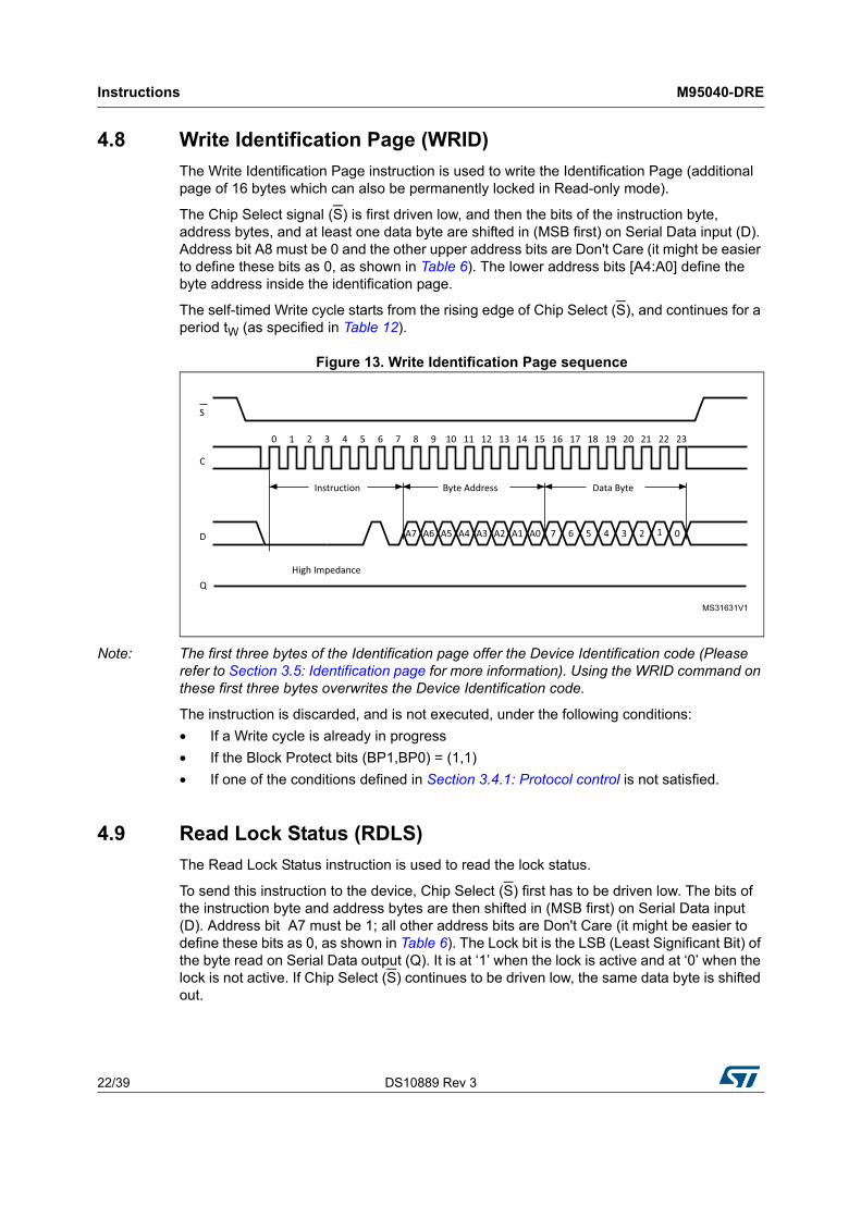
4.8 Write Identification Page (WRID)
The Write Identification Page instruction is used to write the Identification Page (additional page of 16 bytes which can also be permanently locked in Read-only mode).
The Chip Select signal (S) is first driven low, and then the bits of the instruction byte, address bytes, and at least one data byte are shifted in (MSB first) on Serial Data input (D). Address bit A8 must be 0 and the other upper address bits are Don't Care (it might be easier to define these bits as 0, as shown in Table 6). The lower address bits [A4:A0] define the byte address inside the identification page.
The self-timed Write cycle starts from the rising edge of Chip Select (S), and continues for a period tW (as specified in Table 12).
Figure 13. Write Identification Page sequence
Note: The first three bytes of the Identification page offer the Device Identification code (Please refer to Section 3.5: Identification page for more information). Using the WRID command on these first three bytes overwrites the Device Identification code.
The instruction is discarded, and is not executed, under the following conditions:
• If a Write cycle is already in progress
• If the Block Protect bits (BP1,BP0) = (1,1)
• If one of the conditions defined in Section 3.4.1: Protocol control is not satisfied.
4.9 Read Lock Status (RDLS)
The Read Lock Status instruction is used to read the lock status.
To send this instruction to the device, Chip Select (S) first has to be driven low. The bits of the instruction byte and address bytes are then shifted in (MSB first) on Serial Data input (D). Address bit A7 must be 1; all other address bits are Don't Care (it might be easier to define these bits as 0, as shown in Table 6). The Lock bit is the LSB (Least Significant Bit) of the byte read on Serial Data output (Q). It is at ‘1’ when the lock is active and at ‘0’ when the lock is not active. If Chip Select (S) continues to be driven low, the same data byte is shifted out.

DS10889 Rev 3 23/39
M95040-DRE Instructions
38
The read cycle is terminated by driving Chip Select (S) high. The instruction sequence is shown in Figure 14.
The Read Lock Status instruction is not accepted and not executed if a Write cycle is currently in progress.
Figure 14. Read Lock Status sequence
4.10 Lock Identification Page (LID)
The Lock Identification Page (LID) command is used to permanently lock the Identification Page in Read-only mode.
The LID instruction is issued by driving Chip Select (S) low, sending (MSB first) the instruction code, the address and a data byte on Serial Data input (D), and driving Chip Select (S) high. In the address sent, A7 must be equal to 1. All other address bits are Don't Care (it might be easier to define these bits as 0, as shown in Table 6). The data byte sent must be equal to the binary value xxxx xx1x, where x = Don't Care. The LID instruction is terminated by driving Chip Select (S) high at a data byte boundary, otherwise, the instruction is not executed.
Figure 15. Lock ID sequence

Instructions M95040-DRE
24/39 DS10889 Rev 3
Driving Chip Select (S) high at a byte boundary of the input data triggers the self-timed Write cycle which duration is tW (specified in Table 12). The instruction sequence is shown in Figure 15.
The instruction is discarded, and is not executed, under the following conditions:
• If a Write cycle is already in progress
• If the Block Protect bits (BP1,BP0) = (1,1)
• If one of the conditions defined in Section 3.4.1: Protocol control is not satisfied.
DS10889 Rev 3 25/39
M95040-DRE Application design recommendations
38
5 Application design recommendations
5.1 Supply voltage (VCC)
5.1.1 Operating supply voltage (VCC)
Prior to selecting the memory and issuing instructions to it, a valid and stable VCC voltage within the specified [VCC(min), VCC(max)] range must be applied (see Table 9 and Table 10).
This voltage must remain stable and valid until the end of the transmission of the instruction and, for a Write instruction, until the completion of the internal Write cycle (tW). In order to secure a stable DC supply voltage, it is recommended to decouple the VCC line with a suitable capacitor (usually of the order of 10 nF to 100 nF) close to the VCC/VSS package pins.
5.1.2 Power-up conditions
When the power supply is turned on, VCC continuously rises from VSS to VCC. During this time, the Chip Select (S) line is not allowed to float but should follow the VCC voltage. It is therefore recommended to connect the S line to VCC via a suitable pull-up resistor (see Figure 16).
The VCC voltage has to rise continuously from 0 V up to the minimum VCC operating voltage defined in Table 11.
In order to prevent inadvertent write operations during power-up, a power-on-reset (POR) circuit is included.
At power-up, the device does not respond to any instruction until VCC reaches the internal threshold voltage (this threshold is defined in the DC characteristics Table 11 as VRES).
When VCC passes over the POR threshold, the device is reset and in the following state:
• in the Standby power mode
• deselected
• Status register values:
– Write Enable Latch (WEL) bit is reset to 0.
– Write In Progress (WIP) bit is reset to 0.
– BP1 and BP0 bits remain unchanged (non-volatile bits).
• not in the Hold condition
As soon as the VCC voltage has reached a stable value within [VCC(min), VCC(max)] range, the device is ready for operation.

Application design recommendations M95040-DRE
26/39 DS10889 Rev 3
5.1.3 Power-down
At power down, the power-on-reset (POR) circuit resets and locks the device as soon as the VCC reached the internal threshold voltage
During power-down (continuous decrease in the VCC supply voltage below the minimum VCC operating voltage defined in Table 11), the device must be:
• deselected (Chip Select (S) should be allowed to follow the voltage applied on VCC),
• in Standby power mode (there should not be any internal Write cycle in progress).
5.2 Implementing devices on SPI bus
Figure 16 shows an example of three devices, connected to the SPI bus master. Only one device is selected at a time, so that only the selected device drives the Serial Data output (Q) line. All the other devices outputs are then in high impedance.
Figure 16. Bus master and memory devices on the SPI bus
1. The Write Protect (W) and Hold (HOLD) signals must be driven high or low as appropriate.
A pull-up resistor connected on each /S input (represented in Figure 16) ensures that each device is not selected if the bus master leaves the /S line in the high impedance state.
5.3 Error Correction Code (ECC x 1)
The Error Correction Code (ECC x 1) is an internal logic function which is transparent for the SPI communication protocol.
The ECC x 1 logic is implemented on each byte of the memory array. If a single bit out of the byte happens to be erroneous during a Read operation, the ECC x 1 detects this bit and replaces it with the correct value. The read reliability is therefore much improved.

DS10889 Rev 3 27/39
M95040-DRE Delivery state
38
6 Delivery state
The device is delivered with:
• the memory array set to all 1s (each byte = FFh),
• Status register: bit BP1 =0 and BP0 =0,
• Identification page: the first three bytes define the Device identification code (value defined in Table 4). The content of the following bytes is Don’t Care.
7 Absolute maximum ratings
Stressing the device outside the ratings listed in Table 7 may cause permanent damage to the device. These are stress ratings only, and operation of the device at these, or any other conditions outside those indicated in the operating sections of this specification, is not implied. Exposure to absolute maximum rating conditions for extended periods may affect device reliability.
Table 7. Absolute maximum ratings
Symbol Parameter Min. Max. Unit
TSTG Storage temperature - 65 150 °C
TAMR Ambient operating temperature - 40 150 °C
TLEAD Lead temperature during soldering See note (1)
1. Compliant with JEDEC Std J-STD-020D (for small body, Sn-Pb or Pb-free assembly), the ST ECOPACK® 7191395 specification, and the European directive on Restrictions of Hazardous Substances (RoHS directive 2011/65/EU of July 2011).
°C
VO Voltage on Q pin - 0.50 VCC+0.6 V
VI Input voltage - 0.50 6.5 V
IOL DC output current (Q = 0) - 5 mA
IOH DC output current (Q = 1) - 5 mA
VCC Supply voltage - 0.50 6.5 V
VESD Electrostatic pulse (Human Body Model)(2)
2. Positive and negative pulses applied on pin pairs, in accordance with AEC-Q100-002 (compliant with ANSI/ESDA/JEDEC JS-001-2012, C1=100 pF, R1=1500 Ω, R2=500 Ω)
- 4000 V

DC and AC parameters M95040-DRE
28/39 DS10889 Rev 3
8 DC and AC parameters
This section summarizes the operating conditions and the DC/AC characteristics of the device.
Table 8. Cycling performance by byte
Symbol Parameter Test condition Min. Max. Unit
Ncycle Write cycle endurance
TA ≤ 25 °C, 1.7 V < VCC < 5.5 V - 4,000,000Write cycle(1)TA = 85 °C, 1.7 V < VCC < 5.5 V - 1,200,000
TA = 105 °C, 1.7 V < VCC < 5.5 V - 900,000
1. A Write cycle is executed when either a Page Write, a Byte Write, a WRSR, a WRID or an LID instruction is decoded. When using the Byte Write, the Page Write or the WRID, refer also to Section 5.3: Error Correction Code (ECC x 1).
Table 9. Operating conditions (voltage range R, temperature range 8)
Symbol Parameter Conditions Min. Max. Unit
VCC Supply voltage - 1.7 5.5 V
TA Ambient operating temperature - - 40 105 °C
fC Operating clock frequencyVCC ≥ 2.5 V, capacitive load on Q pin ≤ 100pF - 10
MHzVCC ≥ 1.7 V, capacitive load on Q pin ≤ 100pF - 5
Table 10. Operating conditions (voltage range R, temperature range 8)for high-speed communications
Symbol Parameter Conditions Min. Max. Unit
VCC Supply voltage - 4.5 5.5 V
TA Ambient operating temperature - - 40 85 °C
fC Operating clock frequency VCC ≥ 4.5 V, capacitive load on Q pin ≤ 60 pF - 20 MHz

DS10889 Rev 3 29/39
M95040-DRE DC and AC parameters
38
Table 11. DC characteristics (voltage range R, temperature range 8)
Symbol ParameterTest conditions
(in addition to conditions specified in Table 9)
Min. Max. Unit
COUT(1) Output capacitance (Q) VOUT = 0 V - 8
pFCIN
(1) Input capacitance VIN = 0 V - 6
ILI Input leakage current VIN = VSS or VCC - 2µA
ILO Output leakage current S = VCC, VOUT = VSS or VCC - 3
ICC Supply current (Read)
VCC = 1.7 V, C = 0.1 VCC/0.9 VCC, Q = open, fC = 5 MHz
- 2
mAVCC = 2.5 V, C = 0.1 VCC/0.9 VCC, Q = open, fC = 10 MHz
- 2
VCC = 5.5 V, fC = 20 MHz(2)
C = 0.1 VCC/0.9 VCC, Q = open- 5
ICC0(3) Supply current (Write)
1.7 V ≤ VCC < 5.5 V during tW,
S = VCC- 2(1) mA
ICC1 Supply current (Standby mode)
t° = 25 °C, VCC = 1.7 V, S = VCC, VIN = VSS or VCC
- 1
µA
t° = 25 °C, VCC = 2.5 V, S = VCC, VIN = VSS or VCC
- 2
t° = 25 °C, VCC = 5.5 V, S = VCC, VIN = VSS or VCC
- 3
t° = 105 °C, VCC = 1.7 V, S = VCC, VIN = VSS or VCC
- 1
t° = 105 °C, VCC = 2.5 V, S = VCC, VIN = VSS or VCC
- 2
t° = 105 °C, VCC = 5.5 V, S = VCC, VIN = VSS or VCC
- 3
VIL Input low voltage1.7 V ≤ VCC < 2.5 V - 0.45 0.25 VCC
V2.5 V ≤ VCC < 5.5 V - 0.45 0.3 VCC
VIH Input high voltage1.7 V ≤ VCC < 2.5 V 0.75 VCC VCC+ 1
V2.5 V ≤ VCC < 5.5 V 0.7 VCC VCC+ 1
VOL Output low voltageVCC = 1.7 V, IOL = 1 mA - 0.3
VVCC ≥ 2.5 V, IOL = 2 mA - 0.4
VOH Output high voltageVCC = 1.7 V, IOH = 1 mA 0.8 VCC -
VVCC ≥ 2.5 V, IOH = -2 mA 0.8 VCC -
VRES(1) Internal reset threshold voltage - 0.5 1.5 V
1. Characterized only, not 100% tested.
2. When –40 °C < t° < 85 °C.
3. Average value during the Write cycle (tW).

DC and AC parameters M95040-DRE
30/39 DS10889 Rev 3
Table 12. AC characteristics
Symbol Alt. Parameter
Min. Max. Min. Max. Min. Max.
UnitTest
conditions specified in
Table 9
Test conditions specified in
Table 9
Test conditions specified in
Table 10
fC fSCK Clock frequency - 5 - 10 - 20 MHz
tSLCH tCSS1 S active setup time 60 - 30 - 15 -
ns
tSHCH tCSS2 S not active setup time 60 - 30 - 15 -
tSHSL tCS S deselect time 90 - 40 - 20 -
tCHSH tCSH S active hold time 60 - 30 - 15 -
tCHSL S not active hold time 60 - 30 - 15 -
tCH(1) tCLH Clock high time 80 - 40 - 20 -
tCL(1) tCLL Clock low time 80 - 40 - 20 -
tCLCH(2) tRC Clock rise time - 2 - 2 - 2
µstCHCL
(2) tFC Clock fall time - 2 - 2 - 2
tDVCH tDSU Data in setup time 20 - 10 - 5 -
ns
tCHDX tDH Data in hold time 20 - 10 - 10 -
tHHCH Clock low hold time after HOLD not active 60 - 30 - 15 -
tHLCH Clock low hold time after HOLD active 60 - 30 - 15 -
tCLHL Clock low set-up time before HOLD active 0 - 0 - 0 -
tCLHHClock low set-up time before HOLD not active
0 - 0 - 0 -
tSHQZ(2) tDIS Output disable time - 80 - 40 - 20
tCLQV(3) tV Clock low to output valid - 80 - 40 - 20
tCLQX tHO Output hold time 0 - 0 - 0 -
tQLQH(2) tRO Output rise time - 20 - 20 - 20
tQHQL(2) tFO Output fall time - 20 - 20 - 20
tHHQV tLZ HOLD high to output valid - 80 - 40 - 20
tHLQZ(2) tHZ HOLD low to output high-Z - 80 - 40 - 20
tW tWC Write time - 4 - 4 - 4 ms
1. tCH + tCL must never be lower than the shortest possible clock period, 1/fC(max).
2. Value guaranteed by characterization, not 100% tested in production.
3. tCLQV must be compatible with tCL (clock low time): if tSU is the Read setup time of the SPI bus master, tCL must be equal to (or greater than) tCLQV+tSU.
DS10889 Rev 3 31/39
M95040-DRE DC and AC parameters
38
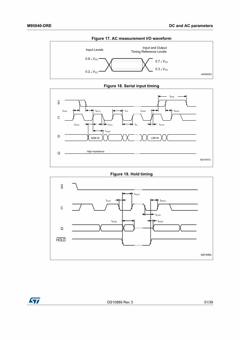
Figure 17. AC measurement I/O waveform
Figure 18. Serial input timing
Figure 19. Hold timing

DC and AC parameters M95040-DRE
32/39 DS10889 Rev 3
Figure 20. Serial output timing

DS10889 Rev 3 33/39
M95040-DRE Package information
38
9 Package information
In order to meet environmental requirements, ST offers these devices in different grades of ECOPACK® packages, depending on their level of environmental compliance. ECOPACK® specifications, grade definitions and product status are available at: www.st.com. ECOPACK® is an ST trademark.
9.1 SO8N package information
Figure 21. SO8N – 8-lead plastic small outline, 150 mils body width, package outline
1. Drawing is not to scale.
Table 13. SO8N – 8-lead plastic small outline, 150 mils body width, package mechanical data
Symbolmillimeters inches(1)
Typ. Min. Max. Typ. Min. Max.
A - - 1.75 - - 0.0689
A1 - 0.10 0.25 - 0.0039 0.0098
A2 - 1.25 - - 0.0492 -
b - 0.28 0.48 - 0.011 0.0189
c - 0.17 0.23 - 0.0067 0.0091
ccc - - 0.10 - - 0.0039
D 4.90 4.80 5.00 0.1929 0.189 0.1969
E 6.00 5.80 6.20 0.2362 0.2283 0.2441
E1 3.90 3.80 4.00 0.1535 0.1496 0.1575
e 1.27 - - 0.05 - -
h - 0.25 0.50 - 0.0098 0.0197
k - 0° 8° - 0° 8°
Package information M95040-DRE
34/39 DS10889 Rev 3
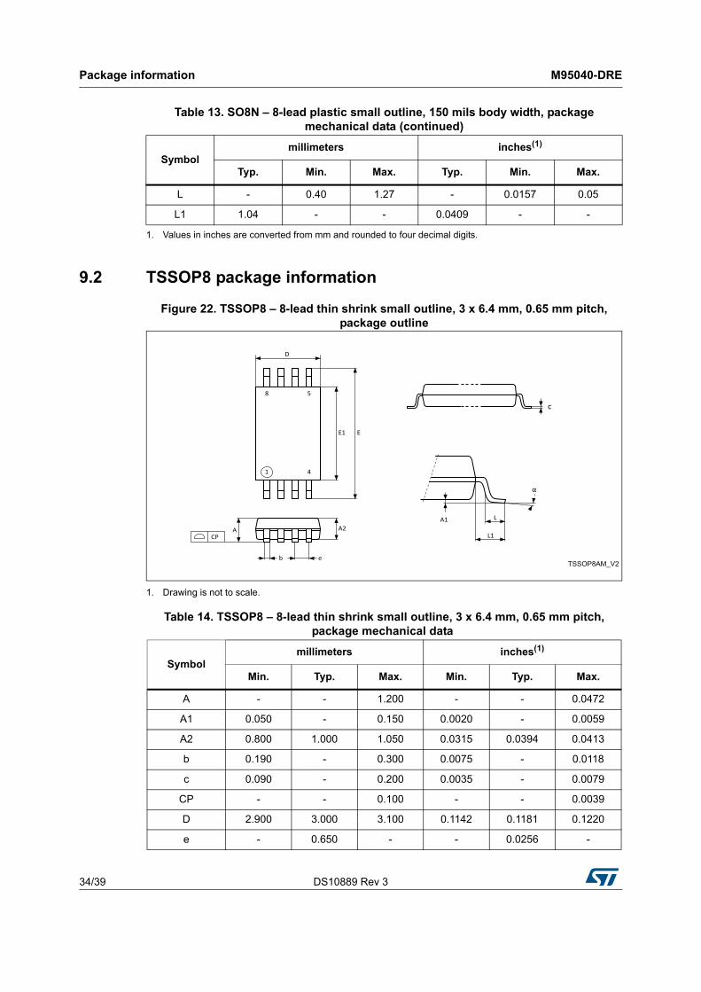
9.2 TSSOP8 package information
Figure 22. TSSOP8 – 8-lead thin shrink small outline, 3 x 6.4 mm, 0.65 mm pitch, package outline
1. Drawing is not to scale.
L - 0.40 1.27 - 0.0157 0.05
L1 1.04 - - 0.0409 - -
1. Values in inches are converted from mm and rounded to four decimal digits.
Table 13. SO8N – 8-lead plastic small outline, 150 mils body width, package mechanical data (continued)
Symbolmillimeters inches(1)
Typ. Min. Max. Typ. Min. Max.
Table 14. TSSOP8 – 8-lead thin shrink small outline, 3 x 6.4 mm, 0.65 mm pitch, package mechanical data
Symbolmillimeters inches(1)
Min. Typ. Max. Min. Typ. Max.
A - - 1.200 - - 0.0472
A1 0.050 - 0.150 0.0020 - 0.0059
A2 0.800 1.000 1.050 0.0315 0.0394 0.0413
b 0.190 - 0.300 0.0075 - 0.0118
c 0.090 - 0.200 0.0035 - 0.0079
CP - - 0.100 - - 0.0039
D 2.900 3.000 3.100 0.1142 0.1181 0.1220
e - 0.650 - - 0.0256 -

DS10889 Rev 3 35/39
M95040-DRE Package information
38
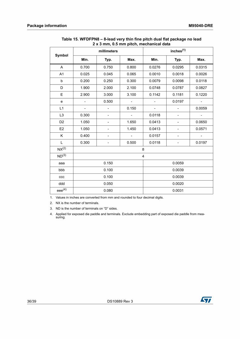
9.3 WFDFPN8 (DFN8) package information
Figure 23. WFDFPN8 – 8-lead very thin fine pitch dual flat package no lead 2 x 3 mm, 0.5 mm, package outline
1. Drawing is not to scale.
2. The central pad (the area E2 by D2 in the above illustration) must be either connected to Vss or left floating (not connected) in the end application.
E 6.200 6.400 6.600 0.2441 0.2520 0.2598
E1 4.300 4.400 4.500 0.1693 0.1732 0.1772
L 0.450 0.600 0.750 0.0177 0.0236 0.0295
L1 - 1.000 - - 0.0394 -
α 0° - 8° 0° - 8°
1. Values in inches are converted from mm and rounded to four decimal digits.
Table 14. TSSOP8 – 8-lead thin shrink small outline, 3 x 6.4 mm, 0.65 mm pitch, package mechanical data (continued)
Symbolmillimeters inches(1)
Min. Typ. Max. Min. Typ. Max.
Package information M95040-DRE
36/39 DS10889 Rev 3
Table 15. WFDFPN8 – 8-lead very thin fine pitch dual flat package no lead2 x 3 mm, 0.5 mm pitch, mechanical data
Symbolmillimeters inches(1)
1. Values in inches are converted from mm and rounded to four decimal digits.
Min. Typ. Max. Min. Typ. Max.
A 0.700 0.750 0.800 0.0276 0.0295 0.0315
A1 0.025 0.045 0.065 0.0010 0.0018 0.0026
b 0.200 0.250 0.300 0.0079 0.0098 0.0118
D 1.900 2.000 2.100 0.0748 0.0787 0.0827
E 2.900 3.000 3.100 0.1142 0.1181 0.1220
e - 0.500 - - 0.0197 -
L1 - - 0.150 - - 0.0059
L3 0.300 - - 0.0118 - -
D2 1.050 - 1.650 0.0413 - 0.0650
E2 1.050 - 1.450 0.0413 - 0.0571
K 0.400 - - 0.0157 - -
L 0.300 - 0.500 0.0118 - 0.0197
NX(2)
2. NX is the number of terminals.
8
ND(3)
3. ND is the number of terminals on “D” sides.
4
aaa 0.150 0.0059
bbb 0.100 0.0039
ccc 0.100 0.0039
ddd 0.050 0.0020
eee(4)
4. Applied for exposed die paddle and terminals. Exclude embedding part of exposed die paddle from mea-suring.
0.080 0.0031

DS10889 Rev 3 37/39
M95040-DRE Ordering information
38
10 Ordering information
For a list of available options (speed, package, etc.) or for further information on any aspect of this device, please contact your nearest ST sales office.
Note: Parts marked as “ES”, “E” or accompanied by an Engineering Sample notification letter, are not yet qualified and therefore not yet ready to be used in production and any consequences deriving from such usage will not be at ST charge. In no event, ST will be liable for any customer usage of these engineering samples in production. ST Quality has to be contacted prior to any decision to use these Engineering samples to run qualification activity.
Table 16. Ordering information scheme
Example: M95 040-D R DW 8 T P /K
Device type
M95 = SPI serial access EEPROM
Device function
040-D = 4 Kbit (512 bytes) plus Identification Page
Operating voltage
R = VCC = 1.7 to 5.5 V
Package(1)
1. All packages are ECOPACK2® (RoHS compliant and free of brominated, chlorinated and antimony-oxide flame retardants).
MN = SO8 (150 mils width)
DW = TSSOP8 (169 mils width)
MF = WFDFPN8 (DFN8 2 x 3 mm)
Device grade
8 = – 40 to 105 °C.
Option
blank = Tube packing
T = Tape and reel packing
Plating technology
P or G = ECOPACK2®
Process letter
/K = Manufacturing technology code

Revision history M95040-DRE
38/39 DS10889 Rev 3
11 Revision history
Table 17. Document revision history
Date Revision Changes
17-Feb-2015 1 Initial release.
31-Jan-2017 2
Updated:
– Features
– Section 5.1.3: Power-down
– Table 8: Cycling performance by byte
– Table 9: Operating conditions (voltage range R, temperature range 8)
– Table 11: DC characteristics (voltage range R, temperature range 8)
– Table 14: TSSOP8 – 8-lead thin shrink small outline, 3 x 6.4 mm, 0.65 mm pitch, package mechanical data
– Figure 22: TSSOP8 – 8-lead thin shrink small outline, 3 x 6.4 mm, 0.65 mm pitch, package outline
– Section 10: Ordering information
18-Apr-2018 3
Updated:
– Section 4: Instructions
– Section 9.3: WFDFPN8 (DFN8) package information
– Section 10: Ordering information

DS10889 Rev 3 39/39
M95040-DRE
39
IMPORTANT NOTICE – PLEASE READ CAREFULLY
STMicroelectronics NV and its subsidiaries (“ST”) reserve the right to make changes, corrections, enhancements, modifications, and improvements to ST products and/or to this document at any time without notice. Purchasers should obtain the latest relevant information on ST products before placing orders. ST products are sold pursuant to ST’s terms and conditions of sale in place at the time of order acknowledgement.
Purchasers are solely responsible for the choice, selection, and use of ST products and ST assumes no liability for application assistance or the design of Purchasers’ products.
No license, express or implied, to any intellectual property right is granted by ST herein.
Resale of ST products with provisions different from the information set forth herein shall void any warranty granted by ST for such product.
ST and the ST logo are trademarks of ST. All other product or service names are the property of their respective owners.
Information in this document supersedes and replaces information previously supplied in any prior versions of this document.
© 2018 STMicroelectronics – All rights reserved