Embed Size (px)
Citation preview
DATASHEET
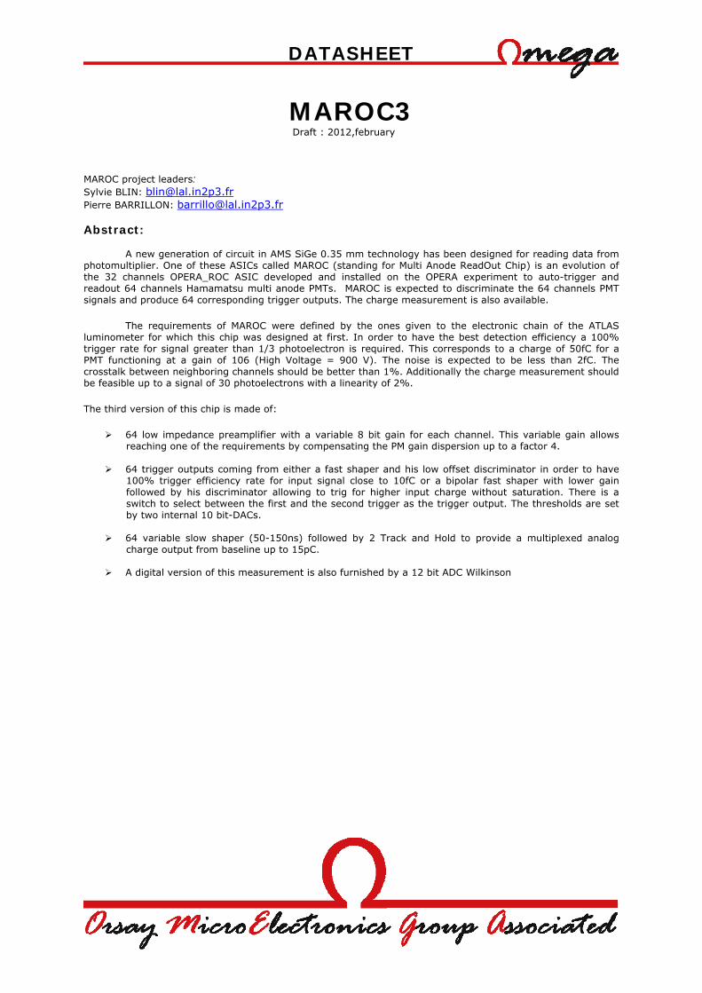
MAROC3 Draft : 2012,february MAROC project leaders: Sylvie BLIN: [email protected] Pierre BARRILLON: [email protected] Abstract:
A new generation of circuit in AMS SiGe 0.35 mm technology has been designed for reading data from photomultiplier. One of these ASICs called MAROC (standing for Multi Anode ReadOut Chip) is an evolution of the 32 channels OPERA_ROC ASIC developed and installed on the OPERA experiment to auto-trigger and readout 64 channels Hamamatsu multi anode PMTs. MAROC is expected to discriminate the 64 channels PMT signals and produce 64 corresponding trigger outputs. The charge measurement is also available.
The requirements of MAROC were defined by the ones given to the electronic chain of the ATLAS luminometer for which this chip was designed at first. In order to have the best detection efficiency a 100% trigger rate for signal greater than 1/3 photoelectron is required. This corresponds to a charge of 50fC for a PMT functioning at a gain of 106 (High Voltage = 900 V). The noise is expected to be less than 2fC. The crosstalk between neighboring channels should be better than 1%. Additionally the charge measurement should be feasible up to a signal of 30 photoelectrons with a linearity of 2%. The third version of this chip is made of:
64 low impedance preamplifier with a variable 8 bit gain for each channel. This variable gain allows reaching one of the requirements by compensating the PM gain dispersion up to a factor 4.
64 trigger outputs coming from either a fast shaper and his low offset discriminator in order to have
100% trigger efficiency rate for input signal close to 10fC or a bipolar fast shaper with lower gain followed by his discriminator allowing to trig for higher input charge without saturation. There is a switch to select between the first and the second trigger as the trigger output. The thresholds are set by two internal 10 bit-DACs.
64 variable slow shaper (50-150ns) followed by 2 Track and Hold to provide a multiplexed analog
charge output from baseline up to 15pC.
A digital version of this measurement is also furnished by a 12 bit ADC Wilkinson

DATASHEET
MAROC die snapshot
Chip characteristics: Technology : AMS SiGe 0.35μm Chip Area : 16mm2 (4mm *3.9mm) Package : CQFP240 Power consumption : 220mW ( 3.5mW/channel) Power supply : 0-3.5 V
DATASHEET
MAROC3 Datasheet 3/48
1. Table of content 1. Table of content ......................................................................................................................... 3 2. Table of figures .......................................................................................................................... 4 3. General description .................................................................................................................... 5 4. Preamplifier ............................................................................................................................... 7
4.1. Super Common Base .............................................................................................................. 7 4.2. 8bit-current mirror ................................................................................................................. 8
5. Sum outputs .............................................................................................................................. 8 5.1. Principe ................................................................................................................................. 8 5.2. Simulations ........................................................................................................................... 9
6. Slow Channel ........................................................................................................................... 10 6.1. Charge measurement description ........................................................................................... 10
6.1.1. RC buffer and Slow Shaper ................................................................................................ 10 6.1.2. Measurements results ....................................................................................................... 10
6.2. Slow shaper linearity ............................................................................................................ 12 6.3. Slow shaper linearity at different PA gain ................................................................................ 13 6.4. Crosstalk ............................................................................................................................. 14 6.5. Wilkinson ADC ..................................................................................................................... 15
6.5.1. ADC description ................................................................................................................ 15 6.5.2. Wilkinson calibration and pedestals measurements ............................................................... 17 6.5.3. Correlation with DC measurements ..................................................................................... 22
7. Fast channel ............................................................................................................................ 23 7.1. DAC .................................................................................................................................... 23
7.1.1. Principle .......................................................................................................................... 23 7.1.2. DAC measurements .......................................................................................................... 23
7.2. Variable Fast Shapers ........................................................................................................... 24 7.3. Fast Shaper Measurements .................................................................................................... 24
7.3.1. DC measurements ............................................................................................................ 24 8. Trigger outputs ........................................................................................................................ 25
8.1. S-curve vs injected charge .................................................................................................... 25 8.1.1. Bipolar Fast Shaper .......................................................................................................... 25 8.1.2. Unipolar Fast Shaper ......................................................................................................... 25 8.1.3. Correlation ...................................................................................................................... 26
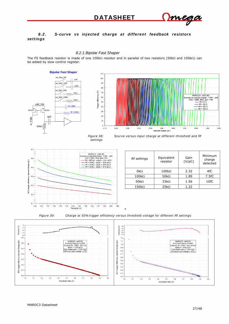
8.2. S-curve vs injected charge at different feedback resistors settings ............................................. 27 8.2.1. Bipolar Fast Shaper .......................................................................................................... 27 8.2.2. Gain adjustement ............................................................................................................. 29
8.3. Cross talk ............................................................................................................................ 30 9. Result summary ....................................................................................................................... 31 10. TEST BOARD ........................................................................................................................... 32
10.1. MAROC3 chip Input/Output.................................................................................................... 32 10.1.1. Pinout Table ................................................................................................................. 32
10.2. ASIC Registers ..................................................................................................................... 36 10.2.1. D_SC, CK_SC and RST_SC (Static Register) ..................................................................... 36 10.2.2. D_R, CK_R and RST_R* (Dynamic Register) .................................................................... 38 10.2.3. Wilkinson calibration ........................................................... Error! Bookmark not defined.
DATASHEET
MAROC3 Datasheet 4/48
2. Table of figures Figure 1: Block schematic of MAROC3 chip architecture ........................................................................ 5 Figure 2: One channel schematic ....................................................................................................... 6 Figure 3: Block schematic ................................................................................................................. 7 Figure 4: Super Common Base .......................................................................................................... 7 Figure 5: Variable Gain block ............................................................................................................. 8 Figure 6: Sum schematic .................................................................................................................. 8 Figure 7: Sim: DC voltage and pulse amplitude versus the number of fibers ............................................ 9 Figure 8: Sim: Waveform of the one sum output versus the number of fiber and linearity versus the number of fiber 9 Figure 9: Sim: The sum linearity versus input charge for 1 and 8 fibers .................................................. 9 Figure 10: RC Buffer schematic .......................................................................................................... 10 Figure 11: Inside the chip: Waveform of the RC buffer (simulation) ....................................................... 10 Figure 12: a: Slow shaper schematic; b: Slow shaper waveform (simulation) .......................................... 10 Figure 13: Measurement Slow shaper waveform versus buffer capacitances and feedback SS capacitances for the same input charge (1pC) ................................................................................................................ 12 Figure 14: Measurement Slow shaper waveform versus hold delay at different input charge and Slow shaper linearity at different shaping time .......................................................................................................... 13 Figure 15: Charge Linearity at different gain ....................................................................................... 13 Figure 16: Slow shaper crosstalk ....................................................................................................... 14 Figure 17: Wilkinson ADC.................................................................................................................. 16 Figure 18: Wilkinson signal Zoom ...................................................................................................... 16 Figure 19: Wilkinson ADC digital outputs ............................................................................................ 17 Figure 20: Delay between start_adc and transmitON ............................................................................ 17 Figure 21: Ramp waveform for 12-bit conversions ............................................................................... 18 Figure 22: Histogramme of 3 channel pedestals via the 12-bit Wilkinson ADC .......................................... 19 Figure 23: Mean and rms of charge pedestal via the ADC ...................................................................... 19 Figure 24: Ramp waveform for 10-bit conversions ............................................................................... 20 Figure 25: Histogramme of 2 channel pedestals via the 10-bit Wilkinson ADC .......................................... 21 Figure 26: Mean and rms of charge pedestal via the ADC ...................................................................... 21 Figure 27: Ramp waveform for 8-bit conversions ................................................................................. 22 Figure 28: DC level of the first and second T&H outputs ........................................................................ 22 Figure 29: DAC schematic ................................................................................................................. 23 Figure 30: DAC linearity : simulation and measurement ....................................................................... 23 Figure 31: Fast Shapers schematics ................................................................................................... 24 Figure 32: Pedestal uniformity: Bipolar and Unipolar DC level vs channel number .................................... 24 Figure 33: Left: Scurve vs Injected charge at different threshold, Right: 50%trigger efficiency versus threshold 25 Figure 34: Left: FSB1 gain for all channels , Right: intercept of the fit .................................................... 25 Figure 35: Left: Scurve vs Injected charge at different threshold, Right: 50%trigger efficiency versus threshold 26 Figure 36: Left: FSU gain for all channels , Right: intercept of the fit ...................................................... 26 Figure 37: DC piedestals versus intercept ........................................................................................... 26 Figure 38: Scurve versus input charge at different threshold and Rf settings ........................................... 27 Figure 39: Charge at 50%trigger efficiency versus threshold voltage for different Rf settings .................... 27 Figure 40: Charge at 50%trigger efficiency versus threshold voltage for different Rf settings .................... 28 Figure 41: Preamplifier gain adjustement for the bipolar fast shaper ...................................................... 29 Figure 42: Preamplifier gain adjustement for the unipolar fast shaper .................................................... 29 Figure 43: Scope Slow shaper waveform versus buffer capacitances and feedback SS capacitances for the same input charge (1pC) ...................................................................................................................... 46 Figure 44: Slow shaper waveform via scope for variable input charge ..................................................... 47 Figure 45: Slow shaper linearity ........................................................................................................ 47 Figure 46: Ramp waveform for 12-bit conversions ............................................................................... 48
DATASHEET
MAROC3 Datasheet 5/48
3. General description
The MAROC3 chip is a 64-channel input front end circuit to read out MAPMT outputs. It provides one shaped signal proportional to the input charge and 64 trigger outputs. Two outputs are implemented to make OR of the first and the second discriminator in order to perform a charge measurement with an auto trigger. Figure 1 gives a simplified schematic of the whole chip with its main features.
Each channel is made of a variable gain preamplifier (“Super Commun Base”) with low input tunable impedance (50-100), a low offset and a low bias current (5A) in order to minimize the cross talk. This variable gain allows adapting the gain depending on the detector choice, up to a factor 4 to an accuracy of 1% with 8 bits. This gain tuning is also convenient to switch off a noisy channel. The amplified current feeds then two paths:
- A slow shaper path which consists in a CRRC2 shaper with switchable capacitances to allow tuning peaking time and gain and 2 Track and Hold Widlar differential buffer one to measure the baseline and other one to obtain charge measurement. These T&H blocks store the charge in a 2pF capacitor and deliver a multiplexed charge measurement with a 5 MHz readout speed.
- Two possible fast shapers selected with cmd_fsb_fsu switch are followed by a one discriminator to deliver trigger outputs. An other fast shaper with less gain is implemented to trig for higher threshold.
- CK_mux and d1_d2 commands allow selecting the wanted discriminator outputs as the trigger output. The different blocks are described in the next section.
CHANNEL 63
in63
RC
Preamplifier
Gain correction(8 bits)
Variableslow shaper
UnipolarFast shaper
DiscriVth 1
S&H
gnd
S&H
gnd
BipolarFast shaper
Half BipolarFast shaper
MUXEN_ADC=1 andH1H2_choice=0
DiscriVth 0
43
5
4
4
d1
d2
in0
cmd_sum
cmd_ss
cmd_fsu
cmd_fsb
cmd_fsb_fsu
cmd_fsb_fsu
MUX
in_ADCCHANNEL 0
in_ADC
Multiplexcharge output
Hit_ch0
ADC_output
Common to the 64 channels
DAC 010 bits
Vth 0
DAC 110 bits
Vth 1
Bandgap
Bias
Vbandgap
SUM of 8channels
8 SUMs
Hit_ch63
EN_ADC=1 andH1H2_choice=1
Hold 1(pedestal)
Hold 2(pulse max)
d1[63..0]OR1
mask_1
mask_2
d2[63..0]OR2
LVDS/CMOSClk_40M
Clkb_40M
MAROC3
Wilkinson ADC
8bits, 10bits or 12 bits
Figure 1: Block schematic of MAROC3 chip architecture
All the biases of each stage are common for every channels and have an internal default value
referenced at a 2.5V internal bandgap. Each threshold is loaded by a 10-bit DAC and all switch commands are programmed through the Slow Control register. There are 829 Slow Control (SC) parameters which are loaded serially to control the chip.
Few blocks are power pulsed to decrease the power consumption: Bandgap, DAC OTA, Slow Shaper A Read register is used to readout the charge output and the outputs of the selected fast shaper (Unipolar Fast Shaper “FSU”, Bipolar Fast Shaper “FSB1”, Half Gain Bipolar Fast Shaper “FSB2”).

DATASHEET
MAROC3 Datasheet 6/48
Figure 2: One channel schematic
"mod
n"
ng=
1l=
0.35
u
wto
t=2u
"modn"
ng=1l=0.35u
wtot=2u
"modn"
ng=1
l=0.35uwtot=2u
"mod
n"
ng=
1
l=0.
35u
wto
t=10
u
"mod
n"
ng=
1l=
0.35
u
wto
t=10
u
"mod
n"
ng=
1l=
0.35
uw
tot=
2u
"mod
n"
ng=
1l=
0.35
u
wto
t=2u
10u
10u
MN
3
MN35
MN51
MN
1
MN
2
MN
0
MN
6
read
_dc_
fsb1
out_
fsb
vss
out_
fs
cmdb_fsb_fsu
in_discri1
vss
out_fsb
cmd_fsb_fsu
in_discri1
vss
out_fsu
d1
gndd
vss
NO
R64
_1
d2
gndd
vss
NO
R64
_2
read
_dc_
fsu
out_
fsu
vss
out_
fs
read
_dc_
fsb2 in
_dis
cri2
vss
out_
fs
I262
I687
I257
I261
I212
I260
I259
I265
I76
I213
I146
I74
I236
I89
I231
I235
I234
I237
in1.
pola
rbin
2.po
lar
in1.
mas
kb
in2.
mas
km
ask=
0 (d
efau
lt va
lue)
in1.
cmdb
in2.
cmd
in1.
mas
kb
in2.
mas
km
ask=
0 (d
efau
lt va
lue)
cmd_
fsu=
0 --
> in
1-->
pas
inve
rsio
n_
-
-> fs
b ->
pas
inve
rsio
n
_ _cm
d_fs
u=1
-->
in2-
-> in
vers
ion
-->
fsu
-> in
vers
ion
Def
ault
valu
e=0
d1.C
Kb
d2.C
K
if fs
b
if fs
u
anti
sat,
no
casc
dig_
mux
dig_
mux
dig_
mux
dig_
mux
dig_
mux
Dis
crim
inat
or
Uni
pola
r F
S
FS
B H
ALF
GA
IN
Bip
olar
FS
Dis
criA
DC
valid
valid
valid
gnd_
fsb2vss
Q_
R1
vdd_
fsb
rea
d_
dc_
fsu
rea
d_
dc_
fsb
1
vdd_
fsb
Q_
R1
gnd_
fsb2vss
rea
d_
dc_
fsb
2Q
_R
2
vss
gnd_
fsb2
vdd_
fsb
in_d
iscr
i1
vss
out_
fs
vss
read
_dc_
fsb2
out_
fs
in_
fsb
gnd_
fsb1
vbi_
fsb
gnd_
fsb0
in_d
iscr
i2
out_
fsb
vss
vbo_
fsb
vbo
_d
iscr
i
vbi_
dis
criA
DC
vbm
_d
iscr
i
read
_dc_
fsb1
gnd_
fsb2
vss
vss
read
_dc_
fsu
in_f
suvs
s
out_
fsu
mas
k_d2
vddd
gndd
vss
gndd
vss
vss
vddd
vss
vss
gndd
d2
gndd
vddd
vss
gn
dd
gndd
d2
RS
Tb
_G
vddd
gndd
vss
vss
gndd
gndd
gn
dd
mux
_d1d
2
gndd
vss
gndd
vddd
vss
d1
out_
d2
vss
vss
gndd
vddd
vddd
Q_m
ask
d1gn
ddvd
ddvd
dd
vss
ma
sk_
d2
vdd
d
CK
_G
CK
_G
cmd_
fsb_
fsu
out_
d1
valid
b_dc
_fs
valid
_dc_
fsva
lid_d
c_fs
b2
VL
VH
vss
vdd_
fsu1
vdd_
disc
ri1
gnd_
fsu
vdd_
fsu2
gnd_
fsb1
gnd_
disc
riAD
C
vss
vss
vbi_
fsb
vdd_
fsb
gnd_
fsb2
vbo_
fsb
vdd_
disc
ri2
E_f
su
vdd_
fsb
gnd_
disc
ri
gnd_
fsb0
NO
R64
_1
Q_
ma
sk
NO
R64
_2
out_
fs
out_
VH
VL
G_d
iode
vref
_fsb
vbo_
disc
ri
sw_f
su_2
5kvr
ef_f
su
pola
r_di
scri
D_
ma
sk EN
b_tr
ista
teC
K_m
ux
vth2
sw_f
sb2_
100f
sw_f
su_5
0k
sw_f
sb1_
100k
vbm
_dis
cri
vbi_
disc
ri
vbi_
otaf
su
sw_f
su_4
0fvc
asc_
fsu
vbo_
tz
cmdb
_fsb
_fsu
sw_f
su_2
0f
vref
_fsb
sw_f
sb2_
50f
sw_f
sb1_
50kcm
d_fs
b_fs
u
sw_f
su_1
00k
vth1
sw_f
sb2_
100k
sw_f
sb1_
50f
sw_f
sb1_
100f
vbi_
tz
sw_f
sb2_
50k
gnd
vss
vcc
AQ
gnd
vss
vcc
AQ
vssd
gndd
vddd
out
CK
_mux
in1
in2
vssd
gndd
vddd
out
CK
_mux
in1
in2
vssd
gndd
vddd
out
CK
_mux
in1
in2
vssd
gndd
vddd
out
CK
_mux
in1
in2
vssd
gndd
vddd
out
CK
_mux
in1
in2
Vm
inus
Vpl
us
gnd
vcc
vss
AQ
gnd_DFF
vss_DFF
vdd_
DF
F
gnd_DFFvss_DFFvd
d_D
FF
gnd_Discri
vss_Discri
vdd_Discri
out_
Dis
cri
ibm
_Dis
cri
ibi_
Dis
cri
ibo_
Dis
cri
in_D
iscr
i
thre
shol
d
vcasc_FSU
vref_FSU
SW_100K
gnd_FSU
SW_20f
SW_40f
vbo_TZ
E_FSU
vbi_TZ
vbi_OTA
vdd_FSU1
vdd_FSU2
SW_25K
SW_50K
vss_FSU
G_d
iode
out_
FS
U
in_F
SU
SW_50K
SW_100K
SW_100f
gnd_FSB0
vss_FSB
vdd_FSB
vbi_FSB
gnd_FSB2
gnd_FSB1
vbo_FSB
out_
FS
B
SW_50f
in_F
SB
vref_FSB
SW_50K
SW_100K
SW_100f
gnd_FSB0
vss_FSB
vdd_FSBvbi_FSB
gnd_FSB2
gnd_FSB1
vbo_FSB
out_
FS
B
SW_50f
in_F
SB
vref_FSB
gnd_Discri
vss_Discri
vdd_Discri
out_
Dis
cri
ibm
_Dis
cri
ibi_
Dis
cri
ibo_
Dis
cri
in_D
iscr
i
thre
shol
d
gnd
vss
vdd
out
in valid
gnd
vss
vdd
out
in valid
gnd
vss
vdd
out
in valid
10u
0.35u
2u
0.35u
I229
I230
I195
I148
I194
slow
_sha
per
I149
I145
I215
I216
I225
in1.
invb
_dis
cri
_in2
.inv_
disc
ri
(=E
nd
Ra
mp
b o
f th
e g
ray
cou
nte
r)
Def
ault
valu
e=0
sw_s
sci=
3.5V
a la
mis
e so
us t
ensi
on
_(so
rtie
Q*
des
basc
ules
du
SC
)
Rpr
ot=
50 a
u ni
veau
des
Pad
s
Var
iabl
e C
f
mar
oc3
cmd_
sum
anti
sat,
no
casc
MA
RO
C3
dig
_m
ux
bu
ffer
ga
in_
reg
iste
rs
Dis
criA
DC
NM
OS
_mirr
or
du
al_
TH
CO
NV
EY
OR
in_f
sb
in_f
su
in_b
uf
cmd3
out_
ss
out_
pmos
cmd2
vss
cmd0
vss
vdd_
pa RS
Tb_
G
Q_G
cmd5
cmd7
CK
_G
cmd4
in_b
uf
vss
cmd6
cmd1
ou
t_b
uf
gnd_
pa
cmd4
cmd3
cmd2
cmd6
cmd7
cmd5
cmd1
vss
gnd_
pmos
cmd0
vbm
_dis
cri
vbo_
disc
ri
vddd
vss
vddd
gndd
gndd
vss
out_
ss_t
o_ad
c
sum
vdd
_p
mo
s
vss
gn
d_
dis
criA
DC
gndd
vddd
vdd
_d
iscr
iAD
C
vss
vdd
_p
a
vdd_
th
vss
gnd_
capa
gn
d_
bu
f
vdd
_b
uf1
gnd_
w
vdd
_ss
gn
d_
pm
os
vss
vbi_
bu
f
vdd
_ss
vbi_
pa
gnd_
thvs
s
gn
d_
pa
gn
d_
ss
vdd
_n
mo
s
vss
vdd_
w
vga
in_
pa
gn
d_
nm
os
Q_
G
ou
tb_
AD
Cco
mp
Q_
R2
Q_
test
Q_
R1
ss_
tra
ck
CK
_G
D_
G
RS
Tb
_G
vbi_
disc
riAD
C
inv_
dis
criA
DC
Ra
mp
swb_
buf_
2p
D_R
2
D_R
1
vbi_
ss
EN
_AD
C
H1H
2b_C
hoic
e
RS
Tb_
R
swb_
buf_
1p
sw_
ss_
12
00
f
D_
test
vre
f_ss
vca
sc_
pm
os
CK
_R
H2b
H1b
H1H
2_C
hoic
e
sw_
ss_
30
0f
cmd
_fs
u
swb_
buf_
250f
in_
pa
vca
sc_
nm
os
vbo_
ss
sw_
ss_
60
0f
cmd
_fs
bcm
d_
ss
swb_
buf_
500f
vb_w
c_te
st
gnd
vss
vcc
vssd
gndd
vddd
out
CK
_mux
in1
in2
gnd_DFFvss_DFF
vdd_
DF
F
swb_
bufc
0
swb_
bufc
1
swb_
bufc
2
swb_
bufc
3
gnd_
buf
vss_
buf
vdd_
buf2
vdd_
buf1
out_
buf
in_b
uf
vbi_
buf
cmd7
cmd6
gnd_DFF
cmd5
vss_DFF
vdd_DFF
RST_G*
cmd4
cmd3
cmd2
cmd1
cmd0
Q_G
CK
_G
D_G
vboswss1_c2
swss1_c1
swss1_c0 gnd
vbi
vdd vss
out
in vref
gnd_Discri
vss_Discri
vdd_Discri
out_
Dis
cri
ibm
_Dis
cri
ibi_
Dis
cri
ibo_
Dis
cri
in_D
iscr
i
thre
shol
d
cmd_
ss
cmd_
fsu
cmd_
sum
vdd_nmos
sum
out_
to_f
sb
out_
to_s
s
in_n
mos
out_
to_f
su
vcasc_nmos
cmd_
fsb
gnd_nmos
vss_nmos
D_R
1
gnd_capa
gnd_w
gndd
vss_th
vdd_w
vddd
Q_R
1
Q_R
2
out_
to_A
DC
ss_t
rack
CK
_R
D_R
2
EN
_AD
C
H1H
2_C
hoic
e
H1H
2b_C
hoic
e
H1b
H2b
RS
Tb
in vb_w
cmd1
cmd0
vss_pa
gnd_pa
gnd_pmos
cmd2
cmd3
cmd4
cmd5
cmd6
cmd7
ibi_pa
vgain_pa
vcasc_pmos
vdd_pa
out_
pmos
in_p
a
DATASHEET
MAROC3 Datasheet 7/48
4. Preamplifier
4.1. Super Common Base The preamplifier (PA) is a super common base to minimise the input impedance following by scaled
mirror to set the gain for each channel. The gain of 0 allows inhibiting the signal at input. Otherwise the gain can be tuned from 0 to about 4.
Figure 3: Block schematic
Figure 4: Super Common Base
Rc
vb_pa
Q1
Q2
in_pa
ibi_pa
vdd_pa
in_pmos
cmd 0 à cmd 7
SUMVariable Gain
Super Commun Base
input
cmd_SUM
current mirrors
cmd_ss
cmd_fsu
cmd_fsb
in_buf
in_fsu
in_fsb
in
DATASHEET
MAROC3 Datasheet 8/48
After the variable gain block (figure 5), the current is copied to provide the sum outputs and to send or not signal at the slow shaper and fast shapers inputs (figure 3). The input impedance of the SBC is given by: which is a low value resulting in small currents in the mirrors and thereby reducing the crosstalk. The polarisation current ibi_pa is small (5uA) to minimize the power consumption.
4.2. 8bit-current mirror The PA output is a current that is copied by 8 variable size current mirrors that can be selected using the slow control parameters. There are 8bits/channel to command these switches. These 8 bits correspond to a binary Gain tuneable between 0 and 255 and to an analog gain varying from 0 up to 3.984 (=1/64+ 1/32 …+1/2+1+2). The gain value 64 corresponds to the analog unity gain. The current mirrors are quite big and cascaded to decrease the early effect and thus to increase the linearity. The chosen length (L=0.5 µm) is a compromise between speed and linearity.
Vdd VddVddVddVddVdd
cmd5 cmd3cmd4 cmd2 cmd1 cmd0
in_pmos
vdd_PA
out_pmos
64u/0.5u 2u/0.5u4u/0.5u8u/0.5u16u/0.5u32u/0.5u
x 2 x 1/16x 1/8x 1/4x 0.5x 1
vcasc_pmos
Vdd
cmd6
Vdd
cmd7
x 1/32 x 1/64
1u/0.5u 0.5u/0.5u
Gain variable
Figure 5: Variable Gain block
5. Sum outputs
5.1. Principe We added the possibility to perform a sum up to 8 successive channel preamplifier signals.
Vcascode_nmoscmd 0 à cmd 7
input i
Sum output4k
vdd_ss
Variable Gain
Super Common Base
Vcascode_nmos
cmd 0 à cmd 7
input i+7
x1
cmd_sum i cmd_sum i+7
Figure 6: Sum schematic
cm
m
Rg
gRZin
1
20
1
/1

DATASHEET
MAROC3 Datasheet 9/48
5.2. Simulations In this simulation, a same charge (100fC ) is injected in all channels and the preamplifier gain is 1.
Figure 7: Sim: DC voltage and pulse amplitude versus the number of fibers
The DC voltage is proportional with the number of fibers used for the sum.
Figure 8: Sim: Waveform of the one sum output versus the number of fiber and linearity versus the number of fiber
Figure 9: Sim: The sum linearity versus input charge for 1 and 8 fibers

DATASHEET
MAROC3 Datasheet 10/48
6. Slow Channel
6.1. Charge measurement description
6.1.1. RC buffer and Slow Shaper
The preamplifier signal goes to the slow channel part thanks to a NMOS current mirror. The charge measurement will be performed through a RC buffer with variable capacitors to change the gain and a slow shaper to improve the signal/noise ratio at different rise time settings.
Figure 10: RC Buffer schematic
Figure 11: Inside the chip: Waveform of the RC buffer (simulation)
The waveform on the right graph cannot be seen on a scope because it is only an internal signal. The simulation shows the capacitor settings influence.
Figure 12: a: Slow shaper schematic; b: Slow shaper waveform (simulation)
Its gain and speed can be tuned changing the RC buffer network and SS feedback capacitor (SC parameters). The peaking time (tp5-100%) is expected to vary from 30 ns up to 150ns. (tp5-100%=0.98τ). The SS is followed by 2 Track and Hold to store the baseline and maximum charge in a 2pF capacitor. The output can be read by selecting the channel using the Read register.
6.1.2. Measurements results The analogue output has been studied as a function of different tuneable capacitors. There are 3
feedback capacitors on the slow shaper (Css varies from 0.3pF to 2.1pF) and 4 buffer capacitors (Cbuf varies from 0pF to 3.75pF) common to all the channels, that can be switched on and off independently in order to vary the signal shape and its duration.
To reconstruct the waveform of the slow shaper, internal ADC conversions have been performed at different hold delays. This measure allows finding the best delay for the hold signal (hold value that corresponds to the signal maximum) for 8 capacitor configurations.
x 1
50k
swb_buf_2p
2pF
swb_buf_1p
1pF
swb_buf_500f
500fF
swb_buf_250f
250fF
vdd_buf1
in_buf
vbi_buf
gnd_buf
in_slow_shaper
RC Buffer
sw_ss_1200f
sw_ss_600f
vref_ss +
-out_slow_shaper
in_slow_shaper
sw_ss_300f
300fF
600fF
1.2pF
100k
0.9pF
1.8pF
3.6pF
33k
sw_ss_1200f
sw_ss_600f
sw_ss_300f
SLOW SHAPER
DATASHEET
MAROC3 Datasheet 11/48
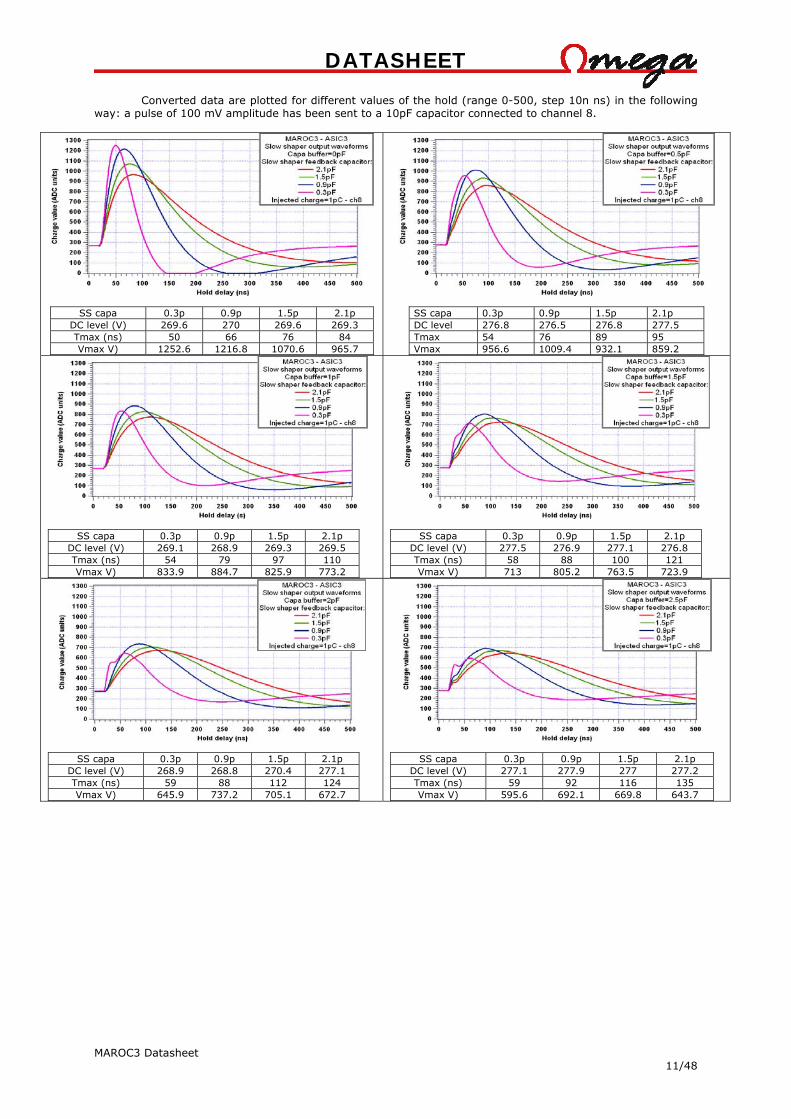
Converted data are plotted for different values of the hold (range 0-500, step 10n ns) in the following way: a pulse of 100 mV amplitude has been sent to a 10pF capacitor connected to channel 8.
SS capa 0.3p 0.9p 1.5p 2.1p DC level (V) 269.6 270 269.6 269.3 Tmax (ns) 50 66 76 84 Vmax V) 1252.6 1216.8 1070.6 965.7
SS capa 0.3p 0.9p 1.5p 2.1p DC level 276.8 276.5 276.8 277.5 Tmax 54 76 89 95 Vmax 956.6 1009.4 932.1 859.2
SS capa 0.3p 0.9p 1.5p 2.1p DC level (V) 269.1 268.9 269.3 269.5 Tmax (ns) 54 79 97 110 Vmax V) 833.9 884.7 825.9 773.2
SS capa 0.3p 0.9p 1.5p 2.1p DC level (V) 277.5 276.9 277.1 276.8 Tmax (ns) 58 88 100 121 Vmax V) 713 805.2 763.5 723.9
SS capa 0.3p 0.9p 1.5p 2.1p DC level (V) 268.9 268.8 270.4 277.1 Tmax (ns) 59 88 112 124 Vmax V) 645.9 737.2 705.1 672.7
SS capa 0.3p 0.9p 1.5p 2.1p DC level (V) 277.1 277.9 277 277.2 Tmax (ns) 59 92 116 135 Vmax V) 595.6 692.1 669.8 643.7
DATASHEET
MAROC3 Datasheet 12/48
Figure 13: Measurement Slow shaper waveform versus buffer capacitances and feedback SS capacitances for the same input charge (1pC)
For few Cbuf and Css combinaisons, we can see a coupling with the FSB1. But this problem doesn’t disturb the hold position at the maximum.
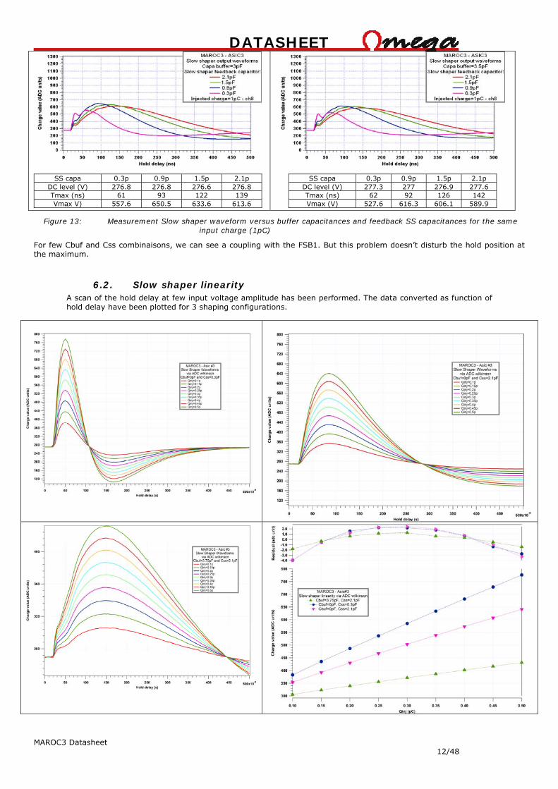
6.2. Slow shaper linearity A scan of the hold delay at few input voltage amplitude has been performed. The data converted as function of hold delay have been plotted for 3 shaping configurations.
SS capa 0.3p 0.9p 1.5p 2.1p DC level (V) 276.8 276.8 276.6 276.8 Tmax (ns) 61 93 122 139 Vmax V) 557.6 650.5 633.6 613.6
SS capa 0.3p 0.9p 1.5p 2.1p DC level (V) 277.3 277 276.9 277.6 Tmax (ns) 62 92 126 142 Vmax (V) 527.6 616.3 606.1 589.9
DATASHEET
MAROC3 Datasheet 13/48
Figure 14: Measurement Slow shaper waveform versus hold delay at different input charge and Slow shaper linearity at different shaping time
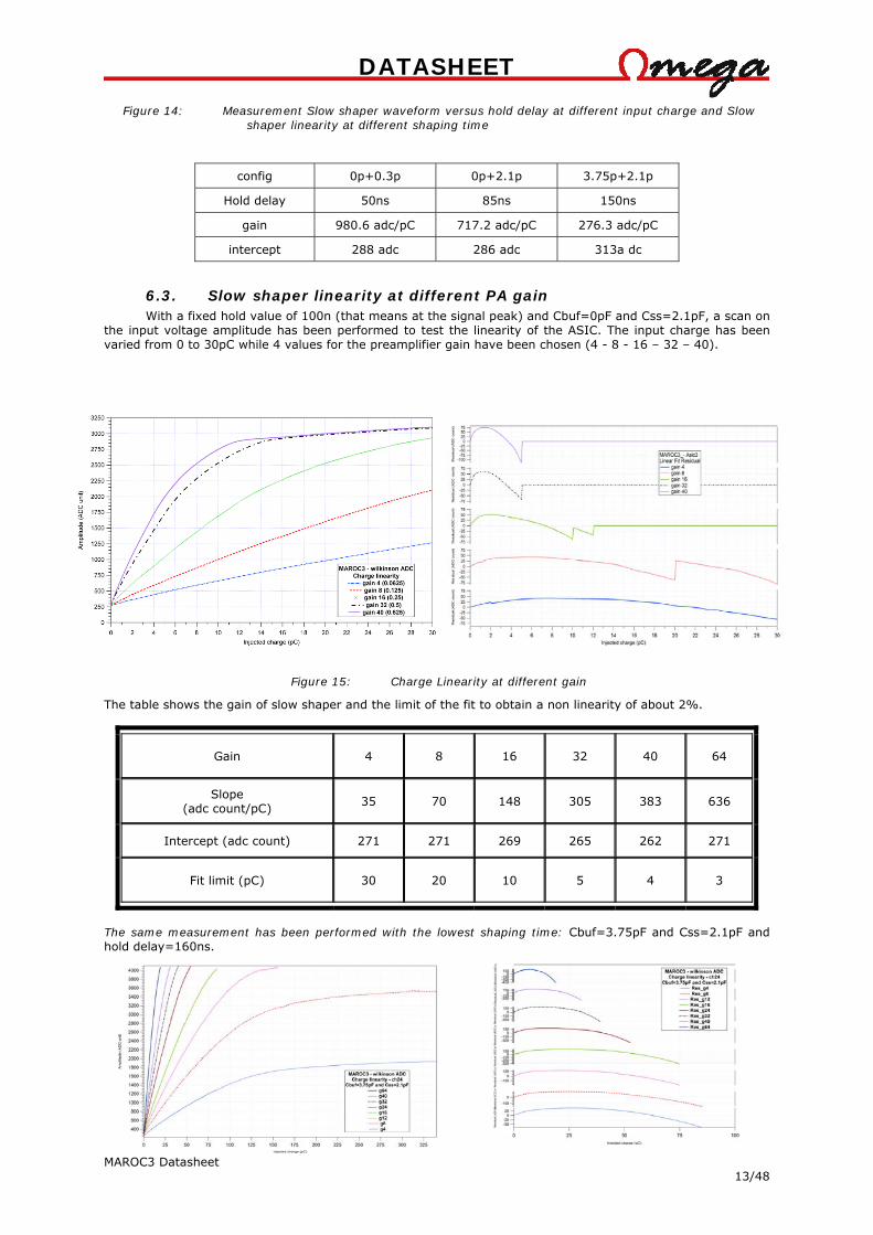
6.3. Slow shaper linearity at different PA gain With a fixed hold value of 100n (that means at the signal peak) and Cbuf=0pF and Css=2.1pF, a scan on
the input voltage amplitude has been performed to test the linearity of the ASIC. The input charge has been varied from 0 to 30pC while 4 values for the preamplifier gain have been chosen (4 - 8 - 16 – 32 – 40).
Figure 15: Charge Linearity at different gain
The table shows the gain of slow shaper and the limit of the fit to obtain a non linearity of about 2%.
Gain 4 8 16 32 40 64
Slope (adc count/pC) 35 70 148 305 383 636
Intercept (adc count) 271 271 269 265 262 271
Fit limit (pC) 30 20 10 5 4 3
The same measurement has been performed with the lowest shaping time: Cbuf=3.75pF and Css=2.1pF and hold delay=160ns.
config 0p+0.3p 0p+2.1p 3.75p+2.1p
Hold delay 50ns 85ns 150ns
gain 980.6 adc/pC 717.2 adc/pC 276.3 adc/pC
intercept 288 adc 286 adc 313a dc
DATASHEET
MAROC3 Datasheet 14/48
The table shows the gain of slow shaper and the limit of the fit to obtain a non linearity of about 2%.
Gain 4 8
12 16
24 32 40 64
Slope (adc count/pC) 13 26 9 52 79 107 138 225
Intercept (adc count) 247 249 246 247 247 247 246 244
Fit limit (pC) 85 85 75 75 51 39.1 30.6 18.9
Data at fit limit 1292.5 2325.6 2991.7 3801.7 4026.7 4054.6 4073.5 4034.3
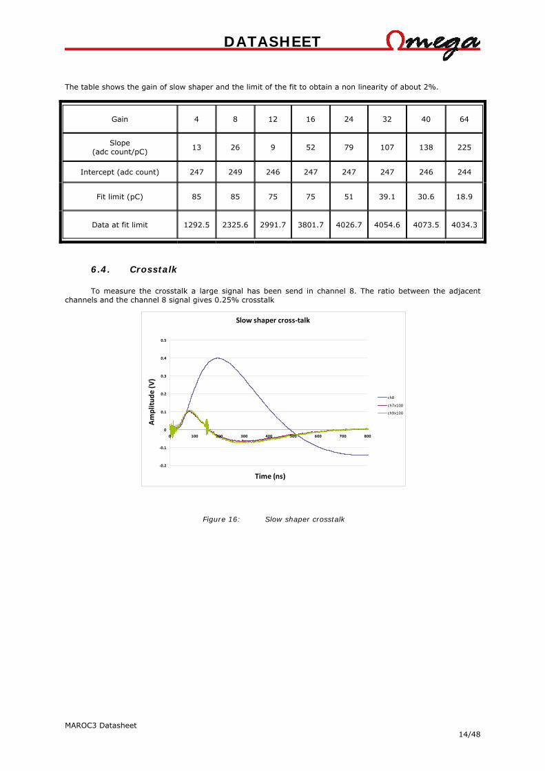
6.4. Crosstalk
To measure the crosstalk a large signal has been send in channel 8. The ratio between the adjacent channels and the channel 8 signal gives 0.25% crosstalk
Figure 16: Slow shaper crosstalk
Slow shaper cross‐talk
‐0.2
‐0.1
0
0.1
0.2
0.3
0.4
0.5
0 100 200 300 400 500 600 700 800
Time (ns)
Amplitude (V)
ch8
ch7x100
ch9x100

DATASHEET
MAROC3 Datasheet 15/48
6.5. Wilkinson ADC
6.5.1. ADC description
Ch.0
Ch.1
Ch.62
Ch.63
Ramp generator
12 bits register
12 bits register
12 bits register
12 bits register
12 bits gray counter
12
Start Ramp Reset Ramp
64 Channel hitRegister in Wilkinson control
Vref_sh
Start Cmpt
99 vref_Ramp97 Ramp output
95 vslope
Start_ADC
RST_ADC
out_ADC
TransmitOn_ADC
startstopreset overflow
115
114
184
116
The Analog to Digital conversion chosen is a Ramp ADC working at 40MHz. The voltage to digital conversion is performed by measuring the time between the start of a voltage ramp (or another position) and its crossing, detected by the comparator, of the voltage to be converted. The time measurement is achieved by a gray counter not started simultaneously with the ramp. Indeed the launching of the ramp is ordered by the start_ADC falling edge signal. The crossing between the ramp and the reference voltage of the slow shaper generates a trigger pulse which becomes the start of the gray counter. When a comparator triggers, its output is synchronized by the clock to memorize the state of the counter which will be the digital data.
The 12-bit gray counter and the ramp generator are shared between the channels. The ADC part replicated in each channel can be reduced to a discriminator and a memory used to copy and memorize the counter state when the discriminator triggers. So the power consumption and the area used can be very small even for high dynamic range.
The use of this kind of ADC is limited by its long conversion time. In fact, for an N bit conversion, it requires 2N/Fck, where Fck is the clock period of the counter. So for a 12-bit conversion, making use of a 40 MHz clock, 102.4µs are required.
On the test board, the RST_ADC is synchronised by the Hold1 pulse falling edge and stays at 0 during
25ns. The Start_ADC is synchronised by the rising edge of the RST_ADC pulse and have to stay at zero during 3 clock ticks.
The ramp begins at the Start_ADC falling edge and the readout of the data starts automatically at the end of the conversion. Data are synchronised with the rising edge of the TransmitOn_ADC.
Be careful: The TransmitOn_ADC and the out_ADC signals are either on pin 114 or 115 depending of
the chip production run. The swapping can be easily done in the FPGA.
DATASHEET
MAROC3 Datasheet 16/48
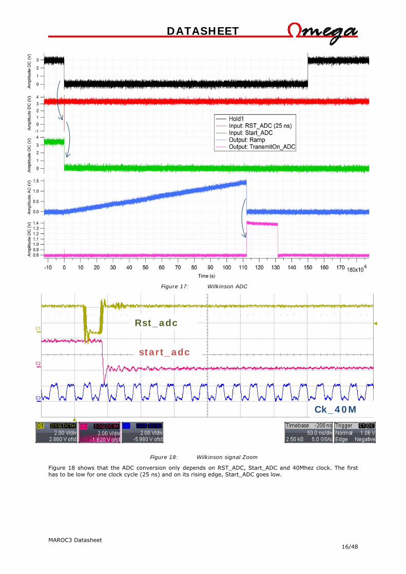
Figure 17: Wilkinson ADC
Figure 18: Wilkinson signal Zoom
Figure 18 shows that the ADC conversion only depends on RST_ADC, Start_ADC and 40Mhez clock. The first has to be low for one clock cycle (25 ns) and on its rising edge, Start_ADC goes low.
Rst_adc
start_adc
Ck_40M
DATASHEET
MAROC3 Datasheet 17/48
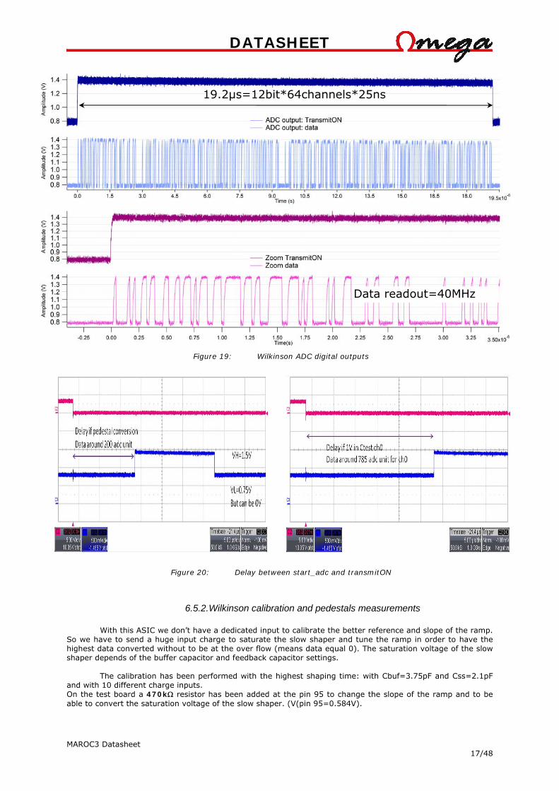
Figure 19: Wilkinson ADC digital outputs
Figure 20: Delay between start_adc and transmitON
6.5.2. Wilkinson calibration and pedestals measurements
With this ASIC we don’t have a dedicated input to calibrate the better reference and slope of the ramp. So we have to send a huge input charge to saturate the slow shaper and tune the ramp in order to have the highest data converted without to be at the over flow (means data equal 0). The saturation voltage of the slow shaper depends of the buffer capacitor and feedback capacitor settings.
The calibration has been performed with the highest shaping time: with Cbuf=3.75pF and Css=2.1pF and with 10 different charge inputs. On the test board a 470k resistor has been added at the pin 95 to change the slope of the ramp and to be able to convert the saturation voltage of the slow shaper. (V(pin 95=0.584V).
19.2µs=12bit*64channels*25ns
Data readout=40MHz

DATASHEET
MAROC3 Datasheet 18/48
12 bits ramps
Figure 21: Ramp waveform for 12-bit conversions
Input charge (pC)
Tmax (µs)
Vmax (V)
Data (adc unit)
Rms (adc unit)
Start_ counter
(µs)
Voltage at start
counter (V)
LSB (mV/adc
unit)
slope (mV/µs)
intercept (V)
0 18.06 1.05 263 2 11.51 0.976 0.265 9.972 0.861 0.1 19.21 1.06 333.2 1.9 10.88 0.97 0.264 9.971 0.861 0.5 25.79 1.12 593.5 2.3 10.95 0.971 0.258 10.01 0.861 1 33.39 1.2 896.1 2.1 10.99 0.971 0.258 10.06 0.86
2.5 52.59 1.4 1674 2.2 10.75 0.969 0.255 10.08 0.86 5 72.34 1.59 2454 2 10.99 0.971 0.254 10.06 0.861
7.5 80.96 1.68 2803 2 10.88 0.97 0.254 10.09 0.86
10 82.56 1.7 2865 2.1 10.95 0.97 0.254 10.09 0.86
25 87.41 1.75 3063 1.8 10.83 0.969 0.254 10.09 0.859 50 90.39 1.78 3183 1.9 10.82 0.969 0.254 10.1 0.86
mean 10.95 0.97 0.257 10.05 0.861
rms 0.21 0.002 0.004 0.05 0.0007
Thanks to all ramp waveforms and the data converted the temporal position the start counter can be estimated at 10.95µs. The subtraction between the voltage max and the voltage at start counter divided by the data in time unit give us the value of the LSB. In our case the LSB of the 12-bit ADC is 257µV. Conversion formula: Analog voltage [mV]=970[mV] +data*LSB[mV/adc]

DATASHEET
MAROC3 Datasheet 19/48
Pedestals 12-bit conversion
Figure 22: Histogramme of 3 channel pedestals via the 12-bit Wilkinson ADC
The histogram rms corresponds of the noise of the slow shaper. In our case the slow shaper noise is 2 adc unit or about 514µV. The scope measurement gives about 580µV.
Figure 23: Mean and rms of charge pedestal via the ADC
These graphs show a good uniformity for the pedestals and for the noise et the output of the slow shaper. The mean of the charge pedestal id about 270 adc unit or 1.039V.

DATASHEET
MAROC3 Datasheet 20/48
Now we can to the same calibration for the 10 and 8 bits conversion.
10 bits ramps
Figure 24: Ramp waveform for 10-bit conversions
Tmax (µs)
Vmax (V)
Data (adc unit)
Rms (adc unit)
Start_ counter
(µs)
Voltage at start
counter (V)
LSB (mV/adc
unit)
slope (mV/s)
intercept (V)
0pC 4.12 1.06 60.5 0.55 2.61 0.975 1.421 45.581 0.856 0.1pC 4.53 1.07 78.7 0.56 2.57 0.973 1.276 45.885 0.856 0.5pC 6.11 1.15 143.4 0.56 2.52 0.972 1.235 45.919 0.856 1pC 7.82 1.23 215.1 0.55 2.44 0.968 1.220 46.285 0.855 5pC 16.78 1.64 574.1 0.56 2.43 0.968 1.176 46.238 0.855 10pC 19.12 1.75 662 0.52 2.57 0.974 1.170 46.229 0.855 50pC 21.50 1.86 756.6 0.53 2.59 0.976 1.171 46.119 0.856
mean 2.53173 0.972 1.238 46.04 0.856
rms 0.072 0.003 0.09 0.0003 <0.001
Thanks to all ramp waveforms and the data converted the temporal position the start counter can be estimated. The subtraction between the voltage max and the voltage at start counter divided by the data in time unit give us the value of the LSB. In our case the LSB of the 10-bit ADC is 1.24mV.

DATASHEET
MAROC3 Datasheet 21/48
Pedestals 10bit conversion
Figure 25: Histogramme of 2 channel pedestals via the 10-bit Wilkinson ADC
The histogram rms corresponds of the noise of the slow shaper. In our case the slow shaper noise is 0.5 adc unit or about 620µV. The scope measurement gives about 600µV.
Figure 26: Mean and rms of charge pedestal via the ADC
These graphs show a good uniformity for the pedestals and for the noise et the output of the slow shaper. The mean of the charge pedestal id about 60 adc unit or 1.044.V.
DATASHEET
MAROC3 Datasheet 22/48
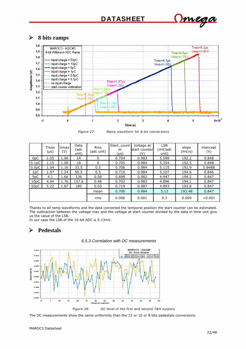
8 bits ramps
Figure 27: Ramp waveform for 8-bit conversions
Thanks to all ramp waveforms and the data converted the temporal position the start counter can be estimated. The subtraction between the voltage max and the voltage at start counter divided by the data in time unit give us the value of the LSB. In our case the LSB of the 10-bit ADC is 5.13mV.
Pedestals
6.5.3. Correlation with DC measurements
Figure 28: DC level of the first and second T&H outputs
The DC measurements show the same uniformity than the 12 or 10 or 8 bits pedestals conversions.
Tmax (µs)
Vmax (V)
Data (adc unit)
Rms (adc unit)
Start_counter
(µs)
Voltage at start counter
(V)
LSB (mV/adc
unit)
slope (mV/s)
intercept (V)
0pC 1.05 1.06 14 0 0.704 0.983 5.598 192.2 0.848 0.1pC 1.15 1.08 18 0 0.705 0.984 5.354 192.5 0.848 0.5pC 1.54 1.16 33.5 0.5 0.706 0.984 5.115 192.9 0.8488 1pC 1.97 1.24 50.5 0.5 0.710 0.984 5.107 194.6 0.846 5pC 4.1 1.66 136 0.08 0.698 0.982 4.947 194.2 0.847 10pC 4.64 1.76 157.6 0.48 0.702 0.983 4.896 194.1 0.847 50pC 5.22 1.87 180 0.03 0.719 0.987 4.893 193.8 0.847
mean 0.706 0.984 5.13 193.48 0.847
rms 0.006 0.001 0.3 0.009 <0.001

DATASHEET
MAROC3 Datasheet 23/48
7. Fast channel To deliver the trigger information there are 3 variable fast shapers and two discriminators. Two fast shapers (one unipolar and another bipolar) followed by one discriminator are dedicated for the photon electron counting and one bipolar fast shaper with lower gain followed by its discriminator has been added to provide a trigger signal at higher input charge. The 2 discriminator outputs are multiplexed to provide only 64 trigger outputs. The thresholds are loaded by 2 internal 10-bit DACs common for the 64 channels.
7.1. DAC
7.1.1. Principle The threshold of each discriminator is set by a 10 bit-DAC which is different that those integrated in MAROC1 or MAROC2. The 2 DACs are identical except that the reference current for DAC0 can be chosen using SC parameter (small dac) equal or half of the Iref. This is to allow finest tunings of the thresholds for small dynamic range charge inputs. Reference voltages are referred to an integrated band gap (v_bg=2.5V).
Figure 29: DAC schematic
7.1.2. DAC measurements
Figure 30: DAC linearity : simulation and measurement
DAC0 DAC0 small DAC1
slope 2.3mV/UDAC 1.1mV/UDAC 2.2mV/UDAC
DAC=0 2.3V 2.3V 2.3V
Linearity: ±0.2%
DC_FSB
DC_FSU

DATASHEET
MAROC3 Datasheet 24/48
7.2. Variable Fast Shapers There are 2 variable CRRC fast shapers. The network feedback of each amplifier can be changed independently thanks to the SC parameters. The peaking time is ≈ 20-25 ns.
Bipolar Fast Shaper
Cf: 20fF
Rf: 100k
100fF
100k
50k
50fF
30k
3pF
sw_fsb2_100K
sw_fsb2_50K
sw_fsb2_100f
sw_fsb2_50f
in_F
SB
10u/2u 10u/2u
vdd_fsb
Half Bipolar Fast Shaper
30k
3pF
in_F
SB
10u/2u 5u/2u
vdd_fsbCf: 20fF
Rf: 100k
100fF
100k
50k
50fF
sw_fsb2_100K
sw_fsb2_50K
sw_fsb2_100f
sw_fsb2_50f
Figure 31: Fast Shapers schematics
7.3. Fast Shaper Measurements
7.3.1. DC measurements The DC levels, named also pedestals, of each fast shaper outputs for all channels are measured.
Figure 32: Pedestal uniformity: Bipolar and Unipolar DC level vs channel number
Bipolar fast shaper n°1 Bipolar fast shaper n°2 Unipolar fast shaper
DC level Mean=1.926V Rms=1.5mV
Mean=1.926V Rms=1.5mV
Mean=1.005V Rms=1.2mV
Equivalent DAC value 353 (small DAC) 169 569
TZ
OTA
Cf: 10fF
Rf: 100k
40fF
100k
50k
25k
20fF
Unipolar Fast Shaper
sw_fsu_100K
sw_fsu_50K
sw_fsu_25K
sw_fsu_40f
sw_fsu_20f
in_F
SU
DATASHEET
MAROC3 Datasheet 25/48
8. Trigger outputs
8.1. S-curve vs injected charge
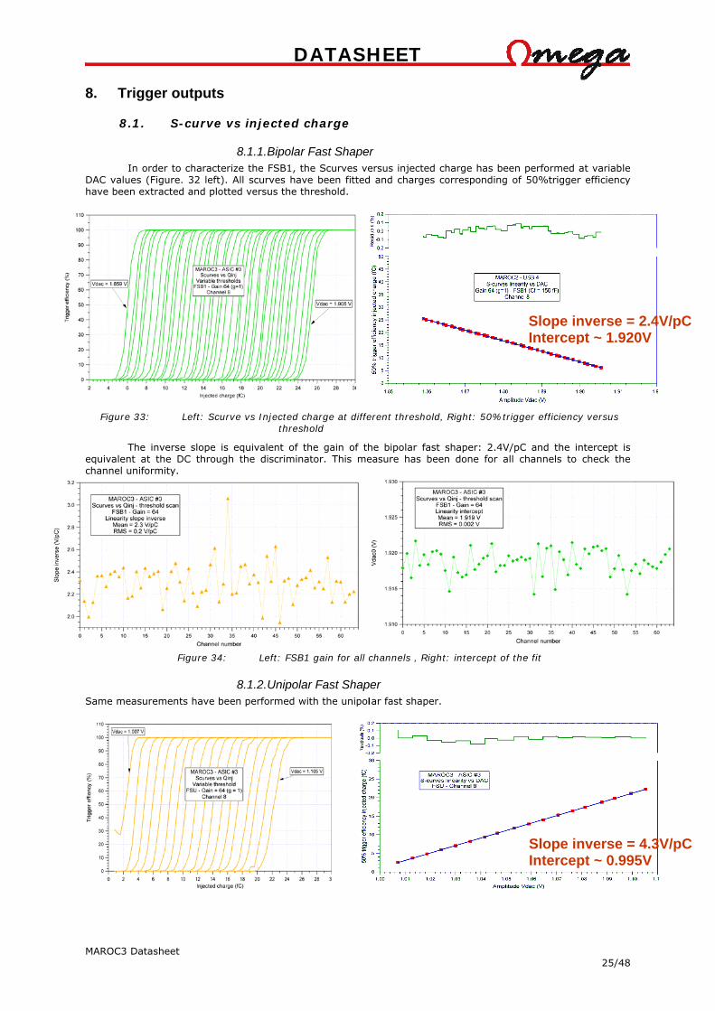
8.1.1. Bipolar Fast Shaper In order to characterize the FSB1, the Scurves versus injected charge has been performed at variable
DAC values (Figure. 32 left). All scurves have been fitted and charges corresponding of 50%trigger efficiency have been extracted and plotted versus the threshold.
Figure 33: Left: Scurve vs Injected charge at different threshold, Right: 50%trigger efficiency versus threshold
The inverse slope is equivalent of the gain of the bipolar fast shaper: 2.4V/pC and the intercept is equivalent at the DC through the discriminator. This measure has been done for all channels to check the channel uniformity.
Figure 34: Left: FSB1 gain for all channels , Right: intercept of the fit
8.1.2. Unipolar Fast Shaper Same measurements have been performed with the unipolar fast shaper.
Slope inverse = 2.4V/pCIntercept ~ 1.920V
Slope inverse = 4.3V/pC Intercept ~ 0.995V

DATASHEET
MAROC3 Datasheet 26/48
Figure 35: Left: Scurve vs Injected charge at different threshold, Right: 50%trigger efficiency versus threshold
The inverse of the slope gives the Unipolar fast shaper gain: 4.4V/pC
Figure 36: Left: FSU gain for all channels , Right: intercept of the fit
Very good results in trigger measurements have been obtained. Thanks to the S-Curve tests with
different injected charges, it has been demonstrated that the discriminator threshold can be set at lower than 1/3 of pe for the bipolar and the unipolar fast shaper.
8.1.3. Correlation The bipolar and unipolar fast shapers are followed by the same discriminator. So the influence of the offset could be seen through the next graph where the DC pedestals have been plotted en function of the intercept for all channels.
Figure 37: DC piedestals versus intercept
DATASHEET
MAROC3 Datasheet 27/48
8.2. S-curve vs injected charge at different feedback resistors settings
8.2.1. Bipolar Fast Shaper The FS feedback resistor is made of one 100k resistor and in parallel of two resistors (50k and 100k) can be added by slow control register.
Figure 38: Scurve versus input charge at different threshold and Rf settings
*
Figure 39: Charge at 50%trigger efficiency versus threshold voltage for different Rf settings
Rf settings
Equivalent
resistor Gain
(V/pC)
Minimum charge
detected
0k 100k 2.32 4fC 100k 50k 1.89 7.5fC
50k 33k 1.56 10fC
150k 25k 1.32
Bipolar Fast Shaper
Cf: 20fF
Rf: 100k
100fF
100k
50k
50fF
30k
3pF
sw_fsb2_100K
sw_fsb2_50K
sw_fsb2_100f
sw_fsb2_50f
in_F
SB
10u/2u 10u/2u
vdd_fsb
DATASHEET
MAROC3 Datasheet 28/48
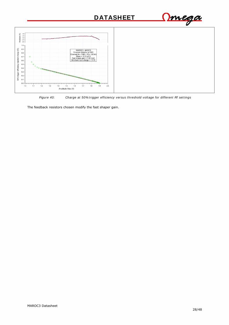
Figure 40: Charge at 50%trigger efficiency versus threshold voltage for different Rf settings
The feedback resistors chosen modify the fast shaper gain.

DATASHEET
MAROC3 Datasheet 29/48
8.2.2. Gain adjustement
Figure 41: Preamplifier gain adjustement for the bipolar fast shaper
The gain adjustement improve the trigger uniformity inside the asic.
Figure 42: Preamplifier gain adjustement for the unipolar fast shaper
With the Unipolar fast shaper, the Scurves show different slope at 50% trigger efficiency which dhould be correlated with channel noise. The noise measurement in function of channel should be performed. Slope versus channels? Correlation avec le noise rms?
DATASHEET
MAROC3 Datasheet 30/48
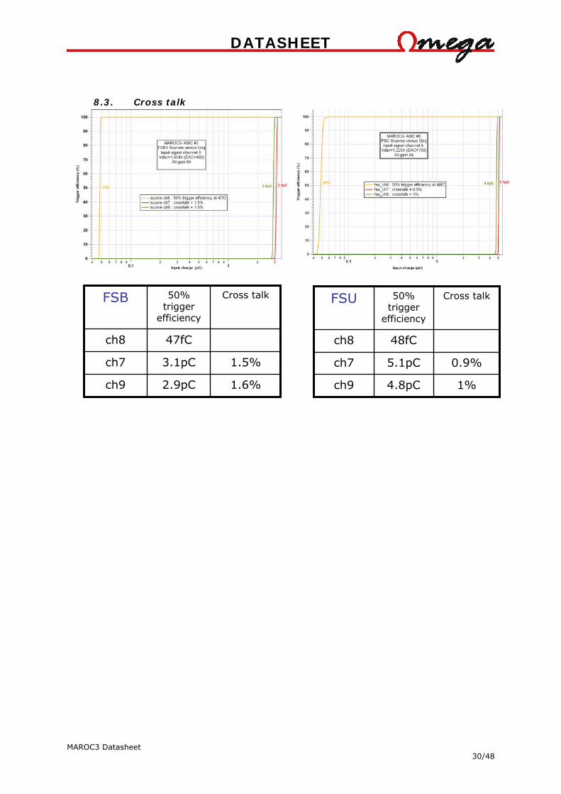
8.3. Cross talk
1.5% 3.1pC ch7
1.6% 2.9pC ch9
47fC ch8
Cross talk 50% trigger
efficiency
FSB
0.9% 5.1pC ch7
1% 4.8pC ch9
48fC ch8
Cross talk 50% trigger
efficiency
FSU

DATASHEET
MAROC3 Datasheet 31/48
9. Result summary
MAROC3
inputs
number 64
polarity negative
outputs
triggers 64 triggers (Vhi=1.5V and Vlo=0.7V)
charge 1 analog multiplex output 1 digital charge (12, 10 or 8 bits)
PA Gain variable 8 bits
(0 to ~4)
BFS
Gain 4.5V/pC
Noise 1.6mV
Min charge 5fC
UFS
Gain 2.3V/pC
Noise 2.4mV
Min charge 3fC
Slow
shaper
Gain 55mV/pC (gain64) – shaping=160ns
Noise 0.58mV
DATASHEET
MAROC3 Datasheet 32/48
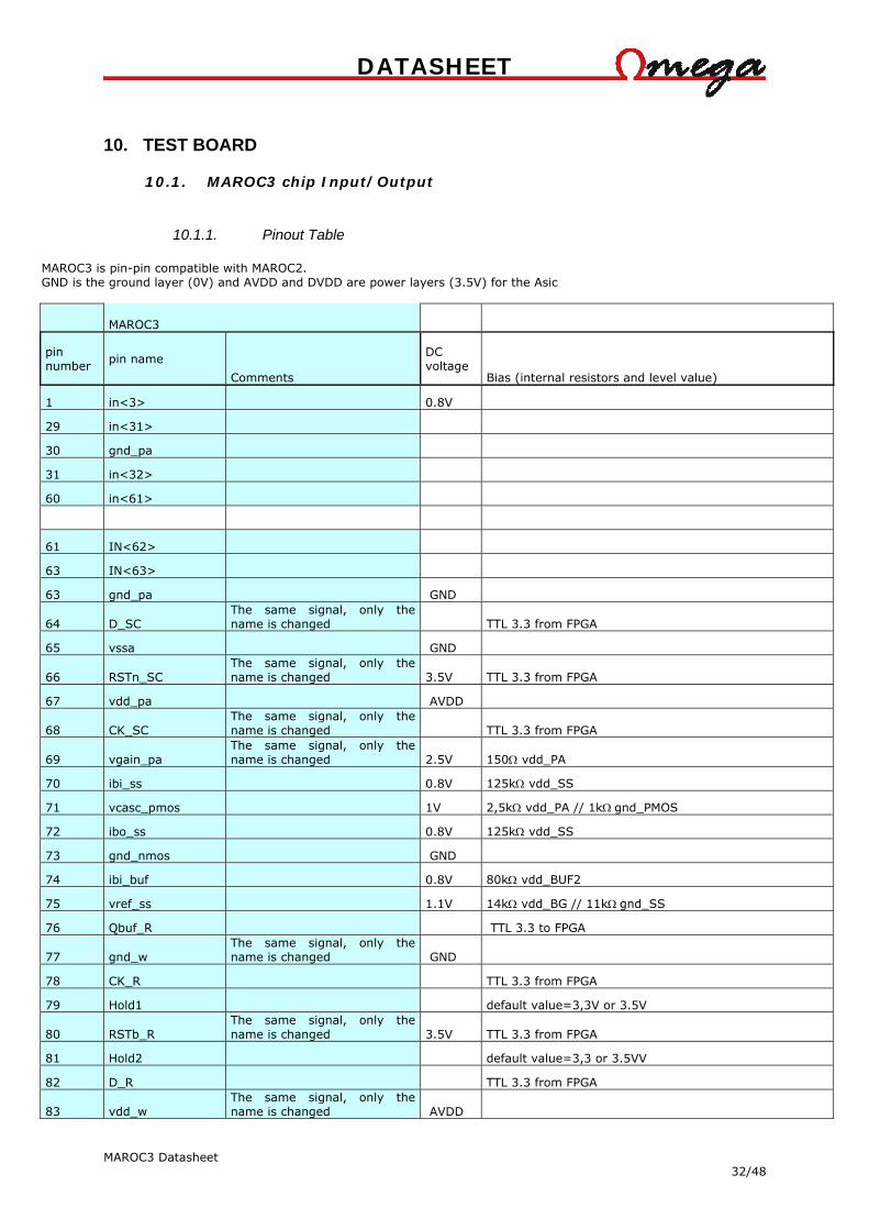
10. TEST BOARD
10.1. MAROC3 chip Input/Output
10.1.1. Pinout Table
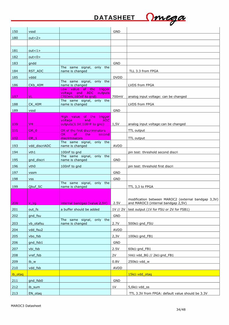
MAROC3 is pin-pin compatible with MAROC2. GND is the ground layer (0V) and AVDD and DVDD are power layers (3.5V) for the Asic
MAROC3
pin number pin name
Comments
DC voltage
Bias (internal resistors and level value)
1 in<3> 0.8V
29 in<31>
30 gnd_pa
31 in<32>
60 in<61>
61 IN<62>
63 IN<63>
63 gnd_pa GND
64 D_SC The same signal, only the name is changed TTL 3.3 from FPGA
65 vssa GND
66 RSTn_SC The same signal, only the name is changed 3.5V TTL 3.3 from FPGA
67 vdd_pa AVDD
68 CK_SC The same signal, only the name is changed TTL 3.3 from FPGA
69 vgain_pa The same signal, only the name is changed 2.5V 150 vdd_PA
70 ibi_ss 0.8V 125k vdd_SS
71 vcasc_pmos 1V 2,5k vdd_PA // 1kgnd_PMOS
72 ibo_ss 0.8V 125k vdd_SS
73 gnd_nmos GND
74 ibi_buf 0.8V 80k vdd_BUF2
75 vref_ss 1.1V 14k vdd_BG // 11kgnd_SS
76 Qbuf_R TTL 3.3 to FPGA
77 gnd_w The same signal, only the name is changed GND
78 CK_R TTL 3.3 from FPGA
79 Hold1 default value=3,3V or 3.5V
80 RSTb_R The same signal, only the name is changed 3.5V TTL 3.3 from FPGA
81 Hold2 default value=3,3 or 3.5VV
82 D_R TTL 3.3 from FPGA
83 vdd_w The same signal, only the name is changed AVDD

DATASHEET
MAROC3 Datasheet 33/48
84 ibo_dac 0,6V 100k vdd_DAC
85 gnd_dac GND
86 iref_dac 0,46V 305kvdd_DAC
87 vdd_dac AVDD
ibi_dac 15kvdd_DAC
88 vref_dac 2V 50kvdd_BG //200k gnd_DAC
89 vbi_tz 2,6V 170k gnd_FSU
90 vdd_fsu1 AVDD
91 G_diode 1V 1kgnd_FSU//2,5kW vdd_FSU1
92 E_fsu GND
93 vbo_tz 0.96V 40k vdd_FSU2
94 vcasc_fsu 1V 2,5k vdd_FSU1 // 10kgnd_FSU
95 vslope 800mV 154k vdd_BG // 46kgnd_Wilk
96 vref_fsu 1V 1,5k vdd_BG // 1kgnd_FSU
97 ramp Scope waveform
98 gnd_wilk GND
99 vref_ramp 0.8V 126k vdd_BG // 74kgnd_Wilk
100 vdd_wilk AVDD
101 ib_integ 15kgnd_Wilk
102 vssa GND
103 vssm GND
104 vbi_discri The same signal, only the name is changed 0.8V 100k vdd_discri
105 vdd_discri The same signal, only the name is changed AVDD
106 vbm_discri The same signal, only the name is changed 2.5V 100k gnd_discri
107 vdd_discriADC The same signal, only the name is changed AVDD
108 vbo_discri The same signal, only the name is changed 2.5V 100k gnd_discri
109 gnd_discri The same signal, only the name is changed GND
110 PWR_ON should be set to vdd value (3.5V)
111 vssd GND
112 gndd GND
113 vddd2 DVDD
114 TransmitOn The same signal, only the name is changed VH-VL logic to FPGA
115 out_ADC The same signal, only the name is changed VH-VL logic to FPGA
116 start_ADC The same signal, only the name is changed TTL 3.3 from FPGA
117 vbi_discriADC Rx to vdda and Rx to gnd if needed 0,8V
118 out<63> VH-VL logic to FPGA
119 out<62>
120 out<61>
121 out<60>
DATASHEET
MAROC3 Datasheet 34/48
150 vssd GND
180 out<2>
181 out<1>
182 out<0>
183 gndd GND
184 RST_ADC The same signal, only the name is changed TLL 3.3 from FPGA
185 vddd DVDD
186 CKb_40M The same signal, only the name is changed LVDS from FPGA
187 VL
Low value of the trigger voltage and ADC outputs (700mV,100nF to gnd) 700mV analog input voltage: can be changed
188 CK_40M The same signal, only the name is changed LVDS from FPGA
189 vssd GND
190 VH
High value of the trigger voltage and ADC outputs(1.5V,100nF to gnd) 1,5V analog input voltage:can be changed
191 OR_0 OR of the first discriminators TTL output
192 OR_1 OR of the second discriminators TTL output
193 vdd_discriADC The same signal, only the name is changed AVDD
194 vth1 100nF to gnd pin test: threshold second discri
195 gnd_discri The same signal, only the name is changed GND
196 vth0 100nF to gnd pin test: threshold first discri
197 vssm GND
198 vss GND
199 Qbuf_SC The same signal, only the name is changed TTL 3,3 to FPGA
200 v_bg internal bandgap (value 2,5V) 2.5V modification between MAROC2 (external bandgap 3,3V) and MAROC3 (internal bandgap 2,5V)
201 out_fs a buffer should be added 1V // 2V test output (1V for FSU or 2V for FSB1)
202 gnd_fsu GND
203 vb_otafsu The same signal, only the name is changed 2.7V 500k gnd_FSU
204 vdd_fsu2 AVDD
205 vbo_fsb 2,3V 100k gnd_FB1
206 gnd_fsb1 GND
207 vbi_fsb 2.5V 60k gnd_FB1
208 vref_fsb 2V vdd_BG // 2kgnd_FB1
209 ib_w 0.8V 250k vdd_w
210 vdd_fsb AVDD
ib_otaq 15k vdd_otaq
211 gnd_fsb0 GND
212 ib_sum 1V 5,6k vdd_ss
213 EN_otaq TTL 3.3V from FPGA: default value should be 3.3V

DATASHEET
MAROC3 Datasheet 35/48
214 sum8
215 out_q a buffer should be added 1V Charge ouput
216 sum7
217 gnd_capa GND
218 sum6
219 gnd_ss GND
220 sum5
221 vdd_ss AVDD
222 sum4
223 vdd_buf1 AVDD
224 sum3
225 vdd_otaq AVDD
226 sum2
227 gnd_otaq GND
228 sum1
229 vcasc_nmos 1.5V 2k vdd_NMOS //1,5kgnd_NMOS
230 vbi_pa Rx to vdda and Rx to gnd if needed 0,65V 500k vdd_pa
231 gnd_nmos GND
232 NC
233 vdd_pa AVDD
234 Ctest input signal for internal capacitors Test input
235 vssi GND
236 vdd_pad The same signal, only the name is changed AVDD
237 gnd_pa GND
238 in<0>
239 in<1>
240 in<2>
power pin name Pin
number current (mA)
power pin name Pin
number current (mA)
vdd_w 83 2.4 vdd_FSU2 204 5.2 vdd_DAC 87 0.65 (dac max) to 1.92 (dac min) vdd_FSB 210 8.3 vdd_FSU1 90 1,4 vdd_SS 221 8 vdd_wilk 100 4.6 vdd_buf1 223 0.6
vdd_discri 105 3,6 vdd_OTAQ 225 5 vddd2 113 7.1 vdd_pa 233 5.4 vddd 185 0,8 vdd_pad 236 0
vdd_discriADC 193 7.6 Consumption Current ~ 62mA
DATASHEET
MAROC3 Datasheet 36/48
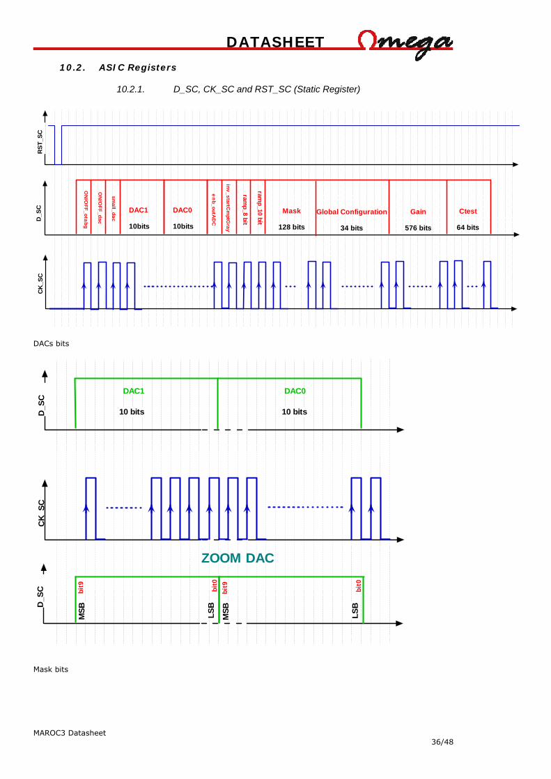
10.2. ASIC Registers
10.2.1. D_SC, CK_SC and RST_SC (Static Register)
DAC1
10bits
sm
all_
da
c
ON
/OF
F_
ota
bg
ON
/OF
F_
da
c
DAC0
10bits
en
b_
ou
tAD
C
inv
_s
tartC
mp
tGra
y
ramp
_8 bit
ramp
_10 bit
Mask
128 bits
Global Configuration
34 bits
Gain
576 bits
Ctest
64 bits
RS
T_S
CD
_SC
CK
_SC
DACs bits
D_S
CC
K_S
CD
_SC
10 bits10 bits
DAC1 DAC0
MS
B
LS
B
bit
9
bit
0
MS
B
LS
B
bit
9
bit
0
ZOOM DAC
Mask bits

DATASHEET
MAROC3 Datasheet 37/48
D_S
CC
K_S
C
mask
ma
sk
_O
R2
_c
h6
3
ma
sk
_O
R2
_c
h6
2
ma
sk
_O
R1
_c
h1
ma
sk
_O
R1
_c
h0
ma
sk
_O
R2
_c
h0
ma
sk
_O
R2
_c
h1
ma
sk
_O
R1
_c
h6
3
ma
sk
_O
R1
_c
h6
2
Global Config
CK
_SC
D_S
C
po
lar_
dis
cri
EN
b_
trista
te
va
lid_
dc
_fs
b2
sw
_fs
b2
_5
0f
cm
d_
CK
_m
ux
d1
_d
2
inv
_d
isc
riAD
C
sw
_fs
b2
_1
00
f
sw
_fs
b2
_1
00
k
sw
_fs
b2
_5
0k
va
lid_
dc
_fs
cm
d_
fsb
_fs
u
sw
_fs
b1
_5
0f
sw
_fs
b1
_1
00
f
sw
_fs
b1
_1
00
k
sw
_fs
b1
_5
0k
sw
_fs
u_
10
0k
sw
_fs
u_
50
k
sw
_fs
u_
25
k
sw
_fs
u_
20
f
sw
_fs
u_
40
f
EN
_A
DC
sw
_s
s_
12
00
f
H1
H2
_c
ho
ice
sw
_s
s_
60
0f
sw
_s
s_
30
0f
ON
/OF
F_
ss
sw
b_
bu
f_2
p
sw
b_
bu
f_1
p
sw
b_
bu
f_5
00
f
sw
b_
bu
f_2
50
f
cm
d_
fsb
cm
d_
fsu
cm
d_
ss
Gain, Sum and Ctest
CK
_SC
D_S
C
data channel 63
LS
B
MS
B
8 bits
cm
d_
SU
M6
3
data channel 0
LS
B
MS
B
8 bits
cm
d_
SU
M0
bit
0
bit
7
bit
0
bit
7
Cte
st_
ch
63
Cte
st_
ch
62
Cte
st_
ch
0
Cte
st_
ch
1Ctest

DATASHEET
MAROC3 Datasheet 38/48
10.2.2. D_R, CK_R and RST_R* (Dynamic Register)
For multiplex charge output
Multiplex charge output
CK
_RR
ST
_RD
_RQ
_Ro
ut
CH
0
CH
1
CH
2
CH
3
CH
60
CH
61
CH
62
CH
63
CH
59
Ho
ld Hold=3.3V TrackHold=0V Hold
CH
1
CH
61
CH
62
CH
63
CH
0
HOLD1 HOLD2
For DC_FS output (pin 201)
DATASHEET
MAROC3 Datasheet 39/48
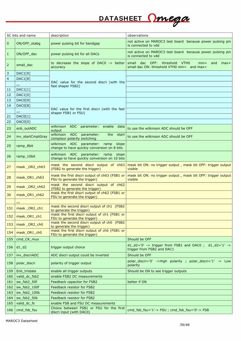
SC bits and name description observations
0 ON/OFF_otabg power pulsing bit for bandgap not active on MAROC3 test board because power pulsing pin is connected to vdd
1 ON/OFF_dac power pulsing bit for all DACs not active on MAROC3 test board because power pulsing pin is connected to vdd
2 small_dac to decrease the slope of DAC0 -> better accuracy
small dac OFF: threshold VTH0 min= and max= small dac ON: threshold VTH0 min= and max=
3 DAC1[9]
DAC value for the second discri (with the fast shaper FSB2)
4 DAC1[8]
,,,
11 DAC1[1]
12 DAC1[0]
13 DAC0[9]
DAC value for the first discri (with the fast shaper FSB1 or FSU)
14 DAC0[8]
,,,
21 DAC0[1]
22 DAC0[0]
23 enb_outADC wilkinson ADC parameter: enable data output to use the wilkinson ADC should be OFF
24 inv_startCmptGray wilkinson ADC parameter: the start compteur polarity switching to use the wilkinson ADC should be OFF
25 ramp_8bit wilkinson ADC parameter: ramp slope change to have quickly conversion on 8 bits
26 ramp_10bit wilkinson ADC parameter: ramp slope change to have quickly conversion on 10 bits
27 mask _OR2_ch63 mask the second discri output of ch63 (FSB2 to generate the trigger)
mask bit ON: no trigger output , mask bit OFF: trigger output visible
28 mask_OR1_ch63 mask the first discri output of ch63 (FSB1 or FSU to generate the trigger)
mask bit ON: no trigger output , mask bit OFF: trigger output visible
29 mask _OR2_ch62 mask the second discri output of ch62 (FSB2 to generate the trigger)
30 mask_OR1_ch62 mask the first discri output of ch62 (FSB1 or FSU to generate the trigger)
,,,
151 mask _OR2_ch1 mask the second discri output of ch1 (FSB2 to generate the trigger)
152 mask_OR1_ch1 mask the first discri output of ch1 (FSB1 or FSU to generate the trigger)
153 mask _OR2_ch0 mask the second discri output of ch0 (FSB2 to generate the trigger)
154 mask_OR1_ch0 mask the first discri output of ch0 (FSB1 or FSU to generate the trigger)
155 cmd_CK_mux Should be OFF
156 d1_d2 trigger output choice d1_d2='0' -> trigger from FSB1 and DAC0 ; d1_d2='1' -> trigger from FSB2 and DAC1
157 inv_discriADC ADC discri output could be inverted Should be OFF
158 polar_discri polarity of trigger output polar_discri='0' ->High polarity ; polar_discri='1' -> Low polarity
159 Enb_tristate enable all trigger outputs Should be ON to see trigger outputs 160 valid_dc_fsb2 enable FSB2 DC measurements
161 sw_fsb2_50f Feedback capacitor for FSB2 better if ON 162 sw_fsb2_100f Feedback resistor for FSB2
163 sw_fsb2_100k Feedback resistor for FSB2
164 sw_fsb2_50k Feedback resistor for FSB2
165 valid_dc_fs enable FSB and FSU DC measurements
166 cmd_fsb_fsu Choice between FSB1 or FSU for the first discri input (with DAC0) cmd_fsb_fsu='1'-> FSU ; cmd_fsb_fsu='0'-> FSB
DATASHEET
MAROC3 Datasheet 40/48
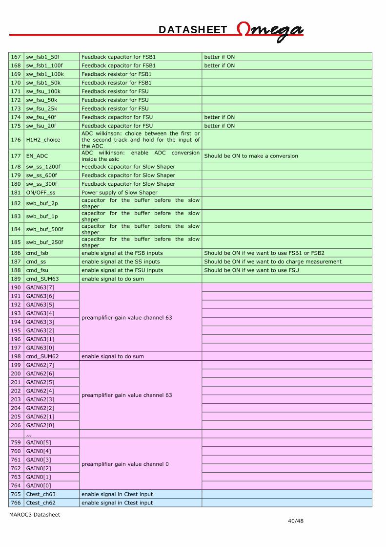
167 sw_fsb1_50f Feedback capacitor for FSB1 better if ON 168 sw_fsb1_100f Feedback capacitor for FSB1 better if ON 169 sw_fsb1_100k Feedback resistor for FSB1
170 sw_fsb1_50k Feedback resistor for FSB1
171 sw_fsu_100k Feedback resistor for FSU
172 sw_fsu_50k Feedback resistor for FSU
173 sw_fsu_25k Feedback resistor for FSU
174 sw_fsu_40f Feedback capacitor for FSU better if ON 175 sw_fsu_20f Feedback capacitor for FSU better if ON
176 H1H2_choice ADC wilkinson: choice between the first or the second track and hold for the input of the ADC
177 EN_ADC ADC wilkinson: enable ADC conversion inside the asic Should be ON to make a conversion
178 sw_ss_1200f Feedback capacitor for Slow Shaper
179 sw_ss_600f Feedback capacitor for Slow Shaper
180 sw_ss_300f Feedback capacitor for Slow Shaper
181 ON/OFF_ss Power supply of Slow Shaper
182 swb_buf_2p capacitor for the buffer before the slow shaper
183 swb_buf_1p capacitor for the buffer before the slow shaper
184 swb_buf_500f capacitor for the buffer before the slow shaper
185 swb_buf_250f capacitor for the buffer before the slow shaper
186 cmd_fsb enable signal at the FSB inputs Should be ON if we want to use FSB1 or FSB2 187 cmd_ss enable signal at the SS inputs Should be ON if we want to do charge measurement 188 cmd_fsu enable signal at the FSU inputs Should be ON if we want to use FSU 189 cmd_SUM63 enable signal to do sum
190 GAIN63[7]
preamplifier gain value channel 63
191 GAIN63[6]
192 GAIN63[5]
193 GAIN63[4]
194 GAIN63[3]
195 GAIN63[2]
196 GAIN63[1]
197 GAIN63[0]
198 cmd_SUM62 enable signal to do sum
199 GAIN62[7]
preamplifier gain value channel 63
200 GAIN62[6]
201 GAIN62[5]
202 GAIN62[4]
203 GAIN62[3]
204 GAIN62[2]
205 GAIN62[1]
206 GAIN62[0]
,,,
759 GAIN0[5]
preamplifier gain value channel 0
760 GAIN0[4]
761 GAIN0[3]
762 GAIN0[2]
763 GAIN0[1]
764 GAIN0[0]
765 Ctest_ch63 enable signal in Ctest input
766 Ctest_ch62 enable signal in Ctest input

DATASHEET
MAROC3 Datasheet 41/48
767 Ctest_ch61 enable signal in Ctest input
,,, enable signal in Ctest input
826 Ctest_ch2 enable signal in Ctest input
827 Ctest_ch1 enable signal in Ctest input
828 Ctest_ch0 enable signal in Ctest input

DATASHEET
MAROC3 Datasheet 42/48
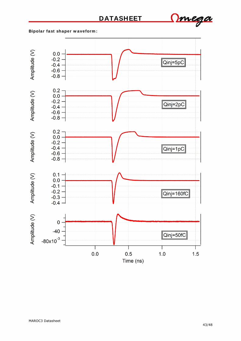
ANNEXE ANNEXE 1 : Waveforms which can be seen on the scope from the test board Input pulse goes to Ctest Slow shaper waveform:
DATASHEET
MAROC3 Datasheet 43/48
Bipolar fast shaper waveform:

DATASHEET
MAROC3 Datasheet 44/48
Unipolar fast shaper waveform:
DATASHEET
MAROC3 Datasheet 45/48
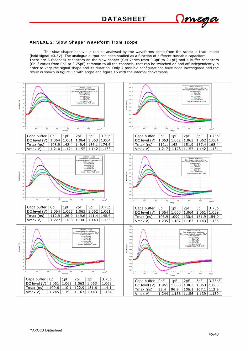
ANNEXE 2: Slow Shaper waveform from scope
The slow shaper behaviour can be analysed by the waveforms come from the scope in track mode (hold signal =3.5V). The analogue output has been studied as a function of different tuneable capacitors. There are 3 feedback capacitors on the slow shaper (Css varies from 0.3pF to 2.1pF) and 4 buffer capacitors (Cbuf varies from 0pF to 3.75pF) common to all the channels, that can be switched on and off independently in order to vary the signal shape and its duration. Only 7 possible configurations have been investigated and the result is shown in figure 13 with scope and figure 16 with the internal conversions.
Capa buffer 0pF 1pF 2pF 3pF 3.75pF DC level (V) 1.064 1.061 1.064 1.063 1.064 Tmax (ns) 108.9 148.4 149.4 156.1 174.6 Vmax V) 1.210 1.174 1.155 1.142 1.133
Capa buffer 0pF 1pF 2pF 3pF 3.75pF DC level (V) 1.063 1.062 1.063 1.062 1.064 Tmax (ns) 112.1 142.4 151.9 157.4 168.4 Vmax V) 1.217 1.178 1.157 1.142 1.134
Capa buffer 0pF 1pF 2pF 3pF 3.75pF DC level (V) 1.064 1.063 1.063 1.062 1.061 Tmax (ns) 112.9 126.9 149.6 141.4 145.6 Vmax V) 1.227 1.183 1.160 1.143 1.135
Capa buffer 0pF 1pF 2pF 3pF 3.75pF DC level (V) 1.064 1.065 1.064 1.061 1.059 Tmax (ns) 103.9 1099 130.4 151.9 154.9 Vmax V) 1.235 1.187 1.163 1.143 1.135
Capa buffer 0pF 1pF 2pF 3pF 3.75pF DC level (V) 1.061 1.063 1.063 1.063 1.063 Tmax (ns) 100.6 110.1 122.9 131.6 114.1 Vmax V) 1.245 1.19 1.163 1.1431 1.134
Capa buffer 0pF 1pF 2pF 3pF 3.75pF DC level (V) 1.061 1.063 1.063 1.063 1.063 Tmax (ns) 92.4 96.9 106.1 107.1 112.9 Vmax V) 1.244 1.186 1.156 1.139 1.130
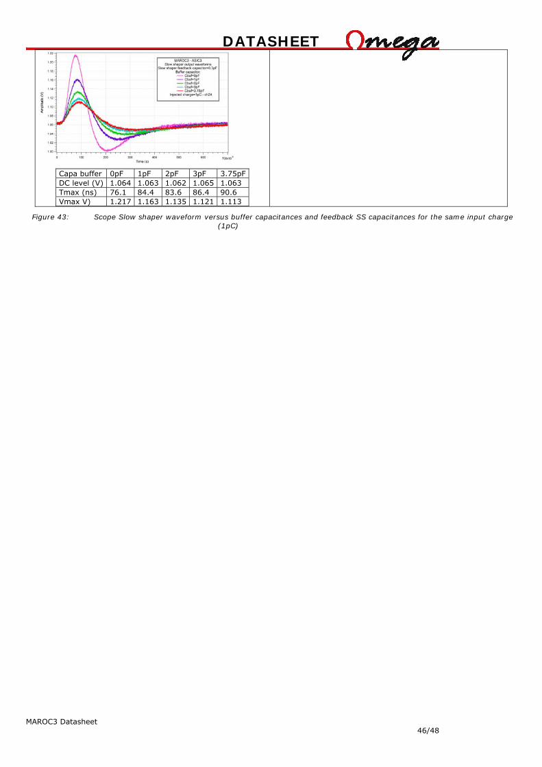
DATASHEET
MAROC3 Datasheet 46/48
Figure 43: Scope Slow shaper waveform versus buffer capacitances and feedback SS capacitances for the same input charge (1pC)
Capa buffer 0pF 1pF 2pF 3pF 3.75pF DC level (V) 1.064 1.063 1.062 1.065 1.063 Tmax (ns) 76.1 84.4 83.6 86.4 90.6 Vmax V) 1.217 1.163 1.135 1.121 1.113

DATASHEET
MAROC3 Datasheet 47/48
ANNEXE 3: Slow Shaper linearity from scope With the settings corresponding of the slower output signal (Cbuf=3.75pF and Css=2.1pF) we checked the linearity of the slow shaper.
Figure 44: Slow shaper waveform via scope for variable input charge
In the next graph, the maximum of the waveform and the value at 160ns have been plotted in function of injected charge.
Figure 45: Slow shaper linearity
The gain of the slow channel in this configuration (Cbuf=3.75pF and Css=2.1pF) is 55mV/pC. The rms noise is 580µV that is equivalent at 10.5fC for the lower shaping time.

DATASHEET
MAROC3 Datasheet 48/48
ANNEXE 4: other Wilkinson calibration Other Wilkinson calibration On the test board a 180k resistor has been added at the pin 95 to change the slope of the ramp and to be able to convert the saturation voltage of the slow shaper. (V(pin 95)=0.771V).
12 bits ramps
Figure 46: Ramp waveform for 12-bit conversions
Input charge (pC) Tmax (µs) Vmax (V) Data
(adc unit) Rms (adc unit)
Start_ counter (µs)
Voltage at start counter (V)
LSB (mV/adc unit)
slope (mV/µs)
intercept (V)
0 14.949 1.04 191.86 1.46 10.15 0.972 0.3802 13.98 0.8298 0.066 18.179 1.09 339.55 1.3 9.69 0.965 0.3651 14.05 0.8287 1.32 21.429 1.13 469.9 1.46 9.682 0.965 0.3538 13.98 0.8292 1.98 24.629 1.18 597.15 1.47 9.7 0.965 0.3548 13.87 0.83 3.3 30.579 1.26 836.31 1.21 9.671 0.964 0.3513 13.86 0.8302 6.6 43.829 1.44 1366.03 1.53 9.678 0.964 0.3481 13.82 0.8305 13.2 67.491 1.76 2312.32 1.5 9.683 0.965 0.3452 13.75 0.8319
19.8 86.935 2.03 3090.76 1.33 9.666 0.966 0.3431 13.71 0.8332
26.4 100 2.21 3613.05 1.4 9.674 0.966 0.344 13.69 0.8336 33 107 2.3 3897.58 1.37 9.561 0.964 0.3427 13.68 0.8332
49.5 110 2.34 4010.61 1.44 9.735 0.966 0.3422 13.67 0.8334
mean 9.72 0.966 0.352 13.82 0.831
rms 0.15 0.002 0.012 0.13 0.002
Thanks to all ramp waveforms and the data converted the temporal position the start counter can be estimated. The subtraction between the voltage max and the voltage at start counter divided by the data in time unit give us the value of the LSB. In our case the LSB of the 12-bit ADC is 352µV.