Embed Size (px)
Citation preview

Datasheet
Linx Technologies’ Splatch® SP610 is a surface-mount monopole antenna for embedded LTE and cellular IoT (LTE-M and NB-IoT) applications. The SP610 specifically supports low-frequency LTE bands from 698 MHz to 960 MHz, notably the 700 MHz bands, and 1710 MHz to 2700 MHz making it an outstanding antenna for LTE and cellular low-power wide-area (LPWA) applications in North America, Europe and worldwide.
The SP610 uses a grounded-line technique to achieve outstanding performance when subject to nearby sources of interference.
It is available in tape and reel packaging and is designed for reflow-solder mounting directly to a printed circuit board for high-volume applications.
Features• 700 MHz bands
― Efficiency 61% ― Peak Gain 5.1 dBi ― VSWR ≤ 3.4
• Compact package ― 40 mm x 10 mm x 2.8 mm
• Excellent performance with small ground plane (102 mm x 45 mm)
• Resistant to proximity effect from nearby interferers
• Direct surface-mount PCB attachment• Reflow- or hand-solder assembly
Applications• Cellular IoT: LTE-M (Cat-M1) and NB-IoT• Worldwide LTE, UMTS and GSM• Low-power, wide-area (LPWA)• Smart Home networking• Sensing and remote monitoring• Internet of Things (IoT) devices
Splatch® SP610 Embedded LTE, LTE-M, NB-IoT Monopole Antenna
Ordering InformationPart Number Description
ANT-LTE-SP610-T Tape and reel (1000 per reel, lower quantities available)AEK-SP610 Antenna evaluation kit
Available from Linx Technologies and select distributors and representatives.
Selected Carrier and Regional PerformanceCarrier (Region) LTE Bands Maximum VSWR
AT&T, T-Mobile (North America) 2, 4, 5, 12, 14, 17, 29, 30, 66 3.4Verizon (North America) 2, 4, 5, 13, 66 3.4Sprint (North America) 25, 26 3.4Europe, Latin America 1, 3, 8, 20, 28 3.4

2
DatasheetSplatch® SP610
ANT-LTE-SP610 Electrical SpecificationsSelect LTE Bands 12, 13, 14, 17, 26, 28, 29 5, 8, 20 1, 2, 3, 4, 10, 25, 66 30, 40 7, 41
Frequency Range 698 MHz to 803 MHz 791 MHz to 960 MHz 1710 MHz to 2200 MHz 2305 MHz to 2400 MHz 2496 MHz to 2690 MHz
VSWR (max.) 3.4 3.4 3.1 3.0 5.0Peak Gain (dBi) 5.1 5.1 5.3 4.9 2.7Avg. Gain (dBi) -2.3 -2.4 -1.3 -1.7 -3.0Efficiency (%) 61 60 80 71 52Polarization LinearRadiation OmnidirectionalMax Power 10 WWavelength 1/4-waveElectrical Type MonopoleImpedance 50 ΩConnection Surface-mountWeight 1.5 g (0.05 oz)Dimensions 40 mm x 10 mm x 2.8 mm (1.6 in x 0.4 in x 0.1 in)Operating Temp. -40 °C to +120 °CESD Sensitivity NOT ESD sensitive. As a best practice, Linx may use ESD packaging.
Electrical specifications and plots measured with a 102 mm x 45 mm (4.0 in x 1.77 in) reference ground plane.
VSWRFigure 1 provides the voltage standing wave ratio (VSWR) across the SP610 bandwidth. VSWR describes the power reflected from the antenna back to the radio. A lower VSWR value indicates better antenna performance at a given frequency. Reflected power is also shown on the right-side vertical axis as a gauge of the percentage of transmitter power reflected back from the antenna.
2690
960
803
2305
2400
2496
1710
2200
698
0
10
20
30
40
1
2
3
4
5
600 800 1000 1200 1400 1600 1800 2000 2200 2400 2600 2800
Refle
cted
Pow
er (%
)
VSW
R
Frequency (MHz)
Figure 1. SP610 VSWR with Frequency Band Highlights
3
Datasheet Splatch® SP610
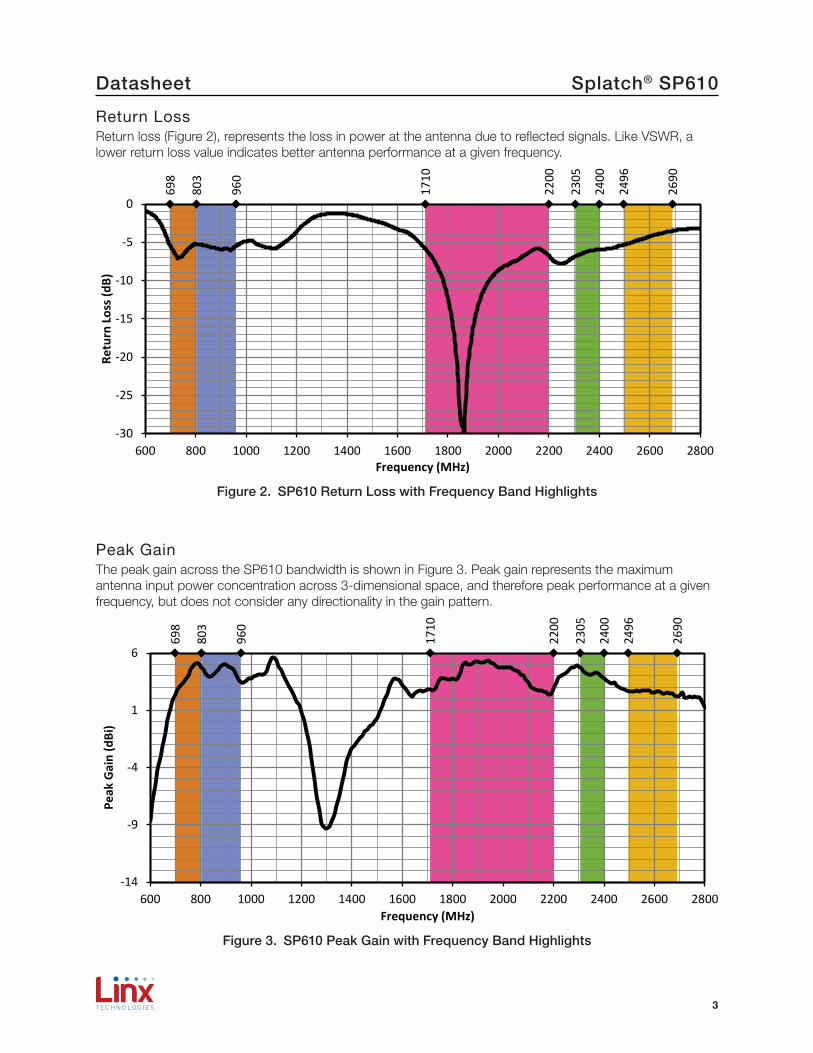
Return LossReturn loss (Figure 2), represents the loss in power at the antenna due to reflected signals. Like VSWR, a lower return loss value indicates better antenna performance at a given frequency.
2690
960
803
2305
2400
2496
1710
2200
698
-30
-25
-20
-15
-10
-5
0
600 800 1000 1200 1400 1600 1800 2000 2200 2400 2600 2800
Retu
rn L
oss (
dB)
Frequency (MHz)
Figure 2. SP610 Return Loss with Frequency Band Highlights
Peak GainThe peak gain across the SP610 bandwidth is shown in Figure 3. Peak gain represents the maximum antenna input power concentration across 3-dimensional space, and therefore peak performance at a given frequency, but does not consider any directionality in the gain pattern.
2690
960
803
2305
2400
2496
1710
2200
698
-14
-9
-4
1
6
600 800 1000 1200 1400 1600 1800 2000 2200 2400 2600 2800
Peak
Gai
n (d
Bi)
Frequency (MHz)
Figure 3. SP610 Peak Gain with Frequency Band Highlights

4
DatasheetSplatch® SP610
Average GainAverage gain (Figure 4), is the average of all antenna gain in 3-dimensional space at each frequency, providing an indication of overall performance without expressing antenna directionality.
2690
960
803
2305
2400
2496
1710
2200
698
-14
-9
-4
1
6
600 800 1000 1200 1400 1600 1800 2000 2200 2400 2600 2800
Aver
age
Gai
n (d
Bi)
Frequency (MHz)
Figure 4. SP610 Average Gain with Frequency Band Highlights
Radiation EfficiencyRadiation efficiency (Figure 5), shows the ratio of power delivered to the antenna relative to the power radiated at the antenna, expressed as a percentage, where a higher percentage indicates better performance at a given frequency.
2690
960
803
2305
2400
2496
1710
2200
698
0
10
20
30
40
50
60
70
80
90
100
600 800 1000 1200 1400 1600 1800 2000 2200 2400 2600 2800
Effic
ienc
y (%
)
Frequency (MHz)
Figure 5. SP610 Radiation Efficiency with Frequency Band Highlights

5
Datasheet Splatch® SP610
Product Dimensions
ANT-LTE-SP610ANT-LTE-SP610ANT-LTE-SP610
ANT-LTE-SP610ANT-LTE-SP610
ASY-EVAL-LTE-SP610Reference Jig #55 (120 mm x 45 mm)
www.linxtechnologies.com
ASY-EVAL-LTE-SP610Reference Jig #55 (120 mm x 45 mm)
www.linxtechnologies.com
1 2
40.0 mm(1.57 in)
2.8 mm(0.11 in)
Rx/Tx GND
3 4
10.0 mm(0.40 in)
Figure 6. SP610 Dimensions
Product SignalsThe signal definitions for the SP610 are provided in Figure 7.
Function Pad DescriptionRx/Tx 1 Pad marked with arrowGND 2 Pad next to arrow pad
Mechanical 3, 4 Unmarked pads may be used for mechanical support, but should not be grounded
Figure 7. SP610 Pin-Out Table
Proximity EffectWireless devices are often designed based on antenna performance measured on an evaluation board. In practice, however, many wireless devices are used in the presence of materials near the antenna which were not present during evaluation. These materials, such as batteries, components on the PCB, or even a person’s body or hand1, can cause a shift in the frequency performance of the antenna, resulting in less than optimal device performance. The shift in the frequency performance can be quite dramatic, especially for monopole (1/4 wavelength) antennas.
The SP610 antenna is designed to help reduce the impact of nearby objects on the performance of the antenna by using a grounded line technique to reduce the overall length of the antenna radiator to provide wider bandwidth for better immunity to frequency shifts, while using a multilayer PCB to maintain a lower profile and small size. Matching components can be added, if necessary, to mitigate larger proximity effects from features like metal shields or enclosures.
Notes1 Antenna Proximity Effects for Talk and Data Modes in Mobile Phones; M. Pelosi, et al; IEEE Antennas and Propagation Magazine, Vol. 52, Issue 3, June 2010
Radiation PatternsRadiation patterns provide information about the directionality and 3-dimensional gain performance of the antenna by plotting gain at specific frequencies in three orthogonal planes. Antenna radiation patterns are shown in Figure 8 using polar plots covering 360 degrees. The antenna graphic provides reference to the plane of the column of plots below it. Note: when viewed with typical PDF viewing software, zooming into radiation patterns is possible to reveal fine detail.

6
DatasheetSplatch® SP610
Radiation Patterns
XZ-Plane Gain YZ-Plane Gain XY-Plane Gain
690 MHz to 800 MHz (750 MHz)
-50-45-40-35-30-25-20-15-10
-505
12 3
45
6
7
8
9
10
11
12
13
14
1516
171819
202122
23
24
25
26
27
28
29
30
31
32
3334
35 36
-50-45-40-35-30-25-20-15-10
-505
12 3
45
6
7
8
9
10
11
12
13
14
1516
171819
202122
23
24
25
26
27
28
29
30
31
32
3334
35 36
690 MHz750 MHz800 MHz
-50-45-40-35-30-25-20-15-10
-505
12 3
45
6
7
8
9
10
11
12
13
14
1516
171819
202122
23
24
25
26
27
28
29
30
31
32
3334
35 36
XZ-Plane Gain YZ-Plane Gain XY-Plane Gain
790 MHz to 960 MHz (870 MHz)
-50-45-40-35-30-25-20-15-10
-505
12 3
45
6
7
8
9
10
11
12
13
14
1516
171819
202122
23
24
25
26
27
28
29
30
31
32
3334
35 36
-50-45-40-35-30-25-20-15-10
-505
12 3
45
6
7
8
9
10
11
12
13
14
1516
171819
202122
23
24
25
26
27
28
29
30
31
32
3334
35 36
790 MHz870 MHz960 MHz
-50-45-40-35-30-25-20-15-10
-505
12 3
45
6
7
8
9
10
11
12
13
14
1516
171819
202122
23
24
25
26
27
28
29
30
31
32
3334
35 36
XZ-Plane Gain YZ-Plane Gain XY-Plane Gain

7
Datasheet Splatch® SP610
Radiation Patterns
1710 MHz to 2170 MHz (1940 MHz)
-50-45-40-35-30-25-20-15-10
-505
12 3
45
6
7
8
9
10
11
12
13
14
1516
171819
202122
23
24
25
26
27
28
29
30
31
32
3334
35 36
-50-45-40-35-30-25-20-15-10
-505
12 3
45
6
7
8
9
10
11
12
13
14
1516
171819
202122
23
24
25
26
27
28
29
30
31
32
3334
35 36
1710 MHz1940 MHz2170 MHz
-50-45-40-35-30-25-20-15-10
-505
12 3
45
6
7
8
9
10
11
12
13
14
1516
171819
202122
23
24
25
26
27
28
29
30
31
32
3334
35 36
XZ-Plane Gain YZ-Plane Gain XY-Plane Gain
2300 MHz to 2400 MHz (2350 MHz)
-50-45-40-35-30-25-20-15-10
-505
12 3
45
6
7
8
9
10
11
12
13
14
1516
171819
202122
23
24
25
26
27
28
29
30
31
32
3334
35 36
-50-45-40-35-30-25-20-15-10
-505
12 3
45
6
7
8
9
10
11
12
13
14
1516
171819
202122
23
24
25
26
27
28
29
30
31
32
3334
35 36
2300 MHz2350 MHz2400 MHz
-50-45-40-35-30-25-20-15-10
-505
12 3
45
6
7
8
9
10
11
12
13
14
1516
171819
202122
23
24
25
26
27
28
29
30
31
32
3334
35 36
XZ-Plane Gain YZ-Plane Gain XY-Plane Gain
Figure 8. Radiation Patterns for the SP610 Antenna
2500 MHz to 2700 MHz (2600 MHz)
-50-45-40-35-30-25-20-15-10
-505
12 3
45
6
7
8
9
10
11
12
13
14
1516
171819
202122
23
24
25
26
27
28
29
30
31
32
3334
35 36
-50-45-40-35-30-25-20-15-10
-505
12 3
45
6
7
8
9
10
11
12
13
14
1516
171819
202122
23
24
25
26
27
28
29
30
31
32
3334
35 36
2500 MHz2600 MHz2700 MHz
-50-45-40-35-30-25-20-15-10
-505
12 3
45
6
7
8
9
10
11
12
13
14
1516
171819
202122
23
24
25
26
27
28
29
30
31
32
3334
35 36
XZ-Plane Gain YZ-Plane Gain XY-Plane Gain

8
DatasheetSplatch® SP610
Recommended LayoutThe recommended printed circuit board (PCB) layout for the SP610 is shown in Figure 9. This layout is used for the SP610 evaluation board which is available for purchase as listed under Ordering Information. Contact Linx for availability of PCB layout design files.
The recommended layout includes a matching network, ground plane and PCB transmission line from the antenna to the matching network, and to the connector or radio circuitry. The connector used for the evaluation board is optional, the transmission line may be run directly to the radio if on the same PCB.
Linx recommends inclusion of at least a 3-element, surface mount pi matching network of two parallel capacitors, (C1, C2) and one series inductor, (L1) in all designs (Figure 10). Surface mount components should be 0603 size. 0402 size components are also supported. The SP610, as designed, does not require matching, but matching may improve end-product antenna performance depending on the effects of the enclosure, PCB and other electronic components. If no matching is necessary, the series element may be populated with a zero-ohm resistor and no components in the two capacitor positions. This is the configuration of the Linx evaluation board as supplied. Linx believes in wireless made simple® and offers matching network design support.
ANT-LTE-SP610ANT-LTE-SP610ANT-LTE-SP610
ANT-LTE-SP610ANT-LTE-SP610
ASY-EVAL-LTE-SP610Reference Jig #55 (120 mm x 45 mm)
www.linxtechnologies.com
ASY-EVAL-LTE-SP610Reference Jig #55 (120 mm x 45 mm)
www.linxtechnologies.com
120.0 mm(4.72 in)
Ground Plane Area = 102.8 mm x 45.0 mm
(4.1 in x 1.8 in)
6.0 mm(0.24 in)
45.0 mm(1.77 in)
C1
GNDRx/Tx
C2
ANT-LTE-SP610
L1
No ground plane or traces under the antennaPCB pads for the SP610 antennaGround connection (1 mm to 2 mm wide)Ground plane coplanar waveguide structure for counterpoisePi matching circuitMHF1/U.FL-compatible receptacle, male pin
Feedline trace
Figure 9. SP610 Recommended Layout.GNDGND
ANTENNA
3-Element 4-Element
C1C2
L1
C2C1
L1
L2L1
C2C1
Figure 10. Matching Network Recommendations

9
Datasheet Splatch® SP610
Recommended PCB FootprintFigure 11 shows the recommended printed circuit board footprint and spacing for the SP610 antenna. The footprint recommendation should be used in conjunction with the recommended layout configuration shown in Figure 9. The antenna placement on the PCB should be centered horizontally and spaced vertically so the edge of the antenna aligns with the edges of pads 1 and 2.
ANT-LTE-SP610ANT-LTE-SP610ANT-LTE-SP610
ANT-LTE-SP610ANT-LTE-SP610
ASY-EVAL-LTE-SP610Reference Jig #55 (120 mm x 45 mm)
www.linxtechnologies.com
ASY-EVAL-LTE-SP610Reference Jig #55 (120 mm x 45 mm)
www.linxtechnologies.com
1.0 mm(0.04 in)
39.0 mm(1.54 in)
22.0 mm(0.87 in)
12.0 mm(0.47 in)
5.0 mm(0.20 in)
1 2
3 4
GNDTx/Rx
CL
CL
Pad sizes:Pads 1, 2 = 1.65 mm x 2 mm (0.07 in x 0.08 in)Pads 3, 4 = 3 mm x 4 mm (0.12 in x 0.16 in) for mechanical attachment to antenna only, do not ground.
Figure 11. SP610 Placement on PCB
Transmission Lines for Embedded AntennasFor most designs, Linx recommends a microstrip transmission line for the SP610. A microstrip transmission line is a PCB trace that runs over a ground plane to maintain the characteristic impedance for optimal signal transfer between the antenna and radio circuitry. Linx designs all antennas with a characteristic impedance of 50 Ω.
Important practices to observe when designing a transmission line are:
• Keep all transmission lines to a minimum length for best signal performance.• Use RF components that also operate at a 50 Ω impedance.• If the radio is not on the same PCB as the antenna, the microstrip should be terminated in a connector,
as exemplified on the SP610 evaluation board, enabling a shielded cable to complete the antenna connection to the radio.
• For designs subject to significant electromagnetic interference, a coplanar waveguide transmission line may be used on the PCB.
The design of a PCB transmission line can be aided by many commercially available software packages which can calculate the correct transmission line width and gap dimensions based upon the PCB thickness and dielectric constant used. Linx offers PCB design reviews to help optimize solution performance.
Ground PlaneThe SP610 is a 1/4-wave monopole antenna, and requires a ground plane on the PCB to which it is mounted. Linx recommends a minimum 102 mm x 45 mm or larger ground plane. If a smaller ground plane is used, Linx recommends providing for at least a 4-element 2nd order matching network like that shown in Figure 10.
The SP610 should be mounted at a distance of 6 mm from the edge of the ground plane (see Figure 9), and none of the ground plane should be underneath the antenna. If the ground plane is placed too close to the antenna it may impair antenna function rather than promote it.
Other ground plane sizes and antenna mounting locations are possible. Simulated performance data for different ground plane sizes can be found in the application note, Splatch® SP610 Ground Plane Optimization on the Linx website. Linx offers PCB design reviews to help optimize solution performance.

10
DatasheetSplatch® SP610
Tape and Reel PackagingFigure 12 shows the dimension of the tape in which the SP610 is packaged. Reel dimensions are provided in Figure 13.
ANT-LTE-SP610
ANT-LTE-SP610
D1
D2
F
P4P5
T2
T3
T4
P1
W
P3
P2
E
C
W
W1A
B
S
Tape DimensionsSymbol Dimension (mm) Tolerance
D1 1.50 ± 0.10D2 2.00 ± 0.10F 41.4 ± 0.10
P1 16.0 ± 0.10P2 26.2 ± 0.15P3 1.75 ± 0.10P4 4.00 ± 0.10P5 2.00 ± 0.10T2 0.35 ± 0.05T3 10.3 ± 0.10T4 3.36 ± 0.10S 52.4 ± 0.10W 56.0 ± 0.30
Figure 12. Tape Specifications for the SP610 Antenna
ANT-LTE-SP610
ANT-LTE-SP610
D1
D2
F
P4P5
T2
T3
T4
P1
W
P3
P2
E
C
W
W1A
B
S Reel DimensionsSymbol SP610 Unit
QTY per reel 1000 pcsTape width 56 mm
A 330 ±1 mmB 100 ±0.5 mmC 13 ±0.2 mmE 2.2 ±0.5 mmW 56 ±1.0 mmW1 60.4 ±0.2 mm
Figure 13. Reel Specifications for the SP610 Antenna
Reflow Solder ProfileThe SP610 uses a typical RoHS solder reflow profile. Refer to application note AN-00504 on the Linx website for more information.
11
Datasheet Splatch® SP610
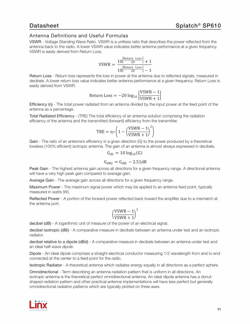
Antenna Definitions and Useful FormulasVSWR - Voltage Standing Wave Ratio. VSWR is a unitless ratio that describes the power reflected from the antenna back to the radio. A lower VSWR value indicates better antenna performance at a given frequency. VSWR is easily derived from Return Loss.
VSWR = 10
Return Loss20 + 1
10Return Loss
20 − 1
Return Loss = −20 log10VSWR− 1VSWR + 1
Gdb = 10 log10(G)
GdBd = GdBi − 2.51dB
VSWR− 1VSWR + 1
2
TRE = η 1 −VSWR − 1VSWR + 1
2
� /4
•
Return Loss - Return loss represents the loss in power at the antenna due to reflected signals, measured in decibels. A lower return loss value indicates better antenna performance at a given frequency. Return Loss is easily derived from VSWR.
VSWR = 10
Return Loss20 + 1
10Return Loss
20 − 1
Return Loss = −20 log10VSWR− 1VSWR + 1
Gdb = 10 log10(G)
GdBd = GdBi − 2.51dB
VSWR− 1VSWR + 1
2
TRE = η 1 −VSWR − 1VSWR + 1
2
� /4
•
Efficiency (η) - The total power radiated from an antenna divided by the input power at the feed point of the antenna as a percentage.
Total Radiated Efficiency - (TRE) The total efficiency of an antenna solution comprising the radiation efficiency of the antenna and the transmitted (forward) efficiency from the transmitter.
VSWR = 10
Return Loss20 + 1
10Return Loss
20 − 1
Return Loss = −20 log10VSWR− 1VSWR + 1
Gdb = 10 log10(G)
GdBd = GdBi − 2.51dB
VSWR− 1VSWR + 1
2
TRE = η 1 −VSWR − 1VSWR + 1
2
� /4
•
Gain - The ratio of an antenna’s efficiency in a given direction (G) to the power produced by a theoretical lossless (100% efficient) isotropic antenna. The gain of an antenna is almost always expressed in decibels.
VSWR = 10
Return Loss20 + 1
10Return Loss
20 − 1
Return Loss = −20 log10VSWR− 1VSWR + 1
Gdb = 10 log10(G)
GdBd = GdBi − 2.51dB
VSWR− 1VSWR + 1
2
TRE = η 1 −VSWR − 1VSWR + 1
2
� /4
•
Peak Gain - The highest antenna gain across all directions for a given frequency range. A directional antenna will have a very high peak gain compared to average gain.
Average Gain - The average gain across all directions for a given frequency range.
Maximum Power - The maximum signal power which may be applied to an antenna feed point, typically measured in watts (W).
Reflected Power - A portion of the forward power reflected back toward the amplifier due to a mismatch at the antenna port.
VSWR = 10
Return Loss20 + 1
10Return Loss
20 − 1
Return Loss = −20 log10VSWR− 1VSWR + 1
Gdb = 10 log10(G)
GdBd = GdBi − 2.51dB
VSWR− 1VSWR + 1
2
TRE = η 1 −VSWR − 1VSWR + 1
2
� /4
•
decibel (dB) - A logarithmic unit of measure of the power of an electrical signal.
decibel isotropic (dBi) - A comparative measure in decibels between an antenna under test and an isotropic radiator.
decibel relative to a dipole (dBd) - A comparative measure in decibels between an antenna under test and an ideal half-wave dipole.
Dipole - An ideal dipole comprises a straight electrical conductor measuring 1/2 wavelength from end to end connected at the center to a feed point for the radio.
Isotropic Radiator - A theoretical antenna which radiates energy equally in all directions as a perfect sphere.
Omnidirectional - Term describing an antenna radiation pattern that is uniform in all directions. An isotropic antenna is the theoretical perfect omnidirectional antenna. An ideal dipole antenna has a donut-shaped radiation pattern and other practical antenna implementations will have less perfect but generally omnidirectional radiation patterns which are typically plotted on three axes.

Doc # DS200002-02ANT Replaces (DS19256-02ANT)
Website: http://linxtechnologies.com Linx Offices: 159 Ort Lane, Merlin, OR, US 97532 Phone: +1 (541) 471-6256 E-MAIL: [email protected] Technologies reserves the right to make changes to the product(s) or information contained herein without notice. No liability is assumed as a result of their use or application. No rights under any patent accompany the sale of any such product(s) or information.
Wireless Made Simple, & Splatch are registered trademarks of Linx Acquisitions LLC. Other product and brand names may be trademarks or registered trademarks of their respective owners.
Copyright © 2020 Linx Technologies
All Rights Reserved
DatasheetSplatch® SP610