Embed Size (px)
Citation preview
Features• High voltage rail up to 1700 V• Driver current capability: 4 A sink/source @25 °C• dV/dt transient immunity ±100 V/ns in full temperature range• Overall input-output propagation delay: 75 ns• Separate sink and source option for easy gate driving configuration• 4 A Miller CLAMP dedicated pin option• UVLO function• Gate driving voltage up to 26 V• 3.3 V, 5 V TTL/CMOS inputs with hysteresis• Temperature shutdown protection• Standby function• 4.8 kVPK isolation• Narrow body SO-8
Application• Motor driver for home appliances, factory automation, industrial drives and fans.• 600/1200 V inverters• Battery chargers• Induction heating• Welding• UPS• Power supply units• DC-DC converters• Power Factor Correction
DescriptionThe STGAP2SICSN is a single gate driver which provides galvanic isolation betweenthe gate driving channel and the low voltage control and interface circuitry.
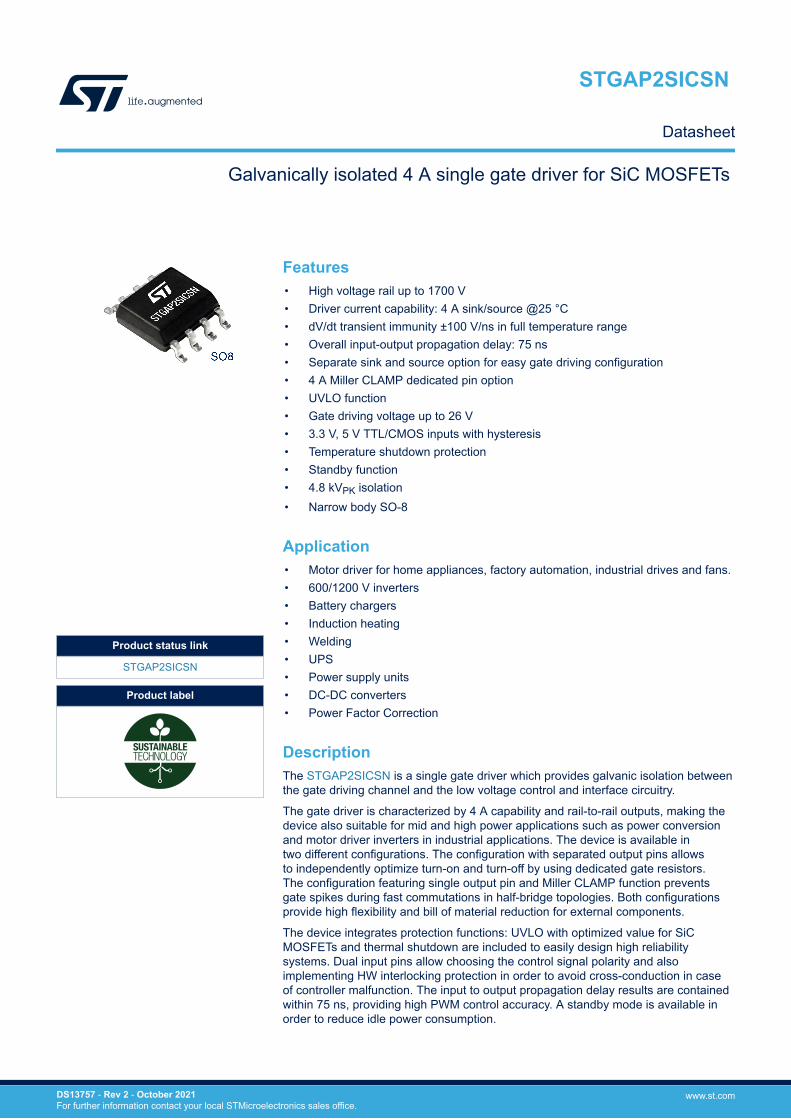
The gate driver is characterized by 4 A capability and rail-to-rail outputs, making thedevice also suitable for mid and high power applications such as power conversionand motor driver inverters in industrial applications. The device is available intwo different configurations. The configuration with separated output pins allowsto independently optimize turn-on and turn-off by using dedicated gate resistors.The configuration featuring single output pin and Miller CLAMP function preventsgate spikes during fast commutations in half-bridge topologies. Both configurationsprovide high flexibility and bill of material reduction for external components.
The device integrates protection functions: UVLO with optimized value for SiCMOSFETs and thermal shutdown are included to easily design high reliabilitysystems. Dual input pins allow choosing the control signal polarity and alsoimplementing HW interlocking protection in order to avoid cross-conduction in caseof controller malfunction. The input to output propagation delay results are containedwithin 75 ns, providing high PWM control accuracy. A standby mode is available inorder to reduce idle power consumption.
Product status link
STGAP2SICSN
Product label
Galvanically isolated 4 A single gate driver for SiC MOSFETs
STGAP2SICSN
Datasheet
DS13757 - Rev 2 - October 2021For further information contact your local STMicroelectronics sales office.
www.st.com
1 Block diagram
Figure 1. Block diagram - Single output and Miller Clamp configuration
ISOLATION
VH
CLAMP
GNDISO
VDD
GND
ControlLogic
IN+
IN-
GOUTFloating SectionControlLogic
Floating ground A
UVLOVH
LevelShifter
VCLAMPth
+
Figure 2. Block diagram - Separate outputs configuration
ISOLATION
VH
GOFF
GNDISO
VDD
GND
ControlLogic
IN+
IN-
GONFloating SectionControlLogic
Floating ground
UVLOVH
LevelShifter
STGAP2SICSN Block diagram
DS13757 - Rev 2 page 2/23
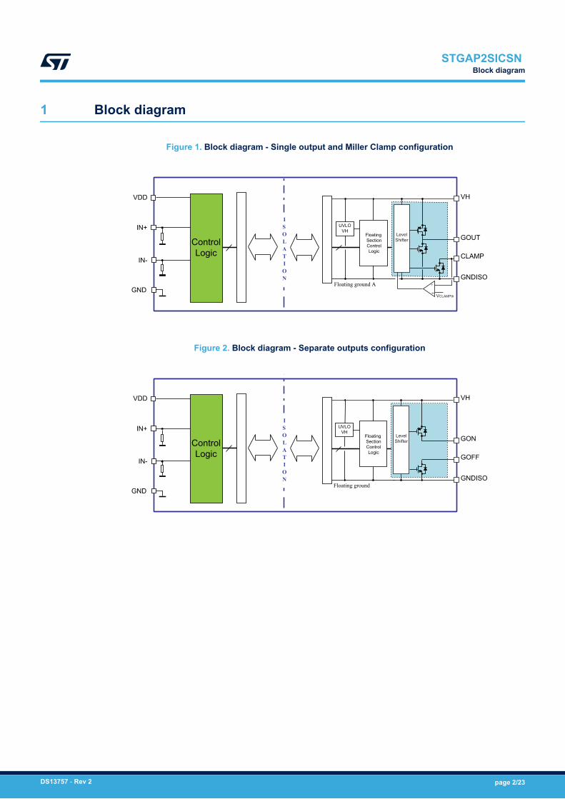
2 Pin description and connection diagram
Figure 3. Pin connection (top view), Separated outputs option
1
3
2IN+
GON
5
7
6
8
VH4
VDD
GND
IN-
GOFF
GNDISO
Figure 4. Pin connection (top view), Single output and Miller CLAMP option
1
3
2IN+
GOUT
5
7
6
8
VH4
VDD
GND
IN-
CLAMP
GNDISO
Table 1. Pin Description
Pin #Pin name Type Function
Figure 3 Figure 4
1 1 VDD Power supply Driver logic supply voltage.
2 2 IN+ Logic input Driver logic input, active high.
3 3 IN- Logic input Driver logic input, active low.
4 4 GND Power supply Driver logic ground.
5 5 VH Power supply Gate driving positive voltage supply.
6 GOUT Analog output Sink/Source output.
7 CLAMP Analog output Active Miller Clamp.
6 GON Analog output Source output.
7 GOFF Analog output Sink output.
8 8 GNDISO Power supply Gate driving Isolated ground.
STGAP2SICSN Pin description and connection diagram
DS13757 - Rev 2 page 3/23
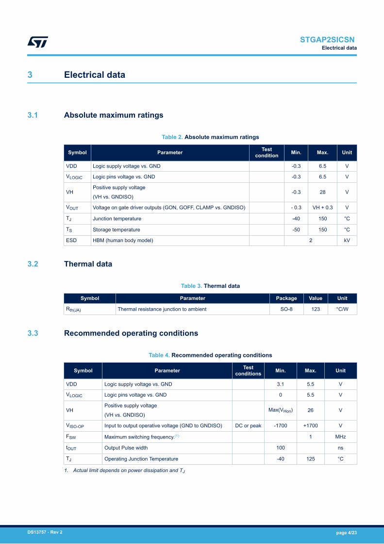
3 Electrical data
3.1 Absolute maximum ratings
Table 2. Absolute maximum ratings
Symbol Parameter Testcondition Min. Max. Unit
VDD Logic supply voltage vs. GND -0.3 6.5 V
VLOGIC Logic pins voltage vs. GND -0.3 6.5 V
VHPositive supply voltage
(VH vs. GNDISO)-0.3 28 V
VOUT Voltage on gate driver outputs (GON, GOFF, CLAMP vs. GNDISO) - 0.3 VH + 0.3 V
TJ Junction temperature -40 150 °C
TS Storage temperature -50 150 °C
ESD HBM (human body model) 2 kV
3.2 Thermal data
Table 3. Thermal data
Symbol Parameter Package Value Unit
Rth(JA) Thermal resistance junction to ambient SO-8 123 °C/W
3.3 Recommended operating conditions
Table 4. Recommended operating conditions
Symbol Parameter Testconditions Min. Max. Unit
VDD Logic supply voltage vs. GND 3.1 5.5 V
VLOGIC Logic pins voltage vs. GND 0 5.5 V
VHPositive supply voltage
(VH vs. GNDISO)Max(VHon) 26 V
VISO-OP Input to output operative voltage (GND to GNDISO) DC or peak -1700 +1700 V
FSW Maximum switching frequency.(1) 1 MHz
tOUT Output Pulse width 100 ns
TJ Operating Junction Temperature -40 125 °C
1. Actual limit depends on power dissipation and TJ
STGAP2SICSN Electrical data
DS13757 - Rev 2 page 4/23
4 Electrical characteristics
Table 5. Electrical characteristics (TJ = 25°C, VH = 18 V, VDD = 5 V unless otherwise specified)
Symbol Pin Parameter Test conditions Min. Typ. Max. Unit
Dynamic characteristics
tDon IN+, IN- Input to outputpropagation delay ON 50 75 90 ns
tDoff IN+, IN- Input to outputpropagation delay OFF 50 75 90 ns
tr Rise time CL= 4.7 nFsee Figure 12
30 ns
tf Fall time 30 ns
PWD Pulse Width Distortion |tDon - tDoff|
20 ns
tdeglitch IN+, IN- Inputs deglitch filter 20 40 ns
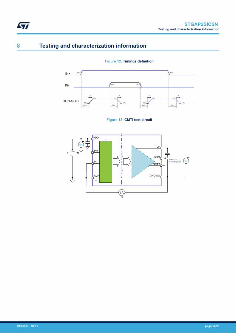
CMTI(1) Common-mode transientimmunity, |dVISO/dt|
VCM = 1500 V,
see Figure 13100 V/ns
Supply voltage
VHon VH VH UVLO turn-onthreshold 14.6 15.5 16.4 V
VHoff VH VH UVLO turn-offthreshold 13.9 14.8 15.7 V
VHhyst VH VH UVLO hysteresis 600 750 950 mV
IQHU VH VH undervoltagequiescent supply current VH = 7.0 V 1.3 1.8 mA
IQH VH VH quiescent supplycurrent 1.3 1.8 mA
IQHSBY VH Standby VH quiescentsupply current Standby mode 400 550 µA
SafeClp GOUT / GOFF GOFF active clampIGOFF = 0.2 A;
VH floating2 2.3 V
IQDD VDD VDD quiescent supplycurrent 1.0 1.3 mA
IQDDSBY VDD Standby VDD quiescentsupply current Standby mode 40 65 µA
Logic inputs
Vil IN+, IN- Low-level logic thresholdvoltage 0.29·VDD 0.33·VDD 0.37·VDD V
Vih IN+, IN- High-level logic thresholdvoltage 0.62·VDD 0.66·VDD 0.70·VDD V
IINh IN+, IN- INx logic “1” input biascurrent INx = 5 V 33 50 70 µA
IINl IN+, IN- INx logic “0” input biascurrent INx = GND 1 µA
Rpd IN+, IN- Inputs pull-down resistors INx = 5 V 70 100 150 kΩ
Driver buffer section
IGON GOUT / GON Source short-circuitcurrent
TJ = 25 °C 4 A
STGAP2SICSN Electrical characteristics
DS13757 - Rev 2 page 5/23
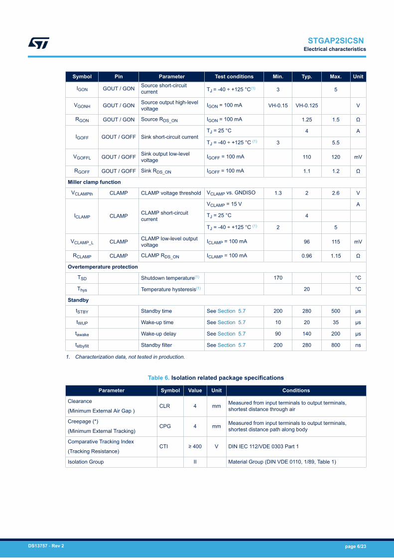
Symbol Pin Parameter Test conditions Min. Typ. Max. Unit
IGON GOUT / GON Source short-circuitcurrent TJ = -40 ÷ +125 °C(1) 3 5
VGONH GOUT / GON Source output high-levelvoltage IGON = 100 mA VH-0.15 VH-0.125 V
RGON GOUT / GON Source RDS_ON IGON = 100 mA 1.25 1.5 Ω
IGOFF GOUT / GOFF Sink short-circuit currentTJ = 25 °C 4 A
TJ = -40 ÷ +125 °C (1) 3 5.5
VGOFFL GOUT / GOFF Sink output low-levelvoltage IGOFF = 100 mA 110 120 mV
RGOFF GOUT / GOFF Sink RDS_ON IGOFF = 100 mA 1.1 1.2 Ω
Miller clamp function
VCLAMPth CLAMP CLAMP voltage threshold VCLAMP vs. GNDISO 1.3 2 2.6 V
ICLAMP CLAMP CLAMP short-circuitcurrent
VCLAMP = 15 V A
TJ = 25 °C 4
TJ = -40 ÷ +125 °C (1) 2 5
VCLAMP_L CLAMP CLAMP low-level outputvoltage ICLAMP = 100 mA 96 115 mV
RCLAMP CLAMP CLAMP RDS_ON ICLAMP = 100 mA 0.96 1.15 Ω
Overtemperature protection
TSD Shutdown temperature(1) 170 °C
Thys Temperature hysteresis(1) 20 °C
Standby
tSTBY Standby time See Section 5.7 200 280 500 µs
tWUP Wake-up time See Section 5.7 10 20 35 µs
tawake Wake-up delay See Section 5.7 90 140 200 µs
tstbyfilt Standby filter See Section 5.7 200 280 800 ns
1. Characterization data, not tested in production.
Table 6. Isolation related package specifications
Parameter Symbol Value Unit Conditions
Clearance
(Minimum External Air Gap )CLR 4 mm Measured from input terminals to output terminals,
shortest distance through air
Creepage (*)
(Minimum External Tracking)CPG 4 mm Measured from input terminals to output terminals,
shortest distance path along body
Comparative Tracking Index
(Tracking Resistance)CTI ≥ 400 V DIN IEC 112/VDE 0303 Part 1
Isolation Group II Material Group (DIN VDE 0110, 1/89, Table 1)
STGAP2SICSN Electrical characteristics
DS13757 - Rev 2 page 6/23
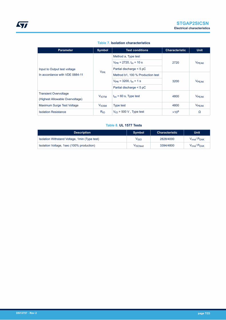
Table 7. Isolation characteristics
Parameter Symbol Test conditions Characteristic Unit
Input to Output test voltage
In accordance with VDE 0884-11VPR
Method a, Type test
2720 VPEAKVPR = 2720, tm = 10 s
Partial discharge < 5 pC
Method b1, 100 % Production test
3200 VPEAKVPR = 3200, tm = 1 s
Partial discharge < 5 pC
Transient Overvoltage
(Highest Allowable Overvoltage)VIOTM tini = 60 s, Type test 4800 VPEAK
Maximum Surge Test Voltage VIOSM Type test 4800 VPEAK
Isolation Resistance RIO VIO = 500 V , Type test >109 Ω
Table 8. UL 1577 Tests
Description Symbol Characteristic Unit
Isolation Withstand Voltage, 1min (Type test) VISO 2828/4000 Vrms/ PEAK
Isolation Voltage, 1sec (100% production) VISOtest 3394/4800 Vrms/ PEAK
STGAP2SICSN Electrical characteristics
DS13757 - Rev 2 page 7/23
5 Functional Description
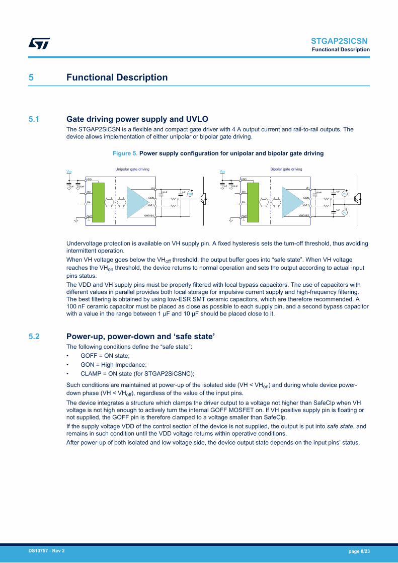
5.1 Gate driving power supply and UVLOThe STGAP2SiCSN is a flexible and compact gate driver with 4 A output current and rail-to-rail outputs. Thedevice allows implementation of either unipolar or bipolar gate driving.
Figure 5. Power supply configuration for unipolar and bipolar gate driving
VDD
ISOLATION
VH
GOFF
GNDISO
VDD
GND
IN+
IN-
GON
+VH
+VH
+VL
ISOLATION
VH
GOFF
GNDISO
VDD
GND
IN+
IN-
GON
Unipolar gate driving Bipolar gate driving
1uF 100nF
VDD
1uF 100nF
1uF100nF 100nF 1uF
1uF
Undervoltage protection is available on VH supply pin. A fixed hysteresis sets the turn-off threshold, thus avoidingintermittent operation.When VH voltage goes below the VHoff threshold, the output buffer goes into “safe state”. When VH voltagereaches the VHon threshold, the device returns to normal operation and sets the output according to actual inputpins status.The VDD and VH supply pins must be properly filtered with local bypass capacitors. The use of capacitors withdifferent values in parallel provides both local storage for impulsive current supply and high-frequency filtering.The best filtering is obtained by using low-ESR SMT ceramic capacitors, which are therefore recommended. A100 nF ceramic capacitor must be placed as close as possible to each supply pin, and a second bypass capacitorwith a value in the range between 1 µF and 10 µF should be placed close to it.
5.2 Power-up, power-down and ‘safe state’The following conditions define the “safe state”:• GOFF = ON state;• GON = High Impedance;• CLAMP = ON state (for STGAP2SiCSNC);
Such conditions are maintained at power-up of the isolated side (VH < VHon) and during whole device power-down phase (VH < VHoff), regardless of the value of the input pins.The device integrates a structure which clamps the driver output to a voltage not higher than SafeClp when VHvoltage is not high enough to actively turn the internal GOFF MOSFET on. If VH positive supply pin is floating ornot supplied, the GOFF pin is therefore clamped to a voltage smaller than SafeClp.If the supply voltage VDD of the control section of the device is not supplied, the output is put into safe state, andremains in such condition until the VDD voltage returns within operative conditions.After power-up of both isolated and low voltage side, the device output state depends on the input pins’ status.
STGAP2SICSN Functional Description
DS13757 - Rev 2 page 8/23
5.3 Control inputsThe device is controlled through the IN+ and IN- logic inputs, in accordance with the truth table described inTable 9.
Table 9. Inputs truth table (applicable when device is not in UVLO or "safe state")
Input pins Output pins
IN+ IN- GON GOFF
L L OFF ON
H L ON OFF
L H OFF ON
H H OFF ON
A deglitch filter allows input signals with duration shorter than tdeglitch to be ignored, thereby preventing noisespikes potentially present in the application from generating unwanted commutations.
5.4 Miller Clamp functionThe Miller Clamp function allows the control of the Miller current during the power stage switching in half-bridgeconfigurations. When the external power transistor is in the OFF state, the driver operates to avoid the inducedturn-on phenomenon that may occur when the other switch in the same leg is being turned on, due to the CGDcapacitance.During the turn-off period the gate of the external switch is monitored through the CLAMP pin. The CLAMP switchis activated when gate voltage goes below the voltage threshold, VCLAMPth, thus creating a low impedance pathbetween the switch gate and the GNDISO pin.
5.5 WatchdogThe isolated HV side has a watchdog function in order to identify when it is not able to communicate with LV side,for example because the VDD of the LV side is not supplied. In this case the output of the driver is forced in “safestate” until communication link is properly established again.
5.6 Thermal shutdown protectionThe device provides a thermal shutdown protection. When junction temperature reaches the TSD temperaturethreshold, the device is forced into “safe state”. The device operation is restored as soon as the junctiontemperature is lower than TSD - Thys.
STGAP2SICSN Control inputs
DS13757 - Rev 2 page 9/23
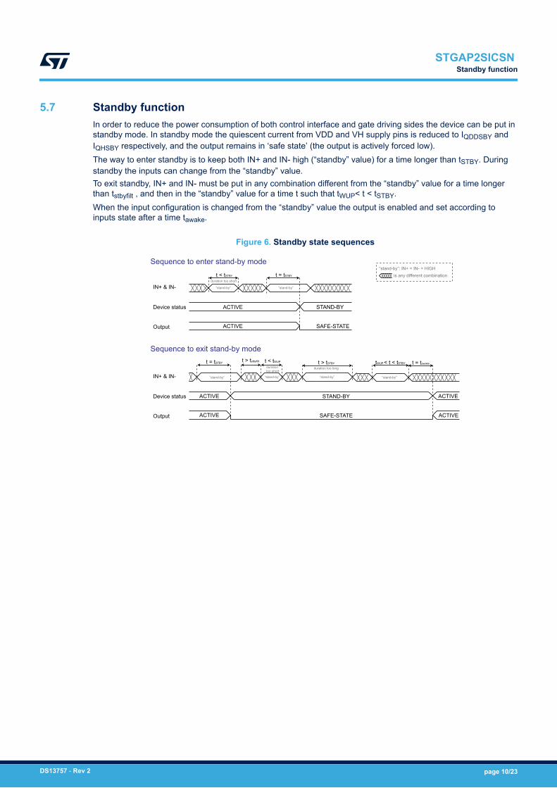
5.7 Standby functionIn order to reduce the power consumption of both control interface and gate driving sides the device can be put instandby mode. In standby mode the quiescent current from VDD and VH supply pins is reduced to IQDDSBY andIQHSBY respectively, and the output remains in ‘safe state’ (the output is actively forced low).The way to enter standby is to keep both IN+ and IN- high (“standby” value) for a time longer than tSTBY. Duringstandby the inputs can change from the “standby” value.To exit standby, IN+ and IN- must be put in any combination different from the “standby” value for a time longerthan tstbyfilt , and then in the “standby” value for a time t such that tWUP< t < tSTBY.When the input configuration is changed from the “standby” value the output is enabled and set according toinputs state after a time tawake.
Figure 6. Standby state sequences
Sequence to enter stand-by mode
Sequence to exit stand-by mode
t < tSTBY t = tSTBY
IN+ & IN-
Device status
Output
ACTIVE STAND-BY
SAFE-STATEACTIVE
“stand-by” “stand-by”
duration too short
t = tSTBY
IN+ & IN-
Device status
Output
ACTIVE STAND-BY
SAFE-STATEACTIVE
t > tstbyfilt t < tWUP t > tSTBY tWUP < t < tSTBY t = tawake
ACTIVE
ACTIVE
“stand-by”“stand-by” “stand-by” “stand-by”
durationtoo short
duration too long
“stand-by”: IN+ = IN- = HIGHis any different combination
STGAP2SICSN Standby function
DS13757 - Rev 2 page 10/23
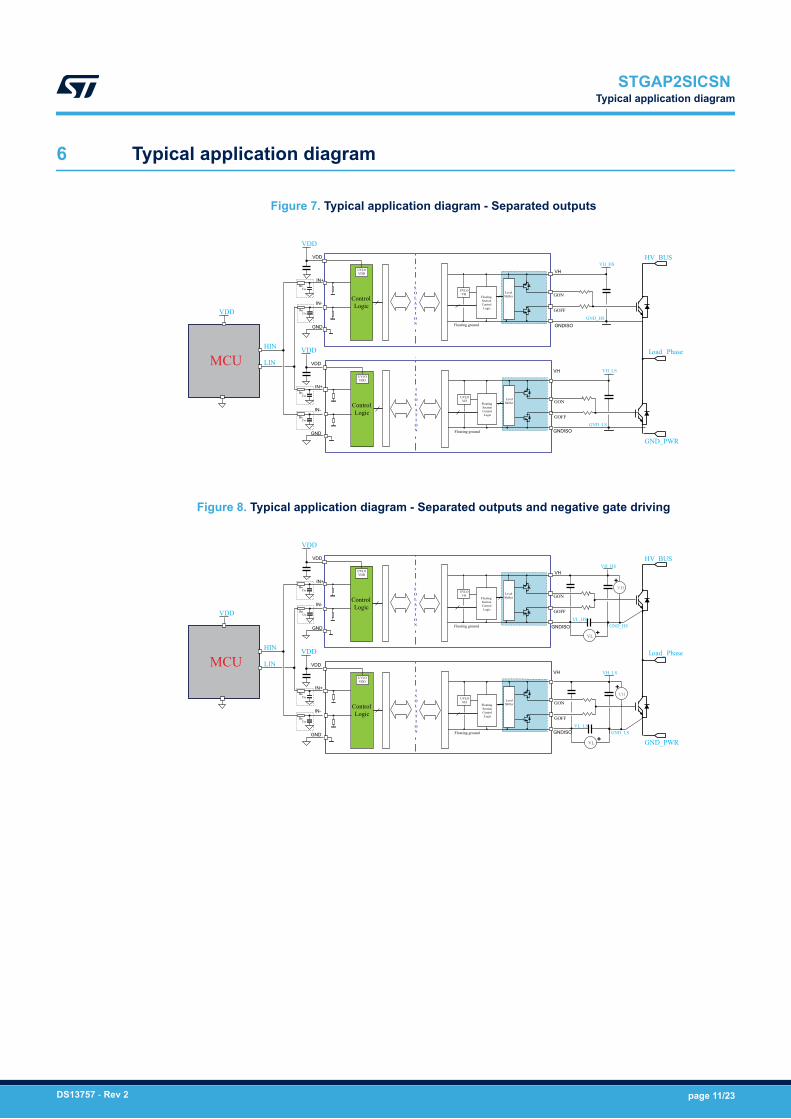
6 Typical application diagram
Figure 7. Typical application diagram - Separated outputs
GND_HS
VH_HS
VDD
MCUHIN
LIN
VDD
VDD
CR
CR
CR
CR
GND_PWR
Load_ Phase
HV_BUSVDD
GND
IN+
IN-
VH
GNDISO
VDD
GND
IN+
IN-
VH
GNDISO
ISOLATION
LevelShifterFloating
SectionControlLogic
Floating ground
UVLOVH
GOFF
ControlLogic
UVLOVDD
GON
ISOLATION
LevelShifterFloating
SectionControlLogic
Floating ground
UVLOVH
GOFF
ControlLogic
UVLOVDD
GON
GND_LS
VH_LS
Figure 8. Typical application diagram - Separated outputs and negative gate driving
VDD
MCUHIN
LIN
VDD
VDD
CR
CR
CR
CR
GND_PWR
Load_ Phase
HV_BUSVDD
GND
IN+
IN-
VH
VDD
GND
IN+
IN-
VH
GNDISO
ISOLATION
LevelShifterFloating
SectionControlLogic
Floating ground
UVLOVH
GOFF
ControlLogic
UVLOVDD
GON
ISOLATION
LevelShifterFloating
SectionControlLogic
Floating ground
UVLOVH
GOFF
ControlLogic
UVLOVDD
GON
GND_HS
VH_HS
VL_HS
+VL
VH+
GNDISO
GND_LS
VH_LS
VL_LS
+VL
VH+
STGAP2SICSN Typical application diagram
DS13757 - Rev 2 page 11/23
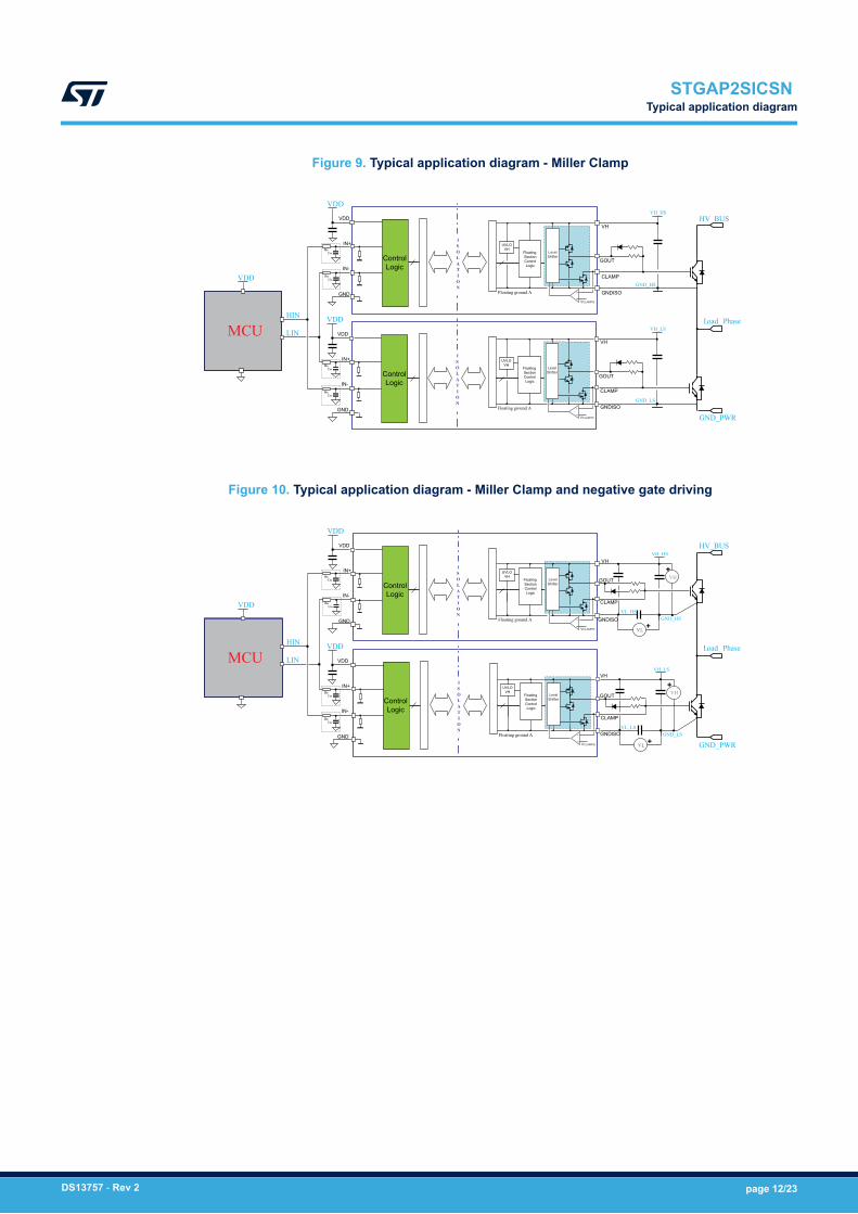
Figure 9. Typical application diagram - Miller Clamp
GND_HS
VH_HSVDD
MCUHIN
LIN
VDD
VDD
CR
CR
CR
CR
GND_PWR
Load_ Phase
HV_BUS
ISOLATION
ControlLogic
Floating SectionControlLogic
Floating ground A
UVLOVH
LevelShifter
VCLAMPth
+
VDD
GND
IN+
IN-
VH
CLAMP
GNDISO
GOUT
GND_LS
VH_LS
ISOLATION
ControlLogic
Floating SectionControlLogic
Floating ground A
UVLOVH
LevelShifter
VCLAMPth
+
VDD
GND
IN+
IN-
VH
CLAMP
GNDISO
GOUT
Figure 10. Typical application diagram - Miller Clamp and negative gate driving
VDD
MCUHIN
LIN
VDD
VDD
CR
CR
CR
CR
GND_PWR
Load_ Phase
HV_BUSVDD
GND
IN+
IN-
VH
VDD
GND
IN+
IN-
VH
GNDISO
GND_HS
VH_HS
VL_HS
+VL
VH+
GNDISO
GND_LS
VH_LS
VL_LS
+VL
VH+
ISOLATION
ControlLogic
Floating SectionControlLogic
Floating ground A
UVLOVH
LevelShifter
VCLAMPth
+
ISOLATION
ControlLogic
Floating SectionControlLogic
Floating ground A
UVLOVH
LevelShifter
VCLAMPth
+
CLAMP
GOUT
CLAMP
GOUT
STGAP2SICSN Typical application diagram
DS13757 - Rev 2 page 12/23
7 Layout
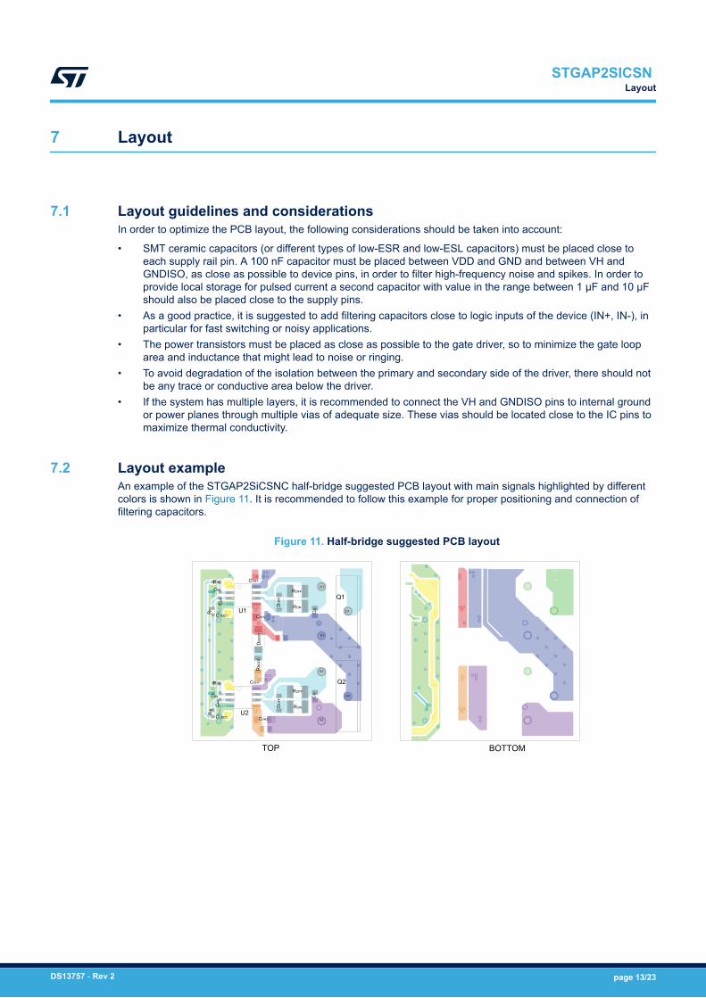
7.1 Layout guidelines and considerationsIn order to optimize the PCB layout, the following considerations should be taken into account:
• SMT ceramic capacitors (or different types of low-ESR and low-ESL capacitors) must be placed close toeach supply rail pin. A 100 nF capacitor must be placed between VDD and GND and between VH andGNDISO, as close as possible to device pins, in order to filter high-frequency noise and spikes. In order toprovide local storage for pulsed current a second capacitor with value in the range between 1 µF and 10 µFshould also be placed close to the supply pins.
• As a good practice, it is suggested to add filtering capacitors close to logic inputs of the device (IN+, IN-), inparticular for fast switching or noisy applications.
• The power transistors must be placed as close as possible to the gate driver, so to minimize the gate looparea and inductance that might lead to noise or ringing.
• To avoid degradation of the isolation between the primary and secondary side of the driver, there should notbe any trace or conductive area below the driver.
• If the system has multiple layers, it is recommended to connect the VH and GNDISO pins to internal groundor power planes through multiple vias of adequate size. These vias should be located close to the IC pins tomaximize thermal conductivity.
7.2 Layout exampleAn example of the STGAP2SiCSNC half-bridge suggested PCB layout with main signals highlighted by differentcolors is shown in Figure 11. It is recommended to follow this example for proper positioning and connection offiltering capacitors.
Figure 11. Half-bridge suggested PCB layout
Q1
Q2
U1
U2
CVH1
CVH2CVDD1
ROFF
RONDO
FF
G1
D1
S1
CIN
CIN
RIN
RIN
CG
CVH1
CVH2CVDD1
ROFF
RONDO
FF
G2
D2
S2
CIN
CIN
RIN
RIN
CG
DBO
OT
RBO
OT
TOP BOTTOM
STGAP2SICSN Layout
DS13757 - Rev 2 page 13/23
8 Testing and characterization information
Figure 12. Timings definition
50%
50%
10%
90%
tr t f
tDon
90%
10%GON-GOFF
IN-
IN+
tDoff
50%
50%
10%
90%
tr t f
tDon
90%
10%
tDoff
Figure 13. CMTI test circuit
ISOLATION
VH
GOFF
GNDISO
VDD
GND
IN+
IN-
GON +VH
Output Vout monitoring node
S1+
-
G1
+VDD
STGAP2SICSN Testing and characterization information
DS13757 - Rev 2 page 14/23
9 Package information
In order to meet environmental requirements, ST offers these devices in different grades of ECOPACK packages,depending on their level of environmental compliance. ECOPACK specifications, grade definitions and productstatus are available at: www.st.com. ECOPACK is an ST trademark.
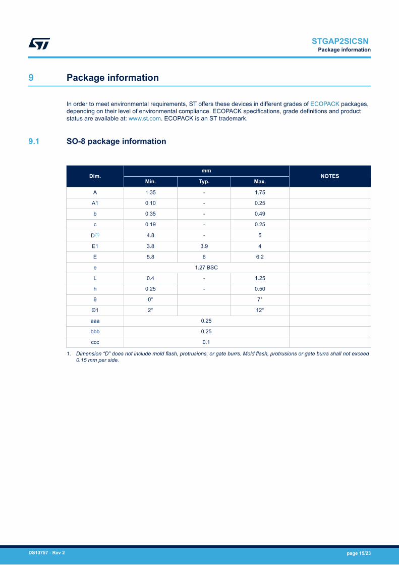
9.1 SO-8 package information
Dim.mm
NOTESMin. Typ. Max.
A 1.35 - 1.75
A1 0.10 - 0.25
b 0.35 - 0.49
c 0.19 - 0.25
D(1) 4.8 - 5
E1 3.8 3.9 4
E 5.8 6 6.2
e 1.27 BSC
L 0.4 - 1.25
h 0.25 - 0.50
θ 0° 7°
Θ1 2° 12°
aaa 0.25
bbb 0.25
ccc 0.1
1. Dimension “D” does not include mold flash, protrusions, or gate burrs. Mold flash, protrusions or gate burrs shall not exceed0.15 mm per side.
STGAP2SICSN Package information
DS13757 - Rev 2 page 15/23
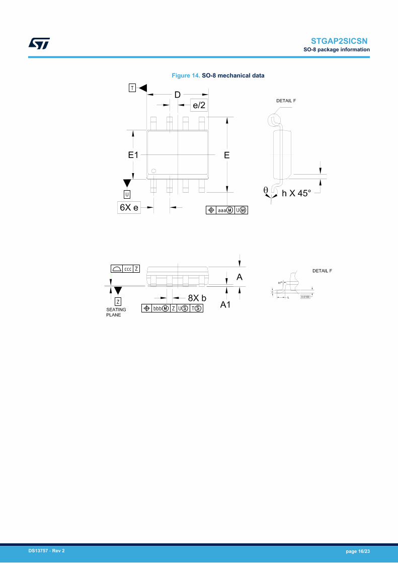
Figure 14. SO-8 mechanical data
STGAP2SICSN SO-8 package information
DS13757 - Rev 2 page 16/23
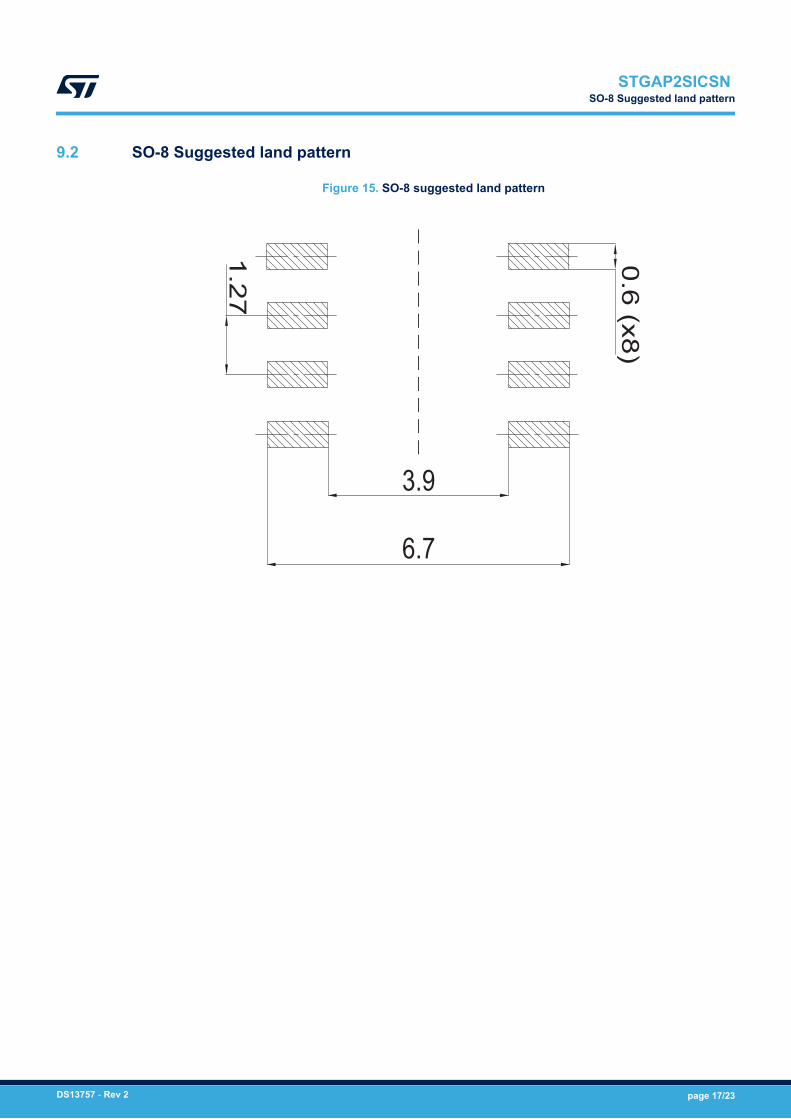
9.2 SO-8 Suggested land pattern
Figure 15. SO-8 suggested land pattern
3.9
6.7
0.6 (x8)
1.27
STGAP2SICSN SO-8 Suggested land pattern
DS13757 - Rev 2 page 17/23
10 Ordering information
Table 10. Device summary
Order code Output configuration Package Package marking Packaging
STGAP2SiCSNTR GON-GOFF SO-8 GAP2ISN Tape and Reel
STGAP2SiCSNCTR GOUT-CLAMP SO-8 GAP2ISCN Tape and Reel
STGAP2SICSN Ordering information
DS13757 - Rev 2 page 18/23
Revision history
Table 11. Document revision history
Date Version Changes
13-Aug-2021 1 Initial release.
19-Oct-2021 2 Updated test condition in Table 5; updated order codes.
STGAP2SICSN
DS13757 - Rev 2 page 19/23
Contents
1 Block diagram . . . . . . . . . . . . . . . . . . . . . . . . . . . . . . . . . . . . . . . . . . . . . . . . . . . . . . . . . . . . . . . . . . . . .2
2 Pin description and connection diagram . . . . . . . . . . . . . . . . . . . . . . . . . . . . . . . . . . . . . . . . . . .3
3 Electrical data . . . . . . . . . . . . . . . . . . . . . . . . . . . . . . . . . . . . . . . . . . . . . . . . . . . . . . . . . . . . . . . . . . . . .4
3.1 Absolute maximum ratings. . . . . . . . . . . . . . . . . . . . . . . . . . . . . . . . . . . . . . . . . . . . . . . . . . . . . . . 4
3.2 Thermal data . . . . . . . . . . . . . . . . . . . . . . . . . . . . . . . . . . . . . . . . . . . . . . . . . . . . . . . . . . . . . . . . . . 4
3.3 Recommended operating conditions . . . . . . . . . . . . . . . . . . . . . . . . . . . . . . . . . . . . . . . . . . . . . . 4
4 Electrical characteristics. . . . . . . . . . . . . . . . . . . . . . . . . . . . . . . . . . . . . . . . . . . . . . . . . . . . . . . . . . .5
5 Functional Description. . . . . . . . . . . . . . . . . . . . . . . . . . . . . . . . . . . . . . . . . . . . . . . . . . . . . . . . . . . . .8
5.1 Gate driving power supply and UVLO . . . . . . . . . . . . . . . . . . . . . . . . . . . . . . . . . . . . . . . . . . . . . 8
5.2 Power-up, power-down and ‘safe state’ . . . . . . . . . . . . . . . . . . . . . . . . . . . . . . . . . . . . . . . . . . . . 8
5.3 Control inputs. . . . . . . . . . . . . . . . . . . . . . . . . . . . . . . . . . . . . . . . . . . . . . . . . . . . . . . . . . . . . . . . . . 9
5.4 Miller Clamp function . . . . . . . . . . . . . . . . . . . . . . . . . . . . . . . . . . . . . . . . . . . . . . . . . . . . . . . . . . . 9
5.5 Watchdog . . . . . . . . . . . . . . . . . . . . . . . . . . . . . . . . . . . . . . . . . . . . . . . . . . . . . . . . . . . . . . . . . . . . . 9
5.6 Thermal shutdown protection . . . . . . . . . . . . . . . . . . . . . . . . . . . . . . . . . . . . . . . . . . . . . . . . . . . . 9
5.7 Standby function . . . . . . . . . . . . . . . . . . . . . . . . . . . . . . . . . . . . . . . . . . . . . . . . . . . . . . . . . . . . . . 10
6 Typical application diagram. . . . . . . . . . . . . . . . . . . . . . . . . . . . . . . . . . . . . . . . . . . . . . . . . . . . . . .11
7 Layout. . . . . . . . . . . . . . . . . . . . . . . . . . . . . . . . . . . . . . . . . . . . . . . . . . . . . . . . . . . . . . . . . . . . . . . . . . . .13
7.1 Layout guidelines and considerations. . . . . . . . . . . . . . . . . . . . . . . . . . . . . . . . . . . . . . . . . . . . . 13
7.2 Layout example . . . . . . . . . . . . . . . . . . . . . . . . . . . . . . . . . . . . . . . . . . . . . . . . . . . . . . . . . . . . . . . 13
8 Testing and characterization information. . . . . . . . . . . . . . . . . . . . . . . . . . . . . . . . . . . . . . . . . .14
9 Package information. . . . . . . . . . . . . . . . . . . . . . . . . . . . . . . . . . . . . . . . . . . . . . . . . . . . . . . . . . . . . .15
9.1 [Package name] package information . . . . . . . . . . . . . . . . . . . . . . . . . . . . . . . . . . . . . . . . . . . . 15
9.2 SO-8 Suggested land pattern . . . . . . . . . . . . . . . . . . . . . . . . . . . . . . . . . . . . . . . . . . . . . . . . . . . 17
10 Ordering information . . . . . . . . . . . . . . . . . . . . . . . . . . . . . . . . . . . . . . . . . . . . . . . . . . . . . . . . . . . . .18
Revision history . . . . . . . . . . . . . . . . . . . . . . . . . . . . . . . . . . . . . . . . . . . . . . . . . . . . . . . . . . . . . . . . . . . . . . .19
Contents . . . . . . . . . . . . . . . . . . . . . . . . . . . . . . . . . . . . . . . . . . . . . . . . . . . . . . . . . . . . . . . . . . . . . . . . . . . . . .20
List of tables . . . . . . . . . . . . . . . . . . . . . . . . . . . . . . . . . . . . . . . . . . . . . . . . . . . . . . . . . . . . . . . . . . . . . . . . . .21
List of figures. . . . . . . . . . . . . . . . . . . . . . . . . . . . . . . . . . . . . . . . . . . . . . . . . . . . . . . . . . . . . . . . . . . . . . . . . .22
STGAP2SICSN Contents
DS13757 - Rev 2 page 20/23
List of tablesTable 1. Pin Description . . . . . . . . . . . . . . . . . . . . . . . . . . . . . . . . . . . . . . . . . . . . . . . . . . . . . . . . . . . . . . . . . . . . . 3Table 2. Absolute maximum ratings . . . . . . . . . . . . . . . . . . . . . . . . . . . . . . . . . . . . . . . . . . . . . . . . . . . . . . . . . . . . . 4Table 3. Thermal data. . . . . . . . . . . . . . . . . . . . . . . . . . . . . . . . . . . . . . . . . . . . . . . . . . . . . . . . . . . . . . . . . . . . . . . 4Table 4. Recommended operating conditions. . . . . . . . . . . . . . . . . . . . . . . . . . . . . . . . . . . . . . . . . . . . . . . . . . . . . . . 4Table 5. Electrical characteristics (TJ = 25°C, VH = 18 V, VDD = 5 V unless otherwise specified) . . . . . . . . . . . . . . . . . . . 5Table 6. Isolation related package specifications . . . . . . . . . . . . . . . . . . . . . . . . . . . . . . . . . . . . . . . . . . . . . . . . . . . . 6Table 7. Isolation characteristics. . . . . . . . . . . . . . . . . . . . . . . . . . . . . . . . . . . . . . . . . . . . . . . . . . . . . . . . . . . . . . . . 7Table 8. UL 1577 Tests . . . . . . . . . . . . . . . . . . . . . . . . . . . . . . . . . . . . . . . . . . . . . . . . . . . . . . . . . . . . . . . . . . . . . . 7Table 9. Inputs truth table (applicable when device is not in UVLO or "safe state") . . . . . . . . . . . . . . . . . . . . . . . . . . . . . 9Table 10. Device summary . . . . . . . . . . . . . . . . . . . . . . . . . . . . . . . . . . . . . . . . . . . . . . . . . . . . . . . . . . . . . . . . . . . 18Table 11. Document revision history . . . . . . . . . . . . . . . . . . . . . . . . . . . . . . . . . . . . . . . . . . . . . . . . . . . . . . . . . . . . . 19
STGAP2SICSN List of tables
DS13757 - Rev 2 page 21/23
List of figuresFigure 1. Block diagram - Single output and Miller Clamp configuration . . . . . . . . . . . . . . . . . . . . . . . . . . . . . . . . . . . . 2Figure 2. Block diagram - Separate outputs configuration . . . . . . . . . . . . . . . . . . . . . . . . . . . . . . . . . . . . . . . . . . . . . 2Figure 3. Pin connection (top view), Separated outputs option . . . . . . . . . . . . . . . . . . . . . . . . . . . . . . . . . . . . . . . . . . 3Figure 4. Pin connection (top view), Single output and Miller CLAMP option. . . . . . . . . . . . . . . . . . . . . . . . . . . . . . . . . 3Figure 5. Power supply configuration for unipolar and bipolar gate driving . . . . . . . . . . . . . . . . . . . . . . . . . . . . . . . . . . 8Figure 6. Standby state sequences. . . . . . . . . . . . . . . . . . . . . . . . . . . . . . . . . . . . . . . . . . . . . . . . . . . . . . . . . . . . 10Figure 7. Typical application diagram - Separated outputs . . . . . . . . . . . . . . . . . . . . . . . . . . . . . . . . . . . . . . . . . . . . 11Figure 8. Typical application diagram - Separated outputs and negative gate driving . . . . . . . . . . . . . . . . . . . . . . . . . . 11Figure 9. Typical application diagram - Miller Clamp . . . . . . . . . . . . . . . . . . . . . . . . . . . . . . . . . . . . . . . . . . . . . . . . 12Figure 10. Typical application diagram - Miller Clamp and negative gate driving . . . . . . . . . . . . . . . . . . . . . . . . . . . . . . 12Figure 11. Half-bridge suggested PCB layout. . . . . . . . . . . . . . . . . . . . . . . . . . . . . . . . . . . . . . . . . . . . . . . . . . . . . . 13Figure 12. Timings definition . . . . . . . . . . . . . . . . . . . . . . . . . . . . . . . . . . . . . . . . . . . . . . . . . . . . . . . . . . . . . . . . . 14Figure 13. CMTI test circuit . . . . . . . . . . . . . . . . . . . . . . . . . . . . . . . . . . . . . . . . . . . . . . . . . . . . . . . . . . . . . . . . . . 14Figure 14. SO-8 mechanical data . . . . . . . . . . . . . . . . . . . . . . . . . . . . . . . . . . . . . . . . . . . . . . . . . . . . . . . . . . . . . . 16Figure 15. SO-8 suggested land pattern . . . . . . . . . . . . . . . . . . . . . . . . . . . . . . . . . . . . . . . . . . . . . . . . . . . . . . . . . 17
STGAP2SICSN List of figures
DS13757 - Rev 2 page 22/23
IMPORTANT NOTICE – PLEASE READ CAREFULLY
STMicroelectronics NV and its subsidiaries (“ST”) reserve the right to make changes, corrections, enhancements, modifications, and improvements to STproducts and/or to this document at any time without notice. Purchasers should obtain the latest relevant information on ST products before placing orders. STproducts are sold pursuant to ST’s terms and conditions of sale in place at the time of order acknowledgement.
Purchasers are solely responsible for the choice, selection, and use of ST products and ST assumes no liability for application assistance or the design ofPurchasers’ products.
No license, express or implied, to any intellectual property right is granted by ST herein.
Resale of ST products with provisions different from the information set forth herein shall void any warranty granted by ST for such product.
ST and the ST logo are trademarks of ST. For additional information about ST trademarks, please refer to www.st.com/trademarks. All other product or servicenames are the property of their respective owners.
Information in this document supersedes and replaces information previously supplied in any prior versions of this document.
© 2021 STMicroelectronics – All rights reserved
STGAP2SICSN
DS13757 - Rev 2 page 23/23