Embed Size (px)
Citation preview

TGF2819-FL 100W Peak Power, 20W Average Power,
32V DC – 3.5 GHz, GaN RF Power Transistor
Datasheet: Rev B- 03-03-15 - 1 of 21 - Disclaimer: Subject to change without notice
© 2014 TriQuint www.triquint.com
Applications Military radar
Civilian radar
Professional and military radio communications
Test instrumentation
Wideband or narrowband amplifiers
Jammers
Ordering Information Part ECCN Description
TGF2819-FL 3A001.b.3.a Packaged part Flanged
TGF2819-FS-EVB1 EAR99 3.1-3.5 GHz Evaluation Board
Functional Block Diagram
Pin Configuration Pin No. Label
1 VD / RF OUT
2 VG / RF IN
Flange Source
General Description The TriQuint TGF2819-FL is a greater-than 100 W Peak (20 W Avg.) (P3dB) discrete GaN on SiC HEMT which operates from DC to 3.5 GHz. The device is constructed with TriQuint’s proven TQGaN25HV process, which features advanced field plate techniques to optimize power and efficiency at high drain bias operating conditions. This optimization can potentially lower system costs in terms of fewer amplifier line-ups and lower thermal management costs.
Lead-free and ROHS compliant
Evaluation boards are available upon request.
Product Features Frequency: DC to 3.5 GHz
Output Power (P3dB): 126 W Peak (25 Watts Avg.) at 3.3 GHz
Linear Gain: >14 dB at 3.3 GHz
Typical PAE: > 58% at 3.3 GHz
Operating Voltage: 32 V
Low thermal resistance package

TGF2819-FL 100W Peak Power, 20W Average Power,
32V DC – 3.5 GHz, GaN RF Power Transistor
Datasheet: Rev B- 03-03-15 - 2 of 21 - Disclaimer: Subject to change without notice
© 2014 TriQuint www.triquint.com
RF Characterization – Load Pull Performance at 2.7 GHz (1)
Test conditions unless otherwise noted: TA = 25 °C, VD = 32 V, IDQ = 250 mA
Symbol Parameter Min Typical Max Units GLIN Linear Gain (Power Tuned) 13.6 dB
P3dB Output Power at 3 dB Gain Compression (Power Tuned) 135 W
PAE3dB Power-Added Efficiency at 3 dB Gain Compression (Eff. Tuned)
60.9 %
G3dB Gain at 3 dB Compression (Power Tuned) 10.6 dB
Notes: 1. Pulse: 100µs, 20%
RF Characterization – Load Pull Performance at 2.9 GHz (1)
Test conditions unless otherwise noted: TA = 25 °C, VD = 32 V, IDQ = 250 mA
Symbol Parameter Min Typical Max Units GLIN Linear Gain (Power Tuned) 14.8 dB
P3dB Output Power at 3 dB Gain Compression (Power Tuned) 145 W
PAE3dB Power-Added Efficiency at 3 dB Gain Compression (Eff. Tuned)
69.5 %
G3dB Gain at 3 dB Compression (Power Tuned) 11.8 dB
Notes: 1. Pulse: 100µs, 20%
Absolute Maximum Ratings Parameter Value Breakdown Voltage (BVDG) 145 V
Gate Voltage Range (VG) -7 to 0 V
Drain Current (ID) 12 A
Gate Current (IG) -28.8 to 33.6 mA
Power Dissipation (PD) 144 W
RF Input Power, CW, T = 25°C (PIN)
39.8 dBm
Channel Temperature (TCH) 275 °C
Mounting Temperature (30 Seconds)
320 °C
Storage Temperature -40 to 150 °C
Operation of this device outside the parameter ranges given above may cause permanent damage. These are stress ratings only, and functional operation of the device at these conditions is not implied.
Recommended Operating Conditions
Parameter Value Drain Voltage (VD) 32 V (Typ.)
Drain Quiescent Current (IDQ) 250 mA (Typ.)
Peak Drain Current, Pulse ( ID) 7.23 A (Typ.)
Gate Voltage (VG) -2.9 V (Typ.)
Channel Temperature (TCH) 250 °C (Max.)
Power Dissipation, CW (PD) 86 W (Max)
Power Dissipation, Pulse (PD) 144 W (Max)
Electrical specifications are measured at specified test conditions.
Specifications are not guaranteed over all recommended operating conditions.
Pulse signal: 100uS Pulse Width, 20% Duty Cycle

TGF2819-FL 100W Peak Power, 20W Average Power,
32V DC – 3.5 GHz, GaN RF Power Transistor
Datasheet: Rev B- 03-03-15 - 3 of 21 - Disclaimer: Subject to change without notice
© 2014 TriQuint www.triquint.com
RF Characterization – Load Pull Performance at 3.1 GHz (1)
Test conditions unless otherwise noted: TA = 25 °C, VD = 32 V, IDQ = 250 mA
Symbol Parameter Min Typical Max Units GLIN Linear Gain (Power Tuned) 14.3 dB
P3dB Output Power at 3 dB Gain Compression (Power Tuned) 129 W
PAE3dB Power-Added Efficiency at 3 dB Gain Compression (Eff. Tuned)
61.4 %
G3dB Gain at 3 dB Compression (Power Tuned) 11.3 dB
Notes: 1. Pulse: 100µs, 20%
RF Characterization – Load Pull Performance at 3.3 GHz (1)
Test conditions unless otherwise noted: TA = 25 °C, VD = 32 V, IDQ = 250 mA
Symbol Parameter Min Typical Max Units GLIN Linear Gain (Power Tuned) 14.2 dB
P3dB Output Power at 3 dB Gain Compression (Power Tuned) 126 W
PAE3dB Power-Added Efficiency at 3 dB Gain Compression (Eff. Tuned)
58.3 %
G3dB Gain at 3 dB Compression (Power Tuned) 11.2 dB
Notes: 1. Pulse: 100µs, 20%
RF Characterization – Load Pull Performance at 3.5 GHz (1)
Test conditions unless otherwise noted: TA = 25 °C, VD = 32 V, IDQ = 250 mA
Symbol Parameter Min Typical Max Units GLIN Linear Gain (Power Tuned) 13.9 dB
P3dB Output Power at 3 dB Gain Compression (Power Tuned) 120 W
PAE3dB Power-Added Efficiency at 3 dB Gain Compression (Eff. Tuned)
59.8 %
G3dB Gain at 3 dB Compression (Power Tuned) 10.9 dB
Notes: 1. Pulse: 100µs, 20%

TGF2819-FL 100W Peak Power, 20W Average Power,
32V DC – 3.5 GHz, GaN RF Power Transistor
Datasheet: Rev B- 03-03-15 - 4 of 21 - Disclaimer: Subject to change without notice
© 2014 TriQuint www.triquint.com
RF Characterization – Performance at 3.5GHz (1, 2)
Test conditions unless otherwise noted: TA = 25 °C, VD = 32 V, IDQ = 250 mA
Symbol Parameter Min Typical Max Units
GLIN Linear Gain 15.1 dB
P3dB Output Power at 3 dB Gain Compression 126 W
PAE3dB Power-Added Efficiency at 3 dB Gain Compression 49.2 %
G3dB Gain at 3 dB Compression 12.1 dB
Notes: 1. Pulse: 100µs PW, 20% 2. Performance at 3.5GHz in the 3.1 to 3.5GHz Evaluation Board
RF Characterization – Mismatched Ruggedness at 3.50 GHz (1, 2)
Test conditions unless otherwise noted: TA = 25 °C, VD = 32 V, IDQ = 250 mA
Symbol Parameter Typical VSWR Impedance Mismatch Ruggedness 10:1
Notes: 1. Input power established at P3dB at matched load at the output of 3.1 – 3.5 GHz Evaluation Board 2. Pulse: 100uS PW, 20%

TGF2819-FL 100W Peak Power, 20W Average Power,
32V DC – 3.5 GHz, GaN RF Power Transistor
Datasheet: Rev B- 03-03-15 - 5 of 21 - Disclaimer: Subject to change without notice
© 2014 TriQuint www.triquint.com
Thermal and Reliability Information Parameter Test Conditions Value Units Thermal Resistance(1) (θJC)
Vd = 32V, Tbase = 85°C 100uS, 5%, Pdiss = 100W
0.75 °C/W
Channel Temperature (TCH) 160 °C
Median Lifetime (TM) 1.92E09 Hours
Thermal Resistance(1) (θJC) Vd = 32V, Tbase = 85°C 100uS, 10%, Pdiss = 100W
0.79 °C/W
Channel Temperature (TCH) 164.3 °C
Median Lifetime (TM) 1.24E09 Hours
Thermal Resistance(1) (θJC) Vd = 32V, Tbase = 85°C 300uS, 20%, Pdiss = 100W
0.88 °C/W
Channel Temperature (TCH) 173 °C
Median Lifetime (TM) 5.13E08 Hours
Thermal Resistance(1) (θJC) Vd = 32V, Tbase = 85°C 300uS, 50%, Pdiss = 100W
1.15 °C/W
Channel Temperature (TCH) 200.3 °C
Median Lifetime (TM) 4.20E07 Hours
Notes: 1. Thermal resistance measured to bottom of package.
Median Lifetime
1.00E+05
1.00E+06
1.00E+07
1.00E+08
1.00E+09
1.00E+10
1.00E+11
1.00E+12
1.00E+13
1.00E+14
1.00E+15
1.00E+16
1.00E+17
1.00E+18
1.00E+19
25 50 75 100 125 150 175 200 225 250 275
Me
dia
n L
ifet
ime,
TM
(Ho
urs
)
Channel Temperature, TCH (°C)
Median Lifetime vs. Channel Temperature

TGF2819-FL 100W Peak Power, 20W Average Power,
32V DC – 3.5 GHz, GaN RF Power Transistor
Datasheet: Rev B- 03-03-15 - 6 of 21 - Disclaimer: Subject to change without notice
© 2014 TriQuint www.triquint.com
Maximum Channel Temperature
120.0
140.0
160.0
180.0
200.0
220.0
240.0
260.0
1.00E-06 1.00E-05 1.00E-04 1.00E-03 1.00E-02 1.00E-01 1.00E+00
Max
imu
m C
han
nel
Tem
per
atu
re (
oC
)
Pulse Width (sec)
Maximum Channel TemperaturePackage base fixed at 85 oC, Pdiss = 100 W
5% Duty Cycle
10% Duty Cycle
20% Duty Cycle
50% Duty Cycle
TGF2819-FL 100W Peak Power, 20W Average Power,
32V DC – 3.5 GHz, GaN RF Power Transistor
Datasheet: Rev B- 03-03-15 - 7 of 21 - Disclaimer: Subject to change without notice
© 2014 TriQuint www.triquint.com
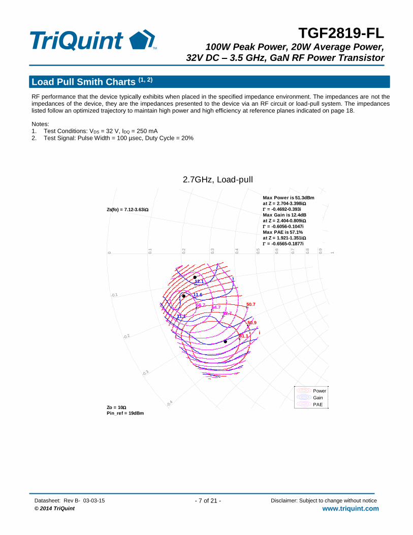
Load Pull Smith Charts (1, 2)
RF performance that the device typically exhibits when placed in the specified impedance environment. The impedances are not the impedances of the device, they are the impedances presented to the device via an RF circuit or load-pull system. The impedances listed follow an optimized trajectory to maintain high power and high efficiency at reference planes indicated on page 18.
Notes: 1. Test Conditions: VDS = 32 V, IDQ = 250 mA 2. Test Signal: Pulse Width = 100 µsec, Duty Cycle = 20%
0 0.1
0.2
0.3
0.4
0.5
0.6
0.7
0.8
0.9
1
-0.4
-0.3
-0.2
-0.1
0.1
2.7GHz, Load-pull
51.1
50.9
50.7
12.1
11.6
11.1
56.7 54.7
52.7
Max Power is 51.3dBm
at Z = 2.704-3.398i
= -0.4692-0.393i
Max Gain is 12.4dB
at Z = 2.404-0.809i
= -0.6056-0.1047i
Max PAE is 57.1%
at Z = 1.921-1.351i
= -0.6565-0.1877i
Zo = 10
Pin_ref = 19dBm
Zs(fo) = 7.12-3.63i
Power
Gain
PAE

TGF2819-FL 100W Peak Power, 20W Average Power,
32V DC – 3.5 GHz, GaN RF Power Transistor
Datasheet: Rev B- 03-03-15 - 8 of 21 - Disclaimer: Subject to change without notice
© 2014 TriQuint www.triquint.com
Load Pull Smith Charts (1, 2)
RF performance that the device typically exhibits when placed in the specified impedance environment. The impedances are not the impedances of the device, they are the impedances presented to the device via an RF circuit or load-pull system. The impedances listed follow an optimized trajectory to maintain high power and high efficiency at reference planes indicated on page 18.
Notes: 1. Test Conditions: VDS = 32 V, IDQ = 250 mA 2. Test Signal: Pulse Width = 100 µsec, Duty Cycle = 20%
0 0.1
0.2
0.3
0.4
0.5
0.6
-0.4
-0.3
-0.2
-0.1
2.9GHz, Load-pull
51.6
51.4
51.2
13.3
13.3
12.8
12.3
62.260.2
58.2
Max Power is 51.6dBm
at Z = 2.377-3.545i
= -0.4934-0.4278i
Max Gain is 13.6dB
at Z = 2.514-1.449i
= -0.577-0.1827i
Max PAE is 63.8%
at Z = 1.796-2.264i
= -0.6352-0.3138i
Zo = 10
Pin_ref = 20.6dBm
Zs(fo) = 8.04-7.51i
Power
Gain
PAE

TGF2819-FL 100W Peak Power, 20W Average Power,
32V DC – 3.5 GHz, GaN RF Power Transistor
Datasheet: Rev B- 03-03-15 - 9 of 21 - Disclaimer: Subject to change without notice
© 2014 TriQuint www.triquint.com
Load Pull Smith Charts (1, 2)
RF performance that the device typically exhibits when placed in the specified impedance environment. The impedances are not the impedances of the device, they are the impedances presented to the device via an RF circuit or load-pull system. The impedances listed follow an optimized trajectory to maintain high power and high efficiency at reference planes indicated on page 18.
Notes: 1. Test Conditions: VDS = 32 V, IDQ = 250 mA 2. Test Signal: Pulse Width = 100 µsec, Duty Cycle = 20%
0 0.1
0.2
0.3
0.4
0.5
0.6
-0.4
-0.3
-0.2
-0.1
3.1GHz, Load-pull
51.150.9
50.7
13.5
13
12.5
56.654.6
52.6
Max Power is 51.1dBm
at Z = 2.962-4.499i
= -0.3771-0.478i
Max Gain is 13.8dB
at Z = 1.394-1.6i
= -0.7214-0.2418i
Max PAE is 57.9%
at Z = 1.75-2.246i
= -0.6422-0.314i
Zo = 10
Pin_ref = 25.5dBm
Zs(fo) = 12.14-8.66i
Power
Gain
PAE

TGF2819-FL 100W Peak Power, 20W Average Power,
32V DC – 3.5 GHz, GaN RF Power Transistor
Datasheet: Rev B- 03-03-15 - 10 of 21 - Disclaimer: Subject to change without notice
© 2014 TriQuint www.triquint.com
Load Pull Smith Charts (1, 2)
RF performance that the device typically exhibits when placed in the specified impedance environment. The impedances are not the impedances of the device, they are the impedances presented to the device via an RF circuit or load-pull system. The impedances listed follow an optimized trajectory to maintain high power and high efficiency at reference planes indicated on page 18.
Notes: 1. Test Conditions: VDS = 32 V, IDQ = 250 mA 2. Test Signal: Pulse Width = 100 µsec, Duty Cycle = 20%
0 0.1
0.2
0.3
0.4
0.5
0.6
0.7
0.8
-0.5
-0.4
-0.3
-0.2
-0.1
3.3GHz, Load-pull
50.850.6
50.4
13.4
12.9
12.4
53 51
49
Max Power is 51dBm
at Z = 2.435-4.724i
= -0.4055-0.534i
Max Gain is 13.8dB
at Z = 1.759-2.31i
= -0.6377-0.3218i
Max PAE is 53.7%
at Z = 1.813-2.877i
= -0.5982-0.3892i
Zo = 10
Pin_ref = 23.8dBm
Zs(fo) = 10.5-2.53i
Power
Gain
PAE

TGF2819-FL 100W Peak Power, 20W Average Power,
32V DC – 3.5 GHz, GaN RF Power Transistor
Datasheet: Rev B- 03-03-15 - 11 of 21 - Disclaimer: Subject to change without notice
© 2014 TriQuint www.triquint.com
Load Pull Smith Charts (1, 2)
RF performance that the device typically exhibits when placed in the specified impedance environment. The impedances are not the impedances of the device, they are the impedances presented to the device via an RF circuit or load-pull system. The impedances listed follow an optimized trajectory to maintain high power and high efficiency at reference planes indicated on page 18.
Notes: 1. Test Conditions: VDS = 32 V, IDQ = 250 mA 2. Test Signal: Pulse Width = 100 µsec, Duty Cycle = 20%
0 0.1
0.2
0.3
0.4
0.5
0.6
0.7
0.8
-0.5
-0.4
-0.3
-0.2
-0.1
3.5GHz, Load-pull
50.8 50.6
50.4
13
12.5
12
47.9
45.943.9
Max Power is 50.8dBm
at Z = 2.293-5.249i
= -0.3761-0.5875i
Max Gain is 13.5dB
at Z = 1.314-2.805i
= -0.6653-0.4129i
Max PAE is 48.4%
at Z = 2.077-3.533i
= -0.5256-0.4462i
Zo = 10
Pin_ref = 23.7dBm
Zs(fo) = 7.59+2.45i
Power
Gain
PAE

TGF2819-FL 100W Peak Power, 20W Average Power,
32V DC – 3.5 GHz, GaN RF Power Transistor
Datasheet: Rev B- 03-03-15 - 12 of 21 - Disclaimer: Subject to change without notice
© 2014 TriQuint www.triquint.com
Typical Load-pull Performance – Power Tuned(1, 2)
1. Vds = 32V, Idq = 250mA, Pulse Width = 100uS, Duty Cycle = 20%, 25°C
2. Performance measured at device’s reference planes. See page 18.
10
15
20
25
30
35
40
45
50
10
11
12
13
14
15
16
17
18
39 40 41 42 43 44 45 46 47 48 49 50 51 52
PA
E [
%]
Gain
[dB
]
Pout [dBm]
TGF2819-FL Gain and PAE vs. Pout
Zs = 7.12-j3.63Ω
Zl = 2.70-j3.40Ω
2.7GHz; Vds = 32V; Idq = 250mA; Pulse: 100us, 20%; Power Tuned
10
15
20
25
30
35
40
45
50
55
60
10
11
12
13
14
15
16
17
18
19
20
39 40 41 42 43 44 45 46 47 48 49 50 51 52
PA
E [
%]
Gain
[dB
]
Pout [dBm]
TGF2819-FL Gain and PAE vs. Pout
Zs = 8.04-j7.51Ω
Zl = 2.38-j3.55Ω
2.9GHz; Vds = 32V; Idq = 250mA; Pulse: 100us, 20%; Power Tuned
10
15
20
25
30
35
40
45
50
10
11
12
13
14
15
16
17
18
39 40 41 42 43 44 45 46 47 48 49 50 51 52
PA
E [
%]
Gain
[dB
]
Pout [dBm]
TGF2819-FL Gain and PAE vs. Pout
Zs = 12.1-j8.66Ω
Zl = 2.96-j4.50Ω
3.1GHz; Vds = 32V; Idq = 250mA; Pulse: 100us, 20%; Power Tuned
10
15
20
25
30
35
40
45
50
10
11
12
13
14
15
16
17
18
38 39 40 41 42 43 44 45 46 47 48 49 50 51 52
PA
E [
%]
Gain
[dB
]
Pout [dBm]
TGF2819-FL Gain and PAE vs. Pout
Zs = 10.5-j2.53Ω
Zl = 2.44-j4.72Ω
3.3GHz; Vds = 32V; Idq = 250mA; Pulse: 100us, 20%; Power Tuned
10
15
20
25
30
35
40
45
50
10
11
12
13
14
15
16
17
18
38 39 40 41 42 43 44 45 46 47 48 49 50 51 52
PA
E [
%]
Gain
[dB
]
Pout [dBm]
TGF2819-FLGain and PAE vs. Pout
Zs = 7.59+j2.45Ω
Zl = 2.29-j5.25Ω
3.5GHz; Vds = 32V; Idq = 250mA; Pulse: 100us, 20%; Power Tuned

TGF2819-FL 100W Peak Power, 20W Average Power,
32V DC – 3.5 GHz, GaN RF Power Transistor
Datasheet: Rev B- 03-03-15 - 13 of 21 - Disclaimer: Subject to change without notice
© 2014 TriQuint www.triquint.com
Typical Load-pull Performance – Efficiency Tuned(1, 2)
3. Vds = 32V, Idq = 250mA, Pulse Width = 100uS, Duty Cycle = 20%, 25°C
4. Performance measured at device’s reference planes. See page 18.
5
10
15
20
25
30
35
40
45
50
55
60
65
8
9
10
11
12
13
14
15
16
17
18
19
20
33 35 37 39 41 43 45 47 49 51
PA
E [
%]
Gain
[dB
]
Pout [dBm]
TGF2819-FL Gain and PAE vs. Pout
Zs = 7.12-j3.63Ω
Zl (fo)= 1.96-j1.93ΩZl (2fo)= 2.37+j13.1Ω
2.7GHz; Vds = 32V; Idq = 250mA; Pulse: 100us, 20%; Efficiency Tuned
20
25
30
35
40
45
50
55
60
65
70
12.0
12.5
13.0
13.5
14.0
14.5
15.0
15.5
16.0
16.5
17.0
40 41 42 43 44 45 46 47 48 49 50 51 52
PA
E [
%]
Gain
[dB
]
Pout [dBm]
TGF2819-FL Gain and PAE vs. Pout
Zs = 8.04-j7.51Ω
Zl (fo)= 1.81-j2.24ΩZl(2fo) = 5.92-j23.5Ω
2.9GHz; Vds = 32V; Idq = 250mA; Pulse: 100us, 20%; Efficiency Tuned
20
25
30
35
40
45
50
55
60
65
70
10
11
12
13
14
15
16
17
18
19
20
42 43 44 45 46 47 48 49 50 51
PA
E [
%]
Gain
[dB
]
Pout [dBm]
TGF2819-FL Gain and PAE vs. Pout
Zs = 12.1-j8.66Ω
Zl(fo) = 1.83-j2.30ΩZl(fo) = 1.97+j2.83Ω
3.1GHz; Vds = 32V; Idq = 250mA; Pulse: 100us, 20%; Efficiency Tuned
20
25
30
35
40
45
50
55
60
11
12
13
14
15
16
17
18
19
40 41 42 43 44 45 46 47 48 49 50 51
PA
E [
%]
Gain
[dB
]
Pout [dBm]
TGF2819-FL Gain and PAE vs. Pout
Zs = 10.5-j2.53Ω
Zl(fo) = 1.90-j2.85ΩZl(2fo) = 1.96+j1.58Ω
3.3GHz; Vds = 32V; Idq = 250mA; Pulse: 100us, 20%; Efficiency Tuned
15
20
25
30
35
40
45
50
55
60
65
10
11
12
13
14
15
16
17
18
19
20
40 41 42 43 44 45 46 47 48 49 50 51 52
PA
E [
%]
Gain
[dB
]
Pout [dBm]
TGF2819-FL Gain and PAE vs. Pout
Zs = 7.61+j2.57Ω
Zl (fo)= 2.11-j3.65ΩZl (fo)= 2.39+j9.60Ω
3.5GHz; Vds = 32V; Idq = 260mA; Pulse: 100us, 20%; Efficiency Tuned

TGF2819-FL 100W Peak Power, 20W Average Power,
32V DC – 3.5 GHz, GaN RF Power Transistor
Datasheet: Rev B- 03-03-15 - 14 of 21 - Disclaimer: Subject to change without notice
© 2014 TriQuint www.triquint.com
Performance Over Temperature (1, 2)
Performance measured in TriQuint’s 3.1 GHz to 3.5 GHz Evaluation Board at 3 dB compression.
Notes:
1. Test Conditions: VDS = 32 V, IDQ = 250 mA
2. Test Signal: Pulse Width = 100 µs, Duty Cycle = 20%
120
122
124
126
128
130
132
134
136
138
140
3.1 3.2 3.3 3.4 3.5
P3dB
[W
]
Frequency [GHz]
P3dB vs. Frequency vs. Temperature
-40°C
-20°C
0°C
25°C
45°C
65°C
85°C
8
9
10
11
12
13
14
15
16
3.1 3.2 3.3 3.4 3.5
G3dB
[dB
]
Frequency [GHz]
G3dB vs. Frequency vs. Temperature
-40°C
-20°C
0°C
25°C
45°C
65°C
85°C
45
46
47
48
49
50
51
52
3.1 3.2 3.3 3.4 3.5
PA
E3dB
[%
]
Frequency [GHz]
PAE3dB vs. Frequency vs. Temperature
-40°C
-20°C
0°C
25°C
45°C
65°C
85°C

TGF2819-FL 100W Peak Power, 20W Average Power,
32V DC – 3.5 GHz, GaN RF Power Transistor
Datasheet: Rev B- 03-03-15 - 15 of 21 - Disclaimer: Subject to change without notice
© 2014 TriQuint www.triquint.com
Evaluation Board Performance at 25°C (1, 2)
Performance measured in TriQuint’s 3.1 GHz to 3.5 GHz Evaluation Board at 3 dB compression.
Notes:
1. Test Conditions: VDS = 32 V, IDQ = 250 mA 2. Test Signal: Pulse Width = 100 µs, Duty Cycle = 20 %
10.0
10.5
11.0
11.5
12.0
12.5
13.0
13.5
14.0
14.5
15.0
120
122
124
126
128
130
132
134
136
138
140
3.1 3.2 3.3 3.4 3.5
Gain
[dB
]
Pow
er
[W]
Frequency [GHz]
Output Power and Gain vs. Frequency @ 25°C
Power
Gain
49
49
49
50
50
50
50
50
51
51
51
3.1 3.2 3.3 3.4 3.5
PA
E [
%]
Frequency [GHz]
PAE vs. Frequency at 25°C
TGF2819-FL 100W Peak Power, 20W Average Power,
32V DC – 3.5 GHz, GaN RF Power Transistor
Datasheet: Rev B- 03-03-15 - 16 of 21 - Disclaimer: Subject to change without notice
© 2014 TriQuint www.triquint.com
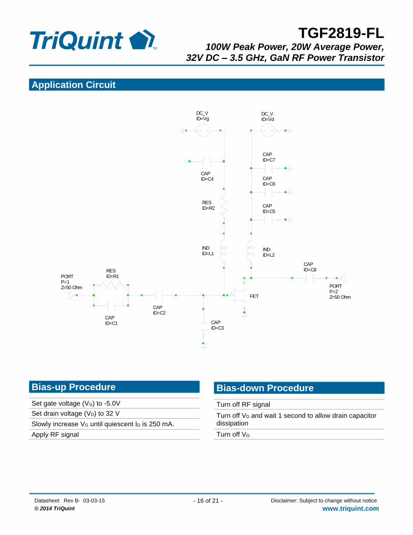
Application Circuit
1
2
3
FET
CAPID=C1
RESID=R1
CAPID=C2
CAPID=C3
INDID=L1
RESID=R2
CAPID=C4
INDID=L2
CAPID=C5
CAPID=C6
CAPID=C7
CAPID=C8
DC_VID=Vg
DC_VID=Vd
PORTP=1Z=50 Ohm PORT
P=2Z=50 Ohm
Bias-up Procedure Set gate voltage (VG) to -5.0V
Set drain voltage (VD) to 32 V
Slowly increase VG until quiescent ID is 250 mA.
Apply RF signal
Bias-down Procedure Turn off RF signal
Turn off VD and wait 1 second to allow drain capacitor dissipation
Turn off VG

TGF2819-FL 100W Peak Power, 20W Average Power,
32V DC – 3.5 GHz, GaN RF Power Transistor
Datasheet: Rev B- 03-03-15 - 17 of 21 - Disclaimer: Subject to change without notice
© 2014 TriQuint www.triquint.com
Evaluation Board Layout Top RF layer is 0.020” thick Rogers RO4350B, ɛr = 3.48. The pad pattern shown has been developed and tested for optimized assembly at TriQuint Semiconductor. The PCB land pattern has been developed to accommodate lead and package tolerances.
Bill of Materials Reference Design Value Qty Manufacturer Part Number
R1 100Ω 1 Vishay/Dale CRCW0603100RJNEA
C1, C2 5.6pF 2 ATC 600S5R6BT
C3 1.0pF 1 ATC 600S1R0BT
L1 22nH 1 Coilcraft 0805CS-220X-LB
R2 10Ω 1 Vishay/Dale CRCW060310R0JNEA
C4 10uF 1 Murata C1632X5R0J106M130AC
L2 12nH 1 Coilcraft A04T_L
C5 2400pF 1 Murata C08BL242X-5UN-X0T
C6 1000pF 1 ATC 800B102JT50XT
C7 220uF 1 United Chemi-Con EMVY500ADA221MJA0G
C8 15pF 1 ATC 600S150JT250XT
R1 C2
L2
C1 C3
L1R2
C4 C5
C6
C7
C8

TGF2819-FL 100W Peak Power, 20W Average Power,
32V DC – 3.5 GHz, GaN RF Power Transistor
Datasheet: Rev B- 03-03-15 - 18 of 21 - Disclaimer: Subject to change without notice
© 2014 TriQuint www.triquint.com
Pin Layout
Note: The TGF2819-FL will be marked with the “TGF2819-FL” designator and a lot code marked below the part designator. The “YY” represents the last two digits of the calendar year the part was manufactured, the “WW” is the work week of the assembly lot start, the “MXXX” is the production lot number, and the “ZZZ” is an auto-generated serial number.
Pin Description Pin Symbol Description
1 VD / RF OUT Drain voltage / RF Output
2 VG / RF IN Gate voltage / RF
3 Flange Source connected to ground
Re
fere
nce
Pla
ne
s

TGF2819-FL 100W Peak Power, 20W Average Power,
32V DC – 3.5 GHz, GaN RF Power Transistor
Datasheet: Rev B- 03-03-15 - 19 of 21 - Disclaimer: Subject to change without notice
© 2014 TriQuint www.triquint.com
Mechanical Information All dimensions are in inches.
Note:
Unless otherwise noted, all tolerances are +/-0.005 inches. This package is lead-free/RoHS-compliant. The plating material on the leads is NiAu. It is compatible with both lead-free and tin-lead soldering processes.

TGF2819-FL 100W Peak Power, 20W Average Power,
32V DC – 3.5 GHz, GaN RF Power Transistor
Datasheet: Rev B- 03-03-15 - 20 of 21 - Disclaimer: Subject to change without notice
© 2014 TriQuint www.triquint.com
Product Compliance Information ESD Sensitivity Ratings
Caution! ESD-Sensitive Device
ESD Rating: Class 1B Value: ≥ 500 V and < 1000V Test: Human Body Model (HBM) Standard: JEDEC Standard JESD22-A114
Solderability Compatible with the latest version of J-STD-020, Lead free solder, 260° C
RoHs Compliance This part is compliant with EU 2002/95/EC RoHS directive (Restrictions on the Use of Certain Hazardous Substances in Electrical and Electronic Equipment). This product also has the following attributes:
Lead Free
Halogen Free (Chlorine, Bromine)
Antimony Free
TBBP-A (C15H12Br402) Free
PFOS Free
SVHC Free
MSL Rating
The part is rated Moisture Sensitivity Level 3 at 260°C per JEDEC standard IPC/JEDEC J-STD-020.
ECCN
US Department of Commerce 3A001.b.3.a
Recommended Soldering Temperature Profile

TGF2819-FL 100W Peak Power, 20W Average Power,
32V DC – 3.5 GHz, GaN RF Power Transistor
Datasheet: Rev B- 03-03-15 - 21 of 21 - Disclaimer: Subject to change without notice
© 2014 TriQuint www.triquint.com
Contact Information For the latest specifications, additional product information, worldwide sales and distribution locations, and information about TriQuint: Web: www.triquint.com Tel: +1.972.994.8465 Email: [email protected] Fax: +1.972.994.8504 For technical questions and application information: Email: [email protected]
Important Notice The information contained herein is believed to be reliable. TriQuint makes no warranties regarding the information contained herein. TriQuint assumes no responsibility or liability whatsoever for any of the information contained herein. TriQuint assumes no responsibility or liability whatsoever for the use of the information contained herein. The information contained herein is provided "AS IS, WHERE IS" and with all faults, and the entire risk associated with such information is entirely with the user. All information contained herein is subject to change without notice. Customers should obtain and verify the latest relevant information before placing orders for TriQuint products. The information contained herein or any use of such information does not grant, explicitly or implicitly, to any party any patent rights, licenses, or any other intellectual property rights, whether with regard to such information itself or anything described by such information. TriQuint products are not warranted or authorized for use as critical components in medical, life-saving, or life-sustaining applications, or other applications where a failure would reasonably be expected to cause severe personal injury or death.