Embed Size (px)
Citation preview
Revision Date: Jun. 28, 2007
32 H8SX/1651GroupHardware Manual
Renesas 32-Bit CISC Microcomputer H8SX Family / H8SX/1600 Series
H8SX/1651C R5S61651C
Rev.2.00
REJ09B0248-0200
All information contained in this material, including products and product specifications at the time of publication of this material, is subject to change by Renesas Technology Corp. without notice. Please review the latest information published by Renesas Technology Corp. through various means, including the Renesas Technology Corp. website (http://www.renesas.com).
Downloaded from Elcodis.com electronic components distributor

Rev.2.00 Jun. 28, 2007 Page ii of xxiv
Downloaded from Elcodis.com electronic components distributor
Rev.2.00 Jun. 28, 2007 Page iii of xxiv
1. This document is provided for reference purposes only so that Renesas customers may select the appropriate Renesas products for their use. Renesas neither makes warranties or representations with respect to the accuracy or completeness of the information contained in this document nor grants any license to any intellectual property rights or any other rights of Renesas or any third party with respect to the information in this document. 2. Renesas shall have no liability for damages or infringement of any intellectual property or other rights arising out of the use of any information in this document, including, but not limited to, product data, diagrams, charts, programs, algorithms, and application circuit examples.3. You should not use the products or the technology described in this document for the purpose of military applications such as the development of weapons of mass destruction or for the purpose of any other military use. When exporting the products or technology described herein, you should follow the applicable export control laws and regulations, and procedures required by such laws and regulations.4. All information included in this document such as product data, diagrams, charts, programs, algorithms, and application circuit examples, is current as of the date this document is issued. Such information, however, is subject to change without any prior notice. Before purchasing or using any Renesas products listed in this document, please confirm the latest product information with a Renesas sales office. Also, please pay regular and careful attention to additional and different information to be disclosed by Renesas such as that disclosed through our website. (http://www.renesas.com )5. Renesas has used reasonable care in compiling the information included in this document, but Renesas assumes no liability whatsoever for any damages incurred as a result of errors or omissions in the information included in this document.6. When using or otherwise relying on the information in this document, you should evaluate the information in light of the total system before deciding about the applicability of such information to the intended application. Renesas makes no representations, warranties or guaranties regarding the suitability of its products for any particular application and specifically disclaims any liability arising out of the application and use of the information in this document or Renesas products. 7. With the exception of products specified by Renesas as suitable for automobile applications, Renesas products are not designed, manufactured or tested for applications or otherwise in systems the failure or malfunction of which may cause a direct threat to human life or create a risk of human injury or which require especially high quality and reliability such as safety systems, or equipment or systems for transportation and traffic, healthcare, combustion control, aerospace and aeronautics, nuclear power, or undersea communication transmission. If you are considering the use of our products for such purposes, please contact a Renesas sales office beforehand. Renesas shall have no liability for damages arising out of the uses set forth above.8. Notwithstanding the preceding paragraph, you should not use Renesas products for the purposes listed below: (1) artificial life support devices or systems (2) surgical implantations (3) healthcare intervention (e.g., excision, administration of medication, etc.) (4) any other purposes that pose a direct threat to human life Renesas shall have no liability for damages arising out of the uses set forth in the above and purchasers who elect to use Renesas products in any of the foregoing applications shall indemnify and hold harmless Renesas Technology Corp., its affiliated companies and their officers, directors, and employees against any and all damages arising out of such applications. 9. You should use the products described herein within the range specified by Renesas, especially with respect to the maximum rating, operating supply voltage range, movement power voltage range, heat radiation characteristics, installation and other product characteristics. Renesas shall have no liability for malfunctions or damages arising out of the use of Renesas products beyond such specified ranges.10. Although Renesas endeavors to improve the quality and reliability of its products, IC products have specific characteristics such as the occurrence of failure at a certain rate and malfunctions under certain use conditions. Please be sure to implement safety measures to guard against the possibility of physical injury, and injury or damage caused by fire in the event of the failure of a Renesas product, such as safety design for hardware and software including but not limited to redundancy, fire control and malfunction prevention, appropriate treatment for aging degradation or any other applicable measures. Among others, since the evaluation of microcomputer software alone is very difficult, please evaluate the safety of the final products or system manufactured by you. 11. In case Renesas products listed in this document are detached from the products to which the Renesas products are attached or affixed, the risk of accident such as swallowing by infants and small children is very high. You should implement safety measures so that Renesas products may not be easily detached from your products. Renesas shall have no liability for damages arising out of such detachment.12. This document may not be reproduced or duplicated, in any form, in whole or in part, without prior written approval from Renesas. 13. Please contact a Renesas sales office if you have any questions regarding the information contained in this document, Renesas semiconductor products, or if you have any other inquiries.
Notes regarding these materials
Downloaded from Elcodis.com electronic components distributor
Rev.2.00 Jun. 28, 2007 Page iv of xxiv
General Precautions in the Handling of MPU/MCU Products
The following usage notes are applicable to all MPU/MCU products from Renesas. For detailed usage notes on the products covered by this manual, refer to the relevant sections of the manual. If the descriptions under General Precautions in the Handling of MPU/MCU Products and in the body of the manual differ from each other, the description in the body of the manual takes precedence.
1. Handling of Unused Pins Handle unused pins in accord with the directions given under Handling of Unused Pins in the manual. The input pins of CMOS products are generally in the high-impedance state. In operation
with an unused pin in the open-circuit state, extra electromagnetic noise is induced in the vicinity of LSI, an associated shoot-through current flows internally, and malfunctions occur due to the false recognition of the pin state as an input signal become possible. Unused pins should be handled as described under Handling of Unused Pins in the manual.
2. Processing at Power-on The state of the product is undefined at the moment when power is supplied. The states of internal circuits in the LSI are indeterminate and the states of register
settings and pins are undefined at the moment when power is supplied. In a finished product where the reset signal is applied to the external reset pin, the states of pins are not guaranteed from the moment when power is supplied until the reset process is completed. In a similar way, the states of pins in a product that is reset by an on-chip power-on reset function are not guaranteed from the moment when power is supplied until the power reaches the level at which resetting has been specified.
3. Prohibition of Access to Reserved Addresses Access to reserved addresses is prohibited. The reserved addresses are provided for the possible future expansion of functions. Do
not access these addresses; the correct operation of LSI is not guaranteed if they are accessed.
4. Clock Signals After applying a reset, only release the reset line after the operating clock signal has become stable. When switching the clock signal during program execution, wait until the target clock signal has stabilized. When the clock signal is generated with an external resonator (or from an external
oscillator) during a reset, ensure that the reset line is only released after full stabilization of the clock signal. Moreover, when switching to a clock signal produced with an external resonator (or by an external oscillator) while program execution is in progress, wait until the target clock signal is stable.
5. Differences between Products Before changing from one product to another, i.e. to one with a different type number, confirm that the change will not lead to problems. The characteristics of MPU/MCU in the same group but having different type numbers may
differ because of the differences in internal memory capacity and layout pattern. When changing to products of different type numbers, implement a system-evaluation test for each of the products.
Downloaded from Elcodis.com electronic components distributor
Rev.2.00 Jun. 28, 2007 Page v of xxiv
How to Use This Manual
1. Objective and Target Users
This manual was written to explain the hardware functions and electrical characteristics of this LSI to the target users, i.e. those who will be using this LSI in the design of application systems. Target users are expected to understand the fundamentals of electrical circuits, logic circuits, and microcomputers.
This manual is organized in the following items: an overview of the product, descriptions of the CPU, system control functions, and peripheral functions, electrical characteristics of the device, and usage notes.
When designing an application system that includes this LSI, take all points to note into account. Points to note are given in their contexts and at the final part of each section, and in the section giving usage notes.
The list of revisions is a summary of major points of revision or addition for earlier versions. It does not cover all revised items. For details on the revised points, see the actual locations in the manual.
The following documents have been prepared for the H8SX/1651 Group. Before using any of the documents, please visit our web site to verify that you have the most up-to-date available version of the document.
Document Type Contents Document Title Document No.
Data Sheet Overview of hardware and electrical characteristics
Hardware Manual Hardware specifications (pin assignments, memory maps, peripheral specifications, electrical characteristics, and timing charts) and descriptions of operation
H8SX/1651 Group Hardware Manual
This manual
Software Manual Detailed descriptions of the CPU and instruction set
H8SX Software Manual REJ09B0102
Application Note Examples of applications and sample programs
Renesas Technical Update
Preliminary report on the specifications of a product, document, etc.
The latest versions are available from our web site.
Downloaded from Elcodis.com electronic components distributor

Rev.2.00 Jun. 28, 2007 Page vi of xxiv
2. Description of Numbers and Symbols
Aspects of the notations for register names, bit names, numbers, and symbolic names in this manual are explained below.
CMCSR indicates compare match generation, enables or disables interrupts, and selects the counter input clock. Generation of a WDTOVF signal or interrupt initializes the TCNT value to 0.
14.3 Operation
The style "register name"_"instance number" is used in cases where there is more than one instance of the same function or similar functions.[Example] CMCSR_0: Indicates the CMCSR register for the compare-match timer of channel 0.
In descriptions involving the names of bits and bit fields within this manual, the modules and registers to which the bits belong may be clarified by giving the names in the forms "module name"."register name"."bit name" or "register name"."bit name".
(1) Overall notation
(2) Register notation
Rev. 0.50, 10/04, page 416 of 914
14.2.2 Compare Match Control/Status Register_0, _1 (CMCSR_0, CMCSR_1)
14.3.1 Interval Count Operation
(4)
(3)
(2)
Binary numbers are given as B'nnnn (B' may be omitted if the number is obviously binary), hexadecimal numbers are given as H'nnnn or 0xnnnn, and decimal numbers are given as nnnn.[Examples] Binary: B'11 or 11 Hexadecimal: H'EFA0 or 0xEFA0 Decimal: 1234
(3) Number notation
An overbar on the name indicates that a signal or pin is active-low.[Example] WDTOVF
Note: The bit names and sentences in the above figure are examples and have nothing to dowith the contents of this manual.
(4) Notation for active-low
When an internal clock is selected with the CKS1 and CKS0 bits in CMCSR and the STR bit in CMSTR is set to 1, CMCNT starts incrementing using the selected clock. When the values in CMCNT and the compare match constant register (CMCOR) match, CMCNT is cleared to H'0000 and the CMF flag in CMCSR is set to 1. When the CKS1 and CKS0 bits are set to B'01 at this time, a f/4 clock is selected.
Downloaded from Elcodis.com electronic components distributor
Rev.2.00 Jun. 28, 2007 Page vii of xxiv
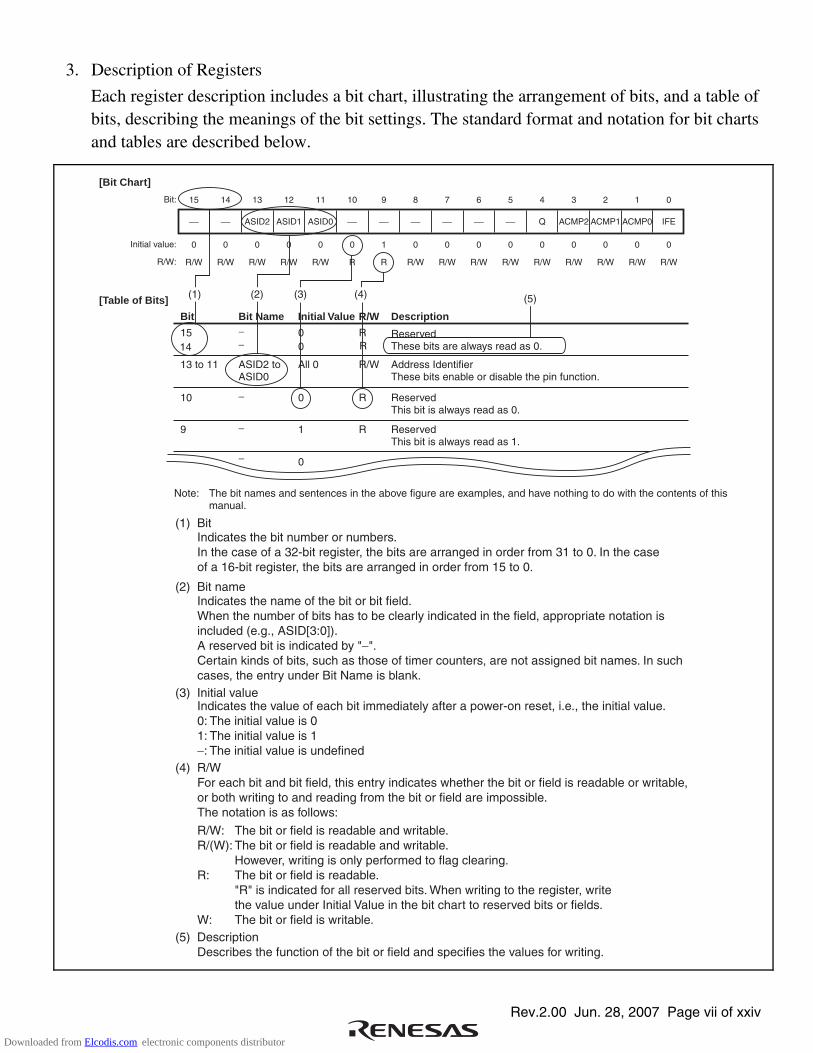
3. Description of Registers
Each register description includes a bit chart, illustrating the arrangement of bits, and a table of bits, describing the meanings of the bit settings. The standard format and notation for bit charts and tables are described below.
Indicates the bit number or numbers.In the case of a 32-bit register, the bits are arranged in order from 31 to 0. In the caseof a 16-bit register, the bits are arranged in order from 15 to 0.
Indicates the name of the bit or bit field.When the number of bits has to be clearly indicated in the field, appropriate notation is included (e.g., ASID[3:0]).A reserved bit is indicated by "−".Certain kinds of bits, such as those of timer counters, are not assigned bit names. In such cases, the entry under Bit Name is blank.
(1) Bit
(2) Bit name
Indicates the value of each bit immediately after a power-on reset, i.e., the initial value.0: The initial value is 01: The initial value is 1−: The initial value is undefined
(3) Initial value
For each bit and bit field, this entry indicates whether the bit or field is readable or writable, or both writing to and reading from the bit or field are impossible.The notation is as follows:
R/W:R/(W):
R:
W:
The bit or field is readable and writable.The bit or field is readable and writable.However, writing is only performed to flag clearing.The bit or field is readable."R" is indicated for all reserved bits. When writing to the register, write the value under Initial Value in the bit chart to reserved bits or fields.The bit or field is writable.
Note: The bit names and sentences in the above figure are examples, and have nothing to do with the contents of thismanual.
(4) R/W
Describes the function of the bit or field and specifies the values for writing.(5) Description
Bit
15
13 to 11
10
9
0
All 0
0
0
1
R
R/W
R
R
Address IdentifierThese bits enable or disable the pin function.
ReservedThis bit is always read as 0.
ReservedThis bit is always read as 1.
−
ASID2 to ASID0
−
−
−
Bit Name Initial Value R/W Description
[Bit Chart]
[Table of Bits]
14
15 14 13 12 11 10 9 8 7 6 5 4 3 2 1 0Bit:
Initial value:
R/W:
0 0 0 0 0 0 1 0 0 0 0 0 0 0 0 0
R/W R/W R/W R/W R/W R R R/W R/W R/W R/W R/W R/W R/W R/W R/W
ASID2 ACMP2Q IFE ASID1 ASID0 ACMP1 ACMP0
− 0 R
(1) (2) (3) (4) (5)
ReservedThese bits are always read as 0.
Downloaded from Elcodis.com electronic components distributor
Rev.2.00 Jun. 28, 2007 Page viii of xxiv
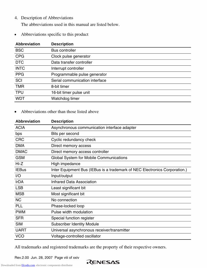
4. Description of Abbreviations
The abbreviations used in this manual are listed below. • Abbreviations specific to this product Abbreviation Description
BSC Bus controller
CPG Clock pulse generator
DTC Data transfer controller
INTC Interrupt controller
PPG Programmable pulse generator
SCI Serial communication interface
TMR 8-bit timer
TPU 16-bit timer pulse unit
WDT Watchdog timer
• Abbreviations other than those listed above Abbreviation Description
ACIA Asynchronous communication interface adapter
bps Bits per second
CRC Cyclic redundancy check
DMA Direct memory access
DMAC Direct memory access controller
GSM Global System for Mobile Communications
Hi-Z High impedance
IEBus Inter Equipment Bus (IEBus is a trademark of NEC Electronics Corporation.)
I/O Input/output
IrDA Infrared Data Association
LSB Least significant bit
MSB Most significant bit
NC No connection
PLL Phase-locked loop
PWM Pulse width modulation
SFR Special function register
SIM Subscriber Identity Module
UART Universal asynchronous receiver/transmitter
VCO Voltage-controlled oscillator All trademarks and registered trademarks are the property of their respective owners.
Downloaded from Elcodis.com electronic components distributor
Rev.2.00 Jun. 28, 2007 Page ix of xxiv
Contents
Section 1 Overview................................................................................................1 1.1 Features................................................................................................................................. 1
1.1.1 Applications .......................................................................................................... 1 1.1.2 Overview of Functions.......................................................................................... 2
1.2 List of Products..................................................................................................................... 7 1.3 Block Diagram...................................................................................................................... 8 1.4 Pin Assignments ................................................................................................................... 9 1.5 Pin Functions ...................................................................................................................... 10
Section 2 CPU......................................................................................................15 2.1 Features............................................................................................................................... 15 2.2 CPU Operating Modes........................................................................................................ 17
2.2.1 Normal Mode...................................................................................................... 17 2.2.2 Middle Mode....................................................................................................... 19 2.2.3 Advanced Mode.................................................................................................. 20 2.2.4 Maximum Mode ................................................................................................. 21
2.3 Instruction Fetch ................................................................................................................. 23 2.4 Address Space..................................................................................................................... 23 2.5 Registers ............................................................................................................................. 24
2.5.1 General Registers ................................................................................................ 25 2.5.2 Program Counter (PC) ........................................................................................ 26 2.5.3 Condition-Code Register (CCR)......................................................................... 26 2.5.4 Extended Control Register (EXR) ...................................................................... 28 2.5.5 Vector Base Register (VBR)............................................................................... 28 2.5.6 Short Address Base Register (SBR).................................................................... 28 2.5.7 Multiply-Accumulate Register (MAC)............................................................... 29 2.5.8 Initial Register Values......................................................................................... 29
2.6 Data Formats....................................................................................................................... 30 2.6.1 General Register Data Formats ........................................................................... 30 2.6.2 Memory Data Formats ........................................................................................ 31
2.7 Instruction Set ..................................................................................................................... 32 2.7.1 Instructions and Addressing Modes.................................................................... 34 2.7.2 Table of Instructions Classified by Function ...................................................... 39 2.7.3 Basic Instruction Formats ................................................................................... 50
2.8 Addressing Modes and Effective Address Calculation....................................................... 51 2.8.1 Register Direct—Rn ........................................................................................... 52
Downloaded from Elcodis.com electronic components distributor

Rev.2.00 Jun. 28, 2007 Page x of xxiv
2.8.2 Register Indirect—@ERn................................................................................... 52 2.8.3 Register Indirect with Displacement—@(d:2, ERn), @(d:16, ERn), or @(d:32, ERn)...................................................................................................... 52 2.8.4 Index Register Indirect with Displacement—@(d:16,RnL.B), @(d:32,RnL.B), @(d:16,Rn.W), @(d:32,Rn.W), @(d:16,ERn.L), or @(d:32,ERn.L)................. 52 2.8.5 Register Indirect with Post-Increment, Pre-Decrement, Pre-Increment, or Post-Decrement—@ERn+, @−ERn, @+ERn, or @ERn− ............................ 53 2.8.6 Absolute Address—@aa:8, @aa:16, @aa:24, or @aa:32................................... 54 2.8.7 Immediate—#xx ................................................................................................. 55 2.8.8 Program-Counter Relative—@(d:8, PC) or @(d:16, PC) .................................. 56 2.8.9 Program-Counter Relative with Index Register—@(RnL.B, PC), @(Rn.W, PC), or @(ERn.L, PC)........................................................................ 56 2.8.10 Memory Indirect—@@aa:8 ............................................................................... 56 2.8.11 Extended Memory Indirect—@@vec:7 ............................................................. 57 2.8.12 Effective Address Calculation ............................................................................ 57 2.8.13 MOVA Instruction.............................................................................................. 59
2.9 Processing States ................................................................................................................ 60
Section 3 MCU Operating Modes .......................................................................63 3.1 Operating Mode Selection .................................................................................................. 63 3.2 Register Descriptions.......................................................................................................... 64
3.2.1 Mode Control Register (MDCR) ........................................................................ 64 3.2.2 System Control Register (SYSCR)..................................................................... 66
3.3 Operating Mode Descriptions ............................................................................................. 68 3.3.1 Mode 4................................................................................................................ 68 3.3.2 Mode 5................................................................................................................ 68 3.3.3 Pin Functions ...................................................................................................... 69
3.4 Address Map....................................................................................................................... 70 3.4.1 Address Map (Advanced Mode)......................................................................... 70
Section 4 Exception Handling .............................................................................71 4.1 Exception Handling Types and Priority.............................................................................. 71 4.2 Exception Sources and Exception Handling Vector Table ................................................. 72 4.3 Reset ................................................................................................................................... 74
4.3.1 Reset Exception Handling .................................................................................. 74 4.3.2 Interrupts after Reset........................................................................................... 75 4.3.3 On-Chip Peripheral Functions after Reset Release............................................. 75
4.4 Traces.................................................................................................................................. 77 4.5 Address Error...................................................................................................................... 78
4.5.1 Address Error Source.......................................................................................... 78
Downloaded from Elcodis.com electronic components distributor
Rev.2.00 Jun. 28, 2007 Page xi of xxiv
4.5.2 Address Error Exception Handling ..................................................................... 79 4.6 Interrupts............................................................................................................................. 80
4.6.1 Interrupt Sources................................................................................................. 80 4.6.2 Interrupt Exception Handling ............................................................................. 80
4.7 Instruction Exception Handling .......................................................................................... 81 4.7.1 Trap Instruction................................................................................................... 81 4.7.2 Exception Handling by Illegal Instruction .......................................................... 82
4.8 Stack Status after Exception Handling................................................................................ 83 4.9 Usage Note.......................................................................................................................... 84
Section 5 Interrupt Controller ..............................................................................85 5.1 Features............................................................................................................................... 85 5.2 Input/Output Pins................................................................................................................ 87 5.3 Register Descriptions.......................................................................................................... 87
5.3.1 Interrupt Control Register (INTCR) ................................................................... 88 5.3.2 CPU Priority Control Register (CPUPCR) ......................................................... 89 5.3.3 Interrupt Priority Registers A to C, E to I, K, and L (IPRA to IPRC, IPRE to IPRI, IPRK, and IPRL) ............................................... 91 5.3.4 IRQ Enable Register (IER) ................................................................................. 93 5.3.5 IRQ Sense Control Registers H and L (ISCRH, ISCRL).................................... 95 5.3.6 IRQ Status Register (ISR)................................................................................... 99 5.3.7 Software Standby Release IRQ Enable Register (SSIER) ................................ 100
5.4 Interrupt Sources............................................................................................................... 101 5.4.1 External Interrupts ............................................................................................ 101 5.4.2 Internal Interrupts ............................................................................................. 102 5.4.3 Sleep Interrupt................................................................................................... 102
5.5 Interrupt Exception Handling Vector Table...................................................................... 103 5.6 Interrupt Control Modes and Interrupt Operation ............................................................. 108
5.6.1 Interrupt Control Mode 0 .................................................................................. 108 5.6.2 Interrupt Control Mode 2 .................................................................................. 110 5.6.3 Interrupt Exception Handling Sequence ........................................................... 112 5.6.4 Interrupt Response Times ................................................................................. 113 5.6.5 DTC and DMAC Activation by Interrupt ......................................................... 114
5.7 CPU Priority Control Function Over DTC and DMAC.................................................... 117 5.8 Usage Notes ...................................................................................................................... 120
5.8.1 Conflict between Interrupt Generation and Disabling ...................................... 120 5.8.2 Instructions that Disable Interrupts ................................................................... 121 5.8.3 Times when Interrupts are Disabled ................................................................. 121 5.8.4 Interrupts during Execution of EEPMOV Instruction....................................... 121 5.8.5 Interrupts during Execution of MOVMD and MOVSD Instructions................ 121
Downloaded from Elcodis.com electronic components distributor

Rev.2.00 Jun. 28, 2007 Page xii of xxiv
5.8.6 Interrupt Source Flag of Peripheral Module ..................................................... 122
Section 6 Bus Controller (BSC) ........................................................................123 6.1 Features............................................................................................................................. 123 6.2 Register Descriptions........................................................................................................ 126
6.2.1 Bus Width Control Register (ABWCR)............................................................ 127 6.2.2 Access State Control Register (ASTCR) .......................................................... 128 6.2.3 Wait Control Registers A and B (WTCRA, WTCRB) ..................................... 129 6.2.4 Read Strobe Timing Control Register (RDNCR) ............................................. 134 6.2.5 CS Assertion Period Control Registers (CSACR) ............................................ 135 6.2.6 Idle Control Register (IDLCR) ......................................................................... 138 6.2.7 Bus Control Register 1 (BCR1) ........................................................................ 140 6.2.8 Bus Control Register 2 (BCR2) ........................................................................ 142 6.2.9 Endian Control Register (ENDIANCR) ........................................................... 143 6.2.10 SRAM Mode Control Register (SRAMCR) ..................................................... 144 6.2.11 Burst ROM Interface Control Register (BROMCR) ........................................ 145 6.2.12 Address/Data Multiplexed I/O Control Register (MPXCR) ............................. 147
6.3 Bus Configuration............................................................................................................. 148 6.4 Multi-Clock Function and Number of Access Cycles ...................................................... 149 6.5 External Bus ..................................................................................................................... 153
6.5.1 Input/Output Pins.............................................................................................. 153 6.5.2 Area Division.................................................................................................... 156 6.5.3 Chip Select Signals ........................................................................................... 157 6.5.4 External Bus Interface ...................................................................................... 158 6.5.5 Area and External Bus Interface ....................................................................... 162 6.5.6 Endian and Data Alignment.............................................................................. 167
6.6 Basic Bus Interface ........................................................................................................... 170 6.6.1 Data Bus ........................................................................................................... 170 6.6.2 I/O Pins Used for Basic Bus Interface .............................................................. 170 6.6.3 Basic Timing..................................................................................................... 171 6.6.4 Wait Control ..................................................................................................... 178 6.6.5 Read Strobe (RD) Timing................................................................................. 180 6.6.6 Extension of Chip Select (CS) Assertion Period............................................... 182 6.6.7 DACK Signal Output Timing ........................................................................... 184
6.7 Byte Control SRAM Interface .......................................................................................... 185 6.7.1 Byte Control SRAM Space Setting................................................................... 185 6.7.2 Data Bus ........................................................................................................... 185 6.7.3 I/O Pins Used for Byte Control SRAM Interface ............................................. 186 6.7.4 Basic Timing..................................................................................................... 187 6.7.5 Wait Control ..................................................................................................... 189
Downloaded from Elcodis.com electronic components distributor
Rev.2.00 Jun. 28, 2007 Page xiii of xxiv
6.7.6 Read Strobe (RD).............................................................................................. 191 6.7.7 Extension of Chip Select (CS) Assertion Period............................................... 191 6.7.8 DACK Signal Output Timing ........................................................................... 191
6.8 Burst ROM Interface ........................................................................................................ 193 6.8.1 Burst ROM Space Setting................................................................................. 193 6.8.2 Data Bus............................................................................................................ 193 6.8.3 I/O Pins Used for Burst ROM Interface............................................................ 194 6.8.4 Basic Timing..................................................................................................... 194 6.8.5 Wait Control ..................................................................................................... 197 6.8.6 Read Strobe (RD) Timing................................................................................. 197 6.8.7 Extension of Chip Select (CS) Assertion Period............................................... 197
6.9 Address/Data Multiplexed I/O Interface........................................................................... 198 6.9.1 Address/Data Multiplexed I/O Space Setting ................................................... 198 6.9.2 Address/Data Multiplex .................................................................................... 198 6.9.3 Data Bus............................................................................................................ 198 6.9.4 I/O Pins Used for Address/Data Multiplexed I/O Interface .............................. 199 6.9.5 Basic Timing..................................................................................................... 200 6.9.6 Address Cycle Control...................................................................................... 201 6.9.7 Wait Control ..................................................................................................... 202 6.9.8 Read Strobe (RD) Timing................................................................................. 203 6.9.9 Extension of Chip Select (CS) Assertion Period............................................... 204 6.9.10 DACK Signal Output Timing ........................................................................... 206
6.10 Idle Cycle.......................................................................................................................... 207 6.10.1 Operation .......................................................................................................... 207 6.10.2 Pin States in Idle Cycle ..................................................................................... 216
6.11 Bus Release....................................................................................................................... 217 6.11.1 Operation .......................................................................................................... 217 6.11.2 Pin States in External Bus Released State......................................................... 218 6.11.3 Transition Timing ............................................................................................. 219
6.12 Internal Bus....................................................................................................................... 220 6.12.1 Access to Internal Address Space ..................................................................... 220
6.13 Write Data Buffer Function .............................................................................................. 221 6.13.1 Write Data Buffer Function for External Data Bus........................................... 221 6.13.2 Write Data Buffer Function for Peripheral Modules ........................................ 222
6.14 Bus Arbitration ................................................................................................................. 223 6.14.1 Operation .......................................................................................................... 223 6.14.2 Bus Transfer Timing......................................................................................... 224
6.15 Bus Controller Operation in Reset .................................................................................... 226 6.16 Usage Notes ...................................................................................................................... 226
Downloaded from Elcodis.com electronic components distributor
Rev.2.00 Jun. 28, 2007 Page xiv of xxiv
Section 7 DMA Controller (DMAC).................................................................229 7.1 Features............................................................................................................................. 229 7.2 Input/Output Pins.............................................................................................................. 232 7.3 Register Descriptions........................................................................................................ 233
7.3.1 DMA Source Address Register (DSAR) .......................................................... 235 7.3.2 DMA Destination Address Register (DDAR) .................................................. 236 7.3.3 DMA Offset Register (DOFR).......................................................................... 237 7.3.4 DMA Transfer Count Register (DTCR) ........................................................... 238 7.3.5 DMA Block Size Register (DBSR) .................................................................. 239 7.3.6 DMA Mode Control Register (DMDR)............................................................ 240 7.3.7 DMA Address Control Register (DACR)......................................................... 249 7.3.8 DMA Module Request Select Register (DMRSR) ........................................... 256
7.4 Transfer Modes................................................................................................................. 256 7.5 Operations......................................................................................................................... 257
7.5.1 Address Modes ................................................................................................. 257 7.5.2 Transfer Modes................................................................................................. 260 7.5.3 Activation Sources............................................................................................ 265 7.5.4 Bus Access Modes............................................................................................ 267 7.5.5 Extended Repeat Area Function ....................................................................... 268 7.5.6 Address Update Function using Offset ............................................................. 270 7.5.7 Register during DMA Transfer......................................................................... 276 7.5.8 Priority of Channels .......................................................................................... 281 7.5.9 DMA Basic Bus Cycle...................................................................................... 283 7.5.10 Bus Cycles in Dual Address Mode ................................................................... 284 7.5.11 Bus Cycles in Single Address Mode................................................................. 293
7.6 DMA Transfer End ........................................................................................................... 298 7.7 Relationship among DMAC and Other Bus Masters ........................................................ 300
7.7.1 CPU Priority Control Function Over DMAC ................................................... 300 7.7.2 Bus Arbitration among DMAC and Other Bus Masters ................................... 301
7.8 Interrupt Sources............................................................................................................... 302 7.9 Notes on Usage ................................................................................................................. 305
Section 8 Data Transfer Controller (DTC)........................................................307 8.1 Features............................................................................................................................. 307 8.2 Register Descriptions........................................................................................................ 309
8.2.1 DTC Mode Register A (MRA) ......................................................................... 310 8.2.2 DTC Mode Register B (MRB).......................................................................... 311 8.2.3 DTC Source Address Register (SAR)............................................................... 313 8.2.4 DTC Destination Address Register (DAR)....................................................... 313 8.2.5 DTC Transfer Count Register A (CRA) ........................................................... 314
Downloaded from Elcodis.com electronic components distributor
Rev.2.00 Jun. 28, 2007 Page xv of xxiv
8.2.6 DTC Transfer Count Register B (CRB)............................................................ 314 8.2.7 DTC Enable Registers A to H (DTCERA to DTCERH) .................................. 315 8.2.8 DTC Control Register (DTCCR) ...................................................................... 316 8.2.9 DTC Vector Base Register (DTCVBR)............................................................ 317
8.3 Activation Sources............................................................................................................ 318 8.4 Location of Transfer Information and DTC Vector Table ................................................ 318 8.5 Operation .......................................................................................................................... 322
8.5.1 Bus Cycle Division ........................................................................................... 324 8.5.2 Transfer Information Read Skip Function ........................................................ 326 8.5.3 Transfer Information Writeback Skip Function ................................................ 327 8.5.4 Normal Transfer Mode ..................................................................................... 327 8.5.5 Repeat Transfer Mode....................................................................................... 328 8.5.6 Block Transfer Mode ........................................................................................ 330 8.5.7 Chain Transfer .................................................................................................. 331 8.5.8 Operation Timing.............................................................................................. 332 8.5.9 Number of DTC Execution Cycles ................................................................... 334 8.5.10 DTC Bus Release Timing ................................................................................. 335 8.5.11 DTC Priority Level Control to the CPU ........................................................... 335
8.6 DTC Activation by Interrupt............................................................................................. 336 8.7 Examples of Use of the DTC............................................................................................ 337
8.7.1 Normal Transfer Mode ..................................................................................... 337 8.7.2 Chain Transfer .................................................................................................. 338 8.7.3 Chain Transfer when Counter = 0..................................................................... 339
8.8 Interrupt Sources............................................................................................................... 340 8.9 Usage Notes ...................................................................................................................... 341
8.9.1 Module Stop Mode Setting ............................................................................... 341 8.9.2 On-Chip RAM .................................................................................................. 341 8.9.3 DMAC Transfer End Interrupt.......................................................................... 341 8.9.4 DTCE Bit Setting.............................................................................................. 341 8.9.5 Chain Transfer .................................................................................................. 341 8.9.6 Transfer Information Start Address, Source Address, and Destination Address ........................................................ 342 8.9.7 Transfer Information Modification ................................................................... 342 8.9.8 Endian ............................................................................................................... 342
Section 9 I/O Ports .............................................................................................343 9.1 Register Descriptions........................................................................................................ 350
9.1.1 Data Direction Register (PnDDR) (n = 1 to 3, 6, A, B, D to F, H, and I) ......... 351 9.1.2 Data Register (PnDR) (n = 1 to 3, 6, A, B, D to F, H, and I)............................ 351 9.1.3 Port Register (PORTn) (n = 1 to 3, 5, 6, A, B, D to F, H, and I) ...................... 352
Downloaded from Elcodis.com electronic components distributor
Rev.2.00 Jun. 28, 2007 Page xvi of xxiv
9.1.4 Input Buffer Control Register (PnICR) (n = 1 to 3, 5, 6, A, B, D to F, H, and I)............................................................ 352 9.1.5 Pull-Up MOS Control Register (PnPCR) (n = D to F, H, and I) ...................... 353 9.1.6 Open-Drain Control Register (PnODR) (n = 2 and F)...................................... 354
9.2 Output Buffer Control....................................................................................................... 355 9.2.1 Port 1................................................................................................................. 355 9.2.2 Port 2................................................................................................................. 358 9.2.3 Port 3................................................................................................................. 362 9.2.4 Port 5................................................................................................................. 366 9.2.5 Port 6................................................................................................................. 367 9.2.6 Port A................................................................................................................ 370 9.2.7 Port B................................................................................................................ 373 9.2.8 Port D................................................................................................................ 375 9.2.9 Port E ................................................................................................................ 376 9.2.10 Port F ................................................................................................................ 376 9.2.11 Port H................................................................................................................ 379 9.2.12 Port I ................................................................................................................. 379
9.3 Port Function Controller ................................................................................................... 386 9.3.1 Port Function Control Register 0 (PFCR0)....................................................... 386 9.3.2 Port Function Control Register 1 (PFCR1)....................................................... 387 9.3.3 Port Function Control Register 2 (PFCR2)....................................................... 388 9.3.4 Port Function Control Register 4 (PFCR4)....................................................... 390 9.3.5 Port Function Control Register 6 (PFCR6)....................................................... 391 9.3.6 Port Function Control Register 7 (PFCR7)....................................................... 392 9.3.7 Port Function Control Register 9 (PFCR9)....................................................... 393 9.3.8 Port Function Control Register B (PFCRB) ..................................................... 395 9.3.9 Port Function Control Register C (PFCRC) ..................................................... 396
9.4 Usage Notes ...................................................................................................................... 398 9.4.1 Notes on Input Buffer Control Register (ICR) Setting ..................................... 398 9.4.2 Notes on Port Function Control Register (PFCR) Settings............................... 398
Section 10 16-Bit Timer Pulse Unit (TPU) .......................................................399 10.1 Features............................................................................................................................. 399 10.2 Input/Output Pins.............................................................................................................. 403 10.3 Register Descriptions........................................................................................................ 404
10.3.1 Timer Control Register (TCR).......................................................................... 407 10.3.2 Timer Mode Register (TMDR)......................................................................... 412 10.3.3 Timer I/O Control Register (TIOR).................................................................. 413 10.3.4 Timer Interrupt Enable Register (TIER)........................................................... 431 10.3.5 Timer Status Register (TSR)............................................................................. 433
Downloaded from Elcodis.com electronic components distributor
Rev.2.00 Jun. 28, 2007 Page xvii of xxiv
10.3.6 Timer Counter (TCNT)..................................................................................... 437 10.3.7 Timer General Register (TGR) ......................................................................... 437 10.3.8 Timer Start Register (TSTR) ............................................................................ 438 10.3.9 Timer Synchronous Register (TSYR)............................................................... 439
10.4 Operation .......................................................................................................................... 440 10.4.1 Basic Functions................................................................................................. 440 10.4.2 Synchronous Operation..................................................................................... 446 10.4.3 Buffer Operation ............................................................................................... 448 10.4.4 Cascaded Operation .......................................................................................... 452 10.4.5 PWM Modes ..................................................................................................... 454 10.4.6 Phase Counting Mode....................................................................................... 460
10.5 Interrupt Sources............................................................................................................... 466 10.6 DTC Activation................................................................................................................. 468 10.7 DMAC Activation............................................................................................................. 468 10.8 A/D Converter Activation................................................................................................. 469 10.9 Operation Timing.............................................................................................................. 469
10.9.1 Input/Output Timing ......................................................................................... 469 10.9.2 Interrupt Signal Timing..................................................................................... 473
10.10 Usage Notes ...................................................................................................................... 477 10.10.1 Module Stop Mode Setting ............................................................................... 477 10.10.2 Input Clock Restrictions ................................................................................... 477 10.10.3 Caution on Cycle Setting .................................................................................. 478 10.10.4 Conflict between TCNT Write and Clear Operations....................................... 478 10.10.5 Conflict between TCNT Write and Increment Operations ............................... 479 10.10.6 Conflict between TGR Write and Compare Match........................................... 479 10.10.7 Conflict between Buffer Register Write and Compare Match .......................... 480 10.10.8 Conflict between TGR Read and Input Capture ............................................... 481 10.10.9 Conflict between TGR Write and Input Capture .............................................. 481 10.10.10 Conflict between Buffer Register Write and Input Capture.............................. 482 10.10.11 Conflict between Overflow/Underflow and Counter Clearing ......................... 483 10.10.12 Conflict between TCNT Write and Overflow/Underflow ................................ 483 10.10.13 Multiplexing of I/O Pins ................................................................................... 484 10.10.14 Interrupts and Module Stop Mode .................................................................... 484
Section 11 Programmable Pulse Generator (PPG) ............................................485 11.1 Features............................................................................................................................. 485 11.2 Input/Output Pins.............................................................................................................. 487 11.3 Register Descriptions........................................................................................................ 488
11.3.1 Next Data Enable Registers H, L (NDERH, NDERL) ..................................... 488 11.3.2 Output Data Registers H, L (PODRH, PODRL)............................................... 490
Downloaded from Elcodis.com electronic components distributor

Rev.2.00 Jun. 28, 2007 Page xviii of xxiv
11.3.3 Next Data Registers H, L (NDRH, NDRL) ...................................................... 491 11.3.4 PPG Output Control Register (PCR) ................................................................ 494 11.3.5 PPG Output Mode Register (PMR) .................................................................. 495
11.4 Operation .......................................................................................................................... 497 11.4.1 Output Timing .................................................................................................. 498 11.4.2 Sample Setup Procedure for Normal Pulse Output........................................... 499 11.4.3 Example of Normal Pulse Output (Example of 5-Phase Pulse Output)............ 500 11.4.4 Non-Overlapping Pulse Output......................................................................... 501 11.4.5 Sample Setup Procedure for Non-Overlapping Pulse Output ........................... 503 11.4.6 Example of Non-Overlapping Pulse Output (Example of 4-Phase Complementary Non-Overlapping Pulse Output) .......... 504 11.4.7 Inverted Pulse Output ....................................................................................... 506 11.4.8 Pulse Output Triggered by Input Capture ......................................................... 507
11.5 Usage Notes ...................................................................................................................... 508 11.5.1 Module Stop Mode Setting ............................................................................... 508 11.5.2 Operation of Pulse Output Pins......................................................................... 508
Section 12 8-Bit Timers (TMR) ........................................................................509 12.1 Features............................................................................................................................. 509 12.2 Input/Output Pins.............................................................................................................. 512 12.3 Register Descriptions........................................................................................................ 513
12.3.1 Timer Counter (TCNT)..................................................................................... 514 12.3.2 Time Constant Register A (TCORA)................................................................ 514 12.3.3 Time Constant Register B (TCORB)................................................................ 515 12.3.4 Timer Control Register (TCR).......................................................................... 515 12.3.5 Timer Counter Control Register (TCCR) ......................................................... 517 12.3.6 Timer Control/Status Register (TCSR)............................................................. 519
12.4 Operation .......................................................................................................................... 524 12.4.1 Pulse Output...................................................................................................... 524 12.4.2 Reset Input ........................................................................................................ 525
12.5 Operation Timing.............................................................................................................. 526 12.5.1 TCNT Count Timing ........................................................................................ 526 12.5.2 Timing of CMFA and CMFB Setting at Compare Match ................................ 526 12.5.3 Timing of Timer Output at Compare Match..................................................... 527 12.5.4 Timing of Counter Clear by Compare Match ................................................... 527 12.5.5 Timing of TCNT External Reset....................................................................... 528 12.5.6 Timing of Overflow Flag (OVF) Setting .......................................................... 528
12.6 Operation with Cascaded Connection............................................................................... 529 12.6.1 16-Bit Counter Mode........................................................................................ 529 12.6.2 Compare Match Count Mode............................................................................ 529
Downloaded from Elcodis.com electronic components distributor
Rev.2.00 Jun. 28, 2007 Page xix of xxiv
12.7 Interrupt Sources............................................................................................................... 530 12.7.1 Interrupt Sources and DTC Activation ............................................................. 530 12.7.2 A/D Converter Activation................................................................................. 530
12.8 Usage Notes ...................................................................................................................... 531 12.8.1 Notes on Setting Cycle...................................................................................... 531 12.8.2 Conflict between TCNT Write and Clear ......................................................... 531 12.8.3 Conflict between TCNT Write and Increment.................................................. 531 12.8.4 Conflict between TCOR Write and Compare Match ........................................ 532 12.8.5 Conflict between Compare Matches A and B................................................... 533 12.8.6 Switching of Internal Clocks and TCNT Operation.......................................... 533 12.8.7 Mode Setting with Cascaded Connection ......................................................... 535 12.8.8 Module Stop Mode Setting ............................................................................... 535 12.8.9 Interrupts in Module Stop Mode....................................................................... 535
Section 13 Watchdog Timer (WDT)..................................................................537 13.1 Features............................................................................................................................. 537 13.2 Input/Output Pin ............................................................................................................... 538 13.3 Register Descriptions........................................................................................................ 538
13.3.1 Timer Counter (TCNT)..................................................................................... 538 13.3.2 Timer Control/Status Register (TCSR)............................................................. 539 13.3.3 Reset Control/Status Register (RSTCSR)......................................................... 540
13.4 Operation .......................................................................................................................... 542 13.4.1 Watchdog Timer Mode ..................................................................................... 542 13.4.2 Interval Timer Mode......................................................................................... 543
13.5 Interrupt Source ................................................................................................................ 544 13.6 Usage Notes ...................................................................................................................... 544
13.6.1 Notes on Register Access.................................................................................. 544 13.6.2 Conflict between Timer Counter (TCNT) Write and Increment....................... 545 13.6.3 Changing Values of Bits CKS2 to CKS0.......................................................... 546 13.6.4 Switching between Watchdog Timer Mode and Interval Timer Mode............. 546 13.6.5 Internal Reset in Watchdog Timer Mode.......................................................... 546 13.6.6 System Reset by WDTOVF Signal................................................................... 546 13.6.7 Transition to Watchdog Timer Mode or Software Standby Mode.................... 547
Section 14 Serial Communication Interface (SCI) ............................................549 14.1 Features............................................................................................................................. 549 14.2 Input/Output Pins.............................................................................................................. 551 14.3 Register Descriptions........................................................................................................ 552
14.3.1 Receive Shift Register (RSR) ........................................................................... 554 14.3.2 Receive Data Register (RDR)........................................................................... 554
Downloaded from Elcodis.com electronic components distributor

Rev.2.00 Jun. 28, 2007 Page xx of xxiv
14.3.3 Transmit Data Register (TDR).......................................................................... 554 14.3.4 Transmit Shift Register (TSR) .......................................................................... 555 14.3.5 Serial Mode Register (SMR) ............................................................................ 555 14.3.6 Serial Control Register (SCR) .......................................................................... 558 14.3.7 Serial Status Register (SSR) ............................................................................. 563 14.3.8 Smart Card Mode Register (SCMR)................................................................. 571 14.3.9 Bit Rate Register (BRR) ................................................................................... 572 14.3.10 Serial Extended Mode Register (SEMR) .......................................................... 579
14.4 Operation in Asynchronous Mode .................................................................................... 581 14.4.1 Data Transfer Format........................................................................................ 582 14.4.2 Receive Data Sampling Timing and Reception Margin in Asynchronous Mode..................................................................................... 583 14.4.3 Clock................................................................................................................. 584 14.4.4 SCI Initialization (Asynchronous Mode).......................................................... 585 14.4.5 Serial Data Transmission (Asynchronous Mode) ............................................. 586 14.4.6 Serial Data Reception (Asynchronous Mode) .................................................. 588
14.5 Multiprocessor Communication Function ........................................................................ 592 14.5.1 Multiprocessor Serial Data Transmission ......................................................... 594 14.5.2 Multiprocessor Serial Data Reception .............................................................. 595
14.6 Operation in Clocked Synchronous Mode........................................................................ 598 14.6.1 Clock................................................................................................................. 598 14.6.2 SCI Initialization (Clocked Synchronous Mode).............................................. 599 14.6.3 Serial Data Transmission (Clocked Synchronous Mode) ................................. 600 14.6.4 Serial Data Reception (Clocked Synchronous Mode) ...................................... 602 14.6.5 Simultaneous Serial Data Transmission and Reception (Clocked Synchronous Mode) .......................................................................... 604
14.7 Operation in Smart Card Interface Mode.......................................................................... 606 14.7.1 Sample Connection........................................................................................... 606 14.7.2 Data Format (Except in Block Transfer Mode) ................................................ 607 14.7.3 Block Transfer Mode ........................................................................................ 608 14.7.4 Receive Data Sampling Timing and Reception Margin ................................... 609 14.7.5 Initialization...................................................................................................... 610 14.7.6 Data Transmission (Except in Block Transfer Mode) ...................................... 611 14.7.7 Serial Data Reception (Except in Block Transfer Mode) ................................. 614 14.7.8 Clock Output Control........................................................................................ 615
14.8 Interrupt Sources............................................................................................................... 617 14.8.1 Interrupts in Normal Serial Communication Interface Mode ........................... 617 14.8.2 Interrupts in Smart Card Interface Mode .......................................................... 618
14.9 Usage Notes ...................................................................................................................... 619 14.9.1 Module Stop Mode Setting ............................................................................... 619
Downloaded from Elcodis.com electronic components distributor

Rev.2.00 Jun. 28, 2007 Page xxi of xxiv
14.9.2 Break Detection and Processing ....................................................................... 619 14.9.3 Mark State and Break Detection ....................................................................... 619 14.9.4 Receive Error Flags and Transmit Operations (Clocked Synchronous Mode Only) ................................................................. 619 14.9.5 Relation between Writing to TDR and TDRE Flag .......................................... 620 14.9.6 Restrictions on Using DTC or DMAC.............................................................. 620 14.9.7 SCI Operations during Mode Transitions ......................................................... 621
Section 15 A/D Converter..................................................................................625 15.1 Features............................................................................................................................. 625 15.2 Input/Output Pins.............................................................................................................. 627 15.3 Register Descriptions........................................................................................................ 627
15.3.1 A/D Data Registers A to H (ADDRA to ADDRH) .......................................... 628 15.3.2 A/D Control/Status Register (ADCSR) ............................................................ 629 15.3.3 A/D Control Register (ADCR) ......................................................................... 631
15.4 Operation .......................................................................................................................... 632 15.4.1 Single Mode...................................................................................................... 632 15.4.2 Scan Mode ........................................................................................................ 633 15.4.3 Input Sampling and A/D Conversion Time ...................................................... 635 15.4.4 External Trigger Input Timing.......................................................................... 636
15.5 Interrupt Source ................................................................................................................ 637 15.6 A/D Conversion Accuracy Definitions ............................................................................. 637 15.7 Usage Notes ...................................................................................................................... 639
15.7.1 Module Stop Mode Setting ............................................................................... 639 15.7.2 Permissible Signal Source Impedance .............................................................. 639 15.7.3 Influences on Absolute Accuracy ..................................................................... 640 15.7.4 Setting Range of Analog Power Supply and Other Pins ................................... 640 15.7.5 Notes on Board Design ..................................................................................... 640 15.7.6 Notes on Noise Countermeasures ..................................................................... 641 15.7.7 A/D Input Hold Function in Software Standby Mode ...................................... 642
Section 16 D/A Converter..................................................................................643 16.1 Features............................................................................................................................. 643 16.2 Input/Output Pins.............................................................................................................. 644 16.3 Register Descriptions........................................................................................................ 644
16.3.1 D/A Data Registers 0 and 1 (DADR0 and DADR1)......................................... 644 16.3.2 D/A Control Register 01 (DACR01) ................................................................ 645
16.4 Operation .......................................................................................................................... 647 16.5 Usage Notes ...................................................................................................................... 648
16.5.1 Module Stop Mode Setting ............................................................................... 648
Downloaded from Elcodis.com electronic components distributor
Rev.2.00 Jun. 28, 2007 Page xxii of xxiv
16.5.2 D/A Output Hold Function in Software Standby Mode.................................... 648
Section 17 RAM................................................................................................649
Section 18 Clock Pulse Generator.....................................................................651 18.1 Register Description ......................................................................................................... 652
18.1.1 System Clock Control Register (SCKCR) ........................................................ 652 18.2 Oscillator .......................................................................................................................... 655
18.2.1 Connecting Crystal Resonator .......................................................................... 655 18.2.2 External Clock Input......................................................................................... 656
18.3 PLL Circuit ....................................................................................................................... 656 18.4 Frequency Divider ............................................................................................................ 656 18.5 Usage Notes ...................................................................................................................... 657
18.5.1 Notes on Clock Pulse Generator ....................................................................... 657 18.5.2 Notes on Resonator........................................................................................... 658 18.5.3 Notes on Board Design ..................................................................................... 658
Section 19 Power-Down Modes........................................................................661 19.1 Features............................................................................................................................. 661 19.2 Register Descriptions........................................................................................................ 663
19.2.1 Standby Control Register (SBYCR) ................................................................. 664 19.2.2 Module Stop Control Registers A, B (MSTPCRA, MSTPCRB)...................... 666 19.2.3 Module Stop Control Register C (MSTPCRC)................................................. 669
19.3 Multi-Clock Function ....................................................................................................... 670 19.4 Sleep Mode ....................................................................................................................... 671
19.4.1 Transition to Sleep Mode.................................................................................. 671 19.4.2 Clearing Sleep Mode ........................................................................................ 671
19.5 Software Standby Mode.................................................................................................... 672 19.5.1 Transition to Software Standby Mode .............................................................. 672 19.5.2 Clearing Software Standby Mode..................................................................... 672 19.5.3 Setting Oscillation Settling Time after Clearing Software Standby Mode ....... 673 19.5.4 Software Standby Mode Application Example................................................. 675
19.6 Hardware Standby Mode .................................................................................................. 676 19.6.1 Transition to Hardware Standby Mode............................................................. 676 19.6.2 Clearing Hardware Standby Mode.................................................................... 676 19.6.3 Hardware Standby Mode Timing...................................................................... 676 19.6.4 Timing Sequence at Power-On ......................................................................... 677
19.7 Module Stop Mode ........................................................................................................... 678 19.7.1 Module Stop Mode ........................................................................................... 678 19.7.2 All-Module-Clock-Stop Mode.......................................................................... 678
Downloaded from Elcodis.com electronic components distributor
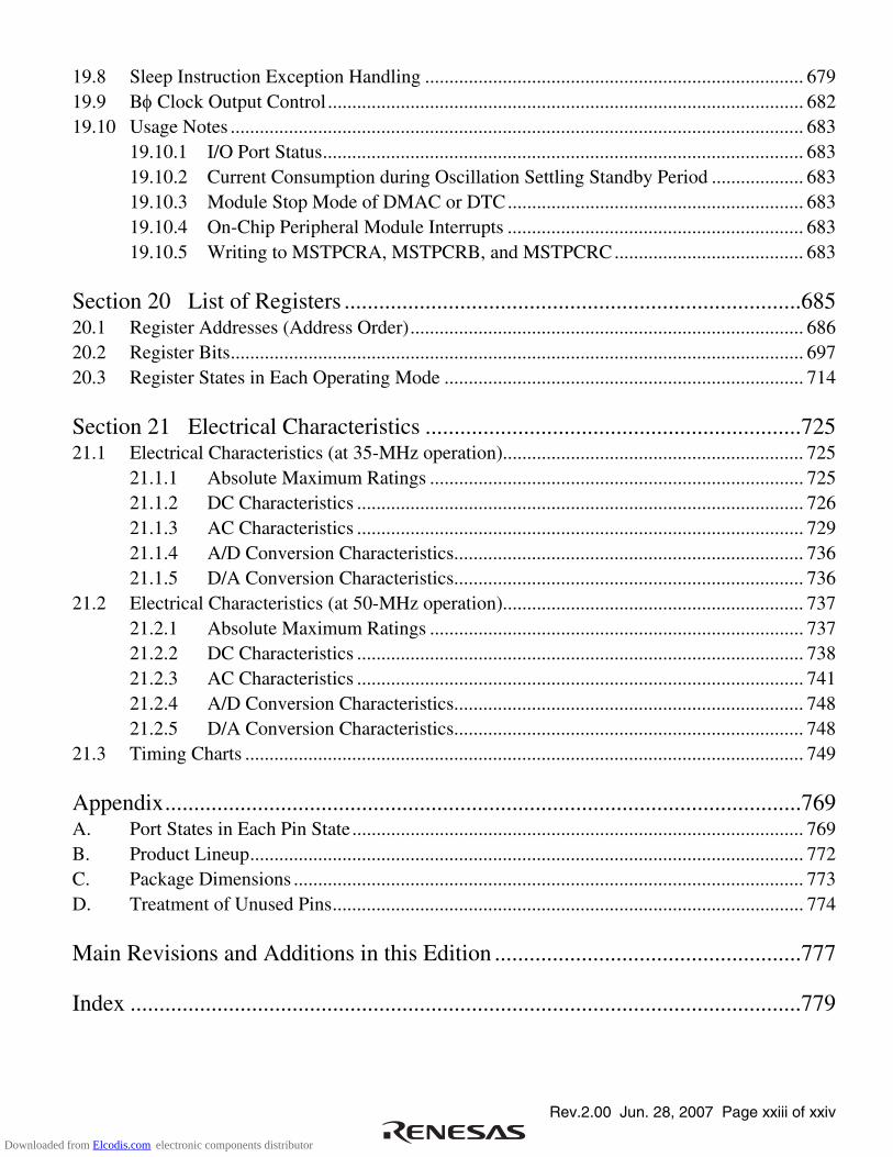
Rev.2.00 Jun. 28, 2007 Page xxiii of xxiv
19.8 Sleep Instruction Exception Handling .............................................................................. 679 19.9 Bφ Clock Output Control.................................................................................................. 682 19.10 Usage Notes ...................................................................................................................... 683
19.10.1 I/O Port Status................................................................................................... 683 19.10.2 Current Consumption during Oscillation Settling Standby Period ................... 683 19.10.3 Module Stop Mode of DMAC or DTC............................................................. 683 19.10.4 On-Chip Peripheral Module Interrupts ............................................................. 683 19.10.5 Writing to MSTPCRA, MSTPCRB, and MSTPCRC....................................... 683
Section 20 List of Registers ...............................................................................685 20.1 Register Addresses (Address Order)................................................................................. 686 20.2 Register Bits...................................................................................................................... 697 20.3 Register States in Each Operating Mode .......................................................................... 714
Section 21 Electrical Characteristics .................................................................725 21.1 Electrical Characteristics (at 35-MHz operation).............................................................. 725
21.1.1 Absolute Maximum Ratings ............................................................................. 725 21.1.2 DC Characteristics ............................................................................................ 726 21.1.3 AC Characteristics ............................................................................................ 729 21.1.4 A/D Conversion Characteristics........................................................................ 736 21.1.5 D/A Conversion Characteristics........................................................................ 736
21.2 Electrical Characteristics (at 50-MHz operation).............................................................. 737 21.2.1 Absolute Maximum Ratings ............................................................................. 737 21.2.2 DC Characteristics ............................................................................................ 738 21.2.3 AC Characteristics ............................................................................................ 741 21.2.4 A/D Conversion Characteristics........................................................................ 748 21.2.5 D/A Conversion Characteristics........................................................................ 748
21.3 Timing Charts ................................................................................................................... 749
Appendix..............................................................................................................769 A. Port States in Each Pin State............................................................................................. 769 B. Product Lineup.................................................................................................................. 772 C. Package Dimensions ......................................................................................................... 773 D. Treatment of Unused Pins................................................................................................. 774
Main Revisions and Additions in this Edition .....................................................777
Index ....................................................................................................................779
Downloaded from Elcodis.com electronic components distributor

Rev.2.00 Jun. 28, 2007 Page xxiv of xxiv
Downloaded from Elcodis.com electronic components distributor

Section 1 Overview
Rev.2.00 Jun. 28, 2007 Page 1 of 784
REJ09B248-0200
Section 1 Overview
1.1 Features
The core of each product in the H8SX/1651 Group of CISC (complex instruction set computer) microcomputers is an H8SX CPU, which has an internal 32-bit architecture. The H8SX CPU provides upward-compatibility with the CPUs of other Renesas Technology-original microcomputers; H8/300, H8/300H, and H8S.
As peripheral functions, each LSI of the Group includes a DMA controller, which enables high-speed data transfer, and a bus-state controller, which enables direct connection to different kinds of memory. The LSI of the Group also includes serial communication interfaces, A/D and D/A converters, and a multi-function timer that makes motor control easy. Together, the modules realize low-cost configurations for end systems. The power consumption of these modules are kept down dynamically by an on-chip power-management function.
1.1.1 Applications
Examples of the applications of this LSI include PC peripheral equipment, optical storage devices, office automation equipment, and industrial equipment.
Downloaded from Elcodis.com electronic components distributor

Section 1 Overview
Rev.2.00 Jun. 28, 2007 Page 2 of 784
REJ09B248-0200
1.1.2 Overview of Functions
Table 1.1 lists the functions of H8SX/1651 Group products in outline.
Table 1.1 Overview of Functions
Classification Module/ Function Description
• ROM lineup: ROMless versions only Memory
RAM • RAM capacity: 40 Kbytes
CPU • 32-bit high-speed H8SX CPU (CISC type)
Upward compatibility for H8/300, H8/300H, and H8S CPUs at object level
• Sixteen 16-bit general registers
• Eleven addressing modes
• 4-Gbyte address space
Program: 4 Gbytes available
Data: 4 Gbytes available
• 87 basic instructions, classifiable as bit arithmetic and logic instructions, multiply and divide instructions, bit manipulation
instructions, multiply-and-accumulate instructions, and others
• Minimum instruction execution time: 20.0 ns (for an ADD
instruction while system clock Iφ = 50 MHz and
VCC = 3.0 to 3.6 V)
• On-chip multiplier (16 × 16 → 32 bits)
• Supports multiply-and-accumulate instructions
(16 × 16 + 32 → 32 bits)
Operating mode
• Advanced mode
CPU
MCU operating mode
Mode 4: On-chip ROM disabled external extended mode, 16-bit bus (selected by driving the MD0 pin low)
Mode 5: On-chip ROM disabled external extended mode, 8-bit bus (selected by driving the MD0 pin high)
• Low power consumption state (transition driven by the SLEEP
instruction)
Downloaded from Elcodis.com electronic components distributor

Section 1 Overview
Rev.2.00 Jun. 28, 2007 Page 3 of 784
REJ09B248-0200
Classification Module/ Function Description
Interrupt (source)
Interrupt controller (INTC)
• Thirteen external interrupt pins (NMI, and IRQ11 to IRQ0)
• 68 internal interrupt sources
• Two interrupt control modes (specified by the interrupt control
register)
• Eight priority orders specifiable (by setting the interrupt priority
register)
• Independent vector addresses
DMA controller (DMAC)
• Four-channel DMA transfer available
• Three activation methods (auto-request, on-chip module
interrupt, external request)
• Three transfer modes (normal transfer, repeat transfer, block
transfer)
• Dual or single address mode selectable
• Extended repeat-area function
DMA
Data transfer controller (DTC)
• Allows DMA transfer over 55 channels (number of DTC
activation sources)
• Activated by interrupt sources (chain transfer enabled)
• Three transfer modes (normal transfer, repeat transfer, block
transfer)
• Short-address mode or full-address mode selectable
• 16-Mbyte external address space External bus extension
Bus controller (BSC)
• The external address space can be divided into eight areas,
each of which is independently controllable
Chip-select signals (CS0 to CA7) can be output
Access in two or three states can be selected for each area
Program wait cycles can be inserted
The period of CS assertion can be extended
Idle cycles can be inserted
• Bus arbitration function (arbitrates bus mastership among the
internal CPU and DTC, and external bus masters)
Downloaded from Elcodis.com electronic components distributor
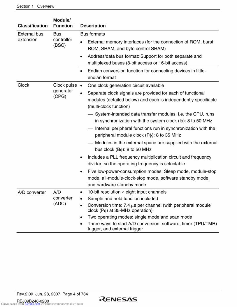
Section 1 Overview
Rev.2.00 Jun. 28, 2007 Page 4 of 784
REJ09B248-0200
Classification Module/ Function Description
Bus formats
• External memory interfaces (for the connection of ROM, burst
ROM, SRAM, and byte control SRAM)
• Address/data bus format: Support for both separate and
multiplexed buses (8-bit access or 16-bit access)
External bus extension
Bus controller (BSC)
• Endian conversion function for connecting devices in little-
endian format
Clock Clock pulse generator (CPG)
• One clock generation circuit available
• Separate clock signals are provided for each of functional
modules (detailed below) and each is independently specifiable
(multi-clock function)
System-intended data transfer modules, i.e. the CPU, runs
in synchronization with the system clock (Iφ): 8 to 50 MHz
Internal peripheral functions run in synchronization with the
peripheral module clock (Pφ): 8 to 35 MHz
Modules in the external space are supplied with the external
bus clock (Bφ): 8 to 50 MHz
• Includes a PLL frequency multiplication circuit and frequency
divider, so the operating frequency is selectable
• Five low-power-consumption modes: Sleep mode, module-stop
mode, all-module-clock-stop mode, software standby mode,
and hardware standby mode
A/D converter A/D converter (ADC)
• 10-bit resolution × eight input channels
• Sample and hold function included • Conversion time: 7.4 µs per channel (with peripheral module
clock (Pφ) at 35-MHz operation) • Two operating modes: single mode and scan mode • Three ways to start A/D conversion: software, timer (TPU/TMR)
trigger, and external trigger
Downloaded from Elcodis.com electronic components distributor

Section 1 Overview
Rev.2.00 Jun. 28, 2007 Page 5 of 784
REJ09B248-0200
Classification Module/ Function Description
D/A converter D/A converter (DAC)
• 8-bit resolution × two output channels
• Output voltage: 0 V to Vref, maximum conversion time: 10 µs (with 20-pF load)
8-bit timer (TMR)
• 8 bits × four channels (can be used as 16 bits × two channels) • Select from among seven clock sources (six internal clocks and
one external clock) • Allows the output of pulse trains with a desired duty cycle or
PWM signals
16-bit timer pulse unit (TPU)
• 16 bits × six channels (general pulse timer unit)
• Select from among eight counter-input clocks for each channel
• Up to 16 pulse inputs and outputs • Counter clear operation, simultaneous writing to multiple timer
counters (TCNT), simultaneous clearing by compare match and input capture possible, simultaneous input/output for registers possible by counter synchronous operation, and up to 15-phase PWM output possible by combination with synchronous operation
• Buffered operation, cascaded operation (32 bits × two channels), and phase counting mode (two-phase encoder input) settable for each channel
• Input capture function supported
• Output compare function (by the output of compare match waveform) supported
Timer
Program-mable pulse generator (PPG)
• 16-bit pulse output • Four output groups, non-overlapping mode, and inverted output
can be set • Selectable output trigger signals; the PPG can operate in
conjunction with the data transfer controller (DTC) and the DMA controller (DMAC)
Watchdog timer Watchdog timer (WDT)
• 8 bits × one channel (selectable from eight counter input clocks)
• Switchable between watchdog timer mode and interval timer mode
Downloaded from Elcodis.com electronic components distributor

Section 1 Overview
Rev.2.00 Jun. 28, 2007 Page 6 of 784
REJ09B248-0200
Classification Module/ Function Description
Serial interface • Five channels (select asynchronous or clocked synchronous serial communication mode)
• Full-duplex communication capability • Select the desired bit rate and LSB-first or MSB-first transfer
Smart card/ SIM
Serial communi-cation interface (SCI) • The SCI module supports a smart card (SIM) interface.
I/O ports • Eight CMOS input-only pins
• 50 CMOS input/output pins
• Eight large-current drive pins (port 3) • 11 pull-up resistors
• 11 open drains
Package • 120-pin thin QFP package (package code: FP-120B, package dimensions: 14 × 14 mm, pin pitch: 0.40 mm)
• Lead- (Pb-) free versions available
Operating frequency/ Power supply voltage
• Operating frequency: 8 to 50 MHz
• Power supply voltage: Vcc = 3.0 to 3.6 V, Avcc = 3.0 to 3.6 V
• Supply current:
30 mA (typ.) (Vcc = 3.3 V, Avcc = 3.3 V, Iφ = Pφ = Bφ =
35 MHz)
45 mA (typ.) (Vcc = 3.3 V, Avcc = 3.3 V, Iφ = Bφ = 50 MHz,
Pφ = 25 MHz)
Operating peripheral temperature (°C)
• −20 to +75°C (regular specifications)
• −40 to +85°C (wide-range specifications)
Downloaded from Elcodis.com electronic components distributor

Section 1 Overview
Rev.2.00 Jun. 28, 2007 Page 7 of 784
REJ09B248-0200
1.2 List of Products
Table 1.2 is the list of products, and figure 1.1 shows how to read the product name code.
Table 1.2 List of Products
Product Type No. ROM Capacity RAM Capacity Package Remarks
R5S61651CFPV 40 Kbytes PLQP0120LA-A
(FP-120BV)
ROMless versions only
(as of June, 2007)
Indicates the Pb-free version.
VProduct type no. R 5 S 61651C FP
Indicates the package.
Indicates the product-specific number.
Indicates the type of ROM device.
Indicates the product classificationMicrocomputer
R indicates a Renesas semiconductor product.
H8SX/1651 Group
FP: LQFP
S: External ROM
Figure 1.1 How to Read the Product Name Code
Downloaded from Elcodis.com electronic components distributor

Section 1 Overview
Rev.2.00 Jun. 28, 2007 Page 8 of 784
REJ09B248-0200
1.3 Block Diagram
DTC DMAC × 4 channels
BSC
PPG
WDT Port 1
Port 2
Port 3
Port 5
Port 6
Port A
Port B
Port D
Port E
Port F
Port H
Port I
H8SXCPU
RAM
Inte
rnal
per
iphe
ral b
us
Ext
erna
l bus
SCI × 5 channels
Clock pulsegenerator
Inte
rnal
sys
tem
bus
TMR (unit 0)(TMR_0, TMR_1)
TMR (unit 1)(TMR_2, TMR_3)
A/D converter
D/A converter
Interruptcontroller
TPU (channel_0 to
channel_5)
CPU:DTC:BSC:DMAC:WDT:
TMR:TPU:PPG:SCI:
[Legend]Central processing unitData transfer controllerBus controllerDMA controllerWatchdog timer
8-bit timer16-bit timer pulse unitProgrammable pulse generatorSerial communication interface
Figure 1.2 Block Diagram
Downloaded from Elcodis.com electronic components distributor

Section 1 Overview
Rev.2.00 Jun. 28, 2007 Page 9 of 784
REJ09B248-0200
1.4 Pin Assignments
PB
1/CS1
/CS2
-B/CS5
-A/CS6
-B/CS7
-BP
B2/CS2
-A/CS6
-AP
B3/CS3
/CS7
-AM
D2
PF
7/A
23/CS4
-C/CS5
-C/CS6
-C/CS7
-CP
F6/
A22
/CS6
-DP
F5/
A21
/CS5
-DA
20A
19 Vss
A18
A17
A16
A15
A14
A13 Vss
A12 Vcc
A11
A10 A
9A
8A
7A
6V
ss A5
A4
A3
A2
P61
/TM
CI2
/RxD
4/TEND2
/IRQ9
-BP
60/T
MR
I2/T
xD4/DREQ2
/IRQ8
-BSTBY
P17
/IRQ7
-A/T
CLK
D-B
P16
/SC
K3/DACK1
-A/IRQ6
-A/T
CLK
C-B
Vcc
EX
TA
LX
TA
LV
ssWDTOVF
/TD
OP
15/R
xD3/TEND1
-A/IRQ5
-A/T
CLK
B-B
P14
/TxD
3/DREQ1-A
/IRQ4
-A/T
CLK
A-B
VC
LRES
Vss
P13
/ADTRG0
/IRQ3
-AP
12/S
CK
2/DACK0
-A/IRQ2
-AP
11/R
xD2/TEND0
-A/IRQ1
-AP
10/T
xD2/DREQ0-A
/IRQ0
-AP
I7/D
15P
I6/D
14P
I5/D
13P
I4/D
12V
ssP
I3/D
11P
I2/D
10P
I1/D
9P
I0/D
8V
ccD
7
90 89 88 87 86 85 84 83 82 81 80 79 78 77 76 75 74 73 72 71 70 69 68 67 66 65 64 63 62 61
P62/TMO2/SCK4/DACK2/IRQ10-B/TRSTPLLVcc
P63/TMRI3/DREQ3/IRQ11-B/TMSPLLVss
P64/TMCI3/TEND3/TDIP65/TMO3/DACK3/TCK
MD0P50/AN0/IRQ0-BP51/AN1/IRQ1-BP52/AN2/IRQ2-B
AVccP53/AN3/IRQ3-B
AVssP54/AN4/IRQ4-B
VrefP55/AN5/IRQ5-B
P56/AN6/DA0/IRQ6-BP57/AN7/DA1/IRQ7-B
MD1PA0/BREQO/BS-A
PA1/BACK/[RD/WR]PA2/BREQ/WAIT
LLWR/LLBPA4/LHWR/LUB
RD
PA6/AS/AH/BS-BVss
PA7/BφVcc
PB0/CS0/CS4-A/CS5-B
919293949596979899100101102103104105106107108109110111112113114115116117118119120
D6D5D4VssD3D2D1D0NMIP37/PO15/TIOCA2/TIOCB2/TCLKD-AP36/PO14/TIOCA2P35/PO13/TIOCA1/TIOCB1/TCLKC-A/DACK1-BP34/PO12/TIOCA1/TEND1-BP33/PO11/TIOCC0/TIOCD0/TCLKB-A/DREQ1-BP32/PO10/TIOCC0/TCLKA-A/DACK0-BP31/PO9/TIOCA0/TIOCB0/TEND0-BVccP30/PO8/DREQ0-B/TIOCA0VssP27/PO7/TIOCA5/TIOCB5P26/PO6/TIOCA5/TMO1/TxD1P25/PO5/TIOCA4/TMCI1/RxD1P24/PO4/TIOCA4/TIOCB4/TMRI1/SCK1P23/PO3/TIOCC3/TIOCD3/IRQ11-AP22/PO2/TIOCC3/TMO0/TxD0/IRQ10-AP21/PO1/TIOCA3/TMCI0/RxD0/IRQ9-AP20/PO0/TIOCA3/TIOCB3/TMRI0/SCK0/IRQ8-AEMLE*
A0A1
605958575655545352515049484746454443424140393837363534333231
1 2 3 4 5 6 7 8 9 10
11
12
13
14
15
16
17
18
19
20
21
22
23
24
25
26
27
28
29
30
H8SX/1651 GroupPLQP0120LA-A (FP-120BV)
(Top View)
Note: * This is an on-chip emulator enable pin. Drive this pin low for the connection in normal operating mode. When this pin is driven high, the on-chip emulation function is enabled and pins P62, P63, P64, P65, and WDTOVF are dedicated for the on-chip emulator. For details on a connection example with the E10A, refer to the E10A Emulator User's Manual.
Figure 1.3 Pin Assignments
Downloaded from Elcodis.com electronic components distributor

Section 1 Overview
Rev.2.00 Jun. 28, 2007 Page 10 of 784
REJ09B248-0200
1.5 Pin Functions
Table 1.3 Pin Functions
Classification Pin Name I/O Description
Power supply VCC Power supply pins. Connect them to the system power supply.
VCL Connect this pin to VSS via a 0.1-uF capacitor (The capacitor should be placed close to the pin).
VSS Ground pins. Connect them to the system power supply (0 V).
PLLVCC Power supply pin for the PLL circuit.
PLLVSS Ground pin for the PLL circuit.
Clock XTAL Input
EXTAL Input
Pins for a crystal resonator. An external clock signal can be input through the EXTAL pin. For an example of this connection, see section 18, Clock Pulse Generator.
Bφ Output Outputs the system clock for external devices.
Operating mode control
MD2 to MD0 Input Pins for setting the operating mode. The signal levels on these pins must not be changed during operation.
System control RES Input Reset signal input pin. This LSI enters the reset state when this signal goes low.
STBY Input This LSI enters hardware standby mode when this signal goes low.
EMLE Input Input pin for the on-chip emulator enable signal. The signal level should normally be fixed low.
Address bus A23 to A0 Output Output pins for the address bits.
Data bus D15 to D0 Input/ output
Input and output for the bidirectional data bus. These pins also output addresses when accessing an address–data multiplexed I/O interface space.
Bus control BREQ Input External bus-master modules assert this signal to request the bus.
BREQO Output Internal bus-master modules assert this signal to request access to the external space via the bus in the external bus released state.
Downloaded from Elcodis.com electronic components distributor
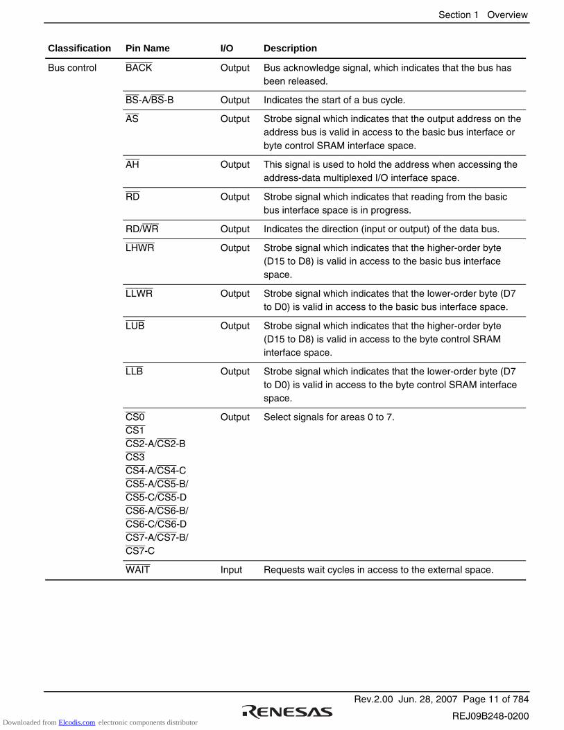
Section 1 Overview
Rev.2.00 Jun. 28, 2007 Page 11 of 784
REJ09B248-0200
Classification Pin Name I/O Description
Bus control BACK Output Bus acknowledge signal, which indicates that the bus has been released.
BS-A/BS-B Output Indicates the start of a bus cycle.
AS Output Strobe signal which indicates that the output address on the address bus is valid in access to the basic bus interface or byte control SRAM interface space.
AH Output This signal is used to hold the address when accessing the address-data multiplexed I/O interface space.
RD Output Strobe signal which indicates that reading from the basic bus interface space is in progress.
RD/WR Output Indicates the direction (input or output) of the data bus.
LHWR Output Strobe signal which indicates that the higher-order byte (D15 to D8) is valid in access to the basic bus interface space.
LLWR Output Strobe signal which indicates that the lower-order byte (D7 to D0) is valid in access to the basic bus interface space.
LUB Output Strobe signal which indicates that the higher-order byte (D15 to D8) is valid in access to the byte control SRAM interface space.
LLB Output Strobe signal which indicates that the lower-order byte (D7 to D0) is valid in access to the byte control SRAM interface space.
CS0 CS1 CS2-A/CS2-B CS3 CS4-A/CS4-C CS5-A/CS5-B/ CS5-C/CS5-D CS6-A/CS6-B/ CS6-C/CS6-D CS7-A/CS7-B/ CS7-C
Output Select signals for areas 0 to 7.
WAIT Input Requests wait cycles in access to the external space.
Downloaded from Elcodis.com electronic components distributor
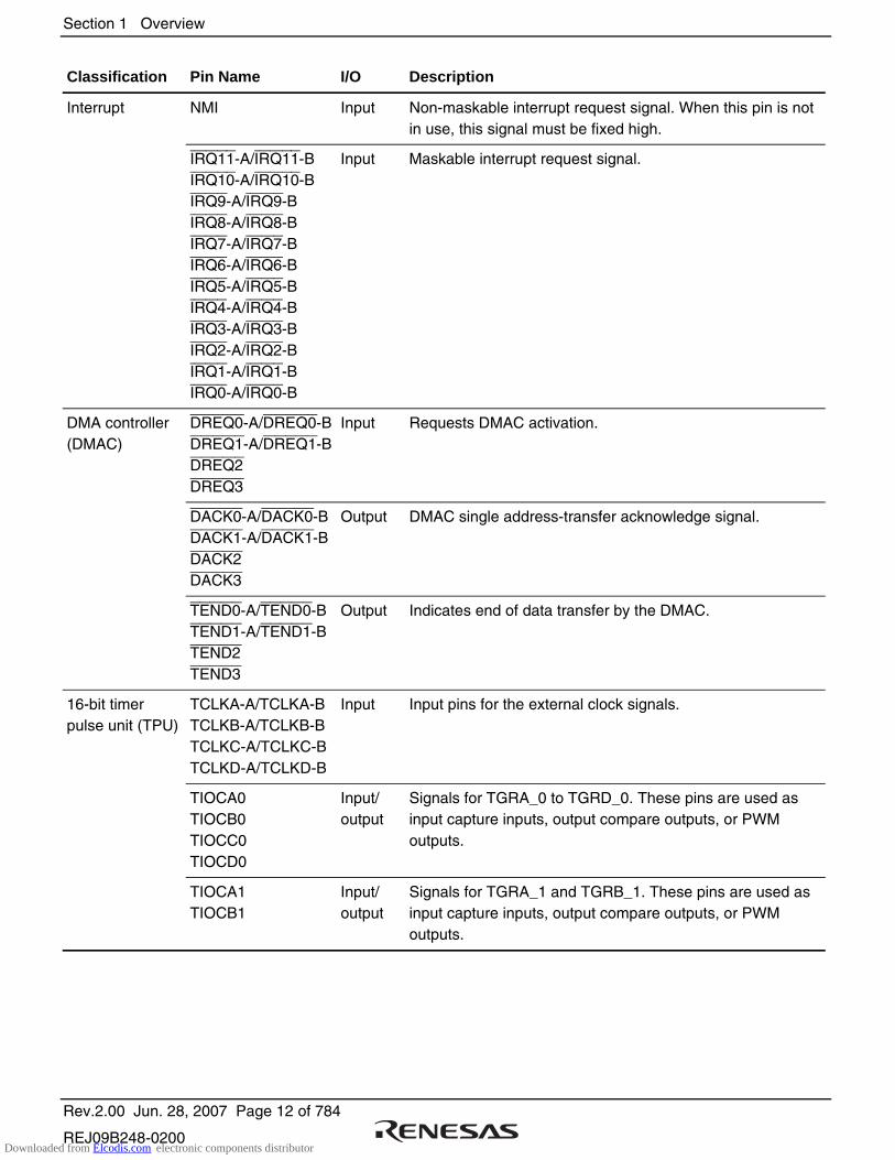
Section 1 Overview
Rev.2.00 Jun. 28, 2007 Page 12 of 784
REJ09B248-0200
Classification Pin Name I/O Description
Interrupt NMI Input Non-maskable interrupt request signal. When this pin is not in use, this signal must be fixed high.
IRQ11-A/IRQ11-B IRQ10-A/IRQ10-B IRQ9-A/IRQ9-B IRQ8-A/IRQ8-B IRQ7-A/IRQ7-B IRQ6-A/IRQ6-B IRQ5-A/IRQ5-B IRQ4-A/IRQ4-B IRQ3-A/IRQ3-B IRQ2-A/IRQ2-B IRQ1-A/IRQ1-B IRQ0-A/IRQ0-B
Input Maskable interrupt request signal.
DREQ0-A/DREQ0-B DREQ1-A/DREQ1-B DREQ2 DREQ3
Input Requests DMAC activation.
DACK0-A/DACK0-B DACK1-A/DACK1-B DACK2 DACK3
Output DMAC single address-transfer acknowledge signal.
DMA controller (DMAC)
TEND0-A/TEND0-B TEND1-A/TEND1-B TEND2 TEND3
Output Indicates end of data transfer by the DMAC.
16-bit timer pulse unit (TPU)
TCLKA-A/TCLKA-B TCLKB-A/TCLKB-B TCLKC-A/TCLKC-B TCLKD-A/TCLKD-B
Input Input pins for the external clock signals.
TIOCA0 TIOCB0 TIOCC0 TIOCD0
Input/ output
Signals for TGRA_0 to TGRD_0. These pins are used as input capture inputs, output compare outputs, or PWM outputs.
TIOCA1 TIOCB1
Input/ output
Signals for TGRA_1 and TGRB_1. These pins are used as input capture inputs, output compare outputs, or PWM outputs.
Downloaded from Elcodis.com electronic components distributor
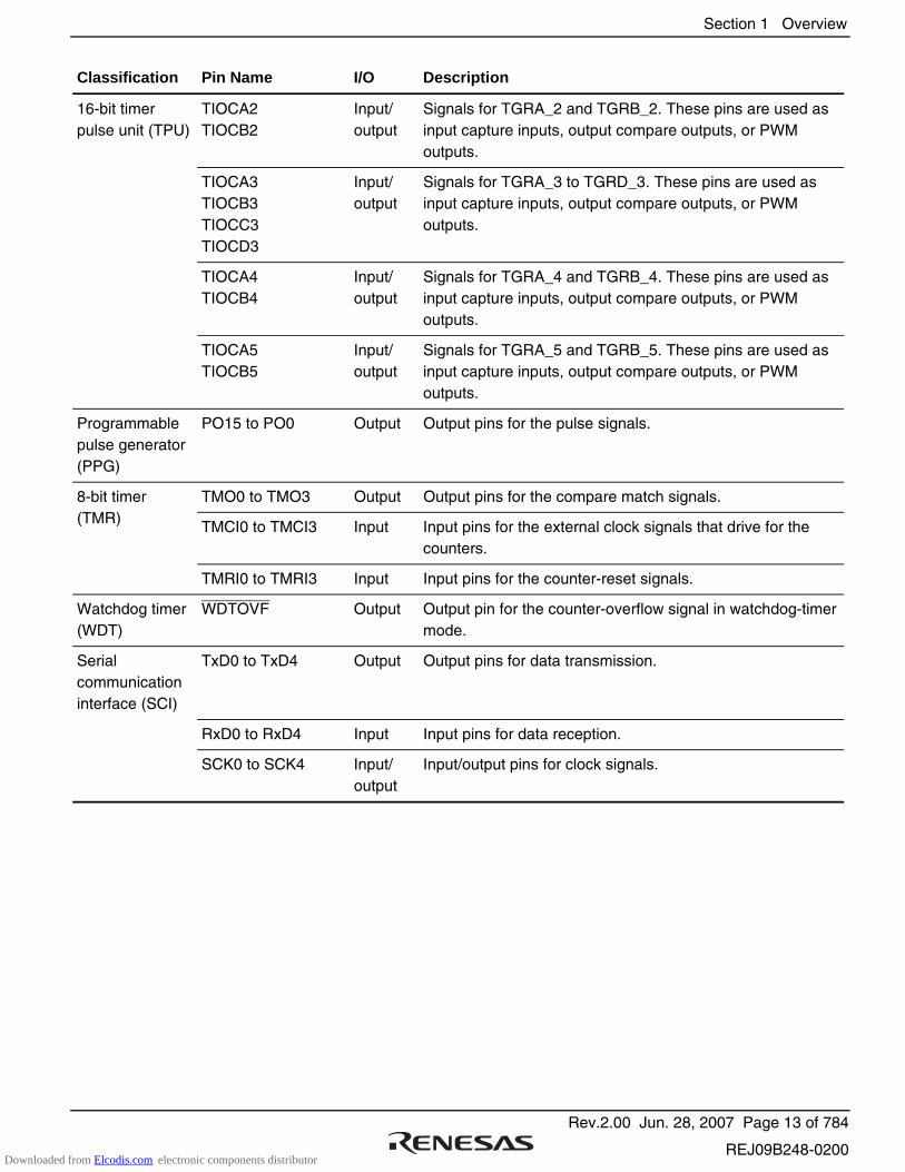
Section 1 Overview
Rev.2.00 Jun. 28, 2007 Page 13 of 784
REJ09B248-0200
Classification Pin Name I/O Description
16-bit timer pulse unit (TPU)
TIOCA2 TIOCB2
Input/ output
Signals for TGRA_2 and TGRB_2. These pins are used as input capture inputs, output compare outputs, or PWM outputs.
TIOCA3 TIOCB3 TIOCC3 TIOCD3
Input/ output
Signals for TGRA_3 to TGRD_3. These pins are used as input capture inputs, output compare outputs, or PWM outputs.
TIOCA4 TIOCB4
Input/ output
Signals for TGRA_4 and TGRB_4. These pins are used as input capture inputs, output compare outputs, or PWM outputs.
TIOCA5 TIOCB5
Input/ output
Signals for TGRA_5 and TGRB_5. These pins are used as input capture inputs, output compare outputs, or PWM outputs.
Programmable pulse generator (PPG)
PO15 to PO0 Output Output pins for the pulse signals.
TMO0 to TMO3 Output Output pins for the compare match signals.
TMCI0 to TMCI3 Input Input pins for the external clock signals that drive for the counters.
8-bit timer (TMR)
TMRI0 to TMRI3 Input Input pins for the counter-reset signals.
Watchdog timer (WDT)
WDTOVF Output Output pin for the counter-overflow signal in watchdog-timer mode.
Serial communication interface (SCI)
TxD0 to TxD4 Output Output pins for data transmission.
RxD0 to RxD4 Input Input pins for data reception.
SCK0 to SCK4 Input/ output
Input/output pins for clock signals.
Downloaded from Elcodis.com electronic components distributor
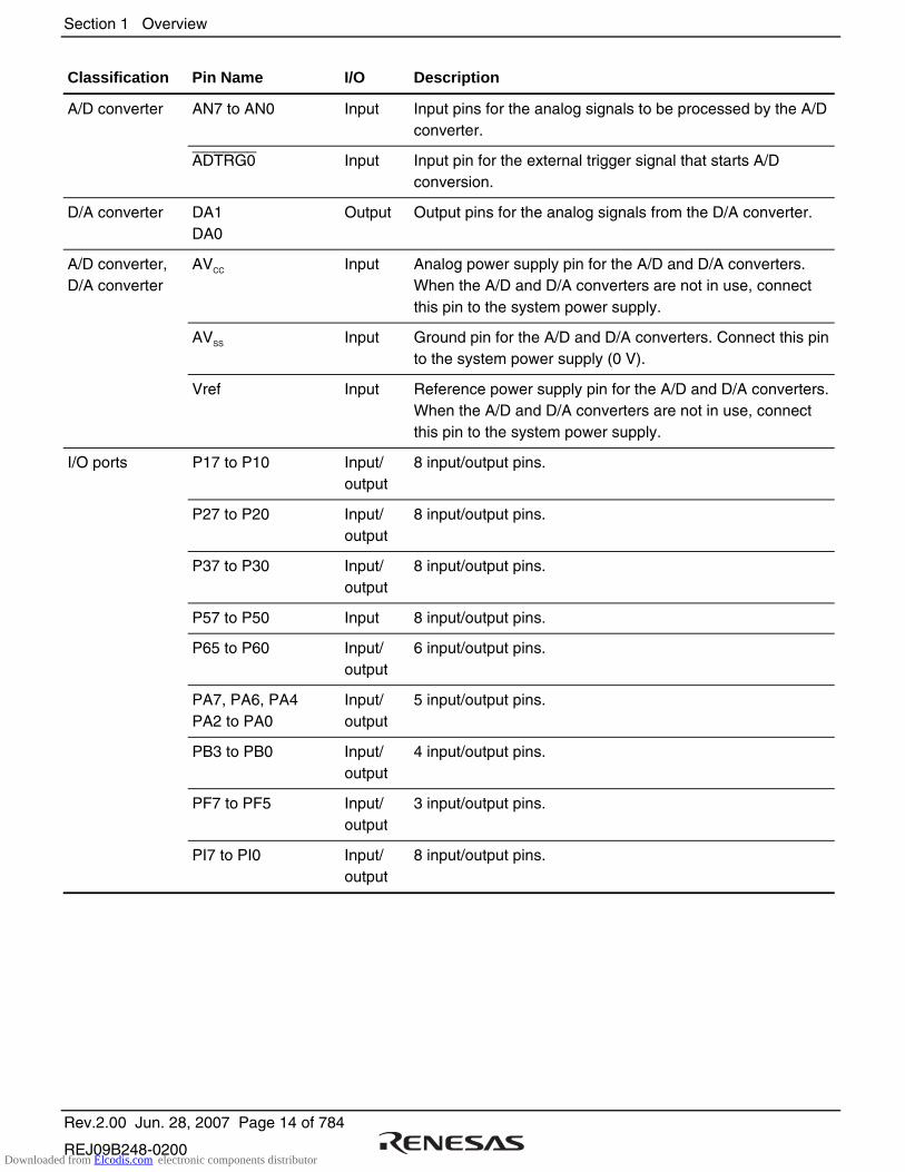
Section 1 Overview
Rev.2.00 Jun. 28, 2007 Page 14 of 784
REJ09B248-0200
Classification Pin Name I/O Description
A/D converter AN7 to AN0 Input Input pins for the analog signals to be processed by the A/D converter.
ADTRG0 Input Input pin for the external trigger signal that starts A/D conversion.
D/A converter DA1 DA0
Output Output pins for the analog signals from the D/A converter.
A/D converter, D/A converter
AVCC Input Analog power supply pin for the A/D and D/A converters. When the A/D and D/A converters are not in use, connect this pin to the system power supply.
AVSS Input Ground pin for the A/D and D/A converters. Connect this pin to the system power supply (0 V).
Vref Input Reference power supply pin for the A/D and D/A converters. When the A/D and D/A converters are not in use, connect this pin to the system power supply.
I/O ports P17 to P10 Input/ output
8 input/output pins.
P27 to P20 Input/ output
8 input/output pins.
P37 to P30 Input/ output
8 input/output pins.
P57 to P50 Input 8 input/output pins.
P65 to P60 Input/ output
6 input/output pins.
PA7, PA6, PA4 PA2 to PA0
Input/ output
5 input/output pins.
PB3 to PB0 Input/ output
4 input/output pins.
PF7 to PF5 Input/ output
3 input/output pins.
PI7 to PI0 Input/ output
8 input/output pins.
Downloaded from Elcodis.com electronic components distributor

Section 2 CPU
Rev.2.00 Jun. 28, 2007 Page 15 of 784
REJ09B248-0200
Section 2 CPU
The H8SX CPU is a high-speed central processing unit with an internal 32-bit architecture that is upward-compatible with the H8/300, H8/300H, and H8S CPUs. The H8SX CPU has sixteen 16-bit general registers, can handle a 4-Gbyte linear address space, and is ideal for a realtime control system.
2.1 Features
• Upward-compatible with H8/300, H8/300H, and H8S CPUs
Can execute these CPU's object programs
• General-register architecture
Sixteen 16-bit general registers (also usable as sixteen 8-bit registers or eight 32-bit registers)
• 87 basic instructions
8/16/32-bit arithmetic and logic instructions
Multiply and divide instructions
Bit field transfer instructions
Powerful bit-manipulation instructions
Bit condition branch instructions
Multiply-and-accumulate instruction
• Eleven addressing modes
Register direct [Rn]
Register indirect [@ERn]
Register indirect with displacement [@(d:2,ERn), @(d:16,ERn), or @(d:32,ERn)]
Index register indirect with displacement [@(d:16,RnL.B), @(d:32,RnL.B), @(d:16,Rn.W), @(d:32,Rn.W), @(d:16,ERn.L), or @(d:32,ERn.L)]
Register indirect with post-/pre-increment or post-/pre-decrement [@+ERn/@−ERn/@ERn+/@ERn−]
Absolute address [@aa:8, @aa:16, @aa:24, or @aa:32]
Immediate [#xx:3, #xx:4, #xx:8, #xx:16, or #xx:32]
Program-counter relative [@(d:8,PC) or @(d:16,PC)]
Program-counter relative with index register [@(RnL.B,PC), @(Rn.W,PC), or @(ERn.L,PC)]
Memory indirect [@@aa:8]
Extended memory indirect [@@vec:7]
Downloaded from Elcodis.com electronic components distributor
Section 2 CPU
Rev.2.00 Jun. 28, 2007 Page 16 of 784
REJ09B248-0200
• Two base registers
Vector base register
Short address base register
• 4-Gbyte address space
Program: 4 Gbytes
Data: 4 Gbytes
• High-speed operation
All frequently-used instructions execute in one or two states
8/16/32-bit register-register add/subtract: 1 state
8 × 8-bit register-register multiply: 1 state
16 ÷ 8-bit register-register divide: 10 states
16 × 16-bit register-register multiply: 1 state
32 ÷ 16-bit register-register divide: 18 states
32 × 32-bit register-register multiply: 5 states
32 ÷ 32-bit register-register divide: 18 states
• Four CPU operating modes
Normal mode
Middle mode
Advanced mode
Maximum mode
• Power-down modes
Transition is made by execution of SLEEP instruction
Choice of CPU operating clocks Notes: 1. Advanced mode is only supported as the CPU operating mode of the H8SX/1651
Group. Normal, middle, and maximum modes are not supported.
2. The multiplier and divider are supported by the H8SX/1651 Group.
Downloaded from Elcodis.com electronic components distributor
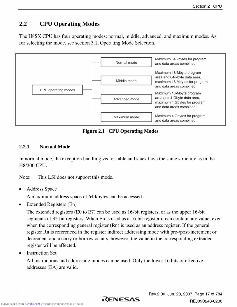
Section 2 CPU
Rev.2.00 Jun. 28, 2007 Page 17 of 784
REJ09B248-0200
2.2 CPU Operating Modes
The H8SX CPU has four operating modes: normal, middle, advanced, and maximum modes. As for selecting the mode, see section 3.1, Operating Mode Selection.
CPU operating modes
Normal mode
Maximum mode
Maximum 64 kbytes for program and data areas combined
Maximum 4 Gbytes for program and data areas combined
Maximum 16-Mbyte program area and 64-kbyte data area, maximum 16 Mbytes for program and data areas combined
Maximum 16-Mbyte program area and 4-Gbyte data area, maximum 4 Gbytes for program and data areas combined
Advanced mode
Middle mode
Figure 2.1 CPU Operating Modes
2.2.1 Normal Mode
In normal mode, the exception handling vector table and stack have the same structure as in the H8/300 CPU.
Note: This LSI does not support this mode.
• Address Space
A maximum address space of 64 kbytes can be accessed.
• Extended Registers (En)
The extended registers (E0 to E7) can be used as 16-bit registers, or as the upper 16-bit segments of 32-bit registers. When En is used as a 16-bit register it can contain any value, even when the corresponding general register (Rn) is used as an address register. If the general register Rn is referenced in the register indirect addressing mode with pre-/post-increment or decrement and a carry or borrow occurs, however, the value in the corresponding extended register will be affected.
• Instruction Set
All instructions and addressing modes can be used. Only the lower 16 bits of effective addresses (EA) are valid.
Downloaded from Elcodis.com electronic components distributor
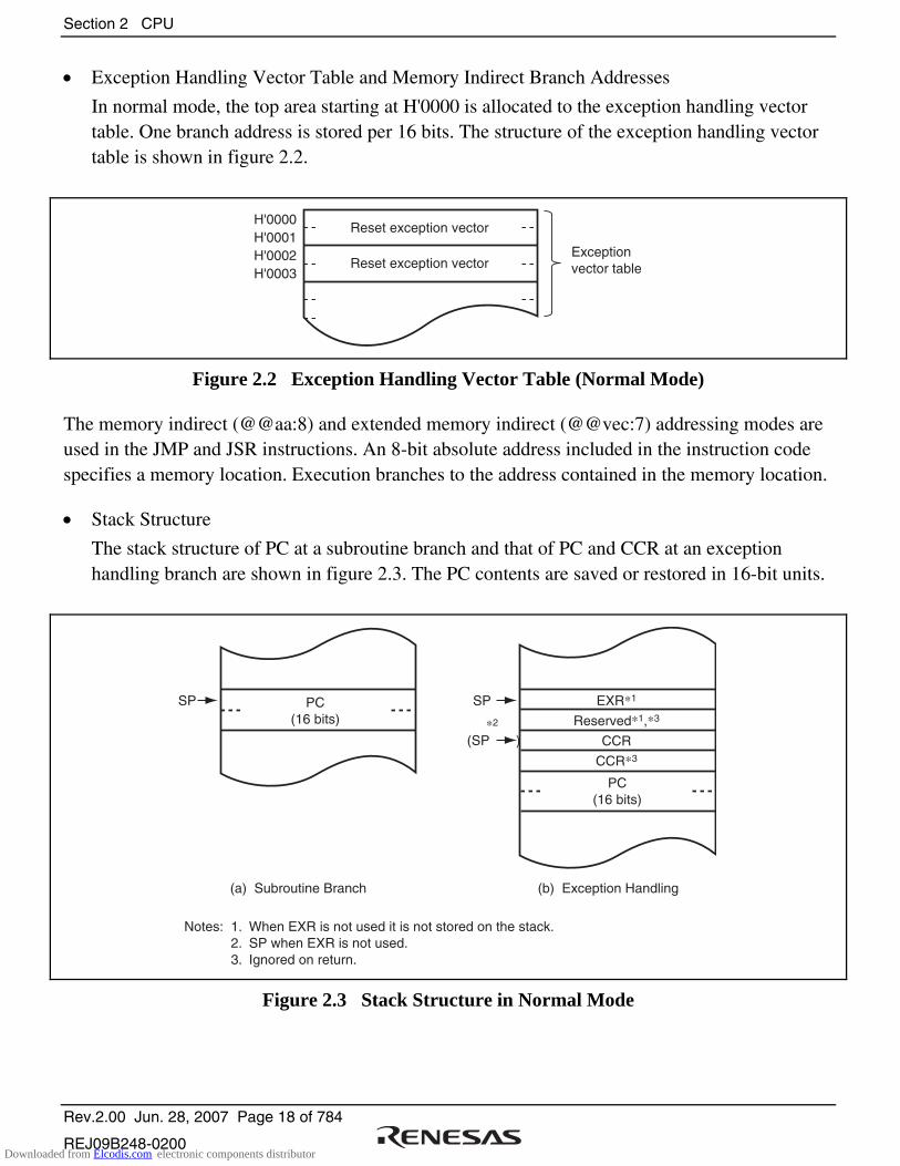
Section 2 CPU
Rev.2.00 Jun. 28, 2007 Page 18 of 784
REJ09B248-0200
• Exception Handling Vector Table and Memory Indirect Branch Addresses
In normal mode, the top area starting at H'0000 is allocated to the exception handling vector table. One branch address is stored per 16 bits. The structure of the exception handling vector table is shown in figure 2.2.
H'0000H'0001H'0002H'0003
Reset exception vector
Reset exception vectorException vector table
Figure 2.2 Exception Handling Vector Table (Normal Mode)
The memory indirect (@@aa:8) and extended memory indirect (@@vec:7) addressing modes are used in the JMP and JSR instructions. An 8-bit absolute address included in the instruction code specifies a memory location. Execution branches to the address contained in the memory location.
• Stack Structure
The stack structure of PC at a subroutine branch and that of PC and CCR at an exception handling branch are shown in figure 2.3. The PC contents are saved or restored in 16-bit units.
(a) Subroutine Branch (b) Exception Handling
PC(16 bits)
EXR*1
Reserved*1,*3
CCR
CCR*3
PC(16 bits)
SP SP
Notes: 1.2.3.
When EXR is not used it is not stored on the stack.SP when EXR is not used.Ignored on return.
(SP )*2
Figure 2.3 Stack Structure in Normal Mode
Downloaded from Elcodis.com electronic components distributor
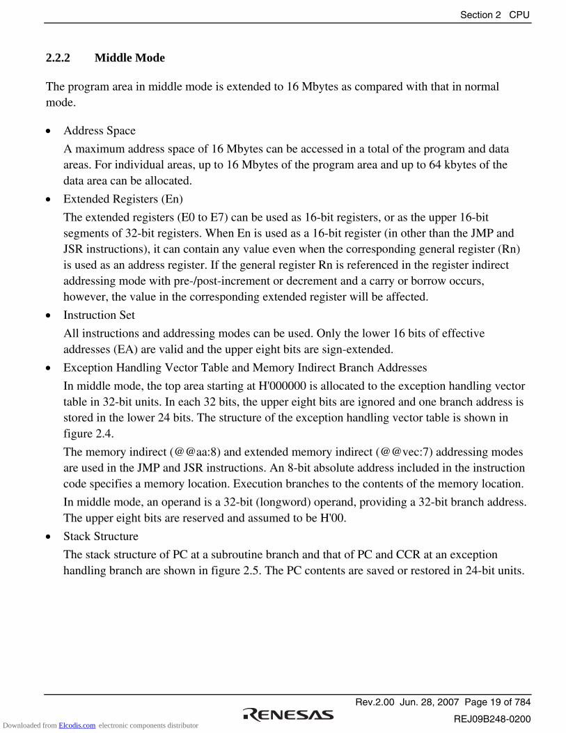
Section 2 CPU
Rev.2.00 Jun. 28, 2007 Page 19 of 784
REJ09B248-0200
2.2.2 Middle Mode
The program area in middle mode is extended to 16 Mbytes as compared with that in normal mode.
• Address Space
A maximum address space of 16 Mbytes can be accessed in a total of the program and data areas. For individual areas, up to 16 Mbytes of the program area and up to 64 kbytes of the data area can be allocated.
• Extended Registers (En)
The extended registers (E0 to E7) can be used as 16-bit registers, or as the upper 16-bit segments of 32-bit registers. When En is used as a 16-bit register (in other than the JMP and JSR instructions), it can contain any value even when the corresponding general register (Rn) is used as an address register. If the general register Rn is referenced in the register indirect addressing mode with pre-/post-increment or decrement and a carry or borrow occurs, however, the value in the corresponding extended register will be affected.
• Instruction Set
All instructions and addressing modes can be used. Only the lower 16 bits of effective addresses (EA) are valid and the upper eight bits are sign-extended.
• Exception Handling Vector Table and Memory Indirect Branch Addresses
In middle mode, the top area starting at H'000000 is allocated to the exception handling vector table in 32-bit units. In each 32 bits, the upper eight bits are ignored and one branch address is stored in the lower 24 bits. The structure of the exception handling vector table is shown in figure 2.4.
The memory indirect (@@aa:8) and extended memory indirect (@@vec:7) addressing modes are used in the JMP and JSR instructions. An 8-bit absolute address included in the instruction code specifies a memory location. Execution branches to the contents of the memory location.
In middle mode, an operand is a 32-bit (longword) operand, providing a 32-bit branch address. The upper eight bits are reserved and assumed to be H'00.
• Stack Structure
The stack structure of PC at a subroutine branch and that of PC and CCR at an exception handling branch are shown in figure 2.5. The PC contents are saved or restored in 24-bit units.
Downloaded from Elcodis.com electronic components distributor

Section 2 CPU
Rev.2.00 Jun. 28, 2007 Page 20 of 784
REJ09B248-0200
2.2.3 Advanced Mode
The data area in advanced mode is extended to 4 Gbytes as compared with that in middle mode.
• Address Space
A maximum address space of 4 Gbytes can be linearly accessed. For individual areas, up to 16 Mbytes of the program area and up to 4 Gbytes of the data area can be allocated.
• Extended Registers (En)
The extended registers (E0 to E7) can be used as 16-bit registers, or as the upper 16-bit segments of 32-bit registers or address registers.
• Instruction Set
All instructions and addressing modes can be used.
• Exception Handling Vector Table and Memory Indirect Branch Addresses
In advanced mode, the top area starting at H'00000000 is allocated to the exception handling vector table in 32-bit units. In each 32 bits, the upper eight bits are ignored and one branch address is stored in the lower 24 bits. The structure of the exception handling vector table is shown in figure 2.4.
H'00000000
H'00000003
H'00000004 Exception vector table
Reserved
Reset exception vector
Reserved
H'00000007
H'00000001
H'00000002
H'00000005
H'00000006
Figure 2.4 Exception Handling Vector Table (Middle and Advanced Modes)
The memory indirect (@@aa:8) and extended memory indirect (@@vec:7) addressing modes are used in the JMP and JSR instructions. An 8-bit absolute address included in the instruction code specifies a memory location. Execution branches to the contents of the memory location.
In advanced mode, an operand is a 32-bit (longword) operand, providing a 32-bit branch address. The upper eight bits are reserved and assumed to be H'00.
Downloaded from Elcodis.com electronic components distributor
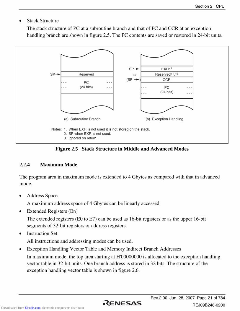
Section 2 CPU
Rev.2.00 Jun. 28, 2007 Page 21 of 784
REJ09B248-0200
• Stack Structure
The stack structure of PC at a subroutine branch and that of PC and CCR at an exception handling branch are shown in figure 2.5. The PC contents are saved or restored in 24-bit units.
(a) Subroutine Branch (b) Exception Handling
PC(24 bits)
EXR*1
Reserved*1,*3
CCR
PC(24 bits)
SP
SP
Notes: 1.2.3.
When EXR is not used it is not stored on the stack.SP when EXR is not used.Ignored on return.
(SP )*2Reserved
Figure 2.5 Stack Structure in Middle and Advanced Modes
2.2.4 Maximum Mode
The program area in maximum mode is extended to 4 Gbytes as compared with that in advanced mode.
• Address Space
A maximum address space of 4 Gbytes can be linearly accessed.
• Extended Registers (En)
The extended registers (E0 to E7) can be used as 16-bit registers or as the upper 16-bit segments of 32-bit registers or address registers.
• Instruction Set
All instructions and addressing modes can be used.
• Exception Handling Vector Table and Memory Indirect Branch Addresses
In maximum mode, the top area starting at H'00000000 is allocated to the exception handling vector table in 32-bit units. One branch address is stored in 32 bits. The structure of the exception handling vector table is shown in figure 2.6.
Downloaded from Elcodis.com electronic components distributor
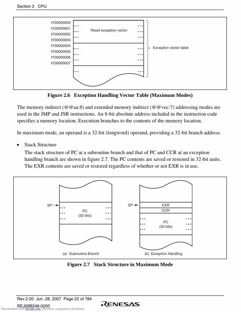
Section 2 CPU
Rev.2.00 Jun. 28, 2007 Page 22 of 784
REJ09B248-0200
H'00000000
H'00000003
H'00000004 Exception vector table
Reset exception vector
H'00000007
H'00000001
H'00000002
H'00000005
H'00000006
Figure 2.6 Exception Handling Vector Table (Maximum Modes)
The memory indirect (@@aa:8) and extended memory indirect (@@vec:7) addressing modes are used in the JMP and JSR instructions. An 8-bit absolute address included in the instruction code specifies a memory location. Execution branches to the contents of the memory location.
In maximum mode, an operand is a 32-bit (longword) operand, providing a 32-bit branch address.
• Stack Structure
The stack structure of PC at a subroutine branch and that of PC and CCR at an exception handling branch are shown in figure 2.7. The PC contents are saved or restored in 32-bit units. The EXR contents are saved or restored regardless of whether or not EXR is in use.
(a) Subroutine Branch (b) Exception Handling
PC(32 bits)
EXR
CCR
PC(32 bits)
SP SP
Figure 2.7 Stack Structure in Maximum Mode
Downloaded from Elcodis.com electronic components distributor

Section 2 CPU
Rev.2.00 Jun. 28, 2007 Page 23 of 784
REJ09B248-0200
2.3 Instruction Fetch
The H8SX CPU has two modes for instruction fetch: 16-bit and 32-bit modes. It is recommended that the mode should be set according to the bus width of the memory in which the program is stored.
The instruction-fetch mode setting does not affect operation other than instruction fetch such as data accesses. The FETCHMD bit in SYSCR selects one of the two modes. For details, see section 3.2.2, System Control Register (SYSCR).
2.4 Address Space
Figure 2.8 shows a memory map of the H8SX CPU. The address space differs depending on the operating mode.
H'0000 H'000000
H'007FFF
H'FF8000
H'FFFFFF
H'00000000
H'00FFFFFF
H'FFFFFFFF
H'00000000
H'FFFFFFFF
H'FFFF
Normal mode
Program areaData area(64 kbytes)
Program areaData area(4 Gbytes)
Program area(16 Mbytes)
Program area(16 Mbytes)Data area
(64 kbytes)
Data area(4 Gbytes)
Middle mode Advanced mode Maximum mode
Figure 2.8 Memory Map
Downloaded from Elcodis.com electronic components distributor
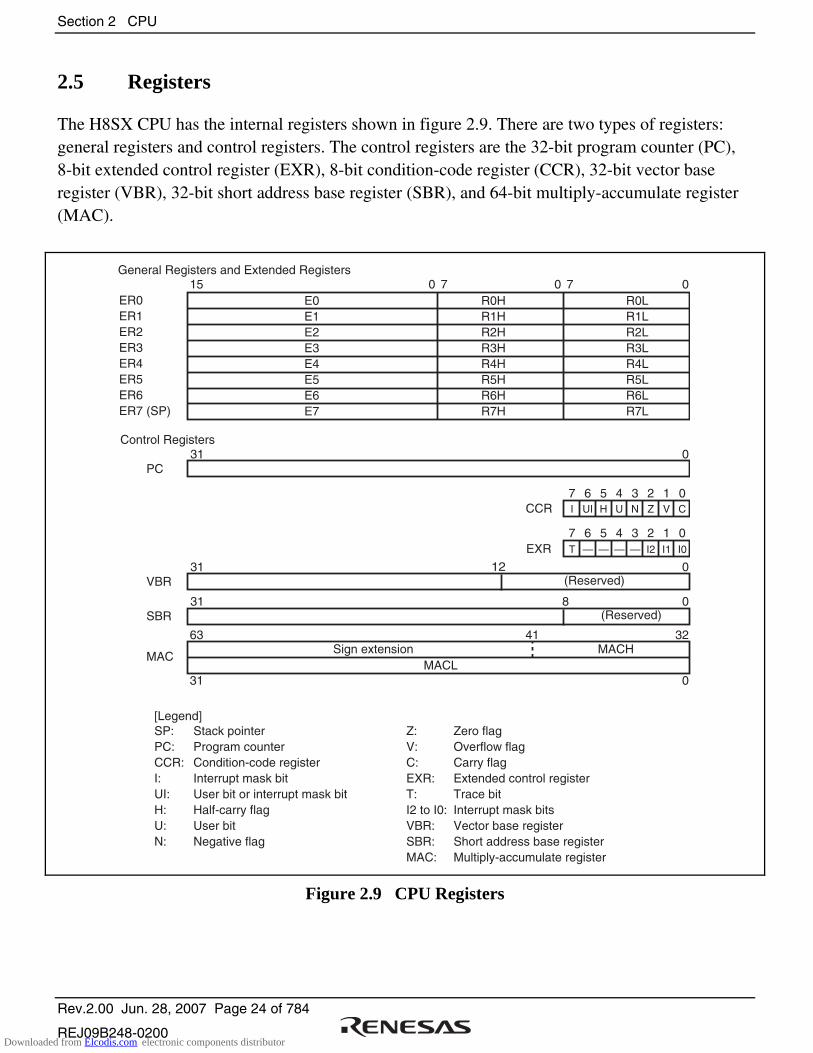
Section 2 CPU
Rev.2.00 Jun. 28, 2007 Page 24 of 784
REJ09B248-0200
2.5 Registers
The H8SX CPU has the internal registers shown in figure 2.9. There are two types of registers: general registers and control registers. The control registers are the 32-bit program counter (PC), 8-bit extended control register (EXR), 8-bit condition-code register (CCR), 32-bit vector base register (VBR), 32-bit short address base register (SBR), and 64-bit multiply-accumulate register (MAC).
T — — — — I2 I1 I0EXR
7 6 5 4 3 2 1 0
31 0
15 0 7 0 7 0E0E1E2E3E4E5E6E7
R0HR1HR2HR3HR4HR5HR6HR7H
R0LR1LR2LR3LR4LR5LR6LR7L
General Registers and Extended Registers
Control Registers
[Legend]Stack pointerProgram counterCondition-code registerInterrupt mask bitUser bit or interrupt mask bitHalf-carry flagUser bitNegative flag
SP:PC:CCR:I:UI:H:U:N:
ER0ER1ER2ER3ER4ER5ER6ER7 (SP)
I UI H U N Z V CCCR
7 6 5 4 3 2 1 0
Sign extension63 3241
031
MAC
PC
(Reserved)31 012
VBR
(Reserved)31 08
SBR
MACL
Zero flagOverflow flagCarry flagExtended control registerTrace bitInterrupt mask bitsVector base registerShort address base register Multiply-accumulate register
Z:V:C: EXR:T:I2 to I0:VBR: SBR:MAC:
MACH
Figure 2.9 CPU Registers
Downloaded from Elcodis.com electronic components distributor

Section 2 CPU
Rev.2.00 Jun. 28, 2007 Page 25 of 784
REJ09B248-0200
2.5.1 General Registers
The H8SX CPU has eight 32-bit general registers. These general registers are all functionally alike and can be used as both address registers and data registers. When a general register is used as a data register, it can be accessed as a 32-bit, 16-bit, or 8-bit register. Figure 2.10 illustrates the usage of the general registers.
When the general registers are used as 32-bit registers or address registers, they are designated by the letters ER (ER0 to ER7).
The ER registers are divided into 16-bit general registers designated by the letters E (E0 to E7) and R (R0 to R7). These registers are functionally equivalent, providing a maximum of sixteen 16-bit registers. The E registers (E0 to E7) are also referred to as extended registers.
The R registers are divided into 8-bit general registers designated by the letters RH (R0H to R7H) and RL (R0L to R7L). These registers are functionally equivalent, providing a maximum of sixteen 8-bit registers.
The general registers ER (ER0 to ER7), R (R0 to R7), and RL (R0L to R7L) are also used as index registers. The size in the operand field determines which register is selected.
The usage of each register can be selected independently.
Address registers32-bit registers32-bit index registers
16-bit registers
General registers E(E0 to E7)
8-bit registers
General registers RH(R0H to R7H)16-bit registers
16-bit index registers
General registers R(R0 to R7) 8-bit registers
8-bit index registers
General registers RL(R0L to R7L)
General registers ER(ER0 to ER7)
•••
••
••
•
•
Figure 2.10 Usage of General Registers
General register ER7 has the function of stack pointer (SP) in addition to its general-register function, and is used implicitly in exception handling and subroutine calls. Figure 2.11 shows the stack.
Downloaded from Elcodis.com electronic components distributor
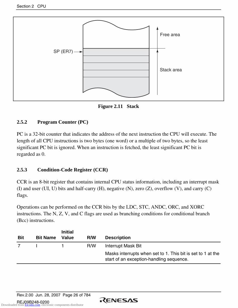
Section 2 CPU
Rev.2.00 Jun. 28, 2007 Page 26 of 784
REJ09B248-0200
Free area
Stack area
SP (ER7)
Figure 2.11 Stack
2.5.2 Program Counter (PC)
PC is a 32-bit counter that indicates the address of the next instruction the CPU will execute. The length of all CPU instructions is two bytes (one word) or a multiple of two bytes, so the least significant PC bit is ignored. When an instruction is fetched, the least significant PC bit is regarded as 0.
2.5.3 Condition-Code Register (CCR)
CCR is an 8-bit register that contains internal CPU status information, including an interrupt mask (I) and user (UI, U) bits and half-carry (H), negative (N), zero (Z), overflow (V), and carry (C) flags.
Operations can be performed on the CCR bits by the LDC, STC, ANDC, ORC, and XORC instructions. The N, Z, V, and C flags are used as branching conditions for conditional branch (Bcc) instructions.
Bit Bit Name Initial Value R/W Description
7 I 1 R/W Interrupt Mask Bit
Masks interrupts when set to 1. This bit is set to 1 at the start of an exception-handling sequence.
Downloaded from Elcodis.com electronic components distributor
Section 2 CPU
Rev.2.00 Jun. 28, 2007 Page 27 of 784
REJ09B248-0200
Bit Bit Name Initial Value R/W Description
6 UI Undefined R/W User Bit or Interrupt Mask Bit
Can be written and read by software using the LDC, STC, ANDC, ORC, and XORC instructions. This bit can also be used as an interrupt mask bit.
5 H Undefined R/W Half-Carry Flag
When the ADD.B, ADDX.B, SUB.B, SUBX.B, CMP.B, or NEG.B instruction is executed, this flag is set to 1 if there is a carry or borrow at bit 3, and cleared to 0 otherwise. When the ADD.W, SUB.W, CMP.W, or NEG.W instruction is executed, the H flag is set to 1 if there is a carry or borrow at bit 11, and cleared to 0 otherwise. When the ADD.L, SUB.L, CMP.L, or NEG.L instruction is executed, the H flag is set to 1 if there is a carry or borrow at bit 27, and cleared to 0 otherwise.
4 U Undefined R/W User Bit
Can be written and read by software using the LDC, STC, ANDC, ORC, and XORC instructions.
3 N Undefined R/W Negative Flag
Stores the value of the most significant bit (regarded as sign bit) of data.
2 Z Undefined R/W Zero Flag
Set to 1 to indicate zero data, and cleared to 0 to indicate non-zero data.
1 V Undefined R/W Overflow Flag
Set to 1 when an arithmetic overflow occurs, and cleared to 0 otherwise.
0 C Undefined R/W Carry Flag
Set to 1 when a carry occurs, and cleared to 0 otherwise. A carry flag indicates the following:
• A carry by an add instruction
• A borrow by a subtract instruction
• A carry by a shift or rotate instruction
The carry flag is also used as a bit accumulator by bit manipulation instructions.
Downloaded from Elcodis.com electronic components distributor
Section 2 CPU
Rev.2.00 Jun. 28, 2007 Page 28 of 784
REJ09B248-0200
2.5.4 Extended Control Register (EXR)
EXR is an 8-bit register that contains the trace bit (T) and three interrupt mask bits (I2 to I0).
Operations can be performed on the EXR bits by the LDC, STC, ANDC, ORC, and XORC instructions.
For details, see section 4, Exception Handling.
Bit Bit Name Initial Value R/W Description
7 T 0 R/W Trace Bit
Selects trace mode. When this bit is cleared to 0, instructions are executed in sequence. When this bit is set to 1, a trace exception is generated each time an instruction is executed.
6 to 3 All 1 R/W Reserved
These bits are always read as 1. The write value should always be 1.
2
1
0
I2
I1
I0
1
1
1
R/W
R/W
R/W
Interrupt Mask Bits
These bits designate the interrupt mask level (0 to 7).
2.5.5 Vector Base Register (VBR)
VBR is a 32-bit register that has the valid upper 20 bits. The lower 12 bits of this register are read as 0s. This register value is a base address of the vector area for exception handling other than a reset and a CPU address error (extended memory indirect is also out of the target). The initial value is H'00000000.
2.5.6 Short Address Base Register (SBR)
SBR is a 32-bit register that has the valid upper 24 bits. The lower eight bits are read as 0s. In 8-bit absolute addressing mode (@aa:8), this register is used as the upper address. The initial value is H'FFFFFF00.
Downloaded from Elcodis.com electronic components distributor
Section 2 CPU
Rev.2.00 Jun. 28, 2007 Page 29 of 784
REJ09B248-0200
2.5.7 Multiply-Accumulate Register (MAC)
MAC is a 64-bit register that stores the results of multiply-and-accumulate operations. It consists of two 32-bit registers denoted MACH and MACL. The lower 10 bits of MACH are valid; the upper bits are sign-extended.
2.5.8 Initial Register Values
Reset exception handling loads the start address from the vector table into the PC contents, clears the trace bit in EXR to 0, and sets the interrupt mask bits in CCR and EXR to 1. The other CCR bits, MAC and the general registers are not initialized. In particular, the stack pointer (ER7) is not initialized. The stack pointer should therefore be initialized using an MOV.L instruction executed immediately after a reset.
Downloaded from Elcodis.com electronic components distributor

Section 2 CPU
Rev.2.00 Jun. 28, 2007 Page 30 of 784
REJ09B248-0200
2.6 Data Formats
The H8SX CPU can process 1-bit, 4-bit BCD, 8-bit (byte), 16-bit (word), and 32-bit (longword) data. Bit-manipulation instructions operate on 1-bit data by accessing bit n (n = 0, 1, 2, …, 7) of byte operand data. The DAA and DAS decimal-adjust instructions treat byte data as two digits of 4-bit BCD data.
2.6.1 General Register Data Formats
Figure 2.12 shows the data formats in general registers.
7 6 5 4 3 2 1 0 Don’t care7 0
Don’t care 7 6 5 4 3 2 1 0
4 37 0
7 0
Don’t careUpper Lower
LSB
MSB LSB
1-bit data
1-bit data
4-bit BCD data
4-bit BCD data
Byte data
Byte data
Word data
Word data
Longword data
RnH
RnL
RnH
RnL
RnH
RnL
Rn
En
ERn
MSB
Don’t care Upper Lower4 37 0
Don’t care7 0
Don’t care7 0
General register ERGeneral register EGeneral register RGeneral register RH
[Legend]ERn:En:Rn:RnH:
015
MSB LSB
0
LSB
1516
MSB
31
En Rn
0
MSB LSB
15
RnL:MSB:LSB:
General register RLMost significant bitLeast significant bit
Figure 2.12 General Register Data Formats
Downloaded from Elcodis.com electronic components distributor
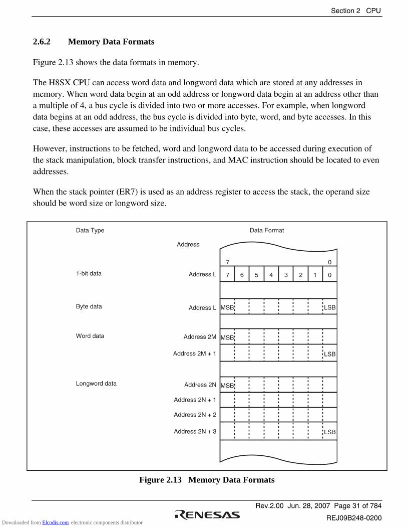
Section 2 CPU
Rev.2.00 Jun. 28, 2007 Page 31 of 784
REJ09B248-0200
2.6.2 Memory Data Formats
Figure 2.13 shows the data formats in memory.
The H8SX CPU can access word data and longword data which are stored at any addresses in memory. When word data begin at an odd address or longword data begin at an address other than a multiple of 4, a bus cycle is divided into two or more accesses. For example, when longword data begins at an odd address, the bus cycle is divided into byte, word, and byte accesses. In this case, these accesses are assumed to be individual bus cycles.
However, instructions to be fetched, word and longword data to be accessed during execution of the stack manipulation, block transfer instructions, and MAC instruction should be located to even addresses.
When the stack pointer (ER7) is used as an address register to access the stack, the operand size should be word size or longword size.
7 6 5 4 3 2 1 0
7 0
MSB LSB
MSB
LSB
MSB
LSB
Data Type Data Format
1-bit data
Byte data
Word data
Longword data
Address
Address L
Address L
Address 2M
Address 2M + 1
Address 2N
Address 2N + 1
Address 2N + 2
Address 2N + 3
Figure 2.13 Memory Data Formats
Downloaded from Elcodis.com electronic components distributor

Section 2 CPU
Rev.2.00 Jun. 28, 2007 Page 32 of 784
REJ09B248-0200
2.7 Instruction Set
The H8SX CPU has 87 types of instructions. The instructions are classified by function as shown in table 2.1.
Note: The arithmetic operation, logic operation, shift, and bit manipulation instructions are called operation instruction in this manual.
Table 2.1 Instruction Classification
Function Instructions Size Types
Data transfer MOV B/W/L 6
MOVFPE*6, MOVTPE*6 B
POP, PUSH*1 W/L
LDM, STM L
MOVA B/W*2
Block transfer EEPMOV B 3
MOVMD B/W/L
MOVSD B
ADD, ADDX, SUB, SUBX, CMP, NEG, INC, DEC B/W/L 27 Arithmetic operations DAA, DAS B
ADDS, SUBS L
MULXU, DIVXU, MULXS, DIVXS B/W
MULU, DIVU, MULS, DIVS W/L
MULU/U, MULS/U L
EXTU, EXTS W/L
TAS B
MAC
LDMAC, STMAC
CLRMAC
Downloaded from Elcodis.com electronic components distributor
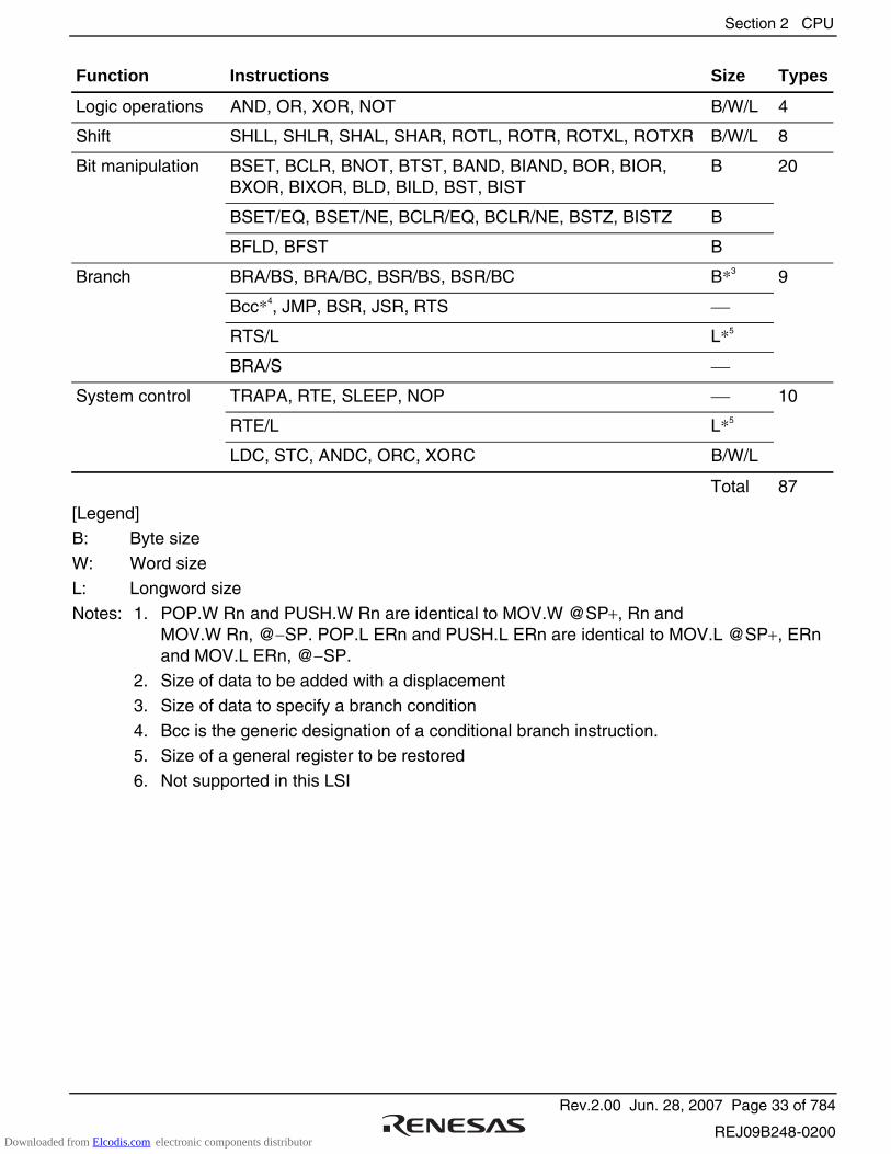
Section 2 CPU
Rev.2.00 Jun. 28, 2007 Page 33 of 784
REJ09B248-0200
Function Instructions Size Types
Logic operations AND, OR, XOR, NOT B/W/L 4
Shift SHLL, SHLR, SHAL, SHAR, ROTL, ROTR, ROTXL, ROTXR B/W/L 8
Bit manipulation BSET, BCLR, BNOT, BTST, BAND, BIAND, BOR, BIOR, BXOR, BIXOR, BLD, BILD, BST, BIST
B 20
BSET/EQ, BSET/NE, BCLR/EQ, BCLR/NE, BSTZ, BISTZ B
BFLD, BFST B
Branch BRA/BS, BRA/BC, BSR/BS, BSR/BC B*3 9
Bcc*4, JMP, BSR, JSR, RTS
RTS/L L*5
BRA/S
System control TRAPA, RTE, SLEEP, NOP 10
RTE/L L*5
LDC, STC, ANDC, ORC, XORC B/W/L
Total 87
[Legend]
B: Byte size
W: Word size L: Longword size
Notes: 1. POP.W Rn and PUSH.W Rn are identical to MOV.W @SP+, Rn and MOV.W Rn, @−SP. POP.L ERn and PUSH.L ERn are identical to MOV.L @SP+, ERn and MOV.L ERn, @−SP.
2. Size of data to be added with a displacement
3. Size of data to specify a branch condition
4. Bcc is the generic designation of a conditional branch instruction. 5. Size of a general register to be restored
6. Not supported in this LSI
Downloaded from Elcodis.com electronic components distributor
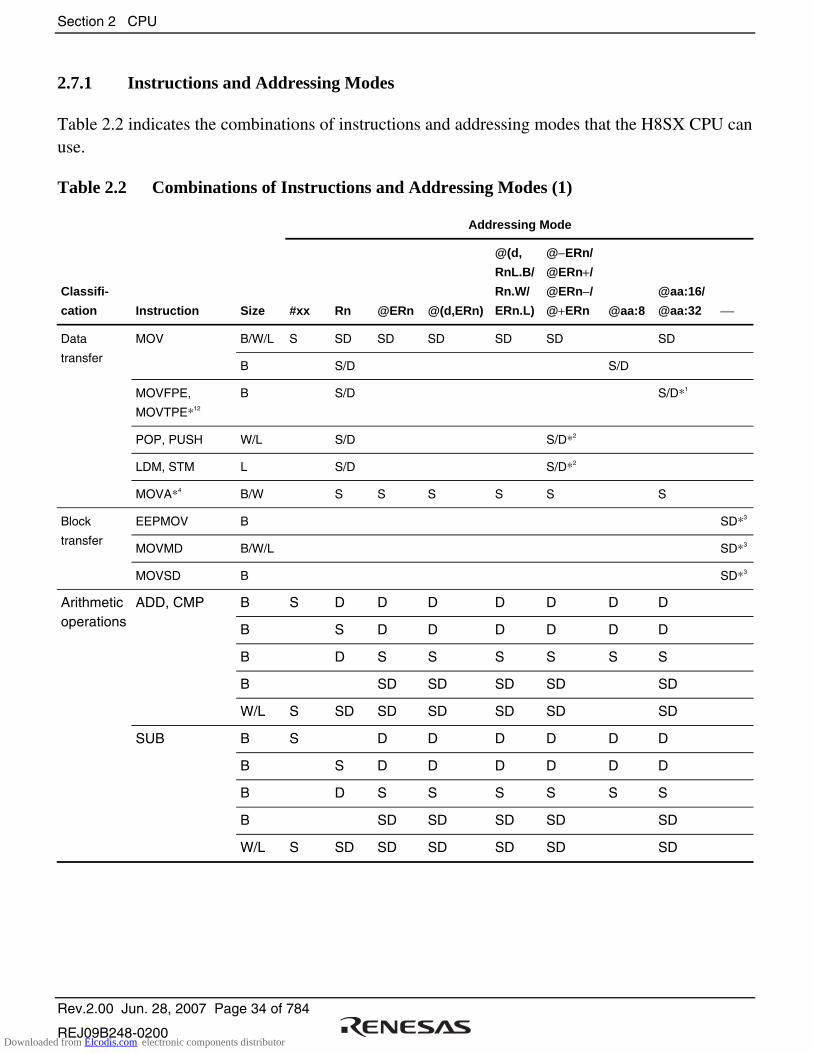
Section 2 CPU
Rev.2.00 Jun. 28, 2007 Page 34 of 784
REJ09B248-0200
2.7.1 Instructions and Addressing Modes
Table 2.2 indicates the combinations of instructions and addressing modes that the H8SX CPU can use.
Table 2.2 Combinations of Instructions and Addressing Modes (1)
Addressing Mode
Classifi-
cation Instruction Size #xx Rn @ERn @(d,ERn)
@(d,
RnL.B/
Rn.W/
ERn.L)
@−ERn/
@ERn+/
@ERn−/
@+ERn @aa:8
@aa:16/
@aa:32
B/W/L S SD SD SD SD SD SD MOV
B S/D S/D
MOVFPE,
MOVTPE*12
B S/D S/D*1
POP, PUSH W/L S/D S/D*2
LDM, STM L S/D S/D*2
Data
transfer
MOVA*4 B/W S S S S S S
EEPMOV B SD*3
MOVMD B/W/L SD*3
Block
transfer
MOVSD B SD*3
B S D D D D D D D
B S D D D D D D
B D S S S S S S
B SD SD SD SD SD
ADD, CMP
W/L S SD SD SD SD SD SD
B S D D D D D D
B S D D D D D D
B D S S S S S S
B SD SD SD SD SD
Arithmetic operations
SUB
W/L S SD SD SD SD SD SD
Downloaded from Elcodis.com electronic components distributor

Section 2 CPU
Rev.2.00 Jun. 28, 2007 Page 35 of 784
REJ09B248-0200
Addressing Mode
Classifi-
cation Instruction Size #xx Rn @ERn @(d,ERn)
@(d,
RnL.B/
Rn.W/
ERn.L)
@−ERn/
@ERn+/
@ERn−/
@+ERn @aa:8
@aa:16/
@aa:32
ADDX, SUBX B/W/L S SD
B/W/L S SD
B/W/L S SD*5
INC, DEC B/W/L D
ADDS, SUBS L D
DAA, DAS B D
MULXU, DIVXU B/W S:4 SD
MULU, DIVU W/L S:4 SD
MULXS, DIVXS B/W S:4 SD
MULS, DIVS W/L S:4 SD
B D D D D D D D NEG
W/L D D D D D D
EXTU, EXTS W/L D D D D D D
TAS B D
MAC
CLRMAC O
LDMAC S
Arithmetic
operations
STMAC D
B S D D D D D D
B D S S S S S S
B SD SD SD SD SD
AND, OR, XOR
W/L S SD SD SD SD SD SD
B D D D D D D D
Logic
operations
NOT
W/L D D D D D D
Downloaded from Elcodis.com electronic components distributor

Section 2 CPU
Rev.2.00 Jun. 28, 2007 Page 36 of 784
REJ09B248-0200
Addressing Mode
Classifi-
cation Instruction Size #xx Rn @ERn @(d,ERn)
@(d,
RnL.B/
Rn.W/
ERn.L)
@−ERn/
@ERn+/
@ERn−/
@+ERn @aa:8
@aa:16/
@aa:32
B D D D D D D D
W/L*6 D D D D D D
SHLL, SHLR
B/W/L*7 D
B D D D D D D D
Shift
SHAL, SHAR,
ROTL, ROTR,
ROTXL, ROTXR W/L D D D D D D
BSET, BCLR,
BNOT, BTST,
BSET/cc,
BCLR/cc
B D D D D
BAND, BIAND,
BOR, BIOR,
BXOR, BIXOR,
BLD, BILD, BST,
BIST, BSTZ,
BISTZ
B D D D D
BFLD B D S S S
Bit manipu-
lation
BFST B S D D D
BRA/BS, BRA/BC*8
B S S S Branch
BSR/BS, BSR/BC*8
B S S S
Downloaded from Elcodis.com electronic components distributor
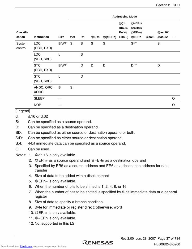
Section 2 CPU
Rev.2.00 Jun. 28, 2007 Page 37 of 784
REJ09B248-0200
Addressing Mode
Classifi-
cation Instruction Size #xx Rn @ERn @(d,ERn)
@(d,
RnL.B/
Rn.W/
ERn.L)
@−ERn/
@ERn+/
@ERn−/
@+ERn @aa:8
@aa:16/
@aa:32
LDC (CCR, EXR)
B/W*9 S S S S S*10 S
LDC (VBR, SBR)
L S
STC (CCR, EXR)
B/W*9 D D D D*11 D
STC (VBR, SBR)
L D
ANDC, ORC, XORC
B S
SLEEP O
System control
NOP O
[Legend] d: d:16 or d:32
S: Can be specified as a source operand.
D: Can be specified as a destination operand. SD: Can be specified as either source or destination operand or both.
S/D: Can be specified as either source or destination operand.
S:4: 4-bit immediate data can be specified as a source operand.
O: Can be used.
Notes: 1. @aa:16 is only available.
2. @ERn+ as a source operand and @−ERn as a destination operand
3. Specified by ER5 as a source address and ER6 as a destination address for data transfer
4. Size of data to be added with a displacement 5. @ERn− is only available.
6. When the number of bits to be shifted is 1, 2, 4, 8, or 16
7. When the number of bits to be shifted is specified by 5-bit immediate data or a general register
8. Size of data to specify a branch condition 9. Byte for immediate or register direct; otherwise, word
10. @ERn+ is only available.
11. @−ERn is only available. 12. Not supported in this LSI
Downloaded from Elcodis.com electronic components distributor
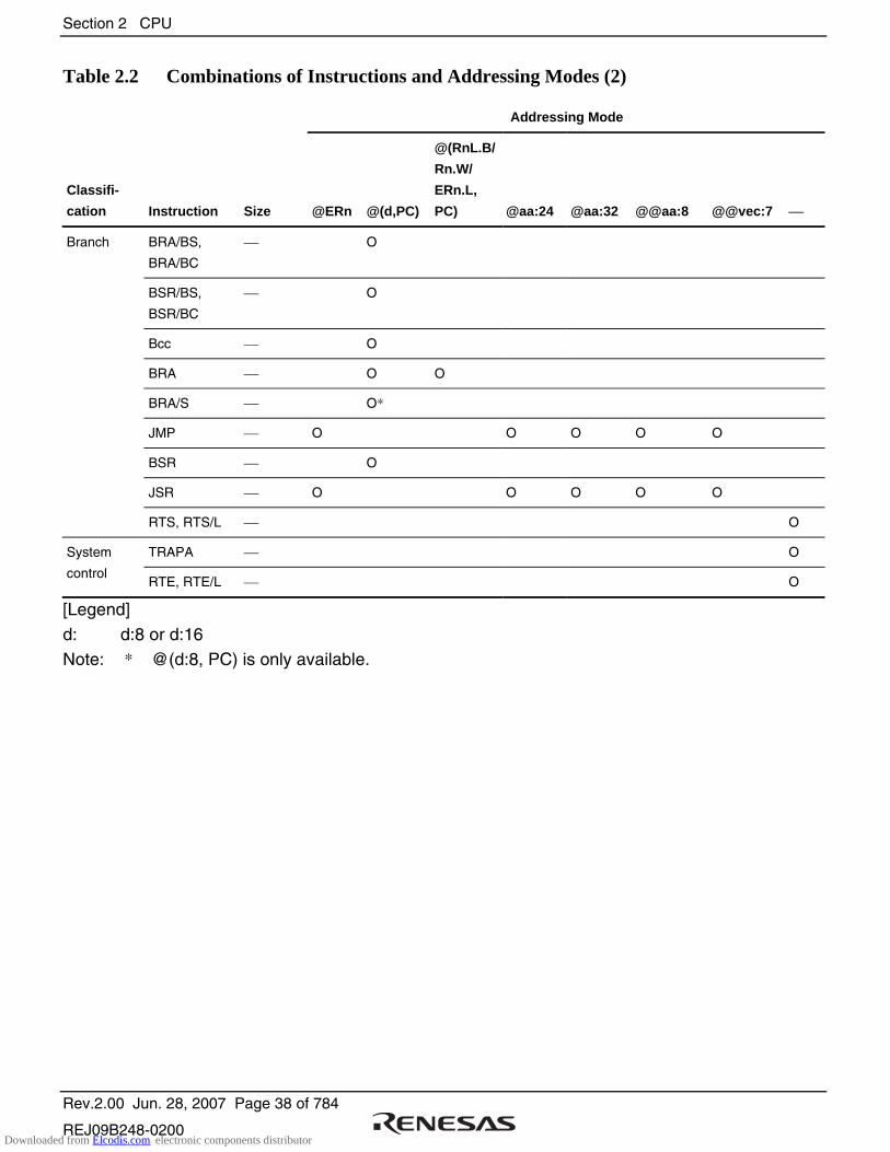
Section 2 CPU
Rev.2.00 Jun. 28, 2007 Page 38 of 784
REJ09B248-0200
Table 2.2 Combinations of Instructions and Addressing Modes (2)
Addressing Mode
Classifi-
cation Instruction Size @ERn @(d,PC)
@(RnL.B/
Rn.W/
ERn.L,
PC) @aa:24 @aa:32 @@aa:8 @@vec:7
BRA/BS,
BRA/BC
O
BSR/BS,
BSR/BC
O
Bcc O
BRA O O
BRA/S O*
JMP O O O O O
BSR O
JSR O O O O O
Branch
RTS, RTS/L O
TRAPA O System
control RTE, RTE/L O
[Legend]
d: d:8 or d:16 Note: * @(d:8, PC) is only available.
Downloaded from Elcodis.com electronic components distributor

Section 2 CPU
Rev.2.00 Jun. 28, 2007 Page 39 of 784
REJ09B248-0200
2.7.2 Table of Instructions Classified by Function
Tables 2.4 to 2.11 summarize the instructions in each functional category. The notation used in the tables is defined in table 2.3.
Table 2.3 Operation Notation
Operation Notation Description
Rd General register (destination)*
Rs General register (source)*
Rn General register*
ERn General register (32-bit register)
(EAd) Destination operand
(EAs) Source operand
EXR Extended control register
CCR Condition-code register
VBR Vector base register
SBR Short address base register
N N (negative) flag in CCR
Z Z (zero) flag in CCR
V V (overflow) flag in CCR
C C (carry) flag in CCR
PC Program counter
SP Stack pointer
#IMM Immediate data
disp Displacement
+ Addition
− Subtraction
× Multiplication
÷ Division
∧ Logical AND
∨ Logical OR
⊕ Logical exclusive OR
→ Move
∼ Logical not (logical complement)
:8/:16/:24/:32 8-, 16-, 24-, or 32-bit length
Note: * General registers include 8-bit registers (R0H to R7H, R0L to R7L), 16-bit registers (R0 to R7, E0 to E7), and 32-bit registers (ER0 to ER7).
Downloaded from Elcodis.com electronic components distributor
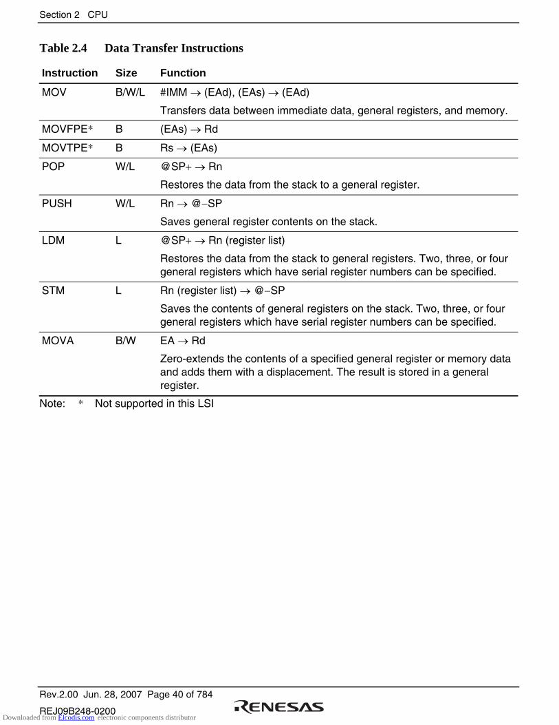
Section 2 CPU
Rev.2.00 Jun. 28, 2007 Page 40 of 784
REJ09B248-0200
Table 2.4 Data Transfer Instructions
Instruction Size Function
MOV B/W/L #IMM → (EAd), (EAs) → (EAd)
Transfers data between immediate data, general registers, and memory.
MOVFPE* B (EAs) → Rd
MOVTPE* B Rs → (EAs)
POP W/L @SP+ → Rn
Restores the data from the stack to a general register.
PUSH W/L Rn → @−SP
Saves general register contents on the stack.
LDM L @SP+ → Rn (register list)
Restores the data from the stack to general registers. Two, three, or four general registers which have serial register numbers can be specified.
STM L Rn (register list) → @−SP
Saves the contents of general registers on the stack. Two, three, or four general registers which have serial register numbers can be specified.
MOVA B/W EA → Rd
Zero-extends the contents of a specified general register or memory data and adds them with a displacement. The result is stored in a general register.
Note: * Not supported in this LSI
Downloaded from Elcodis.com electronic components distributor
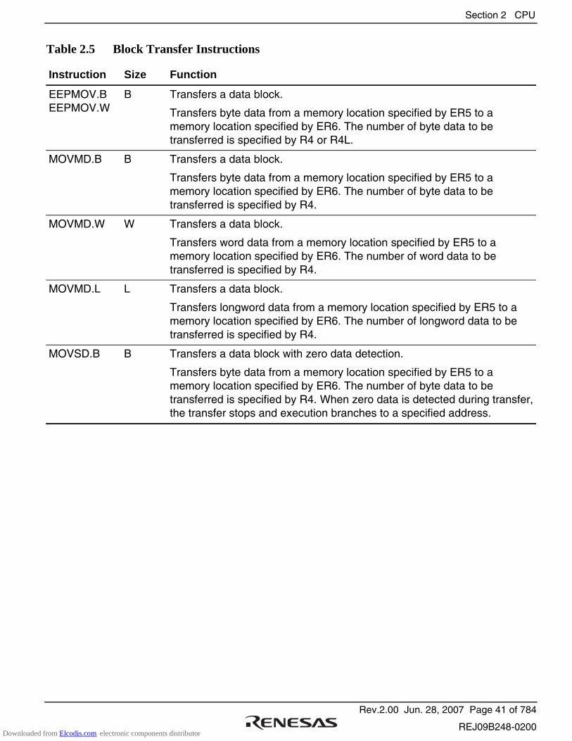
Section 2 CPU
Rev.2.00 Jun. 28, 2007 Page 41 of 784
REJ09B248-0200
Table 2.5 Block Transfer Instructions
Instruction Size Function
EEPMOV.B EEPMOV.W
B Transfers a data block.
Transfers byte data from a memory location specified by ER5 to a memory location specified by ER6. The number of byte data to be transferred is specified by R4 or R4L.
MOVMD.B B Transfers a data block.
Transfers byte data from a memory location specified by ER5 to a memory location specified by ER6. The number of byte data to be transferred is specified by R4.
MOVMD.W W Transfers a data block.
Transfers word data from a memory location specified by ER5 to a memory location specified by ER6. The number of word data to be transferred is specified by R4.
MOVMD.L L Transfers a data block.
Transfers longword data from a memory location specified by ER5 to a memory location specified by ER6. The number of longword data to be transferred is specified by R4.
MOVSD.B B Transfers a data block with zero data detection.
Transfers byte data from a memory location specified by ER5 to a memory location specified by ER6. The number of byte data to be transferred is specified by R4. When zero data is detected during transfer, the transfer stops and execution branches to a specified address.
Downloaded from Elcodis.com electronic components distributor
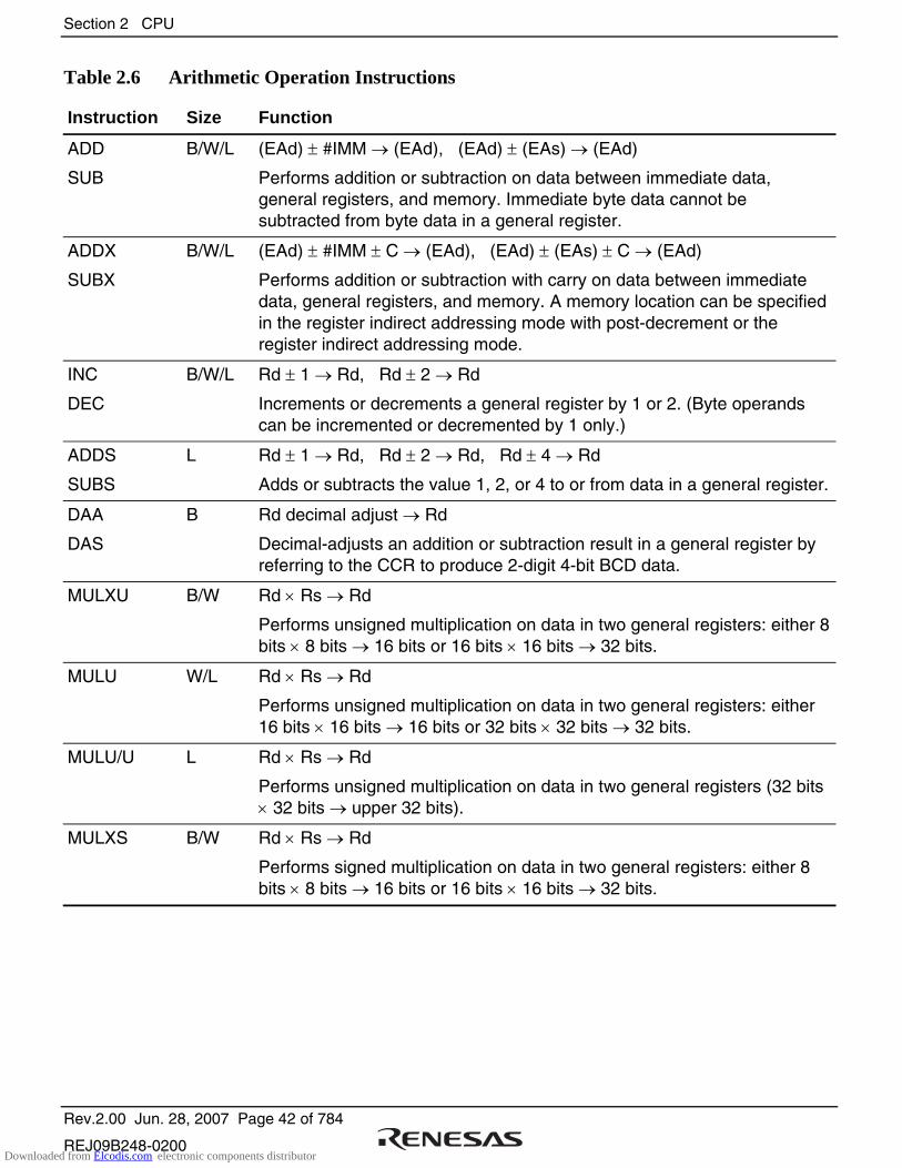
Section 2 CPU
Rev.2.00 Jun. 28, 2007 Page 42 of 784
REJ09B248-0200
Table 2.6 Arithmetic Operation Instructions
Instruction Size Function
ADD
SUB
B/W/L (EAd) ± #IMM → (EAd), (EAd) ± (EAs) → (EAd)
Performs addition or subtraction on data between immediate data, general registers, and memory. Immediate byte data cannot be subtracted from byte data in a general register.
ADDX
SUBX
B/W/L (EAd) ± #IMM ± C → (EAd), (EAd) ± (EAs) ± C → (EAd)
Performs addition or subtraction with carry on data between immediate data, general registers, and memory. A memory location can be specified in the register indirect addressing mode with post-decrement or the register indirect addressing mode.
INC
DEC
B/W/L Rd ± 1 → Rd, Rd ± 2 → Rd
Increments or decrements a general register by 1 or 2. (Byte operands can be incremented or decremented by 1 only.)
ADDS
SUBS
L Rd ± 1 → Rd, Rd ± 2 → Rd, Rd ± 4 → Rd
Adds or subtracts the value 1, 2, or 4 to or from data in a general register.
DAA
DAS
B Rd decimal adjust → Rd
Decimal-adjusts an addition or subtraction result in a general register by referring to the CCR to produce 2-digit 4-bit BCD data.
MULXU B/W Rd × Rs → Rd
Performs unsigned multiplication on data in two general registers: either 8 bits × 8 bits → 16 bits or 16 bits × 16 bits → 32 bits.
MULU W/L Rd × Rs → Rd
Performs unsigned multiplication on data in two general registers: either 16 bits × 16 bits → 16 bits or 32 bits × 32 bits → 32 bits.
MULU/U L Rd × Rs → Rd
Performs unsigned multiplication on data in two general registers (32 bits × 32 bits → upper 32 bits).
MULXS B/W Rd × Rs → Rd
Performs signed multiplication on data in two general registers: either 8 bits × 8 bits → 16 bits or 16 bits × 16 bits → 32 bits.
Downloaded from Elcodis.com electronic components distributor

Section 2 CPU
Rev.2.00 Jun. 28, 2007 Page 43 of 784
REJ09B248-0200
Instruction Size Function
MULS W/L Rd × Rs → Rd
Performs signed multiplication on data in two general registers: either 16 bits × 16 bits → 16 bits or 32 bits × 32 bits → 32 bits.
MULS/U L Rd × Rs → Rd
Performs signed multiplication on data in two general registers (32 bits × 32 bits → upper 32 bits).
DIVXU B/W Rd ÷ Rs → Rd
Performs unsigned division on data in two general registers: either 16 bits ÷ 8 bits → 8-bit quotient and 8-bit remainder or 32 bits ÷ 16 bits → 16-bit quotient and 16-bit remainder.
DIVU W/L Rd ÷ Rs → Rd
Performs unsigned division on data in two general registers: either 16 bits ÷ 16 bits → 16-bit quotient or 32 bits ÷ 32 bits → 32-bit quotient.
DIVXS B/W Rd ÷ Rs → Rd
Performs signed division on data in two general registers: either 16 bits ÷ 8 bits → 8-bit quotient and 8-bit remainder or 32 bits ÷ 16 bits → 16-bit quotient and 16-bit remainder.
DIVS W/L Rd ÷ Rs → Rd
Performs signed division on data in two general registers: either 16 bits ÷ 16 bits → 16-bit quotient or 32 bits ÷ 32 bits → 32-bit quotient.
CMP B/W/L (EAd) − #IMM, (EAd) − (EAs)
Compares data between immediate data, general registers, and memory and stores CCR bits according to the result.
NEG B/W/L 0 − (EAd) → (EAd)
Takes the two's complement (arithmetic complement) of the contents of a general register or a memory location.
EXTU W/L (EAd) (zero extension) → (EAd)
Extends the lower 8 or 16 bits of data in a general register or a memory location to word or longword size by padding with 0s.
The lower eight bits can be extended to word or longword, or lower 16 bits to longword.
Downloaded from Elcodis.com electronic components distributor
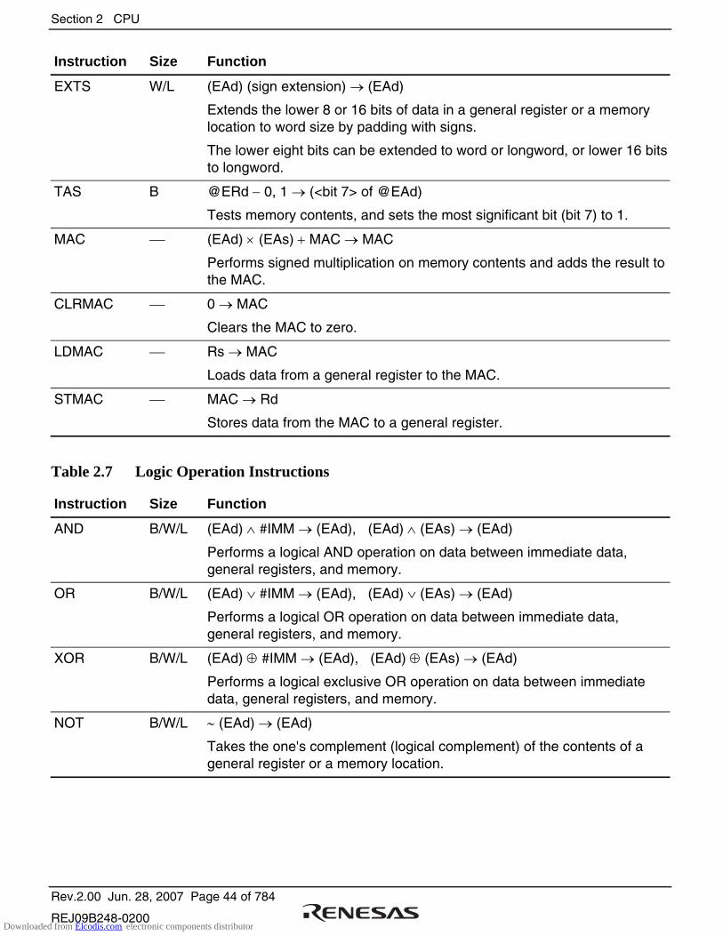
Section 2 CPU
Rev.2.00 Jun. 28, 2007 Page 44 of 784
REJ09B248-0200
Instruction Size Function
EXTS W/L (EAd) (sign extension) → (EAd)
Extends the lower 8 or 16 bits of data in a general register or a memory location to word size by padding with signs.
The lower eight bits can be extended to word or longword, or lower 16 bits to longword.
TAS B @ERd − 0, 1 → (<bit 7> of @EAd)
Tests memory contents, and sets the most significant bit (bit 7) to 1.
MAC (EAd) × (EAs) + MAC → MAC
Performs signed multiplication on memory contents and adds the result to the MAC.
CLRMAC 0 → MAC
Clears the MAC to zero.
LDMAC Rs → MAC
Loads data from a general register to the MAC.
STMAC MAC → Rd
Stores data from the MAC to a general register.
Table 2.7 Logic Operation Instructions
Instruction Size Function
AND B/W/L (EAd) ∧ #IMM → (EAd), (EAd) ∧ (EAs) → (EAd)
Performs a logical AND operation on data between immediate data, general registers, and memory.
OR B/W/L (EAd) ∨ #IMM → (EAd), (EAd) ∨ (EAs) → (EAd)
Performs a logical OR operation on data between immediate data, general registers, and memory.
XOR B/W/L (EAd) ⊕ #IMM → (EAd), (EAd) ⊕ (EAs) → (EAd)
Performs a logical exclusive OR operation on data between immediate data, general registers, and memory.
NOT B/W/L ∼ (EAd) → (EAd)
Takes the one's complement (logical complement) of the contents of a general register or a memory location.
Downloaded from Elcodis.com electronic components distributor
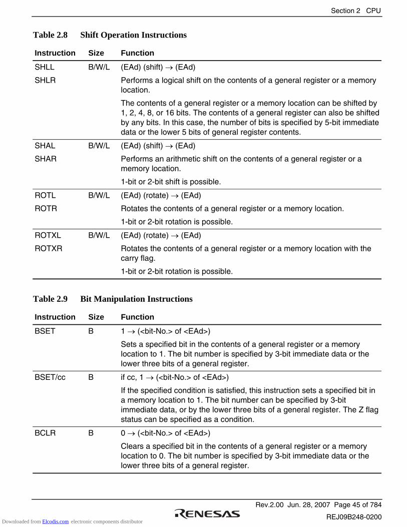
Section 2 CPU
Rev.2.00 Jun. 28, 2007 Page 45 of 784
REJ09B248-0200
Table 2.8 Shift Operation Instructions
Instruction Size Function
SHLL
SHLR
B/W/L (EAd) (shift) → (EAd)
Performs a logical shift on the contents of a general register or a memory location.
The contents of a general register or a memory location can be shifted by 1, 2, 4, 8, or 16 bits. The contents of a general register can also be shifted by any bits. In this case, the number of bits is specified by 5-bit immediate data or the lower 5 bits of general register contents.
SHAL
SHAR
B/W/L (EAd) (shift) → (EAd)
Performs an arithmetic shift on the contents of a general register or a memory location.
1-bit or 2-bit shift is possible.
ROTL
ROTR
B/W/L (EAd) (rotate) → (EAd)
Rotates the contents of a general register or a memory location.
1-bit or 2-bit rotation is possible.
ROTXL
ROTXR
B/W/L (EAd) (rotate) → (EAd)
Rotates the contents of a general register or a memory location with the carry flag.
1-bit or 2-bit rotation is possible.
Table 2.9 Bit Manipulation Instructions
Instruction Size Function
BSET B 1 → (<bit-No.> of <EAd>)
Sets a specified bit in the contents of a general register or a memory location to 1. The bit number is specified by 3-bit immediate data or the lower three bits of a general register.
BSET/cc B if cc, 1 → (<bit-No.> of <EAd>)
If the specified condition is satisfied, this instruction sets a specified bit in a memory location to 1. The bit number can be specified by 3-bit immediate data, or by the lower three bits of a general register. The Z flag status can be specified as a condition.
BCLR B 0 → (<bit-No.> of <EAd>)
Clears a specified bit in the contents of a general register or a memory location to 0. The bit number is specified by 3-bit immediate data or the lower three bits of a general register.
Downloaded from Elcodis.com electronic components distributor
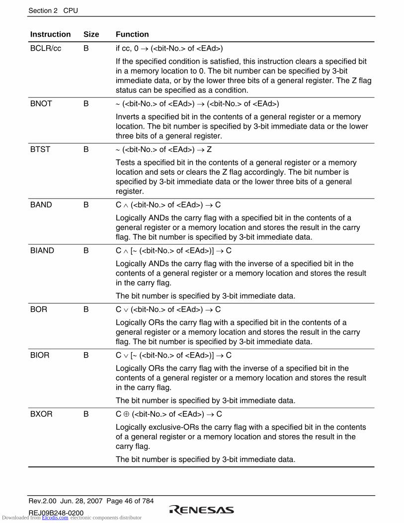
Section 2 CPU
Rev.2.00 Jun. 28, 2007 Page 46 of 784
REJ09B248-0200
Instruction Size Function
BCLR/cc B if cc, 0 → (<bit-No.> of <EAd>)
If the specified condition is satisfied, this instruction clears a specified bit in a memory location to 0. The bit number can be specified by 3-bit immediate data, or by the lower three bits of a general register. The Z flag status can be specified as a condition.
BNOT B ∼ (<bit-No.> of <EAd>) → (<bit-No.> of <EAd>)
Inverts a specified bit in the contents of a general register or a memory location. The bit number is specified by 3-bit immediate data or the lower three bits of a general register.
BTST B ∼ (<bit-No.> of <EAd>) → Z
Tests a specified bit in the contents of a general register or a memory location and sets or clears the Z flag accordingly. The bit number is specified by 3-bit immediate data or the lower three bits of a general register.
BAND B C ∧ (<bit-No.> of <EAd>) → C
Logically ANDs the carry flag with a specified bit in the contents of a general register or a memory location and stores the result in the carry flag. The bit number is specified by 3-bit immediate data.
BIAND B C ∧ [∼ (<bit-No.> of <EAd>)] → C
Logically ANDs the carry flag with the inverse of a specified bit in the contents of a general register or a memory location and stores the result in the carry flag.
The bit number is specified by 3-bit immediate data.
BOR B C ∨ (<bit-No.> of <EAd>) → C
Logically ORs the carry flag with a specified bit in the contents of a general register or a memory location and stores the result in the carry flag. The bit number is specified by 3-bit immediate data.
BIOR B C ∨ [∼ (<bit-No.> of <EAd>)] → C
Logically ORs the carry flag with the inverse of a specified bit in the contents of a general register or a memory location and stores the result in the carry flag.
The bit number is specified by 3-bit immediate data.
BXOR B C ⊕ (<bit-No.> of <EAd>) → C
Logically exclusive-ORs the carry flag with a specified bit in the contents of a general register or a memory location and stores the result in the carry flag.
The bit number is specified by 3-bit immediate data.
Downloaded from Elcodis.com electronic components distributor
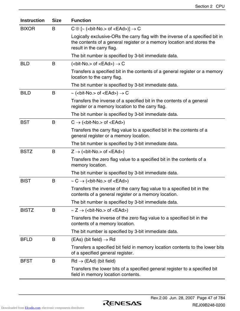
Section 2 CPU
Rev.2.00 Jun. 28, 2007 Page 47 of 784
REJ09B248-0200
Instruction Size Function
BIXOR B C ⊕ [∼ (<bit-No.> of <EAd>)] → C
Logically exclusive-ORs the carry flag with the inverse of a specified bit in the contents of a general register or a memory location and stores the result in the carry flag.
The bit number is specified by 3-bit immediate data.
BLD B (<bit-No.> of <EAd>) → C
Transfers a specified bit in the contents of a general register or a memory location to the carry flag.
The bit number is specified by 3-bit immediate data.
BILD B ∼ (<bit-No.> of <EAd>) → C
Transfers the inverse of a specified bit in the contents of a general register or a memory location to the carry flag.
The bit number is specified by 3-bit immediate data.
BST B C → (<bit-No.> of <EAd>)
Transfers the carry flag value to a specified bit in the contents of a general register or a memory location.
The bit number is specified by 3-bit immediate data.
BSTZ B Z → (<bit-No.> of <EAd>)
Transfers the zero flag value to a specified bit in the contents of a memory location.
The bit number is specified by 3-bit immediate data.
BIST B ∼ C → (<bit-No.> of <EAd>)
Transfers the inverse of the carry flag value to a specified bit in the contents of a general register or a memory location.
The bit number is specified by 3-bit immediate data.
BISTZ B ∼ Z → (<bit-No.> of <EAd>)
Transfers the inverse of the zero flag value to a specified bit in the contents of a memory location.
The bit number is specified by 3-bit immediate data.
BFLD B (EAs) (bit field) → Rd
Transfers a specified bit field in memory location contents to the lower bits of a specified general register.
BFST B Rd → (EAd) (bit field)
Transfers the lower bits of a specified general register to a specified bit field in memory location contents.
Downloaded from Elcodis.com electronic components distributor
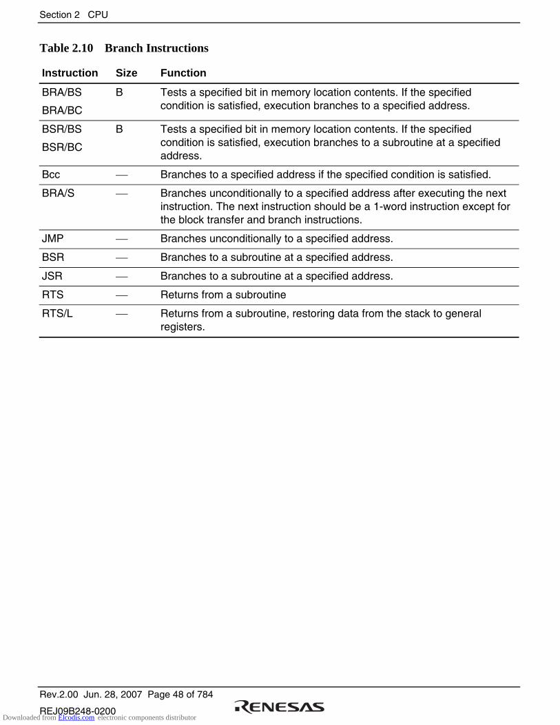
Section 2 CPU
Rev.2.00 Jun. 28, 2007 Page 48 of 784
REJ09B248-0200
Table 2.10 Branch Instructions
Instruction Size Function
BRA/BS
BRA/BC
B Tests a specified bit in memory location contents. If the specified condition is satisfied, execution branches to a specified address.
BSR/BS
BSR/BC
B Tests a specified bit in memory location contents. If the specified condition is satisfied, execution branches to a subroutine at a specified address.
Bcc Branches to a specified address if the specified condition is satisfied.
BRA/S Branches unconditionally to a specified address after executing the next instruction. The next instruction should be a 1-word instruction except for the block transfer and branch instructions.
JMP Branches unconditionally to a specified address.
BSR Branches to a subroutine at a specified address.
JSR Branches to a subroutine at a specified address.
RTS Returns from a subroutine
RTS/L Returns from a subroutine, restoring data from the stack to general registers.
Downloaded from Elcodis.com electronic components distributor
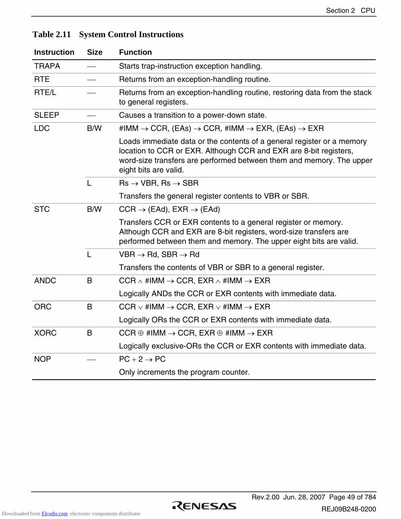
Section 2 CPU
Rev.2.00 Jun. 28, 2007 Page 49 of 784
REJ09B248-0200
Table 2.11 System Control Instructions
Instruction Size Function
TRAPA Starts trap-instruction exception handling.
RTE Returns from an exception-handling routine.
RTE/L Returns from an exception-handling routine, restoring data from the stack to general registers.
SLEEP Causes a transition to a power-down state.
B/W #IMM → CCR, (EAs) → CCR, #IMM → EXR, (EAs) → EXR
Loads immediate data or the contents of a general register or a memory location to CCR or EXR. Although CCR and EXR are 8-bit registers, word-size transfers are performed between them and memory. The upper eight bits are valid.
LDC
L Rs → VBR, Rs → SBR
Transfers the general register contents to VBR or SBR.
B/W CCR → (EAd), EXR → (EAd)
Transfers CCR or EXR contents to a general register or memory. Although CCR and EXR are 8-bit registers, word-size transfers are performed between them and memory. The upper eight bits are valid.
STC
L VBR → Rd, SBR → Rd
Transfers the contents of VBR or SBR to a general register.
ANDC B CCR ∧ #IMM → CCR, EXR ∧ #IMM → EXR
Logically ANDs the CCR or EXR contents with immediate data.
ORC B CCR ∨ #IMM → CCR, EXR ∨ #IMM → EXR
Logically ORs the CCR or EXR contents with immediate data.
XORC B CCR ⊕ #IMM → CCR, EXR ⊕ #IMM → EXR
Logically exclusive-ORs the CCR or EXR contents with immediate data.
NOP PC + 2 → PC
Only increments the program counter.
Downloaded from Elcodis.com electronic components distributor

Section 2 CPU
Rev.2.00 Jun. 28, 2007 Page 50 of 784
REJ09B248-0200
2.7.3 Basic Instruction Formats
The H8SX CPU instructions consist of 2-byte (1-word) units. An instruction consists of an operation field (op field), a register field (r field), an effective address extension (EA field), and a condition field (cc).
Figure 2.14 shows examples of instruction formats.
op
op rn rm
NOP, RTS, etc.
ADD.B Rn, Rm, etc.
MOV.B @(d:16, Rn), Rm, etc.
(1) Operation field only
(2) Operation field and register fields
(3) Operation field, register fields, and effective address extension
rn rmop
EA (disp)
(4) Operation field, effective address extension, and condition field
op cc EA (disp) BRA d:16, etc
Figure 2.14 Instruction Formats
• Operation Field
Indicates the function of the instruction, the addressing mode, and the operation to be carried out on the operand. The operation field always includes the first four bits of the instruction. Some instructions have two operation fields.
• Register Field
Specifies a general register. Address registers are specified by 3 bits, data registers by 3 bits or 4 bits. Some instructions have two register fields. Some have no register field.
• Effective Address Extension
Eight, 16, or 32 bits specifying immediate data, an absolute address, or a displacement.
• Condition Field
Specifies the branching condition of Bcc instructions.
Downloaded from Elcodis.com electronic components distributor
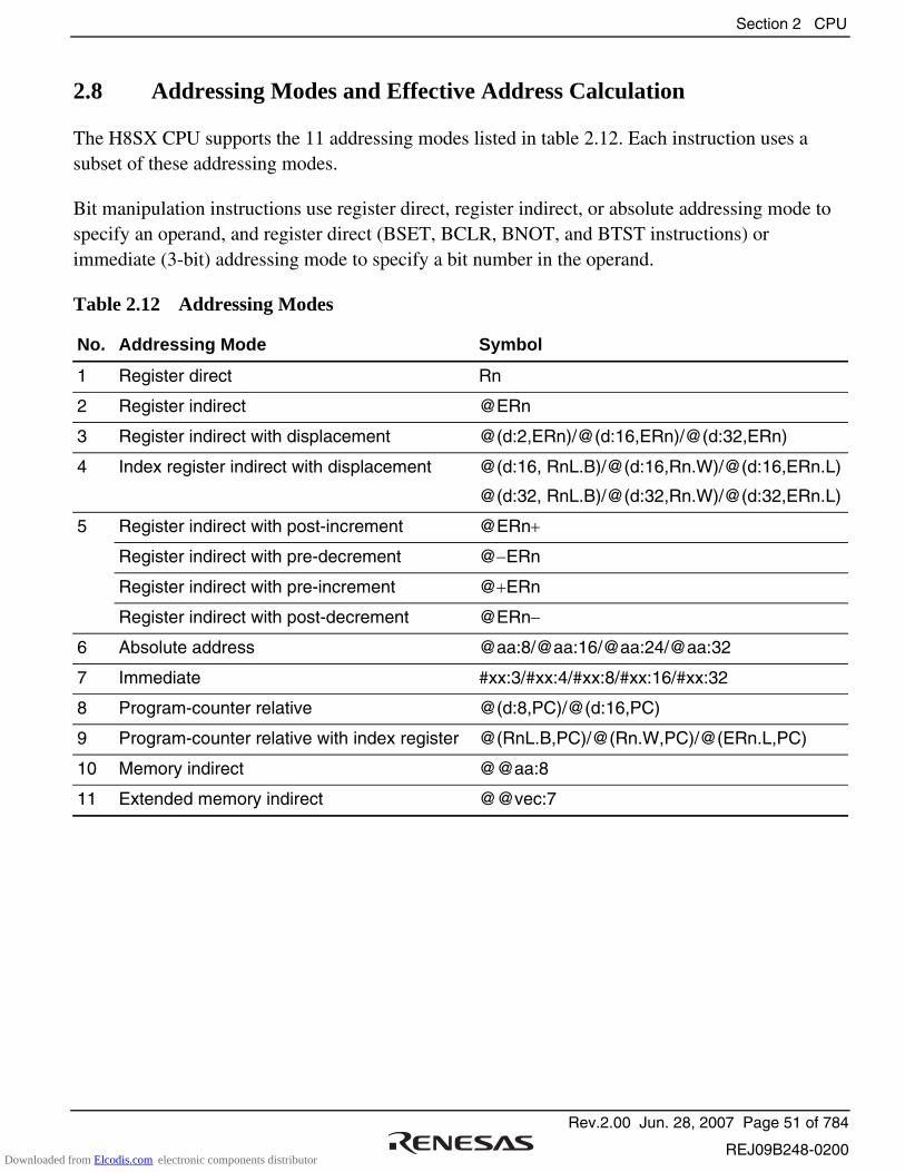
Section 2 CPU
Rev.2.00 Jun. 28, 2007 Page 51 of 784
REJ09B248-0200
2.8 Addressing Modes and Effective Address Calculation
The H8SX CPU supports the 11 addressing modes listed in table 2.12. Each instruction uses a subset of these addressing modes.
Bit manipulation instructions use register direct, register indirect, or absolute addressing mode to specify an operand, and register direct (BSET, BCLR, BNOT, and BTST instructions) or immediate (3-bit) addressing mode to specify a bit number in the operand.
Table 2.12 Addressing Modes
No. Addressing Mode Symbol
1 Register direct Rn
2 Register indirect @ERn
3 Register indirect with displacement @(d:2,ERn)/@(d:16,ERn)/@(d:32,ERn)
4 Index register indirect with displacement @(d:16, RnL.B)/@(d:16,Rn.W)/@(d:16,ERn.L)
@(d:32, RnL.B)/@(d:32,Rn.W)/@(d:32,ERn.L)
Register indirect with post-increment @ERn+
Register indirect with pre-decrement @−ERn
Register indirect with pre-increment @+ERn
5
Register indirect with post-decrement @ERn−
6 Absolute address @aa:8/@aa:16/@aa:24/@aa:32
7 Immediate #xx:3/#xx:4/#xx:8/#xx:16/#xx:32
8 Program-counter relative @(d:8,PC)/@(d:16,PC)
9 Program-counter relative with index register @(RnL.B,PC)/@(Rn.W,PC)/@(ERn.L,PC)
10 Memory indirect @@aa:8
11 Extended memory indirect @@vec:7
Downloaded from Elcodis.com electronic components distributor
Section 2 CPU
Rev.2.00 Jun. 28, 2007 Page 52 of 784
REJ09B248-0200
2.8.1 Register Direct—Rn
The operand value is the contents of an 8-, 16-, or 32-bit general register which is specified by the register field in the instruction code. R0H to R7H and R0L to R7L can be specified as 8-bit registers. R0 to R7 and E0 to E7 can be specified as 16-bit registers. ER0 to ER7 can be specified as 32-bit registers.
2.8.2 Register Indirect—@ERn
The operand value is the contents of a memory location which is pointed to by the contents of an address register (ERn). ERn is specified by the register field in the instruction code.
In advanced mode, if this addressing mode is used in a branch instruction, the lower 24 bits are valid and the upper eight bits are all assumed to be 0 (H'00).
2.8.3 Register Indirect with Displacement—@(d:2, ERn), @(d:16, ERn), or
@(d:32, ERn)
The operand value is the contents of a memory location which is pointed to by the sum of the contents of an address register (ERn) and a 16- or 32-bit displacement. ERn is specified by the register field of the instruction code. The displacement is included in the instruction code and the 16-bit displacement is sign-extended when added to ERn.
This addressing mode has a short format (@(d:2, ERn)). The short format can be used: when a displacement is 1, 2, or 3 and the operand is byte data, when a displacement is 2, 4, or 6 and the operand is word data, or when a displacement is 4, 8, or 12 and the operand is longword data.
2.8.4 Index Register Indirect with Displacement—@(d:16,RnL.B), @(d:32,RnL.B),
@(d:16,Rn.W), @(d:32,Rn.W), @(d:16,ERn.L), or @(d:32,ERn.L)
The operand value is the contents of a memory location which is pointed to by the sum of the following operation result and a 16- or 32-bit displacement: specified bits of the contents of an address register (RnL, Rn, ERn) specified by the register field in the instruction code are zero-extended to 32-bit data and multiplied by 1, 2, or 4.
The displacement is included in the instruction code and the 16-bit displacement is sign-extended when added to ERn. If the operand is byte data, ERn is multiplied by 1. If the operand is word or longword data, ERn is multiplied by 2 or 4, respectively.
Downloaded from Elcodis.com electronic components distributor
Section 2 CPU
Rev.2.00 Jun. 28, 2007 Page 53 of 784
REJ09B248-0200
2.8.5 Register Indirect with Post-Increment, Pre-Decrement, Pre-Increment,
or Post-Decrement—@ERn+, @−ERn, @+ERn, or @ERn−
• Register indirect with post-increment—@ERn+
The operand value is the contents of a memory location which is pointed to by the contents of an address register (ERn). ERn is specified by the register field in the instruction code. After the memory location is accessed, 1, 2, or 4 is added to the address register contents and the sum is stored in the address register. The value added is 1 for byte access, 2 for word access, or 4 for longword access.
• Register indirect with pre-decrement—@−ERn
The operand value is the contents of a memory location which is pointed to by the following operation result: the value 1, 2, or 4 is subtracted from the contents of an address register (ERn) which is specified by the register field in the instruction code. After that, the subtraction result is stored in the address register. The value subtracted is 1 for byte access, 2 for word access, or 4 for longword access.
• Register indirect with pre-increment—@+ERn
The operand value is the contents of a memory location which is pointed to by the following operation result: the value 1, 2, or 4 is added to the contents of an address register (ERn) which is specified by the register field in the instruction code. After that, the sum is stored in the address register. The value added is 1 for byte access, 2 for word access, or 4 for longword access.
• Register indirect with post-decrement—@ERn−
The operand value is the contents of a memory location which is pointed to by the contents of an address register (ERn). ERn is specified by the register field in the instruction code. After the memory location is accessed, 1, 2, or 4 is subtracted from the address register contents and the subtraction result is stored in the address register. The value subtracted is 1 for byte access, 2 for word access, or 4 for longword access.
If the contents of a general register which is also used as an address register is written to memory using this addressing mode, data to be written is the contents of the general register after calculating an effective address. If the same general register is specified in an instruction and two effective addresses are calculated, the contents of the general register after the first calculation of an effective address is used in the second calculation of an effective address.
Downloaded from Elcodis.com electronic components distributor
Section 2 CPU
Rev.2.00 Jun. 28, 2007 Page 54 of 784
REJ09B248-0200
Example 1:
MOV.W R0, @ER0+ When ER0 before execution is H'12345678, H'567A is written at H'12345678.
Example 2:
MOV.B @ER0+, @ER0+ When ER0 before execution is H'00001000, H'00001000 is read and the contents is written at H'00001001. After execution, ER0 is H'00001002.
2.8.6 Absolute Address—@aa:8, @aa:16, @aa:24, or @aa:32
The operand value is the contents of a memory location which is pointed to by an absolute address included in the instruction code. There are 8-bit (@aa:8), 16-bit (@aa:16), 24-bit (@aa:24), and 32-bit (@aa:32) absolute addresses.
To access the data area, the absolute address of eight bits (@aa:8), 16 bits (@aa:16), or 32 bits (@aa:32) is used. For an 8-bit absolute address, the upper 24 bits are specified by SBR. For a 16-bit absolute address, the upper 16 bits are sign-extended. A 32-bit absolute address can access the entire address space.
To access the program area, the absolute address of 24 bits (@aa:24) or 32 bits (@aa:32) is used. For a 24-bit absolute address, the upper eight bits are all assumed to be 0 (H'00).
Downloaded from Elcodis.com electronic components distributor
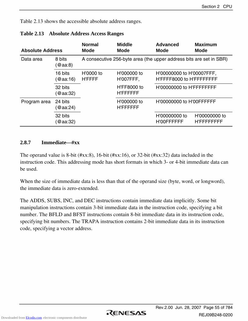
Section 2 CPU
Rev.2.00 Jun. 28, 2007 Page 55 of 784
REJ09B248-0200
Table 2.13 shows the accessible absolute address ranges.
Table 2.13 Absolute Address Access Ranges
Absolute Address Normal Mode
Middle Mode
Advanced Mode
Maximum Mode
8 bits (@aa:8)
A consecutive 256-byte area (the upper address bits are set in SBR)
16 bits (@aa:16)
H'00000000 to H'00007FFF, H'FFFF8000 to H'FFFFFFFF
Data area
32 bits (@aa:32)
H'000000 to H'007FFF,
H'FF8000 to H'FFFFFF
H'00000000 to H'FFFFFFFF
24 bits (@aa:24)
H'00000000 to H'00FFFFFF Program area
32 bits (@aa:32)
H'0000 to H'FFFF
H'000000 to H'FFFFFF
H'00000000 to H'00FFFFFF
H'00000000 to H'FFFFFFFF
2.8.7 Immediate—#xx
The operand value is 8-bit (#xx:8), 16-bit (#xx:16), or 32-bit (#xx:32) data included in the instruction code. This addressing mode has short formats in which 3- or 4-bit immediate data can be used.
When the size of immediate data is less than that of the operand size (byte, word, or longword), the immediate data is zero-extended.
The ADDS, SUBS, INC, and DEC instructions contain immediate data implicitly. Some bit manipulation instructions contain 3-bit immediate data in the instruction code, specifying a bit number. The BFLD and BFST instructions contain 8-bit immediate data in its instruction code, specifying bit numbers. The TRAPA instruction contains 2-bit immediate data in its instruction code, specifying a vector address.
Downloaded from Elcodis.com electronic components distributor

Section 2 CPU
Rev.2.00 Jun. 28, 2007 Page 56 of 784
REJ09B248-0200
2.8.8 Program-Counter Relative—@(d:8, PC) or @(d:16, PC)
This mode is used in the Bcc and BSR instructions. The operand value is a 32-bit branch address, which is the sum of an 8- or 16-bit displacement in the instruction code and the 32-bit address of the PC contents. The 8-bit or 16-bit displacement is sign-extended when added to the PC contents.
The PC contents to which the displacement is added is the address of the first byte of the next instruction, so the possible branching range is −126 to +128 bytes (−63 to +64 words) or −32766 to +32768 bytes (−16383 to +16384 words) from the branch instruction. The resulting value should be an even number. In advanced mode, only the lower 24 bits of this branch address are valid; the upper eight bits are all assumed to be 0 (H'00).
2.8.9 Program-Counter Relative with Index Register—@(RnL.B, PC), @(Rn.W, PC), or
@(ERn.L, PC)
This mode is used in the Bcc and BSR instructions. The operand value is a 32-bit branch address, which is the sum of the following operation result and the 32-bit address of the PC contents: specified bits of the contents of an address register (RnL, Rn, or ERn) specified by the register field in the instruction code is zero-extended to 32-bit data and multiplied by 2.
The PC content to which the displacement is added is the address of the first byte of the next instruction. In advanced mode, only the lower 24 bits of this branch address are valid; the upper eight bits are all assumed to be 0 (H'00).
2.8.10 Memory Indirect—@@aa:8
This mode is used in the JMP and JSR instructions. The operand value is a branch address, which is the content of a memory location pointed to by an 8-bit absolute address in the instruction code.
The upper bits of an 8-bit absolute address are all assumed to be 0, so the address range to store a branch address is 0 to 255 (H'0000 to H'00FF in normal mode, H'000000 to H'0000FF in other modes). In normal mode, the memory location is pointed to by word-size data and the branch address is 16 bits long. In other modes, the memory location is pointed to by longword-size data. In middle or advanced mode, the first byte of the longword-size data is assumed to be all 0 (H'00).
Note that the top part of the address range is also used as the exception handling vector area. A vector address of an exception handling other than a reset or a CPU address error can be changed by VBR.
Downloaded from Elcodis.com electronic components distributor
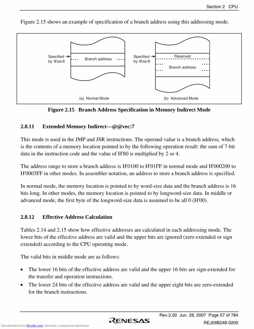
Section 2 CPU
Rev.2.00 Jun. 28, 2007 Page 57 of 784
REJ09B248-0200
Figure 2.15 shows an example of specification of a branch address using this addressing mode.
(a) Normal Mode (b) Advanced Mode
Branch addressSpecifiedby @aa:8
Specified by @aa:8
Reserved
Branch address
Figure 2.15 Branch Address Specification in Memory Indirect Mode
2.8.11 Extended Memory Indirect—@@vec:7
This mode is used in the JMP and JSR instructions. The operand value is a branch address, which is the contents of a memory location pointed to by the following operation result: the sum of 7-bit data in the instruction code and the value of H'80 is multiplied by 2 or 4.
The address range to store a branch address is H'0100 to H'01FF in normal mode and H'000200 to H'0003FF in other modes. In assembler notation, an address to store a branch address is specified.
In normal mode, the memory location is pointed to by word-size data and the branch address is 16 bits long. In other modes, the memory location is pointed to by longword-size data. In middle or advanced mode, the first byte of the longword-size data is assumed to be all 0 (H'00).
2.8.12 Effective Address Calculation
Tables 2.14 and 2.15 show how effective addresses are calculated in each addressing mode. The lower bits of the effective address are valid and the upper bits are ignored (zero extended or sign extended) according to the CPU operating mode.
The valid bits in middle mode are as follows:
• The lower 16 bits of the effective address are valid and the upper 16 bits are sign-extended for the transfer and operation instructions.
• The lower 24 bits of the effective address are valid and the upper eight bits are zero-extended for the branch instructions.
Downloaded from Elcodis.com electronic components distributor
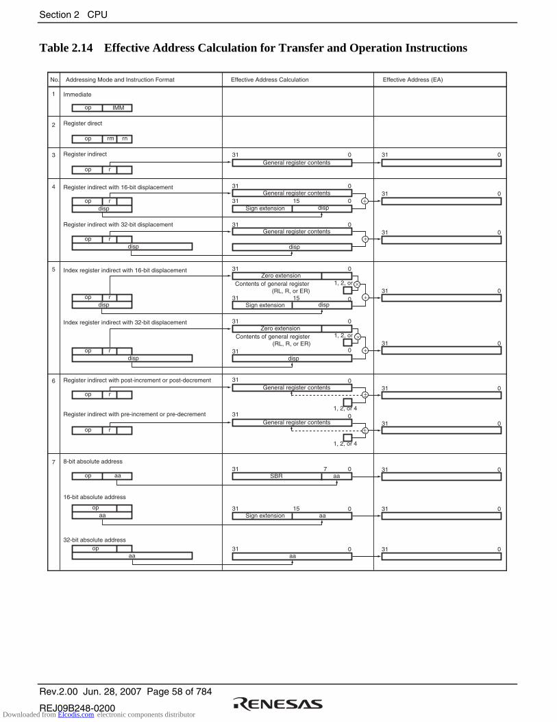
Section 2 CPU
Rev.2.00 Jun. 28, 2007 Page 58 of 784
REJ09B248-0200
Table 2.14 Effective Address Calculation for Transfer and Operation Instructions
31 0 31 0
31 0
31 0
31 0
31 0
31 0
31 0
31 0
31 0
31 0
31 15
31 15
0
31 0
31 0
0
31 15 0
31 0
1, 2, or 4
31
31 0
0
31 0
31
1, 2, or 4
1, 2, or 4
31 07
No.
op
op
rm rn
IMM
1
2
3
4
5
6
7
op r
opdisp disp
disp
disp
aa
aa
aa
disp
r
opdisp
r
opaa
opdisp
r
opdisp
r
opaa
op r
op r
op aa
31 00
1, 2, or 4
Addressing Mode and Instruction Format Effective Address Calculation Effective Address (EA)
Immediate
Register direct
Register indirect
Register indirect with 16-bit displacement
Register indirect with 32-bit displacement
Index register indirect with 16-bit displacement
Index register indirect with 32-bit displacement
Register indirect with post-increment or post-decrement
Register indirect with pre-increment or pre-decrement
8-bit absolute address
16-bit absolute address
32-bit absolute address
Sign extension
SBR
General register contents
General register contents
Zero extensionContents of general register (RL, R, or ER)
Zero extensionContents of general register (RL, R, or ER)
Sign extension
General register contents
General register contents
General register contents
Sign extension
+
±
×
+
+
±
×
+
Downloaded from Elcodis.com electronic components distributor
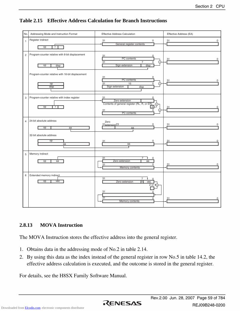
Section 2 CPU
Rev.2.00 Jun. 28, 2007 Page 59 of 784
REJ09B248-0200
Table 2.15 Effective Address Calculation for Branch Instructions
31 0
31 0
31 0
31 0
31
31 23 0
0
31
31 0
0
31 0
2 or 4
7
17
vec
op disp
1
2
3
4
5
6
opdisp
op r
opaa
op r
op aa aa
aa
op aa aa
31 0
31 0
op vec
31 0 31 0
31 031 0
31 7 0disp
31 031 0
31 15 0disp
31 031
31 0
20
No.
Register indirect
Program-counter relative with 8-bit displacement
24-bit absolute address
32-bit absolute address
Zero extension
Contents of general register (RL, R, or ER)
General register contents
Sign extension
Addressing Mode and Instruction Format Effective Address Calculation Effective Address (EA)
PC contents
Sign extension
PC contents
Zero extension
Zero extension
Memory contents
Memory contents
Zero extension
PC contents
Program-counter relative with 16-bit displacement
Program-counter relative with index register
Memory indirect
Extended memory indirect
+
×
+
×
+
2.8.13 MOVA Instruction
The MOVA Instruction stores the effective address into the general register.
1. Obtains data in the addressing mode of No.2 in table 2.14.
2. By using this data as the index instead of the general register in row No.5 in table 14.2, the effective address calculation is executed, and the outcome is stored in the general register.
For details, see the H8SX Family Software Manual.
Downloaded from Elcodis.com electronic components distributor
Section 2 CPU
Rev.2.00 Jun. 28, 2007 Page 60 of 784
REJ09B248-0200
2.9 Processing States
The H8SX CPU has five main processing states: the reset state, exception-handling state, program execution state, bus-released state, and program stop state. Figure 2.16 indicates the state transitions.
• Reset state
In this state the CPU and internal peripheral modules are all initialized and stopped. When the RES input goes low, all current processing stops and the CPU enters the reset state. All interrupts are masked in the reset state. Reset exception handling starts when the RES signal changes from low to high. For details, see section 4, Exception Handling.
The reset state can also be entered by a watchdog timer overflow when available.
• Exception-handling state
The exception-handling state is a transient state that occurs when the CPU alters the normal processing flow due to activation of an exception source, such as, a reset, trace, interrupt, or trap instruction. The CPU fetches a start address (vector) from the exception handling vector table and branches to that address. For further details, see section 4, Exception Handling.
• Program execution state
In this state the CPU executes program instructions in sequence.
• Bus-released state
The bus-released state occurs when the bus has been released in response to a bus request from a bus master other than the CPU. While the bus is released, the CPU halts operations.
• Program stop state
This is a power-down state in which the CPU stops operating. The program stop state occurs when a SLEEP instruction is executed or the CPU enters hardware standby mode. For details, see section 19, Power-Down Modes.
Downloaded from Elcodis.com electronic components distributor

Section 2 CPU
Rev.2.00 Jun. 28, 2007 Page 61 of 784
REJ09B248-0200
In any state, when the STBY signal goes low, the hardware standbymode is entered.From any state except hardware standby mode, a transition to thereset state occurs whenever the RES signal goes low. A transitioncan also be made to the reset state when the watchdog timer overflows.
Notes:
*
Reset state*
Exception-handlingstate
Request for exception handling
End of exception handling
Program executionstate
Bus-released stateBus
request
End of bus request
Program stop stateSLEEP instruction
Interrupt request
Bus request
End of bus request
RES = HighSTBY = High,RES = Low
Figure 2.16 State Transitions
Downloaded from Elcodis.com electronic components distributor

Section 2 CPU
Rev.2.00 Jun. 28, 2007 Page 62 of 784
REJ09B248-0200
Downloaded from Elcodis.com electronic components distributor
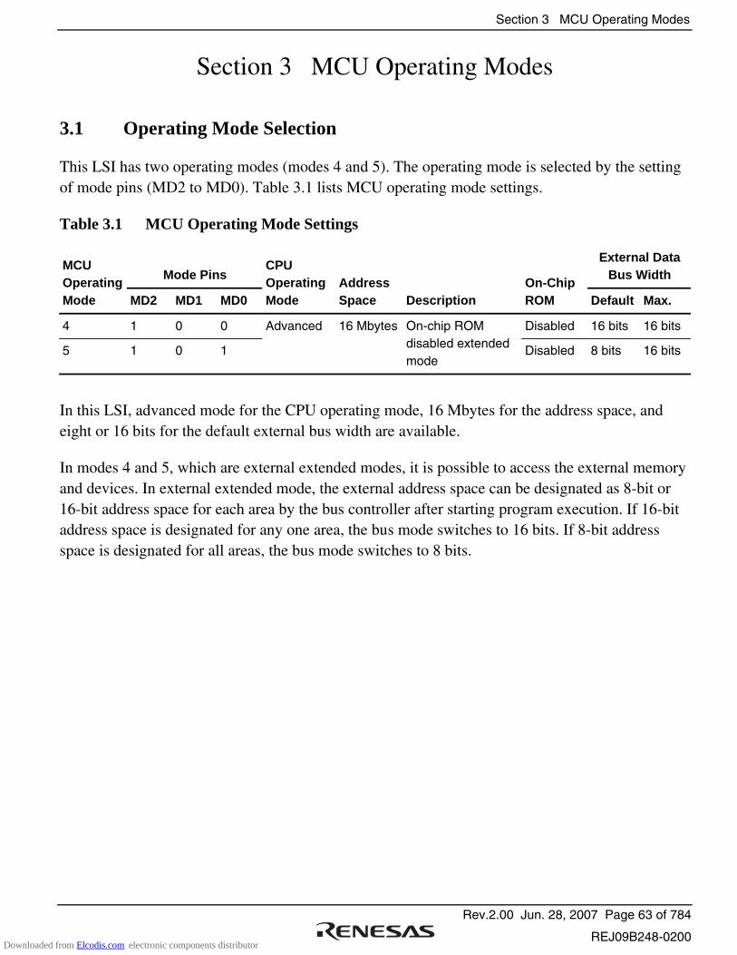
Section 3 MCU Operating Modes
Rev.2.00 Jun. 28, 2007 Page 63 of 784
REJ09B248-0200
Section 3 MCU Operating Modes
3.1 Operating Mode Selection
This LSI has two operating modes (modes 4 and 5). The operating mode is selected by the setting of mode pins (MD2 to MD0). Table 3.1 lists MCU operating mode settings.
Table 3.1 MCU Operating Mode Settings
Mode Pins External Data
Bus Width MCU Operating Mode MD2 MD1 MD0
CPU Operating Mode
Address Space Description
On-Chip ROM Default Max.
4 1 0 0 Advanced 16 Mbytes Disabled 16 bits 16 bits
5 1 0 1
On-chip ROM disabled extended mode
Disabled 8 bits 16 bits
In this LSI, advanced mode for the CPU operating mode, 16 Mbytes for the address space, and eight or 16 bits for the default external bus width are available.
In modes 4 and 5, which are external extended modes, it is possible to access the external memory and devices. In external extended mode, the external address space can be designated as 8-bit or 16-bit address space for each area by the bus controller after starting program execution. If 16-bit address space is designated for any one area, the bus mode switches to 16 bits. If 8-bit address space is designated for all areas, the bus mode switches to 8 bits.
Downloaded from Elcodis.com electronic components distributor

Section 3 MCU Operating Modes
Rev.2.00 Jun. 28, 2007 Page 64 of 784
REJ09B248-0200
3.2 Register Descriptions
The following registers are related to the operating mode setting.
• Mode control register (MDCR)
• System control register (SYSCR)
3.2.1 Mode Control Register (MDCR)
MDCR indicates the current operating mode.
When MCDR is read, the input levels in pins MD2 to MD 0 are latched. These latches are released by a reset.
Bit
Bit Name
Initial Value
R/W
Note: * Determined by pins MD2 to MD0.
15
0
R
14
1
R
13
0
R
12
1
R
11
0
R
10
MDS2
Undefined*
R
9
MDS1
Undefined*
R
8
MDS0
Undefined*
R
Bit
Bit Name
Initial Value
R/W
7
0
R
6
1
R
5
0
R
4
1
R
3
0
R
2
Undefined*
R
1
Undefined*
R
0
Undefined*
R
Bit Bit Name Initial Value R/W Descriptions
15
14
13
12
11
0
1
0
1
0
R
R
R
R
R
Reserved
These are read-only bits and cannot be modified.
10
9
8
MDS2
MDS1
MDS0
Undefined*
Undefined*
Undefined*
R
R
R
Mode Select 2 to 0
These bits indicate the operating mode selected by the mode pins (MD2 to MD0) (see table 3.2).
When MDCR is read, the signal levels input on pins MD2 to MD0 are latched into these bits. These latches are released by a reset.
Downloaded from Elcodis.com electronic components distributor
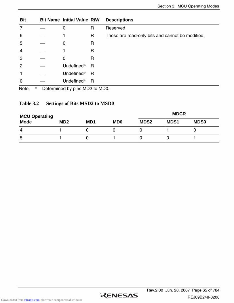
Section 3 MCU Operating Modes
Rev.2.00 Jun. 28, 2007 Page 65 of 784
REJ09B248-0200
Bit Bit Name Initial Value R/W Descriptions
7
6
5
4
3
2
1
0
0
1
0
1
0
Undefined*
Undefined*
Undefined*
R
R
R
R
R
R
R
R
Reserved
These are read-only bits and cannot be modified.
Note: * Determined by pins MD2 to MD0.
Table 3.2 Settings of Bits MSD2 to MSD0
MDCR MCU Operating Mode MD2 MD1 MD0 MDS2 MDS1 MDS0
4 1 0 0 0 1 0
5 1 0 1 0 0 1
Downloaded from Elcodis.com electronic components distributor
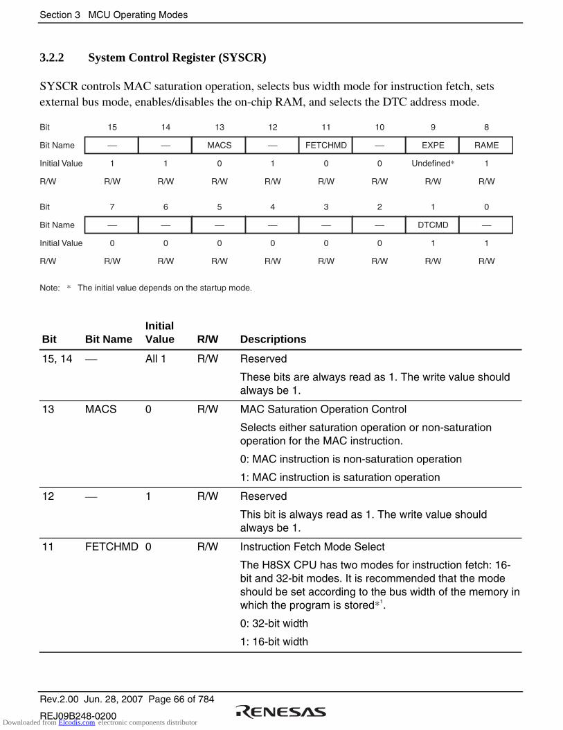
Section 3 MCU Operating Modes
Rev.2.00 Jun. 28, 2007 Page 66 of 784
REJ09B248-0200
3.2.2 System Control Register (SYSCR)
SYSCR controls MAC saturation operation, selects bus width mode for instruction fetch, sets external bus mode, enables/disables the on-chip RAM, and selects the DTC address mode.
Bit
Bit Name
Initial Value
R/W
Note: * The initial value depends on the startup mode.
15
1
R/W
14
1
R/W
13
MACS
0
R/W
12
1
R/W
11
FETCHMD
0
R/W
10
0
R/W
9
EXPE
Undefined*
R/W
8
RAME
1
R/W
Bit
Bit Name
Initial Value
R/W
7
0
R/W
6
0
R/W
5
0
R/W
4
0
R/W
3
0
R/W
2
0
R/W
1
DTCMD
1
R/W
0
1
R/W
Bit Bit Name Initial Value R/W Descriptions
15, 14 All 1 R/W Reserved
These bits are always read as 1. The write value should always be 1.
13 MACS 0 R/W MAC Saturation Operation Control
Selects either saturation operation or non-saturation operation for the MAC instruction.
0: MAC instruction is non-saturation operation
1: MAC instruction is saturation operation
12 1 R/W Reserved
This bit is always read as 1. The write value should always be 1.
11 FETCHMD 0 R/W Instruction Fetch Mode Select
The H8SX CPU has two modes for instruction fetch: 16-bit and 32-bit modes. It is recommended that the mode should be set according to the bus width of the memory in which the program is stored*1.
0: 32-bit width
1: 16-bit width
Downloaded from Elcodis.com electronic components distributor
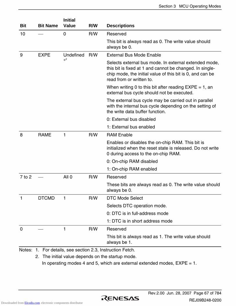
Section 3 MCU Operating Modes
Rev.2.00 Jun. 28, 2007 Page 67 of 784
REJ09B248-0200
Bit Bit Name Initial Value R/W Descriptions
10 0 R/W Reserved
This bit is always read as 0. The write value should always be 0.
9 EXPE Undefined *2
R/W External Bus Mode Enable
Selects external bus mode. In external extended mode, this bit is fixed at 1 and cannot be changed. In single-chip mode, the initial value of this bit is 0, and can be read from or written to.
When writing 0 to this bit after reading EXPE = 1, an external bus cycle should not be executed.
The external bus cycle may be carried out in parallel with the internal bus cycle depending on the setting of the write data buffer function.
0: External bus disabled
1: External bus enabled
8 RAME 1 R/W RAM Enable
Enables or disables the on-chip RAM. This bit is initialized when the reset state is released. Do not write 0 during access to the on-chip RAM.
0: On-chip RAM disabled
1: On-chip RAM enabled
7 to 2 All 0 R/W Reserved
These bits are always read as 0. The write value should always be 0.
1 DTCMD 1 R/W DTC Mode Select
Selects DTC operation mode.
0: DTC is in full-address mode
1: DTC is in short address mode
0 1 R/W Reserved
This bit is always read as 1. The write value should always be 1.
Notes: 1. For details, see section 2.3, Instruction Fetch.
2. The initial value depends on the startup mode. In operating modes 4 and 5, which are external extended modes, EXPE = 1.
Downloaded from Elcodis.com electronic components distributor

Section 3 MCU Operating Modes
Rev.2.00 Jun. 28, 2007 Page 68 of 784
REJ09B248-0200
3.3 Operating Mode Descriptions
3.3.1 Mode 4
The CPU operating mode is advanced mode in which the address space is 16 Mbytes, and the on-chip ROM is disabled.
The initial bus mode immediately after a reset is 16 bits, with 16-bit access to all areas. Ports D, E, and F function as an address bus, ports H and I function as a data bus, and parts of ports A and B function as bus control signals. However, if all areas are designated as an 8-bit access space by the bus controller, the bus mode switches to 8 bits, and only port H functions as a data bus.
3.3.2 Mode 5
The CPU operating mode is advanced mode in which the address space is 16 Mbytes, and the on-chip ROM is disabled.
The initial bus mode immediately after a reset is 8 bits, with 8-bit access to all areas. Ports D, E, and F function as an address bus, port H functions as a data bus, and parts of ports A and B function as bus control signals. However, if all areas are designated as a 16-bit access space by the bus controller, the bus mode switches to 16 bits, and ports H and I function as a data bus.
Downloaded from Elcodis.com electronic components distributor

Section 3 MCU Operating Modes
Rev.2.00 Jun. 28, 2007 Page 69 of 784
REJ09B248-0200
3.3.3 Pin Functions
Table 3.3 lists the pin functions in each operating mode.
Table 3.3 Pin Functions in Each Operating Mode (Advanced Mode)
Port Mode 4 Mode 5
PA7 P/C* P/C*
PA6, PA4 P/C* P/C*
Port A
PA2 to PA0 P*/C P*/C
PB3 to 1 P*/C P*/C Port B
PB0 P/C* P/C*
Port D A A
Port E A A
Port F PF7 to PF5 P*/A P*/A
PF4 to PF0 A A
Port H D D
Port I P/D* P*/D
[Legend] P: I/O port
A: Address bus output
D: Data bus input/output C: Control signals, clock input/output
*: Immediately after a reset
Downloaded from Elcodis.com electronic components distributor
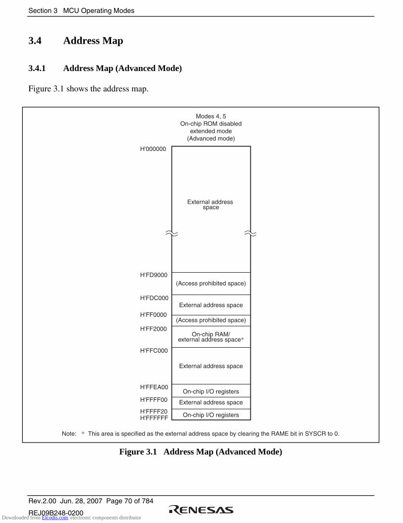
Section 3 MCU Operating Modes
Rev.2.00 Jun. 28, 2007 Page 70 of 784
REJ09B248-0200
3.4 Address Map
3.4.1 Address Map (Advanced Mode)
Figure 3.1 shows the address map.
Modes 4, 5On-chip ROM disabled
extended mode(Advanced mode)
Note: * This area is specified as the external address space by clearing the RAME bit in SYSCR to 0.
On-chip RAM/external address space*
External address space
External address space
External address space
External address space
On-chip I/O registers
On-chip I/O registers
H'000000
H'FF2000
H'FFC000
H'FFEA00
H'FFFF00
H'FFFF20H'FFFFFF
H'FF0000
(Access prohibited space)
(Access prohibited space)
H'FD9000
H'FDC000
Figure 3.1 Address Map (Advanced Mode)
Downloaded from Elcodis.com electronic components distributor
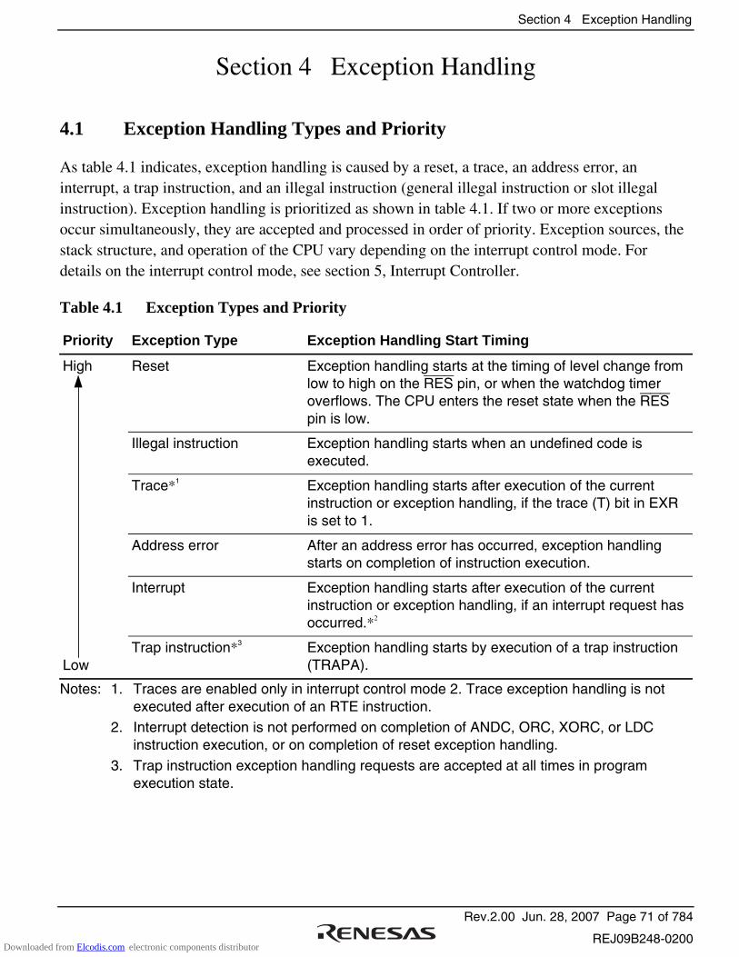
Section 4 Exception Handling
Rev.2.00 Jun. 28, 2007 Page 71 of 784
REJ09B248-0200
Section 4 Exception Handling
4.1 Exception Handling Types and Priority
As table 4.1 indicates, exception handling is caused by a reset, a trace, an address error, an interrupt, a trap instruction, and an illegal instruction (general illegal instruction or slot illegal instruction). Exception handling is prioritized as shown in table 4.1. If two or more exceptions occur simultaneously, they are accepted and processed in order of priority. Exception sources, the stack structure, and operation of the CPU vary depending on the interrupt control mode. For details on the interrupt control mode, see section 5, Interrupt Controller.
Table 4.1 Exception Types and Priority
Priority Exception Type Exception Handling Start Timing
High Reset Exception handling starts at the timing of level change from low to high on the RES pin, or when the watchdog timer overflows. The CPU enters the reset state when the RES pin is low.
Illegal instruction Exception handling starts when an undefined code is executed.
Trace*1 Exception handling starts after execution of the current instruction or exception handling, if the trace (T) bit in EXR is set to 1.
Address error After an address error has occurred, exception handling starts on completion of instruction execution.
Interrupt Exception handling starts after execution of the current instruction or exception handling, if an interrupt request has occurred.*2
Low Trap instruction*3 Exception handling starts by execution of a trap instruction
(TRAPA).
Notes: 1. Traces are enabled only in interrupt control mode 2. Trace exception handling is not executed after execution of an RTE instruction.
2. Interrupt detection is not performed on completion of ANDC, ORC, XORC, or LDC instruction execution, or on completion of reset exception handling.
3. Trap instruction exception handling requests are accepted at all times in program execution state.
Downloaded from Elcodis.com electronic components distributor

Section 4 Exception Handling
Rev.2.00 Jun. 28, 2007 Page 72 of 784
REJ09B248-0200
4.2 Exception Sources and Exception Handling Vector Table
Different vector table address offsets are assigned to different exception sources. The vector table addresses are calculated from the contents of the vector base register (VBR) and vector table address offset of the vector number. The start address of the exception service routine is fetched from the exception handling vector table indicated by this vector table address.
Table 4.2 shows the correspondence between the exception sources and vector table address offsets. Table 4.3 shows the calculation method of exception handling vector table addresses.
Since the usable modes differ depending on the product, for details on the available modes, see section 3, MCU Operating Modes.
Table 4.2 Exception Handling Vector Table
Vector Table Address Offset*1
Exception Source Vector Number Normal Mode*2 Advanced, Middle*2, Maximum*2 Modes
Reset 0 H'0000 to H'0001 H'0000 to H'0003
Reserved for system use 1 H'0002 to H'0003 H'0004 to H'0007
2 H'0004 to H'0005 H'0008 to H'000B
3 H'0006 to H'0007 H'000C to H'000F
Illegal instruction 4 H'0008 to H'0009 H'0010 to H'0013
Trace 5 H'000A to H'000B H'0014 to H'0017
Reserved for system use 6 H'000C to H'000D H'0018 to H'001B
Interrupt (NMI) 7 H'000E to H'000F H'001C to H'001F
Trap instruction (#0) 8 H'0010 to H'0011 H'0020 to H'0023
(#1) 9 H'0012 to H'0013 H'0024 to H'0027
(#2) 10 H'0014 to H'0015 H'0028 to H'002B
(#3) 11 H'0016 to H'0017 H'002C to H'002F
CPU address error 12 H'0018 to H'0019 H'0030 to H'0033
DMA address error*3 13 H'001A to H'001B H'0034 to H'0037
Reserved for system use 14 17
H'001C to H'001D H'0022 to H'0023
H'0038 to H'003B H'0044 to H'0047
Sleep interrupt 18 H'0024 to H'0025 H'0048 to H'004B
Downloaded from Elcodis.com electronic components distributor

Section 4 Exception Handling
Rev.2.00 Jun. 28, 2007 Page 73 of 784
REJ09B248-0200
Vector Table Address Offset*1
Exception Source Vector Number Normal Mode*2 Advanced, Middle*2, Maximum*2 Modes
Reserved for system use 19 23
H'0026 to H'0027 H'002E to H'002F
H'004C to H'004F H'005C to H'005F
User area (open space) 24 63
H'0030 to H'0031 H'007E to H'007F
H'0060 to H'0063 H'00FC to H'00FF
External interrupt IRQ0 64 H'0080 to H'0081 H'0100 to H'0103
IRQ1 65 H'0082 to H'0083 H'0104 to H'0107
IRQ2 66 H'0084 to H'0085 H'0108 to H'010B
IRQ3 67 H'0086 to H'0087 H'010C to H'010F
IRQ4 68 H'0088 to H'0089 H'0110 to H'0113
IRQ5 69 H'008A to H'008B H'0114 to H'0117
IRQ6 70 H'008C to H'008D H'0118 to H'011B
IRQ7 71 H'008E to H'008F H'011C to H'011F
IRQ8 72 H'0090 to H'0091 H'0120 to H'0123
IRQ9 73 H'0092 to H'0093 H'0124 to H'0127
IRQ10 74 H'0094 to H'0095 H'0128 to H'012B
IRQ11 75 H'0096 to H'0097 H'012C to H'012F
Reserved for system use 76 79
H'0098 to H'0099 H'009E to H'009F
H'0130 to H'0133 H'013C to H'013F
Internal interrupt*4 80 255
H'00A0 to H'00A1 H'01FE to H'01FF
H'0140 to H'0143 H'03FC to H'03FF
Notes: 1. Lower 16 bits of the address. 2. Not available in this LSI.
3. A DMA address error is generated by the DTC and DMAC.
4. For details of internal interrupt vectors, see section 5.5, Interrupt Exception Handling Vector Table.
Downloaded from Elcodis.com electronic components distributor

Section 4 Exception Handling
Rev.2.00 Jun. 28, 2007 Page 74 of 784
REJ09B248-0200
Table 4.3 Calculation Method of Exception Handling Vector Table Address
Exception Source Calculation Method of Vector Table Address
Reset, CPU address error Vector table address = (vector table address offset)
Other than above Vector table address = VBR + (vector table address offset)
[Legend] VBR: Vector base register
Vector table address offset: See table 4.2.
4.3 Reset
A reset has priority over any other exception. When the RES pin goes low, all processing halts and this LSI enters the reset state. To ensure that this LSI is reset, hold the RES pin low for at least 20 ms with the STBY pin driven high when the power is turned on. When operation is in progress, hold the RES pin low for at least 20 cycles.
The chip can also be reset by overflow of the watchdog timer. For details, see section 13, Watchdog Timer (WDT).
A reset initializes the internal state of the CPU and the registers of the on-chip peripheral modules. The interrupt control mode is 0 immediately after a reset.
4.3.1 Reset Exception Handling
When the RES pin goes high after being held low for the necessary time, this LSI starts reset exception handling as follows:
1. The internal state of the CPU and the registers of the on-chip peripheral modules are initialized, VBR is cleared to H'00000000, the T bit is cleared to 0 in EXR, and the I bits are set to 1 in EXR and CCR.
2. The reset exception handling vector address is read and transferred to the PC, and program execution starts from the address indicated by the PC.
Figures 4.1 and 4.2 show examples of the reset sequence.
Downloaded from Elcodis.com electronic components distributor
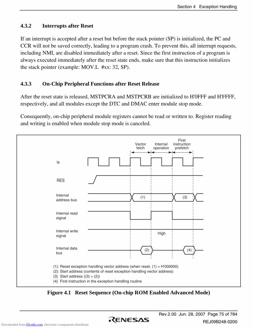
Section 4 Exception Handling
Rev.2.00 Jun. 28, 2007 Page 75 of 784
REJ09B248-0200
4.3.2 Interrupts after Reset
If an interrupt is accepted after a reset but before the stack pointer (SP) is initialized, the PC and CCR will not be saved correctly, leading to a program crash. To prevent this, all interrupt requests, including NMI, are disabled immediately after a reset. Since the first instruction of a program is always executed immediately after the reset state ends, make sure that this instruction initializes the stack pointer (example: MOV.L #xx: 32, SP).
4.3.3 On-Chip Peripheral Functions after Reset Release
After the reset state is released, MSTPCRA and MSTPCRB are initialized to H'0FFF and H'FFFF, respectively, and all modules except the DTC and DMAC enter module stop mode.
Consequently, on-chip peripheral module registers cannot be read or written to. Register reading and writing is enabled when module stop mode is canceled.
RES
High
Vectorfetch
Internaloperation
Firstinstructionprefetch
(1): Reset exception handling vector address (when reset, (1) = H'000000)(2): Start address (contents of reset exception handling vector address)(3) Start address ((3) = (2))(4) First instruction in the exception handling routine
Iφ
Internaladdress bus
Internal readsignal
Internal writesignal
Internal databus
(1)
(2) (4)
(3)
Figure 4.1 Reset Sequence (On-chip ROM Enabled Advanced Mode)
Downloaded from Elcodis.com electronic components distributor

Section 4 Exception Handling
Rev.2.00 Jun. 28, 2007 Page 76 of 784
REJ09B248-0200
RES
RD
HWR, LWR
D15 to D0
High
* * *Bφ
Address bus
Vector fetchInternal
operationFirst instruction
prefetch
(1)
(2) (4) (6)
(3) (5)
(1)(3) Reset exception handling vector address (when reset, (1) = H'000000, (3) = H'000002)(2)(4) Start address (contents of reset exception handling vector address)(5) Start address ((5) = (2)(4))(6) First instruction in the exception handling routine
Note: * Seven program wait cycles are inserted.
Figure 4.2 Reset Sequence (16-Bit External Access in On-chip ROM Disabled Advanced Mode)
Downloaded from Elcodis.com electronic components distributor

Section 4 Exception Handling
Rev.2.00 Jun. 28, 2007 Page 77 of 784
REJ09B248-0200
4.4 Traces
Traces are enabled in interrupt control mode 2. Trace mode is not activated in interrupt control mode 0, irrespective of the state of the T bit. Before changing interrupt control modes, the T bit must be cleared. For details on interrupt control modes, see section 5, Interrupt Controller.
If the T bit in EXR is set to 1, trace mode is activated. In trace mode, a trace exception occurs on completion of each instruction. Trace mode is not affected by interrupt masking by CCR. Table 4.4 shows the state of CCR and EXR after execution of trace exception handling. Trace mode is canceled by clearing the T bit in EXR to 0 during the trace exception handling. However, the T bit saved on the stack retains its value of 1, and when control is returned from the trace exception handling routine by the RTE instruction, trace mode resumes. Trace exception handling is not carried out after execution of the RTE instruction.
Interrupts are accepted even within the trace exception handling routine.
Table 4.4 Status of CCR and EXR after Trace Exception Handling
CCR EXR
Interrupt Control Mode I UI I2 to I0 T
0 Trace exception handling cannot be used.
2 1 0
[Legend]
1: Set to 1
0: Cleared to 0 : Retains the previous value.
Downloaded from Elcodis.com electronic components distributor
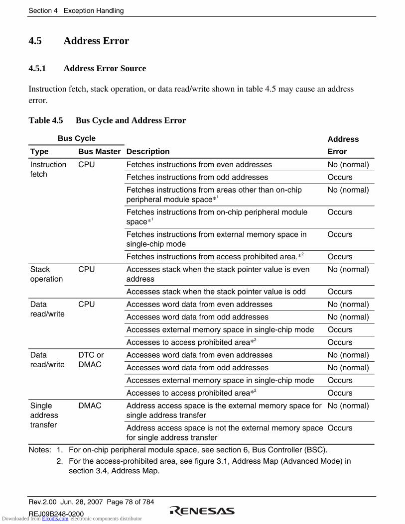
Section 4 Exception Handling
Rev.2.00 Jun. 28, 2007 Page 78 of 784
REJ09B248-0200
4.5 Address Error
4.5.1 Address Error Source
Instruction fetch, stack operation, or data read/write shown in table 4.5 may cause an address error.
Table 4.5 Bus Cycle and Address Error
Bus Cycle
Type Bus Master Description
Address
Error
Fetches instructions from even addresses No (normal)
Fetches instructions from odd addresses Occurs
Fetches instructions from areas other than on-chip peripheral module space*1
No (normal)
Fetches instructions from on-chip peripheral module space*1
Occurs
Fetches instructions from external memory space in single-chip mode
Occurs
Instruction fetch
CPU
Fetches instructions from access prohibited area.*2 Occurs
Accesses stack when the stack pointer value is even address
No (normal) Stack operation
CPU
Accesses stack when the stack pointer value is odd Occurs
Accesses word data from even addresses No (normal)
Accesses word data from odd addresses No (normal)
Accesses external memory space in single-chip mode Occurs
Data read/write
CPU
Accesses to access prohibited area*2 Occurs
Accesses word data from even addresses No (normal)
Accesses word data from odd addresses No (normal)
Accesses external memory space in single-chip mode Occurs
Data read/write
DTC or DMAC
Accesses to access prohibited area*2 Occurs
Address access space is the external memory space for single address transfer
No (normal) Single address transfer
DMAC
Address access space is not the external memory space for single address transfer
Occurs
Notes: 1. For on-chip peripheral module space, see section 6, Bus Controller (BSC). 2. For the access-prohibited area, see figure 3.1, Address Map (Advanced Mode) in
section 3.4, Address Map.
Downloaded from Elcodis.com electronic components distributor
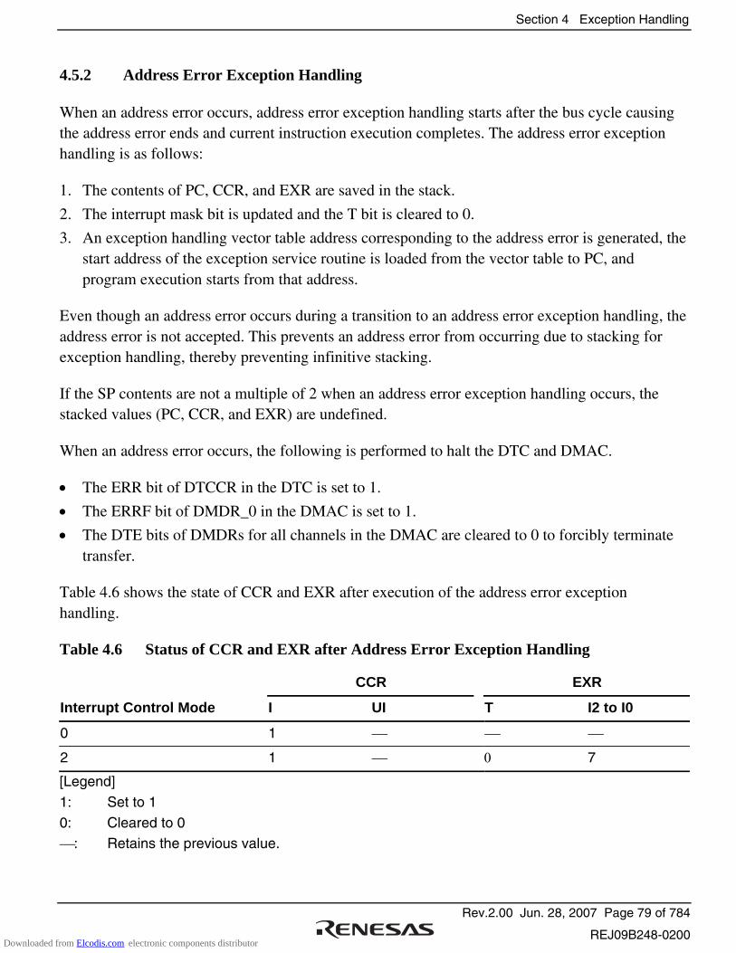
Section 4 Exception Handling
Rev.2.00 Jun. 28, 2007 Page 79 of 784
REJ09B248-0200
4.5.2 Address Error Exception Handling
When an address error occurs, address error exception handling starts after the bus cycle causing the address error ends and current instruction execution completes. The address error exception handling is as follows:
1. The contents of PC, CCR, and EXR are saved in the stack.
2. The interrupt mask bit is updated and the T bit is cleared to 0.
3. An exception handling vector table address corresponding to the address error is generated, the start address of the exception service routine is loaded from the vector table to PC, and program execution starts from that address.
Even though an address error occurs during a transition to an address error exception handling, the address error is not accepted. This prevents an address error from occurring due to stacking for exception handling, thereby preventing infinitive stacking.
If the SP contents are not a multiple of 2 when an address error exception handling occurs, the stacked values (PC, CCR, and EXR) are undefined.
When an address error occurs, the following is performed to halt the DTC and DMAC.
• The ERR bit of DTCCR in the DTC is set to 1.
• The ERRF bit of DMDR_0 in the DMAC is set to 1.
• The DTE bits of DMDRs for all channels in the DMAC are cleared to 0 to forcibly terminate transfer.
Table 4.6 shows the state of CCR and EXR after execution of the address error exception handling.
Table 4.6 Status of CCR and EXR after Address Error Exception Handling
CCR EXR
Interrupt Control Mode I UI T I2 to I0
0 1
2 1 0 7
[Legend]
1: Set to 1
0: Cleared to 0 : Retains the previous value.
Downloaded from Elcodis.com electronic components distributor
Section 4 Exception Handling
Rev.2.00 Jun. 28, 2007 Page 80 of 784
REJ09B248-0200
4.6 Interrupts
4.6.1 Interrupt Sources
Interrupt sources are NMI, sleep interrupt, IRQ0 to IRQ11, and on-chip peripheral modules, as shown in table 4.7.
Table 4.7 Interrupt Sources
Type Source Number of Sources
NMI NMI pin (external input) 1
Sleep interrupt SLEEP instruction 1
IRQ0 to IRQ11 Pins IRQ0 to IRQ11 (external input) 12
DMA controller (DMAC) 8
Watchdog timer (WDT) 1
A/D converter 1
16-bit timer pulse unit (TPU) 26
8-bit timer (TMR) 12
On-chip peripheral module
Serial communications interface (SCI) 20
Different vector numbers and vector table offsets are assigned to different interrupt sources. For vector number and vector table offset, see table 5.2, Interrupt Sources, Vector Address Offsets, and Interrupt Priority in section 5, Interrupt Controller.
4.6.2 Interrupt Exception Handling
Interrupts are controlled by the interrupt controller. The interrupt controller has two interrupt control modes and can assign interrupts other than NMI or sleep interrupt to eight priority/mask levels to enable multiple-interrupt control. The source to start interrupt exception handling and the vector address differ depending on the product. For details, see section 5, Interrupt Controller.
Downloaded from Elcodis.com electronic components distributor

Section 4 Exception Handling
Rev.2.00 Jun. 28, 2007 Page 81 of 784
REJ09B248-0200
The interrupt exception handling is as follows:
1. The contents of PC, CCR, and EXR are saved in the stack.
2. The interrupt mask bit is updated and the T bit is cleared to 0.
3. An exception handling vector table address corresponding to the interrupt source is generated, the start address of the exception service routine is loaded from the vector table to PC, and program execution starts from that address.
4.7 Instruction Exception Handling
There are two instructions that cause exception handling: trap instruction and illegal instruction.
4.7.1 Trap Instruction
Trap instruction exception handling starts when a TRAPA instruction is executed. Trap instruction exception handling can be executed at all times in the program execution state. The trap instruction exception handling is as follows:
1. The contents of PC, CCR, and EXR are saved in the stack.
2. The interrupt mask bit is updated and the T bit is cleared to 0.
3. An exception handling vector table address corresponding to the vector number specified in the TRAPA instruction is generated, the start address of the exception service routine is loaded from the vector table to PC, and program execution starts from that address.
A start address is read from the vector table corresponding to a vector number from 0 to 3, as specified in the instruction code.
Table 4.8 shows the state of CCR and EXR after execution of trap instruction exception handling.
Table 4.8 Status of CCR and EXR after Trap Instruction Exception Handling
CCR EXR
Interrupt Control Mode I UI I2 to I0 T
0 1
2 1 0
[Legend] 1: Set to 1
0: Cleared to 0
: Retains the previous value.
Downloaded from Elcodis.com electronic components distributor

Section 4 Exception Handling
Rev.2.00 Jun. 28, 2007 Page 82 of 784
REJ09B248-0200
4.7.2 Exception Handling by Illegal Instruction
The illegal instructions are general illegal instructions and slot illegal instructions. The exception handling by the general illegal instruction starts when an undefined code is executed. The exception handling by the slot illegal instruction starts when a particular instruction (e.g. its code length is two words or more, or it changes the PC contents) at a delay slot (immediately after a delayed branch instruction) is executed. The exception handling by the general illegal instruction and slot illegal instruction is always executable in the program execution state.
The exception handling is as follows:
1. The contents of PC, CCR, and EXR are saved in the stack.
2. The interrupt mask bit is updated and the T bit is cleared to 0.
3. An exception handling vector table address corresponding to the occurred exception is generated, the start address of the exception service routine is loaded from the vector table to PC, and program execution starts from that address.
Table 4.9 shows the state of CCR and EXR after execution of illegal instruction exception handling.
Table 4.9 Status of CCR and EXR after Illegal Instruction Exception Handling
CCR EXR
Interrupt Control Mode I UI T I2 to I0
0 1
2 1 0
[Legend] 1: Set to 1
0: Cleared to 0
: Retains the previous value.
Downloaded from Elcodis.com electronic components distributor
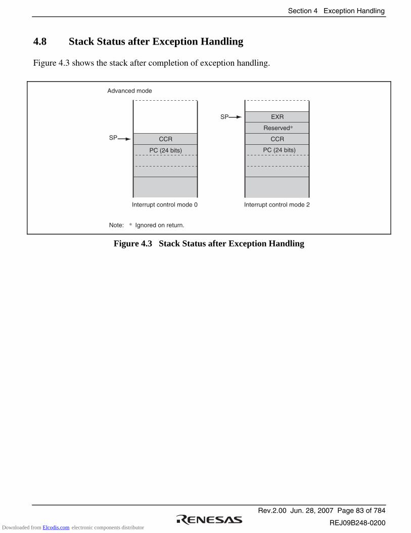
Section 4 Exception Handling
Rev.2.00 Jun. 28, 2007 Page 83 of 784
REJ09B248-0200
4.8 Stack Status after Exception Handling
Figure 4.3 shows the stack after completion of exception handling.
CCR
PC (24 bits)
SP
EXR
Reserved*
CCR
PC (24 bits)
SP
Advanced mode
Interrupt control mode 0 Interrupt control mode 2
Note: * Ignored on return.
Figure 4.3 Stack Status after Exception Handling
Downloaded from Elcodis.com electronic components distributor
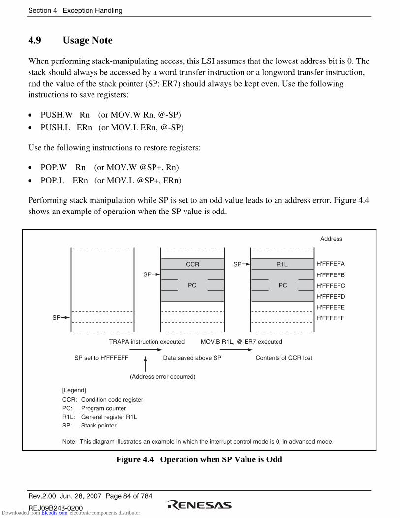
Section 4 Exception Handling
Rev.2.00 Jun. 28, 2007 Page 84 of 784
REJ09B248-0200
4.9 Usage Note
When performing stack-manipulating access, this LSI assumes that the lowest address bit is 0. The stack should always be accessed by a word transfer instruction or a longword transfer instruction, and the value of the stack pointer (SP: ER7) should always be kept even. Use the following instructions to save registers:
• PUSH.W Rn (or MOV.W Rn, @-SP)
• PUSH.L ERn (or MOV.L ERn, @-SP) Use the following instructions to restore registers:
• POP.W Rn (or MOV.W @SP+, Rn)
• POP.L ERn (or MOV.L @SP+, ERn) Performing stack manipulation while SP is set to an odd value leads to an address error. Figure 4.4 shows an example of operation when the SP value is odd.
SP
CCR:PC:R1L:SP:
Condition code registerProgram counterGeneral register R1LStack pointer
CCR R1L H'FFFEFA
H'FFFEFB
H'FFFEFC
H'FFFEFD
H'FFFEFE
H'FFFEFF
PC PC
SP
SP
TRAPA instruction executed
SP set to H'FFFEFF Data saved above SP
MOV.B R1L, @-ER7 executed
Contents of CCR lost
Address
[Legend]
Note: This diagram illustrates an example in which the interrupt control mode is 0, in advanced mode.
(Address error occurred)
Figure 4.4 Operation when SP Value is Odd
Downloaded from Elcodis.com electronic components distributor
Section 5 Interrupt Controller
Rev.2.00 Jun. 28, 2007 Page 85 of 784
REJ09B248-0200
Section 5 Interrupt Controller
5.1 Features
• Two interrupt control modes
Any of two interrupt control modes can be set by means of bits INTM1 and INTM0 in the interrupt control register (INTCR).
• Priority can be assigned by the interrupt priority register (IPR)
IPR provides for setting interrupt priory. Eight levels can be set for each module for all interrupts except for the interrupt requests listed below. The following seven interrupt requests are given priority of 8, therefore they are accepted at all times.
NMI
Illegal instructions
Trace
Trap instructions
CPU address error
DMA address error (occurred in the DTC and DMAC)
Sleep interrupt
• Independent vector addresses
All interrupt sources are assigned independent vector addresses, making it unnecessary for the source to be identified in the interrupt handling routine.
• Thirteen external interrupts
NMI is the highest-priority interrupt, and is accepted at all times. Rising edge or falling edge detection can be selected for NMI. Falling edge, rising edge, or both edge detection, or level sensing, can be selected for IRQ11 to IRQ0.
• DTC and DMAC control
DTC and DMAC can be activated by means of interrupts.
• CPU priority control function
The priority levels can be assigned to the CPU, DTC, and DMAC. The priority level of the CPU can be automatically assigned on an exception generation. Priority can be given to the CPU interrupt exception handling over that of the DTC and DMAC transfer.
Downloaded from Elcodis.com electronic components distributor
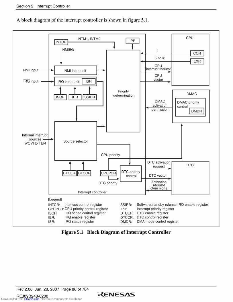
Section 5 Interrupt Controller
Rev.2.00 Jun. 28, 2007 Page 86 of 784
REJ09B248-0200
A block diagram of the interrupt controller is shown in figure 5.1.
INTCR IPR
NMI input
IRQ input
Internal interrupt sources
WOVI to TEI4
INTM1, INTM0
NMIEG
NMI input unit
IRQ input unit
CPU priority
DTC priority
Interrupt controller
Priority determination
Source selector
CPUinterrupt request
CPUvector
DTC vector
Activation request
clear signal
DTC activationrequest
I
I2 to I0CCR
EXR
CPU
DTC
INTCR:CPUPCR:ISCR:IER:ISR:
Interrupt control registerCPU priority control registerIRQ sense control registerIRQ enable registerIRQ status register
SSIER:IPR:DTCER:DTCCR:DMDR:
Software standby release IRQ enable registerInterrupt priority registerDTC enable registerDTC control registerDMA mode control register
[Legend]
ISCR SSIERIER
DTCER DTC priority control
DTCCR
ISR
DMACactivation
permission DMDR
DMAC
DMAC priority control
CPUPCR
Figure 5.1 Block Diagram of Interrupt Controller
Downloaded from Elcodis.com electronic components distributor

Section 5 Interrupt Controller
Rev.2.00 Jun. 28, 2007 Page 87 of 784
REJ09B248-0200
5.2 Input/Output Pins
Table 5.1 shows the pin configuration of the interrupt controller.
Table 5.1 Pin Configuration
Name I/O Function
NMI Input Nonmaskable External Interrupt
Rising or falling edge can be selected.
IRQ11 to IRQ0 Input Maskable External Interrupts
Rising, falling, or both edges, or level sensing, can be selected.
5.3 Register Descriptions
The interrupt controller has the following registers.
• Interrupt control register (INTCR)
• CPU priority control register (CPUPCR)
• Interrupt priority registers A to C, E to I, K, and L (IPRA to IPRC, IPRE to IPRI, IPRK, and IPRL)
• IRQ enable register (IER)
• IRQ sense control registers H and L (ISCRH, ISCRL)
• IRQ status register (ISR)
• Software standby release IRQ enable register (SSIER)
Downloaded from Elcodis.com electronic components distributor
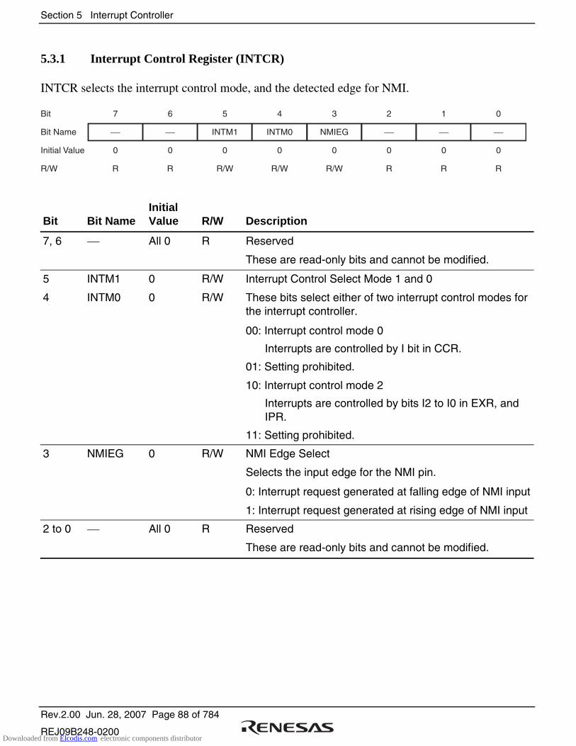
Section 5 Interrupt Controller
Rev.2.00 Jun. 28, 2007 Page 88 of 784
REJ09B248-0200
5.3.1 Interrupt Control Register (INTCR)
INTCR selects the interrupt control mode, and the detected edge for NMI.
Bit
Bit Name
Initial Value
R/W
7
0
R
6
0
R
5
INTM1
0
R/W
4
INTM0
0
R/W
3
NMIEG
0
R/W
2
0
R
1
0
R
0
0
R
Bit Bit Name Initial Value R/W Description
7, 6 All 0 R Reserved
These are read-only bits and cannot be modified.
5
4
INTM1
INTM0
0
0
R/W
R/W
Interrupt Control Select Mode 1 and 0
These bits select either of two interrupt control modes for the interrupt controller.
00: Interrupt control mode 0
Interrupts are controlled by I bit in CCR.
01: Setting prohibited.
10: Interrupt control mode 2
Interrupts are controlled by bits I2 to I0 in EXR, and IPR.
11: Setting prohibited.
3 NMIEG 0 R/W NMI Edge Select
Selects the input edge for the NMI pin.
0: Interrupt request generated at falling edge of NMI input
1: Interrupt request generated at rising edge of NMI input
2 to 0 All 0 R Reserved
These are read-only bits and cannot be modified.
Downloaded from Elcodis.com electronic components distributor

Section 5 Interrupt Controller
Rev.2.00 Jun. 28, 2007 Page 89 of 784
REJ09B248-0200
5.3.2 CPU Priority Control Register (CPUPCR)
CPUPCR sets whether or not the CPU has priority over the DTC and DMAC. The interrupt exception handling by the CPU can be given priority over that of the DTC or DMAC transfer. The priority level of the DTC is assigned by the bits DTCP2 to DTCP0 in CPUPCR. The priority level of the DMAC is assigned by the control register of DMAC respectively in each channel.
Bit
Bit Name
Initial Value
R/W
Note: * When the IPSETE bit is set to 1, the CPU priority is automatically updated, so these bits cannot be modified.
7
CPUPCE
0
R/W
6
DTCP2
0
R/W
5
DTCP1
0
R/W
4
DTCP0
0
R/W
3
IPSETE
0
R/W
2
CPUP2
0
R/(W)*
1
CPUP1
0
R/(W)*
0
CPUP0
0
R/(W)*
Bit Bit Name Initial Value R/W Description
7 CPUPCE 0 R/W CPU Priority Control Enable
Controls the CPU priority control function. Setting this bit to 1 enables the CPU priority control over DTC or DMAC.
0: CPU always has the lowest priority
1: CPU priority control enabled
6
5
4
DTCP2
DTCP1
DTCP0
0
0
0
R/W
R/W
R/W
DTC Priority Level 2 to 0
These bits set the DTC priority level.
000: Priority level 0 (lowest)
001: Priority level 1
010: Priority level 2
011: Priority level 3
100: Priority level 4
101: Priority level 5
110: Priority level 6
111: Priority level 7 (highest)
Downloaded from Elcodis.com electronic components distributor
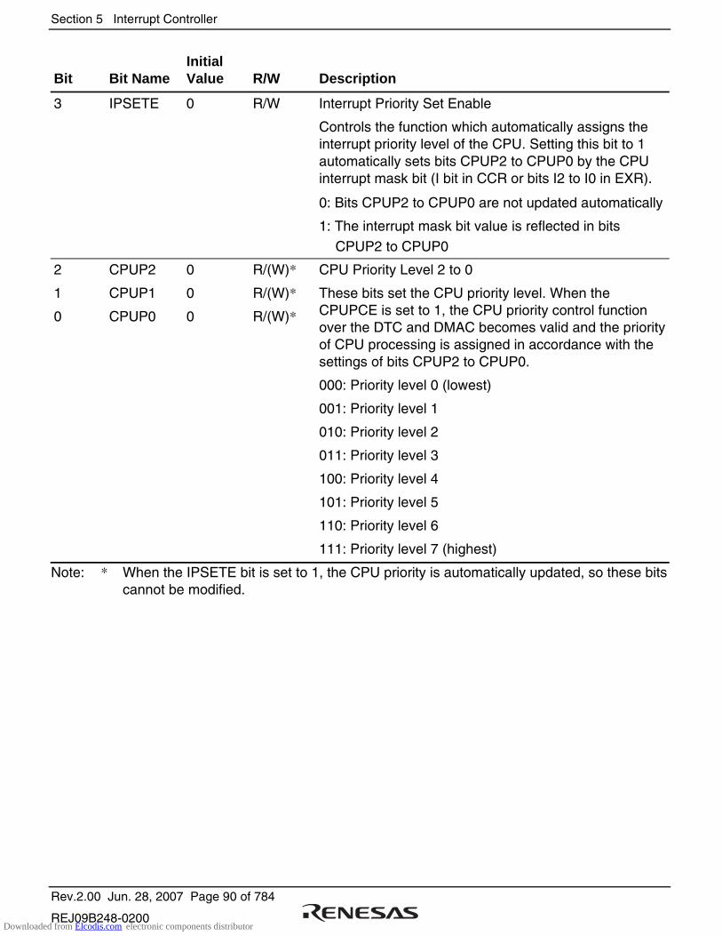
Section 5 Interrupt Controller
Rev.2.00 Jun. 28, 2007 Page 90 of 784
REJ09B248-0200
Bit Bit Name Initial Value R/W Description
3 IPSETE 0 R/W Interrupt Priority Set Enable
Controls the function which automatically assigns the interrupt priority level of the CPU. Setting this bit to 1 automatically sets bits CPUP2 to CPUP0 by the CPU interrupt mask bit (I bit in CCR or bits I2 to I0 in EXR).
0: Bits CPUP2 to CPUP0 are not updated automatically
1: The interrupt mask bit value is reflected in bits
CPUP2 to CPUP0
2
1
0
CPUP2
CPUP1
CPUP0
0
0
0
R/(W)*
R/(W)*
R/(W)*
CPU Priority Level 2 to 0
These bits set the CPU priority level. When the CPUPCE is set to 1, the CPU priority control function over the DTC and DMAC becomes valid and the priority of CPU processing is assigned in accordance with the settings of bits CPUP2 to CPUP0.
000: Priority level 0 (lowest)
001: Priority level 1
010: Priority level 2
011: Priority level 3
100: Priority level 4
101: Priority level 5
110: Priority level 6
111: Priority level 7 (highest)
Note: * When the IPSETE bit is set to 1, the CPU priority is automatically updated, so these bits cannot be modified.
Downloaded from Elcodis.com electronic components distributor

Section 5 Interrupt Controller
Rev.2.00 Jun. 28, 2007 Page 91 of 784
REJ09B248-0200
5.3.3 Interrupt Priority Registers A to C, E to I, K, and L (IPRA to IPRC, IPRE to IPRI,
IPRK, and IPRL)
IPR sets priory (levels 7 to 0) for interrupts other than NMI and sleep interrupt.
Setting a value in the range from B'000 to B'111 in the 3-bit groups of bits 14 to 12, 10 to 8, 6 to 4, and 2 to 0 assigns a priority level to the corresponding interrupt. For the correspondence between the interrupt sources and the IPR settings, see table 5.2.
Bit
Bit Name
Initial Value
R/W
15
0
R
14
IPR14
1
R/W
13
IPR13
1
R/W
12
IPR12
1
R/W
11
0
R
10
IPR10
1
R/W
9
IPR9
1
R/W
8
IPR8
1
R/W
Bit
Bit Name
Initial Value
R/W
7
0
R
6
IPR6
1
R/W
5
IPR5
1
R/W
4
IPR4
1
R/W
3
0
R
2
IPR2
1
R/W
1
IPR1
1
R/W
0
IPR0
1
R/W
Bit Bit Name Initial Value R/W Description
15 0 R Reserved
This is a read-only bit and cannot be modified.
14
13
12
IPR14
IPR13
IPR12
1
1
1
R/W
R/W
R/W
Sets the priority level of the corresponding interrupt source.
000: Priority level 0 (lowest)
001: Priority level 1
010: Priority level 2
011: Priority level 3
100: Priority level 4
101: Priority level 5
110: Priority level 6
111: Priority level 7 (highest)
11 0 R Reserved
This is a read-only bit and cannot be modified.
Downloaded from Elcodis.com electronic components distributor
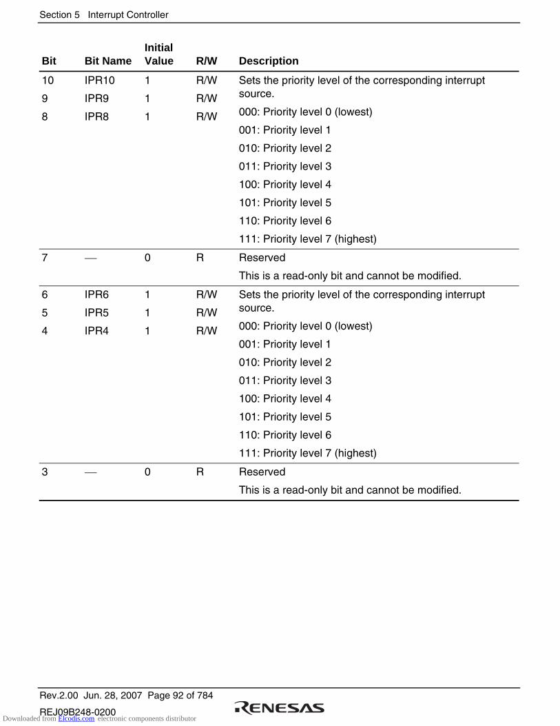
Section 5 Interrupt Controller
Rev.2.00 Jun. 28, 2007 Page 92 of 784
REJ09B248-0200
Bit Bit Name Initial Value R/W Description
10
9
8
IPR10
IPR9
IPR8
1
1
1
R/W
R/W
R/W
Sets the priority level of the corresponding interrupt source.
000: Priority level 0 (lowest)
001: Priority level 1
010: Priority level 2
011: Priority level 3
100: Priority level 4
101: Priority level 5
110: Priority level 6
111: Priority level 7 (highest)
7 0 R Reserved
This is a read-only bit and cannot be modified.
6
5
4
IPR6
IPR5
IPR4
1
1
1
R/W
R/W
R/W
Sets the priority level of the corresponding interrupt source.
000: Priority level 0 (lowest)
001: Priority level 1
010: Priority level 2
011: Priority level 3
100: Priority level 4
101: Priority level 5
110: Priority level 6
111: Priority level 7 (highest)
3 0 R Reserved
This is a read-only bit and cannot be modified.
Downloaded from Elcodis.com electronic components distributor
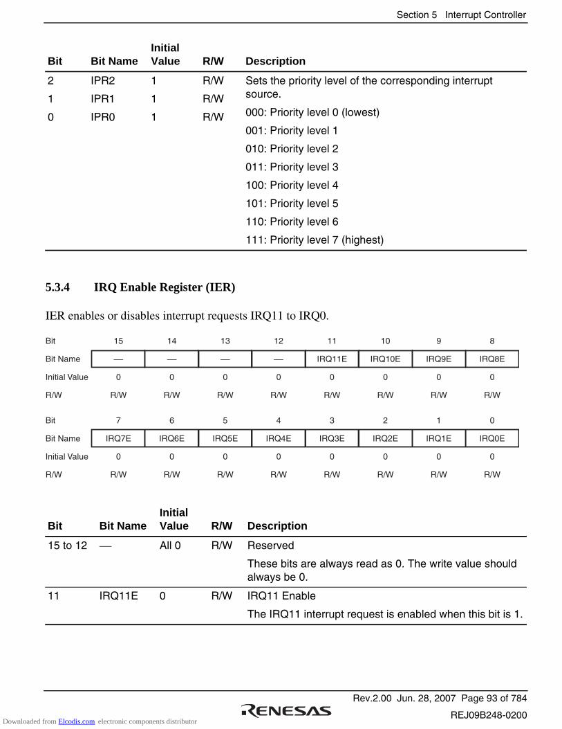
Section 5 Interrupt Controller
Rev.2.00 Jun. 28, 2007 Page 93 of 784
REJ09B248-0200
Bit Bit Name Initial Value R/W Description
2
1
0
IPR2
IPR1
IPR0
1
1
1
R/W
R/W
R/W
Sets the priority level of the corresponding interrupt source.
000: Priority level 0 (lowest)
001: Priority level 1
010: Priority level 2
011: Priority level 3
100: Priority level 4
101: Priority level 5
110: Priority level 6
111: Priority level 7 (highest)
5.3.4 IRQ Enable Register (IER)
IER enables or disables interrupt requests IRQ11 to IRQ0.
Bit
Bit Name
Initial Value
R/W
15
0
R/W
14
0
R/W
13
0
R/W
12
0
R/W
11
IRQ11E
0
R/W
10
IRQ10E
0
R/W
9
IRQ9E
0
R/W
8
IRQ8E
0
R/W
Bit
Bit Name
Initial Value
R/W
7
IRQ7E
0
R/W
6
IRQ6E
0
R/W
5
IRQ5E
0
R/W
4
IRQ4E
0
R/W
3
IRQ3E
0
R/W
2
IRQ2E
0
R/W
1
IRQ1E
0
R/W
0
IRQ0E
0
R/W
Bit Bit Name Initial Value R/W Description
15 to 12 All 0 R/W Reserved
These bits are always read as 0. The write value should always be 0.
11 IRQ11E 0 R/W IRQ11 Enable
The IRQ11 interrupt request is enabled when this bit is 1.
Downloaded from Elcodis.com electronic components distributor
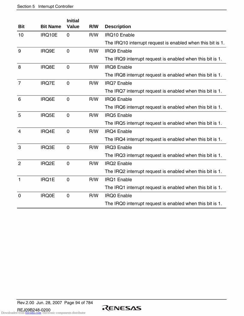
Section 5 Interrupt Controller
Rev.2.00 Jun. 28, 2007 Page 94 of 784
REJ09B248-0200
Bit Bit Name Initial Value R/W Description
10 IRQ10E 0 R/W IRQ10 Enable
The IRQ10 interrupt request is enabled when this bit is 1.
9 IRQ9E 0 R/W IRQ9 Enable
The IRQ9 interrupt request is enabled when this bit is 1.
8 IRQ8E 0 R/W IRQ8 Enable
The IRQ8 interrupt request is enabled when this bit is 1.
7 IRQ7E 0 R/W IRQ7 Enable
The IRQ7 interrupt request is enabled when this bit is 1.
6 IRQ6E 0 R/W IRQ6 Enable
The IRQ6 interrupt request is enabled when this bit is 1.
5 IRQ5E 0 R/W IRQ5 Enable
The IRQ5 interrupt request is enabled when this bit is 1.
4 IRQ4E 0 R/W IRQ4 Enable
The IRQ4 interrupt request is enabled when this bit is 1.
3 IRQ3E 0 R/W IRQ3 Enable
The IRQ3 interrupt request is enabled when this bit is 1.
2 IRQ2E 0 R/W IRQ2 Enable
The IRQ2 interrupt request is enabled when this bit is 1.
1 IRQ1E 0 R/W IRQ1 Enable
The IRQ1 interrupt request is enabled when this bit is 1.
0 IRQ0E 0 R/W IRQ0 Enable
The IRQ0 interrupt request is enabled when this bit is 1.
Downloaded from Elcodis.com electronic components distributor
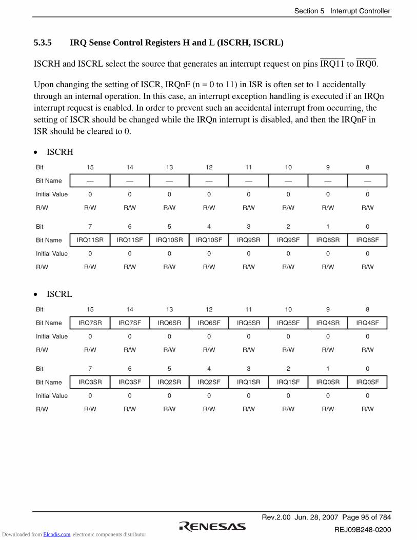
Section 5 Interrupt Controller
Rev.2.00 Jun. 28, 2007 Page 95 of 784
REJ09B248-0200
5.3.5 IRQ Sense Control Registers H and L (ISCRH, ISCRL)
ISCRH and ISCRL select the source that generates an interrupt request on pins IRQ11 to IRQ0.
Upon changing the setting of ISCR, IRQnF (n = 0 to 11) in ISR is often set to 1 accidentally through an internal operation. In this case, an interrupt exception handling is executed if an IRQn interrupt request is enabled. In order to prevent such an accidental interrupt from occurring, the setting of ISCR should be changed while the IRQn interrupt is disabled, and then the IRQnF in ISR should be cleared to 0.
• ISCRH
Bit
Bit Name
Initial Value
R/W
Bit
Bit Name
Initial Value
R/W
15
0
R/W
14
0
R/W
13
0
R/W
12
0
R/W
11
0
R/W
10
0
R/W
9
0
R/W
8
0
R/W
7
IRQ11SR
0
R/W
6
IRQ11SF
0
R/W
5
IRQ10SR
0
R/W
4
IRQ10SF
0
R/W
3
IRQ9SR
0
R/W
2
IRQ9SF
0
R/W
1
IRQ8SR
0
R/W
0
IRQ8SF
0
R/W
• ISCRL
Bit
Bit Name
Initial Value
R/W
Bit
Bit Name
Initial Value
R/W
15
IRQ7SR
0
R/W
14
IRQ7SF
0
R/W
13
IRQ6SR
0
R/W
12
IRQ6SF
0
R/W
11
IRQ5SR
0
R/W
10
IRQ5SF
0
R/W
9
IRQ4SR
0
R/W
8
IRQ4SF
0
R/W
7
IRQ3SR
0
R/W
6
IRQ3SF
0
R/W
5
IRQ2SR
0
R/W
4
IRQ2SF
0
R/W
3
IRQ1SR
0
R/W
2
IRQ1SF
0
R/W
1
IRQ0SR
0
R/W
0
IRQ0SF
0
R/W
Downloaded from Elcodis.com electronic components distributor
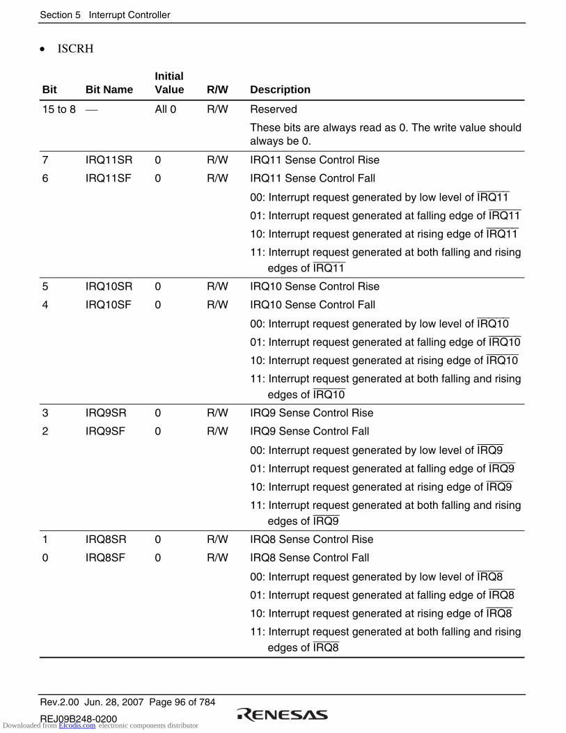
Section 5 Interrupt Controller
Rev.2.00 Jun. 28, 2007 Page 96 of 784
REJ09B248-0200
• ISCRH
Bit Bit Name Initial Value R/W Description
15 to 8 All 0 R/W Reserved
These bits are always read as 0. The write value should always be 0.
7
6
IRQ11SR
IRQ11SF
0
0
R/W
R/W
IRQ11 Sense Control Rise
IRQ11 Sense Control Fall
00: Interrupt request generated by low level of IRQ11
01: Interrupt request generated at falling edge of IRQ11
10: Interrupt request generated at rising edge of IRQ11
11: Interrupt request generated at both falling and rising
edges of IRQ11
5
4
IRQ10SR
IRQ10SF
0
0
R/W
R/W
IRQ10 Sense Control Rise
IRQ10 Sense Control Fall
00: Interrupt request generated by low level of IRQ10
01: Interrupt request generated at falling edge of IRQ10
10: Interrupt request generated at rising edge of IRQ10
11: Interrupt request generated at both falling and rising
edges of IRQ10
3
2
IRQ9SR
IRQ9SF
0
0
R/W
R/W
IRQ9 Sense Control Rise
IRQ9 Sense Control Fall
00: Interrupt request generated by low level of IRQ9
01: Interrupt request generated at falling edge of IRQ9
10: Interrupt request generated at rising edge of IRQ9
11: Interrupt request generated at both falling and rising
edges of IRQ9
1
0
IRQ8SR
IRQ8SF
0
0
R/W
R/W
IRQ8 Sense Control Rise
IRQ8 Sense Control Fall
00: Interrupt request generated by low level of IRQ8
01: Interrupt request generated at falling edge of IRQ8
10: Interrupt request generated at rising edge of IRQ8
11: Interrupt request generated at both falling and rising
edges of IRQ8
Downloaded from Elcodis.com electronic components distributor
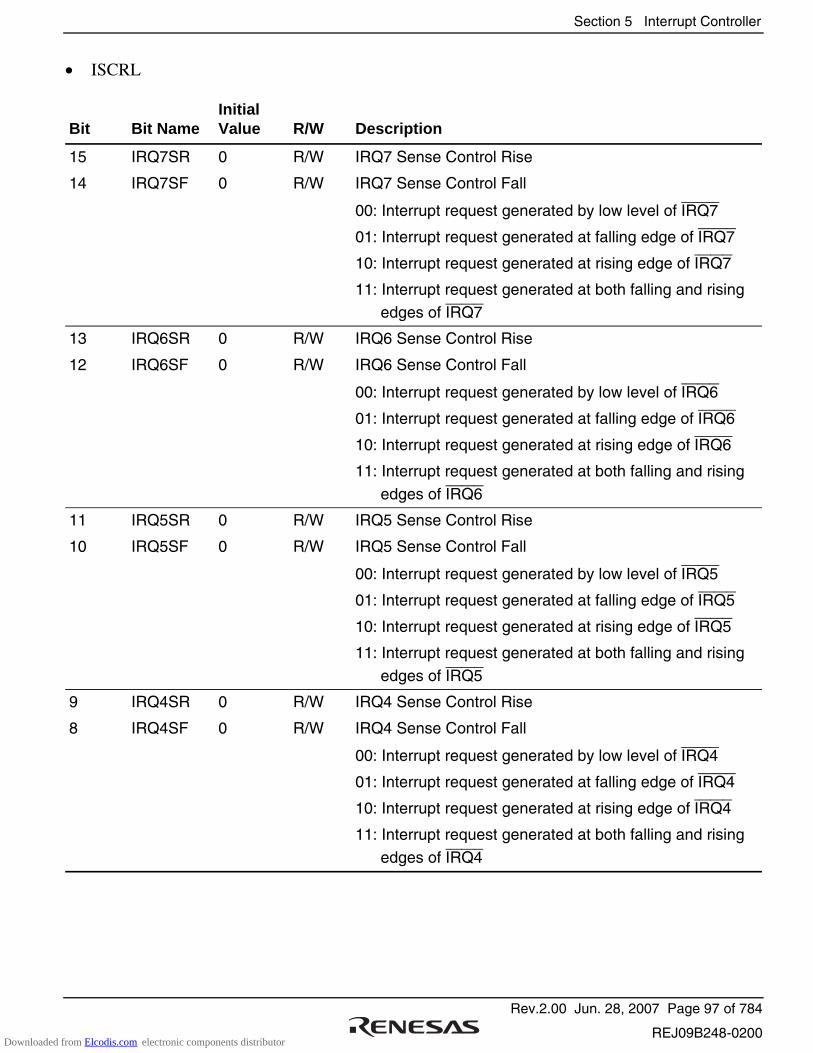
Section 5 Interrupt Controller
Rev.2.00 Jun. 28, 2007 Page 97 of 784
REJ09B248-0200
• ISCRL
Bit Bit Name Initial Value R/W Description
15
14
IRQ7SR
IRQ7SF
0
0
R/W
R/W
IRQ7 Sense Control Rise
IRQ7 Sense Control Fall
00: Interrupt request generated by low level of IRQ7
01: Interrupt request generated at falling edge of IRQ7
10: Interrupt request generated at rising edge of IRQ7
11: Interrupt request generated at both falling and rising
edges of IRQ7
13
12
IRQ6SR
IRQ6SF
0
0
R/W
R/W
IRQ6 Sense Control Rise
IRQ6 Sense Control Fall
00: Interrupt request generated by low level of IRQ6
01: Interrupt request generated at falling edge of IRQ6
10: Interrupt request generated at rising edge of IRQ6
11: Interrupt request generated at both falling and rising
edges of IRQ6
11
10
IRQ5SR
IRQ5SF
0
0
R/W
R/W
IRQ5 Sense Control Rise
IRQ5 Sense Control Fall
00: Interrupt request generated by low level of IRQ5
01: Interrupt request generated at falling edge of IRQ5
10: Interrupt request generated at rising edge of IRQ5
11: Interrupt request generated at both falling and rising
edges of IRQ5
9
8
IRQ4SR
IRQ4SF
0
0
R/W
R/W
IRQ4 Sense Control Rise
IRQ4 Sense Control Fall
00: Interrupt request generated by low level of IRQ4
01: Interrupt request generated at falling edge of IRQ4
10: Interrupt request generated at rising edge of IRQ4
11: Interrupt request generated at both falling and rising
edges of IRQ4
Downloaded from Elcodis.com electronic components distributor
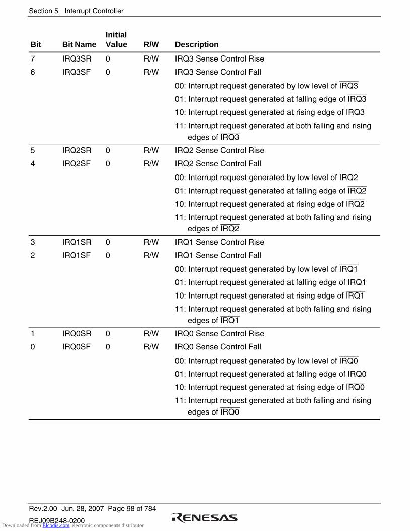
Section 5 Interrupt Controller
Rev.2.00 Jun. 28, 2007 Page 98 of 784
REJ09B248-0200
Bit Bit Name Initial Value R/W Description
7
6
IRQ3SR
IRQ3SF
0
0
R/W
R/W
IRQ3 Sense Control Rise
IRQ3 Sense Control Fall
00: Interrupt request generated by low level of IRQ3
01: Interrupt request generated at falling edge of IRQ3
10: Interrupt request generated at rising edge of IRQ3
11: Interrupt request generated at both falling and rising
edges of IRQ3
5
4
IRQ2SR
IRQ2SF
0
0
R/W
R/W
IRQ2 Sense Control Rise
IRQ2 Sense Control Fall
00: Interrupt request generated by low level of IRQ2
01: Interrupt request generated at falling edge of IRQ2
10: Interrupt request generated at rising edge of IRQ2
11: Interrupt request generated at both falling and rising
edges of IRQ2
3
2
IRQ1SR
IRQ1SF
0
0
R/W
R/W
IRQ1 Sense Control Rise
IRQ1 Sense Control Fall
00: Interrupt request generated by low level of IRQ1
01: Interrupt request generated at falling edge of IRQ1
10: Interrupt request generated at rising edge of IRQ1
11: Interrupt request generated at both falling and rising
edges of IRQ1
1
0
IRQ0SR
IRQ0SF
0
0
R/W
R/W
IRQ0 Sense Control Rise
IRQ0 Sense Control Fall
00: Interrupt request generated by low level of IRQ0
01: Interrupt request generated at falling edge of IRQ0
10: Interrupt request generated at rising edge of IRQ0
11: Interrupt request generated at both falling and rising
edges of IRQ0
Downloaded from Elcodis.com electronic components distributor

Section 5 Interrupt Controller
Rev.2.00 Jun. 28, 2007 Page 99 of 784
REJ09B248-0200
5.3.6 IRQ Status Register (ISR)
ISR is an IRQ11 to IRQ0 interrupt request register.
Bit
Bit Name
Initial Value
R/W
15
0
R/W
14
0
R/W
13
0
R/W
12
0
R/W
11
IRQ11F
0
R/(W)*
10
IRQ10F
0
R/(W)*
9
IRQ9F
0
R/(W)*
8
IRQ8F
0
R/(W)*
Bit
Bit Name
Initial Value
R/W
Note: * Only 0 can be written, to clear the flag. The bit manipulation instructions or memory operation instructions should be used to clear the flag.
7
IRQ7F
0
R/(W)*
6
IRQ6F
0
R/(W)*
5
IRQ5F
0
R/(W)*
4
IRQ4F
0
R/(W)*
3
IRQ3F
0
R/(W)*
2
IRQ2F
0
R/(W)*
1
IRQ1F
0
R/(W)*
0
IRQ0F
0
R/(W)*
Bit Bit Name Initial Value R/W Description
15 to 12 All 0 R/W Reserved
These bits are always read as 0. The write value should always be 0.
11
10
9
8
7
6
5
4
3
2
1
0
IRQ11F
IRQ10F
IRQ9F
IRQ8F
IRQ7F
IRQ6F
IRQ5F
IRQ4F
IRQ3F
IRQ2F
IRQ1F
IRQ0F
0
0
0
0
0
0
0
0
0
0
0
0
R/(W)*
R/(W)*
R/(W)*
R/(W)*
R/(W)*
R/(W)*
R/(W)*
R/(W)*
R/(W)*
R/(W)*
R/(W)*
R/(W)*
[Setting condition]
• When the interrupt selected by ISCR occurs
[Clearing conditions]
• Writing 0 after reading IRQnF = 1
• When interrupt exception handling is executed when
low-level sensing is selected and IRQn input is high
• When IRQn interrupt exception handling is executed when falling-, rising-, or both-edge sensing is
selected
• When the DTC is activated by an IRQn interrupt,
and the DISEL bit in MRB of the DTC is cleared to 0
Note: * Only 0 can be written, to clear the flag.
Downloaded from Elcodis.com electronic components distributor

Section 5 Interrupt Controller
Rev.2.00 Jun. 28, 2007 Page 100 of 784
REJ09B248-0200
5.3.7 Software Standby Release IRQ Enable Register (SSIER)
SSIER selects pins used to leave software standby mode from pins IRQ11 to IRQ0.
The IRQ interrupt used to leave software standby mode should not be set as the DTC activation source.
Bit
Bit Name
Initial Value
R/W
15
0
R/W
14
0
R/W
13
0
R/W
12
0
R/W
11
SSI11
0
R/W
10
SSI10
0
R/W
9
SSI9
0
R/W
8
SSI8
0
R/W
Bit
Bit Name
Initial Value
R/W
7
SSI7
0
R/W
6
SSI6
0
R/W
5
SSI5
0
R/W
4
SSI4
0
R/W
3
SSI3
0
R/W
2
SSI2
0
R/W
1
SSI1
0
R/W
0
SSI0
0
R/W
Bit Bit Name Initial Value R/W Description
15 to 12 All 0 R/W Reserved
These bits are always read as 0. The write value should always be 0.
11
10
9
8
7
6
5
4
3
2
1
0
SSI11
SSI10
SSI9
SSI8
SSI7
SSI6
SSI5
SSI4
SSI3
SSI2
SSI1
SSI0
0
0
0
0
0
0
0
0
0
0
0
0
R/W
R/W
R/W
R/W
R/W
R/W
R/W
R/W
R/W
R/W
R/W
R/W
Software Standby Release IRQ Setting
These bits select the IRQn pins used to leave software standby mode (n = 11 to 0).
0: IRQn requests are not sampled in software standby
mode
1: When an IRQn request occurs in software standby
mode, this LSI leaves software standby mode after
the oscillation settling time has elapsed
Downloaded from Elcodis.com electronic components distributor
Section 5 Interrupt Controller
Rev.2.00 Jun. 28, 2007 Page 101 of 784
REJ09B248-0200
5.4 Interrupt Sources
5.4.1 External Interrupts
There are thirteen external interrupts: NMI and IRQ11 to IRQ0. These interrupts can be used to leave software standby mode.
(1) NMI Interrupts
Nonmaskable interrupt request (NMI) is the highest-priority interrupt, and is always accepted by the CPU regardless of the interrupt control mode or the settings of the CPU interrupt mask bits. The NMIEG bit in INTCR selects whether an interrupt is requested at the rising or falling edge on the NMI pin.
When an NMI interrupt is generated, the interrupt controller determines that an error has occurred, and performs the following procedure.
• Sets the ERR bit in DTCCR to 1.
• Sets the ERRF bit of DMDR_0 in DMAC to 1.
• The DTE bits of all channels in DMAC are cleared to 0, and transfer is terminated. (2) IRQn Interrupts
An IRQn interrupt is requested by a signal input on pins IRQn (n = 11 to 0). IRQn interrupts have the following features:
• Using ISCR, it is possible to select whether an interrupt is generated by a low level, falling edge, rising edge, or both edges, on pins IRQn.
• Enabling or disabling of interrupt requests IRQn can be selected by IER.
• The interrupt priority can be set by IPR.
• The status of interrupt requests IRQn is indicated in ISR. ISR flags can be cleared to 0 by software. The bit manipulation instructions and memory operation instructions should be used to clear the flag.
Detection of IRQn interrupts is enabled through the P1ICR, P2ICR, and P5ICR register settings, and does not change regardless of the output setting. However, when a pin is used as an external interrupt input pin, the pin must not be used as an I/O pin for another function by clearing the corresponding DDR bit to 0.
Downloaded from Elcodis.com electronic components distributor
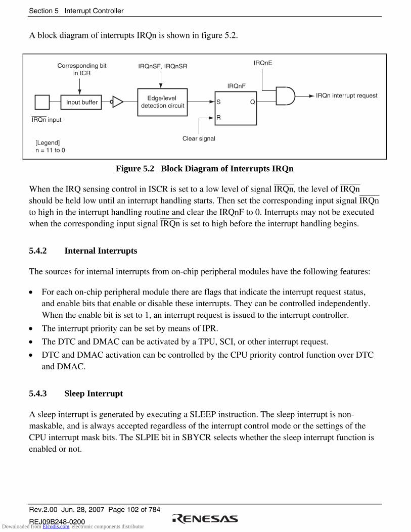
Section 5 Interrupt Controller
Rev.2.00 Jun. 28, 2007 Page 102 of 784
REJ09B248-0200
A block diagram of interrupts IRQn is shown in figure 5.2.
IRQn interrupt request
IRQnE
IRQnF
S
R
Q
Clear signal
Edge/level detection circuitInput buffer
Corresponding bitin ICR
IRQnSF, IRQnSR
IRQn input
[Legend]n = 11 to 0
Figure 5.2 Block Diagram of Interrupts IRQn
When the IRQ sensing control in ISCR is set to a low level of signal IRQn, the level of IRQn should be held low until an interrupt handling starts. Then set the corresponding input signal IRQn to high in the interrupt handling routine and clear the IRQnF to 0. Interrupts may not be executed when the corresponding input signal IRQn is set to high before the interrupt handling begins.
5.4.2 Internal Interrupts
The sources for internal interrupts from on-chip peripheral modules have the following features:
• For each on-chip peripheral module there are flags that indicate the interrupt request status, and enable bits that enable or disable these interrupts. They can be controlled independently. When the enable bit is set to 1, an interrupt request is issued to the interrupt controller.
• The interrupt priority can be set by means of IPR.
• The DTC and DMAC can be activated by a TPU, SCI, or other interrupt request.
• DTC and DMAC activation can be controlled by the CPU priority control function over DTC and DMAC.
5.4.3 Sleep Interrupt
A sleep interrupt is generated by executing a SLEEP instruction. The sleep interrupt is non-maskable, and is always accepted regardless of the interrupt control mode or the settings of the CPU interrupt mask bits. The SLPIE bit in SBYCR selects whether the sleep interrupt function is enabled or not.
Downloaded from Elcodis.com electronic components distributor

Section 5 Interrupt Controller
Rev.2.00 Jun. 28, 2007 Page 103 of 784
REJ09B248-0200
5.5 Interrupt Exception Handling Vector Table
Table 5.2 lists interrupt exception handling sources, vector address offsets, and interrupt priority.
In the default priority order, a lower vector number corresponds to a higher priority. When interrupt control mode 2 is set, priority levels can be changed by setting the IPR contents. The priority for interrupt sources allocated to the same level in IPR follows the default priority, that is, they are fixed.
Table 5.2 Interrupt Sources, Vector Address Offsets, and Interrupt Priority
Vector Address Offset*
Classifi-cation Interrupt Source
Vector Number
Advanced Mode IPR Priority
DTC Acti-vation
DMAC Acti-vation
External pin
NMI 7 H'001C High
SLEEP instruc- tion
Sleep interrupt 18 H'0048
IRQ0 64 H'0100 IPRA14 to IPRA12 Enabled External pin IRQ1 65 H'0104 IPRA10 to IPRA8 Enabled
IRQ2 66 H'0108 IPRA6 to IPRA4 Enabled
IRQ3 67 H'010C IPRA2 to IPRA0 Enabled
IRQ4 68 H'0110 IPRB14 to IPRB12 Enabled
IRQ5 69 H'0114 IPRB10 to IPRB8 Enabled
IRQ6 70 H'0118 IPRB6 to IPRB4 Enabled
IRQ7 71 H'011C IPRB2 to IPRB0 Enabled
IRQ8 72 H'0120 IPRC14 to IPRC12 Enabled
IRQ9 73 H'0124 IPRC10 to IPRC8 Enabled
IRQ10 74 H'0128 IPRC6 to IPRC4 Enabled
IRQ11 75 H'012C IPRC2 to IPRC0 Low Enabled
Downloaded from Elcodis.com electronic components distributor
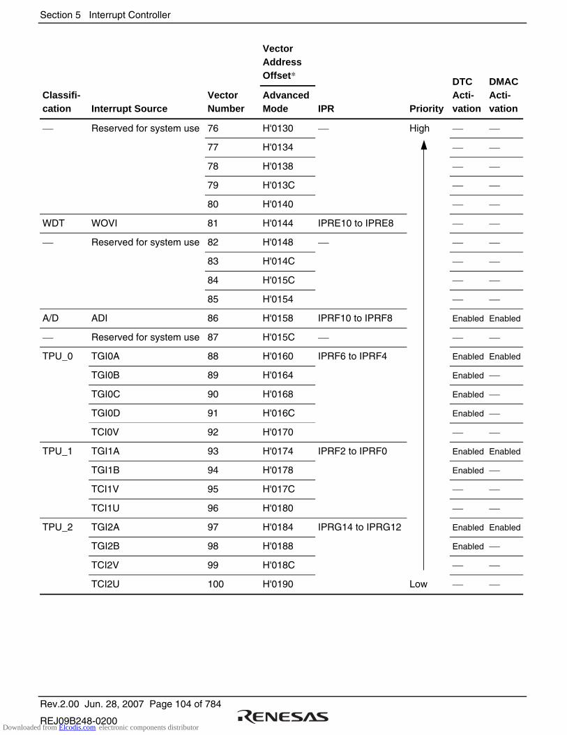
Section 5 Interrupt Controller
Rev.2.00 Jun. 28, 2007 Page 104 of 784
REJ09B248-0200
Vector Address Offset*
Classifi-cation Interrupt Source
Vector Number
Advanced Mode IPR Priority
DTC Acti-vation
DMAC Acti-vation
Reserved for system use 76 H'0130 High
77 H'0134
78 H'0138
79 H'013C
80 H'0140
WDT WOVI 81 H'0144 IPRE10 to IPRE8
Reserved for system use 82 H'0148
83 H'014C
84 H'015C
85 H'0154
A/D ADI 86 H'0158 IPRF10 to IPRF8 Enabled Enabled
Reserved for system use 87 H'015C
TPU_0 TGI0A 88 H'0160 IPRF6 to IPRF4 Enabled Enabled
TGI0B 89 H'0164 Enabled
TGI0C 90 H'0168 Enabled
TGI0D 91 H'016C Enabled
TCI0V 92 H'0170
TPU_1 TGI1A 93 H'0174 IPRF2 to IPRF0 Enabled Enabled
TGI1B 94 H'0178 Enabled
TCI1V 95 H'017C
TCI1U 96 H'0180
TPU_2 TGI2A 97 H'0184 IPRG14 to IPRG12 Enabled Enabled
TGI2B 98 H'0188 Enabled
TCI2V 99 H'018C
TCI2U 100 H'0190 Low
Downloaded from Elcodis.com electronic components distributor
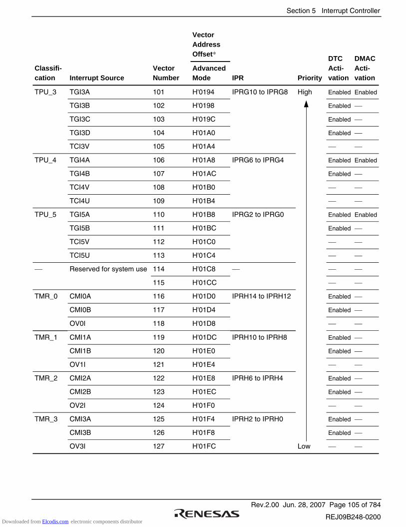
Section 5 Interrupt Controller
Rev.2.00 Jun. 28, 2007 Page 105 of 784
REJ09B248-0200
Vector Address Offset*
Classifi-cation Interrupt Source
Vector Number
Advanced Mode IPR Priority
DTC Acti-vation
DMAC Acti-vation
TPU_3 TGI3A 101 H'0194 IPRG10 to IPRG8 High Enabled Enabled
TGI3B 102 H'0198 Enabled
TGI3C 103 H'019C Enabled
TGI3D 104 H'01A0 Enabled
TCI3V 105 H'01A4
TPU_4 TGI4A 106 H'01A8 IPRG6 to IPRG4 Enabled Enabled
TGI4B 107 H'01AC Enabled
TCI4V 108 H'01B0
TCI4U 109 H'01B4
TPU_5 TGI5A 110 H'01B8 IPRG2 to IPRG0 Enabled Enabled
TGI5B 111 H'01BC Enabled
TCI5V 112 H'01C0
TCI5U 113 H'01C4
Reserved for system use 114 H'01C8
115 H'01CC
TMR_0 CMI0A 116 H'01D0 IPRH14 to IPRH12 Enabled
CMI0B 117 H'01D4 Enabled
OV0I 118 H'01D8
TMR_1 CMI1A 119 H'01DC IPRH10 to IPRH8 Enabled
CMI1B 120 H'01E0 Enabled
OV1I 121 H'01E4
TMR_2 CMI2A 122 H'01E8 IPRH6 to IPRH4 Enabled
CMI2B 123 H'01EC Enabled
OV2I 124 H'01F0
TMR_3 CMI3A 125 H'01F4 IPRH2 to IPRH0 Enabled
CMI3B 126 H'01F8 Enabled
OV3I 127 H'01FC Low
Downloaded from Elcodis.com electronic components distributor
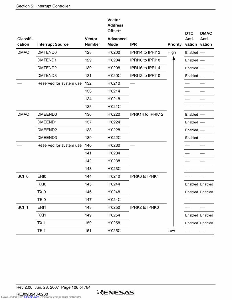
Section 5 Interrupt Controller
Rev.2.00 Jun. 28, 2007 Page 106 of 784
REJ09B248-0200
Vector Address Offset*
Classifi-cation Interrupt Source
Vector Number
Advanced Mode IPR Priority
DTC Acti-vation
DMAC Acti-vation
DMAC DMTEND0 128 H'0200 IPRI14 to IPRI12 High Enabled
DMTEND1 129 H'0204 IPRI10 to IPRI18 Enabled
DMTEND2 130 H'0208 IPRI16 to IPRI14 Enabled
DMTEND3 131 H'020C IPRI12 to IPRI10 Enabled
Reserved for system use 132 H'0210
133 H'0214
134 H'0218
135 H'021C
DMAC DMEEND0 136 H'0220 IPRK14 to IPRK12 Enabled
DMEEND1 137 H'0224 Enabled
DMEEND2 138 H'0228 Enabled
DMEEND3 139 H'022C Enabled
Reserved for system use 140 H'0230
141 H'0234
142 H'0238
143 H'023C
SCI_0 ERI0 144 H'0240 IPRK6 to IPRK4
RXI0 145 H'0244 Enabled Enabled
TXI0 146 H'0248 Enabled Enabled
TEI0 147 H'024C
SCI_1 ERI1 148 H'0250 IPRK2 to IPRK0
RXI1 149 H'0254 Enabled Enabled
TXI1 150 H'0258 Enabled Enabled
TEI1 151 H'025C Low
Downloaded from Elcodis.com electronic components distributor
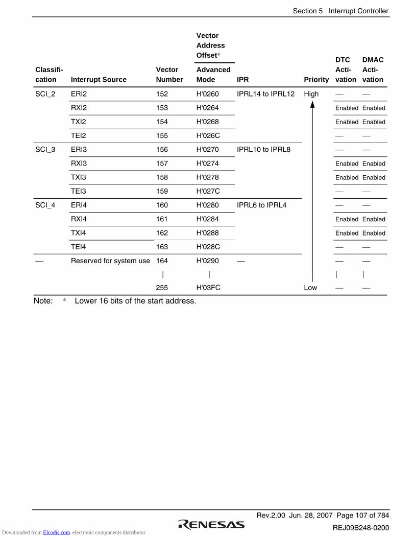
Section 5 Interrupt Controller
Rev.2.00 Jun. 28, 2007 Page 107 of 784
REJ09B248-0200
Vector Address Offset*
Classifi-cation Interrupt Source
Vector Number
Advanced Mode IPR Priority
DTC Acti-vation
DMAC Acti-vation
SCI_2 ERI2 152 H'0260 IPRL14 to IPRL12 High
RXI2 153 H'0264 Enabled Enabled
TXI2 154 H'0268 Enabled Enabled
TEI2 155 H'026C
SCI_3 ERI3 156 H'0270 IPRL10 to IPRL8
RXI3 157 H'0274 Enabled Enabled
TXI3 158 H'0278 Enabled Enabled
TEI3 159 H'027C
SCI_4 ERI4 160 H'0280 IPRL6 to IPRL4
RXI4 161 H'0284 Enabled Enabled
TXI4 162 H'0288 Enabled Enabled
TEI4 163 H'028C
Reserved for system use 164 H'0290
| | | |
255 H'03FC Low
Note: * Lower 16 bits of the start address.
Downloaded from Elcodis.com electronic components distributor

Section 5 Interrupt Controller
Rev.2.00 Jun. 28, 2007 Page 108 of 784
REJ09B248-0200
5.6 Interrupt Control Modes and Interrupt Operation
The interrupt controller has two interrupt control modes: interrupt control mode 0 and interrupt control mode 2. Interrupt operations differ depending on the interrupt control mode. The interrupt control mode is selected by INTCR. Table 5.3 shows the differences between interrupt control mode 0 and interrupt control mode 2.
Table 5.3 Interrupt Control Modes
Interrupt Control Mode
Priority Setting Register
Interrupt Mask Bit Description
0 Default I The priority levels of the interrupt sources are fixed default settings. The interrupts except for NMI and sleep interrupt is masked by the I bit.
2 IPR I2 to I0 Eight priority levels can be set for interrupt sources except for NMI and sleep interrupt with IPR. 8-level interrupt mask control is performed by bits I2 to I0.
5.6.1 Interrupt Control Mode 0
In interrupt control mode 0, interrupt requests except for NMI and sleep interrupt are masked by the I bit in CCR of the CPU. Figure 5.3 shows a flowchart of the interrupt acceptance operation in this case.
1. If an interrupt request occurs when the corresponding interrupt enable bit is set to 1, the interrupt request is sent to the interrupt controller.
2. If the I bit in CCR is set to 1, NMI and sleep interrupt is accepted, and other interrupt requests are held pending. If the I bit is cleared to 0, an interrupt request is accepted.
3. For multiple interrupt requests, the interrupt controller selects the interrupt request with the highest priority, sends the request to the CPU, and holds other interrupt requests pending.
4. When the CPU accepts the interrupt request, it starts interrupt exception handling after execution of the current instruction has been completed.
5. The PC and CCR contents are saved to the stack area during the interrupt exception handling. The PC contents saved on the stack are the address of the first instruction to be executed after returning from the interrupt handling routine.
6. Next, the I bit in CCR is set to 1. This masks all interrupts except NMI and sleep interrupt.
Downloaded from Elcodis.com electronic components distributor

Section 5 Interrupt Controller
Rev.2.00 Jun. 28, 2007 Page 109 of 784
REJ09B248-0200
7. The CPU generates a vector address for the accepted interrupt and starts execution of the interrupt handling routine at the address indicated by the contents of the vector address in the vector table.
Program execution state
Interrupt generated?
NMI or sleep interrupt
IRQ0
IRQ1
TEI4
I = 0
Save PC and CCR
I ← 1
Read vector address
Branch to interrupt handling routine
Yes
No
Yes
Yes
Yes No
No
No
Yes
Yes
No
Pending
Figure 5.3 Flowchart of Procedure Up to Interrupt Acceptance in Interrupt Control Mode 0
Downloaded from Elcodis.com electronic components distributor
Section 5 Interrupt Controller
Rev.2.00 Jun. 28, 2007 Page 110 of 784
REJ09B248-0200
5.6.2 Interrupt Control Mode 2
In interrupt control mode 2, interrupt requests except for NMI and sleep interrupt are masked by comparing the interrupt mask level (I2 to I0 bits) in EXR of the CPU and the IPR setting. There are eight levels in mask control. Figure 5.4 shows a flowchart of the interrupt acceptance operation in this case.
1. If an interrupt request occurs when the corresponding interrupt enable bit is set to 1, an interrupt request is sent to the interrupt controller.
2. For multiple interrupt requests, the interrupt controller selects the interrupt request with the highest priority according to the IPR setting, and holds other interrupt requests pending. If multiple interrupt requests have the same priority, an interrupt request is selected according to the default setting shown in table 5.2.
3. Next, the priority of the selected interrupt request is compared with the interrupt mask level set in EXR. When the interrupt request does not have priority over the mask level set, it is held pending, and only an interrupt request with a priority over the interrupt mask level is accepted.
4. When the CPU accepts an interrupt request, it starts interrupt exception handling after execution of the current instruction has been completed.
5. The PC, CCR, and EXR contents are saved to the stack area during interrupt exception handling. The PC saved on the stack is the address of the first instruction to be executed after returning from the interrupt handling routine.
6. The T bit in EXR is cleared to 0. The interrupt mask level is rewritten with the priority of the accepted interrupt. If the accepted interrupt is NMI or sleep interrupt, the interrupt mask level is set to H'7.
7. The CPU generates a vector address for the accepted interrupt and starts execution of the interrupt handling routine at the address indicated by the contents of the vector address in the vector table.
Downloaded from Elcodis.com electronic components distributor

Section 5 Interrupt Controller
Rev.2.00 Jun. 28, 2007 Page 111 of 784
REJ09B248-0200
Yes
Program execution state
Interrupt generated?
NMI or sleep interrupt
Level 6 interrupt?
Mask level 5 or below?
Level 7 interrupt?
Mask level 6or below?
Save PC, CCR, and EXR
Clear T bit to 0
Update mask level
Read vector address
Branch to interrupt handling routine
Pending
Level 1 interrupt?
Mask level 0?
Yes
Yes
NoYes
Yes
Yes
No
Yes
Yes
No
No
No
No
No
No
Figure 5.4 Flowchart of Procedure Up to Interrupt Acceptance in Interrupt Control Mode 2
Downloaded from Elcodis.com electronic components distributor

Section 5 Interrupt Controller
Rev.2.00 Jun. 28, 2007 Page 112 of 784
REJ09B248-0200
5.6.3 Interrupt Exception Handling Sequence
Figure 5.5 shows the interrupt exception handling sequence. The example is for the case where interrupt control mode 0 is set in maximum mode, and the program area and stack area are in on-chip memory.
(12)
(10)
(6)
(4)
(2)
(1)
(5)
(7)
(9)
(11)
Inst
ruct
ion
pref
etch
Inte
rrup
tac
cept
ance
Inte
rrup
t lev
el d
eter
min
atio
nW
ait f
or e
nd o
f ins
truc
tion
(3)
(8)
Inst
ruct
ion
pref
etch
in in
terr
upt h
andl
ing
rout
ine
Inte
rnal
oper
atio
nV
ecto
r fe
tch
Sta
ckIn
tern
alop
erat
ion
Inte
rrup
tre
ques
t sig
nal
Inte
rnal
addr
ess
bus
Inte
rnal
read
sig
nal
Inte
rnal
writ
e si
gnal
Inte
rnal
data
bus
Iφ (1)
(2)
(4)
(3)
(5)
(7)
Inst
ruct
ion
pref
etch
add
ress
(N
ot e
xecu
ted.
Thi
s is
th
e co
nten
ts o
f the
sav
ed P
C, t
he r
etur
n ad
dres
s.)
Inst
ruct
ion
code
(N
ot e
xecu
ted.
)In
stru
ctio
n pr
efet
ch a
ddre
ss (
Not
exe
cute
d.)
SP
− 2
SP
− 4
Sav
ed P
C a
nd s
aved
CC
RV
ecto
r ad
dres
sS
tart
add
ress
of i
nter
rupt
han
dlin
g ro
utin
e (
vect
or a
ddre
ss c
onte
nts)
Sta
rt a
ddre
ss o
f Int
erru
pt h
andl
ing
rout
ine
((11
) =
(10
))F
irst i
nstr
uctio
n of
inte
rrup
t han
dlin
g ro
utin
e
(6)
(8)
(9)
(10)
(1
1)(1
2)
Figure 5.5 Interrupt Exception Handling
Downloaded from Elcodis.com electronic components distributor
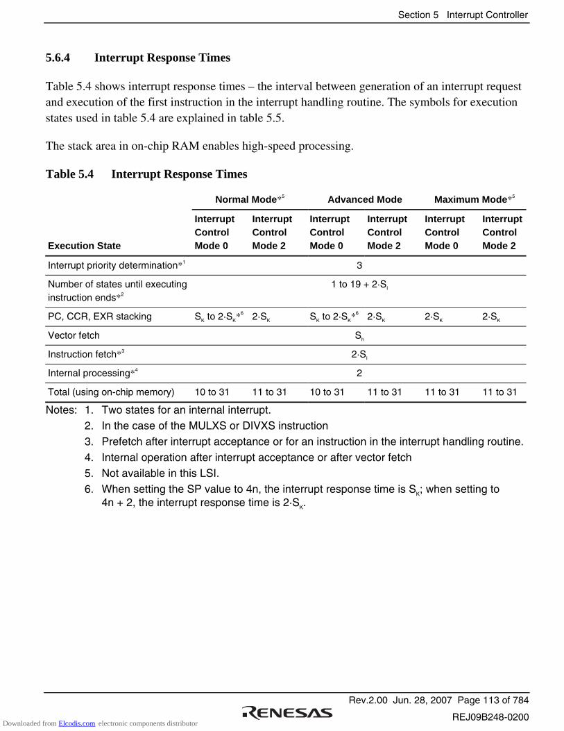
Section 5 Interrupt Controller
Rev.2.00 Jun. 28, 2007 Page 113 of 784
REJ09B248-0200
5.6.4 Interrupt Response Times
Table 5.4 shows interrupt response times – the interval between generation of an interrupt request and execution of the first instruction in the interrupt handling routine. The symbols for execution states used in table 5.4 are explained in table 5.5.
The stack area in on-chip RAM enables high-speed processing.
Table 5.4 Interrupt Response Times
Normal Mode*5 Advanced Mode Maximum Mode*5
Execution State
Interrupt Control Mode 0
Interrupt Control Mode 2
Interrupt Control Mode 0
Interrupt Control Mode 2
Interrupt Control Mode 0
Interrupt Control Mode 2
Interrupt priority determination*1 3
Number of states until executing instruction ends*2
1 to 19 + 2·SI
PC, CCR, EXR stacking SK to 2·SK*6 2·SK SK to 2·SK*
6 2·SK 2·SK 2·SK
Vector fetch Sh
Instruction fetch*3 2·SI
Internal processing*4 2
Total (using on-chip memory) 10 to 31 11 to 31 10 to 31 11 to 31 11 to 31 11 to 31
Notes: 1. Two states for an internal interrupt. 2. In the case of the MULXS or DIVXS instruction
3. Prefetch after interrupt acceptance or for an instruction in the interrupt handling routine.
4. Internal operation after interrupt acceptance or after vector fetch 5. Not available in this LSI.
6. When setting the SP value to 4n, the interrupt response time is SK; when setting to 4n + 2, the interrupt response time is 2·SK.
Downloaded from Elcodis.com electronic components distributor
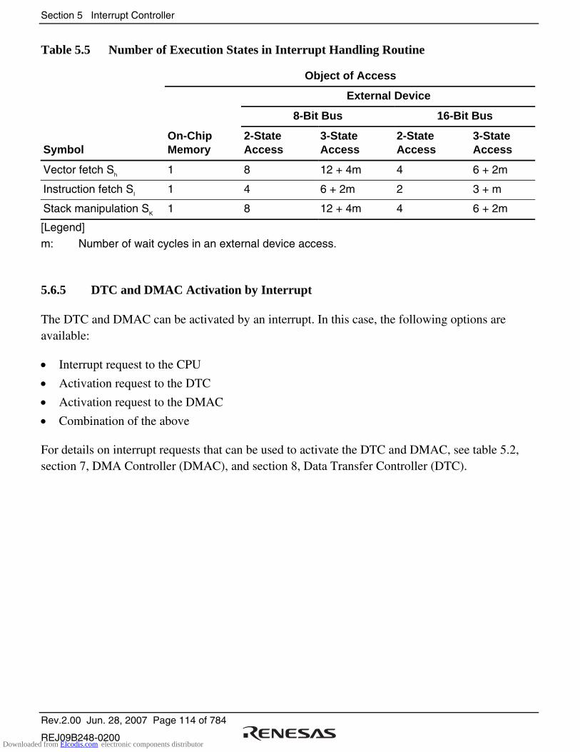
Section 5 Interrupt Controller
Rev.2.00 Jun. 28, 2007 Page 114 of 784
REJ09B248-0200
Table 5.5 Number of Execution States in Interrupt Handling Routine
Object of Access
External Device
8-Bit Bus 16-Bit Bus
Symbol On-Chip Memory
2-State Access
3-State Access
2-State Access
3-State Access
Vector fetch Sh 1 8 12 + 4m 4 6 + 2m
Instruction fetch SI 1 4 6 + 2m 2 3 + m
Stack manipulation SK 1 8 12 + 4m 4 6 + 2m
[Legend]
m: Number of wait cycles in an external device access.
5.6.5 DTC and DMAC Activation by Interrupt
The DTC and DMAC can be activated by an interrupt. In this case, the following options are available:
• Interrupt request to the CPU
• Activation request to the DTC
• Activation request to the DMAC
• Combination of the above For details on interrupt requests that can be used to activate the DTC and DMAC, see table 5.2, section 7, DMA Controller (DMAC), and section 8, Data Transfer Controller (DTC).
Downloaded from Elcodis.com electronic components distributor
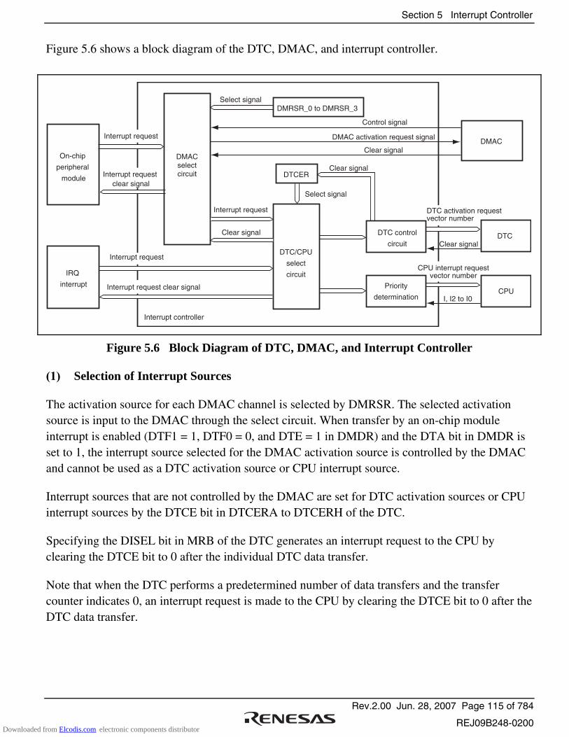
Section 5 Interrupt Controller
Rev.2.00 Jun. 28, 2007 Page 115 of 784
REJ09B248-0200
Figure 5.6 shows a block diagram of the DTC, DMAC, and interrupt controller.
Select signal
DTCER
DMRSR_0 to DMRSR_3
Select signal
IRQ
interrupt
On-chip
peripheral
module
Interrupt controller
Clear signal
Control signal
DMAC activation request signal
Clear signal
I, I2 to I0
Clear signalDTC/CPU
select
circuit
DMACselectcircuit
DTC control
circuit
Priority
determination
DTC
DMAC
CPU
Interrupt request
Clear signal
Interrupt request
Interrupt request clear signal
Interrupt request clear signal
Interrupt request
DTC activation requestvector number
CPU interrupt requestvector number
Figure 5.6 Block Diagram of DTC, DMAC, and Interrupt Controller
(1) Selection of Interrupt Sources
The activation source for each DMAC channel is selected by DMRSR. The selected activation source is input to the DMAC through the select circuit. When transfer by an on-chip module interrupt is enabled (DTF1 = 1, DTF0 = 0, and DTE = 1 in DMDR) and the DTA bit in DMDR is set to 1, the interrupt source selected for the DMAC activation source is controlled by the DMAC and cannot be used as a DTC activation source or CPU interrupt source.
Interrupt sources that are not controlled by the DMAC are set for DTC activation sources or CPU interrupt sources by the DTCE bit in DTCERA to DTCERH of the DTC.
Specifying the DISEL bit in MRB of the DTC generates an interrupt request to the CPU by clearing the DTCE bit to 0 after the individual DTC data transfer.
Note that when the DTC performs a predetermined number of data transfers and the transfer counter indicates 0, an interrupt request is made to the CPU by clearing the DTCE bit to 0 after the DTC data transfer.
Downloaded from Elcodis.com electronic components distributor
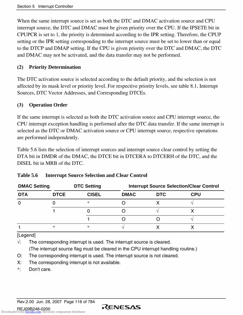
Section 5 Interrupt Controller
Rev.2.00 Jun. 28, 2007 Page 116 of 784
REJ09B248-0200
When the same interrupt source is set as both the DTC and DMAC activation source and CPU interrupt source, the DTC and DMAC must be given priority over the CPU. If the IPSETE bit in CPUPCR is set to 1, the priority is determined according to the IPR setting. Therefore, the CPUP setting or the IPR setting corresponding to the interrupt source must be set to lower than or equal to the DTCP and DMAP setting. If the CPU is given priority over the DTC and DMAC, the DTC and DMAC may not be activated, and the data transfer may not be performed.
(2) Priority Determination
The DTC activation source is selected according to the default priority, and the selection is not affected by its mask level or priority level. For respective priority levels, see table 8.1, Interrupt Sources, DTC Vector Addresses, and Corresponding DTCEs.
(3) Operation Order
If the same interrupt is selected as both the DTC activation source and CPU interrupt source, the CPU interrupt exception handling is performed after the DTC data transfer. If the same interrupt is selected as the DTC or DMAC activation source or CPU interrupt source, respective operations are performed independently.
Table 5.6 lists the selection of interrupt sources and interrupt source clear control by setting the DTA bit in DMDR of the DMAC, the DTCE bit in DTCERA to DTCERH of the DTC, and the DISEL bit in MRB of the DTC.
Table 5.6 Interrupt Source Selection and Clear Control
DMAC Setting DTC Setting Interrupt Source Selection/Clear Control
DTA DTCE CISEL DMAC DTC CPU
0 * O X √
0 O √ X
0
1
1 O O √
1 * * √ X X
[Legend]
√: The corresponding interrupt is used. The interrupt source is cleared. (The interrupt source flag must be cleared in the CPU interrupt handling routine.)
O: The corresponding interrupt is used. The interrupt source is not cleared.
X: The corresponding interrupt is not available. *: Don't care.
Downloaded from Elcodis.com electronic components distributor

Section 5 Interrupt Controller
Rev.2.00 Jun. 28, 2007 Page 117 of 784
REJ09B248-0200
(4) Usage Note
The interrupt sources of the SCI and A/D converter are cleared according to the setting shown in table 5.6, when the DTC or DMAC reads/writes the prescribed register.
To initiate multiple channels for the DTC or DMAC with the same interrupt, the same priority (DTCP = DMAP) should be assigned.
5.7 CPU Priority Control Function Over DTC and DMAC
The interrupt controller has a function to control the priority among the DTC, DMAC, and the CPU by assigning different priority levels to the DTC, DMAC, and CPU. Since the priority level can automatically be assigned to the CPU on an interrupt occurrence, it is possible to execute the CPU interrupt exception handling prior to the DTC or DMAC transfer.
The priority level of the CPU is assigned by bits CPUP2 to CPUP0 in CPUPCR. The priority level of the DTC is assigned by bits DTCP2 to DTCP0 in CPUPCR. The priority level of the DMAC is assigned by bits DMAP2 to DMAP0 in DMDR for each channel.
The priority control function over the DTC and DMAC is enabled by setting the CPUPCE bit in CPUPCR to 1. When the CPUPCE bit is 1, the DTC and DMAC activation sources are controlled according to the respective priority levels.
The DTC activation source is controlled according to the priority level of the CPU indicated by bits CPUP2 to CPUP0 and the priority level of the DTC indicated by bits DTCP2 to DTCP0. If the CPU has priority, the DTC activation source is held. The DTC is activated when the condition by which the activation source is held is cancelled (CPUPCE = 1 and value of bits CPUP2 to CPUP0 is greater than that of bits DTCP2 to DTCP0). The priority level of the DTC is assigned by the DTCP2 to DTCP0 bits regardless of the activation source.
For the DMAC, the priority level can be specified for each channel. The DMAC activation source is controlled according to the priority level of each DMAC channel indicated by bits DMAP2 to DMAP0 and the priority level of the CPU. If the CPU has priority, the DMAC activation source is held. The DMAC is activated when the condition by which the activation source is held is cancelled (CPUPCE = 1 and value of bits CPUP2 to CPUP0 is greater than that of bits DMAP2 to DMAP0). If different priority levels are specified for channels, the channels of the higher priority levels continue transfer and the activation sources for the channels of lower priority levels than that of the CPU are held.
Downloaded from Elcodis.com electronic components distributor
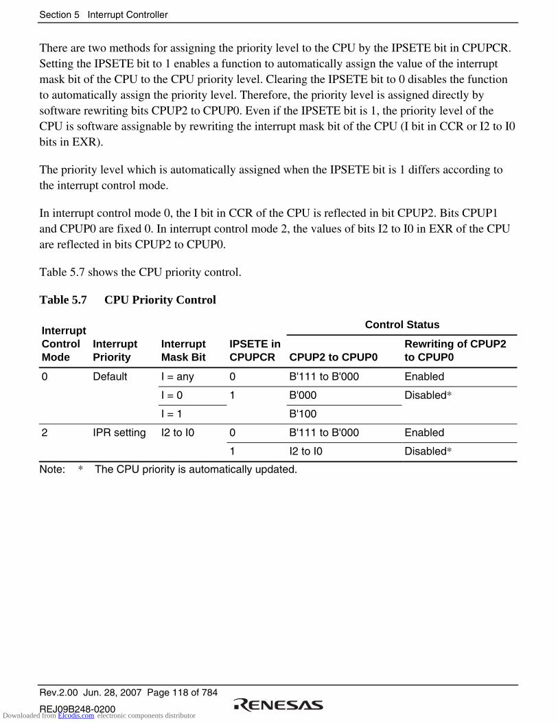
Section 5 Interrupt Controller
Rev.2.00 Jun. 28, 2007 Page 118 of 784
REJ09B248-0200
There are two methods for assigning the priority level to the CPU by the IPSETE bit in CPUPCR. Setting the IPSETE bit to 1 enables a function to automatically assign the value of the interrupt mask bit of the CPU to the CPU priority level. Clearing the IPSETE bit to 0 disables the function to automatically assign the priority level. Therefore, the priority level is assigned directly by software rewriting bits CPUP2 to CPUP0. Even if the IPSETE bit is 1, the priority level of the CPU is software assignable by rewriting the interrupt mask bit of the CPU (I bit in CCR or I2 to I0 bits in EXR).
The priority level which is automatically assigned when the IPSETE bit is 1 differs according to the interrupt control mode.
In interrupt control mode 0, the I bit in CCR of the CPU is reflected in bit CPUP2. Bits CPUP1 and CPUP0 are fixed 0. In interrupt control mode 2, the values of bits I2 to I0 in EXR of the CPU are reflected in bits CPUP2 to CPUP0.
Table 5.7 shows the CPU priority control.
Table 5.7 CPU Priority Control
Control Status Interrupt Control Mode
Interrupt Priority
Interrupt Mask Bit
IPSETE in CPUPCR CPUP2 to CPUP0
Rewriting of CPUP2 to CPUP0
0 Default I = any 0 B'111 to B'000 Enabled
I = 0 1 B'000 Disabled*
I = 1 B'100
2 IPR setting I2 to I0 0 B'111 to B'000 Enabled
1 I2 to I0 Disabled*
Note: * The CPU priority is automatically updated.
Downloaded from Elcodis.com electronic components distributor

Section 5 Interrupt Controller
Rev.2.00 Jun. 28, 2007 Page 119 of 784
REJ09B248-0200
Table 5.8 shows an setting example of the priority control function over the DTC and DMAC and the transfer request control state. A priority level can be independently set to each DMAC channel, but the table only shows one channel for example. Transfers through the DMAC channels can be separately controlled by assigning different priority levels for channels.
Table 5.8 Example of Priority Control Function Setting and Control State
Transfer Request Control State Interrupt Control Mode
CPUPCE in CPUPCR
CPUP2 to CPUP0
DTCP2 to DTCP0
DMAP2 to DMAP0 DTC DMAC
0 0 Any Any Any Enabled Enabled
1 B'000 B'000 B'000 Enabled Enabled
B'100 B'000 B'000 Masked Masked
B'100 B'000 B'011 Masked Masked
B'100 B'111 B'101 Enabled Enabled
B'000 B'111 B'101 Enabled Enabled
2 0 Any Any Any Enabled Enabled
1 B'000 B'000 B'000 Enabled Enabled
B'000 B'011 B'101 Enabled Enabled
B'011 B'011 B'101 Enabled Enabled
B'100 B'011 B'101 Masked Enabled
B'101 B'011 B'101 Masked Enabled
B'110 B'011 B'101 Masked Masked
B'111 B'011 B'101 Masked Masked
B'101 B'011 B'101 Masked Enabled
B'101 B'110 B'101 Enabled Enabled
Downloaded from Elcodis.com electronic components distributor

Section 5 Interrupt Controller
Rev.2.00 Jun. 28, 2007 Page 120 of 784
REJ09B248-0200
5.8 Usage Notes
5.8.1 Conflict between Interrupt Generation and Disabling
When an interrupt enable bit is cleared to 0 to mask the interrupt, the masking becomes effective after execution of the instruction.
When an interrupt enable bit is cleared to 0 by an instruction such as BCLR or MOV, if an interrupt is generated during execution of the instruction, the interrupt concerned will still be enabled on completion of the instruction, and so interrupt exception handling for that interrupt will be executed on completion of the instruction. However, if there is an interrupt request with priority over that interrupt, interrupt exception handling will be executed for the interrupt with priority, and another interrupt will be ignored. The same also applies when an interrupt source flag is cleared to 0. Figure 5.7 shows an example in which the TCIEV bit in TIER of the TPU is cleared to 0. The above conflict will not occur if an enable bit or interrupt source flag is cleared to 0 while the interrupt is masked.
Internaladdress bus
Internalwrite signal
Pφ
TCIEV
TCFV
TCIVinterrupt signal
TIER_0 write cycle by CPU TCIV exception handling
TIER_0 address
Figure 5.7 Conflict between Interrupt Generation and Disabling
If an interrupt is generated immediately before rewriting the DTC enable bit, both DTC activation and CPU interrupt exception handling are executed. To rewrite the DTC enable bit, execute this while the corresponding interrupt request is not generated.
Downloaded from Elcodis.com electronic components distributor

Section 5 Interrupt Controller
Rev.2.00 Jun. 28, 2007 Page 121 of 784
REJ09B248-0200
5.8.2 Instructions that Disable Interrupts
Instructions that disable interrupts immediately after execution are LDC, ANDC, ORC, and XORC. After any of these instructions is executed, all interrupts including NMI are disabled and the next instruction is always executed. When the I bit is set by one of these instructions, the new value becomes valid two states after execution of the instruction ends.
5.8.3 Times when Interrupts are Disabled
There are times when interrupt acceptance is disabled by the interrupt controller.
The interrupt controller disables interrupt acceptance for a 3-state period after the CPU has updated the mask level with an LDC, ANDC, ORC, or XORC instruction, and for a period of writing to the registers of the interrupt controller.
5.8.4 Interrupts during Execution of EEPMOV Instruction
Interrupt operation differs between the EEPMOV.B and the EEPMOV.W instructions.
With the EEPMOV.B instruction, an interrupt request (including NMI) issued during the transfer is not accepted until the transfer is completed.
With the EEPMOV.W instruction, if an interrupt request is issued during the transfer, interrupt exception handling starts at the end of the individual transfer cycle. The PC value saved on the stack in this case is the address of the next instruction. Therefore, if an interrupt is generated during execution of an EEPMOV.W instruction, the following coding should be used.
L1: EEPMOV.W
MOV.W R4,R4
BNE L1
5.8.5 Interrupts during Execution of MOVMD and MOVSD Instructions
With the MOVMD or MOVSD instruction, if an interrupt request is issued during the transfer, interrupt exception handling starts at the end of the individual transfer cycle. The PC value saved on the stack in this case is the address of the MOVMD or MOVSD instruction. The transfer of the remaining data is resumed after returning from the interrupt handling routine.
Downloaded from Elcodis.com electronic components distributor
Section 5 Interrupt Controller
Rev.2.00 Jun. 28, 2007 Page 122 of 784
REJ09B248-0200
5.8.6 Interrupt Source Flag of Peripheral Module
To clear an interrupt source flag by the CPU using an interrupt function of a peripheral module, the flag must be read from after clearing within the interrupt processing routine. This makes the request signal synchronized with the peripheral module clock.
Downloaded from Elcodis.com electronic components distributor
Section 6 Bus Controller (BSC)
Rev.2.00 Jun. 28, 2007 Page 123 of 784
REJ09B248-0200
Section 6 Bus Controller (BSC)
This LSI has an on-chip bus controller (BSC) that manages the external address space divided into eight areas.
The bus controller also has a bus arbitration function, and controls the operation of the internal bus masters; CPU, DMAC, and DTC.
6.1 Features
• Manages external address space in area units
Manages the external address space divided into eight areas.
Chip select signals (CS0 to CS7) can be output for each area.
Bus specifications can be set independently for each area.
8-bit access or 16-bit access can be selected for each area.
Burst ROM, byte control SRAM, or address/data multiplexed I/O interface can be set.
An endian conversion function is provided to connect a device of little endian.
• Basic bus interface
This interface can be connected to the SRAM and ROM.
2-state access or 3-state access can be selected for each area.
Program wait cycles can be inserted for each area.
Wait cycles can be inserted by the WAIT pin.
Extension cycles can be inserted while CSn is asserted for each area (n = 0 to 7).
The negation timing of the read strobe signal (RD) can be modified.
• Byte control SRAM interface
Byte control SRAM interface can be set for areas 0 to 7.
The SRAM that has a byte control pin can be directly connected.
• Burst ROM interface
Burst ROM interface can be set for areas 0 and 1.
Burst ROM interface parameters can be set independently for areas 0 and 1.
• Address/data multiplexed I/O interface
Address/data multiplexed I/O interface can be set for areas 3 to 7.
Downloaded from Elcodis.com electronic components distributor

Section 6 Bus Controller (BSC)
Rev.2.00 Jun. 28, 2007 Page 124 of 784
REJ09B248-0200
• Idle cycle insertion
Idle cycles can be inserted between external read accesses to different areas.
Idle cycles can be inserted before the external write access after an external read access.
Idle cycles can be inserted before the external read access after an external write access.
Idle cycles can be inserted before the external access after a DMAC single address transfer (write access)
• Write buffer function
External write cycles and internal accesses can be executed in parallel
Write accesses to the on-chip peripheral module and on-chip memory accesses can be executed in parallel
DMAC single address transfers and internal accesses can be executed in parallel
• External bus release function
• Bus arbitration function
Includes a bus arbiter that arbitrates bus mastership among the CPU, DMAC, DTC, and external bus master
• Multi-clock function
The internal peripheral functions can be operated in synchronization with the peripheral module clock (Pφ). Accesses to the external address space can be operated in synchronization with the external bus clock (Bφ).
• The bus start (BS) and read/write (RD/WR) signals can be output.
Downloaded from Elcodis.com electronic components distributor
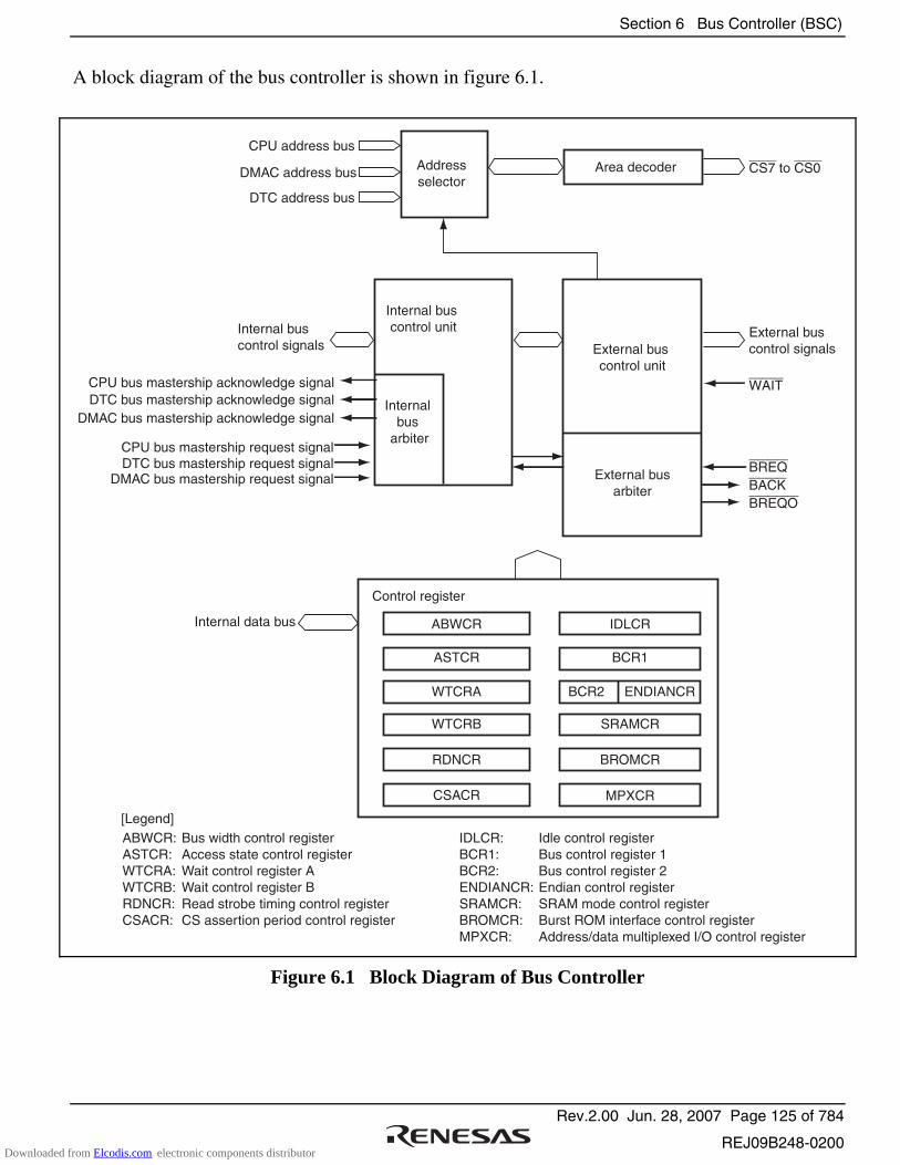
Section 6 Bus Controller (BSC)
Rev.2.00 Jun. 28, 2007 Page 125 of 784
REJ09B248-0200
A block diagram of the bus controller is shown in figure 6.1.
Addressselector
Area decoder
Internal bus control unit
Internal data bus
[Legend]
Internal bus control signals External bus
control unit
External busarbiter
Internal bus
arbiter
CPU address bus
CS7 to CS0
WAIT
BREQ
BACK
BREQO
DTC address bus
DMAC address bus
CPU bus mastership acknowledge signalDTC bus mastership acknowledge signal
CPU bus mastership request signalDTC bus mastership request signal
DMAC bus mastership acknowledge signal
DMAC bus mastership request signal
External bus control signals
Control register
ABWCR
ASTCR
WTCRA
WTCRB
RDNCR
CSACR
IDLCR
BCR1
BCR2 ENDIANCR
SRAMCR
BROMCR
MPXCR
ABWCR:ASTCR:WTCRA:WTCRB:RDNCR:CSACR:
Bus width control registerAccess state control registerWait control register AWait control register BRead strobe timing control registerCS assertion period control register
IDLCR:BCR1:BCR2:ENDIANCR:SRAMCR:BROMCR:MPXCR:
Idle control registerBus control register 1Bus control register 2Endian control registerSRAM mode control registerBurst ROM interface control registerAddress/data multiplexed I/O control register
Figure 6.1 Block Diagram of Bus Controller
Downloaded from Elcodis.com electronic components distributor
Section 6 Bus Controller (BSC)
Rev.2.00 Jun. 28, 2007 Page 126 of 784
REJ09B248-0200
6.2 Register Descriptions
The bus controller has the following registers.
• Bus width control register (ABWCR)
• Access state control register (ASTCR)
• Wait control register A (WTCRA)
• Wait control register B (WTCRB)
• Read strobe timing control register (RDNCR)
• CS assertion period control register (CSACR)
• Idle control register (IDLCR)
• Bus control register 1 (BCR1)
• Bus control register 2 (BCR2)
• Endian control register (ENDIANCR)
• SRAM mode control register (SRAMCR)
• Burst ROM interface control register (BROMCR)
• Address/data multiplexed I/O control register (MPXCR)
Downloaded from Elcodis.com electronic components distributor
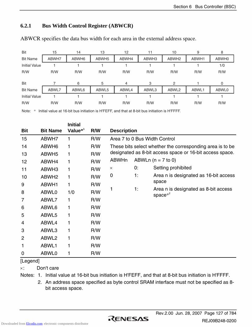
Section 6 Bus Controller (BSC)
Rev.2.00 Jun. 28, 2007 Page 127 of 784
REJ09B248-0200
6.2.1 Bus Width Control Register (ABWCR)
ABWCR specifies the data bus width for each area in the external address space.
Bit
Bit Name
Initial Value
R/W
15
ABWH7
1
R/W
14
ABWH6
1
R/W
13
ABWH5
1
R/W
12
ABWH4
1
R/W
11
ABWH3
1
R/W
10
ABWH2
1
R/W
9
ABWH1
1
R/W
8
ABWH0
1/0
R/W
Bit
Bit Name
Initial Value
R/W
Note: * Initial value at 16-bit bus initiation is H'FEFF, and that at 8-bit bus initiation is H'FFFF.
7
ABWL7
1
R/W
6
ABWL6
1
R/W
5
ABWL5
1
R/W
4
ABWL4
1
R/W
3
ABWL3
1
R/W
2
ABWL2
1
R/W
1
ABWL1
1
R/W
0
ABWL0
1
R/W
Bit Bit Name Initial Value*1 R/W Description
15
14
13
12
11
10
9
8
7
6
5
4
3
2
1
0
ABWH7
ABWH6
ABWH5
ABWH4
ABWH3
ABWH2
ABWH1
ABWL0
ABWL7
ABWL6
ABWL5
ABWL4
ABWL3
ABWL2
ABWL1
ABWL0
1
1
1
1
1
1
1
1/0
1
1
1
1
1
1
1
1
R/W
R/W
R/W
R/W
R/W
R/W
R/W
R/W
R/W
R/W
R/W
R/W
R/W
R/W
R/W
R/W
Area 7 to 0 Bus Width Control
These bits select whether the corresponding area is to be designated as 8-bit access space or 16-bit access space.
ABWHn ABWLn (n = 7 to 0)
× 0: Setting prohibited
0 1: Area n is designated as 16-bit access space
1 1: Area n is designated as 8-bit access space*2
[Legend]
×: Don't care Notes: 1. Initial value at 16-bit bus initiation is H'FEFF, and that at 8-bit bus initiation is H'FFFF.
2. An address space specified as byte control SRAM interface must not be specified as 8-bit access space.
Downloaded from Elcodis.com electronic components distributor
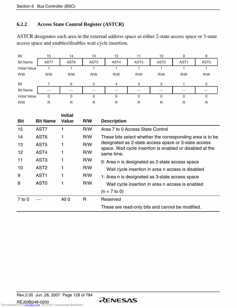
Section 6 Bus Controller (BSC)
Rev.2.00 Jun. 28, 2007 Page 128 of 784
REJ09B248-0200
6.2.2 Access State Control Register (ASTCR)
ASTCR designates each area in the external address space as either 2-state access space or 3-state access space and enables/disables wait cycle insertion.
Bit
Bit Name
Initial Value
R/W
15
AST7
1
R/W
14
AST6
1
R/W
13
AST5
1
R/W
12
AST4
1
R/W
11
AST3
1
R/W
10
AST2
1
R/W
9
AST1
1
R/W
8
AST0
1
R/W
Bit
Bit Name
Initial Value
R/W
7
0
R
6
0
R
5
0
R
4
0
R
3
0
R
2
0
R
1
0
R
0
0
R
Bit Bit Name Initial Value R/W Description
15
14
13
12
11
10
9
8
AST7
AST6
AST5
AST4
AST3
AST2
AST1
AST0
1
1
1
1
1
1
1
1
R/W
R/W
R/W
R/W
R/W
R/W
R/W
R/W
Area 7 to 0 Access State Control
These bits select whether the corresponding area is to be designated as 2-state access space or 3-state access space. Wait cycle insertion is enabled or disabled at the same time.
0: Area n is designated as 2-state access space
Wait cycle insertion in area n access is disabled
1: Area n is designated as 3-state access space
Wait cycle insertion in area n access is enabled
(n = 7 to 0)
7 to 0 All 0 R Reserved
These are read-only bits and cannot be modified.
Downloaded from Elcodis.com electronic components distributor
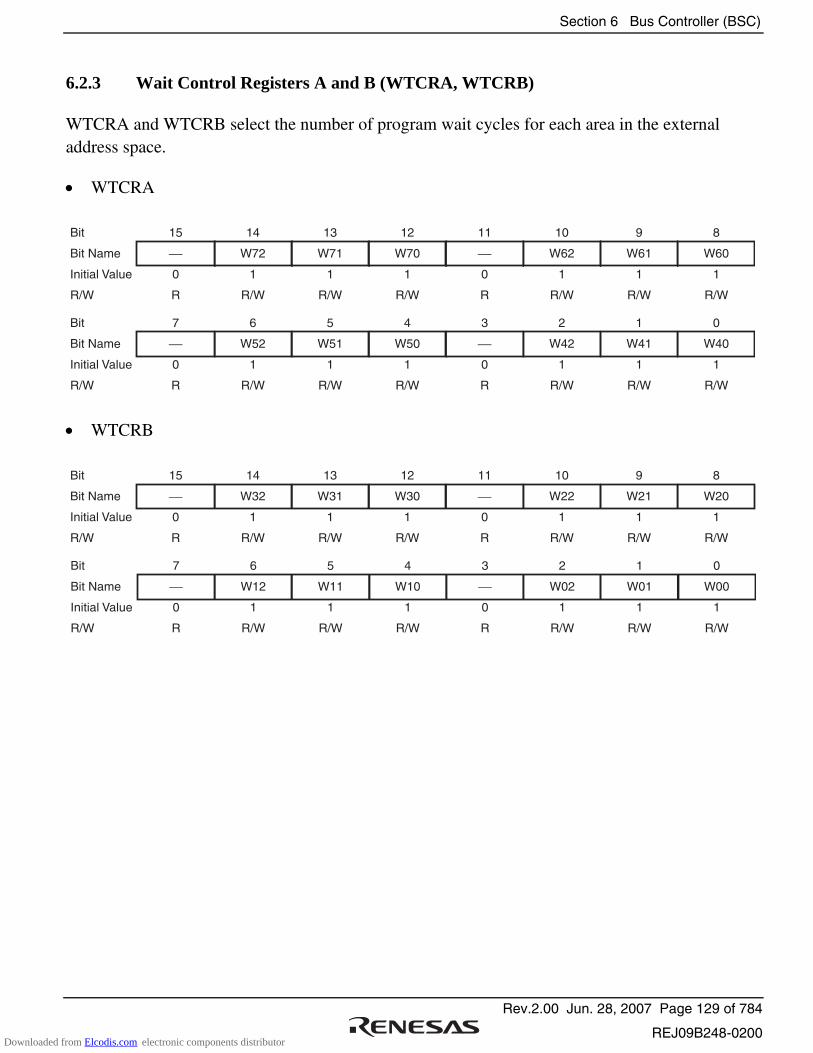
Section 6 Bus Controller (BSC)
Rev.2.00 Jun. 28, 2007 Page 129 of 784
REJ09B248-0200
6.2.3 Wait Control Registers A and B (WTCRA, WTCRB)
WTCRA and WTCRB select the number of program wait cycles for each area in the external address space.
• WTCRA
Bit
Bit Name
Initial Value
R/W
15
0
R
14
W72
1
R/W
13
W71
1
R/W
12
W70
1
R/W
11
0
R
10
W62
1
R/W
9
W61
1
R/W
8
W60
1
R/W
Bit
Bit Name
Initial Value
R/W
7
0
R
6
W52
1
R/W
5
W51
1
R/W
4
W50
1
R/W
3
0
R
2
W42
1
R/W
1
W41
1
R/W
0
W40
1
R/W
• WTCRB
Bit
Bit Name
Initial Value
R/W
15
0
R
14
W32
1
R/W
13
W31
1
R/W
12
W30
1
R/W
11
0
R
10
W22
1
R/W
9
W21
1
R/W
8
W20
1
R/W
Bit
Bit Name
Initial Value
R/W
7
0
R
6
W12
1
R/W
5
W11
1
R/W
4
W10
1
R/W
3
0
R
2
W02
1
R/W
1
W01
1
R/W
0
W00
1
R/W
Downloaded from Elcodis.com electronic components distributor

Section 6 Bus Controller (BSC)
Rev.2.00 Jun. 28, 2007 Page 130 of 784
REJ09B248-0200
• WTCRA
Bit Bit Name Initial Value R/W Description
15 0 R Reserved
This is a read-only bit and cannot be modified.
14
13
12
W72
W71
W70
1
1
1
R/W
R/W
R/W
Area 7 Wait Control 2 to 0
These bits select the number of program wait cycles when accessing area 7 while bit AST7 in ASTCR is 1.
000: Program wait cycle not inserted
001: 1 program wait cycle inserted
010: 2 program wait cycles inserted
011: 3 program wait cycles inserted
100: 4 program wait cycles inserted
101: 5 program wait cycles inserted
110: 6 program wait cycles inserted
111: 7 program wait cycles inserted
11 0 R Reserved
This is a read-only bit and cannot be modified.
10
9
8
W62
W61
W60
1
1
1
R/W
R/W
R/W
Area 6 Wait Control 2 to 0
These bits select the number of program wait cycles when accessing area 6 while bit AST6 in ASTCR is 1.
000: Program wait cycle not inserted
001: 1 program wait cycle inserted
010: 2 program wait cycles inserted
011: 3 program wait cycles inserted
100: 4 program wait cycles inserted
101: 5 program wait cycles inserted
110: 6 program wait cycles inserted
111: 7 program wait cycles inserted
7 0 R Reserved
This is a read-only bit and cannot be modified.
Downloaded from Elcodis.com electronic components distributor
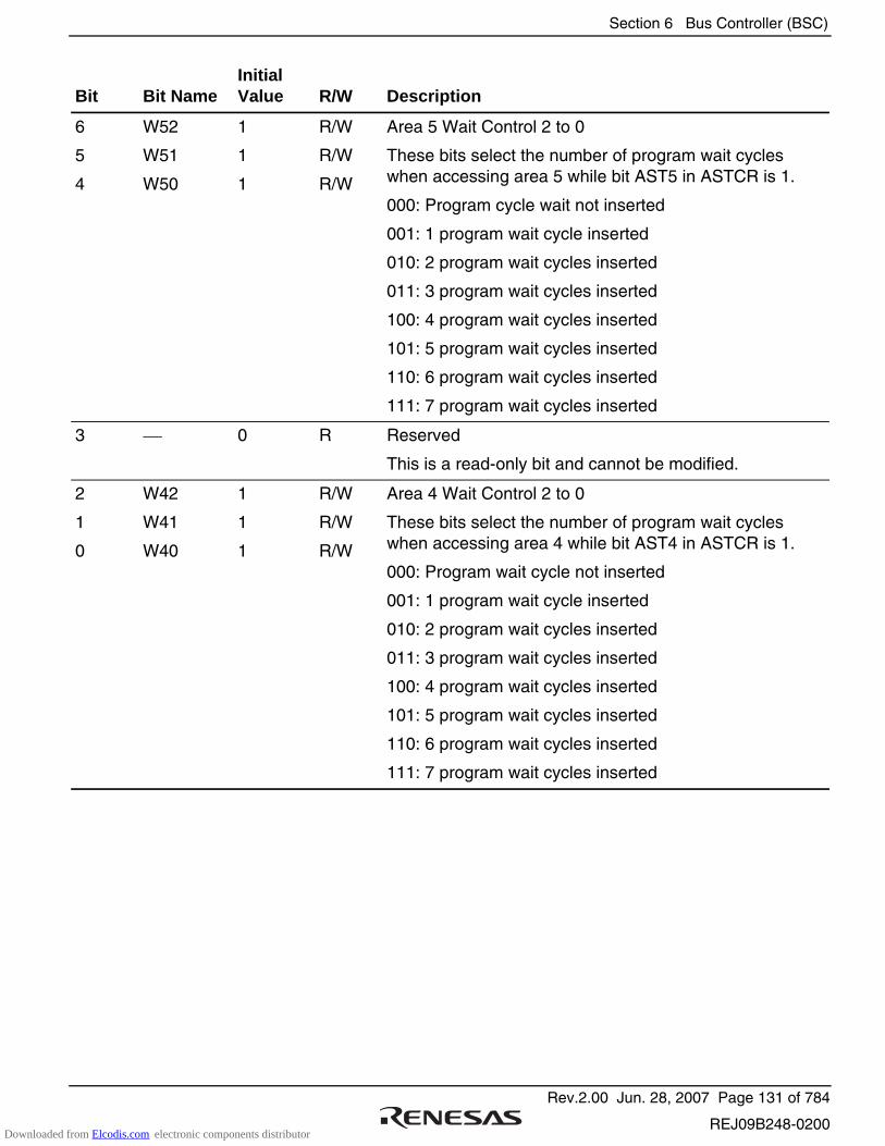
Section 6 Bus Controller (BSC)
Rev.2.00 Jun. 28, 2007 Page 131 of 784
REJ09B248-0200
Bit Bit Name Initial Value R/W Description
6
5
4
W52
W51
W50
1
1
1
R/W
R/W
R/W
Area 5 Wait Control 2 to 0
These bits select the number of program wait cycles when accessing area 5 while bit AST5 in ASTCR is 1.
000: Program cycle wait not inserted
001: 1 program wait cycle inserted
010: 2 program wait cycles inserted
011: 3 program wait cycles inserted
100: 4 program wait cycles inserted
101: 5 program wait cycles inserted
110: 6 program wait cycles inserted
111: 7 program wait cycles inserted
3 0 R Reserved
This is a read-only bit and cannot be modified.
2
1
0
W42
W41
W40
1
1
1
R/W
R/W
R/W
Area 4 Wait Control 2 to 0
These bits select the number of program wait cycles when accessing area 4 while bit AST4 in ASTCR is 1.
000: Program wait cycle not inserted
001: 1 program wait cycle inserted
010: 2 program wait cycles inserted
011: 3 program wait cycles inserted
100: 4 program wait cycles inserted
101: 5 program wait cycles inserted
110: 6 program wait cycles inserted
111: 7 program wait cycles inserted
Downloaded from Elcodis.com electronic components distributor
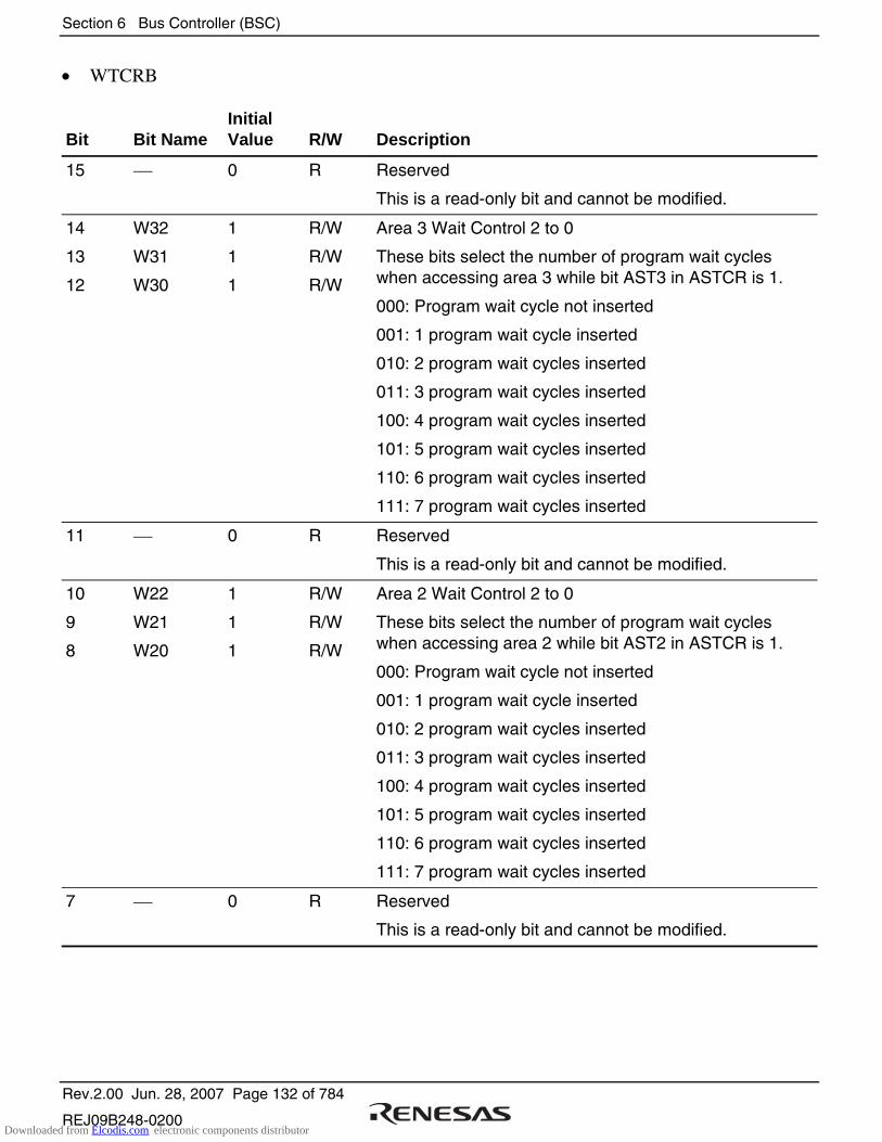
Section 6 Bus Controller (BSC)
Rev.2.00 Jun. 28, 2007 Page 132 of 784
REJ09B248-0200
• WTCRB
Bit Bit Name Initial Value R/W Description
15 0 R Reserved
This is a read-only bit and cannot be modified.
14
13
12
W32
W31
W30
1
1
1
R/W
R/W
R/W
Area 3 Wait Control 2 to 0
These bits select the number of program wait cycles when accessing area 3 while bit AST3 in ASTCR is 1.
000: Program wait cycle not inserted
001: 1 program wait cycle inserted
010: 2 program wait cycles inserted
011: 3 program wait cycles inserted
100: 4 program wait cycles inserted
101: 5 program wait cycles inserted
110: 6 program wait cycles inserted
111: 7 program wait cycles inserted
11 0 R Reserved
This is a read-only bit and cannot be modified.
10
9
8
W22
W21
W20
1
1
1
R/W
R/W
R/W
Area 2 Wait Control 2 to 0
These bits select the number of program wait cycles when accessing area 2 while bit AST2 in ASTCR is 1.
000: Program wait cycle not inserted
001: 1 program wait cycle inserted
010: 2 program wait cycles inserted
011: 3 program wait cycles inserted
100: 4 program wait cycles inserted
101: 5 program wait cycles inserted
110: 6 program wait cycles inserted
111: 7 program wait cycles inserted
7 0 R Reserved
This is a read-only bit and cannot be modified.
Downloaded from Elcodis.com electronic components distributor

Section 6 Bus Controller (BSC)
Rev.2.00 Jun. 28, 2007 Page 133 of 784
REJ09B248-0200
Bit Bit Name Initial Value R/W Description
6
5
4
W12
W11
W10
1
1
1
R/W
R/W
R/W
Area 1 Wait Control 2 to 0
These bits select the number of program wait cycles when accessing area 1 while bit AST1 in ASTCR is 1.
000: Program wait cycle not inserted
001: 1 program wait cycle inserted
010: 2 program wait cycles inserted
011: 3 program wait cycles inserted
100: 4 program wait cycles inserted
101: 5 program wait cycles inserted
110: 6 program wait cycles inserted
111: 7 program wait cycles inserted
3 0 R Reserved
This is a read-only bit and cannot be modified.
2
1
0
W02
W01
W00
1
1
1
R/W
R/W
R/W
Area 0 Wait Control 2 to 0
These bits select the number of program wait cycles when accessing area 0 while bit AST0 in ASTCR is 1.
000: Program wait cycle not inserted
001: 1 program wait cycle inserted
010: 2 program wait cycles inserted
011: 3 program wait cycles inserted
100: 4 program wait cycles inserted
101: 5 program wait cycles inserted
110: 6 program wait cycles inserted
111: 7 program wait cycles inserted
Downloaded from Elcodis.com electronic components distributor
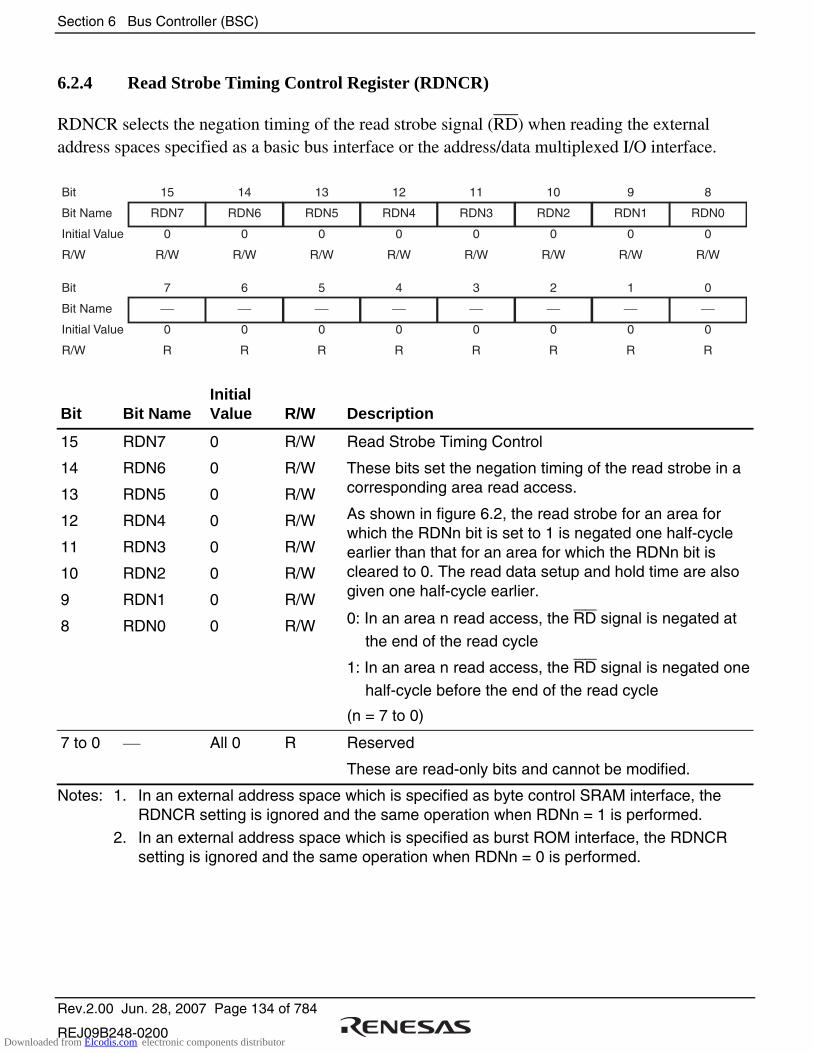
Section 6 Bus Controller (BSC)
Rev.2.00 Jun. 28, 2007 Page 134 of 784
REJ09B248-0200
6.2.4 Read Strobe Timing Control Register (RDNCR)
RDNCR selects the negation timing of the read strobe signal (RD) when reading the external address spaces specified as a basic bus interface or the address/data multiplexed I/O interface.
Bit
Bit Name
Initial Value
R/W
15
RDN7
0
R/W
14
RDN6
0
R/W
13
RDN5
0
R/W
12
RDN4
0
R/W
11
RDN3
0
R/W
10
RDN2
0
R/W
9
RDN1
0
R/W
8
RDN0
0
R/W
Bit
Bit Name
Initial Value
R/W
7
0
R
6
0
R
5
0
R
4
0
R
3
0
R
2
0
R
1
0
R
0
0
R
Bit Bit Name Initial Value R/W Description
15
14
13
12
11
10
9
8
RDN7
RDN6
RDN5
RDN4
RDN3
RDN2
RDN1
RDN0
0
0
0
0
0
0
0
0
R/W
R/W
R/W
R/W
R/W
R/W
R/W
R/W
Read Strobe Timing Control
These bits set the negation timing of the read strobe in a corresponding area read access.
As shown in figure 6.2, the read strobe for an area for which the RDNn bit is set to 1 is negated one half-cycle earlier than that for an area for which the RDNn bit is cleared to 0. The read data setup and hold time are also given one half-cycle earlier.
0: In an area n read access, the RD signal is negated at
the end of the read cycle
1: In an area n read access, the RD signal is negated one
half-cycle before the end of the read cycle
(n = 7 to 0)
7 to 0 All 0 R Reserved
These are read-only bits and cannot be modified.
Notes: 1. In an external address space which is specified as byte control SRAM interface, the RDNCR setting is ignored and the same operation when RDNn = 1 is performed.
2. In an external address space which is specified as burst ROM interface, the RDNCR setting is ignored and the same operation when RDNn = 0 is performed.
Downloaded from Elcodis.com electronic components distributor
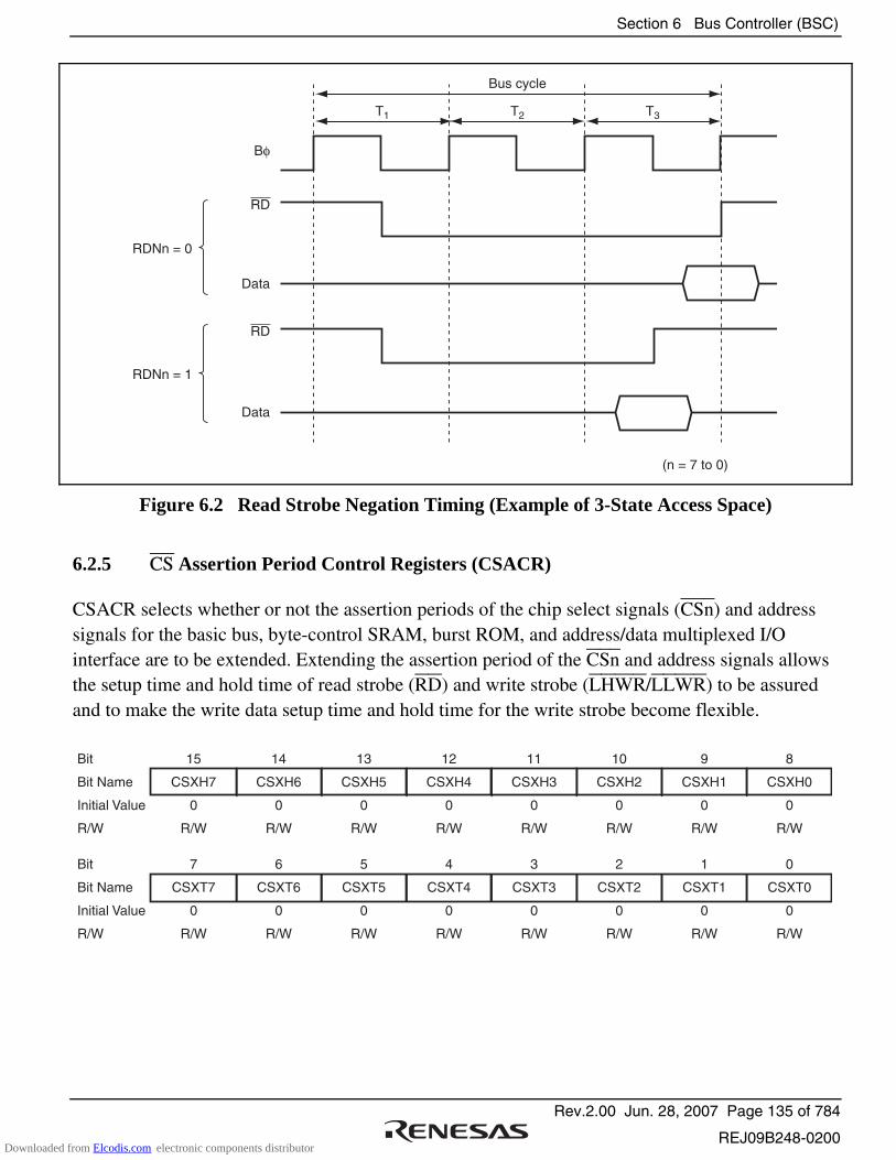
Section 6 Bus Controller (BSC)
Rev.2.00 Jun. 28, 2007 Page 135 of 784
REJ09B248-0200
Bus cycle
T1 T2
RD
Bφ
Data
RD
Data
RDNn = 0
RDNn = 1
T3
(n = 7 to 0)
Figure 6.2 Read Strobe Negation Timing (Example of 3-State Access Space)
6.2.5 CS Assertion Period Control Registers (CSACR)
CSACR selects whether or not the assertion periods of the chip select signals (CSn) and address signals for the basic bus, byte-control SRAM, burst ROM, and address/data multiplexed I/O interface are to be extended. Extending the assertion period of the CSn and address signals allows the setup time and hold time of read strobe (RD) and write strobe (LHWR/LLWR) to be assured and to make the write data setup time and hold time for the write strobe become flexible.
Bit
Bit Name
Initial Value
R/W
15
CSXH7
0
R/W
14
CSXH6
0
R/W
13
CSXH5
0
R/W
12
CSXH4
0
R/W
11
CSXH3
0
R/W
10
CSXH2
0
R/W
9
CSXH1
0
R/W
8
CSXH0
0
R/W
Bit
Bit Name
Initial Value
R/W
7
CSXT7
0
R/W
6
CSXT6
0
R/W
5
CSXT5
0
R/W
4
CSXT4
0
R/W
3
CSXT3
0
R/W
2
CSXT2
0
R/W
1
CSXT1
0
R/W
0
CSXT0
0
R/W
Downloaded from Elcodis.com electronic components distributor

Section 6 Bus Controller (BSC)
Rev.2.00 Jun. 28, 2007 Page 136 of 784
REJ09B248-0200
Bit Bit Name Initial Value R/W Description
15
14
13
12
11
10
9
8
CSXH7
CSXH6
CSXH5
CSXH4
CSXH3
CSXH2
CSXH1
CSXH0
0
0
0
0
0
0
0
0
R/W
R/W
R/W
R/W
R/W
R/W
R/W
R/W
CS and Address Signal Assertion Period Control 1
These bits specify whether or not the Th cycle is to be inserted (see figure 6.3). When an area for which bit CSXHn is set to 1 is accessed, one Th cycle, in which the CSn and address signals are asserted, is inserted before the normal access cycle.
0: In access to area n, the CSn and address assertion
period (Th) is not extended
1: In access to area n, the CSn and address assertion
period (Th) is extended
(n = 7 to 0)
7
6
5
4
3
2
1
0
CSXT7
CSXT6
CSXT5
CSXT4
CSXT3
CSXT2
CSXT1
CSXT0
0
0
0
0
0
0
0
0
R/W
R/W
R/W
R/W
R/W
R/W
R/W
R/W
CS and Address Signal Assertion Period Control 2
These bits specify whether or not the Tt cycle is to be inserted (see figure 6.3). When an area for which bit CSXTn is set to 1 is accessed, one Tt cycle, in which the CSn and address signals are retained, is inserted after the normal access cycle.
0: In access to area n, the CSn and address assertion
period (Tt) is not extended
1: In access to area n, the CSn and address assertion
period (Tt) is extended
(n = 7 to 0)
Note: * In burst ROM interface, the CSXTn settings are ignored.
Downloaded from Elcodis.com electronic components distributor
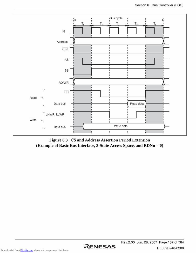
Section 6 Bus Controller (BSC)
Rev.2.00 Jun. 28, 2007 Page 137 of 784
REJ09B248-0200
Read data
Write data
Bus cycle
Th T1 T2 T3 Tt
Bφ
Address
CSn
AS
BS
RD/WR
RD
Read
Write
Data bus
Data bus
LHWR, LLWR
Figure 6.3 CS and Address Assertion Period Extension (Example of Basic Bus Interface, 3-State Access Space, and RDNn = 0)
Downloaded from Elcodis.com electronic components distributor

Section 6 Bus Controller (BSC)
Rev.2.00 Jun. 28, 2007 Page 138 of 784
REJ09B248-0200
6.2.6 Idle Control Register (IDLCR)
IDLCR specifies the idle cycle insertion conditions and the number of idle cycles.
Bit
Bit Name
Initial Value
R/W
15
IDLS3
1
R/W
14
IDLS2
1
R/W
13
IDLS1
1
R/W
12
IDLS0
1
R/W
11
IDLCB1
1
R/W
10
IDLCB0
1
R/W
9
IDLCA1
1
R/W
8
IDLCA0
1
R/W
Bit
Bit Name
Initial Value
R/W
7
IDLSEL7
0
R/W
6
IDLSEL6
0
R/W
5
IDLSEL5
0
R/W
4
IDLSEL4
0
R/W
3
IDLSEL3
0
R/W
2
IDLSEL2
0
R/W
1
IDLSEL1
0
R/W
0
IDLSEL0
0
R/W
Bit Bit Name Initial Value R/W Description
15 IDLS3 1 R/W Idle Cycle Insertion 3
Inserts an idle cycle between the bus cycles when the DMAC single address transfer (write cycle) is followed by external access.
0: No idle cycle is inserted
1: An idle cycle is inserted
14 IDLS2 1 R/W Idle Cycle Insertion 2
Inserts an idle cycle between the bus cycles when the external write cycle is followed by external read cycle.
0: No idle cycle is inserted
1: An idle cycle is inserted
13 IDLS1 1 R/W Idle Cycle Insertion 1
Inserts an idle cycle between the bus cycles when the external read cycles of different areas continue.
0: No idle cycle is inserted
1: An idle cycle is inserted
12 IDLS0 1 R/W Idle Cycle Insertion 0
Inserts an idle cycle between the bus cycles when the external read cycle is followed by external write cycle.
0: No idle cycle is inserted
1: An idle cycle is inserted
Downloaded from Elcodis.com electronic components distributor
Section 6 Bus Controller (BSC)
Rev.2.00 Jun. 28, 2007 Page 139 of 784
REJ09B248-0200
Bit Bit Name Initial Value R/W Description
11
10
IDLCB1
IDLCB0
1
1
R/W
R/W
Idle Cycle State Number Select B
Specifies the number of idle cycles to be inserted for the idle condition specified by IDLS1 and IDLS0.
00: No idle cycle is inserted
01: 2 idle cycles are inserted
00: 3 idle cycles are inserted
01: 4 idle cycles are inserted
9
8
IDLCA1
IDLCA0
1
1
R/W
R/W
Idle Cycle State Number Select A
Specifies the number of idle cycles to be inserted for the idle condition specified by IDLS3 to IDLS0.
00: 1 idle cycle is inserted
01: 2 idle cycles are inserted
10: 3 idle cycles are inserted
11: 4 idle cycles are inserted
7
6
5
4
3
2
1
0
IDLSEL7
IDLSEL6
IDLSEL5
IDLSEL4
IDLSEL3
IDLSEL2
IDLSEL1
IDLSEL0
0
0
0
0
0
0
0
0
R/W
R/W
R/W
R/W
R/W
R/W
R/W
R/W
Idle Cycle Number Select
Specifies the number of idle cycles to be inserted for each area for the idle insertion condition specified by IDLS1 and IDLS0.
0: Number of idle cycles to be inserted for area n is specified by IDLCA1 and IDLCA0.
1: Number of idle cycles to be inserted for area n is specified by IDLCB1 and IDLCB0.
(n = 7 to 0)
Downloaded from Elcodis.com electronic components distributor
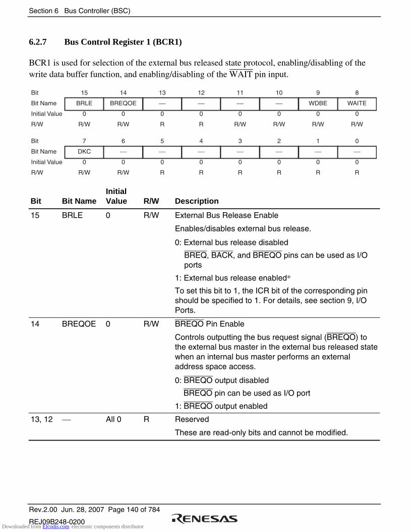
Section 6 Bus Controller (BSC)
Rev.2.00 Jun. 28, 2007 Page 140 of 784
REJ09B248-0200
6.2.7 Bus Control Register 1 (BCR1)
BCR1 is used for selection of the external bus released state protocol, enabling/disabling of the write data buffer function, and enabling/disabling of the WAIT pin input.
Bit
Bit Name
Initial Value
R/W
15
BRLE
0
R/W
14
BREQOE
0
R/W
13
0
R
12
0
R
11
0
R/W
10
0
R/W
9
WDBE
0
R/W
8
WAITE
0
R/W
Bit
Bit Name
Initial Value
R/W
7
DKC
0
R/W
6
0
R/W
5
0
R
4
0
R
3
0
R
2
0
R
1
0
R
0
0
R
Bit Bit Name Initial Value R/W Description
15 BRLE 0 R/W External Bus Release Enable
Enables/disables external bus release.
0: External bus release disabled
BREQ, BACK, and BREQO pins can be used as I/O ports
1: External bus release enabled*
To set this bit to 1, the ICR bit of the corresponding pin should be specified to 1. For details, see section 9, I/O Ports.
14 BREQOE 0 R/W BREQO Pin Enable
Controls outputting the bus request signal (BREQO) to the external bus master in the external bus released state when an internal bus master performs an external address space access.
0: BREQO output disabled
BREQO pin can be used as I/O port
1: BREQO output enabled
13, 12 All 0 R Reserved
These are read-only bits and cannot be modified.
Downloaded from Elcodis.com electronic components distributor
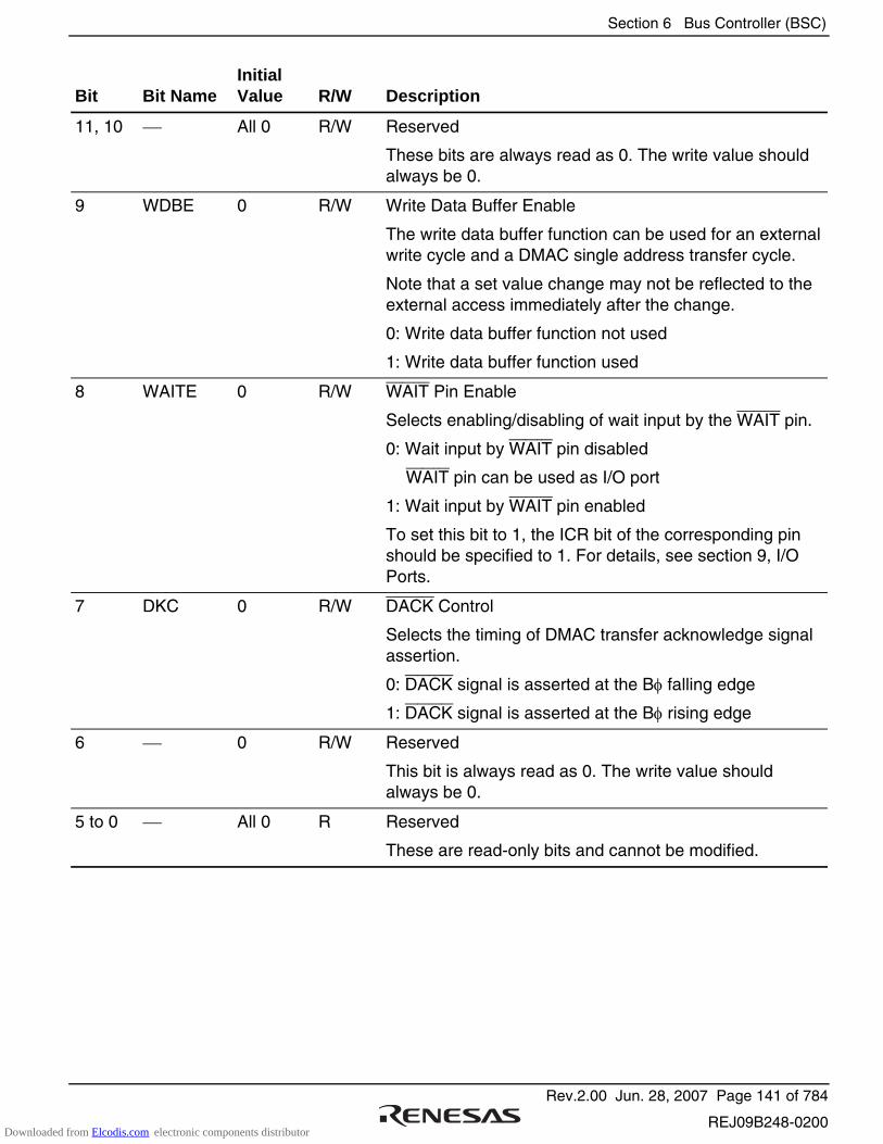
Section 6 Bus Controller (BSC)
Rev.2.00 Jun. 28, 2007 Page 141 of 784
REJ09B248-0200
Bit Bit Name Initial Value R/W Description
11, 10 All 0 R/W Reserved
These bits are always read as 0. The write value should always be 0.
9 WDBE 0 R/W Write Data Buffer Enable
The write data buffer function can be used for an external write cycle and a DMAC single address transfer cycle.
Note that a set value change may not be reflected to the external access immediately after the change.
0: Write data buffer function not used
1: Write data buffer function used
8 WAITE 0 R/W WAIT Pin Enable
Selects enabling/disabling of wait input by the WAIT pin.
0: Wait input by WAIT pin disabled
WAIT pin can be used as I/O port
1: Wait input by WAIT pin enabled
To set this bit to 1, the ICR bit of the corresponding pin should be specified to 1. For details, see section 9, I/O Ports.
7 DKC 0 R/W DACK Control
Selects the timing of DMAC transfer acknowledge signal assertion.
0: DACK signal is asserted at the Bφ falling edge
1: DACK signal is asserted at the Bφ rising edge
6 0 R/W Reserved
This bit is always read as 0. The write value should always be 0.
5 to 0 All 0 R Reserved
These are read-only bits and cannot be modified.
Downloaded from Elcodis.com electronic components distributor
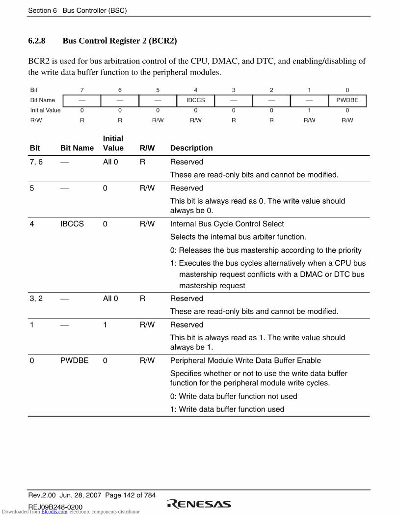
Section 6 Bus Controller (BSC)
Rev.2.00 Jun. 28, 2007 Page 142 of 784
REJ09B248-0200
6.2.8 Bus Control Register 2 (BCR2)
BCR2 is used for bus arbitration control of the CPU, DMAC, and DTC, and enabling/disabling of the write data buffer function to the peripheral modules.
Bit
Bit Name
Initial Value
R/W
7
0
R
6
0
R
5
0
R/W
4
IBCCS
0
R/W
3
0
R
2
0
R
1
1
R/W
0
PWDBE
0
R/W
Bit Bit Name Initial Value R/W Description
7, 6 All 0 R Reserved
These are read-only bits and cannot be modified.
5 0 R/W Reserved
This bit is always read as 0. The write value should always be 0.
4 IBCCS 0 R/W Internal Bus Cycle Control Select
Selects the internal bus arbiter function.
0: Releases the bus mastership according to the priority
1: Executes the bus cycles alternatively when a CPU bus
mastership request conflicts with a DMAC or DTC bus
mastership request
3, 2 All 0 R Reserved
These are read-only bits and cannot be modified.
1 1 R/W Reserved
This bit is always read as 1. The write value should always be 1.
0 PWDBE 0 R/W Peripheral Module Write Data Buffer Enable
Specifies whether or not to use the write data buffer function for the peripheral module write cycles.
0: Write data buffer function not used
1: Write data buffer function used
Downloaded from Elcodis.com electronic components distributor

Section 6 Bus Controller (BSC)
Rev.2.00 Jun. 28, 2007 Page 143 of 784
REJ09B248-0200
6.2.9 Endian Control Register (ENDIANCR)
ENDIANCR selects the endian format for each area of the external address space. Though the data format of this LSI is big endian, data can be transferred in the little endian format during external address space access.
Note that the data format for the areas used as a program area or a stack area should be big endian.
Bit
Bit Name
Initial Value
R/W
7
LE7
0
R/W
6
LE6
0
R/W
5
LE5
0
R/W
4
LE4
0
R/W
3
LE3
0
R/W
2
LE2
0
R/W
1
0
R
0
0
R
Bit Bit Name Initial Value R/W Description
7
6
5
4
3
2
LE7
LE6
LE5
LE4
LE3
LE2
0
0
0
0
0
0
R/W
R/W
R/W
R/W
R/W
R/W
Little Endian Select
Selects the endian for the corresponding area.
0: Data format of area n is specified as big endian
1: Data format of area n is specified as little endian
(n = 7 to 2)
1, 0 All 0 R Reserved
These are read-only bits and cannot be modified.
Downloaded from Elcodis.com electronic components distributor
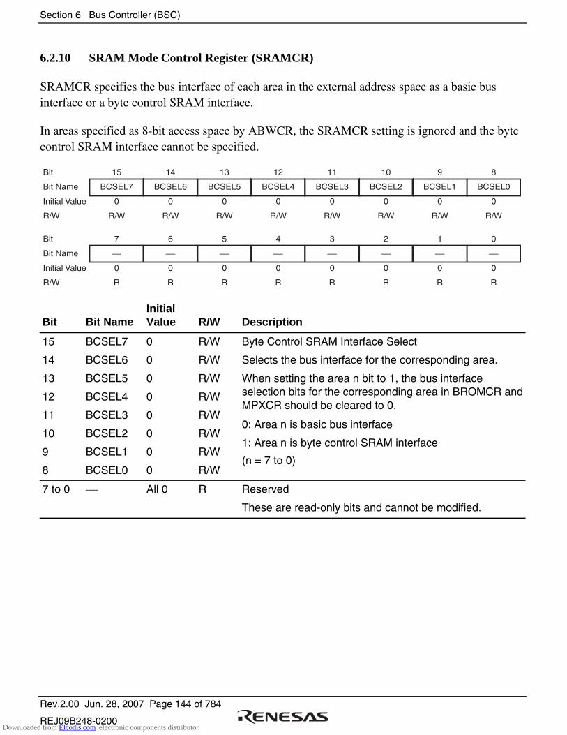
Section 6 Bus Controller (BSC)
Rev.2.00 Jun. 28, 2007 Page 144 of 784
REJ09B248-0200
6.2.10 SRAM Mode Control Register (SRAMCR)
SRAMCR specifies the bus interface of each area in the external address space as a basic bus interface or a byte control SRAM interface.
In areas specified as 8-bit access space by ABWCR, the SRAMCR setting is ignored and the byte control SRAM interface cannot be specified.
Bit
Bit Name
Initial Value
R/W
15
BCSEL7
0
R/W
14
BCSEL6
0
R/W
13
BCSEL5
0
R/W
12
BCSEL4
0
R/W
11
BCSEL3
0
R/W
10
BCSEL2
0
R/W
9
BCSEL1
0
R/W
8
BCSEL0
0
R/W
Bit
Bit Name
Initial Value
R/W
7
0
R
6
0
R
5
0
R
4
0
R
3
0
R
2
0
R
1
0
R
0
0
R
Bit Bit Name Initial Value R/W Description
15
14
13
12
11
10
9
8
BCSEL7
BCSEL6
BCSEL5
BCSEL4
BCSEL3
BCSEL2
BCSEL1
BCSEL0
0
0
0
0
0
0
0
0
R/W
R/W
R/W
R/W
R/W
R/W
R/W
R/W
Byte Control SRAM Interface Select
Selects the bus interface for the corresponding area.
When setting the area n bit to 1, the bus interface selection bits for the corresponding area in BROMCR and MPXCR should be cleared to 0.
0: Area n is basic bus interface
1: Area n is byte control SRAM interface
(n = 7 to 0)
7 to 0 All 0 R Reserved
These are read-only bits and cannot be modified.
Downloaded from Elcodis.com electronic components distributor
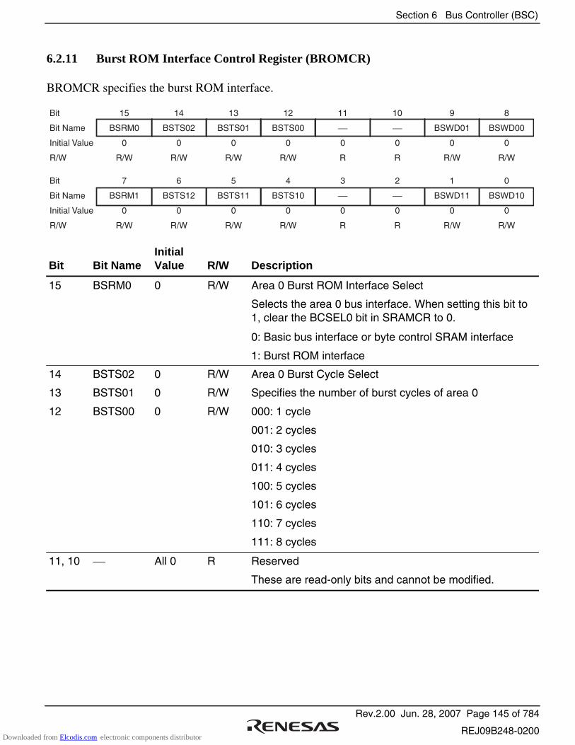
Section 6 Bus Controller (BSC)
Rev.2.00 Jun. 28, 2007 Page 145 of 784
REJ09B248-0200
6.2.11 Burst ROM Interface Control Register (BROMCR)
BROMCR specifies the burst ROM interface.
Bit
Bit Name
Initial Value
R/W
15
BSRM0
0
R/W
14
BSTS02
0
R/W
13
BSTS01
0
R/W
12
BSTS00
0
R/W
11
0
R
10
0
R
9
BSWD01
0
R/W
8
BSWD00
0
R/W
Bit
Bit Name
Initial Value
R/W
7
BSRM1
0
R/W
6
BSTS12
0
R/W
5
BSTS11
0
R/W
4
BSTS10
0
R/W
3
0
R
2
0
R
1
BSWD11
0
R/W
0
BSWD10
0
R/W
Bit Bit Name Initial Value R/W Description
15 BSRM0 0 R/W Area 0 Burst ROM Interface Select
Selects the area 0 bus interface. When setting this bit to 1, clear the BCSEL0 bit in SRAMCR to 0.
0: Basic bus interface or byte control SRAM interface
1: Burst ROM interface
14
13
12
BSTS02
BSTS01
BSTS00
0
0
0
R/W
R/W
R/W
Area 0 Burst Cycle Select
Specifies the number of burst cycles of area 0
000: 1 cycle
001: 2 cycles
010: 3 cycles
011: 4 cycles
100: 5 cycles
101: 6 cycles
110: 7 cycles
111: 8 cycles
11, 10 All 0 R Reserved
These are read-only bits and cannot be modified.
Downloaded from Elcodis.com electronic components distributor
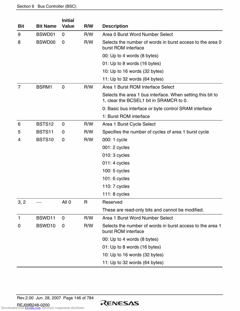
Section 6 Bus Controller (BSC)
Rev.2.00 Jun. 28, 2007 Page 146 of 784
REJ09B248-0200
Bit Bit Name Initial Value R/W Description
9
8
BSWD01
BSWD00
0
0
R/W
R/W
Area 0 Burst Word Number Select
Selects the number of words in burst access to the area 0 burst ROM interface
00: Up to 4 words (8 bytes)
01: Up to 8 words (16 bytes)
10: Up to 16 words (32 bytes)
11: Up to 32 words (64 bytes)
7 BSRM1 0 R/W Area 1 Burst ROM Interface Select
Selects the area 1 bus interface. When setting this bit to 1, clear the BCSEL1 bit in SRAMCR to 0.
0: Basic bus interface or byte control SRAM interface
1: Burst ROM interface
6
5
4
BSTS12
BSTS11
BSTS10
0
0
0
R/W
R/W
R/W
Area 1 Burst Cycle Select
Specifies the number of cycles of area 1 burst cycle
000: 1 cycle
001: 2 cycles
010: 3 cycles
011: 4 cycles
100: 5 cycles
101: 6 cycles
110: 7 cycles
111: 8 cycles
3, 2 All 0 R Reserved
These are read-only bits and cannot be modified.
1
0
BSWD11
BSWD10
0
0
R/W
R/W
Area 1 Burst Word Number Select
Selects the number of words in burst access to the area 1 burst ROM interface
00: Up to 4 words (8 bytes)
01: Up to 8 words (16 bytes)
10: Up to 16 words (32 bytes)
11: Up to 32 words (64 bytes)
Downloaded from Elcodis.com electronic components distributor

Section 6 Bus Controller (BSC)
Rev.2.00 Jun. 28, 2007 Page 147 of 784
REJ09B248-0200
6.2.12 Address/Data Multiplexed I/O Control Register (MPXCR)
MPXCR specifies the address/data multiplexed I/O interface.
Bit
Bit Name
Initial Value
R/W
15
MPXE7
0
R/W
14
MPXE6
0
R/W
13
MPXE5
0
R/W
12
MPXE4
0
R/W
11
MPXE3
0
R/W
10
0
R
9
0
R
8
0
R
Bit
Bit Name
Initial Value
R/W
7
0
R
6
0
R
5
0
R
4
0
R
3
0
R
2
0
R
1
0
R
0
ADDEX
0
R/W
Bit Bit Name Initial Value R/W Description
15
14
13
12
11
MPXE7
MPXE6
MPXE5
MPXE4
MPXE3
0
0
0
0
0
R/W
R/W
R/W
R/W
R/W
Address/Data Multiplexed I/O Interface Select
Specifies the bus interface for the corresponding area.
When setting the area n bit to 1, clear the BCSELn bit in SRAMCR to 0.
0: Area n is specified as a basic interface or a byte
control SRAM interface.
1: Area n is specified as an address/data multiplexed I/O
interface
(n = 7 to 3)
10 to 1 All 0 R Reserved
These are read-only bits and cannot be modified.
0 ADDEX 0 R/W Address Output Cycle Extension
Specifies whether a wait cycle is inserted for the address output cycle of address/data multiplexed I/O interface.
0: No wait cycle is inserted for the address output cycle
1: One wait cycle is inserted for the address output cycle
Downloaded from Elcodis.com electronic components distributor
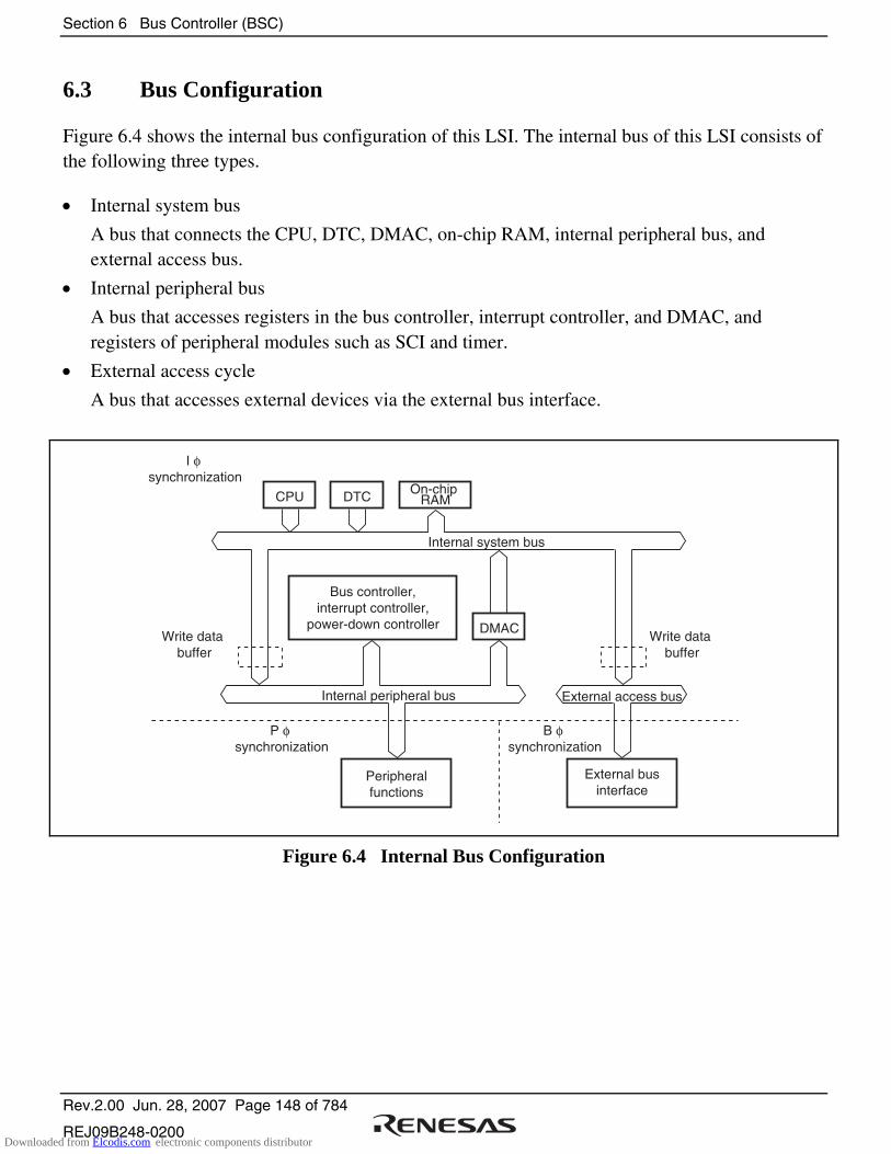
Section 6 Bus Controller (BSC)
Rev.2.00 Jun. 28, 2007 Page 148 of 784
REJ09B248-0200
6.3 Bus Configuration
Figure 6.4 shows the internal bus configuration of this LSI. The internal bus of this LSI consists of the following three types.
• Internal system bus
A bus that connects the CPU, DTC, DMAC, on-chip RAM, internal peripheral bus, and external access bus.
• Internal peripheral bus
A bus that accesses registers in the bus controller, interrupt controller, and DMAC, and registers of peripheral modules such as SCI and timer.
• External access cycle
A bus that accesses external devices via the external bus interface.
CPU DTC
B φ synchronization
P φ synchronization
I φ synchronization
Bus controller,interrupt controller,
power-down controller
External businterface
Peripheralfunctions
On-chip RAM
Internal system bus
Internal peripheral bus
Write data buffer
Write data buffer
External access bus
DMAC
Figure 6.4 Internal Bus Configuration
Downloaded from Elcodis.com electronic components distributor

Section 6 Bus Controller (BSC)
Rev.2.00 Jun. 28, 2007 Page 149 of 784
REJ09B248-0200
6.4 Multi-Clock Function and Number of Access Cycles
The internal functions of this LSI operate synchronously with the system clock (Iφ), the peripheral module clock (Pφ), or the external bus clock (Bφ). Table 6.1 shows the synchronization clock and their corresponding functions.
Table 6.1 Synchronization Clocks and Their Corresponding Functions
Synchronization Clock Function Name
Iφ MCU operating mode Interrupt controller Bus controller CPU DMAC DTC Internal memory Clock pulse generator Power down control
Pφ I/O ports TPU PPG TMR WDT SCI A/D D/A
Bφ External bus interface
The frequency of each synchronization clock (Iφ, Pφ, and Bφ) is specified by the system clock control register (SCKCR) independently. For further details, see section 18, Clock Pulse Generator.
There will be cases when Pφ and Bφ are equal to Iφ and when Pφ and Bφ are different from Iφ according to the SCKCR specifications. In any case, access cycles for internal peripheral functions and external space is performed synchronously with Pφ and Bφ, respectively.
For example, in an external address access where the frequency rate of Iφ and Bφ is n : 1, the operation is performed in synchronization with Bφ. In this case, external 2-state access space is 2n cycles and external 3-state access space is 3n cycles (no wait cycles is inserted) if the number of access cycles is counted based on Iφ.
Downloaded from Elcodis.com electronic components distributor
Section 6 Bus Controller (BSC)
Rev.2.00 Jun. 28, 2007 Page 150 of 784
REJ09B248-0200
If the frequencies of Iφ, Pφ and Bφ are different, the start of bus cycle may not synchronize with Pφ or Bφ according to the bus cycle initiation timing. In this case, clock synchronization cycle (Tsy) is inserted at the beginning of each bus cycle.
For example, if an external address access occurs when the frequency rate of Iφ and Bφ is n : 1, 0 to n-1 cycles of Tsy may be inserted. If an internal peripheral module access occurs when the frequency rate of Iφ and Pφ is m : 1, 0 to m-1 cycles of Tsy may be inserted.
Figure 6.5 shows the external 2-state access timing when the frequency rate of Iφ and Bφ is 4 : 1. Figure 6.6 shows the external 3-state access timing when the frequency rate of Iφ and Bφ is 2 : 1.
Downloaded from Elcodis.com electronic components distributor
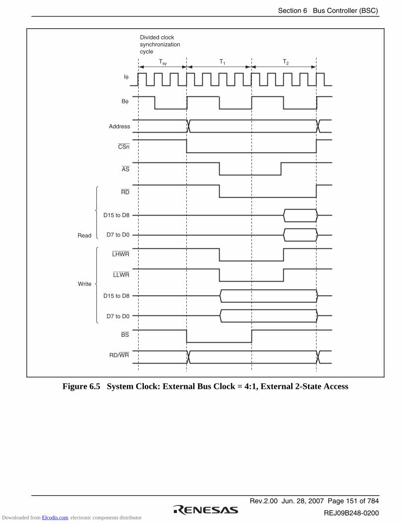
Section 6 Bus Controller (BSC)
Rev.2.00 Jun. 28, 2007 Page 151 of 784
REJ09B248-0200
Divided clock synchronizationcycle
T1
Address
Iφ
Bφ
AS
CSn
RD
D15 to D8
D7 to D0
D15 to D8
D7 to D0
Read
LHWR
LLWR
Write
T2Tsy
BS
RD/WR
Figure 6.5 System Clock: External Bus Clock = 4:1, External 2-State Access
Downloaded from Elcodis.com electronic components distributor

Section 6 Bus Controller (BSC)
Rev.2.00 Jun. 28, 2007 Page 152 of 784
REJ09B248-0200
Divided clocksynchronizationcycle
T1
Address
Iφ
Bφ
AS
CSn
RD
D15 to D8
D7 to D0
D15 to D8
D7 to D0
Read
LHWR
LLWR
Write
T2Tsy T3
BS
RD/WR
Figure 6.6 System Clock: External Bus Clock = 2:1, External 3-State Access
Downloaded from Elcodis.com electronic components distributor

Section 6 Bus Controller (BSC)
Rev.2.00 Jun. 28, 2007 Page 153 of 784
REJ09B248-0200
6.5 External Bus
6.5.1 Input/Output Pins
Table 6.2 shows the pin configuration of the bus controller and table 6.3 shows the pin functions on each interface.
Table 6.2 Pin Configuration
Name Symbol I/O Function
Bus cycle start BS Output Signal indicating that the bus cycle has started
Address strobe/address hold AS/AH Output • Strobe signal indicating that the basic
bus, byte control SRAM, or burst ROM
space is accessed and address output
on address bus is enabled
• Signal to hold the address during
access to the address/data multiplexed
I/O interface
Read strobe RD Output Strobe signal indicating that the basic bus, byte control SRAM, burst ROM, or address/data multiplexed I/O space is being read
Read/write RD/WR Output • Signal indicating the input or output
direction
• Write enable signal of the SRAM during
access to the byte control SRAM space
Low-high write/lower-upper byte select
LHWR/LUB Output • Strobe signal indicating that the basic
bus, burst ROM, or address/data multiplexed I/O space is written to, and
the upper byte (D15 to D8) of data bus
is enabled
• Strobe signal indicating that the byte control SRAM space is accessed, and
the upper byte (D15 to D8) of data bus
is enabled
Downloaded from Elcodis.com electronic components distributor
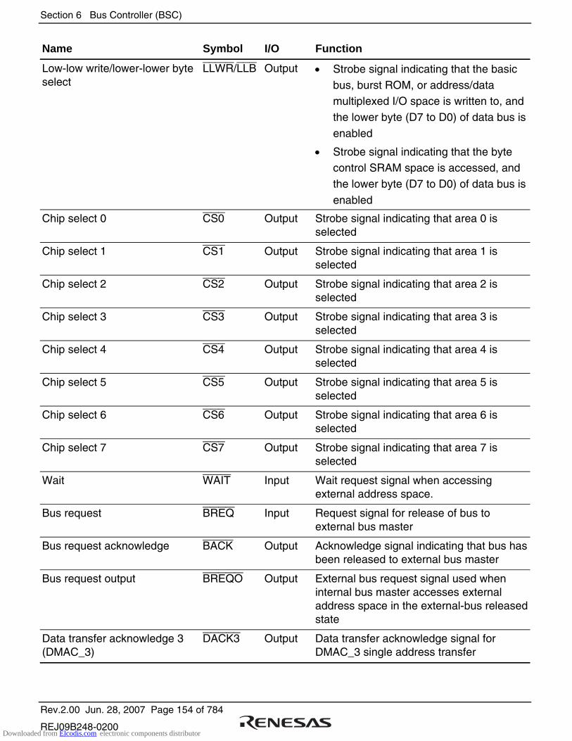
Section 6 Bus Controller (BSC)
Rev.2.00 Jun. 28, 2007 Page 154 of 784
REJ09B248-0200
Name Symbol I/O Function
Low-low write/lower-lower byte select
LLWR/LLB Output • Strobe signal indicating that the basic
bus, burst ROM, or address/data multiplexed I/O space is written to, and
the lower byte (D7 to D0) of data bus is
enabled
• Strobe signal indicating that the byte control SRAM space is accessed, and
the lower byte (D7 to D0) of data bus is
enabled
Chip select 0 CS0 Output Strobe signal indicating that area 0 is selected
Chip select 1 CS1 Output Strobe signal indicating that area 1 is selected
Chip select 2 CS2 Output Strobe signal indicating that area 2 is selected
Chip select 3 CS3 Output Strobe signal indicating that area 3 is selected
Chip select 4 CS4 Output Strobe signal indicating that area 4 is selected
Chip select 5 CS5 Output Strobe signal indicating that area 5 is selected
Chip select 6 CS6 Output Strobe signal indicating that area 6 is selected
Chip select 7 CS7 Output Strobe signal indicating that area 7 is selected
Wait WAIT Input Wait request signal when accessing external address space.
Bus request BREQ Input Request signal for release of bus to external bus master
Bus request acknowledge BACK Output Acknowledge signal indicating that bus has been released to external bus master
Bus request output BREQO Output External bus request signal used when internal bus master accesses external address space in the external-bus released state
Data transfer acknowledge 3 (DMAC_3)
DACK3 Output Data transfer acknowledge signal for DMAC_3 single address transfer
Downloaded from Elcodis.com electronic components distributor
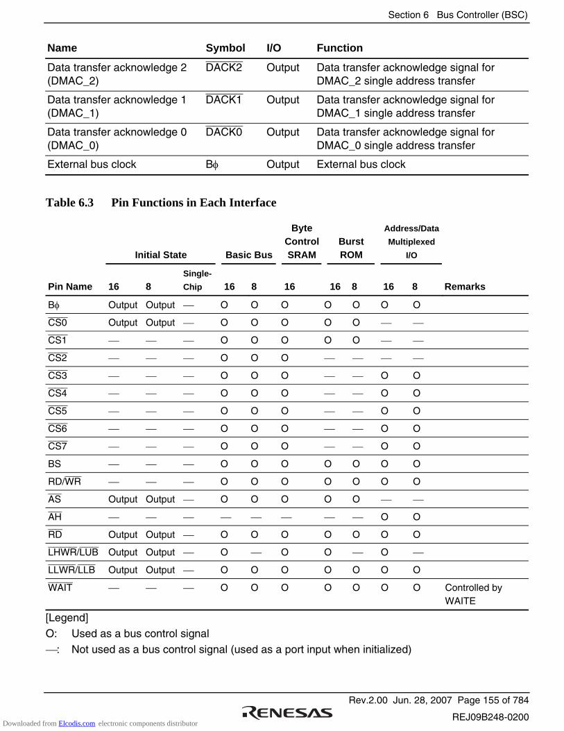
Section 6 Bus Controller (BSC)
Rev.2.00 Jun. 28, 2007 Page 155 of 784
REJ09B248-0200
Name Symbol I/O Function
Data transfer acknowledge 2 (DMAC_2)
DACK2 Output Data transfer acknowledge signal for DMAC_2 single address transfer
Data transfer acknowledge 1 (DMAC_1)
DACK1 Output Data transfer acknowledge signal for DMAC_1 single address transfer
Data transfer acknowledge 0 (DMAC_0)
DACK0 Output Data transfer acknowledge signal for DMAC_0 single address transfer
External bus clock Bφ Output External bus clock
Table 6.3 Pin Functions in Each Interface
Initial State
Basic Bus
Byte Control SRAM
Burst ROM
Address/Data
Multiplexed
I/O
Pin Name 16 8 Single-
Chip
16 8 16 16 8 16 8 Remarks
Bφ Output Output O O O O O O O
CS0 Output Output O O O O O
CS1 O O O O O
CS2 O O O
CS3 O O O O O
CS4 O O O O O
CS5 O O O O O
CS6 O O O O O
CS7 O O O O O
BS O O O O O O O
RD/WR O O O O O O O
AS Output Output O O O O O
AH O O
RD Output Output O O O O O O O
LHWR/LUB Output Output O O O O
LLWR/LLB Output Output O O O O O O O
WAIT O O O O O O O Controlled by WAITE
[Legend]
O: Used as a bus control signal
: Not used as a bus control signal (used as a port input when initialized)
Downloaded from Elcodis.com electronic components distributor

Section 6 Bus Controller (BSC)
Rev.2.00 Jun. 28, 2007 Page 156 of 784
REJ09B248-0200
6.5.2 Area Division
The bus controller divides the 16-Mbyte address space into eight areas, and performs bus control for the external address space in area units. Chip select signals (CS0 to CS7) can be output for each area.
Figure 6.7 shows an area division of the 16-Mbyte address space. For details on address map, see section 3, MCU Operating Modes.
16-Mbyte space
Area 0(2 Mbytes)
Area 1(2 Mbytes)
Area 2(8 Mbytes)
Area 3(2 Mbytes)
Area 4(1 Mbyte)
Area 5(1 Mbyte − 8 kbytes)
Area 6(8 kbytes − 256 bytes)
Area 7(256 bytes)
H'000000
H'1FFFFFH'200000
H'3FFFFFH'400000
H'BFFFFFH'C00000
H'DFFFFFH'E00000
H'EFFFFFH'F00000
H'FFDFFFH'FFE000
H'FFFEFFH'FFFF00H'FFFFFF
Figure 6.7 Address Space Area Division
Downloaded from Elcodis.com electronic components distributor
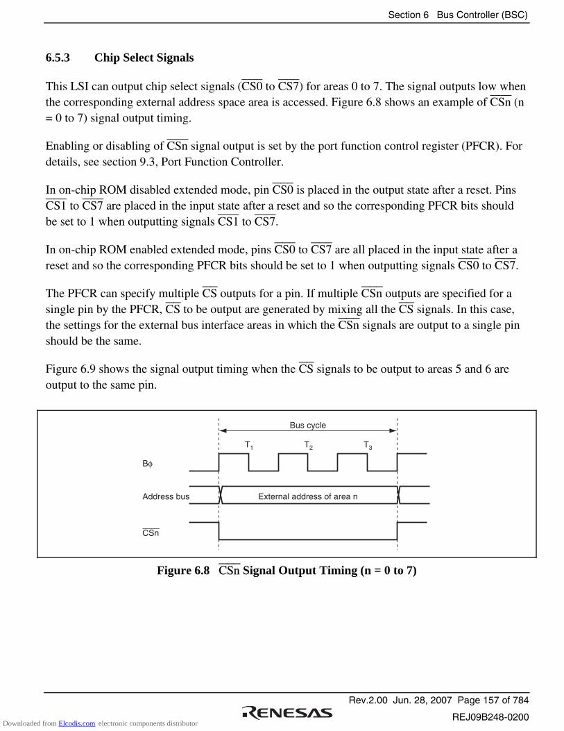
Section 6 Bus Controller (BSC)
Rev.2.00 Jun. 28, 2007 Page 157 of 784
REJ09B248-0200
6.5.3 Chip Select Signals
This LSI can output chip select signals (CS0 to CS7) for areas 0 to 7. The signal outputs low when the corresponding external address space area is accessed. Figure 6.8 shows an example of CSn (n = 0 to 7) signal output timing.
Enabling or disabling of CSn signal output is set by the port function control register (PFCR). For details, see section 9.3, Port Function Controller.
In on-chip ROM disabled extended mode, pin CS0 is placed in the output state after a reset. Pins CS1 to CS7 are placed in the input state after a reset and so the corresponding PFCR bits should be set to 1 when outputting signals CS1 to CS7.
In on-chip ROM enabled extended mode, pins CS0 to CS7 are all placed in the input state after a reset and so the corresponding PFCR bits should be set to 1 when outputting signals CS0 to CS7.
The PFCR can specify multiple CS outputs for a pin. If multiple CSn outputs are specified for a single pin by the PFCR, CS to be output are generated by mixing all the CS signals. In this case, the settings for the external bus interface areas in which the CSn signals are output to a single pin should be the same.
Figure 6.9 shows the signal output timing when the CS signals to be output to areas 5 and 6 are output to the same pin.
Bus cycle
T1 T2 T3
External address of area nAddress bus
Bφ
CSn
Figure 6.8 CSn Signal Output Timing (n = 0 to 7)
Downloaded from Elcodis.com electronic components distributor

Section 6 Bus Controller (BSC)
Rev.2.00 Jun. 28, 2007 Page 158 of 784
REJ09B248-0200
Output waveform
Bφ
Area 5 access
CS6
CS5
Area 6 access
Area 5 access Area 6 accessAddress bus
Figure 6.9 Timing When CS Signal is Output to the Same Pin
6.5.4 External Bus Interface
The type of the external bus interfaces, bus width, endian format, number of access cycles, and strobe assert/negate timings can be set for each area in the external address space. The bus width and the number of access cycles for both on-chip memory and internal I/O registers are fixed, and are not affected by the external bus settings.
(1) Type of External Bus Interface
Four types of external bus interfaces are provided and can be selected in area units. Table 6.4 shows each interface name, description, and area name to be set for each interface. Table 6.5 shows the areas that can be specified for each interface. The initial state of each area is a basic bus interface.
Table 6.4 Interface Names and Area Names
Interface Description Area Name
Basic interface Directly connected to ROM and RAM
Basic bus space
Byte control SRAM interface Directly connected to byte SRAM with byte control pin
Byte control SRAM space
Burst ROM interface Directly connected to the ROM that allows page access
Burst ROM space
Address/data multiplexed I/O interface
Directly connected to the peripheral LSI that requires address and data multiplexing
Address/data multiplexed I/O space
Downloaded from Elcodis.com electronic components distributor

Section 6 Bus Controller (BSC)
Rev.2.00 Jun. 28, 2007 Page 159 of 784
REJ09B248-0200
Table 6.5 Areas Specifiable for Each Interface
Areas
Interface Related Registers 0 1 2 3 4 5 6 7
Basic interface O O O O O O O O
Byte control SRAM interface
SRAMCR
O O O O O O O O
Burst ROM interface BROMCR O O
Address/data multiplexed I/O interface
MPXCR O O O O O
(2) Bus Width
A bus width of 8 or 16 bits can be selected with ABWCR. An area for which an 8-bit bus is selected functions as an 8-bit access space and an area for which a 16-bit bus is selected functions as a 16-bit access space. In addition, the bus width of address/data multiplexed I/O space is 8 bits or 16 bits, and the bus width for the byte control SRAM space is 16 bits.
The initial state of the bus width is specified by the operating mode.
If all areas are designated as 8-bit access space, 8-bit bus mode is set; if any area is designated as 16-bit access space, 16-bit bus mode is set.
(3) Endian Format
Though the endian format of this LSI is big endian, data can be converted into little endian format when reading or writing to the external address space.
Areas 7 to 2 can be specified as either big endian or little endian format by the LE7 to LE2 bits in ENDIANCR.
The initial state of each area is the big endian format.
Note that the data format for the areas used as a program area or a stack area should be big endian.
Downloaded from Elcodis.com electronic components distributor
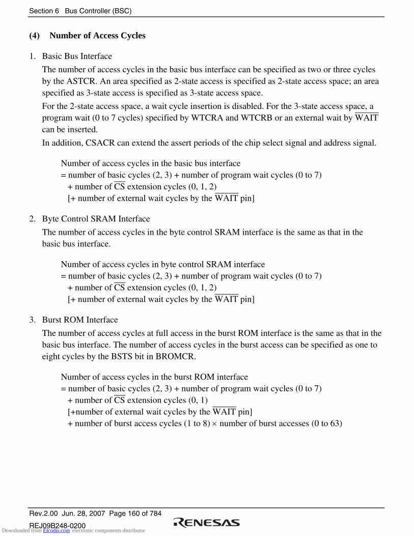
Section 6 Bus Controller (BSC)
Rev.2.00 Jun. 28, 2007 Page 160 of 784
REJ09B248-0200
(4) Number of Access Cycles
1. Basic Bus Interface
The number of access cycles in the basic bus interface can be specified as two or three cycles by the ASTCR. An area specified as 2-state access is specified as 2-state access space; an area specified as 3-state access is specified as 3-state access space.
For the 2-state access space, a wait cycle insertion is disabled. For the 3-state access space, a program wait (0 to 7 cycles) specified by WTCRA and WTCRB or an external wait by WAIT can be inserted.
In addition, CSACR can extend the assert periods of the chip select signal and address signal. Number of access cycles in the basic bus interface
= number of basic cycles (2, 3) + number of program wait cycles (0 to 7) + number of CS extension cycles (0, 1, 2) [+ number of external wait cycles by the WAIT pin]
2. Byte Control SRAM Interface
The number of access cycles in the byte control SRAM interface is the same as that in the basic bus interface.
Number of access cycles in byte control SRAM interface
= number of basic cycles (2, 3) + number of program wait cycles (0 to 7) + number of CS extension cycles (0, 1, 2) [+ number of external wait cycles by the WAIT pin]
3. Burst ROM Interface
The number of access cycles at full access in the burst ROM interface is the same as that in the basic bus interface. The number of access cycles in the burst access can be specified as one to eight cycles by the BSTS bit in BROMCR.
Number of access cycles in the burst ROM interface
= number of basic cycles (2, 3) + number of program wait cycles (0 to 7) + number of CS extension cycles (0, 1) [+number of external wait cycles by the WAIT pin] + number of burst access cycles (1 to 8) × number of burst accesses (0 to 63)
Downloaded from Elcodis.com electronic components distributor
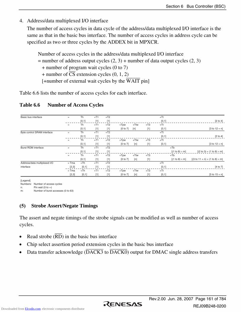
Section 6 Bus Controller (BSC)
Rev.2.00 Jun. 28, 2007 Page 161 of 784
REJ09B248-0200
4. Address/data multiplexed I/O interface
The number of access cycles in data cycle of the address/data multiplexed I/O interface is the same as that in the basic bus interface. The number of access cycles in address cycle can be specified as two or three cycles by the ADDEX bit in MPXCR.
Number of access cycles in the address/data multiplexed I/O interface
= number of address output cycles (2, 3) + number of data output cycles (2, 3) + number of program wait cycles (0 to 7) + number of CS extension cycles (0, 1, 2) [+number of external wait cycles by the WAIT pin]
Table 6.6 lists the number of access cycles for each interface.
Table 6.6 Number of Access Cycles
=
=
=
=
=
=
= Tma
[2,3]
= Tma
[2,3]
Th
[0,1]
Th
[0,1]
Th
[0,1]
Th
[0,1]
Th
[0,1]
Th
[0,1]
+Th
[0,1]
+Th
[0,1]
+T1
[1]
+T1
[1]
+T1
[1]
+T1
[1]
+T1
[1]
+T1
[1]
+T1
[1]
+T1
[1]
+T2
[1]
+T2
[1]
+T2
[1]
+T2
[1]
+T2
[1]
+T2
[1]
+T2
[1]
+T2
[1]
+Tt
[0,1]
+Tt
[0,1]
+Tt
[0,1]
+Tt
[0,1]
+Tt
[0,1]
+Tt
[0,1]
[2 to 4]
[3 to 12 + n]
[2 to 4]
[3 to 12 + n]
[(2 to 3) + (1 to 8) × m]
[(3 to 11 + n) + (1 to 8) × m]
[4 to 7]
[5 to 15 + n]
+Tpw
[0 to 7]
+Tpw
[0 to 7]
+Tpw
[0 to 7]
+Tpw
[0 to 7]
+Ttw
[n]
+Ttw
[n]
+Ttw
[n]
+Ttw
[n]
+T3
[1]
+T3
[1]
+T3
[1]
+T3
[1]
Basic bus interface
Byte control SRAM interface
Burst ROM interface
Address/data multiplexed I/O
interface
+Tb
[(1 to 8) × m]
+Tb
[(1 to 8) × m]
[Legend]Numbers: Number of access cyclesn: Pin wait (0 to ∞)m: Number of burst accesses (0 to 63)
(5) Strobe Assert/Negate Timings
The assert and negate timings of the strobe signals can be modified as well as number of access cycles.
• Read strobe (RD) in the basic bus interface
• Chip select assertion period extension cycles in the basic bus interface
• Data transfer acknowledge (DACK3 to DACK0) output for DMAC single address transfers
Downloaded from Elcodis.com electronic components distributor
Section 6 Bus Controller (BSC)
Rev.2.00 Jun. 28, 2007 Page 162 of 784
REJ09B248-0200
6.5.5 Area and External Bus Interface
(1) Area 0
Area 0 includes on-chip ROM*. All of area 0 is used as external address space in on-chip ROM disabled extended mode, and the space excluding on-chip ROM is external address space in on-chip ROM enabled extended mode.
When area 0 external address space is accessed, the CS0 signal can be output.
Either of the basic bus interface, byte control SRAM interface, or burst ROM interface can be selected for area 0 by bit BSRM0 in BROMCR and bit BCSEL0 in SRAMCR. Table 6.7 shows the external interface of area 0.
Note: Applied to the LSI version that incorporates the ROM.
Table 6.7 Area 0 External Interface
Register Setting
Interface BSRM0 of BROMCR BCSEL0 of SRAMCR
Basic bus interface 0 0
Byte control SRAM interface 0 1
Burst ROM interface 1 0
Setting prohibited 1 1
(2) Area 1
In externally extended mode, all of area 1 is external address space. In on-chip ROM enabled extended mode, the space excluding on-chip ROM* is external address space.
When area 1 external address space is accessed, the CS1 signal can be output.
Either of the basic bus interface, byte control SRAM, or burst ROM interface can be selected for area 1 by bit BSRM1 in BROMCR and bit BCSEL1 in SRAMCR. Table 6.8 shows the external interface of area 1.
Note: Applied to the LSI version that incorporates the ROM.
Downloaded from Elcodis.com electronic components distributor

Section 6 Bus Controller (BSC)
Rev.2.00 Jun. 28, 2007 Page 163 of 784
REJ09B248-0200
Table 6.8 Area 1 External Interface
Register Setting
Interface BSRM1 of BROMCR BCSEL1 of SRAMCR
Basic bus interface 0 0
Byte control SRAM interface 0 1
Burst ROM interface 1 0
Setting prohibited 1 1
(3) Area 2
In externally extended mode, all of area 2 is external address space.
When area 2 external address space is accessed, the CS2 signal can be output.
Either the basic bus interface or byte control SRAM interface can be selected for area 2 by bit BCSEL2 in SRAMCR. Table 6.9 shows the external interface of area 2.
Table 6.9 Area 2 External Interface
Register Setting
Interface BCSEL2 of SRAMCR
Basic bus interface 0
Byte control SRAM interface 1
(4) Area 3
In externally extended mode, all of area 3 is external address space.
When area 3 external address space is accessed, the CS3 signal can be output.
Either of the basic bus interface, byte control SRAM interface, or address/data multiplexed I/O interface can be selected for area 3 by bit MPXE3 in MPXCR and bit BCSEL3 in SRAMCR. Table 6.10 shows the external interface of area 3.
Downloaded from Elcodis.com electronic components distributor
Section 6 Bus Controller (BSC)
Rev.2.00 Jun. 28, 2007 Page 164 of 784
REJ09B248-0200
Table 6.10 Area 3 External Interface
Register Setting
Interface MPXE3 of MPXCR BCSEL3 of SRAMCR
Basic bus interface 0 0
Byte control SRAM interface 0 1
Address/data multiplexed I/O interface
1 0
Setting prohibited 1 1
(5) Area 4
In externally extended mode, all of area 4 is external address space.
When area 4 external address space is accessed, the CS4 signal can be output.
Either of the basic bus interface, byte control SRAM interface, or address/data multiplexed I/O interface can be selected for area 4 by bit MPXE4 in MPXCR and bit BCSEL4 in SRAMCR. Table 6.11 shows the external interface of area 4.
Table 6.11 Area 4 External Interface
Register Setting
Interface MPXE4 of MPXCR BCSEL4 of SRAMCR
Basic bus interface 0 0
Byte control SRAM interface 0 1
Address/data multiplexed I/O interface
1 0
Setting prohibited 1 1
Downloaded from Elcodis.com electronic components distributor

Section 6 Bus Controller (BSC)
Rev.2.00 Jun. 28, 2007 Page 165 of 784
REJ09B248-0200
(6) Area 5
Area 5 includes the on-chip RAM and access prohibited spaces. In external extended
mode, area 5, other than the on-chip RAM and access-prohibited spaces, is external address space. Note that the on-chip RAM is enabled when the RAME bit in SYSCR are set to 1. If the RAME bit in SYSCR is cleared to 0, the on-chip RAM is disabled and the corresponding addresses are an external address space. For details, see section 3, MCU Operating Modes.
When area 5 external address space is accessed, the CS5 signal can be output.
Either of the basic bus interface, byte control SRAM interface, or address/data multiplexed I/O interface can be selected for area 5 by the MPXE5 bit in MPXCR and the BCSEL5 bit in SRAMCR. Table 6.12 shows the external interface of area 5.
Table 6.12 Area 5 External Interface
Register Setting
Interface MPXE5 of MPXCR BCSEL5 of SRAMCR
Basic bus interface 0 0
Byte control SRAM interface 0 1
Address/data multiplexed I/O interface
1 0
Setting prohibited 1 1
(7) Area 6
Area 6 includes internal I/O registers. In external extended mode, area 6 other than on-chip I/O register area is external address space.
When area 6 external address space is accessed, the CS6 signal can be output.
Either of the basic bus interface, byte control SRAM interface, or address/data multiplexed I/O interface can be selected for area 6 by the MPXE6 bit in MPXCR and the BCSEL6 bit in SRAMCR. Table 6.13 shows the external interface of area 6.
Downloaded from Elcodis.com electronic components distributor
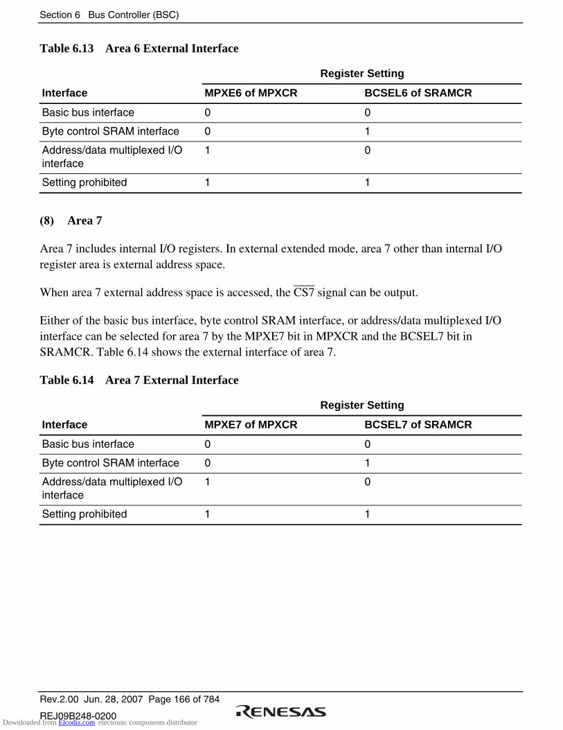
Section 6 Bus Controller (BSC)
Rev.2.00 Jun. 28, 2007 Page 166 of 784
REJ09B248-0200
Table 6.13 Area 6 External Interface
Register Setting
Interface MPXE6 of MPXCR BCSEL6 of SRAMCR
Basic bus interface 0 0
Byte control SRAM interface 0 1
Address/data multiplexed I/O interface
1 0
Setting prohibited 1 1
(8) Area 7
Area 7 includes internal I/O registers. In external extended mode, area 7 other than internal I/O register area is external address space.
When area 7 external address space is accessed, the CS7 signal can be output.
Either of the basic bus interface, byte control SRAM interface, or address/data multiplexed I/O interface can be selected for area 7 by the MPXE7 bit in MPXCR and the BCSEL7 bit in SRAMCR. Table 6.14 shows the external interface of area 7.
Table 6.14 Area 7 External Interface
Register Setting
Interface MPXE7 of MPXCR BCSEL7 of SRAMCR
Basic bus interface 0 0
Byte control SRAM interface 0 1
Address/data multiplexed I/O interface
1 0
Setting prohibited 1 1
Downloaded from Elcodis.com electronic components distributor

Section 6 Bus Controller (BSC)
Rev.2.00 Jun. 28, 2007 Page 167 of 784
REJ09B248-0200
6.5.6 Endian and Data Alignment
Data sizes for the CPU and other internal bus masters are byte, word, and longword. The bus controller has a data alignment function, and controls whether the upper byte data bus (D15 to D8) or lower data bus (D7 to D0) is used according to the bus specifications for the area being accessed (8-bit access space or 16-bit access space), the data size, and endian format when accessing external address space.
(1) 8-Bit Access Space
With the 8-bit access space, the lower byte data bus (D7 to D0) is always used for access. The amount of data that can be accessed at one time is one byte: a word access is performed as two byte accesses, and a longword access, as four byte accesses.
Figures 6.10 and 6.11 illustrate data alignment control for the 8-bit access space. Figure 6.10 shows the data alignment when the data endian format is specified as big endian. Figure 6.11 shows the data alignment when the data endian format is specified as little endian.
Longword
AccessAddress
Access Count
23
7
15 8
07
Data Size
Byte Byte
Byte
Byte
Byte
Byte
Byte
Byte
Word
1 1st
1st
2nd
1st
2nd
3rd
4th
2
4
BusCycle Data Size
Data busD15 D8 D7 D0
RD
7
15
31
8
0
24
16
0
LHWR/LUB LLWR/LLB
Strobe signal
n
n
n
Figure 6.10 Access Sizes and Data Alignment Control for 8-Bit Access Space (Big Endian)
Downloaded from Elcodis.com electronic components distributor
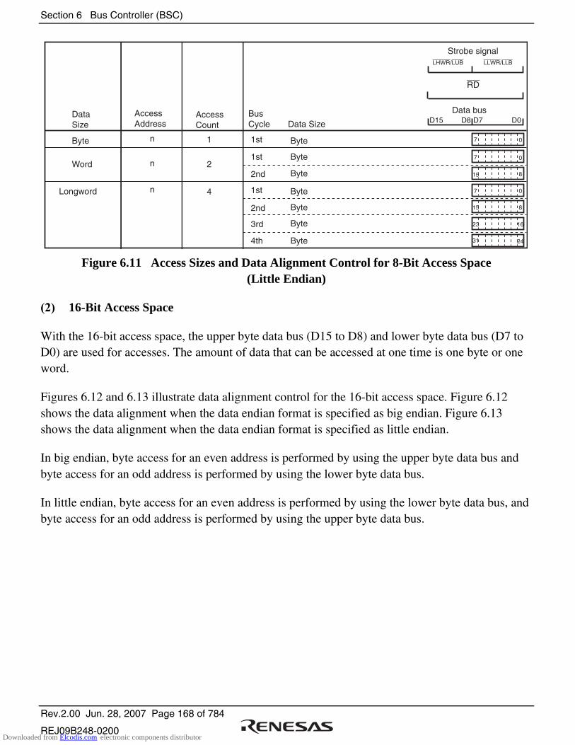
Section 6 Bus Controller (BSC)
Rev.2.00 Jun. 28, 2007 Page 168 of 784
REJ09B248-0200
Longword
AccessAddress
Access Count
15
15
23 16
2431
DataSize
Byte Byte
Byte
Byte
Byte
Byte
Byte
Byte
Word
1 1st
1st
2nd
1st
2nd
3rd
4th
2
4
Bus Cycle Data Size
Data busD15 D8 D7 D0
RD
7
7
7
0
8
0
8
0
LHWR/LUB LLWR/LLB
Strobe signal
n
n
n
Figure 6.11 Access Sizes and Data Alignment Control for 8-Bit Access Space (Little Endian)
(2) 16-Bit Access Space
With the 16-bit access space, the upper byte data bus (D15 to D8) and lower byte data bus (D7 to D0) are used for accesses. The amount of data that can be accessed at one time is one byte or one word.
Figures 6.12 and 6.13 illustrate data alignment control for the 16-bit access space. Figure 6.12 shows the data alignment when the data endian format is specified as big endian. Figure 6.13 shows the data alignment when the data endian format is specified as little endian.
In big endian, byte access for an even address is performed by using the upper byte data bus and byte access for an odd address is performed by using the lower byte data bus.
In little endian, byte access for an even address is performed by using the lower byte data bus, and byte access for an odd address is performed by using the upper byte data bus.
Downloaded from Elcodis.com electronic components distributor

Section 6 Bus Controller (BSC)
Rev.2.00 Jun. 28, 2007 Page 169 of 784
REJ09B248-0200
Longword
AccessAddress
AccessCount
15
31 24
07
AccessSize
Byte
Byte
Byte
Byte
Byte
Word
Word
Word
Word
Byte
Byte
Word
1
1
1
1st
1st
1st
1st
2nd
1st
2nd
1st
2nd
3rd
2
2
3
Bus Cycle Data Size
Data busD15 D8 D7 D0
RD
15
23
8
8
7 0
7 0
7 0
23 16
16
15 8
31 24
7 0
15 8
7 0
LHWR/LUB LLWR/LLB
Strobe signal
Even(2n)
(2n)
Odd
Even(2n+1)
Odd(2n+1)
Odd(2n+1)
Even(2n)
Figure 6.12 Access Sizes and Data Alignment Control for 16-Bit Access Space (Big Endian)
Longword
AccessAddress
AccessCount
15
31 24
07
AccessSize
Byte
Byte
Byte
Byte
Byte
Word
Word
Word
Word
Byte
Byte
Word
1
1
1
1st
1st
1st
1st
2nd
1st
2nd
1st
2nd
3rd
2
2
3
Bus Cycle Data Size
15
23
8
8
7 0
7 0
7 0
23 16
16
15 8
31 24
7 0
15 8
7 0Even(2n)
(2n)
Odd
Even(2n+1)
Odd(2n+1)
Odd(2n+1)
Even(2n)
Data busD15 D8 D7 D0
RD
LHWR/LUB LLWR/LLB
Strobe signal
Figure 6.13 Access Sizes and Data Alignment Control for 16-Bit Access Space (Little Endian)
Downloaded from Elcodis.com electronic components distributor
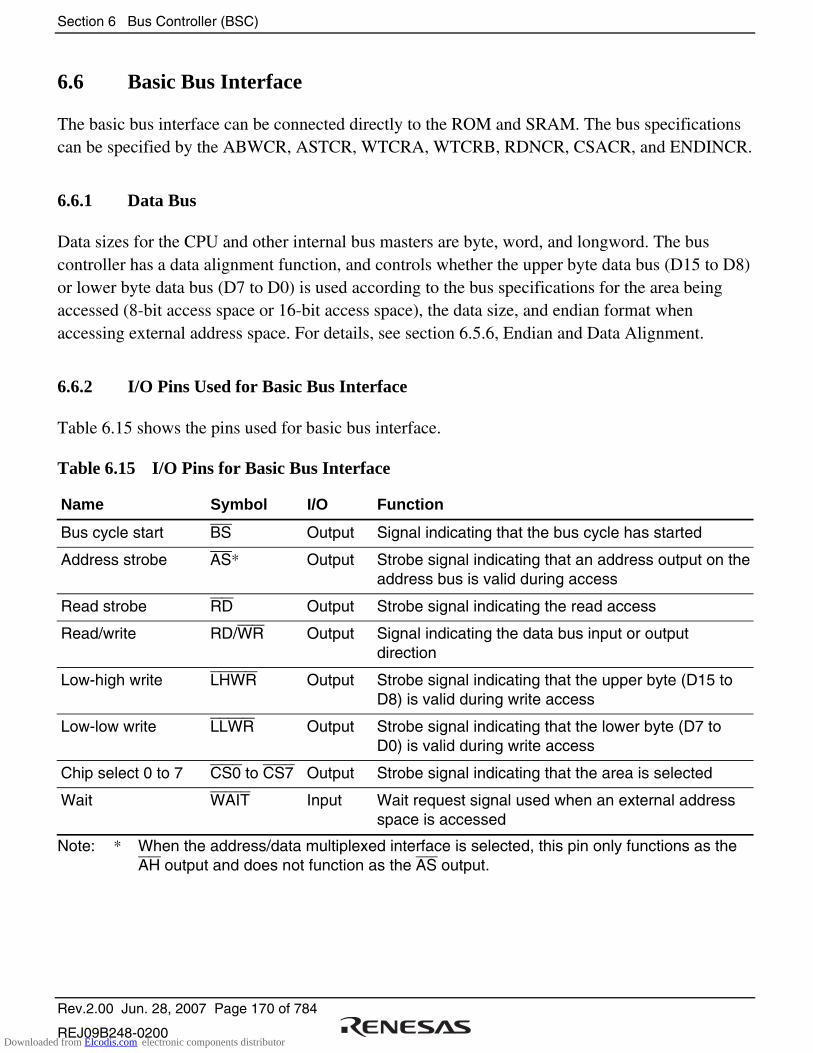
Section 6 Bus Controller (BSC)
Rev.2.00 Jun. 28, 2007 Page 170 of 784
REJ09B248-0200
6.6 Basic Bus Interface
The basic bus interface can be connected directly to the ROM and SRAM. The bus specifications can be specified by the ABWCR, ASTCR, WTCRA, WTCRB, RDNCR, CSACR, and ENDINCR.
6.6.1 Data Bus
Data sizes for the CPU and other internal bus masters are byte, word, and longword. The bus controller has a data alignment function, and controls whether the upper byte data bus (D15 to D8) or lower byte data bus (D7 to D0) is used according to the bus specifications for the area being accessed (8-bit access space or 16-bit access space), the data size, and endian format when accessing external address space. For details, see section 6.5.6, Endian and Data Alignment.
6.6.2 I/O Pins Used for Basic Bus Interface
Table 6.15 shows the pins used for basic bus interface.
Table 6.15 I/O Pins for Basic Bus Interface
Name Symbol I/O Function
Bus cycle start BS Output Signal indicating that the bus cycle has started
Address strobe AS* Output Strobe signal indicating that an address output on the address bus is valid during access
Read strobe RD Output Strobe signal indicating the read access
Read/write RD/WR Output Signal indicating the data bus input or output direction
Low-high write LHWR Output Strobe signal indicating that the upper byte (D15 to D8) is valid during write access
Low-low write LLWR Output Strobe signal indicating that the lower byte (D7 to D0) is valid during write access
Chip select 0 to 7 CS0 to CS7 Output Strobe signal indicating that the area is selected
Wait WAIT Input Wait request signal used when an external address space is accessed
Note: * When the address/data multiplexed interface is selected, this pin only functions as the AH output and does not function as the AS output.
Downloaded from Elcodis.com electronic components distributor
Section 6 Bus Controller (BSC)
Rev.2.00 Jun. 28, 2007 Page 171 of 784
REJ09B248-0200
6.6.3 Basic Timing
This section describes the basic timing when the data is specified as big endian.
(1) 16-Bit 2-State Access Space
Figures 6.14 to 6.16 show the bus timing of 16-bit 2-state access space.
When accessing 16-bit access space, the upper byte data bus (D15 to D8) is used for even addresses access, and the lower byte data bus (D7 to D0) is used for odd addresses. No wait cycles can be inserted.
Downloaded from Elcodis.com electronic components distributor
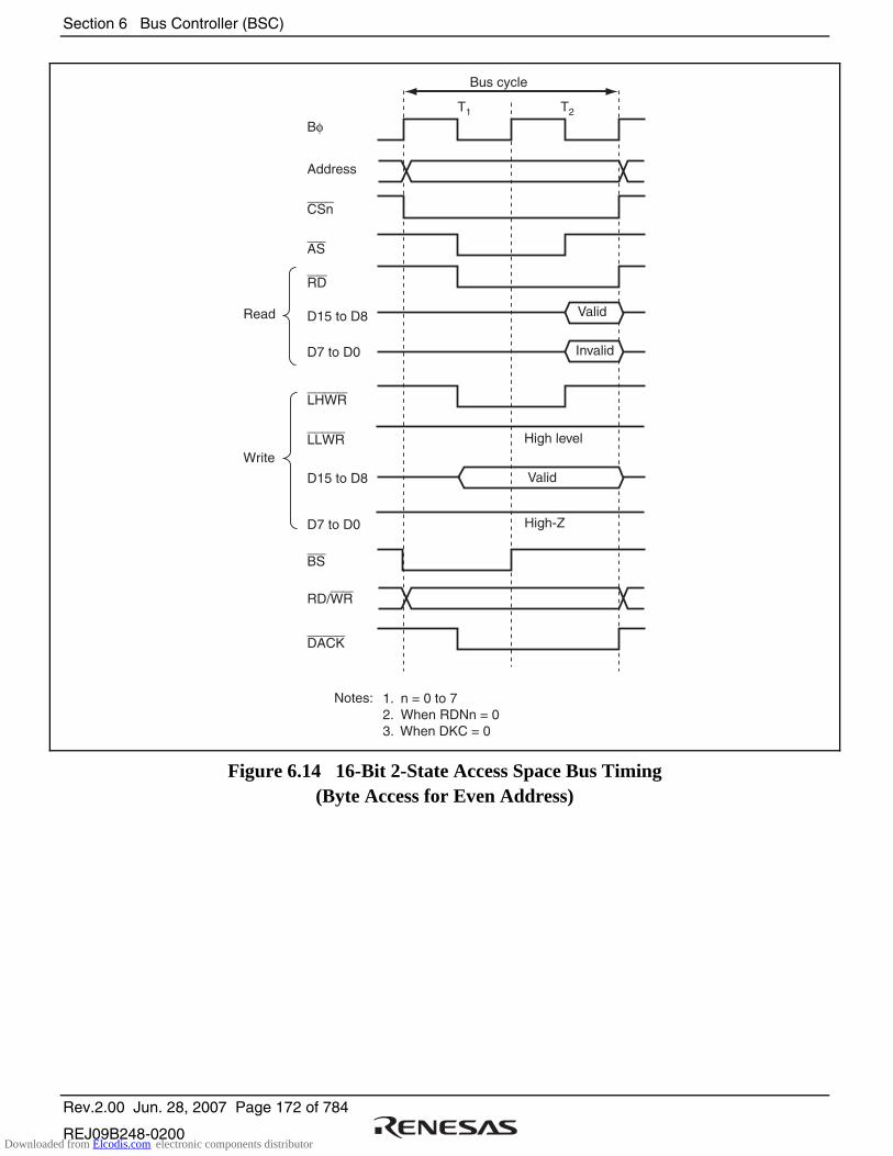
Section 6 Bus Controller (BSC)
Rev.2.00 Jun. 28, 2007 Page 172 of 784
REJ09B248-0200
1. n = 0 to 72. When RDNn = 03. When DKC = 0
Valid
Invalid
Valid
T1 T2
Address
CSn
AS
RD
D15 to D8
D7 to D0
D15 to D8
D7 to D0
LHWR
LLWR
Read
Write
Notes:
High level
High-Z
Bφ
Bus cycle
BS
RD/WR
DACK
Figure 6.14 16-Bit 2-State Access Space Bus Timing (Byte Access for Even Address)
Downloaded from Elcodis.com electronic components distributor

Section 6 Bus Controller (BSC)
Rev.2.00 Jun. 28, 2007 Page 173 of 784
REJ09B248-0200
Invalid
Valid
T1 T2
Address
CSn
AS
RD
D15 to D8
D7 to D0
D15 to D8
D7 to D0
LHWR
LLWR
DACK
Read
Write
High level
High-Z
Bφ
Bus cycle
Valid
BS
RD/WR
1. n = 0 to 72. When RDNn = 03. When DKC = 0
Notes:
Figure 6.15 16-Bit 2-State Access Space Bus Timing (Byte Access for Odd Address)
Downloaded from Elcodis.com electronic components distributor
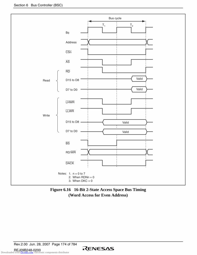
Section 6 Bus Controller (BSC)
Rev.2.00 Jun. 28, 2007 Page 174 of 784
REJ09B248-0200
Valid
Valid
T1 T2
Address
CSn
AS
RD
D15 to D8
D7 to D0
D15 to D8
D7 to D0
LHWR
LLWR
DACK
Read
Write
Bφ
Bus cycle
Valid
Valid
BS
RD/WR
1. n = 0 to 72. When RDNn = 03. When DKC = 0
Notes:
Figure 6.16 16-Bit 2-State Access Space Bus Timing (Word Access for Even Address)
Downloaded from Elcodis.com electronic components distributor
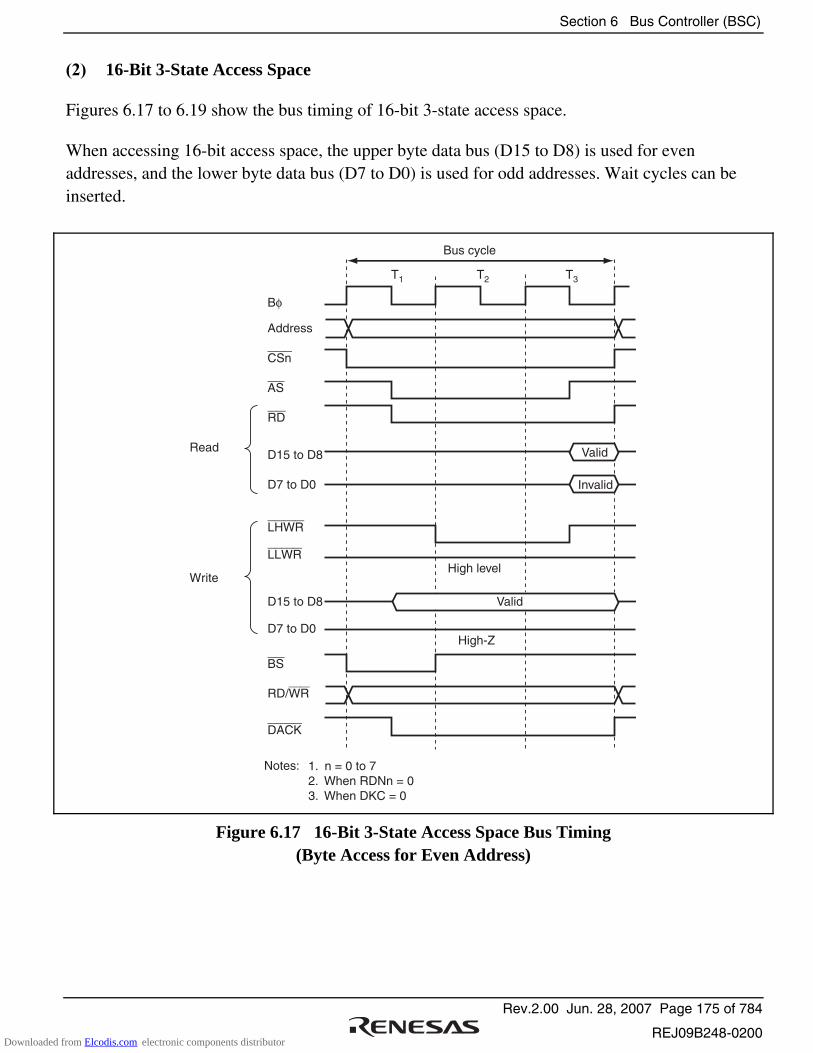
Section 6 Bus Controller (BSC)
Rev.2.00 Jun. 28, 2007 Page 175 of 784
REJ09B248-0200
(2) 16-Bit 3-State Access Space
Figures 6.17 to 6.19 show the bus timing of 16-bit 3-state access space.
When accessing 16-bit access space, the upper byte data bus (D15 to D8) is used for even addresses, and the lower byte data bus (D7 to D0) is used for odd addresses. Wait cycles can be inserted.
Valid
Invalid
T1 T2 T3
Address
CSn
AS
RD
DACK
D15 to D8
D7 to D0
D15 to D8
D7 to D0
LHWR
LLWRHigh level
High-Z
Bφ
Bus cycle
Valid
BS
RD/WR
Read
Write
1. n = 0 to 72. When RDNn = 03. When DKC = 0
Notes:
Figure 6.17 16-Bit 3-State Access Space Bus Timing (Byte Access for Even Address)
Downloaded from Elcodis.com electronic components distributor

Section 6 Bus Controller (BSC)
Rev.2.00 Jun. 28, 2007 Page 176 of 784
REJ09B248-0200
Invalid
Valid
T1 T2 T3
Address
CSn
AS
RD
DACK
D15 to D8
D7 to D0
D15 to D8
D7 to D0
LHWR
LLWR
High level
High-Z
Bφ
Bus cycle
Valid
BS
RD/WR
Read
Write
1. n = 0 to 72. When RDNn = 03. When DKC = 0
Notes:
Figure 6.18 16-Bit 3-State Access Space Bus Timing (Word Access for Odd Address)
Downloaded from Elcodis.com electronic components distributor

Section 6 Bus Controller (BSC)
Rev.2.00 Jun. 28, 2007 Page 177 of 784
REJ09B248-0200
Valid
Valid
T1 T2 T3
Address
CSn
AS
RD
Bφ
Bus cycle
Valid
Valid
RD
D15 to D8
D7 to D0
D15 to D8
D7 to D0
LHWR
LLWR
Read
Write
BS
RD/WR
DACK
1. n = 0 to 72. When RDNn = 03. When DKC = 0
Notes:
Figure 6.19 16-Bit 3-State Access Space Bus Timing (Word Access for Even Address)
Downloaded from Elcodis.com electronic components distributor

Section 6 Bus Controller (BSC)
Rev.2.00 Jun. 28, 2007 Page 178 of 784
REJ09B248-0200
6.6.4 Wait Control
This LSI can extend the bus cycle by inserting wait cycles (Tw) when the external address space is accessed. There are two ways of inserting wait cycles: program wait (Tpw) insertion and pin wait (Ttw) insertion using the WAIT pin.
(1) Program Wait Insertion
From 0 to 7 wait cycles can be inserted automatically between the T2 state and T3 state for 3-state access space, according to the settings in WTCRA and WTCRB.
(2) Pin Wait Insertion
For 3-state access space, when the WAITE bit in BCR1 is set to 1 and the ICR bit for the corresponding pin is set to 1, wait input by means of the WAIT pin is enabled. When the external address space is accessed in this state, a program wait (TPW) is first inserted according to the WTCRA and WTCRB settings. If the WAIT pin is low at the falling edge of Bφ in the last T2 or Tpw cycle, another Ttw cycle is inserted until the WAIT pin is brought high. The pin wait insertion is effective when the Tw cycles are inserted to seven cycles or more, or when the number of Tw cycles to be inserted is changed according to the external devices. The WAITE bit is common to all areas. For details on ICR, see section 9, I/O Ports.
Figure 6.20 shows an example of wait cycle insertion timing. After a reset, the 3-state access is specified, the program wait is inserted for seven cycles, and the WAIT input is disabled.
Downloaded from Elcodis.com electronic components distributor
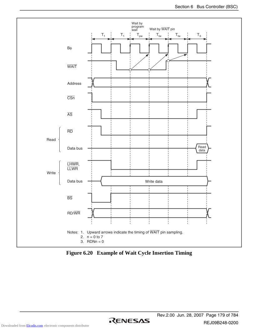
Section 6 Bus Controller (BSC)
Rev.2.00 Jun. 28, 2007 Page 179 of 784
REJ09B248-0200
Wait byprogram wait
T1
Address
Bφ
AS
CSn
RD
Data bus
Read
Readdata
LHWR, LLWR
Write data
Write
Notes: 1. Upward arrows indicate the timing of WAIT pin sampling. 2. n = 0 to 7 3. RDNn = 0
WAIT
Data bus
T1 Tpw Ttw Ttw T3
Wait by WAIT pin
BS
RD/WR
Figure 6.20 Example of Wait Cycle Insertion Timing
Downloaded from Elcodis.com electronic components distributor

Section 6 Bus Controller (BSC)
Rev.2.00 Jun. 28, 2007 Page 180 of 784
REJ09B248-0200
6.6.5 Read Strobe (RD) Timing
The read strobe timing can be modified in area units by setting bits RDN7 to RDN0 in RDNCR to 1.
Note that the RD timing with respect to the DACK rising edge will change if the read strobe timing is modified by setting RDNn to 1 when the DMAC is used in the single address mode.
Figure 6.21 shows an example of timing when the read strobe timing is changed in the basic bus 3-state access space.
Downloaded from Elcodis.com electronic components distributor
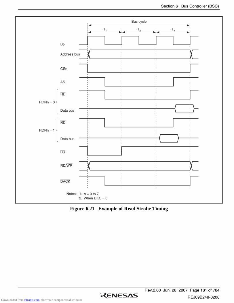
Section 6 Bus Controller (BSC)
Rev.2.00 Jun. 28, 2007 Page 181 of 784
REJ09B248-0200
Bus cycle
T1 T2
Address bus
Bφ
CSn
AS
RD
T3
Data bus
RD
Data bus
RDNn = 0
RDNn = 1
BS
RD/WR
DACK
1. n = 0 to 72. When DKC = 0
Notes:
Figure 6.21 Example of Read Strobe Timing
Downloaded from Elcodis.com electronic components distributor
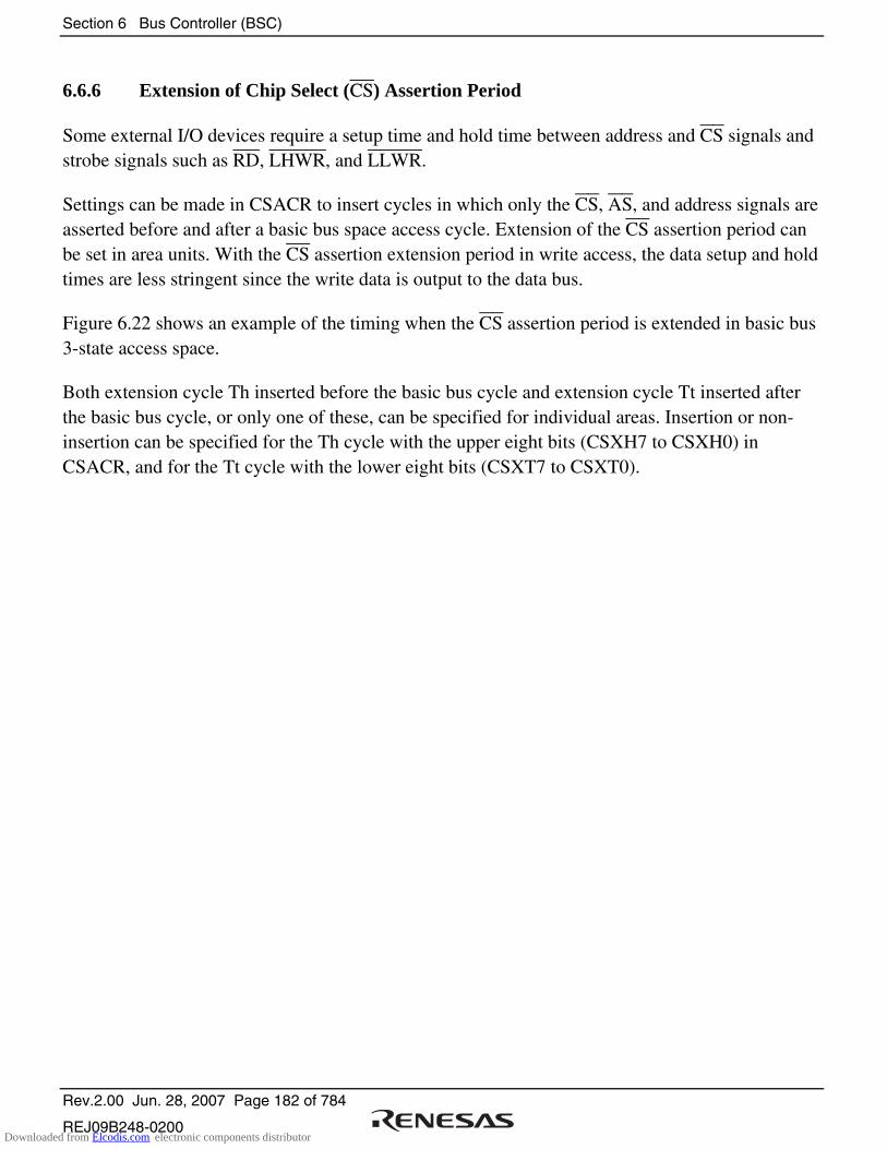
Section 6 Bus Controller (BSC)
Rev.2.00 Jun. 28, 2007 Page 182 of 784
REJ09B248-0200
6.6.6 Extension of Chip Select (CS) Assertion Period
Some external I/O devices require a setup time and hold time between address and CS signals and strobe signals such as RD, LHWR, and LLWR.
Settings can be made in CSACR to insert cycles in which only the CS, AS, and address signals are asserted before and after a basic bus space access cycle. Extension of the CS assertion period can be set in area units. With the CS assertion extension period in write access, the data setup and hold times are less stringent since the write data is output to the data bus.
Figure 6.22 shows an example of the timing when the CS assertion period is extended in basic bus 3-state access space.
Both extension cycle Th inserted before the basic bus cycle and extension cycle Tt inserted after the basic bus cycle, or only one of these, can be specified for individual areas. Insertion or non-insertion can be specified for the Th cycle with the upper eight bits (CSXH7 to CSXH0) in CSACR, and for the Tt cycle with the lower eight bits (CSXT7 to CSXT0).
Downloaded from Elcodis.com electronic components distributor

Section 6 Bus Controller (BSC)
Rev.2.00 Jun. 28, 2007 Page 183 of 784
REJ09B248-0200
Th T1 T2 T3 Tt
Address
Bus cycle
Bφ
AS
CSn
RD
Data bus Read data
Read
LHWR, LLWR
Write data
Write
Data bus
BS
RD/WR
DACK
1. n = 0 to 72. When DKC = 0
Notes:
Figure 6.22 Example of Timing when Chip Select Assertion Period is Extended
Downloaded from Elcodis.com electronic components distributor
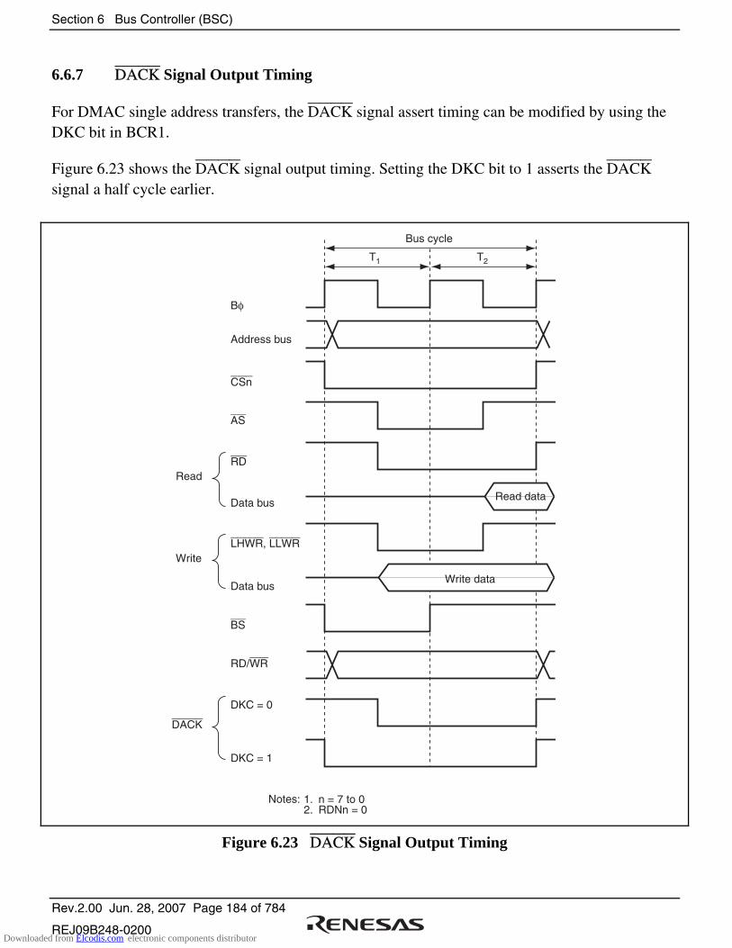
Section 6 Bus Controller (BSC)
Rev.2.00 Jun. 28, 2007 Page 184 of 784
REJ09B248-0200
6.6.7 DACK Signal Output Timing
For DMAC single address transfers, the DACK signal assert timing can be modified by using the DKC bit in BCR1.
Figure 6.23 shows the DACK signal output timing. Setting the DKC bit to 1 asserts the DACK signal a half cycle earlier.
T1 T2
Bus cycle
Bφ
Address bus
Write data
Write
Read data
Read
CSn
AS
RD
Data bus
Data bus
LHWR, LLWR
BS
RD/WR
DKC = 0
DKC = 1
DACK
Notes: 1. n = 7 to 02. RDNn = 0
Figure 6.23 DACK Signal Output Timing
Downloaded from Elcodis.com electronic components distributor
Section 6 Bus Controller (BSC)
Rev.2.00 Jun. 28, 2007 Page 185 of 784
REJ09B248-0200
6.7 Byte Control SRAM Interface
The byte control SRAM interface is a memory interface for outputting a byte select strobe during a read or a write bus cycle. This interface has 16-bit data input/output pins and can be connected to the SRAM that has the upper byte select and the lower byte select strobes such as UB and LB.
The operation of the byte control SRAM interface is the same as the basic bus interface except that: the byte select strobes (LUB and LLB) are output from the write strobe output pins (LHWR and LLWR), respectively; the read strobe (RD) negation timing is a half cycle earlier than that in the case where RDNn = 0 in the basic bus interface regardless of the RDNCR settings; and the RD/WR signal is used as write enable (WE).
6.7.1 Byte Control SRAM Space Setting
Byte control SRAM interface can be specified for areas 0 to 7. Each area can be specified as byte control SRAM interface by setting bits BCSELn (n = 0 to 7) in SRAMCR. For the area specified as burst ROM interface or address/data multiplexed I/O interface, the SRAMCR setting is invalid and byte control SRAM interface cannot be used.
6.7.2 Data Bus
The bus width of the byte control SRAM space can be specified as 16-bit byte control SRAM space according to bits ABWHn and ABWLn (n = 0 to 7) in ABWCR. The area specified as 8-bit access space cannot be specified as the byte control SRAM space.
For the 16-bit byte control SRAM space, data bus (D15 to D0) is valid.
Access size and data alignment are the same as the basic bus interface. For details, see section 6.5.6, Endian and Data Alignment.
Downloaded from Elcodis.com electronic components distributor
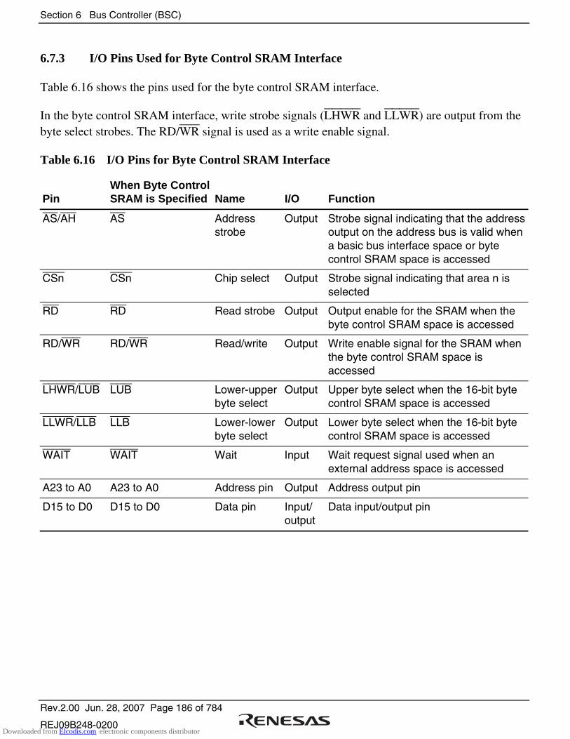
Section 6 Bus Controller (BSC)
Rev.2.00 Jun. 28, 2007 Page 186 of 784
REJ09B248-0200
6.7.3 I/O Pins Used for Byte Control SRAM Interface
Table 6.16 shows the pins used for the byte control SRAM interface.
In the byte control SRAM interface, write strobe signals (LHWR and LLWR) are output from the byte select strobes. The RD/WR signal is used as a write enable signal.
Table 6.16 I/O Pins for Byte Control SRAM Interface
Pin When Byte Control SRAM is Specified Name I/O Function
AS/AH AS Address strobe
Output Strobe signal indicating that the address output on the address bus is valid when a basic bus interface space or byte control SRAM space is accessed
CSn CSn Chip select Output Strobe signal indicating that area n is selected
RD RD Read strobe Output Output enable for the SRAM when the byte control SRAM space is accessed
RD/WR RD/WR Read/write Output Write enable signal for the SRAM when the byte control SRAM space is accessed
LHWR/LUB LUB Lower-upper byte select
Output Upper byte select when the 16-bit byte control SRAM space is accessed
LLWR/LLB LLB Lower-lower byte select
Output Lower byte select when the 16-bit byte control SRAM space is accessed
WAIT WAIT Wait Input Wait request signal used when an external address space is accessed
A23 to A0 A23 to A0 Address pin Output Address output pin
D15 to D0 D15 to D0 Data pin Input/ output
Data input/output pin
Downloaded from Elcodis.com electronic components distributor

Section 6 Bus Controller (BSC)
Rev.2.00 Jun. 28, 2007 Page 187 of 784
REJ09B248-0200
6.7.4 Basic Timing
(1) 2-State Access Space
Figure 6.24 shows the bus timing when the byte control SRAM space is specified as a 2-state access space.
Data buses used for 16-bit access space is the same as those in basic bus interface. No wait cycles can be inserted.
Bφ
Address
D15 to D8
D7 to D0
High level
D15 to D8
D7 to D0
Bus cycle
CSn
AS
RD
LUB
LLB
DACK
BS
RD/WR
RD
RD/WR
T1 T2
Note: n = 0 to 7
Valid
Valid
Read
WriteValid
Valid
Figure 6.24 16-Bit 2-State Access Space Bus Timing
Downloaded from Elcodis.com electronic components distributor

Section 6 Bus Controller (BSC)
Rev.2.00 Jun. 28, 2007 Page 188 of 784
REJ09B248-0200
(2) 3-State Access Space
Figure 6.25 shows the bus timing when the byte control SRAM space is specified as a 3-state access space.
Data buses used for 16-bit access space is the same as those in the basic bus interface. Wait cycles can be inserted.
Bφ
Address
High level
Bus cycle
CSn
AS
T1 T2 T3
Valid
Valid
Valid
Valid
D15 to D8
D7 to D0
D15 to D8
D7 to D0
RD
LUB
LLB
DACK
BS
RD/WR
RD
RD/WR
Note: n = 0 to 7
Read
Write
Figure 6.25 16-Bit 3-State Access Space Bus Timing
Downloaded from Elcodis.com electronic components distributor
Section 6 Bus Controller (BSC)
Rev.2.00 Jun. 28, 2007 Page 189 of 784
REJ09B248-0200
6.7.5 Wait Control
The bus cycle can be extended for the byte control SRAM interface by inserting wait cycles (Tw) in the same way as the basic bus interface.
(1) Program Wait Insertion
From 0 to 7 wait cycles can be inserted automatically between T2 cycle and T3 cycle for the 3-state access space in area units, according to the settings in WTCRA and WTCRB.
(2) Pin Wait Insertion
For 3-state access space, when the WAITE bit in BCR1 is set to 1, the corresponding DDR bit is cleared to 0, and the ICR bit is set to 1, wait input by means of the WAIT pin is enabled. For details on DDR and ICR, see section 9, I/O Ports.
Figure 6.26 shows an example of wait cycle insertion timing.
Downloaded from Elcodis.com electronic components distributor
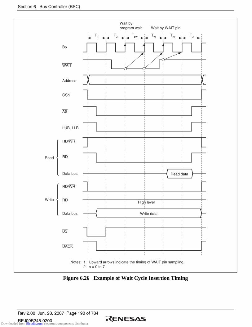
Section 6 Bus Controller (BSC)
Rev.2.00 Jun. 28, 2007 Page 190 of 784
REJ09B248-0200
Wait byprogram wait
T1
Address
Bφ
AS
DACK
LUB, LLB
CSn
RD
RD
RD/WR
RD/WR
Data bus Read data
Read
BS
Write data
High levelWrite
Notes: 1. Upward arrows indicate the timing of WAIT pin sampling. 2. n = 0 to 7
WAIT
Data bus
T2 Tpw Ttw Ttw T3
Wait by WAIT pin
Figure 6.26 Example of Wait Cycle Insertion Timing
Downloaded from Elcodis.com electronic components distributor
Section 6 Bus Controller (BSC)
Rev.2.00 Jun. 28, 2007 Page 191 of 784
REJ09B248-0200
6.7.6 Read Strobe (RD)
When the byte control SRAM space is specified, the RDNCR setting for the corresponding space is invalid.
The read strobe negation timing is the same timing as when RDNn = 1 in the basic bus interface. Note that the RD timing with respect to the DACK rising edge becomes different.
6.7.7 Extension of Chip Select (CS) Assertion Period
In the byte control SRAM interface, the extension cycles can be inserted before and after the bus cycle in the same way as the basic bus interface. For details, see section 6.6.6, Extension of Chip Select (CS) Assertion Period.
6.7.8 DACK Signal Output Timing
For DMAC single address transfers, the DACK signal assert timing can be modified by using the DKC bit in BCR1.
Figure 6.27 shows the DACK signal output timing. Setting the DKC bit to 1 asserts the DACK signal a half cycle earlier.
Downloaded from Elcodis.com electronic components distributor
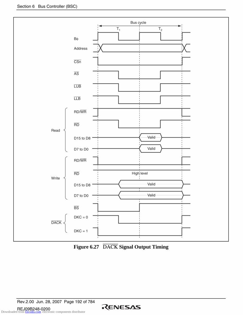
Section 6 Bus Controller (BSC)
Rev.2.00 Jun. 28, 2007 Page 192 of 784
REJ09B248-0200
Bφ
Address
D15 to D8
D7 to D0
High level
D15 to D8
D7 to D0
DKC = 0
DKC = 1
Bus cycle
CSn
AS
RD
LUB
LLB
BS
DACK
RD/WR
RD
RD/WR
T1 T2
Valid
Valid
Read
Write
Valid
Valid
Figure 6.27 DACK Signal Output Timing
Downloaded from Elcodis.com electronic components distributor
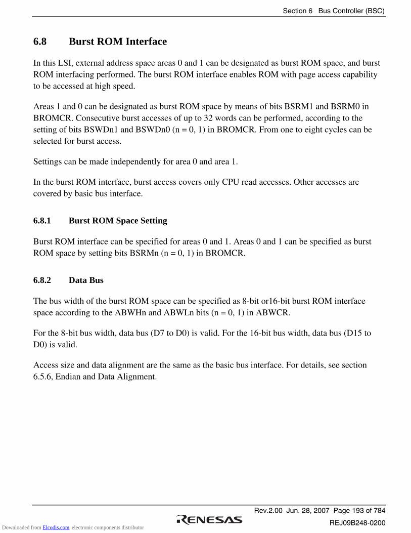
Section 6 Bus Controller (BSC)
Rev.2.00 Jun. 28, 2007 Page 193 of 784
REJ09B248-0200
6.8 Burst ROM Interface
In this LSI, external address space areas 0 and 1 can be designated as burst ROM space, and burst ROM interfacing performed. The burst ROM interface enables ROM with page access capability to be accessed at high speed.
Areas 1 and 0 can be designated as burst ROM space by means of bits BSRM1 and BSRM0 in BROMCR. Consecutive burst accesses of up to 32 words can be performed, according to the setting of bits BSWDn1 and BSWDn0 (n = 0, 1) in BROMCR. From one to eight cycles can be selected for burst access.
Settings can be made independently for area 0 and area 1.
In the burst ROM interface, burst access covers only CPU read accesses. Other accesses are covered by basic bus interface.
6.8.1 Burst ROM Space Setting
Burst ROM interface can be specified for areas 0 and 1. Areas 0 and 1 can be specified as burst ROM space by setting bits BSRMn (n = 0, 1) in BROMCR.
6.8.2 Data Bus
The bus width of the burst ROM space can be specified as 8-bit or16-bit burst ROM interface space according to the ABWHn and ABWLn bits (n = 0, 1) in ABWCR.
For the 8-bit bus width, data bus (D7 to D0) is valid. For the 16-bit bus width, data bus (D15 to D0) is valid.
Access size and data alignment are the same as the basic bus interface. For details, see section 6.5.6, Endian and Data Alignment.
Downloaded from Elcodis.com electronic components distributor

Section 6 Bus Controller (BSC)
Rev.2.00 Jun. 28, 2007 Page 194 of 784
REJ09B248-0200
6.8.3 I/O Pins Used for Burst ROM Interface
Table 6.17 shows the pins used for the burst ROM interface.
Table 6.17 I/O Pins Used for Burst ROM Interface
Name Symbol I/O Function
Bus cycle start BS Output Signal indicating that the bus cycle has started.
Address strobe AS Output Strobe signal indicating that an address output on the address bus is valid during access
Read strobe RD Output Strobe signal indicating the read access
Read/write RD/WR Output Signal indicating the data bus input or output direction
Low-high write LHWR Output Strobe signal indicating that the upper byte (D15 to D8) is valid during write access
Low-low write LLWR Output Strobe signal indicating that the lower byte (D7 to D0) is valid during write access
Chip select 0, 1 CS0, CS1 Output Strobe signal indicating that the area is selected
Wait WAIT Input Wait request signal used when an external address space is accessed
6.8.4 Basic Timing
The number of access cycles in the initial cycle (full access) on the burst ROM interface is determined by the basic bus interface settings in ABWCR, ASTCR, WTCRA, WTCRB, and bits CSXHn in CSACR (n = 0 to 7). When area 0 or area 1 designated as burst ROM space is read by the CPU, the settings in RDNCR and bits CSXTn in CSACR (n = 0 to 7) are ignored.
From one to eight cycles can be selected for the burst cycle, according to the settings of bits BSTS02 to BSTS00 and BSTS12 to BSTS10 in BROMCR. Wait cycles cannot be inserted. In addition, 4-word, 8-word, 16-word, or 32-word consecutive burst access can be performed according to the settings of BSTS01, BSTS00, BSTS11, and BSTS10 bits in BROMCR.
The basic access timing for burst ROM space is shown in figures 6.28 and 6.29.
Downloaded from Elcodis.com electronic components distributor

Section 6 Bus Controller (BSC)
Rev.2.00 Jun. 28, 2007 Page 195 of 784
REJ09B248-0200
T1 T2 T1 T2 T1 T2T3
Bφ
Upper address bus
Note: n = 1, 0
Lower address bus
Data bus
Full access Burst access
CSn
AS
RD
BS
RD/WR
Figure 6.28 Example of Burst ROM Access Timing (ASTn = 1, Two Burst Cycles)
Downloaded from Elcodis.com electronic components distributor
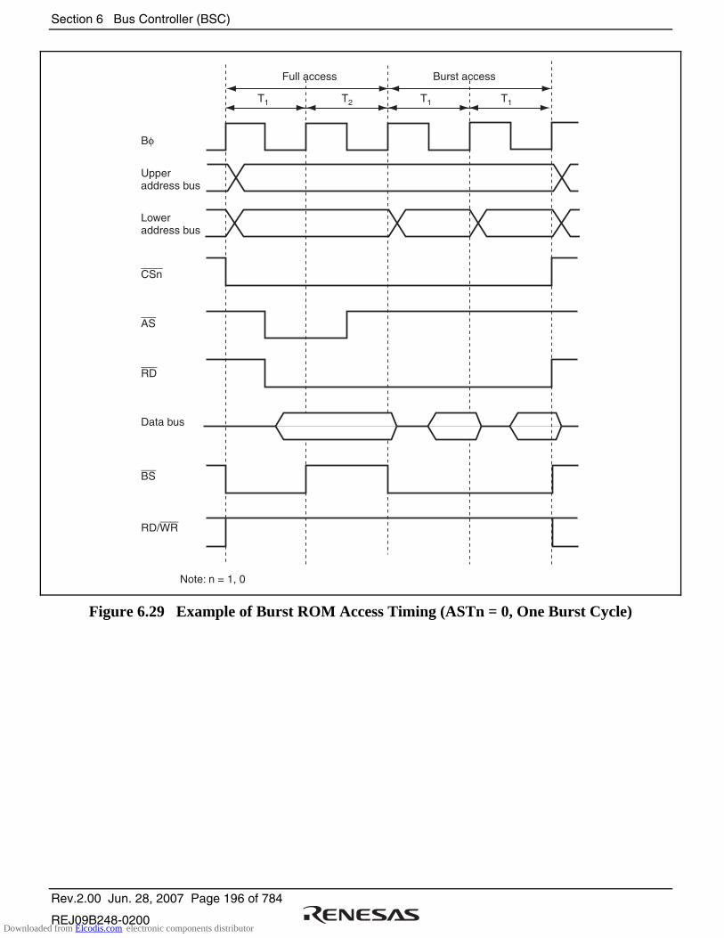
Section 6 Bus Controller (BSC)
Rev.2.00 Jun. 28, 2007 Page 196 of 784
REJ09B248-0200
T1 T2 T1T1
Bφ
Upper address bus
Lower address bus
Data bus
Full access Burst access
CSn
AS
RD
BS
RD/WR
Note: n = 1, 0
Figure 6.29 Example of Burst ROM Access Timing (ASTn = 0, One Burst Cycle)
Downloaded from Elcodis.com electronic components distributor

Section 6 Bus Controller (BSC)
Rev.2.00 Jun. 28, 2007 Page 197 of 784
REJ09B248-0200
6.8.5 Wait Control
As with the basic bus interface, either program wait insertion or pin wait insertion by the WAIT pin can be used in the initial cycle (full access) on the burst ROM interface. See section 6.6.4, Wait Control. Wait cycles cannot be inserted in a burst cycle.
6.8.6 Read Strobe (RD) Timing
When the burst ROM space is read by the CPU, the RDNCR setting for the corresponding space is invalid.
The read strobe negation timing is the same timing as when RDNn = 0 in the basic bus interface.
6.8.7 Extension of Chip Select (CS) Assertion Period
In the burst ROM interface, the extension cycles can be inserted in the same way as the basic bus interface.
For the burst ROM space, the burst access can be enabled only in read access by the CPU. In this case, the setting of the corresponding CSXTn bit in CSACR is ignored and an extension cycle can be inserted only before the full access cycle. Note that no extension cycle can be inserted before or after the burst access cycles.
In read accesses by the CPU, the burst ROM space is equivalent to the basic bus interface space. Accordingly, extension cycles can be inserted before and after the burst access cycles.
Downloaded from Elcodis.com electronic components distributor

Section 6 Bus Controller (BSC)
Rev.2.00 Jun. 28, 2007 Page 198 of 784
REJ09B248-0200
6.9 Address/Data Multiplexed I/O Interface
If areas 3 to 7 of external address space are specified as address/data multiplexed I/O space in this LSI, the address/data multiplexed I/O interface can be performed. In the address/data multiplexed I/O interface, peripheral LSIs that require the multiplexed address/data can be connected directly to this LSI.
6.9.1 Address/Data Multiplexed I/O Space Setting
Address/data multiplexed I/O interface can be specified for areas 3 to 7. Each area can be specified as the address/data multiplexed I/O space by setting bits MPXEn (n = 3 to 7) in MPXCR.
6.9.2 Address/Data Multiplex
In the address/data multiplexed I/O space, data bus is multiplexed with address bus. Table 6.18 shows the relationship between the bus width and address output.
Table 6.18 Address/Data Multiplex
Bus Width Cycle
Data Pins
Address
Data
Address
Data
8 bits
16 bits
PI7
A15
D15
PI6
A14
D14
PI5
A13
D13
PI4
A12
D12
PI3
A11
D11
PI2
A10
D10
PI1
A9
D9
PI0
A8
D8
PH7
A7
D7
A7
D7
PH6
A6
D6
A6
D6
PH5
A5
D5
A5
D5
PH4
A4
D4
A4
D4
PH3
A3
D3
A3
D3
PH2
A2
D2
A2
D2
PH1
A1
D1
A1
D1
PH0
A0
D0
A0
D0
6.9.3 Data Bus
The bus width of the address/data multiplexed I/O space can be specified for either 8-bit access space or 16-bit access space by the ABWHn and ABWLn bits (n = 3 to 7) in ABWCR.
For the 8-bit access space, D7 to D0 are valid for both address and data. For 16-bit access space, D15 to D0 are valid for both address and data. If the address/data multiplexed I/O space is accessed, the corresponding address will be output to the address bus.
For details on access size and data alignment, see section 6.5.6, Endian and Data Alignment.
Downloaded from Elcodis.com electronic components distributor

Section 6 Bus Controller (BSC)
Rev.2.00 Jun. 28, 2007 Page 199 of 784
REJ09B248-0200
6.9.4 I/O Pins Used for Address/Data Multiplexed I/O Interface
Table 6.19 shows the pins used for the address/data multiplexed I/O Interface.
Table 6.19 I/O Pins for Address/Data Multiplexed I/O Interface
Pin
When Byte Control SRAM is Specified Name I/O Function
CSn CSn Chip select Output Chip select (n = 3 to 7) when area n is specified as the address/data multiplexed I/O space
AS/AH AH* Address hold Output Signal to hold an address when the address/data multiplexed I/O space is specified
RD RD Read strobe Output Signal indicating that the address/data multiplexed I/O space is being read
LHWR/LUB LHWR Low-high write Output Strobe signal indicating that the upper bytes (D15 to D8) is valid when the address/data multiplexed I/O space is written
LLWR/LLB LLWR Low-low write Output Strobe signal indicating that the lower bytes (D7 to D0) is valid when the address/data multiplexed I/O space is written
D15 to D0 D15 to D0 Address/data Input/ output
Address and data multiplexed pins for the address/data multiplexed I/O space.
Only D7 to D0 are valid when the 8-bit space is specified. D15 to D0 are valid when the 16-bit space is specified.
A23 to A0 A23 to A0 Address Output Address output pin
WAIT WAIT Wait Input Wait request signal used when the external address space is accessed
BS BS Bus cycle start Output Signal to indicate the bus cycle start
RD/WR RD/WR Read/write Output Signal indicating the data bus input or output direction
Note: * The AH output is multiplexed with the AS output. At the timing that an area is specified as address/data multiplexed I/O, this pin starts to function as the AH output meaning that this pin cannot be used as the AS output. At this time, when other areas set to the basic bus interface is accessed, this pin does not function as the AS output. Until an area is specified as address/data multiplexed I/O, be aware that this pin functions as the AS output.
Downloaded from Elcodis.com electronic components distributor

Section 6 Bus Controller (BSC)
Rev.2.00 Jun. 28, 2007 Page 200 of 784
REJ09B248-0200
6.9.5 Basic Timing
The bus cycle in the address/data multiplexed I/O interface consists of an address cycle and a data cycle. The data cycle is based on the basic bus interface timing specified by the ABWCR, ASTCR, WTCRA, WTCRB, RDNCR, and CSACR.
Figures 6.30 and 6.31 show the basic access timings.
Tma1 Tma2 T2T1
Bφ
Address bus
D7 to D0
D7 to D0
Address cycle Data cycle
CSn
LLWR
AH
RD
DACK
BS
RD/WR
Note: n = 3 to 7
Address Read data
Address Write data
Read
Write
Figure 6.30 8-Bit Access Space Access Timing (ABWHn = 1, ABWLn = 1)
Downloaded from Elcodis.com electronic components distributor
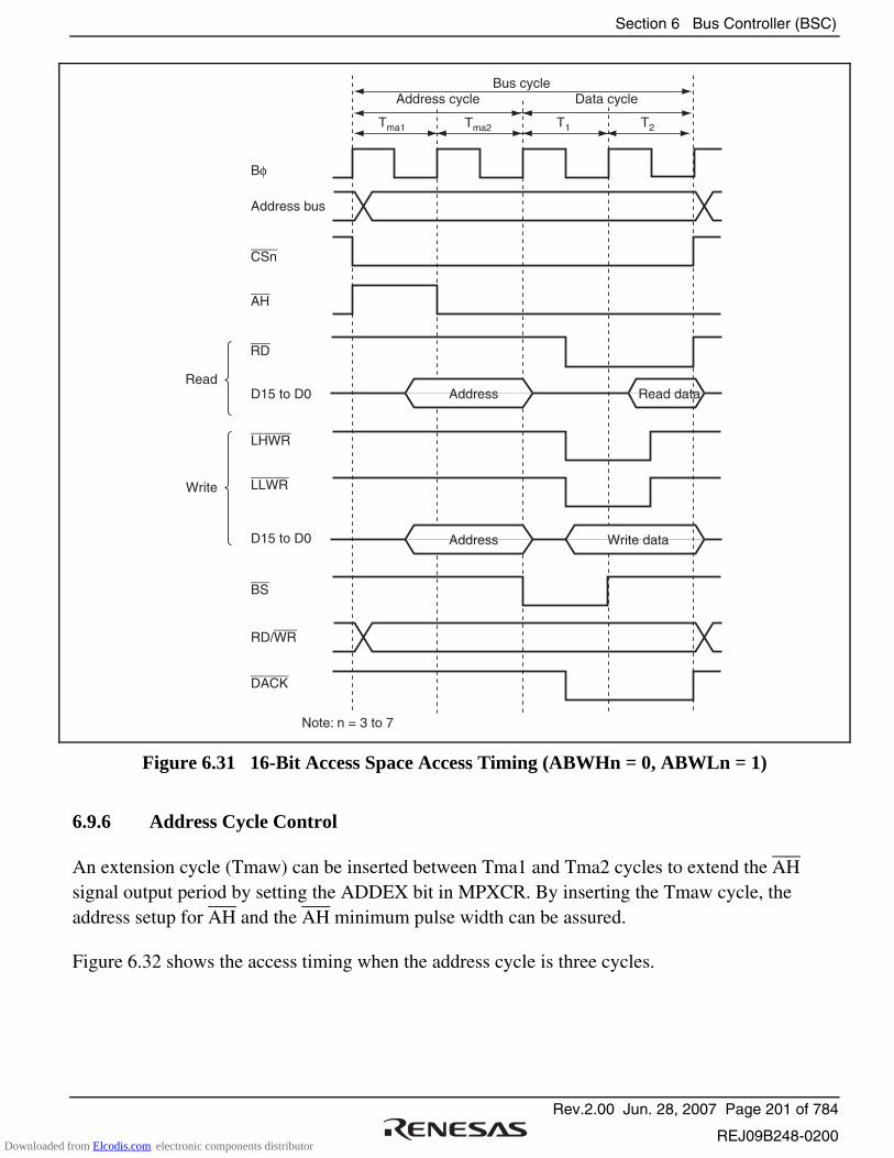
Section 6 Bus Controller (BSC)
Rev.2.00 Jun. 28, 2007 Page 201 of 784
REJ09B248-0200
RD
Tma1 Tma2 T2T1
Bφ
Address bus
D15 to D0
D15 to D0
Address cycleBus cycle
Data cycle
CSn
LHWR
LLWR
AH
DACK
BS
RD/WR
Note: n = 3 to 7
Address Read data
Address Write data
Read
Write
Figure 6.31 16-Bit Access Space Access Timing (ABWHn = 0, ABWLn = 1)
6.9.6 Address Cycle Control
An extension cycle (Tmaw) can be inserted between Tma1 and Tma2 cycles to extend the AH signal output period by setting the ADDEX bit in MPXCR. By inserting the Tmaw cycle, the address setup for AH and the AH minimum pulse width can be assured.
Figure 6.32 shows the access timing when the address cycle is three cycles.
Downloaded from Elcodis.com electronic components distributor

Section 6 Bus Controller (BSC)
Rev.2.00 Jun. 28, 2007 Page 202 of 784
REJ09B248-0200
Tma1 Tmaw Tma2 T2T1
Bφ
Address bus
D15 to D0
D15 to D0
Address cycle Data cycle
CSn
LHWR
LLWR
AH
RD
DACK
BS
RD/WR
Note: n = 3 to 7
Address Read data
Address Write data
Read
Write
Figure 6.32 Access Timing of 3 Address Cycles (ADDEX = 1)
6.9.7 Wait Control
In the data cycle of the address/data multiplexed I/O interface, program wait insertion and pin wait insertion by the WAIT pin are enabled in the same way as in the basic bus interface. For details, see section 6.6.4, Wait Control.
Wait control settings do not affect the address cycles.
Downloaded from Elcodis.com electronic components distributor
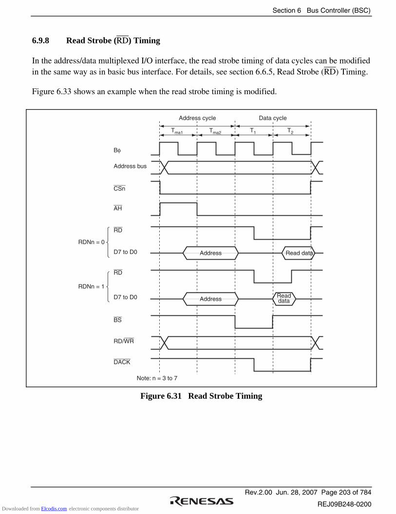
Section 6 Bus Controller (BSC)
Rev.2.00 Jun. 28, 2007 Page 203 of 784
REJ09B248-0200
6.9.8 Read Strobe (RD) Timing
In the address/data multiplexed I/O interface, the read strobe timing of data cycles can be modified in the same way as in basic bus interface. For details, see section 6.6.5, Read Strobe (RD) Timing.
Figure 6.33 shows an example when the read strobe timing is modified.
Tma1 Tma2 T2T1
Bφ
Address bus
D7 to D0
D7 to D0
Address cycle Data cycle
CSn
RD
AH
RD
DACK
BS
RD/WR
Note: n = 3 to 7
Address Read data
Address Readdata
RDNn = 0
RDNn = 1
Figure 6.31 Read Strobe Timing
Downloaded from Elcodis.com electronic components distributor
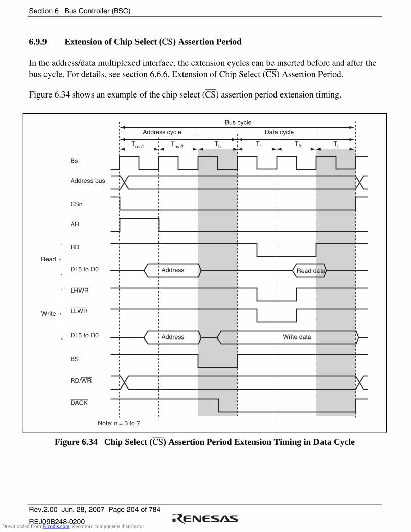
Section 6 Bus Controller (BSC)
Rev.2.00 Jun. 28, 2007 Page 204 of 784
REJ09B248-0200
6.9.9 Extension of Chip Select (CS) Assertion Period
In the address/data multiplexed interface, the extension cycles can be inserted before and after the bus cycle. For details, see section 6.6.6, Extension of Chip Select (CS) Assertion Period.
Figure 6.34 shows an example of the chip select (CS) assertion period extension timing.
Tma1 Tma2 T2 TtT1Th
Bφ
Address bus
D15 to D0
D15 to D0
Address cycle
Bus cycle
Data cycle
CSn
LHWR
LLWR
AH
RD
DACK
BS
RD/WR
Note: n = 3 to 7
Address Read data
Address Write data
Read
Write
Figure 6.34 Chip Select (CS) Assertion Period Extension Timing in Data Cycle
Downloaded from Elcodis.com electronic components distributor
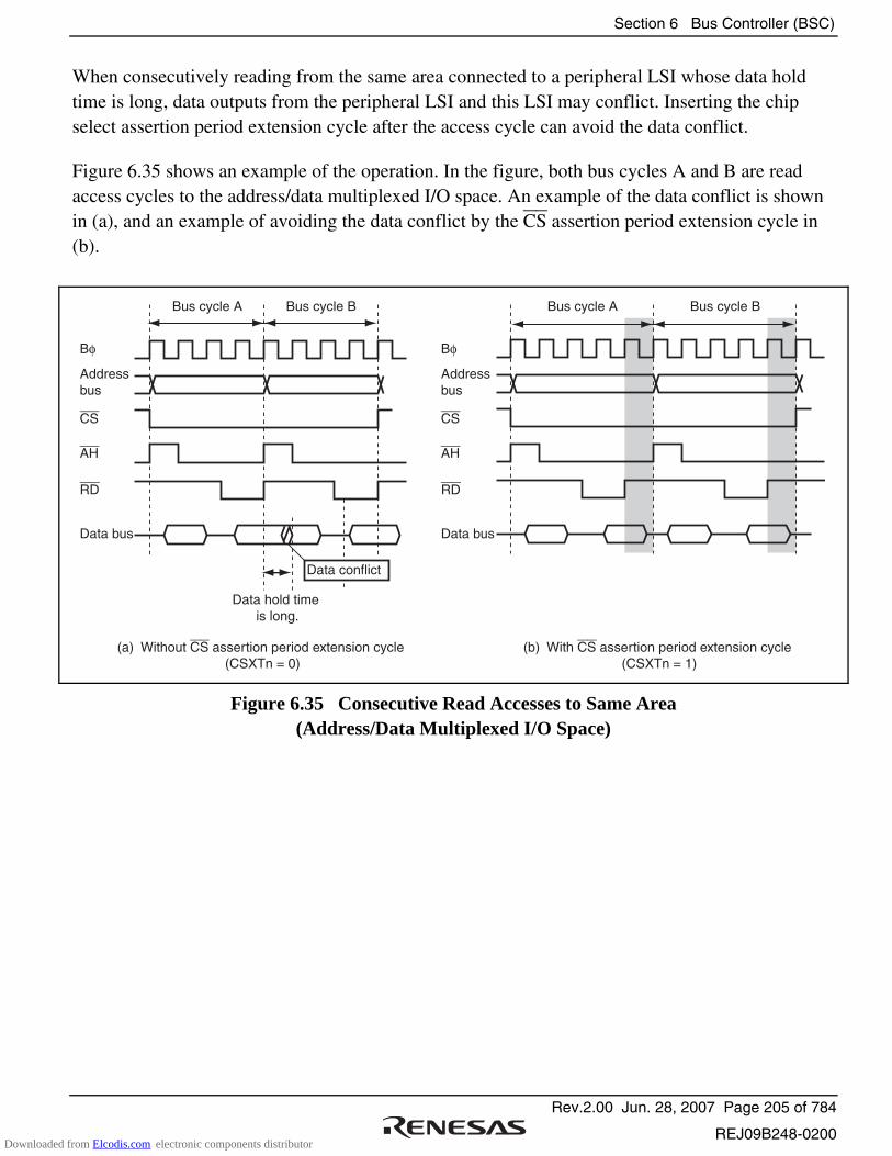
Section 6 Bus Controller (BSC)
Rev.2.00 Jun. 28, 2007 Page 205 of 784
REJ09B248-0200
When consecutively reading from the same area connected to a peripheral LSI whose data hold time is long, data outputs from the peripheral LSI and this LSI may conflict. Inserting the chip select assertion period extension cycle after the access cycle can avoid the data conflict.
Figure 6.35 shows an example of the operation. In the figure, both bus cycles A and B are read access cycles to the address/data multiplexed I/O space. An example of the data conflict is shown in (a), and an example of avoiding the data conflict by the CS assertion period extension cycle in (b).
Bφ
Address bus
Data bus
Bus cycle A Bus cycle B
CS
AH
RD
Bφ
Address bus
Data bus
CS
AH
RD
(a) Without CS assertion period extension cycle (CSXTn = 0)
(b) With CS assertion period extension cycle (CSXTn = 1)
Data hold time is long.
Bus cycle A Bus cycle B
Data conflict
Figure 6.35 Consecutive Read Accesses to Same Area (Address/Data Multiplexed I/O Space)
Downloaded from Elcodis.com electronic components distributor

Section 6 Bus Controller (BSC)
Rev.2.00 Jun. 28, 2007 Page 206 of 784
REJ09B248-0200
6.9.10 DACK Signal Output Timing
For DMAC single address transfers, the DACK signal assert timing can be modified by using the DKC bit in BCR1.
Figure 6.36 shows the DACK signal output timing. Setting the DKC bit to 1 asserts the DACK signal a half cycle earlier.
Tma1 Tma2 T2T1
Bφ
DKC = 0
DKC = 1
Address bus
D7 to D0
D7 to D0
Address cycle Data cycle
CSn
RD
AH
RD
DACK
BS
RD/WR
Note: n = 3 to 7
Address Read data
RDNn = 0
RDNn = 1
Address Read data
Figure 6.36 DACK Signal Output Timing
Downloaded from Elcodis.com electronic components distributor
Section 6 Bus Controller (BSC)
Rev.2.00 Jun. 28, 2007 Page 207 of 784
REJ09B248-0200
6.10 Idle Cycle
In this LSI, idle cycles can be inserted between the consecutive external accesses. By inserting the idle cycle, data conflicts between ROM read cycle whose output floating time is long and an access cycle from/to high-speed memory or I/O interface can be prevented.
6.10.1 Operation
When this LSI consecutively accesses external address space, it can insert an idle cycle between bus cycles in the following four cases. These conditions are determined by the sequence of read and write and previously accessed area.
1. When read cycles of different areas in the external address space occur consecutively
2. When an external write cycle occurs immediately after an external read cycle
3. When an external read cycle occurs immediately after an external write cycle
4. When an external access occurs immediately after a DMAC single address transfer (write cycle)
Up to four idle cycles can be inserted under the conditions shown above. The number of idle cycles to be inserted should be specified to prevent data conflicts between the output data from a previously accessed device and data from a subsequently accessed device.
Under conditions 1 and 2, which are the conditions to insert idle cycles after read, the number of idle cycles can be selected from setting A specified by the bits IDLCA1 and IDLCA0 in IDLCR or setting B specified by the bits IDLCB1 and IDLCB0 in IDLCR: Setting A can be selected from one to four cycles, and setting B can be selected from one or two to four cycles. Setting A or B can be specified for each area by setting the bits IDLSEL7 to IDLSEL0 in IDLCR. Note that the bits IDLSEL7 to IDLSEL0 correspond to the previously accessed area of the consecutive accesses.
The number of idle cycles to be inserted under conditions 3 and 4, which is a condition to insert idle cycles after write, can be determined by setting A as described above.
After the reset release, IDLCR is initialized to four idle cycle insertion under all conditions 1 to 4 shown above.
Table 6.20 shows the correspondence between conditions 1 to 4 and number of idle cycles to be inserted for each area. Table 6.21 shows the correspondence between the number of idle cycles to be inserted specified by settings A and B, and number of cycles to be inserted.
Downloaded from Elcodis.com electronic components distributor
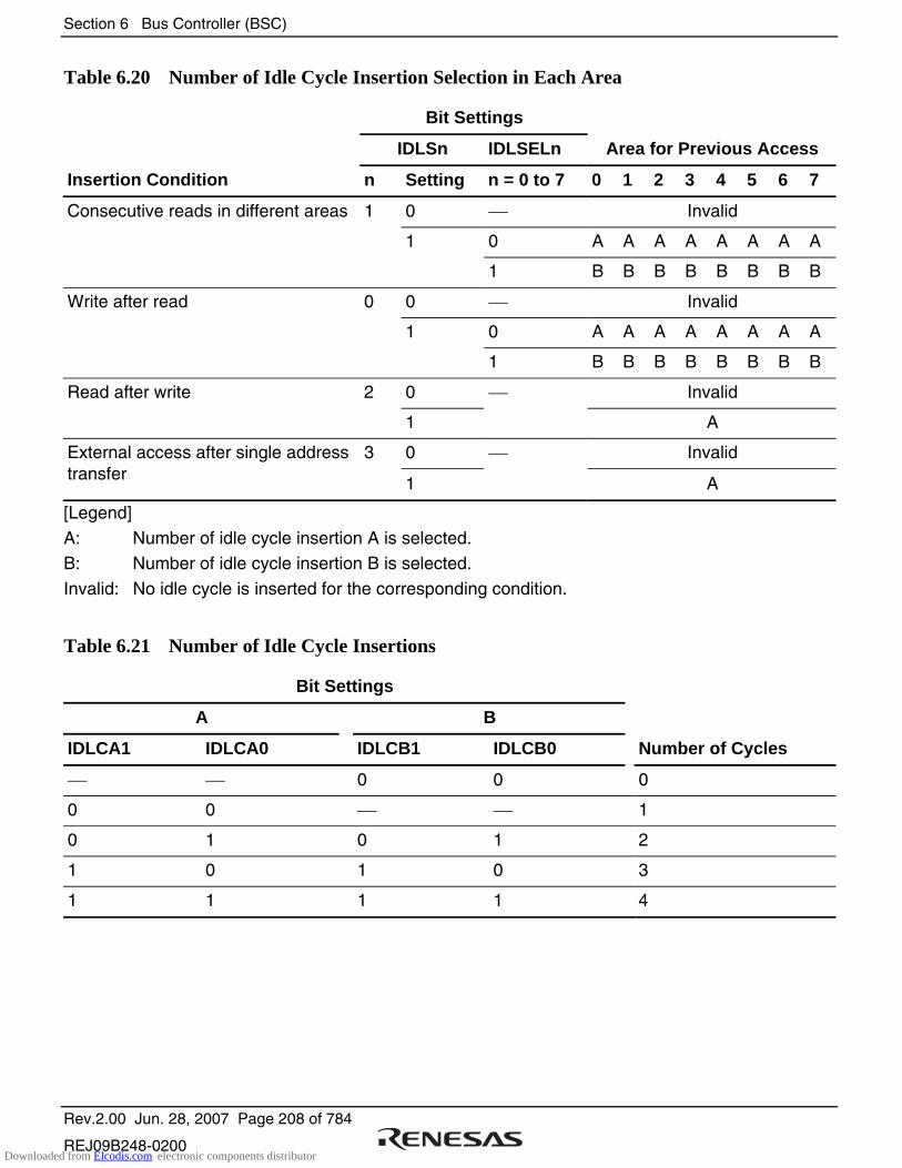
Section 6 Bus Controller (BSC)
Rev.2.00 Jun. 28, 2007 Page 208 of 784
REJ09B248-0200
Table 6.20 Number of Idle Cycle Insertion Selection in Each Area
Bit Settings
IDLSn IDLSELn Area for Previous Access
Insertion Condition n Setting n = 0 to 7 0 1 2 3 4 5 6 7
0 Invalid
0 A A A A A A A A
Consecutive reads in different areas 1
1
1 B B B B B B B B
0 Invalid
0 A A A A A A A A
Write after read 0
1
1 B B B B B B B B
0 Invalid Read after write 2
1
A
0 Invalid External access after single address transfer
3
1
A
[Legend]
A: Number of idle cycle insertion A is selected. B: Number of idle cycle insertion B is selected.
Invalid: No idle cycle is inserted for the corresponding condition.
Table 6.21 Number of Idle Cycle Insertions
Bit Settings
A B
IDLCA1 IDLCA0 IDLCB1 IDLCB0 Number of Cycles
0 0 0
0 0 1
0 1 0 1 2
1 0 1 0 3
1 1 1 1 4
Downloaded from Elcodis.com electronic components distributor
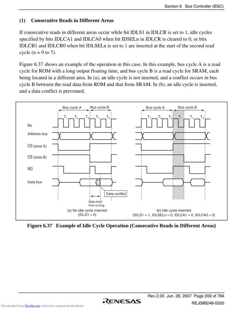
Section 6 Bus Controller (BSC)
Rev.2.00 Jun. 28, 2007 Page 209 of 784
REJ09B248-0200
(1) Consecutive Reads in Different Areas
If consecutive reads in different areas occur while bit IDLS1 in IDLCR is set to 1, idle cycles specified by bits IDLCA1 and IDLCA0 when bit IDSELn in IDLCR is cleared to 0, or bits IDLCB1 and IDLCB0 when bit IDLSELn is set to 1 are inserted at the start of the second read cycle (n = 0 to 7).
Figure 6.37 shows an example of the operation in this case. In this example, bus cycle A is a read cycle for ROM with a long output floating time, and bus cycle B is a read cycle for SRAM, each being located in a different area. In (a), an idle cycle is not inserted, and a conflict occurs in bus cycle B between the read data from ROM and that from SRAM. In (b), an idle cycle is inserted, and a data conflict is prevented.
Data hold time is long.
Data conflict
Bus cycle A Bus cycle B
(a) No idle cycle inserted(IDLS1 = 0)
(b) Idle cycle inserted
Bφ
Address bus
CS (area A)
CS (area B)
RD
Data bus
T1 T2 T3 T1 T2
Bus cycle A Bus cycle B
T1 T2 T3 T1Ti T2
(IDLS1 = 1, IDLSELn = 0, IDLCA1 = 0, IDLCA0 = 0)
Figure 6.37 Example of Idle Cycle Operation (Consecutive Reads in Different Areas)
Downloaded from Elcodis.com electronic components distributor

Section 6 Bus Controller (BSC)
Rev.2.00 Jun. 28, 2007 Page 210 of 784
REJ09B248-0200
(2) Write after Read
If an external write occurs after an external read while bit IDLS0 in IDLCR is set to 1, idle cycles specified by bits IDLCA1 and IDLCA0 when bit IDSELn in IDLCR is cleared to 0 when IDLSELn = 0,or bits IDLCB1 and IDLCB0 when IDLSELn is set to 1 are inserted at the start of the write cycle (n = 0 to 7).
Figure 6.38 shows an example of the operation in this case. In this example, bus cycle A is a read cycle for ROM with a long output floating time, and bus cycle B is a CPU write cycle. In (a), an idle cycle is not inserted, and a conflict occurs in bus cycle B between the read data from ROM and the CPU write data. In (b), an idle cycle is inserted, and a data conflict is prevented.
Data hold time is long.
Data conflict
Bus cycle A Bus cycle B
Bφ
Address bus
CS (area A)
CS (area B)
RD
LLWR
Data bus
T1 T2 T3 T1 T2
(b) Idle cycle inserted
Bus cycle A Bus cycle B
T1 T2 T3 T1Ti T2
(a) No idle cycle inserted(IDLS0 = 0) (IDLS0 = 1, IDLSELn = 0, IDLCA1 = 0, IDLCA0 = 0)
Figure 6.38 Example of Idle Cycle Operation (Write after Read)
Downloaded from Elcodis.com electronic components distributor
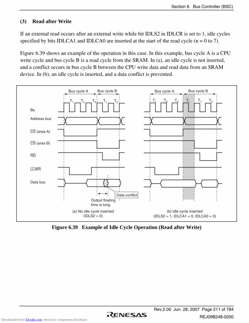
Section 6 Bus Controller (BSC)
Rev.2.00 Jun. 28, 2007 Page 211 of 784
REJ09B248-0200
(3) Read after Write
If an external read occurs after an external write while bit IDLS2 in IDLCR is set to 1, idle cycles specified by bits IDLCA1 and IDLCA0 are inserted at the start of the read cycle (n = 0 to 7).
Figure 6.39 shows an example of the operation in this case. In this example, bus cycle A is a CPU write cycle and bus cycle B is a read cycle from the SRAM. In (a), an idle cycle is not inserted, and a conflict occurs in bus cycle B between the CPU write data and read data from an SRAM device. In (b), an idle cycle is inserted, and a data conflict is prevented.
Output floating time is long.
Data conflict
Bus cycle A Bus cycle B
Bφ
Address bus
CS (area A)
CS (area B)
RD
LLWR
Data bus
T1 T2 T3 T1 T2
Bus cycle A Bus cycle B
T1 T2 T3 T1Ti T2
(a) No idle cycle inserted(IDLS2 = 0)
(b) Idle cycle inserted(IDLS2 = 1, IDLCA1 = 0, IDLCA0 = 0)
Figure 6.39 Example of Idle Cycle Operation (Read after Write)
Downloaded from Elcodis.com electronic components distributor

Section 6 Bus Controller (BSC)
Rev.2.00 Jun. 28, 2007 Page 212 of 784
REJ09B248-0200
(4) External Access after Single Address Transfer Write
If an external access occurs after a single address transfer write while bit IDLS3 in IDLCR is set to 1, idle cycles specified by bits IDLCA1 and IDLCA0 are inserted at the start of the external access.
Figure 6.40 shows an example of the operation in this case. In this example, bus cycle A is a single address transfer (write cycle) and bus cycle B is a CPU write cycle. In (a), an idle cycle is not inserted, and a conflict occurs in bus cycle B between the external device write data and this LSI write data. In (b), an idle cycle is inserted, and a data conflict is prevented.
Output floating time is long.
Data conflict
Bus cycle A Bus cycle B
(a) No idle cycle inserted(IDLS3 = 0)
Bφ
Address bus
CS (area A)
CS (area B)
LLWR
DACK
Data bus
T1 T2 T3 T1 T2
(b) Idle cycle inserted
Bus cycle A Bus cycle B
T1 T2 T3 T1Ti T2
(IDLS3 = 1, IDLCA1 = 0, IDLCA0 = 0)
Figure 6.40 Example of Idle Cycle Operation (Write after Single Address Transfer Write)
Downloaded from Elcodis.com electronic components distributor
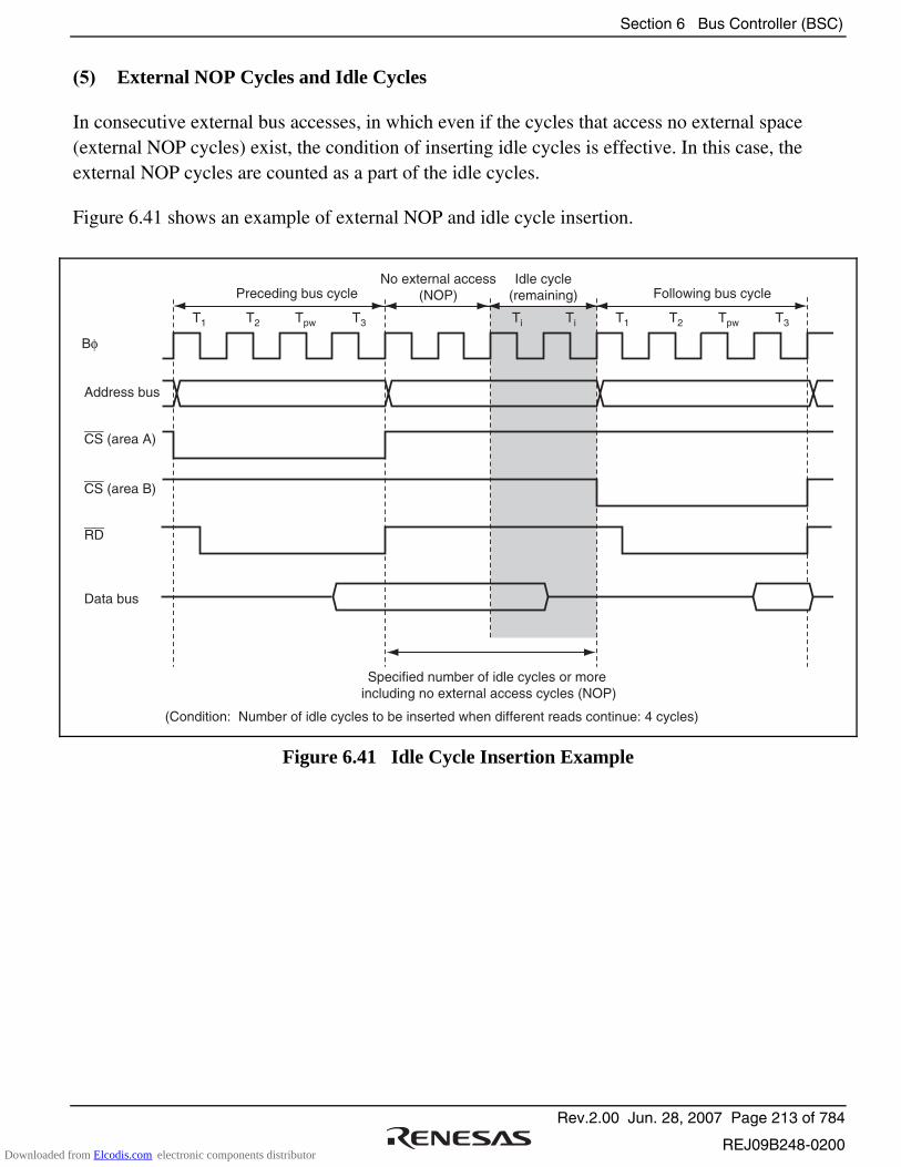
Section 6 Bus Controller (BSC)
Rev.2.00 Jun. 28, 2007 Page 213 of 784
REJ09B248-0200
(5) External NOP Cycles and Idle Cycles
In consecutive external bus accesses, in which even if the cycles that access no external space (external NOP cycles) exist, the condition of inserting idle cycles is effective. In this case, the external NOP cycles are counted as a part of the idle cycles.
Figure 6.41 shows an example of external NOP and idle cycle insertion.
T1 T2 T3Tpw T1 T2 T3TpwTi Ti
Address bus
No external access(NOP)
Specified number of idle cycles or more including no external access cycles (NOP)
Idle cycle(remaining) Following bus cyclePreceding bus cycle
(Condition: Number of idle cycles to be inserted when different reads continue: 4 cycles)
Data bus
Bφ
CS (area B)
CS (area A)
RD
Figure 6.41 Idle Cycle Insertion Example
Downloaded from Elcodis.com electronic components distributor

Section 6 Bus Controller (BSC)
Rev.2.00 Jun. 28, 2007 Page 214 of 784
REJ09B248-0200
(6) Relationship between Chip Select (CS) Signal and Read (RD) Signal
Depending on the system's load conditions, the RD signal may lag behind the CS signal. An example is shown in figure 6.42. In this case, with the setting for no idle cycle insertion (a), there may be a period of overlap between the RD signal in bus cycle A and the CS signal in bus cycle B. Setting idle cycle insertion, as in (b), however, will prevent any overlap between the RD and CS signals. In the initial state after reset release, idle cycle indicated in (b) is set.
Bus cycle A Bus cycle B
Bφ
Address bus
CS (area A)
CS (area B)
RD
T1 T2 T3 T1 T2
Bus cycle A Bus cycle B
T1 T2 T3 T1Ti T2
Overlap time may occur between the CS (area B) and RD
(a) No idle cycle inserted(IDLS1 = 0)
(b) Idle cycle inserted(IDLS1 = 1, IDLSELn = 0, IDLCA1 = 0, IDLCA0 = 0)
Figure 6.42 Relationship between Chip Select (CS) and Read (RD)
Downloaded from Elcodis.com electronic components distributor
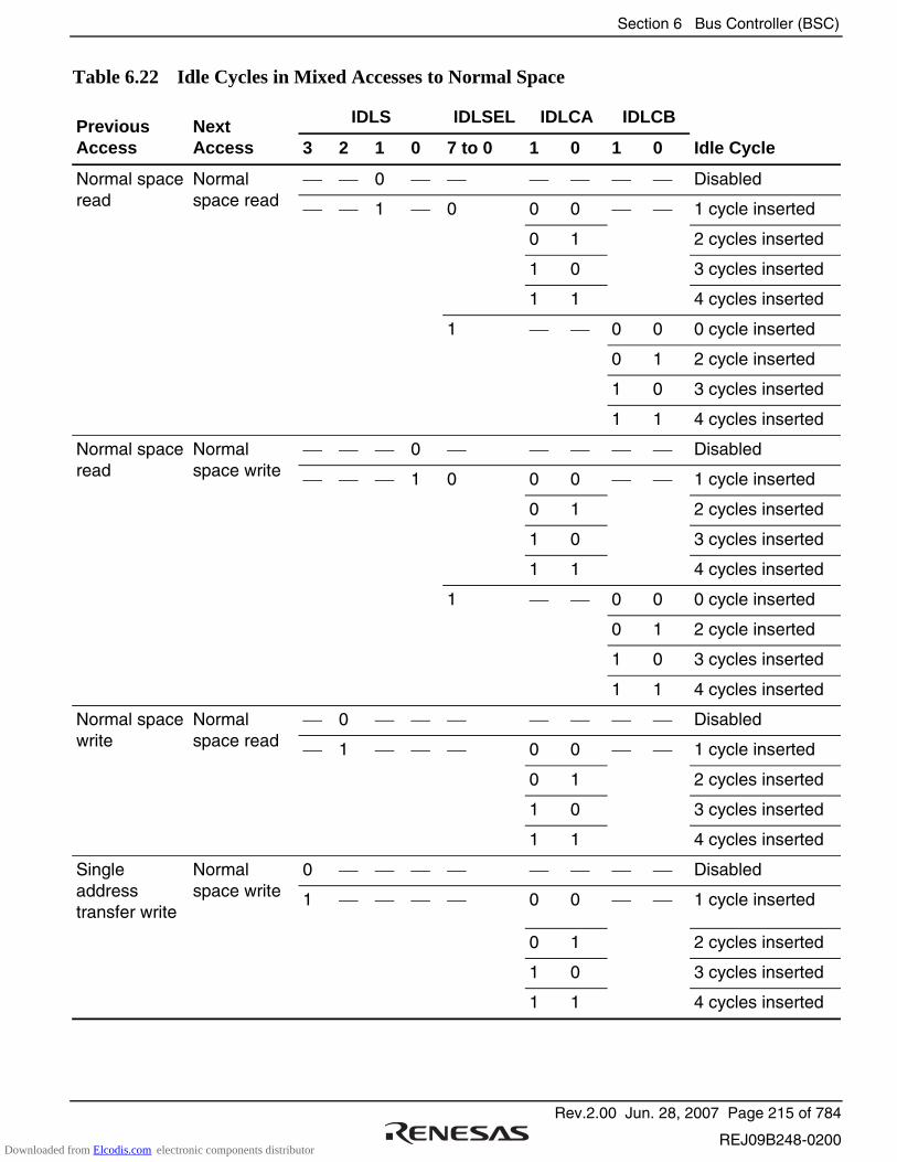
Section 6 Bus Controller (BSC)
Rev.2.00 Jun. 28, 2007 Page 215 of 784
REJ09B248-0200
Table 6.22 Idle Cycles in Mixed Accesses to Normal Space
IDLS IDLSEL IDLCA IDLCB Previous Access
Next Access 3 2 1 0 7 to 0 1 0 1 0 Idle Cycle
0 Disabled Normal space read
Normal space read 1 0 0 0 1 cycle inserted
0 1 2 cycles inserted
1 0 3 cycles inserted
1 1 4 cycles inserted
1 0 0 0 cycle inserted
0 1 2 cycle inserted
1 0 3 cycles inserted
1 1 4 cycles inserted
0 Disabled Normal space read
Normal space write 1 0 0 0 1 cycle inserted
0 1 2 cycles inserted
1 0 3 cycles inserted
1 1 4 cycles inserted
1 0 0 0 cycle inserted
0 1 2 cycle inserted
1 0 3 cycles inserted
1 1 4 cycles inserted
0 Disabled Normal space write
Normal space read 1 0 0 1 cycle inserted
0 1 2 cycles inserted
1 0 3 cycles inserted
1 1 4 cycles inserted
0 Disabled Single address transfer write
Normal space write 1 0 0 1 cycle inserted
0 1 2 cycles inserted
1 0 3 cycles inserted
1 1 4 cycles inserted
Downloaded from Elcodis.com electronic components distributor
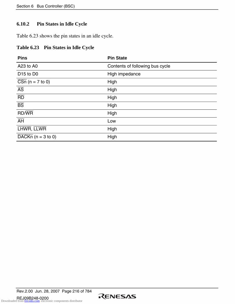
Section 6 Bus Controller (BSC)
Rev.2.00 Jun. 28, 2007 Page 216 of 784
REJ09B248-0200
6.10.2 Pin States in Idle Cycle
Table 6.23 shows the pin states in an idle cycle.
Table 6.23 Pin States in Idle Cycle
Pins Pin State
A23 to A0 Contents of following bus cycle
D15 to D0 High impedance
CSn (n = 7 to 0) High
AS High
RD High
BS High
RD/WR High
AH Low
LHWR, LLWR High
DACKn (n = 3 to 0) High
Downloaded from Elcodis.com electronic components distributor
Section 6 Bus Controller (BSC)
Rev.2.00 Jun. 28, 2007 Page 217 of 784
REJ09B248-0200
6.11 Bus Release
This LSI can release the external bus in response to a bus request from an external device. In the external bus released state, internal bus masters continue to operate as long as there is no external access.
In addition, in the external bus released state, the BREQO signal can be driven low to output a bus request externally.
6.11.1 Operation
In external extended mode, when the BRLE bit in BCR1 is set to 1, and the ICR bit for the corresponding pin is set to 1, the bus can be released to the external. Driving the BREQ pin low issues an external bus request to this LSI. When the BREQ pin is sampled, at the prescribed timing, the BACK pin is driven low, and the address bus, data bus, and bus control signals are placed in the high-impedance state, establishing the external bus released state. For details on DDR and ICR, see section 9, I/O Ports.
In the external bus released state, the CPU, DTC, and DMAC can access the internal space using the internal bus. When the CPU, DTC, or DMAC attempts to access the external address space, it temporarily defers initiation of the bus cycle, and waits for the bus request from the external bus master to be canceled.
In the external bus released state, when write access to SCKCR is granted to set the clock frequency, the current setting for the clock frequency is deferred until the bus request of the external bus master is canceled. For details of the SCKCR, see section 18, Clock Pulse Generator.
If the BREQOE bit in BCR1is set to 1, the BREQO pin can be driven low when any of the following requests are issued, to request cancellation of the bus request externally.
• When the CPU, DTC, or DMAC attempts to access the external address space
• When a SLEEP instruction is executed to place the chip in software standby mode or all-module-clock-stop mode
• When write access to SCKCR is granted to set the clock frequency If an external bus release request and external access occur simultaneously, the priority is as follows:
(High) External bus release > External access by CPU, DTC, or DMAC (Low)
Downloaded from Elcodis.com electronic components distributor
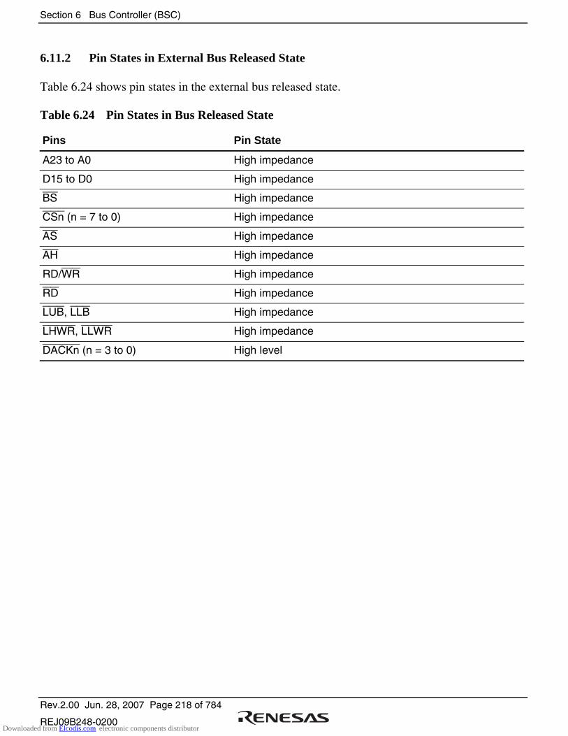
Section 6 Bus Controller (BSC)
Rev.2.00 Jun. 28, 2007 Page 218 of 784
REJ09B248-0200
6.11.2 Pin States in External Bus Released State
Table 6.24 shows pin states in the external bus released state.
Table 6.24 Pin States in Bus Released State
Pins Pin State
A23 to A0 High impedance
D15 to D0 High impedance
BS High impedance
CSn (n = 7 to 0) High impedance
AS High impedance
AH High impedance
RD/WR High impedance
RD High impedance
LUB, LLB High impedance
LHWR, LLWR High impedance
DACKn (n = 3 to 0) High level
Downloaded from Elcodis.com electronic components distributor

Section 6 Bus Controller (BSC)
Rev.2.00 Jun. 28, 2007 Page 219 of 784
REJ09B248-0200
6.11.3 Transition Timing
Figure 6.43 shows the timing for transition to the bus released state.
Bφ
Address bus
CSn
LHWR, LLWR
AS
Hi-Z
Hi-Z
[1] [2] [3] [4] [7] [5] [6][8]
Hi-Z
Hi-Z
Hi-Z
Hi-Z
RD
BREQ
BACK
BREQO
External spaceaccess cycle CPU cycleExternal bus released state
Data bus
T1 T2
[1] A low level of the BREQ signal is sampled at the rising edge of the Bφ signal.[2] The bus control signals are driven high at the end of the external space access cycle. It takes two cycles or more after the low level of the BREQ signal is sampled.[3] The BACK signal is driven low, releasing bus to the external bus master.[4] The BREQ signal state sampling is continued in the external bus released state.[5] A high level of the BREQ signal is sampled.[6] The external bus released cycles are ended one cycle after the BREQ signal is driven high.[7] When the external space is accessed by an internal bus master during external bus released while the BREQOE bit is set to 1, the BREQO signal goes low.[8] Normally the BREQO signal goes high at the rising edge of the BACK signal.
Figure 6.43 Bus Released State Transition Timing
Downloaded from Elcodis.com electronic components distributor

Section 6 Bus Controller (BSC)
Rev.2.00 Jun. 28, 2007 Page 220 of 784
REJ09B248-0200
6.12 Internal Bus
6.12.1 Access to Internal Address Space
The internal address spaces of this LSI are the on-chip RAM space and register space for the on-chip peripheral modules. The number of cycles necessary for access differs according the space.
Table 6.25 shows the number of access cycles for each on-chip memory space.
Table 6.25 Number of Access Cycles for On-Chip Memory Spaces
Access Space Access Number of Access Cycles
Read One Iφ cycle On-chip RAM space
Write One Iφ cycle
In access to the registers for on-chip peripheral modules, the number of access cycles differs according to the register to be accessed. When the dividing ratio of the operating clock of a bus master and that of a peripheral module is 1 : n, synchronization cycles using a clock divided by 0 to n-1 are inserted for register access in the same way as for external bus clock division.
The number of access cycles to the registers for on-chip peripheral modules is shown in table 6.26.
Table 6.26 Number of Access Cycles for Registers of On-Chip Peripheral Modules
Number of Cycles
Module to be Accessed Read Write Write Data Buffer Function
DMAC registers 2Iφ Disabled
MCU operating mode, clock pulse generator, power-down control registers, interrupt controller, bus controller, and DTC registers
2Iφ 3Iφ Disabled
I/O port PFCR registers and WDT registers 2Pφ 3Pφ Disabled
I/O port registers other than PFCR, TPU, PPG, TMR, SCI, A/D, and D/A registers
2Pφ Enabled
Downloaded from Elcodis.com electronic components distributor
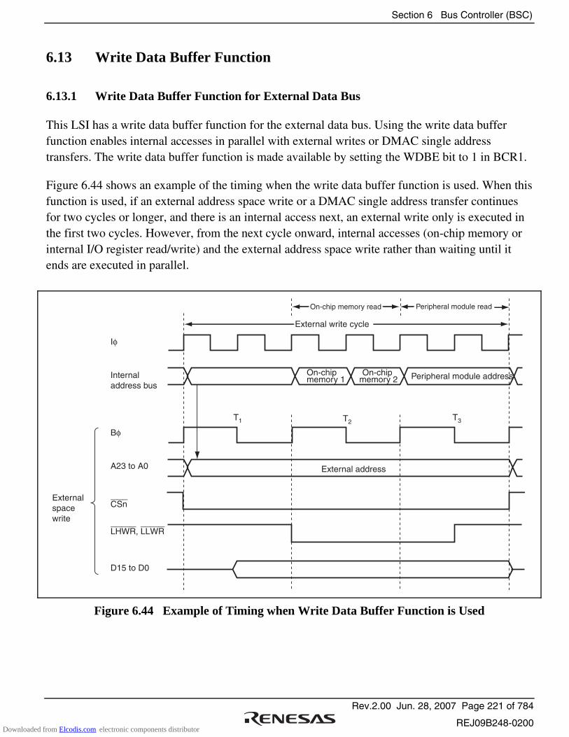
Section 6 Bus Controller (BSC)
Rev.2.00 Jun. 28, 2007 Page 221 of 784
REJ09B248-0200
6.13 Write Data Buffer Function
6.13.1 Write Data Buffer Function for External Data Bus
This LSI has a write data buffer function for the external data bus. Using the write data buffer function enables internal accesses in parallel with external writes or DMAC single address transfers. The write data buffer function is made available by setting the WDBE bit to 1 in BCR1.
Figure 6.44 shows an example of the timing when the write data buffer function is used. When this function is used, if an external address space write or a DMAC single address transfer continues for two cycles or longer, and there is an internal access next, an external write only is executed in the first two cycles. However, from the next cycle onward, internal accesses (on-chip memory or internal I/O register read/write) and the external address space write rather than waiting until it ends are executed in parallel.
On-chip memory read Peripheral module read
Peripheral module address
External write cycle
On-chip memory 2
On-chip memory 1
External address
Internal address bus
Bφ
A23 to A0
CSn
LHWR, LLWR
D15 to D0
External spacewrite
T1 T2T3
Iφ
Figure 6.44 Example of Timing when Write Data Buffer Function is Used
Downloaded from Elcodis.com electronic components distributor

Section 6 Bus Controller (BSC)
Rev.2.00 Jun. 28, 2007 Page 222 of 784
REJ09B248-0200
6.13.2 Write Data Buffer Function for Peripheral Modules
This LSI has a write data buffer function for the peripheral module access. Using the write data buffer function enables peripheral module writes and on-chip memory or external access to be executed in parallel. The write data buffer function is made available by setting the PWDBE bit in BCR2 to 1. As for the peripheral module register space in which the write data buffer function is effective, see table 6.26 in section 6.12.
Figure 6.45 shows an example of the timing when the write data buffer function is used. When this function is used, if an internal I/O register write continues for two cycles or longer and then there is an on-chip RAM, or an external access, internal I/O register write only is performed in the first two cycles. However, from the next cycle onward an internal memory or an external access and internal I/O register write are executed in parallel rather than waiting until it ends.
On-chipmemoryread
Peripheral module write
Peripheral module address
Internal address bus
Pφ
Iφ
Internal I/O address bus
Internal I/O data bus
Figure 6.45 Example of Timing when Peripheral Module Write Data Buffer Function is Used
Downloaded from Elcodis.com electronic components distributor

Section 6 Bus Controller (BSC)
Rev.2.00 Jun. 28, 2007 Page 223 of 784
REJ09B248-0200
6.14 Bus Arbitration
This LSI has bus arbiters that arbitrate bus mastership operations (bus arbitration). This LSI incorporates internal access and external access bus arbiters that can be used and controlled independently. The internal bus arbiter handles the CPU, DTC, and DMAC accesses. The external bus arbiter handles the external access by the CPU, DTC, and DMAC and external bus release request (external bus master).
The bus arbiters determine priorities at the prescribed timing, and permit use of the bus by means of the bus request acknowledge signal.
6.14.1 Operation
The bus arbiter detects the bus masters' bus request signals, and if the bus is requested, sends a bus request acknowledge signal to the bus master. If there are bus requests from more than one bus master, the bus request acknowledge signal is sent to the one with the highest priority. When a bus master receives the bus request acknowledge signal, it takes possession of the bus until that signal is canceled.
The priority of the internal bus arbitration:
(High) DMAC > DTC > CPU (Low)
The priority of the external bus arbitration:
(High) External bus release request > External access by the CPU, DTC, and DMAC (Low)
If the DMAC or DTC accesses continue, the CPU can be given priority over the DMAC or DTC to execute the bus cycles alternatively between them by setting the IBCCS bit in BCR2. In this case, the priority between the DMAC and DTC does not change.
An internal bus access by the CPU, DTC, or DMAC and an external bus access by an external bus release request can be executed in parallel.
Downloaded from Elcodis.com electronic components distributor
Section 6 Bus Controller (BSC)
Rev.2.00 Jun. 28, 2007 Page 224 of 784
REJ09B248-0200
6.14.2 Bus Transfer Timing
Even if a bus request is received from a bus master with a higher priority over that of the bus master that has taken control of the bus and is currently operating, the bus is not necessarily transferred immediately. There are specific timings at which each bus master can release the bus.
(1) CPU
The CPU is the lowest-priority bus master, and if a bus request is received from the DTC or DMAC, the bus arbiter transfers the bus to the bus master that issued the request.
The timing for transfer of the bus is at the end of the bus cycle. In sleep mode, the bus is transferred synchronously with the clock.
Note, however, that the bus cannot be transferred in the following cases.
• The word or longword access is performed in some divisions.
• Stack handling is performed in multiple bus cycles.
• Transfer data read or write by memory transfer instructions, block transfer instructions, or TAS instruction.
(In the block transfer instructions, the bus can be transferred in the write cycle and the following transfer data read cycle.)
• From the target read to write in the bit manipulation instructions or memory operation instructions.
(In an instruction that performs no write operation according to the instruction condition, up to a cycle corresponding the write cycle)
(2) DTC
The DTC sends the internal bus arbiter a request for the bus when an activation request is generated. When the DTC accesses an external bus space, the DTC first takes control of the bus from the internal bus arbiter and then requests a bus to the external bus arbiter.
Once the DTC takes control of the bus, the DTC continues the transfer processing cycles. If a bus master whose priority is higher than the DTC requests the bus, the DTC transfers the bus to the higher priority bus master. If the IBCCS bit in BCR2 is set to 1, the DTC transfers the bus to the CPU.
Downloaded from Elcodis.com electronic components distributor

Section 6 Bus Controller (BSC)
Rev.2.00 Jun. 28, 2007 Page 225 of 784
REJ09B248-0200
Note, however, that the bus cannot be transferred in the following cases.
• During transfer information read
• During the first data transfer
• During transfer information write back The DTC releases the bus when the consecutive transfer cycles completed.
(3) DMAC
The DMAC sends the internal bus arbiter a request for the bus when an activation request is generated. When the DMAC accesses an external bus space, the DMAC first takes control of the bus from the internal bus arbiter and then requests a bus to the external bus arbiter.
After the DMAC takes control of the bus, it may continue the transfer processing cycles or release the bus at the end of every bus cycle depending on the conditions.
The DMAC continues transfers without releasing the bus in the following case:
• Between the read cycle in the dual-address mode and the write cycle corresponding to the read cycle
If no bus master of a higher priority than the DMAC requests the bus and the IBCCS bit in BCR2 is cleared to 0, the DMAC continues transfers without releasing the bus in the following cases:
• During 1-block transfers in the block transfer mode
• During transfers in the burst mode In other cases, the DMAC transfers the bus at the end of the bus cycle.
(4) External Bus Release
When the BREQ pin goes low and an external bus release request is issued while the BRLE bit in BCR1 and the ICR bit of the corresponding pin are set to 1, a bus request is sent to the bus arbiter.
External bus release can be performed on completion of an external bus cycle.
Downloaded from Elcodis.com electronic components distributor
Section 6 Bus Controller (BSC)
Rev.2.00 Jun. 28, 2007 Page 226 of 784
REJ09B248-0200
6.15 Bus Controller Operation in Reset
In a reset, this LSI, including the bus controller, enters the reset state immediately, and any executing bus cycle is aborted.
6.16 Usage Notes
(1) Setting Registers
The BSC registers must be specified before accessing the external address space. When activating the external ROM, specify the registers before external accesses other than the instruction fetch from the external ROM are generated.
(2) External Bus Release Function and All-Module-Clock-Stop Mode
In this LSI, if the ACSE bit in MSTPCRA is set to 1, and then a SLEEP instruction is executed with the setting for all peripheral module clocks to be stopped (MSTPCRA, MSTPCRB = H'FFFFFFFF) or for operation of the 8-bit timer module alone (MSTPCRA, MSTPCRB = H'F[E to 0]FFFFFF), and a transition is made to the sleep state, the all-module-clock-stop mode is entered in which the clock is also stopped for the bus controller and I/O ports. For details, see section 19, Power-Down Modes.
In this state, the external bus release function is halted. To use the external bus release function in sleep mode, the ACSE bit in MSTPCRA must be cleared to 0. Conversely, if a SLEEP instruction to place the chip in all-module-clock-stop mode is executed in the external bus released state, the transition to all-module-clock-stop mode is deferred and performed until after the bus is recovered.
(3) External Bus Release Function and Software Standby
In this LSI, internal bus master operation does not stop even while the bus is released, as long as the program is running in on-chip RAM, etc., and no external access occurs. If a SLEEP instruction to place the chip in software standby mode is executed while the external bus is released, the transition to software standby mode is deferred and performed after the bus is recovered.
Also, since clock oscillation halts in software standby mode, if the BREQ signal goes low in this mode, indicating an external bus release request, the request cannot be answered until the chip has recovered from the software standby mode.
Downloaded from Elcodis.com electronic components distributor
Section 6 Bus Controller (BSC)
Rev.2.00 Jun. 28, 2007 Page 227 of 784
REJ09B248-0200
Note that the BACK and BREQO pins are both in the high-impedance state in software standby mode.
(4) BREQO Output Timing
When the BREQOE bit is set to 1 and the BREQO signal is output, both the BREQO and BACK signals may go low simultaneously.
This will occur if the next external access request occurs while internal bus arbitration is in progress after the chip samples a low level of the BREQ signal.
Downloaded from Elcodis.com electronic components distributor

Section 6 Bus Controller (BSC)
Rev.2.00 Jun. 28, 2007 Page 228 of 784
REJ09B248-0200
Downloaded from Elcodis.com electronic components distributor
Section 7 DMA Controller (DMAC)
Rev.2.00 Jun. 28, 2007 Page 229 of 784
REJ09B248-0200
Section 7 DMA Controller (DMAC)
This LSI includes a 4-channel DMA controller (DMAC).
7.1 Features
• Maximum of 4-G byte address space can be accessed
• Byte, word, or longword can be set as data transfer unit
• Maximum of 4-G bytes (4,294,967,295 bytes) can be set as total transfer size
Supports free-running mode in which total transfer size setting is not needed
• DMAC activation methods are auto-request, on-chip module interrupt, and external request.
Auto request: Activated by the CPU (cycle stealing or burst access can be selected)
On-chip module interrupt: Interrupt requests from on-chip peripheral modules can be selected as an activation source
External request: Low level or falling edge detection of the DREQ signal can be selected. External request is available for all four channels.
In block transfer mode, low level detection is only available.
• Dual or single address mode can be selected as address mode
Dual address mode: Both source and destination are specified by addresses
Single address mode: Either source or destination is specified by the DREQ signal and the other is specified by address
• Normal, repeat, or block transfer can be selected as transfer mode
Normal transfer mode: One byte, one word, or one longword data is transferred at a single transfer request
Repeat transfer mode: One byte, one word, or one longword data is transferred at a single transfer request
Repeat size of data is transferred and then a transfer address returns to the transfer start address
Up to 65536 transfers (65,536 bytes/words/longwords) can be set as repeat size
Block transfer mode: One block data is transferred at a single transfer request
Up to 65,536 bytes/words/longwords can be set as block size
Downloaded from Elcodis.com electronic components distributor
Section 7 DMA Controller (DMAC)
Rev.2.00 Jun. 28, 2007 Page 230 of 784
REJ09B248-0200
• Extended repeat area function which repeats the addresses within a specified area using the transfer address with the fixed upper bits (ring buffer transfer can be performed, as an example) is available
One bit (two bytes) to 27 bits (128 Mbytes) for transfer source and destination can be set as extended repeat areas
• Address update can be selected from fixed address, offset addition, and increment or decrement by 1, 2, or 4
Address update by offset addition enables to transfer data at addresses which are not placed continuously
• Word or longword data can be transferred to an address which is not aligned with the respective boundary
Data is divided according to its address (byte or word) when it is transferred
• Two types of interrupts can be requested to the CPU
A transfer end interrupt is generated after the number of data specified by the transfer counter is transferred. A transfer escape end interrupt is generated when the remaining total transfer size is less than the transfer data size at a single transfer request, when the repeat size of data transfer is completed, or when the extended repeat area overflows.
Downloaded from Elcodis.com electronic components distributor
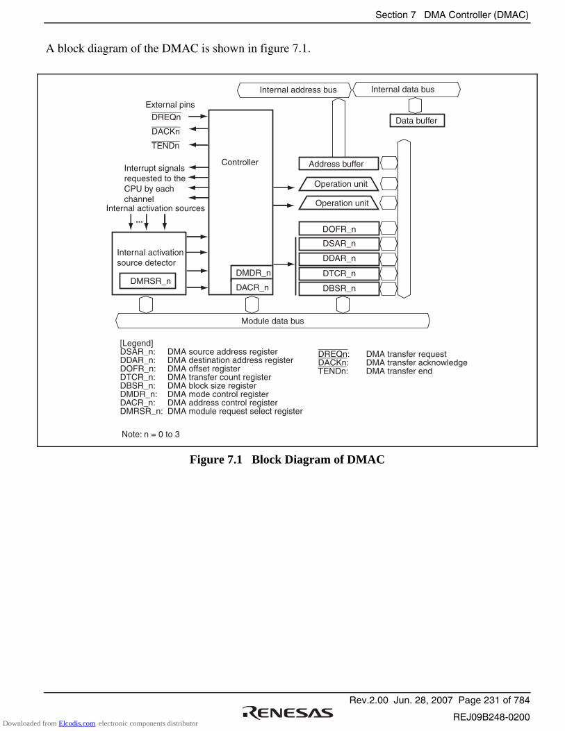
Section 7 DMA Controller (DMAC)
Rev.2.00 Jun. 28, 2007 Page 231 of 784
REJ09B248-0200
A block diagram of the DMAC is shown in figure 7.1.
External pins
DREQn
DACKn
TENDn
Interrupt signalsrequested to theCPU by eachchannel
Internal activation sources
Internal activationsource detector
Controller
DMDR_nDMRSR_n
DACR_n
DOFR_n
Internal address bus Internal data bus
DSAR_n
DDAR_n
DTCR_n
DBSR_n
Module data bus
Address buffer
Data buffer
Operation unit
Operation unit
...
DREQn: DMA transfer requestDACKn: DMA transfer acknowledgeTENDn: DMA transfer end
Note: n = 0 to 3
[Legend]DSAR_n: DMA source address registerDDAR_n: DMA destination address registerDOFR_n: DMA offset registerDTCR_n: DMA transfer count registerDBSR_n: DMA block size registerDMDR_n: DMA mode control registerDACR_n: DMA address control registerDMRSR_n: DMA module request select register
Figure 7.1 Block Diagram of DMAC
Downloaded from Elcodis.com electronic components distributor
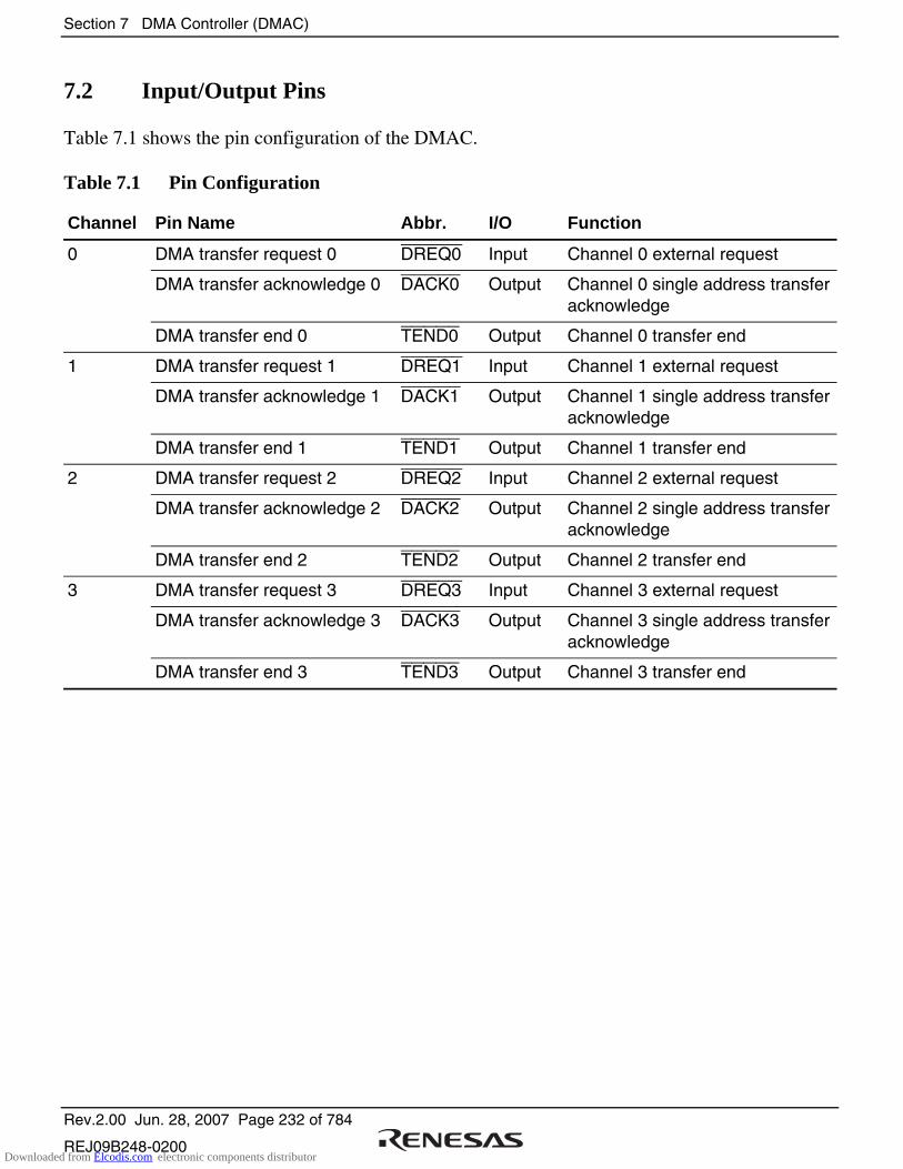
Section 7 DMA Controller (DMAC)
Rev.2.00 Jun. 28, 2007 Page 232 of 784
REJ09B248-0200
7.2 Input/Output Pins
Table 7.1 shows the pin configuration of the DMAC.
Table 7.1 Pin Configuration
Channel Pin Name Abbr. I/O Function
0 DMA transfer request 0 DREQ0 Input Channel 0 external request
DMA transfer acknowledge 0 DACK0 Output Channel 0 single address transfer acknowledge
DMA transfer end 0 TEND0 Output Channel 0 transfer end
1 DMA transfer request 1 DREQ1 Input Channel 1 external request
DMA transfer acknowledge 1 DACK1 Output Channel 1 single address transfer acknowledge
DMA transfer end 1 TEND1 Output Channel 1 transfer end
2 DMA transfer request 2 DREQ2 Input Channel 2 external request
DMA transfer acknowledge 2 DACK2 Output Channel 2 single address transfer acknowledge
DMA transfer end 2 TEND2 Output Channel 2 transfer end
3 DMA transfer request 3 DREQ3 Input Channel 3 external request
DMA transfer acknowledge 3 DACK3 Output Channel 3 single address transfer acknowledge
DMA transfer end 3 TEND3 Output Channel 3 transfer end
Downloaded from Elcodis.com electronic components distributor
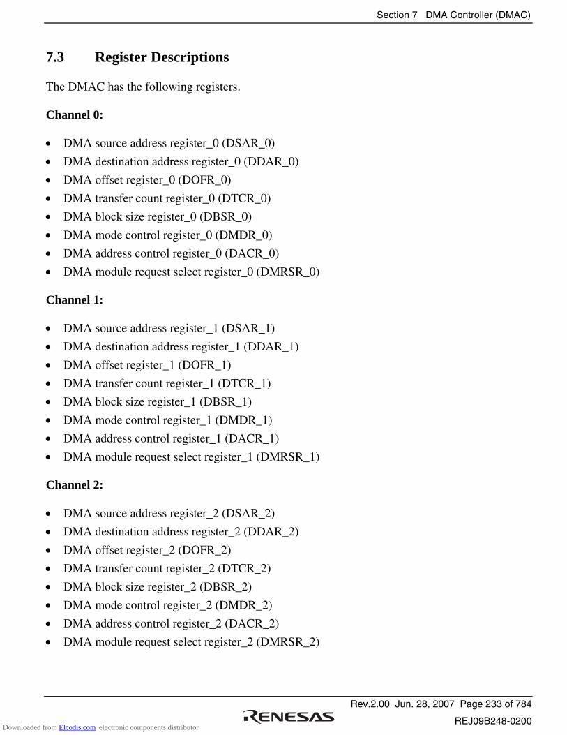
Section 7 DMA Controller (DMAC)
Rev.2.00 Jun. 28, 2007 Page 233 of 784
REJ09B248-0200
7.3 Register Descriptions
The DMAC has the following registers.
Channel 0:
• DMA source address register_0 (DSAR_0)
• DMA destination address register_0 (DDAR_0)
• DMA offset register_0 (DOFR_0)
• DMA transfer count register_0 (DTCR_0)
• DMA block size register_0 (DBSR_0)
• DMA mode control register_0 (DMDR_0)
• DMA address control register_0 (DACR_0)
• DMA module request select register_0 (DMRSR_0) Channel 1:
• DMA source address register_1 (DSAR_1)
• DMA destination address register_1 (DDAR_1)
• DMA offset register_1 (DOFR_1)
• DMA transfer count register_1 (DTCR_1)
• DMA block size register_1 (DBSR_1)
• DMA mode control register_1 (DMDR_1)
• DMA address control register_1 (DACR_1)
• DMA module request select register_1 (DMRSR_1) Channel 2:
• DMA source address register_2 (DSAR_2)
• DMA destination address register_2 (DDAR_2)
• DMA offset register_2 (DOFR_2)
• DMA transfer count register_2 (DTCR_2)
• DMA block size register_2 (DBSR_2)
• DMA mode control register_2 (DMDR_2)
• DMA address control register_2 (DACR_2)
• DMA module request select register_2 (DMRSR_2)
Downloaded from Elcodis.com electronic components distributor
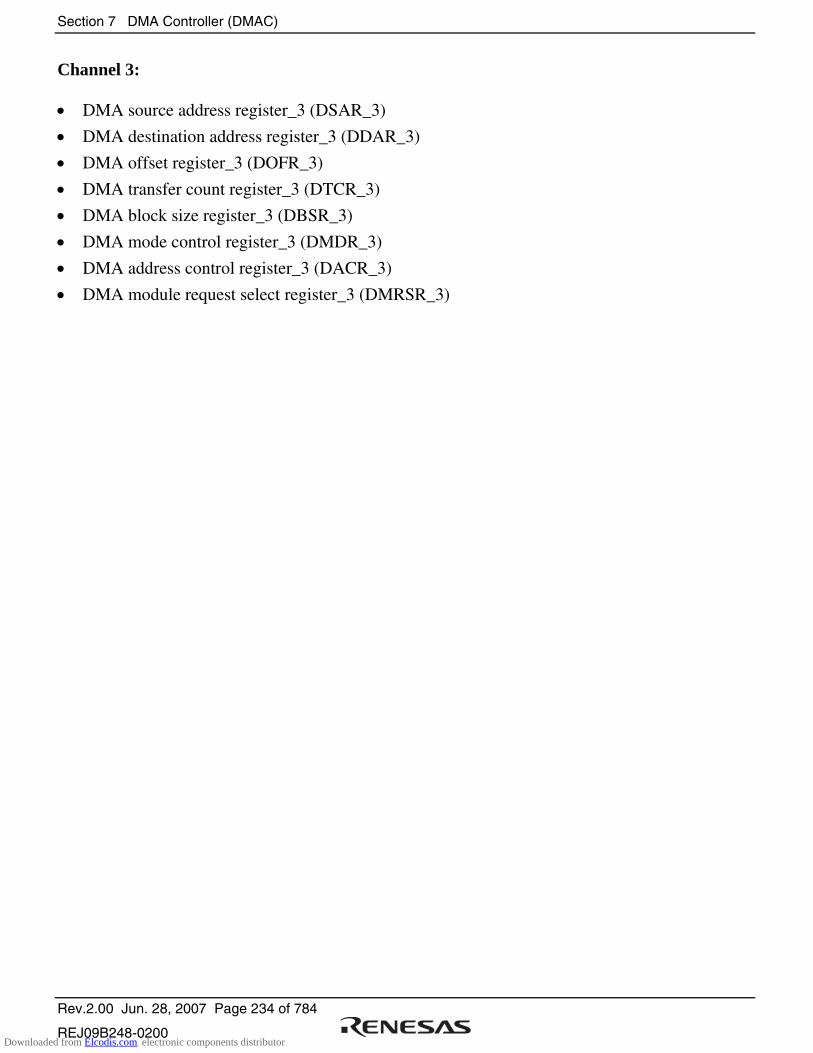
Section 7 DMA Controller (DMAC)
Rev.2.00 Jun. 28, 2007 Page 234 of 784
REJ09B248-0200
Channel 3:
• DMA source address register_3 (DSAR_3)
• DMA destination address register_3 (DDAR_3)
• DMA offset register_3 (DOFR_3)
• DMA transfer count register_3 (DTCR_3)
• DMA block size register_3 (DBSR_3)
• DMA mode control register_3 (DMDR_3)
• DMA address control register_3 (DACR_3)
• DMA module request select register_3 (DMRSR_3)
Downloaded from Elcodis.com electronic components distributor

Section 7 DMA Controller (DMAC)
Rev.2.00 Jun. 28, 2007 Page 235 of 784
REJ09B248-0200
7.3.1 DMA Source Address Register (DSAR)
DSAR is a 32-bit readable/writable register that specifies the transfer source address. DSAR updates the transfer source address every time data is transferred. When DDAR is specified as the destination address (the DIRS bit in DACR is 1) in single address mode, DSAR is ignored.
Although DSAR can always be read from by the CPU, it must be read from in longwords and must not be written to while data for the channel is being transferred.
31
0
R/W
30
0
R/W
29
0
R/W
28
0
R/W
27
0
R/W
24
0
R/W
26
0
R/W
25
0
R/W
Bit
Bit Name
Initial Value
R/W
23
0
R/W
22
0
R/W
21
0
R/W
20
0
R/W
19
0
R/W
16
0
R/W
18
0
R/W
17
0
R/W
Bit
Bit Name
Initial Value
R/W
15
0
R/W
14
0
R/W
13
0
R/W
12
0
R/W
11
0
R/W
8
0
R/W
10
0
R/W
9
0
R/W
Bit
Bit Name
Initial Value
R/W
7
0
R/W
6
0
R/W
5
0
R/W
4
0
R/W
3
0
R/W
0
0
R/W
2
0
R/W
1
0
R/W
Bit
Bit Name
Initial Value
R/W
Downloaded from Elcodis.com electronic components distributor

Section 7 DMA Controller (DMAC)
Rev.2.00 Jun. 28, 2007 Page 236 of 784
REJ09B248-0200
7.3.2 DMA Destination Address Register (DDAR)
DDAR is a 32-bit readable/writable register that specifies the transfer destination address. DDAR updates the transfer destination address every time data is transferred. When DSAR is specified as the source address (the DIRS bit in DACR is 0) in single address mode, DDAR is ignored.
Although DDAR can always be read from by the CPU, it must be read from in longwords and must not be written to while data for the channel is being transferred.
31
0
R/W
30
0
R/W
29
0
R/W
28
0
R/W
27
0
R/W
24
0
R/W
26
0
R/W
25
0
R/W
Bit
Bit Name
Initial Value
R/W
23
0
R/W
22
0
R/W
21
0
R/W
20
0
R/W
19
0
R/W
16
0
R/W
18
0
R/W
17
0
R/W
Bit
Bit Name
Initial Value
R/W
15
0
R/W
14
0
R/W
13
0
R/W
12
0
R/W
11
0
R/W
8
0
R/W
10
0
R/W
9
0
R/W
Bit
Bit Name
Initial Value
R/W
7
0
R/W
6
0
R/W
5
0
R/W
4
0
R/W
3
0
R/W
0
0
R/W
2
0
R/W
1
0
R/W
Bit
Bit Name
Initial Value
R/W
Downloaded from Elcodis.com electronic components distributor
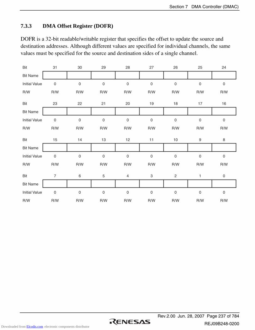
Section 7 DMA Controller (DMAC)
Rev.2.00 Jun. 28, 2007 Page 237 of 784
REJ09B248-0200
7.3.3 DMA Offset Register (DOFR)
DOFR is a 32-bit readable/writable register that specifies the offset to update the source and destination addresses. Although different values are specified for individual channels, the same values must be specified for the source and destination sides of a single channel.
31
0
R/W
30
0
R/W
29
0
R/W
28
0
R/W
27
0
R/W
24
0
R/W
26
0
R/W
25
0
R/W
Bit
Bit Name
Initial Value
R/W
23
0
R/W
22
0
R/W
21
0
R/W
20
0
R/W
19
0
R/W
16
0
R/W
18
0
R/W
17
0
R/W
Bit
Bit Name
Initial Value
R/W
15
0
R/W
14
0
R/W
13
0
R/W
12
0
R/W
11
0
R/W
8
0
R/W
10
0
R/W
9
0
R/W
Bit
Bit Name
Initial Value
R/W
7
0
R/W
6
0
R/W
5
0
R/W
4
0
R/W
3
0
R/W
0
0
R/W
2
0
R/W
1
0
R/W
Bit
Bit Name
Initial Value
R/W
Downloaded from Elcodis.com electronic components distributor
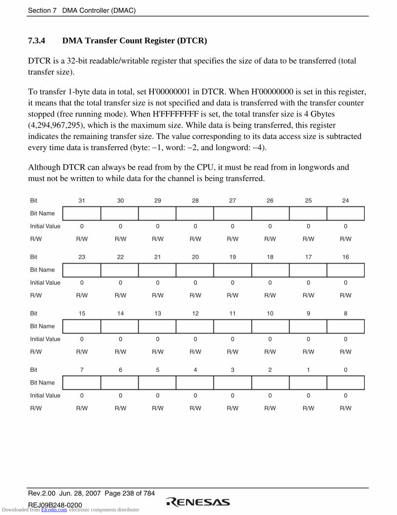
Section 7 DMA Controller (DMAC)
Rev.2.00 Jun. 28, 2007 Page 238 of 784
REJ09B248-0200
7.3.4 DMA Transfer Count Register (DTCR)
DTCR is a 32-bit readable/writable register that specifies the size of data to be transferred (total transfer size).
To transfer 1-byte data in total, set H'00000001 in DTCR. When H'00000000 is set in this register, it means that the total transfer size is not specified and data is transferred with the transfer counter stopped (free running mode). When H'FFFFFFFF is set, the total transfer size is 4 Gbytes (4,294,967,295), which is the maximum size. While data is being transferred, this register indicates the remaining transfer size. The value corresponding to its data access size is subtracted every time data is transferred (byte: −1, word: −2, and longword: −4).
Although DTCR can always be read from by the CPU, it must be read from in longwords and must not be written to while data for the channel is being transferred.
31
0
R/W
30
0
R/W
29
0
R/W
28
0
R/W
27
0
R/W
24
0
R/W
26
0
R/W
25
0
R/W
Bit
Bit Name
Initial Value
R/W
23
0
R/W
22
0
R/W
21
0
R/W
20
0
R/W
19
0
R/W
16
0
R/W
18
0
R/W
17
0
R/W
Bit
Bit Name
Initial Value
R/W
15
0
R/W
14
0
R/W
13
0
R/W
12
0
R/W
11
0
R/W
8
0
R/W
10
0
R/W
9
0
R/W
Bit
Bit Name
Initial Value
R/W
7
0
R/W
6
0
R/W
5
0
R/W
4
0
R/W
3
0
R/W
0
0
R/W
2
0
R/W
1
0
R/W
Bit
Bit Name
Initial Value
R/W
Downloaded from Elcodis.com electronic components distributor
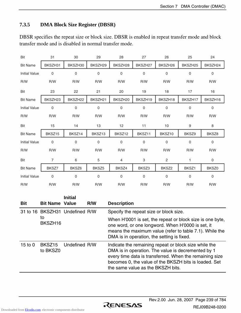
Section 7 DMA Controller (DMAC)
Rev.2.00 Jun. 28, 2007 Page 239 of 784
REJ09B248-0200
7.3.5 DMA Block Size Register (DBSR)
DBSR specifies the repeat size or block size. DBSR is enabled in repeat transfer mode and block transfer mode and is disabled in normal transfer mode.
31
BKSZH31
0
R/W
30
BKSZH30
0
R/W
29
BKSZH29
0
R/W
28
BKSZH28
0
R/W
27
BKSZH27
0
R/W
24
BKSZH24
0
R/W
26
BKSZH26
0
R/W
25
BKSZH25
0
R/W
Bit
Bit Name
Initial Value
R/W
23
BKSZH23
0
R/W
22
BKSZH22
0
R/W
21
BKSZH21
0
R/W
20
BKSZH20
0
R/W
19
BKSZH19
0
R/W
16
BKSZH16
0
R/W
18
BKSZH18
0
R/W
17
BKSZH17
0
R/W
Bit
Bit Name
Initial Value
R/W
15
BKSZ15
0
R/W
14
BKSZ14
0
R/W
13
BKSZ13
0
R/W
12
BKSZ12
0
R/W
11
BKSZ11
0
R/W
8
BKSZ8
0
R/W
10
BKSZ10
0
R/W
9
BKSZ9
0
R/W
Bit
Bit Name
Initial Value
R/W
7
BKSZ7
0
R/W
6
BKSZ6
0
R/W
5
BKSZ5
0
R/W
4
BKSZ4
0
R/W
3
BKSZ3
0
R/W
0
BKSZ0
0
R/W
2
BKSZ2
0
R/W
1
BKSZ1
0
R/W
Bit
Bit Name
Initial Value
R/W
Bit Bit NameInitial Value R/W Description
31 to 16 BKSZH31 to BKSZH16
Undefined R/W Specify the repeat size or block size.
When H'0001 is set, the repeat or block size is one byte, one word, or one longword. When H'0000 is set, it means the maximum value (refer to table 7.1). While the DMA is in operation, the setting is fixed.
15 to 0 BKSZ15 to BKSZ0
Undefined R/W Indicate the remaining repeat or block size while the DMA is in operation. The value is decremented by 1 every time data is transferred. When the remaining size becomes 0, the value of the BKSZH bits is loaded. Set the same value as the BKSZH bits.
Downloaded from Elcodis.com electronic components distributor

Section 7 DMA Controller (DMAC)
Rev.2.00 Jun. 28, 2007 Page 240 of 784
REJ09B248-0200
Table 7.2 Data Access Size, Valid Bits, and Settable Size
Mode Data Access Size BKSZH Valid Bits BKSZ Valid Bits Settable Size (Byte)
Byte 31 to 16 15 to 0 1 to 65,536 Repeat transfer and block transfer Word 2 to 131,072
Longword 4 to 262,144
7.3.6 DMA Mode Control Register (DMDR)
DMDR controls the DMAC operation.
• DMDR_0
31
DTE
0
R/W
30
DACKE
0
R/W
29
TENDE
0
R/W
28
0
R/W
27
DREQS
0
R/W
24
0
R
26
NRD
0
R/W
25
0
R
Bit
Bit Name
Initial Value
R/W
23
ACT
0
R
22
0
R
21
0
R
20
0
R
19
ERRF
0
R/(W)*
16
DTIF
0
R/(W)*
18
0
R
17
ESIF
0
R/(W)*
Bit
Bit Name
Initial Value
R/W
15
DTSZ1
0
R/W
14
DTSZ0
0
R/W
13
MDS1
0
R/W
12
MDS0
0
R/W
11
TSEIE
0
R/W
8
DTIE
0
R/W
10
0
R
9
ESIE
0
R/W
Bit
Bit Name
Initial Value
R/W
7
DTF1
0
R/W
6
DTF0
0
R/W
5
DTA
0
R/W
4
0
R
3
0
R
0
DMAP0
0
R/W
2
DMAP2
0
R/W
1
DMAP1
0
R/W
Bit
Bit Name
Initial Value
R/W
Note: * Only 0 can be written to this bit after having been read as 1, to clear the flag.
Downloaded from Elcodis.com electronic components distributor

Section 7 DMA Controller (DMAC)
Rev.2.00 Jun. 28, 2007 Page 241 of 784
REJ09B248-0200
• DMDR_1 to DMDR_3
31
DTE
0
R/W
30
DACKE
0
R/W
29
TENDE
0
R/W
28
0
R/W
27
DREQS
0
R/W
24
0
R
26
NRD
0
R/W
25
0
R
Bit
Bit Name
Initial Value
R/W
23
ACT
0
R
22
0
R
21
0
R
20
0
R
19
0
R
16
DTIF
0
R/(W)*
18
0
R
17
ESIF
0
R/(W)*
Bit
Bit Name
Initial Value
R/W
15
DTSZ1
0
R/W
14
DTSZ0
0
R/W
13
MDS1
0
R/W
12
MDS0
0
R/W
11
TSEIE
0
R/W
8
DTIE
0
R/W
10
0
R
9
ESIE
0
R/W
Bit
Bit Name
Initial Value
R/W
7
DTF1
0
R/W
6
DTF0
0
R/W
5
DTA
0
R/W
4
0
R
3
0
R
0
DMAP0
0
R/W
2
DMAP2
0
R/W
1
DMAP1
0
R/W
Bit
Bit Name
Initial Value
R/W
Note: * Only 0 can be written to this bit after having been read as 1, to clear the flag.
Downloaded from Elcodis.com electronic components distributor
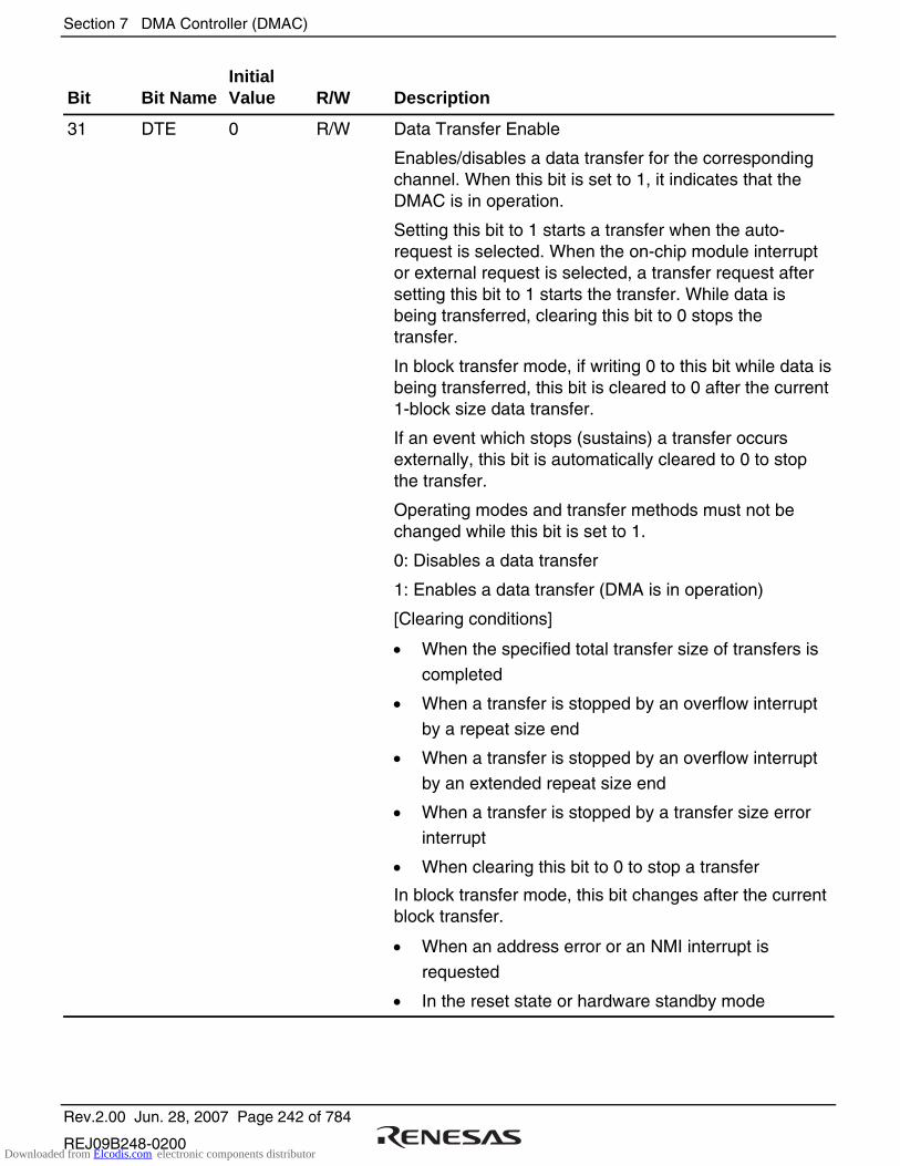
Section 7 DMA Controller (DMAC)
Rev.2.00 Jun. 28, 2007 Page 242 of 784
REJ09B248-0200
Bit Bit NameInitial Value R/W Description
31 DTE 0 R/W Data Transfer Enable
Enables/disables a data transfer for the corresponding channel. When this bit is set to 1, it indicates that the DMAC is in operation.
Setting this bit to 1 starts a transfer when the auto-request is selected. When the on-chip module interrupt or external request is selected, a transfer request after setting this bit to 1 starts the transfer. While data is being transferred, clearing this bit to 0 stops the transfer.
In block transfer mode, if writing 0 to this bit while data is being transferred, this bit is cleared to 0 after the current 1-block size data transfer.
If an event which stops (sustains) a transfer occurs externally, this bit is automatically cleared to 0 to stop the transfer.
Operating modes and transfer methods must not be changed while this bit is set to 1.
0: Disables a data transfer
1: Enables a data transfer (DMA is in operation)
[Clearing conditions]
• When the specified total transfer size of transfers is
completed
• When a transfer is stopped by an overflow interrupt
by a repeat size end
• When a transfer is stopped by an overflow interrupt
by an extended repeat size end
• When a transfer is stopped by a transfer size error
interrupt
• When clearing this bit to 0 to stop a transfer
In block transfer mode, this bit changes after the current block transfer.
• When an address error or an NMI interrupt is
requested
• In the reset state or hardware standby mode
Downloaded from Elcodis.com electronic components distributor

Section 7 DMA Controller (DMAC)
Rev.2.00 Jun. 28, 2007 Page 243 of 784
REJ09B248-0200
Bit Bit NameInitial Value R/W Description
30 DACKE 0 R/W DACK Signal Output Enable
Enables/disables the DACK signal output in single address mode. This bit is ignored in dual address mode.
0: Enables DACK signal output
1: Disables DACK signal output
29 TENDE 0 R/W TEND Signal Output Enable
Enables/disables the TEND signal output.
0: Enables TEND signal output
1: Disables TEND signal output
28 0 R/W Reserved
Initial value should not be changed.
27 DREQS 0 R/W DREQ Select
Selects whether a low level or the falling edge of the DREQ signal used in external request mode is detected.
When a block transfer is performed in external request mode, clear this bit to 0.
0: Low level detection
1: Falling edge detection (the first transfer after a transfer enabled is detected on a low level)
26 NRD 0 R/W Next Request Delay
Selects the accepting timing of the next transfer request.
0: Starts accepting the next transfer request after completion of the current transfer
1: Starts accepting the next transfer request one cycle after completion of the current transfer
25, 24 All 0 R Reserved
These bits are always read as 0 and cannot be modified.
23 ACT 0 R Active State
Indicates the operating state for the channel.
0: Waiting for a transfer request or a transfer disabled state by clearing the DTE bit to 0
1: Active state
22 to 20 All 0 R Reserved
These bits are always read as 0 and cannot be modified.
Downloaded from Elcodis.com electronic components distributor
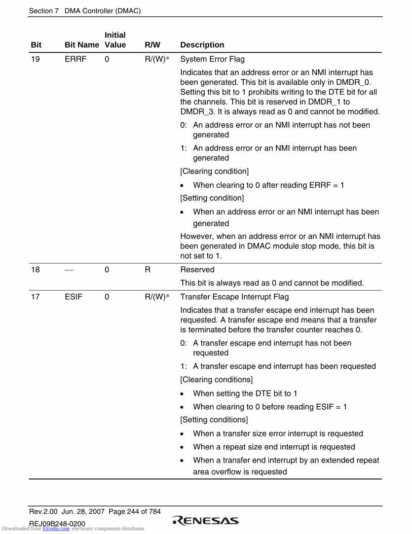
Section 7 DMA Controller (DMAC)
Rev.2.00 Jun. 28, 2007 Page 244 of 784
REJ09B248-0200
Bit Bit NameInitial Value R/W Description
19 ERRF 0 R/(W)* System Error Flag
Indicates that an address error or an NMI interrupt has been generated. This bit is available only in DMDR_0. Setting this bit to 1 prohibits writing to the DTE bit for all the channels. This bit is reserved in DMDR_1 to DMDR_3. It is always read as 0 and cannot be modified.
0: An address error or an NMI interrupt has not been generated
1: An address error or an NMI interrupt has been generated
[Clearing condition]
• When clearing to 0 after reading ERRF = 1
[Setting condition]
• When an address error or an NMI interrupt has been
generated
However, when an address error or an NMI interrupt has been generated in DMAC module stop mode, this bit is not set to 1.
18 0 R Reserved
This bit is always read as 0 and cannot be modified.
17 ESIF 0 R/(W)* Transfer Escape Interrupt Flag
Indicates that a transfer escape end interrupt has been requested. A transfer escape end means that a transfer is terminated before the transfer counter reaches 0.
0: A transfer escape end interrupt has not been requested
1: A transfer escape end interrupt has been requested
[Clearing conditions]
• When setting the DTE bit to 1
• When clearing to 0 before reading ESIF = 1
[Setting conditions]
• When a transfer size error interrupt is requested
• When a repeat size end interrupt is requested
• When a transfer end interrupt by an extended repeat
area overflow is requested
Downloaded from Elcodis.com electronic components distributor

Section 7 DMA Controller (DMAC)
Rev.2.00 Jun. 28, 2007 Page 245 of 784
REJ09B248-0200
Bit Bit NameInitial Value R/W Description
16 DTIF 0 R/(W)* Data Transfer Interrupt Flag
Indicates that a transfer end interrupt by the transfer counter has been requested.
0: A transfer end interrupt by the transfer counter has not been requested
1: A transfer end interrupt by the transfer counter has been requested
[Clearing conditions]
• When setting the DTE bit to 1
• When clearing to 0 after reading DTIF = 1
[Setting condition]
• When DTCR reaches 0 and the transfer is
completed
15
14
DTSZ1
DTSZ0
0
0
R/W
R/W
Data Access Size 1 and 0
Select the data access size for a transfer.
00: Byte size (eight bits)
01: Word size (16 bits)
10: Longword size (32 bits)
11: Setting prohibited
13
12
MDS1
MDS0
0
0
R/W
R/W
Transfer Mode Select 1 and 0
Select the transfer mode.
00: Normal transfer mode
01: Block transfer mode
10: Repeat transfer mode
11: Setting prohibited
Downloaded from Elcodis.com electronic components distributor
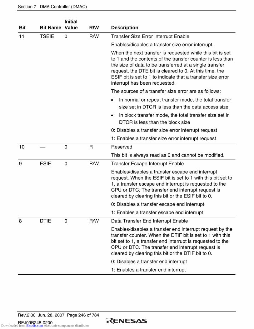
Section 7 DMA Controller (DMAC)
Rev.2.00 Jun. 28, 2007 Page 246 of 784
REJ09B248-0200
Bit Bit NameInitial Value R/W Description
11 TSEIE 0 R/W Transfer Size Error Interrupt Enable
Enables/disables a transfer size error interrupt.
When the next transfer is requested while this bit is set to 1 and the contents of the transfer counter is less than the size of data to be transferred at a single transfer request, the DTE bit is cleared to 0. At this time, the ESIF bit is set to 1 to indicate that a transfer size error interrupt has been requested.
The sources of a transfer size error are as follows:
• In normal or repeat transfer mode, the total transfer
size set in DTCR is less than the data access size
• In block transfer mode, the total transfer size set in
DTCR is less than the block size
0: Disables a transfer size error interrupt request
1: Enables a transfer size error interrupt request
10 0 R Reserved
This bit is always read as 0 and cannot be modified.
9 ESIE 0 R/W Transfer Escape Interrupt Enable
Enables/disables a transfer escape end interrupt request. When the ESIF bit is set to 1 with this bit set to 1, a transfer escape end interrupt is requested to the CPU or DTC. The transfer end interrupt request is cleared by clearing this bit or the ESIF bit to 0.
0: Disables a transfer escape end interrupt
1: Enables a transfer escape end interrupt
8 DTIE 0 R/W Data Transfer End Interrupt Enable
Enables/disables a transfer end interrupt request by the transfer counter. When the DTIF bit is set to 1 with this bit set to 1, a transfer end interrupt is requested to the CPU or DTC. The transfer end interrupt request is cleared by clearing this bit or the DTIF bit to 0.
0: Disables a transfer end interrupt
1: Enables a transfer end interrupt
Downloaded from Elcodis.com electronic components distributor
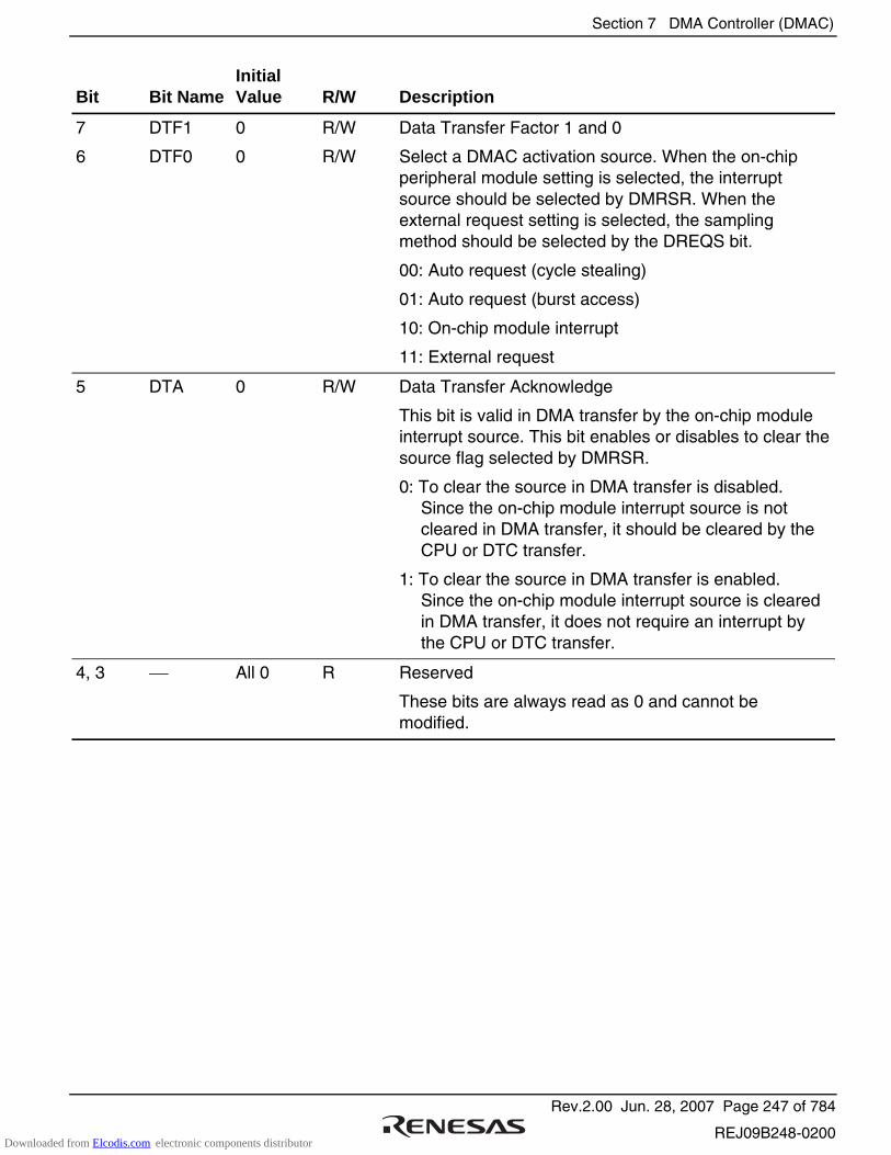
Section 7 DMA Controller (DMAC)
Rev.2.00 Jun. 28, 2007 Page 247 of 784
REJ09B248-0200
Bit Bit NameInitial Value R/W Description
7
6
DTF1
DTF0
0
0
R/W
R/W
Data Transfer Factor 1 and 0
Select a DMAC activation source. When the on-chip peripheral module setting is selected, the interrupt source should be selected by DMRSR. When the external request setting is selected, the sampling method should be selected by the DREQS bit.
00: Auto request (cycle stealing)
01: Auto request (burst access)
10: On-chip module interrupt
11: External request
5 DTA 0 R/W Data Transfer Acknowledge
This bit is valid in DMA transfer by the on-chip module interrupt source. This bit enables or disables to clear the source flag selected by DMRSR.
0: To clear the source in DMA transfer is disabled. Since the on-chip module interrupt source is not cleared in DMA transfer, it should be cleared by the CPU or DTC transfer.
1: To clear the source in DMA transfer is enabled. Since the on-chip module interrupt source is cleared in DMA transfer, it does not require an interrupt by the CPU or DTC transfer.
4, 3 All 0 R Reserved
These bits are always read as 0 and cannot be modified.
Downloaded from Elcodis.com electronic components distributor
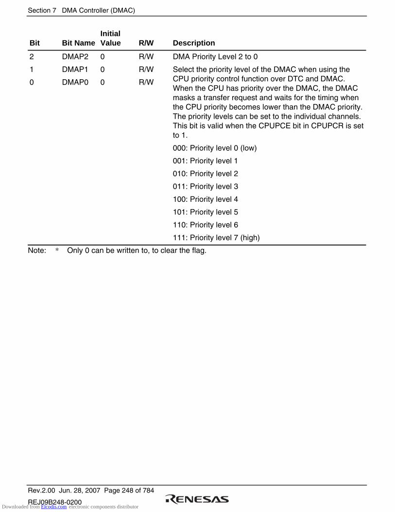
Section 7 DMA Controller (DMAC)
Rev.2.00 Jun. 28, 2007 Page 248 of 784
REJ09B248-0200
Bit Bit NameInitial Value R/W Description
2
1
0
DMAP2
DMAP1
DMAP0
0
0
0
R/W
R/W
R/W
DMA Priority Level 2 to 0
Select the priority level of the DMAC when using the CPU priority control function over DTC and DMAC. When the CPU has priority over the DMAC, the DMAC masks a transfer request and waits for the timing when the CPU priority becomes lower than the DMAC priority. The priority levels can be set to the individual channels. This bit is valid when the CPUPCE bit in CPUPCR is set to 1.
000: Priority level 0 (low)
001: Priority level 1
010: Priority level 2
011: Priority level 3
100: Priority level 4
101: Priority level 5
110: Priority level 6
111: Priority level 7 (high)
Note: * Only 0 can be written to, to clear the flag.
Downloaded from Elcodis.com electronic components distributor
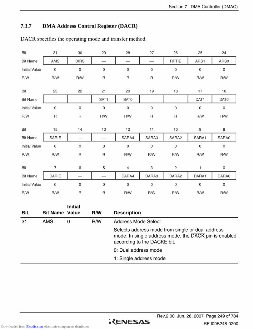
Section 7 DMA Controller (DMAC)
Rev.2.00 Jun. 28, 2007 Page 249 of 784
REJ09B248-0200
7.3.7 DMA Address Control Register (DACR)
DACR specifies the operating mode and transfer method.
31
AMS
0
R/W
30
DIRS
0
R/W
29
0
R
28
0
R
27
0
R
24
ARS0
0
R/W
26
RPTIE
0
R/W
25
ARS1
0
R/W
Bit
Bit Name
Initial Value
R/W
23
0
R
22
0
R
21
SAT1
0
R/W
20
SAT0
0
R/W
19
0
R
16
DAT0
0
R/W
18
0
R
17
DAT1
0
R/W
Bit
Bit Name
Initial Value
R/W
15
SARIE
0
R/W
14
0
R
13
0
R
12
SARA4
0
R/W
11
SARA3
0
R/W
8
SARA0
0
R/W
10
SARA2
0
R/W
9
SARA1
0
R/W
Bit
Bit Name
Initial Value
R/W
7
DARIE
0
R/W
6
0
R
5
0
R
4
DARA4
0
R/W
3
DARA3
0
R/W
0
DARA0
0
R/W
2
DARA2
0
R/W
1
DARA1
0
R/W
Bit
Bit Name
Initial Value
R/W
Bit Bit NameInitial Value R/W Description
31 AMS 0 R/W Address Mode Select
Selects address mode from single or dual address mode. In single address mode, the DACK pin is enabled according to the DACKE bit.
0: Dual address mode
1: Single address mode
Downloaded from Elcodis.com electronic components distributor

Section 7 DMA Controller (DMAC)
Rev.2.00 Jun. 28, 2007 Page 250 of 784
REJ09B248-0200
Bit Bit NameInitial Value R/W Description
30 DIRS 0 R/W Single Address Direction Select
Specifies the data transfer direction in single address mode. This bit s ignored in dual address mode.
0: Specifies DSAR as source address
1: Specifies DDAR as destination address
29 to 27 0 R/W Reserved
These bits are always read as 0 and cannot be modified.
26 RPTIE 0 R/W Repeat Size End Interrupt Enable
Enables/disables a repeat size end interrupt request.
In repeat transfer mode, when the next transfer is requested after completion of a 1-repeat-size data transfer while this bit is set to 1, the DTE bit in DMDR is cleared to 0. At this time, the ESIF bit in DMDR is set to 1 to indicate that a repeat size end interrupt is requested. Even when the repeat area is not specified (ARS1 = 1 and ARS0 = 0), a repeat size end interrupt after a 1-block data transfer can be requested.
In addition, in block transfer mode, when the next transfer is requested after 1-block data transfer while this bit is set to 1, the DTE bit in DMDR is cleared to 0. At this time, the ESIF bit in DMDR is set to 1 to indicate that a repeat size end interrupt is requested.
0: Disables a repeat size end interrupt
1: Enables a repeat size end interrupt
25
24
ARS1
ARS0
0
0
R/W
R/W
Area Select 1 and 0
Specify the block area or repeat area in block or repeat transfer mode.
00: Specify the block area or repeat area on the source address
01: Specify the block area or repeat area on the destination address
10: Do not specify the block area or repeat area
11: Setting prohibited
Downloaded from Elcodis.com electronic components distributor
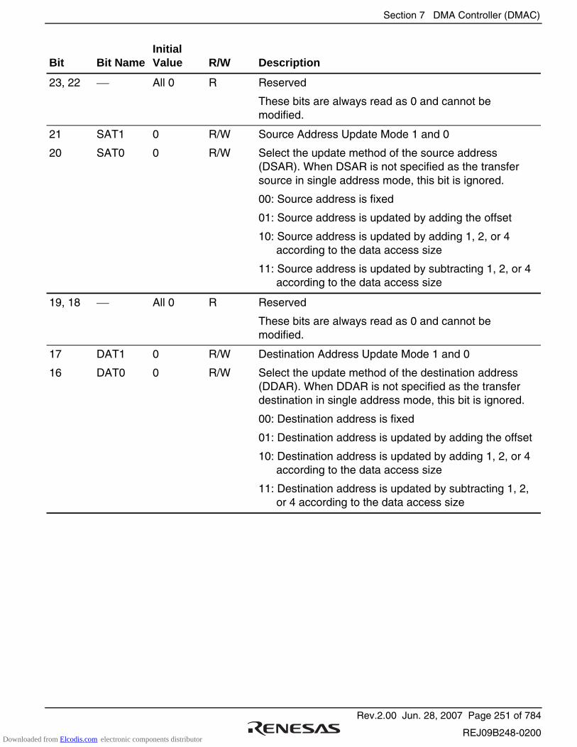
Section 7 DMA Controller (DMAC)
Rev.2.00 Jun. 28, 2007 Page 251 of 784
REJ09B248-0200
Bit Bit NameInitial Value R/W Description
23, 22 All 0 R Reserved
These bits are always read as 0 and cannot be modified.
21
20
SAT1
SAT0
0
0
R/W
R/W
Source Address Update Mode 1 and 0
Select the update method of the source address (DSAR). When DSAR is not specified as the transfer source in single address mode, this bit is ignored.
00: Source address is fixed
01: Source address is updated by adding the offset
10: Source address is updated by adding 1, 2, or 4 according to the data access size
11: Source address is updated by subtracting 1, 2, or 4 according to the data access size
19, 18 All 0 R Reserved
These bits are always read as 0 and cannot be modified.
17
16
DAT1
DAT0
0
0
R/W
R/W
Destination Address Update Mode 1 and 0
Select the update method of the destination address (DDAR). When DDAR is not specified as the transfer destination in single address mode, this bit is ignored.
00: Destination address is fixed
01: Destination address is updated by adding the offset
10: Destination address is updated by adding 1, 2, or 4 according to the data access size
11: Destination address is updated by subtracting 1, 2, or 4 according to the data access size
Downloaded from Elcodis.com electronic components distributor
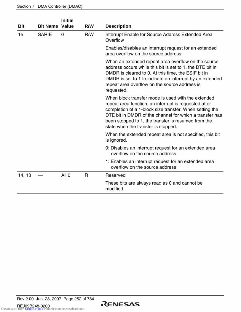
Section 7 DMA Controller (DMAC)
Rev.2.00 Jun. 28, 2007 Page 252 of 784
REJ09B248-0200
Bit Bit NameInitial Value R/W Description
15 SARIE 0 R/W Interrupt Enable for Source Address Extended Area Overflow
Enables/disables an interrupt request for an extended area overflow on the source address.
When an extended repeat area overflow on the source address occurs while this bit is set to 1, the DTE bit in DMDR is cleared to 0. At this time, the ESIF bit in DMDR is set to 1 to indicate an interrupt by an extended repeat area overflow on the source address is requested.
When block transfer mode is used with the extended repeat area function, an interrupt is requested after completion of a 1-block size transfer. When setting the DTE bit in DMDR of the channel for which a transfer has been stopped to 1, the transfer is resumed from the state when the transfer is stopped.
When the extended repeat area is not specified, this bit is ignored.
0: Disables an interrupt request for an extended area overflow on the source address
1: Enables an interrupt request for an extended area overflow on the source address
14, 13 All 0 R Reserved
These bits are always read as 0 and cannot be modified.
Downloaded from Elcodis.com electronic components distributor
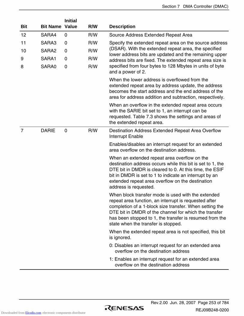
Section 7 DMA Controller (DMAC)
Rev.2.00 Jun. 28, 2007 Page 253 of 784
REJ09B248-0200
Bit Bit NameInitial Value R/W Description
12
11
10
9
8
SARA4
SARA3
SARA2
SARA1
SARA0
0
0
0
0
0
R/W
R/W
R/W
R/W
R/W
Source Address Extended Repeat Area
Specify the extended repeat area on the source address (DSAR). With the extended repeat area, the specified lower address bits are updated and the remaining upper address bits are fixed. The extended repeat area size is specified from four bytes to 128 Mbytes in units of byte and a power of 2.
When the lower address is overflowed from the extended repeat area by address update, the address becomes the start address and the end address of the area for address addition and subtraction, respectively.
When an overflow in the extended repeat area occurs with the SARIE bit set to 1, an interrupt can be requested. Table 7.3 shows the settings and areas of the extended repeat area.
7 DARIE 0 R/W Destination Address Extended Repeat Area Overflow Interrupt Enable
Enables/disables an interrupt request for an extended area overflow on the destination address.
When an extended repeat area overflow on the destination address occurs while this bit is set to 1, the DTE bit in DMDR is cleared to 0. At this time, the ESIF bit in DMDR is set to 1 to indicate an interrupt by an extended repeat area overflow on the destination address is requested.
When block transfer mode is used with the extended repeat area function, an interrupt is requested after completion of a 1-block size transfer. When setting the DTE bit in DMDR of the channel for which the transfer has been stopped to 1, the transfer is resumed from the state when the transfer is stopped.
When the extended repeat area is not specified, this bit is ignored.
0: Disables an interrupt request for an extended area overflow on the destination address
1: Enables an interrupt request for an extended area overflow on the destination address
Downloaded from Elcodis.com electronic components distributor
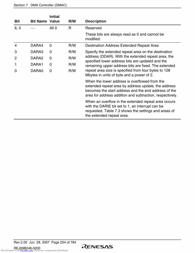
Section 7 DMA Controller (DMAC)
Rev.2.00 Jun. 28, 2007 Page 254 of 784
REJ09B248-0200
Bit Bit NameInitial Value R/W Description
6, 5 All 0 R Reserved
These bits are always read as 0 and cannot be modified.
4
3
2
1
0
DARA4
DARA3
DARA2
DARA1
DARA0
0
0
0
0
0
R/W
R/W
R/W
R/W
R/W
Destination Address Extended Repeat Area
Specify the extended repeat area on the destination address (DDAR). With the extended repeat area, the specified lower address bits are updated and the remaining upper address bits are fixed. The extended repeat area size is specified from four bytes to 128 Mbytes in units of byte and a power of 2.
When the lower address is overflowed from the extended repeat area by address update, the address becomes the start address and the end address of the area for address addition and subtraction, respectively.
When an overflow in the extended repeat area occurs with the DARIE bit set to 1, an interrupt can be requested. Table 7.3 shows the settings and areas of the extended repeat area.
Downloaded from Elcodis.com electronic components distributor
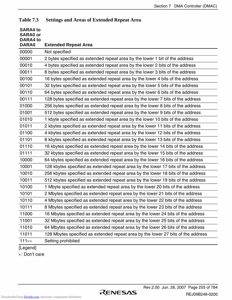
Section 7 DMA Controller (DMAC)
Rev.2.00 Jun. 28, 2007 Page 255 of 784
REJ09B248-0200
Table 7.3 Settings and Areas of Extended Repeat Area
SARA4 to SARA0 or DARA4 to DARA0 Extended Repeat Area
00000 Not specified
00001 2 bytes specified as extended repeat area by the lower 1 bit of the address
00010 4 bytes specified as extended repeat area by the lower 2 bits of the address
00011 8 bytes specified as extended repeat area by the lower 3 bits of the address
00100 16 bytes specified as extended repeat area by the lower 4 bits of the address
00101 32 bytes specified as extended repeat area by the lower 5 bits of the address
00110 64 bytes specified as extended repeat area by the lower 6 bits of the address
00111 128 bytes specified as extended repeat area by the lower 7 bits of the address
01000 256 bytes specified as extended repeat area by the lower 8 bits of the address
01001 512 bytes specified as extended repeat area by the lower 9 bits of the address
01010 1 kbyte specified as extended repeat area by the lower 10 bits of the address
01011 2 kbytes specified as extended repeat area by the lower 11 bits of the address
01100 4 kbytes specified as extended repeat area by the lower 12 bits of the address
01101 8 kbytes specified as extended repeat area by the lower 13 bits of the address
01110 16 kbytes specified as extended repeat area by the lower 14 bits of the address
01111 32 kbytes specified as extended repeat area by the lower 15 bits of the address
10000 64 kbytes specified as extended repeat area by the lower 16 bits of the address
10001 128 kbytes specified as extended repeat area by the lower 17 bits of the address
10010 256 kbytes specified as extended repeat area by the lower 18 bits of the address
10011 512 kbytes specified as extended repeat area by the lower 19 bits of the address
10100 1 Mbyte specified as extended repeat area by the lower 20 bits of the address
10101 2 Mbytes specified as extended repeat area by the lower 21 bits of the address
10110 4 Mbytes specified as extended repeat area by the lower 22 bits of the address
10111 8 Mbytes specified as extended repeat area by the lower 23 bits of the address
11000 16 Mbytes specified as extended repeat area by the lower 24 bits of the address
11001 32 Mbytes specified as extended repeat area by the lower 25 bits of the address
11010 64 Mbytes specified as extended repeat area by the lower 26 bits of the address
11011 128 Mbytes specified as extended repeat area by the lower 27 bits of the address
111×× Setting prohibited
[Legend] ×: Don't care
Downloaded from Elcodis.com electronic components distributor

Section 7 DMA Controller (DMAC)
Rev.2.00 Jun. 28, 2007 Page 256 of 784
REJ09B248-0200
7.3.8 DMA Module Request Select Register (DMRSR)
DMRSR is an 8-bit readable/writable register that specifies the on-chip module interrupt source. The vector number of the interrupt source is specified in eight bits. However, 0 is regarded as no interrupt source. For the vector numbers of the interrupt sources, refer to table 7.5.
7
0
R/W
6
0
R/W
5
0
R/W
4
0
R/W
3
0
R/W
0
0
R/W
2
0
R/W
1
0
R/W
Bit
Bit Name
Initial Value
R/W
7.4 Transfer Modes
Table 7.4 shows the DMAC transfer modes. The transfer modes can be specified to the individual channels.
Table 7.4 Transfer Modes
Address Register
Address Mode Transfer mode Activation Source Common Function Source
Destina-tion
Dual address
• Normal transfer
• Repeat transfer
• Block transfer
Repeat or block size = 1 to 65,536 bytes, 1 to 65,536 words, or 1 to 65,536 longwords
• Auto request
(activated by CPU)
• On-chip module
interrupt
• External request
• Total transfer size:
1 to 4 Gbytes or not
specified
• Offset addition
• Extended repeat
area function
DSAR DDAR
Single address
• Instead of specifying the source or destination address registers, data
is directly transferred from/to the external device using the DACK pin
• The same settings as above are available other than address register
setting (e.g., above transfer modes can be specified)
• One transfer can be performed in one bus cycle (the types of transfer
modes are the same as those of dual address modes)
DSAR/ DACK
DACK/ DDAR
When the auto request setting is selected as the activation source, the cycle stealing or burst access can be selected. When the total transfer size is not specified (DTCR = H'00000000), the transfer counter is stopped and the transfer is continued without the limitation of the transfer count.
Downloaded from Elcodis.com electronic components distributor
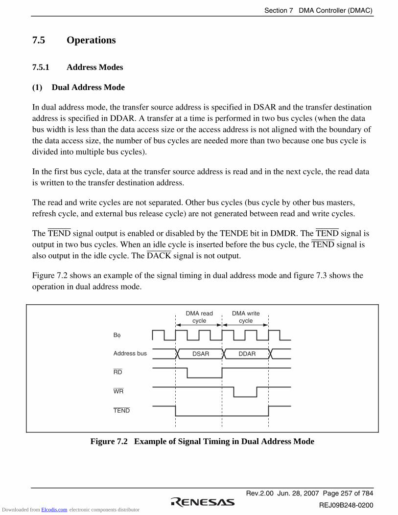
Section 7 DMA Controller (DMAC)
Rev.2.00 Jun. 28, 2007 Page 257 of 784
REJ09B248-0200
7.5 Operations
7.5.1 Address Modes
(1) Dual Address Mode
In dual address mode, the transfer source address is specified in DSAR and the transfer destination address is specified in DDAR. A transfer at a time is performed in two bus cycles (when the data bus width is less than the data access size or the access address is not aligned with the boundary of the data access size, the number of bus cycles are needed more than two because one bus cycle is divided into multiple bus cycles).
In the first bus cycle, data at the transfer source address is read and in the next cycle, the read data is written to the transfer destination address.
The read and write cycles are not separated. Other bus cycles (bus cycle by other bus masters, refresh cycle, and external bus release cycle) are not generated between read and write cycles.
The TEND signal output is enabled or disabled by the TENDE bit in DMDR. The TEND signal is output in two bus cycles. When an idle cycle is inserted before the bus cycle, the TEND signal is also output in the idle cycle. The DACK signal is not output.
Figure 7.2 shows an example of the signal timing in dual address mode and figure 7.3 shows the operation in dual address mode.
Address bus
Bφ
RD
WR
TEND
DMA readcycle
DMA writecycle
DSAR DDAR
Figure 7.2 Example of Signal Timing in Dual Address Mode
Downloaded from Elcodis.com electronic components distributor

Section 7 DMA Controller (DMAC)
Rev.2.00 Jun. 28, 2007 Page 258 of 784
REJ09B248-0200
TransferAddress TA
Address BA Address update setting is as follows: Source address increment Fixed destination address
Address TB
Figure 7.3 Operations in Dual Address Mode
(2) Single Address Mode
In single address mode, data between an external device and an external memory is directly transferred using the DACK pin instead of DSAR or DDAR. A transfer at a time is performed in one bus cycle. In this mode, the data bus width must be the same as the data access size. For details on the data bus width, see section 6, Bus Controller (BSC).
The DMAC accesses an external device as the transfer source or destination by outputting the strobe signal (DACK) to the external device with DACK and accesses the other transfer target by outputting the address. Accordingly, the DMA transfer is performed in one bus cycle. Figure 7.4 shows an example of a transfer between an external memory and an external device with the DACK pin. In this example, the external device outputs data on the data bus and the data is written to the external memory in the same bus cycle.
The transfer direction is decided by the DIRS bit in DACR which specifies an external device with the DACK pin as the transfer source or destination. When DIRS = 0, data is transferred from an external memory (DSAR) to an external device with the DACK pin. When DIRS = 1, data is transferred from an external device with the DACK pin to an external memory (DDAR). The settings of registers which are not used as the transfer source or destination are ignored.
The DACK signal output is enabled in single address mode by the DACKE bit in DMDR. The DACK signal is low active.
The TEND signal output is enabled or disabled by the TENDE bit in DMDR. The TEND signal is output in one bus cycle. When an idle cycle is inserted before the bus cycle, the TEND signal is also output in the idle cycle.
Figure 7.5 shows an example of timing charts in single address mode and figure 7.6 shows an example of operation in single address mode.
Downloaded from Elcodis.com electronic components distributor
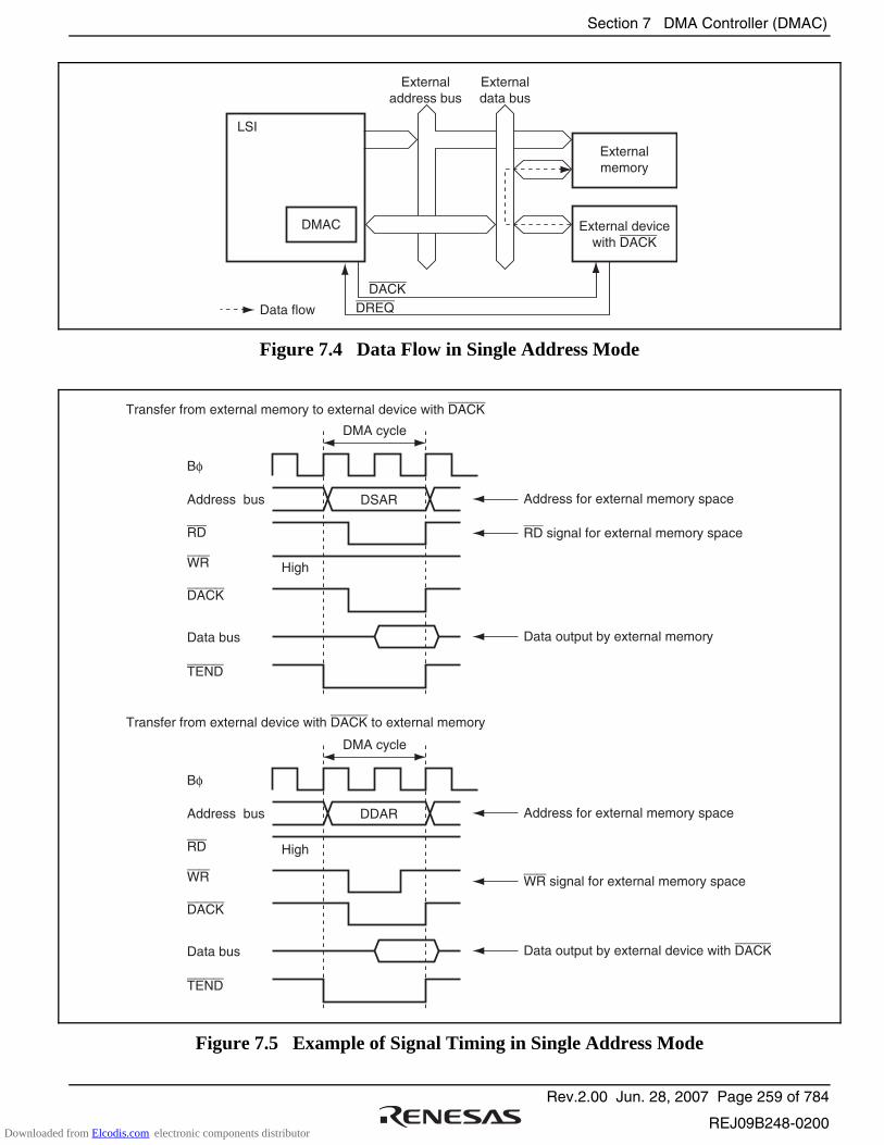
Section 7 DMA Controller (DMAC)
Rev.2.00 Jun. 28, 2007 Page 259 of 784
REJ09B248-0200
LSI
Data flow
Externaladdress bus
Externaldata bus
DMAC
DACK
DREQ
Externalmemory
External devicewith DACK
Figure 7.4 Data Flow in Single Address Mode
DMA cycle
DSAR
High
High
Address for external memory space
RD signal for external memory space
Data output by external memory
Address bus
Bφ
RD
WR
DACK
TEND
Data bus
DMA cycle
DDAR Address for external memory space
WR signal for external memory space
Bφ
Address bus
Transfer from external memory to external device with DACK
RD
WR
DACK
TEND
Data bus Data output by external device with DACK
Transfer from external device with DACK to external memory
Figure 7.5 Example of Signal Timing in Single Address Mode
Downloaded from Elcodis.com electronic components distributor

Section 7 DMA Controller (DMAC)
Rev.2.00 Jun. 28, 2007 Page 260 of 784
REJ09B248-0200
TransferAddress T
Address B
DACK
Figure 7.6 Operations in Single Address Mode
7.5.2 Transfer Modes
(1) Normal Transfer Mode
In normal transfer mode, one data access size of data is transferred at a single transfer request. Up to 4 Gbytes can be specified as a total transfer size by DTCR. DBSR is ignored in normal transfer mode.
The TEND signal is output only in the last DMA transfer. The DACK signal is output every time a transfer request is received and a transfer starts.
Figure 7.7 shows an example of the signal timing in normal transfer mode and figure 7.8 shows the operation in normal transfer mode.
Read Write Read Write
DMA transfercycle
Last DMAtransfer cycle
Bus cycle
Auto request transfer in dual address mode:
External request transfer in single address mode:
TEND
DMA DMA
DREQ
Bus cycle
DACK
Figure 7.7 Example of Signal Timing in Normal Transfer Mode
Downloaded from Elcodis.com electronic components distributor
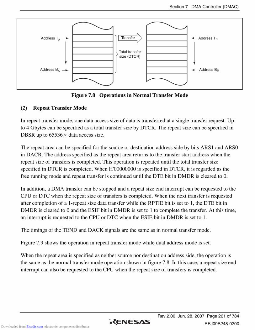
Section 7 DMA Controller (DMAC)
Rev.2.00 Jun. 28, 2007 Page 261 of 784
REJ09B248-0200
Transfer
Total transfersize (DTCR)
Address TA
Address BA
Address TB
Address BB
Figure 7.8 Operations in Normal Transfer Mode
(2) Repeat Transfer Mode
In repeat transfer mode, one data access size of data is transferred at a single transfer request. Up to 4 Gbytes can be specified as a total transfer size by DTCR. The repeat size can be specified in DBSR up to 65536 × data access size.
The repeat area can be specified for the source or destination address side by bits ARS1 and ARS0 in DACR. The address specified as the repeat area returns to the transfer start address when the repeat size of transfers is completed. This operation is repeated until the total transfer size specified in DTCR is completed. When H'00000000 is specified in DTCR, it is regarded as the free running mode and repeat transfer is continued until the DTE bit in DMDR is cleared to 0.
In addition, a DMA transfer can be stopped and a repeat size end interrupt can be requested to the CPU or DTC when the repeat size of transfers is completed. When the next transfer is requested after completion of a 1-repeat size data transfer while the RPTIE bit is set to 1, the DTE bit in DMDR is cleared to 0 and the ESIF bit in DMDR is set to 1 to complete the transfer. At this time, an interrupt is requested to the CPU or DTC when the ESIE bit in DMDR is set to 1.
The timings of the TEND and DACK signals are the same as in normal transfer mode.
Figure 7.9 shows the operation in repeat transfer mode while dual address mode is set.
When the repeat area is specified as neither source nor destination address side, the operation is the same as the normal transfer mode operation shown in figure 7.8. In this case, a repeat size end interrupt can also be requested to the CPU when the repeat size of transfers is completed.
Downloaded from Elcodis.com electronic components distributor

Section 7 DMA Controller (DMAC)
Rev.2.00 Jun. 28, 2007 Page 262 of 784
REJ09B248-0200
TransferAddress TA Address TB
Address BB
Address BA
Operation when the repeat area is specifiedto the source side
Repeat size =BKSZH × data access size
Total transfersize (DTCR)
Figure 7.9 Operations in Repeat Transfer Mode
(3) Block Transfer Mode
In block transfer mode, one block size of data is transferred at a single transfer request. Up to 4 Gbytes can be specified as total transfer size by DTCR. The block size can be specified in DBSR up to 65536 × data access size.
While one block of data is being transferred, transfer requests from other channels are suspended. When the transfer is completed, the bus is released to the other bus master.
The block area can be specified for the source or destination address side by bits ARS1 and ARS0 in DACR. The address specified as the block area returns to the transfer start address when the block size of data is completed. When the block area is specified as neither source nor destination address side, the operation continues without returning the address to the transfer start address. A repeat size end interrupt can be requested.
The TEND signal is output every time 1-block data is transferred in the last DMA transfer cycle. When the external request is selected as an activation source, the low level detection of the DREQ signal (DREQS = 0) should be selected.
When an interrupt request by an extended repeat area overflow is used in block transfer mode, settings should be selected carefully. For details, see section 7.5.5, Extended Repeat Area Function.
Downloaded from Elcodis.com electronic components distributor
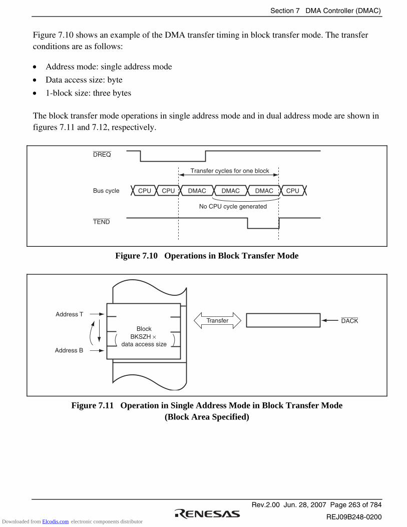
Section 7 DMA Controller (DMAC)
Rev.2.00 Jun. 28, 2007 Page 263 of 784
REJ09B248-0200
Figure 7.10 shows an example of the DMA transfer timing in block transfer mode. The transfer conditions are as follows:
• Address mode: single address mode
• Data access size: byte
• 1-block size: three bytes The block transfer mode operations in single address mode and in dual address mode are shown in figures 7.11 and 7.12, respectively.
CPU CPU DMAC DMAC DMAC CPUBus cycle
TEND
DREQ
No CPU cycle generated
Transfer cycles for one block
Figure 7.10 Operations in Block Transfer Mode
Address T
Address B
DACK
BlockBKSZH ×
data access size
Transfer
Figure 7.11 Operation in Single Address Mode in Block Transfer Mode (Block Area Specified)
Downloaded from Elcodis.com electronic components distributor
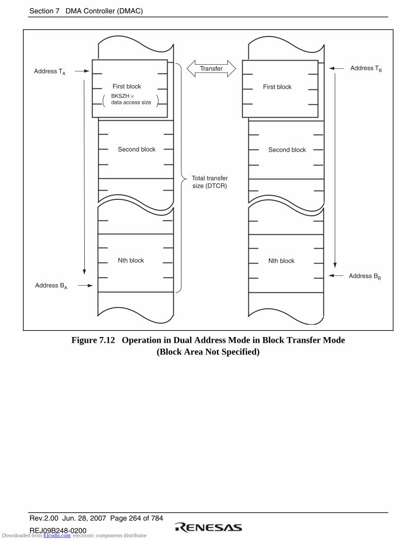
Section 7 DMA Controller (DMAC)
Rev.2.00 Jun. 28, 2007 Page 264 of 784
REJ09B248-0200
TransferAddress TA
Address BA
Address TB
Address BB
Nth block
Second block
First block
Nth block
Second block
First blockBKSZH × data access size
Total transfersize (DTCR)
Figure 7.12 Operation in Dual Address Mode in Block Transfer Mode (Block Area Not Specified)
Downloaded from Elcodis.com electronic components distributor
Section 7 DMA Controller (DMAC)
Rev.2.00 Jun. 28, 2007 Page 265 of 784
REJ09B248-0200
7.5.3 Activation Sources
The DMAC is activated by an auto request, an on-chip module interrupt, and an external request. The activation source is specified by bits DTF1 and DTF0 in DMDR.
(1) Activation by Auto Request
The auto request activation is used when a transfer request from an external device or an on-chip peripheral module is not generated such as a transfer between memory and memory or between memory and an on-chip peripheral module which does not request a transfer. A transfer request is automatically generated inside the DMAC. In auto request activation, setting the DTE bit in DMDR starts a transfer. The bus mode can be selected from cycle stealing and burst modes.
(2) Activation by On-Chip Module Interrupt
An interrupt request from an on-chip peripheral module (on-chip peripheral module interrupt) is used as a transfer request. When a DMA transfer is enabled (DTE = 1), the DMA transfer is started by an on-chip module interrupt.
The activation source of the on-chip module interrupt is selected by the DMA module request select register (DMRSR). The activation sources are specified to the individual channels. Table 7.5 is a list of on-chip module interrupts for the DMAC. The interrupt request selected as the activation source can generate an interrupt request simultaneously to the CPU or DTC. For details, refer to section 5, Interrupt Controller.
The DMAC receives interrupt requests by on-chip peripheral modules independent of the interrupt controller. Therefore, the DMAC is not affected by priority given in the interrupt controller.
When the DMAC is activated while DTA = 1, the interrupt request flag is automatically cleared by a DMA transfer. If multiple channels use a single transfer request as an activation source, when the channel having priority is activated, the interrupt request flag is cleared. In this case, other channels may not be activated because the transfer request is not held in the DMAC.
When the DMAC is activated while DTA = 0, the interrupt request flag is not cleared by the DMAC and should be cleared by the CPU or DTC transfer.
When an activation source is selected while DTE = 0, the activation source does not request a transfer to the DMAC. It requests an interrupt to the CPU or DTC.
In addition, make sure that an interrupt request flag as an on-chip module interrupt source is cleared to 0 before writing 1 to the DTE bit.
Downloaded from Elcodis.com electronic components distributor
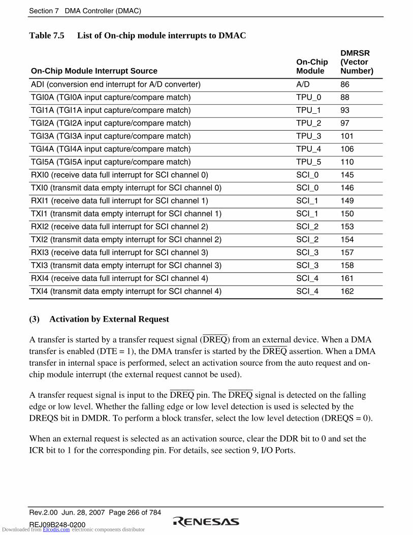
Section 7 DMA Controller (DMAC)
Rev.2.00 Jun. 28, 2007 Page 266 of 784
REJ09B248-0200
Table 7.5 List of On-chip module interrupts to DMAC
On-Chip Module Interrupt Source On-Chip Module
DMRSR (Vector Number)
ADI (conversion end interrupt for A/D converter) A/D 86
TGI0A (TGI0A input capture/compare match) TPU_0 88
TGI1A (TGI1A input capture/compare match) TPU_1 93
TGI2A (TGI2A input capture/compare match) TPU_2 97
TGI3A (TGI3A input capture/compare match) TPU_3 101
TGI4A (TGI4A input capture/compare match) TPU_4 106
TGI5A (TGI5A input capture/compare match) TPU_5 110
RXI0 (receive data full interrupt for SCI channel 0) SCI_0 145
TXI0 (transmit data empty interrupt for SCI channel 0) SCI_0 146
RXI1 (receive data full interrupt for SCI channel 1) SCI_1 149
TXI1 (transmit data empty interrupt for SCI channel 1) SCI_1 150
RXI2 (receive data full interrupt for SCI channel 2) SCI_2 153
TXI2 (transmit data empty interrupt for SCI channel 2) SCI_2 154
RXI3 (receive data full interrupt for SCI channel 3) SCI_3 157
TXI3 (transmit data empty interrupt for SCI channel 3) SCI_3 158
RXI4 (receive data full interrupt for SCI channel 4) SCI_4 161
TXI4 (transmit data empty interrupt for SCI channel 4) SCI_4 162
(3) Activation by External Request
A transfer is started by a transfer request signal (DREQ) from an external device. When a DMA transfer is enabled (DTE = 1), the DMA transfer is started by the DREQ assertion. When a DMA transfer in internal space is performed, select an activation source from the auto request and on-chip module interrupt (the external request cannot be used).
A transfer request signal is input to the DREQ pin. The DREQ signal is detected on the falling edge or low level. Whether the falling edge or low level detection is used is selected by the DREQS bit in DMDR. To perform a block transfer, select the low level detection (DREQS = 0).
When an external request is selected as an activation source, clear the DDR bit to 0 and set the ICR bit to 1 for the corresponding pin. For details, see section 9, I/O Ports.
Downloaded from Elcodis.com electronic components distributor
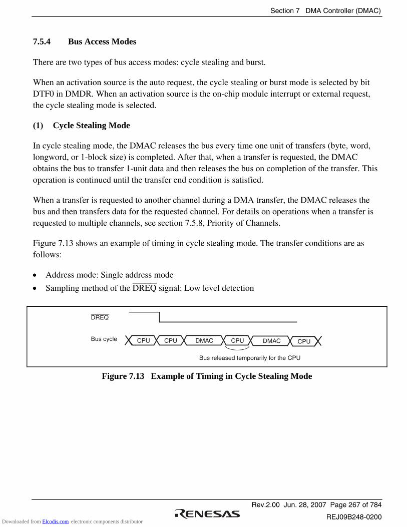
Section 7 DMA Controller (DMAC)
Rev.2.00 Jun. 28, 2007 Page 267 of 784
REJ09B248-0200
7.5.4 Bus Access Modes
There are two types of bus access modes: cycle stealing and burst.
When an activation source is the auto request, the cycle stealing or burst mode is selected by bit DTF0 in DMDR. When an activation source is the on-chip module interrupt or external request, the cycle stealing mode is selected.
(1) Cycle Stealing Mode
In cycle stealing mode, the DMAC releases the bus every time one unit of transfers (byte, word, longword, or 1-block size) is completed. After that, when a transfer is requested, the DMAC obtains the bus to transfer 1-unit data and then releases the bus on completion of the transfer. This operation is continued until the transfer end condition is satisfied.
When a transfer is requested to another channel during a DMA transfer, the DMAC releases the bus and then transfers data for the requested channel. For details on operations when a transfer is requested to multiple channels, see section 7.5.8, Priority of Channels.
Figure 7.13 shows an example of timing in cycle stealing mode. The transfer conditions are as follows:
• Address mode: Single address mode
• Sampling method of the DREQ signal: Low level detection
CPU CPU CPUDMAC CPUDMAC
DREQ
Bus cycle
Bus released temporarily for the CPU
Figure 7.13 Example of Timing in Cycle Stealing Mode
Downloaded from Elcodis.com electronic components distributor
Section 7 DMA Controller (DMAC)
Rev.2.00 Jun. 28, 2007 Page 268 of 784
REJ09B248-0200
(2) Burst Access Mode
In burst mode, once it takes the bus, the DMAC continues a transfer without releasing the bus until the transfer end condition is satisfied. Even if a transfer is requested from another channel having priority, the transfer is not stopped once it is started. The DMAC releases the bus in the next cycle after the transfer for the channel in burst mode is completed. This is similarly to operation in cycle stealing mode. However, setting the IBCCS bit in IBCR of the bus controller makes the DMAC release the bus to pass the bus to another bus master.
In block transfer mode, the burst mode setting is ignored (operation is the same as that in burst mode during one block of transfers). The DMAC is always operated in cycle stealing mode.
Clearing the DTE bit in DMDR stops a DMA transfer. A transfer requested before the DTE bit is cleared to 0 by the DMAC is executed. When an interrupt by a transfer size error, a repeat size end, or an extended repeat area overflow occurs, the DTE bit is cleared to 0 and the transfer ends.
Figure 7.14 shows an example of timing in burst mode.
CPU CPU CPU CPUDMAC DMAC DMACBus cycle
No CPU cycle generated
Figure 7.14 Example of Timing in Burst Mode
7.5.5 Extended Repeat Area Function
The source and destination address sides can be specified as the extended repeat area. The contents of the address register repeat addresses within the area specified as the extended repeat area. For example, to use a ring buffer as the transfer target, the contents of the address register should return to the start address of the buffer every time the contents reach the end address of the buffer (overflow on the ring buffer address). This operation can automatically be performed using the extended repeat area function of the DMAC.
The extended repeat areas can be specified independently to the source address register (DSAR) and destination address register (DDAR).
The extended repeat area on the source address is specified by bits SARA4 to SARA0 in DACR. The extended repeat area on the destination address is specified by bits DARA4 to DARA0 in DACR. The extended repeat area sizes for each side can be specified independently.
Downloaded from Elcodis.com electronic components distributor
Section 7 DMA Controller (DMAC)
Rev.2.00 Jun. 28, 2007 Page 269 of 784
REJ09B248-0200
A DMA transfer is stopped and an interrupt by an extended repeat area overflow can be requested to the CPU when the contents of the address register reach the end address of the extended repeat area. When an overflow on the extended repeat area set in DSAR occurs while the SARIE bit in DACR is set to 1, the ESIF bit in DMDR is set to 1 and the DTE bit in DMDR is cleared to 0 to stop the transfer. At this time, if the ESIE bit in DMDR is set to 1, an interrupt by an extended repeat area overflow is requested to the CPU. When the DARIE bit in DACR is set to 1, an overflow on the extended repeat area set in DDAR occurs, meaning that the destination side is a target. During the interrupt handling, setting the DTE bit in DMDR resumes the transfer.
Figure 7.15 shows an example of the extended repeat area operation.
External memory
When the area represented by the lower three bits of DSAR (eight bytes) is specified as the extended repeat area (SARA4 to SARA0 = B'00011)
Repeat
An interrupt request by extended repeat areaoverflow can be generated.
Area specifiedby DSAR
H'23FFFE
H'23FFFF
H'240000
H'240001
H'240002
H'240003
H'240004
H'240005
H'240006
H'240007
H'240008
H'240009
H'240000
H'240001
H'240002
H'240003
H'240004
H'240005
H'240006
H'240007
......
Figure 7.15 Example of Extended Repeat Area Operation
Downloaded from Elcodis.com electronic components distributor

Section 7 DMA Controller (DMAC)
Rev.2.00 Jun. 28, 2007 Page 270 of 784
REJ09B248-0200
When an interrupt by an extended repeat area overflow is used in block transfer mode, the following should be taken into consideration.
When a transfer is stopped by an interrupt by an extended repeat area overflow, the address register must be set so that the block size is a power of 2 or the block size boundary is aligned with the extended repeat area boundary. When an overflow on the extended repeat area occurs during a transfer of one block, the interrupt by the overflow is suspended and the transfer overruns.
Figure 7.16 shows examples when the extended repeat area function is used in block transfer mode.
External memory Area specifiedby DSAR
1st block transfer
2nd block transfer
H'23FFFE
H'23FFFF
H'240000
H'240001
H'240002
H'240003
H'240004
H'240005
H'240006
H'240007
H'240008
H'240009
H'240000
H'240001
H'240002
H'240003
H'240004
H'240005
H'240006
H'240007
H'240000
H'240001
H'240002
H'240003
H'240004
H'240000
H'240001
H'240005
H'240006
H'240007
Interruptrequestgenerated
Block transfercontinued
When the are represented by the lower three bits (eight bytes) of DSAR are specified as the extended repeat area (SARA4 to SARA0 = 3) and the block size in block transfer mode is specified to 5 (bits 23 to 16 in DTCR = 5).
......
Figure 7.16 Example of Extended Repeat Area Function in Block Transfer Mode
7.5.6 Address Update Function using Offset
The source and destination addresses are updated by fixing, increment/decrement by 1, 2, or 4, or offset addition. When the offset addition is selected, the offset specified by the offset register (DOFR) is added to the address every time the DMAC transfers the data access size of data. This function realizes a data transfer where addresses are allocated to separated areas.
Figure 7.17 shows the address update method.
Downloaded from Elcodis.com electronic components distributor
Section 7 DMA Controller (DMAC)
Rev.2.00 Jun. 28, 2007 Page 271 of 784
REJ09B248-0200
±0
+ offset
±1, 2, or 4
Address notupdated
Data access sizeadded to or subtractedfrom address (addressesare continuous)
Offset is added to address(addresses are notcontinuous)
(a) Address fixed (b) Increment or decrement by 1, 2, or 4
(c) Offset addition
Figure 7.17 Address Update Method
In item (a), Address fixed, the transfer source or destination address is not updated indicating the same address.
In item (b), Increment or decrement by 1, 2, or 4, the transfer source or destination address is incremented or decremented by the value according to the data access size at each transfer. Byte, word, or longword can be specified as the data access size. The value of 1 for byte, 2 for word, and 4 for longword is used for updating the address. This operation realizes the data transfer placed in consecutive areas.
In item (c), Offset addition, the address update does not depend on the data access size. The offset specified by DOFR is added to the address every time the DMAC transfers data of the data access size.
The address is calculated by the offset set in DOFR and the contents of DSAR and DDAR. Although the DMAC calculates only addition, an offset subtraction can be realized by setting the negative value in DOFR. In this case, the negative value must be 2's complement.
Downloaded from Elcodis.com electronic components distributor

Section 7 DMA Controller (DMAC)
Rev.2.00 Jun. 28, 2007 Page 272 of 784
REJ09B248-0200
(1) Basic Transfer Using Offset
Figure 7.18 shows a basic operation of a transfer using the offset addition.
Data 1
Offset
Address A1Transfer
Address A2 = Address A1 + Offset
Address B1Address B2 = Address B1 + 4Address B3 = Address B2 + 4Address B4 = Address B3 + 4Address B5 = Address B4 + 4
Address A3 = Address A2 + Offset
Address A4 = Address A3 + Offset
Address A5 = Address A4 + Offset
Offset
Offset
Offset
Transfer source: Offset additionTransfer destination: Increment by 4 (longword)
Data 1Data 2Data 3Data 4Data 5
:
:
::
Data 2
Data 3
Data 4
Data 5
Figure 7.18 Operation of Offset Addition
In figure 7.18, the offset addition is selected as the transfer source address update and increment or decrement by 1, 2, or 4 is selected as the transfer destination address. The address update means that data at the address which is away from the previous transfer source address by the offset is read from. The data read from the address away from the previous address is written to the consecutive area in the destination side.
Downloaded from Elcodis.com electronic components distributor

Section 7 DMA Controller (DMAC)
Rev.2.00 Jun. 28, 2007 Page 273 of 784
REJ09B248-0200
(2) XY Conversion Using Offset
Figure 7.19 shows the XY conversion using the offset addition in repeat transfer mode.
Data 1
Data 2Data 3Data 4
Data 5
Data 11
Data 12 Data 16Data 16
Data 15Data 14
Data 13Data 10
Data 9
Data 8
Data 7Data 6
Data 1
Data 5Data 9
Data 13
Data 2
Data 11
Data 15
Data 12Data 8
Data 4Data 7Data 3
Data 14
Data 10Data 6
1st transfer
1st transfer
2nd transfer
2nd transfer
3rd transfer
3rd transfer
4th transfer
1st transfer
2nd transfer
3rd transfer
4th transfer
Data 1
Data 2
Data 3
Data 4Data 15
Data 5
Data 11
Data 12Data 16
Data 14
Data 13
Data 10
Data 9
Data 8
Data 7
Data 6
Data 1
Data 2
Data 3
Data 4Data 15
Data 5
Data 11
Data 12Data 16
Data 14
Data 13
Data 10
Data 9
Data 8
Data 7
Data 6
Data 1
Data 2
Data 3
Data 4Data 15
Data 5
Data 11
Data 12Data 16
Data 14
Data 13
Data 10
Data 9
Data 8
Data 7
Data 6
Data 1
Data 5
Data 9
Data 13Data 12
Data 2
Data 11
Data 15Data 16
Data 8
Data 4
Data 7
Data 3
Data 14
Data 10
Data 6
Transfer
Transfer
Interruptrequest generated Interrupt
request generated
Addressinitialized
Interruptrequest generated
Addressinitialized
Transfer sourceaddresses changedby CPU
Transfer sourceaddresses changedby CPU
Offset
Offset
Offset
Figure 7.19 XY Conversion Operation Using Offset Addition in Repeat Transfer Mode
In figure 7.19, the source address side is specified to the repeat area by DACR and the offset addition is selected. The offset value is set to 4 × data access size (when the data access size is longword, H'00000010 is set in DOFR, as an example). The repeat size is set to 4 × data access size (when the data access size is longword, the repeat size is set to 4 × 4 = 16 bytes, as an example). The increment or decrement by 1, 2, or 4 is specified as the transfer destination address. A repeat size end interrupt is requested when the repeat size of transfers is completed.
Downloaded from Elcodis.com electronic components distributor
Section 7 DMA Controller (DMAC)
Rev.2.00 Jun. 28, 2007 Page 274 of 784
REJ09B248-0200
When a transfer starts, the transfer source address is added to the offset every time data is transferred. The transfer data is written to the destination continuous addresses. When data 4 is transferred meaning that the repeat size of transfers is completed, the transfer source address returns to the transfer start address (address of data 1 on the transfer source) and a repeat size end interrupt is requested. While this interrupt stops the transfer temporarily, the contents of DSAR are written to the address of data 5 by the CPU (when the data access size is longword, write the data 1 address + 4). When the DTE bit in DMDR is set to 1, the transfer is resumed from the state when the transfer is stopped. Accordingly, operations are repeated and the transfer source data is transposed to the destination area (XY conversion).
Downloaded from Elcodis.com electronic components distributor
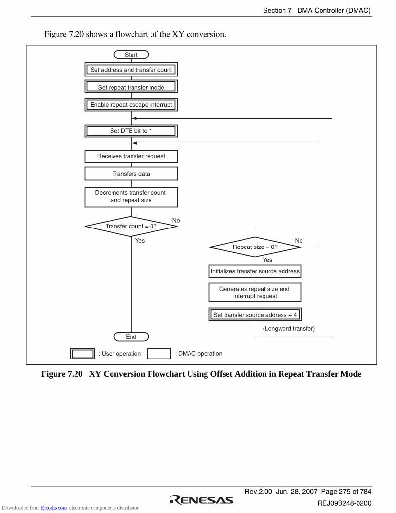
Section 7 DMA Controller (DMAC)
Rev.2.00 Jun. 28, 2007 Page 275 of 784
REJ09B248-0200
Figure 7.20 shows a flowchart of the XY conversion.
: User operation : DMAC operation
Start
Set address and transfer count
Set repeat transfer mode
Set DTE bit to 1
Receives transfer request
Transfers data
Decrements transfer count and repeat size
Enable repeat escape interrupt
Set transfer source address + 4
Initializes transfer source address
Generates repeat size end interrupt request
Transfer count = 0?
Repeat size = 0?
End
No
NoYes
Yes
(Longword transfer)
Figure 7.20 XY Conversion Flowchart Using Offset Addition in Repeat Transfer Mode
Downloaded from Elcodis.com electronic components distributor
Section 7 DMA Controller (DMAC)
Rev.2.00 Jun. 28, 2007 Page 276 of 784
REJ09B248-0200
(3) Offset Subtraction
When setting the negative value in DOFR, the offset value must be 2's complement. The 2's complement is obtained by the following formula.
2's complement of offset = 1 + ~offset (~: bit inversion)
Example: 2's complement of H'0001FFFF = H'FFFE0000 + H'00000001 = H'FFFE0001
The value of 2's complement can be obtained by the NEG.L instruction.
7.5.7 Register during DMA Transfer
The DMAC registers are updated by a DMA transfer. The value to be updated differs according to the other settings and transfer state. The registers to be updated are DSAR, DDAR, DTCR, bits BKSZH and BKSZ in DBSR, and the DTE, ACT, ERRF, ESIF, and DTIF bits in DMDR.
(1) DMA Source Address Register
When the transfer source address set in DSAR is accessed, the contents of DSAR are output and then are updated to the next address.
The increment or decrement can be specified by bits SAT1 and SAT0 in DACR. When SAT1 and SAT0 = B'00, the address is fixed. When SAT1 and SAT0 = B'01, the address is added with the offset. When SAT1 and SAT0 = B'10, the address is incremented. When SAT1 and SAT0 = B'11, the address is decremented. The size of increment or decrement depends on the data access size.
The data access size is specified by bits DTSZ1 and DTSZ0 in DMDR. When DTSZ1 and DTSZ0 = B'00, the data access size is byte and the address is incremented or decremented by 1. When DTSZ1 and DTSZ0 = B'01, the data access size is word and the address is incremented or decremented by 2. When DTSZ1 and DTSZ0 = B'10, the data access size is longword and the address is incremented or decremented by 4. Even if the access data size of the source address is word or longword, when the source address is not aligned with the word or longword boundary, the read bus cycle is divided into byte or word cycles. While data of one word or one longword is being read, the size of increment or decrement is changing according to the actual data access size, for example, +1 or +2 for byte or word data. After one word or one longword of data is read, the address when the read cycle is started is incremented or decremented by the value according to bits SAT1 and SAT0.
Downloaded from Elcodis.com electronic components distributor

Section 7 DMA Controller (DMAC)
Rev.2.00 Jun. 28, 2007 Page 277 of 784
REJ09B248-0200
In block or repeat transfer mode, when the block or repeat size of data transfers is completed while the block or repeat area is specified to the source address side, the source address returns to the transfer start address and is not affected by the address update.
When the extended repeat area is specified to the source address side, operation follows the setting. The upper address bits are fixed and is not affected by the address update.
While data is being transferred, DSAR must be accessed in longwords. If the upper word and lower word are read separately, incorrect data may be read from since the contents of DSAR during the transfer may be updated regardless of the access by the CPU. Moreover, DSAR for the channel being transferred must not be written to.
(2) DMA Destination Address Register
When the transfer destination address set in DDAR is accessed, the contents of DDAR are output and then are updated to the next address.
The increment or decrement can be specified by bits DAT1 and DAT0 in DACR. When DAT1 and DAT0 = B'00, the address is fixed. When DAT1 and DAT0 = B'01, the address is added with the offset. When DAT1 and DAT0 = B'10, the address is incremented. When DAT1 and DAT0 = B'11, the address is decremented. The incrementing or decrementing size depends on the data access size.
The data access size is specified by bits DTSZ1 and DTSZ0 in DMDR. When DTSZ1 and DTSZ0 = B'00, the data access size is byte and the address is incremented or decremented by 1. When DTSZ1 and DTSZ0 = B'01, the data access size is word and the address is incremented or decremented by 2. When DTSZ1 and DTSZ0 = B'10, the data access size is longword and the address is incremented or decremented by 4. Even if the access data size of the destination address is word or longword, when the destination address is not aligned with the word or longword boundary, the write bus cycle is divided into byte and word cycles. While one word or one longword of data is being written, the incrementing or decrementing size is changing according to the actual data access size, for example, +1 or +2 for byte or word data. After the one word or one longword of data is written, the address when the write cycle is started is incremented or decremented by the value according to bits SAT1 and SAT0.
In block or repeat transfer mode, when the block or repeat size of data transfers is completed while the block or repeat area is specified to the destination address side, the destination address returns to the transfer start address and is not affected by the address update.
Downloaded from Elcodis.com electronic components distributor

Section 7 DMA Controller (DMAC)
Rev.2.00 Jun. 28, 2007 Page 278 of 784
REJ09B248-0200
When the extended repeat area is specified to the destination address side, operation follows the setting. The upper address bits are fixed and is not affected by the address update.
While data is being transferred, DDAR must be accessed in longwords. If the upper word and lower word are read separately, incorrect data may be read from since the contents of DDAR during the transfer may be updated regardless of the access by the CPU. Moreover, DDAR for the channel being transferred must not be written to.
(3) DMA Transfer Count Register (DTCR)
A DMA transfer decrements the contents of DTCR by the transferred bytes. When byte data is transferred, DTCR is decremented by 1. When word data is transferred, DTCR is decremented by 2. When longword data is transferred, DTCR is decremented by 4. However, when DTCR = 0, the contents of DTCR are not changed since the number of transfers is not counted.
While data is being transferred, all the bits of DTCR may be changed. DTCR must be accessed in longwords. If the upper word and lower word are read separately, incorrect data may be read from since the contents of DTCR during the transfer may be updated regardless of the access by the CPU. Moreover, DTCR for the channel being transferred must not be written to.
When a conflict occurs between the address update by DMA transfer and write access by the CPU, the CPU has priority. When a conflict occurs between change from 1, 2, or 4 to 0 in DTCR and write access by the CPU (other than 0), the CPU has priority in writing to DTCR. However, the transfer is stopped.
(4) DMA Block Size Register (DBSR)
DBSR is enabled in block or repeat transfer mode. Bits 31 to 16 in DBSR function as BKSZH and bits 15 to 0 in DBSR function as BKSZ. The BKSZH bits (16 bits) store the block size and repeat size and its value is not changed. The BKSZ bits (16 bits) function as a counter for the block size and repeat size and its value is decremented every transfer by 1. When the BKSZ value is to change from 1 to 0 by a DMA transfer, 0 is not stored but the BKSZH value is loaded into the BKSZ bits.
Since the upper 16 bits of DBSR are not updated, DBSR can be accessed in words.
DBSR for the channel being transferred must not be written to.
Downloaded from Elcodis.com electronic components distributor
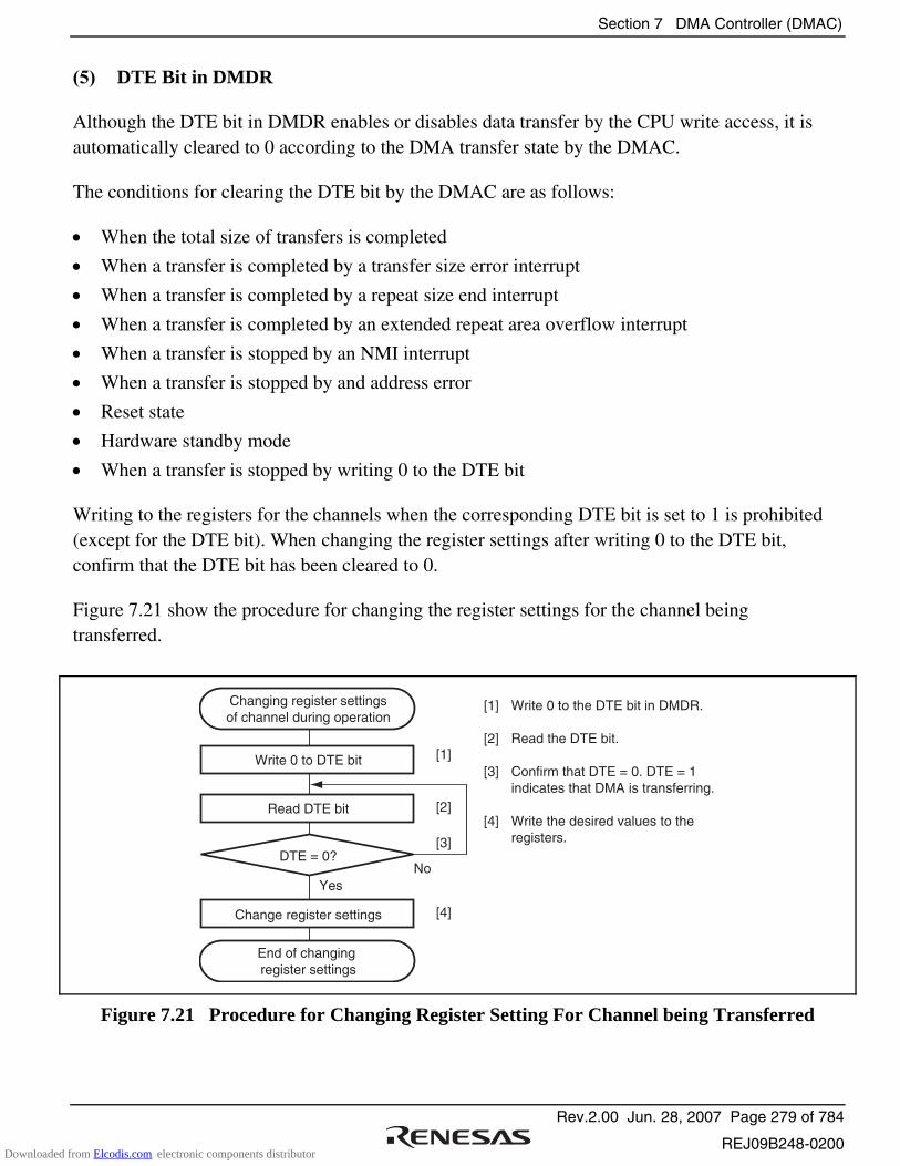
Section 7 DMA Controller (DMAC)
Rev.2.00 Jun. 28, 2007 Page 279 of 784
REJ09B248-0200
(5) DTE Bit in DMDR
Although the DTE bit in DMDR enables or disables data transfer by the CPU write access, it is automatically cleared to 0 according to the DMA transfer state by the DMAC.
The conditions for clearing the DTE bit by the DMAC are as follows:
• When the total size of transfers is completed
• When a transfer is completed by a transfer size error interrupt
• When a transfer is completed by a repeat size end interrupt
• When a transfer is completed by an extended repeat area overflow interrupt
• When a transfer is stopped by an NMI interrupt
• When a transfer is stopped by and address error
• Reset state
• Hardware standby mode
• When a transfer is stopped by writing 0 to the DTE bit Writing to the registers for the channels when the corresponding DTE bit is set to 1 is prohibited (except for the DTE bit). When changing the register settings after writing 0 to the DTE bit, confirm that the DTE bit has been cleared to 0.
Figure 7.21 show the procedure for changing the register settings for the channel being transferred.
Read DTE bit
Write 0 to DTE bit
Change register settings
DTE = 0?
[1]
[2]
[3]
[4]
NoYes
Changing register settingsof channel during operation
End of changing register settings
[1] Write 0 to the DTE bit in DMDR.
[2] Read the DTE bit.
[3] Confirm that DTE = 0. DTE = 1 indicates that DMA is transferring.
[4] Write the desired values to the registers.
Figure 7.21 Procedure for Changing Register Setting For Channel being Transferred
Downloaded from Elcodis.com electronic components distributor

Section 7 DMA Controller (DMAC)
Rev.2.00 Jun. 28, 2007 Page 280 of 784
REJ09B248-0200
(6) ACT Bit in DMDR
The ACT bit in DMDR indicates whether the DMAC is in the idle or active state. When DTE = 0 or DTE = 1 and the DMAC is waiting for a transfer request, the ACT bit is 0. Otherwise (the DMAC is in the active state), the ACT bit is 1. When individual transfers are stopped by writing 0 and the transfer is not completed, the ACT bit retains 1.
In block transfer mode, even if individual transfers are stopped by writing 0 to the DTE bit, the 1-block size of transfers is not stopped. The ACT bit retains 1 from writing 0 to the DTE bit to completion of a 1-block size transfer.
In burst mode, up to three times of DMA transfer are performed from the cycle in which the DTE bit is written to 0. The ACT bit retains 1 from writing 0 to the DTE bit to completion of DMA transfer.
(7) ERRF Bit in DMDR
When an address error or an NMI interrupt occur, the DMAC clears the DTE bits for all the channels to stop a transfer. In addition, it sets the ERRF bit in DMDR_0 to 1 to indicate that an address error or an NMI interrupt has occurred regardless of whether or not the DMAC is in operation.
(8) ESIF Bit in DMDR
When an interrupt by an transfer size error, a repeat size end, or an extended repeat area overflow is requested, the ESIF bit in DMDR is set to 1. When both the ESIF and ESIE bits are set to 1, a transfer escape interrupt is requested to the CPU or DTC.
The ESIF bit is set to 1 when the ACT bit in DMDR is cleared to 0 to stop a transfer after the bus cycle of the interrupt source is completed.
The ESIF bit is automatically cleared to 0 and a transfer request is cleared if the transfer is resumed by setting the DTE bit to 1 during interrupt handling.
For details on interrupts, see section 7.8, Interrupt Sources.
Downloaded from Elcodis.com electronic components distributor

Section 7 DMA Controller (DMAC)
Rev.2.00 Jun. 28, 2007 Page 281 of 784
REJ09B248-0200
(9) DTIF Bit in DMDR
The DTIF bit in DMDR is set to 1 after the total transfer size of transfers is completed. When both the DTIF and DTIE bits in DMDR are set to 1, a transfer end interrupt by the transfer counter is requested to the CPU or DTC.
The DTIF bit is set to 1 when the ACT bit in DMDR is cleared to 0 to stop a transfer after the bus cycle is completed.
The DTIF bit is automatically cleared to 0 and a transfer request is cleared if the transfer is resumed by setting the DTE bit to 1 during interrupt handling.
For details on interrupts, see section 7.8, Interrupt Sources.
7.5.8 Priority of Channels
The channels of the DMAC are given following priority levels: channel 0 > channel 1 > channel 2 > channel3. Table 7.6 shows the priority levels among the DMAC channels.
Table 7.6 Priority among DMAC Channels
Channel Priority
Channel 0 High
Channel 1
Channel 2
Channel 3 Low
The channel having highest priority other than the channel being transferred is selected when a transfer is requested from other channels. The selected channel starts the transfer after the channel being transferred releases the bus. At this time, when a bus master other than the DMAC requests the bus, the cycle for the bus master is inserted.
In a burst transfer or a block transfer, channels are not switched.
Downloaded from Elcodis.com electronic components distributor

Section 7 DMA Controller (DMAC)
Rev.2.00 Jun. 28, 2007 Page 282 of 784
REJ09B248-0200
Figure 7.22 shows a transfer example when multiple transfer requests from channels 0 to 2.
Channel 0 Channel 1Busreleased
Busreleased Channel 2
Channel 0 transfer Channel 1 transfer Channel 2 transfer
Channel 0 Channel 1 Channel 2Wait Wait
Request cleared
Request cleared
Request cleared
Requestretained
Requestretained
Requestretained
Selected
SelectedNotselected
Address bus
Channel 0
Channel 1
Channel 2
Bφ
DMACoperation
Figure 7.22 Example of Timing for Channel Priority
Downloaded from Elcodis.com electronic components distributor

Section 7 DMA Controller (DMAC)
Rev.2.00 Jun. 28, 2007 Page 283 of 784
REJ09B248-0200
7.5.9 DMA Basic Bus Cycle
Figure 7.23 shows an examples of signal timing of a basic bus cycle. In figure 7.23, data is transferred in words from the 16-bit 2-state access space to the 8-bit 3-state access space. When the bus mastership is passed from the DMAC to the CPU, data is read from the source address and it is written to the destination address. The bus is not released between the read and write cycles by other bus requests. DMAC bus cycles follows the bus controller settings.
CPU cycle DMAC cycle (one word transfer) CPU cycle
Address bus
Bφ
T1 T2 T1 T2 T3 T1 T2 T3
Source address Destination address
RD
LHWR
LLWR
High
Figure 7.23 Example of Bus Timing of DMA Transfer
Downloaded from Elcodis.com electronic components distributor
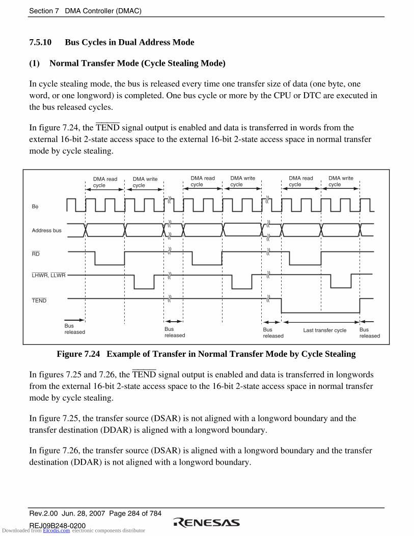
Section 7 DMA Controller (DMAC)
Rev.2.00 Jun. 28, 2007 Page 284 of 784
REJ09B248-0200
7.5.10 Bus Cycles in Dual Address Mode
(1) Normal Transfer Mode (Cycle Stealing Mode)
In cycle stealing mode, the bus is released every time one transfer size of data (one byte, one word, or one longword) is completed. One bus cycle or more by the CPU or DTC are executed in the bus released cycles.
In figure 7.24, the TEND signal output is enabled and data is transferred in words from the external 16-bit 2-state access space to the external 16-bit 2-state access space in normal transfer mode by cycle stealing.
DMA readcycle
DMA writecycle
Address bus
DMA readcycle
DMA writecycle
DMA readcycle
DMA writecycle
Bφ
RD
LHWR, LLWR
TEND
Bus released Bus
releasedBus released
Bus released
Last transfer cycle
Figure 7.24 Example of Transfer in Normal Transfer Mode by Cycle Stealing
In figures 7.25 and 7.26, the TEND signal output is enabled and data is transferred in longwords from the external 16-bit 2-state access space to the 16-bit 2-state access space in normal transfer mode by cycle stealing.
In figure 7.25, the transfer source (DSAR) is not aligned with a longword boundary and the transfer destination (DDAR) is aligned with a longword boundary.
In figure 7.26, the transfer source (DSAR) is aligned with a longword boundary and the transfer destination (DDAR) is not aligned with a longword boundary.
Downloaded from Elcodis.com electronic components distributor

Section 7 DMA Controller (DMAC)
Rev.2.00 Jun. 28, 2007 Page 285 of 784
REJ09B248-0200
Address bus
DMA wordwrite cycle
DMA byteread cycle
DMA byteread cycle
DMA wordread cycle
DMA wordwrite cycle
DMA wordwrite cycle
DMA byteread cycle
DMA byteread cycle
DMA wordread cycle
DMA wordwrite cycle
Bφ
RD
LLWR
LHWR
TEND
Bus released
Bus released
Bus released
Last transfer cycle
4m + 1 4m + 2 4m + 4 4n + 4 4n + 64n 4n +2 4m + 5 4m + 6 4m + 8
m and n are integers.
Figure 7.25 Example of Transfer in Normal Transfer Mode by Cycle Stealing (Transfer Source DSAR = Odd Address and Source Address Increment)
DMA wordread cycle
DMA bytewrite cycle
DMA wordread cycle
Address bus
DMA bytewrite cycle
DMA bytewrite cycle
DMA wordwrite cycle
DMA wordread cycle
DMA bytewrite cycle
DMA wordread cycle
DMA wordwrite cycle
Bφ
RD
LLWR
LHWR
TEND
Bus released
Bus released
Bus released
Last transfer cycle
4m 4m + 2 4n + 5 4n + 2 4n + 44n + 6 4n + 8 4m + 4 4m + 6 4n + 1
m and n are integers.
Figure 7.26 Example of Transfer in Normal Transfer Mode by Cycle Stealing (Transfer Destination DDAR = Odd Address and Destination Address Decrement)
Downloaded from Elcodis.com electronic components distributor

Section 7 DMA Controller (DMAC)
Rev.2.00 Jun. 28, 2007 Page 286 of 784
REJ09B248-0200
(2) Normal Transfer Mode (Burst Mode)
In burst mode, one byte, one word, or one longword of data continues to be transferred until the transfer end condition is satisfied.
When a burst transfer starts, a transfer request from a channel having priority is suspended until the burst transfer is completed.
In figure 7.27, the TEND signal output is enabled and data is transferred in words from the external 16-bit 2-state access space to the external 16-bit 2-state access space in normal transfer mode by burst access.
DMA read cycle DMA read cycleDMA write cycle
Address bus
DMA write cycle DMA read cycle DMA write cycle
Bφ
RD
LHWR, LLWR
TEND
Bus released
Bus released
Last transfer cycle
Burst transfer
Figure 7.27 Example of Transfer in Normal Transfer Mode by Burst Access
Downloaded from Elcodis.com electronic components distributor
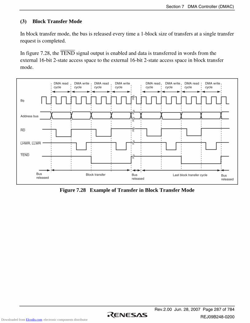
Section 7 DMA Controller (DMAC)
Rev.2.00 Jun. 28, 2007 Page 287 of 784
REJ09B248-0200
(3) Block Transfer Mode
In block transfer mode, the bus is released every time a 1-block size of transfers at a single transfer request is completed.
In figure 7.28, the TEND signal output is enabled and data is transferred in words from the external 16-bit 2-state access space to the external 16-bit 2-state access space in block transfer mode.
DMA read cycle
DMA read cycle
DMA write cycle
Address bus
DMA write cycle
DMA read cycle
DMA read cycle
DMA write cycle
DMA write cycle
Bφ
RD
LHWR, LLWR
TEND
Bus released
Bus released
Bus released
Last block transfer cycleBlock transfer
Figure 7.28 Example of Transfer in Block Transfer Mode
Downloaded from Elcodis.com electronic components distributor

Section 7 DMA Controller (DMAC)
Rev.2.00 Jun. 28, 2007 Page 288 of 784
REJ09B248-0200
(4) Activation Timing by DREQ Falling Edge
Figure 7.29 shows an example of normal transfer mode activated by the DREQ signal falling edge.
The DREQ signal is sampled every cycle from the next rising edge of the Bφ signal immediately after the DTE bit write cycle.
When a low level of the DREQ signal is detected while a transfer request by the DREQ signal is enabled, a transfer request is held in the DMAC. When the DMAC is activated, the transfer request is cleared and starts detecting a high level of the DREQ signal for falling edge detection. If a high level of the DREQ signal has been detected until completion of the DMA write cycle, receiving the next transfer request resumes and then a low level of the DREQ signal is detected. This operation is repeated until the transfer is completed.
Request
Wait Wait Wait
RequestDuration of transferrequest disabled
Duration of transferrequest disabled
Min. of 3 cycles Min. of 3 cycles
Transfer source Transfer destination Transfer destinationTransfer source
Read Write Read Write
Bus released Bus releasedBus releasedDMA read
cycleDMA write
cycleDMA read
cycleDMA write
cycle
Bφ
DREQ
Address bus
DMAoperation
Channel
[1] [2] [3] [4] [5] [6] [7]
Transfer request enable resumed Transfer request enable resumed
[1] After DMA transfer request is enabled, a low level of the DREQ signal is detected at the rising edge of the Bφ signal and a transfer request is held.[2][5] The DMAC is activated and the transfer request is cleared.[3][6] A DMA cycle is started and sampling the DREQ signal at the rising edge of the Bφ signal is started to detect a high level of the DREQ signal.[4][7] When a high level of the DREQ signal has been detected, transfer request enable is resumed after completion of the write cycle. (A low level of the DREQ signal is detected at the rising edge of the Bφ signal and a transfer request is held. This is the same as [1].)
Figure 7.29 Example of Transfer in Normal Transfer Mode Activated by DREQ Falling Edge
Downloaded from Elcodis.com electronic components distributor
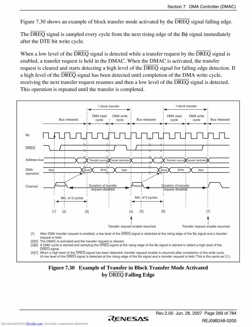
Section 7 DMA Controller (DMAC)
Rev.2.00 Jun. 28, 2007 Page 289 of 784
REJ09B248-0200
Figure 7.30 shows an example of block transfer mode activated by the DREQ signal falling edge.
The DREQ signal is sampled every cycle from the next rising edge of the Bφ signal immediately after the DTE bit write cycle.
When a low level of the DREQ signal is detected while a transfer request by the DREQ signal is enabled, a transfer request is held in the DMAC. When the DMAC is activated, the transfer request is cleared and starts detecting a high level of the DREQ signal for falling edge detection. If a high level of the DREQ signal has been detected until completion of the DMA write cycle, receiving the next transfer request resumes and then a low level of the DREQ signal is detected. This operation is repeated until the transfer is completed.
Request
Wait Wait Wait
RequestDuration of transferrequest disabled
Duration of transferrequest disabled
Min. of 3 cycles Min. of 3 cycles
Transfer source Transfer destination Transfer destinationTransfer source
Read Write Read Write
Bus released Bus releasedBus releasedDMA read
cycleDMA write
cycleDMA read
cycleDMA write
cycle
Bφ
DREQ
Address bus
DMAoperation
Channel
[1] [2] [3] [4] [5] [6] [7]
Transfer request enable resumed Transfer request enable resumed
[1] After DMA transfer request is enabled, a low level of the DREQ signal is detected at the rising edge of the Bφ signal and a transfer request is held.[2][5] The DMAC is activated and the transfer request is cleared.[3][6] A DMA cycle is started and sampling the DREQ signal at the rising edge of the Bφ signal is started to detect a high level of the DREQ signal.[4][7] When a high level of the DREQ signal has been detected, transfer request enable is resumed after completion of the write cycle. (A low level of the DREQ signal is detected at the rising edge of the Bφ signal and a transfer request is held. This is the same as [1].)
1-block transfer1-block transfer
Figure 7.30 Example of Transfer in Block Transfer Mode Activated by DREQ Falling Edge
Downloaded from Elcodis.com electronic components distributor
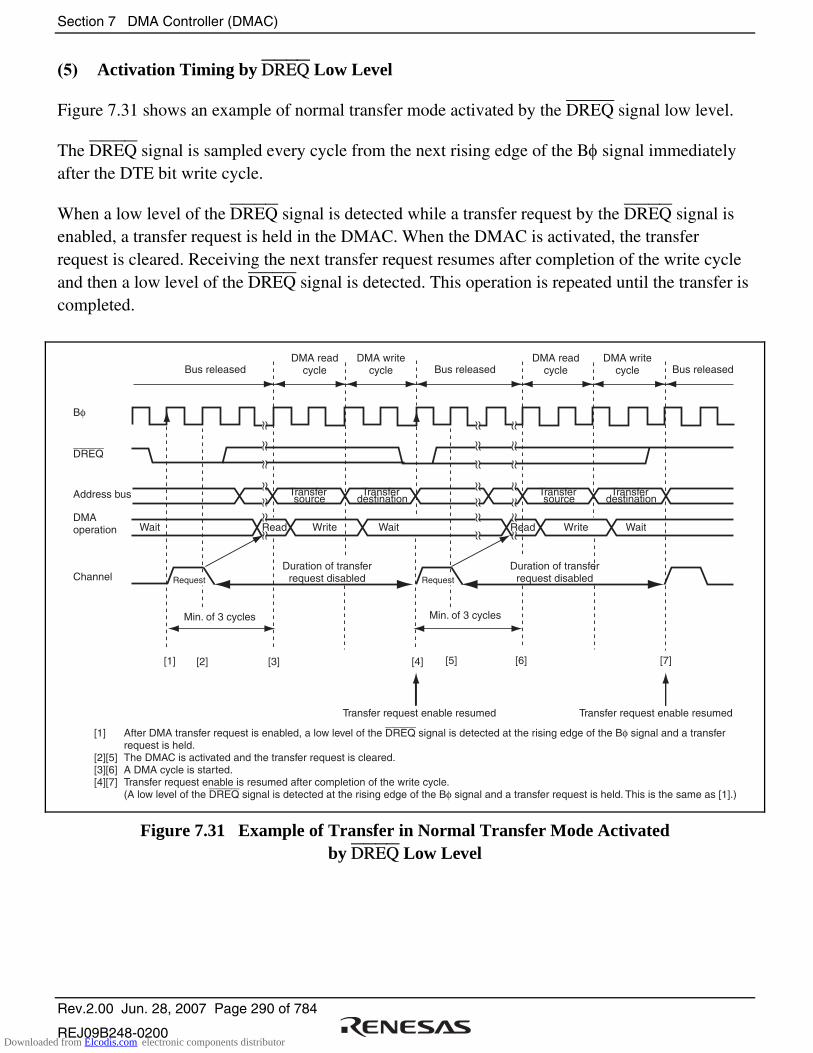
Section 7 DMA Controller (DMAC)
Rev.2.00 Jun. 28, 2007 Page 290 of 784
REJ09B248-0200
(5) Activation Timing by DREQ Low Level
Figure 7.31 shows an example of normal transfer mode activated by the DREQ signal low level.
The DREQ signal is sampled every cycle from the next rising edge of the Bφ signal immediately after the DTE bit write cycle.
When a low level of the DREQ signal is detected while a transfer request by the DREQ signal is enabled, a transfer request is held in the DMAC. When the DMAC is activated, the transfer request is cleared. Receiving the next transfer request resumes after completion of the write cycle and then a low level of the DREQ signal is detected. This operation is repeated until the transfer is completed.
Wait Wait Wait
Min. of 3 cycles Min. of 3 cycles
Transfer source
Transfer destination
Transfer destination
Transfer source
Read Write Read Write
Bus released Bus releasedBus releasedDMA read
cycleDMA write
cycleDMA read
cycleDMA write
cycle
Bφ
DREQ
Address bus
DMAoperation
Channel
[1] [2] [3] [4] [5] [6] [7]
Transfer request enable resumed Transfer request enable resumed
[1] After DMA transfer request is enabled, a low level of the DREQ signal is detected at the rising edge of the Bφ signal and a transfer request is held.[2][5] The DMAC is activated and the transfer request is cleared.[3][6] A DMA cycle is started.[4][7] Transfer request enable is resumed after completion of the write cycle. (A low level of the DREQ signal is detected at the rising edge of the Bφ signal and a transfer request is held. This is the same as [1].)
Request Request
Duration of transferrequest disabled
Duration of transferrequest disabled
Figure 7.31 Example of Transfer in Normal Transfer Mode Activated by DREQ Low Level
Downloaded from Elcodis.com electronic components distributor

Section 7 DMA Controller (DMAC)
Rev.2.00 Jun. 28, 2007 Page 291 of 784
REJ09B248-0200
Figure 7.32 shows an example of block transfer mode activated by the DREQ signal low level.
The DREQ signal is sampled every cycle from the next rising edge of the Bφ signal immediately after the DTE bit write cycle.
When a low level of the DREQ signal is detected while a transfer request by the DREQ signal is enabled, a transfer request is held in the DMAC. When the DMAC is activated, the transfer request is cleared. Receiving the next transfer request resumes after completion of the write cycle and then a low level of the DREQ signal is detected. This operation is repeated until the transfer is completed.
Wait Wait Wait
Min. of 3 cycles Min. of 3 cycles
Transfer source
Transfer destination
Transfer destination
Transfer source
Read Write Read Write
Bus released Bus releasedBus releasedDMA read
cycleDMA write
cycleDMA read
cycleDMA write
cycle
Bφ
DREQ
Address bus
DMAoperation
Channel
[1] [2] [3] [4] [5] [6] [7]
Transfer request enable resumed Transfer request enable resumed
[1] After DMA transfer request is enabled, a low level of the DREQ signal is detected at the rising edge of the Bφ signal and a transfer request is held.[2][5] The DMAC is activated and the transfer request is cleared.[3][6] A DMA cycle is started.[4][7] Transfer request enable is resumed after completion of the write cycle. (A low level of the DREQ signal is detected at the rising edge of the Bφ signal and a transfer request is held. This is the same as [1].)
1-block transfer 1-block transfer
Request Request
Duration of transferrequest disabled
Duration of transferrequest disabled
Figure 7.32 Example of Transfer in Block Transfer Mode Activated by DREQ Low Level
Downloaded from Elcodis.com electronic components distributor
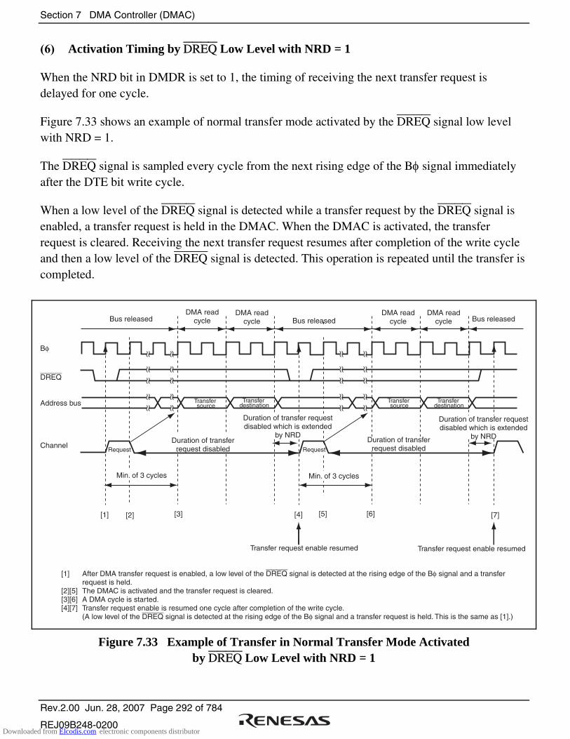
Section 7 DMA Controller (DMAC)
Rev.2.00 Jun. 28, 2007 Page 292 of 784
REJ09B248-0200
(6) Activation Timing by DREQ Low Level with NRD = 1
When the NRD bit in DMDR is set to 1, the timing of receiving the next transfer request is delayed for one cycle.
Figure 7.33 shows an example of normal transfer mode activated by the DREQ signal low level with NRD = 1.
The DREQ signal is sampled every cycle from the next rising edge of the Bφ signal immediately after the DTE bit write cycle.
When a low level of the DREQ signal is detected while a transfer request by the DREQ signal is enabled, a transfer request is held in the DMAC. When the DMAC is activated, the transfer request is cleared. Receiving the next transfer request resumes after completion of the write cycle and then a low level of the DREQ signal is detected. This operation is repeated until the transfer is completed.
Duration of transferrequest disabled
Transfer source
Transfer destination
Transfer destination
Transfer source
Bus released Bus releasedBus releasedDMA read
cycleDMA read
cycleDMA read
cycleDMA read
cycle
Bφ
DREQ
Address bus
Channel
[1] [2] [3] [4] [5] [6] [7]
Transfer request enable resumed Transfer request enable resumed
[1] After DMA transfer request is enabled, a low level of the DREQ signal is detected at the rising edge of the Bφ signal and a transfer request is held.[2][5] The DMAC is activated and the transfer request is cleared.[3][6] A DMA cycle is started.[4][7] Transfer request enable is resumed one cycle after completion of the write cycle. (A low level of the DREQ signal is detected at the rising edge of the Bφ signal and a transfer request is held. This is the same as [1].)
Request Request
Min. of 3 cycles Min. of 3 cycles
Duration of transfer requestdisabled which is extended
by NRD
Duration of transfer requestdisabled which is extended
by NRDDuration of transferrequest disabled
Figure 7.33 Example of Transfer in Normal Transfer Mode Activated by DREQ Low Level with NRD = 1
Downloaded from Elcodis.com electronic components distributor
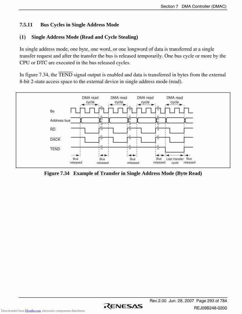
Section 7 DMA Controller (DMAC)
Rev.2.00 Jun. 28, 2007 Page 293 of 784
REJ09B248-0200
7.5.11 Bus Cycles in Single Address Mode
(1) Single Address Mode (Read and Cycle Stealing)
In single address mode, one byte, one word, or one longword of data is transferred at a single transfer request and after the transfer the bus is released temporarily. One bus cycle or more by the CPU or DTC are executed in the bus released cycles.
In figure 7.34, the TEND signal output is enabled and data is transferred in bytes from the external 8-bit 2-state access space to the external device in single address mode (read).
Bus released
Bus released
Bus released
DMA readcycle
DMA readcycle
DMA readcycle
DMA readcycle
Bφ
Address bus
Bus released
Bus released
Last transfercycle
RD
TEND
DACK
Figure 7.34 Example of Transfer in Single Address Mode (Byte Read)
Downloaded from Elcodis.com electronic components distributor
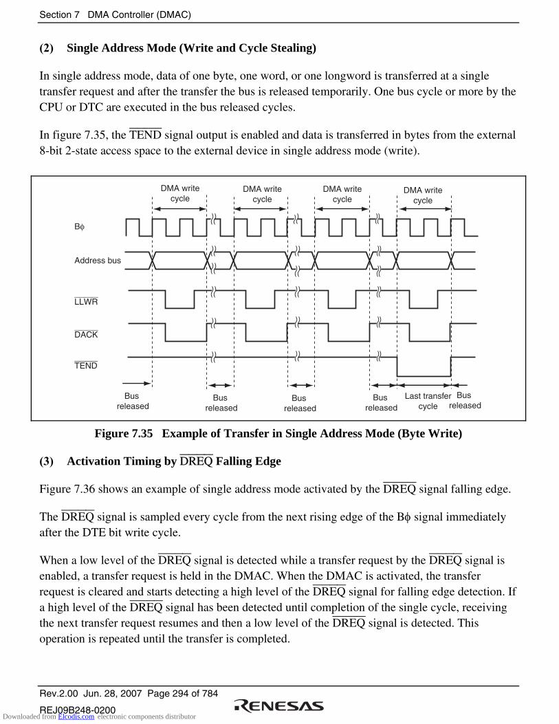
Section 7 DMA Controller (DMAC)
Rev.2.00 Jun. 28, 2007 Page 294 of 784
REJ09B248-0200
(2) Single Address Mode (Write and Cycle Stealing)
In single address mode, data of one byte, one word, or one longword is transferred at a single transfer request and after the transfer the bus is released temporarily. One bus cycle or more by the CPU or DTC are executed in the bus released cycles.
In figure 7.35, the TEND signal output is enabled and data is transferred in bytes from the external 8-bit 2-state access space to the external device in single address mode (write).
Bus released
Bus released
DMA writecycle
Bφ
Address bus
Bus released
Bus released
Last transfercycle
TEND
DACK
DMA writecycle
DMA writecycle
DMA writecycle
LLWR
Bus released
Figure 7.35 Example of Transfer in Single Address Mode (Byte Write)
(3) Activation Timing by DREQ Falling Edge
Figure 7.36 shows an example of single address mode activated by the DREQ signal falling edge.
The DREQ signal is sampled every cycle from the next rising edge of the Bφ signal immediately after the DTE bit write cycle.
When a low level of the DREQ signal is detected while a transfer request by the DREQ signal is enabled, a transfer request is held in the DMAC. When the DMAC is activated, the transfer request is cleared and starts detecting a high level of the DREQ signal for falling edge detection. If a high level of the DREQ signal has been detected until completion of the single cycle, receiving the next transfer request resumes and then a low level of the DREQ signal is detected. This operation is repeated until the transfer is completed.
Downloaded from Elcodis.com electronic components distributor

Section 7 DMA Controller (DMAC)
Rev.2.00 Jun. 28, 2007 Page 295 of 784
REJ09B248-0200
Request
Wait Wait Wait
Request
Min. of 3 cyclesMin. of 3 cycles
Transfer source/Transfer destination
Single
Bus released
Bus released
Bus released
DMA singlecycle
DMA singlecycle
Bφ
DREQ
Address bus
DMAoperation
Channel
[1] [2] [3] [4] [5] [6] [7]
Transfer request enable resumed
Transfer request enable resumed
[1] After DMA transfer request is enabled, a low level of the DREQ signal is detected at the rising edge of the Bφ signal and a transfer request is held.[2][5] The DMAC is activated and the transfer request is cleared.[3][6] A DMA cycle is started and sampling the DREQ signal at the rising edge of the Bφ signal is started to detect a high level of the DREQ signal.[4][7] When a high level of the DREQ signal has been detected, transfer enable is resumed after completion of the write cycle. (A low level of the DREQ signal is detected at the rising edge of the Bφ signal and a transfer request is held. This is the same as [1].)
Transfer source/Transfer destination
Single
DACK
Duration of transferrequest disabled
Duration of transferrequest disabled
Figure 7.36 Example of Transfer in Single Address Mode Activated by DREQ Falling Edge
Downloaded from Elcodis.com electronic components distributor

Section 7 DMA Controller (DMAC)
Rev.2.00 Jun. 28, 2007 Page 296 of 784
REJ09B248-0200
(4) Activation Timing by DREQ Low Level
Figure 7.37 shows an example of normal transfer mode activated by the DREQ signal low level.
The DREQ signal is sampled every cycle from the next rising edge of the Bφ signal immediately after the DTE bit write cycle.
When a low level of the DREQ signal is detected while a transfer request by the DREQ signal is enabled, a transfer request is held in the DMAC. When the DMAC is activated, the transfer request is cleared. Receiving the next transfer request resumes after completion of the single cycle and then a low level of the DREQ signal is detected. This operation is repeated until the transfer is completed.
Request
Wait Wait Wait
Request
Min. of 3 cyclesMin. of 3 cycles
Transfer source/Transfer destination
Single
Bus released
Bus released
Bus released
DMA singlecycle
DMA singlecycle
Bφ
DREQ
Address bus
DMAoperation
Channel
[1] [2] [3] [4] [5] [6] [7]
Transfer request enable resumed
Transfer request enable resumed
[1] After DMA transfer request is enabled, a low level of the DREQ signal is detected at the rising edge of the Bφ signal and a transfer request is held.[2][5] The DMAC is activated and the transfer request is cleared.[3][6] A DMA cycle is started.[4][7] Transfer request enable is resumed after completion of the single cycle. (A low level of the DREQ signal is detected at the rising edge of the Bφ signal and a transfer request is held. This is the same as [1].)
Transfer source/Transfer destination
Single
DACK
Duration of transferrequest disabled
Duration of transferrequest disabled
Figure 7.37 Example of Transfer in Single Address Mode Activated by DREQ Low Level
Downloaded from Elcodis.com electronic components distributor
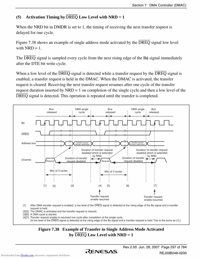
Section 7 DMA Controller (DMAC)
Rev.2.00 Jun. 28, 2007 Page 297 of 784
REJ09B248-0200
(5) Activation Timing by DREQ Low Level with NRD = 1
When the NRD bit in DMDR is set to 1, the timing of receiving the next transfer request is delayed for one cycle.
Figure 7.38 shows an example of single address mode activated by the DREQ signal low level with NRD = 1.
The DREQ signal is sampled every cycle from the next rising edge of the Bφ signal immediately after the DTE bit write cycle.
When a low level of the DREQ signal is detected while a transfer request by the DREQ signal is enabled, a transfer request is held in the DMAC. When the DMAC is activated, the transfer request is cleared. Receiving the next transfer request resumes after one cycle of the transfer request duration inserted by NRD = 1 on completion of the single cycle and then a low level of the DREQ signal is detected. This operation is repeated until the transfer is completed.
Min. of 3 cyclesMin. of 3 cycles
DMA singlecycle
DMA singlecycle
Bφ
DREQ
Address bus
Channel
[1] [2] [3] [4] [5] [6] [7]
[1] After DMA transfer request is enabled, a low level of the DREQ signal is detected at the rising edge of the Bφ signal and a transfer request is held.[2][5] The DMAC is activated and the transfer request is cleared.[3][6] A DMA cycle is started.[4][7] Transfer request enable is resumed one cycle after completion of the single cycle. (A low level of the DREQ signal is detected at the rising edge of the Bφ signal and a transfer request is held. This is the same as [1].)
Transfer source/Transfer destination
Bus released
Bus released
Transfer request enable resumed
Transfer request enable resumed
Transfer source/Transfer destination
Request RequestDuration of transfer
request disabledDuration of transfer
request disabled
Duration of transfer requestdisabled which is extended
by NRD
Duration of transfer requestdisabled which is extended
by NRD
Bus released
Figure 7.38 Example of Transfer in Single Address Mode Activated by DREQ Low Level with NRD = 1
Downloaded from Elcodis.com electronic components distributor

Section 7 DMA Controller (DMAC)
Rev.2.00 Jun. 28, 2007 Page 298 of 784
REJ09B248-0200
7.6 DMA Transfer End
Operations on completion of a transfer differ according to the transfer end condition. DMA transfer completion is indicated that the DTE and ACT bits in DMDR are changed from 1 to 0.
(1) Transfer End by DTCR Change from 1, 2, or 4, to 0
When DTCR is changed from 1, 2, or 4 to 0, a DMA transfer for the channel is completed. The DTE bit in DMDR is cleared to 0 and the DTIF bit in DMDR is set to 1. At this time, when the DTIE bit in DMDR is set to 1, a transfer end interrupt by the transfer counter is requested. When the DTCR value is 0 before the transfer, the transfer is not stopped.
(2) Transfer End by Transfer Size Error Interrupt
When the following conditions are satisfied while the TSEIE bit in DMDR is set to 1, a transfer size error occurs and a DMA transfer is terminated. At this time, the DTE bit in DMR is cleared to 0 and the ESIF bit in DMDR is set to 1.
• In normal transfer mode and repeat transfer mode, when the next transfer is requested while a transfer is disabled due to the DTCR value less than the data access size
• In block transfer mode, when the next transfer is requested while a transfer is disabled due to the DTCR value less than the block size
When the TSEIE bit in DMDR is cleared to 0, data is transferred until the DTCR value reaches 0. A transfer size error is not generated. Operation in each transfer mode is shown below.
• In normal transfer mode and repeat transfer mode, when the DTCR value is less than the data access size, data is transferred in bytes
• In block transfer mode, when the DTCR value is less than the block size, the specified size of data in DTCR is transferred instead of transferring the block size of data. The transfer is performed in bytes.
(3) Transfer End by Repeat Size End Interrupt
In repeat transfer mode, when the next transfer is requested after completion of a 1-repeat size data transfer while the RPTIE bit in DACR is set to 1, a repeat size end interrupt is requested. When the interrupt is requested to complete DMA transfer, the DTE bit in DMDR is cleared to 0 and the ESIF bit in DMDR is set to 1. Under this condition, setting the DTE bit to 1 resumes the transfer.
In block transfer mode, when the next transfer is requested after completion of a 1-block size data transfer, a repeat size end interrupt can be requested.
Downloaded from Elcodis.com electronic components distributor
Section 7 DMA Controller (DMAC)
Rev.2.00 Jun. 28, 2007 Page 299 of 784
REJ09B248-0200
(4) Transfer End by Interrupt on Extended Repeat Area Overflow
When an overflow on the extended repeat area occurs while the extended repeat area is specified and the SARIE or DARIE bit in DACR is set to 1, an interrupt by an extended repeat area overflow is requested. When the interrupt is requested, the DMA transfer is terminated, the DTE bit in DMDR is cleared to 0, and the ESIF bit in DMDR is set to 1.
In dual address mode, even if an interrupt by an extended repeat area overflow occurs during a read cycle, the following write cycle is performed.
In block transfer mode, even if an interrupt by an extended repeat area overflow occurs during a 1-block transfer, the remaining data is transferred. The transfer is not terminated by an extended repeat area overflow interrupt unless the current transfer is complete.
(5) Transfer End by Clearing DTE Bit in DMDR
When the DTE bit in DMDR is cleared to 0 by the CPU, a transfer is completed after the current DMA cycle and a DMA cycle in which the transfer request is accepted are completed.
In block transfer mode, a DMA transfer is completed after 1-block data is transferred.
(6) Transfer End by NMI Interrupt
When an NMI interrupt is requested, the DTE bits for all the channels are cleared to 0 and the ERRF bit in DMDR_0 is set to 1. When an NMI interrupt is requested during a DMA transfer, the transfer is forced to stop. To perform DMA transfer after an NMI interrupt is requested, clear the ERRF bit to 0 and then set the DTE bits for the channels to 1.
The transfer end timings after an NMI interrupt is requested are shown below.
(a) Normal Transfer Mode and Repeat Transfer Mode
In dual address mode, a DMA transfer is completed after completion of the write cycle for one transfer unit.
In single address mode, a DMA transfer is completed after completion of the bus cycle for one transfer unit.
(b) Block Transfer Mode
A DMA transfer is forced to stop. Since a 1-block size of transfers is not completed, operation is not guaranteed.
In dual address mode, the write cycle corresponding to the read cycle is performed. This is similar to (a) in normal transfer mode.
Downloaded from Elcodis.com electronic components distributor
Section 7 DMA Controller (DMAC)
Rev.2.00 Jun. 28, 2007 Page 300 of 784
REJ09B248-0200
(7) Transfer End by Address Error
When an address error occurs, the DTE bits for all the channels are cleared to 0 and the ERRF bit in DMDR_0 is set to 1. When an address error occurs during a DMA transfer, the transfer is forced to stop. To perform a DMA transfer after an address error occurs, clear the ERRF bit to 0 and then set the DTE bits for the channels.
The transfer end timing after an address error is the same as that after an NMI interrupt.
(8) Transfer End by Hardware Standby Mode or Reset
The DMAC is initialized by a reset and a transition to the hardware standby mode. A DMA transfer is not guaranteed.
7.7 Relationship among DMAC and Other Bus Masters
7.7.1 CPU Priority Control Function Over DMAC
The CPU priority control function over DMAC can be used according to the CPU priority control register (CPUPCR) setting. For details, see section 5.7, CPU Priority Control Function Over DTC and DMAC.
The priority level of the DMAC is specified by bits DMAP2 to DMAP0 and can be specified for each channel.
The priority level of the CPU is specified by bits CPUP2 to CPUP0. The value of bits CPUP2 to CPUP0 is updated according to the exception handling priority.
If the CPU priority control is enabled by the CPUPCE bit in CPUPCR, when the CPU has priority over the DMAC, a transfer request for the corresponding channel is masked and the transfer is not activated. When another channel has priority over or the same as the CPU, a transfer request is received regardless of the priority between channels and the transfer is activated.
The transfer request masked by the CPU priority control function is suspended. When the transfer channel is given priority over the CPU by changing priority levels of the CPU or channel, the transfer request is received and the transfer is resumed. Writing 0 to the DTE bit clears the suspended transfer request.
When the CPUPCE bit is cleared to 0, it is regarded as the lowest priority.
Downloaded from Elcodis.com electronic components distributor
Section 7 DMA Controller (DMAC)
Rev.2.00 Jun. 28, 2007 Page 301 of 784
REJ09B248-0200
7.7.2 Bus Arbitration among DMAC and Other Bus Masters
When DMA transfer cycles are consecutively performed, bus cycles of other bus masters may be inserted between the transfer cycles. The DMAC can release the bus temporarily to pass the bus to other bus masters.
The consecutive DMA transfer cycles may not be divided according to the transfer mode settings to achieve high-speed access.
The read and write cycles of a DMA transfer are not separated. Refreshing, external bus release, and on-chip bus master (CPU or DTC) cycles are not inserted between the read and write cycles of a DMA transfer.
In block transfer mode and an auto request transfer by burst access, bus cycles of the DMA transfer are consecutively performed. For this duration, since the DMAC has priority over the CPU and DTC, accesses to the external space is suspended (the IBCCS bit in the bus control register 2 (BCR2) is cleared to 0).
When the bus is passed to another channel or an auto request transfer by cycle stealing, bus cycles of the DMAC and on-chip bus master are performed alternatively.
When the arbitration function among the DMAC and on-chip bus masters is enabled by setting the IBCCS bit in BCR2, the bus is used alternatively except the bus cycles which are not separated. For details, see section 6, Bus Controller (BSC).
A conflict may occur between external space access of the DMAC and an external bus release cycle. Even if a burst or block transfer is performed by the DMAC, the transfer is stopped temporarily and a cycle of external bus release is inserted by the BSC according to the external bus priority (when the CPU external access and the DTC external access do not have priority over a DMAC transfer, the transfers are not operated until the DMAC releases the bus).
In dual address mode, the DMAC releases the external bus after the external space write cycle. Since the read and write cycles are not separated, the bus is not released.
An internal space (on-chip memory and internal I/O registers) access of the DMAC and an external bus release cycle may be performed at the same time.
Downloaded from Elcodis.com electronic components distributor

Section 7 DMA Controller (DMAC)
Rev.2.00 Jun. 28, 2007 Page 302 of 784
REJ09B248-0200
7.8 Interrupt Sources
The DMAC interrupt sources are a transfer end interrupt by the transfer counter and a transfer escape end interrupt which is generated when a transfer is terminated before the transfer counter reaches 0. Table 7.7 shows interrupt sources and priority.
Table 7.7 Interrupt Sources and Priority
Abbr. Interrupt Sources Priority
DMTEND0 Transfer end interrupt by channel 0 transfer counter High
DMTEND1 Transfer end interrupt by channel 1 transfer counter
DMTEND2 Transfer end interrupt by channel 2 transfer counter
DMTEND3 Transfer end interrupt by channel 3 transfer counter
DMEEND0 Interrupt by channel 0 transfer size error
Interrupt by channel 0 repeat size end
Interrupt by channel 0 extended repeat area overflow on source address
Interrupt by channel 0 extended repeat area overflow on destination address
DMEEND1 Interrupt by channel 1 transfer size error
Interrupt by channel 1 repeat size end
Interrupt by channel 1 extended repeat area overflow on source address
Interrupt by channel 1 extended repeat area overflow on destination address
DMEEND2 Interrupt by channel 2 transfer size error
Interrupt by channel 2 repeat size end
Interrupt by channel 2 extended repeat area overflow on source address
Interrupt by channel 2 extended repeat area overflow on destination address
DMEEND3 Interrupt by channel 3 transfer size error
Interrupt by channel 3 repeat size end
Interrupt by channel 3 extended repeat area overflow on source address
Interrupt by channel 3 extended repeat area overflow on destination address Low
Each interrupt is enabled or disabled by the DTIE and ESIE bits in DMDR for the corresponding channel. A DMTEND interrupt is generated by the combination of the DTIF and DTIE bits in DMDR. A DMEEND interrupt is generated by the combination of the ESIF and ESIE bits in DMDR. The DMEEND interrupt sources are not distinguished. The priority among channels are decided by the interrupt controller and it is shown in table 7.7. For details, see section 5, Interrupt Controller.
Downloaded from Elcodis.com electronic components distributor
Section 7 DMA Controller (DMAC)
Rev.2.00 Jun. 28, 2007 Page 303 of 784
REJ09B248-0200
Each interrupt source is specified by the interrupt enable bit in the register for the corresponding channel. A transfer end interrupt by the transfer counter, a transfer size error interrupt, a repeat size end interrupt, an interrupt by an extended repeat area overflow on the source address, and an interrupt by an extended repeat area overflow on the destination address are enabled or disabled by the DTIE bit in DMDR, the TSEIE bit in DMDR, the RPTIE bit in DACR, SARIE bit in DACR, and the DARIE bit in DACR, respectively.
A transfer end interrupt by the transfer counter is generated when the DTIF bit in DMDR is set to 1. The DTIF bit is set to 1 when DTCR becomes 0 by a transfer while the DTIE bit in DMDR is set to 1.
An interrupt other than the transfer end interrupt by the transfer counter is generated when the ESIF bit in DMDR is set to 1. The ESIF bit is set to 1 when the conditions are satisfied by a transfer while the enable bit is set to 1.
A transfer size error interrupt is generated when the next transfer cannot be performed because the DTCR value is less than the data access size, meaning that the data access size of transfers cannot be performed. In block transfer mode, the block size is compared with the DTCR value for transfer error decision.
A repeat size end interrupt is generated when the next transfer is requested after completion of the repeat size of transfers in repeat transfer mode. Even when the repeat area is not specified in the address register, the transfer can be stopped periodically according to the repeat size. At this time, when a transfer end interrupt by the transfer counter is generated, the ESIF bit is set to 1.
An interrupt by an extended repeat area overflow on the source and destination addresses is generated when the address exceeds the extended repeat area (overflow). At this time, when a transfer end interrupt by the transfer counter, the ESIF bit is set to 1.
Figure 7.39 is a block diagram of interrupts and interrupt flags. To clear an interrupt, clear the DTIF or ESIF bit in DMDR to 0 in the interrupt handling routine or continue the transfer by setting the DTE bit in DMDR after setting the register. Figure 7.40 shows procedure to resume the transfer by clearing an interrupt.
Downloaded from Elcodis.com electronic components distributor

Section 7 DMA Controller (DMAC)
Rev.2.00 Jun. 28, 2007 Page 304 of 784
REJ09B248-0200
TSIE bit
DMAC is activated in transfer size error state
RPTIE bit
DMAC is activated after BKSZ bits are changed from 1 to 0
SARIE bit
Extended repeat area overflow occurs in source address
DARIE bit
Extended repeat area overflow occurs in destination address
DTIE bit
DTIF bit
Transfer end interrupt
[Setting condition]When DTCR becomes 0 and transfer ends
Setting condition is satisfied
ESIE bit
ESIF bit
Transfer escape end interrupt
Figure 7.39 Interrupt and Interrupt Sources
Transfer end interrupthandling routine
Consecutive transfer processing
Registers are specified
DTE bit is set to 1
Interrupt handling routine ends (RTE instruction
executed)
Transfer resume processing end
Transfer resumed after interrupt handling routine
DTIF and ESIF bits are cleared to 0
Interrupt handling routine ends
DTE bit is set to 1
Registers are specified
Transfer resume processing end
[1]
[2]
[3]
[4]
[5]
[6]
[7]
[1] Specify the values in the registers such as transfer counter and address register.[2] Set the DTE bit in DMDR to 1 to resume DMA operation. Setting the DTE bit to 1 automatically clears the DTIF or ESIF bit in DMDR to 0 and an interrupt source is cleared.[3] End the interrupt handling routine by the RTE instruction.[4] Read that the DTIF or the ESIF bit in DMDR = 1 and then write 0 to the bit.[5] Complete the interrupt handling routine and clear the interrupt mask.[6] Specify the values in the registers such as transfer counter and address register.[7] Set the DTE bit to 1 to resume DMA operation.
Figure 7.40 Procedure Example of Resuming Transfer by Clearing Interrupt Source
Downloaded from Elcodis.com electronic components distributor
Section 7 DMA Controller (DMAC)
Rev.2.00 Jun. 28, 2007 Page 305 of 784
REJ09B248-0200
7.9 Notes on Usage
1. DMAC Register Access During Operation
Except for clearing the DTE bit in DMDR, the settings for channels being transferred (including waiting state) must not be changed. The register settings must be changed during the transfer prohibited state.
2. Settings of Module Stop Function
The DMAC operation can be enabled or disabled by the module stop control register. The DMAC is enabled by the initial value.
Setting bit MSTPA13 in MSTPCRA stops the clock supplied to the DMAC and the DMAC enters the module stop state. However, when a transfer for a channel is enabled or when an interrupt is being requested, bit MSTPA13 cannot be set to 1. Clear the DTE bit to 0, clear the DTIF or DTIE bit in DMDR to 0, and then set bit MSTPA13.
When the clock is stopped, the DMAC registers cannot be accessed. However, the following register settings are valid in the module stop state. Disable them before entering the module stop state, if necessary.
TENDE bit in DMDR is 1 (the TEND signal output enabled)
DACKE bit in DMDR is 1 (the DACK signal output enabled) 3. Activation by DREQ Falling Edge
The DREQ falling edge detection is synchronized with the DMAC internal operation.
A. Activation request waiting state: Waiting for detecting the DREQ low level. A transition to 2. is made.
B. Transfer waiting state: Waiting for a DMAC transfer. A transition to 3. is made.
C. Transfer prohibited state: Waiting for detecting the DREQ high level. A transition to 1. is made.
After a DMAC transfer enabled, a transition to 1. is made. Therefore, the DREQ signal is sampled by low level detection at the first activation after a DMAC transfer enabled.
4. Acceptation of Activation Source
At the beginning of an activation source reception, a low level is detected regardless of the setting of DREQ falling edge or low level detection. Therefore, if the DREQ signal is driven low before setting DMDR, the low level is received as a transfer request.
When the DMAC is activated, clear the DREQ signal of the previous transfer.
Downloaded from Elcodis.com electronic components distributor

Section 7 DMA Controller (DMAC)
Rev.2.00 Jun. 28, 2007 Page 306 of 784
REJ09B248-0200
Downloaded from Elcodis.com electronic components distributor

Section 8 Data Transfer Controller (DTC)
Rev.2.00 Jun. 28, 2007 Page 307 of 784
REJ09B248-0200
Section 8 Data Transfer Controller (DTC)
This LSI includes a data transfer controller (DTC). The DTC can be activated to transfer data by an interrupt request.
8.1 Features
• Transfer possible over any number of channels:
Multiple data transfer enabled for one activation source (chain transfer)
Chain transfer specifiable after data transfer (when the counter is 0)
• Three transfer modes
Normal/repeat/block transfer modes selectable
Transfer source and destination addresses can be selected from increment/decrement/fixed
• Short address mode or full address mode selectable
Short address mode
Transfer information is located on a 3-longword boundary
The transfer source and destination addresses can be specified by 24 bits to select a 16-Mbyte address space directly
Full address mode
Transfer information is located on a 4-longword boundary
The transfer source and destination addresses can be specified by 32 bits to select a 4-Gbyte address space directly
• Size of data for data transfer can be specified as byte, word, or longword The bus cycle is divided if an odd address is specified for a word or longword transfer. The bus cycle is divided if address 4n + 2 is specified for a longword transfer.
• A CPU interrupt can be requested for the interrupt that activated the DTC A CPU interrupt can be requested after one data transfer completion A CPU interrupt can be requested after the specified data transfer completion
• Read skip of the transfer information specifiable • Writeback skip executed for the fixed transfer source and destination addresses • Module stop mode specifiable
Downloaded from Elcodis.com electronic components distributor
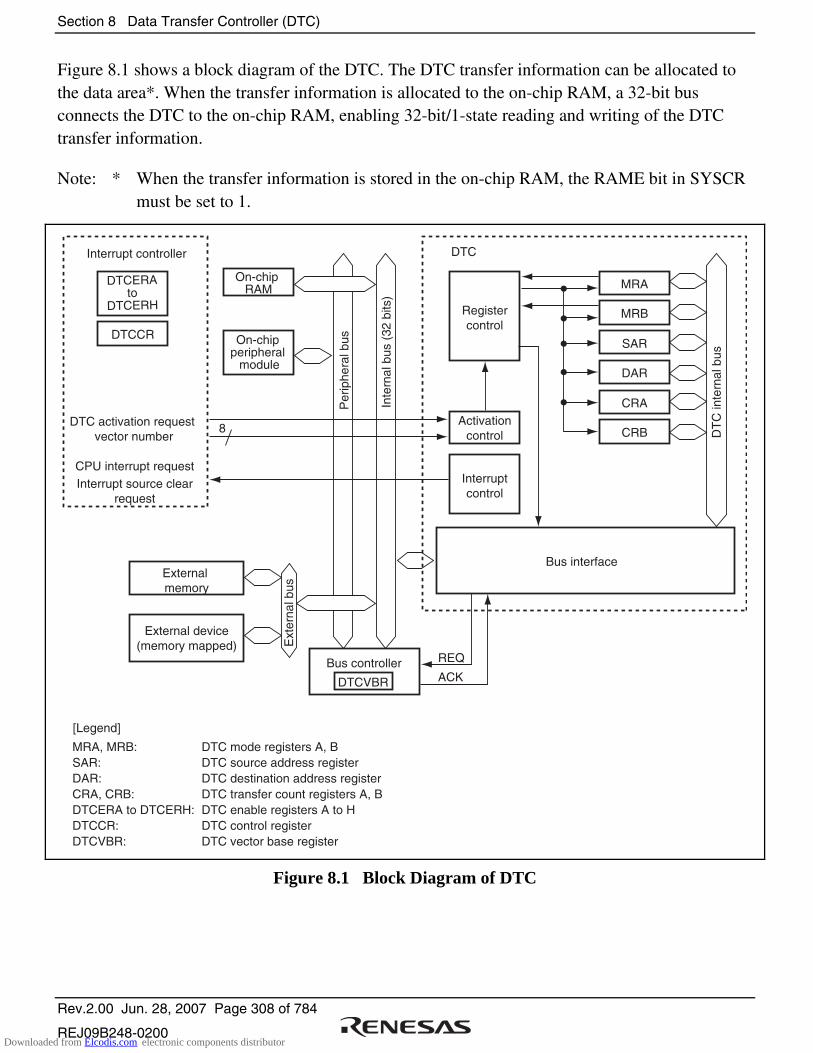
Section 8 Data Transfer Controller (DTC)
Rev.2.00 Jun. 28, 2007 Page 308 of 784
REJ09B248-0200
Figure 8.1 shows a block diagram of the DTC. The DTC transfer information can be allocated to the data area*. When the transfer information is allocated to the on-chip RAM, a 32-bit bus connects the DTC to the on-chip RAM, enabling 32-bit/1-state reading and writing of the DTC transfer information.
Note: * When the transfer information is stored in the on-chip RAM, the RAME bit in SYSCR must be set to 1.
Bus interface
Bus controller
DTCCR
Interrupt controller
ACK
REQ
DTCVBR
DTC
DT
C in
tern
al b
us
Per
iphe
ral b
us
Inte
rnal
bus
(32
bits
)
Ext
erna
l bus
CPU interrupt requestInterrupt source clear
request
8
Registercontrol
Activationcontrol
Interruptcontrol
On-chip RAM MRA
MRB
SAR
DAR
CRA
CRB
On-chip peripheral
module
External memory
External device(memory mapped)
DTC activation request vector number
MRA, MRB:SAR:DAR:CRA, CRB:DTCERA to DTCERH:DTCCR:DTCVBR:
DTC mode registers A, B DTC source address registerDTC destination address registerDTC transfer count registers A, BDTC enable registers A to HDTC control registerDTC vector base register
DTCERAto
DTCERH
[Legend]
Figure 8.1 Block Diagram of DTC
Downloaded from Elcodis.com electronic components distributor
Section 8 Data Transfer Controller (DTC)
Rev.2.00 Jun. 28, 2007 Page 309 of 784
REJ09B248-0200
8.2 Register Descriptions
DTC has the following registers.
• DTC mode register A (MRA)
• DTC mode register B (MRB)
• DTC source address register (SAR)
• DTC destination address register (DAR)
• DTC transfer count register A (CRA)
• DTC transfer count register B (CRB) These six registers MRA, MRB, SAR, DAR, CRA, and CRB cannot be directly accessed by the CPU. The contents of these registers are stored in the data area as transfer information. When a DTC activation request occurs, the DTC reads a start address of transfer information that is stored in the data area according to the vector address, reads the transfer information, and transfers data. After the data transfer, it writes a set of updated transfer information back to the data area.
• DTC enable registers A to H (DTCERA to DTCERH)
• DTC control register (DTCCR)
• DTC vector base register (DTCVBR)
Downloaded from Elcodis.com electronic components distributor
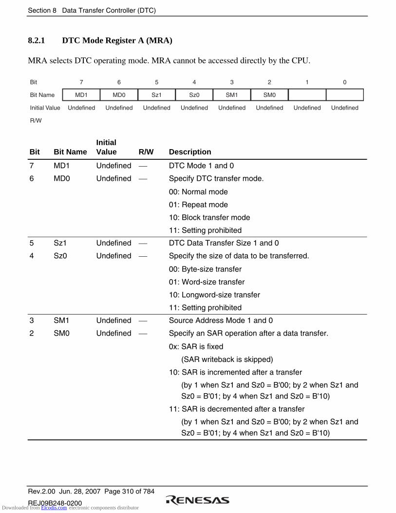
Section 8 Data Transfer Controller (DTC)
Rev.2.00 Jun. 28, 2007 Page 310 of 784
REJ09B248-0200
8.2.1 DTC Mode Register A (MRA)
MRA selects DTC operating mode. MRA cannot be accessed directly by the CPU.
Bit
Bit Name
Initial Value
R/W
7
MD1
Undefined
6
MD0
Undefined
5
Sz1
Undefined
4
Sz0
Undefined
3
SM1
Undefined
2
SM0
Undefined
1
Undefined
0
Undefined
Bit Bit Name Initial Value R/W Description
7
6
MD1
MD0
Undefined
Undefined
DTC Mode 1 and 0
Specify DTC transfer mode.
00: Normal mode
01: Repeat mode
10: Block transfer mode
11: Setting prohibited
5
4
Sz1
Sz0
Undefined
Undefined
DTC Data Transfer Size 1 and 0
Specify the size of data to be transferred.
00: Byte-size transfer
01: Word-size transfer
10: Longword-size transfer
11: Setting prohibited
3
2
SM1
SM0
Undefined
Undefined
Source Address Mode 1 and 0
Specify an SAR operation after a data transfer.
0x: SAR is fixed
(SAR writeback is skipped)
10: SAR is incremented after a transfer
(by 1 when Sz1 and Sz0 = B'00; by 2 when Sz1 and
Sz0 = B'01; by 4 when Sz1 and Sz0 = B'10)
11: SAR is decremented after a transfer
(by 1 when Sz1 and Sz0 = B'00; by 2 when Sz1 and
Sz0 = B'01; by 4 when Sz1 and Sz0 = B'10)
Downloaded from Elcodis.com electronic components distributor
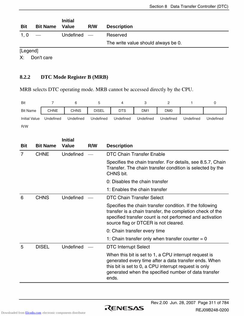
Section 8 Data Transfer Controller (DTC)
Rev.2.00 Jun. 28, 2007 Page 311 of 784
REJ09B248-0200
Bit Bit Name Initial Value R/W Description
1, 0 Undefined Reserved
The write value should always be 0.
[Legend] X: Don't care
8.2.2 DTC Mode Register B (MRB)
MRB selects DTC operating mode. MRB cannot be accessed directly by the CPU.
Bit
Bit Name
Initial Value
R/W
7
CHNE
Undefined
6
CHNS
Undefined
5
DISEL
Undefined
4
DTS
Undefined
3
DM1
Undefined
2
DM0
Undefined
1
Undefined
0
Undefined
Bit Bit Name Initial Value R/W Description
7 CHNE Undefined DTC Chain Transfer Enable
Specifies the chain transfer. For details, see 8.5.7, Chain Transfer. The chain transfer condition is selected by the CHNS bit.
0: Disables the chain transfer
1: Enables the chain transfer
6 CHNS Undefined DTC Chain Transfer Select
Specifies the chain transfer condition. If the following transfer is a chain transfer, the completion check of the specified transfer count is not performed and activation source flag or DTCER is not cleared.
0: Chain transfer every time
1: Chain transfer only when transfer counter = 0
5 DISEL Undefined DTC Interrupt Select
When this bit is set to 1, a CPU interrupt request is generated every time after a data transfer ends. When this bit is set to 0, a CPU interrupt request is only generated when the specified number of data transfer ends.
Downloaded from Elcodis.com electronic components distributor
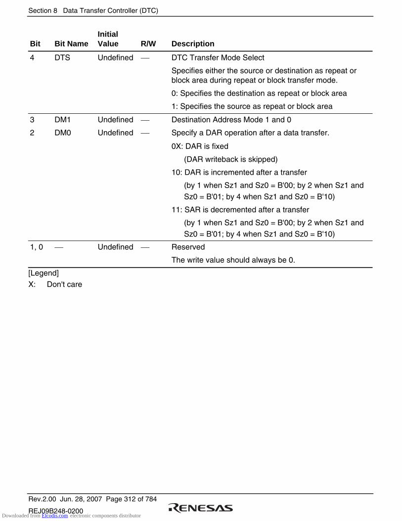
Section 8 Data Transfer Controller (DTC)
Rev.2.00 Jun. 28, 2007 Page 312 of 784
REJ09B248-0200
Bit Bit Name Initial Value R/W Description
4 DTS Undefined DTC Transfer Mode Select
Specifies either the source or destination as repeat or block area during repeat or block transfer mode.
0: Specifies the destination as repeat or block area
1: Specifies the source as repeat or block area
3
2
DM1
DM0
Undefined
Undefined
Destination Address Mode 1 and 0
Specify a DAR operation after a data transfer.
0X: DAR is fixed
(DAR writeback is skipped)
10: DAR is incremented after a transfer
(by 1 when Sz1 and Sz0 = B'00; by 2 when Sz1 and
Sz0 = B'01; by 4 when Sz1 and Sz0 = B'10)
11: SAR is decremented after a transfer
(by 1 when Sz1 and Sz0 = B'00; by 2 when Sz1 and
Sz0 = B'01; by 4 when Sz1 and Sz0 = B'10)
1, 0 Undefined Reserved
The write value should always be 0.
[Legend]
X: Don't care
Downloaded from Elcodis.com electronic components distributor
Section 8 Data Transfer Controller (DTC)
Rev.2.00 Jun. 28, 2007 Page 313 of 784
REJ09B248-0200
8.2.3 DTC Source Address Register (SAR)
SAR is a 32-bit register that designates the source address of data to be transferred by the DTC.
In full address mode, 32 bits of SAR are valid. In short address mode, the lower 24 bits of SAR are valid and bits 31 to 24 are ignored. At this time, the upper eight bits are filled with the value of bit 23.
If a word or longword access is performed while an odd address is specified in SAR or if a longword access is performed while address 4n + 2 is specified in SAR, the bus cycle is divided into multiple cycles to transfer data. For details, see section 8.5.1, Bus Cycle Division.
SAR cannot be accessed directly from the CPU.
8.2.4 DTC Destination Address Register (DAR)
DAR is a 32-bit register that designates the destination address of data to be transferred by the DTC.
In full address mode, 32 bits of DAR are valid. In short address mode, the lower 24 bits of DAR are valid and bits 31 to 24 are ignored. At this time, the upper eight bits are filled with the value of bit 23.
If a word or longword access is performed while an odd address is specified in DAR or if a longword access is performed while address 4n + 2 is specified in DAR, the bus cycle is divided into multiple cycles to transfer data. For details, see section 8.5.1, Bus Cycle Division.
DAR cannot be accessed directly from the CPU.
Downloaded from Elcodis.com electronic components distributor

Section 8 Data Transfer Controller (DTC)
Rev.2.00 Jun. 28, 2007 Page 314 of 784
REJ09B248-0200
8.2.5 DTC Transfer Count Register A (CRA)
CRA is a 16-bit register that designates the number of times data is to be transferred by the DTC.
In normal transfer mode, CRA functions as a 16-bit transfer counter (1 to 65,536). It is decremented by 1 every time data is transferred, and bit DTCEn (n = 15 to 0) corresponding to the activation source is cleared and then an interrupt is requested to the CPU when the count reaches H'0000. The transfer count is 1 when CRA = H'0001, 65,535 when CRA = H'FFFF, and 65,536 when CRA = H'0000.
In repeat transfer mode, CRA is divided into two parts: the upper eight bits (CRAH) and the lower eight bits (CRAL). CRAH holds the number of transfers while CRAL functions as an 8-bit transfer counter (1 to 256). CRAL is decremented by 1 every time data is transferred, and the contents of CRAH are sent to CRAL when the count reaches H'00. The transfer count is 1 when CRAH = CRAL = H'01, 255 when CRAH = CRAL = H'FF, and 256 when CRAH = CRAL = H'00.
In block transfer mode, CRA is divided into two parts: the upper eight bits (CRAH) and the lower eight bits (CRAL). CRAH holds the block size while CRAL functions as an 8-bit block-size counter (1 to 256 for byte, word, or longword). CRAL is decremented by 1 every time a byte (word or longword) data is transferred, and the contents of CRAH are sent to CRAL when the count reaches H'00. The block size is 1 byte (word or longword) when CRAH = CRAL =H'01, 255 bytes (words or longwords) when CRAH = CRAL = H'FF, and 256 bytes (words or longwords) when CRAH = CRAL =H'00.
CRA cannot be accessed directly from the CPU.
8.2.6 DTC Transfer Count Register B (CRB)
CRB is a 16-bit register that designates the number of times data is to be transferred by the DTC in block transfer mode. It functions as a 16-bit transfer counter (1 to 65,536) that is decremented by 1 every time data is transferred, and bit DTCEn (n = 15 to 0) corresponding to the activation source is cleared and then an interrupt is requested to the CPU when the count reaches H'0000. The transfer count is 1 when CRB = H'0001, 65,535 when CRB = H'FFFF, and 65,536 when CRB = H'0000.
CRB is not available in normal and repeat modes and cannot be accessed directly by the CPU.
Downloaded from Elcodis.com electronic components distributor
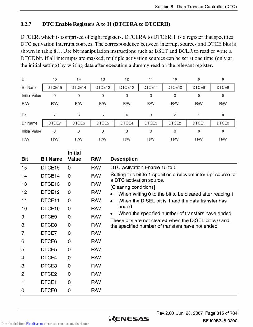
Section 8 Data Transfer Controller (DTC)
Rev.2.00 Jun. 28, 2007 Page 315 of 784
REJ09B248-0200
8.2.7 DTC Enable Registers A to H (DTCERA to DTCERH)
DTCER, which is comprised of eight registers, DTCERA to DTCERH, is a register that specifies DTC activation interrupt sources. The correspondence between interrupt sources and DTCE bits is shown in table 8.1. Use bit manipulation instructions such as BSET and BCLR to read or write a DTCE bit. If all interrupts are masked, multiple activation sources can be set at one time (only at the initial setting) by writing data after executing a dummy read on the relevant register.
Bit
Bit Name
Initial Value
R/W
15
DTCE15
0
R/W
14
DTCE14
0
R/W
13
DTCE13
0
R/W
12
DTCE12
0
R/W
11
DTCE11
0
R/W
10
DTCE10
0
R/W
9
DTCE9
0
R/W
8
DTCE8
0
R/W
Bit
Bit Name
Initial Value
R/W
7
DTCE7
0
R/W
6
DTCE6
0
R/W
5
DTCE5
0
R/W
4
DTCE4
0
R/W
3
DTCE3
0
R/W
2
DTCE2
0
R/W
1
DTCE1
0
R/W
0
DTCE0
0
R/W
Bit Bit Name Initial Value R/W Description
15
14
13
12
11
10
9
8
7
6
5
4
3
2
1
0
DTCE15
DTCE14
DTCE13
DTCE12
DTCE11
DTCE10
DTCE9
DTCE8
DTCE7
DTCE6
DTCE5
DTCE4
DTCE3
DTCE2
DTCE1
DTCE0
0
0
0
0
0
0
0
0
0
0
0
0
0
0
0
0
R/W
R/W
R/W
R/W
R/W
R/W
R/W
R/W
R/W
R/W
R/W
R/W
R/W
R/W
R/W
R/W
DTC Activation Enable 15 to 0 Setting this bit to 1 specifies a relevant interrupt source to a DTC activation source. [Clearing conditions] • When writing 0 to the bit to be cleared after reading 1 • When the DISEL bit is 1 and the data transfer has
ended • When the specified number of transfers have ended These bits are not cleared when the DISEL bit is 0 and the specified number of transfers have not ended
Downloaded from Elcodis.com electronic components distributor
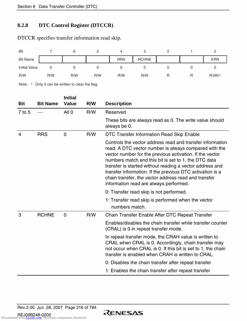
Section 8 Data Transfer Controller (DTC)
Rev.2.00 Jun. 28, 2007 Page 316 of 784
REJ09B248-0200
8.2.8 DTC Control Register (DTCCR)
DTCCR specifies transfer information read skip.
Bit
Bit Name
Initial Value
R/W
Note: * Only 0 can be written to clear the flag.
7
0
R/W
6
0
R/W
5
0
R/W
4
RRS
0
R/W
3
RCHNE
0
R/W
2
0
R
1
0
R
0
ERR
0
R/(W)*
Bit Bit Name Initial Value R/W Description
7 to 5 All 0 R/W Reserved
These bits are always read as 0. The write value should always be 0.
4 RRS 0 R/W DTC Transfer Information Read Skip Enable
Controls the vector address read and transfer information read. A DTC vector number is always compared with the vector number for the previous activation. If the vector numbers match and this bit is set to 1, the DTC data transfer is started without reading a vector address and transfer information. If the previous DTC activation is a chain transfer, the vector address read and transfer information read are always performed.
0: Transfer read skip is not performed.
1: Transfer read skip is performed when the vector
numbers match.
3 RCHNE 0 R/W Chain Transfer Enable After DTC Repeat Transfer
Enables/disables the chain transfer while transfer counter (CRAL) is 0 in repeat transfer mode.
In repeat transfer mode, the CRAH value is written to CRAL when CRAL is 0. Accordingly, chain transfer may not occur when CRAL is 0. If this bit is set to 1, the chain transfer is enabled when CRAH is written to CRAL.
0: Disables the chain transfer after repeat transfer
1: Enables the chain transfer after repeat transfer
Downloaded from Elcodis.com electronic components distributor
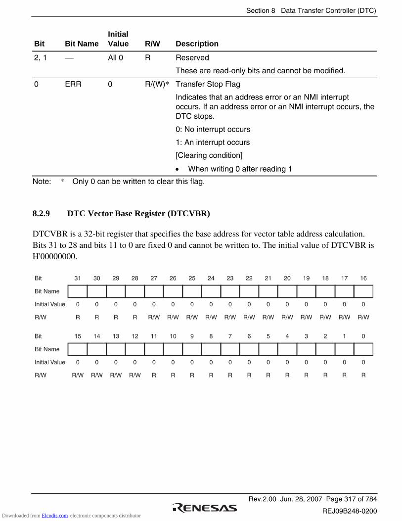
Section 8 Data Transfer Controller (DTC)
Rev.2.00 Jun. 28, 2007 Page 317 of 784
REJ09B248-0200
Bit Bit Name Initial Value R/W Description
2, 1 All 0 R Reserved
These are read-only bits and cannot be modified.
0 ERR 0 R/(W)* Transfer Stop Flag
Indicates that an address error or an NMI interrupt occurs. If an address error or an NMI interrupt occurs, the DTC stops.
0: No interrupt occurs
1: An interrupt occurs
[Clearing condition]
• When writing 0 after reading 1
Note: * Only 0 can be written to clear this flag.
8.2.9 DTC Vector Base Register (DTCVBR)
DTCVBR is a 32-bit register that specifies the base address for vector table address calculation. Bits 31 to 28 and bits 11 to 0 are fixed 0 and cannot be written to. The initial value of DTCVBR is H'00000000.
Bit
Bit Name
Initial Value
R/W
31
0
R
30
0
R
29
0
R
28
0
R
27
0
R/W
26
0
R/W
25
0
R/W
24
0
R/W
23
0
R/W
22
0
R/W
21
0
R/W
20
0
R/W
19
0
R/W
18
0
R/W
17
0
R/W
16
0
R/W
Bit
Bit Name
Initial Value
R/W
15
0
R/W
14
0
R/W
13
0
R/W
12
0
R/W
11
0
R
10
0
R
9
0
R
8
0
R
7
0
R
6
0
R
5
0
R
4
0
R
3
0
R
2
0
R
1
0
R
0
0
R
Downloaded from Elcodis.com electronic components distributor
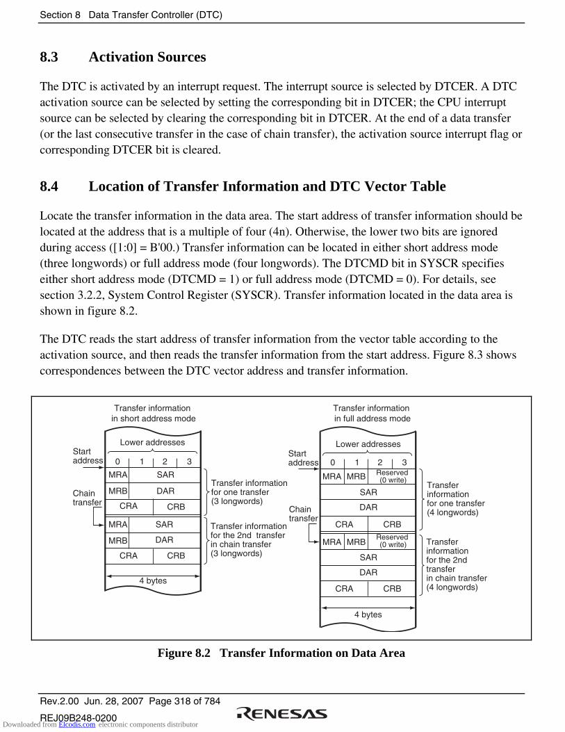
Section 8 Data Transfer Controller (DTC)
Rev.2.00 Jun. 28, 2007 Page 318 of 784
REJ09B248-0200
8.3 Activation Sources
The DTC is activated by an interrupt request. The interrupt source is selected by DTCER. A DTC activation source can be selected by setting the corresponding bit in DTCER; the CPU interrupt source can be selected by clearing the corresponding bit in DTCER. At the end of a data transfer (or the last consecutive transfer in the case of chain transfer), the activation source interrupt flag or corresponding DTCER bit is cleared.
8.4 Location of Transfer Information and DTC Vector Table
Locate the transfer information in the data area. The start address of transfer information should be located at the address that is a multiple of four (4n). Otherwise, the lower two bits are ignored during access ([1:0] = B'00.) Transfer information can be located in either short address mode (three longwords) or full address mode (four longwords). The DTCMD bit in SYSCR specifies either short address mode (DTCMD = 1) or full address mode (DTCMD = 0). For details, see section 3.2.2, System Control Register (SYSCR). Transfer information located in the data area is shown in figure 8.2.
The DTC reads the start address of transfer information from the vector table according to the activation source, and then reads the transfer information from the start address. Figure 8.3 shows correspondences between the DTC vector address and transfer information.
Startaddress
4 bytes
10
MRA SAR
MRB DAR
CRA CRB
MRA SAR
MRB DAR
CRA CRB
MRA MRB Reserved (0 write)
MRA MRBReserved (0 write)
SAR
DAR
CRA CRB
CRA CRB
SAR
DAR
32
Transfer information in short address mode
Chaintransfer
Transfer information for one transfer (3 longwords)
Transfer information for the 2nd transfer in chain transfer (3 longwords)
Lower addresses Lower addresses
Transfer information in full address mode
Transfer information for one transfer (4 longwords)
Transferinformation for the 2nd transfer in chain transfer (4 longwords)
Startaddress
4 bytes
10 32
Chaintransfer
Figure 8.2 Transfer Information on Data Area
Downloaded from Elcodis.com electronic components distributor

Section 8 Data Transfer Controller (DTC)
Rev.2.00 Jun. 28, 2007 Page 319 of 784
REJ09B248-0200
Transfer information (1)start address
Transfer information (2)start address
Transfer information (n)start address
Vector table
Upper: DTCVBRLower: H'400 + vector number × 4
DTC vectoraddress
+4
+4n
Transfer information (1)
4 bytes
Transfer information (2)
Transfer information (n)
:::
:::
Figure 8.3 Correspondence between DTC Vector Address and Transfer Information
Downloaded from Elcodis.com electronic components distributor
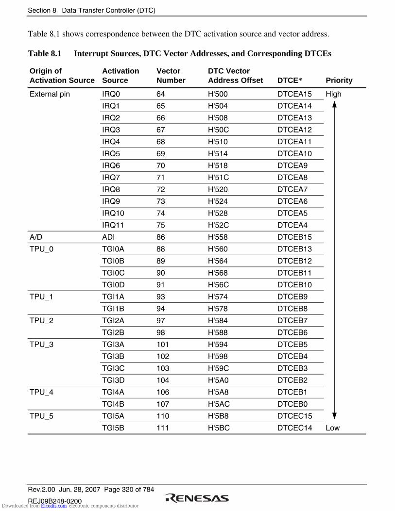
Section 8 Data Transfer Controller (DTC)
Rev.2.00 Jun. 28, 2007 Page 320 of 784
REJ09B248-0200
Table 8.1 shows correspondence between the DTC activation source and vector address.
Table 8.1 Interrupt Sources, DTC Vector Addresses, and Corresponding DTCEs
Origin of Activation Source
Activation Source
Vector Number
DTC Vector Address Offset DTCE* Priority
External pin IRQ0 64 H'500 DTCEA15 High
IRQ1 65 H'504 DTCEA14
IRQ2 66 H'508 DTCEA13
IRQ3 67 H'50C DTCEA12
IRQ4 68 H'510 DTCEA11
IRQ5 69 H'514 DTCEA10
IRQ6 70 H'518 DTCEA9
IRQ7 71 H'51C DTCEA8
IRQ8 72 H'520 DTCEA7
IRQ9 73 H'524 DTCEA6
IRQ10 74 H'528 DTCEA5
IRQ11 75 H'52C DTCEA4
A/D ADI 86 H'558 DTCEB15
TPU_0 TGI0A 88 H'560 DTCEB13
TGI0B 89 H'564 DTCEB12
TGI0C 90 H'568 DTCEB11
TGI0D 91 H'56C DTCEB10
TPU_1 TGI1A 93 H'574 DTCEB9
TGI1B 94 H'578 DTCEB8
TPU_2 TGI2A 97 H'584 DTCEB7
TGI2B 98 H'588 DTCEB6
TPU_3 TGI3A 101 H'594 DTCEB5
TGI3B 102 H'598 DTCEB4
TGI3C 103 H'59C DTCEB3
TGI3D 104 H'5A0 DTCEB2
TPU_4 TGI4A 106 H'5A8 DTCEB1
TGI4B 107 H'5AC DTCEB0
TPU_5 TGI5A 110 H'5B8 DTCEC15
TGI5B 111 H'5BC DTCEC14 Low
Downloaded from Elcodis.com electronic components distributor
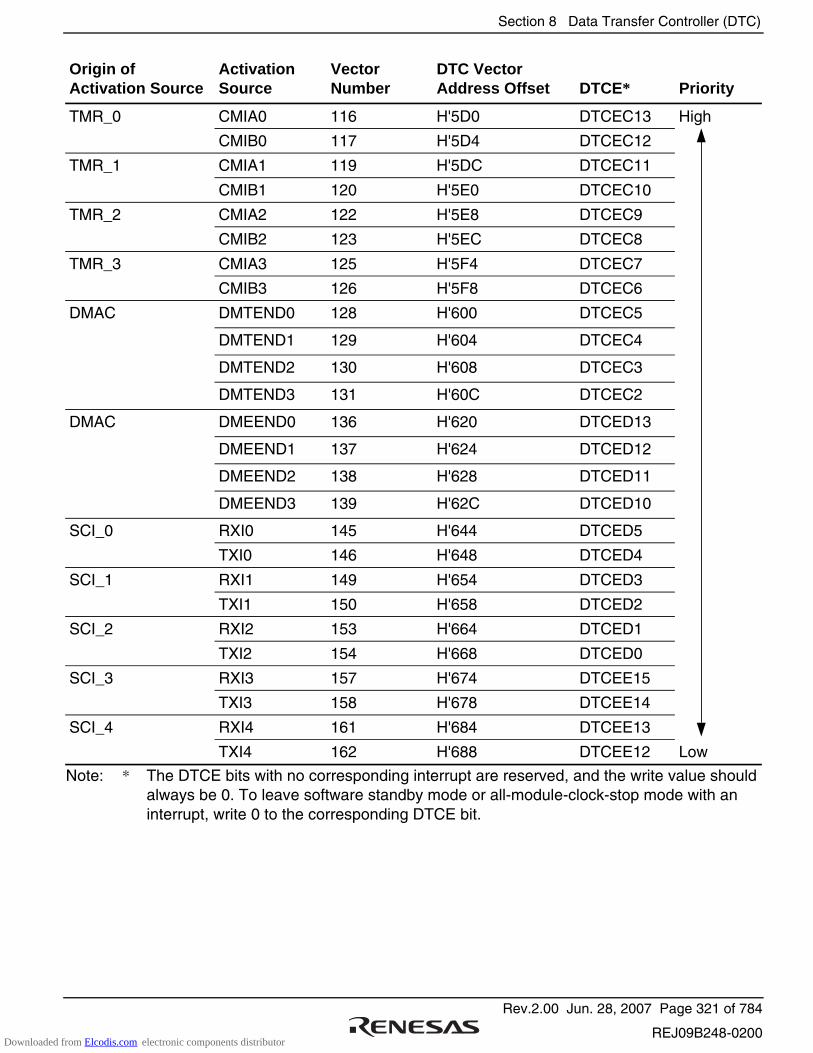
Section 8 Data Transfer Controller (DTC)
Rev.2.00 Jun. 28, 2007 Page 321 of 784
REJ09B248-0200
Origin of Activation Source
Activation Source
Vector Number
DTC Vector Address Offset DTCE* Priority
TMR_0 CMIA0 116 H'5D0 DTCEC13 High
CMIB0 117 H'5D4 DTCEC12
TMR_1 CMIA1 119 H'5DC DTCEC11
CMIB1 120 H'5E0 DTCEC10
TMR_2 CMIA2 122 H'5E8 DTCEC9
CMIB2 123 H'5EC DTCEC8
TMR_3 CMIA3 125 H'5F4 DTCEC7
CMIB3 126 H'5F8 DTCEC6
DMAC DMTEND0 128 H'600 DTCEC5
DMTEND1 129 H'604 DTCEC4
DMTEND2 130 H'608 DTCEC3
DMTEND3 131 H'60C DTCEC2
DMAC DMEEND0 136 H'620 DTCED13
DMEEND1 137 H'624 DTCED12
DMEEND2 138 H'628 DTCED11
DMEEND3 139 H'62C DTCED10
SCI_0 RXI0 145 H'644 DTCED5
TXI0 146 H'648 DTCED4
SCI_1 RXI1 149 H'654 DTCED3
TXI1 150 H'658 DTCED2
SCI_2 RXI2 153 H'664 DTCED1
TXI2 154 H'668 DTCED0
SCI_3 RXI3 157 H'674 DTCEE15
TXI3 158 H'678 DTCEE14
SCI_4 RXI4 161 H'684 DTCEE13
TXI4 162 H'688 DTCEE12 Low
Note: * The DTCE bits with no corresponding interrupt are reserved, and the write value should always be 0. To leave software standby mode or all-module-clock-stop mode with an interrupt, write 0 to the corresponding DTCE bit.
Downloaded from Elcodis.com electronic components distributor
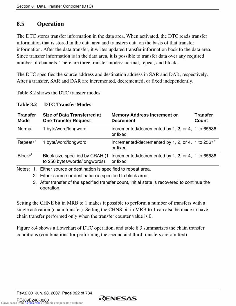
Section 8 Data Transfer Controller (DTC)
Rev.2.00 Jun. 28, 2007 Page 322 of 784
REJ09B248-0200
8.5 Operation
The DTC stores transfer information in the data area. When activated, the DTC reads transfer information that is stored in the data area and transfers data on the basis of that transfer information. After the data transfer, it writes updated transfer information back to the data area. Since transfer information is in the data area, it is possible to transfer data over any required number of channels. There are three transfer modes: normal, repeat, and block.
The DTC specifies the source address and destination address in SAR and DAR, respectively. After a transfer, SAR and DAR are incremented, decremented, or fixed independently.
Table 8.2 shows the DTC transfer modes.
Table 8.2 DTC Transfer Modes
Transfer Mode
Size of Data Transferred at One Transfer Request
Memory Address Increment or Decrement
Transfer Count
Normal 1 byte/word/longword Incremented/decremented by 1, 2, or 4, or fixed
1 to 65536
Repeat*1 1 byte/word/longword Incremented/decremented by 1, 2, or 4, or fixed
1 to 256*3
Block*2 Block size specified by CRAH (1 to 256 bytes/words/longwords)
Incremented/decremented by 1, 2, or 4, or fixed
1 to 65536
Notes: 1. Either source or destination is specified to repeat area.
2. Either source or destination is specified to block area.
3. After transfer of the specified transfer count, initial state is recovered to continue the operation.
Setting the CHNE bit in MRB to 1 makes it possible to perform a number of transfers with a single activation (chain transfer). Setting the CHNS bit in MRB to 1 can also be made to have chain transfer performed only when the transfer counter value is 0.
Figure 8.4 shows a flowchart of DTC operation, and table 8.3 summarizes the chain transfer conditions (combinations for performing the second and third transfers are omitted).
Downloaded from Elcodis.com electronic components distributor
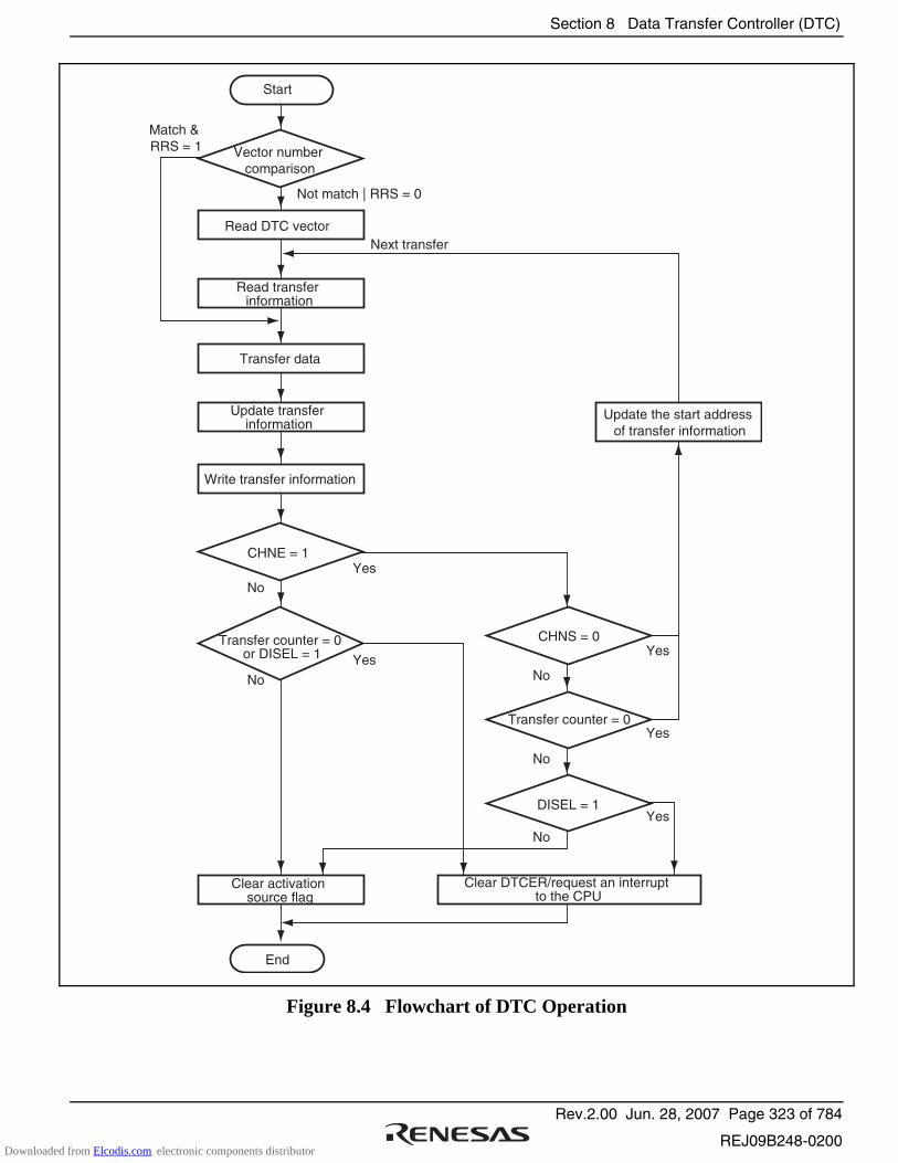
Section 8 Data Transfer Controller (DTC)
Rev.2.00 Jun. 28, 2007 Page 323 of 784
REJ09B248-0200
Start
Match & RRS = 1
Not match | RRS = 0
Next transfer
Read transfer information
Transfer data
Update transfer information
Update the start address of transfer information
Write transfer information
CHNE = 1
Transfer counter = 0 or DISEL = 1
Clear activation source flag
End
CHNS = 0
Transfer counter = 0
DISEL = 1
Clear DTCER/request an interrupt to the CPU
No
No
No
No
NoYes
Yes
Yes
Yes
Yes
Vector number comparison
Read DTC vector
Figure 8.4 Flowchart of DTC Operation
Downloaded from Elcodis.com electronic components distributor

Section 8 Data Transfer Controller (DTC)
Rev.2.00 Jun. 28, 2007 Page 324 of 784
REJ09B248-0200
Table 8.3 Chain Transfer Conditions
1st Transfer 2nd Transfer
CHNE CHNS DISEL Transfer Counter*1 CHNE CHNS DISEL
Transfer Counter*1 DTC Transfer
0 0 Not 0 Ends at 1st transfer
0 0 0*2 Ends at 1st transfer
0 1 Interrupt request to CPU
0 0 Not 0 Ends at 2nd transfer
0 0 0*2 Ends at 2nd transfer
1 0
0 1 Interrupt request to CPU
1 1 0 Not 0 Ends at 1st transfer
0 0 Not 0 Ends at 2nd transfer
0 0 0*2 Ends at 2nd transfer
1 1 0*2
0 1 Interrupt request to CPU
1 1 1 Not 0 Ends at 1st transfer
Interrupt request to CPU
Notes: 1. CRA in normal mode transfer, CRAL in repeat transfer mode, or CRB in block transfer mode
2. When the contents of the CRAH is written to the CRAL in repeat transfer mode
8.5.1 Bus Cycle Division
When the transfer data size is word and the SAR and DAR values are not a multiple of 2, the bus cycle is divided and the transfer data is read from or written to in bytes. Similarly, when the transfer data size is longword and the SAR and DAR values are not a multiple of 4, the bus cycle is divided and the transfer data is read from or written to in words.
Table 8.4 shows the relationship among, SAR, DAR, transfer data size, bus cycle divisions, and access data size. Figure 8.5 shows the bus cycle division example.
Table 8.4 Number of Bus Cycle Divisions and Access Size
Specified Data Size
SAR and DAR Values Byte (B) Word (W) Longword (LW)
Address 4n 1 (B) 1 (W) 1 (LW)
Address 2n + 1 1 (B) 2 (B-B) 3 (B-W-B)
Address 4n + 2 1 (B) 1 (W) 2 (W-W)
Downloaded from Elcodis.com electronic components distributor
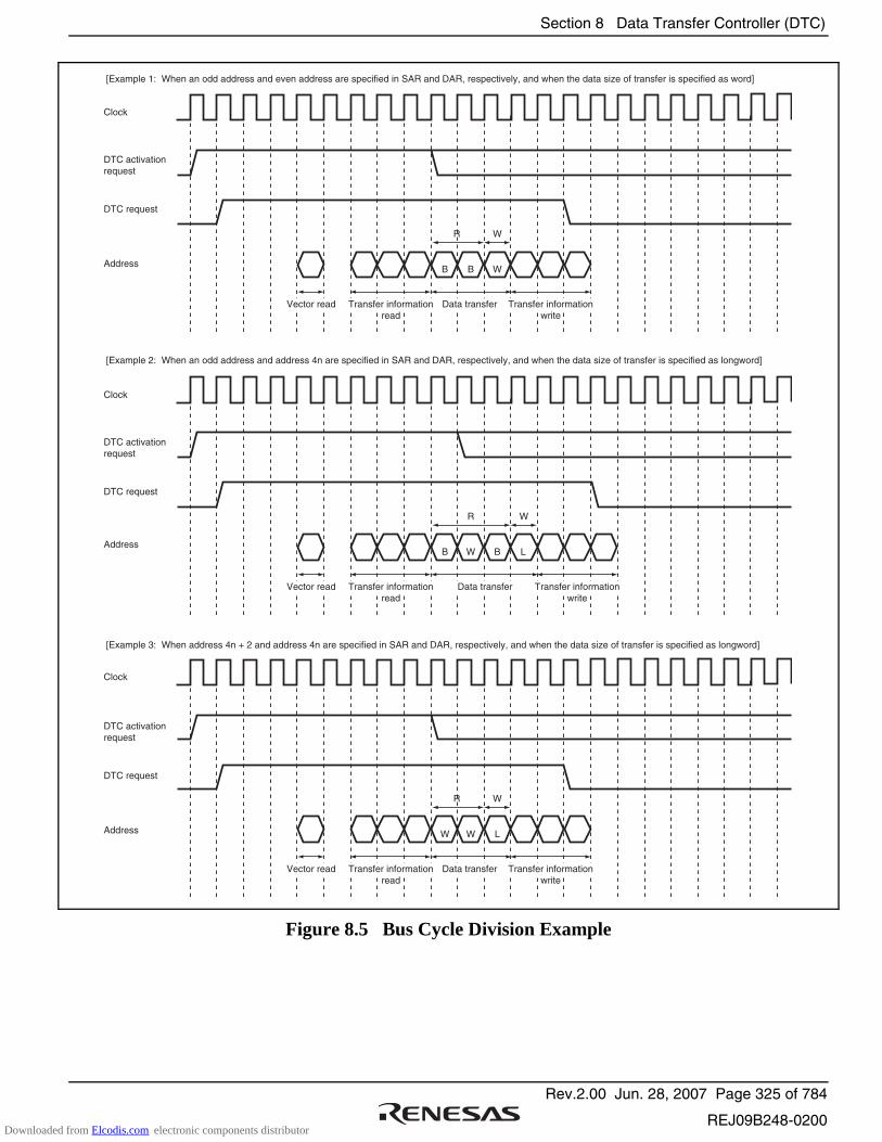
Section 8 Data Transfer Controller (DTC)
Rev.2.00 Jun. 28, 2007 Page 325 of 784
REJ09B248-0200
Clock
Address
DTC activation request
DTC request
B B W
R W
Clock
Address
DTC activationrequest
DTC request
W W L
R W
Clock
Address
DTC activationrequest
DTC request
B B LW
R W
[Example 1: When an odd address and even address are specified in SAR and DAR, respectively, and when the data size of transfer is specified as word]
[Example 2: When an odd address and address 4n are specified in SAR and DAR, respectively, and when the data size of transfer is specified as longword]
[Example 3: When address 4n + 2 and address 4n are specified in SAR and DAR, respectively, and when the data size of transfer is specified as longword]
Vector read Transfer informationread
Data transfer Transfer informationwrite
Vector read Transfer informationread
Data transfer Transfer informationwrite
Vector read Transfer informationread
Data transfer Transfer informationwrite
Figure 8.5 Bus Cycle Division Example
Downloaded from Elcodis.com electronic components distributor

Section 8 Data Transfer Controller (DTC)
Rev.2.00 Jun. 28, 2007 Page 326 of 784
REJ09B248-0200
8.5.2 Transfer Information Read Skip Function
By setting the RRS bit of DTCCR, the vector address read and transfer information read can be skipped. The current DTC vector number is always compared with the vector number of previous activation. If the vector numbers match when RRS = 1, a DTC data transfer is performed without reading the vector address and transfer information. If the previous activation is a chain transfer, the vector address read and transfer information read are always performed. Figure 8.6 shows the transfer information read skip timing.
To modify the vector table and transfer information, temporarily clear the RRS bit to 0, modify the vector table and transfer information, and then set the RRS bit to 1 again. When the RRS bit is cleared to 0, the stored vector number is deleted, and the updated vector table and transfer information are read at the next activation.
Clock
Vector read
Note: Transfer information read is skipped when the activation sources of (1) and (2) (vector numbers) are the same while RRS = 1.
(1) (2)
Transfer informationread
Data transfer
Transfer informationwrite
Address
DTC activationrequest
DTC request
Transfer informationread skip
R W
Data transfer
Transfer information write
R W
Figure 8.6 Transfer Information Read Skip Timing
Downloaded from Elcodis.com electronic components distributor
Section 8 Data Transfer Controller (DTC)
Rev.2.00 Jun. 28, 2007 Page 327 of 784
REJ09B248-0200
8.5.3 Transfer Information Writeback Skip Function
By specifying bit SM1 in MRA and bit DM1 in MRB to the fixed address mode, a part of transfer information will not be written back. This function is performed regardless of short or full address mode. Table 8.5 shows the transfer information writeback skip condition and writeback skipped registers. Note that the CRA and CRB are always written back regardless of the short or full address mode. In addition in full address mode, the writeback of the MRA and MRB are always skipped.
Table 8.5 Transfer Information Writeback Skip Condition and Writeback Skipped Registers
SM1 DM1 SAR DAR
0 0 Skipped Skipped
0 1 Skipped Written back
1 0 Written back Skipped
1 1 Written back Written back
8.5.4 Normal Transfer Mode
In normal transfer mode, one operation transfers one byte, one word, or one longword of data. From 1 to 65,536 transfers can be specified. The transfer source and destination addresses can be specified as incremented, decremented, or fixed. When the specified number of transfers ends, an interrupt can be requested to the CPU.
Table 8.6 lists the register function in normal transfer mode. Figure 8.7 shows the memory map in normal transfer mode.
Table 8.6 Register Function in Normal Transfer Mode
Register Function Written Back Value
SAR Source address Incremented/decremented/fixed*
DAR Destination address Incremented/decremented/fixed*
CRA Transfer count A CRA − 1
CRB Transfer count B Not updated
Note: * Transfer information writeback is skipped.
Downloaded from Elcodis.com electronic components distributor
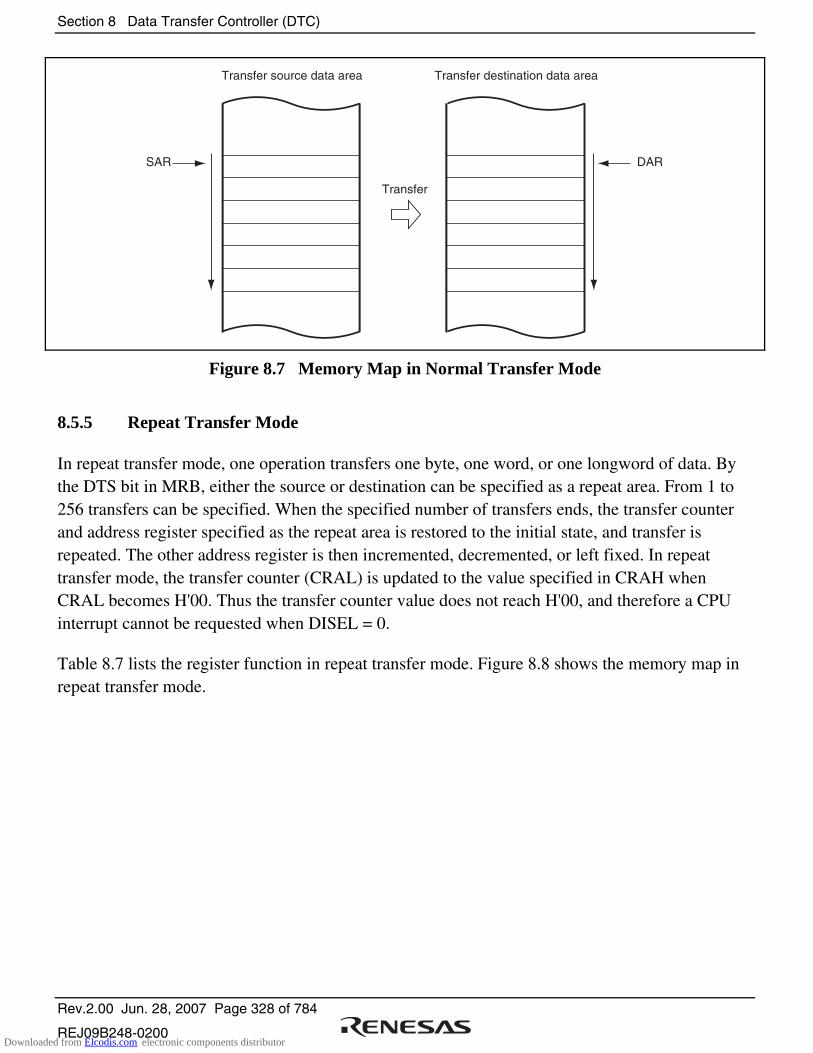
Section 8 Data Transfer Controller (DTC)
Rev.2.00 Jun. 28, 2007 Page 328 of 784
REJ09B248-0200
SAR
Transfer source data area
DAR
Transfer
Transfer destination data area
Figure 8.7 Memory Map in Normal Transfer Mode
8.5.5 Repeat Transfer Mode
In repeat transfer mode, one operation transfers one byte, one word, or one longword of data. By the DTS bit in MRB, either the source or destination can be specified as a repeat area. From 1 to 256 transfers can be specified. When the specified number of transfers ends, the transfer counter and address register specified as the repeat area is restored to the initial state, and transfer is repeated. The other address register is then incremented, decremented, or left fixed. In repeat transfer mode, the transfer counter (CRAL) is updated to the value specified in CRAH when CRAL becomes H'00. Thus the transfer counter value does not reach H'00, and therefore a CPU interrupt cannot be requested when DISEL = 0.
Table 8.7 lists the register function in repeat transfer mode. Figure 8.8 shows the memory map in repeat transfer mode.
Downloaded from Elcodis.com electronic components distributor

Section 8 Data Transfer Controller (DTC)
Rev.2.00 Jun. 28, 2007 Page 329 of 784
REJ09B248-0200
Table 8.7 Register Function in Repeat Transfer Mode
Written Back Value
Register Function CRAL is not 1 CRAL is 1
SAR Source address Incremented/decremented/fixed*
DTS =0: Incremented/ decremented/fixed*
DTS = 1: SAR initial value
DAR Destination address Incremented/decremented/fixed*
DTS = 0: DAR initial value
DTS =1: Incremented/ decremented/fixed*
CRAH Transfer count storage
CRAH CRAH
CRAL Transfer count A CRAL − 1 CRAH
CRB Transfer count B Not updated Not updated
Note: * Transfer information writeback is skipped.
SAR
Transfer source data area(specified as repeat area)
DAR
Transfer
Transfer destination data area
Figure 8.8 Memory Map in Repeat Transfer Mode (When Transfer Source is Specified as Repeat Area)
Downloaded from Elcodis.com electronic components distributor
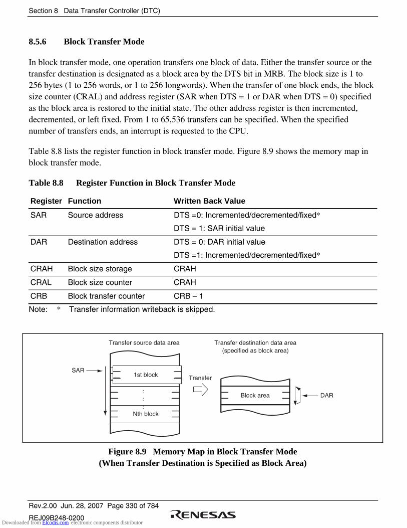
Section 8 Data Transfer Controller (DTC)
Rev.2.00 Jun. 28, 2007 Page 330 of 784
REJ09B248-0200
8.5.6 Block Transfer Mode
In block transfer mode, one operation transfers one block of data. Either the transfer source or the transfer destination is designated as a block area by the DTS bit in MRB. The block size is 1 to 256 bytes (1 to 256 words, or 1 to 256 longwords). When the transfer of one block ends, the block size counter (CRAL) and address register (SAR when DTS = 1 or DAR when DTS = 0) specified as the block area is restored to the initial state. The other address register is then incremented, decremented, or left fixed. From 1 to 65,536 transfers can be specified. When the specified number of transfers ends, an interrupt is requested to the CPU.
Table 8.8 lists the register function in block transfer mode. Figure 8.9 shows the memory map in block transfer mode.
Table 8.8 Register Function in Block Transfer Mode
Register Function Written Back Value
SAR Source address DTS =0: Incremented/decremented/fixed*
DTS = 1: SAR initial value
DAR Destination address DTS = 0: DAR initial value
DTS =1: Incremented/decremented/fixed*
CRAH Block size storage CRAH
CRAL Block size counter CRAH
CRB Block transfer counter CRB − 1
Note: * Transfer information writeback is skipped.
Transfer source data area Transfer destination data area(specified as block area)
Block area DAR
SAR
:::
Transfer1st block
Nth block
Figure 8.9 Memory Map in Block Transfer Mode (When Transfer Destination is Specified as Block Area)
Downloaded from Elcodis.com electronic components distributor
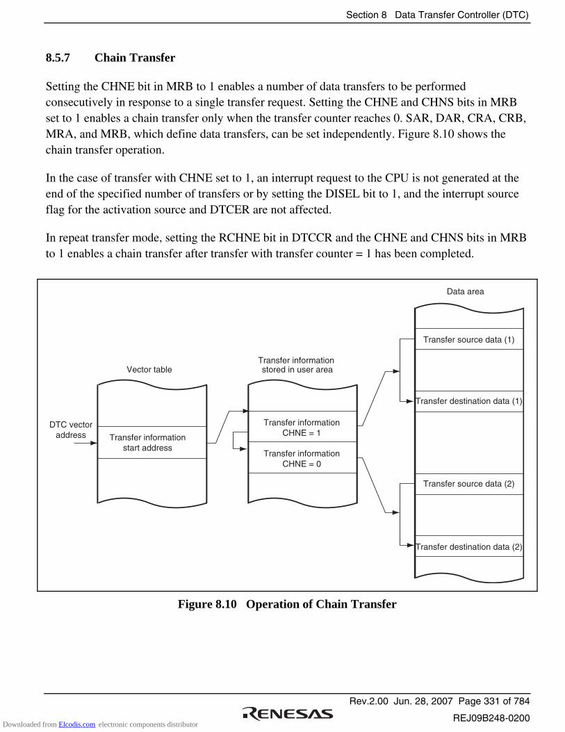
Section 8 Data Transfer Controller (DTC)
Rev.2.00 Jun. 28, 2007 Page 331 of 784
REJ09B248-0200
8.5.7 Chain Transfer
Setting the CHNE bit in MRB to 1 enables a number of data transfers to be performed consecutively in response to a single transfer request. Setting the CHNE and CHNS bits in MRB set to 1 enables a chain transfer only when the transfer counter reaches 0. SAR, DAR, CRA, CRB, MRA, and MRB, which define data transfers, can be set independently. Figure 8.10 shows the chain transfer operation.
In the case of transfer with CHNE set to 1, an interrupt request to the CPU is not generated at the end of the specified number of transfers or by setting the DISEL bit to 1, and the interrupt source flag for the activation source and DTCER are not affected.
In repeat transfer mode, setting the RCHNE bit in DTCCR and the CHNE and CHNS bits in MRB to 1 enables a chain transfer after transfer with transfer counter = 1 has been completed.
Transfer informationCHNE = 1
Transfer informationCHNE = 0
Transfer information stored in user area
Data area
Transfer source data (1)
Transfer destination data (1)
Transfer source data (2)
Transfer destination data (2)
Transfer informationstart address
Vector table
DTC vectoraddress
Figure 8.10 Operation of Chain Transfer
Downloaded from Elcodis.com electronic components distributor
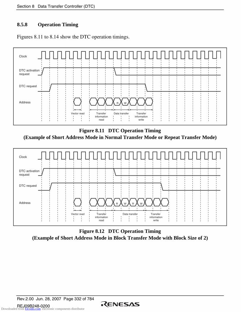
Section 8 Data Transfer Controller (DTC)
Rev.2.00 Jun. 28, 2007 Page 332 of 784
REJ09B248-0200
8.5.8 Operation Timing
Figures 8.11 to 8.14 show the DTC operation timings.
Clock
Address
DTC activationrequest
DTC request
R W
Vector read Transfer information
read
Data transfer Transferinformation
write
Figure 8.11 DTC Operation Timing (Example of Short Address Mode in Normal Transfer Mode or Repeat Transfer Mode)
Clock
Address
DTC activationrequest
DTC request
R W R W
Vector read Transferinformation
read
Data transfer Transfer information
write
Figure 8.12 DTC Operation Timing (Example of Short Address Mode in Block Transfer Mode with Block Size of 2)
Downloaded from Elcodis.com electronic components distributor
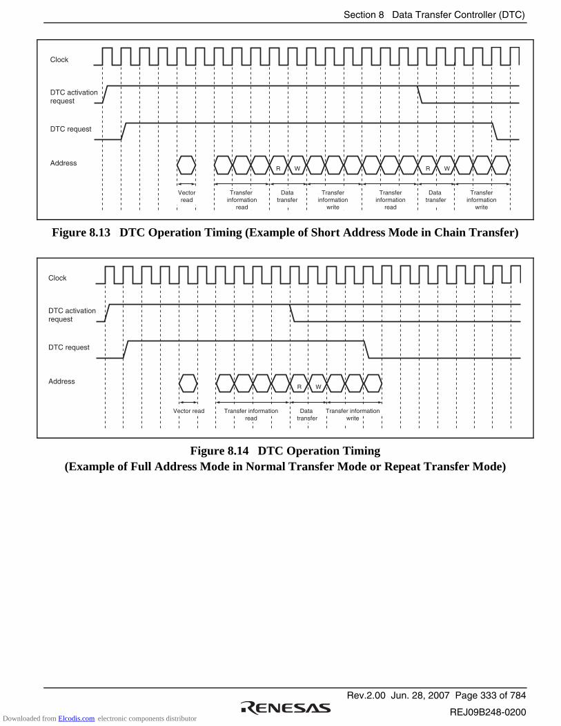
Section 8 Data Transfer Controller (DTC)
Rev.2.00 Jun. 28, 2007 Page 333 of 784
REJ09B248-0200
Clock
Address
DTC activationrequest
DTC request
R W R W
Vectorread
Transfer information
read
Datatransfer
Transferinformation
write
Transferinformation
read
Data transfer
Transferinformation
write
Figure 8.13 DTC Operation Timing (Example of Short Address Mode in Chain Transfer)
Clock
Address
DTC activationrequest
DTC request
R W
Vector read Transfer informationread
Data transfer
Transfer informationwrite
Figure 8.14 DTC Operation Timing (Example of Full Address Mode in Normal Transfer Mode or Repeat Transfer Mode)
Downloaded from Elcodis.com electronic components distributor
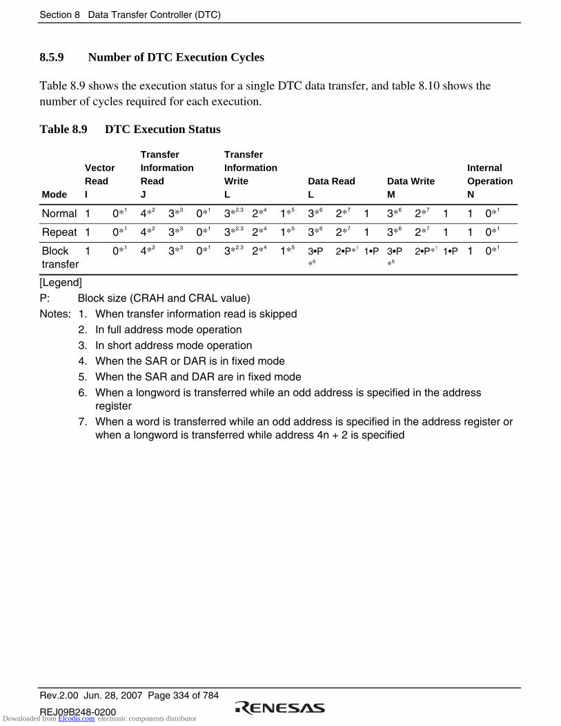
Section 8 Data Transfer Controller (DTC)
Rev.2.00 Jun. 28, 2007 Page 334 of 784
REJ09B248-0200
8.5.9 Number of DTC Execution Cycles
Table 8.9 shows the execution status for a single DTC data transfer, and table 8.10 shows the number of cycles required for each execution.
Table 8.9 DTC Execution Status
Mode
Vector Read I
Transfer Information Read J
Transfer Information Write L
Data Read L
Data Write M
Internal Operation N
Normal 1 0*1 4*2 3*3 0*1 3*2.3 2*4 1*5 3*6 2*7 1 3*6 2*7 1 1 0*1
Repeat 1 0*1 4*2 3*3 0*1 3*2.3 2*4 1*5 3*6 2*7 1 3*6 2*7 1 1 0*1
Block transfer
1 0*1 4*2 3*3 0*1 3*2.3 2*4 1*5 3•P*6
2•P*7 1•P 3•P*6
2•P*7 1•P 1 0*1
[Legend]
P: Block size (CRAH and CRAL value) Notes: 1. When transfer information read is skipped
2. In full address mode operation
3. In short address mode operation 4. When the SAR or DAR is in fixed mode
5. When the SAR and DAR are in fixed mode
6. When a longword is transferred while an odd address is specified in the address register
7. When a word is transferred while an odd address is specified in the address register or when a longword is transferred while address 4n + 2 is specified
Downloaded from Elcodis.com electronic components distributor
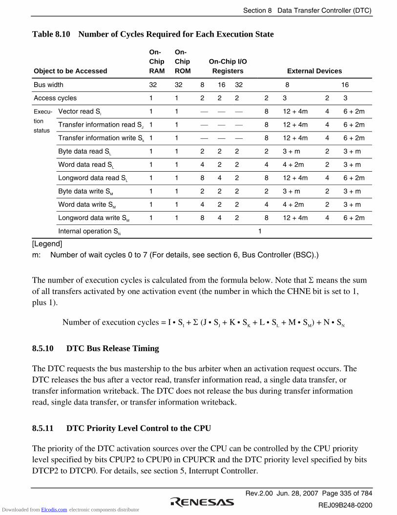
Section 8 Data Transfer Controller (DTC)
Rev.2.00 Jun. 28, 2007 Page 335 of 784
REJ09B248-0200
Table 8.10 Number of Cycles Required for Each Execution State
Object to be Accessed
On-Chip RAM
On-Chip ROM
On-Chip I/O Registers External Devices
Bus width 32 32 8 16 32 8 16
Access cycles 1 1 2 2 2 2 3 2 3
Vector read SI 1 1 8 12 + 4m 4 6 + 2m
Transfer information read SJ 1 1 8 12 + 4m 4 6 + 2m
Execu-
tion
status Transfer information write Sk 1 1 8 12 + 4m 4 6 + 2m
Byte data read SL 1 1 2 2 2 2 3 + m 2 3 + m
Word data read SL 1 1 4 2 2 4 4 + 2m 2 3 + m
Longword data read SL 1 1 8 4 2 8 12 + 4m 4 6 + 2m
Byte data write SM 1 1 2 2 2 2 3 + m 2 3 + m
Word data write SM 1 1 4 2 2 4 4 + 2m 2 3 + m
Longword data write SM 1 1 8 4 2 8 12 + 4m 4 6 + 2m
Internal operation SN 1
[Legend] m: Number of wait cycles 0 to 7 (For details, see section 6, Bus Controller (BSC).)
The number of execution cycles is calculated from the formula below. Note that Σ means the sum of all transfers activated by one activation event (the number in which the CHNE bit is set to 1, plus 1).
Number of execution cycles = I • SI + Σ (J • SJ + K • SK + L • SL + M • SM) + N • SN
8.5.10 DTC Bus Release Timing
The DTC requests the bus mastership to the bus arbiter when an activation request occurs. The DTC releases the bus after a vector read, transfer information read, a single data transfer, or transfer information writeback. The DTC does not release the bus during transfer information read, single data transfer, or transfer information writeback.
8.5.11 DTC Priority Level Control to the CPU
The priority of the DTC activation sources over the CPU can be controlled by the CPU priority level specified by bits CPUP2 to CPUP0 in CPUPCR and the DTC priority level specified by bits DTCP2 to DTCP0. For details, see section 5, Interrupt Controller.
Downloaded from Elcodis.com electronic components distributor

Section 8 Data Transfer Controller (DTC)
Rev.2.00 Jun. 28, 2007 Page 336 of 784
REJ09B248-0200
8.6 DTC Activation by Interrupt
The procedure for using the DTC with interrupt activation is shown in figure 8.15.
Clearing the RRS bit in DTCCR to 0 clears the read skip flagof transfer information. Read skip is not performed when theDTC is activated after clearing the RRS bit. When updatingtransfer information, the RRS bit must be cleared.
Set the MRA, MRB, SAR, DAR, CRA, and CRB transfer information in the data area. For details on setting transferinformation, see section 8.2, Register Descriptions. For detailson location of transfer information, see section 8.4, Location of Transfer Information and DTC Vector Table.
Set the start address of the transfer information in the DTC vector table. For details on setting DTC vector table, see section8.4, Location of Transfer Information and DTC Vector Table.
Setting the RRS bit to 1 performs a read skip of second time or later transfer information when the DTC is activated consecu-tively by the same interrupt source. Setting the RRS bit to 1 is always allowed. However, the value set during transfer will bevalid from the next transfer.
Set the bit in DTCER corresponding to the DTC activation interrupt source to 1. For the correspondence of interrupts andDTCER, refer to table 8.1. The bit in DTCER may be set to 1 onthe second or later transfer. In this case, setting the bit is not needed.
Set the enable bits for the interrupt sources to be used as the activation sources to 1. The DTC is activated when an interrupt used as an activation source is generated. For details on thesettings of the interrupt enable bits, see the corresponding descriptions of the corresponding module.
After the end of one data transfer, the DTC clears the activationsource flag or clears the corresponding bit in DTCER and requests an interrupt to the CPU. The operation after transfer depends on the transfer information. For details, see section 8.2, Register Descriptions and figure 8.4.
DTC activation by interrupt
Clear RRS bit in DTCCR to 0
Set transfer information(MRA, MRB, SAR, DAR,
CRA, CRB)
Set starts address of transfer information in DTC vector table
Set RRS bit in DTCCR to 1
Set corresponding bit in DTCER to 1
Set enable bit of interruptrequest for activation source
to 1
Interrupt request generated
DTC activated
Corresponding bit in DTCERcleared or CPU interrupt
requested
Transfer end
[1]
[2]
[3]
[4]
[5]
[6]
[7]
[1]
[2]
[3]
[4]
[5]
[6]
[7]
Determineclearing method of activation source
Clear activation source
Clear corresponding bit in DTCER
Figure 8.15 DTC with Interrupt Activation
Downloaded from Elcodis.com electronic components distributor
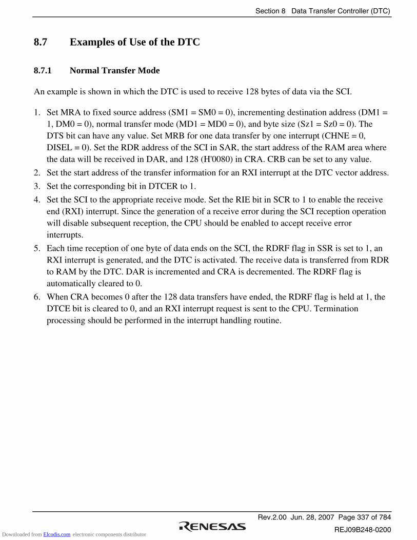
Section 8 Data Transfer Controller (DTC)
Rev.2.00 Jun. 28, 2007 Page 337 of 784
REJ09B248-0200
8.7 Examples of Use of the DTC
8.7.1 Normal Transfer Mode
An example is shown in which the DTC is used to receive 128 bytes of data via the SCI.
1. Set MRA to fixed source address (SM1 = SM0 = 0), incrementing destination address (DM1 = 1, DM0 = 0), normal transfer mode (MD1 = MD0 = 0), and byte size (Sz1 = Sz0 = 0). The DTS bit can have any value. Set MRB for one data transfer by one interrupt (CHNE = 0, DISEL = 0). Set the RDR address of the SCI in SAR, the start address of the RAM area where the data will be received in DAR, and 128 (H'0080) in CRA. CRB can be set to any value.
2. Set the start address of the transfer information for an RXI interrupt at the DTC vector address.
3. Set the corresponding bit in DTCER to 1.
4. Set the SCI to the appropriate receive mode. Set the RIE bit in SCR to 1 to enable the receive end (RXI) interrupt. Since the generation of a receive error during the SCI reception operation will disable subsequent reception, the CPU should be enabled to accept receive error interrupts.
5. Each time reception of one byte of data ends on the SCI, the RDRF flag in SSR is set to 1, an RXI interrupt is generated, and the DTC is activated. The receive data is transferred from RDR to RAM by the DTC. DAR is incremented and CRA is decremented. The RDRF flag is automatically cleared to 0.
6. When CRA becomes 0 after the 128 data transfers have ended, the RDRF flag is held at 1, the DTCE bit is cleared to 0, and an RXI interrupt request is sent to the CPU. Termination processing should be performed in the interrupt handling routine.
Downloaded from Elcodis.com electronic components distributor
Section 8 Data Transfer Controller (DTC)
Rev.2.00 Jun. 28, 2007 Page 338 of 784
REJ09B248-0200
8.7.2 Chain Transfer
An example of DTC chain transfer is shown in which pulse output is performed using the PPG. Chain transfer can be used to perform pulse output data transfer and PPG output trigger cycle updating. Repeat mode transfer to the PPG's NDR is performed in the first half of the chain transfer, and normal mode transfer to the TPU's TGR in the second half. This is because clearing of the activation source and interrupt generation at the end of the specified number of transfers are restricted to the second half of the chain transfer (transfer when CHNE = 0).
1. Perform settings for transfer to the PPG's NDR. Set MRA to source address incrementing (SM1 = 1, SM0 = 0), fixed destination address (DM1 = DM0 = 0), repeat mode (MD1 = 0, MD0 = 1), and word size (Sz1 = 0, Sz0 = 1). Set the source side as a repeat area (DTS = 1). Set MRB to chain transfer mode (CHNE = 1, CHNS = 0, DISEL = 0). Set the data table start address in SAR, the NDRH address in DAR, and the data table size in CRAH and CRAL. CRB can be set to any value.
2. Perform settings for transfer to the TPU's TGR. Set MRA to source address incrementing (SM1 = 1, SM0 = 0), fixed destination address (DM1 = DM0 = 0), normal mode (MD1 = MD0 = 0), and word size (Sz1 = 0, Sz0 = 1). Set the data table start address in SAR, the TGRA address in DAR, and the data table size in CRA. CRB can be set to any value.
3. Locate the TPU transfer information consecutively after the NDR transfer information.
4. Set the start address of the NDR transfer information to the DTC vector address.
5. Set the bit corresponding to the TGIA interrupt in DTCER to 1.
6. Set TGRA as an output compare register (output disabled) with TIOR, and enable the TGIA interrupt with TIER.
7. Set the initial output value in PODR, and the next output value in NDR. Set bits in DDR and NDER for which output is to be performed to 1. Using PCR, select the TPU compare match to be used as the output trigger.
8. Set the CST bit in TSTR to 1, and start the TCNT count operation.
9. Each time a TGRA compare match occurs, the next output value is transferred to NDR and the set value of the next output trigger period is transferred to TGRA. The activation source TGFA flag is cleared.
10. When the specified number of transfers are completed (the TPU transfer CRA value is 0), the TGFA flag is held at 1, the DTCE bit is cleared to 0, and a TGIA interrupt request is sent to the CPU. Termination processing should be performed in the interrupt handling routine.
Downloaded from Elcodis.com electronic components distributor
Section 8 Data Transfer Controller (DTC)
Rev.2.00 Jun. 28, 2007 Page 339 of 784
REJ09B248-0200
8.7.3 Chain Transfer when Counter = 0
By executing a second data transfer and performing re-setting of the first data transfer only when the counter value is 0, it is possible to perform 256 or more repeat transfers.
An example is shown in which a 128-kbyte input buffer is configured. The input buffer is assumed to have been set to start at lower address H'0000. Figure 8.16 shows the chain transfer when the counter value is 0.
1. For the first transfer, set the normal transfer mode for input data. Set the fixed transfer source address, CRA = H'0000 (65,536 times), CHNE = 1, CHNS = 1, and DISEL = 0.
2. Prepare the upper 8-bit addresses of the start addresses for 65,536-transfer units for the first data transfer in a separate area (in ROM, etc.). For example, if the input buffer is configured at addresses H'200000 to H'21FFFF, prepare H'21 and H'20.
3. For the second transfer, set repeat transfer mode (with the source side as the repeat area) for re-setting the transfer destination address for the first data transfer. Use the upper eight bits of DAR in the first transfer information area as the transfer destination. Set CHNE = DISEL = 0. If the above input buffer is specified as H'200000 to H'21FFFF, set the transfer counter to 2.
4. Execute the first data transfer 65536 times by means of interrupts. When the transfer counter for the first data transfer reaches 0, the second data transfer is started. Set the upper eight bits of the transfer source address for the first data transfer to H'21. The lower 16 bits of the transfer destination address of the first data transfer and the transfer counter are H'0000.
5. Next, execute the first data transfer the 65536 times specified for the first data transfer by means of interrupts. When the transfer counter for the first data transfer reaches 0, the second data transfer is started. Set the upper eight bits of the transfer source address for the first data transfer to H'20. The lower 16 bits of the transfer destination address of the first data transfer and the transfer counter are H'0000.
6. Steps 4 and 5 are repeated endlessly. As repeat mode is specified for the second data transfer, no interrupt request is sent to the CPU.
Downloaded from Elcodis.com electronic components distributor

Section 8 Data Transfer Controller (DTC)
Rev.2.00 Jun. 28, 2007 Page 340 of 784
REJ09B248-0200
1st data transferinformation
2nd data transferinformation
Transfer information located on the on-chip memory
Chain transfer(counter = 0)
Input circuit
Input buffer
Upper 8 bits of DAR
Figure 8.16 Chain Transfer when Counter = 0
8.8 Interrupt Sources
An interrupt request is issued to the CPU when the DTC finishes the specified number of data transfers or a data transfer for which the DISEL bit was set to 1. In the case of interrupt activation, the interrupt set as the activation source is generated. These interrupts to the CPU are subject to CPU mask level and priority level control in the interrupt controller.
Downloaded from Elcodis.com electronic components distributor
Section 8 Data Transfer Controller (DTC)
Rev.2.00 Jun. 28, 2007 Page 341 of 784
REJ09B248-0200
8.9 Usage Notes
8.9.1 Module Stop Mode Setting
Operation of the DTC can be disabled or enabled using the module stop control register. The initial setting is for operation of the DTC to be enabled. Register access is disabled by setting module stop mode. Module stop mode cannot be set while the DTC is activated. For details, see section 19, Power-Down Modes.
8.9.2 On-Chip RAM
Transfer information can be located in on-chip RAM. In this case, the RAME bit in SYSCR must not be cleared to 0.
8.9.3 DMAC Transfer End Interrupt
When the DTC is activated by a DMAC transfer end interrupt, the DTE bit of DMDR is not controlled by the DTC but its value is modified with the write data regardless of the transfer counter value and DISEL bit setting. Accordingly, even if the DTC transfer counter value becomes 0, no interrupt request may be sent to the CPU in some cases.
8.9.4 DTCE Bit Setting
For DTCE bit setting, use bit manipulation instructions such as BSET and BCLR. If all interrupts are disabled, multiple activation sources can be set at one time (only at the initial setting) by writing data after executing a dummy read on the relevant register.
8.9.5 Chain Transfer
When chain transfer is used, clearing of the activation source or DTCER is performed when the last of the chain of data transfers is executed. At this time, SCI and A/D converter interrupt/activation sources, are cleared when the DTC reads or writes to the relevant register.
Therefore, when the DTC is activated by an interrupt or activation source, if a read/write of the relevant register is not included in the last chained data transfer, the interrupt or activation source will be retained.
Downloaded from Elcodis.com electronic components distributor
Section 8 Data Transfer Controller (DTC)
Rev.2.00 Jun. 28, 2007 Page 342 of 784
REJ09B248-0200
8.9.6 Transfer Information Start Address, Source Address, and Destination Address
The transfer information start address to be specified in the vector table should be address 4n. If an address other than address 4n is specified, the lower 2 bits of the address are regarded as 0s.
The source and destination addresses specified in SAR and DAR, respectively, will be transferred in the divided bus cycles depending on the address and data size.
8.9.7 Transfer Information Modification
When IBCCS = 1 and the DMAC is used, clear the IBCCS bit to 0 and then set to 1 again before modifying the DTC transfer information in the CPU exception handling routine initiated by a DTC transfer end interrupt.
8.9.8 Endian
The DTC supports the big-endian and little-endian format. However, use the same endian format for writing and reading the transfer information.
Downloaded from Elcodis.com electronic components distributor

Section 9 I/O Ports
Rev.2.00 Jun. 28, 2007 Page 343 of 784
REJ09B248-0200
Section 9 I/O Ports
Table 9.1 summarizes the port functions. The pins of each port also have other functions such as input/output pins of on-chip peripheral modules or external interrupt input pins. Each I/O port includes a data direction register (DDR) that controls input/output, a data register (DR) that stores output data, a port register (PORT) used to read the pin states, and an input buffer control register (ICR) that controls input buffer on/off. Port 5 does not have a DR or a DDR register.
Ports D to F, H, and I have internal input pull-up MOSs and a pull-up MOS control register (PCR) that controls the on/off state of the input pull-up MOSs.
Ports 2 and F include an open-drain control register (ODR) that controls on/off of the output buffer PMOSs.
All of the I/O ports can drive a single TTL load and capacitive loads up to 30 pF.
All of the I/O ports can drive Darlington transistors when functioning as output ports.
Ports 2 and 3 are Schmitt-trigger inputs. Schmitt-trigger inputs for other ports are enabled when used as the IRQ, TPU, or TMR inputs.
Downloaded from Elcodis.com electronic components distributor

Section 9 I/O Ports
Rev.2.00 Jun. 28, 2007 Page 344 of 784
REJ09B248-0200
Table 9.1 Port Functions
Function
Port Description Bit I/O Input Output
Schmitt-Trigger Input*1
Input Pull-up MOS Function
Open-Drain Output Function
Port 1 7 P17 IRQ7-A/ TCLKD-B
IRQ7-A, TCLKD-B
6 P16/SCK3 IRQ6-A/ TCLKC-B
DACK1-A IRQ6-A, TCLKC-B
5 P15 RxD3/ IRQ5-A/ TCLKB-B
TEND1-A IRQ5-A, TCLKB-B
General I/O port also functioning as interrupt inputs, SCI I/Os, DMAC I/Os, A/D converter inputs, and TPU inputs
4 P14 DREQ1-A/ IRQ4-A/ TCLKA-B
TxD3 IRQ4-A, TCLKA-B
3 P13 ADTRG0/ IRQ3-A
IRQ3-A
2 P12/SCK2 IRQ2-A DACK0-A IRQ2-A
1 P11 RxD2/ IRQ1-A
TEND0-A IRQ1-A
0 P10 DREQ0-A/ IRQ0-A
TxD2 IRQ0-A
Downloaded from Elcodis.com electronic components distributor

Section 9 I/O Ports
Rev.2.00 Jun. 28, 2007 Page 345 of 784
REJ09B248-0200
Function
Port Description Bit I/O Input Output
Schmitt-Trigger Input *1
Input Pull-up MOS Function
Open-Drain Output Function
Port 2 7 P27/ TIOCB5
TIOCA5 PO7 All input functions
O
6 P26/ TIOCA5
PO6/TMO1/TxD1
All input functions
General I/O port also functioning as interrupt inputs, PPG outputs, TPU I/Os, TMR I/Os, and SCI I/Os 5 P25/
TIOCA4 TMCI1/ RxD1
PO5 P25, TIOCA4, TMCI1
4 P24/ TIOCB4/ SCK1
TIOCA4/ TMRI1
PO4 P24, TIOCB4,TIOCA4, TMRI1
3 P23/ TIOCD3
IRQ11-A/ TIOCC3
PO3 All input functions
2 P22/ TIOCC3
IRQ10-A PO2/TMO0/TxD0/
All input functions
1 P21/ TIOCA3
TMCI0/ RxD0/ IRQ9-A
PO1 P21, IRQ9-A, TIOCA3, TMCI0
0 P20/ TIOCB3/ SCK0
TIOCA3/ TMRI0/ IRQ8-A
PO0 P20, IRQ8-A, TIOCB3, TIOCA3, TMRI0
Downloaded from Elcodis.com electronic components distributor
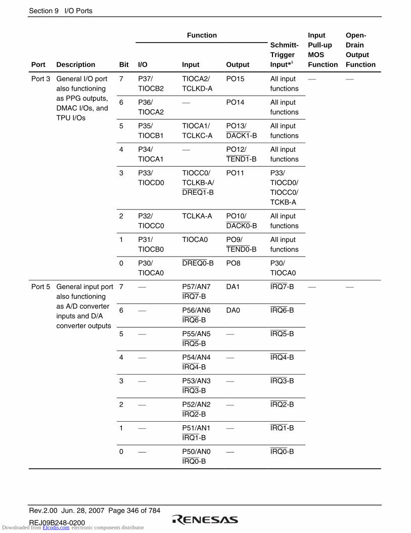
Section 9 I/O Ports
Rev.2.00 Jun. 28, 2007 Page 346 of 784
REJ09B248-0200
Function
Port Description Bit I/O Input Output
Schmitt-Trigger Input*1
Input Pull-up MOS Function
Open-Drain Output Function
Port 3 7 P37/ TIOCB2
TIOCA2/ TCLKD-A
PO15 All input functions
6 P36/ TIOCA2
PO14 All input functions
5 P35/ TIOCB1
TIOCA1/ TCLKC-A
PO13/ DACK1-B
All input functions
General I/O port also functioning as PPG outputs, DMAC I/Os, and TPU I/Os
4 P34/ TIOCA1
PO12/ TEND1-B
All input functions
3 P33/ TIOCD0
TIOCC0/ TCLKB-A/ DREQ1-B
PO11 P33/ TIOCD0/TIOCC0/TCKB-A
2 P32/ TIOCC0
TCLKA-A PO10/ DACK0-B
All input functions
1 P31/ TIOCB0
TIOCA0 PO9/ TEND0-B
All input functions
0 P30/ TIOCA0
DREQ0-B PO8 P30/ TIOCA0
Port 5 7 P57/AN7 IRQ7-B
DA1 IRQ7-B
6 P56/AN6 IRQ6-B
DA0 IRQ6-B
General input port also functioning as A/D converter inputs and D/A converter outputs
5 P55/AN5 IRQ5-B
IRQ5-B
4 P54/AN4 IRQ4-B
IRQ4-B
3 P53/AN3 IRQ3-B
IRQ3-B
2 P52/AN2 IRQ2-B
IRQ2-B
1 P51/AN1 IRQ1-B
IRQ1-B
0 P50/AN0 IRQ0-B
IRQ0-B
Downloaded from Elcodis.com electronic components distributor

Section 9 I/O Ports
Rev.2.00 Jun. 28, 2007 Page 347 of 784
REJ09B248-0200
Function
Port Description Bit I/O Input Output
Schmitt-Trigger Input*1
Input Pull-up MOS Function
Open-Drain Output Function
7 Port 6
6
5 P65 TMO3/ DACK3
4 P64 TMCI3 TEND3 TMCI3
General I/O port also functioning as TMR I/Os, SCI I/Os, DMAC I/Os, and interrupt inputs
3 P63 TMRI3/ DREQ3/ IRQ11-B
TMRI3/ IRQ11-B
2 P62/SCK4 IRQ10-B TMO2/ DACK2
IRQ10-B
1 P61 TMCI2/ RxD4/ IRQ9-B
TEND2 TMCI2/ IRQ9-B
0 P60 TMRI2/ DREQ2/ IRQ8-B
TxD4 TMCI2/ IRQ8-B
7 PA7 Bφ Port A
6 PA6 AS/AH/ BS-B
General I/O port also functioning as system clock output and bus control I/Os 5 RD
4 PA4 LHWR/LUB
3 LLWR/LLB
2 PA2 BREQ/ WAIT
1 PA1 BACK/ (RD/WR)
0 PA0 BREQO/ BS-A
Downloaded from Elcodis.com electronic components distributor

Section 9 I/O Ports
Rev.2.00 Jun. 28, 2007 Page 348 of 784
REJ09B248-0200
Function
Port Description Bit I/O Input Output
Schmitt-Trigger Input*1
Input Pull-up MOS Function
Open-Drain Output Function
7 Port B
6
5
General I/O port also functioning as bus control outputs
4
3 PB3 CS3/ CS7-A
2 PB2 CS2-A/ CS6-A
1 PB1 CS1/ CS2-B/ CS5-A/ CS6-B/ CS7-B
0 PB0 CS0/CS4-A/CS5-B
7 A7 O Port D
6 A6
5 A5
Address outputs
4 A4
3 A3
2 A2
1 A1
0 A0
7 A15 O Port E
6 A14
5 A13
Address outputs
4 A12
3 A11
2 A10
1 A9
0 A8
Downloaded from Elcodis.com electronic components distributor
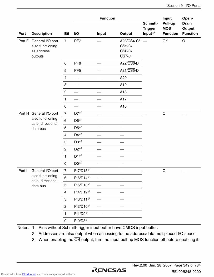
Section 9 I/O Ports
Rev.2.00 Jun. 28, 2007 Page 349 of 784
REJ09B248-0200
Function
Port Description Bit I/O Input Output
Schmitt-Trigger Input*1
Input Pull-up MOS Function
Open-Drain Output Function
7 PF7 A23/CS4-C/CS5-C/ CS6-C/ CS7-C
O*3 O Port F
6 PF6 A22/CS6-D
5 PF5 A21/CS5-D
General I/O port also functioning as address outputs
4 A20
3 A19
2 A18
1 A17
0 A16
7 D7*2 O Port H
6 D6*2
5 D5*2
General I/O port also functioning as bi-directional data bus
4 D4*2
3 D3*2
2 D2*2
1 D1*2
0 D0*2
7 PI7/D15*2 O Port I
6 PI6/D14*2
5 PI5/D13*2
General I/O port also functioning as bi-directional data bus
4 PI4/D12*2
3 PI3/D11*2
2 PI2/D10*2
1 PI1/D9*2
0 PI0/D8*2
Notes: 1. Pins without Schmitt-trigger input buffer have CMOS input buffer.
2. Addresses are also output when accessing to the address/data multiplexed I/O space. 3. When enabling the CS output, turn the input pull-up MOS function off before enabling it.
Downloaded from Elcodis.com electronic components distributor
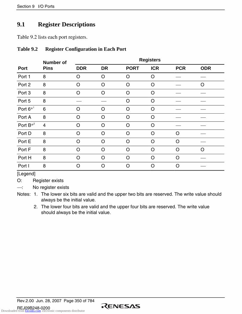
Section 9 I/O Ports
Rev.2.00 Jun. 28, 2007 Page 350 of 784
REJ09B248-0200
9.1 Register Descriptions
Table 9.2 lists each port registers.
Table 9.2 Register Configuration in Each Port
Registers
Port Number of Pins DDR DR PORT ICR PCR ODR
Port 1 8 O O O O
Port 2 8 O O O O O
Port 3 8 O O O O
Port 5 8 O O
Port 6*1 6 O O O O
Port A 8 O O O O
Port B*2 4 O O O O
Port D 8 O O O O O
Port E 8 O O O O O
Port F 8 O O O O O O
Port H 8 O O O O O
Port I 8 O O O O O
[Legend] O: Register exists
: No register exists
Notes: 1. The lower six bits are valid and the upper two bits are reserved. The write value should always be the initial value.
2. The lower four bits are valid and the upper four bits are reserved. The write value should always be the initial value.
Downloaded from Elcodis.com electronic components distributor
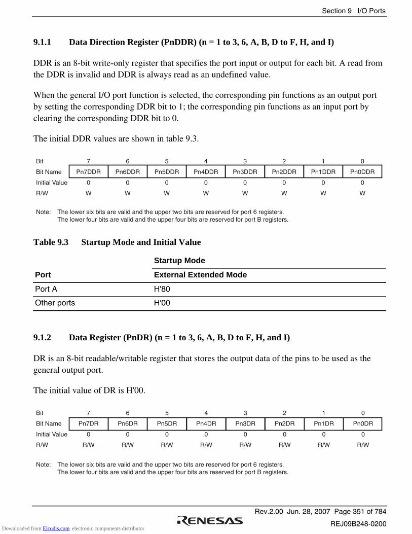
Section 9 I/O Ports
Rev.2.00 Jun. 28, 2007 Page 351 of 784
REJ09B248-0200
9.1.1 Data Direction Register (PnDDR) (n = 1 to 3, 6, A, B, D to F, H, and I)
DDR is an 8-bit write-only register that specifies the port input or output for each bit. A read from the DDR is invalid and DDR is always read as an undefined value.
When the general I/O port function is selected, the corresponding pin functions as an output port by setting the corresponding DDR bit to 1; the corresponding pin functions as an input port by clearing the corresponding DDR bit to 0.
The initial DDR values are shown in table 9.3.
Bit
Bit Name
Initial Value
R/W
Note: The lower six bits are valid and the upper two bits are reserved for port 6 registers. The lower four bits are valid and the upper four bits are reserved for port B registers.
7
Pn7DDR
0
W
6
Pn6DDR
0
W
5
Pn5DDR
0
W
4
Pn4DDR
0
W
3
Pn3DDR
0
W
2
Pn2DDR
0
W
1
Pn1DDR
0
W
0
Pn0DDR
0
W
Table 9.3 Startup Mode and Initial Value
Startup Mode
Port External Extended Mode
Port A H'80
Other ports H'00
9.1.2 Data Register (PnDR) (n = 1 to 3, 6, A, B, D to F, H, and I)
DR is an 8-bit readable/writable register that stores the output data of the pins to be used as the general output port.
The initial value of DR is H'00.
Bit
Bit Name
Initial Value
R/W
7
Pn7DR
0
R/W
6
Pn6DR
0
R/W
5
Pn5DR
0
R/W
4
Pn4DR
0
R/W
3
Pn3DR
0
R/W
2
Pn2DR
0
R/W
1
Pn1DR
0
R/W
0
Pn0DR
0
R/W
Note: The lower six bits are valid and the upper two bits are reserved for port 6 registers. The lower four bits are valid and the upper four bits are reserved for port B registers.
Downloaded from Elcodis.com electronic components distributor

Section 9 I/O Ports
Rev.2.00 Jun. 28, 2007 Page 352 of 784
REJ09B248-0200
9.1.3 Port Register (PORTn) (n = 1 to 3, 5, 6, A, B, D to F, H, and I)
PORT is an 8-bit read-only register that reflects the port pin status. A write to PORT is invalid.
When PORT is read, the DR bits that correspond to the respective DDR bits set to 1 are read and the status of each pin whose corresponding DDR bit is cleared to 0 is also read regardless of the ICR value.
The initial value of PORT is undefined and is determined based on the port pin status.
Bit
Bit Name
Initial Value
R/W
7
Pn7
Undefined
R
6
Pn6
Undefined
R
5
Pn5
Undefined
R
4
Pn4
Undefined
R
3
Pn3
Undefined
R
2
Pn2
Undefined
R
1
Pn1
Undefined
R
0
Pn0
Undefined
R
Note: The lower six bits are valid and the upper two bits are reserved for port 6 registers. The lower four bits are valid and the upper four bits are reserved for port B registers.
9.1.4 Input Buffer Control Register (PnICR) (n = 1 to 3, 5, 6, A, B, D to F, H, and I)
ICR is an 8-bit readable/writable register that controls the port input buffers.
For bits in ICR set to 1, the input buffers of the corresponding pins are valid. For bits in ICR cleared to 0, the input buffers of the corresponding pins are invalid and the input signals are fixed high.
When the pin functions as an input for the peripheral modules, the corresponding bits should be set to 1. The initial value should be written to a bit whose corresponding pin is not used as an input or is used as an analog input/output pin.
If the bits in ICR have been cleared to 0, the pin state is not reflected to the peripheral modules.
When PORT is read, the pin status is always read regardless of the ICR value.
Downloaded from Elcodis.com electronic components distributor
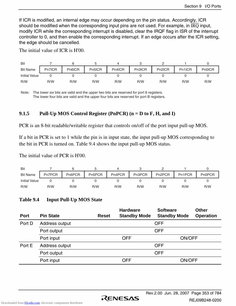
Section 9 I/O Ports
Rev.2.00 Jun. 28, 2007 Page 353 of 784
REJ09B248-0200
If ICR is modified, an internal edge may occur depending on the pin status. Accordingly, ICR should be modified when the corresponding input pins are not used. For example, in IRQ input, modify ICR while the corresponding interrupt is disabled, clear the IRQF flag in ISR of the interrupt controller to 0, and then enable the corresponding interrupt. If an edge occurs after the ICR setting, the edge should be cancelled.
The initial value of ICR is H'00.
Bit
Bit Name
Initial Value
R/W
7
Pn7ICR
0
R/W
6
Pn6ICR
0
R/W
5
Pn5ICR
0
R/W
4
Pn4ICR
0
R/W
3
Pn3ICR
0
R/W
2
Pn2ICR
0
R/W
1
Pn1ICR
0
R/W
0
Pn0ICR
0
R/W
Note: The lower six bits are valid and the upper two bits are reserved for port 6 registers. The lower four bits are valid and the upper four bits are reserved for port B registers.
9.1.5 Pull-Up MOS Control Register (PnPCR) (n = D to F, H, and I)
PCR is an 8-bit readable/writable register that controls on/off of the port input pull-up MOS.
If a bit in PCR is set to 1 while the pin is in input state, the input pull-up MOS corresponding to the bit in PCR is turned on. Table 9.4 shows the input pull-up MOS status.
The initial value of PCR is H'00.
Bit
Bit Name
Initial Value
R/W
7
Pn7PCR
0
R/W
6
Pn6PCR
0
R/W
5
Pn5PCR
0
R/W
4
Pn4PCR
0
R/W
3
Pn3PCR
0
R/W
2
Pn2PCR
0
R/W
1
Pn1PCR
0
R/W
0
Pn0PCR
0
R/W
Table 9.4 Input Pull-Up MOS State
Port Pin State Reset Hardware Standby Mode
Software Standby Mode
Other Operation
Port D Address output OFF
Port output OFF
Port input OFF ON/OFF
Port E Address output OFF
Port output OFF
Port input OFF ON/OFF
Downloaded from Elcodis.com electronic components distributor
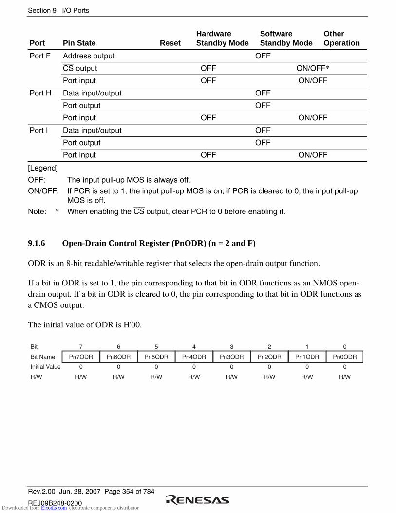
Section 9 I/O Ports
Rev.2.00 Jun. 28, 2007 Page 354 of 784
REJ09B248-0200
Port Pin State Reset Hardware Standby Mode
Software Standby Mode
Other Operation
Port F Address output OFF
CS output OFF ON/OFF*
Port input OFF ON/OFF
Port H Data input/output OFF
Port output OFF
Port input OFF ON/OFF
Port I Data input/output OFF
Port output OFF
Port input OFF ON/OFF
[Legend]
OFF: The input pull-up MOS is always off. ON/OFF: If PCR is set to 1, the input pull-up MOS is on; if PCR is cleared to 0, the input pull-up
MOS is off. Note: * When enabling the CS output, clear PCR to 0 before enabling it.
9.1.6 Open-Drain Control Register (PnODR) (n = 2 and F)
ODR is an 8-bit readable/writable register that selects the open-drain output function.
If a bit in ODR is set to 1, the pin corresponding to that bit in ODR functions as an NMOS open-drain output. If a bit in ODR is cleared to 0, the pin corresponding to that bit in ODR functions as a CMOS output.
The initial value of ODR is H'00.
Bit
Bit Name
Initial Value
R/W
7
Pn7ODR
0
R/W
6
Pn6ODR
0
R/W
5
Pn5ODR
0
R/W
4
Pn4ODR
0
R/W
3
Pn3ODR
0
R/W
2
Pn2ODR
0
R/W
1
Pn1ODR
0
R/W
0
Pn0ODR
0
R/W
Downloaded from Elcodis.com electronic components distributor
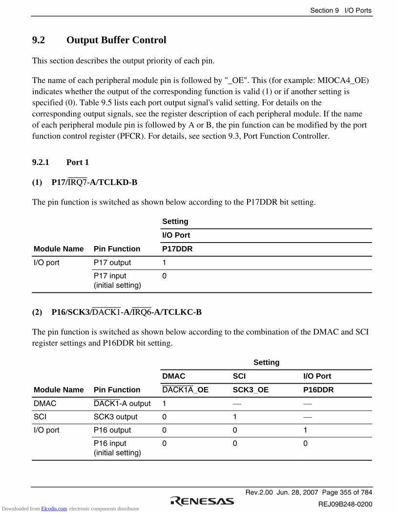
Section 9 I/O Ports
Rev.2.00 Jun. 28, 2007 Page 355 of 784
REJ09B248-0200
9.2 Output Buffer Control
This section describes the output priority of each pin.
The name of each peripheral module pin is followed by "_OE". This (for example: MIOCA4_OE) indicates whether the output of the corresponding function is valid (1) or if another setting is specified (0). Table 9.5 lists each port output signal's valid setting. For details on the corresponding output signals, see the register description of each peripheral module. If the name of each peripheral module pin is followed by A or B, the pin function can be modified by the port function control register (PFCR). For details, see section 9.3, Port Function Controller.
9.2.1 Port 1
(1) P17/IRQ7-A/TCLKD-B
The pin function is switched as shown below according to the P17DDR bit setting.
Setting
I/O Port
Module Name Pin Function P17DDR
I/O port P17 output 1
P17 input (initial setting)
0
(2) P16/SCK3/DACK1-A/IRQ6-A/TCLKC-B
The pin function is switched as shown below according to the combination of the DMAC and SCI register settings and P16DDR bit setting.
Setting
DMAC SCI I/O Port
Module Name Pin Function DACK1A_OE SCK3_OE P16DDR
DMAC DACK1-A output 1
SCI SCK3 output 0 1
I/O port P16 output 0 0 1
P16 input (initial setting)
0 0 0
Downloaded from Elcodis.com electronic components distributor
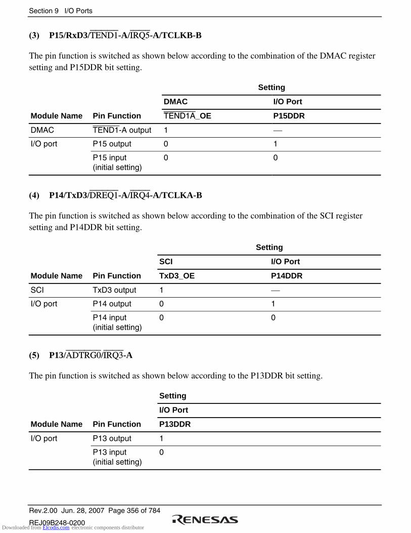
Section 9 I/O Ports
Rev.2.00 Jun. 28, 2007 Page 356 of 784
REJ09B248-0200
(3) P15/RxD3/TEND1-A/IRQ5-A/TCLKB-B
The pin function is switched as shown below according to the combination of the DMAC register setting and P15DDR bit setting.
Setting
DMAC I/O Port
Module Name Pin Function TEND1A_OE P15DDR
DMAC TEND1-A output 1
I/O port P15 output 0 1
P15 input (initial setting)
0 0
(4) P14/TxD3/DREQ1-A/IRQ4-A/TCLKA-B
The pin function is switched as shown below according to the combination of the SCI register setting and P14DDR bit setting.
Setting
SCI I/O Port
Module Name Pin Function TxD3_OE P14DDR
SCI TxD3 output 1
I/O port P14 output 0 1
P14 input (initial setting)
0 0
(5) P13/ADTRG0/IRQ3-A
The pin function is switched as shown below according to the P13DDR bit setting.
Setting
I/O Port
Module Name Pin Function P13DDR
I/O port P13 output 1
P13 input (initial setting)
0
Downloaded from Elcodis.com electronic components distributor
Section 9 I/O Ports
Rev.2.00 Jun. 28, 2007 Page 357 of 784
REJ09B248-0200
(6) P12/SCK2/DACK0-A/IRQ2-A
The pin function is switched as shown below according to the combination of the DMAC and SCI register settings and P12DDR bit setting.
Setting
DMAC SCI I/O Port
Module Name Pin Function DACK0A_OE SCK2_OE P12DDR
DMAC DACK0-A output 1
SCI SCK2 output 0 1
I/O port P12 output 0 0 1
P12 input (initial setting)
0 0 0
(7) P11/RxD2/TEND0-A/IRQ1-A
The pin function is switched as shown below according to the combination of the DMAC register setting and P11DDR bit setting.
Setting
DMAC I/O Port
Module Name Pin Function TEND0A_OE P11DDR
DMAC TEND0-A output 1
I/O port P11 output 0 1
P11 input (initial setting)
0 0
Downloaded from Elcodis.com electronic components distributor

Section 9 I/O Ports
Rev.2.00 Jun. 28, 2007 Page 358 of 784
REJ09B248-0200
(8) P10/TxD2/DREQ0-A/IRQ0-A
The pin function is switched as shown below according to the combination of the SCI register setting and P10DDR bit setting.
Setting
SCI I/O Port
Module Name Pin Function TxD2_OE P10DDR
SCI TxD2 output 1
P10 output 0 1 I/O port
P10 input (initial setting)
0 0
9.2.2 Port 2
(1) P27/PO7/TIOCA5/TIOCB5
The pin function is switched as shown below according to the combination of the TPU and PPG register settings and P27DDR bit setting.
Setting
TPU PPG I/O Port
Module Name Pin Function TIOCB5_OE PO7_OE P27DDR
TPU TIOCB5 output 1
PPG PO7 output 0 1
P27 output 0 0 1 I/O port
P27 input (initial setting)
0 0 0
Downloaded from Elcodis.com electronic components distributor
Section 9 I/O Ports
Rev.2.00 Jun. 28, 2007 Page 359 of 784
REJ09B248-0200
(2) P26/PO6/TIOCA5/TMO1/TxD1
The pin function is switched as shown below according to the combination of the TPU, TMR, SCI, and PPG register settings and P26DDR bit setting.
Setting
TPU TMR SCI PPG I/O Port
Module Name Pin Function TIOCA5_OE TMO1_OE TxD1_OE PO6_OE P26DDR
TPU TIOCA5 output 1
TMR TMO1 output 0 1
SCI TxD1 output 0 0 1
PPG PO6 output 0 0 0 1
P26 output 0 0 0 0 1 I/O port
P26 input (initial setting)
0 0 0 0 0
(3) P25/PO5/TIOCA4/TMCI1/RxD1
The pin function is switched as shown below according to the combination of the TPU and PPG register settings and P25DDR bit setting.
Setting
TPU PPG I/O Port
Module Name Pin Function TIOCA4_OE PO5_OE P25DDR
TPU TIOCA4 output 1
PPG PO5 output 0 1
P25 output 0 0 1 I/O port
P25 input (initial setting)
0 0 0
Downloaded from Elcodis.com electronic components distributor
Section 9 I/O Ports
Rev.2.00 Jun. 28, 2007 Page 360 of 784
REJ09B248-0200
(4) P24/PO4/TIOCA4/TIOCB4/TMRI1/SCK1
The pin function is switched as shown below according to the combination of the TPU, SCI, and PPG register settings and P24DDR bit setting.
Setting
TPU SCI PPG I/O Port
Module Name Pin Function TIOCB4_OE SCK1_OE PO4_OE P24DDR
TPU TIOCB4 output 1
SCI SCK1 output 0 1
PPG PO4 output 0 0 1
P24 output 0 0 0 1 I/O port
P24 input (initial setting)
0 0 0 0
(5) P23/PO3/TIOCC3/TIOCD3/IRQ11-A
The pin function is switched as shown below according to the combination of the TPU and PPG register settings and P23DDR bit setting.
Setting
TPU PPG I/O Port
Module Name Pin Function TIOCD3_OE PO3_OE P23DDR
TPU TIOCD3 output 1
PPG PO3 output 0 1
P23 output 0 0 1 I/O port
P23 input (initial setting)
0 0 0
Downloaded from Elcodis.com electronic components distributor

Section 9 I/O Ports
Rev.2.00 Jun. 28, 2007 Page 361 of 784
REJ09B248-0200
(6) P22 /PO2/TIOCC3/TMO0/TxD0/IRQ10-A
The pin function is switched as shown below according to the combination of the TPU, TMR, SCI, and PPG register settings and P22DDR bit setting.
Setting
TPU TMR SCI PPG I/O Port
Module Name Pin Function TIOCC3_OE TMO0_OE TxD0_OE PO2_OE P22DDR
TPU TIOCC3 output
1
TMR TMO0 output 0 1
SCI TxD0 output 0 0 1
PPG PO2 output 0 0 0 1
P22 output 0 0 0 0 1 I/O port
P22 input (initial setting)
0 0 0 0 0
(7) P21/PO1/TIOCA3/TMCI0/RxD0/IRQ9-A
The pin function is switched as shown below according to the combination of the TPU and PPG register settings and P21DDR bit setting.
Setting
TPU PPG I/O Port
Module Name Pin Function TIOCA3_OE PO1_OE P21DDR
TPU TIOCA3 output 1
PPG PO1 output 0 1
P21 output 0 0 1 I/O port
P21 input (initial setting)
0 0 0
Downloaded from Elcodis.com electronic components distributor

Section 9 I/O Ports
Rev.2.00 Jun. 28, 2007 Page 362 of 784
REJ09B248-0200
(8) P20/PO0/TIOCA3/TIOCB3/TMRI0/SCK0/IRQ8-A
The pin function is switched as shown below according to the combination of the TPU, SCI, and PPG register settings and P20DDR bit setting.
Setting
TPU SCI PPG I/O Port
Module Name Pin Function TIOCB3_OE SCK0_OE PO0_OE P20DDR
TPU TIOCB3 output 1
SCI SCK0 output 0 1
PPG PO0 output 0 0 1
P20 output 0 0 0 1 I/O port
P20 input (initial setting)
0 0 0 0
9.2.3 Port 3
(1) P37/PO15/TIOCA2/TIOCB2/TCLKD-A
The pin function is switched as shown below according to the combination of the TPU and PPG register settings and P37DDR bit setting.
Setting
TPU PPG I/O Port
Module Name Pin Function TIOCB2_OE PO15_OE P37DDR
TPU TIOCB2 output 1
PPG PO15 output 0 1
P37 output 0 0 1 I/O port
P37 input (initial setting)
0 0 0
Downloaded from Elcodis.com electronic components distributor
Section 9 I/O Ports
Rev.2.00 Jun. 28, 2007 Page 363 of 784
REJ09B248-0200
(2) P36/PO14/TIOCA2
The pin function is switched as shown below according to the combination of the TPU and PPG register settings and P36DDR bit setting.
Setting
TPU PPG I/O Port
Module Name Pin Function TIOCA2_OE PO14_OE P36DDR
TPU TIOCA2 output 1
PPG PO14 output 0 1
P36 output 0 0 1 I/O port
P36 input (initial setting)
0 0 0
(3) P35/PO13/TIOCA1/TIOCB1/TCLKC-A/DACK1-B
The pin function is switched as shown below according to the combination of the DMAC, TPU, and PPG register settings and P35DDR bit setting.
Setting
DMAC TPU PPG I/O Port
Module Name Pin Function DACK1B_OE TIOCB1_OE PO13_OE P35DDR
DMAC DACK1-B output 1
TPU TIOCB1 output 0 1
PPG PO13 output 0 0 1
P35 output 0 0 0 1 I/O port
P35 input (initial setting)
0 0 0 0
Downloaded from Elcodis.com electronic components distributor

Section 9 I/O Ports
Rev.2.00 Jun. 28, 2007 Page 364 of 784
REJ09B248-0200
(4) P34/PO12/TIOCA1/TEND1-B
The pin function is switched as shown below according to the combination of the DMAC, TPU, and PPG register settings and P34DDR bit setting.
Setting
DMAC TPU PPG I/O Port
Module Name Pin Function TEND1B_OE TIOCA1_OE PO12_OE P34DDR
DMAC TEND1-B output 1
TPU TIOCA1 output 0 1
PPG PO12 output 0 0 1
P34 output 0 0 0 1 I/O port
P34 input (initial setting)
0 0 0 0
(5) P33/PO11/TIOCC0/TIOCD0/TCLKB-A/DREQ1-B
The pin function is switched as shown below according to the combination of the TPU and PPG register settings and P33DDR bit setting.
Setting
TPU PPG I/O Port
Module Name Pin Function TIOCD0_OE PO11_OE P33DDR
TPU TIOCD0 output 1
PPG PO11 output 0 1
P33 output 0 0 1 I/O port
P33 input (initial setting)
0 0 0
Downloaded from Elcodis.com electronic components distributor
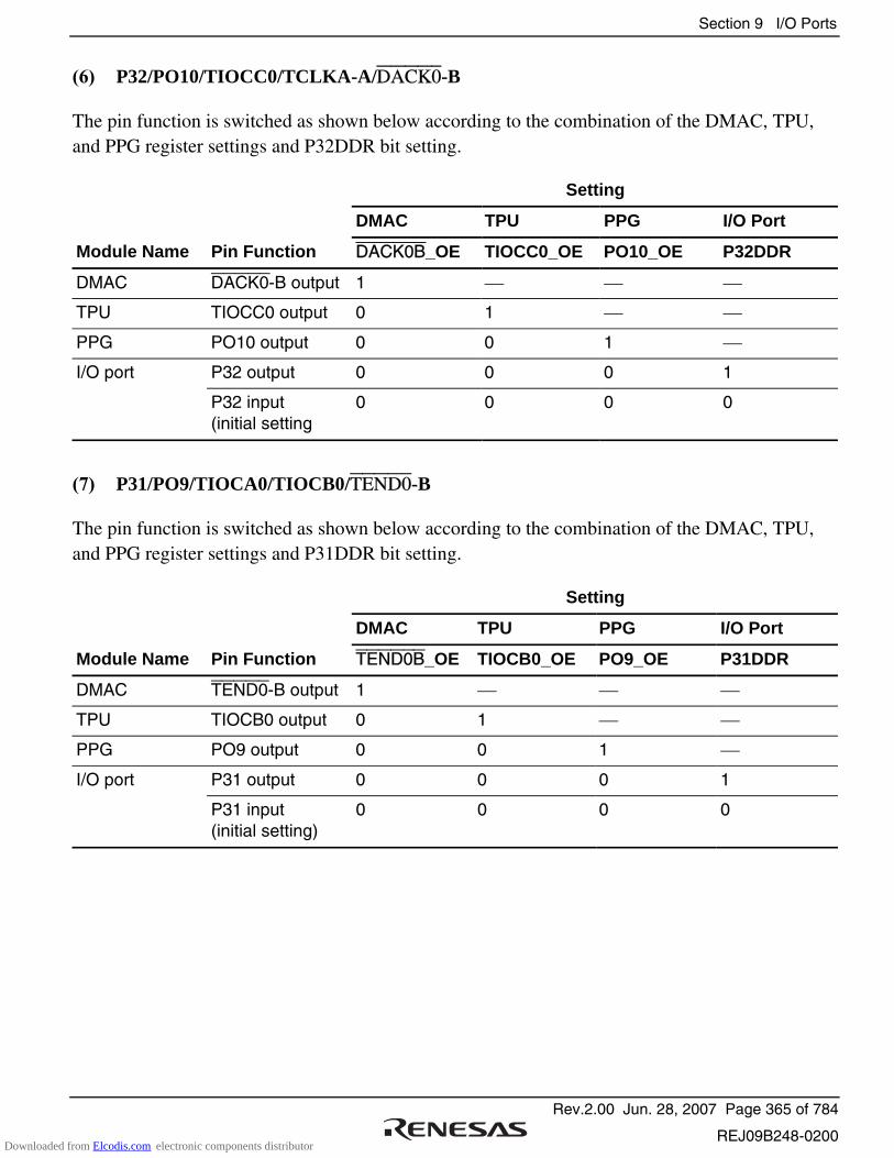
Section 9 I/O Ports
Rev.2.00 Jun. 28, 2007 Page 365 of 784
REJ09B248-0200
(6) P32/PO10/TIOCC0/TCLKA-A/DACK0-B
The pin function is switched as shown below according to the combination of the DMAC, TPU, and PPG register settings and P32DDR bit setting.
Setting
DMAC TPU PPG I/O Port
Module Name Pin Function DACK0B_OE TIOCC0_OE PO10_OE P32DDR
DMAC DACK0-B output 1
TPU TIOCC0 output 0 1
PPG PO10 output 0 0 1
P32 output 0 0 0 1 I/O port
P32 input (initial setting
0 0 0 0
(7) P31/PO9/TIOCA0/TIOCB0/TEND0-B
The pin function is switched as shown below according to the combination of the DMAC, TPU, and PPG register settings and P31DDR bit setting.
Setting
DMAC TPU PPG I/O Port
Module Name Pin Function TEND0B_OE TIOCB0_OE PO9_OE P31DDR
DMAC TEND0-B output 1
TPU TIOCB0 output 0 1
PPG PO9 output 0 0 1
P31 output 0 0 0 1 I/O port
P31 input (initial setting)
0 0 0 0
Downloaded from Elcodis.com electronic components distributor
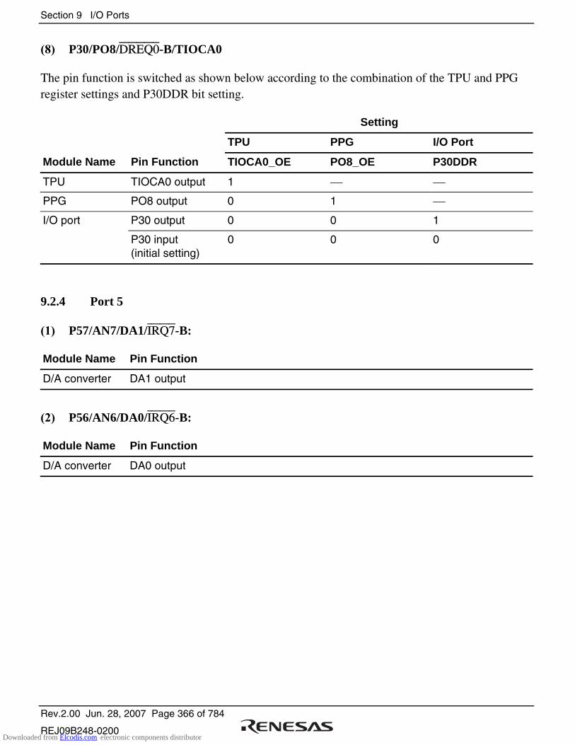
Section 9 I/O Ports
Rev.2.00 Jun. 28, 2007 Page 366 of 784
REJ09B248-0200
(8) P30/PO8/DREQ0-B/TIOCA0
The pin function is switched as shown below according to the combination of the TPU and PPG register settings and P30DDR bit setting.
Setting
TPU PPG I/O Port
Module Name Pin Function TIOCA0_OE PO8_OE P30DDR
TPU TIOCA0 output 1
PPG PO8 output 0 1
P30 output 0 0 1 I/O port
P30 input (initial setting)
0 0 0
9.2.4 Port 5
(1) P57/AN7/DA1/IRQ7-B:
Module Name Pin Function
D/A converter DA1 output
(2) P56/AN6/DA0/IRQ6-B:
Module Name Pin Function
D/A converter DA0 output
Downloaded from Elcodis.com electronic components distributor

Section 9 I/O Ports
Rev.2.00 Jun. 28, 2007 Page 367 of 784
REJ09B248-0200
9.2.5 Port 6
(1) P65/TMO3/DACK3
The pin function is switched as shown below according to the combination of the DMAC and TMR register settings and P65DDR bit setting.
Setting
DMAC TMR I/O Port
Module Name Pin Function DACK3_OE TMO3_OE P65DDR
DMAC DACK3 output 1
TMR TMO3 output 0 1
P65 output 0 0 1 I/O port
P65 input (initial setting)
0 0 0
(2) P64/TMCI3/TEND3
The pin function is switched as shown below according to the combination of the DMAC register setting and P64DDR bit setting.
Setting
DMAC I/O Port
Module Name Pin Function TEND3_OE P64DDR
DMAC TEND3 output 1
P64 output 0 1 I/O port
P64 input (initial setting)
0 0
Downloaded from Elcodis.com electronic components distributor
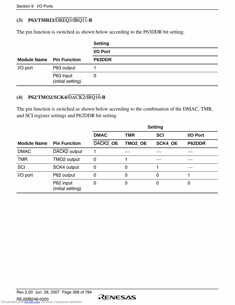
Section 9 I/O Ports
Rev.2.00 Jun. 28, 2007 Page 368 of 784
REJ09B248-0200
(3) P63/TMRI3/DREQ3/IRQ11-B
The pin function is switched as shown below according to the P63DDR bit setting.
Setting
I/O Port
Module Name Pin Function P63DDR
I/O port P63 output 1
P63 input (initial setting)
0
(4) P62/TMO2/SCK4/DACK2/IRQ10-B
The pin function is switched as shown below according to the combination of the DMAC, TMR, and SCI register settings and P62DDR bit setting.
Setting
DMAC TMR SCI I/O Port
Module Name Pin Function DACK2_OE TMO2_OE SCK4_OE P62DDR
DMAC DACK2 output 1
TMR TMO2 output 0 1
SCI SCK4 output 0 0 1
P62 output 0 0 0 1 I/O port
P62 input (initial setting)
0 0 0 0
Downloaded from Elcodis.com electronic components distributor

Section 9 I/O Ports
Rev.2.00 Jun. 28, 2007 Page 369 of 784
REJ09B248-0200
(5) P61/TMCI2/RxD4/TEND2/IRQ9-B
The pin function is switched as shown below according to the combination of the DMAC register setting and P61DDR bit setting.
Setting
DMAC I/O Port
Module Name Pin Function TEND2_OE P61DDR
DMAC TEND2 output 1
P61 output 0 1 I/O port
P61 input (initial setting)
0 0
(6) P60/TMRI2/TxD4/DREQ2/IRQ8-B
The pin function is switched as shown below according to the combination of the SCI register setting and P60DDR bit setting.
Setting
SCI I/O Port
Module Name Pin Function TxD4_OE P60DDR
SCI TxD4 output 1
P60 output 0 1 I/O port
P60 input (initial setting)
0 0
Downloaded from Elcodis.com electronic components distributor
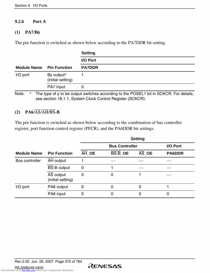
Section 9 I/O Ports
Rev.2.00 Jun. 28, 2007 Page 370 of 784
REJ09B248-0200
9.2.6 Port A
(1) PA7/Bφ
The pin function is switched as shown below according to the PA7DDR bit setting.
Setting
I/O Port
Module Name Pin Function PA7DDR
I/O port Bφ output* (initial setting)
1
PA7 input 0
Note: * The type of φ to be output switches according to the POSEL1 bit in SCKCR. For details, see section 18.1.1, System Clock Control Register (SCKCR).
(2) PA6/AS/AH/BS-B
The pin function is switched as shown below according to the combination of bus controller register, port function control register (PFCR), and the PA6DDR bit settings.
Setting
Bus Controller I/O Port
Module Name Pin Function AH_OE BS-B_OE AS_OE PA6DDR
AH output 1
BS-B output 0 1
Bus controller
AS output (initial setting)
0 0 1
PA6 output 0 0 0 1 I/O port
PA6 input 0 0 0 0
Downloaded from Elcodis.com electronic components distributor
Section 9 I/O Ports
Rev.2.00 Jun. 28, 2007 Page 371 of 784
REJ09B248-0200
(3) PA5/RD
The pin function is always RD output.
Setting
MCU Operating Mode I/O Port
Module Name Pin Function EXPE PA5DDR
Bus controller RD output (initial setting) 1
(4) PA4/LHWR/LUB
The pin function is switched as shown below according to the combination of bus controller register, port function control register (PFCR), and the PA4DDR bit settings.
Setting
Bus Controller I/O Port
Module Name Pin Function LUB_OE* LHWR_OE* PA4DDR
LUB output 1 Bus controller
LHWR output (initial setting)
1
PA4 output 0 0 1 I/O port
PA4 input 0 0 0
Note: * When the byte control SRAM space is accessed while the byte control SRAM space is specified or while LHWROE =1, this pin functions as the LUB output; otherwise, the LHWR output.
(5) PA3/LLWR/LLB
The pin function is switched as shown below according to the bus controller register setting.
Setting
Bus Controller I/O Port
Module Name Pin Function LLB_OE* LLWR_OE* PA3DDR
LLB output 1 Bus controller
LLWR output (initial setting)
1
Note: * If the byte control SRAM space is accessed, this pin functions as the LLB output; otherwise, the LLWR.
Downloaded from Elcodis.com electronic components distributor
Section 9 I/O Ports
Rev.2.00 Jun. 28, 2007 Page 372 of 784
REJ09B248-0200
(6) PA2/BREQ/WAIT
The pin function is switched as shown below according to the combination of the bus controller register setting and PA2DDR bit setting.
Setting
Bus Controller I/O Port
Module Name Pin Function BCR_BRLE BCR_WAITE PA2DDR
BREQ input 1 Bus controller
WAIT input 0 1
PA2 output 0 0 1 I/O port
PA2 input (initial setting)
0 0 0
(7) PA1/BACK/(RD/WR)
The pin function is switched as shown below according to the combination of bus controller register, port function control register (PFCR), and the PA1DDR bit settings.
Setting
Bus Controller I/O Port
Module Name Pin Function BACK_OE
Byte control SRAM Selection (RD/WR)_OE PA1DDR
BACK output 1
0 1
Bus controller
RD/WR output
0 0 1
PA1 output 0 0 0 1 I/O port
PA1 input (initial setting)
0 0 0 0
Downloaded from Elcodis.com electronic components distributor
Section 9 I/O Ports
Rev.2.00 Jun. 28, 2007 Page 373 of 784
REJ09B248-0200
(8) PA0/BREQO/BS-A
The pin function is switched as shown below according to the combination of bus controller register, port function control register (PFCR), and the PA0DDR bit settings.
Setting
I/O Port Bus Controller I/O Port
Module Name Pin Function BS-A_OE BREQ_OE PA0DDR
BS-A output 1 Bus controller
BREQO output 0 1
PA0 output 0 0 1 I/O port
PA0 input (initial setting)
0 0 0
9.2.7 Port B
(1) PB3/CS3/CS7-A
The pin function is switched as shown below according to the combination of port function control register (PFCR) and the PB3DDR bit settings.
Setting
I/O Port
Module Name Pin Function CS3_OE CS7A_OE PB3DDR
Bus controller CS3 output 1
CS7-A output 1
I/O port PB3 output 0 0 1
PB3 input (initial setting)
0 0 0
Downloaded from Elcodis.com electronic components distributor
Section 9 I/O Ports
Rev.2.00 Jun. 28, 2007 Page 374 of 784
REJ09B248-0200
(2) PB2/CS2-A/CS6-A
The pin function is switched as shown below according to the combination of port function control register (PFCR) and the PB2DDR bit settings.
Setting
I/O Port
Module Name Pin Function CS2A_OE CS6A_OE PB2DDR
Bus controller CS2-A output 1
CS6-A output 1
I/O port PB2 output 0 0 1
PB2 input (initial setting)
0 0 0
(3) PB1/CS1/CS2-B/CS5-A/CS6-B/CS7-B
The pin function is switched as shown below according to the combination of port function control register (PFCR) and the PB1DDR bit settings.
Setting
I/O Port
Module Name Pin Function CS1_OE CS2B_OE CS5A_OE CS6B_OE CS7B_OE PB1DDR
CS1 output 1 Bus controller
CS2-B output 1
CS5-A output 1
CS6-B output 1
CS7-B output 1
I/O port PB1 output 0 0 0 0 0 1
PB1 input (initial setting)
0 0 0 0 0 0
Downloaded from Elcodis.com electronic components distributor

Section 9 I/O Ports
Rev.2.00 Jun. 28, 2007 Page 375 of 784
REJ09B248-0200
(4) PB0/CS0/CS4-A/CS5-B
The pin function is switched as shown below according to the combination of port function control register (PFCR) and the PB0DDR bit settings.
Setting
I/O Port
Module Name Pin Function CS0_OE CS4A_OE CS5B_OE PB0DDR
CS0 output (initial setting)
1
CS4-A output 1
Bus controller
CS5-B output 1
PB0 output 0 0 0 1 I/O port
PB0 input 0 0 0 0
9.2.8 Port D
(1) PD7/A7, PD6/A6, PD5/A5, PD4/A4, PD3/A3, PD2/A2, PD1/A1, PD0/A0
The pin function is always address output.
Setting
I/O Port
Module Name Pin Function PDnDDR
Bus controller Address output
[Legend]
n = 0 to 7
Downloaded from Elcodis.com electronic components distributor
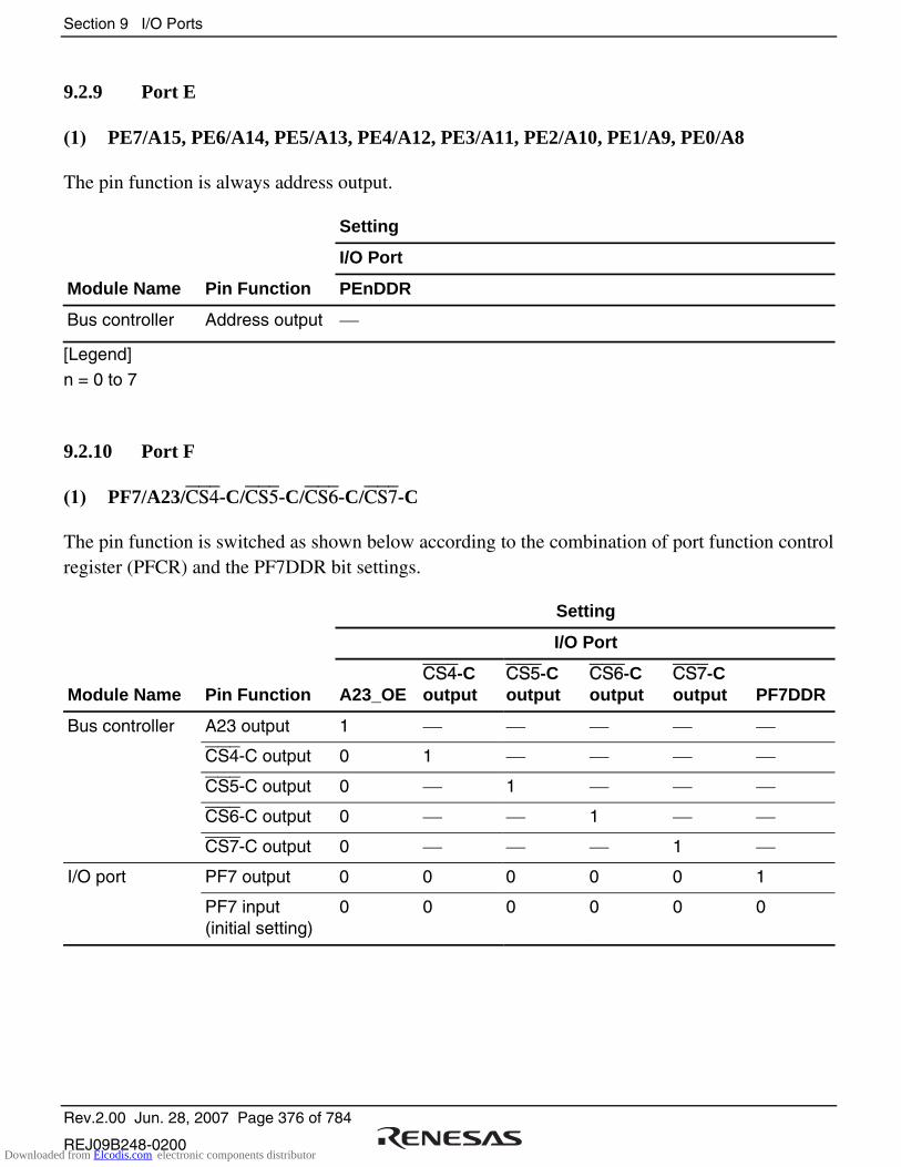
Section 9 I/O Ports
Rev.2.00 Jun. 28, 2007 Page 376 of 784
REJ09B248-0200
9.2.9 Port E
(1) PE7/A15, PE6/A14, PE5/A13, PE4/A12, PE3/A11, PE2/A10, PE1/A9, PE0/A8
The pin function is always address output.
Setting
I/O Port
Module Name Pin Function PEnDDR
Bus controller Address output
[Legend]
n = 0 to 7
9.2.10 Port F
(1) PF7/A23/CS4-C/CS5-C/CS6-C/CS7-C
The pin function is switched as shown below according to the combination of port function control register (PFCR) and the PF7DDR bit settings.
Setting
I/O Port
Module Name Pin Function A23_OE CS4-C output
CS5-C output
CS6-C output
CS7-C output PF7DDR
A23 output 1
CS4-C output 0 1
CS5-C output 0 1
CS6-C output 0 1
Bus controller
CS7-C output 0 1
PF7 output 0 0 0 0 0 1 I/O port
PF7 input (initial setting)
0 0 0 0 0 0
Downloaded from Elcodis.com electronic components distributor

Section 9 I/O Ports
Rev.2.00 Jun. 28, 2007 Page 377 of 784
REJ09B248-0200
(2) PF6/A22/CS6-D
The pin function is switched as shown below according to the combination of port function control register (PFCR) and the PF6DDR bit settings.
Setting
I/O Port
Module Name Pin Function A22_OE CS6D_OE PF6DDR
Bus controller A22 output 1
CS6-D output 0 1
I/O port PF6 output 0 0 1
PF6 input (initial setting)
0 0 0
(3) PF5/A21/CS5-D
The pin function is switched as shown below according to the combination of port function control register (PFCR) and the PF5DDR bit settings.
Setting
I/O Port
Module Name Pin Function A21_OE CS5D_OE PF5DDR
Bus controller A21 output 1
CS5-D output 0 1
I/O port PF5 output 0 0 1
PF5 input (initial setting)
0 0 0
(4) PF4/A20
The pin function is always address output.
Setting
I/O Port
Module Name Pin Function PF4DDR
Bus controller A20 output
Downloaded from Elcodis.com electronic components distributor
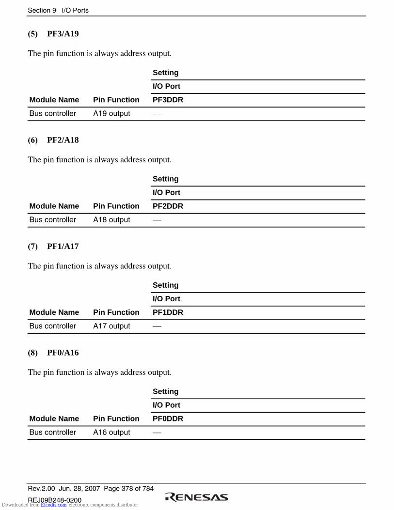
Section 9 I/O Ports
Rev.2.00 Jun. 28, 2007 Page 378 of 784
REJ09B248-0200
(5) PF3/A19
The pin function is always address output.
Setting
I/O Port
Module Name Pin Function PF3DDR
Bus controller A19 output
(6) PF2/A18
The pin function is always address output.
Setting
I/O Port
Module Name Pin Function PF2DDR
Bus controller A18 output
(7) PF1/A17
The pin function is always address output.
Setting
I/O Port
Module Name Pin Function PF1DDR
Bus controller A17 output
(8) PF0/A16
The pin function is always address output.
Setting
I/O Port
Module Name Pin Function PF0DDR
Bus controller A16 output
Downloaded from Elcodis.com electronic components distributor

Section 9 I/O Ports
Rev.2.00 Jun. 28, 2007 Page 379 of 784
REJ09B248-0200
9.2.11 Port H
(1) PH7/D7, PH6/D6, PH5/D5, PH4/D4, PH3/D3, PH2/D2, PH1/D1, PH0/D0
The pin function is always data input/output.
Setting
I/O Port
Module Name Pin Function PHnDDR
Bus controller Data I/O (initial setting)
9.2.12 Port I
(1) PI7/D15, PI6/D14, PI5/D13, PI4/D12, PI3/D11, PI2/D10, PI1/D9, PI0/D8
The pin function is switched as shown below according to the combination of operating mode, bus mode, and the PInDDR bit settings.
Setting
Bus Controller I/O Port
Module Name Pin Function 16-Bit Bus Mode PInDDR
Bus controller Data I/O (mode 4 initial setting)
1
PIn output 0 1 I/O port
PIn input (mode 5 initial setting)
0 0
[Legend]
n = 0 to 7
Downloaded from Elcodis.com electronic components distributor

Section 9 I/O Ports
Rev.2.00 Jun. 28, 2007 Page 380 of 784
REJ09B248-0200
Table 9.5 Available Output Signals and Settings in Each Port
Port
Output
Specification
Signal Name
Output
Signal
Name
Signal Selection
Register Settings Peripheral Module Settings
P1 DACK1A_OE DACK1 PFCR7.DMAS1[A,B] =
00
DACR.AMS = 1, DMDR.DACKE = 1
6
SCK3_OE SCK3 When SCMR_3.SMIF = 1:
SCR_3.TE = 1 or SCR_3.RE = 1 while SMR_3.GM = 0,
SCR_3.CKE [1, 0] = 01 or while SMR_3.GM = 1
When SCMR_3.SMIF = 0:
SCR_3.TE = 1 or SCR_3.RE = 1
while SMR_3.C/A = 0, SCR_3.CKE [1, 0] = 01 or
while SMR_3.C/A = 1, SCR_3.CKE 1 = 0
5 TEND1A_OE TEND1 PFCR7.DMAS1[A,B] =
00
DMDR.TENDE = 1
4 TxD3_OE TxD3 SCR.TE = 1
DACK0A_OE DACK0 PFCR7.DMAS0[A,B] =
00
DACR.AMS = 1, DMDR.DACKE = 1
2
SCK2_OE SCK2 When SCMR.SMIF = 1:
SCR.TE = 1 or SCR.RE = 1 while SMR.GM = 0,
SCR.CKE [1, 0] = 01 or while SMR.GM = 1
When SCMR.SMIF = 0:
SCR.TE = 1 or SCR.RE = 1
while SMR.C/A = 0, SCR.CKE [1, 0] = 01 or
while SMR.C/A = 1, SCR.CKE 1 = 0
1 TEND0A_OE TEND0 PFCR7.DMAS0[A,B] =
00
DMDR.TENDE = 1
0 TxD2_OE TxD2 SCR.TE = 1
P2 7 TIOCB5_OE TIOCB5 TPU.TIOR5.IOB3 = 0, TPU.TIOR5.IOB[1,0] = 01/10/11
PO7_OE PO7 NDERL.NDER7 = 1
6 TIOCA5_OE TIOCA5 TPU.TIOR5.IOA3 = 0, TPU.TIOR5.IOA[1,0] = 01/10/11
TMO1_OE TMO1 TCSR.OS3,2 = 01/10/11 or TCSR.OS[1,0] = 01/10/11
TxD1_OE TxD1 SCR.TE = 1
PO6_OE PO6 NDERL.NDER6 = 1
Downloaded from Elcodis.com electronic components distributor
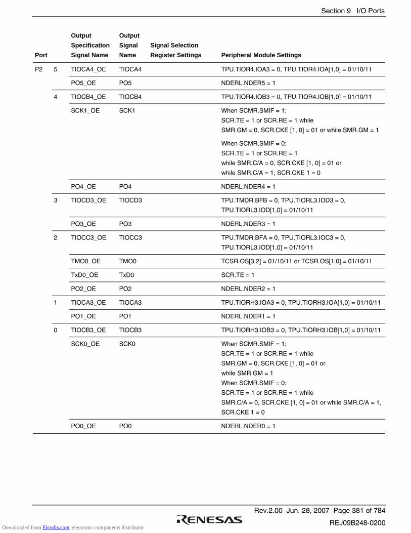
Section 9 I/O Ports
Rev.2.00 Jun. 28, 2007 Page 381 of 784
REJ09B248-0200
Port
Output
Specification
Signal Name
Output
Signal
Name
Signal Selection
Register Settings Peripheral Module Settings
P2 5 TIOCA4_OE TIOCA4 TPU.TIOR4.IOA3 = 0, TPU.TIOR4.IOA[1,0] = 01/10/11
PO5_OE PO5 NDERL.NDER5 = 1
4 TIOCB4_OE TIOCB4 TPU.TIOR4.IOB3 = 0, TPU.TIOR4.IOB[1,0] = 01/10/11
SCK1_OE SCK1 When SCMR.SMIF = 1:
SCR.TE = 1 or SCR.RE = 1 while
SMR.GM = 0, SCR.CKE [1, 0] = 01 or while SMR.GM = 1
When SCMR.SMIF = 0:
SCR.TE = 1 or SCR.RE = 1
while SMR.C/A = 0, SCR.CKE [1, 0] = 01 or
while SMR.C/A = 1, SCR.CKE 1 = 0
PO4_OE PO4 NDERL.NDER4 = 1
3 TIOCD3_OE TIOCD3 TPU.TMDR.BFB = 0, TPU.TIORL3.IOD3 = 0,
TPU.TIORL3.IOD[1,0] = 01/10/11
PO3_OE PO3 NDERL.NDER3 = 1
2 TIOCC3_OE TIOCC3 TPU.TMDR.BFA = 0, TPU.TIORL3.IOC3 = 0,
TPU.TIORL3.IOD[1,0] = 01/10/11
TMO0_OE TMO0 TCSR.OS[3,2] = 01/10/11 or TCSR.OS[1,0] = 01/10/11
TxD0_OE TxD0 SCR.TE = 1
PO2_OE PO2 NDERL.NDER2 = 1
1 TIOCA3_OE TIOCA3 TPU.TIORH3.IOA3 = 0, TPU.TIORH3.IOA[1,0] = 01/10/11
PO1_OE PO1 NDERL.NDER1 = 1
0 TIOCB3_OE TIOCB3 TPU.TIORH3.IOB3 = 0, TPU.TIORH3.IOB[1,0] = 01/10/11
SCK0_OE SCK0 When SCMR.SMIF = 1:
SCR.TE = 1 or SCR.RE = 1 while
SMR.GM = 0, SCR.CKE [1, 0] = 01 or
while SMR.GM = 1
When SCMR.SMIF = 0:
SCR.TE = 1 or SCR.RE = 1 while
SMR.C/A = 0, SCR.CKE [1, 0] = 01 or while SMR.C/A = 1,
SCR.CKE 1 = 0
PO0_OE PO0 NDERL.NDER0 = 1
Downloaded from Elcodis.com electronic components distributor

Section 9 I/O Ports
Rev.2.00 Jun. 28, 2007 Page 382 of 784
REJ09B248-0200
Port
Output
Specification
Signal Name
Output
Signal
Name
Signal Selection
Register Settings Peripheral Module Settings
P3 7 TIOCB2_OE TIOCB2 TPU.TIOR2.IOB3 = 0, TPU.TIOR2.IOB[1,0] = 01/10/11
PO15_OE PO15 NDERH.NDER15 = 1
6 TIOCA2_OE TIOCA2 TPU.TIOR2.IOA3 = 0, TPU.TIOR2.IOA[1,0] = 01/10/11
PO14_OE PO14 NDERH.NDER14 = 1
5 DACK1B_OE DACK1 PFCR7.DMAS1[A,B] =
01
DACR.AMS = 1, DMDR.DACKE = 1
TIOCB1_OE TIOCB1 TPU.TIOR1.IOB3 = 0, TPU.TIOR1.IOB[1,0] = 01/10/11
PO13_OE PO13 NDERH.NDER13 = 1
4 TEND1B_OE TEND1 PFCR7.DMAS1[A,B] =
01
DMDR.TENDE = 1
TIOCA1_OE TIOCA1 TPU.TIOR1.IOA3 = 0, TPU.TIOR1.IOA[1,0] = 01/10/11
PO12_OE PO12 NDERH.NDER12 = 1
3 TIOCD0_OE TIOCD0 TPU.TMDR.BFB = 0, TPU.TIORL0.IOD3 = 0,
TPU.TIORL0.IOD[1,0] = 01/10/11
PO11_OE PO11 NDERH.NDER11 = 1
2 DACK0B_OE DACK0 PFCR7.DMAS0[A,B] =
01
DACR.AMS = 1, DMDR.DACKE = 1
TIOCC0_OE TIOCC0 TPU.TMDR.BFA = 0, TPU.TIORL0.IOC3 = 0,
TPU.TIORL0.IOD[1,0] = 01/10/11
PO10_OE PO10 NDERH.NDER10 = 1
1 TEND0B_OE TEND0 PFCR7.DMAS0[A,B] =
01
DMDR.TENDE = 1
TIOCB0_OE TIOCB0 TPU.TIORH0.IOB3 = 0,
TPU.TIORH0.IOB[1,0] = 01/10/11
PO9_OE PO9 NDERH.NDER9 = 1
0 TIOCA0_OE TIOCA0 TPU.TIORH0.IOA3 = 0,
TPU.TIORH0.IOA[1,0] = 01/10/11
PO8_OE PO8 NDERH.NDER8 = 1
Downloaded from Elcodis.com electronic components distributor
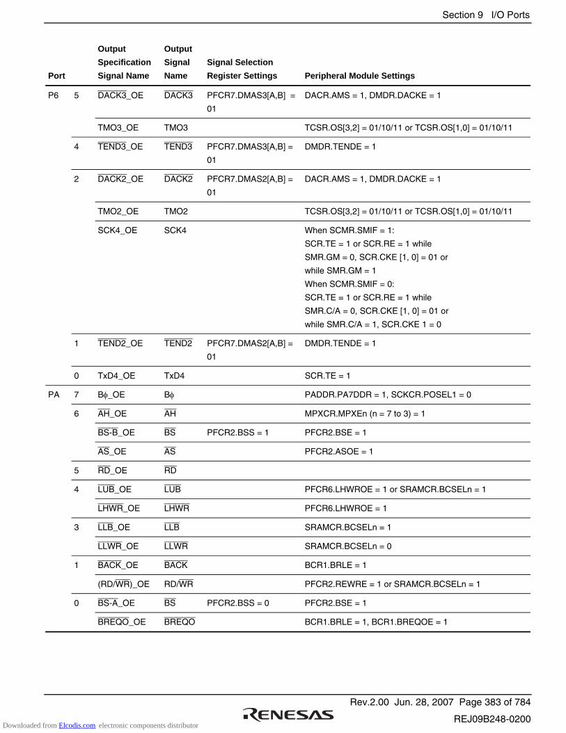
Section 9 I/O Ports
Rev.2.00 Jun. 28, 2007 Page 383 of 784
REJ09B248-0200
Port
Output
Specification
Signal Name
Output
Signal
Name
Signal Selection
Register Settings Peripheral Module Settings
P6 5 DACK3_OE DACK3 PFCR7.DMAS3[A,B] =
01
DACR.AMS = 1, DMDR.DACKE = 1
TMO3_OE TMO3 TCSR.OS[3,2] = 01/10/11 or TCSR.OS[1,0] = 01/10/11
4 TEND3_OE TEND3 PFCR7.DMAS3[A,B] =
01
DMDR.TENDE = 1
2 DACK2_OE DACK2 PFCR7.DMAS2[A,B] =
01
DACR.AMS = 1, DMDR.DACKE = 1
TMO2_OE TMO2 TCSR.OS[3,2] = 01/10/11 or TCSR.OS[1,0] = 01/10/11
SCK4_OE SCK4 When SCMR.SMIF = 1:
SCR.TE = 1 or SCR.RE = 1 while
SMR.GM = 0, SCR.CKE [1, 0] = 01 or
while SMR.GM = 1
When SCMR.SMIF = 0:
SCR.TE = 1 or SCR.RE = 1 while
SMR.C/A = 0, SCR.CKE [1, 0] = 01 or
while SMR.C/A = 1, SCR.CKE 1 = 0
1 TEND2_OE TEND2 PFCR7.DMAS2[A,B] =
01
DMDR.TENDE = 1
0 TxD4_OE TxD4 SCR.TE = 1
PA 7 Bφ_OE Bφ PADDR.PA7DDR = 1, SCKCR.POSEL1 = 0
6 AH_OE AH MPXCR.MPXEn (n = 7 to 3) = 1
BS-B_OE BS PFCR2.BSS = 1 PFCR2.BSE = 1
AS_OE AS PFCR2.ASOE = 1
5 RD_OE RD
4 LUB_OE LUB PFCR6.LHWROE = 1 or SRAMCR.BCSELn = 1
LHWR_OE LHWR PFCR6.LHWROE = 1
3 LLB_OE LLB SRAMCR.BCSELn = 1
LLWR_OE LLWR SRAMCR.BCSELn = 0
1 BACK_OE BACK BCR1.BRLE = 1
(RD/WR)_OE RD/WR PFCR2.REWRE = 1 or SRAMCR.BCSELn = 1
0 BS-A_OE BS PFCR2.BSS = 0 PFCR2.BSE = 1
BREQO_OE BREQO BCR1.BRLE = 1, BCR1.BREQOE = 1
Downloaded from Elcodis.com electronic components distributor

Section 9 I/O Ports
Rev.2.00 Jun. 28, 2007 Page 384 of 784
REJ09B248-0200
Port
Output
Specification
Signal Name
Output
Signal
Name
Signal Selection
Register Settings Peripheral Module Settings
PB 3 CS3_OE CS3 PFCR0.CS3E = 1
CS7A_OE CS7 PFCR1.CS7S[A,B] = 00 PFCR0.CS7E = 1
2 CS2A_OE CS2 PFCR2.CS2S = 0 PFCR0.CS2E = 1
CS6A_OE CS6 PFCR1.CS6S[A,B] = 00 PFCR0.CS6E = 1
1 CS1_OE CS1 PFCR0.CS1E = 1
CS2B_OE CS2 PFCR2.CS2S = 1 PFCR0.CS2E = 1
CS5A_OE CS5 PFCR1.CS5S[A,B] = 00 PFCR0.CS5E = 1
CS6B_OE CS6 PFCR1.CS6S[A,B] = 01 PFCR0.CS6E = 1
CS7B_OE CS7 PFCR1.CS7S[A,B] = 01 PFCR0.CS7E = 1
0 CS0_OE CS0 PFCR0.CS0E = 1
CS4A_OE CS4 PFCR1.CS4S[A,B] = 00
PFCR0.CS4E = 1
PFCR0.CS4E = 1
CS5B_OE CS5 PFCR1.CS5S[A,B] = 01 PFCR0.CS5E = 1
PD 7 A7_OE A7
6 A6_OE A6
5 A5_OE A5
4 A4_OE A4
3 A3_OE A3
2 A2_OE A2
1 A1_OE A1
0 A0_OE A0
PE 7 A15_OE A15
6 A14_OE A14
5 A13_OE A13
4 A12_OE A12
3 A11_OE A11
2 A10_OE A10
1 A9_OE A9
0 A8_OE A8
Downloaded from Elcodis.com electronic components distributor

Section 9 I/O Ports
Rev.2.00 Jun. 28, 2007 Page 385 of 784
REJ09B248-0200
Port
Output
Specification
Signal Name
Output
Signal
Name
Signal Selection
Register Settings Peripheral Module Settings
PF 7 A23_OE
CS4C_OE
CS5C_OE
CS6C_OE
CS7C_OE
A23
CS4 CS5 CS6 CS7
PFCR4.A23E = 1
PFCR1.CS4S[A,B] = 10 PFCR0.CS4E = 1
PFCR1.CS5S[A,B] = 10 PFCR0.CS5E = 1
PFCR1.CS6S[A,B] = 10 PFCR0.CS6E = 1
PFCR1.CS7S[A,B] = 10 PFCR0.CS7E = 1
6 A22_OE
CS6D_OE
A22
CS6
PFCR4.A22E = 1
PFCR1.CS6S[A,B] = 11 PFCR0.CS6E = 1
5 A21_OE
CS5D_OE
A21
CS5
PFCR4.A21E = 1
PFCR1.CS5S[A,B] = 11 PFCR0.CS5E = 1
4 A20_OE A20
3 A19_OE A19
2 A18_OE A18
1 A17_OE A17
0 A16_OE A16
PH 7 D7_E D7
6 D6_E D6
5 D5_E D5
4 D4_E D4
3 D3_E D3
2 D2_E D2
1 D1_E D1
0 D0_E D0
PI 7 D15_E D15 ABWCR.ABW[H,L]n = 01
6 D14_E D14 ABWCR.ABW[H,L]n = 01
5 D13_E D13 ABWCR.ABW[H,L]n = 01
4 D12_E D12 ABWCR.ABW[H,L]n = 01
3 D11_E D11 ABWCR.ABW[H,L]n = 01
2 D10_E D10 ABWCR.ABW[H,L]n = 01
1 D9_E D9 ABWCR.ABW[H,L]n = 01
0 D8_E D8 ABWCR.ABW[H,L]n = 01
Downloaded from Elcodis.com electronic components distributor

Section 9 I/O Ports
Rev.2.00 Jun. 28, 2007 Page 386 of 784
REJ09B248-0200
9.3 Port Function Controller
The port function controller controls the I/O ports.
The port function controller incorporates the following registers.
• Port function control register 0 (PFCR0)
• Port function control register 1 (PFCR1)
• Port function control register 2 (PFCR2)
• Port function control register 4 (PFCR4)
• Port function control register 6 (PFCR6)
• Port function control register 7 (PFCR7)
• Port function control register 9 (PFCR9)
• Port function control register B (PFCRB)
• Port function control register C (PFCRC)
9.3.1 Port Function Control Register 0 (PFCR0)
PFCR0 enables/disables the CS output.
Bit
Bit Name
Initial Value
R/W
7
CS7E
0
R/W
6
CS6E
0
R/W
5
CS5E
0
R/W
4
CS4E
0
R/W
3
CS3E
0
R/W
2
CS2E
0
R/W
1
CS1E
0
R/W
0
CS0E
1
R/W
Bit Bit Name Initial Value R/W Description
7 CS7E 0 R/W
6 CS6E 0 R/W
5 CS5E 0 R/W
4 CS4E 0 R/W
3 CS3E 0 R/W
2 CS2E 0 R/W
1 CS1E 0 R/W
0 CS0E 1 R/W
CS7 to CS0 Enable
These bits enable/disable the corresponding CSn output.
0: Pin functions as I/O port
1: Pin functions as CSn output pin
(n = 7 to 0)
Downloaded from Elcodis.com electronic components distributor
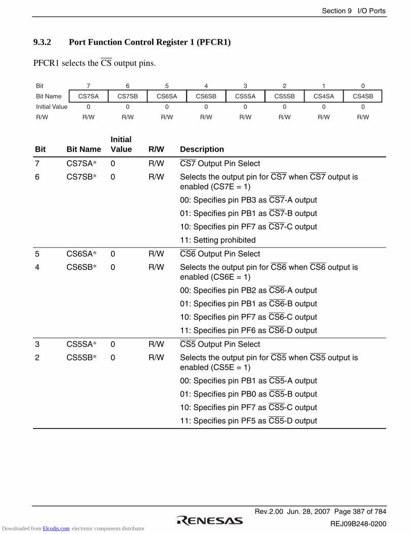
Section 9 I/O Ports
Rev.2.00 Jun. 28, 2007 Page 387 of 784
REJ09B248-0200
9.3.2 Port Function Control Register 1 (PFCR1)
PFCR1 selects the CS output pins.
Bit
Bit Name
Initial Value
R/W
7
CS7SA
0
R/W
6
CS7SB
0
R/W
5
CS6SA
0
R/W
4
CS6SB
0
R/W
3
CS5SA
0
R/W
2
CS5SB
0
R/W
1
CS4SA
0
R/W
0
CS4SB
0
R/W
Bit Bit Name Initial Value R/W Description
7
6
CS7SA*
CS7SB*
0
0
R/W
R/W
CS7 Output Pin Select
Selects the output pin for CS7 when CS7 output is enabled (CS7E = 1)
00: Specifies pin PB3 as CS7-A output
01: Specifies pin PB1 as CS7-B output
10: Specifies pin PF7 as CS7-C output
11: Setting prohibited
5
4
CS6SA*
CS6SB*
0
0
R/W
R/W
CS6 Output Pin Select
Selects the output pin for CS6 when CS6 output is enabled (CS6E = 1)
00: Specifies pin PB2 as CS6-A output
01: Specifies pin PB1 as CS6-B output
10: Specifies pin PF7 as CS6-C output
11: Specifies pin PF6 as CS6-D output
3
2
CS5SA*
CS5SB*
0
0
R/W
R/W
CS5 Output Pin Select
Selects the output pin for CS5 when CS5 output is enabled (CS5E = 1)
00: Specifies pin PB1 as CS5-A output
01: Specifies pin PB0 as CS5-B output
10: Specifies pin PF7 as CS5-C output
11: Specifies pin PF5 as CS5-D output
Downloaded from Elcodis.com electronic components distributor
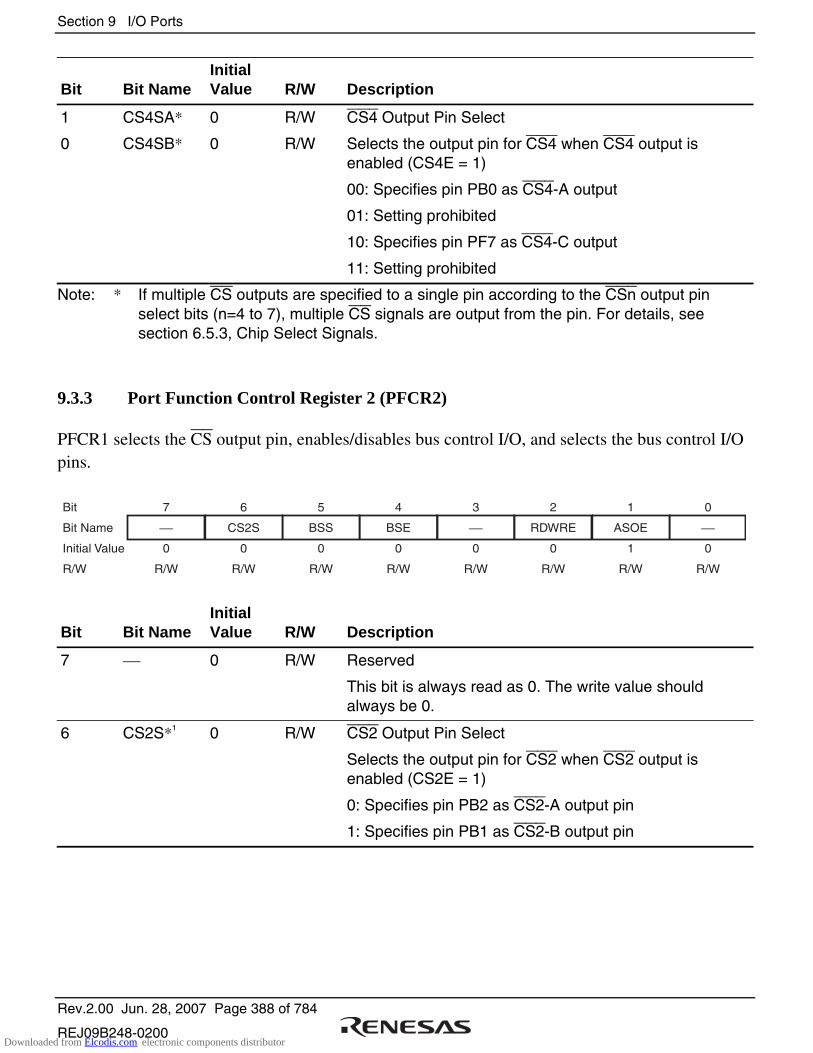
Section 9 I/O Ports
Rev.2.00 Jun. 28, 2007 Page 388 of 784
REJ09B248-0200
Bit Bit Name Initial Value R/W Description
1
0
CS4SA*
CS4SB*
0
0
R/W
R/W
CS4 Output Pin Select
Selects the output pin for CS4 when CS4 output is enabled (CS4E = 1)
00: Specifies pin PB0 as CS4-A output
01: Setting prohibited
10: Specifies pin PF7 as CS4-C output
11: Setting prohibited
Note: * If multiple CS outputs are specified to a single pin according to the CSn output pin select bits (n=4 to 7), multiple CS signals are output from the pin. For details, see section 6.5.3, Chip Select Signals.
9.3.3 Port Function Control Register 2 (PFCR2)
PFCR1 selects the CS output pin, enables/disables bus control I/O, and selects the bus control I/O pins.
Bit
Bit Name
Initial Value
R/W
7
0
R/W
6
CS2S
0
R/W
5
BSS
0
R/W
4
BSE
0
R/W
3
0
R/W
2
RDWRE
0
R/W
1
ASOE
1
R/W
0
0
R/W
Bit Bit Name Initial Value R/W Description
7 0 R/W Reserved
This bit is always read as 0. The write value should always be 0.
6 CS2S*1 0 R/W CS2 Output Pin Select
Selects the output pin for CS2 when CS2 output is enabled (CS2E = 1)
0: Specifies pin PB2 as CS2-A output pin
1: Specifies pin PB1 as CS2-B output pin
Downloaded from Elcodis.com electronic components distributor
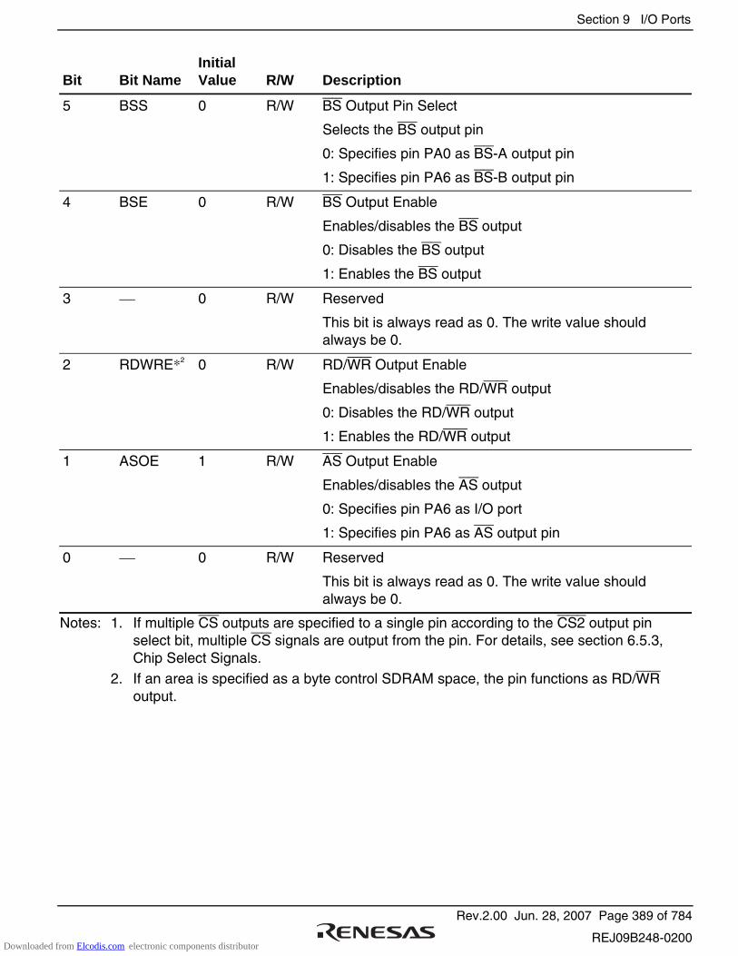
Section 9 I/O Ports
Rev.2.00 Jun. 28, 2007 Page 389 of 784
REJ09B248-0200
Bit Bit Name Initial Value R/W Description
5 BSS 0 R/W BS Output Pin Select
Selects the BS output pin
0: Specifies pin PA0 as BS-A output pin
1: Specifies pin PA6 as BS-B output pin
4 BSE 0 R/W BS Output Enable
Enables/disables the BS output
0: Disables the BS output
1: Enables the BS output
3 0 R/W Reserved
This bit is always read as 0. The write value should always be 0.
2 RDWRE*2 0 R/W RD/WR Output Enable
Enables/disables the RD/WR output
0: Disables the RD/WR output
1: Enables the RD/WR output
1 ASOE 1 R/W AS Output Enable
Enables/disables the AS output
0: Specifies pin PA6 as I/O port
1: Specifies pin PA6 as AS output pin
0 0 R/W Reserved
This bit is always read as 0. The write value should always be 0.
Notes: 1. If multiple CS outputs are specified to a single pin according to the CS2 output pin select bit, multiple CS signals are output from the pin. For details, see section 6.5.3, Chip Select Signals.
2. If an area is specified as a byte control SDRAM space, the pin functions as RD/WR output.
Downloaded from Elcodis.com electronic components distributor

Section 9 I/O Ports
Rev.2.00 Jun. 28, 2007 Page 390 of 784
REJ09B248-0200
9.3.4 Port Function Control Register 4 (PFCR4)
PFCR4 enables/disables the address output.
Bit
Bit Name
Initial Value
R/W
7
A23E
0
R/W
6
A22E
0
R/W
5
A21E
0
R/W
4
1
R/W
3
1
R/W
2
1
R/W
1
1
R/W
0
1
R/W
Bit Bit Name Initial Value R/W Description
7 A23E 0 R/W Address A23 Enable
Enables/disables the address output (A23)
0: Disables the A23 output
1: Enables the A23 output
6 A22E 0 R/W Address A22 Enable
Enables/disables the address output (A22)
0: Disables the A22 output
1: Enables the A22 output
5 A21E 0 R/W Address A21 Enable
Enables/disables the address output (A21)
0: Disables the A21 output
1: Enables the A21 output
4 to 0 All 1 R/W Reserved
These bits are always read as 1. The write value should always be 1.
Downloaded from Elcodis.com electronic components distributor

Section 9 I/O Ports
Rev.2.00 Jun. 28, 2007 Page 391 of 784
REJ09B248-0200
9.3.5 Port Function Control Register 6 (PFCR6)
PFCR6 selects the TPU clock input pin.
Bit
Bit Name
Initial Value
R/W
7
1
R/W
6
LHWROE
1
R/W
5
1
R/W
4
0
R
3
TCLKS
0
R/W
2
0
R/W
1
0
R/W
0
0
R/W
Bit Bit Name Initial Value R/W Description
7 1 R/W Reserved
This bit is always read as 1. The write value should always be 1.
6 LHWROE 1 R/W LHWR Output Enable
Enables/disables LHWR output (valid in external extended mode).
0: Specifies pin PA4 as I/O port
1: Specifies pin PA4 as LHWR output pin
5 1 R/W Reserved
This bit is always read as 1. The write value should always be 1.
4 0 R Reserved
This is a read-only bit and cannot be modified.
3 TCLKS 0 R/W TPU External Clock Input Pin Select
Selects the TPU external clock input pins.
0: Specifies pins P32, P33, P35, and P37 as external
clock inputs
1: Specifies pins P14 to P17 as external clock inputs
2 to 0 All 0 R/W Reserved
These bits are always read as 0. The write value should always be 0.
Downloaded from Elcodis.com electronic components distributor

Section 9 I/O Ports
Rev.2.00 Jun. 28, 2007 Page 392 of 784
REJ09B248-0200
9.3.6 Port Function Control Register 7 (PFCR7)
PFCR7 selects the DMAC I/O pins (DREQ, DACK, and TEND).
Bit
Bit Name
Initial Value
R/W
7
DMAS3A
0
R/W
6
DMAS3B
0
R/W
5
DMAS2A
0
R/W
4
DMAS2B
0
R/W
3
DMAS1A
0
R/W
2
DMAS1B
0
R/W
1
DMAS0A
0
R/W
0
DMAS0B
0
R/W
Bit Bit Name Initial Value R/W Description
7
6
DMAS3A
DMAS3B
0
0
R/W
R/W
DMAC Control Pin Select
Selects the I/O port to control DMAC_3.
00: Setting prohibited
01: Specifies pins P63 to P65 as DMAC control pins
10: Setting prohibited
11: Setting prohibited
5
4
DMAS2A
DMAS2B
0
0
R/W
R/W
DMAC Control Pin Select
Selects the I/O port to control DMAC_2.
00: Setting prohibited
01: Specifies pins P60 to P62 as DMAC control pins
10: Setting prohibited
11: Setting prohibited
3
2
DMAS1A
DMAS1B
0
0
R/W
R/W
DMAC Control Pin Select
Selects the I/O port to control DMAC_1.
00: Specifies pins P14 to P16 as DMAC control pins
01: Specifies pins P33 to P35 as DMAC control pins
10: Setting prohibited
11: Setting prohibited
1
0
DMAS0A
DMAS0B
0
0
R/W
R/W
DMAC Control Pin Select
Selects the I/O port to control DMAC_0.
00: Specifies pins P10 to P12 as DMAC control pins
01: Specifies pins P30 to P32 as DMAC control pins
10: Setting prohibited
11: Setting prohibited
Downloaded from Elcodis.com electronic components distributor
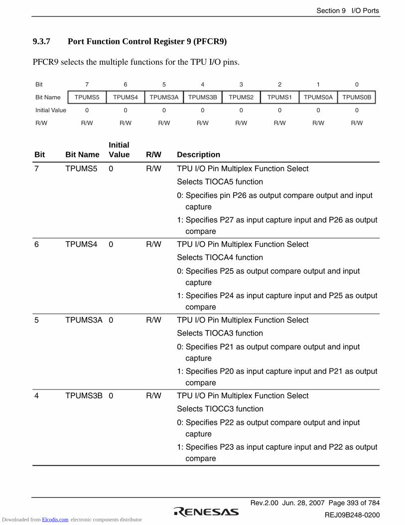
Section 9 I/O Ports
Rev.2.00 Jun. 28, 2007 Page 393 of 784
REJ09B248-0200
9.3.7 Port Function Control Register 9 (PFCR9)
PFCR9 selects the multiple functions for the TPU I/O pins.
Bit
Bit Name
Initial Value
R/W
7
TPUMS5
0
R/W
6
TPUMS4
0
R/W
5
TPUMS3A
0
R/W
4
TPUMS3B
0
R/W
3
TPUMS2
0
R/W
2
TPUMS1
0
R/W
1
TPUMS0A
0
R/W
0
TPUMS0B
0
R/W
Bit Bit Name Initial Value R/W Description
7 TPUMS5 0 R/W TPU I/O Pin Multiplex Function Select
Selects TIOCA5 function
0: Specifies pin P26 as output compare output and input
capture
1: Specifies P27 as input capture input and P26 as output
compare
6 TPUMS4 0 R/W TPU I/O Pin Multiplex Function Select
Selects TIOCA4 function
0: Specifies P25 as output compare output and input
capture
1: Specifies P24 as input capture input and P25 as output
compare
5 TPUMS3A 0 R/W TPU I/O Pin Multiplex Function Select
Selects TIOCA3 function
0: Specifies P21 as output compare output and input
capture
1: Specifies P20 as input capture input and P21 as output
compare
4 TPUMS3B 0 R/W TPU I/O Pin Multiplex Function Select
Selects TIOCC3 function
0: Specifies P22 as output compare output and input
capture
1: Specifies P23 as input capture input and P22 as output
compare
Downloaded from Elcodis.com electronic components distributor
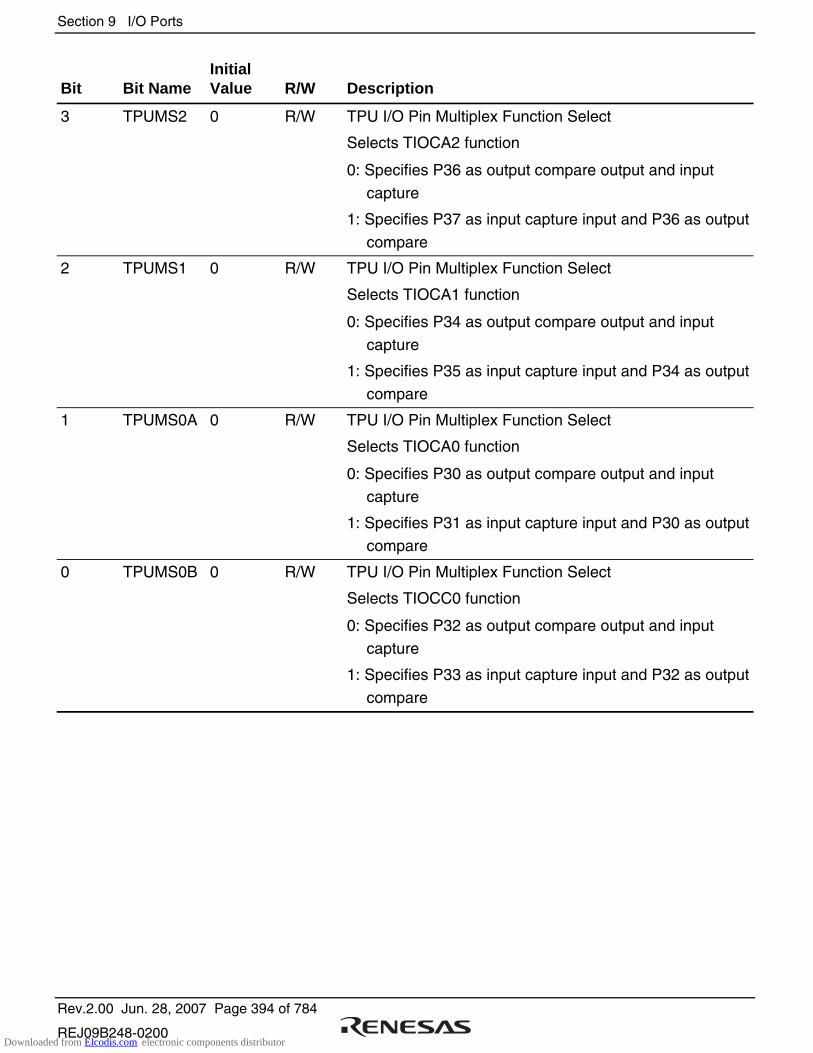
Section 9 I/O Ports
Rev.2.00 Jun. 28, 2007 Page 394 of 784
REJ09B248-0200
Bit Bit Name Initial Value R/W Description
3 TPUMS2 0 R/W TPU I/O Pin Multiplex Function Select
Selects TIOCA2 function
0: Specifies P36 as output compare output and input
capture
1: Specifies P37 as input capture input and P36 as output
compare
2 TPUMS1 0 R/W TPU I/O Pin Multiplex Function Select
Selects TIOCA1 function
0: Specifies P34 as output compare output and input
capture
1: Specifies P35 as input capture input and P34 as output
compare
1 TPUMS0A 0 R/W TPU I/O Pin Multiplex Function Select
Selects TIOCA0 function
0: Specifies P30 as output compare output and input
capture
1: Specifies P31 as input capture input and P30 as output
compare
0 TPUMS0B 0 R/W TPU I/O Pin Multiplex Function Select
Selects TIOCC0 function
0: Specifies P32 as output compare output and input
capture
1: Specifies P33 as input capture input and P32 as output
compare
Downloaded from Elcodis.com electronic components distributor
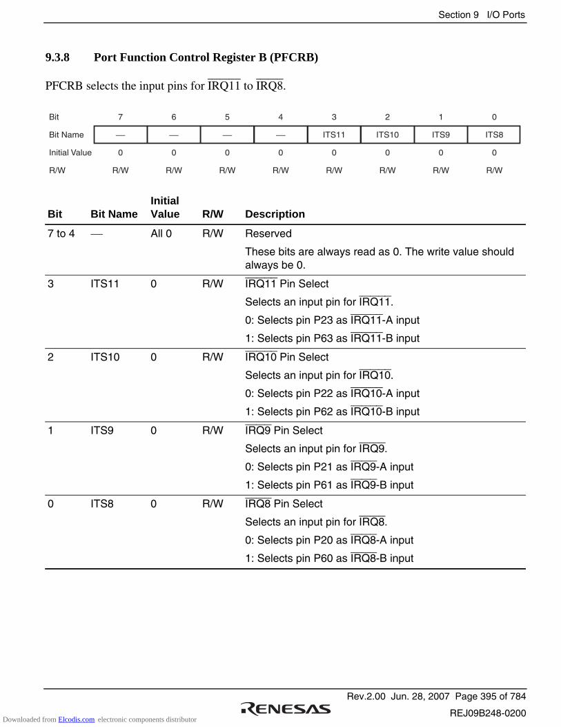
Section 9 I/O Ports
Rev.2.00 Jun. 28, 2007 Page 395 of 784
REJ09B248-0200
9.3.8 Port Function Control Register B (PFCRB)
PFCRB selects the input pins for IRQ11 to IRQ8.
Bit
Bit Name
Initial Value
R/W
7
0
R/W
6
0
R/W
5
0
R/W
4
0
R/W
3
ITS11
0
R/W
2
ITS10
0
R/W
1
ITS9
0
R/W
0
ITS8
0
R/W
Bit Bit Name Initial Value R/W Description
7 to 4 All 0 R/W Reserved
These bits are always read as 0. The write value should always be 0.
3 ITS11 0 R/W IRQ11 Pin Select
Selects an input pin for IRQ11.
0: Selects pin P23 as IRQ11-A input
1: Selects pin P63 as IRQ11-B input
2 ITS10 0 R/W IRQ10 Pin Select
Selects an input pin for IRQ10.
0: Selects pin P22 as IRQ10-A input
1: Selects pin P62 as IRQ10-B input
1 ITS9 0 R/W IRQ9 Pin Select
Selects an input pin for IRQ9.
0: Selects pin P21 as IRQ9-A input
1: Selects pin P61 as IRQ9-B input
0 ITS8 0 R/W IRQ8 Pin Select
Selects an input pin for IRQ8.
0: Selects pin P20 as IRQ8-A input
1: Selects pin P60 as IRQ8-B input
Downloaded from Elcodis.com electronic components distributor
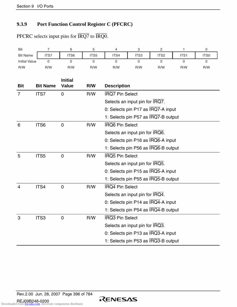
Section 9 I/O Ports
Rev.2.00 Jun. 28, 2007 Page 396 of 784
REJ09B248-0200
9.3.9 Port Function Control Register C (PFCRC)
PFCRC selects input pins for IRQ7 to IRQ0.
Bit
Bit Name
Initial Value
R/W
7
ITS7
0
R/W
6
ITS6
0
R/W
5
ITS5
0
R/W
4
ITS4
0
R/W
3
ITS3
0
R/W
2
ITS2
0
R/W
1
ITS1
0
R/W
0
ITS0
0
R/W
Bit Bit Name Initial Value R/W Description
7 ITS7 0 R/W IRQ7 Pin Select
Selects an input pin for IRQ7.
0: Selects pin P17 as IRQ7-A input
1: Selects pin P57 as IRQ7-B output
6 ITS6 0 R/W IRQ6 Pin Select
Selects an input pin for IRQ6.
0: Selects pin P16 as IRQ6-A input
1: Selects pin P56 as IRQ6-B output
5 ITS5 0 R/W IRQ5 Pin Select
Selects an input pin for IRQ5.
0: Selects pin P15 as IRQ5-A input
1: Selects pin P55 as IRQ5-B output
4 ITS4 0 R/W IRQ4 Pin Select
Selects an input pin for IRQ4.
0: Selects pin P14 as IRQ4-A input
1: Selects pin P54 as IRQ4-B output
3 ITS3 0 R/W IRQ3 Pin Select
Selects an input pin for IRQ3.
0: Selects pin P13 as IRQ3-A input
1: Selects pin P53 as IRQ3-B output
Downloaded from Elcodis.com electronic components distributor
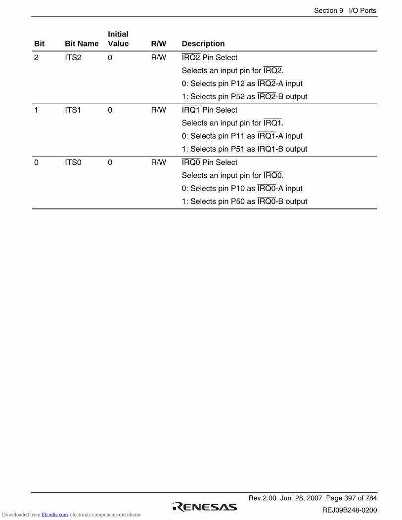
Section 9 I/O Ports
Rev.2.00 Jun. 28, 2007 Page 397 of 784
REJ09B248-0200
Bit Bit Name Initial Value R/W Description
2 ITS2 0 R/W IRQ2 Pin Select
Selects an input pin for IRQ2.
0: Selects pin P12 as IRQ2-A input
1: Selects pin P52 as IRQ2-B output
1 ITS1 0 R/W IRQ1 Pin Select
Selects an input pin for IRQ1.
0: Selects pin P11 as IRQ1-A input
1: Selects pin P51 as IRQ1-B output
0 ITS0 0 R/W IRQ0 Pin Select
Selects an input pin for IRQ0.
0: Selects pin P10 as IRQ0-A input
1: Selects pin P50 as IRQ0-B output
Downloaded from Elcodis.com electronic components distributor

Section 9 I/O Ports
Rev.2.00 Jun. 28, 2007 Page 398 of 784
REJ09B248-0200
9.4 Usage Notes
9.4.1 Notes on Input Buffer Control Register (ICR) Setting
1. When changing the ICR setting, the LSI may malfunction due to an edge that is internally generated according to the pin states. To change the ICR setting, fix the pin high or disable the input function by setting the peripheral module allocated to the corresponding pin.
2. If an input is enabled by setting ICR while multiple input functions are assigned to the pin, the pin state is reflected in all the inputs. Care must be taken for each module settings for unused input functions.
3. When a pin is used as an output, data to be output from the pin will be latched as the pin state if the input by the ICR setting is enabled. To use the pin as an output, disable the input function for the pin by setting ICR.
9.4.2 Notes on Port Function Control Register (PFCR) Settings
1. The port function controller controls the I/O ports. To set the input/output to each pin, select the input/output destination and then enable input/output.
2. When changing the input pin, an edge may be generated if the previous pin level differs from the pin level after the change, causing an unintended malfunction. To change the input pin, follow the procedure below.
A. Disable the input function by the setting of the peripheral module corresponding to the pin to be changed.
B. Select the input pin by the setting of PFCR.
C. Enable the input function by the setting of the peripheral module corresponding to the pin to be changed.
3. If a pin function has both a selection bit that modifies the input/output destination and an enable bit that enables the pin function, first specify the input/output destination by the selection bit and then enable the pin function by the enable bit.
Downloaded from Elcodis.com electronic components distributor
Section 10 16-Bit Timer Pulse Unit (TPU)
Rev.2.00 Jun. 28, 2007 Page 399 of 784
REJ09B248-0200
Section 10 16-Bit Timer Pulse Unit (TPU)
This LSI has an on-chip 16-bit timer pulse unit (TPU) that comprises six 16-bit timer channels.
Table 10.1 lists the 16-bit timer unit functions and figure 10.1 is a block diagram.
10.1 Features
• Maximum 16-pulse input/output
• Selection of eight counter input clocks for each channel
• The following operations can be set for each channel:
Waveform output at compare match
Input capture function
Counter clear operation
Synchronous operations:
• Multiple timer counters (TCNT) can be written to simultaneously
• Simultaneous clearing by compare match and input capture possible
• Simultaneous input/output for registers possible by counter synchronous operation
• Maximum of 15-phase PWM output possible by combination with synchronous operation
• Buffer operation settable for channels 0 and 3
• Phase counting mode settable independently for each of channels 1, 2, 4, and 5
• Cascaded operation
• Fast access via internal 16-bit bus
• 26 interrupt sources
• Automatic transfer of register data
• Programmable pulse generator (PPG) output trigger can be generated
• Conversion start trigger for the A/D converter can be generated
• Module stop mode can be set
Downloaded from Elcodis.com electronic components distributor
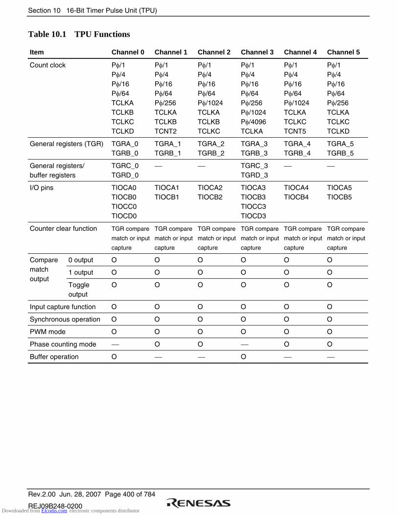
Section 10 16-Bit Timer Pulse Unit (TPU)
Rev.2.00 Jun. 28, 2007 Page 400 of 784
REJ09B248-0200
Table 10.1 TPU Functions
Item Channel 0 Channel 1 Channel 2 Channel 3 Channel 4 Channel 5
Count clock Pφ/1 Pφ/4 Pφ/16 Pφ/64 TCLKA TCLKB TCLKC TCLKD
Pφ/1 Pφ/4 Pφ/16 Pφ/64 Pφ/256 TCLKA TCLKB TCNT2
Pφ/1 Pφ/4 Pφ/16 Pφ/64 Pφ/1024 TCLKA TCLKB TCLKC
Pφ/1 Pφ/4 Pφ/16 Pφ/64 Pφ/256 Pφ/1024 Pφ/4096 TCLKA
Pφ/1 Pφ/4 Pφ/16 Pφ/64 Pφ/1024 TCLKA TCLKC TCNT5
Pφ/1 Pφ/4 Pφ/16 Pφ/64 Pφ/256 TCLKA TCLKC TCLKD
General registers (TGR) TGRA_0 TGRB_0
TGRA_1 TGRB_1
TGRA_2 TGRB_2
TGRA_3 TGRB_3
TGRA_4 TGRB_4
TGRA_5 TGRB_5
General registers/ buffer registers
TGRC_0 TGRD_0
TGRC_3 TGRD_3
I/O pins TIOCA0 TIOCB0 TIOCC0 TIOCD0
TIOCA1 TIOCB1
TIOCA2 TIOCB2
TIOCA3 TIOCB3 TIOCC3 TIOCD3
TIOCA4 TIOCB4
TIOCA5 TIOCB5
Counter clear function TGR compare
match or input
capture
TGR compare
match or input
capture
TGR compare
match or input
capture
TGR compare
match or input
capture
TGR compare
match or input
capture
TGR compare
match or input
capture
0 output O O O O O O
1 output O O O O O O
Compare match output
Toggle output
O O O O O O
Input capture function O O O O O O
Synchronous operation O O O O O O
PWM mode O O O O O O
Phase counting mode O O O O
Buffer operation O O
Downloaded from Elcodis.com electronic components distributor
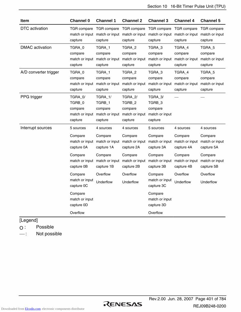
Section 10 16-Bit Timer Pulse Unit (TPU)
Rev.2.00 Jun. 28, 2007 Page 401 of 784
REJ09B248-0200
Item Channel 0 Channel 1 Channel 2 Channel 3 Channel 4 Channel 5
DTC activation TGR compare
match or input
capture
TGR compare
match or input
capture
TGR compare
match or input
capture
TGR compare
match or input
capture
TGR compare
match or input
capture
TGR compare
match or input
capture
DMAC activation TGRA_0
compare
match or input
capture
TGRA_1
compare
match or input
capture
TGRA_2
compare
match or input
capture
TGRA_3
compare
match or input
capture
TGRA_4
compare
match or input
capture
TGRA_5
compare
match or input
capture
A/D converter trigger TGRA_0
compare
match or input
capture
TGRA_1
compare
match or input
capture
TGRA_2
compare
match or input
capture
TGRA_3
compare
match or input
capture
TGRA_4
compare
match or input
capture
TGRA_5
compare
match or input
capture
PPG trigger TGRA_0/
TGRB_0
compare
match or input
capture
TGRA_1/
TGRB_1
compare
match or input
capture
TGRA_2/
TGRB_2
compare
match or input
capture
TGRA_3/
TGRB_3
compare
match or input
capture
Interrupt sources 5 sources
Compare
match or input
capture 0A
Compare
match or input
capture 0B
Compare
match or input
capture 0C
Compare
match or input
capture 0D
Overflow
4 sources
Compare
match or input
capture 1A
Compare
match or input
capture 1B
Overflow
Underflow
4 sources
Compare
match or input
capture 2A
Compare
match or input
capture 2B
Overflow
Underflow
5 sources
Compare
match or input
capture 3A
Compare
match or input
capture 3B
Compare
match or input
capture 3C
Compare
match or input
capture 3D
Overflow
4 sources
Compare
match or input
capture 4A
Compare
match or input
capture 4B
Overflow
Underflow
4 sources
Compare
match or input
capture 5A
Compare
match or input
capture 5B
Overflow
Underflow
[Legend]
O : Possible
: Not possible
Downloaded from Elcodis.com electronic components distributor
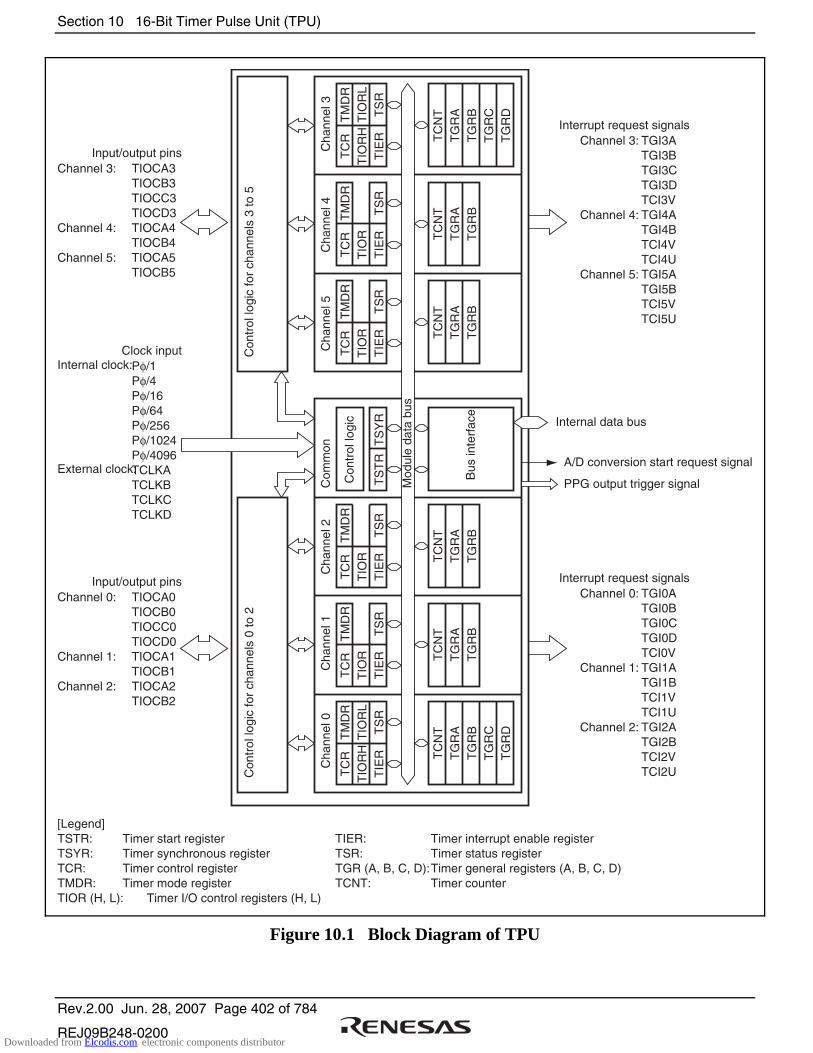
Section 10 16-Bit Timer Pulse Unit (TPU)
Rev.2.00 Jun. 28, 2007 Page 402 of 784
REJ09B248-0200
Cha
nnel
3
TM
DR
TIO
RL
TS
R
TC
RT
IOR
HT
IER TG
RA
TC
NT
TG
RB
TG
RC
TG
RD
Cha
nnel
4
TM
DR
TS
R
TC
RT
IOR
TIE
R TG
RA
TC
NT
TG
RB
Con
trol
logi
cT
MD
R
TS
R
TC
RT
IOR
TIE
R TG
RA
TC
NT
TG
RB
Con
trol
logi
c fo
r ch
anne
ls 3
to 5
TM
DR
TS
R
TC
RT
IOR
TIE
R
TG
RA
TC
NT
TG
RB
TG
RC
Cha
nnel
1
TM
DR
TS
R
TC
RT
IOR
TIE
R TG
RA
TC
NT
TG
RB
Cha
nnel
0
TM
DR
TS
R
TC
RT
IOR
HT
IER
Con
trol
logi
c fo
r ch
anne
ls 0
to 2
TG
RA
TC
NT
TG
RB
TG
RD
TS
YR
TS
TR
Input/output pinsTIOCA3TIOCB3TIOCC3TIOCD3TIOCA4TIOCB4TIOCA5TIOCB5
Clock inputPφ/1Pφ/4Pφ/16Pφ/64Pφ/256Pφ/1024Pφ/4096TCLKATCLKBTCLKCTCLKD
Input/output pinsTIOCA0TIOCB0TIOCC0TIOCD0TIOCA1TIOCB1TIOCA2TIOCB2
Interrupt request signalsChannel 3:
Channel 4:
Channel 5:
Interrupt request signalsChannel 0:
Channel 1:
Channel 2:
Internal data bus
A/D conversion start request signal
PPG output trigger signal
TIO
RL
Mod
ule
data
bus
TGI3ATGI3BTGI3CTGI3DTCI3VTGI4ATGI4BTCI4VTCI4UTGI5ATGI5BTCI5VTCI5U
TGI0ATGI0BTGI0CTGI0DTCI0VTGI1ATGI1BTCI1VTCI1UTGI2ATGI2BTCI2VTCI2U
Channel 3:
Channel 4:
Channel 5:
Internal clock:
External clock:
Channel 0:
Channel 1:
Channel 2:
[Legend]TSTR: Timer start registerTSYR: Timer synchronous registerTCR: Timer control registerTMDR: Timer mode registerTIOR (H, L): Timer I/O control registers (H, L)
TIER: Timer interrupt enable registerTSR: Timer status registerTGR (A, B, C, D): Timer general registers (A, B, C, D)TCNT: Timer counter
Cha
nnel
2C
omm
onC
hann
el 5
Bus
inte
rfac
e
Figure 10.1 Block Diagram of TPU
Downloaded from Elcodis.com electronic components distributor

Section 10 16-Bit Timer Pulse Unit (TPU)
Rev.2.00 Jun. 28, 2007 Page 403 of 784
REJ09B248-0200
10.2 Input/Output Pins
Table 10.2 shows TPU pin configurations.
Table 10.2 Pin Configuration
Channel Symbol I/O Function
TCLKA Input External clock A input pin
(Channel 1 and 5 phase counting mode A phase input)
TCLKB Input External clock B input pin
(Channel 1 and 5 phase counting mode B phase input)
TCLKC Input External clock C input pin
(Channel 2 and 4 phase counting mode A phase input)
All
TCLKD Input External clock D input pin
(Channel 2 and 4 phase counting mode B phase input)
TIOCA0 I/O TGRA_0 input capture input/output compare output/PWM output pin
TIOCB0 I/O TGRB_0 input capture input/output compare output/PWM output pin
TIOCC0 I/O TGRC_0 input capture input/output compare output/PWM output pin
0
TIOCD0 I/O TGRD_0 input capture input/output compare output/PWM output pin
TIOCA1 I/O TGRA_1 input capture input/output compare output/PWM output pin 1
TIOCB1 I/O TGRB_1 input capture input/output compare output/PWM output pin
TIOCA2 I/O TGRA_2 input capture input/output compare output/PWM output pin 2
TIOCB2 I/O TGRB_2 input capture input/output compare output/PWM output pin
TIOCA3 I/O TGRA_3 input capture input/output compare output/PWM output pin
TIOCB3 I/O TGRB_3 input capture input/output compare output/PWM output pin
TIOCC3 I/O TGRC_3 input capture input/output compare output/PWM output pin
3
TIOCD3 I/O TGRD_3 input capture input/output compare output/PWM output pin
TIOCA4 I/O TGRA_4 input capture input/output compare output/PWM output pin 4
TIOCB4 I/O TGRB_4 input capture input/output compare output/PWM output pin
TIOCA5 I/O TGRA_5 input capture input/output compare output/PWM output pin 5
TIOCB5 I/O TGRB_5 input capture input/output compare output/PWM output pin
Downloaded from Elcodis.com electronic components distributor
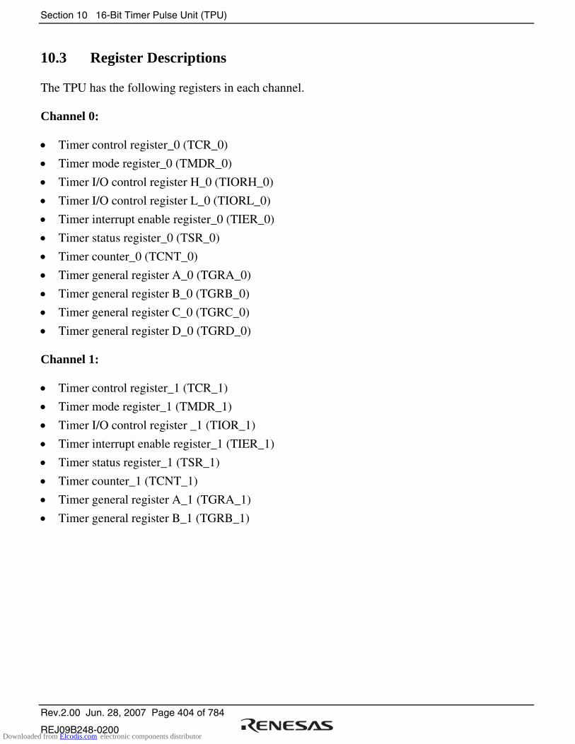
Section 10 16-Bit Timer Pulse Unit (TPU)
Rev.2.00 Jun. 28, 2007 Page 404 of 784
REJ09B248-0200
10.3 Register Descriptions
The TPU has the following registers in each channel.
Channel 0:
• Timer control register_0 (TCR_0)
• Timer mode register_0 (TMDR_0)
• Timer I/O control register H_0 (TIORH_0)
• Timer I/O control register L_0 (TIORL_0)
• Timer interrupt enable register_0 (TIER_0)
• Timer status register_0 (TSR_0)
• Timer counter_0 (TCNT_0)
• Timer general register A_0 (TGRA_0)
• Timer general register B_0 (TGRB_0)
• Timer general register C_0 (TGRC_0)
• Timer general register D_0 (TGRD_0) Channel 1:
• Timer control register_1 (TCR_1)
• Timer mode register_1 (TMDR_1)
• Timer I/O control register _1 (TIOR_1)
• Timer interrupt enable register_1 (TIER_1)
• Timer status register_1 (TSR_1)
• Timer counter_1 (TCNT_1)
• Timer general register A_1 (TGRA_1)
• Timer general register B_1 (TGRB_1)
Downloaded from Elcodis.com electronic components distributor

Section 10 16-Bit Timer Pulse Unit (TPU)
Rev.2.00 Jun. 28, 2007 Page 405 of 784
REJ09B248-0200
Channel 2:
• Timer control register_2 (TCR_2)
• Timer mode register_2 (TMDR_2)
• Timer I/O control register_2 (TIOR_2)
• Timer interrupt enable register_2 (TIER_2)
• Timer status register_2 (TSR_2)
• Timer counter_2 (TCNT_2)
• Timer general register A_2 (TGRA_2)
• Timer general register B_2 (TGRB_2) Channel 3:
• Timer control register_3 (TCR_3)
• Timer mode register_3 (TMDR_3)
• Timer I/O control register H_3 (TIORH_3)
• Timer I/O control register L_3 (TIORL_3)
• Timer interrupt enable register_3 (TIER_3)
• Timer status register_3 (TSR_3)
• Timer counter_3 (TCNT_3)
• Timer general register A_3 (TGRA_3)
• Timer general register B_3 (TGRB_3)
• Timer general register C_3 (TGRC_3)
• Timer general register D_3 (TGRD_3) Channel 4:
• Timer control register_4 (TCR_4)
• Timer mode register_4 (TMDR_4)
• Timer I/O control register _4 (TIOR_4)
• Timer interrupt enable register_4 (TIER_4)
• Timer status register_4 (TSR_4)
• Timer counter_4 (TCNT_4)
• Timer general register A_4 (TGRA_4)
• Timer general register B_4 (TGRB_4)
Downloaded from Elcodis.com electronic components distributor

Section 10 16-Bit Timer Pulse Unit (TPU)
Rev.2.00 Jun. 28, 2007 Page 406 of 784
REJ09B248-0200
Channel 5:
• Timer control register_5 (TCR_5)
• Timer mode register_5 (TMDR_5)
• Timer I/O control register_5 (TIOR_5)
• Timer interrupt enable register_5 (TIER_5)
• Timer status register_5 (TSR_5)
• Timer counter_5 (TCNT_5)
• Timer general register A_5 (TGRA_5)
• Timer general register B_5 (TGRB_5) Common Registers:
• Timer start register (TSTR)
• Timer synchronous register (TSYR)
Downloaded from Elcodis.com electronic components distributor

Section 10 16-Bit Timer Pulse Unit (TPU)
Rev.2.00 Jun. 28, 2007 Page 407 of 784
REJ09B248-0200
10.3.1 Timer Control Register (TCR)
TCR controls the TCNT operation for each channel. The TPU has a total of six TCR registers, one for each channel. TCR register settings should be made only while TCNT operation is stopped.
7
CCLR2
0
R/W
6
CCLR1
0
R/W
5
CCLR0
0
R/W
4
CKEG1
0
R/W
3
CKEG0
0
R/W
2
TPSC2
0
R/W
1
TPSC1
0
R/W
0
TPSC0
0
R/W
Bit
Bit Name
Initial Value
R/W
Bit Bit Name Initial Value R/W Description
7
6
5
CCLR2
CCLR1
CCLR0
0
0
0
R/W
R/W
R/W
Counter Clear 2 to 0
These bits select the TCNT counter clearing source. See tables 10.3 and 10.4 for details.
4
3
CKEG1
CKEG0
0
0
R/W
R/W
Clock Edge 1 and 0
These bits select the input clock edge. For details, see table 10.5. When the input clock is counted using both edges, the input clock period is halved (e.g. Pφ/4 both edges = Pφ/2 rising edge). If phase counting mode is used on channels 1, 2, 4, and 5, this setting is ignored and the phase counting mode setting has priority. Internal clock edge selection is valid when the input clock is Pφ/4 or slower. This setting is ignored if the input clock is Pφ/1, or when overflow/underflow of another channel is selected.
2
1
0
TPSC2
TPSC1
TPSC0
0
0
0
R/W
R/W
R/W
Timer Prescaler 2 to 0
These bits select the TCNT counter clock. The clock source can be selected independently for each channel. See tables 10.6 to 10.11 for details. To select the external clock as the clock source, the DDR bit and ICR bit for the corresponding pin should be set to 0 and 1, respectively. For details, see section 9, I/O Ports.
Downloaded from Elcodis.com electronic components distributor

Section 10 16-Bit Timer Pulse Unit (TPU)
Rev.2.00 Jun. 28, 2007 Page 408 of 784
REJ09B248-0200
Table 10.3 CCLR2 to CCLR0 (Channels 0 and 3)
Channel Bit 7 CCLR2
Bit 6 CCLR1
Bit 5 CCLR0 Description
0 0 0 TCNT clearing disabled
0 0 1 TCNT cleared by TGRA compare match/input capture
0 1 0 TCNT cleared by TGRB compare match/input capture
0 1 1 TCNT cleared by counter clearing for another channel performing synchronous clearing/ synchronous operation*1
1 0 0 TCNT clearing disabled
1 0 1 TCNT cleared by TGRC compare match/input capture*2
1 1 0 TCNT cleared by TGRD compare match/input capture*2
0, 3
1 1 1 TCNT cleared by counter clearing for another channel performing synchronous clearing/ synchronous operation*1
Notes: 1. Synchronous operation is selected by setting the SYNC bit in TSYR to 1. 2. When TGRC or TGRD is used as a buffer register, TCNT is not cleared because the
buffer register setting has priority, and compare match/input capture does not occur.
Table 10.4 CCLR2 to CCLR0 (Channels 1, 2, 4, and 5)
Channel
Bit 7 Reserved *2
Bit 6 CCLR1
Bit 5 CCLR0 Description
0 0 0 TCNT clearing disabled
0 0 1 TCNT cleared by TGRA compare match/input capture
0 1 0 TCNT cleared by TGRB compare match/input capture
1, 2, 4, 5
0 1 1 TCNT cleared by counter clearing for another channel performing synchronous clearing/ synchronous operation*1
Notes: 1. Synchronous operation is selected by setting the SYNC bit in TSYR to 1. 2. Bit 7 is reserved in channels 1, 2, 4, and 5. It is always read as 0 and cannot be
modified.
Downloaded from Elcodis.com electronic components distributor
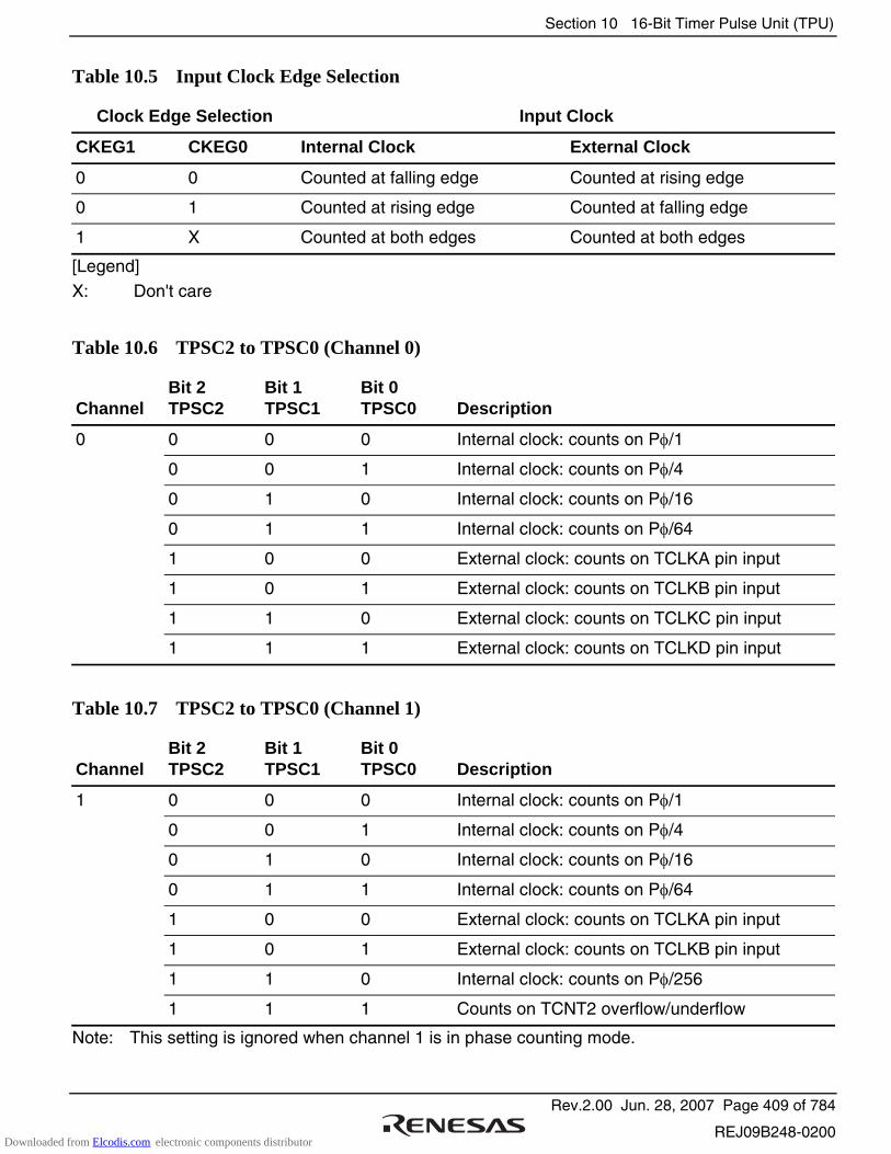
Section 10 16-Bit Timer Pulse Unit (TPU)
Rev.2.00 Jun. 28, 2007 Page 409 of 784
REJ09B248-0200
Table 10.5 Input Clock Edge Selection
Clock Edge Selection Input Clock
CKEG1 CKEG0 Internal Clock External Clock
0 0 Counted at falling edge Counted at rising edge
0 1 Counted at rising edge Counted at falling edge
1 X Counted at both edges Counted at both edges
[Legend] X: Don't care
Table 10.6 TPSC2 to TPSC0 (Channel 0)
Channel Bit 2 TPSC2
Bit 1 TPSC1
Bit 0 TPSC0 Description
0 0 0 Internal clock: counts on Pφ/1
0 0 1 Internal clock: counts on Pφ/4
0 1 0 Internal clock: counts on Pφ/16
0 1 1 Internal clock: counts on Pφ/64
1 0 0 External clock: counts on TCLKA pin input
1 0 1 External clock: counts on TCLKB pin input
1 1 0 External clock: counts on TCLKC pin input
0
1 1 1 External clock: counts on TCLKD pin input
Table 10.7 TPSC2 to TPSC0 (Channel 1)
Channel Bit 2 TPSC2
Bit 1 TPSC1
Bit 0 TPSC0 Description
0 0 0 Internal clock: counts on Pφ/1
0 0 1 Internal clock: counts on Pφ/4
0 1 0 Internal clock: counts on Pφ/16
0 1 1 Internal clock: counts on Pφ/64
1 0 0 External clock: counts on TCLKA pin input
1 0 1 External clock: counts on TCLKB pin input
1 1 0 Internal clock: counts on Pφ/256
1
1 1 1 Counts on TCNT2 overflow/underflow
Note: This setting is ignored when channel 1 is in phase counting mode.
Downloaded from Elcodis.com electronic components distributor
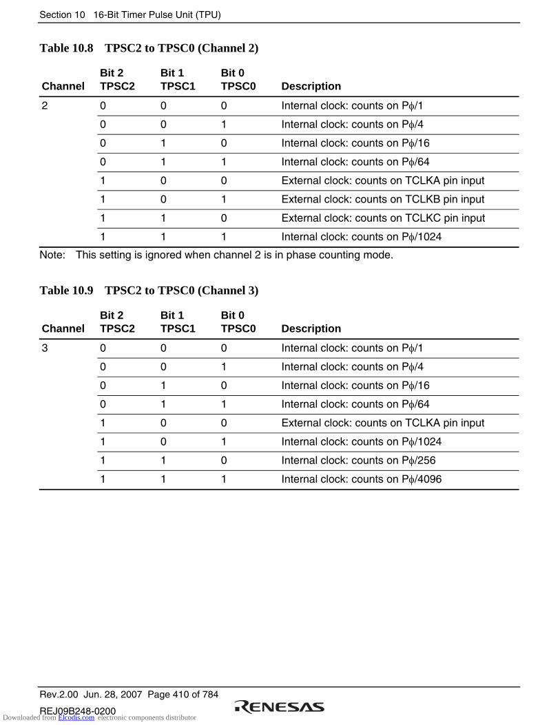
Section 10 16-Bit Timer Pulse Unit (TPU)
Rev.2.00 Jun. 28, 2007 Page 410 of 784
REJ09B248-0200
Table 10.8 TPSC2 to TPSC0 (Channel 2)
Channel Bit 2 TPSC2
Bit 1 TPSC1
Bit 0 TPSC0 Description
0 0 0 Internal clock: counts on Pφ/1
0 0 1 Internal clock: counts on Pφ/4
0 1 0 Internal clock: counts on Pφ/16
0 1 1 Internal clock: counts on Pφ/64
1 0 0 External clock: counts on TCLKA pin input
1 0 1 External clock: counts on TCLKB pin input
1 1 0 External clock: counts on TCLKC pin input
2
1 1 1 Internal clock: counts on Pφ/1024
Note: This setting is ignored when channel 2 is in phase counting mode.
Table 10.9 TPSC2 to TPSC0 (Channel 3)
Channel Bit 2 TPSC2
Bit 1 TPSC1
Bit 0 TPSC0 Description
0 0 0 Internal clock: counts on Pφ/1
0 0 1 Internal clock: counts on Pφ/4
0 1 0 Internal clock: counts on Pφ/16
0 1 1 Internal clock: counts on Pφ/64
1 0 0 External clock: counts on TCLKA pin input
1 0 1 Internal clock: counts on Pφ/1024
1 1 0 Internal clock: counts on Pφ/256
3
1 1 1 Internal clock: counts on Pφ/4096
Downloaded from Elcodis.com electronic components distributor

Section 10 16-Bit Timer Pulse Unit (TPU)
Rev.2.00 Jun. 28, 2007 Page 411 of 784
REJ09B248-0200
Table 10.10 TPSC2 to TPSC0 (Channel 4)
Channel Bit 2 TPSC2
Bit 1 TPSC1
Bit 0 TPSC0 Description
0 0 0 Internal clock: counts on Pφ/1
0 0 1 Internal clock: counts on Pφ/4
0 1 0 Internal clock: counts on Pφ/16
0 1 1 Internal clock: counts on Pφ/64
1 0 0 External clock: counts on TCLKA pin input
1 0 1 External clock: counts on TCLKC pin input
1 1 0 Internal clock: counts on Pφ/1024
4
1 1 1 Counts on TCNT5 overflow/underflow
Note: This setting is ignored when channel 4 is in phase counting mode.
Table 10.11 TPSC2 to TPSC0 (Channel 5)
Channel Bit 2 TPSC2
Bit 1 TPSC1
Bit 0 TPSC0 Description
0 0 0 Internal clock: counts on Pφ/1
0 0 1 Internal clock: counts on Pφ/4
0 1 0 Internal clock: counts on Pφ/16
0 1 1 Internal clock: counts on Pφ/64
1 0 0 External clock: counts on TCLKA pin input
1 0 1 External clock: counts on TCLKC pin input
1 1 0 Internal clock: counts on Pφ/256
5
1 1 1 External clock: counts on TCLKD pin input
Note: This setting is ignored when channel 5 is in phase counting mode.
Downloaded from Elcodis.com electronic components distributor
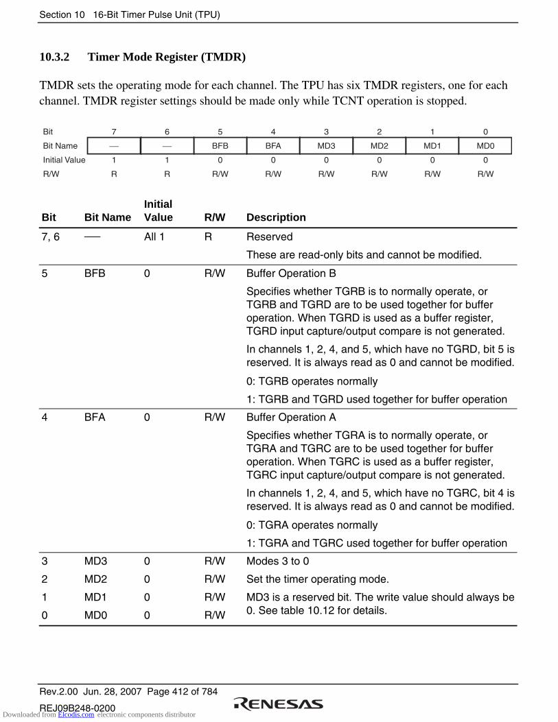
Section 10 16-Bit Timer Pulse Unit (TPU)
Rev.2.00 Jun. 28, 2007 Page 412 of 784
REJ09B248-0200
10.3.2 Timer Mode Register (TMDR)
TMDR sets the operating mode for each channel. The TPU has six TMDR registers, one for each channel. TMDR register settings should be made only while TCNT operation is stopped.
7
1
R
6
1
R
5
BFB
0
R/W
4
BFA
0
R/W
3
MD3
0
R/W
2
MD2
0
R/W
1
MD1
0
R/W
0
MD0
0
R/W
Bit
Bit Name
Initial Value
R/W
Bit Bit Name Initial Value R/W Description
7, 6 All 1 R Reserved
These are read-only bits and cannot be modified.
5 BFB 0 R/W Buffer Operation B
Specifies whether TGRB is to normally operate, or TGRB and TGRD are to be used together for buffer operation. When TGRD is used as a buffer register, TGRD input capture/output compare is not generated.
In channels 1, 2, 4, and 5, which have no TGRD, bit 5 is reserved. It is always read as 0 and cannot be modified.
0: TGRB operates normally
1: TGRB and TGRD used together for buffer operation
4 BFA 0 R/W Buffer Operation A
Specifies whether TGRA is to normally operate, or TGRA and TGRC are to be used together for buffer operation. When TGRC is used as a buffer register, TGRC input capture/output compare is not generated.
In channels 1, 2, 4, and 5, which have no TGRC, bit 4 is reserved. It is always read as 0 and cannot be modified.
0: TGRA operates normally
1: TGRA and TGRC used together for buffer operation
3
2
1
0
MD3
MD2
MD1
MD0
0
0
0
0
R/W
R/W
R/W
R/W
Modes 3 to 0
Set the timer operating mode.
MD3 is a reserved bit. The write value should always be 0. See table 10.12 for details.
Downloaded from Elcodis.com electronic components distributor
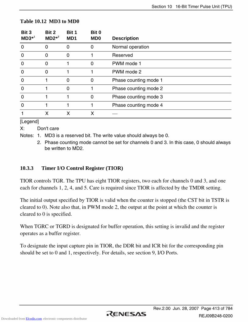
Section 10 16-Bit Timer Pulse Unit (TPU)
Rev.2.00 Jun. 28, 2007 Page 413 of 784
REJ09B248-0200
Table 10.12 MD3 to MD0
Bit 3 MD3*1
Bit 2 MD2*2
Bit 1 MD1
Bit 0 MD0 Description
0 0 0 0 Normal operation
0 0 0 1 Reserved
0 0 1 0 PWM mode 1
0 0 1 1 PWM mode 2
0 1 0 0 Phase counting mode 1
0 1 0 1 Phase counting mode 2
0 1 1 0 Phase counting mode 3
0 1 1 1 Phase counting mode 4
1 X X X
[Legend]
X: Don't care
Notes: 1. MD3 is a reserved bit. The write value should always be 0. 2. Phase counting mode cannot be set for channels 0 and 3. In this case, 0 should always
be written to MD2.
10.3.3 Timer I/O Control Register (TIOR)
TIOR controls TGR. The TPU has eight TIOR registers, two each for channels 0 and 3, and one each for channels 1, 2, 4, and 5. Care is required since TIOR is affected by the TMDR setting.
The initial output specified by TIOR is valid when the counter is stopped (the CST bit in TSTR is cleared to 0). Note also that, in PWM mode 2, the output at the point at which the counter is cleared to 0 is specified.
When TGRC or TGRD is designated for buffer operation, this setting is invalid and the register operates as a buffer register.
To designate the input capture pin in TIOR, the DDR bit and ICR bit for the corresponding pin should be set to 0 and 1, respectively. For details, see section 9, I/O Ports.
Downloaded from Elcodis.com electronic components distributor
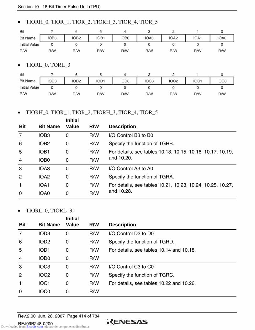
Section 10 16-Bit Timer Pulse Unit (TPU)
Rev.2.00 Jun. 28, 2007 Page 414 of 784
REJ09B248-0200
• TIORH_0, TIOR_1, TIOR_2, TIORH_3, TIOR_4, TIOR_5
7
IOB3
0
R/W
6
IOB2
0
R/W
5
IOB1
0
R/W
4
IOB0
0
R/W
3
IOA3
0
R/W
2
IOA2
0
R/W
1
IOA1
0
R/W
0
IOA0
0
R/W
Bit
Bit Name
Initial Value
R/W
• TIORL_0, TORL_3
7
IOD3
0
R/W
6
IOD2
0
R/W
5
IOD1
0
R/W
4
IOD0
0
R/W
3
IOC3
0
R/W
2
IOC2
0
R/W
1
IOC1
0
R/W
0
IOC0
0
R/W
Bit
Bit Name
Initial Value
R/W
• TIORH_0, TIOR_1, TIOR_2, TIORH_3, TIOR_4, TIOR_5
Bit Bit Name Initial Value R/W Description
7
6
5
4
IOB3
IOB2
IOB1
IOB0
0
0
0
0
R/W
R/W
R/W
R/W
I/O Control B3 to B0
Specify the function of TGRB.
For details, see tables 10.13, 10.15, 10.16, 10.17, 10.19, and 10.20.
3
2
1
0
IOA3
IOA2
IOA1
IOA0
0
0
0
0
R/W
R/W
R/W
R/W
I/O Control A3 to A0
Specify the function of TGRA.
For details, see tables 10.21, 10.23, 10.24, 10.25, 10.27, and 10.28.
• TIORL_0, TIORL_3:
Bit Bit Name Initial Value R/W Description
7
6
5
4
IOD3
IOD2
IOD1
IOD0
0
0
0
0
R/W
R/W
R/W
R/W
I/O Control D3 to D0
Specify the function of TGRD.
For details, see tables 10.14 and 10.18.
3
2
1
0
IOC3
IOC2
IOC1
IOC0
0
0
0
0
R/W
R/W
R/W
R/W
I/O Control C3 to C0
Specify the function of TGRC.
For details, see tables 10.22 and 10.26.
Downloaded from Elcodis.com electronic components distributor
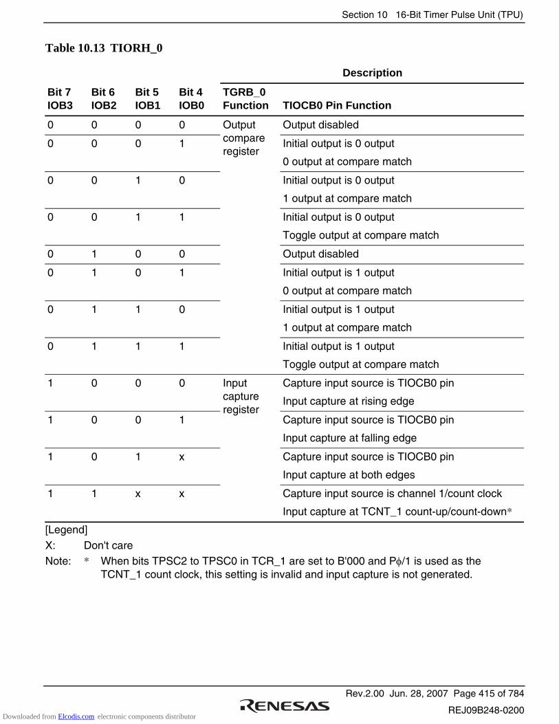
Section 10 16-Bit Timer Pulse Unit (TPU)
Rev.2.00 Jun. 28, 2007 Page 415 of 784
REJ09B248-0200
Table 10.13 TIORH_0
Description
Bit 7 IOB3
Bit 6 IOB2
Bit 5 IOB1
Bit 4 IOB0
TGRB_0 Function TIOCB0 Pin Function
0 0 0 0 Output disabled
0 0 0 1 Initial output is 0 output
0 output at compare match
0 0 1 0 Initial output is 0 output
1 output at compare match
0 0 1 1 Initial output is 0 output
Toggle output at compare match
0 1 0 0 Output disabled
0 1 0 1 Initial output is 1 output
0 output at compare match
0 1 1 0 Initial output is 1 output
1 output at compare match
0 1 1 1
Output compare register
Initial output is 1 output
Toggle output at compare match
1 0 0 0 Capture input source is TIOCB0 pin
Input capture at rising edge
1 0 0 1 Capture input source is TIOCB0 pin
Input capture at falling edge
1 0 1 x Capture input source is TIOCB0 pin
Input capture at both edges
1 1 x x
Input capture register
Capture input source is channel 1/count clock
Input capture at TCNT_1 count-up/count-down*
[Legend]
X: Don't care Note: * When bits TPSC2 to TPSC0 in TCR_1 are set to B'000 and Pφ/1 is used as the
TCNT_1 count clock, this setting is invalid and input capture is not generated.
Downloaded from Elcodis.com electronic components distributor

Section 10 16-Bit Timer Pulse Unit (TPU)
Rev.2.00 Jun. 28, 2007 Page 416 of 784
REJ09B248-0200
Table 10.14 TIORL_0
Description
Bit 7 IOD3
Bit 6 IOD2
Bit 5 IOD1
Bit 4 IOD0
TGRD_0 Function TIOCD0 Pin Function
0 0 0 0 Output disabled
0 0 0 1 Initial output is 0 output
0 output at compare match
0 0 1 0 Initial output is 0 output
1 output at compare match
0 0 1 1 Initial output is 0 output
Toggle output at compare match
0 1 0 0 Output disabled
0 1 0 1 Initial output is 1 output
0 output at compare match
0 1 1 0 Initial output is 1 output
1 output at compare match
0 1 1 1
Output compare register*2
Initial output is 1 output
Toggle output at compare match
1 0 0 0 Capture input source is TIOCD0 pin
Input capture at rising edge
1 0 0 1 Capture input source is TIOCD0 pin
Input capture at falling edge
1 0 1 X Capture input source is TIOCD0 pin
Input capture at both edges
1 1 X X
Input capture register*2
Capture input source is channel 1/count clock
Input capture at TCNT_1 count-up/count-down*1
[Legend]
X: Don't care Notes: 1. When bits TPSC2 to TPSC0 in TCR_1 are set to B'000 and Pφ/1 is used as the
TCNT_1 count clock, this setting is invalid and input capture is not generated. 2. When the BFB bit in TMDR_0 is set to 1 and TGRD_0 is used as a buffer register, this
setting is invalid and input capture/output compare is not generated.
Downloaded from Elcodis.com electronic components distributor
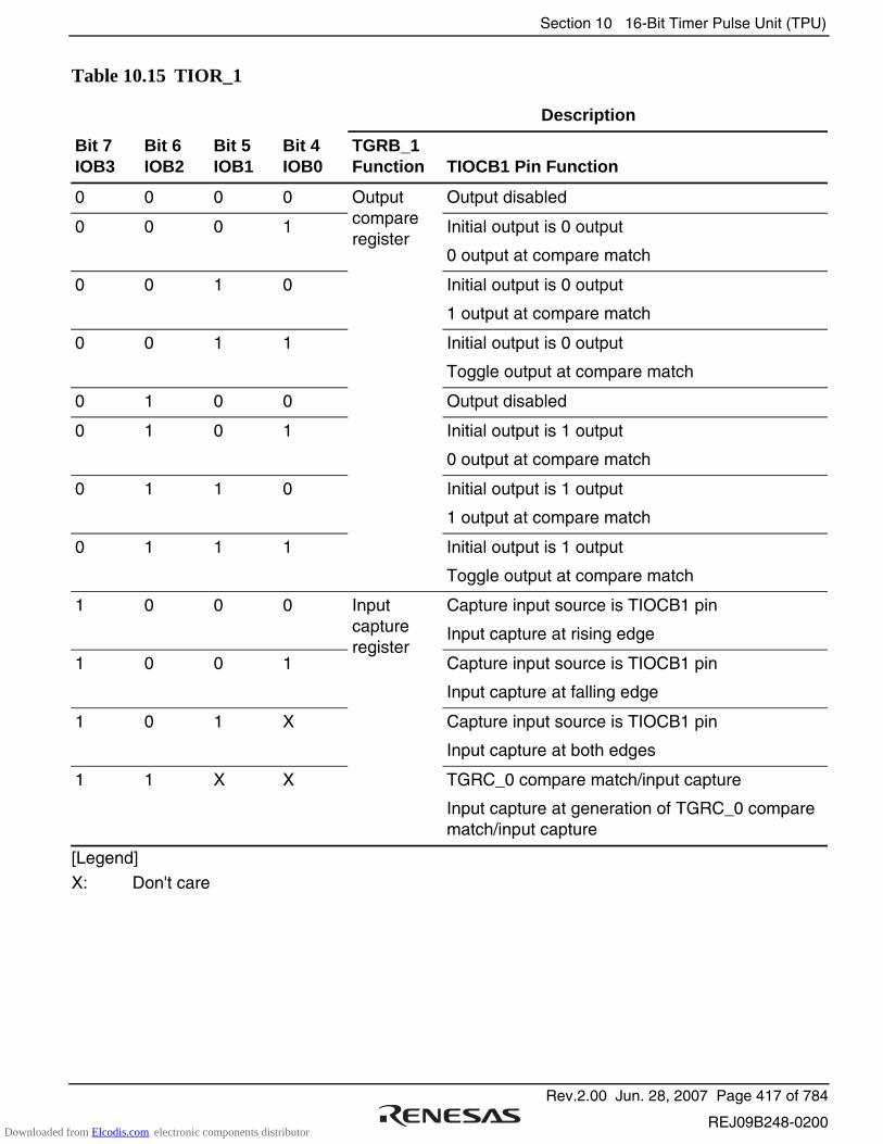
Section 10 16-Bit Timer Pulse Unit (TPU)
Rev.2.00 Jun. 28, 2007 Page 417 of 784
REJ09B248-0200
Table 10.15 TIOR_1
Description
Bit 7 IOB3
Bit 6 IOB2
Bit 5 IOB1
Bit 4 IOB0
TGRB_1 Function TIOCB1 Pin Function
0 0 0 0 Output disabled
0 0 0 1 Initial output is 0 output
0 output at compare match
0 0 1 0 Initial output is 0 output
1 output at compare match
0 0 1 1 Initial output is 0 output
Toggle output at compare match
0 1 0 0 Output disabled
0 1 0 1 Initial output is 1 output
0 output at compare match
0 1 1 0 Initial output is 1 output
1 output at compare match
0 1 1 1
Output compare register
Initial output is 1 output
Toggle output at compare match
1 0 0 0 Capture input source is TIOCB1 pin
Input capture at rising edge
1 0 0 1 Capture input source is TIOCB1 pin
Input capture at falling edge
1 0 1 X Capture input source is TIOCB1 pin
Input capture at both edges
1 1 X X
Input capture register
TGRC_0 compare match/input capture
Input capture at generation of TGRC_0 compare match/input capture
[Legend]
X: Don't care
Downloaded from Elcodis.com electronic components distributor
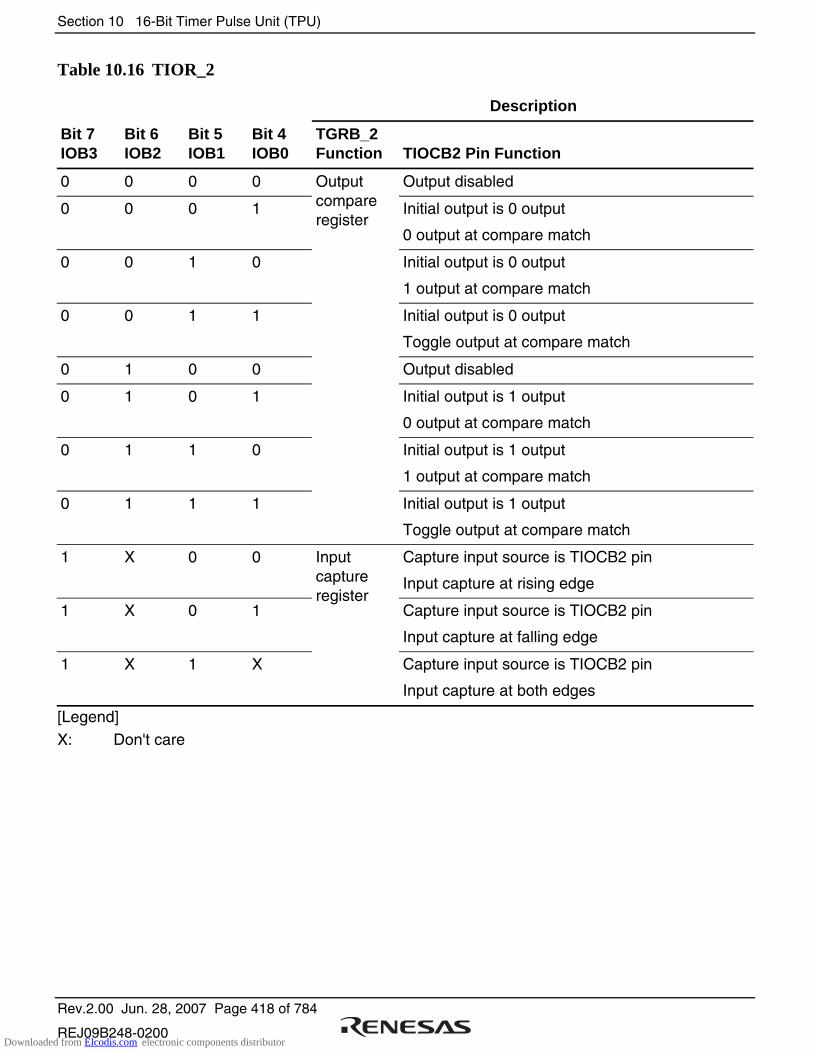
Section 10 16-Bit Timer Pulse Unit (TPU)
Rev.2.00 Jun. 28, 2007 Page 418 of 784
REJ09B248-0200
Table 10.16 TIOR_2
Description
Bit 7 IOB3
Bit 6 IOB2
Bit 5 IOB1
Bit 4 IOB0
TGRB_2 Function TIOCB2 Pin Function
0 0 0 0 Output disabled
0 0 0 1 Initial output is 0 output
0 output at compare match
0 0 1 0 Initial output is 0 output
1 output at compare match
0 0 1 1 Initial output is 0 output
Toggle output at compare match
0 1 0 0 Output disabled
0 1 0 1 Initial output is 1 output
0 output at compare match
0 1 1 0 Initial output is 1 output
1 output at compare match
0 1 1 1
Output compare register
Initial output is 1 output
Toggle output at compare match
1 X 0 0 Capture input source is TIOCB2 pin
Input capture at rising edge
1 X 0 1 Capture input source is TIOCB2 pin
Input capture at falling edge
1 X 1 X
Input capture register
Capture input source is TIOCB2 pin
Input capture at both edges
[Legend] X: Don't care
Downloaded from Elcodis.com electronic components distributor
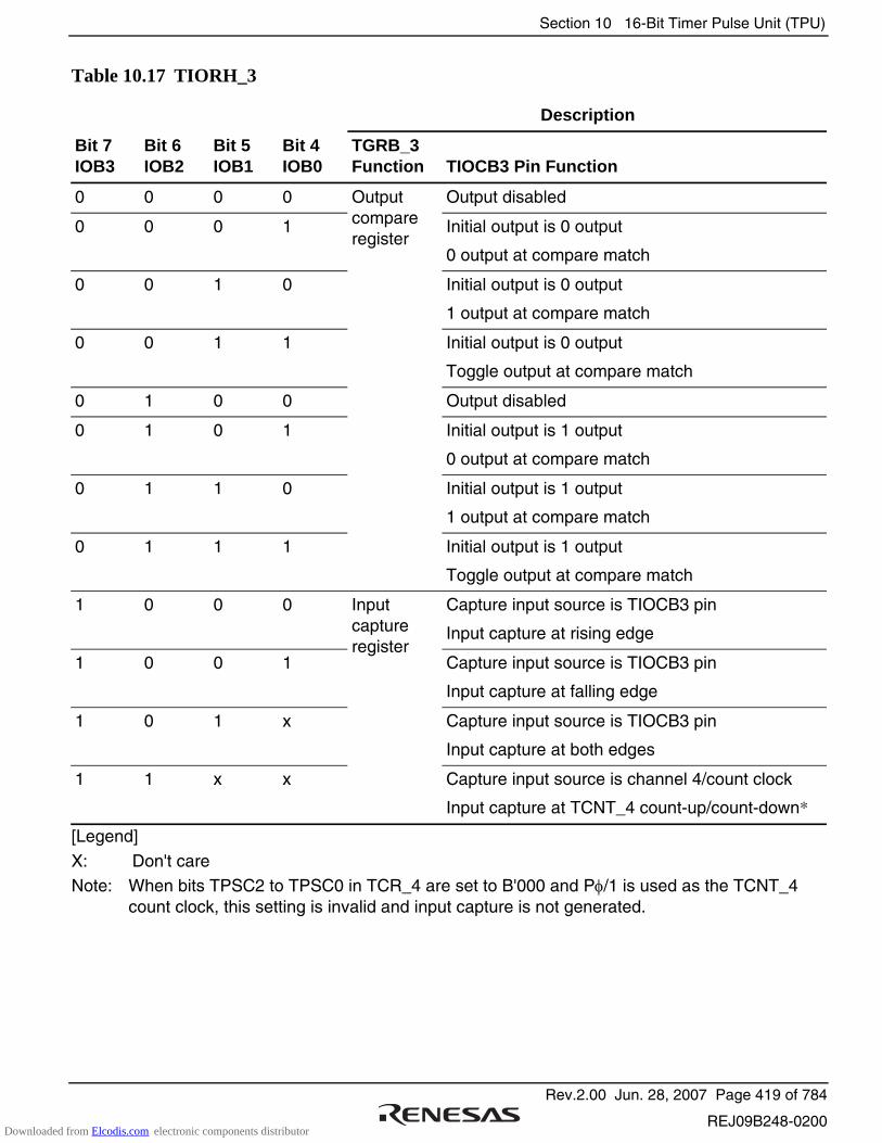
Section 10 16-Bit Timer Pulse Unit (TPU)
Rev.2.00 Jun. 28, 2007 Page 419 of 784
REJ09B248-0200
Table 10.17 TIORH_3
Description
Bit 7 IOB3
Bit 6 IOB2
Bit 5 IOB1
Bit 4 IOB0
TGRB_3 Function TIOCB3 Pin Function
0 0 0 0 Output disabled
0 0 0 1 Initial output is 0 output
0 output at compare match
0 0 1 0 Initial output is 0 output
1 output at compare match
0 0 1 1 Initial output is 0 output
Toggle output at compare match
0 1 0 0 Output disabled
0 1 0 1 Initial output is 1 output
0 output at compare match
0 1 1 0 Initial output is 1 output
1 output at compare match
0 1 1 1
Output compare register
Initial output is 1 output
Toggle output at compare match
1 0 0 0 Capture input source is TIOCB3 pin
Input capture at rising edge
1 0 0 1 Capture input source is TIOCB3 pin
Input capture at falling edge
1 0 1 x Capture input source is TIOCB3 pin
Input capture at both edges
1 1 x x
Input capture register
Capture input source is channel 4/count clock
Input capture at TCNT_4 count-up/count-down*
[Legend]
X: Don't care Note: When bits TPSC2 to TPSC0 in TCR_4 are set to B'000 and Pφ/1 is used as the TCNT_4
count clock, this setting is invalid and input capture is not generated.
Downloaded from Elcodis.com electronic components distributor
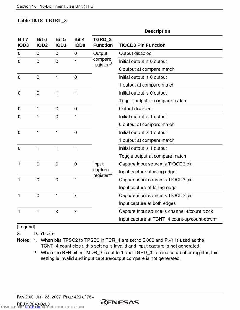
Section 10 16-Bit Timer Pulse Unit (TPU)
Rev.2.00 Jun. 28, 2007 Page 420 of 784
REJ09B248-0200
Table 10.18 TIORL_3
Description
Bit 7 IOD3
Bit 6 IOD2
Bit 5 IOD1
Bit 4 IOD0
TGRD_3 Function TIOCD3 Pin Function
0 0 0 0 Output disabled
0 0 0 1 Initial output is 0 output
0 output at compare match
0 0 1 0 Initial output is 0 output
1 output at compare match
0 0 1 1 Initial output is 0 output
Toggle output at compare match
0 1 0 0 Output disabled
0 1 0 1 Initial output is 1 output
0 output at compare match
0 1 1 0 Initial output is 1 output
1 output at compare match
0 1 1 1
Output compare register*2
Initial output is 1 output
Toggle output at compare match
1 0 0 0 Capture input source is TIOCD3 pin
Input capture at rising edge
1 0 0 1 Capture input source is TIOCD3 pin
Input capture at falling edge
1 0 1 x Capture input source is TIOCD3 pin
Input capture at both edges
1 1 x x
Input capture register*2
Capture input source is channel 4/count clock
Input capture at TCNT_4 count-up/count-down*1
[Legend]
X: Don't care Notes: 1. When bits TPSC2 to TPSC0 in TCR_4 are set to B'000 and Pφ/1 is used as the
TCNT_4 count clock, this setting is invalid and input capture is not generated. 2. When the BFB bit in TMDR_3 is set to 1 and TGRD_3 is used as a buffer register, this
setting is invalid and input capture/output compare is not generated.
Downloaded from Elcodis.com electronic components distributor
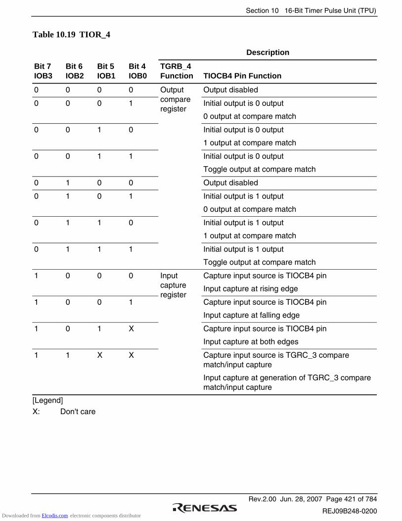
Section 10 16-Bit Timer Pulse Unit (TPU)
Rev.2.00 Jun. 28, 2007 Page 421 of 784
REJ09B248-0200
Table 10.19 TIOR_4
Description
Bit 7 IOB3
Bit 6 IOB2
Bit 5 IOB1
Bit 4 IOB0
TGRB_4 Function TIOCB4 Pin Function
0 0 0 0 Output disabled
0 0 0 1 Initial output is 0 output
0 output at compare match
0 0 1 0 Initial output is 0 output
1 output at compare match
0 0 1 1 Initial output is 0 output
Toggle output at compare match
0 1 0 0 Output disabled
0 1 0 1 Initial output is 1 output
0 output at compare match
0 1 1 0 Initial output is 1 output
1 output at compare match
0 1 1 1
Output compare register
Initial output is 1 output
Toggle output at compare match
1 0 0 0 Capture input source is TIOCB4 pin
Input capture at rising edge
1 0 0 1 Capture input source is TIOCB4 pin
Input capture at falling edge
1 0 1 X Capture input source is TIOCB4 pin
Input capture at both edges
1 1 X X
Input capture register
Capture input source is TGRC_3 compare match/input capture
Input capture at generation of TGRC_3 compare match/input capture
[Legend] X: Don't care
Downloaded from Elcodis.com electronic components distributor

Section 10 16-Bit Timer Pulse Unit (TPU)
Rev.2.00 Jun. 28, 2007 Page 422 of 784
REJ09B248-0200
Table 10.20 TIOR_5
Description
Bit 7 IOB3
Bit 6 IOB2
Bit 5 IOB1
Bit 4 IOB0
TGRB_5 Function TIOCB5 Pin Function
0 0 0 0 Output disabled
0 0 0 1 Initial output is 0 output
0 output at compare match
0 0 1 0 Initial output is 0 output
1 output at compare match
0 0 1 1 Initial output is 0 output
Toggle output at compare match
0 1 0 0 Output disabled
0 1 0 1 Initial output is 1 output
0 output at compare match
0 1 1 0 Initial output is 1 output
1 output at compare match
0 1 1 1
Output compare register
Initial output is 1 output
Toggle output at compare match
1 X 0 0 Capture input source is TIOCB5 pin
Input capture at rising edge
1 X 0 1 Capture input source is TIOCB5 pin
Input capture at falling edge
1 X 1 X
Input capture register
Capture input source is TIOCB5 pin
Input capture at both edges
[Legend] X: Don't care
Downloaded from Elcodis.com electronic components distributor

Section 10 16-Bit Timer Pulse Unit (TPU)
Rev.2.00 Jun. 28, 2007 Page 423 of 784
REJ09B248-0200
Table 10.21 TIORH_0
Description
Bit 3 IOA3
Bit 2 IOA2
Bit 1 IOA1
Bit 0 IOA0
TGRA_0 Function TIOCA0 Pin Function
0 0 0 0 Output disabled
0 0 0 1 Initial output is 0 output
0 output at compare match
0 0 1 0 Initial output is 0 output
1 output at compare match
0 0 1 1 Initial output is 0 output
Toggle output at compare match
0 1 0 0 Output disabled
0 1 0 1 Initial output is 1 output
0 output at compare match
0 1 1 0 Initial output is 1 output
1 output at compare match
0 1 1 1
Output compare register
Initial output is 1 output
Toggle output at compare match
1 0 0 0 Capture input source is TIOCA0 pin
Input capture at rising edge
1 0 0 1 Capture input source is TIOCA0 pin
Input capture at falling edge
1 0 1 X Capture input source is TIOCA0 pin
Input capture at both edges
1 1 X X
Input capture register
Capture input source is channel 1/count clock
Input capture at TCNT_1 count-up/count-down
[Legend]
X: Don't care
Downloaded from Elcodis.com electronic components distributor
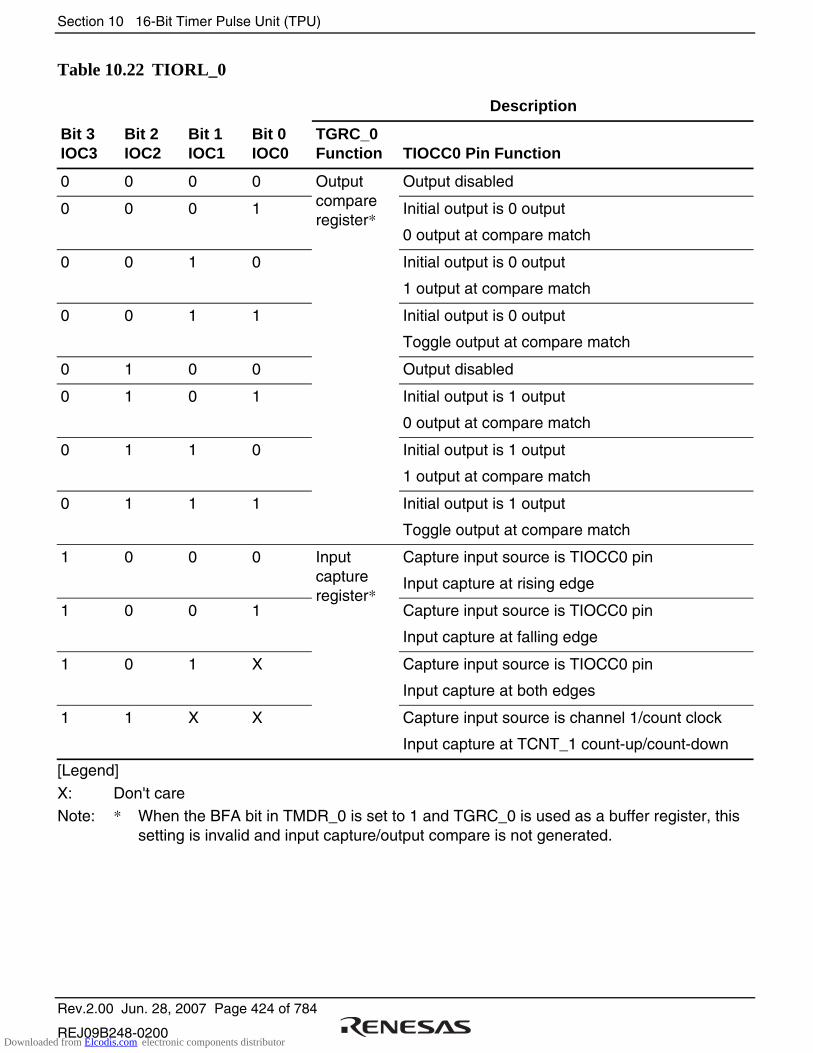
Section 10 16-Bit Timer Pulse Unit (TPU)
Rev.2.00 Jun. 28, 2007 Page 424 of 784
REJ09B248-0200
Table 10.22 TIORL_0
Description
Bit 3 IOC3
Bit 2 IOC2
Bit 1 IOC1
Bit 0 IOC0
TGRC_0 Function TIOCC0 Pin Function
0 0 0 0 Output disabled
0 0 0 1 Initial output is 0 output
0 output at compare match
0 0 1 0 Initial output is 0 output
1 output at compare match
0 0 1 1 Initial output is 0 output
Toggle output at compare match
0 1 0 0 Output disabled
0 1 0 1 Initial output is 1 output
0 output at compare match
0 1 1 0 Initial output is 1 output
1 output at compare match
0 1 1 1
Output compare register*
Initial output is 1 output
Toggle output at compare match
1 0 0 0 Capture input source is TIOCC0 pin
Input capture at rising edge
1 0 0 1 Capture input source is TIOCC0 pin
Input capture at falling edge
1 0 1 X Capture input source is TIOCC0 pin
Input capture at both edges
1 1 X X
Input capture register*
Capture input source is channel 1/count clock
Input capture at TCNT_1 count-up/count-down
[Legend]
X: Don't care Note: * When the BFA bit in TMDR_0 is set to 1 and TGRC_0 is used as a buffer register, this
setting is invalid and input capture/output compare is not generated.
Downloaded from Elcodis.com electronic components distributor
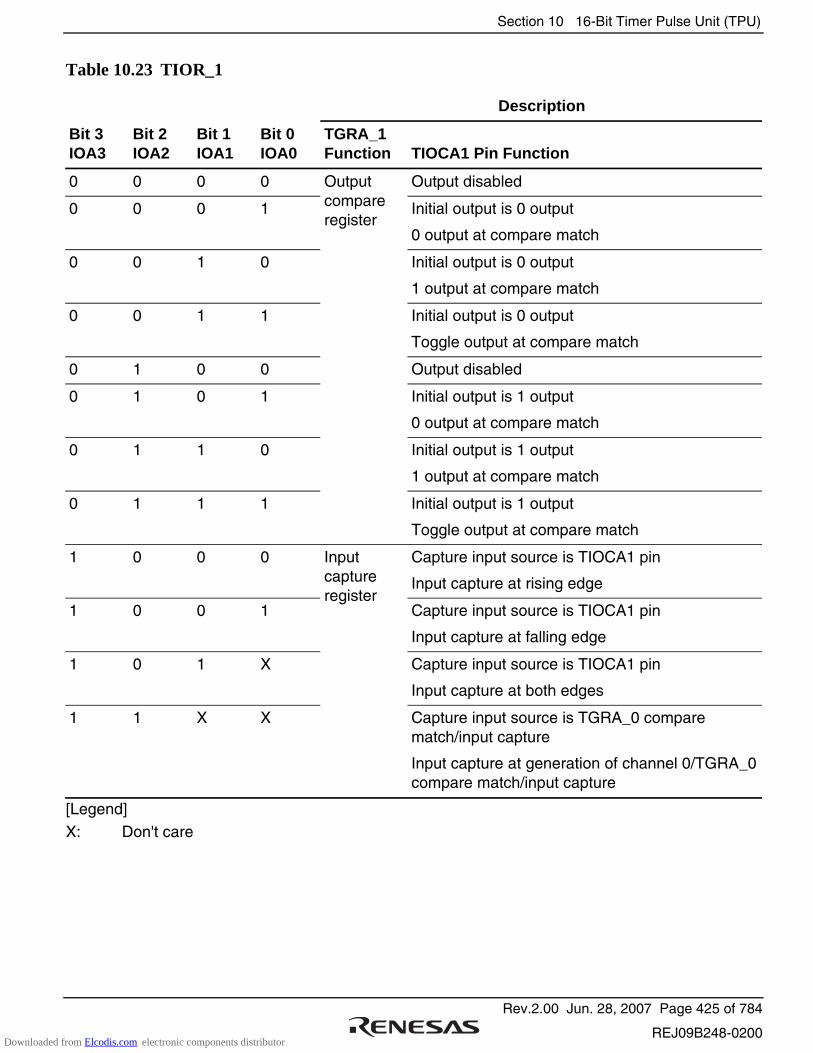
Section 10 16-Bit Timer Pulse Unit (TPU)
Rev.2.00 Jun. 28, 2007 Page 425 of 784
REJ09B248-0200
Table 10.23 TIOR_1
Description
Bit 3 IOA3
Bit 2 IOA2
Bit 1 IOA1
Bit 0 IOA0
TGRA_1 Function TIOCA1 Pin Function
0 0 0 0 Output disabled
0 0 0 1 Initial output is 0 output
0 output at compare match
0 0 1 0 Initial output is 0 output
1 output at compare match
0 0 1 1 Initial output is 0 output
Toggle output at compare match
0 1 0 0 Output disabled
0 1 0 1 Initial output is 1 output
0 output at compare match
0 1 1 0 Initial output is 1 output
1 output at compare match
0 1 1 1
Output compare register
Initial output is 1 output
Toggle output at compare match
1 0 0 0 Capture input source is TIOCA1 pin
Input capture at rising edge
1 0 0 1 Capture input source is TIOCA1 pin
Input capture at falling edge
1 0 1 X Capture input source is TIOCA1 pin
Input capture at both edges
1 1 X X
Input capture register
Capture input source is TGRA_0 compare match/input capture
Input capture at generation of channel 0/TGRA_0 compare match/input capture
[Legend] X: Don't care
Downloaded from Elcodis.com electronic components distributor

Section 10 16-Bit Timer Pulse Unit (TPU)
Rev.2.00 Jun. 28, 2007 Page 426 of 784
REJ09B248-0200
Table 10.24 TIOR_2
Description
Bit 3 IOA3
Bit 2 IOA2
Bit 1 IOA1
Bit 0 IOA0
TGRA_2 Function TIOCA2 Pin Function
0 0 0 0 Output disabled
0 0 0 1 Initial output is 0 output
0 output at compare match
0 0 1 0 Initial output is 0 output
1 output at compare match
0 0 1 1 Initial output is 0 output
Toggle output at compare match
0 1 0 0 Output disabled
0 1 0 1 Initial output is 1 output
0 output at compare match
0 1 1 0 Initial output is 1 output
1 output at compare match
0 1 1 1
Output compare register
Initial output is 1 output
Toggle output at compare match
1 X 0 0 Capture input source is TIOCA2 pin
Input capture at rising edge
1 X 0 1 Capture input source is TIOCA2 pin
Input capture at falling edge
1 X 1 X
Input capture register
Capture input source is TIOCA2 pin
Input capture at both edges
[Legend] X: Don't care
Downloaded from Elcodis.com electronic components distributor
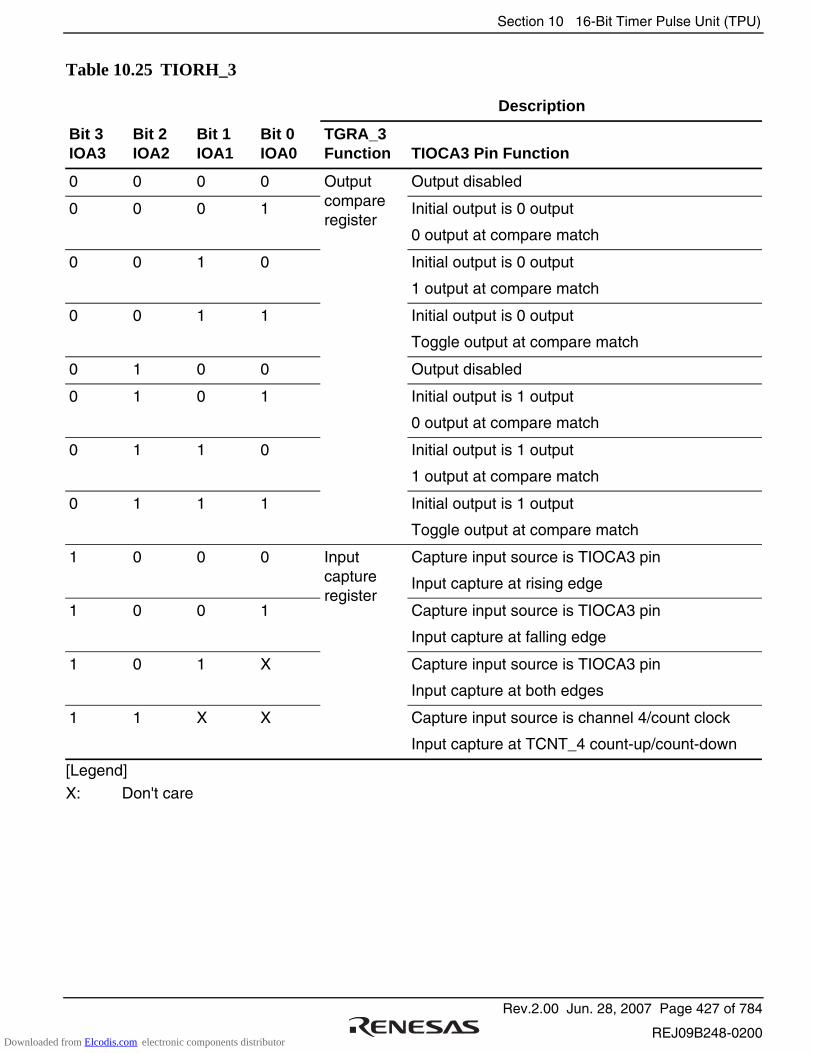
Section 10 16-Bit Timer Pulse Unit (TPU)
Rev.2.00 Jun. 28, 2007 Page 427 of 784
REJ09B248-0200
Table 10.25 TIORH_3
Description
Bit 3 IOA3
Bit 2 IOA2
Bit 1 IOA1
Bit 0 IOA0
TGRA_3 Function TIOCA3 Pin Function
0 0 0 0 Output disabled
0 0 0 1 Initial output is 0 output
0 output at compare match
0 0 1 0 Initial output is 0 output
1 output at compare match
0 0 1 1 Initial output is 0 output
Toggle output at compare match
0 1 0 0 Output disabled
0 1 0 1 Initial output is 1 output
0 output at compare match
0 1 1 0 Initial output is 1 output
1 output at compare match
0 1 1 1
Output compare register
Initial output is 1 output
Toggle output at compare match
1 0 0 0 Capture input source is TIOCA3 pin
Input capture at rising edge
1 0 0 1 Capture input source is TIOCA3 pin
Input capture at falling edge
1 0 1 X Capture input source is TIOCA3 pin
Input capture at both edges
1 1 X X
Input capture register
Capture input source is channel 4/count clock
Input capture at TCNT_4 count-up/count-down
[Legend]
X: Don't care
Downloaded from Elcodis.com electronic components distributor

Section 10 16-Bit Timer Pulse Unit (TPU)
Rev.2.00 Jun. 28, 2007 Page 428 of 784
REJ09B248-0200
Table 10.26 TIORL_3
Description
Bit 3 IOC3
Bit 2 IOC2
Bit 1 IOC1
Bit 0 IOC0
TGRC_3 Function TIOCC3 Pin Function
0 0 0 0 Output disabled
0 0 0 1 Initial output is 0 output
0 output at compare match
0 0 1 0 Initial output is 0 output
1 output at compare match
0 0 1 1 Initial output is 0 output
Toggle output at compare match
0 1 0 0 Output disabled
0 1 0 1 Initial output is 1 output
0 output at compare match
0 1 1 0 Initial output is 1 output
1 output at compare match
0 1 1 1
Output compare register*
Initial output is 1 output
Toggle output at compare match
1 0 0 0 Capture input source is TIOCC3 pin
Input capture at rising edge
1 0 0 1 Capture input source is TIOCC3 pin
Input capture at falling edge
1 0 1 X Capture input source is TIOCC3 pin
Input capture at both edges
1 1 X X
Input capture register*
Capture input source is channel 4/count clock
Input capture at TCNT_4 count-up/count-down
[Legend]
X: Don't care Note: * When the BFA bit in TMDR_3 is set to 1 and TGRC_3 is used as a buffer register, this
setting is invalid and input capture/output compare is not generated.
Downloaded from Elcodis.com electronic components distributor

Section 10 16-Bit Timer Pulse Unit (TPU)
Rev.2.00 Jun. 28, 2007 Page 429 of 784
REJ09B248-0200
Table 10.27 TIOR_4
Description
Bit 3 IOA3
Bit 2 IOA2
Bit 1 IOA1
Bit 0 IOA0
TGRA_4 Function TIOCA4 Pin Function
0 0 0 0 Output disabled
0 0 0 1 Initial output is 0 output
0 output at compare match
0 0 1 0 Initial output is 0 output
1 output at compare match
0 0 1 1 Initial output is 0 output
Toggle output at compare match
0 1 0 0 Output disabled
0 1 0 1 Initial output is 1 output
0 output at compare match
0 1 1 0 Initial output is 1 output
1 output at compare match
0 1 1 1
Output compare register
Initial output is 1 output
Toggle output at compare match
1 0 0 0 Capture input source is TIOCA4 pin
Input capture at rising edge
1 0 0 1 Capture input source is TIOCA4 pin
Input capture at falling edge
1 0 1 X Capture input source is TIOCA4 pin
Input capture at both edges
1 1 X X
Input capture register
Capture input source is TGRA_3 compare match/input capture
Input capture at generation of TGRA_3 compare match/input capture
[Legend] X: Don't care
Downloaded from Elcodis.com electronic components distributor

Section 10 16-Bit Timer Pulse Unit (TPU)
Rev.2.00 Jun. 28, 2007 Page 430 of 784
REJ09B248-0200
Table 10.28 TIOR_5
Description
Bit 3 IOA3
Bit 2 IOA2
Bit 1 IOA1
Bit 0 IOA0
TGRA_5 Function TIOCA5 Pin Function
0 0 0 0 Output disabled
0 0 0 1 Initial output is 0 output
0 output at compare match
0 0 1 0 Initial output is 0 output
1 output at compare match
0 0 1 1 Initial output is 0 output
Toggle output at compare match
0 1 0 0 Output disabled
0 1 0 1 Initial output is 1 output
0 output at compare match
0 1 1 0 Initial output is 1 output
1 output at compare match
0 1 1 1
Output compare register
Initial output is 1 output
Toggle output at compare match
1 X 0 0 Input capture source is TIOCA5 pin
Input capture at rising edge
1 X 0 1 Input capture source is TIOCA5 pin
Input capture at falling edge
1 X 1 X
Input capture register
Input capture source is TIOCA5 pin
Input capture at both edges
[Legend] X: Don't care
Downloaded from Elcodis.com electronic components distributor
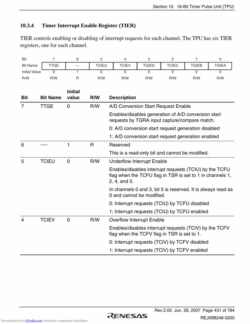
Section 10 16-Bit Timer Pulse Unit (TPU)
Rev.2.00 Jun. 28, 2007 Page 431 of 784
REJ09B248-0200
10.3.4 Timer Interrupt Enable Register (TIER)
TIER controls enabling or disabling of interrupt requests for each channel. The TPU has six TIER registers, one for each channel.
Bit
Bit Name
Initial Value
R/W
7
TTGE
0
R/W
6
1
R
5
TCIEU
0
R/W
4
TCIEV
0
R/W
3
TGIED
0
R/W
2
TCIEC
0
R/W
1
TGIEB
0
R/W
0
TGIEA
0
R/W
Bit Bit Name Initial value R/W Description
7 TTGE 0 R/W A/D Conversion Start Request Enable
Enables/disables generation of A/D conversion start requests by TGRA input capture/compare match.
0: A/D conversion start request generation disabled
1: A/D conversion start request generation enabled
6 1 R Reserved
This is a read-only bit and cannot be modified.
5 TCIEU 0 R/W Underflow Interrupt Enable
Enables/disables interrupt requests (TCIU) by the TCFU flag when the TCFU flag in TSR is set to 1 in channels 1, 2, 4, and 5.
In channels 0 and 3, bit 5 is reserved. It is always read as 0 and cannot be modified.
0: Interrupt requests (TCIU) by TCFU disabled
1: Interrupt requests (TCIU) by TCFU enabled
4 TCIEV 0 R/W Overflow Interrupt Enable
Enables/disables interrupt requests (TCIV) by the TCFV flag when the TCFV flag in TSR is set to 1.
0: Interrupt requests (TCIV) by TCFV disabled
1: Interrupt requests (TCIV) by TCFV enabled
Downloaded from Elcodis.com electronic components distributor
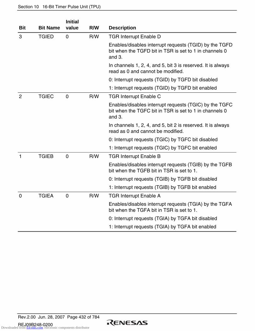
Section 10 16-Bit Timer Pulse Unit (TPU)
Rev.2.00 Jun. 28, 2007 Page 432 of 784
REJ09B248-0200
Bit Bit Name Initial value R/W Description
3 TGIED 0 R/W TGR Interrupt Enable D
Enables/disables interrupt requests (TGID) by the TGFD bit when the TGFD bit in TSR is set to 1 in channels 0 and 3.
In channels 1, 2, 4, and 5, bit 3 is reserved. It is always read as 0 and cannot be modified.
0: Interrupt requests (TGID) by TGFD bit disabled
1: Interrupt requests (TGID) by TGFD bit enabled
2 TGIEC 0 R/W TGR Interrupt Enable C
Enables/disables interrupt requests (TGIC) by the TGFC bit when the TGFC bit in TSR is set to 1 in channels 0 and 3.
In channels 1, 2, 4, and 5, bit 2 is reserved. It is always read as 0 and cannot be modified.
0: Interrupt requests (TGIC) by TGFC bit disabled
1: Interrupt requests (TGIC) by TGFC bit enabled
1 TGIEB 0 R/W TGR Interrupt Enable B
Enables/disables interrupt requests (TGIB) by the TGFB bit when the TGFB bit in TSR is set to 1.
0: Interrupt requests (TGIB) by TGFB bit disabled
1: Interrupt requests (TGIB) by TGFB bit enabled
0 TGIEA 0 R/W TGR Interrupt Enable A
Enables/disables interrupt requests (TGIA) by the TGFA bit when the TGFA bit in TSR is set to 1.
0: Interrupt requests (TGIA) by TGFA bit disabled
1: Interrupt requests (TGIA) by TGFA bit enabled
Downloaded from Elcodis.com electronic components distributor

Section 10 16-Bit Timer Pulse Unit (TPU)
Rev.2.00 Jun. 28, 2007 Page 433 of 784
REJ09B248-0200
10.3.5 Timer Status Register (TSR)
TSR indicates the status of each channel. The TPU has six TSR registers, one for each channel.
Bit
Bit Name
Initial Value
R/W
7
TCFD
1
R
6
1
R
5
TCFU
0
R/(W)*
4
TCFV
0
R/(W)*
3
TGFD
0
R/(W)*
2
TGFC
0
R/(W)*
1
TGFB
0
R/(W)*
0
TGFA
0
R/(W)*
Note: * Only 0 can be written to bits 5 to 0, to clear flags.
Bit Bit Name Initial value R/W Description
7 TCFD 1 R Count Direction Flag
Status flag that shows the direction in which TCNT counts in channels 1, 2, 4, and 5.
In channels 0 and 3, bit 7 is reserved. It is always read as 1 and cannot be modified.
0: TCNT counts down
1: TCNT counts up
6 1 R Reserved
This is a read-only bit and cannot be modified.
5 TCFU 0 R/(W)* Underflow Flag
Status flag that indicates that a TCNT underflow has occurred when channels 1, 2, 4, and 5 are set to phase counting mode.
In channels 0 and 3, bit 5 is reserved. It is always read as 0 and cannot be modified.
[Setting condition]
When the TCNT value underflows (changes from H'0000 to H'FFFF)
[Clearing condition]
When a 0 is written to TCFU after reading TCFU = 1
(When the CPU is used to clear this flag by writing 0 while the corresponding interrupt is enabled, be sure to read the flag after writing 0 to it.)
Downloaded from Elcodis.com electronic components distributor
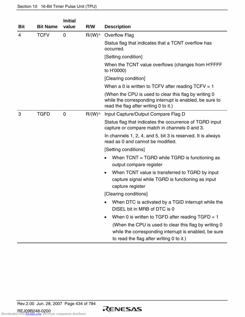
Section 10 16-Bit Timer Pulse Unit (TPU)
Rev.2.00 Jun. 28, 2007 Page 434 of 784
REJ09B248-0200
Bit Bit Name Initial value R/W Description
4 TCFV 0 R/(W)* Overflow Flag
Status flag that indicates that a TCNT overflow has occurred.
[Setting condition]
When the TCNT value overflows (changes from H'FFFF to H'0000)
[Clearing condition]
When a 0 is written to TCFV after reading TCFV = 1
(When the CPU is used to clear this flag by writing 0 while the corresponding interrupt is enabled, be sure to read the flag after writing 0 to it.)
3 TGFD 0 R/(W)* Input Capture/Output Compare Flag D
Status flag that indicates the occurrence of TGRD input capture or compare match in channels 0 and 3.
In channels 1, 2, 4, and 5, bit 3 is reserved. It is always read as 0 and cannot be modified.
[Setting conditions]
• When TCNT = TGRD while TGRD is functioning as
output compare register
• When TCNT value is transferred to TGRD by input capture signal while TGRD is functioning as input
capture register
[Clearing conditions]
• When DTC is activated by a TGID interrupt while the
DISEL bit in MRB of DTC is 0
• When 0 is written to TGFD after reading TGFD = 1
(When the CPU is used to clear this flag by writing 0 while the corresponding interrupt is enabled, be sure
to read the flag after writing 0 to it.)
Downloaded from Elcodis.com electronic components distributor

Section 10 16-Bit Timer Pulse Unit (TPU)
Rev.2.00 Jun. 28, 2007 Page 435 of 784
REJ09B248-0200
Bit Bit Name Initial value R/W Description
2 TGFC 0 R/(W)* Input Capture/Output Compare Flag C
Status flag that indicates the occurrence of TGRC input capture or compare match in channels 0 and 3.
In channels 1, 2, 4, and 5, bit 2 is reserved. It is always read as 0 and cannot be modified.
[Setting conditions]
• When TCNT = TGRC while TGRC is functioning as
output compare register
• When TCNT value is transferred to TGRC by input
capture signal while TGRC is functioning as input
capture register
[Clearing conditions]
• When DTC is activated by a TGIC interrupt while the
DISEL bit in MRB of DTC is 0
• When 0 is written to TGFC after reading TGFC = 1
(When the CPU is used to clear this flag by writing 0
while the corresponding interrupt is enabled, be sure
to read the flag after writing 0 to it.)
1 TGFB 0 R/(W)* Input Capture/Output Compare Flag B
Status flag that indicates the occurrence of TGRB input capture or compare match.
[Setting conditions]
• When TCNT = TGRB while TGRB is functioning as output compare register
• When TCNT value is transferred to TGRB by input capture signal while TGRB is functioning as input capture register
[Clearing conditions]
• When DTC is activated by a TGIB interrupt while the DISEL bit in MRB of DTC is 0
• When 0 is written to TGFB after reading TGFB = 1
(When the CPU is used to clear this flag by writing 0 while the corresponding interrupt is enabled, be sure to read the flag after writing 0 to it.)
Downloaded from Elcodis.com electronic components distributor
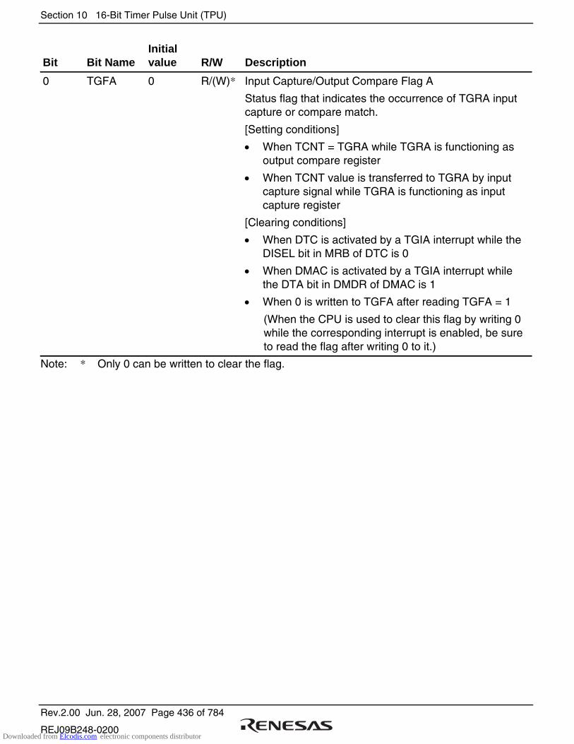
Section 10 16-Bit Timer Pulse Unit (TPU)
Rev.2.00 Jun. 28, 2007 Page 436 of 784
REJ09B248-0200
Bit Bit Name Initial value R/W Description
0 TGFA 0 R/(W)* Input Capture/Output Compare Flag A
Status flag that indicates the occurrence of TGRA input capture or compare match.
[Setting conditions]
• When TCNT = TGRA while TGRA is functioning as output compare register
• When TCNT value is transferred to TGRA by input capture signal while TGRA is functioning as input capture register
[Clearing conditions]
• When DTC is activated by a TGIA interrupt while the DISEL bit in MRB of DTC is 0
• When DMAC is activated by a TGIA interrupt while the DTA bit in DMDR of DMAC is 1
• When 0 is written to TGFA after reading TGFA = 1
(When the CPU is used to clear this flag by writing 0 while the corresponding interrupt is enabled, be sure to read the flag after writing 0 to it.)
Note: * Only 0 can be written to clear the flag.
Downloaded from Elcodis.com electronic components distributor

Section 10 16-Bit Timer Pulse Unit (TPU)
Rev.2.00 Jun. 28, 2007 Page 437 of 784
REJ09B248-0200
10.3.6 Timer Counter (TCNT)
TCNT is a 16-bit readable/writable counter. The TPU has six TCNT counters, one for each channel.
TCNT is initialized to H'0000 by a reset or in hardware standby mode.
TCNT cannot be accessed in 8-bit units. TCNT must always be accessed in 16-bit units.
Bit
Bit Name
Initial Value
R/W
15
0
R/W
14
0
R/W
13
0
R/W
12
0
R/W
11
0
R/W
10
0
R/W
9
0
R/W
8
0
R/W
Bit
Bit Name
Initial Value
R/W
7
0
R/W
6
0
R/W
5
0
R/W
4
0
R/W
3
0
R/W
2
0
R/W
1
0
R/W
0
0
R/W
10.3.7 Timer General Register (TGR)
TGR is a 16-bit readable/writable register with a dual function as output compare and input capture registers. The TPU has 16 TGR registers, four each for channels 0 and 3 and two each for channels 1, 2, 4, and 5. TGRC and TGRD for channels 0 and 3 can also be designated for operation as buffer registers. The TGR registers cannot be accessed in 8-bit units; they must always be accessed in 16-bit units. TGR and buffer register combinations during buffer operations are TGRA−TGRC and TGRB−TGRD.
Bit
Bit Name
Initial Value
R/W
15
1
R/W
14
1
R/W
13
1
R/W
12
1
R/W
11
1
R/W
10
1
R/W
9
1
R/W
8
1
R/W
Bit
Bit Name
Initial Value
R/W
7
1
R/W
6
1
R/W
5
1
R/W
4
1
R/W
3
1
R/W
2
1
R/W
1
1
R/W
0
1
R/W
Downloaded from Elcodis.com electronic components distributor
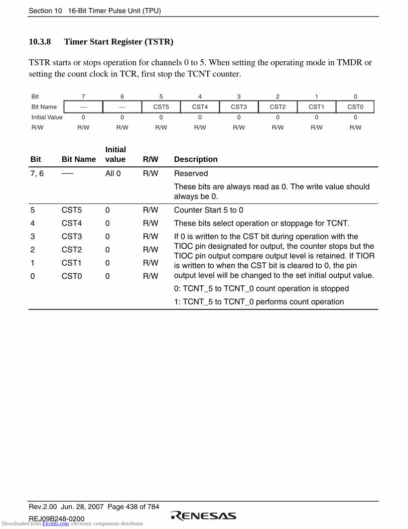
Section 10 16-Bit Timer Pulse Unit (TPU)
Rev.2.00 Jun. 28, 2007 Page 438 of 784
REJ09B248-0200
10.3.8 Timer Start Register (TSTR)
TSTR starts or stops operation for channels 0 to 5. When setting the operating mode in TMDR or setting the count clock in TCR, first stop the TCNT counter.
7
0
R/W
6
0
R/W
5
CST5
0
R/W
4
CST4
0
R/W
3
CST3
0
R/W
2
CST2
0
R/W
1
CST1
0
R/W
0
CST0
0
R/W
Bit
Bit Name
Initial Value
R/W
Bit Bit Name Initial value R/W Description
7, 6 All 0 R/W Reserved
These bits are always read as 0. The write value should always be 0.
5
4
3
2
1
0
CST5
CST4
CST3
CST2
CST1
CST0
0
0
0
0
0
0
R/W
R/W
R/W
R/W
R/W
R/W
Counter Start 5 to 0
These bits select operation or stoppage for TCNT.
If 0 is written to the CST bit during operation with the TIOC pin designated for output, the counter stops but the TIOC pin output compare output level is retained. If TIOR is written to when the CST bit is cleared to 0, the pin output level will be changed to the set initial output value.
0: TCNT_5 to TCNT_0 count operation is stopped
1: TCNT_5 to TCNT_0 performs count operation
Downloaded from Elcodis.com electronic components distributor

Section 10 16-Bit Timer Pulse Unit (TPU)
Rev.2.00 Jun. 28, 2007 Page 439 of 784
REJ09B248-0200
10.3.9 Timer Synchronous Register (TSYR)
TSYR selects independent operation or synchronous operation for the TCNT counters of channels 0 to 5. A channel performs synchronous operation when the corresponding bit in TSYR is set to 1.
7
0
R/W
6
0
R/W
5
SYNC5
0
R/W
4
SYNC4
0
R/W
3
SYNC3
0
R/W
2
SYNC2
0
R/W
1
SYNC1
0
R/W
0
SYNC0
0
R/W
Bit
Bit Name
Initial Value
R/W
Bit Bit Name Initial value R/W Description
7, 6 All 0 R/W Reserved
These bits are always read as 0. The write value should always be 0.
5
4
3
2
1
0
SYNC5
SYNC4
SYNC3
SYNC2
SYNC1
SYNC0
0
0
0
0
0
0
R/W
R/W
R/W
R/W
R/W
R/W
Timer Synchronization 5 to 0
These bits select whether operation is independent of or synchronized with other channels.
When synchronous operation is selected, synchronous presetting of multiple channels, and synchronous clearing through counter clearing on another channel are possible.
To set synchronous operation, the SYNC bits for at least two channels must be set to 1. To set synchronous clearing, in addition to the SYNC bit, the TCNT clearing source must also be set by means of bits CCLR2 to CCLR0 in TCR.
0: TCNT_5 to TCNT_0 operate independently (TCNT presetting/clearing is unrelated to other channels)
1: TCNT_5 to TCNT_0 perform synchronous operation (TCNT synchronous presetting/synchronous clearing is possible)
Downloaded from Elcodis.com electronic components distributor
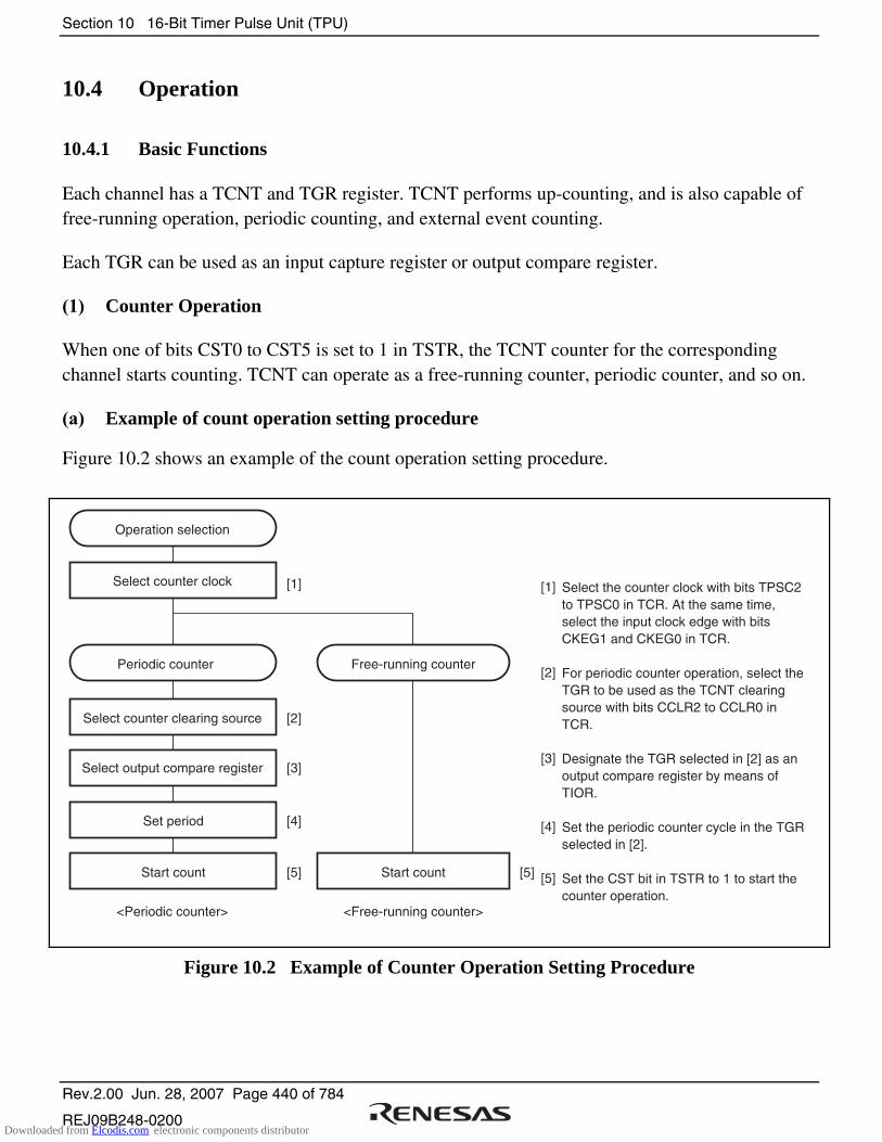
Section 10 16-Bit Timer Pulse Unit (TPU)
Rev.2.00 Jun. 28, 2007 Page 440 of 784
REJ09B248-0200
10.4 Operation
10.4.1 Basic Functions
Each channel has a TCNT and TGR register. TCNT performs up-counting, and is also capable of free-running operation, periodic counting, and external event counting.
Each TGR can be used as an input capture register or output compare register.
(1) Counter Operation
When one of bits CST0 to CST5 is set to 1 in TSTR, the TCNT counter for the corresponding channel starts counting. TCNT can operate as a free-running counter, periodic counter, and so on.
(a) Example of count operation setting procedure
Figure 10.2 shows an example of the count operation setting procedure.
Select counter clock
Operation selection
Select counter clearing source
Periodic counter
Set period
Start count
<Periodic counter>
[1]
[2]
[4]
[3]
[5]
Free-running counter
Start count
<Free-running counter>
[5]
[1]
[2]
[3]
[4]
[5]
Select output compare register
Select the counter clock with bits TPSC2 to TPSC0 in TCR. At the same time, select the input clock edge with bits CKEG1 and CKEG0 in TCR.
For periodic counter operation, select the TGR to be used as the TCNT clearing source with bits CCLR2 to CCLR0 in TCR.
Designate the TGR selected in [2] as an output compare register by means of TIOR.
Set the periodic counter cycle in the TGR selected in [2].
Set the CST bit in TSTR to 1 to start the counter operation.
Figure 10.2 Example of Counter Operation Setting Procedure
Downloaded from Elcodis.com electronic components distributor

Section 10 16-Bit Timer Pulse Unit (TPU)
Rev.2.00 Jun. 28, 2007 Page 441 of 784
REJ09B248-0200
(b) Free-running count operation and periodic count operation
Immediately after a reset, the TPU's TCNT counters are all designated as free-running counters. When the relevant bit in TSTR is set to 1 the corresponding TCNT counter starts up-count operation as a free-running counter. When TCNT overflows (changes from H'FFFF to H'0000), the TCFV bit in TSR is set to 1. If the value of the corresponding TCIEV bit in TIER is 1 at this point, the TPU requests an interrupt. After overflow, TCNT starts counting up again from H'0000.
Figure 10.3 illustrates free-running counter operation.
TCNT value
H'FFFF
H'0000
CST bit
TCFV
Time
Figure 10.3 Free-Running Counter Operation
When compare match is selected as the TCNT clearing source, the TCNT counter for the relevant channel performs periodic count operation. The TGR register for setting the period is designated as an output compare register, and counter clearing by compare match is selected by means of bits CCLR2 to CCLR0 in TCR. After the settings have been made, TCNT starts count-up operation as a periodic counter when the corresponding bit in TSTR is set to 1. When the count value matches the value in TGR, the TGF bit in TSR is set to 1 and TCNT is cleared to H'0000.
If the value of the corresponding TGIE bit in TIER is 1 at this point, the TPU requests an interrupt. After a compare match, TCNT starts counting up again from H'0000.
Downloaded from Elcodis.com electronic components distributor
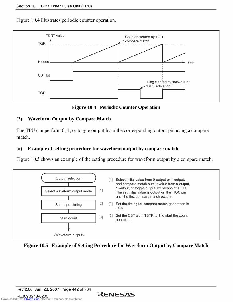
Section 10 16-Bit Timer Pulse Unit (TPU)
Rev.2.00 Jun. 28, 2007 Page 442 of 784
REJ09B248-0200
Figure 10.4 illustrates periodic counter operation.
TCNT value
TGR
H'0000
CST bit
TGF
Time
Counter cleared by TGR compare match
Flag cleared by software orDTC activation
Figure 10.4 Periodic Counter Operation
(2) Waveform Output by Compare Match
The TPU can perform 0, 1, or toggle output from the corresponding output pin using a compare match.
(a) Example of setting procedure for waveform output by compare match
Figure 10.5 shows an example of the setting procedure for waveform output by a compare match.
Select waveform output mode
Output selection
Set output timing
Start count
<Waveform output>
[1]
[2]
[3]
[1] Select initial value from 0-output or 1-output, and compare match output value from 0-output, 1-output, or toggle-output, by means of TIOR. The set initial value is output on the TIOC pin until the first compare match occurs.
[2] Set the timing for compare match generation in TGR.
[3] Set the CST bit in TSTR to 1 to start the count operation.
Figure 10.5 Example of Setting Procedure for Waveform Output by Compare Match
Downloaded from Elcodis.com electronic components distributor
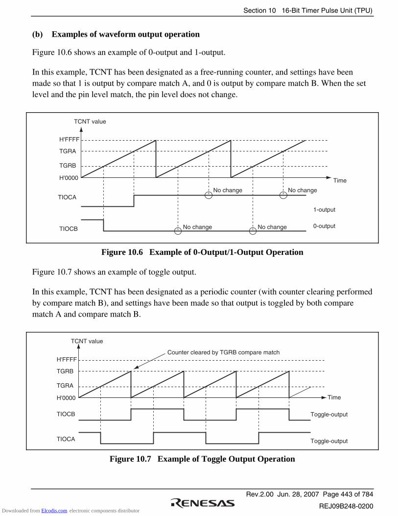
Section 10 16-Bit Timer Pulse Unit (TPU)
Rev.2.00 Jun. 28, 2007 Page 443 of 784
REJ09B248-0200
(b) Examples of waveform output operation
Figure 10.6 shows an example of 0-output and 1-output.
In this example, TCNT has been designated as a free-running counter, and settings have been made so that 1 is output by compare match A, and 0 is output by compare match B. When the set level and the pin level match, the pin level does not change.
TCNT value
H'FFFF
H'0000
TIOCA
TIOCB
Time
TGRA
TGRB
No change No change
No change No change
1-output
0-output
Figure 10.6 Example of 0-Output/1-Output Operation
Figure 10.7 shows an example of toggle output.
In this example, TCNT has been designated as a periodic counter (with counter clearing performed by compare match B), and settings have been made so that output is toggled by both compare match A and compare match B.
TCNT value
H'FFFF
H'0000
TIOCB
TIOCA
Time
TGRB
TGRA
Toggle-output
Toggle-output
Counter cleared by TGRB compare match
Figure 10.7 Example of Toggle Output Operation
Downloaded from Elcodis.com electronic components distributor
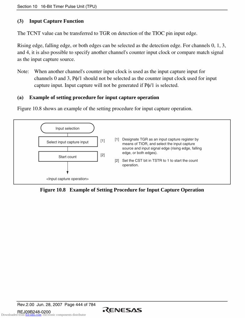
Section 10 16-Bit Timer Pulse Unit (TPU)
Rev.2.00 Jun. 28, 2007 Page 444 of 784
REJ09B248-0200
(3) Input Capture Function
The TCNT value can be transferred to TGR on detection of the TIOC pin input edge.
Rising edge, falling edge, or both edges can be selected as the detection edge. For channels 0, 1, 3, and 4, it is also possible to specify another channel's counter input clock or compare match signal as the input capture source.
Note: When another channel's counter input clock is used as the input capture input for channels 0 and 3, Pφ/1 should not be selected as the counter input clock used for input capture input. Input capture will not be generated if Pφ/1 is selected.
(a) Example of setting procedure for input capture operation
Figure 10.8 shows an example of the setting procedure for input capture operation.
Select input capture input
Input selection
Start count
<Input capture operation>
[1]
[2]
[1] Designate TGR as an input capture register by means of TIOR, and select the input capture
source and input signal edge (rising edge, falling edge, or both edges).
[2] Set the CST bit in TSTR to 1 to start the count operation.
Figure 10.8 Example of Setting Procedure for Input Capture Operation
Downloaded from Elcodis.com electronic components distributor

Section 10 16-Bit Timer Pulse Unit (TPU)
Rev.2.00 Jun. 28, 2007 Page 445 of 784
REJ09B248-0200
(b) Example of input capture operation
Figure 10.9 shows an example of input capture operation.
In this example, both rising and falling edges have been selected as the TIOCA pin input capture input edge, falling edge has been selected as the TIOCB pin input capture input edge, and counter clearing by TGRB input capture has been designated for TCNT.
TCNT value
H'0180
H'0000
TIOCA
TGRA
Time
H'0010
H'0005
Counter cleared by TIOCBinput (falling edge)
H'0160
H'0005 H'0160 H'0010
TGRB H'0180
TIOCB
Figure 10.9 Example of Input Capture Operation
Downloaded from Elcodis.com electronic components distributor
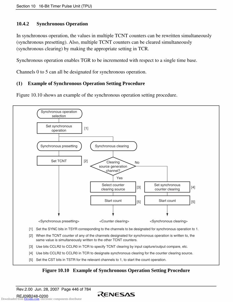
Section 10 16-Bit Timer Pulse Unit (TPU)
Rev.2.00 Jun. 28, 2007 Page 446 of 784
REJ09B248-0200
10.4.2 Synchronous Operation
In synchronous operation, the values in multiple TCNT counters can be rewritten simultaneously (synchronous presetting). Also, multiple TCNT counters can be cleared simultaneously (synchronous clearing) by making the appropriate setting in TCR.
Synchronous operation enables TGR to be incremented with respect to a single time base.
Channels 0 to 5 can all be designated for synchronous operation.
(1) Example of Synchronous Operation Setting Procedure
Figure 10.10 shows an example of the synchronous operation setting procedure.
Synchronous operationselection
Set TCNT
Synchronous presetting
<Synchronous presetting>
[1]
[2]
Synchronous clearing
Select counterclearing source
<Counter clearing>
[3]
Start count [5]
Set synchronouscounter clearing
<Synchronous clearing>
[4]
Start count [5]
Clearingsource generation
channel?
No
Yes
[1] Set the SYNC bits in TSYR corresponding to the channels to be designated for synchronous operation to 1.
[2] When the TCNT counter of any of the channels designated for synchronous operation is written to, the same value is simultaneously written to the other TCNT counters.
[3] Use bits CCLR2 to CCLR0 in TCR to specify TCNT clearing by input capture/output compare, etc.
[4] Use bits CCLR2 to CCLR0 in TCR to designate synchronous clearing for the counter clearing source.
[5] Set the CST bits in TSTR for the relevant channels to 1, to start the count operation.
Set synchronousoperation
Figure 10.10 Example of Synchronous Operation Setting Procedure
Downloaded from Elcodis.com electronic components distributor
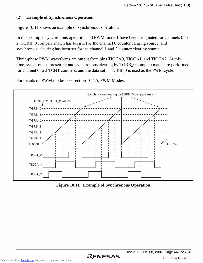
Section 10 16-Bit Timer Pulse Unit (TPU)
Rev.2.00 Jun. 28, 2007 Page 447 of 784
REJ09B248-0200
(2) Example of Synchronous Operation
Figure 10.11 shows an example of synchronous operation.
In this example, synchronous operation and PWM mode 1 have been designated for channels 0 to 2, TGRB_0 compare match has been set as the channel 0 counter clearing source, and synchronous clearing has been set for the channel 1 and 2 counter clearing source.
Three-phase PWM waveforms are output from pins TIOCA0, TIOCA1, and TIOCA2. At this time, synchronous presetting and synchronous clearing by TGRB_0 compare match are performed for channel 0 to 2 TCNT counters, and the data set in TGRB_0 is used as the PWM cycle.
For details on PWM modes, see section 10.4.5, PWM Modes.
TCNT_0 to TCNT_2 values
H'0000
TIOCA_0
TIOCA_1
TGRB_0
Synchronous clearing by TGRB_0 compare match
TGRA_2
TGRA_1
TGRB_2
TGRA_0
TGRB_1
TIOCA_2
Time
Figure 10.11 Example of Synchronous Operation
Downloaded from Elcodis.com electronic components distributor

Section 10 16-Bit Timer Pulse Unit (TPU)
Rev.2.00 Jun. 28, 2007 Page 448 of 784
REJ09B248-0200
10.4.3 Buffer Operation
Buffer operation, provided for channels 0 and 3, enables TGRC and TGRD to be used as buffer registers.
Buffer operation differs depending on whether TGR has been designated as an input capture register or a compare match register.
Table 10.29 shows the register combinations used in buffer operation.
Table 10.29 Register Combinations in Buffer Operation
Channel Timer General Register Buffer Register
TGRA_0 TGRC_0 0
TGRB_0 TGRD_0
TGRA_3 TGRC_3 3
TGRB_3 TGRD_3
• When TGR is an output compare register
When a compare match occurs, the value in the buffer register for the corresponding channel is transferred to the timer general register.
This operation is illustrated in figure 10.12.
Buffer register Timer generalregister TCNTComparator
Compare match signal
Figure 10.12 Compare Match Buffer Operation
Downloaded from Elcodis.com electronic components distributor

Section 10 16-Bit Timer Pulse Unit (TPU)
Rev.2.00 Jun. 28, 2007 Page 449 of 784
REJ09B248-0200
• When TGR is an input capture register
When input capture occurs, the value in TCNT is transferred to TGR and the value previously held in TGR is transferred to the buffer register.
This operation is illustrated in figure 10.13.
Buffer register Timer generalregister
TCNT
Input capturesignal
Figure 10.13 Input Capture Buffer Operation
(1) Example of Buffer Operation Setting Procedure
Figure 10.14 shows an example of the buffer operation setting procedure.
Select TGR function
Buffer operation
Set buffer operation
Start count
<Buffer operation>
[1]
[2]
[3]
[1] Designate TGR as an input capture register or output compare register by means of TIOR.
[2] Designate TGR for buffer operation with bits BFA and BFB in TMDR.
[3] Set the CST bit in TSTR to 1 to start the count operation.
Figure 10.14 Example of Buffer Operation Setting Procedure
Downloaded from Elcodis.com electronic components distributor
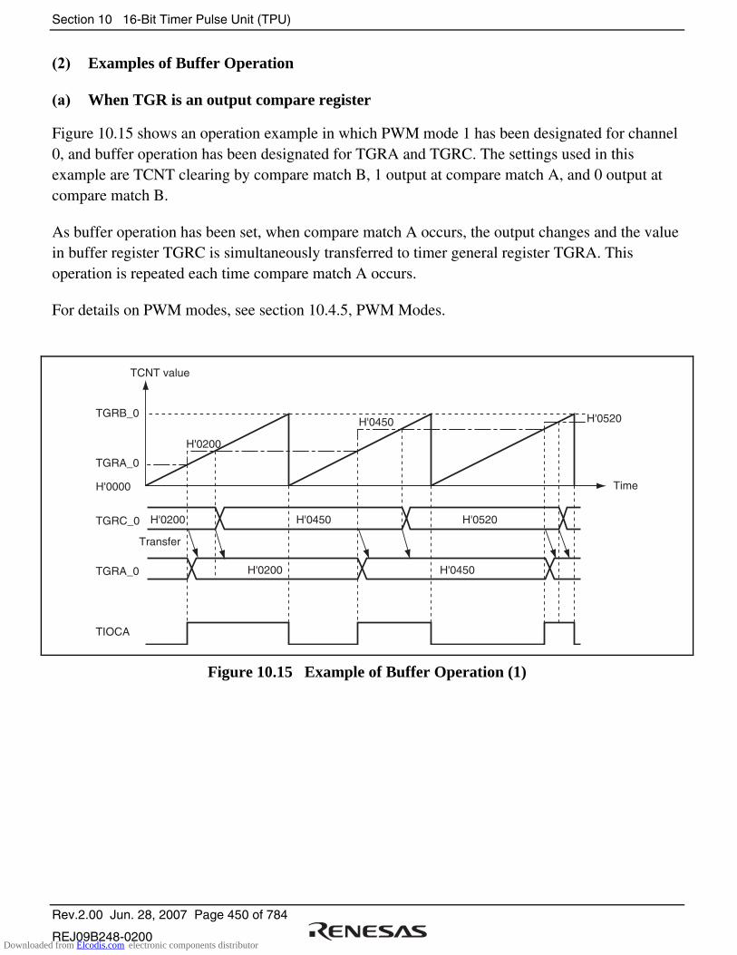
Section 10 16-Bit Timer Pulse Unit (TPU)
Rev.2.00 Jun. 28, 2007 Page 450 of 784
REJ09B248-0200
(2) Examples of Buffer Operation
(a) When TGR is an output compare register
Figure 10.15 shows an operation example in which PWM mode 1 has been designated for channel 0, and buffer operation has been designated for TGRA and TGRC. The settings used in this example are TCNT clearing by compare match B, 1 output at compare match A, and 0 output at compare match B.
As buffer operation has been set, when compare match A occurs, the output changes and the value in buffer register TGRC is simultaneously transferred to timer general register TGRA. This operation is repeated each time compare match A occurs.
For details on PWM modes, see section 10.4.5, PWM Modes.
TCNT value
TGRB_0
H'0000
TGRC_0
TGRA_0
H'0200 H'0520
TIOCA
H'0200
H'0450 H'0520
H'0450
TGRA_0 H'0450H'0200
Transfer
Time
Figure 10.15 Example of Buffer Operation (1)
Downloaded from Elcodis.com electronic components distributor
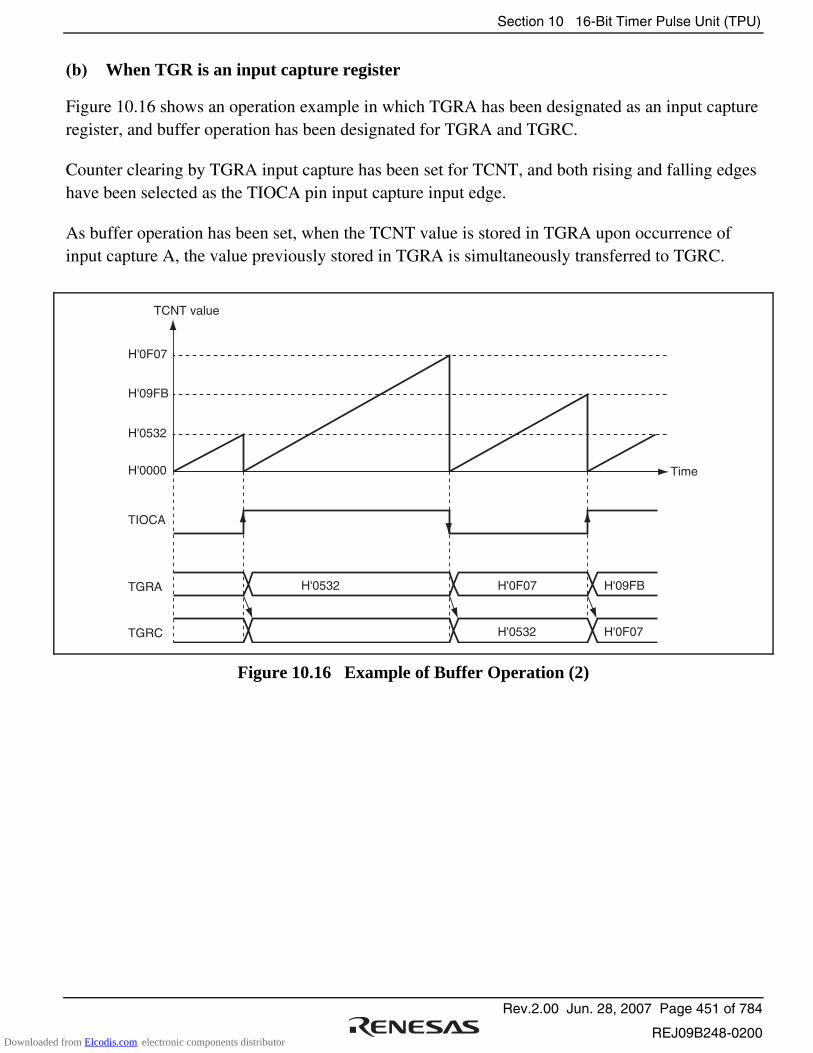
Section 10 16-Bit Timer Pulse Unit (TPU)
Rev.2.00 Jun. 28, 2007 Page 451 of 784
REJ09B248-0200
(b) When TGR is an input capture register
Figure 10.16 shows an operation example in which TGRA has been designated as an input capture register, and buffer operation has been designated for TGRA and TGRC.
Counter clearing by TGRA input capture has been set for TCNT, and both rising and falling edges have been selected as the TIOCA pin input capture input edge.
As buffer operation has been set, when the TCNT value is stored in TGRA upon occurrence of input capture A, the value previously stored in TGRA is simultaneously transferred to TGRC.
TCNT value
H'09FB
H'0000
TGRC
Time
H'0532
TIOCA
TGRA H'0F07H'0532
H'0F07
H'0532
H'0F07
H'09FB
Figure 10.16 Example of Buffer Operation (2)
Downloaded from Elcodis.com electronic components distributor
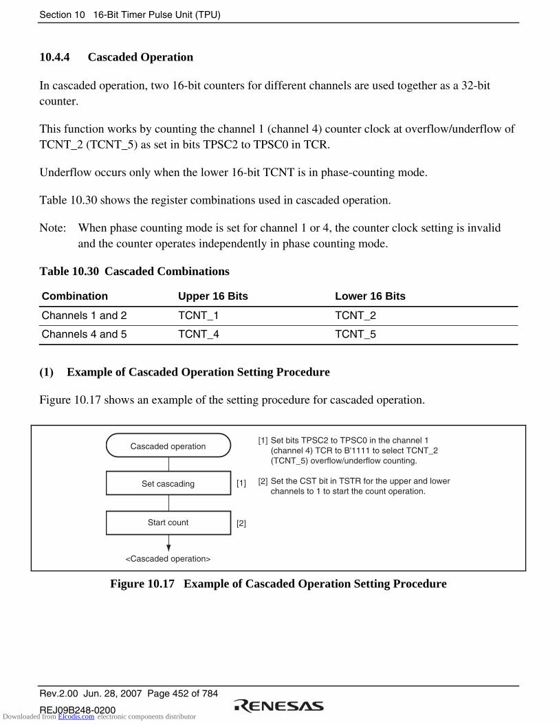
Section 10 16-Bit Timer Pulse Unit (TPU)
Rev.2.00 Jun. 28, 2007 Page 452 of 784
REJ09B248-0200
10.4.4 Cascaded Operation
In cascaded operation, two 16-bit counters for different channels are used together as a 32-bit counter.
This function works by counting the channel 1 (channel 4) counter clock at overflow/underflow of TCNT_2 (TCNT_5) as set in bits TPSC2 to TPSC0 in TCR.
Underflow occurs only when the lower 16-bit TCNT is in phase-counting mode.
Table 10.30 shows the register combinations used in cascaded operation.
Note: When phase counting mode is set for channel 1 or 4, the counter clock setting is invalid and the counter operates independently in phase counting mode.
Table 10.30 Cascaded Combinations
Combination Upper 16 Bits Lower 16 Bits
Channels 1 and 2 TCNT_1 TCNT_2
Channels 4 and 5 TCNT_4 TCNT_5
(1) Example of Cascaded Operation Setting Procedure
Figure 10.17 shows an example of the setting procedure for cascaded operation.
Cascaded operation
Set cascading
Start count
<Cascaded operation>
Set bits TPSC2 to TPSC0 in the channel 1(channel 4) TCR to B'1111 to select TCNT_2(TCNT_5) overflow/underflow counting.
Set the CST bit in TSTR for the upper and lowerchannels to 1 to start the count operation.
[1]
[2]
[1]
[2]
Figure 10.17 Example of Cascaded Operation Setting Procedure
Downloaded from Elcodis.com electronic components distributor
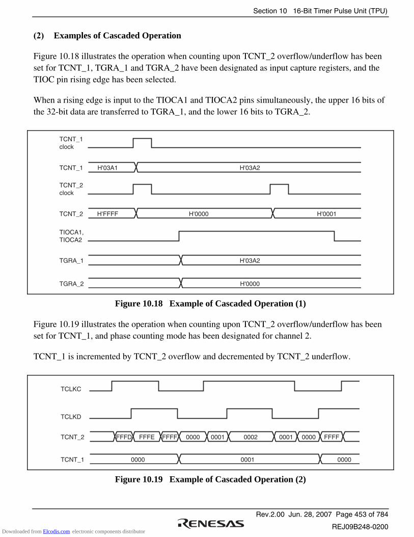
Section 10 16-Bit Timer Pulse Unit (TPU)
Rev.2.00 Jun. 28, 2007 Page 453 of 784
REJ09B248-0200
(2) Examples of Cascaded Operation
Figure 10.18 illustrates the operation when counting upon TCNT_2 overflow/underflow has been set for TCNT_1, TGRA_1 and TGRA_2 have been designated as input capture registers, and the TIOC pin rising edge has been selected.
When a rising edge is input to the TIOCA1 and TIOCA2 pins simultaneously, the upper 16 bits of the 32-bit data are transferred to TGRA_1, and the lower 16 bits to TGRA_2.
TCNT_2clock
TCNT_2 H'FFFF H'0000 H'0001
TIOCA1,TIOCA2
TGRA_1 H'03A2
TGRA_2 H'0000
TCNT_1clock
TCNT_1 H'03A1 H'03A2
Figure 10.18 Example of Cascaded Operation (1)
Figure 10.19 illustrates the operation when counting upon TCNT_2 overflow/underflow has been set for TCNT_1, and phase counting mode has been designated for channel 2.
TCNT_1 is incremented by TCNT_2 overflow and decremented by TCNT_2 underflow.
TCLKC
TCNT_2 FFFD
TCNT_1 0001
TCLKD
FFFE FFFF 0000 0001 0002 0001 0000 FFFF
0000 0000
Figure 10.19 Example of Cascaded Operation (2)
Downloaded from Elcodis.com electronic components distributor
Section 10 16-Bit Timer Pulse Unit (TPU)
Rev.2.00 Jun. 28, 2007 Page 454 of 784
REJ09B248-0200
10.4.5 PWM Modes
In PWM mode, PWM waveforms are output from the output pins. 0-, 1-, or toggle-output can be selected as the output level in response to compare match of each TGR.
Settings of TGR registers can output a PWM waveform in the range of 0% to 100% duty cycle.
Designating TGR compare match as the counter clearing source enables the cycle to be set in that register. All channels can be designated for PWM mode independently. Synchronous operation is also possible.
There are two PWM modes, as described below.
(a) PWM mode 1
PWM output is generated from the TIOCA and TIOCC pins by pairing TGRA with TGRB and TGRC with TGRD. The outputs specified by bits IOA3 to IOA0 and IOC3 to IOC0 in TIOR are output from the TIOCA and TIOCC pins at compare matches A and C, respectively. The outputs specified by bits IOB3 to IOB0 and IOD3 to IOD0 in TIOR are output at compare matches B and D, respectively. The initial output value is the value set in TGRA or TGRC. If the set values of paired TGRs are identical, the output value does not change when a compare match occurs.
In PWM mode 1, a maximum 8-phase PWM output is possible.
(b) PWM mode 2
PWM output is generated using one TGR as the cycle register and the others as duty cycle registers. The output specified in TIOR is performed by means of compare matches. Upon counter clearing by a cycle register compare match, the output value of each pin is the initial value set in TIOR. If the set values of the cycle and duty cycle registers are identical, the output value does not change when a compare match occurs.
In PWM mode 2, a maximum 15-phase PWM output is possible by combined use with synchronous operation.
Downloaded from Elcodis.com electronic components distributor
Section 10 16-Bit Timer Pulse Unit (TPU)
Rev.2.00 Jun. 28, 2007 Page 455 of 784
REJ09B248-0200
The correspondence between PWM output pins and registers is shown in table 10.31.
Table 10.31 PWM Output Registers and Output Pins
Output Pins
Channel Registers PWM Mode 1 PWM Mode 2
TGRA_0 TIOCA0
TGRB_0
TIOCA0
TIOCB0
TGRC_0 TIOCC0
0
TGRD_0
TIOCC0
TIOCD0
TGRA_1 TIOCA1 1
TGRB_1
TIOCA1
TIOCB1
TGRA_2 TIOCA2 2
TGRB_2
TIOCA2
TIOCB2
TGRA_3 TIOCA3
TGRB_3
TIOCA3
TIOCB3
TGRC_3 TIOCC3
3
TGRD_3
TIOCC3
TIOCD3
TGRA_4 TIOCA4 4
TGRB_4
TIOCA4
TIOCB4
TGRA_5 TIOCA5 5
TGRB_5
TIOCA5
TIOCB5
Note: In PWM mode 2, PWM output is not possible for the TGR register in which the cycle is set.
Downloaded from Elcodis.com electronic components distributor
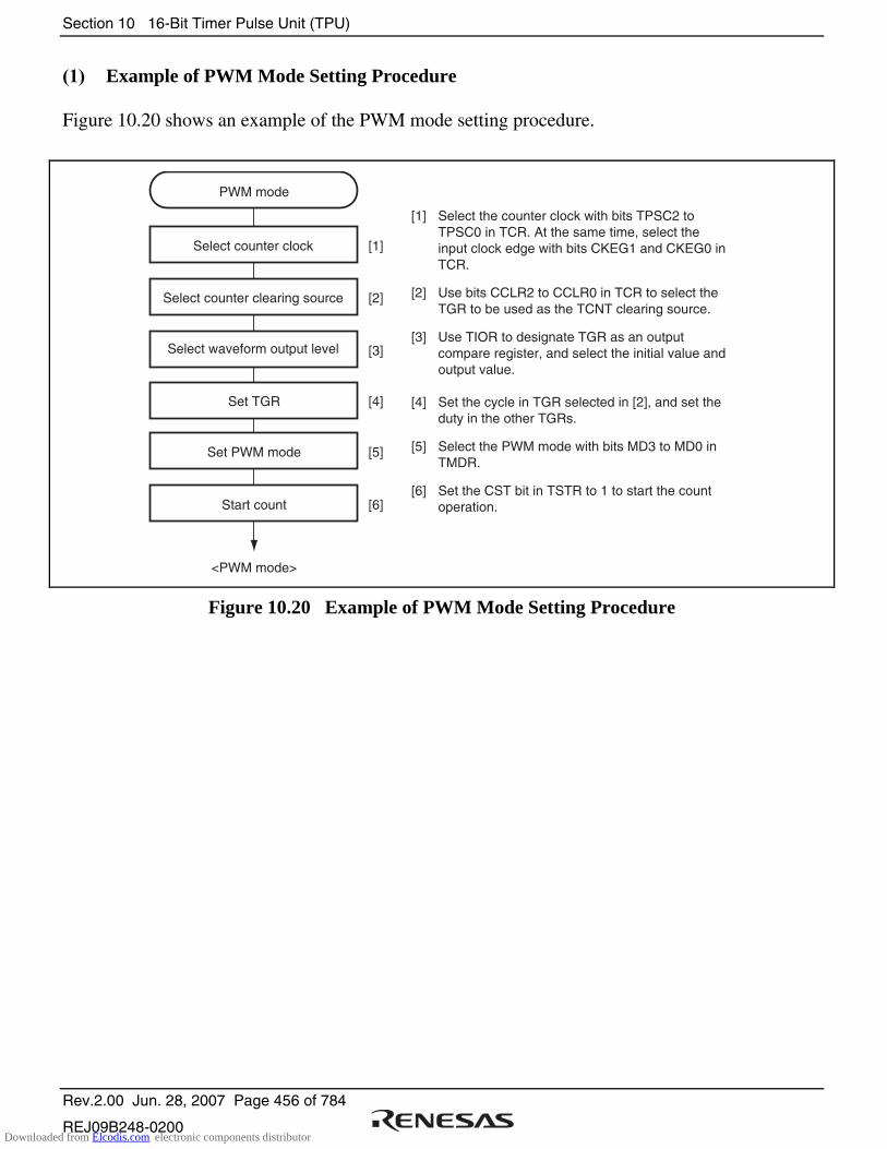
Section 10 16-Bit Timer Pulse Unit (TPU)
Rev.2.00 Jun. 28, 2007 Page 456 of 784
REJ09B248-0200
(1) Example of PWM Mode Setting Procedure
Figure 10.20 shows an example of the PWM mode setting procedure.
Select counter clock
PWM mode
Select counter clearing source
Select waveform output level
<PWM mode>
[1]
[2]
[3]
Set TGR [4]
Set PWM mode [5]
Start count [6]
[1] Select the counter clock with bits TPSC2 to TPSC0 in TCR. At the same time, select the input clock edge with bits CKEG1 and CKEG0 in TCR.
[2] Use bits CCLR2 to CCLR0 in TCR to select the TGR to be used as the TCNT clearing source.
[3] Use TIOR to designate TGR as an output compare register, and select the initial value and output value.
[4] Set the cycle in TGR selected in [2], and set the duty in the other TGRs.
[5] Select the PWM mode with bits MD3 to MD0 in TMDR.
[6] Set the CST bit in TSTR to 1 to start the count operation.
Figure 10.20 Example of PWM Mode Setting Procedure
Downloaded from Elcodis.com electronic components distributor

Section 10 16-Bit Timer Pulse Unit (TPU)
Rev.2.00 Jun. 28, 2007 Page 457 of 784
REJ09B248-0200
(2) Examples of PWM Mode Operation
Figure 10.21 shows an example of PWM mode 1 operation.
In this example, TGRA compare match is set as the TCNT clearing source, 0 is set for the TGRA initial output value and output value, and 1 is set as the TGRB output value.
In this case, the value set in TGRA is used as the cycle, and the value set in TGRB register as the duty cycle.
TCNT value
TGRA
H'0000
TIOCA
Time
TGRB
Counter cleared byTGRA compare match
Figure 10.21 Example of PWM Mode Operation (1)
Downloaded from Elcodis.com electronic components distributor

Section 10 16-Bit Timer Pulse Unit (TPU)
Rev.2.00 Jun. 28, 2007 Page 458 of 784
REJ09B248-0200
Figure 10.22 shows an example of PWM mode 2 operation.
In this example, synchronous operation is designated for channels 0 and 1, TGRB_1 compare match is set as the TCNT clearing source, and 0 is set for the initial output value and 1 for the output value of the other TGR registers (TGRA_0 to TGRD_0, TGRA_1), to output a 5-phase PWM waveform.
In this case, the value set in TGRB_1 is used as the cycle, and the values set in the other TGRs as the duty cycle.
TCNT value
TGRB_1
H'0000
TIOCA0
Counter cleared byTGRB_1 compare match
Time
TGRA_1TGRD_0TGRC_0TGRB_0TGRA_0
TIOCB0
TIOCC0
TIOCD0
TIOCA1
Figure 10.22 Example of PWM Mode Operation (2)
Downloaded from Elcodis.com electronic components distributor
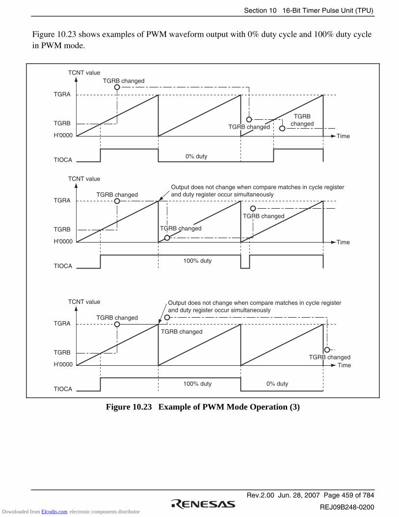
Section 10 16-Bit Timer Pulse Unit (TPU)
Rev.2.00 Jun. 28, 2007 Page 459 of 784
REJ09B248-0200
Figure 10.23 shows examples of PWM waveform output with 0% duty cycle and 100% duty cycle in PWM mode.
TCNT value
TGRA
H'0000
TIOCA
Time
TGRB
0% duty
TGRB changed
TGRBchangedTGRB changed
TCNT value
TGRA
H'0000
TIOCA
Time
TGRB
100% duty
TGRB changed
TGRB changed
TGRB changed
Output does not change when compare matches in cycle registerand duty register occur simultaneously
TCNT value
TGRA
H'0000
TIOCA
Time
TGRB
100% duty
TGRB changed
TGRB changed
TGRB changed
Output does not change when compare matches in cycle registerand duty register occur simultaneously
0% duty
Figure 10.23 Example of PWM Mode Operation (3)
Downloaded from Elcodis.com electronic components distributor

Section 10 16-Bit Timer Pulse Unit (TPU)
Rev.2.00 Jun. 28, 2007 Page 460 of 784
REJ09B248-0200
10.4.6 Phase Counting Mode
In phase counting mode, the phase difference between two external clock inputs is detected and TCNT is incremented/decremented accordingly. This mode can be set for channels 1, 2, 4, and 5.
When phase counting mode is set, an external clock is selected as the counter input clock and TCNT operates as an up/down-counter regardless of the setting of bits TPSC2 to TPSC0 and bits CKEG1 and CKEG0 in TCR. However, the functions of bits CCLR1 and CCLR0 in TCR, and of TIOR, TIER, and TGR are valid, and input capture/compare match and interrupt functions can be used.
This can be used for two-phase encoder pulse input.
When overflow occurs while TCNT is counting up, the TCFV flag in TSR is set; when underflow occurs while TCNT is counting down, the TCFU flag is set.
The TCFD bit in TSR is the count direction flag. Reading the TCFD flag provides an indication of whether TCNT is counting up or down.
Table 10.32 shows the correspondence between external clock pins and channels.
Table 10.32 Clock Input Pins in Phase Counting Mode
External Clock Pins
Channels A-Phase B-Phase
When channel 1 or 5 is set to phase counting mode TCLKA TCLKB
When channel 2 or 4 is set to phase counting mode TCLKC TCLKD
(1) Example of Phase Counting Mode Setting Procedure
Figure 10.24 shows an example of the phase counting mode setting procedure.
Phase counting mode
Select phase counting mode
Start count
<Phase counting mode>
Select phase counting mode with bits MD3 toMD0 in TMDR.
Set the CST bit in TSTR to 1 to start the countoperation.
[1]
[2]
[1]
[2]
Figure 10.24 Example of Phase Counting Mode Setting Procedure
Downloaded from Elcodis.com electronic components distributor

Section 10 16-Bit Timer Pulse Unit (TPU)
Rev.2.00 Jun. 28, 2007 Page 461 of 784
REJ09B248-0200
(2) Examples of Phase Counting Mode Operation
In phase counting mode, TCNT counts up or down according to the phase difference between two external clocks. There are four modes, according to the count conditions.
(a) Phase counting mode 1
Figure 10.25 shows an example of phase counting mode 1 operation, and table 10.33 summarizes the TCNT up/down-count conditions.
TCNT value
Time
Down-countUp-count
TCLKA (channels 1 and 5)TCLKC (channels 2 and 4)
TCLKB (channels 1 and 5)TCLKD (channels 2 and 4)
Figure 10.25 Example of Phase Counting Mode 1 Operation
Table 10.33 Up/Down-Count Conditions in Phase Counting Mode 1
TCLKA (Channels 1 and 5) TCLKC (Channels 2 and 4)
TCLKB (Channels 1 and 5) TCLKD (Channels 2 and 4) Operation
High level Low level
Low level
High level
Up-count
High level Low level
High level
Low level
Down-count
[Legend]
: Rising edge
: Falling edge
Downloaded from Elcodis.com electronic components distributor

Section 10 16-Bit Timer Pulse Unit (TPU)
Rev.2.00 Jun. 28, 2007 Page 462 of 784
REJ09B248-0200
(b) Phase counting mode 2
Figure 10.26 shows an example of phase counting mode 2 operation, and table 10.34 summarizes the TCNT up/down-count conditions.
Time
Down-countUp-count
TCNT value
TCLKA (channels 1 and 5)TCLKC (channels 2 and 4)
TCLKB (channels 1 and 5)TCLKD (channels 2 and 4)
Figure 10.26 Example of Phase Counting Mode 2 Operation
Table 10.34 Up/Down-Count Conditions in Phase Counting Mode 2
TCLKA (Channels 1 and 5) TCLKC (Channels 2 and 4)
TCLKB (Channels 1 and 5) TCLKD (Channels 2 and 4) Operation
High level Don't care
Low level Don't care
Low level Don't care
High level Up-count
High level Don't care
Low level Don't care
High level Don't care
Low level Down-count
[Legend]
: Rising edge
: Falling edge
Downloaded from Elcodis.com electronic components distributor
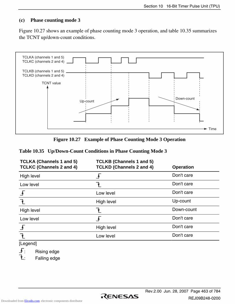
Section 10 16-Bit Timer Pulse Unit (TPU)
Rev.2.00 Jun. 28, 2007 Page 463 of 784
REJ09B248-0200
(c) Phase counting mode 3
Figure 10.27 shows an example of phase counting mode 3 operation, and table 10.35 summarizes the TCNT up/down-count conditions.
Time
Up-countDown-count
TCNT value
TCLKA (channels 1 and 5)TCLKC (channels 2 and 4)
TCLKB (channels 1 and 5)TCLKD (channels 2 and 4)
Figure 10.27 Example of Phase Counting Mode 3 Operation
Table 10.35 Up/Down-Count Conditions in Phase Counting Mode 3
TCLKA (Channels 1 and 5) TCLKC (Channels 2 and 4)
TCLKB (Channels 1 and 5) TCLKD (Channels 2 and 4) Operation
High level Don't care
Low level Don't care
Low level Don't care
High level Up-count
High level Down-count
Low level Don't care
High level Don't care
Low level Don't care
[Legend]
: Rising edge
: Falling edge
Downloaded from Elcodis.com electronic components distributor
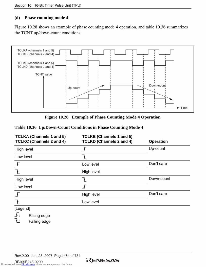
Section 10 16-Bit Timer Pulse Unit (TPU)
Rev.2.00 Jun. 28, 2007 Page 464 of 784
REJ09B248-0200
(d) Phase counting mode 4
Figure 10.28 shows an example of phase counting mode 4 operation, and table 10.36 summarizes the TCNT up/down-count conditions.
Time
Up-countDown-count
TCNT value
TCLKA (channels 1 and 5)TCLKC (channels 2 and 4)
TCLKB (channels 1 and 5)TCLKD (channels 2 and 4)
Figure 10.28 Example of Phase Counting Mode 4 Operation
Table 10.36 Up/Down-Count Conditions in Phase Counting Mode 4
TCLKA (Channels 1 and 5) TCLKC (Channels 2 and 4)
TCLKB (Channels 1 and 5) TCLKD (Channels 2 and 4) Operation
High level
Low level
Up-count
Low level
High level
Don't care
High level
Low level
Down-count
High level
Low level
Don't care
[Legend]
: Rising edge
: Falling edge
Downloaded from Elcodis.com electronic components distributor

Section 10 16-Bit Timer Pulse Unit (TPU)
Rev.2.00 Jun. 28, 2007 Page 465 of 784
REJ09B248-0200
(3) Phase Counting Mode Application Example
Figure 10.29 shows an example in which phase counting mode is designated for channel 1, and channel 1 is coupled with channel 0 to input servo motor 2-phase encoder pulses in order to detect the position or speed.
Channel 1 is set to phase counting mode 1, and the encoder pulse A-phase and B-phase are input to TCLKA and TCLKB.
Channel 0 operates with TCNT counter clearing by TGRC_0 compare match; TGRA_0 and TGRC_0 are used for the compare match function and are set with the speed control cycle and position control cycle. TGRB_0 is used for input capture, with TGRB_0 and TGRD_0 operating in buffer mode. The channel 1 counter input clock is designated as the TGRB_0 input capture source, and the pulse width of 2-phase encoder 4-multiplication pulses is detected.
TGRA_1 and TGRB_1 for channel 1 are designated for input capture, channel 0 TGRA_0 and TGRC_0 compare matches are selected as the input capture source, and the up/down-counter values for the control cycles are stored.
This procedure enables accurate position/speed detection to be achieved.
TCNT_1
TCNT_0
Channel 1
TGRA_1(speed cycle capture)
TGRA_0(speed control cycle)
TGRB_1(position cycle capture)
TGRC_0(position control cycle)
TGRB_0 (pulse width capture)
TGRD_0 (buffer operation)
Channel 0
TCLKA
TCLKB
Edgedetectioncircuit
+-
+-
Figure 10.29 Phase Counting Mode Application Example
Downloaded from Elcodis.com electronic components distributor

Section 10 16-Bit Timer Pulse Unit (TPU)
Rev.2.00 Jun. 28, 2007 Page 466 of 784
REJ09B248-0200
10.5 Interrupt Sources
There are three kinds of TPU interrupt sources: TGR input capture/compare match, TCNT overflow, and TCNT underflow. Each interrupt source has its own status flag and enable/disable bit, allowing generation of interrupt request signals to be enabled or disabled individually.
When an interrupt request is generated, the corresponding status flag in TSR is set to 1. If the corresponding enable/disable bit in TIER is set to 1 at this time, an interrupt is requested. The interrupt request is cleared by clearing the status flag to 0.
Relative channel priority levels can be changed by the interrupt controller, but the priority within a channel is fixed. For details, see section 5, Interrupt Controller.
Table 10.37 lists the TPU interrupt sources.
Table 10.37 TPU Interrupts
Channel Name Interrupt Source Interrupt Flag
DTC Activation
DMAC Activation
0 TGI0A TGRA_0 input capture/ compare match
TGFA_0 Possible Possible
TGI0B TGRB_0 input capture/ compare match
TGFB_0 Possible Not possible
TGI0C TGRC_0 input capture/ compare match
TGFC_0 Possible Not possible
TGI0D TGRD_0 input capture/ compare match
TGFD_0 Possible Not possible
TCI0V TCNT_0 overflow TCFV_0 Not possible Not possible
1 TGI1A TGRA_1 input capture/ compare match
TGFA_1 Possible Possible
TGI1B TGRB_1 input capture/ compare match
TGFB_1 Possible Not possible
TCI1V TCNT_1 overflow TCFV_1 Not possible Not possible
TCI1U TCNT_1 underflow TCFU_1 Not possible Not possible
Downloaded from Elcodis.com electronic components distributor

Section 10 16-Bit Timer Pulse Unit (TPU)
Rev.2.00 Jun. 28, 2007 Page 467 of 784
REJ09B248-0200
Channel Name Interrupt Source Interrupt Flag
DTC Activation
DMAC Activation
2 TGI2A TGRA_2 input capture/ compare match
TGFA_2 Possible Possible
TGI2B TGRB_2 input capture/ compare match
TGFB_2 Possible Not possible
TCI2V TCNT_2 overflow TCFV_2 Not possible Not possible
TCI2U TCNT_2 underflow TCFU_2 Not possible Not possible
3 TGI3A TGRA_3 input capture/ compare match
TGFA_3 Possible Possible
TGI3B TGRB_3 input capture/ compare match
TGFB_3 Possible Not possible
TGI3C TGRC_3 input capture/ compare match
TGFC_3 Possible Not possible
TGI3D TGRD_3 input capture/ compare match
TGFD_3 Possible Not possible
TCI3V TCNT_3 overflow TCFV_3 Not possible Not possible
4 TGI4A TGRA_4 input capture/ compare match
TGFA_4 Possible Possible
TGI4B TGRB_4 input capture/ compare match
TGFB_4 Possible Not possible
TCI4V TCNT_4 overflow TCFV_4 Not possible Not possible
TCI4U TCNT_4 underflow TCFU_4 Not possible Not possible
5 TGI5A TGRA_5 input capture/ compare match
TGFA_5 Possible Possible
TGI5B TGRB_5 input capture/ compare match
TGFB_5 Possible Not possible
TCI5V TCNT_5 overflow TCFV_5 Not possible Not possible
TCI5U TCNT_5 underflow TCFU_5 Not possible Not possible
Note: This table shows the initial state immediately after a reset. The relative channel priority levels can be changed by the interrupt controller.
Downloaded from Elcodis.com electronic components distributor
Section 10 16-Bit Timer Pulse Unit (TPU)
Rev.2.00 Jun. 28, 2007 Page 468 of 784
REJ09B248-0200
(1) Input Capture/Compare Match Interrupt
An interrupt is requested if the TGIE bit in TIER is set to 1 when the TGF flag in TSR is set to 1 by the occurrence of a TGR input capture/compare match on a channel. The interrupt request is cleared by clearing the TGF flag to 0. The TPU has 16 input capture/compare match interrupts, four each for channels 0 and 3, and two each for channels 1, 2, 4, and 5.
(2) Overflow Interrupt
An interrupt is requested if the TCIEV bit in TIER is set to 1 when the TCFV flag in TSR is set to 1 by the occurrence of a TCNT overflow on a channel. The interrupt request is cleared by clearing the TCFV flag to 0. The TPU has six overflow interrupts, one for each channel.
(3) Underflow Interrupt
An interrupt is requested if the TCIEU bit in TIER is set to 1 when the TCFU flag in TSR is set to 1 by the occurrence of a TCNT underflow on a channel. The interrupt request is cleared by clearing the TCFU flag to 0. The TPU has four underflow interrupts, one each for channels 1, 2, 4, and 5.
10.6 DTC Activation
The DTC can be activated by the TGR input capture/compare match interrupt for a channel. For details, see section 8, Data Transfer Controller (DTC).
A total of 16 TPU input capture/compare match interrupts can be used as DTC activation sources, four each for channels 0 and 3, and two each for channels 1, 2, 4, and 5.
10.7 DMAC Activation
The DMAC can be activated by the TGRA input capture/compare match interrupt for a channel. For details, see section 7, DMA Controller (DMAC).
In TPU, one in each channel, totally six TGRA input capture/compare match interrupts can be used as DMAC activation sources.
Downloaded from Elcodis.com electronic components distributor
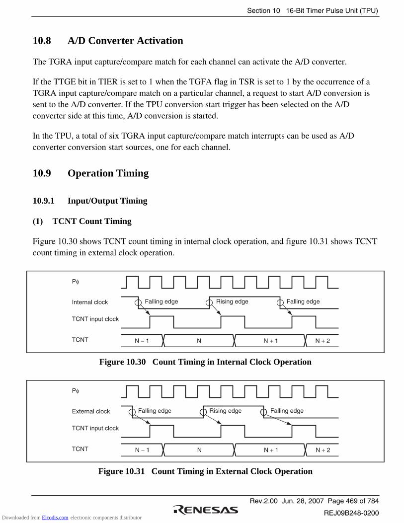
Section 10 16-Bit Timer Pulse Unit (TPU)
Rev.2.00 Jun. 28, 2007 Page 469 of 784
REJ09B248-0200
10.8 A/D Converter Activation
The TGRA input capture/compare match for each channel can activate the A/D converter.
If the TTGE bit in TIER is set to 1 when the TGFA flag in TSR is set to 1 by the occurrence of a TGRA input capture/compare match on a particular channel, a request to start A/D conversion is sent to the A/D converter. If the TPU conversion start trigger has been selected on the A/D converter side at this time, A/D conversion is started.
In the TPU, a total of six TGRA input capture/compare match interrupts can be used as A/D converter conversion start sources, one for each channel.
10.9 Operation Timing
10.9.1 Input/Output Timing
(1) TCNT Count Timing
Figure 10.30 shows TCNT count timing in internal clock operation, and figure 10.31 shows TCNT count timing in external clock operation.
Pφ
Internal clock
TCNT input clock
TCNT
Falling edge Rising edge
N − 1 N + 1 N + 2N
Falling edge
Figure 10.30 Count Timing in Internal Clock Operation
Pφ
External clock
TCNT input clock
TCNT
Falling edge Rising edge
N − 1 N + 1 N + 2N
Falling edge
Figure 10.31 Count Timing in External Clock Operation
Downloaded from Elcodis.com electronic components distributor
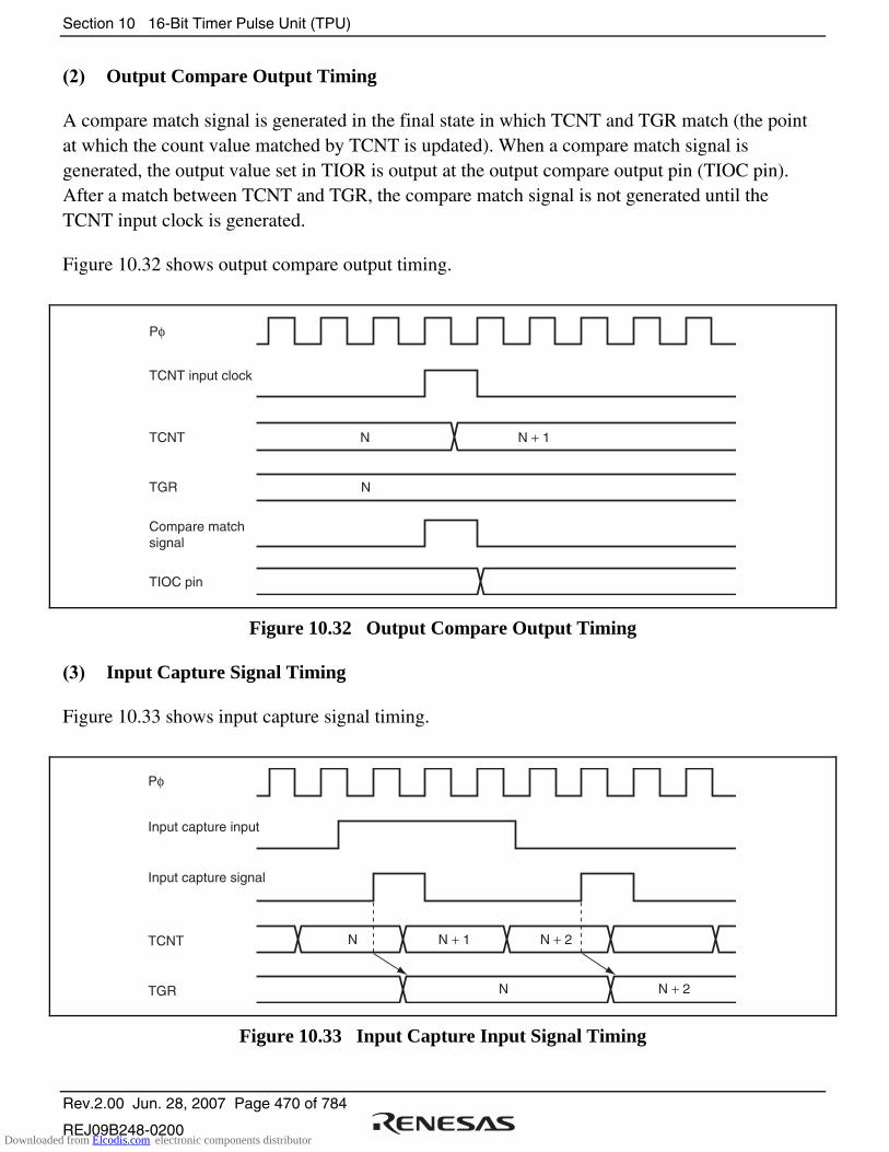
Section 10 16-Bit Timer Pulse Unit (TPU)
Rev.2.00 Jun. 28, 2007 Page 470 of 784
REJ09B248-0200
(2) Output Compare Output Timing
A compare match signal is generated in the final state in which TCNT and TGR match (the point at which the count value matched by TCNT is updated). When a compare match signal is generated, the output value set in TIOR is output at the output compare output pin (TIOC pin). After a match between TCNT and TGR, the compare match signal is not generated until the TCNT input clock is generated.
Figure 10.32 shows output compare output timing.
Pφ
TCNT input clock
TCNT N + 1N
Compare match signal
TIOC pin
TGR N
Figure 10.32 Output Compare Output Timing
(3) Input Capture Signal Timing
Figure 10.33 shows input capture signal timing.
Pφ
TCNT N + 1N
TGR
Input capture input
Input capture signal
N + 2
N N + 2
Figure 10.33 Input Capture Input Signal Timing
Downloaded from Elcodis.com electronic components distributor

Section 10 16-Bit Timer Pulse Unit (TPU)
Rev.2.00 Jun. 28, 2007 Page 471 of 784
REJ09B248-0200
(4) Timing for Counter Clearing by Compare Match/Input Capture
Figure 10.34 shows the timing when counter clearing by compare match occurrence is specified, and figure 10.35 shows the timing when counter clearing by input capture occurrence is specified.
Pφ
TCNT N
TGR
Compare match signal
Counter clear signal
H'0000
N
Figure 10.34 Counter Clear Timing (Compare Match)
TGR
Counter clearsignal
H'0000
Pφ
TCNT N
Input capturesignal
N
Figure 10.35 Counter Clear Timing (Input Capture)
Downloaded from Elcodis.com electronic components distributor
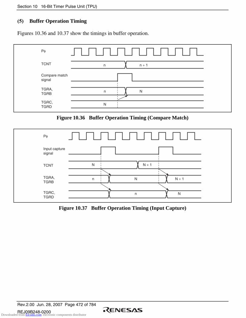
Section 10 16-Bit Timer Pulse Unit (TPU)
Rev.2.00 Jun. 28, 2007 Page 472 of 784
REJ09B248-0200
(5) Buffer Operation Timing
Figures 10.36 and 10.37 show the timings in buffer operation.
Pφ
n + 1n
TGRA,TGRB
TGRC,TGRD
N
N
Compare matchsignal
TCNT
n
Figure 10.36 Buffer Operation Timing (Compare Match)
Pφ
TCNT N + 1N
Input capturesignal
TGRA,TGRB
TGRC,TGRD
n N + 1N
n N
Figure 10.37 Buffer Operation Timing (Input Capture)
Downloaded from Elcodis.com electronic components distributor

Section 10 16-Bit Timer Pulse Unit (TPU)
Rev.2.00 Jun. 28, 2007 Page 473 of 784
REJ09B248-0200
10.9.2 Interrupt Signal Timing
(1) TGF Flag Setting Timing in Case of Compare Match
Figure 10.38 shows the timing for setting of the TGF flag in TSR by compare match occurrence, and the TGI interrupt request signal timing.
TGR
Compare matchsignal
Pφ
TCNT inputclock
TCNT N + 1N
N
TGF flag
TGI interrupt
Figure 10.38 TGI Interrupt Timing (Compare Match)
(2) TGF Flag Setting Timing in Case of Input Capture
Figure 10.39 shows the timing for setting of the TGF flag in TSR by input capture occurrence, and the TGI interrupt request signal timing.
TGR
Pφ
TCNT
N
Input capturesignal
TGF flag
TGI interrupt
N
Figure 10.39 TGI Interrupt Timing (Input Capture)
Downloaded from Elcodis.com electronic components distributor
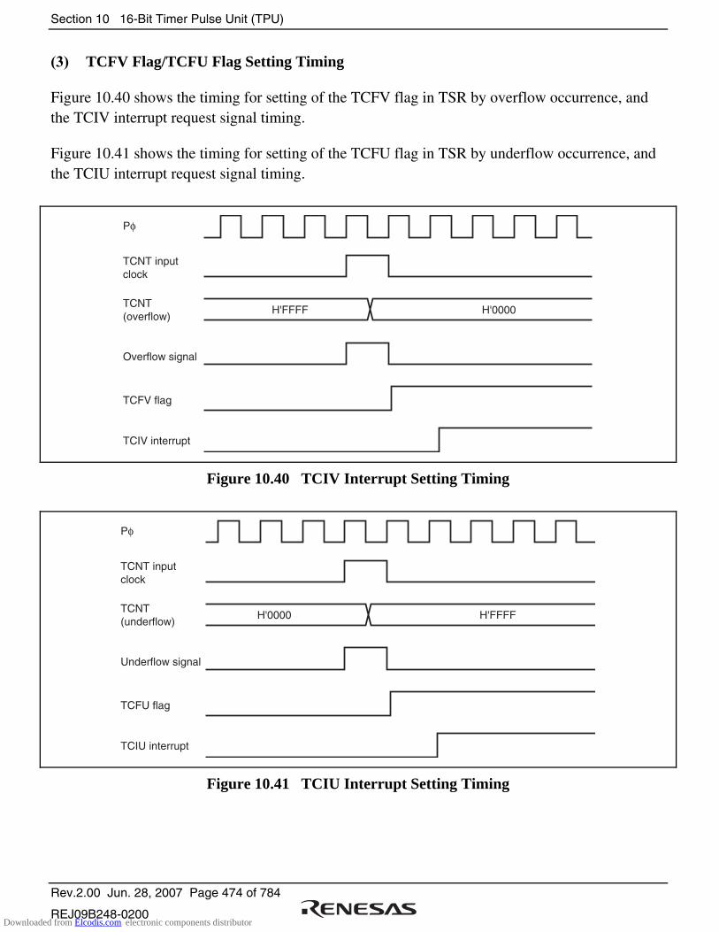
Section 10 16-Bit Timer Pulse Unit (TPU)
Rev.2.00 Jun. 28, 2007 Page 474 of 784
REJ09B248-0200
(3) TCFV Flag/TCFU Flag Setting Timing
Figure 10.40 shows the timing for setting of the TCFV flag in TSR by overflow occurrence, and the TCIV interrupt request signal timing.
Figure 10.41 shows the timing for setting of the TCFU flag in TSR by underflow occurrence, and the TCIU interrupt request signal timing.
H'FFFF
Pφ
TCNT inputclock
TCNT(overflow)
Overflow signal
TCFV flag
TCIV interrupt
H'0000
Figure 10.40 TCIV Interrupt Setting Timing
H'0000
Pφ
TCNT inputclock
TCNT(underflow)
Underflow signal
TCFU flag
TCIU interrupt
H'FFFF
Figure 10.41 TCIU Interrupt Setting Timing
Downloaded from Elcodis.com electronic components distributor

Section 10 16-Bit Timer Pulse Unit (TPU)
Rev.2.00 Jun. 28, 2007 Page 475 of 784
REJ09B248-0200
(4) Status Flag Clearing Timing
After a status flag is read as 1 by the CPU, it is cleared by writing 0 to it. When the DTC or DMAC is activated, the flag is cleared automatically. Figure 10.42 shows the timing for status flag clearing by the CPU, and figures 10.43 and 10.44 show the timing for status flag clearing by the DTC or DMAC.
Status flag
Pφ
Interrupt requestsignal
Address
Write
TSR address
TSR write cycleT1 T2
Figure 10.42 Timing for Status Flag Clearing by CPU
The status flag and interrupt request signal are cleared in synchronization with Pφ after the DTC or DMAC transfer has started, as shown in figure 10.43. If conflict occurs for clearing the status flag and interrupt request signal due to activation of multiple DTC or DMAC transfers, it will take up to five clock cycles (Pφ) for clearing them, as shown in figure 10.44. The next transfer request is masked for a longer period of either a period until the current transfer ends or a period for five clock cycles (Pφ) from the beginning of the transfer. Note that in the DTC transfer, the status flag may be cleared during outputting the destination address.
Downloaded from Elcodis.com electronic components distributor
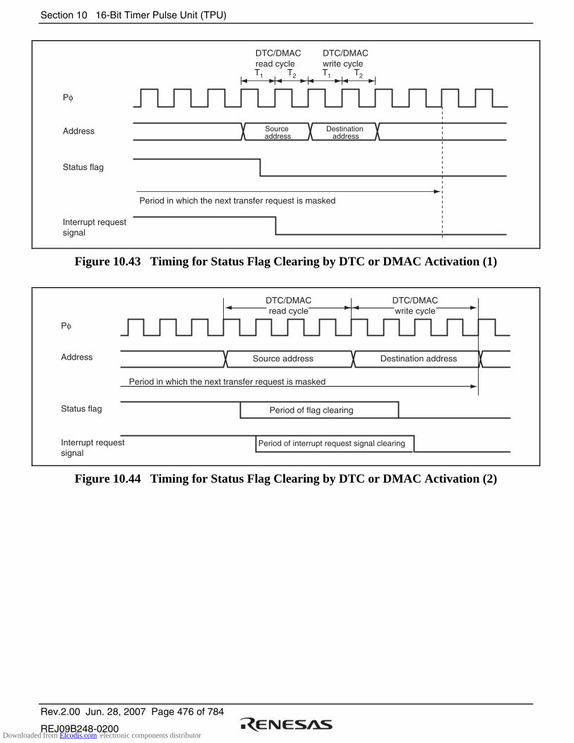
Section 10 16-Bit Timer Pulse Unit (TPU)
Rev.2.00 Jun. 28, 2007 Page 476 of 784
REJ09B248-0200
Pφ
Address
Status flag
Interrupt requestsignal
Source address
Destination address
Period in which the next transfer request is masked
T1 T2
DTC/DMACread cycle
DTC/DMACwrite cycleT1 T2
Figure 10.43 Timing for Status Flag Clearing by DTC or DMAC Activation (1)
Pφ
Address
Status flag
Interrupt requestsignal
Source address Destination address
Period of flag clearing
Period of interrupt request signal clearing
Period in which the next transfer request is masked
DTC/DMACread cycle
DTC/DMACwrite cycle
Figure 10.44 Timing for Status Flag Clearing by DTC or DMAC Activation (2)
Downloaded from Elcodis.com electronic components distributor

Section 10 16-Bit Timer Pulse Unit (TPU)
Rev.2.00 Jun. 28, 2007 Page 477 of 784
REJ09B248-0200
10.10 Usage Notes
10.10.1 Module Stop Mode Setting
Operation of the TPU can be disabled or enabled using the module stop control register. The initial setting is for operation of the TPU to be halted. Register access is enabled by clearing module stop mode. For details, see section 19, Power-Down Modes.
10.10.2 Input Clock Restrictions
The input clock pulse width must be at least 1.5 states in the case of single-edge detection, and at least 2.5 states in the case of both-edge detection. The TPU will not operate properly with a narrower pulse width.
In phase counting mode, the phase difference and overlap between the two input clocks must be at least 1.5 states, and the pulse width must be at least 2.5 states. Figure 10.45 shows the input clock conditions in phase counting mode.
TCLKA(TCLKC)
TCLKB(TCLKD)
Overlap
Phasedifference
Pulse width
Note: Phase difference, Overlap ≥ 1.5 statesPulse width ≥ 2.5 states
Pulse width
Phasedifference
Overlap
Pulse width Pulse width
Figure 10.45 Phase Difference, Overlap, and Pulse Width in Phase Counting Mode
Downloaded from Elcodis.com electronic components distributor
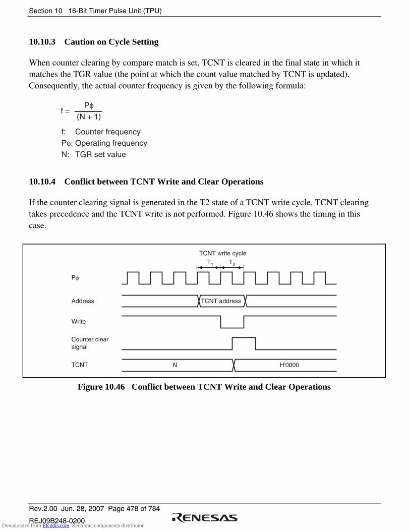
Section 10 16-Bit Timer Pulse Unit (TPU)
Rev.2.00 Jun. 28, 2007 Page 478 of 784
REJ09B248-0200
10.10.3 Caution on Cycle Setting
When counter clearing by compare match is set, TCNT is cleared in the final state in which it matches the TGR value (the point at which the count value matched by TCNT is updated). Consequently, the actual counter frequency is given by the following formula:
f = Pφ
(N + 1)
f:Pφ:N:
Counter frequencyOperating frequencyTGR set value
10.10.4 Conflict between TCNT Write and Clear Operations
If the counter clearing signal is generated in the T2 state of a TCNT write cycle, TCNT clearing takes precedence and the TCNT write is not performed. Figure 10.46 shows the timing in this case.
Counter clear signal
H'0000
Pφ
TCNT N
Address
Write
TCNT address
TCNT write cycleT1 T2
Figure 10.46 Conflict between TCNT Write and Clear Operations
Downloaded from Elcodis.com electronic components distributor
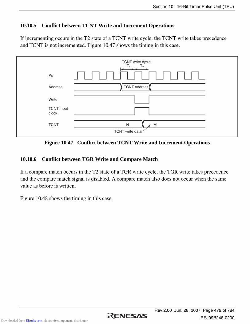
Section 10 16-Bit Timer Pulse Unit (TPU)
Rev.2.00 Jun. 28, 2007 Page 479 of 784
REJ09B248-0200
10.10.5 Conflict between TCNT Write and Increment Operations
If incrementing occurs in the T2 state of a TCNT write cycle, the TCNT write takes precedence and TCNT is not incremented. Figure 10.47 shows the timing in this case.
Pφ
TCNT inputclock
TCNT N
Address
Write
T1 T2
TCNT write cycle
M
TCNT write data
TCNT address
Figure 10.47 Conflict between TCNT Write and Increment Operations
10.10.6 Conflict between TGR Write and Compare Match
If a compare match occurs in the T2 state of a TGR write cycle, the TGR write takes precedence and the compare match signal is disabled. A compare match also does not occur when the same value as before is written.
Figure 10.48 shows the timing in this case.
Downloaded from Elcodis.com electronic components distributor

Section 10 16-Bit Timer Pulse Unit (TPU)
Rev.2.00 Jun. 28, 2007 Page 480 of 784
REJ09B248-0200
TGR
Compare matchsignal
Pφ
TCNT N + 1N
Address
Write
M
TGR address
TGR write cycle
N
Disabled
TGR write data
T1 T2
Figure 10.48 Conflict between TGR Write and Compare Match
10.10.7 Conflict between Buffer Register Write and Compare Match
If a compare match occurs in the T2 state of a TGR write cycle, the data transferred to TGR by the buffer operation will be the write data.
Figure 10.49 shows the timing in this case.
TGR
Compare match signal
Pφ
N
Address
Write
M
TGR write cycle
Buffer registeraddress
Data written to buffer register
M
Buffer register
T1 T2
Figure 10.49 Conflict between Buffer Register Write and Compare Match
Downloaded from Elcodis.com electronic components distributor
Section 10 16-Bit Timer Pulse Unit (TPU)
Rev.2.00 Jun. 28, 2007 Page 481 of 784
REJ09B248-0200
10.10.8 Conflict between TGR Read and Input Capture
If the input capture signal is generated in the T1 state of a TGR read cycle, the data that is read will be the data after input capture transfer.
Figure 10.50 shows the timing in this case.
TGR
Pφ
Input capture signal
Address TGR address
Read
TGR read cycle
X M
MInternal data bus
T1 T2
Figure 10.50 Conflict between TGR Read and Input Capture
10.10.9 Conflict between TGR Write and Input Capture
If the input capture signal is generated in the T2 state of a TGR write cycle, the input capture operation takes precedence and the write to TGR is not performed.
Figure 10.51 shows the timing in this case.
Downloaded from Elcodis.com electronic components distributor

Section 10 16-Bit Timer Pulse Unit (TPU)
Rev.2.00 Jun. 28, 2007 Page 482 of 784
REJ09B248-0200
TCNT
Pφ
Input capture signal
Address TGR address
Write
TGR write cycle
M
MTGR
T1 T2
Figure 10.51 Conflict between TGR Write and Input Capture
10.10.10 Conflict between Buffer Register Write and Input Capture
If the input capture signal is generated in the T2 state of a buffer register write cycle, the buffer operation takes precedence and the write to the buffer register is not performed.
Figure 10.52 shows the timing in this case.
TCNT
Pφ
Input capture signal
Address Buffer registeraddress
Write
Buffer register write cycle
N
NTGR
Buffer register M
M
T1 T2
Figure 10.52 Conflict between Buffer Register Write and Input Capture
Downloaded from Elcodis.com electronic components distributor
Section 10 16-Bit Timer Pulse Unit (TPU)
Rev.2.00 Jun. 28, 2007 Page 483 of 784
REJ09B248-0200
10.10.11 Conflict between Overflow/Underflow and Counter Clearing
If overflow/underflow and counter clearing occur simultaneously, the TCFV/TCFU flag in TSR is not set and TCNT clearing takes precedence.
Figure 10.53 shows the operation timing when a TGR compare match is specified as the clearing source, and H'FFFF is set in TGR.
Counter clear signal
H'0000
Pφ
TCNT input clock
TCNT
TGF flag
TCFV flag
H'FFFF
Disabled
Figure 10.53 Conflict between Overflow and Counter Clearing
10.10.12 Conflict between TCNT Write and Overflow/Underflow
If an overflow/underflow occurs due to increment/decrement in the T2 state of a TCNT write cycle, the TCNT write takes precedence and the TCFV/TCFU flag in TSR is not set.
Figure 10.54 shows the operation timing when there is conflict between TCNT write and overflow.
Downloaded from Elcodis.com electronic components distributor

Section 10 16-Bit Timer Pulse Unit (TPU)
Rev.2.00 Jun. 28, 2007 Page 484 of 784
REJ09B248-0200
Pφ
TCNT H'FFFF
TCFV flag
Address
Write
TCNT address
M
TCNT write data
TGR write cycleT1 T2
Figure 10.54 Conflict between TCNT Write and Overflow
10.10.13 Multiplexing of I/O Pins
In this LSI, the TCLKA input pin is multiplexed with the TIOCC0 I/O pin, the TCLKB input pin with the TIOCD0 I/O pin, the TCLKC input pin with the TIOCB1 I/O pin, and the TCLKD input pin with the TIOCB2 I/O pin. When an external clock is input, compare match output should not be performed from a multiplexed pin.
10.10.14 Interrupts and Module Stop Mode
If module stop mode is entered when an interrupt has been requested, it will not be possible to clear the CPU interrupt source or the DMAC or DTC activation source. Interrupts should therefore be disabled before entering module stop mode.
Downloaded from Elcodis.com electronic components distributor
Section 11 Programmable Pulse Generator (PPG)
Rev.2.00 Jun. 28, 2007 Page 485 of 784
REJ09B248-0200
Section 11 Programmable Pulse Generator (PPG)
The programmable pulse generator (PPG) provides pulse outputs by using the 16-bit timer pulse unit (TPU) as a time base. The PPG pulse outputs are divided into 4-bit groups (groups 3 to 0) that can operate both simultaneously and independently. Figure 11.1 shows a block diagram of the PPG.
11.1 Features
• 16-bit output data
• Four output groups
• Selectable output trigger signals
• Non-overlapping mode
• Can operate together with the data transfer controller (DTC) and DMA controller (DMAC)
• Inverted output can be set
• Module stop mode can be set
Downloaded from Elcodis.com electronic components distributor
Section 11 Programmable Pulse Generator (PPG)
Rev.2.00 Jun. 28, 2007 Page 486 of 784
REJ09B248-0200
Compare match signals
PO15PO14PO13PO12PO11PO10PO9PO8PO7PO6PO5PO4PO3PO2PO1PO0
[Legend]PMR:PCR:NDERH:NDERL:NDRH:NDRL:PODRH:PODRL:
PPG output mode registerPPG output control registerNext data enable register HNext data enable register LNext data register HNext data register LOutput data register HOutput data register L
Internaldata bus
Pulse outputpins, group 3
Pulse outputpins, group 2
Pulse outputpins, group 1
Pulse outputpins, group 0
PODRH
PODRL
NDRH
NDRL
Control logic
NDERH
PMR
NDERL
PCR
Figure 11.1 Block Diagram of PPG
Downloaded from Elcodis.com electronic components distributor

Section 11 Programmable Pulse Generator (PPG)
Rev.2.00 Jun. 28, 2007 Page 487 of 784
REJ09B248-0200
11.2 Input/Output Pins
Table 11.1 shows the PPG pin configuration.
Table 11.1 Pin Configuration
Pin Name I/O Function
PO15 Output
PO14 Output
PO13 Output
PO12 Output
Group 3 pulse output
PO11 Output
PO10 Output
PO9 Output
PO8 Output
Group 2 pulse output
PO7 Output
PO6 Output
PO5 Output
PO4 Output
Group 1 pulse output
PO3 Output
PO2 Output
PO1 Output
PO0 Output
Group 0 pulse output
Downloaded from Elcodis.com electronic components distributor
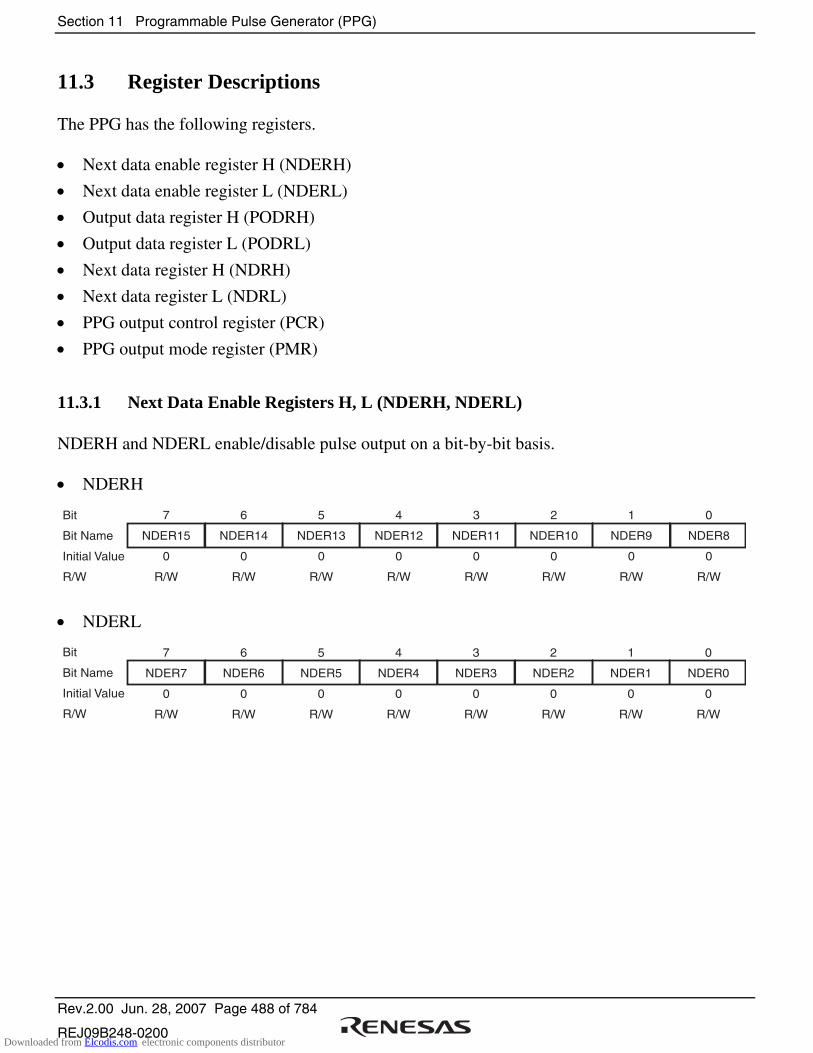
Section 11 Programmable Pulse Generator (PPG)
Rev.2.00 Jun. 28, 2007 Page 488 of 784
REJ09B248-0200
11.3 Register Descriptions
The PPG has the following registers.
• Next data enable register H (NDERH)
• Next data enable register L (NDERL)
• Output data register H (PODRH)
• Output data register L (PODRL)
• Next data register H (NDRH)
• Next data register L (NDRL)
• PPG output control register (PCR)
• PPG output mode register (PMR)
11.3.1 Next Data Enable Registers H, L (NDERH, NDERL)
NDERH and NDERL enable/disable pulse output on a bit-by-bit basis.
• NDERH
7
NDER15
0
R/W
6
NDER14
0
R/W
5
NDER13
0
R/W
4
NDER12
0
R/W
3
NDER11
0
R/W
2
NDER10
0
R/W
1
NDER9
0
R/W
0
NDER8
0
R/W
Bit
Bit Name
Initial Value
R/W
• NDERL
7
NDER7
0
R/W
6
NDER6
0
R/W
5
NDER5
0
R/W
4
NDER4
0
R/W
3
NDER3
0
R/W
2
NDER2
0
R/W
1
NDER1
0
R/W
0
NDER0
0
R/W
Bit
Bit Name
Initial Value
R/W
Downloaded from Elcodis.com electronic components distributor
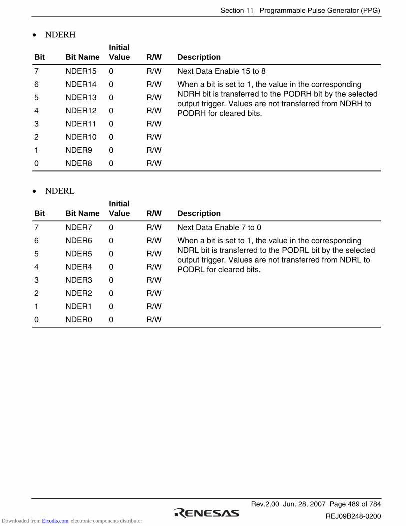
Section 11 Programmable Pulse Generator (PPG)
Rev.2.00 Jun. 28, 2007 Page 489 of 784
REJ09B248-0200
• NDERH
Bit Bit Name Initial Value R/W Description
7
6
5
4
3
2
1
0
NDER15
NDER14
NDER13
NDER12
NDER11
NDER10
NDER9
NDER8
0
0
0
0
0
0
0
0
R/W
R/W
R/W
R/W
R/W
R/W
R/W
R/W
Next Data Enable 15 to 8
When a bit is set to 1, the value in the corresponding NDRH bit is transferred to the PODRH bit by the selected output trigger. Values are not transferred from NDRH to PODRH for cleared bits.
• NDERL
Bit Bit Name Initial Value R/W Description
7
6
5
4
3
2
1
0
NDER7
NDER6
NDER5
NDER4
NDER3
NDER2
NDER1
NDER0
0
0
0
0
0
0
0
0
R/W
R/W
R/W
R/W
R/W
R/W
R/W
R/W
Next Data Enable 7 to 0
When a bit is set to 1, the value in the corresponding NDRL bit is transferred to the PODRL bit by the selected output trigger. Values are not transferred from NDRL to PODRL for cleared bits.
Downloaded from Elcodis.com electronic components distributor

Section 11 Programmable Pulse Generator (PPG)
Rev.2.00 Jun. 28, 2007 Page 490 of 784
REJ09B248-0200
11.3.2 Output Data Registers H, L (PODRH, PODRL)
PODRH and PODRL store output data for use in pulse output. A bit that has been set for pulse output by NDER is read-only and cannot be modified.
• PODRH
7
POD15
0
R/W
6
POD14
0
R/W
5
POD13
0
R/W
4
POD12
0
R/W
3
POD11
0
R/W
2
POD10
0
R/W
1
POD9
0
R/W
0
POD8
0
R/W
Bit
Bit Name
Initial Value
R/W
• PODRL
7
POD7
0
R/W
6
POD6
0
R/W
5
POD5
0
R/W
4
POD4
0
R/W
3
POD3
0
R/W
2
POD2
0
R/W
1
POD2
0
R/W
0
POD0
0
R/W
Bit
Bit Name
Initial Value
R/W
• PODRH
Bit Bit Name Initial Value R/W Description
7
6
5
4
3
2
1
0
POD15
POD14
POD13
POD12
POD11
POD10
POD9
POD8
0
0
0
0
0
0
0
0
R/W
R/W
R/W
R/W
R/W
R/W
R/W
R/W
Output Data Register 15 to 8
For bits which have been set to pulse output by NDERH, the output trigger transfers NDRH values to this register during PPG operation. While NDERH is set to 1, the CPU cannot write to this register. While NDERH is cleared, the initial output value of the pulse can be set.
Downloaded from Elcodis.com electronic components distributor
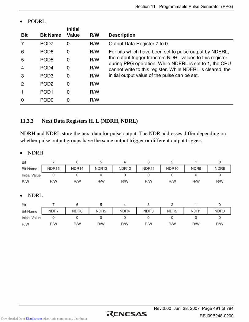
Section 11 Programmable Pulse Generator (PPG)
Rev.2.00 Jun. 28, 2007 Page 491 of 784
REJ09B248-0200
• PODRL
Bit Bit Name Initial Value R/W Description
7
6
5
4
3
2
1
0
POD7
POD6
POD5
POD4
POD3
POD2
POD1
POD0
0
0
0
0
0
0
0
0
R/W
R/W
R/W
R/W
R/W
R/W
R/W
R/W
Output Data Register 7 to 0
For bits which have been set to pulse output by NDERL, the output trigger transfers NDRL values to this register during PPG operation. While NDERL is set to 1, the CPU cannot write to this register. While NDERL is cleared, the initial output value of the pulse can be set.
11.3.3 Next Data Registers H, L (NDRH, NDRL)
NDRH and NDRL store the next data for pulse output. The NDR addresses differ depending on whether pulse output groups have the same output trigger or different output triggers.
• NDRH
Bit
Bit Name
Initial Value
R/W
7
NDR15
0
R/W
6
NDR14
0
R/W
5
NDR13
0
R/W
4
NDR12
0
R/W
3
NDR11
0
R/W
2
NDR10
0
R/W
1
NDR9
0
R/W
0
NDR8
0
R/W
• NDRL
Bit
Bit Name
Initial Value
R/W
7
NDR7
0
R/W
6
NDR6
0
R/W
5
NDR5
0
R/W
4
NDR4
0
R/W
3
NDR3
0
R/W
2
NDR2
0
R/W
1
NDR1
0
R/W
0
NDR0
0
R/W
Downloaded from Elcodis.com electronic components distributor
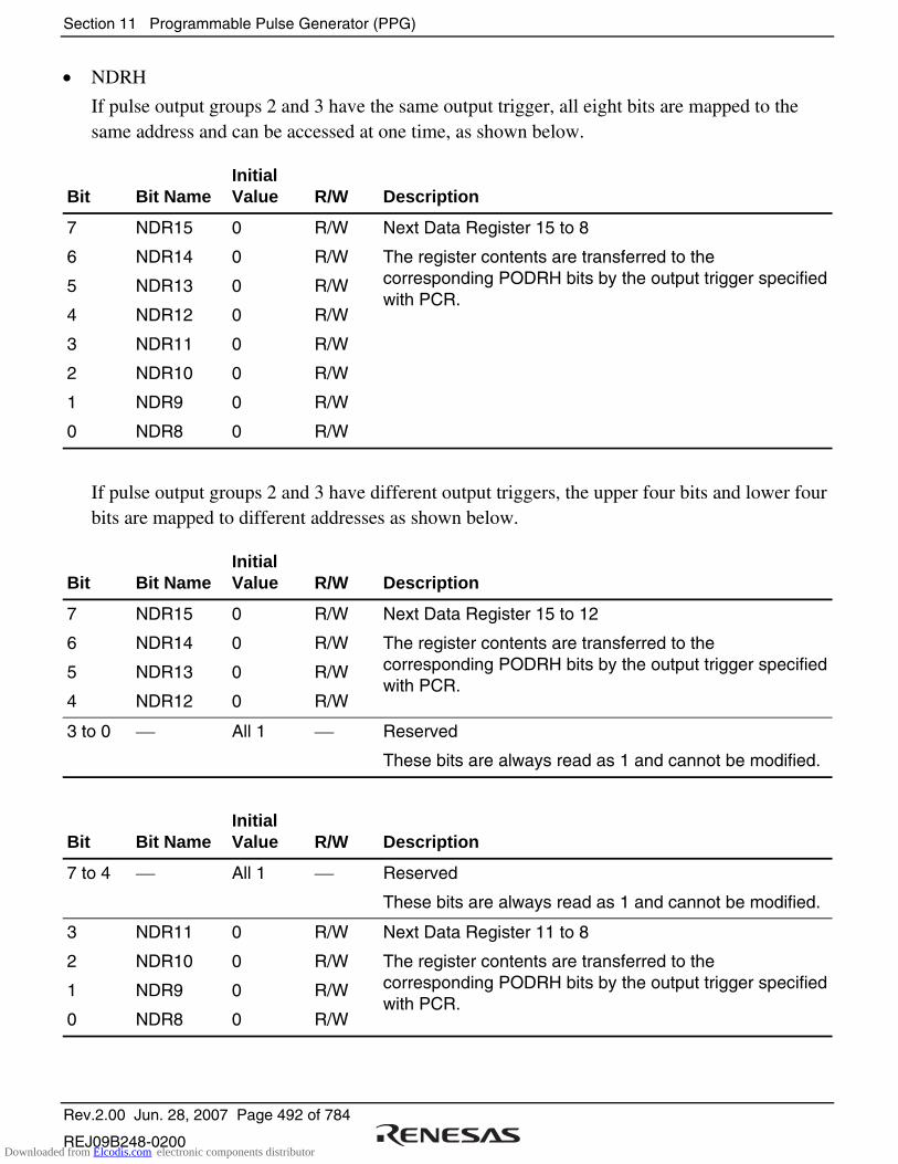
Section 11 Programmable Pulse Generator (PPG)
Rev.2.00 Jun. 28, 2007 Page 492 of 784
REJ09B248-0200
• NDRH
If pulse output groups 2 and 3 have the same output trigger, all eight bits are mapped to the same address and can be accessed at one time, as shown below.
Bit Bit Name Initial Value R/W Description
7
6
5
4
3
2
1
0
NDR15
NDR14
NDR13
NDR12
NDR11
NDR10
NDR9
NDR8
0
0
0
0
0
0
0
0
R/W
R/W
R/W
R/W
R/W
R/W
R/W
R/W
Next Data Register 15 to 8
The register contents are transferred to the corresponding PODRH bits by the output trigger specified with PCR.
If pulse output groups 2 and 3 have different output triggers, the upper four bits and lower four bits are mapped to different addresses as shown below.
Bit Bit Name Initial Value R/W Description
7
6
5
4
NDR15
NDR14
NDR13
NDR12
0
0
0
0
R/W
R/W
R/W
R/W
Next Data Register 15 to 12
The register contents are transferred to the corresponding PODRH bits by the output trigger specified with PCR.
3 to 0 All 1 Reserved
These bits are always read as 1 and cannot be modified.
Bit Bit Name Initial Value R/W Description
7 to 4 All 1 Reserved
These bits are always read as 1 and cannot be modified.
3
2
1
0
NDR11
NDR10
NDR9
NDR8
0
0
0
0
R/W
R/W
R/W
R/W
Next Data Register 11 to 8
The register contents are transferred to the corresponding PODRH bits by the output trigger specified with PCR.
Downloaded from Elcodis.com electronic components distributor
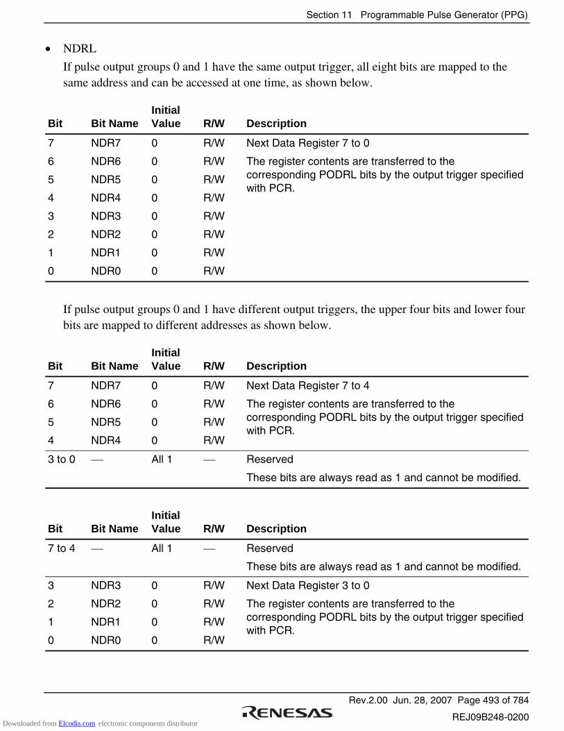
Section 11 Programmable Pulse Generator (PPG)
Rev.2.00 Jun. 28, 2007 Page 493 of 784
REJ09B248-0200
• NDRL
If pulse output groups 0 and 1 have the same output trigger, all eight bits are mapped to the same address and can be accessed at one time, as shown below.
Bit Bit Name Initial Value R/W Description
7
6
5
4
3
2
1
0
NDR7
NDR6
NDR5
NDR4
NDR3
NDR2
NDR1
NDR0
0
0
0
0
0
0
0
0
R/W
R/W
R/W
R/W
R/W
R/W
R/W
R/W
Next Data Register 7 to 0
The register contents are transferred to the corresponding PODRL bits by the output trigger specified with PCR.
If pulse output groups 0 and 1 have different output triggers, the upper four bits and lower four bits are mapped to different addresses as shown below.
Bit Bit Name Initial Value R/W Description
7
6
5
4
NDR7
NDR6
NDR5
NDR4
0
0
0
0
R/W
R/W
R/W
R/W
Next Data Register 7 to 4
The register contents are transferred to the corresponding PODRL bits by the output trigger specified with PCR.
3 to 0 All 1 Reserved
These bits are always read as 1 and cannot be modified.
Bit Bit Name Initial Value R/W Description
7 to 4 All 1 Reserved
These bits are always read as 1 and cannot be modified.
3
2
1
0
NDR3
NDR2
NDR1
NDR0
0
0
0
0
R/W
R/W
R/W
R/W
Next Data Register 3 to 0
The register contents are transferred to the corresponding PODRL bits by the output trigger specified with PCR.
Downloaded from Elcodis.com electronic components distributor
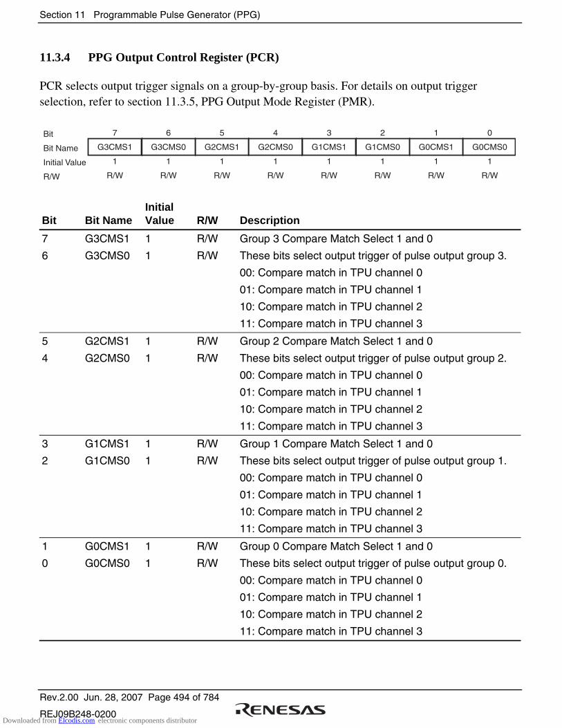
Section 11 Programmable Pulse Generator (PPG)
Rev.2.00 Jun. 28, 2007 Page 494 of 784
REJ09B248-0200
11.3.4 PPG Output Control Register (PCR)
PCR selects output trigger signals on a group-by-group basis. For details on output trigger selection, refer to section 11.3.5, PPG Output Mode Register (PMR).
7
G3CMS1
1
R/W
6
G3CMS0
1
R/W
5
G2CMS1
1
R/W
4
G2CMS0
1
R/W
3
G1CMS1
1
R/W
2
G1CMS0
1
R/W
1
G0CMS1
1
R/W
0
G0CMS0
1
R/W
Bit
Bit Name
Initial Value
R/W
Bit Bit Name Initial Value R/W Description
7
6
G3CMS1
G3CMS0
1
1
R/W
R/W
Group 3 Compare Match Select 1 and 0
These bits select output trigger of pulse output group 3.
00: Compare match in TPU channel 0
01: Compare match in TPU channel 1
10: Compare match in TPU channel 2
11: Compare match in TPU channel 3
5
4
G2CMS1
G2CMS0
1
1
R/W
R/W
Group 2 Compare Match Select 1 and 0
These bits select output trigger of pulse output group 2.
00: Compare match in TPU channel 0
01: Compare match in TPU channel 1
10: Compare match in TPU channel 2
11: Compare match in TPU channel 3
3
2
G1CMS1
G1CMS0
1
1
R/W
R/W
Group 1 Compare Match Select 1 and 0
These bits select output trigger of pulse output group 1.
00: Compare match in TPU channel 0
01: Compare match in TPU channel 1
10: Compare match in TPU channel 2
11: Compare match in TPU channel 3
1
0
G0CMS1
G0CMS0
1
1
R/W
R/W
Group 0 Compare Match Select 1 and 0
These bits select output trigger of pulse output group 0.
00: Compare match in TPU channel 0
01: Compare match in TPU channel 1
10: Compare match in TPU channel 2
11: Compare match in TPU channel 3
Downloaded from Elcodis.com electronic components distributor
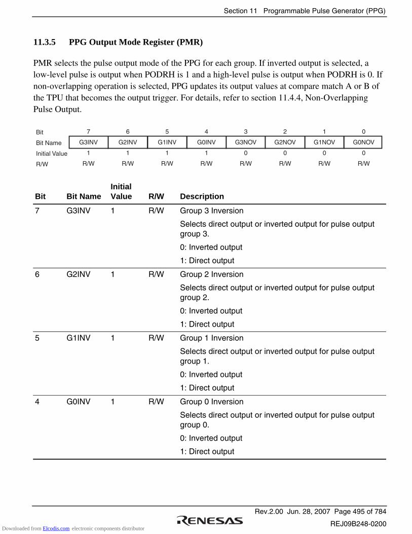
Section 11 Programmable Pulse Generator (PPG)
Rev.2.00 Jun. 28, 2007 Page 495 of 784
REJ09B248-0200
11.3.5 PPG Output Mode Register (PMR)
PMR selects the pulse output mode of the PPG for each group. If inverted output is selected, a low-level pulse is output when PODRH is 1 and a high-level pulse is output when PODRH is 0. If non-overlapping operation is selected, PPG updates its output values at compare match A or B of the TPU that becomes the output trigger. For details, refer to section 11.4.4, Non-Overlapping Pulse Output.
7
G3INV
1
R/W
6
G2INV
1
R/W
5
G1INV
1
R/W
4
G0INV
1
R/W
3
G3NOV
0
R/W
2
G2NOV
0
R/W
1
G1NOV
0
R/W
0
G0NOV
0
R/W
Bit
Bit Name
Initial Value
R/W
Bit Bit Name Initial Value R/W Description
7 G3INV 1 R/W Group 3 Inversion
Selects direct output or inverted output for pulse output group 3.
0: Inverted output
1: Direct output
6 G2INV 1 R/W Group 2 Inversion
Selects direct output or inverted output for pulse output group 2.
0: Inverted output
1: Direct output
5 G1INV 1 R/W Group 1 Inversion
Selects direct output or inverted output for pulse output group 1.
0: Inverted output
1: Direct output
4 G0INV 1 R/W Group 0 Inversion
Selects direct output or inverted output for pulse output group 0.
0: Inverted output
1: Direct output
Downloaded from Elcodis.com electronic components distributor

Section 11 Programmable Pulse Generator (PPG)
Rev.2.00 Jun. 28, 2007 Page 496 of 784
REJ09B248-0200
Bit Bit Name Initial Value R/W Description
3 G3NOV 0 R/W Group 3 Non-Overlap
Selects normal or non-overlapping operation for pulse output group 3.
0: Normal operation (output values updated at compare match A in the selected TPU channel)
1: Non-overlapping operation (output values updated at compare match A or B in the selected TPU channel)
2 G2NOV 0 R/W Group 2 Non-Overlap
Selects normal or non-overlapping operation for pulse output group 2.
0: Normal operation (output values updated at compare match A in the selected TPU channel)
1: Non-overlapping operation (output values updated at compare match A or B in the selected TPU channel)
1 G1NOV 0 R/W Group 1 Non-Overlap
Selects normal or non-overlapping operation for pulse output group 1.
0: Normal operation (output values updated at compare match A in the selected TPU channel)
1: Non-overlapping operation (output values updated at compare match A or B in the selected TPU channel)
0 G0NOV 0 R/W Group 0 Non-Overlap
Selects normal or non-overlapping operation for pulse output group 0.
0: Normal operation (output values updated at compare match A in the selected TPU channel)
1: Non-overlapping operation (output values updated at compare match A or B in the selected TPU channel)
Downloaded from Elcodis.com electronic components distributor

Section 11 Programmable Pulse Generator (PPG)
Rev.2.00 Jun. 28, 2007 Page 497 of 784
REJ09B248-0200
11.4 Operation
Figure 11.2 shows a schematic diagram of the PPG. PPG pulse output is enabled when the corresponding bits in NDER are set to 1. An initial output value is determined by its corresponding PODR initial setting. When the compare match event specified by PCR occurs, the corresponding NDR bit contents are transferred to PODR to update the output values. Sequential output of data of up to 16 bits is possible by writing new output data to NDR before the next compare match.
Output trigger signal
Pulse output pinInternal data bus
Normal output/inverted output
C
PODRQ D
NDER
Q
NDRQ D
Figure 11.2 Schematic Diagram of PPG
Downloaded from Elcodis.com electronic components distributor
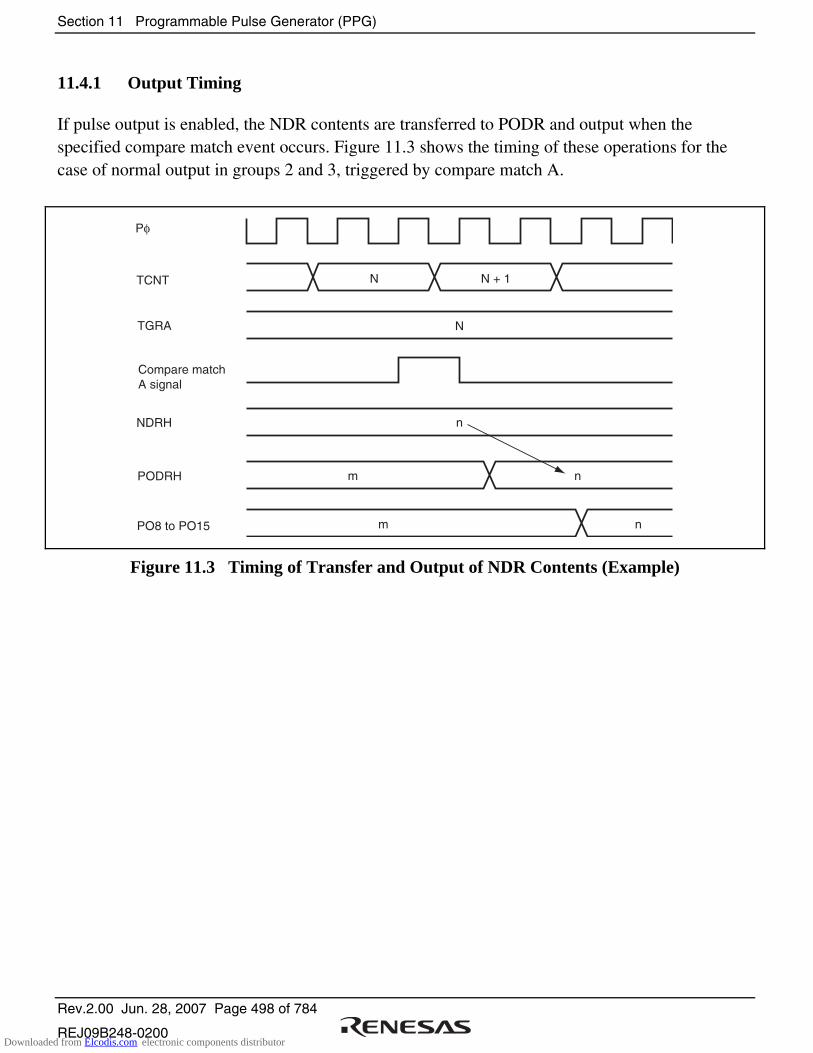
Section 11 Programmable Pulse Generator (PPG)
Rev.2.00 Jun. 28, 2007 Page 498 of 784
REJ09B248-0200
11.4.1 Output Timing
If pulse output is enabled, the NDR contents are transferred to PODR and output when the specified compare match event occurs. Figure 11.3 shows the timing of these operations for the case of normal output in groups 2 and 3, triggered by compare match A.
TCNT N N + 1
Pφ
TGRA N
Compare matchA signal
NDRH
m nPODRH
PO8 to PO15
n
m n
Figure 11.3 Timing of Transfer and Output of NDR Contents (Example)
Downloaded from Elcodis.com electronic components distributor

Section 11 Programmable Pulse Generator (PPG)
Rev.2.00 Jun. 28, 2007 Page 499 of 784
REJ09B248-0200
11.4.2 Sample Setup Procedure for Normal Pulse Output
Figure 11.4 shows a sample procedure for setting up normal pulse output.
Select TGR functions [1]
Set TGRA value
Set counting operation
Select interrupt request
Set initial output data
Enable pulse output
Select output trigger
Set next pulseoutput data
Start counter
Set next pulseoutput data
Normal PPG output
No
Yes
TPU setup
PPG setup
TPU setup
[2]
[3]
[4]
[5]
[6]
[7]
[8]
[9]
[10]
Compare match?
[1] Set TIOR to make TGRA an output compare register (with output disabled).
[2] Set the PPG output trigger cycle.
[3] Select the counter clock source with bits TPSC2 to TPSC0 in TCR. Select the counter clear source with bits CCLR1 and CCLR0.
[4] Enable the TGIA interrupt in TIER. The DTC or DMAC can also be set up to transfer data to NDR.
[5] Set the initial output values in PODR.
[6] Set the bits in NDER for the pins to be used for pulse output to 1.
[7] Select the TPU compare match event to be used as the output trigger in PCR.
[8] Set the next pulse output values in NDR.
[9] Set the CST bit in TSTR to 1 to start the TCNT counter.
[10] At each TGIA interrupt, set the next output values in NDR.
Figure 11.4 Setup Procedure for Normal Pulse Output (Example)
Downloaded from Elcodis.com electronic components distributor
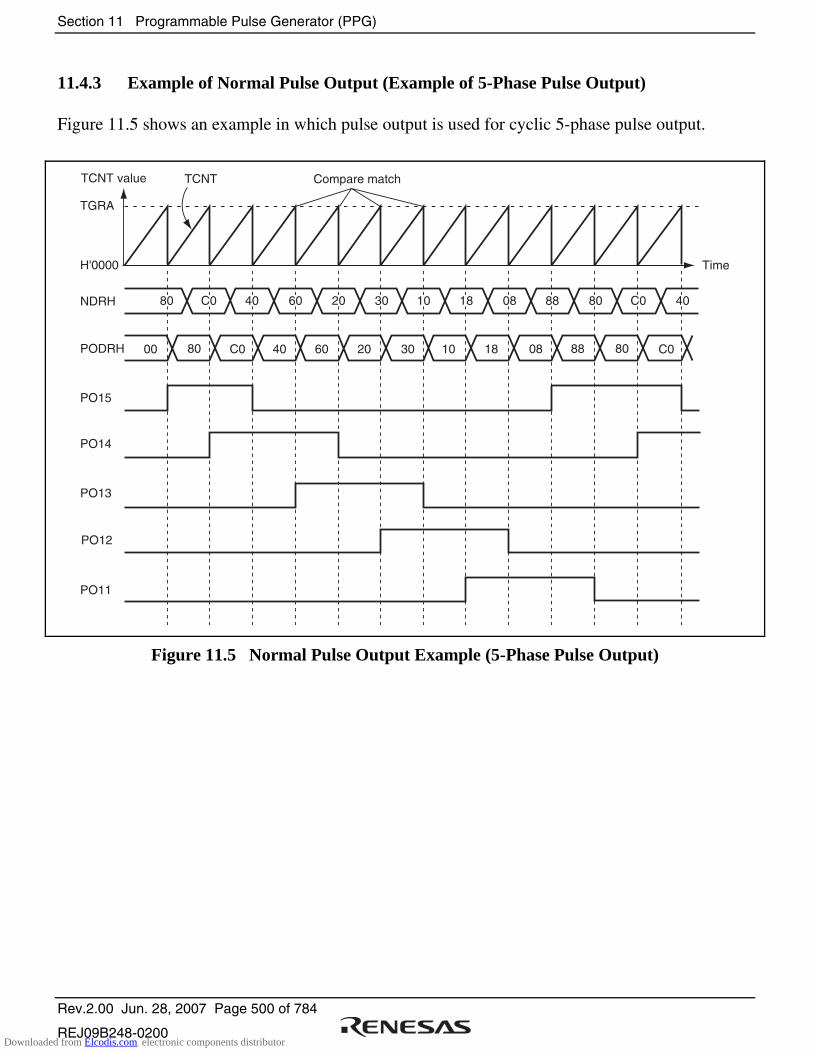
Section 11 Programmable Pulse Generator (PPG)
Rev.2.00 Jun. 28, 2007 Page 500 of 784
REJ09B248-0200
11.4.3 Example of Normal Pulse Output (Example of 5-Phase Pulse Output)
Figure 11.5 shows an example in which pulse output is used for cyclic 5-phase pulse output.
TCNT value TCNT
TGRA
H'0000
NDRH
00 80 C0 40 60 20 30 10 18 08 88PODRH
PO15
PO14
PO13
PO12
PO11
Time
Compare match
C080
C080 40 60 20 30 10 18 08 88 80 C0 40
Figure 11.5 Normal Pulse Output Example (5-Phase Pulse Output)
Downloaded from Elcodis.com electronic components distributor
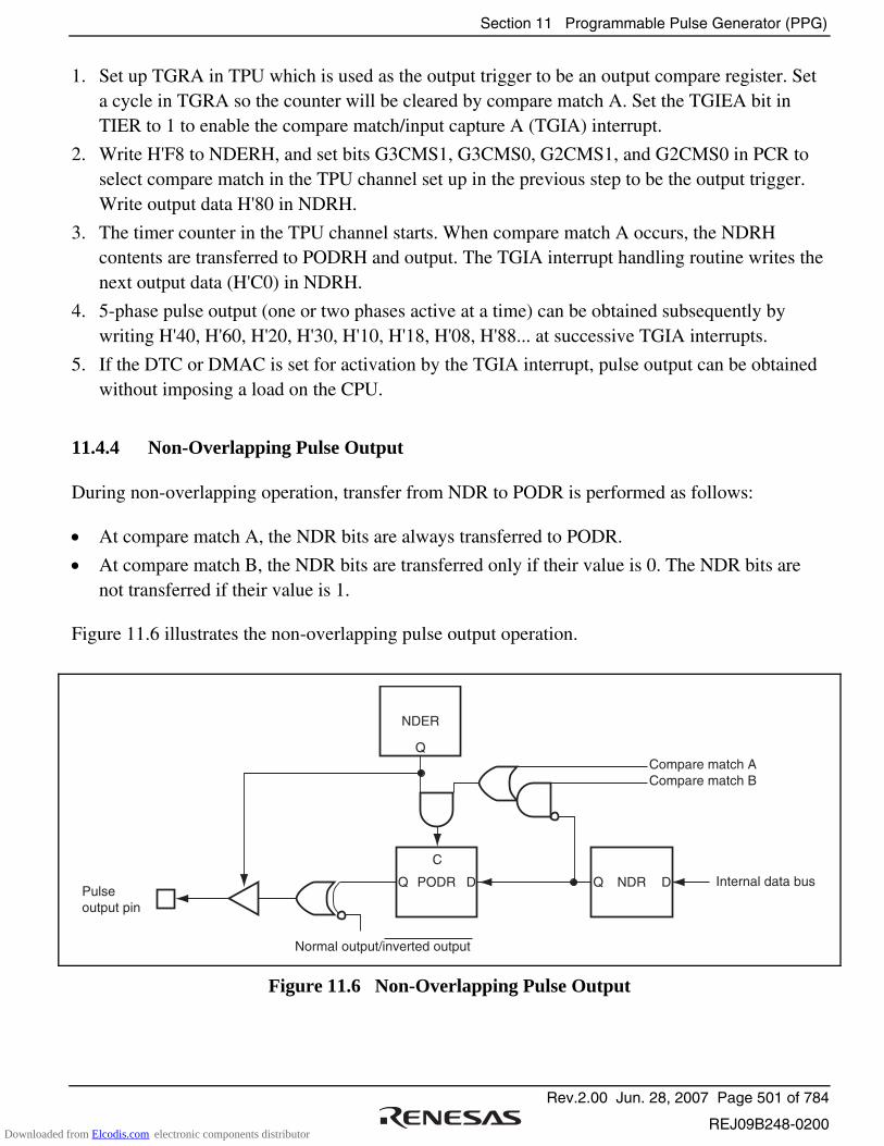
Section 11 Programmable Pulse Generator (PPG)
Rev.2.00 Jun. 28, 2007 Page 501 of 784
REJ09B248-0200
1. Set up TGRA in TPU which is used as the output trigger to be an output compare register. Set a cycle in TGRA so the counter will be cleared by compare match A. Set the TGIEA bit in TIER to 1 to enable the compare match/input capture A (TGIA) interrupt.
2. Write H'F8 to NDERH, and set bits G3CMS1, G3CMS0, G2CMS1, and G2CMS0 in PCR to select compare match in the TPU channel set up in the previous step to be the output trigger. Write output data H'80 in NDRH.
3. The timer counter in the TPU channel starts. When compare match A occurs, the NDRH contents are transferred to PODRH and output. The TGIA interrupt handling routine writes the next output data (H'C0) in NDRH.
4. 5-phase pulse output (one or two phases active at a time) can be obtained subsequently by writing H'40, H'60, H'20, H'30, H'10, H'18, H'08, H'88... at successive TGIA interrupts.
5. If the DTC or DMAC is set for activation by the TGIA interrupt, pulse output can be obtained without imposing a load on the CPU.
11.4.4 Non-Overlapping Pulse Output
During non-overlapping operation, transfer from NDR to PODR is performed as follows:
• At compare match A, the NDR bits are always transferred to PODR.
• At compare match B, the NDR bits are transferred only if their value is 0. The NDR bits are not transferred if their value is 1.
Figure 11.6 illustrates the non-overlapping pulse output operation.
Compare match ACompare match B
Pulse output pin
Internal data bus
Normal output/inverted output
C
PODRQ D
NDER
Q
NDRQ D
Figure 11.6 Non-Overlapping Pulse Output
Downloaded from Elcodis.com electronic components distributor

Section 11 Programmable Pulse Generator (PPG)
Rev.2.00 Jun. 28, 2007 Page 502 of 784
REJ09B248-0200
Therefore, 0 data can be transferred ahead of 1 data by making compare match B occur before compare match A.
The NDR contents should not be altered during the interval from compare match B to compare match A (the non-overlapping margin).
This can be accomplished by having the TGIA interrupt handling routine write the next data in NDR, or by having the TGIA interrupt activate the DTC or DMAC. Note, however, that the next data must be written before the next compare match B occurs.
Figure 11.7 shows the timing of this operation.
0/1 output0 output 0/1 output0 output
Do not writeto NDR here
Write to NDRhere
Compare match A
Compare match B
NDR
PODR
Do not writeto NDR here
Write to NDRhere
Write to NDR Write to NDR
Figure 11.7 Non-Overlapping Operation and NDR Write Timing
Downloaded from Elcodis.com electronic components distributor

Section 11 Programmable Pulse Generator (PPG)
Rev.2.00 Jun. 28, 2007 Page 503 of 784
REJ09B248-0200
11.4.5 Sample Setup Procedure for Non-Overlapping Pulse Output
Figure 11.8 shows a sample procedure for setting up non-overlapping pulse output.
Select TGR functions [1]
Set TGR values
Set counting operation
Select interrupt request
Set initial output data
Enable pulse output
Select output trigger
Set next pulseoutput data
Start counter
Set next pulseoutput data
Compare match A?No
Yes
TPU setup
PPG setup
TPU setup
Non-overlappingpulse output
Set non-overlapping groups
[2]
[3]
[4]
[5]
[6]
[7]
[8]
[9]
[10]
[11]
[1] Set TIOR to make TGRA and TGRB output compare registers (with output disabled).
[2] Set the pulse output trigger cycle in TGRB and the non-overlapping margin in TGRA.
[3] Select the counter clock source with bits TPSC2 to TPSC0 in TCR. Select the counter clear source with bits CCLR1 and CCLR0.
[4] Enable the TGIA interrupt in TIER. The DTC or DMAC can also be set up to transfer data to NDR.
[5] Set the initial output values in PODR.
[6] Set the bits in NDER for the pins to be used for pulse output to 1.
[7] Select the TPU compare match event to be used as the pulse output trigger in PCR.
[8] In PMR, select the groups that will operate in non-overlapping mode.
[9] Set the next pulse output values in NDR.
[10] Set the CST bit in TSTR to 1 to start the TCNT counter.
[11] At each TGIA interrupt, set the next output values in NDR.
Figure 11.8 Setup Procedure for Non-Overlapping Pulse Output (Example)
Downloaded from Elcodis.com electronic components distributor
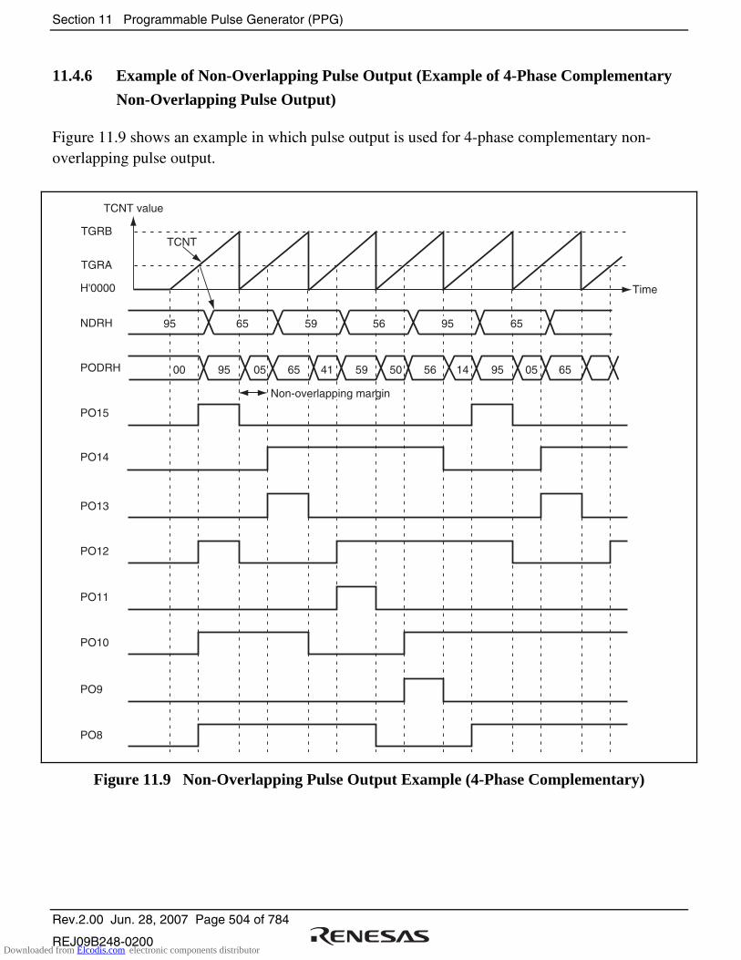
Section 11 Programmable Pulse Generator (PPG)
Rev.2.00 Jun. 28, 2007 Page 504 of 784
REJ09B248-0200
11.4.6 Example of Non-Overlapping Pulse Output (Example of 4-Phase Complementary
Non-Overlapping Pulse Output)
Figure 11.9 shows an example in which pulse output is used for 4-phase complementary non-overlapping pulse output.
TCNT value
TCNTTGRB
TGRA
H'0000
NDRH 95 65 59 56 95 65
00 95 05 65 41 59 50 56 14 95 05 65PODRH
PO15
PO14
PO13
PO12
PO11
PO10
PO9
PO8
Time
Non-overlapping margin
Figure 11.9 Non-Overlapping Pulse Output Example (4-Phase Complementary)
Downloaded from Elcodis.com electronic components distributor
Section 11 Programmable Pulse Generator (PPG)
Rev.2.00 Jun. 28, 2007 Page 505 of 784
REJ09B248-0200
1. Set up the TPU channel to be used as the output trigger channel so that TGRA and TGRB are output compare registers. Set the cycle in TGRB and the non-overlapping margin in TGRA, and set the counter to be cleared by compare match B. Set the TGIEA bit in TIER to 1 to enable the TGIA interrupt.
2. Write H'FF to NDERH, and set bits G3CMS1, G3CMS0, G2CMS1, and G2CMS0 in PCR to select compare match in the TPU channel set up in the previous step to be the output trigger.
Set bits G3NOV and G2NOV in PMR to 1 to select non-overlapping pulse output.
Write output data H'95 to NDRH.
3. The timer counter in the TPU channel starts. When a compare match with TGRB occurs, outputs change from 1 to 0. When a compare match with TGRA occurs, outputs change from 0 to 1 (the change from 0 to 1 is delayed by the value set in TGRA).
The TGIA interrupt handling routine writes the next output data (H'65) to NDRH.
4. 4-phase complementary non-overlapping pulse output can be obtained subsequently by writing H'59, H'56, H'95... at successive TGIA interrupts.
If the DTC or DMAC is set for activation by a TGIA interrupt, pulse can be output without imposing a load on the CPU.
Downloaded from Elcodis.com electronic components distributor
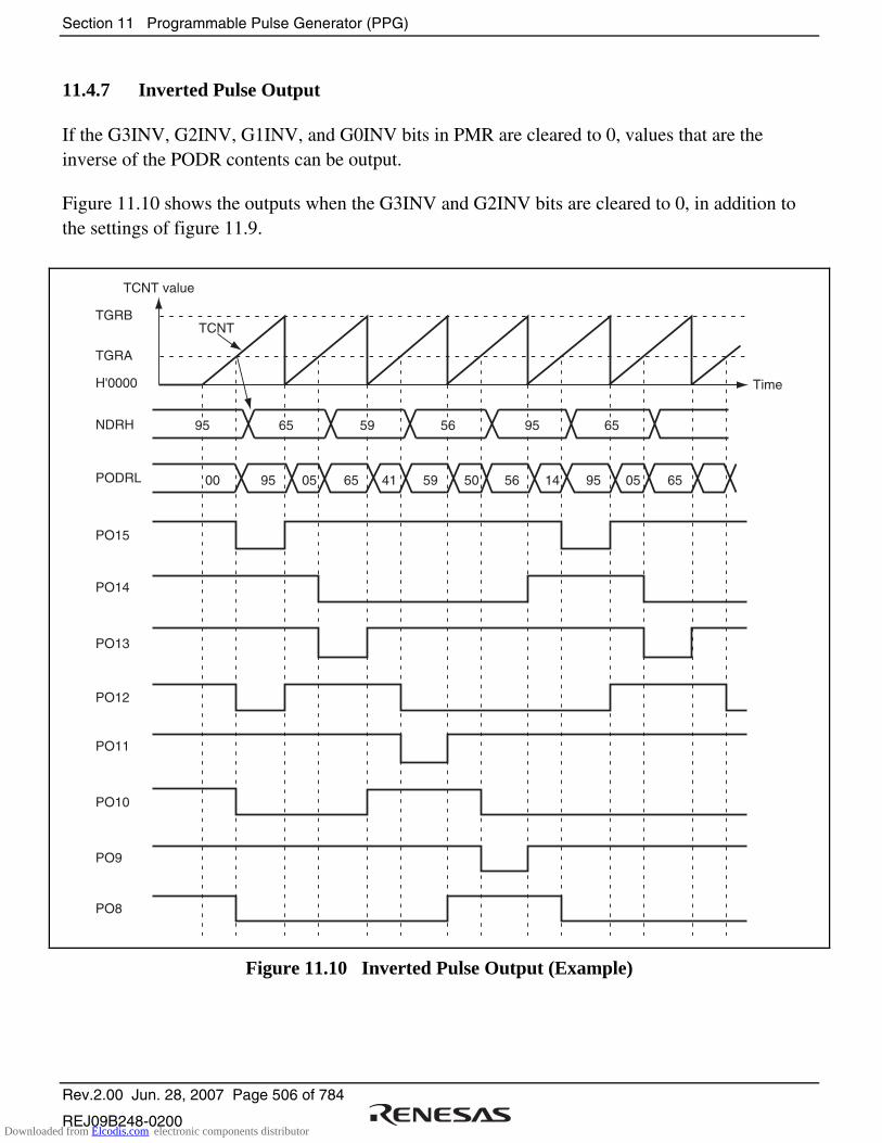
Section 11 Programmable Pulse Generator (PPG)
Rev.2.00 Jun. 28, 2007 Page 506 of 784
REJ09B248-0200
11.4.7 Inverted Pulse Output
If the G3INV, G2INV, G1INV, and G0INV bits in PMR are cleared to 0, values that are the inverse of the PODR contents can be output.
Figure 11.10 shows the outputs when the G3INV and G2INV bits are cleared to 0, in addition to the settings of figure 11.9.
TCNT value
TCNTTGRB
TGRA
H'0000
NDRH 95 65 59 56 95 65
00 95 05 65 41 59 50 56 14 95 05 65PODRL
PO15
PO14
PO13
PO12
PO11
PO10
PO9
PO8
Time
Figure 11.10 Inverted Pulse Output (Example)
Downloaded from Elcodis.com electronic components distributor
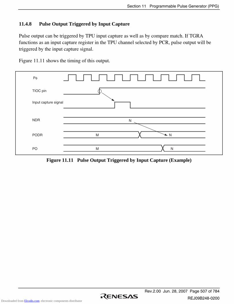
Section 11 Programmable Pulse Generator (PPG)
Rev.2.00 Jun. 28, 2007 Page 507 of 784
REJ09B248-0200
11.4.8 Pulse Output Triggered by Input Capture
Pulse output can be triggered by TPU input capture as well as by compare match. If TGRA functions as an input capture register in the TPU channel selected by PCR, pulse output will be triggered by the input capture signal.
Figure 11.11 shows the timing of this output.
Pφ
N
M N
TIOC pin
Input capture signal
NDR
PODR
M NPO
Figure 11.11 Pulse Output Triggered by Input Capture (Example)
Downloaded from Elcodis.com electronic components distributor

Section 11 Programmable Pulse Generator (PPG)
Rev.2.00 Jun. 28, 2007 Page 508 of 784
REJ09B248-0200
11.5 Usage Notes
11.5.1 Module Stop Mode Setting
PPG operation can be disabled or enabled using the module stop control register. The initial value is for PPG operation to be halted. Register access is enabled by clearing module stop mode. For details, refer to section 19, Power-Down Modes.
11.5.2 Operation of Pulse Output Pins
Pins PO0 to PO15 are also used for other peripheral functions such as the TPU. When output by another peripheral function is enabled, the corresponding pins cannot be used for pulse output. Note, however, that data transfer from NDR bits to PODR bits takes place, regardless of the usage of the pins.
Pin functions should be changed only under conditions in which the output trigger event will not occur.
Downloaded from Elcodis.com electronic components distributor
Section 12 8-Bit Timers (TMR)
Rev.2.00 Jun. 28, 2007 Page 509 of 784
REJ09B248-0200
Section 12 8-Bit Timers (TMR)
This LSI has two units (unit 0 and unit 1) of an on-chip 8-bit timer module that comprise two 8-bit counter channels, totaling four channels. The 8-bit timer module can be used to count external events and also be used as a multifunction timer in a variety of applications, such as generation of counter reset, interrupt requests, and pulse output with a desired duty cycle using a compare-match signal with two registers.
Figures 12.1 and 12.2 show block diagrams of the 8-bit timer module (unit 0 and unit 1).
This section describes unit 0 (channels 0 and 1), which has the same functions as the other unit.
12.1 Features
• Selection of seven clock sources
The counters can be driven by one of six internal clock signals (Pφ/2, Pφ/18, Pφ/32, Pφ/164, Pφ/1024, or Pφ/8192) or an external clock input.
• Selection of three ways to clear the counters
The counters can be cleared on compare match A or B, or by an external reset signal.
• Timer output control by a combination of two compare match signals
The timer output signal in each channel is controlled by a combination of two independent compare match signals, enabling the timer to output pulses with a desired duty cycle or PWM output.
• Cascading of two channels (TMR_0 and TMR_1)
Operation as a 16-bit timer is possible, using TMR_0 for the upper 8 bits and TMR_1 for the lower 8 bits (16-bit count mode).
TMR_1 can be used to count TMR_0 compare matches (compare match count mode).
• Three interrupt sources
Compare match A, compare match B, and overflow interrupts can be requested independently.
• Generation of trigger to start A/D converter conversion
Downloaded from Elcodis.com electronic components distributor
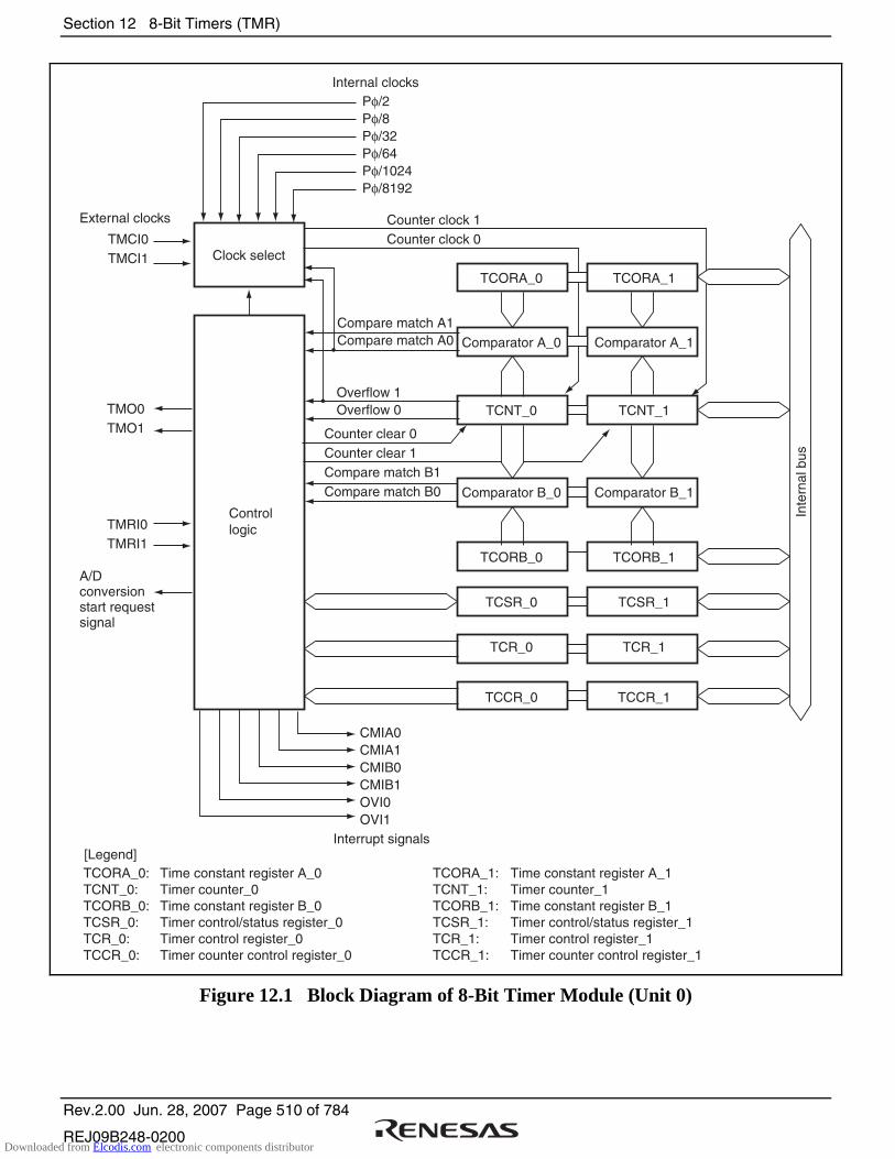
Section 12 8-Bit Timers (TMR)
Rev.2.00 Jun. 28, 2007 Page 510 of 784
REJ09B248-0200
CMIA0CMIA1CMIB0CMIB1OVI0OVI1
TMO0TMO1
TMCI0TMCI1
TMRI0 TMRI1
TCORA_1:TCNT_1: TCORB_1:TCSR_1:TCR_1:TCCR_1:
TCORA_0:TCNT_0:TCORB_0: TCSR_0: TCR_0:TCCR_0:
Pφ/2Pφ/8Pφ/32Pφ/64Pφ/1024Pφ/8192
Counter clock 1Counter clock 0
Compare match A1Compare match A0
Overflow 1Overflow 0
Counter clear 0Counter clear 1Compare match B1Compare match B0
Comparator A_0 Comparator A_1
TCORA_0
TCORB_0
TCSR_0
TCCR_0
TCORA_1
TCNT_1
TCORB_1
TCSR_1
TCCR_1
TCR_0 TCR_1
TCNT_0
Comparator B_0 Comparator B_1
A/Dconversionstart requestsignal
Inte
rnal
bus
Time constant register A_1Timer counter_1Time constant register B_1Timer control/status register_1Timer control register_1Timer counter control register_1
Time constant register A_0Timer counter_0Time constant register B_0Timer control/status register_0Timer control register_0Timer counter control register_0
Interrupt signals
Internal clocks
Clock select
Controllogic
External clocks
[Legend]
Figure 12.1 Block Diagram of 8-Bit Timer Module (Unit 0)
Downloaded from Elcodis.com electronic components distributor
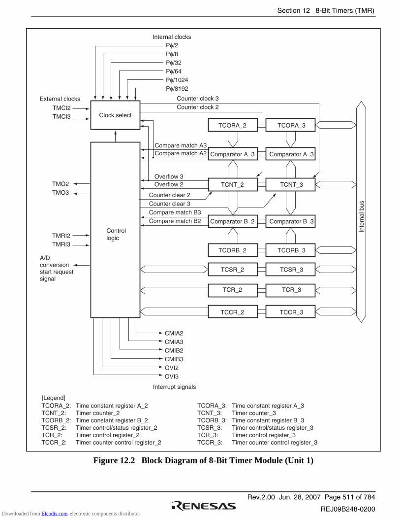
Section 12 8-Bit Timers (TMR)
Rev.2.00 Jun. 28, 2007 Page 511 of 784
REJ09B248-0200
CMIA2CMIA3CMIB2CMIB3OVI2OVI3
TMO2TMO3
TMCI2TMCI3
TMRI2 TMRI3
TCORA_3:TCNT_3: TCORB_3:TCSR_3:TCR_3:TCCR_3:
TCORA_2:TCNT_2:TCORB_2: TCSR_2: TCR_2:TCCR_2:
Pφ/2Pφ/8Pφ/32Pφ/64Pφ/1024Pφ/8192
Counter clock 3Counter clock 2
Compare match A3Compare match A2
Overflow 3Overflow 2
Counter clear 2Counter clear 3Compare match B3Compare match B2
Comparator A_3 Comparator A_3
TCORA_2
TCORB_2
TCSR_2
TCCR_2
TCORA_3
TCNT_3
TCORB_3
TCSR_3
TCCR_3
TCR_2 TCR_3
TCNT_2
Comparator B_2 Comparator B_3
A/Dconversionstart requestsignal
Inte
rnal
bus
Time constant register A_3Timer counter_3Time constant register B_3Timer control/status register_3Timer control register_3Timer counter control register_3
Time constant register A_2Timer counter_2Time constant register B_2Timer control/status register_2Timer control register_2Timer counter control register_2
Interrupt signals
Internal clocks
Clock select
Controllogic
External clocks
[Legend]
Figure 12.2 Block Diagram of 8-Bit Timer Module (Unit 1)
Downloaded from Elcodis.com electronic components distributor
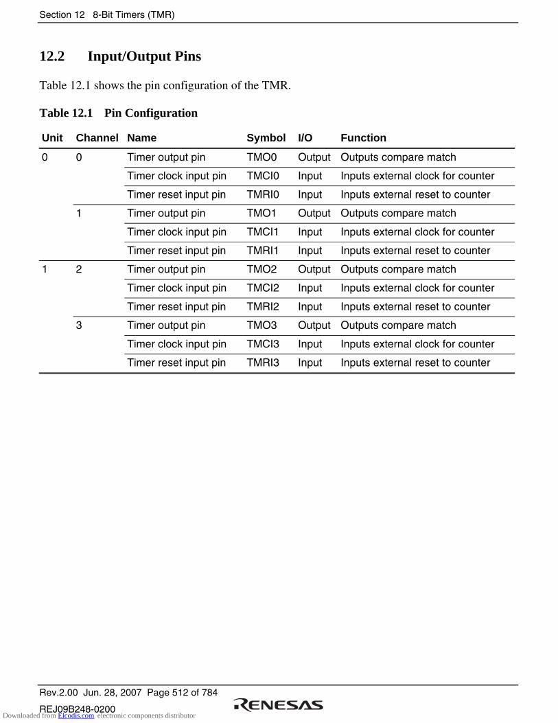
Section 12 8-Bit Timers (TMR)
Rev.2.00 Jun. 28, 2007 Page 512 of 784
REJ09B248-0200
12.2 Input/Output Pins
Table 12.1 shows the pin configuration of the TMR.
Table 12.1 Pin Configuration
Unit Channel Name Symbol I/O Function
0 0 Timer output pin TMO0 Output Outputs compare match
Timer clock input pin TMCI0 Input Inputs external clock for counter
Timer reset input pin TMRI0 Input Inputs external reset to counter
1 Timer output pin TMO1 Output Outputs compare match
Timer clock input pin TMCI1 Input Inputs external clock for counter
Timer reset input pin TMRI1 Input Inputs external reset to counter
1 2 Timer output pin TMO2 Output Outputs compare match
Timer clock input pin TMCI2 Input Inputs external clock for counter
Timer reset input pin TMRI2 Input Inputs external reset to counter
3 Timer output pin TMO3 Output Outputs compare match
Timer clock input pin TMCI3 Input Inputs external clock for counter
Timer reset input pin TMRI3 Input Inputs external reset to counter
Downloaded from Elcodis.com electronic components distributor
Section 12 8-Bit Timers (TMR)
Rev.2.00 Jun. 28, 2007 Page 513 of 784
REJ09B248-0200
12.3 Register Descriptions
The TMR has the following registers.
Unit 0:
• Channel 0
Timer counter_0 (TCNT_0)
Time constant register A_0 (TCORA_0)
Time constant register B_0 (TCORB_0)
Timer control register_0 (TCR_0)
Timer counter control register_0 (TCCR_0)
Timer control/status register_0 (TCSR_0)
• Channel 1
Timer counter_1 (TCNT_1)
Time constant register A_1 (TCORA_1)
Time constant register B_1 (TCORB_1)
Timer control register_1 (TCR_1)
Timer counter control register_1 (TCCR_1)
Timer control/status register_1 (TCSR_1) Unit 1:
• Channel 2
Timer counter_2 (TCNT_2)
Time constant register A_2 (TCORA_2)
Time constant register B_2 (TCORB_2)
Timer control register_2 (TCR_2)
Timer counter control register_2 (TCCR_2)
Timer control/status register_2 (TCSR_2)
• Channel 3
Timer counter_3 (TCNT_3)
Time constant register A_3 (TCORA_3)
Time constant register B_3 (TCORB_3)
Timer control register_3 (TCR_3)
Timer counter control register_3 (TCCR_3)
Timer control/status register_3 (TCSR_3)
Downloaded from Elcodis.com electronic components distributor

Section 12 8-Bit Timers (TMR)
Rev.2.00 Jun. 28, 2007 Page 514 of 784
REJ09B248-0200
12.3.1 Timer Counter (TCNT)
TCNT is an 8-bit readable/writable up-counter. TCNT_0 and TCNT_1 comprise a single 16-bit register so they can be accessed together by a word transfer instruction. Bits CKS2 to CKS0 in TCR and bits ICKS1 and ICKS0 in TCCR are used to select a clock. TCNT can be cleared by an external reset input signal, compare match A signal, or compare match B signal. Which signal is to be used for clearing is selected by bits CCLR1 and CCLR0 in TCR. When TCNT overflows from H'FF to H'00, bit OVF in TCSR is set to 1. TCNT is initialized to H'00.
7
0
R/W
6
0
R/W
5
0
R/W
4
0
R/W
3
0
R/W
2
0
R/W
1
0
R/W
0
0
R/W
7
0
R/W
6
0
R/W
5
0
R/W
4
0
R/W
3
0
R/W
2
0
R/W
1
0
R/W
0
0
R/W
TCNT_0 TCNT_1
Bit
Bit Name
Initial Value
R/W
12.3.2 Time Constant Register A (TCORA)
TCORA is an 8-bit readable/writable register. TCORA_0 and TCORA_1 comprise a single 16-bit register so they can be accessed together by a word transfer instruction. The value in TCORA is continually compared with the value in TCNT. When a match is detected, the corresponding CMFA flag in TCSR is set to 1. Note however that comparison is disabled during the T2 state of a TCORA write cycle. The timer output from the TMO pin can be freely controlled by this compare match signal (compare match A) and the settings of bits OS1 and OS0 in TCSR. TCORA is initialized to H'FF.
7
1
R/W
6
1
R/W
5
1
R/W
4
1
R/W
3
1
R/W
2
1
R/W
1
1
R/W
0
1
R/W
7
1
R/W
6
1
R/W
5
1
R/W
4
1
R/W
3
1
R/W
2
1
R/W
1
1
R/W
0
1
R/W
TCORA_0 TCORA_1
Bit
Bit Name
Initial Value
R/W
Downloaded from Elcodis.com electronic components distributor
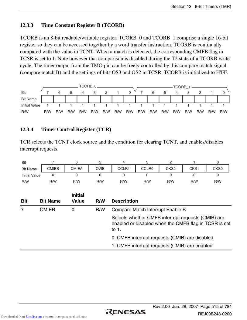
Section 12 8-Bit Timers (TMR)
Rev.2.00 Jun. 28, 2007 Page 515 of 784
REJ09B248-0200
12.3.3 Time Constant Register B (TCORB)
TCORB is an 8-bit readable/writable register. TCORB_0 and TCORB_1 comprise a single 16-bit register so they can be accessed together by a word transfer instruction. TCORB is continually compared with the value in TCNT. When a match is detected, the corresponding CMFB flag in TCSR is set to 1. Note however that comparison is disabled during the T2 state of a TCORB write cycle. The timer output from the TMO pin can be freely controlled by this compare match signal (compare match B) and the settings of bits OS3 and OS2 in TCSR. TCORB is initialized to H'FF.
7
1
R/W
6
1
R/W
5
1
R/W
4
1
R/W
3
1
R/W
2
1
R/W
1
1
R/W
0
1
R/W
7
1
R/W
6
1
R/W
5
1
R/W
4
1
R/W
3
1
R/W
2
1
R/W
1
1
R/W
0
1
R/W
TCORB_0 TCORB_1
Bit
Bit Name
Initial Value
R/W
12.3.4 Timer Control Register (TCR)
TCR selects the TCNT clock source and the condition for clearing TCNT, and enables/disables interrupt requests.
7
CMIEB
0
R/W
6
CMIEA
0
R/W
5
OVIE
0
R/W
4
CCLR1
0
R/W
3
CCLR0
0
R/W
2
CKS2
0
R/W
1
CKS1
0
R/W
0
CKS0
0
R/W
Bit
Bit Name
Initial Value
R/W
Bit Bit Name Initial Value R/W Description
7 CMIEB 0 R/W Compare Match Interrupt Enable B
Selects whether CMFB interrupt requests (CMIB) are enabled or disabled when the CMFB flag in TCSR is set to 1.
0: CMFB interrupt requests (CMIB) are disabled
1: CMFB interrupt requests (CMIB) are enabled
Downloaded from Elcodis.com electronic components distributor

Section 12 8-Bit Timers (TMR)
Rev.2.00 Jun. 28, 2007 Page 516 of 784
REJ09B248-0200
Bit Bit Name Initial Value R/W Description
6 CMIEA 0 R/W Compare Match Interrupt Enable A
Selects whether CMFA interrupt requests (CMIA) are enabled or disabled when the CMFA flag in TCSR is set to 1.
0: CMFA interrupt requests (CMIA) are disabled
1: CMFA interrupt requests (CMIA) are enabled
5 OVIE 0 R/W Timer Overflow Interrupt Enable
Selects whether OVF interrupt requests (OVI) are enabled or disabled when the OVF flag in TCSR is set to 1.
0: OVF interrupt requests (OVI) are disabled
1: OVF interrupt requests (OVI) are enabled
4
3
CCLR1
CCLR0
0
0
R/W
R/W
Counter Clear 1 and 0*
These bits select the method by which TCNT is cleared.
00: Clearing is disabled
01: Cleared by compare match A
10: Cleared by compare match B
11: Cleared at rising edge (TMRIS in TCCR is cleared
to 0) of the external reset input or when the external reset input is high (TMRIS in TCCR is set
to 1)
2
1
0
CKS2
CKS1
CKS0
0
0
0
R/W
R/W
R/W
Clock Select 2 to 0*
These bits select the clock input to TCNT and count condition. See table 12.2.
Note: * To use an external reset or external clock, the DDR and ICR bits in the corresponding pin should be set to 0 and 1, respectively. For details, see section 9, I/O Ports.
Downloaded from Elcodis.com electronic components distributor
Section 12 8-Bit Timers (TMR)
Rev.2.00 Jun. 28, 2007 Page 517 of 784
REJ09B248-0200
12.3.5 Timer Counter Control Register (TCCR)
TCCR selects the TCNT internal clock source and controls external reset input.
7
0
R/W
6
0
R/W
5
0
R/W
4
0
R/W
3
TMRIS
0
R/W
2
0
R/W
1
ICKS1
0
R/W
0
ICKS0
0
R/W
Bit
Bit Name
Initial Value
R/W
Bit Bit Name Initial Value R/W Description
7 to 4 0 R/W Reserved
These bits are always read as 0. The write value should always be 0.
3 TMRIS 0 R/W Timer Reset Input Select
Selects an external reset input when the CCLR1 and CCLR0 bits in TCR are B'11.
0: Cleared at rising edge of the external reset
1: Cleared when the external reset is high
2 0 R/W Reserved
This bit is always read as 0. The write value should always be 0
1
0
ICKS1
ICKS0
0
0
R/W
R/W
Internal Clock Select 1 and 0
These bits in combination with bits CKS2 to CKS0 in TCR select the internal clock. See table 12.2.
Downloaded from Elcodis.com electronic components distributor

Section 12 8-Bit Timers (TMR)
Rev.2.00 Jun. 28, 2007 Page 518 of 784
REJ09B248-0200
Table 12.2 Clock Input to TCNT and Count Condition
TCR TCCR
Channel Bit 2 CKS2
Bit 1 CKS1
Bit 0 CKS0
Bit 1ICKS1
Bit 0 ICKS0 Description
TMR_0 0 0 0 Clock input prohibited.
0 0 1 0 0 Uses internal clock. Counts at rising edge of Pφ/8.
0 1 Uses internal clock. Counts at rising edge of Pφ/2.
1 0 Uses internal clock. Counts at falling edge of Pφ/8.
1 1 Uses internal clock. Counts at falling edge of Pφ/2.
0 1 0 0 0 Uses internal clock. Counts at rising edge of Pφ/64.
0 1 Uses internal clock. Counts at rising edge of Pφ/32.
1 0 Uses internal clock. Counts at falling edge of Pφ/64.
1 1 Uses internal clock. Counts at falling edge of Pφ/32.
0 1 1 0 0 Uses internal clock. Counts at rising edge of Pφ/8192.
0 1 Uses internal clock. Counts at rising edge of Pφ/1024.
1 0 Uses internal clock. Counts at falling edge of Pφ/8192.
1 1 Uses internal clock. Counts at falling edge of Pφ/1024.
1 0 0 Counts at TCNT_1 overflow signal*1.
TMR_1 0 0 0 Clock input prohibited.
0 0 1 0 0 Uses internal clock. Counts at rising edge of Pφ/8.
0 1 Uses internal clock. Counts at rising edge of Pφ/2.
1 0 Uses internal clock. Counts at falling edge of Pφ/8.
1 1 Uses internal clock. Counts at falling edge of Pφ/2.
0 1 0 0 0 Uses internal clock. Counts at rising edge of Pφ/64.
0 1 Uses internal clock. Counts at rising edge of Pφ/32.
1 0 Uses internal clock. Counts at falling edge of Pφ/64.
1 1 Uses internal clock. Counts at falling edge of Pφ/32.
0 1 1 0 0 Uses internal clock. Counts at rising edge of Pφ/8192.
0 1 Uses internal clock. Counts at rising edge of Pφ/1024.
1 0 Uses internal clock. Counts at falling edge of Pφ/8192.
1 1 Uses internal clock. Counts at falling edge of Pφ/1024.
1 0 0 Counts at TCNT_0 compare match A*1.
Downloaded from Elcodis.com electronic components distributor
Section 12 8-Bit Timers (TMR)
Rev.2.00 Jun. 28, 2007 Page 519 of 784
REJ09B248-0200
TCR TCCR
Channel Bit 2 CKS2
Bit 1 CKS1
Bit 0 CKS0
Bit 1ICKS1
Bit 0 ICKS0 Description
All 1 0 1 Uses external clock. Counts at rising edge*2.
1 1 0 Uses external clock. Counts at falling edge*2.
1 1 1 Uses external clock. Counts at both rising and falling edges*2.
Notes: 1. If the clock input of TMR_0 is the TCNT_1 overflow signal and that of TMR_1 is the TCNT_0 compare match signal, no incrementing clock is generated. Do not use this setting.
2. To use the external clock, the DDR and ICR bits in the corresponding pin should be set to 0 and 1, respectively. For details, see section 9, I/O Ports.
12.3.6 Timer Control/Status Register (TCSR)
TCSR displays status flags, and controls compare match output.
• TCSR_0
• TCSR_1
7
CMFB
0
R/(W)*
6
CMFA
0
R/(W)*
5
OVF
0
R/(W)*
4
ADTE
0
R/W
3
OS3
0
R/W
2
OS2
0
R/W
1
OS1
0
R/W
0
OS0
0
R/W
7
CMFB
0
R/(W)*
6
CMFA
0
R/(W)*
5
OVF
0
R/(W)*
4
1
R
3
OS3
0
R/W
2
OS2
0
R/W
1
OS1
0
R/W
0
OS0
0
R/W
Bit
Bit Name
Initial Value
R/W
Bit
Bit Name
Initial Value
R/W
Note: * Only 0 can be written to this bit, to clear the flag.
Downloaded from Elcodis.com electronic components distributor

Section 12 8-Bit Timers (TMR)
Rev.2.00 Jun. 28, 2007 Page 520 of 784
REJ09B248-0200
• TCSR_0
Bit Bit Name Initial Value R/W Description
7 CMFB 0 R/(W)*1 Compare Match Flag B
[Setting condition]
• When TCNT matches TCORB
[Clearing conditions]
• When writing 0 after reading CMFB = 1
(When the CPU is used to clear this flag by writing 0
while the corresponding interrupt is enabled, be sure
to read the flag after writing 0 to it.)
• When the DTC is activated by a CMIB interrupt
while the DISEL bit in MRB of the DTC is 0
6 CMFA 0 R/(W)*1 Compare Match Flag A
[Setting condition]
• When TCNT matches TCORA
[Clearing conditions]
• When writing 0 after reading CMFA = 1
(When the CPU is used to clear this flag by writing 0
while the corresponding interrupt is enabled, be
sure to read the flag after writing 0 to it.)
• When the DTC is activated by a CMIA interrupt
while the DISEL bit in MRB in the DTC is 0
5 OVF 0 R/(W)*1 Timer Overflow Flag
[Setting condition]
When TCNT overflows from H'FF to H'00
[Clearing condition]
When writing 0 after reading OVF = 1
(When the CPU is used to clear this flag by writing 0 while the corresponding interrupt is enabled, be sure to read the flag after writing 0 to it.)
Downloaded from Elcodis.com electronic components distributor
Section 12 8-Bit Timers (TMR)
Rev.2.00 Jun. 28, 2007 Page 521 of 784
REJ09B248-0200
Bit Bit Name Initial Value R/W Description
4 ADTE 0 R/W A/D Trigger Enable
Selects enabling or disabling of A/D converter start requests by compare match A.
0: A/D converter start requests by compare match A are disabled
1: A/D converter start requests by compare match A are enabled
3
2
OS3
OS2
0
0
R/W
R/W
Output Select 3 and 2*2
These bits select a method of TMO pin output when compare match B of TCORB and TCNT occurs.
00: No change when compare match B occurs
01: 0 is output when compare match B occurs
10: 1 is output when compare match B occurs
11: Output is inverted when compare match B occurs (toggle output)
1
0
OS1
OS0
0
0
R/W
R/W
Output Select 1 and 0*2
These bits select a method of TMO pin output when compare match A of TCORA and TCNT occurs.
00: No change when compare match A occurs
01: 0 is output when compare match A occurs
10: 1 is output when compare match A occurs
11: Output is inverted when compare match A occurs
(toggle output)
Notes: 1. Only 0 can be written to bits 7 to 5, to clear these flags.
2. Timer output is disabled when bits OS3 to OS0 are all 0. Timer output is 0 until the first compare match occurs after resetting.
Downloaded from Elcodis.com electronic components distributor
Section 12 8-Bit Timers (TMR)
Rev.2.00 Jun. 28, 2007 Page 522 of 784
REJ09B248-0200
• TCSR_1
Bit Bit Name Initial Value R/W Description
7 CMFB 0 R/(W)*1 Compare Match Flag B
[Setting condition]
• When TCNT matches TCORB
[Clearing conditions]
• When writing 0 after reading CMFB = 1
(When the CPU is used to clear this flag by writing 0
while the corresponding interrupt is enabled, be
sure to read the flag after writing 0 to it.)
• When the DTC is activated by a CMIB interrupt
while the DISEL bit in MRB of the DTC is 0
6 CMFA 0 R/(W)*1 Compare Match Flag A
[Setting condition]
• When TCNT matches TCORA
[Clearing conditions]
• When writing 0 after reading CMFA = 1
(When the CPU is used to clear this flag by writing 0
while the corresponding interrupt is enabled, be sure
to read the flag after writing 0 to it.)
• When the DTC is activated by a CMIA interrupt
while the DISEL bit in MRB of the DTC is 0
5 OVF 0 R/(W)*1 Timer Overflow Flag
[Setting condition]
When TCNT overflows from H'FF to H'00
[Clearing condition]
Cleared by reading OVF when OVF = 1, then writing 0 to OVF
(When the CPU is used to clear this flag by writing 0 while the corresponding interrupt is enabled, be sure to read the flag after writing 0 to it.)
Downloaded from Elcodis.com electronic components distributor
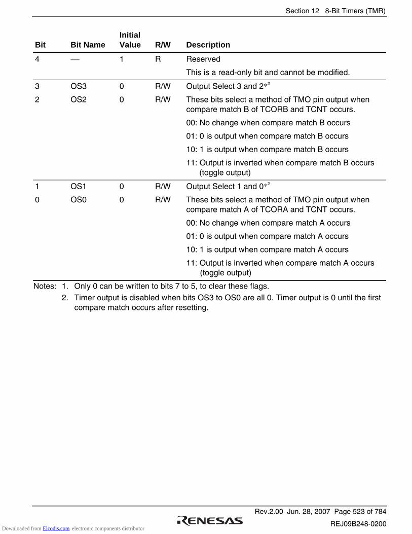
Section 12 8-Bit Timers (TMR)
Rev.2.00 Jun. 28, 2007 Page 523 of 784
REJ09B248-0200
Bit Bit Name Initial Value R/W Description
4 1 R Reserved
This is a read-only bit and cannot be modified.
3
2
OS3
OS2
0
0
R/W
R/W
Output Select 3 and 2*2
These bits select a method of TMO pin output when compare match B of TCORB and TCNT occurs.
00: No change when compare match B occurs
01: 0 is output when compare match B occurs
10: 1 is output when compare match B occurs
11: Output is inverted when compare match B occurs (toggle output)
1
0
OS1
OS0
0
0
R/W
R/W
Output Select 1 and 0*2
These bits select a method of TMO pin output when compare match A of TCORA and TCNT occurs.
00: No change when compare match A occurs
01: 0 is output when compare match A occurs
10: 1 is output when compare match A occurs
11: Output is inverted when compare match A occurs (toggle output)
Notes: 1. Only 0 can be written to bits 7 to 5, to clear these flags. 2. Timer output is disabled when bits OS3 to OS0 are all 0. Timer output is 0 until the first
compare match occurs after resetting.
Downloaded from Elcodis.com electronic components distributor

Section 12 8-Bit Timers (TMR)
Rev.2.00 Jun. 28, 2007 Page 524 of 784
REJ09B248-0200
12.4 Operation
12.4.1 Pulse Output
Figure 12.3 shows an example of the 8-bit timer being used to generate a pulse output with a desired duty cycle. The control bits are set as follows:
1. In TCR, clear bit CCLR1 to 0 and set bit CCLR0 to 1 so that TCNT is cleared at a TCORA compare match.
2. In TCSR, set bits OS3 to OS0 to B'0110, causing the output to change to 1 at a TCORA compare match and to 0 at a TCORB compare match.
With these settings, the 8-bit timer provides pulses output at a cycle determined by TCORA with a pulse width determined by TCORB. No software intervention is required. The output level of the 8-bit timer holds 0 until the first compare match occurs after a reset.
TCNTH'FF
Counter clear
TCORA
TCORB
H'00
TMO
Figure 12.3 Example of Pulse Output
Downloaded from Elcodis.com electronic components distributor
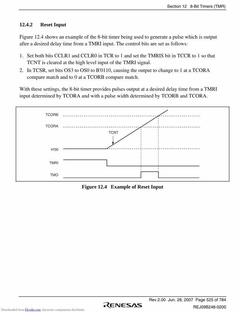
Section 12 8-Bit Timers (TMR)
Rev.2.00 Jun. 28, 2007 Page 525 of 784
REJ09B248-0200
12.4.2 Reset Input
Figure 12.4 shows an example of the 8-bit timer being used to generate a pulse which is output after a desired delay time from a TMRI input. The control bits are set as follows:
1. Set both bits CCLR1 and CCLR0 in TCR to 1 and set the TMRIS bit in TCCR to 1 so that TCNT is cleared at the high level input of the TMRI signal.
2. In TCSR, set bits OS3 to OS0 to B'0110, causing the output to change to 1 at a TCORA compare match and to 0 at a TCORB compare match.
With these settings, the 8-bit timer provides pulses output at a desired delay time from a TMRI input determined by TCORA and with a pulse width determined by TCORB and TCORA.
TCNT
TCORB
TCORA
H'00
TMRI
TMO
Figure 12.4 Example of Reset Input
Downloaded from Elcodis.com electronic components distributor

Section 12 8-Bit Timers (TMR)
Rev.2.00 Jun. 28, 2007 Page 526 of 784
REJ09B248-0200
12.5 Operation Timing
12.5.1 TCNT Count Timing
Figure 12.5 shows the TCNT count timing for internal clock input. Figure 12.6 shows the TCNT count timing for external clock input. Note that the external clock pulse width must be at least 1.5 states for incrementation at a single edge, and at least 2.5 states for incrementation at both edges. The counter will not increment correctly if the pulse width is less than these values.
Pφ
Internal clock
TCNT inputclock
TCNT N – 1 N N + 1
Figure 12.5 Count Timing for Internal Clock Input at Falling Edge
Pφ
External clockinput pin
TCNT inputclock
TCNT N – 1 N N + 1
Figure 12.6 Count Timing for External Clock Input at Falling and Rising Edges
12.5.2 Timing of CMFA and CMFB Setting at Compare Match
The CMFA and CMFB flags in TCSR are set to 1 by a compare match signal generated when the TCOR and TCNT values match. The compare match signal is generated at the last state in which the match is true, just before the timer counter is updated. Therefore, when the TCOR and TCNT values match, the compare match signal is not generated until the next TCNT clock input. Figure 12.7 shows this timing.
Downloaded from Elcodis.com electronic components distributor
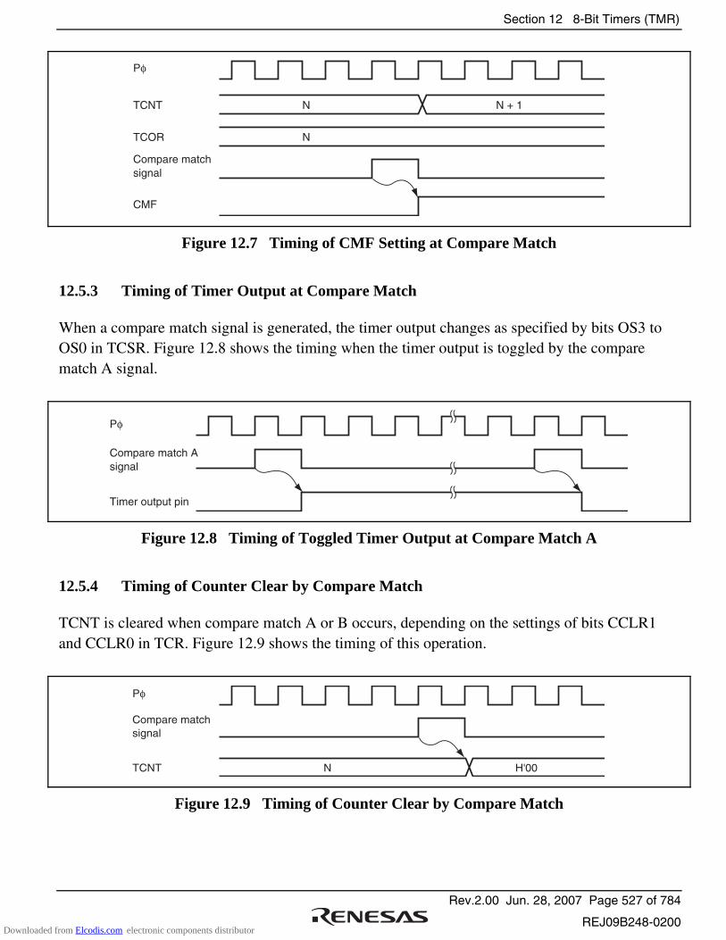
Section 12 8-Bit Timers (TMR)
Rev.2.00 Jun. 28, 2007 Page 527 of 784
REJ09B248-0200
Pφ
TCNT N N + 1
TCOR N
Compare matchsignal
CMF
Figure 12.7 Timing of CMF Setting at Compare Match
12.5.3 Timing of Timer Output at Compare Match
When a compare match signal is generated, the timer output changes as specified by bits OS3 to OS0 in TCSR. Figure 12.8 shows the timing when the timer output is toggled by the compare match A signal.
Pφ
Compare match Asignal
Timer output pin
Figure 12.8 Timing of Toggled Timer Output at Compare Match A
12.5.4 Timing of Counter Clear by Compare Match
TCNT is cleared when compare match A or B occurs, depending on the settings of bits CCLR1 and CCLR0 in TCR. Figure 12.9 shows the timing of this operation.
Pφ
N H'00
Compare matchsignal
TCNT
Figure 12.9 Timing of Counter Clear by Compare Match
Downloaded from Elcodis.com electronic components distributor

Section 12 8-Bit Timers (TMR)
Rev.2.00 Jun. 28, 2007 Page 528 of 784
REJ09B248-0200
12.5.5 Timing of TCNT External Reset
TCNT is cleared at the rising edge or high level of an external reset input, depending on the settings of bits CCLR1 and CCLR0 in TCR. The clear pulse width must be at least 2 states. Figures 12.10 and 12.11 show the timing of this operation.
Pφ
Clear signal
External resetinput pin
TCNT N H'00N – 1
Figure 12.10 Timing of Clearance by External Reset (Rising Edge)
Pφ
Clear signal
External resetinput pin
TCNT N H'00N – 1
Figure 12.11 Timing of Clearance by External Reset (High Level)
12.5.6 Timing of Overflow Flag (OVF) Setting
The OVF bit in TCSR is set to 1 when TCNT overflows (changes from H'FF to H'00). Figure 12.12 shows the timing of this operation.
Pφ
OVF
Overflow signal
TCNT H'FF H'00
Figure 12.12 Timing of OVF Setting
Downloaded from Elcodis.com electronic components distributor

Section 12 8-Bit Timers (TMR)
Rev.2.00 Jun. 28, 2007 Page 529 of 784
REJ09B248-0200
12.6 Operation with Cascaded Connection
If bits CKS2 to CKS0 in either TCR_0 or TCR_1 are set to B'100, the 8-bit timers of the two channels are cascaded. With this configuration, a single 16-bit timer could be used (16-bit counter mode) or compare matches of the 8-bit channel 0 could be counted by the timer of channel 1 (compare match count mode).
12.6.1 16-Bit Counter Mode
When bits CKS2 to CKS0 in TCR_0 are set to B'100, the timer functions as a single 16-bit timer with channel 0 occupying the upper 8 bits and channel 1 occupying the lower 8 bits.
(1) Setting of Compare Match Flags:
• The CMF flag in TCSR_0 is set to 1 when a 16-bit compare match event occurs.
• The CMF flag in TCSR_1 is set to 1 when a lower 8-bit compare match event occurs. (2) Counter Clear Specification
• If the CCLR1 and CCLR0 bits in TCR_0 have been set for counter clear at compare match, the 16-bit counter (TCNT_0 and TCNT_1 together) is cleared when a 16-bit compare match event occurs. The 16-bit counter (TCNT0 and TCNT1 together) is cleared even if counter clear by the TMRI0 pin has been set.
• The settings of the CCLR1 and CCLR0 bits in TCR_1 are ignored. The lower 8 bits cannot be cleared independently.
(3) Pin Output
• Control of output from the TMO0 pin by bits OS3 to OS0 in TCSR_0 is in accordance with the 16-bit compare match conditions.
• Control of output from the TMO1 pin by bits OS3 to OS0 in TCSR_1 is in accordance with the lower 8-bit compare match conditions.
12.6.2 Compare Match Count Mode
When bits CKS2 to CKS0 in TCR_1 are set to B'100, TCNT_1 counts compare match A for channel 0. Channels 0 and 1 are controlled independently. Conditions such as setting of the CMF flag, generation of interrupts, output from the TMO pin, and counter clear are in accordance with the settings for each channel.
Downloaded from Elcodis.com electronic components distributor
Section 12 8-Bit Timers (TMR)
Rev.2.00 Jun. 28, 2007 Page 530 of 784
REJ09B248-0200
12.7 Interrupt Sources
12.7.1 Interrupt Sources and DTC Activation
There are three interrupt sources for the 8-bit timer (TMR_0 or TMR_1): CMIA, CMIB, and OVI. Their interrupt sources and priorities are shown in table 12.3. Each interrupt source is enabled or disabled by the corresponding interrupt enable bit in TCR or TCSR, and independent interrupt requests are sent for each to the interrupt controller. It is also possible to activate the DTC by means of CMIA and CMIB interrupts.
Table 12.3 8-Bit Timer (TMR_0 or TMR_1) Interrupt Sources
Name Interrupt Source Interrupt Flag DTC Activation Priority
CMIA0 TCORA_0 compare match CMFA Possible (VNUM = 2'b00) High
CMIB0 TCORB_0 compare match CMFB Possible (VNUM = 2'b01)
OVI0 TCNT_0 overflow OVF Not possible Low
CMIA1 TCORA_1 compare match CMFA Possible (VNUM = 2'b10) High
CMIB1 TCORB_1 compare match CMFB Possible (VNUM = 2'b11)
OVI1 TCNT_1 overflow OVF Not possible Low
Note: VNUM is an internal signal.
12.7.2 A/D Converter Activation
The A/D converter can be activated only by TMR_0 compare match A.
If the ADTE bit in TCSR_0 is set to 1 when the CMFA flag in TCSR_0 is set to 1 by the occurrence of TMR_0 compare match A, a request to start A/D conversion is sent to the A/D converter. If the 8-bit timer conversion start trigger has been selected on the A/D converter side at this time, A/D conversion is started.
Downloaded from Elcodis.com electronic components distributor
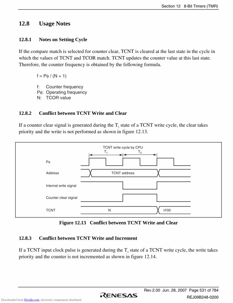
Section 12 8-Bit Timers (TMR)
Rev.2.00 Jun. 28, 2007 Page 531 of 784
REJ09B248-0200
12.8 Usage Notes
12.8.1 Notes on Setting Cycle
If the compare match is selected for counter clear, TCNT is cleared at the last state in the cycle in which the values of TCNT and TCOR match. TCNT updates the counter value at this last state. Therefore, the counter frequency is obtained by the following formula.
f = Pφ / (N + 1)
f: Counter frequencyPφ: Operating frequencyN: TCOR value
12.8.2 Conflict between TCNT Write and Clear
If a counter clear signal is generated during the T2 state of a TCNT write cycle, the clear takes priority and the write is not performed as shown in figure 12.13.
Pφ
Address TCNT address
Internal write signal
Counter clear signal
TCNT N H'00
T1 T2
TCNT write cycle by CPU
Figure 12.13 Conflict between TCNT Write and Clear
12.8.3 Conflict between TCNT Write and Increment
If a TCNT input clock pulse is generated during the T2 state of a TCNT write cycle, the write takes priority and the counter is not incremented as shown in figure 12.14.
Downloaded from Elcodis.com electronic components distributor
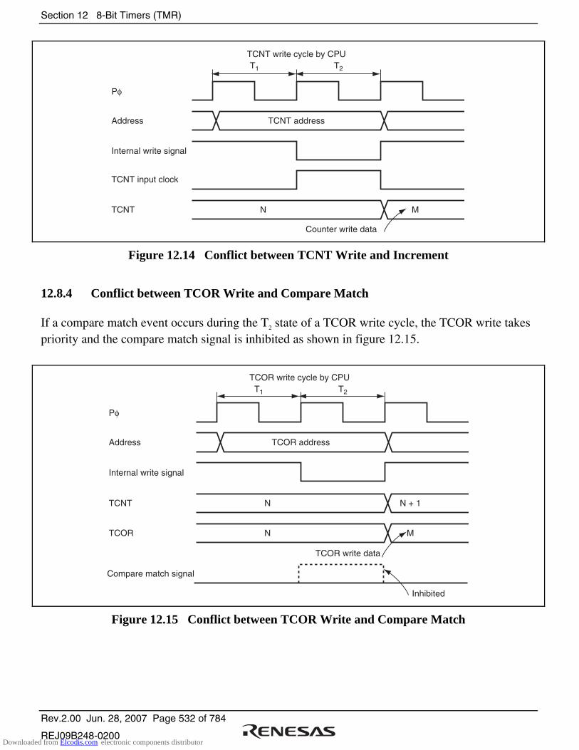
Section 12 8-Bit Timers (TMR)
Rev.2.00 Jun. 28, 2007 Page 532 of 784
REJ09B248-0200
Pφ
Address TCNT address
Internal write signal
TCNT input clock
TCNT N M
T1 T2
TCNT write cycle by CPU
Counter write data
Figure 12.14 Conflict between TCNT Write and Increment
12.8.4 Conflict between TCOR Write and Compare Match
If a compare match event occurs during the T2 state of a TCOR write cycle, the TCOR write takes priority and the compare match signal is inhibited as shown in figure 12.15.
Pφ
Address TCOR address
Internal write signal
TCNT
TCOR N M
T1 T2
TCOR write cycle by CPU
TCOR write data
N N + 1
Compare match signal
Inhibited
Figure 12.15 Conflict between TCOR Write and Compare Match
Downloaded from Elcodis.com electronic components distributor
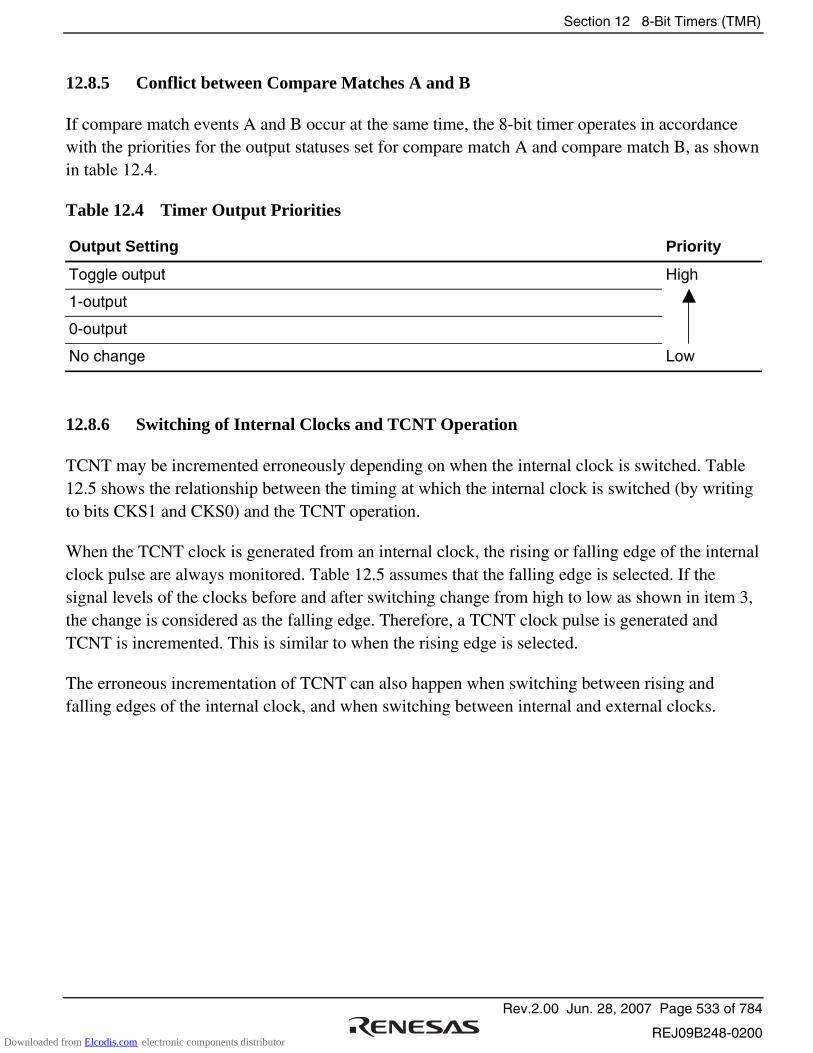
Section 12 8-Bit Timers (TMR)
Rev.2.00 Jun. 28, 2007 Page 533 of 784
REJ09B248-0200
12.8.5 Conflict between Compare Matches A and B
If compare match events A and B occur at the same time, the 8-bit timer operates in accordance with the priorities for the output statuses set for compare match A and compare match B, as shown in table 12.4.
Table 12.4 Timer Output Priorities
Output Setting Priority
Toggle output High
1-output
0-output
No change Low
12.8.6 Switching of Internal Clocks and TCNT Operation
TCNT may be incremented erroneously depending on when the internal clock is switched. Table 12.5 shows the relationship between the timing at which the internal clock is switched (by writing to bits CKS1 and CKS0) and the TCNT operation.
When the TCNT clock is generated from an internal clock, the rising or falling edge of the internal clock pulse are always monitored. Table 12.5 assumes that the falling edge is selected. If the signal levels of the clocks before and after switching change from high to low as shown in item 3, the change is considered as the falling edge. Therefore, a TCNT clock pulse is generated and TCNT is incremented. This is similar to when the rising edge is selected.
The erroneous incrementation of TCNT can also happen when switching between rising and falling edges of the internal clock, and when switching between internal and external clocks.
Downloaded from Elcodis.com electronic components distributor
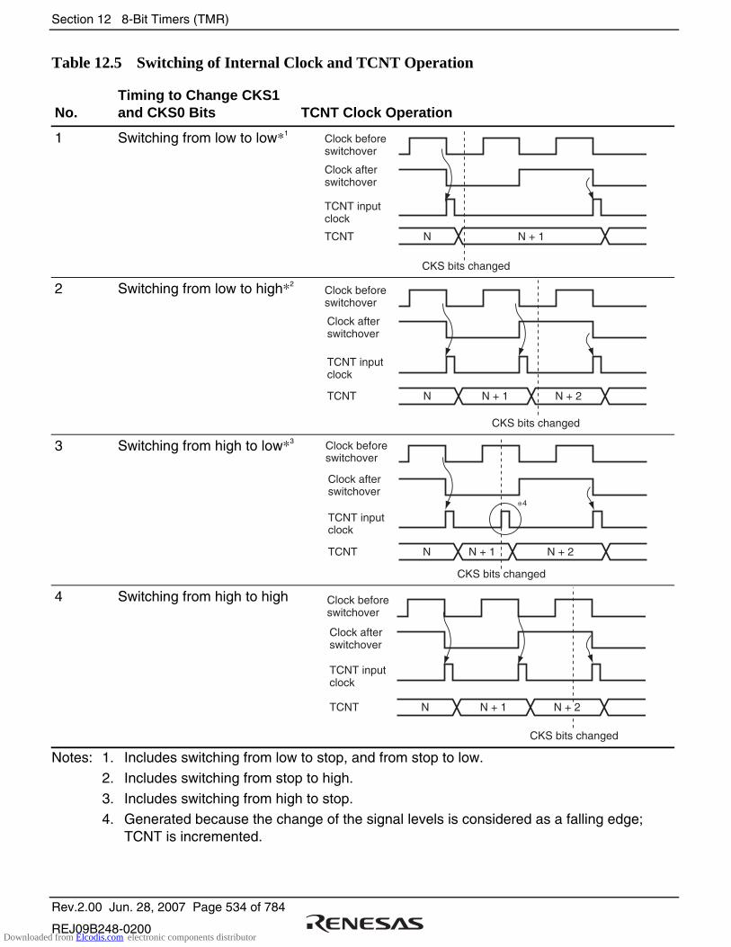
Section 12 8-Bit Timers (TMR)
Rev.2.00 Jun. 28, 2007 Page 534 of 784
REJ09B248-0200
Table 12.5 Switching of Internal Clock and TCNT Operation
No. Timing to Change CKS1 and CKS0 Bits TCNT Clock Operation
1 Switching from low to low*1 Clock before switchover
Clock after switchover
TCNT input clock
TCNT
CKS bits changed
N N + 1
2 Switching from low to high*2Clock before switchover
Clock after switchover
TCNT inputclock
TCNT
CKS bits changed
N N + 1 N + 2
3 Switching from high to low*3 Clock before switchover
Clock after switchover
TCNT inputclock
TCNT
CKS bits changed
N N + 1 N + 2
*4
4 Switching from high to high Clock beforeswitchover
Clock after switchover
TCNT inputclock
TCNT
CKS bits changed
N N + 1 N + 2
Notes: 1. Includes switching from low to stop, and from stop to low.
2. Includes switching from stop to high.
3. Includes switching from high to stop. 4. Generated because the change of the signal levels is considered as a falling edge;
TCNT is incremented.
Downloaded from Elcodis.com electronic components distributor
Section 12 8-Bit Timers (TMR)
Rev.2.00 Jun. 28, 2007 Page 535 of 784
REJ09B248-0200
12.8.7 Mode Setting with Cascaded Connection
If 16-bit counter mode and compare match count mode are specified at the same time, input clocks for TCNT_0 and TCNT_1 are not generated, and the counter stops. Do not specify 16-bit counter mode and compare match count mode simultaneously.
12.8.8 Module Stop Mode Setting
Operation of the TMR can be disabled or enabled using the module stop control register. The initial setting is for operation of the TMR to be halted. Register access is enabled by clearing module stop mode. For details, see section 19, Power-Down Modes.
12.8.9 Interrupts in Module Stop Mode
If module stop mode is entered when an interrupt has been requested, it will not be possible to clear the CPU interrupt source or the DTC activation source. Interrupts should therefore be disabled before entering module stop mode.
Downloaded from Elcodis.com electronic components distributor
Section 12 8-Bit Timers (TMR)
Rev.2.00 Jun. 28, 2007 Page 536 of 784
REJ09B248-0200
Downloaded from Elcodis.com electronic components distributor
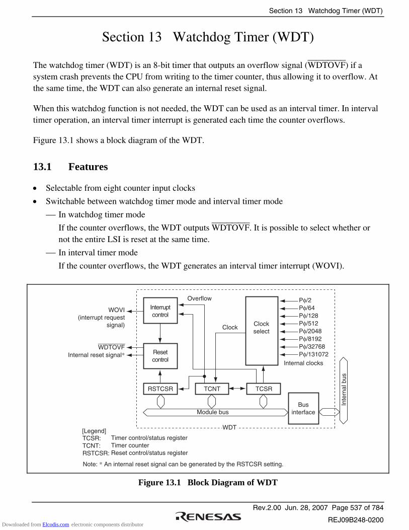
Section 13 Watchdog Timer (WDT)
Rev.2.00 Jun. 28, 2007 Page 537 of 784
REJ09B248-0200
Section 13 Watchdog Timer (WDT)
The watchdog timer (WDT) is an 8-bit timer that outputs an overflow signal (WDTOVF) if a system crash prevents the CPU from writing to the timer counter, thus allowing it to overflow. At the same time, the WDT can also generate an internal reset signal.
When this watchdog function is not needed, the WDT can be used as an interval timer. In interval timer operation, an interval timer interrupt is generated each time the counter overflows.
Figure 13.1 shows a block diagram of the WDT.
13.1 Features
• Selectable from eight counter input clocks
• Switchable between watchdog timer mode and interval timer mode
In watchdog timer mode
If the counter overflows, the WDT outputs WDTOVF. It is possible to select whether or not the entire LSI is reset at the same time.
In interval timer mode
If the counter overflows, the WDT generates an interval timer interrupt (WOVI).
OverflowInterruptcontrol
WOVI(interrupt request
signal)
Internal reset signal*WDTOVF
Resetcontrol
RSTCSR TCNT TCSR
Pφ/2Pφ/64Pφ/128Pφ/512Pφ/2048Pφ/8192Pφ/32768Pφ/131072
Clock Clockselect
Internal clocks
BusinterfaceModule bus
TCSR:TCNT:RSTCSR:
Note: * An internal reset signal can be generated by the RSTCSR setting.
Timer control/status registerTimer counterReset control/status register
WDT[Legend]
Inte
rnal
bus
Figure 13.1 Block Diagram of WDT
Downloaded from Elcodis.com electronic components distributor

Section 13 Watchdog Timer (WDT)
Rev.2.00 Jun. 28, 2007 Page 538 of 784
REJ09B248-0200
13.2 Input/Output Pin
Table 13.1 shows the WDT pin configuration.
Table 13.1 Pin Configuration
Name Symbol I/O Function
Watchdog timer overflow WDTOVF Output Outputs a counter overflow signal in watchdog timer mode
13.3 Register Descriptions
The WDT has the following three registers. To prevent accidental overwriting, TCSR, TCNT, and RSTCSR have to be written to in a method different from normal registers. For details, see section 13.6.1, Notes on Register Access.
• Timer counter (TCNT)
• Timer control/status register (TCSR)
• Reset control/status register (RSTCSR)
13.3.1 Timer Counter (TCNT)
TCNT is an 8-bit readable/writable up-counter. TCNT is initialized to H'00 when the TME bit in TCSR is cleared to 0.
Bit
Bit Name
Initial Value
R/W
7
0
R/W
6
0
R/W
5
0
R/W
4
0
R/W
3
0
R/W
2
0
R/W
1
0
R/W
0
0
R/W
Downloaded from Elcodis.com electronic components distributor
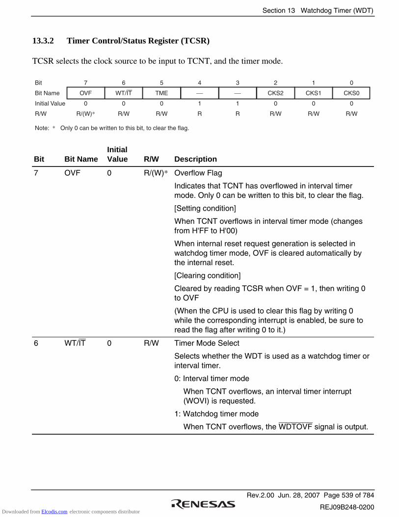
Section 13 Watchdog Timer (WDT)
Rev.2.00 Jun. 28, 2007 Page 539 of 784
REJ09B248-0200
13.3.2 Timer Control/Status Register (TCSR)
TCSR selects the clock source to be input to TCNT, and the timer mode.
Bit
Bit Name
Initial Value
R/W
Note: * Only 0 can be written to this bit, to clear the flag.
7
OVF
0
R/(W)*
6
WT/IT
0
R/W
5
TME
0
R/W
4
1
R
3
1
R
2
CKS2
0
R/W
1
CKS1
0
R/W
0
CKS0
0
R/W
Bit Bit Name Initial Value R/W Description
7 OVF 0 R/(W)* Overflow Flag
Indicates that TCNT has overflowed in interval timer mode. Only 0 can be written to this bit, to clear the flag.
[Setting condition]
When TCNT overflows in interval timer mode (changes from H'FF to H'00)
When internal reset request generation is selected in watchdog timer mode, OVF is cleared automatically by the internal reset.
[Clearing condition]
Cleared by reading TCSR when OVF = 1, then writing 0 to OVF
(When the CPU is used to clear this flag by writing 0 while the corresponding interrupt is enabled, be sure to read the flag after writing 0 to it.)
6 WT/IT 0 R/W Timer Mode Select
Selects whether the WDT is used as a watchdog timer or interval timer.
0: Interval timer mode
When TCNT overflows, an interval timer interrupt (WOVI) is requested.
1: Watchdog timer mode
When TCNT overflows, the WDTOVF signal is output.
Downloaded from Elcodis.com electronic components distributor
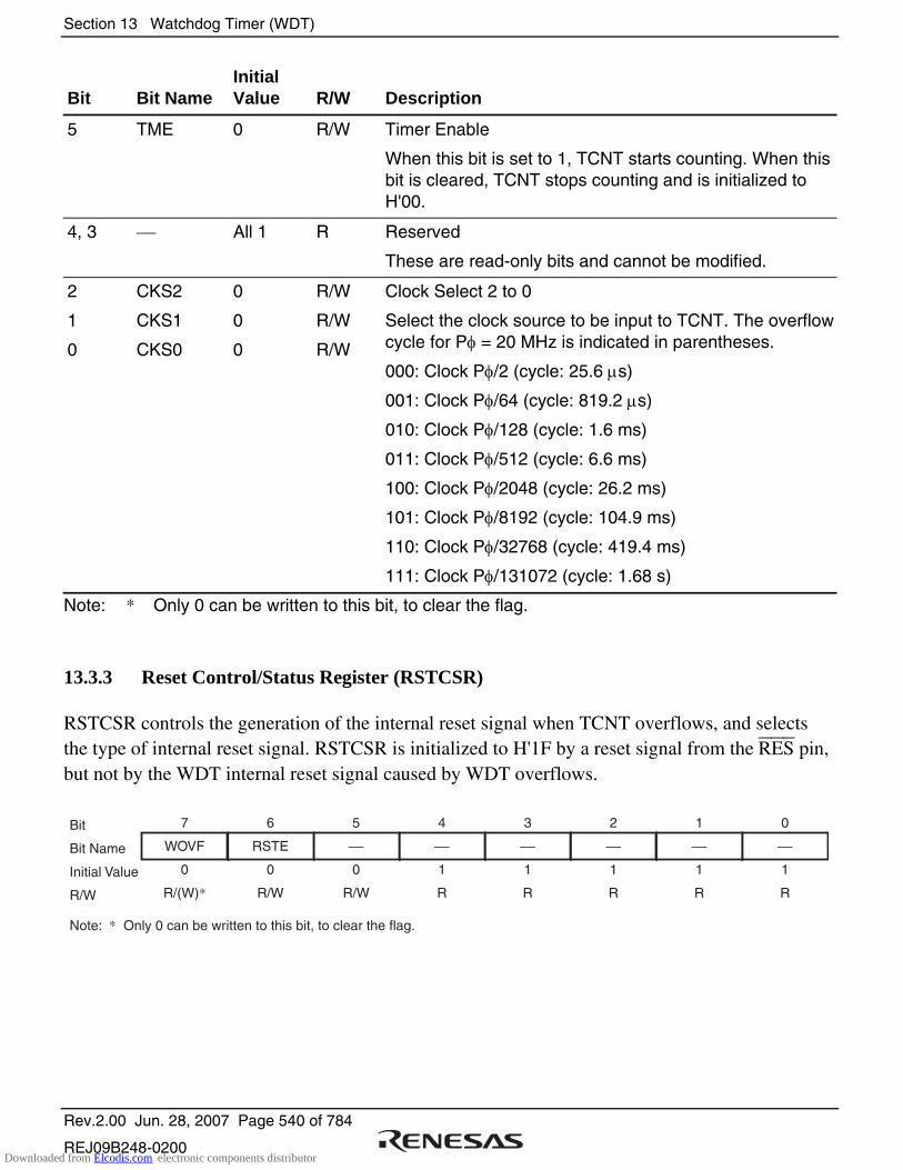
Section 13 Watchdog Timer (WDT)
Rev.2.00 Jun. 28, 2007 Page 540 of 784
REJ09B248-0200
Bit Bit Name Initial Value R/W Description
5 TME 0 R/W Timer Enable
When this bit is set to 1, TCNT starts counting. When this bit is cleared, TCNT stops counting and is initialized to H'00.
4, 3 All 1 R Reserved
These are read-only bits and cannot be modified.
2
1
0
CKS2
CKS1
CKS0
0
0
0
R/W
R/W
R/W
Clock Select 2 to 0
Select the clock source to be input to TCNT. The overflow cycle for Pφ = 20 MHz is indicated in parentheses.
000: Clock Pφ/2 (cycle: 25.6 µs)
001: Clock Pφ/64 (cycle: 819.2 µs)
010: Clock Pφ/128 (cycle: 1.6 ms)
011: Clock Pφ/512 (cycle: 6.6 ms)
100: Clock Pφ/2048 (cycle: 26.2 ms)
101: Clock Pφ/8192 (cycle: 104.9 ms)
110: Clock Pφ/32768 (cycle: 419.4 ms)
111: Clock Pφ/131072 (cycle: 1.68 s)
Note: * Only 0 can be written to this bit, to clear the flag.
13.3.3 Reset Control/Status Register (RSTCSR)
RSTCSR controls the generation of the internal reset signal when TCNT overflows, and selects the type of internal reset signal. RSTCSR is initialized to H'1F by a reset signal from the RES pin, but not by the WDT internal reset signal caused by WDT overflows.
7
WOVF
0
R/(W)*
6
RSTE
0
R/W
5
0
R/W
4
1
R
3
1
R
2
1
R
1
1
R
0
1
R
Bit
Bit Name
Initial Value
R/W
Note: * Only 0 can be written to this bit, to clear the flag.
Downloaded from Elcodis.com electronic components distributor

Section 13 Watchdog Timer (WDT)
Rev.2.00 Jun. 28, 2007 Page 541 of 784
REJ09B248-0200
Bit Bit Name Initial Value R/W Description
7 WOVF 0 R/(W)* Watchdog Timer Overflow Flag
This bit is set when TCNT overflows in watchdog timer mode. This bit cannot be set in interval timer mode, and only 0 can be written.
[Setting condition]
When TCNT overflows (changed from H'FF to H'00) in watchdog timer mode
[Clearing condition]
Reading RSTCSR when WOVF = 1, and then writing 0 to WOVF
(When the CPU is used to clear this flag by writing 0 while the corresponding interrupt is enabled, be sure to read the flag after writing 0 to it.)
6 RSTE 0 R/W Reset Enable
Specifies whether or not this LSI is internally reset if TCNT overflows during watchdog timer operation.
0: LSI is not reset even if TCNT overflows (Though this LSI is not reset, TCNT and TCSR in WDT are reset)
1: LSI is reset if TCNT overflows
5 0 R/W Reserved
Although this bit is readable/writable, reading from or writing to this bit does not affect operation.
4 to 0 All 1 R Reserved
These are read-only bits and cannot be modified.
Note: * Only 0 can be written to this bit, to clear the flag.
Downloaded from Elcodis.com electronic components distributor

Section 13 Watchdog Timer (WDT)
Rev.2.00 Jun. 28, 2007 Page 542 of 784
REJ09B248-0200
13.4 Operation
13.4.1 Watchdog Timer Mode
To use the WDT in watchdog timer mode, set both the WT/IT and TME bits in TCSR to 1.
During watchdog timer operation, if TCNT overflows without being rewritten because of a system crash or other error, the WDTOVF signal is output. This ensures that TCNT does not overflow while the system is operating normally. Software must prevent TCNT overflows by rewriting the TCNT value (normally H'00 is written) before overflow occurs. This WDTOVF signal can be used to reset the LSI internally in watchdog timer mode.
If TCNT overflows when the RSTE bit in RSTCSR is set to 1, a signal that resets this LSI internally is generated at the same time as the WDTOVF signal. If a reset caused by a signal input to the RES pin occurs at the same time as a reset caused by a WDT overflow, the RES pin reset has priority and the WOVF bit in RSTCSR is cleared to 0.
The WDTOVF signal is output for 133 states with Pφ when RSTE = 1 in RSTCSR, and for 130 states with Pφ when RSTE = 0 in RSTCSR. The internal reset signal is output for 519 states with Pφ.
When the RSTE bit = 1, an internal reset signal is generated. As this signal resets the system clock control register (SCKCR), the magnification power of Pφ to the input clock becomes the initial value. When the RSTE bit = 0, no internal reset signal is generated. Therefore, the setting of SCKCR is retained and the magnification power of Pφ to the input clock does not change.
When TCNT overflows in watchdog timer mode, the WOVF bit in RSTCSR is set to 1. If TCNT overflows when the RSTE bit in RSTCSR is set to 1, an internal reset signal is generated for the entire LSI.
Downloaded from Elcodis.com electronic components distributor
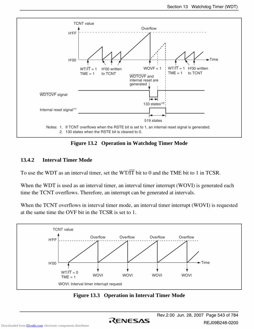
Section 13 Watchdog Timer (WDT)
Rev.2.00 Jun. 28, 2007 Page 543 of 784
REJ09B248-0200
TCNT value
H'00 Time
H'FF
WT/IT = 1TME = 1
H'00 writtento TCNT
WT/IT = 1TME = 1
H'00 writtento TCNT
133 states*2
519 states
WDTOVF signal
Internal reset signal*1
Notes: 1. If TCNT overflows when the RSTE bit is set to 1, an internal reset signal is generated.2. 130 states when the RSTE bit is cleared to 0.
Overflow
WDTOVF and internal reset are generated
WOVF = 1
Figure 13.2 Operation in Watchdog Timer Mode
13.4.2 Interval Timer Mode
To use the WDT as an interval timer, set the WT/IT bit to 0 and the TME bit to 1 in TCSR.
When the WDT is used as an interval timer, an interval timer interrupt (WOVI) is generated each time the TCNT overflows. Therefore, an interrupt can be generated at intervals.
When the TCNT overflows in interval timer mode, an interval timer interrupt (WOVI) is requested at the same time the OVF bit in the TCSR is set to 1.
TCNT value
H'00 Time
H'FF
WT/IT = 0TME = 1 WOVI
Overflow Overflow Overflow Overflow
WOVI: Interval timer interrupt request
WOVI WOVI WOVI
Figure 13.3 Operation in Interval Timer Mode
Downloaded from Elcodis.com electronic components distributor
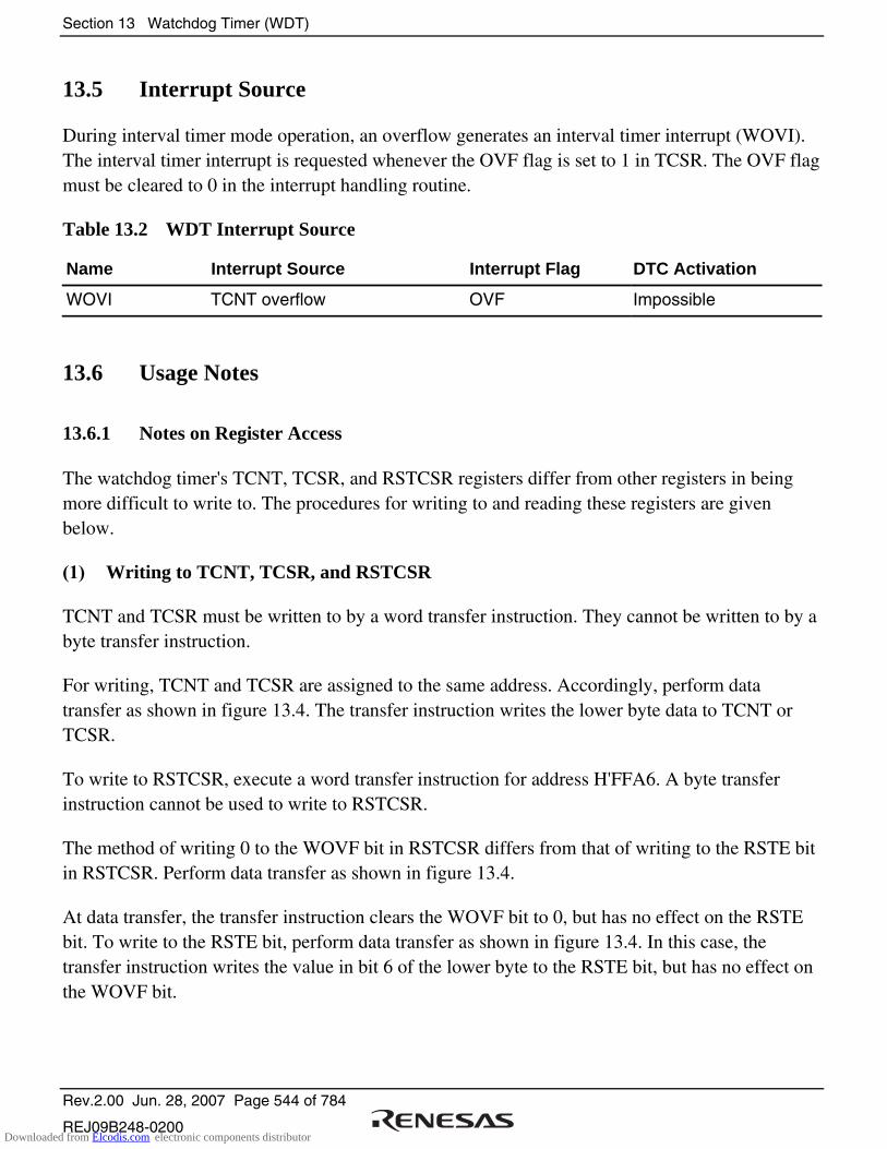
Section 13 Watchdog Timer (WDT)
Rev.2.00 Jun. 28, 2007 Page 544 of 784
REJ09B248-0200
13.5 Interrupt Source
During interval timer mode operation, an overflow generates an interval timer interrupt (WOVI). The interval timer interrupt is requested whenever the OVF flag is set to 1 in TCSR. The OVF flag must be cleared to 0 in the interrupt handling routine.
Table 13.2 WDT Interrupt Source
Name Interrupt Source Interrupt Flag DTC Activation
WOVI TCNT overflow OVF Impossible
13.6 Usage Notes
13.6.1 Notes on Register Access
The watchdog timer's TCNT, TCSR, and RSTCSR registers differ from other registers in being more difficult to write to. The procedures for writing to and reading these registers are given below.
(1) Writing to TCNT, TCSR, and RSTCSR
TCNT and TCSR must be written to by a word transfer instruction. They cannot be written to by a byte transfer instruction.
For writing, TCNT and TCSR are assigned to the same address. Accordingly, perform data transfer as shown in figure 13.4. The transfer instruction writes the lower byte data to TCNT or TCSR.
To write to RSTCSR, execute a word transfer instruction for address H'FFA6. A byte transfer instruction cannot be used to write to RSTCSR.
The method of writing 0 to the WOVF bit in RSTCSR differs from that of writing to the RSTE bit in RSTCSR. Perform data transfer as shown in figure 13.4.
At data transfer, the transfer instruction clears the WOVF bit to 0, but has no effect on the RSTE bit. To write to the RSTE bit, perform data transfer as shown in figure 13.4. In this case, the transfer instruction writes the value in bit 6 of the lower byte to the RSTE bit, but has no effect on the WOVF bit.
Downloaded from Elcodis.com electronic components distributor
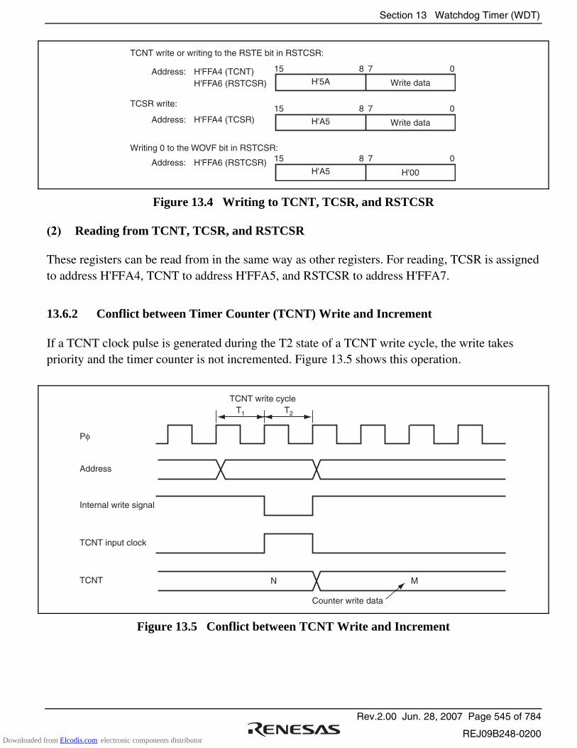
Section 13 Watchdog Timer (WDT)
Rev.2.00 Jun. 28, 2007 Page 545 of 784
REJ09B248-0200
TCNT write or writing to the RSTE bit in RSTCSR:
TCSR write:
Address: H'FFA4 (TCNT)H'FFA6 (RSTCSR)
15 8 7 0
H'5A Write data
15 8 7 0
H'A5 Write data
15 8 7 0
H'A5 H'00
Address: H'FFA4 (TCSR)
Writing 0 to the WOVF bit in RSTCSR:
Address: H'FFA6 (RSTCSR)
Figure 13.4 Writing to TCNT, TCSR, and RSTCSR
(2) Reading from TCNT, TCSR, and RSTCSR
These registers can be read from in the same way as other registers. For reading, TCSR is assigned to address H'FFA4, TCNT to address H'FFA5, and RSTCSR to address H'FFA7.
13.6.2 Conflict between Timer Counter (TCNT) Write and Increment
If a TCNT clock pulse is generated during the T2 state of a TCNT write cycle, the write takes priority and the timer counter is not incremented. Figure 13.5 shows this operation.
N M
T1 T2
Address
Pφ
Internal write signal
TCNT input clock
TCNT
TCNT write cycle
Counter write data
Figure 13.5 Conflict between TCNT Write and Increment
Downloaded from Elcodis.com electronic components distributor

Section 13 Watchdog Timer (WDT)
Rev.2.00 Jun. 28, 2007 Page 546 of 784
REJ09B248-0200
13.6.3 Changing Values of Bits CKS2 to CKS0
If bits CKS2 to CKS0 in TCSR are written to while the WDT is operating, errors could occur in the incrementation. The watchdog timer must be stopped (by clearing the TME bit to 0) before the values of bits CKS2 to CKS0 are changed.
13.6.4 Switching between Watchdog Timer Mode and Interval Timer Mode
If the timer mode is switched from watchdog timer mode to interval timer mode while the WDT is operating, errors could occur in the incrementation. The watchdog timer must be stopped (by clearing the TME bit to 0) before switching the timer mode.
13.6.5 Internal Reset in Watchdog Timer Mode
This LSI is not reset internally if TCNT overflows while the RSTE bit is cleared to 0 during watchdog timer mode operation, but TCNT and TCSR of the WDT are reset.
TCNT, TCSR, and RSTCR cannot be written to while the WDTOVF signal is low. Also note that a read of the WOVF flag is not recognized during this period. To clear the WOVF flag, therefore, read TCSR after the WDTOVF signal goes high, and then write 0 to the WOVF flag.
13.6.6 System Reset by WDTOVF Signal
If the WDTOVF signal is input to the RES pin, this LSI will not be initialized correctly. Make sure that the WDTOVF signal is not input logically to the RES pin. To reset the entire system by means of the WDTOVF signal, use a circuit like that shown in figure 13.6.
Reset input
Reset signal to entire system
This LSI
RES
WDTOVF
Figure 13.6 Circuit for System Reset by WDTOVF Signal (Example)
Downloaded from Elcodis.com electronic components distributor
Section 13 Watchdog Timer (WDT)
Rev.2.00 Jun. 28, 2007 Page 547 of 784
REJ09B248-0200
13.6.7 Transition to Watchdog Timer Mode or Software Standby Mode
When the WDT operates in watchdog timer mode, a transition to software standby mode is not made even when the SLEEP instruction is executed when the SSBY bit in SBYCR is set to 1. Instead, a transition to sleep mode is made.
To transit to software standby mode, the SLEEP instruction must be executed after halting the WDT (clearing the TME bit to 0).
When the WDT operates in interval timer mode, a transition to software standby mode is made through execution of the SLEEP instruction when the SSBY bit in SBYCR is set to 1.
Downloaded from Elcodis.com electronic components distributor

Section 13 Watchdog Timer (WDT)
Rev.2.00 Jun. 28, 2007 Page 548 of 784
REJ09B248-0200
Downloaded from Elcodis.com electronic components distributor
Section 14 Serial Communication Interface (SCI)
Rev.2.00 Jun. 28, 2007 Page 549 of 784
REJ09B248-0200
Section 14 Serial Communication Interface (SCI)
This LSI has five independent serial communication interface (SCI) channels. The SCI can handle both asynchronous and clocked synchronous serial communication. Asynchronous serial data communication can be carried out with standard asynchronous communication chips such as a Universal Asynchronous Receiver/Transmitter (UART) or Asynchronous Communication Interface Adapter (ACIA). A function is also provided for serial communication between processors (multiprocessor communication function). The SCI also supports the smart card (IC card) interface supporting ISO/IEC 7816-3 (Identification Card) as an extended asynchronous communication mode. Figure 14.1 shows a block diagram of the SCI.
14.1 Features
• Choice of asynchronous or clocked synchronous serial communication mode
• Full-duplex communication capability
The transmitter and receiver are mutually independent, enabling transmission and reception to be executed simultaneously. Double-buffering is used in both the transmitter and the receiver, enabling continuous transmission and continuous reception of serial data.
• On-chip baud rate generator allows any bit rate to be selected
The external clock can be selected as a transfer clock source (except for the smart card interface).
• Choice of LSB-first or MSB-first transfer (except in the case of asynchronous mode 7-bit data)
• Four interrupt sources
The interrupt sources are transmit-end, transmit-data-empty, receive-data-full, and receive error. The transmit-data-empty and receive-data-full interrupt sources can activate the DTC or DMAC.
• Module stop mode can be set Asynchronous Mode:
• Data length: 7 or 8 bits
• Stop bit length: 1 or 2 bits
• Parity: Even, odd, or none
• Receive error detection: Parity, overrun, and framing errors
• Break detection: Break can be detected by reading the RxD pin level directly in case of a framing error
Downloaded from Elcodis.com electronic components distributor

Section 14 Serial Communication Interface (SCI)
Rev.2.00 Jun. 28, 2007 Page 550 of 784
REJ09B248-0200
• Average transfer rate generator (SCI_2 only)
10.667-MHz operation: 460.606 kbps or 115.152 kbps can be selected
16-MHz operation: 720 kbps, 460.784 kbps, or 115.196 kbps can be selected
32-MHz operation: 720 kbps Clocked Synchronous Mode:
• Data length: 8 bits
• Receive error detection: Overrun errors Smart Card Interface:
• An error signal can be automatically transmitted on detection of a parity error during reception
• Data can be automatically re-transmitted on receiving an error signal during transmission
• Both direct convention and inverse convention are supported
RxD
TxD
SCK
Clock
Pφ
Pφ/4
Pφ/16
Pφ/64
TEITXIRXIERI
SCMR
SSR
SCR
SMR
Transmission/reception control
Baud rategenerator
BRR
Module data bus
RDR
TSRRSR
Parity generation
Parity check
[Legend]RSR: Receive shift registerRDR: Receive data registerTSR: Transmit shift registerTDR: Transmit data registerSMR: Serial mode register
TDRB
us in
terf
ace
Inte
rnal
dat
a bu
s
External clock
SCR: Serial control registerSSR: Serial status registerSCMR: Smart card mode registerBRR: Bit rate registerSEMR: Serial extended mode register (available only for SCI_2)
Average transfer rate generator (SCI_2) At 10.667-MHz operation: 115.152 kbps 460.606 kbps At 16-MHz operation: 115.196 kbps 460.784 kbps 720 kbps At 32-MHz operation: 720 kbps
Figure 14.1 Block Diagram of SCI
Downloaded from Elcodis.com electronic components distributor
Section 14 Serial Communication Interface (SCI)
Rev.2.00 Jun. 28, 2007 Page 551 of 784
REJ09B248-0200
14.2 Input/Output Pins
Table 14.1 lists the pin configuration of the SCI.
Table 14.1 Pin Configuration
Channel Pin Name* I/O Function
SCK0 I/O Channel 0 clock input/output
RxD0 Input Channel 0 receive data input
0
TxD0 Output Channel 0 transmit data output
SCK1 I/O Channel 1 clock input/output
RxD1 Input Channel 1 receive data input
1
TxD1 Output Channel 1 transmit data output
SCK2 I/O Channel 2 clock input/output
RxD2 Input Channel 2 receive data input
2
TxD2 Output Channel 2 transmit data output
SCK3 I/O Channel 3 clock input/output
RxD3 Input Channel 3 receive data input
3
TxD3 Output Channel 3 transmit data output
SCK4 I/O Channel 4 clock input/output
RxD4 Input Channel 4 receive data input
4
TxD4 Output Channel 4 transmit data output
Note: * Pin names SCK, RxD, and TxD are used in the text for all channels, omitting the channel designation.
Downloaded from Elcodis.com electronic components distributor
Section 14 Serial Communication Interface (SCI)
Rev.2.00 Jun. 28, 2007 Page 552 of 784
REJ09B248-0200
14.3 Register Descriptions
The SCI has the following registers. Some bits in the serial mode register (SMR), serial status register (SSR), and serial control register (SCR) have different functions in different modesnormal serial communication interface mode and smart card interface mode; therefore, the bits are described separately for each mode in the corresponding register sections.
Channel 0:
• Receive shift register_0 (RSR_0)
• Transmit shift register_0 (TSR_0)
• Receive data register_0 (RDR_0)
• Transmit data register_0 (TDR_0)
• Serial mode register_0 (SMR_0)
• Serial control register_0 (SCR_0)
• Serial status register_0 (SSR_0)
• Smart card mode register_0 (SCMR_0)
• Bit rate register_0 (BRR_0) Channel 1:
• Receive shift register_1 (RSR_1)
• Transmit shift register_1 (TSR_1)
• Receive data register_1 (RDR_1)
• Transmit data register_1 (TDR_1)
• Serial mode register_1 (SMR_1)
• Serial control register_1 (SCR_1)
• Serial status register_1 (SSR_1)
• Smart card mode register_1 (SCMR_1)
• Bit rate register_1 (BRR_1)
Downloaded from Elcodis.com electronic components distributor

Section 14 Serial Communication Interface (SCI)
Rev.2.00 Jun. 28, 2007 Page 553 of 784
REJ09B248-0200
Channel 2:
• Receive shift register_2 (RSR_2)
• Transmit shift register_2 (TSR_2)
• Receive data register_2 (RDR_2)
• Transmit data register_2 (TDR_2)
• Serial mode register_2 (SMR_2)
• Serial control register_2 (SCR_2)
• Serial status register_2 (SSR_2)
• Smart card mode register_2 (SCMR_2)
• Bit rate register_2 (BRR_2)
• Serial extended mode register_2 (SEMR_2) (SCI_2 only) Channel 3:
• Receive shift register_3 (RSR_3)
• Transmit shift register_3 (TSR_3)
• Receive data register_3 (RDR_3)
• Transmit data register_3 (TDR_3)
• Serial mode register_3 (SMR_3)
• Serial control register_3 (SCR_3)
• Serial status register_3 (SSR_3)
• Smart card mode register_3 (SCMR_3)
• Bit rate register_3 (BRR_3) Channel 4:
• Receive shift register_4 (RSR_4)
• Transmit shift register_4 (TSR_4)
• Receive data register_4 (RDR_4)
• Transmit data register_4 (TDR_4)
• Serial mode register_4 (SMR_4)
• Serial control register_4 (SCR_4)
• Serial status register_4 (SSR_4)
• Smart card mode register_4 (SCMR_4)
• Bit rate register_4 (BRR_4)
Downloaded from Elcodis.com electronic components distributor

Section 14 Serial Communication Interface (SCI)
Rev.2.00 Jun. 28, 2007 Page 554 of 784
REJ09B248-0200
14.3.1 Receive Shift Register (RSR)
RSR is a shift register which is used to receive serial data input from the RxD pin and converts it into parallel data. When one frame of data has been received, it is transferred to RDR automatically. RSR cannot be directly accessed by the CPU.
14.3.2 Receive Data Register (RDR)
RDR is an 8-bit register that stores receive data. When the SCI has received one frame of serial data, it transfers the received serial data from RSR to RDR where it is stored. This allows RSR to receive the next data. Since RSR and RDR function as a double buffer in this way, continuous receive operations can be performed. After confirming that the RDRF bit in SSR is set to 1, read RDR only once. RDR cannot be written to by the CPU.
Bit
Bit Name
Initial Value
R/W
7
0
R
6
0
R
5
0
R
4
0
R
3
0
R
2
0
R
1
0
R
0
0
R
14.3.3 Transmit Data Register (TDR)
TDR is an 8-bit register that stores transmit data. When the SCI detects that TSR is empty, it transfers the transmit data written in TDR to TSR and starts transmission. The double-buffered structures of TDR and TSR enables continuous serial transmission. If the next transmit data has already been written to TDR when one frame of data is transmitted, the SCI transfers the written data to TSR to continue transmission. Although TDR can be read from or written to by the CPU at all times, to achieve reliable serial transmission, write transmit data to TDR for only once after confirming that the TDRE bit in SSR is set to 1.
Bit
Bit Name
Initial Value
R/W
7
1
R/W
6
1
R/W
5
1
R/W
4
1
R/W
3
1
R/W
2
1
R/W
1
1
R/W
0
1
R/W
Downloaded from Elcodis.com electronic components distributor
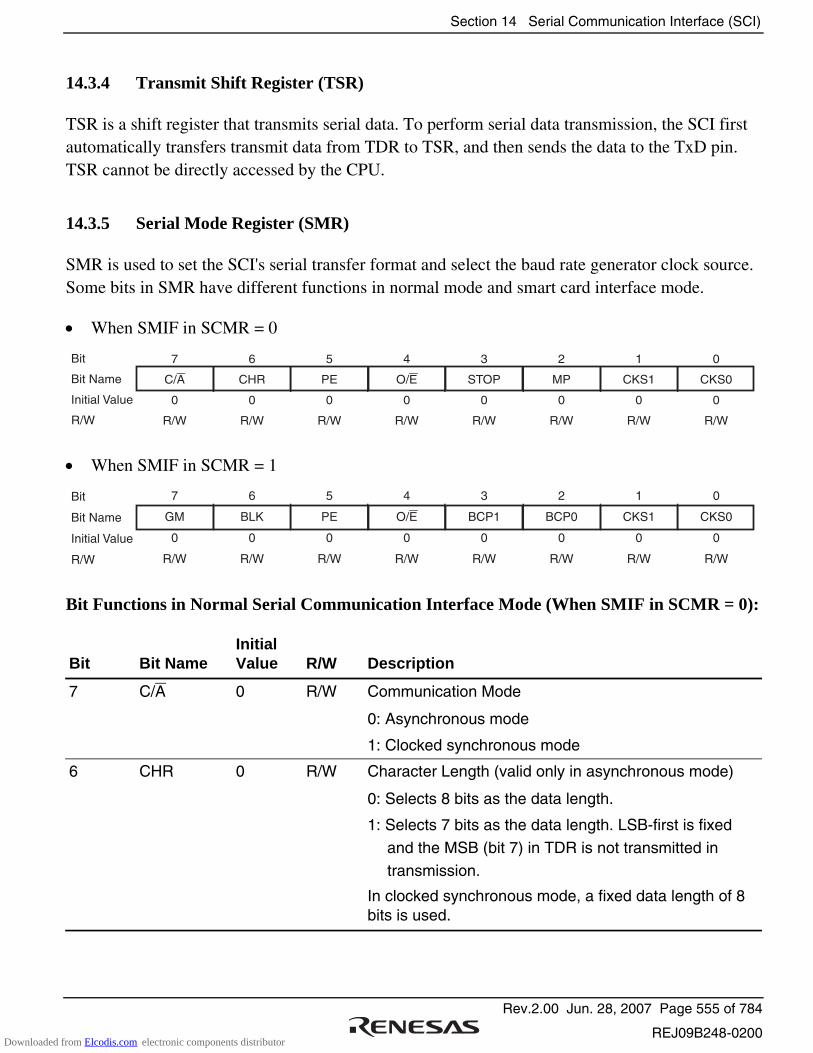
Section 14 Serial Communication Interface (SCI)
Rev.2.00 Jun. 28, 2007 Page 555 of 784
REJ09B248-0200
14.3.4 Transmit Shift Register (TSR)
TSR is a shift register that transmits serial data. To perform serial data transmission, the SCI first automatically transfers transmit data from TDR to TSR, and then sends the data to the TxD pin. TSR cannot be directly accessed by the CPU.
14.3.5 Serial Mode Register (SMR)
SMR is used to set the SCI's serial transfer format and select the baud rate generator clock source. Some bits in SMR have different functions in normal mode and smart card interface mode.
• When SMIF in SCMR = 0
7
C/A
0
R/W
6
CHR
0
R/W
5
PE
0
R/W
4
O/E
0
R/W
3
STOP
0
R/W
2
MP
0
R/W
1
CKS1
0
R/W
0
CKS0
0
R/W
Bit
Bit Name
Initial Value
R/W
• When SMIF in SCMR = 1
7
GM
0
R/W
6
BLK
0
R/W
5
PE
0
R/W
4
O/E
0
R/W
3
BCP1
0
R/W
2
BCP0
0
R/W
1
CKS1
0
R/W
0
CKS0
0
R/W
Bit
Bit Name
Initial Value
R/W
Bit Functions in Normal Serial Communication Interface Mode (When SMIF in SCMR = 0):
Bit Bit Name Initial Value R/W Description
7 C/A 0 R/W Communication Mode
0: Asynchronous mode
1: Clocked synchronous mode
6 CHR 0 R/W Character Length (valid only in asynchronous mode)
0: Selects 8 bits as the data length.
1: Selects 7 bits as the data length. LSB-first is fixed
and the MSB (bit 7) in TDR is not transmitted in
transmission.
In clocked synchronous mode, a fixed data length of 8 bits is used.
Downloaded from Elcodis.com electronic components distributor
Section 14 Serial Communication Interface (SCI)
Rev.2.00 Jun. 28, 2007 Page 556 of 784
REJ09B248-0200
Bit Bit Name Initial Value R/W Description
5 PE 0 R/W Parity Enable (valid only in asynchronous mode)
When this bit is set to 1, the parity bit is added to transmit data before transmission, and the parity bit is checked in reception. For a multiprocessor format, parity bit addition and checking are not performed regardless of the PE bit setting.
4 O/E 0 R/W Parity Mode (valid only when the PE bit is 1 in asynchronous mode)
0: Selects even parity.
1: Selects odd parity.
3 STOP 0 R/W Stop Bit Length (valid only in asynchronous mode)
Selects the stop bit length in transmission.
0: 1 stop bit
1: 2 stop bits
In reception, only the first stop bit is checked. If the second stop bit is 0, it is treated as the start bit of the next transmit frame.
2 MP 0 R/W Multiprocessor Mode (valid only in asynchronous mode)
When this bit is set to 1, the multiprocessor function is enabled. The PE bit and O/E bit settings are invalid in multiprocessor mode.
1
0
CKS1
CKS0
0
0
R/W
R/W
Clock Select 1, 0
These bits select the clock source for the baud rate generator.
00: Pφ clock (n = 0)
01: Pφ/4 clock (n = 1)
10: Pφ/16 clock (n = 2)
11: Pφ/64 clock (n = 3)
For the relation between the settings of these bits and the baud rate, see section 14.3.9, Bit Rate Register (BRR). n is the decimal display of the value of n in BRR (see section 14.3.9, Bit Rate Register (BRR)).
Downloaded from Elcodis.com electronic components distributor
Section 14 Serial Communication Interface (SCI)
Rev.2.00 Jun. 28, 2007 Page 557 of 784
REJ09B248-0200
Bit Functions in Smart Card Interface Mode (When SMIF in SCMR = 1):
Bit Bit Name Initial Value R/W Description
7 GM 0 R/W GSM Mode
Setting this bit to 1 allows GSM mode operation. In GSM mode, the TEND set timing is put forward to 11.0 etu from the start and the clock output control function is appended. For details, see sections 14.7.6, Data Transmission (Except in Block Transfer Mode) and 14.7.8, Clock Output Control.
6 BLK 0 R/W Setting this bit to 1 allows block transfer mode operation. For details, see section 14.7.3, Block Transfer Mode.
5 PE 0 R/W Parity Enable (valid only in asynchronous mode)
When this bit is set to 1, the parity bit is added to transmit data before transmission, and the parity bit is checked in reception. Set this bit to 1 in smart card interface mode.
4 O/E 0 R/W Parity Mode (valid only when the PE bit is 1 in asynchronous mode)
0: Selects even parity
1: Selects odd parity
For details on the usage of this bit in smart card interface mode, see section 14.7.2, Data Format (Except in Block Transfer Mode).
3
2
BCP1
BCP0
0
0
R/W
R/W
Basic Clock Pulse 1,0
These bits select the number of basic clock cycles in a 1-bit data transfer time in smart card interface mode.
00: 32 clock cycles (S = 32)
01: 64 clock cycles (S = 64)
10: 372 clock cycles (S = 372)
11: 256 clock cycles (S = 256)
For details, see section 14.7.4, Receive Data Sampling Timing and Reception Margin. S is described in section 14.3.9, Bit Rate Register (BRR).
Downloaded from Elcodis.com electronic components distributor
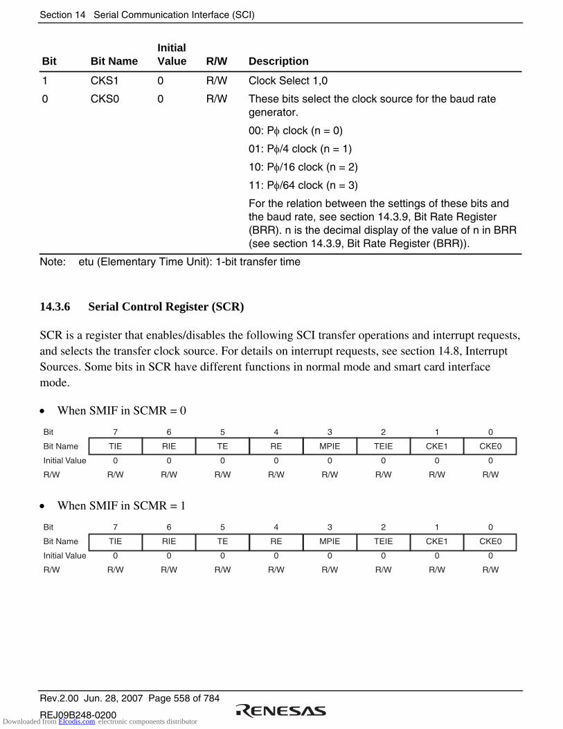
Section 14 Serial Communication Interface (SCI)
Rev.2.00 Jun. 28, 2007 Page 558 of 784
REJ09B248-0200
Bit Bit Name Initial Value R/W Description
1
0
CKS1
CKS0
0
0
R/W
R/W
Clock Select 1,0
These bits select the clock source for the baud rate generator.
00: Pφ clock (n = 0)
01: Pφ/4 clock (n = 1)
10: Pφ/16 clock (n = 2)
11: Pφ/64 clock (n = 3)
For the relation between the settings of these bits and the baud rate, see section 14.3.9, Bit Rate Register (BRR). n is the decimal display of the value of n in BRR (see section 14.3.9, Bit Rate Register (BRR)).
Note: etu (Elementary Time Unit): 1-bit transfer time
14.3.6 Serial Control Register (SCR)
SCR is a register that enables/disables the following SCI transfer operations and interrupt requests, and selects the transfer clock source. For details on interrupt requests, see section 14.8, Interrupt Sources. Some bits in SCR have different functions in normal mode and smart card interface mode.
• When SMIF in SCMR = 0
7
TIE
0
R/W
6
RIE
0
R/W
5
TE
0
R/W
4
RE
0
R/W
3
MPIE
0
R/W
2
TEIE
0
R/W
1
CKE1
0
R/W
0
CKE0
0
R/W
Bit
Bit Name
Initial Value
R/W
• When SMIF in SCMR = 1
7
TIE
0
R/W
6
RIE
0
R/W
5
TE
0
R/W
4
RE
0
R/W
3
MPIE
0
R/W
2
TEIE
0
R/W
1
CKE1
0
R/W
0
CKE0
0
R/W
Bit
Bit Name
Initial Value
R/W
Downloaded from Elcodis.com electronic components distributor
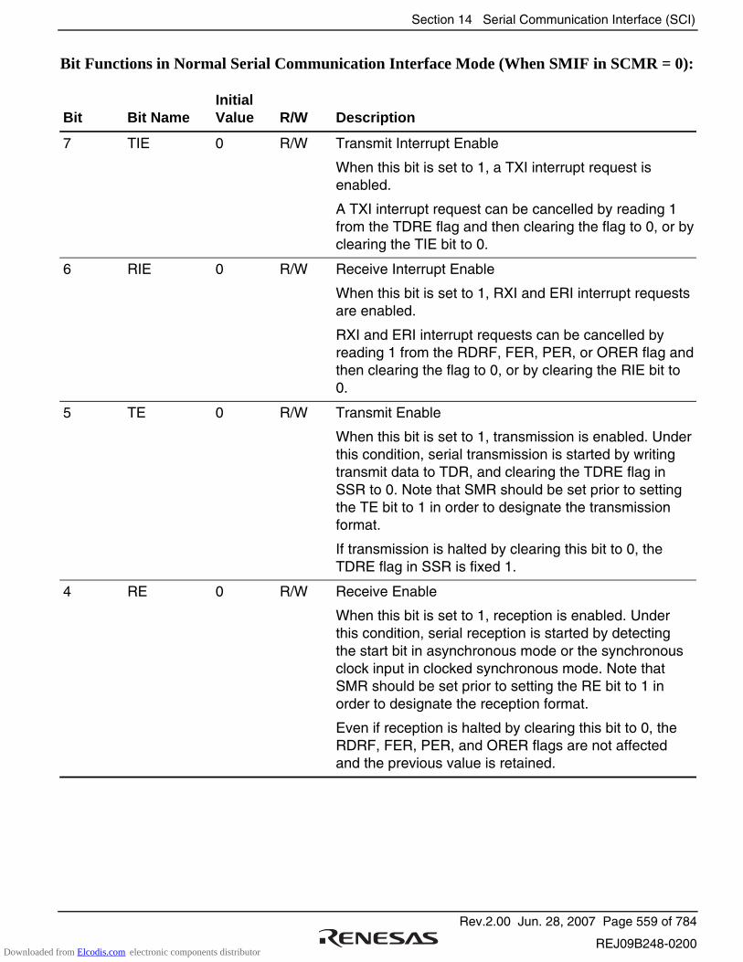
Section 14 Serial Communication Interface (SCI)
Rev.2.00 Jun. 28, 2007 Page 559 of 784
REJ09B248-0200
Bit Functions in Normal Serial Communication Interface Mode (When SMIF in SCMR = 0):
Bit Bit Name Initial Value R/W Description
7 TIE 0 R/W Transmit Interrupt Enable
When this bit is set to 1, a TXI interrupt request is enabled.
A TXI interrupt request can be cancelled by reading 1 from the TDRE flag and then clearing the flag to 0, or by clearing the TIE bit to 0.
6 RIE 0 R/W Receive Interrupt Enable
When this bit is set to 1, RXI and ERI interrupt requests are enabled.
RXI and ERI interrupt requests can be cancelled by reading 1 from the RDRF, FER, PER, or ORER flag and then clearing the flag to 0, or by clearing the RIE bit to 0.
5 TE 0 R/W Transmit Enable
When this bit is set to 1, transmission is enabled. Under this condition, serial transmission is started by writing transmit data to TDR, and clearing the TDRE flag in SSR to 0. Note that SMR should be set prior to setting the TE bit to 1 in order to designate the transmission format.
If transmission is halted by clearing this bit to 0, the TDRE flag in SSR is fixed 1.
4 RE 0 R/W Receive Enable
When this bit is set to 1, reception is enabled. Under this condition, serial reception is started by detecting the start bit in asynchronous mode or the synchronous clock input in clocked synchronous mode. Note that SMR should be set prior to setting the RE bit to 1 in order to designate the reception format.
Even if reception is halted by clearing this bit to 0, the RDRF, FER, PER, and ORER flags are not affected and the previous value is retained.
Downloaded from Elcodis.com electronic components distributor
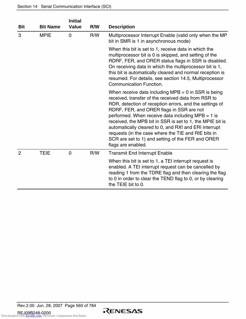
Section 14 Serial Communication Interface (SCI)
Rev.2.00 Jun. 28, 2007 Page 560 of 784
REJ09B248-0200
Bit Bit Name Initial Value R/W Description
3 MPIE 0 R/W Multiprocessor Interrupt Enable (valid only when the MP bit in SMR is 1 in asynchronous mode)
When this bit is set to 1, receive data in which the multiprocessor bit is 0 is skipped, and setting of the RDRF, FER, and ORER status flags in SSR is disabled. On receiving data in which the multiprocessor bit is 1, this bit is automatically cleared and normal reception is resumed. For details, see section 14.5, Multiprocessor Communication Function.
When receive data including MPB = 0 in SSR is being received, transfer of the received data from RSR to RDR, detection of reception errors, and the settings of RDRF, FER, and ORER flags in SSR are not performed. When receive data including MPB = 1 is received, the MPB bit in SSR is set to 1, the MPIE bit is automatically cleared to 0, and RXI and ERI interrupt requests (in the case where the TIE and RIE bits in SCR are set to 1) and setting of the FER and ORER flags are enabled.
2 TEIE 0 R/W Transmit End Interrupt Enable
When this bit is set to 1, a TEI interrupt request is enabled. A TEI interrupt request can be cancelled by reading 1 from the TDRE flag and then clearing the flag to 0 in order to clear the TEND flag to 0, or by clearing the TEIE bit to 0.
Downloaded from Elcodis.com electronic components distributor
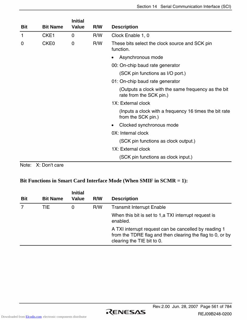
Section 14 Serial Communication Interface (SCI)
Rev.2.00 Jun. 28, 2007 Page 561 of 784
REJ09B248-0200
Bit Bit Name Initial Value R/W Description
1
0
CKE1
CKE0
0
0
R/W
R/W
Clock Enable 1, 0
These bits select the clock source and SCK pin function.
• Asynchronous mode
00: On-chip baud rate generator
(SCK pin functions as I/O port.)
01: On-chip baud rate generator
(Outputs a clock with the same frequency as the bit rate from the SCK pin.)
1X: External clock
(Inputs a clock with a frequency 16 times the bit rate from the SCK pin.)
• Clocked synchronous mode
0X: Internal clock
(SCK pin functions as clock output.)
1X: External clock
(SCK pin functions as clock input.)
Note: X: Don't care
Bit Functions in Smart Card Interface Mode (When SMIF in SCMR = 1):
Bit Bit Name Initial Value R/W Description
7 TIE 0 R/W Transmit Interrupt Enable
When this bit is set to 1,a TXI interrupt request is enabled.
A TXI interrupt request can be cancelled by reading 1 from the TDRE flag and then clearing the flag to 0, or by clearing the TIE bit to 0.
Downloaded from Elcodis.com electronic components distributor
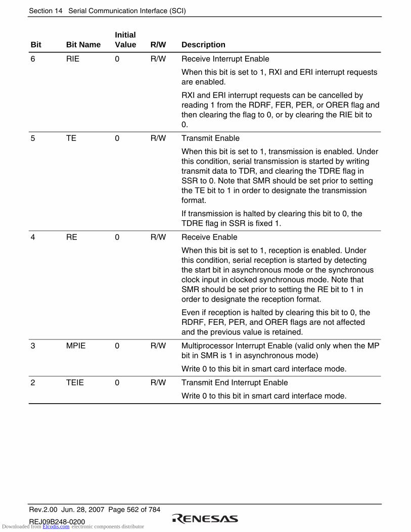
Section 14 Serial Communication Interface (SCI)
Rev.2.00 Jun. 28, 2007 Page 562 of 784
REJ09B248-0200
Bit Bit Name Initial Value R/W Description
6 RIE 0 R/W Receive Interrupt Enable
When this bit is set to 1, RXI and ERI interrupt requests are enabled.
RXI and ERI interrupt requests can be cancelled by reading 1 from the RDRF, FER, PER, or ORER flag and then clearing the flag to 0, or by clearing the RIE bit to 0.
5 TE 0 R/W Transmit Enable
When this bit is set to 1, transmission is enabled. Under this condition, serial transmission is started by writing transmit data to TDR, and clearing the TDRE flag in SSR to 0. Note that SMR should be set prior to setting the TE bit to 1 in order to designate the transmission format.
If transmission is halted by clearing this bit to 0, the TDRE flag in SSR is fixed 1.
4 RE 0 R/W Receive Enable
When this bit is set to 1, reception is enabled. Under this condition, serial reception is started by detecting the start bit in asynchronous mode or the synchronous clock input in clocked synchronous mode. Note that SMR should be set prior to setting the RE bit to 1 in order to designate the reception format.
Even if reception is halted by clearing this bit to 0, the RDRF, FER, PER, and ORER flags are not affected and the previous value is retained.
3 MPIE 0 R/W Multiprocessor Interrupt Enable (valid only when the MP bit in SMR is 1 in asynchronous mode)
Write 0 to this bit in smart card interface mode.
2 TEIE 0 R/W Transmit End Interrupt Enable
Write 0 to this bit in smart card interface mode.
Downloaded from Elcodis.com electronic components distributor
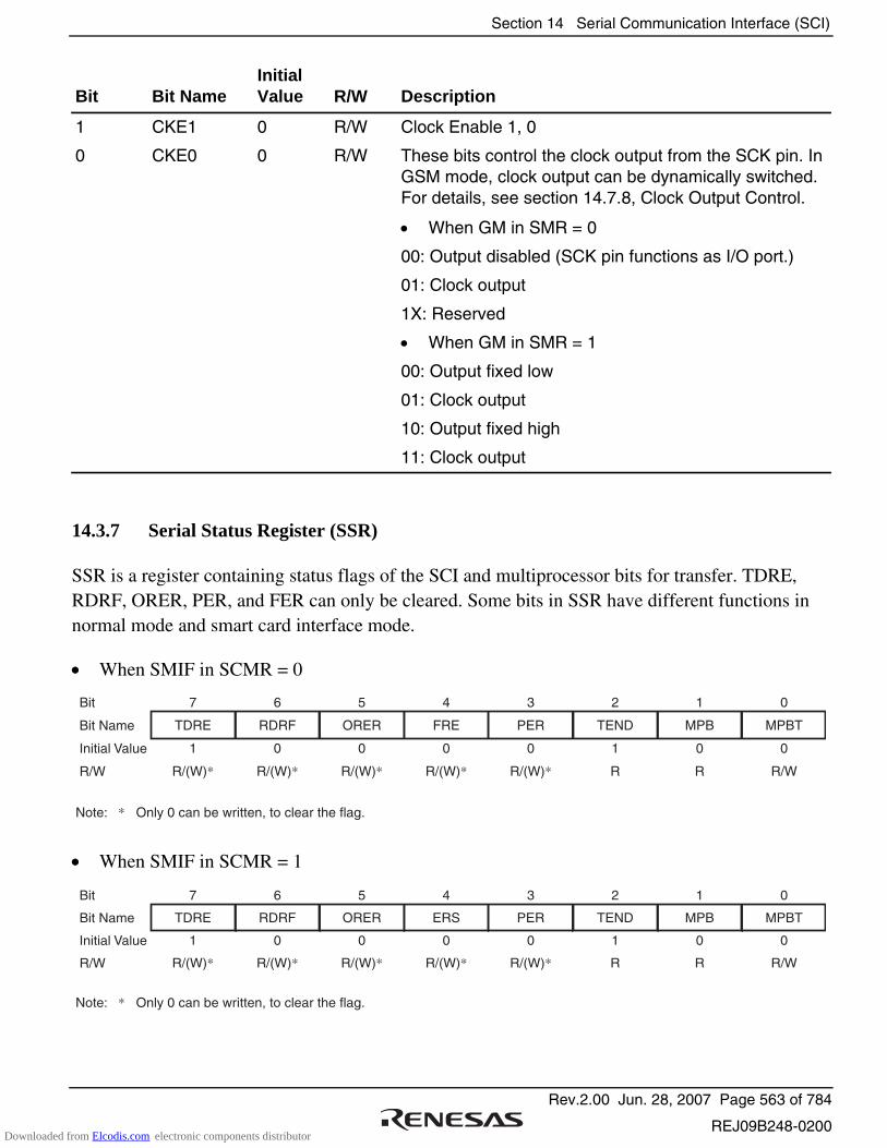
Section 14 Serial Communication Interface (SCI)
Rev.2.00 Jun. 28, 2007 Page 563 of 784
REJ09B248-0200
Bit Bit Name Initial Value R/W Description
1
0
CKE1
CKE0
0
0
R/W
R/W
Clock Enable 1, 0
These bits control the clock output from the SCK pin. In GSM mode, clock output can be dynamically switched. For details, see section 14.7.8, Clock Output Control.
• When GM in SMR = 0
00: Output disabled (SCK pin functions as I/O port.)
01: Clock output
1X: Reserved
• When GM in SMR = 1
00: Output fixed low
01: Clock output
10: Output fixed high
11: Clock output
14.3.7 Serial Status Register (SSR)
SSR is a register containing status flags of the SCI and multiprocessor bits for transfer. TDRE, RDRF, ORER, PER, and FER can only be cleared. Some bits in SSR have different functions in normal mode and smart card interface mode.
• When SMIF in SCMR = 0
Bit
Bit Name
Initial Value
R/W
7
TDRE
1
R/(W)*
6
RDRF
0
R/(W)*
5
ORER
0
R/(W)*
4
FRE
0
R/(W)*
3
PER
0
R/(W)*
2
TEND
1
R
1
MPB
0
R
0
MPBT
0
R/W
Note: * Only 0 can be written, to clear the flag.
• When SMIF in SCMR = 1
Bit
Bit Name
Initial Value
R/W
7
TDRE
1
R/(W)*
6
RDRF
0
R/(W)*
5
ORER
0
R/(W)*
4
ERS
0
R/(W)*
3
PER
0
R/(W)*
2
TEND
1
R
1
MPB
0
R
0
MPBT
0
R/W
Note: * Only 0 can be written, to clear the flag.
Downloaded from Elcodis.com electronic components distributor
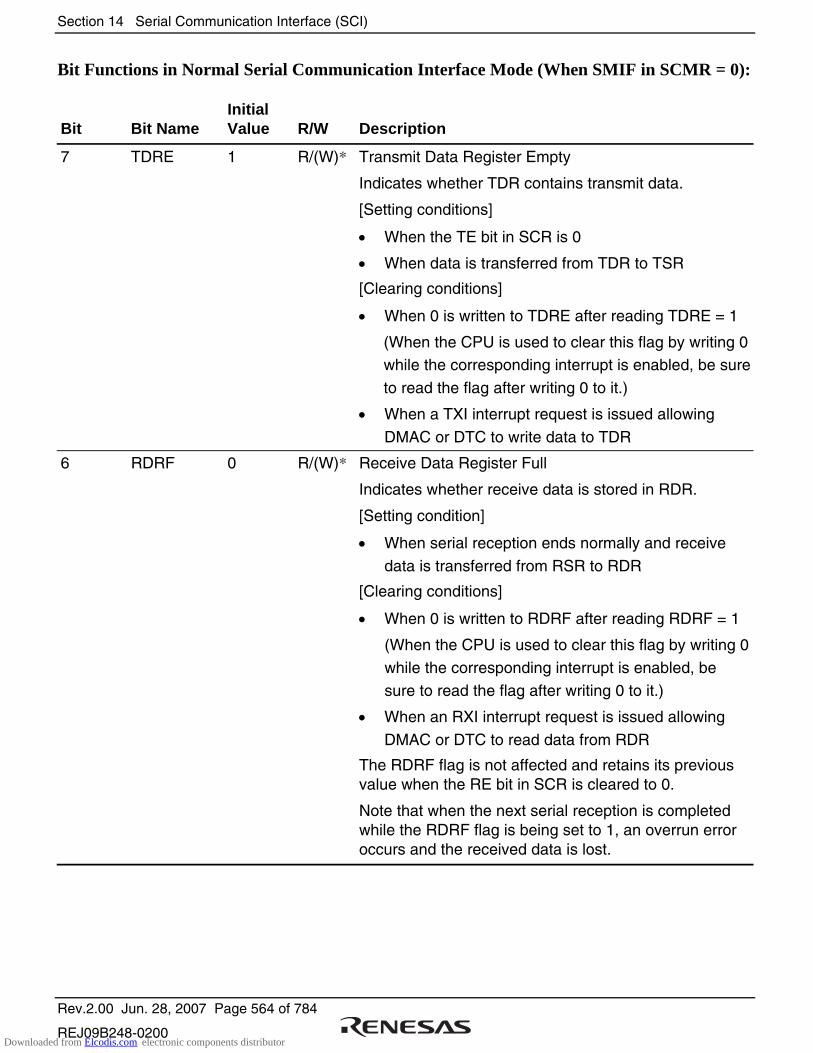
Section 14 Serial Communication Interface (SCI)
Rev.2.00 Jun. 28, 2007 Page 564 of 784
REJ09B248-0200
Bit Functions in Normal Serial Communication Interface Mode (When SMIF in SCMR = 0):
Bit Bit Name Initial Value R/W Description
7 TDRE 1 R/(W)* Transmit Data Register Empty
Indicates whether TDR contains transmit data.
[Setting conditions]
• When the TE bit in SCR is 0
• When data is transferred from TDR to TSR
[Clearing conditions]
• When 0 is written to TDRE after reading TDRE = 1
(When the CPU is used to clear this flag by writing 0 while the corresponding interrupt is enabled, be sure
to read the flag after writing 0 to it.)
• When a TXI interrupt request is issued allowing
DMAC or DTC to write data to TDR
6 RDRF 0 R/(W)* Receive Data Register Full
Indicates whether receive data is stored in RDR.
[Setting condition]
• When serial reception ends normally and receive
data is transferred from RSR to RDR
[Clearing conditions]
• When 0 is written to RDRF after reading RDRF = 1
(When the CPU is used to clear this flag by writing 0
while the corresponding interrupt is enabled, be
sure to read the flag after writing 0 to it.)
• When an RXI interrupt request is issued allowing
DMAC or DTC to read data from RDR
The RDRF flag is not affected and retains its previous value when the RE bit in SCR is cleared to 0.
Note that when the next serial reception is completed while the RDRF flag is being set to 1, an overrun error occurs and the received data is lost.
Downloaded from Elcodis.com electronic components distributor

Section 14 Serial Communication Interface (SCI)
Rev.2.00 Jun. 28, 2007 Page 565 of 784
REJ09B248-0200
Bit Bit Name Initial Value R/W Description
5 ORER 0 R/(W)* Overrun Error
Indicates that an overrun error has occurred during reception and the reception ends abnormally. [Setting condition]
• When the next serial reception is completed while RDRF = 1 In RDR, receive data prior to an overrun error occurrence is retained, but data received after the overrun error occurrence is lost. When the ORER flag is set to 1, subsequent serial reception cannot be performed. Note that, in clocked synchronous mode, serial transmission also cannot continue.
[Clearing condition]
• When 0 is written to ORER after reading ORER = 1
Even when the RE bit in SCR is cleared, the ORER flag is not affected and retains its previous value. (When the CPU is used to clear this flag by writing 0 while the corresponding interrupt is enabled, be sure to read the flag after writing 0 to it.)
4 FER 0 R/(W)* Framing Error Indicates that a framing error has occurred during reception in asynchronous mode and the reception ends abnormally. [Setting condition]
• When the stop bit is 0
In 2-stop-bit mode, only the first stop bit is checked whether it is 1 but the second stop bit is not checked. Note that receive data when the framing error occurs is transferred to RDR, however, the RDRF flag is not set. In addition, when the FER flag is being set to 1, the subsequent serial reception cannot be performed. In clocked synchronous mode, serial transmission also cannot continue.
[Clearing condition]
• When 0 is written to FER after reading FER = 1 Even when the RE bit in SCR is cleared, the FER flag is not affected and retains its previous value. (When the CPU is used to clear this flag by writing 0 while the corresponding interrupt is enabled, be sure to read the flag after writing 0 to it.)
Downloaded from Elcodis.com electronic components distributor
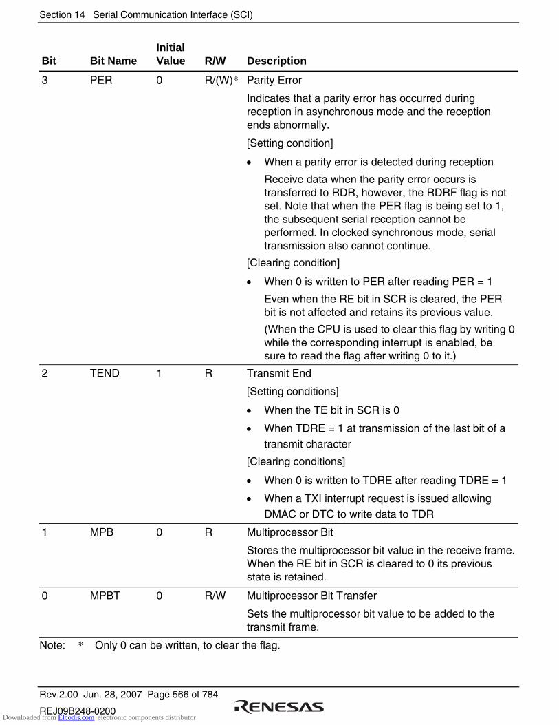
Section 14 Serial Communication Interface (SCI)
Rev.2.00 Jun. 28, 2007 Page 566 of 784
REJ09B248-0200
Bit Bit Name Initial Value R/W Description
3 PER 0 R/(W)* Parity Error
Indicates that a parity error has occurred during reception in asynchronous mode and the reception ends abnormally.
[Setting condition]
• When a parity error is detected during reception
Receive data when the parity error occurs is transferred to RDR, however, the RDRF flag is not set. Note that when the PER flag is being set to 1, the subsequent serial reception cannot be performed. In clocked synchronous mode, serial transmission also cannot continue.
[Clearing condition]
• When 0 is written to PER after reading PER = 1
Even when the RE bit in SCR is cleared, the PER bit is not affected and retains its previous value.
(When the CPU is used to clear this flag by writing 0 while the corresponding interrupt is enabled, be sure to read the flag after writing 0 to it.)
2 TEND 1 R Transmit End
[Setting conditions]
• When the TE bit in SCR is 0
• When TDRE = 1 at transmission of the last bit of a
transmit character
[Clearing conditions]
• When 0 is written to TDRE after reading TDRE = 1
• When a TXI interrupt request is issued allowing
DMAC or DTC to write data to TDR
1 MPB 0 R Multiprocessor Bit
Stores the multiprocessor bit value in the receive frame. When the RE bit in SCR is cleared to 0 its previous state is retained.
0 MPBT 0 R/W Multiprocessor Bit Transfer
Sets the multiprocessor bit value to be added to the transmit frame.
Note: * Only 0 can be written, to clear the flag.
Downloaded from Elcodis.com electronic components distributor

Section 14 Serial Communication Interface (SCI)
Rev.2.00 Jun. 28, 2007 Page 567 of 784
REJ09B248-0200
Bit Functions in Smart Card Interface Mode (When SMIF in SCMR = 1):
Bit Bit Name Initial Value R/W Description
7 TDRE 1 R/(W)* Transmit Data Register Empty
Indicates whether TDR contains transmit data.
[Setting conditions]
• When the TE bit in SCR is 0
• When data is transferred from TDR to TSR
[Clearing conditions]
• When 0 is written to TDRE after reading TDRE = 1
(When the CPU is used to clear this flag by writing 0 while the corresponding interrupt is enabled, be sure to read the flag after writing 0 to it.)
• When a TXI interrupt request is issued allowing
DMAC or DTC to write data to TDR
6 RDRF 0 R/(W)* Receive Data Register Full
Indicates whether receive data is stored in RDR.
[Setting condition]
• When serial reception ends normally and receive
data is transferred from RSR to RDR
[Clearing conditions]
• When 0 is written to RDRF after reading RDRF = 1
(When the CPU is used to clear this flag by writing 0 while the corresponding interrupt is enabled, be sure to read the flag after writing 0 to it.)
• When an RXI interrupt request is issued allowing
DMAC or DTC to read data from RDR
The RDRF flag is not affected and retains its previous value even when the RE bit in SCR is cleared to 0.
Note that when the next reception is completed while the RDRF flag is being set to 1, an overrun error occurs and the received data is lost.
Downloaded from Elcodis.com electronic components distributor
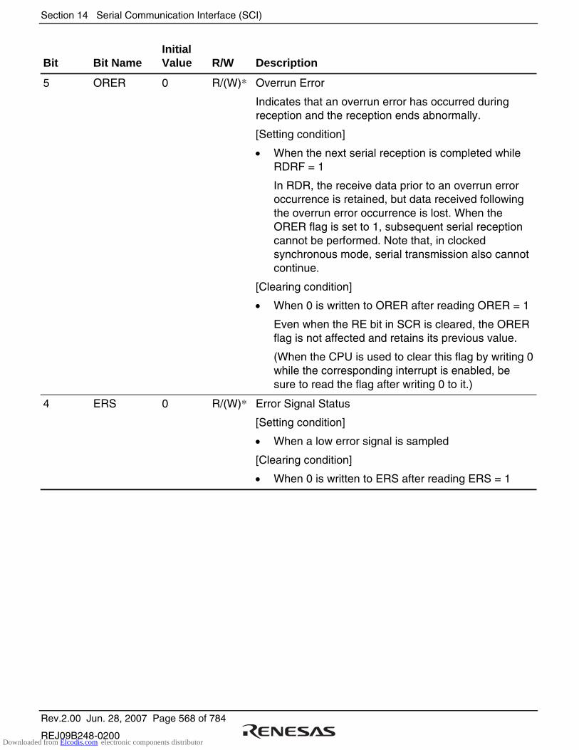
Section 14 Serial Communication Interface (SCI)
Rev.2.00 Jun. 28, 2007 Page 568 of 784
REJ09B248-0200
Bit Bit Name Initial Value R/W Description
5 ORER 0 R/(W)* Overrun Error
Indicates that an overrun error has occurred during reception and the reception ends abnormally.
[Setting condition]
• When the next serial reception is completed while RDRF = 1
In RDR, the receive data prior to an overrun error occurrence is retained, but data received following the overrun error occurrence is lost. When the ORER flag is set to 1, subsequent serial reception cannot be performed. Note that, in clocked synchronous mode, serial transmission also cannot continue.
[Clearing condition]
• When 0 is written to ORER after reading ORER = 1
Even when the RE bit in SCR is cleared, the ORER flag is not affected and retains its previous value.
(When the CPU is used to clear this flag by writing 0 while the corresponding interrupt is enabled, be sure to read the flag after writing 0 to it.)
4 ERS 0 R/(W)* Error Signal Status
[Setting condition]
• When a low error signal is sampled
[Clearing condition]
• When 0 is written to ERS after reading ERS = 1
Downloaded from Elcodis.com electronic components distributor
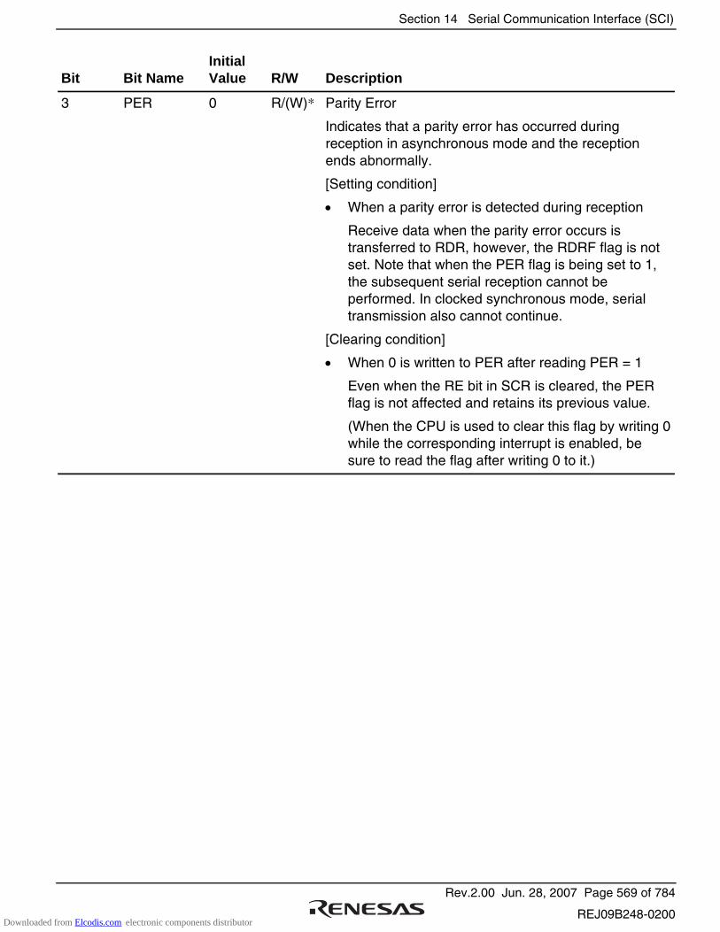
Section 14 Serial Communication Interface (SCI)
Rev.2.00 Jun. 28, 2007 Page 569 of 784
REJ09B248-0200
Bit Bit Name Initial Value R/W Description
3 PER 0 R/(W)* Parity Error
Indicates that a parity error has occurred during reception in asynchronous mode and the reception ends abnormally.
[Setting condition]
• When a parity error is detected during reception
Receive data when the parity error occurs is transferred to RDR, however, the RDRF flag is not set. Note that when the PER flag is being set to 1, the subsequent serial reception cannot be performed. In clocked synchronous mode, serial transmission also cannot continue.
[Clearing condition]
• When 0 is written to PER after reading PER = 1
Even when the RE bit in SCR is cleared, the PER flag is not affected and retains its previous value.
(When the CPU is used to clear this flag by writing 0 while the corresponding interrupt is enabled, be sure to read the flag after writing 0 to it.)
Downloaded from Elcodis.com electronic components distributor
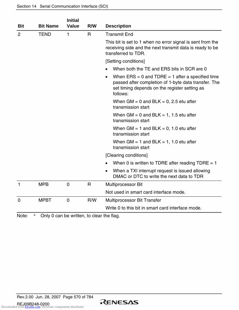
Section 14 Serial Communication Interface (SCI)
Rev.2.00 Jun. 28, 2007 Page 570 of 784
REJ09B248-0200
Bit Bit Name Initial Value R/W Description
2 TEND 1 R Transmit End
This bit is set to 1 when no error signal is sent from the receiving side and the next transmit data is ready to be transferred to TDR.
[Setting conditions]
• When both the TE and ERS bits in SCR are 0
• When ERS = 0 and TDRE = 1 after a specified time passed after completion of 1-byte data transfer. The set timing depends on the register setting as follows:
When GM = 0 and BLK = 0, 2.5 etu after transmission start
When GM = 0 and BLK = 1, 1.5 etu after transmission start
When GM = 1 and BLK = 0, 1.0 etu after transmission start
When GM = 1 and BLK = 1, 1.0 etu after transmission start
[Clearing conditions]
• When 0 is written to TDRE after reading TDRE = 1
• When a TXI interrupt request is issued allowing DMAC or DTC to write the next data to TDR
1 MPB 0 R Multiprocessor Bit
Not used in smart card interface mode.
0 MPBT 0 R/W Multiprocessor Bit Transfer
Write 0 to this bit in smart card interface mode.
Note: * Only 0 can be written, to clear the flag.
Downloaded from Elcodis.com electronic components distributor

Section 14 Serial Communication Interface (SCI)
Rev.2.00 Jun. 28, 2007 Page 571 of 784
REJ09B248-0200
14.3.8 Smart Card Mode Register (SCMR)
SCMR selects smart card interface mode and its format.
7
1
R
6
1
R
5
1
R
4
1
R
1
1
R
Bit
Bit Name
Initial Value
R/W
3
SDIR
0
R/W
2
SINV
0
R/W
0
SMIF
0
R/W
Bit Bit Name Initial Value R/W Description
7 to 4 All 1 R Reserved
These are read-only bits and cannot be modified.
3 SDIR 0 R/W Smart Card Data Transfer Direction
Selects the serial/parallel conversion format.
0: Transfer with LSB-first
1: Transfer with MSB-first
This bit is valid only when the 8-bit data format is used for transmission/reception; when the 7-bit data format is used, data is always transmitted/received with LSB-first.
2 SINV 0 R/W Smart Card Data Invert
Inverts the transmit/receive data logic level. This bit does not affect the logic level of the parity bit. To invert the parity bit, invert the O/E bit in SMR.
0: TDR contents are transmitted as they are. Receive
data is stored as it is in RDR.
1: TDR contents are inverted before being transmitted.
Receive data is stored in inverted form in RDR.
1 1 R Reserved
This is a read-only bit and cannot be modified.
0 SMIF 0 R/W Smart Card Interface Mode Select
When this bit is set to 1, smart card interface mode is selected.
0: Normal asynchronous or clocked synchronous mode
1: Smart card interface mode
Downloaded from Elcodis.com electronic components distributor
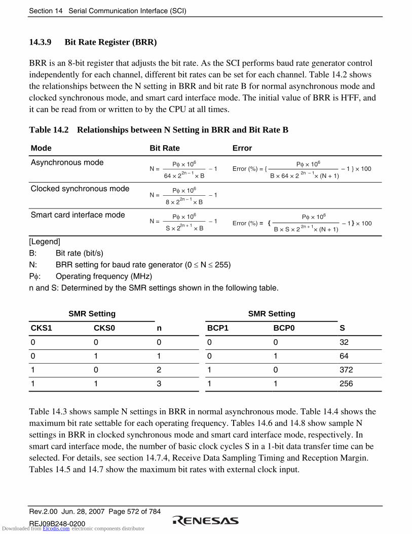
Section 14 Serial Communication Interface (SCI)
Rev.2.00 Jun. 28, 2007 Page 572 of 784
REJ09B248-0200
14.3.9 Bit Rate Register (BRR)
BRR is an 8-bit register that adjusts the bit rate. As the SCI performs baud rate generator control independently for each channel, different bit rates can be set for each channel. Table 14.2 shows the relationships between the N setting in BRR and bit rate B for normal asynchronous mode and clocked synchronous mode, and smart card interface mode. The initial value of BRR is H'FF, and it can be read from or written to by the CPU at all times.
Table 14.2 Relationships between N Setting in BRR and Bit Rate B
Mode Bit Rate Error
Asynchronous mode N = − 1
64 × 2 × B2n – 1
Pφ × 106
Error (%) = – 1 × 100
B × 64 × 2 × (N + 1)2n – 1
Pφ × 106
Clocked synchronous mode N = − 1
8 × 2 × B2n – 1
Pφ × 106
Smart card interface mode N = − 1
S × 2 × B
Pφ × 106
2n + 1
Error (%) =B × S × 2 × (N + 1)
– 1 × 1002n + 1
Pφ × 106
[Legend]
B: Bit rate (bit/s)
N: BRR setting for baud rate generator (0 ≤ N ≤ 255) Pφ: Operating frequency (MHz)
n and S: Determined by the SMR settings shown in the following table.
SMR Setting SMR Setting
CKS1 CKS0 n BCP1 BCP0 S
0 0 0 0 0 32
0 1 1 0 1 64
1 0 2 1 0 372
1 1 3 1 1 256
Table 14.3 shows sample N settings in BRR in normal asynchronous mode. Table 14.4 shows the maximum bit rate settable for each operating frequency. Tables 14.6 and 14.8 show sample N settings in BRR in clocked synchronous mode and smart card interface mode, respectively. In smart card interface mode, the number of basic clock cycles S in a 1-bit data transfer time can be selected. For details, see section 14.7.4, Receive Data Sampling Timing and Reception Margin. Tables 14.5 and 14.7 show the maximum bit rates with external clock input.
Downloaded from Elcodis.com electronic components distributor

Section 14 Serial Communication Interface (SCI)
Rev.2.00 Jun. 28, 2007 Page 573 of 784
REJ09B248-0200
Table 14.3 Examples of BRR Settings for Various Bit Rates (Asynchronous Mode) (1)
Operating Frequency Pφ (MHz)
8 9.8304 10 12
Bit Rate (bit/s) n N
Error (%) n N
Error (%) n N
Error (%) n N
Error (%)
110 2 141 0.03 2 174 –0.26 2 177 –0.25 2 212 0.03
150 2 103 0.16 2 127 0.00 2 129 0.16 2 155 0.16
300 1 207 0.16 1 255 0.00 2 64 0.16 2 77 0.16
600 1 103 0.16 1 127 0.00 1 129 0.16 1 155 0.16
1200 0 207 0.16 0 255 0.00 1 64 0.16 1 77 0.16
2400 0 103 0.16 0 127 0.00 0 129 0.16 0 155 0.16
4800 0 51 0.16 0 63 0.00 0 64 0.16 0 77 0.16
9600 0 25 0.16 0 31 0.00 0 32 –1.36 0 38 0.16
19200 0 12 0.16 0 15 0.00 0 15 1.73 0 19 –2.34
31250 0 7 0.00 0 9 –1.70 0 9 0.00 0 11 0.00
38400 0 7 0.00 0 7 1.73 0 9 –2.34
Operating Frequency Pφ (MHz)
12.288 14 14.7456 16
Bit Rate (bit/s) n N
Error (%) n N
Error (%) n N
Error (%) n N
Error (%)
110 2 217 0.08 2 248 –0.17 3 64 0.70 3 70 0.03
150 2 159 0.00 2 181 0.16 2 191 0.00 2 207 0.16
300 2 79 0.00 2 90 0.16 2 95 0.00 2 103 0.16
600 1 159 0.00 1 181 0.16 1 191 0.00 1 207 0.16
1200 1 79 0.00 1 90 0.16 1 95 0.00 1 103 0.16
2400 0 159 0.00 0 181 0.16 0 191 0.00 0 207 0.16
4800 0 79 0.00 0 90 0.16 0 95 0.00 0 103 0.16
9600 0 39 0.00 0 45 –0.93 0 47 0.00 0 51 0.16
19200 0 19 0.00 0 22 –0.93 0 23 0.00 0 25 0.16
31250 0 11 2.40 0 13 0.00 0 14 –1.70 0 15 0.00
38400 0 9 0.00 0 11 0.00 0 12 0.16
Downloaded from Elcodis.com electronic components distributor
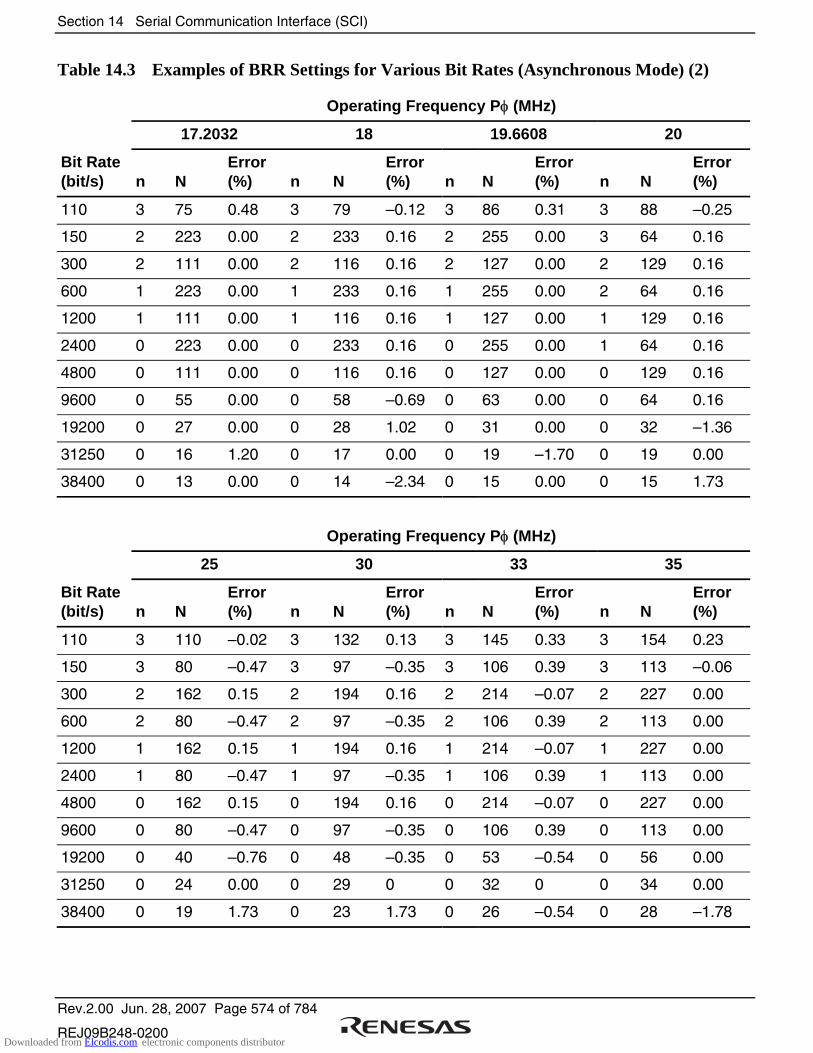
Section 14 Serial Communication Interface (SCI)
Rev.2.00 Jun. 28, 2007 Page 574 of 784
REJ09B248-0200
Table 14.3 Examples of BRR Settings for Various Bit Rates (Asynchronous Mode) (2)
Operating Frequency Pφ (MHz)
17.2032 18 19.6608 20
Bit Rate (bit/s) n N
Error (%) n N
Error (%) n N
Error (%) n N
Error (%)
110 3 75 0.48 3 79 –0.12 3 86 0.31 3 88 –0.25
150 2 223 0.00 2 233 0.16 2 255 0.00 3 64 0.16
300 2 111 0.00 2 116 0.16 2 127 0.00 2 129 0.16
600 1 223 0.00 1 233 0.16 1 255 0.00 2 64 0.16
1200 1 111 0.00 1 116 0.16 1 127 0.00 1 129 0.16
2400 0 223 0.00 0 233 0.16 0 255 0.00 1 64 0.16
4800 0 111 0.00 0 116 0.16 0 127 0.00 0 129 0.16
9600 0 55 0.00 0 58 –0.69 0 63 0.00 0 64 0.16
19200 0 27 0.00 0 28 1.02 0 31 0.00 0 32 –1.36
31250 0 16 1.20 0 17 0.00 0 19 –1.70 0 19 0.00
38400 0 13 0.00 0 14 –2.34 0 15 0.00 0 15 1.73
Operating Frequency Pφ (MHz)
25 30 33 35
Bit Rate (bit/s) n N
Error (%) n N
Error (%) n N
Error (%) n N
Error (%)
110 3 110 –0.02 3 132 0.13 3 145 0.33 3 154 0.23
150 3 80 –0.47 3 97 –0.35 3 106 0.39 3 113 –0.06
300 2 162 0.15 2 194 0.16 2 214 –0.07 2 227 0.00
600 2 80 –0.47 2 97 –0.35 2 106 0.39 2 113 0.00
1200 1 162 0.15 1 194 0.16 1 214 –0.07 1 227 0.00
2400 1 80 –0.47 1 97 –0.35 1 106 0.39 1 113 0.00
4800 0 162 0.15 0 194 0.16 0 214 –0.07 0 227 0.00
9600 0 80 –0.47 0 97 –0.35 0 106 0.39 0 113 0.00
19200 0 40 –0.76 0 48 –0.35 0 53 –0.54 0 56 0.00
31250 0 24 0.00 0 29 0 0 32 0 0 34 0.00
38400 0 19 1.73 0 23 1.73 0 26 –0.54 0 28 –1.78
Downloaded from Elcodis.com electronic components distributor
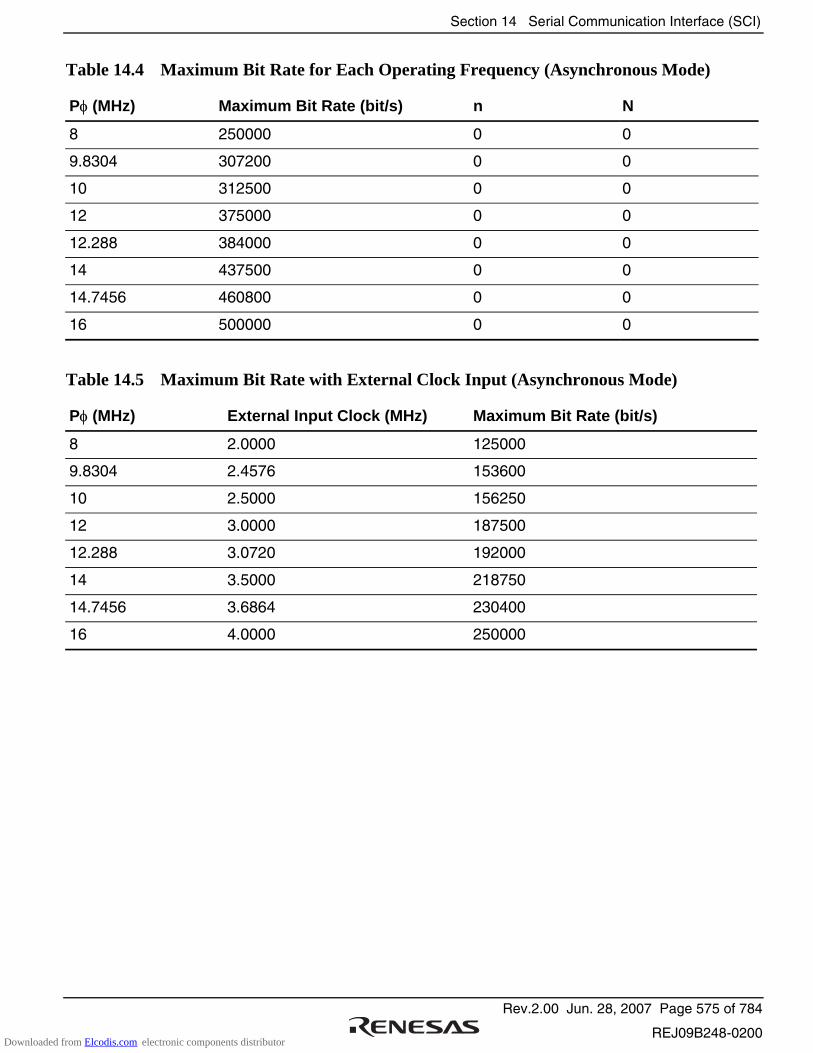
Section 14 Serial Communication Interface (SCI)
Rev.2.00 Jun. 28, 2007 Page 575 of 784
REJ09B248-0200
Table 14.4 Maximum Bit Rate for Each Operating Frequency (Asynchronous Mode)
Pφ (MHz) Maximum Bit Rate (bit/s) n N
8 250000 0 0
9.8304 307200 0 0
10 312500 0 0
12 375000 0 0
12.288 384000 0 0
14 437500 0 0
14.7456 460800 0 0
16 500000 0 0
Table 14.5 Maximum Bit Rate with External Clock Input (Asynchronous Mode)
Pφ (MHz) External Input Clock (MHz) Maximum Bit Rate (bit/s)
8 2.0000 125000
9.8304 2.4576 153600
10 2.5000 156250
12 3.0000 187500
12.288 3.0720 192000
14 3.5000 218750
14.7456 3.6864 230400
16 4.0000 250000
Downloaded from Elcodis.com electronic components distributor
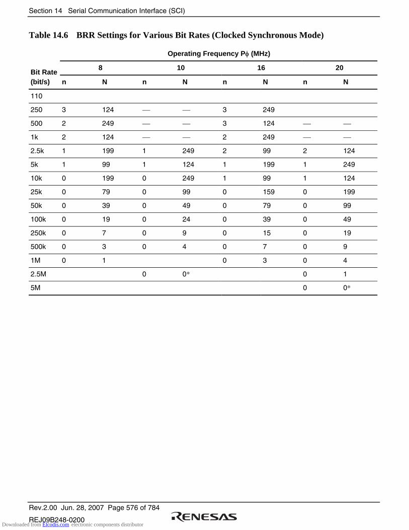
Section 14 Serial Communication Interface (SCI)
Rev.2.00 Jun. 28, 2007 Page 576 of 784
REJ09B248-0200
Table 14.6 BRR Settings for Various Bit Rates (Clocked Synchronous Mode)
Operating Frequency Pφ (MHz)
8 10 16 20 Bit Rate (bit/s) n N n N n N n N
110
250 3 124 3 249
500 2 249 3 124
1k 2 124 2 249
2.5k 1 199 1 249 2 99 2 124
5k 1 99 1 124 1 199 1 249
10k 0 199 0 249 1 99 1 124
25k 0 79 0 99 0 159 0 199
50k 0 39 0 49 0 79 0 99
100k 0 19 0 24 0 39 0 49
250k 0 7 0 9 0 15 0 19
500k 0 3 0 4 0 7 0 9
1M 0 1 0 3 0 4
2.5M 0 0* 0 1
5M 0 0*
Downloaded from Elcodis.com electronic components distributor

Section 14 Serial Communication Interface (SCI)
Rev.2.00 Jun. 28, 2007 Page 577 of 784
REJ09B248-0200
Operating Frequency Pφ (MHz)
25 30 33 35 Bit Rate (bit/s) n N n N n N n N
110
250
500 3 233
1k 3 97 3 116 3 128 3 136
2.5k 2 155 2 187 2 205 2 218
5k 2 77 2 93 2 102 2 108
10k 1 155 1 187 1 205 1 218
25k 0 249 1 74 1 82 1 87
50k 0 124 0 149 0 164 0 174
100k 0 62 0 74 0 82 0 87
250k 0 24 0 29 0 32 0 34
500k 0 14
1M
2.5M 0 2
5M
[Legend]
Space: Setting prohibited.
: Can be set, but there will be error. *: Continuous transmission or reception is not possible.
Table 14.7 Maximum Bit Rate with External Clock Input (Clocked Synchronous Mode)
Pφ (MHz) External Input Clock (MHz)
Maximum Bit Rate (bit/s) Pφ (MHz)
External Input Clock (MHz)
Maximum Bit Rate (bit/s)
8 1.3333 1333333.3 20 3.3333 3333333.3
10 1.6667 1666666.7 25 4.1667 4166666.7
12 2.0000 2000000.0 30 5.0000 5000000.0
14 2.3333 2333333.3 33 5.5000 5500000.0
16 2.6667 2666666.7 35 5.8336 5833625.0
18 3.0000 3000000.0
Downloaded from Elcodis.com electronic components distributor

Section 14 Serial Communication Interface (SCI)
Rev.2.00 Jun. 28, 2007 Page 578 of 784
REJ09B248-0200
Table 14.8 BRR Settings for Various Bit Rates (Smart Card Interface Mode, n = 0, S = 372)
Operating Frequency Pφ (MHz)
7.1424 10.00 10.7136 13.00 Bit Rate
(bit/s) n N Error (%) n N Error (%) n N Error (%) n N Error (%)
9600 0 0 0.00 0 1 30 0 1 25 0 1 8.99
Operating Frequency Pφ (MHz)
14.2848 16.00 18.00 20.00 Bit Rate
(bit/s) n N Error (%) n N Error (%) n N Error (%) n N Error (%)
9600 0 1 0.00 0 1 12.01 0 2 15.99 0 2 6.60
Operating Frequency Pφ (MHz)
25.00 30.00 33.00 35.00 Bit Rate
(bit/s) n N Error (%) n N Error (%) n N Error (%) n N Error (%)
9600 0 3 12.49 0 3 5.01 0 4 7.59 0 4 1.99
Table 14.9 Maximum Bit Rate for Each Operating Frequency (Smart Card Interface Mode, S = 372)
Pφ (MHz) Maximum Bit Rate (bit/s) n N Pφ (MHz)
Maximum Bit Rate (bit/s) n N
7.1424 9600 0 0 18.00 24194 0 0
10.00 13441 0 0 20.00 26882 0 0
10.7136 14400 0 0 25.00 33602 0 0
13.00 17473 0 0 30.00 40323 0 0
14.2848 19200 0 0 33.00 44355 0 0
16.00 21505 0 0 35.00 47043 0 0
Downloaded from Elcodis.com electronic components distributor
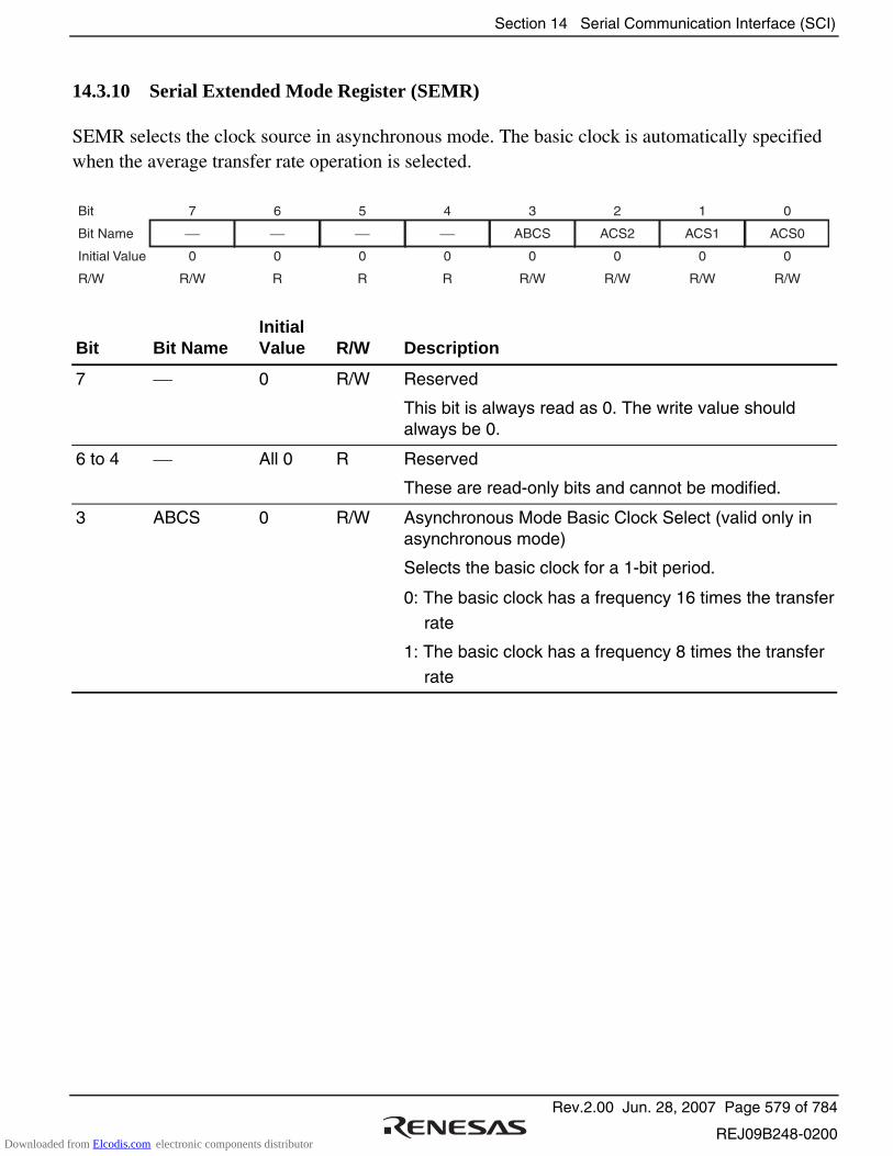
Section 14 Serial Communication Interface (SCI)
Rev.2.00 Jun. 28, 2007 Page 579 of 784
REJ09B248-0200
14.3.10 Serial Extended Mode Register (SEMR)
SEMR selects the clock source in asynchronous mode. The basic clock is automatically specified when the average transfer rate operation is selected.
7
0
R/W
6
0
R
5
0
R
4
0
R
Bit
Bit Name
Initial Value
R/W
3
ABCS
0
R/W
2
ACS2
0
R/W
1
ACS1
0
R/W
0
ACS0
0
R/W
Bit Bit Name Initial Value R/W Description
7 0 R/W Reserved
This bit is always read as 0. The write value should always be 0.
6 to 4 All 0 R Reserved
These are read-only bits and cannot be modified.
3 ABCS 0 R/W Asynchronous Mode Basic Clock Select (valid only in asynchronous mode)
Selects the basic clock for a 1-bit period.
0: The basic clock has a frequency 16 times the transfer
rate
1: The basic clock has a frequency 8 times the transfer
rate
Downloaded from Elcodis.com electronic components distributor
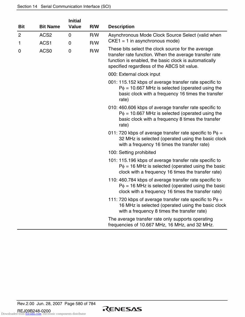
Section 14 Serial Communication Interface (SCI)
Rev.2.00 Jun. 28, 2007 Page 580 of 784
REJ09B248-0200
Bit Bit Name Initial Value R/W Description
2
1
0
ACS2
ACS1
ACS0
0
0
0
R/W
R/W
R/W
Asynchronous Mode Clock Source Select (valid when CKE1 = 1 in asynchronous mode)
These bits select the clock source for the average transfer rate function. When the average transfer rate function is enabled, the basic clock is automatically specified regardless of the ABCS bit value.
000: External clock input
001: 115.152 kbps of average transfer rate specific to Pφ = 10.667 MHz is selected (operated using the basic clock with a frequency 16 times the transfer rate)
010: 460.606 kbps of average transfer rate specific to Pφ = 10.667 MHz is selected (operated using the basic clock with a frequency 8 times the transfer rate)
011: 720 kbps of average transfer rate specific to Pφ = 32 MHz is selected (operated using the basic clock with a frequency 16 times the transfer rate)
100: Setting prohibited
101: 115.196 kbps of average transfer rate specific to Pφ = 16 MHz is selected (operated using the basic clock with a frequency 16 times the transfer rate)
110: 460.784 kbps of average transfer rate specific to Pφ = 16 MHz is selected (operated using the basic clock with a frequency 16 times the transfer rate)
111: 720 kbps of average transfer rate specific to Pφ = 16 MHz is selected (operated using the basic clock with a frequency 8 times the transfer rate)
The average transfer rate only supports operating frequencies of 10.667 MHz, 16 MHz, and 32 MHz.
Downloaded from Elcodis.com electronic components distributor
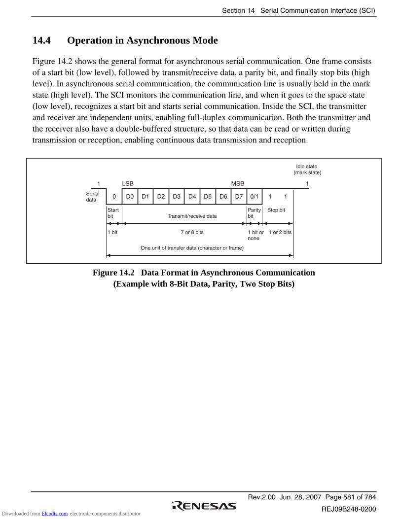
Section 14 Serial Communication Interface (SCI)
Rev.2.00 Jun. 28, 2007 Page 581 of 784
REJ09B248-0200
14.4 Operation in Asynchronous Mode
Figure 14.2 shows the general format for asynchronous serial communication. One frame consists of a start bit (low level), followed by transmit/receive data, a parity bit, and finally stop bits (high level). In asynchronous serial communication, the communication line is usually held in the mark state (high level). The SCI monitors the communication line, and when it goes to the space state (low level), recognizes a start bit and starts serial communication. Inside the SCI, the transmitter and receiver are independent units, enabling full-duplex communication. Both the transmitter and the receiver also have a double-buffered structure, so that data can be read or written during transmission or reception, enabling continuous data transmission and reception.
LSB
Start bit
MSB
Idle state (mark state)
Stop bit
0
Transmit/receive data
D0 D1 D2 D3 D4 D5 D6 D7 0/1 1 1
1 1
Serial data
Parity bit
1 bit 1 or 2 bits7 or 8 bits 1 bit or none
One unit of transfer data (character or frame)
Figure 14.2 Data Format in Asynchronous Communication (Example with 8-Bit Data, Parity, Two Stop Bits)
Downloaded from Elcodis.com electronic components distributor
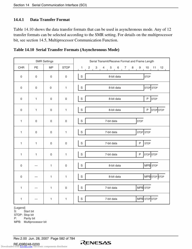
Section 14 Serial Communication Interface (SCI)
Rev.2.00 Jun. 28, 2007 Page 582 of 784
REJ09B248-0200
14.4.1 Data Transfer Format
Table 14.10 shows the data transfer formats that can be used in asynchronous mode. Any of 12 transfer formats can be selected according to the SMR setting. For details on the multiprocessor bit, see section 14.5, Multiprocessor Communication Function.
Table 14.10 Serial Transfer Formats (Asynchronous Mode)
PE
0
0
1
1
0
0
1
1
—
—
—
—
S 8-bit data STOP
S 7-bit data STOP
S 8-bit data STOP STOP
S 8-bit data P STOP
S 7-bit data STOPP
S 8-bit data MPB STOP
S 8-bit data MPB STOP STOP
S 7-bit data STOPMPB
S 7-bit data STOPMPB STOP
S 7-bit data STOPSTOP
CHR
0
0
0
0
1
1
1
1
0
0
1
1
MP
0
0
0
0
0
0
0
0
1
1
1
1
STOP
0
1
0
1
0
1
0
1
0
1
0
1
SMR Settings
1 2 3 4 5 6 7 8 9 10 11 12
Serial Transmit/Receive Format and Frame Length
STOPS 8-bit data P STOP
S 7-bit data STOPP STOP
[Legend]S: Start bitSTOP: Stop bitP: Parity bitMPB: Multiprocessor bit
Downloaded from Elcodis.com electronic components distributor

Section 14 Serial Communication Interface (SCI)
Rev.2.00 Jun. 28, 2007 Page 583 of 784
REJ09B248-0200
14.4.2 Receive Data Sampling Timing and Reception Margin in Asynchronous Mode
In asynchronous mode, the SCI operates on a basic clock with a frequency of 16 times the bit rate. In reception, the SCI samples the falling edge of the start bit using the basic clock, and performs internal synchronization. Since receive data is sampled at the rising edge of the 8th pulse of the basic clock, data is latched at the middle of each bit, as shown in figure 14.3. Thus the reception margin in asynchronous mode is determined by formula (1) below.
M = (0.5 – ) – (L – 0.5) F – (1 + F ) 2N1
N| D – 0.5 |
M: Reception marginN: Ratio of bit rate to clock (N = 16)D: Duty cycle of clock (D = 0.5 to 1.0)L: Frame length (L = 9 to 12)F: Absolute value of clock frequency deviation
× 100 [%] ... Formula (1)
Assuming values of F = 0 and D = 0.5 in formula (1), the reception margin is determined by the formula below.
M = ( 0.5 – ) × 100[%] = 46.875%2 × 16
1
However, this is only the computed value, and a margin of 20% to 30% should be allowed in system design.
Internal basic clock
16 clocks8 clocks
Receive data (RxD)
Synchronization sampling timing
Start bit D0 D1
Data sampling timing
15 0 7 15 00 7
Figure 14.3 Receive Data Sampling Timing in Asynchronous Mode
Downloaded from Elcodis.com electronic components distributor
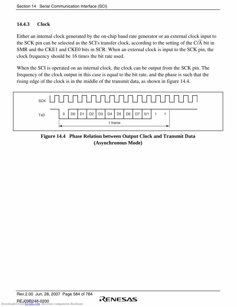
Section 14 Serial Communication Interface (SCI)
Rev.2.00 Jun. 28, 2007 Page 584 of 784
REJ09B248-0200
14.4.3 Clock
Either an internal clock generated by the on-chip baud rate generator or an external clock input to the SCK pin can be selected as the SCI's transfer clock, according to the setting of the C/A bit in SMR and the CKE1 and CKE0 bits in SCR. When an external clock is input to the SCK pin, the clock frequency should be 16 times the bit rate used.
When the SCI is operated on an internal clock, the clock can be output from the SCK pin. The frequency of the clock output in this case is equal to the bit rate, and the phase is such that the rising edge of the clock is in the middle of the transmit data, as shown in figure 14.4.
0
1 frame
D0 D1 D2 D3 D4 D5 D6 D7 0/1 1 1
SCK
TxD
Figure 14.4 Phase Relation between Output Clock and Transmit Data (Asynchronous Mode)
Downloaded from Elcodis.com electronic components distributor
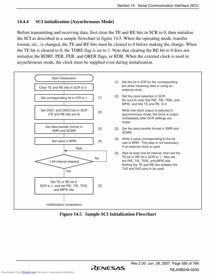
Section 14 Serial Communication Interface (SCI)
Rev.2.00 Jun. 28, 2007 Page 585 of 784
REJ09B248-0200
14.4.4 SCI Initialization (Asynchronous Mode)
Before transmitting and receiving data, first clear the TE and RE bits in SCR to 0, then initialize the SCI as described in a sample flowchart in figure 14.5. When the operating mode, transfer format, etc., is changed, the TE and RE bits must be cleared to 0 before making the change. When the TE bit is cleared to 0, the TDRE flag is set to 1. Note that clearing the RE bit to 0 does not initialize the RDRF, PER, FER, and ORER flags, or RDR. When the external clock is used in asynchronous mode, the clock must be supplied even during initialization.
Wait
<Initialization completion>
Start initialization
Set data transfer format inSMR and SCMR
[2]Set CKE1 and CKE0 bits in SCR(TE and RE bits are 0)
No
Yes
Set value in BRR
Set corresponding bit in ICR to 1
[3]
[4]
Set TE or RE bit inSCR to 1, and set RIE, TIE, TEIE,
and MPIE bits[5]
1-bit interval elapsed
[1] Set the bit in ICR for the corresponding pin when receiving data or using an external clock.
[2] Set the clock selection in SCR. Be sure to clear bits RIE, TIE, TEIE, and
MPIE, and bits TE and RE, to 0.
When the clock output is selected in asynchronous mode, the clock is output immediately after SCR settings are made.
[3] Set the data transfer format in SMR and SCMR.
[4] Write a value corresponding to the bit rate to BRR. This step is not necessary if an external clock is used.
[5] Wait at least one bit interval, then set the TE bit or RE bit in SCR to 1. Also set the RIE, TIE, TEIE, and MPIE bits. Setting the TE and RE bits enables the TxD and RxD pins to be used.
[1]
Clear TE and RE bits in SCR to 0
Figure 14.5 Sample SCI Initialization Flowchart
Downloaded from Elcodis.com electronic components distributor
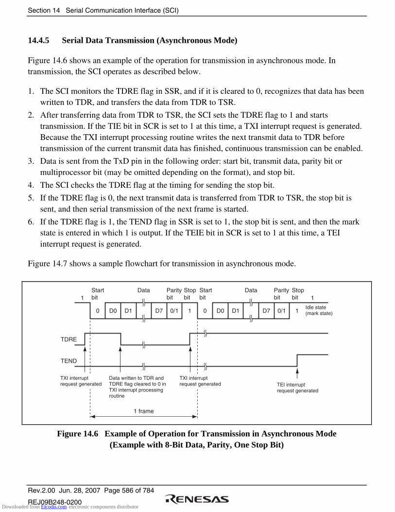
Section 14 Serial Communication Interface (SCI)
Rev.2.00 Jun. 28, 2007 Page 586 of 784
REJ09B248-0200
14.4.5 Serial Data Transmission (Asynchronous Mode)
Figure 14.6 shows an example of the operation for transmission in asynchronous mode. In transmission, the SCI operates as described below.
1. The SCI monitors the TDRE flag in SSR, and if it is cleared to 0, recognizes that data has been written to TDR, and transfers the data from TDR to TSR.
2. After transferring data from TDR to TSR, the SCI sets the TDRE flag to 1 and starts transmission. If the TIE bit in SCR is set to 1 at this time, a TXI interrupt request is generated. Because the TXI interrupt processing routine writes the next transmit data to TDR before transmission of the current transmit data has finished, continuous transmission can be enabled.
3. Data is sent from the TxD pin in the following order: start bit, transmit data, parity bit or multiprocessor bit (may be omitted depending on the format), and stop bit.
4. The SCI checks the TDRE flag at the timing for sending the stop bit.
5. If the TDRE flag is 0, the next transmit data is transferred from TDR to TSR, the stop bit is sent, and then serial transmission of the next frame is started.
6. If the TDRE flag is 1, the TEND flag in SSR is set to 1, the stop bit is sent, and then the mark state is entered in which 1 is output. If the TEIE bit in SCR is set to 1 at this time, a TEI interrupt request is generated.
Figure 14.7 shows a sample flowchart for transmission in asynchronous mode.
TDRE
TEND
0
1 frame
D0 D1 D7 0/1 1 0 D0 D1 D7 0/1 1
1 1DataStart
bitParitybit
Stopbit
Startbit
Data Paritybit
Stopbit
TXI interruptrequest generated
Data written to TDR andTDRE flag cleared to 0 inTXI interrupt processing routine
TEI interruptrequest generated
Idle state(mark state)
TXI interruptrequest generated
Figure 14.6 Example of Operation for Transmission in Asynchronous Mode (Example with 8-Bit Data, Parity, One Stop Bit)
Downloaded from Elcodis.com electronic components distributor
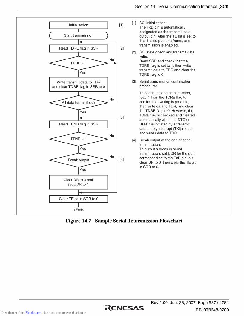
Section 14 Serial Communication Interface (SCI)
Rev.2.00 Jun. 28, 2007 Page 587 of 784
REJ09B248-0200
No
<End>
[1]
Yes
Initialization
Start transmission
Read TDRE flag in SSR [2]
Write transmit data to TDRand clear TDRE flag in SSR to 0
No
Yes
No
Yes
Read TEND flag in SSR
[3]
No
Yes
[4]
Clear DR to 0 andset DDR to 1
Clear TE bit in SCR to 0
TDRE = 1
All data transmitted?
TEND = 1
Break output
[1] SCI initialization: The TxD pin is automatically
designated as the transmit data output pin. After the TE bit is set to 1, a 1 is output for a frame, and transmission is enabled.
[2] SCI state check and transmit data write:
Read SSR and check that the TDRE flag is set to 1, then write transmit data to TDR and clear the TDRE flag to 0.
[3] Serial transmission continuation procedure:
To continue serial transmission, read 1 from the TDRE flag to confirm that writing is possible, then write data to TDR, and clear the TDRE flag to 0. However, the TDRE flag is checked and cleared automatically when the DTC or DMAC is initiated by a transmit data empty interrupt (TXI) request and writes data to TDR.
[4] Break output at the end of serial transmission:
To output a break in serial transmission, set DDR for the port corresponding to the TxD pin to 1, clear DR to 0, then clear the TE bit in SCR to 0.
Figure 14.7 Sample Serial Transmission Flowchart
Downloaded from Elcodis.com electronic components distributor

Section 14 Serial Communication Interface (SCI)
Rev.2.00 Jun. 28, 2007 Page 588 of 784
REJ09B248-0200
14.4.6 Serial Data Reception (Asynchronous Mode)
Figure 14.8 shows an example of the operation for reception in asynchronous mode. In serial reception, the SCI operates as described below.
1. The SCI monitors the communication line, and if a start bit is detected, performs internal synchronization, stores receive data in RSR, and checks the parity bit and stop bit.
2. If an overrun error (when reception of the next data is completed while the RDRF flag in SSR is still set to 1) occurs, the ORER bit in SSR is set to 1. If the RIE bit in SCR is set to 1 at this time, an ERI interrupt request is generated. Receive data is not transferred to RDR. The RDRF flag remains to be set to 1.
3. If a parity error is detected, the PER bit in SSR is set to 1 and receive data is transferred to RDR. If the RIE bit in SCR is set to 1 at this time, an ERI interrupt request is generated.
4. If a framing error (when the stop bit is 0) is detected, the FER bit in SSR is set to 1 and receive data is transferred to RDR. If the RIE bit in SCR is set to 1 at this time, an ERI interrupt request is generated.
5. If reception finishes successfully, the RDRF bit in SSR is set to 1, and receive data is transferred to RDR. If the RIE bit in SCR is set to 1 at this time, an RXI interrupt request is generated. Because the RXI interrupt processing routine reads the receive data transferred to RDR before reception of the next receive data has finished, continuous reception can be enabled.
RDRF
FER
0
1 frame
D0 D1 D7 0/1 1 0 D0 D1 D7 0/1 0
1 1DataStart
bitParitybit
Stopbit
Startbit
Data Paritybit
Stopbit
ERI interrupt requestgenerated by framingerror
Idle state(mark state)
RDR data read and RDRFflag cleared to 0 in RXIinterrupt processing routine
RXI interruptrequestgenerated
Figure 14.8 Example of SCI Operation for Reception (Example with 8-Bit Data, Parity, One Stop Bit)
Downloaded from Elcodis.com electronic components distributor
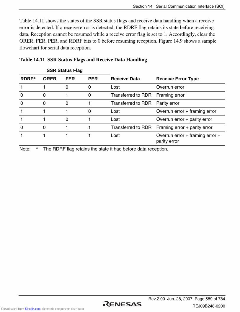
Section 14 Serial Communication Interface (SCI)
Rev.2.00 Jun. 28, 2007 Page 589 of 784
REJ09B248-0200
Table 14.11 shows the states of the SSR status flags and receive data handling when a receive error is detected. If a receive error is detected, the RDRF flag retains its state before receiving data. Reception cannot be resumed while a receive error flag is set to 1. Accordingly, clear the ORER, FER, PER, and RDRF bits to 0 before resuming reception. Figure 14.9 shows a sample flowchart for serial data reception.
Table 14.11 SSR Status Flags and Receive Data Handling
SSR Status Flag
RDRF* ORER FER PER Receive Data Receive Error Type
1 1 0 0 Lost Overrun error
0 0 1 0 Transferred to RDR Framing error
0 0 0 1 Transferred to RDR Parity error
1 1 1 0 Lost Overrun error + framing error
1 1 0 1 Lost Overrun error + parity error
0 0 1 1 Transferred to RDR Framing error + parity error
1 1 1 1 Lost Overrun error + framing error + parity error
Note: * The RDRF flag retains the state it had before data reception.
Downloaded from Elcodis.com electronic components distributor

Section 14 Serial Communication Interface (SCI)
Rev.2.00 Jun. 28, 2007 Page 590 of 784
REJ09B248-0200
Yes
<End>
[1]
No
Initialization
Start reception
[2]
No
Yes
Read RDRF flag in SSR [4]
[5]
Clear RE bit in SCR to 0
Read ORER, PER, andFER flags in SSR
Error processing
(Continued on next page)
[3]
Read receive data in RDR, andclear RDRF flag in SSR to 0
No
Yes
PER ∨ FER ∨ ORER = 1
RDRF = 1
All data received?
[1] SCI initialization: The RxD pin is automatically
designated as the receive data input pin.
[2] [3] Receive error processing and break detection:
If a receive error occurs, read the ORER, PER, and FER flags in SSR to identify the error. After performing the appropriate error processing, ensure that the ORER, PER, and FER flags are all cleared to 0. Reception cannot be resumed if any of these flags are set to 1. In the case of a framing error, a break can be detected by reading the value of the input port corresponding to the RxD pin.
[4] SCI state check and receive data read: Read SSR and check that RDRF = 1,
then read the receive data in RDR and clear the RDRF flag to 0. Transition of the RDRF flag from 0 to 1 can also be identified by an RXI interrupt.
[5] Serial reception continuation procedure: To continue serial reception, before the
stop bit for the current frame is received, read the RDRF flag and RDR, and clear the RDRF flag to 0.
However, the RDRF flag is cleared automatically when the DTC or DMAC is initiated by an RXI interrupt and reads data from RDR.
Figure 14.9 Sample Serial Reception Flowchart (1)
Downloaded from Elcodis.com electronic components distributor

Section 14 Serial Communication Interface (SCI)
Rev.2.00 Jun. 28, 2007 Page 591 of 784
REJ09B248-0200
<End>
[3]
Error processing
Parity error processing
Yes
No
Clear ORER, PER, andFER flags in SSR to 0
No
Yes
No
Yes
Framing error processing
No
Yes
Overrun error processing
ORER = 1
FER = 1
Break?
PER = 1
Clear RE bit in SCR to 0
Figure 14.9 Sample Serial Reception Flowchart (2)
Downloaded from Elcodis.com electronic components distributor
Section 14 Serial Communication Interface (SCI)
Rev.2.00 Jun. 28, 2007 Page 592 of 784
REJ09B248-0200
14.5 Multiprocessor Communication Function
Use of the multiprocessor communication function enables data transfer to be performed among a number of processors sharing communication lines by means of asynchronous serial communication using the multiprocessor format, in which a multiprocessor bit is added to the transfer data. When multiprocessor communication is carried out, each receiving station is addressed by a unique ID code. The serial communication cycle consists of two component cycles: an ID transmission cycle which specifies the receiving station, and a data transmission cycle for the specified receiving station. The multiprocessor bit is used to differentiate between the ID transmission cycle and the data transmission cycle. If the multiprocessor bit is 1, the cycle is an ID transmission cycle, and if the multiprocessor bit is 0, the cycle is a data transmission cycle. Figure 14.10 shows an example of inter-processor communication using the multiprocessor format. The transmitting station first sends data which includes the ID code of the receiving station and a multiprocessor bit set to 1. It then transmits transmit data added with a multiprocessor bit cleared to 0. The receiving station skips data until data with a 1 multiprocessor bit is sent. When data with a 1 multiprocessor bit is received, the receiving station compares that data with its own ID. The station whose ID matches then receives the data sent next. Stations whose ID does not match continue to skip data until data with a 1 multiprocessor bit is again received.
The SCI uses the MPIE bit in SCR to implement this function. When the MPIE bit is set to 1, transfer of receive data from RSR to RDR, error flag detection, and setting the SSR status flags, RDRF, FER, and ORER in SSR to 1 are prohibited until data with a 1 multiprocessor bit is received. On reception of a receive character with a 1 multiprocessor bit, the MPB bit in SSR is set to 1 and the MPIE bit is automatically cleared, thus normal reception is resumed. If the RIE bit in SCR is set to 1 at this time, an RXI interrupt is generated.
When the multiprocessor format is selected, the parity bit setting is invalid. All other bit settings are the same as those in normal asynchronous mode. The clock used for multiprocessor communication is the same as that in normal asynchronous mode.
Downloaded from Elcodis.com electronic components distributor
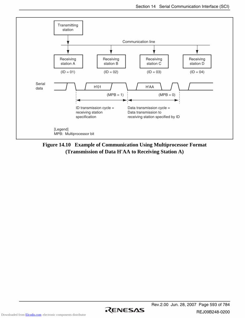
Section 14 Serial Communication Interface (SCI)
Rev.2.00 Jun. 28, 2007 Page 593 of 784
REJ09B248-0200
Transmittingstation
Receivingstation A
Receivingstation B
Receivingstation C
Receivingstation D
(ID = 01) (ID = 02) (ID = 03) (ID = 04)
Communication line
Serial data
ID transmission cycle = receiving stationspecification
Data transmission cycle =Data transmission to receiving station specified by ID
(MPB = 1) (MPB = 0)
H'01 H'AA
[Legend]MPB: Multiprocessor bit
Figure 14.10 Example of Communication Using Multiprocessor Format (Transmission of Data H'AA to Receiving Station A)
Downloaded from Elcodis.com electronic components distributor
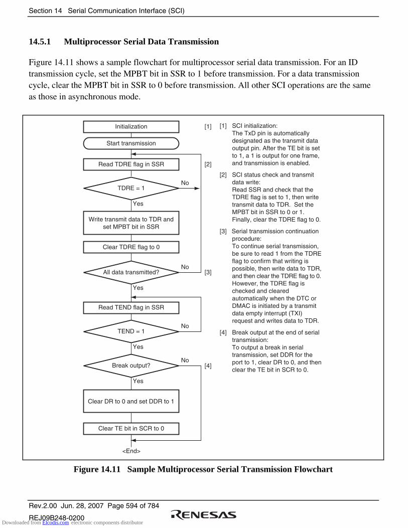
Section 14 Serial Communication Interface (SCI)
Rev.2.00 Jun. 28, 2007 Page 594 of 784
REJ09B248-0200
14.5.1 Multiprocessor Serial Data Transmission
Figure 14.11 shows a sample flowchart for multiprocessor serial data transmission. For an ID transmission cycle, set the MPBT bit in SSR to 1 before transmission. For a data transmission cycle, clear the MPBT bit in SSR to 0 before transmission. All other SCI operations are the same as those in asynchronous mode.
No
<End>
[1]
Yes
Initialization
Start transmission
Read TDRE flag in SSR [2]
Write transmit data to TDR andset MPBT bit in SSR
No
Yes
No
Yes
Read TEND flag in SSR
[3]
No
Yes
[4]
Clear DR to 0 and set DDR to 1
Clear TE bit in SCR to 0
TDRE = 1
All data transmitted?
TEND = 1
Break output?
Clear TDRE flag to 0
[1] SCI initialization: The TxD pin is automatically
designated as the transmit data output pin. After the TE bit is set to 1, a 1 is output for one frame, and transmission is enabled.
[2] SCI status check and transmit data write:
Read SSR and check that the TDRE flag is set to 1, then write transmit data to TDR. Set the MPBT bit in SSR to 0 or 1. Finally, clear the TDRE flag to 0.
[3] Serial transmission continuation procedure:
To continue serial transmission, be sure to read 1 from the TDRE flag to confirm that writing is possible, then write data to TDR, and then clear the TDRE flag to 0.
However, the TDRE flag is checked and cleared automatically when the DTC or DMAC is initiated by a transmit data empty interrupt (TXI) request and writes data to TDR.
[4] Break output at the end of serial transmission:
To output a break in serial transmission, set DDR for the port to 1, clear DR to 0, and then clear the TE bit in SCR to 0.
Figure 14.11 Sample Multiprocessor Serial Transmission Flowchart
Downloaded from Elcodis.com electronic components distributor

Section 14 Serial Communication Interface (SCI)
Rev.2.00 Jun. 28, 2007 Page 595 of 784
REJ09B248-0200
14.5.2 Multiprocessor Serial Data Reception
Figure 14.13 shows a sample flowchart for multiprocessor serial data reception. If the MPIE bit in SCR is set to 1, data is skipped until data with a 1 multiprocessor bit is sent. On receiving data with a 1 multiprocessor bit, the receive data is transferred to RDR. An RXI interrupt request is generated at this time. All other SCI operations are the same as in asynchronous mode. Figure 14.12 shows an example of SCI operation for multiprocessor format reception.
MPIE
RDRvalue
0 D0 D1 D7 1 1 0 D0 D1 D7 0 1
1 1
Data (ID1)Startbit MPB
Stopbit
Startbit
Data (Data 1)MPB
Stopbit
Data (ID2)Startbit
Stopbit
Startbit
Data (Data 2) Stopbit
RXI interruptrequest(multiprocessorinterrupt)generated
Idle state(mark state)
RDRF
RDR data readand RDRF flagcleared to 0 in RXI interruptprocessing routine
If not this station’s ID,MPIE bit is set to 1again
RXI interrupt request isnot generated, and RDRretains its state
ID1
(a) Data does not match station’s ID
MPIE
RDRvalue
0 D0 D1 D7 1 1 0 D0 D1 D7 0 1
1 1MPB MPB
RXI interruptrequest(multiprocessorinterrupt)generated
Idle state(mark state)
RDRF
RDR data read and RDRF flag cleared to 0 in RXI interruptprocessing routine
Matches this station’s ID,so reception continues, and data is received in RXIinterrupt processing routine
MPIE bit set to 1again
ID2
(b) Data matches station’s ID
Data 2ID1
MPIE = 0
MPIE = 0
Figure 14.12 Example of SCI Operation for Reception (Example with 8-Bit Data, Multiprocessor Bit, One Stop Bit)
Downloaded from Elcodis.com electronic components distributor

Section 14 Serial Communication Interface (SCI)
Rev.2.00 Jun. 28, 2007 Page 596 of 784
REJ09B248-0200
Yes
<End>
[1]
No
Initialization
Start reception
No
Yes
[4]
Clear RE bit in SCR to 0
Error processing
(Continued onnext page)
[5]No
Yes
FER ∨ ORER = 1
RDRF = 1
All data received?
Set MPIE bit in SCR to 1 [2]
Read ORER and FER flags in SSR
Read RDRF flag in SSR [3]
Read receive data in RDR
No
Yes
This station’s ID?
Read ORER and FER flags in SSR
Yes
No
Read RDRF flag in SSR
No
Yes
FER ∨ ORER = 1
Read receive data in RDR
RDRF = 1
[1] SCI initialization: The RxD pin is automatically designated
as the receive data input pin.
[2] ID reception cycle: Set the MPIE bit in SCR to 1.
[3] SCI state check, ID reception and comparison:
Read SSR and check that the RDRF flag is set to 1, then read the receive data in RDR and compare it with this station’s ID. If the data is not this station’s ID, set the MPIE bit to 1 again, and clear the RDRF flag to 0. If the data is this station’s ID, clear the RDRF flag to 0.
[4] SCI state check and data reception: Read SSR and check that the RDRF
flag is set to 1, then read the data in RDR.
[5] Receive error processing and break detection:
If a receive error occurs, read the ORER and FER flags in SSR to identify the error. After performing the appropriate error processing, ensure that the ORER and FER flags are both cleared to 0.
Reception cannot be resumed if either of these flags is set to 1. In the case of a framing error, a break can be detected by reading the RxD pin value.
Figure 14.13 Sample Multiprocessor Serial Reception Flowchart (1)
Downloaded from Elcodis.com electronic components distributor

Section 14 Serial Communication Interface (SCI)
Rev.2.00 Jun. 28, 2007 Page 597 of 784
REJ09B248-0200
<End>
Error processing
Yes
No
Clear ORER, PER, andFER flags in SSR to 0
No
Yes
No
Yes
Framing error processing
Overrun error processing
ORER = 1
FER = 1
Break?
Clear RE bit in SCR to 0
[5]
Figure 14.13 Sample Multiprocessor Serial Reception Flowchart (2)
Downloaded from Elcodis.com electronic components distributor

Section 14 Serial Communication Interface (SCI)
Rev.2.00 Jun. 28, 2007 Page 598 of 784
REJ09B248-0200
14.6 Operation in Clocked Synchronous Mode
Figure 14.14 shows the general format for clocked synchronous communication. In clocked synchronous mode, data is transmitted or received in synchronization with clock pulses. One character in transfer data consists of 8-bit data. In data transmission, the SCI outputs data from one falling edge of the synchronization clock to the next. In data reception, the SCI receives data in synchronization with the rising edge of the synchronization clock. After 8-bit data is output, the transmission line holds the MSB output state. In clocked synchronous mode, no parity bit or multiprocessor bit is added. Inside the SCI, the transmitter and receiver are independent units, enabling full-duplex communication by use of a common clock. Both the transmitter and the receiver also have a double-buffered structure, so that the next transmit data can be written during transmission or the previous receive data can be read during reception, enabling continuous data transfer.
Don't careDon't care
One unit of transfer data (character or frame)
Bit 0Serial data
Synchronizationclock
Bit 1 Bit 3 Bit 4 Bit 5
LSB MSB
Bit 2 Bit 6 Bit 7
**
Note: * Holds a high level except during continuous transfer.
Figure 14.14 Data Format in Clocked Synchronous Communication (LSB-First)
14.6.1 Clock
Either an internal clock generated by the on-chip baud rate generator or an external synchronization clock input at the SCK pin can be selected, according to the setting of the CKE1 and CKE0 bits in SCR. When the SCI is operated on an internal clock, the synchronization clock is output from the SCK pin. Eight synchronization clock pulses are output in the transfer of one character, and when no transfer is performed the clock is fixed high. Note that in the case of reception only, the synchronization clock is output until an overrun error occurs or until the RE bit is cleared to 0.
Downloaded from Elcodis.com electronic components distributor
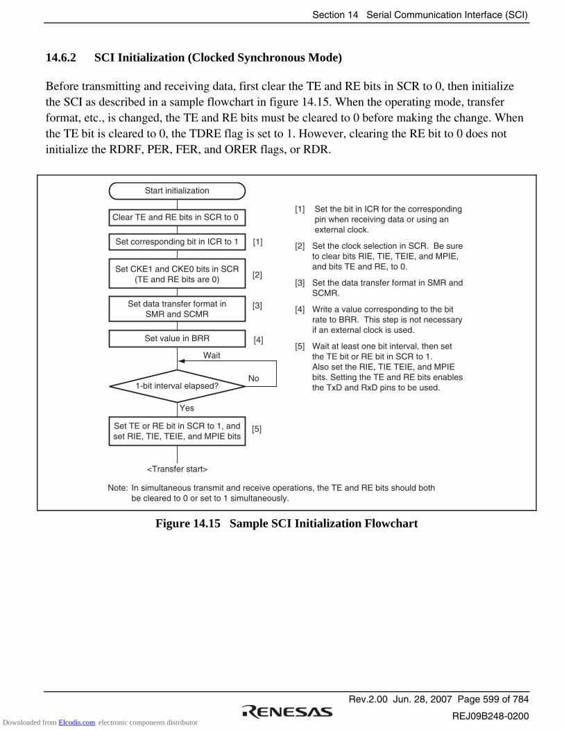
Section 14 Serial Communication Interface (SCI)
Rev.2.00 Jun. 28, 2007 Page 599 of 784
REJ09B248-0200
14.6.2 SCI Initialization (Clocked Synchronous Mode)
Before transmitting and receiving data, first clear the TE and RE bits in SCR to 0, then initialize the SCI as described in a sample flowchart in figure 14.15. When the operating mode, transfer format, etc., is changed, the TE and RE bits must be cleared to 0 before making the change. When the TE bit is cleared to 0, the TDRE flag is set to 1. However, clearing the RE bit to 0 does not initialize the RDRF, PER, FER, and ORER flags, or RDR.
Wait
<Transfer start>
Start initialization
Set data transfer format inSMR and SCMR
No
Yes
Set value in BRR
Set corresponding bit in ICR to 1
[2]
[3]
Set TE or RE bit in SCR to 1, andset RIE, TIE, TEIE, and MPIE bits
[5]
1-bit interval elapsed?
Set CKE1 and CKE0 bits in SCR(TE and RE bits are 0)
[1]
[1] Set the bit in ICR for the corresponding pin when receiving data or using an external clock.
[2] Set the clock selection in SCR. Be sure to clear bits RIE, TIE, TEIE, and MPIE, and bits TE and RE, to 0.
[3] Set the data transfer format in SMR and SCMR.
[4] Write a value corresponding to the bit rate to BRR. This step is not necessary if an external clock is used.
[5] Wait at least one bit interval, then set the TE bit or RE bit in SCR to 1.
Also set the RIE, TIE TEIE, and MPIE bits. Setting the TE and RE bits enables the TxD and RxD pins to be used.
Note: In simultaneous transmit and receive operations, the TE and RE bits should both be cleared to 0 or set to 1 simultaneously.
Clear TE and RE bits in SCR to 0
[4]
Figure 14.15 Sample SCI Initialization Flowchart
Downloaded from Elcodis.com electronic components distributor
Section 14 Serial Communication Interface (SCI)
Rev.2.00 Jun. 28, 2007 Page 600 of 784
REJ09B248-0200
14.6.3 Serial Data Transmission (Clocked Synchronous Mode)
Figure 14.16 shows an example of the operation for transmission in clocked synchronous mode. In transmission, the SCI operates as described below.
1. The SCI monitors the TDRE flag in SSR, and if it is 0, recognizes that data has been written to TDR, and transfers the data from TDR to TSR.
2. After transferring data from TDR to TSR, the SCI sets the TDRE flag to 1 and starts transmission. If the TIE bit in SCR is set to 1 at this time, a TXI interrupt request is generated. Because the TXI interrupt processing routine writes the next transmit data to TDR before transmission of the current transmit data has finished, continuous transmission can be enabled.
3. 8-bit data is sent from the TxD pin synchronized with the output clock when clock output mode has been specified and synchronized with the input clock when use of an external clock has been specified.
4. The SCI checks the TDRE flag at the timing for sending the last bit.
5. If the TDRE flag is cleared to 0, the next transmit data is transferred from TDR to TSR, and serial transmission of the next frame is started.
6. If the TDRE flag is set to 1, the TEND flag in SSR is set to 1, and the TxD pin retains the output state of the last bit. If the TEIE bit in SCR is set to 1 at this time, a TEI interrupt request is generated. The SCK pin is fixed high.
Figure 14.17 shows a sample flowchart for serial data transmission. Even if the TDRE flag is cleared to 0, transmission will not start while a receive error flag (ORER, FER, or PER) is set to 1. Make sure to clear the receive error flags to 0 before starting transmission. Note that clearing the RE bit to 0 does not clear the receive error flags.
Downloaded from Elcodis.com electronic components distributor
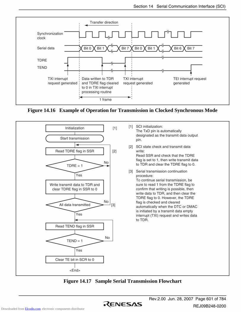
Section 14 Serial Communication Interface (SCI)
Rev.2.00 Jun. 28, 2007 Page 601 of 784
REJ09B248-0200
Transfer direction
Bit 0Serial data
Synchronizationclock
1 frame
TDRE
TEND
Data written to TDR and TDRE flag cleared to 0 in TXI interrupt processing routine
TXI interrupt request generated
Bit 1 Bit 7 Bit 0 Bit 1 Bit 6 Bit 7
TXI interrupt request generated
TEI interrupt request generated
Figure 14.16 Example of Operation for Transmission in Clocked Synchronous Mode
No
<End>
[1]
Yes
Initialization
Start transmission
Read TDRE flag in SSR [2]
Write transmit data to TDR andclear TDRE flag in SSR to 0
No
Yes
No
Yes
Read TEND flag in SSR
[3]
Clear TE bit in SCR to 0
TDRE = 1
All data transmitted
TEND = 1
[1] SCI initialization: The TxD pin is automatically
designated as the transmit data output pin.
[2] SCI state check and transmit data write:
Read SSR and check that the TDRE flag is set to 1, then write transmit data to TDR and clear the TDRE flag to 0.
[3] Serial transmission continuation procedure:
To continue serial transmission, be sure to read 1 from the TDRE flag to confirm that writing is possible, then write data to TDR, and then clear the TDRE flag to 0. However, the TDRE flag is checked and cleared automatically when the DTC or DMAC is initiated by a transmit data empty interrupt (TXI) request and writes data to TDR.
Figure 14.17 Sample Serial Transmission Flowchart
Downloaded from Elcodis.com electronic components distributor

Section 14 Serial Communication Interface (SCI)
Rev.2.00 Jun. 28, 2007 Page 602 of 784
REJ09B248-0200
14.6.4 Serial Data Reception (Clocked Synchronous Mode)
Figure 14.18 shows an example of SCI operation for reception in clocked synchronous mode. In serial reception, the SCI operates as described below.
1. The SCI performs internal initialization in synchronization with a synchronization clock input or output, starts receiving data, and stores the receive data in RSR.
2. If an overrun error (when reception of the next data is completed while the RDRF flag in SSR is still set to 1) occurs, the ORER bit in SSR is set to 1. If the RIE bit in SCR is set to 1 at this time, an ERI interrupt request is generated. Receive data is not transferred to RDR. The RDRF flag remains to be set to 1.
3. If reception finishes successfully, the RDRF bit in SSR is set to 1, and receive data is transferred to RDR. If the RIE bit in SCR is set to 1 at this time, an RXI interrupt request is generated. Because the RXI interrupt processing routine reads the receive data transferred to RDR before reception of the next receive data has finished, continuous reception can be enabled.
Bit 7Serial data
Synchronizationclock
1 frame
RDRF
ORER
ERI interrupt request generated by overrun error
RXI interrupt request generated
RDR data read and RDRF flag cleared to 0 in RXI interrupt processing routine
RXI interrupt request generated
Bit 0 Bit 7 Bit 0 Bit 1 Bit 6 Bit 7
Figure 14.18 Example of Operation for Reception in Clocked Synchronous Mode
Downloaded from Elcodis.com electronic components distributor
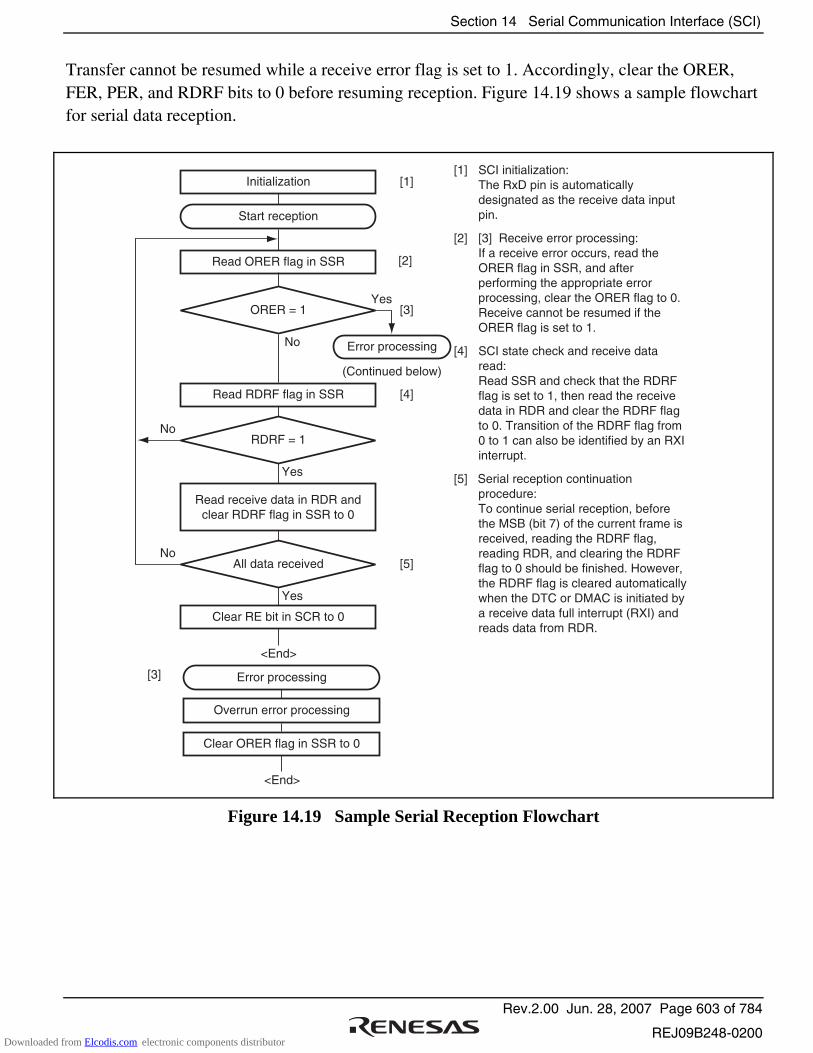
Section 14 Serial Communication Interface (SCI)
Rev.2.00 Jun. 28, 2007 Page 603 of 784
REJ09B248-0200
Transfer cannot be resumed while a receive error flag is set to 1. Accordingly, clear the ORER, FER, PER, and RDRF bits to 0 before resuming reception. Figure 14.19 shows a sample flowchart for serial data reception.
Yes
<End>
[1]
No
Initialization
Start reception
[2]
No
Yes
Read RDRF flag in SSR [4]
[5]
Clear RE bit in SCR to 0
Error processing
(Continued below)
[3]
Read receive data in RDR andclear RDRF flag in SSR to 0
No
Yes
ORER = 1
RDRF = 1
All data received
Read ORER flag in SSR
<End>
Error processing
Overrun error processing
Clear ORER flag in SSR to 0
[3]
[1] SCI initialization: The RxD pin is automatically
designated as the receive data input pin.
[2] [3] Receive error processing: If a receive error occurs, read the
ORER flag in SSR, and after performing the appropriate error processing, clear the ORER flag to 0. Receive cannot be resumed if the ORER flag is set to 1.
[4] SCI state check and receive data read:
Read SSR and check that the RDRF flag is set to 1, then read the receive data in RDR and clear the RDRF flag to 0. Transition of the RDRF flag from 0 to 1 can also be identified by an RXI interrupt.
[5] Serial reception continuation procedure:
To continue serial reception, before the MSB (bit 7) of the current frame is received, reading the RDRF flag, reading RDR, and clearing the RDRF flag to 0 should be finished. However, the RDRF flag is cleared automatically when the DTC or DMAC is initiated by a receive data full interrupt (RXI) and reads data from RDR.
Figure 14.19 Sample Serial Reception Flowchart
Downloaded from Elcodis.com electronic components distributor
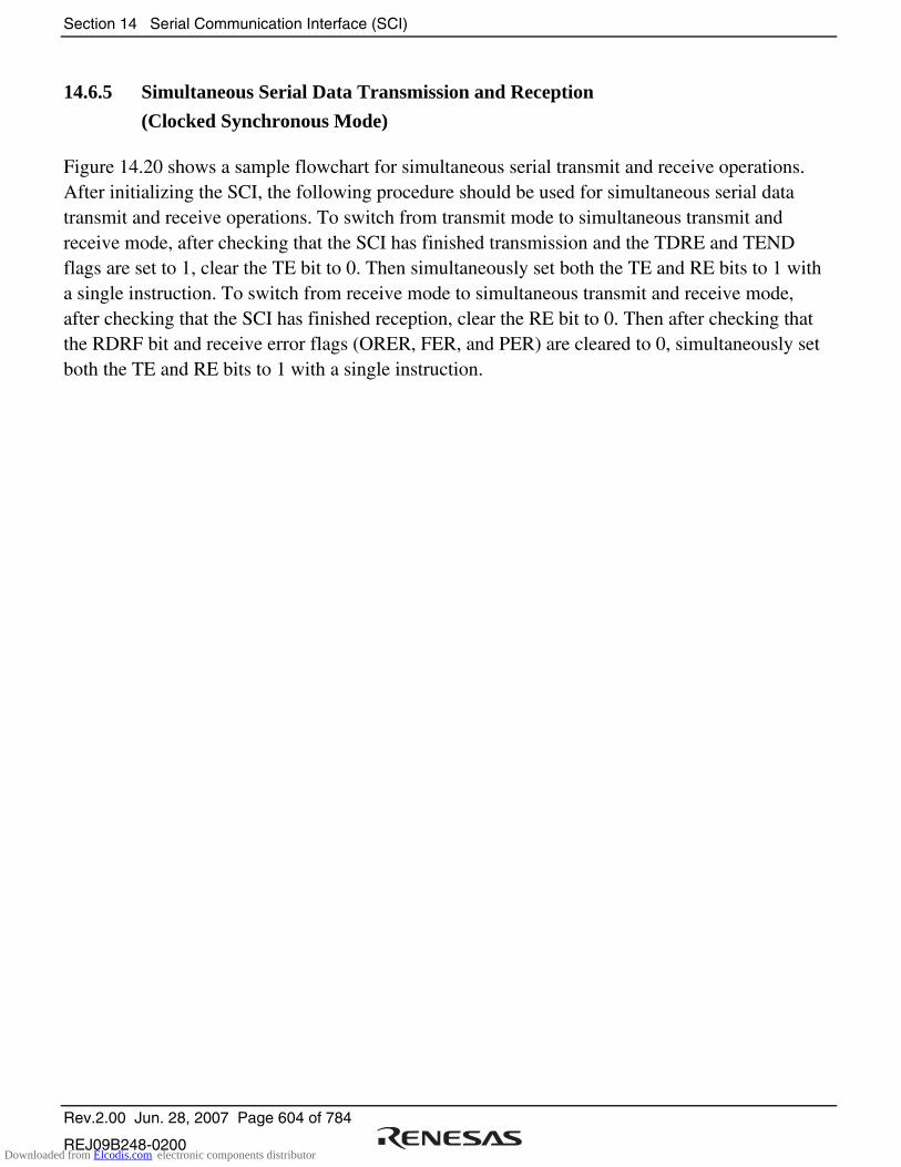
Section 14 Serial Communication Interface (SCI)
Rev.2.00 Jun. 28, 2007 Page 604 of 784
REJ09B248-0200
14.6.5 Simultaneous Serial Data Transmission and Reception
(Clocked Synchronous Mode)
Figure 14.20 shows a sample flowchart for simultaneous serial transmit and receive operations. After initializing the SCI, the following procedure should be used for simultaneous serial data transmit and receive operations. To switch from transmit mode to simultaneous transmit and receive mode, after checking that the SCI has finished transmission and the TDRE and TEND flags are set to 1, clear the TE bit to 0. Then simultaneously set both the TE and RE bits to 1 with a single instruction. To switch from receive mode to simultaneous transmit and receive mode, after checking that the SCI has finished reception, clear the RE bit to 0. Then after checking that the RDRF bit and receive error flags (ORER, FER, and PER) are cleared to 0, simultaneously set both the TE and RE bits to 1 with a single instruction.
Downloaded from Elcodis.com electronic components distributor
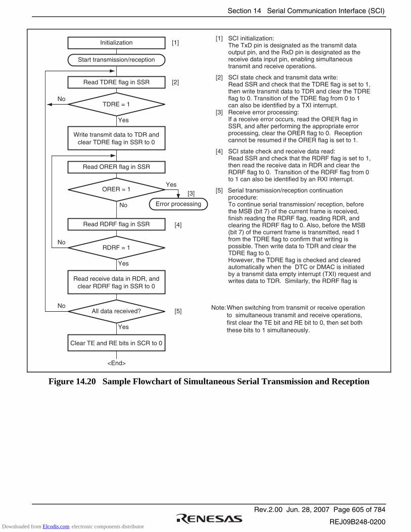
Section 14 Serial Communication Interface (SCI)
Rev.2.00 Jun. 28, 2007 Page 605 of 784
REJ09B248-0200
Yes
<End>
[1]
No
Initialization
Start transmission/reception
[5]
Error processing
[3]
Read receive data in RDR, andclear RDRF flag in SSR to 0
No
Yes
ORER = 1
All data received?
[2]Read TDRE flag in SSR
No
Yes
TDRE = 1
Write transmit data to TDR andclear TDRE flag in SSR to 0
No
Yes
RDRF = 1
Read ORER flag in SSR
[4]Read RDRF flag in SSR
Clear TE and RE bits in SCR to 0
[1] SCI initialization: The TxD pin is designated as the transmit data
output pin, and the RxD pin is designated as the receive data input pin, enabling simultaneous transmit and receive operations.
[2] SCI state check and transmit data write: Read SSR and check that the TDRE flag is set to 1,
then write transmit data to TDR and clear the TDRE flag to 0. Transition of the TDRE flag from 0 to 1 can also be identified by a TXI interrupt.
[3] Receive error processing: If a receive error occurs, read the ORER flag in
SSR, and after performing the appropriate error processing, clear the ORER flag to 0. Reception cannot be resumed if the ORER flag is set to 1.
[4] SCI state check and receive data read: Read SSR and check that the RDRF flag is set to 1,
then read the receive data in RDR and clear the RDRF flag to 0. Transition of the RDRF flag from 0 to 1 can also be identified by an RXI interrupt.
[5] Serial transmission/reception continuation procedure:
To continue serial transmission/ reception, before the MSB (bit 7) of the current frame is received, finish reading the RDRF flag, reading RDR, and clearing the RDRF flag to 0. Also, before the MSB (bit 7) of the current frame is transmitted, read 1 from the TDRE flag to confirm that writing is possible. Then write data to TDR and clear the TDRE flag to 0.
However, the TDRE flag is checked and cleared automatically when the DTC or DMAC is initiated by a transmit data empty interrupt (TXI) request and writes data to TDR. Similarly, the RDRF flag is
Note: When switching from transmit or receive operation to simultaneous transmit and receive operations, first clear the TE bit and RE bit to 0, then set both these bits to 1 simultaneously.
Figure 14.20 Sample Flowchart of Simultaneous Serial Transmission and Reception
Downloaded from Elcodis.com electronic components distributor
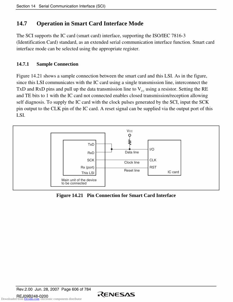
Section 14 Serial Communication Interface (SCI)
Rev.2.00 Jun. 28, 2007 Page 606 of 784
REJ09B248-0200
14.7 Operation in Smart Card Interface Mode
The SCI supports the IC card (smart card) interface, supporting the ISO/IEC 7816-3 (Identification Card) standard, as an extended serial communication interface function. Smart card interface mode can be selected using the appropriate register.
14.7.1 Sample Connection
Figure 14.21 shows a sample connection between the smart card and this LSI. As in the figure, since this LSI communicates with the IC card using a single transmission line, interconnect the TxD and RxD pins and pull up the data transmission line to VCC using a resistor. Setting the RE and TE bits to 1 with the IC card not connected enables closed transmission/reception allowing self diagnosis. To supply the IC card with the clock pulses generated by the SCI, input the SCK pin output to the CLK pin of the IC card. A reset signal can be supplied via the output port of this LSI.
TxD
RxD
This LSI
VCC
I/O
Main unit of the device to be connected
IC card
Data line
CLK
RST
SCK
Rx (port)Clock line
Reset line
Figure 14.21 Pin Connection for Smart Card Interface
Downloaded from Elcodis.com electronic components distributor

Section 14 Serial Communication Interface (SCI)
Rev.2.00 Jun. 28, 2007 Page 607 of 784
REJ09B248-0200
14.7.2 Data Format (Except in Block Transfer Mode)
Figure 14.22 shows the data transfer formats in smart card interface mode.
• One frame contains 8-bit data and a parity bit in asynchronous mode.
• During transmission, at least 2 etu (elementary time unit: time required for transferring one bit) is secured as a guard time after the end of the parity bit before the start of the next frame.
• If a parity error is detected during reception, a low error signal is output for 1 etu after 10.5 etu has passed from the start bit.
• If an error signal is sampled during transmission, the same data is automatically re-transmitted after at least 2 etu.
Ds D0 D1 D2 D3 D4 D5 D6 D7 Dp
In normal transmission/reception
Output from the transmitting station
Ds D0 D1 D2 D3 D4 D5 D6 D7 Dp
When a parity error is generated
Output from the transmitting station
DE
Output from the receiving station[Legend]
Ds: Start bitD0 to D7: Data bitsDp: Parity bitDE: Error signal
Figure 14.22 Data Formats in Normal Smart Card Interface Mode
For communication with the IC cards of the direct convention and inverse convention types, follow the procedure below.
Ds
A Z Z A Z Z ZZ AA(Z) (Z) state
D0 D1 D2 D3 D4 D5 D6 D7 Dp
Figure 14.23 Direct Convention (SDIR = SINV = O/E = 0)
Downloaded from Elcodis.com electronic components distributor

Section 14 Serial Communication Interface (SCI)
Rev.2.00 Jun. 28, 2007 Page 608 of 784
REJ09B248-0200
For the direct convention type, logic levels 1 and 0 correspond to states Z and A, respectively, and data is transferred with LSB-first as the start character, as shown in figure 14.23. Therefore, data in the start character in the figure is H'3B. When using the direct convention type, write 0 to both the SDIR and SINV bits in SCMR. Write 0 to the O/E bit in SMR in order to use even parity, which is prescribed by the smart card standard.
Ds
A Z Z A A A ZA AA(Z) (Z) state
D7 D6 D5 D4 D3 D2 D1 D0 Dp
Figure 14.24 Inverse Convention (SDIR = SINV = O/E = 1)
For the inverse convention type, logic levels 1 and 0 correspond to states A and Z, respectively and data is transferred with MSB-first as the start character, as shown in figure 14.24. Therefore, data in the start character in the figure is H'3F. When using the inverse convention type, write 1 to both the SDIR and SINV bits in SCMR. The parity bit is logic level 0 to produce even parity, which is prescribed by the smart card standard, and corresponds to state Z. Since the SNIV bit of this LSI only inverts data bits D7 to D0, write 1 to the O/E bit in SMR to invert the parity bit in both transmission and reception.
14.7.3 Block Transfer Mode
Block transfer mode is different from normal smart card interface mode in the following respects.
• Even if a parity error is detected during reception, no error signal is output. Since the PER bit in SSR is set by error detection, clear the PER bit before receiving the parity bit of the next frame.
• During transmission, at least 1 etu is secured as a guard time after the end of the parity bit before the start of the next frame.
• Since the same data is not re-transmitted during transmission, the TEND flag is set 11.5 etu after transmission start.
• Although the ERS flag in block transfer mode displays the error signal status as in normal smart card interface mode, the flag is always read as 0 because no error signal is transferred.
Downloaded from Elcodis.com electronic components distributor
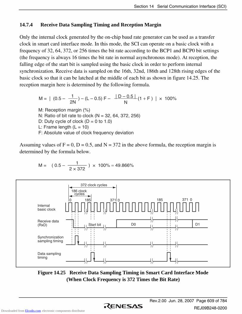
Section 14 Serial Communication Interface (SCI)
Rev.2.00 Jun. 28, 2007 Page 609 of 784
REJ09B248-0200
14.7.4 Receive Data Sampling Timing and Reception Margin
Only the internal clock generated by the on-chip baud rate generator can be used as a transfer clock in smart card interface mode. In this mode, the SCI can operate on a basic clock with a frequency of 32, 64, 372, or 256 times the bit rate according to the BCP1 and BCP0 bit settings (the frequency is always 16 times the bit rate in normal asynchronous mode). At reception, the falling edge of the start bit is sampled using the basic clock in order to perform internal synchronization. Receive data is sampled on the 16th, 32nd, 186th and 128th rising edges of the basic clock so that it can be latched at the middle of each bit as shown in figure 14.25. The reception margin here is determined by the following formula.
M = | (0.5 – ) – (L – 0.5) F – (1 + F ) | × 100%2N1
N| D – 0.5 |
M: Reception margin (%)N: Ratio of bit rate to clock (N = 32, 64, 372, 256)D: Duty cycle of clock (D = 0 to 1.0)L: Frame length (L = 10)F: Absolute value of clock frequency deviation
Assuming values of F = 0, D = 0.5, and N = 372 in the above formula, the reception margin is determined by the formula below.
M = ( 0.5 – ) × 100% = 49.866%2 × 372
1
Internal basic clock
372 clock cycles
186 clock cycles
Receive data (RxD)
Synchronization sampling timing
D0 D1
Data sampling timing
185 371 0371185 00
Start bit
Figure 14.25 Receive Data Sampling Timing in Smart Card Interface Mode (When Clock Frequency is 372 Times the Bit Rate)
Downloaded from Elcodis.com electronic components distributor

Section 14 Serial Communication Interface (SCI)
Rev.2.00 Jun. 28, 2007 Page 610 of 784
REJ09B248-0200
14.7.5 Initialization
Before transmitting and receiving data, initialize the SCI using the following procedure. Initialization is also necessary before switching from transmission to reception and vice versa.
1. Clear the TE and RE bits in SCR to 0.
2. Set the ICR bit of the corresponding pin to 1.
3. Clear the error flags ERS, PER, and ORER in SSR to 0.
4. Set the GM, BLK, O/E, BCP1, BCP0, CKS1, and CKS0 bits in SMR appropriately. Also set the PE bit to 1.
5. Set the SMIF, SDIR, and SINV bits in SCMR appropriately. When the DDR corresponding to the TxD pin is cleared to 0, the TxD and RxD pins are changed from port pins to SCI pins, placing the pins into high impedance state.
6. Set the value corresponding to the bit rate in BRR.
7. Set the CKE1 and CKE0 bits in SCR appropriately. Clear the TIE, RIE, TE, RE, MPIE, and TEIE bits to 0 simultaneously.
When the CKE0 bit is set to 1, the SCK pin is allowed to output clock pulses.
8. Set the TIE, RIE, TE, and RE bits in SCR appropriately after waiting for at least a 1-bit interval. Setting the TE and RE bits to 1 simultaneously is prohibited except for self diagnosis.
To switch from reception to transmission, first verify that reception has completed, then initialize the SCI. At the end of initialization, RE and TE should be set to 0 and 1, respectively. Reception completion can be verified by reading the RDRF, PER, or ORER flag. To switch from transmission to reception, first verify that transmission has completed, then initialize the SCI. At the end of initialization, TE and RE should be set to 0 and 1, respectively. Transmission completion can be verified by reading the TEND flag.
Downloaded from Elcodis.com electronic components distributor

Section 14 Serial Communication Interface (SCI)
Rev.2.00 Jun. 28, 2007 Page 611 of 784
REJ09B248-0200
14.7.6 Data Transmission (Except in Block Transfer Mode)
Data transmission in smart card interface mode (except in block transfer mode) is different from that in normal serial communication interface mode in that an error signal is sampled and data can be re-transmitted. Figure 14.26 shows the data re-transfer operation during transmission.
1. If an error signal from the receiving end is sampled after one frame of data has been transmitted, the ERS bit in SSR is set to 1. Here, an ERI interrupt request is generated if the RIE bit in SCR is set to 1. Clear the ERS bit to 0 before the next parity bit is sampled.
2. For the frame in which an error signal is received, the TEND bit in SSR is not set to 1. Data is re-transferred from TDR to TSR allowing automatic data retransmission.
3. If no error signal is returned from the receiving end, the ERS bit in SSR is not set to 1.
4. In this case, one frame of data is determined to have been transmitted including re-transfer, and the TEND bit in SSR is set to 1. Here, a TXI interrupt request is generated if the TIE bit in SCR is set to 1. Writing transmit data to TDR starts transmission of the next data.
Figure 14.28 shows a sample flowchart for transmission. All the processing steps are automatically performed using a TXI interrupt request to activate the DTC or DMAC. In transmission, the TEND and TDRE flags in SSR are simultaneously set to 1, thus generating a TXI interrupt request if the TIE bit in SCR has been set to 1. This activates the DTC or DMAC by a TXI request thus allowing transfer of transmit data if the TXI interrupt request is specified as a source of DTC or DMAC activation beforehand. The TDRE and TEND flags are automatically cleared to 0 at data transfer by the DTC or DMAC. If an error occurs, the SCI automatically re-transmits the same data. During re-transmission, TEND remains as 0, thus not activating the DTC or DMAC. Therefore, the SCI and DTC or DMAC automatically transmit the specified number of bytes, including re-transmission in the case of error occurrence. However, the ERS flag is not automatically cleared; the ERS flag must be cleared by previously setting the RIE bit to 1 to enable an ERI interrupt request to be generated at error occurrence.
When transmitting/receiving data using the DTC or DMAC, be sure to set and enable the DTC or DMAC prior to making SCI settings. For DTC or DMAC settings, see section 7, DMA Controller (DMAC) and section 8, Data Transfer Controller (DTC).
Downloaded from Elcodis.com electronic components distributor
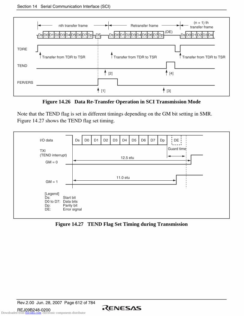
Section 14 Serial Communication Interface (SCI)
Rev.2.00 Jun. 28, 2007 Page 612 of 784
REJ09B248-0200
D0 D1 D2 D3 D4 D5 D6 D7 Dp DE Ds D0 D1 D2 D3 D4 D5 D6 D7 Dp(DE)
Ds D0 D1 D2 D3 D4Ds
(n + 1) th transfer frameRetransfer framenth transfer frame
TDRE
TEND
[1]
FER/ERS
Transfer from TDR to TSR Transfer from TDR to TSR Transfer from TDR to TSR
[2] [4]
[3]
Figure 14.26 Data Re-Transfer Operation in SCI Transmission Mode
Note that the TEND flag is set in different timings depending on the GM bit setting in SMR. Figure 14.27 shows the TEND flag set timing.
Ds D0 D1 D2 D3 D4 D5 D6 D7 DpI/O data
12.5 etu
TXI (TEND interrupt)
11.0 etu
DE
Guard time
GM = 0
GM = 1
[Legend]Ds: Start bitD0 to D7: Data bitsDp: Parity bitDE: Error signal
Figure 14.27 TEND Flag Set Timing during Transmission
Downloaded from Elcodis.com electronic components distributor

Section 14 Serial Communication Interface (SCI)
Rev.2.00 Jun. 28, 2007 Page 613 of 784
REJ09B248-0200
Initialization
No
Yes
Clear TE bit in SCR to 0
Start transmission
Start
No
No
No
Yes
Yes
Yes
Yes
No
End
Write data to TDR and clear TDRE flag in SSR to 0
Error processing
Error processing
TEND = 1?
All data transmitted?
TEND = 1?
ERS = 0?
ERS = 0?
Figure 14.28 Sample Transmission Flowchart
Downloaded from Elcodis.com electronic components distributor

Section 14 Serial Communication Interface (SCI)
Rev.2.00 Jun. 28, 2007 Page 614 of 784
REJ09B248-0200
14.7.7 Serial Data Reception (Except in Block Transfer Mode)
Data reception in smart card interface mode is similar to that in normal serial communication interface mode. Figure 14.29 shows the data re-transfer operation during reception.
1. If a parity error is detected in receive data, the PER bit in SSR is set to 1. Here, an ERI interrupt request is generated if the RIE bit in SCR is set to 1. Clear the PER bit to 0 before the next parity bit is sampled.
2. For the frame in which a parity error is detected, the RDRF bit in SSR is not set to 1.
3. If no parity error is detected, the PER bit in SSR is not set to 1.
4. In this case, data is determined to have been received successfully, and the RDRF bit in SSR is set to 1. Here, an RXI interrupt request is generated if the RIE bit in SCR is set to 1.
Figure 14.30 shows a sample flowchart for reception. All the processing steps are automatically performed using an RXI interrupt request to activate the DTC or DMAC. In reception, setting the RIE bit to 1 allows an RXI interrupt request to be generated when the RDRF flag is set to 1. This activates the DTC or DMAC by an RXI request thus allowing transfer of receive data if the RXI interrupt request is specified as a source of DTC or DMAC activation beforehand. The RDRF flag is automatically cleared to 0 at data transfer by the DTC or DMAC. If an error occurs during reception, i.e., either the ORER or PER flag is set to 1, a transmit/receive error interrupt (ERI) request is generated and the error flag must be cleared. If an error occurs, the DTC or DMAC is not activated and receive data is skipped, therefore, the number of bytes of receive data specified in the DTC or DMAC is transferred. Even if a parity error occurs and the PER bit is set to 1 in reception, receive data is transferred to RDR, thus allowing the data to be read.
Note: For operations in block transfer mode, see section 14.4, Operation in Asynchronous Mode.
D0 D1 D2 D3 D4 D5 D6 D7 Dp DE Ds D0 D1 D2 D3 D4 D5 D6 D7 Dp(DE)
Ds D0 D1 D2 D3 D4Ds
(n + 1) th transfer frameRetransfer framenth transfer frame
RDRF
[1]
PER
[2]
[3]
[4]
Figure 14.29 Data Re-Transfer Operation in SCI Reception Mode
Downloaded from Elcodis.com electronic components distributor
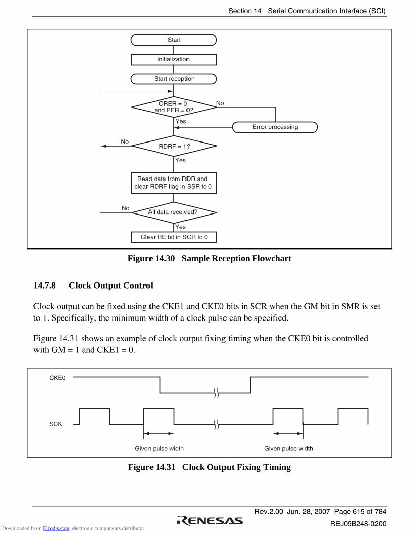
Section 14 Serial Communication Interface (SCI)
Rev.2.00 Jun. 28, 2007 Page 615 of 784
REJ09B248-0200
Initialization
Read data from RDR and clear RDRF flag in SSR to 0
Clear RE bit in SCR to 0
Start reception
Start
Error processing
No
No
No
Yes
Yes
ORER = 0 and PER = 0?
RDRF = 1?
All data received?
Yes
Figure 14.30 Sample Reception Flowchart
14.7.8 Clock Output Control
Clock output can be fixed using the CKE1 and CKE0 bits in SCR when the GM bit in SMR is set to 1. Specifically, the minimum width of a clock pulse can be specified.
Figure 14.31 shows an example of clock output fixing timing when the CKE0 bit is controlled with GM = 1 and CKE1 = 0.
Given pulse width
SCK
CKE0
Given pulse width
Figure 14.31 Clock Output Fixing Timing
Downloaded from Elcodis.com electronic components distributor
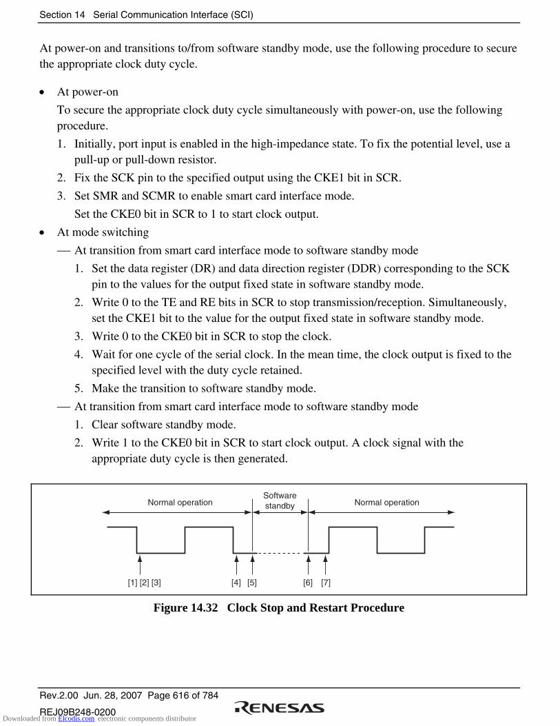
Section 14 Serial Communication Interface (SCI)
Rev.2.00 Jun. 28, 2007 Page 616 of 784
REJ09B248-0200
At power-on and transitions to/from software standby mode, use the following procedure to secure the appropriate clock duty cycle.
• At power-on
To secure the appropriate clock duty cycle simultaneously with power-on, use the following procedure.
1. Initially, port input is enabled in the high-impedance state. To fix the potential level, use a pull-up or pull-down resistor.
2. Fix the SCK pin to the specified output using the CKE1 bit in SCR.
3. Set SMR and SCMR to enable smart card interface mode.
Set the CKE0 bit in SCR to 1 to start clock output.
• At mode switching
At transition from smart card interface mode to software standby mode
1. Set the data register (DR) and data direction register (DDR) corresponding to the SCK pin to the values for the output fixed state in software standby mode.
2. Write 0 to the TE and RE bits in SCR to stop transmission/reception. Simultaneously, set the CKE1 bit to the value for the output fixed state in software standby mode.
3. Write 0 to the CKE0 bit in SCR to stop the clock.
4. Wait for one cycle of the serial clock. In the mean time, the clock output is fixed to the specified level with the duty cycle retained.
5. Make the transition to software standby mode.
At transition from smart card interface mode to software standby mode
1. Clear software standby mode.
2. Write 1 to the CKE0 bit in SCR to start clock output. A clock signal with the appropriate duty cycle is then generated.
[1] [2] [3] [4] [5] [7]
SoftwarestandbyNormal operation Normal operation
[6]
Figure 14.32 Clock Stop and Restart Procedure
Downloaded from Elcodis.com electronic components distributor
Section 14 Serial Communication Interface (SCI)
Rev.2.00 Jun. 28, 2007 Page 617 of 784
REJ09B248-0200
14.8 Interrupt Sources
14.8.1 Interrupts in Normal Serial Communication Interface Mode
Table 14.12 shows the interrupt sources in normal serial communication interface mode. A different interrupt vector is assigned to each interrupt source, and individual interrupt sources can be enabled or disabled using the enable bits in SCR.
When the TDRE flag in SSR is set to 1, a TXI interrupt request is generated. When the TEND flag in SSR is set to 1, a TEI interrupt request is generated. A TXI interrupt request can activate the DTC or DMAC to allow data transfer. The TDRE flag is automatically cleared to 0 at data transfer by the DTC or DMAC.
When the RDRF flag in SSR is set to 1, an RXI interrupt request is generated. When the ORER, PER, or FER flag in SSR is set to 1, an ERI interrupt request is generated. An RXI interrupt can activate the DTC or DMAC to allow data transfer. The RDRF flag is automatically cleared to 0 at data transfer by the DTC or DMAC.
A TEI interrupt is requested when the TEND flag is set to 1 while the TEIE bit is set to 1. If a TEI interrupt and a TXI interrupt are requested simultaneously, the TXI interrupt has priority for acceptance. However, note that if the TDRE and TEND flags are cleared to 0 simultaneously by the TXI interrupt processing routine, the SCI cannot branch to the TEI interrupt processing routine later.
Table 14.12 SCI Interrupt Sources
Name Interrupt Source Interrupt Flag DMAC Activation DTC Activation Priority
ERI Receive error ORER, FER, or PER
Not possible Not possible High
RXI Receive data full RDRF Possible Possible
TXI Transmit data empty
TDRE Possible Possible
TEI Transmit end TEND Not possible Not possible Low
Downloaded from Elcodis.com electronic components distributor
Section 14 Serial Communication Interface (SCI)
Rev.2.00 Jun. 28, 2007 Page 618 of 784
REJ09B248-0200
14.8.2 Interrupts in Smart Card Interface Mode
Table 14.13 shows the interrupt sources in smart card interface mode. A transmit end (TEI) interrupt request cannot be used in this mode.
Table 14.13 SCI Interrupt Sources
Name Interrupt Source Interrupt Flag DMAC Activation DTC Activation Priority
ERI Receive error or error signal detection
ORER, PER, or ERS
Not possible Not possible High
RXI Receive data full RDRF Possible Possible
TXI Transmit data empty
TDRE Possible Possible Low
Data transmission/reception using the DTC or DMAC is also possible in smart card interface mode, similar to in the normal SCI mode. In transmission, the TEND and TDRE flags in SSR are simultaneously set to 1, thus generating a TXI interrupt. This activates the DTC or DMAC by a TXI request thus allowing transfer of transmit data if the TXI request is specified as a source of DTC or DMAC activation beforehand. The TDRE and TEND flags are automatically cleared to 0 at data transfer by the DTC or DMAC. If an error occurs, the SCI automatically re-transmits the same data. During re-transmission, the TEND flag remains as 0, thus not activating the DTC or DMAC. Therefore, the SCI and DTC or DMAC automatically transmit the specified number of bytes, including re-transmission in the case of error occurrence. However, the ERS flag in SSR, which is set at error occurrence, is not automatically cleared; the ERS flag must be cleared by previously setting the RIE bit in SCR to 1 to enable an ERI interrupt request to be generated at error occurrence.
When transmitting/receiving data using the DTC or DMAC, be sure to set and enable the DTC or DMAC prior to making SCI settings. For DTC or DMAC settings, see section 7, DMA Controller (DMAC) and section 8, Data Transfer Controller (DTC).
In reception, an RXI interrupt request is generated when the RDRF flag in SSR is set to 1. This activates the DTC or DMAC by an RXI request thus allowing transfer of receive data if the RXI request is specified as a source of DTC or DMAC activation beforehand. The RDRF flag is automatically cleared to 0 at data transfer by the DTC or DMAC. If an error occurs, the RDRF flag is not set but the error flag is set. Therefore, the DTC or DMAC is not activated and an ERI interrupt request is issued to the CPU instead; the error flag must be cleared.
Downloaded from Elcodis.com electronic components distributor

Section 14 Serial Communication Interface (SCI)
Rev.2.00 Jun. 28, 2007 Page 619 of 784
REJ09B248-0200
14.9 Usage Notes
14.9.1 Module Stop Mode Setting
Operation of the SCI can be disabled or enabled using the module stop control register. The initial setting is for operation of the SCI to be halted. Register access is enabled by clearing module stop mode. For details, see section 19, Power-Down Modes.
14.9.2 Break Detection and Processing
When framing error detection is performed, a break can be detected by reading the RxD pin value directly. In a break, the input from the RxD pin becomes all 0s, and so the FER flag is set, and the PER flag may also be set. Note that, since the SCI continues the receive operation even after receiving a break, even if the FER flag is cleared to 0, it will be set to 1 again.
14.9.3 Mark State and Break Detection
When the TE bit is 0, the TxD pin is used as an I/O port whose direction (input or output) and level are determined by DR and DDR. This can be used to set the TxD pin to mark state (high level) or send a break during serial data transmission. To maintain the communication line in mark state (the state of 1) until TE is set to 1, set both DDR and DR to 1. Since the TE bit is cleared to 0 at this point, the TxD pin becomes an I/O port, and 1 is output from the TxD pin. To send a break during serial transmission, first set DDR to 1 and DR to 0, and then clear the TE bit to 0. When the TE bit is cleared to 0, the transmitter is initialized regardless of the current transmission state, the TxD pin becomes an I/O port, and 0 is output from the TxD pin.
14.9.4 Receive Error Flags and Transmit Operations (Clocked Synchronous Mode Only)
Transmission cannot be started when a receive error flag (ORER, FER, or RER) is set to 1, even if the TDRE flag is cleared to 0. Be sure to clear the receive error flags to 0 before starting transmission. Note also that the receive error flags cannot be cleared to 0 even if the RE bit is cleared to 0.
Downloaded from Elcodis.com electronic components distributor
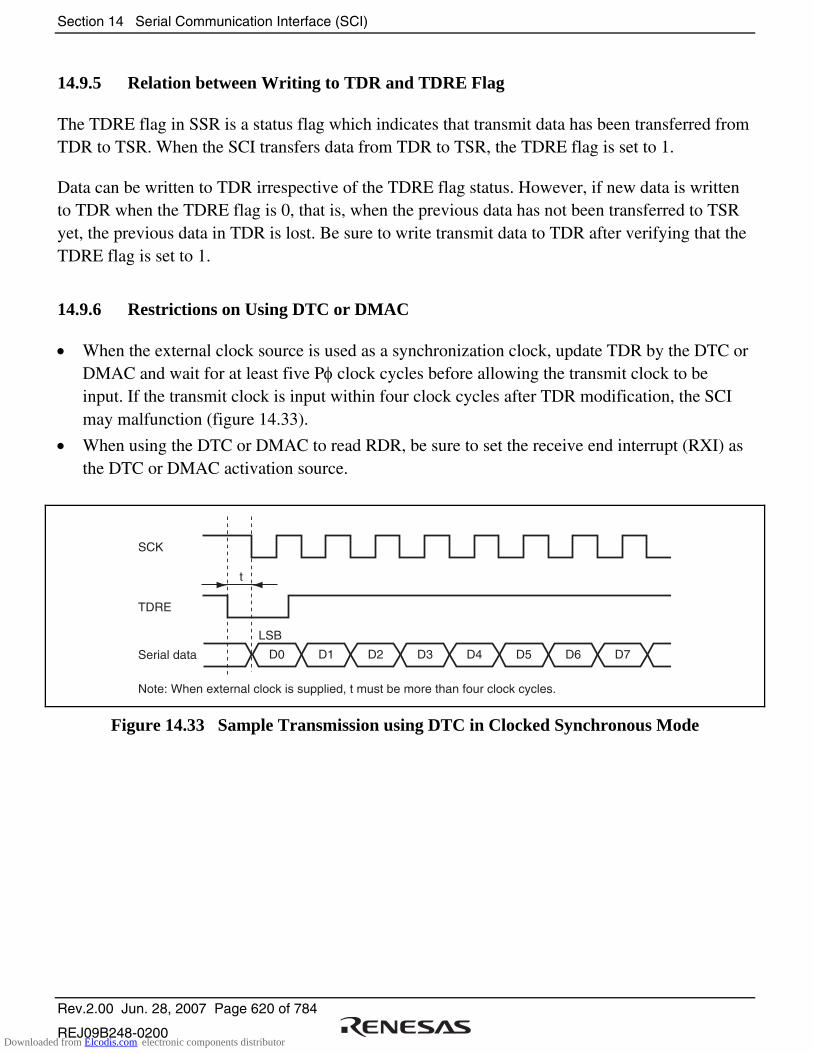
Section 14 Serial Communication Interface (SCI)
Rev.2.00 Jun. 28, 2007 Page 620 of 784
REJ09B248-0200
14.9.5 Relation between Writing to TDR and TDRE Flag
The TDRE flag in SSR is a status flag which indicates that transmit data has been transferred from TDR to TSR. When the SCI transfers data from TDR to TSR, the TDRE flag is set to 1.
Data can be written to TDR irrespective of the TDRE flag status. However, if new data is written to TDR when the TDRE flag is 0, that is, when the previous data has not been transferred to TSR yet, the previous data in TDR is lost. Be sure to write transmit data to TDR after verifying that the TDRE flag is set to 1.
14.9.6 Restrictions on Using DTC or DMAC
• When the external clock source is used as a synchronization clock, update TDR by the DTC or DMAC and wait for at least five Pφ clock cycles before allowing the transmit clock to be input. If the transmit clock is input within four clock cycles after TDR modification, the SCI may malfunction (figure 14.33).
• When using the DTC or DMAC to read RDR, be sure to set the receive end interrupt (RXI) as the DTC or DMAC activation source.
t
D0
LSB
Serial data
SCK
D1 D3 D4 D5D2 D6 D7
Note: When external clock is supplied, t must be more than four clock cycles.
TDRE
Figure 14.33 Sample Transmission using DTC in Clocked Synchronous Mode
Downloaded from Elcodis.com electronic components distributor

Section 14 Serial Communication Interface (SCI)
Rev.2.00 Jun. 28, 2007 Page 621 of 784
REJ09B248-0200
14.9.7 SCI Operations during Mode Transitions
(1) Transmission
Before making the transition to module stop mode or software standby mode, stop the transmit operations (TE = TIE = TEIE = 0). TSR, TDR, and SSR are reset. The states of the output pins during module stop mode or software standby mode depend on the port settings, and the pins output a high-level signal after mode cancellation. If the transition is made during data transmission, the data being transmitted will be undefined.
To transmit data in the same transmission mode after mode cancellation, set the TE bit to 1, read SSR, write to TDR, clear TDRE in this order, and then start transmission. To transmit data in a different transmission mode, initialize the SCI first.
Figure 14.34 shows a sample flowchart for mode transition during transmission. Figures 14.35 and 14.36 show the port pin states during mode transition.
Before making the transition from the transmission mode using DTC transfer to module stop mode or software standby mode, stop all transmit operations (TE = TIE = TEIE = 0). Setting the TE and TIE bits to 1 after mode cancellation sets the TXI flag to start transmission using the DTC.
(2) Reception
Before making the transition to module stop mode or software standby mode, stop the receive operations (RE = 0). RSR, RDR, and SSR are reset. If transition is made during data reception, the data being received will be invalid.
To receive data in the same reception mode after mode cancellation, set the RE bit to 1, and then start reception. To receive data in a different reception mode, initialize the SCI first.
Downloaded from Elcodis.com electronic components distributor
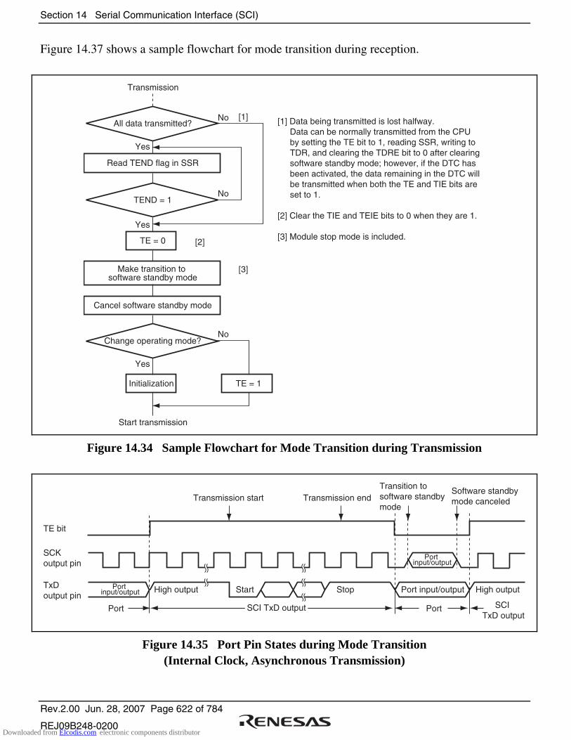
Section 14 Serial Communication Interface (SCI)
Rev.2.00 Jun. 28, 2007 Page 622 of 784
REJ09B248-0200
Figure 14.37 shows a sample flowchart for mode transition during reception.
Start transmission
Transmission
[1]
No
No
No
Yes
Yes
Yes
Read TEND flag in SSR
Make transition to software standby mode
Cancel software standby mode
TE = 0
Initialization TE = 1
[2]
[3]
All data transmitted?
Change operating mode?
TEND = 1
[1] Data being transmitted is lost halfway. Data can be normally transmitted from the CPU by setting the TE bit to 1, reading SSR, writing to TDR, and clearing the TDRE bit to 0 after clearing software standby mode; however, if the DTC has been activated, the data remaining in the DTC will be transmitted when both the TE and TIE bits are set to 1.
[2] Clear the TIE and TEIE bits to 0 when they are 1.
[3] Module stop mode is included.
Figure 14.34 Sample Flowchart for Mode Transition during Transmission
TE bit
SCK output pin
TxD output pin
Port input/output
Port input/outputPort input/output Start Stop High outputHigh output
Transmission start Transmission endTransition to software standbymode
Software standby mode canceled
SCI TxD outputPort Port SCI TxD output
Figure 14.35 Port Pin States during Mode Transition (Internal Clock, Asynchronous Transmission)
Downloaded from Elcodis.com electronic components distributor
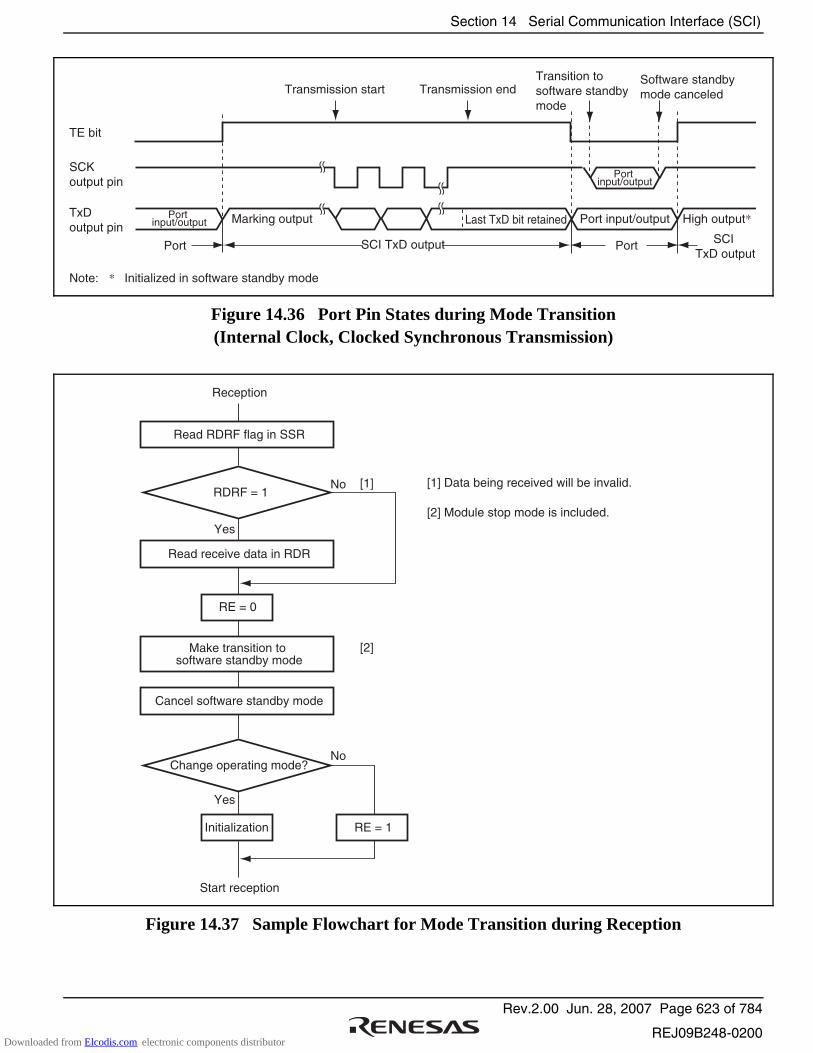
Section 14 Serial Communication Interface (SCI)
Rev.2.00 Jun. 28, 2007 Page 623 of 784
REJ09B248-0200
TE bit
SCK output pin
TxD output pin
Port input/output
Port input/output
Port input/output High output*Marking output
Transmission start Transmission endTransition to software standbymode
Software standby mode canceled
SCI TxD outputPort Port SCI TxD output
Last TxD bit retained
Note: * Initialized in software standby mode
Figure 14.36 Port Pin States during Mode Transition (Internal Clock, Clocked Synchronous Transmission)
Start reception
Reception
[1]
No
No
Yes
Yes
Read receive data in RDR
Read RDRF flag in SSR
Make transition to software standby mode
Cancel software standby mode
RE = 0
Initialization RE = 1
[2]
Change operating mode?
RDRF = 1[1] Data being received will be invalid.
[2] Module stop mode is included.
Figure 14.37 Sample Flowchart for Mode Transition during Reception
Downloaded from Elcodis.com electronic components distributor
Section 14 Serial Communication Interface (SCI)
Rev.2.00 Jun. 28, 2007 Page 624 of 784
REJ09B248-0200
Downloaded from Elcodis.com electronic components distributor
Section 15 A/D Converter
Rev.2.00 Jun. 28, 2007 Page 625 of 784
REJ09B248-0200
Section 15 A/D Converter
This LSI includes a successive approximation type 10-bit A/D converter that allows up to eight analog input channels to be selected.
Figure 15.1 shows a block diagram of the A/D converter.
15.1 Features
• 10-bit resolution
• Eight input channels
• Conversion time: 7.4 µs per channel (at 35-MHz operation)
• Two kinds of operating modes
Single mode: Single-channel A/D conversion
Scan mode: Continuous A/D conversion on 1 to 4 channels, or 1 to 8 channels
• Eight data registers
A/D conversion results are held in a 16-bit data register for each channel
• Sample and hold function
• Three types of conversion start
Conversion can be started by software, a conversion start trigger by the 16-bit timer pulse unit (TPU) or 8-bit timer (TMR), or an external trigger signal.
• Interrupt source
A/D conversion end interrupt (ADI) request can be generated.
• Module stop mode can be set
Downloaded from Elcodis.com electronic components distributor
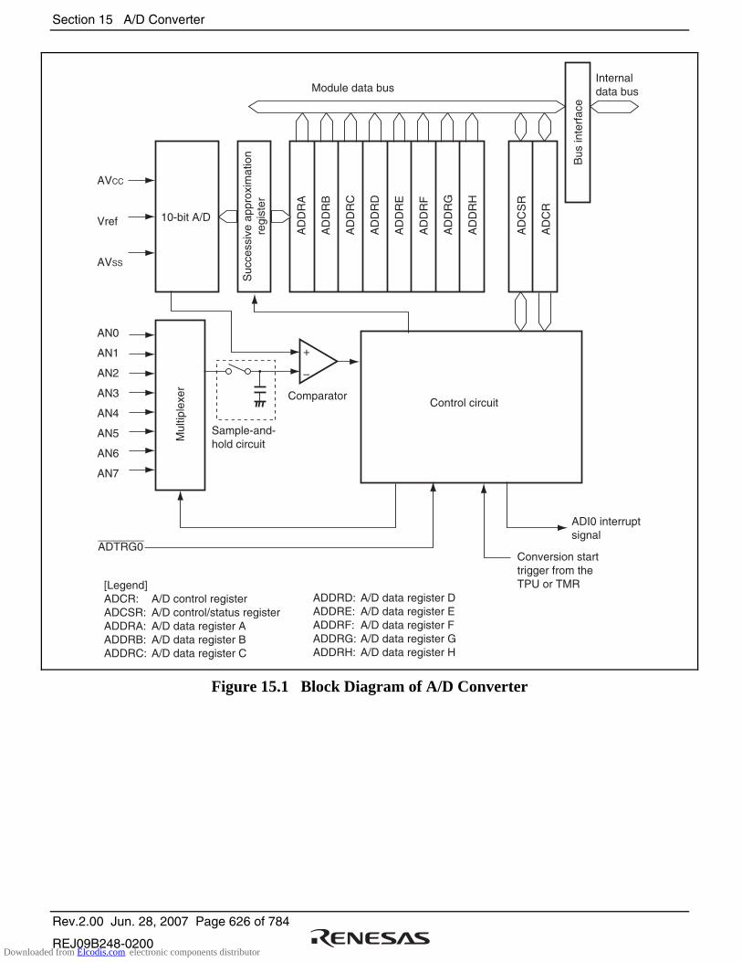
Section 15 A/D Converter
Rev.2.00 Jun. 28, 2007 Page 626 of 784
REJ09B248-0200
Module data bus
Control circuit
Internaldata bus
10-bit A/D
Comparator
+
–
Sample-and-hold circuit
ADI0 interruptsignal
Bus
inte
rfac
e
AVCC
Vref
AVSS
AN0
AN1
AN2
AN3
AN4
AN5
AN6
AN7
ADTRG0Conversion starttrigger from the TPU or TMR
Suc
cess
ive
appr
oxim
atio
nre
gist
er
Mul
tiple
xer
[Legend]ADCR: A/D control register ADCSR: A/D control/status registerADDRA: A/D data register AADDRB: A/D data register BADDRC: A/D data register C
ADDRD: A/D data register DADDRE: A/D data register EADDRF: A/D data register FADDRG: A/D data register GADDRH: A/D data register H
AD
DR
A
AD
DR
B
AD
DR
C
AD
DR
D
AD
DR
E
AD
DR
F
AD
DR
G
AD
DR
H
AD
CS
R
AD
CR
Figure 15.1 Block Diagram of A/D Converter
Downloaded from Elcodis.com electronic components distributor
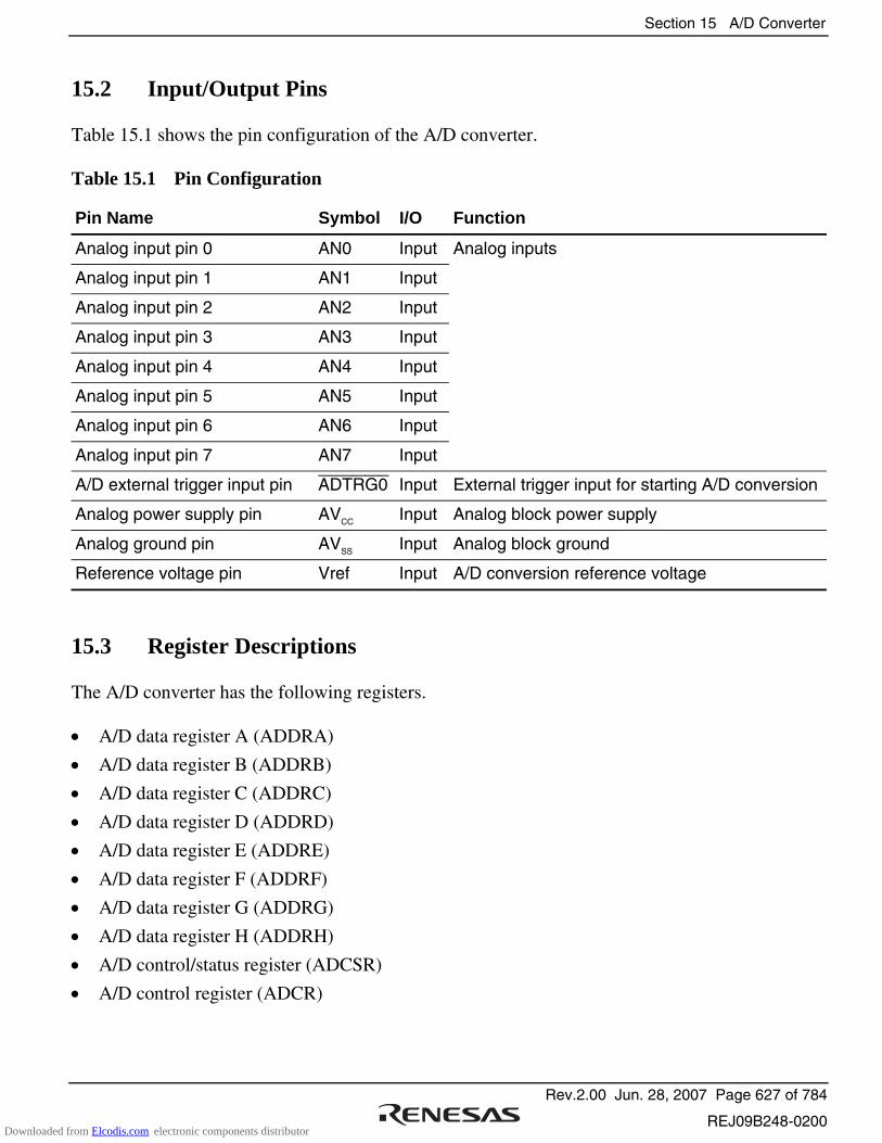
Section 15 A/D Converter
Rev.2.00 Jun. 28, 2007 Page 627 of 784
REJ09B248-0200
15.2 Input/Output Pins
Table 15.1 shows the pin configuration of the A/D converter.
Table 15.1 Pin Configuration
Pin Name Symbol I/O Function
Analog input pin 0 AN0 Input Analog inputs
Analog input pin 1 AN1 Input
Analog input pin 2 AN2 Input
Analog input pin 3 AN3 Input
Analog input pin 4 AN4 Input
Analog input pin 5 AN5 Input
Analog input pin 6 AN6 Input
Analog input pin 7 AN7 Input
A/D external trigger input pin ADTRG0 Input External trigger input for starting A/D conversion
Analog power supply pin AVCC Input Analog block power supply
Analog ground pin AVSS Input Analog block ground
Reference voltage pin Vref Input A/D conversion reference voltage
15.3 Register Descriptions
The A/D converter has the following registers.
• A/D data register A (ADDRA)
• A/D data register B (ADDRB)
• A/D data register C (ADDRC)
• A/D data register D (ADDRD)
• A/D data register E (ADDRE)
• A/D data register F (ADDRF)
• A/D data register G (ADDRG)
• A/D data register H (ADDRH)
• A/D control/status register (ADCSR)
• A/D control register (ADCR)
Downloaded from Elcodis.com electronic components distributor

Section 15 A/D Converter
Rev.2.00 Jun. 28, 2007 Page 628 of 784
REJ09B248-0200
15.3.1 A/D Data Registers A to H (ADDRA to ADDRH)
There are eight 16-bit read-only ADDR registers, ADDRA to ADDRH, used to store the results of A/D conversion. The ADDR registers, which store a conversion result for each channel, are shown in table 15.2.
The converted 10-bit data is stored in bits 15 to 6. The lower 6-bit data is always read as 0.
The data bus between the CPU and the A/D converter has a 16-bit width. The data can be read directly from the CPU. ADDR must not be accessed in 8-bit units and must be accessed in 16-bit units.
15
0
R
14
0
R
13
0
R
12
0
R
11
0
R
10
0
R
9
0
R
8
0
R
7
0
R
6
0
R
5
0
R
4
0
R
3
0
R
2
0
R
1
0
R
0
0
R
Bit
Bit Name
Initial Value
R/W
Table 15.2 Analog Input Channels and Corresponding ADDR Registers
Analog Input Channel A/D Data Register Which Stores Conversion Result
AN0 ADDRA
AN1 ADDRB
AN2 ADDRC
AN3 ADDRD
AN4 ADDRE
AN5 ADDRF
AN6 ADDRG
AN7 ADDRH
Downloaded from Elcodis.com electronic components distributor

Section 15 A/D Converter
Rev.2.00 Jun. 28, 2007 Page 629 of 784
REJ09B248-0200
15.3.2 A/D Control/Status Register (ADCSR)
ADCSR controls A/D conversion operations.
7
ADF
0
R/(W)*
6
ADIE
0
R/W
5
ADST
0
R/W
4
0
R
3
CH3
0
R/W
2
CH2
0
R/W
1
CH1
0
R/W
0
CH0
0
R/W
Bit
Bit Name
Initial Value
R/W
Note: * Only 0 can be written to this bit, to clear the flag.
Bit Bit Name Initial Value R/W Description
7 ADF 0 R/(W)* A/D End Flag
A status flag that indicates the end of A/D conversion.
[Setting conditions]
• When A/D conversion ends in single mode
• When A/D conversion ends on all specified channels
in scan mode
[Clearing conditions]
• When 0 is written after reading ADF = 1
(When the CPU is used to clear this flag by writing 0 while the corresponding interrupt is enabled, be sure to read the flag after writing 0 to it.)
• When the DTC or DMAC is activated by an ADI
interrupt and ADDR is read
6 ADIE 0 R/W A/D Interrupt Enable
When this bit is set to 1, ADI interrupts by ADF are enabled.
5 ADST 0 R/W A/D Start
Clearing this bit to 0 stops A/D conversion, and the A/D converter enters wait state.
Setting this bit to 1 starts A/D conversion. In single mode, this bit is cleared to 0 automatically when A/D conversion on the specified channel ends. In scan mode, A/D conversion continues sequentially on the specified channels until this bit is cleared to 0 by software, a reset, or hardware standby mode.
Downloaded from Elcodis.com electronic components distributor

Section 15 A/D Converter
Rev.2.00 Jun. 28, 2007 Page 630 of 784
REJ09B248-0200
Bit Bit Name Initial Value R/W Description
4 0 R Reserved
This is a read-only bit and cannot be modified.
3
2
1 0
CH3
CH2
CH1 CH0
0
0
0 0
R/W
R/W
R/W R/W
Channel Select 3 to 0
Selects analog input together with bits SCANE and SCANS in ADCR. • When SCANE = 0 and SCANS = X
0000: AN0 0001: AN1 0010: AN2 0011: AN3 0100: AN4 0101: AN5 0110: AN6 0111: AN7 1XXX: Setting prohibited
• When SCANE = 1 and SCANS = 0 0000: AN0 0001: AN0 and AN1 0010: AN0 to AN2 0011: AN0 to AN3 0100: AN4 0101: AN4 and AN5 0110: AN4 to AN6 0111: AN4 to AN7 1XXX: Setting prohibited
• When SCANE = 1 and SCANS = 1 0000: AN0 0001: AN0 and AN1 0010: AN0 to AN2 0011: AN0 to AN3 0100: AN0 to AN4 0101: AN0 to AN5 0110: AN0 to AN6 0111: AN0 to AN7 1XXX: Setting prohibited
[Legend]
X: Don't care
Note: * Only 0 can be written to this bit, to clear the flag.
Downloaded from Elcodis.com electronic components distributor
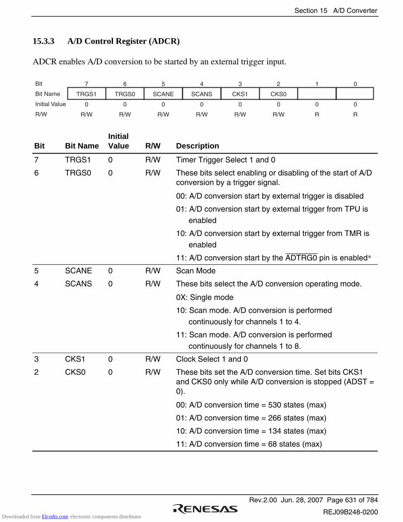
Section 15 A/D Converter
Rev.2.00 Jun. 28, 2007 Page 631 of 784
REJ09B248-0200
15.3.3 A/D Control Register (ADCR)
ADCR enables A/D conversion to be started by an external trigger input.
7
TRGS1
0
R/W
6
TRGS0
0
R/W
5
SCANE
0
R/W
4
SCANS
0
R/W
3
CKS1
0
R/W
2
CKS0
0
R/W
1
0
R
0
0
R
Bit
Bit Name
Initial Value
R/W
Bit Bit Name Initial Value R/W Description
7
6
TRGS1
TRGS0
0
0
R/W
R/W
Timer Trigger Select 1 and 0
These bits select enabling or disabling of the start of A/D conversion by a trigger signal.
00: A/D conversion start by external trigger is disabled
01: A/D conversion start by external trigger from TPU is
enabled
10: A/D conversion start by external trigger from TMR is
enabled
11: A/D conversion start by the ADTRG0 pin is enabled*
5
4
SCANE
SCANS
0
0
R/W
R/W
Scan Mode
These bits select the A/D conversion operating mode.
0X: Single mode
10: Scan mode. A/D conversion is performed
continuously for channels 1 to 4.
11: Scan mode. A/D conversion is performed
continuously for channels 1 to 8.
3
2
CKS1
CKS0
0
0
R/W
R/W
Clock Select 1 and 0
These bits set the A/D conversion time. Set bits CKS1 and CKS0 only while A/D conversion is stopped (ADST = 0).
00: A/D conversion time = 530 states (max)
01: A/D conversion time = 266 states (max)
10: A/D conversion time = 134 states (max)
11: A/D conversion time = 68 states (max)
Downloaded from Elcodis.com electronic components distributor
Section 15 A/D Converter
Rev.2.00 Jun. 28, 2007 Page 632 of 784
REJ09B248-0200
Bit Bit Name Initial Value R/W Description
1, 0 All 0 R Reserved
These are read-only bits and cannot be modified.
[Legend] X: Don't care
Note: * To set A/D conversion to start by the ADTRG0 pin, the DDR bit and ICR bit for the corresponding pin should be set to 0 and 1, respectively. For details, see section 9, I/O Ports.
15.4 Operation
The A/D converter operates by successive approximation with 10-bit resolution. It has two operating modes: single mode and scan mode. When changing the operating mode or analog input channel, to prevent incorrect operation, first clear the ADST bit in ADCSR to 0 to halt A/D conversion. The ADST bit can be set to 1 at the same time as the operating mode or analog input channel is changed.
15.4.1 Single Mode
In single mode, A/D conversion is to be performed only once on the analog input of the specified single channel.
1. A/D conversion for the selected channel is started when the ADST bit in ADCSR is set to 1 by software or an external trigger input.
2. When A/D conversion is completed, the A/D conversion result is transferred to the corresponding A/D data register of the channel.
3. When A/D conversion is completed, the ADF bit in ADCSR is set to 1. If the ADIE bit is set to 1 at this time, an ADI interrupt request is generated.
4. The ADST bit remains set to 1 during A/D conversion, and is automatically cleared to 0 when A/D conversion ends. The A/D converter enters wait state. If the ADST bit is cleared to 0 during A/D conversion, A/D conversion stops and the A/D converter enters wait state.
Downloaded from Elcodis.com electronic components distributor

Section 15 A/D Converter
Rev.2.00 Jun. 28, 2007 Page 633 of 784
REJ09B248-0200
ADIE
ADST
ADF
ADDRA
ADDRB
ADDRC
ADDRD
Channel 0 (AN0)operation state
Channel 1 (AN1)operation state
Channel 2 (AN2)operation state
Channel 3 (AN3)operation state
Set*
Set* Set*
A/D conversion start
Clear* Clear*
Waiting for conversion
Waiting for conversion Waiting for conversion
Waiting for conversion
Waiting for conversion
Reading A/D conversion result Reading A/D conversion result
A/D conversion 1 A/D conversion 2
A/D conversion result 1 A/D conversion result 2
Waiting for conversion
Note: * ↓ indicates the timing of instruction execution by software.
Figure 15.2 Example of A/D Converter Operation (Single Mode, Channel 1 Selected)
15.4.2 Scan Mode
In scan mode, A/D conversion is to be performed sequentially on the analog inputs of the specified channels up to four or eight channels.
1. When the ADST bit in ADCSR is set to 1 by software, TPU, TMR, or an external trigger input, A/D conversion starts on the first channel in the group. Consecutive A/D conversion on a maximum of four channels (SCANE and SCANS = B'10) or on a maximum of eight channels (SCANE and SCANS = B'11) can be selected. When consecutive A/D conversion is performed on four channels, A/D conversion starts on AN4 when CH3 and CH2 = B'01. When consecutive A/D conversion is performed on eight channels, A/D conversion starts on AN0 when CH3 = B'0.
2. When A/D conversion for each channel is completed, the A/D conversion result is sequentially transferred to the corresponding ADDR of each channel.
Downloaded from Elcodis.com electronic components distributor
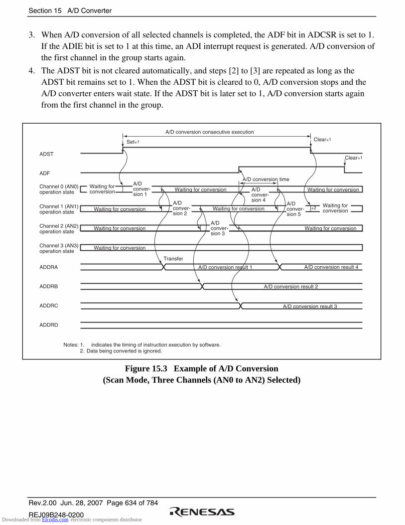
Section 15 A/D Converter
Rev.2.00 Jun. 28, 2007 Page 634 of 784
REJ09B248-0200
3. When A/D conversion of all selected channels is completed, the ADF bit in ADCSR is set to 1. If the ADIE bit is set to 1 at this time, an ADI interrupt request is generated. A/D conversion of the first channel in the group starts again.
4. The ADST bit is not cleared automatically, and steps [2] to [3] are repeated as long as the ADST bit remains set to 1. When the ADST bit is cleared to 0, A/D conversion stops and the A/D converter enters wait state. If the ADST bit is later set to 1, A/D conversion starts again from the first channel in the group.
ADST
ADF
ADDRA
ADDRB
ADDRC
ADDRD
Set*1 Clear*1
Clear*1
*2
Waiting for conversionChannel 0 (AN0)operation state
Channel 1 (AN1)operation state
Channel 2 (AN2)operation state
Channel 3 (AN3)operation state
Waiting for conversion
A/Dconver-sion 1
A/D conversion result 3
Waiting for conversion
Waiting for conversion
Waiting for conversion
A/D conversion result 2
A/D conversion result 4
A/D conver-sion 5
A/D conver-sion 4
A/D conversion time
Waiting for conversion
A/D conver-sion 3
Waiting for conversion
Waiting for conversion
Waiting for conversion
A/D conver-sion 2
A/D conversion result 1
Transfer
A/D conversion consecutive execution
Notes: 1.2.
↓ indicates the timing of instruction execution by software.Data being converted is ignored.
Figure 15.3 Example of A/D Conversion (Scan Mode, Three Channels (AN0 to AN2) Selected)
Downloaded from Elcodis.com electronic components distributor

Section 15 A/D Converter
Rev.2.00 Jun. 28, 2007 Page 635 of 784
REJ09B248-0200
15.4.3 Input Sampling and A/D Conversion Time
The A/D converter has a built-in sample-and-hold circuit. The A/D converter samples the analog input when the A/D conversion start delay time (tD) passes after the ADST bit in ADCSR is set to 1, then starts A/D conversion. Figure 15.4 shows the A/D conversion timing. Table 15.3 indicates the A/D conversion time.
As indicated in figure 15.4, the A/D conversion time (tCONV) includes tD and the input sampling time (tSPL). The length of tD varies depending on the timing of the write access to ADCSR. The total conversion time therefore varies within the ranges indicated in table 15.3.
In scan mode, the values given in table 15.3 apply to the first conversion time. The values given in table 15.4 apply to the second and subsequent conversions. In either case, bits CKS1 and CKS0 in ADCR should be set so that the conversion time is within the ranges indicated by the A/D conversion characteristics.
(1)
(2)
tD tSPL
tCONV
Pφ
Address
Write signal
Input samplingtiming
ADF
[Legend](1): ADCSR write cycle(2): ADCSR addresstD: A/D conversion start delay timetSPL: Input sampling timetCONV: A/D conversion time
Figure 15.4 A/D Conversion Timing
Downloaded from Elcodis.com electronic components distributor

Section 15 A/D Converter
Rev.2.00 Jun. 28, 2007 Page 636 of 784
REJ09B248-0200
Table 15.3 A/D Conversion Characteristics (Single Mode)
CKS1 = 0 CKS1 = 1
CKS0 = 0 CKS0 = 1 CKS0 = 0 CKS0 = 1
Item Symbol Min. Typ. Max. Min. Typ. Max. Min. Typ. Max. Min. Typ. Max.
A/D conversion start delay time
tD 18 33 10 17 6 9 4 5
Input sampling time tSPL 127 63 31 15
A/D conversion time
tCONV 515 530 259 266 131 134 67 68
Note: Values in the table are the number of states.
Table 15.4 A/D Conversion Characteristics (Scan Mode)
CKS1 CKS0 Conversion Time (Number of States)
0 512 (Fixed) 0
1 256 (Fixed)
0 128 (Fixed) 1
1 64 (Fixed)
15.4.4 External Trigger Input Timing
A/D conversion can be externally triggered. When the TRGS1 and TRGS0 bits are set to B'11 in ADCR, an external trigger is input from the ADTRG0 pin. A/D conversion starts when the ADST bit in ADCSR is set to 1 on the falling edge of the ADTRG0 pin. Other operations, in both single and scan modes, are the same as when the ADST bit has been set to 1 by software. Figure 15.5 shows the timing.
Pφ
ADTRG0
Internal trigger signal
ADSTA/D conversion
Figure 15.5 External Trigger Input Timing
Downloaded from Elcodis.com electronic components distributor
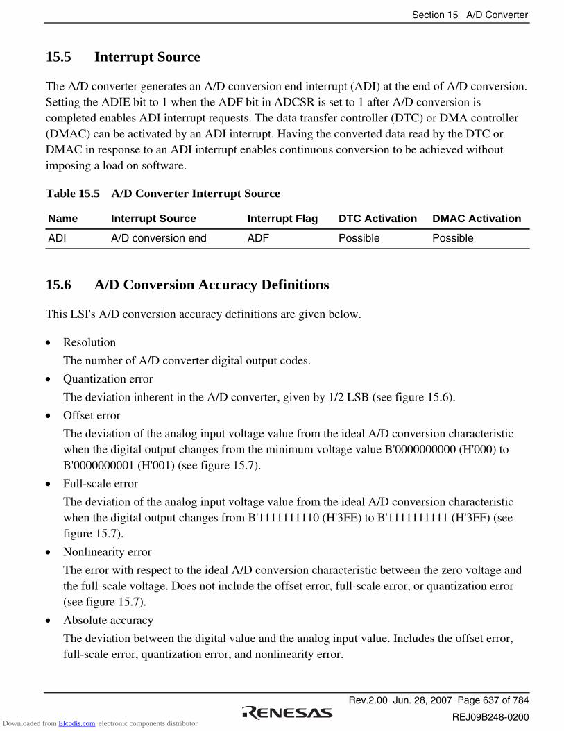
Section 15 A/D Converter
Rev.2.00 Jun. 28, 2007 Page 637 of 784
REJ09B248-0200
15.5 Interrupt Source
The A/D converter generates an A/D conversion end interrupt (ADI) at the end of A/D conversion. Setting the ADIE bit to 1 when the ADF bit in ADCSR is set to 1 after A/D conversion is completed enables ADI interrupt requests. The data transfer controller (DTC) or DMA controller (DMAC) can be activated by an ADI interrupt. Having the converted data read by the DTC or DMAC in response to an ADI interrupt enables continuous conversion to be achieved without imposing a load on software.
Table 15.5 A/D Converter Interrupt Source
Name Interrupt Source Interrupt Flag DTC Activation DMAC Activation
ADI A/D conversion end ADF Possible Possible
15.6 A/D Conversion Accuracy Definitions
This LSI's A/D conversion accuracy definitions are given below.
• Resolution
The number of A/D converter digital output codes.
• Quantization error
The deviation inherent in the A/D converter, given by 1/2 LSB (see figure 15.6).
• Offset error
The deviation of the analog input voltage value from the ideal A/D conversion characteristic when the digital output changes from the minimum voltage value B'0000000000 (H'000) to B'0000000001 (H'001) (see figure 15.7).
• Full-scale error
The deviation of the analog input voltage value from the ideal A/D conversion characteristic when the digital output changes from B'1111111110 (H'3FE) to B'1111111111 (H'3FF) (see figure 15.7).
• Nonlinearity error
The error with respect to the ideal A/D conversion characteristic between the zero voltage and the full-scale voltage. Does not include the offset error, full-scale error, or quantization error (see figure 15.7).
• Absolute accuracy
The deviation between the digital value and the analog input value. Includes the offset error, full-scale error, quantization error, and nonlinearity error.
Downloaded from Elcodis.com electronic components distributor
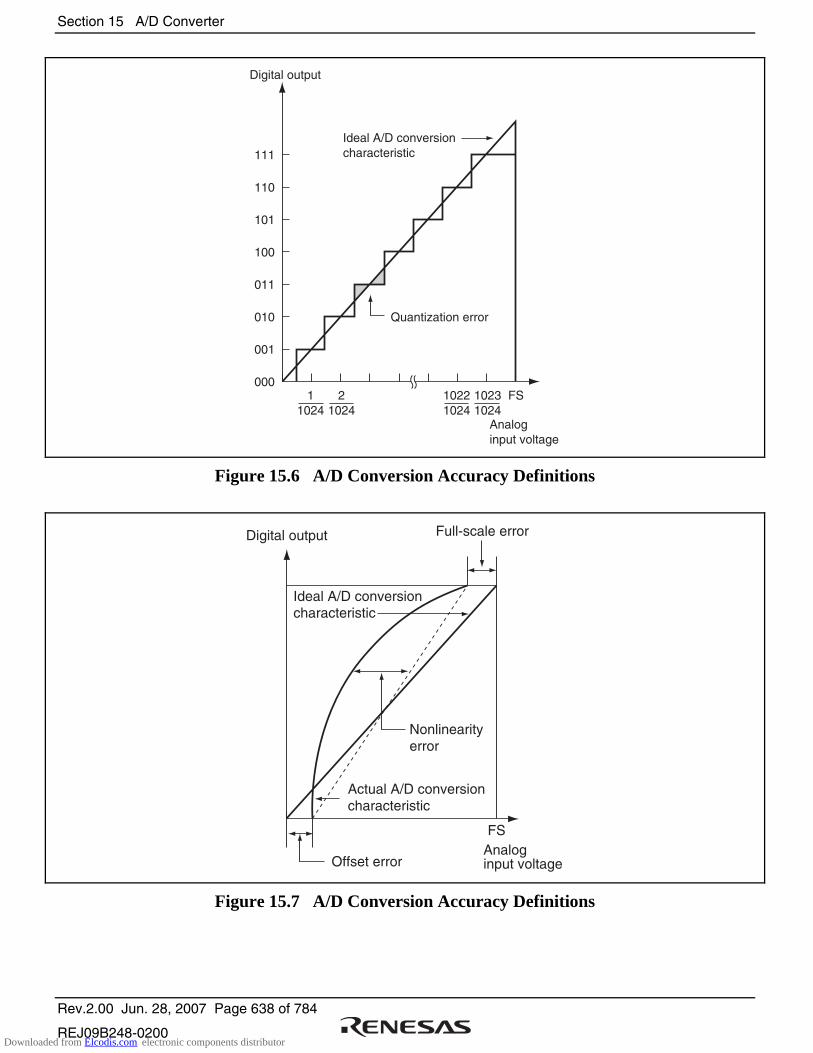
Section 15 A/D Converter
Rev.2.00 Jun. 28, 2007 Page 638 of 784
REJ09B248-0200
111
110
101
100
011
010
001
0001
10242
102410221024
10231024
FS
Quantization error
Digital output
Ideal A/D conversioncharacteristic
Analoginput voltage
Figure 15.6 A/D Conversion Accuracy Definitions
FS
Digital output
Ideal A/D conversioncharacteristic
Nonlinearityerror
Analoginput voltageOffset error
Actual A/D conversioncharacteristic
Full-scale error
Figure 15.7 A/D Conversion Accuracy Definitions
Downloaded from Elcodis.com electronic components distributor
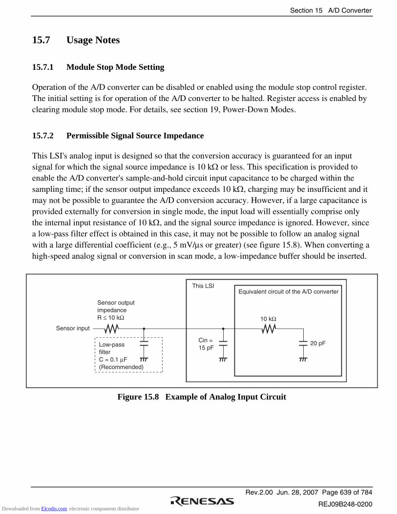
Section 15 A/D Converter
Rev.2.00 Jun. 28, 2007 Page 639 of 784
REJ09B248-0200
15.7 Usage Notes
15.7.1 Module Stop Mode Setting
Operation of the A/D converter can be disabled or enabled using the module stop control register. The initial setting is for operation of the A/D converter to be halted. Register access is enabled by clearing module stop mode. For details, see section 19, Power-Down Modes.
15.7.2 Permissible Signal Source Impedance
This LSI's analog input is designed so that the conversion accuracy is guaranteed for an input signal for which the signal source impedance is 10 kΩ or less. This specification is provided to enable the A/D converter's sample-and-hold circuit input capacitance to be charged within the sampling time; if the sensor output impedance exceeds 10 kΩ, charging may be insufficient and it may not be possible to guarantee the A/D conversion accuracy. However, if a large capacitance is provided externally for conversion in single mode, the input load will essentially comprise only the internal input resistance of 10 kΩ, and the signal source impedance is ignored. However, since a low-pass filter effect is obtained in this case, it may not be possible to follow an analog signal with a large differential coefficient (e.g., 5 mV/µs or greater) (see figure 15.8). When converting a high-speed analog signal or conversion in scan mode, a low-impedance buffer should be inserted.
Equivalent circuit of the A/D converterThis LSI
20 pFCin =15 pF
10 kΩ
Low-pass filterC = 0.1 µF(Recommended)
Sensor output impedanceR ≤ 10 kΩ
Sensor input
Figure 15.8 Example of Analog Input Circuit
Downloaded from Elcodis.com electronic components distributor
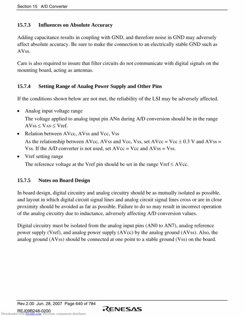
Section 15 A/D Converter
Rev.2.00 Jun. 28, 2007 Page 640 of 784
REJ09B248-0200
15.7.3 Influences on Absolute Accuracy
Adding capacitance results in coupling with GND, and therefore noise in GND may adversely affect absolute accuracy. Be sure to make the connection to an electrically stable GND such as AVss.
Care is also required to insure that filter circuits do not communicate with digital signals on the mounting board, acting as antennas.
15.7.4 Setting Range of Analog Power Supply and Other Pins
If the conditions shown below are not met, the reliability of the LSI may be adversely affected.
• Analog input voltage range
The voltage applied to analog input pin ANn during A/D conversion should be in the range AVss ≤ VAN ≤ Vref.
• Relation between AVcc, AVss and Vcc, Vss
As the relationship between AVcc, AVss and Vcc, Vss, set AVcc = Vcc ± 0.3 V and AVss = Vss. If the A/D converter is not used, set AVcc = Vcc and AVss = Vss.
• Vref setting range
The reference voltage at the Vref pin should be set in the range Vref ≤ AVcc.
15.7.5 Notes on Board Design
In board design, digital circuitry and analog circuitry should be as mutually isolated as possible, and layout in which digital circuit signal lines and analog circuit signal lines cross or are in close proximity should be avoided as far as possible. Failure to do so may result in incorrect operation of the analog circuitry due to inductance, adversely affecting A/D conversion values.
Digital circuitry must be isolated from the analog input pins (AN0 to AN7), analog reference power supply (Vref), and analog power supply (AVcc) by the analog ground (AVss). Also, the analog ground (AVss) should be connected at one point to a stable ground (Vss) on the board.
Downloaded from Elcodis.com electronic components distributor
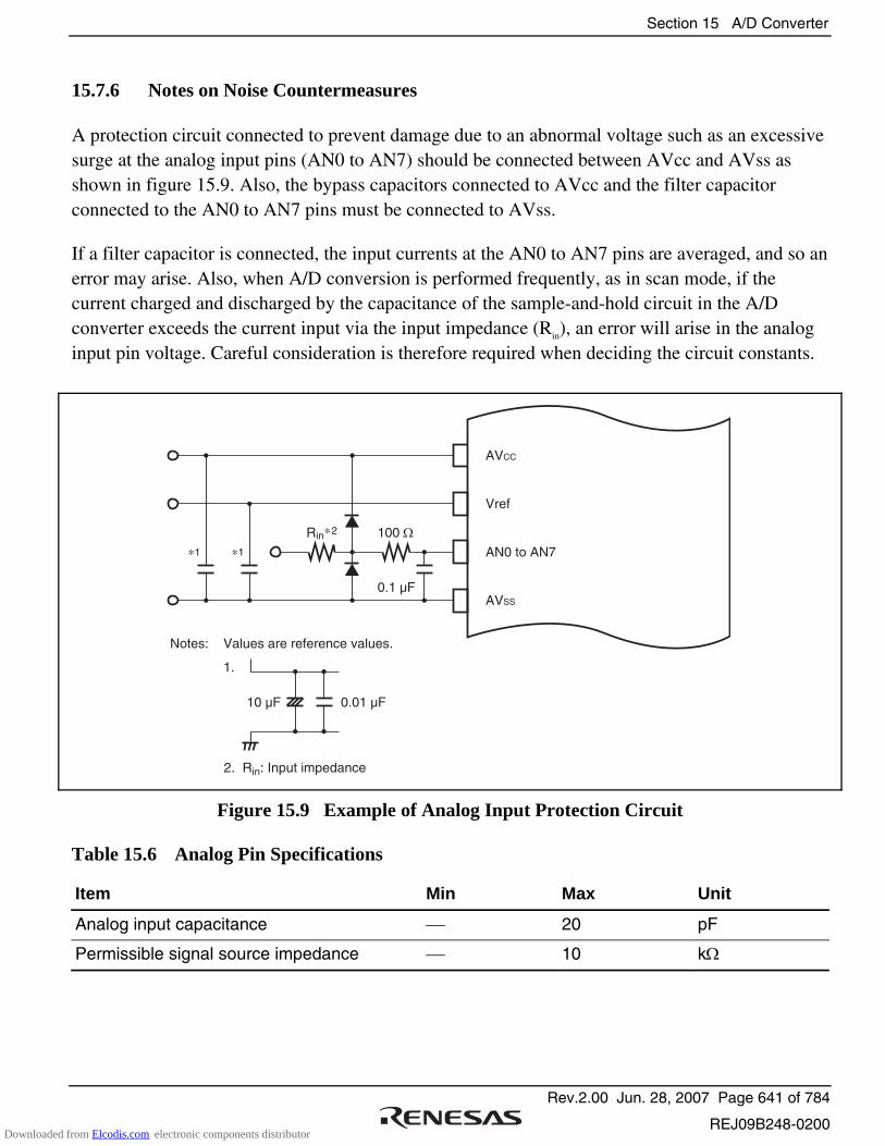
Section 15 A/D Converter
Rev.2.00 Jun. 28, 2007 Page 641 of 784
REJ09B248-0200
15.7.6 Notes on Noise Countermeasures
A protection circuit connected to prevent damage due to an abnormal voltage such as an excessive surge at the analog input pins (AN0 to AN7) should be connected between AVcc and AVss as shown in figure 15.9. Also, the bypass capacitors connected to AVcc and the filter capacitor connected to the AN0 to AN7 pins must be connected to AVss.
If a filter capacitor is connected, the input currents at the AN0 to AN7 pins are averaged, and so an error may arise. Also, when A/D conversion is performed frequently, as in scan mode, if the current charged and discharged by the capacitance of the sample-and-hold circuit in the A/D converter exceeds the current input via the input impedance (Rin), an error will arise in the analog input pin voltage. Careful consideration is therefore required when deciding the circuit constants.
AVCC
*1 *1
Vref
AN0 to AN7
AVSS
Notes: Values are reference values.
1.
2. Rin: Input impedance
Rin*2 100 Ω
0.1 µF
0.01 µF10 µF
Figure 15.9 Example of Analog Input Protection Circuit
Table 15.6 Analog Pin Specifications
Item Min Max Unit
Analog input capacitance 20 pF
Permissible signal source impedance 10 kΩ
Downloaded from Elcodis.com electronic components distributor
Section 15 A/D Converter
Rev.2.00 Jun. 28, 2007 Page 642 of 784
REJ09B248-0200
20 pF
To A/D converterAN0 to AN710 kΩ
Note: Values are reference values.
Figure 15.10 Analog Input Pin Equivalent Circuit
15.7.7 A/D Input Hold Function in Software Standby Mode
When this LSI enters software standby mode with A/D conversion enabled, the analog inputs are retained, and the analog power supply current is equal to as during A/D conversion. If the analog power supply current needs to be reduced in software standby mode, clear the ADST, TRGS1, and TRGS0 bits all to 0 to disable A/D conversion.
Downloaded from Elcodis.com electronic components distributor
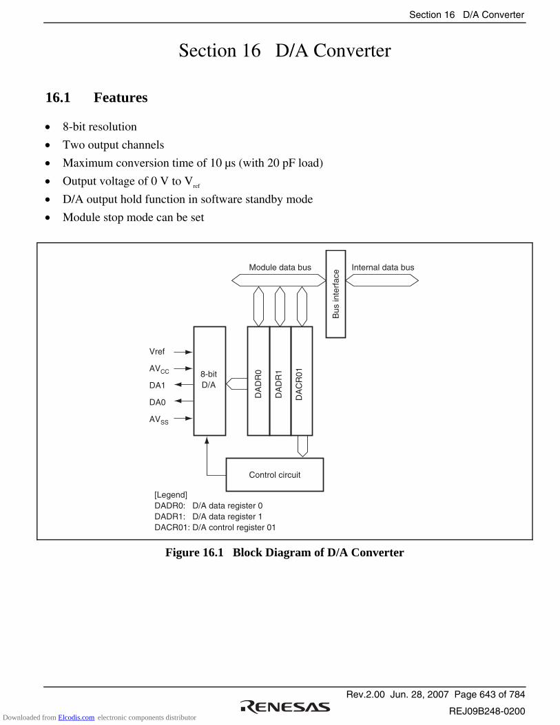
Section 16 D/A Converter
Rev.2.00 Jun. 28, 2007 Page 643 of 784
REJ09B248-0200
Section 16 D/A Converter
16.1 Features
• 8-bit resolution
• Two output channels
• Maximum conversion time of 10 µs (with 20 pF load)
• Output voltage of 0 V to Vref
• D/A output hold function in software standby mode
• Module stop mode can be set
Module data bus Internal data bus
Vref
AVCC
DA1
DA0
AVSS
8-bitD/A
Control circuit
Bus
inte
rfac
e
[Legend]DADR0: D/A data register 0DADR1: D/A data register 1DACR01: D/A control register 01
DA
DR
0
DA
DR
1
DA
CR
01
Figure 16.1 Block Diagram of D/A Converter
Downloaded from Elcodis.com electronic components distributor
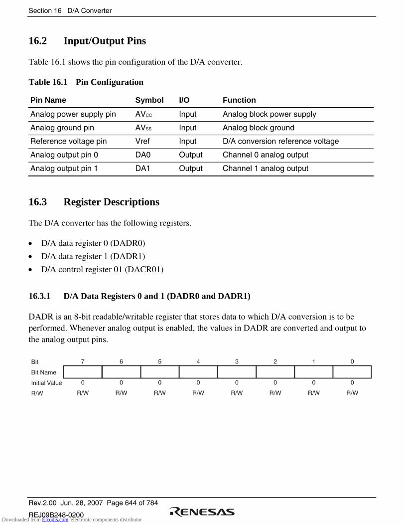
Section 16 D/A Converter
Rev.2.00 Jun. 28, 2007 Page 644 of 784
REJ09B248-0200
16.2 Input/Output Pins
Table 16.1 shows the pin configuration of the D/A converter.
Table 16.1 Pin Configuration
Pin Name Symbol I/O Function
Analog power supply pin AVCC Input Analog block power supply
Analog ground pin AVSS Input Analog block ground
Reference voltage pin Vref Input D/A conversion reference voltage
Analog output pin 0 DA0 Output Channel 0 analog output
Analog output pin 1 DA1 Output Channel 1 analog output
16.3 Register Descriptions
The D/A converter has the following registers.
• D/A data register 0 (DADR0)
• D/A data register 1 (DADR1)
• D/A control register 01 (DACR01)
16.3.1 D/A Data Registers 0 and 1 (DADR0 and DADR1)
DADR is an 8-bit readable/writable register that stores data to which D/A conversion is to be performed. Whenever analog output is enabled, the values in DADR are converted and output to the analog output pins.
7
0
R/W
6
0
R/W
5
0
R/W
4
0
R/W
3
0
R/W
2
0
R/W
1
0
R/W
0
0
R/W
Bit
Bit Name
Initial Value
R/W
Downloaded from Elcodis.com electronic components distributor

Section 16 D/A Converter
Rev.2.00 Jun. 28, 2007 Page 645 of 784
REJ09B248-0200
16.3.2 D/A Control Register 01 (DACR01)
DACR01 controls the operation of the D/A converter.
7
DAOE1
0
R/W
6
DAOE0
0
R/W
5
DAE
0
R/W
4
1
R
3
1
R
2
1
R
1
1
R
0
1
R
Bit
Bit Name
Initial Value
R/W
Bit Bit Name Initial Value R/W Description
7 DAOE1 0 R/W D/A Output Enable 1
Controls D/A conversion and analog output.
0: Analog output of channel 1 (DA1) is disabled
1: D/A conversion of channel 1 is enabled. Analog output of channel 1 (DA1) is enabled.
6 DAOE0 0 R/W D/A Output Enable 0
Controls D/A conversion and analog output.
0: Analog output of channel 0 (DA0) is disabled
1: D/A conversion of channel 0 is enabled. Analog output of channel 0 (DA0) is enabled.
5 DAE 0 R/W D/A Enable
Used together with the DAOE0 and DAOE1 bits to control D/A conversion. When this bit is cleared to 0, D/A conversion is controlled independently for channels 0 and 1. When this bit is set to 1, D/A conversion for channels 0 and 1 is controlled together.
Output of conversion results is always controlled by the DAOE0 and DAOE1 bits. For details, see table 16.2, Control of D/A Conversion.
4 to 0 All 1 R Reserved
These are read-only bits and cannot be modified.
Downloaded from Elcodis.com electronic components distributor
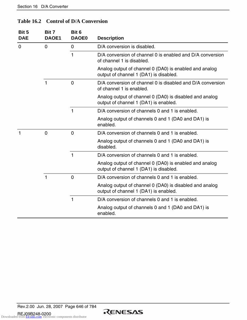
Section 16 D/A Converter
Rev.2.00 Jun. 28, 2007 Page 646 of 784
REJ09B248-0200
Table 16.2 Control of D/A Conversion
Bit 5 DAE
Bit 7 DAOE1
Bit 6 DAOE0 Description
0 0 0 D/A conversion is disabled.
1 D/A conversion of channel 0 is enabled and D/A conversion of channel 1 is disabled.
Analog output of channel 0 (DA0) is enabled and analog output of channel 1 (DA1) is disabled.
1 0 D/A conversion of channel 0 is disabled and D/A conversion of channel 1 is enabled.
Analog output of channel 0 (DA0) is disabled and analog output of channel 1 (DA1) is enabled.
1 D/A conversion of channels 0 and 1 is enabled.
Analog output of channels 0 and 1 (DA0 and DA1) is enabled.
1 0 0 D/A conversion of channels 0 and 1 is enabled.
Analog output of channels 0 and 1 (DA0 and DA1) is disabled.
1 D/A conversion of channels 0 and 1 is enabled.
Analog output of channel 0 (DA0) is enabled and analog output of channel 1 (DA1) is disabled.
1 0 D/A conversion of channels 0 and 1 is enabled.
Analog output of channel 0 (DA0) is disabled and analog output of channel 1 (DA1) is enabled.
1 D/A conversion of channels 0 and 1 is enabled.
Analog output of channels 0 and 1 (DA0 and DA1) is enabled.
Downloaded from Elcodis.com electronic components distributor
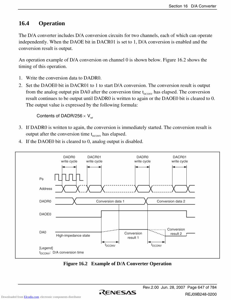
Section 16 D/A Converter
Rev.2.00 Jun. 28, 2007 Page 647 of 784
REJ09B248-0200
16.4 Operation
The D/A converter includes D/A conversion circuits for two channels, each of which can operate independently. When the DAOE bit in DACR01 is set to 1, D/A conversion is enabled and the conversion result is output.
An operation example of D/A conversion on channel 0 is shown below. Figure 16.2 shows the timing of this operation.
1. Write the conversion data to DADR0.
2. Set the DAOE0 bit in DACR01 to 1 to start D/A conversion. The conversion result is output from the analog output pin DA0 after the conversion time tDCONV has elapsed. The conversion result continues to be output until DADR0 is written to again or the DAOE0 bit is cleared to 0. The output value is expressed by the following formula:
Contents of DADR/256 × Vref
3. If DADR0 is written to again, the conversion is immediately started. The conversion result is output after the conversion time tDCONV has elapsed.
4. If the DAOE0 bit is cleared to 0, analog output is disabled.
Conversion data 1
Conversionresult 1
High-impedance state
tDCONV
DADR0write cycle
DA0
DAOE0
DADR0
Address
Pφ
DACR01write cycle
Conversion data 2
Conversionresult 2
tDCONV[Legend]tDCONV: D/A conversion time
DADR0write cycle
DACR01write cycle
Figure 16.2 Example of D/A Converter Operation
Downloaded from Elcodis.com electronic components distributor
Section 16 D/A Converter
Rev.2.00 Jun. 28, 2007 Page 648 of 784
REJ09B248-0200
16.5 Usage Notes
16.5.1 Module Stop Mode Setting
Operation of the D/A converter can be disabled or enabled using the module stop control register. The initial setting is for operation of the D/A converter to be halted. Register access is enabled by clearing module stop mode. For details, see section 19, Power-Down Modes.
16.5.2 D/A Output Hold Function in Software Standby Mode
When this LSI enters software standby mode with D/A conversion enabled, the D/A outputs are retained, and the analog power supply current is equal to as during D/A conversion. If the analog power supply current needs to be reduced in software standby mode, clear the ADST, TRGS1, and TRGS0 bits all to 0 to disable D/A conversion.
Downloaded from Elcodis.com electronic components distributor
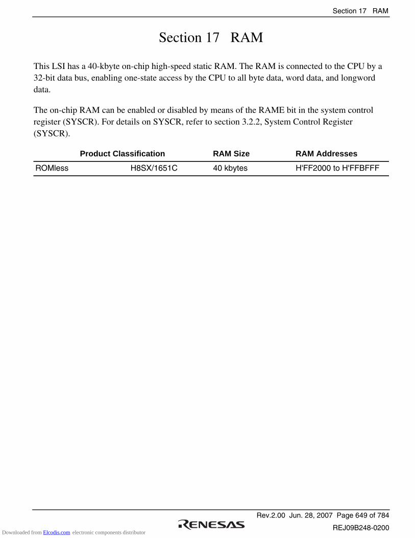
Section 17 RAM
Rev.2.00 Jun. 28, 2007 Page 649 of 784
REJ09B248-0200
Section 17 RAM
This LSI has a 40-kbyte on-chip high-speed static RAM. The RAM is connected to the CPU by a 32-bit data bus, enabling one-state access by the CPU to all byte data, word data, and longword data.
The on-chip RAM can be enabled or disabled by means of the RAME bit in the system control register (SYSCR). For details on SYSCR, refer to section 3.2.2, System Control Register (SYSCR).
Product Classification RAM Size RAM Addresses
ROMless H8SX/1651C 40 kbytes H'FF2000 to H'FFBFFF
Downloaded from Elcodis.com electronic components distributor

Section 17 RAM
Rev.2.00 Jun. 28, 2007 Page 650 of 784
REJ09B248-0200
Downloaded from Elcodis.com electronic components distributor
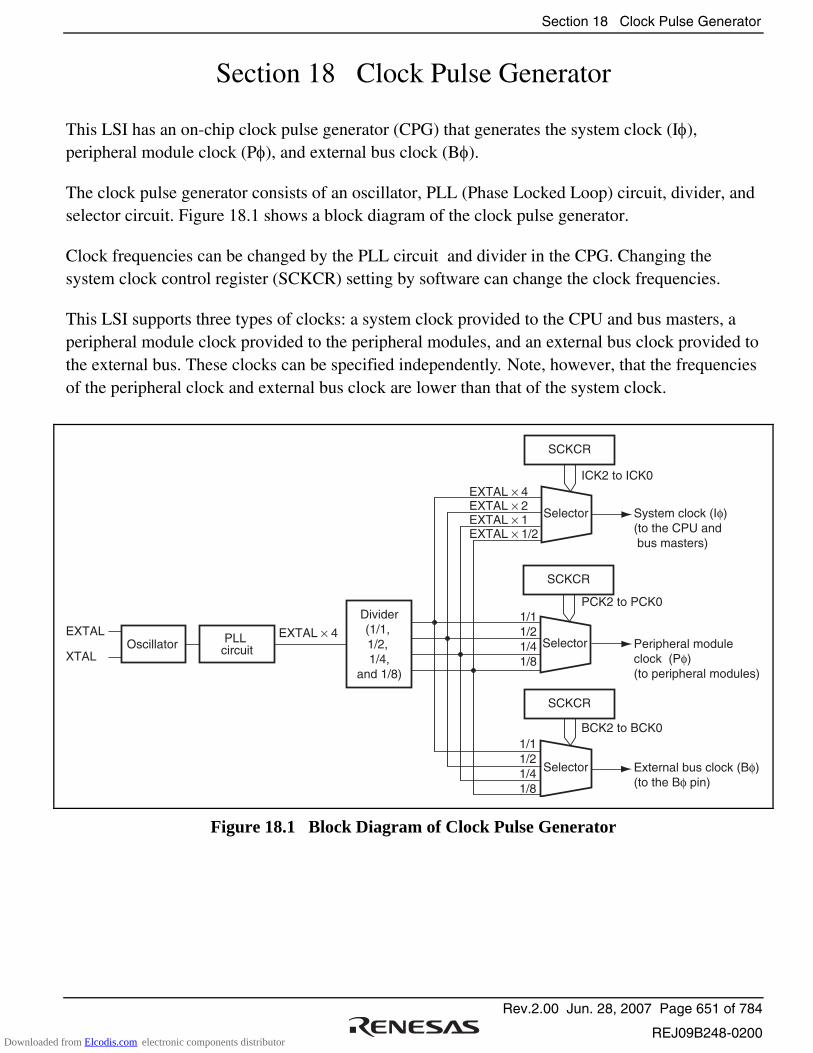
Section 18 Clock Pulse Generator
Rev.2.00 Jun. 28, 2007 Page 651 of 784
REJ09B248-0200
Section 18 Clock Pulse Generator
This LSI has an on-chip clock pulse generator (CPG) that generates the system clock (Iφ), peripheral module clock (Pφ), and external bus clock (Bφ).
The clock pulse generator consists of an oscillator, PLL (Phase Locked Loop) circuit, divider, and selector circuit. Figure 18.1 shows a block diagram of the clock pulse generator.
Clock frequencies can be changed by the PLL circuit and divider in the CPG. Changing the system clock control register (SCKCR) setting by software can change the clock frequencies.
This LSI supports three types of clocks: a system clock provided to the CPU and bus masters, a peripheral module clock provided to the peripheral modules, and an external bus clock provided to the external bus. These clocks can be specified independently. Note, however, that the frequencies of the peripheral clock and external bus clock are lower than that of the system clock.
EXTAL
XTAL
PLL circuitOscillator
Selector System clock (Iφ)(to the CPU and bus masters)
Peripheral module clock (Pφ)(to peripheral modules)
External bus clock (Bφ)(to the Bφ pin)
ICK2 to ICK0
SCKCR
PCK2 to PCK0Divider(1/1, 1/2, 1/4,
and 1/8)
BCK2 to BCK0
EXTAL × 4
EXTAL × 4 EXTAL × 2 EXTAL × 1 EXTAL × 1/2
Selector
SCKCR
1/11/21/41/8
Selector
SCKCR
1/11/21/41/8
Figure 18.1 Block Diagram of Clock Pulse Generator
Downloaded from Elcodis.com electronic components distributor
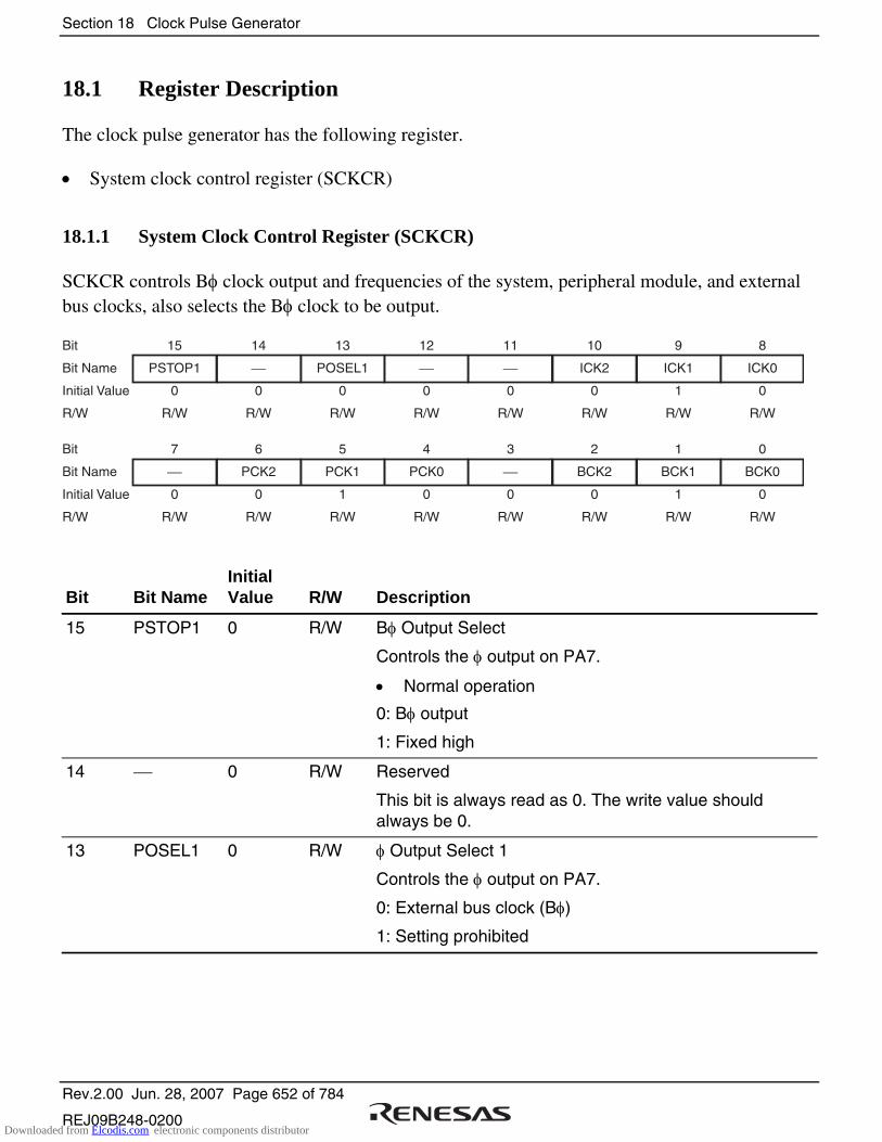
Section 18 Clock Pulse Generator
Rev.2.00 Jun. 28, 2007 Page 652 of 784
REJ09B248-0200
18.1 Register Description
The clock pulse generator has the following register.
• System clock control register (SCKCR)
18.1.1 System Clock Control Register (SCKCR)
SCKCR controls Bφ clock output and frequencies of the system, peripheral module, and external bus clocks, also selects the Bφ clock to be output.
Bit
Bit Name
Initial Value
R/W
15
PSTOP1
0
R/W
14
0
R/W
13
POSEL1
0
R/W
12
0
R/W
11
0
R/W
10
ICK2
0
R/W
9
ICK1
1
R/W
8
ICK0
0
R/W
Bit
Bit Name
Initial Value
R/W
7
0
R/W
6
PCK2
0
R/W
5
PCK1
1
R/W
4
PCK0
0
R/W
3
0
R/W
2
BCK2
0
R/W
1
BCK1
1
R/W
0
BCK0
0
R/W
Bit Bit Name Initial Value R/W Description
15 PSTOP1 0 R/W Bφ Output Select
Controls the φ output on PA7.
• Normal operation
0: Bφ output
1: Fixed high
14 0 R/W Reserved
This bit is always read as 0. The write value should always be 0.
13 POSEL1 0 R/W φ Output Select 1
Controls the φ output on PA7.
0: External bus clock (Bφ)
1: Setting prohibited
Downloaded from Elcodis.com electronic components distributor

Section 18 Clock Pulse Generator
Rev.2.00 Jun. 28, 2007 Page 653 of 784
REJ09B248-0200
Bit Bit Name Initial Value R/W Description
12, 11 All 0 R/W Reserved
These bits are always read as 0. The write value should always be 0.
10
9
8
ICK2
ICK1
ICK0
0
1
0
R/W
R/W
R/W
System Clock (Iφ) Select
These bits select the frequency of the system clock provided to the CPU, DTC, and DMAC. The ratio to the input clock is as follows:
000: × 4
001: × 2
010: × 1
011: × 1/2
1XX: Setting prohibited
The frequencies of the peripheral module clock and external bus clock change to the same frequency as the system clock if the frequency of the system clock is lower than that of the two clocks.
7 0 R/W Reserved
This bit is always read as 0. The write value should always be 0.
6
5
4
PCK2
PCK1
PCK0
0
1
0
R/W
R/W
R/W
Peripheral Module Clock (Pφ) Select
These bits select the frequency of the peripheral module clock. The ratio to the input clock is as follows:
000: × 4
001: × 2
010: × 1
011: × 1/2
1XX: Setting prohibited
The frequency of the peripheral module clock should be lower than that of the system clock. Though these bits can be set so as to make the frequency of the peripheral module clock higher than that of the system clock, the clocks will have the same frequency in reality.
3 0 R/W Reserved
This bit is always read as 0. The write value should always be 0.
Downloaded from Elcodis.com electronic components distributor

Section 18 Clock Pulse Generator
Rev.2.00 Jun. 28, 2007 Page 654 of 784
REJ09B248-0200
Bit Bit Name Initial Value R/W Description
2
1
0
BCK2
BCK1
BCK0
0
1
0
R/W
R/W
R/W
External Bus Clock (Bφ) Select
These bits select the frequency of the external bus clock. The ratio to the input clock is as follows:
000: × 4
001: × 2
010: × 1
011: × 1/2
1XX: Setting prohibited
The frequency of the external bus clock should be lower than that of the system clock. Though these bits can be set so as to make the frequency of the external bus clock higher than that of the system clock, the clocks will have the same frequency in reality.
[Legend]
X: Don't care
Downloaded from Elcodis.com electronic components distributor
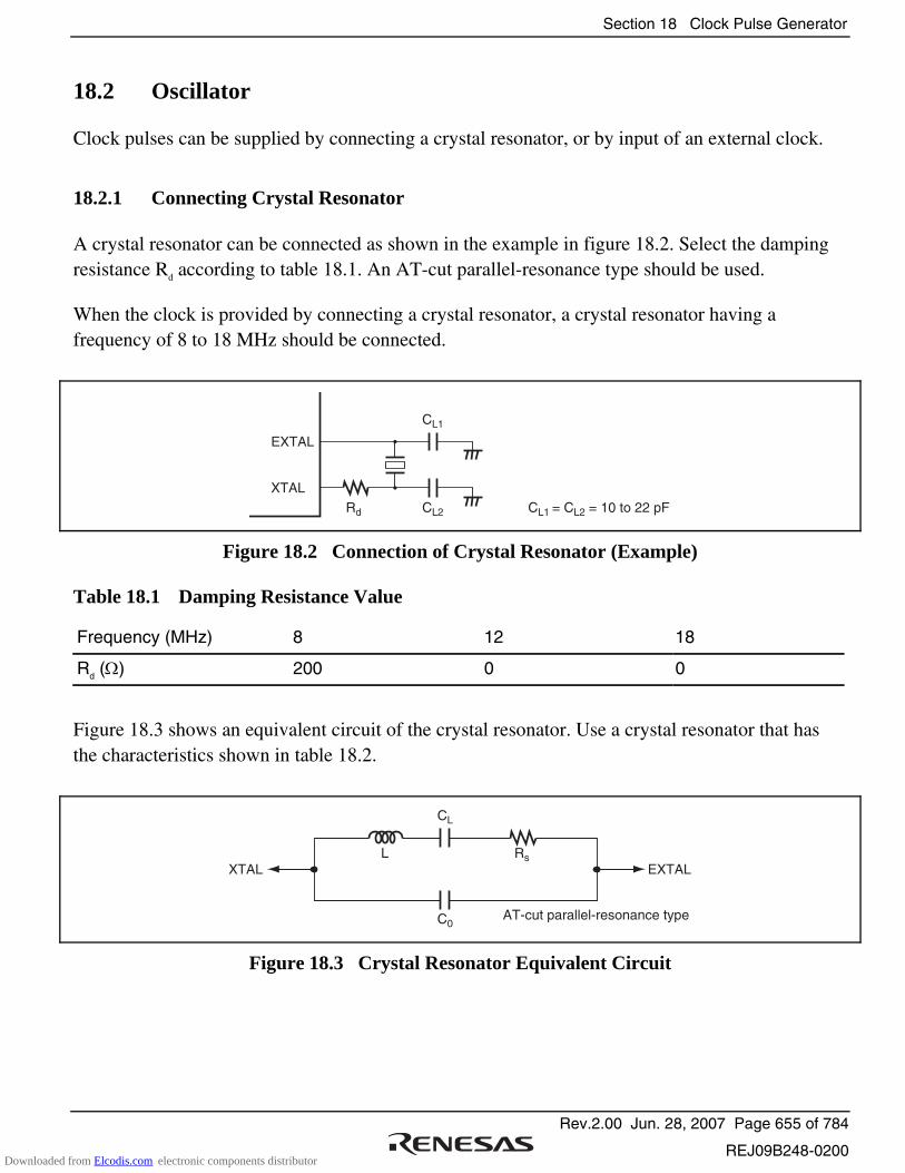
Section 18 Clock Pulse Generator
Rev.2.00 Jun. 28, 2007 Page 655 of 784
REJ09B248-0200
18.2 Oscillator
Clock pulses can be supplied by connecting a crystal resonator, or by input of an external clock.
18.2.1 Connecting Crystal Resonator
A crystal resonator can be connected as shown in the example in figure 18.2. Select the damping resistance Rd according to table 18.1. An AT-cut parallel-resonance type should be used.
When the clock is provided by connecting a crystal resonator, a crystal resonator having a frequency of 8 to 18 MHz should be connected.
EXTAL
XTALRd CL2
CL1
CL1 = CL2 = 10 to 22 pF
Figure 18.2 Connection of Crystal Resonator (Example)
Table 18.1 Damping Resistance Value
Frequency (MHz) 8 12 18
Rd (Ω) 200 0 0
Figure 18.3 shows an equivalent circuit of the crystal resonator. Use a crystal resonator that has the characteristics shown in table 18.2.
XTAL
CL
AT-cut parallel-resonance type
EXTAL
C0
L Rs
Figure 18.3 Crystal Resonator Equivalent Circuit
Downloaded from Elcodis.com electronic components distributor

Section 18 Clock Pulse Generator
Rev.2.00 Jun. 28, 2007 Page 656 of 784
REJ09B248-0200
Table 18.2 Crystal Resonator Characteristics
Frequency (MHz) 8 12 18
RS Max. (Ω) 80 60 40
C0 Max. (pF) 7
18.2.2 External Clock Input
An external clock signal can be input as shown in the examples in figure 18.4. If the XTAL pin is left open, make sure that parasitic capacitance is no more than 10 pF. When the counter clock is input to the XTAL pin, make sure that the external clock is held high in standby mode.
EXTAL
XTAL
External clock input
Open
(a) XTAL pin left open
EXTAL
XTAL
External clock input
(b) Counter clock input on XTAL pin
Figure 18.4 External Clock Input (Examples)
For the input conditions of the external clock, refer to tables 21.4 and 21.14 in section 21, Electrical Characteristics. The input external clock should be from 8 to 18 MHz.
18.3 PLL Circuit
The PLL circuit has the function of multiplying the frequency of the clock from the oscillator by a factor of 4. The frequency multiplication factor is fixed. The phase difference is controlled so that the timing of the rising edge of the internal clock is the same as that of the EXTAL pin signal.
18.4 Frequency Divider
The frequency divider divides the PLL clock to generate a 1/2, 1/4, or 1/8 clock. After bits ICK2 to ICK0, PCK 2 to PCK0, and BCK2 to BCK0 are modified, this LSI operates at the modified frequency.
Downloaded from Elcodis.com electronic components distributor

Section 18 Clock Pulse Generator
Rev.2.00 Jun. 28, 2007 Page 657 of 784
REJ09B248-0200
18.5 Usage Notes
18.5.1 Notes on Clock Pulse Generator
1. The following points should be noted since the frequency of φ (Iφ: system clock, Pφ: peripheral module clock, Bφ: external bus clock) supplied to each module changes according to the setting of SCKCR.
Select a clock division ratio that is within the operation guaranteed range of clock cycle time tcyc shown in the AC timing of electrical characteristics.
The setting should be within the operation guaranteed range of 8 MHz ≤ Iφ ≤ 50 MHz, 8 MHz ≤ Pφ ≤ 35 MHz, and 8 MHz ≤ Bφ ≤ 50 MHz.
2. All the on-chip peripheral modules (except for the DTC) operate on the Pφ. Therefore, note that the time processing of modules such as a timer and SCI differs before and after changing the clock division ratio.
In addition, wait time for clearing software standby mode differs by changing the clock division ratio. For details, see section 19.5.3, Setting Oscillation Settling Time after Clearing Software Standby Mode.
3. The relationship among the system clock, peripheral module clock, and external bus clock is Iφ ≥ Pφ and Iφ ≥ Bφ. In addition, the system clock setting has the highest priority. Accordingly, Pφ or Bφ may have the frequency set by bits ICK2 to ICK0 regardless of the settings of bits PCK2 to PCK0 or BCK2 to BCK0.
4. Figure 18.5 shows the clock modification timing. After a value is written to SCKCR, this LSI waits for the current bus cycle to complete. After the current bus cycle completes, each clock frequency will be modified within one cycle (worst case) of the external input clock.
Downloaded from Elcodis.com electronic components distributor
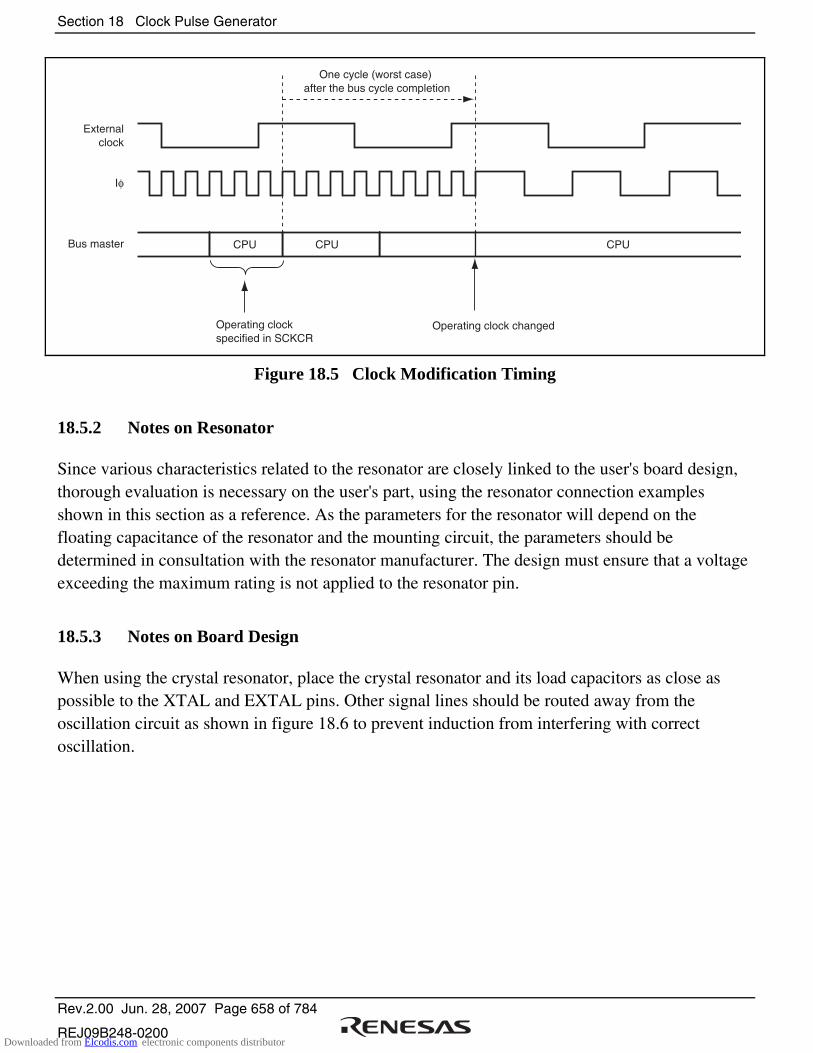
Section 18 Clock Pulse Generator
Rev.2.00 Jun. 28, 2007 Page 658 of 784
REJ09B248-0200
Externalclock
One cycle (worst case) after the bus cycle completion
Operating clockspecified in SCKCR
Operating clock changed
Iφ
CPU CPU CPUBus master
Figure 18.5 Clock Modification Timing
18.5.2 Notes on Resonator
Since various characteristics related to the resonator are closely linked to the user's board design, thorough evaluation is necessary on the user's part, using the resonator connection examples shown in this section as a reference. As the parameters for the resonator will depend on the floating capacitance of the resonator and the mounting circuit, the parameters should be determined in consultation with the resonator manufacturer. The design must ensure that a voltage exceeding the maximum rating is not applied to the resonator pin.
18.5.3 Notes on Board Design
When using the crystal resonator, place the crystal resonator and its load capacitors as close as possible to the XTAL and EXTAL pins. Other signal lines should be routed away from the oscillation circuit as shown in figure 18.6 to prevent induction from interfering with correct oscillation.
Downloaded from Elcodis.com electronic components distributor

Section 18 Clock Pulse Generator
Rev.2.00 Jun. 28, 2007 Page 659 of 784
REJ09B248-0200
CL2
Signal A Signal B
CL1
This LSI
XTAL
EXTAL
Inhibited
Figure 18.6 Note on Board Design for Oscillation Circuit
Figure 18.7 shows the external circuitry recommended for the PLL circuit. Separate PLLVcc and PLLVss from the other Vcc and Vss lines at the board power supply source, and be sure to insert bypass capacitors CPB and CB close to the pins.
PLLVCC
PLLVSS
VCC
VSS
Rp: 100 Ω
CPB: 0.1 µF*
CB: 0.1 µF*
Note: * CB and CPB are laminated ceramic capacitors.
Figure 18.7 Recommended External Circuitry for PLL Circuit
Downloaded from Elcodis.com electronic components distributor
Section 18 Clock Pulse Generator
Rev.2.00 Jun. 28, 2007 Page 660 of 784
REJ09B248-0200
Downloaded from Elcodis.com electronic components distributor
Section 19 Power-Down Modes
Rev.2.00 Jun. 28, 2007 Page 661 of 784
REJ09B248-0200
Section 19 Power-Down Modes
This LSI has power consumption reduction functions, such as multi-clock function, module stop function, and transition function to power-down mode.
19.1 Features
• Multi-clock function
The frequency division ratio is settable independently for the system clock, peripheral module clock, and external bus clock.
• Module stop function
The functions for each peripheral module can be stopped to make a transition to a power-down mode.
• Transition function to power-down mode
Transition to a power-down mode is possible to stop the CPU, peripheral modules, and oscillator.
• Four power-down modes
Sleep mode
All-module-clock-stop mode
Software standby mode
Hardware standby mode
Downloaded from Elcodis.com electronic components distributor
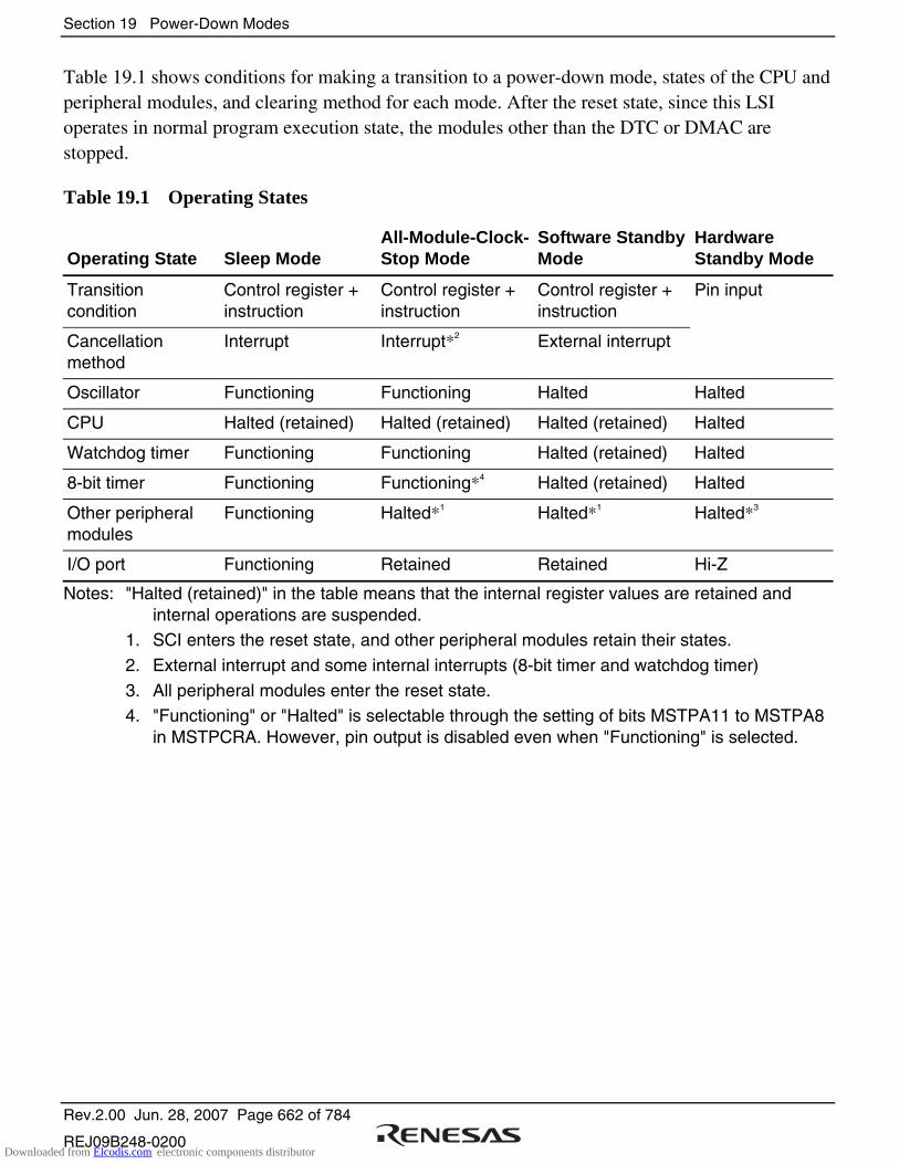
Section 19 Power-Down Modes
Rev.2.00 Jun. 28, 2007 Page 662 of 784
REJ09B248-0200
Table 19.1 shows conditions for making a transition to a power-down mode, states of the CPU and peripheral modules, and clearing method for each mode. After the reset state, since this LSI operates in normal program execution state, the modules other than the DTC or DMAC are stopped.
Table 19.1 Operating States
Operating State Sleep Mode All-Module-Clock-Stop Mode
Software Standby Mode
Hardware Standby Mode
Transition condition
Control register + instruction
Control register + instruction
Control register + instruction
Pin input
Cancellation method
Interrupt Interrupt*2 External interrupt
Oscillator Functioning Functioning Halted Halted
CPU Halted (retained) Halted (retained) Halted (retained) Halted
Watchdog timer Functioning Functioning Halted (retained) Halted
8-bit timer Functioning Functioning*4 Halted (retained) Halted
Other peripheral modules
Functioning Halted*1 Halted*1 Halted*3
I/O port Functioning Retained Retained Hi-Z
Notes: "Halted (retained)" in the table means that the internal register values are retained and internal operations are suspended.
1. SCI enters the reset state, and other peripheral modules retain their states.
2. External interrupt and some internal interrupts (8-bit timer and watchdog timer)
3. All peripheral modules enter the reset state. 4. "Functioning" or "Halted" is selectable through the setting of bits MSTPA11 to MSTPA8
in MSTPCRA. However, pin output is disabled even when "Functioning" is selected.
Downloaded from Elcodis.com electronic components distributor

Section 19 Power-Down Modes
Rev.2.00 Jun. 28, 2007 Page 663 of 784
REJ09B248-0200
SLEEP instruction
SLEEP instruction
All interrupts
SLEEP instruction
External interrupt*2
Interrupt*1
RES pin = low
STBY pin = high
STBY pin = low
SSBY = 0
SSBY = 0, ACSE = 1 MSTPCR = H'F[0-F]FFFFFF
SSBY = 1
RES pin = high
Transition after exception handling
Reset state
Program execution state
Program halted state
Hardware standby mode
Sleep mode
Notes: From any state, a transition to hardware standby mode occurs when STBY is driven low. From any state except for hardware standby mode, a transition to the reset state occurs when RES is driven low. 1. NMI, IRQ0 to IRQ11, 8-bit timer interrupts, and watchdog timer interrupts. The 8-bit timer is valid when bits MSTPCRA11 to MSTPCRA8 are all cleared to 0. 2. NMI and IRQ0 to IRQ11. Note that IRQ is valid only when the corresponding bit in SSIER is set to 1.
All-module-clock-stop mode
Software standby mode
Figure 19.1 Mode Transitions
19.2 Register Descriptions
The registers related to the power-down modes are shown below. For details on the system clock control register (SCKCR), see section 18.1.1, System Clock Control Register (SCKCR).
• Standby control register (SBYCR)
• Module stop control register A (MSTPCRA)
• Module stop control register B (MSTPCRB)
• Module stop control register C (MSTPCRC)
Downloaded from Elcodis.com electronic components distributor
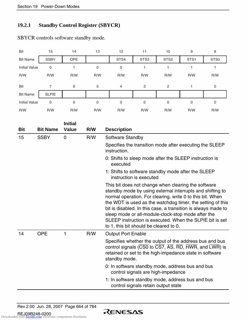
Section 19 Power-Down Modes
Rev.2.00 Jun. 28, 2007 Page 664 of 784
REJ09B248-0200
19.2.1 Standby Control Register (SBYCR)
SBYCR controls software standby mode.
Bit
Bit Name
Initial Value
R/W
15
SSBY
0
R/W
14
OPE
1
R/W
13
0
R/W
12
STS4
0
R/W
11
STS3
1
R/W
10
STS2
1
R/W
9
STS1
1
R/W
8
STS0
1
R/W
Bit
Bit Name
Initial Value
R/W
7
SLPIE
0
R/W
6
0
R/W
5
0
R/W
4
0
R/W
3
0
R/W
2
0
R/W
1
0
R/W
0
0
R/W
Bit Bit Name Initial Value R/W Description
15 SSBY 0 R/W Software Standby
Specifies the transition mode after executing the SLEEP instruction.
0: Shifts to sleep mode after the SLEEP instruction is executed
1: Shifts to software standby mode after the SLEEP instruction is executed
This bit does not change when clearing the software standby mode by using external interrupts and shifting to normal operation. For clearing, write 0 to this bit. When the WDT is used as the watchdog timer, the setting of this bit is disabled. In this case, a transition is always made to sleep mode or all-module-clock-stop mode after the SLEEP instruction is executed. When the SLPIE bit is set to 1, this bit should be cleared to 0.
14 OPE 1 R/W Output Port Enable
Specifies whether the output of the address bus and bus control signals (CS0 to CS7, AS, RD, HWR, and LWR) is retained or set to the high-impedance state in software standby mode.
0: In software standby mode, address bus and bus control signals are high-impedance
1: In software standby mode, address bus and bus control signals retain output state
Downloaded from Elcodis.com electronic components distributor
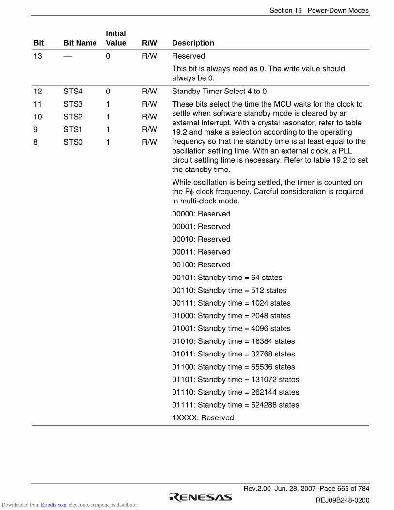
Section 19 Power-Down Modes
Rev.2.00 Jun. 28, 2007 Page 665 of 784
REJ09B248-0200
Bit Bit Name Initial Value R/W Description
13 0 R/W Reserved
This bit is always read as 0. The write value should always be 0.
12
11
10
9
8
STS4
STS3
STS2
STS1
STS0
0
1
1
1
1
R/W
R/W
R/W
R/W
R/W
Standby Timer Select 4 to 0
These bits select the time the MCU waits for the clock to settle when software standby mode is cleared by an external interrupt. With a crystal resonator, refer to table 19.2 and make a selection according to the operating frequency so that the standby time is at least equal to the oscillation settling time. With an external clock, a PLL circuit settling time is necessary. Refer to table 19.2 to set the standby time.
While oscillation is being settled, the timer is counted on the Pφ clock frequency. Careful consideration is required in multi-clock mode.
00000: Reserved
00001: Reserved
00010: Reserved
00011: Reserved
00100: Reserved
00101: Standby time = 64 states
00110: Standby time = 512 states
00111: Standby time = 1024 states
01000: Standby time = 2048 states
01001: Standby time = 4096 states
01010: Standby time = 16384 states
01011: Standby time = 32768 states
01100: Standby time = 65536 states
01101: Standby time = 131072 states
01110: Standby time = 262144 states
01111: Standby time = 524288 states
1XXXX: Reserved
Downloaded from Elcodis.com electronic components distributor
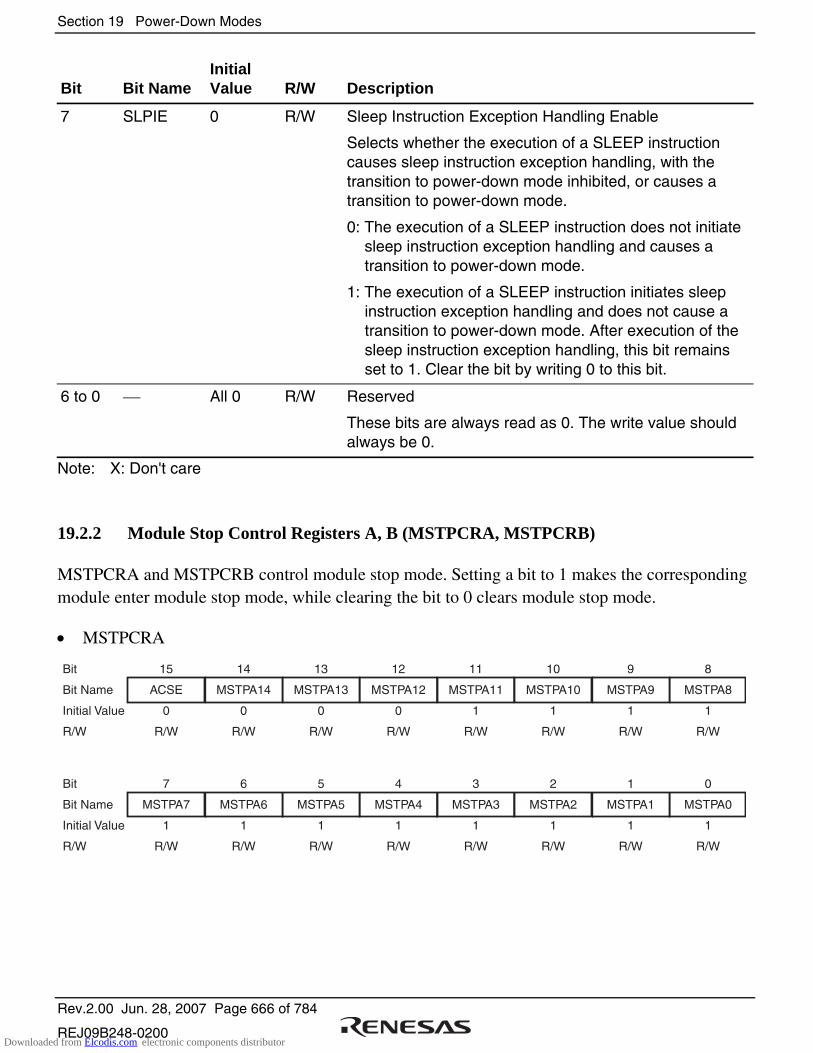
Section 19 Power-Down Modes
Rev.2.00 Jun. 28, 2007 Page 666 of 784
REJ09B248-0200
Bit Bit Name Initial Value R/W Description
7 SLPIE 0 R/W Sleep Instruction Exception Handling Enable
Selects whether the execution of a SLEEP instruction causes sleep instruction exception handling, with the transition to power-down mode inhibited, or causes a transition to power-down mode.
0: The execution of a SLEEP instruction does not initiate sleep instruction exception handling and causes a transition to power-down mode.
1: The execution of a SLEEP instruction initiates sleep instruction exception handling and does not cause a transition to power-down mode. After execution of the sleep instruction exception handling, this bit remains set to 1. Clear the bit by writing 0 to this bit.
6 to 0 All 0 R/W Reserved
These bits are always read as 0. The write value should always be 0.
Note: X: Don't care
19.2.2 Module Stop Control Registers A, B (MSTPCRA, MSTPCRB)
MSTPCRA and MSTPCRB control module stop mode. Setting a bit to 1 makes the corresponding module enter module stop mode, while clearing the bit to 0 clears module stop mode.
• MSTPCRA
Bit
Bit Name
Initial Value
R/W
15
ACSE
0
R/W
14
MSTPA14
0
R/W
13
MSTPA13
0
R/W
12
MSTPA12
0
R/W
11
MSTPA11
1
R/W
10
MSTPA10
1
R/W
9
MSTPA9
1
R/W
8
MSTPA8
1
R/W
Bit
Bit Name
Initial Value
R/W
7
MSTPA7
1
R/W
6
MSTPA6
1
R/W
5
MSTPA5
1
R/W
4
MSTPA4
1
R/W
3
MSTPA3
1
R/W
2
MSTPA2
1
R/W
1
MSTPA1
1
R/W
0
MSTPA0
1
R/W
Downloaded from Elcodis.com electronic components distributor
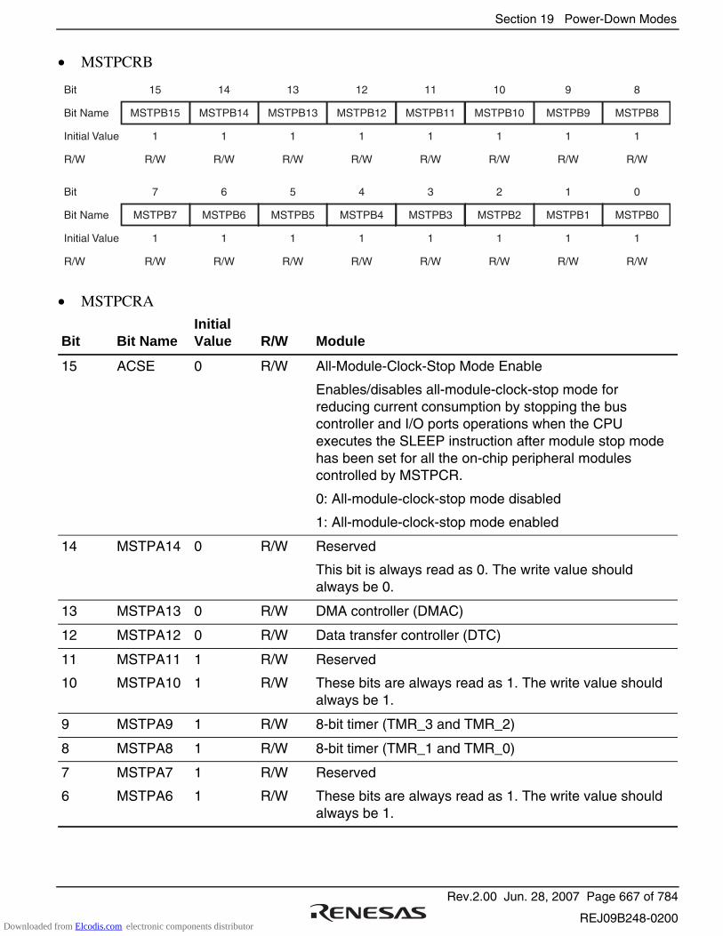
Section 19 Power-Down Modes
Rev.2.00 Jun. 28, 2007 Page 667 of 784
REJ09B248-0200
• MSTPCRB
Bit
Bit Name
Initial Value
R/W
15
MSTPB15
1
R/W
14
MSTPB14
1
R/W
13
MSTPB13
1
R/W
12
MSTPB12
1
R/W
11
MSTPB11
1
R/W
10
MSTPB10
1
R/W
9
MSTPB9
1
R/W
8
MSTPB8
1
R/W
Bit
Bit Name
Initial Value
R/W
7
MSTPB7
1
R/W
6
MSTPB6
1
R/W
5
MSTPB5
1
R/W
4
MSTPB4
1
R/W
3
MSTPB3
1
R/W
2
MSTPB2
1
R/W
1
MSTPB1
1
R/W
0
MSTPB0
1
R/W
• MSTPCRA
Bit Bit Name Initial Value R/W Module
15 ACSE 0 R/W All-Module-Clock-Stop Mode Enable
Enables/disables all-module-clock-stop mode for reducing current consumption by stopping the bus controller and I/O ports operations when the CPU executes the SLEEP instruction after module stop mode has been set for all the on-chip peripheral modules controlled by MSTPCR.
0: All-module-clock-stop mode disabled
1: All-module-clock-stop mode enabled
14 MSTPA14 0 R/W Reserved
This bit is always read as 0. The write value should always be 0.
13 MSTPA13 0 R/W DMA controller (DMAC)
12 MSTPA12 0 R/W Data transfer controller (DTC)
11
10
MSTPA11
MSTPA10
1
1
R/W
R/W
Reserved
These bits are always read as 1. The write value should always be 1.
9 MSTPA9 1 R/W 8-bit timer (TMR_3 and TMR_2)
8 MSTPA8 1 R/W 8-bit timer (TMR_1 and TMR_0)
7
6
MSTPA7
MSTPA6
1
1
R/W
R/W
Reserved
These bits are always read as 1. The write value should always be 1.
Downloaded from Elcodis.com electronic components distributor

Section 19 Power-Down Modes
Rev.2.00 Jun. 28, 2007 Page 668 of 784
REJ09B248-0200
Bit Bit Name Initial Value R/W Module
5 MSTPA5 1 R/W D/A converter (channels 1 and 0)
4 MSTPA4 1 R/W Reserved
This bit is always read as 1. The write value should always be 1.
3 MSTPA3 1 R/W A/D converter (unit 0)
2
1
MSTPA2
MSTPA1
1
1
R/W
R/W
Reserved
These bits are always read as 1. The write value should always be 1.
0 MSTPA0 1 R/W 16-bit timer pulse unit (TPU channels 5 to 0)
• MSTPCRB
Bit Bit Name Initial Value R/W Module
15 MSTPB15 1 R/W Programmable pulse generator (PPG)
14
13
MSTPB14
MSTPB13
1
1
R/W
R/W
Reserved
These bits are always read as 1. The write value should always be 1.
12 MSTPB12 1 R/W Serial communication interface_4 (SCI_4)
11 MSTPB11 1 R/W Serial communication interface_3 (SCI_3)
10 MSTPB10 1 R/W Serial communication interface_2 (SCI_2)
9 MSTPB9 1 R/W Serial communication interface_1 (SCI_1)
8 MSTPB8 1 R/W Serial communication interface_0 (SCI_0)
7
6
5
4
3
2
1
0
MSTPB7
MSTPB6
MSTPB5
MSTPB4
MSTPB3
MSTPB2
MSTPB1
MSTPB0
1
1
1
1
1
1
1
1
R/W
R/W
R/W
R/W
R/W
R/W
R/W
R/W
Reserved
These bits are always read as 1. The write value should always be 1.
Downloaded from Elcodis.com electronic components distributor

Section 19 Power-Down Modes
Rev.2.00 Jun. 28, 2007 Page 669 of 784
REJ09B248-0200
19.2.3 Module Stop Control Register C (MSTPCRC)
When bits MSTPC4 to MSTPC0 are set to 1, the corresponding on-chip RAM stops. Do not set the corresponding MSTPC4 to MSTPC0 bits to 1 while accessing on-chip RAM.
Bit
Bit Name
Initial Value
R/W
15
MSTPC15
1
R/W
14
MSTPC14
1
R/W
13
MSTPC13
1
R/W
12
MSTPC12
1
R/W
11
MSTPC11
1
R/W
10
MSTPC10
1
R/W
9
MSTPC9
1
R/W
8
MSTPC8
1
R/W
Bit
Bit Name
Initial Value
R/W
7
MSTPC7
0
R/W
6
MSTPC6
0
R/W
5
MSTPC5
0
R/W
4
MSTPC4
0
R/W
3
MSTPC3
0
R/W
2
MSTPC2
0
R/W
1
MSTPC1
0
R/W
0
MSTPC0
0
R/W
Bit Bit Name Initial Value R/W Module
15
14
13
12
11
10
9
8
MSTPC15
MSTPC14
MSTPC13
MSTPC12
MSTPC11
MSTPC10
MSTPC9
MSTPC8
1
1
1
1
1
1
1
1
R/W
R/W
R/W
R/W
R/W
R/W
R/W
R/W
Reserved
These bits are always read as 1. The write value should always be 1.
7
6
5
MSTPC7
MSTPC6
MSTPC5
0
0
0
R/W
R/W
R/W
Reserved
These bits are always read as 0. The write value should always be 0.
4 MSTPC4 0 R/W On-chip RAM_4 (H'FFF2000 to H'FFF3FFF)
3 MSTPC3 0 R/W On-chip RAM_3 (H'FFF4000 to H'FFF5FFF)
2 MSTPC2 0 R/W On-chip RAM_2 (H'FFF6000 to H'FFF7FFF)
1 MSTPC1 0 R/W On-chip RAM_1 (H'FFF8000 to H'FFF9FFF)
0 MSTPC0 0 R/W On-chip RAM_0 (H'FFFA000 to H'FFFBFFF)
Downloaded from Elcodis.com electronic components distributor

Section 19 Power-Down Modes
Rev.2.00 Jun. 28, 2007 Page 670 of 784
REJ09B248-0200
19.3 Multi-Clock Function
When bits ICK2 to ICK0, PCK2 to PCK0, and BCK2 to BCK0 in SCKCR are set, a transition is made to multi-clock mode at the end of the bus cycle. In multi-clock mode, the CPU and bus masters operate on the operating clock specified by bits ICK2 to ICK0. The peripheral modules operate on the operating clock specified by bits PCK2 to PCK0. The external bus operates on the operating clock specified by bits BCK2 to BCK0.
Even if the frequencies specified by bits PCK2 to PCK0 and BCK2 to BCK0 are higher than the frequency specified by bits ICK2 to ICK0, the specified values are not reflected in the peripheral module and external bus clocks. The peripheral module and external bus clocks are restricted to the operating clock specified by bits ICK2 to ICK0.
Multi-clock mode is cleared by clearing all of bits ICK2 to ICK0, PCK2 to PCK0, and BCK2 to BCK0 to 0. A transition is made to normal mode at the end of the bus cycle, and multi-clock mode is cleared.
If a SLEEP instruction is executed while the SSBY bit in SBYCR is cleared to 0, this LSI enters sleep mode. When sleep mode is cleared by an interrupt, multi-clock mode is restored.
If a SLEEP instruction is executed while the SSBY bit in SBYCR is set to 1, this LSI enters software standby mode. When software standby mode is cleared by an external interrupt, multi-clock mode is restored.
When the RES pin is driven low, the reset state is entered and multi-clock mode is cleared. The same applies to a reset caused by watchdog timer overflow.
When the STBY pin is driven low, a transition is made to hardware standby mode.
Downloaded from Elcodis.com electronic components distributor

Section 19 Power-Down Modes
Rev.2.00 Jun. 28, 2007 Page 671 of 784
REJ09B248-0200
19.4 Sleep Mode
19.4.1 Transition to Sleep Mode
When the SLEEP instruction is executed when the SSBY bit in SBYCR is 0, the CPU enters sleep mode. In sleep mode, CPU operation stops but the contents of the CPU's internal registers are retained. Other peripheral functions do not stop.
19.4.2 Clearing Sleep Mode
Sleep mode is exited by any interrupt, signals on the RES or STBY pin, and a reset caused by a watchdog timer overflow.
1. Clearing by interrupt
When an interrupt occurs, sleep mode is exited and interrupt exception processing starts. Sleep mode is not exited if the interrupt is disabled, or interrupts other than NMI are masked by the CPU.
2. Clearing by RES pin
Setting the RES pin level low selects the reset state. After the stipulated reset input duration, driving the RES pin high makes the CPU start the reset exception processing.
3. Clearing by STBY pin
When the STBY pin level is driven low, a transition is made to hardware standby mode.
4. Clearing by reset caused by watchdog timer overflow
Sleep mode is exited by an internal reset caused by a watchdog timer overflow.
Downloaded from Elcodis.com electronic components distributor

Section 19 Power-Down Modes
Rev.2.00 Jun. 28, 2007 Page 672 of 784
REJ09B248-0200
19.5 Software Standby Mode
19.5.1 Transition to Software Standby Mode
If a SLEEP instruction is executed when the SSBY bit in SBYCR is set to 1, software standby mode is entered. In this mode, the CPU, on-chip peripheral functions, and oscillator all stop. However, the contents of the CPU's internal registers, on-chip RAM data, and the states of on-chip peripheral functions other than the SCI, and the states of the I/O ports, are retained. Whether the address bus and bus control signals are placed in the high-impedance state or retain the output state can be specified by the OPE bit in SBYCR. In this mode the oscillator stops, allowing power consumption to be significantly reduced.
If the WDT is used as a watchdog timer, it is impossible to make a transition to software standby mode. The WDT should be stopped before the SLEEP instruction execution.
19.5.2 Clearing Software Standby Mode
Software standby mode is cleared by an external interrupt (NMI pin, or pins IRQ0 to IRQ11*), or by means of the RES pin or STBY pin.
1. Clearing by interrupt
When an NMI or IRQ0 to IRQ11* interrupt request signal is input, clock oscillation starts, and after the elapse of the time set in bits STS4 to STS0 in SBYCR, stable clocks are supplied to the entire LSI, software standby mode is cleared, and interrupt exception handling is started.
When clearing software standby mode with an IRQ0 to IRQ11* interrupt, set the corresponding enable bit to 1 and ensure that no interrupt with a higher priority than interrupts IRQ0 to IRQ11* is generated. Software standby mode cannot be cleared if the interrupt has been masked on the CPU side or has been designated as a DTC activation source.
Note: * By setting the SSIn bit in SSIER to 1, IRQ0 to IRQ11 can be used as a software standby mode clearing source.
2. Clearing by RES pin
When the RES pin is driven low, clock oscillation is started. At the same time as clock oscillation starts, clocks are supplied to the entire LSI. Note that the RES pin must be held low until clock oscillation settles. When the RES pin goes high, the CPU begins reset exception handling.
3. Clearing by STBY pin
When the STBY pin is driven low, a transition is made to hardware standby mode.
Downloaded from Elcodis.com electronic components distributor
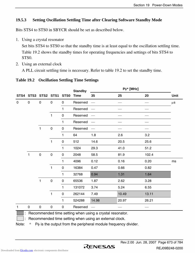
Section 19 Power-Down Modes
Rev.2.00 Jun. 28, 2007 Page 673 of 784
REJ09B248-0200
19.5.3 Setting Oscillation Settling Time after Clearing Software Standby Mode
Bits STS4 to STS0 in SBYCR should be set as described below.
1. Using a crystal resonator
Set bits STS4 to STS0 so that the standby time is at least equal to the oscillation settling time.
Table 19.2 shows the standby times for operating frequencies and settings of bits STS4 to STS0.
2. Using an external clock
A PLL circuit settling time is necessary. Refer to table 19.2 to set the standby time. Table 19.2 Oscillation Settling Time Settings
Pφ* [MHz]
STS4 STS3 STS2 STS1 STS0 Standby Time 35 25 20 Unit
0 0 0 0 0 Reserved µs
1 Reserved
1 0 Reserved
1 Reserved
1 0 0 Reserved
1 64 1.8 2.6 3.2
1 0 512 14.6 20.5 25.6
1 1024 29.3 41.0 51.2
1 0 0 0 2048 58.5 81.9 102.4
1 4096 0.12 0.16 0.20 ms
1 0 16384 0.47 0.66 0.82
1 32768 0.94 1.31 1.64
1 0 0 65536 1.87 2.62 3.28
1 131072 3.74 5.24 6.55
1 0 262144 7.49 10.49 13.11
1 524288 14.98 20.97 26.21
1 0 0 0 0 Reserved
: Recommended time setting when using a crystal resonator.
: Recommended time setting when using an external clock.
Note: * Pφ is the output from the peripheral module frequency divider.
Downloaded from Elcodis.com electronic components distributor
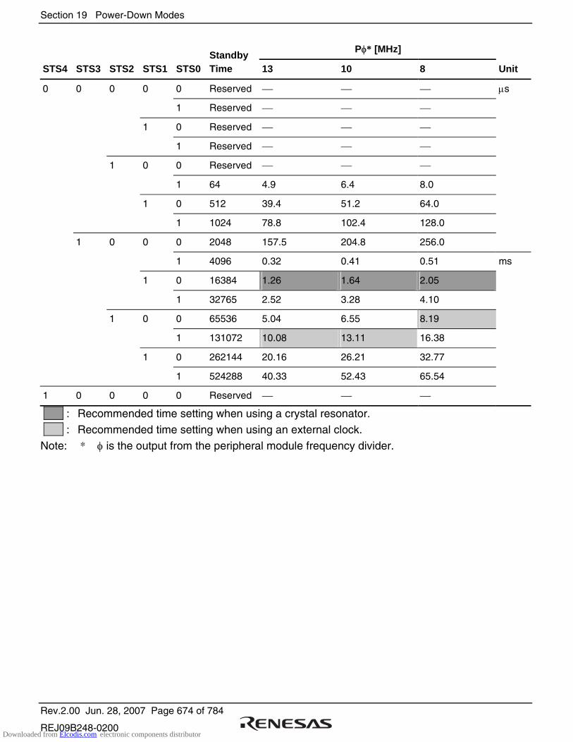
Section 19 Power-Down Modes
Rev.2.00 Jun. 28, 2007 Page 674 of 784
REJ09B248-0200
Pφ* [MHz]
STS4 STS3 STS2 STS1 STS0 Standby Time 13 10 8 Unit
0 0 0 0 0 Reserved µs
1 Reserved
1 0 Reserved
1 Reserved
1 0 0 Reserved
1 64 4.9 6.4 8.0
1 0 512 39.4 51.2 64.0
1 1024 78.8 102.4 128.0
1 0 0 0 2048 157.5 204.8 256.0
1 4096 0.32 0.41 0.51 ms
1 0 16384 1.26 1.64 2.05
1 32765 2.52 3.28 4.10
1 0 0 65536 5.04 6.55 8.19
1 131072 10.08 13.11 16.38
1 0 262144 20.16 26.21 32.77
1 524288 40.33 52.43 65.54
1 0 0 0 0 Reserved
: Recommended time setting when using a crystal resonator.
: Recommended time setting when using an external clock.
Note: * φ is the output from the peripheral module frequency divider.
Downloaded from Elcodis.com electronic components distributor
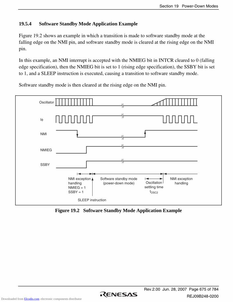
Section 19 Power-Down Modes
Rev.2.00 Jun. 28, 2007 Page 675 of 784
REJ09B248-0200
19.5.4 Software Standby Mode Application Example
Figure 19.2 shows an example in which a transition is made to software standby mode at the falling edge on the NMI pin, and software standby mode is cleared at the rising edge on the NMI pin.
In this example, an NMI interrupt is accepted with the NMIEG bit in INTCR cleared to 0 (falling edge specification), then the NMIEG bit is set to 1 (rising edge specification), the SSBY bit is set to 1, and a SLEEP instruction is executed, causing a transition to software standby mode.
Software standby mode is then cleared at the rising edge on the NMI pin.
Oscillator
Iφ
NMI
NMIEG
SSBY
NMI exceptionhandlingNMIEG = 1SSBY = 1
SLEEP instruction
Software standby mode(power-down mode) Oscillation
settling timetOSC2
NMI exceptionhandling
Figure 19.2 Software Standby Mode Application Example
Downloaded from Elcodis.com electronic components distributor

Section 19 Power-Down Modes
Rev.2.00 Jun. 28, 2007 Page 676 of 784
REJ09B248-0200
19.6 Hardware Standby Mode
19.6.1 Transition to Hardware Standby Mode
When the STBY pin is driven low, a transition is made to hardware standby mode from any mode.
In hardware standby mode, all functions enter the reset state and stop operation, resulting in a significant reduction in power consumption. As long as the prescribed voltage is supplied, on-chip RAM data is retained. I/O ports are set to the high-impedance state.
In order to retain on-chip RAM data, the RAME bit in SYSCR should be cleared to 0 before driving the STBY pin low. Do not change the state of the mode pins (MD2 to MD0) while this LSI is in hardware standby mode.
19.6.2 Clearing Hardware Standby Mode
Hardware standby mode is cleared by means of the STBY pin and the RES pin. When the STBY pin is driven high while the RES pin is low, the reset state is entered and clock oscillation is started. Ensure that the RES pin is held low until clock oscillation settles (for details on the oscillation settling time, refer to table 19.2). When the RES pin is subsequently driven high, a transition is made to the program execution state via the reset exception handling state.
19.6.3 Hardware Standby Mode Timing
Figure 19.3 shows an example of hardware standby mode timing.
When the STBY pin is driven low after the RES pin has been driven low, a transition is made to hardware standby mode. Hardware standby mode is cleared by driving the STBY pin high, waiting for the oscillation settling time, then changing the RES pin from low to high.
Oscillator
RES
STBY
Oscillationsettling time
Reset exception handling
Figure 19.3 Hardware Standby Mode Timing
Downloaded from Elcodis.com electronic components distributor
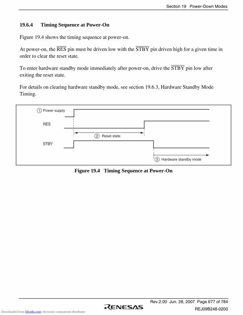
Section 19 Power-Down Modes
Rev.2.00 Jun. 28, 2007 Page 677 of 784
REJ09B248-0200
19.6.4 Timing Sequence at Power-On
Figure 19.4 shows the timing sequence at power-on.
At power-on, the RES pin must be driven low with the STBY pin driven high for a given time in order to clear the reset state.
To enter hardware standby mode immediately after power-on, drive the STBY pin low after exiting the reset state.
For details on clearing hardware standby mode, see section 19.6.3, Hardware Standby Mode Timing.
Power supply
RES
STBY
Reset state
Hardware standby mode
1
2
3
Figure 19.4 Timing Sequence at Power-On
Downloaded from Elcodis.com electronic components distributor
Section 19 Power-Down Modes
Rev.2.00 Jun. 28, 2007 Page 678 of 784
REJ09B248-0200
19.7 Module Stop Mode
19.7.1 Module Stop Mode
Module stop mode can be set for individual on-chip peripheral modules.
When the corresponding MSTP bit in MSTPCRA, MSTPCRB, or MSTPCRC is set to 1, module operation stops at the end of the bus cycle and a transition is made to module stop mode. The CPU continues operating independently.
When the corresponding MSTP bit is cleared to 0, module stop mode is cleared and the module starts operating at the end of the bus cycle. In module stop mode, the internal states of modules other than the SCI are retained.
After the reset state is cleared, all modules other than the DTC, DMAC, or on-chip RAM are in module stop mode.
The registers of the module for which module stop mode is selected cannot be read from or written to.
19.7.2 All-Module-Clock-Stop Mode
When the ACSE bit is set to 1 and all modules controlled by MSTPCR are stopped (MSTPCRA, MSTPCRB = H'FFFFFFFF), or all modules except for the 8-bit timer are stopped (MSTPCRA, MSTPCRB = H'F[0 to F]FFFFFF), executing a SLEEP instruction with the SSBY bit in SBYCR cleared to 0 will cause all modules (except for the 8-bit timer* and watchdog timer), the bus controller, and the I/O ports to stop operating, and to make a transition to all-module-clock-stop mode at the end of the bus cycle.
All-module-clock-stop mode is cleared by an external interrupt (NMI or IRQ0 to IRQ11 pins), RES pin input, or an internal interrupt (8-bit timer* or watchdog timer), and the CPU returns to the normal program execution state via the exception handling state. All-module-clock-stop mode is not cleared if interrupts are disabled, if interrupts other than NMI are masked on the CPU side, or if the relevant interrupt is designated as a DTC activation source.
When the STBY pin is driven low, a transition is made to hardware standby mode.
Note: * Operation or halting of the 8-bit timer can be selected by bits MSTPA11 to MSTPA8 in MSTPCRA.
Downloaded from Elcodis.com electronic components distributor
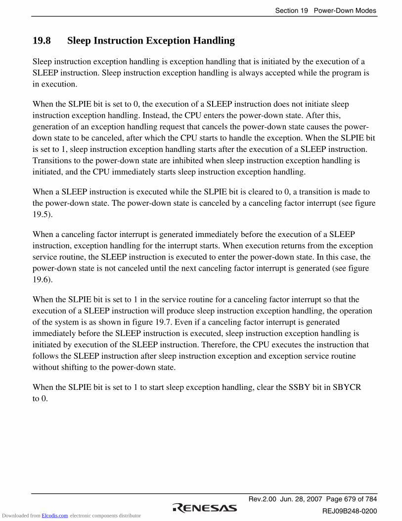
Section 19 Power-Down Modes
Rev.2.00 Jun. 28, 2007 Page 679 of 784
REJ09B248-0200
19.8 Sleep Instruction Exception Handling
Sleep instruction exception handling is exception handling that is initiated by the execution of a SLEEP instruction. Sleep instruction exception handling is always accepted while the program is in execution.
When the SLPIE bit is set to 0, the execution of a SLEEP instruction does not initiate sleep instruction exception handling. Instead, the CPU enters the power-down state. After this, generation of an exception handling request that cancels the power-down state causes the power-down state to be canceled, after which the CPU starts to handle the exception. When the SLPIE bit is set to 1, sleep instruction exception handling starts after the execution of a SLEEP instruction. Transitions to the power-down state are inhibited when sleep instruction exception handling is initiated, and the CPU immediately starts sleep instruction exception handling.
When a SLEEP instruction is executed while the SLPIE bit is cleared to 0, a transition is made to the power-down state. The power-down state is canceled by a canceling factor interrupt (see figure 19.5).
When a canceling factor interrupt is generated immediately before the execution of a SLEEP instruction, exception handling for the interrupt starts. When execution returns from the exception service routine, the SLEEP instruction is executed to enter the power-down state. In this case, the power-down state is not canceled until the next canceling factor interrupt is generated (see figure 19.6).
When the SLPIE bit is set to 1 in the service routine for a canceling factor interrupt so that the execution of a SLEEP instruction will produce sleep instruction exception handling, the operation of the system is as shown in figure 19.7. Even if a canceling factor interrupt is generated immediately before the SLEEP instruction is executed, sleep instruction exception handling is initiated by execution of the SLEEP instruction. Therefore, the CPU executes the instruction that follows the SLEEP instruction after sleep instruction exception and exception service routine without shifting to the power-down state.
When the SLPIE bit is set to 1 to start sleep exception handling, clear the SSBY bit in SBYCR to 0.
Downloaded from Elcodis.com electronic components distributor
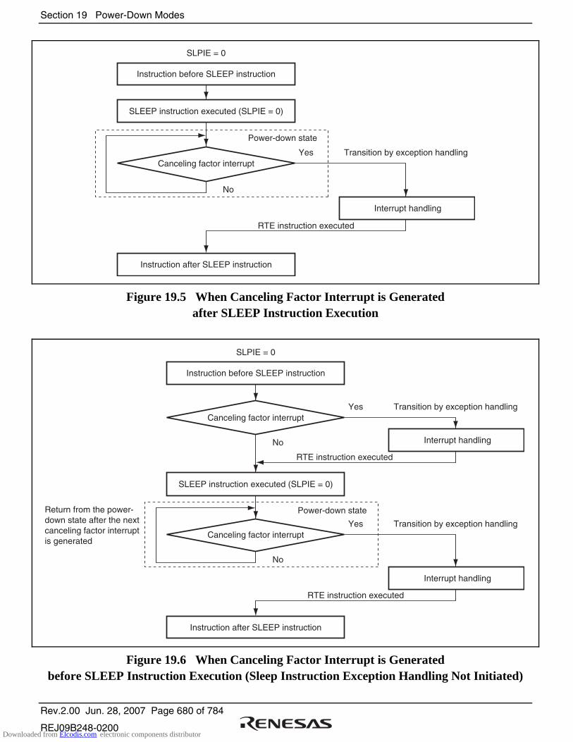
Section 19 Power-Down Modes
Rev.2.00 Jun. 28, 2007 Page 680 of 784
REJ09B248-0200
SLPIE = 0
Power-down state
RTE instruction executed
Transition by exception handling
No
YesCanceling factor interrupt
Instruction before SLEEP instruction
SLEEP instruction executed (SLPIE = 0)
Instruction after SLEEP instruction
Interrupt handling
Figure 19.5 When Canceling Factor Interrupt is Generated after SLEEP Instruction Execution
SLPIE = 0
Power-down state
RTE instruction executed
Return from the power-down state after the next canceling factor interrupt is generated
Transition by exception handling
No
YesCanceling factor interrupt
Instruction before SLEEP instruction
SLEEP instruction executed (SLPIE = 0)
Instruction after SLEEP instruction
Interrupt handling
RTE instruction executed
Transition by exception handling
No
YesCanceling factor interrupt
Interrupt handling
Figure 19.6 When Canceling Factor Interrupt is Generated before SLEEP Instruction Execution (Sleep Instruction Exception Handling Not Initiated)
Downloaded from Elcodis.com electronic components distributor
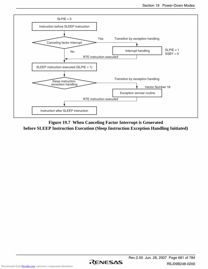
Section 19 Power-Down Modes
Rev.2.00 Jun. 28, 2007 Page 681 of 784
REJ09B248-0200
SLPIE = 0
SLPIE = 1SSBY = 0
RTE instruction executed
Transition by exception handling
Vector Number 18
Sleep instruction exceotion handling
Instruction before SLEEP instruction
SLEEP instruction executed (SLPIE = 1)
Instruction after SLEEP instruction
Exception servise routine
RTE instruction executed
Transition by exception handling
No
YesCanceling factor interrupt
Interrupt handling
Figure 19.7 When Canceling Factor Interrupt is Generated before SLEEP Instruction Execution (Sleep Instruction Exception Handling Initiated)
Downloaded from Elcodis.com electronic components distributor
Section 19 Power-Down Modes
Rev.2.00 Jun. 28, 2007 Page 682 of 784
REJ09B248-0200
19.9 Bφ Clock Output Control
Output of the Bφ clock can be controlled by bits PSTOP1 and POSEL1 in SCKCR, and DDR for the corresponding PA7 pin.
Clearing both bits PSTOP1 and POSEL1 to 0 enables the Bφ clock output on the PA7 pin. When bit PSTOP1 is set to 1, the Bφ clock output stops at the end of the bus cycle, and the Bφ clock output goes high. When DDR for the PA7 pin is cleared to 0, the Bφ clock output is disabled and the pin becomes an input port.
Tables 19.3 shows the states of the Bφ pin in each processing state.
Table 19.3 Bφ Pin (PA7) State in Each Processing State
Register Setting Value Software
Standby Mode
DDR PSTOP1 POSEL1
Normal Operating State
Sleep Mode
All-Module-Clock-Stop Mode OPE = 0 OPE = 1
Hardware Standby Mode
0 X X Hi-Z Hi-Z Hi-Z Hi-Z Hi-Z Hi-Z
1 0 0 Bφ output Bφ output Bφ output High High Hi-Z
1 0 1 Setting prohibited
Setting prohibited
Setting prohibited
Setting prohibited
Setting prohibited
Setting prohibited
1 1 X High High High High High Hi-Z
Downloaded from Elcodis.com electronic components distributor
Section 19 Power-Down Modes
Rev.2.00 Jun. 28, 2007 Page 683 of 784
REJ09B248-0200
19.10 Usage Notes
19.10.1 I/O Port Status
In software standby mode, the I/O port states are retained. Therefore, there is no reduction in current consumption for the output current when a high-level signal is output.
19.10.2 Current Consumption during Oscillation Settling Standby Period
Current consumption increases during the oscillation settling standby period.
19.10.3 Module Stop Mode of DMAC or DTC
Depending on the operating state of the DMAC and DTC, bits MSTPA13 and MSTPA12 may not be set to 1, respectively. The module stop mode setting for the DMAC or DTC should be carried out only when the DMAC or DTC is not activated.
For details, refer to section 7, DMA Controller (DMAC), and section 8, Data Transfer Controller (DTC).
19.10.4 On-Chip Peripheral Module Interrupts
Relevant interrupt operations cannot be performed in module stop mode. Consequently, if module stop mode is entered when an interrupt has been requested, it will not be possible to clear the CPU interrupt source or the DMAC or DTC activation source. Interrupts should therefore be disabled before entering module stop mode.
19.10.5 Writing to MSTPCRA, MSTPCRB, and MSTPCRC
MSTPCRA, MSTPCRB, and MSTPCRC should only be written to by the CPU.
Downloaded from Elcodis.com electronic components distributor
Section 19 Power-Down Modes
Rev.2.00 Jun. 28, 2007 Page 684 of 784
REJ09B248-0200
Downloaded from Elcodis.com electronic components distributor

Section 20 List of Registers
Rev.2.00 Jun. 28, 2007 Page 685 of 784
REJ09B248-0200
Section 20 List of Registers
The register list gives information on the on-chip I/O register addresses, how the register bits are configured, and the register states in each operating mode. The information is given as shown below.
1. Register addresses (address order)
• Registers are listed from the lower allocation addresses.
• Registers are classified according to functional modules.
• The number of Access Cycles indicates the number of states based on the specified reference clock. For details, refer to section 6.5.4, External Bus Interface.
• Among the internal I/O register area, addresses not listed in the list of registers are undefined or reserved addresses. Undefined and reserved addresses cannot be accessed. Do not access these addresses; otherwise, the operation when accessing these bits and subsequent operations cannot be guaranteed.
2. Register bits
• Bit configurations of the registers are listed in the same order as the register addresses.
• Reserved bits are indicated by in the bit name column.
• Space in the bit name field indicates that the entire register is allocated to either the counter or data.
• For the registers of 16 or 32 bits, the MSB is listed first.
Byte configuration description order is subject to big endian.
3. Register states in each operating mode
• Register states are listed in the same order as the register addresses.
• For the initialized state of each bit, refer to the register description in the corresponding section.
• The register states shown here are for the basic operating modes. If there is a specific reset for an on-chip peripheral module, refer to the section on that on-chip peripheral module.
Downloaded from Elcodis.com electronic components distributor
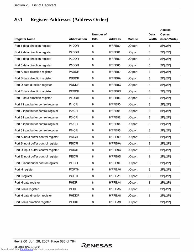
Section 20 List of Registers
Rev.2.00 Jun. 28, 2007 Page 686 of 784
REJ09B248-0200
20.1 Register Addresses (Address Order)
Register Name Abbreviation
Number of
Bits Address Module
Data
Width
Access
Cycles
(Read/Write)
Port 1 data direction register P1DDR 8 H'FFB80 I/O port 8 2Pφ/2Pφ
Port 2 data direction register P2DDR 8 H'FFB81 I/O port 8 2Pφ/2Pφ
Port 3 data direction register P3DDR 8 H'FFB82 I/O port 8 2Pφ/2Pφ
Port 6 data direction register P6DDR 8 H'FFB85 I/O port 8 2Pφ/2Pφ
Port A data direction register PADDR 8 H'FFB89 I/O port 8 2Pφ/2Pφ
Port B data direction register PBDDR 8 H'FFB8A I/O port 8 2Pφ/2Pφ
Port D data direction register PDDDR 8 H'FFB8C I/O port 8 2Pφ/2Pφ
Port E data direction register PEDDR 8 H'FFB8D I/O port 8 2Pφ/2Pφ
Port F data direction register PFDDR 8 H'FFB8E I/O port 8 2Pφ/2Pφ
Port 1 input buffer control register P1ICR 8 H'FFB90 I/O port 8 2Pφ/2Pφ
Port 2 input buffer control register P2ICR 8 H'FFB91 I/O port 8 2Pφ/2Pφ
Port 3 input buffer control register P3ICR 8 H'FFB92 I/O port 8 2Pφ/2Pφ
Port 5 input buffer control register P5ICR 8 H'FFB94 I/O port 8 2Pφ/2Pφ
Port 6 input buffer control register P6ICR 8 H'FFB95 I/O port 8 2Pφ/2Pφ
Port A input buffer control register PAICR 8 H'FFB99 I/O port 8 2Pφ/2Pφ
Port B input buffer control register PBICR 8 H'FFB9A I/O port 8 2Pφ/2Pφ
Port D input buffer control register PDICR 8 H'FFB9C I/O port 8 2Pφ/2Pφ
Port E input buffer control register PEICR 8 H'FFB9D I/O port 8 2Pφ/2Pφ
Port F input buffer control register PFICR 8 H'FFB9E I/O port 8 2Pφ/2Pφ
Port H register PORTH 8 H'FFBA0 I/O port 8 2Pφ/2Pφ
Port I register PORTI 8 H'FFBA1 I/O port 8 2Pφ/2Pφ
Port H data register PHDR 8 H'FFBA4 I/O port 8 2Pφ/2Pφ
Port I data register PIDR 8 H'FFBA5 I/O port 8 2Pφ/2Pφ
Port H data direction register PHDDR 8 H'FFBA8 I/O port 8 2Pφ/2Pφ
Port I data direction register PIDDR 8 H'FFBA9 I/O port 8 2Pφ/2Pφ
Downloaded from Elcodis.com electronic components distributor
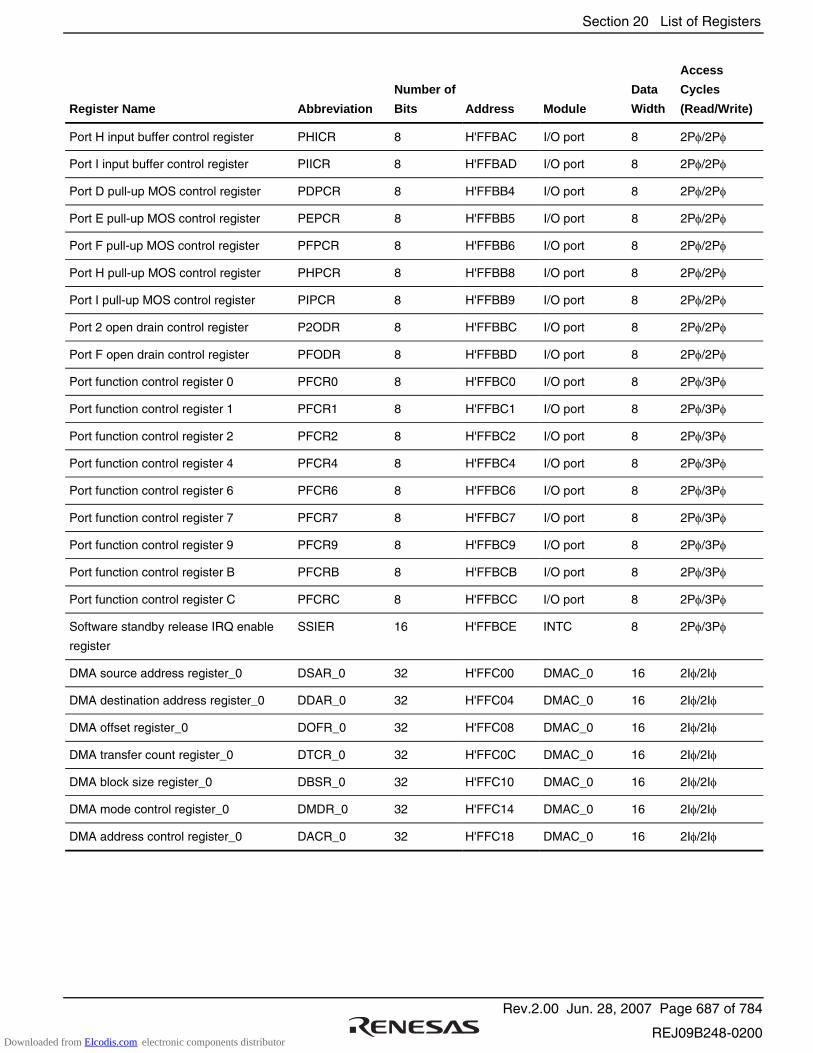
Section 20 List of Registers
Rev.2.00 Jun. 28, 2007 Page 687 of 784
REJ09B248-0200
Register Name Abbreviation
Number of
Bits Address Module
Data
Width
Access
Cycles
(Read/Write)
Port H input buffer control register PHICR 8 H'FFBAC I/O port 8 2Pφ/2Pφ
Port I input buffer control register PIICR 8 H'FFBAD I/O port 8 2Pφ/2Pφ
Port D pull-up MOS control register PDPCR 8 H'FFBB4 I/O port 8 2Pφ/2Pφ
Port E pull-up MOS control register PEPCR 8 H'FFBB5 I/O port 8 2Pφ/2Pφ
Port F pull-up MOS control register PFPCR 8 H'FFBB6 I/O port 8 2Pφ/2Pφ
Port H pull-up MOS control register PHPCR 8 H'FFBB8 I/O port 8 2Pφ/2Pφ
Port I pull-up MOS control register PIPCR 8 H'FFBB9 I/O port 8 2Pφ/2Pφ
Port 2 open drain control register P2ODR 8 H'FFBBC I/O port 8 2Pφ/2Pφ
Port F open drain control register PFODR 8 H'FFBBD I/O port 8 2Pφ/2Pφ
Port function control register 0 PFCR0 8 H'FFBC0 I/O port 8 2Pφ/3Pφ
Port function control register 1 PFCR1 8 H'FFBC1 I/O port 8 2Pφ/3Pφ
Port function control register 2 PFCR2 8 H'FFBC2 I/O port 8 2Pφ/3Pφ
Port function control register 4 PFCR4 8 H'FFBC4 I/O port 8 2Pφ/3Pφ
Port function control register 6 PFCR6 8 H'FFBC6 I/O port 8 2Pφ/3Pφ
Port function control register 7 PFCR7 8 H'FFBC7 I/O port 8 2Pφ/3Pφ
Port function control register 9 PFCR9 8 H'FFBC9 I/O port 8 2Pφ/3Pφ
Port function control register B PFCRB 8 H'FFBCB I/O port 8 2Pφ/3Pφ
Port function control register C PFCRC 8 H'FFBCC I/O port 8 2Pφ/3Pφ
Software standby release IRQ enable
register
SSIER 16 H'FFBCE INTC 8 2Pφ/3Pφ
DMA source address register_0 DSAR_0 32 H'FFC00 DMAC_0 16 2Iφ/2Iφ
DMA destination address register_0 DDAR_0 32 H'FFC04 DMAC_0 16 2Iφ/2Iφ
DMA offset register_0 DOFR_0 32 H'FFC08 DMAC_0 16 2Iφ/2Iφ
DMA transfer count register_0 DTCR_0 32 H'FFC0C DMAC_0 16 2Iφ/2Iφ
DMA block size register_0 DBSR_0 32 H'FFC10 DMAC_0 16 2Iφ/2Iφ
DMA mode control register_0 DMDR_0 32 H'FFC14 DMAC_0 16 2Iφ/2Iφ
DMA address control register_0 DACR_0 32 H'FFC18 DMAC_0 16 2Iφ/2Iφ
Downloaded from Elcodis.com electronic components distributor

Section 20 List of Registers
Rev.2.00 Jun. 28, 2007 Page 688 of 784
REJ09B248-0200
Register Name Abbreviation
Number of
Bits Address Module
Data
Width
Access
Cycles
(Read/Write)
DMA source address register_1 DSAR_1 32 H'FFC20 DMAC_1 16 2Iφ/2Iφ
DMA destination address register_1 DDAR_1 32 H'FFC24 DMAC_1 16 2Iφ/2Iφ
DMA offset register_1 DOFR_1 32 H'FFC28 DMAC_1 16 2Iφ/2Iφ
DMA transfer count register_1 DTCR_1 32 H'FFC2C DMAC_1 16 2Iφ/2Iφ
DMA block size register_1 DBSR_1 32 H'FFC30 DMAC_1 16 2Iφ/2Iφ
DMA mode control register_1 DMDR_1 32 H'FFC34 DMAC_1 16 2Iφ/2Iφ
DMA address control register_1 DACR_1 32 H'FFC38 DMAC_1 16 2Iφ/2Iφ
DMA source address register_2 DSAR_2 32 H'FFC40 DMAC_2 16 2Iφ/2Iφ
DMA destination address register_2 DDAR_2 32 H'FFC44 DMAC_2 16 2Iφ/2Iφ
DMA offset register_2 DOFR_2 32 H'FFC48 DMAC_2 16 2Iφ/2Iφ
DMA transfer count register_2 DTCR_2 32 H'FFC4C DMAC_2 16 2Iφ/2Iφ
DMA block size register_2 DBSR_2 32 H'FFC50 DMAC_2 16 2Iφ/2Iφ
DMA mode control register_2 DMDR_2 32 H'FFC54 DMAC_2 16 2Iφ/2Iφ
DMA address control register_2 DACR_2 32 H'FFC58 DMAC_2 16 2Iφ/2Iφ
DMA source address register_3 DSAR_3 32 H'FFC60 DMAC_3 16 2Iφ/2Iφ
DMA destination address register_3 DDAR_3 32 H'FFC64 DMAC_3 16 2Iφ/2Iφ
DMA offset register_3 DOFR_3 32 H'FFC68 DMAC_3 16 2Iφ/2Iφ
DMA transfer count register_3 DTCR_3 32 H'FFC6C DMAC_3 16 2Iφ/2Iφ
DMA block size register_3 DBSR_3 32 H'FFC70 DMAC_3 16 2Iφ/2Iφ
DMA mode control register_3 DMDR_3 32 H'FFC74 DMAC_3 16 2Iφ/2Iφ
DMA address control register_3 DACR_3 32 H'FFC78 DMAC_3 16 2Iφ/2Iφ
DMA module request select register_0 DMRSR_0 8 H'FFD20 DMAC_0 16 2Iφ/2Iφ
DMA module request select register_1 DMRSR_1 8 H'FFD21 DMAC_1 16 2Iφ/2Iφ
DMA module request select register_2 DMRSR_2 8 H'FFD22 DMAC_2 16 2Iφ/2Iφ
DMA module request select register_3 DMRSR_3 8 H'FFD23 DMAC_3 16 2Iφ/2Iφ
Downloaded from Elcodis.com electronic components distributor

Section 20 List of Registers
Rev.2.00 Jun. 28, 2007 Page 689 of 784
REJ09B248-0200
Register Name Abbreviation
Number of
Bits Address Module
Data
Width
Access
Cycles
(Read/Write)
Interrupt priority register A IPRA 16 H'FFD40 INTC 16 2Iφ/3Iφ
Interrupt priority register B IPRB 16 H'FFD42 INTC 16 2Iφ/3Iφ
Interrupt priority register C IPRC 16 H'FFD44 INTC 16 2Iφ/3Iφ
Interrupt priority register E IPRE 16 H'FFD48 INTC 16 2Iφ/3Iφ
Interrupt priority register F IPRF 16 H'FFD4A INTC 16 2Iφ/3Iφ
Interrupt priority register G IPRG 16 H'FFD4C INTC 16 2Iφ/3Iφ
Interrupt priority register H IPRH 16 H'FFD4E INTC 16 2Iφ/3Iφ
Interrupt priority register I IPRI 16 H'FFD50 INTC 16 2Iφ/3Iφ
Interrupt priority register K IPRK 16 H'FFD54 INTC 16 2Iφ/3Iφ
Interrupt priority register L IPRL 16 H'FFD56 INTC 16 2Iφ/3Iφ
IRQ sense control register H ISCRH 16 H'FFD68 INTC 16 2Iφ/3Iφ
IRQ sense control register L ISCRL 16 H'FFD6A INTC 16 2Iφ/3Iφ
DTC vector base register DTCVBR 32 H'FFD80 BSC 16 2Iφ/3Iφ
Bus width control register ABWCR 16 H'FFD84 BSC 16 2Iφ/3Iφ
Access state control register ASTCR 16 H'FFD86 BSC 16 2Iφ/3Iφ
Wait control register A WTCRA 16 H'FFD88 BSC 16 2Iφ/3Iφ
Wait control register B WTCRB 16 H'FFD8A BSC 16 2Iφ/3Iφ
Read strobe timing control register RDNCR 16 H'FFD8C BSC 16 2Iφ/3Iφ
CS assert period control register CSACR 16 H'FFD8E BSC 16 2Iφ/3Iφ
Idle control register IDLCR 16 H'FFD90 BSC 16 2Iφ/3Iφ
Bus control register 1 BCR1 16 H'FFD92 BSC 16 2Iφ/3Iφ
Bus control register 2 BCR2 8 H'FFD94 BSC 16 2Iφ/3Iφ
Endian control register ENDIANCR 8 H'FFD95 BSC 16 2Iφ/3Iφ
SRAM mode control register SRAMCR 16 H'FFD98 BSC 16 2Iφ/3Iφ
Burst ROM interface control register BROMCR 16 H'FFD9A BSC 16 2Iφ/3Iφ
Address/data multiplexed I/O control
register
MPXCR 16 H'FFD9C BSC 16 2Iφ/3Iφ
Downloaded from Elcodis.com electronic components distributor
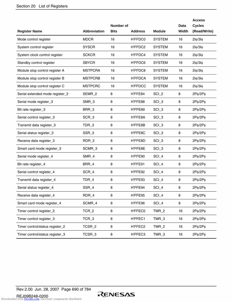
Section 20 List of Registers
Rev.2.00 Jun. 28, 2007 Page 690 of 784
REJ09B248-0200
Register Name Abbreviation
Number of
Bits Address Module
Data
Width
Access
Cycles
(Read/Write)
Mode control register MDCR 16 H'FFDC0 SYSTEM 16 2Iφ/3Iφ
System control register SYSCR 16 H'FFDC2 SYSTEM 16 2Iφ/3Iφ
System clock control register SCKCR 16 H'FFDC4 SYSTEM 16 2Iφ/3Iφ
Standby control register SBYCR 16 H'FFDC6 SYSTEM 16 2Iφ/3Iφ
Module stop control register A MSTPCRA 16 H'FFDC8 SYSTEM 16 2Iφ/3Iφ
Module stop control register B MSTPCRB 16 H'FFDCA SYSTEM 16 2Iφ/3Iφ
Module stop control register C MSTPCRC 16 H'FFDCC SYSTEM 16 2Iφ/3Iφ
Serial extended mode register_2 SEMR_2 8 H'FFE84 SCI_2 8 2Pφ/2Pφ
Serial mode register_3 SMR_3 8 H'FFE88 SCI_3 8 2Pφ/2Pφ
Bit rate register_3 BRR_3 8 H'FFE89 SCI_3 8 2Pφ/2Pφ
Serial control register_3 SCR_3 8 H'FFE8A SCI_3 8 2Pφ/2Pφ
Transmit data register_3 TDR_3 8 H'FFE8B SCI_3 8 2Pφ/2Pφ
Serial status register_3 SSR_3 8 H'FFE8C SCI_3 8 2Pφ/2Pφ
Receive data register_3 RDR_3 8 H'FFE8D SCI_3 8 2Pφ/2Pφ
Smart card mode register_3 SCMR_3 8 H'FFE8E SCI_3 8 2Pφ/2Pφ
Serial mode register_4 SMR_4 8 H'FFE90 SCI_4 8 2Pφ/2Pφ
Bit rate register_4 BRR_4 8 H'FFE91 SCI_4 8 2Pφ/2Pφ
Serial control register_4 SCR_4 8 H'FFE92 SCI_4 8 2Pφ/2Pφ
Transmit data register_4 TDR_4 8 H'FFE93 SCI_4 8 2Pφ/2Pφ
Serial status register_4 SSR_4 8 H'FFE94 SCI_4 8 2Pφ/2Pφ
Receive data register_4 RDR_4 8 H'FFE95 SCI_4 8 2Pφ/2Pφ
Smart card mode register_4 SCMR_4 8 H'FFE96 SCI_4 8 2Pφ/2Pφ
Timer control register_2 TCR_2 8 H'FFEC0 TMR_2 16 2Pφ/2Pφ
Timer control register_3 TCR_3 8 H'FFEC1 TMR_3 16 2Pφ/2Pφ
Timer control/status register_2 TCSR_2 8 H'FFEC2 TMR_2 16 2Pφ/2Pφ
Timer control/status register_3 TCSR_3 8 H'FFEC3 TMR_3 16 2Pφ/2Pφ
Downloaded from Elcodis.com electronic components distributor
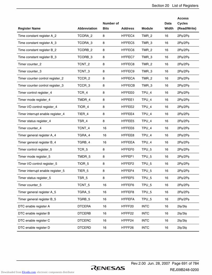
Section 20 List of Registers
Rev.2.00 Jun. 28, 2007 Page 691 of 784
REJ09B248-0200
Register Name Abbreviation
Number of
Bits Address Module
Data
Width
Access
Cycles
(Read/Write)
Time constant register A_2 TCORA_2 8 H'FFEC4 TMR_2 16 2Pφ/2Pφ
Time constant register A_3 TCORA_3 8 H'FFEC5 TMR_3 16 2Pφ/2Pφ
Time constant register B_2 TCORB_2 8 H'FFEC6 TMR_2 16 2Pφ/2Pφ
Time constant register B_3 TCORB_3 8 H'FFEC7 TMR_3 16 2Pφ/2Pφ
Timer counter_2 TCNT_2 8 H'FFEC8 TMR_2 16 2Pφ/2Pφ
Timer counter_3 TCNT_3 8 H'FFEC9 TMR_3 16 2Pφ/2Pφ
Timer counter control register_2 TCCR_2 8 H'FFECA TMR_2 16 2Pφ/2Pφ
Timer counter control register_3 TCCR_3 8 H'FFECB TMR_3 16 2Pφ/2Pφ
Timer control register_4 TCR_4 8 H'FFEE0 TPU_4 16 2Pφ/2Pφ
Timer mode register_4 TMDR_4 8 H'FFEE1 TPU_4 16 2Pφ/2Pφ
Timer I/O control register_4 TIOR_4 8 H'FFEE2 TPU_4 16 2Pφ/2Pφ
Timer interrupt enable register_4 TIER_4 8 H'FFEE4 TPU_4 16 2Pφ/2Pφ
Timer status register_4 TSR_4 8 H'FFEE5 TPU_4 16 2Pφ/2Pφ
Timer counter_4 TCNT_4 16 H'FFEE6 TPU_4 16 2Pφ/2Pφ
Timer general register A_4 TGRA_4 16 H'FFEE8 TPU_4 16 2Pφ/2Pφ
Timer general register B_4 TGRB_4 16 H'FFEEA TPU_4 16 2Pφ/2Pφ
Timer control register_5 TCR_5 8 H'FFEF0 TPU_5 16 2Pφ/2Pφ
Timer mode register_5 TMDR_5 8 H'FFEF1 TPU_5 16 2Pφ/2Pφ
Timer I/O control register_5 TIOR_5 8 H'FFEF2 TPU_5 16 2Pφ/2Pφ
Timer interrupt enable register_5 TIER_5 8 H'FFEF4 TPU_5 16 2Pφ/2Pφ
Timer status register_5 TSR_5 8 H'FFEF5 TPU_5 16 2Pφ/2Pφ
Timer counter_5 TCNT_5 16 H'FFEF6 TPU_5 16 2Pφ/2Pφ
Timer general register A_5 TGRA_5 16 H'FFEF8 TPU_5 16 2Pφ/2Pφ
Timer general register B_5 TGRB_5 16 H'FFEFA TPU_5 16 2Pφ/2Pφ
DTC enable register A DTCERA 16 H'FFF20 INTC 16 2Iφ/3Iφ
DTC enable register B DTCERB 16 H'FFF22 INTC 16 2Iφ/3Iφ
DTC enable register C DTCERC 16 H'FFF24 INTC 16 2Iφ/3Iφ
DTC enable register D DTCERD 16 H'FFF26 INTC 16 2Iφ/3Iφ
Downloaded from Elcodis.com electronic components distributor
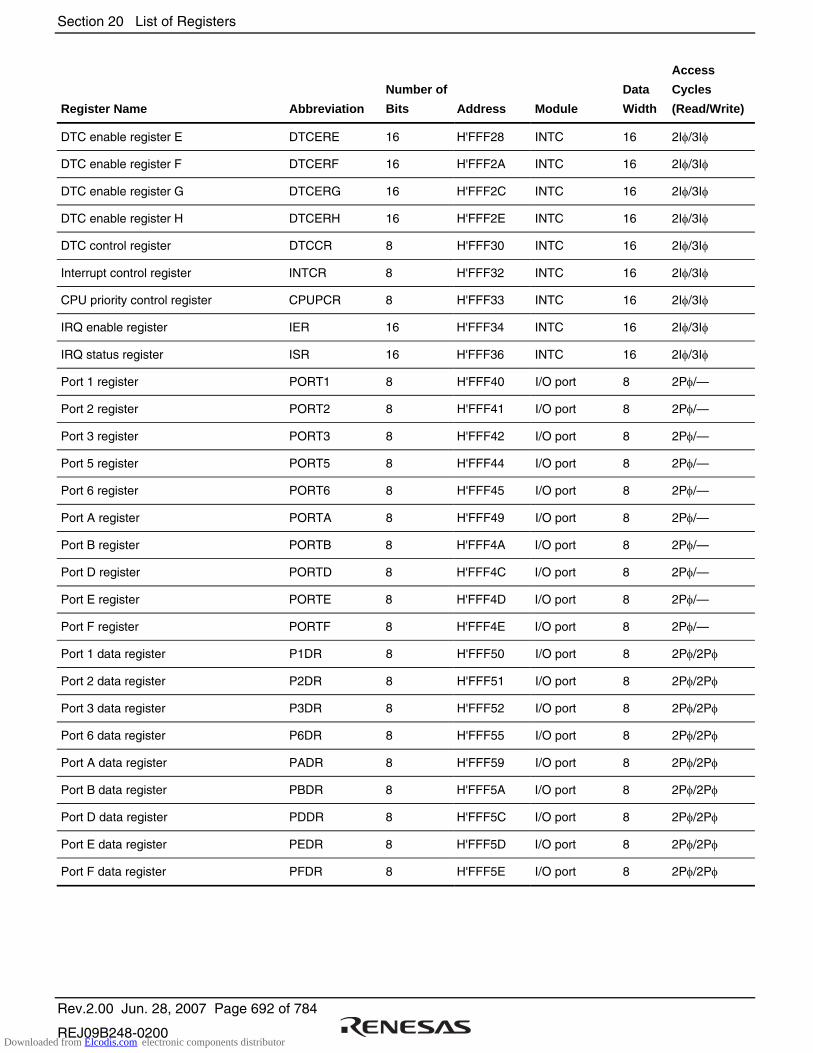
Section 20 List of Registers
Rev.2.00 Jun. 28, 2007 Page 692 of 784
REJ09B248-0200
Register Name Abbreviation
Number of
Bits Address Module
Data
Width
Access
Cycles
(Read/Write)
DTC enable register E DTCERE 16 H'FFF28 INTC 16 2Iφ/3Iφ
DTC enable register F DTCERF 16 H'FFF2A INTC 16 2Iφ/3Iφ
DTC enable register G DTCERG 16 H'FFF2C INTC 16 2Iφ/3Iφ
DTC enable register H DTCERH 16 H'FFF2E INTC 16 2Iφ/3Iφ
DTC control register DTCCR 8 H'FFF30 INTC 16 2Iφ/3Iφ
Interrupt control register INTCR 8 H'FFF32 INTC 16 2Iφ/3Iφ
CPU priority control register CPUPCR 8 H'FFF33 INTC 16 2Iφ/3Iφ
IRQ enable register IER 16 H'FFF34 INTC 16 2Iφ/3Iφ
IRQ status register ISR 16 H'FFF36 INTC 16 2Iφ/3Iφ
Port 1 register PORT1 8 H'FFF40 I/O port 8 2Pφ/—
Port 2 register PORT2 8 H'FFF41 I/O port 8 2Pφ/—
Port 3 register PORT3 8 H'FFF42 I/O port 8 2Pφ/—
Port 5 register PORT5 8 H'FFF44 I/O port 8 2Pφ/—
Port 6 register PORT6 8 H'FFF45 I/O port 8 2Pφ/—
Port A register PORTA 8 H'FFF49 I/O port 8 2Pφ/—
Port B register PORTB 8 H'FFF4A I/O port 8 2Pφ/—
Port D register PORTD 8 H'FFF4C I/O port 8 2Pφ/—
Port E register PORTE 8 H'FFF4D I/O port 8 2Pφ/—
Port F register PORTF 8 H'FFF4E I/O port 8 2Pφ/—
Port 1 data register P1DR 8 H'FFF50 I/O port 8 2Pφ/2Pφ
Port 2 data register P2DR 8 H'FFF51 I/O port 8 2Pφ/2Pφ
Port 3 data register P3DR 8 H'FFF52 I/O port 8 2Pφ/2Pφ
Port 6 data register P6DR 8 H'FFF55 I/O port 8 2Pφ/2Pφ
Port A data register PADR 8 H'FFF59 I/O port 8 2Pφ/2Pφ
Port B data register PBDR 8 H'FFF5A I/O port 8 2Pφ/2Pφ
Port D data register PDDR 8 H'FFF5C I/O port 8 2Pφ/2Pφ
Port E data register PEDR 8 H'FFF5D I/O port 8 2Pφ/2Pφ
Port F data register PFDR 8 H'FFF5E I/O port 8 2Pφ/2Pφ
Downloaded from Elcodis.com electronic components distributor

Section 20 List of Registers
Rev.2.00 Jun. 28, 2007 Page 693 of 784
REJ09B248-0200
Register Name Abbreviation
Number of
Bits Address Module
Data
Width
Access
Cycles
(Read/Write)
Serial mode register_2 SMR_2 8 H'FFF60 SCI_2 8 2Pφ/2Pφ
Bit rate register_2 BRR_2 8 H'FFF61 SCI_2 8 2Pφ/2Pφ
Serial control register_2 SCR_2 8 H'FFF62 SCI_2 8 2Pφ/2Pφ
Transmit data register_2 TDR_2 8 H'FFF63 SCI_2 8 2Pφ/2Pφ
Serial status register_2 SSR_2 8 H'FFF64 SCI_2 8 2Pφ/2Pφ
Receive data register_2 RDR_2 8 H'FFF65 SCI_2 8 2Pφ/2Pφ
Smart card mode register_2 SCMR_2 8 H'FFF66 SCI_2 8 2Pφ/2Pφ
D/A data register 0 DADR0 8 H'FFF68 D/A 8 2Pφ/2Pφ
D/A data register 1 DADR1 8 H'FFF69 D/A 8 2Pφ/2Pφ
D/A control register 01 DACR01 8 H'FFF6A D/A 8 2Pφ/2Pφ
PPG output control register PCR 8 H'FFF76 PPG 8 2Pφ/2Pφ
PPG output mode register PMR 8 H'FFF77 PPG 8 2Pφ/2Pφ
Next data enable register H NDERH 8 H'FFF78 PPG 8 2Pφ/2Pφ
Next data enable register L NDERL 8 H'FFF79 PPG 8 2Pφ/2Pφ
Output data register H PODRH 8 H'FFF7A PPG 8 2Pφ/2Pφ
Output data register L PODRL 8 H'FFF7B PPG 8 2Pφ/2Pφ
Next data register H* NDRH 8 H'FFF7C PPG 8 2Pφ/2Pφ
Next data register L* NDRL 8 H'FFF7D PPG 8 2Pφ/2Pφ
Next data register H* NDRH 8 H'FFF7E PPG 8 2Pφ/2Pφ
Next data register L* NDRL 8 H'FFF7F PPG 8 2Pφ/2Pφ
Serial mode register_0 SMR_0 8 H'FFF80 SCI_0 8 2Pφ/2Pφ
Bit rate register_0 BRR_0 8 H'FFF81 SCI_0 8 2Pφ/2Pφ
Serial control register_0 SCR_0 8 H'FFF82 SCI_0 8 2Pφ/2Pφ
Transmit data register_0 TDR_0 8 H'FFF83 SCI_0 8 2Pφ/2Pφ
Serial status register_0 SSR_0 8 H'FFF84 SCI_0 8 2Pφ/2Pφ
Receive data register_0 RDR_0 8 H'FFF85 SCI_0 8 2Pφ/2Pφ
Smart card mode register_0 SCMR_0 8 H'FFF86 SCI_0 8 2Pφ/2Pφ
Downloaded from Elcodis.com electronic components distributor

Section 20 List of Registers
Rev.2.00 Jun. 28, 2007 Page 694 of 784
REJ09B248-0200
Register Name Abbreviation
Number of
Bits Address Module
Data
Width
Access
Cycles
(Read/Write)
Serial mode register_1 SMR_1 8 H'FFF88 SCI_1 8 2Pφ/2Pφ
Bit rate register_1 BRR_1 8 H'FFF89 SCI_1 8 2Pφ/2Pφ
Serial control register_1 SCR_1 8 H'FFF8A SCI_1 8 2Pφ/2Pφ
Transmit data register_1 TDR_1 8 H'FFF8B SCI_1 8 2Pφ/2Pφ
Serial status register_1 SSR_1 8 H'FFF8C SCI_1 8 2Pφ/2Pφ
Receive data register_1 RDR_1 8 H'FFF8D SCI_1 8 2Pφ/2Pφ
Smart card mode register_1 SCMR_1 8 H'FFF8E SCI_1 8 2Pφ/2Pφ
A/D data register A ADDRA 16 H'FFF90 A/D 16 2Pφ/2Pφ
A/D data register B ADDRB 16 H'FFF92 A/D 16 2Pφ/2Pφ
A/D data register C ADDRC 16 H'FFF94 A/D 16 2Pφ/2Pφ
A/D data register D ADDRD 16 H'FFF96 A/D 16 2Pφ/2Pφ
A/D data register E ADDRE 16 H'FFF98 A/D 16 2Pφ/2Pφ
A/D data register F ADDRF 16 H'FFF9A A/D 16 2Pφ/2Pφ
A/D data register G ADDRG 16 H'FFF9C A/D 16 2Pφ/2Pφ
A/D data register H ADDRH 16 H'FFF9E A/D 16 2Pφ/2Pφ
A/D control/status register ADCSR 8 H'FFFA0 A/D 16 2Pφ/2Pφ
A/D control register ADCR 8 H'FFFA1 A/D 16 2Pφ/2Pφ
Timer control/status register TCSR 8 H'FFFA4 WDT 2Pφ/3Pφ
Timer counter TCNT 8 H'FFFA5 WDT 2Pφ/3Pφ
Reset control/status register RSTCSR 8 H'FFFA7 WDT 2Pφ/3Pφ
Timer control register_0 TCR_0 8 H'FFFB0 TMR_0 16 2Pφ/2Pφ
Timer control register_1 TCR_1 8 H'FFFB1 TMR_1 16 2Pφ/2Pφ
Timer control/status register_0 TCSR_0 8 H'FFFB2 TMR_0 16 2Pφ/2Pφ
Timer control/status register_1 TCSR_1 8 H'FFFB3 TMR_1 16 2Pφ/2Pφ
Time constant register A_0 TCORA_0 8 H'FFFB4 TMR_0 16 2Pφ/2Pφ
Time constant register A_1 TCORA_1 8 H'FFFB5 TMR_1 16 2Pφ/2Pφ
Time constant register B_0 TCORB_0 8 H'FFFB6 TMR_0 16 2Pφ/2Pφ
Time constant register B_1 TCORB_1 8 H'FFFB7 TMR_1 16 2Pφ/2Pφ
Downloaded from Elcodis.com electronic components distributor
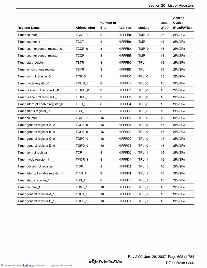
Section 20 List of Registers
Rev.2.00 Jun. 28, 2007 Page 695 of 784
REJ09B248-0200
Register Name Abbreviation
Number of
Bits Address Module
Data
Width
Access
Cycles
(Read/Write)
Timer counter_0 TCNT_0 8 H'FFFB8 TMR_0 16 2Pφ/2Pφ
Timer counter_1 TCNT_1 8 H'FFFB9 TMR_1 16 2Pφ/2Pφ
Timer counter control register_0 TCCR_0 8 H'FFFBA TMR_0 16 2Pφ/2Pφ
Timer counter control register_1 TCCR_1 8 H'FFFBB TMR_1 16 2Pφ/2Pφ
Timer start register TSTR 8 H'FFFBC TPU 16 2Pφ/2Pφ
Timer synchronous register TSYR 8 H'FFFBD TPU 16 2Pφ/2Pφ
Timer control register_0 TCR_0 8 H'FFFC0 TPU_0 16 2Pφ/2Pφ
Timer mode register_0 TMDR_0 8 H'FFFC1 TPU_0 16 2Pφ/2Pφ
Timer I/O control register H_0 TIORH_0 8 H'FFFC2 TPU_0 16 2Pφ/2Pφ
Timer I/O control register L_0 TIORL_0 8 H'FFFC3 TPU_0 16 2Pφ/2Pφ
Timer interrupt enable register_0 TIER_0 8 H'FFFC4 TPU_0 16 2Pφ/2Pφ
Timer status register_0 TSR_0 8 H'FFFC5 TPU_0 16 2Pφ/2Pφ
Timer counter_0 TCNT_0 16 H'FFFC6 TPU_0 16 2Pφ/2Pφ
Timer general register A_0 TGRA_0 16 H'FFFC8 TPU_0 16 2Pφ/2Pφ
Timer general register B_0 TGRB_0 16 H'FFFCA TPU_0 16 2Pφ/2Pφ
Timer general register C_0 TGRC_0 16 H'FFFCC TPU_0 16 2Pφ/2Pφ
Timer general register D_0 TGRD_0 16 H'FFFCE TPU_0 16 2Pφ/2Pφ
Timer control register_1 TCR_1 8 H'FFFD0 TPU_1 16 2Pφ/2Pφ
Timer mode register_1 TMDR_1 8 H'FFFD1 TPU_1 16 2Pφ/2Pφ
Timer I/O control register_1 TIOR_1 8 H'FFFD2 TPU_1 16 2Pφ/2Pφ
Timer interrupt enable register_1 TIER_1 8 H'FFFD4 TPU_1 16 2Pφ/2Pφ
Timer status register_1 TSR_1 8 H'FFFD5 TPU_1 16 2Pφ/2Pφ
Timer counter_1 TCNT_1 16 H'FFFD6 TPU_1 16 2Pφ/2Pφ
Timer general register A_1 TGRA_1 16 H'FFFD8 TPU_1 16 2Pφ/2Pφ
Timer general register B_1 TGRB_1 16 H'FFFDA TPU_1 16 2Pφ/2Pφ
Downloaded from Elcodis.com electronic components distributor
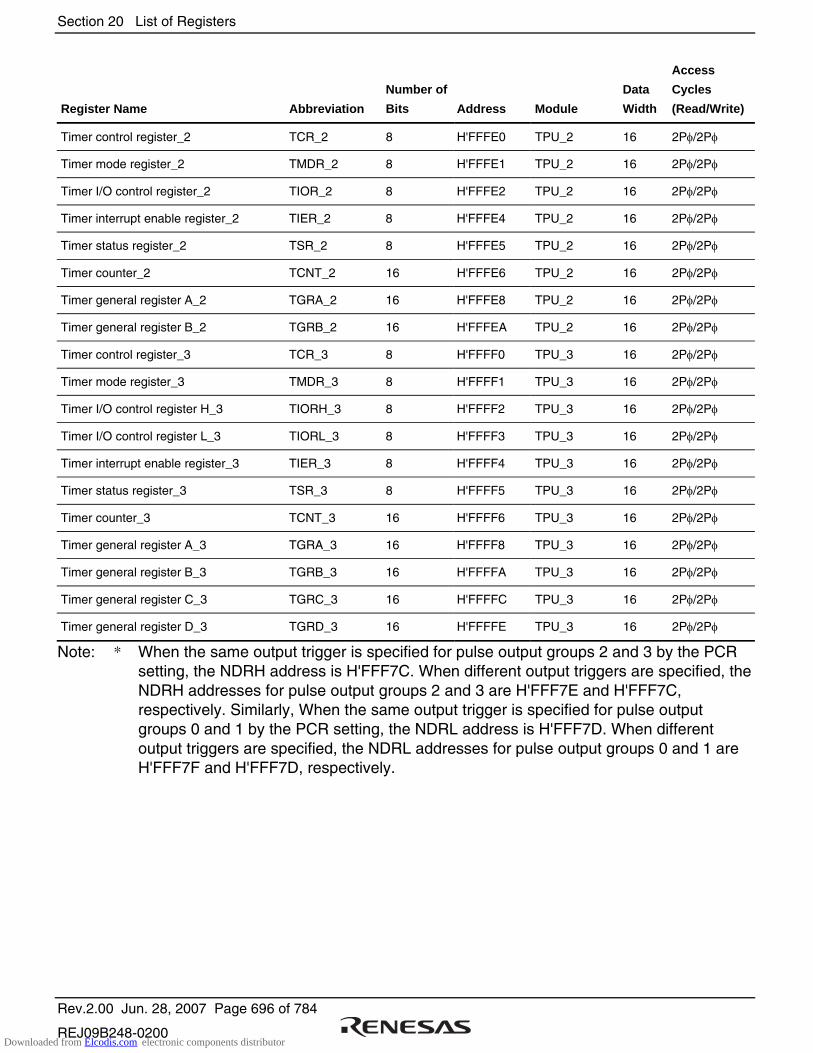
Section 20 List of Registers
Rev.2.00 Jun. 28, 2007 Page 696 of 784
REJ09B248-0200
Register Name Abbreviation
Number of
Bits Address Module
Data
Width
Access
Cycles
(Read/Write)
Timer control register_2 TCR_2 8 H'FFFE0 TPU_2 16 2Pφ/2Pφ
Timer mode register_2 TMDR_2 8 H'FFFE1 TPU_2 16 2Pφ/2Pφ
Timer I/O control register_2 TIOR_2 8 H'FFFE2 TPU_2 16 2Pφ/2Pφ
Timer interrupt enable register_2 TIER_2 8 H'FFFE4 TPU_2 16 2Pφ/2Pφ
Timer status register_2 TSR_2 8 H'FFFE5 TPU_2 16 2Pφ/2Pφ
Timer counter_2 TCNT_2 16 H'FFFE6 TPU_2 16 2Pφ/2Pφ
Timer general register A_2 TGRA_2 16 H'FFFE8 TPU_2 16 2Pφ/2Pφ
Timer general register B_2 TGRB_2 16 H'FFFEA TPU_2 16 2Pφ/2Pφ
Timer control register_3 TCR_3 8 H'FFFF0 TPU_3 16 2Pφ/2Pφ
Timer mode register_3 TMDR_3 8 H'FFFF1 TPU_3 16 2Pφ/2Pφ
Timer I/O control register H_3 TIORH_3 8 H'FFFF2 TPU_3 16 2Pφ/2Pφ
Timer I/O control register L_3 TIORL_3 8 H'FFFF3 TPU_3 16 2Pφ/2Pφ
Timer interrupt enable register_3 TIER_3 8 H'FFFF4 TPU_3 16 2Pφ/2Pφ
Timer status register_3 TSR_3 8 H'FFFF5 TPU_3 16 2Pφ/2Pφ
Timer counter_3 TCNT_3 16 H'FFFF6 TPU_3 16 2Pφ/2Pφ
Timer general register A_3 TGRA_3 16 H'FFFF8 TPU_3 16 2Pφ/2Pφ
Timer general register B_3 TGRB_3 16 H'FFFFA TPU_3 16 2Pφ/2Pφ
Timer general register C_3 TGRC_3 16 H'FFFFC TPU_3 16 2Pφ/2Pφ
Timer general register D_3 TGRD_3 16 H'FFFFE TPU_3 16 2Pφ/2Pφ
Note: * When the same output trigger is specified for pulse output groups 2 and 3 by the PCR setting, the NDRH address is H'FFF7C. When different output triggers are specified, the NDRH addresses for pulse output groups 2 and 3 are H'FFF7E and H'FFF7C, respectively. Similarly, When the same output trigger is specified for pulse output groups 0 and 1 by the PCR setting, the NDRL address is H'FFF7D. When different output triggers are specified, the NDRL addresses for pulse output groups 0 and 1 are H'FFF7F and H'FFF7D, respectively.
Downloaded from Elcodis.com electronic components distributor
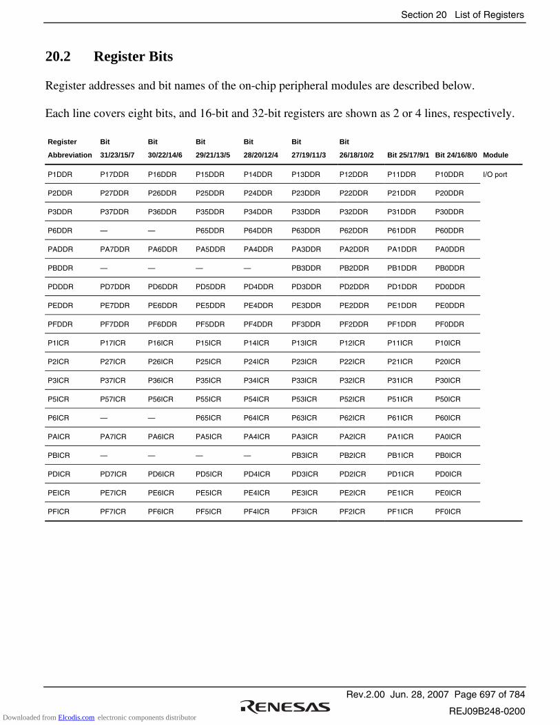
Section 20 List of Registers
Rev.2.00 Jun. 28, 2007 Page 697 of 784
REJ09B248-0200
20.2 Register Bits
Register addresses and bit names of the on-chip peripheral modules are described below.
Each line covers eight bits, and 16-bit and 32-bit registers are shown as 2 or 4 lines, respectively.
Register
Abbreviation
Bit
31/23/15/7
Bit
30/22/14/6
Bit
29/21/13/5
Bit
28/20/12/4
Bit
27/19/11/3
Bit
26/18/10/2 Bit 25/17/9/1 Bit 24/16/8/0 Module
P1DDR P17DDR P16DDR P15DDR P14DDR P13DDR P12DDR P11DDR P10DDR I/O port
P2DDR P27DDR P26DDR P25DDR P24DDR P23DDR P22DDR P21DDR P20DDR
P3DDR P37DDR P36DDR P35DDR P34DDR P33DDR P32DDR P31DDR P30DDR
P6DDR — — P65DDR P64DDR P63DDR P62DDR P61DDR P60DDR
PADDR PA7DDR PA6DDR PA5DDR PA4DDR PA3DDR PA2DDR PA1DDR PA0DDR
PBDDR — — — — PB3DDR PB2DDR PB1DDR PB0DDR
PDDDR PD7DDR PD6DDR PD5DDR PD4DDR PD3DDR PD2DDR PD1DDR PD0DDR
PEDDR PE7DDR PE6DDR PE5DDR PE4DDR PE3DDR PE2DDR PE1DDR PE0DDR
PFDDR PF7DDR PF6DDR PF5DDR PF4DDR PF3DDR PF2DDR PF1DDR PF0DDR
P1ICR P17ICR P16ICR P15ICR P14ICR P13ICR P12ICR P11ICR P10ICR
P2ICR P27ICR P26ICR P25ICR P24ICR P23ICR P22ICR P21ICR P20ICR
P3ICR P37ICR P36ICR P35ICR P34ICR P33ICR P32ICR P31ICR P30ICR
P5ICR P57ICR P56ICR P55ICR P54ICR P53ICR P52ICR P51ICR P50ICR
P6ICR — — P65ICR P64ICR P63ICR P62ICR P61ICR P60ICR
PAICR PA7ICR PA6ICR PA5ICR PA4ICR PA3ICR PA2ICR PA1ICR PA0ICR
PBICR — — — — PB3ICR PB2ICR PB1ICR PB0ICR
PDICR PD7ICR PD6ICR PD5ICR PD4ICR PD3ICR PD2ICR PD1ICR PD0ICR
PEICR PE7ICR PE6ICR PE5ICR PE4ICR PE3ICR PE2ICR PE1ICR PE0ICR
PFICR PF7ICR PF6ICR PF5ICR PF4ICR PF3ICR PF2ICR PF1ICR PF0ICR
Downloaded from Elcodis.com electronic components distributor
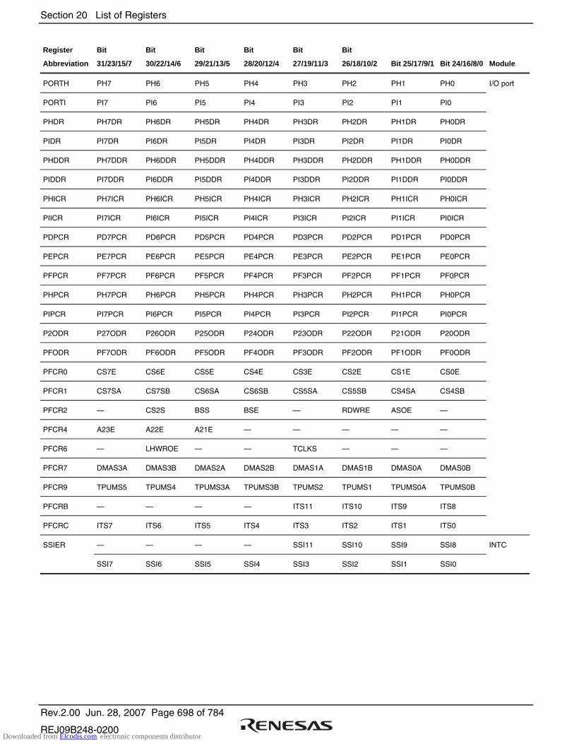
Section 20 List of Registers
Rev.2.00 Jun. 28, 2007 Page 698 of 784
REJ09B248-0200
Register
Abbreviation
Bit
31/23/15/7
Bit
30/22/14/6
Bit
29/21/13/5
Bit
28/20/12/4
Bit
27/19/11/3
Bit
26/18/10/2 Bit 25/17/9/1 Bit 24/16/8/0 Module
PORTH PH7 PH6 PH5 PH4 PH3 PH2 PH1 PH0 I/O port
PORTI PI7 PI6 PI5 PI4 PI3 PI2 PI1 PI0
PHDR PH7DR PH6DR PH5DR PH4DR PH3DR PH2DR PH1DR PH0DR
PIDR PI7DR PI6DR PI5DR PI4DR PI3DR PI2DR PI1DR PI0DR
PHDDR PH7DDR PH6DDR PH5DDR PH4DDR PH3DDR PH2DDR PH1DDR PH0DDR
PIDDR PI7DDR PI6DDR PI5DDR PI4DDR PI3DDR PI2DDR PI1DDR PI0DDR
PHICR PH7ICR PH6ICR PH5ICR PH4ICR PH3ICR PH2ICR PH1ICR PH0ICR
PIICR PI7ICR PI6ICR PI5ICR PI4ICR PI3ICR PI2ICR PI1ICR PI0ICR
PDPCR PD7PCR PD6PCR PD5PCR PD4PCR PD3PCR PD2PCR PD1PCR PD0PCR
PEPCR PE7PCR PE6PCR PE5PCR PE4PCR PE3PCR PE2PCR PE1PCR PE0PCR
PFPCR PF7PCR PF6PCR PF5PCR PF4PCR PF3PCR PF2PCR PF1PCR PF0PCR
PHPCR PH7PCR PH6PCR PH5PCR PH4PCR PH3PCR PH2PCR PH1PCR PH0PCR
PIPCR PI7PCR PI6PCR PI5PCR PI4PCR PI3PCR PI2PCR PI1PCR PI0PCR
P2ODR P27ODR P26ODR P25ODR P24ODR P23ODR P22ODR P21ODR P20ODR
PFODR PF7ODR PF6ODR PF5ODR PF4ODR PF3ODR PF2ODR PF1ODR PF0ODR
PFCR0 CS7E CS6E CS5E CS4E CS3E CS2E CS1E CS0E
PFCR1 CS7SA CS7SB CS6SA CS6SB CS5SA CS5SB CS4SA CS4SB
PFCR2 — CS2S BSS BSE — RDWRE ASOE —
PFCR4 A23E A22E A21E — — — — —
PFCR6 — LHWROE — — TCLKS — — —
PFCR7 DMAS3A DMAS3B DMAS2A DMAS2B DMAS1A DMAS1B DMAS0A DMAS0B
PFCR9 TPUMS5 TPUMS4 TPUMS3A TPUMS3B TPUMS2 TPUMS1 TPUMS0A TPUMS0B
PFCRB — — — — ITS11 ITS10 ITS9 ITS8
PFCRC ITS7 ITS6 ITS5 ITS4 ITS3 ITS2 ITS1 ITS0
SSIER — — — — SSI11 SSI10 SSI9 SSI8 INTC
SSI7 SSI6 SSI5 SSI4 SSI3 SSI2 SSI1 SSI0
Downloaded from Elcodis.com electronic components distributor

Section 20 List of Registers
Rev.2.00 Jun. 28, 2007 Page 699 of 784
REJ09B248-0200
Register
Abbreviation
Bit
31/23/15/7
Bit
30/22/14/6
Bit
29/21/13/5
Bit
28/20/12/4
Bit
27/19/11/3
Bit
26/18/10/2 Bit 25/17/9/1 Bit 24/16/8/0 Module
DSAR_0 DMAC_0
DDAR_0
DOFR_0
DTCR_0
DBSR_0 BKSZH31 BKSZH30 BKSZH29 BKSZH28 BKSZH27 BKSZH26 BKSZH25 BKSZH24
BKSZH23 BKSZH22 BKSZH21 BKSZH20 BKSZH19 BKSZH18 BKSZH17 BKSZH16
BKSZ15 BKSZ14 BKSZ13 BKSZ12 BKSZ11 BKSZ10 BKSZ9 BKSZ8
BKSZ7 BKSZ6 BKSZ5 BKSZ4 BKSZ3 BKSZ2 BKSZ1 BKSZ0
DMDR_0 DTE DACKE TENDE — DREQS NRD — —
ACT — — — ERRF — ESIF DTIF
DTSZ1 DTSZ0 MDS1 MDS0 TSEIE — ESIE DTIE
DTF1 DTF0 DTA — — DMAP2 DMAP1 DMAP0
DACR_0 AMS DIRS — — — RPTIE ARS1 ARS0
— — SAT1 SAT0 — — DAT1 DAT0
SARIE — — SARA4 SARA3 SARA2 SARA1 SARA0
DARIE — — DARA4 DARA3 DARA2 DARA1 DARA0
Downloaded from Elcodis.com electronic components distributor

Section 20 List of Registers
Rev.2.00 Jun. 28, 2007 Page 700 of 784
REJ09B248-0200
Register
Abbreviation
Bit
31/23/15/7
Bit
30/22/14/6
Bit
29/21/13/5
Bit
28/20/12/4
Bit
27/19/11/3
Bit
26/18/10/2 Bit 25/17/9/1 Bit 24/16/8/0 Module
DSAR_1 DMAC_1
DDAR_1
DOFR_1
DTCR_1
DBSR_1 BKSZH31 BKSZH30 BKSZH29 BKSZH28 BKSZH27 BKSZH26 BKSZH25 BKSZH24
BKSZH23 BKSZH22 BKSZH21 BKSZH20 BKSZH19 BKSZH18 BKSZH17 BKSZH16
BKSZ15 BKSZ14 BKSZ13 BKSZ12 BKSZ11 BKSZ10 BKSZ9 BKSZ8
BKSZ7 BKSZ6 BKSZ5 BKSZ4 BKSZ3 BKSZ2 BKSZ1 BKSZ0
DMDR_1 DTE DACKE TENDE — DREQS NRD — —
ACT — — — — — ESIF DTIF
DTSZ1 DTSZ0 MDS1 MDS0 TSEIE — ESIE DTIE
DTF1 DTF0 DTA — — DMAP2 DMAP1 DMAP0
DACR_1 AMS DIRS — — — RPTIE ARS1 ARS0
— — SAT1 SAT0 — — DAT1 DAT0
SARIE — — SARA4 SARA3 SARA2 SARA1 SARA0
DARIE — — DARA4 DARA3 DARA2 DARA1 DARA0
Downloaded from Elcodis.com electronic components distributor

Section 20 List of Registers
Rev.2.00 Jun. 28, 2007 Page 701 of 784
REJ09B248-0200
Register
Abbreviation
Bit
31/23/15/7
Bit
30/22/14/6
Bit
29/21/13/5
Bit
28/20/12/4
Bit
27/19/11/3
Bit
26/18/10/2 Bit 25/17/9/1 Bit 24/16/8/0 Module
DSAR_2 DMAC_2
DDAR_2
DOFR_2
DTCR_2
DBSR_2 BKSZH31 BKSZH30 BKSZH29 BKSZH28 BKSZH27 BKSZH26 BKSZH25 BKSZH24
BKSZH23 BKSZH22 BKSZH21 BKSZH20 BKSZH19 BKSZH18 BKSZH17 BKSZH16
BKSZ15 BKSZ14 BKSZ13 BKSZ12 BKSZ11 BKSZ10 BKSZ9 BKSZ8
BKSZ7 BKSZ6 BKSZ5 BKSZ4 BKSZ3 BKSZ2 BKSZ1 BKSZ0
DMDR_2 DTE DACKE TENDE — DREQS NRD — —
ACT — — — — — ESIF DTIF
DTSZ1 DTSZ0 MDS1 MDS0 TSEIE — ESIE DTIE
DTF1 DTF0 DTA — — DMAP2 DMAP1 DMAP0
DACR_2 AMS DIRS — — — RPTIE ARS1 ARS0
— — SAT1 SAT0 — — DAT1 DAT0
SARIE — — SARA4 SARA3 SARA2 SARA1 SARA0
DARIE — — DARA4 DARA3 DARA2 DARA1 DARA0
Downloaded from Elcodis.com electronic components distributor
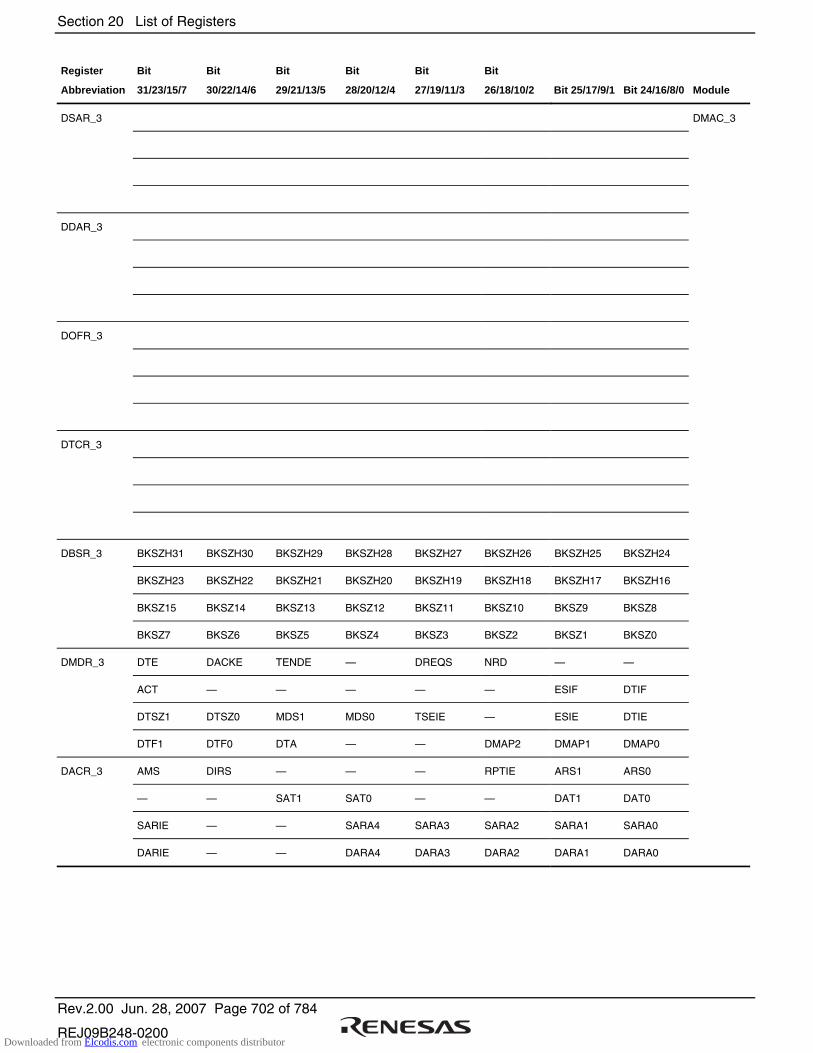
Section 20 List of Registers
Rev.2.00 Jun. 28, 2007 Page 702 of 784
REJ09B248-0200
Register
Abbreviation
Bit
31/23/15/7
Bit
30/22/14/6
Bit
29/21/13/5
Bit
28/20/12/4
Bit
27/19/11/3
Bit
26/18/10/2 Bit 25/17/9/1 Bit 24/16/8/0 Module
DSAR_3 DMAC_3
DDAR_3
DOFR_3
DTCR_3
DBSR_3 BKSZH31 BKSZH30 BKSZH29 BKSZH28 BKSZH27 BKSZH26 BKSZH25 BKSZH24
BKSZH23 BKSZH22 BKSZH21 BKSZH20 BKSZH19 BKSZH18 BKSZH17 BKSZH16
BKSZ15 BKSZ14 BKSZ13 BKSZ12 BKSZ11 BKSZ10 BKSZ9 BKSZ8
BKSZ7 BKSZ6 BKSZ5 BKSZ4 BKSZ3 BKSZ2 BKSZ1 BKSZ0
DMDR_3 DTE DACKE TENDE — DREQS NRD — —
ACT — — — — — ESIF DTIF
DTSZ1 DTSZ0 MDS1 MDS0 TSEIE — ESIE DTIE
DTF1 DTF0 DTA — — DMAP2 DMAP1 DMAP0
DACR_3 AMS DIRS — — — RPTIE ARS1 ARS0
— — SAT1 SAT0 — — DAT1 DAT0
SARIE — — SARA4 SARA3 SARA2 SARA1 SARA0
DARIE — — DARA4 DARA3 DARA2 DARA1 DARA0
Downloaded from Elcodis.com electronic components distributor
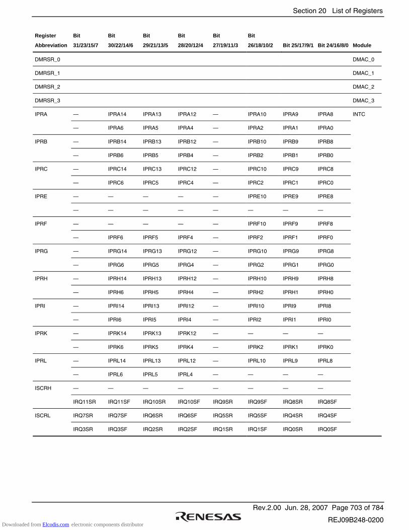
Section 20 List of Registers
Rev.2.00 Jun. 28, 2007 Page 703 of 784
REJ09B248-0200
Register
Abbreviation
Bit
31/23/15/7
Bit
30/22/14/6
Bit
29/21/13/5
Bit
28/20/12/4
Bit
27/19/11/3
Bit
26/18/10/2 Bit 25/17/9/1 Bit 24/16/8/0 Module
DMRSR_0 DMAC_0
DMRSR_1 DMAC_1
DMRSR_2 DMAC_2
DMRSR_3 DMAC_3
IPRA — IPRA14 IPRA13 IPRA12 — IPRA10 IPRA9 IPRA8 INTC
— IPRA6 IPRA5 IPRA4 — IPRA2 IPRA1 IPRA0
IPRB — IPRB14 IPRB13 IPRB12 — IPRB10 IPRB9 IPRB8
— IPRB6 IPRB5 IPRB4 — IPRB2 IPRB1 IPRB0
IPRC — IPRC14 IPRC13 IPRC12 — IPRC10 IPRC9 IPRC8
— IPRC6 IPRC5 IPRC4 — IPRC2 IPRC1 IPRC0
IPRE — — — — — IPRE10 IPRE9 IPRE8
— — — — — — — —
IPRF — — — — — IPRF10 IPRF9 IPRF8
— IPRF6 IPRF5 IPRF4 — IPRF2 IPRF1 IPRF0
IPRG — IPRG14 IPRG13 IPRG12 — IPRG10 IPRG9 IPRG8
— IPRG6 IPRG5 IPRG4 — IPRG2 IPRG1 IPRG0
IPRH — IPRH14 IPRH13 IPRH12 — IPRH10 IPRH9 IPRH8
— IPRH6 IPRH5 IPRH4 — IPRH2 IPRH1 IPRH0
IPRI — IPRI14 IPRI13 IPRI12 — IPRI10 IPRI9 IPRI8
— IPRI6 IPRI5 IPRI4 — IPRI2 IPRI1 IPRI0
IPRK — IPRK14 IPRK13 IPRK12 — — — —
— IPRK6 IPRK5 IPRK4 — IPRK2 IPRK1 IPRK0
IPRL — IPRL14 IPRL13 IPRL12 — IPRL10 IPRL9 IPRL8
— IPRL6 IPRL5 IPRL4 — — — —
ISCRH — — — — — — — —
IRQ11SR IRQ11SF IRQ10SR IRQ10SF IRQ9SR IRQ9SF IRQ8SR IRQ8SF
ISCRL IRQ7SR IRQ7SF IRQ6SR IRQ6SF IRQ5SR IRQ5SF IRQ4SR IRQ4SF
IRQ3SR IRQ3SF IRQ2SR IRQ2SF IRQ1SR IRQ1SF IRQ0SR IRQ0SF
Downloaded from Elcodis.com electronic components distributor
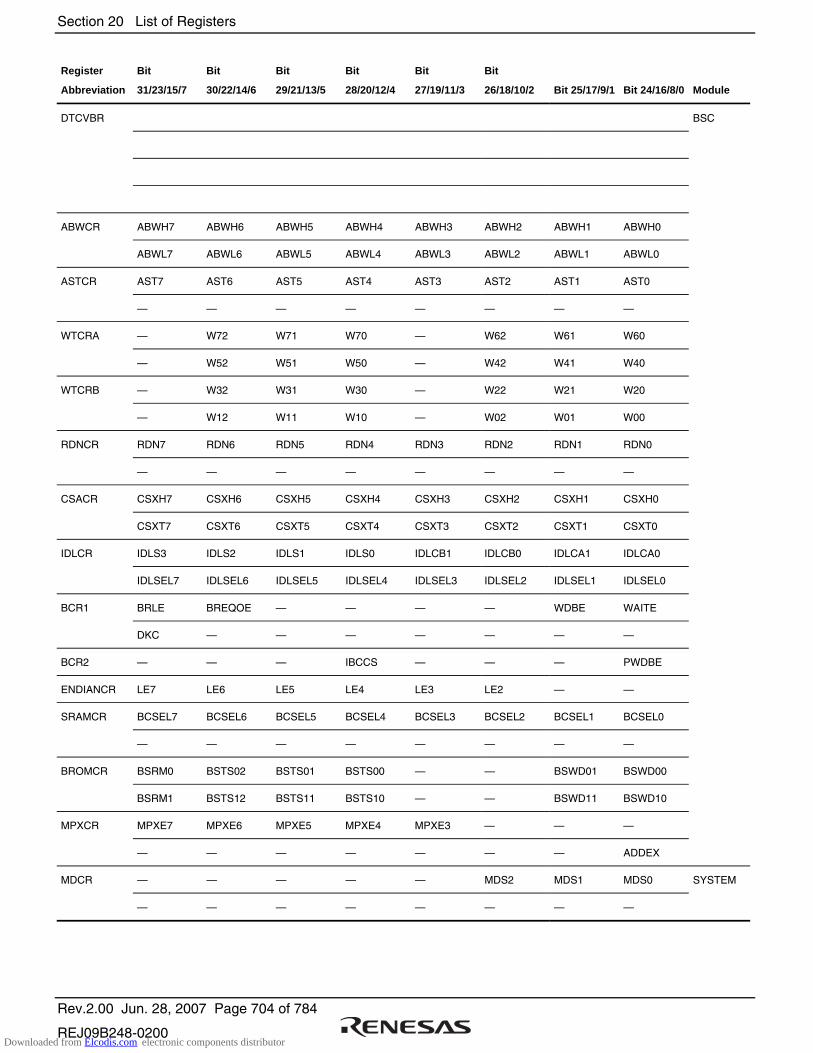
Section 20 List of Registers
Rev.2.00 Jun. 28, 2007 Page 704 of 784
REJ09B248-0200
Register
Abbreviation
Bit
31/23/15/7
Bit
30/22/14/6
Bit
29/21/13/5
Bit
28/20/12/4
Bit
27/19/11/3
Bit
26/18/10/2 Bit 25/17/9/1 Bit 24/16/8/0 Module
DTCVBR BSC
ABWCR ABWH7 ABWH6 ABWH5 ABWH4 ABWH3 ABWH2 ABWH1 ABWH0
ABWL7 ABWL6 ABWL5 ABWL4 ABWL3 ABWL2 ABWL1 ABWL0
ASTCR AST7 AST6 AST5 AST4 AST3 AST2 AST1 AST0
— — — — — — — —
WTCRA — W72 W71 W70 — W62 W61 W60
— W52 W51 W50 — W42 W41 W40
WTCRB — W32 W31 W30 — W22 W21 W20
— W12 W11 W10 — W02 W01 W00
RDNCR RDN7 RDN6 RDN5 RDN4 RDN3 RDN2 RDN1 RDN0
— — — — — — — —
CSACR CSXH7 CSXH6 CSXH5 CSXH4 CSXH3 CSXH2 CSXH1 CSXH0
CSXT7 CSXT6 CSXT5 CSXT4 CSXT3 CSXT2 CSXT1 CSXT0
IDLCR IDLS3 IDLS2 IDLS1 IDLS0 IDLCB1 IDLCB0 IDLCA1 IDLCA0
IDLSEL7 IDLSEL6 IDLSEL5 IDLSEL4 IDLSEL3 IDLSEL2 IDLSEL1 IDLSEL0
BCR1 BRLE BREQOE — — — — WDBE WAITE
DKC — — — — — — —
BCR2 — — — IBCCS — — — PWDBE
ENDIANCR LE7 LE6 LE5 LE4 LE3 LE2 — —
SRAMCR BCSEL7 BCSEL6 BCSEL5 BCSEL4 BCSEL3 BCSEL2 BCSEL1 BCSEL0
— — — — — — — —
BROMCR BSRM0 BSTS02 BSTS01 BSTS00 — — BSWD01 BSWD00
BSRM1 BSTS12 BSTS11 BSTS10 — — BSWD11 BSWD10
MPXCR MPXE7 MPXE6 MPXE5 MPXE4 MPXE3 — — —
— — — — — — — ADDEX
MDCR — — — — — MDS2 MDS1 MDS0 SYSTEM
— — — — — — — —
Downloaded from Elcodis.com electronic components distributor
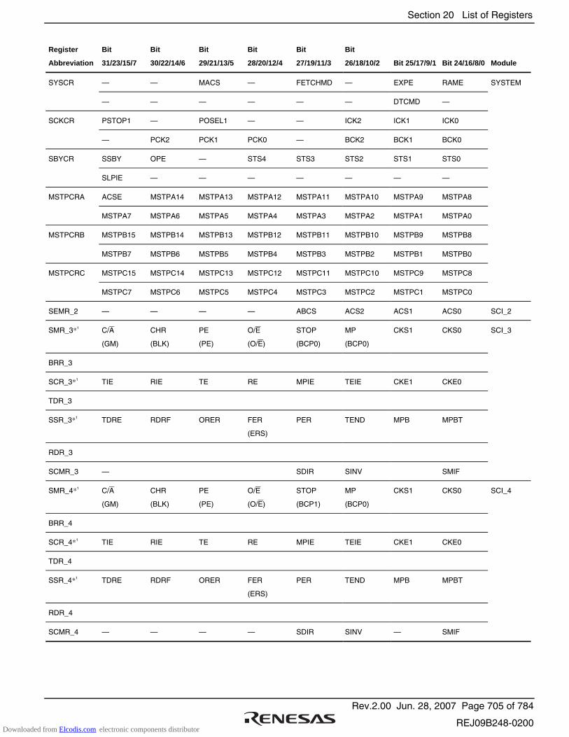
Section 20 List of Registers
Rev.2.00 Jun. 28, 2007 Page 705 of 784
REJ09B248-0200
Register
Abbreviation
Bit
31/23/15/7
Bit
30/22/14/6
Bit
29/21/13/5
Bit
28/20/12/4
Bit
27/19/11/3
Bit
26/18/10/2 Bit 25/17/9/1 Bit 24/16/8/0 Module
SYSCR — — MACS — FETCHMD — EXPE RAME SYSTEM
— — — — — — DTCMD —
SCKCR PSTOP1 — POSEL1 — — ICK2 ICK1 ICK0
— PCK2 PCK1 PCK0 — BCK2 BCK1 BCK0
SBYCR SSBY OPE — STS4 STS3 STS2 STS1 STS0
SLPIE — — — — — — —
MSTPCRA ACSE MSTPA14 MSTPA13 MSTPA12 MSTPA11 MSTPA10 MSTPA9 MSTPA8
MSTPA7 MSTPA6 MSTPA5 MSTPA4 MSTPA3 MSTPA2 MSTPA1 MSTPA0
MSTPCRB MSTPB15 MSTPB14 MSTPB13 MSTPB12 MSTPB11 MSTPB10 MSTPB9 MSTPB8
MSTPB7 MSTPB6 MSTPB5 MSTPB4 MSTPB3 MSTPB2 MSTPB1 MSTPB0
MSTPCRC MSTPC15 MSTPC14 MSTPC13 MSTPC12 MSTPC11 MSTPC10 MSTPC9 MSTPC8
MSTPC7 MSTPC6 MSTPC5 MSTPC4 MSTPC3 MSTPC2 MSTPC1 MSTPC0
SEMR_2 — — — — ABCS ACS2 ACS1 ACS0 SCI_2
SMR_3*1 C/A
(GM)
CHR
(BLK)
PE
(PE)
O/E
(O/E)
STOP
(BCP0)
MP
(BCP0)
CKS1 CKS0 SCI_3
BRR_3
SCR_3*1 TIE RIE TE RE MPIE TEIE CKE1 CKE0
TDR_3
SSR_3*1 TDRE RDRF ORER FER
(ERS)
PER TEND MPB MPBT
RDR_3
SCMR_3 — SDIR SINV SMIF
SMR_4*1 C/A
(GM)
CHR
(BLK)
PE
(PE)
O/E
(O/E)
STOP
(BCP1)
MP
(BCP0)
CKS1 CKS0 SCI_4
BRR_4
SCR_4*1 TIE RIE TE RE MPIE TEIE CKE1 CKE0
TDR_4
SSR_4*1 TDRE RDRF ORER FER
(ERS)
PER TEND MPB MPBT
RDR_4
SCMR_4 — — — — SDIR SINV — SMIF
Downloaded from Elcodis.com electronic components distributor
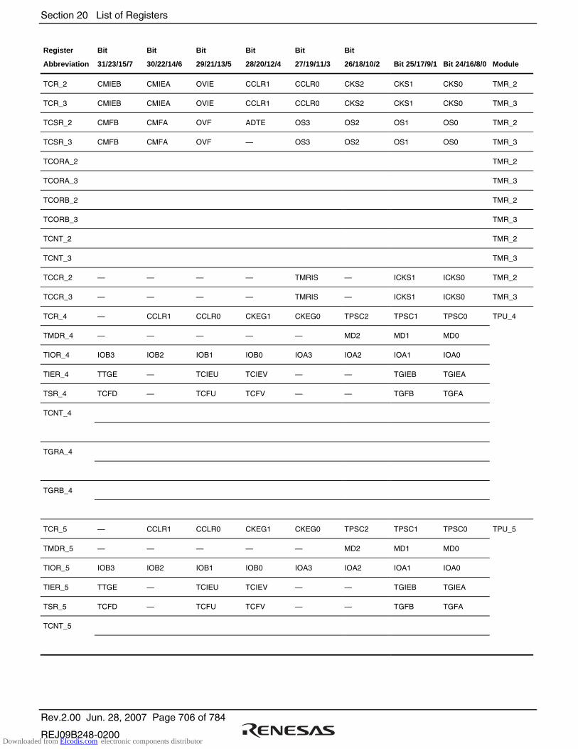
Section 20 List of Registers
Rev.2.00 Jun. 28, 2007 Page 706 of 784
REJ09B248-0200
Register
Abbreviation
Bit
31/23/15/7
Bit
30/22/14/6
Bit
29/21/13/5
Bit
28/20/12/4
Bit
27/19/11/3
Bit
26/18/10/2 Bit 25/17/9/1 Bit 24/16/8/0 Module
TCR_2 CMIEB CMIEA OVIE CCLR1 CCLR0 CKS2 CKS1 CKS0 TMR_2
TCR_3 CMIEB CMIEA OVIE CCLR1 CCLR0 CKS2 CKS1 CKS0 TMR_3
TCSR_2 CMFB CMFA OVF ADTE OS3 OS2 OS1 OS0 TMR_2
TCSR_3 CMFB CMFA OVF — OS3 OS2 OS1 OS0 TMR_3
TCORA_2 TMR_2
TCORA_3 TMR_3
TCORB_2 TMR_2
TCORB_3 TMR_3
TCNT_2 TMR_2
TCNT_3 TMR_3
TCCR_2 — — — — TMRIS — ICKS1 ICKS0 TMR_2
TCCR_3 — — — — TMRIS — ICKS1 ICKS0 TMR_3
TCR_4 — CCLR1 CCLR0 CKEG1 CKEG0 TPSC2 TPSC1 TPSC0 TPU_4
TMDR_4 — — — — — MD2 MD1 MD0
TIOR_4 IOB3 IOB2 IOB1 IOB0 IOA3 IOA2 IOA1 IOA0
TIER_4 TTGE — TCIEU TCIEV — — TGIEB TGIEA
TSR_4 TCFD — TCFU TCFV — — TGFB TGFA
TCNT_4
TGRA_4
TGRB_4
TCR_5 — CCLR1 CCLR0 CKEG1 CKEG0 TPSC2 TPSC1 TPSC0 TPU_5
TMDR_5 — — — — — MD2 MD1 MD0
TIOR_5 IOB3 IOB2 IOB1 IOB0 IOA3 IOA2 IOA1 IOA0
TIER_5 TTGE — TCIEU TCIEV — — TGIEB TGIEA
TSR_5 TCFD — TCFU TCFV — — TGFB TGFA
TCNT_5
Downloaded from Elcodis.com electronic components distributor
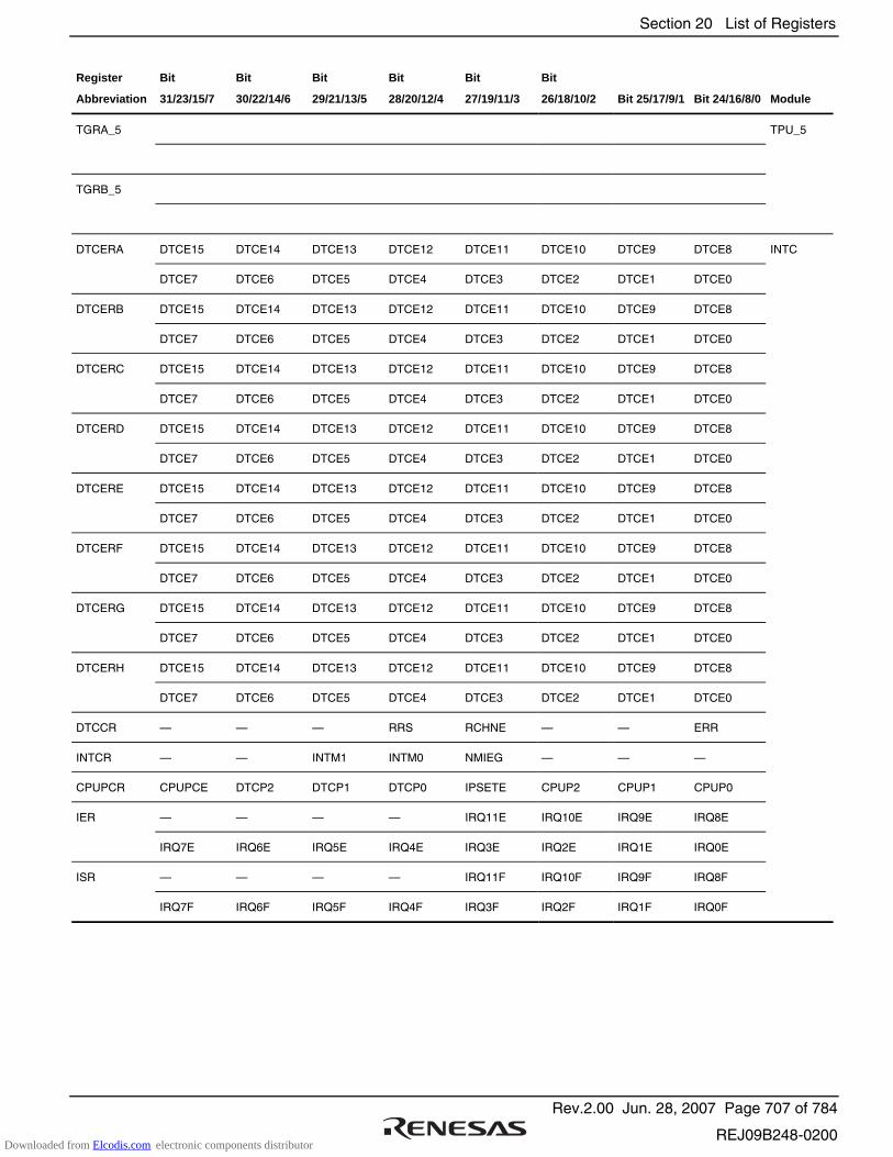
Section 20 List of Registers
Rev.2.00 Jun. 28, 2007 Page 707 of 784
REJ09B248-0200
Register
Abbreviation
Bit
31/23/15/7
Bit
30/22/14/6
Bit
29/21/13/5
Bit
28/20/12/4
Bit
27/19/11/3
Bit
26/18/10/2 Bit 25/17/9/1 Bit 24/16/8/0 Module
TGRA_5 TPU_5
TGRB_5
DTCERA DTCE15 DTCE14 DTCE13 DTCE12 DTCE11 DTCE10 DTCE9 DTCE8 INTC
DTCE7 DTCE6 DTCE5 DTCE4 DTCE3 DTCE2 DTCE1 DTCE0
DTCERB DTCE15 DTCE14 DTCE13 DTCE12 DTCE11 DTCE10 DTCE9 DTCE8
DTCE7 DTCE6 DTCE5 DTCE4 DTCE3 DTCE2 DTCE1 DTCE0
DTCERC DTCE15 DTCE14 DTCE13 DTCE12 DTCE11 DTCE10 DTCE9 DTCE8
DTCE7 DTCE6 DTCE5 DTCE4 DTCE3 DTCE2 DTCE1 DTCE0
DTCERD DTCE15 DTCE14 DTCE13 DTCE12 DTCE11 DTCE10 DTCE9 DTCE8
DTCE7 DTCE6 DTCE5 DTCE4 DTCE3 DTCE2 DTCE1 DTCE0
DTCERE DTCE15 DTCE14 DTCE13 DTCE12 DTCE11 DTCE10 DTCE9 DTCE8
DTCE7 DTCE6 DTCE5 DTCE4 DTCE3 DTCE2 DTCE1 DTCE0
DTCERF DTCE15 DTCE14 DTCE13 DTCE12 DTCE11 DTCE10 DTCE9 DTCE8
DTCE7 DTCE6 DTCE5 DTCE4 DTCE3 DTCE2 DTCE1 DTCE0
DTCERG DTCE15 DTCE14 DTCE13 DTCE12 DTCE11 DTCE10 DTCE9 DTCE8
DTCE7 DTCE6 DTCE5 DTCE4 DTCE3 DTCE2 DTCE1 DTCE0
DTCERH DTCE15 DTCE14 DTCE13 DTCE12 DTCE11 DTCE10 DTCE9 DTCE8
DTCE7 DTCE6 DTCE5 DTCE4 DTCE3 DTCE2 DTCE1 DTCE0
DTCCR — — — RRS RCHNE — — ERR
INTCR — — INTM1 INTM0 NMIEG — — —
CPUPCR CPUPCE DTCP2 DTCP1 DTCP0 IPSETE CPUP2 CPUP1 CPUP0
IER — — — — IRQ11E IRQ10E IRQ9E IRQ8E
IRQ7E IRQ6E IRQ5E IRQ4E IRQ3E IRQ2E IRQ1E IRQ0E
ISR — — — — IRQ11F IRQ10F IRQ9F IRQ8F
IRQ7F IRQ6F IRQ5F IRQ4F IRQ3F IRQ2F IRQ1F IRQ0F
Downloaded from Elcodis.com electronic components distributor

Section 20 List of Registers
Rev.2.00 Jun. 28, 2007 Page 708 of 784
REJ09B248-0200
Register
Abbreviation
Bit
31/23/15/7
Bit
30/22/14/6
Bit
29/21/13/5
Bit
28/20/12/4
Bit
27/19/11/3
Bit
26/18/10/2 Bit 25/17/9/1 Bit 24/16/8/0 Module
PORT1 P17 P16 P15 P14 P13 P12 P11 P10 I/O port
PORT2 P27 P26 P25 P24 P23 P22 P21 P20
PORT3 P37 P36 P35 P34 P33 P32 P31 P30
PORT5 P57 P56 P55 P54 P53 P52 P51 P50
PORT6 — — P65 P64 P63 P62 P61 P60
PORTA PA7 PA6 PA5 PA4 PA3 PA2 PA1 PA0
PORTB — — — — PB3 PB2 PB1 PB0
PORTD PD7 PD6 PD5 PD4 PD3 PD2 PD1 PD0
PORTE PE7 PE6 PE5 PE4 PE3 PE2 PE1 PE0
PORTF PF7 PF6 PF5 PF4 PF3 PF2 PF1 PF0
P1DR P17DR P16DR P15DR P14DR P13DR P12DR P11DR P10DR
P2DR P27DR P26DR P25DR P24DR P23DR P22DR P21DR P20DR
P3DR P37DR P36DR P35DR P34DR P33DR P32DR P31DR P30DR
P6DR — — P65DR P64DR P63DR P62DR P61DR P60DR
PADR PA7DR PA6DR PA5DR PA4DR PA3DR PA2DR PA1DR PA0DR
PBDR — — — — PB3DR PB2DR PB1DR PB0DR
PDDR PD7DR PD6DR PD5DR PD4DR PD3DR PD2DR PD1DR PD0DR
PEDR PE7DR PE6DR PE5DR PE4DR PE3DR PE2DR PE1DR PE0DR
PFDR PF7DR PF6DR PF5DR PF4DR PF3DR PF2DR PF1DR PF0DR
SMR_2*1 C/A
(GM)
CHR
(BLK)
PE
(PE)
O/E
(O/E)
STOP
(BCP1)
MP
(BCP0)
CKS1 CKS0 SCI_2
BRR_2
SCR_2*1 TIE RIE TE RE MPIE TEIE CKE1 CKE0
TDR_2
SSR_2*1 TDRE RDRF ORER FER
(ERS)
PER TEND MPB MPBT
RDR_2
SCMR_2 — — — — SDIR SINV — SMIF
Downloaded from Elcodis.com electronic components distributor
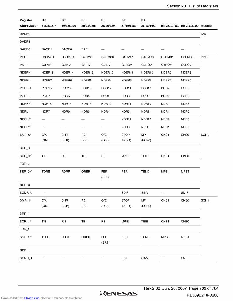
Section 20 List of Registers
Rev.2.00 Jun. 28, 2007 Page 709 of 784
REJ09B248-0200
Register
Abbreviation
Bit
31/23/15/7
Bit
30/22/14/6
Bit
29/21/13/5
Bit
28/20/12/4
Bit
27/19/11/3
Bit
26/18/10/2 Bit 25/17/9/1 Bit 24/16/8/0 Module
DADR0 D/A
DADR1
DACR01 DAOE1 DAOE0 DAE — — — — —
PCR G3CMS1 G3CMS0 G2CMS1 G2CMS0 G1CMS1 G1CMS0 G0CMS1 G0CMS0 PPG
PMR G3INV G2INV G1INV G0INV G3NOV G2NOV G1NOV G0NOV
NDERH NDER15 NDER14 NDER13 NDER12 NDER11 NDER10 NDER9 NDER8
NDERL NDER7 NDER6 NDER5 NDER4 NDER3 NDER2 NDER1 NDER0
PODRH POD15 POD14 POD13 POD12 POD11 POD10 POD9 POD8
PODRL POD7 POD6 POD5 POD4 POD3 POD2 POD1 POD0
NDRH*2 NDR15 NDR14 NDR13 NDR12 NDR11 NDR10 NDR9 NDR8
NDRL*2 NDR7 NDR6 NDR5 NDR4 NDR3 NDR2 NDR1 NDR0
NDRH*2 — — — — NDR11 NDR10 NDR9 NDR8
NDRL*2 — — — — NDR3 NDR2 NDR1 NDR0
SMR_0*1 C/A
(GM)
CHR
(BLK)
PE
(PE)
O/E
(O/E)
STOP
(BCP1)
MP
(BCP0)
CKS1 CKS0 SCI_0
BRR_0
SCR_0*1 TIE RIE TE RE MPIE TEIE CKE1 CKE0
TDR_0
SSR_0*1 TDRE RDRF ORER FER
(ERS)
PER TEND MPB MPBT
RDR_0
SCMR_0 — — — — SDIR SINV — SMIF
SMR_1*1 C/A
(GM)
CHR
(BLK)
PE
(PE)
O/E
(O/E)
STOP
(BCP1)
MP
(BCP0)
CKS1 CKS0 SCI_1
BRR_1
SCR_1*1 TIE RIE TE RE MPIE TEIE CKE1 CKE0
TDR_1
SSR_1*1 TDRE RDRF ORER FER
(ERS)
PER TEND MPB MPBT
RDR_1
SCMR_1 — — — — SDIR SINV — SMIF
Downloaded from Elcodis.com electronic components distributor

Section 20 List of Registers
Rev.2.00 Jun. 28, 2007 Page 710 of 784
REJ09B248-0200
Register
Abbreviation
Bit
31/23/15/7
Bit
30/22/14/6
Bit
29/21/13/5
Bit
28/20/12/4
Bit
27/19/11/3
Bit
26/18/10/2 Bit 25/17/9/1 Bit 24/16/8/0 Module
ADDRA A/D
ADDRB
ADDRC
ADDRD
ADDRE
ADDRF
ADDRG
ADDRH
ADCSR ADF ADIE ADST — CH3 CH2 CH1 CH0
ADCR TRGS1 TRGS0 SCANE SCANS CKS1 CKS0 — —
TCSR OVF WT/IT TME — — CKS2 CKS1 CKS0 WDT
TCNT
RSTCSR WOVF RSTE — — — — — —
TCR_0 CMIEB CMIEA OVIE CCLR1 CCLR0 CKS2 CKS1 CKS0 TMR_0
TCR_1 CMIEB CMIEA OVIE CCLR1 CCLR0 CKS2 CKS1 CKS0 TMR_1
TCSR_0 CMFB CMFA OVF ADTE OS3 OS2 OS1 OS0 TMR_0
TCSR_1 CMFB CMFA OVF — OS3 OS2 OS1 OS0 TMR_1
Downloaded from Elcodis.com electronic components distributor
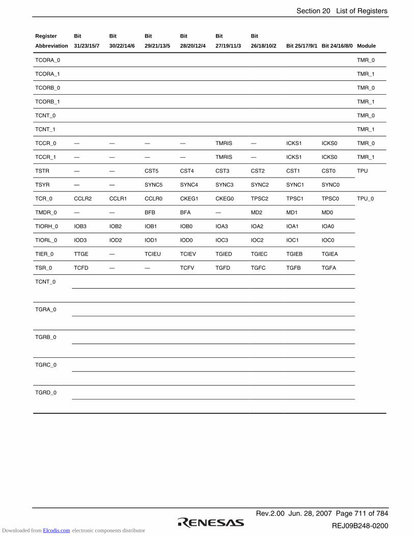
Section 20 List of Registers
Rev.2.00 Jun. 28, 2007 Page 711 of 784
REJ09B248-0200
Register
Abbreviation
Bit
31/23/15/7
Bit
30/22/14/6
Bit
29/21/13/5
Bit
28/20/12/4
Bit
27/19/11/3
Bit
26/18/10/2 Bit 25/17/9/1 Bit 24/16/8/0 Module
TCORA_0 TMR_0
TCORA_1 TMR_1
TCORB_0 TMR_0
TCORB_1 TMR_1
TCNT_0 TMR_0
TCNT_1 TMR_1
TCCR_0 — — — — TMRIS — ICKS1 ICKS0 TMR_0
TCCR_1 — — — — TMRIS — ICKS1 ICKS0 TMR_1
TSTR — — CST5 CST4 CST3 CST2 CST1 CST0 TPU
TSYR — — SYNC5 SYNC4 SYNC3 SYNC2 SYNC1 SYNC0
TCR_0 CCLR2 CCLR1 CCLR0 CKEG1 CKEG0 TPSC2 TPSC1 TPSC0 TPU_0
TMDR_0 — — BFB BFA — MD2 MD1 MD0
TIORH_0 IOB3 IOB2 IOB1 IOB0 IOA3 IOA2 IOA1 IOA0
TIORL_0 IOD3 IOD2 IOD1 IOD0 IOC3 IOC2 IOC1 IOC0
TIER_0 TTGE — TCIEU TCIEV TGIED TGIEC TGIEB TGIEA
TSR_0 TCFD — — TCFV TGFD TGFC TGFB TGFA
TCNT_0
TGRA_0
TGRB_0
TGRC_0
TGRD_0
Downloaded from Elcodis.com electronic components distributor
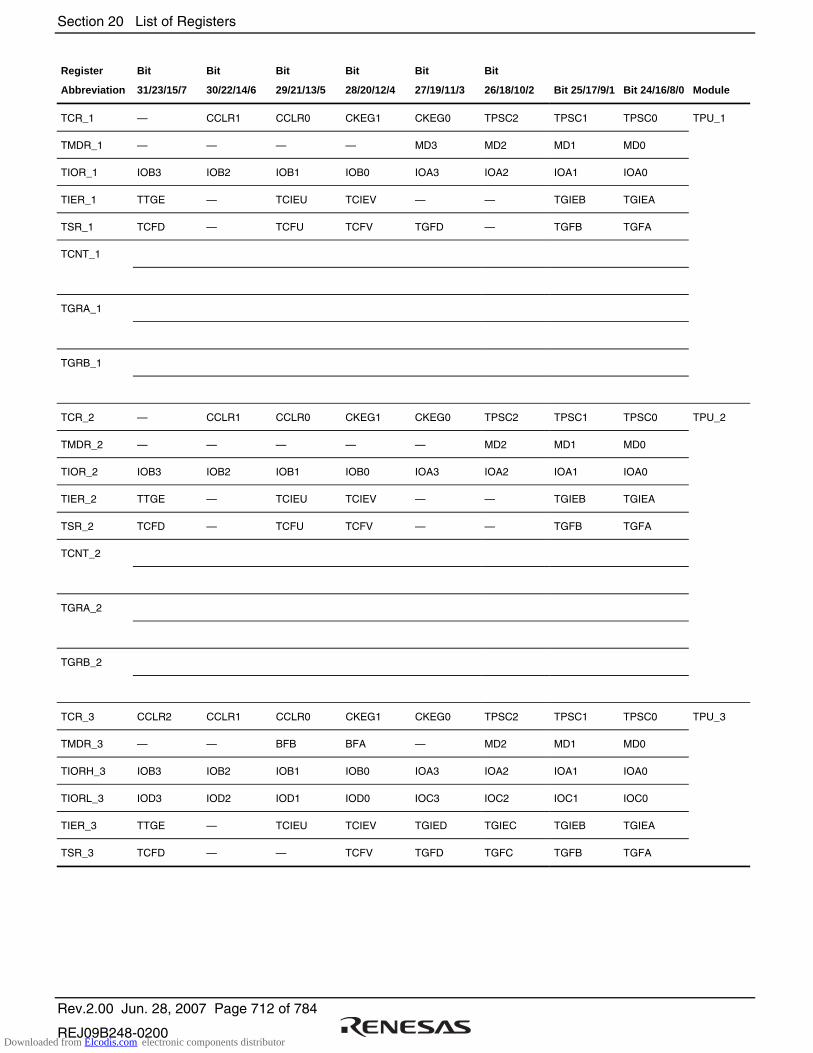
Section 20 List of Registers
Rev.2.00 Jun. 28, 2007 Page 712 of 784
REJ09B248-0200
Register
Abbreviation
Bit
31/23/15/7
Bit
30/22/14/6
Bit
29/21/13/5
Bit
28/20/12/4
Bit
27/19/11/3
Bit
26/18/10/2 Bit 25/17/9/1 Bit 24/16/8/0 Module
TCR_1 — CCLR1 CCLR0 CKEG1 CKEG0 TPSC2 TPSC1 TPSC0 TPU_1
TMDR_1 — — — — MD3 MD2 MD1 MD0
TIOR_1 IOB3 IOB2 IOB1 IOB0 IOA3 IOA2 IOA1 IOA0
TIER_1 TTGE — TCIEU TCIEV — — TGIEB TGIEA
TSR_1 TCFD — TCFU TCFV TGFD — TGFB TGFA
TCNT_1
TGRA_1
TGRB_1
TCR_2 — CCLR1 CCLR0 CKEG1 CKEG0 TPSC2 TPSC1 TPSC0 TPU_2
TMDR_2 — — — — — MD2 MD1 MD0
TIOR_2 IOB3 IOB2 IOB1 IOB0 IOA3 IOA2 IOA1 IOA0
TIER_2 TTGE — TCIEU TCIEV — — TGIEB TGIEA
TSR_2 TCFD — TCFU TCFV — — TGFB TGFA
TCNT_2
TGRA_2
TGRB_2
TCR_3 CCLR2 CCLR1 CCLR0 CKEG1 CKEG0 TPSC2 TPSC1 TPSC0 TPU_3
TMDR_3 — — BFB BFA — MD2 MD1 MD0
TIORH_3 IOB3 IOB2 IOB1 IOB0 IOA3 IOA2 IOA1 IOA0
TIORL_3 IOD3 IOD2 IOD1 IOD0 IOC3 IOC2 IOC1 IOC0
TIER_3 TTGE — TCIEU TCIEV TGIED TGIEC TGIEB TGIEA
TSR_3 TCFD — — TCFV TGFD TGFC TGFB TGFA
Downloaded from Elcodis.com electronic components distributor
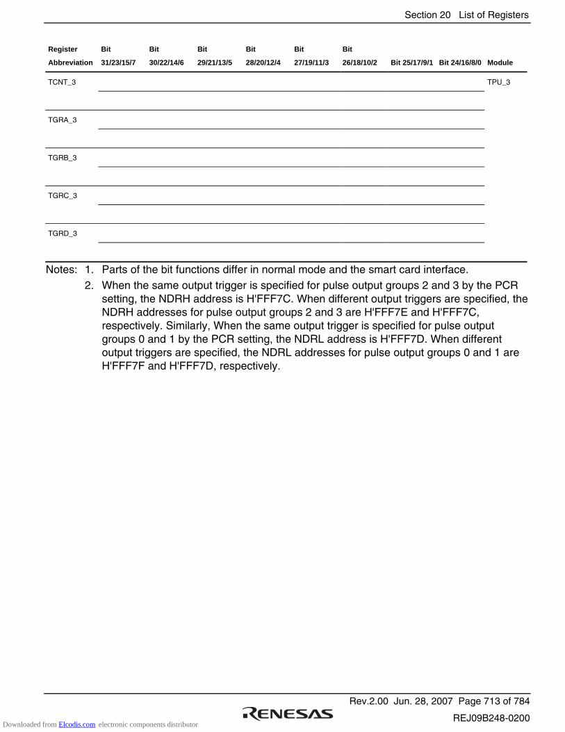
Section 20 List of Registers
Rev.2.00 Jun. 28, 2007 Page 713 of 784
REJ09B248-0200
Register
Abbreviation
Bit
31/23/15/7
Bit
30/22/14/6
Bit
29/21/13/5
Bit
28/20/12/4
Bit
27/19/11/3
Bit
26/18/10/2 Bit 25/17/9/1 Bit 24/16/8/0 Module
TCNT_3 TPU_3
TGRA_3
TGRB_3
TGRC_3
TGRD_3
Notes: 1. Parts of the bit functions differ in normal mode and the smart card interface. 2. When the same output trigger is specified for pulse output groups 2 and 3 by the PCR
setting, the NDRH address is H'FFF7C. When different output triggers are specified, the NDRH addresses for pulse output groups 2 and 3 are H'FFF7E and H'FFF7C, respectively. Similarly, When the same output trigger is specified for pulse output groups 0 and 1 by the PCR setting, the NDRL address is H'FFF7D. When different output triggers are specified, the NDRL addresses for pulse output groups 0 and 1 are H'FFF7F and H'FFF7D, respectively.
Downloaded from Elcodis.com electronic components distributor
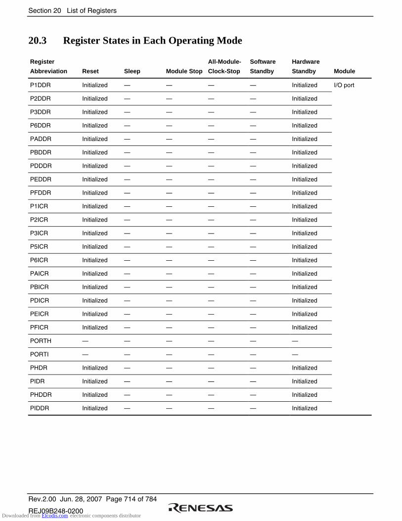
Section 20 List of Registers
Rev.2.00 Jun. 28, 2007 Page 714 of 784
REJ09B248-0200
20.3 Register States in Each Operating Mode
Register
Abbreviation Reset Sleep Module Stop
All-Module-
Clock-Stop
Software
Standby
Hardware
Standby Module
P1DDR Initialized — — — — Initialized I/O port
P2DDR Initialized — — — — Initialized
P3DDR Initialized — — — — Initialized
P6DDR Initialized — — — — Initialized
PADDR Initialized — — — — Initialized
PBDDR Initialized — — — — Initialized
PDDDR Initialized — — — — Initialized
PEDDR Initialized — — — — Initialized
PFDDR Initialized — — — — Initialized
P1ICR Initialized — — — — Initialized
P2ICR Initialized — — — — Initialized
P3ICR Initialized — — — — Initialized
P5ICR Initialized — — — — Initialized
P6ICR Initialized — — — — Initialized
PAICR Initialized — — — — Initialized
PBICR Initialized — — — — Initialized
PDICR Initialized — — — — Initialized
PEICR Initialized — — — — Initialized
PFICR Initialized — — — — Initialized
PORTH — — — — — —
PORTI — — — — — —
PHDR Initialized — — — — Initialized
PIDR Initialized — — — — Initialized
PHDDR Initialized — — — — Initialized
PIDDR Initialized — — — — Initialized
Downloaded from Elcodis.com electronic components distributor

Section 20 List of Registers
Rev.2.00 Jun. 28, 2007 Page 715 of 784
REJ09B248-0200
Register
Abbreviation Reset Sleep Module Stop
All-Module-
Clock-Stop
Software
Standby
Hardware
Standby Module
PHICR Initialized — — — — Initialized I/O port
PIICR Initialized — — — — Initialized
PDPCR Initialized — — — — Initialized
PEPCR Initialized — — — — Initialized
PFPCR Initialized — — — — Initialized
PHPCR Initialized — — — — Initialized
PIPCR Initialized — — — — Initialized
P2ODR Initialized — — — — Initialized
PFODR Initialized — — — — Initialized
PFCR0 Initialized — — — — Initialized
PFCR1 Initialized — — — — Initialized
PFCR2 Initialized — — — — Initialized
PFCR4 Initialized — — — — Initialized
PFCR6 Initialized — — — — Initialized
PFCR7 Initialized — — — — Initialized
PFCR9 Initialized — — — — Initialized
PFCRB Initialized — — — — Initialized
PFCRC Initialized — — — — Initialized
SSIER Initialized — — — — Initialized INTC
DSAR_0 Initialized — — — — Initialized DMAC_0
DDAR_0 Initialized — — — — Initialized
DOFR_0 Initialized — — — — Initialized
DTCR_0 Initialized — — — — Initialized
DBSR_0 Initialized — — — — Initialized
DMDR_0 Initialized — — — — Initialized
DACR_0 Initialized — — — — Initialized
Downloaded from Elcodis.com electronic components distributor

Section 20 List of Registers
Rev.2.00 Jun. 28, 2007 Page 716 of 784
REJ09B248-0200
Register
Abbreviation Reset Sleep Module Stop
All-Module-
Clock-Stop
Software
Standby
Hardware
Standby Module
DSAR_1 Initialized — — — — Initialized DMAC_1
DDAR_1 Initialized — — — — Initialized
DOFR_1 Initialized — — — — Initialized
DTCR_1 Initialized — — — — Initialized
DBSR_1 Initialized — — — — Initialized
DMDR_1 Initialized — — — — Initialized
DACR_1 Initialized — — — — Initialized
DSAR_2 Initialized — — — — Initialized DMAC_2
DDAR_2 Initialized — — — — Initialized
DOFR_2 Initialized — — — — Initialized
DTCR_2 Initialized — — — — Initialized
DBSR_2 Initialized — — — — Initialized
DMDR_2 Initialized — — — — Initialized
DACR_2 Initialized — — — — Initialized
DSAR_3 Initialized — — — — Initialized DMAC_3
DDAR_3 Initialized — — — — Initialized
DOFR_3 Initialized — — — — Initialized
DTCR_3 Initialized — — — — Initialized
DBSR_3 Initialized — — — — Initialized
DMDR_3 Initialized — — — — Initialized
DACR_3 Initialized — — — — Initialized
DMRSR_0 Initialized — — — — Initialized DMAC_0
DMRSR_1 Initialized — — — — Initialized DMAC_1
DMRSR_2 Initialized — — — — Initialized DMAC_2
DMRSR_3 Initialized — — — — Initialized DMAC_3
Downloaded from Elcodis.com electronic components distributor
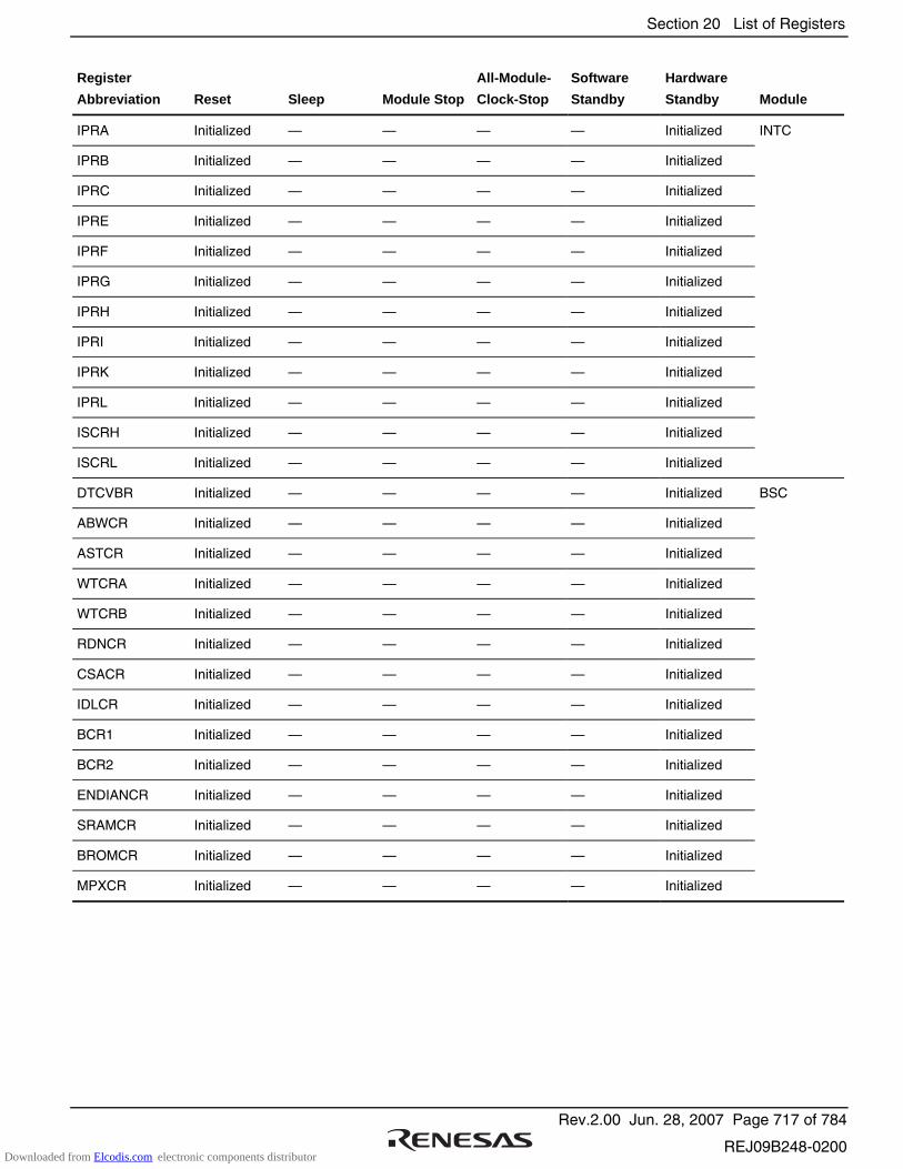
Section 20 List of Registers
Rev.2.00 Jun. 28, 2007 Page 717 of 784
REJ09B248-0200
Register
Abbreviation Reset Sleep Module Stop
All-Module-
Clock-Stop
Software
Standby
Hardware
Standby Module
IPRA Initialized — — — — Initialized INTC
IPRB Initialized — — — — Initialized
IPRC Initialized — — — — Initialized
IPRE Initialized — — — — Initialized
IPRF Initialized — — — — Initialized
IPRG Initialized — — — — Initialized
IPRH Initialized — — — — Initialized
IPRI Initialized — — — — Initialized
IPRK Initialized — — — — Initialized
IPRL Initialized — — — — Initialized
ISCRH Initialized — — — — Initialized
ISCRL Initialized — — — — Initialized
DTCVBR Initialized — — — — Initialized BSC
ABWCR Initialized — — — — Initialized
ASTCR Initialized — — — — Initialized
WTCRA Initialized — — — — Initialized
WTCRB Initialized — — — — Initialized
RDNCR Initialized — — — — Initialized
CSACR Initialized — — — — Initialized
IDLCR Initialized — — — — Initialized
BCR1 Initialized — — — — Initialized
BCR2 Initialized — — — — Initialized
ENDIANCR Initialized — — — — Initialized
SRAMCR Initialized — — — — Initialized
BROMCR Initialized — — — — Initialized
MPXCR Initialized — — — — Initialized
Downloaded from Elcodis.com electronic components distributor
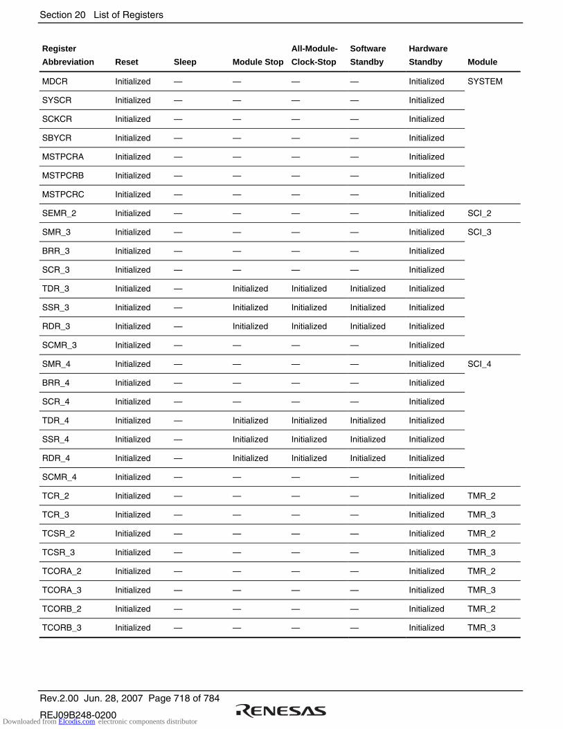
Section 20 List of Registers
Rev.2.00 Jun. 28, 2007 Page 718 of 784
REJ09B248-0200
Register
Abbreviation Reset Sleep Module Stop
All-Module-
Clock-Stop
Software
Standby
Hardware
Standby Module
MDCR Initialized — — — — Initialized SYSTEM
SYSCR Initialized — — — — Initialized
SCKCR Initialized — — — — Initialized
SBYCR Initialized — — — — Initialized
MSTPCRA Initialized — — — — Initialized
MSTPCRB Initialized — — — — Initialized
MSTPCRC Initialized — — — — Initialized
SEMR_2 Initialized — — — — Initialized SCI_2
SMR_3 Initialized — — — — Initialized SCI_3
BRR_3 Initialized — — — — Initialized
SCR_3 Initialized — — — — Initialized
TDR_3 Initialized — Initialized Initialized Initialized Initialized
SSR_3 Initialized — Initialized Initialized Initialized Initialized
RDR_3 Initialized — Initialized Initialized Initialized Initialized
SCMR_3 Initialized — — — — Initialized
SMR_4 Initialized — — — — Initialized SCI_4
BRR_4 Initialized — — — — Initialized
SCR_4 Initialized — — — — Initialized
TDR_4 Initialized — Initialized Initialized Initialized Initialized
SSR_4 Initialized — Initialized Initialized Initialized Initialized
RDR_4 Initialized — Initialized Initialized Initialized Initialized
SCMR_4 Initialized — — — — Initialized
TCR_2 Initialized — — — — Initialized TMR_2
TCR_3 Initialized — — — — Initialized TMR_3
TCSR_2 Initialized — — — — Initialized TMR_2
TCSR_3 Initialized — — — — Initialized TMR_3
TCORA_2 Initialized — — — — Initialized TMR_2
TCORA_3 Initialized — — — — Initialized TMR_3
TCORB_2 Initialized — — — — Initialized TMR_2
TCORB_3 Initialized — — — — Initialized TMR_3
Downloaded from Elcodis.com electronic components distributor

Section 20 List of Registers
Rev.2.00 Jun. 28, 2007 Page 719 of 784
REJ09B248-0200
Register
Abbreviation Reset Sleep Module Stop
All-Module-
Clock-Stop
Software
Standby
Hardware
Standby Module
TCNT_2 Initialized — — — — Initialized TMR_2
TCNT_3 Initialized — — — — Initialized TMR_3
TCCR_2 Initialized — — — — Initialized TMR_2
TCCR_3 Initialized — — — — Initialized TMR_3
TCR_4 Initialized — — — — Initialized TPU_4
TMDR_4 Initialized — — — — Initialized
TIOR_4 Initialized — — — — Initialized
TIER_4 Initialized — — — — Initialized
TSR_4 Initialized — — — — Initialized
TCNT_4 Initialized — — — — Initialized
TGRA_4 Initialized — — — — Initialized
TGRB_4 Initialized — — — — Initialized
TCR_5 Initialized — — — — Initialized TPU_5
TMDR_5 Initialized — — — — Initialized
TIOR_5 Initialized — — — — Initialized
TIER_5 Initialized — — — — Initialized
TSR_5 Initialized — — — — Initialized
TCNT_5 Initialized — — — — Initialized
TGRA_5 Initialized — — — — Initialized
TGRB_5 Initialized — — — — Initialized
DTCERA Initialized — — — — Initialized INTC
DTCERB Initialized — — — — Initialized
DTCERC Initialized — — — — Initialized
DTCERD Initialized — — — — Initialized
DTCERE Initialized — — — — Initialized
DTCERF Initialized — — — — Initialized
DTCERG Initialized — — — — Initialized
DTCERH Initialized — — — — Initialized
DTCCR Initialized — — — — Initialized
INTCR Initialized — — — — Initialized
Downloaded from Elcodis.com electronic components distributor
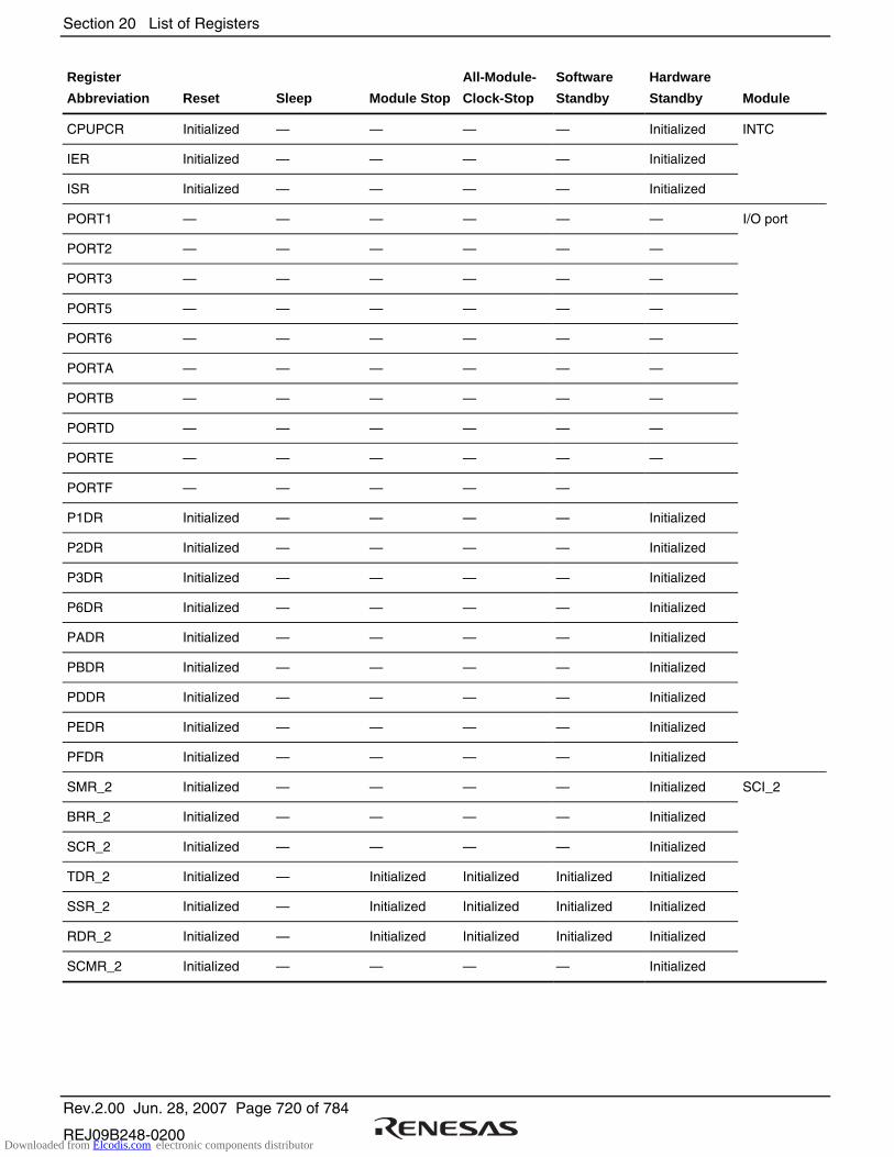
Section 20 List of Registers
Rev.2.00 Jun. 28, 2007 Page 720 of 784
REJ09B248-0200
Register
Abbreviation Reset Sleep Module Stop
All-Module-
Clock-Stop
Software
Standby
Hardware
Standby Module
CPUPCR Initialized — — — — Initialized INTC
IER Initialized — — — — Initialized
ISR Initialized — — — — Initialized
PORT1 — — — — — — I/O port
PORT2 — — — — — —
PORT3 — — — — — —
PORT5 — — — — — —
PORT6 — — — — — —
PORTA — — — — — —
PORTB — — — — — —
PORTD — — — — — —
PORTE — — — — — —
PORTF — — — — —
P1DR Initialized — — — — Initialized
P2DR Initialized — — — — Initialized
P3DR Initialized — — — — Initialized
P6DR Initialized — — — — Initialized
PADR Initialized — — — — Initialized
PBDR Initialized — — — — Initialized
PDDR Initialized — — — — Initialized
PEDR Initialized — — — — Initialized
PFDR Initialized — — — — Initialized
SMR_2 Initialized — — — — Initialized SCI_2
BRR_2 Initialized — — — — Initialized
SCR_2 Initialized — — — — Initialized
TDR_2 Initialized — Initialized Initialized Initialized Initialized
SSR_2 Initialized — Initialized Initialized Initialized Initialized
RDR_2 Initialized — Initialized Initialized Initialized Initialized
SCMR_2 Initialized — — — — Initialized
Downloaded from Elcodis.com electronic components distributor
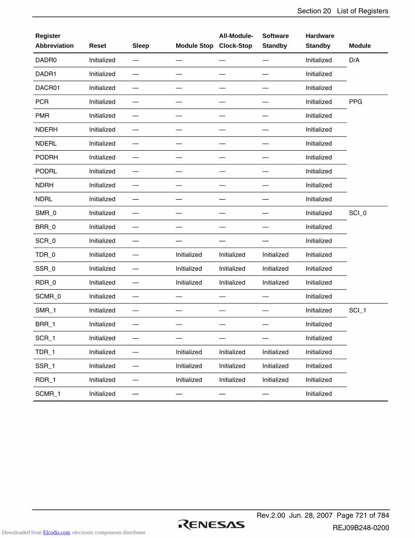
Section 20 List of Registers
Rev.2.00 Jun. 28, 2007 Page 721 of 784
REJ09B248-0200
Register
Abbreviation Reset Sleep Module Stop
All-Module-
Clock-Stop
Software
Standby
Hardware
Standby Module
DADR0 Initialized — — — — Initialized D/A
DADR1 Initialized — — — — Initialized
DACR01 Initialized — — — — Initialized
PCR Initialized — — — — Initialized PPG
PMR Initialized — — — — Initialized
NDERH Initialized — — — — Initialized
NDERL Initialized — — — — Initialized
PODRH Initialized — — — — Initialized
PODRL Initialized — — — — Initialized
NDRH Initialized — — — — Initialized
NDRL Initialized — — — — Initialized
SMR_0 Initialized — — — — Initialized SCI_0
BRR_0 Initialized — — — — Initialized
SCR_0 Initialized — — — — Initialized
TDR_0 Initialized — Initialized Initialized Initialized Initialized
SSR_0 Initialized — Initialized Initialized Initialized Initialized
RDR_0 Initialized — Initialized Initialized Initialized Initialized
SCMR_0 Initialized — — — — Initialized
SMR_1 Initialized — — — — Initialized SCI_1
BRR_1 Initialized — — — — Initialized
SCR_1 Initialized — — — — Initialized
TDR_1 Initialized — Initialized Initialized Initialized Initialized
SSR_1 Initialized — Initialized Initialized Initialized Initialized
RDR_1 Initialized — Initialized Initialized Initialized Initialized
SCMR_1 Initialized — — — — Initialized
Downloaded from Elcodis.com electronic components distributor

Section 20 List of Registers
Rev.2.00 Jun. 28, 2007 Page 722 of 784
REJ09B248-0200
Register
Abbreviation Reset Sleep Module Stop
All-Module-
Clock-Stop
Software
Standby
Hardware
Standby Module
ADDRA Initialized — — — — Initialized A/D
ADDRB Initialized — — — — Initialized
ADDRC Initialized — — — — Initialized
ADDRD Initialized — — — — Initialized
ADDRE Initialized — — — — Initialized
ADDRF Initialized — — — — Initialized
ADDRG Initialized — — — — Initialized
ADDRH Initialized — — — — Initialized
ADCSR Initialized — — — — Initialized
ADCR Initialized — — — — Initialized
TCSR Initialized — — — — Initialized WDT
TCNT Initialized — — — — Initialized
RSTCSR Initialized — — — — Initialized
TCR_0 Initialized — — — — Initialized TMR_0
TCR_1 Initialized — — — — Initialized TMR_1
TCSR_0 Initialized — — — — Initialized TMR_0
TCSR_1 Initialized — — — — Initialized TMR_1
TCORA_0 Initialized — — — — Initialized TMR_0
TCORA_1 Initialized — — — — Initialized TMR_1
TCORB_0 Initialized — — — — Initialized TMR_0
TCORB_1 Initialized — — — — Initialized TMR_1
TCNT_0 Initialized — — — — Initialized TMR_0
TCNT_1 Initialized — — — — Initialized TMR_1
TCCR_0 Initialized — — — — Initialized TMR_0
TCCR_1 Initialized — — — — Initialized TMR_1
TSTR Initialized — — — — Initialized TPU
TSYR Initialized — — — — Initialized
Downloaded from Elcodis.com electronic components distributor
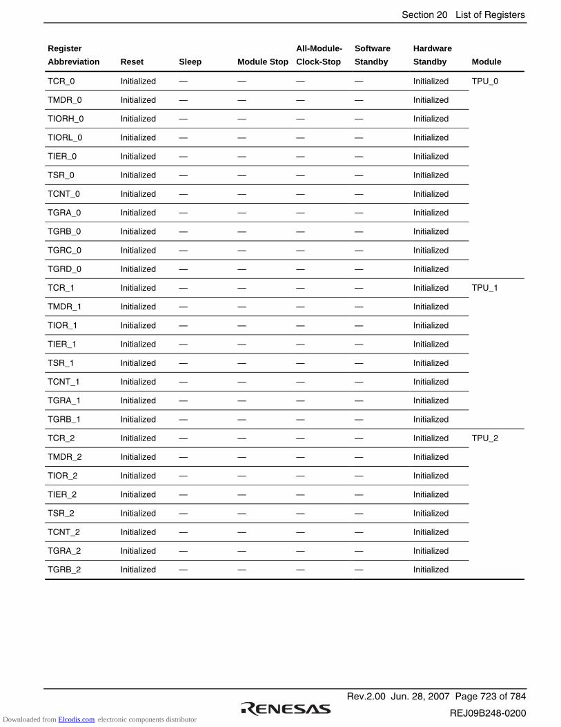
Section 20 List of Registers
Rev.2.00 Jun. 28, 2007 Page 723 of 784
REJ09B248-0200
Register
Abbreviation Reset Sleep Module Stop
All-Module-
Clock-Stop
Software
Standby
Hardware
Standby Module
TCR_0 Initialized — — — — Initialized TPU_0
TMDR_0 Initialized — — — — Initialized
TIORH_0 Initialized — — — — Initialized
TIORL_0 Initialized — — — — Initialized
TIER_0 Initialized — — — — Initialized
TSR_0 Initialized — — — — Initialized
TCNT_0 Initialized — — — — Initialized
TGRA_0 Initialized — — — — Initialized
TGRB_0 Initialized — — — — Initialized
TGRC_0 Initialized — — — — Initialized
TGRD_0 Initialized — — — — Initialized
TCR_1 Initialized — — — — Initialized TPU_1
TMDR_1 Initialized — — — — Initialized
TIOR_1 Initialized — — — — Initialized
TIER_1 Initialized — — — — Initialized
TSR_1 Initialized — — — — Initialized
TCNT_1 Initialized — — — — Initialized
TGRA_1 Initialized — — — — Initialized
TGRB_1 Initialized — — — — Initialized
TCR_2 Initialized — — — — Initialized TPU_2
TMDR_2 Initialized — — — — Initialized
TIOR_2 Initialized — — — — Initialized
TIER_2 Initialized — — — — Initialized
TSR_2 Initialized — — — — Initialized
TCNT_2 Initialized — — — — Initialized
TGRA_2 Initialized — — — — Initialized
TGRB_2 Initialized — — — — Initialized
Downloaded from Elcodis.com electronic components distributor

Section 20 List of Registers
Rev.2.00 Jun. 28, 2007 Page 724 of 784
REJ09B248-0200
Register
Abbreviation Reset Sleep Module Stop
All-Module-
Clock-Stop
Software
Standby
Hardware
Standby Module
TCR_3 Initialized — — — — Initialized TPU_3
TMDR_3 Initialized — — — — Initialized
TIORH_3 Initialized — — — — Initialized
TIORL_3 Initialized — — — — Initialized
TIER_3 Initialized — — — — Initialized
TSR_3 Initialized — — — — Initialized
TCNT_3 Initialized — — — — Initialized
TGRA_3 Initialized — — — — Initialized
TGRB_3 Initialized — — — — Initialized
TGRC_3 Initialized — — — — Initialized
TGRD_3 Initialized — — — — Initialized
Downloaded from Elcodis.com electronic components distributor
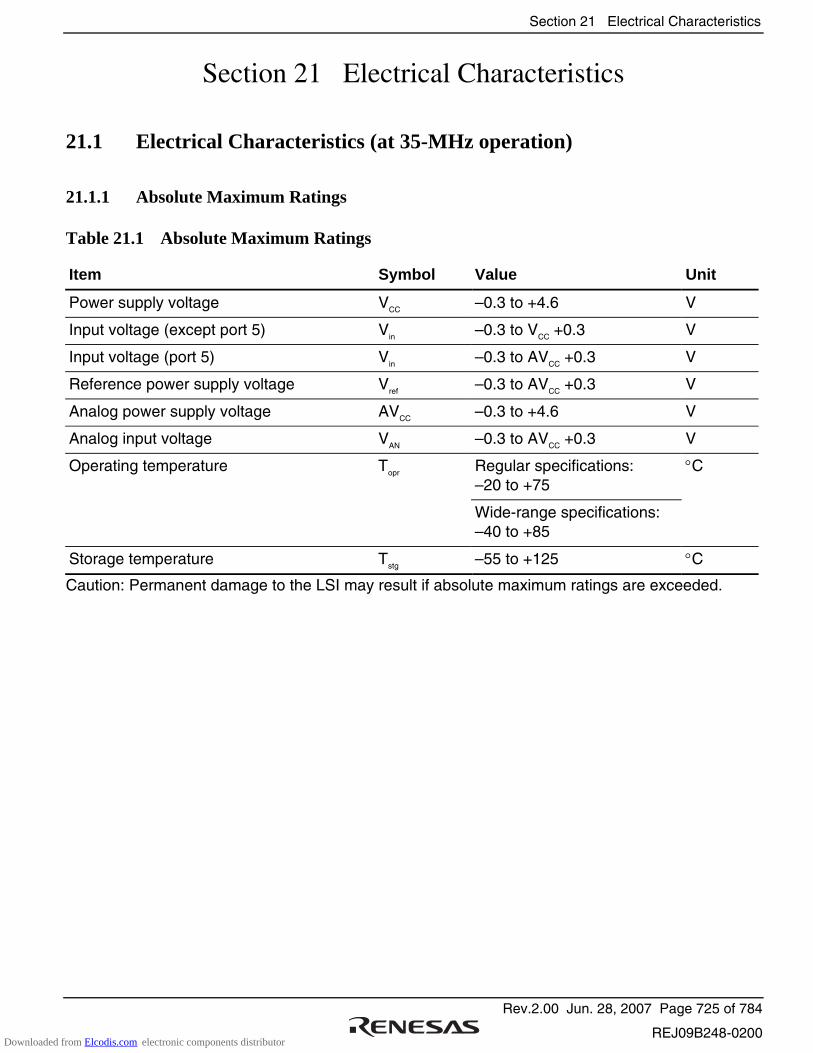
Section 21 Electrical Characteristics
Rev.2.00 Jun. 28, 2007 Page 725 of 784
REJ09B248-0200
Section 21 Electrical Characteristics
21.1 Electrical Characteristics (at 35-MHz operation)
21.1.1 Absolute Maximum Ratings
Table 21.1 Absolute Maximum Ratings
Item Symbol Value Unit
Power supply voltage VCC –0.3 to +4.6 V
Input voltage (except port 5) Vin –0.3 to VCC +0.3 V
Input voltage (port 5) Vin –0.3 to AVCC +0.3 V
Reference power supply voltage Vref –0.3 to AVCC +0.3 V
Analog power supply voltage AVCC –0.3 to +4.6 V
Analog input voltage VAN –0.3 to AVCC +0.3 V
Regular specifications: –20 to +75
Operating temperature Topr
Wide-range specifications: –40 to +85
°C
Storage temperature Tstg –55 to +125 °C
Caution: Permanent damage to the LSI may result if absolute maximum ratings are exceeded.
Downloaded from Elcodis.com electronic components distributor
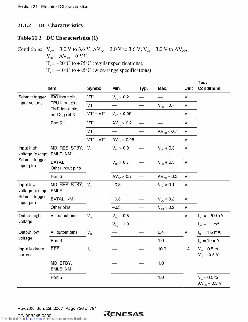
Section 21 Electrical Characteristics
Rev.2.00 Jun. 28, 2007 Page 726 of 784
REJ09B248-0200
21.1.2 DC Characteristics
Table 21.2 DC Characteristics (1)
Conditions: VCC = 3.0 V to 3.6 V, AVCC = 3.0 V to 3.6 V, Vref = 3.0 V to AVCC, VSS = AVSS = 0 V*1, Ta = –20°C to +75°C (regular specifications), Ta = –40°C to +85°C (wide-range specifications)
Item Symbol Min. Typ. Max. Unit Test Conditions
VT– VCC × 0.2 V
VT+ VCC × 0.7 V
Schmitt trigger input voltage
IRQ input pin, TPU input pin, TMR input pin, port 2, port 3 VT+ – VT– VCC × 0.06 V
Port 5*2 VT– AVCC × 0.2 V
VT+ AVCC × 0.7 V
VT+ – VT– AVCC × 0.06 V
MD, RES, STBY, EMLE, NMI
VIH VCC × 0.9 VCC + 0.3 V
EXTAL Other input pins
VCC × 0.7 VCC + 0.3 V
Input high voltage (except Schmitt trigger input pin)
Port 5 AVCC × 0.7 AVCC + 0.3 V
MD, RES, STBY, EMLE
VIL –0.3 VCC × 0.1 V
EXTAL, NMI –0.3 VCC × 0.2 V
Input low voltage (except Schmitt trigger input pin)
Other pins –0.3 VCC × 0.2 V
All output pins VOH VCC – 0.5 V IOH = –200 µA Output high voltage VCC – 1.0 IOH = –1 mA
All output pins 0.4 V IOL = 1.6 mA Output low voltage Port 3
VOL
1.0 IOL = 10 mA
Input leakage current
RES |Iin| 10.0 µA Vin = 0.5 to VCC – 0.5 V
MD, STBY, EMLE, NMI
1.0
Port 5 1.0 Vin = 0.5 to AVCC – 0.5 V
Downloaded from Elcodis.com electronic components distributor
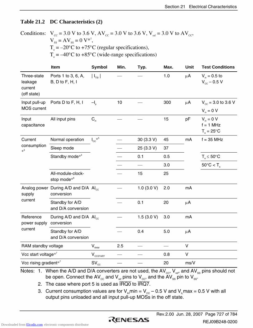
Section 21 Electrical Characteristics
Rev.2.00 Jun. 28, 2007 Page 727 of 784
REJ09B248-0200
Table 21.2 DC Characteristics (2)
Conditions: VCC = 3.0 V to 3.6 V, AVCC = 3.0 V to 3.6 V, Vref = 3.0 V to AVCC, VSS = AVSS = 0 V*1, Ta = –20°C to +75°C (regular specifications), Ta = –40°C to +85°C (wide-range specifications)
Item Symbol Min. Typ. Max. Unit Test Conditions
Three-state leakage current (off state)
Ports 1 to 3, 6, A, B, D to F, H, I
| ITSI | 1.0 µA Vin = 0.5 to VCC – 0.5 V
Input pull-up MOS current
Ports D to F, H, I –Ip 10 300 µA VCC = 3.0 to 3.6 V
Vin = 0 V
Input capacitance
All input pins Cin 15 pF Vin = 0 V f = 1 MHz Ta = 25°C
Normal operation ICC*5 30 (3.3 V) 45 mA f = 35 MHz
Sleep mode 25 (3.3 V) 37
Current consumption *3
Standby mode*4 0.1 0.5 Ta ≤ 50°C
3.0 50°C < Ta
All-module-clock-stop mode*6
15 25
During A/D and D/A conversion
AICC 1.0 (3.0 V) 2.0 mA Analog power supply current Standby for A/D
and D/A conversion 0.1 20 µA
During A/D and D/A conversion
AICC 1.5 (3.0 V) 3.0 mA Reference power supply current Standby for A/D
and D/A conversion 0.4 5.0 µA
RAM standby voltage VRAM 2.5 V
Vcc start voltage*7 VCCSTART 0.8 V
Vcc rising gradient*7 SVCC 20 ms/V
Notes: 1. When the A/D and D/A converters are not used, the AVCC, Vref, and AVSS pins should not be open. Connect the AVCC and Vref pins to VCC, and the AVSS pin to VSS.
2. The case where port 5 is used as IRQ0 to IRQ7. 3. Current consumption values are for VIHmin = VCC – 0.5 V and VILmax = 0.5 V with all
output pins unloaded and all input pull-up MOSs in the off state.
Downloaded from Elcodis.com electronic components distributor

Section 21 Electrical Characteristics
Rev.2.00 Jun. 28, 2007 Page 728 of 784
REJ09B248-0200
4. The values are for VRAM ≤ VCC < 3.0 V, VIHmin = VCC × 0.9, and VILmax = 0.3 V.
5. ICC depends on VCC and f as follows: ICCmax = 3.0 (mA) + 0.34 (mA/(MHz × V)) × VCC × f (normal operation)
ICCmax = 3.0 (mA) + 0.27 (mA/(MHz × V)) × VCC × f (sleep mode)
6. The values are for reference. 7. This can be applied when the RES pin is held low at power-on.
Table 21.3 Permissible Output Currents
Conditions: VCC = 3.0 V to 3.6 V, AVCC = 3.0 V to 3.6 V, Vref = 3.0 V to AVCC, VSS = AVSS = 0 V*, Ta = –20°C to +75°C (regular specifications), Ta = –40°C to +85°C (wide-range specifications)
Item Symbol Min. Typ. Max. Unit
Permissible output low current (per pin)
Output pins except port 3
IOL 2.0 mA
Permissible output low current (per pin)
Port 3 IOL 10 mA
Permissible output low current (total)
Total of all output pins
ΣIOL 80 mA
Permissible output high current (per pin)
All output pins –IOH 2.0 mA
Permissible output high current (total)
Total of all output pins
Σ–IOH 40 mA
Caution: To protect the LSI’s reliability, do not exceed the output current values in table 21.3. Note: * When the A/D and D/A converters are not used, the AVCC, Vref, and AVSS pins should not
be open. Connect the AVCC and Vref pins to VCC, and the AVSS pin to VSS.
Downloaded from Elcodis.com electronic components distributor
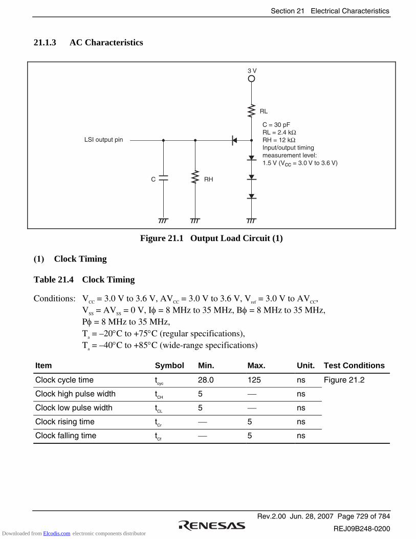
Section 21 Electrical Characteristics
Rev.2.00 Jun. 28, 2007 Page 729 of 784
REJ09B248-0200
21.1.3 AC Characteristics
LSI output pin
C RH
RL
3 V
C = 30 pFRL = 2.4 kΩRH = 12 kΩInput/output timing measurement level: 1.5 V (Vcc = 3.0 V to 3.6 V)
Figure 21.1 Output Load Circuit (1)
(1) Clock Timing
Table 21.4 Clock Timing
Conditions: VCC = 3.0 V to 3.6 V, AVCC = 3.0 V to 3.6 V, Vref = 3.0 V to AVCC, VSS = AVSS = 0 V, Iφ = 8 MHz to 35 MHz, Bφ = 8 MHz to 35 MHz, Pφ = 8 MHz to 35 MHz, Ta = –20°C to +75°C (regular specifications), Ta = –40°C to +85°C (wide-range specifications)
Item Symbol Min. Max. Unit. Test Conditions
Clock cycle time tcyc 28.0 125 ns Figure 21.2
Clock high pulse width tCH 5 ns
Clock low pulse width tCL 5 ns
Clock rising time tCr 5 ns
Clock falling time tCf 5 ns
Downloaded from Elcodis.com electronic components distributor

Section 21 Electrical Characteristics
Rev.2.00 Jun. 28, 2007 Page 730 of 784
REJ09B248-0200
Item Symbol Min. Max. Unit. Test Conditions
Oscillation settling time after reset (crystal)
tOSC1 10 ms Figure 21.4
Oscillation settling time after leaving software standby mode (crystal)
tOSC2 10 ms Figure 21.3
External clock output delay settling time
tDEXT 1 ms Figure 21.4
External clock input low pulse width
tEXL 27.7 ns Figure 21.5
External clock input high pulse width
tEXH 27.7 ns
External clock rising time tEXr 5 ns
External clock falling time tEXf 5 ns
(2) Control Signal Timing
Table 21.5 Control Signal Timing
Conditions: VCC = 3.0 V to 3.6 V, AVCC = 3.0 V to 3.6 V, Vref = 3.0 V to AVCC, VSS = AVSS = 0 V, Iφ = 8 MHz to 35 MHz, Ta = –20°C to +75°C (regular specifications), Ta = –40°C to +85°C (wide-range specifications)
Item Symbol Min. Max. Unit Test Conditions
RES setup time tRESS 200 ns Figure 21.6
RES pulse width tRESW 20 tcyc
NMI setup time tNMIS 150 ns Figure 21.7
NMI hold time tNMIH 10 ns
NMI pulse width (after leaving software standby mode)
tNMIW 200 ns
IRQ setup time tIRQS 150 ns
IRQ hold time tIRQH 10 ns
IRQ pulse width (after leaving software standby mode)
tIRQW 200 ns
Downloaded from Elcodis.com electronic components distributor
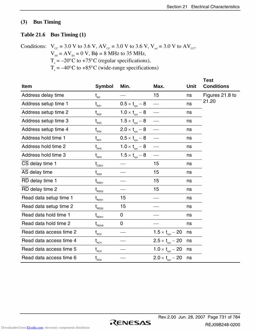
Section 21 Electrical Characteristics
Rev.2.00 Jun. 28, 2007 Page 731 of 784
REJ09B248-0200
(3) Bus Timing
Table 21.6 Bus Timing (1)
Conditions: VCC = 3.0 V to 3.6 V, AVCC = 3.0 V to 3.6 V, Vref = 3.0 V to AVCC, VSS = AVSS = 0 V, Bφ = 8 MHz to 35 MHz, Ta = –20°C to +75°C (regular specifications), Ta = –40°C to +85°C (wide-range specifications)
Item Symbol Min. Max. Unit Test Conditions
Address delay time tAD 15 ns
Address setup time 1 tAS1 0.5 × tcyc − 8 ns
Figures 21.8 to 21.20
Address setup time 2 tAS2 1.0 × tcyc − 8 ns
Address setup time 3 tAS3 1.5 × tcyc − 8 ns
Address setup time 4 tAS4 2.0 × tcyc − 8 ns
Address hold time 1 tAH1 0.5 × tcyc − 8 ns
Address hold time 2 tAH2 1.0 × tcyc − 8 ns
Address hold time 3 tAH3 1.5 × tcyc − 8 ns
CS delay time 1 tCSD1 15 ns
AS delay time tASD 15 ns
RD delay time 1 tRSD1 15 ns
RD delay time 2 tRSD2 15 ns
Read data setup time 1 tRDS1 15 ns
Read data setup time 2 tRDS2 15 ns
Read data hold time 1 tRDH1 0 ns
Read data hold time 2 tRDH2 0 ns
Read data access time 2 tAC2 1.5 × tcyc − 20 ns
Read data access time 4 tAC4 2.5 × tcyc − 20 ns
Read data access time 5 tAC5 1.0 × tcyc − 20 ns
Read data access time 6 tAC6 2.0 × tcyc − 20 ns
Downloaded from Elcodis.com electronic components distributor

Section 21 Electrical Characteristics
Rev.2.00 Jun. 28, 2007 Page 732 of 784
REJ09B248-0200
Item Symbol Min. Max. Unit Test Conditions
Read data access time (from address) 1
tAA1 1.0 × tcyc − 20 ns Figures 21.8 to 21.20
Read data access time (from address) 2
tAA2 1.5 × tcyc − 20 ns
Read data access time (from address) 3
tAA3 2.0 × tcyc − 20 ns
Read data access time (from address) 4
tAA4 2.5 × tcyc − 20 ns
Read data access time (from address) 5
tAA5 3.0 × tcyc − 20 ns
WR delay time 1 tWRD1 15 ns
WR delay time 2 tWRD2 15 ns
WR pulse width 1 tWSW1 1.0 × tcyc − 13 ns
WR pulse width 2 tWSW2 1.5 × tcyc − 13 ns
Write data delay time tWDD 20 ns
Write data setup time 1 tWDS1 0.5 × tcyc − 13 ns
Write data setup time 2 tWDS2 1.0 × tcyc − 13 ns
Write data setup time 3 tWDS3 1.5 × tcyc − 13 ns
Write data hold time 1 tWDH1 0.5 × tcyc − 8 ns
Write data hold time 3 tWDH3 1.5 × tcyc − 8 ns
Downloaded from Elcodis.com electronic components distributor
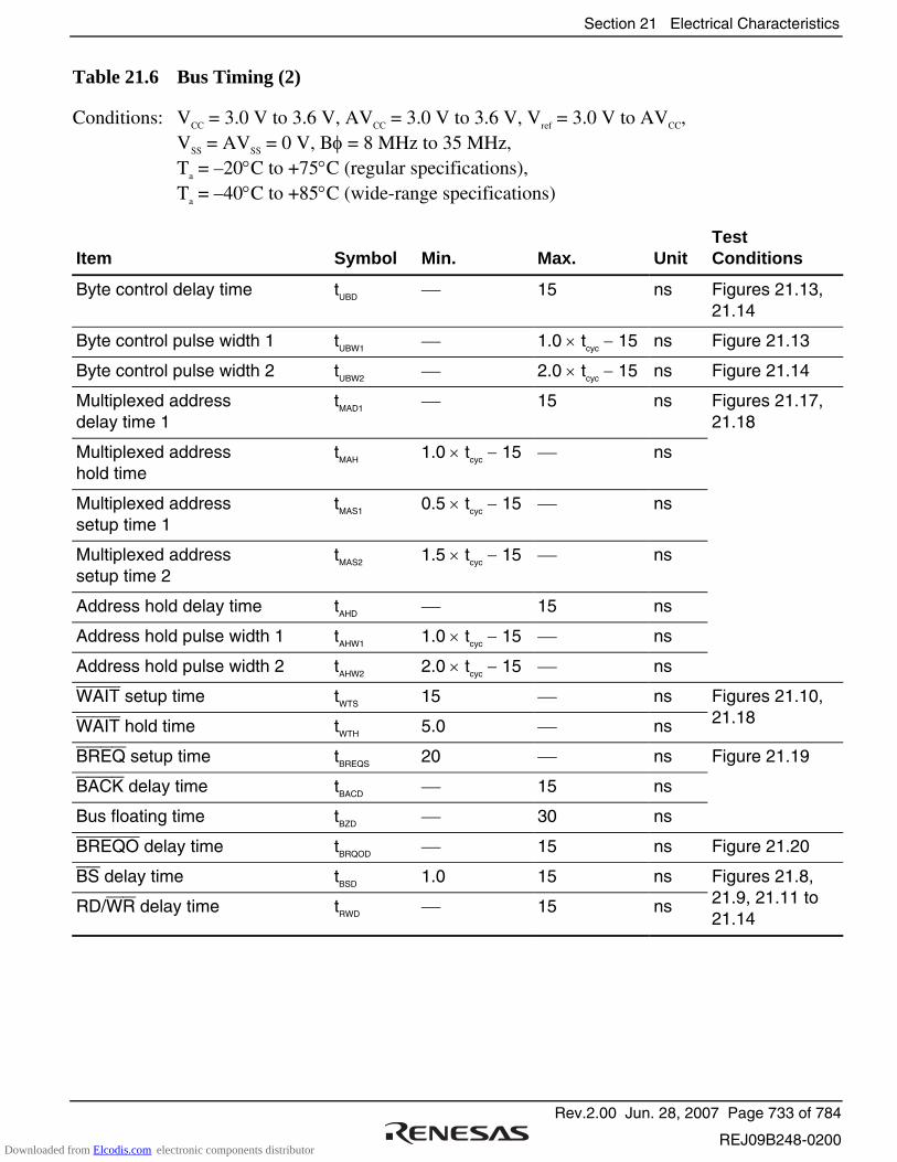
Section 21 Electrical Characteristics
Rev.2.00 Jun. 28, 2007 Page 733 of 784
REJ09B248-0200
Table 21.6 Bus Timing (2)
Conditions: VCC = 3.0 V to 3.6 V, AVCC = 3.0 V to 3.6 V, Vref = 3.0 V to AVCC, VSS = AVSS = 0 V, Bφ = 8 MHz to 35 MHz, Ta = –20°C to +75°C (regular specifications), Ta = –40°C to +85°C (wide-range specifications)
Item Symbol Min. Max. Unit Test Conditions
Byte control delay time tUBD 15 ns Figures 21.13, 21.14
Byte control pulse width 1 tUBW1 1.0 × tcyc − 15 ns Figure 21.13
Byte control pulse width 2 tUBW2 2.0 × tcyc − 15 ns Figure 21.14
Multiplexed address delay time 1
tMAD1 15 ns
Multiplexed address hold time
tMAH 1.0 × tcyc − 15 ns
Figures 21.17, 21.18
Multiplexed address setup time 1
tMAS1 0.5 × tcyc − 15 ns
Multiplexed address setup time 2
tMAS2 1.5 × tcyc − 15 ns
Address hold delay time tAHD 15 ns
Address hold pulse width 1 tAHW1 1.0 × tcyc − 15 ns
Address hold pulse width 2 tAHW2 2.0 × tcyc − 15 ns
WAIT setup time tWTS 15 ns
WAIT hold time tWTH 5.0 ns
Figures 21.10, 21.18
BREQ setup time tBREQS 20 ns Figure 21.19
BACK delay time tBACD 15 ns
Bus floating time tBZD 30 ns
BREQO delay time tBRQOD 15 ns Figure 21.20
BS delay time tBSD 1.0 15 ns
RD/WR delay time tRWD 15 ns
Figures 21.8, 21.9, 21.11 to 21.14
Downloaded from Elcodis.com electronic components distributor

Section 21 Electrical Characteristics
Rev.2.00 Jun. 28, 2007 Page 734 of 784
REJ09B248-0200
(4) DMAC Timing
Table 21.7 DMAC Timing
Conditions: VCC = 3.0 V to 3.6 V, AVCC = 3.0 V to 3.6 V, Vref = 3.0 V to AVCC, VSS = AVSS = 0 V, Bφ = 8 MHz to 35 MHz, Ta = –20°C to +75°C (regular specifications), Ta = –40°C to +85°C (wide-range specifications)
Item Symbol Min. Max. Unit Test Conditions
DREQ setup time tDRQS 20 — ns
DREQ hold time tDRQH 5 — ns
Figure 21.21
TEND delay time tTED — 15 ns Figure 21.22
DACK delay time 1 tDACD1 — 15 ns
DACK delay time 2 tDACD2 — 15 ns
Figures 21.23, 21.24
(5) On-Chip Peripheral Modules
Table 21.8 Timing of On-Chip Peripheral Modules
Conditions: VCC = 3.0 V to 3.6 V, AVCC = 3.0 V to 3.6 V, Vref = 3.0 V to AVCC, VSS = AVSS = 0 V, Pφ = 8 MHz to 35 MHz, Ta = –20°C to +75°C (regular specifications), Ta = –40°C to +85°C (wide-range specifications)
Item Symbol Min. Max. Unit Test Conditions
I/O ports Output data delay time tPWD 40 ns Figure 21.25
Input data setup time tPRS 25 ns
Input data hold time tPRH 25 ns
TPU Timer output delay time tTOCD 40 ns Figure 21.26
Timer input setup time tTICS 25 ns
Timer clock input setup time tTCKS 25 ns Figure 21.27
Timer clock pulse width
Single-edge setting
tTCKWH 1.5 tcyc
Both-edge setting
tTCKWL 2.5 tcyc
Downloaded from Elcodis.com electronic components distributor

Section 21 Electrical Characteristics
Rev.2.00 Jun. 28, 2007 Page 735 of 784
REJ09B248-0200
Item Symbol Min. Max. Unit Test Conditions
PPG Pulse output delay time tPOD 40 ns Figure 21.28
Timer output delay time tTMOD 40 ns Figure 21.29 8-bit timer Timer reset input setup time tTMRS 25 ns Figure 21.30
Timer clock input setup time tTMCS 25 ns Figure 21.31
Timer clock pulse width
Single-edge setting
tTMCWH 1.5 tcyc
Both-edge setting
tTMCWL 2.5 tcyc
WDT Overflow output delay time tWOVD 40 ns Figure 21.32
SCI Asynchronous tScyc 4 tcyc Figure 21.33
Input clock cycle Clocked
synchronous 6
Input clock pulse width tSCKW 0.4 0.6 tScyc
Input clock rise time tSCKr 1.5 tcyc
Input clock fall time tSCKf 1.5 tcyc
Transmit data delay time tTXD 40 ns Figure 21.34
Receive data setup time (clocked synchronous)
tRXS 40 ns
Receive data hold time (clocked synchronous)
tRXH 40 ns
A/D converter
Trigger input setup time tTRGS 30 ns Figure 21.35
Downloaded from Elcodis.com electronic components distributor
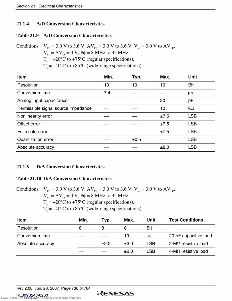
Section 21 Electrical Characteristics
Rev.2.00 Jun. 28, 2007 Page 736 of 784
REJ09B248-0200
21.1.4 A/D Conversion Characteristics
Table 21.9 A/D Conversion Characteristics
Conditions: VCC = 3.0 V to 3.6 V, AVCC = 3.0 V to 3.6 V, Vref = 3.0 V to AVCC, VSS = AVSS = 0 V, Pφ = 8 MHz to 35 MHz, Ta = –20°C to +75°C (regular specifications), Ta = –40°C to +85°C (wide-range specifications)
Item Min. Typ. Max. Unit
Resolution 10 10 10 Bit
Conversion time 7.4 µs
Analog input capacitance 20 pF
Permissible signal source impedance 10 kΩ
Nonlinearity error ±7.5 LSB
Offset error ±7.5 LSB
Full-scale error ±7.5 LSB
Quantization error ±0.5 LSB
Absolute accuracy ±8.0 LSB
21.1.5 D/A Conversion Characteristics
Table 21.10 D/A Conversion Characteristics
Conditions: VCC = 3.0 V to 3.6 V, AVCC = 3.0 V to 3.6 V, Vref = 3.0 V to AVCC, VSS = AVSS = 0 V, Pφ = 8 MHz to 35 MHz, Ta = –20°C to +75°C (regular specifications), Ta = –40°C to +85°C (wide-range specifications)
Item Min. Typ. Max. Unit Test Conditions
Resolution 8 8 8 Bit
Conversion time 10 µs 20-pF capacitive load
Absolute accuracy ±2.0 ±3.0 LSB 2-MΩ resistive load
±2.0 LSB 4-MΩ resistive load
Downloaded from Elcodis.com electronic components distributor

Section 21 Electrical Characteristics
Rev.2.00 Jun. 28, 2007 Page 737 of 784
REJ09B248-0200
21.2 Electrical Characteristics (at 50-MHz operation)
21.2.1 Absolute Maximum Ratings
Table 21.11 Absolute Maximum Ratings
Item Symbol Value Unit
Power supply voltage VCC –0.3 to +4.6 V
Input voltage (except port 5) Vin –0.3 to VCC +0.3 V
Input voltage (port 5) Vin –0.3 to AVCC +0.3 V
Reference power supply voltage Vref –0.3 to AVCC +0.3 V
Analog power supply voltage AVCC –0.3 to +4.6 V
Analog input voltage VAN –0.3 to AVCC +0.3 V
Regular specifications: –20 to +75
Operating temperature Topr
Wide-range specifications: –40 to +85
°C
Storage temperature Tstg –55 to +125 °C
Caution: Permanent damage to the LSI may result if absolute maximum ratings are exceeded.
Downloaded from Elcodis.com electronic components distributor
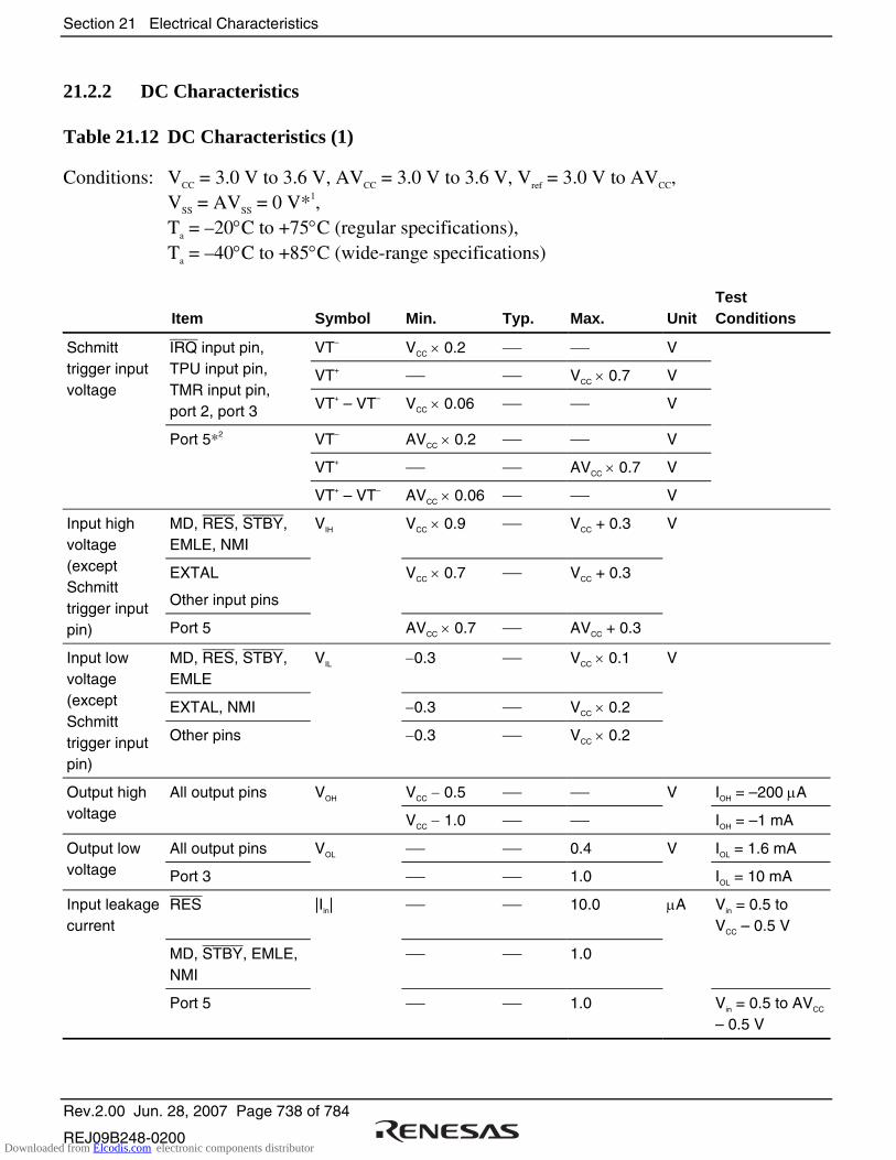
Section 21 Electrical Characteristics
Rev.2.00 Jun. 28, 2007 Page 738 of 784
REJ09B248-0200
21.2.2 DC Characteristics
Table 21.12 DC Characteristics (1)
Conditions: VCC = 3.0 V to 3.6 V, AVCC = 3.0 V to 3.6 V, Vref = 3.0 V to AVCC, VSS = AVSS = 0 V*1, Ta = –20°C to +75°C (regular specifications), Ta = –40°C to +85°C (wide-range specifications)
Item Symbol Min. Typ. Max. Unit Test Conditions
VT– VCC × 0.2 V
VT+ VCC × 0.7 V
Schmitt trigger input voltage
IRQ input pin, TPU input pin, TMR input pin, port 2, port 3 VT+ – VT– VCC × 0.06 V
Port 5*2 VT– AVCC × 0.2 V
VT+ AVCC × 0.7 V
VT+ – VT– AVCC × 0.06 V
MD, RES, STBY, EMLE, NMI
VIH VCC × 0.9 VCC + 0.3
EXTAL
Other input pins
VCC × 0.7 VCC + 0.3
Input high voltage (except Schmitt trigger input pin) Port 5 AVCC × 0.7 AVCC + 0.3
V
MD, RES, STBY, EMLE
VIL −0.3 VCC × 0.1
EXTAL, NMI −0.3 VCC × 0.2
Input low voltage (except Schmitt trigger input pin)
Other pins −0.3 VCC × 0.2
V
All output pins VOH VCC − 0.5 V IOH = –200 µA Output high voltage VCC − 1.0 IOH = –1 mA
All output pins 0.4 V IOL = 1.6 mA Output low voltage Port 3
VOL
1.0 IOL = 10 mA
Input leakage current
RES |Iin| 10.0 µA Vin = 0.5 to VCC – 0.5 V
MD, STBY, EMLE, NMI
1.0
Port 5 1.0 Vin = 0.5 to AVCC – 0.5 V
Downloaded from Elcodis.com electronic components distributor
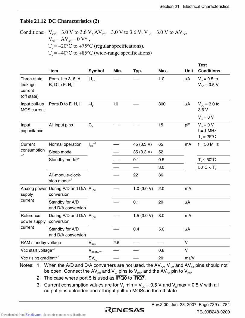
Section 21 Electrical Characteristics
Rev.2.00 Jun. 28, 2007 Page 739 of 784
REJ09B248-0200
Table 21.12 DC Characteristics (2)
Conditions: VCC = 3.0 V to 3.6 V, AVCC = 3.0 V to 3.6 V, Vref = 3.0 V to AVCC, VSS = AVSS = 0 V*1, Ta = –20°C to +75°C (regular specifications), Ta = –40°C to +85°C (wide-range specifications)
Item Symbol Min. Typ. Max. Unit Test Conditions
Three-state leakage current (off state)
Ports 1 to 3, 6, A, B, D to F, H, I
| ITSI | 1.0 µA Vin = 0.5 to VCC – 0.5 V
Input pull-up MOS current
Ports D to F, H, I –Ip 10 300 µA VCC = 3.0 to 3.6 V
Vin = 0 V
Input capacitance
All input pins Cin 15 pF Vin = 0 V f = 1 MHz Ta = 25°C
Normal operation ICC*5 45 (3.3 V) 65 mA f = 50 MHz
Sleep mode 35 (3.3 V) 52
Current consumption *3
Standby mode*4 0.1 0.5 Ta ≤ 50°C
3.0 50°C < Ta
All-module-clock-stop mode*6
22 36
During A/D and D/A conversion
AICC 1.0 (3.0 V) 2.0 mA Analog power supply current Standby for A/D
and D/A conversion 0.1 20 µA
During A/D and D/A conversion
AICC 1.5 (3.0 V) 3.0 mA Reference power supply current Standby for A/D
and D/A conversion 0.4 5.0 µA
RAM standby voltage VRAM 2.5 V
Vcc start voltage*7 VCCSTART 0.8 V
Vcc rising gradient*7 SVCC 20 ms/V
Notes: 1. When the A/D and D/A converters are not used, the AVCC, Vref, and AVSS pins should not be open. Connect the AVCC and Vref pins to VCC, and the AVSS pin to VSS.
2. The case where port 5 is used as IRQ0 to IRQ7.
3. Current consumption values are for VIHmin = VCC – 0.5 V and VILmax = 0.5 V with all output pins unloaded and all input pull-up MOSs in the off state.
Downloaded from Elcodis.com electronic components distributor
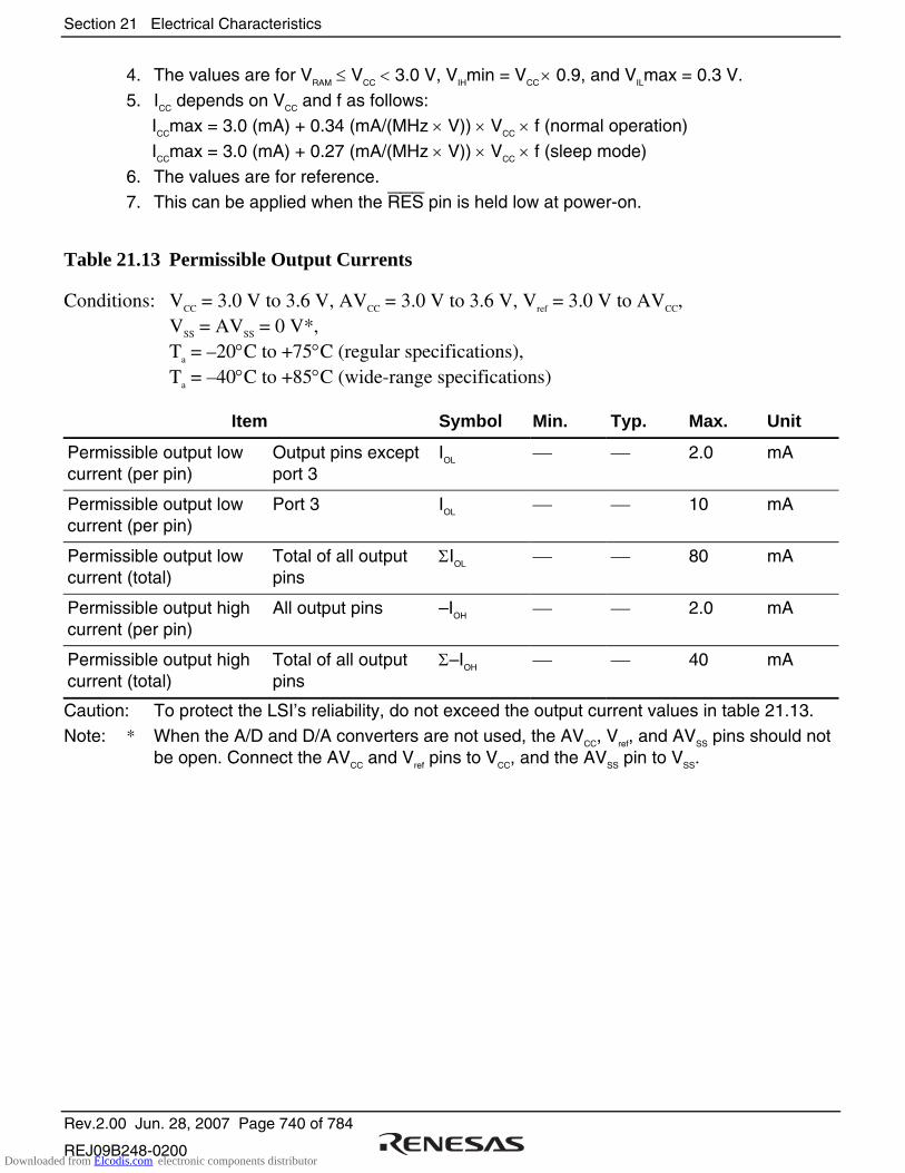
Section 21 Electrical Characteristics
Rev.2.00 Jun. 28, 2007 Page 740 of 784
REJ09B248-0200
4. The values are for VRAM ≤ VCC < 3.0 V, VIHmin = VCC × 0.9, and VILmax = 0.3 V.
5. ICC depends on VCC and f as follows: ICCmax = 3.0 (mA) + 0.34 (mA/(MHz × V)) × VCC × f (normal operation)
ICCmax = 3.0 (mA) + 0.27 (mA/(MHz × V)) × VCC × f (sleep mode)
6. The values are for reference. 7. This can be applied when the RES pin is held low at power-on.
Table 21.13 Permissible Output Currents
Conditions: VCC = 3.0 V to 3.6 V, AVCC = 3.0 V to 3.6 V, Vref = 3.0 V to AVCC, VSS = AVSS = 0 V*, Ta = –20°C to +75°C (regular specifications), Ta = –40°C to +85°C (wide-range specifications)
Item Symbol Min. Typ. Max. Unit
Permissible output low current (per pin)
Output pins except port 3
IOL 2.0 mA
Permissible output low current (per pin)
Port 3 IOL 10 mA
Permissible output low current (total)
Total of all output pins
ΣIOL 80 mA
Permissible output high current (per pin)
All output pins –IOH 2.0 mA
Permissible output high current (total)
Total of all output pins
Σ–IOH 40 mA
Caution: To protect the LSI’s reliability, do not exceed the output current values in table 21.13. Note: * When the A/D and D/A converters are not used, the AVCC, Vref, and AVSS pins should not
be open. Connect the AVCC and Vref pins to VCC, and the AVSS pin to VSS.
Downloaded from Elcodis.com electronic components distributor
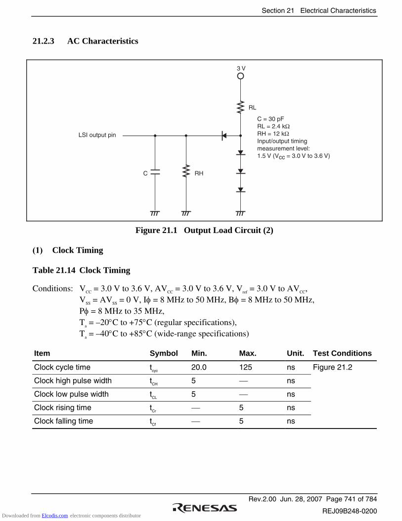
Section 21 Electrical Characteristics
Rev.2.00 Jun. 28, 2007 Page 741 of 784
REJ09B248-0200
21.2.3 AC Characteristics
C = 30 pFRL = 2.4 kΩRH = 12 kΩInput/output timing measurement level: 1.5 V (Vcc = 3.0 V to 3.6 V)
LSI output pin
C RH
RL
3 V
Figure 21.1 Output Load Circuit (2)
(1) Clock Timing
Table 21.14 Clock Timing
Conditions: VCC = 3.0 V to 3.6 V, AVCC = 3.0 V to 3.6 V, Vref = 3.0 V to AVCC, VSS = AVSS = 0 V, Iφ = 8 MHz to 50 MHz, Bφ = 8 MHz to 50 MHz, Pφ = 8 MHz to 35 MHz, Ta = –20°C to +75°C (regular specifications), Ta = –40°C to +85°C (wide-range specifications)
Item Symbol Min. Max. Unit. Test Conditions
Clock cycle time tcyc 20.0 125 ns Figure 21.2
Clock high pulse width tCH 5 ns
Clock low pulse width tCL 5 ns
Clock rising time tCr 5 ns
Clock falling time tCf 5 ns
Downloaded from Elcodis.com electronic components distributor
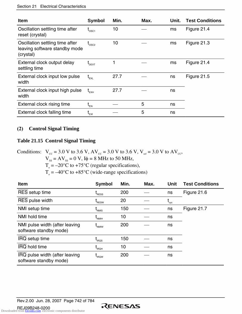
Section 21 Electrical Characteristics
Rev.2.00 Jun. 28, 2007 Page 742 of 784
REJ09B248-0200
Item Symbol Min. Max. Unit. Test Conditions
Oscillation settling time after reset (crystal)
tOSC1 10 ms Figure 21.4
Oscillation settling time after leaving software standby mode (crystal)
tOSC2 10 ms Figure 21.3
External clock output delay settling time
tDEXT 1 ms Figure 21.4
External clock input low pulse width
tEXL 27.7 ns Figure 21.5
External clock input high pulse width
tEXH 27.7 ns
External clock rising time tEXr 5 ns
External clock falling time tEXf 5 ns
(2) Control Signal Timing
Table 21.15 Control Signal Timing
Conditions: VCC = 3.0 V to 3.6 V, AVCC = 3.0 V to 3.6 V, Vref = 3.0 V to AVCC, VSS = AVSS = 0 V, Iφ = 8 MHz to 50 MHz, Ta = –20°C to +75°C (regular specifications), Ta = –40°C to +85°C (wide-range specifications)
Item Symbol Min. Max. Unit Test Conditions
RES setup time tRESS 200 ns Figure 21.6
RES pulse width tRESW 20 tcyc
NMI setup time tNMIS 150 ns Figure 21.7
NMI hold time tNMIH 10 ns
NMI pulse width (after leaving software standby mode)
tNMIW 200 ns
IRQ setup time tIRQS 150 ns
IRQ hold time tIRQH 10 ns
IRQ pulse width (after leaving software standby mode)
tIRQW 200 ns
Downloaded from Elcodis.com electronic components distributor

Section 21 Electrical Characteristics
Rev.2.00 Jun. 28, 2007 Page 743 of 784
REJ09B248-0200
(3) Bus Timing
Table 21.16 Bus Timing (1)
Conditions: VCC = 3.0 V to 3.6 V, AVCC = 3.0 V to 3.6 V, Vref = 3.0 V to AVCC, VSS = AVSS = 0 V, Bφ = 8 MHz to 50 MHz, Ta = –20°C to +75°C (regular specifications), Ta = –40°C to +85°C (wide-range specifications)
Item Symbol Min. Max. Unit Test Conditions
Address delay time tAD 15 ns
Address setup time 1 tAS1 0.5 × tCYC − 8 ns
Figures 21.8 to 21.20
Address setup time 2 tAS2 1.0 × tCYC − 8 ns
Address setup time 3 tAS3 1.5 × tCYC − 8 ns
Address setup time 4 tAS4 2.0 × tCYC − 8 ns
Address hold time 1 tAH1 0.5 × tCYC − 8 ns
Address hold time 2 tAH2 1.0 × tCYC − 8 ns
Address hold time 3 tAH3 1.5 × tCYC − 8 ns
CS delay time 1 tCSD1 15 ns
AS delay time tASD 15 ns
RD delay time 1 tRSD1 15 ns
RD delay time 2 tRSD2 15 ns
Read data setup time 1 tRDS1 15 ns
Read data setup time 2 tRDS2 15 ns
Read data hold time 1 tRDH1 0 ns
Read data hold time 2 tRDH2 0 ns
Read data access time 2 tAC2 1.5 × tCYC − 20 ns
Read data access time 4 tAC4 2.5 × tCYC − 20 ns
Read data access time 5 tAC5 1.0 × tCYC − 20 ns
Read data access time 6 tAC6 2.0 × tCYC − 20 ns
Downloaded from Elcodis.com electronic components distributor

Section 21 Electrical Characteristics
Rev.2.00 Jun. 28, 2007 Page 744 of 784
REJ09B248-0200
Table 21.16 Bus Timing (2)
Conditions: VCC = 3.0 V to 3.6 V, AVCC = 3.0 V to 3.6 V, Vref = 3.0 V to AVCC, VSS = AVSS = 0 V, Bφ = 8 MHz to 50 MHz, Ta = –20°C to +75°C (regular specifications), Ta = –40°C to +85°C (wide-range specifications)
Item Symbol Min. Max. Unit Test Conditions
Read data access time (from address) 1
tAA1 1.0 × tCYC − 20 ns Figures 21.8 to 21.20
Read data access time (from address) 2
tAA2 1.5 × tCYC − 20 ns
Read data access time (from address) 3
tAA3 2.0 × tCYC − 20 ns
Read data access time (from address) 4
tAA4 2.5 × tCYC − 20 ns
Read data access time (from address) 5
tAA5 3.0 × tCYC − 20 ns
WR delay time 1 tWRD1 15 ns
WR delay time 2 tWRD2 15 ns
WR pulse width 1 tWSW1 1.0 × tCYC − 13 ns
WR pulse width 2 tWSW2 1.5 × tCYC − 13 ns
Write data delay time tWDD 20 ns
Write data setup time 1 tWDS1 0.5 × tCYC − 13 ns
Write data setup time 2 tWDS2 1.0 × tCYC − 13 ns
Write data setup time 3 tWDS3 1.5 × tCYC − 13 ns
Write data hold time 1 tWDH1 0.5 × tCYC − 8 ns
Write data hold time 3 tWDH3 1.5 × tCYC − 8 ns
Downloaded from Elcodis.com electronic components distributor
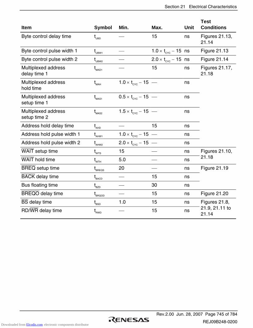
Section 21 Electrical Characteristics
Rev.2.00 Jun. 28, 2007 Page 745 of 784
REJ09B248-0200
Item Symbol Min. Max. Unit Test Conditions
Byte control delay time tUBD 15 ns Figures 21.13, 21.14
Byte control pulse width 1 tUBW1 1.0 × tCYC − 15 ns Figure 21.13
Byte control pulse width 2 tUBW2 2.0 × tCYC − 15 ns Figure 21.14
Multiplexed address delay time 1
tMAD1 15 ns
Multiplexed address hold time
tMAH 1.0 × tCYC − 15 ns
Figures 21.17, 21.18
Multiplexed address setup time 1
tMAS1 0.5 × tCYC − 15 ns
Multiplexed address setup time 2
tMAS2 1.5 × tCYC − 15 ns
Address hold delay time tAHD 15 ns
Address hold pulse width 1 tAHW1 1.0 × tCYC − 15 ns
Address hold pulse width 2 tAHW2 2.0 × tCYC − 15 ns
WAIT setup time tWTS 15 ns
WAIT hold time tWTH 5.0 ns
Figures 21.10, 21.18
BREQ setup time tBREQS 20 ns Figure 21.19
BACK delay time tBACD 15 ns
Bus floating time tBZD 30 ns
BREQO delay time tBRQOD 15 ns Figure 21.20
BS delay time tBSD 1.0 15 ns
RD/WR delay time tRWD 15 ns
Figures 21.8, 21.9, 21.11 to 21.14
Downloaded from Elcodis.com electronic components distributor
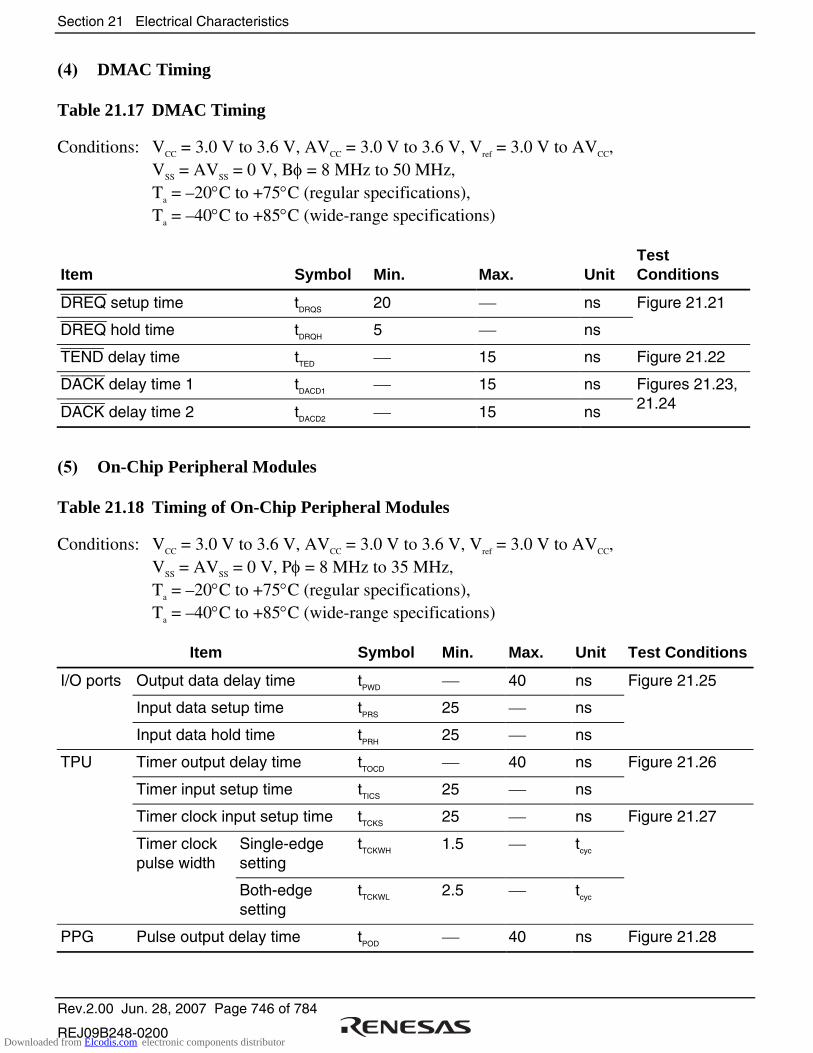
Section 21 Electrical Characteristics
Rev.2.00 Jun. 28, 2007 Page 746 of 784
REJ09B248-0200
(4) DMAC Timing
Table 21.17 DMAC Timing
Conditions: VCC = 3.0 V to 3.6 V, AVCC = 3.0 V to 3.6 V, Vref = 3.0 V to AVCC, VSS = AVSS = 0 V, Bφ = 8 MHz to 50 MHz, Ta = –20°C to +75°C (regular specifications), Ta = –40°C to +85°C (wide-range specifications)
Item Symbol Min. Max. Unit Test Conditions
DREQ setup time tDRQS 20 ns
DREQ hold time tDRQH 5 ns
Figure 21.21
TEND delay time tTED 15 ns Figure 21.22
DACK delay time 1 tDACD1 15 ns
DACK delay time 2 tDACD2 15 ns
Figures 21.23, 21.24
(5) On-Chip Peripheral Modules
Table 21.18 Timing of On-Chip Peripheral Modules
Conditions: VCC = 3.0 V to 3.6 V, AVCC = 3.0 V to 3.6 V, Vref = 3.0 V to AVCC, VSS = AVSS = 0 V, Pφ = 8 MHz to 35 MHz, Ta = –20°C to +75°C (regular specifications), Ta = –40°C to +85°C (wide-range specifications)
Item Symbol Min. Max. Unit Test Conditions
I/O ports Output data delay time tPWD 40 ns Figure 21.25
Input data setup time tPRS 25 ns
Input data hold time tPRH 25 ns
TPU Timer output delay time tTOCD 40 ns Figure 21.26
Timer input setup time tTICS 25 ns
Timer clock input setup time tTCKS 25 ns Figure 21.27
Timer clock pulse width
Single-edge setting
tTCKWH 1.5 tcyc
Both-edge setting
tTCKWL 2.5 tcyc
PPG Pulse output delay time tPOD 40 ns Figure 21.28
Downloaded from Elcodis.com electronic components distributor

Section 21 Electrical Characteristics
Rev.2.00 Jun. 28, 2007 Page 747 of 784
REJ09B248-0200
Item Symbol Min. Max. Unit Test Conditions
Timer output delay time tTMOD 40 ns Figure 21.29 8-bit timer Timer reset input setup time tTMRS 25 ns Figure 21.30
Timer clock input setup time tTMCS 25 ns Figure 21.31
Timer clock pulse width
Single-edge setting
tTMCWH 1.5 tcyc
Both-edge setting
tTMCWL 2.5 tcyc
WDT Overflow output delay time tWOVD 40 ns Figure 21.32
SCI Asynchronous tScyc 4 tcyc Figure 21.33
Input clock cycle Clocked
synchronous 6
Input clock pulse width tSCKW 0.4 0.6 tScyc
Input clock rise time tSCKr 1.5 tcyc
Input clock fall time tSCKf 1.5 tcyc
Transmit data delay time tTXD 40 ns Figure 21.34
Receive data setup time (clocked synchronous)
tRXS 40 ns
Receive data hold time (clocked synchronous)
tRXH 40 ns
A/D converter
Trigger input setup time tTRGS 30 ns Figure 21.35
Downloaded from Elcodis.com electronic components distributor

Section 21 Electrical Characteristics
Rev.2.00 Jun. 28, 2007 Page 748 of 784
REJ09B248-0200
21.2.4 A/D Conversion Characteristics
Table 21.19 A/D Conversion Characteristics
Conditions: VCC = 3.0 V to 3.6 V, AVCC = 3.0 V to 3.6 V, Vref = 3.0 V to AVCC, VSS = AVSS = 0 V, Pφ = 8 MHz to 35 MHz, Ta = –20°C to +75°C (regular specifications), Ta = –40°C to +85°C (wide-range specifications)
Item Min. Typ. Max. Unit
Resolution 10 10 10 Bit
Conversion time 7.4 µs
Analog input capacitance 20 pF
Permissible signal source impedance 10 kΩ
Nonlinearity error ±7.5 LSB
Offset error ±7.5 LSB
Full-scale error ±7.5 LSB
Quantization error ±0.5 LSB
Absolute accuracy ±8.0 LSB
21.2.5 D/A Conversion Characteristics
Table 21.20 D/A Conversion Characteristics
Conditions: VCC = 3.0 V to 3.6 V, AVCC = 3.0 V to 3.6 V, Vref = 3.0 V to AVCC, VSS = AVSS = 0 V, Pφ = 8 MHz to 35 MHz, Ta = –20°C to +75°C (regular specifications), Ta = –40°C to +85°C (wide-range specifications)
Item Min. Typ. Max. Unit Test Conditions
Resolution 8 8 8 Bit
Conversion time 10 µs 20-pF capacitive load
Absolute accuracy ±2.0 ±3.0 LSB 2-MΩ resistive load
±2.0 LSB 4-MΩ resistive load
Downloaded from Elcodis.com electronic components distributor

Section 21 Electrical Characteristics
Rev.2.00 Jun. 28, 2007 Page 749 of 784
REJ09B248-0200
21.3 Timing Charts
tcyc
Bφ
tCH tCf
tCL tCr
Figure 21.2 External Bus Clock Timing
Oscillator
Software standby mode(power-down mode)
Oscillation settling time
tOSC2
Iφ
NMI
NMI exceptionhandlingNMIEG = 1SSBY = 1
NMI exception handling
SLEEPinstruction
NMIEG
SSBY
Figure 21.3 Oscillation Settling Timing after Software Standby Mode
Downloaded from Elcodis.com electronic components distributor
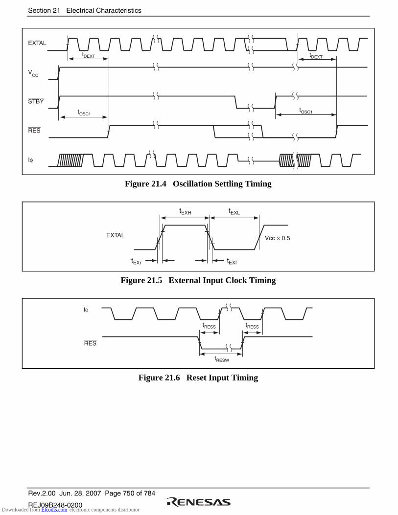
Section 21 Electrical Characteristics
Rev.2.00 Jun. 28, 2007 Page 750 of 784
REJ09B248-0200
EXTAL
VCC
STBY
RES
Iφ
tDEXT
tOSC1
tDEXT
tOSC1
Figure 21.4 Oscillation Settling Timing
EXTAL Vcc × 0.5
tEXr
tEXH tEXL
tEXf
Figure 21.5 External Input Clock Timing
Iφ
RES
tRESS tRESS
tRESW
Figure 21.6 Reset Input Timing
Downloaded from Elcodis.com electronic components distributor
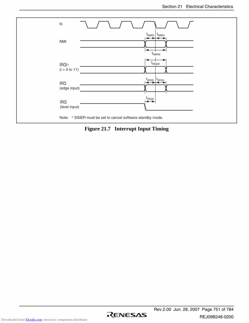
Section 21 Electrical Characteristics
Rev.2.00 Jun. 28, 2007 Page 751 of 784
REJ09B248-0200
Iφ
NMI
IRQi*(i = 0 to 11)
IRQ(edge input)
Note: * SSIER must be set to cancel software standby mode.
IRQ(level input)
tNMIS tNMIH
tIRQS
tIRQS
tIRQH
tNMIW
tIRQW
Figure 21.7 Interrupt Input Timing
Downloaded from Elcodis.com electronic components distributor
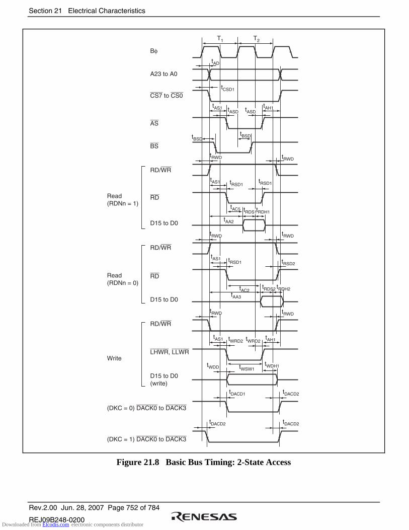
Section 21 Electrical Characteristics
Rev.2.00 Jun. 28, 2007 Page 752 of 784
REJ09B248-0200
T1 T2
Bφ
tCSD1
tRWD tRWD
tAS1
tBSDtBSD
tAS1
tAS1
tAS1
tRSD1tRSD1
tAC5
tAA2
tRSD1
tWRD2
tWSW1tWDH1tWDD
tWRD2
tDACD1 tDACD2
tDACD2 tDACD2
tAH1
tAC2tRDS2 tRDH2
tAA3
tRSD2
tRDS1tRDH1
tAH1tASD tASD
tRWD tRWD
tRWD tRWD
A23 to A0
CS7 to CS0
AS
RD
D15 to D0
RD
D15 to D0
Read(RDNn = 1)
Read(RDNn = 0)
Write
BS
RD/WR
RD/WR
RD/WR
D15 to D0(write)
(DKC = 0) DACK0 to DACK3
(DKC = 1) DACK0 to DACK3
LHWR, LLWR
tAD
Figure 21.8 Basic Bus Timing: 2-State Access
Downloaded from Elcodis.com electronic components distributor
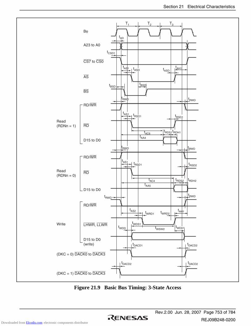
Section 21 Electrical Characteristics
Rev.2.00 Jun. 28, 2007 Page 753 of 784
REJ09B248-0200
tCSD1
tAD
T1 T2 T3
tAS1 tAH1
tRSD1
tRDS1tRDH1
tRSD2
tRDS2 tRDH2
tASDtASD
tRSD1
tRSD1
tAC6
tAC4tAA5
tAS2
tWDD tWSW2tWDH1
tWDS1
tWRD1 tWRD2tAH1
tAA4
tAS1
tAS1
tRWD
tRWD tRWD
tBSDtBSD
tRWD tRWD
tRWD
Bφ
A23 to A0
CS7 to CS0
AS
BS
RD/WR
RD/WR
RD/WR
RD
D15 to D0
RD
D15 to D0
Write
Read(RDNn = 1)
Read(RDNn = 0)
D15 to D0(write)
LHWR, LLWR
tDACD1 tDACD2
tDACD2 tDACD2
(DKC = 0) DACK0 to DACK3
(DKC = 1) DACK0 to DACK3
Figure 21.9 Basic Bus Timing: 3-State Access
Downloaded from Elcodis.com electronic components distributor
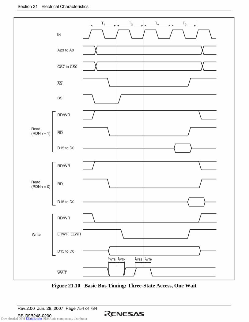
Section 21 Electrical Characteristics
Rev.2.00 Jun. 28, 2007 Page 754 of 784
REJ09B248-0200
T1
Bφ
A23 to A0
CS7 to CS0
AS
BS
RD/WR
RD
D15 to D0
RD
D15 to D0
LHWR, LLWR
D15 to D0
WAIT
tWTS tWTH tWTS tWTH
T2 Tw T3
Read(RDNn = 1)
Read(RDNn = 0)
Write
RD/WR
RD/WR
Figure 21.10 Basic Bus Timing: Three-State Access, One Wait
Downloaded from Elcodis.com electronic components distributor
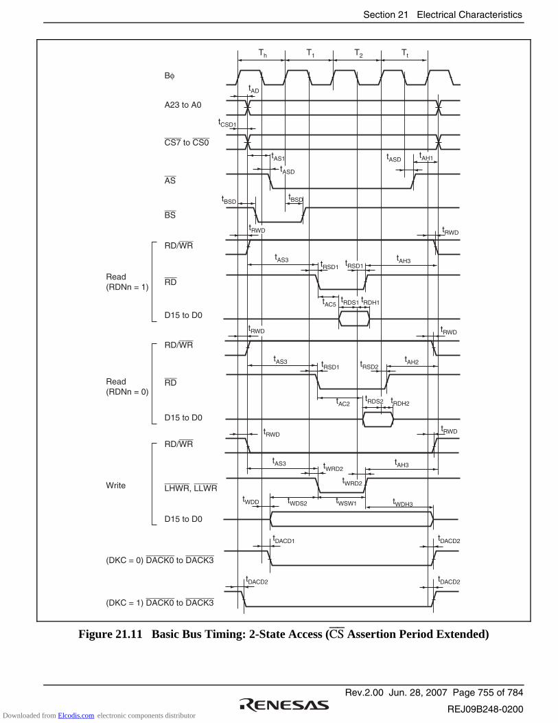
Section 21 Electrical Characteristics
Rev.2.00 Jun. 28, 2007 Page 755 of 784
REJ09B248-0200
Th
tAD
T1 T2 Tt
tCSD1
tAS1
tASD
tAS3 tRSD1
tAC5tRDS1 tRDH1
tAH2
tAH3
tWDH3tWSW1tWDS2tWDD
tAS3
tWRD2
tWRD2
tRSD2tRSD1
tAC2tRDS2 tRDH2
tAS3
tRSD1tAH3
tAH1tASD
tRWD
tRWD tRWD
tBSDtBSD
tRWD tRWD
tRWD
Bφ
A23 to A0
CS7 to CS0
AS
RD
D15 to D0
RD
D15 to D0
D15 to D0
Read(RDNn = 1)
Read(RDNn = 0)
Write
BS
RD/WR
RD/WR
RD/WR
LHWR, LLWR
tDACD1 tDACD2
tDACD2 tDACD2
(DKC = 0) DACK0 to DACK3
(DKC = 1) DACK0 to DACK3
Figure 21.11 Basic Bus Timing: 2-State Access (CS Assertion Period Extended)
Downloaded from Elcodis.com electronic components distributor

Section 21 Electrical Characteristics
Rev.2.00 Jun. 28, 2007 Page 756 of 784
REJ09B248-0200
Th
tAD
T1 T2 T3 Tt
tCSD1
tAS1tASD
tAS3 tRSD1 tRSD1
tASDtAH1
tAH3
tAH2
tAH3
tWDH3tWSW2
tWDS3
tAS4
tAS3 tRSD1
tWDD
tWRD2tWRD1
tAC4tRDS2 tRDH2
tRSD2
tAC6tRDS1tRDH1
AS
RD
RD
BS
RD/WR
RD/WR
RD/WR
tRWD
tRWD tRWD
tRWD tRWD
tBSDtBSD
tRWD
Bφ
A23 to A0
CS7 to CS0
D15 to D0
D15 to D0
D15 to D0(write)
Read(RDNn = 1)
Read(RDNn = 0)
Write LHWR, LLWR
tDACD1 tDACD2
tDACD2 tDACD2
(DKC = 0) DACK0 to DACK3
(DKC = 1) DACK0 to DACK3
Figure 21.12 Basic Bus Timing: 3-State Access (CS Assertion Period Extended)
Downloaded from Elcodis.com electronic components distributor

Section 21 Electrical Characteristics
Rev.2.00 Jun. 28, 2007 Page 757 of 784
REJ09B248-0200
tAD
T1
AS
BS
RD/WR
tCSD1
tAS1 tAH1
tAH1
tASD tASD
T2
tBSD
tAC5
tAC5
tAA2
tRWD tRWD
tBSD
RD
RD/WR
RD
tRSD1tRSD1
tRDS1 tRDH1
tUBW1
tUBD
tRWD
tWDD tWDH1
tRWD
tUBD
tAS1
tAS1
Bφ
A23 to A0
CS7 to CS0
Read
D15 to D0
LUB, LLB
D15 to D0(write)
HighWrite
Figure 21.13 Byte Control SRAM: 2-State Read/Write Access
Downloaded from Elcodis.com electronic components distributor
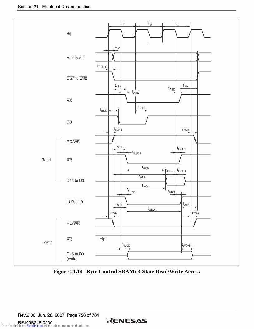
Section 21 Electrical Characteristics
Rev.2.00 Jun. 28, 2007 Page 758 of 784
REJ09B248-0200
T1
tAD
tCSD1
tAS1 tAH1
tASD
tRWD tRWD
tASD
AS
BS
RD/WR
RD
RD/WR
RD
T2 T3
tAS1 tAH1
tAS1
tRSD1
tUBD
tRWD
tWDD tWDH1
tRWD
tUBD
tRSD1
tRDS1tAC6
tAC6
tUBW2
tAA4
tRDH1
tBSDtBSD
Bφ
A23 to A0
CS7 to CS0
LUB, LLB
D15 to D0
D15 to D0(write)
Read
WriteHigh
Figure 21.14 Byte Control SRAM: 3-State Read/Write Access
Downloaded from Elcodis.com electronic components distributor
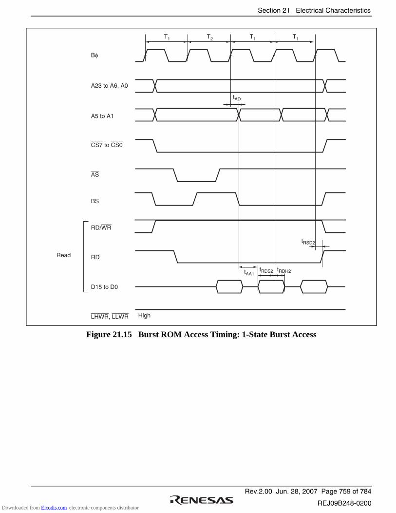
Section 21 Electrical Characteristics
Rev.2.00 Jun. 28, 2007 Page 759 of 784
REJ09B248-0200
T1
Bφ
A23 to A6, A0
A5 to A1
CS7 to CS0
AS
BS
RD/WR
RD
D15 to D0
LHWR, LLWR
T2 T1
tAD
tRSD2
tAA1tRDS2 tRDH2
T1
Read
High
Figure 21.15 Burst ROM Access Timing: 1-State Burst Access
Downloaded from Elcodis.com electronic components distributor

Section 21 Electrical Characteristics
Rev.2.00 Jun. 28, 2007 Page 760 of 784
REJ09B248-0200
T1
Bφ
A23 to A6, A0
A5 to A1
CS7 to CS0
AS
RD
D15 to D0
HighLHWR, LLWR
T2 T3 T1
tAD
tAS1
tASD
tAA3
tRSD2
tRDS2 tRDH2
tASD
tAH1
T2
Read
BS
RD/WR
Figure 21.16 Burst ROM Access Timing: 2-State Burst Access
Downloaded from Elcodis.com electronic components distributor

Section 21 Electrical Characteristics
Rev.2.00 Jun. 28, 2007 Page 761 of 784
REJ09B248-0200
Tma1
tAD
tAHD
tAHW1
tWSW1
tAHD
tMAD1
tMAHtRDS2 tRDH2
Tma2 T1 T2
RD/WR
BS
RD
DKC = 0
DKC = 1
RD/WR
tMAD1tWDD tWDH1
tMAS1
tMAHtMAS1
Bφ
A23 to A0
CS7 to CS0
AH (AS)
D15 to D0
LHWR, LLWR
D15 to D0
Read
Write
DACK0 to DACK3
Figure 21.17 Address/Data Multiplexed Access Timing (No Wait) (Basic, 4-State Access)
Downloaded from Elcodis.com electronic components distributor
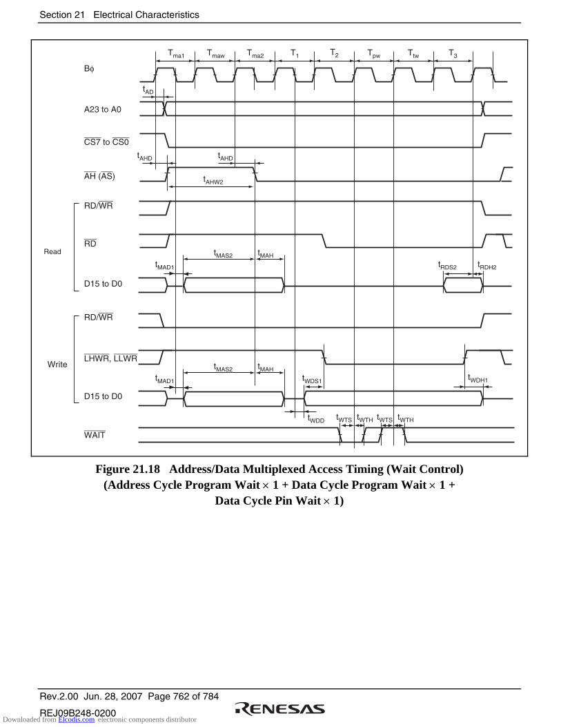
Section 21 Electrical Characteristics
Rev.2.00 Jun. 28, 2007 Page 762 of 784
REJ09B248-0200
Tma1 Tmaw Tma2 T1 T2 Tpw Ttw T3
RD/WR
WAIT
tAD
tAHD tAHD
tAHW2
tMAS2 tMAH
RD
RD/WR
tMAD1 tRDS2 tRDH2
tWDD
tWDS1
tWTS tWTH tWTS tWTH
tWDH1
tMAS2 tMAH
tMAD1
A23 to A0
CS7 to CS0
AH (AS)
D15 to D0
Read
Write
D15 to D0
LHWR, LLWR
Bφ
Figure 21.18 Address/Data Multiplexed Access Timing (Wait Control) (Address Cycle Program Wait × 1 + Data Cycle Program Wait × 1 +
Data Cycle Pin Wait × 1)
Downloaded from Elcodis.com electronic components distributor
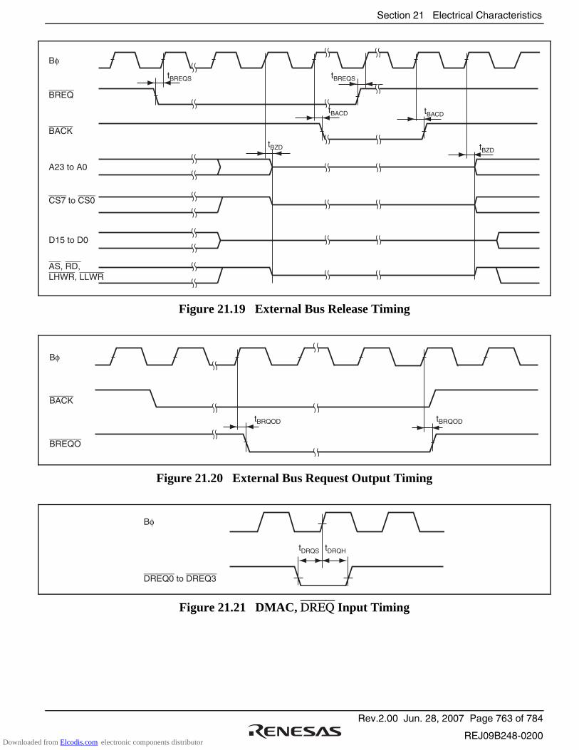
Section 21 Electrical Characteristics
Rev.2.00 Jun. 28, 2007 Page 763 of 784
REJ09B248-0200
Bφ
BREQ
tBREQS tBREQS
tBACD
tBZD
tBACD
tBZD
BACK
A23 to A0
CS7 to CS0
D15 to D0
AS, RD,LHWR, LLWR
Figure 21.19 External Bus Release Timing
Bφ
BACK
tBRQOD tBRQOD
BREQO
Figure 21.20 External Bus Request Output Timing
Bφ
DREQ0 to DREQ3
tDRQS tDRQH
Figure 21.21 DMAC, DREQ Input Timing
Downloaded from Elcodis.com electronic components distributor
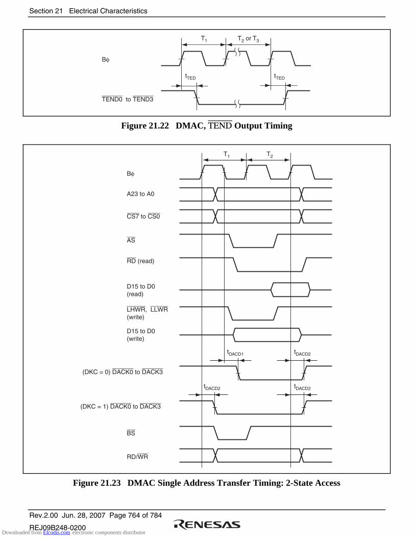
Section 21 Electrical Characteristics
Rev.2.00 Jun. 28, 2007 Page 764 of 784
REJ09B248-0200
T1
tTED tTED
Bφ
TEND0 to TEND3
T2 or T3
Figure 21.22 DMAC, TEND Output Timing
T1
Bφ
A23 to A0
CS7 to CS0
AS
BS
RD/WR
tDACD1 tDACD2
tDACD2 tDACD2
RD (read)
D15 to D0 (read)
LHWR, LLWR(write)
D15 to D0 (write)
T2
(DKC = 0) DACK0 to DACK3
(DKC = 1) DACK0 to DACK3
Figure 21.23 DMAC Single Address Transfer Timing: 2-State Access
Downloaded from Elcodis.com electronic components distributor
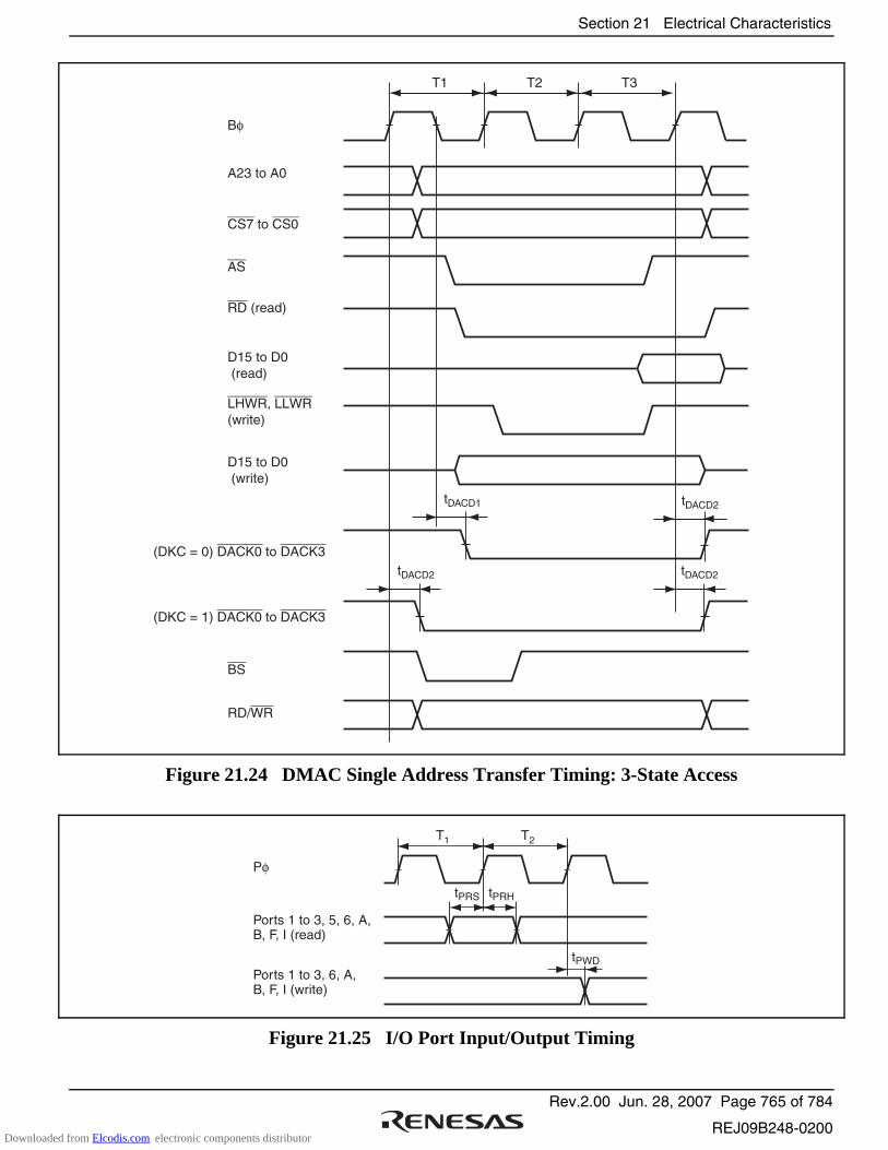
Section 21 Electrical Characteristics
Rev.2.00 Jun. 28, 2007 Page 765 of 784
REJ09B248-0200
Bφ
A23 to A0
CS7 to CS0
AS
RD (read)
D15 to D0 (read)
LHWR, LLWR(write)
D15 to D0 (write)
(DKC = 0) DACK0 to DACK3
(DKC = 1) DACK0 to DACK3
BS
RD/WR
T1
tDACD1 tDACD2
T2 T3
tDACD2 tDACD2
Figure 21.24 DMAC Single Address Transfer Timing: 3-State Access
T1
tPRS tPRH
tPWD
T2
Pφ
Ports 1 to 3, 5, 6, A,B, F, I (read)
Ports 1 to 3, 6, A,B, F, I (write)
Figure 21.25 I/O Port Input/Output Timing
Downloaded from Elcodis.com electronic components distributor
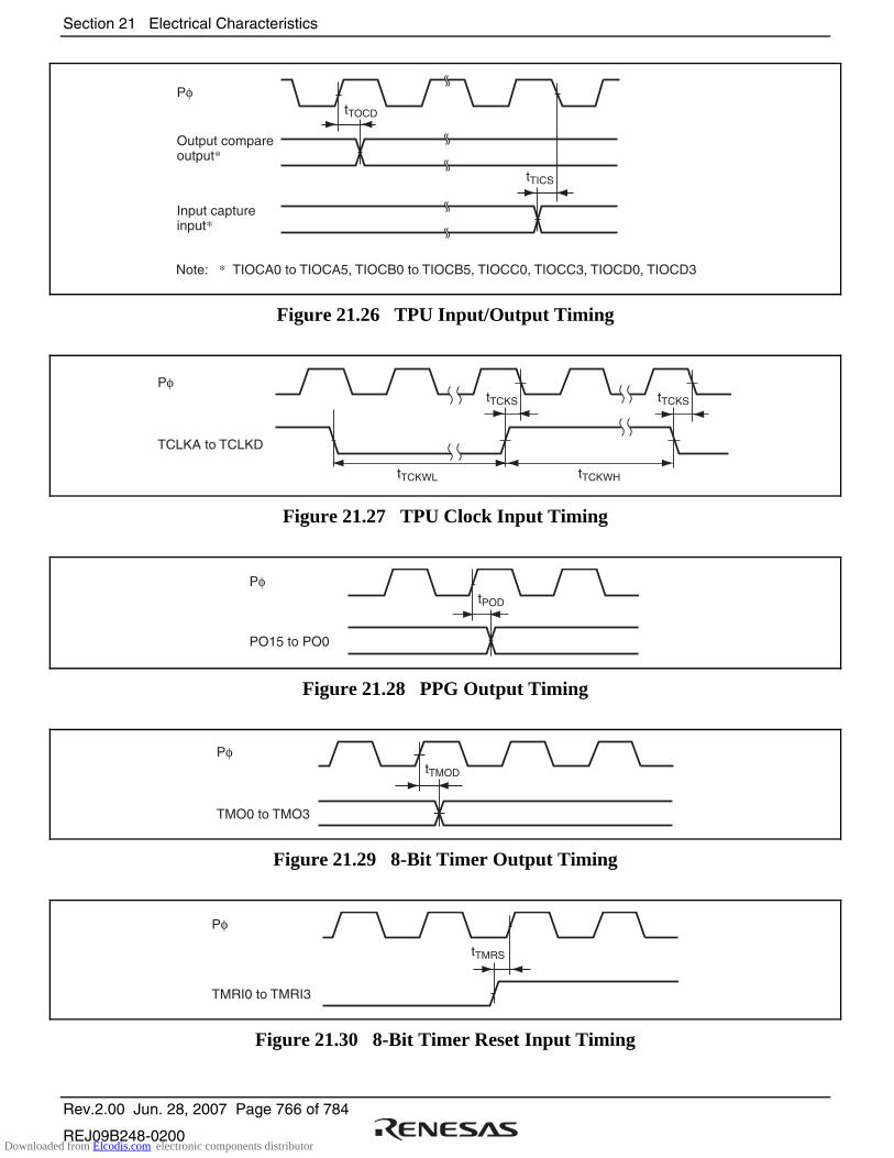
Section 21 Electrical Characteristics
Rev.2.00 Jun. 28, 2007 Page 766 of 784
REJ09B248-0200
Pφ
Output compare output*
Input capture input*
tTOCD
tTICS
Note: * TIOCA0 to TIOCA5, TIOCB0 to TIOCB5, TIOCC0, TIOCC3, TIOCD0, TIOCD3
Figure 21.26 TPU Input/Output Timing
Pφ
TCLKA to TCLKD
tTCKWL tTCKWH
tTCKS tTCKS
Figure 21.27 TPU Clock Input Timing
Pφ
PO15 to PO0
tPOD
Figure 21.28 PPG Output Timing
Pφ
TMO0 to TMO3
tTMOD
Figure 21.29 8-Bit Timer Output Timing
Pφ
TMRI0 to TMRI3
tTMRS
Figure 21.30 8-Bit Timer Reset Input Timing
Downloaded from Elcodis.com electronic components distributor
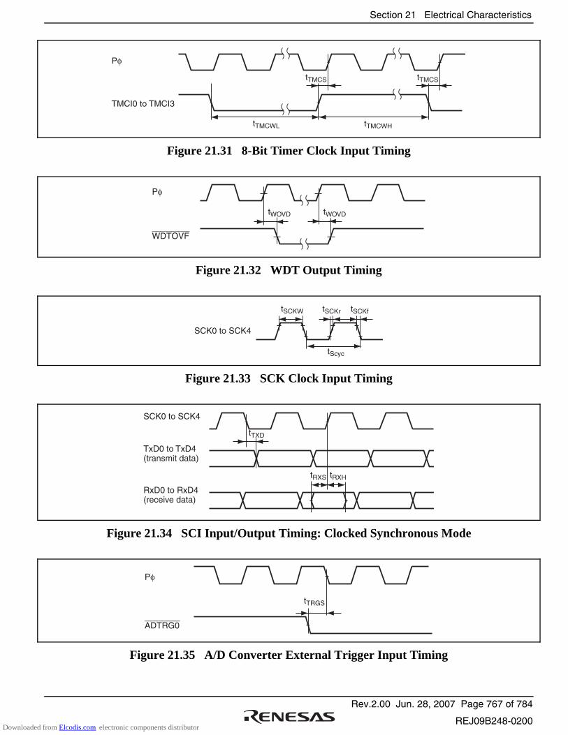
Section 21 Electrical Characteristics
Rev.2.00 Jun. 28, 2007 Page 767 of 784
REJ09B248-0200
Pφ
TMCI0 to TMCI3
tTMCWL tTMCWH
tTMCS tTMCS
Figure 21.31 8-Bit Timer Clock Input Timing
Pφ
WDTOVF
tWOVD tWOVD
Figure 21.32 WDT Output Timing
SCK0 to SCK4
tSCKW tSCKr tSCKf
tScyc
Figure 21.33 SCK Clock Input Timing
SCK0 to SCK4
tTXD
tRXS tRXH
TxD0 to TxD4 (transmit data)
RxD0 to RxD4 (receive data)
Figure 21.34 SCI Input/Output Timing: Clocked Synchronous Mode
Pφ
ADTRG0
tTRGS
Figure 21.35 A/D Converter External Trigger Input Timing
Downloaded from Elcodis.com electronic components distributor

Section 21 Electrical Characteristics
Rev.2.00 Jun. 28, 2007 Page 768 of 784
REJ09B248-0200
Downloaded from Elcodis.com electronic components distributor
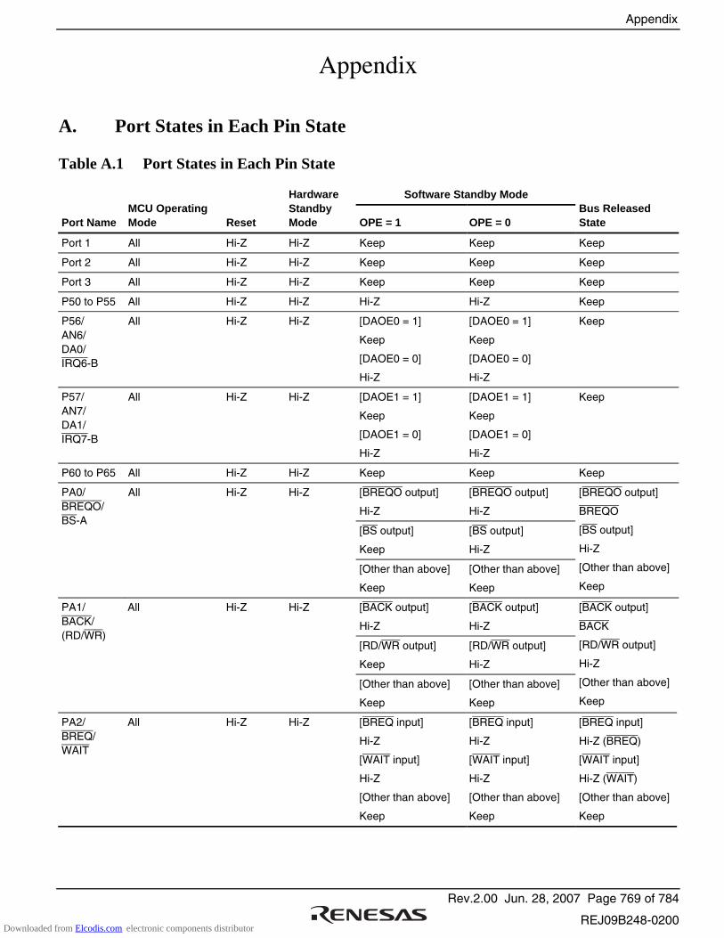
Appendix
Rev.2.00 Jun. 28, 2007 Page 769 of 784
REJ09B248-0200
Appendix
A. Port States in Each Pin State
Table A.1 Port States in Each Pin State
Software Standby Mode
Port Name MCU Operating Mode Reset
Hardware Standby Mode OPE = 1 OPE = 0
Bus Released State
Port 1 All Hi-Z Hi-Z Keep Keep Keep
Port 2 All Hi-Z Hi-Z Keep Keep Keep
Port 3 All Hi-Z Hi-Z Keep Keep Keep
P50 to P55 All Hi-Z Hi-Z Hi-Z Hi-Z Keep
P56/ AN6/ DA0/ IRQ6-B
All Hi-Z Hi-Z [DAOE0 = 1]
Keep
[DAOE0 = 0]
Hi-Z
[DAOE0 = 1]
Keep
[DAOE0 = 0]
Hi-Z
Keep
P57/ AN7/ DA1/ IRQ7-B
All Hi-Z Hi-Z [DAOE1 = 1]
Keep
[DAOE1 = 0]
Hi-Z
[DAOE1 = 1]
Keep
[DAOE1 = 0]
Hi-Z
Keep
P60 to P65 All Hi-Z Hi-Z Keep Keep Keep
All Hi-Z Hi-Z [BREQO output]
Hi-Z
[BREQO output]
Hi-Z
PA0/ BREQO/ BS-A
[BS output]
Keep
[BS output]
Hi-Z
[Other than above]
Keep
[Other than above]
Keep
[BREQO output]
BREQO
[BS output]
Hi-Z
[Other than above]
Keep
All Hi-Z Hi-Z [BACK output]
Hi-Z
[BACK output]
Hi-Z
PA1/ BACK/ (RD/WR)
[RD/WR output]
Keep
[RD/WR output]
Hi-Z
[Other than above]
Keep
[Other than above]
Keep
[BACK output]
BACK
[RD/WR output]
Hi-Z
[Other than above]
Keep
PA2/ BREQ/ WAIT
All Hi-Z Hi-Z [BREQ input]
Hi-Z
[WAIT input]
Hi-Z
[Other than above]
Keep
[BREQ input]
Hi-Z
[WAIT input]
Hi-Z
[Other than above]
Keep
[BREQ input]
Hi-Z (BREQ)
[WAIT input]
Hi-Z (WAIT)
[Other than above]
Keep
Downloaded from Elcodis.com electronic components distributor

Appendix
Rev.2.00 Jun. 28, 2007 Page 770 of 784
REJ09B248-0200
Software Standby Mode
Port Name MCU Operating Mode Reset
Hardware Standby Mode OPE = 1 OPE = 0
Bus Released State
PA3/ LLWR/ LLB
External extended mode
H Hi-Z H Hi-Z Hi-Z
PA4/ LHWR/ LUB
External extended mode
H Hi-Z [LHWR, LUB output]
H
[Other than above]
Keep
[LHWR, LUB output]
Hi-Z
[Other than above]
Keep
[LHWR, LUB output]
Hi-Z
[Other than above]
Keep
PA5/RD External extended mode
H Hi-Z H Hi-Z Hi-Z
PA6/ AS/ AH/ BS-B
External extended mode
H Hi-Z [AS, BS output]
H
[AH output]
L
[Other than above]
Keep
[AS, AH, BS output]
Hi-Z
[Other than above]
Keep
[AS, AH, BS output]
Hi-Z
[Other than above]
Keep
PA7/Bφ External extended mode
Clock output
Hi-Z [Clock output]
H
[Other than above]
Keep
[Clock output]
H
[Other than above]
Keep
[Clock output]
Clock output
[Other than above]
Keep
PB0/ CS0/ CS4-A/ CS5-B
External extended mode
H Hi-Z [CS output]
H
[Other than above]
Keep
[CS output]
Hi-Z
[Other than above]
Keep
[CS output]
Hi-Z
[Other than above]
Keep
PB1/ CS1/ CS2-B/ CS5-A/ CS6-B/ CS7-B
All Hi-Z Hi-Z [CS output]
H
[Other than above]
Keep
[CS output]
Hi-Z
[Other than above]
Keep
[CS output]
Hi-Z
[Other than above]
Keep
PB2/ CS2-A/ CS6-A
All Hi-Z Hi-Z [CS output]
H
[Other than above]
Keep
[CS output]
Hi-Z
[Other than above]
Keep
[CS output]
Hi-Z
[Other than above]
Keep
PB3/ CS3/ CS7-A
All Hi-Z Hi-Z [CS output]
H
[Other than above]
Keep
[CS output]
Hi-Z
[Other than above]
Keep
[CS output]
Hi-Z
[Other than above]
Keep
Downloaded from Elcodis.com electronic components distributor
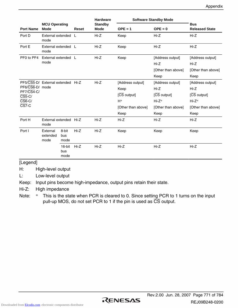
Appendix
Rev.2.00 Jun. 28, 2007 Page 771 of 784
REJ09B248-0200
Software Standby Mode
Port Name MCU Operating Mode Reset
Hardware Standby Mode OPE = 1 OPE = 0
Bus Released State
Port D External extended mode
L Hi-Z Keep Hi-Z Hi-Z
Port E External extended mode
L Hi-Z Keep Hi-Z Hi-Z
PF0 to PF4 External extended mode
L Hi-Z Keep [Address output]
Hi-Z
[Other than above]
Keep
[Address output]
Hi-Z
[Other than above]
Keep
PF5/CS5-D/ PF6/CS6-D/ PF7/CS4-C/ CS5-C/ CS6-C/ CS7-C
External extended mode
Hi-Z Hi-Z [Address output]
Keep
[CS output]
H*
[Other than above]
Keep
[Address output]
Hi-Z
[CS output]
Hi-Z*
[Other than above]
Keep
[Address output]
Hi-Z
[CS output]
Hi-Z*
[Other than above]
Keep
Port H External extended mode
Hi-Z Hi-Z Hi-Z Hi-Z Hi-Z
Port I 8-bit bus mode
Hi-Z Hi-Z Keep Keep Keep
External extended mode
16-bit bus mode
Hi-Z Hi-Z Hi-Z Hi-Z Hi-Z
[Legend]
H: High-level output
L: Low-level output Keep: Input pins become high-impedance, output pins retain their state.
Hi-Z: High impedance
Note: * This is the state when PCR is cleared to 0. Since setting PCR to 1 turns on the input pull-up MOS, do not set PCR to 1 if the pin is used as CS output.
Downloaded from Elcodis.com electronic components distributor

Appendix
Rev.2.00 Jun. 28, 2007 Page 772 of 784
REJ09B248-0200
B. Product Lineup
Product Classification Product Model Marking Package (Package Code)
H8SX/1651C ROMless R5S61651CFPV R5S61651FPV FP-120BV*
Note: * Pb-free version
Downloaded from Elcodis.com electronic components distributor
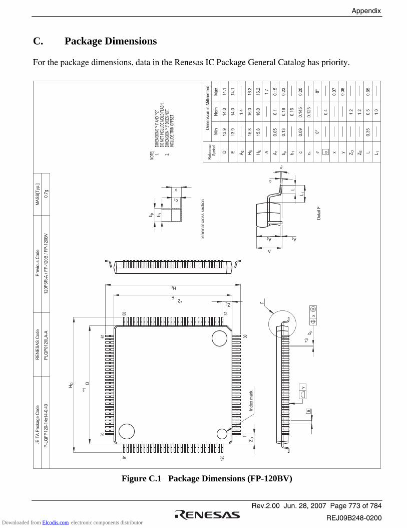
Appendix
Rev.2.00 Jun. 28, 2007 Page 773 of 784
REJ09B248-0200
C. Package Dimensions
For the package dimensions, data in the Renesas IC Package General Catalog has priority.
Term
inal c
ross
sect
ion
b1
c1
bp
c
INCL
UDE
TRIM
OFF
SET.
DIM
ENSI
ON
"*3"
DO
ES N
OT
NOTE
)
DO N
OT
INCL
UDE
MO
LD F
LASH
.DI
MEN
SIO
NS "*
1" A
ND "*
2"1. 2.
De
tail
F
c
A
A2 A1L
L1
*2
*3
*1
F
12091
9061
60 31
301
x
Index
mark
y
D
HD
bp
E
HE
ZD
ZE
1.0
0.1
25
0.1
6
1.2
1.2
0.0
7
0.2
00
.14
50
.09
0.2
30
.18
0.1
3
Ma
xN
om
MinD
imensi
on in
Mill
imete
rs
Sym
bol
Ref
eren
ce
14.1
14
.013.9
D
14.1
14
.013.9
E
1.4
A2
16.2
16
.015.8
16.2
16
.015.8
1.7
A
0.1
50.1
0.0
5
0.6
50.5
0.3
5Lx
8°
0°
c
0.4
e
0.0
8yHD
HE
A1
bp
b1
c 1 ZD
ZE
L1
P-L
QF
P1
20
-14
x14
-0.4
00
.7g
MA
SS
[Typ
.]
120P
6R
-A / F
P-1
20B
/ F
P-1
20B
VP
LQ
P0
12
0L
A-A
RE
NE
SA
S C
od
eJE
ITA
Pack
age C
ode
Pre
vious
Code
e
Figure C.1 Package Dimensions (FP-120BV)
Downloaded from Elcodis.com electronic components distributor
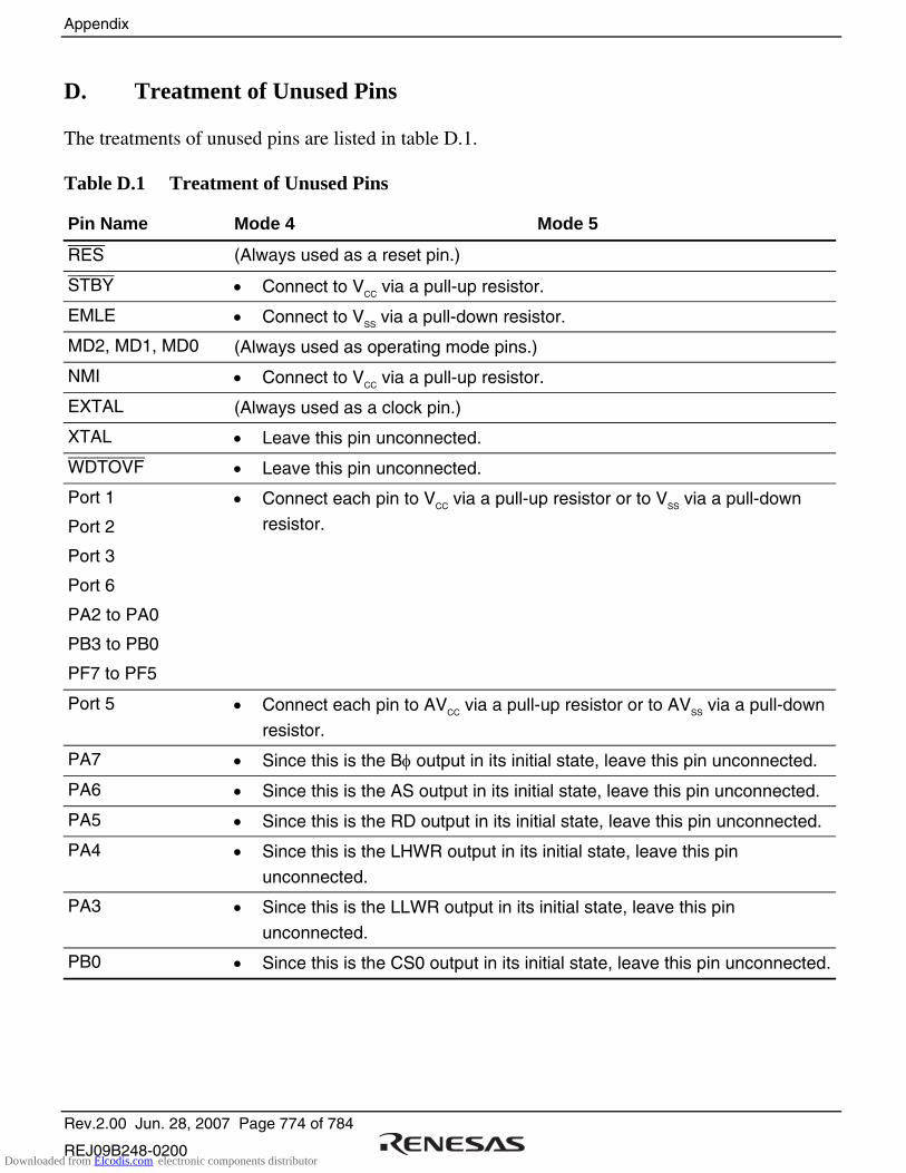
Appendix
Rev.2.00 Jun. 28, 2007 Page 774 of 784
REJ09B248-0200
D. Treatment of Unused Pins
The treatments of unused pins are listed in table D.1.
Table D.1 Treatment of Unused Pins
Pin Name Mode 4 Mode 5
RES (Always used as a reset pin.)
STBY • Connect to VCC via a pull-up resistor.
EMLE • Connect to VSS via a pull-down resistor.
MD2, MD1, MD0 (Always used as operating mode pins.)
NMI • Connect to VCC via a pull-up resistor.
EXTAL (Always used as a clock pin.)
XTAL • Leave this pin unconnected.
WDTOVF • Leave this pin unconnected.
Port 1
Port 2
Port 3
Port 6
PA2 to PA0
PB3 to PB0
PF7 to PF5
• Connect each pin to VCC via a pull-up resistor or to VSS via a pull-down
resistor.
Port 5 • Connect each pin to AVCC via a pull-up resistor or to AVSS via a pull-down
resistor.
PA7 • Since this is the Bφ output in its initial state, leave this pin unconnected.
PA6 • Since this is the AS output in its initial state, leave this pin unconnected.
PA5 • Since this is the RD output in its initial state, leave this pin unconnected.
PA4 • Since this is the LHWR output in its initial state, leave this pin
unconnected.
PA3 • Since this is the LLWR output in its initial state, leave this pin
unconnected.
PB0 • Since this is the CS0 output in its initial state, leave this pin unconnected.
Downloaded from Elcodis.com electronic components distributor

Appendix
Rev.2.00 Jun. 28, 2007 Page 775 of 784
REJ09B248-0200
Pin Name Mode 4 Mode 5
Port D
Port E
PF4 to PF0
• Since this is the address output in its initial state, leave this pin
unconnected.
Port H (Used as a data bus.)
Port I (Used as a data bus.) Since this is a general-purpose input port in its initial state, connect each pin to VCC via a pull-up resistor or connect each pin to VSS via a pull-down resistor.
Vref • Connect to AVCC.
Notes: 1. Do not change the function of an unused pin from its initial state. 2. Do not change the initial value (input buffer disabled) of PnICR corresponding to an
unused pin.
Downloaded from Elcodis.com electronic components distributor

Appendix
Rev.2.00 Jun. 28, 2007 Page 776 of 784
REJ09B248-0200
Downloaded from Elcodis.com electronic components distributor
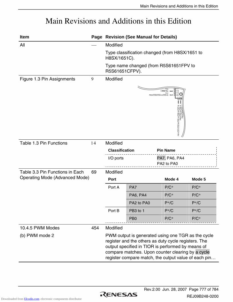
Main Revisions and Additions in this Edition
Rev.2.00 Jun. 28, 2007 Page 777 of 784
REJ09B248-0200
Main Revisions and Additions in this Edition
Item Page Revision (See Manual for Details)
All Modified
Type classification changed (from H8SX/1651 to H8SX/1651C).
Type name changed (from R5S61651FPV to R5S61651CFPV).
Figure 1.3 Pin Assignments 9 Modified
PB1/CS1/CS2-B/CS5-A/CS6-B/CS7-B
PB2/CS2-A/CS6-A
PB3/CS3/CS7-A
Vss
PA7/BφVcc
PB0/CS0/CS4-A/CS5-B
117
118
119
120
1 2 3
Table 1.3 Pin Functions 14 Modified
Classification Pin Name
I/O ports PA7, PA6, PA4 PA2 to PA0
Table 3.3 Pin Functions in Each Operating Mode (Advanced Mode)
69 Modified
Port Mode 4 Mode 5
PA7 P/C* P/C*
PA6, PA4 P/C* P/C*
Port A
PA2 to PA0 P*/C P*/C
PB3 to 1 P*/C P*/C Port B
PB0 P/C* P/C*
10.4.5 PWM Modes
(b) PWM mode 2
454 Modified
PWM output is generated using one TGR as the cycle register and the others as duty cycle registers. The output specified in TIOR is performed by means of compare matches. Upon counter clearing by a cycle register compare match, the output value of each pin…
Downloaded from Elcodis.com electronic components distributor
Main Revisions and Additions in this Edition
Rev.2.00 Jun. 28, 2007 Page 778 of 784
REJ09B248-0200
Item Page Revision (See Manual for Details)
18.5.1 Notes on Clock Pulse Generator
657 Deleted
4. Note that the frequency of φ will be changed in the middle of a bus cycle when setting SCKCR0 or SCKCR1 while executing the external bus cycle with the write-data-buffer function.
21.1 Electrical Characteristics (at 35-MHz operation)
725 Modified
21.2 Electrical Characteristics (at 50-MHz operation)
737 Modified
Downloaded from Elcodis.com electronic components distributor
Rev.2.00 Jun. 28, 2007 Page 779 of 784
REJ09B248-0200
Index
Numerics 0-output/1-output .................................... 443 16-Bit access space................................. 168 16-bit counter mode................................ 529 16-bit timer pulse unit (TPU) ................. 399 8-Bit access space................................... 167 8-bit timers (TMR) ................................. 509 A A/D conversion accuracy........................ 637 A/D converter ......................................... 625 Absolute accuracy................................... 637 Absolute address....................................... 54 Address error ............................................ 78 Address map ............................................. 70 Address modes........................................ 257 Address register ........................................ 25 Address/data multiplexed I/O interface.................................... 161, 198 Addressing modes..................................... 51 Advanced mode ........................................ 20 All-module-clock-stop mode .......... 662, 678 Area 0 ..................................................... 162 Area 1 ..................................................... 162 Area 2 ..................................................... 163 Area 3 ..................................................... 163 Area 4 ..................................................... 164 Area 5 ..................................................... 165 Area 6 ..................................................... 165 Area 7 ..................................................... 166 Area division........................................... 156 Arithmetic operation instructions ............. 42 Asynchronous mode ............................... 581 AT-cut parallel-resonance type............... 655 Available output signal and settings in each port ......................... 380
Average transfer rate generator............... 550 B Bφ clock output control........................... 682 Basic bus interface .......................... 160, 170 Basic instruction formats .......................... 50 Big endian ............................................... 159 Bit manipulation instructions .................... 45 Bit rate..................................................... 572 Block transfer instructions ........................ 41 Block transfer mode........................ 262, 330 Branch instructions ................................... 48 Buffer operation ...................................... 448 Burst access mode................................... 268 Burst ROM interface....................... 160, 193 Bus access modes.................................... 267 Bus arbitration......................................... 223 Bus configuration.................................... 148 Bus controller (BSC)............................... 123 Bus cycle division ................................... 324 Bus width ................................................ 159 Bus-released state...................................... 60 Byte control SRAM interface ......... 160, 185 C Carry (C) ................................................... 26 Cascaded operation ................................. 452 Chain transfer.......................................... 331 Chip select signals................................... 157 Clock pulse generator ............................. 651 Clock synchronization cycle (Tsy).......... 150 Clocked synchronous mode .................... 598 Compare match A ................................... 527 Compare match B ................................... 527 Compare match count mode ................... 529
Downloaded from Elcodis.com electronic components distributor
Rev.2.00 Jun. 28, 2007 Page 780 of 784
REJ09B248-0200
Compare match signal ............................ 526 Condition field.......................................... 50 Counter operation ................................... 440 CPU .......................................................... 15 CPU operating modes............................... 17 CPU priority control function over DTC.................................. 117 Crystal resonator..................................... 655 Cycle stealing mode................................ 267 D D/A converter ......................................... 643 Data direction register ............................ 351 Data register...................................... 25, 351 Data transfer controller (DTC) ............... 307 Data transfer instructions.......................... 40 Direct convention ................................... 607 DMA controller (DMAC)....................... 229 Double-buffered structure....................... 581 DTC vector address ................................ 320 DTC vector address offset ...................... 320 Dual address mode.................................. 257 E Effective address extension ...................... 50 Endian and data alignment ..................... 167 Endian format ......................................... 159 Error signal ............................................. 607 Exception handling................................... 71 Exception handling vector table ............... 72 Exception-handling state .......................... 60 Extended memory indirect........................ 57 Extended repeat area............................... 255 Extended repeat area function ................ 268 Extension of chip select (CS) assertion period....................................... 182 External access bus................................. 148 External bus ............................................ 153
External bus clock (Bφ) .................. 149, 651 External bus interface ............................. 158 External clock ......................................... 656 External interrupts................................... 101 F Free-running count operation.................. 441 Frequency divider ........................... 651, 656 Full address mode ................................... 318 Full-scale error........................................ 637 G General register data formats .................... 30 General registers ....................................... 25 H Half-carry (H) ........................................... 26 Hardware standby mode ................. 662, 676 I I/O ports .................................................. 343 ID code.................................................... 592 Idle cycle................................................. 207 Illegal instruction ................................ 81, 82 Immediate ................................................. 55 Index register ............................................ 25 Index register indirect with displacement ..................................... 52 Initial register values................................. 29 Input buffer control register .................... 352 Input capture function............................. 444 Instruction fetch ........................................ 23 Instruction set............................................ 32 Instructions and addressing modes ........... 34 Internal interrupts.................................... 102
Downloaded from Elcodis.com electronic components distributor

Rev.2.00 Jun. 28, 2007 Page 781 of 784
REJ09B248-0200
Internal peripheral bus ............................ 148 Internal system bus ................................. 148 Interrupt .................................................... 80 Interrupt control mode 0 ......................... 108 Interrupt control mode 2 ......................... 110 Interrupt controller.................................... 85 Interrupt exception handling sequence ... 112 Interrupt exception handling vector table ............................................. 103 Interrupt mask bit (I)................................. 26 Interrupt response times.......................... 113 Interrupt sources ..................................... 101 Interrupt sources and vector address offsets ....................... 103 Interval timer .......................................... 543 Interval timer mode................................. 543 Inverse convention.................................. 608 IRQn interrupts ....................................... 101 L Little endian............................................ 159 Logic operation instructions ..................... 44 M Mark state ....................................... 581, 619 Maximum mode........................................ 21 MCU operating modes.............................. 63 Memory data formats................................ 31 Memory indirect ....................................... 56 Memory map............................................. 23 Middle mode............................................. 19 Mode 4...................................................... 68 Mode 5...................................................... 68 Mode pin................................................... 63 Module stop mode .................................. 678 Multi-clock mode ................................... 670 Multiprocessor bit................................... 592
Multiprocessor communication function ................................................... 592 N Negative (N) ............................................. 26 NMI interrupt .......................................... 101 Nonlinearity error.................................... 637 Non-overlapping pulse output................. 501 Normal mode ............................................ 17 Normal transfer mode ............................. 327 Normal transfer mode ............................. 260 Number of access cycles ......................... 160 O Offset addition ........................................ 270 Offset error.............................................. 637 On-chip baud rate generator.................... 584 Open-drain control register ..................... 354 Operation field .......................................... 50 Operation with cascaded connection....... 529 Oscillator................................................. 655 Output buffer control .............................. 355 Output trigger.......................................... 501 Overflow ......................................... 528, 542 Overflow (V)............................................. 26 P Parity bit.................................................. 581 Periodic count operation ......................... 441 Peripheral module clock (Pφ).......... 149, 651 Phase counting mode .............................. 460 Pin assignments........................................... 9 Pin functions ............................................. 10 PLL circuit ...................................... 651, 656 Port function controller ........................... 386 Port register............................................. 352 Power-down modes................................. 661
Downloaded from Elcodis.com electronic components distributor
Rev.2.00 Jun. 28, 2007 Page 782 of 784
REJ09B248-0200
Processing states ....................................... 60 Program execution state............................ 60 Program stop state .................................... 60 Program-counter relative .......................... 56 Program-counter relative with index register ............................................ 56 Programmable pulse generator (PPG) .... 485 Pull-up MOS control register.................. 353 PWM modes ........................................... 454 Q Quantization error................................... 637 R RAM....................................................... 649 Read strobe (RD) timing......................... 180 Register addresses................................... 686 Register bits ............................................ 697 Register configuration in each port......... 350 Register direct........................................... 52 Register field ............................................ 50 Register indirect........................................ 52 Register indirect with displacement.......... 52 Register indirect with post-decrement ...... 53 Register indirect with post-increment....... 53 Register indirect with pre-decrement........ 53 Register indirect with pre-increment ........ 53 Register states in each operating mode... 714 Registers
ABWCR ......................127, 689, 704, 717 ADCR..........................631, 694, 710, 722 ADCSR........................629, 694, 710, 722 ADDR..........................628, 694, 710, 722 ASTCR ........................128, 689, 704, 717 BCR.............................140, 689, 704, 717 BROMCR....................145, 689, 704, 717 BRR.............................572, 693, 709, 721 CCR...................................................... 26
CPUPCR....................... 89, 692, 707, 720 CRA .................................................... 314 CRB .................................................... 314 CSACR ....................... 135, 689, 704, 717 DACR ......................... 249, 687, 699, 715 DACR01 ..................... 645, 693, 709, 721 DADR......................... 644, 693, 709, 721 DAR.................................................... 313 DBSR.......................... 239, 687, 699, 715 DDAR......................... 236, 687, 699, 715 DDR.................... 351, 686, 697, 698, 714 DMDR ........................ 240, 687, 699, 715 DMRSR ...................... 256, 688, 703, 716 DOFR.......................... 237, 687, 699, 715 DR............................... 351, 686, 698, 714 DSAR.......................... 235, 687, 699, 715 DTCCR....................... 316, 692, 707, 719 DTCER ....................... 315, 691, 707, 719 DTCR.......................... 238, 687, 699, 715 DTCVBR .................... 317, 689, 704, 717 ENDIANCR................ 143, 689, 704, 717 EXR ...................................................... 28 ICR...... 352, 686, 687, 697, 698, 714, 715 IDLCR ........................ 138, 689, 704, 717 IER................................ 93, 692, 707, 720 INTCR .......................... 88, 692, 707, 719 IPR ................................ 91, 689, 703, 717 ISCR ............................. 95, 689, 703, 717 ISR ................................ 99, 692, 707, 720 MAC ..................................................... 29 MDCR........................... 64, 690, 704, 718 MPXCR ...................... 147, 689, 704, 717 MRA ................................................... 310 MRB ................................................... 311 MSTPCR..................... 666, 690, 705, 718 NDER ......................... 488, 693, 709, 721 NDR............................ 491, 693, 709, 721 ODR............................ 354, 687, 698, 715 PC ......................................................... 26
Downloaded from Elcodis.com electronic components distributor

Rev.2.00 Jun. 28, 2007 Page 783 of 784
REJ09B248-0200
PCR............................ 353, 494, 687, 693, .................................... 698, 709, 715, 721 PFCR .................................. 687, 698, 715 PFCR0 ................................................ 386 PFCR1 ................................................ 387 PFCR2 ................................................ 388 PFCR4 ................................................ 390 PFCR6 ................................................ 391 PFCR7 ................................................ 392 PFCR9 ................................................ 393 PFCRB................................................ 395 PFCRC................................................ 396 PMR............................ 495, 693, 709, 721 PODR ......................... 490, 693, 709, 721 PORT.................................................. 352 RDNCR ...................... 134, 689, 704, 717 RDR............................ 554, 693, 709, 721 RSR..................................................... 554 RSTCSR ..................... 540, 694, 710, 722 SAR .................................................... 313 SBR....................................................... 28 SBYCR....................... 664, 690, 705, 718 SCKCR....................... 652, 690, 705, 718 SCMR......................... 571, 693, 709, 721 SCR............................. 558, 693, 709, 721 SEMR ................................................. 579 SMR............................ 555, 693, 709, 721 SRAMCR ................... 144, 689, 704, 717 SSIER ......................... 100, 687, 698, 715 SSR............................. 563, 693, 709, 721 SYSCR ......................... 66, 690, 705, 718 TCCR.......................... 517, 695, 711, 722 TCNT......................... 437, 514, 538, 694, .............................695, 710, 711, 722, 723 TCOR ......................... 514, 694, 711, 722 TCR ........................... 407, 515, 694, 695, .................................... 710, 711, 722, 723 TCSR ...................519, 539, 694, 710, 722 TDR ............................ 554, 693, 709, 721 TGR ............................ 437, 695, 711, 723
TIER............................ 431, 695, 711, 723 TIOR ........................... 413, 695, 711, 723 TMDR......................... 412, 695, 711, 723 TSR ............................. 433, 695, 711, 723 TSTR........................... 438, 695, 711, 722 TSYR .......................... 439, 695, 711, 722 VBR ...................................................... 28 WTCR......................... 129, 689, 704, 717
Repeat transfer mode ...................... 261, 328 Reset ......................................................... 74 Reset state ................................................. 60 Resolution ............................................... 637 S Sample-and-hold circuit.......................... 635 Scan mode............................................... 633 Serial communication interface (SCI)..... 549 Shift operation instructions ....................... 45 Short address mode ................................. 318 Single address mode ............................... 258 Single mode ............................................ 632 Sleep mode...................................... 662, 671 Smart card interface ................................ 606 Software standby mode................... 662, 672 Space state............................................... 581 Stack pointer (SP) ..................................... 25 Stack status after exception handling........ 83 Start bit.................................................... 581 State transitions......................................... 62 Stop bit.................................................... 581 Strobe assert/negate timing ..................... 161 Synchronous clearing.............................. 446 Synchronous operation............................ 446 Synchronous presetting........................... 446 System clock (Iφ) ............................ 149, 651 System control instructions....................... 49
Downloaded from Elcodis.com electronic components distributor

Rev.2.00 Jun. 28, 2007 Page 784 of 784
REJ09B248-0200
T Toggle output.......................................... 443 Trace exception handling.......................... 77 Transfer information............................... 318 Transfer information read skip function ................................... 326 Transfer information writeback skip function .......................... 327 Transfer modes ....................................... 260 Transmit/receive data ............................. 581 Trap instruction exception handling ......... 81 U User bit (UI, U)......................................... 26 V Vector table address.................................. 72
Vector table address offset........................ 72 W Wait control ............................................ 178 Watchdog timer (WDT).......................... 537 Watchdog timer mode............................. 542 Waveform output by compare match...... 442 Write data buffer function....................... 221 Write data buffer function for external data bus................................ 221 Write data buffer function for peripheral modules ............................ 222 Z Zero (Z)..................................................... 26
Downloaded from Elcodis.com electronic components distributor

Renesas 32-Bit CISC MicrocomputerHardware ManualH8SX/1651 Group
Publication Date: Rev.1.00, Jan. 16, 2006 Rev.2.00, Jun. 28, 2007Published by: Sales Strategic Planning Div. Renesas Technology Corp.Edited by: Customer Support Department Global Strategic Communication Div. Renesas Solutions Corp.
2007. Renesas Technology Corp., All rights reserved. Printed in Japan.
Downloaded from Elcodis.com electronic components distributor
Sales Strategic Planning Div. Nippon Bldg., 2-6-2, Ohte-machi, Chiyoda-ku, Tokyo 100-0004, Japan
http://www.renesas.comRefer to "http://www.renesas.com/en/network" for the latest and detailed information.
Renesas Technology America, Inc.450 Holger Way, San Jose, CA 95134-1368, U.S.ATel: <1> (408) 382-7500, Fax: <1> (408) 382-7501 Renesas Technology Europe LimitedDukes Meadow, Millboard Road, Bourne End, Buckinghamshire, SL8 5FH, U.K.Tel: <44> (1628) 585-100, Fax: <44> (1628) 585-900
Renesas Technology (Shanghai) Co., Ltd.Unit 204, 205, AZIACenter, No.1233 Lujiazui Ring Rd, Pudong District, Shanghai, China 200120Tel: <86> (21) 5877-1818, Fax: <86> (21) 6887-7898 Renesas Technology Hong Kong Ltd.7th Floor, North Tower, World Finance Centre, Harbour City, 1 Canton Road, Tsimshatsui, Kowloon, Hong Kong Tel: <852> 2265-6688, Fax: <852> 2730-6071
Renesas Technology Taiwan Co., Ltd.10th Floor, No.99, Fushing North Road, Taipei, Taiwan Tel: <886> (2) 2715-2888, Fax: <886> (2) 2713-2999 Renesas Technology Singapore Pte. Ltd.1 Harbour Front Avenue, #06-10, Keppel Bay Tower, Singapore 098632 Tel: <65> 6213-0200, Fax: <65> 6278-8001
Renesas Technology Korea Co., Ltd.Kukje Center Bldg. 18th Fl., 191, 2-ka, Hangang-ro, Yongsan-ku, Seoul 140-702, KoreaTel: <82> (2) 796-3115, Fax: <82> (2) 796-2145 Renesas Technology Malaysia Sdn. BhdUnit 906, Block B, Menara Amcorp, Amcorp Trade Centre, No.18, Jalan Persiaran Barat, 46050 Petaling Jaya, Selangor Darul Ehsan, MalaysiaTel: <603> 7955-9390, Fax: <603> 7955-9510
RENESAS SALES OFFICES
Colophon 6.0
Downloaded from Elcodis.com electronic components distributor

Downloaded from Elcodis.com electronic components distributor
H8SX/1651 GroupHardware Manual
Downloaded from Elcodis.com electronic components distributor