Embed Size (px)
Citation preview
HUAWEI.COM Security Level:
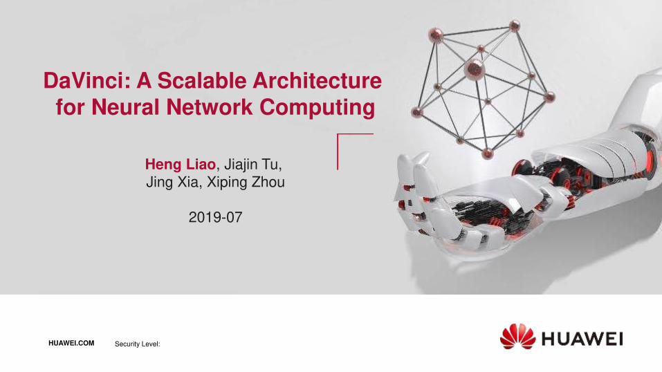
DaVinci: A Scalable Architecture for Neural Network Computing
Heng Liao, Jiajin Tu, Jing Xia, Xiping Zhou
2019-07
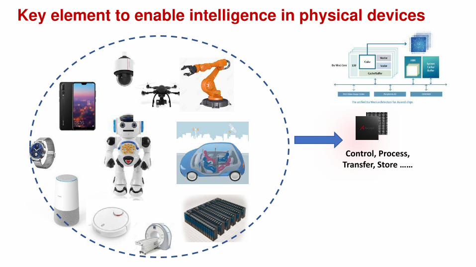
Key element to enable intelligence in physical devices
Control, Process,
Transfer, Store ……
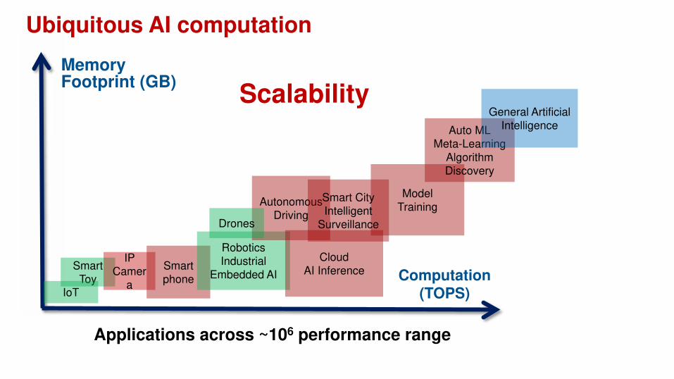
Ubiquitous AI computation
Smart
Toy
Memory Footprint (GB)
IP
Camer
a
Smart
phoneIoT
Robotics
Industrial
Embedded AI
Autonomous
Driving
Cloud
AI Inference
Drones
Model
Training
Auto ML
Meta-Learning
Algorithm
Discovery
Smart City
Intelligent
Surveillance
General Artificial
Intelligence
Scalability
Applications across ~106 performance range
Computation (TOPS)
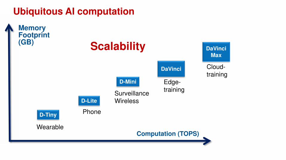
Ubiquitous AI computation
D-Tiny
D-Lite
D-Mini
DaVinciMax
Cloud-training
SurveillanceWireless
Phone
Wearable
DaVinci
Edge-training
Memory Footprint (GB)
Computation (TOPS)
Scalability
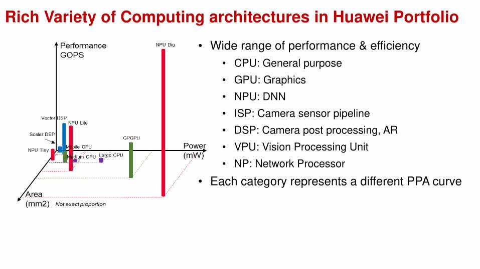
Rich Variety of Computing architectures in Huawei Portfolio
• Wide range of performance & efficiency
• CPU: General purpose
• GPU: Graphics
• NPU: DNN
• ISP: Camera sensor pipeline
• DSP: Camera post processing, AR
• VPU: Vision Processing Unit
• NP: Network Processor
• Each category represents a different PPA curve
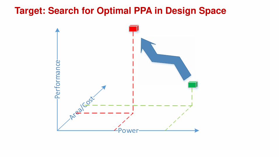
Target: Search for Optimal PPA in Design Space
Power
Pe
rfo
rma
nce

Architecture Overview of DaVinci
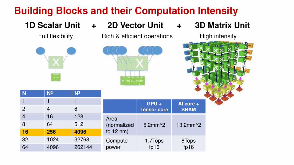
Building Blocks and their Computation Intensity
N N2 N3
1 1 1
2 4 8
4 16 128
8 64 512
16 256 4096
32 1024 32768
64 4096 262144
1D Scalar Unit + 2D Vector Unit + 3D Matrix Unit
Full flexibility Rich & efficient operations High intensity
GPU +Tensor core
AI core + SRAM
Area (normalizedto 12 nm)
5.2mm^2 13.2mm^2
Computepower
1.7Tops fp16
8Tops fp16

DaVinci Core
• Cube:4096(16^3) FP16 MACs + 8192 INT8 MACs
• Vector:2048bit INT8/FP16/FP32 vector with special functions
(activation functions, NMS- Non Minimum Suppression, ROI, SORT)
• Explicit memory hierarchy design, managed by MTE
16^3 CubeA/B
DFF 16^2
accu
mul
ator
Buffer A L0
(64KB)
Buffer B L0
(64KB)
Unified Buffer (256KB)
DaVinci Core (16^3 Cube)
trans
img2
col
MTE
Acc
um D
FF
L1 B
uffe
r (1M
B)
L1 D
MAC
BIU
8*16 Vector Unit
Buffer C L0 (256KB)
I Cache
(32KB) Sca
lar
PSQ
L0 load4096-bit
L1 load2048-bit
System
ControlConfigPort
FP16->FP32 FP32->FP16ReLU
L/S2048-bit
Scalar Unit/ AGU/
Mask Gen GP
R
SPR
Cube Queue
Vector Queue
MTE Queue
Event SyncInstr.
Dispatch
deco
mp
L2 access1024-bit *2
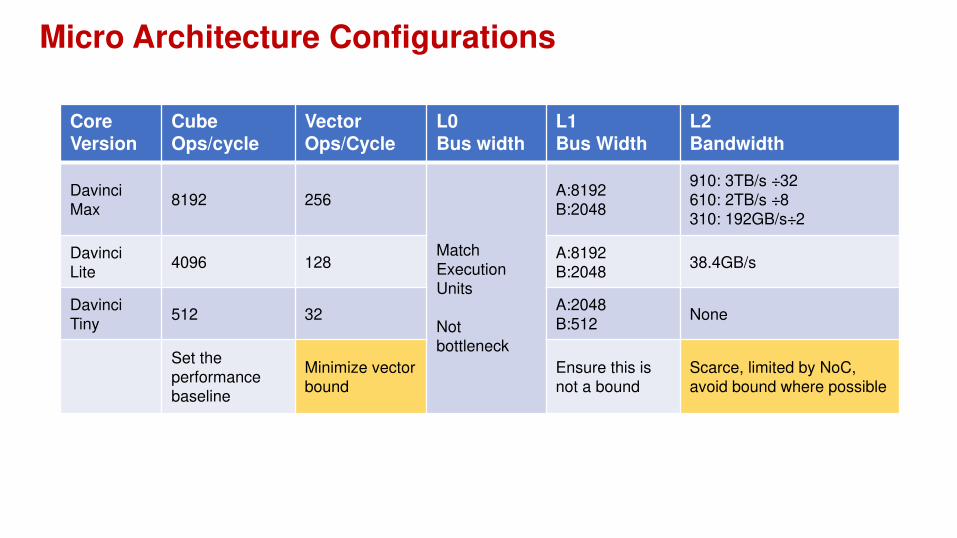
Micro Architecture Configurations
Core Version
Cube Ops/cycle
VectorOps/Cycle
L0Bus width
L1Bus Width
L2Bandwidth
Davinci
Max8192 256
Match
Execution
Units
Not
bottleneck
A:8192
B:2048
910: 3TB/s ÷32
610: 2TB/s ÷8
310: 192GB/s÷2
Davinci
Lite4096 128
A:8192
B:204838.4GB/s
Davinci
Tiny512 32
A:2048
B:512None
Set the
performance
baseline
Minimize vector
bound
Ensure this is
not a bound
Scarce, limited by NoC,
avoid bound where possible
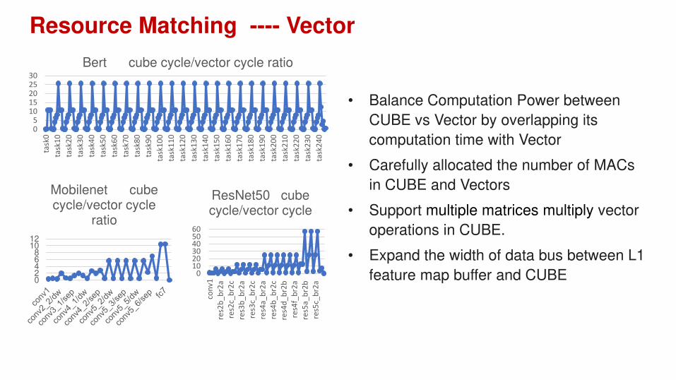
Resource Matching ---- Vector
05
1015202530
task
0
task
10
task
20
task
30
task
40
task
50
task
60
task
70
task
80
task
90
task
10
0
task
11
0
task
12
0
task
13
0
task
14
0
task
15
0
task
16
0
task
17
0
task
18
0
task
19
0
task
20
0
task
21
0
task
22
0
task
23
0
task
24
0
Bert cube cycle/vector cycle ratio
02468
1012
Mobilenet cube cycle/vector cycle
ratio
0102030405060
con
v1
res2
b_
br2
a
res2
c_b
r2c
res3
b_
br2
a
res3
c_b
r2c
res4
a_
br2
a
res4
b_
br2
c
res4
d_
br2
b
res4
f_b
r2a
res5
a_
br2
b
res5
c_b
r2a
ResNet50 cube cycle/vector cycle
• Balance Computation Power between
CUBE vs Vector by overlapping its
computation time with Vector
• Carefully allocated the number of MACs
in CUBE and Vectors
• Support multiple matrices multiply vector
operations in CUBE.
• Expand the width of data bus between L1
feature map buffer and CUBE

Resource Matching ---- Memory Hierarchy
Davinci carefully balance the memory hierarchy
design to avoid bandwidth become bottleneck at key
locations.
Examples:
• Reduce the DDR bandwidth requirement by
reusing data within L1, L0A, L0B.
• Asymmetric bandwidth provided according to the
nature of computation
• L1 -> L0A bandwidth >> L1->L0B bandwidth,
because W*H could be much bigger than
output channel number

More Challenges of DaVinci
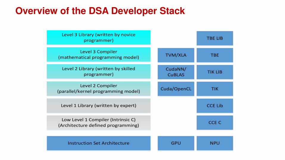
Overview of the DSA Developer Stack
Instruction Set Architecture
Low Level 1 Compiler (Intrinsic C)
(Architecture defined programming)
Level 1 Library (written by expert)
Level 2 Compiler
(parallel/kernel programming model)
Level 2 Library (written by skilled
programmer)
Level 3 Compiler
(mathematical programming model)
Level 3 Library (written by novice
programmer)
GPU
Cuda/OpenCL
NPU
CCE C
CCE Lib
TIK
TIK LIB
TBE
TBE LIB
CudaNN/
CuBLAS
TVM/XLA
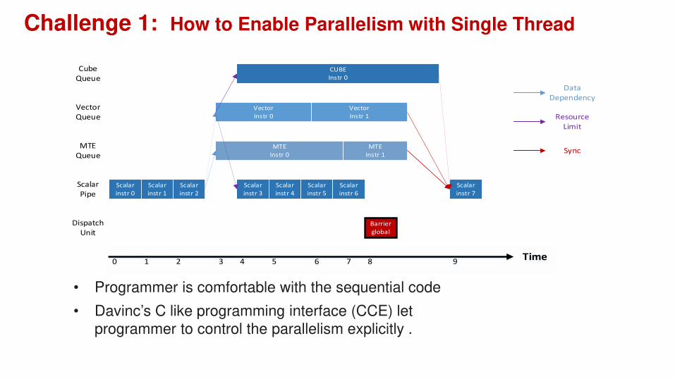
Challenge 1: How to Enable Parallelism with Single Thread
Scalar
instr 0
Scalar
instr 1
Scalar
instr 2
MTE
Instr 0
Vector
Instr 0
CUBE
Instr 0
Scalar
instr 3
Scalar
instr 7
MTE
Instr 1
Vector
Instr 1
Data
Dependency
Resource
Limit
Sync
Scalar
instr 4
Scalar
instr 5
Scalar
instr 6
Barrier
global
Time0 1 2 3 4 6 7 95 8
Dispatch
Unit
Scalar
Pipe
MTE
Queue
Vector
Queue
Cube
Queue
• Programmer is comfortable with the sequential code
• Davinc’s C like programming interface (CCE) let programmer to control the parallelism explicitly .

Solution with Multi-thread?
How about support hardware multi-thread feature?
• The code in each thread is sequential
• CUBE is a share resource between threads
• It has hardware cost

How does it work - TIK
• Typical sequential Davinci code is a combination of nested FOR loops
• Software multi-thread can be added to any FOR loop body (iterator kernel).
threads
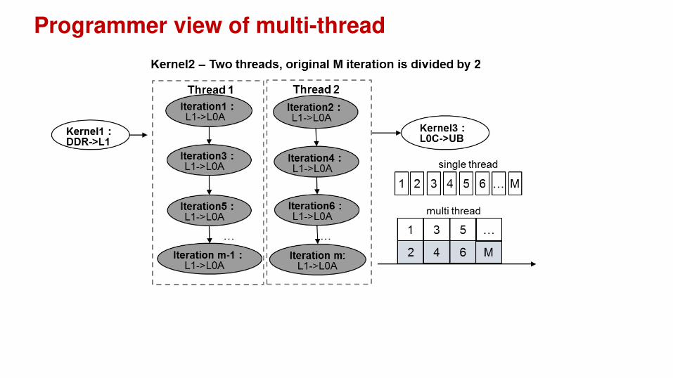
Programmer view of multi-thread
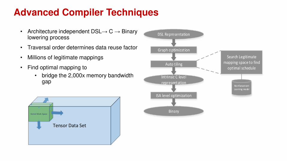
Advanced Compiler Techniques
• Architecture independent DSL→ C → Binary lowering process
• Traversal order determines data reuse factor
• Millions of legitimate mappings
• Find optimal mapping to
• bridge the 2,000x memory bandwidth gap
Kernel Work Space
Tensor Data Set
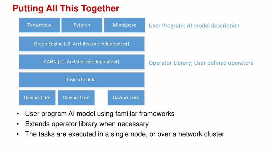
Putting All This Together
PytorchTensorflow Mindspore
Graph Engine (L2: Architecture independent)
CANN (L1: Architecture dependent)
Task scheduler
Davinci Core Davinci Core Davinci Core
User Program: AI model description
Operator Library, User defined operators
• User program AI model using familiar frameworks
• Extends operator library when necessary
• The tasks are executed in a single node, or over a network cluster
Davinci AI Core in SoCs
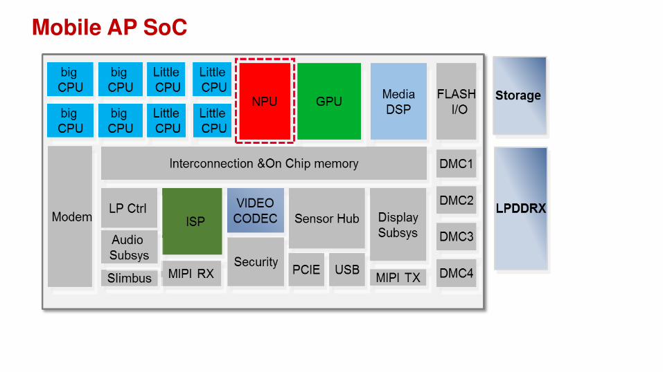
Mobile AP SoC
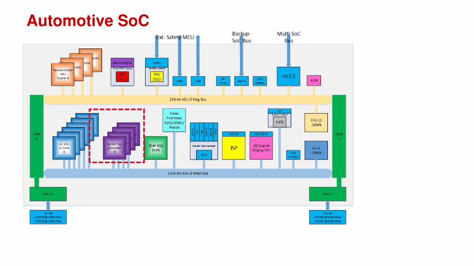
Automotive SoC
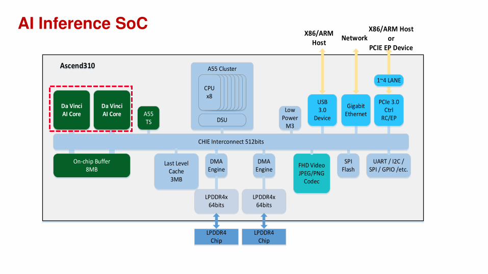
AI Inference SoC
A55 Cluster
CPUCPUCPU
DMA
Engine
SPI
Flash
UART / I2C /
SPI / GPIO /etc.
Da Vinci
AI Core
Da Vinci
AI Core
LPDDR4x
64bits
USB
3.0
Device
Gigabit
Ethernet
PCIe 3.0
Ctrl
RC/EP
X86/ARM
Host
X86/ARM Host
or
PCIE EP Device
Network
LPDDR4
Chip
On-chip Buffer
8MBFHD Video
JPEG/PNG
Codec
Ascend310
1~4 LANE
CPUCPUCPUCPUCPU
x8
DSU
DMA
Engine
LPDDR4x
64bits
LPDDR4
Chip
Low
Power
M3
CHIE Interconnect 512bits
A55
TS
Last Level
Cache
3MB
DDR4 DIMM
On-chip Buffer
32MB
HBM 2.0
DMA
Engine
Da Vinci
AI Core
Da Vinci
AI Core
HBM 2.0
DMA
Engine
HBM 2.0
DMA
Engine
HBM 2.0
DMA
Engine
DVPPDVPP
0~1
DVPP
DVPP
2~3
SubsysTS
Subsys
DDR4
L3 Cache
Taishan
Cluster
MP4
0~3
DDR4
CHIE NOC (Mesh)
Taishan
Cluster
MP4
0~3
Taishan
Cluster
MP4
0~3
Taishan
MP4
0~15
Da Vinci
AI Core
Da Vinci
AI Core
Da Vinci
AI Core
Da Vinci
AI Core
Da Vinci
AI Core
16~23Da Vinci
AI Core
Da Vinci
AI Core
Da Vinci
AI Core
Da Vinci
AI Core
Da Vinci
AI Core
Da Vinci
AI Core
Da Vinci
AI Core
24~31
Da Vinci
AI CoreDa Vinci
AI CoreDa Vinci
AI CoreDa Vinci
AI CoreDa Vinci
AI CoreDa Vinci
AI Core
Da Vinci
AI Core
0~7
Da Vinci
AI CoreDa Vinci
AI CoreDa Vinci
AI CoreDa Vinci
AI CoreDa Vinci
AI CoreDa Vinci
AI Core
Da Vinci
AI Core
8~15
DDR4 DIMM
DDR4 DIMM
DDR4 DIMM
On-chip HBM DIE On-chip HBM DIE
On-chip HBM DIE On-chip HBM DIE
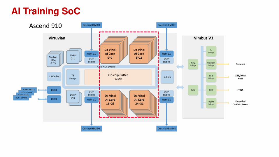
Nimbus V3
X86/ARM
Host
FPGA
Extended
Da Vinci Board
NetworkHAC
Subsys
PCIE
Subsys
Hydra
Subsys
CCIX
Network
Subsys
IO
Subsys
IMU
Virtuvian
AI Training SoC
Ascend 910
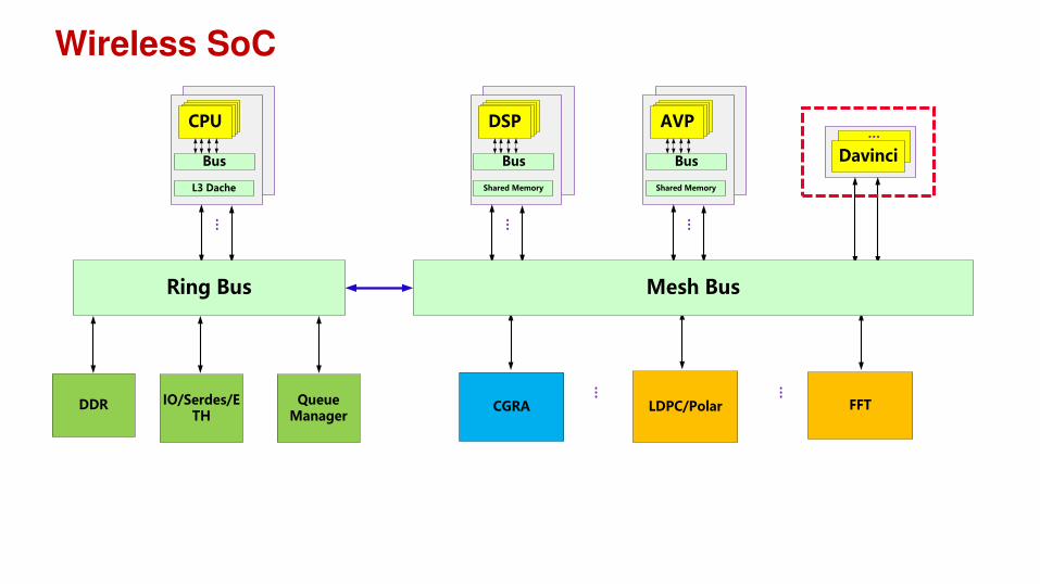
Wireless SoC
Bus
CPU
L3 Dache
DDR Queue Manager
IO/Serdes/ETH
…
Bus
DSP
Shared Memory
…
Bus
AVP
Shared Memory
…
LDPC/Polar FFTCGRA
…
Davinci
…
…
Mesh BusRing Bus

Alleviate Memory Wall and Slow down
of Moore’s Law
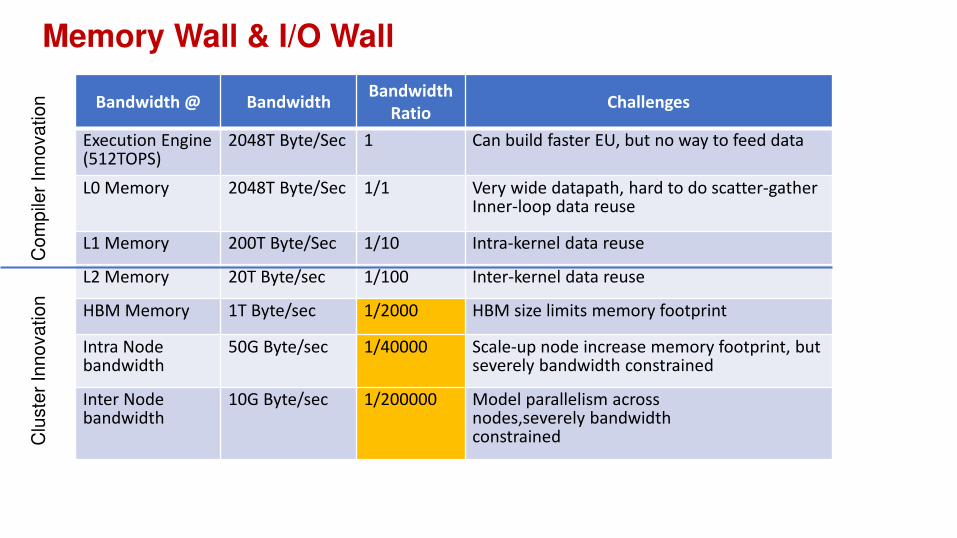
Memory Wall & I/O Wall
Bandwidth @ BandwidthBandwidth
RatioChallenges
Execution Engine (512TOPS)
2048T Byte/Sec 1 Can build faster EU, but no way to feed data
L0 Memory 2048T Byte/Sec 1/1 Very wide datapath, hard to do scatter-gatherInner-loop data reuse
L1 Memory 200T Byte/Sec 1/10 Intra-kernel data reuse
L2 Memory 20T Byte/sec 1/100 Inter-kernel data reuse
HBM Memory 1T Byte/sec 1/2000 HBM size limits memory footprint
Intra Node bandwidth
50G Byte/sec 1/40000 Scale-up node increase memory footprint, but severely bandwidth constrained
Inter Node bandwidth
10G Byte/sec 1/200000 Model parallelism across nodes,severely bandwidth constrained
Co
mp
iler
Inn
ovatio
nC
luste
r In
no
vation
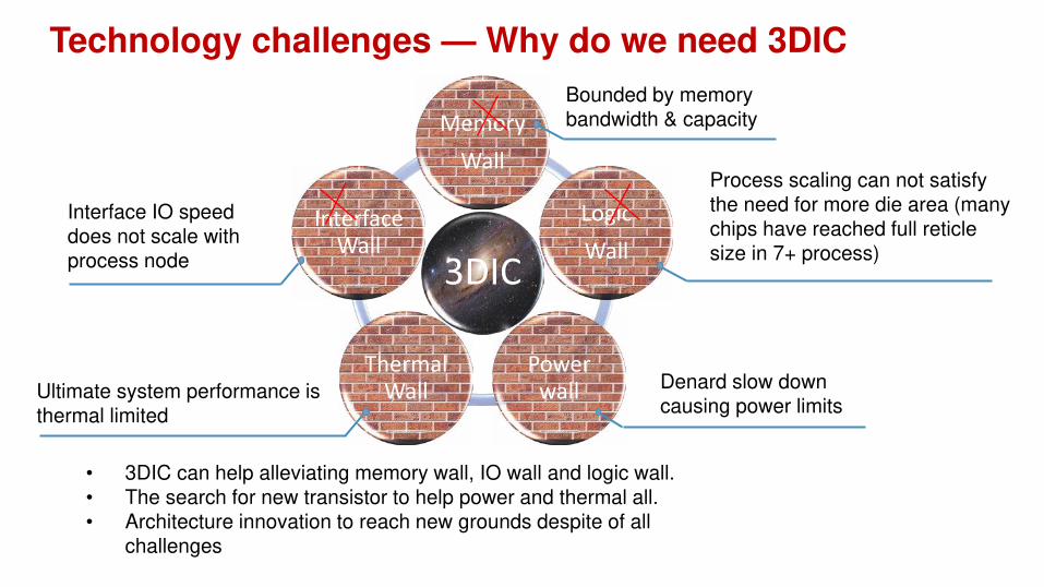
Technology challenges — Why do we need 3DIC
• 3DIC can help alleviating memory wall, IO wall and logic wall.
• The search for new transistor to help power and thermal all.
• Architecture innovation to reach new grounds despite of all
challenges
3DIC
Memory
Wall
Logic
Wall
Power wall
Thermal Wall
Interface Wall
Process scaling can not satisfy
the need for more die area (many
chips have reached full reticle
size in 7+ process)
Bounded by memory
bandwidth & capacity
Interface IO speed
does not scale with
process node
Ultimate system performance is
thermal limited
Denard slow down
causing power limits
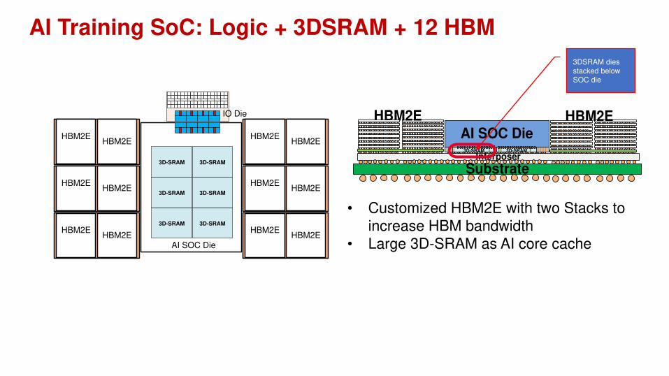
AI Training SoC: Logic + 3DSRAM + 12 HBM
HBM2EHBM2E
HBM2EHBM2E
HBM2EHBM2E
HBM2EHBM2E
HBM2EHBM2E
HBM2EHBM2E
3D-SRAM
3D-SRAM 3D-SRAM
3D-SRAM
3D-SRAM 3D-SRAM
IO Die
AI SOC Die
AI SOC Die3D-SRAM 3D-SRAM
Interposer
Substrate
HBM2E HBM2E
• Customized HBM2E with two Stacks to increase HBM bandwidth
• Large 3D-SRAM as AI core cache
3DSRAM dies
stacked below
SOC die
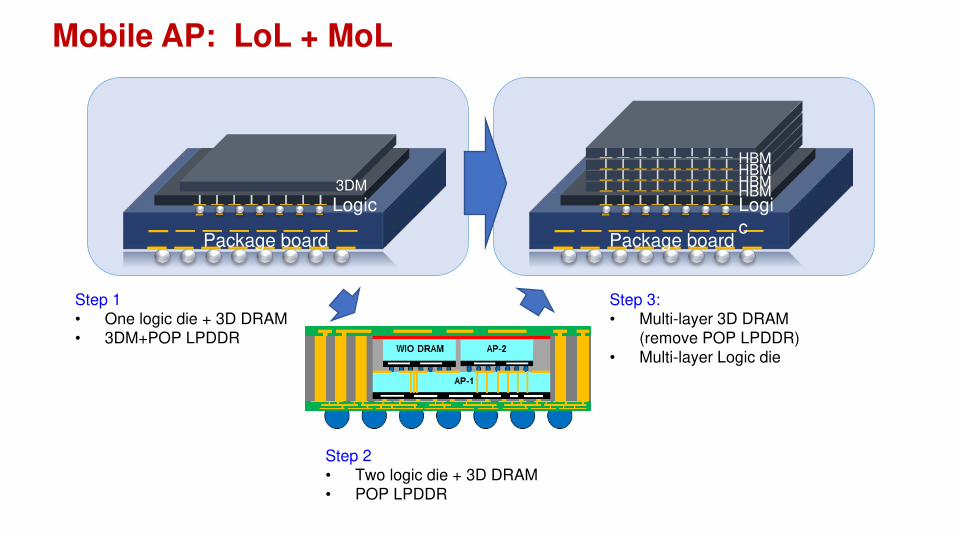
Mobile AP: LoL + MoL
HBMHBMHBMHBMLogi
cPackage board
3DM
Logic
Package board
Step 1
• One logic die + 3D DRAM
• 3DM+POP LPDDR
Step 3:
• Multi-layer 3D DRAM
(remove POP LPDDR)
• Multi-layer Logic die
Step 2
• Two logic die + 3D DRAM
• POP LPDDR

Physical Design of Davinci AI Chips
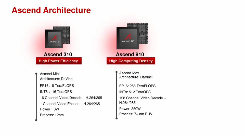
Ascend 910Ascend 310High Computing DensityHigh Power Efficiency
Ascend-Mini
FP16:8 TeraFLOPS
INT8 :16 TeraOPS
16 Channel Video Decode – H.264/265
1 Channel Video Encode – H.264/265
Architecture: DaVinci
Power:8W
Process: 12nm
Ascend-Max
FP16: 256 TeraFLOPS
INT8: 512 TeraOPS
128 Channel Video Decode –
H.264/265
Architecture: DaVinci
Process: 7+ nm EUV
Power: 350W
Ascend Architecture
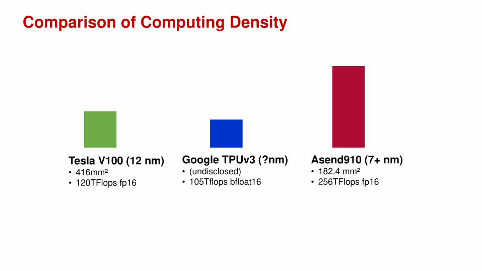
Comparison of Computing Density
Tesla V100 (12 nm)• 416mm²• 120TFlops fp16
Asend910 (7+ nm)• 182.4 mm²• 256TFlops fp16
Google TPUv3 (?nm)• (undisclosed)• 105Tflops bfloat16
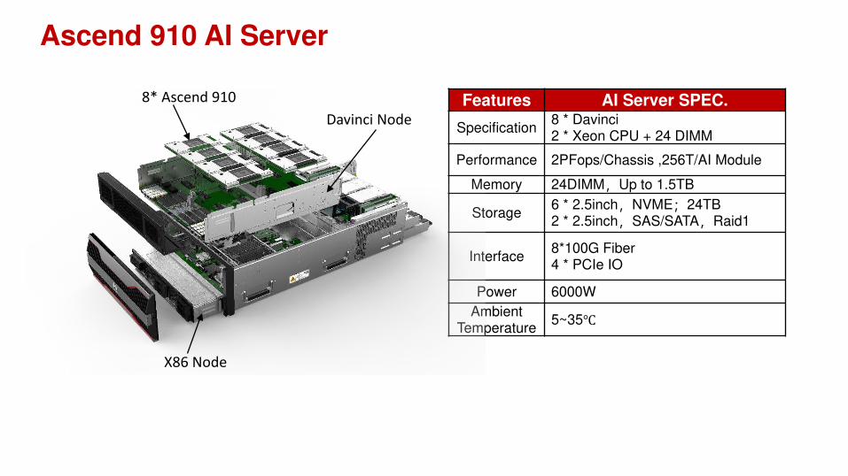
Ascend 910 AI Server
Features AI Server SPEC.
Specification8 * Davinci2 * Xeon CPU + 24 DIMM
Performance 2PFops/Chassis ,256T/AI Module
Memory 24DIMM,Up to 1.5TB
Storage6 * 2.5inch,NVME;24TB2 * 2.5inch,SAS/SATA,Raid1
Interface8*100G Fiber4 * PCIe IO
Power 6000W
Ambient Temperature
5~35℃X86 Node
8* Ascend 910
Davinci Node
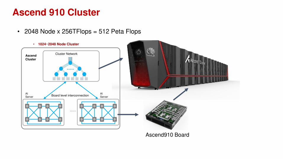
Ascend 910 Cluster
• 2048 Node x 256TFlops = 512 Peta Flops
……
Ascend Cluster
D
D D
DD
DD
D
AIServer
D
D D
DD
DD
D
AIServer
• 1024~2048 Node Cluster
Cluster Network
Board level interconnection
Ascend910 Board
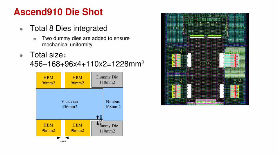
Ascend910 Die Shot
Total 8 Dies integrated Two dummy dies are added to ensure
mechanical uniformity
Total size:456+168+96x4+110x2=1228mm2
Vitruvian
456mm2
Nimbus
168mm2
Dummy Die
110mm2
2mm
HBM
96mm2
HBM
96mm2
HBM
96mm2
HBM
96mm2
Dummy Die
110mm2
0.7
2m
m
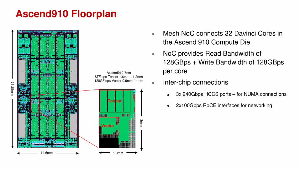
Ascend910 Floorplan
Mesh NoC connects 32 Davinci Cores in
the Ascend 910 Compute Die
NoC provides Read Bandwidth of
128GBps + Write Bandwidth of 128GBps
per core
Inter-chip connections
3x 240Gbps HCCS ports – for NUMA connections
2x100Gbps RoCE interfaces for networking
31.2
5m
m
14.6mm 1.9mm
3m
m
Tensor
Vector
Ascend910 7nm
8TFlops Tensor 1.6mm * 1.2mm
128GFlops Vector 0.9mm * 1mm

Ascend910 NoC
1024bits 2GHz NoC Mesh
Topology : 6 Rows x 4 Columns
Access Bandwidth to on-chip L2
Cache: 4 TByte/s
Access Bandwidth to offchip
HBM: 1.2 TByte/s
NoC bandwidth fairly shared
among the Davinci Cores
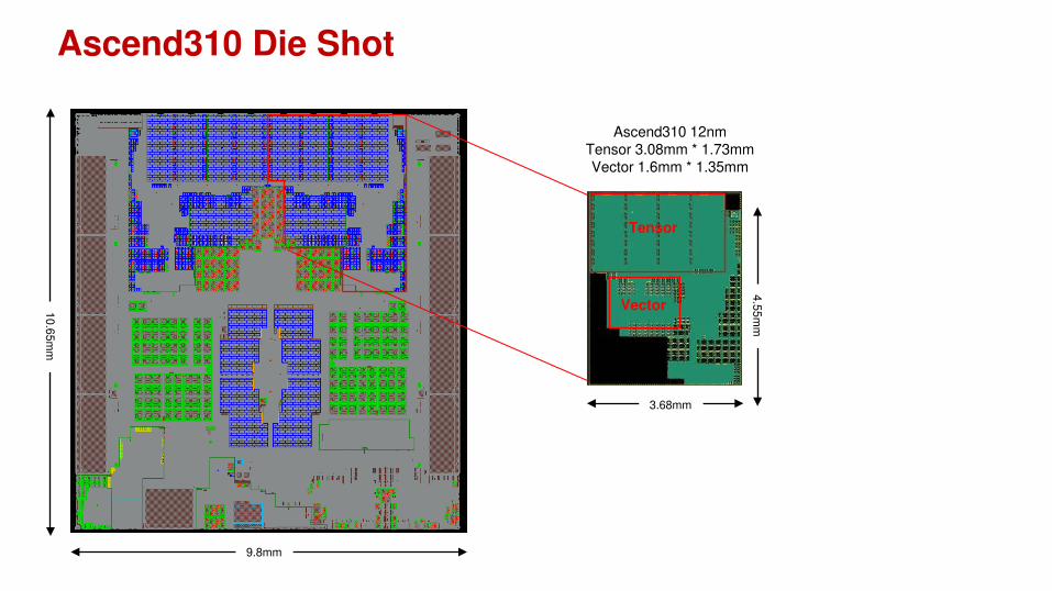
3.68mm
4.5
5m
m
Ascend310 Die Shot
10.6
5m
m
9.8mm
Tensor
Vector
Ascend310 12nmTensor 3.08mm * 1.73mmVector 1.6mm * 1.35mm

Ascend310
Ascend910
Kunpeng920
Kunpeng Vs Ascend
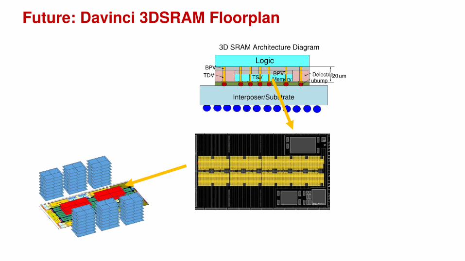
Future: Davinci 3DSRAM Floorplan
3D SRAM Architecture Diagram
Logic
Memory
Interposer/Substrate
BPV
TDV TSVBPV Delectric
ubump~ 20 um

More Challenges…
• Generalized Auto ML
• Efficiency for Re-enforcement Learning, GNN?
• Generalized method for Data/Model/Pipeline parallelism
• How to unify data precision?
• Finding the sweet spot architecture
Big chip vs Small chip
Dense vs Sparse
Out of memory, near memory, in memory

Copyright©2018 Huawei Technologies Co., Ltd.
All Rights Reserved.
The information in this document may contain predictive statements including, without limitation, statements regarding
the future financial and operating results, future product portfolio, new technology, etc. There are a number of factors that could cause actual results and developments to differ materially
from those expressed or implied in the predictive statements. Therefore, such information is provided for reference purpose only and constitutes neither an offer nor an acceptance. Huawei
may change the information at any time without notice.
Huawei Confidential
把数字世界带入每个人、每个家庭、每个组织,构建万物互联的智能世界。Bring digital to every person, home and organization for a fully connected, intelligent world.
Thank you.